Silicon-photonic clos networks for global on-chip communication
11
Silicon-photonic clos networks for global on-chip communication Citation Joshi, A. et al. “Silicon-photonic clos networks for global on-chip communication.” Networks-on-Chip, 2009. NoCS 2009. 3rd ACM/IEEE International Symposium on. 2009. 124-133. © 2009 IEEE As Published http://dx.doi.org/10.1109/NOCS.2009.5071460 Publisher Institute of Electrical and Electronics Engineers Version Final published version Accessed Sat May 21 21:28:59 EDT 2011 Citable Link http://hdl.handle.net/1721.1/54685 Terms of Use Article is made available in accordance with the publisher's policy and may be subject to US copyright law. Please refer to the publisher's site for terms of use. Detailed Terms
-
Upload
independent -
Category
Documents
-
view
2 -
download
0
Transcript of Silicon-photonic clos networks for global on-chip communication
Silicon-photonic clos networks for global on-chipcommunication
Citation Joshi, A. et al. “Silicon-photonic clos networks for global on-chipcommunication.” Networks-on-Chip, 2009. NoCS 2009. 3rdACM/IEEE International Symposium on. 2009. 124-133. © 2009IEEE
As Published http://dx.doi.org/10.1109/NOCS.2009.5071460
Publisher Institute of Electrical and Electronics Engineers
Version Final published version
Accessed Sat May 21 21:28:59 EDT 2011
Citable Link http://hdl.handle.net/1721.1/54685
Terms of Use Article is made available in accordance with the publisher's policyand may be subject to US copyright law. Please refer to thepublisher's site for terms of use.
Detailed Terms
Silicon-Photonic Clos Networks for Global On-Chip Communication
Ajay Joshi*, Christopher Batten*, Yong-Jin Kwon†, Scott Beamer†, Imran Shamim*
Krste Asanovic†, Vladimir Stojanovic*
* Department of EECS, Massachusetts Institute of Technology, Cambridge, MA† Department of EECS, University of California, Berkeley, CA
Abstract
Future manycore processors will require energy-efficient, high-throughput on-chip networks. Silicon-photonics is a promising new interconnect technologywhich offers lower power, higher bandwidth density, andshorter latencies than electrical interconnects. In thispaper we explore using photonics to implement low-diameter non-blocking crossbar and Clos networks. Weuse analytical modeling to show that a 64-tile photonicClos network consumes significantly less optical power,thermal tuning power, and area compared to global pho-tonic crossbars over a range of photonic device param-eters. Compared to various electrical on-chip networks,our simulation results indicate that a photonic Clos net-work can provide more uniform latency and throughputacross a range of traffic patterns while consuming lesspower. These properties will help simplify parallel pro-gramming by allowing the programmer to ignore networktopology during optimization.
1. Introduction
Today’s graphics, network, embedded and server pro-cessors already contain many processor cores on one chipand this number is expected to increase with future scal-ing. The on-chip communication network is becoming acritical component, affecting not only performance andpower consumption, but also programmer productivity.From a software perspective, an ideal network would haveuniformly low latency and uniformly high bandwidth.The electrical on-chip networks used in today’s multicoresystems (e.g., crossbars [8], meshes [3], and rings [11])will either be difficult to scale to higher core counts withreasonable power and area overheads or introduce signif-icant bandwidth and latency non-uniformities. In this pa-per we explore the use of silicon-photonic technology tobuild on-chip networks that scale well, and provide uni-formly low latency and uniformly high bandwidth.
Various photonic materials and integration approacheshave been proposed to enable efficient global on-chipcommunication, and several network architectures (e.g.,crossbars [7, 15] and meshes [13]) have been developedbottom-up using fixed device technology parameters as
drivers. In this paper, we take a top-down approach bydriving the photonic device requirements based on theprojected network and system needs. This allows quickdesign-space exploration at the network level, and pro-vides insight into which network topologies can best har-ness the advantages of photonics at different stages of thetechnology roadmap.
This paper begins by identifying our target system andbriefly reviewing the electrical on-chip networks whichwill serve as a baseline for our photonic network pro-posals. We then use analytical models to investigate thetradeoffs between various implementations of global pho-tonic crossbars found in the literature and our own imple-mentations of photonic Clos networks. We also use sim-ulations to compare the photonic Clos network to elec-trical mesh and Clos networks. Our results show thatphotonic Clos networks consume significantly less opticallaser power, thermal tuning power, and area as comparedto photonic crossbar networks, and offer better energy-efficiency than electrical networks while providing moreuniform performance across various traffic patterns.
2. Target System
Silicon-photonic technology for on-chip communica-tion is still in its formative stages, but with recent technol-ogy advances we project that photonics might be viable inthe late 2010’s. This makes the 22 nm node a reasonabletarget process technology for our work. By then it willbe possible to integrate hundreds of cores onto a singledie. To simplify design and verification complexity, thesecores and/or memory will most likely be clustered intotiles which are then replicated across the chip and inter-connected with a well-structured on-chip network. Theexact nature of the tiles and the inter-tile communicationparadigm are still active areas of research. The tiles mightbe homogeneous with each tile including both some num-ber of cores and a slice of the on-chip memory, or thetiles might be heterogeneous with a mix of compute andmemory tiles. The global on-chip network might be usedto implement shared memory, message passing, or both.Regardless of their exact configuration, however, all fu-ture systems will require some form of on-chip networkwhich provides low-latency and high-throughput commu-
978-1-4244-4143-3/09/$25.00 ©2009 IEEE
Authorized licensed use limited to: MIT Libraries. Downloaded on April 21,2010 at 14:33:32 UTC from IEEE Xplore. Restrictions apply.
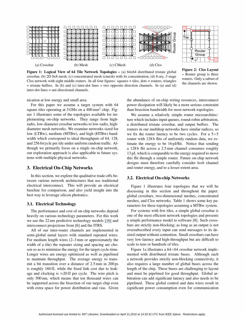
(a) Crossbar (b) Mesh (c) CMesh (d) Clos
Figure 1: Logical View of 64 Tile Network Topologies – (a) 64x64 distributed tristate globalcrossbar, (b) 2D 8x8 mesh, (c) concentrated mesh (cmesh) with 4x concentration, (d) 8-ary, 3-stageClos network with eight middle routers. In all four figures: squares = tiles, dots = routers, triangles= tristate buffers. In (b) and (c) inter-dot lines = two opposite direction channels. In (a) and (d)inter-dot lines = uni-directional channels.
Figure 2: Clos Layout– Router group is threerouters. Only a subset ofthe channels are shown.
nication at low energy and small area.For this paper we assume a target system with 64
square tiles operating at 5 GHz on a 400 mm2 chip. Fig-ure 1 illustrates some of the topologies available for im-plementing on-chip networks. They range from high-radix, low-diameter crossbar networks to low-radix, high-diameter mesh networks. We examine networks sized forlow (LTBw), medium (MTBw), and high (HTBw) band-width which correspond to ideal throughputs of 64, 128,and 256 b/cycle per tile under uniform random traffic. Al-though we primarily focus on a single on-chip network,our exploration approach is also applicable to future sys-tems with multiple physical networks.
3. Electrical On-Chip NetworksIn this section, we explore the qualitative trade-offs be-
tween various network architectures that use traditionalelectrical interconnect. This will provide an electricalbaseline for comparison, and also yield insight into thebest way to leverage silicon photonics.
3.1. Electrical TechnologyThe performance and cost of on-chip networks depend
heavily on various technology parameters. For this workwe use the 22 nm predictive technology models [16] andinterconnect projections from [6] and the ITRS.
All of our inter-router channels are implemented insemi-global metal layers with standard repeated wires.For medium length wires (2–3 mm or approximately thewidth of a tile) the repeater sizing and spacing are cho-sen so as to minimize the energy for the target cycle-time.Longer wires are energy optimized as well as pipelinedto maintain throughput. The average energy to trans-mit a bit transition over a distance of 2.5 mm in 200 psis roughly 160 fJ, while the fixed link cost due to leak-age and clocking is ≈20 fJ per cycle. The wire pitch isonly 500 nm, which means that ten thousand wires canbe supported across the bisection of our target chip evenwith extra space for power distribution and vias. Given
the abundance of on-chip wiring resources, interconnectpower dissipation will likely be a more serious constraintthan bisection bandwidth for most network topologies.
We assume a relatively simple router microarchitec-ture which includes input queues, round-robin arbitration,a distributed tristate crossbar, and output buffers. Therouters in our multihop networks have similar radices, sowe fix the router latency to be two cycles. For a 5×5router with 128 b flits of uniformly random data, we es-timate the energy to be 16 pJ/flit. Notice that sendinga 128 b flit across a 2.5 mm channel consumes roughly13 pJ, which is comparable to the energy required to movethis flit through a simple router. Future on-chip networkdesigns must therefore carefully consider both channeland router energy, and to a lesser extent area.
3.2. Electrical On-chip Networks
Figure 1 illustrates four topologies that we will bediscussing in this section and throughout the paper:global crossbars, two-dimensional meshes, concentratedmeshes, and Clos networks. Table 1 shows some key pa-rameters for these topologies assuming a MTBw system.
For systems with few tiles, a simple global crossbar isone of the most efficient network topologies and presentsa simple performance model to software [8]. Such cross-bars are strictly non-blocking; as long as an output is notoversubscribed every input can send messages to its de-sired output without contention. Small crossbars can havevery low-latency and high-throughput but are difficult toscale to tens or hundreds of tiles.
Figure 1a illustrates a 64×64 crossbar network imple-mented with distributed tristate buses. Although sucha network provides strictly non-blocking connectivity, italso requires a large number of global buses across thelength of the chip. These buses are challenging to layoutand must be pipelined for good throughput. Global ar-bitration can add significant latency and also needs to bepipelined. These global control and data wires result insignificant power consumption even for communication
Authorized licensed use limited to: MIT Libraries. Downloaded on April 21,2010 at 14:33:32 UTC from IEEE Xplore. Restrictions apply.
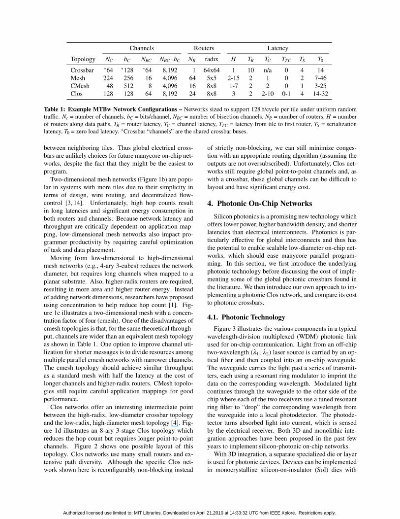
Channels Routers Latency
Topology NC bC NBC NBC ·bC NR radix H TR TC TTC TS T0
Crossbar ∗64 ∗128 ∗64 8,192 1 64x64 1 10 n/a 0 4 14Mesh 224 256 16 4,096 64 5x5 2-15 2 1 0 2 7-46CMesh 48 512 8 4,096 16 8x8 1-7 2 2 0 1 3-25Clos 128 128 64 8,192 24 8x8 3 2 2-10 0-1 4 14-32
Table 1: Example MTBw Network Configurations – Networks sized to support 128 b/cycle per tile under uniform randomtraffic. Nc = number of channels, bC = bits/channel, NBC = number of bisection channels, NR = number of routers, H = numberof routers along data paths, TR = router latency, TC = channel latency, TTC = latency from tile to first router, TS = serializationlatency, T0 = zero load latency. ∗Crossbar “channels” are the shared crossbar buses.
between neighboring tiles. Thus global electrical cross-bars are unlikely choices for future manycore on-chip net-works, despite the fact that they might be the easiest toprogram.
Two-dimensional mesh networks (Figure 1b) are popu-lar in systems with more tiles due to their simplicity interms of design, wire routing, and decentralized flow-control [3, 14]. Unfortunately, high hop counts resultin long latencies and significant energy consumption inboth routers and channels. Because network latency andthroughput are critically dependent on application map-ping, low-dimensional mesh networks also impact pro-grammer productivity by requiring careful optimizationof task and data placement.
Moving from low-dimensional to high-dimensionalmesh networks (e.g., 4-ary 3-cubes) reduces the networkdiameter, but requires long channels when mapped to aplanar substrate. Also, higher-radix routers are required,resulting in more area and higher router energy. Insteadof adding network dimensions, researchers have proposedusing concentration to help reduce hop count [1]. Fig-ure 1c illustrates a two-dimensional mesh with a concen-tration factor of four (cmesh). One of the disadvantages ofcmesh topologies is that, for the same theoretical through-put, channels are wider than an equivalent mesh topologyas shown in Table 1. One option to improve channel uti-lization for shorter messages is to divide resources amongmultiple parallel cmesh networks with narrower channels.The cmesh topology should achieve similar throughputas a standard mesh with half the latency at the cost oflonger channels and higher-radix routers. CMesh topolo-gies still require careful application mappings for goodperformance.
Clos networks offer an interesting intermediate pointbetween the high-radix, low-diameter crossbar topologyand the low-radix, high-diameter mesh topology [4]. Fig-ure 1d illustrates an 8-ary 3-stage Clos topology whichreduces the hop count but requires longer point-to-pointchannels. Figure 2 shows one possible layout of thistopology. Clos networks use many small routers and ex-tensive path diversity. Although the specific Clos net-work shown here is reconfigurably non-blocking instead
of strictly non-blocking, we can still minimize conges-tion with an appropriate routing algorithm (assuming theoutputs are not oversubscribed). Unfortunately, Clos net-works still require global point-to-point channels and, aswith a crossbar, these global channels can be difficult tolayout and have significant energy cost.
4. Photonic On-Chip NetworksSilicon photonics is a promising new technology which
offers lower power, higher bandwidth density, and shorterlatencies than electrical interconnects. Photonics is par-ticularly effective for global interconnects and thus hasthe potential to enable scalable low-diameter on-chip net-works, which should ease manycore parallel program-ming. In this section, we first introduce the underlyingphotonic technology before discussing the cost of imple-menting some of the global photonic crossbars found inthe literature. We then introduce our own approach to im-plementing a photonic Clos network, and compare its costto photonic crossbars.
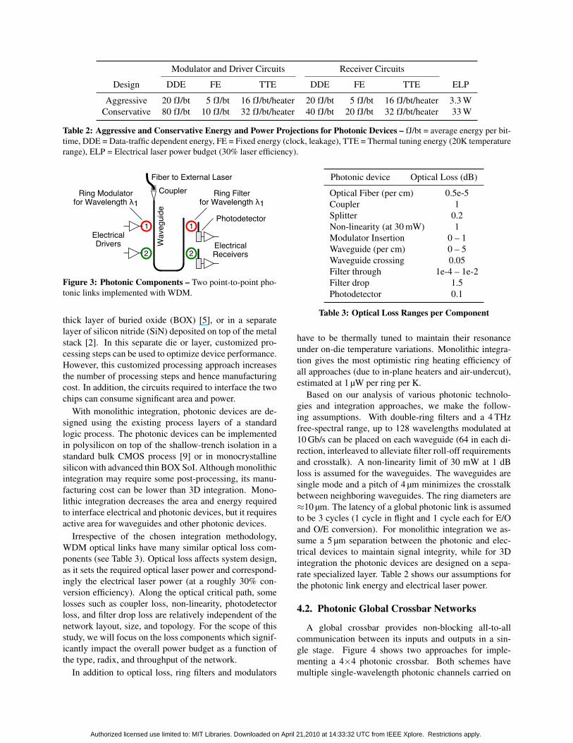
4.1. Photonic TechnologyFigure 3 illustrates the various components in a typical
wavelength-division multiplexed (WDM) photonic linkused for on-chip communication. Light from an off-chiptwo-wavelength (λ1, λ2) laser source is carried by an op-tical fiber and then coupled into an on-chip waveguide.The waveguide carries the light past a series of transmit-ters, each using a resonant ring modulator to imprint thedata on the corresponding wavelength. Modulated lightcontinues through the waveguide to the other side of thechip where each of the two receivers use a tuned resonantring filter to “drop” the corresponding wavelength fromthe waveguide into a local photodetector. The photode-tector turns absorbed light into current, which is sensedby the electrical receiver. Both 3D and monolithic inte-gration approaches have been proposed in the past fewyears to implement silicon-photonic on-chip networks.
With 3D integration, a separate specialized die or layeris used for photonic devices. Devices can be implementedin monocrystalline silicon-on-insulator (SoI) dies with
Authorized licensed use limited to: MIT Libraries. Downloaded on April 21,2010 at 14:33:32 UTC from IEEE Xplore. Restrictions apply.
Modulator and Driver Circuits Receiver Circuits
Design DDE FE TTE DDE FE TTE ELP
Aggressive 20 fJ/bt 5 fJ/bt 16 fJ/bt/heater 20 fJ/bt 5 fJ/bt 16 fJ/bt/heater 3.3 WConservative 80 fJ/bt 10 fJ/bt 32 fJ/bt/heater 40 fJ/bt 20 fJ/bt 32 fJ/bt/heater 33 W
Table 2: Aggressive and Conservative Energy and Power Projections for Photonic Devices – fJ/bt = average energy per bit-time, DDE = Data-traffic dependent energy, FE = Fixed energy (clock, leakage), TTE = Thermal tuning energy (20K temperaturerange), ELP = Electrical laser power budget (30% laser efficiency).
Figure 3: Photonic Components – Two point-to-point pho-tonic links implemented with WDM.
thick layer of buried oxide (BOX) [5], or in a separatelayer of silicon nitride (SiN) deposited on top of the metalstack [2]. In this separate die or layer, customized pro-cessing steps can be used to optimize device performance.However, this customized processing approach increasesthe number of processing steps and hence manufacturingcost. In addition, the circuits required to interface the twochips can consume significant area and power.
With monolithic integration, photonic devices are de-signed using the existing process layers of a standardlogic process. The photonic devices can be implementedin polysilicon on top of the shallow-trench isolation in astandard bulk CMOS process [9] or in monocrystallinesilicon with advanced thin BOX SoI. Although monolithicintegration may require some post-processing, its manu-facturing cost can be lower than 3D integration. Mono-lithic integration decreases the area and energy requiredto interface electrical and photonic devices, but it requiresactive area for waveguides and other photonic devices.
Irrespective of the chosen integration methodology,WDM optical links have many similar optical loss com-ponents (see Table 3). Optical loss affects system design,as it sets the required optical laser power and correspond-ingly the electrical laser power (at a roughly 30% con-version efficiency). Along the optical critical path, somelosses such as coupler loss, non-linearity, photodetectorloss, and filter drop loss are relatively independent of thenetwork layout, size, and topology. For the scope of thisstudy, we will focus on the loss components which signif-icantly impact the overall power budget as a function ofthe type, radix, and throughput of the network.
In addition to optical loss, ring filters and modulators
Photonic device Optical Loss (dB)
Optical Fiber (per cm) 0.5e-5Coupler 1Splitter 0.2Non-linearity (at 30 mW) 1Modulator Insertion 0 – 1Waveguide (per cm) 0 – 5Waveguide crossing 0.05Filter through 1e-4 – 1e-2Filter drop 1.5Photodetector 0.1
Table 3: Optical Loss Ranges per Component
have to be thermally tuned to maintain their resonanceunder on-die temperature variations. Monolithic integra-tion gives the most optimistic ring heating efficiency ofall approaches (due to in-plane heaters and air-undercut),estimated at 1 µW per ring per K.
Based on our analysis of various photonic technolo-gies and integration approaches, we make the follow-ing assumptions. With double-ring filters and a 4 THzfree-spectral range, up to 128 wavelengths modulated at10 Gb/s can be placed on each waveguide (64 in each di-rection, interleaved to alleviate filter roll-off requirementsand crosstalk). A non-linearity limit of 30 mW at 1 dBloss is assumed for the waveguides. The waveguides aresingle mode and a pitch of 4 µm minimizes the crosstalkbetween neighboring waveguides. The ring diameters are≈10 µm. The latency of a global photonic link is assumedto be 3 cycles (1 cycle in flight and 1 cycle each for E/Oand O/E conversion). For monolithic integration we as-sume a 5 µm separation between the photonic and elec-trical devices to maintain signal integrity, while for 3Dintegration the photonic devices are designed on a sepa-rate specialized layer. Table 2 shows our assumptions forthe photonic link energy and electrical laser power.
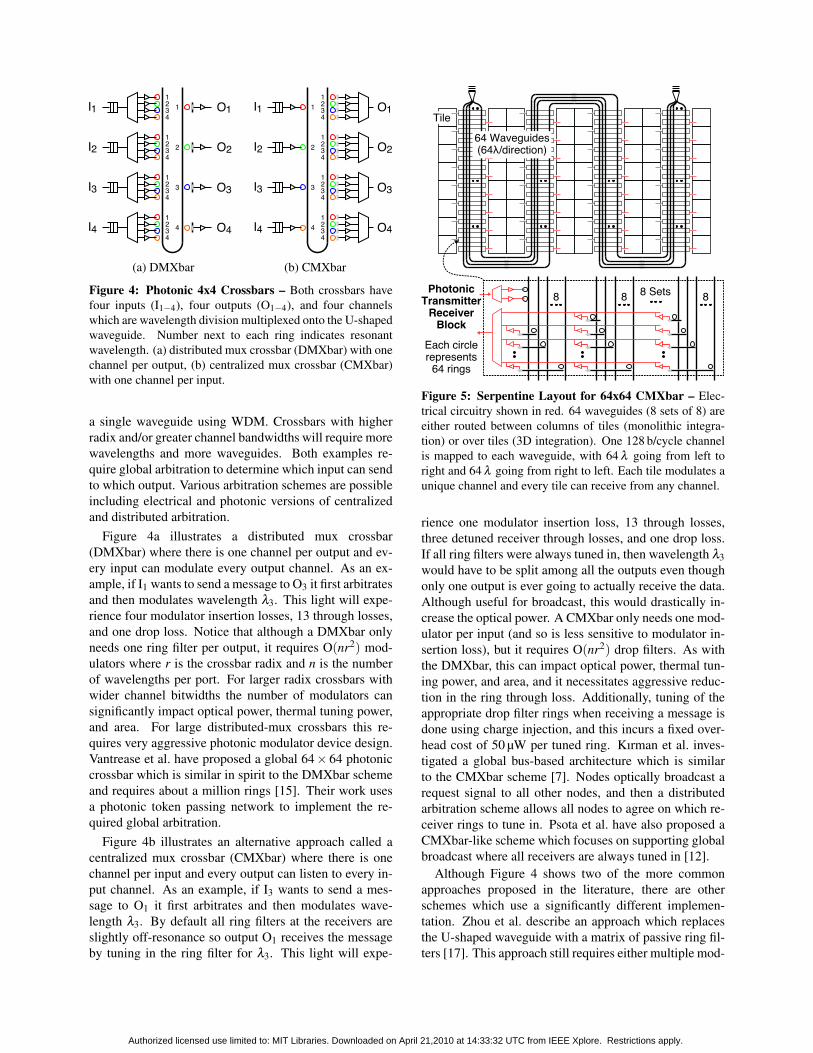
4.2. Photonic Global Crossbar Networks
A global crossbar provides non-blocking all-to-allcommunication between its inputs and outputs in a sin-gle stage. Figure 4 shows two approaches for imple-menting a 4×4 photonic crossbar. Both schemes havemultiple single-wavelength photonic channels carried on
Authorized licensed use limited to: MIT Libraries. Downloaded on April 21,2010 at 14:33:32 UTC from IEEE Xplore. Restrictions apply.
(a) DMXbar (b) CMXbar
Figure 4: Photonic 4x4 Crossbars – Both crossbars havefour inputs (I1−4), four outputs (O1−4), and four channelswhich are wavelength division multiplexed onto the U-shapedwaveguide. Number next to each ring indicates resonantwavelength. (a) distributed mux crossbar (DMXbar) with onechannel per output, (b) centralized mux crossbar (CMXbar)with one channel per input.
a single waveguide using WDM. Crossbars with higherradix and/or greater channel bandwidths will require morewavelengths and more waveguides. Both examples re-quire global arbitration to determine which input can sendto which output. Various arbitration schemes are possibleincluding electrical and photonic versions of centralizedand distributed arbitration.
Figure 4a illustrates a distributed mux crossbar(DMXbar) where there is one channel per output and ev-ery input can modulate every output channel. As an ex-ample, if I1 wants to send a message to O3 it first arbitratesand then modulates wavelength λ3. This light will expe-rience four modulator insertion losses, 13 through losses,and one drop loss. Notice that although a DMXbar onlyneeds one ring filter per output, it requires O(nr2) mod-ulators where r is the crossbar radix and n is the numberof wavelengths per port. For larger radix crossbars withwider channel bitwidths the number of modulators cansignificantly impact optical power, thermal tuning power,and area. For large distributed-mux crossbars this re-quires very aggressive photonic modulator device design.Vantrease et al. have proposed a global 64× 64 photoniccrossbar which is similar in spirit to the DMXbar schemeand requires about a million rings [15]. Their work usesa photonic token passing network to implement the re-quired global arbitration.
Figure 4b illustrates an alternative approach called acentralized mux crossbar (CMXbar) where there is onechannel per input and every output can listen to every in-put channel. As an example, if I3 wants to send a mes-sage to O1 it first arbitrates and then modulates wave-length λ3. By default all ring filters at the receivers areslightly off-resonance so output O1 receives the messageby tuning in the ring filter for λ3. This light will expe-
Figure 5: Serpentine Layout for 64x64 CMXbar – Elec-trical circuitry shown in red. 64 waveguides (8 sets of 8) areeither routed between columns of tiles (monolithic integra-tion) or over tiles (3D integration). One 128 b/cycle channelis mapped to each waveguide, with 64 λ going from left toright and 64 λ going from right to left. Each tile modulates aunique channel and every tile can receive from any channel.
rience one modulator insertion loss, 13 through losses,three detuned receiver through losses, and one drop loss.If all ring filters were always tuned in, then wavelength λ3would have to be split among all the outputs even thoughonly one output is ever going to actually receive the data.Although useful for broadcast, this would drastically in-crease the optical power. A CMXbar only needs one mod-ulator per input (and so is less sensitive to modulator in-sertion loss), but it requires O(nr2) drop filters. As withthe DMXbar, this can impact optical power, thermal tun-ing power, and area, and it necessitates aggressive reduc-tion in the ring through loss. Additionally, tuning of theappropriate drop filter rings when receiving a message isdone using charge injection, and this incurs a fixed over-head cost of 50 µW per tuned ring. Kırman et al. inves-tigated a global bus-based architecture which is similarto the CMXbar scheme [7]. Nodes optically broadcast arequest signal to all other nodes, and then a distributedarbitration scheme allows all nodes to agree on which re-ceiver rings to tune in. Psota et al. have also proposed aCMXbar-like scheme which focuses on supporting globalbroadcast where all receivers are always tuned in [12].
Although Figure 4 shows two of the more commonapproaches proposed in the literature, there are otherschemes which use a significantly different implemen-tation. Zhou et al. describe an approach which replacesthe U-shaped waveguide with a matrix of passive ring fil-ters [17]. This approach still requires either multiple mod-
Authorized licensed use limited to: MIT Libraries. Downloaded on April 21,2010 at 14:33:32 UTC from IEEE Xplore. Restrictions apply.
ulators per input or multiple ring filters per output, but re-sults in shorter waveguide lengths since all wavelengthsdo not need to pass by all tiles. Unfortunately, the matrixalso increases the number of rings and waveguide cross-ings. Petracca et al. describe a crossbar implementationwhich leverages photonic switching elements that switchmany wavelengths with a single ring resonator [10]. Theirscheme requires an electrical control network to config-ure these photonic switching elements, and thus is bestsuited for transmitting very long messages which amor-tize configuration overhead. In this paper, we focus on theschemes illustrated in Figure 4 and leave a detailed com-parison to more complicated crossbars for future work.
The DMXbar and CMXbar schemes can be extendedto much larger systems in a variety of ways. A naive ex-tension of the CMXbar scheme in Figure 4b is to layouta global loop around the chip with light always travelingin one direction. Unfortunately this layout has an opticalcritical path which would traverse the loop twice. Figure 5shows a more efficient serpentine layout of the CMXbarscheme for our target system of 64 tiles. This crossbarhas 128 b/cycle input ports which makes it suitable fora MTBw system (i.e., 128 b/cycle per tile under uniformrandom traffic). At a 5 GHz clock rate, each channel uses64 λ (10 Gb/s/λ ), and we need a total of 64 waveguides(1 waveguide/channel). An input can send light in eitherdirection on the waveguides, which shortens the opticalcritical path but requires additional modulators per input.
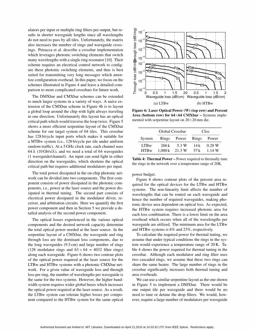
The total power dissipated in the on-chip photonic net-work can be divided into two components. The first com-ponent consists of power dissipated in the photonic com-ponents, i.e., power at the laser source and the power dis-sipated in thermal tuning. The second part consists ofelectrical power dissipated in the modulator driver, re-ceiver, and arbitration circuits. Here we quantify the firstpower component and then in Section 5 we provide a de-tailed analysis of the second power component.
The optical losses experienced in the various opticalcomponents and the desired network capacity determinethe total optical power needed at the laser source. In theserpentine layout of a CMXbar, the waveguide and ringthrough loss are the dominant loss components, due tothe long waveguides (9.5 cm) and large number of rings(128 modulator rings and 63× 64 = 4032 filter rings)along each waveguide. Figure 6 shows two contour plotsof the optical power required at the laser source for theLTBw and HTBw systems with a photonic CMXbar net-work. For a given value of waveguide loss and throughloss per ring, the number of wavelengths per waveguide isthe same for the two systems. However, the higher band-width system requires wider global buses which increasesthe optical power required at the laser source. As a result,the LTBw system can tolerate higher losses per compo-nent compared to the HTBw system for the same optical
10−4
10−3
10−2
10−1
12
5
5 10
10
Thro
ugh
loss
(dB/
ring)
12
510 40
40
0 0.5 1 1.5 210−4
10−3
10−2
10−1
10 25
2550
50
100 100
Waveguide loss (dB/cm)
Thro
ugh
loss
(dB/
ring)
25
50 100
100200
200
Waveguide loss (dB/cm)0 0.5 1 1.5 2
(a) LTBw (b) HTBw
Figure 6: Laser Optical Power (W) (top row) and PercentArea (bottom row) for 64×64 CMXbar – Systems imple-mented with serpentine layout on 20×20 mm die.
Global Crossbar Clos
System Rings Power Rings Power
LTBw 266 k 5.3 W 14 k 0.28 WHTBw 1,000 k 21.3 W 57 k 1.14 W
Table 4: Thermal Power – Power required to thermally tunethe rings in the network over a temperature range of 20K.
power budget.Figure 6 shows contour plots of the percent area re-
quired for the optical devices for the LTBw and HTBwsystems. The non-linearity limit affects the number ofwavelengths that can be routed on each waveguide andhence the number of required waveguides, making pho-tonic device area dependent on optical loss. As expected,the HTBw system requires increased photonic area foreach loss combination. There is a lower limit on the areaoverhead which occurs when all of the wavelengths perwaveguide are utilized. The minimum area for the LTBwand HTBw systems is 6% and 23%, respectively.
To calculate the required power for thermal tuning, weassume that under typical conditions the rings in the sys-tem would experience a temperature range of 20 K. Ta-ble 4 shows the power required for thermal tuning in thecrossbar. Although each modulator and ring filter usestwo cascaded rings, we assume that these two rings canshare the same heater. The large number of rings in thecrossbar significantly increases both thermal tuning andarea overheads.
We can use a similar serpentine layout as the one shownin Figure 5 to implement a DMXbar. There would beone output tile per waveguide and there would be noneed to tune or detune the drop filters. We would, how-ever, require a large number of modulators per waveguide
Authorized licensed use limited to: MIT Libraries. Downloaded on April 21,2010 at 14:33:32 UTC from IEEE Xplore. Restrictions apply.
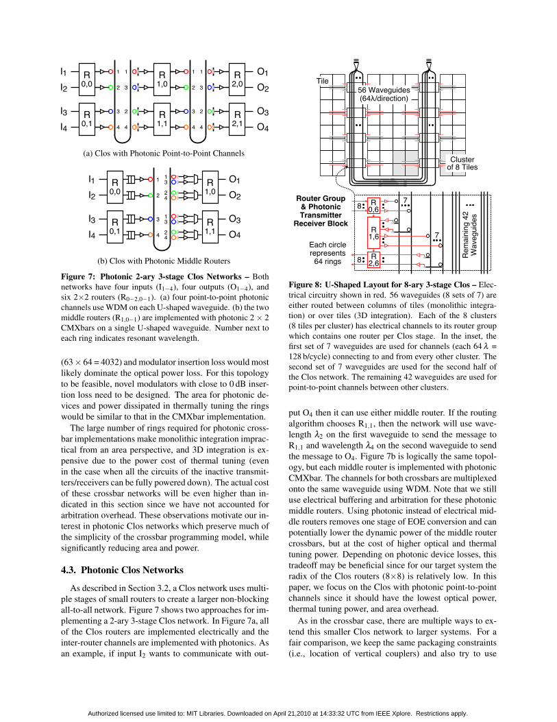
(a) Clos with Photonic Point-to-Point Channels
(b) Clos with Photonic Middle Routers
Figure 7: Photonic 2-ary 3-stage Clos Networks – Bothnetworks have four inputs (I1−4), four outputs (O1−4), andsix 2×2 routers (R0−2,0−1). (a) four point-to-point photonicchannels use WDM on each U-shaped waveguide. (b) the twomiddle routers (R1,0−1) are implemented with photonic 2× 2CMXbars on a single U-shaped waveguide. Number next toeach ring indicates resonant wavelength.
(63× 64 = 4032) and modulator insertion loss would mostlikely dominate the optical power loss. For this topologyto be feasible, novel modulators with close to 0 dB inser-tion loss need to be designed. The area for photonic de-vices and power dissipated in thermally tuning the ringswould be similar to that in the CMXbar implementation.
The large number of rings required for photonic cross-bar implementations make monolithic integration imprac-tical from an area perspective, and 3D integration is ex-pensive due to the power cost of thermal tuning (evenin the case when all the circuits of the inactive transmit-ters/receivers can be fully powered down). The actual costof these crossbar networks will be even higher than in-dicated in this section since we have not accounted forarbitration overhead. These observations motivate our in-terest in photonic Clos networks which preserve much ofthe simplicity of the crossbar programming model, whilesignificantly reducing area and power.
4.3. Photonic Clos Networks
As described in Section 3.2, a Clos network uses multi-ple stages of small routers to create a larger non-blockingall-to-all network. Figure 7 shows two approaches for im-plementing a 2-ary 3-stage Clos network. In Figure 7a, allof the Clos routers are implemented electrically and theinter-router channels are implemented with photonics. Asan example, if input I2 wants to communicate with out-
Figure 8: U-Shaped Layout for 8-ary 3-stage Clos – Elec-trical circuitry shown in red. 56 waveguides (8 sets of 7) areeither routed between columns of tiles (monolithic integra-tion) or over tiles (3D integration). Each of the 8 clusters(8 tiles per cluster) has electrical channels to its router groupwhich contains one router per Clos stage. In the inset, thefirst set of 7 waveguides are used for channels (each 64 λ =128 b/cycle) connecting to and from every other cluster. Thesecond set of 7 waveguides are used for the second half ofthe Clos network. The remaining 42 waveguides are used forpoint-to-point channels between other clusters.
put O4 then it can use either middle router. If the routingalgorithm chooses R1,1, then the network will use wave-length λ2 on the first waveguide to send the message toR1,1 and wavelength λ4 on the second waveguide to sendthe message to O4. Figure 7b is logically the same topol-ogy, but each middle router is implemented with photonicCMXbar. The channels for both crossbars are multiplexedonto the same waveguide using WDM. Note that we stilluse electrical buffering and arbitration for these photonicmiddle routers. Using photonic instead of electrical mid-dle routers removes one stage of EOE conversion and canpotentially lower the dynamic power of the middle routercrossbars, but at the cost of higher optical and thermaltuning power. Depending on photonic device losses, thistradeoff may be beneficial since for our target system theradix of the Clos routers (8×8) is relatively low. In thispaper, we focus on the Clos with photonic point-to-pointchannels since it should have the lowest optical power,thermal tuning power, and area overhead.
As in the crossbar case, there are multiple ways to ex-tend this smaller Clos network to larger systems. For afair comparison, we keep the same packaging constraints(i.e., location of vertical couplers) and also try to use
Authorized licensed use limited to: MIT Libraries. Downloaded on April 21,2010 at 14:33:32 UTC from IEEE Xplore. Restrictions apply.
10−4
10−3
10−2
10−1
1 2
5
510
Thro
ugh
loss
(dB/
ring)
1 2 5 10
10
40
0 1 2 3 4 510−4
10−3
10−2
10−1
3
3 5
510
1025
Waveguide loss (dB/cm)
Thro
ugh
loss
(dB/
ring)
10
25
2550
50100
Waveguide loss (dB/cm)0 1 2 3 4 5
(a) LTBw (b) HTBw
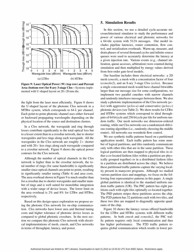
Figure 9: Laser Optical Power (W) (top row) and PercentArea (bottom row) for 8-ary 3-stage Clos – Systems imple-mented with U-shaped layout on 20×20 mm die.
the light from the laser most efficiently. Figure 8 showsthe U-shaped layout of the photonic Clos network in aMTBw system, which corresponds to 64 λ per channel.Each point-to-point photonic channel uses either forwardor backward propagating wavelengths depending on thephysical location of the source and destination clusters.
In a Clos network, the waveguide and ring throughlosses contribute significantly to the total optical loss butto a lesser extent than in a crossbar network, due to shorterwaveguides and less rings along each waveguide. All thewaveguides in the Clos network are roughly 2× shorterand with 20× less rings along each waveguide comparedto a crossbar network. Figure 9 shows the optical powercontours for the Clos network.
Although the number of optical channels in the Closnetwork is higher than in the crossbar network, the to-tal number of rings (for same bandwidth) is significantlysmaller since optical channels are point-to-point, resultingin significantly smaller tuning (Table 4) and area costs.The area overhead shown in Figure 9 is much smaller thanfor a crossbar due to shorter waveguides and smaller num-ber of rings and is well suited for monolithic integrationwith a wider range of device losses. The lower limit onthe area overhead is 2% and 8% for LTBw and HTBw,respectively.
Based on this design-space exploration we propose us-ing the photonic Clos network for on-chip communica-tion. Clos networks have lower area and thermal tuningcosts and higher tolerance of photonic device losses ascompared to global photonic crossbars. In the next sec-tion we compare this photonic Clos network with electri-cal implementations of mesh, cmesh, and Clos networksin terms of throughput, latency, and power.
5. Simulation Results
In this section, we use a detailed cycle-accurate mi-croarchitectural simulator to study the performance andpower of various electrical and photonic networks fora 64-tile system with 512 b messages. Our model in-cludes pipeline latencies, router contention, flow con-trol, and serialization overheads. Warm-up, measure, anddrain phases of several thousand cycles and infinite sourcequeues were used to accurately determine the latency ata given injection rate. Various events (e.g., channel uti-lization, queue accesses, arbitration) were counted duringsimulation and then multiplied by energy values derivedfrom first-order gate-level models.
Our baseline includes three electrical networks: a 2Dmesh (emesh), a mesh with a concentration factor of four(ecmeshx2), and an 8-ary 3-stage Clos (eclos). Becausea single concentrated mesh would have channel bitwidthslarger than our message size for some configurations, weimplement two parallel cmeshes with narrow channelsand randomly interleave messages between them. We alsostudy a photonic implementation of the Clos network (pc-los) with aggressive (pclos-a) and conservative (pclos-c)photonic devices (see Table 2). We show results for LTBwand HTBw systems which correspond to ideal through-puts of 64 b/cycle and 256 b/cycle per tile for uniform ran-dom traffic. Our mesh networks use dimension-orderedrouting, while our Clos networks use a randomized oblivi-ous routing algorithm (i.e., randomly choosing the middlerouter). All networks use wormhole flow control.
We use synthetic traffic patterns based on a partitionedapplication model. Each traffic pattern has some num-ber of logical partitions, and tiles randomly communicateonly with other tiles that are in the same partition. Theselogical partitions are then mapped to physical tiles in ei-ther a co-located fashion (tiles within a partition are phys-ically grouped together) or in a distributed fashion (tilesin a partition are distributed across the chip). We believethese partitioned traffic patterns capture the varying local-ity present in manycore programs. Although we studiedvarious partition sizes and mappings, we focus on the fol-lowing four representative patterns in this paper. A singleglobal partition is identical to the standard uniform ran-dom traffic pattern (UR). The P8C pattern has eight par-titions each with eight tiles optimally co-located together.The P8D pattern stripes these partitions across the chip.The P2D pattern has 32 partitions each with two tiles, andthese two tiles are mapped to diagonally opposite quad-rants of the chip.
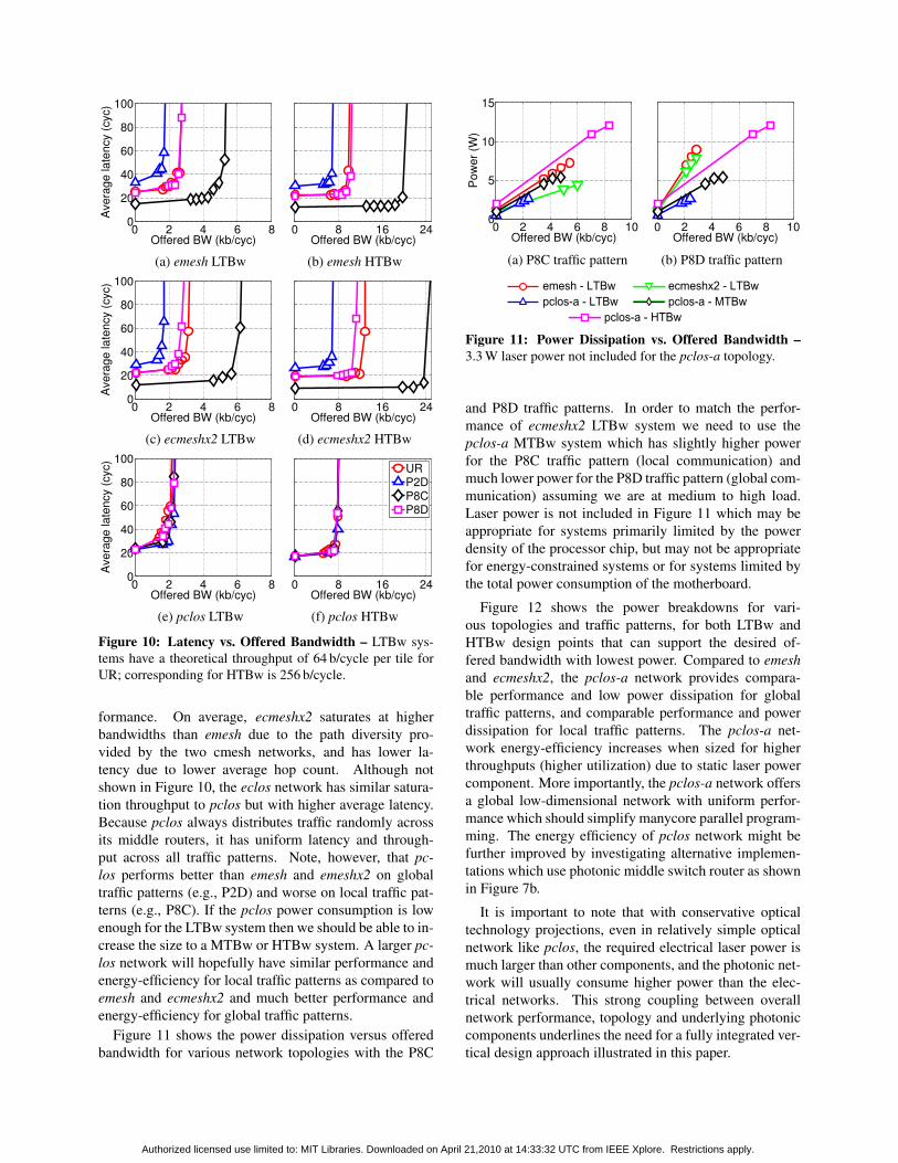
Figure 10 shows the latency versus offered bandwidthfor the LTBw and HTBw systems with different trafficpatterns. In both emesh and ecmeshx2, the P8C traf-fic pattern requires only local communication and thushas higher performance. The P2D traffic pattern re-quires global communication which results in lower per-
Authorized licensed use limited to: MIT Libraries. Downloaded on April 21,2010 at 14:33:32 UTC from IEEE Xplore. Restrictions apply.
0 2 4 6 80
20
40
60
80
100
Offered BW (kb/cyc)
Aver
age
late
ncy
(cyc
)
0 8 16 24Offered BW (kb/cyc)
(a) emesh LTBw (b) emesh HTBw
0 2 4 6 80
20
40
60
80
100
Offered BW (kb/cyc)
Aver
age
late
ncy
(cyc
)
0 8 16 24Offered BW (kb/cyc)
(c) ecmeshx2 LTBw (d) ecmeshx2 HTBw
0 2 4 6 80
20
40
60
80
100
Offered BW (kb/cyc)
Aver
age
late
ncy
(cyc
)
0 8 16 24Offered BW (kb/cyc)
URP2DP8CP8D
(e) pclos LTBw (f) pclos HTBw
Figure 10: Latency vs. Offered Bandwidth – LTBw sys-tems have a theoretical throughput of 64 b/cycle per tile forUR; corresponding for HTBw is 256 b/cycle.
formance. On average, ecmeshx2 saturates at higherbandwidths than emesh due to the path diversity pro-vided by the two cmesh networks, and has lower la-tency due to lower average hop count. Although notshown in Figure 10, the eclos network has similar satura-tion throughput to pclos but with higher average latency.Because pclos always distributes traffic randomly acrossits middle routers, it has uniform latency and through-put across all traffic patterns. Note, however, that pc-los performs better than emesh and emeshx2 on globaltraffic patterns (e.g., P2D) and worse on local traffic pat-terns (e.g., P8C). If the pclos power consumption is lowenough for the LTBw system then we should be able to in-crease the size to a MTBw or HTBw system. A larger pc-los network will hopefully have similar performance andenergy-efficiency for local traffic patterns as compared toemesh and ecmeshx2 and much better performance andenergy-efficiency for global traffic patterns.
Figure 11 shows the power dissipation versus offeredbandwidth for various network topologies with the P8C
0 2 4 6 8 100
5
10
15
Offered BW (kb/cyc)
Powe
r (W
)
0 2 4 6 8 10Offered BW (kb/cyc)
(a) P8C traffic pattern (b) P8D traffic pattern
Figure 11: Power Dissipation vs. Offered Bandwidth –3.3 W laser power not included for the pclos-a topology.
and P8D traffic patterns. In order to match the perfor-mance of ecmeshx2 LTBw system we need to use thepclos-a MTBw system which has slightly higher powerfor the P8C traffic pattern (local communication) andmuch lower power for the P8D traffic pattern (global com-munication) assuming we are at medium to high load.Laser power is not included in Figure 11 which may beappropriate for systems primarily limited by the powerdensity of the processor chip, but may not be appropriatefor energy-constrained systems or for systems limited bythe total power consumption of the motherboard.
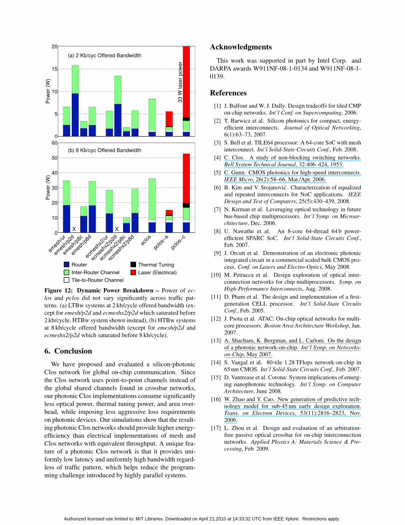
Figure 12 shows the power breakdowns for vari-ous topologies and traffic patterns, for both LTBw andHTBw design points that can support the desired of-fered bandwidth with lowest power. Compared to emeshand ecmeshx2, the pclos-a network provides compara-ble performance and low power dissipation for globaltraffic patterns, and comparable performance and powerdissipation for local traffic patterns. The pclos-a net-work energy-efficiency increases when sized for higherthroughputs (higher utilization) due to static laser powercomponent. More importantly, the pclos-a network offersa global low-dimensional network with uniform perfor-mance which should simplify manycore parallel program-ming. The energy efficiency of pclos network might befurther improved by investigating alternative implemen-tations which use photonic middle switch router as shownin Figure 7b.
It is important to note that with conservative opticaltechnology projections, even in relatively simple opticalnetwork like pclos, the required electrical laser power ismuch larger than other components, and the photonic net-work will usually consume higher power than the elec-trical networks. This strong coupling between overallnetwork performance, topology and underlying photoniccomponents underlines the need for a fully integrated ver-tical design approach illustrated in this paper.
Authorized licensed use limited to: MIT Libraries. Downloaded on April 21,2010 at 14:33:32 UTC from IEEE Xplore. Restrictions apply.
0
5
10
15
20Po
wer (
W)
(a) 2 Kb/cyc Offered Bandwidth
33 W
lase
r pow
er
0
10
20
30
40
50
60
Powe
r (W
)
emes
h/ur
emes
h/p2d
emes
h/p8c
emes
h/p8d
ecmes
hx2/u
r
ecmes
hx2/p
2d
ecmes
hx2/p
8c
ecmes
hx2/p
8dec
los
pclos
−a
pclos
−c
(b) 8 Kb/cyc Offered Bandwidth
X X
Figure 12: Dynamic Power Breakdown – Power of ec-los and pclos did not vary significantly across traffic pat-terns. (a) LTBw systems at 2 kb/cycle offered bandwidth (ex-cept for emesh/p2d and ecmeshx2/p2d which saturated before2 kb/cycle, HTBw system shown instead), (b) HTBw systemsat 8 kb/cycle offered bandwidth (except for emesh/p2d andecmeshx2/p2d which saturated before 8 kb/cycle).
6. ConclusionWe have proposed and evaluated a silicon-photonic
Clos network for global on-chip communication. Sincethe Clos network uses point-to-point channels instead ofthe global shared channels found in crossbar networks,our photonic Clos implementations consume significantlyless optical power, thermal tuning power, and area over-head, while imposing less aggressive loss requirementson photonic devices. Our simulations show that the result-ing photonic Clos networks should provide higher energy-efficiency than electrical implementations of mesh andClos networks with equivalent throughput. A unique fea-ture of a photonic Clos network is that it provides uni-formly low latency and uniformly high bandwidth regard-less of traffic pattern, which helps reduce the program-ming challenge introduced by highly parallel systems.
Acknowledgments
This work was supported in part by Intel Corp. andDARPA awards W911NF-08-1-0134 and W911NF-08-1-0139.
References[1] J. Balfour and W. J. Dally. Design tradeoffs for tiled CMP
on-chip networks. Int’l Conf. on Supercomputing, 2006.[2] T. Barwicz et al. Silicon photonics for compact, energy-
efficient interconnects. Journal of Optical Networking,6(1):63–73, 2007.
[3] S. Bell et al. TILE64 processor: A 64-core SoC with meshinterconnect. Int’l Solid-State Circuits Conf., Feb. 2008.
[4] C. Clos. A study of non-blocking switching networks.Bell System Technical Journal, 32:406–424, 1953.
[5] C. Gunn. CMOS photonics for high-speed interconnects.IEEE Micro, 26(2):58–66, Mar./Apr. 2006.
[6] B. Kim and V. Stojanovic. Characterization of equalizedand repeated interconnects for NoC applications. IEEEDesign and Test of Computers, 25(5):430–439, 2008.
[7] N. Kırman et al. Leveraging optical technology in futurebus-based chip multiprocessors. Int’l Symp. on Microar-chitecture, Dec. 2006.
[8] U. Nawathe et al. An 8-core 64-thread 64 b power-efficient SPARC SoC. Int’l Solid-State Circuits Conf.,Feb. 2007.
[9] J. Orcutt et al. Demonstration of an electronic photonicintegrated circuit in a commercial scaled bulk CMOS pro-cess. Conf. on Lasers and Electro-Optics, May 2008.
[10] M. Petracca et al. Design exploration of optical inter-connection networks for chip multiprocessors. Symp. onHigh-Performance Interconnects, Aug. 2008.
[11] D. Pham et al. The design and implementation of a first-generation CELL processor. Int’l Solid-State CircuitsConf., Feb. 2005.
[12] J. Psota et al. ATAC: On-chip optical networks for multi-core processors. Boston Area Architecture Workshop, Jan.2007.
[13] A. Shacham, K. Bergman, and L. Carloni. On the designof a photonic network-on-chip. Int’l Symp. on Networks-on-Chip, May 2007.
[14] S. Vangal et al. 80-tile 1.28 TFlops network-on-chip in65 nm CMOS. Int’l Solid-State Circuits Conf., Feb. 2007.
[15] D. Vantrease et al. Corona: System implications of emerg-ing nanophotonic technology. Int’l Symp. on ComputerArchitecture, June 2008.
[16] W. Zhao and Y. Cao. New generation of predictive tech-nology model for sub-45 nm early design exploration.Trans. on Electron Devices, 53(11):2816–2823, Nov.2006.
[17] L. Zhou et al. Design and evaluation of an arbitration-free passive optical crossbar for on-chip interconnectionnetworks. Applied Physics A: Materials Science & Pro-cessing, Feb. 2009.
Authorized licensed use limited to: MIT Libraries. Downloaded on April 21,2010 at 14:33:32 UTC from IEEE Xplore. Restrictions apply.