Ultrashort 2-D photonic crystal directional couplers
15
1 Ultra-short 2D photonic crystal directional couplers A. Martinez, F. Cuesta, J. Marti Fibre-Radio Group, ITACA Research Institute, Universidad Politécnica de Valencia, Camino de Vera s/n, 46022 Valencia (SPAIN) Tel. +34 96 387 9768 - Fax. +34 96 387 7279 E-mail: [email protected] Indexing terms : photonic crystals, integrated optics, waveguide couplers, demultiplexing, wavelength division multiplexing. Abstract A novel approach to reduce the coupling length and to increase the coupling coefficient in waveguide directional couplers implemented on two dimensional (2D) photonic crystals (PhC) is proposed. To increase the coupling coefficient of a 2D PhC directional coupler, which is composed of two parallel PhC waveguides separated by one or several rows of rods or holes, the radius of the rods (holes) between both waveguides is reduced. The application of this feature to ultra-small channel interleavers and wavelength demultiplexers is addressed.
-
Upload
independent -
Category
Documents
-
view
0 -
download
0
Transcript of Ultrashort 2-D photonic crystal directional couplers
1
Ultra-short 2D photonic crystal directional couplers
A. Martinez, F. Cuesta, J. Marti
Fibre-Radio Group, ITACA Research Institute,
Universidad Politécnica de Valencia, Camino de Vera s/n, 46022 Valencia (SPAIN)
Tel. +34 96 387 9768 - Fax. +34 96 387 7279
E-mail: [email protected]
Indexing terms: photonic crystals, integrated optics, waveguide couplers, demultiplexing,
wavelength division multiplexing.
Abstract
A novel approach to reduce the coupling length and to increase the coupling coefficient in
waveguide directional couplers implemented on two dimensional (2D) photonic crystals
(PhC) is proposed. To increase the coupling coefficient of a 2D PhC directional coupler,
which is composed of two parallel PhC waveguides separated by one or several rows of rods
or holes, the radius of the rods (holes) between both waveguides is reduced. The application
of this feature to ultra-small channel interleavers and wavelength demultiplexers is addressed.
2
I. INTRODUCTION
Two dimensional (2D) photonic crystal (PhC) structures [1] have attracted great interest as
key technology to develop microscale optical integrated circuits due to their relevant features
such as ultra-small size, compactness and mass-manufacturing possibilities. Optical
waveguides in 2D PhCs produced by inserting linear defects in the PhC structure have been
proposed [2] and experimentally proved [3]. By setting closely two parallel 2D PhC
waveguides a directional waveguide coupler can be created [4,5]. The main advantage of such
approach relies on achieving strong coupling due to the narrow separation between both
waveguides. 2D PhC-based couplers have been theoretically studied and proposed as a simple
manner for implementing wavelength demultiplexers [5,6]. Furthermore, a three-port
directional PhC waveguide coupler with a coupling region of only 21 µm has been recently
fabricated on a silicon-on-insulator wafer [7]. However, owing to manufacturing limitations
and high propagation losses in 2D PhC waveguides, the total length of those couplers are too
large to employ them in applications such as channel interleaving or wavelength
demultiplexing for wavelength division multiplexing (WDM) networks. In this paper, a novel
technique to both increase the coupling coefficient and diminish the coupling length in PhC
waveguide couplers is proposed. This approach is based on reducing the radius of the rods or
holes that separate the two waveguides forming the directional coupler. Owing to the increase
of the slope of the coupling coefficient against the frequency, a narrow channel spacing may
be attained for ultra-short waveguide couplers used in wavelength-dependent devices, such as
channel interleavers or wavelength demultiplexers. Both theoretical and simulation results
show that a 0.8 nm channel spacing 1x2 wavelength demultiplexer with a power ratio
between outputs higher than 14 dB may be achieved employing a PhC coupler shorter than
200 µm, which corresponds to only a third of the length of that proposed in [5].
II. PhC WAVEGUIDE COUPLER STRUCTURE

3
Fig. 1 depicts the proposed coupler structure implemented on a hexagonal 2D PhC consisting
of Si rods with ε = 12 and radius r = 0.2a, a being the lattice constant, embedded on a SiO2
background with ε = 2.1. This structure has a photonic band gap (PBG) for TM modes
ranging from 0.26387 to 0.35987 in normalized frequency units (a/λ), λ being the wavelength
in vacuum. In this structure the waveguides are inherently single-mode because total internal
reflection (TIR) modes are prevented to exist and the core of the waveguides is dielectric so
vertical confinement in PhC slabs surrounded by air may be attained. A detailed analysis of
this novel 2D PhC structure is presented in [8]. Nevertheless, the same approach here
proposed may be used in other PhC structures such as those composed of air holes on a
dielectric substrate. To create the waveguide directional coupler, two parallel waveguides are
set along the ΓK direction by removing two entire rows of rods, which are separated by
another row of rods whose radius is rc ≤ r. The total length of the coupler (L) is an integer
multiple of a due to the periodicity of the structure along the waveguide direction. The
dispersion relation of the structure is obtained by using a 2D plane-wave expansion (PWE)
method [9]. The dotted rectangle shown in Fig. 1 is the supercell used for the band structure
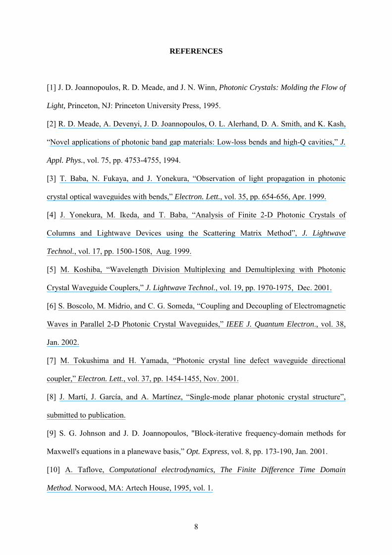
calculations. Fig. 2 shows the dispersion relation of the modes of the structure inside the PBG
for different rc/a values. In Fig. 2 it is observed that two guided TM modes arising from the
splitting of an isolated single waveguide mode appear inside the PBG. These modes, named
odd and even regarding the symmetry plane between the waveguides, have different
propagation constants for every frequency, ko and ke, respectively. As the mismatch between
the propagation constants of both modes is large, the coupling length, defined as Lc = 2π/|ke-
ko|, may become significantly small, and the coupling coefficient, defined as κ = |ke-ko|/2, may
be very large. It should be pointed out that the strong coupling feature is limited to the
frequency range between the lowest frequency of the even mode and the frequency at which
both modes have the same wave vector, as shown in Fig. 2. The insets depicted in Fig. 2 show
4
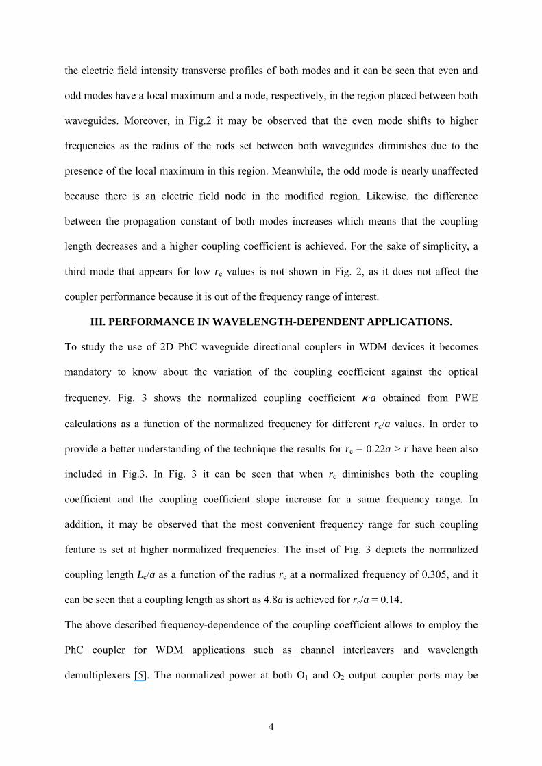
the electric field intensity transverse profiles of both modes and it can be seen that even and
odd modes have a local maximum and a node, respectively, in the region placed between both
waveguides. Moreover, in Fig.2 it may be observed that the even mode shifts to higher
frequencies as the radius of the rods set between both waveguides diminishes due to the
presence of the local maximum in this region. Meanwhile, the odd mode is nearly unaffected
because there is an electric field node in the modified region. Likewise, the difference
between the propagation constant of both modes increases which means that the coupling
length decreases and a higher coupling coefficient is achieved. For the sake of simplicity, a
third mode that appears for low rc values is not shown in Fig. 2, as it does not affect the
coupler performance because it is out of the frequency range of interest.
III. PERFORMANCE IN WAVELENGTH-DEPENDENT APPLICATIONS.
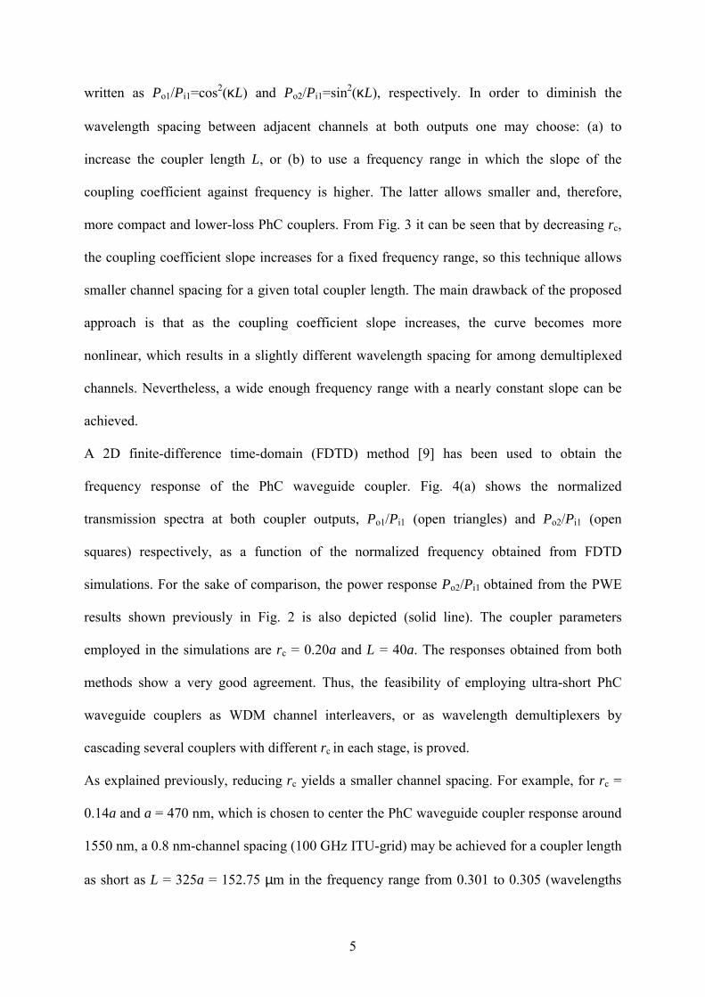
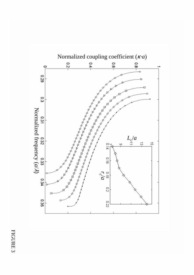
To study the use of 2D PhC waveguide directional couplers in WDM devices it becomes
mandatory to know about the variation of the coupling coefficient against the optical
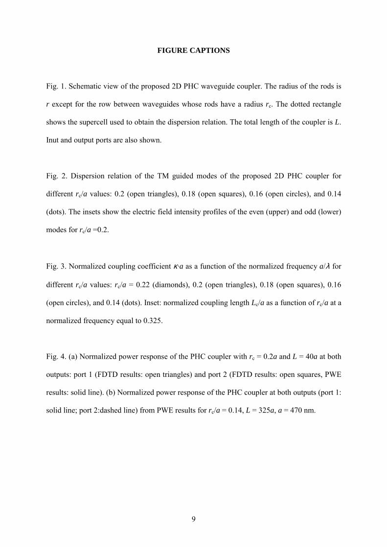
frequency. Fig. 3 shows the normalized coupling coefficient κ·a obtained from PWE
calculations as a function of the normalized frequency for different rc/a values. In order to
provide a better understanding of the technique the results for rc = 0.22a > r have been also
included in Fig.3. In Fig. 3 it can be seen that when rc diminishes both the coupling
coefficient and the coupling coefficient slope increase for a same frequency range. In
addition, it may be observed that the most convenient frequency range for such coupling
feature is set at higher normalized frequencies. The inset of Fig. 3 depicts the normalized
coupling length Lc/a as a function of the radius rc at a normalized frequency of 0.305, and it
can be seen that a coupling length as short as 4.8a is achieved for rc/a = 0.14.
The above described frequency-dependence of the coupling coefficient allows to employ the
PhC coupler for WDM applications such as channel interleavers and wavelength
demultiplexers [5]. The normalized power at both O1 and O2 output coupler ports may be
5
written as Po1/Pi1=cos2(κL) and Po2/Pi1=sin2(κL), respectively. In order to diminish the
wavelength spacing between adjacent channels at both outputs one may choose: (a) to
increase the coupler length L, or (b) to use a frequency range in which the slope of the
coupling coefficient against frequency is higher. The latter allows smaller and, therefore,
more compact and lower-loss PhC couplers. From Fig. 3 it can be seen that by decreasing rc,
the coupling coefficient slope increases for a fixed frequency range, so this technique allows
smaller channel spacing for a given total coupler length. The main drawback of the proposed
approach is that as the coupling coefficient slope increases, the curve becomes more
nonlinear, which results in a slightly different wavelength spacing for among demultiplexed
channels. Nevertheless, a wide enough frequency range with a nearly constant slope can be
achieved.
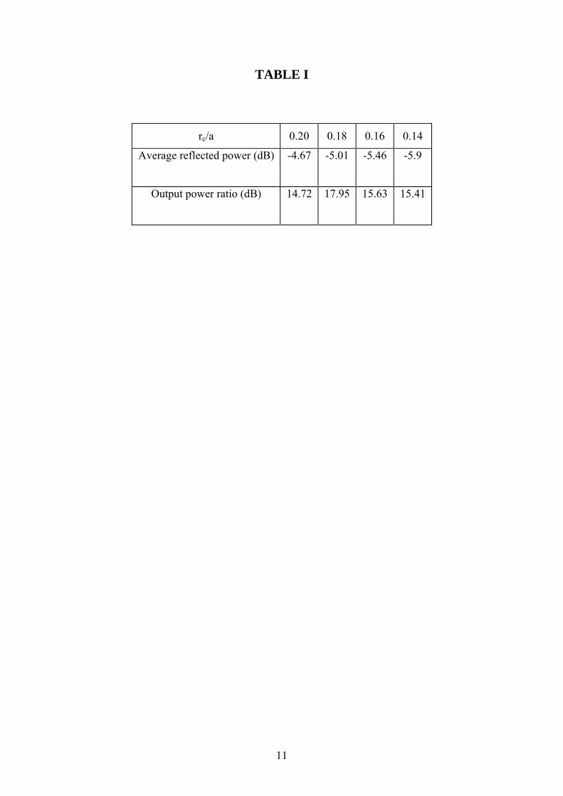
A 2D finite-difference time-domain (FDTD) method [9] has been used to obtain the
frequency response of the PhC waveguide coupler. Fig. 4(a) shows the normalized
transmission spectra at both coupler outputs, Po1/Pi1 (open triangles) and Po2/Pi1 (open
squares) respectively, as a function of the normalized frequency obtained from FDTD
simulations. For the sake of comparison, the power response Po2/Pi1 obtained from the PWE
results shown previously in Fig. 2 is also depicted (solid line). The coupler parameters
employed in the simulations are rc = 0.20a and L = 40a. The responses obtained from both
methods show a very good agreement. Thus, the feasibility of employing ultra-short PhC
waveguide couplers as WDM channel interleavers, or as wavelength demultiplexers by
cascading several couplers with different rc in each stage, is proved.
As explained previously, reducing rc yields a smaller channel spacing. For example, for rc =
0.14a and a = 470 nm, which is chosen to center the PhC waveguide coupler response around
1550 nm, a 0.8 nm-channel spacing (100 GHz ITU-grid) may be achieved for a coupler length
as short as L = 325a = 152.75 µm in the frequency range from 0.301 to 0.305 (wavelengths

6
from 1541 to 1561.5 nm), which would result in a 20.5 nm operating bandwidth. To illustrate
this example, Fig. 4(b) shows the normalized power at both outputs as a function of the
wavelength obtained from PWE results. In Fig. 4(b) it may also be clearly observed the
drawback reported above, i. e., the transmission maxima are not evenly spaced over the whole
frequency range due to the slight non-linearity of the coupling coefficient frequency response
at the chosen wavelengths. Therefore, a trade-off between the PhC coupler length and the
channel spacing uniformity has to be taken into account for designing purposes. On the other
hand, the large mismatch between even and odd modes for strong coupling conditions may
result in a lower efficiency by reducing the power ratio between output ports, defined as
Po1/Po2 or Po2/Po1, and increasing the reflected power at the coupler input [4]. This
degradation has been studied by means of FDTD simulations. Table I shows the reflected
power and the power ratio between output ports and for different rc/a values when light
impinges input port 1. The reflected power has been obtained by integrating the normalized
reflected power over all the coupling frequency range. The obtained values are rather large
due to the fact that no matching technique has been used at the coupler input. Nevertheless,
from results shown in Table I it is noticed that the reflected power decreases as rc diminishes,
despite the increase in the mismatching of even and odd modes. This occurs because the
coupler waveguides are wider as rc decreases whilst the transverse width of the input field
remains constant, so the optical power entering the structure is larger and enhances the
efficiency. The output power ratio is obtained by averaging this value corresponding to the
five central channels at every rc/a value and it is higher than 14 dB regardless the rc/a value,
reaching a maximum for rc/a = 0.18. Thus, it can be concluded that the mismatching of the
modes has an almost negligible effect on the output power ratio.
IV. CONCLUSION.
7
In this paper, a novel and simple method that allows to reduce the coupling length and to
increase the coupling coefficient in 2D PhC waveguide couplers, which yields reduction of
the total coupler length, is reported. This technique may become important to develop ultra-
short couplers for applications like splitters, combiners, interleavers or demultiplexers
implemented by employing 2D PhC technology. The results show that the realization of a 0.8
nm channel interleaver may be feasible by using PhC waveguide couplers with a total length
smaller than 200 µm.
ACKNOLEDGEMENT
This work has been partially funded by the Spanish Ministry of Science and Technology
under grant TIC2002-01553. A. Martinez acknowledges the Generalitat Valenciana for
funding his grant.
8
REFERENCES
[1] J. D. Joannopoulos, R. D. Meade, and J. N. Winn, Photonic Crystals: Molding the Flow of
Light, Princeton, NJ: Princeton University Press, 1995.
[2] R. D. Meade, A. Devenyi, J. D. Joannopoulos, O. L. Alerhand, D. A. Smith, and K. Kash,
“Novel applications of photonic band gap materials: Low-loss bends and high-Q cavities,” J.
Appl. Phys., vol. 75, pp. 4753-4755, 1994.
[3] T. Baba, N. Fukaya, and J. Yonekura, “Observation of light propagation in photonic
crystal optical waveguides with bends,” Electron. Lett., vol. 35, pp. 654-656, Apr. 1999.
[4] J. Yonekura, M. Ikeda, and T. Baba, “Analysis of Finite 2-D Photonic Crystals of
Columns and Lightwave Devices using the Scattering Matrix Method”, J. Lightwave
Technol., vol. 17, pp. 1500-1508, Aug. 1999.
[5] M. Koshiba, “Wavelength Division Multiplexing and Demultiplexing with Photonic
Crystal Waveguide Couplers,” J. Lightwave Technol., vol. 19, pp. 1970-1975, Dec. 2001.
[6] S. Boscolo, M. Midrio, and C. G. Someda, “Coupling and Decoupling of Electromagnetic
Waves in Parallel 2-D Photonic Crystal Waveguides,” IEEE J. Quantum Electron., vol. 38,
Jan. 2002.
[7] M. Tokushima and H. Yamada, “Photonic crystal line defect waveguide directional
coupler,” Electron. Lett., vol. 37, pp. 1454-1455, Nov. 2001.
[8] J. Martí, J. García, and A. Martínez, “Single-mode planar photonic crystal structure”,
submitted to publication.
[9] S. G. Johnson and J. D. Joannopoulos, "Block-iterative frequency-domain methods for
Maxwell's equations in a planewave basis,” Opt. Express, vol. 8, pp. 173-190, Jan. 2001.
[10] A. Taflove, Computational electrodynamics, The Finite Difference Time Domain
Method. Norwood, MA: Artech House, 1995, vol. 1.
9
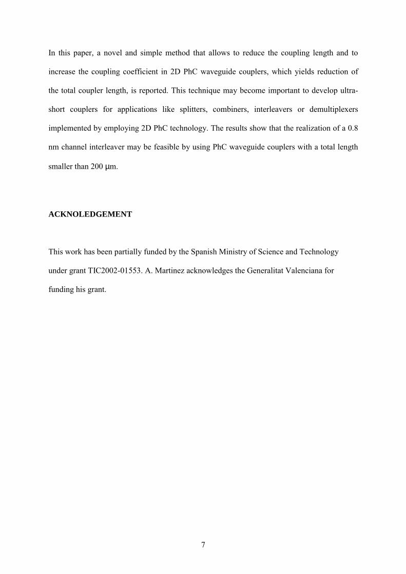
FIGURE CAPTIONS
Fig. 1. Schematic view of the proposed 2D PHC waveguide coupler. The radius of the rods is
r except for the row between waveguides whose rods have a radius rc. The dotted rectangle
shows the supercell used to obtain the dispersion relation. The total length of the coupler is L.
Inut and output ports are also shown.
Fig. 2. Dispersion relation of the TM guided modes of the proposed 2D PHC coupler for
different rc/a values: 0.2 (open triangles), 0.18 (open squares), 0.16 (open circles), and 0.14
(dots). The insets show the electric field intensity profiles of the even (upper) and odd (lower)
modes for rc/a =0.2.
Fig. 3. Normalized coupling coefficient κ·a as a function of the normalized frequency a/λ for
different rc/a values: rc/a = 0.22 (diamonds), 0.2 (open triangles), 0.18 (open squares), 0.16
(open circles), and 0.14 (dots). Inset: normalized coupling length Lc/a as a function of rc/a at a
normalized frequency equal to 0.325.
Fig. 4. (a) Normalized power response of the PHC coupler with rc = 0.2a and L = 40a at both
outputs: port 1 (FDTD results: open triangles) and port 2 (FDTD results: open squares, PWE
results: solid line). (b) Normalized power response of the PHC coupler at both outputs (port 1:
solid line; port 2:dashed line) from PWE results for rc/a = 0.14, L = 325a, a = 470 nm.

10
TABLE CAPTIONS
Table I:. Average reflected power and average output power ratio for different rc/a values.
Power is injected into input port 1.
11
TABLE I
rc/a 0.20 0.18 0.16 0.14
Average reflected power (dB) -4.67 -5.01 -5.46 -5.9
Output power ratio (dB) 14.72 17.95 15.63 15.41
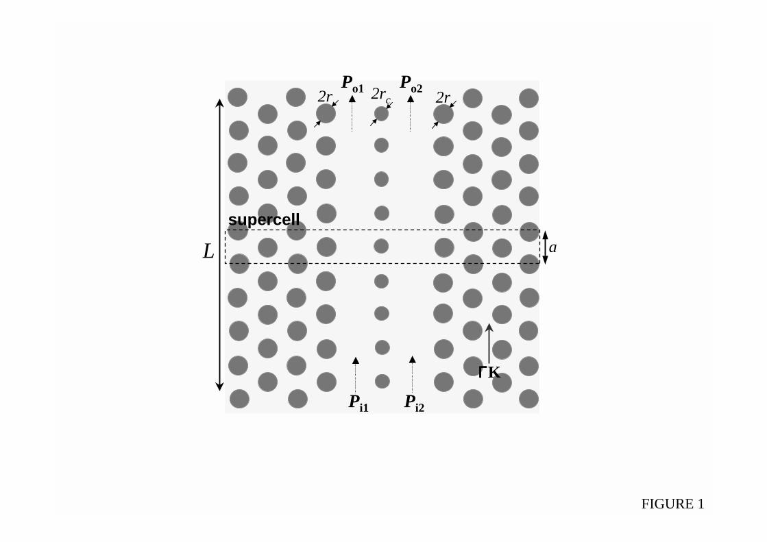
FIGURE 1
ΓΓΓΓK
a
2r 2rc
Lsupercell
Po1 Po2
Pi2Pi1
2r
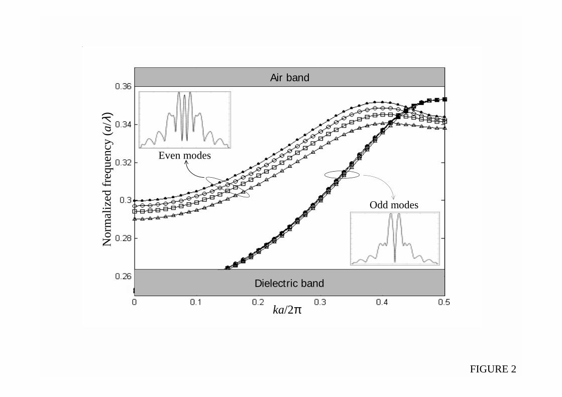
FIGURE 2
ka/2π
Nor
mal
ized
freq
uenc
y(a
/λ)
Dielectric band
Air band
Even modes
Odd modes
Norm
alized frequency(a/λ)
Normalized coupling coefficient (κ·a)
rc /a
Lc/a
FIGU
RE 3

Wavelength (nm)
rc=0.20
Normalized frequency (a/λ)
Nor
mal
ized
out
put p
ower
(dB
)N
orm
aliz
ed o
utpu
t pow
er
FIGURE 4
(a)
(b)