Zone-plate-array lithography (ZPAL): optical maskless lithography for cost-effective patterning
10
Zone-Plate-Array Lithography (ZPAL): Optical Maskless Lithography for Cost-Effective Patterning Rajesh Menon* 1 , Amil Patel, David Chao, Michael Walsh*, and Henry I. Smith* Research Laboratory of Electronics Massachusetts Institute of Technology, Cambridge, MA 02139 *LumArray LLC 2 , Cambridge, MA 02139 ABSTRACT Zone-Plate-Array Lithography (ZPAL) is an optical-maskless-lithography technique, in which an array of tightly focused spots is formed on the surface of a substrate by means of an array of high-numerical-aperture zone plates. The substrate is scanned while an upstream spatial-light modulator, enabling “dot-matrix” style writing, modulates the light intensity in each spot. We have built a proof-of-concept system using an array of zone plates, and the Silicon Light Machines Grating Light Valve (GLV TM ) as the light modulator. We have demonstrated fully multiplexed writing, multilevel alignment and resolution corresponding to k 1 < 0.3. This system currently operates at λ = 400nm and utilizes well-known I-line processes. Diffractive optics such as zone plates offer significant advantages over refractive approaches since near-ideal performance is achieved on axis, reliable planar fabrication techniques are used, costs are low, and the approach can be readily scaled to shorter wavelengths. In this paper, we also developed models and analyzed the cost-of-ownership of maskless lithography (ZPAL) versus that for optical-projection lithography (OPL). In this context, we propose the use of an effective throughput to consider the photomask delivery times in the case of OPL. We believe that ZPAL has the potential to become the most practical and cost-effective method of maskless lithography, enabling circuit designers to fully exploit their creativity, unencumbered by the constraints of mask-based lithography. This may revolutionize custom circuit design as well as research in electronics, NEMS, microphotonics, nanomagnetics and nanoscale science and engineering. Keywords: Lithography, maskless lithography, low-k 1 lithography, zone-plate-array lithography, zone plates, cost-of- ownership. 1. INTRODUCTION Lithography is the key enabling technology responsible for the proliferation of micro- and nano-scale integrated devices. Patterning via optical-projection lithography (OPL) remains the most expensive as well as one of the most complicated steps in the semiconductor manufacturing process. Patterns etched into a photomask are imaged by highly complex, refractive optical systems onto the surface of the photoresist-coated wafer. The complexity of the optical system is further enhanced by the nanoscale tolerances required in the printed image, which translates into extremely tight tolerances on the allowable aberrations in the imaging optics. Progress (both technical and economic) in the semiconductor industry is primarily defined by the decrease in feature sizes. Smaller feature sizes are accompanied by even more stringent requirements on the performance of the optics as well as the entire OPL tool. In the past, reducing the exposure wavelength as well as clever designs of the photomask, and illumination systems traded off some of these complexities. Such resolution-enhancement techniques 1 (RETs) shifted the complexities from the optics to the photomask and the illumination sub-systems of the OPL tool. Meanwhile, material issues constrained the path to shorter wavelengths as it became extremely difficult and expensive to design aberration-free optical systems for wavelengths below 193nm. This shifted even more complexity onto RETs and enhancements to the photomask such as optical- proximity correction (OPC). Manufacturing tolerances on the photomasks themselves became more stringent, driving up their costs exponentially. It is clear that increasingly clever (and hence, complex!) photomask patterns will be 1 Email: [email protected] 2 www.lumarray.com
-
Upload
independent -
Category
Documents
-
view
0 -
download
0
Transcript of Zone-plate-array lithography (ZPAL): optical maskless lithography for cost-effective patterning

Zone-Plate-Array Lithography (ZPAL): Optical MasklessLithography for Cost-Effective Patterning
Rajesh Menon*1, Amil Patel, David Chao, Michael Walsh*, and Henry I. Smith*
Research Laboratory of ElectronicsMassachusetts Institute of Technology, Cambridge, MA 02139
*LumArray LLC2, Cambridge, MA 02139
ABSTRACTZone-Plate-Array Lithography (ZPAL) is an optical-maskless-lithography technique, in which an array of tightlyfocused spots is formed on the surface of a substrate by means of an array of high-numerical-aperture zone plates. Thesubstrate is scanned while an upstream spatial-light modulator, enabling “dot-matrix” style writing, modulates the lightintensity in each spot. We have built a proof-of-concept system using an array of zone plates, and the Silicon LightMachines Grating Light Valve (GLVTM) as the light modulator. We have demonstrated fully multiplexed writing,multilevel alignment and resolution corresponding to k1 < 0.3. This system currently operates at λ = 400nm and utilizeswell-known I-line processes. Diffractive optics such as zone plates offer significant advantages over refractiveapproaches since near-ideal performance is achieved on axis, reliable planar fabrication techniques are used, costs arelow, and the approach can be readily scaled to shorter wavelengths. In this paper, we also developed models andanalyzed the cost-of-ownership of maskless lithography (ZPAL) versus that for optical-projection lithography (OPL). Inthis context, we propose the use of an effective throughput to consider the photomask delivery times in the case of OPL.We believe that ZPAL has the potential to become the most practical and cost-effective method of masklesslithography, enabling circuit designers to fully exploit their creativity, unencumbered by the constraints of mask-basedlithography. This may revolutionize custom circuit design as well as research in electronics, NEMS, microphotonics,nanomagnetics and nanoscale science and engineering.
Keywords: Lithography, maskless lithography, low-k1 lithography, zone-plate-array lithography, zone plates, cost-of-ownership.
1. INTRODUCTION
Lithography is the key enabling technology responsible for the proliferation of micro- and nano-scale integrateddevices. Patterning via optical-projection lithography (OPL) remains the most expensive as well as one of the mostcomplicated steps in the semiconductor manufacturing process. Patterns etched into a photomask are imaged by highlycomplex, refractive optical systems onto the surface of the photoresist-coated wafer. The complexity of the opticalsystem is further enhanced by the nanoscale tolerances required in the printed image, which translates into extremelytight tolerances on the allowable aberrations in the imaging optics. Progress (both technical and economic) in thesemiconductor industry is primarily defined by the decrease in feature sizes. Smaller feature sizes are accompanied byeven more stringent requirements on the performance of the optics as well as the entire OPL tool. In the past, reducingthe exposure wavelength as well as clever designs of the photomask, and illumination systems traded off some of thesecomplexities. Such resolution-enhancement techniques1 (RETs) shifted the complexities from the optics to thephotomask and the illumination sub-systems of the OPL tool. Meanwhile, material issues constrained the path to shorterwavelengths as it became extremely difficult and expensive to design aberration-free optical systems for wavelengthsbelow 193nm. This shifted even more complexity onto RETs and enhancements to the photomask such as optical-proximity correction (OPC). Manufacturing tolerances on the photomasks themselves became more stringent, drivingup their costs exponentially. It is clear that increasingly clever (and hence, complex!) photomask patterns will be
1 Email: [email protected] www.lumarray.com
responsible for driving optical lithography to the limits of the lithographic process. Hence, it is a worthwhile exercise toconsider alternative patterning techniques, which sidestep the requirement of expensive photomasks.
In the semiconductor industry OPL is very successful in large part because the photomask can be used repeatedly topattern thousands of wafers at high yield and at high speeds. Although maskless lithography avoids the extra cost anddelays involved in the photomask, it is usually very slow compared to OPL. Thus maskless lithography offers flexibilityin patterning at the cost of speed. Several forms of maskless lithography have been proposed. In most proposals,patterns are recorded in a resist layer either by focused beams of photons, electrons or other charged particles, or byimages projected from a reconfigurable photomask. In the former, proposals have been made to increase the number offocused beams in order to increase the writing speed. Since electrons as well as any charged particles are deflected byelectric and magnetic fields, the position accuracy that can be achieved with electron-based lithographic systems istypically limited to over 10nm. Moreover, the process incompatibilities raised by using electrons instead of photonsmake it much more difficult to be accepted into a manufacturing process. In the latter proposal, complex projectionoptics are required. The nature of the complexity is shifted to a much larger demagnification factor (over 250X). This isdue to the fact that individually addressable pixels on a MEMs-based reconfigurable photomask (spatial-lightmodulator) are typically large (of the order of 10 µm). This problem is slightly easier to solve if smaller image (so-called field) sizes are used. However, smaller field sizes severely deteriorate the writing speed. Although such maskless-optical-projection lithography (MOPL) could be compatible with existing OPL materials and processes, the cost andcomplexity involved in these systems will likely impede their general acceptance. Beyond the semiconductor industry,we believe that a simpler, low-cost technology for flexible lithography will be invaluable in enabling thenanotechnology revolution.
At MIT, we have a developed a technique that uses a large number of focused optical beams writing in parallel. Thelarge number of tightly focused beams is created by an array of high-numerical aperture diffractive lenses, of whichzone plates are the simplest ones. Hence, this technology is called zone-plate-array lithography (ZPAL) 2. Light in eachfocused spot is controlled by one pixel of an upstream spatial-light modulator. The wafer is scanned on a high-precisionstage in the focal plane of the zone-plate array (ZPA), while the light in each spot is modulated. Thus, patterns ofarbitrary geometry are written in a “dot-matrix” fashion. A simple schematic of ZPAL is shown in Figure 1.
Figure 1: Schematic of Zone-Plate-Array Lithography (ZPAL). An array of high-numerical aperture zone plates create an array oftightly focused spots. The substrate is scanned while a spatial-light modulator controls the light in each spot. Patterns are printed in a“dot-matrix” fashion. Scanning-electron micrographs on the left show a portion of a zone-plate array and a single zone plate. Thesephase zone plates were designed to operate at λ = 400nm at NA = 0.7. They were fabricated in fused silica using scanning-electron-beam lithography. The spatial-light modulator in our prototype system is the Grating Light Valve from Silicon Light Machines3.
Since two-level phase zone plates can be fabricated using planar techniques, we are able to manufacture arrayscontaining over 1000 zone plates readily (see Figure 1 inset)4. Our fabrication techniques ensure the uniformity of alloptical properties including the focal length across the array. In fact, we have verified this via measurements made on alarge-area micromagnetic device5. In addition, numerical apertures as high as 0.95 have been demonstrated in the past6.Another advantage of using diffractive optics is the potential to improve the focused spot by wavefront engineering. Wemade progress in this direction by showing the first lithography results with high-numerical aperture photon sieves7,which have the potential to pattern images with increased contrast. Finally, diffractive optics can be readily designed tooperate at shorter wavelengths8. Thus, ZPAL has an architecture that can be extended to the limits of lithography.
2. LITHOGRAPHY PERFORMANCE
ZPAL has demonstrated excellent lithographic performance based on several figures-of-merit. We have patterned avariety of micro and nano scale devices, and demonstrated the feasibility of this technology. In this section, we brieflysummarize these lithographic capabilities.
2.1 Resolution
Resolution in optical lithography is given by:
€
Wmin = k1λ
NA, (1)
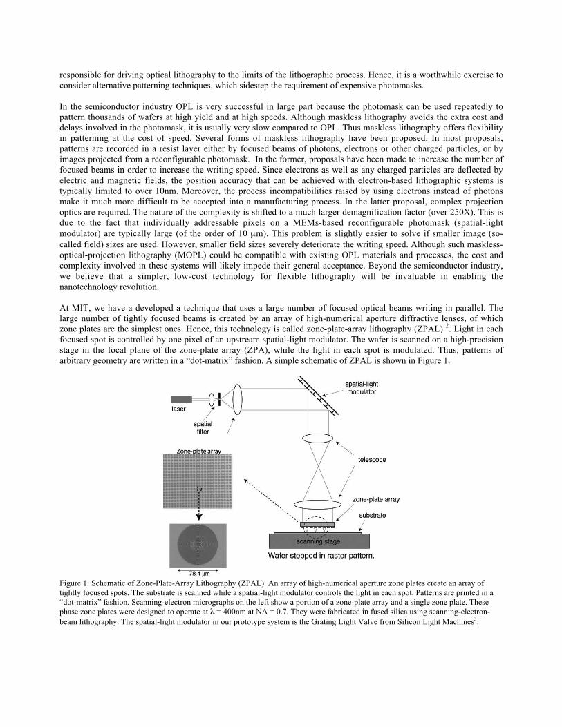
where Wmin is printable minimum feature size, λ is the exposing wavelength, NA is the numerical aperture, and k1 isproportionality constant. In OPL, use of k1 less than 0.4 is very difficult, especially for non-periodic patterns. ZPAL isan incoherent imaging system, which implies that periodic as well as non-periodic patterns may be printed at very lowk1. Examples of periodic patterns (dense lines and spaces) are demonstrated in Figure 2. The smallest lines have awidth of 135nm, which corresponds to a k1 of 0.287. An example of a non-periodic pattern (the seal of MIT) is shownon the right. The smallest feature on this dense, non-periodic pattern is about 140nm, which corresponds to a k1 of0.298. Note also that the linewidth control (i.e., the change in the linewidth) as small as 5nm is demonstrated in thedense gratings. In fact, with an exposure grid of 75nm and an 8-bit gray-level exposure scheme, this linewidth controlcan be theoretically 0.29nm! Of course, then the linewidth is limited by errors in the scanning stage, which themselvescan be minimized to a few nanometers by using laser-interferometer control.
Figure 2: Resolution of ZPAL. Scanning-electron micrographs of periodic patterns (a) and a non-periodic pattern (b) in photoresistare shown. These were patterned at λ = 400nm and NA = 0.85. These demonstrate that ZPAL is capable of printing k1 < 0.3 forpatterns of any geometry. Note that (b) shows the seal of MIT.

2.2 Image contrast
In ZPAL, the first-order focused spot is used for lithography. The first-order focusing efficiency of phase zone plates isat most about 40%. This is slightly misleading as the remaining 60% of the light is distributed in the focal plane in sucha manner that the aerial power density is extremely low compared to the first order of diffraction. As demonstrated byour results below, the effect of this background appears to be less than deleterious effects due to flare in OPL. Figure 3(a) shows a scanning-electron micrograph of dense lines and spaces of width 290nm spanning an area of over 10mm2.This pattern was printed with over 1000 zone plates in the presence of all the background in the focal plane. In spite ofthe 60% background from each zone plate, the lines were resolved very uniformly across the entire pattern. This ispossible as the background energy is spread over extremely large areas compared to the main 1st order lobe. One canemploy gray-scale optimization techniques to further overcome the effects of this background. This is demonstrated in a“worst-case” scenario shown in Figure 3(b), where a single spot is left unexposed in the center of a completely exposedsquare. By appropriate gray-scale modulation, the single unexposed spot can be resolved as shown. Note that there arealmost 5000 exposed pixels surrounding this one unexposed pixel in this case!
Figure 3: Issue of contrast in ZPAL. (a) Scanning-electron micrographs of 290 lines and spaces covering an area of over 10mm2. Thiswas patterned by over 1000 zone plates at λ = 400nm and NA = 0.7. Each white square shown in the top SEM represents the portionof the pattern printed by one zone plate. (b) Scanning-electron micrographs of a single unexposed spot in the center of a largeexposed square. This was printed at λ = 400nm and NA = 0.85.
2.3 Pattern fidelity
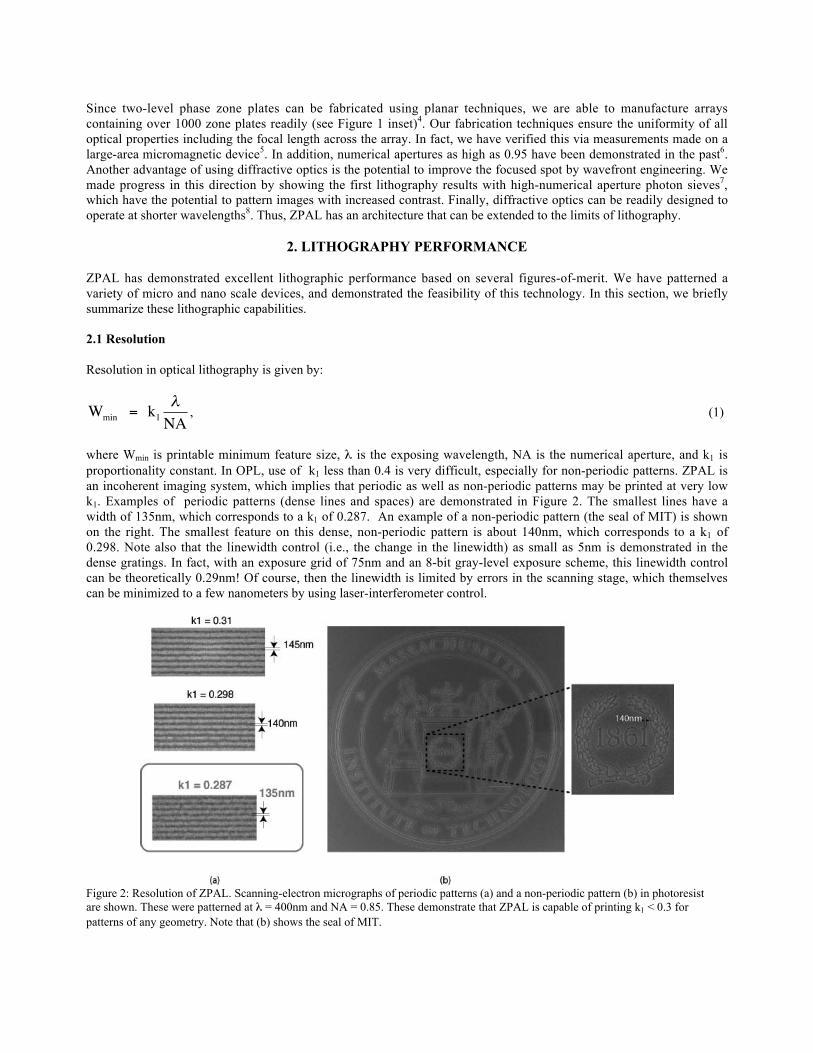
We have also demonstrated various metrics of pattern fidelity using ZPAL. Using a combination of sub-pixel printingand gray-scale modulation, we have developed efficient algorithms to determine the optimum exposure dose map forany given pattern. Although these algorithms are general to any incoherent imaging system, we have applied these toZPAL and the optimized results are demonstrated in Figure 4. This pattern-optimization technique is capable ofimproving line-edge shortening, linewidth uniformity, corner- rounding, placement errors, and overall process latitude.This can also be used to almost perfectly emulate the optical characteristics of an OPL tool, thereby allowing seamlessinsertion of ZPAL into the process flow. Pattern-placement error of less than 30nm was demonstrated by simplecalibration of our system3. We also developed unique alignment techniques9, which have the potential to achieve sub-10nm alignment accuracy in the future10.
Figure 4: Pattern optimization using grayscale modulation. Scanning-electron micrographs of a pattern before (a), and afteroptimization (b) are shown. The patterns were printed at λ = 400nm and NA = 0.7. Note the improved pattern fidelity in theoptimized pattern.
3. COST-OF-OWNERSHIP
Beyond the intricate technical issues, which transform a lithographic technology into a high-yield manufacturableprocess, the economic issues often are almost equally important. The cost-of-ownership analysis is a tool that can assistin estimating the true cost of a lithographic technology irrespective of the technical details. Thus, it is a valuable tool tocompare the myriad technologies for next-generation lithography. Here, we compare the cost of ZPAL to OPL usingscanners or steppers.
The cost-of-ownership for lithography11, 12 is defined in terms of dollars per wafer-level13 and it is expressed as
€
CoO = PW + M0
Mu
+ E0 + D×EM
D× T ×U × 365 × 24, (2)
where PW is the process cost per wafer level, M0 is the photomask cost, Mu is the photomask usage in number of wafer-levels exposed per photomask, E0 is the lithography equipment cost, D is the depreciation time in years, EM is thelithography equipment maintenance cost per year, T is the throughput in wafer-levels per hour (WPH), and U is thelithography equipment utilization level.
3.1 Effective throughput
In conventional CoO analyses of OPL, the throughput used in equation (2) is the raw writing speed of the lithographyequipment. We would like to modify this slightly by taking into account the actual time between completion of layoutdesign and the end of the life of the mask, thereby taking into account the mask delivery time, Md. Thus, the effectivethroughput is defined as:
€
€
Teff = 11
TU + Md
Mu
(3)
Figure 5 shows a plot of Teff as a function of Md and Mu for T = 100WPH and U = 70%. For a mask delivery time of 1week, the effective throughput is ~ 30 WPH for a mask usage as high as 10,000. For lower mask usages and higher
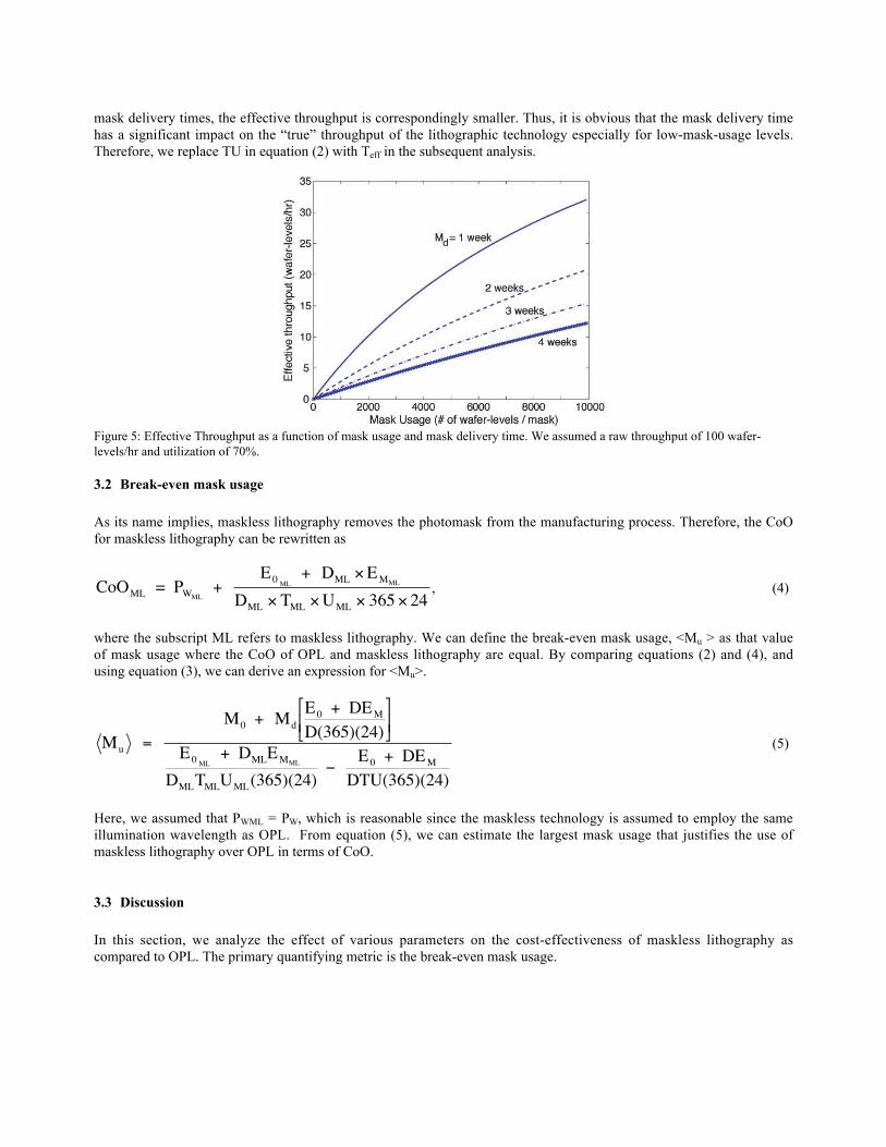
mask delivery times, the effective throughput is correspondingly smaller. Thus, it is obvious that the mask delivery timehas a significant impact on the “true” throughput of the lithographic technology especially for low-mask-usage levels.Therefore, we replace TU in equation (2) with Teff in the subsequent analysis.
Figure 5: Effective Throughput as a function of mask usage and mask delivery time. We assumed a raw throughput of 100 wafer-levels/hr and utilization of 70%.
3.2 Break-even mask usage
As its name implies, maskless lithography removes the photomask from the manufacturing process. Therefore, the CoOfor maskless lithography can be rewritten as
€
CoOML = PWML +
E0 ML + DML ×EMML
DML × TML ×UML × 365 × 24, (4)
where the subscript ML refers to maskless lithography. We can define the break-even mask usage, <Mu > as that valueof mask usage where the CoO of OPL and maskless lithography are equal. By comparing equations (2) and (4), andusing equation (3), we can derive an expression for <Mu>.
€
Mu = M0 + Md
E0 + DE M
D(365)(24)
E0 ML + DMLEMML
DMLTMLUML(365)(24) − E0 + DE M
DTU(365)(24)
(5)
Here, we assumed that PWML = PW, which is reasonable since the maskless technology is assumed to employ the sameillumination wavelength as OPL. From equation (5), we can estimate the largest mask usage that justifies the use ofmaskless lithography over OPL in terms of CoO.
3.3 Discussion
In this section, we analyze the effect of various parameters on the cost-effectiveness of maskless lithography ascompared to OPL. The primary quantifying metric is the break-even mask usage.

Figure 6 shows the break-even mask usage as a function of the OPL tool cost. The assumptions used in the calculationare enumerated in the figure caption. Note that for typical values, the break-even mask usage is over a thousand wafersper mask even at low tool costs of ~ $10M. For a high tool cost of $50M, the break-even mask usage is as high as 3500i.e. it is cheaper to use maskless lithography if fewer than 3500 wafers are printed using one photomask.
Figure 6: Break-even mask usage as a function of OPL tool cost. We assumed that M0 = $25,000, Md = 1 week, D = 5 years, EM =$1M, T = 100WPH, U = 70%, E0ML = $8M, EMML = $1M, and TML = 5WPH.
Figure 7 shows the break-even mask usage as a function of the photomask cost. The assumptions are defined in thecaption. Note that for a typical mask of cost $25,000, maskless lithography is cheaper if fewer than ~1800 wafers areprinted per mask. This number increases linearly with increasing mask cost.
Figure 7: Break-even mask usage as a function of photomask cost. We assumed that E0 = $25M, Md = 1 week, D = 5 years, EM =$1M, T = 100WPH, U = 70%, E0ML = $8M, EMML = $1M, and TML = 5WPH.
Figure 8 shows the break-even mask usage as a function of the mask delivery time (in weeks). For a typical deliverytime of 1 week, the break-even point is around 1800 wafers per mask. The break-even point is almost linearlyproportional to the mask delivery time.

Figure 8: Break-even mask usage as a function of photomask delivery time. We assumed that E0 = $25M, M0 = $25,000, D = 5 years,EM = $1M, T = 100WPH, U = 70%, E0ML = $8M, EMML = $1M, and TML = 5WPH.
Figure 9 shows the break-even mask usage as a function of the raw OPL tool throughput in wafers per hour (WPH). Asexpected, higher the throughput, the smaller the break-even point. Even at very high throughputs of 200 WPH, thebreak-even point is over 1750 wafers per mask.
Figure 9: Break-even mask usage as a function of OPL tool throughput. We assumed that E0 = $25M, M0 = $25,000, D = 5 years, EM
= $1M, Md = 1 week, U = 70%, E0ML = $8M, EMML = $1M, and TML = 5WPH.
We can also compare the actual CoO of maskless lithography and OPL as a function of the mask usage. In Figure 10,difference in CoO between OPL and maskless lithography (defined as the savings achieved by using masklesslithography) is plotted as a function of the mask usage. As expected, for low mask usage, the savings are very high.Even for a mask usage of 1000, the savings achieved by maskless lithography is about $65 per wafer-level.

Figure 10: Difference in CoO between OPL and maskless lithography as a function of mask usage. We assumed that PW = $7, E0 =$25M, T = 100 WPH, M0 = $25,000, D = 5 years, EM = $1M, Md = 1 week, U = 70%, E0ML = $8M, EMML = $1M, and TML = 5WPH.
Figure 11 shows the CoO of maskless lithography as a function of its raw throughput. This analysis creates acompelling case to pursue the highest possible throughput in maskless lithography. CoO is over $4000 in the case ofvery slow maskless lithography (T ~ 0.1 WPH) such as in single-beam scanning-electron beam lithography (SEBL).ZPAL can achieve throughputs in the order of 5 WPH, which reduces the CoO to about $90, a reduction of over anorder of magnitude compared to SEBL.
Figure 11: CoO of maskless lithography as a function of throughput. We assumed that PW = $7, D = 5 years, U = 70%, E0ML = $8M,and EMML = $1M.
4. CONCLUSION
The feasibility of maskless lithography in the form of ZPAL was demonstrated in the past. In this paper, we summarizethe earlier results as well as present some improved results in terms of resolution, image contrast and pattern fidelity.ZPAL has shown high quality patterning at extremely low k1 values (less than 0.3). We also analyzed the cost-of-ownership of ZPAL and compared it to that of OPL. We demonstrated that the mask delivery time could have asignificant impact on the CoO especially for low mask usage. Hence, we propose the use of an “effective throughput”for OPL, which takes into account the mask delivery time. Finally, our analysis indicates that for a typical case,maskless lithography is justified when the mask usage is fewer than ~1800 wafers per photomask.
REFERENCES
[1] Wong, A. K-K., Resolution enhancement techniques in optical lithography, SPIE Press, Bellingham, (2001).
[2] R. Menon, A. Patel, D. Gil and H. I. Smith, “Maskless Lithography”, Materials Today, p. 26-33, February, 2005.
[3] R. Menon. A. Patel, E. E. Moon, and H. I. Smith, “An Alpha Prototype System for Zone-Plate-Array Lithography”,J. Vac. Sci. Technol. B, 22 (16), p. 3032-3037, 2004.
[4] D. Gil, R. Menon, and H. I. Smith, “Fabrication of High-Numerical-Aperture Phase Zone Plates with a SingleLithography Exposure and no Etching”, J. Vac. Sci. Technol. B, 21 (6), p. 2956-2960, 2003.
[5] W. Jung, F. J. Castaño, C. A. Ross, R. Menon, A. Patel, E. E. Moon, M. K. Mondol, and H. I. Smith, “EllipticalRing Magnetic Arrays fabricated using Zone-Plate-Array Lithography”, J. Vac. Sci. Technol. B, 22 (16), p. 3335-3338,2004.
[6] D. Gil, R. Menon, D. J. D. Carter and H. I. Smith, “Lithographic Patterning and Confocal Imaging with ZonePlates”, J. Vac. Sci. Technol. B, 18 (6), p. 2881-2885, 2000.
[7] R. Menon, D. Gil, G. Barbastathis, and H. I. Smith, “Photon-sieve lithography”, J. Opt. Soc. Am. A, 22 (2), p. 342-345, 2005.
[8] H. I. Smith, “A proposal for maskless zone-plate-array nanolithography”, J. Vac. Sci. Technol. B, 14 (6), 1996.
[9] R. Menon, E. E. Moon, M. K. Mondol, F. J. Castaño, and H. I. Smith, “Scanning-Spatial-Phase Alignment for Zone-Plate-Array Lithography”, J. Vac. Sci. Technol. B, 22 (16), p. 3382-3385, 2004.
[10] E. E. Moon, L. Chen, P. N. Everett, M. K. Mondol, and H. I. Smith, “Interferometric-spatial-phase imaging for six-axis mask control”, J. Vac. Sci. Technol. B, 21 (6), p. 3112-3115, 2003.
[11] E. Muzio, P Seidel, G. Shelden, and J. Canning, “An overview of cost of ownership for optical lithography at the100nm and 70nm generations”, Semiconductor Fabtech, 11, p. 191-194.
[12] Y. Z. Ke, P. Ware, K. Kotoku, and Y. Yamada, “Cost-of-ownership analysis for 300mm lithography mix-and-match applications”, Semiconductor Fabtech 12, p. 175-178.
[13] S. V. Sreenivasan, C. G. Wilson, N. E. Schumaker, D. J. Resnick, “Cost of Ownership Analysis for Patterningusing step and flash imprint lithography”, Proc. SPIE, v. 4688, p. 903-909 (2002).