3D patterning by means of nanoimprinting, X-ray and two-photon lithography
7
3D patterning by means of nanoimprinting, X-ray and two-photon lithography M. Tormen a , L. Businaro a , M. Altissimo a , F. Romanato a , S. Cabrini a , F. Perennes b , R. Proietti a,c , Hong-Bo Sun c , Satoshi Kawata d,e , E. Di Fabrizio a, * a LILIT-NNL (National Nanotechnology Laboratory), TASC-INFM, Nanolithography beamline at Elettra Synchrotron Light Source, S.S.14 km 163.5, Area Science Park, 34012 Basovizza, Trieste, Italy b Elettra Synchrotron Light Source, S.S.14 km 163.5, Area Science Park, 34012 Basovizza, Trieste, Italy c PRESTO, Department of Applied Physics, Japan Science and Technology Corporation (JST), Osaka University, Suita, Osaka 565-0871, Japan d Department of Applied Physics, Osaka University, Suita, Osaka 565-0871, Japan e The Institute of Physical and Chemical Research (RIKEN), Hirosawa, Wako, Saitama 351-0198, Japan Available online 14 March 2004 Abstract Two lithographic techniques suitable for fabricating complex 3D structures with high spatial resolution are pre- sented and discussed. The first one is based on the combined use of nanoimprint and X-ray lithography. Its techno- logical potential has been demonstrated by patterning several types of structures with X-ray lithography on hexagonal array of hemispheres obtained previously by nanoimprinting. These consecutive steps give rise to an intersection- structure where the overall profile of high aspect ratio structures is enveloped by the original 3D imprinted profile. The second technique, two-photon lithography, is an intrinsic 3D lithography and has the highest potential for structuring 3D in the widest sense. The principle of this technology and experimental results in the field of nanomechanics and photonics will be presented. Ó 2004 Elsevier B.V. All rights reserved. Keywords: Nanoimprint lithography; X-ray lithography; Two photon lithography; 3D microstructures and nanostructures In the fast run toward device miniaturization, microelectronics has relied on planar lithography and layering of essentially 2D structures. Techno- logical advances in micro- and nanoelectrome- chanical systems [1] (MEMS, NEMS), microfluidic devices [2], micro- or nano-optics (diffractive op- tics [3], high efficiency multilevel zone plates [4], photonic crystals [5]), and innovations in the toolset of biology (microfluidic chips for DNA array [6]) and medicine (microsurgical tools [7], drug delivery) will require the development of fully 3D structuring capabilities at the nanometer scale. * Corresponding author. Tel.: +390403758417; fax: +390402 26767. E-mail address: [email protected] (E. Di Fabrizio). 0167-9317/$ - see front matter Ó 2004 Elsevier B.V. All rights reserved. doi:10.1016/j.mee.2004.02.081 www.elsevier.com/locate/mee Microelectronic Engineering 73–74 (2004) 535–541
Transcript of 3D patterning by means of nanoimprinting, X-ray and two-photon lithography

www.elsevier.com/locate/mee
Microelectronic Engineering 73–74 (2004) 535–541
3D patterning by means of nanoimprinting, X-rayand two-photon lithography
M. Tormen a, L. Businaro a, M. Altissimo a, F. Romanato a, S. Cabrini a,F. Perennes b, R. Proietti a,c, Hong-Bo Sun c, Satoshi Kawata d,e,
E. Di Fabrizio a,*
a LILIT-NNL (National Nanotechnology Laboratory), TASC-INFM, Nanolithography beamline at Elettra Synchrotron Light Source,
S.S.14 km 163.5, Area Science Park, 34012 Basovizza, Trieste, Italyb Elettra Synchrotron Light Source, S.S.14 km 163.5, Area Science Park, 34012 Basovizza, Trieste, Italy
c PRESTO, Department of Applied Physics, Japan Science and Technology Corporation (JST), Osaka University, Suita,
Osaka 565-0871, Japand Department of Applied Physics, Osaka University, Suita, Osaka 565-0871, Japan
e The Institute of Physical and Chemical Research (RIKEN), Hirosawa, Wako, Saitama 351-0198, Japan
Available online 14 March 2004
Abstract
Two lithographic techniques suitable for fabricating complex 3D structures with high spatial resolution are pre-
sented and discussed. The first one is based on the combined use of nanoimprint and X-ray lithography. Its techno-
logical potential has been demonstrated by patterning several types of structures with X-ray lithography on hexagonal
array of hemispheres obtained previously by nanoimprinting. These consecutive steps give rise to an intersection-
structure where the overall profile of high aspect ratio structures is enveloped by the original 3D imprinted profile. The
second technique, two-photon lithography, is an intrinsic 3D lithography and has the highest potential for structuring
3D in the widest sense. The principle of this technology and experimental results in the field of nanomechanics and
photonics will be presented.
� 2004 Elsevier B.V. All rights reserved.
Keywords: Nanoimprint lithography; X-ray lithography; Two photon lithography; 3D microstructures and nanostructures
In the fast run toward device miniaturization,
microelectronics has relied on planar lithography
and layering of essentially 2D structures. Techno-logical advances in micro- and nanoelectrome-
* Corresponding author. Tel.: +390403758417; fax: +390402
26767.
E-mail address: [email protected] (E. Di Fabrizio).
0167-9317/$ - see front matter � 2004 Elsevier B.V. All rights reserv
doi:10.1016/j.mee.2004.02.081
chanical systems [1] (MEMS, NEMS), microfluidic
devices [2], micro- or nano-optics (diffractive op-
tics [3], high efficiency multilevel zone plates [4],photonic crystals [5]), and innovations in the
toolset of biology (microfluidic chips for DNA
array [6]) and medicine (microsurgical tools [7],
drug delivery) will require the development of fully
3D structuring capabilities at the nanometer scale.
ed.

Fig. 1. Hexagonal array of microlenses imprinted in PMMA.
536 M. Tormen et al. / Microelectronic Engineering 73–74 (2004) 535–541
In the search for methods for 3D structuring of
matter at sub-micron resolution level, several
lithographic techniques have been explored. elec-
tron beam lithography (EBL) for example can
generate ‘‘gray-scale’’ profiles by control of the
exposure dose. High resolution X-ray lithography(XRL) can replicate multilevel mask amplifying
the thickness profile [8] and can generate complex
3D structures with multiple exposure at tilted an-
gles [9]. Focused ion beam (FIB) lithography has
shown capability for direct milling and for growth
of hard materials [10]. Nanoimprint lithography
(NIL) can mould 3D profiles [11].
All lithographies above have their own pecu-liarities and potentialities which in many cases are
not completely exploited and cannot cover the
entire spectrum of the fabrication needs.
In this paper, we present results about two
techniques, the first based on the combined use of
nanoimprinting and X-ray lithography and the
other based on two-photon induced photopoly-
merization. Two-photon lithography has recentlybeen established as a powerful tool for laser pre-
cision microfabrication since its first proposal [8]
by which various 3D photonic devices and micro/
nanomachine systems have been readily produced.
In this work, the combination of nanoimprint
and X-ray lithography has been employed for
fabricating non-conventional 3D polymer struc-
tures. The technological potential of this method isdemonstrated by patterning with X-ray lithogra-
phy several types of structures on hexagonal arrays
of hemispheres previously obtained by nanoim-
printing. The overall profile consists of high aspect
ratio trenches and/or pillars modulated by slowly
varying 3D structures defined by imprinting.
Both imprinting and X-ray lithography possess
their own 3D patterning capabilities. NIL is a highresolution (sub-10 nm), low cost, high throughput
technique that has intrinsically 3D replication
potentiality. Fig. 1 shows for example an array of
PMMA hemispheres closely packed in a 20 lmhexagonal lattice. The master used for NIL was
fabricated by isotropic etching of a fused silica
substrate to form an array of hemispherical cavi-
ties. The imprinting step was carried out onto a 6lm thick 950 K poly(methyl-methacrylate) film on
silicon, at a pressure of 20 MPa and a temperature
of 210 �C. The imprinted structures are correctly
reproduced on the entire area of the stamp (Fig. 1).
This result illustrates the capability of NIL to
form smooth curved surfaces over large areas.
Obviously, a large variety of master profiles can be
transferred into polymers by NIL. However, some
principle and practical limitations exist for arbi-
trary structures. For example, it would be difficultto fabricate arrays of pillars oriented in any direc-
tion differing from the normal to the substrate or
any structure having overhanging parts. Their
presence would make it impossible to separate the
mould from the polymer in a non-destructive way.
A second limitation to the 3D NIL patterning ca-
pabilities is related to the aspect ratio of the struc-
tures. Due to stresses produced by shear and tensileforces at the surfaces of micro- and nanostructures
during the release of the master, high aspect ratio
structures suffer high mechanical stresses and may
easily break. At present, the highest aspect ratios
that can obtained by NIL are �3.
XRL does not share these limitations of NIL.
In this respect, XRL is well known to provide as-
pect ratios attaining values of �20 (for structureswith lm scale resolution), and resolution that at its
present status of development can go below 50 nm.
Geometrically, the structures obtainable by XRL
can be described as the intersection of the volume
shadowed by a 2D pattern defined on a mask, with
the volume of the resist film. As the 2D pattern of
the mask can be projected in arbitrary directions
with respect to the resist film, XRL allows defini-
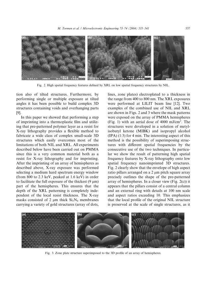
Fig. 2. High spatial frequency features defined by XRL on low spatial frequency structures by NIL.
M. Tormen et al. / Microelectronic Engineering 73–74 (2004) 535–541 537
tion also of tilted structures. Furthermore, by
performing single or multiple exposure at tilted
angles it has been possible to build complex 3D
structures containing voids and overhanging parts
[9].
In this paper we showed that performing a step
of imprinting into a thermoplastic film and utiliz-
ing that pre-patterned polymer layer as a resist forX-ray lithography provides a flexible method to
fabricate a wide class of complex small-scale 3D
structures which easily overcomes most of the
limitations of both NIL and XRL. All experiments
described below have been carried out on PMMA
since this is a very common material both as a
resist for X-ray lithography and for imprinting.
After the imprinting of an array of hemispheres asdescribed above, X-ray exposure was performed
selecting a medium hard spectrum energy window
(from 800 to 2.3 keV, peaked at 1.6 keV) in order
to facilitate the full exposure of the thickest (9 lm)
part of the hemispheres. This ensures that the
depth of the XRL patterning is completely inde-
pendent of the local resist thickness. The X-ray
masks consisted of 2 lm thick Si3N4 membranescarrying a variety of gold structures (array of dots,
Fig. 3. Zone plate structure superimposed to th
lines, zone plates) electroplated to a thickness in
the range from 400 to 800 nm. The XRL exposures
were performed at LILIT beam line [12]. Two
examples of the combined use of NIL and XRL
are shown in Figs. 2 and 3 where the mask patterns
were exposed on the array of PMMA hemispheres
(Fig. 1) with an aerial dose of 4000 mJ/cm2. The
structures were developed in a solution of metyl-isobutyl ketone (MIBK) and isopropyl alcohol
(IPA) (1:3) for 4 min. The interesting aspect of this
method is the possibility of superimposing struc-
tures with different spatial frequencies by the
consecutive use of the two techniques. In particu-
lar we show the result of patterning high spatial
frequency features by X-ray lithography onto low
spatial frequency nanoimprinted 3D structures.Fig. 2 clearly show that the envelope of high aspect
ratio pillars arranged on a 2 lm pitch square array
precisely outlines the shape of the pre-patterned
array of hemispheres. In a closer view (Fig. 2(c)) it
appears that the pillars consist of a central column
and an external ring with details at 100 nm scale
and aspect ratios exceeding 10. This emphasizes
that the local profile of the original NIL structureis preserved at the scale of single structures, as it
e 3D profile of an array of hemispheres.

538 M. Tormen et al. / Microelectronic Engineering 73–74 (2004) 535–541
can be easily recognized from the slope of the top
of the pillars.
We present also the results of the X-ray expo-
sure of a zone plate (Fig. 3) on an imprinted array
of hemispheres. The X-ray mask consisted of a 2
lm thick silicon nitrate membrane with 500 nmgold in the absorbing regions, giving a transmitted
intensity contrast of 15:1 between transparent and
absorbing regions. The high penetration depth of
the X-rays makes the lithographic image almost
insensitive to the thickness modulation of the pre-
existing structure.
Although, Fig. 3(a)–(c) shows the results of a
process that could be considered just as a lithog-raphy test, it shows that special optical elements
containing refractive and diffractive components
could be produced.
The second technology considered in this paper
is two-photon photopolymerization. The basic
idea is tightly focusing a femtosecond (fs) la-
ser into a photopolymerizable resin and directly
writing 3D patterns by focus or sample scanning.Due to the quadratic dependence of two-photon
absorption (TPA) rate on laser power, photopo-
lymerization (solidification) occurs only at the
close vicinity of the focal spot. Then following
the scanning locus, a solidified skeleton will be
formed, which remains after the removal of un-
solidified liquid resin [13]. With this method, var-
ious micromachines [14,15] and photonic crystals[13,16,17,19] have been readily produced with
near-diffraction-limit 3D spatial resolutions.
Starting liquid materials could be converted
into solid phase upon light exposure by photo-
polymerization [18,20]. Photopolymerization is
usually concerned with creation of a polymer
through a chain reaction initiated by light. Since
most monomers and oligomers commonly em-ployed do not possess initiating species with a
sufficient quantum yield upon light exposure, it is
necessary to introduce low-molecular-weight
molecules called photoinitiators that start poly-
merization. A photosensitizer is also generally
used, which has a large light absorbance and
transfers the excitation to a photoinitiator. For
all fabrications presented in this research, we usedresins consisting of urethane acrylate monomer/
oligomer and radical initiators. Photopolymer-
ization is a photochemical reaction that occurs
when photon energy is provided. Electronic
transition energy for most initiator molecules
corresponds to UV spectral range.
In particular, benzoyl chromophor is sensitive
to near UV wavelength, and has a good photo-chemical reactivity, therefore utilized as common
UV radical initiators. If the irradiation photon
fluence is sufficiently high, e.g., by tightly focusing
a fs laser, the probability of an electron simulta-
neously absorbing two photons is increased, and
then TPA becomes practically useful.
Typical cross-sections for one- and two-photon
processes are 10�6 cm2 and 10�50 cm4 s/photon,respectively. For producing sufficient photon flux
density, it is essential to tightly confine laser pulses
in both spatial and time domains. This, for the
work presented in this article, was accomplished
by a homemade system. A Titanium:Sapphire laser
that operated in mode-lock at 76 MHz and 780 nm
with a 150-fs pulsewidth is utilized as the exposure
source. A two-galvano-mirror set moves the laserbeam in the two horizontal dimensions, and a
piezo stage moved the laser focus vertically, both
controlled by a computer. The laser is focused into
the resin by a high numerical aperture (NA �1.4,
oil immersion) objective lens. The single-lens fo-
cusing geometry naturally satisfies the requirement
of pulse overlapping in both time and spatial do-
mains. In this system, the utilization of shortpulsewidth and tight focusing are critical for ex-
citing sufficient amount of TPA and for achieve-
ment of high accuracy of fabrication. An average
focal spot power of 1 mW under a 150 fs pulse-
width and 76 MHz repetition rate corresponds to a
transient peak power of 20 GW/cm, or a photon
flux density of 8� 10 [22] photon s�1 lm�2.
Laser scanning is the step to convert pre-de-signed CAD pattern to a resist structure. We used
two basic modes for direct laser scanning, i.e.,
raster-scan mode and vector-scan mode. In the
raster mode, all voxels in a cubic volume that
contains the microstructure are scanned by the
actual/virtual focal spot, depending on the shutter
ON/OFF (actual/virtual). In the vector mode, the
laser focus directly traces the profile to be defined,and requires a smaller number of voxels. De-
pending on structures, alternations and combina-

M. Tormen et al. / Microelectronic Engineering 73–74 (2004) 535–541 539
tion of the these two basic scanning modes could
be used. Experimentally we fabricated the same
object using the two modes. The microbull in
Fig. 4(a) was produced using a layer-by-layer
raster-scanning scheme, i.e., all voxels consisting
of the bull were exposed point-by-point, line-by-line, and layer-by-layer by a two-photon process.
As a result, it took 3 h to complete the manufac-
turing. If we make a detailed analysis on the bull
structure, it is found that the entire bull consists of
2� 106 voxels. However, the bull profile can be
well defined with only 5% of them. As a test, the
bull was written once more by using the vector
scanning. Astonishingly, we find it possible to de-pict the same structure within 13 min (Fig. 4(b)).
In both cases the scanning step in 3D was 50 nm,
the latter, however, the fabrication time in vector
scan was reduced by more than 90%. The TPA
produced bull crust was self-supported, standing
on glass substrate either in liquid or in air. To
avoid possible distortion, we further solidified the
structure under a mercury lamp, which is a single-photon exposure process.
Two-photon photopolymerization becomes
conspicuous in the race for developing 3D pho-
tonic crystals (PhCs) due to its intrinsic 3D pro-
cessing capability [17,19,22] and the potential to
comprise materials of various properties like
fluorescence emission and refractive index tuning
for device functions. Since the demonstration of aphotonic bandgap (PBG) in two-photon photo-
polymerized PhCs [18,20] much research effort has
been attracted to laser nanofabrication of polymer
Fig. 4. (a) SEM images of a microbull structure produced by raster sc
(b) The same structure but produced by vector scanning. Only the cr
solidified by illumination under an mercury lamp.
photonic lattices [21,23]. However, most efforts
result in no presence of the PBG effect. To solve
this problem, a high-reproducibility and high-fi-
delity writing scheme was recently proposed. It
utilizes finely quantified pixels and subdiffraction-
limited voxels to precisely depict the shape and sizeof elements, and employs a pre-compensation
method to correct the structural deformation
brought on by polymerization shrinkage. In order
to maximize the PBG effect for given component
materials, more complicated lattices are generally
required for the purpose of tailoring the density of
photon states. For example, rod overlapped fct,
diamond, and distorted diamond open the largestfull band gap between the second and the third
photonic bands [24]. Realization of these struc-
tures with sub-micron feature sizes is arduous by
conventional techniques, but within the scope of
two-photon photopolymerization since more
complicated 3D nanomachines have been created
[17,19,26,27]. However, related work has not been
reported yet. As the first step toward arbitrary-lattice 3D PhCs, we herein report a covalent-bond
type diamond crystal with pronounced band-gap
effect. Fig. 5(a) illustrates the diamond structure,
which is composed of two interpenetrating fcc
lattices, one displaced 1/4 of a lattice constant, L,in each direction from the other. Each atom is
tetrahedrally coordinated with four other atoms in
the other sublattice. Examples of electronic crys-tals with the diamond crystal structure are dia-
mond, silicon, and germanium. In PhCs, the
crystal atoms are represented as photonic atoms.
anning, where all voxels were formed by two-photon exposure.
ust was defined by the two-photon process and the inside was

Fig. 5. Stick-and-ball model of unit cells of diamond lattices. (a) Schematic illustration, and (b) two-photon photopolymerized 2� 1
primitive. Letters denote vertical atomic coordinates: Að0Þ, Bð1=4Þ, Cð1=2Þ, Dð3=4Þ, and A0(4/4). (c) Two-photon photopolymerized
diamond PhCs. A 8� 8� 2 period crystal, from which a PBG was measured.
540 M. Tormen et al. / Microelectronic Engineering 73–74 (2004) 535–541
Different from the case in a solid matrix [28], inside
which atoms are inlaid or, in situ fixed where they
are positioned, photonic atoms polymerized fromliquids need connection. The linking bridges, or
covalent bonds in a stick-and-ball molecular
model, are actually the major component in at-
tained crystal configuration. Rather than image
observation, the accomplishment of high-quality
PhCs has been confirmed by their band-gap effect.
Shown in Fig. 6 are the transmission spectra of the
demonstrated structure (Fig. 5(c)) as well as asimilar lattice with K ¼ 3:0 lm, both normalized
to the transmission of a featureless solidified resin
bulk. The transmission minima are at 3790 cm�1
Fig. 6. Transmission spectra of diamond-lattice PhCs with
periods of 2.5 and 3.0 lm. The gray curve is from the uni-
formly polymerized resin film, to which the two spectra were
normalized.
(k ¼ 2:6 lm) and 3100 cm�1 (k ¼ 3:2 lm), re-
spectively. They occur at the identical normalized
frequency of 1.05, as defined by k=K showing thelinear scaling performance of the diamond lattices.
This implies that the band-gap effect of 1.55 lm-
lattice PhCs, of which the fabrication is, in prin-
ciple, of no problem due to the 100 nm lateral
spatial resolution, should occur approximately at
the communication wavelength of 1.55 lm. A
complete PBG is not expected from these crystals
since the refractive index contrast (�1.5) is farlower than that necessary for the current lattice to
open a full band gap (�2.0) [25], however, the
single-period transmission attenuation as large as
35% indicates the necessity to select a suitable
lattice type for a strong PBG effect. A natural
extension of this work is the enhancement of re-
fractive index of photopolymerizable materials to
above 2.0, which has been proved possible fromour preliminary research.
The techniques explored in this paper allows the
realization of a very broad class of 3D micro- and
nano-objects. In absolute, the technique that al-
lows the fabrication of the most general topologies
and morphologies is two-photon lithography.
Unfortunately, it suffers from a low throughput
due to the sequential nature of the laser scanningprocess. In order to limit this problem, ongoing
efforts are devoted to increasing the parallelism of
the technique, as for example by using dynamic
diffractive optics to generate and scan a distribu-

M. Tormen et al. / Microelectronic Engineering 73–74 (2004) 535–541 541
tion of independent focal points. The other
techniques considered in the paper, nanoimprint,
X-ray lithographies and combination thereof are
instead parallel techniques. In particular, while
maintaining their individual characteristics of
highly parallel high-throughput methods the con-secutive use of nanoimprint, X-ray lithographies
greatly enlarges the possibilities for 3D structur-
ing. Although, still this combination cannot com-
pete with the versatility of two-photon lithography
they could become in future very useful in several
domains of micro- and nanotechnology. It would
make it possible for example to conceive and to
realize new innovative devices that involve existingprocedures for the accurate (sub-50 nm) alignment
of the X-ray lithography to NIL structures.
Moreover, the parallelism of NIL and XRL would
allow to upscale the fabrication of complex 3D
nano- or micro-objects to a mass-production level.
In particular this could become important for
special optical elements that exploit diffractive and
refractive phenomena for a better tailoring of thelight propagation.
In the next future it will be attempted the
combination of NIL, XRL and TPA. In fact due
to the alignment capabilities already available in
XRL steppers, it is in principle possible to write
very complex 3D structures in a mix and match
strategy by using all three fabrication techniques.
Photonics, microfluidics for diagnostic bio-physics and drug delivery, new hybrid optics, will
be the fields where we will first attempt the merg-
ing of these three fabrication methods.
References
[1] H.G. Craighead, Science 290 (2000) 1535.
[2] Hongkai Wu, Teri W. Odom, Daniel T. Chiu, George M.
Whitesides, J. Am. Chem. Soc. 125 (2003) 554.
[3] P. Ehbets, H.P. Herzig, D. Prongu�e, M.T. Gale, Opt. Lett.
17 (1992) 908.
[4] E. Di Fabrizio, F. Romanato, M. Gentili, S. Cabrini, B.
Kaulich, J. Susini, R. Barrett, Nature 401 (1999) 895.
[5] Yurii A. Vlasov, Xiang-Zheng Bo, James C. Sturm, David
J. Norris, Nature 414 (2001) 289.
[6] J. Khandurina, A. Guttman, J. Chromatography A 943
(2002) 159.
[7] Michael J. Vasile, Raja Nassar, Jushan Xie, J. Vac. Sci.
Technol. B 16 (1998) 2499.
[8] Pantazis Mouroulis, Frank T. Hartley, Daniel W. Wilson,
Victor E. White, Opt. Exp. 11 (2003) 270.
[9] C. Cuisin, A. Chelnokov, J.-M. Lourtioz, D. Decanini, Y.
Chen, Appl. Phys. Lett. 77 (2000) 770;
F. Romanato, L. Businaro, L. Vaccari, S. Cabrini,
P. Candeloro, M. De Vittorio, A. Passaseo, M.T.
Todaro, R. Cingolani, E. Cattaruzza, M. Galli, C. And-
reani, E. Di Fabrizio, Microelectron. Eng. 67–68 (2003)
679.
[10] Michael J. Vasile, Raja Nassar, Jushan Xie, J. Vac. Sci.
Technol. B 16 (1998) 2499.
[11] Mingtao Li, Lei Chen, Stephen Y. Chou, Appl. Phys. Lett.
78 (2001) 3322.
[12] E. Di Fabrizio, A. Nucara, M. Gentili, R. Cingolani, Rev.
Sci. Instrum. 70 (1999) 1605;
Filippo Romanato, Enzo Di Fabrizio, Lisa Vaccari, M.
Altissimo, D. Cojoc, L. Businaro, Stefano Cabrini, Micro-
electron. Eng. 57–58 (2001) 101.
[13] H.-B. Sun, S. Matsuo, H. Misawa, Appl. Phys. Lett. 74
(1999) 786–788.
[14] S. Maruo, S. Kawata, J. Microelectromech. Syst. 7 (1998)
411–415.
[15] H.-B. Sun, T. Kawakami, Y. Xu, J.-Y. Ye, S. Matuso,
H. Misawa, M. Miwa, R. Kaneko, Opt. Lett. 25 (2000)
1110–1112.
[16] B.H. Cumpston, S.P. Ananthavel, S. Barlow, D.L. Dyer,
J.E. Ehrlich, L.L. Erskine, A.A. Heikal, S.M. Kuebuler, I.-
Y. Sandy Lee, D.M. Maugon, J. Qin, H. Rokel, M. Rumi,
X. Wu, S.R. Marder, J.W. Perry, Nature 398 (1999)
51–54.
[17] H.-B. Sun, V. Mizeikis, Y. Xu, S. Juodkazis, J.-Y. Ye, S.
Matsuo, H. Misawa, Appl. Phys. Lett. 79 (2001) 1–3.
[18] G. Odian, Principles of Polymerization, third ed., Wiley,
New York, 1991.
[19] S. Kawata, H.-B. Sun, T. Tanaka, K. Takada, Nature
(London) 412 (2001) 667.
[20] H.-B. Sun, S. Matsuo, H. Misawa, Appl. Phys. Lett. 74
(1999) 786.
[21] H.-B. Sun, V. Mizeikis, Y. Xu, S. Juodkazis, J.-Y. Ye, S.
Matsuo, H. Misawa, Appl. Phys. Lett. 79 (2001) 1.
[22] S. Maruo, O. Nakamura, S. Kawata, Opt. Lett. 22 (1997)
132.
[23] J. Serbin, A. Egbert, A. Ostendorf, B.N. Chichkov, R.
Houbertz, G. Domann, J. Schulz, C. Cronauer, L. Froh-
lich, M. Popall, Opt. Lett. 28 (2003) 301.
[24] R. Bitwas, C.T. Chan, M. Sigalas, C.M. Soukoulis,
K.M. Ho, in: C.M. Soukoulis (Ed.), Photonic Band
Gap Materials, Kluwer Academic Publishers, Dordrecht,
1995.
[25] K.M. Ho, C.T. Chan, C.M. Soukoulis, Phys. Rev. Lett. 65
(1990) 3152.
[26] H.-B. Sun, K. Takada, S. Kawata, Appl. Phys. Lett. 79
(2001) 3173.
[27] P. Galajda, P. Ormos, Appl. Phys. Lett. 78 (2001) 249.
[28] H.-B. Sun, Y. Xu, S. Juodkazis, K. Sun, M. Watanabe, S.
Matsuo, H. Misawa, J. Nishii, Opt. Lett. 26 (2001)
325.