PDMS patterning by proton beam - arXiv
19
1. Selective etching of PDMS: etching as positive resist S.Z. Szilasi 1,* , C. Cserháti 2 1 Institute for Nuclear Research, Hungarian Academy of Sciences, H-4001 Debrecen, P.O. Box 51, Hungary 2 University of Debrecen, Dept. of Solid State Physics, H-4010 Debrecen, P.O. Box 2, Hungary * Corresponding author. S.Z. Szilasi Address: Institute of Nuclear Research of the Hungarian Academy of Sciences H-4026 Debrecen Bem tér 18/c, Mail: H-4001 Debrecen, POB. 51 Hungary E-mail address: [email protected] Tel: +36 52 509 200; Fax: +36 52 416 181 Abstract Although, poly(dimethylsiloxane) (PDMS) is a widely used material in numerous applications, such as micro- or nanofabrication, the method of its selective etching has not been known up to now. In this work authors present two methods of etching the pure, additive-free and cured PDMS as a positive resist material. To achieve the chemical modification of the polymer necessary for selective etching, energetic ions were used. We created 7 m and 45 m thick PDMS layers and patterned them by a focused proton microbeam with various, relatively large fluences. In this paper authors demonstrate that 30 wt% Potassium Hydroxide (KOH) or 30 wt% sodium hydroxide (NaOH)
-
Upload
khangminh22 -
Category
Documents
-
view
0 -
download
0
Transcript of PDMS patterning by proton beam - arXiv
1.
Selective etching of PDMS: etching as positive resist
S.Z. Szilasi1,*, C. Cserháti2
1 Institute for Nuclear Research, Hungarian Academy of Sciences,
H-4001 Debrecen, P.O. Box 51, Hungary
2 University of Debrecen, Dept. of Solid State Physics,
H-4010 Debrecen, P.O. Box 2, Hungary
* Corresponding author. S.Z. Szilasi
Address: Institute of Nuclear Research of the Hungarian Academy of Sciences
H-4026 Debrecen Bem tér 18/c, Mail: H-4001 Debrecen, POB. 51 Hungary
E-mail address: [email protected]
Tel: +36 52 509 200; Fax: +36 52 416 181
Abstract
Although, poly(dimethylsiloxane) (PDMS) is a widely used material in numerous
applications, such as micro- or nanofabrication, the method of its selective etching has not
been known up to now. In this work authors present two methods of etching the pure,
additive-free and cured PDMS as a positive resist material.
To achieve the chemical modification of the polymer necessary for selective etching,
energetic ions were used. We created 7 m and 45 m thick PDMS layers and patterned them
by a focused proton microbeam with various, relatively large fluences. In this paper authors
demonstrate that 30 wt% Potassium Hydroxide (KOH) or 30 wt% sodium hydroxide (NaOH)
2.
at 70 oC temperature etch proton irradiated PDMS selectively, and remove the chemically
sufficiently modified areas. In case of KOH development, the maximum etching rate was
approximately 3.5 m/minute and it occurs at about 7.5×10¹⁵ ion × cm-2. In case of NaOH
etching the maximum etching rate is slightly lower, 1.75 m/minute and can be found at the
slightly higher fluence of 8.75×10¹⁵ ion × cm-2.
These results are of high importance since up to this time it has not been known how to
develop the additive-free, cross-linked poly(dimethylsiloxane) in lithography as a positive
tone resist material.
Keywords: PDMS; Resist; Development; Etching; Irradiation; Proton Beam Writing (PBW)
1. Introduction
The continuous development of lithographic techniques demand the improvement of both
the development methods and resist materials. By emerging new methods or materials, new
possibilities become attainable making the existing methods simpler, more reliable, better
quality or faster.
Poly(dimethylsiloxane) (PDMS) is the most widely used silicon-based, organic, cross-
linkable polymer. The cross-linked PDMS is a rubbery solid, it does not permanently deform
under stress or strain. Since it is chemically inert and by a chemical or physical treatment it
can be turned into biocompatible, PDMS is widely used in medical fields also. Its high
oxygen permeability, good mechanical properties, chemical stability and easy processing
make it an ideal raw material for ophthalmological products (e.g. contact lenses [1]) or
implants that are in direct, and sometimes prolonged contact with human tissues [2]. The high
optical clarity, low attenuation [3] and the excellent stability against weathering makes this
3.
polymer applicable for creating optical waveguides or microlenses [4,5].
Poly(dimethylsiloxane) is undoubtedly the most commonly used microfluidic material in
research laboratories. It is also hydrophobic, chemically resistive, cost effective and easy to
use. With plasma treatment, it can easily be bonded to another PDMS layer, to a glass or Si
substrate [6]. All these features together are highly desirable at fabrication and prototyping of
microfluidic chips and lab-on-a-chip devices. These devices, and thus Poly(dimethylsiloxane),
have demonstrated significant potential in countless applications, such as chemical separation
[7], separation and processing of biological cells [8], fuel cells [9], chemical microreactors
[10] or even spacecraft thrusters [11].
Despite its versatility and the numerous advantageous properties mentioned above,
PDMS is mainly used as a mold, a casting or replicating material [12]. However, recent
researches pointed out that PDMS can be applied as a resist material also. In 2002,
Constantoudis et.al. applied electron beam lithography to pattern a thin layer of liquid,
uncured PDMS and then used the structures as a hard mask [13]. In 2009, Szilasi et.al.
observed that significant compaction occurs at the irradiated areas [14] and applied it to create
parallel lines with curved surfaces [15] and microlenses [4] in one step, without the need of
any further development. In 2011, Tsuchiya et.al. reported that the uncured, liquid phase
PDMS polymer crosslinks, thus acts as a negative resist if it is exposed to proton irradiation
and created microstructures in it [16]. Bowen et.al. created structures by electron beam
lithography and studied the change of Young’s modulus as a function of the delivered dose in
2012 [17]. In 2016, Gorissen et.al. patterned PDMS through SU8 mask by reactive ion
etching (RIE) [18]. Others use various additives to make the pre-polymer photosensitive [19]
and apply photolithography.
The key to the application of PDMS as a resist material is the change of its chemical
properties where it is exposed to various types of radiation. Due to irradiation, chain
4.
scissioning happens in the polymer, the main Si-O-Si chain brakes, functional groups split and
the volatile products (e.g. H2, CH4 and C2H6 gases) leave the irradiated volume [20,21]. As a
result of these processes, PDMS shrinks at the place of irradiation and the initially elastic
polymer becomes a rigid, brittle and glass-like material [15]. Since the cured PDMS is
chemically very resistant, it has been unknown how to selectively etch the modified areas to
create micro/nanostructures directly in the polymer.
Some studies show that cured and unirradiated PDMS resists potassium hydroxide
(KOH) solution relatively well. Brugger et.al. used PDMS seal rings during etching of silicon
wafers with KOH solution at 60 oC [22]. In these experiments, the PDMS rings were reused
many times after more than 30 hours of etching. Mata et.al. found that shallow PDMS
microstructures damage after immersing them into KOH solution for 27 hours [23].
The above result show that cured poly(dimethylsiloxane) withstands KOH solution for
an extended period of time, but it is also known that amorphous silicon, crystalline silicon and
SiO2 can be selectively etched by the same solution [24, 25]. Since the irradiation degrades
the polymer significantly which becomes glass-like, and SiOx forms [21], we expected that
the reaction rate of KOH with the degraded PDMS would increase. In many applications
potassium hydroxide is almost interchangeable with sodium hydroxide (NaOH). The two
substances have very similar chemical properties, so we tested and compared the performance
of both in etching irradiated PDMS. The result of this study is the subject of this paper.
Since the method of selective etching of PDMS as a positive tone resist has not been
known up to know, these results may be of high importance in various micro- and
nanolithography techniques. Our findings make possible the direct / maskless creation of
micro- and nanostructures, microfluidic systems or even lithography masks in fewer steps,
without the need of molds, directly in cured PDMS.
5.
2. Material and methods
To create the samples, Sylgard 184 kit (Dow-Corning) was used. The base polymer and
the curing agent were mixed with the volume ratio of 10:1, respectively, spin coated on glass
substrates in 7 m and 45 m thicknesses and baked at 125 ◦C for 30 min.
The samples were irradiated by a 2 MeV focused proton beam at the nuclear microprobe
facility at HAS-ATOMKI, Debrecen, Hungary [26]. The size of the beam spot was 2.5 m ×
2.5 m, the scanning resolution of the irradiated patterns (i.e. the distance between
neighbouring pixels) was ~1 m. Since the beam spot was larger than the scanning resolution,
the beam spot overlaps with itself multiple times when scanning neighbouring pixels. SRIM
[27] calculations showed that the penetration depth for 2 MeV protons is ~85 m in PDMS.
Since the polymer layer is much thinner than the maximal penetration depth, the particles
easily penetrate through the resist layer without considerable lateral scattering making the
creation of vertical sidewalls possible. To test if the etching method works and to find the
ideal irradiation and etching parameters, 7 m thick samples were irradiated with 15 parallel
lines. Each line received a different fluence in increasing order between 1.33×10¹⁵ ion × cm-2
(2130 nC×mm-2) and 2×10¹⁶ ion × cm-2 (32 050 nC×mm-2) in approximately 1.25×10¹⁵ ion ×
cm-2 (2000 nC×mm-2) increments. These samples were called fluence test samples. Other test
structures, such as circles with different diameters, squares in different sizes and lines with
various widths were also irradiated in 7 m and 45 m thick cured PDMS. These structures
received 1.19×10¹⁶ ion × cm-2 (19 000 nC×mm-2) fluence. The beam current was 1.4 nA in
every case.
To remove the irradiated areas of the cured PDMS, 30 wt% Potassium Hydroxide
(KOH) and 30 wt% sodium hydroxide (NaOH) were used. The samples were placed in one of
these solutions for various times to find the best etching parameters. Since the temperature of
the solutions was 70 oC in every case, the beaker needed to be covered to avoid evaporation
6.
and thus the change of the concentration of the etchant. The solutions were continuously
stirred magnetically during etching.
The decontamination of the structures following etching was done by immersing them
into 5:1:1 H2O:H2O2:HCl solution for 2 minutes and then they were rinsed in distilled water.
The etched structures were investigated by optical microscopy and scanning electron
microscopy (SEM).
3. Results and Discussion
A fluence test sample, that was irradiated with fifteen parallel lines and each line
received different fluences, was attempted to etch at room temperature in 30 wt% KOH and
30 wt% NaOH. The etchant was stirred continuously and the progress of etching was recorded
in every 5 minutes. After 50 minutes, no etching was observed at any fluences in either
etchants.
This experiment was repeated at elevated temperatures. The observations show that in
this case both KOH and NaOH etches effectively the irradiated areas of the cured PDMS
while the unirradiated parts do not etch away. This indicates that the etching rate of the
irradiated PDMS is highly dependent of the temperature of the KOH and NaOH solutions.
The etching in both cases was found to be isotropic and homogenous.
3.1 Etching with Potassium Hydroxide (KOH)
A fluence test sample was taken out from the KOH solution after certain period of
times. After each time, the advancement of the etching process have been investigated. The
cured PDMS is quite resistant to the KOH solution, while the irradiated areas etch quickly.
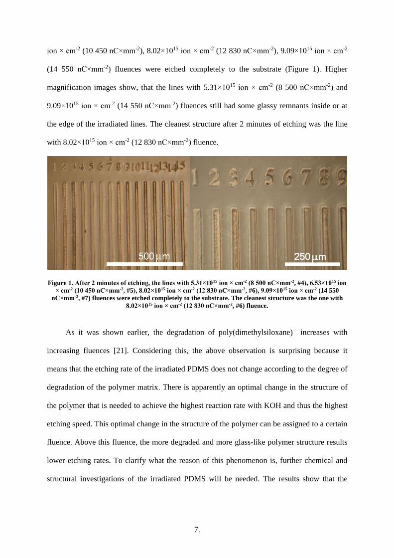
After 2 minutes of etching, the lines with 5.31×10¹⁵ ion × cm-2 (8 500 nC×mm-2), 6.53×10¹⁵
7.
ion × cm-2 (10 450 nC×mm-2), 8.02×10¹⁵ ion × cm-2 (12 830 nC×mm-2), 9.09×10¹⁵ ion × cm-2
(14 550 nC×mm-2) fluences were etched completely to the substrate (Figure 1). Higher
magnification images show, that the lines with 5.31×10¹⁵ ion × cm-2 (8 500 nC×mm-2) and
9.09×10¹⁵ ion × cm-2 (14 550 nC×mm-2) fluences still had some glassy remnants inside or at
the edge of the irradiated lines. The cleanest structure after 2 minutes of etching was the line
with 8.02×10¹⁵ ion × cm-2 (12 830 nC×mm-2) fluence.
Figure 1. After 2 minutes of etching, the lines with 5.31×10¹⁵ ion × cm-2 (8 500 nC×mm-2, #4), 6.53×10¹⁵ ion
× cm-2 (10 450 nC×mm-2, #5), 8.02×10¹⁵ ion × cm-2 (12 830 nC×mm-2, #6), 9.09×10¹⁵ ion × cm-2 (14 550
nC×mm-2, #7) fluences were etched completely to the substrate. The cleanest structure was the one with
8.02×10¹⁵ ion × cm-2 (12 830 nC×mm-2, #6) fluence.
As it was shown earlier, the degradation of poly(dimethylsiloxane) increases with
increasing fluences [21]. Considering this, the above observation is surprising because it
means that the etching rate of the irradiated PDMS does not change according to the degree of
degradation of the polymer matrix. There is apparently an optimal change in the structure of
the polymer that is needed to achieve the highest reaction rate with KOH and thus the highest
etching speed. This optimal change in the structure of the polymer can be assigned to a certain
fluence. Above this fluence, the more degraded and more glass-like polymer structure results
lower etching rates. To clarify what the reason of this phenomenon is, further chemical and
structural investigations of the irradiated PDMS will be needed. The results show that the
8.
fastest etching occurs at around the fluence of 7.5×10¹⁵ ion × cm-2 (12 000 nC×mm-2), below
and above this fluence the etching rate is lower.
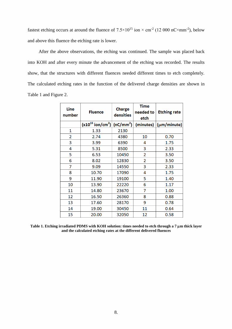
After the above observations, the etching was continued. The sample was placed back
into KOH and after every minute the advancement of the etching was recorded. The results
show, that the structures with different fluences needed different times to etch completely.
The calculated etching rates in the function of the delivered charge densities are shown in
Table 1 and Figure 2.
Table 1. Etching irradiated PDMS with KOH solution: times needed to etch through a 7 m thick layer
and the calculated etching rates at the different delivered fluences
9.
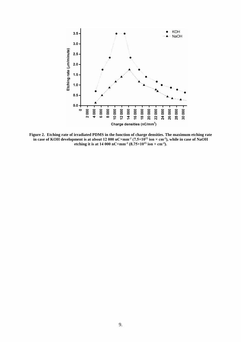
Figure 2. Etching rate of irradiated PDMS in the function of charge densities. The maximum etching rate
in case of KOH development is at about 12 000 nC×mm-2 (7.5×10¹⁵ ion × cm-2), while in case of NaOH
etching it is at 14 000 nC×mm-2 (8.75×10¹⁵ ion × cm-2).
10.
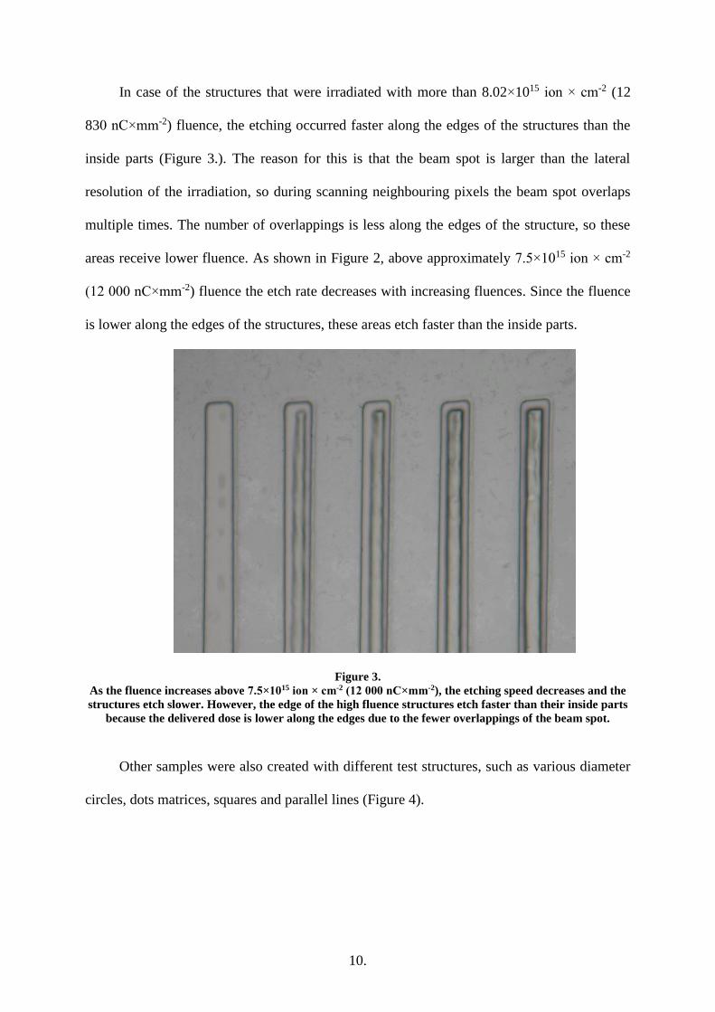
In case of the structures that were irradiated with more than 8.02×10¹⁵ ion × cm-2 (12
830 nC×mm-2) fluence, the etching occurred faster along the edges of the structures than the
inside parts (Figure 3.). The reason for this is that the beam spot is larger than the lateral
resolution of the irradiation, so during scanning neighbouring pixels the beam spot overlaps
multiple times. The number of overlappings is less along the edges of the structure, so these
areas receive lower fluence. As shown in Figure 2, above approximately 7.5×10¹⁵ ion × cm-2
(12 000 nC×mm-2) fluence the etch rate decreases with increasing fluences. Since the fluence
is lower along the edges of the structures, these areas etch faster than the inside parts.
Figure 3.
As the fluence increases above 7.5×10¹⁵ ion × cm-2 (12 000 nC×mm-2), the etching speed decreases and the
structures etch slower. However, the edge of the high fluence structures etch faster than their inside parts
because the delivered dose is lower along the edges due to the fewer overlappings of the beam spot.
Other samples were also created with different test structures, such as various diameter
circles, dots matrices, squares and parallel lines (Figure 4).
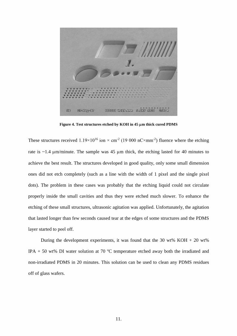
11.
Figure 4. Test structures etched by KOH in 45 m thick cured PDMS
These structures received 1.19×10¹⁶ ion × cm-2 (19 000 nC×mm-2) fluence where the etching
rate is ~1.4 m/minute. The sample was 45 m thick, the etching lasted for 40 minutes to
achieve the best result. The structures developed in good quality, only some small dimension
ones did not etch completely (such as a line with the width of 1 pixel and the single pixel
dots). The problem in these cases was probably that the etching liquid could not circulate
properly inside the small cavities and thus they were etched much slower. To enhance the
etching of these small structures, ultrasonic agitation was applied. Unfortunately, the agitation
that lasted longer than few seconds caused tear at the edges of some structures and the PDMS
layer started to peel off.
During the development experiments, it was found that the 30 wt% KOH + 20 wt%
IPA + 50 wt% DI water solution at 70 oC temperature etched away both the irradiated and
non-irradiated PDMS in 20 minutes. This solution can be used to clean any PDMS residues
off of glass wafers.
12.
It was also found that 98% sulfuric acid etches away the unirradiated PDMS while it
keeps the irradiated areas, making thus the etching of PDMS as a negative tone resist possible.
This finding is studied in details in a separate paper.
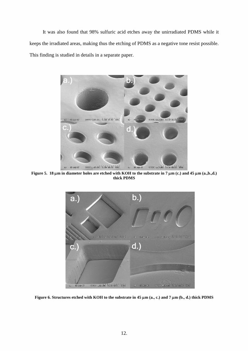
Figure 5. 18m in diameter holes are etched with KOH to the substrate in 7 m (c.) and 45 m (a.,b.,d.)
thick PDMS
Figure 6. Structures etched with KOH to the substrate in 45 m (a., c.) and 7 m (b., d.) thick PDMS

13.
3.2 Etching with sodium hydroxide
Since sodium hydroxide and potassium hydroxide has similar chemical properties, the
etching behaviour of NaOH was expected to be similar to that of KOH. The development
procedure of the fluence test sample was the same as in case of KOH etching, the results are
summarized in Table 2. and Figure 2.
Table 2. Etching irradiated PDMS with NaOH: times needed to etch through a 7 m thick layer and the
calculated etching rates in the function of the delivered fluence
As it can be seen in Figure 2., the etch rate curve for NaOH has similar character to that
of KOH, but the etching rates are about 1.5 - 2 times lower at every fluences. The highest etch
rate was found at about 8.89×10¹⁵ ion × cm-2 (14 240 nC×mm-2) fluence, which was a little
higher than in case of KOH. Since the etching was slower above this fluence, similarly to the
case of KOH etching, higher fluence samples etched faster along its edges. SEM images
showed that the smoothness and quality of the sidewalls improved with increasing fluences.
14.
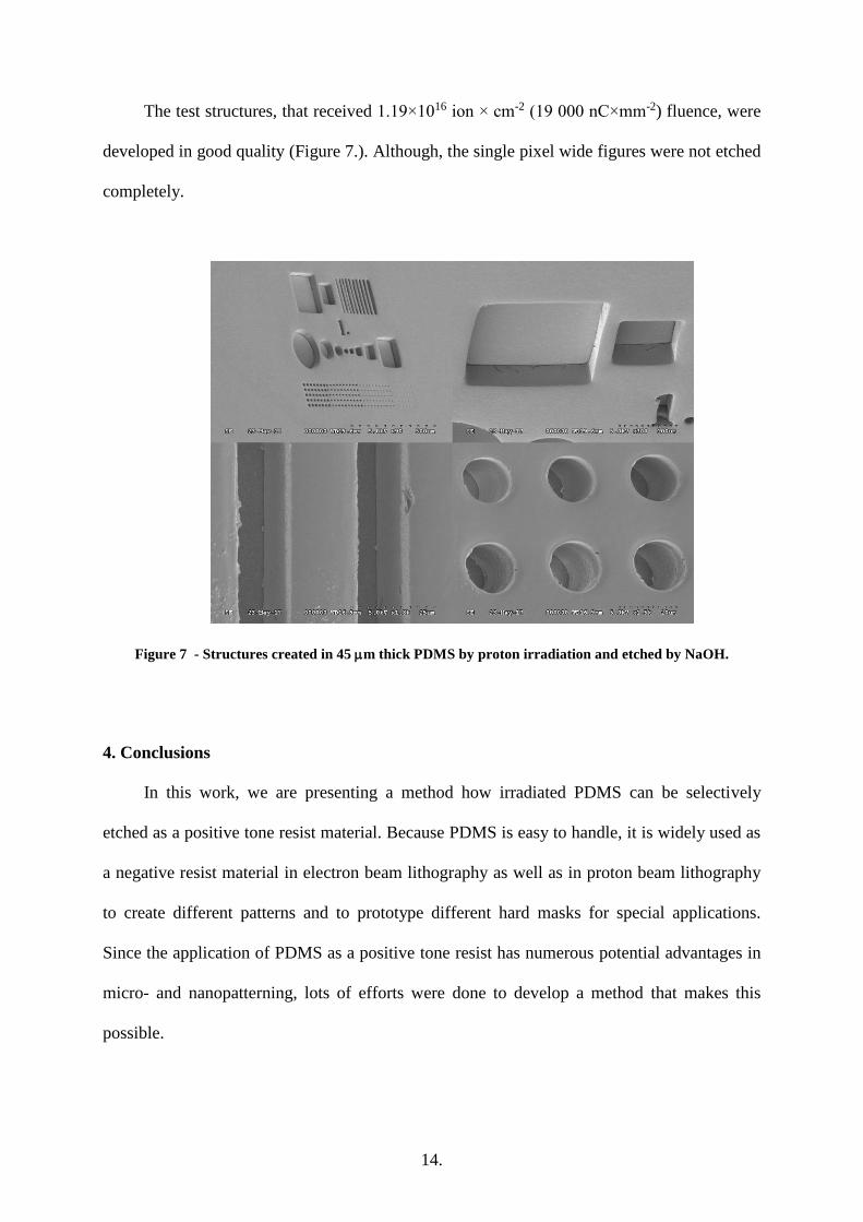
The test structures, that received 1.19×10¹⁶ ion × cm-2 (19 000 nC×mm-2) fluence, were
developed in good quality (Figure 7.). Although, the single pixel wide figures were not etched
completely.
Figure 7 - Structures created in 45 m thick PDMS by proton irradiation and etched by NaOH.
4. Conclusions
In this work, we are presenting a method how irradiated PDMS can be selectively
etched as a positive tone resist material. Because PDMS is easy to handle, it is widely used as
a negative resist material in electron beam lithography as well as in proton beam lithography
to create different patterns and to prototype different hard masks for special applications.
Since the application of PDMS as a positive tone resist has numerous potential advantages in
micro- and nanopatterning, lots of efforts were done to develop a method that makes this
possible.

15.
In this study, PDMS was irradiated with 2 MeV protons with various fluences and the
irradiated areas were etched with KOH and NaOH solutions. The concentration of KOH and
NaOH was 30 wt% in every cases, their temperature during etching was always 70 oC. In case
of KOH etching, the maximal etching rate occurred at about 7.5×10¹⁵ ion × cm-2 (12 000
nC×mm-2) proton fluence and it was approximately 3.5 m/minute. In case of NaOH, the
maximal etching rate is slightly lower, 1.75 m/minute and it can be found at about 8.89×10¹⁵
ion × cm-2 (14 240 nC×mm-2) fluence. The etching at room temperature happens much
slower, after 50 minutes no etching was observed at any fluences in either of the etchants.
This shows that the etching rate strongly depends on the temperature of the etchant.
It was also observed that the smoothness and quality of the sidewalls improves with
increasing fluences.
In case of those structures that received more fluence than the value where the maximal
etching rate occurs, the edges of the structures etch faster than their inside parts. This is
caused by the overlappings of the beam spot. Since the dimension of the beam spot is larger
than the lateral resolution of the irradiation, so during scanning neighbouring pixels the beam
spot overlaps multiple times. The number of overlappings is less along the edges of the
structures, so these areas receive lower fluence. Since at high doses the etching rate increases
with decreasing fluences, the edges will etch faster than the inside parts of the structures.
Various test structures were created with 1.19×10¹⁶ ion × cm-2 (19 000 nC×mm-2)
fluence in 7 m and 45 m thick PDMS polymer and etched with both etchants. The
structures etched with good quality down to the substrate, only the smallest ones did not
develop completely. The reason for this probably was that the etchant could not circulate
adequately inside small cavities and thus they etched much slower.

16.
5. Acknowledgements
This work was supported by the National Research, Development and Innovation Fund
No. PD 121076, by the Hungarian Scientific Research Fund OTKA No. K 108366 and by the
TAMOP 4.2.2.A-11/1/ KONV-2012-0036 project, which is co-financed by the European
Union and European Social Fund.
The work was also supported by the GINOP 2.3.2-15-2016-00041 (co-financed by the
European Union and the European Regional Development Fund).
References:
[1] C.H. Lin, Y.H. Yeh, W.C. Lin, Ming-Chien Yang, Novel silicone hydrogel based on
PDMS and PEGMA for contact lens application, Colloids and Surfaces B: Biointerfaces, 123
(2014) 986-994
[2] P.A. Gunatillake, R. Adhikari, Nondegradable synthetic polymers for medical devices and
implants, in: Biosynthetic Polymers for Medical Applications, Woodhead Publishing, 2016
pp. 33–62
[3] S.Z. Szilasi, J. Budai, Z. Pápa, R. Huszank, Z. Tóth, I. Rajta, Refractive index depth
profile and its relaxation in polydimethylsiloxane (PDMS) due to proton irradiation, Mater.
Chem. and Phys., 131 (2011) 370-374
[4] S.Z. Szilasi, N. Hegman, A. Csik, I. Rajta, Creation of convex microlenses in PDMS with
focused MeV ion beam, Microelectronic Eng., 88 (2011) 2885-2888
[5] G.U.L. Nagy, V. Lavrentiev, I. Bányász, S.Z. Szilasi, V. Havranek,, V. Vosecek, R.
Huszánk, I. Rajta, Compaction of polydimethylsiloxane due to nitrogen ion irradiation and its
application for creating microlens arrays, Thin Solid Films 636 (2017) 634-638
17.
[6] J. Casanova-Moreno, J. To, C.W.T. Yang, R.F.B. Turner, D. Bizzotto, K.C. Cheunga,
Fabricating devices with improved adhesion between PDMS and gold-patterned glass,
Sensors and Actuators B 246 (2017) 904–909
[7] J. Kudr, O. Zitka, M. Klimanek, R. Vrba, V. Adam, Microfluidic electrochemical devices
for pollution analysis–A review, Sensors and Actuators B 246 (2017) 578–590
[8] M. Antfolk, T. Laurell , Continuous flow microfluidic separation and processing of rare
cells and bioparticles found in blood - A review, Analytica Chimica Acta 965 (2017) 9-35
[9] Y. Yang, D. Ye, J. Li, X. Zhu, Q. Liao, B. Zhang, Microfluidic microbial fuel cells: from
membrane to membrane free, J. of Power Sources 324 (2016) 113-125
[10] X. Yao, Y. Zhang, L. Du, J. Liu, J. Yao, Review of the applications of microreactors,
Renewable and Sustainable Energy Reviews 47 (2015) 519–539
[11] K. H. Cheah, P. S. Khiew, J. K. Chin, Fabrication of a zirconia MEMS-based
microthruster by gel casting on PDMS soft molds, J. Micromech. Microeng. 22 (2012)
095013
[12] B. Zhang, J. Cui, J. Duan, M. Cui, A new fabrication method for nano-gratings based on
the high flexibility of PDMS, Optics & Laser Technology 92 (2017) 206–210
[13] V. Constantoudis, E. Gogolides, A. Tserepi, C.D. Diakoumakos, E.S. Valamontes,
Roughness characterization in positive and negative resists, Microelectronic Eng., 61–62
(2002) 793-801
[14] S.Z. Szilasi, R. Huszank, A. Csik, C. Cserháti, I. Rajta, PDMS patterning by proton
beam, Nucl. Instrum. and Methods in Phys. Res. B 267 (2009) 2296–2298
[15] S.Z. Szilasi, J. Kokavecz, R. Huszank, I. Rajta, Compaction of poly(dimethylsiloxane)
(PDMS) due to proton beam irradiation, Appl. Surf. Sci. 257 (2011) 4612–4615
18.
[16] R. Tsuchiya, H. Nishikawa "Fabrication of silica-based three-dimensional structures by
changing fluence using proton beam writing.", Transactions of the Mater. Res. Society of
Japan 36.3 (2011) 325-328.
[17] J. Bowen, D. Cheneler, A.P.G. Robinson, Direct e-beam lithography of PDMS,
Microelectronic Eng. 97 (2012) 34–37
[18] B. Gorissen, C. Van Hoof, D. Reynaerts, M. De Volder, SU8 etch mask for patterning
PDMS and its application to flexible fluidic microactuators, Microsystems &
Nanoengineering 2 (2016) 16045
[19] H. Cong, T. Pan, Photopatternable Conductive PDMS Materials for Microfabrication,
Advanced Functional Mater. 18 (2008) 1912–1921
[20] A.J. Satti, N.A. Andreucetti, A.E. Ciolino, C. Vitale, C. Sarmoria, E.M. Valles,
Molecular weight changes induced in an anionic polydimethylsiloxane by gamma irradiation
in vacuum, Radiat. Phys. and Chem. 79 (2010) 1137–1143
[21] R. Huszank, S.Z. Szilasi, D. Szikra, Ion-Energy Dependency in Proton Irradiation
Induced Chemical Processes of Poly(dimethylsiloxane), J. Phys. Chem. C 117 (2013)
25884−25889
[22] J. Brugger, G. Beljakovic, M. Despont, H. Biebuyck, N.F. de Rooij, P. Vettiger, Low-
cost PDMS seal ring for single-side wet etching of MEMS structures, Sensors and Actuators
A 70 (1998) 191-194
[23] A. Mata, A.J. Fleischman, S. Roy, Characterization of Polydimethylsiloxane (PDMS)
Properties for Biomedical Micro/Nanosystems, Biomedical Microdevices 7:4 (2005) 281–293
[24] I. Stoev, Y. Koprinarova, I. Kosseva, Determination of defects in SiO2 grown on Si(100),
Thin Solid Films, 105 (1983) 61-69
[25] L.C. Chen, M. Chert, C.C. Wan, T.H. Tsaur, C. Lien, Selective etching of silicon in
aqueous KOH, Materials Science and Engineering B34 (1995) 180-187

19.
[26] I. Rajta, I. Borbély-Kiss, Gy. Mórik, L. Bartha, E. Koltay, Á.Z. Kiss, The new
ATOMKI Scanning proton microprobe, Nucl. Instr. and Meth. B 109 (1996) 148
[27] J.F. Ziegler, SRIM-2008.03. <http://www.srim.org>