Antenna beam steering and beam forming at mm-Wave and ...
69
Antenna beam steering and beam forming at mm-Wave and THz frequencies Master Thesis submitted to the Faculty of the Escola T` ecnica d’Enginyeria de Telecomunicaci´o de Barcelona Universitat Polit` ecnica de Catalunya by Sara Vega Pi˜ na In partial fulfillment of the requirements for the master in TELECOMMUNICATIONS ENGINEERING Advisor: Mar´ ıa Concepci´ on Santos Co-Advisor: Daniel Nu˜ no Barcelona, January 20th, 2021
-
Upload
khangminh22 -
Category
Documents
-
view
3 -
download
0
Transcript of Antenna beam steering and beam forming at mm-Wave and ...
Antenna beam steering andbeam forming at mm-Wave and THz
frequencies
Master Thesissubmitted to the Faculty of the
Escola Tecnica d’Enginyeria de Telecomunicacio de BarcelonaUniversitat Politecnica de Catalunya
by
Sara Vega Pina
In partial fulfillmentof the requirements for the master in
TELECOMMUNICATIONS ENGINEERING
Advisor: Marıa Concepcion Santos
Co-Advisor: Daniel Nuno
Barcelona, January 20th, 2021
ContentsList of Figures 4
List of Tables 6
1 Introduction 8
2 Photonic Antenna Control 102.1 Phased Array Antennas Beam forming . . . . . . . . . . . . . . . . . . . . . . 102.2 Photoconductive Antennas for THz Radiation . . . . . . . . . . . . . . . . . . 11
3 Optical TTD Network 143.1 Multiwavelength Beam Steering Network . . . . . . . . . . . . . . . . . . . . 14
3.1.1 Effect of compensating delays . . . . . . . . . . . . . . . . . . . . . . 153.1.2 Geometrical Delays . . . . . . . . . . . . . . . . . . . . . . . . . . . . 163.1.3 Dispersive Delays . . . . . . . . . . . . . . . . . . . . . . . . . . . . 183.1.4 Maximum beam steered angle . . . . . . . . . . . . . . . . . . . . . . 19
3.2 CD-fading control . . . . . . . . . . . . . . . . . . . . . . . . . . . . . . . . . 203.3 OTTDN Simulations . . . . . . . . . . . . . . . . . . . . . . . . . . . . . . . 23
4 TeraHertz Systems 264.1 Definition of THz systems simulation methodology . . . . . . . . . . . . . . . 26
4.1.1 Time-Domain simulation of PCAs (Primary fields) . . . . . . . . . . . 264.1.2 Time-Domain simulation of Lens-coupled PCAs (Secondary fields) . . 32
4.2 Validation of THz Simulation Methodology . . . . . . . . . . . . . . . . . . . 354.2.1 PCAs modeling . . . . . . . . . . . . . . . . . . . . . . . . . . . . . . 354.2.2 Lens approach . . . . . . . . . . . . . . . . . . . . . . . . . . . . . . 364.2.3 Primary fields . . . . . . . . . . . . . . . . . . . . . . . . . . . . . . . 384.2.4 Secondary fields . . . . . . . . . . . . . . . . . . . . . . . . . . . . . 38
4.3 Simulation and measurement of THz systems . . . . . . . . . . . . . . . . . . 404.3.1 Fractal structures characteristics . . . . . . . . . . . . . . . . . . . . . 404.3.2 Modeling of Sierpinski Fractal structures for THz radiation . . . . . . . 404.3.3 Simulation of THz Far Fields with Sierpinski structures . . . . . . . . . 44
4.4 Terahertz Beam Steering . . . . . . . . . . . . . . . . . . . . . . . . . . . . . 49
5 Conclusions and future development 52
References 54
Appendices 59
A Matlab Codes 59A.1 VPI Radiation Pattern .mat file . . . . . . . . . . . . . . . . . . . . . . . . . . 59A.2 VPI Radiation Pattern Polar Plot . . . . . . . . . . . . . . . . . . . . . . . . . 59A.3 Radiation Pattern Projection . . . . . . . . . . . . . . . . . . . . . . . . . . . 60A.4 Radiation Pattern Cuts . . . . . . . . . . . . . . . . . . . . . . . . . . . . . . 61
2

B PCAs dimensions 63B.1 Dipole dimensions list . . . . . . . . . . . . . . . . . . . . . . . . . . . . . . 63B.2 Bow-Tie dimensions list . . . . . . . . . . . . . . . . . . . . . . . . . . . . . 64
C Sierpinski PCAs Secondary Fields 65C.1 Bow-Tie Secondary Fields . . . . . . . . . . . . . . . . . . . . . . . . . . . . 65C.2 Sierpinski 1st-Order Secondary Fields . . . . . . . . . . . . . . . . . . . . . . 66C.3 Sierpinski 2nd-Order Secondary Fields . . . . . . . . . . . . . . . . . . . . . . 67C.4 Sierpinski 3rd-Order Secondary Fields . . . . . . . . . . . . . . . . . . . . . . 68C.5 Sierpinski 4th-Order Secondary Fields . . . . . . . . . . . . . . . . . . . . . . 69
3
List of Figures1 Vision of a future communication network architecture integrating THz wireless
links into optical-fiber infrastructures. . . . . . . . . . . . . . . . . . . . . . . 82 Currents distribution for an N elements PAA. . . . . . . . . . . . . . . . . . . 103 Block scheme of PAA feeding network for beam steering. . . . . . . . . . . . . 114 PCA parts. Biasing Voltage (1), Electrodes or antenna metalization (2), Sub-
strate of photoconductive material, optical pulse (3) and the correspondent inputOptical Pump (4) and output THz radiation (5)[10]. . . . . . . . . . . . . . . . 12
5 Radiated rays refraction with a single dielectric substrate (a) and a dielectriclens coupled (b). . . . . . . . . . . . . . . . . . . . . . . . . . . . . . . . . . . 13
6 PCA coupled to an Hyperhemispherical lens. . . . . . . . . . . . . . . . . . . 137 OTTDN setup with DE-MZM. . . . . . . . . . . . . . . . . . . . . . . . . . . 148 Group delay distribution against wavelength at the PAAEs: red line, right after
the AWG (see Figure 7) and green line, right before photodetection (see Figure7). . . . . . . . . . . . . . . . . . . . . . . . . . . . . . . . . . . . . . . . . . 15
9 Geometrical delays for each PAAE and a beam direction θ . . . . . . . . . . . . 1710 Relative delays and beam direction for MW tuning. . . . . . . . . . . . . . . . 1811 Maximum wavelength shift for δλ0 < 0 (a) and δλ0 > 0 (b). . . . . . . . . . . 1912 Sketch of the typical options for external RF modulation at optical frequencies:
DE-MZM configured for SSB modulation (a), Conventional PP-MZM (b), andDE-MZM for CD RF-amplitude free band control using the bias voltage (c). . . 20
13 Comparison of fading function between a PP-MZM at Quadrature Point (blue)and a DE-MZM biased by condition (22) (red). . . . . . . . . . . . . . . . . . 21
14 VPI setup of the MW-OTTDN. . . . . . . . . . . . . . . . . . . . . . . . . . . 2315 Array Factor diagram for a relative progressive wavelength shift δλ0 > 0 (a)
and δλ0 < 0 (b). . . . . . . . . . . . . . . . . . . . . . . . . . . . . . . . . . . 2516 Array Factor diagrams for θB = π/2 (a) and θB = 1.35π (b). . . . . . . . . . . 2517 Primary fields (a) and Secondary fields (b) radiation scenarios. . . . . . . . . . 2618 Back (a) and perspective (b) view of a PCA structure in CST. . . . . . . . . . . 2719 CST background configuration section. . . . . . . . . . . . . . . . . . . . . . 2720 CST boundary conditions section. . . . . . . . . . . . . . . . . . . . . . . . . 2821 Discrete port connected to the electrodes (a) and excitation signal (b). . . . . . 2922 CST decoupling plane settings in the far field plot properties menu. . . . . . . . 2923 Example of far field 2D plots without decoupling plane (a)-(c) and with a de-
coupling plane at Z = −20 (b)-(d). The Copolar components of the field arerepresented in (a)-(b) while the Crosspolar ones are plotted in (c)-(d). . . . . . 30
24 Example of far field 3D plots without decoupling plane (a)-(c) and with a de-coupling plane at Z = −20 (b)-(d). The Copolar components of the field arerepresented in (a)-(b) while the Crosspolar ones are plotted in (c)-(d). . . . . . 31
25 Back (a), perspective (b) and left (c) view of a lens-coupled PCA structure inCST. . . . . . . . . . . . . . . . . . . . . . . . . . . . . . . . . . . . . . . . . 32
26 Excitation signal for a frequency range 0.45−0.55 T Hz. . . . . . . . . . . . . 32
4

27 Co-polar and Cross-polar far fields cuts for a mesh of 4 lines per wavelength(a), 8 lines per wavelength (b), 12 lines per wavelength (c) and 14 lines perwavelength (d) at f = 0.5 T Hz. . . . . . . . . . . . . . . . . . . . . . . . . . . 33
28 Reference PCAs models for simulation methodology validation: H-shape Dipole(a) and Bow-Tie (b). . . . . . . . . . . . . . . . . . . . . . . . . . . . . . . . 35
29 Dipole PCA schematic. . . . . . . . . . . . . . . . . . . . . . . . . . . . . . . 3530 Bow-Tie PCA schematic. . . . . . . . . . . . . . . . . . . . . . . . . . . . . . 3631 Parameters setup of the Lens figure. . . . . . . . . . . . . . . . . . . . . . . . 3632 Maximum lens angle. . . . . . . . . . . . . . . . . . . . . . . . . . . . . . . . 3733 Co-polar and Cross-polar Primary fields projections comparison between the
previous work [5] (left) and simulations (right) for a frequency f = 0.5 T Hz. . 3834 Co-polar and Cross-polar Secondary fields cuts comparison between the previ-
ous work [5] (left) and simulations (right) for a frequency f = 0.5 T Hz. . . . . 3935 Schematic of bow-tie (a), sierpinski’s first-order (b), sierpinski’s second-order
(c), and sierpinski’s third-order (d) structure. . . . . . . . . . . . . . . . . . . . 4036 Example of sierpinski PCA schematic with La = 1200 µm and it = 4. . . . . . 4137 Reflection coefficient of Bow-tie and sierpinski antennas of dimensions La =
400 µm (a) and La = 1200 µm (b). . . . . . . . . . . . . . . . . . . . . . . . . 4438 Co-polar and Cross-polar Primary fields projections comparison between the
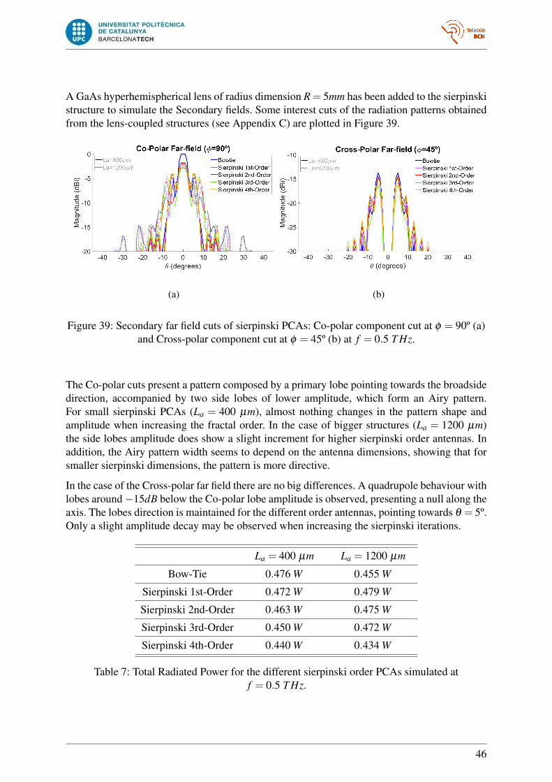
Bow-Tie structure and different sierpinski orders at f = 0.5 T Hz. . . . . . . . . 4539 Secondary far field cuts of sierpinski PCAs: Co-polar component cut at φ = 90º
(a) and Cross-polar component cut at φ = 45º (b) at f = 0.5 T Hz. . . . . . . . 4640 Secondary far field cuts of a 3rd-Order sierpinski PCA of dimensions La =
400 µm: laboratory measurements (a) versus simulations (b) at f = 0.5 T Hz. . 4741 Design of the optically steerable array with the dielectric lens [6]: Perspective
view with dielectric lens and beam switching (a) and Back view with opticalswitch and fiber connections (b). . . . . . . . . . . . . . . . . . . . . . . . . . 49
42 Rays direction representation when the PCA is positioned at x = 0 (a) and atx = ∆x (b). . . . . . . . . . . . . . . . . . . . . . . . . . . . . . . . . . . . . . 49
43 CST setup of the lens-coupled PCA with an off-axis of ∆x = 1000µm (a), ∆x =0µm (b) and ∆x =−1000µm (c). . . . . . . . . . . . . . . . . . . . . . . . . . 50
44 Simulated radiation patterns for different off-axis displacements at f = 0.5 T Hz. 5145 Co-polar and Cross-polar Secondary Fields projections comparison between
Bow-Tie of dimensions La = 400 µm (a) and La = 1200 µm (b) at f = 0.5 T Hz. 6546 Co-polar and Cross-polar Secondary Fields projections comparison between
1st-order Sierpinski of dimensions La = 400 µm (a) and La = 1200 µm (b)at f = 0.5 T Hz. . . . . . . . . . . . . . . . . . . . . . . . . . . . . . . . . . . 66
47 Co-polar and Cross-polar Secondary Fields projections comparison between2nd-order Sierpinski of dimensions La = 400 µm (a) and La = 1200 µm (b)at f = 0.5 T Hz. . . . . . . . . . . . . . . . . . . . . . . . . . . . . . . . . . . 67
48 Co-polar and Cross-polar Secondary Fields projections comparison between3rd-order Sierpinski of dimensions La = 400 µm (a) and La = 1200 µm (b)at f = 0.5 T Hz. . . . . . . . . . . . . . . . . . . . . . . . . . . . . . . . . . . 68
5
49 Co-polar and Cross-polar Secondary Fields projections comparison between4th-order Sierpinski of dimensions La = 400 µm (a) and La = 1200 µm (b)at f = 0.5 T Hz. . . . . . . . . . . . . . . . . . . . . . . . . . . . . . . . . . . 69
Listings1 Sierpinski Macro - Main Script. . . . . . . . . . . . . . . . . . . . . . . . . . 422 Sierpinski Macro - Iteration Script. . . . . . . . . . . . . . . . . . . . . . . . . 423 Matlab Function to generate a .mat file from VPI output. . . . . . . . . . . . . 594 Matlab Code to plot the polar radiation pattern from the .mat file. . . . . . . . . 595 Matlab Code to plot radiation pattern circular projections from ASCII files ex-
ported from CST. . . . . . . . . . . . . . . . . . . . . . . . . . . . . . . . . . 606 Matlab Script to plot radiation pattern cuts from ASCII files exported from CST. 61
List of Tables1 Summary of delays and wavelengths expressions for an array of N = 4 PAAE. . 162 Summary of simulation parameters. . . . . . . . . . . . . . . . . . . . . . . . 243 Summary of delays and wavelengths values for an array of N = 4 PAAE and
the setup of Table 2. . . . . . . . . . . . . . . . . . . . . . . . . . . . . . . . . 244 Mesh cell size and computation time for different values of lines per wavelength
and a bandwidth of 100 GHz at a central frequency f = 0.5 T Hz. . . . . . . . . 345 List of lens dimensions values. . . . . . . . . . . . . . . . . . . . . . . . . . . 376 List of fixed sierpinski dimensions values. . . . . . . . . . . . . . . . . . . . . 417 Total Radiated Power for the different sierpinski order PCAs simulated at f =
0.5 T Hz. . . . . . . . . . . . . . . . . . . . . . . . . . . . . . . . . . . . . . . 468 Scanning angle for different off-axis values and an extension length Le = 1466 µm. 509 List of simulated dipole dimensions values. . . . . . . . . . . . . . . . . . . . 6310 List of simulated bow-tie dimensions values. . . . . . . . . . . . . . . . . . . . 64
6
AbstractThe evolution of wireless communications and the emergence of novel applications will spurthe demand of higher data rates, requiring, on one hand, unallocated spectrum in the millimeterWave (mm-Wave) and Terahertz (THz) frequency bands to be exploited. On the other hand,the high propagation loss in the higher spectral bands will entail reduction of coverage areas,so that taking the signal in native format up to the radio interfaces leveraging existing opticalfiber infrastructure will be advantageous. Along the same lines, beam steering techniques areexpected to play an important role in the envisioned integrated wireless-photonic network.
Photonic techniques for next generation fiber-wireless networks will be explored in this work.On one hand, a multiwavelength (MW) optical true time delay Network (OTTDN) to feed aphased array antenna (PAA) is presented. Beam steering capabilities can be demonstrated whenapplying MW tuning. A Dual Electrode Mach Zehnder Modulator (DE-MZM) as radio fre-quency (RF) external modulating stage allows to tune the operative band avoiding severe Chro-matic Dispersion (CD) fading to obtain a flattened response. An experimental setup for testingthe technique in the UPC labs is described and studied in detail, showing the RF multibandspectral flat response potential of the technique, as well as the network conditions needed forbeam steering with free-lobe operation.
On the other hand, a simulation methodology to obtain the Co-Polar and Cross-Polar com-ponents of the far fields radiated by THz lens-coupled photoconductive antennas (PCAs) ispresented and validated by applying and contrasting the solution with previous publicationsmodels, with excellent agreement, as well as by comparing simulated lens-coupled PCAs withmeasures made in our UPC labs with a Menlo time-domain spectrometer, showing the samepattern trends. Sierpinski structures are simulated at f = 0.5 T Hz using this method, observingthat the power improvement with the fractal order, as well as the Airy pattern width dependon both the sampling aperture and the receiving antenna pattern. Finally, a simulation of anoff-axis feeding example scenario shows the steering properties of the hyperhemispherical lensgeometry.
7
1 IntroductionData traffic in wireless networks is experiencing an explosive growth which implies future linkdata rates of hundreds of Gbps. Achieving these levels of demand will require to employ un-allocated spectrum at the millimiter Wave (mm-Wave) and Terahertz (THz) frequency bands,allowing transmission through wider channels. An objective in the evolution of wireless systemshas been to improve radio links to achieve increasingly higher speeds and transmission capac-ities. Nevertheless, it is of great interest to explore the possibility of integrating these wirelesssystems with existing optical-fiber infrastructures, taking advantage of the broadband and highcapacity of optical systems and the huge market of fiber optic communications.
5G has driven the emergence of new applications, from Internet of Things (IoT) networks,which will be the mainstay of smart cities, to autonomous driving. Radar imagers at mm-Waveshave acquired a high relevance for applications as unmanned vehicles, traffic control or securityscanning, for which the design of phased array antennas (PAA) for beam steering has becomea very active research topic. The use of optical True Time Delay Networks (OTTDN) to feedthe PAAs is advantageous because it presents low-losses, has a small footprint and it is immuneto interferences, besides it allows direct interfacing with high-capacity fiber networks throughRadio-over-Fiber (RoF) fronthauling in communication networks [1].
The evolution towards 6G makes necessary to explore the THz frequency band, for which newtransceivers models are needed. Moreover, integration of THz-over-Fiber (ToF) architecturesis of high interest, leading the concept of a future network that combines geographically dis-tributed THz transceivers (TRx) connected through widely deployed optical-fiber infrastruc-tures, relying on direct Optical-to-THz conversion [2].
Figure 1: Vision of a future communication network architecture integrating THz wirelesslinks into optical-fiber infrastructures.
The main goal of this thesis is to explore different photonic methods to achieve beam formingand beam steering at mm-Wave and THz frequencies. It will be focused on simulated demon-strations of optically feed radiation elements, with the ultimate goal of putting those ideas intopractice in realistic contexts and lead to compact chips with mm-Wave and THz antennas con-trolled by optical fiber and which connect to the network. The objectives of this thesis aresummarized below.
• Analyse a new OTTDN architecture to feed PAAs with beam steering capabilities, con-
8
sidering an alternative configuration to the one presented in our previous work [3].
• Explore photonic techniques to overcome the severe CD RoF amplitude fading.
• Characterize THz transceivers (Lens-coupled photoconductive antennas).
• Define a simulation methodology to obtain the Co-polar and Cross-polar components ofTHz radiation.
• Analyse beam forming and beam steering capabilities of THz systems.
In Chapter 2 different radiation elements and structures are introduced and characterized, fo-cusing on mm-Wave PAAs, on the one hand, and on the other, on lens-coupled PhotoconductiveAntennas (PCAs)
An OTTDN is presented in Chapter 3 [4], where multiwavelength (MW) tuning is theoreticallydeveloped to prove its beam steering principle. A Dual-Electrodue Mach Zehnder Modulator(DE-MZM) is proposed as an alternative to conventional Push-Pull Mach Zehnder Modulator(PP-MZM) to achieve a multiband operation without RF amplitude fading effects. An exam-ple of MW beam steering network is defined, characterized and simulated, demonstrating thepredicted capabilities.
Focusing on the THz band, a lens-coupled PCA scenario is studied in Chapter 4. An Elec-tromagnetic (EM) simulation solver setup is characterized in order to define a THz analysismethodology, which is, in the first place, validated with the analysis of previous publicationsmodels [5]. Fractal Antennas geometries are characterized and simulated with the describedmethodology to compare their properties. Finally, an array optical switch will be considered tochange the origin of the lens feeding in order to study the beam steering capabilities [6].
This thesis concludes in Chapter 5, with a summary of the obtained analysis results, demon-strating the potential of the systems presented, and a proposal of future work lines.
9
2 Photonic Antenna ControlIn this chapter, optical techniques to control wireless antenna transmissions are introduced. Forthe mm-Wave band, the focus will be the optical feeding of PAAs to achieve beam forming andbeam steering. In the case of THz band, Lens-coupled PCAs will be analysed.
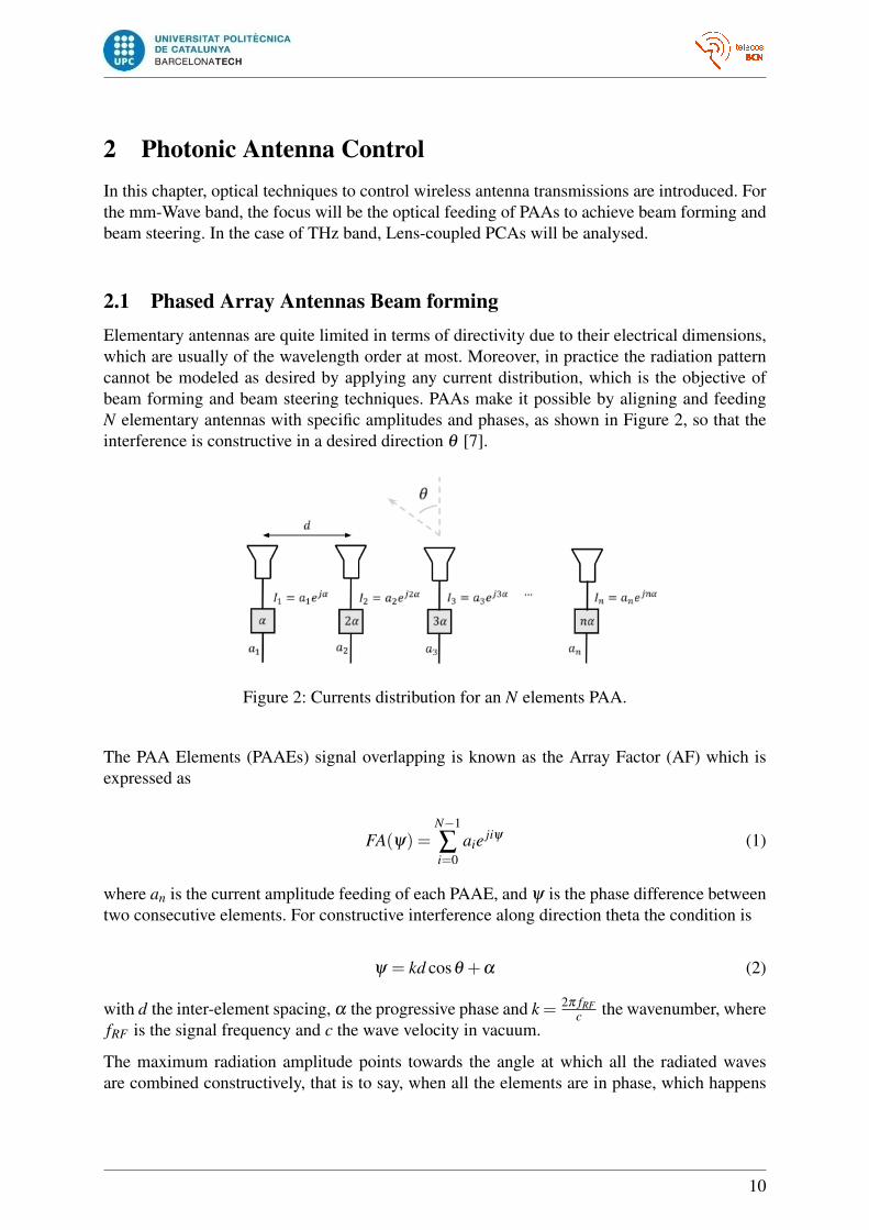
2.1 Phased Array Antennas Beam formingElementary antennas are quite limited in terms of directivity due to their electrical dimensions,which are usually of the wavelength order at most. Moreover, in practice the radiation patterncannot be modeled as desired by applying any current distribution, which is the objective ofbeam forming and beam steering techniques. PAAs make it possible by aligning and feedingN elementary antennas with specific amplitudes and phases, as shown in Figure 2, so that theinterference is constructive in a desired direction θ [7].
Figure 2: Currents distribution for an N elements PAA.
The PAA Elements (PAAEs) signal overlapping is known as the Array Factor (AF) which isexpressed as
FA(ψ) =N−1
∑i=0
aie jiψ (1)
where an is the current amplitude feeding of each PAAE, and ψ is the phase difference betweentwo consecutive elements. For constructive interference along direction theta the condition is
ψ = kd cosθ +α (2)
with d the inter-element spacing, α the progressive phase and k = 2π fRFc the wavenumber, where
fRF is the signal frequency and c the wave velocity in vacuum.
The maximum radiation amplitude points towards the angle at which all the radiated wavesare combined constructively, that is to say, when all the elements are in phase, which happens
10
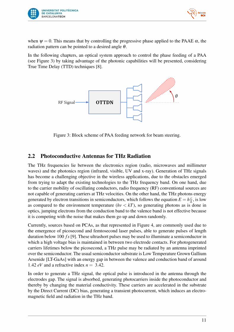
when ψ = 0. This means that by controlling the progressive phase applied to the PAAE α , theradiation pattern can be pointed to a desired angle θ .
In the following chapters, an optical system approach to control the phase feeding of a PAA(see Figure 3) by taking advantage of the photonic capabilities will be presented, consideringTrue Time Delay (TTD) techniques [8].
Figure 3: Block scheme of PAA feeding network for beam steering.
2.2 Photoconductive Antennas for THz RadiationThe THz frequencies lie between the electronics region (radio, microwaves and millimeterwaves) and the photonics region (infrared, visible, UV and x-ray). Generation of THz signalshas become a challenging objective in the wireless applications, due to the obstacles emergedfrom trying to adapt the existing technologies to the THz frequency band. On one hand, dueto the carrier mobility of oscillating conductors, radio frequency (RF) conventional sources arenot capable of generating carriers at THz velocities. On the other hand, the THz photons energygenerated by electron transitions in semiconductors, which follows the equation E = h c
λ, is low
as compared to the environment temperature (hv < kT ), so generating photons as is done inoptics, jumping electrons from the conduction band to the valence band is not effective becauseit is competing with the noise that makes them go up and down randomly.
Currently, sources based on PCAs, as that represented in Figure 4, are commonly used due tothe emergence of picosecond and femtosecond laser pulses, able to generate pulses of lengthduration below 100 f s [9]. These ultrashort pulses may be used to illuminate a semiconductor inwhich a high voltage bias is maintained in between two electrode contacts. For photogeneratedcarriers lifetimes below the picosecond, a THz pulse may be radiated by an antenna imprintedover the semiconductor. The usual semiconductor substrate is Low Temperature Grown GalliumArsenide [LT-GaAs] with an energy gap in between the valence and conduction band of around1.42 eV and a refractive index n = 3.42.
In order to generate a THz signal, the optical pulse is introduced in the antenna through theelectrodes gap. The signal is absorbed, generating photocarriers inside the photoconductor andthereby by changing the material conductivity. These carriers are accelerated in the substrateby the Direct Current (DC) bias, generating a transient photocurrent, which induces an electro-magnetic field and radiation in the THz band.
11

Figure 4: PCA parts. Biasing Voltage (1), Electrodes or antenna metalization (2), Substrate ofphotoconductive material, optical pulse (3) and the correspondent input Optical Pump (4) and
output THz radiation (5)[10].
On the other hand, to detect THz radiation, a portion of the optical pumped pulse is driftedtowards the receiver and focused to the receiving PCA gap by the electrodes side, generatingphotocarriers in the substrate. When the THz beam is pointed to the PCA gap from the substrateside, those carriers are accelerated inducing a signal current between the PCA electrodes.
The energy band gap restricts the range of wavelengths that may be used to those yield photonenergies higher than the energy bandgap. That unfortunately excludes, the typical wavelengthsin fiber optic communications λ = 1550 nm. The literature shows examples of alternative PCAsubstrates that allow exploitation of fiber optic devices and equipment, which usually involve atrade-off between the carrier lifetime and the band gap [11].
A main drawback may be observed when coupling antennas with dielectric substrates with highrefractive index values. Radiated rays are deflected due to the change of medium (see Figure 5),following the Snell’s law
sinθr =nsub
nairsinθi (3)
where θi and θr are the plane incident and refracted angles from the normal, and nsub, nair therefractive index of the substrate and air medium respectively.
As the substrate refractive index will be always higher than the vacuum one, the rays will bestrongly deflected, which means that for a certain incident angle, known as critical angle, therays will be completely reflected as shown in Figure 5a, letting escape only the rays transmittedinside the solid angle of width
Ω = 4π sin2 α
2(4)
with α = arcsin(n−1) the boundary angle for total reflection.
12
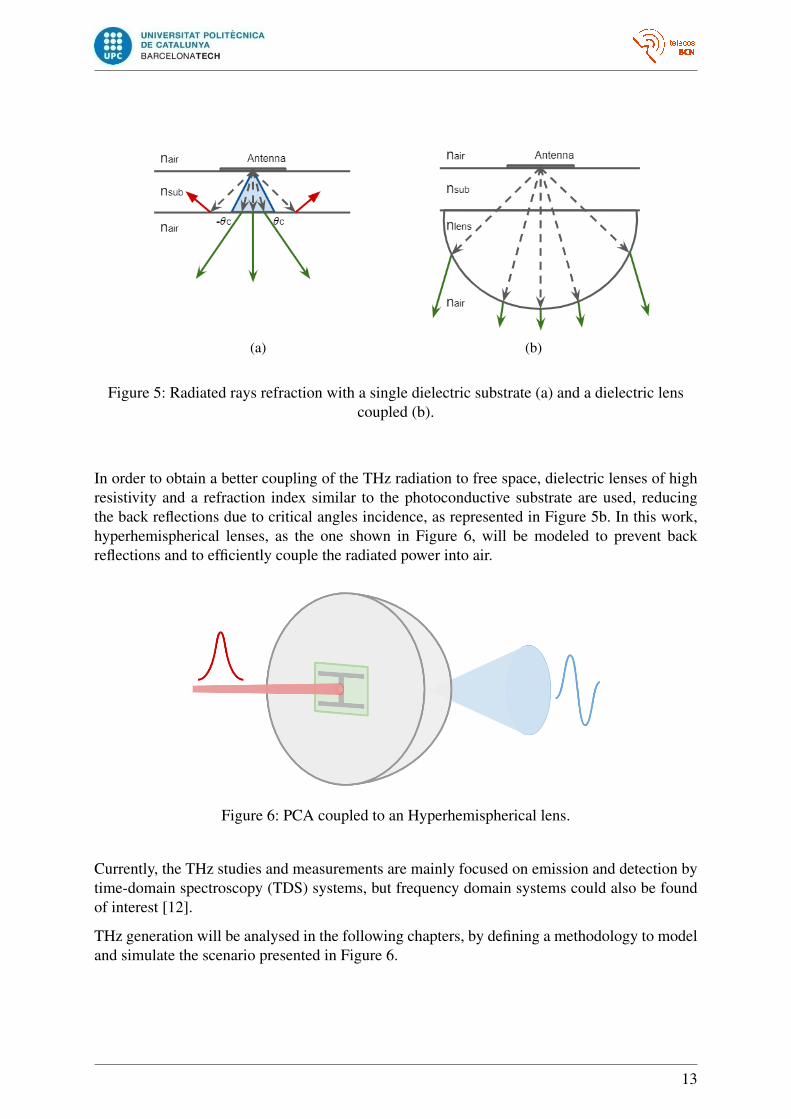
(a) (b)
Figure 5: Radiated rays refraction with a single dielectric substrate (a) and a dielectric lenscoupled (b).
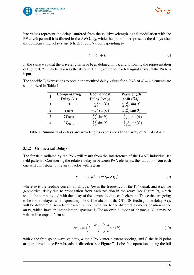
In order to obtain a better coupling of the THz radiation to free space, dielectric lenses of highresistivity and a refraction index similar to the photoconductive substrate are used, reducingthe back reflections due to critical angles incidence, as represented in Figure 5b. In this work,hyperhemispherical lenses, as the one shown in Figure 6, will be modeled to prevent backreflections and to efficiently couple the radiated power into air.
Figure 6: PCA coupled to an Hyperhemispherical lens.
Currently, the THz studies and measurements are mainly focused on emission and detection bytime-domain spectroscopy (TDS) systems, but frequency domain systems could also be foundof interest [12].
THz generation will be analysed in the following chapters, by defining a methodology to modeland simulate the scenario presented in Figure 6.
13

3 Optical TTD NetworkIn this first part of the thesis, a MW OTTDN to feed a PAA will be presented in order todemonstrate beam steering capabilities when applying MW tuning. A DE-MZM as the RFexternal modulating stage will be proposed, allowing to tune the operative band avoiding severeCD fading and obtaining a flattened response.
3.1 Multiwavelength Beam Steering NetworkFigure 7 shows a sketch of the targeted OTTDN, which resembles the distribution of wavelengthchannels to users in access Wavelength Division Multiplexing-Passive Optical Network (WDM-PONs) [13].
An array of tunable input lasers, provides a MW signal comprising wavelengths λi, i= 1,2, ...,N,numbered in descending order in Figure 7, with N the number of PAA elements. For clarity, wewill consider in this analysis an even number of array elements, but extension to an odd numberis straightforward.
After RF modulation with an external DE-MZM, which will be analyzed in more detail in thefollowing sections, the signal propagates through a dispersive medium for which DispersionCompensating Fiber (DCF) with negative dispersion coefficient D is conveniently chosen toprovide large values of CD in a low volume and over a wide optical band. For the PAA steer-ing, each laser wavelength will be conveniently tuned inside a specific channel of an ArrayedWaveguide Grating (AWG) whose outputs are connected to the PAAEs through an array of Nphotodetectors. In order to exploit WDM-PON equipment, the C-band of optical communica-tions around λ0 = 1.55 µm is considered. Figure 7 shows the group delay acquired by the RFsignal over the different wavelength optical carriers after travelling through the fiber. This delayis proportional to the optical carrier wavelength difference, with the dispersion coefficient D,the proportionality constant. A typical value D = −85 ps/(nm ·Km) is used for the dispersioncompensating fiber.
Figure 7: OTTDN setup with DE-MZM.
14

3.1.1 Effect of compensating delays
Owing to CD, the signal fed to every PAAE will have suffered a delay that will depend on thewavelength value inside its channel. Let the center wavelength of each OTTDN channel be
λ0i = λ01 +(i−1)∆λAWG (5)
with ∆λAWG the AWG channel spacing in wavelength units and λ01 the nominal center wave-length of the first element of the array (placed at the top in Figure 7), which is considered herethe one with the lowest wavelength value, as shown in Figure 8.
Figure 8: Group delay distribution against wavelength at the PAAEs: red line, right after theAWG (see Figure 7) and green line, right before photodetection (see Figure 7).
To properly exhaust the channel bandwidth provided by the AWG for a PAA symmetricallysteered along both positive and negative angles, when all the input lasers are located at the centerof their respective AWG channels, the PAA should radiate towards the broadside direction. Thisis accomplished by matching the arrival time of each center channel wavelength through thefixed delays Ti placed before each PAAE, either before or after the photodetection stage.
For lasers wavelengths in their AWG channel center, the value of the proportional delay inbetween PAAEs will be
TAWG = |D|L∆λAWG (6)
with D the CD parameter and L the fiber length, so that the compensating delays for each PAAEneed to be
Ti = (i−1)TAWG (7)
In Figure 8, we provide a graphical explanation to illustrate the effect of the compensatingdelays over the delay dependence on wavelength for this OTTDN structure proposal. The red
15
line values represent the delays suffered from the multiwavelength signal modulation with theRF envelope until it is filtered in the AWG, τ0i, while the green line represents the delays afterthe compensating delay stage (check Figure 7), corresponding to
τi = τ0i +Ti (8)
In the same way that the wavelengths have been defined in (5), and following the representationof Figure 8, τ01 may be taken as the absolute timing reference for RF signal arrival at the PAAEsinput.
The specific Ti expressions to obtain the required delay values for a PAA of N = 4 elements aresummarized in Table 1.
i CompensatingDelay (Ti)
GeometricalDelay (∆τGi)
Wavelengthshift (δλi)
1 0 −32
dc sin(θ) 3
2d
DLc sin(θ)
2 TAWG −12
dc sin(θ) 1
2d
DLc sin(θ)
3 2TAWG12
dc sin(θ) −1
2d
DLc sin(θ)
4 3TAWG32
dc sin(θ) −3
2d
DLc sin(θ)
Table 1: Summary of delays and wavelengths expressions for an array of N = 4 PAAE.
3.1.2 Geometrical Delays
The far field radiated by the PAA will result from the interference of the PAAE individual farfield patterns. Considering the relative delay in between PAA elements, the radiation from eachone will contribute to the array factor with a term
Ei = ai exp(− j2π fRF∆τGi) (9)
where ai is the feeding current amplitude, fRF is the frequency of the RF signal, and ∆τGi thegeometrical delay due to propagation from each position in the array (see Figure 9), whichshould be compensated with the delay of the current feeding each element. Those that are goingto be more delayed when spreading, should be ahead in the OTTDN feeding. The delay ∆τGiwill be different as seen from each direction theta due to the different elements position in thearray, which have an inter-element spacing d. For an even number of channels N, it may bewritten in compact form as
∆τGi =
(i− N +1
2
)dc
sin(θ) (10)
with c the free-space wave velocity, d the a PAA inter-element spacing, and θ the field pointangle referred to the PAA broadside direction (see Figure 7). Lobe-free operation among the full
16

180º beam steering of the PAA requires d < λRF2 [20]. Uniform distributions will be considered
and therefore ai = a.
The summation over all the array elements currents distributions provides the AF (1), that whenconvolved with the individual beam pattern of the antennas in the array Ei provides the PAAbeam pattern
EPAA(θ) = AF(θ)∗Ei(θ) (11)
Isotropic radiators will be considered in the analysis, to focus on the PAA response, and there-fore Ei(θ) = Ei.
Figure 9: Geometrical delays for each PAAE and a beam direction θ .
The mechanism by which the OTTDN achieves the beam steering towards angle θ consists inproviding each PAAE with a RF signal replica which has the same amplitude and a progressivedelay that compensates the geometrical delay due to the PAAE position in the array, see Figure9. We may then write the complex signal of each PAAE as
Ii = Aexp(− j2π fRF∆τNi) (12)
with A the common RF amplitude and ∆τNi its corresponding network delay. The condition forbeam steering is that network delays compensate the geometrical delays due to the position inspace of each PAAE, pointing at the intended direction of maximum directivity.
∆τGi +∆τNi = 0 (13)
Note that while for the network delays we measure the time starting from the first elementin the array, here it is preferable to take the center of the array as the time reference due tothe geometrical symmetry. As an example, the geometrical delays expressions for a PAA withN = 4 elements are summarized in Table 1.
As long as all the channels are synchronized to the same absolute time reference for the broad-side condition, the relative delays between the PAAEs will define the beam direction by fulfil-ment of the condition (13).
17
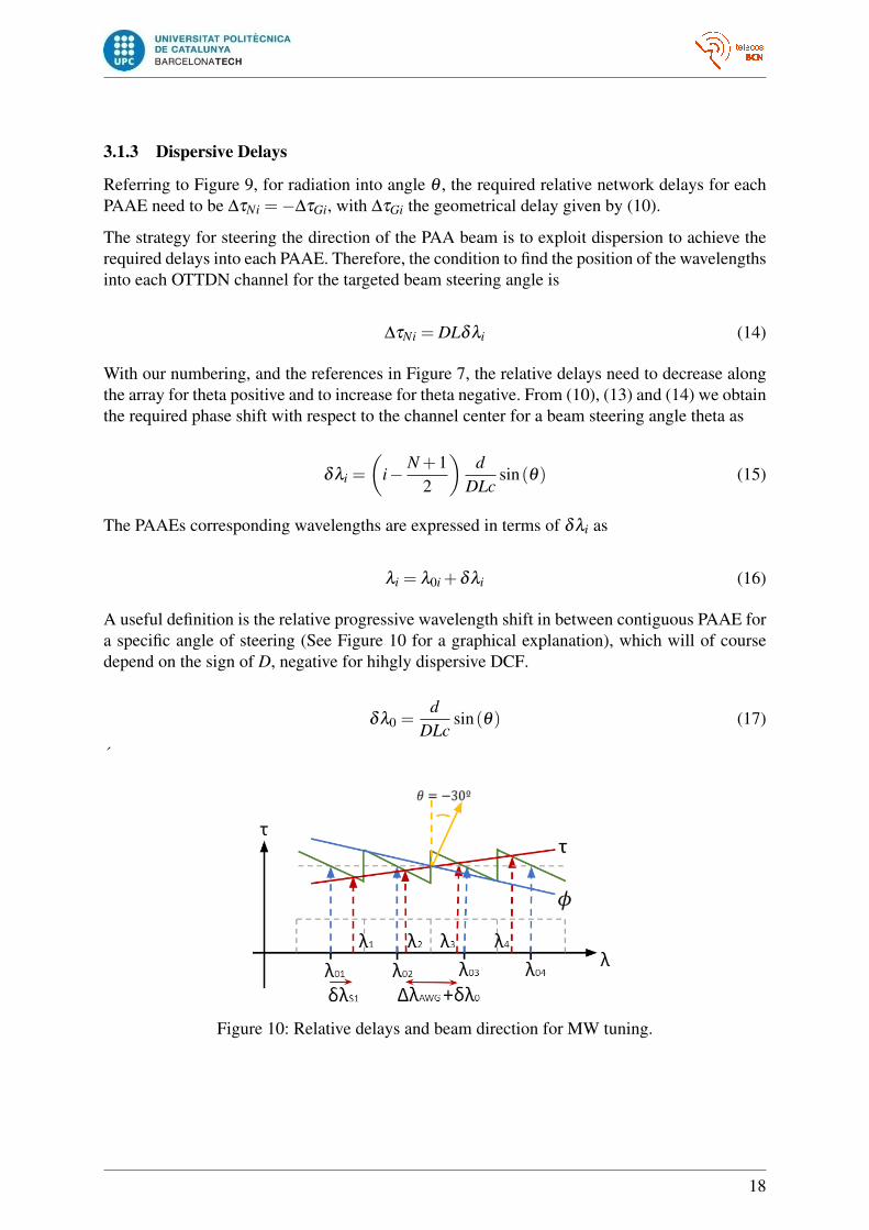
3.1.3 Dispersive Delays
Referring to Figure 9, for radiation into angle θ , the required relative network delays for eachPAAE need to be ∆τNi =−∆τGi, with ∆τGi the geometrical delay given by (10).
The strategy for steering the direction of the PAA beam is to exploit dispersion to achieve therequired delays into each PAAE. Therefore, the condition to find the position of the wavelengthsinto each OTTDN channel for the targeted beam steering angle is
∆τNi = DLδλi (14)
With our numbering, and the references in Figure 7, the relative delays need to decrease alongthe array for theta positive and to increase for theta negative. From (10), (13) and (14) we obtainthe required phase shift with respect to the channel center for a beam steering angle theta as
δλi =
(i− N +1
2
)d
DLcsin(θ) (15)
The PAAEs corresponding wavelengths are expressed in terms of δλi as
λi = λ0i +δλi (16)
A useful definition is the relative progressive wavelength shift in between contiguous PAAE fora specific angle of steering (See Figure 10 for a graphical explanation), which will of coursedepend on the sign of D, negative for hihgly dispersive DCF.
δλ0 =d
DLcsin(θ) (17)
´
Figure 10: Relative delays and beam direction for MW tuning.
18

3.1.4 Maximum beam steered angle
The limit for the maximum steered angle, considering that the wavelengths are always equidis-tant to obtain the progressive delays, will come from the required wavelength shift of any of thePAAEs reaching the limit of the AWG channel half-bandwidth.
(a) (b)
Figure 11: Maximum wavelength shift for δλ0 < 0 (a) and δλ0 > 0 (b).
As shown in Figure 11, the channels that experience the greater wavelength shift are the onesfurther apart from the PAA center, which suffer a maximum displacement δλi = ±∆λAWG/2.Therefore, letting i = N in (15) the maximum steered angle with respect to the broadside direc-tion is
θmax = arcsin(
c|D|∆λAWG
d (N−1)
)(18)
It could be checked that, the higher the number of elements in the PAA or the narrower the AWGchannel bandwidth, the larger the CD value needed to fulfill the requirement of a specific maxi-mum steering angle. On the other hand, the higher the CD, the shorter the Distributed FeedbackBragg (DFB) tuning ranges to achieve the same angle shift, which means better accuracy andstability required for the tuning. Depending of specifications, the proper trade-off for the chosenvalue of D should be found.
19

3.2 CD-fading controlA significant downside of a high value of CD is the RF amplitude fading effect which reducesthe RF operative bandwidth [19]. In this section we will show how the RF amplitude fading typ-ical of dispersive propagation of Double Side-Band (DSB) signals may be avoided at a specificoperative frequency through appropriate biasing of a DE-MZM with no specific requirementfor RF signal electrical shift, allowing the OTTDN to be tuned over a wide frequency band.
Figure 12 illustrates different choices for the electrical connections in the RF modulation stageof the OTTDN.
(a) (b)
(c)
Figure 12: Sketch of the typical options for external RF modulation at optical frequencies:DE-MZM configured for SSB modulation (a), Conventional PP-MZM (b), and DE-MZM for
CD RF-amplitude free band control using the bias voltage (c).
In a typical configuration, the external RF modulation stage is implemented using a conven-tional PP-MZM characterized by a 180º phase difference between RF signals applied to eachinterferometer arm. The usual outcome is a RF DSB amplitude modulation, for which frequencydependent CD-induced RF amplitude fading may cause significant amplitude distortion and RFamplitude notches at specific frequencies [19] [21].
A DE-MZM as the RF modulating element of a dispersive OTTDN for PAA beam steering hasbeen proposed in [17] to achieve a Single Side-Band (SSB) modulation of the data by drivingeach MZ arm with the same RF signal delayed by 90º. However the requirement of a specificelectrical phase shift makes the technique intrinsically narrow band [22] and no frequency re-configuration is possible. We are going to make a comparison of the different modulations inorder to demonstrate how the biasing technique can be used with a DE-MZM to switch thefading notch frequency.
Taking as delay reference the time of arrival when all wavelengths are centered into their AWG,
20
τ01, the normalized amplitude field in the small signal approximation of the signal at each AWGport when a DE-MZM with independent feed of each branch is used is given by
Ei ≈ cos(
θB
2
)+ jme j
(φ− θB
2
)cos(2π fRF (t−δλiDL)) (19)
where θB = πVBVπ
, and m = πVRFVπ
with VB, VRF respectively the biasing voltage and RF signal peakamplitude applied to different electrodes of the DE-MZM, (see Figure 12c), with Vπ its half-wave voltage, and φ the phase due to CD expressed in (20), with λ0 the reference wavelengthwhich is conveniently set to the center of the C-band [19].
φ =πDLλ 2
0 f 2RF
c(20)
The small-signal approximation in (19) implies that small enough RF amplitudes are applied tothe modulators, that is VRFVπ . From there, the normalized photodetected current at frequencyfR at each PAAE will be
IPDi ≈ cos(
θB
2
)sin
(θB
2−φ
)cos(2π fRF (t−δλiDL)) (21)
The biasing voltage VB may be adjusted to compensate the CD-induced amplitude fading givenby φ , using the condition
θB = (2n−1)π +2φ (22)
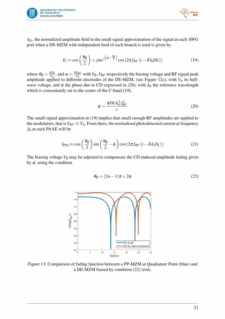
Figure 13: Comparison of fading function between a PP-MZM at Quadrature Point (blue) anda DE-MZM biased by condition (22) (red).
21

In Figure 13 an example comparison for the operation frequency 8GHz, between the fadingfunction when biasing different modulators is represented. For a physical system with a disper-sion coefficient DL, the notch of the PP-MZM fading function (blue) will remain in the sameposition despite the biasing applied, while the notch of the DE-MZM fading function (red) canbe displaced to flatten the photodetected current amplitude around the desired frequency.
22
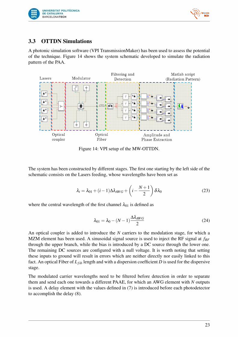
3.3 OTTDN SimulationsA photonic simulation software (VPI TransmissionMaker) has been used to assess the potentialof the technique. Figure 14 shows the system schematic developed to simulate the radiationpattern of the PAA.
Figure 14: VPI setup of the MW-OTTDN.
The system has been constructed by different stages. The first one starting by the left side of theschematic consists on the Lasers feeding, whose wavelengths have been set as
λi = λ01 +(i−1)∆λAWG +
(i− N +1
2
)δλ0 (23)
where the central wavelength of the first channel λ01 is defined as
λ01 = λ0− (N−1)∆λAWG
2(24)
An optical coupler is added to introduce the N carriers to the modulation stage, for which aMZM element has been used. A sinusoidal signal source is used to inject the RF signal at fRFthrough the upper branch, while the bias is introduced by a DC source through the lower one.The remaining DC sources are configured with a null voltage. It is worth noting that settingthese inputs to ground will result in errors which are neither directly nor easily linked to thisfact. An optical Fiber of L f ib length and with a dispersion coefficient D is used for the dispersivestage.
The modulated carrier wavelengths need to be filtered before detection in order to separatethem and send each one towards a different PAAE, for which an AWG element with N outputsis used. A delay element with the values defined in (7) is introduced before each photodetectorto accomplish the delay (8).
23
Once the modulated signals are photodetected, the amplitude Ai and phase Phi need to be ob-tained to represent the radiation pattern, for which Two Port Analyzers are used. A last Simula-tion Interface element is used to run a Matlab function (see Appendix A.1 and A.2), introducingAi and Phi values as inputs. This function plots and saves a 2D radiation pattern over θ angle.
Assuming a PAAE spacing of d = λ
4 complying with the secondary lobe-free radiation condi-tion, a full 180º beam steering requires a minimum dispersion |D|minL = 58 ps/nm, accordingto the maximum beam condition (18). Considering standard DCF with distributed dispersioncoefficient D =−85 ps/(nm ·Km), it corresponds to roughly 0.68 Km.
Parameter Definition Value
λ0 Reference wavelength 1550 nm
N Number of PAAEs 4
∆λAWG AWG channel spacing 1.6 nm
D Dispersion −85 psnm·Km
L Fiber Length 4 Km
Table 2: Summary of simulation parameters.
In order to focus the study towards an experimental test, the values have been adapted to theavailable resources, yielding the parameters listed in Table 2 with an inter-element spacingd = 4λ/5 at 8 GHz and a dispersion of DL =−340 ps/nm. Table 3 lists the required delays bysetting these simulation parameters.
i CompensatingDelay (Ti)
GeometricalDelay (∆τGi)
Wavelengthshift (δλi)
1 0 ns −0.15sin(θ) ns 0.45sin(θ) nm
2 0.54 ns −0.05sin(θ) ns 0.15sin(θ) nm
3 1.08 ns 0.05sin(θ) ns −0.15sin(θ) nm
4 1.62 ns 0.15sin(θ) ns −0.45sin(θ) nm
Table 3: Summary of delays and wavelengths values for an array of N = 4 PAAE and the setupof Table 2.
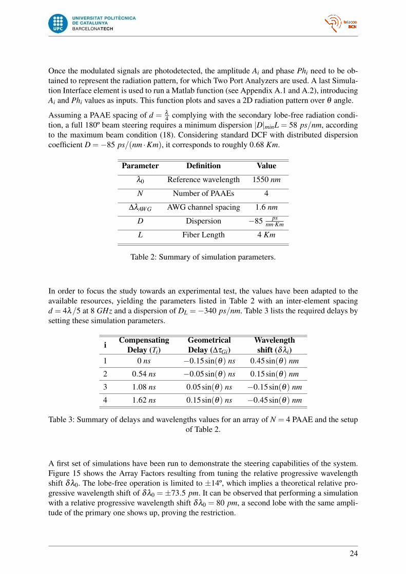
A first set of simulations have been run to demonstrate the steering capabilities of the system.Figure 15 shows the Array Factors resulting from tuning the relative progressive wavelengthshift δλ0. The lobe-free operation is limited to ±14º, which implies a theoretical relative pro-gressive wavelength shift of δλ0 =±73.5 pm. It can be observed that performing a simulationwith a relative progressive wavelength shift δλ0 = 80 pm, a second lobe with the same ampli-tude of the primary one shows up, proving the restriction.
24
(a) (b)
Figure 15: Array Factor diagram for a relative progressive wavelength shift δλ0 > 0 (a) andδλ0 < 0 (b).
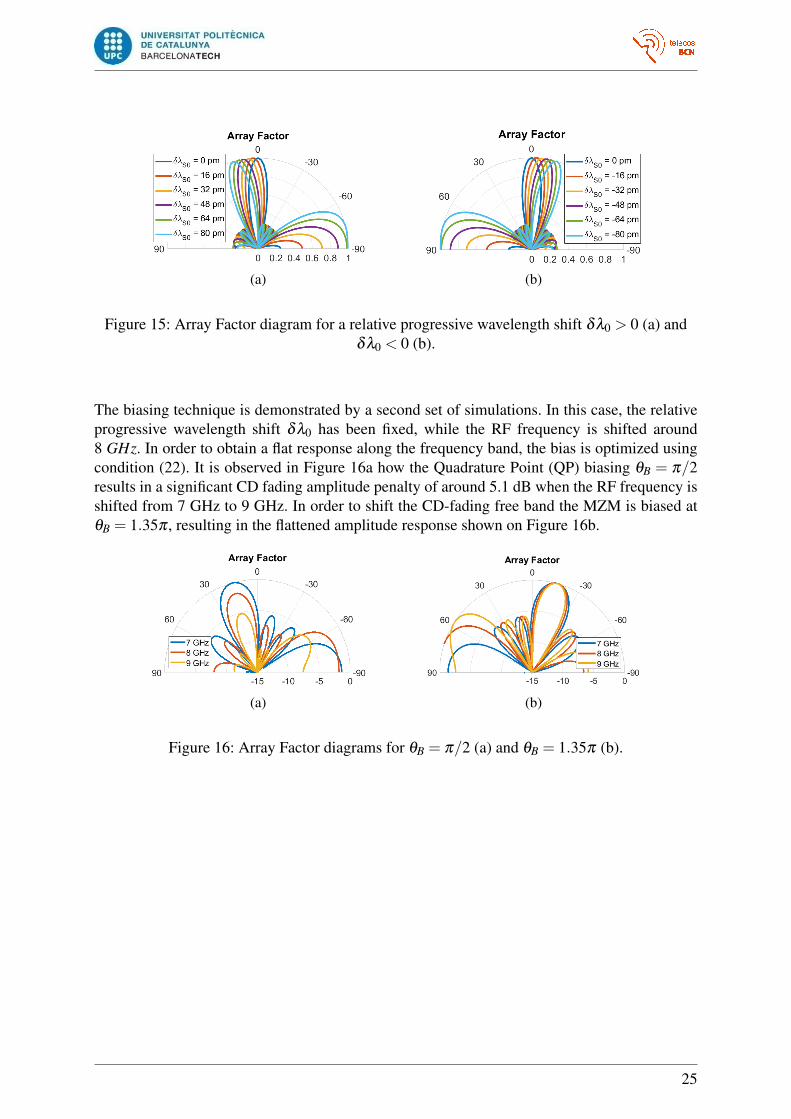
The biasing technique is demonstrated by a second set of simulations. In this case, the relativeprogressive wavelength shift δλ0 has been fixed, while the RF frequency is shifted around8 GHz. In order to obtain a flat response along the frequency band, the bias is optimized usingcondition (22). It is observed in Figure 16a how the Quadrature Point (QP) biasing θB = π/2results in a significant CD fading amplitude penalty of around 5.1 dB when the RF frequency isshifted from 7 GHz to 9 GHz. In order to shift the CD-fading free band the MZM is biased atθB = 1.35π , resulting in the flattened amplitude response shown on Figure 16b.
(a) (b)
Figure 16: Array Factor diagrams for θB = π/2 (a) and θB = 1.35π (b).
25
4 TeraHertz SystemsThe goal of this second part of the thesis is to define a methodology to study and analyse THzradiation using lens-coupled PCAs and use it to analyse different antenna models. In the fol-lowing sections, different kinds of PCAs geometries are going to be modeled and characterizedwith and without the lens coupling for, on the one hand, validate our methodology with theexisting literature and, on the other one, analyse the properties of some geometries of interestin order to prove the beam forming and beam steering properties of the lens.
4.1 Definition of THz systems simulation methodologyThe THz systems under analysis, as explained in Section 2.2, consist of different lens-coupledphotoconductive antennas, from which the Co-polar and Cross-polar components of the radiatedfields want to be obtained. CST microwave studio [23] will be used as the EM simulationsolver in charge of computing the Maxwell Equations to obtain the THz radiated signals of themodeled antennas.
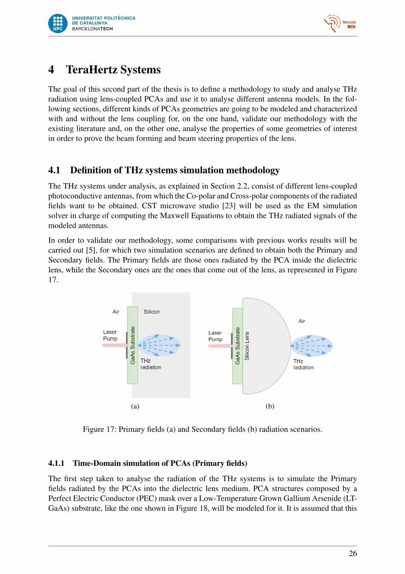
In order to validate our methodology, some comparisons with previous works results will becarried out [5], for which two simulation scenarios are defined to obtain both the Primary andSecondary fields. The Primary fields are those ones radiated by the PCA inside the dielectriclens, while the Secondary ones are the ones that come out of the lens, as represented in Figure17.
(a) (b)
Figure 17: Primary fields (a) and Secondary fields (b) radiation scenarios.
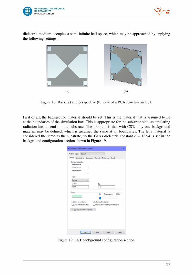
4.1.1 Time-Domain simulation of PCAs (Primary fields)
The first step taken to analyse the radiation of the THz systems is to simulate the Primaryfields radiated by the PCAs into the dielectric lens medium. PCA structures composed by aPerfect Electric Conductor (PEC) mask over a Low-Temperature Grown Gallium Arsenide (LT-GaAs) substrate, like the one shown in Figure 18, will be modeled for it. It is assumed that this
26
dielectric medium occupies a semi-infinite half space, which may be approached by applyingthe following settings.
(a) (b)
Figure 18: Back (a) and perspective (b) view of a PCA structure in CST.
First of all, the background material should be set. This is the material that is assumed to lieat the boundaries of the simulation box. This is appropriate for the substrate side, as emulatingradiation into a semi-infinite substrate. The problem is that with CST, only one backgroundmaterial may be defined, which is assumed the same at all boundaries. The lens material isconsidered the same as the substrate, so the GaAs dielectric constant ε = 12.94 is set in thebackground configuration section shown in Figure 19.
Figure 19: CST background configuration section.
27
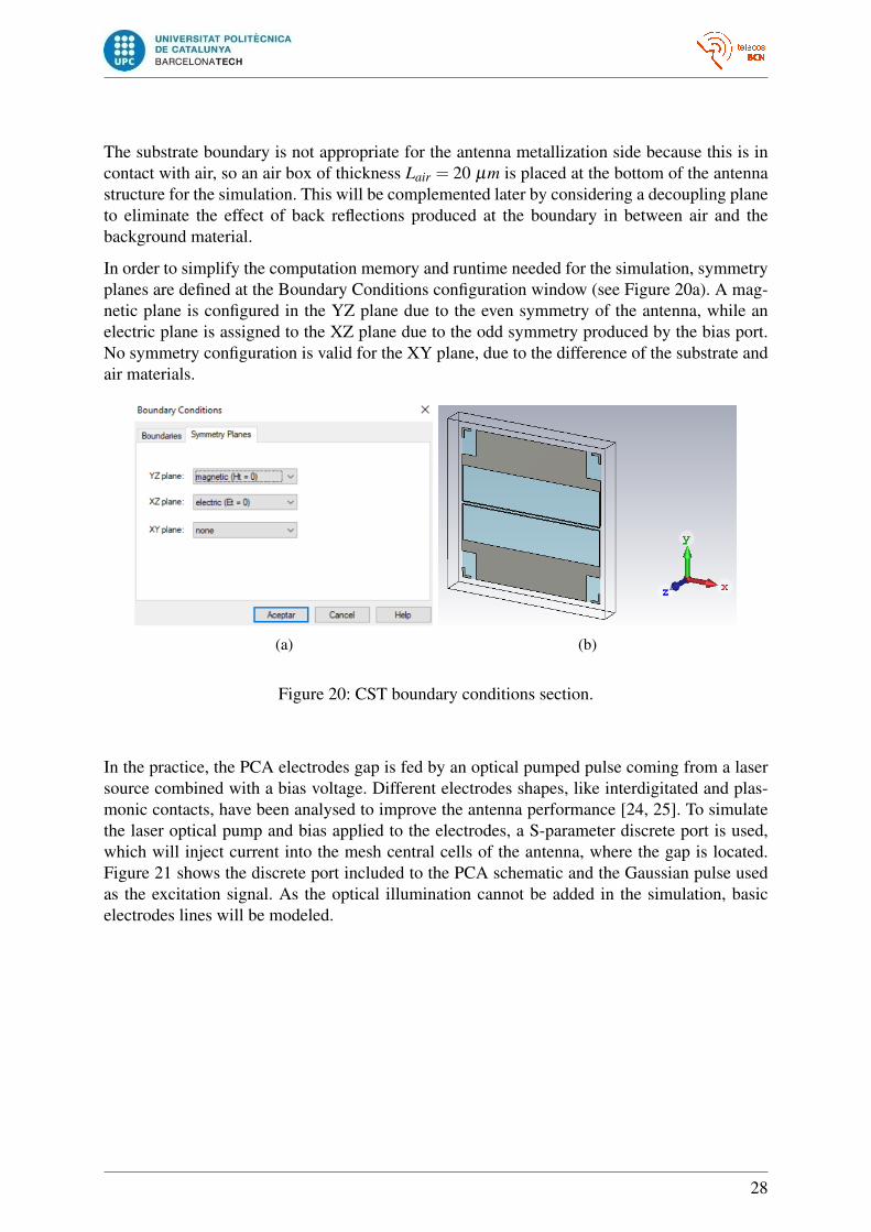
The substrate boundary is not appropriate for the antenna metallization side because this is incontact with air, so an air box of thickness Lair = 20 µm is placed at the bottom of the antennastructure for the simulation. This will be complemented later by considering a decoupling planeto eliminate the effect of back reflections produced at the boundary in between air and thebackground material.
In order to simplify the computation memory and runtime needed for the simulation, symmetryplanes are defined at the Boundary Conditions configuration window (see Figure 20a). A mag-netic plane is configured in the YZ plane due to the even symmetry of the antenna, while anelectric plane is assigned to the XZ plane due to the odd symmetry produced by the bias port.No symmetry configuration is valid for the XY plane, due to the difference of the substrate andair materials.
(a) (b)
Figure 20: CST boundary conditions section.
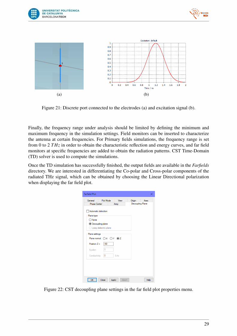
In the practice, the PCA electrodes gap is fed by an optical pumped pulse coming from a lasersource combined with a bias voltage. Different electrodes shapes, like interdigitated and plas-monic contacts, have been analysed to improve the antenna performance [24, 25]. To simulatethe laser optical pump and bias applied to the electrodes, a S-parameter discrete port is used,which will inject current into the mesh central cells of the antenna, where the gap is located.Figure 21 shows the discrete port included to the PCA schematic and the Gaussian pulse usedas the excitation signal. As the optical illumination cannot be added in the simulation, basicelectrodes lines will be modeled.
28
(a) (b)
Figure 21: Discrete port connected to the electrodes (a) and excitation signal (b).
Finally, the frequency range under analysis should be limited by defining the minimum andmaximum frequency in the simulation settings. Field monitors can be inserted to characterizethe antenna at certain frequencies. For Primary fields simulations, the frequency range is setfrom 0 to 2 T Hz in order to obtain the characteristic reflection and energy curves, and far fieldmonitors at specific frequencies are added to obtain the radiation patterns. CST Time-Domain(TD) solver is used to compute the simulations.
Once the TD simulation has successfully finished, the output fields are available in the Farfieldsdirectory. We are interested in differentiating the Co-polar and Cross-polar components of theradiated THz signal, which can be obtained by choosing the Linear Directional polarizationwhen displaying the far field plot.
Figure 22: CST decoupling plane settings in the far field plot properties menu.
29
As mentioned previously, the decoupling plane option prevents reflection at the air-substrateboundary to arrive at the substrate. An interesting discussion about the use of decoupling planesfor PCA simulation may be found in [26]. Figure 22, shows hot to select the decoupling planeoption and position inside the Properties section of the far field Plot.
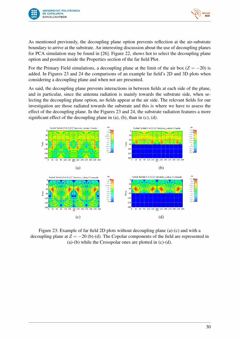
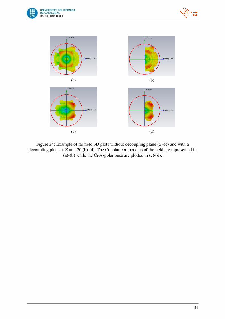
For the Primary Field simulations, a decoupling plane at the limit of the air box (Z = −20) isadded. In Figures 23 and 24 the comparisons of an example far field’s 2D and 3D plots whenconsidering a decoupling plane and when not are presented.
As said, the decoupling plane prevents interactions in between fields at each side of the plane,and in particular, since the antenna radiation is mainly towards the substrate side, when se-lecting the decoupling plane option, no fields appear at the air side. The relevant fields for ourinvestigation are those radiated towards the substrate and this is where we have to assess theeffect of the decoupling plane. In the Figures 23 and 24, the substrate radiation features a moresignificant effect of the decoupling plane in (a), (b), than in (c), (d).
(a) (b)
(c) (d)
Figure 23: Example of far field 2D plots without decoupling plane (a)-(c) and with adecoupling plane at Z =−20 (b)-(d). The Copolar components of the field are represented in
(a)-(b) while the Crosspolar ones are plotted in (c)-(d).
30
(a) (b)
(c) (d)
Figure 24: Example of far field 3D plots without decoupling plane (a)-(c) and with adecoupling plane at Z =−20 (b)-(d). The Copolar components of the field are represented in
(a)-(b) while the Crosspolar ones are plotted in (c)-(d).
31

4.1.2 Time-Domain simulation of Lens-coupled PCAs (Secondary fields)
The fields of interest of the THz systems are those that come out of the lens (Secondary fields),which are the ones that we are actually able to measure with a physical setup. To simulate thisscenario, a lens is added to the PCA structures of Figure 18 to obtain a lens-coupled structurelike the one shown in Figure 25.
(a) (b) (c)
Figure 25: Back (a), perspective (b) and left (c) view of a lens-coupled PCA structure in CST.
In this case, the background medium is considered a semi-infinite space of vacuum in all direc-tions, with a refraction index n = 1 and a dielectric constant ε = 1, which is configured in theBackground menu of Figure 19. The symmetry planes and the ports are added in the same wayas for the Primary fields simulations.
When the lens is added to the antenna structure, the electrical size of the model increases, and sodo the number of mesh cells to obtain an accurate result. This may lead to a quite high memoryusage due to the significant computer RAM required, as well as a long computation time. Thislimitations may be faced by adjusting the simulation bandwidth and the number of mesh cellsused in order to chose a proper input signal duration and time step width respectively [27].
To perform our simulations, a bandwidth of 100 GHz will be chosen for low frequencies( f < 1 T Hz), where multiple resonance is expected, generating the excitation pulse observed inFigure 26.
Figure 26: Excitation signal for a frequency range 0.45−0.55 T Hz.
32
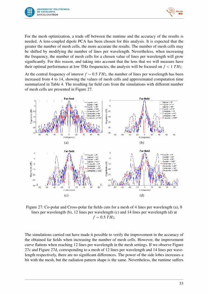
For the mesh optimization, a trade off between the runtime and the accuracy of the results isneeded. A lens-coupled dipole PCA has been chosen for this analysis. It is expected that thegreater the number of mesh cells, the more accurate the results. The number of mesh cells maybe shifted by modifying the number of lines per wavelength. Nevertheless, when increasingthe frequency, the number of mesh cells for a chosen value of lines per wavelength will growsignificantly. For this reason, and taking into account that the lens that we will measure havetheir optimal performance at low THz frequencies, the analysis will be focused on f < 1 T Hz.
At the central frequency of interest f ∼ 0.5 T Hz, the number of lines per wavelength has beenincreased from 4 to 14, showing the values of mesh cells and approximated computation timesummarized in Table 4. The resulting far field cuts from the simulations with different numberof mesh cells are presented in Figure 27.
(a) (b)
(c) (d)
Figure 27: Co-polar and Cross-polar far fields cuts for a mesh of 4 lines per wavelength (a), 8lines per wavelength (b), 12 lines per wavelength (c) and 14 lines per wavelength (d) at
f = 0.5 T Hz.
The simulations carried out have made it possible to verify the improvement in the accuracy ofthe obtained far fields when increasing the number of mesh cells. However, the improvementcurve flattens when reaching 12 lines per wavelength in the mesh settings. If we observe Figure27c and Figure 27d, corresponding to a mesh of 12 lines per wavelength and 14 lines per wave-length respectively, there are no significant differences. The power of the side lobes increases abit with the mesh, but the radiation pattern shape is the same. Nevertheless, the runtime suffers
33

an increase from 24 up to 72 hours, which means that this last value of mesh cells does not addvalue to the simulations. For this reason, a value of 12 lines per wavelength is selected to set thenumber of mesh cells.
Lines perwavelength
Number of meshcells (millions)
Computation time(hours)
4 3.9 1
8 28.0 3
12 91.3 24
14 142.2 72
Table 4: Mesh cell size and computation time for different values of lines per wavelength and abandwidth of 100 GHz at a central frequency f = 0.5 T Hz.
In the same way as with the Primary fields Simulation, CST TD solver is used to compute thefields which will be available in the Farfields directory once the simulation has successfullyfinished.
34
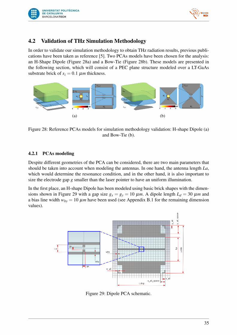
4.2 Validation of THz Simulation MethodologyIn order to validate our simulation methodology to obtain THz radiation results, previous publi-cations have been taken as reference [5]. Two PCAs models have been chosen for the analysis:an H-Shape Dipole (Figure 28a) and a Bow-Tie (Figure 28b). These models are presented inthe following section, which will consist of a PEC plane structure modeled over a LT-GaAssubstrate brick of sz = 0.1 µm thickness.
(a) (b)
Figure 28: Reference PCAs models for simulation methodology validation: H-shape Dipole (a)and Bow-Tie (b).
4.2.1 PCAs modeling
Despite different geometries of the PCA can be considered, there are two main parameters thatshould be taken into account when modeling the antennas. In one hand, the antenna length La,which would determine the resonance condition, and in the other hand, it is also important tosize the electrode gap g smaller than the laser pointer to have an uniform illumination.
In the first place, an H-shape Dipole has been modeled using basic brick shapes with the dimen-sions shown in Figure 29 with a gap size gx = gy = 10 µm. A dipole length Ld = 30 µm anda bias line width wby = 10 µm have been used (see Appendix B.1 for the remaining dimensionvalues).
Figure 29: Dipole PCA schematic.
35
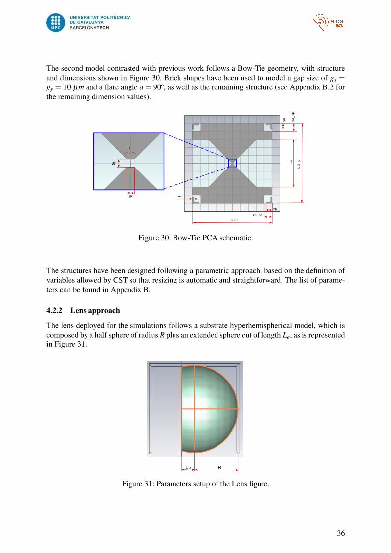
The second model contrasted with previous work follows a Bow-Tie geometry, with structureand dimensions shown in Figure 30. Brick shapes have been used to model a gap size of gx =gy = 10 µm and a flare angle a = 90º, as well as the remaining structure (see Appendix B.2 forthe remaining dimension values).
Figure 30: Bow-Tie PCA schematic.
The structures have been designed following a parametric approach, based on the definition ofvariables allowed by CST so that resizing is automatic and straightforward. The list of parame-ters can be found in Appendix B.
4.2.2 Lens approach
The lens deployed for the simulations follows a substrate hyperhemispherical model, which iscomposed by a half sphere of radius R plus an extended sphere cut of length Le, as is representedin Figure 31.
Figure 31: Parameters setup of the Lens figure.
36
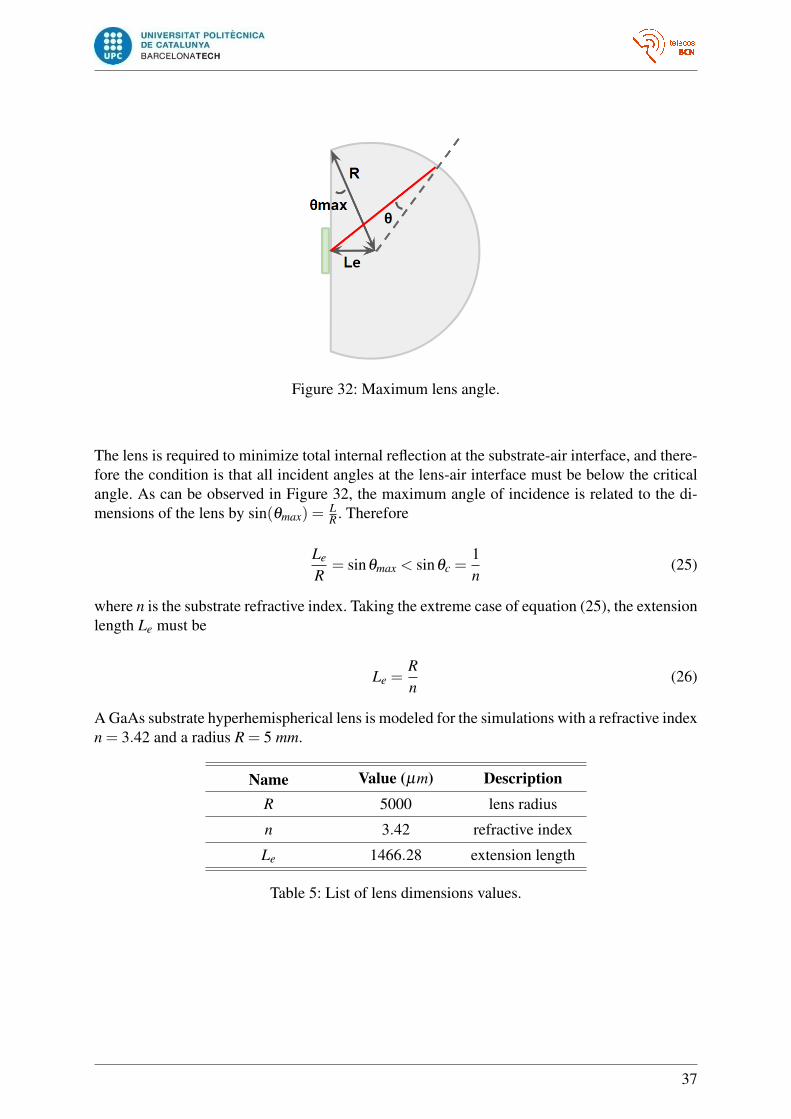
Figure 32: Maximum lens angle.
The lens is required to minimize total internal reflection at the substrate-air interface, and there-fore the condition is that all incident angles at the lens-air interface must be below the criticalangle. As can be observed in Figure 32, the maximum angle of incidence is related to the di-mensions of the lens by sin(θmax) =
LR . Therefore
Le
R= sinθmax < sinθc =
1n
(25)
where n is the substrate refractive index. Taking the extreme case of equation (25), the extensionlength Le must be
Le =Rn
(26)
A GaAs substrate hyperhemispherical lens is modeled for the simulations with a refractive indexn = 3.42 and a radius R = 5 mm.
Name Value (µm) DescriptionR 5000 lens radius
n 3.42 refractive index
Le 1466.28 extension length
Table 5: List of lens dimensions values.
37

4.2.3 Primary fields
The Primary fields of the dipole and the bow-tie have been simulated, obtaining the far fieldsat f = 0.5 T Hz. The exported ASCII files of the results have been used to plot the circularprojections of Figure 33 (right ones) using Matlab (see Appendix A.3), which are comparedwith those obtained from the same PCAs shapes in previous analysis (left ones) [5].
H Dipole
(a) (b)
Bow-Tie
(c) (d)
Figure 33: Co-polar and Cross-polar Primary fields projections comparison between theprevious work [5] (left) and simulations (right) for a frequency f = 0.5 T Hz.
It can be seen that following our methodology, the projections have similar patterns to thoseof the previous publications. On the one hand, the dipole maintains a slotted pattern for theCo-polar component, while four maximums appear around φ = ±15º and φ = 180± 15º forthe Cross-polar component. On the other hand, the Bow-tie shows a uniform pattern for theCo-polar component while the four maximums, in that case of lower amplitude, are observedat φ = ±45º and φ = ±135º. It is worth mentioning that the results used for comparison [5],have also been obtained with simulations carried out in CST and therefore the small differencesobserved have to be attributed to slightly different choices of the simulation parameters.
4.2.4 Secondary fields
The Secondary fields of the dipole and the bow-tie have been obtained, the far field cuts ofwhich are represented in Figure 34 (right ones) by using Matlab (see Appendix A.4), whichare also compared with those obtained from the same PCAs shapes in previous analysis (left
38
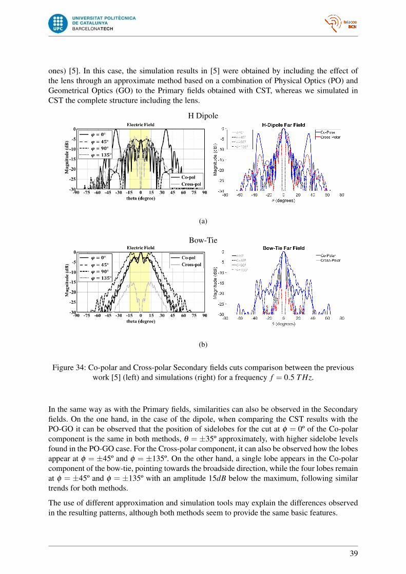
ones) [5]. In this case, the simulation results in [5] were obtained by including the effect ofthe lens through an approximate method based on a combination of Physical Optics (PO) andGeometrical Optics (GO) to the Primary fields obtained with CST, whereas we simulated inCST the complete structure including the lens.
H Dipole
(a)
Bow-Tie
(b)
Figure 34: Co-polar and Cross-polar Secondary fields cuts comparison between the previouswork [5] (left) and simulations (right) for a frequency f = 0.5 T Hz.
In the same way as with the Primary fields, similarities can also be observed in the Secondaryfields. On the one hand, in the case of the dipole, when comparing the CST results with thePO-GO it can be observed that the position of sidelobes for the cut at φ = 0º of the Co-polarcomponent is the same in both methods, θ = ±35º approximately, with higher sidelobe levelsfound in the PO-GO case. For the Cross-polar component, it can also be observed how the lobesappear at φ = ±45º and φ = ±135º. On the other hand, a single lobe appears in the Co-polarcomponent of the bow-tie, pointing towards the broadside direction, while the four lobes remainat φ = ±45º and φ = ±135º with an amplitude 15dB below the maximum, following similartrends for both methods.
The use of different approximation and simulation tools may explain the differences observedin the resulting patterns, although both methods seem to provide the same basic features.
39
4.3 Simulation and measurement of THz systemsTHz radiated far fields’ characteristics, such as the bandwidth and the power amplitude of thegenerated signal, is influenced by the PCA shape. Focusing on the Bow-tie shape, recent stud-ies have demonstrated an enhancement of the radiated power by modeling a fractal structureof the antenna. This structure changes the surface current distribution to form individual sub-wavelength radiators which are coherently coupled [28]. In this section, an analysis of differentorder Fractal PCAs following the methodology described above will be carried out.
4.3.1 Fractal structures characteristics
Mathematically, the term fractal, coming from the Latin word fractus ’broken, irregular’, is usedto define a self-similar subset of a base pattern. A self-similar object consists on the replicationof its structure at different scales, normally made of smaller copies of itself, which is also knownas unfolding symmetry [29].
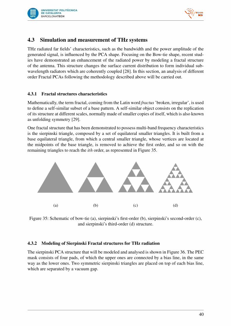
One fractal structure that has been demonstrated to possess multi-band frequency characteristicsis the sierpinski triangle, composed by a set of equilateral smaller triangles. It is built from abase equilateral triangle, from which a central smaller triangle, whose vertices are located atthe midpoints of the base triangle, is removed to achieve the first order, and so on with theremaining triangles to reach the ith order, as represented in Figure 35.
(a) (b) (c) (d)
Figure 35: Schematic of bow-tie (a), sierpinski’s first-order (b), sierpinski’s second-order (c),and sierpinski’s third-order (d) structure.
4.3.2 Modeling of Sierpinski Fractal structures for THz radiation
The sierpinski PCA structure that will be modeled and analysed is shown in Figure 36. The PECmask consists of four pads, of which the upper ones are connected by a bias line, in the sameway as the lower ones. Two symmetric sierpinski triangles are placed on top of each bias line,which are separated by a vacuum gap.
40

Figure 36: Example of sierpinski PCA schematic with La = 1200 µm and it = 4.
In order to build the structure, basic shapes are used to model the pads, bias lines and alignmentmarks in the first place, setting the dimension values listed in Table 6. The antenna length Lawill be switched to analyse different sierpinski dimensions.
NameValue (µm or
deg) Description
gx 10 x dimension of the gap
gy 10 y dimension of the gap
a 60 Equilateral triangle angle
Lchip 2000 chip size
xpad 400 x dimension of the pad
ypad 200 y dimension of the pad
wb 2 y width of the bias line
wa 20 width of the alignment mark
xa 150 x length of the alignment mark
ya 150 y length of the alignment mark
xa sp 200 x void space for alignment mark
ya sp 200 y void space for alignment mark
Table 6: List of fixed sierpinski dimensions values.
A CST Macro is developed to construct the sierpinski triangle structure based on the antenna
41
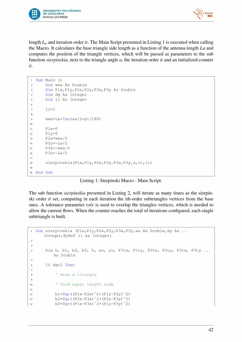
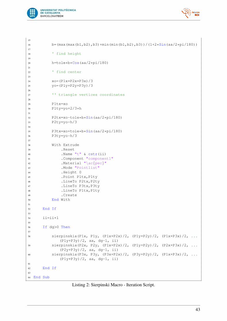
length La and iteration order it. The Main Script presented in Listing 1 is executed when callingthe Macro. It calculates the base triangle side length as a function of the antenna length La andcomputes the position of the triangle vertices, which will be passed as parameters to the subfunction sierpinskia, next to the triangle angle a, the iteration order it and an initialized counterii.
1 Sub Main ()2 Dim wwa As Double3 Dim P1x,P1y,P2x,P2y,P3x,P3y As Double4 Dim dg As Integer5 Dim ii As Integer6
7 ii=18
9 wwa=La*Tan(aa/2*pi/180)10
11 P1x=012 P1y=013 P2x=wwa/214 P2y=−La/215 P3x=−wwa/216 P3y=−La/217
18 sierpinskia(P1x,P1y,P2x,P2y,P3x,P3y,a,it,ii)19
20 End Sub
Listing 1: Sierpinski Macro - Main Script.
The sub function sierpinskia presented in Listing 2, will iterate as many times as the sierpin-ski order it set, computing in each iteration the ith-order subtriangles vertices from the baseones. A tolerance parameter tole is used to overlap the triangles vertices, which is needed toallow the current flows. When the counter reaches the total of iterations configured, each singlesubtriangle is built.
1 Sub sierpinskia (P1x,P1y,P2x,P2y,P3x,P3y,aa As Double,dg As ...Integer,ByRef ii As Integer)
2
3
4 Dim b, b1, b2, b3, h, xo, yo, P1tx, P1ty, P2tx, P2ty, P3tx, P3ty ...As Double
5
6 If dg<1 Then7
8 ' draw a triangle9
10 ' find equal length side11
12 b1=Sqr((P1x−P2x)ˆ2+(P1y−P2y)ˆ2)13 b2=Sqr((P2x−P3x)ˆ2+(P2y−P3y)ˆ2)14 b3=Sqr((P1x−P3x)ˆ2+(P1y−P3y)ˆ2)
42
15
16 b=(max(max(b1,b2),b3)+min(min(b1,b2),b3))/(1+2*Sin(aa/2*pi/180))17
18 ' find height19
20 h=tole*b*Cos(aa/2*pi/180)21
22 ' find center23
24 xo=(P1x+P2x+P3x)/325 yo=(P1y+P2y+P3y)/326
27 '' triangle vertices coordinates28
29 P1tx=xo30 P1ty=yo+2/3*h31
32 P2tx=xo−tole*b*Sin(aa/2*pi/180)33 P2ty=yo−h/334
35 P3tx=xo+tole*b*Sin(aa/2*pi/180)36 P3ty=yo−h/337
38 With Extrude39 .Reset40 .Name "t" & cstr(ii)41 .Component "component1"42 .Material "\acpec"43 .Mode "Pointlist"44 .Height 045 .Point P1tx,P1ty46 .LineTo P2tx,P2ty47 .LineTo P3tx,P3ty48 .LineTo P1tx,P1ty49 .Create50 End With51
52 End If53
54 ii=ii+155
56 If dg>0 Then57
58 sierpinskia(P1x, P1y, (P1x+P2x)/2, (P1y+P2y)/2, (P1x+P3x)/2, ...(P1y+P3y)/2, aa, dg−1, ii)
59 sierpinskia(P2x, P2y, (P1x+P2x)/2, (P1y+P2y)/2, (P2x+P3x)/2, ...(P2y+P3y)/2, aa, dg−1, ii)
60 sierpinskia(P3x, P3y, (P3x+P2x)/2, (P3y+P2y)/2, (P1x+P3x)/2, ...(P1y+P3y)/2, aa, dg−1, ii)
61
62 End If63
64 End Sub
Listing 2: Sierpinski Macro - Iteration Script.
43
Once the sierpinski triangle is obtained, it is manually replicated using the mirror tool to formthe bow tie antenna, a gap of dimensions gx = gy = 10 µm is subtracted and a substrate box ofthe chip dimensions with a width sz = 0.1 µm and of GaAs dielectric material is added.
4.3.3 Simulation of THz Far Fields with Sierpinski structures
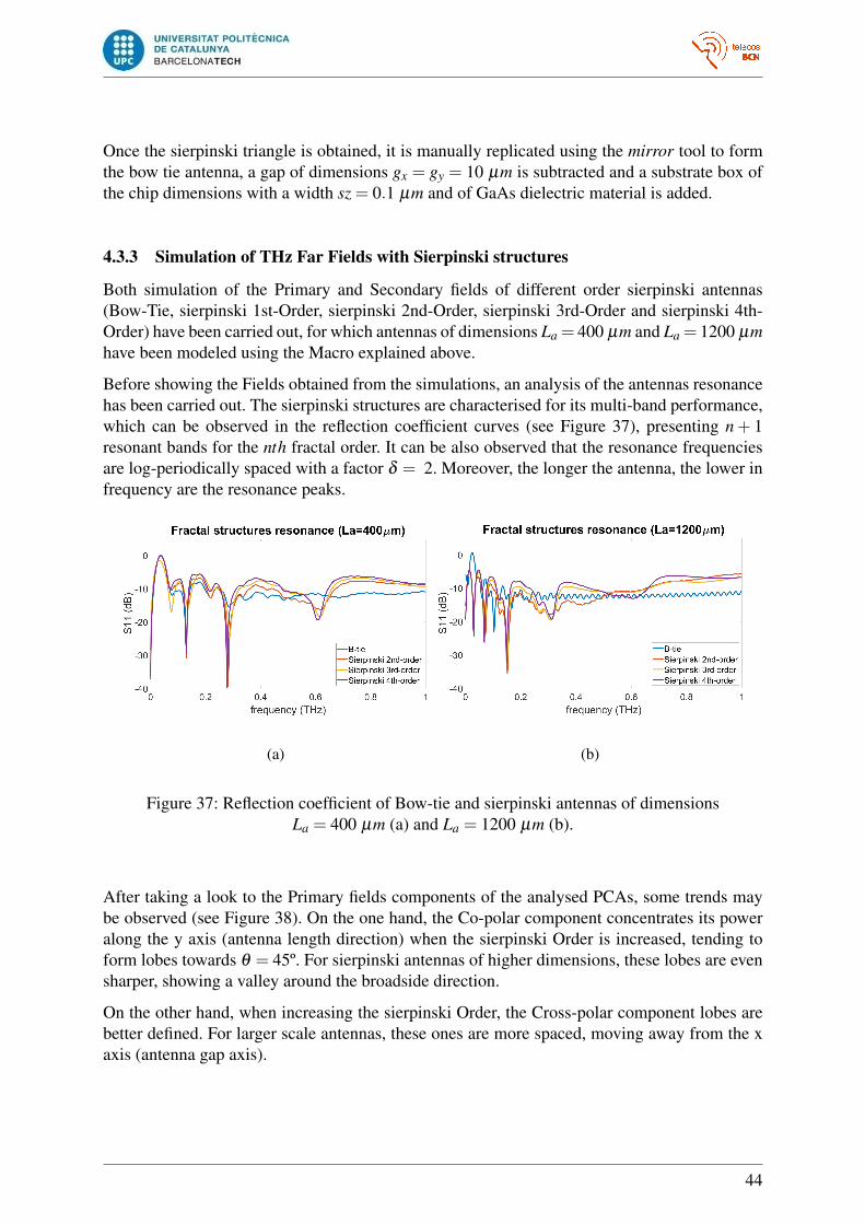
Both simulation of the Primary and Secondary fields of different order sierpinski antennas(Bow-Tie, sierpinski 1st-Order, sierpinski 2nd-Order, sierpinski 3rd-Order and sierpinski 4th-Order) have been carried out, for which antennas of dimensions La = 400 µm and La = 1200 µmhave been modeled using the Macro explained above.
Before showing the Fields obtained from the simulations, an analysis of the antennas resonancehas been carried out. The sierpinski structures are characterised for its multi-band performance,which can be observed in the reflection coefficient curves (see Figure 37), presenting n+ 1resonant bands for the nth fractal order. It can be also observed that the resonance frequenciesare log-periodically spaced with a factor δ = 2. Moreover, the longer the antenna, the lower infrequency are the resonance peaks.
(a) (b)
Figure 37: Reflection coefficient of Bow-tie and sierpinski antennas of dimensionsLa = 400 µm (a) and La = 1200 µm (b).
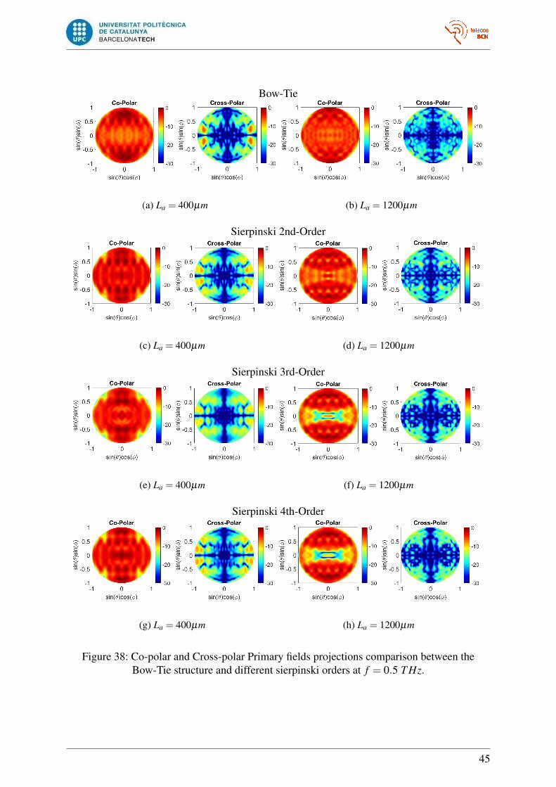
After taking a look to the Primary fields components of the analysed PCAs, some trends maybe observed (see Figure 38). On the one hand, the Co-polar component concentrates its poweralong the y axis (antenna length direction) when the sierpinski Order is increased, tending toform lobes towards θ = 45º. For sierpinski antennas of higher dimensions, these lobes are evensharper, showing a valley around the broadside direction.
On the other hand, when increasing the sierpinski Order, the Cross-polar component lobes arebetter defined. For larger scale antennas, these ones are more spaced, moving away from the xaxis (antenna gap axis).
44
Bow-Tie
(a) La = 400µm (b) La = 1200µm
Sierpinski 2nd-Order
(c) La = 400µm (d) La = 1200µm
Sierpinski 3rd-Order
(e) La = 400µm (f) La = 1200µm
Sierpinski 4th-Order
(g) La = 400µm (h) La = 1200µm
Figure 38: Co-polar and Cross-polar Primary fields projections comparison between theBow-Tie structure and different sierpinski orders at f = 0.5 T Hz.
45
A GaAs hyperhemispherical lens of radius dimension R = 5mm has been added to the sierpinskistructure to simulate the Secondary fields. Some interest cuts of the radiation patterns obtainedfrom the lens-coupled structures (see Appendix C) are plotted in Figure 39.
(a) (b)
Figure 39: Secondary far field cuts of sierpinski PCAs: Co-polar component cut at φ = 90º (a)and Cross-polar component cut at φ = 45º (b) at f = 0.5 T Hz.
The Co-polar cuts present a pattern composed by a primary lobe pointing towards the broadsidedirection, accompanied by two side lobes of lower amplitude, which form an Airy pattern.For small sierpinski PCAs (La = 400 µm), almost nothing changes in the pattern shape andamplitude when increasing the fractal order. In the case of bigger structures (La = 1200 µm)the side lobes amplitude does show a slight increment for higher sierpinski order antennas. Inaddition, the Airy pattern width seems to depend on the antenna dimensions, showing that forsmaller sierpinski dimensions, the pattern is more directive.
In the case of the Cross-polar far field there are no big differences. A quadrupole behaviour withlobes around−15dB below the Co-polar lobe amplitude is observed, presenting a null along theaxis. The lobes direction is maintained for the different order antennas, pointing towards θ = 5º.Only a slight amplitude decay may be observed when increasing the sierpinski iterations.
La = 400 µm La = 1200 µm
Bow-Tie 0.476 W 0.455 W
Sierpinski 1st-Order 0.472 W 0.479 W
Sierpinski 2nd-Order 0.463 W 0.475 W
Sierpinski 3rd-Order 0.450 W 0.472 W
Sierpinski 4th-Order 0.440 W 0.434 W
Table 7: Total Radiated Power for the different sierpinski order PCAs simulated atf = 0.5 T Hz.
46

As it has been mentioned above, fractal structures have been modeled to increase the radiation ofTHz emitters in terms of power, therefore the total radiated power of the simulated antennas hasbeen summarized in Table 7 to analyse the improvement at a central frequency f = 0.5 T Hz.An upturn may be observed for sierpinski structures of dimensions La = 1200 µm, reachingits better power performance for the first fractal order. However, in the case of the smallersierpinski (La = 400 µm), the radiated power decays when increasing the fractal order. It maybe substantiated for the perforations dimensions, which for this antenna length may be smallerthan the wavelength reassembling a solid surface current distribution [30].
(a)
(b)
Figure 40: Secondary far field cuts of a 3rd-Order sierpinski PCA of dimensions La = 400 µm:laboratory measurements (a) versus simulations (b) at f = 0.5 T Hz.
The measured results in Figure 40 feature asymmetries which are specially apparent in theCross-polar components. These asymmetries are an indication of the need for further adjustmentof the laser feed and have been proposed as a measure of the laser alignment quality in practicalsetups. Considering the details of the measurement system [31] we find a reasonable agreementwith simulated patterns, with similar Co-polar 3 dB beam widths of respectively 4º and 3º inthe 0º and 90º cuts, and side-lobes located around 5º in the 90º cut. As for the Cross-polarcomponent, apart from the mentioned laser misalignment asymmetry the position of side-lobes
47

in the Cross-polar cuts at 0º / 90º is seen to coincide around 3º / 5º in both simulation andmeasures. Further adjustment of the physical setup is presently underway.
48
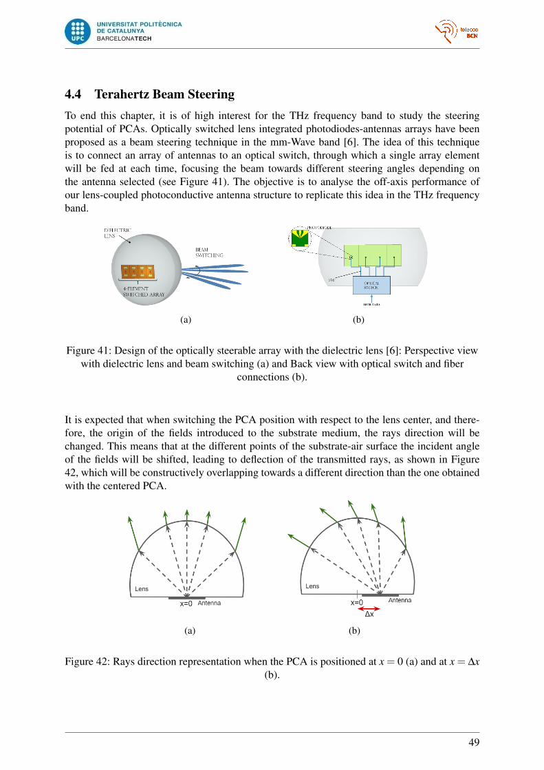
4.4 Terahertz Beam SteeringTo end this chapter, it is of high interest for the THz frequency band to study the steeringpotential of PCAs. Optically switched lens integrated photodiodes-antennas arrays have beenproposed as a beam steering technique in the mm-Wave band [6]. The idea of this techniqueis to connect an array of antennas to an optical switch, through which a single array elementwill be fed at each time, focusing the beam towards different steering angles depending onthe antenna selected (see Figure 41). The objective is to analyse the off-axis performance ofour lens-coupled photoconductive antenna structure to replicate this idea in the THz frequencyband.
(a) (b)
Figure 41: Design of the optically steerable array with the dielectric lens [6]: Perspective viewwith dielectric lens and beam switching (a) and Back view with optical switch and fiber
connections (b).
It is expected that when switching the PCA position with respect to the lens center, and there-fore, the origin of the fields introduced to the substrate medium, the rays direction will bechanged. This means that at the different points of the substrate-air surface the incident angleof the fields will be shifted, leading to deflection of the transmitted rays, as shown in Figure42, which will be constructively overlapping towards a different direction than the one obtainedwith the centered PCA.
(a) (b)
Figure 42: Rays direction representation when the PCA is positioned at x = 0 (a) and at x = ∆x(b).
49
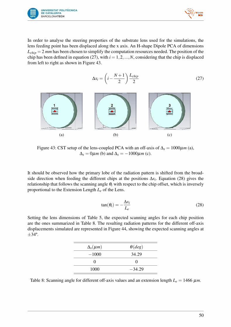
In order to analyse the steering properties of the substrate lens used for the simulations, thelens feeding point has been displaced along the x axis. An H-shape Dipole PCA of dimensionsLchip = 2 mm has been chosen to simplify the computation resources needed. The position of thechip has been defined in equation (27), with i = 1,2, ...,N, considering that the chip is displacedfrom left to right as shown in Figure 43.
∆xi =
(i− N +1
2
)Lchip
2(27)
(a) (b) (c)
Figure 43: CST setup of the lens-coupled PCA with an off-axis of ∆x = 1000µm (a),∆x = 0µm (b) and ∆x =−1000µm (c).
It should be observed how the primary lobe of the radiation pattern is shifted from the broad-side direction when feeding the different chips at the positions ∆xi. Equation (28) gives therelationship that follows the scanning angle θi with respect to the chip offset, which is inverselyproportional to the Extension Length Le of the Lens.
tan(θi) =−∆xi
Le(28)
Setting the lens dimensions of Table 5, the expected scanning angles for each chip positionare the ones summarized in Table 8. The resulting radiation patterns for the different off-axisdisplacements simulated are represented in Figure 44, showing the expected scanning angles at±34º.
∆x(µm) θ(deg)
−1000 34.29
0 0
1000 −34.29
Table 8: Scanning angle for different off-axis values and an extension length Le = 1466 µm.
50
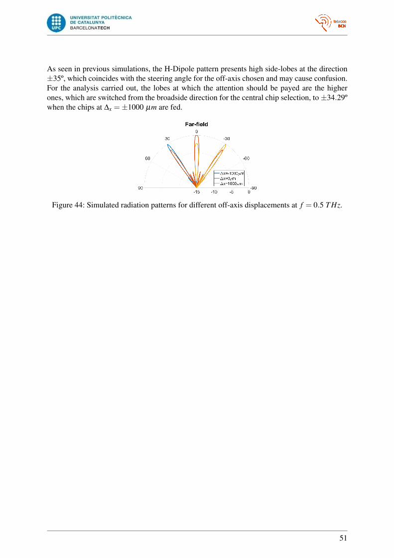
As seen in previous simulations, the H-Dipole pattern presents high side-lobes at the direction±35º, which coincides with the steering angle for the off-axis chosen and may cause confusion.For the analysis carried out, the lobes at which the attention should be payed are the higherones, which are switched from the broadside direction for the central chip selection, to±34.29ºwhen the chips at ∆x =±1000 µm are fed.
Figure 44: Simulated radiation patterns for different off-axis displacements at f = 0.5 T Hz.
51
5 Conclusions and future developmentTo sum up, this thesis has been divided in two main parts to analyse different models of opti-cally feed antenna elements to achieve beam forming and beam steering at mm-Wave and THzfrequencies.
In the first part, we have presented a proposal for an optical network to control the direction ofmaximum directivity of a PAA, for which the beam steering is achieved through the wavelengthtuning of an array of input lasers and dispersive propagation. The free-lobe beam steering op-eration is mainly restricted by the PAA inter-elements spacing, which will also determine themaximum pointing direction along with the AWG channel bandwidth.
Moreover, a double-branch DE-MZM configuration for optical modulation has been proposed.The simulation results show the ability of the biasing technique to avoid the CD-fading penalty,of around 5dB in the example system biased at QP, and enable large bandwidth and high countPAAs by switching the notch position of the photodetected signal. The method is tunable, al-lowing to reconfigure the target frequency band.
In the second part, a simulation solver setup has been described to define a methodology to ob-tain the far fields of THz radiation elements, including the solver configuration to reproduce theradiated fields inside the lens (Primary Fields) and the transmitted fields from the lens surfacetowards the air (Secondary Fields). Despite a trade off between the runtime of the solver and theaccuracy of the results has been applied, the solution has shown excellent results, which havebeen validated by comparing the far fields obtained from simulating replicas of previous publi-cations models with remarkable similarity, even when with the present resources it is limited tothe simulation of frequencies below 1 T Hz and some simulations may take up to more than 24hours of computer time.
This methodology has been used to analyse Fractal Antennas. After simulating different ordersierpinski PCAs, the resonance curves have been obtained, proving the multi-band characteris-tics of the shapes. An analysis around the frequency f = 0.5 T Hz of different sierpinski orderand dimensions has been carried out. Smaller structures (La = 400 µm) seem to be more di-rective, but little improvement may be seen when increasing the iteration order, while largerantennas (La = 1200 µm) show a wider airy pattern and slight power improvement when shift-ing the fractal order, with an optimal power transmission for the first fractal order. This analysishas helped us to see the scope of the methodology presented, even when we are limited to fre-quencies below 1 THz by the computer power required to simulate with CST large structures.
Finally, the lens-coupled H Dipole off-axis performance has been analysed by carrying outsimulations where the PCA is displaced along the x axis, showing the steering capability ofthe hyperhemispherical lens substrate and its dependence with the extension length, which willdefine the limits of the steering range. Our simulations have yielded a ±34º steering with atypical H dipole PCA with a spatial shift of ∆x = 1000 µm.
Besides the results summarized above, the results of this work may constitute the foundationsfor future developments, in the path towards portraying this principles into real communicationsystems. Possible future work lines are summarized below.
A first step to evolve towards mm-Wave optical feed arrays is to build the setup of the MW
52
OTTDN system simulated in the laboratory in order to measure the steering and reconfigu-ration performance and determine the physical limitations. Microwave operating frequencieshave been considered for the analysis in order to replicate the available antenna elements per-formance, so a next step could be to design photonic integrated antenna arrays to work at themm-Wave band.
On the other hand, and thinking of a functional model of the presented solution, an automaticbias control method may be the implementation key. This would add the flexibility needed towork with adaptive resources by adjusting the bias as a function of the operating frequency.
It can be observed that the proposed solution presents unused spectrum in the central channelsdue to the wavelength spacing conditions. Another work line could be to find a way of reduc-ing the spectrum occupied by looking for an alternative to the AWG filter with non-uniformchannels.
The THz band is still a novel study field and great advances are yet to come. The methodologypresented could be a tool to study in depth different antennas and lens shapes characteristics,as it has been done with the sierpinski antennas. In particular, further work should considerthe development of simulation strategies that may allow to increase the simulation frequenciesby reducing the computer resources and time required. Approximate methods to include theeffect of the lens and obtain the Secondary fields as a function of the Primary fields are worthexploring.
The steering capabilities have been analysed with a dipole PCA, which presents high secondarylobes. A more optimal PCA shape could be analysed to fit in the free-lobe condition. Laboratorymeasurements of the lens-coupled antenna with the PCA feeding displaced could be also carriedout to observe the physical performance of the lens steering capability. This could be the basisto implement the optically switched PCAs array proposed in previous publications to feed thelens and switch the beam towards specific directions when feeding each one of the array PCAs.
53
References[1] B. G. Kim, S. H. Bae, H. Kim, and Yun C. Chung. “RoF-Based Mobile Fronthaul Net-
works Implemented by Using DML and EML for 5G Wireless Communication Systems”. J. Of Lightwave Technol., Vol. 36:pp. 1874 – 2881, July 2018.
[2] S. Ummethala, T. Harter, K. Koehnle, Z. Li, S. Muehlbrandt, Y. Kutuvantavida, J. Ke-mal, P. Marin-Palomo, J. Schaefer, A. Tessmann, S. K. Garlapati, A. Bacher, L. Hahn, M.Walther, T. Zwick, S. Randel, W. Freude and C. Koos. “THz-to-optical conversion in wire-less communications using an ultra-broadband plasmonic modulator” . nature photonics,Vol. 13:pp. 519 – 524, August 2019.
[3] S. Vega. “Orientacion de Antenas Mediante Tecnicas Fotonicas en Sistemas Inalambricosde Radiofrecuencia” . Degree’s Thesis of Telecommunications Engineering: UniversiatPolitecnica de Catalunya, July 2018.
[4] S. Vega, D. Nuno and M. C. Santos. “Optical beam steering network with multibandcapability” . XXXV Simposium Nacional de la Union Cientıfica Internacional de Radio,URSI 2020.
[5] A. Garufo, G. Carluccio, J.R. Freeman, D.R. Beacon, N. Llombart, E.H. Linfield, A.G.Davies and A. Neto. “Norton Equivalent Circuit for Pulsed Photoconductive Anten-nas—Part II: Experimental Validation” . IEEE Trans. Antennas Propag., Vol. 66(no. 4):pp.1635–1645, April 2018.
[6] C. Ballesteros, M. Maestre, M.C. Santos, J. Romeu and L. Jofre. “An Architecture Anal-ysis for Millimeter-Wave Optically Steerable Antenna Array” . EuCAP, 2019.
[7] A. Cardama, L. Jofre, J. M. Rius, J. Romeu and S. Blanch. “Antenes” . 1st ed. Barcelona,Spain: Edicions UPC, 1998.
[8] Z. Cao et al. “Advanced integration techniques on broadband millimeter-wave beam steer-ing for 5G wireless networks and beyond” . IEEE J. Quantum Electron., Vol. 52(no.1):Art. no. 0600620, January 2016.
[9] P. Shumyatsky and R. R. Alfano. “Therahertz sources” . J. Biomed. Opt., Vol. 16(no.3):033001, March 2011.
[10] J. Klier, G. Torosyan, N. S. Schreiner, D. Molter, F. Ellrich, W. Zouaghi, E. Peytavit, J. F.Lampin, R. Beigang, J. Jonuscheit and G. von Freymann. “Influence of Substrate Materialon Radiation Characteristics of THz Photoconductive Emitters” . International Journal ofAntennas and Propagation, Vol. 2015:540175, 2015.
[11] N. M. Burford and M. O. El-Shenawee. “Review of terahertz photoconductive antennatechnology” . Opt. Eng., Vol. 56(no. 1):010901, January 2017.
[12] H. Kitahara, M. Tani and M. Hangyo. “Frequency-domain optical coherence tomographysystem in the terahertz region” . Applied Physics B, page 126:22, January 2020.
[13] J. Prat et al. “Technologies for cost-effective udWDM-PONs” . J. Lightw. Technol, Vol.34(no. 2):pp. 783–791, January 2016.
54

[14] X. Ye, D. Zhu, Y. Zhang, S. Li, and S. Pan. “Analysis of Photonics-Based RF Beamform-ing With Large Instantaneous Bandwidth” . J. Of Lightwave Technol., Vol. 35:pp. 5010 –5019, 2017.
[15] L. Jofre, C. Stoltidou, S. Blanch, T. Mengual, B. Vidal, J. Marti, I. McKenzie, and J.M. delCura. “Optically beamformed wideband array performance” . IEEE Trans. on Antennasand Propagation, Vol. 56(no. 6):pp. 1594 – 1604, June 2008.
[16] B. G. Kim, S. H. Bae, H. Kim, and Yun C. Chung. “RoF-Based Mobile Fronthaul Net-works Implemented by Using DML and EML for 5G Wireless Communication Systems”. J. Of Lightwave Technol., Vol. 36:pp. 2874 – 1881, July 2018.
[17] J. L. Corral, J. Marti and J. M. Fuster. “Optical Up-Conversion on Continuously VariableTrue-Time-Delay Lines Based on Chirped Fiber Gratings for Millimeter-Wave OpticalBeamforming Networks” . IEEE Trans. Microwave Theory Tech, Vol. 47:pp. 1315 – 1320,July 1999.
[18] J. Tabares, S. Ghasemi, V. Polo, and J. Prat. “Simplified Carrier Recovery for IntradyneOptical PSK Receivers in udWDM-PON” . J. Of Lightwave Technol., Vol. 36:pp. 2941 –2947, July 2018.
[19] Y. Gao, A. Wen, Y. Chen, S. Xiang, H. Zhang, and L. Shang. “An Analog PhotonicLink With Compensation of Dispersion-Induced Power Fading” . IEEE Photon. Technol.Letters, Vol. 27(no. 12), June 2015.
[20] C. A. Balanis. “Antenna Theory: Analysis and Design” . Wiley, 2005.
[21] P. S. Devgan, D. P. Brown, and R. L. Nelson. “RF Performance of Single Sideband Mod-ulation Versus Dual Sideband Modulation in a Photonic Link” . J. Of Lightwave Technol.,Vol. 33, May 2015.
[22] J. L. Corral, J. Marti, J. M. Fuster, and R. I. Laming. “Dispersion induced bandwidth limi-tation of variable true time delay lines based on linearly chirped fiber gratings” . Electron.Lett., Vol. 34(no. 2):pp. 209 – 211, 1998.
[23] Computer Simulation Technology. https://www.cst.com/.
[24] H. Tanoto, J. H. Teng, Q. Y. Wu, M. Sun, Z. N. Chen, S. A. Maier, B. Wang, C. C. Chum, G.Y. Si, A. J. Danner and S. J. Chua. “Greatly enhanced continuous-wave terahertz emissionby nano-electrodes in a photoconductive photomixer” . nature photonics, January 2012.
[25] C.W. Berry, N. Wang, M.R. Hashemi, M. Unlu and M. Jarrahi. “Significant performanceenhancement in photoconductive terahertz optoelectronics by incorporating plasmoniccontact electrodes” . nature communications, March 2013.
[26] N. Llombart and A. Neto. “Authors’ Reply” . IEEE Transactions on Terahertz Scienceand Technology, Vol. 4(no. 1):pp. 127 – 128, January 2014.
[27] A. K. M. Zakir Hossain. “Planar Antennas for Terahertz Detectors” . Master’s Thesis inElectronics: University of Gavle, September 2012.
55

[28] P. Maraghechi and A. Y. Elezzabi. “Fractal Structures for THz Radiation Emitters” .Journal of Selected Topics in Quantum Electronics, Vol. 19(no. 1), January 2013.
[29] P MIshra, G Bhatnagar. “Self-similarity” . At Right Angles, Vol. 3(no.2), July 2014.
[30] P. Maraghechi and A. Y. Elezzabi. “Enhanced THz radiation emission from plasmoniccomplementary Sierpinski fractal emitters Emitters” . Opt. Express 18, 2010.
[31] D. Nuno, M. C. Santos, J. S. Gomez-Dıaz, J. Romeu and L. Jofre. “Characterizationof THz radiation by collimated wavefront aperture raster scanning” . XXXV SimposiumNacional de la Union Cientıfica Internacional de Radio, URSI 2020.
56

AcronymsAF Array Factor
AWG Arrayed Waveguide Gratings
CD Chromatic Dispersion
DC Direct Current
DCF Dispersion Compensating Fiber
DE-MZM Dual Electrode Mach Zehnder Modulator
DFB Distributed Feedback Bragg
DSB Double Side-Band
EM Electromagnetic
GO Geometrical Optics
IoT Internet of Things
LT-GaAs Low-Temperature Grown Gallium Arsenide
mm-Wave millimeter Wave
MW multiwavelength
OTTDN Optical True Time Delay Network
PAA Phased Array Antenna
PAAE Phased Array Antenna Element
PCA Photoconductive Antenna
PEC Perfect Electric Conductor
PO Physical Optics
PP-MZM Push-Pull Mach Zehnder Modulator
QP Quadrature Point
RF Radio Frequency
RoF Radio-over-Fiber
SSB Single Side-Band
TD Time Domain
TDS Time-Domain Spectroscopy
THz Terahertz
ToF THz-over-Fiber
57

TRx Transceiver
TTD True Time Delay
WDM-PON Wavelength Division Multiplexing-Passive Optical Network
58
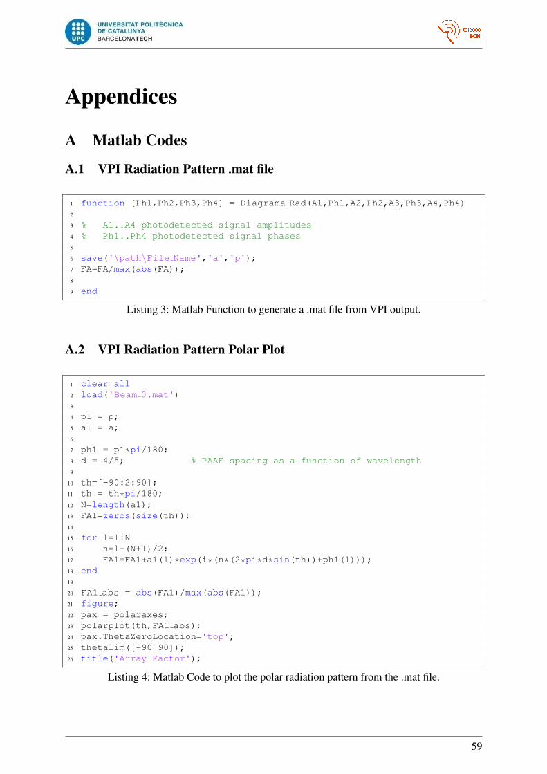
Appendices
A Matlab Codes
A.1 VPI Radiation Pattern .mat file
1 function [Ph1,Ph2,Ph3,Ph4] = Diagrama Rad(A1,Ph1,A2,Ph2,A3,Ph3,A4,Ph4)2
3 % A1..A4 photodetected signal amplitudes4 % Ph1..Ph4 photodetected signal phases5
6 save('\path\File Name','a','p');7 FA=FA/max(abs(FA));8
9 end
Listing 3: Matlab Function to generate a .mat file from VPI output.
A.2 VPI Radiation Pattern Polar Plot
1 clear all2 load('Beam 0.mat')3
4 p1 = p;5 a1 = a;6
7 ph1 = p1*pi/180;8 d = 4/5; % PAAE spacing as a function of wavelength9
10 th=[−90:2:90];11 th = th*pi/180;12 N=length(a1);13 FA1=zeros(size(th));14
15 for l=1:N16 n=l−(N+1)/2;17 FA1=FA1+a1(l)*exp(i*(n*(2*pi*d*sin(th))+ph1(l)));18 end19
20 FA1 abs = abs(FA1)/max(abs(FA1));21 figure;22 pax = polaraxes;23 polarplot(th,FA1 abs);24 pax.ThetaZeroLocation='top';25 thetalim([−90 90]);26 title('Array Factor');
Listing 4: Matlab Code to plot the polar radiation pattern from the .mat file.
59
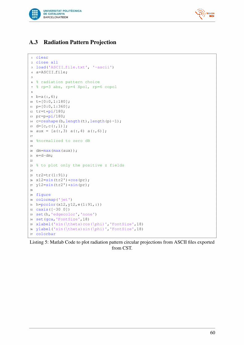
A.3 Radiation Pattern Projection
1 clear2 close all3 load('ASCII file.txt', '−ascii')4 a=ASCII file;5
6 % radiation pattern choice7 % rp=3 abs, rp=4 Xpol, rp=6 copol8
9 b=a(:,6);10 t=[0:0,1:180];11 p=[0:0,1:360];12 tr=t*pi/180;13 pr=p*pi/180;14 c=reshape(b,length(t),length(p)−1);15 d=[c,c(:,1)];16 aux = [a(:,3) a(:,4) a(:,6)];17
18 %normalized to zero dB19
20 dm=max(max(aux));21 e=d−dm;22
23 % to plot only the positive z fields24
25 tr2=tr(1:91);26 x12=sin(tr2')*cos(pr);27 y12=sin(tr2')*sin(pr);28
29 figure30 colormap('jet')31 h=pcolor(x12,y12,e(1:91,:))32 caxis([−30 0])33 set(h,'edgecolor','none')34 set(gca,'FontSize',18)35 xlabel('sin(\theta)cos(\phi)','FontSize',18)36 ylabel('sin(\theta)sin(\phi)','FontSize',18)37 colorbar
Listing 5: Matlab Code to plot radiation pattern circular projections from ASCII files exportedfrom CST.
60
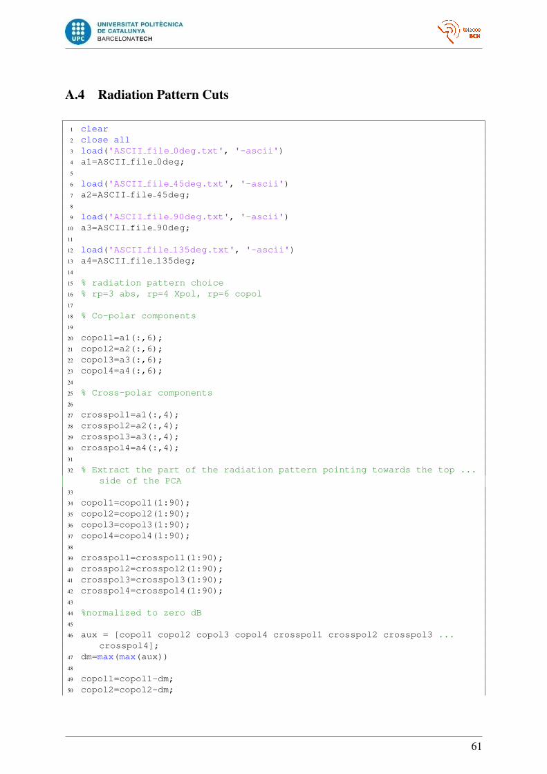
A.4 Radiation Pattern Cuts
1 clear2 close all3 load('ASCII file 0deg.txt', '−ascii')4 a1=ASCII file 0deg;5
6 load('ASCII file 45deg.txt', '−ascii')7 a2=ASCII file 45deg;8
9 load('ASCII file 90deg.txt', '−ascii')10 a3=ASCII file 90deg;11
12 load('ASCII file 135deg.txt', '−ascii')13 a4=ASCII file 135deg;14
15 % radiation pattern choice16 % rp=3 abs, rp=4 Xpol, rp=6 copol17
18 % Co−polar components19
20 copol1=a1(:,6);21 copol2=a2(:,6);22 copol3=a3(:,6);23 copol4=a4(:,6);24
25 % Cross−polar components26
27 crosspol1=a1(:,4);28 crosspol2=a2(:,4);29 crosspol3=a3(:,4);30 crosspol4=a4(:,4);31
32 % Extract the part of the radiation pattern pointing towards the top ...side of the PCA
33
34 copol1=copol1(1:90);35 copol2=copol2(1:90);36 copol3=copol3(1:90);37 copol4=copol4(1:90);38
39 crosspol1=crosspol1(1:90);40 crosspol2=crosspol2(1:90);41 crosspol3=crosspol3(1:90);42 crosspol4=crosspol4(1:90);43
44 %normalized to zero dB45
46 aux = [copol1 copol2 copol3 copol4 crosspol1 crosspol2 crosspol3 ...crosspol4];
47 dm=max(max(aux))48
49 copol1=copol1−dm;50 copol2=copol2−dm;
61

51 copol3=copol3−dm;52 copol4=copol4−dm;53
54 crosspol1=crosspol1−dm;55 crosspol2=crosspol2−dm;56 crosspol3=crosspol3−dm;57 crosspol4=crosspol4−dm;58
59 % Construct the other half pattern by symmetry60
61 N=length(copol1);62 for n=1:N63 copol1 neg(n)=copol1(N+1−n);64 copol2 neg(n)=copol2(N+1−n);65 copol3 neg(n)=copol3(N+1−n);66 copol4 neg(n)=copol4(N+1−n);67
68 crosspol1 neg(n)=crosspol1(N+1−n);69 crosspol2 neg(n)=crosspol2(N+1−n);70 crosspol3 neg(n)=crosspol3(N+1−n);71 crosspol4 neg(n)=crosspol4(N+1−n);72 end73
74 copol1 total=[copol1 neg, copol1(1), copol1.'];75 copol2 total=[copol2 neg, copol2(1), copol2.'];76 copol3 total=[copol3 neg, copol3(1), copol3.'];77 copol4 total=[copol4 neg, copol4(1), copol4.'];78
79 crosspol1 total=[crosspol1 neg, crosspol1(1), crosspol1.'];80 crosspol2 total=[crosspol2 neg, crosspol2(1), crosspol2.'];81 crosspol3 total=[crosspol3 neg, crosspol3(1), crosspol3.'];82 crosspol4 total=[crosspol4 neg, crosspol4(1), crosspol4.'];83
84 % Set the x axis85
86 T=length(copol1 total);87 t=[0:0,1:T−1]−90;88
89 figure;90 plot(t, copol1 total, 'b', t, copol2 total, 'b−.', t, copol3 total, ...
'b:', t, copol4 total, 'b−−', t, crospol1 total, 'r', t, ...crosspol2 total, 'r−.', t, crosspol3 total, 'r:', t, ...crosspol4 total, 'r−−', 'LineWidth', 2);
91 legend('Copolar \phi=0', 'Copolar \phi=45', 'Copolar \phi=90', ...'Copolar \phi=135', 'Crosspolar \phi=0', 'Crosspolar \phi=45', ...'Crosspolar \phi=90', 'Crosspolar \phi=135');
92 set(gca,'FontSize',26)93 title('Far−field','FontSize',34);94 xlabel('\theta (degrees)','FontSize',30);95 ylabel('Magnitude (dB)','FontSize',30);96 ylim([−30 0]);97 xlim([−90 90]);
Listing 6: Matlab Script to plot radiation pattern cuts from ASCII files exported from CST.
62
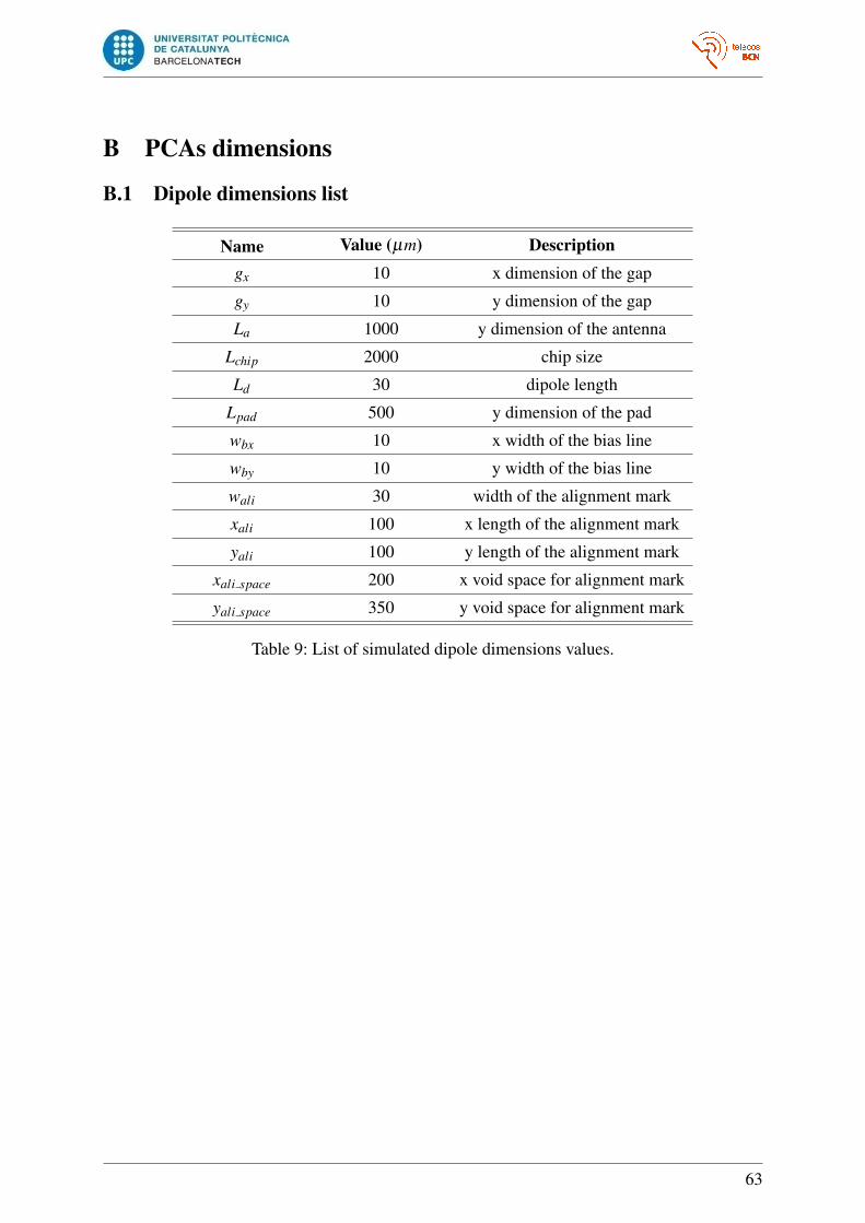
B PCAs dimensions
B.1 Dipole dimensions list
Name Value (µm) Descriptiongx 10 x dimension of the gap
gy 10 y dimension of the gap
La 1000 y dimension of the antenna
Lchip 2000 chip size
Ld 30 dipole length
Lpad 500 y dimension of the pad
wbx 10 x width of the bias line
wby 10 y width of the bias line
wali 30 width of the alignment mark
xali 100 x length of the alignment mark
yali 100 y length of the alignment mark
xali space 200 x void space for alignment mark
yali space 350 y void space for alignment mark
Table 9: List of simulated dipole dimensions values.
63
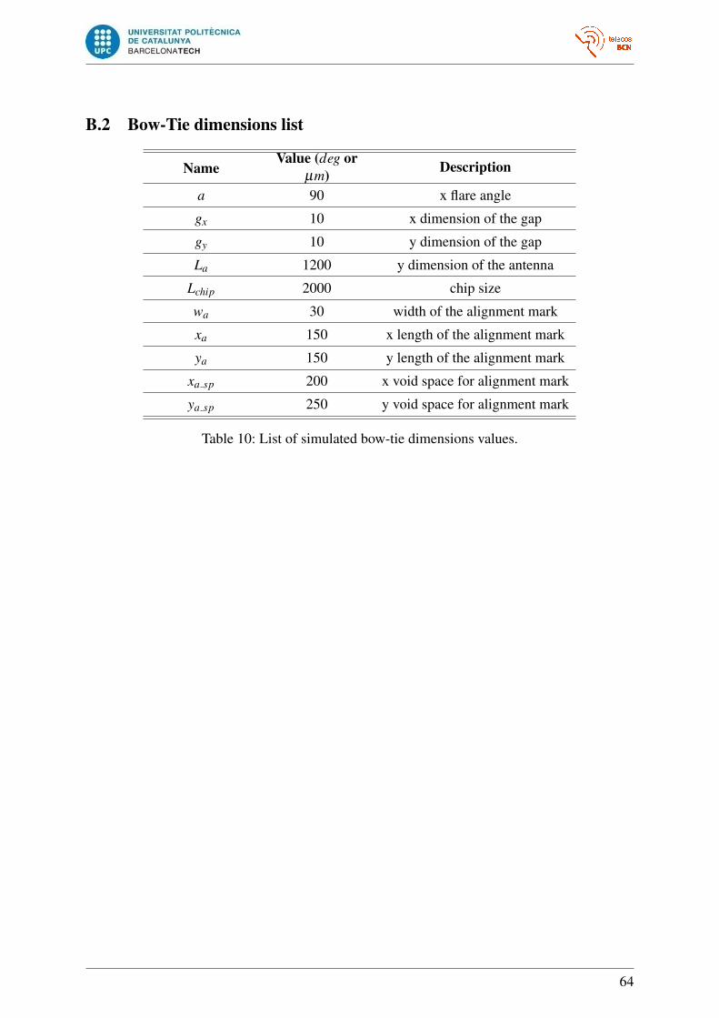
B.2 Bow-Tie dimensions list
NameValue (deg or
µm) Description
a 90 x flare angle
gx 10 x dimension of the gap
gy 10 y dimension of the gap
La 1200 y dimension of the antenna
Lchip 2000 chip size
wa 30 width of the alignment mark
xa 150 x length of the alignment mark
ya 150 y length of the alignment mark
xa sp 200 x void space for alignment mark
ya sp 250 y void space for alignment mark
Table 10: List of simulated bow-tie dimensions values.
64
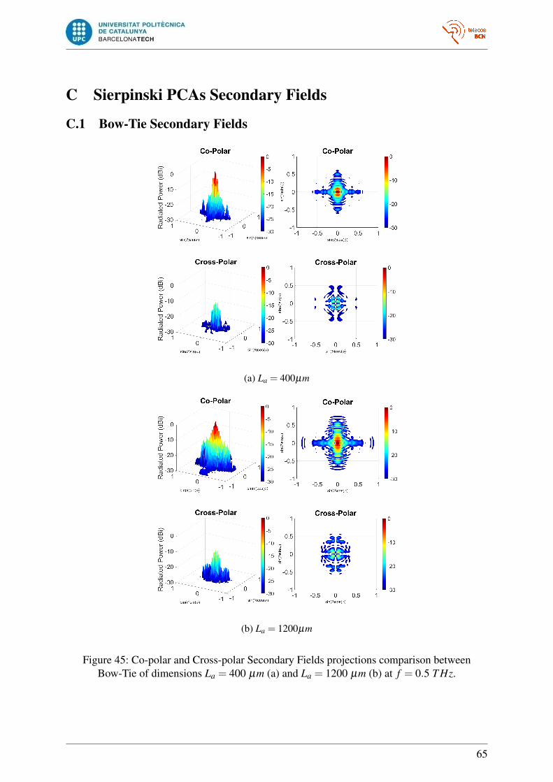
C Sierpinski PCAs Secondary Fields
C.1 Bow-Tie Secondary Fields
(a) La = 400µm
(b) La = 1200µm
Figure 45: Co-polar and Cross-polar Secondary Fields projections comparison betweenBow-Tie of dimensions La = 400 µm (a) and La = 1200 µm (b) at f = 0.5 T Hz.
65
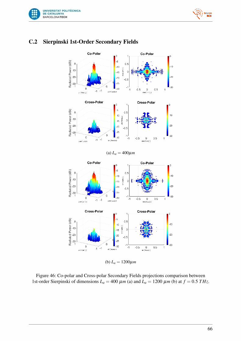
C.2 Sierpinski 1st-Order Secondary Fields
(a) La = 400µm
(b) La = 1200µm
Figure 46: Co-polar and Cross-polar Secondary Fields projections comparison between1st-order Sierpinski of dimensions La = 400 µm (a) and La = 1200 µm (b) at f = 0.5 T Hz.
66
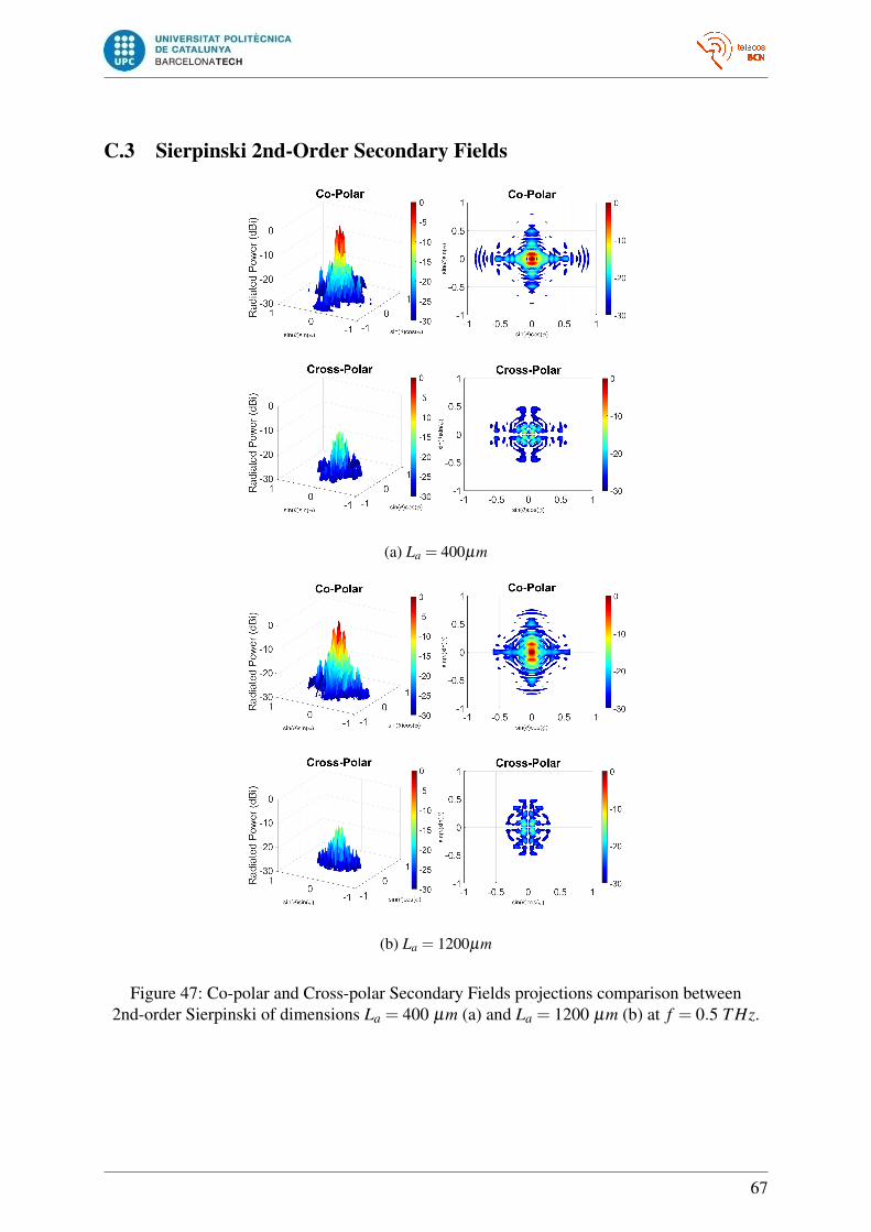
C.3 Sierpinski 2nd-Order Secondary Fields
(a) La = 400µm
(b) La = 1200µm
Figure 47: Co-polar and Cross-polar Secondary Fields projections comparison between2nd-order Sierpinski of dimensions La = 400 µm (a) and La = 1200 µm (b) at f = 0.5 T Hz.
67
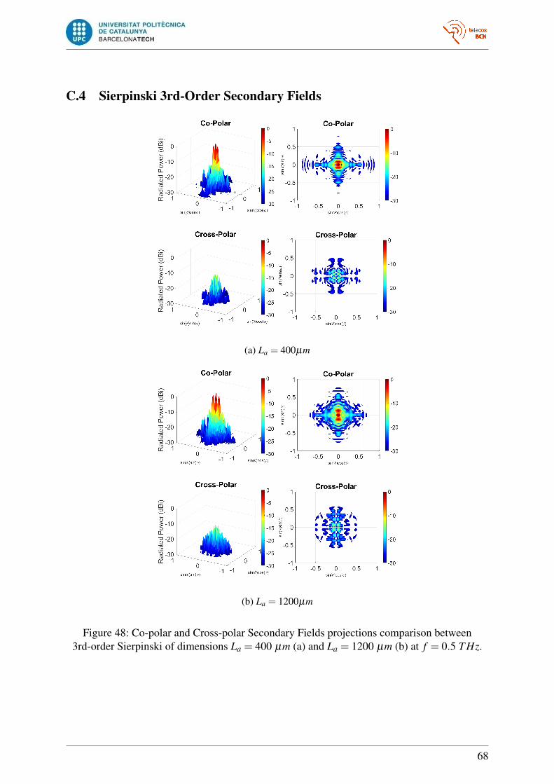
C.4 Sierpinski 3rd-Order Secondary Fields
(a) La = 400µm
(b) La = 1200µm
Figure 48: Co-polar and Cross-polar Secondary Fields projections comparison between3rd-order Sierpinski of dimensions La = 400 µm (a) and La = 1200 µm (b) at f = 0.5 T Hz.
68
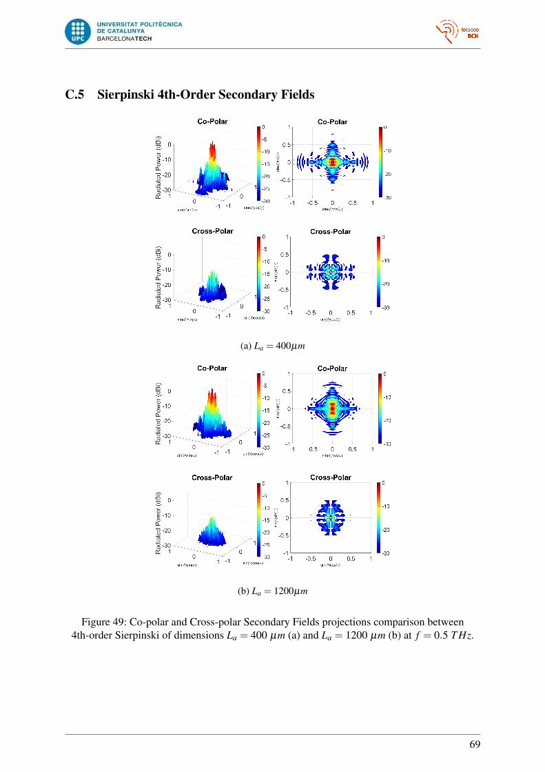
C.5 Sierpinski 4th-Order Secondary Fields
(a) La = 400µm
(b) La = 1200µm
Figure 49: Co-polar and Cross-polar Secondary Fields projections comparison between4th-order Sierpinski of dimensions La = 400 µm (a) and La = 1200 µm (b) at f = 0.5 T Hz.
69