Control of quantum transverse correlations on a four-photon system
Upload
khangminh22Category
view
3download
0
QUANTUM STOCHASTIC COMMUNICATION WITH
PHOTON-NUMBER SQUEEZED LIGHT
by
JOSHUA PARAMANANDAM
A thesis submitted to the
Graduate School—New Brunswick
Rutgers, The State University of New Jersey
in partial fulfillment of the requirements
for the degree of
Master of Science
Graduate Program in Electrical And Computer Engineering
Written under the direction of
Professor Michael A Parker
and approved by
New Brunswick, New Jersey
October, 2007

ABSTRACT OF THE THESIS
Quantum Stochastic Communication with Photon-number
squeezed light
By Joshua Paramanandam
Thesis Director: Professor Michael A Parker
Squeezed states of light have found importance in quantum cryptography due to the no-
cloning theorem which prevents two states from being identical to each other. The quantum
state with quadrature operators X1 and X2 can be visualized as a point in phase space with
the center being 〈X1〉,〈X2〉 surrounded by an error region which satisfies the minimum
uncertainty product 〈ΔX21 〉〈ΔX2
2 〉 = 1/16. These states are intrinsically secure since one
needs to know which quadrature the measurement is to be made and any attempt to mea-
sure the wrong quadratures with arbitrary accuracy would disturb the message. Of course,
the eavesdropper cannot simultaneously measure both quadratures with infinite precision
for each. This thesis describes a method that not only encodes information in the ampli-
tudes of the quadratures alone but also in the uncertainty of those states. One example of
squeezed light is the number-phase squeezed state which satisfying the uncertainity relation
〈Δn2〉〈Δφ2〉 = 1/4. An implementation is demonstrated where the information is encoded
only in the photon number uncertainity and the phase variable is ignored.
The barrier regulation mechanisms such as macroscopic coulomb blockade in semicon-
ductor junction diodes are responsible for generating photon fluxes with penetration be-
low the standard quantum limit(shot noise level). The thesis describes a comprehensive
quantum mechanical Langevin model which details the various mechanisms responsible for
ii

producing photon number squeezing from the thermionic emission to the diffusion current
limits. Quantities such as the pump fluctuations and cross correlation spectral densities are
studied under constant current and constant voltage conditions. The research investigates
the generation of photon number squeezed light from high efficiency light emitting diodes.
A measurement setup for subshot noise is constructed and each stage is properly calibrated.
Experiments were performed to determine the squeezing spectra and Fanofactors for the
L2656 and the L9337 high efficiency LEDs. The L9337 produces a squeezing of 1.5dB below
the shot noise level over a bandwidth of 25Mhz, the largest known penetration at room
temperature. The quantum stochastic communicator is also demonstrated. The research
shows that the switching elements used in the modulation of the electrical bias which in
turn affect the regulation mechanisms do not affect the statistics of the emitted light under
certain conditions. The decoding of the time varying variances is achieved by using time
frequency analysis with the aid of the spectrum analyzer.
iii

Acknowledgements
To start with, I am grateful to my advisor, Dr. Michael A. Parker, who has been a source
of constant encouragement and guidance. He has since introduced me to Quantum Optics
with one on one sessions, Machining, and Electronics.
I would also like to give a shout-out to my present and past nanolab colleagues, Gunay
Akdogan, Mandira Thakedast, HeeTaek Yi, Morris Reichbach for interesting discussions
and motivation. I would like to thank Steve Orbine for helping out with quick fix solutions
to equipment problems. I would like to thank my family and friends who have supported
and believed in me through my research. Most of all, I thank the almighty, who has made
this thesis possible
iv

Table of Contents
Abstract . . . . . . . . . . . . . . . . . . . . . . . . . . . . . . . . . . . . . . . . . . ii
Acknowledgements . . . . . . . . . . . . . . . . . . . . . . . . . . . . . . . . . . . iv
List of Tables . . . . . . . . . . . . . . . . . . . . . . . . . . . . . . . . . . . . . . . ix
List of Figures . . . . . . . . . . . . . . . . . . . . . . . . . . . . . . . . . . . . . . x
1. Introduction . . . . . . . . . . . . . . . . . . . . . . . . . . . . . . . . . . . . . 1
1.1. Introduction . . . . . . . . . . . . . . . . . . . . . . . . . . . . . . . . . . . . 1
1.2. The concept of Stochastic Modulation . . . . . . . . . . . . . . . . . . . . . 1
1.3. Why Quantum Noise? . . . . . . . . . . . . . . . . . . . . . . . . . . . . . . 4
1.4. Thesis Overview . . . . . . . . . . . . . . . . . . . . . . . . . . . . . . . . . 6
2. Quantum Noise from Light emitting diodes . . . . . . . . . . . . . . . . . . 9
2.1. Introduction . . . . . . . . . . . . . . . . . . . . . . . . . . . . . . . . . . . . 9
2.2. Origin of Shot Noise . . . . . . . . . . . . . . . . . . . . . . . . . . . . . . . 12
2.2.1. Shot Noise from a vacuum diode . . . . . . . . . . . . . . . . . . . . 13
Case 1 : τtr << τRC . . . . . . . . . . . . . . . . . . . . . . . . . . . 14
Case 2 : τtr >> τRC . . . . . . . . . . . . . . . . . . . . . . . . . . . 14
Remarks . . . . . . . . . . . . . . . . . . . . . . . . . . . . . . . . . . 15
2.2.2. Noise from Maxwell-Boltzmann conductors . . . . . . . . . . . . . . 16
2.3. Shot Noise in PN Junction Diodes . . . . . . . . . . . . . . . . . . . . . . . 21
2.3.1. Generation Recombination Noise . . . . . . . . . . . . . . . . . . . . 28
2.3.2. Thermal Diffusive Noise . . . . . . . . . . . . . . . . . . . . . . . . . 30
Single Heterojunction Long Diode . . . . . . . . . . . . . . . . . . . 33
v

Double Heterojunction Diode . . . . . . . . . . . . . . . . . . . . . 36
Numerical Analysis . . . . . . . . . . . . . . . . . . . . . . . . . . . . 37
2.4. Subshot Noise in pn junction devices . . . . . . . . . . . . . . . . . . . . . . 37
2.4.1. Photonic Noise . . . . . . . . . . . . . . . . . . . . . . . . . . . . . . 41
2.4.2. Noise Spectral Densities . . . . . . . . . . . . . . . . . . . . . . . . . 43
2.4.3. Macroscopic Coulomb Blockade . . . . . . . . . . . . . . . . . . . . . 50
2.5. Pump Current Mechanisms . . . . . . . . . . . . . . . . . . . . . . . . . . . 51
2.5.1. From Thermionic emission to Diffusion . . . . . . . . . . . . . . . . . 52
2.5.2. The forward/backward pump model . . . . . . . . . . . . . . . . . . 54
2.6. Langevin Analysis of shot noise suppression in LEDs . . . . . . . . . . . . . 58
2.6.1. Semiconductor Bloch-Langevin Equations . . . . . . . . . . . . . . . 62
2.6.2. Field Langevin Equations . . . . . . . . . . . . . . . . . . . . . . . . 65
2.6.3. Noise Correlations . . . . . . . . . . . . . . . . . . . . . . . . . . . . 70
2.6.4. Photon Number Noise with a c-number Pump . . . . . . . . . . . . 74
2.6.5. Pumping mechanisms . . . . . . . . . . . . . . . . . . . . . . . . . . 82
2.6.6. Field Langevin Equation under Homogeneous emission conditions . 86
2.6.7. Photon Number Noise with Regulated Current flows . . . . . . . . . 87
2.6.8. Pump rate fluctuations . . . . . . . . . . . . . . . . . . . . . . . . . 92
2.6.9. Squeezing Bandwidth . . . . . . . . . . . . . . . . . . . . . . . . . . 94
2.6.10. Correlations between the fluctuation quantities . . . . . . . . . . . . 95
Correlation between junction voltage and carrier number . . . . . . 95
Correlation between junction voltage and photon flux . . . . . . . . 96
2.6.11. Validity of the Equivalent circuit model in the diffusion limit . . . . 97
Constant Current Case . . . . . . . . . . . . . . . . . . . . . . . . . 99
Constant Voltage Case . . . . . . . . . . . . . . . . . . . . . . . . . . 99
External Circuit Fluctuations . . . . . . . . . . . . . . . . . . . . . . 100
2.7. Summary . . . . . . . . . . . . . . . . . . . . . . . . . . . . . . . . . . . . . 101
vi

3. Experiments on Subshot Noise . . . . . . . . . . . . . . . . . . . . . . . . . . 102
3.1. Introduction . . . . . . . . . . . . . . . . . . . . . . . . . . . . . . . . . . . . 102
3.2. Thermal and electrical shot noise Measurements . . . . . . . . . . . . . . . 104
3.3. Experimental setup for subshot noise measurement . . . . . . . . . . . . . . 110
3.3.1. Spectrum Analyzer Calibration . . . . . . . . . . . . . . . . . . . . . 113
3.3.2. LED Characteristics . . . . . . . . . . . . . . . . . . . . . . . . . . . 119
3.3.3. Photodetector Nonlinearity . . . . . . . . . . . . . . . . . . . . . . . 124
3.3.4. Amplifier Characteristics . . . . . . . . . . . . . . . . . . . . . . . . 125
3.3.5. Shielding . . . . . . . . . . . . . . . . . . . . . . . . . . . . . . . . . 136
3.4. Optical Shot Noise Source Measurements . . . . . . . . . . . . . . . . . . . 139
3.5. SubShot Noise experiments . . . . . . . . . . . . . . . . . . . . . . . . . . . 147
3.5.1. Verification of High-impedance Pump suppression mechanism . . . . 147
3.5.2. Squeezing Results for the L2656 LED . . . . . . . . . . . . . . . . . 153
3.5.3. Approximate Constant Voltage conditions . . . . . . . . . . . . . . . 160
3.5.4. Issues with frequency dependent squeezing characteristics . . . . . . 161
3.5.5. Squeezing Results for the L9337 LED . . . . . . . . . . . . . . . . . 170
3.6. Summary . . . . . . . . . . . . . . . . . . . . . . . . . . . . . . . . . . . . . 174
4. Quantum Stochastic Modulation . . . . . . . . . . . . . . . . . . . . . . . . 175
4.1. Introduction . . . . . . . . . . . . . . . . . . . . . . . . . . . . . . . . . . . . 175
4.2. Time Frequency Analysis using the spectrum analyzer . . . . . . . . . . . . 178
4.3. Design of Quantum Stochastic Modulator . . . . . . . . . . . . . . . . . . . 192
4.3.1. Capacitive Switching . . . . . . . . . . . . . . . . . . . . . . . . . . 195
4.3.2. Direct Modulation with BJT . . . . . . . . . . . . . . . . . . . . . . 198
FanoFactors for the hybrid-π,Van-Der Ziel T model and the Grey-
Meyer model . . . . . . . . . . . . . . . . . . . . . . . . . . 200
T model with partition noise . . . . . . . . . . . . . . . . . . . . . . 205
Noise Model Under Saturation . . . . . . . . . . . . . . . . . . . . . 211
Spectral Density Fluctuations in the LED . . . . . . . . . . . . . . . 215
vii

Analysis and Experiment . . . . . . . . . . . . . . . . . . . . . . . . 217
4.3.3. Direct Modulation with MOSFET . . . . . . . . . . . . . . . . . . . 218
Noise Analysis . . . . . . . . . . . . . . . . . . . . . . . . . . . . . . 219
Switching . . . . . . . . . . . . . . . . . . . . . . . . . . . . . . . . . 227
4.4. Results . . . . . . . . . . . . . . . . . . . . . . . . . . . . . . . . . . . . . . . 233
4.5. Summary . . . . . . . . . . . . . . . . . . . . . . . . . . . . . . . . . . . . . 236
5. Conclusions . . . . . . . . . . . . . . . . . . . . . . . . . . . . . . . . . . . . . . 240
Appendix A. . . . . . . . . . . . . . . . . . . . . . . . . . . . . . . . . . . . . . . . 242
A.1. Compact Noise Model of PN Junction Devices . . . . . . . . . . . . . . . . 242
A.2. The Renormalized Many Body Hamiltonian for the LED system . . . . . . 243
A.3. Spontaneous Emission Operator . . . . . . . . . . . . . . . . . . . . . . . . . 248
A.4. Code for evaluation of noise spectral densities . . . . . . . . . . . . . . . . . 250
Appendix B. Classical Stochastic Communicator . . . . . . . . . . . . . . . . 255
B.1. Hardware Setup . . . . . . . . . . . . . . . . . . . . . . . . . . . . . . . . . . 255
B.2. Results . . . . . . . . . . . . . . . . . . . . . . . . . . . . . . . . . . . . . . . 257
References . . . . . . . . . . . . . . . . . . . . . . . . . . . . . . . . . . . . . . . . . 259
Vita . . . . . . . . . . . . . . . . . . . . . . . . . . . . . . . . . . . . . . . . . . . . . 264
viii
List of Tables
3.1. Experimental values of optical power PL and photocurrent Iph for the L2656.The
efficiencies ηL, η0 have been calculated for two similar LEDs where LE char-
acterizes the LED with low internal efficiency. . . . . . . . . . . . . . . . . . 123
3.2. Noise contributions of the various noise sources in the calculation of the total
output noise voltage of the AD8009 non-inverting opamp . . . . . . . . . . 135
3.3. The experimental results of η0,ηd which are used to compute F according
to Eq. (3.23) are compared with the experimental results for varying drive
currents. . . . . . . . . . . . . . . . . . . . . . . . . . . . . . . . . . . . . . . 157
3.4. Photocurrent drift with time when driven by the shot and subshot sources . 158
4.1. Small Signal parameters used in the calculations of Fanofactors for the three
configurations plotted in Fig: . . . . . . . . . . . . . . . . . . . . . . . . . . 211
4.2. MOSFET model parameters used in the calculation of the drain current noise
and the external terminal noise of the LED. . . . . . . . . . . . . . . . . . . 225
ix

List of Figures
1.1. (a)The random signal with variable finite time average and standard devia-
tion (b)A modulated average without affecting the standard deviation . . . 3
1.2. Thesis chapter Overview . . . . . . . . . . . . . . . . . . . . . . . . . . . . . 6
2.1. Description of the scalar short-circuit current Green ’s function. (a)The elec-
tron Green’s function and (b)The hole Green’s function. xp and xn indicate
the edges of the depletion region and in and ip are the injected electron and
hole scalar currents at x’. i′W ,i′0,ic and i0p are the output current variations
induced in response to the perturbations by the scalar current sources. . . 25
2.2. The initial current flow followed by the relaxation current flows for (a)a
thermal diffusion event and (b)generation process of a minority carrier. . . 33
2.3. (a)Scalar Green’s function according to the Bonani model in Eqs.(2.27,2.28)
for long(τp = τn = 1ns) diode and short (τp = τn = 1μs) diodes (b)The
terminal Green’s function according to Eq.(2.41) (c)The spatial Generation-
recombination noise calculated using the Bonani model versus the terminal
Green’s function. . . . . . . . . . . . . . . . . . . . . . . . . . . . . . . . . . 35
2.4. Regulated electron emission process in a space charge limited vacuum tube
obtained by self-modulation of the potential field profile. The space charge is
overlayed with the space charge of the semiconductor junction diode driven
by a high impedance current source which also shows the regulated electron
emissions through junction voltage modulation. . . . . . . . . . . . . . . . . 38
x

2.5. Noise equivalent circuit of light emitting diode for long base structures valid
under low to moderate injection conditions. The circuit shows the ohmic
resistance RS , dynamic resistance Rd,total capacitance C,stored charge fluc-
tuation q(t),junction voltage fluctuation vjn(t) ,recombination current ijn
junction current in and the noise generators vsn and vth. . . . . . . . . . . . 39
2.6. The (a)Constant voltage operation and (b)Constant current operation a pn
junction diode . . . . . . . . . . . . . . . . . . . . . . . . . . . . . . . . . . . 47
2.7. Langevin description of damping with the diffusion capacitance and differen-
tial resistance of a pn junction diode . . . . . . . . . . . . . . . . . . . . . . 48
2.8. The band-diagram of a typical double heterojunction LED under forward
bias condition. Here Vj is the applied bias, Pfi and Pbi denote the forward
and backward pump rates and nc/τr denotes carrier recombination in the
active region. . . . . . . . . . . . . . . . . . . . . . . . . . . . . . . . . . . . 55
2.9. Photon Fanofactors for Poisson and Subpoisson pump noise considering the
effects of non-radiative mechanisms. Here ε0 = τr0τnr0
. The three cases treated
are a)Kr = Knr = 0 b)Kr = Knr = 0.5 and Kr = Knr = −0.4 . . . . . . . . 81
2.10. The pump equivalent circuit model which describes the charging and dis-
charging of the pn junction by the stochastic forward and backward injection
currents . . . . . . . . . . . . . . . . . . . . . . . . . . . . . . . . . . . . . . 83
2.11. Photon Fanofactors under constant voltage and constant current conditions
for the thermionic emission and the diffusion regime pump models. Constant
current case is reached when τRC � τte and the constant voltage case is true
when τRC � τte is satisfied. . . . . . . . . . . . . . . . . . . . . . . . . . . . 91
2.12. 3dB Squeezing bandwidth as a function of LED drive current for the pump
model evaluated from the thermionic emission to the diffusion limits. . . . . 94
3.1. Experimental results for V 2 (obtain by correcting for amplifier noise and
normalizing to gain) versus resistance R. The solid line implements the the-
oretical equation 4kTRB where B is the fitting parameter used. . . . . . . . 106
xi

3.2. (a) Histogram of thermal noise for a 1MΩ source (b) PDF of shot noise
obtained from a thermionic noise vacuum diode. The solid line is the the
theoretical Poisson distribution obtained by fitting the average < n > to the
data(points) . . . . . . . . . . . . . . . . . . . . . . . . . . . . . . . . . . . . 109
3.3. Overview of the experimental apparatus: By switching from resistor RS to
photodiode PD1 subpoisson and Poisson light can be produced which is de-
tected by photodiode PD2. The DC voltage is measured across RL with
a multimeter and AC is passed on to the amplifier and the spectrum ana-
lyzer(SA). PD1, RS and battery are housed in a shielded box(as indicated
by the dotted lines). The rest of the components(except the SA) are housed
in a RF cage. . . . . . . . . . . . . . . . . . . . . . . . . . . . . . . . . . . . 112
3.4. Spectra of the noise floor of setup in Fig. (3.3) measured with (a)Variation of
VBW with a constant RBW of 10Khz (b)Variation of RBW with a constant
VBW of 3Hz (c)Different span/center frequencies(start/stop frequencies) as
a function of RBW . . . . . . . . . . . . . . . . . . . . . . . . . . . . . . . . 117
3.5. (a)Measured IL − Vmeas characteristics of the L2656 LED which is com-
pared with the ideal diode equation IL = ISexp(qVj/nkT ) as well as the
I − Vmeas curves obtained through pspice device modeling for both L2656
and L9337 LEDs. b)Mean quantum efficiency(η0) and differential quantum
efficiency(ηd) measured for the L2656(1) and L9337(2) LEDs.The DC oper-
ating point and tangent are shown for the L9337. . . . . . . . . . . . . . . . 121
3.6. Normalized function g(I) versus photocurrent Iph measured for the S5107 PD
in photoconductive mode along with the interpolated curve . . . . . . . . . 126
3.7. (a)System gain Kt = VoVi
measured for the Analog Modules 322-6 amplifier
with an input power of -60dBm (b)Noise equivalent circuit model of the
entire measurement chain including PD equivalent circuit, cable reactances
and input impedance of the amplifier . . . . . . . . . . . . . . . . . . . . . . 127
xii

3.8. (a)Thermal Noise Power of a 50Ω resistor obtained with a 3 gain stage am-
plifier chain (b)Dark current + 50Ω noise power for the PD reverse biased at
10V with the same 3 gain stage amplifier. . . . . . . . . . . . . . . . . . . . 131
3.9. (a)Noninverting Equivalent circuit noise model of the Analog Devices AD8009
opamp (b)Input and Output noise spectral densities of the circuit in (a) cal-
culated using pspice (c)Experimental noise power obtained for the unity gain
opamp which is obtained by amplifying using the Analog Modules 322-6 am-
plifier. A 50Ω terminated resistor noise is also shown as reference. . . . . . 133
3.10. Noise power variations due to environmental and spurious optical noise ob-
tained with the shielded RF cage open or closed. The measured noise power
is the known PD2 darkcurrent+5080Ω resistor noise as well as spurious en-
vironmental RF and optical noise obtained at a RBW=30kHz. . . . . . . . 139
3.11. (a)Noise powers of the mean photocurrent for a red-filtered white light(from
a lamp) incident on the PD which is observed at a RBW of 3kHz. (b)Noise
spectral densities normalized to 1Hz(points) as well as linear regression(solid
line) obtained as a function of photocurrent.The linear fit gives us the filter
response function F (ω) at 650kHz. . . . . . . . . . . . . . . . . . . . . . . . 142
3.12. Noise power from the photocurrent obtained for the lamp(which is also repre-
sentative of the LED driven by the SNS) as a function of current-current con-
version efficiency. The points give the measured values whereas the straight
line represents the average. The inset of the figure represents the efficiency
of the lamp as a function of drive current. . . . . . . . . . . . . . . . . . . . 144
3.13. Optical noise spectra for (a)Lamp driven by voltage and current sources
(b)650nm Luxeon LED driven with a noisy source (c)Attenuated spectra
from Luxeon LED (d)L2656 driven by ILX current source and (d)Generic
laser driven by ILX current source . . . . . . . . . . . . . . . . . . . . . . . 146
xiii

3.14. (a)Optical Noise spectra for the L2656 with different bias sources.The refer-
ence low noise source is the battery. (b) and (c) show high impedance pump
suppression effect for the L2656 and for the Luxeon LED as function of series
resistance RS . Experiments were performed at a RBW of 100Khz(a,b) and
30Khz(c) with a VBW of 3Hz. . . . . . . . . . . . . . . . . . . . . . . . . . 150
3.15. Optical noise spectra and Fanofactors of the photon fluxes from the L2656
LED obtained at (a,b)IL = 1.92mA (c,d)IL = 6.53mA (e) IL = 8.08mA
and (f) IL = 9.81mA. The Fanofactors were fit to the theoretical diffu-
sion model(solid lines) which were obtained using Eq.(3.21) with various
correction factors C to fit to the data better to F.The Fanofactor obtained
with C=1 line has been shown for reference.The model parameters used are
Cdep = 0.1μF and τr = 250ns. . . . . . . . . . . . . . . . . . . . . . . . . . 152
3.16. (a)Optical noise spectra for the L2656 with reduced coupling efficiency of
η0 = 2%.The SNL has been obtained by driving the LED with the SNS
(b)Experimental(points) and theoretical(solid line) Fanofactors as function
of coupling efficiency (η0) (c)Optical Noise spectra for the L2656 driven under
a Constant Voltage bias of 1.26V . . . . . . . . . . . . . . . . . . . . . . . . 158
3.17. (a)Squeezing spectra for the L9337 LED highlighting the super-Poissonity at
mid-frequencies when driven with the SNS (b)The overestimated Fanofactors
for the low injection case of Vph =2V and high injection case of Vph =8V
.The solid lines are the smoothing filters applied. (c)Shot noise spectra for
the cases of 1.L2656 driven with SNS, 2.Reduced coupling efficiency(< 1%)
and 3.Changing the PD1 from UDT to S3994 in the SNS. For each of these
cases, the subshot noise as well as lamp noise spectra have been plotted. . . 162
xiv

3.18. Electrical Response characteristics of photodiode-amplifier configuration (a)Optical
Noise spectra of S5107 PD compared with a generic low responsivity PD
(b)Optical Noise Spectra of S5107 and S3994 PDs (c) Electrical transfer
function according to Eq: for S5107 and S3994 PD where the fitting pa-
rameters L = 0.15μH and CC = 150pF have been used. The inset shows
the experimental noise spectra from 1-3Mhz and the solid lines depict the
theoretical model. . . . . . . . . . . . . . . . . . . . . . . . . . . . . . . . . . 165
3.19. (a) and (b) shows the squeezing spectra and computed fanofactors(without
the noise floor correction) for the driving current of IL = 3.27mA. (c)Squeezing
spectra obtained for a driving current of IL = 2.43mA.The inset depicts the
constant Fanofactor over a range of 1-10Mhz. (d)The Fanofactors for the
low injection current(IL = 1.35mA) versus high injection(IL = 3.13mA)
cases.The solid line in the fanofactors depicts the result of a smoothing filter. 168
3.20. Spectral Fanofactors of the photon fluxes from the L9337 LED obtained at
(a)IL = 1.54mA(b)IL = 2.01mA (c) IL = 2.17mA and (d) IL = 2.61mA.
The Fanofactors were fit to the theoretical diffusion model and thermionic
emission model(solid lines) which were obtained using Eq.(3.21)(C=1) and
Eq.(3.27) with the model parameters Cdep = 52.4pF and τr = 6.36ns. The
center dark line represents a smoothing filter applied to the raw data. (e)
Pump current dependence of the squeezing bandwidth. The solid lines indi-
cate the theoretical diffusion model and thermionic emission models. Model
parameters for the diffusion model is Cdep = 60pF and τr = 7ns and the
thermionic emission model is Cdep = 50pF and τr = 7.3ns. . . . . . . . . . . 172
4.1. (a)The detection of cyclostationary processes by means of a spectrum an-
alyzer (b)The finite time power spectral density G(T, f) (c)The equivalent
input signal description of Sn2(ω, t) and the corresponding time varying sig-
nal amplitudes along the line ω ∝ t(marked by circles) is plotted on the
spectrum analyzer. . . . . . . . . . . . . . . . . . . . . . . . . . . . . . . . . 181
xv

4.2. Minimum noise pulse width Tmin as a function of span .The fixed parameters
are resolution bandwidth(RBW), video bandwidth(VBW) and number of
samples N. . . . . . . . . . . . . . . . . . . . . . . . . . . . . . . . . . . . . 189
4.3. (a)Shot Noise Modulation experiment describing the time varying optical
spectra S1(ω, t) = F.Sn(ω, t) where F=1 always (b)Shot and subshot spectra
obtained with an RBW = 10Khz but with low averaging of V BW = 30Hz.
The solid dark lines indicate the negative exponential smoothing filter. . . 191
4.4. Comparison of optical spectra with LED driven with DAQ,shot and sub-shot
noise sources.The inset shows a simple switching design using NI DAQ . . . 194
4.5. (a)Design of a capacitive switching circuit (b)Switching waveforms for MOS-
FET and AC switching (c)Optical spectra of true subshot noise compared
with subshot spectra obtained by using a Capacitor with 5Ω in series . . . . 196
4.6. (a)Circuit Diagrams for transistor in open circuit base/closed base setups in
CE and CC configurations (b)Load line of L2656 with numerical Ic − Vce
characteristics of the 2N2222 transistor . . . . . . . . . . . . . . . . . . . . . 199
4.7. (a) Grey and Meyer hybrid-π Bipolar transistor model (b)Van-derZiel-Chenette
T bipolar transistor model . . . . . . . . . . . . . . . . . . . . . . . . . . . . 205
4.8. (a)Electrical Fanofactors of grounded base-open emitter Power BJT from
[1](b)Comparison of Fanofactors for the hybrid-π, T and GM Models . . . . 206
4.9. Numerical Fanofactors for the three cases of (a)grounded base-grounded emit-
ter (b)open base-grounded emitter and (c)grounded base-open emitter con-
figurations . . . . . . . . . . . . . . . . . . . . . . . . . . . . . . . . . . . . . 210
4.10. (a)Observed optical spectra for transistor in the CE deep saturation com-
pared to shot noise obtained by driving with lamp. (b)Observed spectra for
transistor with open/closed base in deep saturation . . . . . . . . . . . . . . 218
4.11. (a)Small signal noise model and large signal model of MOSFET (b)ID−VDS
characteristics of MOSFET in ohmic or triode region . . . . . . . . . . . . . 220
xvi

4.12. Numerical Fanofactors for the IRF511-MOSFET under (a)VGS constant and
ID − VDS being varied (b)ID and VGS constant and RD varied (c)ID − RD
constant andVGS varied. (d) LED optical noise spectra using the IRF120
MOSFET . . . . . . . . . . . . . . . . . . . . . . . . . . . . . . . . . . . . . 226
4.13. (a)Schematic for average and variance modulation using MOSFETs. M1,M2
and M3 represent the MOSFETs. The 7V battery with the 1k resistor repre-
sents the constant current source and the 5.8mA current source represents the
shot noise from a photodiode. (b)Experimental Observations of the switch-
ing characteristics of the setup when switched between the shot and subshot
pulses. . . . . . . . . . . . . . . . . . . . . . . . . . . . . . . . . . . . . . . . 228
4.14. Transient analysis of MOSFETs (a)properly connected according to Fig (b)Source
and Drain terminals of M1 inverted (c)M3 Removed . . . . . . . . . . . . . 229
4.15. LED drive currents for the various switch configurations . . . . . . . . . . . 232
4.16. (a)The block diagram of the quantum stochastic communicator. (b)Timing
diagram indicating voltages applied to MOSFETs M1,M2,M3 as well as the
photovoltages observed for noise and AC modulation. . . . . . . . . . . . . 237
4.17. Time and Probability distribution for shot and subshot data at 5 and 25
Megasamples per second . . . . . . . . . . . . . . . . . . . . . . . . . . . . . 238
4.18. Variance Modulation between shot and subshot noise with (a)L2656 LED
and (b)L9337 LED . . . . . . . . . . . . . . . . . . . . . . . . . . . . . . . . 238
4.19. (a)The detected average signal (b)The random signal with only variance mod-
ulation and (c)The detected variance signal in the frequency domain. The
smooth curve represents the moving average with an averaging time of ap-
proximately 100ms. . . . . . . . . . . . . . . . . . . . . . . . . . . . . . . . . 239
B.1. Hardware realization of the classical stochastic modulator. (a)Microprocessor
realization of the transmitter.The letter ’g’ refers to “chassis” ground (b)Receiver
for demodulating random signals using discrete components. . . . . . . . . 256
xvii

B.2. Observed waveforms from the stochastic communicator. The waveforms are
obtained by switching between 8 stored distributions in the microprocessor
to produce time varying mean,standard deviation and skew each independent
of one another. . . . . . . . . . . . . . . . . . . . . . . . . . . . . . . . . . . 258
xviii

1
Chapter 1
Introduction
1.1 Introduction
We start by asking the question ’Is it possible to communicate with noise?’. The neverending
quest for nanoscale devices and nanosignals, keeps lowering the signal to noise ratios. One
way to combat this is to reduce the noise, such as using squeezed fields for optical or RF
signals. But we could consider an alternative: ie. Use the noise itself as the signal. In fact,at
this point we may wonder: What is noise? The answer is very subjective. For example, a
person may enjoy listening to a certain type of music while others may find it distasteful and
noisy. We certainly can encode information in noise itself, and that is the sole purpose of
this thesis. However, this thesis approaches the problem from a quantum perspective, using
continuous distributions arising from natural sources such as optoelectronic devices, but the
same idea can be applied to any classical stochastic process produced using computers.
1.2 The concept of Stochastic Modulation
The premise of the stochastic modulation idea is that the set of statistical moments of
a random signal should be modulated independent of one another. The n’th statistical
moment of a random variable Z is defined as < zn > where Z takes on values z and
〈〉 represents the average with respect to a continuous or discrete probability distribution
P(z). The n=1 moment provides the mean. The central moments are defined by removing
the mean component of z and can be stated in general as
mn(z) =< (z − z)n > (1.1)

2
The moments defined in Eq. (1.1) assume that the probability function is known a priori
at the transmitter end ie a random signal should be sculpted with these specified statistical
moments. For a process, whereby the values of z arrive as a sequence in time at a receiver,
the moments must be calculated based on the observed values. For example z = z(ti)
must represent a sequence of voltages generated by a computer every 0.1 nanoseconds. An
’estimator’ on the receiving side approximates the statistical moment by averaging over a
finite number of observed values. For a communications system, the finite time interval
might be attributed to the response time of the electronc circuits or to the number of values
a processor samples from the data stream to calculate these estimations. If N samples are
obtained the finite time moments are then estimated as
< z >≈ 1
NΣN
i=1zi < (z − z)n >≈ 1
NΣN
i=1(zi − z)n (1.2)
Of course as the number of samples N increases, the estimate becomes closer to the actual
statistical moments. However this is only true for ergodic processes where the underlying
probability distribution does not depend on time ie. p(z,t)=p(z,0) .The moments estimator
depends on the original modulation rate(the number of samples produced) and the averaging
time of the receiving electronic circuits or processors. The actual averaging of a computer
circuit follows a convolution integral and not necessarily a uniform average over a finite time
interval. Note that the stochastic modulator intentionally alters the probability distribution
in time, and for two different pulses it may be that p(z, t1) �= p(z, t2).However this is very
subjective to the receiver side and the concept of non-ergodicity needs furthur clarification.
For example consider N ensembles of random processes z(t) where each realization of one
ensemble carries the same statistical information. If we pick one element k of the ensemble
l ,the different time averages (k,l)z then coincide with the ensemble average (l) < z > . The
same applies to any other process say m(t) constructed from (l)z(t). This property defines
the ergodic nature of the random variable Z. for ensemble l. Now let us define a process z(t)
made up of realizations k and l from two ensembles whose finite time average is(k,1),(l,2)zT
. Now the ensemble average is defined as
<(k,1),(l,2) zT >=1
T
∫ t+T/2
t−T/2<(k,1),(l,2) zT > dt (1.3)

3
Figure 1.1: (a)The random signal with variable finite time average and standard deviation(b)A modulated average without affecting the standard deviation
When T is short enough that we capture the realization of the first ensemble, we have
<(k,1),(l,2) zT >=<(k,1) zT >=(1)< z > and the process is certainly ergodic with respect to
the first ensemble but when T encompasses both ensembles, we lose ergodicity.
Our first goal was to develop a macroscale version of the communicator where the signals
may be in volts and rely on man made distribution rather on the intrinisic distributions
of thermal noise or shot noise from resistors and diodes. This was done to verify that
the estimations could be performed in the time domain and as a testbed to validate our
ideas. In order to illustrate our ideas, we start by considering the simulation performed in
Fig.(1.1). It shows a sequence of random values generated by a computer at a rate of 1 value
every 0.1 nanosecond(the grey lines in the background) and the detected signal obtained
by estimating these random values(thick lines in the foreground). The detection circuits
uniformly average over a 10 nanosecond interval. The signal appears to be noise as evident
from the finite-time average (A) that fluctuates randomly about the expected value of 0.
However, the finite-time standard deviation (SD) shows a sequence of digital values (0101).
The rounding of the standard deviation SD near the transitions between 0 and 1 can be
attributed to the averaging of the detection circuits.
The random signal in Fig.(1.1a) is generated by two different probability distributions.
The distributions operate at different times from each other so that the total process cannot
be classified as ergodic. The two probability distributions for the figure differ only in the

4
standard deviation. Distribution 1, which is active in the ranges 0-30 and 60-90 nanoseconds,
has probabilities of P (−50) = P (50) = 0.2 and P (−10) = P (10) = 0.3, while distribution
2, which is active at the other times, has probabilities of P (−50) = P (50) = 0.2 and
P (−40) = P (40) = 0.3 . A processor can generate arbitrary probability distributions P(z)
for random variable Z in real time using the well known relation P (z) = k( dzdx )−1 where x
represents the values of the random variable X with uniform probability distribution and
the constant k ensures the probability P(z) integrates to unity . As an estimator, the finite-
time standard deviation in Fig.(1.1) shows that distribution 1 has a standard deviation of
approximately 30 while the second one has an approximate value of 45.
Modulation can also be impressed on the average without affecting the modulation
on the standard deviation. Typically most systems modulate the average and keep the
standard deviation as small as possible in order to provide a large signal-to-noise ratio; the
standard deviation usually characterizes the noise level. However, in this case the standard
deviation must be allowed to change since it also represents a signal. Figure (1.1b) shows
the signals detected by circuits that uniformly average over 150 nSec. The detected average
(A) and standard deviation (SD) appear relatively independent of each other. Normally,
slight bumps in the standard SD can appear near the transitions in the average A as a result
of the circuits performing a finite time average. In general, all of the statistical moments
can be independently modulated.
1.3 Why Quantum Noise?
This thesis deals primarily with nanoscale optical signals. The optical signal can in general
be a random variation of amplitude or phase. The noise from the optical sources has
magnitudes ranging from picoWatts to nanoWatts. The noise in these sources can be
modulated by properly electrically biasing the device or using an optical modulator. Let
us consider a single polarized electromagnetic field travelling along the z direction with an
electric field of the form
E(z, t) = −√
hω
ε0V(P cos(kz − ωt) + Q sin(kz − ωt)) (1.4)

5
for the quadrature amplitudes P and Q where V denotes the photon modal volume and
hω represents the photon energy. When we perform repeated measurements of the electric
field, we obtain a range of P and Q values that fall within a region of phase space. The
points in phase space can be represented by the amplitude
|E| =√
hω
ε0V
√Q2 + P 2 (1.5)
and the phase space angle φ = tan−1(Q/P ) .The distance from origin to center of the ’circle’
represents the average electric field amplitude 〈|E|〉 and the angle to P-axis represents the
average phase < φ > of the wave. Any experimental setup would have to generate two types
of fluctuations:The first a minimum uncertainty state with uncertainty regions represented
by the product of the standard deviation of the two quadratures ie. ΔQΔP = 1/2.This type
of optical state is the coherent state which is represented by the state vector |α〉 and if we
reduce the uncertainity of one of the quadratures as well as simultaneously increasing the
conjugate quadrature such that the minimum uncertainty is preserved, we have the squeezed
state represented by |α, η〉.The complex quantity η represents the degree of squeezing and
has the property that |α, η〉 → |α〉 as η → 0.The squeezing parameter determines the degree
of assymetry of the ellipse or phase angle. The amplitude squeezed state has smaller ampli-
tude fluctuations and for certain cases smaller fluctuations in the photon number than the
standard quantum limit. The phase fluctuations are larger than that of the coherent state.
Other types of squeezed states are the phase squeezed states(where the phase fluctuations
are reduced and the quadrature squeezed states. There is another important state known
as photon number squeezed which is the essence of this thesis. This state is produced by
LEDs and multimode devices under spontaneous emission, where the photon emissions are
highly correlated. Studies of photon number squeezed light, ignore the conjugate phase
quadrature, focussing on only reducing the photon number variance to low levels.The phase
quadrature may be undefined or rather take any value in phase space with average 0. The
average of the photon number can also be modulated.The bias current to the optical device
controls the optical power and hence the average electrical field 〈|E|〉 or photon number. We
deal typically with mixed state density operators where instead of writing ρ = |α, η〉〈α, η|,we express in terms of probabilities associated with an ensemble of such systems given by

6
Method of Bias
LightemittingDiode
Photo-Detector
Amplifier RFSpectrum
Analyzer
Oscilloscope
Circuitto controlbiasingconditions
Chapter 4-Experiment
Chapter 2- TheoryChapter 3-Experiment
Figure 1.2: Thesis chapter Overview
ρ =∫
dαP (α)|α, η〉〈α, η| .The quantum mechanical aspects of squeezing in photodetected
light can be traced back the commutation relations of field operators and to the dynamics
of the matter field interaction in the semiconductor carriers.
Quantum states of light provide us the means to send secure information by using the
rules of quantum mechanics. The rules of quantum mechanics allows us to create a secure
channel that detects the presence of eavesdroppers. The very process of measurement leads
to collapse of the wavefunction causing it to be no longer measurable or to affect it in such
a way that the uncertainities of the state would reflect the measurement process. Hence
the fragile nature of nonclassical light states make it attractive in secure point to point
communication systems.
1.4 Thesis Overview
Fig. (1.3) describes the significance of each of the following 3 chapters in this thesis. The
central premise is a method of communication by modulating the quantum noise from
light emitting diodes(LEDs). The organization of chapters 2 to 4,follows a bottom to top
approach designed to answer the following questions:
1)What is shot/subshot noise and how does subshot noise arise in LEDs.
2)Demonstrate subshot noise experimentally and be assured that it is below the quantum
noise limit. ie. to show that the LED generates nonclassical(true quantum) light states.
3)To develop a method of controlling and modulating the statistics of emitted quantum

7
light and to demonstrate the quantum stochastic communicator.
1. In Chapter 2, the theoretical models surrounding the LED and methods of controlling
the statistics of light from the device are outlined. We review the mechanisms respon-
sible for shot noise generation in light emitting diodes and the methods of suppressing
it. The noise model of the LED is sufficient to understand the subshot photon noise
generation for diffusion current based devices. However it is not sufficient to explain
devices that utilize the thermionic emission model such as double barrier hetero-
junctions. Since the experiments use both diffusion and thermionic emission limited
devices, we derive a general theory using quantum mechanical Langevin equations.
The theory re derives the already established photon Fanofactors from a quantum
mechanical basis. The central purpose is to obtain analytical results that will be used
later in experimental modeling. We also obtain expressions for pump fluctuations,
cross correlation of spectral densities and show that the Langevin analysis predicts
the same results as the noise equivalent model of the LED in the diffusion regime.
2. In Chapter 3, the experiments required to measure subshot noise in light emitting
diodes are devised. Each stage of the measurement chain is properly calibrated. As
a fiduciary, we start by studying the L2656 LED which has been well established
in the literature. However, most authors have ignored the concept of differential
efficiency and non-radiative processes which may affect squeezing. We fit our results
to theoretical models with very good accuracies at all frequencies. We also perform
such experiments for the L9337 LED.
3. Finally in chapter 4, we discuss the methods of stochastic modulation using quantum
light states from the L2656 and L9337 LEDs. A demodulation scheme is developed
that performs the decoding in the frequency domain. The idea relies on using the
spectrum analyzer to perform a time-frequency analysis of the quantum signals. In
order to perform variance modulation,we need to choose proper switching circuits.
This requires knowledge of the noise mechanisms in the switching elements with and
without the LED inserted. This affects the output spectral densities of light from the

8
LED. Finally, the modulation circuit(ie. circuit to control the biasing conditions) is
combined with the time frequency decoder and the modulation of the average and
variance is simultaneously demonstrated using classical signals for the ac channel and
quantum signals for the noise channel.
4. Chapter 5 concludes our work where the achievements in this thesis are outlined along
with possible future research ideas.

9
Chapter 2
Quantum Noise from Light emitting diodes
2.1 Introduction
In recent years, squeezed states have attracted great attention with many proposals for its
usage in quantum cryptography[2]. However, one would need to resort to nonlinear quantum
optical setups such as four wave mixing or second harmonic generation for generating such
states of light. They are expensive and difficult to setup and require very precise single
mode lasers as the pump source. These systems have demonstrated anywhere from 1-10dB
of penetration below the standard quantum limit[3]. Yamamoto and coworkers discovered
that amplitude squeezed states which has photon number uncertainty below the standard
quantum limit(shot noise level) could be generated easily with light from semiconductor
lasers[4]. These observations were made on laser diodes driven with high impedance constant
current sources and demonstrated that noise could indeed be suppressed below the shot
noise level. The explanation for this behavior relied on an electronic feedback mechanism
which was first proposed by Yamamoto for laser diodes[5] and later extended to LEDs by
Edwards[6]. Before this discovery, it was a long standing conclusion that the electron-
hole recombination noise in a semiconductor junction LED was characterized by the full
shot noise level and could not be changed and one paper went as far as to conclude that
the effect was only restricted to semiconductor lasers[7]. Our goal in this thesis is to
demonstrate a way of communicating using a nonclassical state of light. For this purpose,
we have chosen LEDs as it is easy to setup, and large degrees of squeezing have been
demonstrated which are comparable to the nonlinear setups. The LED form the crucial
transmitter section of our communicator and we would like to modulate the moments of the
quantum states such as the photon number average and variance. In order to manipulate

10
the statistics of light from LEDs, it is essential that the LED source actually generates
subshot(squeezed) light. There have been examples in the literature[3] where experiments
falsely claim subshot characteristics but they are essentially nonlinearities. One way to
verify the experimental results is to fit it with well established theoretical models. The
experiments in the following chapters are performed using a semiconductor heterojunction
diode and a double heterojunction diode. We develop the theoretical models in this chapter
corresponding to these two structures and study the pump and photon noise characteristics
of these devices. Quantum light from semiconductor diodes are a part of the growing field of
semiconductor quantum optics. There are two parts to this problem: (a) An electronic part
which involves the carrier continuity equations and current flow in semiconductor junctions
and (b)quantum optical part for the photon generation through radiative recombination
by means of the light-matter interaction as well as the propagation of the photon states
through optical components introducing loss. We are interested in the noise spectra of
these electronic and optical processes(rather than their steady state dc quantities) as we
shall experimentally verify them in the following chapters. In this chapter we review the
mechanisms that are responsible for producing both subshot electrical junction current
and optical flux. The need to follow both the electric current and the photon flux is that
when the pump electron flows are quieted down, the electron statistics can be transferred
to the photons provided the recombination is instantaneous. For example, a shot noise
recombination current implies a shot noise limited photon flux.
This chapter deals with the theory of subshot noise from light emitting diodes. In
section 2.2, we try to answer the question as to what the nature of the electrical shot
noise is and how it arises in semiconductor systems. The most popular interpretation of
shot noise in pn diodes comes from the earlier thermionic emission vacuum diodes where
if one counts the random passage of carriers from one electrode to another it results in a
Poisson electron count distribution. Early authors have applied the same idea to the charge
transit across a pn junction diode and this idea has been referred to in recent papers[8]. Of
course this interpretation is only partly correct. The electron shot noise at the terminals
of the diode appears as it does for the Boltzmann conductors ie. due to the discreteness

11
of electron motion in the bulk regions of the semiconductor. Nevertheless at low injection
currents the carrier transport across the depletion region does contribute to the shot noise
spectra and at moderate current regimes the current is primarily due to the recombination
processes taking place in the bulk. Our focus is only in the low and moderate current
injection regimes as they are the conditions under which the experiments are performed in
the following chapter. Shot noise suppression was not a new idea when it was first observed
in pn junction diodes. As early as the 70s,the vacuum tubes had already shown a small
degree of electron noise suppression due to the space charge and memory effects[9]. The
suppression from this system depends on the nature of applied bias, ie. constant voltage
or constant current. The same bias methods are relevant to pn junction diodes. Also most
textbooks[10] make the distinction between thermal and electrical shot noise stating their
corresponding formulas. However Landauer has shown[11] that in the quantum regime,
for ballistic transport problems and extremely small resistors(where the conductance is
quantized) there is no such distinction and both thermal and shot noise are extremes of a
more basic result which deals with the discreteness of an electronic charge. So the origin
of noise is due to the discrete nature of electrons and both shot and thermal(and even 1/f)
arise eventually from this electron motion. This is easily validated in classical Maxwell
Boltzmann conductors of finite resistance, where one can prove a rather strange equality:
2qI=4kT/R. In section 2.3 the origin of shot noise and PN junction diodes is due to random
processes taking place in the bulk regions of the diode which is contradictory to the random
passage of carriers across the depletion region as presented in most textbooks[10].
Subshot photon generation relies on the presence of a quiet pump, which is established
by means of a negative feedback mechanism. Section 2.4 illustrates this idea using the the
equivalent noise circuit of the diode. Such a circuit is sufficient to understand the regulation
mechanism and the suppressed recombination current but is inadequate when applied to
double heterojunction diodes with short active regions where the thermionic emission model
dictates the current flow mechanism. In order to explain the squeezing in the thermionic
emission regime, a Langevin model was proposed by Kobayashi et al[12] where they obtained
a general relationship that allowed one to characterize LED structures that operated from

12
the diffusion to the thermionic emission limits. Such a theory extended earlier results
from Kim et al[13]and Fujisaki et al[14]. The most important contribution in [12] was the
ratio of the backward to forward pump rates which offered a simple way of representing
current mechanism from the diffusion limit (valid for long heterojunction diodes) to the
thermionic emission limit(valid for double heterojunction diodes). Typically most LED’s
are long diodes since the recombination lifetime is small as a result of heavy doping(eg. a
diode’s physical length could be as small as1μm and still be categorized as long diodes due
to its short minority carrier lifetime). Section 2.6 discusses the current mechanisms in both
these device structures as well as their relation to the Backward Pump(BP) model. The
BP model is later used in the quantum mechanical Langevin theory to derive important
relations for the photon flux Fanofactors as well as the squeezing bandwidth which are then
used to fit the experimental results of chapter 3.
2.2 Origin of Shot Noise
The electric current is defined microscopically as the transport of discrete units of electronic
charge(electrons or holes in semiconductors). If we can visualize the electrons regularly
spaced in time, then the current is quiet with no noise. Electrons traveling through the
semiconductor suffer inelastic collisions with the lattice (which result in loss of coherence),
Coulomb interactions between particles and other many body effects. All these are respon-
sible for current noise in the terminals of semiconductor devices. At the macroscopic level or
from an experimental point of view, we hardly observe these discrete units but we observe
current noise as a continuous quantity. In order to establish the current noise(in particular
the shot noise), we need to relate it to the discrete nature of electrons in devices. In the
following sections, we show the origin of shot noise is due to passage of carriers in the space
charge limited region.There are two important reasons why understanding noise in vacuum
diodes is important: (a)The early models of diode noise by Van-der-Ziel[15] extended the
analysis of vacuum tubes to semiconductor junctions. This is not entirely correct as was
later challenged by Buckingham[16, 17]and Robinson[18] who attributed it to entirely the
bulk regions. More recent observations show it to be a combination of both space charge

13
effects and random events in the bulk region. (b)The constant voltage and constant current
modes affects the lifetimes of carrier transport and charging. These are directly applicable
to PN diodes where the nature of the bias controls the external charging lifetimes which in
turn allows one to observe either Poisson or sub-Poisson currents.
2.2.1 Shot Noise from a vacuum diode
One of the earliest observations of shot noise was measured in the thermionic emission
diode[18] where the random passage of carriers through the tube produced a Poissonian
current. Let us consider such a device which has two infinite plates separated by a distance
d. We assume there is no space charge for now, and any electron once it enters the vacuum
makes a complete transit without returning. If an electron is emitted from the cathode, the
instantaneous current measured in the external circuit according to Ramo’s theorem[18, 16]
is i(t) = qv(t)d . Even though the electron emissions are discrete events, the current is a
continuous quantity as it depends on the time varying velocity. The random emission of
electrons from the cathode gives rise to an electric current which is a random pulse train
expressed as
i(t) = −e
K∑k=1
F (t− tk) (2.1)
where tk is the time at which the k’th electron is emitted from the cathode(where the
emissions can be modeled as a Poisson process) and K is the total number of pulses in
a time duration T. The pulse F (t − tk) measured in the external circuit is the response
function and can be taken as a delta function if we assume the transit time of the electron
is negligible. We can use Campbell’s theorem[18] to find the mean as
〈I〉 =e〈K〉
T
∫ ∞
−∞F (t)dt (2.2)
and from Carson’s theorem[18] we obtain
Si(ω) = 2νq2|F (iω)|2 + 4πI2δ(ω) (2.3)
The first term reduces to 2qI when we assume the |F (iω)|2 = 1 which is the shot noise
spectral density and is characteristic of any device which at any point receives or sends a

14
random pulse train of the form Eq. (2.1). The diode is connected to a voltage V through
a resistor Rs. There are two circuit time constants: τtr = dv -transit time of carrier and
τRC = RSC-circuit relaxation time which determine the shape of the function F(t). We
assume that the velocity is a constant. In addition to the following two cases, particles
accelerated from 0 at the cathode by an electric field have non constant velocity and have
been treated in [19].
Case 1 : τtr << τRC
At t = 0−, the voltage at the anode is VA = V . After an electron transit, the cathode
loses a charge and the anode gains a charge immediately. The voltage at the anode is
VA(t = 0+) = V − q/C. An external circuit current flows in order to relax the circuit back
to the original voltage VA = V . Using Kirchoff’s law we can write
dVA
dt= − VA
τRC+
V
τRC(2.4)
and obtain using the initial condition at t = 0+, VA(t) = V − qC e−t/τRC . The current in the
external circuit is
i(t) =V − VA
Rs=
q
RSCe−t/τRC (2.5)
We could have obtained the above results simply by understanding how a capacitor works
ie. the voltage rises with a circuit time constant and similarly current decays until the
voltage across the capacitor is constant after which there is no more flow of charge. The
response function in this case from Eqs. (2.1) and (3.29) is F (t) = 1RSC e−t/τRC . Obtaining
the Fourier transform of F(t) and substituting it in Eq. (2.3) we obtain[19]
Si(ω) = 2qI1
1 + ω2R2C2+ 4πI2δ(ω) (2.6)
At low frequencies 0 < ω < 1/RC, we obtain Si(ω) = 2qI which is equivalent to the full
shot noise.
Case 2 : τtr >> τRC
When an electron is emitted from the cathode it induces a charge of -q on the anode.
However this is not an instantaneous process and the charge q builds up by τtr = dv which

15
is the time it takes to cross the diode. From Ramo’s theorem, this leads to a current in
the external circuit i(t) = qvd . Note that i(t) is continuous since a current meter at the
anode plate will register a continuous value corresponding to the position of the electron
at various positions in the tube. This same current flows into the cathode to balance the
charge. Initially the surface charge on the cathode is -CV. After electron emission it becomes
-CV+q and at the same time it starts charging with the current from the anode. So the
surface charge on the cathode can be written as
QC(t) = −CV + q − qv
dt 0 < t <
d
v(2.7)
At t = dv surface charge is restored to QC(t) = −CV . The response function in this case is
F (t) = q vd . Converting F(t) to the Fourier Transform and using Eq. (2.3) we obtain[19]
Si(ω) = 2qI[sin c(ωd/2v)]2 + 4πν2δ(ω) (2.8)
At low frequencies 0 < ω < v/d, we can use the identity sinxx = 1.Thus the current noise
spectral density of Eq. (2.8) reduces Si(ω) = 2qI which is once again the full shot noise.
Remarks
From the above two cases, we note that the current through the response function depends
on the slowest time constant. In the case of τtr � τRC we assume that when an electron
is in transit there are no further emissions. Then each transport is completely independent
of the other and we have a Poisson point process for which Eq. (2.1) is applicable. Hence
the rate of emission from the cathode is R � 1τtr
. If R > 1τtr
there will be more than
one electron in transit creating a space charge effect. The potential profile can be obtained
by solving the Poisson equation. Each particle will have to cross a potential barrier while
contributing to the potential themselves. There is now the probability that the electron
returns back to the cathode. Excess electron emission is followed by increasing barrier,
which leads to reduced emission in the next instant. In the long time scale the electron
emissions are regulated and this is the space charge suppression mechanism. However the
regulation mechanism does not greatly suppress the noise, and experimental results have
shown the noise current to be only 0.01dB below the shot noise level[9]

16
In the case of τtr � τRC , the electron transport from the cathode to anode is instan-
taneous, but the voltage recovers very slowly at a time scale of τRC . In order to ensure
statistical independence the emission from the cathode must be on a longer time scale com-
pared to τRC ie. the rate of emission from the cathode is R � 1τRC
. The emission rate
that depends on the voltage assumes that the electron emission events are completely inde-
pendent of each other. In other words, it is a Poisson point process. The rate of emission
depends on the voltage applied and is only fully recovered after a time τRC has elapsed. For
the case R > 1τRC
, the slow recovery of the voltage would suppress the rate of subsequent
electron emission due to memory effects in the voltage. Both memory effects and space
charge suppression lead to subshot noise. When τtr � τRC the voltage recovers immedi-
ately and we call this the constant voltage case. The converse is considered as constant
current case. The same physics can be observed in pn junction diodes. The Johnson noise
from the resistor connected to the vacuum diode is neglected in the above analysis. It causes
the charge on the plates to fluctuate about its steady state and its effect is an important
contribution in the depletion region charging process and voltage fluctuation of pn diodes.
2.2.2 Noise from Maxwell-Boltzmann conductors
Next we consider the case of noise in Boltzmann conductors which is characterized by
thermal noise. The Brownian motion of charge carriers as they interact with the crystal
lattice leads to a fluctuating emf at the terminals. This random signal was first observed
by Johnson[20] who verified the now famous relation V 2th = 4kTRB. This result was simul-
taneously developed by Nyquist[21] using a transmission line model which can be described
as a macroscopic (or thermodynamic) theory since it linked the macroscopic parameters of
the system such as the temperature T, resistance R and the fluctuating current (Ith) or
voltage(Vth) by using two laws from statistical mechanics: second law of thermodynamics
and the equipartition theorem. The derivation as such was valid only for a system where the
charge carriers approach thermal equilibrium through interaction with the crystal lattice.
However this macroscopic description can be quite deceiving as this leads us to believe that
thermal noise is quite different from shot noise. Consider a one dimensional conductor of

17
length L with n average(a nonfluctuating quantity) charge carriers per unit length. The
shot noise current 〈i2〉 = 2qIΔν where q is the electronic charge and I is the dc current
and Δν is the bandwidth. The same expression can be written in particulate form using
I = q dndt = q n
τ which leads to
〈i2〉 = 2q2 dn
dtΔν = 2〈q2〉AL
n
τΔν (2.9)
where A is the area of the semiconductor and τ is the mean free path. A carrier moving with
velocity v for a time t will contribute a fractional charge q(t) at the terminating electrodes
which is given by[11]
q(t) =evt
L(2.10)
In the thermionic diode, the noise was due to the random injection of charges and statistical
independence of these events. Also each event made a complete transit from one electrode
to another. In the case of the conductor, each carrier performs a free flight until a collision
with the lattice in which case the velocity becomes randomized which is also the source
of noise. This free flight is less than the length of the conductor and hence produces the
fractional charge. Since each collision randomizes the velocity and each such collision takes
place at random times, the charge q(t) is a doubly stochastic variable in both v and t
ie. the joint probability P (v, t) = P (v).P (t) since both velocity and time are statistically
independent variables. Eq. (2.9) can now be written as
〈i2〉 = 2e2〈v2〉〈t2〉n
LτΔν (2.11)
We need to obtain expressions for 〈v2〉 and 〈t2〉.The probability of a flight time between
t and t + dt is equal to zero collisions at times [0, t] and one collision in the time interval
[t, t+ dt] and can be written as the product of a Poisson and Bernoulli probability densities
given by
ρ(t)dt = p(0, t) ∗ p(1, dt) =1
τe−tτ dt (2.12)
Using Eq.(2.12 ), we can obtain the second order moment in t as
〈t2〉 =
∫ ∞
0t2ρ(t)dt = 2τ2 (2.13)

18
In order to obtain a relation for the velocity fluctuations of an electron 〈v2〉, we resort to
the Langevin equation[22] which can written as
mdv
dt= −γv(t) + F (t) (2.14)
The above equation is quite general as it describes the one dimensional classical Brownian
motion of a particle of mass-m immersed in a liquid with temperature T. The degrees of
freedom for the particle are represented by the center of mass coordinate at time t which
is x(t) and its corresponding velocity v = dxdt . It would be quite difficult to describe the
interaction of x(t) with the many degrees of freedom associated with the molecules of the
surrounding liquid. It would be easier to treat the surrounding liquid as a singular heat
reservoir(which includes the effects of the many degrees of freedom) at absolute temperature
T whose interaction with x(t) could be established as a net force Fnet. The decomposition
of Fnet into the two forces which constitute the two terms in the RHS of Eq. (2.14), requires
some clarification. Since we have aggregated the effects of the reservoir into a single Fnet,
we may expect it to depend on the position of many atoms which are in constant motion.
Hence Fnet is a rapidly varying function of time which changes in an irregular manner due
to the random motion associated with the atoms. We cannot specify a precise functional
dependence of Fnet on t, but we can give more information about it if the problem is studied
from a statistical standpoint. Hence, we must consider an ensemble of similarly prepared
systems, each of which consists of a particle and its surrounding medium governed by Eq.
(2.14). Since Fnet(t) is a random force, it follows that v(t) also fluctuates in time. The
solution for v(t) is no longer obtained by solving an ordinary differential equation but has
to be stated in terms of a probability distribution P (v, t, v0)- which governs the occurrence
of velocity v at time t given that v = v0 at t = 0. From statistical thermodynamics, we
know that the system should tend to a Maxwellian distribution of temperature T of the
surrounding liquid, ’independently’ of v0 in long time scales. This implies that any non-zero
initial velocity v �= 0 which may be produced by the presence of an external force, requires
the velocity to tend to the equilibrium value of v = 0 once the external force is removed. If
Fnet = 0, Eq. (2.14) then fails to predict this behavior of v(t) and hence the interaction force
Fnet must be affected by the motion of the particle such that it contains a slowly moving

19
force, say Ffriction which is some function of v, tending to restore the particle to equilibrium.
Now Fnet(t) = Ffriction(v)+F (t) is decomposed into the slowly moving component and the
faster component which is independent of velocity. If v is not too large, we may expand
Ffriction(v) in a power series leading to Ffriction(v) = −γv1 where γ is also known as the
friction coefficient and we see that this force represents the dynamical friction experienced
by a particle which tends to reduce v(t) to zero as time increases. The frictional force
implies that the energy associated with the degrees of freedom of the particle is dissipated
to the other degrees of freedom associated with the reservoir. The concept of dissipation is
an important one, and exists only when we treat the particle and reservoir as two separate
systems. Once the particle loses energy to the reservoir, it is forever lost. This is different if
one were to construct a microscopic equation for the combined particle-surrounding liquid
system. In such a case, there are no frictional forces and hence no dissipation ie. the energy
has simply been transferred to the reservoir which is still the same system. The total energy
is conserved and if the arrow of time were reversed, the particles would retrace their paths
backward in time. Since we have separated the slower moving frictional component from the
net reservoir interaction force Fnet, we can say more about the properties of the remaining
fluctuating term F (t): (a)It is independent of v(t) and it drives v(t) in such a way that
〈v(t1)F (t2)〉 = 0 for t2 > t1.(b) F (t) is a a Gaussian random process which will has as many
positive as negative variations such that 〈F (t)〉 = 02. (c)It varies quite rapidly compared to
v(t) ie. there exists a time interval Δt such that the difference between v(t) and v(t + Δt)
is negligible whereas F (t) may undergo several fluctuations and no correlations between
F (t) and F (t′ = t + Δt) exists3. This implies that 〈F (t)F (t′)〉 = Dδ(t − t′) where D is
1One important assumption that we have made is that since Fnet is a random force, the velocity v(t) mustalso fluctuate in time and must be decomposed as follows: v(t) = 〈v〉+ v′ ie. into a slow moving componentgiven by the ensemble average of the velocity 〈v(t)〉 and a faster moving component v′. The faster componentcan be ignored since the mass of the particle is appreciable which leads to the approximation α〈v〉 ≈ αv.This is important when taking the power series expansion of the velocity.
2The formal solution to the Langevin Equation of Eq.(2.14) is v − v0e−t/τc = e−t/τc
� t
0et′/τcF (t′)dt′.
Applying the ensemble average to the formal solution along with Property (b), we get〈v〉 = v0e−t/τc .
The average velocity tends to zero in the long time scales which is the expected result in systems wheremacroscopic frictional forces are commonplace.
3The function F (t) as well as its integral as seen in the RHS of the formal solution has only statisticallydefined properties. Hence the solution of the Langevin equation is understood as specifying a probabilitydistribution P (v, t, v0) such that P (v, t, v0) = P (
� t
0e(t′−t)/τcF (t′)dt′). Property (c), allows us to divide

20
the strength of the Langevin noise force. These three conditions for F (t) are characteristics
held by Langevin equations in general and Eq. (2.14) may be considered as a prototype for
the expressions used to describe the junction voltage and carrier number fluctuations in pn
junction diodes which are encountered later on in this chapter.
We now return to the problem of the noise in a resistor, where the particle which is
described by the Langevin equation of Eq. (2.14), is the electron and the heat reservoir is
the lattice. Under zero applied bias(thermal equilibrium situation), the average drift velocity
is zero. Whenever the electron collides with the lattice, it acquires a non-zero momentum
which decays towards zero with a time constant τc = mγ . This physics is described by the
Langevin equation, where the drift velocity is kicked by the rapidly moving Langevin noise
source F(t) (which is due to the interaction of the lattice with the electron) and represents
the fluctuation term and the resultant non-zero velocity which is damped at the same time
by the slow moving friction component which represents the dissipation term. Taking the
Fourier transform of Eq. (2.14) gives us
V (iω) =F (iω)
(γ + iωm)(2.15)
In order to determine the Langevin noise force |F (iω)2|, the equipartition theorem is used
where for thermal equilibrium, the mean energy of the particle
1
2m〈v2〉 =
m
2
∫ ∞
0SV (ω)dω =
kT
2(2.16)
Taking the spectral density of Eq.(2.15) as SV (ω) = 〈V ∗(iω)V (iω)〉 and substituting it in
Eq.(2.16), we can obtain, |F (iω)2| = 4kTγ2/m. The voltage spectral density is then
SV (ω) =4kT
m(1 + ω2τ2c )
(2.17)
where τc = mγ . Taking the Fourier transform of the zero time autocorrelation function of
Eq.(2.11), followed by substituting Eq.(2.13) and Eq.(2.17) in it, the power spectral density
the interval of time t over which the integration is performed into a large number of subintervals of dura-tion Δt where the velocity or position of a Brownian particle can be treated as constants and only F (t)is time varying. This assumption allows one to derive the solution[22] P (v, t, v0) = P (v − v0e
−t/τc) =�m
2πkT (1−e−2t/τc )
�0.5
exp
�−
m|v−v0e−t/τc |2
2πkT (1−e−2t/τc )
�which leads to a Maxwellian distribution which is indepen-
dent of v0 when t →∞ as expected.

21
of the current fluctuations becomes
SI(ω) =A
Le2nτSV (ω) = 4kT/R(ω) (2.18)
where R(ω) = LA
(m
e2nτ
)(1 + ω2τ2
c ) is the frequency dependent resistance. The current fluc-
tuations power spectral density which is obtained by short-circuiting the terminals produce
the familiar Johnson noise result. Since Eq.(2.18) was obtained from the shot noise cur-
rent of Eq.(2.9), it tells us that there is no difference between the shot and thermal noise
quantities and each arise as a result of the discrete nature of electronic charge. This result
also allows one to argue that for any device, the origin of shot noise is not only due to the
random passage of carriers through the space charge region as analyzed for the thermionic
emission diode. In the case of the pn diode, the shot noise arises in the regions far away
from the space-charge region(in the bulk) due to small thermal induced electron motion or
through random generation or recombination events.
2.3 Shot Noise in PN Junction Diodes
This section discusses the minority carrier transport noise in a one dimensional asymmet-
rically doped heterojunction barrier diodes. The current noise of a pn heterojunction is
solved by combining the small signal Green’s function method of Van Vliet[23] with the dif-
fusive treatment of Buckingham[16],thereby consolidating the two approaches. The method
is quite general as it treats the processes occurring in the bulk material(away from the
depletion region) of the diode and is applicable irrespective of nature of the barrier, be it
either heterojunction or homojunction barrier diodes. Numerical solutions for the spatial
electron noise densities can be obtained by coupling the analytical Green’s function with
numerical drift-diffusion simulations and will allow us to study the noise processes in the
heterojunction type structures. We can analytically obtain either the voltage or the current
fluctuations at the terminals of the device. In order to obtain the current fluctuations, the
noise current generator connected to the terminals must be established and no potential
fluctuation is allowed on such a terminal which is set by a constant voltage source. This
condition will be referred from hereon as the constant voltage case. To obtain the voltage
fluctuations, the noise voltage generator is determined with no current fluctuations occur

22
on this terminal and this condition is referred to as constant current case. Constant voltage
and constant current cases are two methods of bias which influenced the noise in thermionic
diodes and they have the similar interpretation in pn junction diodes.
The focus of noise is on single and double heterojunction diodes as these are the typical
light emitting diode structures which are dealt with experimentally in chapter 3, but exten-
sions to homojunctions is straightforward since we assume that the evaluation of the Green’s
function does not depend on the nature of the barrier. This assumption is true only for
constant voltage bias and is validated by numerical simulations performed on pn homojunc-
tions which show that the Green’s function tend to zero at the metallurgical junction[24].
Under constant current mode, recent analytical work on n+n homojunctions show that the
transfer impedance4 produces additional terms due to the coupling between the n+ and
n sides instead of just providing the standard bulk terms corresponding to these regions.
This implies that the junction exhibits a long term Coulombic interaction induced by space
charge at the junction which has a noise suppression effect. This effect is the space charge
suppression mechanism already seen earlier in the thermionic emission diode, and has been
referred to by Yamamoto[25] as the Macroscopic Coulomb Blockade effect with respect to
p+n junctions. In this section, the terminal current noise in a p+N heterojunction under
constant voltage mode is established. We do not obtain self-consistent expressions for the
Green’s functions under the constant current mode(as this still a topic under research) and
will not see if the junction effect is manifested as additional terms in the Green’s functions.
Instead, the extension to constant current case can be obtained by placing the diode noise
model obtained from the constant voltage case in a high impedance environment which is
determined by a large series resistance in series with the noise model of the diode. The
constant current case is the origin of subshot noise in these systems and will be the focus
4The propagation of a microscopic noise fluctuation to the device terminals is represented by the gradientof the impedance function-Z(x) also known as the impedance field ∇Z. The spectral density of the voltage
fluctuations between the probing terminals under constant current operation is SV = A� L
−L|∇Z(x)|2K(x)dx
where K(x) is the noise source in slice x and the integration is over the device of length of 2L. In thissection we obtain the spectral density of the current fluctuation under constant voltage condition given bya similar expressionSI = A
� L
−L|∇G(x)|2K(x)dx where ∇G is the gradient of the Green’s function. Using
the expression for SI along with circuit analysis of equivalent noise model of the diode, we can obtain theexpression for SV .

23
of Section 2.3.
The structure considered in the analysis is shown in Fig.(2.1) as an arbitrary(barrier is
irrelevant) pn junction with the depletion region width at xp + xn and the p and n neutral
regions having widths wp − xp and wn − xn. The following assumptions are made in the
analysis of the current noise: a)The low frequency spectra is obtained ignoring the cutoff
characteristics of the carrier lifetimes. b)The depletion approximation is used in obtaining
the Green functions ie. the depletion region has abrupt boundaries and the applied voltage is
contained within this region and the semiconductor is charge neutral outside the depletion
region. c)The analysis is performed at low to moderate injection conditions where the
junction current is expressed as the sum of the minority carrier diffusion current in the two
quasineutral regions of the diode. The injected carrier concentrations are much smaller than
the majority carrier concentrations which are approximated by their equilibrium values. The
depletion region generation-recombination current contribution is neglected. High injection
conditions where series resistance effects dominate with the presence of an electric field in
the quasi-neutral regions are not treated. d)Green function are obtained by small signal
methods based on a perturbation approach to arrive at stationary noise compact device
models(compact also means closed-form analytical models used in device design). The small
signal method requires linearizing the device equations about the steady state working point
and since both the continuity equation as well as the diffusion equation in the quasi-neutral
regions are already linear, the Green functions so obtained using these equations are also
linear.
Neglecting the electric field in the quasi-neutral regions, the electron continuity equation
written on the p side of the junction diode is
∂n′
∂t= −n′
τn+ Dn
∂2n′
∂x2(2.19)
where n′(x, t) = n(x, t) − np0 is the excess electron density, np0 is the equilibrium elec-
tron density, Dn is the electric field independent diffusion constant and τn is the lifetime
of minority electrons. Only the electron noise is studied since a)we consider a p+N het-
erojunction where only the electrons contribute significantly to the current because of the
heterojunction barrier. This differs for the asymmetrically doped p+n homojunction where

24
holes would form the majority of the current. b)The same result applies to hole noise on
the p side and can be obtained by replacing n, τn,Dn → p, τp,Dp. In order to evaluate the
stationary noise, a small signal analysis must be performed provided the noise perturbation
is small enough to warrant a linearized analysis. In order to obtain the frequency dependent
Green’s functions, we need to take the Fourier transform of Eq. (2.19), which leads to
d2n′(x, jω)
dx2=
n′(x, jω)
L2n
(2.20)
where L2n = L2
0(1
1+jωτn) is the ac electron diffusion length and L0 is its dc quantity. Since the
terminal current is calculated from minority carrier diffusion currents at the two depletion
region edges x = xp and x = xn, one may assume that the terminal current noise is also due
to the random passage of carriers across the depletion region. This corpuscular treatment
was originated by Van-der Ziel[15] by using the thermionic emission diode model of Eq.(2.1),
but Faulkner and Buckingham[17] showed that the forward and backward carrier fluxes
crossing the junction provide a small contribution to the total terminal current noise, and
are unable to explain the measured shot noise results until the fluctuations taking place in
regions extending away from the junction are considered. The reason for the noise is due
to the relaxation mechanism which return the perturbed minority carriers to equilibrium.
The deviation of minority carriers from equilibrium near the junction causes a change in
the gradient of the carrier distribution at the edge of the depletion region, which in order
to relax to the steady state requires carriers to cross the junction giving rise to a flow
of charge around the circuit ie. the terminal current noise is calculated at the depletion
region edges as we do for the steady state currents but as a response to events taking place
away from the junction. A voltage source is applied across the terminals of the device
and the source resistance and the bulk resistance is assumed to be negligibly small when
compared with the differential resistance of the diode(constant voltage case). The constant
voltage bias fixes the quasi-Fermi levels at the levels set by the applied voltage-V and hence
the electron densities at x = −xp(edge of the depletion layer) in Fig. (2.1) are fixed at
np(−xp) = np0eV/VT and the large recombination velocity at x = −wp(metal contact) sets
it at the equilibrium carrier density np(−wp) = np0. These are non-fluctuating quantities
and as a result, the electron distribution fluctuates only in the bulk between x = −xp and

25
p+ side N side
p+ side N side
-wp x’ -xp xn0 wn
-wp -xp 0 xn x’ wn
i’w
ic
i’0
i0p
-ip
in(a)
(b)
Figure 2.1: Description of the scalar short-circuit current Green ’s function. (a)The electronGreen’s function and (b)The hole Green’s function. xp and xn indicate the edges of thedepletion region and in and ip are the injected electron and hole scalar currents at x’.i′W ,i′0,ic and i0p are the output current variations induced in response to the perturbationsby the scalar current sources.
x = −wp. In other words, the terminals are ’ac-shorted’ and the excess electron densities
at the edges of the bulk region should be zero for all frequencies save the dc component.
This leaves us with the boundary conditions
n′p(−xp, jω) = n′p(−wp, jω) = 0 (2.21)
The events in the bulk which arises due to action of discrete electronic charges set up fluc-
tuations in electron density which are rapidly relaxed by diffusive current flows in the entire
region in order to return the bulk to equilibrium. The relaxation currents are responsible
for violation of charge neutrality in this region which induce majority current flow in the ex-
ternal circuit and is the one that leads to the observed current noise in the external circuit.
The noise model can be obtained by following the Green’s function approach which has
a two step recipe ie. a)The microscopic noise sources are identified inside the device as a
function of the steady state working point and b)The noise sources are propagated to the
device terminals to evaluate the current noise generators.

26
There are two microscopic noise sources responsible for the current noise of a constant-
voltage driven p+N heterojunction. One is due to the velocity fluctuation of electron
flow(diffusion noise) associated with the Brownian motion of charge carriers or electron-
phonon or electron-impurity scattering and the other is the carrier density fluctuation due
to transitions between bands and localized states leading to generation-recombination noise
of electrons. In this section, we consider only the generation-recombination and diffusion
noise in the neutral regions and ignore the noise generated in the depletion region. The
propagation of the microscopic noise sources is achieved through a Green’s function for each
of the carrier species ie. Gn(x,′ , ω) for electrons and Gp(x′, ω) for holes. The frequency-
dependent ’scalar’ Green’s function G(x′, ω) can be considered as a current gain which is
defined as the ratio of the current variation induced(output variable) at the device anode(p
side ohmic contact-(x=W)) or at the edges of the depletion region(x=0) to the electron or
hole scalar current excitation(input variable) injected at x’ anywhere in the quasi-neutral
p+ or N regions.
The spectrum of the current noise generator is expressed as the sum of the diffusion and
GR spectra
SiT (ω) = Si,D(ω) + Si,GR(ω) (2.22)
where the expressions for the two terms in Eq.(2.22) are[26]
Si,D(ω) = A∑
α=n,p
∫Ω
KJα,Jα
∣∣∣∣∂Gα
∂x
∣∣∣∣2
dx (2.23)
Si,GR(ω) = Aq2∑
α,β=n,p
∫Ω
Kγα,γβGαG∗βdx (2.24)
and the integration is carried out over the entire diode except the depletion regions .ie. Ω =
Ωp ∪ Ωn where the neutral regions are Ωp = [−wp,−xp] and Ωn = [xn, wn]. Here KJ,J and
Kγ,γ are the local noise sources due to diffusion and generation recombination noise. The
local noise sources can be obtained from the moments of the Fokker-Planck equations(see
[23] for a first principles derivation of these moments from the Master equation) and for the
case of diffusion noise, the local noise source for electrons is
KJn,Jn(x) = 4q2n(x)Dn (2.25)

27
and the local noise source for generation-recombination noise is
Kγn,γn(x) = 2np0 + np(x)
τn(2.26)
Eqs.(2.23-2.24) can be obtained rigorously by adding scalar impulsive current source as a
forcing term in the linearized continuity equations[26]. Let us consider the electron Green’s
function Gn(x′, ω) =i′Win
. From Fig.(2.1a), the Kirchhoff’s current law(KCL) for a scalar
electron current injection at x = x′ where x′ ∈ Ωp gives i′W + in − i′0 = 0. On the other
hand for x′ ∈ Ωn, the electrons are majority carriers, and all of the injected current flows
through the ohmic contacts in wn and therefore i′W = 0. Hence
Gn(x′, ω) =
⎧⎨⎩ 0 x′ ∈ Ωn
−1 + Gnp x′ ∈ Ωp
(2.27)
where Gnp =i′0i′W
. Consider Fig.(2.1b), the injection of holes in x′ ∈ Ωp, leads to a flow
through the ohmic contacts a x = −wp and from KCL we have ic = ip. For x′ ∈ Ωn, hole
injection in minority carrier region leads to i0p = ip. The hole Green’s function is defined
as
Gp(x′, ω) =
ici0p
=
⎧⎨⎩ Gpn x′ ∈ Ωn
1 x′ ∈ Ωp
(2.28)
where Gpn =i0p
ip. The choice of Green’s functions in Eq.(2.27) and Eq.(2.28) are the same
expressions used by Bonani et al[26]. Substituting Eq.(2.27) and Eq.(2.27) in Eq.(2.23) and
Eq.(2.24) gives us
Si,D = A
∫Ωp
KJn,Jn(x)
∣∣∣∣∂Gnp
∂x
∣∣∣∣2
dx + A
∫Ωn
KJp,Jp(x)
∣∣∣∣∂Gpn
∂x
∣∣∣∣2
dx (2.29)
Si,GR = Aq2
∫Ωp
KJn,Jn(x)∣∣Gnp
∣∣2 dx + Aq2
∫Ωn
KJp,Jp(x) |Gpn |2 dx (2.30)
According to the Bonani model, the Green functions have been evaluated using the KCL
which may not be entirely correct. For example, according to Eq.(2.28), i0p = ip in the
n side. In fact, injection of a current source at x = x′ would establish a concentration
gradient, which would lead to different currents along the length of the diode and unless the
diode is short, using KCL to evaluate the Green’s function is not valid. We shall use the
Buckingham diffusion noise theory[16] to see if the choice of Green’s function in the Bonani

28
model is correct. Since the noise is studied only in the neutral p+ region, we can redefine
x = xp as the origin of a new coordinate system and will consider the region from x = 0 to
x = W where W = wp − xp.
2.3.1 Generation Recombination Noise
When a generation or recombination event occurs, there is no violation of overall charge
neutrality between x=0 and x=W5. The majority charge carriers do not have relaxation
flows, but there is a perturbation in the minority carrier distribution which cause relaxation
flows away from the disturbance to return the system to equilibrium and is responsible for
a fraction of the total current noise. Let us consider an electron generation event for which
there is an instantaneous appearance or disappearance of an electron at x=x’. This causes
an instantaneous current of in(t) = −qδ(t) that flows from ’nowhere’ to the x=x’ plane in the
p+ region as shown in Fig.(2.2b). The initial and final perturbed electron distribution due
to this scalar current source inserted at x=x’ is shown also shown in the same figure. Solving
the Fourier transformed continuity equation of Eq.(2.20) using the boundary conditions of
Eq.(2.21) and n′(ω) = n′1 at x=x’, we obtain
n′(x, ω) =n′1
ex′/L − e−x′/L(ex/L − e−x/L) , 0 ≤ x ≤ x′ (2.31)
n′(x, ω) =n′1
e(W−x′)/L − e−(W−x′)/L(e(W−x)/L − e−(W−x)/L) , x′ ≤ x ≤ W (2.32)
The relaxation currents at x=x’+0 and x=x’-0 can be calculated from the diffusion equation
and we find the following currents
i′1(ω) = qDndn′(ω)
dx|x=x′−0 = k1n
′1 (2.33)
i′2(ω) = qDndn′(ω)
dx|x=x′+0 = −k2n
′1 (2.34)
where we the symbols k1 and k2 are defined as
k1 =qDn
Lncoth(
x′
Ln) , k2 =
qDn
Lncoth(
W − x′
Ln) (2.35)
5The charge neutrality is initially observed when the generation or recombination processes produce orremove an electron-hole pair. The holes being majority carriers do not produce concentration gradientsor diffusive current flows unlike the minority carrier distributions. After diffusive relaxations flows aresetup(almost instantly) charge neutrality is lost.

29
Since we cannot have any accumulation of charge in the p region, we must maintain current
continuity at x=x’ which is given by the following jump conditions
i′1(ω)− i′2(ω) + in(ω) = i′1(ω)− i′2(ω)− q = 0 (2.36)
Relation with the KCL of Bonani. Substituting Eqs.(2.33) and (2.34) in Eq.(2.36), we can
obtain n′1 = qk1+k2
. The relaxation currents evaluated at x=0 and x=W are
Gnp(x′, ω) =
i′0(ω)
in(ω)=
qDn
in(ω)
dn′(ω)
dx|x=0 = − k0
k1 + k2(2.37)
Gn(x′, ω) =i′W (ω)
in(ω)=
qDn
in(ω)
dn′(ω)
dx|x=W = +
kW
k1 + k2(2.38)
where k0 and kW are defined as
k0 =qDn
Lncosech(
x′
Ln) , kW =
qDn
Lncosech(
W − x′
Ln) (2.39)
The external circuit current due to a single event is given as
i′T (ω) = i′0(ω)− i′W (ω) (2.40)
and defining the terminal current Green function as GnT=
i′Tin
which from Eq.(2.40) gives
GnT= Gnp −Gn (2.41)
The average number of generation rate in a small volume AΔx is given as γG =np0AΔx
τnand
the average recombination rate is γR = n(x)AΔxτn
. Note that each generation and recombi-
nation event is uncorrelated, and so the total spectral density includes the sum of all such
events in the volume AΔx and can be written using Carsons theorem(Eq.(3.27))
ΔSi,GR(ω) = 2(γG + γR)|i′T (ω)|2
= 2(γG + γR)|in(ω)|2 |GnT|2 (2.42)
The total external circuit fluctuation power spectral density Si,GR(ω) over the entire base
is obtained by integrating Eq. (2.42)
Si,GR(ω) = Aq2
∫ W
0
2(n(x) + np0)
τn
∣∣Gnp −Gn
∣∣2 dx (2.43)

30
where Kγn,γn =2(n(x)+np0)
τnis the local noise spectral density of the generation recombination
noise. Comparing Eq.(2.43) with Eq.(2.30), the choice of Green’s function is different by
the presence of the additional term Gn. Substituting Eq.(2.37) and Eq.(2.38) in Eq.(2.43)
gives us
Si,GR(ω) =2Aq2
τn
∫ W
0[n(x) + np0]
∣∣∣∣k0 + kW
k1 + k2
∣∣∣∣2
dx (2.44)
2.3.2 Thermal Diffusive Noise
The topic as it implies refers to thermal noise. But unlike a resistor where the electrons
were considered as the majority carriers we consider here the minority carriers in the bulk
region(electrons in the p base). The majority carriers by themselves still retain the thermal
noise component 4kTR. Otherwise the same mechanisms are in effect. A single electron due
to collision makes a transit of the mean free path lf and this results in an instantaneous
current qδ(t) at two positions x and x + lf . The electron densities due to this current are
perturbed as seen in Fig. (2.2a). We assume that current flows in the positive x direction
which implies that electron motion is negative. This sets up a diffusion current(relaxation
flows) in accordance with the equations of continuity to return the electron density to
steady state(ie. remove this charge). The ac boundary conditions are n′′(jω) = 0 at x=0
and n′′(jω) = n′1 at x = x′. Using the BCs we obtain the following electron concentration
n′′(x, jω) = n1ex/Ln − e−x/:n
ex′/Ln − e−x′/Ln(2.45)
The corresponding diffusion current is
i1(ω) = qDndn′
dx|x=x′ =
qDn
Lncoth
(x′
Ln
)= k1n1 (2.46)
We can similarly obtain for the other side using the BCs n′′(jω) = −n2 at x = x′ + lf and
n′′(jω) = 0 at x=W. The resultant current density is
i2(ω) = qDndn′′(jω)
dx= −qDn
Lncoth
(x−W
Ln
)n2 = −k2n2 (2.47)
Notice the negative sign, which implies the current is opposite to the direction of flow we
chose. However n′′2 is negative which gives the current a net positive flow. At x = x′ + 0

31
and x = x′ + lf − 0 we can obtain the return currents using the same diffusion equations
ir1(ω) =qDn
Ln sinh(
lfLn
) (−n′′1 cosh
(lfLn
)+ n′′2
)(2.48)
Similarly we can define Ir2.In fact the return currents can be simplified since the mean free
path on the order of nm is less than the diffusion length lf � Ln in which case we obtain
ir1 = ir2 = −qDn
lf(n1 − n′′2) (2.49)
If we replace lf by the width of the depletion region, we obtain the diffusion current for
charge carriers crossing the depletion region. In other words,within lf we have another
space charge region or at least devoid of any charge carriers as per our assumption. Since
there is no accumulation of charge throughout the bulk, we must have current continuity
at x′ and x′ + lf which can be written as
i′′1(ω) + i′′r1(ω) = −qδ(t) (2.50)
i′′2(ω) + i′′r2(ω) = −qδ(t) (2.51)
Substituting the results of the currents and simultaneously solving the equations we obtain
the expressions for the charge densities
n′′1(ω) = − lfk2
Dn(k1 + k2), n′′2(ω) = − lfk1
Dn(k1 + k2)(2.52)
The circuit current which flows in the external circuit can be determined by the two relax-
ation currents which flow into the base ie. i0(ω) at x=0 and i′′W (ω) at x=W. Notice that
the continuity equation states that there is no violation of charge neutrality. However the
resulting relaxation flows which lead to outflow of carriers throughout the region cause the
charge imbalance and the violation of neutrality has to be compensated by the external
current flow which is made up of a majority carrier hole flow through the contacts and a
electron flow across the depletion region. The external circuit current at x=0 is carried
by many events of forward and backward injection(through diffusion or thermionic emis-
sion) and continuously charge and discharge the region.The same condition applies to holes
injected through the contacts. The violation of charge neutrality in the bulk p region is

32
equal to the difference between the currents flowing at x=0 and x=W . This is the terminal
current that flows into the junction in response to internal events and is
i′′T (ω) = i′′0(ω)− i′′W (ω) (2.53)
where
i′′0(ω) =lfk0k2
Dn(k1 + k2), i′′W (ω) =
lfkW k1
Dn(k1 + k2)(2.54)
We note that i′′T is the Fourier transformed circuit current pulse due to a single electron
event. In fact we are closer to using Ramo’s theorem now and Eq. 2.3 . The average number
of thermal diffusive transits per second in a small volume is AΔx is
γT =n(x)AΔx
τf=
n(x)AΔx
l2fDn (2.55)
where we have used the Einstein relation for the mean free time between collisions τf =l2fDn
and lf is the mean free path of the electron in the p region. Since each thermal event occurs
independently, this leads to a random pulse train from which the spectral density of current
fluctuations due to a small region Δx can be obtained using the Carson’s theorem from
Eq.(2.3) by replacing ν = γT and |FT (iω)2| = |iT (iω)2| and ignoring the dc component
which gives
ΔSi,D(x, ω) = 2γT |iT (ω)|2 =4An(x)
Dn
∣∣∣∣k0k2 − kwk1
k1 + k2
∣∣∣∣Δx (2.56)
Note that the expression gives the spectral density of the terminal current which is
obtained from a single event multiplied by the total number of average events at each
point x of the semiconductor which is simply a dc carrier concentration n(x) which we can
easily obtain either by analytical or numerical means. The total current fluctuation spectral
density can be obtained by integrating this equation across the entire p region of the diode
as
Si,D(ω) =4A
Dn
∫ W
0n(x)
∣∣∣∣k0k2 − kwk1
k1 + k2
∣∣∣∣2
dx (2.57)
The vector Green’s function for the diffusion noise can be obtained by comparing Eq.(2.57)
and Eq.(2.23) from which∂GnT
∂x =∂Gnp
∂x − ∂Gn∂x = 1
qDk0k2−kW k1
k1+k2. The important point to
note is that this choice of Green’s functions differs from Eq.(2.42) used in the Bonani model.
The authors assume that the diode is long, in which case the second term does not have

33
x’
x’+lf
x’ x’+lf
qδ(t)
(a)Initial Current
(b)RelaxationCurrent flows
Steady stateelectron current
x=0 x=W
in(t)=-qδ(t)
x=0 x=W
Steady State electron current
n’’(jω) n’(jω)
n1’’
n2’’
x’
x’
(a)Initial Current
Current flows(b)Relaxation
(a)Thermal diffusion event (b)A generation event
i1’’
i2’’
i2’i1’
n1’
ir1
ir2
in in
Figure 2.2: The initial current flow followed by the relaxation current flows for (a)a thermaldiffusion event and (b)generation process of a minority carrier.
an important contribution. This has been verified by the numerical simulation, but in the
case of short diodes, it is essential in setting the thermal noise contribution to zero.
The integrals of Eq.(2.57) and Eq.(2.44) contain various hyperbolic functions in the
form of k0, kW , k1 and k2 which are hard to integrate unless done numerically. To obtain
meaningful results we can consider two cases which are useful for the analysis of LEDs,
which is the short diode and the long diode. The total noise can be written as the sum of
Eq. (2.57) and Eq. (2.44)
SIT(ω) = Si,GR(ω) + Si,D(ω)
=4A
Dn
∫ W
0n(x)|k0k2 − kwk1
k1 + k2|2dx +
2ADnq2
L20
∫ W
0[n(x) + np0]|k0 + kW
k1 + k2|2dx(2.58)
Single Heterojunction Long Diode
For a long diode, the bulk p+ region thickness W is much longer than the diffusion length Ln
and the upper limit on the integrals can be replaced by infinity. The dc electron distribution
as obtained from the continuity equation is
n(x) = np0 + (np − np0)exp(−x/L0) (2.59)
and the remaining position dependent terms can be evaluated as follows:
|k0k2 − kwk1
k1 + k2|2 ≈ qDn
Lnexp(−2x/|Ln|) (2.60)

34
|k0 + kW
k1 + k2|2 ≈ exp(−2x/|Ln|) (2.61)
where we find that k2 ≈ 1, kW ≈ 0. Substituting these results in Eq. (2.58), and after
performing the integrations,we obtain the spectral density as
SiT (ω) =4q2ADn
L0(a2 + b2)[
np − np0
2a + 1+
np0
2a] +
2q2ADn
L0[np − np0
2a + 1+
np0
a] (2.62)
Taking the low frequency form(ωτn � 1) for which a=1,b=0 and L0 = L , we get the result,
SIT(ω) =
4Aq2Dn
Ln(np − np0
3+
np0
2) +
4Aq2Dn
Ln(np − np0
6+
np0
2) (2.63)
At zero bias np = np0, and using the value of differential resistance at V=0 Rd = kTeI(V =0) ,we
can simplify Eq. (2.63) as
SIT(ω) =
4Aq2Dnnp0
Ln=
4kT
Rd(2.64)
The above expression is the Nyquist theorem for the thermal noise of resistor except
we replace the majority carrier resistance with minority carrier junction resistance. It may
seem reasonable to invoke Nyquist theorem, whenever the system is in thermal equilib-
rium. However if we consider the microscopic processes behind Eq.(2.64) , we look towards
Eq.(2.63) which shows that there are two equal contributions: from the thermal phonons
due to lattice vibrations which cause thermal diffusion noise and from the thermal photon
reservoirs which cause g-r noise.
For V > 0, Eq. (2.63) reduces to the form
SIT=
2Aq2Dn
Ln(np + np0) = 2q(I0 + 2Is) ≈ 2qI0 (2.65)
where I0 and IS are the forward and reverse saturation currents respectively. This is the
standard shot noise current flowing in the external circuit of the diode. Eq.(2.63) has been
obtained in the limit of low frequency and of course, the assumption that the diode is
long. In Appendix.A we have derived the compact frequency dependent device noise model
using the Buckingham’s theory which agrees with that obtained in [26], verifying that the
Green’s function method and Buckingham’s diffusion theory are the same when the term
Gn is omitted in the calculations.

35
0 0.1 0.2 0.3 0.4 0.5 0.6 0.7 0.8 0.9 1
x 10−5
0
0.1
0.2
0.3
0.4
0.5
0.6
0.7
0.8
0.9
1
Position (m)
Rea
l par
t of S
cala
r Gre
en’s
func
tion
n Sidep Side
τp=τn=1ns
τp=τn=1μs
electronGreen’sfunction
holeGreen’sfunction
(a)
0 0.2 0.4 0.6 0.8 1
x 10−5
0.2
0.3
0.4
0.5
0.6
0.7
0.8
0.9
1
1.1
Position(m)R
eal p
art o
f Ter
min
al G
reen
’s fu
nctio
n G n T
p side n side
electron Green’sfunction
hole Green’sfunction
Depletionedges
τp,τn=1ns
τp,τn=1μs
0 0.1 0.2 0.3 0.4 0.5 0.6 0.7 0.8 0.9 1
x 10−5
−2
−1
0
1
2
3
4
5
6
7
8x 10⁻¹⁸
Position(m)
Spa
tial G
ener
atio
n−re
com
bina
tion
spec
tral d
ensi
ty(A
2 /Hz/
cm3 )
Bonani Model
Terminal Green’sfunction(c)
Figure 2.3: (a)Scalar Green’s function according to the Bonani model in Eqs.(2.27,2.28)for long(τp = τn = 1ns) diode and short (τp = τn = 1μs) diodes (b)The terminal Green’sfunction according to Eq.(2.41) (c)The spatial Generation-recombination noise calculatedusing the Bonani model versus the terminal Green’s function.

36
Double Heterojunction Diode
An example of a double heterojunction diode is shown in Fig.(2.4). In such structures, the
p+ region thickness W is much smaller than the electron diffusion length which makes the
diode short. In reality, the diffusion currents are zero since the concentration throughout the
p+ region is np = np0 exp(qV/kT ) and there are no concentration gradients. The injected
current cannot diffuse towards the contacts because of the conduction band discontinuity at
p+P heterojunction. We can think of the junction current as electrons crosses an imaginary
plane between the conduction and valence bands by radiative or non-radiative processes. If
nc is the total number of carriers in the active region then I = encτn
where τn is the minority
carrier lifetime. Since the diode is small, we can make the following simplifications
k0k2
k1 + k2=
kW k1
k1 + k2≈ qDn
W
k0
k1 + k2= 1− x′
W,
kW
k1 + k2=
x′
W(2.66)
Using Eq.(2.66) in Eq.(2.54) the noise currents at x = 0 and x = W , due to the diffusion
noise is
i0(ω) = iW (ω) =qlfW
(2.67)
Since i0 and iW are identical and positively correlated, the external circuit current fluctua-
tions T = W − 0 is zero. The thermal diffusion noise does not cause a departure from charge
neutrality in the entire p+ region and hence does not induce external circuit current noise.
On the other hand, for g-r noise the currents
i0 = q(1− x;
W) , iW = −q
x′
W(2.68)
The terminal current is iT = i0 − iw = q. Each event of generation and recombination of
electrons results in independent current pulses of area q in the external circuit. The low
frequency spectra for the forward bias(V > 0) which is obtained by ignoring the generation
events(or np0) is obtained from Eq.(2.44) as
SIT= 2
∫np(x)
τn|iT (ω)|2dx = 2e2 np
τn= 2qI (2.69)
Hence the total shot noise arises completely from the generation-recombination mechanisms
in short base diodes.
37
Numerical Analysis
In Fig.(2.3a), we have plotted the scalar Green’s function according to the Bonani model for
the case of short diodes and long diodes which agrees with the results in [24]. The terminal
Green’s function model according to Eq.(2.41) is plotted in Fig.(2.3b). The terminal Green’s
function agrees with our previous discussions for both long and short diodes. For the case
of short diode, a current injection of a single electronic charge anywhere in the p region
produces a terminal current of that electronic charge. Hence the Green’s function is one
throughout the diode. The spectral density using the Bonani model versus the terminal
Green function approach is plotted in Fig.(2.3c) for a symmetrical long diode with doping
NA = ND = 1016cm−3 with a length of 5μm for the p and n sides. The applied voltage is
0.5V and the lifetime employed is τp = τn = 1ns. Since this is a long diode, the difference
between the two models is small, since most of the noise appears in the vicinity of the
junction. For the short diode case, the Bonani model will neglect the contributions of those
events occuring close to the device terminals and will lead to a result which is smaller than
predicted by the terminal Green’s function model.
2.4 Subshot Noise in pn junction devices
The shot noise current flows into the junction of the diode from the external circuit in
response to internal events. The equivalent circuit for noise involves introducing this ex-
ternal current in parallel with the differential resistance of the diode. The noise equivalent
circuit is sufficient to explain the regulation mechanisms originally encountered in experi-
ments. In the early 90s, Edwards introduced the ’leaky reservoir’ model[6, 27, 28] in order
to explain the feedback as well as the noise suppression in the recombination current. He
treated the problem electrically by completely relying on the noise equivalent circuit of
the LED, and making the assertion that the photon number emitted is equivalent to the
carrier number in the active region. The model works quite well but only when describing
the moderate injection regime for heterojunction and homojunction based ’long’ diodes. In
the original paper[6], the regulation mechanism required only the storage of charge carriers
in the diffusion capacitance. Later on, Kim et al[13] showed the existence of a depletion

38
U1U2
|U2|>|U1|
e- return
e- crossing
Cathode Anode
Pot
entia
l pro
file
U(x
)N
pP
φp
-qV1
-qV2
V2<V1φn
Rs
V
Space charge limited vacuum tube
Semiconductor junction with high impedance source
Figure 2.4: Regulated electron emission process in a space charge limited vacuum tubeobtained by self-modulation of the potential field profile. The space charge is overlayedwith the space charge of the semiconductor junction diode driven by a high impedancecurrent source which also shows the regulated electron emissions through junction voltagemodulation.
layer based regulation mechanism quite similar to the space charge mechanism of Fig.(2.4).
This required the presence of the depletion capacitance which can be added to the exist-
ing equivalent circuit to satisfy experimental observations. Along with the statistical point
process for carrier recombination, the process of photon emission-attenuation and photode-
tection leads to shot noise suppression. Subshot noise relies on the presence of a high
impedance current source which establishes a negative feedback and this can be described
by the noise equivalent circuit model of LED in Fig. (2.5) which has the following elements:
C = Cdiff + Cdep is the sum of diffusion and depletion capacitances, Rd = ( dIdV )−1 is the
differential resistance , vsn is the shot noise voltage associated with Rd , RS is the source
resistance and vth is the thermal noise voltage associated with RS . Alternatively, we can
express all the noise sources in their Norton equivalents in which case isn = vsnRd
is the shot
noise current and ith = vthRs
. The bias current into the junction is Ib(t) = Ib + in(t), the
recombination current as I(t) = I + ijn(t), the diode junction voltage as V (t) = V + vjn(t)
.The circuit only shows the small signal or noise quantities. The shot noise and thermal
noise voltage have the relations v2sn = 2qIR2
d and v2th = 4kTRS . Applying nodal analysis to

39
isnRd
Cdiff+CdepRSith
in vjn
q(t)
vth
RS
vsn
ijn
Thevenin Equivalent Thevenin Equivalent
Figure 2.5: Noise equivalent circuit of light emitting diode for long base structures validunder low to moderate injection conditions. The circuit shows the ohmic resistance RS ,dynamic resistance Rd,total capacitance C,stored charge fluctuation q(t),junction voltagefluctuation vjn(t) ,recombination current ijn junction current in and the noise generatorsvsn and vth.
Fig. (2.5) , the current noise flowing through Rd can be written as
ijn(t) = −i(t) + in(t) (2.70)
where i(t) is the current flowing through the diffusion capacitance and in(t) is the current
flowing into the junction. Using Eq. (2.70), we can write an expression for the junction
voltage fluctuation as
Cdvjn
dt=
(vsn − vjn)
Rd+
(vth − vjn)
Rs(2.71)
where i(t) = Cdvjn
dt . The above equation represents a simple low pass filter. Note that the
Thevenin equivalent form for the current sources have been used in obtaining Eq. (2.71) A
diode biased with a constant current source has very high source impedance ie. Rs � Rd,
which approximates Eq. (2.71) asdvjn
dt =(vsn−vjn)
RdC .The corresponding voltage transfer func-
tion can be written asVjn(iω)Vsn(jω) = 1
1+sRdC . At low frequencies the Vjn(ω) ≈ Vsn(ω), which
implies junction voltage fluctuations vjn follows the shot noise fluctuations vsn. Beyond
the corner frequency fc = 1RdC , the junction voltage noise decreases by 6dB/octave and is
strongly suppressed for frequencies f � fc where it no longer follows the shot noise fluctu-
ations. So at time scale t � RdC, a negative feedback mechanism works to suppress the
noise below the shot noise level. In state equation terms, the shot noise voltage fluctuation
is low pass filtered and fed back to the junction ie. at low frequencies the junction voltage
noise follows the shot noise so that the recombination current ijn =vsn−vjn
Rdis reduced. The
stored charge fluctuations in the active region q(t) determines the junction voltage fluctu-
ations through v(t) = q(t)C which implies that any change or suppression of fluctuations in

40
v(t) in turn affects q(t) and the net recombination process. As the capacitive impedance
becomes large at low frequencies, there will be no current flow through this branch. The re-
combination current through the stored charge in the diffusion capacitance i = C dvdt should
be nearly zero since the junction voltage follows the shot noise fluctuations but,we should
not forget the thermal noise in the external circuit which flows into the internal junction
deciding the recombination current as 〈i2〉 = 〈i2n〉 = 4kT/R. For large R the noise is suffi-
ciently suppressed. At high frequencies the opposite is true, where the capacitive impedance
shorts the shot noise generator and this internal junction noise cannot be extracted into the
external circuit to measure. The feedback is essentially broken for frequencies greater than
the cutoff of the low pass filter ie. fc > 1RdC and the high frequency junction voltage fluc-
tuations vjn and charge recombination noise q(t) are both negligible and the recombination
current i(t) =vsn−(vjn≈0)
Rdreverts to the full shot noise level. Similar conditions exist for
the constant voltage case RS � Rd except in this case the corner frequency is fc = 1RsC .
However we find that Vjn(ω) ≈ Vth(ω) which implies the junction noise is the thermal noise
of the external resistor and is quite small for all frequencies.
In general,we can establish the noise at low frequencies by removing the diffusion ca-
pacitance from the circuit model of Fig. (2.5). Hence,the external circuit current noise
and the recombination current noise flowing internally in the junction must be equal to one
another. The Fanofactor F can be used to define the degree of suppression/enhancement of
the recombination noise with respect to the shot noise spectral density and for the circuit
model without the capacitance, we have
Fp =< v2
th > + < v2sn >
(Rs + Rd)2 ∗ 2eI(2.72)
For the case of high impedance and noting that the shot noise level is much larger than the
thermal noise which can be seen by 2qI = 2kTrd� 4kT
Rs,the Fanofactor is
Fp =4kT/Rs
2qI= (
Rd
Rs)2 � 1 (2.73)
The Fanofactors under constant voltage condition where Rd � Rs is Fp =2qIR2
d
r2d∗2qI
= 1 which
agrees with recombination current being shot noise limited. Note that the Fanofactors do
not express the noise measured at the photodetector but indicate the noise due to carrier

41
recombination alone. The nature of biasing(constant current or voltage) does not provide
us with any new results that may differ with the conventional electrical noise quantities
obtained through nodal analysis of equivalent circuits or through numerical means(eg spice
simulations), but the nature of bias does affect the photon flux from pn junction diodes.
2.4.1 Photonic Noise
We make the assumption Cdiff � Cdep and assume that the overall capacitance C = Cdiff .
This is a valid assumption for the moderate injection levels. The reason for not includ-
ing Cdep is that the regulation mechanism that uses the depletion region follows a space
charge effect. The equivalent circuit model predicts the same results as the experiments
by including Cdep as a “fudge factor” into the circuit, but it does not provide the proper
physical pictures to explain the mechanism. Then in state variable terms, we can express
the junction voltage to the charge stored in Cdiff as v(t) = q(t)C . Note that this is an impor-
tant relation since it states that one can measure the photon number of a quantum state
without disturbing it. In fact the junction voltage monitors the photon number and feeds it
back to reduce the fluctuation under high impedance bias conditions. Such non-destructive
measurements are known as quantum nondemolition measurements and have been exper-
imentally verified for semiconductor lasers[4]. Here RdCdiff = τ is the minority carrier
lifetime in the active region of the semiconductor. Rewriting Eq. (2.71) by rearranging
terms we obtain
dvjn
dt= vjn(
1
RSC+
1
RdC) +
vsn
RdC+
vth
RSC(2.74)
dq
dt= −q(
1
Rd+
1
RS) + fn(t) (2.75)
The above equation represents the charge carrier fluctuations in the recombination region
and with comparison with Eq. (2.14) resembles a Langevin equation with two relax-
ation(dissipation) terms and the stochastic thermal equilibrium forcing(fluctuation) terms
isn and ith where
< fn(t)2 >=< f2sn > + < f2
th >= 2qI + 4kT/R (2.76)

42
We can convert this into a optical rate equation by making the change q(t) = en(t) and
grouping external current iin and internal processes n(t), fsn(t) separately gives
dn
dt=
in(t)
e− n(t)
τ+
fsn(t)
e(2.77)
The first term describes the fluctuating rate at which the carriers are injected from the
external circuit through the depletion region into the active region. The second term de-
scribes the net recombination fluctuation events which by itself(by means of feedback) is the
response to the pump noise iin(t)e and the intrinsic stochastic charge recombination process
represented by the Langevin term < f2sn >= 2e2N
τ . The second and third term completely
describe the recombination noise of the active region. The same concepts of constant volt-
age and constant current are applicable here. In constant voltage case, the junction voltage
is pinned which implies the stored electron population is fixed at N(t)=N ie. dndt = n(t) = 0.
The charge carriers recombine randomly as a Poisson point process with mean lifetime τ
and we observe the full shot noise in the photon flux. Also since in(t) = fsn(t), the shot
noise can be observed in the external circuit.
In the constant current case, carrier population N(t) is allowed to fluctuate. If the
external junction current noise is suppressed ie. in(t) = 0, then dndt = −n(t)
τ + fsn(t)e . The
corresponding spectral density can be obtained as
Si(ω) =2eIω2τ2
1 + ω2τ2(2.78)
This a high pass filter, where the noise at low frequencies is suppressed below the shot
noise. From the above equation we note the bandwidth to be B = 12πτ and is the same
as the ac modulation bandwidth of the diode which is incorrect. In actuality we need to
consider the depletion capacitance also which becomes more important at weak forward
bias and the exact bandwidth is B = 12π(RdCdep+RdCdiff ) and is the observed spectrum
from experiments. From a small signal standpoint, this may seem obvious,but note that
there must be a feedback mechanism in place when the depletion capacitance is included
as was the case of the diffusion capacitance. The presence of the depletion capacitance is
responsible for regulating the electron flow across the depletion region and is known as the
macroscopic Coulomb blockade effect.

43
Spontaneous emission is an intrinsically Poisson process with mean rate < Φ >= 〈N〉/τwhich is seen when we assume that the junction voltage V (t) = 〈V 〉 + v(t) , the charge
recombination Q(t) = 〈Q〉+ q(t) and the recombination number N(t) = 〈N〉+ n(t) are all
held constant. With feedback each of these variables are modulated by the low pass filtering
which leads to reduced current noise at frequencies within the feedback loop bandwidth
according to Eq. (2.78). Note that there is no optical feedback involved as in the case of
amplitude squeezed lasers. The time varying recombination(which is similar to the photon
flux and will be shown on a more theoretical basis later on) is a stochastic process given by
Φ(t) =N
τ+ fsn(t)/e =
〈N〉τ
+n
τ+
isne
(2.79)
The second equality shows three terms which we state from left to right: a)the net recom-
bination rate characteristic of Poisson processes b)the feedback term determined by Eq.
(2.77) and gives the response to the stochastic fluctuations in the third term c)the shot
noise fluctuations. At constant voltage there is no fluctuation in the electron population
n(t) which leads to recombination noise(ie. without the average 〈N〉) being shot noise
limited. As RS � Rd,the carrier number n(t) follows the shot noise fluctuations and we
can set nτ + isn
e = 0. This implies that the flux of photons is suppressed. But we should
remember that we are not controlling the spontaneous emission process which is itself a one
variable birth-death rate process[23] producing Poisson statistics. What we are affecting is
the carrier number and therefore the recombined photon emissions(that follow the carrier
statistics) which appear noiseless on time scales much larger than τ . Alternatively, one may
consider the following scenario, where the electron crosses the barrier instantly, whereas it
takes a longer time for the photons to recombine. In this case, the birth-death rate model
is valid. But typically LEDs have heavily doped active regions, where the recombination
lifetime is negligible and it is the pump lifetimes that dominate the problem.
2.4.2 Noise Spectral Densities
In section 3, we have seen that the external noise current spectral density SITis due to the
two processes of thermal diffusive transit of an electron due to collision with the lattice and
the generation-recombination of a minority carrier.This is infact the origin of shot noise

44
in constant voltage driven pn junction diodes.Each random event due to these processes
sets up a perturbation in the minority carrier region, which in turn leads to relaxation
current flows in order to restore the steady state carrier distribution. The departure of
minority carrier densities at the depletion layer edge is a side effect of these events and
leads to the full shot noise level. For example, a sudden decrease in minority electrons nc in
the p-active region of a p+N heterojunction leads to an reduced recombination rate. The
junction voltage being a measure of the active number, also decreases instantly. Since the
voltage is to be held constant under constant voltage conditions, it is followed by excess
thermionic emission events from the wideband N layer to the p layer thus decreasing the
majority carrier electron density nN in the N layer. The departure of the electron den-
sity nN from the steady state leads to a replenishment of carriers by the majority carrier
current flow in the N region and subsequent flows in the external circuit. Note that even
though the junction voltage changes from the steady state value,it is immediately relaxed
by the external circuit within the RSC time constant which is much smaller than the in-
ternal generation-recombination time constant RdC. So we can see the junction voltage as
being unchanging or constant. A temporal increase of nc may cause increased backward
thermionic emission events causing nN to increase, followed by a relaxation to steady state
by a majority carrier flow in the opposite direction. Following each recombination event
which looses an electron hole pair, the external circuit injects carriers into the pn junction
in order to restore the steady state carrier density nc and the junction voltage Vj. The
external current noise is thus made of a series of relaxation pulses with the area under
each pulse equal to an electron. In this way, the carrier number and voltage recovers to
the steady state level before being the next generation/recombination event. In this way,
each event is independent of the other or does not have memory of the other event. If
the sink for recombination events is through radiative means, a Poisson point Process is
seen in the photon flux. The external circuit pulses are also shot noise limited, but it
must be pointed out that, the external circuit current is not the origin of the shot noise
in the photon flux but is instead the relaxation pulses produced in response to the Poisso-
nian recombination events which is internally generated in the bulk regions of the diode.

45
↓ ←−←−←−←− Feedback 2 ←−←−←−←−←− ↑
nc(↓) ⇒ Vj(↓) ⇒ Iext(↑) ⇒ nN (↑) ⇒ Vj(↑) = Vj0 ⇒ nc(↑)
⇒ Vj(↑) ⇒ Iext(↓) ⇒ nN (↓) ⇒ Vj(↓) ⇒ Vj0
We illustrate above the constant voltage operations for two cycles where the first cycle
describes the response to the reduction in carrier number and the second cycle attempts to
increase the carrier number above the average rate. It may seem that a feedback mechanism
is in place but it essentially maintains nc and Vj at the steady state values of nc0 and Vj0.
It is possible that the feedback mechanism may produce squeezing at frequencies f < 1RSC
which we have already noted earlier. Since the system had negligible source resistance,
the circuit relaxation mechanisms were carried out with negligible time delay which is why
we could include the external circuit current response in the feedback loop. Each random
event whether it be generation recombination or thermal diffusive was not stored in the
system memory and occurred independently of one another and this is the origin of shot
noise. Note that the system has memory through the storage of carrier concentrations in
the diffusion capacitance. If the carriers recombine instantly ie. if the diffusion capacitance
is removed from the feedback loop by negligible lifetimes for carriers, the memory effect
will cease to exist. In the constant voltage case, the near zero external series forms the sink
for shot noise process, bypassing the capacitor which is why we see the shot noise in the
external circuit.
In the constant current case, where the source resistance satisfies the condition Rs � 2Rd
, the electron density nN in the N layer which is modulated by the forward and backward
thermionic emission events is not removed immediately by the external circuit current.
When compared to the constant voltage case, the external circuit current is relatively fixed
but the junction voltage is allowed to fluctuate freely. When the carrier number for electrons
in the p region exceeds the average for some reason, the recombination rate also increases.
This causes an increased junction voltage and an increase in the thermionic emission events
crossing the barrier. The increase of thermionic emission events causes a decrease in the

46
junction voltage as well as a decrease in the the electron density nN . Since the decrease in
both nN and Vj are not instantly eliminated by the external circuit relaxation currents, the
forward thermionic emission rate decreases followed by a reduction in the number of carriers
in the active region and the recombination rate. In other words, the deviation of the carrier
number from steady state due to the noise events is not eliminated by the external circuit
but is done so by the modification of the internal recombination rates which establishes
a self-feedback stabilization mechanism regulating the carrier recombinations in the long
time scale. Note that each generation-recombination event initiates an external relaxation
pulse. But since the time constant for the external relaxation RSC is much larger than the
internal carrier generation-recombination time constant RdC, the external relaxation pulses
are smoothed out. In other words, before a external pulse is allowed to die out, another
one is initiated and the sum series of these events appears to have an almost dc like quality.
Note that both the carrier number and junction voltage fluctuate at the shot noise level
whereas it was kept constant in the constant voltage case. The carrier recombination and
thus the photon flux is regulated producing a sub-Poisson process. Once again, the external
electric current carries the same statistics of the internally regulated photon process and is
not the origin of the sub-shot photon flux. The regulated external current noise can also
be explained from the equivalent circuit of Fig.(2.5), where we noted that under constant
current operation, the internal shot noise is not extracted into the external circuit and the
thermal noise current that flows is highly suppressed and very nearly zero. The two modes
of operation of the pn junction diode are shown in Fig.(2.6)
The so called ’leaky reservoir’ model which employs the equivalent circuit of Fig.(2.5),
provided a simple working of subshot noise from a pn junction diode with series resistance
RS connected to the voltage V. We shall now obtain more precise quantities for the spectral
densities by writing the the nodal equations using the Norton equivalent forms for the noise
sources. Here ith is the thermal current noise associated with RS and isn is the shot noise
current associated with Rd. The KCL for this noise equivalent circuit is then
ith + isn =dvjn
dt+
vjn
CRS+
vjn
CRd(2.80)

47
Thermionic Emission events
Vj
Iext(t)
Time t
Time t
Time t
Constant Voltage Case
Thermionic Emission events
Vj
Iext(t)
Time t
Time t
Time t
Constant Current CaseRSC
Figure 2.6: The (a)Constant voltage operation and (b)Constant current operation a pnjunction diode
where C is the total capacitance and is the sum of the diffusion(Cdiff ) and depletion(Cdep
) capacitance. The above equation is a Langevin equation with the second term on the
right indicating the dissipation of of junction voltage vjn due to external circuit current
and the first term on the left as the corresponding external circuit fluctuation. The third
term on the right of Eq. (2.80) represents the dissipation of vjn due to carriers crossing the
depletion region(C = Cdep) and/or recombination of electrons(C = Cdiff ) and the second
term on the left represents the corresponding fluctuation of vjn due to the thermionic emis-
sion/recombination process. For the case of RS � Rd, the Langevin equation of Eq.(2.80)
becomes
dvjn
dt= −γvjn + F (t) (2.81)
where γ = 1CRd
is the damping constant and the Langevin noise term is F (t) = isn. This
formulation is quite similar to Eq.(2.14) and the stochastic trajectories traced by the charge
fluctuations(or the junction voltage fluctuations through vjn = q/C), the noise source F (t)
and the recombination current irec are plotted in Fig(2.7). For the case of γ = 1000 in
Fig.(2.7c), F (t) gives the junction voltage a kick, but the effect of this force is damped very
quickly to zero by the damping term due to the large value of the damping constant. In
this case, vjn essentially follows F (t) and the recombination noise given by irec =vjn−vsn
Rd
is zero as indicated by the flat line. For the case of γ = 1 in Fig(2.7a), F (t) fluctuates

48
0 0.5 1 1.5 2−5
0
5
10
15
20x 10−13
Time
Cur
rent
Flu
ctua
tions
(Arb
uni
ts)
Shot Noise
Damping γ=0.1
Figure 2.7: Langevin description of damping with the diffusion capacitance and differentialresistance of a pn junction diode
vjn, but vjn does not recover immediately and the future F (t) will kick a vjn which has
a memory associated with the past value. The case of γ = 100 lies in between these two
cases. It should be mentioned that γ = 1 is unrealistic, since it implies Rd � RS which
is not the condition we started with. In general, for Rd � RS(or RS � Rd), we can
construct a Langevin equation with damping constant γ = 1RSC (or γ = 1
RdC ) and noise
term F = ith(or F = isn) and the junction voltage always follows the Langevin force F (t)
whether it be thermal noise or shot noise limited. A complete expression for the spectral
densities(without approximations) can be obtained by Fourier transforming Eq.(2.80) and
rewriting it to obtain the junction voltage fluctuations
Vjn(ω) =[Ith(ω) + Isn(ω)]Rd
1 + RdRS
+ iωCRd
(2.82)

49
The spectral density is obtained by calculating 〈V ∗n (ω)Vn(ω)〉and is
SVjn =4kTRS
R2d + 2qIR2
d
(1 + RdRS
)2 + (ωCRd)2(2.83)
In the case of constant voltage which is Rd � RS, we see that at low frequencies, the
junction voltage spectral density is thermal in nature
SVjn(ω) =4kTRS + 2qIR2
s
1 + (ωCRS)2≈ 4kTRS
1 + (ωCRS)2(2.84)
As we remove the series resistance RS → 0, SVn(ω) → 0.In the case of constant current
operation, the junction spectral density is at the shot noise level. At very high frequencies,
both the constant current and voltage cases, show the same noiseless spectral densities. The
external junction current fluctuations are
in = ith − vjn
RS(2.85)
Fourier transforming the above equations and substituting for Vjn(ω) we obtain
In(ω) = Ith(ω)− Vjn(ω)
Rs=
Ith(ω)(iωCRs + RsRd
)− Isn(ω)
1 + RsRd
+ iωCRs
(2.86)
At low frequencies, Eq.(2.86) shows that In → −I which states that the current in the
external circuit is equal and opposite to the internal current noise generator. The internal
current source I represents the minority carrier noise current from the region between x = 0
and x = W in the p region(as seen in Section 2), whereas the external current generator
In represents the majority carrier flow through the metal contacts to restore the charge to
equilibrium in this region. The spectral density for current fluctuations using Eq.(2.86) is
expressed as
SIn(ω) = 〈I∗n(ω)In(ω)〉 =2qIsn + [(RS
Rd)2 + (ωRsC)2 4kT
RS]
1 + (ωCRs)2(2.87)
At constant current operation,we have the external current density is at thermal noise limit
given by SIn = 4kTRS
almost independent of frequency. At constant voltage operation, the
current spectral density is at the shot noise level at low frequencies, and moves towards the
thermal level at higher frequencies.

50
2.4.3 Macroscopic Coulomb Blockade
In section 3.2, we noted that the regulated emission of photons was due to the modification of
recombination rates(by negative feedback) of the charges stored in the diffusion capacitance.
But in section 3.1, we noted that the bandwidth for squeezing depended on the sum of the
depletion and diffusion capacitance. The thermionic emission diode produces a subshot noise
current by modification of the space charge region, which may indicate that such a similar
condition exists for the pn junction diode through its depletion capacitance. The terminal
current of a strongly biased pn diode is the difference between a forward and backward
injection current(which will be detailed in section 4). These currents are individually quite
large, but the difference current is the very small diffusion current used in diode analysis.
Due to the large forward injection current, Buckingham introduced the forward differential
resistance[16] rfi = kTeIfi
in order to account for the voltage drop across the junction and
this resistance represents the relaxation mechanism by which equilibrium is restored after
a carrier crosses the depletion layer. This differential resistance is much smaller than the
differential resistance of the junction Rd simply because because of the much larger Ifi.
Since the crossing of carriers across the depletion layer is random, this leads to a Poissonian
injection events with shot noise given by 4kTrfi which is much smaller than than the
total shot noise of the diode 2kTRd produced by sum of the generation-recombination
and diffusion noise in the bulk of the diode. In other words,the noise due to carriers
crossing the depletion region is not the principal reason for the observed shot noise in the
macroscopic diffusion limit. However Imamaglo and Yamamoto pointed out that at very
low injection currents, the forward emission dominates and the injection of carriers across
the junction does provide a shot noise contribution, not at the external terminal current,
but in the emission of photons. Under high impedance conditions, the photon emission
was subPoissonian, which could only be explained by means of pump noise suppression ie.
the injection current induced junction voltage fluctuations worked to provide a negative
feedback to regulate the carrier injection rate as in the vacuum diodes of Section 2.1. The
central idea used was the Coulomb blockade, a term borrowed from mesoscopic junctions[29,
30], where a single electron crossing the junction prevents further electrons from crossing

51
over, if the electron charging energy due to a single transit e2/Cdep is much larger than the
thermal energy kT . This regulates the electron injection process, but in the macroscopic
junction case, the junction voltage after each injection drops by e/Cdep, the depletion layer
charging energy is much smaller than kT and each microscopic event is unregulated and
completely random. The macroscopic junction voltage only drops after the injection of Ni
carriers to provide ΔVj = NieCde[
. As a result, the forward current will on average decrease to a
factor exp(−eΔVj/kT ) = exp(−e2Ni/kTCdep) of its initial value. When e2Ni/kTCdep ≈ 1,
the collective regulation effect will be active for carrier number Ni =kTCdep
e2 . Since the
mean injection rate is I/e, this establishes a time scale τteI/e = Ni on which the junction
voltage provides negative feedback to regulate the carrier injection rate and
τte =kTCdep
e2τ =
kTCdep
eI= RdCdep (2.88)
When Ni electrons are injected, the charging energy is Nie2/2Cdep is larger than kT (the
condition is now similar to the mesoscopic Coulomb blockade case) which leads to reduction
of junction voltage and raises the barrier against further injection. It results in antibunched
electrons on a time scale associated with τte which is known as the thermionic emission
time . As the injection current is lowered, τte increases, and may exceed the recombination
lifetime in which case there is negligible charge storage. Each injection event leads to an
instantaneous recombination, and the statistics of pump determines the subshot nature of
the photon flux. For measurement times smaller than τte, the negative feedback mechanism
is broken and we don’t observe subshot photon features, which is why the bandwidth of
suppression is upper limited at B = 12πτte
. Combining the two effects of thermionic emission
regulation and spontaneous emission regulation treated in Section 4.2, the total effective
squeezing bandwidth B = 12π(τte+τr)
2.5 Pump Current Mechanisms
From our discussion of depletion capacitance, we note that the junction physics plays an
important role in shot noise suppression and we are inclined to consider two types of junc-
tions ie. p+N heterojunction and a p+N double heterojunction based upon experiments
carried out in the following chapter. Each of these are popular examples of light emitting

52
diodes. The p+ region is the active region where recombination takes place. The population
inversion is the total excess electron carrier density compared to the equilibrium value in the
active region. The electron reservoir serves as the pump which injects electrons across the
depletion region into the active region. In the case of the heterojunction barriers, the heavily
doped p regions have a smaller band gap(GaAs) than the n-type semiconductor(AlGaAs).
The current injection is primarily due to electrons because of the bandgap discontinuity
of ΔE which reduces hole injection. In the case of pn homojunctions,most of the junction
current is due to holes,we follow the electron injection process, effective mass.
2.5.1 From Thermionic emission to Diffusion
The important current conduction mechanisms are thermionic emission and diffusion. The
thermionic emission current density is given by the concentration of all electrons with energy
sufficient to cross the barrier from the N side to p side. Bethe derived this theory with two
important assumptions 1.The barrier height is much larger than kT and 2.even though
electrons are lost to the neighboring material at a very high rate, the electron distribution
still says Fermi or Maxwell like. The current density from AlGaAs to GaAs is given as[10, 31]
JN→p = (m∗h
)3e
4π3
∫vx,vy
dvxdvy
∫vz>vz0
dvzvzf(v) (2.89)
where f(E) = exp(EF−Ec
kT )exp(−E−EckT ) is the Boltzmann approximated Fermi-Dirac distri-
bution. If we assume that all the electrons above the conduction band have kinetic energy
then E − Ec = 12m(v2
x + v2y + v2
z). Then f(v) = exp(EF n−EckT )exp(−m(v2
x+v2y+v2
z)
2kT ). Also
we assume that the minimum energy required by an electron to surmount the barrier is
12m ∗ v2
z0 = qV ′Jn ≈ q(Vbi − Va), where VJn is the amount of voltage dropped across the
N region. We approximate VJn to Vbi − Va since the p region is more heavily doped and
most of the voltage drops across the N region. The steady state forward injection of elec-
trons by thermionic emission from the widebandgap N region to the narrow gap p region(ie.
Ifi0 = IN→p) can be expressed as
Ifi0 =ek2T 2m∗
2πh3exp(
EFn − Ec − qVbi + qVa
kT) (2.90)

53
Using the relations for the conduction band density of states Nc = 2(2πm∗kTh2 )3/2 and the
Richardson thermal velocity vRth =√
kTm∗2π we can simplify the above relation to
Ifi0 = evthNcexp(EF − Ec − qVbi
kT)exp(qVa/kT ) (2.91)
where A∗ is the Richardson constant and Vbi is the built in voltage given by From Eq.
(2.91) and using the Boltzmann relation for the electron concentration at the interface ie.
n(x = 0) = NCexp(EC(0)−EF n
kT ) where EC(0)−EFn = q(Vbi−Va)+ Ec(∞)−EFn we obtain
the much simpler relation
Ifi0 =1
2evthn(0) (2.92)
This above simple form implies all the electrons at the in the interface spill into the p-side
with a thermal velocity which contribute to current. The factor of 1/2 accounts from the
difference between the thermal and Richardson’s version of the thermal velocity. This can
be traced to Eq. (2.89) where we consider only positive velocities or rather the positive part
of the Maxwellian. This accounts for nN0/2 particles traversing the +x direction. Then
NCexp− (Ec(∞)−EF
kT )exp(−qVbi/kT ) = nN0exp(−qVbi/kT ) = np0.
Ifi0 =1
2evthnp0exp(qVa/kT ) (2.93)
At the edge of the depletion region at x=0(note that xp0 ≈ 0) the current density is n(0).
Since these electrons are distributed in a Maxwellian velocity distribution half of them can
return back to the N region.
Ibi0 =1
2evthn(0) (2.94)
The difference between the two currents should be the net current into the p region. If we
assume the typical result np(0) = np0exp(qVa/kT ) we would get a current of zero. This
implies that the value of n(0) should be different. Once the electrons are in the p-type
region they diffuse towards the contacts and are
Jdiff =qDn
Ln(np(0)− np0) (2.95)
We can set J = JN→p − Jp→N = Jdiff from which we find the value of np(0) to be
np(0) =1
1 +lfLn
np0(exp(qVa/kT ) +lfLn
) (2.96)

54
np(0) − np0 = 1
1+vdiffvRth
np0(exp(qVa/kT )− 1). The current can be written as
I0 = qvdiff1
1 +vdiff
vRth
np0(exp(qVa/kT )− 1) (2.97)
For vRth � vDiff , the electron current is by diffusion ie. electrons diffuse much slowly in
the neutral p regions compared to the rate of injection by thermionic emission and hence
diffusion is the rate limiting step. In the case vRth � vDiff ,the carriers diffuse or recombine
immediately and are able to follow the thermionic emission events. The current in this
case is by thermionic emission. This is seen in metal semiconductor structures due to short
dielectric relaxation time or in our case if the width of the base is made small compared to
the mean free path ie W ≈ lf or the diode base is short by having a negligible recombination
time(τ → 0). For pn heterojunctions the same arguments hold where the diffusion currents
can be obtained by noticing that
np0 = Xnn0exp(−qVbi/kT ) (2.98)
where X is the transmission coefficient of the electrons crossing the heterojunction interface.
Using this, the same steady state carrier concentration of a pn junction is applicable ie.
np(x) = np0 + (np − np0)e−x/Ln and the diffusion current is obtained from Eq. (2.95).
The Langevin analysis which is to be discussed treats particularly the pn heterojunction
from the thermionic emission to diffusion regime. The regime in between the diffusion and
thermionic emission limits, are possible because of carrier hot electron effects and different
barrier structures. In order to account for them, the forward/backward pump model was
developed which relates the pump currents in between these two limits, to experimentally
observed quantities in typical photodetection experiments.
2.5.2 The forward/backward pump model
Fig.(2.8) describes the variables used in the description of the foward/backward pump model
for a double heterojunction diode. For light emitting diodes, the total current which is the
difference between the backward and forward thermionic emission currents is equivalent to

55
Figure 2.8: The band-diagram of a typical double heterojunction LED under forward biascondition. Here Vj is the applied bias, Pfi and Pbi denote the forward and backward pumprates and nc/τr denotes carrier recombination in the active region.
the total recombination in the active region. The net current is
I0 = Ifi0 − Ibi0 = e(Pfi0 − Pbi0) = e
(nc0
τr+
nc0
τnr(nc0)
)(2.99)
where nc0 =∫
np(x)dx is the total minority carrier density in the entire active p region, τr
and τnr are the radiative and non-radiative lifetimes, Pfi0, Pbi0 correspond to the forward
and backward pump rates instead of their currents. The inclusion of non-radiative processes
affects the photodetection process the rough the efficiencies. The DC efficiency can be
defined as the ratio of current at photodetector IPD to the current flowing in the LED and
is
η0 =IPD
IO=
N0
P0=
ηc(1/τr)
1/τr + 1/τnr(2.100)
Here ηc is the finite collection efficiency which represents the photons lost in the photode-
tection process through beam splitter losses and coupling. The differential efficiency can
be defined as the differential ratio of the radiative recombination to the total recombina-
tion rate and may take on constant values.In other words,we can use the dc values itself
to calculate these quantities, since any change in the frequency population Δnc around the
dc value is followed by immediate reordering of the Fermi-Dirac distributions due to the
short time scale over which the reservoir of phonons interact with the electrons and holes.
In fact,Δnc follows quasi-steady state the steady state values and we can instead treat it

56
as small perturbation of the dc steady steady state as Δnc0 without requiring a frequency
dependent solution. This approximation may be valid to about 100Mhz and is written as
ηd =dIPD
dI0=
dN
dP=
ηcd
dnc(nc
τr)|nc=nc0
ddnc
(nc/τr(nc) + nc/τnr(nc))|nc=nc0
(2.101)
Introducing efficiencies, allows a simple way of including experimentally measurable quan-
tities into the definitions of the backward to forward pump rate ratio α0 as
α0 =Ibi0
Ifi0=
Pbi0
Pfi0(2.102)
The current can then be written in terms of only the FP rate from Eq. (2.99) I0 =
(1− α0)Ifi0 which leads to
Ifi0 =1
1− α0
enc0
τr, Ibi0 =
α0
1− α0
enc0
τr(2.103)
We can also define the differential ratio of BP to FP rates, which can be defined in the dc
limit as
αd =dIbi0
dIfi0=
dPbi0
dPfi0(2.104)
The defined values of α0 and αd are valid irrespective of the presence of the nonradiative
processes. Electrons injected into the p region with energies in excess of the barrier height
are assumed to have fast energy relaxation times to quickly establish the Fermi-Dirac dis-
tribution of elevated temperature Te. Such short relaxation times justifies the independence
of the differential ratio αd with respect to frequency over the range of device operation. The
small signal change in forward or backward currents can be expressed on the basis of the
differential ratios as
ΔIfi0 =1
1− αd
eΔnc0
τr, ΔIbi0 =
αd
1− αd
eΔnc0
τr(2.105)
The small signal changes are equivalent to fluctuations around the steady state and can be
applied equally to ac and noise problems. Due to the continuity of particle flow, the net
fluctuations in current can be obtained from Eq. (2.105) as
ΔI0 = ΔIfi0 −ΔIbi0 =d
dnc0(nc0
τr)Δnc0 =
eΔnc0
τr(2.106)

57
In obtaining the above equation, we have ignored non-radiative process and hence the
expression may be considered ideal. Including τnr we can obtain the FP current from Eqs.
(2.99) and (2.103) as
Ifi0 =1
1− α0(nc0
τr) +
nc0
τnr(nc0)(2.107)
An important assumption we make in arriving at Eq. (2.107) is that the dc and small
signal values of the BP processes- Ibi0 and ΔIbi0 are proportional to the average and the
fluctuation of the electron population in the active regions and are considered independent
of the junction voltage fluctuations. Also the BP rates are valid regardless of the existence
of the non-radiative process which is why only Ifi0 given by Eq. (2.107) is a function
of τnr(nc0) whereas Ibi0 is given by Eq. (2.103). With the presence of the non-radiative
lifetimes, we can define an effective dc BP to FP rate from Eqs. (2.103) and (2.107) as
α0,eff =Ibi0
Ifi0=
α0
1 + (1− α0)τrτnr
=α0
1 + (1− α0)(ηc
η0− 1)
(2.108)
The net change in fluctuation in current including the non-radiative processes are
ΔI0 = ΔIfi0 −ΔIbi0 =d
dnc0(nc0
τr+
nc0
τnr(nc0))Δnc0 =
ηc
ηd
Δnc0
τr(2.109)
The forward current fluctuations are then expressed as
ΔIfi0 =αd
1− αd
Δnc0
τr+
ηc
ηd
Δnc0
τr(2.110)
We can also define an effective differential BP to FP rate ratio at the dc limit using the
non-radiative non-ideality which leads to
αd,eff =dPbi0
dPfi0=
αd
1 + (1− αd)(ηc
ηd− 1)
(2.111)
Substituting these results,we can obtain a semi-qualitative expression for the dc currents as
I0 = Is(exp(eVj0
nkT)(1 − α0,eff (Vj0))− 1) (2.112)
where α0,eff can take values from 0 to 1. When α0,eff = 1, we obtain the diffusion case
where the forward and backward currents are large and equal to each other and the difference
current is the small diffusion current. When α0,eff = 0, we obtain the thermionic emission
case, where the forward electron current is large and the reverse electron current is very

58
small as a result of the large barrier or bandgap discontinuity which prevents the reverse
electron flow. This implies that the diffusion current is one limit to the thermionic emission
current flows. The more exact analytical value of α0,eff can be proven by comparing Eq.
(2.112) with Eq. (2.97). The effective differential efficiency of an LED is defined as
rdj,eff = (dI0
dVj)−1 =
kT
eIfi0(
1
1− α0,eff − kTe
ddVj0
α0,eff (Vj0))
=kT
eI0
1− α0,eff
1− αd,eff(2.113)
where we have used Ifi0 = 11−α0meff
I0 and defined αd,eff as
αd,eff = α0,eff (Vj0) +nkT
eI0
dα0,eff (Vj0)
dVj0(2.114)
where Eq. (2.114) has been shown to be equivalent to Eq.(2.111)[32]. We shall employ the
BP rates in the Langevin model treated in the following section.
2.6 Langevin Analysis of shot noise suppression in LEDs
Typically most semiconductor models utilize a semiclassical rate equation to determine the
time evolution of the total carrier density. For an LED where the gain is very small, we can
write
dN
dt=
Jη
ed−BNP +
n0
τr− Δn
τnr(2.115)
where the first term indicates the pumping process into the active region with current J
and d is the thickness of the active region,N = n0+Δn and P = p0+Δp are the active region
carrier concentration and Δn = Δp are the nonequilibrium excess carrier density of electrons
and holes generated by current.B is the bimolecular radiative recombination coefficient and
τnr is the non-radiative lifetime. The second term indicates the radiative recombination,
the third represents generation and the fourth represents the nonradiative channel. First
the equation can be written phenomenologically with additional terms such as gain for laser
oscillation added easily but it also represents the state equation for the total charge stored in
the diffusion capacitance under high bias and can be obtained using the circuit of Fig.(2.5) .
This recombination term may be simplified by the BNP = Bn0p0 + BΔn(n0 + p0 + Δn) =

59
n0τr
+ Δnτr
where τr ≈ 1Bp0
.
dΔn
dt=
Jη
ed− (n0 + Δn)
τr+
n0
τr− Δn
τnr(2.116)
The simple equation may in itself be sufficient to describe the subshot characteristics(as we
did in the intuitive model) of photon flux provided we add the necessary Langevin forces.We
also need to decompose the current into the forward and backward pump process across the
semiconductor junction which in turn are effected by another semiclassical rate equation
involving the time evolution of junction voltage fluctuations. Usage of such semiclassical
equations are justified since there was no optical mechanisms responsible for generating
phase coherent light as in semiconductor lasers. This led Kim et al[33] to obtain the optical
noise spectra in the the macroscopic diffusion limit. The diode current in their analysis
was split into a current fluctuated by the junction voltage fluctuations and another which
is the Langevin or Markovian carrier injection process. The current flowing in the external
circuit was the junction charging current plus the net diffusion current. The analysis is also
applicable to the thermionic emission limit but the authors have made the assumption that
the forward and backward carrier lifetimes are negligible which automatically implies the
diffusion limit. The analysis was constrained to a long diode such that the difference between
the forward and backward currents result in the net diffusion current seen in homojunctions.
The pump process depends on the nature of the device structure. For example, the
diffusion model is applicable to homojunctions whereas in heterojunctions the thermionic
emission model is applicable. Recently Kobayashi et al investigated the current dependence
of squeezing bandwidth in a heterojunction LED and found that a low injection currents the
thermionic emission model was valid and at high injection currents, the diffusion model was
valid. In intermediate current regimes they found that could not be fit their experimental
data with either theories, since there would be some amount of backward carrier injection
causing a situation between the two models. By taking into account the ratio of the BP rate
to the FP pump rate,they were able to account for the experimental results for squeezing
bandwidth over the entire range of currents. Even though there is a barrier to prevent the
backward flow of carriers from the active region, the BP process cannot be prevented since
the injected electrons may not thermalize to the lower states because of band-tail states and

60
hot carrier effects. Also in order to describe the pump process for a myriad of possible device
structures, the phenomenological ratio of the BP to FP processes(α0, αd) was introduced
in section 2. The case of αd = αd = 1 restores the diffusion limit and since the carriers
move across the junction quickly compared to the other time constants in the system, we
cannot make the distinction between recombination and forward injection since they are
strongly coupled with one bandwidth given by f3dB = 12π(τr+τte) .In the case of α0 = αd = 1
where the back current is zero and the forward current in non-negligible we reach the
thermionic emission limit where carrier injection and recombination are viewed as cascaded
processes. Another important point is that from a circuit perspective, the external circuit
current noise must be suppressed if the recombination noise is to be suppressed because any
current variations would affect the carrier number and the recombination rate. ie the low
frequency terminal current is related to the recombination in the absence of the capacitance
as I(t) = eN(t)τ . When the external current noise is shot noise limited, it implies that the
photon flux emitter is also shot noise limited. However we saw earlier that the sub-shot(or
shot) external current noise is not the origin of the photon flux noise but the result of self-
regulated(or lack of) photon emission process. Suppression of the external terminal current
noise may be a necessary but not sufficient condition ,since the dynamics of the carrier
injection into the active region as well as recombination may affect the degree of shot noise
suppression. For example, even if the terminal current is highly suppressed, the junction
voltage fluctuations which are shot noise at low frequencies, become zero and pin the voltage
at higher frequencies leading to a shot noise photon flux. Another example is the generation
of sub-Poisson states from pn junction driven under constant voltage source[] .In this case
the sub-Poisson external circuit current cannot be assumed, and its the internal junction
dynamics responsible, in particular the non-linear microscopic relation between FP and BP
process that is responsible for squeezing.
Finally Fujisaki et al[14] studied the quantum noise of LEDs under low injection lev-
els.They treated the case of many photon modes excited in the cavity and found disagree-
ments with the simpler theories which claimed that Fph = 1− η + ηFdr. The reasoning was
that the non-radiative processes and carrier number dependence on lifetimes could affect

61
the efficiencies such that the quantum efficiency η0 differs from the differential quantum
efficiency ηd . In the experiment carried out by, it has been reported that ηd > 2η0 under
low current conditions and the simpler theories are infact valid only in the case of high injec-
tions where η0 = ηd. The authors used the quantum mechanical Langevin equations(QLE)
to obtain the semiconductor and optical QLEs at low injection conditions. They did this
by extending the Chow,Koch and Sargent[34] analysis for the case where many photon
modes are present inside the cavity of the LED. However they did not include the effects
of pumping such as BP and FP processes seen in the semiclassical theories. Note that we
don’t distinguish between microscopic and semiclassical, since one deals with currents and
the other with particles. A quantum mechanical theory is also microscopic in description
but the equations of motion regarding the electron and photon number are strictly derived
from Heisenberg’s equation of motion. But for the QLE such as electron number, the pump
does not have a formal derivation, and has to be included phenomenologically since we are
using theα parameters.
In this section we closely follow the Chow,Koch and Sargent theory to derive an expres-
sion for the photon Fanofactor which includes the pump statistics, the efficiencies η0 and ηd
, the ratio of the BP to FP process α0 and αd as well as parameters related to multimod-
eness of the LEDs. The expression also agrees with the expressions given by semiclassical
theories under large injection conditions from the thermionic emission to the diffusion limit.
We investigate the squeezing dependence on bandwidth in these two limits as well squeez-
ing under constant voltage conditions using the nonlinear BP process and the extension
of cutoff frequency due to this process. The crosscorrelations between LED quantities are
also obtained in these limits. The photon Fanofactors are essential as they allow us to
verify the validity of the subshot noise experiments detailed in chapter 3. We shall now
discuss the Langevin formalism, which starts with the definition of the total Hamiltonian
which includes the contribution of the electron carriers(electrons and holes), the many-body
interactions among particles(Coulomb scattering), the dipole polarization, the field modes
inside the cavity, the reservoir of modes outside the cavity and the interaction between the

62
reservoir and the cavity field modes.
Htotal = Hcarriers + Hmany−body + Hdipole + Hfield + Hbath + Hfield−bath (2.117)
The total Hamiltonian of Eq.(2.117) is derived in Appendix.A but the terms of interest are
Hcarriers =∑
k
((�
2k2
2me+Eg0)c
†kck+(
�2k2
2mh+ΔEch)d†−kd−k),Hdipole = �
∑l,k
(g0l,kalc
†kd†−k+g0
l,ka†l d−kck)
(2.118)
Hfield + Hbath + Hfield−bath =∑
l
�Ωlalal +∑
j
�ωjbjbj + �
∑l,j
(μlja†l bj + μ∗ljb
†jal) (2.119)
The variables appearing in the Hamiltonian are as follows: al is the annihilation operator
for mode l, Ωl is the field oscillation frequency for mode l, ck and d−k are the annihilation
operators for electrons and holes, Eg0 is the bandgap, me and mh are the electron and
hole effective mass, g0l,k represents the coupling constant between the dipole and mode of
the field, bj is the annihilation operator for the reservoir modes and μlj is the coupling
constant describing the interaction between the modes of the bath and the field. The other
Hamiltonian terms, such as many body Hamiltonian, lead to complicated expansions in the
equations of motion such as four operator products whose effects can be explained by simple
handwaving. The Heisenberg equations of motion for any operator O which is part of this
entire system is
dO
dt=
i
�[Htotal, O] (2.120)
2.6.1 Semiconductor Bloch-Langevin Equations
The equation of motion for the dipole operator(which is also referred to as the spin-flip
or raising or lowering operator-since it removes an excited state |11〉 which represents the
presence of an electron-hole pair to the ground state |00〉) in the rotating frame σk(t) =
d−kck exp(iΩlt) is [34]
dσk
dt= −ik − Ωl)σk − i
∑l,k
glk[ckd−k, σk]al + [dσk
dt− dσk
dt|HF ] (2.121)
where the renormalized transition energy is hωk which includes a density dependent con-
tribution from the many-body Hamiltonian and whose details are found in Chapter 4 of
Ref.[34]. The term in the bracket represents the effect of the Coulomb interaction which

63
couples the two operator terms to four operator terms and dσkdt |HF is the Hartree-Fock
contribution which is essentially the first two terms of Eq.(2.121). The net effect of the
terms within the square bracket is to to produce collision terms which result from the many
body interactions ie. dσkdt |coll = dσk
dt − dσkdt |HF . The following commutator is useful in and
represents in some sense the probability of filled valence and conduction band k state minus
the probability of an empty valence and conduction band states.
[ckd−k, d−kck] = nek + nhk − 1 (2.122)
Substituting Eq.(2.122) in Eq.(2.121), the equations of motion for dipole operator is
dσk
dt= −ik − Ωl)σk + i
∑l
glk(nek + nhk − 1)Al +dσk
dt|coll (2.123)
Similarly we can write an equation of motion for the electron number operator, where we
have added the pumping term Aek and the formal collision term which arises from the many
body Hamiltonian
dnek
dt= Aek + i
∑l
(g∗lkAlσk + H.C)− nek
τnr+
dnek
dt|coll (2.124)
Note that the coupling constant glk is renormalized from g0lk defined in Eq.(2.118) as it
includes the effect of the many body Hamiltonian. Eq.(2.123) and Eq.(2.124) are the semi-
conductor Bloch equations and they reduce to the case of an undamped inhomogeneously
broadened two level Bloch equation(for a two level atom) when all the Coulomb potential
contributions are dropped. In Eq.(2.124), τnr is the non-radiative decay constant due to
capture by vacancies due to defects in the semiconductor and is an implicit function of the
total carrier density. The simplest approximation of the collision contribution in the polar-
ization equation of Eq.(2.123) describes the dipole dephasing which is dσkdt = −γσk and the
net contribution of the intraband scattering is to return the electron and hole distribution
to equilibrium which leads to dnekdt = −γ(nek−fek) where fek is the quasi-Fermi distribution
satisfying the condition Σkfek = Σknek = nc where nc which is the total particle density
is conserved. In fact, the intraband scattering part does not play a part in the equations
of motion for the total carrier density as it vanishes as seen by summing Eq.(2.124) for
all modes. The dipole interacts with the other carrier scattering reservoirs(such as phonon

64
interactions) which could complicate the problem, but we can treat them by adding the
Langevin noise operator Fσ,k to Eq.(2.123). Similarly the electron number is fluctuated
by pump processes which are included as the Langevin operator Fek in Eq(2.124). The
resultant equations are the semiconductor Bloch-Langevin equations
dσk
dt= −(γ + i(ωk − νl))σk + i
∑l′
gl′k(nek + nhk − 1)Al′ + Fσk (2.125)
dnek
dt= Aek + i
∑l
(g∗lkAlσk + H.C)− nek
τnr− γ(nek − fek) + Fek (2.126)
The rate of change in the carrier density and the electric field envelope vary very little in
the dipole lifetime 1/γ and hence the dipole operator can be eliminated from the field and
carrier density equation by using the quasi-equilibrium approximation which assumes that
it has reached steady state. The carrier density nc varies significantly only over relatively
long times such as the interband relaxation time. Multiplying Eq.(2.125) by the integrating
factors e(γ+i(ωk−νl)t) leads to
d(σke(γ+i(ωk−νl)t))
dt=
∑l
(igl,kAl(nek + nhk − 1) + Fσk)e(γ+i(ωk−νl)t) (2.127)
The above equation can be integrated to give
σk =
∫ t
−∞
∑l
(igl,kAl(nek + nhk − 1) + Fσk)e(γ+i(ωk−νl)(t−t′))dt′ (2.128)
We now take the rate-equation approximation by assuming that the carrier densities nek
,nhk and the mode amplitude Al are constant over the integration, can be evaluated at time
t and taken out of the integral. Next the integration is performed leading to two terms of
exponentials. We use the rotating wave approximation, where one of the terms is neglected
since it leads to a very large denominator. The final result is
σk ≈ iΣl′gl′k(nek + nhk − 1)Al′ + Fσk
(γ + i(ωk − νl))(2.129)
The total carrier density nc =∑
k nekis obtained from Eq.(2.124) as
dnc
dt= P − nc
τnr+ i
∑k,l
(g∗lkAlσk + H.C) +∑
k
Fek (2.130)
We shall return to simplify the above equation after we discuss the field Langevin equations
and define the noise operators.

65
2.6.2 Field Langevin Equations
Each mode of the cavity inside the LED are coupled to the many modes of free space
through mirrors of finite transmission. The Langevin method simplifies the analysis by
considering that each mode is coupled to a reservoir which is essentially unperturbed by the
internal mode(also known as the system) dynamics. The reservoir(or bath) being large(due
to many available modes) has a very large bandwidth whereby it is responds much faster
than the system variable and is indifferent to the system changes. Using Eq.(2.120) , the
annihilation operator for the cavity system obeys the equation of motion,
dal
dt=
i
�[Htot, al] =
i
�[Hdipole + Hfield−bath + Hfield, al] (2.131)
The total Hamiltonian is expanded to include only the dipole, field and field-bath coupling
terms since only these terms contain the mode operators of the field. Using the bosonic
commutator [a, a†] = 1 and an extended result [a†l al, al] = −al, the equations of motion can
be solved as
dal
dt= −iΩlal − iΣjμl,jbj − iΣkgl,kd−kck (2.132)
Similarly, the equation of motion of the annihilation operator for the bath is obtained from
Eq.(2.120) as
dbj
dt=
i
�[Htot, bj ] =
i
�[Hfield−bath + Hbath, bj ] (2.133)
The bath obeys the same commutation relations as the field system [bj, b†j ] = 1 and [bj , bj ] =
0. Using these properties in Eq.(2.133), we find
dbj
dt= −iωjbj − iμ∗ljal (2.134)
Eq.(2.133) and Eq.(2.134) show that the system and the reservoir are linked by nature
of interaction Hamiltonian which create an infinite set of coupled Heisenberg equations of
motion. The coupled equations can be simplified by adiabatically eliminating the reservoir
variables-bj(t) by using a Wigner-Weisskopf approximation[35], thereby obtaining a modi-
fied equation of motion for the system variable al. Integrating Eq.(2.134) from t0 to t we
obtain
bj(t) = bj(t0)e−iωj(t−t0) − i
∫ t
t0
μ∗l,jal(t′)e−iωj(t−t′)dt′ (2.135)

66
In the above equation, the first term on the right represents the solution of the Heisenberg
equation without the effects of the interaction Hamiltonian and thus describes the free
evolution of the bj(t). Note that this free evolution satisfies the commutation relation as
[bj(t), b†j(t)] = [bj(t0), b
†j(t0)] which shows that equal time commutation relations remains
unchanged at all instants of time. The second term describes the perturbation of the free
evolving mode amplitudes by the modes inside the cavity, by altering the number of photon
in the modes of the reservoir as can be seen by its dependence on aj(t). Substituting
Eq.(2.135) in Eq.(2.132) gives us
dal
dt= −iΩlal − i
∑j
μl,jbj(0)e−iωj t −
∑j
∫ t
0μ∗l,jμl,jal(t
′)e−iωj(t−t′)dt′ − i∑
k
gl,kd−kck
(2.136)
The first term of Eq.(2.136) is the free evolution of the mode inside the cavity. The second
term indicates the fluctuations in the reservoir affecting the system. The third term gives
the radiation reaction which may be considered as a back-action from the reservoir on
the system. This can be inferred by noticing that both Eq.(2.135) and Eq.(2.136) have a
similar term. The system first polarizes the reservoir affecting the field modes as shown by
the second term Eq.(2.135). The net change of all the reservoir field modes in turn affect
the system inside the cavity according to second term of Eq.(2.136). We can move the
operator al into the Heisenberg interaction picture by removing the fast moving frequencies
associated with the various system Hamiltonians as
Al(t) = ei�(Hfield+Hbath)t)ale
− i�(Hfield+Hbath)t)
= ei(ΣmΩma†mam)tale−i(ΣmΩma†mam)t (2.137)
Eq.(2.137) can be solved by differentiating Al(t) leading to
dAl
dt= iΩle
i(Ωla†l al)t(a†l al − ala
†l )ale
−i(Ωla†l al)t = −iΩlAl (2.138)
This differential equation is easily solved to obtain
Al(t) = Al(0) exp(−iΩlt) = al exp(−iΩlt) (2.139)
where the equal time commutation relations [Al(t), A†l (t′)] = δ(t − t′) are once again pre-
served. In essence, going into the interaction picture causes Al(t) to contain, the much

67
slower time dependence of the interaction energy. Substituting Eq.(2.139) in Eq.(2.136)
and choosing t0 = 0 gives
dAl
dt= −
∫ t
o
∑j
|μl,j|2Al(t′)e−i(ωj−Ωl)(t−t′)dt′ − i
∑k
gl,kd−kck + Fl(t) (2.140)
where Fl(t) is the noise operator associated with damping the cavity mode l and is given
by
Fl(t) = −i∑
j
μl,jbj(0)ei(Ωl−ωj)t (2.141)
The noise operator contains all the mode frequencies of the reservoir and varies rapidly with
time, affecting the field system within the cavity. The first integral of Eq.(2.140) can be
simplified by interchanging the sum and integral and noting that[35]
limt→∞
∫ t
0dτe−i(ω−ω0)τ = πδ(ω − ω0) + i
P
ω0 − ω(2.142)
where P indicates the Cauchy principle value. In Eq.(2.140), we note that the t integration
is performed on a time scale commensurate with the inverse of the reservoir bandwidth.
Al(t) varies very little in this timescale allowing it to be taken out of the integral followed
by extending the limit of integration to infinity. We can then substitute Eq.(2.142) into
Eq.(2.140) as follows
∑j
|μl,j|2Al(t′) lim
t→∞
∫ t
0e−i(ωj−Ωl)(t−t′)dt′ = π
∑j
|μl,j|2Al(t′)δ(ωj − Ωl) (2.143)
The Cauchy principal value is responsible for the Lamb shift in the harmonic oscillator[36]
but this frequency shift is small and has been neglected in Eq.(2.143). Next we replace the
sum over j in Eq.(2.143) with an integral which also introduces the density of states D(ω)
in the integrand which identifies the degree of degeneracy for each frequency. This step
followed by further simplification with the delta function which is given by
π
∫|μl(ω)|2D(ω)Al(t)δ(ω − Ωl)dω = πD(Ωl)|μl(Ωl)|2Al(t) (2.144)
If the the decay constant is chosen as κl = 2πD(Ωl)|μl(Ωl)|2 , along with Eq.(2.141),
Eq.(2.140) becomes
dAl
dt= −κl
2Al − iΣkg
∗lkσk + Fl(t) (2.145)

68
Except for the second term, Eq.(2.145) resembles the classical Langevin equation of Eq.(2.14),
where the first term represents the drift term and the third term the stochastic forcing term
responsible for the fluctuations. We started with a coupled supersystem(system+reservoir)
given by Eqs.(2.132) and (2.134), decoupled the reservoir from the system by only including
its effects on the system which is to fluctuate and damp the modes inside the cavity. The
net effect of this process, is to lose precision which leads to noise. Unlike classical systems,
the presence of fluctuation termFl(t) is required in order to prevent the commutators from
decaying to zero. We can further simplify Eq.(2.145) by inserting the expression for the
spin flip operator obtained by the quasi-equilibrium approximation in Eq.(2.129) to give
dAl
dt= −κl
2Al +
∑l′,k
g∗l,kgl′,knek + nhk − 1
γ + i(ωk − νl)Al′ − i
∑k
g∗lk1
γ + i(ωk − νl)Fσ,k + Fl (2.146)
For convenience, we define a fluctuation operator Fσ,l(t) associated with the carrier scatter-
ing reservoirs
Fσ,l = −i∑
k
g∗lk1
γ + i(ωk − νl)Fσ,k (2.147)
which is associated with the coupling between the electron-hole dipoles and the fields inside
the cavity. Also we make the following expansion nek +nhk−1 = neknhk−(1−nek)(1−nhk).
Eq.(2.146) now becomes
dAl
dt= −κl
2Al +
∑l′,k
g∗l,kgl′,kneknhk
γ + i(ωk − νl)Al′ −
∑l′,k
g∗l,kgl′,k(1− nek)(1− nhk)
γ + i(ωk − νl)Al′ + Fσ,l + Fl
(2.148)
We can now determine the quantum Langevin equation for the photon number operator
nl = A†l Al using dnldt =
dA†ldt Al + A†l
dAldt and Eq.(2.148) which gives us
dnl
dt= −κlnl +
∑k
|gl,k|2 2γneknhk
γ2 + (ωk − Ωl)2A†l Al +
∑k
|gl,k|2 2γ(1 − nek)(1− nhk)
γ2 + (ωk − Ωl)2A†l Al′
+[F †σ,lAl + H.C] + [F †l Al + H.C] (2.149)
The spontaneous emission is noted as a consequence of vacuum fluctuations stimulating the
excited states to recombine. This should be readily explainable with the quantum theory.
In Appendix.A, we determine the spontaneous emission (or absorption) operator which
determines the emission rate of carriers into mode l(or absorption rate of photons from

69
mode l) which are
Rsp,l =∑
k
|gl,k|2 2γ
γ2 + (ωk − Ωl)2neknhk (2.150)
Rabs,l =∑
k
|gl,k|2 2γ
γ2 + (ωk − Ωl)2(1− nek)(1− nhk) (2.151)
Using Eq.(2.150) and Eq.(2.151) in Eq.(2.149), we obtain Eq.(2.152) as
dnl
dt= −κlnl + (Rsp,l + Rabs,l)nl + [F †σ,lAl + H.C] + [F †l Al + H.C] (2.152)
Next we add and subtract two terms, Rsp,l and κln(νl) which is followed by rearranging the
terms giving us
dnl
dt= −(κl−Rsp,l+Rabs,l)nl+Rsp,l+κln(νl)+[F †σ,lAl+H.C−Rsp,l]+[F †l Al+H.C−κln(νl)]
(2.153)
We can now define the following fluctuation operators
Fr,l = F †σ,lAl + H.C −Rsp,l (2.154)
Fκ,l = F †l Al + H.C − κln(νl) (2.155)
where Fr,l is the noise operator associated with conversion of carriers to photons, and
Fκ,l is the noise operator associated with photons escaping the cavity. We note that
the noise operator Fr,l is present in equations for carrier number(Eq.(2.130) ) and pho-
ton number(Eq.(2.153)) but are negatively correlated which implies that any fluctuation
which leads to the loss of electrons in mode k is reflected in addition of photons to mode l.
The motivation behind adding and subtracting terms in Eq.(2.153) is to add these terms to
the noise operators Fr,l and Fκ,l such that the average of these noise operators(which will
be evaluated in the following section) evaluate to zero ie.〈Fr,l〉, 〈Fκ,l〉 = 0. Using Eq.(2.154)
and Eq.(2.155) along with the assumption Rsp,l, Rabs,l � κl in Eq.(2.153) affords us the
following compact representation.
dnl
dt= −κlnl + Rsp,l + Fr,l + Fκ,l (2.156)
The condition Rsp,l, Rabs,l � κl is an important assumption for LEDs. This implies that
the rate at which photons leave the cavity is higher than the rate at which the photons

70
are created inside the LED cavity. In fact, the steady state result of Eq.(2.156) is l)ss =
Rsp,l
κl� 1, ie. the photon number in each mode is negligible. In order to verify that Rsp,l
is indeed smaller than κl, we note that Rsp,l depends on the coupling term |glk|2which is
proportional to 1/Vcavity(where Vcavity is the volume of the LED cavity and appears through
the electric field of a single photon) and the sum over the k modes Σk which is proportional
to the volume of the active region Vactive.. Hence we can write Rsp,l ∝ VactiveVcavity
. The active
region volume is the region where photons are generated. In the case of the LEDs, most
modes of the photons are not confined to the cavity region. In fact, these modes are not
separated from the modes of free space outside the cavity, since the transmission coefficient
of the mirrors is assumed to be maximum. The cavity volume can be redefined to be a
cube on which the detector’s surface is located. The volume of this cube is quite large and
since κl ∝ 1(Vcavity)1/3 we can determine Rsp,l/κl � 1 which validates our assumption. At
this stage, we can also further simplify Eq.(2.130) by substituting Eq.(2.129) in Eq.(2.130),
followed by assuming that∑
k Fek = FP + Fnr and finally using Eqs.(2.150,2.151,2.154) to
arrive at the equation of motion for the total carrier density in the active region.
dnc
dt= P − nc
τr− nc
τnr+ FP + Fnr + Fr (2.157)
2.6.3 Noise Correlations
In order to determine the fluctuation spectra of the photon number noise, the noise corre-
lations among the various noise operators associated with the equations of motion must be
determined. These are Fr,l,Fκ,l in Eq.(2.156) and Fr,FP and Fnr in Eq.(2.164) respectively
which we refer to as the principal operators of the problem. Since the various reservoirs
are not related to each other, we assume that the correlations between different reservoir
noise operators are zero(eg. 〈F †l Fσk〉 = 0). Also the correlation between different modes of
photon and wavenumbers of carriers can be neglected[35] which provides for
〈A†l Al′〉 = 〈nl〉δll′ , 〈σ†kσk′〉 = 〈neknhk′〉δkk′ , 〈σkσ†k′〉 = (1− nek)(1− nhk′)δkk′ (2.158)
For a general quantum mechanical Langevin equation Aμ = Dμ + Fμ with system operator
Aμ(t) coupled to an arbitrary Markovian reservoir Fμ, the diffusion coefficient satisfies the

71
generalized Einstein relation
2〈Dμν〉 =d
dt〈AμAν〉 − 〈AμDν〉 − 〈DμAν〉 (2.159)
Eq.(2.159) comprises a quantum fluctuation dissipation theorem which relates the drift
component-Dμ,Dν with the diffusion coefficient Dμν . From the diffusion coefficient, the
noise operator correlation function is determined as
〈Fμ(t)F ν(t′)〉 = 2〈Dμν〉δ(t − t′) (2.160)
The general advantage of using Eq.(2.159 ) to determine Eq.(2.160) is that one does not need
to specify the noise operator Fμ. For example, the effect of the carrier scattering reservoirs
are included in the equation of motion for dipole operator in Eq.(2.125) as Fσ,k without
knowing its explicit form. Hence in order to determine 〈F †σk(t)Fσk(t′)〉, we determine the
diffusion coefficient
2〈Dσ†kσk
〉 =d
dt〈σ†kσk〉+(γ+iωk−iνl)〈neknhk〉+(γ−iωk+iνl)〈neknhk〉 ≈ 2γ〈neknhk〉 (2.161)
where ddt〈σ†kσk〉 = 〈dσ†k
dt σk〉+ 〈σ†k dσkdt 〉 contains terms such as 〈F †σkσk〉 which are unknown at
this point, making the usage of 〈Dσ†kσk
〉 for finding noise correlations difficult. However for
this case, we can use the quasi-equilibrium approximation ddt〈σ†kσk〉 ≈ 0 which allows for
the approximate result of Eq.(2.161). Substituting Eq.(2.161) in Eq.(2.160) gives us
〈F †σk(t)Fσk′
(t′)〉 ≈ 2γ〈neknhk〉δkk′δ(t− t′) (2.162)
〈Fσk(t)F †σk′
(t′)〉 ≈ 2γ〈(1 − nek)(1− nhk)〉δkk′δ(t − t′) (2.163)
We need to establish the correlations between the noise operators for Fσ,k and Fl since, the
principal noise operators are expressed in terms of them. We first start with the principal
operator Fr,l which requires evaluation of noise correlations
〈F †σ,l(t)Fσ,l(t′)〉 =
∑kk′
g∗lkglk′1
γ − i(ωk −Ωl)
1
γ + i(ωk′ − Ωl)
⟨F †σ,k′Fσ,k
⟩
=∑
k
|glk|2 2γ
γ2 + (ωk − Ωl)2〈neknhk〉 δ(t− t′)
= 〈Rsp,l〉δ(t− t′) (2.164)
〈Fσ,l(t)F†σ,l(t
′)〉 = 〈Rabs,l〉δ(t − t′) (2.165)

72
where we have used Eq.(2.162) and Eq.(2.163) in obtaining the results. The average of
the noise fluctuations vanishes which motivated us to define Fr,l and Fκ,l according to
Eq.(2.154) and Eq.(2.155) which we can now verify. Consider the following noise operator-
system operator correlation function whose system operator can be expanded as
〈F †σ,l(t)Al(t′)〉 = 〈F †σ,l(t)Al(t−Δt)〉+
∫ t
t−Δt〈F †σ,l(t
′)dAl(t
′)dt
〉dt′
≈∫ t
t−Δt〈F †σ,l(t
′)˙
Fσ,l(t′)〉dt′ =1
2〈Rsp,l〉 (2.166)
In the first equality of Eq.(2.166), the first term is zero, since a fluctuation in the future
cannot affect an operator in the past. Here Δt is a time interval which is shorter than the
decay time of the cavity mode t = 1/κ but much longer than the correlation time of the
reservoir. We encounter the correlation〈F †σ,l l(t′)〉which is non-zero only at t = t′ and can be
ignored. The final result in Eq.(2.166) is obtained by substituting Eq.(2.164) followed by
an integration over half the delta function at t = t′ which leads to the factor of 1/2. We can
also evaluate the Hermitian conjugate similarly and establish that 〈F †σ,lAl + H.C〉 = 〈Rsp,l〉and 〈Fr,l〉 = 0. On the other hand, for the case of an oscillator coupled to a reservoir
of oscillators, the precise form of Fl(t) is given by Eq.(2.141) and Eq.(2.159) need not be
applied. In this case
〈F †l Fl〉 = κl〈b†j(0)bj(0)〉δ(t − t′) = κlnth(νj)δ(t− t′) (2.167)
where the average number of photons per mode in the reservoir is given by a thermal
distribution nth(νj) = 1
e�ωkkT −1
. The motivation for the choice of the principal operator Fκ,l
in Eq.(2.155) is such that the average of the principal operator vanishes ie. 〈Fκ,l〉 = 0. This
can be seen by obtaining 〈F †l Al + H.C〉 = κl¯n(νl) by the same methods used in evaluating
Eq.2.166 . The correlation function for principal operator Fr,l is
〈F †r,l(t)Fr,l(t′)〉 = 〈F †σ,l(t)Fσ,l(t
′)〉〈Al(t)A†l (t′)〉+ 〈A†l (t)Al(t
′)〉〈Fσ,l(t)F†σ,l(t
′)〉+ cross.terms
(2.168)
In Eq.(2.168), the cross terms have terms like 〈A†l A†l 〉 or κl〈Fr,l〉 and these are zero. Sub-
stituting Eq.(2.164) and Eq.(2.165) in Eq.(2.168), we obtain
〈F †r,l(t)Fr,l(t′)〉 = [(〈Rsp,l〉+ 〈Rabs,l〉)〈nl〉+ 〈Rsp,l〉]δ(t − t′) ≈ 〈Rsp,l〉δ(t− t′) (2.169)

73
We also establish in the following step that the correlation between the two noise operators
Fr,l and Fκ,m which are associated with the conversion of carriers to photons and escape
of photons from the cavity vanish since fluctuations in different reservoirs are typically
uncorrelated.
〈F †r,lFκ,m〉 = 〈Fσ,l〉 ∗ (Term1) + 〈F †σ,l〉 ∗ (Term2)−Rsp〈Fκ,m〉 = 0 (2.170)
where the averages of the noise operator 〈Fσ,l〉 = 〈F †σ,l〉 = 〈Fκ,m〉 = 0. The correlation
function of the principal operator Fκ,l is
〈F †κ,lFκ,l〉 = 〈(A†l Fl + H.c)(F †l Al + H.c)〉 = 0 (2.171)
The above result can be explained by simple handwaving. These are expectation values
of 4 operator products with terms like 〈A†l FlF†l Al〉. An exact solution can be obtained by
substituting for Al in a manner similar to Eq. (2.166), except we have double integrals
and summations. If we look past the integrals and summations, all the four terms take
the form 〈b†jbjb†jbj〉. These terms which are the averages of four operator products, can
be evaluated using the density matrix for the thermal distribution, but its simpler to use
Wick’s theorem[] where the operator products decompose as
〈n2j〉 = 〈b†jbj〉〈b†jbj〉+ 〈b†jb†j〉〈bjbj〉+ 〈b†jbj〉〈bjb
†j〉 = nth(νl)(1 + nth(νl)) (2.172)
Since we assume that there are no thermal photons at optical frequencies these correlations
in Eq.(2.172) are evaluated to zero. We now summarize the non-zero correlation functions
of the principal operators.
〈F †r,l(t)Fr,l′(t′)〉 = 〈Rsp,l〉δll′δ(t − t′) =
⟨nc
τr,l
⟩δll′δ(t− t′) (2.173)
〈F †r (t)Fr(t′)〉 =
∑l
〈F †r,l(t)Fr,l(t′)〉 =
⟨nc
τr
⟩δll′δ(t− t′) (2.174)
The correlation function for the principal operators associated with pump and non-radiative
processes FP , Fnr cannot be directly evaluated since ΣkFek = FP +Fnr has not been specified
precisely(we have to assume that 〈Fek〉 = 0) but we can use the generalized Einstein relation
of Eq.(2.159) to obtain the diffusion coefficient which leads to the noise correlation function

74
for Fek as 〈FekFek′〉 = (〈Pek(1− nek)〉+ 〈nekτnr〉)δkk′δ(t− t′). Summing over all modes we get
Σk〈FekFek〉 = (〈P 〉+ 〈 ncτnr〉)δ(t − t′) from which the following decompositions are valid
〈F †nr(t)Fnr(t′)〉 =
⟨nc
τnr
⟩δ(t− t′) (2.175)
〈F †P (t)FP (t′)〉 = 〈P 〉δ(t − t′) (2.176)
2.6.4 Photon Number Noise with a c-number Pump
The total flux detected at the photodiode surface needs to be determined. In order to do
this, we must first relate the photon number inside the cavity to the photon flux outside
the cavity. The modes inside the cavity can be linked to the modes outside the cavity using
the input-output formalism first introduced by Gardiner[37]. The total number of photons
outside the cavity from mode ’l’ is obtained from the mode operator outside the cavity-Al,out
which is Vl = A†l,outAl,out. Then the relation between Vl and nl follows
Vl = κlnl − Fκ,l (2.177)
Here nl = A†l Al and Fκ,l = Fl/κ. Note that the cross terms lead to zero, since they are
uncorrelated. Next, the photon flux outside the cavity needs to be related to the total
photon number N detected at the photodetector(PD) surface. The photons outside the
cavity will be further subject to loss mechanisms, such as imperfect transmission, loss at
the PD surface and coupling of the LED to the PD through optical elements. These effects
can be suitably represented by introducing a beam splitter between the output of the cavity
and the input of the PD. Now, the relation between the mean flux at the detector surface
N0 and that of the average photon number V0 outside the cavity through the beam splitter
can be written as
N0 = 〈N〉 =∑
l
θl〈Vl〉 = ηc〈V 〉 = ηcV0 (2.178)
where V = ΣlVl is the total photon flux from the cavity. Here θl is the coupling or transmis-
sion coefficient of mode ’l’ through the beam splitter. As all the modes are summed at the
PD, we obtain a photon number, whose average N0 is related to the total flux V0 through a
’net’ coupling efficiency ηc = N0V0
which includes all the loss mechanisms represented by the

75
beam splitter. As the average has been established, the mean photon number fluctuations
at the PD surface next needs to be determined. The PD detects Nl photons that pass
through the beam splitter as
Nl = θlVl + Fp,l (2.179)
Here Fp,l represents the additional partition noise introduced into the unused portion of
the beam splitter. Hence there are two components :(a) the attenuated photon flux outside
the cavity, which passes through one port of the beam splitter as given by term 1 of Eq.
(2.x) and (b) the vacuum fluctuations (that permeate all space and is present even under
no-light conditions) which enter into the second unused port of the beam splitter as given
by Fp,l. The vacuum fluctuations serve to introduce a stochasticity to the beam splitter
which randomly deletes the photons at its output with probability θl. The cross-correlation
associated with Fp,l can be determined from the number fluctuations in mode ’l’ obtained
from Eq. (2.179) using ΔNl = Nl − 〈Nl〉and calculating 〈ΔNlΔNl′〉 as
〈ΔNlΔNl′〉 = 〈NlNl′〉 − 〈Nl〉〈Nl′〉 = θl(1− θl)〈Vl〉δll′ (2.180)
where we have used 〈Nl〉 = θl〈Vl〉. Eq.(2.180) describes the fluctuation aspects and is the
noise correlation function for Fp,l
〈F †p,lFp,l〉 = θl(1− θl)〈Vl〉δll′δ(t− t′) (2.181)
The total spectral density of the photon number fluctuations at the PD(since the quantity
is to be observed on a spectrum analyzer) needs to be obtained. A relation between total
photon fluctuation and Vl can be obtained by linearizing Eq. (2.179), taking its Fourier
transform and adding all the modes to obtain
ΔN(ω) =∑
l
θlΔVl(ω) +∑
l
Fp,l(ω) (2.182)
where Nl(ω), Vl(ω) and Fp,l(ω) are the Fourier components of N(t), Vl(t) and Fp,l(t) re-
spectively. The flux correlation of N is obtained from Eq. (2.182) using 〈ΔN(ω)∗ΔN(ω)〉as
〈|ΔN(ω)|2〉 = Σll′θlθl′〈ΔV ∗l (ω)ΔVl′〉+∑ll′
〈F †p,lFp,l〉+ 〈cross.terms〉 (2.183)

76
The cross terms are of the form 〈ΔVl〉〈Vl〉 and since the average of the fluctuations is zero
these terms can be ignored. Hence the photon fluctuation spectral density can be obtained
as
〈|ΔN(ω)|2〉 =∑ll′
θlθl′〈ΔV ∗l ΔVl′〉+∑
l
θl(1− θl)〈Vl〉 (2.184)
We adopt the small signal methods used in Ref.[38] for the radiative and non-radiative
lifetimes since they are dependent on the nonequilibrium carrier concentration nc. We
linearize them to order Δnc = nc − nc0 by performing a Taylor’s series expansion and for
the single mode lifetime
τr,l(nc) = τr,l(nc0) +dτr,l(nc)
dnc|nc=nc0Δnc (2.185)
We set Kr,l = −∂τr,l
∂nc|nc=nc0
nc0τrl,(nc0) which indicates the strength of the nonlinearity or the
sensitivity of the lifetime to the carrier number fluctuations and allows us to reexpress
Eq.(2.185) as
τr.l(nc) = τr,l0(1−Kr,lΔnc
nc0) (2.186)
The total effective radiative carrier lifetime is 1τr
= Σl1
τr,land performing a similar Taylor’s
series expansion on this variable we have
τr(nc) = τr0(1−KrΔnc
nc0) (2.187)
The effect of the linearized lifetimes can be included in the equations of motion. For
example, the fluctuation in carrier density obtained by considering only the second term of
Eq.(2.164) (since it depends on the radiative lifetime) is
dΔnc
dt=
dnc
dt− d(nc)0
dt→ nc
τr− nc0
τr0= Δnc
(1 + Kr,l)
τr0=
Δnc
τ ′r(2.188)
where we have used Eq.(2.188) to construct the redefined lifetime τ ′r. Note that there are
three lifetimes: the carrier dependent lifetime τr, the DC lifetime associated with steady
state τr0 and finally the redefined lifetime τ ′r which is expressed in terms of the DC lifetime
and the strength of the carrier fluctuations. From now on, we work with the redefined
lifetimes and for the nonradiative term in Eq.(2.164) and the second term in Eq.(2.156), we
can obtain similar definitions for the redefined lifetime as
τ ′r,l =τr,l0
1 + Kr,l, τ ′r =
τr0
1 + Kr, τ ′nr =
τnr0
1−Kr(2.189)

77
The total effective lifetime can be expressed in terms of the radiative and the nonradiative
lifetime as
1
τ ′′=
1
τ ′r+
1
τ ′nr
(2.190)
Linearizing Eqs. (2.156),(2.164) and (2.177) in terms of Δnn = nc − nc0,Δnl = nl − nl0
and ΔVl = Vl − Vl0 and using Eqs. (2.189) and (2.190) in them leads to
dΔnc
dt= ΔP − Δnc
τ ′′+ Fp + Fr + Fnr (2.191)
dΔnl
dt= −κlΔnl +
Δnc
τ ′r,l+ Fκ,l + Fr,l (2.192)
ΔVl = κlΔnl − Fκ,l (2.193)
Taking the Fourier transforms of Eq. (2.191) and (2.192), followed by eliminating the carrier
number fluctuation Δnc(ω) from the expression for the photon number fluctuation inside
the cavity(Δnl(ω)) leads to
Δnl(ω) =τ ′′
τr,l
(ΔP + Fp(ω) + Fr(ω) + Fnr(ω))
(1 + iωτ ′′)(κl + iω)+
(Fκ,l(ω) + Fr,l(ω))
(κl + iω)(2.194)
Similarly, taking the Fourier transform of Eq. (2.193), followed by substituting of Δnl(ω)
in the resultant equation gives
ΔVl(ω) =τ ′′
τr,l
κl(ΔP (ω) + Fp(ω) + Fr(ω) + Fnr(ω))
(1 + iωτ ′′)(κl + iω)+
κl(Fκ,l(ω) + Fr,l(ω))
(κl + iω)− Fκ,l(ω)
(2.195)
We drop the ωfrom the noise operators with the assumption that we are referring from there
on to the Fourier transforms of the time domain operators. The cross correlation between
modes l and l’ of the photon flux fluctuation is obtained as
〈ΔV ∗l ΔVl′〉 =τ ′′
τ ′r,l
τ ′′
τ ′r,l′(〈|ΔPtot|2〉+ SFr + SFnr)
(1 + ω2τ ′′2)+
τ ′′〈F ∗r (ω)Fr,l′(ω)〉τ ′r,l(1− iωτ ′′)
+τ ′′〈F †r,lr(ω)〉
τr,l′(1 + iωτ ′′)+ 〈F †r,lr,l′(ω)〉+ coeff ∗ 〈Fκ,l(ω)X(ω)〉 (2.196)
where SFr = 〈|Fr|2〉 and SFnr = 〈|Fnr|2〉 which are the power spectral densities obtained
by taking the Fourier transform of Eq.(2.174) and Eq.(2.175). The total pump fluctuations
is grouped together as ΔPtot = ΔP + Fp and its spectral density can be greater or smaller
than 〈p(ω)|2〉 = 〈P 〉 depending on the modulation of the pump ΔP . X(ω) in Eq. (2.196)

78
can be replaced by Fr,l, Fr or Fκ,l. In all these cases the correlations evaluate to zero. The
pump is included only as a c-number in these equations and represents the net forward
injection events. The pump can be either noiseless(ΔPtot = 0) or at the full shot noise level.
For the time being, we ignore the negative feedback mechanism that serves to suppress
the pump fluctuations below the shot noise level to establish the condition ΔPtot = 0.
The purpose is to obtain a general expression that studies the effects of non-radiative
mechanism ie. the presence of differential efficiencies and the nature of emission lifetimes on
the squeezing characteristics. The pump regulation when properly included, tends to change
only frequency dependent squeezing spectra but predicts the same result as the untreated
pump case at low frequencies. The reason for investigating the role of differential efficiencies,
is that the simple relations for the photon noise used in the early experimental observations
of subshot noise were not very accurate. This is validated in the squeezing spectra for the
LEDs in chapter 3. It is useful to redefine the correlation terms of Eq.(2.173-2.175) in terms
of the pump factorP . In order to do this, the equation relating the variables V0,P0 and N0
where N0 is the number of photons detected at the photodetector surface, V0 is the number
of photons emitted from the cavity and P0 is the number of electrons pumped into the
active region is given by Eq.(2.99) which can be written as N0P0
= ηcnc0/τr0
nc0/τr0+nc0/τnr= ηcV0
P0from
which the following relations for the spectral densities can be inferred
SFr =nc0
τr=
η0
ηcP0 , SFnr =
nc0
τnr= (1− η0
ηc)P0 (2.197)
Substituting Eq.(2.197) in Eq.(2.196) gives us
⟨|ΔN(ω)|2⟩ =∑
l
θl(1− θl) 〈Vl〉+∑ll′
θlθl′{( τ ′′2
τ ′r,lτ′r,l′
⟨|ΔPTot|2⟩
+ P0
(1 + ω2τ ′′2))−
(τ ′′
τ ′r,l
∑l
nc0
τr,l′0(1− iωτ ′′)
δll′ +τ ′′
τ ′r,l′
∑l′
nc0
τr,l0(1− iωτ ′′)δl′l) + 〈Vl〉 δll′}(2.198)
The above expression has many unknowns associated with the lifetime and carrier numbers
such as θl, τr,l, τr, τ′′, nc0, VL,etc. We need to convert it to an experimental observable related
to parameters that can be extracted from measurements. As a first step we note that
d
dnc(
nc
τr(nc))|nc=nc0 =
1
τr(nc0)(1− nc0
τr(nc0)
∂τr
∂nc) =
1
τr0(1 + Kr) =
1
τ ′r(2.199)
which allows us to re-express the differential efficiency(Eq.(2.101)) as

79
ηd =ηc(1/τ
′r)
1/τ ′r + 1/τ ′nr
(2.200)
The total lifetime is then expressed in terms of the radiative lifetime using τ ′′ = ηdηc
τ ′r which
when substituted in Eq.(2.198) gives us
⟨|ΔN(ω)|2⟩ =∑
l
θl 〈Vl〉+η2d
∑ll′
θlθl′τ ′2r
η2c τ′r,lτ
′r,l′
⟨|ΔPTot|2⟩
+ P0
(1 + ω2τ ′′2)−2ηd
∑l
τ ′rθ2l
ηcτ ′r,lτr,l0
nc0
1 + ω2τ ′′2
(2.201)
The photon Fanofactors which are normalized to a calibrated shot noise level and detected
at the PD surface is Fph =〈|ΔN(ω)|2〉
N0and can be obtained in terms of the normalized pump
Fanofactors which are defined as Fp = 〈|ΔPtot|2〉P0
= η 〈|ΔPtot|2〉N0
. Eq.(2.201) now becomes
Fph(ω) = 1 +η2
d
ηξ1
Fp(ω) + 1
(1 + ω2τ ′′2)− 2
ηdξ2
(1 + ω2τ ′′2)(2.202)
where we have collected the remaining variables under ξ1 = Σll′θlθl′τ ′rτ ′r
η2cτ ′r,lτ
′r,l′
and ξ2 =(Σl
τ ′rθl
ηcτ ′r,l
)2and we have used nc0
N0= τr0
ηc. Note that ξ1, ξ2 represent the multimode properties
of the cavity and are equal to each other when l = l′. Eq.(2.202) can be rearranged by
separating out the pump Fanofactors as
Fph(ω) = 1− 1
(1 + ω2τ ′′2)η2
d
ηξ1(
2ξ2η
ξ1ηd− 1) +
η2d
ηξ1
Fp(ω)
(1 + ω2τ ′′2)(2.203)
The photon Fanofactors obtained are a function of the normalized(and controllable) pump
fluctuations, the cutoff frequency 1/τ ′′ (where τ ′′ is the net lifetime of radiative and non-
radiative processes) and parameters which are related to cavity properties such as ξ1, ξ2 and
the electronic to optical conversion efficiencies including beam splitter loss through ηd, and
η0. We now discuss a few cases to illustrate Eq. (2.203)
Case 1:The low frequency limit of Eq. (2.203) can be obtained by setting ω = 0.
This case is generally applicable, irrespective of pump conditions(which is still untreated
at this point), since the pump serves to change the cutoff frequencies and along with the
recombination process is not a concern at lower frequencies. This allows us to obtain
Fph(0) = 1− η2d
η0ξ1(
2ξ2η0
ξ1ηd− 1) +
η2d
η0ξ1Fp(0) (2.204)

80
When the photons are emitted into each mode as well as detected homogeneously, ie. under
the same conditions for each mode. This leads to the conditions that θl = θm and Kr = Kr,l
which also sets ξ1 = ξ2. Eq. (2.204) further reduces to
Fph(0) = 1− η2d
η0(2η0
ηd− 1) +
η2d
η0Fp(0) (2.205)
Eq. (2.205) is valid for most macrojunction LEDs. The presence of ξ1 and ξ2 is valid for
microcavities where vacuum fluctuations influence the cavity emission and absorption rates.
When the non-radiative processes cease to exist and/or the carrier number dependence of
the lifetimes is zero, ie. τnr →∞ or Kr +Knr = 0, this leads to the condition ηd = η0, which
reduces Eq. (2.205) to the familiar Fanofactor expression obtained in early experiments[28]
Fph = 1− η0 + η0Fp (2.206)
When the pump currents are Poissonian, Fp = 1 and the detected photon Fanofactors are
also Poissonian ie. Fph = 1 . When Fp = 0 the photon Fanofactors are limited by the total
efficiency of the system as Fph = 1− η0. Any values of Fp in between 0 and 1 create values
such as Fph = 1− η0
c where c tends to ∞ as Fp → 1.
Case 2:Subpoisson light from cavity due to multimodedness of cavity: We assume that
there are no non-radiative processes ie. ηd = η0 which leads to
Fph = 1− η0ξ1(2ξ2
ξ1− 1) + η0ξ1Fp (2.207)
For Fp = 1, we have Fph = 1− 2η0(ξ1 − ξ2). If ξ1 − ξ2 = 12η0
then we can establish Fph = 0
even when the pump is Poissonian. For Fp = 0, we have Fph = 1 − η0(2ξ2 − ξ1) and we
see that to get Fph = 0 we need to set 2ξ2 − ξ1 = 1η0
. Hence even when the pump noise
is zero, we can still see Poisson outputs and the Fp = 1 and Fp = 0 cases are completely
independent of one another. For eg. if we set ξ1 = 0.7 and ξ2 = 0.2 we have Fph = 1 − η0
for Fp = 1 but Fph = 1 + 0.3η0 for Fph = 0 which is clearly superPoisson.
Case 3:Nonradiative process: Now we shall see if subshot noise is possible from the
nonlinearity associated with the efficiencies. We assume homogeneous conditions ie. ξ1 =
ξ2 = 1. This leads to
Fph = 1− η2d
η0(2η0
ηd− 1) +
η2d
η0Fp (2.208)

81
105 106 107 108 109 1010 10110
0.2
0.4
0.6
0.8
1
1.2
1.4
Ω (Hz)
Fano
Fact
or F
ε0=(0..1),Fp=1
ε0=1,Fp=0
ε0=0,Fp=0
Kr=Knr=0 ∼ηd=ηc
106 107 108 109 1010 10110
0.2
0.4
0.6
0.8
1
1.2
1.4
1.6
1.8
Ω (Hz)
Fano
fact
or F
Kr=Knr=0.5,ε0=0,Fp=0
Kr=Knr=0.5,ε0=1,Fp=0
Kr=Knr=0.5,ε0=0,Fp=1
Kr=Knr=0.5,ε1=0,Fp=1
105 106 107 108 109 1010 10110
0.2
0.4
0.6
0.8
1
1.2
Ω (Hz)
Fano
fact
or F
Kr=Knr=−0.4 ∼ηd<η0ε0=0,Fp=1
ε0=1,Fp=1
ε0=0,Fp=0
ε0=1,Fp=0
Figure 2.9: Photon Fanofactors for Poisson and Subpoisson pump noise considering theeffects of non-radiative mechanisms. Here ε0 = τr0
τnr0. The three cases treated are a)Kr =
Knr = 0 b)Kr = Knr = 0.5 and Kr = Knr = −0.4
For Fp = 1 we have Fph = 1 − 2η2d
η0( η0
ηd− 1). When η0
ηd= 1 we have Poisson, for η0
ηd> 1
superPoisson and for η0
ηd< 1 subPoisson. For Fp = 0, we have Fph = 1− η2
dη0
(2η0
ηd− 1) where
we have η0
ηd= 1/2 for Poisson and η0
ηd> 1/2 for subPoisson and η0
ηd< 1/2 for superPoisson.
Case 4:Finite frequency case: The frequency dependent photon Fanofactors of Eq.(2.203)
have been plotted in Fig.(2.9). Homogeneous emission conditions have been assumed and we
define ε0 = τr0τnr0
. Figs.(2.9a,b,c) represent the three cases of Kr = Knr = 0, Kr = Knr = 0.5
and Kr = Knr = −0.4. The first two cases do not show the typical relationships between the
pump and emitted photons, ie. when the pump is Poisson the emitted photons are Poisson
or superPoisson and when the pump is suppressed, the emitted photons are subPoisson.
The third case of Kr + Knr < 0, corresponds to the situation where ηd < η0 which can be

82
seen from Eq.(2.200) and Eq.(2.189). In this case, it is possible to achieve a subshot noise
even with a Poissonian pump.
2.6.5 Pumping mechanisms
So far we left the pump P (ω) untreated mainly because, when properly treated it serves
to either enhance or reduce the other lifetimes in the problem contributing to variations in
squeezing spectra as well as reducing the lower limit to the degree of pumping noise. For
example, treating a noiseless pump ΔP = 0 is not acceptable, and we can obtain more
precise relationships for it in terms of circuit time constants. One of the most straight
forward methods is to add P = ηJed as in Eq.(2.116). Here η is the total charge carrier
injection efficiency, J is the current density and d is the thickness of the active region.
Another important assumption is that the pump electrons go through enough collisions
in the active region to maintain quasi Fermi-Dirac statistics. The current can be treated
similar to the Fermi golden rule transitions between two states,ie. we need one k state
empty in the active layer and another filled in the pump reservoir. This leads to[34]
Pek =ηtrJ
edN0fek0(1 − nek) (2.209)
where ηtr is the transport factor which indicates the efficiency with which the carrier makes
it into the active region and fek0 and N0 are the Fermi probability and total carrier densities
in the absence of an perturbation such as the electromagnetic field. The most important
thing to realize is that each quantum state which can be occupied by only one carrier
gets filled, Pek = 0. This is also known as pump blocking and only the higher energy
particles can enter the active region or if the existing carriers thermalize or recombine. The
total pump carrier rate is given as P = ΣkPek.This pumping method is popular in the
treatment of lasers but it is not strongly applicable to LEDs since the active region is not
in a state of inversion. Nevertheless, in high injection conditions it should be included.
We assume that most of the currents are in the low to moderate injection regime. We
may draw comparison to the backward flow of carriers which take place from the active
region to the pump reservoir and is seen at moderately high currents. This is a different
effect where the active region carriers do not recombine fast enough and have energies to

83
+− Cdep
IbiIfi
Rs
V
Vs
Figure 2.10: The pump equivalent circuit model which describes the charging and discharg-ing of the pn junction by the stochastic forward and backward injection currents
surmount the barrier in the reverse direction. Let us consider Fig.(2.10) where the junction
voltage Vj = Vbi− Va is the difference between the Fermi levels between the n and p side of
the junction.This is the voltage across the depletion layer capacitance Cdep . This circuit
diagram is different from the one of Fig.(2.5) which included the diffusion capacitance
and the noise terms. The difference stems from the fact that we have constructed a rate
equation for carrier densities in the active region as in Eq.(2.164) and this accounts for
the effect of recombination and generation through the diffusion capacitance. The pump
currents Ifi(t) and Ibi(t) charge and discharge the junction capacitance and hence this
circuit may be called a ’pump’ equivalent circuit. There are three mechanisms responsible
for changing the depletion layer width xn . : 1)The external circuit current which pushes
the electron cloud forward thus forward biasing the junction and decreasing xn until steady
state is reached. 2)The forward injection of carriers across Cdep which causes uncovering of
charges and increasing the space charge layer which leads to reverse bias and an increase
in xn. 3)The backward injection current which recovers the ionized charges and decreases
the depletion region width xn. One important assumption here is that Cdep = εoAxn
is not
affected by the changes in xn and is assumed constant. This is true since current changes
don’t affect the capacitance as much as voltage changes which enjoys a 1/√
Vj relationship.
These effects can be added together with appropriate signs to obtain the rate of change of
junction voltage.
Cdep
e
dVj
dt=
Iext
e− Pfi(t) + Pbi(t) (2.210)
This is the only expression which does not have a quantum mechanical underpinning but
nevertheless the electron FP rate Pfi and electron BP rate Pbi are treated as operators
similar to the pump term of Eq.(2.164). Since the injection process is stochastic, we can
split the FP and BP rates into two parts:an average rate which varies according to the

84
time dependent junction voltage Vj(t) and stochastic part which is due to the random
carrier injection events and is reduced to zero when averaged ie. Pfi(t) → Pfi(Vj(t)) + Ffi
and Pbi(t) → Pbi(nc(t)) + eFbi Here Ffi and Fbi are the Langevin noise operators. The
external circuit current is expressed as Iext =V−Vj
RS. Since the resistor is a source of
thermal fluctuations of VRs =√
4kTRs, we can define the ’current’ Langevin operator
associated with it as FrsI= VRs/Rs with associated Markoffian correlation function <
F †rsIFrsI>= 4kT
Rs.This is the stochastic part of the external current which is Iext(t) →
V−Vj
Rs+ eFrs.Substituting these relations in Eq.(2.210) we get
Cdep
e
dVj
dt=
V − Vj
eRs− Pfi(Vj) + Pbi(nc)− Ffi + Fbi + FrsI
(2.211)
Note that the FP and BP rates also give us the forward and backward currents Ifi(t) =
ePfi(t) and Ibi(t) = ePbi(t) flowing across the junction. In the steady state ie.settingdVj
dt = 0
we obtain
V − Vj0
eRs= Pfi(Vj0) + Pbi(nc0) (2.212)
where the subscript 0 indicates the steady state values.We can now linearize Eq.(2.211)
by expanding about its steady state values ie Vj = Vj0 + ΔVj and nc = nc0 + Δnc.We
substitute these relations in Eq.(2.211) taking into consideration Eq.(2.212) to obtain the
junction voltage fluctuation rate as
Cdep
e
dΔVj
dt= −ΔVj
eRs−ΔPfi + ΔPbi − Ffi + Fbi + FrsI
(2.213)
where ΔPfi = Pfi(Vj0 + ΔV )−Pfi(Vj0) and ΔPbi = Pbi(nc0 + Δnc)−Pfi(Vj0) .Taking the
Fourier transform of Eq.(2.213) and using FrsVwhich is the voltage variant of the Langevin
force with Markoffian correlation < FrsVFrsV
>= 4kTRs instead of FrsIwe obtain
ΔVj(ω) = − e
Cdep
τRC
1 + iωτRC(ΔPfi + ΔPbi − Ffi + Fbi +
Cdep
eτRCFrsV
) (2.214)
Eq.(2.214) can be now shown to satisfy the microscopic pulse description shown in Fig.(2.6).
When an electron crosses the depletion region at a random time ti,it creates +e at the n-
depletion region edge and -e in the active region and the sum FP rate is Pfi+Ffi = Σiδ(t−ti)
.Integrating this expression and using the integral definition u(x) =∫ x−∞ δ(t)dt∫
(Pfi(t) + Ffi(t))dt = Σiu(t− ti) (2.215)

85
where u(t) is the unit step function.This gives us the total number of such pulses N in some
interval and resembles the typical Poisson staircase. Each FP event results in the in the
change of junction voltage by −e/Cdep.The FP events tend to bring in charges from the
external circuit with a time constant τRC = RSCdep in order to restore the junction to its
stead state value.The external current is made up of the same number of FP events given
by Iext = eτRC
Σi exp[−(t− ti)/τRC ]u(t− ti).The pulses can be integrated as∫Iextdt = e
∑i
(1− e−(t−ti)/τRC )u(t− ti) (2.216)
Adding Eq.(2.215) and Eq.(2.216) we obtain the resultant junction voltage fluctuations
induced by the FP process and the subsequent recharging by the external circuit as
ΔVj1 =−e
Cdep
∑i
e−(t−ti)/τRC u(t− ti) (2.217)
Applying the Fourier transform to the above equation gives
ΔVj1(ω) = − e
Cdep
τRC
1 + iωτRCΣe−iωti (2.218)
If we apply the Fourier transform to the FP rate and the Langevin term we see that
FT (Pfi + Ffi) = FT (Σiδ(t− ti)) = Σie−iωti .This gives us
ΔVj1 = − e
Cdep
τRC
1 + iωτRC(ΔPfi + Ffi) (2.219)
We can obtain a similar expression for the junction voltage fluctuations induced by the BP
rate and the Langevin force as
ΔVj2 =e
Cdep
τRC
1 + iωτRC(ΔPbi + Fbi) (2.220)
The last contribution is the thermal noise of RS which fluctuates the junction voltage.
This is seen as an additional noise component in the external circuit pulses that affects the
junction voltage even if there is no current and in thermal equilibrium. It can be written as
ΔVrs =1
Cdep
∫i(t)dt =
Frs
1 + iωτRC(2.221)
Adding Eqs.(2.219-2.221) together we obtain the net junction voltage fluctuations caused
by the FP and BP rates, subsequent circuit responses and the thermal noise current of Rs
and we see that summed result shows us that the pulse description of Fig.(2.6) satisfies
Eq.(2.214) since they are similar.

86
2.6.6 Field Langevin Equation under Homogeneous emission conditions
In typical macroscopic LEDs, we can make a few simplifying assumptions: The transmission
coefficients for each mode are equal and we can set θl = ηc. Also the radiative lifetime in
each mode is assumed to be the same ie. homogeneous emission conditions where each
photon is emitted and detected in the same manner which leads to ξ1 = ξ2 = 1. Summing
all the modes of photons inside the cavity ie.n = Σlnl , Eq.(2.156) then becomes
dn
dt= −κn +
nc
τr+ Fr + Fk (2.222)
where Fκ = ΣllFκ,l and Fr = ΣlFr,l and the decay constant κl for each mode is the same.
The total number of photons outside the cavity can be obtained by summing Eq.(2.177)
over all modes which leads to ΣlVl = V = κn−Fκ . Since ω � κ under typical experimental
conditions, we can assume Eq.(2.222) reaches steady state, ie. dndt = 0 which gives κn =
ncτr
+ Fr + Fk from which V = ncτr
+ Fr. Linearizing V , followed by taking the Fourier
transform gives us
ΔV (ω) =Δnc(ω)
τr+ Fr = ΣlΔVl(ω) (2.223)
where the last equality states that the total fluctuation is equal to the fluctuation in each
mode. However note that ΔV 2 �= ΣlΔV 2l from which 〈ΔV †ΔV 〉 = Σll′〈ΔVlΔVl′〉. The
homogeneous emission conditions play an important part in writing the equation in this
form. Otherwise the multimoded-ness will stand out. Eq.(2.184) now becomes
〈|ΔN |2〉 = ηc(1− ηc)∑
l
〈Vl〉+ η2c 〈ΔV †ΔV 〉 (2.224)
In order to distinguish Eq.(2.224) from Eq.(2.184), we replace 〈|ΔN |2〉 = 〈ΔΦ†ΔΦ〉 which
is the spectral density of the flux at the photodetector due to all modes. Substituting the
first equality of Eq.(2.223) in Eq.(2.224) gives us
〈ΔΦ†ΔΦ〉 = ηc(1− ηc)nc0
τr+ η2
c (Δn†cΔnc
τ2r
+ 〈Δn†cFr〉+ 〈F †r Δnc〉+ 〈F †r Fr〉) (2.225)
The reason we arrived at Eq.(2.225) is two fold: a)For LED structures, the modes inside
and outside the cavity can be considered as continuous, allowing us to consider a cavity
as big as the cube on whose edges the detector is placed. This allows us to state that the

87
radiative recombination rate nc0τr
is the same as the photodetector current in a unity efficiency
detector. So we do not need to deal with the multimodedness of the cavity. b)We have
added another equation of motion to describe the junction voltage fluctuations, which in
turn modulates the pump rate. This requires us to solve rate of change of junction voltage
fluctuation, carrier number, photon number inside the cavity and finally photon number
outside the cavity which makes the problem more complex. By making the assumption
that photons inside are equal to photons outside the cavity, we do not need Eq.(2.177)
leaving only three equations to solve. We shall next obtain Eq.(2.225) by including the
pump regulation mechanisms such as the macroscopic Coulomb blockade and non-linear
backward pump processes.
2.6.7 Photon Number Noise with Regulated Current flows
The linearized small signal equation of motion for the carrier densities in Eq.(2.191) is
modified to include the effects of the FP and BP rates as discussed in Section.5.5 to give
dΔnc
dt= ΔPfi −ΔPbi − Δnc
τ ′′+ Ffi − Fbi + Fr + Fnr (2.226)
where the single c-number pump operator P has been replaced by operators which increase
and decrease the carrier densities of the active region by the process of forward(Pfi + Ffi)
and backward injection(Pbi + Fbi). Since the FP rate is modulated by the junction voltage
fluctuation, it is a function of Vj which allows us to write
ΔPfi =dPfi(Vj)
dVj|Vj=Vj0ΔVj =
Cdep
τfiΔVj (2.227)
where τfi = Cdep(dIfi
dVj)−1 is the forward injection time or the time taking a single carrier
to transit across the junction in the forward direction. The BP rate is assumed to depend
only on the carrier number at that instant of time(Note that nc is in turn dependent on the
junction voltage fluctuations) which allows us to write
ΔPbi =dPbi(nc)
dnc|nc=nc0Δnc =
Δnc
τbi(2.228)

88
where τbi = (dPbi(nc)dnc
)−1 is the backward injection lifetime. Using the definitions of Eq.(2.227)
and Eq.(2.228) in Eq.(2.226) and Eq.(2.213), we obtain
dΔnc
dt=
Cdep
τfiΔVj − Δnc
τbi− Δnc
τ ′′+ Ffi − Fbi + Fr + Fnr (2.229)
Cdep
e
dΔVj
dt= −ΔVj
eRs− Cdep
τfiΔVj +
Δnc
τbi− Ffi + Fbi + FrsI
(2.230)
Taking the Fourier transform of the above equations we get
Cdep
eΔVj =
τfiτRC
τfi + τRC + iωτfiτRC(Δnc
τbi− Ffi + Fbi + Frs) (2.231)
Δnc =τ ′′τbi
τ ′′ + τbi + ıωτ ′′τbi(CdepΔVj
eτfi− Fr + Ffi − Fbi) (2.232)
Solving the above two equations algebraically we get
CdepΔVj =1
A + iB(−τ ′′τfi
τbiFr − τfi(1 + iωτ ′′)(Ffi − Fbi) + τfi(1 + iωτ ′′ +
τ ′′
τbi)FrsI
)(2.233)
Δnc =1
A + iBτ ′′(−(1 +
τfi
τRC+ iωτfi)Fr + (
τfi
τRC+ iωτfi)(Ffi − Fbi) +
Cdep
eτcFrsV
)(2.234)
where
A = 1− ω2τ ′′τfi +τfi
τRC(1 +
τ ′′
τbi) (2.235)
B = ω(τfi + τ ′′ +τfiτ
′′
τbi+
τfiτ′′
τRC) (2.236)
The spectral density of the photon flux is obtained by substituting Eq.(2.233) and Eq.(2.234)
in Eq.(2.225) to give
SΔΦ = ηcSFr −η2
c
A2 + B2[{2A(1 +
τfi
τRC) + 2Bωτfi}SFr − {(1 +
τfi
τRC)2 + ω2τ2
fi}SFr
−C2dep
e2τ2c
SFrs − {(τfi
τRC)2 + ω2τ2
fi}(SFfi+ SFbi
)] (2.237)
where SFfiand SFbi
are the spectral densities of the forward and backward processes which
are defined from Eq.(2.103) as SFfi= 1
1−α0,effP0 and SFbi
=α0,eff
1−α0,effP where the substi-
tution α0 → α0,eff has been made to include the effect of non-radiative processes. One
does not need Eq.(2.159) to arrive at the pump spectral densities. They can be obtained
by noting that the forward and backward events are shot noise process, and the spectral

89
density of shot noise process is equal to the DC average value. The photon Fanofactor is
obtained from Eq.(2.237) as
Fph =SΔΦ
η0P0= 1− ηc
A2 + B2[{2A(1 +
τfi
τRC) + 2Bωτfi} − ηc
η0[{(1 +
τfi
τRC)2 + ω2τ2
fi}
+1
(1− α0,eff )(1 − αd,eff )
2
n
Rs
Rd+ {( τfi
τRC)2 + ω2τ2
fi}1 + α0,eff
1− αd,eff]] (2.238)
Eq.(2.77) is the central equation in this chapter which describes the photon emission statis-
tics for a LED based upon the following time constantsτfi,τbi,τRC ,τr. The expression is
independent of the nature of the junction as the specific choice of a junction simply rede-
fines τfi and τbi For our homo/heterojunction case, the forward emission time is obtained
from Eq.(2.109) as τfi =kTCdep
eIfi=
kTCdep
eI)(1 − α0,,eff ) = Cdeprdj,eff where rdj,eff has been
defined in Eq.(2.113). Also an expression for τbi can be obtained by comparing Eq.(2.228)
with Eq.(2.105) to obtain τbi = 1−αdαd
τ ′r . Substituting τ ′′ = ηdηc
τr, τbi = 1−αdαd
τr and choosing
r = τRCτfi
, we can temper Eq.(2.238) to the form
Fph = 1− ηc
A′2 + B′2[{2(1 − αd){A(1 + r) + 2BωτRC} − ηc
η0(1− αd)
2[{(1 + r)2 + ω2τ2RC}
+1
(1− α0,eff )(1− αd,eff )
2
n
Rs
Rd+ {1 + ω2τ2
RC}1 + α0,eff
1− αd,eff]] (2.239)
where
A′ =ηc
ηd(1− αd)(1 + r)− ω2τRCτr(1− αd) + αd (2.240)
B′ = (1− αd)(1 + r)ωτr +ηc
ηd(1− αd)ωτRC + αdωτRC (2.241)
Based on the modes of operation of the diode, we can study Eq.(2.238) under the following
cases:
a)High impedance conditions: Here Rd � Rs which leads to τte � τRC . We also assume
that there are no non-radiative process and Eq.(2.239) becomes
Fph = 1− ηc
1− 2ω2τ2fi(
α01−α0
) + 2ω2αdτfiτte
1 + 2αd(ωτr)(ωτte) + (1− αd)2(ωτr)2(ωτte)2 + (ωτte)2 + (ωτr)2
= 1− ηc
1 + 2ω2τ2te(1− αd)
(αd−α0)1−α0
1 + 2αd(ωτr)(ωτte) + (1− αd)2(ωτr)2(ωτte)2 + (ωτte)2 + (ωτr)2(2.242)

90
where τfi = (1−α0)kT
eILED= (1−α0)τte,0. For the thermionic emission case(α0, αd → 1)
Eq.(2.242) gives
Fph = 1− ηc1
(1 + ω2τ2te)(1 + ω2τ2
r )(2.243)
For the diffusion case, Eq.(2.242) gives
Fph = 1− ηc1
1 + ω2(τte + τr)2(2.244)
b) Constant Voltage conditions: Here Rd � RS which also implies τte � τRC . Eq.(2.239)
is now
Fph = 1−2ηc(1− αd){ ηc
ηd(1− αd) + αd} − η2
cη0
(1− αd)2 2
1−α0,eff
{ ηc
ηd(1− αd) + αd}2 + (1− αd)2ω2τ2
r
(2.245)
Let us first consider the thermionic emission case(α0 = αd = 0)
Fph = 1−2η2
dη0{η0
ηd− 1}
1 + ω2 η2d
η2cτ2r
(2.246)
Eq.(2.246) agrees with Eq.(2.205) for the case Fp = 1. This similarity tells us that by
leaving the pump untreated, the Fanofactors obtained are for the thermionic emission case.
The pump being at the shot noise level translates to the shot noise for the photon flux as
expected for the constant voltage case. For the diffusive case of α0 = αd → 1, Eq.(2.245)
provides Fph ≈ 1. This may be explained as follows: In the case of thermionic emission, the
pump current does not include the backward recombination current and hence the radiative
processes. So the Fanofactors essentially decouple into the pump and radiative mechanisms
separately each of them Poisson processes. But since the recombination is instantaneous,
the pump shot noise process is the one observed in the photon flux. But in the case of
diffusion, the recombination and pump processes becomes tightly coupled. For example an
electron may return to the pump reservoir before recombining changing the simple Poisson
recombination statistics. We can however attempt to treat the problem by considering
three random processes which are all Poisson a)the forward pump b) the backward pump
and c)the recombination. The forward and backward pump events take place on the time
scales of τfi ≈ τbi = 0 compared to the radiative lifetime τr. This causes the forward and
backward current to monitor each each, reducing the net current noise and what is left is
the random recombination process. Hence the noise is Poissonian.

91
105 106 107 108 109 1010 1011
0.2
0.4
0.6
0.8
1
1.2
Ω (Hz)
Fano
fact
or F
τte/τRC=105
τte/τRC=1
τte/τRC=0.1
τte/τRC=0
τte/τRC=1
τte/τRC=0
τte/τRC=106
Diffusion: αd=α0=1Kr=Knr=0.5
ε0=0ε0=1
105 106 107 108 109 1010 1011
0.2
0.4
0.6
0.8
1
1.2
1.4
1.6
1.8
Ω (Hz)
Fano
fact
or F
Thermionic emission:αd=α0=0Kr=Knr=0.5
τte/τRC=0
τte/τRC=1
τte/τRC=107
τte/τRC=0
τte/τRC=0.1
τte/τRC=107
τte/τRC=1
τte/τRC=0.1
ε0=1
ε0=0
Figure 2.11: Photon Fanofactors under constant voltage and constant current conditionsfor the thermionic emission and the diffusion regime pump models. Constant current caseis reached when τRC � τte and the constant voltage case is true when τRC � τte is satisfied.
Now let us assume that there are no non-radiative processes which implies ηd = η0 = ηc.
Eq. (2.245 ) then gives us
Fph = 1− 2ηc(1− αd){αd−α01−α0
}1 + (1− αd)2ω2τ2
t
(2.247)
From Eq.(2.247), we see that for thermionic emission or diffusion we end up with Fph ≈1. For the condition αd > α0, we see that there is subshot behavior. We can obtain a
subPoisson case under constant voltage conditions itself. This is the regime of squeezing
due to the nonlinear backward pump model. This case is not studied in our experiments as it
creates a situation where both constant voltage and constant current produces subshot noise.
In the noise modulation experiments of chapter 4, it is a requirement to switch between
constant voltage and constant current modes and expect shot and subshot noise respectively.
This controls the variance of noise and is the essence of the stochastic communication
method. In Fig.(2.11), we plot the finite frequency photon Fanofactors of Eq.(2.238) for
the diffusion and thermionic emission case under constant voltage and constant current
operations. We see that the results of Fig.(2.11) agree with each of the simple cases discussed
above.

92
2.6.8 Pump rate fluctuations
We would also like to determine the pump fluctuations independently of the detected
Fanofactors. The net current fluctuations can be rewritten as
ΔPfi(ω) = Pfi − Pfi0 = Pfi0qΔVj
kT(2.248)
The pump fluctuations can be obtain from the voltage fluctuations of Eq.(2.214) as
ΔPfi = − 1
τte,fi
τRC
1 + iωτRC(ΔPfi + Ffi −ΔPbi − Fbi −
Cdep
eτRCFrs) (2.249)
where τfi = kTeIfi0
Cdep = (1−α0,eff ) kTeI0
Cdep = (1−αd,eff )τte,eff . The net forward injection
process with the Langevin term gives
ΔPfi + Ffi =Ffi(1 + iωτRC) + τRC
τfi(ΔPbi + Fbi +
Cdep
eτRCFrs)
1 + τRCτfi
+ iωτRC(2.250)
Similarly one can write an expression for the backward injection events as
ΔPbi + Fbi =αd,eff
1− αd,eff
ηc
ηd
Δnc
τr+ Fbi (2.251)
The net fluctuations can be obtained as ΔPnet = ΔPfi + Ffi −ΔPbi − Fbi from which
ΔPnet =Ffi(1 + iωτRC) + r Cdel
eτRCFrs − (1 + iωτRC)(
αd,eff
1−αd,eff
ηc
ηd
Δncτr
+ Fbi)
1 + r + iωτRC(2.252)
where for simplicity r is the ratio τRC/τfi. We note that the above equation is dependent of
Δnc which is in turn coupled to two other equations. Substituting Eq.(2.234) in Eq.(2.252)
and grouping together the various terms we end up with the following result for the pump
fluctuations
ΔPnet =1
(A + iB)(1 + r + iωτRC){[(A− α′) + i(B − ωα′τRC)]((1 + iωτRC)(Ffi + Fbi)
+FrsrCdep
eτRC) + α′(1 + r + iωτRC)(1 + iωτRC)(Fr + Fnr)} (2.253)
where α′ = αd,eff
(1−αd,eff )ηc
ηd(1−αd). We can calculate the spectral fluctuations as 〈ΔP †netΔPnet〉
and obtain the Fanofactor as Fp =〈ΔP †netΔPnet〉
P0.The resulting expression after substituting

93
the necessary correlations are
Fp =1
(A2 + B2)((1 + r)2 + ω2τ2RC)
{((A− α′)2 + (B − ωα′τRC)2)(1 + ω2τ2RC)
1 + α0,eff
1− α0,eff
+1
(1− αd,eff )(1− α0,eff )
2Rs
nrdj,eff) + α′2((1 + r)2 + ω2τ2
RC)(1 + ω2τ2RC)} (2.254)
We shall consider only the low frequency case ie. ωτRC � 1, ωτr � 1 and ignore non-
radiative recombination which sets α0,eff = α0 and αd,eff = αd. For constant voltage case,
we obtain
Fp = (1− αd)2 1 + α0
1− α0+ α2
d (2.255)
The first term is due to the forward and backward emission processes and the second term
is due to recombination induced fluctuations. The reason why the recombination noise
affects the net pump noise is that the backward injection events are dependent on the
electron population in the active region Δnc and is affected by Fr which fluctuates the
carrier number due to recombination. If we assume the linear relationshipα0 = αd , we
have Fp = (1−α20)+α2
0 which is true for either thermionic emission or diffusion conditions.
For the case of diffusion(α0 = 1), the first part which is due to the forward and backward
injection events, is completely suppressed below the full shot noise by the linear correlation
between the forward and backward injections but the negative feedback caused by the
backward pump events is completely removed by the recombination induced noise. For the
thermionic emission case(α0 = 0), the recombination noise does not affect the pump since
the backward injection events do not exist. In [32], the researchers have found that the
nonlinear case αd > α0, provides a stronger negative feedback due to the BP process which
overcomes recombination induced noise producing a subshot pump even under constant
voltage conditions. Under constant current conditions, we see from Eq.(2.254), that under
thermionic emission or diffusion conditions the low frequency pump Fanofactor is
Fp ≈ (τte
τRC)2 (2.256)
and hence Fp � 1. This is the same result predicted by the simple equivalent circuit model
in Eq. (2.73).

94
0 0.005 0.01 0.015 0.020
1
2
3
4
5
6
7x 10⁷
Drive Current ILED (mA)
Squ
eezi
ng B
andw
idth
(Hz)
αd=α0=1
αd=α0=0
αd=α0=0.5
Figure 2.12: 3dB Squeezing bandwidth as a function of LED drive current for the pumpmodel evaluated from the thermionic emission to the diffusion limits.
2.6.9 Squeezing Bandwidth
The squeezing bandwidth is defined as the frequency at which the frequency dependent
Fanofactor is reduced by a factor of 2 compared to the Fanofactor at the dc frequency limit.
This can be calculated from Eq. (2.242) by setting
1− ηc
1 + 2ω2τ2te(1− αd)
(αd−α0)1−α0
1 + 2αd(ωτr)(ωτte) + (1− αd)2(ωτr)2(ωτte)2 + (ωτte)2 + (ωτr)2= 1− ηc
2(2.257)
The frequency ω which satisfies the above condition is the cutoff frequency of the squeez-
ing(subshot noise) and we can denote it as ω = ωc which is determined as
ωc =
√1
2(1− αd)2τ2r τ2
te
{− (C) +
√C2 + 4(1 − αd)2τ2
r τ2te
}(2.258)
where C = τ2r + τ2
te + 2αdτrτte − 4 (1−αd)(1−α0)(αd − α0)τ
2te . In the case of the thermionic
emission limit obtained by setting αd,= α0 = 0, the cutoff frequency is given by
ωc =
√1
2τ2teτ
2r
(−(τ2
r + τ2te) +
√τ4r + τ4
te + 6τ2r τ2
te
)(2.259)
In the case of the diffusion limit ie. αd = α0 = 1, we obtain the limit
ωc =1
τte + τr(2.260)

95
which is the bandwidth predicted by the equivalent noise circuit model of the pn diode.
Fig.(2.12) plots the functional dependence of squeezing on the LED drive current which
is varied through the parameter τte = kTCdep/eI0 .The squeezing dependence is plotted
for three different constant values of 0,0.5 and 1 for α0 and αd but with the same values
for Cdep and drive currents. Kobayashi et al[12] have shown that as the drive current is
increased for a double barrier heterojunction diode, the experimental results start from
the thermionic emission limit, followed by gradual changes in α0, αd until it reached the
diffusion limit. In other words, the BP rates are functions of increasing drive current. So
in the case of homojunction and heterojunctions where diffusion is the current mechanism,
the injected electrons may easily go back whereas for heterojunction diodes at low current
levels, the presence of large barrier(conduction band discontinuity) prevents this backward
flow of electrons. Both these mechanisms affect the frequency dependent squeezing char-
acteristics as seen in Fig. (2.12). Also we can see that both the thermionic emission and
diffusion models predict the same cutoff frequency at high currents. In fact, this is a prob-
lem experimentally, as one needs to perform experiments at low drive currents to determine
the squeezing bandwidths in order to ascertain if the device falls within the thermionic
emission or diffusion model or in between. Note that even homojunction based diodes can
have thermionic emission if the diffusion velocity is much larger than the thermal velocity
vdiff � vRth according to Eq. (2.109). At the present, the BP parameter is dependent
on the electron population nc in the active region which is in turn affected by the carrier
dependent velocities.
2.6.10 Correlations between the fluctuation quantities
Correlation between junction voltage and carrier number
The normalized correlations between the junction voltage fluctuations and the carrier num-
ber are defined as
|Cn,v|2 =〈Cdep
e Δn∗c(ω)ΔVj(ω)〉2C2
dep
e2 〈Δn∗c(ω)Δnc(ω)〉〈ΔV ∗j (ω)ΔVj(ω)〉(2.261)

96
For the case of diffusion αd, α0 → 1, which leads to the following definitions
〈Cdep
eΔn∗c(ω)ΔVj(ω)〉 =
τteτr
A2 + B2(SFr + SFrs) , 〈Δn∗c(ω)Δn(ω)〉 =
τ2r
A2 + B2(SFr + SFrs)
〈C2dep
e2ΔV ∗j (ω)ΔVj(ω)〉 =
τ2te
A2 + B2(SFr + SFrs)
which causes |Cn,v|2 = 1. In the case of the thermionic emission limit α0, αd → 1, which
leads to the following definitions
〈Cdep
eΔn∗c(ω)ΔVj(ω)〉 = τteτr
A2+B2 (SFrs) , 〈Δn∗c(ω)Δn(ω)〉 =τ2r
A2 + B2(SFr + SFrs)
〈C2dep
e2ΔV ∗j (ω)ΔVj(ω)〉 =
τ2te
A2 + B2(SFfi
+ SFbi+ SFrs)
which leads to |Cn,V |2 ≈ 1. What we see is that irrespective of the constant voltage
or constant current biasing conditions(irrespective of the value of τRC) or whether the
device has diffusion limited or thermionic emission limited current, the correlations between
junction voltage and carrier number approach unity. The reason behind this is that any
changes in carrier number due to forward and backward injection of carriers which move
rapidly back and forth across the junction with time constants τfi, τbi establishing the
correlation between the junction voltage and carrier number. Any recombination will cause
a reduction in carrier number and a corresponding decrease in the junction voltage of
e/Cdep which are directly correlated or can be seen by noting that the charge fluctuations
in the capacitor is related to voltage fluctuations ie.ΔQ = CΔV provided the capacitance
is constant.
Correlation between junction voltage and photon flux
The analytical relation for the correlation function between the junction voltage and pho-
ton flux has been obtained in [33] for the diffusion case. We shall describe the effects here
qualitatively. Irrespective of the bias conditions, there is near perfect correlation between
the carrier number and the junction voltage. The photon flux is related to the carrier
number by a coupling efficiency. If the efficiency is 1, then we will observe a perfect corre-
lation(correlation is 1) between the photons and the junction voltage. When the efficiency
is reduced, photons may be deleted but carriers are still emitted which is reflected in the

97
junction voltage which then results in the loss of the correlation. The value of this correla-
tion coefficient is the same as the coupling efficiency at high frequencies(or short counting
times) since each each photon counted or not is equivalent to a junction voltage drop of
e/Cdep. Along with the decreasing coupling efficiency, if the measurement time is long, then
many photons may be emitted and detected, and this destroys the correlation between the
junction voltage and photon flux further.
2.6.11 Validity of the Equivalent circuit model in the diffusion limit
Finally, we shall now see if the Langevin model supports the small signal equivalent model
laid out in the intuitive description of noise in the beginning of the chapter as well the noise
spectral densities obtained when we discussed the Buckingham’s diffusion noise model, for
the simpler case of long diodes. We obtain the carrier spectral densities from Eq.(2.234) as
SΔnc = 〈Δn†cΔnc〉 =1
A2 + B2τ2r ((1+
τfi
τRC)2+ω2τ2
fi)SFr+((τfi
τRC)2+ω2τ2
fi)(SFfi+SFbi
)+SFrsI)
(2.262)
The forward injection current is modeled as a thermionic emission current from n-layer to
p-layer with an average which varies as a function of the time dependent junction voltage
and a stochastic random injection events with zero average. Using Eq.(2.93), with vth =lfτf
and Dn =l2f2τf
we obtain
Ifi(t) =enp0DnA
lfe
eVj (t)
kT + eFfi (2.263)
where lf is the electron mean free path and Dn =l2f2τf
. Since the thermal motion is random,
electrons at a distance of −lf from the edge of the junction, reach the edge of the junction
and cross back into the p region. The backward injection current as a function of its time
varying average and stochastic term evaluated at x = −lf is
Ibi(t) = eDndn
dx|x=−lf =
eDnA
lf[np0 +
N
ALne−lf /Ln] + eFbi (2.264)
In the previous sections, the diffusion model was established with the BP rates α0, αd = 1
but the total current in Eq.(2.112) became zero. This is not incorrect, but simply states,

98
that the diffusion current is very small when compared to forward and backward injec-
tion currents where I0 = Ifi − Ibi is the difference between the average forward and
backward currents and can be verified to be the diffusion current equation of a diode
I0 = Is(exp(eVj/kT ) − 1). To complete the picture, the pn junction is connected to a
constant voltage source with a series resistor that carries voltage noise which is responsible
for the external terminal current
Iext(t) =V − Vj
Rs+ eFrs (2.265)
At steady state, the diffusion current balances the external current as V − Vj0/eRS =
Ifi(Vj0)−Ibi(nc0). Since the backward injection current depends on the carrier number nc0,
the backward lifetimes are redefined from the pump rates of Eq. (2.228) to currents using
Eq. (2.264) as
1
τbi=
1
e
dIbi(N)
dN|N=N0 =
Ibi(N0)
e(N0 + np0ALnelf /Ln)(2.266)
Since the electron mean free path is much smaller than the diffusion length, at a high bias,
we obtain Ifi, Ibi � I0 which implies that the time constants τfi and τbi are the smallest
time constants in this problem which leads to the following condition τfi, τbi � τr, τte, τRC .
The currents expressed in terms of the LED diffusion current and the lifetimes are
Ifi(V0) = I(1 +τr
τbi) +
τr
τbiI0 , Ibi(N0) ≈ τr
τbi(I + I0) (2.267)
The spectral densities are redefined, according to the new pump or current definitions as
SFr =2
e(I + 2Io) =
2I
e+
4kT
e2Rd0, SFrs =
4kT
e2Rs=
4(I + I0)
e
τte
τRC(2.268)
SFfi=
2Ifi(V0)
e, SFbi
=2Ibi(N0)
e(2.269)
Substituting the various noise correlation terms in the obtained expression for the spectral
density we obtain
SΔn =1
A2 + B2τ2r ((1 +
τfi
τRC)2 + ω2τ2
fi)(2I
e+
4kT
e2Rd0)
+((τfi
τRC)2 + ω2τ2
fi)(2I
e(1 +
2τr
τbi) +
4
e
τr
τbi
kT
eRd0) +
4(I + kTeRd0
)
e
τte
τRC) (2.270)

99
Eq.(2.270) can be applied to a wide range of conditions, but since we are interested in the
diffusion limit case we set τfi, τbi → 0. Under strong bias conditions where I � I0 the above
equation is greatly simplified to
SΔn =τ2r
A′′2 + B′′2(2I
e+
4kT
e2Rs) (2.271)
where the denominator A′′2 + B′′2 = (1 + τteτRC
)2 + ω2(τr + τte)2.
Constant Current Case
In the constant current case τte � τRC and the denominator terms are A′′2 + B′′2 =
1 + ω2(τr + τte)2. Eq.(2.271) now reduces to
SΔn =τ2r
2Ie
1 + ω2(τr + τte)2(2.272)
The current noise can be obtained from the carrier spectral density by SΔI = e2ω2SΔn
which leads to
SΔI =2eIω2τ2
r
1 + ω2R2dC
2(2.273)
where C = Cdiff + Cdep. Note that Eq.(2.273) represents the ’recombination’ current noise
which was obtained in Eq.(2.78) using the equivalent circuit model and not the external
circuit current noise of Eq.(2.87) Since I = CdiffdVdt , the voltage spectral density across the
capacitance can be obtained asSΔV = 1ω2C2
diffSΔI from which
SΔV =2eIR2
d
1 + ω2R2dC
2(2.274)
and agrees with the macroscopic theory of Eq.(2.83) under constant current case.
Constant Voltage Case
Under the constant voltage case, the series resistance is removed producing the condition
τte � τRC . The denominator terms then become A′′2 +B′′2 = ( τteτRC
)2(1+ω2( τRCτte
τr +τRC)2)
and Eq.(2.271) now reduces to
SΔn =τ2r
4kTe2RS
( τRCτte
)2
1 + ω2( τRCτte
τr + τRC)2(2.275)

100
The current noise spectral density and voltage spectral density are obtained similar to
Eq.(2.273) and Eq.(2.274) to obtain
SΔI =τ2r 4kTω2 RS
R2d
1 + ω2R2SC2
, SΔV =4kTRS
1 + ω2R2SC2
(2.276)
which once again agrees with the macroscopic theory in the diffusion limit for long diodes.
External Circuit Fluctuations
Linearizing Eq.(2.265) followed by taking the Fourier transform provides the external circuit
current as
ΔIext = −ΔVj
RS+ eFrs (2.277)
The external current spectral density is obtained from Eq.(2.277) using 〈ΔI∗extΔIext〉 as
SΔIext =1
A2 + B2{( τte
τRC)2(2e(I + 2I0)) + (1 + ω2(τr + τte)
2)4kT
Rs} (2.278)
With a little simplification we see that at low frequencies.the above expression is equal to
the shot noise under constant voltage conditions and is at the thermal noise limit at the
constant voltage conditions. The origin of noise in the external circuit can be obtained
by recognizing which variables appear in Eq.(2.278). The forward and backward currents
introduce effective resistances kTeIfi
, kTeIbi
across the junction layer which is the related to the
time constants τfi =kTCdep
eIfi, τbi =
kTCdep
eIni. Since the currents is so much larger than the
differential resistance kTeI0
established by the diffusion currents, the junction voltage dropped
by forward(or backward injection) event are immediately relaxed by a backward(or forward)
injection rather by the current through the external circuit. This implies that the noise due
to stochastic injection events across the junction are not seen in the external circuit, and
all the noise comes from the recombination events in the active region as seen earlier in the
circuit analysis.

101
2.7 Summary
The mechanisms responsible for subshot noise generation have been reviewed in this chap-
ter. Analytical expressions for the photon Fanofactors are obtained using the quantum
mechanical Langevin model. The theory obtains expressions from the thermionic emission
limit to the diffusion limit corresponding to a long base heterojunction and short active
region double heterojunction diodes since these structures are typical of LEDs used in the
following chapter. The Fanofactors for the pump have been determined as well as cross-
correlation spectral densities between junction voltage and carrier number as well as carrier
number and photon numbers. Finally we also show the validity of the Langevin model to
predict the same results as the simple equivalent noise model of the LED under moderate
injection conditions.

102
Chapter 3
Experiments on Subshot Noise
3.1 Introduction
In recent years there have been numerous experiments that verified reduced intensity noise
in semiconductor laser diodes(LD) and LEDs. This suppression has so far been the largest
in LD with nearly 4.5dB below the SQL which has been demonstrated from pump noise
suppressed quantum well lasers[39]. LEDs, since they are thresholdless have an advantage
over the LD for generating low intensity subpoisson light since they have very high efficiency
compared to LD at low injection currents. The largest intensity squeezing reported so far is
3.1dB at 77K[40] and squeezing over the broadest frequency range of nearly 1.5Ghz[41] has
been reported using an integrated LED-Photodetector(PD) system with Be heavily doped
active region of 3.5 ∗ 10−19cm−3. The lowest current range over which squeezing has been
demonstrated runs in a few microamperes[42]. Also the ease in showing subshot characteris-
tics with LEDs have included them in many nonclassical light experiments such as quantum
non-demolition(QND) devices[43], optoelectronic amplifiers and quantum correlated light
beams using series and shunt coupled devices[44]. In each application requiring the genera-
tion of nonclassical light, the LEDs have to been operated under constant current operation
where the squeezing is essentially limited by two factors: 1)The response time of the pn
junction(also known as the thermionic emission time τte = RdCdep) which determines the
cutoff frequency for the pump noise suppression due to the macroscopic Coulomb blockade
effect and 2)The carrier lifetime τr which determines the cutoff frequency for suppression
of recombination noise. These issues have already been dealt with theoretically in chapter
2. It is important to note that the constant current biasing mechanism is not sufficient to
explain the subshot experimental results. For example having a high impedance constant

103
current bias does not imply regulation of carriers across the depletion region into an active
region,since unlike a mesoscopic junction the carriers do not block the successive carrier
injection(single electron coulomb blockade). The random stochastic process of injection
cannot be suppressed just by quieting the pump. There must a collective coulomb block-
ade regulation which involves many carriers and takes place on a time scale of τte and for
observation times smaller than this value we would still observe shot noise irrespective of
high impedance pump suppression. If a LED does not regulate well, it will not demon-
strate squeezing and this is characteristic of low efficiency generic diodes. Hence we need
to use high efficiency heterojunction structures and this narrows the study of the optical
noise spectra to the L2656 LED which has been shown previously to produce a squeezing
of about 0.7dB[45] as well as the L9337 LED for which the results have not been previously
reported.
Our principle goal in this chapter is to construct a measurement setup to observe opti-
cal noise spectra of sub-Poisson light and to achieve maximal squeezing, with suppression
greater than 1dB over a frequency range of several Mhz at room temperature. The measured
photon Fanofactors play an integral role in the communication experiments of chapter 4. In
order to be sure that the shot noise suppression is valid, the measured spectral density of
the noise from the photodetector and the corresponding Fanofactors are fit to the analytical
expressions that have been developed in chapter 2. Section 3.2 details the thermal and elec-
trical shot noise measurements performed. The shot noise of the optical noise spectra will
have to surpass the electrical shot noise from the photodetector and the thermal noise from
the resistors in order to be displayed. Section 3.3 details the experimental setup to measure
shot and subshot noise spectra. Each stage of the setup, which includes the LED, photode-
tector, amplifier and the spectrum analyzer are calibrated and the parameters which may
affect subshot noise are studied. In Section 3.4, experiments are carried out to verify that
the optical noise spectra from the lamp are at the shot noise level. It is important that the
shot noise levels are well calibrated. Otherwise the degree of suppression for subshot noise
will not be established without the reference shot noise level and the measured Fanofactors
would be in error casting doubt on all experiments. In Section 3.5, the subshot experiments

104
are performed for the L2656 and L9337 LEDs. Even though the noise spectra under high
impedance pump suppression and constant voltage bias conditions are well understood from
a theoretical point of view, experiments are performed to demonstrate the physics of these
biasing mechanisms. We also observe certain anomalous behavior in some experiments,
where the frequency dependent Fanofactors show increased squeezing at certain frequencies
instead of the expected low pass characteristic and provide possible explanations for this
behavior. The noise squeezing bandwidth as a function of drive current is also obtained.
This describes the maximum ’noise modulation’ bandwidth in the communication setup of
chapter 4.
3.2 Thermal and electrical shot noise Measurements
The first experiments we performed was to characterize the electrical thermal noise voltage
and shot noise current. The thermal noise is associated with the resistor and shot noise
appears as the photocurrent noise in the experimental setup used to measure subshot optical
spectra(which appears in the following section). It is important to make sure that the
subshot/shot optical noise is much larger than the electrical and thermal noise spectra
in order to be measured. The quantities measured in this section are integrated over a
certain bandwidth and did not deal with spectral densities(noise measured over 1Hz). In
order to measure the noise over a 1Hz resolution(such as the optical noise spectra for
subshot measurements), the experimental setup required a high gain, low noise amplifier
and a low noise spectrum analyzer, the choice of which became clearer once the electrical
noise measurements were completed and the lower limits of electrical noise quantities were
established.
Thermal noise is due to electron agitations which give rise to random voltage fluctuations
in the terminals. The particles perform random motion and suffer collisions in the lattice.
The velocity and the consequent current due to this particle motion is described by a
Langevin equation. We would now like to experimentally verify the variation of noise
voltage with resistance. The thermal noise formula can be obtained using the transmission
line method of Nyquist[21] which is an important quantity that can be measured. Consider

105
two resistors of equal resistances R at temperature T connected by a transmission line of
characteristic impedance of R. Conductor 1 produces a current I equal to the emf due to
thermal agitation divided by the total resistance 2R. Power transferred to conductor 2 is this
current squared times the resistance. Because the two resistors are at the same temperature,
the second law of thermodynamics requires that the power flow in one direction is equal
to the power flow from the opposite direction. We may imagine this as a voltage wave
V = V0 exp i(kx− ωt) traveling with a velocity v = ωkx
where kx = 2πλ . By shorting the two
resistors and trapping the wave on the transmission line, we can obtain the power or the
energy transferred per second which Nyquist derived to be
P =Energy
Length∗ Length
T ime=
Lv ∗ kT ∗B
L∗ v = kTB (3.1)
The power transferred is the maximum noise power since the load is matched to the trans-
mission line(no losses). The circuit can be represented as a noise generator(voltage source)
connected to a resistor. The mean-square voltage amplitude at the destination resistor is
then V 2/R which gives
< V 2 >= 4kTRB (3.2)
It is important to note that when one resistor drives another noiseless resistor and the two
resistors are matched to each other, the net power developed is kT for a bandwidth of
1Hz. This is equal to -174dBm for T=293K where the dBm is decibels referred to 1mW
power. A measuring instrument with sensitivity to very small signals would measure this
value if we terminated its input with a 50Ω resistor but most instruments do not have such
sensitivity which is why we need good amplifiers which raise the noise to appreciable levels.
If the resistor is connected across the input of a high gain amplifier whose voltage gain as
a function of frequency is G(f), the mean square output voltage of the amplifier which is
the sum of resistor(R) and amplifier noise(A) is
< V 2o (R + A) >= 4kTR
∫ ∞
0|G(f)|2df+ < V 2
o (A) >= 4kTRG(0)2BN+ < V 2o (A) > (3.3)
where Vo(A) is the amplifier noise referred to the output and BN = 1G(0)2
∫∞0 |G(f)|2df is
the effective noise bandwidth(ENB). For a simple first order low pass gain characteristic we
can evaluate ENB to be BN = 1.57f3dB .Normally, the bandwidth of a system(eg. amplifier)

106
Figure 3.1: Experimental results for V 2 (obtain by correcting for amplifier noise and nor-malizing to gain) versus resistance R. The solid line implements the theoretical equation4kTRB where B is the fitting parameter used.
is defined as the difference between the half-power points (-3dB points). A -3dB reduction
corresponds to a loss of 50% of the power level or a voltage which is 0.707 that of the
voltage at the center frequency. Noise power however exists at all frequencies and is not only
constrained to the 3dB points. So ENB should be larger then the conventional bandwidth.
From the expression for BN we see that it is defined as the frequency span of a rectangular
shaped power gain curve equal in area to the area under the actual power gain versus
frequency curve. It is the area of the power gain curve divided by the peak amplitude of
the curve.
So the measurement procedure is as follows: Measure G(f) at a range of frequencies
and find the 3dB point. Then we measure < V 2o (R + A) > using a true rms meter, and
then subtract away the noise of the amplifier. The measurement setup we constructed for
this purpose is as follows: The resistors and the differential amplifier were housed in a
metallic enclosure. The resistors were mounted on a rotary switch.By turns of the knob,
different resistances were placed at the input of the differential amplifier. The differential
amplifier output was fed to a oscilloscope as well as to a computer where measurements were
taken using Labview. The differential amplifier circuitry was soldered onto a printed circuit
board. By doing so,the leads were kept as short as possible in order to minimize problems

107
of electrical interference and capacitance. Care was taken to keep the setup away from
magnetic sources such as the oscilloscope monitor. The amplifier we used was the AD625
instrumentation amplifier which was set for a gain of 1000 according to the formula[46]
G = 2RFRG
+ 1 where RF ≈ 19kΩ and RG ≈ 39kΩ were chosen.We followed the datasheet
recommendation for the resistor choices since bandwidth, stability and output noise are
affected by them. With these settings, the output noise of the measurement setup was in
the millivolt range.
Before the measurements were taken, a calibration step was performed wherein a sinu-
soidal test signal in the range of 100mV to 1V from a function generator was fed into the
differential stage(set for a unity gain). The RMS output was measured on a oscilloscope.
Once this step was verified, for a fixed voltage on the function generator Vi, the frequency
was varied from 100Hz to 25Khz and the output voltage Vo was observed on the scope.The
gain can be found as G(f) = VoVi
which over the frequency range was 1000. The 3dB point
was found to be 25kHz which agreed with the gain-bandwidth product of the amplifier.
The roll-off was around 15dB per decade which was less than the 20dB roll-off expected
of a single pole filter.If we assume it to approximately a single pole filter the ENB can
be calculated as BN = 39kHz Now we have both G(0) which is 1000 and BN . Finally
we connected the setup to the computer and the true rms voltages were measured using a
Virtual Instrument designed for making noise measurements in Labview.
The input of the differential amplifier was shorted and the noise contribution of the
amplifier stage was measured(〈V 2rms〉) to be around 0.6mV. Next noise voltages of resistances
from a few ohms to 1MΩ were measured. Note that the datasheet[46] specified the input
capacitance of the differential amplifier as around 4pF . Together with the input resistance R
this forms a low pass filter with a cutoff frequency of ≈ 12πRC . For the maximum resistance
used which is 1MΩ, this cutoff is around 39.8Khz which is beyond the 3dB bandwidth
f3dB = 25kHz of the amplifier. If this is smaller we have to account for it in the gain
integral of Eq. (3.3) by modifying it as∫∞0
|G(f)|21+(ωRC)2
df . Since all contributions to the
measured RMS voltage are statistically uncorrelated, the amplifier and resistor noises add
in quadrature. The measurement of the Johnson noise without the amplifier noise was

108
calculated as V 2o (R) = V 2
o (R + A)− V 2o (A). We obtained 1000 data points for each resistor
value and averaged them. The resultant points are plotted in Fig. (3.1). The points are
normalized to G(0)2.The solid line is the theoretical curve which was used to fit the data
and the fitting parameter used was the effective noise bandwidth-ENB.
There are a few points to notice. Conventionally, a low pass filter is used after the
amplifier stage to set the bandwidth[47]. Here we have used the amplifier response itself.
The National instruments data acquisition card(DAQ) used has a maximum sampling rate
of around 22kS/s which is another bandwidth limit. The original experiment was carried
out by setting the DAQ to 50kS/s and the Labview program did not produce any error
which was surprising. If the DAQ sampling rate was 50kS/s. the amplifier would serves
as a gain as well as an antialiasing prefilter to the DAQ card[48] and we could take the
ENB of 39kHz which we measured earlier. So the ENB in this regard will have to be
smaller(around 25kHz) , and we estimate it from the slope of the experimental data. When
the output from the amplifier is hooked up to the oscilloscope, we obtain a noise pattern
which is Gaussian distributed in voltage. This is seen in Fig. (3.2a) .This is characteristic
of all white noise including shot noise. The Gaussian character depends on the bandwidth
limit(around 20kHz) and resistance. In the oscilloscope,we observed a definite increase in 3σ
deviation of the Gaussian distribution as the resistances were increased from 10kΩ to 1MΩ.
Below this value the amplifier noise would swamp the readings and we were not able to
identify any variations. Also the type of meter used is very important. Voltmeters are peak
responding devices calibrated to show the rms values of a sine signal. So if Gaussian voltages
are to measured they are to be multiplied by 1.13[49].In our case we measured the voltages
by means of a Labview program which was in essence an integrating true rms voltmeter. We
had options to choose windows but we did not use them since we are dealing with broadband
noise[48]. There is another important difference between taking a peak measurement versus
rms values: An averaging voltmeter would result in zero voltage in an infinite integration
time,whereas the rms meter would measure a nonzero value.This is quite similar to sine
wave measurements where a single frequency would be squared and then averaged for the
rms. Noise may be considered as a number of sine wave power amplitudes(V 2) of different

109
Figure 3.2: (a) Histogram of thermal noise for a 1MΩ source (b) PDF of shot noise ob-tained from a thermionic noise vacuum diode. The solid line is the the theoretical Poissondistribution obtained by fitting the average < n > to the data(points)
frequencies and the net square voltage can be obtained by adding them all up.
We notice that the datapoints in Fig. (3.1) show slight deviations from the theoretical
plot for values of 10kΩ and 15kΩ. This may be due to several factors. 1. The resistors used
are close to the noise of the amplifier stage. 2.The resistors may have excess noise(some of the
resistors used were carbon composition). 3. Insufficient averaging prompting measurement
of more datapoints. 4. From looking at Eq. (3.3) , a more exact procedure would be
to measure the gains to very large frequencies and integrating them using a numerical
procedure. However we do see that there is a linear relationship between the mean square
noise voltage and the resistance as expected and the effective noise bandwidth obtained by
fitting the theoretical curve to the datapoints is equal to 21kHz and is close to the ENB of
25kHz-39kHz dictated by the measurement setup.
We obtained Fig. (3.2a) by collecting about 8000 data points from a 1MΩ thermal source
which was fed into an oscilloscope virtual instrument in Labview. We divided the data into
bins and plotted the relative frequencies. The measurement shows us that thermal noise has
a Gaussian distribution as expected. Note that the histogram charts the peak-peak values.
The rms value < V 2rms > which we measured in the above using the rms meter is essentially
the 1σ2 variance of the histogram. Typically for Gaussian limited noise,instantaneous values
like between 0 and σ 68% of the time and between 0 and 3σ 99.6% of the time[49]. Fig.
(3.2b) was obtained in the same way except we used a bandwidth limited noise source which

110
housed a vacuum noise diode which is a good shot noise source. The instantaneous shot
noise diode current results in a Gaussian probability density function(pdf) which shows us
that the probability at any time for the current to lie between I and I + dI is p(I)dI. The
variance is the mean square shot noise current given as σ2 = 2qIdcΔf . The bandwidth of
the noise source was adjusted to be 10Khz and the voltage around 2Vrms through the front
panel controls. We measured the noise current using a Labview ammeter module. We were
measuring an integrated current I =∫ t+Tt i(t)dt over the measurement time interval T set
by the DAQ and datapoints were continually obtained in intervals of T. Note that even
though the pdf of shot processes are actually Poisson, at large currents we can approximate
the curve to be Gaussian. We then normalized the currents to the electron number n by
the relation n = Ie . The electron number was divided into bins and the probability was
obtained after normalizing the relative frequency plot. The noise source produced 0 centered
values which resulted in < n >= 0. But from our understanding of shot noise, the mean
square noise current is proportional to the dc current. We fit the theoretical Poisson curve
p(n) = e−<n><n>n
n! to the above data by estimating < n > by trial and error . This method
of obtaining the pdf of shot noise is also a method of calibrating it precisely and has been
used to determine the optical shot/subshot noise of LEDs and feedback stabilized lasers[4].
We however use another method for the optical noise measurements, where we calculate
the noise powers from the photocurrents of the detector.
3.3 Experimental setup for subshot noise measurement
In the previous section we measured the rms voltage of thermal noise and verified its prob-
ability distribution. We could have obtained the shot noise rms current using the above
measurement setup,but there are a number of issues that prompted an alternate design:
1.We are more interested in the noise spectral densities(the power per hertz) and not
in an integrated current or voltage. In other words, a sound spectral analysis needs to be
performed, so we can compare noise levels relative to one another. The spectral densities
are often referred to as ’spot noise’.
2.The AD625 amplifier noise is quite large at 4nV/√
Hz. This would ultimately limit

111
the spot noise measured values.
3.The frequency range of measurement should be equal to the electrical modulation
bandwidth of the LEDs used ie. 100kHz to 40Mhz , which is beyond the range of the
thermal noise measuring system.
The experimental setup is shown in Fig. (3.3) .The heart of the subshot experiment
is the light emitting diodes which are the L2656 and L9337 from Hamamatsu. These are
high efficiency GaAlAs semiconductor heterojunction light emitters with a typical quantum
efficiencies of .22 and 0.32 photons-per electron respectively at a center wavelength of 890nm
specified at a forward current level of 50mA. We shall treat the L2656 as a pn homojunction
device since many papers have done the same and the differences between applying the
thermionic current or diffusion current model is usually imperceptible. The LEDs are
mounted on a faceplate attached to a movable post. The photodiodes used are S5107 and
S3997 which have large active area of 10*10 mm with specified internal quantum efficiencies
as high as 0.93 electrons per photon. The photodiodes as well as the load resistance RL
and battery are housed in a metal box which is in turn mounted on a post. The posts are
placed on a movable slide allowing us to adjust the distance between the LED-photodiode.
But usually we placed the LED and photodiode in a face-face configuration in order to
allow maximum light collection efficiency. The light from the photodiode is converted to
a voltage by means of the load resistance RL which could be switched between 50Ω and
5080Ω. The batteries used were originally 9V which were later switched to 24V. So some of
the initial experiments were done at low currents so as not to saturate the PD. If the PD got
saturated we could change RL to 50Ω and get a larger maximum photocurrent range given
approximately by VBRL
where VB is the battery voltage but the gain would be reduced. The
maximum reverse voltage of these detectors is -50V. The photovoltage developed across RL
is amplified by a low noise 40dB gain Analog Modules(AM) 322-6 voltage amplifier whose
output is fed to a HP8568B spectrum analyzer(SA) which displays the noise power. This
SA is capable of measuring noise levels as low as -135dBm and has very good low frequency
drift,good stability, and accuracy. A GPIB driver was used to extract the data from the
spectrum analyzer onto a computer for further processing. A voltmeter or oscilloscope can

112
be switched in place of the Analog Modules-Spectrum Analyzer(AM-SA) chain to read the
photovoltage for each measurement. We opted for a discrete component design where each
element can be modified easily. The LEDs could be switched in and out easily and for some
experiments such as the shot noise measurement the post could be replaced with another
fitted with a lamp.The LED,PD and amplifier stages were placed inside a shielded box with
external BNC connections to meters and current sources.
Lamp
0-2V9V
PD1RS
LED
PD2
RL
C Amplifier
SA
9 or 24V
DC
Figure 3.3: Overview of the experimental apparatus: By switching from resistor RS to
photodiode PD1 subpoisson and Poisson light can be produced which is detected by pho-
todiode PD2. The DC voltage is measured across RL with a multimeter and AC is passed
on to the amplifier and the spectrum analyzer(SA). PD1, RS and battery are housed in a
shielded box(as indicated by the dotted lines). The rest of the components(except the SA)
are housed in a RF cage.
The LED itself is driven by either a shot noise source(SNS) or a constant current
source(CCS) by means of a switch. The SNS consists of a lamp which illuminates a re-
verse biased photodiode which was from UDT sensors. Most of the current produced by
the SNS is due to optical power of the lamp and so the measured variance can be expressed
as < Δi2sn >= 2e < i > B. The goal of the experiment is to generate a light field which is
below the shot noise level.The need for the SNS is to generate a light field with Poissonian

113
statistics from the LED. This is done in order to compare the shot noise level against other
measured fields. The Fanofactor of the noise from the SNS PD is given by Eq. (??) which
we rewrite here as
Fph = η0Fp + (1− η0) (3.4)
where η0 is the dc efficiency(the effect of differential efficiency as discussed in the previous
chapter is ignored for the time being) and Fp is the Fanofactor of the LED drive cur-
rent(This was referred to as the pump Fanofactor in the previous chapter and we either
infer this value from experimental results or relate it to experimental quantities). Typically
lamps have efficiency close to 0 and so Fph = 1 therefore approximating the shot noise
level. Alternatively, the same result could have been obtained by setting Fp = 1. This
PD in turn drives the LED which has the same Fanofactor relationship except now the
photodetector’s Fph is the Fp of the LED. So in general we have a series of optoelectronic
LED-detector stages, where the statistics is transferred from one stage to another using the
general expression[50] FM+1 = F1Πηi + (1−Πηi). For example,the case i=2, has led to the
construction of an approximate quantum non demolition device [44] provided the efficiencies
are close to 1. The CCS consists of a large series resistance RS and a 9V battery. As seen in
the previous chapter, the series resistance RS should be greater than the diode differential
resistance Rd in order to establish high impedance pump suppression conditions. The SNS
and CCS were housed together in a separate box and were connected to the shielded box
and to the LED inside it by means of short shielded coax cables. In addition, we used the
ILX Lightwave LDX3620(referred to as ILX from here on) low noise current source to set
the LED drive current to calibrated levels. In order to be assured that the experiments
outlined in this chapter are valid, each stage of the experimental setup discussed above will
need to calibrated and factors that may affect the squeezing results will be studied in the
following sections.
3.3.1 Spectrum Analyzer Calibration
The Spectrum Analyzer(SA) is the most important tool in our arsenal to measure noise and
it is important that the analyzer is properly calibrated and correction factors if any, should

114
be included in all future extractions of data from the SA noise measurements. A classic
superheterodyne SA consists of a mixer stage, several IF filter stages with an effective center
frequency fIF , a log amp,an envelope detector and the video filters. The mixer is a nonlinear
device which receives as input the external signal of frequency(frequencies)fsig and the local
oscillator signal of frequency fLO and produces an output which includes the original signal
frequency fsig as well as the sum(fsig + fLO) and difference frequencies(fsig − fLO). If for
some reason, the signal frequency is below the LO by the IF frequency(fIF ) then one of the
mixing products will lie within the passband of the IF filter and would be detected. In other
words, there exists a tuning equation given by fsig = fLO − fIF which the signal frequency
satisfies. This is best described with an example. Let us introduce a sine wave of 500Mhz
into the SA with a tuning range of 0-1Ghz. Assume that the fIF is fixed at 3Ghz and a
ramp generator sweeps the frequency variable local oscillator fLO from fIF up to fIF +1Ghz
thus covering the entire tuning of 1Ghz. For the 500Mhz signal the LO frequency should
be fLO = fsig + fIF = 3.5Ghz. In other words when the local oscillator sweeps through
the frequency fLO = 3.5Ghz, the output from the mixer(fIF ) is at 3Ghz and is within
the passband of the IF filter and therefore registers a spike on the display. The signal
has been translated or upconverted to the IF frequency according to the superheterodyne
principle. The IF stage has the ability to resolve two nearby equal amplitude frequency
signals according to its resolution bandwidth(RBW) which is stated as the 3dB bandwidth
of the IF filter chain. The envelope detector converts the IF signal to video by following
the changes in the envelope of the IF signal ie. baseband signal and not the instantaneous
variation of the IF carrier itself. The video filter is a low pass filter that follows the envelope
detector. If the cutoff frequency or video bandwidth(VBW) is setup to be much less than
the RBW, then the video system no longer follows the rapid variations of the signal envelope
passing through the IF chain. In other words, the displayed signal will be smoothed out
and for noise in particular, the peak to peak variations are reduced(any sine wave present in
the noise remains unaffected). The noise levels themselves are unchanged since we use the
normal detection algorithm in the SA Labview program. The SA does not display all the
frequency points that it sweeps. It displays a small bandwidth of frequencies(also known

115
as a bucket) as one point on the display. The normal or rose’n’fell detection algorithm
essentially displays the maximum value in its bucket if its an odd numbered data point
and minimum value if it is an even numbered data point and is the best choice for viewing
both signals and noise. If we had used the positive peak detection method(which displays
only the maximum value in each bucket) then for the case V BW < RBW ,changing the
video bandwidth would affect the average noise level. The normal detection method is seen
in Fig. (3.4a), where the RBW is kept constant but the VBW is varied from 10Khz to
3Hz. The noise levels are unchanged(characteristic of the rose’n’fell algorithm) whereas the
variance is reduced. The noise powers are obtained by connecting the amplifier and PD
combination without any input signal onto the photodetector. This implies that the noise
on the spectrum analyzer is the resistor noise of the load resistor RL of the PD paralleled
with the amplifiers internal resistance.
Even though the spectrum analyzer (SA) works well with ac signals, the main require-
ment is to display the spot noise quantities of the test signals accurately. When the SA
input is terminated with a 50Ω resistor, the noise indicated on the screen is nothing but the
SA’s own noise floor also known as the Display Averaged Noise Level or DANL. The DANL
is calibrated to reflect a fictitious noise level at the SA’s input in order to compare it with
the other noise signals inserted into the SA. This DANL is due to the shot noise amplified
through the various gain stages of the system and finally referred back to the 50Ω input. So
any noise signal we insert has to have a larger magnitude than the DANL to be displayed on
screen. Note that both the input noise as well as the DANL are affected by various stages
in the SA such as the attenuator, mixer, IF and video filter stages. Our attenuation was
set to auto. The lowest SNR can be obtained by setting 0dB attenuation. The RBW also
affects the sensitivity of the system. The DANL as well as the signal noise passes through
the IF bandwidth filters and the total noise power displayed is dependent on the effective
noise bandwidth(ENB) of these filters. For example,a signal of 10nV/√
Hz, and a IF filter
of RBW≈ENB=30kHz, causes the SA to display(without corrections) an integrated noise
of 10nV/√
Hz*√
30kHz=1.732μV . Since the spot noise values are required for the experi-
ments, all the displayed noise measurements will be converted to 1Hz by effectively dividing

116
by the RBW. Also when one changes from one RBW setting to another, the displayed
noise changes as 10 log(
RBW2RBW1
)ie. the input is normalized to 1Hz followed by inserting it
into another RBW setting. Fig. (3.4b) illustrates the variation of RBW, with VBW kept
constant at 3Hz. When the RBW is changed from 3Khz to 10Khz, a change of 5.22dB is
expected but only 4.1dB is seen, which is an uncertainty of nearly 1.1dB. The inset of the
Fig. (3.4b) displays the noise over a wider frequency range and as the RBW is changed
from 10kHz to 100kHz an increase of 10dB is expected, but only 8.9dB is seen, which is once
again an uncertainty of 1.1dB. This uncertainty will affect the absolute noise measurements
if it is not properly accounted for as a correction factor. Most instruments typically have a
transfer function(defined as ratio of the output to input) which do not follow the datasheets
explicitly. This does not indicate that the measurements are incorrect, but rather the gains
in the system have changed(perhaps due to miscalibration). On the other hand, the spec-
trum analyzer(SA) perfectly reproduces a well calibrated sine wave at all frequencies with
no spurious responses. The SA produced a flat white noise characteristic over its entire
frequency range of 100Hz-1Ghz. A similar test done on amplifiers where one or more gain
stages were not working, produced a frequency varying spectrum with spurious responses
which indicated its nonlinear behavior. The SA was free from some observations. Our con-
clusion was that the SA worked perfectly, but was slightly miscalibrated. We have found
our absolute measurements to agree very well with the theoretical results once this 1.1dB
is accounted for in all our calculations. Section 3.5 which deals with subshot experiments,
relies on relative measurements(the ratio of one level to another). Relative measurements
do not require any correction since each level is affected the same and the net effect cancels
out.
So why does this 1.1dB uncertainty occur in the first place? Fig. (3.4b) indicates an
anomaly when the RBW is switched from 3Khz to 1Khz. We should expect a drop of
4.77dB but we notice only 1dB change. We believe that one of the IF gain stage or filter(in
particular the 1kHz RBW filter) may be miscalibrated. This may also be the reason for
the 1.1dB uncertainty in the other RBW settings and thus the gain change. Notice that
the 3kHz and 10kHz noise levels have the same rolloff characteristic whereas the 1kHz

117
Figure 3.4: Spectra of the noise floor of setup in Fig. (3.3) measured with (a)Variation ofVBW with a constant RBW of 10Khz (b)Variation of RBW with a constant VBW of 3Hz(c)Different span/center frequencies(start/stop frequencies) as a function of RBW
level seems to be flat at all frequencies similar to the DANL(The DANL actually has a 1/f
characteristic as seen in the spec sheets but the SA calibrates the output in such a way that
the noise looks flat on the display). The DANL from the data sheets is quoted at -112dBm
at 500khz for a RBW=1kHz but due to the SA miscalibration, the noise level level may
have shifted to -93dBm in Fig. (3.4b). So what is being measured may be the noise floor of
the SA, and the expected resistor noise level has sunk below the DANL. This would explain
why the 1kHz levels do not follow the 3kHz response at a constant difference. Most of the
measurements were done at RBW of 3kHz and above and so that this discrepancy would
not have to be dealt with.
Fig. (3.4c) show various measurements(performed individually on the SA and arranged
on the same plot) indicating the variation in noise levels as we adjust the span and center

118
frequency settings. If we look at measurements 4 and 5, we notice that the noise powers at
100kHz are not the same. This can be explained as follows: The total span for measurement
4 is 9.9Mhz whereas for 5, it is 1.9Mhz. Given that the total number of datapoints taken is
1000, we obtain a frequency resolution of Δf = Span1000 which is 9900Hz for 4 and 1900Hz for
5. The RBW has been set to 10Khz in both cases. So during the sweep of the LO past the
IF stage, the SA would give the most accurate readings when it sweeps for an integration
time of nearly 1/RBW or a noise power equivalent to this effective bandwidth. But for
the case of measurement 5, the SA needs to display a point on the screen around 2Khz
before it has a chance to sweep past the 10kHz filter therefore displaying a fraction of the
noise power expected. For measurement 4 on the other hand, the frequency resolution is
nearly the same as the RBW, so we would expect more accurate noise powers. In actuality
we should expect a 1/f dependence on the noise which is due to the LO tracing out the
IF filter shape, followed by the 1/f character of the DANL in the frequency range of 0-
1Mhz. In case of measurement 1 we set the start at 0Hz. The SA would obtain readouts
at 0, 45kHz, 90kHz and so on integrating the 1/f nature of its own DANL since it is much
larger than the noise of the resistor and PD combination. This would not affect relative
measurements(such as comparing one noise level to another) but absolute measurements
will be incorrect. The correct way is to set the start frequency to 1Mhz, thereby avoiding
this 1/f nature completely and we notice that it has constant difference from measurements
3,4 and 5.
What is displayed on the SA screen is not the input noise spectral density but rather
an integrated noise. As we have mentioned before we are more interested in the spot noise
quantities and in order to convert what is displayed on the SA plots which is in dBm to
dBmHz, three corrections need to applied [51, 52] which are as follows: 1.Under response
due to logscale envelope detection(+2.51dB) 2.Over response due to the ratio of ENB to
the -3dB bandwidth(-0.52dB) 3.Normalization to 1Hz bandwidth(−10 log RBW ). The net
effect of these contributions give us
Pexp(ω)dBmHz= P (ω)dBm − 10 log(RBW ) + 1.99dB (3.5)
where PdBm is the spectral power displayed on SA screen and Pexp(ω)dBmHzis the corrected

119
spectral density normalized to 1 Hz. Using this formula, the measured noise power can be
related to the theoretical values. The noise marker feature of the SA makes these corrections
automatically. We were not able to extract the noise marker values directly because the
Labview drivers utilize the GPIB command KSA which essentially captures the complete
trace of dBm values. It is more difficult to obtain the spot noise powers as we have to
initialize the SA, followed by a complete sweep each time we need to extract the noise
power for a certain frequency component. Instead, we rely on making the conversions to
the dBm plots that we have acquired.
3.3.2 LED Characteristics
The LED IV characteristics are important for two main reasons:(a)For each measurement of
shot and subshot noise, the drive current to the LED is inferred from the PD photovoltage.
One way to ensure its accuracy is to perform IV tests with the setup of Fig. (3.3) which
also serves to calibrate the setup provided the IV results agree with the specifications in
the datasheet. There is no need to construct a separate IV measuring unit. (b)As we move
to higher current ranges, the existence of series resistance effects, could affect the subshot
noise spectra. So we need to set a boundary on the range of currents within which we
would be assured of our subshot results. In Fig. (5a) ,the IV curves for the L2656 LED
have been measured along with the squeezing measurements which was obtained as follows:
Using the constant current source and varying the resistance we were able to vary the
current according to the LED circuit equation IL = V−V:RS
and since V is the fixed battery
voltage,VL can be obtained. Note that if a voltage had been applied across the diode and
the resulting current measured through a low impedance probe,we would get more error
because of the exponential dependence of the current on voltage. The drive current IL was
obtained by replacing the constant current source with the current from the ILX Lightwave
source and making sure that the same photovoltage was measured as using the constant
current source. This way we did not have to disturb the setup of the system. The solid
lines have been obtained by modeling the diode using pspice and the datasheet values. The
datasheets specify currents only in excess of 10mA and so the experimental values were

120
used to fit the IV curves for lesser current values. The L9337 should have a very similar
structure to that of the L2656 which is seen by the values of ideality factor n=1.8 and
bulk series resistancers = 1.8Ω(In fact the L9337 is advertised as the replacement to the
L2656). The only source of measurement inaccuracy is the ILX current source which tends
to fluctuate by as much as ±0.03mA which could explain the deviation in the Fig. (3.5a)
from the solid lines. For example, the largest deviation is at 1.12V with an IL = 3.41mA.
If we set IL = 3.39mA, we would get V=1.2V which would agree with the solid curves. The
most important point to note is that we are working away from the high injection regime
where bulk series resistance effects start to arise. This is also the region of backward pump
processes which are responsible for squeezing under constant voltage condition[53]. Most
textbooks attribute the deviation from the ideal diode equation model to only the series
resistance[10] which is not true. For example, the total measured differential resistance is
given by rd,meas = rd0 + rback + rs where rback is the backward differential resistance(given
by Eq. (2.x)) and rd0 = nkTqIL
is the standard differential resistance. At low temperatures,
the authors of[] found that rback which is a function of the BP process is nearly zero. Under
this condition rs can be estimated easily. At room temperature, we can extrapolate and
determine rs according to the resistivity-temperature dependence but in addition rback is
also present . The sum contributions will be the total resistance and not only the series
resistance. When we subtract away the determined rs from Vmeas we obtain a diode equation
which is still nonideal and is given by IL = ISexp(eVa/kT )(1 − α0(Vj)) . The ratio of this
IL to the ideal diode equation in the Fig. (3.5a) gives us the measure of the BP process
ie.1−α0(Vj). It is quite hard to estimate this quantity,since we need to determine rs which
is unknown unless we know the device geometry or perform low temperature measurements.
Because of the uncertainty of experiments under high injection conditions, the squeezing
experiments are restricted to current levels of less than 10mA. Since the nonlinear backward
pump processes would produce squeezing under constant voltage high injection current
conditions, it would lead to a situation where both constant voltage and constant current
bias methods produce the same subshot noise spectra, and hence the method of controlling
the statistics of light between shot and subshot levels(which is an integral part of this thesis)
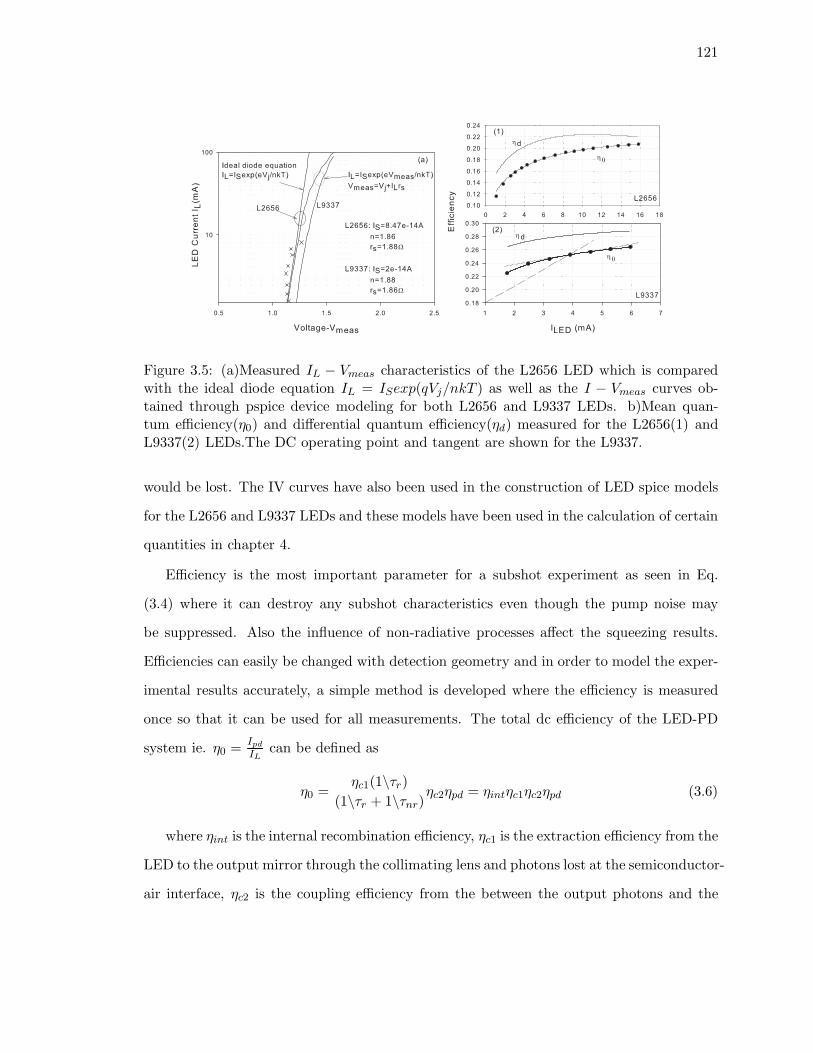
121
Figure 3.5: (a)Measured IL − Vmeas characteristics of the L2656 LED which is comparedwith the ideal diode equation IL = ISexp(qVj/nkT ) as well as the I − Vmeas curves ob-tained through pspice device modeling for both L2656 and L9337 LEDs. b)Mean quan-tum efficiency(η0) and differential quantum efficiency(ηd) measured for the L2656(1) andL9337(2) LEDs.The DC operating point and tangent are shown for the L9337.
would be lost. The IV curves have also been used in the construction of LED spice models
for the L2656 and L9337 LEDs and these models have been used in the calculation of certain
quantities in chapter 4.
Efficiency is the most important parameter for a subshot experiment as seen in Eq.
(3.4) where it can destroy any subshot characteristics even though the pump noise may
be suppressed. Also the influence of non-radiative processes affect the squeezing results.
Efficiencies can easily be changed with detection geometry and in order to model the exper-
imental results accurately, a simple method is developed where the efficiency is measured
once so that it can be used for all measurements. The total dc efficiency of the LED-PD
system ie. η0 =Ipd
ILcan be defined as
η0 =ηc1(1\τr)
(1\τr + 1\τnr)ηc2ηpd = ηintηc1ηc2ηpd (3.6)
where ηint is the internal recombination efficiency, ηc1 is the extraction efficiency from the
LED to the output mirror through the collimating lens and photons lost at the semiconductor-
air interface, ηc2 is the coupling efficiency from the between the output photons and the

122
photodetector and ηpd is the conversion efficiency of the photodetector which is depen-
dent on the responsivity. We cannot measure ηint very easily, and so we rewrite the ef-
ficiency as η0 = ηLηc2ηpd where ηL = ηintηc1 is the total efficiency of the LED. LED
injection efficiencies have been assumed to be 1. The differential efficiency is defined as
ηd = ηc1ηc2ηpddηint
dNC|Nc=NC0
where Nc is the electron population in the active region.In Fig.
(3.5b), we have plotted the efficiencies as a function of photocurrent for the two LEDs used
in our experiments. The differential efficiency has been calculated by taking the difference
between the neighboring data. To get smoother results, a linear regression was done on η0
followed by differentiation to obtain ηd. The efficiency plot obtained also coincides with
typical values obtained in the squeezing experiments.Usually it is very hard to fix η0 to
be the same as we move from experiment to experiment, but any changes are only in the
coupling efficiency as seen in Eq. (3.6). Hence the ratio ηdη0
is independent of the coupling
parameter ηc and with the value of η0 for that typical run of the experiment, we can esti-
mate the fanofactors. Note that the efficiencies are frequency independent parameters(The
authors in [42] had originally assumed it to be otherwise). From the Fig. (3.5b) we note
that Ipd rises superlinearly with IL and becomes more linear as drive current increases and
eventually saturates. The LED saturation here is before the onset of detector saturation.
If we had perfect linearity, ηint could have been taken as 1 and we could have determined
ηc1. But this is not possible unless the device is cooled to low temperatures where the
non-radiative channels are closed.ηd is essentially this deviation from linear behavior and
characterizes the nonradiative processes. However ηc2 can be estimated easily. The S5107
detector used has a responsivity(S) of 0.7A/W at 890nm and produces a high efficiency of
ηpd = S hνq = 0.97. The optical powers were measured using a calibrated Newport optical
power meter from which we could obtain ηL. The dc efficiencies η0 are determine from
Ipd and IL through face-face coupling between LED and PD. From these values estimated
ηc2 can be estimated. Some of these measurements have been shown in table (3.1). The
L2656 has a typical flux of 15mW at 50mA[54] which gives us an efficiency of 21.5%. In
the table. (3.1), at 20mA, the total efficiency is shown to be ηL = 21% which confirms the
accuracy of the power meter. This can be used as power input to the PD, from which the

123
LED Current-IL LED Power-PL Photocurrent-Iph EfficiencyηL =
PL1.39IL
Efficiencyη0 =
Ipd
IL
5mA 1.236mW 0.7716mA 0.1778 0.1542
10mA 2.740mW 1.706mA 0.1971 0.1705
15mA 4.278mW Saturated 0.2051 -
20mA 5.838mW Saturated 0.21 -
10mA(LE) 1.195mW 0.561mA 0.0895 0.06525
20mA(LE) 2.630mW 1.22mA 0.0917 0.06445
Table 3.1: Experimental values of optical power PL and photocurrent Iph for the L2656.Theefficiencies ηL, η0 have been calculated for two similar LEDs where LE characterizes the LEDwith low internal efficiency.
responsivity can be calculated asR =Ipd
PL= 0.62 ,a value smaller than the expected 0.7A/W.
This is nothing but the loss in coupling efficiency at the detector which is calculated to be
ηc2 = 0.89 and is quite high even without the aid of an integrating sphere. Such high ηc2 is
possible since the LED is outfitted with a collimating lens. Note that ηdη0
takes on values as
large as 1.24 for the L2656, whereas it is close to 1.08 for the L9337. This implies that there
fewer nonradiative mechanisms in the L9337 thus increasing the efficiency. A typical flux at
50mA is 23mW[54] which gives an efficiency of 32.2% at a center wavelength of 870nm,which
is almost a decade larger than the L2656. The last two rows of table show results at 10mA
and 20mA drive currents where the LED efficiencies calculated are 8% and 9%. These
are efficiency measurements performed for a L2656 LED for which squeezing was observed
initially but had later vanished. If the efficiencies are inserted into the Fanofactor relation
of Eq. (3.4) under constant current conditions(Fp = 1), one should theoretically see some
squeezing but this is not the case. Since the coupling geometry was not drastically changed,
the loss of efficiency in this case is due to the LED which had have been operated previously
at peak currents of 80mA, causing joule heating and a decrease in internal efficiency. At
10mA, the total efficiency is 8% which is far below the 19% expected. This loss can be
traced back to the radiative processes and injection mechanisms which are responsible for
squeezing. Even though the LED was usable, squeezing was lost because the internal drive
fanofactors reverted to their Poisson states. This is an interesting conclusion,since it shows
that a constant current is not the only condition to establish squeezing.

124
3.3.3 Photodetector Nonlinearity
The S5107 PD used in the experiments must show good linearity at all ranges of optical
powers used, since many experiments in the past have shown squeezing characteristics
only to be later attributed to the photodetector nonlinearities[3]. So it is important to
experimentally verify this nonlinearity and make sure it is at a minimum for the range
of photocurrents detected. An integrated optical power PL that is incident on the PD is
related to the photocurrent by P (I) = PLIph
= Gh(I) where h(I) is the nonlinearity function
of the detector with a certain response P (I) and G is a constant of the photodetection
process[?].The important assumption here is that at very low currents, the detector is
linear giving h(0)=1 and the response P (I) = G. Now define
f(I) =dh(I)
dI=
1
G
dP (I)
dI(3.7)
where f(I) can be interpreted as the rate of change of the nonlinearity with photocurrent.
We can define the small signal ac quantities ΔP = pac and ΔI = iac as follows:
ΔP
ΔI=
dP
dI→ pac = Gf(I)iac(I) (3.8)
from which the function f(I) save for the extra constant of G is the inverse responsivity
function g(I) of the PD and is given as
f(I) =1
g(I)=
iac(0)
iac(I)(3.9)
where the constant G has been removed by assuming that f(0)=1 and that gives G =
pac
iac(0)which was substituted back in Eq.(3.8) to give Eq. (3.9). The above function was
experimentally determined using the ac-dc technique[55] which is carried out by inserting
two optical signals into the PD; 1) A small periodic optical square wave from the L2656
using a function generator having an amplitude of 0.7V in order to turn the LED on and a
zero OFF(LOW) amplitude and 2) A time invariant dc optical signal from a 650nm Luxeon
LED. The dc power is first set to zero ie P(0)=0 and the on amplitude of the ac photocurrent
iac(0) was measured to be around 0.024mA. Next the ac photocurrent was measured as a
function of the dc optical power with a lockin amplifier and the ratio iac(0)/iac(I) was
calculated from the lockin readings. The lockin is a phase sensitive detector similar in

125
operation to the SA except the mixer inputs are the signal and a square wave instead of
the sine wave from the LO as for the SA. The square wave reference voltage is fed into
the lockin as well as the LED in order to match its phase. The lockin ’locks’ on to a
frequency component or harmonic of the square wave in this case and downconverts and
amplifies it such that the output is a dc voltage with very small noise(In other words signal
to noise is large). The dc component of the photocurrent was obtained from a voltmeter
which measured J = I+ < iac(I) >from which I was obtained. For a square wave we have
< iac(I) >= γiac(I) where γ = 50% is the duty cycle of the square wave.
The inverse response function g(I) = iac(I)iac(0)
has been plotted in Fig. (3.6) since this
is a measure of the responsivity of the system. The results are quite similar to relative
responsivity δ = R(I)R(0)measured in [?]. In addition,a 3-6th order polynomial fitting procedure
was also performed to calculate the relative responsivity and the error uncertainties in our
measurements, but the results were not accurate, since we had taken only a few data points.
However g(I) by itself is a very good indicator and is more sensitive to the nonlinearity
variation than the responsivity[55]. We note that g(I) changes sublinearly about 1% from
0-1.5mA and at larger current detector saturation sets in. Actually iac(0) still has a small
time averaged dc voltage of 0.35V which the square wave rides on,but we assume it to be
negligible to the dc optical powers generated by the Luxeon LED. We can now see what
happens to noise if we interpret g(I) in small signal transfer terms: the slight change in
linearity can cause changes in the fanofactors. If we shine a coherent beam of light on the
PD for which the shot noise is dependent on the photocurrent , at larger photocurrents the
shot noise should be smaller than expected. So we should obtain F < 1. A 1% error as
the Fig. (3.6) dictates, is sufficient to cause 0.04dB change which is very small and can
be neglected. So for all purposes, we assume that the PD is linear. In fact, experimental
results have confirmed this PD to be linear to about 40mA photocurrent[13].
3.3.4 Amplifier Characteristics
The Analog Modules 322-6(AM) is our principal amplifier which provides the gain for
the detectors. The design specs for this amplifier(Appendix.X) cites a gain of 40.7dB

126
Figure 3.6: Normalized function g(I) versus photocurrent Iph measured for the S5107 PDin photoconductive mode along with the interpolated curve
with a noise as low as 316pV/√
Hz. The exact conditions under which these parameters
were measured by the company were unknown. For example, at what frequency was the
measurement made, or was the amplifiers impedance matched for gain measurements. We
have measured the transfer function of the AM amplifier by feeding an input of -60dBm from
a HP 8660 signal generator(which has a frequency range of 1-2600Mhz) into the amplifier.
The difference between -60dBm and output measured on the SA gives us Fig. (3.7a). The
lab function generators(HP 8116A) could not be used as the output rolled off at 50Mhz.This
measurement strategy would seem quite obvious as we find out the ’system’ gain Kt =
Vo/Vi = DvAv where Dv is the voltage divider and Av is the voltage gain. But there is an
impedance mismatch between the 50Ω generator resistance and the 200Ω input resistance
of the AM. This input resistance is a physical resistor in parallel with the infinite input
impedance of a FET stage. The -60dBm reading of the signal generator is specified for a
50Ω load. So if we subtract the gain of the amplifier from the output of SA, we find the
power in dBm such that the source and load are matched. We don’t have to worry about
impedance mismatch. In fact if we plug in a 50Ω resistance into the mismatched amplifier
and subtract the gain we should measure around -174dBm(actually the noise power should
be higher if we consider the input impedance noise and the amplifier noise) according to the
maximum power transfer theorem. This -174dBm noise power is hard to measure using only

127
−
+
Cable Reactance
XLCC
RcellEcell
RLCDRD RIIS ID IL II In
En
(b)
Figure 3.7: (a)System gain Kt = VoVi
measured for the Analog Modules 322-6 amplifier withan input power of -60dBm (b)Noise equivalent circuit model of the entire measurement chainincluding PD equivalent circuit, cable reactances and input impedance of the amplifier
the single AM stage, but this value has been observed by cascading 3 amplifier stages(which
will be discussed later in this section ).
On the other hand when we couple a photodiode to the input,we are more interested
in the shot noise of the photogenerated current. The load resistance is usually set at
5080Ω and the gain curves will not be valid if they are used as such. In such a case,we
calculate the shot noise voltage across the 200ohm resistor(V200) and find the output voltage
as Vo,rms = AvV200 .To find Av we used a 650kHz sine wave of 10mV peak voltage.The
oscope measured it at 11.25mV which was corroborated by the SA giving -35dBm which
can be verified using 10 ∗ log(11.25mV ∗0.5∗0.70750∗1mW ) where 0.5 is the voltage divider ,0.707 is the
rms conversion factor ,and is divided by 50 to find power across 50ohm referred to 1mW.

128
Thus 11.25mV actually represents V200 = 6.28mV at the 200ohm input impedance of the
amplifier. The output at the SA for this input 3.10dBm or is Vo,rms = 0.319V from which
Av = 50. At other frequencies Av rises slowly and the peaking at high frequency as seen
in the Fig. (3.7a) is probably due to the impedance mismatch and inductive behavior of
the cables. The only source of error in this calculation is the voltage divider at the input
which we have assumed based upon our understanding of the amplifier design. We also
note that the spec sheet does not state any capacitance at the input which could change
the voltage division picture. Also transmission line effects are neglected since we deal with
maximum frequencies of 40Mhz and our cables between PD and AM are quite short(< 1m)
ie. the transmission line can be treated as a wire. However, the noise spectra demonstrate
a frequency dependent behavior at higher frequencies(> 10Mhz) which we later attributed
to the reactances in these cables. This issue will be discussed when the optical noise spectra
of the L9337 LEDs are studied. In our shot noise experiments, we find that using a gain of
70(a difference of nearly 1.5dB) helped to get more accurate results, which could be because
of the SA miscalibration and the reactances of the cable. This value of 70 is equivalent to
the total gain from the signal input into the amplifier to that which is being displayed on
the SA screen. Hence the gain curves are used when we insert any 50ohm input source and
for the photodetector experiments, we choose Av = 70 to give us correct measurements.
Also we note that the gain reaches the manufacturer’s gain of 40.7dB only at frequencies
beyond 10Mhz which would affect Av as well. This would imply that the input noise voltage
is specified at the same frequency since it too is a function of gain ie. EnoKt
where Eno is the
output voltage noise.
The simplest way to determine the input noise of the AM(En) is to short the input(which
removes the 200ohms input impedance) and then measure the output. The output divided
by gain gives the En. Looking at the circuit diagram in Fig. (3.7b), the output noise is
given by
E2no = A2
v(4kTRp + I2nR2
p + E2n) (3.10)
where Rp = R1 ‖ R2 = R1R2R1+R2
. We neglect In since its value is quite small unless
Rp > 1kΩ at source[56]. Let us outline a few noise measurement cases:

129
Case 1.The PD was connected to the AM and the noise was measured at 20Mhz which
led to -132dBm/√
Hz(which can be seen in a few of subshot noise plots later on) whereas
the calculation using gain of Av = 70 as described above and Rp = 5080//200 = 192Ω
should give us a noise power of -125dBm , a difference of 7dB. The noise signal actually
rolls off which we have not accounted for. At low frequencies we would expect the resistor
to show full thermal noise but at high frequencies we have kT/C noise ie. the resistors
roll-off asE2
t1+(ωRC)2 leaving only the amplifier noise behind. Of course, there is still some
resistor noise which is why the result is still above the amplifier noise cited at 416nV/√
Hz
Case 2.Terminating with a 50ohm resistor:The noise was -125.57dBm at 650Khz which
disagrees with the expected value by nearly a difference of 9dB. We may reason that the
sensitivity of the SA itself is close to this limit but the spec sheets show that this is not the
case[57]. Also there is the possibility that the SA is uncalibrated at low ranges or excess
noise being added in some input stage. 1/f noise is usually present at low frequencies but
most good amps based on FET designs have the corner frequency at couple of hundred
Hertz, well below the frequency of 650kHz. So we conclude that we cannot measure resistor
noise at low frequencies unless we have a larger amplification. At 10Mhz, we found a value
of -131dBmHz which is very close to the expected result of -131.8dBmHz with a gain of 70
and Rp = 40Ω. The first thought that one might have is that this looks like the SA noise
floor, but from our knowledge of the SA, the noise floor should theoretically be -148dBm
at the 1-1000Mhz range. So the value measured should be the correct result for the resistor
noise. Of course it is also specified that the SA measures noise accurately for signals 10dB
above the noise floor which the above value satisfies.
Case 3. Finally when terminated with a short the value remained around -136dBm
suggesting that the difference between 50ohm and input noise was smaller by 2dB. Going
backwards to the input this time by dividing by the gain we find around 0.506nV/√
Hz. An
AM technician has measured this to be 0.416nV/√
Hz. This is ultimately the resolution of
our experiments and often we deal with noise levels larger than this and we can apply the
10:1 rule ie. we can neglect the smaller of the two noise signals when the rms value of one
is 10 time the other.

130
Case 4.When we open circuited the AM, we saw a increase of 5dB above the base noise
floor. Normally an open load implies that we are measuring In in the Eq. (3.10). But in
this case,we still have the 200ohm resistor which puts the value close to measurement 1
above.
Since we are working so close to the SA noise floor, one might wonder why not just
increase the amplification by chaining a number of such amplifier modules. Some of the
initial experiments coupled the AM with 2 Minicircuits 500ZLN voltage amplifiers with a
gain of 20dB each to create as many as three stage amplifier blocks with theoretical power
gains reaching 80dB. The NF of the 500ZLN minicircuit amplifier is around 2.9dB[58]. The
AM amplifier noise figure can be calculated from the measured input noise voltage density
as [59] NFAM = 10 ∗ log(E2
200+(416pV/√
Hz)2
E2200
) = 0.22dB which is quite small compared with
the 500ZLN and hence it will have to be used as the first stage in the amplifier chain. The
total noise figure obtained by using the Friis formula[49] is NF=0.25 which is a small change
from the first stage NF ie. it implies that most of the noise of the measurement chain is from
the first stage only. In Fig. (3.8a), we note the power spectrum at -30dBm when the three
stage amplifier was terminated at the input with a 50Ω resistor. Using an input of -100dBm,
the measured gain at 10Mhz was 101.6dB. The noise of the 50Ω can be calculated using the
values from Fig. (3.8a) as -30dBm-101.6dB-44.77dB+1.99dB=-174.38dBm which is what
we expect for a resistor. The 44.77dB is due to a 30Khz RBW filter used and the 1.99dB
is the SA corrections as detailed earlier. This system gives similar values when terminated
with a PD with 50ohm load provided no voltage was applied. When we increased the reverse
bias to the PD,the noise levels went down as shown in Fig. (3.8b),something we could not
explain for this 3 amplifier measurement setup. In other words, the degree of reverse bias
set the noise floors at the SA and any light applied to the PD increased the noise level
proportionally from this noise floor. We also experienced issues regarding ground noise and
return paths in the system particularly when the photodetectors were connected. With
such large gain, the inputs were sensitive to how the amplifiers were placed in the shielded
box,wiring of cables and even movement of hands. For the above reasons, we decided to
use just the single stage AM amplifier for our shot/subshot measurements. We would be

131
Figure 3.8: (a)Thermal Noise Power of a 50Ω resistor obtained with a 3 gain stage amplifierchain (b)Dark current + 50Ω noise power for the PD reverse biased at 10V with the same3 gain stage amplifier.
working quite close to the spectrum analyzer noise floor but we would be able to discern or
measure with sufficient accuracy at the range of current levels we used.
With the noise figure of the analog modules amplifier (AM) determined, the maximum
sensitivity limits can now be established in the form of system noise figure(NFsys) of the
AM-SA combination and the noise equivalent power(NEP) of the overall system ie. PD-AM-
SA combination. The noise figure of the AM-SA is essential so we know the fundamental
limits for the smallest photocurrent noise that can be detected on the spectrum analyzer.
When we connect a preamp to the SA, the noise levels either go up or remain unchanged.
For example,if they increase by at least 15dB, then the noise figure of the AM-SA system is
given by NFsys = NFpre −NFSA [52] where NFSA is the spectrum analyzer’s noise figure
and NFpre is the noise figure of the preamp. Our case is different in that the noise levels do
not change all that much when we connect the AM. For the SA, the DANL changes in the
100kHz-1Mhz range. So we choose to evaluate the system noise figure NFsys at 500-600kHz
since our shot noise measurements were performed at this frequency whereas the system
noise figure is constant in the range 1-1000Mhz range. Based on frequency range we can
define two noise figures.

132
1.500kHz: From the spec sheets[57], we see that at 500kHz and an RBW=10kHz , the
DANL is -102dB. The NFSA can be calculated using the formula[52]
NFSA1 = DANL− 10 ∗ log(RBW )− kTBB=1 (3.11)
Here kT = −174dBmHz and we can estimate NFSA1 = 32. Now we need to calculate
NFAM + GAM −NFSA1 = 0.22 + 40 − 32 = 8.22dB and using the charts provided in [52]
we can determine NFsys1 to be at 0.4dB
2.1-1000Mhz: From the spec sheet, we see that at RBW=10kHz, DANL is -110dB.
Then NFSA2 = 24 and NFAM + GAM −NFSA1 = 16.2. From the chart in [52] ,we obtain
NFsys2 = 0.2dB.
The NFsys is usually specified to see how much above -174dBmHz we need the signal
noise to be in order to be displayed on screen. In the case of AM, even -174+NFsys2
gives -173.8 and so it should be able to measure the thermal noise of a 50 ohm resistor
which we have measured. The minicircuits 500LN preamp on the other hand provides a
NFsys = 8.2dB in the 1-1000Mhz range which is quite large when compared to the AM. So -
174+8.2=165.8dBmHz is the minimum noise it can measure. We initially tried to reproduce
results from[60] using the Luxeon LXHL-ND98 light emitter and the ZFL500LN amp but
we found that unless we drove our LEDs hard enough,we had a difficult time trying to
change the noise levels. Note that the DANL does not change at all and still remains at
-110dBm for RBW=10kHz. For example, with an input of -174dBm at the AM amplifier,
the output at the SA becomes −174dBm + GAM + 10 ∗ log(RBW ) = −110dBm and hence
equals the noise floor or DANL. Note that at 650kHz, the result is nearly identical to the
> 1Mhz range. But our measured results showed that noise levels were about 10dB higher
than expected.
Similar to the noise figure of the system, a noise equivalent power(NEP) can also
be defined as[61, 62] NEP = ItS where S = ηe
hν is the responsivity in A/W and It =√2q(ID + Ib + IL) + 4kT
RLis the total noise current for the detector without the amplifiers,
ID is the photodiode dark current noise, Ib is the noise due to background radiation, IL
is the photocurrent due to incident light and RL is the load resistance. NEP represents
the smallest optical noise power that we can measure with the present photodetector, AM

133
−
+
R2
R1
R3
R4 En
Inn
Inp
Eno
E1
E3
E4
AD8009
(a)
Figure 3.9: (a)Noninverting Equivalent circuit noise model of the Analog Devices AD8009opamp (b)Input and Output noise spectral densities of the circuit in (a) calculated usingpspice (c)Experimental noise power obtained for the unity gain opamp which is obtainedby amplifying using the Analog Modules 322-6 amplifier. A 50Ω terminated resistor noiseis also shown as reference.
amplifier and the spectrum analyzer combined. Generally NEP is defined for a PD which
is not connected to any additional stages. With the introduction of the amplifier, the total
current noise is then defined as It = In[63] (here In refers to the input current noise of
the amplifier) since the amplifier noise would then have to be the minimum value for an
equivalent optical power. For the PD-AM setup we cannot use the above relation exactly
since it is more amenable for current and transimpedance amplifiers where the input current
noise is much larger than the voltage noise component. So we calculate the NEP as the
signal power equal to noise at the infinite input impedance of the amplifier as follows
ηe
hνNEP =
(E2
n
R2+ I2
n + I2t
)1/2
(3.12)
Using a value of S = 072A/W for the S5107 PD and R=192Ω,and with the measured
En = 506pV/√
Hz and It =√
4kTR = 9.28pA/
√Hz ,the NEP is 13.39pW/
√Hz. Most of
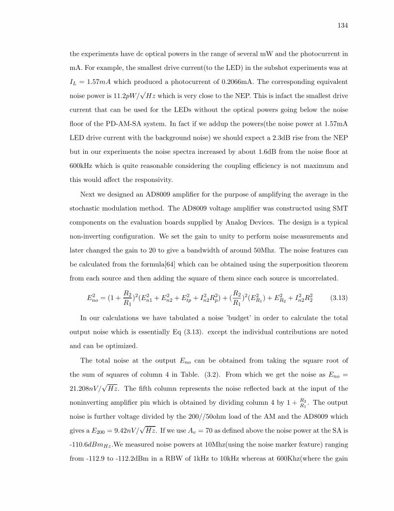
134
the experiments have dc optical powers in the range of several mW and the photocurrent in
mA. For example, the smallest drive current(to the LED) in the subshot experiments was at
IL = 1.57mA which produced a photocurrent of 0.2066mA. The corresponding equivalent
noise power is 11.2pW/√
Hz which is very close to the NEP. This is infact the smallest drive
current that can be used for the LEDs without the optical powers going below the noise
floor of the PD-AM-SA system. In fact if we addup the powers(the noise power at 1.57mA
LED drive current with the background noise) we should expect a 2.3dB rise from the NEP
but in our experiments the noise spectra increased by about 1.6dB from the noise floor at
600kHz which is quite reasonable considering the coupling efficiency is not maximum and
this would affect the responsivity.
Next we designed an AD8009 amplifier for the purpose of amplifying the average in the
stochastic modulation method. The AD8009 voltage amplifier was constructed using SMT
components on the evaluation boards supplied by Analog Devices. The design is a typical
non-inverting configuration. We set the gain to unity to perform noise measurements and
later changed the gain to 20 to give a bandwidth of around 50Mhz. The noise features can
be calculated from the formula[64] which can be obtained using the superposition theorem
from each source and then adding the square of them since each source is uncorrelated.
E2no = (1 +
R2
R1)2(E2
n1 + E2n2 + E2
tp + I2n2R
2p) + (
R2
R1)2(E2
R1) + E2
R2+ I2
n2R22 (3.13)
In our calculations we have tabulated a noise ’budget’ in order to calculate the total
output noise which is essentially Eq (3.13). except the individual contributions are noted
and can be optimized.
The total noise at the output Eno can be obtained from taking the square root of
the sum of squares of column 4 in Table. (3.2). From which we get the noise as Eno =
21.208nV/√
Hz. The fifth column represents the noise reflected back at the input of the
noninverting amplifier pin which is obtained by dividing column 4 by 1 + R2R1
. The output
noise is further voltage divided by the 200//50ohm load of the AM and the AD8009 which
gives a E200 = 9.42nV/√
Hz. If we use Av = 70 as defined above the noise power at the SA is
-110.6dBmHz .We measured noise powers at 10Mhz(using the noise marker feature) ranging
from -112.9 to -112.2dBm in a RBW of 1kHz to 10kHz whereas at 600Khz(where the gain

135
of 70 is valid) we can see from Fig. (3.9c) ,the noise power using a RBW=1kHz is around
-110dBmHz .This is a difference of 0.6dB to the theoretical values. The same discrepancy
existed when we measured the thermal noise using this amplifier. If we had chosen a gain
of 75 instead, we would have measured -110.1dBmHz . Since all our measurements have
uncertainties of around 0.4-0.5dB, we may not be able to explain the variation from 70 to
75,a difference of nearly 0.3dB. The total input noise is obtained from column 5 of Table.
(3.2) to be 10.675nV/√
Hz which is much larger than the AM input noise. The AD8009
requires the design of a properly shielded custom PCB board at Ghz frequencies. This
would eliminate the negative going spikes in the noise spectra of Fig. (3.9c). Since the
AD8009 showed good low noise input, it was used in tandem with the AM to amplify
square waves in our modulation experiments such that the input noise which is quite low
does not propagate and affect other noise levels in the measurement chain. For example, if
we use a T-connector to route a signal to both the oscope and the AM at the same time,
there is a return path for the noise from the scope which gets amplified by the AM. In such
cases, the AD8009 would be used as a low noise buffer with small amplification.
Noise Source Value(nV or
pA/√
Hz)
Gain Multiplier Noise at
output(nV√
Hz)
Noise at
input
R1=499Ω 2.83nV 1 2.83 1.415
R2=499Ω 2.83nV 1 2.83 1.415
Rp=8.33Ω 0.366nV 2 0.7324 0.366
En1 1.9nV 2 3.8 1.9@10Mhz
En2 1.9nV 2 3.8 1.9@10Mhz
In1 41pA 499Ω 20.45 10.229
In2 46pA 16.66Ω 0.766 0.383
Table 3.2: Noise contributions of the various noise sources in the calculation of the total
output noise voltage of the AD8009 non-inverting opamp
Also from the table we note that the noise is large primarily because of the In contri-
bution which could be reduced by lowering R2 resistor. So if we are to go to a gain of 20,

136
and still preserve the same input noise approximately we should change R1 to 26Ω.We used
25Ω resistor to set the gain. From Fig. (3.9c) we see that the noise is white in nature but
there are certain negative peaks which seem to change the variance. When we measured
the noise powers, we used averaging features and these spikes did not appear. In other
words,if an averaging filter had been applied any spurious amplitude pickups would not
have disappeared. When we measured the noise, the AD8009 had no shielding which could
explain the pickup.The input/output terminators(SMB connectors) were not so tight and
the voltage of 5V was applied without any voltage regulation, only relying on supply bypass
capacitors.
3.3.5 Shielding
Our interest is in the device noise sources and in order to study them, we have to minimize
all external sources of interference(such as EMI from wireless phones, power supplies, and
light sources). For proper shielding, it is important to first identify the noise source, the
receiver and the coupling medium. First shielding can be used to confine noise to a small
region and prevent it from getting into a nearby critical circuit. Second, If noise is present
in the system, shields can be placed around the critical circuits. These shields can consist
of metal boxes or cables with shields around the conductors. We minimized the spurious
noise until the optical shot noise spectra could be clearly observed. Even though shielding
has a sound scientific basis, most of the time we felt as if we were chasing a naughty child
with a stick. In general it is a good rule to avoid loopy interconnections and minimize cross
overs. However there are common sources of interference noise which we can avoid using
shielding. The experiments reported in this thesis observed the following design rules to
reduce the ambient noise levels.
1.Capacitive Interference: Capacitive interference occurs when a fringing electric field
associated with a noise source is large enough to produce a displacement current in an
electric circuit. Consider an equivalent circuit made up of a noise source affecting a receiver
of impedance Z through the C defined above.Then the noise voltage at the receiver in the
electronic circuit is given as Von = Vn
1+ ZcZ
where Vn is the noise voltage of the source and

137
Z is the effective impedance of the electronic circuit. From the above equation, it can be
seen that the magnitude of the noise voltage increases with the frequency of the source and
effective impedance Z. This effect is very critical when constructing systems that operate at
reduced power level(high values of Z), higher speed(implying faster frequencies) and higher
resolution(much less output noise permitted). When a shield is added, we have split the
equivalent circuit into two loops, where there is a noise current in loop 1 is proportional
to the driving voltage source Vn whereas in loop 2 , there is no current since there is no
driving source in that loop(ie. the shield has isolated the source). Hence the sensitive circuit
has been shielded from the noise source. In our system for example, we encountered this
problem between LED and PD face to face coupling. The LED metal plate carried noise
currents from the power supply which would capacitively infringe on the detector circuit.
We had constructed shielded twisted pair to connect the LED to the current source and
grounded the face plate, as well as the RF cage. Later when we covered with LED with
black tape, and increased the LED current, we noticed that the noise levels remained the
same at -76dBm for a 2 stage gain amplifier setting effectively removing the capacitive
coupling problem.
2 Magnetic Field Interference: Noise in the form of a magnetic field can induce a voltage
in another conductor due to mutual inductance. Its more difficult to prevent, since it can
penetrate conducting materials. For example, a shield constructed around a conductor
which is grounded has little effect on the magnetically induced voltage in that conductor.
As a magnetic field penetrates a shield its magnitude decreases exponentially. We can define
the skin depth of a shield as the depth of penetration required for the field to attenuated to
37% of its original magnitude(in air). Since skin depth decreases with increase in frequency,
high frequency magnetic noise is not that crucial and can be eliminated from the system
easily. The main problem, however is the 50-60Hz line frequency which is the principal
source of magnetically coupled noise at low frequency. We don’t have to worry too much
about 60Hz noise as the frequencies we work with are in excess of 1kHz. To avoid higher
frequency magnetic interference we use a few design rules:
a) Keep the receivers are far as possible from the source of interference.

138
b) Use a twisted pair of wires for carrying the current that is the source of magnetic
field. If the currents in the two wires are equal and opposite the net field in any direction
will be zero. Alternatively, the shield of the cable can be made to carry the return current.
c) Since magnetically induced noise depends on area of the receiver loop, the induced
voltage can be reduced by either reducing the loop area or the orientation of the loop to
the field. This is quite similar to building a transformer where the flux linkage is increased
by adding more turns to the loop.
3. Conductive Interference: These arise from currents flowing in the ground system.
These currents arise from power systems, from reactive coupling and from radiation. The
resulting ground potential difference can couple into the signal paths. It is usually futile
to short out these potential differences. The two ground points of interest are the power
supply termination and the input lead termination. This ground potential difference is
usually referred to as common-mode. These were one of the greatest issues.
4. Electromagnetic field coupling: Fields from nearby transmitters are a source of
interference. These fields couple voltages into the input cable in the form of a common-
mode signal. The signal is proportional to loop area and the frequency. The loop area is
between the cable and the earth plane. Normally these signals are out of band and do not
appear as noise. They are troublesome because they can be rectified in the instrument and
appear as a DC offset.
5. Transfer Impedance: Current flowing in the shield can couple voltage to the conductor
pair in the cable. This is generally a high frequency phenomenon. For long lines, some form
of differential filtering may be needed to attenuate this form of coupling.
In Fig. (3.10a) we see that when the RF cage was opened we found a noise power of
-55dBm with the 2 stage amplifier setup and in Fig. (3.10b) the noise powers went down to
-60dBm. The interference in this case is an optical noise which is white in nature since it
raises the levels at all frequencies. There are also spikes at 4Mhz which is predominant with
the 3stage amplifier setup since with larger gains it is more sensitive to pickup. We were
able to minimize most of the noise sources but not eliminate it completely. For example
the monitors which were needed to extract the plots produced conductive interference at

139
Figure 3.10: Noise power variations due to environmental and spurious optical noise ob-tained with the shielded RF cage open or closed. The measured noise power is the knownPD2 darkcurrent+5080Ω resistor noise as well as spurious environmental RF and opticalnoise obtained at a RBW=30kHz.
frequencies around 30-40Mhz. So during data extraction we had to turn off the monitors.
3.4 Optical Shot Noise Source Measurements
The spectrum analyzer displays the noise power P which is a measure of the fluctuations
of the photocurrent. Our goal is to obtain the frequency dependent Fanofactors given by
F (ω) = P (ω)PQNL(ω) where PQNL is the shot noise limited optical power from the lamp to which
we choose to normalize the quantum noise. So we need to calibrate the shot noise level(SNL)
precisely which in turn determines if the light statistics are indeed Poissonian. If the levels
are super-Poisson for example,we will end up overestimating F or finding suppression when
there isn’t any. There are two ways to calibrate the SNL.
1.We focus a lamp source directly onto the PD and measure the noise power. If we know
the response and gain of the measurement chain we can calculate the shot noise theoretically

140
and compare with the SA results. This method is straightforward and accuracies to 1dB
have been shown[3] .
2.Alternatively, we can estimate the slope of the power-voltage plots dVdP , and can com-
pare with the theoretical estimates[65] . This method is similar to 1 where we need to know
the constants of the measurement chain,but its useful since if some element of the chain is
unknown we can determine its values.
Our choice of using a lamp which is a a thermal source needs some clarification since the
probability of finding n photons in a mode is given by a Bose-Einstein photon distribution
where the total number of photons in a mode is given by < nks >= 1exp( hν
kT)−1
≈ 10−3
for T=3000K[66]. Typical lamp photocurrents have much larger photon number than this
and so the average per mode photon number is valid only when we count photons in a
time less than the coherence time. The coherence time(Tc) for thermal light is extremely
short(less than 1ps) and most detectors are extremely slow and hence we will not measure
a Bose-Einstein statistical distribution. If we count all the modes together, the variance
is obtained as[66] < Δn2 >=< n > (1 + <n>μ ) where < n >= Σksnks and μ is the total
number of modes. We can also set μ = tdTc
where td is the measurement time and Tc is the
coherence time. The reasoning behind this is that the single mode< nks > is valid only
for times less than Tc and so if end up counting a number of modes< n > ,it should be
valid for several coherence times(ie.μTc) which is the detection interval. As μ → ∞,ie we
count a large number of modes making the photocurrent large, the variance approximates
a Poisson. We can see that if μ = 1,the variance reverts to the form 〈Δn2〉 = 〈n〉+ 〈n〉2 and
if < n >2≤< n >it still approximates a Poisson. So its very hard to get a thermal source
to show its true nature which is why laser sources are scattered off randomly distributed
scattering centers to create a pseudothermal source[67] .
When a LED or lamp of noise power P is incident on the PD, the quantum noise
photocurrent develops a voltage across the resistor Rp which is ΔV 2Q = RpF (ω)(2 ηe
hν P ) where
F is the filter response factor due to the PD,cable reactances and (if any) spectrum analyzer
IF stage miscalibration. In addition there is a Johnson noise component ΔV 2J = 4kTRpF (ω)
due to the parallel combination of resistors and E2n which is the electronic noise which we
141
have already discussed. Putting them together the noise at the input before amplification
is
ΔV 2i = ΔV 2
Q + ΔV 2J + E2
n (3.14)
The noise power at the SA in dBmHz is given as
Pth(ω)dBmHz= 10 log(
A2vΔV 2
Q
50 ∗ 10−3) (3.15)
For a gain of 50 and RL = 192 we can simplify the above equation to get the theoretical
noise power as
Pth(ω)dBmHz= −92.38 + 10 log(I) + 10 log F (ω) (3.16)
For simplicity in calculations,we have set ΔV 2i ≈ ΔV 2
Q, using the 10:1 rule(neglect the
smaller noise component if one is 10 times the other). The shape of the response function
F (ω) can be seen from the electronic noise floor plots of Fig. (3.4b,c). Any noise will
be displaced from this value by a constant amount. For uniformity we perform all noise
power measurements at 500 and 650kHz using the noise marker feature of the SA. The
experiment was carried by shining the lamp on the PD and varying the light power by means
of ILX LDX-3620 current source thus changing the photocurrent. It is suggested that the
lamp be spectrally filtered to the center wavelength of the LED used in the experiments
ie 870 or 890nm±40nm since the response of the photodiodes are wavelength dependent[3]
. We used red optical filters but we observed no variation in the measured noise. We
also used a regulated power supply for the lamp which did not make a difference on the
noise characteristics like it does for the LED. The spectrum of the noise power versus
current is shown in Fig. (3.11a). The 50ohm resistor noise is also quite similar to the noise
measurement obtained when the PD is coupled to the AM without light, which questions
its validity since we should be observing a 192Ω(200 ‖ 5080) resistor noise. This is the
-125dBm noise we discussed earlier for 50ohms except these measurements are at 3kHz
RBW. We see that the photocurrents produce a relatively flat characteristic indicating its
’white’ness. Actually there is a filter response F (ω) present in the noise spectra which can
be observed in a larger frequency range. Since most of the signals are at least 10dB above
the noise floor(-93dB) we can use Eq. (3.16) to calculate the noise powers at the spectrum
analyzer without too much error.

142
Figure 3.11: (a)Noise powers of the mean photocurrent for a red-filtered white light(from alamp) incident on the PD which is observed at a RBW of 3kHz. (b)Noise spectral densitiesnormalized to 1Hz(points) as well as linear regression(solid line) obtained as a function ofphotocurrent.The linear fit gives us the filter response function F (ω) at 650kHz.
We now demonstrate the validity of the equations . We set F=1 ie no filter response
since we need to obtain this value. We obtained the experimental noise powers using the
noise marker feature of the SA. It is best to use the SA noise marker feature whenever
absolute measurements are required since there will be always be some error between it and
reading the plots of Fig. (3.11a) using Eq. (3.5) because of the assumptions regarding the
noise correction factor.
1. For Ipd = 3.927mA, we obtain Pexp(650kHz)dBmHz= −113.45dBmHz . The theo-
retical result gives us Pth(650kHz)dBmHz= −116.33dBmHz a difference of nearly 2.88dB.
This leads to F being defined as 1.4. Alternatively we could have just chosen a gain of 70 to
get the right results ignoring the filter response. Either way, we end up having a consistent
measure of shot noise.
2. For Ipd = 2.946mA, we obtain Pexp(650kHz)dBmHz= −114.82dBmHz . The theo-
retical result gives us Pth(650kHz)dBmHz= −117.58dBmHz a difference of nearly 2.76dB
which gives an F of 1.37.
The above measurements have been performed for 16 data points at the 500 and 650kHz
frequencies and there is a consistent difference of 2.8dBm in all of them. A linear fit has
been done which estimates F to be approximately 1.4. This can be seen in Fig. (3.11b)
where we have plotted the currents versus voltage spectral densities. One might doubt

143
this measurement strategy of calibrating the shot noise level since we have an unknown
parameter. So we might need further tests to show that the source is indeed Poissonian.
Fig. (3.11b) shows that the noise powers is a linear function of photocurrent as expected.
This is by itself taken as a sufficient test for Poissonity since if there are two uncorrelated
noise sources at the same frequency, they would add in quadrature causing deviation from
linearity. The electronic noise is constant independent of optical power and if the noise
is say quantum limited the variation is 0.5 times the optical shot noise[3] . Now if we
assume that F=1, then the 2.8dB discrepancy has to accounted for. When we measured
the dc photocurrents, the load resistance was 5080ohms. When we connected the AM for
noise measurements, load resistance dropped to 200ohms. This would increase the reverse
bias across the diode given by V − Vph = Vt ln(Sφφe
ID) where the photocurrent is given by
iph = Sφφe. But in typical PDs, the application of reverse bias does change the responsivity
slightly due to improved charge collection efficiency in the photodiode[61] which is usually
observed from the slope of the IV curves in the third quadrant. If we need to account for the
discrepancy, the responsivity would have to change by a factor of almost 2 which seems less
likely. So the response function F seems to be the most likely culprit. We also repeated the
above measurements for the LED driven by the SNS and found the same linearity results
at 500kHz when compared to the lamp driving the PD therefore calibrating the SNS to the
shot noise level. So whenever we need to get an absolute measure of noise , we would read
off 650kHz noise markers compute the noise levels with a total gain of 70(Av ∗ F ) and we
would be assured of computing the SNL.
Another important test for Poissonity is the Fanofactor relation. Consider the inset of
Fig. (3.12) where the variation of efficiency has been plotted against current. The minimum
to maximum suffers a change of less than 0.01 and so if we approximate the efficiency as
nearly 0 and plug in this η0 in Eq. (3.4), it gives us seemingly correct results(ie. Fph ≈ 1)
but its usage is highly misleading. For example we may ask the question:does a lamp
distinguish between the constant current or constant voltage case? If we set Fp = 1(CV)
then Fph = 1 and if we set Fp = 0(CC) then Fph = 1 − η0 ≈ 1. Eq. (3.26) has been
constructed specifically to link the variance from LED to PD(in some sense using stochastic

144
Figure 3.12: Noise power from the photocurrent obtained for the lamp(which is also rep-resentative of the LED driven by the SNS) as a function of current-current conversionefficiency. The points give the measured values whereas the straight line represents theaverage. The inset of the figure represents the efficiency of the lamp as a function of drivecurrent.
ideas) but it does not have a solid quantum mechanical underpinning. In fact it has an
electronic part Fp as well as an optical part Fph. Consider a coherent beam of light(say
from a laser) passing incident on a PD which includes loss modeled as a beam splitter with
efficiency η. The output light of the beamsplitter has a mean equal to variance given by
< n >=< Δn2 >= η|α|2, where |α|2 is the average number of photons in the coherent
state |α〉. This implies that coherent states which are Poissonian remain so after beam-
splitting. The detected photon Fanofactor becomes Fph = <Δn2><n> = 1 which is independent
of the efficiency for any bias current and efficiency(not only 0). The lamp is indeed not a
coherent state but the statistics are Poissonian which would make the Fanofactor definition
Fph valid. So whether we use the lamp or SNS ,the measured noise on the SA should remain
unchanged when we vary the efficiency. Fig. (3.12) shows the measured optical shot noise
spectral density which was performed by keeping the photocurrent fixed as we varied the
efficiency.
The efficiency was changed by increasing the distance between the lamp and PD and
the driving current was adjusted to give the same photocurrent for all the measurements.

145
The efficiency was determined as the ratio of driving current to the photocurrent. This
differs from the inset of Fig. (3.12) since there we have kept the distance constant and
varied the drive current. The lamp current was changed from 197mA to 312mA keeping the
photovoltage fixed at 7V(ie 1.379mA photocurrent). The efficiencies varied from 0.0069 to
0.0044 but the noise powers remained the same at approximately -117.98dBmHz or 8.127 ∗10−14V 2/Hz indicating the light statistics are indeed Poissonian. The same experiment has
been verified using the LED driven using the SNS, except in this case Eq. (3.26) is valid
and Fd = 1 defined above is taken as the drive Fanofactor Fp.
When we place a battery of around 1.5V(assuming the battery has negligible voltage
noise) across the diode(CV), we should see shot noise on the SA. But the same shot noise
can be observed using our SNS where the PD inside the SNS(PD1 of Fig. (3.3)) has been
calibrated to the shot noise level which in turn ’noise’ modulates the LED in such a way
that the output remains at a Poisson level. This method produces a Poisson photon flux
similar to the CV case and hence the SNS and CV must share some similarities. Consider
an equivalent circuit diagram of two back to back diodes(PD-LED), except we shall replace
the equivalent circuit of the PD with a Poisson current source. From Eq. (2.77) which we
rewrite here
dn
dt=
i(t)
e− n(t)
τ+ isn(t) (3.17)
where i(t) is external circuit current, which is set to i(t) = −isn(t). This leaves dndt =
−n(t)τ which we can equate to 0. In other words the number fluctuations are constant and
don’t change at least at the time scales we are interested in. This implies that the junction
voltage does not change and the SNS is a CV source.
Since we have established the lamp as a shot noise source, we can compare it against
other noise levels in Fig. (3.13). Fig. (3.13a) shows that whether we drive the lamp with
a Lightwave current source or voltage source the noise levels remain fixed. This is true
since the lamps do not modulate well unlike the LEDs which register huge changes based
upon the type of supply. Fig. (3.13b) shows our initial experiments where we drove the
LED using the photocurrent obtained from a red Luxeon LED driven by a noisy voltage
source.We compare the level with the LED driven by a ILX current source. The goal of this

146
Figure 3.13: Optical noise spectra for (a)Lamp driven by voltage and current sources(b)650nm Luxeon LED driven with a noisy source (c)Attenuated spectra from LuxeonLED (d)L2656 driven by ILX current source and (d)Generic laser driven by ILX currentsource
experiment was to show that if we do not have a reference shot noise source such as the
lamp, we could interpret the upper level as being shot noise and the lower level as being
subshot since it was driven with an ILX ’constant’ current source. In Fig. (3.13c) ,we note
that the Luxeon driven with a ILX current source through a resistance of 330Ω at 23.25mA
to produce a photovoltage of 3.49V which produces a noise level greater than the shot noise
level of the lamp. This contradicts experiments done in [60] where they have observed 1.5dB
squeezing with at mid-frequencies. We also tried the same experiment using a battery and
1K resistor to produce a Vph = 3.15V . The lamp was driven at 192.27mA to produce the

147
same photovoltage and once again the Luxeon showed super-Poisson characteristics. In Fig.
(3.13d) we drive the LED with a current source and compare it with a Luxeon driven by a
constant voltage of 3V. This shows a situation where the L2656 is at a noise level higher than
the Luxeon which is shown to be supershot itself. This proves than the ILX current source
generates a super-Poisson characteristic with the L2656 LED. Finally we compare the lamp
with a laser source and we see nearly 20dB difference and at lower frequencies(not shown)
the noise increases a great deal due to the relaxation oscillation. This is much larger than
the noise produced in the L2656 LED with the ILX current source. It is well known that
lasers driven well beyond saturation produce a coherent state, but in this case unless we use
an intensity noise eater[3], and also suppress the mode partition mechanisms it would be
difficult to produce subshot noise. But it should be noted that one of the largest amplitude
noise reduction(nearly 75% below the SNL) have been predicted to occur in the feedback
loop of a negative feedback semiconductor laser and nearly 10dB intensity squeezing has
been demonstrated[4].
3.5 SubShot Noise experiments
3.5.1 Verification of High-impedance Pump suppression mechanism
Now we are in a position to carry out the subshot noise measurements, since the shot
noise level(SNL) is known. This is accomplished by using a constant current source(CCS)
which in our case is a 9V battery connected through a large series resistance much larger
than the differential resistance of the LED. The noise current of the CCS should be well
below the shot noise limit ie. Fp = 0 which leads the output Fanofactors to be defined as
Fph = 1 − η0 ie. Fph is limited by the dc efficiency η0 of the LEDs. So we should expect
variances less than the SNL. But first we shall demonstrate the concept of high impedance
pump suppression. At low frequencies the diffusion capacitance can be removed from the
equivalent noise circuit of Fig. (2.5) leaving behind a simple circuit with shot noise, thermal
noise sources and two resistors Rs and Rd. The recombination current can be determined
as i =vth+vsn+vps
Rs+Rdwhere we have included the power supply noise vps which we do not know

148
and varies from supply to supply.The Fanofactors can be written as
Fp =< i2 >
2qI=
(< v2th > + < v2
sn > + < v2ps >)
(Rs + Rd)22qI=
(4kTRs + 2kTRd+ < v2ps >)
(Rs + Rd)22qI(3.18)
Case 1. When we apply a constant voltage; we see from Eq. (3.18) that as 2Rs � Rd ,the
Fanofactors become Fp(CV ) =2kTRd+<v2
ps>
R2d∗(2qI)
=<v2
sn>+<v2ps>
<v2sn>
and if we assume < v2ps >�<
v2sn >,the output noise is much above the SNL governed only by the noise of the voltage
supply. If we set vps = 0, the junction voltage fluctuations are almost nonexistent and
output light is at the full shot noise level as seen in chapter 2.
Case 2. When we increase the series resistance Rs such that Rs � Rd, then the Fanofac-
tors become Fp(CC) =4kTRs+<v2
ps>
R2s∗2qI =
4kT/Rs+<v2ps>/R2
s
2eI =<i2th>+<i2ps>
<i2sn> . If we assume that
vps � vth,then Fp(CC) =<v2
ps>/R2s
2eIR2d∗R2
d =<v2
ps>
<v2sn>
∗ R2d
R2S
= FCV ∗ R2d
R2S. This tells us that the as
the series resistance increases, the supply voltage noise is suppressed from the CV case and
as RS →∞, we can completely suppress the power supply noise. Now if we set vth � vps,
then we recover the condition Fp = 4kT/Rs
2eI [6] which is always much less than 1.
In order to demonstrate high impedance pump suppression we could first determine the
SNL based on the calibration method, then use various series resistances and determine the
output noise level. For large series resistance, the recombination noise would be suppressed.
Note that the current noise could be suppressed all the way to 0 as in case 2 for large series
resistance but the light is suppressed by less than a dB because of the limited efficiencies
involved as can be seen from by substituting the Fp obtained above in Fph. So in order to
simulate the effect of pump suppression, the power supply voltage noise is useful since for
Rs > Rd it establishes a recombination current given by
< i2 >=< i2th > +(< i2sn > + < i2ps >)(Rd
RS)2 (3.19)
The purpose of the voltage noise is to increase the noise level from the standard shot
noise level (which can be seen from the Eq. (3.19)) so that the effect of pump suppression
can be demonstrated over several dB. We can consider this enhanced noise as a simulated
shot noise level which will be suppressed as we increase the series resistance. Otherwise it
would be very hard to notice the pump suppression effect. For example if we use a ’quiet’
voltage source, we will not be guaranteed a SNL(case 1), since the effect of contact and bulk

149
resistance of the diode could well exceed the differential resistance causing the suppression
to be already in effect.
Fig. (3.14a) shows us the noise levels for the various power supplies used in the experi-
ment. The L2656 LED was driven with the following sources: 1. A current of 7.64mA from
the ILX current source 2. A battery of 9V with a series resistance of 110ohms and 3.A HP
6236B power supply at 1.2V. For all these sources, the photovoltage at the multimeter was
1.52V(which indicates the same average optical power) and the coupling geometries were
fixed. The noise levels from both the ILX current source and the HP power supply vary by
5-10dB when compared with the battery noise levels. We tried the experiment by running
the ILX off the AC mains as well as using internal batteries. For both cases, the noise was
above the battery levels at low frequency which is quite surprising since the ILX is adver-
tised as an ’ultra-low’ noise current source.We can see that the ILX generates harmonics
when driven off the ac mains(these harmonics disappeared when the ILX was driven with
a battery) and these harmonics are attenuated which may either be the response of the
ILX itself or the modulation bandwidth of the LED which is less than 600kHz. We note
that the ILX is usable as a source at frequencies greater than 800kHz since it reaches the
battery noise levels. The HP supplies are normally noisy and when we used capacitors at
the output terminals the noise levels went down. From the Fig. (3.14a) we see that the HP
noise levels are almost white in nature and so they can be added in quadrature with the shot
noise levels to verify the pump suppression effect. Also they do not modulate and roll off at
frequencies less than 600kHz which suggests that noise does not respond to the modulation
bandwidth of the LED and the rolloff of the ILX is due to stray pickup harmonics(which
are sensitive to modulation bandwidth).
In Fig. (3.14b,c), we demonstrate the pump suppression effect for both the L2656 and
the Luxeon light emitters. First we describe the effect of pump suppression for the L2656
LED shown in Fig. (3.14b). For all experiments, the DC photovoltage was set at 1.93V
by adjusting the supply voltage from the HP unit. This was done so that the photon rate
was the same for all cases. Then using resistors from 10Ω to 1.5kΩ we noted the noise
levels. The flat noise level with no spikes can be considered as a reference that other levels

150
Figure 3.14: (a)Optical Noise spectra for the L2656 with different bias sources.The referencelow noise source is the battery. (b) and (c) show high impedance pump suppression effectfor the L2656 and for the Luxeon LED as function of series resistance RS . Experimentswere performed at a RBW of 100Khz(a,b) and 30Khz(c) with a VBW of 3Hz.
should tend towards(as they are being suppressed) and has been obtained by driving the
LED with a resistor and battery source. We have only depicted the low impedance values
since for resistances greater than 110Ω we noted no difference in the levels from that of the
reference level. The photocurrent for all experiments is at 0.379mA(1.93V/5080Ω) which
at 650kHz gives us a calculated shot noise level of -75.55dBm which is slightly above -
76.5dBm obtained using the 47ohm resistor and the reference in Fig. (3.14b). The DC
voltage gives us about -69.5dBm at 300kHz. At 10ohms we get -74.5dBm , a difference
of nearly 10dB which can be obtained approximately as PdBm(DC) − 10 log R. As the
resistance increases to 22 ohms, we see -75.5dBm(≈ −69.5− 10 log 22). This shows us that
the power supply voltage noise is being suppressed by a factor of R and if vps = 0 it would
also suppress the shot noise. We also see that the noise levels do not go down arbitrarily as

151
R increases and the levels merge with the reference. For example at 47ohms should give us
−69.5dBm − 10 log 47 = −86.22dBm which should be 5dB below the reference. Instead it
can be seen from Fig. (3.14b) that the noise level does not go below the reference level. This
can be seen by calculating Fp. For the DC voltage case we obtain an Fph = 4.07 and for a
typical efficiency of η0 = 0.18 we can obtain Fp = 17.77. When we insert a resistance of 10Ω
we note an Fp = 2.516 which implies that the pump Fanofactors are being suppressed. For
22Ω we can obtain Fph = 0.901 which implies that the noise is being suppressed below the
shot noise level, which also implies that the drive Fanofactor is suppressed ie. Fp = 0.453.
At larger resistance values since Fp is nearly 0 which implies that we are observing full
subshot noise.
Similar results are seen for the Luxeon light emitters in Fig. (3.14c). The experiment
was performed using a dc voltage of 2.15V from the HP supply and calibrating the dc
photovoltage at 8.91V. Later, resistances of 10,47 and 300 ohms were inserted keeping the
photovoltage constant by adjusting the dc voltage. The coupling efficiency was as high as
30% but the emitter is red and not tuned to the peak spectral wavelength of the PD. So
we can expect loss and degradation of squeezing.The SNL calculated for a photocurrent
of 1.75mA is -74.13dBm. Note that the RBW used for this experiment is 30kHz. At low
frequency we see the 10ohm resistance registers a change of almost 10dB as expected. The
Fanofactors calculated for the DC case is Fph = 6.5 which is larger than the Fanofactors
obtained for the L2656 .This may be attributed to the power supply noise which is dependent
on the applied voltage. The reference level in this case is around -76.5dBm which is smaller
than the shot noise level. This is rather surprising since when we compared the level of the
Luxeon to a lamp in Fig. (3.13c) and we found the Luxeon level to be slightly higher. We
have confirmed this source to be super-Poisson using other power supplies. This type of
error can be eliminated if we place both the shot and subshot plots on the same figure to
facilitate easier comparison. We will do so in all future experiments since we are interested
in calculating the Fanofactors which are dependent on the relative values.

152
Figure 3.15: Optical noise spectra and Fanofactors of the photon fluxes from the L2656LED obtained at (a,b)IL = 1.92mA (c,d)IL = 6.53mA (e) IL = 8.08mA and (f) IL =9.81mA. The Fanofactors were fit to the theoretical diffusion model(solid lines) which wereobtained using Eq.(3.21) with various correction factors C to fit to the data better to F.TheFanofactor obtained with C=1 line has been shown for reference.The model parametersused are Cdep = 0.1μF and τr = 250ns.

153
3.5.2 Squeezing Results for the L2656 LED
Next we detail the results of our squeezing experiments for the L2656 which was done over
a range of 1.57mA to 7mA LED drive current for a total photovoltage of 1-8V(just before
photodetector saturation for a 9V supply). In each plot, the upper trace is the SNL and
lower trace denotes the degree of squeezing from the SNL which is typically from 0.2-1.5dB
in our experiments. The noise floor has also been included for comparison. Fig. (3.15a,b)
shows the results at a LED drive current of 1.92mA with a photocurrent of 0.24mA or a
total efficiency of 0.125. The calculated shot noise at a RBW=30kHz is -82.8dBm which is
close to the -83.1dBm seen at 600kHz in the Fig. (3.15a). We note that the photocurrent is
quite small since the power changes only by 2dB from the noise floor which is the reason we
were not able to carry out the experiment at lower LED currents. The lowest currents in
which squeezing has been obtained using this LED is approximately 5μA at a power levels of
several μW [42]. Since smaller LED currents result in lower LED emission efficiency ηLED,
the degree of squeezing also decreases and eventually we would reach the SNL. This can be
seen for the case of the low injection LED drive current of 1.92mA in Fig. (3.15a) where the
subshot noise is only 0.2dB below the shot noise level at 200kHz and merges early with the
shot noise level at a frequency of around 600kHz(Note that for this figure, this is not 3dB
point for squeezing). Statistically, this is explained as follows: The injection current has a
high efficiency even at very low current levels. However the recombination rate or probability
decreases with lower injection current. In other words the probability of emission ηLED(τ)
of an photon after electron injection becomes lower where τ is the observation time. The
response of the LED deteriorates as f = 1τ is lowered and squeezing as well as modulation
is pushed down to lower frequencies.This however should not be construed as squeezing
cannot take place at lower current levels. The thermionic emission regulation process is
still in effect albeit it requires larger observation times(smaller frequencies) and if we can
increase the efficiency of the LED at low currents we should still see squeezing. Since we
are restricted by device technology,this has still not been shown for macrojunctions at low
currents. Fig. (3.15b) gives us the normalized noise level or Fanofactor which has been
calculated from Fig. (3.15a) as the ratio of subshot trace to the shot trace after subtracting

154
the thermal noise from each trace which can be expressed as
F =10Subshot/10 − 10F loor/10
10Shot/10 − 10F loor/10(3.20)
This ratio should be independent of the detection system parameters such as frequency
response and amplifier gain since the traces follow each other. For the remainder of this
chapter, F denotes the measured Fanofactors whereas the theoretical Fanofactors are written
with subscripts. In Fig. (3.15a) we see that at low frequencies particularly from 0-100kHz,
there appears to be little or no squeezing. This is due to the spectrum analyzer response.
In order to get accurate results we have set the starting point of Fanofactor calculation
at 100kHz,but we will have some error since it underestimates the squeezing. The DC
values of F can be obtained by extrapolating from a low frequency point just before the
Fanofactors start to rolloff(which in this case is 200kHz) to dc. If the squeezing took place
over a larger frequency range, we could have made the assumption that the squeezing
at 200kHz is the same as the dc since the response should be in some sense a low pass
filter and some papers have used this method. If we use this assumption we find from
the Fig. (3.15b) that F(200kHz)=0.85 which is somewhat close to the theoretical value of
Fph = 1 − η0 = 0.875(we have got very accurate results at higher currents with differences
of less than 0.01) which would have agreed well. However we note a discrepancy when we
plot the theoretical frequency dependent Fanofactors in the diffusion limit given by the Eq.
(??) which is rewritten along with an additional component C as
Fph(ω) = 1− η0C
1 + ω2(τte + τr)2(3.21)
where we have assumed C ∝ (ηdη0
)2 is a correction factor motivated by a similar factor
appearing for the thermionic emission model which will be used for the L9337 LED later
on. Also this correction factor gives better agreements between theory and experiment.
The thermionic emission lifetime is defined as τte =kTCdep
eI . The theoretical plots have
been obtained by fitting Eq. (3.21) to the center of the variance in F. In order to be
as accurate as possible, we start the fit from Fig. (3.15d) which is the normalized noise
levels calculated from Fig. (3.15c). At a high current value of 6.53mA, τte � τr and so
Fph(ω) ≈ 1− η0C1+ω2τ2
r. As for the recombination lifetime τr, the datasheets do not state this

155
parameter but other papers have measured different values ranging from 600kHz to 1Mhz[44]
. When we measured this value by finding the 3dB point using AC modulating the LED
from the current source, we found a frequency of approximately 600kHz(265ns). Note that
this 3dB point depends on the extrinsic lifetime given by the RSCdep product which could
limit the modulation speeds below the intrinsic carrier lifetime τr. The datasheet specify
a rise time of tr = 0.45μs at a current of 50mA. Using tr = 2.2(τr +1.4∗10−4TCdep
ILED)[68] we
get τr ≈ 204ns. So to get a good fit, we need to set the bounds of τr from 204ns to 265ns.
At 6.53mA and choosing τr = 250ns we found a close fit to F at high frequencies. Notice
that the line does not fit well at low frequencies when using the diffusion model without
the correction factor. If we assume C=1, then we will have to change Cdep or τr to get a
better fit. But at high injection Cdep should not matter unless it is made larger in which
case it would cause discrepancies at low injections(A 0.01μF change is sufficient to cause
drastic variations).Also τr can only be varied between the bounds.Otherwise it would also
cause very large discrepancies. The only logical reason is to account for the deviation in
C. This discrepancy has been noticed by other authors[42] , which they reasoned using the
small signal transfer idea ie. As ηd > η0 the transfer rate of an AC signal is larger than
a DC component and so the ratio of fluctuation⟨Δn2
⟩to the mean can be greater than
1, which would imply that the Poisson source is actually super-Poisson. However, ηd is a
parameter associated with the LED, and it becomes a concern only when we are driving
the LED using the SNS. We have verified that the SNL is nearly the same when we use a
lamp directly(where ηd is not a concern since it is nearly 0), but even 0.1-0.2dB difference
is sufficient to cause great variations in the Fanofactors. But super-Poissonity of the SNS
which is quite small is insufficient to explain the correction factor C. So we reason that the
subshot noise is also much more than expected from the simple formula Fph(0) = 1 − η0.
However it serves as a good approximation for us since our results agree with it very well
at 200kHz which can be seen in the Fig. (3.15d).
At low injection levels, τte � τr and so we obtain Fph(ω) = 1− η0C
1+ω2(kTCdepeILED
)2where Cdep
is a fitting parameter which we estimate to have a value of 0.1μF . We cannot accurately
determine Cdep experimentally because the measured capacitance is the sum of both the

156
diffusion and depletion capacitances at moderate voltage. After the fit,the only variable in
the model is the drive current ILED. We have verified the model for ILED ranging from
1.5mA to 9mA and found good agreements. Fig. (15e,f) shows an example of Fph(ω) at a
currents of 8.08mA and 9.81mA. In the Fanofactor figures, the correction factor have been
estimated to be 1.5, 1.3, 1.1 and 1.09 respectively. We notice that the correction factor
C tends to 1. This can be seen since ηdη0∝ √C gives us ηd ∝ .199 for IL = 8.08mA and
ηd ∝ .20 for IL = 9.81mA. This is less than the values shown in Fig. (3.5b) which is
around 0.21 , but we see that the ratio ηdη0
follows the general shape of the curve. At higher
currents we see that the efficiency η0 becomes more linear from 4-9mA and then saturates
from 10-16mA(Note that this is not the photodetector saturation). So slope of ηdη0
should
decrease and be equal to 1 in the linear region and should tend to 0 in the saturation and
this is what we observe for C as IL increases. We can now see if the correction C gives us
the correct DC fanofactors according to Eq. (??) which we rewrite here
Fph(0) = 1− 2η0
(ηd
η0
)+ η0
(ηd
η0
)2
(1 + Fdr(0)) (3.22)
If we assume a Poissonian drive current Fp = 1 we see that Fph(0) = 1−2η0
(ηdη0
)+η0
(ηdη0
)2
and for ηdη0
> 1 which is typical of our experiments, the optical noise is super-Poissonian.
This is true only when the SNS is driving the LED and not when the lamp itself is used
as the shot source. So the Fanofactor definition itself has to be renormalized to account
for this new supershot noise as Fnorm(0) =<Δn2>Subshgot
<Δn2>Supershot=
Fph(0)Fdr=0
Fph(0)Fdr=1. This gives us the
relation
Fnorm(0) =1− 2η0
(ηdη0
)+ η0
(ηdη0
)2
1− 2η0
(ηdη0
)+ 2η0
(ηdη0
)2 (3.23)
which can be compared with the experimental results obtained by taking the extrapolated
curves from the frequency dependent Fanofactor with the appropriate correction. For exam-
ple, in Fig. (3.5b) we see that η0 = 0.17 and ηd/η0 = 1.2 which gives us Fnorm(0) = 0.7736
which agrees with the Fanofactor at 100kHz. We have assumed that the value at 100khz
is the same as the dc value since the curves level off at this point . We have computed
Fnorm(0) for certain drive currents along with the standard definition Fph(0) = 1 − η0 in
Table. (3.3) and we see that Eq. (3.23) (except for 5.72mA which shows the largest error)

157
Drive currentIL(mA)
η0ηdη0
Fph(0) = 1− η0 Fnorm(0)(Theory)
F (0)(Experiment)
1.92mA 0.125 1.264 0.875 0.815 0.815
6.73mA 0.17 1.20 0.83 0.7736 0.78
4.16mA 0.168 1.205 0.831 0.776 0.78
5.72mA 0.180 1.19 0.82 0.764 0.776
8.08mA 0.191 1.157 0.809 0.76 0.76
Table 3.3: The experimental results of η0,ηd which are used to compute F according to Eq.(3.23) are compared with the experimental results for varying drive currents.
predicts the correct results as expected. To the best of our knowledge most of the results
in the literature for the L2656 have not employed this correction and are thus misleading.
Fig. (3.15a&c) have each been averaged differently. For each trace we used a VBW=1Hz
with a sweep time of several minutes. For the case of 1.9mA we took three averages and
for 6.53mA we took 3-6 averages. As we know the variance goes to zero as the number of
averages increases according to σ2
N . When we compared 3 trace averaging for high and low
currents, we found that lower currents have a larger variance in F. This is seen from Fig.
(3.5a) , where the shot and subshot noise have only a 0.2dB difference and the levels are only
less than 2dB above the thermal floor. The 10:1 rule cannot be used. The larger variance
can be imagined as follows: Imagine we are subtracting a random value from two Gaussians
which overlap a little. The resultant number has a much larger variance shared by the two
pdfs. When the levels are further apart particularly at large currents we find that smaller
averaging results in reasonable accuracy. For example, Figs. (3.15e,f) had no averaging
done besides the video filter. Also when we perform trace averaging, the traces could shift
between each measurements due to slight setup changes. For example, a typical run at say
8.08mA would see a photovoltage of 7.84V before the measurement and 7.81V after. A
single run is typically 2-3minutes. But for 6 averages,we need the keep this photovoltage
constant over several 10s of minutes and there might be non-negligible drift. One solution
is to use TE coolers on these devices. A better option is to use cryogenic methods, but
there are issues regarding the coupling of the LED with the PD. We performed a simple
test to determine how much drift we would encounter by measuring the photovoltage over
time which we summarize in Table (3.4). For the case of the lamp,the shot noise current

158
Figure 3.16: (a)Optical noise spectra for the L2656 with reduced coupling efficiency of η0 =2%.The SNL has been obtained by driving the LED with the SNS (b)Experimental(points)and theoretical(solid line) Fanofactors as function of coupling efficiency (η0) (c)Optical Noisespectra for the L2656 driven under a Constant Voltage bias of 1.26V
changes from 24.106pA/√
Hz to 24pA/√
Hz at 20 minutes which is only a difference of
0.02dB. So errors in noise powers due to drift are very negligible. The decrease in current
for the lamps may be attributed to a change in responsivity due to heating up of the active
area whereas for the LED, it is more likely that the battery discharges over time causing the
current decrease. This is because the center wavelength of the LED lies in a range where
the temperature coefficient of the PD is effectively zero.
Time(minutes) Lamp photocurrent(mA) LED photocurrent(mA)
0 1.816mA 1.309mA
10 1.811mA 1.295mA
20 1.799mA 1.289mA
Table 3.4: Photocurrent drift with time when driven by the shot and subshot sources

159
Looking at Fig. (3.15a) we see that the subshot is about 0.8dB squeezing below the
SNL whereas it is 0.2dB in Fig. (3.15c). At 1.9mA the efficiency is around 0.125 which
should translate to at least 0.5dB which we do not see. This is because the thermal floors
have masked out the expected squeezing. At 300kHz we find the thermal noise is -84.5dBm
which is 13.31μV . The subshot and shot noise spectral densities are (16.38μ)2V 2/Hz and
(16.76μ)2V 2/Hz . If we calculate the ratio directly we see F = (16.38μ)2
(16.76μ)2= 0.95 → 0.2dB.
But when we subtract away the thermal noise from these values we get F = 0.87 → 0.56dB
as expected. Note that at 6.53mA we see 0.7dB. Most papers specify the degree of squeezing
as the difference between SNL and the subshot levels since their amplification is quite large
to satisfy the 10:1 rule and some others do not. We cannot do so and need to include
the thermal noise corrections. Finally in passing, we note that the SNL at 650kHz for the
6.53mA case can be obtained from the photocurrent of 1.07mA which puts it at -119dBm
whereas the experimental result is -118.51dBm, a difference of 0.49dB.
Fig. (3.16a) was obtained by reducing the efficiency of the LED by moving it away
from the detector but keeping the photocurrent constant. As expected the subshot noise
moves towards the SNL. Fig. (3.16b) plots the variation of F versus efficiency. The first
and last points are SNL(η0 = 0.006) and subshot level(η0 = 0.19) which we obtained from
Fig. (3.16a). Note that the subshot is around 0.9dB below the SNL. When the efficiency is
reduced to η0 = 0.0198 we note that F is not at the SNL but rather .2dB below it leaving a
value of F=0.95. This is a discrepancy of nearly 0.03 from the theoretical result expected(ie
1-0.0198=.9802). However notice that the variance of F would itself allow us to put the
result closer with theory. However we refrain from doing so and use only the center of the
variance as the reference. The remaining two values obtained were at 0.45dB(η0 = .12) and
0.8dB(η0 = .16) below the SNL. We can obtain only a few resolvable datapoints in this
experiment unless we can increase the degree of squeezing. For example, we had difficulty
resolving a 0.04 efficiency datapoint from a 0.0198 since the noise levels would merge. More
averaging may be required to produce better results. The same LED has been demonstrated
to produce squeezing upto 1.5dB(efficiencies reaching 30%) at temperatures of 77K. Under
these conditions F varies over a larger range and better fits to the theoretical value have

160
been obtained[27] . Also we should not raise any concern over ηd in this experiment, since
we are primarily adjusting the coupling efficiency(ηc) where η0 = ηcηLED just as we did for
the shot noise experiments. So the more general Fanofactor relation given by Eq. (3.5) is
in effect. The thermal noise has not been subtracted from the above results which should
cause an error of 20-23% since the levels are only 6dB from the noise floor. We see closer fits
without the correction results implying that the theoretical Fanofactor relation may actually
be smaller validating the correction required. The most important point to note is that the
Fanofactors decrease with ηo (or rather ηc) linearly. We have seen results in the literature
where the theory underestimated the experimental points consistently[45] and also results
where they agreed with minimal error[27]. The authors in these papers had used Eq. (3.5)
for all their measurements which we have seen to be incorrect. So in summary, the sources
of error that can cause F to be in error are 1.The SNL is actually super-Poisson which
implies F is larger than expected. 2.No thermal correction has been assumed which implies
a smaller F than expected. 3.The low frequency at which F is measured is not a measure
of F(dc). We will start the experiments with the L9337 LED with these issues in mind.
3.5.3 Approximate Constant Voltage conditions
In Fig. (3.16c), we demonstrate the constant voltage operation of the LED. Ideally this
would include a zero noise voltage source across the diode. This is not possible(unless
we can obtain a battery source which puts out 1.5V at 10-20mA current) but we might
imagine that the same effect can be reproduced by adding a large capacitor in parallel with
the LED in the existing circuit. The series resistance restricts the current and after 5 RC
time constants we would expect a voltage to be developed across the capacitor which would
then pin the junction voltage. We have used two capacitors at 0.1mF and 0.01mF to realize
this effect and both of them show similar results. Note that we are not able to distinguish
between the shot and CV plots in figure. There may a slight degree of suppression from
200-400kHz. At smaller capacitance values, we do see squeezing which can be explained
if we consider the internal junction dynamics coexisting with the RC charging time. The
experiment was carried at a photovoltage of 3.22V(0.63mA) with IL = 3.705mA. First when

161
we include no capacitance,we see only capacitance of the junction which is 0.1μF . This leads
to τRC = 180μs at a source resistance of RS = 1.8k and τte =kTCdep
eIL= 0.7μs. Thus we have
constant current condition ie. τRC > τte. CV is ideally defined as RS → 0 which would
put τRC � τte. When we placed the capacitance across the junction we are artificially
enhancing the junction capacitance to Cdep ≈ 0.1mF . So now we obtain τRC = 0.18s and
τte = 0.70ms and we still see constant current condition. But there is negligible squeezing
as seen in the plots.As Cdep has been made very large, the frequency cutoff given by 12πτte
decreases which in this case is around 1kHz. Since the plot has been obtained from 100kHz
and above, the squeezing has not been noticed. A very large capacitance would push the
3dB to zero frequency whereas setting RS = 0 would be ideal CV operation. Even though
the two methods are different the end result is the same ie we reach the shot noise level.
Recent experiments have used the capacitor method to achieve a constant voltage in order
to study squeezing that happens under CV model[53]. This is the backward pump model
which has not been studied in this thesis.
3.5.4 Issues with frequency dependent squeezing characteristics
The squeezing experiments were repeated with the L9337 which is a higher efficiency het-
erojunction device where the diffusion model is not valid at least at the currents we are
working with. Fig. (3.17a) shows our initial experiments obtained by changing the LED
but using the same general setup as Fig. (3.3). From here on, we choose to work with the
relative measurements(ratio of two noise levels) instead of the absolute measurements of the
noise level. The experiment was carried at a drive current IL = 5.96mA and the photovolt-
age obtained was 8V(1.57mA) for an expected Fanofactor of Fph = 0.73 or a squeezing of
1.32dB below the SNL. At 1Mhz we see 1.3dB but we have not accounted for the thermal
noise yet which may put it at much larger values. We see as we move to larger frequen-
cies the squeezing increases or rather the SNL seems to increase followed by a merging of
levels. The inset describes the squeezing in the frequency range from 5-6Mhz and we see a
squeezing of nearly 1.7dB which is a quite a large deviation. This would imply the LED has
an frequency dependent efficiency of nearly 32% at 5-6Mhz.However the LED is rated for a

162
Figure 3.17: (a)Squeezing spectra for the L9337 LED highlighting the super-Poissonity atmid-frequencies when driven with the SNS (b)The overestimated Fanofactors for the lowinjection case of Vph =2V and high injection case of Vph =8V .The solid lines are thesmoothing filters applied. (c)Shot noise spectra for the cases of 1.L2656 driven with SNS,2.Reduced coupling efficiency(< 1%) and 3.Changing the PD1 from UDT to S3994 in theSNS. For each of these cases, the subshot noise as well as lamp noise spectra have beenplotted.

163
modulation bandwidth of around 25-40Mhz whereas the squeezing disappears at 10Mhz. So
efficiency is not the issue here. In Fig. (3.17b) the Fanofactors for Vph = 2V (IL = 1.75mA)
and Vph = 8V have been plotted. The origin of the plot is 1Mhz and we can obtain the dc
value of F at this frequency since the squeezing takes place over a larger frequency range
and we don’t have rolloff until about 10Mhz in these plots. We see that F(1Mhz) is around
0.7(1.54dB) for 2V and 0.68(1.67dB) for 8V. There is a sizable error since the theoretical
results predict 0.78(1.076dB) and 0.736(1.33dB) respectively. The shot noise source could
be actually be super-Poisson in this case which we need to prove. What should be a flat
response shows peaking in the Fanofactors around 3-8Mhz. This cannot be due to the mea-
surement chain since, the levels track each other and the normalized levels should not carry
any of the frequency response of the chain. Sometimes we notice an interference at lower
frequencies(which we can see in the thermal trace of figure), but this is at a fixed signal
strength whereas the peaking depends on the current. On a sidenote, the interference can
easily be removed by interpolating between neighboring points. Nonlinearity which depends
on the optical power is also not an issue here, since both shot and subshot are at the same
optical power produced by the same LED. Also in typical squeezing experiments, at low
injection currents, the levels merge at much earlier frequencies. Here we see that in both
low(2V) and high injection(8V), the Fanofactor rolls off within the same frequency range
indicating that it is a problem with the LED and not the measurement chain. Fig. (3.17c)
essentially tracks down the problem to the SNS. In Fig. (3.17c1) ,we perform the compar-
ison between SNS driving the LED and a lamp driving the PD directly. First we notice
that SNS produces an error of nearly 0.2dB at 1Mhz when compared to the lamp(which
we have shown to be a true Poisson source). At midfrequencies of 2-8Mhz it rises atleast
0.4dB above the lamp and rolls off around 10Mhz whereas the lamp does not rolloff. The
subshot plot has been included for comparison. The vertical scale is arbitrary as we are not
interested in quantitative answers. In Fig. (3.17c2) , we perform the comparison between
the lamp driving the PD and an LED moved far away from the PD such that the coupling
efficiency is < 1%. We note that the levels are indistinguishable. This is as expected since
when the efficiency of the LED is reduced, the levels should return back to the SNL as we

164
have seen earlier for the L2656. Also there is no rolloff at 10Mhz. This tells us that the
culprit is the SNS and is reasonable since we considered it only as a Poisson current source
and not as an equivalent circuit of a diode connected through cables to another diode. This
definitely affects the frequency response which can be explained as follows: The PD gen-
erates a current given by Idc + ipoisson.The Poisson current falls off with the response of
the PD-LED combination and at a certain frequency the PD becomes a constant current
source which generates a subshot level at the LED. We would like to make this response
’go away’ and so if we are interested in accuracy we have to use the LED to calibrate the
SNL against itself by lowering the efficiency instead of relying on the SNS. Nevertheless, we
find that at lower frequencies(500kHz-1Mhz) and particularly at moderate current levels,
the SNS is still a viable alternative to moving the LED far away and the SNS and the lamp
agree quite well. This fact has been used in our noise modulation experiments. As a final
check, we replaced the detector in the SNS from the UDT model to the Hamamatsu S3994
and observed the noise characteristics of Fig. (3.17c3) . We can see that the response is the
problem as the new detector causes the peaking to be more easily recognizable. Also the
levels merge now at 16Mhz. When we compare with the LED level with the lamp direct, we
see that an error nearly 0.4dB at 5Mhz which is quite large. We may question the validity
of the SNL in the L2656 experiments based on our observations for the L9337. Note that
the Fanofactors are forced to merge at the same frequency range in Fig. (3.17b)(around
10Mhz) for both low and high injection, whereas for the L2656, the response is different for
each case as seen in Fig. (3.15b) (low injection) and Fig. (3.15d) (high injection). Also if
we assume the SNL is super-Poisson, we should see a consistent error above the subshot
level in Fig. (3.15a,c) and the levels should not merge unless its restricted by the frequency
response. From this we conclude that for the L2656 the subshot levels merge with the SNL
as required whereas in Fig. (3.17a), the SNL merges with the subshot level.
The bandwidth limiting mechanisms of pin detectors are 1)Diffusion time of carriers
which is usually made small by placing the junction close to the surface 2)Transit time
across the depletion region τd 3)RC product τRC of terminal capacitance Cdep of the PD and
load resistance RL. Since we use large area photodiodes(100mm2), the junction capacitance

165
Figure 3.18: Electrical Response characteristics of photodiode-amplifier configuration(a)Optical Noise spectra of S5107 PD compared with a generic low responsivity PD(b)Optical Noise Spectra of S5107 and S3994 PDs (c) Electrical transfer function accordingto Eq: for S5107 and S3994 PD where the fitting parameters L = 0.15μH and CC = 150pFhave been used. The inset shows the experimental noise spectra from 1-3Mhz and the solidlines depict the theoretical model.
should be high and the bandwidth will be limited by a combination of the RC product and
transit time. The S5107 PD has a quoted 3dB bandwidth of 10Mhz at RL = 50Ω and
reverse bias VR = 10V with a Cdep ≈ 150pF . With the parameters of RL and Cdep,we
should be able to calculate the cutoff frequency theoretically as[62]
f3dB =0.35√
τ2d + τ2
RC
=0.35√
( d2
μVR)2 + (2.2RLCdep)2
(3.24)
If we ignore the drift time, the cutoff will be 20Mhz which suggests that the drift time has to
be factored in. This is around 30.7ns which is the slower time scale when compared to the
RC of 16.8ns. Now if we change the resistance to 192Ω, because of adding the amplifier, we
can assume that the reverse bias does not change too much and the drift time is constant.

166
With this the RC becomes 4 times larger or 67.2ns and we should expect a cutoff of around
5Mhz. In fact, the bandwidth will be predominantly RC limited for a certain frequency
range after which it is τd limited. If we include the cable reactances we end up with a
transfer function obtained as voltage across the RI = 200Ω resistor to the root sum of
squares of all current noise components which can be obtained from Fig. (3.7b) as
H(ω) =V200
It=
RDRI
RD(1 + sCCRI) + RI(1 + sCDRD) + sL(1 + sCDRD)(1 + sCCRI)
(3.25)
The above equation does not include En which we shall handle separately but its different
from Eq. (3.7) in that it neglects drift as per the assumption that the bandwidths are RC
limited. If we set L ≈ 0 and CCRI � CDRD then we can expect a 20dB per decade rolloff
until the next pole gets activated. Inclusion of L creates a transfer function peaking to take
place at higher frequencies. Increasing CC affects the rolloff rate of the first pole since RICC
gets closer to RDCD and the magnitude of the peaking as well. L and CC affect the frequency
at which resonance takes place. The low pass filter and peaking characteristics are seen in
Figs. (3.18a) and (3.18b). In Fig. (3.18a) we have determined the optical noise spectra for
two different S5107 detectors by varying the cable types. Note that the degree of squeezing
is similar in both curves at approximately 1dB at low frequency. The midfrequency still
shows the error since we used the SNS but we are more interested in the response. Even
though the two detectors are the same, the low frequency pole has shifted up for the case
of η0 = 26% which is why it rolls off slower when compared to the case of η0 = 25%.All the
PDs were driven such that they produced the same photovoltage, and so the noise power
at 1Mhz is similar for the two cases. We have also plotted the case of a generic PD which
has a low responsivity. Even though the LED is driven at a larger current(to produce the
same photovoltage) which also implies a larger squeezing, the efficiency is restricted by the
PD which is around 17% and hence the degree of squeezing is reduced. The 3dB of the
first pole occurs at low frequencies which is why the 1Mhz noise power does not agree with
the other two. The noise floors for each of the PDs have also been included and we notice
the same frequency response according to Eq. (3.25). Particularly interesting is the noise
floor characteristic at around 20Mhz where all the curves join. All the noise sources have

167
a frequency dependent response except En which is at the input of the amplifier. So its
reasonable than It drops below En leaving behind only this voltage noise component. At
20Mhz we measure -132.1dBm which when we refer to the input gives us 0.79nV/√
Hz
which is less than a 50Ω resistor noise but still larger than the En = 0.506nV/√
Hz we
measured earlier. This may be because a portion of the 200Ω input resistor noise(which
was not included in the above response function) adds up with En. In Fig. (3.18b) the
noise spectra for two different PDs are shown. The S3994 has a Cdep = 40pF which should
shift the first pole to larger frequency which is what we observe when we compare with
the Cdep ≈ 100pF (at reverse bias of 20V) of the S5107 detector. The grey lines indicate
the same experiment carried out with improper shielding which we believe may be due
to conductive interference due to the monitor or power supply. The S3994 spectra show
incorrect squeezing at higher frequencies because of this interference.
In Fig. (3.18c) we have plotted Eq. (3.25) for the parameters RD = 5080Ω, CD = 120pF ,
L = .15μH , CC = 150p and RI = 200Ω. These curves have been fitted to the spectrum
of the Vph = 4.16V photovoltage case which is detailed in Fig. (3.19a). Here L and CC
were the only unknown fitting parameters used and CD was estimated from the datasheet
and its value lies between 90 and 150pF(between VR = 10V and VR = 24V ) but we found
120pF to be a closer fit. The cable used was approximately 1foot which should put the
capacitance at 10pF[?] but we have found a much larger value to be a better fit. Also we
have used a lumped parameter model instead of the expected distributed parameter which
is another source of uncertainty. But we have obtained reasonable results with the circuit
model of Fig. (3.7b). As seen in Fig. (3.18c), changing the capacitance from 120pF to
50pF affects the low pass response, but it does not shift the peaking to lower frequency as
it does in Fig. (3.18b). This is because the cables used were different for each of the PDs.
The inset of the Fig. (3.18c) shows the squeezing spectra from 100kHz to 3Mhz and we
see that the 3dB cutoff frequency is at 3Mhz. The solid line is Eq. (3.25) with the above
fitting parameters.We notice that at low frequencies the SNL agrees well with the plot but
the SSL level agrees well only at larger frequencies. We believe that this is an artifact of
the SA, since the SNL and SSL should follow each with a difference of 1dB which is also the

168
difference between the two solid lines. Also at 650kHz we see from the solid line it differs by
0.1dB from 100khz(or about 0.5dB if we use the noise powers) but this is not sufficient to
explain the 2.8dB difference we saw for the optical shot noise. Hence the response function
F (ω) we obtained there must be primarily due to the SA miscalibration. The dotted lines
in the Fig. (3.18c) indicate the difference between a)1Mhz and 10Mhz which is around
9.18dB b)10Mhz and 25Mhz is 5.5dB and c)10 Mhz and 45Mhz is 0.8dB. These differences
were used to obtain the fitting parameters to fit to the noise spectra plots approximately.
Figure 3.19: (a) and (b) shows the squeezing spectra and computed fanofactors(withoutthe noise floor correction) for the driving current of IL = 3.27mA. (c)Squeezing spectraobtained for a driving current of IL = 2.43mA.The inset depicts the constant Fanofactorover a range of 1-10Mhz. (d)The Fanofactors for the low injection current(IL = 1.35mA)versus high injection(IL = 3.13mA) cases.The solid line in the fanofactors depicts the resultof a smoothing filter.
Fig. (3.19a) shows the squeezing spectra for IL = 3.2mA . Notice that the nonlinear
increase at midfrequency is absent since we have used a LED moved far away from the

169
PD keeping the efficiencies to < 1% which makes it as a shot noise source. Using this
method however, restricts the range of drive currents that can be used. For example, for
an IL = 4.49mA the photovoltage obtained was 6V giving us an η0 = 26.3%. To create a
SNS we have to move the LED such that η0 ≈ 1% and so the LED has to be driven with
IL = 118mA which is beyond the maximum rating(80mA) of the LED. And if we drive
the LED at high currents for too long, the LEDs lose their efficiency and squeezing and
we saw such a case earlier. So we restricted our experiments to photovoltages of 4.5V with
efficiencies of < 1.5% and maximum drive currents of 36mA. Next we see that from we
have a difference of 1)8.2dB from 1-10Mhz and 2)1dB from 10-45Mhz. We find an error
from 10-25Mhz where we see 2dB but according to Eq. (3.25) we find 5dB. This may be
due to the other noise components which are present and not accounted in Eq.(3.25) or the
usage of the lumped parameter model for the transmission line. However the qualitative
features(low pass filtering and peaking) have been traced out in these plots. The degree
of squeezing is around 1dB at low frequency and appears to rolloff around 23Mhz and
eventually disappears around 40Mhz. In Fig. (3.19b) we have computed the Fanofactor
from Fig. (3.19a). The cutoff frequency is found to be the frequency where F = 1− η0
2 and
in this case lies beyond 45Mhz. The maximum cutoff for the L9337 LED is rated at 40Mhz
which is beyond that obtained. This is an error which can be recognized by looking at Fig.
(3.19a). We see that the SNL and SSL traces start to rolloff towards the noise floor around
15Mhz even though they maintain the same frequency response. This may be because of
the drift time which is another bandwidth limiting mechanism which can be included in
the photocurrent itself which then becomes frequency dependent(ie. I(ω)). We performed
the following correction to the noise floor: First we find the difference between the SSL
and the noise floor(which is constant at low frequencies) and note the frequency where the
difference changes. At this frequency onwards we recalculate the noise floors such that they
are at a constant difference from the SSL. This way we have ’tricked’ the detector into
ignoring its own bandwidth limiting mechanism. The reason we can use this method is that
the Fanofactor calculation subtracts away a noise floor term according to equation and we
have not modified the shot or subshot noise levels themselves. This constant noise floor is

170
a function of frequency response when there is no light and is primarily the 5080Ω resistor
noise, and when we add the light, the photocurrent+resistor noise are expected to follow
the same response. Hence by correcting the resistor noise by noting the constant difference
and then subtracting it away, we will have the correct photocurrent noise. In Fig. (3.19c)
the optical noise spectra for IL = 2.43mA has been plotted. The inset of Fig. (3.19c) shows
a Fanofactor of 0.77 which is close to the calculated Fanofactor of 0.76. We notice than from
1-10Mhz the fanofactors are constant,something we could not observe for the L2656. There
the 100Khz was taken as the dc point, but in this case we can take 1-10Mhz as representative
of the dc point since the Fanofactor frequency characteristic tends to 1 only at frequencies
greater than 10Mhz. In Fig. (3.19d) we have plotted the fanofactors for the low injection
current of IL = 1.33mA(which is the minimum distinguishable noise power from the noise
floor in this experiment) and for high injection of IL = 3.13mA. As we mentioned earlier
the variance of F for smaller current is larger since it is close to the noise floor. At the
low current the calculated Fanofactor is F=0.782 whereas the experimental result is 0.78
and for the high injection the calculated Fanofactor is F=0.75 and the experimental result
if 0.76. We have not included the differential efficiency in these calculations since they are
quite small, but nevertheless they may cause a finite error which is not discernable with the
present experiment.
3.5.5 Squeezing Results for the L9337 LED
For the L9337 LEDs in the low injection regime, particularly where the backward pump
process can be neglected(αd , α0 ≈ 0) the carrier injection process is predominantly due to
thermionic emission with the frequency dependent Fanofactors given by[69]
Fph(ω) = 1− ηd
ηdη0− 2
(ηdη0− 1
)[1 + (ωτte)
2]
[1 + (ωτte)2][1 + (ωτr)2](3.26)
For the drive currents varying 0.5 to 3.5mA we find that ηdη0
varies from 1.06 to 1.09 and
without incurring too much error we have set it to 1. So the above expression reduces to
the much simpler Eq. (2.244) which we rewrite here as
Fph(ω) = 1− η01
[1 + (ωτte)2][1 + (ωτr)2](3.27)

171
Fig. (3.20) shows the experimental Fanofactors obtained for IL = 1.54, 2.01, 2.17 and
2.61mA respectively. In each of these cases, the dc Fanofactors have been illustrated with
the straight line that passes from around 5Mhz to 0 and except for the 1.54mA case we see
good agreements between experiment and theory . Note that the curves move upward at
lower frequencies. This is because of the SA response which we saw earlier for the L2656.
The solid lines are the theoretical models according to Eq. (3.21) and Eq. (3.27) which are
used to fit the data. For the case of the diffusion model we have set C=1 since the differential
efficiency is quite close to the dc efficiencies. The model parameters can have been obtained
in the same way for the L2656 except in this case we could not measure the cutoff frequency
since the detection bandwidth of our PDs were very small(less than 10Mhz) putting our
results at a cutoff 1Mhz which is clearly incorrect and can be seen just by noticing that
we have squeezing over a much larger range than 10Mhz. The datasheet specifies a cutoff
of 25Mhz or τr = 6.36ns which is what we used to fit the curves. The remaining element
is Cdep which we measured to be 52.4pF using a LCR meter. Using this to calculate the
thermionic emission time for IL = 2.01mA we see that τte = 0.667ns which is much smaller
than τr.In other words the thermionic emission cutoff is fte = 240Mhz almost ten times
larger than the radiative cutoff and hence squeezing is spontaneous emission limited. We
cannot use the lower current levels to obtain Cdep as we did for the L2656 since it seems that
we already working in a high current regime. Higher currents reduce this τte further. If we
try to lower the currents to try and fit Cdep, we will hit the noise floor of the amplifier. On
a side note we can calculate the total recombination time(including nonradiative processes)
by τrec = τrηdη0
which is approximately 7.46ns. We notice that the model parameters fit
quite well and the difference between the diffusion and thermionic emission model is quite
subjective. To us, the thermionic emission model sees a better fit if we use either the center
of the Fanofactor variance or the smoothed curve as reference.
Fig. (3.20e) plots the squeezing bandwidth versus driving current. The linear dashed
line is the thermionic emission lifetime which is also dependent of current according to
kTCdep
eI and illustrates the region where the macroscopic Coulomb blockade effects works.
The horizontal dotted line is the radiative cutoff frequency of 23Mhz. The experimental

172
0 0.5 1 1.5 2 2.5 3 3.5 4
0.6
0.8
1
1.2
1.4
1.6
1.8
2
2.2
2.4
2.6
2.8x 10⁷
ILED mA
Cut
off F
requ
ency
(Hz)
ftau
TE
Diff
fte
Figure 3.20: Spectral Fanofactors of the photon fluxes from the L9337 LED obtainedat (a)IL = 1.54mA(b)IL = 2.01mA (c) IL = 2.17mA and (d) IL = 2.61mA. TheFanofactors were fit to the theoretical diffusion model and thermionic emission model(solidlines) which were obtained using Eq.(3.21)(C=1) and Eq.(3.27) with the model parametersCdep = 52.4pF and τr = 6.36ns. The center dark line represents a smoothing filter appliedto the raw data. (e) Pump current dependence of the squeezing bandwidth. The solid linesindicate the theoretical diffusion model and thermionic emission models. Model parametersfor the diffusion model is Cdep = 60pF and τr = 7ns and the thermionic emission model isCdep = 50pF and τr = 7.3ns.

173
points have been obtained from the Fanofactors by first noting the dc values and finding
the cutoff frequency at which the Fanofactors have dropped by half. The theoretical curves
have been obtained by plotting the diffusion model equation from Eq.(2.243)
fDiff−3db =1
2π(kTCdep
eIL+ τr)
(3.28)
where we have used Cdep = 60pF and τr = 7ns. We also compute thermionic emission
model for 3dB bandwidth given by Eq.(3.17) which we rewrite here
fTE−3dB =1
2π
√1
2τ2teτ
2r
{− (
τ2r + τ2
te
)+
√τ4r + τ4
te + 6τ2r τ2
te
}(3.29)
The model parameters in this case were Cdep = 50pF and τr = 7.3ns. We note that
as we in the low current regime the squeezing bandwidth increases whether we use the TE
or diffusion model. In the high current regime the squeezing bandwidth approaches the
constant value limited by τr. Our experimental points all lie in this range. We we able to
fit our results better to the diffusion model which is quite surprising since we noted that
the L9337 being a heterojunction device should satisfy the TE model. We can see why
just by noting that different model parameters have been used compared to the ones in
Fig. (3.20a-d). This is because the experimental points were obtained using the smoothed
curve, and there is a certain degree of error in interpreting its results. Also we cannot really
categorize the squeezing bandwidth model until we have low injection current values which
is unattainable with the present experimental setup. So in conclusion, both the TE and
diffusion model seems to work well. The fit to the diffusion model should not be confused
with the high injection current regime in the heterojunction where the backward pump
process α0, αd → 1 in which case the diffusion model given by Eq. (3.21) is once again
valid. Also we note that the variance of the Fanofactors have been obtained at an VBW of
1Hz with further averaging done. The end result has a bit quantization look to it rather
than the continuous form of Fig. (3.15). This is the highest level of averaging that we can
achieve.

174
3.6 Summary
We summarize the important contribution of this chapter. A setup has been constructed to
observe the subshot noise of light. Each element of this setup has been calibrated to make
the errors as small as possible. The maximum uncertainty of the absolute measurements
performing using this setup is around 1dB .The L2656 LED which has been previously
studied has been re-investigated and accurate results have been determined. We have noted
discrepancies with previous results which had ignored the role of the differential efficiency
and have fit the results to theoretical models quite well. The concepts of high impedance
pump suppression even though it have been well understood theoretically have not been
experimentally demonstrated until now. We also see that the junction capacitance plays an
important role in the constant voltage setup and introducing the large capacitor seeks to
redefine the total capacitance of the junction which also affects the squeezing bandwidth.
We have fitted the results of L9337 to both the TE and diffusion theoretical models and
determined the pump current dependence on bandwidth. We were unable to determine
which model fit better since our experiments were done at the high injection current regime.
We have demonstrated maximum squeezing of nearly 1.5dB over the frequency range of 1-
25Mhz. We believe that the degree of squeezing(at the time of performing this experiment)
is one of the largest reported at room temperature. The experiments have shown that the
light coming from the L2656 and L9337 LEDs are at the subshot noise level as postulated
by the diffusion and thermionic emission Fanofactor models proving that these LEDs can
be used as nonclassical light sources in quantum communication experiments.

175
Chapter 4
Quantum Stochastic Modulation
4.1 Introduction
Squeezed optical fields have generated considerable interest due to the possibility of reducing
the quantum uncertainty in one dynamical variable (at the expense of enhanced uncertainty
in the conjugate variable) in order to improve measurement accuracy. Classical methods of
optical transmission achieve, as a lower limit, a Poisson distributed photon-number char-
acteristic of the single-mode coherent state |α(t) >= ΣNαN (t)|N > with variance σ2N = N
(shot-noise level). It has been anticipated [70] that subshot noise light (σ2N < N ) with
photon-number fluctuations smaller than the standard quantum limit would produce ultra-
low-noise communication systems although practical ones have not been constructed. We
have demonstrated that semiconductor light emitting diodes (LEDs) conveniently and in-
expensively produce subshot light by means of the mechanisms for high-impedance pump-
noise suppression. These states can be easily detected by semiconductor photodiodes. We
demonstrate in this chapter, a novel quantum-level stochastic communicator that modulates
both the average photon number N(t) (optical power) and the uncertainty in the photon
number (variance) as two independent binary channels. The stochastic communicator pro-
duces random signals based on a controllable intrinsic probability distribution in contrast
to the chaotic optical signals generated from lasers [71]. In principle, a stochastic commu-
nicator could be constructed that superposes M different (but fixed) Fock states to obtain
M-1 independent statistical moments. The transmitter would then independently modulate
the probability amplitudes to produce M-1 independent channels. However, LEDs already
produce superposed number states that can be electronically controlled without using ex-
ternal optical modulators. Those optical states behave similar to the number-squeezed light

176
and approach the fragile Fock states in the limit of infinite squeezing(unlike the amplitude
squeezed states). The noise becomes a useful signal by making it a controllable nonstation-
ary process σ2N (t). However, the optical states can link the variance to the average such
as for the Poisson distribution; this adds another source of nonstationarity and implies the
two channels are not necessarily orthogonal. The technique presented here uses small mod-
ulation amplitude for the “average” signal so that it has negligible impact on the variance.
The modulator section transmits the light over a low-loss medium to the highly efficient
photodetector. The receiver recreates the two signals from the joint time-and-frequency
(JTF) [72] information.
The modulation of noise principle has already outlined in chapter 1, but if we translate
the idea into a quantum optics perspective, we see that the transmitter section of the sta-
tistical communicator uses the interaction potential V created within the LED to produce a
superposed optical field represented by the density operator ρ . Let the symbol v represent
a parameter associated with the pn junction that controls the degree of number squeez-
ing such as the impedance of the drive electronics and the Coulomb blockade mechanism.
Suppose an external driving circuit provides slow binary modulation to the parameter v to
switch between sub-Poisson and Poisson statistics so that v(t) = ΣmΩm(t)vm, where m is
“even” for subshot and “odd” for shot. The function Ωm(t) equals 1 for t ∈ ((m−1)T,mT )
and zero otherwise, and it yields the relation ΩmΩn = Ωmδmn. The interaction potential
can then be subdivided approximately as V (t) = ΣmΩm(t)Vm, where Vm = V (vm).The
equation of motion ∂tρ = [V , ρ]/i�(interaction representation) indicates that the density
operator decomposes as ρ(t) = ΣmΩm(t)ρm , where Vm produces the stationary field ρm.
The field ρ therefore moves between the two stationary processes. The communicator trans-
mits the variance signal σ2N (t) =< (N − N)2 > , where each process m has the Fanofactor
Fm = σ2N (vm)/Nm and the same average N . Any time dependence in the average and
its consequential linkage with the variance can be eliminated by using F(t) as the signal
rather than the variance alone. The transmitter and receiver rely on the Fanofactor to
predict changes in the squeezing level as the signal moves between system components. A
component such as a reflecting interface introduces partition noise since the photons will be

177
transmitted across the interface according to a binomial distribution with the single-photon
transmittal probability p. Assuming highly efficient optical coupling and photodetection,
and given that the transmitted photon number N(t) has a specific probability distribution
at any particular time, the photon arrivals at the photodetector must have a nearly identical
distribution as should the photocarriers comprising the photocurrent I(t). The Fanofactor
F(t) for the optical state therefore transfers to the photocarriers and directly produces the
time-varying spectral density S(ω, t) = 2eF (t)Idc where Idc is the dc photocurrent.
In chapter 1, we developed the concept of stochastic modulation and an implementation
using classical signals has been included in Appendix.B . The decoding of the stochas-
tic modulation was restricted to the time domain since it is effective for the ’hand-made’
probability distributions used. Anticipating the usage of naturally arising photon number
probability distributions such as the Bose-Einstein distribution for thermal light or Poisson
distributions for coherent states, we introduce the idea of decoding in the frequency do-
main using the spectrum analyzer as a joint time-frequency analysis tool. This method is
discussed in section 4.2. In section 4.3, we study the various methods of electronically mod-
ulating the noise since the optical modulation methods are quite lossy. We have performed
theoretical studies for noise arising in the BJTs and MOSFETs and how it would affect the
optical noise of LEDs connected to its terminals. We have been experimentally successful
in producing shot and subshot noise with both of these devices connected to the LEDs, but
the theoretical formulation of the BJT falls short of explaining the optical noise spectra
seen in deep saturation, whereas the MOSFETs are shown to introduce very little change
to the shot/subshot noise produced by LEDs, provided certain conditions are met. This is
why we choose the MOSFETs for the final design of the quantum stochastic communicator,
which consists of a switching circuit built of 3 such devices. After we study the switching
aspects of the circuit, we demonstrate the complete system working with the average(AC)
modulation and noise modulation channels together in section 4.4.

178
4.2 Time Frequency Analysis using the spectrum analyzer
A pulse amplitude modulation would require a cyclostationary(CS) description of the pro-
cess s(t) = Σnanu(t − nT ) at the receiver where {an} are a sequence of WSS random
variables, and u(t-nT) is the step function. The signal s(t) in turn modulates the shot noise
and if periodic square wave are assumed ie. an = −an−1, it leads to a CS shot noise process
n(t). On the other hand, if the Fanofactor is controlled in time, the photocurrent from
the photodiode(as seen in the previous chapter) is a constant DC current and the noise is
given by F (t)2qIdc, where F(t) is the modulated Fanofactor which changes the statistics of
the distribution periodically ie. the probability P (x1, t1) = P (x1, t1 + nT ) where T is the
period of F(t). Since the mean is constant with time, the noise modulation scheme does
not fit under the CS category exactly. When both the average signal-s(t) and the noise
signals-n(t) are modulated, nonstationary noise(the noise is referred to as cyclostationary
when the signal is periodic and nonstationary otherwise) arises due to a)shot noise associ-
ated with signal modulation s(t) as well as b)modulating a random signal x(t) separately.
In this chapter, our goal is to construct a general signal s(t)+n(t) where the signal and noise
modulation can be carried out independently of one another and separately detected. The
shot noise current of the diode - i2sh = 2qIdc is time varying if Idc → I(t) ie. it changes with
a large signal excitation through I(t). For simplicity we restrict ourselves to periodic signals
and assume that the mechanisms for noise generation in the photon flux and photocurrent
generation are sufficiently fast compared to the modulation frequency, the noise sources can
be modeled as a slowly amplitude modulated noise source (CS processes).
The detection of cyclostationary noise requires the spectrum analyzer(receiver) to be
configured to read the time varying nature of the power spectral density. The important
elements of the SA are the local oscillator(LO), the mixer stage,the resolution bandwidth
filter and video bandwidth filter and the parameters associated with these elements which
are sweep time, RBW and VBW which play the role of a time base control to display the
modulated spectral densities in time. The equivalent building blocks shown in Fig.(4.1) are
two mixer stages and a narrow bandpass filter. The first mixer stage is representative of the
way the CS process is generated by modulated noise sources. A white noise source n1(t)

179
with unit spectral density Sn1(ω) = 1 is modulated by the locally time varying operating
point f(t) . The output n2(t) is a CS process shaped in time t with spectral density
Sn2(ω) = f2Sn1(ω) = f2. Alternatively the mixer can be represented by a time varying
transfer function and this represents the modulated signal path for a white stationary noise
as input whose output is once again the CS process n2(t). The second mixer stage represents
the SA circuitry where the inputs are the filtered(without ac modulation) photodetected
light n2(t) and the LO signals and the output n(t) is resolved by the RBW. In general, a
process n(t) is referred to as cyclostationary when the mean and the autocorrelation function
are periodic in time ie. Rn,n(t + τ + T, t + T ) = Rn,n(t + τ, t). Here the t, τ dependence
requires a two dimensional Fourier transform to obtain the spectral density, but if we can
time average the the spectral density of a cyclostationary process S(ω, t) over a period T,
we obtain
1
T
∫ T/2
−T/2S(ω, t)dt =
1
T
∫ T/2
−T/2
∫ ∞
−∞Rn,n(t + τ/2, t− τ/2) exp(−iωτ)dτdt (4.1)
where we have used the time symmetric variant of the autocorrelation function. Inter-
changing the integrals and using the time periodic nature of the autocorrelation function,
we have a time averaged power spectral density given by
S(ω) =
∫ ∞
−∞Rn,n(τ) exp(−iωτ)dτ (4.2)
A random time shifted process n(t) = n(t−θ) where θ is a uniformly distributed random
variable in the interval [0,T] converts a cyclostationary process into a stationary process
with autocorrelation given by Rn,n(τ) =< n(t + τ)n(t) >= 1T
∫ T0 R(t + τ, t)dt validating
the use of Eq. (4.2). In other words if a uniformly distributed random time variable
jitters the signal n(t) randomly by one cycle, the output loses all phase information and
the spectral density S(ω, t) becomes the time averaged power spectral density S(ω). Ex: If
the cyclostationary process n(t) is applied to a system which does not track the variation
of power spectral density with time, the phase information is lost. Most receivers require
synchronizing pulses or timing information to obtain the exact phase of the signal which
requires an exact description of CS processes. This is true for the signal s(t) and if we
time average the signal spectral density Ss(ω, t) we lose the timing information which can

180
be extracted from the received CS signals. So we divide the signal for example by a power
splitter and use the averaging characteristics of the spectrum analyzer to study only the
noise spectral densities. In general,the noise modulation at an operating point I(t) is given
as
S1(ω, t) = F (ω(I), t)Sn(ω, t) (4.3)
where F (ω(I), t) is the modulation function or Fanofactor where ω(I) denotes the depen-
dence of squeezing bandwidth on bias current as in Fig. (3.20f) and Sn(ω, t) is the power
spectral density of the noise that depends on s(t). A spectrum analyzer(SA) can be config-
ured to read S1(ω, t) provided it satisfies certain sweep time constraints which are dependent
on the modulation frequency of the incoming signal. Since our goal is to use the SA to de-
code the time varying noise which appears due F (ω(I), t), we first need to remove the
sensitivity of the receiver to the intrinsic signal noise variations due to s(t) and make it sen-
sitive to the controlled noise variations imposed on n(t). One way to achieve this is If the
noise modulation is performed at a much smaller frequency than the ac signal modulation,
the SA would obtain the time averaged spectral density as
S2(ω, t) =1
T
∫ T/2
−T/2F (ω(I), t)Sn(ω, t)dt = F (ω(I), t)Sn(ω) (4.4)
The SA is inherently a time averaging device where Eq. (4.4) can be implemented thereby
making it sensitive to only the noise modulation and not the average modulation. Modulation
of output noise can be described as a multiplication in the time domain or convolution in
the frequency domain ie
n2(ω) =
∫ ∞
−∞f(ω − ω′)n1(ω
′)dω′ (4.5)
where we can imagine for a periodic signal f(t) = Σnfn exp(jnω0t)→ f(ω) = ΣnfnδT (ω −nω0) of natural frequency ω0 , the white noise at the input n1(t) is replicated around each
harmonic for f(t).The same is true for arbitrary PSD Sn1(ω) as copies appears at ω + kω0
and are weighted by the strength of the harmonic f (n) .The output of mixer is
n2(ω) =
∫ ∞
−∞
∑n
fnδT (ω − ω′ − nω0)n1(ω′)dω′ =
∑n
fnn1(ω − nω0) (4.6)
We have relied on the fact that δT is a finite delta function and T is large enough to
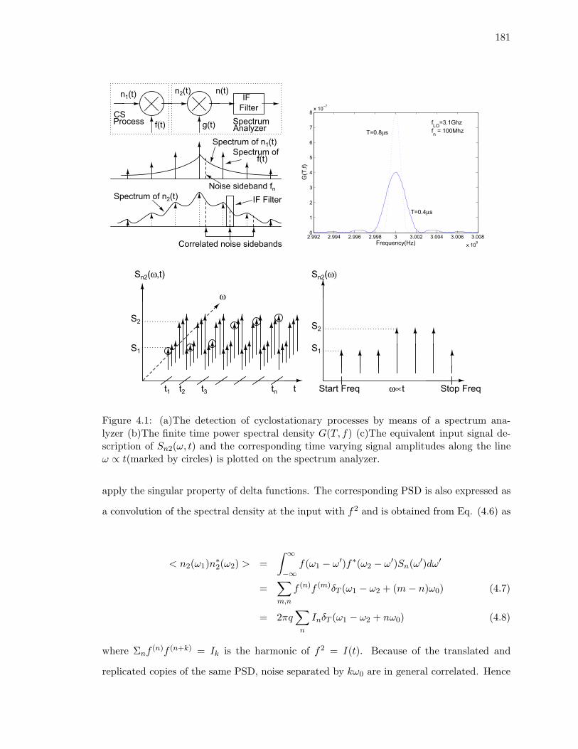
181
f(t) g(t)
n1(t) n2(t) n(t)IF
FilterSpectrumAnalyzer
CSProcess
Spectrum of n1(t)Spectrum of
f(t)
Noise sideband fnIF Filter
Correlated noise sidebands
Spectrum of n2(t)
2.992 2.994 2.996 2.998 3 3.002 3.004 3.006 3.008x 10⁹
0
1
2
3
4
5
6
7
8x 10⁻⁷
Frequency(Hz)
G(T
,f)
T=0.8μs
T=0.4μs
fLO=3.1Ghzfn = 100Mhz
t ω∝t
Sn2(ω)
S1
S2
Sn2(ω,t)
S1
S2
t1 t2 t3 tn Start Freq Stop Freq
ω
Figure 4.1: (a)The detection of cyclostationary processes by means of a spectrum ana-lyzer (b)The finite time power spectral density G(T, f) (c)The equivalent input signal de-scription of Sn2(ω, t) and the corresponding time varying signal amplitudes along the lineω ∝ t(marked by circles) is plotted on the spectrum analyzer.
apply the singular property of delta functions. The corresponding PSD is also expressed as
a convolution of the spectral density at the input with f2 and is obtained from Eq. (4.6) as
< n2(ω1)n∗2(ω2) > =
∫ ∞
−∞f(ω1 − ω′)f∗(ω2 − ω′)Sn(ω′)dω′
=∑m,n
f (n)f (m)δT (ω1 − ω2 + (m− n)ω0) (4.7)
= 2πq∑n
InδT (ω1 − ω2 + nω0) (4.8)
where Σnf (n)f (n+k) = Ik is the harmonic of f2 = I(t). Because of the translated and
replicated copies of the same PSD, noise separated by kω0 are in general correlated. Hence

182
for a general nonstationary process we have < n2(ω1)n∗2(ω2) >= qI(ω1 − ω2). For the case
of for ω1 = ω2 the time averaged PSD is
< n2(ω)2 >= qI(0) = qI(t) (4.9)
So in general,the spectrum can be written as the Fourier components of the time varying
PSD S(k)n (ω) where the k’th cyclic spectrum is the correlation between frequency compo-
nents separated by kω0 given by each term in the summation of Eq. (4.8) and the zero’th
order is the time averaged PSD given by Eq. (4.9). n2(t) undergoes the same periodic
modulation with the LO at the SA mixer stage to produce CS process n(t). The output
of mixer 2 has two cycle frequencies ω0 and ω1(where ω1 is the frequency of the periodic
LO signal of mixer 2) and if the ratio ω0/ω1 is a rational number, n(t) can be viewed with
cycle frequency equal to greatest common divisor of ω0 and ω1[73]. In fact, frequencies of
n(t) at ω + kω1 are ’folded’ onto ω as seen in Fig. (4.1a). Simply adding these noise powers
is incorrect since they are correlated which can be demonstrated as follows: Let there exist
a common frequency ω0 such that ω1 = nω0 and ω2 = mω0 such the ratio ω1/ω2 = n/m is
a rational number. In this case mω1 = nω2 and the harmonics of ω2 which are folded onto
ω are kmω1 which are themselves correlated from the previous mixing process. So when
we add the noise powers we must consider the cross terms also. On the other hand if the
ratio is not a rational number, there is no way we can shift ω1 and have it equal ω2. We
can then assume that n2(t) is stationary process input to the second mixer stage without
significant error. Another way to simplify the problem is to consider m or n to be large as
is the case of our signal and LO frequencies of the SA. If m→∞ and n is small and finite,
the harmonics created due to mixing in stage 2 are far apart from ω and its amplitude is
quite small to contribute to the power spectrum and hence only a minor error is incurred
by adding the correlated components. Similarly for n →∞, the same idea applies. Finally,
the time averaged PSD can be used to describe the noise process n(t) since the RBW filter
can be adjusted to have a bandwidth less than ω0/2 such that only the noise sideband ω
is selected and the correlated components as well the signal harmonic is suppressed(ie. the
output noise is stationary since any two frequencies ω′ and ω′′ will be uncorrelated). As
an example consider Fig.(4.1a), where we see that for a center frequency ω0 and bandpass

183
filter of bandwidth ω0 around ω0, we capture the stationary and second order cyclic spec-
tra component S(2)(ω) only. If the bandwidth is replaced with ω0/2, only one frequency
component is captured and the resulting process is stationary with no cyclic components.
The RBW filter has a Gaussian shape but if we can consider the ENB as a rectangular
bandpass with the above bandwidths, the SA displays the integrated spectrum within this
ENB as a single point on the display. Whether the integrated noise is calculated with or
without correlations, the output looks white in nature and is modulated by the slower noise
modulation factor F (ω, t). To illustrate this, consider the SA which displays a spectrum
with signal harmonics and correlated components S(ω) at time t1. This spectrum is later
updated at time t2 to display the value of F (ω, t2)S(ω). ie the switching process itself is
not captured by the SA. The alternative possibility is to keep the LO fixed(a span of say
1Hz around the desired frequency) and track the variations of this frequency with time but
it is much harder to do so.
Let us see a much simpler problem which will illustrate the modulation or translation
of frequency idea as well as the finite time integration of noise as against the convolution
idea presented before. Consider a WSS non-ergodic noise process
n2(t) =∑n
An(t) exp(j2πfnt) (4.10)
to be demodulated at the mixer stage. Here fn = n/T . The LO signal is g(t) = Ac cos(ωLOt)
where Ac is the amplitude of this carrier and the output is
n(t) = n2(t).g(t) = Ac
∑n
An exp(j2πfnt). cos(2πfLOt) (4.11)
The finite time Fourier transform of the noise spectrum n(t) is determined as
N(T, f) =Ac
2
∑n
An{sinc[(fLO + fn − f)T ] + sinc[(fLO − fn + f)T ]} (4.12)
We notice that the modulation has shifted the frequency fn − f by ±fLO.The power spec-
trum of the signal can be calculated based on the assumption that the different frequency
amplitudes are uncorrelated ie.< AnAm >= 0 and < A2n >= S(ωn)Δω. This leads to
G(T, f) =〈|N(T, f)|2〉
T=
A2cT
4
∑n
S(ωn)Δω{sinc[(fLO+fn−f)T ]+sinc[(fLO−fn+f)T ]}2
(4.13)

184
Note that the concept of finite time Fourier transforms can be used to define the role of the
RBW after the mixing stage. In other words, the RBW filter can be suitably selected to
have long integration times, to cause changes in the displayed spectrum and in this limit, the
spectrum is defined as G(∞, f) = ltT→∞<|N(T,f)|2>
T . If we take one of the sidebands as the
signal to be detected ie. the signal frequency to be detected- fsig = fn , the SA will display it
on screen only if it passes under the passband of the RBW centered at fIF = fLO−fsig. For
a particular signal frequency and time T, Eq.(4.13) is plotted in Fig.(4.1b). Note that the
SA sweeps the LO between the start and stop frequencies as specified in the span settings
which leads to time dependent local oscillator frequency fLO = fLO(t). Eq. (4.10) is a
simplification of the more general harmonic series representation(HSR) used to define a CS
process[74] with the associated definition
An(t) =
∫ ∞
−∞w(t− τ)x(τ) exp(−j2πfnτ)dτ (4.14)
where w(t − τ) = sin(π(t−τ)/T )π(t−τ) . We skip the details of the calculation which can be found
in Ref.[74], but the power spectrum is obtained by taking a 2D Fourier transform of the
autocorrelation function Rx,x(t, s) using Eq.(4.14) which leads to
Rx,x(t1, t2) =∑m,n
Rm,n(t1, t2) exp
(j2π(mt1 − nt2)
T
)(4.15)
The corresponding spectral density is
Sx,x(ω1, ω2) =∑m,n
Rm,n(f − m
T)δ
(ω1 − ω2 +
(m + n)
T
)(4.16)
where we have defined Rm,n(t1, t2) = 〈A∗m(t1)An(t2)〉. Our interest though is the frequency
domain representation of this HSR which divides x(t) into bands of width 1/T so that the
n’th component of An(t) exp(j2πnt/T ) is the output of an ideal one-sided bandpass filter
with input x(t) and transfer function which is the Fourier transform of w(t) as
W (t) =
⎧⎨⎩ 1,
∣∣f − pT
∣∣ ≤ 12T
0, otherwise(4.17)
Each term An(∗) is the centered version of the n’th component An(∗) exp(j2πp ∗ /T ) to
the frequency band [-1/2T,1/2T]. In essence the CS process is decomposed into a set of

185
jointly WSS bandlimited process ie. the terms {An} are jointly WSS if and only if x(t) is
CS[74]. This bandlimited-ness extends to the spectrum of our noise signal n(t) in Eq.(4.11)
at least for the case in which it is stationary. Looking back to Eq.(4.13) , we see that the
delta functions can be defined as the limit of a sequence of ordinary functions and one such
example[49] is δ(x) = ltT→∞ Tπ sinc2(Tx). This implies that in the limit of large T, the
delta function picks out an element of the spectral ’fence’ S(ωn) at f = fn − fLO as the
output spectrum(we set Ac = 2 to normalize the spectrum). We notice this in Fig.(4.1b)
ie. as we increase T, it moves towards a delta function. We have not discussed (besides
the qualitative description of Fig.4.1a) the output spectrum obtained when two mixing
steps are performed on a stationary input signal. There are two reasons for this: 1)The
SA displays a time averaged PSD and with appropriate filtering, a description of sideband
correlations is not required. 2)The mixer carrier frequency is usually much larger than the
signal modulation frequencies which is a filtering in disguise. So in the extreme case, we may
need to deal with only one mixing step which is the first stage in Fig.(4.1a). Alternatively,
we can state the problem in much simpler terms: The SA performs a Fourier transform
of the input cyclostationary signal and by our analysis this spectrum is modified by the
presence of the second mixer stage. In fact, in the presence of stationary input the output
spectrum after the second mixer stage is cyclostationary and based on sweep time settings,
we should see the time varying spectrum S(ω, t) displayed. But from our experiments with
the spectrum analyzer in the previous chapter, we notice that irrespective of sweep time
and bandwidth parameters, the spectrum is not time varying when the input is stationary
noise and this is because of the large(¿3Ghz) local oscillator modulation frequencies used.
The second issue is that we might opt to track one of the bandlimited spectral elements say
S(ω1, t) with time by tuning the LO to a certain frequency, but the RBW filter must be
set to 1Hz which would increase the ST drastically. So in general we select a span where
the LO sweeps from the start and stop frequencies and this way we are not plotting the
time varying nature of the PSD that we need, but rather S(ω) over some time. In other
words,each point displayed represents a frequency range and although we don’t think of time
when performing a spectral analysis, each point is displayed over a time interval. By using

186
the equivalence between time and frequency as well as the property that noise is primarily
white(both shot and subshot), we propose to use the sweeping of frequencies to plot the
time varying PSD at some frequency ω1 by the assumption that S(ω1, t) = S(ω = t) for
all ω. This in turn leads to an equivalent input signal representation for the SA which is
detailed as follows.
The SA does not perform an FFT, but rather uses the envelope detector to follow the
variations of the IF stage which in turn gives us the spectrum. For example when the LO is
tuned to one of the spectral components of the signal, the output of the IF stage is a steady
sine wave and the envelope detector output is a DC component which in turn controls the
deflection plates of the display and if we can envision noise as equal power sine waves for all
frequencies, the envelope detector will be flat across the frequency range. Without having to
describe the envelope detection stage(which is just another mixing and filtering process), we
can equivalently describe the entire detection process(including the RBW) with an FFT with
the help of windows and then use it to plot the time varying densities numerically.We see that
ST defines directly how much time is spent to perform a complete frequency measurement.
We can imagine this as equivalent to a FFT performed on a window of width ST is placed
over the input signal. Of course, there are obvious differences with the SA operations such as
1)LO can be tuned to start and stop at any frequency whereas FFT algorithm typically gives
us a set of frequencies over the sampling frequency [− fs
2 , fs
2 ]. 2)The windows select a subset
of the total signal samples which further restricts the frequency range. If a signal harmonic
is present then this is equivalent to multiplying the impulse with the Fourier transform of
the window which is a sinc function. Note that when we use an N point FFT where N is
greater than the size of the window say M, the remaining N-M points are filled with zeros.
Each bucket element can itself be considered as a window. The windows can be moved over
the signal in time(the short time Fourier transform) also known as the sliding window or we
can take non-overlapping windows. There is no great difference between the two, but the
SA processes the signal for a certain integrating time given by the time to put data into a
bucket and then it processes the next bucket. So non-overlapping window would be a more
exact description of the SA. But in the numerical methods used for generating macroscale

187
signals we cannot generate a large number of random number samples(approx 10ˆ5 samples
is generated in several minutes in MATLAB) to properly represent noise without issues of
periodicity and processing speed cropping up. These samples are then transmitted and in
such applications the sliding window idea is more applicable to obtain a running average
and running standard deviation. The implementation of the macroscale communicator can
be found in Appendix.B.
Note that the signal harmonics are still present in PSD , but they don’t show up in our
experiments as the modulation is performed below the lower cutoff frequency of the amplifier
bandpass filter. If the harmonics are present, the frequency ω of the noise floor inbetween
the harmonics should be selected. The simpler method is to consider a signal modulation
s(t) which is quite small(in mV range) which produces a shot noise current of 2qI(t) ≈ 2qI0
which leads to Sn(ω, t) ≈ Sn(ω). The time varying PSD due to noise modulation can be
written as S3(ω, t) = F (ω(I), t)Sn(ω).We adopt this method in our experiments. However
when S3(ω, t) is input to a filter with sufficiently long integration time, the resultant spectral
density is an average over the Fanofactor period S3(ω) = F (ω(I))Sn(ω) which leads to an
average supershot white spectrum which we have verified in experiments. Since this case
ignores the periodic statistical properties of the noise signals as well its timing information,
it is of little importance and will not be dealt with.
We now determine the minimum pulse width Tmin of S3(ω, t) that can be displayed on
the SA. We choose to define this factor as the smallest time required for two neighboring
’bucket’ elements to maintain the typical up-down motion of the spectrum for a modulated
shot noise process. In order to realistically use the SA as a decoder, we may need to consider
a value which atleast 10 times this minimum which will be seen in the experiments to follow.
The IF filters(which are typically four pole synchronous tuned filters) must need time to
charge and discharge and if the mixing product is swept past too fast there will be a shift in
both amplitude and frequency accuracy. Note that the amplitude inaccuracy is not really
important for noise type signals, and the SA can be run in manual mode with uncalibrated
settings ie.we can set RBW and sweep time(ST) settings independently. We however run
the SA in AUTO mode for which the three parameters RBW,ST and VBW are coupled so

188
that we can make use of the following calculations.The time that the mixing terms stay in
the passband is proportional to RBW and inversely proportional to the ST according to
[52]
dtRB =RBW
SP/ST(4.18)
If we assume that the passband is Gaussian given by H(f) = exp(−π (f−f0)2
σ2 ) where
f is the frequency relative to the center f0 and σ is the variance. The RBW is typically
defined as the 3dB bandwidth of H(f) which we can use to obtain a relation for σ. At
f − f0 = RBW/2, the value of the H(f) = 0.5. This leads to σ = 1.06RBW . Note that
the corresponding time domain response is also Gaussian given by h(t) = σ exp(−πσ2t2).
At t=0, we see that h(t) = σ which is the maximum amplitude that h(t) can assume. We
are interested in the time taken to charge and discharge this Gaussian filter ie. time to rise
from 1/100 of its maximum value (ie. σ) to the maximum and back. When h(t) = 0.01σ,we
have 0.01σ = σ exp(−πσ2t20.01). This gives 2t0.01 = 2.42/σ = 2.3/RBW . HP specifies a
value of 2.5 instead since the IF filters used in practice are not ideally Gaussian. Here 2t0.01
is nothing but the amount of time a signal spends in the passband of the filter that is dtRB
in Eq.(4.18) from which we can obtain a relation from sweep time(ST) according to
ST =2.5 ∗ SP
(RBW )2(4.19)
The time spent in the IF stage in Eq.(4.18) can itself be taken as Tmin,provided that there
is no following stages in the SA. Since we display the data in the SA display over a finite
number of points(buckets), we are further restricted over both time and frequency. The
data from the IF stage is placed into these buckets and a sample is taken from each bucket
to be displayed. Each bucket contains a sample corresponding to a frequency and time
interval determined by the following equations
Δf =SP
N − 1, Δt =
ST
N − 1(4.20)
which leads to Δt being the fundamental limit for the minimum pulse width in our receiver.
We can obtain greater accuracy by either increasing the span or decreasing the sweep time,
since more number of samples are taken in either case.To illustrate the role of buckets
and Eq.(4.20) consider the following case of RBW < Δf : For a span of 100Mhz and 100

189
0 1 2 3 4 5 6 7 8 9 10
x 105
0
0.05
0.1
0.15
Span(Hz)
Min
imum
noi
se p
ulse
wid
th(s
) (235,10,3)(1000,10,1)
(1000,30,3)
(1000,30,1)=(1000,10,3)
(1000,10,10)
(1000,30,10)
(x,y,z) wherex = No of samplesy = RBW in Khzz = VBW in Hz
Figure 4.2: Minimum noise pulse width Tmin as a function of span .The fixed parametersare resolution bandwidth(RBW), video bandwidth(VBW) and number of samples N.
datapoints to be displayed on screen each element corresponds to a point over 1Mhz span.
Sample detection algorithm would obtain the center point in this span. Eg: A 10.5Mhz sine
signal would be properly displayed in the span of 10-11Mhz. If the mixing product does not
happen to be at the center of the IF when the sample is taken it will not displayed. This
issue does not matter in the case of noise.
If we can somehow use the all the data within a bucket in the averaging mode of the SA,
instead of a single point we may be able to reduce the fluctuations in the spectrum. Instead
each point in the bucket equals the input noise integrated over the effective noise bandwidth
and is the same even for the case of RBW > Δf . In order to catch the noise modulations,
we need to mindful of the following: 1)A large RBW allows faster modulation speeds but
also raises the DANL of the SA which makes detection of subshot noise difficult. 2) Span
also affects sweep time and if increasing RBW does not follow the noise modulations, span
can be reduced as an alternative but we loose some accuracy which is not of great concern.
3)If we cannot follow the noise modulations by adjusting the above parameters, the SA
produces an integrated spectrum of both shot and subshot spectras and in such cases we
reduce the modulation speeds. Most our experiments are restricted to less than 50Hz due to
this fact but if we use DSP processors instead we can perform several FFTs over a window

190
and average the signal very fast which in turn will allow faster modulation speeds. Further
work using Analog Devices DSP chip is in progress at Nanolab group at Rutgers, with time
based decoding methods akin to the classical stochastic modulator in Appendix.B already
implemented.
We rely on the analog low pass filter video bandwidth filter after the envelope detector
stage which performs a realtime filtering(time moving average) of the fast moving amplitudes
during the sweep. The VBW filter becomes active only when the cutoff of the filter is smaller
than the RBW and the ST also increases inversely with the VBW. If we assume that the
VBW filter is another Gaussian, the time taken to charge and discharge is the same as the
RBW filter and is given 2t0.01 = 2.5/V BW . This is now the same as Eq.(4.18) which
allows us to obtain an expression for the sweep time as
ST =2.5 ∗ SP
RBW ∗ V BW(4.21)
We have plotted Tmin versus the only freely controllable parameter which is the span or
the start and stop frequencies in Fig.(4.2). The RBW or VBW take fixed values and
rise progressively in 1,3,10 factors. The case V BW > RBW has not been shown as no
experiments use this setting, but it has the lowest Tmin possible for a certain RBW setting.
The traces are instantly swept, but with no averaging we cannot distinguish the relative
squeezing levels. Each of the lines are linear, and we see that for a certain decreasing the
number of samples N or increasing the VBW causes Tmin to become larger. As we decrease
either RBW or VBW and increase SP, the ST increases which affects the number of cycles
of noise modulation displayed on screen. For example, if at a sweep time of 10secs, four
cycles were displayed, cutting it to 5 secs would halve the number of cycles on screen. Since
as we mentioned that VBW and RBW are rather fixed parameters, the SP may be taken
as the time base control quite similar to the oscilloscope.
Fig.(4.3a) shows the case of shot noise modulation. The experiment was performed by
connecting a function generator to a tungsten filament lamp and feeding a square wave
of amplitude 760mV with an offset of 7.3V. The lamp was modulated at a frequency of
100mHz. The lamp could be modulated to a maximum frequency of only 10Hz beyond which
it would produce a constant intensity. As we showed in the previous chapter, irrespective

191
Figure 4.3: (a)Shot Noise Modulation experiment describing the time varying optical spec-tra S1(ω, t) = F.Sn(ω, t) where F=1 always (b)Shot and subshot spectra obtained with anRBW = 10Khz but with low averaging of V BW = 30Hz. The solid dark lines indicatethe negative exponential smoothing filter.
of having a noisy supply such as the function generator in this case, the light from the
lamp is still shot noise limited. The dc photovoltages for the two shot noise levels were at
3.01V and 5.74V. We see in the figure that the shot noise levels during modulation agree
with the calibrated shot noise levels over the entire frequency range of 100kHz-1Mhz. The
square wave of 100mHz corresponds a pulse ON time of 5secs. Considering the following
parameters used:span=900Khz ,the VBW=3Hz ,the RBW=10Khz,N=1000, we can find
Tmin from Fig.(4.2) to be 0.075secs which also implies that the maximum frequency of the
square wave should be around 6Hz in order to see the modulation. Otherwise the signal
would be averaged and a net noise would be displayed along the Fourier transform of the
switching waveform and any transients. From the plot, we see that the duration the pulse
is ON corresponds to a frequency interval of Δf = 65Khz. This corresponds to N1=72

192
sample points from which we can obtain the total ON time in the SA as Tmin ∗ N1 =
0.075 ∗ 72 = 5.4secs which is quite close to 5secs. In fact we have overestimated Δf which
could be the source of error. Note that the difference between the two levels is around 1.7dB
would allows us to clearly distinguish between the two levels as well as the pulse duration.
When the difference becomes smaller(for example ¡1dB as was was seen in some squeezing
experiments) both pulse width and resolution of levels become harder. We also point out
this time varying spectra is an example of S1(ω, t) of Eq.(4.3) where F (ω(I), t) = 1. In
Fig.(4.3b) we see a squeezing experiment carried under a higher VBW of 30Hz. With
such low averaging, we cannot distinguish between the levels, and observing the switching
becomes less reliable. This is typical in most communication systems where the the SNR is
so small that the probability distributions between the two levels overlap causing false bit
triggers. We have also shown the effects of smoothing filter applied to the raw data whereby
we can ¿0.4dB of squeezing. So in order to carry reliable modulation experiments, VBW
should be set to less than 10Hz. Changing the RBW did not seem to make much difference
as it is the averaging in question. Reducing VBW as we have seen, increases sweep time
and Tmin and restricts the modulation frequencies. In Fig.(4.3c), we see the case where the
signal is modulated at a large frequency wherein the spectrum analyzer produces a Fourier
transform of the square pulse.
4.3 Design of Quantum Stochastic Modulator
Using the same methodology as the macroscopic(classical) communicator , we would like
to switch between two quantum noise signals. The simplest way to do this is to switch
between two sources: one calibrated at the quantum noise limit(shot noise level) and another
at the sub-shot level. We can imagine focusing these two sources onto the detector and
switching between them through a switch element which could be either a BJT or a FET
device. The switch element in turn should not affect the statistics of the emitted light
drastically(ie. it could easily raise the noise level above the SNL) and therefore we must
know the noise properties of these devices beforehand. In the inset of Fig.(4.4) we show one
such implementation idea. The data acquisition(DAQ) module from National instruments

193
can serve as a function generator to provide ac modulation to the sources modulating the
average. The two output lines of the DAQ, analog outputs(AO) 0 and 1 are connected
to the LED and lamp respectively which are in turn focused onto the photodetector. The
AO lines can both be calibrated such that the lamp and LED can both be set at the
same photovoltage and we can switch between the AO lines selecting either the LED or
the lamp for the noise modulation. There are three issues why this simple scheme did not
work 1)The lamp draws current in excess of 300mA or a voltage of 2.5-3V. The DAQ card
was able to produce voltage from 0-10V but not the amperage required. 2)In Fig.(4.4) we
show the optical spectra of an L2656 LED driven the NI-DAQ card with a high impedance
10k. Even though such a resistance is sufficient to reduce the power supply noise in most
cases, we see that at frequencies from 100-550kHz the noise levels exceed the SNL from the
lamp by atleast 0.4dB and there are undesired harmonics. At frequencies above 600kHz
squeezing disappears as is seen with the case of the the power supply driving the LED
through the same resistance. These two issues itself make the DAQ card inappropriate for
this experiment and we have to look for other design choices.3)Notice that the LED and
lamp are to focused onto the same detector. Since the LED needs to be maintained in a
face coupled configuration covering the detector, it would make it harder to focus the lamp
for it to establish the same photovoltages as per the LED. This may be a simple mechanical
constraint but we could not find a solution at the time.
We next tried using discrete electronic components directly driving a single LED.Even
though we used many design choices(most of them by trial and error), we were restricted
to a few that worked which will be described here. The central premise of subshot noise
measurement is that the intensity fluctuations in the emitted light is a direct probe of the
statistical fluctuations in the electron-hole recombination rate which in turn requires a high
impedance suppression mechanism or pump noise suppression. Connecting a switch to the
LED modifies the pump noise suppression mechanism and can be seen(or solved) in two
ways:
1.By finding the spectral density of voltage or current fluctuations of the complete
equivalent noise model which includes the switching element and the LED together and

194
Figure 4.4: Comparison of optical spectra with LED driven with DAQ,shot and sub-shotnoise sources.The inset shows a simple switching design using NI DAQ
2.Define an equivalent net impedance while looking back from the LED. If this impedance
is greater than the differential resistance of the LED we will have satisfied the constraints
of high impedance suppression. But this method(to us) is not theoretically sound, but has
worked for most of the configurations used.
Note that the switch simply replaces the manual SPST switch which we used in the
previous chapter and in order to design a successful modulator we have used the following
prescription: a)Does the introduction of the switch allow us to generate a calibrated SSL and
SNL level individually? If yes then b)Use this switch to construct a circuit, to modulate
between these two sources c)Add the ac signal modulation as a separate channel taking
care that it does not affect the statistics or adds switching noise. There are 3 methods of
directly controlling the noise level using a single LED,all of which we have experimentally
demonstrated in chapter 3:
1.Optical Switching: Controlling the efficiency is a simple way to switch between SNL
and SSL, and can be carried out by using acousto-optic modulation(AO-cell) or by using OD
filters with variable attenuation inserted in an optical chopper. An even simpler mechanical
way is to mount the LED on a movable base, and by moving it close and further away we
could control η0. The main disadvantage with these methods is that efficiency is already
very small in most experiments, and trying to calibrate the setup to produce SSL with

195
additional optical elements in between the LED and PD would surely introduce partition
noise and would produce SNL instead. At the present stage, it is not even possible to
couple the light into a fiber unless we have much larger squeezing, and optoelectronic LED-
PD-LED repeaters will have to be used over very small distances to recreate the quantum
states.
2.Capacitive Switching: We had already established the difference between constant
voltage and constant current. We then tried the configuration where the transistor was
connected to the capacitor. By switching it on, the current would flow through the capacitor,
forming the Constant voltage(CV) case which would raise it to the shot noise level. When
the transistor was off, the high impedance formed would establish the Constant current case
required for subshot operation.
3.Direct Modulation: In this method, a BJT or a MOSFET can be used to switch an
LED between SNL and SSL cases. This method does away with some of the problems
with capacitive switching such as slow modulation speeds, but we need to know the noise
mechanisms of the switch itself which influences the photon noise of the LED. We shall now
focus on capacitive switching and direct modulation schemes in greater detail.
4.3.1 Capacitive Switching
The capacitive switching principle is shown in the circuit diagram of Fig.(4.5a). The switch
which could be a transistor or a MOSFET connects or disconnects the capacitor from the
circuit. This in turn modulates the optical spectra between the shot level when the capacitor
is inserted and the subshot levels when it is removed. At the same time, a signal source
such as a function generator with an offset can be connected through RS to the LED in
order to perform the ac modulation. In order to establish shot noise levels, the capacitors
should be quite large(around 1mF-10uF). But with the introduction of these large capacitors
and the presence of R = rd + rs (where rs is the internal diode series resistance and rd
is the differential resistance) introduces a RC low pass filter into the problem and 3dB
frequency is drastically reduced from the original modulation frequency.For example with
a diode capacitance of C = 100nF , and R=5ohms, the 3db point is fc = 12πRC = 318Khz.

196
+− L2656
RS=1 K
C=1mF
Switch
9V
10VVS
VSW
Figure 4.5: (a)Design of a capacitive switching circuit (b)Switching waveforms for MOSFETand AC switching (c)Optical spectra of true subshot noise compared with subshot spectraobtained by using a Capacitor with 5Ω in series
When we introduce a capacitor of 1mF parallel to the diode, the internal capacitance can
be neglected and the 3dB cutoff frequency is now 31.8Hz. Note that the extrinsic time
constant RC which determines the ac bandwidth is slightly different from the internal
diode thermionic emission time constant RdC or the recombination lifetime both of which
determine the squeezing bandwidth. If the diode series resistance is negligible, then the ac
modulation is governed by rd(Cdep + Cdiff ) ≈ rdCdiff which is approximately the radiative
lifetime in moderate diffusion regime. The radiative lifetime predominantly depends on
the doping levels and under these conditions both ac and noise modulation bandwidths
may coincide. Let us now describe the switching processes taking place for a transient
analysis perspective. Two square wave generators VSW and VS are applied to the switch
and the LED independently with the assumption that the duration of the on time of the

197
switchTon,SW is much larger than the time period of the square wave modulation to the
LED. This establishes our requirement that the frequency of noise modulation is much
smaller than the ac modulation.
Let us assume for the time being that VS produces a steady dc voltage of 10V. When
the switch is off, the voltage across the capacitor VC is zero and the LED has a voltage
V0 = 1.245V across it. When the switch is first turned on, a voltage across the capacitor has
to be developed which can be written as VC(t) = VLED(1 − e−t/RC). This effect is seen in
the numerical simulation performed in Fig.(4.5b) where at time t=1secs when the switch is
turned on, voltage across the LED is first pulled to zero followed by the exponential increase
to VLED again. When the switch is turned off at t=3secs, the voltage does not discharge
but remains pinned to VLED. In Fig.(4.5b),we show the case when VS is modulated between
9 and 10volts when the switch is on. The voltage across the capacitor can be written as
VC(t) = VI + (VF − VI)(1 − e−t/RC) (4.22)
. where VI is the voltage across the LED at time t=0 corresponding to VS = 9V and VF = V0
is the final voltage which corresponds to VS = 10. We can easily test the validity of Eq.(4.22)
with the numerical results. For the case of TON,S = 0.1s, we see that VF = 1.245V and
VI = 1.236V . At t = τ , we can obtain VC(t) = 1.247s. This corresponds to t=7.947ms. Now
we can estimate the RC time constant as τ = RC = t
ln
�1
1−(VC (t)−V)/VF−V0)
� . Substituting the
values with C = 1mF , we find R=8.16Ω. This agrees exactly with the sum of rs = 1.88Ω
and rd = 6.28Ω. We also point out that this method is very useful to experimentally
determine the value of the series resistance, from the dc characteristics alone. As RC
product decreases when the capacitor is removed, the rise time increases and the LED
follows the square wave shape of the supply VS . So as we alternate between shot and
subshot modulation, we switch between two ac modulation bandwidths where only the
slowest of signal frequencies are allowed to pass during the shot noise period of duration
TON,SW . This also causes another issue which can be seen the dashed curves of Fig.(4.5b),
where the faster modulation frequencies have smaller peak-peak swings since the capacitor
is not allowed to fully charge and discharge.

198
Fig.(4.5c) shows the noise spectra for the L9337 LED with the upper plot indicat-
ing (a)capacitor in parallel with a small resistance in series and the lower plot indicating
(b)When the switch is opened producing a subshot level. For the switching element,we first
tried to use a Cadmium sulphide light dependent resistor since it has a large impedance
when no light shines on it. Shining light on the LDR decreases the resistance but it was
still large enough that high impedance pump suppression eliminated all signs of squeezing.
We replaced the LDR with various resistors and found that even a 5ohm resistor produced
subshot levels which we observe in Fig.(4.5c) to be quite close to the true subshot level
obtained without the capacitor. Unless we could establish a nearly 0 resistance, it is very
hard to produce shot noise levels using the capacitive method. Using a capacitor establishes
an approximate constant voltage condition and since the L9337 is a heterojunction device
based on the thermionic emission model, it is quite possible to observe squeezing under con-
stant voltage conditions. If we measure the relative difference between the two smoothed
curves, we find a result of 0.25dB at around 290kHz .Considering that the L9337 is capable
of 1-1.5dB squeezing, this clearly shows that the upper plot is not at the true shot noise
level. Most switches introduce some finite resistance, but we found the IRF510 to work well
because of its low on resistance(approx 0.5ohms). The 2N2222 BJT and 4066 switch were
also tried with small success since these elements introduced large resistances. Because of
insufficient squeezing,slow ac modulations and sudden bandwidth changes between shot and
subshot pulse durations, we were forced to look for an alternate design.
4.3.2 Direct Modulation with BJT
Switching mechanism of the transistor: The transistor is operated as a switch with the
LED as a collector load. The low voltage Vi ≈ 0.7V is sufficient to cause the BJT to be in
the cutoff region with a negligible base current according to the equation iB = Vi−VBERB
.The
LED is off since collector current ic = 0.For an input voltage Vi > 0.7V it is sufficient to
place the BJT in linear active or saturation region where ic ≤ βib. As the BE junction
is forward biased the collector current can be obtained using KVL around CE circuit as
ic = VCC−VLED−VCERC
. Hence we can operate the BJT in the cutoff region for Vi < VBE

199
and linear active region VBE < Vi < VBE + RBVCC−VLED−VCE,sat
βRCand saturation regions
according to Vi ≥ VBE + RBVCC−VLED−VCE,sat
βRCwhere in the saturation region we have
VCE,sat ≈ VBE2 . Another option is to use the LED as an emitter load. The goal is not to
simply turn the LED on and off but to switch between the two quantum states ie. SNL
and SSL. In order to do so, the collector or emitter current shot noise should be suppressed
and should be able to assume a range of drive Fanofactors from 0 to 1. Another issue we
wish to sidestep is the modulation aspects of noise in BJTs. This is within the realm of
small signal large signal (SSLS) analysis and is still an open topic of research. As before
we assume that the signal period is sufficiently long that noise characteristics during the
transient periods such as on time,off time and storage time are unimportant.
+−
+−
L2656-CE Mode
Emitter Follower
ish
9V
9V
RB=1k
1k
SW1
SW2
C
Figure 4.6: (a)Circuit Diagrams for transistor in open circuit base/closed base setups in CE
and CC configurations (b)Load line of L2656 with numerical Ic − Vce characteristics of the
2N2222 transistor
SIE(ω) = 4qIE(
GE(ω)
GE(0)− 1/2) ≈ 2qIE , SIC
(ω) = 2qIC (4.23)
where GE(ω) is the conductance of the emitter base junction and at low frequencies,
GE ≈ GE(0) which leads to the forward biased emitter current showing full shot noise
whereas the reverse biased collector current features full shot noise at all frequencies. The
correlation between the emitter and collector terminal fluctuations ΓCE can be obtained

200
from the cross-correlation spectral densities SCE [16] as
SCE(ω) = −2qICαSGE
α0SGE0(4.24)
ΓCE =SCE(ω)
[SIC(ω)SIE
(ω)]1/2≈ −√α0 (4.25)
In most modern transistors(at least in the linear active region) the common-base current
gain α0 → 1 over much of the frequency range. This implies that the collector and emitter
current fluctuations are negatively correlated ie. An electron increase in the collector current
is due to an electron decrease in the emitter current. In fact the base can be modeled as a
linear beam splitter and we shall do so in the following analysis. From Eq.(4.23) it would
seem reasonable that the small signal equivalent noise model of the BJT should include two
current noise generators iesn from the emitter to base and icsn from collector to base. Notice
that even though the collector features full shot noise at all frequencies, icsn is correlated
with the emitter current and so it should not be included. But when α0 → 0 as β → 0 the
transistor is placed in deep saturation but Eq.(4.23) is still valid. It would seem then the
collector current noise generator icsn would have to be included. Also in order to prevent
clipping and distortion when the BJT is used as an amplifier, the small signal models(eg. the
hybrid-π model) are themselves only valid in the linear active region[75] or more precisely
the linear region between cutoff and saturation in the voltage transfer characteristics.We
shall revisit these issues later but first let us obtain the Fanofactors of the collector current
in the linear active region.
FanoFactors for the hybrid-π,Van-Der Ziel T model and the Grey-Meyer model
We would like to obtain the output noise current fluctuations or the Fanofactor of the
common emitter configurations (as the common collector or common base configurations can
be obtained from simple rearranging of the CE circuit model). Typically this is done by using
the superposition theorem by finding the square of the output noise current due to each noise
source present in the small signal equivalent model and adding them up. The goal in this
section is to show the hybrid-π model of Fig.(4.7a) which includes a hypothetical collector

201
shot noise current always(not shown in figure) and the amplification of the base terminal
shot noise is flawed in analyzing the output noise current and it is infact the T model of
Van-derZiel in Fig.(4.7b) which includes a fraction of the base-emitter shot noise and an
additive partition noise component which is valid. In fact the above assertion has already
been claimed and proved experimentally by Edwards[1] by advocating the T model, but we
shall do the same theoretically. Before we start. let us state some assumptions: Since we
are interested in lifetimes smaller than the transit time across the base as well as thermionic
emission lifetime(ie. the base emitter junction follows the same junction dynamics of the pn
diode) we ignore the parameters associated with the base width modulation effect Cμ and
feedback resistance rμ on the basis that they appear in high frequency models. Losing these
feedback elements limits the application of the equivalent circuit to frequencies less than
fβ = fT√β
where fβ is the frequency at which the magnitude of the frequency dependent
gain |β(jω)| reduces by 3dB from its dc value and fT is the transition frequency where
|β(jω)| = 1and is a measure of the maximum useful frequency for the transistor to be used
as an amplifier. The output resistance r0 = VAIC
for an Early Voltage of around 100V and
collector current of 1mA is is quite large at 100kΩ and so its effect can also be neglected
in calculating the output voltage spectral density when the load resistance is smaller. We
can also neglect its effect when obtaining the collector current which changes with vce as
follows ic = βIb + vCEr0
≈ βib. These assumptions are incorporated into the hybrid-π and
the T-models in Fig.(4.7). First let us compare the output noise currents of the two models
and the junction voltage fluctuation obtained for the π model using nodal analysis at the
node B’ is
vjn =ibsn − ith
1rπ
+ 1RS+rb
+ sCπ(4.26)
where ith is the thermal noise current flowing into the base, rb is the ohmic resistance
of the lightly doped base region between the external base contact and the active base
region,Rs is the source resistance(not shown in Fig.(4.7a)) but can be accommodated in rb
as an overall resistance looking backwards from the base terminal) , ibsn is the base shot
noise current and rπ is the base emitter dynamic resistance and Cπ = Cb + Cje is the sum
of the base charging capacitance and emitter-base depletion layer capacitance. Applying

202
high impedance pump suppression ie. Rs + rb � rd, the emitter is short circuited and the
base is open circuited which leads to ith → 0. This leads to
vjn =ibsn
1rπ
+ sCπ=
ibsnrπ
1 + sCπrπ(4.27)
The noise current flowing across the dynamic resistance rπ is obtained by first converting
the Norton equivalent of ibsn − rπ to the Thevenin equivalent vbsn − rπ and then obtaining
the noise current that flows through rπ.
ib =vbsn − vjn
rπ=
ibsnsCπrπ
1 + sCπrπ(4.28)
If we make the following πto T model transformation rπ = (β + 1)re and 1 − α = 11+β
the collector current obtained is
ic = βib =βibsnsCπre
(1− α) + sCπre(4.29)
The output noise current obtained using the π-model when compared with Van Der-
Ziel T noise model under the same open base-grounded emitter configuration(which will
be determined later) as far as the collector shot noise is concerned(ie. partition noise is
neglected for the time) is given by
ic = αie =αiesnsCπre
(1− α) + sCπre(4.30)
The above expression is also known as open base-shorted emitter configuration as the
base terminal has a high impedance in series with it and the emitter is grounded. In order
for the Eqs.(4.29 and 4.30) to yield the same result we requireαiesn = βibsn or rather by
squaring both sides it shows that the two models are equivalent only we have the following
equality α = β which is clearly incorrect. This shows that the hybrid-π model and the T
model are not equivalent to each other unless the we doubt transformation of rπ = kTqIB
to
re = kTqIE
or we redefine the base shot noise current as ibsn → 1√1+β
ibsn. Finally we would
like to state the Grey and Meyer (GM) result[75] where the collector terminal is always set
at the full shot noise level and the base current noise is calculated incorrectly as
ib =ZRS
Z + RSibsn ≈ ibsnrπ
1 + sCπrπ(4.31)

203
where Z = rπ// 1sCπ
.The above expression employs the same hybrid-π model of Fig.(4.7a)
in order to obtain the result, but it deviates from Eq.(4.28) which we obtained using nodal
analysis. This is because the base-emitter shot noise was not associated only with the
differential resistance but with the net impedance Z. This model in addition includes a full
shot noise current at the collector terminal and hence the total noise as predicted by the
GM model is given as
ic =βibsn
1 + sCπrπ+ icsn (4.32)
The GM model suggests that the collector current noise must be at least equal to the
full shot noise whereas the hybrid-π and the T model indicate otherwise. Also the hybrid-
π model and T model show that the collector shot noise can be suppressed under high
impedance conditions and tend to the full shot noise level at large frequencies for the T model
and approximately β times the full shot noise for the hybrid-π model. In order to choose
the correct model, it must hold up to the scrutiny of current noise under constant voltage
conditions. Most textbooks indicate[75] that the base current noise in the hybrid-π model
consists of charges crossing from the base to emitter(IEn), a recombination current in the
base(Irec) and charges crossing from base to collector(ICn ) and is known as the macroscopic
description of base shot noise which claims that all these elements are individual random
processes leading to a sum shot noise process which is 2q(IEn + Irec + ICn). The exact
microscopic formulation however is quite different and shows us that the two processes,
generation-recombination and diffusion noise in the base leads to shot noise in both the
emitter and collector terminals according to Eq.(4.23) and the base terminal noise must be
composed of those elements . Taking the Fourier transform of the terminal base current
IB = IE− IC and finding its spectral density < I∗B(ω)IB(ω) >= SIBby using Eq.(4.23) and
Eq.(4.24) we have
SIB= SIe + SIC
+ 2Re(SCE(ω)) = 2qIC(1
β+
2GE − (αsYE + α∗sY ∗E)
α0sGE0− 2
(1− α0s)
α0s) (4.33)
At low frequencies the base current spectral density is approximately 2qIC/β . These
expressions are valid only under constant voltage conditions ie. the junction voltage is
pinned and the corresponding fluctuations in the minority carrier densities at the boundaries
of the base are fixed(no noise) which is p(0) = p(WB) = 0. So it would be reasonable that

204
the πmodel should reproduce the results of Eq.(4.23) at the collector terminal and 2qIB at
the base terminal under constant voltage conditions for the model to be valid. The base-
emitter circuit at low frequencies where the capacitor offers infinite impedance leads to the
following base current (which can be extracted into the external base circuit)
< i2b >=< v2
bsn > + < v2b >
(rπ + rb)2≈ 2qIB (4.34)
The assumption made in Eq.(4.34) in arriving at 2qIB is that rb is quite small(which
is not altogether true as it has values from 50-200Ω and is a function of current at high
injection levels). If we proceed with this, the collector terminal should read i2c = β2qIC
which is as we have stated earlier and violates Eq.(4.23) whereas the base terminal is
correctly determined as per the constant voltage conditions. Next we check the T model
and under constant voltage conditions. This can be seen from Fig.(4.7b) where the emitter
and base are grounded. Assuming rc, rb are not present and at low frequency Cπ offers a
high impedance, the internal shot noise source ie = iesn can be extracted into the external
circuit validating Eq.(4.23). The collector current obtained neglecting the partition noise
component since α ≈ 1 in linear active region leads to ic = αie ≈ iesn validating the collector
current noise spectral density of Eq.(4.23) . Thus the T model is the correct choice.
The following numerical plots are obtained using the parameters obtained from the
2N2222A datasheet[76] which was used to define the BJT model in Spice in order to obtain
the small signal quantities for the linear-active and saturation regions using the modified
Gummel-Poon model. From the IC − VBE curve of the datasheet, we obtain VBE = 0.7V
at IC = 20mA and choosing an ideality factor of η = 1, and using the formula IC =
IS [exp(VBE/ηkT ) − 1]the saturation current is IS = .33fA. The DC gain βdc(hFE in the
datasheet) is specified at 150mA to be from a minimum of 100 to a maximum of 300. We
take the geometrical mean of 173. The gain is a widely fluctuating parameter even among
various transistor samples.The emitter-base depletion capacitance is specified as Cje = 25pF
at a reverse bias of VEB = 0.5V . The zero bias capacitance can be obtained simply using
Cje0 = Cje(1 + VEBψ0E
)1/3 to be 30pF with a built in potential ψ0E = 0.75V . Similarly the
zero bias collector base capacitance is obtained to be Cμ0 = 19.4pF using the data that
Cμ = 8pF at VCB = 10V and ψ0C = 0.75V . The output resistance r0 at VCE = 10V

205
rπ
rbvb
ibsn Cπic r0
r0ic ipCπ
rb
vb
reiesn
E
B B’ C
C
B’
B
E
(a)Hybrid-π Model
(b)T Model
Figure 4.7: (a) Grey and Meyer hybrid-π Bipolar transistor model (b)Van-derZiel-ChenetteT bipolar transistor model
and IC = 10m,A is 8.3 ∗ 103Ω which gives an early voltage of VA = r0IC = 83.3V . The
most important parameter is perhaps the transit time across the base region which can
be obtained from the transition frequency which is fT = 300Mhz or τT = 530.5ps at
IC = 20mA and VCE = 20V . The transition time is related to the base transit time τF as
τT = τF + 1gm
(Cje + Cμ). We can find the corresponding Cje = 25pF and Cμ = 6.5pF at
VEB = 0.7V and VCB = 19.3V which in turn gives τF = 489.8ps. The total capacitance
is Cπ = Cje + Cb where Cb = gmτF is the base charging capacitance.The reverse transit
time is taken as approximately τR = 10τF = 4.9ns. The rest of the parameters which
determine second order effects such as high injection current,base width modulation,contact
resistances,etc use the conventional model parameters(from the library EVAL.LIB) present
in SPICE.
T model with partition noise
Edwards[1] has claimed that both the base shot noise and the collector shot noise are
unphysical quantities associated with and we have proven so in the previous section. Now
we shall use the circuit diagram of Fig.(4.7b) which illustrates the Van Der Ziel-Chenette

206
1 2 3 4 5 6 7 8 9 10
x 106
0.1
0.2
0.3
0.4
0.5
0.6
0.7
0.8
0.9
1
Frequency(Hz)
Fano
fact
or F
F/β − Hybrid−πmodel withcorrection
F of T−Model
F/β of GMmodel
IC=1mA
β=173Cje=40pFτF=489ps
Figure 4.8: (a)Electrical Fanofactors of grounded base-open emitter Power BJT from[1](b)Comparison of Fanofactors for the hybrid-π, T and GM Models
model[77] obtained by adding an emf eesn in series with the emitter or iesn in parallel as
we have done and a current generator ip in parallel with the collector. The generator iesn
and ip are generally correlated which can be shown to be a byproduct of the partition noise
mechanism due to the iesn − ic correlation of Eq.(4.24). The total collector current noise is
i2c = α2i2e + i2p.The partition noise current in the T model at low frequencies is written as??
i2p = 2eIE(αdc(1− αdc) + (α0 − αdc)2) ≈ 2e(1 − αdc)IC (4.35)
where the last equality in Eq.(4.35) is due to the fact that (α0 − αdc) � 1 and can be
neglected.Typically transistors have α0, αdc ≈ 1 which removes this partition noise compo-
nent. From Eq.(4.35) , the collector shot noise may be thought of as the output of a beam
splitter with efficiency α ≤ 1 where the input is the emitter current and the partitioning
process is the loss of carriers due to transit in the base We can informally arrive at expres-
sions for icand ip by using the Bernoulli selection process on a Poisson statistics[19] . The
collector particle number variance is given as
Δm2 = α2Δn2 + α(1 − α)n (4.36)
Here Δn2 is the variance in particle number of the emitter current and n is the average.
Multiplying by e2and dividing by the observation time scaleΔt2(not uncertainty) we obtain
e2Δm2
Δt2= α2 e2Δn2
Δt2+ α(1 − α)
e2n
Δt2

207
2eicB = α22eieB + α(1 − α)2eieB (4.37)
Using the relations enΔt = ie and the fact that the collector and emitter are shot noise
limited currents ie. Δm2 = m,Δn2 = n and the observation time is the reciprocal of twice
the bandwidth-B we have obtained Eq.(4.37) from which we can infer Eq. (4.35). Now we
shall calculate the collector terminal Fanofactor for 3 possible configurations of the T model
obtained by either opening or shorting the emitter and base terminals. When a terminal is
left open, we place a high impedance(eg. a constant current supply) source in its place and
when the terminal is shorted it implies a low impedance source such as a constant voltage
supply.
1.Shorted emitter-Shorted base configuration: Grounding the base and emitter termi-
nals,and writing KCL at node E for the T model of figure(neglecting r0), we arrive at the
junction voltage fluctuation as
vjn =αie + ip + vesn
re+ vbn
rb
( 1re
+ 1rb
+ sCe)(4.38)
The emitter current which flows through the dynamic emitter resistance re is obtained
as
ie =vjn − vesn
re=
αie + ip + vbnrb− iesn( re
rb+ sCere)
1 + rerb
+ sCere(4.39)
Note that the both sides of the equality have an ie component. This is a feedback process
that corrects the emitter fluctuations from the output collector fluctuations. Collecting
terms the net emitter current is
ie =ip + vbn
rb− iesn(δ + jγ)
(1− α + δ) + jγ(4.40)
where we have set δ = rerb
and γ = ωCere for notational simplicity.The total collector
current noise which is the sum of the shot noise component and the partition noise is
expressed as
ic = αie + ip =αvbn
rb− αiesn(δ + jγ)
(1− α + δ) + jγ+
αip(1− α + δ) + jγ
+ ip (4.41)
The noise spectral density at the collector is calculated as < i2c >=< |i∗c ic| > and we see
that the two noise sources vbn and iesn are uncorrelated and can be added in quadrature.

208
The partition noise component however < |i∗pip| > leads to a cross term of the form 2α|(1−α + δ) + jγ| and the final equation can be written as
< i2c >=α2 < i2esn > (δ2 + γ2) + α2 v2
bn
r2b
(1− α + δ)2 + γ2+ < i2p >
(α +√
(1− α + δ)2 + γ2)2
(1− α + δ)2 + γ2(4.42)
At low frequencies, the collector current noise density is given as
< i2cn >=α2 < i2esn > δ2 + α2 v2
bn
r2b
(1− α + δ)2+
(1− α)(1 + δ)2 < icsn >2
(1− α + δ)2 + γ2(4.43)
We see that as α ≈ 1, the low frequency collector current noise tends to the full shot
noise. This is the same result as predicted by Buckingham’s diffusion theory for noise as per
Eq.(4.23) where the emitter base and the collector base are biased in the constant voltage
regime. When α < 1, then the noise current tends to be slightly larger than the shot
noise level. As we move to higher frequencies, it once again approaches the SNL. Thermal
noise due to the base resistance is very significant since there are no source resistances and
associated thermal noise with the supplies.
2. Shorted Emitter-Open Base: The collector current noise density can be obtained by
making the base resistance very large(open circuited), thus treating it as a high impedance
constant current generator,in effect removing its thermal noise contribution(along with any
resistances associated with the supply).Setting rb, δ →∞ in Eq.(4.43) gives us
< i2c >=α2 < i2esn > γ2
(1− α)2 + γ2+ < i2p >
(α +√
(1− α)2 + γ2)2
(1− α)2 + γ2(4.44)
At low frequencies, as α ≈ 1 the partition noise component is zero and collector noise
is at the full SNL of the emitter. This result is the same as expected and is independent of
the type of bias(constant current or voltage). When α �= 1, the collector noise raises above
the SNL and is given as< i2c >=< i2csn > 11−α ≈ β < i2csn >ie. the collector current noise
is β times the full shot noise of the collector current . At higher frequencies, the first and
second terms in equation reduce as < i2c >≈ α < i2csn > +(1 − α) < i2csn > ie. it reverts
back to the SNL as in case 1.
3.Open Emitter-Shorted/Open Base: In this case, the emitter noise current is zero
according to the high impedance suppression scheme. Only the internal shot noise generator

209
iesn supplies the loop current and as in the case of the pn diode, it cannot be measured at the
output emitter terminal. Also the emitter noise current has a high-pass filter characteristic
and is suppressed below the shot noise at low frequencies according to
ie =vesn
(re + 1sCe
)=
iesnγ
1 + jγ(4.45)
As the frequency rises ie tends towards the SNL since the diffusion capacitance Ce
removes the negative feedback loop and the regulation mechanism is lost ie, the emitter
current keeps up with the shot noise fluctuations which happens on very short observation
timescales.
ic = αie + ip →< i2c >=α2 < i2esn > γ2
1 + γ2+ (1− α) < i2csn > (4.46)
At low frequencies, the current noise spectral density which is primarily due to the
partition noise component(as it is in the other two cases) is given by < i2c >= (1 − α) <
i2csn >= 1β < i2csn > , ie. the partition noise component has been suppressed by β below
the full shot noise collector current. This is the only case where we can expect a subshot
behavior for the collector current. So if we need to switch an LED on and off with subshot
drive current, the BJT has to be operated in the open emitter configuration. The small
signal parameters in Table.(4.1) are used to calculate the Fanofactors by normalizing the
collector current spectral density to the shot noise spectral density. In Fig.(4.9a) ,we have
plotted the Fanofactors of the grounded base-grounded emitter configuration without the
v2bn/r2
b term. This term by itself would raise the noise level and would dominate F, but if by
reducing rb (this parameter can only be changed during fabrication process) ,we can make
it smaller than other elements of term-1 in Eq.(4.43). The effect of term-2 which represents
the partition noise component is negligible here. Term1 by itself is subshot (approx F=0.9)
at smaller frequencies but raises to the shot level at higher frequencies and the reason why
the curves exhibit F > 1, is because of the partition term addition. For a fixed IB = 10μA,
and decreasing VCE we see that F decreases. This is because as VCE decreases IC decreases
causing α to decrease which reduces the amount of subshot noise transferred from emitter to
collector. The partition noise component increases as 1−α and for VCE = 1V it is larger than
VCE = 10V . The sum total of these components causes the Fanofactor for the VCE = 10V
case to be larger than the VCE = 1V case. On the other hand,for IB = 1μA, changing

210
103 104 105 106 107 108 109 10101.0015
1.002
1.0025
1.003
1.0035
1.004
1.0045
Frequency(Hz)
Fano
fact
or F
Vce=1V,Ib=10uA
Vce=10V,Ib=10uA
Vce=1V,Ib=1uA
Vce=10V,Ib=1uA
(a)Fanofactor of grounded base−groundedemitter configuration
103 104 105 106 1070
50
100
150
200
250
300
Frequency(Hz)
Fano
fact
or F
Vce=0.1
Vce=10V
Vce=1V
Vce=0.1VVce=10V
Vce=1V
(b)Open base−grounded emitterconfiguration
Ib=10uA
Ib=1uA
1 2 3 4 5 6 7 8 9 10
x 108
0
0.2
0.4
0.6
0.8
1
1.2
1.4
Frequency(Hz)
Fano
fact
or F
Vce=10V
Vce=1V
Vce=0.1V
Vce=10V
Vce=1V
Vce=0.1V
(c)Grounded base−open emitter configuration Ib=10uAIb=1uA
Figure 4.9: Numerical Fanofactors for the three cases of (a)grounded base-grounded emitter(b)open base-grounded emitter and (c)grounded base-open emitter configurations
VCE from 10V to 0.1V increases F. Once again the partition noise term increases from
10V to 1V and the subshot term decreases but the increase in partition noise component is
sufficient to raise F for VCE = 1V above that of VCE = 10V . Note that by changing VCE,F
changes by as small as 0.002 which is nearly impossible to experimentally verify and for
all purposes, we can say that the collector current generates only the base thermal current
with F > 1 at low frequencies and the shot noise current with F=1 at higher frequencies.
Fig.(4.9b) plots the Fanofactors for the open base-grounded configuration. Here the emitter
shot noise is completely suppressed at low frequencies and F is given by the partition noise
component of term-2 in Eq.(4.44). If we assume that (αac − αdc)2 is negligible then the
partition noise is< i2p >≈ 2qIEαdc(1− αdc). The Fanofactor at low frequencies can then be
obtained as F ≈ 1−αdc(1−αac)2
. By substituting the values of αac, αdc from Table.(4.1) we see
that F decreases from 209 to 186 and then increases to 268 as we reduce VCE from 10V to

211
0.1V. In Fig.(4.9c) ,the Fanofactor is almost completely dependent on term-1 of Eq.(4.46)
with the partition noise component negligible and at low frequencies F ≈ 0 and at high
frequencies it is F ≈ α2ac
αdc≈ 1.The method of biasing obtained by fixing the base current IB
and varying VCE may appear strange particularly to the grounded emitter-grounded base
configuration which is equivalent to saying that a constant voltage source applied to the
base emitter junction. Spice does not make such distinctions and in fixing IB we also fix
VBE and vice-versa, until we move into saturation. If we apply a constant voltage VBE
and decrease VCE when the transistor is in saturation, the previously constant base current
increases from its value in the linear active region. The small signal parameters are also
completely valid in saturation and can be added straightforwardly to the T-model as we
shall see in the next section.
VCE(V ) IB βdc Cπ rπ βac
10V 10μA 173 64.1pF 2.85 ∗ 103Ω 190
1 10μA 154 61.1pF 2.85 ∗ 103Ω 169
0.1 10μA 93.3 51.5pF 4.38 ∗ 103Ω 158
10 1μA 131 36.8pF 2.97 ∗ 104Ω 150
1 1μA 117 36.6pF 2.97 ∗ 104Ω 134
0.1 1μA 77.6 35.8pF 4.12 ∗ 104Ω 124
Table 4.1: Small Signal parameters used in the calculations of Fanofactors for the threeconfigurations plotted in Fig:
Noise Model Under Saturation
If we are to switch a transistor between cutoff and saturation, we need to make sure that
the above models are valid in the saturation region. We now see if the the T model can
be used to predict noise in saturation.We neglect quasi-saturation region where when the
collector current is high enough ,it forward biases the junction causing saturation to occur
when it is supposedly linear active. We also neglect any base pushout effects where the
collector epilayer is reclaimed as part of the base which causes affects the transition fre-
quency. The analysis is ideal, ie we neglect the collector base and emitter base depletion
region recombination noise and the currents are given by the Shockley diffusion model. The
transistor is assumed to be n++p+n which allows us to construct the emitter and collector

212
current carried only by minority carrier electrons in the base region whose carrier profile is
written as[10]
n(x) = np0 + (n(0) − np0)(sinh(W−x
L )
sinh WL
) + (n(W )− np0)sinh x
L
sinh WL
= n(0)− (n(0) − n(W ))(x′
W) (4.47)
where the second equality uses the assumption that W � L.Using the same methodology
as the junction diodes, the emitter current spectral density and collector current spectral
density are each composed of two integrals one dealing with the diffusion component and
the other with the generation recombination term each setting up relaxation current flows
followed by a net charge imbalance over the entire base region.In the transistor the collector
junction maintains the boundary condition but the majority carriers are supplied from the
base contact to neutralize the potentials in the base region whereas in the diode the metal
contact provided both these functions. The minority carrier fluctuations at the the x=0
and x = W edges of the base(where W is the edge of the base-collector depletion region
under zero bias) are written as[49]
SIE=
4A
D
∫ W
0n(x)| k0k2
k1 + k2|2dx +
2q2A
τr
∫ W
0(n(x) + np0)| k0
k1 + k2|2dx (4.48)
SIC=
4A
D
∫ W
0n(x)| k1kW
k1 + k2|2dx +
2q2A
τr
∫ W
0(n(x) + np0)| kW
k1 + k2|2dx (4.49)
where k0, k1, k2, kW are the same hyperbolic functions defined in chapter 2 and τn is
the minority carrier lifetime. Under the low frequency condition ωτn � 1 which leads to
W � |Ln| ≈ L0 (where Ln and L0 are the ac and dc diffusion lengths) we have
k0k2
k1 + k2=
kW k1
k1 + k2≈ qDn
W(4.50)
k0
k1 + k2≈ 1− x′
W,
kW
k1 + k2≈ x′
W(4.51)
Substituting in Eq.(4.50,4.51) and Eq.(4.47) in Eq.(4.48,4.49), we obtain
SIE=
2q2ADn
W(n(0) + n(W )) +
2q2AW
τn(n(0)
4+
n(W )
12) (4.52)
SIC=
2q2ADn
W(n(0) + n(W )) +
2q2AW
τn(n(0)
12+
n(W )
4) (4.53)

213
Setting τn =L2
0Dn
and comparing the coefficients of each of the terms, we see that 2q2ADnWW 2 �
2q2ADnWL2
)
and so we can neglect the second term in the above two equations. In modern
gain transistors, the effect of recombination in the base is small, the emitter and collector
fluctuations are primarily due to thermal fluctuations of minority carriers. The emitter
diffusion current can be expressed as IE = IEp + IEn ≈ IEn since the emitter is more heav-
ily doped than the base and the current due to holes crossing from base to emitter IEp is
negligible. The collector current is IC = ICp + ICn where in saturation where both the hole
and electron currents are non-negligible. The base current is the sum of the recombination
current(Irec),hole current from base to emitter(IEp) and collector(ICp ). These currents are
obtained by solving the diffusion equation[10] using Eq.(4.47) as
IE ≈ IEn =qADn
W(n(0)− n(W )) (4.54)
IC =qADn
W(n(0)− n(W ))− qADpCpoC
LpCexp(
qVBC
kT− 1) (4.55)
IB =qAW
2τn(n(0) + n(W )) +
qADpEpoE
LpEexp(
qVBE
kT− 1)− qADpCpoC
LpCexp(
qVBC
kT− 1)(4.56)
where we see that the electron collector current(first term) of Eq.(4.55) evaluated from
the diffusion equation at x=W is the same as the emitter current ie. ICn = IEn implying
negligible recombination.We can then define the transit time for a minority carrier across
the base in saturation as
τB =QB
ICn
= τB0n(0) + n(W )
n(0)− n(W )(4.57)
where τB0 = W 2
2Dnis the base transit time in the linear active region where W is the thickness
of the base. Then the emitter and collector spectral density of Eq.(4.52) and Eq.(4.53) with
the help of Eq.(4.57) becomes
SIE= SIc = 2qIE
n(0) + n(W )
n(0)− n(W )= 2qIE
τB
τB0(4.58)
According to the above equation, we see that as we move deeper into saturation, the
electron collector current decreases,and the shot noise increases or equivalently, the increase
in shot noise is due to the minority carriers which take a long time to cross the base. Note
that we have ignored noise at the bulk collector region which has to be included as move into

214
saturation but is still small compared to the enhanced noise calculated in the base region at
the x=0 and W planes. The above shot noise source is placed in parallel with the emitter
admittance(which includes the resistance and diffusion capacitance) along with a circuit
embedding procedure which includes the depletion region capacitance and parasitics.This
is the same procedure followed for constructing the noise model of the diode.
Next we ask if the small signal parameters seen in the T-model are valid in ’light’
saturation which would also determine the bandwidth dependence on subshot noise. Using
Eq.(4.55) ,we can obtain the transconductance as
gm =∂IC
∂VBE+
∂IC
∂VBC=
qIC
kT(4.59)
From the linear active to the saturation region, we see that gm is proportional to the collector
terminal current IC .The small signal dynamic resistance of the BE junction in saturation
does not take the form kT/qIB and we can see this from Eq.(4.56) that
rπ = (∂IB
∂VBE)−1 ≈ kT
q((
qAWnp0
2τn+
qADpEp0E
LpE) exp(
qVBE
kT))−1 (4.60)
From Eq.(4.60) we see that fixing VBE also fixes rπ. As we move deeper into saturation
by reducing VCE ,the electron distribution n(W ) increases with increasing base-collector
forward bias but n(0) remains constant because of fixed VBE . This in turn increases IB but
rπ remains the same. We can however write rπ = kT/qIBAct where IBAct is the current
in the active region for a certain VBE . Since IBAct is always smaller than IB, the actual
rπ > kTqIB
. We have verified gm quantitatively through numerical simulations with minimal
error but we can only qualitatively explain rπ since we don’t know IBAct.For example,the
2N2222 with the biasing values IB = 10μA, VCE = 0.1V gave a current of IC = .933mA
with gm = 3.61 ∗ 10−2mho and for the case of IB = 10μA, VCE = 0.11V , IC = 1.07mA and
gm = 4.11 ∗ 10−2mho. We see that both these cases agree with Eq.(4.59). rπ on the other
hand varied for both these tests since VBE varied as we changed VCE.But with VBE fixed
at 0.645V and adjusting VCE we found rπ = 4.3 ∗ 103Ω to be also fixed which validates
Eq.(4.60). At a certain point, there would no collection of electrons by the collector causing
the noise to be entirely due to the partition noise component.
As we saw in the beginning of this section,there are two biasing equations for the LED

215
obtained by writing the KVL first at the BE and CE terminals and their parameters are
important in determining the 3dB response of squeezing.
1. We can fix IB to be a constant, by solving the BE KVL assuming the BE junction
is on(0.7V). Next we can modify either RC or VCC which would in turn affect the load line
causing the transistor to be placed in saturation or active regions which in turn determines
both IC and VCE based on the intersection of the load line with the IC−VCE characteristics .
When RC = 0, we are led to the absence of the loadline by keeping, the CE voltage constant
which in turn fixes IC . This is the condition under which the small signal gain β is defined.
If we had a load, vCE as well as iC is allowed to fluctuate to any modulation in the base
current iB .
2.We keep VCE constant, changing IB by changing VBB or RB . This in turn changes IC
but keeping β relatively unchanged if it is in the linear active region. The above two cases
can be studied in spice by using a current source at the input and voltage source at the
output of the BJT and extracting their small signal parameters which can then be used to
plot the three T model configurations.
The circuit of Fig.(4.6a) was designed to be switched from saturation to cutoff. The base-
emitter circuit was setup to turn the transistor on, with a current of 9−0.751k = 8.25mA.The
collector current was set to be around 7.7mA by fixing a limiting resistor of 1k to the
LED and adjusting the VCC . This is also the drive current to the LED which leads to
VLED ≈ 1.2V and VCE ≈ 0.1V . We can see that this is well into saturation with βdc < 1.
Fig.(4.6b) plots the IC−VCE characteristics from Spice which also validates these parameters
by plotting the LED+RC load-line onto these curves and finding the values at the Q-point.
Spectral Density Fluctuations in the LED
The above section obtained the collector current noise which is now the drive current for
the LED which also determines Fdr. The LED can be connected as a load in the common
emitter or collector mode. If Fdr ≈ 0 then we know that the LED would generate subshot
noise. To analyze this behavior we have to obtain the internal junction voltage fluctuation.
If the noise voltage density is at the full shot noise level then the recombination current

216
noise is below the shot noise level.
1.Common Emitter Configuration: The equivalent circuit of the diode is connected to
the collector terminal and we use the following notations: isn is the internal diode shot
noise generator, rd is the diode dynamic resistance and Cd is the total capacitance. The
junction voltage fluctuation at the collector terminal is
Vn(ω)(sCd +1
rd) = isn − ic (4.61)
SVn(ω) =2qICr2
d+ < i2c > r2d
1 + ω2C2dr2
d
(4.62)
The above expression is actually independent of any current limiting resistors RS placed
between the LED and the supply VCC . This can be seen by superposition where the collector
current source and the diode shot noise generator are opened and the thermal noise from
RS does not contribute to the junction voltage fluctuation. Note that the collector current
source can be opened since it can be treated as an independent source in this problem. If
the collector terminal noise is completely suppressed < i2c >= 0, the voltage spectral density
is shot noise limited at low frequencies. This of course implies that the photon flux noise is
completely suppressed.The recombination current spectral density at low frequencies which
is obtained by removing the capacitor Cd is given as
irec =Vn − vsn
rd→ SIrec ≈< i2c > (4.63)
2.Emitter Follower Configuration: When we connect the LED to the emitter terminal
the voltage applied across it is the difference between the voltage applied at the base minus
the base-emitter voltage VBE . Even if the collector current varies a small amount, VBE
is approximately constant which makes it a good constant voltage scheme. To obtain the
spectral density we used the hybrid-π model to construct the nodal equations since it is
simpler. But since we showed that the model is flawed in predicting the collector noise
we make the following transformation ibsn → ibsn√β
as we stated earlier, which preserves the
T − π noise model transformations. Also the analysis is valid only in the active region,
otherwise the partition noise component needs to be included and we have not found a way
to incorporate it into the hybrid-π model yet. The junction voltage fluctuation at the E

217
terminal is
Vn(ω) =−ibsn + isn
( 1rd
+ 1rπ
+ gm + s(Cd + Cπ))(4.64)
Since the emitter current flows through the LED, the diode parameters isn ,rd and Cd
should be dependent on it.The diode junction voltage spectral density is obtained as
SVn(ω) =
1β 2qIBr2
d + 2qIEr2d
(1 + rdrπ
+ gmrd)2 + (ω(Cd + Cπ)rd)2(4.65)
Since IB � IE ,, the low frequency fluctuation is approximately SVn(ω)/r2d = 1
42qIE ie.
it is a quarter of the full shot noise. Since the junction voltage fluctuations are slightly
suppressed, we can expect a small degrees of squeezing and when the fluctuations are
completely suppressed at high frequencies, we can expect full shot noise in the photon flux.
Analysis and Experiment
Since the collector current is approximately independent of base current in the saturation
region with the LED load line which implies that the transistor is operating in the region
of forced beta. Fig.(4.10a) shows a transistor connected in common emitter configuration.
As derived in Eq.(4.63) , the LED photon noise is suppressed as it is shown below the shot
noise from a calibrated lamp source. Fig.(4.10b) shows the case of an LED connected in an
emitter follower configuration. It would seem that irrespective of when a constant current
or constant voltage source is applied to the base-emitter terminals, the output is always
shot noise limited. This is different from that of Eq.(4.65) which predicts a slight degree of
suppression. It may be possible that the suppression cannot be determined with the present
setup. However, we also noted in Eq.(4.58), that the transistor biased in deep saturation,
the terminal noise currents increase by the base transit time which may be quite large. We
should therefore expect supershot noise, which is clearly not observed. However, the linear
active models seem to provide the correct answers, which is surprising. More experiments
are needed to understand the transistor noise in deep saturation, which is why we chose
MOSFETs as switching elements in our modulation experiments.

218
Figure 4.10: (a)Observed optical spectra for transistor in the CE deep saturation com-pared to shot noise obtained by driving with lamp. (b)Observed spectra for transistor withopen/closed base in deep saturation
4.3.3 Direct Modulation with MOSFET
One of the main advantages of using the MOSFET instead of the BJT as a switch is due to
the simplicity of the noise models involved. The MOSFET promises an ON resistance of less
than an ohm, which when placed in series with a high impedance connected to the drain and
a LED connected to the source should produce squeezing, ie. we can imagine the MOSFET
as a non-linear resistor whose only effect is to introduce an additional negligible channel
resistance which can be added without affecting the statistics of the emitted flux from the
LED. We employ for our experiments, the IRF-510 and IRF-120 which are N-channel power
MOSFETs. We quickly state the dc characteristics of the MOSFET. When it is in cutoff
the gate to source voltage VGS < VT where VT is the threshold voltage. When VGS > VT , a
thin inversion layer of electrons(conducting channel) is formed from source to drain in the
p-type substrate. The current that flows from drain to source is still zero since we have to
apply a voltage from drain to source VDS which sets up an electric field causing electrons
to move from source to drain. When VDS increases and approaches VDS = VGS − VT , then
we may set VDS = VSAT where the channel has been pinched on the drain side causing no
further increase in current. When VDS > VSAT , the current increases very little and the
pinch off region moves towards the left. There are two regions in the channel: one where
the electrons are accelerated and one at pinch off where the electric field is so large that

219
the velocity reaches saturation. The proposed circuit connection of the LED is shown in
Fig .along with its output ID − VDS characteristics. One thing we notice is that when the
LED is driven with drain currents of even several hundred mA(which is more than it can
handle) the VDS is still in mV and transistor remains in the triode or non-linear region.
The saturation voltage which are in volts(not shown), produce currents in amperes and so
the associated equations and physics with saturation can be neglected. The drain current
is given by the well known relation
ID =kpW
2L[2(VGS − VT )VDS − V 2
DS ] ,whereVDS < VSAT (4.66)
where kp = μnCox is the transconductance parameter,μn is the electron surface mobil-
ity which is less than the mobility in the bulk due to surface states and Cox is the oxide
capacitance. There is a discrepancy between Eq with numerical results of Fig. For exam-
ple,with an applied VDS = 2.9mV , we can calculate a current of 25mA whereas the figure
shows us only 5mA.This is because we have neglected the voltage drops across the drain
and source ohmic resistances RD and RS. The true drain-source voltage can be obtained
asVDS = ID(RD + RS)− VD′S′ where VD′S′ is the external drain-source voltage. The VDS
calculated with the correction is 0.5mV which when substituted in Eq leads to the current
of 5mA in Fig. These dc corrections are also incorporated into the transconductance and
channel conductance calculations.
Noise Analysis
To substantiate our initial claim, we first obtain a worst case estimate of the amount of
the drain current noise by performing a nodal analysis on noise model of the MOSFET
along with the equivalent circuit of the LED shown in Fig.(4.11a). Important small signal
parameters are the channel conductance
gds =∂ID
∂VDS|VGS
=kpW
L(VGS − VT − VDS) (4.67)
and the transconductance which is defined as
gm =∂ID
∂VGS|VDS
=kpW
LVDS (4.68)

220
Cgs
Rs
Vth
Cd rd Isn
rdsGmVgs
RD
Ith
G
S
D In1
+−
+−
Vgg
VddRs
RD
LED
In2
id
(a)
(b)
Figure 4.11: (a)Small signal noise model and large signal model of MOSFET (b)ID − VDS
characteristics of MOSFET in ohmic or triode region
Fig.(4.11a-b) shows the small signal equivalent of the dc circuit of Fig.(4.11a-a) . The
small signal model has the following noise elements : ithwhich is the thermal noise associated
with RD, id is the drain current noise which is the sum of flicker and resistive channel
components, isn is the internal shot noise of the LED and vth is the thermal noise of the
source resistor RS . rds is the channel resistance which can be obtained from Eq.(4.67)
as rds = 1gds
. The current generator gmvgs can be obtained by impressing a small signal
voltage vi on VGS in Eq.(4.67) and removing the dc component. The resultant ac current
is id = kWL viVDS = gmvi where gm has been obtained in Eq.4.68). In the BJT case, we
first obtained the collector Fanofactors followed by junction ’voltage’ spectral fluctuations
of the LED. For the MOSFET, we derive the drain terminal ’current’ fluctuations from
in1 seen in Fig.(4.11a). Unlike the BJT where we had two back to back junctions which
included partition noise mechanisms and the requisite inclusion of the feedback resistance
rμ in saturation, here we have here only a resistive channel rds. We make the assumptions
to keep the problem tractable:
1. The gate to drain capacitance can be neglected since it is only relevant at high
frequencies.
2.We even drop Cgs since we are interested in low frequencies where the input impedance

221
is approximately large. The thermal current from vth flows through through Cgs at higher
frequencies contributing to the current in2 at the source terminal but it is such a small
component if RS is quite large. Also at low frequencies, the inclusion of the resistor RS
causes a portion of vth to be dropped across vgs( which can be obtained by performing a
KVL as vth = vgs + vb where vb is the voltage fluctuation at the LED) but this step is
not altogether necessary as we can make the resistance value low in order to eliminate its
thermal noise effect, but of course the thermal current noise contribution to in2 increases.
Finally, we can neglect calculating the noise at the input vgs from vth since its amplified
component gmvgs is quite small. For example, from Fig.(4.11b) we see for a drain current
of 2mA, VDS ≈ 1mV which leads to gm = 64 ∗ 10−5A./V .
3.We keep the junction+diffusion capacitance of the the LED Cd intact at low frequen-
cies, since the internal regulation mechanism depends on its presence.
4.The gate leakage current is usually very small and can be neglected. For example
typical value of .1pA would lead to a shot noise of 0.18fA/√
Hz whereas a 1mA drain
current would lead to a LED shot noise of.
5.The drain ohmic resistance of around 20mΩ can be absorbed into RD whereas the
source ohmic resistance RS which is 0.45Ω has been neglected in the small signal model.
However they are important elements used in the calculation of gm and rds.
Let us define the voltage at drain terminal as va and that at the source terminal as vb.
Writing the KCL at the corresponding nodes we obtain
Node D: va(1
RD+
1
rds)− vb
rds= (ith + id − gmvgs) (4.69)
Node S:va
rds− vb(
1
rds+
1
Z) = −isn − gmvgs (4.70)
where Z = rd//1
sCd= rd
1+sCdrd.Solving the above two equations, we can obtain va as
follows
va =isn − gmvgs
rdsZ + (ith + id)(1 + rds
Z )
( 1RD
+ rdsRDZ + 1
Z )(4.71)
The terminal current noise entering D is then computed as in1 = ith − vaRD
which leads
to
in1 =ith(RD
Z )− isn + gmvgsrdsZ − id(1 + rds
Z )
1 + rdsZ + RD
Z
(4.72)

222
Since we assumed that negligible current from the gate flows into the source, the above
in1 is also equal to in2 flowing into the LED terminal at node S. Since each of the noise
sources are uncorrelated the spectral density can be obtained as
Sin1 =
4kTRD
[(RDrd
)2 + ω2C2dR2
D] + 2qID + SId[(1 + rds
rd)2 + ω2C2
dr2ds] + (gmvgs)
2[( rdsrd
)2 + ω2C2dr2
ds]
(1 + RDrd
+ rdsrd
)2 + ω2(CdRD + Cdrds)2
(4.73)
If we assume that the drain current spectra and the channel conductance as negligible
ie.SId= rds = 0, we obtain Eq.(2.87) which is the expression for the external current spectral
density of an LED driven with a high impedance source. For the IRF-510 MOSFET, the
measured on resistance is as low as 0.5Ω. The spectral density SIdis unknown at this point
and we shall obtain a simple analytical expression for it using the methodology employed
in [78]. The thermal fluctuations in the channel of the MOSFET can be expressed as
SId1= 4kT
μn
L2QN (4.74)
where QN is the total inversion layer charge. This expression is valid when the carrier
temperature is equal to the lattice temperature and temperature effects become important
only when we deal with hot carriers. The drain current in strong inversion is due to the
drift of carriers which is written as
ID = WQI(y)v(y) (4.75)
whereQI(y) is the induced electron charge in the channel per unit area and v(y) is the
position dependent carrier drift velocity given by
v(y) =μnE(y)
1 + E(y)EC
≈ μnE(y) (4.76)
In Eq.(4.76) we have neglected short channel effects since in the triode region, the average
electric field is VDS/L . Since VDS is small and L is large, the average field is much smaller
than the critical field EC which reduces the denominator to unity. The electric field can be
obtained from Eq.(4.75) and Eq.(4.76) as
E =dV
dy=
Id
WQI(y)μn(4.77)

223
The total inversion layer charge can be obtained by integrating QI over the entire channel
length
QN =
∫ L
0WQI(y)dy =
∫ VDS
0WQI(y)(
dV
dy)−1dV
=W 2μn
ID
∫ VDS
0QI(y)2dV (4.78)
The inversion layer charge at y can be expressed as[75]
QI(y) = Cox[VGS − VT − V (y)] (4.79)
where V (y)is the surface potential along the channel at a distance y from the source
and is equal to VDS at y=L. Substituting Eq.(4.79) in Eq.(4.78) and using the resultant
expression in Eq.(4.74) gives us the following drain current spectral density
SId1=
4kTW 2μ2nC2
ox
IDL2[(VGS − VT )2VDS − (VGS − VT )V 2
DS +V 3
DS
3] (4.80)
The above expression is valid only for long channel devices and is a simplification of
analysis done in [78] which applies to a wider range of devices. The MOSFET also has
1/f noise which occurs due the trapping and detrapping of carriers in the gate oxide or
the boundary between the Si and SiO2 interface. This noise increases with the density of
surface states and can be expressed as[49]
SIf=
2πKF IAFD
ωCoxL2(4.81)
where KF is the flicker noise coefficient and AF is a constant usually taken as 1. The
total drain spectral density is SId= SIf
+ SId1which is then used in Eq.(4.73) to obtain
the external circuit current density. The parameters used to obtain the numerical results
are obtained from the LEVEL-3 Spice model are tabulated in Table.(4.2). In Fig.(4.12a)
we have plotted the total spectral density of Eq.(4.73) for the case of varying drain current
with a constant drain load resistance RD and supply voltage VGS. We have also plotted
the contribution of each of the noise components to the total spectral density. For exam-
ple,the term 2qI indicates the second term of Eq.(4.73) along with the frequency dependent
factors in the numerator and denominator. Even though the 2qID ’term’ is the smallest

224
component,in reality, the shot noise 2qID itself is much larger than the thermal component
ie. 2qID → 2kTRd
� 4kTRS
for RD � Rd. As the drain current decreases,almost all the con-
tribution to SIN1is from the drain current noise SId
and if we can make its effect smaller
compared to the shot noise 2qID, we may be able to produce subshot light. (ie. 2kTRd
� SId).
However this condition is not true as we see for the low current of 2mA, where the drain
component is larger than even 4kT/RD and is almost the total contribution to SIN!1. The
drain noise is comparable to shot noise level in which case we may observe supershot be-
havior. When the drain current is increased, shot noise increases whereas the drain current
noise decreases and becomes smaller compared it. In that case, the total noise is due to only
the thermal component 4kT/RD and we will observe suppression. It may be surprising that
we are predicting the output flux from the external circuit current density but SIN1also
represents approximately the internal recombination current density,which can be shown by
finding the junction voltage fluctuations at Va and then the current as irec = Va−vsnrd
. The
low frequency approximation by removing Cd and by assuming RD � rds and RD � rd,
gives us
SIrec =4kT
RD+ 2qID(
rd
RD)2 + SId
(rd + rds
RD
)(4.82)
The first term of Eq.(4.82) is much larger than the second but the main problem is the third
term and even under large RD,SIdcan be made large that the net term-3 equals shot noise.
However if RD → ∞, we see that the recombination current is completely suppressed. In
Fig.(4.12b), we show the effect of increasing RD, keeping the gate source voltage constant
at 8.8V as well as the drain current at 3mA. At 10kΩ, we see that the noise equals the
thermal component only with shot and drain component much lower. As the resistance is
decreased to 1kΩ, the total noise is still approximately thermal, but we see SIdterm coming
closer. Finally at RD = 1Ω, we establish the constant voltage case, where the thermal noise
component is smaller than the shot noise component at lower frequencies as expected for a
diode. However, the drain current noise component dominates over the other components
and equals the total noise. Note that in all cases, the thermal noise is relatively flat at all
frequencies, whereas the shot and drain current noise rolloff with the cutoff frequency of
the diode. In Fig.(4.12a) ,at frequencies above 1Mhz,we see that the thermal noise is the

225
total noise irrespective of biasing conditions because of this drain current noise rolls off .
Parameters Values
Oxide thickness tox 100nm
Surface mobility μn 600cm2/V − s
Transconductance parameter kp = μnCox 20.68μA/V 2
Channel dimensions-W/L 0.64/2μ=0.32*10ˆ6
Threshold voltage VT 3.697V
Flicker noise coefficient KF 3.6*10ˆ-30 Coulomb2/V s
1/f Drain current constantAF 1
Table 4.2: MOSFET model parameters used in the calculation of the drain current noiseand the external terminal noise of the LED.
In Fig.(4.12c), we show the case for the total noise for varying gate-source voltage VGS
, with the drain current held constant at 3mA and the load resistance at RD = 1kΩ. The
thermal noise current is shown as reference. For increasing gate to source voltage, the drain
noise SIdincreases.This also causes the total noise which is completely dependent on it to
increase. So to summarize, in order to expect subshot noise, we should work with large
RD, large drain currents and preferably small gate to source voltages. Since it is possible to
produce subshot noise from LED with the MOSFET inserted, the next question would be if
shot noise is possible. Looking back to Fig.(4.11a), we see that the current noise flowing into
the drain In1 can be replaced by a photodiode based shot noise generator where I2n1 = 2qI.
This implies that shot noise current flows into the diode since In1 = In2. The junction
voltages fluctuations are suppressed and the recombination is at the shot noise level. In
Fig.(4.12d) , we show the experimental results for the IRF120 MOSFET. The experiment
was performed by first inserting the MOSFET in between the LED and the shot and subshot
sources, and observing the corresponding traces. Next the MOSFET was removed and the
traces were recorded. The optical spectra before and after insertion were compared to see if
the MOSFET generated any additional noise. Our original experiment was performed with
the IRF510 whose parameters we used in our analysis. But we observed a peaking effect ie.
supershot noise for both shot and subshot spectra around 1Mhz with a width of about 1Mhz,
and the spectra resumed its normal behavior for the rest of the frequencies. The analysis
shown in Fig.(4.12a) indicates that the drain current is capable of producing supershot noise
but it does not explain why the squeezing could be observed from 2Mhz onwards,since the

226
105 106 10710−27
10−26
10−25
10−24
10−23
10−22
10−21
Frequency(Hz)
Spe
ctra
l Den
sity
(A2 /H
z)
ID=2mA,VD’S’=1mV,rds=0.0294Ω
ID=5mA,VD’S’=2.51mV,rds=0.0296Ω
ID=10mA,VD’S’=5.04mV,rds=0.0299Ω
2qID
SId
4kT/RD
SIN1
105 106 107
10−28
10−26
10−24
10−22
10−20
10−18
Frequency(Hz)
Spe
ctra
l Den
sity
(A2 /H
z)
RD=1ΩRD=1kΩRD=10kΩ
t1−4kT/RDt2−2qID
t3−SId t4−SIN1
t4≈t1
t4≈t1
t4≈t3
t2
t2
t2
t3
t3
t1
105 106 10710−23
10−22
Frequency(Hz)
Spe
ctra
l Den
sity
−SI N
1(A2 /H
z)
VGS=3.82V,VD’S’=5.2mV
VGS=6.82V,VD’S’=1.56mV
VGS=8.82V,VD’S’=1.51mV
kT/RD
Figure 4.12: Numerical Fanofactors for the IRF511-MOSFET under (a)VGS constant andID−VDS being varied (b)ID and VGS constant and RD varied (c)ID−RD constant andVGS
varied. (d) LED optical noise spectra using the IRF120 MOSFET
rolloff of the drain current density should be beyond the cutoff bandwidth of the L9337 at
around 25Mhz. When we replaced the IRF510 with the IRF120 (which has on resistances as
low as 0.25Ω) we observed both shot and subshot spectra agreed with the calibrated levels
and we use this MOSFET hereon. The drive current to the LED is around 3.19mA which is
powered by a supply of 9V through 2.45kΩ resistor with gate voltages ranging from 5V-10V
for this experiment. The inset of Fig.(4.12d) shows the optical spectra which agrees with
the calibrated levels and the Fanofactor agrees approximately with the relation 1−η = 0.76.
The useful range beyond which we have negligible squeezing is 19.6Mhz. We have shown in
chapter 3 that this LED is capable of larger bandwidths at higher drive currents.

227
Switching
Since we have now verified that the MOSFET does not affect the statistics of the emitter
light when it is inserted into the circuit for both the shot and subshot sources, we can design
a circuit that switches between the two sources. Much experimentation was done and we
finally arrived at a design that worked which is shown in Fig.(4.13a). The basic principle
is to connect one MOSFET to the shot noise source and one to the subshot source and
switch between them alternately. The MOSFET M1 is connected to the photodiode which
produces the shot noise of current 5.8mA at the source terminal S1 and the MOSFET M2
is connected through a high resistance R to a voltage of 7V at the drain terminal D2 to
provide high impedance suppression and subshot noise. Note that the drain current in M1
flows from source to drain in an inverted fashion. Typically MOSFETs have an intrinsic
diode due to its construction. In an enhancement type NMOS device, the p-channel and
the n-drift layer combine to provide this diode. Reverse drain current cannot be blocked
as the body is shorted to the source providing a high current path through the diode.The
MOSFET symbol shows this diode connected from source to drain and can be seen in
Fig.(4.13a). Finally source S1 of M1 is connected to drain D3 of M3 which is grounded.
The NOR gate used here essentially performed the NOT function. Initially both M1 and
M2 are off. During the first half period of the square wave, M1 is switched on, followed
by shot noise to LED and in the second half-period M1 is turned off and M2 is turned on
along with M3.
As we switch between the two MOSFETs, the currents should be held constant and
ideally we can expect a near flat line. But in reality the switching process introduces
transients and in some cases are quite large to cause the photodetector voltage to reach
saturation. We have to remember that the spectrum analyzer is rated for +30dBm or 7V
and transients on this scale can damage the front end stages of the SA. We show typical
observations of the voltage at the output photodetector in Fig.(4.13b) for designs that were
not satisfactory. In Fig.(4.13b), case (a) shows the existence of a spike only in between the
subshot and shot pulses.In (b)we show the same except that the shot noise current has been
increased and the levels are no longer equal and the duration of the spike has become longer.

228
+−
M1
M2
G1
S2
D2
G2
5.8mA
7V
1k
M3
D3
S3
G3
LED
10V
S1
D1
ShotPulse
SubshotPulseSaturation
Saturation
ILED(SS) ILED(S)
ILED(SS)
ILED(S)
ILED(SS) ILED(S)
(a)Glitch during transition when ILED(Subshot-SS)=ILED(Shot-S)
(b)Glitch during transition whenILED(S)>ILED(SS)
16V
Time(AU)
Pho
tode
tect
or V
otla
ge(V
)
16V
(c)Mismatch between photovoltageswhen ILED(SS)=ILED(S)
Figure 4.13: (a)Schematic for average and variance modulation using MOSFETs. M1,M2and M3 represent the MOSFETs. The 7V battery with the 1k resistor represents theconstant current source and the 5.8mA current source represents the shot noise from aphotodiode. (b)Experimental Observations of the switching characteristics of the setupwhen switched between the shot and subshot pulses.
These experiments were observations of setup in Fig.(4.13a) without M3. It was reasoned
that the shot ’current’ source was primarily the problem and by replacing it with the ILX
current source, we observed the same behavior. One possible explanation for the detector
saturation was that when M1 was turned off, it caused a high impedance of nearly 4MΩ
to be developed. The photocurrent being blocked would end up flowing into the shot noise
generator photodiode’s own impedance effectively self-biasing itself causing a larger current
to flow. When M1 is turned on, this current flows into the LED which in produced the 16V
saturation voltage(at the time of performing this experiment) followed by the discharge
with the time constant given by RC of the photodiode impedance and other resistances
along the circuit. When the shot noise current was increased, there was the predictable
change in levels, but note that the spike appears to be clipped and the duration time of
the spike also increased.By adjusting the load resistor of the photodetector from 5.08kΩ to
50ohms, and thus changing the gain, we could observe spike in its entirety. The increase in
duration is due to the time taken to discharge from its maximum current value(which has
increased from case-a) with the same discharge time constant as in case-a. Case-c shows
us a situation where the photovoltage levels were offset by a certain amount even when the
shot and subshot sources were calibrated to produce the same LED current. Increase in
the shot noise current caused both the shot and subshot photovoltages to increase. This

229
experiment was once again performed without M3 but with the terminals of M1 reversed.
Adding M3 caused the glitches to disappear and using the circuit diagram of Fig.(4.13a)
seemed to be the only possible option. The spikes due to the switching process themselves
did not disappear and in such cases, the BJTs were better since they provided well rounded
pulses. Since it is not a simple task to analytically study the working of Fig.(4.13a) we
defer to a numerical simulation of the switching process which is shown in Fig.(4.14). The
pulse voltage sources to the MOSFETs M1,M2,M3 had pulse widths of 5ms with rise and
fall times of 200μs. We now analyze the following 3 cases:
Figure 4.14: Transient analysis of MOSFETs (a)properly connected according to Fig(b)Source and Drain terminals of M1 inverted (c)M3 Removed
(a)In Fig.(4.14a), we show the transient analysis of the circuit diagram in Fig.(4.13a)
.First let us assume that M1 is turned on with 10V applied to the G1 and M2 and M3
are off with 0V at G2 and G3. Since M1 is on,the current of 5.8mA flows to the LED

230
setting a voltage of VLED = 1.2177V . From the I-V characteristics we can see that for
5.8mA,VDS1 = −2.8mV . Note that VDS1 is negative because the current flows from source
to drain. Since S1 and D1 are at the same potential as VLED, the gate-source voltage at M2
is VGS2 = −VLED = −1.2177V . In order to find the gate-source voltage at M1,we can write
a KVL around the gate-source of M1 and M2 as −10 + VGD1 + VSG2 = 0 which gives us
VGD1 = 8.78V . We can find VGS1 = VGD1+VDS1 = 8.78−2.8mV ≈ 8.78V . Since no current
flows through M2, its drain to source voltage can be obtained as VDS2 = 7−VLED = 5.78V .
These values are approximately the same as the numerical results from 5 to 5.2ms shown
in Fig.(4.14a). From 5.2 to 5.4ms , we see the transient period during which M1 starts
to switch off and M2 starts to turn on. VGS2 starts increasing from -1.2177V and when it
cross the threshold voltage VT = 3.7V , the channel is formed in the MOSFET, followed by
current flow.Around the same time(or slightly earlier) M3 also turns on causing the current
of 5.8mA to flow through it causing VDS3 = 2.8mV . Since there is no current flow to the
LED,VLED is 0. Now we have a condition where both M1 and M2 are turned on at the
same time.VDS2 drops from its high value of 5.7V to 7mV which indicates a drain current
of nearly 15mA flowing through M2. This 15mA current bypasses the LED and flows from
drain to source of M1 causing VDS1 to be positive for a small duration.The sum of 15mA
and 5.8mA current is sunk at M3. Next when VGS1 drops below the threshold voltage,M1
is turned off. Because of the high impedance,no current flows through M1 and almost
all of the current flows through the LED. We can imagine everything upwards from S2 is
the load and the voltage starts to build across this load until the LED turns on drawing
current and finally reaches 1.217V. Between the time M2 is turned on and M1 is turned off,
VDS1 is continuously decreasing from 7mV and after M1 is turned off,it remains constant at
2.89mV causing a drain current of 5.8mA. The voltages around the circuit from 5.4ms and
above(duration of subshot pulse width=5ms) can be obtained the same way as during the
shot case. Since the VLED is at the same potential as D1, VDS1 = VLED − VDS3 ≈ 1.214V .
Since G1 is at 0, this leads to VGD1 = −1.217V and the gate to source voltage of M1
can be obtained as VGS1 = VDS1 + VGD1 = −3mV . The gate to source voltage of M2 is
VGS2 = VG2 − VS2 = 10− 1.217 = 8.78V .

231
(b)Fig.(4.14b) shows the transient analysis for the same circuit in Fig,(4.13a), except the
drain and source terminals of M1 have now been reversed. We see that the mechanisms are
the same for the shot noise pulse duration and a portion of the crossover from 5.2 to 5.3ms as
that of case a. The only difference is that VDS1 = 2.89mV is now positive since the current
flows from drain to source. Above 5.3ms, the M1 and M2 are both on at the same time and
M3 is also on sinking 5.8mA causing VDS3 = 2.8mV . When VGS1 goes below threshold, it
turns off M1,essentially blocking current and the voltage across the load looking upwards
from S2 increases. When it reaches around 631mV from S2 to ground(which is also the
voltage across LED), the body drain diode connected from source to drain terminals of M1
turns on first before the LED thus drawing current. At the same time, the current drawn
through this diode is sunk at M3 which now has VDS3 ≈ 6mV . Note that at this point
VDS1 = VDS3 − VLED = 6mV − 631mV = −625mV and since source is more positive with
respect to the drain the diode is forward biased. Since the LED voltage is less than the
turn-on voltage of nearly 1.2V,it will not draw current and will always be off. If we increase
the supply voltage,say from 7 to 20V, the voltage across the LED will change very little.
(c)Finally we remove M3 from the circuit in Fig.(4.13a) and perform the transient anal-
ysis which is shown in Fig.(4.14c). We notice that both M1 and M2 turn off and on around
the same time. Since there is no M3 to short the current of 5.8mA it flows through the body
drain diode forward biasing it causing a drain source voltage of VDS1 = −622mV . This
current drives the LED along with the current from M2 and the net current approximately
twice of 5.8mA. So even when we match the sources to produce the same LED current levels
with each MOSFET individually(source or drain connected to ground), when we include
them in the complete circuit, the levels would not match up. Increasing the current from
5.8mA to 10mA would produce a net current of 15.8mA during the subshot pulse.
Both the shot and subshot currents drawn into the LED can be easily controlled and
made equal to each other. In the case of subshot pulse, we can adjust the supply voltage
from the power supply and for the case of shot noise current, we can change the photocurrent
by adjusting the light intensity from the lamp. In Fig.(4.15a) we show the current flowing
into the LED corresponding to Fig.(4.14a). We notice that both shot and subshot pulses

232
Figure 4.15: LED drive currents for the various switch configurations
are equal and the transient spikes are quite small. There is a period of time where the LED
is off, as is seen in the negative going spikes. This can be minimized if we use a switching
source which has fast rise times such as a microprocessor. Figs.(4.15b-c) show the cases
corresponding to Fig.(4.14b and c), where the current does not flow into the LED during
the subshot pulse and when the current is doubled into the LED. We have observed the
current doubling case in our experiments but our observations indicate that the doubling
occurs during the shot pulse. We are not sure why this occurs at this point. Finally
in Fig.(4.15d), we show the case where M3 is removed and M1’s terminals are reversed.
We have not studied this model using transient analysis, but this is seen as the source
of spiking problems in Fig.(4.13b). In this case, the current levels are the same between
the shot and subshot pulses, but we notice a current of approximately 35mA which may
be sufficient to cause photodetector saturation. In the end, we see that the circuit design
in Fig.(4.13a) gives us the best solution ie. equal levels and small switching transients.
We have attempted to use capacitors(for example-snubber circuits) to slow down the rapid

233
turn-on of the MOSFETs, with some success, but have made no indepth study. Also, the
actual experiments are carried at pulse widths of seconds, and the switching transients will
not be important in spectral analysis,since the SA is configured as a time frequency device
with sweep times larger than pulse width of a shot or subshot pulse.
4.4 Results
The entire experimental setup is shown in Fig.(4.16a) where the entire setup is placed in a
metal enclosure to shield against environmental RF and optical noise.The RFSA and oscope
are connected externally to this shield. The transmitter used is the Hamamatsu L9337 LED
(L2) since it has the largest squeezing and ac modulation bandwidth of 40Mhz. A signal
source (SIG) modulates the variance by switching LED L2 between a high-impedance bias
source R1 = 2.45kΩ and a shot-noise source using two power field effective transistors
(FETs) Q1 and Q2 (IRFD 120); A low-noise voltage supply powers the lamp that loosely
couples to a silicon photodetector D1. The signal source modulates the average photon-
number by modulating the bias current to both the shot source LED L1 and subshot source
resistor R1. The amplitude of the modulation is maintained at 20 mV peak-to-peak, which
does not affect the power spectral density of the shot and subshot noise. Optoisolators
(not shown) were employed to reduce ground noise. Also the shorting FET(not shown
in Fig) discussed previously is placed across detector D1 to inhibit the detector self-bias
(saturation) and thereby prevent large current transients during switching. The modulator
transmits the optical signal through free space with high-efficiency coupling so as not to
alter the beam statistics. The receiver uses a Hamamatsu S5107 photodetector D2 with 95%
conversion efficiency at 870 nm. As a check,an estimate of the photocurrent Fano factor
F=0.78 was found by supplying a constant bias current of 1.5 mA to the LED (Fdr = 0)
and measuring the terminal-to- terminal efficiency of 22%. The 1.5 mA is the smallest LED
bias used in the experiments and provides a well defined average rate of photon arrivals
at the photodetector of 2.2 ∗ 1015/s. Photodetector D2 which develops a signal across
resistor R2 = 5.08kΩ is reversed biased by 24 V and the incident photon rate maintains the
photodetector in the linear regime away from the dark current (10 nA) and saturation (5

234
mA for these experiments). A minicircuits power splitter routes a portion of the signal to
the RFSA through an Analog Modules, Inc. lownoise amplifier A1 (model 322-6 with 40
dB gain); the ac coupling and gain bandwidth of the amplifier help to filter out the low-
frequency average signal. An HP 54111D digital oscilloscope displays the average signal
and the swept-based HP 8568B RFSA displays the noise power. A personal computer (PC)
can be used to save the data to file. The RF SA can display both the temporal t and
frequency content of the variance signal since its internal circuitry scans the signal through
a filter in a manner that mimics the action of the JTF window. By suitable choice of sweep
rate, the frequency scale displays the combined time-frequency content of the noise power
spectrum. The RF SA should be set to scan a range of frequencies that is small compared
with that over which the noise signal has any change with frequency. Any modulation
in the probability of the random signal appears on the RF SA as a time resolved signal.
For the demonstration of the stochastic communicator, it is necessary to ensure the LED
actually operates between the Poisson and sub-Poisson levels characteristic of the coherent
and number-squeezed states, respectively. The lamp T1 is the Poisson calibration source
since the photon emission is uncorrelated and they arrive independently at loosely coupled
photodetector D1. The lamp and its optical coupling had efficiency less than 0.06% so
that the Fano factor had a value of F � 1 to indicate the Poisson emission from the lamp.
Fig.(4.16b) shows the timing waveforms applied to the MOSFETs in order to perform ac and
noise modulation simultaneously. The observed photovoltage waveforms at the detectors
are also detailed.
In Fig.(4.17), we attempt to determine if the subshot and shot characteristics can be
determined from the time domain. The noise voltage waveforms were obtained from the
photodetector connected to the amplifier and the HP54111D oscilloscope. Data was ob-
tained at the sampling rates of 1MSPS and 25MSPS. The off pulse corresponds to shot
noise and the on pulse corresponds to subshot noise. The data was tabulated as a his-
togram and the standard deviation was obtained. From the results, we were not able to
infer with great accuracy whether the input was shot or subshot noise. So an eavesdropper
using the time domain signals, will need to do much processing before he is able to discern

235
the signals. Also, this leads to attenuation of the signals which can be easily detected by
the intended receiver.
Fig.(4.18) shows only the variance modulation with both the L2656 and L9337 LEDs.
The level separation is characteristic of the degree of squeezing of these LEDs. It is easy to
verify that the frequency span of one pulse corresponds to the pulse duration in the time
domain using the method described towards the end of Section 4.2. For the L9337 case, we
see the existence of a false bit. This may be because of the spectrum analyzer unable to cope
with the variations of the signal and it has retained some charge in its internal capacitors.
The other possibility is that there is a sudden spike in the dc levels of the average signals,
perhaps due to sudden changes in the LED-detector geometry.
The signal generator Fig.(4.16a) generates two binary signals (square waves) with dif-
ferent frequencies to represent two input channels. The modulation of the average optical
signal shown in Fig.(4.17a) has a frequency of 10 Hz, while the optical variance signal shown
in Fig.(4.17c) has a frequency of 1 Hz. The modulation frequency was limited by the char-
acteristics of the RFSA chosen for the experiments, but it should be remembered that the
squeezing bandwidth for the LED ultimately determines the modulation bandwidth for the
variance channel of the stochastic modulator. The figure clearly shows that the receiver
can distinguish between the two channels and that they appear to be essentially orthog-
onal. The modulation of the average appears skewed (with malformed bit levels) since it
has a frequency lower than the lower cutoff frequency of the amplifier. The noise signal in
Fig.(4.17c) is obtained with the RF SA having settings of 10 kHz for the resolution band-
width, 3 Hz for the video bandwidth, and 4 ms for the sweep time. The oscilloscope trace
in Fig.(4.17b) shows the temporal behavior of a random signal from LED L2 with only the
variance modulation present; the signal was amplified at a bandwidth limitation of 5 MHz.
It should be noted that there is no discernible distinction between those regions with shot
or subshot modulation which thereby boosts communication security.

236
4.5 Summary
In conclusion,we speculate that the stochastic communicator possibly has applications to
secure optical communications especially for F → 0 (the Fock state limit, single mode).
A tap on the optical medium that introduces partition noise would tend to collapse the
squeezed-state probability distribution to the coherent-state Poisson limit. The collapse
reduces the likelihood of an eavesdropper receiving any variance other than that of the
Poisson limit. The receiver can detect the tap by monitoring the noise level. Quantum non-
demolition measurements provide an accurate measurement of the number uncertainty [15],
but the measurement introduces phase uncertainty which can also be monitored. The com-
municator potentially resists interference with discrete multifrequency transmitters, since
each bit level for the variance contains a continuous range of frequency components. In
conclusion, we have demonstrated a novel communicator that exploits statistical degrees of
freedom for optical signals. The communicator modulates the probability distribution for
the production of random photon emission events from a natural source. The demonstration
shows that both the average and the variance can be modulated as two independent com-
munication channels. These channels can be made orthogonal by detecting the Fano factor
rather than the variance for the second channel. The statistics can be potentially modu-
lated over the squeezing bandwidth of 22 MHz for the L9337 at room temperature. The
stochastic communicator can use amplitude squeezed states from lasers by independently
modulating the displacement and squeezing operators. Upon the advent of a synthesizer for
arbitrary Fock states and their quantum superposition, the stochastic communicator would
be capable of sustaining a larger number of channels; the variance could range from sub- to
super-Poisson with macroscale magnitude.

237
50/50PowerSplitter
DigitalOscope
PC
RFSAA1
R1uP SignalGenerator
1 Hz
10 HzSubshotSource
ShotSource
L1
NDD1
T1
CAL
L2D2
R2
V2
SignalTransportSystem
Q1
Q2
Transmitter Receiver
(A)Quantum Stochastic communicator
A2
T1
T2
(a)MOSFET Q2
(b)MOSFET Q1
(c)Noise modulation photovoltage
(d)AC square wave modulation applied to transistors T1 and T2 simultaneously
(e)Photovoltage of noise modulation + square wave modulation at T1 only
(f)Photovoltage of noise modulation + square wave modulation at T2 only
(g)Photovoltage of noise modulation + square wave modulation
(h)Mismatch between shot and subshot dc levels but equal ac amplitudes
(i)Mismatch between ac amplitudes but equal shot and subshot dc levels
Shot pulse Subshot pulse
(B)Timing waveform and photovoltage of stochastic modulator
Figure 4.16: (a)The block diagram of the quantum stochastic communicator. (b)Timingdiagram indicating voltages applied to MOSFETs M1,M2,M3 as well as the photovoltagesobserved for noise and AC modulation.

238
Figure 4.17: Time and Probability distribution for shot and subshot data at 5 and 25Megasamples per second
Figure 4.18: Variance Modulation between shot and subshot noise with (a)L2656 LED and(b)L9337 LED

239
Figure 4.19: (a)The detected average signal (b)The random signal with only variance mod-ulation and (c)The detected variance signal in the frequency domain. The smooth curverepresents the moving average with an averaging time of approximately 100ms.

240
Chapter 5
Conclusions
The subshot noise suppression in the photon flux has been treated from a quantum me-
chanical perspective in Chapter 2. The pump fluctuations are treated classically but are
nevertheless microscopic processes. The Fanofactors are calculated for the photon noise
under constant voltage and constant current conditions from the diffusion to thermionic
emission regime and the correlations between the junction voltage fluctuation and the car-
rier number, as well the photon number have also been studied. Most theories have neglected
the photon number equations of motion within the cavity. This is made possible only under
homogeneous emission conditions where the carrier number fluctuations are equal to the
photon number fluctuations outside the cavity.
Next,we have validated the theory with several experiments in shot noise suppression
using LEDs. One of the most important parts is to validate each section of the measurement
chain. This calibration stage is very important. The nonlinearity of the photodetector or
LED has led other researchers to falsely conclude that squeezing was present when there
was none. We have obtained good agreements with theory when we deal with relative noise
levels. For absolute levels, we have an error of 1dB which may be due to spectrum analyzer
miscalibration. The L2656 LED has been re-investigated, with models fit to theory. We have
also accounted for the non-radiative processes which have been neglected in previous works
with this LED. We have also performed subshot experiments with the L9337 LED which
has been previously unreported. We have achieved a squeezing of nearly 1.5dB at room
temperature which we believe to be the largest degree of suppression at room temperature.
The stochastic communication idea has been developed for both the classical macroscale
and the quantum nanoscale signals. We have studied the noise aspects of each of the
switching elements and its influence on the squeezing optical spectra of the LEDs. There

241
are certain concepts still not very clear such as the transistor noise in deep saturation. We
have successfully demonstrated the two channel modulation scheme of 10Hz AC modulation
and 1Hz noise modulation. The noise modulation has been decoded with the novel idea
of configuring the spectrum analyzer as a time frequency analyzer. We believe that the
ideas can be easily extended to other types of nonclassical states generated by parametric
amplifiers and semiconductor lasers. In the ideal case, the photon number squeezed state will
tend to the Fock states with zero variance of photon number. Such states are extremely
hard to produce and last for very short times. In the absence of a complete error free
communication,we believe that stochastic based modulation/communication methods would
offer convenient alternatives.

242
Appendix A
A.1 Compact Noise Model of PN Junction Devices
The total correlation spectrum of current noise in the external circuit is expressed as the
sum of the diffusion and GR spectra
SIT(ω) = S′IT
(ω) + S′′IT(ω)
=4A
D
∫ W
0p(x)
∣∣∣∣k0k2 − kwk1
k1 + k2
∣∣∣∣2
dx +2ADnq2
L20
∫ W
0[p(x) + pn0]
∣∣∣∣k0 + kW
k1 + k2
∣∣∣∣2
dx(A.1)
We first consider the diffusion noise spectra which is the first term of Eq.(A.1). Also the
analysis is performed on the n-side of the pn diode where holes are the minority carriers
with the DC carrier distribution pn(x) = pno + (p(0) − pn0)sinh W−x′
L0
sinh WL0
. Also we assume the
diode base is long so that kwk1k1+k2
≈ 0. The same expressions are valid for the n side also, by
appropriate change of variables such as pn → np. The diffusion current noise spectra is
S′IT=
4A
D
∫ W
0
(pn0 +
(p(0)− pn0) sinh(W − x′)/L0
sin h(W/L0)
) ∣∣∣∣∣qDL csc h(x′/L) coth(W − x′)/Lcoth(x′/L) + coth(W − x′)/L
∣∣∣∣∣2
dx′
(A.2)
where L = L0/(a + jb) is the frequency dependent diffusion length, a + jb =√
1 + jωτ and
τ is the minority carrier lifetime. We outline a few steps in the solution of Eq.(A.2), by
considering only the p(0) term for which the spectral density is
Sp0IT
=4q2A(a2 + b2)
L0
p(0)
sinh y
∫ W
0sinh((W−x′)/L0)
∣∣∣∣∣cosh(WL ) cosh(x′
L )− sinh(WL ) sinh(x′
L )
sinh(WL )
∣∣∣∣∣2
dx′
(A.3)
where y = W/L0. Furthur simplification of Eq.(A.3) leads to
=4q2A(a2 + b2)
L0
p(0)
sinh y
∫ W
0sinh(y − x′
L0)
∣∣∣∣∣cosh 2a(y − x′
L0)− cos 2b(y − x′
L0)
cosh(2ay)− cos(2by)
∣∣∣∣∣2
dx (A.4)

243
The above equation can be integrated to give the first four terms of the following equation.
The last two terms are due to the pn0 components.
SIT= 4q2A
D
L0
a2 + b2
cosh(2ay)− cos(2by)
{p(0)
sinh y
[cosh(2ay) cosh y − 1
1− (2a)2− 2a sinh(2ay) sinh y
1− (2a)2+
cos(2by) cosh y − 1
1− (2jb)2+
2b sin(2by) sinh y
1− (2jb)2
]+ pn0
[sinh(2ay)
2a+
sin(2by)
2b
]}(A.5)
Similary the spectral density of the GR noise can be obtained as
S′′IT= 2q2A
D
L0
1
cosh(2ay)− cos(2by)
{p(0)
sinh y
[cosh(2ay) cosh y − 1
1− (2a)2− 2a sinh(2ay) sinh y
1− (2a)2+(A.6)
cos(2by) cosh y − 1
1− (2jb)2+
2b sin(2by) sinh y
1− (2jb)2
]+ 2pn0
[sinh(2ay)
2a− sin(2by)
2b
]}
Eqs.(A.5) and (A.6) agree with those obtained in Ref.[26], except that the same results have
been obtained using Buckingham’s diffusion theory.
A.2 The Renormalized Many Body Hamiltonian for the LED system
The basis states in the Fock space are |{nk} > where {nk} = nk1, nk2, ...nkn are the occu-
pation numbers of the k states. If ak can be defined as the annhilation operator,then we
can define
ak|nk1, nk2, ...0, ...nkn >= (−1)Σk−1i=1 ni |nk1, nk2, ...0, ...nkn > (A.7)
In the second quantization representation the electron wave function in the r representation
ψ(r) = Σkφkszcksz is replaced by the corresponding field operator
ψ(r) = Σλ,k,szφλksz(r)aλksz (A.8)
where φλksz is the single particle eigenfunction of an electron in the semiconductor and
λ is the band and a†λkszis the electron creation operator.From Eq.(A.7), we can see that
the fermionic creation and annihilation operators satisfy the anticommutation principles
which are a consequence of the Pauli exclusion principle that states that no two fermions
can occupy any one state. The anticommutation relations which are defined as [A,B]+ =
AB + BA can be obtained for the case of the electron operators as
[aλksz , aλ′k′s′z ]+ = [a†λksz, a†λ′k′s′z ]+ = 0 (A.9)
[aλksz , a†λ′k′s′z
]+ = δλλ′δkk′δszs′z (A.10)

244
If the eigenstates |1λksz > and |0λksz > represent k-states that contain 1 or no electrons
respetively, then the following are also true
a |0λksz〉 = a†λksz|1λksz〉 = 0 (A.11)
a†λkszaλksz |nλksz〉 = n |nλksz〉 (A.12)
The first equation represents the fact that we cannot remove electrons from an unfilled state
and also since electrons are not bosons and follow the Pauli-exclusion principle, we cannot
add to an already filled state. The second describes the number operator a†λkszaλksz whose
satisfies the eigenvalue equation with corresponding eigenstates |1λksz > and |0λksz >.We
assume that the energy band structure follows a parabolic two-band model and hence we
can define the hole creation operator as d†−k,−sz= avksz .The definition is motivated by the
correspondance between the annihilation of a valence band electron with given momentum
and spin and the creation of a hole with opposite momentum and spin. Also to keep
the notation compact, we absorb the spin into the k variable from hereon. In the same
way,the hole annihilation operator can be defined as d−k = a†vksz. For the electrons in the
condutction band,the creation and annihilation operators are defined as c†k = a†ckszand
ck = acksz . This notation is quite useful in representing for example,the recombination or
generation mechanisms which involve simulataneous creation or annihilation of an electron
hole pair. According to Eq.(A.12), the electron number operator in the valence band can
be now expressed as a†vkszavksz = d−kd
†−k = 1 − d†−kd−k and similarly the electron number
in the conduction band is a†ckszacksz = c†kck. We can now obtain the Hamiltonian for N
non-interacting particles in the second quantized representation as
Hcarriers =
∫d3r1
∫d3r2...
∫d3rNψ†(rN )...ψ†(r1)
∑N
p2n
2meψ(r1)...ψ(r2)ψ(r1) (A.13)
Here p2n
2merepresents the kinetic energy of an electron and is an operator in the first
quantized representation. Substituting Eq.(A.8) in Eq.(A.13) and using the free particle
wavefunction φ(r) = 1√V
exp(ik.r) we obtain
Hcarriers =∑ksz
(Ecka†cksz
acksz + Evka†vksz
avksz) (A.14)

245
where Eck = h2k2
2mc+ Eg0 and Evk = h2k2
2mvis the kinetic energy of an electron and hole in
the conduction and valence bands respectively. Here mc and mv are the effective masses of
electrons in the conduction band and valence bands and Eg0 is the bare band gap energy.
Converting into the electron and hole operators we obtain
Hcarriers =∑
k
((h2k2
2mc+ Eg0)c
†kck +
h2k2
2mv(1− d†−kd−k) (A.15)
=∑
k
((h2k2
2me+ Eg0)c
†kck +
h2k2
2mhd†−kd−k) (A.16)
where we have neglected the constant term in Eq.(A.16) and introduced the concept of hole
effective mass which is the negative mass of an electron in the valence band ie. mh = −mv
. This assignment allows us the notion of a particle known as the hole that is introdued
when an electron is removed from the valence band and moves opposite to the direction
of an electron. When the Coulomb interactions among the N particles are considered,
the construction of the second quantized representation for the many body Hamiltonian is
obtained as
Hmany−body =1
2
∫d3r1
∫d3r2...
∫d3rNψ†(rN )...ψ†(r1)V (r)ψ(r1)...ψ(r2)ψ(rN ) (A.17)
where V (r) =∑i,ji�=j
e2
εb|ri−rj | is the Coulomb potential energy. Using Eq.(A.8) in Eq.(A.17)
gives us
Hmany−body =1
2V 2
∫d3ri
∫d3rj
∑kk′
a†k′ak exp(i(k − k′).ri)∑
q
Vq exp(iq.(ri − rj))
∗∑kk′
a†k′ak exp(i(k − k′).rj)
where the following Fourier transformations 1V
∫d3ri exp(i(k−k′+q) = δk′,k+q and 1
V
∫d3ri exp(i(k−
k′ + q) = δk,k′−q transform the above equation as
Hmany−body =1
2
∑Vqa
†k+qaka
†k′−qak′ − 1
2
∑a†kakVq (A.18)
Eq.(A.18) has so far only considered only one band, and so the summation needs to be
extended over the conduction and valence bands. This is followed by normal ordering the

246
creation and destruction operators using the anticommutation relation to get
Hmany−body =1
2
∑k,k′,qq �=0
Vq(a†c,k+qa
†c,k′−qac,k′ac,k+a†v,k+qav,k′−qav,k′av,k+2a†c,k+qa
†v,k′−qav,k′ac,k)
(A.19)
where Vq = 1V
∫d3r exp(−iq.r)V (r) = 4πe2
εbV q2 is the Fourier transform of the Coulomb
potential energy V(r).
Hmany−body =∑
k
Vqd†−kd−k +
1
2
∑k,k′,qq �=0
Vq(c†k+qc
†k′−qck′ck + d†k+qd
†k′−qdk′dk − 2c†k+qd
†k′−qdk′ck)
(A.20)
We can absorb the first term into the free carrier Hamiltonian which gives us the hole energy
asEhk = h2k2
2mh= −Evk +
∑q =0 Vq.
Ehk = −Evk +∑q =0
Vq +∑q =0
(Vsq − Vq)
=h2k2
2mh+ ΔEch (A.21)
The total Hamiltonian for the semiconductor system can be written as
HE = Σk((h2k2
2me+ Eg0)c
†kck + (
h2k2
2mh+ ΔEch)d†−kd−k)
+1
2
∑k,k′,qq �=0
Vq(c†k+qc
†k′−qck′ck + d†k+qd
†k′−qdk′dk − 2c†k+qd
†k′−qdk′ck) (A.22)
At this point the transition frequency can be written as
hωk =h2k2
2me+ Eg0 +
h2k2
2mh+ ΔEch =
�2k2
2mr+ Eg0 + ΔEch (A.23)
Next we obtain the dipole Hamiltonian by first expanding the the dipole operator as
er = e
1∑n,m=0
〈nn, k| r |mm,k〉 |nn, k〉 〈mm,k|
= e(〈00, k| r |11, k〉 |00, k〉 〈11, k| + 〈11, k| r |00, k〉 |11, k〉 〈00, k|
= d12σk + d21σ†k (A.24)
where we have written the final expression in terms of the dipole matrix elements d12 =
d21 and the raising and lowering operators(or pseudo-spin operators from the context of

247
magnetic transitions in spin-1/2 systems) can be defined by recognizing that the two states
|11, k〉 and |00, k〉 are equivalent to the states of the a two level atom
σk = |00, k〉 〈11, k| ≡ d−kck (A.25)
σ†k = |11, k〉 〈00, k| ≡ c†kd−k (A.26)
We have assumed the diagonal terms of the dipole moment are zero which can be written
as
〈00, k| r |00, k〉 = 〈11, k| r |11, k〉 = 0 (A.27)
since energy eigenstates of a wavefunction φnk(r) with a well defined parity has diagonal
elements that vanish. This is true since |φnk(r)|2 is a symmetric function and r is antisym-
metric and the net integratand is antisymmetric which can be written as
〈nn, k| r |nn, k〉 =
∫d3r|φnk(r)|2r = 0 (A.28)
The single mode of an the radiation field in a cavity from a collection of such fields can be
written in the second quantization as
E(z, t)l = iE0,lu(z)(al − a†l ) (A.29)
where E0,l =√
hνl2ε0V is the electric field of a single ’photon’. The dipole-field interaction
hamiltonian is
Hl,k = −erkEl(z, t) = −E0,li(d12σk + d21σ†k)(al − a†l ) (A.30)
The total interaction hamiltonian including all the k states and the l modes can be written
as
Hdipole = −ih(gl,kσ†k exp(iξ) + gl,kσk exp(−iξ))(al − a†l ) (A.31)
where gl,k =|d12,k .u(z)|
�E0,l.When we choose a phase of π/2 and the mode function is u(z) =
sin(kz) we obtain
Hl,k = �(gl,kσ†k − gl,kσk)(al − a†l ) (A.32)
= �(gl,kalσ†k + g
l,ka†l σk) (A.33)
Note that we have omitted the terms σa and σ†a† since they violate energy conservation.
Here σ†a† implies simultaneous creation of a electron-hole pair as well as the addition of a

248
photon to the field and σa implies the annhilation of e-h pair as well as the removal of a
photon from the excitation field. The total interaction hamiltonian adding together all the
k states of the electronic system and the l modes of the radiation field, gives us
Hdipole = �
∑l,k
(gl,kalc†kd†−k + g
l,ka†l d−kck) (A.34)
The field system is modelled as a collection of oscillators with each of frequency Ωl and the
unperturbed hamiltonian of such system is
Hfield =∑
l
�Ωlalal (A.35)
The bath is also a collection of oscillators each of frequency ωj and the unperturbed hamil-
tonian of the reservoir is
Hbath =∑
j
�ωjbjbj (A.36)
Each oscillator or mode within the cavity is coupled to all the modes of the reservoir
outside through the coupling coupling constant μlj.The total system(field)-reservoir(bath)
interaction energy in the rotating wave approximation is obtained by summing over all
modes within the cavity and is expressed as
Hfield−bath = ΣlHfield−bath,l = �
∑l,j
(μlja†l bj + μ∗ljb
†jal) (A.37)
The total Hamiltonian of the entire system can be written as
Htotal = Hcarriers + Hmany−body + Hdipole + Hfield + Hbath + Hfield−bath (A.38)
There are other terms which may be included such as the multimode phonons and the
Frolich Hamiltonian which describes the longitudinal acoustic phonon interaction with car-
riers. Such terms can be avoided by properly accounting for their effects (for example the
equilibration of the lattice and electron termperatures) in the equations of motion.
A.3 Spontaneous Emission Operator
The spontaneous emission is noted as a consequence of vacuum fluctuations stimulating the
exciting the excited states to recombine. This should be readily explainable with the quan-
tum theory. We can describe the process as annihilation of an electron-hole pair followed

249
by creation of a photon and so we need to construct the equations of motion for a†l d−kck
which is
d
dta†l d−kck =
i
�[Hdipole + Hcarriers + Hfield + Hfield−bath, a†l d−kck] (A.39)
We can evaluate three of these commutators individually and obtain [Hfield−bath, a†l d−kck] =
0, [Hcarriers+Hfield, a†l d−kck] = (−iωk+Ωl)a
†l d−kck .The last commutator [Hdipole, a
†l d−kck]
involves the following commutation relation
[a†l d−kck, c†kd†−kal] = a†l al[(1− d†−kd−k)(1− c†kck)− c†kckd
†−kd−k]− c†kckd
†−kd−k
= a†l al[(1− nhk)(1 − nek)− neknhk]− neknhk
The equation of motion for the operator a†l d−kck is obtained from the Heisenburg equation
of motion as
d
dta†l dkck = −[γ + i(ωk −Ωl)]a
†l d−kck + i
∑k
gl,k(a†l al[(1−nhk)(1−nek)−neknhk]−neknhk)
(A.40)
Since spontaneous emission is a slow process compared to the carrier-carrier scattering rates,
the above equation can be solved in steady state leading to
⟨a†l d−kc−k
⟩=
i∑
k
⟨gl,k(a
†l al[(1− nhk)(1− nek)− neknhk]− neknhk)
⟩γ + i(ωk − Ωl)
(A.41)
To see how the excited state operator < neknhk > decays, we write another equation of
motion
d
dt< neknhk >= −[i
∑l,k
gl,k < a†l d−kck > +adj] (A.42)
Inserting Eq.(A.41) in Eq.(A.42), we obtain
d
dt< neknhk >= −
∑k
|gl,k|22γ
⟨(a†l al[(1− nhk)(1− nek)− neknhk]− neknhk)
⟩γ2 + (ωk − Ωl)2
(A.43)
For a state with no photons, the expectation value < a†l al >= 0. This leads to the following
decay of excited state as
d
dt< neknhk >vaccum= −
∑k
|gl,k|2 2γ 〈neknhk〉γ2 + (ωk − Ωl)2
(A.44)

250
Looking at Eq.(A.44),we see the term resembles the radiative recombination rate as Rsp,k =
Bknp where n ≡ nek and p ≡ nhk with the spontaneous recombination coefficient given by
Bk = |gl,k|2 2γ
γ2 + (ωk − Ωl)2≈ 1
4πε0
4ω3k|d12|2n3
3�c3(A.45)
The last equality(which we will not derive here) is the well known Wigner-Weisskopf spon-
taneous emission coefficient for a semiconductor of refractive index n. The first and second
terms in Eq.(A.41) imply stimulated absorption and emission respectively. Since we assume
that stimulated emission is extremely small,we can neglect it. However we can include the
absorption term since it is included as the intrinsic generation of carriers in the semicon-
ductor material.
A.4 Code for evaluation of noise spectral densities
The input to this program comes from Adept, a 1D numerical Poisson equation solver,
which establishes the steady state carrier densities.
clear all;
%obtain carrier concentrations from file:format carrV
%[labels,x1,conc]=readColData(’carr9V.txt’,3,0);
%load(’carr9V.txt’)
%p = conc(:,1);
%n = conc(:,2);
%x1 = carr9V(:,1);
%p = carr9V(:,2);
%n = carr9V(:,3);
format long;
[x1,p,n]=textread(’carr9V.txt’,’%f %f %f’);
x1 = x1 .* 10ˆ-6; %Convert to micron width
%First obtain green functions for long diode
taur = 10ˆ-9;
f = 10*10ˆ3;

251
omega = 2*pi*f;
Na=10ˆ16; %pp0
Nd=10ˆ16; %nn0
ni=10ˆ10;
np0=niˆ2/Nd;
pn0=niˆ2/Na;
mup = 490;
mun = 1390; % specified in cm2/V-s
Dp = mup*26*10ˆ-3*10ˆ-4; % Converted to meters
Dn = mun*26*10ˆ-3*10ˆ-4;
W = 10*10ˆ-6; %Total thickness
wn = 5*10ˆ-6; %Thickness of n type material
wp = 5*10ˆ-6; %Thickness of p type material
Nx = 200; %Mesh number
%x1 = [0:W/200:W];
A = 1*10ˆ-6; %Area of device - mˆ2
Lp = (Dp*taur/(1+i*omega*taur))ˆ.5;
Ln = (Dn*taur/(1+i*omega*taur))ˆ.5;
x=10ˆ-15; % Really small number instead of 0 to prevent NaN
q = 1.6*10ˆ-19;
%Depletion region widths for symetrically doped pn junction
%Calculate depletion region width and xp and xn first
Vbi=25.84*10ˆ-3*log(Na*Nd/niˆ2);
Va =0.5; %Applied voltage
Wdepl=sqrt((2*11.8*8.854*10ˆ-14*(Na+Nd)*(Vbi-Va))/(1.6*10ˆ-19*Na*Nd))*10ˆ-2;
%Theoretical Depletion region widths
xp = W/2-Wdepl/2;
xn = W/2+Wdepl/2;

252
%Find numerical approximations
for ind=1:Nx/2
if abs(xp-x1(ind))¡0.00200*10ˆ-6
xpindex=ind;
break;
end
end
for ind=Nx/2+1:Nx
if abs(xn-x1(ind))¡0.00200*10ˆ-6
xnindex=ind;
break;
end
end
%First Calculate Scalar green functions for the p side
for m=1:Nx/2
% Calculate Hole Green functions Gp first
% First for x¡wp in the p region Gpp
Gp(m)=1;
x=wp-x1(m); %Change from wp to xp
k0 = csch((x)/Ln); % The x here ranges positive from 0 to W where W=wp-xp.
% The reason for positive x is in the derivation of the green functions.
% Here x=-xp is 0 and x=-wp is W.
k1 = coth((x)/Ln);
k2 = coth((wp-x)/Ln); %Change from wp to xp
kw = csch((wp-x)/Ln);
Gn(m)=-k0/(k1+k2);
Gnw2(m)=kw/(k1+k2); %keep backup to obtain imag components
Gpt(m)=0;

253
VGp(m) = 0;
VGn(m) = k0.*k2./(k1+k2).*(1/Lp); %Vector green function in p for electrons
%From xpindex to wp allow diffusion noise to go to zero smoothly
%Kdiff(m) = n(m)*Gn(m);
Kdiff(m)=4*qˆ2*A*Dn*n(m)*(VGn(m)*conj(VGn(m)));
Kgr(m)=qˆ2*A*2*(n(m)+np0)/taur*Gn(m)*conj(Gn(m));
end
%Recalculate noise in p-side of depletion region
slope1=(Kdiff(xpindex)-0)/(x1(xpindex)-wp);
slope2=(Kgr(xpindex)-0)/(x1(xpindex)-wp);
for m=xpindex:Nx/2
Kdiff(m)=slope1*(x1(m)-x1(xpindex))+Kdiff(xpindex);
Kgr(m)=slope2*(x1(m)-x1(xpindex))+Kgr(xpindex);
end
x1(Nx/2+1)=wp+10ˆ-15; %Reinit to very small value
%Gn=Gn(end:-1:1);
Gnw = 1+Gn;
Gnt = abs(Gn - Gnw2);
%For n-side part
for m=Nx/2+1:Nx
x=x1(m)-wp;
k0 = csch((x)/Lp);
k1 = coth((x)/Lp);
k2 = coth((wp-x)/Lp);
kw = csch((wp-x)/Lp);
Gp(m) = k0/(k1+k2); % Notation is green function for holes-p in the n region -1 is to
junction
Gpw(m) = kw/(k1+k2); % 2 indicates to terminal

254
Gnw(m) = 0;
Gnt(m) = 0;
%Gn1(m)=0;
%Remember above are green scalar functions used in computation of GR noise
%Gnp = -sinh((wp+x)/Ln)/sinh((wp-xp)/Ln);
%Gpn = sinh((wn-x)/Lp)/sinh((wn-xn)/Lp);
VGp(m) = k0.*k2./(k1+k2).*(1/Lp);
VGn(m) = 0;
%VGpn2 = k1.*kw./(k1+k2).*(1/Lp);
%x=x+increment
Kdiff(m)= 4*qˆ2*A*Dp*p(m)*(VGp(m)*conj(VGp(m)));
Kgr(m) = qˆ2*A*2*(p(m)+pn0)/taur*Gp(m)*conj(Gp(m));
end
Gpt = abs(Gpw-Gp);
%Recalculate noise in n-side of depletion region
slope1=(0-Kdiff(xnindex))/(wn-x1(xnindex));
slope2=(0-Kgr(xnindex))/(wn-x1(xnindex));
for m=(Nx/2):xnindex
Kdiff(m)=slope1*(x1(m)-x1(xnindex))+Kdiff(xnindex);
Kgr(m)=slope2*(x1(m)-x1(xnindex))+Kgr(xnindex);
end
xdata=[wp+Wdepl/2,wp+Wdepl/2];
ydata=[0,10ˆ11];
%plot(x1,Kdiff,x1,Kgr);
%plot(x1(1:xpindex+1),imag(Gn(1:xpindex+1)),x1(xnindex:Nx),imag(Gp(xnindex:Nx)));
%plot(x1,real(Gn),x1,real(Gp));
%plot(x1,-(Gp),x1,Gnw,x1,Gnt,x1,Gpt,x1,Gpw);
plot(x1,Gp,x1,Gpw);

255
Appendix B
Classical Stochastic Communicator
B.1 Hardware Setup
The processor consists of an Atmel Mega32 using a 14.7456 MHz crystal. The processor
has 32k bytes of flash memory for programs, 1k of internal RAM and 1k of EPROM. The
processor executes most instructions in 1 clock cycle. The processor has four 8-bit digital IO
ports that can also be assigned alternate functions for analog to digital conversion, timers
and triggers and serial communications as necessary. The example transmitter uses Bascom
basic for implementing the algorithm. The circuit diagram for the prototype transmitter
appears in Fig.(B.1a) where the Atmel Mega32 serves as the signal processor. A 14.7456
MHz crystal provides the clock signal. The chip is programmed in compiled Bascom basic
using a 25 pin parallel port from a computer. The figure shows the pin connections in the
parallel cable for programming. The software supports software defined serial ports on any
of the digital IO pins. However, some applications can make better use of the buffer registers
associated with the built-in UART. In this case, inverters must be used as indicated for lines
R and T in the figure. Port C on the Atmel processor provides an 8-bit digital output signal.
Each byte from port C represents a random number generated by the software. The resistor
network next to the Atmel chip (R2R network) provides the digital to analog conversion
(ADC). The voltage from the R2R network can range from 0 to approximately 3.3 volts in
256 steps. The AD 625 opamp was used as an output buffer.
The receiver circuit preferably uses a fast signal processor rather than discrete com-
ponents. The processor can easily perform averages and calculate the incoming moments.
Fig.(B.1b) illustrates a receiver circuit suitable for extracting a modulated average (AVE)
and a quantity proportional to the standard deviation (SD). The random signal is received

256
Port A
Port C
Port B
Port D
−
+10k
RT
G
14.747p
+5V
G
2k
2k
2k
2k
2kG
G
+5V
ATMEL MEGA 32
1k
1k
1k
resetclockmisomosiG25
2
4
115
SignalOutput
Parallel Cable
(a)Transmitter
−
+
−
+
−
+
−
+
Signal+Noise
10k
0.2u
0.1u
47k
0.1u
Noise
StandardDeviation
Average
Signal
1
2
3
4
AD625
AD625
AD625
(b)Receiver
Figure B.1: Hardware realization of the classical stochastic modulator. (a)Microprocessorrealization of the transmitter.The letter ’g’ refers to “chassis” ground (b)Receiver for de-modulating random signals using discrete components.
by instrumentation amplifier #1 (analog devices AD625). The capacitor in the 10k-0.2
charges to the average value of the input signal. AD625 #2 removes removes the modu-
lated average from the signal and AD625 #3 buffers the modulated average. The schottky
diodes with approximately 0.1 volt turn-on voltages charge the parallel RC combinations.
The difference in voltages across the capacitors provides a measure of the standard devi-
ation, which appears on the output of AD625 #4. The circuit extracts a signal SD that
does not agree with the standard deviation, which requires the sum of a voltages squared.
In general, the components (such as analog multipliers) necessary to raise variables to the
n’th power add significant complexity to the circuit. Without the proper multiplication, the
quantities related to standard deviation and skew will not be independent of one another.
The transmitter signal processor has an algorithm to generate random signals with sta-
tistical moments controlled by input data. The number of input channels matches the
number of modulated statistical moments. The transmitter processor constructs the out-
put signal using a digital to analog convert (DAC). The receiver circuit detects the signal
and converts the signal into a digital signal using an analog to digital converter (ADC).
A fast signal processor(not shown) then performs calculations to extract the modulated
moments and therefore the channel data. The transmission medium consists of an electrical
transmission line although it could well be an optical fiber or free space.

257
B.2 Results
The algorithm for the transmitter processor is indepedent of the type of receiver used.
The overall concept consists of reading the input data from 3 channels, determining the
three statistical moments of average, variance and skew, then calculating and transmiting a
sequence of random numbers over the duration of the data bits consistent with the statistical
distribution determined by the average, variance and skew. The channels contain binary
data consisting of a sequence of 0s and 1s representing 0 and 5 volts. The test system stores
8 bits of data for channel 1, 8 bits for channel 2, and 8 bits for channel 3. The actual system
would encode the bits as they arrive rather than store them in memory. The test system
uses two characteristic times. The pulse width (PW) time refers to the duration during
which a random number remains valid. The term pulse width reflects the appearance of
the random number when viewed on an oscilloscope after the digital to analog converter
DAC. The second time is the bit time which refers to the length of time that a data bit
remains valid. During the bit time, multiple random numbers will be generated consistent
with a probability distribution determined by the present data bits in the three channels.
The algorithm implemented is as follows
1. Initialize the PW for each bit and the random number generator
2. Obtain the data bits from channel C1,C2,C3
3. If C1=0 then set Ave=AVE0 else Ave=AVE1.
If C2=0 then choose Var=VAR0 else Var=VAR1.
If C3=0 then choose Skew=SKW0 else Skew=SKW1
4. Generate random number based upon probability distributions from step 3. This is
sent to the the DAC
5. If PW is reached then goto step 2 else send another random number.
Note that the signal processor must generate or store up to 8 different distributions. The
three bits in the three data channels determine the presently active distribution. A random

258
Figure B.2: Observed waveforms from the stochastic communicator. The waveforms areobtained by switching between 8 stored distributions in the microprocessor to produce timevarying mean,standard deviation and skew each independent of one another.
number generator produces a random number consistent with the active probability distri-
bution. A timer built into the signal processor ensures that the random number remains
active for the the PW time (usually 2 to 5 microseconds for the Atmel Mega32 processor
operating at 14.7456 MHz). During the PW time, an 8-bit DAC (an R2R ladder network
in this case), sends the data over a wire to the receiver. The prototype system produces a
random voltage at the output of the DAC and holds it for approximately 5-10 microseconds.
These amplitude bursts may be compared to the shot noise like pulses but of different am-
plitudes and since the waveforms are observed on the millisecond scale they have noise like
appearance. Fig.(B.2a) show the oscilloscope plots for three cases of (1) modulated average
but constant variance and skew, (2) modulated variance but constant average and skew, and
(3) modulated skew but constant average and variance. Fig.(B.2b) shows oscilloscope wave-
form of the signal for the binary modulation where starting from top we see 1)the average
with constant variance and skew 2) the standard deviation varying but average constant,
3)the time varying skew and finally 4) all the three moments taking values independent of
one another.

259
References
[1] R. F. McDonald, P. J. Edwards, and W. N. Cheung, “Shot noise-suppressed operationof bipolar junction transistors.,” in Proceeding of the Workshop on Australian RadioScience, 2000.
[2] D.Gottesman and J.Preskill, “Secure quantum key distribution using squeezed states,”Physical Review A, vol. 63, p. 022309, 2001.
[3] H.A.Bachor and T.C.Ralph, A Guide to Experiments in Quantum Optics, 2nd, Revisedand Enlarged Edition. Wiley International, 2004.
[4] Y.Yamamoto, N.Imoto, and S.Machida, “Amplitude squeezing in a semiconductor laserusing quantum nondemolition measurement and negative feedback,” Physical ReviewA, vol. 33, pp. 3243–3261, 1986.
[5] Y.Yamomoto and S.Machida, “High impedance suppression of pump fluctuation andamplitude squeezing in semiconductor lasers,” Physical Review A, vol. 35, pp. 5114–5130, 1987.
[6] P.J.Edwards, “Reduction of optical shot noise from light emitting diodes,” IEEE Jour-nal of Quantum Electronics, vol. 29, pp. 2302–2304, 1993.
[7] K.Kikuchi and M.Kakui, “Reduction of shot noise with with light emitting diodes,”IEEE Journal of Quantum Electronics,, vol. 28, pp. 1626–1630, 1992.
[8] M.J.Martin, J.E.Valazquez, and D.Pardo, “Analysis of current fluctuations in siliconpn and pn homojunctions,” Journal of Applied Physics, vol. 79, pp. 6975–6981, 1996.
[9] M.C.Teich, F.Capasso, and B.E.A.Saleh, “Photon number squeezed recombination ra-diation in semiconductors,” Journal of Optical Society of America.B, vol. 4, pp. 1663–1666, 1987.
[10] S.M.Sze, Physics of semiconductor devices,2nd Edition. John Wiley and Sons, 2001.
[11] R.Landauer, “Solid state shot noise,” Physics Review B, vol. 47, pp. 16427–16432,1993.
[12] Kobayashi, M.Yamanishi, H.Sumitomo, and Y.Kodoya, “Influence of the backwardpump process on photon number squeezing in a constant current driven heterojunctionled:transition from the thermionic emission to diffusion limits,” Physical Review B,vol. 60, pp. 16686–16700, 1999.
[13] J. Kim, H. Kan, and Y. Yamamoto, “Macroscopic coulomb-blockade effect in aconstant-current-driven light-emitting diode,” Physics Review B, vol. 52, pp. 2008–2012, 1995.

260
[14] H.Fujisaki and A.Shimizu, “Quantum langevin equations for semiconductor light emit-ting devices and the photon statistics at a low injection level,” Physical Review A,vol. 57, pp. 3074–3083, 1998.
[15] V. D. Ziel.A, “Theory of shot noise in junction diodes and junction transistors,” ProcIRE, vol. 43, pp. 1639–1646, 1955.
[16] M.J.Buckingham, Noise in Electronic Devices and Systems. Ellis Horwood Series, 1985.
[17] M.J.Buckingham and E.A.Faulkner, “The theory of inherent noise in pn junction diodesand bipolar transistors,” Radio Electron. Eng, vol. 44, pp. 125–140, 1974.
[18] F.N.H.Robinson, Noise in Electrical Circuits. University Press, 1962.
[19] Y.Yamamoto, ”Fundamentals of noise processes”,Appendix -A, LectureNotes,http://www.stanford.edu/ rsasaki.
[20] J.B.Johnson, “Thermal agitation of electricity in conductors,” Physical Review, vol. 32,pp. 97–109, 1928.
[21] H.Nyquist, “Thermal agitation of electric charge in conductors,” Physical Review,vol. 32, pp. 110–113, 1928.
[22] David.K.Ferry, Semiconductor Transport. Taylor and Francis, 2000.
[23] C. Vliet, “Macroscopic and microscopic methods for noise in devices,” IEEE Transac-tions on Electron devices, vol. 41, pp. 1902–1915, 1994.
[24] F.Bonani and G.Ghione, Noise in Semiconductor Devices:Modeling and Simulation.Springer, 2001.
[25] A.Imamoglu and Y.Yamamoto, “Noise suppression in semiconductor p-i-n junc-tions:transition from macroscopic squeezing to mesoscopic coulomb blockade of electronemission processes,” Physical review Letters, vol. 70, pp. 3327–3330, 1993.
[26] F.Bonani, D.Guerrieri, and G.Ghione, “Compact conversion and cyclostationary noisemodeling of pn junction diodes in low injection-part i:model derivation,” IEEE Trans-actions on Electron Devices, vol. 51, pp. 467–476, 2004.
[27] P.J.Edwards, “Sub-poissonian electronic and photonic noise generation in semiconduc-tor junctions,” Australian Journal of Physics, vol. 53, pp. 179–192, 2000.
[28] P.J.Edwards, “Recombination noise in semiconductor junction devices,” Noise in De-vices and Circuits,IEE Proceedings-Circuit Devices and Systems, vol. 151, pp. 175–183,2004.
[29] A.Imamoglu and Y.Yamamoto, “Single electron thermionic emission oscillations in pnmicrojunctions,” Physical Review B, vol. 46, pp. 9555–9563, 1992.
[30] E.Ben-Jacob and Y.Gefen, “Coherent versus noncoherent bloch oscillations in the pres-ence of direct and alternating fields,” Physical Review B, vol. 37, p. 7400, 1988.
[31] K. Hess, Advanced Theory of Semiconductor Devices. IEEE Press, 2000.

261
[32] H.Sumitomo, M.Yamanishi, and Y.Kadoya, “Theory of photon number squeezing ina heterojunction led by the nonlinear backward pump process,” Physical Review B,vol. 65, 2002.
[33] J.Kim and Y.Yamamoto, “Theory of noise in pn junction light emitters,” PhysicalReview B, vol. 55, pp. 9949–9958, 1997.
[34] K. Chow and S. III, Semiconductor Laser Physics. Springer Verlag, 1994.
[35] Sargent and M.O.Scully, Laser Physics. Westview Press, 2001.
[36] H.J.Carmichael, Statistical Methods in Quantum Optics 1 : Master Equations andFokker-Planck Equations. Springer, 2003.
[37] C.W.Gardiner, Quantum Noise. Springer Verlag, 2002.
[38] M. Yamanishi and Y. Lee, “Scheme for generation of sub-poissonian photons: Anti-bunching of emission events by population-dependent spontaneous-emission lifetime insemiconductor microcavities,” Physical Review A, vol. 48, pp. R2534 – R2537, 1993.
[39] D.C.Kilper, D.G.Steel, R.Craig, and D.R.Scifres, “Polarization dependent noise in pho-ton number squeezed light generated by quantum well lasers,” Optics Letters, vol. 21,pp. 1283–1285, 1996.
[40] J. Abe, T. Kuga, T. Hirano, M. Kobayashi, and M. Yamanishi, “Wideband squeezingin photon number fluctuations from a high-speed light-emitting diode,” Opt. Express,vol. 7, pp. 215–221, 2000.
[41] K.Tanaka, A.Higashi, H.Yuji, R. Masuyama, Y.Kadoya, and M.Yamanishi, “Widebandsub-poissonian light generation in light-emitting diodes incorporating a heavily-dopedactive region,” Applied Physics Letters, vol. 81, pp. 3317–3319, 2002.
[42] Hirano.T and Kuga.T, “Generation of weak sub-poissonian light by a high-efficiencylight-emitting diode,” IEEE Journal of Quantum Electronics, vol. 31, pp. 2236–2240,1995.
[43] J.-F. Roch, J.-P. Poizat, and P. Grangier, “Sub-shot-noise manipulation of light usingsemiconductor emitters and receivers,” Physics Review Letters, vol. 71, pp. 2006–2009,1993.
[44] E.Goobar, A.Karlsson, and G.Bjork, “Experimental realization of a semiconductorphoton number amplifier and a quantum optical tap,” Physics Review Letters, vol. 71,pp. 2002–2005, 1993.
[45] A. Funk and M. Beck, “Sub-poissonian photocurrent statistics: theory and undergrad-uate experiment”,” American Journal of Physics, vol. 6, pp. 492–500, 1997.
[46] DataSheet, ”Programmable Gain Instrumentation Amplifier AD625” , Analog Devices.
[47] Tutorial, ”Johnson and Shot Noise:The Determination of the Boltzmann Con-stant,Absolute Zero temperature and the Charge of the Electron”, MIT Departmentof Physics.

262
[48] Application Note 041, ”The Fundamentals of FFT-Based signal Analysis and Measure-ment”, National Instruments.
[49] C. D. Motchenbacher and J. A. Connelly, Low-Noise Electronic System Design. WileyInterscience, 1993.
[50] J.Paramanandam and M.A.Parker, “Communication via the statistics of photon-number squeezed light,” Physical Review Letters, vol. 94, pp. 233602–1–4, 2005.
[51] Application Note 1303, ”Spectrum Analyzer Measurements and Noise”, Agilent Tech-nologies.
[52] Agilent Technologies, Appication Note 150, ”Spectrum Analyzer Basics” , Agilent Tech-nologies.
[53] Sumitomo.H, Kadoya.Y, Yamanishi.M, and Abe.J, “Squeezing in photon-number fluc-tuations due to backward pump process without high impedance-noise-suppression ina light-emitting-diode,” in Quantum Electronics and Laser Science Conference, Tech-nical Digest., 1999.
[54] DataSheet(s), ”S3994-01 Si PIN Photodiode”,”S5107 Si PIN Photodiode”, ”L2656 In-frared LED”, ”L9337 Infrared LED”, Hamamatsu.
[55] Jon Geist, ”Linearity and the ac/dc technique” , Tech Report , International RadiationDetectors, Inc.
[56] Application Note 300-1, ”Amplifier Modules”, Analog Modules, Inc.
[57] Datasheet, ”Agilent 8568B RF Spectrum Analyzer Technical Specifications”,http://cp.literature.agilent.com/litweb/pdf/5952-9394.pdf.
[58] Datasheet, ”Minicircuits Low Noise Amplifiers - Broadband ,Linear 0.1-3000Mhz”,www.minicircuits.com.
[59] Application Note 300-2, ”How to measure noise in amplifier modules”, Analog Mod-ules,Inc.
[60] P. Lynam, I. Mahboob, A. Parnell, A. Fox, and M. Krames, “Photon-number squeezingin visible-spectrum light-emitting diodes,” Electronics Letters, vol. 39, pp. 110–112,2003.
[61] Application Note, ”Photodiode Characteristics”, UDT Sensors,Inc.
[62] Technical Note, ”Photodiode Technical Information”, Hamamatsu Photonics.
[63] M. B. Gray, D. A. Shaddock, C. C. Harb, and H.-A. Bachor, “Photodetector designs forlow-noise, broadband, and high-power applications,” Review of Scientific Instruments,vol. 69, pp. 3755–3762, 1998.
[64] Application Note 358, ”Noise and Operational Amplifier Circuits”, Analog Devices.
[65] A. M. Bacon, H. Z. Shao, L. J. Wang, and J. E. Thomas, “Microwatt shot-noisemeasurement,” Applied Optics, vol. 34, pp. 5326–5330, 1995.

263
[66] L. Mandel and E. Wolf, Optical coherence and quantum optics. Cambridge UniversityPress, New York, 1995.
[67] P. Koczyk, P. Wiewir, and C. Radzewicz, “Photon counting statistics:undergraduateexperiment,” American Journal of Physics, vol. 64, pp. 240–245, 1996.
[68] D. K. Mynbaev and L. L. Scheiner, Fiber-Optic Communications Technology. PrenticeHall, 2001.
[69] R. Masuyama, A. Higashi, K. Tanaka, Y. Kadoya, and M. Yamanishi, “Broadbandphoton-number squeezing in light-emitting diodes at low photon-flux levels,” AppliedPhysics Letters, vol. 83, pp. 1113–1115, 2003.
[70] B.E.A.Saleh and M.C.Teich, “Information transmission with photon-number-squeezedlight,” in Proceedings of the IEEE, 1992.
[71] G. D. VanWiggeren and R. Roy, “Optical communication with chaotic waveforms,”Physics Review Letters, vol. 81, pp. 3547 – 3550, 1998.
[72] R. Vio and W. Wamsteker, “Joint time-frequency analysis: A tool for exploratory anal-ysis and filtering of non-stationary time series,” Astronomy and Astrophysics, vol. 388,pp. 1124–1138, 2002.
[73] M.T.Terrovitis, K.S.Kundert, and R.G.Meyer, “Cyclostationary noise in radio-frequency communication systems,” IEEE Transactions on Circuits and SystemsI:Fundamental Theory and Applications, vol. 49, pp. 1666–1671, 2002.
[74] W.A.Gardner and L.E.Franks, “Characterization of cyclostationary random signal pro-cesses,” IEEE Transactions on Information Theory, vol. 21, pp. 4–14, 1975.
[75] P. Grey and R.G.Meyer, Analysis and Design of Analog Integrated Circuits. Wiley,2001.
[76] 2N2222 Datasheet, http://www.fairchildsemi.com/pf/PN/PN2222A.html.
[77] E.R.Chenette and A. D. Ziel, “Accurate noise measurements in transistors,” IRETransactions on Electron Devices, vol. 9, pp. 123–128, 1962.
[78] B.Wang, J.R.Hellums, and C.G.Sodini, “Mosfet thermal noise modeling for analogintegrated circuits,” IEEE Journal of Solid State Circuits, vol. 29, pp. 833–835, 1994.

264
Vita
Joshua Paramanandam
2002-2007 M.S in Electrical and Computer Engineering from Rutgers University
1998-2002 B.E in Computer Science and Engineering from University of Madras
1998 Graduated from Don Bosco Matriculation HigherSecondary School
Publications
J.Paramanandam and M.A.Parker, Communication via the Statistics of Photon-Number Squeezed Light. Phys. Rev. Lett. 94, 233602 (2005)
Patent Disclosure: Random Signal Statistical Communicator. Michael. A.Parker and Joshua Paramanandam
Copyright © 2022 FDOKUMEN