Patterning PEDOT:PSS and tailoring its electronic properties by water-vapour-assisted nanoimprint...
12
Patterning PEDOT:PSS and tailoring its electronic properties by water-vapour-assisted nanoimprint lithography† Andrea Radivo, ab Enrico Sovernigo, ac Marco Caputo, d Simone Dal Zilio, a Tsegaye Endale, e Alessandro Pozzato, c Andrea Goldoni d and Massimo Tormen * ac We present a new water-vapour-assisted nanoimprint lithography (NIL) process for the patterning of the conducting poly(3,4-ethylenedioxythiophene):poly(styrenesulfonate) (PEDOT:PSS). The process was optimized with respect to relative humidity, applied pressure and temperature (RH, p, T). The control of environmental humidity was found to be crucial. High quality nanostructures were reproducibly obtained at high relative humidity values (RH T 75%), with sub-100 nm resolution features attaining aspect ratios as high as 6 at 95% RH. The developed process of water-vapour-assisted NIL (WVA-NIL) strongly affects the electronic properties of PEDOT:PSS. By current–voltage measurements and ultraviolet photoemission spectroscopy we demonstrate that the process parameters p, T and RH are correlated with changes of PEDOT:PSS conductivity, work function and states of the valence band. In particular, an increase in the films conductivity by factors as high as 10 5 and a large decrease in the work function, up to 1.5 eV, upon WVA-NIL processing were observed. Employed as an anode buffer layer in P3HT:ICBA bulk heterojunction solar cells, PEDOT:PSS processing was found to affect significantly the device performance. 1. Introduction Owing to its huge economic growth potential, organic opto- electronics is a eld of intense applied research and a very attractive new market for innovative companies. The develop- ment of technologies based on conjugated materials for energy conversion (e.g. photovoltaic cells 1 ), energy storage (e.g. super- capacitors 2 ), or energy saving (e.g. lighting by OLEDs 3 ) is boos- ted by the prospect of cheap, lightweight, exible and environmentally friendly devices, produced over large area substrates by high throughput techniques 4–8 as already successfully demonstrated by the market of OLED displays (smartphones, TVs). The architectures of organic semiconductors based devices are in many cases rather simple. They essentially consist of stacks of planar layers, patterned at the scale of tens to hundreds of micrometres 9 by methods such as ink-jet 10,11 screen printing 12 or laser ablation. 13 The development of organic-based devices is not subject to any roadmap of features' downscaling, analogous to that that in silicon-based microelectronics is referred to as the Moore's law. Nonetheless, new device archi- tectures are calling for an extension to the sub-100 nm scale of the technologies suitable for the patterning of conjugated materials. 14–16 Here we explore the patterning at that scale of poly(3,4- ethylenedioxythiophene):poly(styrenesulfonate) (PEDOT:PSS). The p-conjugated polymer (PEDOT) together with the polyanion (PSS) dispersed in water is currently the most frequently used anode buffer layer on Indium Tin Oxide (ITO) transparent electrode for its relatively high conductivity, high work function, mechanical exibility, stability, transparency and easy pro- cessing in thin lms by spin coating, inkjet printing, air- brushing, doctor blading. PEDOT:PSS is widely used for organic thin-lm transistors (OTFTs), organic light-emitting diode (OLED) displays and in organic photovoltaic device (OPV), and has been also demonstrated as catalytically active anti-corrosion electrode in photoelectrochemical cells, 17,18 in ionic charge storage medium for super capacitors, 19,20 or as stable, biocompatible, implantable electrodes for in vivo neuronal activity recording. 21 PEDOT:PSS, similarly to other anode buffer layers, is intro- duced so as to (i) provide an ohmic contact with p-type organic materials; (ii) to transport positive charges efficiently, (iii) to block negative charges. 22 In addition it should present low a Istituto Officina dei Materiali-CNR, Laboratorio TASC, I-34149 Trieste, Italy. E-mail: [email protected]; Tel: +39 0403758416 b University of Trieste, Piazzale Europa, I-34127 Trieste, Italia c ThunderNIL srl, via Ugo Foscolo 8, 35131 Padova, Italy d Sincrotrone Trieste SCpA, I-34149 Trieste, Italy e Department of Chemistry, Addis Ababa University, P. O. Box: 1176, Addis Ababa, Ethiopia † Electronic supplementary information (ESI) available. See DOI: 10.1039/c4ra04807e Cite this: RSC Adv. , 2014, 4, 34014 Received 21st May 2014 Accepted 23rd July 2014 DOI: 10.1039/c4ra04807e www.rsc.org/advances 34014 | RSC Adv. , 2014, 4, 34014–34025 This journal is © The Royal Society of Chemistry 2014 RSC Advances PAPER Published on 23 July 2014. Downloaded by SINCROTRONE TRIESTE SC. P.A. on 23/01/2015 14:12:50. View Article Online View Journal | View Issue
-
Upload
independent -
Category
Documents
-
view
2 -
download
0
Transcript of Patterning PEDOT:PSS and tailoring its electronic properties by water-vapour-assisted nanoimprint...

RSC Advances
PAPER
Publ
ishe
d on
23
July
201
4. D
ownl
oade
d by
SIN
CR
OT
RO
NE
TR
IEST
E S
C. P
.A. o
n 23
/01/
2015
14:
12:5
0.
View Article OnlineView Journal | View Issue
Patterning PEDO
aIstituto Officina dei Materiali-CNR, Labora
[email protected]; Tel: +39 0403758416bUniversity of Trieste, Piazzale Europa, I-34cThunderNIL srl, via Ugo Foscolo 8, 35131 PdSincrotrone Trieste SCpA, I-34149 Trieste,eDepartment of Chemistry, Addis Ababa Un
Ethiopia
† Electronic supplementary informa10.1039/c4ra04807e
Cite this: RSC Adv., 2014, 4, 34014
Received 21st May 2014Accepted 23rd July 2014
DOI: 10.1039/c4ra04807e
www.rsc.org/advances
34014 | RSC Adv., 2014, 4, 34014–340
T:PSS and tailoring its electronicproperties by water-vapour-assisted nanoimprintlithography†
Andrea Radivo,ab Enrico Sovernigo,ac Marco Caputo,d Simone Dal Zilio,a
Tsegaye Endale,e Alessandro Pozzato,c Andrea Goldonid and Massimo Tormen*ac
We present a new water-vapour-assisted nanoimprint lithography (NIL) process for the patterning of the
conducting poly(3,4-ethylenedioxythiophene):poly(styrenesulfonate) (PEDOT:PSS). The process was
optimized with respect to relative humidity, applied pressure and temperature (RH, p, T). The control of
environmental humidity was found to be crucial. High quality nanostructures were reproducibly obtained
at high relative humidity values (RH T 75%), with sub-100 nm resolution features attaining aspect ratios
as high as �6 at �95% RH. The developed process of water-vapour-assisted NIL (WVA-NIL) strongly
affects the electronic properties of PEDOT:PSS. By current–voltage measurements and ultraviolet
photoemission spectroscopy we demonstrate that the process parameters p, T and RH are correlated
with changes of PEDOT:PSS conductivity, work function and states of the valence band. In particular, an
increase in the films conductivity by factors as high as 105 and a large decrease in the work function, up
to 1.5 eV, upon WVA-NIL processing were observed. Employed as an anode buffer layer in P3HT:ICBA
bulk heterojunction solar cells, PEDOT:PSS processing was found to affect significantly the device
performance.
1. Introduction
Owing to its huge economic growth potential, organic opto-electronics is a eld of intense applied research and a veryattractive new market for innovative companies. The develop-ment of technologies based on conjugated materials for energyconversion (e.g. photovoltaic cells1), energy storage (e.g. super-capacitors2), or energy saving (e.g. lighting by OLEDs3) is boos-ted by the prospect of cheap, lightweight, exible andenvironmentally friendly devices, produced over large areasubstrates by high throughput techniques4–8 as alreadysuccessfully demonstrated by the market of OLED displays(smartphones, TVs).
The architectures of organic semiconductors based devicesare in many cases rather simple. They essentially consist ofstacks of planar layers, patterned at the scale of tens tohundreds of micrometres9 by methods such as ink-jet10,11 screen
torio TASC, I-34149 Trieste, Italy. E-mail:
127 Trieste, Italia
adova, Italy
Italy
iversity, P. O. Box: 1176, Addis Ababa,
tion (ESI) available. See DOI:
25
printing12 or laser ablation.13 The development of organic-baseddevices is not subject to any roadmap of features' downscaling,analogous to that that in silicon-based microelectronics isreferred to as the Moore's law. Nonetheless, new device archi-tectures are calling for an extension to the sub-100 nm scale ofthe technologies suitable for the patterning of conjugatedmaterials.14–16
Here we explore the patterning at that scale of poly(3,4-ethylenedioxythiophene):poly(styrenesulfonate) (PEDOT:PSS).The p-conjugated polymer (PEDOT) together with the polyanion(PSS) dispersed in water is currently the most frequently usedanode buffer layer on Indium Tin Oxide (ITO) transparentelectrode for its relatively high conductivity, high work function,mechanical exibility, stability, transparency and easy pro-cessing in thin lms by spin coating, inkjet printing, air-brushing, doctor blading. PEDOT:PSS is widely used fororganic thin-lm transistors (OTFTs), organic light-emittingdiode (OLED) displays and in organic photovoltaic device(OPV), and has been also demonstrated as catalytically activeanti-corrosion electrode in photoelectrochemical cells,17,18 inionic charge storage medium for super capacitors,19,20 or asstable, biocompatible, implantable electrodes for in vivoneuronal activity recording.21
PEDOT:PSS, similarly to other anode buffer layers, is intro-duced so as to (i) provide an ohmic contact with p-type organicmaterials; (ii) to transport positive charges efficiently, (iii) toblock negative charges.22 In addition it should present low
This journal is © The Royal Society of Chemistry 2014

Paper RSC Advances
Publ
ishe
d on
23
July
201
4. D
ownl
oade
d by
SIN
CR
OT
RO
NE
TR
IEST
E S
C. P
.A. o
n 23
/01/
2015
14:
12:5
0.
View Article Online
series resistance (Rs) and act as a planarization layer for theoen-rough ITO surface, so as to prevent electrical shorts andincrease device yield. Moreover, it is very actively investigated asan option to fully replace the expensive ITO.23–28 The improvedcontacts that PEDOT:PSS provides to most p-type organicsemiconductors compared to bare ITO, is usually explained toarise from the PEDOT:PSS higher work function (reported to bebetween 4.8 and 5.2 eV) versus that of ITO (�4.7 eV). This wouldthus result in a reduction of the barrier for hole injection fromthe deep-lying HOMO levels of many conjugatedsemiconductors.29,30
Past investigations have highlighted severe hurdles innanopatterning PEDOT:PSS by standard lithographic tech-niques. At the micrometre scale several methods31 have beensuccessfully applied, such as so lithography,32 inking andstamping,33 pulsed UV laser patterning,34 inkjet printing, screenprinting in roll to roll system.35 However, extending the previoustechniques to the patterning of PEDOT:PSS at the sub-micrometre scale proved to be non-viable.
Therefore, we concentrated most efforts on nanoimprintinglithography (NIL) in spite of the modest success to patterningPEDOT:PSS by this technique to date.36,16 The main problems ofapplying the standard NIL protocols to PEDOT:PSS are relatedto the thermo-mechanical properties of this material. In fact, itdecomposes with temperature prior to exhibiting a distinctglass transition, while at room temperature and standard labcondition, due to its strong tendency to water uptake fromenvironmental humidity, the material is sticky and with lowinternal cohesion. This leads to nanostructures prone to beingeasily damaged or ripped-off from the substrate during theseparation of the stamp (step that we will refer to “demould-ing”) at the end of the NIL process.37 Organic plasticizers, suchas sorbitol,38 glycerol39 have been used to enhance the materialow, yet with partial success.40,41 PEDOT:PSS is a compositematerial, with grains consisting of a rigid, conductive andhydrophobic PEDOT-rich core and a hydrophilic, so and nonconductive PSS-rich shell, with electrical and mechanicalproprieties that are heavily inuenced by the water content. Insolution PEDOT clusters are kept in colloidal suspension by thePSS shell, and their size in solution has been shown to dependstrongly on temperature and concentration.42,43 When spincoated the resulting lms show a highly anisotropic structurewith attened colloids into PEDOT-rich “lasagne-like” struc-tures separated by PSS-rich lamellas. Water uptake from theatmospheric moisture is for thin PEDOT:PSS lm very fast (inthe matter of seconds for sub-100 nm thick lms) and revers-ible, leading in the end to an equilibrium with the humidity ofthe environment. This effect results in a change in volume andmodies quite heavily the mechanical behaviour of PEDOT:PSSfrom brittle, in dry environment to plastic in wet environment.Lang et al. for instance reported a change of the Young'smodulus from 2.8 GPa at 23% RH to 0.9 Gpa at 55% RH, and ofthe tensile strength from 53.2 MPa to 22.2 MPa in the same RHrange,37 owing to PEDOT:PSS water uptake.38
Several attempts at modifying the standard thermal NILprotocols so as to cope with the peculiar thermo-mechanicalbehaviour of PEDOT:PSS have been reported. An approach
This journal is © The Royal Society of Chemistry 2014
consisted in carrying out the imprinting process under watersaturation conditions, using water vapour like a plasticizer.44 Bythis technique 40 nm height features with sub-100 nm criticaldimension of a silicon stamp could be successfully reproducedinto PEDOT:PSS. Another method, that consisted in placingwith no additional load an elastomeric stamp with hydrophilicsurface on a PEDOT:PSS lm followed by annealing has beendemonstrated for shallow structures (h ¼ 10 nm depth, 700 nmperiod grating).45
A different method consisted of pre-treating the PEDOT:PSSlm for 24 h at low relative humidity (15% RH), followed by ananoimprint lithography step at 100 �C in ambient air (at 45%RH). This NIL process exploits the higher Young's modulus ofPEDOT:PSS with low water content, in order to avoid structuresto be damaged during the demolding, yet sufficient plasticity toundergo deformation under pressure. Grating of lines of 70 nmin width and 60 nm in height, corresponding to an aspect ratio(AR) of 0.86 were reported in this case.46 In all cases, only veryshallow nanostructures could be obtained, a limitation that weintended to overcome.
Given the strong effect of RH on the PEDOT:PSS mechanicalproperties in the development of a nanoimprint lithographyprocess here reported we have focused our attention on thisparameter. Humidity was found to play a crucial role in theprocess, and high quality high aspect ratio nanostructures werereliably and reproducibly obtained in a process window at highRH, close to water vapour saturation. Surprisingly, the processof nanopatterning entails very strong effects on conductivity,work function and electronic states of the valence band. Thisfact may open new opportunities for tailoring PEDOT:PSSproperties for specic optoelectronic applications.
2. Results and discussion2.1 Water-vpour-asisted nanoinprint litholraphy
The peculiarity of the new Water-Vapour-Assisted NIL (WVA-NIL) process consists of taking advantage of the changes inthe PEDOT:PSS thermo-mechanical properties induced by acontrolled drop of RH in the atmosphere surrounding thesample, between stamp indentation and stamp release. Inparticular, during the indentation the PEDOT:PSS lm shouldcontain a sufficient amount of water to be so and deformableat moderate temperature. On the contrary, small residualamount of water should be present during the stamp separationto benet from a higher PEDOT:PSS internal cohesion and fromthe shrinkage upon drying of the features. This last aspectresults in a frictionless extraction of the stamp from thecomplementary features during demoulding.
The Fig. 1 shows the scheme of WVA-NIL process.PEDOT:PSS lms are rst prepared by spin-coating. The thick-ness investigated in this study ranges between 32 and 350 nm.For the deposition of “thick” layers (>50 nm) the startingcommercial solution, the CLEVIOS P VP Al 4083, was pre-concentrated by partial evaporation of water (by hot stirring inair) and ltered with 450 nm pore diameter cellulose acetatelters.
RSC Adv., 2014, 4, 34014–34025 | 34015
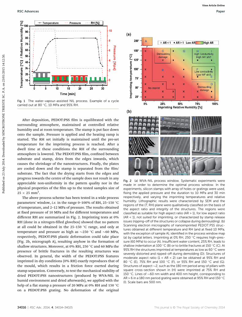
Fig. 1 The water-vapour-assisted NIL process. Example of a cyclecarried out at 80 �C, 10 MPa and 95% RH.
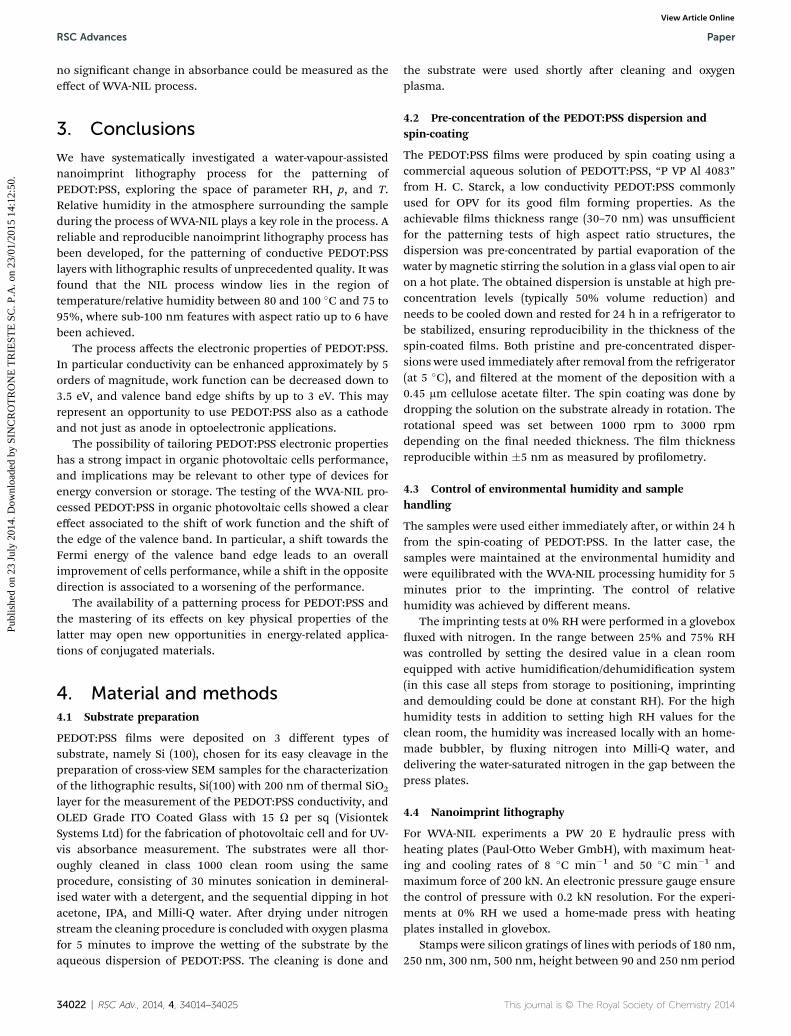
Fig. 2 (a) WVA-NIL process window. Systematic experiments weremade in order to determine the optimal process window. In theexperiments, silicon stamps with array of holes or gratings were used,fixing the applied pressure and the duration to 10 MPa and 30 minrespectively, and varying the imprinting temperatures and relativehumidity. Lithographic results were characterized by SEM and theregions of the (T, RH) plane were qualitatively classified on the basis ofthe aspect ratio and integrity of the structures. The regions wereclassified as suitable for high aspect ratio (AR > 1), for low aspect ratio(AR < 1), not suited for imprinting, or characterized by stamp releaseissues (ripping-off of the structures or collapse during demoulding). (b)Scanning electron micrographs of nanoimprinted PEDOT:PSS struc-tures obtained at different temperature and RH (and at fixed 10 MPa,with the exception of sample A), identified in the process windowmap(a) by capital letters. Imprinting at 0% RH, 250 �C requires high-pres-sure (60 MPa) to occur (A). Insufficient water content, 25% RH, leads toshallow indentation at 100 �C (B) or to brittle fractures at 150 �C (C). At95% RH the structures imprinted at temperatures as low as 60 �C wereseverely distorted and ripped-off during demolding (D). Structures ofmoderate aspect ratio (1 < AR < 2) can be obtained at 95% RH and80 �C (E), 75% RH and 100 �C (F), or 55% RH and 150 �C and (G).Structures of aspect�2, such as the 180 nm period array of pillars withsquare cross-section shown in (H) were imprinted at 75% RH and150 �C. Lines of �60 nm width and 400 nm height, corresponding toAR > 6 in a 180 nm period grating were obtained at 95% RH and 150 �C(I). Scale bars are 500 nm.
RSC Advances Paper
Publ
ishe
d on
23
July
201
4. D
ownl
oade
d by
SIN
CR
OT
RO
NE
TR
IEST
E S
C. P
.A. o
n 23
/01/
2015
14:
12:5
0.
View Article Online
Aer deposition, PEDOT:PSS lm is equilibrated with thesurrounding atmosphere, maintained at controlled relativehumidity and at room temperature. The stamp is put face downonto the sample. Pressure is applied and the heating ramp isstarted. The RH set initially is maintained until the pre-settemperature for the imprinting process is reached. Aer adwell time at these conditions the RH of the surroundingatmosphere is lowered. The PEDOT:PSS lm, conned betweensubstrate and stamp, dries from the edges inwards, whichcauses the shrinkage of the nanostructures. Finally, the platesare cooled down and the stamp is separated from the lm/substrate. The fact that the drying starts from the edges andprogress towards the centre of the sample does not result in anyappreciable non-uniformity in the pattern quality nor in thephysical properties of the lm up to the tested samples size of25 � 25 mm2.
The above process scheme has been tested in a wide processparameters' window, i.e. in the range 0–100% of RH, 25–150 �Cof temperature, and 2–12 MPa of pressure. The results obtainedat xed pressure of 10 MPa and for different temperatures anddifferent RH are summarized in Fig. 2. Imprinting tests at 0%RH (done in a nitrogen-lled glovebox) showed that no patternat all could be obtained in the 25–150 �C range, and only attemperature and pressure as high as �250 �C and �60 MPa,respectively, PEDOT:PSS plastic deformation could take place(Fig. 2b, micrograph A), resulting anyhow in the formation ofshallow structures. Moreover, at 0% RH, 250 �C and 60 MPa thepresence of brittle fractures in the resulting structures wasobserved. In general, the width of the PEDOT:PSS featuresimprinted in dry conditions (0% RH) exactly reproduces that ofthe mould, which results in a friction force exerted duringstamp separation. Conversely, to test the mechanical stability ofdried PEDOT:PSS nanostructures (produced by WVA-NIL inhumid environment and dried aerwards), we applied with thehelp of a at stamp a pressure of 20 MPa at 0% RH and 150 �Con a PEDOT:PSS grating. No deformation of the original
34016 | RSC Adv., 2014, 4, 34014–34025 This journal is © The Royal Society of Chemistry 2014

Paper RSC Advances
Publ
ishe
d on
23
July
201
4. D
ownl
oade
d by
SIN
CR
OT
RO
NE
TR
IEST
E S
C. P
.A. o
n 23
/01/
2015
14:
12:5
0.
View Article Online
structures was detected, which leads to the idea that nano-structured PEDOT:PSS lms could serve themselves as stampsor could be permanently indented as nanopatterned electrodesinto various conjugated materials. This would open a newstrategy for the fabrication of organic optoelectronic deviceswith novel architectures.
At 25% RH, imprinting of PEDOT:PSS was found feasible. At100 �C the imprinted features were shallow (Fig. 2b, micrographB), while at 150 �C they appear fully indented (Fig. 2b, micro-graph C). However, in the latter case, we did not detect anyappreciable lateral shrinkage of the features, which leads to thebuild-up of friction forces between PEDOT:PSS and stampduring the demolding and explains why the resulting structureswere partially damaged.
At 100% RH (i.e. vapour saturation), the PEDOT:PSS lmbecomes unstable, with a tendency to de-wetting, resulting inpoor and irreproducible imprinting results. However, slightlybelow saturation (90–95% RH) the previous issues disappear.Nevertheless, at temperatures below 60 �C the lm could not bedried in a reasonable time, arbitrarily set to 30 min, andconsequently the structures in the lm were severely distortedor ripped away during demoulding (Fig. 2b, micrograph D).
A convenient process window in the (RH, T) plane, leading tofeatures exceeding AR of 1 was identied in the approximatelytriangular region dened by the vertexes (40% RH, 150 �C),(95% RH, 150 �C) and (95% RH, 80 �C). The imprintingprocesses of Fig. 2b, micrographs E, F, G, H, I were conducted inthat region.
Structures of moderate aspect ratio (1 < AR < 2) wereobtained at 95% RH and 80 �C (micrograph E), and 75% RH and100 �C (micrograph F). Structures of increasing AR wereobtained at 150 �C by increasing the relative humidity, from55% (micrograph G) to 75% (micrograph H), and 95% (micro-graph I).
The optimal WVA-NIL process parameters for the fabricationof high AR nanostructures is represented by the region at high
Fig. 3 Linear shrinkage of features' cross section as a function of therelative humidity set initially for the WVA-NIL process for lines andpillars imprinted at 10 MPa. No significant difference in the shrinkagewas found for gratings of different period in the 180–500 nm range.
This journal is © The Royal Society of Chemistry 2014
RH and high temperature such as �95% RH, �150 �C and �10MPa (micrograph I). At these conditions the excellent plasticityof the material and the fast evaporation of water results in arelatively short process time, leading to high AR structures,easily and reliably separated from the stamp, owing to ashrinkage of up to 20–25% of the features' width (Fig. 3).
The WVA-NIL process was extensively tested using differentsilicon stamps with features ranging from 80 to 250 nm, andheight from 100 to 500 nm. In none of the tested imprintingconditions, even at temperatures and pressures of 200 �C and 30MPa, the residual layer could be reduced below 20–30 nm.
2.2 Effects of WVA-NIL process on the physical properties ofPEDOT:PSS
Having identied a convenient parameters' window for thewater-vapour-assisted NIL process, the attention has to befocused on the effects that this process has on the PEDOT:PSSelectronic properties, in particular on the conductivity, workfunction, and density of states in the valence band.
2.2.1 WVA-NIL effects on PEDOT:PSS conductivity. It is wellknown that PEDOT:PSS physical properties strongly depend onthe relative amount of PEDOT and PSS, but that they can also beaffected by the chosen processing conditions or by adding highboiling solvents (HBS) to the dispersion,47–51 Pettersson et al.revealed the effect of sorbitol on the refractive index and extinc-tion coefficient.48 Jonsson et al. found a 600-fold increase ofconductivity and an increase by a factor of 2–3 of the ratio ofPEDOT-to-PSS at the lm surface by adding various solvents tothe dispersion.49 Kim et al. investigated the temperature-dependent conductivity of PEDOT:PSS doped with differentsolvents such as methyl sulfoxide (DMSO), N,N-dimethyl-formamide (DMF), tetrahydrofuran (THF), deducing that thescreening effect of the solvent plays an important role in thevariation of the conductivity.52
Other works highlighted the fact that the deposition by spin-coating itself introduces an anisotropy caused by the squeezingof PEDOT:PSS colloids orthogonally to the substrate, whichresults in different in-plane and out-of-plane conductivities.53,42
The effect of exposing PEDOT:PSS to temperatures exceeding100 �C in the presence of oxygen and/or moisture was reportedto slowly degrade the conductivity.54 (Huang, Miller, de Mello,de Mello, & Bradley, 2003; Vitoratos et al., 2009) Given, thestrong PEDOT:PSS susceptibility to ne processing an compo-sitional details, it is important to establish how the physicalproperties of this material are affected by the different WVA-NILprocessing conditions.
The rst observed effect of our protocol was that conductivityis enhanced by the pre-concentration of PEDOT:PSS waterdispersion. In fact, lms spin-coated from the concentrateddispersion showed �1 order of magnitude increase in the lmconductivity compared to those deposited from the pristinedispersion (Fig. 4a). This effect would be compatible with theformation already in the pre-concentrated dispersion of largerPEDOT:PSS colloids, which, according to the PEDOT:PSSconductivity model by Vitoratos et al.54 is expected to lead tolarger conductivity values. However, evenmore pronounced was
RSC Adv., 2014, 4, 34014–34025 | 34017

Fig. 4 In-plane conductivity of PEDOT:PSS films as a function of (a)the relative humidity and (b) the temperature set for the WVA-NILprocess. The data refer to 32 nm thick film (dashed red line) spin-coated from the pristine PEDOT:PSS dispersion and to 160 nm thickfilm (dashed violet line) deposited from the pre-concentrated solution.The conductivities of the as-coated films are confronted to those offilms processed by water-vapour-assisted NIL on thick films (160 nm)using a flat silicon substrate as a stamp. (a) Effect of RH on theconductivity of films imprinted at 150 �C and 8 MPa, and varying RH,from 0% to 95%. (b) Effect of imprinting temperature on conductivityof films imprinted with 250 nm period line gratings mould and flatsilicon, at 8 MPa, 95% RH and different imprinting temperature in the80–175 �C range. The lines are guides to the eye.
RSC Advances Paper
Publ
ishe
d on
23
July
201
4. D
ownl
oade
d by
SIN
CR
OT
RO
NE
TR
IEST
E S
C. P
.A. o
n 23
/01/
2015
14:
12:5
0.
View Article Online
the effect arising from the WVA-NIL process. The conductivitywas found to increase as a function of the RH. For WVA-NILprocesses at high RH, enhancement by up to 5 orders ofmagnitude with respect to the pristine dispersion has beenmeasured. This effect was limited to the areas actuallycompressed by the stamp, while areas not subjected to pressurewere not affected. On the contrary, thermal NIL processes per-formed in glovebox (0% RH) le conductivity nearly unaffected.The effect on the conductivity depends also on the temperatureat which the WVA-NIL process is carried out (Fig. 4b).Conductivity does not change for process temperatures up to 80�C while it increases nearly exponentially, starting from �100�C. For all tested temperatures the conductivity was found to beindependent of the applied pressure in the 2 to 12 MPa range.
34018 | RSC Adv., 2014, 4, 34014–34025
Only in the case of no load applied to the stamp, the conduc-tivity showed only a weak, almost negligible increase, likely dueto the ineffective connement of the water vapour and theconsequent faster drying of the lm. This interpretation wouldalso explain why WVA-NIL process performed with at stampsresults in an enhancement of conductivity exceeding thatobtained with nanostructured stamps even if it does not involveany polymer ow. In fact at stamps ensure a better watervapour connement, while nanostructures provide easy pathsfor water escape. For given process parameters no major effectcould be ascribed to the differences in the type and size ofnanostructures (we varied AR from 1 to 5, for arrays or gratingsof different periods). Only minor differences in the conductionwere observed by measuring the resistivity in directions paralleland perpendicular to the lines.
The overall picture that emerges from the experiments is thatthe decrease of resistivity would not be related to any netpolymer shear ow and consequent one-dimensional elonga-tion of the PEDOT chains, but it would be an effect of “boiling”PEDOT:PSS in water. The understanding of what the “boiling”of the lm entails at the level of PEDOT:PSS microscopicmorphology is beyond the scope of this work. We speculate thatit may have a similar physical origin as that of the so-calledhigh-conductivity PEDOT:PSS state caused by inclusion ofhigh-boiling solvents (HBS) in the dispersion. In fact, waterremaining conned by the stamp during the WVA-NIL processin PEDOT:PSS lms at temperatures well above 100 �C, may playthe role of plasticizer, similarly to high-boiling solvents such assorbitol, providing the mobility to PEDOT and PSS to rearrangeduring the annealing.
On the other hand, the effect of the presence of high boilingsolvents in the dispersion on morphology is still controversial.Several explanation schemes have been proposed. Someauthors explain this phenomenon in terms of phase segregationbetween PEDOT and PSS due to the higher relative mobility ofthe chains of both components with interposed HBS.55 Rear-rangement of PEDOT-rich clusters into elongated domains, hasbeen reported in STM studies.56 Conformational changes ofPEDOT:PSS toward linear lamentary structures57,58 orscreening due to the polar character of HBS59 are also invoked toexplain the increased conductivity. Future work is required tobetter understand the microscopic effects on morphology ofWVA-NIL process and whether our hypothesis of an analogywith the effect induced by HBS holds.
2.2.2 Effects of WVA-NIL process on PEDOT:PSS workfunction and valence band states. Water-vapour-assisted NILimpacts also on PEDOT:PSS work function and on the states ofthe valence band. This fact is presumably correlated to a changein the phase segregation between PEDOT and PSS alreadyreported by other studies38,60 and in particular to a reduction inthe PSS content at the surface.61 In fact, the work of Lee et al.61
establish a clear correlation between work function and surfaceconcentration of the PSS dopant, with work function increasingfor increasing PSS-to-PEDOT ratio at the surface. This effect wasconrmed by our XPS measurement (data presented in supportinformation), in the opposite direction, i.e. a decreasing workfunction for decreasing PSS-to-PEDOT ratio.
This journal is © The Royal Society of Chemistry 2014

Fig. 5 UPS spectra for the pristine and WVANIL/oxygen plasma pro-cessed films. (a) Valence band and (b) edge of secondary electrons.
Paper RSC Advances
Publ
ishe
d on
23
July
201
4. D
ownl
oade
d by
SIN
CR
OT
RO
NE
TR
IEST
E S
C. P
.A. o
n 23
/01/
2015
14:
12:5
0.
View Article Online
We have analyzed such effects by Ultraviolet PhotoelectronSpectroscopy (UPS). Fig. 5a shows the valence band of a at 160nm thick PEDOT:PSS lm on ITO (black spectrum) compared tothat of lms of the same thickness processed by WVA-NIL at90% RH, but at different temperatures, namely, 80 �C (bluespectrum) and 150 �C (red spectrum). An additional treatmentin oxygen plasma for 5 s of the sample processed by WVA-NIL at80 �C leads to the green spectrum. The orange and yellowspectra refer to the sample processed at 150 �C and subse-quently treated in oxygen plasma for 5 s and additional 15 s,respectively. Fig. 5b shows the measured work function of thesame set of samples obtained by measuring the cut-off energy ofthe secondary peak.
The valence band spectrum of the as-deposited at lm(black spectrum) shows three main structures in the valenceband in agreement with similar measurements already presentin literature. In particular, the top of the valence band (peakcentered at about 3 eV) can be extracted with a linear interpo-lation of the edge at about 2.41 � 0.05 eV from the Fermi level.
This journal is © The Royal Society of Chemistry 2014
The work function is 5.05 � 0.05 eV in good correspondencewith the reported values in literature.38,61,62
In Fig. 5a it is evident that theWVA-NIL treatment at 90 RH%and 150 �C (red spectrum) strongly inuences the valence bandstructures. Upon processing, all valence band peaks appearsmeared out and the onset of the valence band shis away fromthe Fermi level by about 2.9 eV (it is now at 5.27 � 0.05 eV fromthe Fermi level). A concomitant decrease of the work function toabout 3.53 � 0.05 eV is observed, corresponding to a shi of1.52 eV from the value of the untreated lm (black spectrum).Interestingly, by subsequent oxygen plasma (5 s and 20 s,orange and yellow curves), the work function increases andvalence bands appear to recover partially the lost structures withthe edge shiing towards the Fermi level.
On the other hand, the NIL treatment at 90 RH% and 80 �C(blue spectrum) only slightly modies the valence band featureswith the top of the valence band at 2.44� 0.05 eV from the Fermilevel, very close to the value for the as-coated lm. The workfunction decreases by less than 0.1 eV to 4.97 � 0.05 eV.
The oxygen plasma treatment on the WVA-NIL processedsample at 90 RH% and 80 �C (green spectrum) slightlybroadens the valence band features, but increases the workfunction at 5.21 � 0.05 more than the level of the as-coatedlm. Most interesting is the shi of the valence band onsetedge that now appears closer to the Fermi level, i.e. 2.21 �0.05 eV below it.
We try to rationalize the observed phenomenology based onthe currently most accepted morphological model of thePEDOT:PSS system. This model depicts PEDOT:PSSmorphology as consisting of colloids dispersed in water segre-gated into PEDOT-rich cores surrounded by PSS-rich shells, dueto hydrophobic (hydrophilic) character of PEDOT (PSS). Thecore–shell structure is preserved to some extent also in the lm.During the coating the colloids atten into a lamellar structureof PEDOT-rich layers vertically alternated with PSS-rich ones.42
PEDOT:PSS forms a surface layer that is highly enriched in PSS,with respect to bulk PSS/PEDOT ratio.63,61 Furthermore, it isknown that the work function correlates with the surfacecomposition of the PEDOT:PSS lm, which highly depends onthe preparation processes such as thermal annealing process,solvent treatment and coating method.62 In particular, higherPSS surface concentration leads to larger work function.61
Yun et al.62 studied by UPS the electronic properties ofPEDOT:PSS, reporting an increase of work function (from 5.0 to5.2 eV) upon annealing for 1 h at 130 �C in ultra high vacuum(interpreted as the effect of desorption of contaminants),whereas for temperature higher than 170 �C the work functionshied gradually as a function of time towards lower values. Forannealing temperatures of 220 �C and 290 �C for 3 h the workfunction reduced to 4.8 and 4.5 eV, respectively, and thisprogressive lowering of work function as the annealingtemperature increases, correlates with a progressive reductionof the PSS at the lm surface, probed by XPS. On the other handthe work function of the only PEDOT (not doped by PSS) hasbeen reported to be in the range 4.0� 0.2 eV (ref. 64) or 4.3 eV.65
In our investigation on the WVA-NIL process the change ofPEDOT:PSS work function was found, in the most dramatic
RSC Adv., 2014, 4, 34014–34025 | 34019

RSC Advances Paper
Publ
ishe
d on
23
July
201
4. D
ownl
oade
d by
SIN
CR
OT
RO
NE
TR
IEST
E S
C. P
.A. o
n 23
/01/
2015
14:
12:5
0.
View Article Online
case, much larger than previously reported studies on theeffects of thermal annealing.62 Interestingly, the work functionin the WVA-NIL process carried out at 90% RH and 150 �C leadto a work function smaller even than the reported value for theundoped PEDOT (4.0 � 0.2 eV).
WVA-NIL, due to the connement of water in the lm whileheating, ensures large relative mobility to the PEDOT and PSSchains.We presume that the lamellar structure of the PEDOT:PSSis disrupted and that a mixing at a ner level of the twocomponents is reached, lowering the PSS content at the surface.The fact that the PSS-rich top surface is replaced by a phase morerich in PEDOT would explain the reduction in the work function.
Fig. 6 Performance of P3HT:ICBA bulk heterojunction solar cells buildon the pristine and WVA-NIL patterned PEDOT:PSS anode buffer layer.(a) J–V characteristics (b) efficiency and short circuit current density (c)fill factor and open circuit voltage for cells prepared on PEDOT:PSSpatterned at different temperatures.
2.3 Polymer photovoltaic cells on nanostructuredPEDOT:PSS
We have investigated the impact that changes induced on thePEDOT:PSS electronic structure by WVA-NIL process andoxygen plasma produce on the J–V characteristics of poly(3-hexylthiophene) (P3HT): indene-C60 bisadduct (ICBA) bulkheterojunction solar cells. By studying a series of solar cells onPEDOT:PSS anode buffer layers on ITO-coated glass either asspin-coated or processed by WVA-NIL (experimental details arein ESI†), we observed that cells' characteristics are stronglycorrelated with the position of the conduction band edge and ofthe work function of PEDOT:PSS. This dependence is so markedthat the potentially favorable increase of conductivity by severalorder of magnitude induced on PEDOT:PSS owing to WVA-NILprocess is totally obscured by the unfavorable shi of thealignment with the HOMO level of the P3HT.
Though the J–V characteristics that we report here do notrepresent the state of the art in organic photovoltaics, therelative trends in cells performances as a function of the WVA-NIL process parameters and oxygen plasma treatment onPEDOT:PSS reveal very signicant information. The modestvalue of efficiency (�1%) is explained by the following reasons.Our devices were made in N2-lled glovebox with �50 ppmresidual oxygen and water, and characterized in open atmo-sphere without encapsulation. Their active area of 26 mm2 wassignicantly larger than that of the reported best performingones, which rarely exceed 1–4 mm2 area. In our experience aswell as in published research by others66 the efficiency of largercells underestimates by a factor 2–3 the efficiency of the small-area cell limit, where the power dissipation in the ITO owing toohmic loss is negligible. Finally, the large variability of P3HT-based bulk heterojunction solar cells from producer and frombatch it is well known.67
In spite of these factors, the reported trends may be veryrelevant also in the case of high-efficiency cells.
Fig. 6 shows the J–V characteristics and the main photovol-taic parameters, i.e. efficiency (h), short circuit current density(Jsc), open circuit voltage (Voc) and ll factor (FF) under AM 1.5simulated solar irradiation at 100mW cm�2 intensity. Measuresare referred to a set of polymer solar cells made on 300 nmperiod PEDOT:PSS gratings (�120/180 nm lines/spaces) byWVA-NIL at 95% RH and temperatures of 80, 100, 130, and150 �C.
34020 | RSC Adv., 2014, 4, 34014–34025
The J–V characteristics of the cells made on PEDOT:PSSpatterned by WVA-NIL differ markedly from the reference cellmade on the as-deposited 160 nm thick PEDOT:PSS lm.
We observe that the cell on PEDOT:PSS patterned at 80 �Cand the reference one feature approximately the same efficiencyof�0.8%. However, the patterned one exhibits larger Jsc and Vocthan the reference cell (3.5 mA cm�2 and 750 mV vs. 2.5 mAcm�2 and 650 mV, respectively) and lower FF (30% instead of48%).
This journal is © The Royal Society of Chemistry 2014

Fig. 7 Performance of P3HT:ICBA bulk heterojunction solar cells buildon the pristine and WVA-NIL patterned PEDOT:PSS anode buffer layerat 80 �C and 95% RH as a function of an additional oxygen plasmatreatment. (a) J–V characteristics (b) efficiency and short circuitcurrent density (c) fill factor and open circuit voltage for cells patternedPEDOT:PSS treated in oxygen plasma for different time.
Paper RSC Advances
Publ
ishe
d on
23
July
201
4. D
ownl
oade
d by
SIN
CR
OT
RO
NE
TR
IEST
E S
C. P
.A. o
n 23
/01/
2015
14:
12:5
0.
View Article Online
Increasing the WVA-NIL process temperature, which we sawpreviously to shi downwards the level of the PEDOT:PSSvalence band edge, leads to a progressive reduction of Jsc, Vocand FF of the cells. In particular, the lowering of the workfunction from 5.05� 0.05 eV to the 3.53� 0.05 eV by processingthe as-deposited at PEDOT:PSS with WVA-NIL at 150 �C resultsin a reduction of cell efficiency from 0.8% down to 0.15%. Thereason for this behaviour, in spite of the increased holeconductivity in the PEDOT:PSS, must be searched in the newposition of the valence band that with increased WVA-NILtemperature moves below the HOMO of the blend (increasing,therefore, the barrier for hole injection from the polymer to thePEDOT:PSS).
Interestingly, the shi of the valence band edge and thereduction of the work function in PEDOT:PSS due to WVA-NILprocess at high temperature and high RH can be reverted by asubsequent oxygen plasma treatment, that tends to shi the topof the valence band towards the Fermi level (Fig. 5a). At thesame time the efficiency of photovoltaic cells slightly increases(Fig. 7). Fig. 7 shows the current–voltage characteristics and theextracted values for h, Jsc, Voc and FF of OPV cells fabricated onPEDOT:PSS nanopatterned by WVA-NIL at 80 �C and 95% RH.The pattern consisted of gratings of lines (250/250 nm lines/spaces) and were subsequently subjected to oxygen plasma for0, 5, 30, 60 and 120 s.
On the other hand, the only WVA-NIL at 80 �C leaves allvalence band features almost unaffected as in the at samplewith the onset of the valence band at 2.44 � 0.05 eV from theFermi level. The corresponding work function is 4.97 � 0.05 eVand the measured efficiency is about 0.8% as for the referencecell. The oxygen plasma treatment only slightly broadens thevalence band features, but increases the work function to 5.21�0.05 even higher than that of the reference sample. Mostinteresting is the shi of the valence band onset that nowappears at 2.21 � 0.05 eV from the Fermi level, so reducing thebarrier for the hole injection and consequently increasing theefficiency to 1.3%, i.e. 60% relative increase compared to thereference cell. By increasing the duration of the oxygen plasmato 1 min, the cells efficiency decreases to 1.1%, mainly due adrop in the current (whereas FF and Voc remain essentiallystable). Increasing further the plasma treatment to 2 minresults in a drop to 0.7% efficiency by a combined drop of Voc(from 800 mV to 525 mV) and FF (from 42.5% to 35%).
The observed trends as a function of WVA-NIL, temperature,and duration of oxygen plasma treatment show that theperformances of cells tend to worsen for process conditions thatincrease the separation of the valence band edge with the Fermilevel, possibly associated with the lowering of the workfunction.
In particular, the series of measurements as a function of theduration of oxygen plasma show an initial increase of efficiencyfor oxygen plasma etching of 5 s, and 20 s, according to the UPSmeasured shi of work function and valence band edge.
The results of this experiment agree with those of a study byFrohne et al.,68 who studied the inuence of the anodic workfunction on the performance of organic solar cells. In that case,they used an ex situ electrochemical procedure to alter the work
This journal is © The Royal Society of Chemistry 2014
function of PEDOT:PSS, adjusting the equilibrium potential Eqvs. a standard electrode.69 Frohne et al. showed that withdecreasing Eq (i.e. decreasing work function) the J–V curvesshis progressively closer to the origin of axes, showing aprogressive reduction in Jsc, Voc and efficiency.68
Generally the doping of the PEDOT with PSS is associatedalso with a change in the optical properties of the material. Thisaspect has been investigated by UV-vis photospectrometry, but
RSC Adv., 2014, 4, 34014–34025 | 34021
RSC Advances Paper
Publ
ishe
d on
23
July
201
4. D
ownl
oade
d by
SIN
CR
OT
RO
NE
TR
IEST
E S
C. P
.A. o
n 23
/01/
2015
14:
12:5
0.
View Article Online
no signicant change in absorbance could be measured as theeffect of WVA-NIL process.
3. Conclusions
We have systematically investigated a water-vapour-assistednanoimprint lithography process for the patterning ofPEDOT:PSS, exploring the space of parameter RH, p, and T.Relative humidity in the atmosphere surrounding the sampleduring the process of WVA-NIL plays a key role in the process. Areliable and reproducible nanoimprint lithography process hasbeen developed, for the patterning of conductive PEDOT:PSSlayers with lithographic results of unprecedented quality. It wasfound that the NIL process window lies in the region oftemperature/relative humidity between 80 and 100 �C and 75 to95%, where sub-100 nm features with aspect ratio up to 6 havebeen achieved.
The process affects the electronic properties of PEDOT:PSS.In particular conductivity can be enhanced approximately by 5orders of magnitude, work function can be decreased down to3.5 eV, and valence band edge shis by up to 3 eV. This mayrepresent an opportunity to use PEDOT:PSS also as a cathodeand not just as anode in optoelectronic applications.
The possibility of tailoring PEDOT:PSS electronic propertieshas a strong impact in organic photovoltaic cells performance,and implications may be relevant to other type of devices forenergy conversion or storage. The testing of the WVA-NIL pro-cessed PEDOT:PSS in organic photovoltaic cells showed a cleareffect associated to the shi of work function and the shi ofthe edge of the valence band. In particular, a shi towards theFermi energy of the valence band edge leads to an overallimprovement of cells performance, while a shi in the oppositedirection is associated to a worsening of the performance.
The availability of a patterning process for PEDOT:PSS andthe mastering of its effects on key physical properties of thelatter may open new opportunities in energy-related applica-tions of conjugated materials.
4. Material and methods4.1 Substrate preparation
PEDOT:PSS lms were deposited on 3 different types ofsubstrate, namely Si (100), chosen for its easy cleavage in thepreparation of cross-view SEM samples for the characterizationof the lithographic results, Si(100) with 200 nm of thermal SiO2
layer for the measurement of the PEDOT:PSS conductivity, andOLED Grade ITO Coated Glass with 15 U per sq (VisiontekSystems Ltd) for the fabrication of photovoltaic cell and for UV-vis absorbance measurement. The substrates were all thor-oughly cleaned in class 1000 clean room using the sameprocedure, consisting of 30 minutes sonication in demineral-ised water with a detergent, and the sequential dipping in hotacetone, IPA, and Milli-Q water. Aer drying under nitrogenstream the cleaning procedure is concluded with oxygen plasmafor 5 minutes to improve the wetting of the substrate by theaqueous dispersion of PEDOT:PSS. The cleaning is done and
34022 | RSC Adv., 2014, 4, 34014–34025
the substrate were used shortly aer cleaning and oxygenplasma.
4.2 Pre-concentration of the PEDOT:PSS dispersion andspin-coating
The PEDOT:PSS lms were produced by spin coating using acommercial aqueous solution of PEDOTT:PSS, “P VP Al 4083”from H. C. Starck, a low conductivity PEDOT:PSS commonlyused for OPV for its good lm forming properties. As theachievable lms thickness range (30–70 nm) was unsufficientfor the patterning tests of high aspect ratio structures, thedispersion was pre-concentrated by partial evaporation of thewater by magnetic stirring the solution in a glass vial open to airon a hot plate. The obtained dispersion is unstable at high pre-concentration levels (typically 50% volume reduction) andneeds to be cooled down and rested for 24 h in a refrigerator tobe stabilized, ensuring reproducibility in the thickness of thespin-coated lms. Both pristine and pre-concentrated disper-sions were used immediately aer removal from the refrigerator(at 5 �C), and ltered at the moment of the deposition with a0.45 mm cellulose acetate lter. The spin coating was done bydropping the solution on the substrate already in rotation. Therotational speed was set between 1000 rpm to 3000 rpmdepending on the nal needed thickness. The lm thicknessreproducible within �5 nm as measured by prolometry.
4.3 Control of environmental humidity and samplehandling
The samples were used either immediately aer, or within 24 hfrom the spin-coating of PEDOT:PSS. In the latter case, thesamples were maintained at the environmental humidity andwere equilibrated with the WVA-NIL processing humidity for 5minutes prior to the imprinting. The control of relativehumidity was achieved by different means.
The imprinting tests at 0% RH were performed in a gloveboxuxed with nitrogen. In the range between 25% and 75% RHwas controlled by setting the desired value in a clean roomequipped with active humidication/dehumidication system(in this case all steps from storage to positioning, imprintingand demoulding could be done at constant RH). For the highhumidity tests in addition to setting high RH values for theclean room, the humidity was increased locally with an home-made bubbler, by uxing nitrogen into Milli-Q water, anddelivering the water-saturated nitrogen in the gap between thepress plates.
4.4 Nanoimprint lithography
For WVA-NIL experiments a PW 20 E hydraulic press withheating plates (Paul-Otto Weber GmbH), with maximum heat-ing and cooling rates of 8 �C min�1 and 50 �C min�1 andmaximum force of 200 kN. An electronic pressure gauge ensurethe control of pressure with 0.2 kN resolution. For the experi-ments at 0% RH we used a home-made press with heatingplates installed in glovebox.
Stamps were silicon gratings of lines with periods of 180 nm,250 nm, 300 nm, 500 nm, height between 90 and 250 nm period
This journal is © The Royal Society of Chemistry 2014

Paper RSC Advances
Publ
ishe
d on
23
July
201
4. D
ownl
oade
d by
SIN
CR
OT
RO
NE
TR
IEST
E S
C. P
.A. o
n 23
/01/
2015
14:
12:5
0.
View Article Online
and duty cycle of 50%, or arrays of square or cylindrical holes insilicon of 180 and 500 nm period, respectively. Copies of thesilicon stamps into Ormostamp (micro resist technologyGmbH) on glass were used mainly for the patterning ofPEDOT:PSS on ITO/glass, in order to solve a problem consistingin the disruption PEDOT:PSS features caused by the differentthermal expansion of silicon stamps and ITO/glass substrates.By matching the thermal expansion of the substrates theprevious problem disappeared. All stamps were surface func-tionalized by self-assembling of a monolayer of dodecyltri-chlorosilane from vapour phase, to make their surfacehydrophobic and ease the demoulding.
4.5 Oxygen plasma
Oxygen plasma treatment mentioned in the paper were per-formed with a 100 W RF power on 600 cathode, pressure of 0.7 �10�2 mbar and 115 V bias. For treatments of up to 30 seconds nosignicant change in the topography or in the conductivity wereseen.
4.6 Conductivity measurement
The measurement of in-plane conductivity were made on as-coated, and WVA-NIL processed PEDOT:PSS lms on SiO2
(300 nm)/Si substrates. The WVA-NIL process was done using asa stamp either silicon gratings of lines, or at silicon substrates.Contacts to PEDOT:PSS were made evaporation of 80 nm of goldby shadowing a stripe of the substrate with a calibrated metalwire, resulting in 220 mm gap between contacts, as measured bySEM. The resistance was obtained by a linear t of the I–V curvebetween �2.0 V and 2.0 V. The conductivity for the patternedlms were measured in parallel and orthogonal direction withrespect to the lines. To extract the conductivity we used thevalue of lm thickness as measured by prolometry (beforepatterning the lm).
4.7 Scanning electron microscopy
SEM images of the NIL or WVA-NIL-structured PEDOT:PSS lmswere acquired on a Zeiss Supra 40 scanning electron micro-scope. The cross-sections of the samples were obtained aer fewminutes drying PEDOT:PSS lms on at hot plate at 150 �C.Cleavage was done with the substrates still hot (cleavagewithout dehydration step lead to heavy plastic deformation ofthe PEDOT:PSS lm).
4.8 UPS measurements
The UPS experiments were performed in a modied VG-IIESCAlab system (base pressure 10�10 mbar) using the He Iradiation (21.22 eV). The electron hemispherical analyserworked with 2 eV of pass energy and the Fermi level wasmeasured on the copper sample holder in electrical contactwith the sample before each measurement. To obtain the workfunction relative to the measured Fermi level, a bias of 6.00 Vwas applied between the sample and the ground, in order tomake visible the secondary photoelectron cut-off. The energyresolution was 50 meV.
This journal is © The Royal Society of Chemistry 2014
4.9 OPV cell fabrication and testing
For cell production the PEDOT:PSS was deposited on patternedITO substrate. The patterning of ITO was obtained by UVphotolithography on the photoresist S1813 and wet etching ofthe ITO with a 10 : 10 : 1 HCl : H2O : HNO3 solution at 50–60 �C.Regioregular poly(3-hexylthiophene) (P3HT) polymer used inthis work was obtained from Rieke Specialty Polymers, RiekeMetals Inc., while indene-C60 bisadduct (ICBA) from LumtecLuminescence Technology Corp. Aer imprinting withOrmostamp/glass stamp, the PEDOT:PSS/ITO/glass sampleswere transferred in a nitrogen lled glovebox. Residual waterand oxygen were approximately 50 ppm. Prior to device fabri-cation, a solution consisting of P3HT : ICBA in blend ratio of1 : 1 (wt/wt %) and blend concentration of 40 mg mL�1 indichlorobenzene was stirred at 40 �C for 36 hours inside glove-box. P3HT:ICBA solution was spin-casted onto the differentlyprocessed PEDOT:PSS lms at 800 rpm for 50 seconds. Finallythrough shadow mask 100 nm thick aluminum contacts werevacuum evaporated at a pressure of approximately 2 � 10�6
Torr. Aer aluminum evaporation (with evaporator directlyconnected to glovebox) the devices were annealed at 140 �C for30 minutes inside glove-box.
References
1 S. Gunes, H. Neugebauer and N. Saricici, Chem. Rev., 2007,107, 1324–1338.
2 K. Wang, H. Wu, Y. Meng and Z. Wei, Small, 2014, 10, 14–31.3 S. Reineke, F. Lindner, G. Schwartz, N. Seidler, K. Walzer,B. Lussem and K. Leo, Nature, 2009, 459, 234–238.
4 C. Dodabalapur, L. Filas, B. LaDuca and S. K. Li, Nature,2000, 403, 521–523.
5 S. Forrest, Nature, 2004, 428, 911–918.6 G. Malliaras and R. Friend, Phys. Today, 2005, 58, 53–58, DOI:10.1063/1.1995748.
7 H. Klauk, U. Zschieschang, J. Paum and M. Halik, Nature,2007, 445, 745–748.
8 H. Huitema, G. Gelinck, J. van der Putten, K. Kuijk, C. Hart,E. Cantatore, P. Herwig, A. van Breemen and D. de Leeuw,Nature, 2001, 414, 599.
9 Y. Xu, F. Zhang and X. Feng, Small, 2011, 7, 1338–1360.10 T. Kawase, H. Sirringhaus, R. H. Friend and T. Shimoda, Adv.
Mater., 2001, 13, 1601–1605.11 P. Calvert, Chem. Mater., 2001, 13, 3299–3305, DOI: 10.1021/
cm0101632.12 D. A. Pardo, G. E. Jabbour and N. Peyghambarian, Adv.
Mater., 2000, 12, 1249–1252.13 D. G. Lidzey, M. Voigt, C. Giebeler, A. Buckley, J. Wright,
K. Bohlen, J. Fieret and R. Allott, Org. Electron., 2005, 6,221–228, DOI: 10.1016/j.orgel.2005.06.007.
14 P. Watkins, A. Walker and G. Verschoor, Nano Lett., 2005, 5,1814–1818.
15 F. Yang and S. Forrest, ACS Nano, 2008, 2, 1022–1032.16 J. Weickert, R. Dunbar, H. Hesse, W. Wiedemann and
L. Schmidt-Mende, Adv. Mater., 2011, 23, 1810–1828.
RSC Adv., 2014, 4, 34014–34025 | 34023

RSC Advances Paper
Publ
ishe
d on
23
July
201
4. D
ownl
oade
d by
SIN
CR
OT
RO
NE
TR
IEST
E S
C. P
.A. o
n 23
/01/
2015
14:
12:5
0.
View Article Online
17 S. Mubeen, J. Lee, N. Singh, M. Moskovits andE. W. McFarland, Energy Environ. Sci., 2013, 6, 1633.
18 N. Singh, S. Mubeen, J. Lee, H. Metiu, M. Moskovits andE. W. McFarland, Energy Environ. Sci., 2014, 7, 978–981.
19 S. I. Cho and S. B. Lee, Acc. Chem. Res., 2008, 41, 699–707.20 Y. Hou, Y. Cheng, T. Hobson and J. Liu, Nano Lett., 2010, 10,
2727–2733.21 D. Khodagholy, T. Doublet, M. Gurnkel, P. Quilichini,
E. Ismailova, P. Leleux, T. Herve, S. Sanaur, C. Bernard andG. Malliaras, Adv. Mater., 2011, 23, H268–H272.
22 R. Po, C. Carbonera, A. Bernardi and N. Camaioni, EnergyEnviron. Sci., 2011, 4, 285.
23 S.-I. Na, S.-S. Kim, J. Jo and D.-Y. Kim, Adv. Mater., 2008, 20,4061–4067, DOI: 10.1002/adma.200800338.
24 S. K. Hau, H.-L. Yip, J. Zou and A. K.-Y. Jen, Org. Electron.,2009, 10, 1401–1407, DOI: 10.1016/j.orgel.2009.06.019.
25 B. Winther-Jensen and F. C. Krebs, Sol. Energy Mater. Sol.Cells, 2006, 90, 123–132, DOI: 10.1016/j.solmat.2005.02.004.
26 F. Guo, X. Zhu, K. Forberich, J. Krantz, T. Stubhan,M. Salinas, M. Halik, S. Spallek, B. Butz, E. Spiecker,T. Ameri, N. Li, P. Kubis, D. M. Guldi, G. J. Matt andC. J. Brabec, Adv. Energy Mater., 2013, 3, 1062–1067, DOI:10.1002/aenm.201300100.
27 Y. Xia, K. Sun and J. Ouyang, Energy Environ. Sci., 2012, 5,5325–5332.
28 W. Zhang, B. Zhao, Z. He, X. Zhao, H. Wang, S. Yang, H. Wuand Y. Cao, Energy Environ. Sci., 2013, 6, 1956–1964.
29 P. J. Brewer, J. Huang, P. Lane, A. J. deMello, D. D. C. Bradleyand J. C. deMello, Phys. Rev. B: Condens. Matter Mater. Phys.,2006, 74, 115202, DOI: 10.1103/PhysRevB.74.125320.
30 C. Tengstedt, W. Osikowicz, W. R. Salaneck, I. D. Parker,C.-H. Hsu and M. Fahlman, Appl. Phys. Lett., 2006, 88,053502, DOI: 10.1063/1.2168515.
31 B. Charlot, G. Sassine, A. Garraud, B. Sorli, A. Giani andP. Combette, Microsyst. Technol., 2012, 19, 895–903, DOI:10.1007/s00542-012-1696-5.
32 T. Granlund, T. Nyberg, L. S. Roman, M. Svensson andO. Inganas, Adv. Mater., 2000, 12, 269–273.
33 D. Li and L. J. Guo, Appl. Phys. Lett., 2006, 88, 063513, DOI:10.1063/1.2168669.
34 S.-F. Tseng, W.-T. Hsiao, K.-C. Huang and D. Chiang, Appl.Phys. A: Mater. Sci. Process., 2012, 112, 41–47, DOI: 10.1007/s00339-012-7172-3.
35 F. C. Krebs, M. Jørgensen, K. Norrman, O. Hagemann,J. Alstrup, T. D. Nielsen, J. Fyenbo, K. Larsen andJ. Kristensen, Sol. Energy Mater. Sol. Cells, 2009, 93, 422–441, DOI: 10.1016/j.solmat.2008.12.001.
36 L. J. Guo, J. Phys. D: Appl. Phys., 2004, 37, 123–141, DOI:10.1088/0022-3727/37/11/R01.
37 U. Lang, N. Naujoks and J. Dual, Synth. Met., 2009, 159, 473–479, DOI: 10.1016/j.synthmet.2008.11.005.
38 A. M. Nardes, M. Kemerink, M. M. de Kok, E. Vinken,K. Maturova and R. A. J. Janssen, Organic Electronics, 2008,9, 727–734, DOI: 10.1016/j.orgel.2008.05.006.
39 R. Meier, C. Birkenstock, C. Palumbiny and P. Muller-Buschbaum, Phys. Chem. Chem. Phys., 2012, 14, 15088–15098.
34024 | RSC Adv., 2014, 4, 34014–34025
40 R. M. Reano, Y. P. Kong, H. Y. Low, L. Tan, F. Wang,S. W. Pang and A. F. Yee, J. Vac. Sci. Technol., B:Microelectron. Nanometer Struct.–Process., Meas., Phenom.,2004, 22, 3294–3299, DOI: 10.1116/1.1825013.
41 L. Tan, Y. P. Kong, S. W. Pang and A. F. Yee, J. Vac. Sci.Technol., B: Microelectron. Nanometer Struct.–Process., Meas.,Phenom., 2004, 22, 2486–2492, DOI: 10.1116/1.1800353.
42 A. M. Nardes, M. Kemerink, R. A. J. Janssen,J. A. M. Bastiaansen, N. M. M. Kiggen, B. M. W. Langeveld,A. J. J. M. van Breemen and M. M. de Kok, Adv. Mater.,2007, 19, 1196–1200, DOI: 10.1002/adma.200602575.
43 X. Crispin, S. Marciniak, W. Osikowicz, G. Zotti, A. W. D. vander Gon, F. Louwet, M. Fahlman, L. Groenendaal,F. D. Schryver and W. R. Salaneck, J. Polym. Sci., Part B:Polym. Phys., 2003, 41, 2561–2583, DOI: 10.1002/polb.10659.
44 H. Hlaing, X. Lu, C.-Y. Nam and B. M. Ocko, Small, 2012, 8,3443–3447.
45 J. B. Emah, R. J. Curry and S. R. P. Silva, Appl. Phys. Lett.,2008, 93, 103301, DOI: 10.1063/1.2973342.
46 Y. Yang, K. Lee, K. Mielczarek, W. Hu and A. Zakhidov,Nanotechnology, 2011, 22, 485301.
47 W. H. Kim, A. J. Makinen, N. Nikolov, R. Shashidhar, H. Kimand Z. H. Kafa, Appl. Phys. Lett., 2002, 80, 3844–3846, DOI:10.1063/1.1480100.
48 L. Pettersson, S. Ghosh and O. Inganas, Organic Electronics,2002, 3, 143–148.
49 S. K. Jonsson, J. Birgerson, X. Crispin, G. Greczynski,W. Osikowicz, A. D. van der Gon, W. Salaneck andM. Fahlman, Synth. Met., 2003, 139, 1–10, DOI: 10.1016/s0379-6779(02)01259-6.
50 W. Zhang, B. Zhao, Z. He, X. Zhao, H. Wang, S. Yang, H. Wuand Y. Cao, Energy Environ. Sci., 2013, 6, 1956–1964.
51 T. Takano, H. Masunaga, A. Fujiwara, H. Okuzaki andT. Sasaki, Macromolecules, 2012, 45, 3859–3865.
52 J. Y. Kim, J. H. Jung, D. E. Lee and J. Joo, Synth. Met., 2002,126, 311–316.
53 A. Nardes, M. Kemerink and R. Janssen, Phys. Rev. B:Condens. Matter Mater. Phys., 2007, 76, 085208, DOI:10.1103/physrevb.76.085208.
54 E. Vitoratos, S. Sakkapoulos, E. Dalas, N. Paliatsas,D. Karageirgopoulos, F. Petraki, S. Kennou and S. Choulis,Organic Electronics, 2009, 10, 61–66, DOI: 10.1016/j.orgel.2008.10.008.
55 S. Timpanaro, M. Kemerink, F. J. Touwslager, M. M. D. Kokand S. Schrader, Chem. Phys. Lett., 2004, 394, 339–343, DOI:10.1016/j.cplett.2004.07.035.
56 A. M. Nardes, R. A. J. Janssen and M. Kemerink, Adv. Funct.Mater., 2008, 18, 865–871, DOI: 10.1002/adfm.200700796.
57 J. Ouyang, Q. Xu, C.-W. Chu, Y. Yang, G. Li and J. Shinar,Polymer, 2004, 45, 8443.
58 K. van de Ruit, R. I. Cohen, D. Bollen, T. van Mol,R. Yerushalmi-Rozen, R. A. J. Janssen and M. Kemerink,Adv. Funct. Mater., 2013, 46, 5778–5786, DOI: 10.1002/adfm.201301174.
59 Y. Xi and J. Ouyang, J. Mater. Chem., 2011, 21, 4927.60 B. Friedel, P. E. Keivanidis, T. J. K. Brenner, A. Abrusci,
C. R. McNeill, R. H. Friend and N. C. Greenham,
This journal is © The Royal Society of Chemistry 2014
Paper RSC Advances
Publ
ishe
d on
23
July
201
4. D
ownl
oade
d by
SIN
CR
OT
RO
NE
TR
IEST
E S
C. P
.A. o
n 23
/01/
2015
14:
12:5
0.
View Article Online
Macromolecules, 2009, 42, 6741–6747, DOI: 10.1021/ma901182u.
61 T.-W. Lee and Y. Chung, Adv. Funct. Mater., 2008, 18, 2246–2252, DOI: 10.1002/adfm.200700766.
62 D.-J. Yun, H. Ra, J. Kim, I. Hwang, J. Lee, S.-W. Rhee andJ. Chung, ECS J. Solid State Sci. Technol., 2012, 1, M10–M14, DOI: 10.1149/2.028201jss.
63 G. Greczynski, T. Kugler and W. Salaneck, Thin Solid Films,1999, 354, 129–135, DOI: 10.1016/s0040-6090(99)00422-8.
64 K. Z. Xing, M. Fahlman, X. W. Chen, O. Inganas andW. R. Salanek, Synth. Met., 1997, 89, 161–165.
This journal is © The Royal Society of Chemistry 2014
65 A. Gadisa, K. Tvingstedt, S. Admassie, L. Lindell, X. Crispin,M. R. Andersson, W. R. Salaneck and O. Inganas, Synth. Met.,2006, 156, 1102–1107, DOI: 10.1016/j.synthmet.2006.07.006.
66 A. K. Pandey, J. M. Nunzi, B. Ratier and A. Moliton, Phys. Lett.A, 2008, 372, 1333–1336, DOI: 10.1016/j.physleta.2007.09.068.
67 A. Ng, X. Liu, W. Y. Jim, A. B. Djurisic, K. C. Lo, S. Y. Li andW. K. Chan, J. Appl. Polym. Sci., 2014, 131, 39776.
68 H. Frohne, S. Shaheen, C. Brabec, D. Muller, N. Saricici andK. Meerholz, ChemPhysChem, 2002, 3, 795–799.
69 G. Muller, N. Scherf, N. Brauchle and K. Meerholz, Nature,2000, 405, 661–665.
RSC Adv., 2014, 4, 34014–34025 | 34025