Am29000™ Microprocessor Memory Design - bitsavers.org
251
Am29000™ Microprocessor Memory Design Handbook Advanced Micro Devices
-
Upload
khangminh22 -
Category
Documents
-
view
2 -
download
0
Transcript of Am29000™ Microprocessor Memory Design - bitsavers.org

Am29000™ Microprocessor Memory Design Handbook
Advanced Micro
Devices

AI1129000™ Mel110ry Design
Handbook
ADVANCED MICRO DEVICES ~

© 1992 Advanced Micro Devices, Inc.
Advanced Micro Devices reserves the right to make changes in its products without notice in order to improve design or performance characteristics.
This publication neither states nor implies any warranty of any kind, including but not limited to implied warrants of merchantability or fitness for a particular application. AMD assumes no responsibility for the use of any circuitry other than the circuitry in an AMD product.
The information in this publication is believed to be accurate in all respects at the time of publication, but is subject to change without notice. AMD assumes no responsibility for any errors or omissions, and disclaims responsibility for any consequences resulting from the use of the information included herein. Additionally, AMD assumes no responsibility for the functioning of undescribed features or parameters.
Trademarks
AMD, PAL, and PALASM are registered trademarks of Advanced Micro Devices, Inc.
Am29000, Am29005, Am29030, Am29035, Am29050, 29K, Branch Target Cache, LabPro, and MACH are trademarks of Advanced Micro Devices, Inc.
Fusion29K is a service mark of Advanced Micro Devices, Inc.
Product names used in this publication are for identification purposes only and may be trademarks of their respective companies.

TABLE OF CONTENTS
Preface •.•••••••.•.••••••••••.•••••••...••••••••.•••••• P-1
Chapter 1 Overview •••••••••.••••••.••••••••.••.••.•••..•.•••••.••• 1-1 Performance/Cost Options ...................................... 1-1 Memory Latency And Performance . . . . . . . . . . . . . . . . . . . . . . . . . . . . . . .. 1-2 How To Use This Handbook ..................................... 1-3
Chapter 2 Basic Issues For Am29000 Processor Memory Designs •••..••••••• 2-1 Key Memory System Factors. . . . . . . . . . . . . . . . . . . . . . . . . . . . . . . . . . . .. 2-1 Trade-offs ................................................... 2-5 Memory Implementation Issues. . . . . . . . . . . . . . . . . . . . . . . . . . . . . . . . . .. 2-8 Address And Control Driver Issues ............................... 2-17 Speed Limit ................................................. 2-18 Bank Interleaving . . . . . . . . . . . . . . . . . . . . . . . . . . . . . . . . . . . . . . . . . . . .. 2-20 Instruction vs. Data Access Speeds .............................. 2-20 Test Hardware Interface ....................................... 2-20 Memory Design Documentation ................................. 2-22
Chapter 3 The Design Process-5RAM Example •••••••.•...•••••••...•••• 3-1 Interface Decisions ............................................ 3-1 Instruction Memory Design ...................................... 3-4 Instruction Memory: Single-Bank Burst Access ....................... 3-7 Instruction Memory: Dual-Bank Burst Access . . . . . . . . . . . . . . . . . . . . . .. 3-14 Data Memory Design . . . . . . . . . . . . . . . . . . . . . . . . . . . . . . . . . . . . . . . . .. 3-19 Conclusion. . . . . . . . . . . . . . . . . . . . . . . . . . . . . . . . . . . . . . . . . . . . . . . . .. 3-26 Example SRAM Designs - Details . . . . . . . . . . . . . . . . . . . . . . . . . . . . . .. 3-27
Chapter 4 The Design Process-Simple EPROM Example •...•••••••.••••••• 4-1 Background ......... . . . . . . . . . . . . . . . . . . . . . . . . . . . . . . . . . . . . . . . .. 4-1 EPROM Memory Design Assumptions ............................. 4-1 Design Description ............................................ 4-1 Detailed Description ........................................... 4-3 Conclusions . . . . . . . . . . . . . . . . . . . . . . . . . . . . . . . . . . . . . . . . . . . . . . . . .. 4-3 References .................................................. 4-3 PAL Device Equations . . . . . . . . . . . . . . . . . . . . . . . . . . . . . . . . . . . . . . . . .. 4-5
Chapter 5 Connecting the InstructionlData Buses •••.•••••••..••••••••..•• 5-1 Instruction RAM Design ......................................... 5-1 Instruction EPROM Summary .. . . . . . . . . . . . . . . . . . . . . . . . . . . . . . . . . .. 5-5 Addition Of Read/Write Memory .... ; ............................. 5-6 Read/Write Memory Summary ................................... 5-7 DRAM Support ............................................... 5-8 Further Increases In Performance . . . . . . . . . . . . . . . . . . . . . . . . . . . . . . . .. 5-9
Chapter 6 16-Bit Memory Architecture ..•.••••••••.••••.••.••••••••...•• 6-1 Overview Of The 16-Bit Design . . . . . . . . . . . . . . . . . . . . . . . . . . . . . . . . . .. 6-1 Theory Of Operation ........................................... 6-2 Critical Timing Paths ........................................... 6-6
Table Of Contents

Benchmark Figures ............................................ 6-8 Summary . . . . . . . . . . . . . . . . . . . . . . . . . . . . . . . . . . . . . . . . . . . . . . . . . . .. 6-8 Timing Diagrams ............................................ , 6-24 Parts List ...................... . . . . . . . . . . . . . . . . . . . . . . . . . . . .. 6-26
Chapter 7 Interleaved SCDRAM •..•..••...•.....•......•..•.•..••.•..• 7-1 Memory Structure ............................................. 7-1 Instruction Memory ............................................ 7-1 Memory Interface Logic Equations ................................ 7-5 Logic Details Signal By Signal .................................... 7-8 Data Memory ................................................ 7-35
Chapter 8 Single-Bank SCDRAM .................•.....•..••...•...... 8-1 System Block Diagram ......................................... 8-1 Chip Count And Power Consumption .............................. 8-1 Types Of Memory Access ..... . . . . . . . . . . . . . . . . . . . . . . . . . . . . . . . . .. 8-2 Control PAL Device Description .................................. 8-6 Conclusion. . . . . . . . . . . . . . . . . . . . . . . . . . . . . . . . . . . . . . . . . . . . . . . . . .. 8-8
Chapter 9 Interleaved VDRAM ...................•.............•..•... 9-1 Video DRAM Advantages ....................................... 9-1 Memory Features ............................................. 9-2 Interface Logic Block Diagram. . . . . . . . . . . . . . . . . . . . . . . . . . . . . . . . . . .. 9-3 Memory Interface Logic Equations ................................ 9-6 Intra-cycle Timing ............................................ 9-25 Inter-cycle Timing .......... ; ................................. 9-29 Parts List ................................................... 9-35 Final Discussion ............................................ , 9-35
Chapter 10 Single-Bank VDRAM .....•.............................•.. 10-1 Overview .. . . . . . . . . . . . . . . . . . . . . . . . . . . . . . . . . . . . . . . . . . . . . . . . .. 10-1 Memory Features ............................................ 10-1 Interface Logic Block Diagram .................................. , 10-1 Memory Interface Logic Equations ............................... 10-5 Intra-Cycle Timing ..... . . . . . . . . . . . . . . . . . . . . . . . . . . . . . . . . . . . . .. 10-20 Inter-Cycle Timing . . . . . . . . . . . . . . . . . . . . . . . . . . . . . . . . . . . . . . . . . .. 10-24 Parts List .................................................. 10-29 Final Discussion ............................................ 10-29
Chapter 11 Integrated Memory Interface Controllers .........•............ 11-1 V29BMC Burst Mode Memory Controller .......................... 11-1 Score Peripheral Access Controller .............................. , 11-4 Score VME Interface Controller ................................. , 11-4 VLSI Technology ASIC Devices ................................. 11-5
ii Table Of Contents

LIST OF FIGURES
Figure 2-1 Figure 2-2
Figure 3-1 Figure 3-2 Figure 3-3 Figure 3-4 Figure 3-5 Figure 3-6 Figure 3-7 Figure 3-8 Figure 3-9 Figure 3-10 Figure 3-11 Figure 3-12 Figure 3-13 Figure 3-14 Figure 3-15 Figure 3-16 Figure 3-17 Figure 3-18 Figure 3-19 Figure 3-20 Figure 3-21 Figure 3-22 Figure 3-23 Figure 3-24 Figure 3-25 Figure 3-26 Figure 3-27 Figure 3-28 Figure 3-29
Figure 4-1 Figure 4-2 Figure 4-3 Figure 4-4 Figure 4-5 Figure 4-6
Figure 5-1 Figure 5-2 Figure 5-3 Figure 5-4 Figure 5-5 Figure 5-6
Three-Bus Architecture . . . . . . . . . . . . . . . . . . . . . . . . . . . . . . . . . . . . . . . .. 2-4 VDRAM Main Memory ......................................... 2-8
Memory Interface Overview ..................................... 3-2 Simple Access With Bus Invalid .................................. 3-5 Single-Bank Instruction Access State Machine. . . . . . . . . . . . . . . . . . . . . .. 3-6 Instruction Access With Burst And Terminate ................... : .... 3-7 Single-Bank SRAM Block Diagram . . . . . . . . . . . . . . . . . . . . . . . . . . . . . . .. 3-9 Instruction Access With Burst SuspensionlTermination ............... 3-10 Instruction Access With Suspended Burst ......................... 3-11 Mapped Instruction Space ..................................... 3-12 Using A31 To Specify Code Space ............................... 3-12 ROM Space To Instruction Space ................................ 3-13 Data Access With Instruction Burst Termination. . . . . . . . . . . . . . . . . . . .. 3-15 Burst Data Access To Instruction Space ........................... 3-16 Two-Bank Interleaved SRAM Block Diagram ..... " ................ 3-17 Interleaved Instruction Access State Machine ...................... 3-20 Interleaved Instruction Access .................................. 3-21 Data Access State Machine .................................... 3-22 Data Byte Read/Write Access . . . . . . . . . . . . . . . . . . . . . . . . . . . . . . . . . .. 3-23 Simple Data Access Block Diagram .............................. 3-24 Data Access With BINV And Burst ............................... 3-26 Burst Data Access Block Diagram ............................... 3-27 Interleaved SRAM Block Diagram. . . . . . . . . . . . . . . . . . . . . . . . . . . . . . .. 3-28 Simple Data Access Block Diagram .............................. 3-29 Single-Bank SRAM Block Diagram . . . . . . . . . . . . . . . . . . . . . . . . . . . . . .. 3-30 Interleaved SRAM Control Equations .. . . . . . . . . . . . . . . . . . . . . . . . . . .. 3-31 Interleaved SRAM Address Counter Equations ..................... 3-34 Simple Data Access Equations . . . . . . . . . . . . . . . . . . . . . . . . . . . . . . . . .. 3-36 Single-Bank SRAM Decode Control Equations. . . . . . . . . . . . . . . . . . . . .. 3-37 Single-Bank SRAM Address Counter Equations. . . . . . . . . . . . . . . . . . . .. 3-38 Single-Bank SRAM State Control Equations ....................... 3-40
Access State Diagram. . . . . . . . . . . . . . . . . . . . . . . . . . . . . . . . . . . . . . . . .. 4-2 EPROM System Block Diagram .................................. 4-4 16-MHz Timing ............................................... 4-5 Burst Address Counter Equations. . . . . . . . . . . . . . . . . . . . . . . . . . . . . . . .. 4-5 Address Counter/Latch Equations ................................ 4-6 Address Latch Equations ....................................... 4-7
Basic Memory System ......................................... 5-2 Burst Mode Memory System . . . . . . . . . . . . . . . . . . . . . . . . . . . . . . . . . . . .. 5-3 Dual-Bank Interleaved Memory System ............................ 5-5 Read/Write Memory With Combined Instruction/Data Buses ............ 5-6 Addition Of Burst Mode Data Access .............................. 5-7 Static Column DRAM Memory System . . . . . . . . . . . . . . . . . . . . . . . . . . . .. 5-9
Table Of Contents iii

Figure 6-1
Figure 6-2
Figure 6-3
Figure 6-4
Figure 6-5
Figure 6-6
Figure 6-7
Figure 6-8
Figure 6-9
Figure 6-10
Figure 6-11
Figure 6-12
Figure 7-1
Figure 7-2
Figure 7-3
Figure 7-4
Figure 7-5
Figure 7-6
Figure 7-7
Figure 7-8
Figure 7-9
Figure 7-10
Figure 7-11
Figure 7-12
Figure 7-13
Figure 7-14
Figure 7-15
Figure 7-16
Figure 7-17
Figure 7-18
Figure 7-19
Figure 7-20
Figure 7-21
Figure 7-22
iv
System Block Diagram ......................................... 6-2
Clock Diagram ............................................... 6-4
State Machine Flow Diagram .................................... 6-5
BINV Critical Path Timing .............. , ........................ 6-7
CAS Critical Path Timing ....................................... 6-7
Low-Cost Am29000 Processor Design . . . . . . . . . . . . . . . . . . . . . . . . . . . .. 6-9
Clock Generator For Low Cost Am29000 Processor Design Pattern . . . .. 6-20
Bus Controller For Low Cost Am29000 Processor Design .. . . . . . . . . . .. 6-20
RAS And CAS Decoder For Low-Cost Am29000 Processor Design ..... 6-22
Refresh Controller Pattern ..................................... 6-23
Instruction Or Data Access ........ . . . . . . . . . . . . . . . . . . . . . . . . . . . .. 6-24
Refresh Cycle ............................................... 6-25
Interface Logic Block Diagram ................................... 7-5
SCDRAM Memory State Diagram .................. " ..... " ...... 7-6
AmPAL22V10-25 SCDRAM Refresh Counter/Request Generator Device U2 .................................................. 7-20
PAL 16R6-D DRAM Refresh State Generator-Interleaved Device U15 ................................................. 7-21
PAL 16R6-D DRAM Precharge State Generator-Interleaved Device U16 ................................................. 7-22
PAL20L8-B DRAM State Decoder-Interleaved Device U4 .......... . . . . . . . . . . . . . . . . . . . . . . . . . . . . . . . . . . . . . . .. 7-22
PAL20L8-B DRAM State Decoder-Interleaved Device U5 .................................................. 7-23
PAL 16R4-D DRAM Instruction State Generator-Interleaved Device U17 .... . . . . . . . . . . . . . . . . . . . . . . . . . . . . . . . . . . . . . . . . . . . .. 7-23
PAL 16R4-D DRAM Data State Generator-Interleaved Device U18 ................................................. 7-24
PAL 16R6-D DRAM RAS Generator-Interleaved Device U19 ................................................. 7-25
PAL 16R6-D DRAM CAS Generator-Interleaved Device U20 .................... . . . . . . . . . . . . . . . . . . . . . . . . . . . .. 7-26
PAL16L8-B DRAM Counter Load-Interleaved Device U1 .................................................. 7-26
PAL 16R4-D DRAM Address Counter-Interleaved Section O-Even Bank Device U6 .......................... , ....................... 7-27
PAL 16R6-D DRAM Address Counter-Interleaved Section 1-Even Bank Device U7 .... . . . . . . . . . . . . . . . . . . . . . . . . . . . . . . . . . . . . . . . . . . . . .. 7-27
PAL 16R4-D DRAM Address Counter-Interleaved Section O-Qdd Bank Device U9 ................ . . . . . . . . . . . . . . . . . . . . . . . . . . . . . . . . .. 7-28
PAL16R6-D DRAM Address Counter-Interleaved Section 1-Qdd Bank Device U16 .... . . . . . . . . . . . . . . . . . . . . . . . . . . . . . . . . . . . . . . . . . . . .. 7-29
PAL 16L8-D DRAM Row Address Latch-Interleaved Device U8 .................................................. 7-30
PAL 16L8-D DRAM Row Address Latch-Interleaved Device U11 ................................................. 7-30
PAL 16R8-D DRAM Write Enable Controls Device U112 . . . . . . . . . . . . . . . . . . . . . . . . . . . . . . . . . . . . . . . . . . . . . . .. 7-31
SCDRAM Interleaved Bank Memory Decode Cycle . . . . . . . . . . . . . . . . .. 7-33
SCDRAM Interleaved Bank Memory RAS Cycle. . . . . . . . . . . . . . . . . . . .. 7-33
SCDRAM Interleaved Bank Memory Burst Access. . . . . . . . . . . . . . . . . .. 7-34
Table Of Contents

Figure 8-1 Figure 8-2 Figure 8-3 Figure 8-4 Figure 8-5 Figure 8-6 Figure 8-7 Figure 8-8
Figure 9-1 Figure 9-2 Figure 9-3 Figure 9-4
Figure 9-5
Figure 9-6
Figure 9-7
Figure 9-8
Figure 9-9
Figure 9-10
Figure 9-11
Figure 9-12 Figure 9-13 Figure 9-14 Figure 9-15 Figure 9-16 Figure 9-17 Figure 9-18 Figure 9-19 Figure 9-20 Figure 9-21
Figure 10-1 Figure 10-2 Figure 10-3 Figure 10-4
Figure 10-5
Figure 10-6
Figure 10-7
System Block Diagram ......................................... 8-2 EPROM Instruction Access. . . . . . . . . . . . . . . . . . . . . . . . . . . . . . . . . . . . .. 8-3 Simple Instruction Access To DRAM .............................. 8-4 Burst Instruction Access To DRAM . . . . . . . . . . . . . . . . . . . . . . . . . . . . . . .. 8-5 Simple Data Access To DRAM .................................. 8-6 Burst Data Access To DRAM .................................... 8-7 Instruction Burst Pre-empted By a Data Access. . . . . . . . . . . . . . . . . . . . .. 8-8 Simple Instruction Access Followed By Data Access .. . . . . . . . . . . . . . . .. 8-9
Am29000 Processor With Interleaved VDRAM Memory ............... , 9-2 Interleaved VDRAM Memory Block Diagram ........................ 9-3 VDRAM Memory State Diagram ...................... " .......... 9-7 AmPAL22V10-25 VRAM Refresh Counter/Request Generator Device U3 .. . . . . . . . . . . . . . . . . . . . . . . . . . . . . . . . . . . . . . . . . . . . . . . . .. 9-9 PAL20L8-B VRAM State Decoder-Interleaved Device U2 .. . . . . . . . . . . . . . . . . . . . . . . . . . . . . . . . . . . . . . . . . . . . . . . .. 9-10 PALCE16V8-D VRAM Instruction State Generator-Interleaved Device U9 .. . . . . . . . . . . . . . . . . . . . . . . . . . . . . . . . . . . . . . . . . . . . . . . .. 9-11 PAL 16R4-D VRAM Data State Generator-Interleaved Device U1 0 .... . . . . . . . . . . . . . . . . . . . . . . . . . . . . . . . . . . . . . . . . . . . .. 9-11 PAL20L8-D VRAM Transfer Generator-Interleaved Device U13 ................................................. 9-12 PAL20R8-D VRAM RAS-CAS Generator-Interleaved Device U11 ................................................. 9-13 PAL20R4-D Byte-Write Enable Generator-Interleaved Device U12 ......... '" ................... '" .... " ......... 9-14 PALCE16V8-D VRAM Address Incrementer Device U1 .................................................. 9-15 VDRAM Interleaved Bank Memory Decode Cycle ................... 9-26 Row Address Timing . . . . . . . . . . . . . . . . . . . . . . . . . . . . . . . . . . . . . . . . .. 9-26 CAS-to-Data Ready Timing . . . . . . . . . . . . . . . . . . . . . . . . . . . . . . . . . . . .. 9-28 NEC Memory Write Data Hold Time . . . . . . . . . . . . . . . . . . . . . . . . . . . . .. 9-29 Fujitsu Transfer Enable Timing . . . . . . . . . . . . . . . . . . . . . . . . . . . . . . . . .. 9-30 NEC Transfer Enable Timing ................................... 9-31 Burst Access Timing .......................................... 9-31 VDRAM Instruction Burst Timing ................................ 9-32 VDRAM Data Read Timing . . . . . . . . . . . . . . . . . . . . . . . . . . . . . . . . . . . .. 9-33 VDRAM Data Write Timing .................................... , 9-34
Am29000 Processor With VDRAM Memory ... . . . . . . . . . . . . . . . . . . . .. 10-2 Single-Bank VDRAM Memory Block Diagram ...................... 10-3 VDRAM Memory State Diagram . . . . . . . . . . . . . . . . . . . . . . . . . . . . . . . .. 10-6 AmPAL22V10-25 VRAM Refresh Counter/Request Generator Device U2 ..... . . . . . . . . . . . . . . . . . . . . . . . . . . . . . . . . . . . . . . . . . . . .. 10-8 PAL20L8-15 VRAM State Decoder Device U 1 .................................................. 10-9 AmPAL22V10-15 VRAM Instruction State Generator-Single Bank Device U6 .... . . . . . . . . . . . . . . . . . . . . . . . . . . . . . . . . . . . . . . . . . . . .. 10-10 PAL20L8-10 VRAM Transfer Generator-Single Bank Device U7 ................................................. 10-10
Table Of Contents v

vi
Figure 10-8 PAL20R8-B VRAM RAS-CAS Generator-Single Bank Device U8 ................................................. 10-11
Figure 10-9 PAL20R4-B Byte Write Enable Generator-Single Bank Device U9 ........................................... . . . . .. 10-11
Figure 10-10 VDRAM Interleaved Bank Memory Decode Cycle .................. 10-21 Figure 19-11 Row Address Timing . . . . . . . . . . . . . . . . . . . . . . . . . . . . . . . . . . . . . . . .. 10-22 Figure 10-12 CAS-to-data Ready Timing .... . . . . . . . . . . . . . . . . . . . . . . . . . . . . . . .. 10-23 Figure 10-13 NEC Memory Write Data Hold Time . . . . . . . . . . . . . . . . . . . . . . . . . . . .. 10-23 Figure 10-14 Figure 10-15 Figure 10-16 Figure 10-17 Figure 10-18 Figure 10-19
Figure 11-1 Figure 11-2 Figure 11-3
Fujitsu Transfer Enable Timing . . . . . . . . . . . . . . . . . . . . . . . . . . . . . . . .. 10-25 NEC Transfer Enable Timing .................................. 10-25 Burst Access Timing ... . . . . . . . . . . . . . . . . . . . . . . . . . . . . . . . . . . . . .. 10-26 VDRAM Instruction Burst Timing ............................... 10-26 VDRAM Data Read Timing . . . . . . . . . . . . . . . . . . . . . . . . . . . . . . . . . . .. 10-27 VDRAM Data Write Timing . . . . . . . . . . . . . . . . . . . . . . . . . . . . . . . . . . .. 10-28
V29BMC-Based Memory System Block Diagram . . . . . . . . . . . . . . . . . . .. 11-2 V29BMC Configuration Word ................................... 11-4 Am29000 Processor-Based Laser Printer Controller Block Diagram ..... 11-6
Table Of Contents

LIST OF TABLES
Table 6-1 Table 7-1 Table 9-1 Table 10-1
16-Bit Architecture Parts List. . . . . . . . . . . . . . . . . . . . . . . . . . . . . . . . . . .. 6-26 Am29000 Interleaved Dynamic RAM Interface Parts List .............. 7-35 Interleaved VRAM Interface Parts List ............................ 9-35 Single-Bank VRAM Interface Parts List .......................... 10-29
Table Of Contents vii


PREFACE
The 29I(TM Family of microprocessors changes the meaning of "high performance" for 32-bit CMOS Reduced Instruction Set Computers (RISC). First-generation RISC provided performance in the 4 to 5 million instructions per second (MIPS) range. But the 29K Family of three-bus RISC microprocessors (the Am29000™, Am29005™, and Am29050™ processors) can sustain performance in the 1 0- to 32-MIPS range.
The 29K Family brings high performance to a wide range of cost-sensitive applications ranging from laser printers to network bridges/routers and embedded controllers using DRAM or VDRAM (10 to 17 MIPS), to extremely high-performance graphic accelerators and multi-processor systems, using cache or SRAM (17 to over 32 MIPS).
The 29K Family of microprocessors gives the computer-system designer an entire spectrum of cost-effective system performance solutions using a single hardware and software platform. These microprocessors provide many features for easing the performance burden placed on system memory so slower, lower-cost memory systems can be used at any given level of system performance.
This handbook provides 29K Family memory system design information and specific examples helpful in determining how to design a memory system to give you the best cost/performance capabilities in the Am29000, Am29005, and Am29050 microprocessors. The designs shown in this manual illustrate memory interface examples using the 29K Family of three-bus processors. Since the Am29000, Am29050 and the Am29005 processors are pin-, bus-, and software-compatible, references to the Am29000 processor are interchangeable with the Am29050 and Am29005 processors. This manual does not provide examples for the Am29030™ or Am29035™ processors since these two devices are implemented with a two-bus architecture.
Chapter 1 summarizes the performance capabilities of the Am29000 32-bit CMOS microprocessor.
Chapter 2 contains basic information on memory system architectures and how to choose between them.
Chapters 3 through 11 explore memory system design options in detail, often providing detailed design examples. The types of designs and examples are:
• Chapter 3: The Design Process-SRAM Example
• Chapter 4: The Design Process-Simple EPROM Example
• Chapter 5: Connecting the Instruction/Data Buses
• Chapter 6: 16-Bit Memory Architecture
• Chapter 7: Interleaved SCDRAM
• Chapter 8: Single-Bank SCDRAM
• Chapter 9: Interleaved VDRAM
• Chapter 10: Single-Bank VDRAM
• Chapter 11: Integrated Memory Interface Controllers
Preface P-1

~AMD
P-2
In many applications, the simplest and most cost-effective method of interfacing memory with the Am29000 processor is to use an integrated memory controller device, such as the ones described in Chapter 11. In other applications, a custom-designed interface may be appropriate, as described in Chapters 3 through 10.
Application notes are available from your AMD~ representative for many of the design examples presented in this handbook. The handbook contains basic, high-level information on the design examples, while the application notes provide both basic and detailed information (such as parts lists and performance benchmarks).
Additional information on the 29K Family of products can be obtained by calling the AMD 29K hotline number: 800 2929-AMD (800292-9263) or 512462-5651.
Preface

13 a·hi j 3 ;11
OVERVIEW
The Advanced Micro Devices 29K Family of three-bus, streamlined-instruction processors is a new generation of CMOS 32-bit, high-performance microprocessors. The Family is based on Reduced Instruction Set Computer (RISC) architecture principles, providing the ability to execute one instruction almost every clock cycle. The processors in the 29K Family provide the following features:
• A streamlined set of instructions, each of which can be executed in a single clock cycle. The instruction set is generally less complex than those of prior-generation processors, while still providing support for all the basic and most frequently needed algorithm steps. These simpler instructions serve to break complex algorithms down into a series of simple steps that are then exposed to powerful optimization techniques embodied in the latest generation of language compilers.
• An on-chip instruction cache and extensive register set, allowing fast execution by reducing the number of accesses to external system memory.
• A load-store method of access to external resources, often allowing parallel execution of internal (register-to-register) instructions and memory-I/O (register-to-external) instructions.
• Independent instruction and data buses that provide support for concurrent and continuous accesses of external instruction and data memory. Instruction memory can feed the processor with a new instruction in each cycle while the 29K Family memory bus simultaneously provides access to data operands.
Through the use of RISC techniques and the latest in advanced high-speed CMOS technology, the highest-speed 29K Family members are able to sustain performance of 23 to 32 Million Instructions Per Second (MIPS), with a peak of 40 MIPS, when clocked at 40 MHz. This is roughly equivalent to between 22 and 30 times the performance of a VAX 11naO.
PERFORMANCE/COST OPTIONS
If the designer's target is to sustain the highest possible level of performance, the memory system must be able to supply the microprocessor at a rate of one instruction per clock cycle. In that case, the memory-system architecture becomes a critical element in supporting the overall system performance, and also contributes significantly to the overall cost.
However, it is important to understand that the 29K Family members can also achieve very good performance in lower-cost designs. System costs are reduced by using DRAM, which has a far lower cost per bit than static RAM, and by using lower-speed, lower-cost 29K Family members such as the Am29005 processor. Performance in the 6-to 17-MIPSrange can be achieved by using EPROM, static-column DRAM, or video DRAM, at clock rates in the 16- to 25-MHz range. Yet in this kind of lower-cost deSign, the system performance still far exceeds that of comparably priced prior-generation microprocessors, and even that of many current-generation RISC microprocessors.
Overview 1-1

~AMD
1-2
The 29K Family members offer various levels of performance while sharing a common pin structure, bus structure, and instruction set, together with an extensive set of software tools for use in a wide spectrum of cost-effective, high-performance systems. The 29K Family thus provides a wide choice of performance at reasonable cost, without requiring a change in processor architecture or software.
MEMORY LATENCY AND PERFORMANCE
A processor capable of executing instructions at a rate of one per clock cycle must have a memory system that can sustain that rate of access. The key to high performance in a system is to provide burst mode access in the memory architecture. The memory system design will maintain high performance if it can sustain a burst access rate of one access per cycle, even if there is some initial access latency at the beginning of each burst access.
The 29K Family is designed to minimize internal execution-pipeline latency, while allowing the memory system as much latency as possible without loss of performance. Therefore, lower-cost and slower memory systems can often meet the system requirements.
Low-speed memory systems can use techniques such as pipe lining and bankinterleaving to sustain the required burst access rate. In addition, burst mode access is intrinSically supported by modern dynamic-memory devices having the property of highspeed sequential access after a slower initial random-access time. Examples of these memory devices are: DRAM with page mode, nibble mode, static-column mode, or video {serial output} capability.
The allowance for initial latency is provided by a number of 29K Family features:
• For instruction accesses, the Am29000 and Am29050 processors contain an on-chip Branch Target Cache™ memory, which provides up to four cycles for the memory to begin supplying a sequential burst of instructions without incurring a performance penalty.
• For data accesses, the 29K Family members can overlap memory load and store operations with instruction execution, so memory latency occurs in parallel with continued instruction execution. The compiler or programmer can schedule a memory access in advance of when the data is required.
• Once data is read from the memory, it is forwarded directly to the execution stage for use in the next cycle. Again, this minimizes the internal pipeline latency to allow additional access time in the memory.
• The large register file {192 registers} of the Am29000 processor acts as an on-chip stack cache to help reduce the number of off-chip data accesses.
• The on-chip Memory Management Unit (MMU) in the Am29000 and Am29050 processors minimizes pipeline latency by making translated addresses available to the memory early in the cycle following execution. In addition, the MMU simplifies the memory design by performing the address-translation task on-chip.
• The 29K Family of three-bus microprocessors uses separate, non-multiplexed data and instruction buses to simplify the memory interface and to maximize the information transfer rate.
Overview

AMD ~
HOW TO USE THIS HANDBOOK
This handbook shows how to use the Am29000, Am29005, and Am29050 processors in a non-cache memory environment with standard, currently available memory devices. Examples of several specific memory systems are shown, often providing block diagrams, state diagrams, and PAL® device equations.
Chapter 2, Basic Issues for Am29000 Processor Memory Designs, provides basic information on memory system architectures and how to choose between them. Memory architecture options, key considerations, and trade-offs are introduced. Memory interface signals and other implementation details are described.
Chapter 3, The Design Process-SRAM Example, takes you through the process of deciding what type of architecture is best for your application. Although static RAM is used as an example, the basic principles explained in Chapter 3 apply to other types of memory as well.
It is recommended you read Chapters 1, 2, and 3 before you read the other chapters. Chapters 4 through 11 explore additional memory system design options in detail, usually providing detailed examples. You can read these chapters in any order or consult them as needed.
At the end of Chapter 3 is detailed information on two specific examples: a dual-bank interleaved SRAM memory, and a single-bank non-interleaved SRAM memory. SRAM memory is appropriate for systems where speed is important and memory size requirements are modest.
Chapter 4, The Design Process-Simple EPROM, shows a simple, low-cost instruction memory made with a single bank of fast EPROM.
Chapter 5, Connecting the Instruction/Data Buses, describes a form of memory architecture in which the instruction bus and data bus are tied together into a single bus. This architecture offers one method of trading performance for cost savings.
Chapter 6, 16-Bit Memory Architecture, describes a memory organized into 16-bit words, rather than the usual 32 bits. Using a special set of clocks, 16-bit words are put together to form the 32-bit words used by the Am29000 processor. This scheme is useful in systems with moderate speed and memory size requirements.
Chapter 7, Interleaved SCDRAM, is a detailed design example using dual interleaved banks of Static Column DRAM (SCDRAM). In effect, a SCDRAM memory has a built-in cache consisting of one row of words. SCDRAM is appropriate for systems where performance and memory size requirements are important, combined with a need for lower cost and complexity.
Chapter 8, Single-Bank SCDRAM, is another SCDRAM design example. This low-cost design uses a single bank of non-interleaved SCDRAM. The intention of this design is to reduce the component count and power consumption to a minimum, while maintaining the high performance of single-cycle burst access to memory.
Chapter 9, Interleaved VDRAM, is a detailed design example using dual interleaved banks of Video DRAM (VDRAM). VDRAM memory allows independent and concurrent access through two ports: a conventional read/write random-access port (for the data bus), and a serial shift register port (for the instruction bus). VDRAM is appropriate for systems where simplicity and cost savings are important, and performance requirements are moderate.
Overview 1-3

~AMD
1-4
Chapter 10, Single-Bank VDRAM, is another detailed design example similar to that in Chapter 9, but using a single-bank, non-interleaved VDRAM memory. Its complexity, cost, and performance are lower than the design in Chapter 9.
Chapter 11, Integrated Memory Interface Controllers, describes some integrated devices designed specifically for interfacing memory with 29K Family microprocessors. Although somewhat less flexible than a custom design, using an integrated controller is often the best solution because of the simplicity and reasonable cost of the interface.
Design Notes
Some of the design examples presented in this handbook are paper designs that have not been implemented in hardware by the authors. Although all designs have been thoroughly tested logically, they are not guaranteed to be error-free. They are presented in this handbook to show the methodology in designing memory systems for the 29K Family of microprocessors.
The SCDRAM and VDRAM designs in Chapters 7 through 10 have been functionally simulated on an Apollo workstation with Mentor CAD software. Behavioral models for memories, PAL devices, SSI and MSllogic, and the Am29000 processor were provided by Logic Automation. To the best of our knowledge and test vectors, we believe the SCDRAM and VDRAM designs work correctly.
Overview

BASIC ISSUES FOR Am29000 PROCESSOR MEMORY DESIGNS
The Reduced Instruction Set Computer (RISC) architecture of the 29K Family gives the user many more options in designing a memory system than a traditional Complex Instruction Set Computer (CISC) microprocessor. Built-in features in the 29K Family architecture, such as burst-mode addressing, allow faster execution out of relatively slow memory than most other processors. The use of these features are options, depending on performance needs. The memory system can be optimized for speed, low power, small board space, cost, or whatever is the key determining factor. In order to balance the trade-offs effectively, it is important to understand the processor interface to the memory system.
This chapter describes the memory access signals used by the processor, when the signals are used, and how. In addition, this chapter suggests some reasonable compromises that can be made in the memory design to meet specific application goals. In the actual design examples presented later, the design methodology is shown in detail.
KEY MEMORY SYSTEM FACTORS
There are several important factors to consider when designing a memory system. These factors include the memory access speed, memory size requirements, memory structure, design complexity, throughput requirements, and bus structure.
Access Speed
The main goal of using the 29K Family processors is to obtain a substantial performance improvement over other solutions, while maintaining or lowering the overall system cost. Unlike traditional microprocessors, the 29K Family offers a wide performance range depending on how the memory system is designed. Memory access speed is the key element in determining the performance limit of an Am29000 processor system. But there are two separate measures of access speed; the balance between them provides a wide range of performance-to-cost trade-offs.
The first measure of speed is how fast a random word of memory can be accessed; this is the initial access time. The second measure is how fast subsequent sequential words of memory can be accessed; this is the burst access time. The distinction between the two is important to understand.
The burst access time of the instruction memory system is normally tuned to the processor cycle time to allow single-cycle fetches during an instruction burst. Achieving a single-cycle burst instruction memory is the most important factor in achieving a high performance system.
In contrast, the initial access time applies only during the first non-sequential instruction or data fetch and is therefore of less importance. In addition, an instruction cache called the Branch Target Cache memory inside the processor hides the first cycles of the initial access time, so the initial latency in many designs in effect becomes invisible to the
Basic Issues for Am29000 Processor Memory Designs 2-1

~AMD
2-2
processor. The combination of burst mode and the Branch Target Cache memory gives excellent performance characteristics, even when executing instructions in relatively slow DRAM.
The number of data loads and stores is minimized by an internal stack cache that has an image of the memory stack stored in registers. The registers are inside the processor and are therefore immediately accessible to all instructions being executed. Furthermore, the latest compilers have early load generation capability, where the compiler schedules loads as early as possible ahead of the first reference to the data. As a result, the data memory in many cases can be designed using only simple (rather than burst) access. The exceptions would be where very large amounts of data must be transferred quickly, as in DMA and in some graphics applications.
The initial access time is different from burst access time for the following reasons:
• When a new address is supplied by the processor, all bus devices must decode the address to determine whether or not to respond. So an initial access requires some time to decode the address and begin the access of a memory word.
A burst access is always to the next word in sequence after either an initial access or a previous burst access. Therefore, the burst access does not require any address decode time; the memory block already knows it is selected and only needs to increment the address from the last access. Note that the memory block does not need any special logic (Le., added delay, to deal with the possibility of a burst access crossing memory chip or block boundaries because the Am29000 processor always supplies a new address at every 256-word address boundary).
• In the case of a memory block that recognizes its address, the selected word of memory must be accessed. Some memory devices like DRAMs require more time to access a random word of memory than to access a sequential word. This is generally due to time multiplexing the upper (row) and lower (column) halves of the memory address to the DRAM. Therefore, a random-word access requires both a row address and a column address.
A burst access needs only a new column address, or in some types of memories, only a signal to shift out the next sequential word. Thus, access to a sequential word is faster than access to a random location (new row and column address).
• When a new row is accessed, DRAM memories require delay time between the end of a previous access and the beginning of the new row access. This time is in addition to the delay time associated with transferring the new row address. This added delay is called the precharge time. When a random access immediately follows a previous access to the same memory, the new initial access incurs the precharge time delay. This delay is not incurred in a burst access because the same row is addressed.
• In a bank-interleaved memory system, the first access to each bank in a series gains no benefit from the overlapping of access time between banks. This is because all the banks must go through a full bank access time before the first (initial) word is available. Therefore, the initial access is always longer than subsequent burst accesses in an interleaved memory architecture. This concept is covered in more detail later.
Generally, an initial access is slower than a burst access due to the address decode, row-address entry, precharge delay, and initial bank access that may be required for an initial access, but do not apply to a burst access.
Basic Issues for Am29000 Processor Memory Designs

AMD ~
Memory Size
In a dedicated controller application, a few kilobytes of code and data space may be all that is needed. If so, the speed and simplicity of memory can be maximized by using Static RAM (SRAM). But if a few megabytes or more are required to handle a large embedded controller task, then the board space, power, and cost considerations usually favor DRAM over SRAM.
Memory Structure
Cost, power, and board-space considerations favor DRAM memory, while speed and simplicity considerations favor SRAM. Besides the two extremes of using only SRAM or only DRAM, there is also the option of mixing the two. Instruction memory may be built partly with SRAM, to provide fast access to some kernel routines, and the greater part with DRAM for economy. Or instruction memory may be built with SCDRAM, and the data memory built with a relatively slow type of SRAM, as described later in this chapter.
In addition, if performance is important, a multi-bank interleave access structure may be used. When using bank-interleave schemes, slower memories can achieve the same performance as a single bank of higher-speed memory during the critical burst-access mode. In the case of SRAM, it means less costly memories can still provide maximum burst performance. For DRAMs, it means these slower memories can still give maximum burst performance.
Where maximum speed is required along with large size, a compromise structure can be used with a little SRAM and a lot of DRAM. That option is called cache memory. A cache memory can be implemented, for example, as a soft cache, where the virtual tags are held in the TLB registers. As this is a software application, the details of such an application fall outside the scope of this book.
Complexity
The simplest memory system probably consists of one bank of EPROM for instructions and one bank of SRAM for data, with each bank capable only of simple (not burst) accesses. In a design such as this, there is virtually no control logic, no address decode logic, no buffers, and no refresh issues to deal with. Of course, this structure may not provide enough speed, flexibility, or memory size.
The other end of the complexity spectrum involves something like dual-interleave DRAM banks with burst access ability. Here, other considerations must be dealt with: refresh issues, bank sequencing, address counters, and dual porting of the instruction bank for both instruction and data accesses. Although this might seem complex, commercially available memory interface gate arrays now reduce all these design issues to a relatively easy task.
Throughput
Each 29K Family member is a synchronous machine. The timing of all its actions is in relationship to its clock. Information flow to or from the microprocessor must occur in time units that are integer multiples of the system clock cycle. This means if the memory access time does not fit into a single clock cycle, two cycles will be taken. Even if the access time only misses by a few nanoseconds, a whole cycle of time is lost. Depending on how often that situation comes up, it might be advantageous to slow the system clock down by a few nanoseconds so most of the memory accesses can occur
Basic Issues for Am29000 Processor Memory Designs 2-3

~AMD
in a single cycle. Thus, the overall throughput of the system can be significantly improved in some cases by slowing the system down.
The option of slowing down the memory to match a slightly slower system clock can sometimes result in significant savings in cost and complexity. The best tool for finding the optimum cost-performance point is the architectural simulator available for the 29K Family members. This software simulator allows the designer to get a performance measurement of the application program, running the program with a simulated model of the processor and the memory system.
Bus Structure
The Am29000, Am29005, and Am29050 processors have three separate buses:
• Address Bus, shared between instruction, data, I/O, and coprocessor accesses;
• Instruction Bus, used to move instructions from the system memory to the processor; and,
• Data Bus, used to move data between the processor, system, memory, I/O devices, and coprocessors via load and store operations.
Together, these buses and their related control lines are called the channel. The channel provides concurrent access of instructions and data when the instruction and/or data memories are accessed via pipeline or burst requests. As shown in Figure 2-1, this structure, from a performance standpoint, favors memory systems with separate memory blocks for holding instruction and data for simultaneous access.
The instruction and data buses can be tied together to provide a system with a common instruction and data space. The benefit of doing this is a lower part count, as only one physical memory array is needed. The drawback is slightly less performance, because
Figure 2-1 Three-Bus Architecture
2-4
32-bit Address
Bus
32-bit
Instruction Memory
Data Memory
flO, Coprocessor
Basic Issues for Am29000 Processor Memory Designs
32-bit Data Bus
10623C-001

AMD ~
the processor cannot overlap instruction fetches with data operations. This option is described in more detail later. (See Chapter 5.)
The data bus is bidirectional, the address bus is output only, and the instruction bus is input only with respect to the Am29000 processor. When separate data and instruction memory blocks (in RAM) are used, the system design must provide a way to load the instruction memory, because the processor cannot directly write information into the instruction memory via the instruction bus. This is covered in more detail later in this chapter.
TRADE·OFFS
When attempting to determine the optimum memory system for a given application, there are a number of factors to consider. The real determining factor is usually one of cost, power, or board space. Some rough guidelines are given here.
Note that there are several types of integrated controller devices specifically designed to handle interfacing of DRAM and other types of memory with the 29K Family of processors. These devices often provide a simple and cost-effective method of implementing the memory system. See Chapter 11 for some examples of these devices.
SRAM
When building an embedded controller such as a network node processor, digital signal processor, or a mainframe-computer 1/0 processor, the main requirement is system speed. If the memory requirement is small (up to a megabyte or so), then high-speed SRAM works very well.
For small memory systems, the cost, power consumption, and board space of SRAM are reasonable, and the speed is the best possible. In a well-designed 40-MHz clockrate system using the Am29050 processor, the initial access time is one to three cycles, the burst access speed is a single cycle, and the average sustained performance is in the 29- to 32-MIPS range. (Because of the internal caching in the processor, peak performance can reach up to 40 MIPS with any memory system, but it is the sustainable performance that counts.)
DRAM
SRAM designs provide the fastest initial access times. But SRAMs are not very dense and therefore consume a large amount of board space for a given size memory system. Also, they tend to be expensive and consume a good deal of power for a given size memory.
Dynamic RAMs can provide far more memory at lower cost and lower power in the available board space than is possible with SRAM. The main penalty for using DRAMs is a loss of speed in the initial memory access time. Burst-access performance can be maintained by using bank interleaving and Static Column DRAMs (SCDRAM). Fortunately, the Am29000 and Am29050 processors provide features that help compensate for a slower initial access time of system memory.
The Am29000 Branch Target Cache memory stores the first four instructions from the 32 most recently accessed branch target addresses. (The Am29050 Branch Target Cache memory operates in the same manner but is twice as large; instructions are stored from the 64 most recently accessed branch target addresses.) When a branch instruction is executed and the branch target address resides in the Branch Target
Basic Issues for Am29000 Processor Memory Designs 2-5

~AMD
2-6
Cache memory, the first four instructions after the branch come from the internal cache. At the same time, the address of the first instruction following those in the cache is placed on the address bus. In effect, the first three cycles of the memory's initial access time (four cycles in the Am29050 processor) are hidden by the continued execution of instructions from the Branch Target Cache memory. Note: three cycles are saved in the Am29000 and Am29005 processors, rather than four, due to a cycle in which returning instructions must wait in the instruction prefetch buffer; in the Am29050 processor, instructions can bypass the prefetch buffer.
The Am29000 processor accesses virtually all its instructions in burst mode. This means the initial access time of the system memory can be amortized over multiple cycles of a burst access. This again lowers the penalty of a slower initial access time.
The large register file of the Am29000 processor provides a data cache for the most frequently used operands. This significantly reduces the number of times memory needs to be accessed for data as compared with what is required by most competitive microprocessors. Also, the Am29000 processor load and store operations may be overlapped with the execution of other instructions, which again reduces the impact of a slower initial access-time memory system.
As a result, DRAMs can significantly increase the size of system memory, while also improving system performance-to-price ratio. The cost per bit of memory in the system drops dramatically while performance is reduced only slightly.
SCDRAM When building a large embedded controller, memory size is important, and typically, so is system speed. For this type of system, an architecture using Static Column DRAM (SCDRAM) offers cache-like performance but at a far lower cost and complexity than a SRAM cache.
An SCDRAM memory design using interleaved memory banks has an initial row access time of two to six cycles (depending on processor and memory speed), with single-cycle burst accesses. SCDRAM devices also provide a very important caching function. The static column capability means once a row is addressed for the first time, all subsequent accesses within that row can be made by simply changing the column address. Subsequent accesses to any address within the row will save the timing overhead of multiplexed row and column addresses. Random access within the row can occur in three cycles; subsequent burst accesses are single cycle.
In effect, the SCDRAM has a built-in cache with one row of words. The time required to do a complete cache re-Ioad is the initial row access time.
This cache is put to best use when memory accesses tend to be sequential and localized, as they usually are for instruction memory. Also, many programs have data access patterns that benefit from the improved access speed within rows. Even when the accesses are not sequential, as long as the accesses remain local to one row of the memory, the initial access time is held down to three cycles, which is nearly what would be achieved with fast SRAM.
Basic Issues for Am29000 Processor Memory Designs

AMD
In a dual-bank interleaved SCDRAM memory using sixteen 1-Mbit by 4-bit SCDRAMs, the total memory size is 2M words (8 Mbytes), resulting from the two 1-Mbit by 32-bit memory banks. The cache size is 2K words (8 Kbytes), resulting from the two banks of memory, with a 1-kbit row cache in each memory device.
The Am29000 processor's large register file, independent instruction and data buses, overlapped load and store operations, and Branch Target Cache memory (in the Am29000 and Am29050 processors) are all key features that contribute to the 29K Family's high performance with low-cost DRAM memories.
Page Mode DRAM
In a fashion similar to SCDRAMs, page mode DRAMs can be used to allow cache-like performance by utilizing the faster access available within a page of memory. Page mode accesses are typically slower than static column accesses, so the performance of such a system is lower than a SCDRAM system. However, since all standard DRAMs support page mode accesses, this type of memory system is lower in cost than a SCDRAM system. The design can be made very simple by using special memory interface ASICs, specifically designed to be used with page mode DRAMs. An example of such a device is the V3 Corporation's V29BMC Burst Mode Memory Controller, described in Chapter 11 .
Video DRAM (VDRAM)
For a simpler, medium-speed application, a Video DRAM (VDRAM) memory architecture may be appropriate. VDRAM does not quite have the same caching ability of the SCDRAM, but it does provide dual porting of a large common memory array.
One port of the VDRAM is a serial shift register that holds one row of bits from the internal DRAM array. A by-4 organization memory has four shifters. This row is shifted out, providing consecutive memory words, just what the instruction bus of the Am29000 processor needs. The other VDRAM port is a bidirectional random-access bus permitting read or write operations on any word of the internal DRAM array. This is just what the data bus needs.
The two ports are controlled by a common address input of the VDRAM. As shown in Figure 2-2, that matches nicely with the common address of the 29K Family. Once the shifter port is loaded with a row of data, the shifter operation is independent of the internal DRAM array and the random I/O port. This permits simultaneous access to instructions and data by the processor.
Using the VDRAM, a single bank of fairly dense memory can serve both the instruction and data buses of the Am29000 processor in a very simple and efficient manner. The trade-off here is in speed. The initial access time for a VDRAM in a 25-MHz system is three to seven cycles, depending on the memory speed. The burst access speed for instructions can still be single cycle with a 25-MHz shift rate on the serial port. The burst access speed on the random I/O port is limited by the speed of page-mode access, which requires cycling of a column address strobe; data-burst accesses are three to four cycles each. This could be improved by bank interleaving.
Considering the simplicity and low cost of the VDRAM design, it still delivers respectable performance.
Basic Issues for Am29000 Processor Memory Designs 2-7

~AMD
Figure 2·2 VDRAM Main Memory
2-8
Address Bus
VDRAMs:
45
23
1
6
Am29000 Processor
78
Serial Data Port , A ./ VDRAM
, ...... '1t'---......,y'
~. Instruction , 4 Bus
V "" D
}r
- Allow simultaneous instruction fetch and data access
Data Bus
from a common internal memory array. 10623C-002
MEMORY IMPLEMENTATION ISSUES
Once the overall architecture has been decided, it is important to get a good conceptual understanding of the interface between the processor and memory. The most important signals and the protocols used by the processor will be examined first.
Memory Control Signals and Protocol
The 29K Family has been designed to fully utilize the bandwidth of the memory system and hence ensure the system cost remains at a minimum. State-based bus signaling is used, greatly reducing the memory interface complexity normally associated with RiSe processors. In order to achieve this level of simplicity, innovative and somewhat novel architectural features are incorporated. These features might appear complex at first and warrant some further explanation.
The 29K Family memory interface is state based. For instance, in the case of a system supporting only simple instruction fetches, the processor will start the instruction fetch sequence by providing an address and an active IREO (Instruction Request) signal. The memory system responds, once it has obtained the required instruction, by returning an active IRDY (Instruction Ready) signal. The state based nature of the processor means then IREO will simply stay active. In very simple terms, the interface signal edges have no meaning; the active state during the rising edge of the clock provides the meaning.
The processor therefore expects the memory system to track the state of the processor throughout the memory accesses. By far the simplest way of supporting this requirement is to implement the memory system control paths with a state machine.
Basic Issues for Am29000 Processor Memory Designs

AMD ~
Simple Access·
The start of a simple (non-burst) access to instruction memory is notified by the IREa signal going active. This signal also tells the memory system that a valid instruction address is on the address bus. The memory system, on seeing IREa active, is expected to respond with an instruction word and assert IRDY. This sounds very simple and in fact is. However, a few more signals are required for correct operation.
The Am29000 processor has several logical address spaces and distinguishes between the two possible instruction spaces by the signallREaT (Instruction Request Type). This signal must be included and decoded as if it were an address line.
The final signal that must be monitored for a simple access is BINV (Bus Invalid). This signal, if active, is asserted in the second half of the first cycle of an initial access; it signals that the state of IREa and the address are invalid, and the access must be ignored.
Instruction Burst Access
The Am29000 processor burst mode access mechanism takes advantage of the fact that instruction code is sequential in nature, usually with blocks of four to ten instructions executed in succession. A sequential block ends when a program branch occurs. The burst mode protocol allows single-cycle access to be easily achieved from a memory system, thus providing a cost-effective, high-performance solution.
The processor informs the memory system it would like to start a burst access by asserting IBREa (Instruction Burst Request). Due to timing constraints, this signal is normally not usable until the second clock cycle of an access. However, this does not impose any problem, because most burst memory systems require a minimum of two clock cycles for the initial access. The signal is therefore normally captured in a register and the resultant signal used in the second cycle.
In order to support burst mode accesses, the addition of an address latch and an a-bit counter is required. The latch and the counter provide the subsequent addresses to the memory system, rather than coming from the Am29000 processor. The exception to this are VDRAM systems where no counter is needed.
To sustain the burst, the memory system responds to IBREa by asserting IBACK (Instruction Burst Acknowledge). Whenever the processor sees an active IBACK, it assumes the memory system has accepted the initial address and hence will remove IREa, whether or not an IRDY has been supplied. (This sequence of events is very important to understand in order to correctly handle the situation described in the next paragraph.) In the cycle following the assertion of IBACK, the processor releases IREa and the address bus, freeing it to be used for other types of accesses.
As long as the processor outputs an active IBREa, it expects the burst to continue. If the processor's prefetch buffer becomes full due to a pipeline stall, the processor will request a temporary suspension of the instruction supply. This is signaled by the processor de-asserting IBREa. At this point, the IRDY signal must also be de-asserted following the completion of any outstanding access.
If IBACK is asserted throughout the suspension, than when the stall condition i~ moved, the processor will re-assert IBREa and expect the burst to continue. If IBACK is de-asserted during the suspension, the burst is not restarted. Instead, the processor will inform the memory system of a new access by asserting IREa with a new address.
Basic Issues for Am29000 Processor Memory Designs 2-9

~AMD
2-10
The memory system has no way of knowing the difference between a suspended burst (stall) and a completed burst (branch). Therefore, it is recommended the signal IBACK be based on combinatorial logic using IBREa, the instruction burst state, and IREa, such that IBACK is forced inactive in the first cycle of a new access, when IREa goes active. Forcing IBACK inactive causes the processor to keep IREa and the address stable long enough for the memory system to capture the new address.
An instruction burst access m~reempted by de-asserting IBACK. However, if IBREa was active along with IBACK during the last cycle in which IRDYwas active, or when no access is pending (such as when a suspended burst access is resumed by the assertion of IBREa), one last word of information must be transferred before the burst access is ended. That word can be transferred in the same cycle that the burst acknowledge is de-asserted or in some later cycle. Until it is transferred, the burst access is not complete and no new access of the memory may begin.
Data Burst Access
The sequence of events for data burst access is similar to that for instruction burst ~,..,..o~~ Tho ,.."rro~ ... " ... rfinn morn" ... , in+o"~,..o ~inn~l~ ~ro n~morf nCJ;:1l 'R"C'nV 0+,.. """''''''''''''''''''''''. I. I,,", """"I' """"'t""'1 1""'"':::1 • """" .Wll ... "v, ........ "''' 'oJ '::1 , ,,,",,,'v,,,,,,. "" • '''"'''' I.V"", _. '-"-"r - I ,_ ., ""'" loW.
Theoretically, the Am29000 processor always executes a Load Multiple or Store Multiple operation as a single contiguous burst access with no suspended access cycles. All information transferred during the Load or Store Multiple operation goes to or from the registers in the internal register file. In the actual Am29000 processor implementation, the Load and Store Multiple operations are executed as a burst of n-2 Loads or Stores with the first and the final (nth) Load or Store issued as simple accesses rather than as part of the burst. The result is that all data burst accesses begin with a simple access and are suspended one cycle before the end, and are immediately followed by a single, simple access cycle to complete the Load or Store Multiple operation. Following this rule, a Load or Store Multiple two cycles long is executed as two simple accesses in sequence. Depending on the state of the instruction pipeline, it is possible for an instruction fetch to occur between the suspended data burst access and the final data simple access. If the data burst access performance is critical, extra steps can be taken in the design of the memory or bus-interface logic to anticipate this behavior.
Pipeline Enable Signal
The Am29000 processor has separate but equivalent request and response controlline sets for instruction and data accesses. The exception to this rule is the Pipeline Enable (PEN) signal. This response signal must be shared between all instruction and data accesses. Therefore, it is important to note that the only device that should drive the PEN signal in a given cycle is a device being selected by a valid address on the address bus (selected during a primary access). The PEN signal can be tied Low (active) if all bus devices will handle pipelined access, or tied High if all bus devices will not handle pipe lined access.
Memory Response Control Signals
The following signals from the memory interface to the processor must be in a valid state at the end of each clock cycle: the ready signals IRDYand DRDY, the error signals IERR and DERR, the acknowledge signals IBACK and DBACK, and the PEN signal. In systems with multiple memory control interfaces, each interface must be able to drive these response control signals. Only one memory interface can actively drive these signals in each clock cycle. As different memory interfaces are addressed by the
Basic Issues for Am29000 Processor Memory Designs

AMD ~
processor, the control over these signals must pass from interface to interface. This transfer of control must be accomplished within a single cycle to ensure the lines are valid on each cycle.
At a 25 MHz or faster cycle rate, it is very difficult to implement the transfer of control by selectively driving the control lines via three-state buffers as commonly done in slower memory systems. Wire DRing with open-collector drivers is also impractical.
The solution is to logically OR the respective control lines from each memory interface via an 551 logic gate such as a NOR or AND gate. Where there are several memory interfaces to be logically ORed, a PAL device such as the PAL 16L8 may be used instead of 551 logic gates.
The "Late Show" Signals
Three memory control signals from the Am29000 processor arrive rather late in each clock cycle, requiring some special handling. The signals are IBREQ, DBREQ, and BINV. The bus request signals are valid relatively late after the falling edge of the processor clock cycle (5Y5CLK). The state of these signals is therefore best captured in a register, and used in the next clock cycle. As pointed out earlier, this does not impose any problems, because the signals are normally used only in the initial access when establishing a burst.
While the burst request signals are used only in a burst access system, BINV must be included as a qualification signal in all memory designs. In every Am29000 processor design, there are situations where the processor outputs BINV to indicate to the memory system that the other Signals are not valid for that cycle. The easiest way to treat BINV is to design the memory interface logic to ignore either IREQ or DREQ when asserted, when BINV is also asserted.
The meaning of BINV applies only to the instruction or data bus access being started. BINV is always asserted during the first (and only) cycle of an aborted (canceled) access. Any burst or pipelined access already in progress in the unaffected portion of the channel is considered able to continue during the BINV cycle. In other words, if a data burst access is in progress (active or suspended) when an instruction access begins (IREQ is asserted), and BINV is also asserted late in the cycle, only the instruction access is canceled; the data access could continue, even transferring a word (DRDY active) during the cycle BINV is active.
Note that for all of these cases, the memory interface knows only that a burst access is preempted, terminated, or canceled when it sees a new access of the same type requested (instruction or data). When the processor preempts, terminates, or cancels a burst access, it simply makes the Burst Request signal inactive. To the memory interface, that action means only that the access is suspended, not necessarily ended. 50 the memory interface must continue to monitor and react to all the channel control signals.
BINV can become active in the following situations:
• When a Memory Management Unit (MMU) translated address is placed on the address bus to begin a new access and the processor recognizes the address is actually invalid due to a protection violation in the Translation Look-Aside Buffer. The new address is effectively canceled by BINV going active. BINV will appear with DREQ or IREQ, depending on the type of access.
Basic Issues for Am29000 Processor Memory Designs 2-11

~AMD
2-12
• When a jump instruction is immediately followed by another jump. The second jump instruction eliminates the need for any instruction following the first jump. This recognition causes the processor to cancel the memory access for instructions following the first jump by BINV going active.
• On a partial hit in the Branch Target Cache memory. This situation happens when the cache line contains a branch instruction in the first or second position in the cache. The processor will then cancel the planned access to instruction target + 4, an access which is no longer needed, by asserting BINV.
• An internal or external trap is detected.
• Any combination of a load and/or store instruction directly following one another. The pipeline does not advance on the first instruction.
• When there is an unaligned data access and the TU bit is set in the Current Processor Status register.
Again, in these situations BINV is only defined to disrupt the access being started in the cycle that the signal is active. An access on the alternate bus continues even though BINV is active.
• BINV is also involved in the transfer of channel ownership. It goes active during the cycle when the processor releases control of all buses and control lines to another channel master requesting the channel. It also goes active during the cycle that the processor retakes control over the channel being returned to the processor by another channel master.
During the cycles that BINV is active in this situation, all the channel lines are in a state of transition. One channel master is putting its drivers into a high-impedance state and the other has yet to begin actively driving the channel. Therefore, there is no guarantee of what the logic levels on the channel might be, and all control lines and bus lines should simply be ignored while BINV is active. This condition is described in detail in the section below.
Using Another Bus Master
When a transfer of channel ownership occurs~rocessor completes any simple access or suspends any burst access before BGRT (Bus Grant) is made active. This leaves any burst access in a state of suspension during the transfer of channel ownership. A suspended access in this situation is later preempted by the new channel owner beginning a new access of the same type as the suspended access. Or, if the new channel owner never requests an access of the same type as the suspended one, the suspended access is preempted by the original channel master after ownership is returned. This occurs when the suspended access is resumed by the original channel owner issuing the address of the point where the burst transfer was suspended. Again, note that until preemption occurs, a burst transfer is merely suspended from the memory view; this is a subtle but important point.
During the channel transfer when BINV is active, the state of the channel-control lines is not guaranteed. Situations where spurious information is detected as valid can be prevented simply by ignoring any channel-control signals during the time BINV is active during a transfer of channel ownership.
It is fairly difficult for a memory interface to clearly separate the first situation, a channel transfer, from the second, a canceled access request on only one channel bus. In the first, BINV active means all control signals must be ignored during the transfer of channel ownership. In the second situation, BINV active only cancels the access on the bus
Basic Issues for Am29000 Processor Memory Designs

AMD ~
requesting a new access. Control signals for the other bus can still be treated as valid and may affect the state of any access in progress. If the separation between these two situations cannot be clearly made, the memory-interface logic must be designed so BINV is always used as a signal to ignore any bus control or data signal during the cycle when BINV is active.
When BGRT first goes active, it indicates a transfer of channel ownership from the processor to another channel master. The first contiguous set of BINV active cycles to follow BGRT going active identifies a period when all channel signals should be ignored. When BINV goes inactive at the end of the channel-transfer sequence, a period begins during which any further assertions of the BINV signal indicate that only the access request being initiated with BINV asserted needs to be ignored. This period ends when BREa first goes inactive, which indicates the return of control over the channel back to the processor. The first contiguous set of BINV active cycles to follow BREa going inactive identifies another period during which all channel signals should be ignored. Following this period, any future assertions of BINV apply only to the request being started in conjunction with BINV going active, until BGRT again goes active to start the cycle over again.
All the above just gets more complicated if there is more than one channel master in the system which could gain control of the channel without the processor gaining control. In this case, the BINV recognition logic would have to keep track of all channel master BREa and BGRT lines.
For all that effort, the savings would be one extra cycle of information transfer on an unaffected bus for each cycle BINV is asserted, if the unaffected bus is, in fact, ready to transfer information during the cycle. This savings would occur very infrequently. Therefore, it is best to simply define BINV as a signal defining an idle cycle for the entire channel. Design the memory system so no action (change of state) occurs as a result of any signal on the channel when BINV is active.
Memory Write Enable
For memories able to perform data-write operations in a single clock cycle, (e.g., CMOS static RAMs), the Write Enable (WE) signal to these memories must be a pulse occurring during the latter half of the write cycle. In general, an Am29000 processor has a short positive data hold time after the riSing edge of System Clock (SYSCLK); refer to the processor data sheet for exact timing information. If the memory being used has a nonzero data-input hold time relative to the active edge of WE, then that edge must occur early enough for the processor to satisfy the memory-data-input hold time.
For most single-cycle memories, this situation implies SYSCLK is a convenient signal to use as a WE qualifying signal to ensure WE ends at the rising edge of SYSCLK. The delay of the final write-enable logic gate can then be masked by the propagation delay of a buffer on the data lines so at the memory, the WE signal ends at or before the time data goes invalid.
Byte and Half·Word Accesses
The 29K Family supports two modes of access to byte (8 bit) or half-word (16 bit) data elements. The mode selection is made via the Data Width (DW) bit in the configuration register (bit 5 in special purpose Register 3). The bit defines the data width as follows:
• When the DW bit is zero (the power up default mode), the data memory is assumed to have no data alignment hardware and will support only full word-wide (32 bit) write
Basic Issues for Am29000 Processor Memory Designs 2-13

~AMD
2-14
accesses. Wh~n a write operation is performed, all four bytes of the word accessed are written.
• When the OW bit is one, the data memory is assumed to support individual writeenable control lines for each byte within a data word so partial word writes may be performed.
When used with the default mode (OW = 0), the memory interface logic provides only a single write-enable control. In this mode, the processor implements only full-word read and write operations on word-address boundaries directly in hardware. Access to a specific byte or half word within a word is provided by software instructions operating on internal registers.
This software approach to byte, half-word, and unaligned accesses provides a generalpurpose mechanism for manipulating external byte and half-word quantities, without the requirement for special support hardware in the memory system. However, each byte or half-word access requires at least an additional cycle for extraction on a read operation and two or more cycles for the load, insert byte or half word, and store (Le., read-modify-write sequence for a write operation).
To achieve full compatibility with existing and future commercially available software products such as operating systems, resident monitors, and application software, it is required that the memory system be designed to support byte writes (Le., the processor mode where OW = 1). The memory system control logic must decode the Option (OPT) 0-2 lines and the lowest two bits on the address bus, and generate the correct enable signals to memory. When OW = 1, these codes control the alignment and masking of data on load operations and the selection of byte WE Signals during store operations. The encoding of the OPT bits is shown in the Am29000 32-Bit Streamlined Instruction Processor User's Manual (#10620) or in Chapter 3 of the Am29050 Microprocessor User's Manual (#14778).
In mode OW = 1, a load selects a byte/half word from each addressed word based on the OPT 0-2 bits, the Byte Order (BO) bit, and the least-significant two bits of the address (for bytes) or the next-to-Ieast-significant bit of the address (for half words). The selected byte/half word is placed right-justified within the destination register of the load. If the Set Byte Pointer (SB) bit of the load instruction is 0, the rest of the word is zeroextended. If the SB bit is 1, the rest of the word is sign-extended with the sign of the selected byte or half word.
A store operation, when OW = 1, replicates the low-order byte/half word of each source A register (SRCA) into every byte/half word position of each word written. It is the responsibility of the external memory to form the proper byte/half word write enables based on the OPT 0-2 bits indicating word, half word, and byte accesses, the two least significant bits of the address, and the implied byte order of the memory system. Note also the memory must not drive any of the data lines, even though some byte locations are not enabled for writing. That is, not being write enabled should not be misunderstood as permission to perform a Read operation, which drives data onto the data bus; the processor drives all the data lines.
If the OW bit is 1 and the SB bit of the load or store is 1, the Byte Pointer is set to the complement of the BO bit. This causes any subsequent extract or insert instruction to use the least-significant byte or half word of the specified register, thus ensuring compatibility with software written for the default mode of OW = o. Byte and half-word accesses with OW = 1 work as specified for a single load or store. An additional benefit is that byte and half word accesses may also be performed if the
Basic Issues for Am29000 Processor Memory Designs

AMD ~
Freeze (FZ) bit is set during execution of interrupt code, so these accesses may also be done during interrupt routines, as long as the interrupt-routine code does not rely on the value of the byte pointer. Extract and Insert instructions depend on the byte pointer, which is not updated during Freeze mode.
Software written for the DW = 0 mode runs in a system designed for the DW = 1 mode, but the reverse is not true. Software written (compiled) for a DW = 1 mode system will not run correctly in a system without support for byte-write enables. This requires that systems without byte-write enables use only code compiled for the DW = 0 mode. Therefore, it is strongly recommended that data memory systems for the Am29000 processor provide byte-write enables permitting the use of the DW = 1 mode of operation.
In either DW mode, word and half-word accesses not aligned on respective word or half word address boundaries can be accomplished via software trap routines executed when a non-aligned access is attempted.
Memory Error Signals
The Am29000 processor has error inputs (I ERR, D ERR) for both instruction bus and data bus accesses. These signals are only monitored by the Am29000 processor when an instruction or data access is pending. Therefore, if an error condition such as a parity error is to be reported, the appropriate error signal must be driven active at or before the time when the memory-ready (IRDY, DRDY) signals would normally go active. In some cases this may require that the memory access time be increased to allow time for error-detection logic to check the validity of the data.
An alternative to requiring memory-error signals to be valid with or before memory-ready signals is to use the WARN, TRAPO, TRAP1, or INTRO-INTR3 signals in a subsequent cycle to abort the affected process. Another alternative to extending the memory-cycle time, to allow time for Error Detection or Correction (EDC), is to add a pipeline stage to the memory access path. This would provide an entire cycle time to perform an EDC function, while increasing only the initial access time by one cycle. Subsequent burst accesses can continue to be single cycle.
Invalid Address Situation
If no valid bus device is addressed by a bus-access attempt, no ready response will ever be provided. This would cause a bus master to hang up forever, waiting for some response. It is therefore advisable to have some kind of time-out mechanism for bus accesses. If an invalid address is accessed by mistake, the time-out mechanism can end the access with an error response.
Access to Instruction RAM
As noted earlier, the 29K Family makes best use of memory systems containing separate instruction and data memories for simultaneous access to instructions and data. In a memory system with separate instruction and data memory blocks, design of the data memory block is straightforward. The memory data 1/0 pins are simply connected to the Am29000 processor data bus. All reading and writing of the data memory is done via the data bus. Access to the data memory can be by either the processor or any other bus master.
Basic Issues for Am29000 Processor Memory Designs 2-15

~AMD
2-16
The instruction bus is designed to be used only for instruction fetches by the processor, and hence cannot be driven by the processor. Therefore, the instruction memory cannot be directly loaded (written) with information by the processor via the instruction bus in a manner analogous to the data bus.
Depending on the application, there might be a need to read from or write to the instruction memory as if it were data. Here are some of the ways to provide system access to the instruction memory:
• Buffers and some control logic can be added to the instruction memory so the processor can read information onto either the instruction or data bus. Using this configuration, the instruction memory can be both read and written via the data bus by either the Am29000 processor or another bus master. AMD has defined that OPT2-OPTO = 100 is a data access of instruction ROM.
• A Direct Memory Access (DMA) controller with access to both the instruction and data buses could be used to request the channel from the processor, and could then access the instruction memory via the instruction bus. In which case, the instruction memory block would be exactly like the data-memory block. The system restriction is th~t thp nMA ~nntrnllAr wnlllrl hA thA nnlv mA~n~ nf writinn infnrm~tinn intn thA in-..... _ ...... - _ ........ -_ ...... _ .. _ .• --_._- --- _ .. - -"'1 - .. __ .. --- -- ... --... ~ -.. ---.. -- ....
struction memory.
• Dual-port memory such as a VDRAM could be used to build the instruction memory. One port of the memory, the video shifter port, provides read access for the instruction bus, and the other port provides read and write access via the data bus. This scheme has an additional benefit: the VDRAMs simplify the whole memory structure. Since the two ports share access to the same internal memory array, there is no need for an internal distinction between instruction and data information. The VDRAMs can thus be used to serve as both instruction and data memory within a single device. VDRAMs thereby support both the simultaneous access of instruction and data from a common memory array, and a data-bus access path to instruction memory.
Simple Dual.Bus, Single·Port Instruction Memory
The first method of accessing instruction RAM described above implements a simple dual-port access scheme for the instruction memory using buffers and arbitration logic. The arbitration logic resolves the contention between data and instruction accesses made to the same block of RAM.
This situation can occur when either the Am29000 processor or a DMA device in the system accesses the instruction RAM via the data bus. In each case, the interface logic is faced with a slightly different set of conditions as outlined below.
• If the processor is performing the data access, there can be a conflict with the processor's own instruction fetching activity. In this case, the data access is the result of instruction execution, and for program execution to continue, the data access must eventually complete. The data access request can occur during a burst-instruction fetch or an instruction fetch can occur during the data access if the data access is a burst request. If, at the time the data access starts, the processor is in the middle of an instruction access, the data access must be held off until the instruction access is completed or stalls. If an instruction fetch begins during a data burst request, the instruction fetch must be held off until the data access is completed.
• In the case of a DMA device access, the processor releases the bus to the control of the DMA device, so it is not possible for the processor to start an instruction fetch during burst-data accesses. But it is still possible for the DMA access to begin during
Basic Issues for Am29000 Processor Memory Designs

AMD
an already established (but suspended) instruction-burst request. Here again, the memory must be able to preempt the instruction-burst request and proceed with the data access.
Instruction Bus DMA
The second method of accessing instruction RAM described above reqyires hardware outside of the memory system. All access to the instruction memory is done for the processor by a DMA controller, specifically one that can access both the instruction and data buses. A DMA controller with this capability can request the processor to give up all the buses (address, data, and instruction) so the controller has complete access to all memory and I/O devices.
Once the controller owns the buses, there is no rule preventing it from both reading and writing information in the instruction memory via the instruction bus. As long as the instruction memory has been designed for read and write access via the instruction bus, there is no problem with a DMA controller performing these functions. By having access to both the instruction and data buses, the DMA controller can transfer information between I/O devices, instruction memory, data memory, and ROM.
In fact, if it can be assumed the DMA controller can move all the information to and from the instruction memory (including the performance of memory diagnostics), there is no reason for the instruction memory to have a second port for access to the data bus. In this case, the control logic and buffering of the instruction memory can be very simple, in fact, identical to that of the data memory.
True Dual-Port Instruction Memory
True dual-port memory used by the third approach, noted above, provides not only dual-bus access but also includes built-in structures that permit simultaneous access to the memory array from both the instruction and data buses. VDRAM is one very elegant and economical means to provide this type of memory. There are of course other true dual-port memories and dual-access memory controllers.
ADDRESS AND CONTROL DRIVER ISSUES
In high-speed memory designs for the Am29000 processor, the emphasis is on using the slowest memory possible while still achieving the necessary performance for high-speed systems. This means control logic and signal drivers must be the fastest available (i.e., 5-10 ns tpd PAL devices are recommended for control logic devices above 25 MHz). It is also recommended that these devices directly drive the memoryaddress and control lines.
Directly driving the memories eliminates the added delay of separate buffers often used to drive memory-array signals. However, PAL devices generally have worst-case delay times specified for driving a 50-pF load capacitance. Often a memory array has 32 or more memory devices, each with an input capacitance of 5 pF to 10 pF. In addition, typical strip-line PC board traces add an additional 20 pF of capacitance and 100 to 200 nH of inductance per foot of trace length. Such a memory array can represent a capacitive load of 180-380 pF or more, and an inductive load of 100 nH or more. Therefore, the worst-case delay times for the affected PAL device outputs must be increased to account for the added load.
Basic Issues for Am29000 Processor Memory Designs 2-17

~AMD
2-18
SPEED LIMIT
It can be useful to determine and analyze the limiting factors for memory speed. For any memory architecture, there are three signal paths with critical timing:
• The address to data-valid path during a read access
• The address to end-of-write path during a write access
• The channel master control signal active to response-signal-active path during any access
There are also two access cycles of interest: the initial access and the burst access. For this analysis, the channel master of interest is the Am29000 processor.
Address to Data-Valid Path
For the address to data-valid path in an initial access cycle, the memory system is subject to the following key parameters:
• Clock-to-processor address, data, and control signals valid
• Address control logic delay
• Memory access time
• Data bus buffer delay
• Data setup time
In a burst-access cycle, the same parameters are used, except the clock-to-address and control signals valid delay and the address control logic delay are replaced by the clock-to-output delay of the memory address counter.
Clock-to-processor address and control signals valid-During the first access to a non-sequential location in memory, the processor must provide a new address and instruction or data-request control signals to indicate a new memory request is being made.
Address control logic delay-Some memory designs must select between the initial address and the output of an address counter used for burst access cycles. The logic to select the address adds some delay, equivalent to the delay in the PAL device if such a device is used.
Memory access time-This is one factor the memory designer has some control over. The speed limit of the memory system is reached when this delay goes to zero.
Data bus buffer delay-In some cases, a buffer is used to isolate the memory-array outputs from the processor data bus. The propagation delay through the buffer must be considered.
Data setup time-The Am29000 processor requires some setup time for instructions and data.
The combination of the Am29000 processor address to data path delay and the data input setup time implies the initial access time will be two cycles for a maximum speed system.
In a burst-access cycle, the speed limit is set by the clock-to-output time of the address counter (tco for the PAL device used), data-buffer delay, and the processor setup time. In a maximum speed system, burst accesses can be single-cycle from a single bank of
Basic Issues for Am29000 Processor Memory Designs

AMD ~
memory with the use of fast SRAMs. Bank interleaved memory can achieve single-cycle burst access with much slower memory.
Address to End-of-Write Path
For the address to end-of-write path in an initial access cycle, the memory system is subject to the following key parameters:
• Clock-to-processor address, data, and control signals valid
• Address/control logic delay, in parallel with data bus buffer delay
• Memory address and data setup time to write enable active
In a burst-access cycle, the same parameters are used, except that the clock-toaddress and control signals valid delay and the address and control logic delay are replaced by the clock-to-output delay of the memory address counter. That means the clock-to-data-valid delay may predominate.
Clock-to-processor address, data and control signals valid-During the first access to a non-sequential location in memory, the processor must provide a new address and data-request control signals to indicate a new memory request is being made.
Data-bus buffer delay-In some designs, a buffer is used to isolate the memory-array outputs from the processor data bus. The propagation delay through the buffer must be considered. During an initial access this delay is masked by the address/control logic delay. During the burst access this delay adds to the data-valid delay.
Memory address and data setup time to write enable active-This is one factor the memory designer has some control over. The speed limit of the memory system is reached when this delay goes to zero.
Control to Response Path
For the control signal to response signal path, the time restrictions are the same in all access cycles. The key parameters are:
• Clock-to-output time of a register
• Propagation delay of a PAL device
• Propagation delay of a logic-OR gate on the response signals from each memory block
• Control-signal setup time of the processor
Exceeding the Limit
It is possible to build specially restricted memories that do not need the address/control logic or the data-bus-buffer, avoiding their associated delays. This is done by having only a single bank of memory for instructions or data. Then there is no need for address decoding or bus isolation. In this type of memory, the worst-case path delay involves the Chip Enable (CE) signal to memory, which is controlled by the system clock. Using the clock to control the CE signal eliminates bus contention between the processor and memory and possible false WE signals.
Basic Issues for Am29000 Processor Memory Designs 2-19

~AMD
2-20
BANK INTERLEAVING For high-speed designs, bank interleaving is a method of increasing the bandwidth of the memory system without the cost penalty of using fast memory devices.
A simple way to reduce the memory-access speed requirements by half or more is to make use of a bank-interleave memory architecture. In bank interleaving, one set of memories contains the even words and another set contains the odd words. The two banks are accessed on alternate clock cycles so each bank is allowed two cycles of access time. The banks alternately supply data words so there is one new data word available in each bus cycle. Of course, this scheme relies on sequential word accesses, which is exactly the nature of a burst access by the Am29000 processor. This scheme can be further extended to three, four, or more banks in order to further lengthen the allowable memory access time. The penalty is extended initial access time and increased complexity of the control logic. However, only the initial access requires the full delay of a two-cycle (or longer) access.
INSTRUCTION VS. DATA ACCESS SPEEDS
In the discussion of memories, a careful distinction has been made between the initial access and burst access times. This is important to help make the trade-off of memory-access speed and initial access time clear. Single-cycle burst access speed can be maintained even with rather slow memories, given the initial access speed can suffer. Where burst accesses are the predominant mode of memory access and where the bursts are relatively long, the initial access time can be amortized across many accesses. In this case, slow interleaved memory is ideal. But the more often a nonsequential access is done, the more the initial access time lowers the overall memory system performance.
Instruction accesses are always attempted in burst mode. Statistically average instruction streams branch every six to ten instructions. Therefore the initial access time of instruction fetches can be amortized over six to ten access cycles.
Burst access speed is thus important to instruction accesses. Further, the Branch Target Cache memory can hide up to three cycles of an instruction memory's initial access time when the target of the branch is in the cache. The hit rate of the Branch Target Cache memory is application-dependent, but typical hit ratios are 50% or more for the Am29000 processor, or 80% or more for the Am29050 processor. Thus the importance of burst-access time over initial-access time is further emphasized.
Data accesses are different because most are individual load or store operations. They are done more often as individual non-sequential reads or writes of single words. Burst accesses are usually done only at context switch time and during some procedure entries and exits. This means over 95% of data accesses are to non-sequential locations. Therefore, the initial access time is a much more important factor for data memories than for instruction memories.
In general, it is best to emphasize burst access speed in instruction memories and initial access speed in data memories.
TEST HARDWARE INTERFACE
Memory designs must account for the special needs of diagnostics hardware. The key issue is development systems will, at times, want to take control of buses and control lines in a system under test. In particular, to perform Reads and Writes of internal
Basic Issues for Am29000 Processor Memory Designs

AMD ~
registers of the Am29000 processor, a development system may want to masquerade as a system memory device during a diagnostic load or store operation so it can directly observe and control register values. Several emulators available on the market perform this function for the Am29000 processors.
The emulator operates as a system monitor and controller permitting logic-analyzer-like tracking of the Am29000 processor system activity. It is also able to insert diagnostic instructions into the normal processor instruction stream, read and write processor registers, and read and write system memory. The discussion below is general and applicable to all types of instruments the designer may want to use to debug the system. It mayor may not be applicable to a certain vendor's emulator, so it is recommended that you consult the emulator vendor for a description of the access method used, and what considerations have to be taken when designing the memory system.
Taking Control
The emulator system must somehow indicate when it will take control of the signal lines from the system under test. There are two ways to do this: use pin 169 on the Am29000 processor's socket, or use a special code on the DREQTO-DREQT1 (Data Request Type) and the OPTO-OPT2Iines.
Pin 169 is the device-Iocater pin on the PGA package and is not electrically used by the processor. The prototype system under development can simply use the signal on pin 169 as a disable of the selection logic for all system memories. This ensures that when pin 169 is driven, the emulator system is free to take control of the prototype system buses.
The advantage of using pin 169 is that it is a simple, direct, and pre-decoded indication the emulator is taking control. The disadvantage is that it is not a consistent and intrinsic part of an Am29000 processor system. It requires that the system under test be modified to expect this special signal that will only come from specific development hardware. Recognizing the limitations of pin 169, AMD has defined another way to Signal an emulator's use of processor system buses.
The combination of DREQT1-DREQTO=OO and o PT2-O PTO = 110 is defined as the equivalent of the pin-169 signal. Under these conditions, the emulator controls the Instruction bus, Data bus, Ready, and Error lines, even though the address presented would appear to be directed at some other system device. The emulator uses this definition, referred to as an emulator access, when reading or writing the Am29000 processor's internal register. To do this, an emulator access load or store instruction is placed in the processor instruction register via the load Test instruction mode (CNTL 1-CNTLO lines = 00). When the load or store is executed, the DREQT and OPT codes appear on the bus and keep the system memory from responding while the development system directly moves data to or from the processor.
Note: Qualification by the DREQT code = 00 (instruction/data-type access) is required, since the OPT bits have other defined meanings for I/O and coprocessor access types.
The advantage of this scheme is that no special signal connections are required between the prototype and development systems. All communication is via the standard Am29000 processor's socket. Also, it may be possible to use decoding circuits already present for the DREQT/OPT bits to decode the needed signal equivalent to the pin 169 indication, thus saving on special-purpose hardware.
Basic Issues for Am29000 Processor Memory Designs 2-21

~AMD
2-22
MEMORY DESIGN DOCUMENTATION
The remaining chapters of this handbook often include detailed system design examples, sometimes including block diagrams, schematics, logic equations, state diagrams, and parts lists.
Assumptions
In each of the memory design examples in this handbook, the following assumptions are made:
• Any system bus master observes the same bus protocol as the Am29000 processor. Protocol examples: new addresses are provided for each 1 K byte boundary crossing; read and write operations may not be mixed within a burst transaction.
• Each memory monitors pin 169 of the Am29000 processor socket for interface with emulators or other test equipment, if needed.
• Memories drive memory response lines or data lines only when also driving memory Ready or Error signals. This ensures the memories do not contend with test hardware during diagnostic operations, sincA thA processor wi!! comp!ete any pending memO!"J access before entering the Halt or Single-step states preceding test instruction execution.
Boolean Notation
The Boolean equations in this handbook use the conventional Boolean symbols for identifying logic functions such as AND and OR. By way of review, the logic connectives for Boolean symbols are:
.=AND
+=OR
The complement of a variable used in a Boolean equation is represented by an overbar above the variable. For example:
• The complement of X is X. The complement of a variable is also referred to as the negation or not operation.
• Double overbar is used over a variable when a complemented variable is nested in brackets and the bracketed expression is also complemented. For example:
X = A • B • (C + D)
Programmable Array Logic (PAL device) Notation
Depending on the nature of the output signal being described, there are two basic types of PAL device-related equations used in this handbook: registered and combinatorial.
A registered equation shows the calculation of a PAL device output signal that is a function of the inputs and must pass through a register. Thus, the output signal is dependent on a clock (transfer) signal. A registered equation is usually identified by the special operator :=. For example:
X :=A. B + C
Basic Issues for Am29000 Processor Memory Designs

AMD
The combinatorial equation, on the other hand, shows the calculation of a PAL device output signal based only on the PAL device input signals. That is, the output signal is a time-delayed function of the inputs without any intervening state elements. A combinatorial equation is identified by operator =. For example:
Z=Q.X+Y
Basic Issues for Am29000 Processor Memory Designs 2-23


THE DESIGN PROCESS-SRAM EXAMPLE
The 29K Family of microprocessors has been designed to make use of the full bandwidth available from the memory system, allowing simple, cost-effective, yet highperformance systems to be built. The simplest design for any microprocessor system is based on static RAM (SRAM). This chapter describes the design process that may be followed to produce an SRAM-based memory design. The basic principles, however, are applicable to other types of memory as well. With the assistance of examples, this chapter demonstrates the enormous range of system price and performance that the 29K Family provides.
INTERFACE DECISIONS
The Am29000 processor's state-based bus signaling ensures that the memory interface complexity normally associated with RiSe processors is greatly reduced. In order to achieve this, innovative and somewhat novel architectural features have been incorporated. These features, while ensuring maximum performance, can appear a little strange at first and warrant further explanation.
The manner of this explanation will be to consider the various system options in turn, and choose a typical set for further investigation and detailed analysis. The subsequent design will then be developed to highlight the available implementation options and the reasons behind particular selections.
System Speed
The first, and somewhat obvious, decision is that of system clock speed. This is not such a simple question because the elements of cost and performance immediately become important issues. However, some simple guidelines are available that will allow a design to be started, and as the processor is cycle-based, this parameter can be changed. Assuming the speed is not fixed by other items, a gauge of performance can be formulated from the demonstrable fact that the performance of Am29000 processors is typically four to six times that of 32-bit else processors, even when using similar memory speeds.
Included with the AMD tools is an architectural simulator that allows memory speeds to be varied along with system clock speed for a particular piece of executable code. Hence, as the system architecture decisions are made, the effect on performance can be determined. This is particularly useful if an area of the application software is known to be time-critical. The design discussion throughout this chapter will assume 2S-MHz operation is required, although discussion of critical timing areas will introduce ideas regarding slower clock speeds.
On reading the Am29000 processor data sheet, it can be seen that the processor has been designed such that the instruction and data buses are physically separate, although instruction and data space are logically the same.
The Design Process-SRAM Example 3-1

~ AMD
Figure 3·1 Memory Interface Overview
3-2
Address
Controls
Instruction Memory
Am29000 Processor
Instruction Memory
Data Memory
Data
10623C-003
The Am29000 processor is a RiSe microprocessor, and as such demands an instruction every cycle. This therefore places a requirement on the memory system to supply a new instruction on each clock cycle. In traditional elSe-based systems, this requirement has been implemented using cache technology; while providing performance, the cost of such cache memory is not practical for most embedded applications. The Am29000 processor approach to provide a separate path for instruction flow allows a simpler, non-cache memory system to be implemented without complex multi-phase clocks, while minimizing system costs and maintaining high performance.
Traditionally, a cache is used because main memory is slow or must be shared in such a manner that the access bandwidth to the main memory is not consumed by a single user. (In this case, the users are the instruction fetch and data fetch state machines of the system processor.) The cache provides a fast-access copy of a limited portion of the main memory dedicated to one user (either instruction or data fetch), thus improving access speed and eliminating main memory accesses for frequently used information maintained in the cache. This is a good solution, but it usually comes at a high price, with expensive fast memories and additional control logic.
The Am29000 processor architecture allows the instruction memory to be completely separated from the main data memory. This is essentially what is done in most
The Design Process-SRAM Example

AMD
computer systems anyway, since instructions are normally maintained in a separate area of memory, often in a different type of memory such as EPROM. The difference is that by physically separating instructions from data and giving each memory a private bus to the process, instructions can be fetched in parallel with data accesses, increasing system performance and eliminating the need to share bus bandwidth between instruction fetches and data accesses (via a common bus or from a common memory). This solves the information transfer bandwidth needs of a high-performance system without the expensive memories or complex control logic of a cache.
The Am29000 processor architecture allows high-speed memory access via a burst mode protocol. Burst mode provides a way to take advantage of the generally sequential nature of instruction execution such that lower-cost, lower-performance memories may be used in a high-performance system. In burst mode, one address is presented by the processor at the beginning of a burst access. The memory system then loads that address into a counter and increments the address for each successive instruction fetched. Since accesses in a burst are sequential, a simple bank interleaving approach in the memory design allows relatively slow memories to deliver instructions at the rate of one per clock cycle to the process.
The separate instruction supply path, combined with burst mode accesses to instruction memory, produces a high-performance, yet cost-effective system.
Note, however, that while burst mode protocol is a powerful technique for providing high performance at lower cost, burst mode support is not required. Many embedded systems have quite acceptable performance when executing instructions directly from EPROMs requiring multiple cycles for each instruction access. Burst and non-burst memory designs can be mixed in the system to optimize trade-ofts between cost and performance.
The decision whether or not burst mode support should be used in a given memory system depends on the system performance required. System performance can be estimated by running representative code through different simulated memory systems via the Am29000 processor architectural simulator, a utility provided as part of the 29K Family software tool set.
In general, burst mode support becomes more important as the system clock frequency increases. Also recognize that the Am29000, Am29005, and Am29050 processor members of the 29K architecture family use three buses: an instruction bus, a data bus, and a common address bus. The common address bus significantly lowers the cost of 29K Family processors relative to RiSe processors having dual address buses, but it does require that only a data or only an instruction address be provided in anyone cycle. If burst mode is not supported, then the address bus can only be used for one type of access at a time, thus reducing the potential performance of the system. However, if burst mode is supported, the address bus is used only during the cycle that a burst access is started, thus freeing the address bus to be used in a data access in parallel with the instruction burst access.
It is therefore highly recommended that burst mode be supported for instruction memories to maximize system performance.
Data Memory
When burst mode instruction memory is supported, the Am29000 processor no longer requires the address bus to support instruction supply; this allows the data access mechanism to use the same address bus for both instruction and data accesses. The data addressing mechanism supports both simple accesses and burst mode accesses.
The Design Process-SRAM Example 3-3
~ AMD
3-4
A data burst access loads to, or stores from, the registers within the processor. The Am29000 processor provides 192 registers for the complete software environment to use. Of these 192 registers, 128 are a cache of the run-time stack; it is the management of these registers that in most applications makes most use of the data burst facility.
The Am29000 processor uses a stack frame similar to that of CISC processors. However, in the case of the Am29000 processor, a window of the stack is cached in the local registers. During code execution, as the number of stack frames held in the processor vary, the executing code places two trap handlers into action, called spill and fill. The code in these trap handling routines starts the data burst mechanism in order to provide additional register space or to restore previously saved stack frames. Hence, the more varied the nesting level is during execution of the application code, the greater the number of spills and fills that occur. The result is to spread the cost of saving the registers (something performed by all processors) across many procedural call interfaces, improving code execution performance.
If a system includes a Real Time Operating System, and hence is likely to perform context switches, the internal state of the processor can be transferred to memory using a data burst. This burst transfer again ensures that, when needed, the full memory bandwidth is ut!!!zed.
The decision to provide data burst support is not as clearly defined as that of instruction accesses. The Am29000 processor overlaps LOAD instruction execution with internal instruction execution (for example, a LOAD and an ADD can execute in parallel). This means for regular data accesses the access time is often hidden by the concurrent instruction execution. Also, burst data transfer instructions are generally not generated by Am29000 processor compilers, except in special assembly code routines such as the spill and fill traps. Thus, the value of burst data access is very much dependent on the system code. In summary, burst access to data is a feature of limited value in typical applications.
INSTRUCTION MEMORY DESIGN
The Am29000 processor memory interface is typically designed as a state machine. For instance, in the case of a system that only supports simple instruction fetches, the processor starts the instruction fetch sequence by providing an address and an active IREO (Instruction Request) signal. The memory system responds, once it has obtained the required instruction, by returning an active IRDY (Instruction Ready). The state-based nature of the processor means that if the following access is another instruction fetch, then IREO will simply stay active. In very simple terms, the interface signal edges have no meaning; it is the active state at the clock edge that provides the meaning.
The processor therefore expects the memory system to track the state of the processor throughout the accesses. By far the simplest way of to meet this requirement is to implement the memory system control paths with a state machine.
The following design analysis and the subsequent detail assume the use of lower-cost memory devices. Thus, the design attempts not to break the Am29000 speed record, but to show how an Am29000 processor-based system can be produced quickly with very respectable performance at a reasonable cost.
Instruction Memory: Simple Access
The start of a simple access is signified by the Signal IREO going active. This signal also states that a valid instruction address is on the address bus. The memory system, on
The Design Process-SRAM Example

AMD
seeing IREa active, is required to fetch the requested instruction and place it on the pins, signaling this with an active IRDY signal.
The Am29000 processor has many logical address spaces, and in terms of instruction memory, supports two types: instruction/data and read-only. The distinction is provided by the signallREaT (Instruction Request Type), and hence this must be included as if it were an address line in the address decode circuit. The signal IREaT, like the address bus, is only valid while IREa is active.
Also, for simple accesses, BINV (Bus Invalid) must be monitored. If this signal goes active, it will do so only in the second half of the initial access clock cycle, indicating the IREa and address are invalid for the cycle and the access must be ignored (Figure 3-2).
With this information on the memory interface signals, the state machine design can be started, and the condition that will take the Instruction Access State Machine into an instruction access state is:
Instruction Access (IA) = InsCAdd • IREaT • BINV
Instruction Memory Access (IMA) = IA • IREa
The Am29000 processor data sheet states that BINV is active 7 ns after the falling edge of SYSCLK; however, it also states that the setup time of IRDY is 12 ns. At 25 MHz, this leaves 1 ns to cancel the IRDY if single-cycle accesses are desired. The address and IREa signal are active 14 ns after the rising edge of SYSCLK, which with an I Bus setup of 6 ns, leaves 20 ns to decode and access the instruction memory. These timing constraints require the use of a delay line or multiple clocks and different phases to
Figure 3·2 Simple Access with Bus Invalid
Invalid Simple Access
SYSCLK I ADDRESS--t X I tr-1
IREQ I 1 I I/, 1 "'- 1 1 I
BINV 1 I I I "'- ./ 1 1 1 1 IRDY
1 1 1"'- 1/
10623C-004
The Design Process-SRAM Example 3-5

~ AMD
support single-cycle access. As will be discussed next, this level of complexity is not necessary for a high-performance design (17+ MIPS) using the Am29000 processor. So what about a design using two-cycle initial accesses?
Instruction Memory: Burst Access
Initially, it appears a two-cycle design will be slower and therefore less desirable. However, as already mentioned, the Am29000 processor provides support for burst mode instruction fetches. For example, it is often stated that typical code has nonsequential operations (e.g.; jumps, calls, etc.) every six instructions or so on the average. If this is the case, then with single-cycle burst mode instruction fetches and a two-cycle initial access, the Am29000 processor will require seven cycles to execute six instructions. Hence, near-zero wait-state performance is achieved, which combined with the Branch Target Cache memory of the Am29000 processor, provides far greater cost/performance benefits.
Accepting a two-cycle initial access, we can start constructing the state machine. The IMA (Instruction Memory Access) condition will cause a transition in the state machine from the lidle state to the Istart state. On the following clock, the transition will be back to ;jdie anci iRDY made active (see the state diagram, Hgure 3-3). This completes the simple access, and if another is required, then IREQ will stay active (see the timing diagram, Figure 3-4) and the state machine will repeat the sequence.
Figure 3-3 Single-Bank Instruction Access State Machine
IMA+IDMA
3-6
iA+.Ireq +IDA.binv
Note:
IDMAelbreq.d
Ibreq.d
Lowercase used to signify actual signals (Le., ib~d) I nstruction Access = A[31] .lnsCAddress. ireqt. b inv Instruction Memory Access = IA.lreq Instruction as Data Access =A[31] .lnst_Address.dreq.dreqtO. dreqt1 Instruction as Data Memory Access=IDA.binv
The Design Process-SRAM Example
10623C-005

AMD ~
Figure 3·4 Instruction Access with Burst and Terminate
Address
I I I I Ir--":""--':'_';'-''''':'''--; I I I I~ ~~ _____ ~~~ _____________ ~
I II I II
LSU I I I I
LnJI I I I I 1--:-"""":"-":""""-:----:
Istate I I I I I I SIB I BIB I BIB I B I S I I S I I I I I I S I I S I I SIB I BIB I B I
IAccess-start, burst, terminate, start, simple, simple, start, burst 10623C·006
The Am29000 processor provides a hardware error reporting mechanism for instruction fetches. Although this is not included in the general discussion, this mechanism can be easily added to protect from instruction fetches outside the implemented address range. In fact, it is a simple case of adding to the instruction address decode logic such that the signal IERR is asserted when an illegal address is provided by the processor. This action will cause the Am29000 processor to terminate the current request and take a trap to the installed error handler, which can be held in ROM or instruction/data address space.
The Am29000 processor provides support for in-circuit debuggers by allowing control of the processor using external pins (cntl1 ,0). Also, because the PGA package uses pin 169 only for alignment, some debuggers use this pin to inform the memory system it is accessing the processor and the signals should be ignored. Another mechanism is to assume the memory system is not driven when IREQ or IBREQ are inactive, hence allowing for surface mounted Am29000 devices to be controlled. In all cases where an in-circuit debugger is to be used, follow the debugger manufacturer's instructions to ensure the correct considerations are incorporated in the design.
INSTRUCTION MEMORY: SINGLE-BANK BURST ACCESS
The majority of application code executes sequentially between four and ten instructions before branching. The Am29000 burst mode access mechanism for instruction fetch
The Design Process-SRAM Example 3-7
~ AMD
3-8
allows single-cycle access to be easily achieved from a memory system, thus maintaining a cost-effective, high-performance solution (see the block diagram, Figure 3-5).
State Machine: Single-Bank Burst Access
The processor informs the memory system it would like to start a burst by taking IBREQ active. This signal is one of the late signals, valid 14 ns after the falling edge of SYSCLK. This means the signal cannot be used much in the initial cycle unless multiple-phase clocks are used. However, as will be shown, this signal is not actually required in a two-cycle initial access system until the second cycle. Therefore, the signal only has to be captured by a register (see Figure 3-5), and the resulting registered signal IBREQD used throughout the design.
The addition of instruction burst is therefore very simple. A state called Iburst is added to the Instruction Access State Machine and the condition ibreqd is used to force the transition. In order to support burst mode, the addition of an address latch and a-bit counter is required. The latch and counter combination provide the subsequent addresses to the memory system and provide a single-cycle supply of instructions.
The state machinc, on :;ccli1g the IMA cOiiditioii, will iiOW transiiion irum iidie to istart and set ILD active to load the address latch and counter. On the next cycle, if IBREQD is not active, the simple access cycle will complete as before. However, if IBREQD is active, then the state machine will transition to the state Iburst and provide an active IRDY. In order to sustain the burst, the processor requires IBACK to be active (a form of handshake), and it is this transition that provides the IBACK Signal to the processor (see the timing diagram, Figure 3-6).
It is a common mistake to assume IRDY is the IREQ acknowledgement. This is incorrect, for as soon as IBACK is active, whether IRDY has been supplied or not, the processor will remove IREQ and the address. In the design example being used, the signal IBACK is formed using combinatorial logic based on IBREQD, the Iburst state, and IREQ to ensure this condition is handled properly.
The signal IBACK, combined with the signal IBREQD, can provide the signaiICOUNT, which is used to increment the instruction address counter throughout the burst access.
Once the burst has started, the state machine will stay in the Iburst state until a new, non-sequential access is started. On each cycle, the ICOUNT signal increments the address counter and the state machine makes IBACK active and IRDY active, maintaining the supply of an instruction every cycle.
This continues as long as the processor requires sequential instructions. If the processor's prefetch buffer becomes full due to a pipeline stall, the processor will request a temporary suspension of the instruction supply. This event is signaled by the deassertion of IBREQ, which should signify the withholding of the IRDY signal. Once the stall condition has been removed and the prefetcher has space, the processor will signal for the instruction supply to be continued by re-asserting IBREQ, hence allowing the IRDY signal to continue. In terms of the state machine, this demands the addition of a holding state to allow instruction fetch suspension (see the timing diagram, Figure 3-7).
If the suspension is not re-started but a new initial access is required, then the processor will inform the memory system by keeping IBREQ inactive and asserting IREQ with a new address.
Examination of the Instruction Access State Machine diagram (Figure 3-3) shows two conditions holding it in the state of Iburst. The first is IBREQD active, which continues
The Design Process-SRAM Example

Figure 3-5 Single-Bank SRAM Block Diagram
SYSCLK-+
RESET-+
IBREO-+
DBREO-+
A31-A29~ IREO-.
DREO-.
IREOT-.
DREOTO-.
DREOT1-.
RNJ-.
OPT1-OPT04c.
MR
A1-AO~ BINV-.
IBREOD
DBREOD
Control Logic
F?4
SYSCLK ~
A 17-A 10 _..,.8 '---~
ILOAD --+ SYSCLK --+
8 A09-A02~
ICOUNT-'
Latch
ILoAD ~ Counter
SYSCLK --.
SYSCLK
IRDY
DRDY
'DEN
ICOUNT
ILOAD
DTR
F32
J--_--:.;;i5E:;.:... __ ~ OE
IBACK
DBACK
8
8
Static RAM 32kx8
(x4)
I----r---~ AO-A?
The Design Process-SRAM Example
AMD ~
031-00 o .. .,--......;;3~2&-__ •
Buffer
32
o 1-__ -...;.3~2"'--_+ 131-10
10623C-007
3-9

~ AMD
Figure 3-6 Instruction Access with Burst SuspensionlTermination
Address: '~~~~~~~~~~~~ , , , , , , , , ,
, I, , I, , I,
~----------------------------------------------~~ , , , ,
~, , , ,
Istate ,I, I , I, ,S , B , B , B , B , B , B , B , B , B , B , B , B , B , B , B , B , B , S , B ,
3-10
IAccess-start, burst, terminate, start, simple, simple, start, burst 10623C-006
the instruction burst supply, outputting IRDY, IBACK, and ICOUNT active. The other is the instruction supply suspended condition. When this is true, the state machine still maintains IBACK active, but de-asserts IRDYand ICOUNT. The typical cause of instruction supply suspension is a data burst to data space. The burst takes many cycles and hence prevents the processor from continuing instruction execution. However, as soon as the burst is completed, instruction execution and supply can immediately continue at one per clock cycle.
From this description it can be seen instruction burst suspension and termination cannot be distinguished at the point IBREQ is de-asserted. In fact, this can only be decided when either IBREQ is re-asserted (continue) or IREQ is asserted (new start).
Now that we have managed to produce the necessary state machine, we can investigate the system timing to determine any implementation constraints.
Instruction Timing: Single-Bank Burst Access
The initial access in a two-cycle simple access system has to decode and capture the address for the memory system. The Am29000 processor generates the address and related signals 14 ns after the SYSCLK rising edge. From this time, the memory system must identify the access as an instruction fetch to Instruction/Data memory and provide the ILD signal to capture the address.
The Design Process-SRAM Example

AMD ~ Figure 3-7 Instruction Access with Suspended Burst
Address ~~. ~~~~~~~~~~~~'c=)r~~~~ . . . . . . . .
• . I. . I. ~~---------------
• ~ ________ ~rl~ __________ __
~ ______________________________ ~!l~ __________ _ · .
. . . . . . . . . . . . . . . . . . . . . , . I~~e • I. I •• S.B.B.B.B.B.B.B.B.B.B.B.B.B.B.B.S.B.B.B.B.B.
. . . . . . . . . . . . . . . . IAccess-start, burst, terminate, start, simple, simple, start, burst 10623C-009
Instruction Load (ILD) = (lidle • IMA) + (Iburst • IMA)
The following cycle starts the memory access cycle and provides IRDYactive to signify a valid instruction is available. If a typicallatch/counter is assumed for the address, then the clock-to-output delay is around 8 ns. This, combined with an instruction bus setup time of 6 ns, leaves 26 ns to access the memory in a 25-MHz system. For this particular analysis, 20-ns SRAM is recommended, although in a 16-MHz system, this speed requirement would be greatly reduced to around 40 ns.
Write Access to Instruction Memory
The available in-circuit debugging systems and the simple target resident debug monitors use a specific instruction to set software breakpoints. If support for this form of breakpoint is required, then a mechanism for writing the specific instruction to instruction memory will need to be implemented. This mechanism also allows for code downloading, if required, by executing from ROM space while writing to instruction RAM space.
In order to support software breakpoints, the instruction memory must be able to accommodate data accesses to it. Typically, this is provided by defining a data bus memory map that places data space from 0-2 Gigabyte(s) and instruction space starting from 2 Gigabyte(s) up to the maximum address range of 4 Gigabyte(s). This makes the
The Design Process-SRAM Example 3-11

~ AMD
determination of the address area simple, as it only requires that address bit 31 be included in the decoder. In other words:
Data Space = OxOOOOOOOO to Ox7FFFFFFF
Instruction Space = Ox80000000 to OxFFFFFFFF
Figures 3-8 and 3-9 show the mapping of the instruction spaces.
Figure 3·8 Mapped Instruction Space
10623C-010
Figure 3·9 Using A31 to Specify Code Space
Instruction Data Space Space
~o
2G
2G+ 0x200
I L..-_ .... ____ ... __ .1 4G
10623C-011
3-12 The Design Process-SRAM Example

AMD
This requires a modification of the original IMA equation such that two new conditions can be determined. These conditions are:
IMA = A[31]. IA. IREQ
IDA = /A[31]. Inst_Address • DREQ • DREQTO • DREQT1
IDMA = IDA. BINV
This implies instruction memory does not exist at location zero, which may be of concern to some designers. However, the Am29000 processor starts execution from read-only instruction space (IREQT = 1) at location OxO. Once the processor has been initialized and the software execution environment installed, code execution is usually continued by passing control to Instruction/Data memory space (see Figure 3-10). Therefore, it is not necessary to start SRAM instruction memory space at OxO, and for debugging simplicity it is better not to map the various spaces (refer to Figures 3-8 and 3-9), as setting a breakpoint at Ox200, for example, would need knowledge of the mapping by the debugger (i.e., Ox200 instruction = Ox80000200 data).
The task of the instruction access logic is to provide for this type of data access mechanism, because only it is aware of the instruction memory state. Simply put, the data
Figure 3·10 ROM Space to Instruction Space
Address
IREa
IBREa
IBREaD
IBACK
IRDY
IREaT
IOE
ILOAD
ICOUNT
ROM
. . . ~
. I.
~
'~"""""'''''''''''''''''''''''---I , , . . .
ROM/Access-ROM, ROM, ROM, start, simple, burst
The Design Process-SRAM Example
10623C-012
3-13

~ AMD
3-14
access cannot be allowed to be started while an instruction fetch is in progress, and therefore arbitration is necessary.
To provide support for the data access to instruction space, the state machine requires an additional state, IDstart. The condition Instruction as Data Memory Access (IDMA) must have a higher priority than Instruction Memory Access (IMA), otherwise a deadlock may occur. If instruction accesses had higher priority and an instruction burst was running, a data request into the instruction space would be ignored; then sooner or later the instruction burst would suspend, waiting for the data access to complete. This would not happen and the processor would stall indefinitely.
To simplify the explanation, it will be assumed data burst accesses will not be supported into instruction memory space. This means that only the IDstart state is required. (For cases where data burst into instruction space is required, refer to the timing diagram in Figure 3-11.) The support of byte write is also deferred until normal data access is discussed.
The Am29000 processor will not produce the condition where IREQ and DREQ are active at the same time because there is only a single address bus. It is therefore safe to assume ii-Ie slalt::l IIlaGiJille accommodates the situation of simpie instruction tetches and simple data accesses to instruction space. However, some additional thought is needed for the case of instruction burst fetches.
While the state machine is in the state Iburst, the burst should continue as long as IBREQD is active. However, in the case where IBREQD is inactive and the state machine is in the state Iburst, then the state must be held unless the burst is terminated by the condition IMA or IDMA becoming true. Another condition that must be accommodated is when an instruction request is made to a different instruction space. In this situation, the current instruction burst, if suspended, must be terminated; this is signified by IREQ active when the condition IMA is false (Figure 3-3).
In conclusion, assuming the processor is running an instruction burst, the data request will only be recognized when IBREQ is inactive. This mechanism ensures the prefetcher is full before the burst is terminated. Not allowing the data access to occur, and hence forcing the processor to stall, will cause IBREQ to be de-asserted. When this condition is recognized via IBREQD, the signal IBACK should be de-asserted. The IDMA condition causes a transition to IDstart and IBACK inactive will terminate the instruction burst. During this state transition, ILD is asserted to load the address into the latch/counter combination. This allows the actual data access to be started in the following cycle, and once completed, will cause the processor to assert IREQ and start a new initial access. The condition of BINV must also be accommodated with the active DREQ signal, and if asserted, must hold the state machine in the lidle state and prevent the access from occurring. The full prefetcher will buffer the instruction stream such that if the data access was not an access to the instruction memory, then code execution can continue without delay, thereby minimizing the effect of the instruction stream restart.
Figure 3-12 shows the timing for a burst data access to instruction space.
INSTRUCTION MEMORY: DUAL-BANK BURST ACCESS
The Am29000 processor burst addressing mechanism has an additional benefit. It has removed the addressing restrictions occurring with standard CISC processors and has handed the addressing decisions to the designer.
The Design Process-SRAM Example

AMD ~ Figure 3·11 Data Access with Instruction Burst Termination
Address 0
, , , , '--------------..' , ... ' -.;....--...;...-
~ L.!...J
1 state ,I
, I' , I, , I'
, , , , , , , , , , , , , , , , , ,S,8,8,8,8, , S , 8 , 8 , 8 , 8 , 8 , 8 , 8 , 8 , 10,
u
, , , , , , , , , , , , Data Access (Read) with 1 8urst Termination 10623C-013
Once the burst accesses have been started, the mechanism of single instruction supply does not concern the processor. This flexibility allows the designer to take advantage of innovative memory architectures and provide high performance, yet maintain realistic system cost. In the case of SRAM, this benefit can easily be realized by implementing the instruction memory as two or more interleaved banks.
The principle of interleaving is actually very simple. For example, the memory space can be divided into two blocks, one on even addresses the other on odd addresses. In the case of burst accesses, the memory is addressed in a sequential manner, so while one bank of memory is supplying the processor bus, the other is accessing the information required for the following access. Hence, by staggering the accesses, each bank in a two-bank system can take two cycles for each access, yet the overall effect is to supply information every cycle.
The Design Process-SRAM Example 3-15

~ AMD
Figure 3·12 Burst Data Access to Instruction Space
Address
IREO
IBREO
IBREOD
IBACK
I_",_.&._ ':>LctLI:'
~ >' , , , , , , ~~~~~~~~~~~~~~--, , , , ,
, , , , ~
III , , I ,
'~ ,
:~
, , , , , , , , , , , , , ,5, 0,0, 0, 0, 0, ° ,iD,Do,Do,Do,Do,Do,uo,uo,u8,u8,u8, iD,
, , , , 5,0,0,0,8,8 8
, , , , , ICOUNT ~ n
~. ----------~ ~------------------~
DEN
3-16
,...-, ~ - , - -,- - r - , - -,- - r - , - -,- - r - r---t... -vl , It---r-""-"T""-'~"'T'"-r---II r - ., - -,- - r - ., - flI.'!Y - r - ., - -,- - ,. - J , ~ "" ____ --' ___ ...... _0..--1. __ _
Burst Data Access to I Space Running a Burst 10623C·014
Considering the two-bank system for this example, the cost is that the first access will, in most cases, take two cycles. In the case of the Am29000 processor, the latency of the first access is more than compensated by the ability to take advantage of single-cycle subsequent accesses. A typical two-bank memory SRAM system for the Am29000 processor uses two to three cycles for the initial access and requires very little additional logic compared to the single-bank memory system (compare the single-bank block diagram, Figure 3-5, with the two-bank block diagram on the next page, Figure 3-13 .).
Dividing the memory into two banks requires two counters so the odd and even banks can be addressed separately. The same high-order address bits still require only a single latch, as both banks are addressed within the same page area.
The Design Process-SRAM Example

AMD
When using two counters, some additional logic is required to provide for instruction addresses requesting an initial access to the odd bank. Basically, if the first address is to an even word, then simply setting bit 2 will access the odd word. However, if the initial word is a word in the odd memory bank, then the even address must be incremented.
Figure 3-13 Two-Bank Interleaved SRAM Block Diagram
IREO
DREO
IREOT
DREOTQ-DREOT1
PIN169
A31-A27,A2-AO
IBREO
BINV
OPT1-OPTO
RtW RESET
SYSCLK
A17-A1o-~8~_~
A9-A2
ILOAD
ICOUNT
SYSCLK
ILOAD
SYSCLK
8
Dual Cntr &
Incrementor
WE OS-WE 00
WE13-WE10
OEo
OE1
DEN
ILOAD
ICOUNT
IRDY
IBACK
DRDY
8
7
7
32kx8 55ns (x4)
A DO +-+-----. 031-00
WE03 - WEOO 4 WE3-WEO
OEO
32kx8 55ns (x4)
A
WE13-WE10 4 WE 3-WEO
Buffer
32 DO 1--....... -.....".--. 131-10
DEN 10623C·D15
The Design Process-SRAM Example 3-17

~ AMD
3-18
First Access Even:
Even Address
00000
01000
10000
First Access Odd:
Even Address
00100
01100
10100
Odd Address
00100
01100
10100
Odd Address
01000
10000
11000
Description
Set A[2] for Odd bank
Counter is A[3 ... 9]
Description
Increment Even Count
Counter is A[3 ... 91
Because the address lines A[O] and A[1] do not change, these are not connected to the memory and are only used to inform the control logic of partial word accesses. Also, as address line A[2] does not actually change, it need not be connected to the respective memory banks. In fact, the simplest mechanism to implement the two-bank memory system is to wire the top 7 bits of each counter to their respective memory banks. Then use address line A[2] from the initial address to signify which memory bank OE signal to start with, and then toggle the OE signals alternately for each bank.
This leaves the least significant bit of each counter to form the count-enable signal for each bank and hence cause each bank address to be incremented on every other cycle. Even though there are two banks, only one count-enable signal is actually required, that for the even bank address counter. The odd bank address counter only needs to copy the even counter's least significant bit each cycle, and if set to a 1, increment the count on the following cycle.
The even address incrementer then needs to be considered. The easiest method (and the one chosen here) is to allow three cycles for the initial access. The first cycle is used to decode and capture the address, the second to increment the even counter if needed and start the access, and the third to complete the access and supply the initial instruction.
The Design Process-SRAM Example

AMD
Cycle Odd Address Even Address Odd Counter Even Counter
001-00 001-00 00-0 001
2 001-00 010-00 00-1 010
3 011-00 010-00 01-0 011
4 011-00 100-00 01-1 100
5 101-00 100-00 10-0 101
6 101-00 110-00 10-1 110
The address lines A[O] and A[1] have been separated for clarity, as has the least significant bit of the Odd Counter. The Odd Counter is simply the least significant bit of the Even Counter delayed by a cycle. The Even Counter is a standard 8-bit counter that increments whenever the count-enable signal is active. The least significant bit of both the Odd Counter and Even Counter is used as output enables.
This compromise might seem to force a large reduction in performance. However, in the worst case this will mean six instructions executed in eight cycles for a typical burst of six instructions. With the Branch Target Cache memory accelerating frequent non-sequential operations, this will typically be reduced to around 6.5 cycles for six instructions on the average.
~
The performance has been maintained and the design is still very easy to implement. The choice of three-cycle first access also allows for cost reduction to be considered. As the decode can occur within the first cycle, and the first requested location address does not need to be incremented, there are two cycles available for the initial access. If we consider a 25-MHz design, this provides 80 ns to complete the memory access, which will allow 55-ns SRAM to be used, allowing for address generation and processor setup time.
Referring to the state diagram in Figure 3-14, it can be seen that the modifications to the single-bank memory system state machine are minimal. If the case of an instruction burst is considered as an example, then IMA initiates the access as with a single-bank system. The LD signal is set active during the transition from lidle to Iwait (see the timing diagram, Figure 3-15). On the next cycle, the state machine will move on to Istart, and from there back to lidle if IBREaD is not active.
However, assuming IBREaD is active, the state machine will progress to Iburst, IBACK Is asserted, and the burst access starts as the single-bank memory system. Prior to a new instruction request, IBREaD will go inactive, and on the new IMA condition, the state machine will transition to Iwait, capturing the address and starting a new access.
DATA MEMORY DESIGN
While the instruction and data space are the same as seen from the software, the Am29000 processor provides two independent hardware paths for instructions and data. This allows the accesses to operate concurrently and hence prevents code execution stalls caused by data accesses.
The Design Process-SRAM Example 3-19

~ AMD
Figure 3·14 Interleaved Instruction Access State Machine
3-20
ibreq.d
IDMA
1A + .ireq +IDA.binv
IDMA. Ibreq.d
10623C-016
The data access mechanism is very similar to that of instructions. However, it is far simpler because the Am29000 processor does not require access suspension when performing a burst. In fact, as mentioned earlier, many designs do not require burst data access and only implement simple accesses.
When a simple data access is started, the processor is still able to continue to execute and fetch instructions. The load or store is actually overlapped with the code execution and, unless a register dependency is detected, will not cause the processor to stall. Therefore, in many cases, the actual latency of the data memory will not affect the performance of the processor. This is further enhanced by the processor implementing an internal 128-word stack cache, reducing the number of external data accesses.
Like instruction access, the following analysis avoids the use of very fast memories and multiple phase clocks, and while zero wait-state access may be attractive for performance reasons, it is not needed when using an Am29000 processor. As with instruction access, the performance is maintained, yet the memory performance is still realistic.
Data Memory: Simple Access
The processor expects the data memory system to track its state as with instruction accesses. However, this only requires a simple two-state state machine for simple accesses (see Figure 3-16).
The start of a simple access is signified by the assertion of DREQ (Data Request), which states a data request is being made and the address and related signals are valid. The memory system is expected to respond with IRDYactive.
The Design Process-SRAM Example

AMD ~
Figure 3·15 Interleaved Instruction Access
Address
I state
Odd Address
Even Address
Inc Even
~L.'_=--...;.. ......
u , , 'W'S' , , ,
~ , , , ,
Neven Podd
, I'
u , ,
, , , ~~~ __ ~ __ ~rl~ ________ ~~
, , , , , , , , , , , , , , , , , ,W,S,B,B,B,B,B,B,B,W,S,B,B,B,B,B,
~ ________________________________ ~rl~~~~~~~~ ,
Interleaved Instruction Access: Simple, Burst (even1&1), Terminate, Burst (add 1&1), Suspend 10623C-017
Because the Am29000 processor has four address spaces, and three of these are related to data accesses, there are a few more signals that must be considered if correct operation is to be ensured.
When DREQ is active, the processor supplies two signals to inform the memory system of the type of access required (DREQO, DREQT1). From the Am29000 processor data sheet, the following table can be found:
DREQT1
o o 1
DREQTO
o 1 X
Meaning
Instruction/Data Space Input/Output Space Am29027 Coprocessor Space
Many designs do not use the math coprocessor and do not place peripherals (Le., serial I/O) in I/O space. In these types of designs, the DREQTO and DREQT1 signals can be ignored by the external memory logic during any accesses. H.owever, if DERR (data
The Design Process-SRAM Example 3-21

~ AMD
Figure 3-16 Data Access State Machine
3-22
dbreq.d
Note: Lower case used to signify actual signals (i.e., dbreq.d) DMA= Data Memory Access. A[31] • Data_Address. dreq • dreqt[1..0] • binv 10623C-018
error) processing is required, then the memory logic should recognize that DREQT1 and DREQTO should both be low and generate an active DEAR signal if this is not true.
If the coprocessor is required, or at least considered as an option, the recommended method to determine whether it is present is to use the signal CDA combined with DREQT1 as follows:
• Coprocessor optional: Connect CDA to OV via a 33K resistor. When DREQT1 = 1, ensure DRDYand DERR are inactive.
• Coprocessor never present: Connect CDA to OV directly and ensure DADYand DERR are inactive for a coprocessor store.
The Am29000 processor provides support for byte (8 bit) and half-word (16 bit) accesses, as well as word (32 bit) accesses. This support can be used in one of two ways. The simplest way, in terms of hardware, is to only support complete 32-bit word accesses and allow the software (via INBYTE, EXBYTE, etc.) to manipulate the partial word. This naturally produces additional instructions and will therefore affect performance.
The other method is to provide byte-write hardware support, and on setting up the processor, set the Configuration Register bit 5 (DW) to a 1. The Data Width Enable (DW) bit, when set, informs the processor to perform the necessary operations internally to support partial word accesses.
For example, in the case of a byte read, the processor will execute a load instruction with the option bits and address lines set accordingly. The memory system is expected to supply a complete 32-bit word and the processor will, on receiving the word, manipulate the specified byte into the correct position of the destination register. The case of a byte store is similar, except the processor will actually replicate the specified byte in all the byte positions of the provided 32-bit word and expect
The DeSign Process-SRAM Example

AMD
the memory system to assert the relevant write enable (see Figure 3-17). Making the data memory byte writable is strongly recommended.
In simple terms, to provide efficient support of byte and half-word accesses, the hardware need only provide separate Write signals to the memory system. The processor supplies Option Control signals (OPTO-OPT2) and address lines 0 and 1 to allow the hardware to determine what is required. The address lines 0 and 1 state which byte or half-word is to be written to, and the OPT bits state which type of access is needed; these are only valid when DREQ is active. In other words:
OPT2-0
000
001
010
Meaning
Word (32-bit) Access
Byte Access
Half-Word Access
The other OPT bits define whether a data access to ROM is required (e.g., checksum access), or a debugger is accessing. These are not necessary requirements for all implementations and, in the case of a debugger, may differ slightly on the action required. So for this analysis, they have been excluded. Generally the conditions of DREQT1, DREQTO = OxOO and OPT2-O = 110 signify that the DREQ active should be ignored by the memory system; the DRDY active signal will, in this case, be generated by the in-circuit debugger.
The overlapping of loads and stores with instruction execution allows the consideration of BINV to be incorporated easily without affecting performance. The condition of BINV has most significance for store operations, as the memory must not be affected. This involves preventing the write-enable signal from asserting until it is certain BINV is not going active. As stated in the case of instruction accesses, the signal BINV is only asserted during the initial cycle. Therefore, if a two-cycle data memory system is used, then BINV can be accommodated with ease.
In simple terms, the DMA condition will transition the Data Access State Machine from Oidle to Ostart. If BINV is asserted during this initial cycle, then the condition DMA will not be satisfied and the transition will not occur. Once the state machine is in state Ostart, the memory system is sure the access is valid and may continue. This causes a
Figure 3·17 Data Byte Read/Write Access
Register Memory
I ZIAlslcl r--:=::,-------.I ~
101010iAI
LOAO 0, 1, reg, Ox0002
Register
Ixlxlxlol I
Memory
++1+ IzlAIDlcl
STORE 0, 1, reg, Ox0001
The Design Process-SRAM Example
10623C-019
3-23

~ AMD
transition from Dstart back to Didle, which provides the assertion of DRDY and the respective write-enable if needed (determined by the processor signal R/W).
The block diagram for the simple data access memory interface appears in Figure 3-18.
Data Memory: Single-Bank Burst Access
As the processor will hide the latency of data accesses by overlapping the load or store with instruction execution, the addition of burst mode support is not always necessary. Simulation of typical code execution will highlight the data bus activity, and unless the nesting levels of functions are deep and variable or a real-time operating system is in use, then the additional complexity can be avoided.
If the sequence load,load occurs frequently in simulation, an investigation into implementing pipelined accesses may be fruitful. Pipelined addressing allows the processor to use the address bus earlier, and is implemented by the external memory system capturing the current address. Therefore, in order to incorporate this mechanism, a
~igure 3-18 Simple Data Access Block Diagram
3-24
A31-A27
DREQ
DREQTO
DREQT1
RiW
OPTO, OPT1, OPT2
AO,A1
BINV
Control Logic
SYSCL~
SYSCLK
WEo
F32
WEO
• • • WE3
Static RAM 32kx 8
(x4)
A17-A1 0--78<--_____ -:8~~ A15-A08
A09-A02~8,------_....;8~~ A7-AO
DOE
32 DI4-~-r---·
32
Q
The Design Process-SRAM Example
D31-DO
10623C-020

AMD ~ simple latch to capture the address and a small amount of control logic to provide PEN are all that is necessary.
Assuming the decision is to include data burst access, then knowledge of the signal DBREQ is required by the memory system. As with instruction burst, the signal DBREQ will need to be held by a latch, and the latched signal DBREQD will be used throughout the system.
The processor only attempts to start a burst if the instruction loadm (load multiple) or storem (store multiple) is executed. The length of the burst is determined by the setting of an internal register with length minus 1. The load and store multiple instructions only apply to the 192 user registers, and therefore the maximum transfer size is 192 words. However, the internal burst address counter field is a bits, so an actual burst address range of 255 words must be accommodated. Thus, as with the instruction memory, provision for burst data accesses is just a simple case of adding an a-bit counter and address latch.
When the condition DMA is valid, the Data Access State Machine (Figure 3-16) will transition from Didle to Dstart and assert DLD to load the address counter and latch. If DBREQD is not active on the next cycle, then the access will complete as a simple access. However, if DBREQD is active, then the state machine will transition to the state Dburst and assert DRDY and DCOUNT, thereby starting the data burst.
The data burst mechanism is much simpler than that of instruction burst. Additional data accesses do not have to be accommodated, and neither do burst suspensions. If, for example, an interrupt occurs while the processor is performing a data burst, the processor will de-assert DBREQ, which in turn will de-assert DBREQD. In the case of data burst, this signifies a termination. The processor, once it has returned from the interrupt, will restart the burst from where it left off with a new DREQ and address.
The state machine is therefore greatly simplified as the condition DBREQD inactive while in the state Dburst can take the state machine straight to the state Didle.
This is not the complete story; a further performance enhancement can be added to accommodate an access immediately following the last burst access. Referring to the timing diagram in Figure 3-19, it can be seen, as the state machine is using DBREQD, that the condition DREQ active and IBREQD inactive while in the state Dburst signifies a new data access. When this condition is recognized, instead of returning to the state Didle, the state machine can transition straight to Dstart.
Data Timing: Single-Bank Burst Access
Comparing the non-interleaved instruction memory block diagram, Figure 3-6, with the burst data access block diagram, Figure 3-20, it can be seen that the data memory system is an exact subset of the instruction memory system design. This simplifies the timing analysis greatly, as the work already done for the instruction memory system can be used directly for the data memory system.
Data Memory: Dual-Bank Burst Access
As with the Dual Bank memory system described earlier, the Am29000 burst addressing mechanism allows for system performance to be maintained while cost reductions are made. Again, the design for a dual bank data memory system is an exact subset of that for instruction memory. However, as burst suspension and additional accesses do not have to be accommodated, the logic can be simplified substantially.
The Design Process-SRAM Example 3-25

~ AMD
Figure 3·19 Data Access with "I!i1JiIV and Burst
Address
DBREQD •
· L:J · .~.
DBACK
• DRDY • • • •
U u ru Dstate • I • I • .8. I. I. I. .8. I. I. •. 1. I • .8. B. B. B·B·8· I· I· I·
DLOAD "'---I i u u u
3-26
" ~
8imple and Burst Data Access, including BTNV 10623C-021
CONCLUSION
A common belief is that RiSe microprocessors require expensive memory to provide high performance. This stems from the assumption that bandwidth is exp~nsive. In fact, bandwidth is inexpensive; it is low latency that is expensive. This chapter has attempted to address these concerns and show the Am29000 processor allows the latency and bandwidth to be separated, providing access to some major system cost reductions. A few particular examples were chosen to illustrate that while the dependency on low latency, high bandwidth memories has been eased, the logic required to support these features is not complex.
After reading this chapter, the reader should be able to understand the decisions required before starting a system design. One of the more common configurations, a dual-bank interleaved SRAM memory, is described as an example below.
The Design Process-SRAM Example

Figure 3·20 Burst Data Access Block Diagram
A31-A29
DREQ
DREQTO
DREQT1
RNJ OPTO,OPT1
AO,A1
DBREQ.D
BINV
Control Logic
SYSCLK F32
WE3
DRDY
DDEN
DCOUNT
DLOAD
DDTR DOE
WEo • • •
WE3
Static RAM 32kx 8
(x4)
A17-A10 1--___ 87---.1 A 15-A8
DLD
SYSCLK
A09-A02
DCOUNT
DLOAD
SYSCLK
Latch
Counter
8 A7-AO
DDEN
EXAMPLE SRAM DESIGNS - DETAILS
AMD ~
32 D 14-....... -+------1. D31-DO
10623C-022
The equations for implementing SRAM designs in hardware are shown in this section for two designs described earlier in this chapter. Both designs have a two-cycle first access, single-cycle burst access instruction memory, and a two-cycle data access memory. The first design is a dual-bank interleaved SRAM implementation; the second design is a single-bank non-interleaved SRAM implementation.
Dual-Bank Interleaved SRAM Design
A dual-bank interleaved design was described previously in this chapter. A generalized block diagram of the design was shown in Figure 3-13.
The control logic for this design can be implemented in one MACH 110 device, as depicted in Figure 3-21.
The Design Process-SRAM Example 3-27

~ AMD
Figure 3-21 Interleaved SRAM Block Diagram
WE03-WEOO
WE13-Wi:10
0E0
32kx 8 55ns (x4)
om RiW IREQ
DREQ
IREQT
DREQTO-DREQTI
PIN169
A31-A27,A2-AO
IBREQ
BINV
OPTO-OPT1
RiW RESET
SYSCLK
OE1 A DQ 74ACT
16245 D31-DO
3-28
A 17-A 10 _....;8;,c-_.-t
A9-A2
ILOAD
ICOUNT
SYSCLK
ILOAD
SYSCLK
MACH 110 DualCntr
& Incrementor
DEN ILOAD
ICOUNT
IRDY
IBACK
XDRDY
8
7
7
WE03-WEOO
0E0
....------.1
32kx 8 55ns (x4)
A
WE13-WE10 4 WEa-WEo 3
DQ t--.... ---.,-~ .. 131-10
D 10623C·023
The interleaved memory system requires two counters to supply the burst address. This part of the memory interface, like the control logic, fits into a single MACH 110 device. The required logic equations are shown at the end of this chapter.
The two independent paths for instruction memory and data memory used by the Am29000 processor allow performance to be maintained economically. The two separate paths allow concurrent accesses of data and instructions.
The block diagram of the data access circuit is shown in Figure 3-22. The required logic equations are shown at the end of this chapter.
Single-Bank Non-Interleaved SRAM Design
A single-bank design was described previously in this chapter. A generalized block diagram of the design was shown in Figure 3-5.
The Design Process-SRAM Example

Figure 3·22 Simple Data Access Block Diagram
A31-A29
OREa
OREaTO
OREan
RNi
OPTO, OPT1, OPT2
AO, A1
BINV
XOROY
22V10 Control Logic
SYSCLK F32
WEO
WEO
• • • WE3
Static RAM 32kx 8
(x4)
A17-A10~8~------8r-~ A1~A8
A09-A02......,8-------8~ ....... A7-AO
DOE
AMD l1
32 031-00
a
10623C-024
The control logic for this design can be implemented in a few PAL devices, as depicted in Figure 3-23. The required logic equations are shown at the end of this chapter.
The data memory design is the same as the dual-bank interleaved design (see Figure 3-22).
The Design Process-SRAM Example 3-29

~ AMD
Figure 3-23 Single-Bank SRAM Block Diagram
01 A31-A29~3""' __ I4-=':"'------f---'
DREOTO
DREOT1
DBREO.D
U1 20L8
02
03
mE DME
DEN ICOUNT l[QA5
Di'I1
R/W
iBACK.D
DBACK.D
TBRmD DBREQ.D
U3 16L8
SYSCLK'-------~
U4
ILOAD FCT377
SYSCLK
A09-A02
ICOUNT
U5 ILOAD 22V10
SYSCLK
SYSCLK
WE3
IRDY
DRDY
TOE:
8
8
F32
WEo
• • • WE3
Static RAM 32kx 8
(x4)
OE
A15-A8
A7-AO
CE
-=-
3-30 The Design Process-5RAM Example
U19-U13 FCT 245 031-00 (x4)
3 131-10
10623C-025

AMD ~
Equations
The equations for implementing the SRAM design examples are shown in Figure 3-24 through Figure 3-29.
Discussion of the methods required to implement a two-cycle first access, single-cycle burst instruction memory system and a two-cycle data memory system are covered previously in the text.
The control logic can be contained in one MACH 110 device.
Figure 3-24 Interleaved SRAM Control Equations
CHIP cntrLsram MACH11 0
PIN 35 PIN 3 PIN 7 PIN 5 PIN 15,17 PIN 24,36,37,13,32 PIN 9 PIN 33 PIN 11 PIN 25,26 PIN 30,27,39 PIN 41 PIN 10 NODE 26 NODE 29 NODE 27 NODE 25 NODE 33 NODE 30 NODE 31 NODE 23,21,19 NODE 1 PIN 31 PIN 43 PIN 42 PIN 28 PIN 38 PIN 40 PIN 4, 2 PIN 16,14,8,6 PIN 21 .. 18
ClK IREQ IREQT DREQ DREQT[1 .. 0] A[31 .. 27] P169 IBREQ BINV OPT[1 .. 0] A[2 .. 0] RW RESET WE IME DME lD_FB PAIR lD CNT_FB PAIR CNT IBACK_FB PAIR IBACK IBREQ_D Q[3 .. 1] GLOBAL lD CNT DEN IRDY XDRDY iBACK OE[1 .. 0] WEO[3 .. 0) WE1[3 .. 0)
10623C-026
The Design Process-SRAM Example 3-31

~ AMD
Figure 3-24 Interleaved SRAM Control Equations (continued)
3·32
STRING IDLE STRING IQ1 STRING IQ2 STRING IQB STRING DQ1 STRING DQ2 STRING DQ3 STRING IQ12 STRING DQ12 STRING DQ23
STRING IEXIT STRING WEN STRING HENO STRING HEN1 STRING BENO STRING BEN1 STRING BEN2 STRING BEN3
IME
DME
IBREQ_D
IBACK IBACK
IBACK
IBACK_FB
LD
LD_FB
CNT
CNT_FB
IRDY
DEN
XDRDY
0[1]
0[2]
0[3]
OE[O]
'(Q[1] • Q[2] • Q[3])' '(Q[1] • Q[2] • Q[3])' '(Q[1] • Q[2] • Q[3])' '(Q[1] • Q[2] • Q[3])' '(Q[1] • Q[2] • Q[3])' '(Q[1] • Q[2] • Q[3])' '(9i!1. • Q[2] • Q[3])' '(Q[1] • Q[3])' '(Q[1] • Q[2]) , '(Q[1] • Q[3])'
~~~
'(IME + DME • IBREQ_D)' '(OPT[1] • OPT[O])' '(OPT[1] • OPT[O] '(OPT[1]. OPT[O] '(OPT[1] • OPT[O] '(OPT[1] • OPT[O] '(OPT[1] • OPT[O] '(OPT[1] • OPT[O]
• A[1])' • A[1])' • A[1] • A[1] • A[1] • A[1]
• A[O]) , • A[O])' • A[O])' • A[O])'
IREQ. TREQT. P169. AIm • A[30] • A[29] • A[28] • A[27]
DREQ. DREQT[1] • DREQT[O] • P169. A[31] • A[30] • A[29]. A[28] • A[27]
CLK.IBREQ=CLK.IBREQ_D
IQ2. IBREQ_D + IQB • IBACK_FB • (IREQ + IBREQ D. DME) IQ2. IBREQ_D + lOB. IBACK_FB • (IREQ + IBREQ_D • DME)
IQ2 • IBREQ_D + IQB • IBACK_FB • (IREQ + IBREQ_D • DME)
(IBACK)
IDLE. (IREQ + DREQ)
(LD)
IQ2 + IQB • IBREQ_D
(CNT)
IQ2 + IQB • IBREQ_D
DQ12+0Q23
"- DQ2
"- BINV. IDLE. DME + DQ12
"- DQ2 + IQ12 + IQB. IEXIT
"- BINV. IDLE. IME + IQ1 + DQ12
:= BINV. LD_FB. A[2] • (IME + DME. RW) + LD_FB. (CNT_FB :+: OE[O])
The Design Process-SRAM Example

AMD ~ Figure 3·24 Interleaved SHAM Control Equations (continued)
OE[1]
WE
WEO[O]
WEO[1]
WEO[2]
WEO[3]
WE1[O]
WE1[1]
WE1[2]
WE1[3]
:=
BINV. LD_FB. A[2]. (IME + DME. RW) + LD_FB. (CNT_FB :+: OE[1])
BINV. IDLE. DME + DQ1
WE • RW. A[2] • (WEN + HENO + BENO)
WE. RW. A[2] • (WEN + HENO + BEN1)
WE • RW. A[2] • (WEN + HEN1 + BEN2)
WE • RW. A[2] • (WEN + HEN1 + BEN3)
WE • RW. A[2] • (WEN + HENO + BENO)
WE. RW. A[2]. (WEN + HENO + BEN1)
WE. RW. A[2] • (WEN + HEN1 + BEN2)
WE. RW. A[2] • (WEN + HEN1 + BEN3)
OE[O .. 1].CLKF CLK Q[1 .. 3].CLKF CLK
XDRDY.CLKF CLK WE.CLKF CLK
GLOBAL.RSTF GLOBAL.SETF
RESET GND
The Design Process-SRAM Example

~ AMD
Figure 3·25 Interleaved SRAM Address Counter Equations
CHIP duaLcntr MACH11 0
PIN 35 PIN 10 PIN 11 PIN 31,28,27,4,24,33,32,13 PIN 19,18,15,14,8,7,5,3 PIN 42,40 .. 36,30,29 NODE 22, 20, 18 NODE 1
STRING AX3 '(A[3] :+: A[2])' STRING AX4 '(A[4] :+: (A[3] • A[2]})'
CLK LD CNT A[9 .. 2] QE[9 .. 2] QO[9 .. 2] AX[9 .. 7] GLOBAL
STRING AX5 '(A[5] :+: (A[4] • A[3] • A[2]}) , STRING AX6 '(A[6] :+: (A[5] • A [4] • A[3] • A[2]))'
GROUP MACH_SEG_A QE[9 .. 2] GROUP MACH_SEG_B QO[9 .. 2] AX[9 .. 7]
;PRE-INCREMENT OF EVEN COUNTER
AX[7] = A[7] :+: (A[6] • A[5] • A[4] • A[3] • A[2]) AX[8] = A[8] :+: (A[7]. A[6]. A[5]. A[4]. A[3]. A[2]) AX[9] = A[9] :+: (A[8] • A[7] • A[6] • A[5] • A[4] • A[3] • A[2])
;EVEN COUNTER
QE[2].T := LD • (A[2] :+: QE[2]) + LD • CNT QE[3].T := LD • (AX3 :+: QE[3]) + LD • CNT. QE[2]
QE[4].T := LD • (AX4 :+: QE[4]) + LD • CNT. QE[2] • QE[3]
QE[5].T .- LD • (AX5 :+: QE[5]) + LD • CNT. QE[2] • QE[3]
QE[6].T := LD • (AX6 :+: QE[6]) + LD • CNT. QE[2] • QE[3] • QE[5]
10623C·027
3-34 The Design Process-SRAM Example
• QE[4]
• QE[4]

AMD ~ Figure 3-25 Interleaved SHAM Address Counter Equations (continued)
QE[7].T
QE[8].T
'- LD • (AX[7] :+: QE[7]) + LD • CNT • QE[2] • QE[3] • QE[4] • QE[5] • QE[6]
QE[9].T
'- LD • (AX[8] :+: QE[8]) + LD • CNT • QE[2] • QE[3] • QE[4] • QE[5] • QE[6] • QE[7]
'- LD • (AX[9] :+: QE[9]) + LD • CNT • QE[2] • QE[3] • QE[4] • QE[5] • QE[6] • QE[7] • QE[8]
QE[9 .. 2].CLKF = CLK
;ODD COUNTER
QO[2].T '- LD • (A[2] :+: QO[2]) + LD • CNT
QO[3].T '-
QO[4].T '-
QO[5].T '-
QO[6].T '-
QO[7].T '-
QO[8].T '-
QO[9].T '-
LD • (A[3] :+: QO[3]) + LD • CNT • QO[2]
LD. (A[4] :+: QO[4]) + LD. CNT. QO[2]. QO[3]
LD • (A[5] :+: QO[5]) + LD • CNT • QO[2] • QO[3] • QO[4]
LD • (A[6] :+: QO[6]) + LD • CNT • QO[2] • QO[3] • QO[4] • QO[5]
LD • (A[7] :+: QO[7]) + LD • CNT • QO[2] • QO[3] • QO[4] • QO[5] • QO[6]
LD. (A[8] :+: QO[8]) + LD. CNT. QO[2]. QO[3]. QO[4]. QO[5]. QO[6] .OOm . LD. (A[9] :+: QO[9]) + LD. CNT. QO[2]. QO[3]. QO[4]. QO[5]. QO[6] • QO[7] • QO[8]
QO[9 .. 2].CLKF = CLK
GLOBAL.RSTF = GND
GLOBAL.SETF = GND
The Design Process-SRAM Example 3-35

~ AMD
Figure 3·26 Simple Data Access Equations
CHIP Simple_Data_Control AmPAL22V10
PIN 1 SYSCLK COMBINATORIAL PIN 2 . .4 A[31 .. 29] COMBINATORIAL PIN 5 dreq COMBINATORIAL
PIN 6,7 dregt[1 .. 0] COMBINATORIAL PIN 8 xdrdy COMBINATORIAL PIN 9 rw COMBINATORIAL PIN 10 binv COMBINATORIAL PIN 12 GND PIN 11,13,14 opt[2 .. 0] COMBINATORIAL PIN 15,16 A[1 .. 0] COMBINATORIAL
PIN 17 a REGISTERED PIN 18 doe COMBINATORIAL PIN 19 drdy COMBINATORIAL PIN 23 .. 20 we[3 .. 0] COMBINATORIAL PIN 24 VCC
STRING DATA_SPACE '(A[31])' STRING READ '(rW)' STRING WRITE '(rw)' STRING Didle '('0)' STRING Dstart 'a' STRING WEN '(opt[2] • opt[1]. opt[O])' STRING HENO '(opt[2]. opt[1]. opt[O]~)' STRING HEN1 '(opt[2]. opt[1]. opt[O] A[1])' STRING BENO '(opt[2]. opt[1]. opt[O] A[1] • A[O)' STRING BEN1 '(opt[2] • opt[1]. opt[O] ~ • A[O)' STRING BEN2 '(opt[2]. opt[1]. opt[O] A[1] • A[O]' STRING BEN3 '(opt[2]. opt[1]. opt[O] A[1] • A[O]' STRING Data_Address '(A[30] • A[29])' STRING DMA '(DATA_SPACE. Data_Address. dreq. dreqt[O] • dreqt[1]. binv)'
opt[O].TRST = GND A[1 .. 0].TRST = GND a.TRST = vce doe.TRST = vce drdy.TRST VCC we[3 .. 0].TRST = vce
3-36 The Design Process-SRAM Example

AMD ~ Figure 3-26 Simple Data Access Equations (continued)
Dstart := DMA • Didle
drdy = Dstart + xdrdy
doe = DMA • Dstart • READ
we [0] = WRITE • Dstart • (WEN + HENO + BENO) we[1] = WRITE. Dstart • (WEN + HENO + BEN1) we[2] = WRITE • Dstart • (WEN + HEN1 + BEN2) we[3] = WRITE • Dstart • (WEN + HEN1 + BEN3)
A Non-Interleave SHAM Implementation
Covered in detail in earlier text is a decision about the methods required to implement a two-cycle first access, single-cycle burst instruction memory system and a two-cycle data memory system using single memory banks.
Instruction Memory Design
The control logic can be contained in a few PAL devices. The required logic is:
Figure 3-27 Single-Bank SHAM Decode Control Equations
PIN PIN PIN PIN PIN PIN PIN PIN PIN PIN PIN PIN PIN PIN PIN PIN PIN PIN PIN PIN
STRING IDLE STRING 101 STRING lOB STRING 001 STRING DOB
1 iREQ 2 IBREOD 3 i5REQ 4 DBREOD 5,6,7 A[31 .. 29] 8 PIN169 9 IREOT 10,11 DREOT[1 .. 0] 12 GND 13 0[1) 14 0[2) 15 LD 16 DTR 17 DEN 19 RW 20 IME 21 DME 22 CNT 23 0[3] 24 VCC
'(0[1] • 0[2) • 0[3))' '(0[1] • 0[2) • 0[3])' '(0[1] • 0[2] • 0[3))' '(0[1] .0[2] • 0[3])' '(0[1] • 0[2] • 0[3))'
The DeSign Process-SRAM Example
10623C·029
3-37

.'~ AMD
Figure 3-27 Single-Bank SHAM Decode Control Equations (continued)
IME = DME = DEN =
DTR = LD = CNT =
IREO. iREQT. PIN169. A[31]. A[30] • A[29]
DREO. DREOT{1] • DREOT{O] • PIN169. A[31]. A[31] • A[29]
E01 + DEN. DBREOD
RW • DBREOD + DTR. DBREOD
IREO. (IDLE + lOB) + DREO • (IDLE + DOB)
lOB. IBREOD + DOB • DBREOD
Figure 3-28 Single-Bank SHAM Address Counter Equations
3-38
CHIP Address_Counter AmPAL22V1 0
PIN PIN PIN PIN PIN PIN PIN PIN PIN PIN PIN PIN PIN PIN
1 SYSCLK 2 CNT 3 LD 4 .. 11 A[2 .. 9] 12 GND 15 Q[2] 16 Q[3] 17 Q[4] 18 Q[9] 19 Q[8] 20 Q[7] 21 Q[6] 22 Q[5] 24 VCC
Q[2]:= LD. A[2] + LD • CNT • Q[2] + LD • CNT • 0[2]
Q[3]:= LD. A[3] + LD • CNT • Q[3] + LD • CNT • 0[2] • Q[3] + LD • CNT • Q[2] • Q[3]
Q[4]:= LD. A[4] + LD • CNT • Q[4] + LD • CNT • 0[2] • Q[3] • Q[4] + LD • CNT .0[2] • 0[4] + LD • CNT • Q[3] • Q[4]
0[5]:= LD. A[5] + LD • CNT • Q[5] + LD • CNT • Q[2] • Q[3] • 0[4] • Q[5] + LD • CNT. Q[2]. Q[5] + LD. CNT. Q[3]. 0[5] + LD. CNT. Q[4]. 0[5]
10623C·030
The Design Process-SRAM Example

Figure 3-28 Single-Bank SRAM Address Counter Equations (continued)
0[6]:= LD. A[6] + LD. CNT • 0[6] + LD. CNT • 0[2] • 0[3] • 0[4] .0[5] • 0[6] + LD. CNT • 0[2] • 0[6] + LD. CNT • 0[3] • 0[6] + LD. CNT • 0[4] • 0[6] + LD. CNT • 0[5] • 0[6]
0[7]:= LD. A[7] + LD. CNT • 0[7] + LD. CNT • 0[2] • 0[3] • 0[4] • 0[5] • 0[6] • 0[7] + LD. CNT • 0[2] • 0[7] + LD. CNT • 0[3] • 0[7] + LD. CNT • 0[4] • 0[7] + LD. CNT • 0[5] • 0[7] + LD. CNT • 0[6] • 0[7]
0[8]:= LD. A[8] + LD. (0[8] :+: (CNT .0[2] • 0[3] • 0[4] • 0[5] • 0[6] • 0[7]»
0[9]:= LD. A[9] + LD. (0[9] :+: (CNT • 0[2] • 0[3] • 0[4] • 0[5] • 0[6] • 0[7] .0[8]))
The Design Process-SRAM Example
AMD ~
3-39

~ AMD
Figure 3-29 Single-Bank SRAM State Control Equations
3-40
Chip State_Control AmPAL22V10
PIN 1 PIN 2 PIN 3 PIN 4 PIN 5 PIN 6 PIN 7,8 PIN 9,10 PIN 11 PIN 12 PIN 13 PIN 14 PIN 15,16
SYSCLK IME DME IBREQD DBREQD RW OPT[1 .. 0] A[1 .. 0] BINV GND OE iRDY
PIN 17 .. 19 WE[1 .. 0] Q[3 .. 1] iCE PIN 20
PIN 21,22 PIN 23 PIN 24
STRING IDLE STRING IQ1 STRING IQB STRING DQ1 STRING DQB STRING IEXIT STRING WEN STRING HENO STRING HEN1 STRING BENO STRING BEN1 STRING BEN2 STRING BEN3
WE[3 .. 2] XDRDY ; ''To be Or'd with Data DRDYI" vce
'(Q[1] • Q[2] • Q[3))' '(Q[1] • Q[2] • Q[3])' '(Q[1] • Q[2] • Q[3])' '(Q[1] • Q[2] • Q[3])' '(Q[1] • Q[2] • Q[3])' '( DME • IBREQD)' '(OPT[1] • OP![O))' '(OPT[1]. OPT[O] • A[1])' '(OPT[1] • OPT[O] • A[1 ))' '(OP![1] • OPT[O]. A[1]. A[O]), '(OPT[1] • OPT[O] • A[1]. A[O))' '(OPT[1] • OPT[O] • A[1] • A[O])' '(OPT[1] • OPT[O] • A[1] • A[O])'
IRDY = IQ1 + IQB • IBREQD
IOE = IQ1 + IQB + RW • (DQ1 + DQB) + IOE • DBREQD
XDRDY:= DQ1 + DQB • DBREQD
The Design Process-SRAM Example
10623C-031

AMD l1 Figure 3-29 Single-Bank SHAM State Control Equations (continued)
0[1]:= BINV. IDLE. IME + 101 • IBREOD + lOB .IEXIT
0[2]:= BINV. IDLE. DME + D01 • DBREOD + DOB • DBREOD + DOB • DME
0[3]:= 101. IBREOD + lOB • IEXIT. IME + D01 • DBREOD + DOB • DBREOD
WE[O] = RW. D01 • (WEN + HENO + BENO) + WE[O] • DREOD
WE[1]= RW. D01 • (WEN + HENO + BEN1) + WE[1]. DBREOD
WE[2] = RW. D01 • (WEN + HEN1 + BEN2) + WE[2] • DBREOD
WE[3] = RW. D01 • (WEN + HEN 1 + BEN3) + WE[3] • DBREOD
The Design Process-SRAM Example 3-41


THE DESIGN PROCESSSIMPLE EPROM EXAMPLE
This chapter describes a simple low-cost interface between the AMD Am29000 processor and a standard EPROM instruction memory. Two to three standard PALCE16V8H-D PAL devices are employed to deliver single-cycle burst access at 16 MHz (62.5 ns clock period) using 45-ns EPROM. Using the same design architecture, single-cycle burst access performance can also be achieved at 20 MHz (50-ns clock period) using 35-ns EPROM.
BACKGROUND
The low cost and high performance of the Am29000 processor contribute to its effectiveness as an embedded control processor. A key element of its strength is its burst mode address capability. Since the Am29000 processor is capable of executing its instructions in a single clock, issuing instructions at that rate is a definite advantage.
Because instruction execution tends to be sequential in nature, it is not necessary for the processor to issue a new address on every cycle. It is better to use an address counter and simply increment it on each access. This avoids the address output delay time of the microprocessor. Instead, there is only the delay of the counter output, tco.
As an example, the address valid output delay of the 16-MHz Am29000 processor is 16 ns, while tco of the PALCE16V8H-D, used as the address counter, is 8 ns. With the 8-ns savings, a slower, less costly memory may be employed. The Am29000 processor is capable of burst lengths up to 256 instructions; the upper address lines are latched. Therefore, implementing an 8-bit counter in the PAL device is sufficient.
Another advantage of burst mode addressing is that with the counter and latches providing instruction address, the processor address bus is free for data transfers. The performance of a four-bus Harvard architecture (with separate instruction and data buses) is then realized with the reduced pin count of three buses.
EPROM MEMORY DESIGN ASSUMPTIONS
Some general assumptions are made for this design that are valid for a variety of embedded control applications:
1. EPROM is the only instruction memory in the system. This assumption simplifies the address decoding and chip select logic.
2. There is no path from the data bus to the instruction bus.
This assumption simplifies the memory architecture, but if an emulator is used for software development, it must have overlay memory capability. Emulators of this type are readily available.
DESIGN DESCRIPTION
A complete instruction memory can be achieved using only two or three low-cost PAL devices and four EPROMs. The design can be partitioned into three blocks: state
The Design Process-Simple EPROM Example 4-1

~AMD
machine, address counter, and address latch. The counter is divided between two PAL devices, one also containing the state machine, the other containing address latches. A third PAL device serves as a latch for the upper address lines to support 128K words (512K bytes) of EPROM instruction memory. For memory systems requiring less than 2K words (8K bytes), the third PAL device can be omitted.
Signals used from the Am29000 processor are IREQ, IBREQ, IBACK, IRDY, and BINV. All are active-low signals. Refer to the 29K Family Data Book for a more detailed description of 29K Family signals.
IREQ indicates an instruction request from the Am29000 processor. IBREQ is active for establishing burst mode, while IBACK acknowledges to the Am29000 processor that the burst is supported. IRDY indicates a valid instruction is on the bus. BINV will invalidate the current access when a trap occurs, when there is a TLB miss, or for other reasons explained in the 29K Family literature.
The memory access state diagram is shown in Figure 4-1. Using only a single bit called ACC (access), the state machine output indicates either an idle condition or a pending instruction access. ACC is also used to drive the Chip Enable inputs of the EPROMs, as well as IRDY to the Am29000 processor. From the idle state, IREQ active with BINV inactive will move to the access pending state. While IBREQ is active (Le., the burst mode is requested), the access pending state is continued. The access state can also be entered from idle with IBREQ active and IREQ inactive. This would be the case for resuming a previously suspended burst transfer for which a new address is not issued.
Revision D of the Am29000 processor does not allow IBACK to be active when IBREQ is inactive. For this reason, IBACK is a registered version of IBREQ. A side effect is if the Am29000 processor suspends a burst, IBACK is de-asserted, which in turn terminates the burst. The next instruction access will then assert IREQ and place a new address on the bus, asserting IBREQ if a burst is needed.
Revision F of the Am29000 processor allows IBACK to be active when IBREQ is active; then IBACK can always be asserted. With IBACK active, a burst access can be resumed, which does not require a new address. The state machine already supports burst mode resumption. (Revision E is an intermediate revision, not released outside of AMD.)
Figure 4-1 Access State Diagram
4-2
Note:
BINV+ IIREO./IBREO
lit' indicates inactive state (not asserted) irrespective of signal polarity.
IREO./BINV + IBREO
IIBREO
The Design Process-Simple EPROM Example
IBREO
10623C-032

AMD
The address counter for the lower eight bits is loaded whenever a valid instruction address is issued by the Am29000 processor. Since single-cycle burst is supported, it is incremented on every clock while ACC is active.
The upper address bits are also latched when a new instruction is issued. The memory size determines the number of latched bits, and therefore the number of PAL devices used to implement the function.
DETAILED DESCRIPTION
The following paragraphs and figures describe the instruction memory design in detail. Complete PALASM® equations are included at the end of the chapter.
The state machine and lower five bits of the address counter are in a single 16V8 (see Figure 4-2, Block Diagram). A second PAL device contains the upper three counter bits and three latched address bits. If additional address lines are required, a third 16V8 houses them.
There are only a handful of timing parameters critical to the design (see Figure 4-3, 16-MHz Timing). Since IBREQ and BINV are asserted late in the bus cycle, the PAL device must have adequate setup time. For IBREQ at 16 MHz, the value is 13 ns, and BINV requires 20 ns. The 16V8H-10 with a 10-ns setup time fits the bill.
To determine the required PROM access time, both the setup time of 8 ns on the 29K data inputs, as well as the tco of 8 ns on the PAL device, are taken in account.
With a 16-MHz clock:
lace = 62.5-8-8 =46.5 ns
So a 45-ns PROM is required.
CONCLUSIONS
When combined with a two-cycle simple access data memory, this 16-MHz Am29000 processor implementation can yield 22,900 Dhrystones, providing a very cost-effective high-performance solution for embedded control applications.
For 20-MHz operation with this architecture, a tco of 7 ns is needed to allow use of 35-ns PROMS. To allow the use of slower memories, interleaving could be utilized, further lowering the memory cost.
REFERENCES
The following AMD documents are valuable references:
• Am29000 User's Manual
• PAL Device Data Book
(Order #10620)
(Order #10173)
The Design Process-Simple EPROM Example 4-3

~AMD
Figure 4-2 EPROM System Block Diagram
Note: In this diagr that a signa inverted.
.... IBACK ... ...
IROY .. ...
Am29000 Processor
A31-A2
am, the overbar indicates I is active Low, not that it is
SYSCLK
IREO F
· T§"RE5 :
BINV · F
A6-A2 F
IBUS.1
SYSCLK.
IREO : BINV r
ACC p
· p
A12-A7. ·
IBUS.2
SYSCLK .. IREO : BINV • ACe :
F
A18-A13 F
IBUS.3
16V8H-10
131 10 -
ACC.
I Acel
CE 07-00 ~ -IBACK
p A16-AO
RA6-RA2
COUT I---
ACC. CE 015-06 ~ r
. A16-AO p
~
RA12-RA7
ACC a CE 023-016 ~
- A16-AO
RA18-RA13 ACC
CE 031-024 -. f--
p A16-AO
45 ns PROM (2K x 8) or (128K x 8)
10023C-033
4-4 The Design Process-Simple EPROM Example

Figure 4-3
Figure 4-4
i6-MHz Timing
62.5 ns
, ADDRESSM ,
'N+3 '
'N N+1 'N+2 ' Burst'
PAL DEVICE EQUATIONS
Burst Address Counter Equations
CHIP IBUS_1 PAL 16V8 device
M SIMPLE,
sysclock lireq libreq /binv a2 a3 a4 a5 a6 gnd
loe liback lacc ra2 ra3 ra4 ra5 ra6 cout vcc
acc:= lacc. ireq ./binv + lacc. ibreq ./binv + acc. ibreq
iback:= ibreq
ra2 := ireq. /binv • lacc • a2 + lacc. lireq • ra2 + acc. Ira2
; idle state, begin access ; idle state, resume access ; access ; also drives IRDY, CE
; load ; hold ; increment
The Design Process-Simple EPROM Example
AMD ~
10623C-034
4-5

~AMD
Figure 4-4 Burst Address Counter Equations (continued)
ra3 := ireq. Ibinv • lacc • a3 ; load ; hold + lacc ./ireq • ra3
+ acc • (ra3 :+: ra2)
ra4 := ireq. Ibinv • lacc • a4 + lacc ./ireq • ra4 + acc. {ra4 :+: (ra3 • ra2))
ra5 := ireq • Ibinv • lacc • a5 + lacc ./ireq • ra5 + acc • {ra5 :+: (ra4 • ra3 • ra2))
ra6 := ireq. Ibinv .Iacc • a6 + lacc ./ireq • ra6
; increment
; load ; hold ; increment
; load ; hold ; increment
; load ; hold
+ acc. {ra6 :+: (ra5 • ra4. ra3 • ra2)) ; increment
cout = ra6. ra5 • ra4 • ra3 • ra2
Figure 4-5 Address Counter/Latch Equations
CHIP IBUS_2 PALCE16VS
sysclk /ireq Ibinv lacc a7 as a9 a10 a11 gnd
loe a12 ra12 ra11 ra10 ra9 raS ra7 cout vcc
ra7 := ireq .lbinv '. lacc • a7 + lacc ./ireq. ra7 + acc • (ra7:+:cout)
raS := ireq. Ibinv • lacc • as + lacc • /ireq • raS + acc • (raS:+:{ra7 • cout))
ra9 := ireq .lbinv • acc • a9 + lacc ./ireq • ra9 + acc. (ra9:+:{raS • ra7 • cout))
If (ireq .lbinv .Iacc) then begin
end
else
ra10:= a10 ra11:= a11 ra12:= a12
begin
end
ra10:= ra10 ra11:= ra11 ra12:= ra12
; load ; hold ; increment
; load ; hold ; increment
; load ; hold ; increment
; load upper address
; hold upper address
The Design Process-Simple EPROM Example

Figure 4-6 Address Latch Equations
CHIP IBUS_3 PALCE16V8
syselk/ireq Ibinv lace a13 a14 a15 a16 a17 gnd
loe ne ra13 ra14 ra15 ra16 ra17 ra18 a18 vee
If (ireq • Ibinv • lace) then begin
end
else
ra13:= a13 ra14:= a14 ra15:= a15 ra16:= a16 ra17:= a17 ra18:= a18
begin
end
ra13:= ra13 ra14:= ra14 ra15:= ra15 ra16:= ra16 ra17:= ra17 ra18:= ra18
; load upper address
; hold upper address
The Design Process-Simple EPROM Example
AMD
4-7


CONNECTING THE INSTRUCTION/DATA BUSES
The Am29000 processor bus architecture provides separate buses for instructions and data. This feature allows the high-performance system designer to separate the instruction and data fetches by providing a two-bank memory system.
For minimal-cost systems, however, using two banks of 32-bit wide memory (one each for data and instructions) may be too expensive. One solution to this problem is to connect the instruction and data buses together, via some suitable buffering, and to have a single bank of 32-bit wide memory.
The following design description is an example of how to build such a system, for both very low-cost systems and for higher performance systems at slightly higher cost.
INSTRUCTION RAM DESIGN
Initially, only instruction accesses will be described. Typically, because instruction fetches occur much more frequently than data accesses, this is the area where the maximum performance can be gained. Later, data accesses will be described.
Figure 5-1 shows the simplest memory system that can be connected to the Am29000 processor and corresponding timing. The memory system consists of an asynchronous decoder. PAL device generating the CE and OE strobes for the EPROM (or RAM), and also the IRDY signal back to the Am29000 processor. This system can support singlecycle accesses for all instruction accesses when used with fast enough memory devices.
The required memory access time in Figure 5-1 is calculated as follows:
lace = tcye -lad - tpd -ids
where:
lace Memory access speed
bye Am29000 processor clock speed
lad Address delay from Am29000 processor
tpd PAL device propagation delay
ids Am29000 processor data setup
lace tcye-16-7.5-6
lace tcye-29.5
Connecting the InstructionJData Buses 5-1

~ AMD
Figure 5·1 Basic Memory System
5-2
I I
Instruction I
32 0 Address
A EPROM
_ (RAM) CE ~
-Am29000 - OE Processor PAL IRDY
~
Control Device
t
�4 .. ---------~~1 tcyc
SYSCLK
Address/Control
H tpd
C'EandOE
-.j tds Data ------------~<===>~----------
I ..... ----..~I tacc 10623C-035
Using memory devices with standard access times, the maximum frequency at which the Am29000 microprocessor can be clocked is:
Memory Access Time
35 ns 55 ns 70 ns
Max Freq (MHz)
15.5 11.8 10.0
Although this memory system can achieve the maximum possible bandwidth from the memory, the frequency at which the system can be clocked is somewhat low, thus reducing the overall performance.
Closer inspection of the memory access equation shows the only parameter that could possibly be reduced is the address propagation delay from the processor. If a fast external counter can generate the address then this value could be reduced from 16 ns to just the counter update time. This is a practical approach because most instructions are stored in consecutive memory locations.
Connecting the InstructionlData Buses

AMD
One disadvantage with this method is that the first access in any instruction sequence would take two clock cycles, as the counter must be loaded. However, the overall performance is increased due to the higher clock frequency at which the processor can operate, as the majority of the instructions will still execute in a single clock cycle, but at a higher frequency.
Figure 5-2 shows this improved memory design and the corresponding timing.
The required memory access time in Figure 5-2 is calculated as follows:
lace = tcyc-tv-tpd-tds
where:
bv clock inverter delay
lace tcyc-5-7.5-6
lace tcyc-18.5
Figure 5-2 Burst Mode Memory System
I
Instructionl·
I I
D PAL Address Device - A
EPROM (RAM)
CE I-
Am29000 - OE -Processor -
PAL Device
Control -
SYSCLK l-tcyc J
X Address 29K Processor ==><--r: -----r----------r--
Add-Pal Device X , X , ,
tds tds , ~ .. ~ ..
Data ,
, , , ~'
, .. , ' .. .. tacc
, , tacc
, 10623C-036
Connecting the Instruction/Data Buses 5-3

~ AMD
Using memory devices with standard access times, the maximum frequency at which the Am29000 processor can be clocked is:
Memory Speed
35 ns 55 ns 70 ns
Max Freq (MHz)
18.6 13.6 11.3
Extra performance has been gained with the addition of the extra hardware generating the address, with an added side effect that the processor address bus is now only used during the first instruction access and not during the subsequent or "burst" accesses.
This in itself does not gain much performance in data memory accesses in systems with a common instruction/data memory, as the memory devices that could be accessed with this bus are probably being accessed for instructions. However, it may significantly speed up I/O accesses that do not access the memory.
Having now generated a memory system performing two-cycle initial access and singlecycle burst access, it is also possible to build a similar system using lower-speed memories, but using two interleaved banks, as shown in Figure 5-3. This approach Is probably more useful when larger code sizes are needed (more than four 8-bit wide memory devices are being used).
The required memory access time in Figure 5-3 is calculated as follows:
tace = 1.5. tcyc-tpd-tpd-tds-tdd
where:
ldd buffer propagation delay
tace 1.5 • kyc - 30
Using memory devices with standard access times, the maximum frequency at which the Am29000 processor can be clocked is:
Memory Speed Max Freq (MHz)
35 ns 23.0 55 ns 17.6 70 ns 16.0
5-4 Connecting the InstructionIData Buses

Figure 5·3 Dual·Bank Interleaved Memory System
I Data
I L
H<l I Instruction
I
+ Y [><l I I
PAL Device x 5
Wll I Am29000 Address
Processor
Control
I J
SYSCLK
Address ~-,-; ____ -:-___ -:----xj
r -
-I-
AMD ~
EPROM (RAM)
Address 0 X ..... ____ ---'""'T""--".-X ..... -----r------
Address 1 X ..... ____________ ""'-__'X'-__ _ I
:.. lace I
~ I
Data ----------~---------~<===>~------~<===>~----10023C-037
INSTRUCTION EPROM SUMMARY
Using 40-ns EPROMs on an Am29000 processor system employing the modified simple single-bank access design, 16-MHz operation is possible. The chip count of this system would consist of the following:
Am29000 processor
2 PAL devices for high-order addresses
2 PAL devices for low-order addresses
PAL device for decode, etc.
4 EPROMs
Connecting the InstructionlData Buses 5-5

~ AMD
ADDITION OF READ/WRITE MEMORY In a system with separate instruction and data memories, the data memory design can proceed relatively independent of the instruction memory design. In a combined system, certain considerations have to be made.
In order to connect the Am29000 processor instruction and data buses together, buffers have to be used to ensure both the processor and the memory subsystem do not attempt to drive the bus simultaneously. This could occur due to the fast switching of the Am29000 processor outputs, coupled with slow turn-off of the memory subsystem.
Because the buffers have to be used, the read access time of the data memory must be reduced by the propagation delay of the buffer. This implies that data memory access times must be approximately 10 ns faster than the equivalent instruction-only memory. The major drawback is that in minimal systems, the same physical memory is used for both instruction and data storage. The only practical solution for data accesses is to take two clock cycles, because implementing them as single-cycle accesses imposes a high memory cost. This solution would need to be implemented on all the previously discussed memory models. See Figure 5-4.
One potential drawback with this approach is the amount of time the address bus is utilized by the data memory. When performing multiple LOADs or STOREs, a minimum of one free clock cycle is required between the termination of one access and the
Figure 5·4 Read/Write Memory with Combined InstructionJData Buses
I Instruction I
W Data I
I [><l I D Buffer Address A
RAM
CE -Am29000 ~ OE I-
Processor -PAL
IRDY Device Control
f-
i
SYSCLK L-Address ~ >-
Read Data --<=D--I
Write Data ~ >-I I 10623C-038 I
5-6 Connecting the InstructionlData Buses

AMD ~
commencement of the next. For example, to fill half the contents of the register file (i.e., perform 64 LOADs) 191 clocks would be required rather than 128 as first thought. This is a loss of 30% (worst case) of the available data bus bandwidth. This performance impact would only be seen on programs performing many multiple LOADs and STOREs.
To compensate for this, the data accesses can be accomplished in burst mode. In the examples shown in Figures 5-2 and 5-3, the address counting logic is already provided and thus a data memory system allowing three clocks for the first access and two-cycle burst can easily be built. See Figure 5-5.
This requirement is also necessary when looking at the data write timing, as the delay for the write data from the processor is 20 ns.
READ/WRITE MEMORY SUMMARY
Adding read/write capability to the Am29000 processor requires extra buffers be provided to ensure no data contention occurs between the processor and the memory. The minimum chip count capable of performing this task is two Am29C883A Multiple Bus Exchange devices. To maintain high performance, it is mandatory that the speed of
Figure 5·5 Addition of Burst Mode Data Access
Instruction J
I
U Data I I
I l><] I D Address Buffer I Buffer I A
& PAL RAM Devices - CE r-
Am29000 - DE -Processor ~
contrH PAL I IRDY Device I
t
SYSCLK
CPU Address -< >---. ------~------------------~
Add-PAL Device --<"' __________ -'---'X'--______ _
Read Data -< : X'--___ _ I
Write Data -----c>--- 10623C-039
Connecting the InstructlonlData Buses 5-7

~ AMD
instruction execution not be impaired by the buffer delay. Therefore, all data type memory accesses, whether they be reads or writes, will take longer than one clock cycle to execute.
DRAM SUPPORT
For systems requiring more than 256K words of memory, a DRAM solution can provide a cost-effective solution when using 1 M x 1 static column DRAMs.
The advantage of static column DRAM over standard DRAMs is twofold. First, they can sustain high bandwidth, because only the column (not row) information needs to be updated on every cycle. Second, the CS strobe only has to be generated at the beginning of the cycle, as all subsequent accesses are fully combinatorial accesses from the column address. See Figure 5-6.
Refresh also must be provided for the DRAM. This is in the form of a simple 10-bit counter whose output drives refresh addresses onto the bus every 8 ms. During this time, the Am29000 processor must be suspended from making any accesses, and thus the refresh logic behaves like a bus master and takes control of the bus.
With simple timing, and using 100-ns DRAM devices, a system can offer three-cycle initial access, single-cycle burst access for instruction and data reads, and two-cycle burst access for data writes.
The required memory access time in Figure 5-6 for instructions is calculated as follows:
tace tcye - tpd - tsu - tiv
tace bye-7.5 - 6-5
tace tcye-18.5
The required memory access time in Figure 5-6 for data, assuming a buffer delay of 10 ns, is calculated as follows:
tace = tcye-28.5
Therefore, standard 100 ns static column DRAMs, with a tace = 40 ns, can support a maximum clock frequency of 14.6 MHz.
The chip count of this system consists of the following:
Am29000 processor
2 29C983A MBE for data buffers
10-bit latch for high-order address
2 PAL devices for low-order address counter
3 PAL devices for control logic
10-bit counter for refresh address + refresh counter
32 DRAMs
5-8 connecting the InstructionlData Buses

AMD ~
Figure 5·6 Static Column DRAM Memory System
Address A DRAM
Data ~ __ ~ __________ ~~ ____ ~ D
Am29000 Processor
SYSCLK
Address ~ >C -A __
RAS/CAS
• • tpd~tiv
Row/Column --<,.------..... ~,.-------; ..... X ~____________ ~j----------J ~ ______________ _
• • I tace ~ I~ ..
\_------~~----~~---------------______________________ ~ • L :. tell ._
~~:----~~.--~---------------. •
Data ----------------~~~-~ 10623C-040
FURTHER INCREASES IN PERFORMANCE
To further increase the performance of our minimal system, there are several avenues which can be pursued.
First, the clock speed of the processor can be increased along with corresponding upgrades to the memory system. This provides a direct linear performance improvement over the slower system. The major disadvantage of this approach is the increase in cost and lack of availability of faster memory devices.
A second alternative is to increase the processor clock speed, combined with increasing the initial access time of the memory, while still maintaining fast burst capability. This provides a slightly lower performance upgrade, while maintaining the cost of the memory. The integral Branch Target Cache memory of the Am29000 processor helps to maintain high performance.
Connecting the InstructionlData Buses 5-9

~ AMD
5-10
A third solution, as mentioned earlier, is to separate the instruction and data buses, thus simplifying the separate memory interfaces while potentially doubling the number of memories needed to build the system.
The final method is to use a dual-port memory array, providing separate instruction and data paths. This is easily achieved using Video DRAM devices, with the video shift port providing the instruction stream and the standard random access port providing the data memory. In this case it is not necessary to double the memory size.
To decide which approach is most appropriate for any particular application, various factors other than cost must be considered. Performance of the system is also key to any design. The use of AMD's simulation tools can be of help in determining which design provides the best combination of cost savings, performance, and ease of upgrade.
Connecting the InstructionlData Buses

lij: tl ,:; i 3 i1il
i6·BIT MEMORY ARCHITECTURE
In order to meet the ever-increasing appetite for throughput by today's processors, there has been a natural migration from 8-, to 16-, and then to 32-bit buses. However, as the bus size increases, so does system cost, and with DRAM now at the 4 Megabit level, the amount of memory just 32 devices provide is far more than the requirements of many embedded processor systems.
The Am29000 processor has not only one, but two 32-bit buses, one for data and one for instructions. For applications where blazing speed is needed, this architecture is appropriate. However, the Am29000 processor is not limited to the highest-performance and highest-cost end of the embedded processor spectrum. The cost and performance of Am29000 processor-based systems can be varied across a wide range by changing the architecture of the memory system. This allows a single processor and software architecture to be applied to both high-performance and low-cost environments.
This chapter illustrates one solution to providing a low-cost DRAM-only system offering performance greater than many current CISC processor systems requiring expensive cache memory.
OVERVIEW OF THE i6-BIT DESIGN
As DRAM devices have grown in size, speed has increased as a byproduct. Today's 1 Megabit DRAMs achieve 60-ns RAS access time, while in the mid-1980s, 64K DRAM devices were only capable of 100 ns. The cost, on a per-bit basis, of DRAM memories of today is astoundingly low. Yet when 32 DRAM devices are placed on the board, their total cost can easily exceed that of the processor. The challenge is to make the design less expensive by reducing the number of memory components.
As noted earlier, increased memory bit density has allowed traditional 32-bit wide memory systems to far exceed the needs of many processor systems. One bank of 1-Megabit x 1 DRAM devices provides 4 Mb of memory. If separate instruction and data banks are used to increase performance, the memory system size would double to 8 Mb. Even if 256 Kbit x 4 DRAM devices were used, two banks of memory would total 2 Mb, far exceeding the needs for many lower-cost embedded processor systems.
The approach used in the memory design presented here is to cut the memory width in half to 16 bits and access two successive 16-bit words to build each 32-bit instruction or data value needed by the processor. The fast access speed of currently available memories allows a memory cycle rate of 16 MHz, which places the overall system speed at a still-respectable 8 MHz. The size of the memory system is further reduced by sharing the single bank of memory between the instruction and data buses of the processor.
The common instruction/data space eliminates the buffers and control logic usually needed to allow access to the instruction bus from the data bus (necessary for loading the instruction memory). This also simplifies some software issues related to the separation of instruction and data spaces.
16-Bit Memory Architecture 6-1

~AMD
The design presented in this chapter uses 256 Kbit x 1 DRAM devices, supplying 512 Kbytes of memory; 1 Mbit x 1 DRAM devices could be substituted to provide 2 Megabytes of memory; yet the design averages about 5 MIPS execution. This very respectable level of performance is maintained by the unique features of the Am29000 processor that help offset the effects of relatively slow DRAM memory." These features include the on-chip Instruction Branch Target Cache and the 192-location, three-port register file (used as a stack cache).
The system design in this chapter can be described as having an a-MHz clock rate; two-clock first access DRAM with single-cycle burst access of both instructions and data. The ROM (for boot up) has a fixed two-cycle access time.
The design illustrates the use of both ROM and DRAM. I/O is not specifically addressed, although it is an easy extension to the design. This chapter is a general description; complete information on the design (schematics, equations, and timing diagrams) is available separately as an application note.
THEORY OF OPERATION
Figure 6-1 is a high-level block diagram of the 16-bit memory design. This chapter will examine the block diagram and outline the operation of the design.
Figure 6·1 System Block Diagram
Clk Div. i'"'-
IBus Am29000-16
D Bus Processor
ABus
~ II
~ Reg I Buffer I --l 1
I I
ROM DRAM 16 Bit 80 ns
(Code or Data) 16 Bit
512-Byte Increments
10623C-041
6-2 16-BIt Memory Architecture

AMD~
Memory Addressing Scheme
The Am29000 processor provides three modes of addressing: simple, pipelined, and burst. In this design, only the simple mode of addressing is explicitly used, but the control signals associated with burst mode are monitored in order to allow information transfer at the burst mode rate.
In the simple bus access mode, the Am29000 processor presents the address for each word of memory accessed and holds the address valid until a Ready response is provided by the memory. In the burst access mode, the Am29000 processor provides the initial address of a sequence of words to be accessed and then removes the initial address when a memory responds with a Burst Acknowledge signal, which establishes a burst access. Then the initial address is removed and the remainder of the burst transfer is managed by a Burst Request signal from the Am29000 processor. The Burst Request signal controls the incrementing of an address counter in the memory interface.
In a standard Am29000 processor system, the burst access mode allows an instruction burst access to be initiated, followed by a release of the address bus for subsequent use in accessing data words concurrent with instruction word access.
Whenever there are sequential words to be accessed, the Am29000 processor will assert the Burst Request signals in an attempt to establish a burst access so the address bus can be released. However, if a Burst Acknowledge is not received from the memory, the Am29000 processor will continue the access in simple mode, providing an address for each word accessed. The Burst Request signals will also remain active throughout a sequential access stream.
In this system design, the instruction and data buses are tied together, thus preventing concurrent instruction and data access; there is no need to share the address bus between concurrent burst accesses. The memory interface will therefore never respond with a Burst Acknowledge, which forces the Am29000 processor to always provide addresses. This eliminates the need for address counters or latches in the memory interface. However, the Burst Request signals are still monitored to help manage page mode access of the DRAM so a single-cycle access rate can be supported for sequential streams of memory words. Therefore, the access speed advantages of burst mode are retained, while eliminating the need for address counters in the memory interface.
Clock Generator
Clock generation represents the heart of this design. The Am29000 processor runs at 8 MHz, yet the oscillator for this design runs at 32 MHz. The 32-MHz signal is divided down to produce an asymmetrical clock with a 25% duty cycle.
The reason for using an asymmetrical clock is related to the Bus Invalid (BINV) Signal. After the Am29000 processor starts an instruction or data access, late in the cycle it can assert BINV and cancel that access. For that reason it is difficult to start any access in the first clock cycle in a normal symmetrical clock design.
By using a 25% duty-cycle clock, BINV is made valid early in the system cycle so an access can start halfway through the first clock. This allows a two-clock-cycle first access. The clock generator also creates a symmetrical System Clock (SYSCLOCK) and a 2-Times System Clock (2XSYSCLOCK) for the control state machines. The cost for this is that all state machines will run at 32 MHz and use 2XSYSCLOCK and SYSCLOCK for decode, timing, and state hold purposes. The clocks are related as shown in Figure 6-2.
16-Bit Memory Architecture 6-3

~AMD
Figure 6-2
32 MHz
Since the clock input of the Am29000 processor requires CMOS levels, the PAL device clock outputs are buffered through a CMOS buffer device (74HCT04). Two outputs are tied together to drive the 90-pf load of the SYSCLOCK input of the Am29000 processor. The other clocks are also buffered through the CMOS buffer device in order to minimize skew between system clocks.
Clock Diagram
~ ClK3 + ClK2 + ClK1 + ClKO --.
I I I I I
2xSYSClK
SYSClK
29K ClK
6-4
Bus Control PAL Device
A master state machine PAL device arbitrates between the Am29000 processor bus cycle request pins (IREQ and DREQ) and the refresh request signal (REFREQ). The requests have the following priority:
1. Refresh (highest priority)
2. Data
3. Instruction (lowest priority)
The state machine flow diagram is shown in Figure 6-3.
IACESS, DACESS and REFRESH represent the various paths of the state machine flow diagram. These control signals are used by the Decode PAL device to generate RAS and CAS for the DRAM and/or PROM control.
The IRDYand DRDY signals are asserted in the second cycle of an access when that access is to RAM. They remain asserted for each additional cycle of a burst transfer (single cycle burst). If the Access is to PROM (IREQT = 1 or DREQT = 0 with OPT2 = 1),
16-BIt Memory Architecture

AMD~
Figure 6·3 State Machine Flow Diagram
then it is a two-cycle access. DREQ with OPT2 = 1 is for the ADAPT29K to access PROM as data. PIN169 will be High for this type of load, but for other ADAPT29K loads and stores, PIN169 will be Low. Pin 169 is then used by the state machine to hold in the IDLE state.
CLKEN is the controlling term for the registering of data in the first half of a bus cycle, and it is also used as address bit A 1 for all memory accesses. CLKEN is normally Low and then brought High during the CLK 1 and CLK 0 time period.
Decode PAL Device
The Decode PAL device is only used to generate the RAS, MUX, and CAS control signals for the DRAM array. Because this PAL device cycles CAS for page mode accesses on either instruction burst or data burst, this PAL device is in the critical path and needs to be fast; 10-ns propagation delay or less. The delay line on pin 1 and pin 2 form a time delay for the high time of CAS during page mode accesses. This delay line is used to squeeze a burst access cycle time within a single cycle of SYSCLK. Therefore, the CAS high time (precharge) must be as short as the specification will allow (20 ns) in order to provide enough time to access both halves of each memory word and then meet the Am29000 processor data set up requirement.
16-Bit Memory Architecture 6-5

~AMD
6-6
Refresh PAL Device
The Refresh PAL device is simply a counter requesting a refresh cycle from the bus arbiter at 12-J1S intervals. The refresh request (REFREQ) is reset when the REFRESH signal becomes true. No attempt is made to see if refresh requests are skipped since the Am29000 processor will not issue an instruction stream for more than 256 instructions in a row, allowing a single refresh to be missed at most. Most programs will take a branch on the average of every eight instructions, so missing an occasional refresh should not be a problem. Just to be safe, this design over-refreshes memory at 12 JIS rather than the usual 15.5 JIs requirement. This over-refreshing makes up for any misses.
Address MUX
Three 74F157 devices serve as the address multiplexer in this design. They multiplex the lower 18 address lines of the processor into the DRAMs. The MUX control is simply RAS delayed by one 32-MHz clock cycle. The Clock Enable (CLKEN) signal serves as the half-word address (A1) bit. During burst accesses, the lower address bits of the Am29000 processor serve as the DRAM column.
Data/Instruction Bus Register
Since the 16-bit memory is being double-cycled to construct 32-bit words, the first half of the data must be remembered while the second half is being retrieved. This is done with a pair of 29C823A devices for the instruction bus and another pair for the data bus. The reason that the second pair of 29C823A devices is chosen is because the Am29000 processor can write data immediately after reading an instruction. This would violate the memory output hold time of the memory (instruction access) bus, so there must be a buffer between the Am29000 processor data bus and the instruction bus.
The separate Data In (DI) pins of the DRAM are driven by a separate set of 74LS244s attached to the data bus.
CRITICAL TIMING PATHS
This design has two areas critical for worst-case analysis:
1. BINV setup for the state machine
2. Second CAS on a Data Read operation
All other areas have good timing margins. The two critical areas are as follows.
BINV BINV comes out late in the second half of the Am29000 processor clock, however, it is needed to start up the state machine by mid-cycle. The clock for the AmPAL22V1 0-15 comes from the 32-MHZ clock as shown in the path in Figure 6-4.
16-Bit Memory Architecture

AMD~
Figure 6-4 1fIAV Critical Path Timing
32·MHz CLOCK
U2
- PAL Device
U1 • BUFFER
U1 '----------........ BUFFER
Assume the buffer will only have a 2-ns skew.
CLK-Q (7-ns PAL device) Buffer Skew CLK-BINV Setup AmPAL22V10-15
This total must be less than 31.25 ns.
CAS
U3 -Am29000 Processor
6.5 ns 2 ns 9 ns
12 ns
29.5 ns
1 U5 PAL
Device
f
Here an early SYSCLOCK and a 2XSYSCLOCK are used to generate an early lead on CAS going false at the end of the first cycle. Also, a full clock is used to generate CAS; therefore, the CAS false time must be shortened by using a delay line function. CAS precharge time is 20 ns so a 20-ns delay line is chosen.
Worst CAS path is when the top path is slow and the bottom path is fast. The bottom path subtracts from the top path for a time balance.
The paths for operation are in Figure 6-5 below.
Figure 6-5 CAS Critical Path Timing
U7 U4 U21,U22
DELAY -+ FUNCTION
1
CAS Fcr DECODE -+ R10&C -+ ACCESS -+ 244B ~
PAL U Device B FFER
CLKGEN PAL
Device I U1 L.. _________ .... HCT04
BUFFER
16-Bit Memory Architecture
Am29000 Processor
U3
f
6-7

~AMD
6-8
Delay Function (20 + 3) 23.0 ns CAS (DECODE PAL) 7.5 ns RC = 20 ohms x16 parts x6pf. 1.0 ns CAS Access 25.0 ns 244 Buffer 4.5 ns 29K Data Setup 8.0 ns
69.0 ns
HCT04 Buffer -3.0 ns
66.0 ns
This total must be less than 62.5 ns.
Although this is out by 3.5 ns, it is unlikely all parts would be in the wrong direction simultaneously. However, simply slowing the clock down to 7.9 MHz would solve this worst case path without great impact on the MIP rate.
The data hold is guaranteed because all those signals are in a chain and hold time cannot go below the 4-ns minimum required on the data bus.
BENCHMARK FIGURES
This design was simulated using the Am29000 processor architectural simulator with two-clock-cycle first access with single-cycle burst on both data and instruction accesses. It was configured to simulate the sharing of address and data busses. The two programs run were Dhrystone 2.0 and Pi. (Pi is a very bus-access-intensive program that calculates the value of Pi to as many decimal places as desired.) The results are as follows:
• Dhrystone 2.0 at 5.24 MIPS
• Pi at 6.30 MIPS
SUMMARY
This design demonstrates the versatility of the Am29000 processor. Even though the processor has a very high-performance bus architecture, the system implementation can be scaled down very economically while retaining good performance. A system using a single 16-bit bus, together with clock signals derived from a 32-MHz oscillator, can provide very respectable performance. This design approach may be suitable for embedded processor applications requiring a relatively small amount of memory.
16-Bit Memory Architecture

AMD~ Figure 6-6 Low-Cost Am29000 Processor Design
~ ¥ 0 .... : "0
II" U9 U +H :> • ~
9 .. z 0"
U
:>
16-81t Memory Architecture 6·9

~AMD
Figure 6-6
6·10
Low-Cost Am29000 Processor Design (continued)
~ .... ! .I4'ICI --.---::: -.-.....a -----..... --...... --... --OCIUI ----HOC)
16-Blt Memory Architecture

AMD~ Figure 6-6 Low-Cost Am29000 Processor Design (continued)
:~ I
OI ~ S ... III: III: ..
I~ '--- ~
III Q
I II A. ..; g :;l O ... N .... Uhlfl-
Q 0100010000
X
~ .J
~ ~ zzzzzzzzzz
HHHHH ... HHHH g ~ .
r:=... -
~ I ~
I I I I I II I
"'NM .. ", ..... IDOIO O"'NM"Uh,,,, 00000 0000'" 00000(110011
0
~ ~ x ~
O~N ~ .J
~ ~N""'" ~ ~ ",..CD_ ......... ~ ~~~~~~~~~~ """HH "'HHHHHH
nnrrH
j 101 -~~
~ I~
16-8it Memory Architecture 6-11

~AMD
Figure 6-6
6-12
Low-Cost Am29000 Processor Design (continued)
.. .. a:
16-81t Memory Architecture
o

..... cp m =: CD 3 0
-< > ~ n =: CD n c ~
CD
cp ..... (.,)
m~ iY2 iY.1 iV4 2Vi 2Y2 2Y.1 2V4
iVi iY2 iY.1 iV4 2Y1 2Y2 2Y.1 2V4
U16A .K.
"'II ~.
c .. ~
en ch
r-0 , () 0 =. ~ 3 N CD 0
8 " .. 0 n ~ en en 0 .. i en ifj' ~
n 0 ~ .. s· c ~ a
» ~ o
~

ctl ...a. ~
"" ~ 10' c .. » CD $: cp 0 en
... 0 ,
00 01
YO
OZ
~~ 03 04 D5
Y4
n
06 Y5
0
D7 Y6
D8 Y7
en
Y8
.. ~K
J:. 3 ~ CD 0 g
" a n CD en en 0 .. i en 10' :s n-o :s .... 5' c CD S:

Figure 6-6 Low-Cost Am29000 Processor Design (continued)
J I JJIl U IHI H
! IJJJJJ (
I
I~
16-Blt Memory Architecture
!
1
!
AMD~
6-15

~AMD
Figure 6·6 Low-Cost Am29000 Processor Design (continued)
'" .. .'" ..
•
J JJ I
•
IJJ I
6·16 16-81t Memory Architecture

AMD~
Figure 6-6 Low-Cost Am29000 Processor Design (continued)
! t •
a
mr ' IJJJ 1 --I
16-81t Memory Architecture 6-17

~AMD
Figure 6-6 Low-Cost Am29000 Processor Design (continued)
" ..
a CI
UJJ JIJIJJ I
CI
~I
6-18 16-81t Memory Architecture

AMD~
Figure 6-6 Low-Cost Am29000 Processor Design (continued)
16-81t Memory Architecture 6-19

~AMD
Figure 6-7 Clock Generator for Low-Cost Am29000 Processor Design Pattern
CHIP UXX PAL16R4
32CLK RESETIN NC NC NC NC NC NC NC GND OE NC NC NC 29KCLK SYSCLK 2XSYSCLK NRESET PRESET VCC
PRESET = RESETIN
NRESET.TRST = RESETIN
NRESET = VCC
2XSYSCLK:= 2XSYSCLK
SYSCLK:= 2XSYSCLK.SYSCLK + SYSCLK·2XSYSCLK
29KCLK:= 2XSYSCLK.SYSCLK
Figure 6-8 Bus Controller for Low-Cost Am29000 Processor Design
6-20
CHIP UXX AmPAL22V1 0
32CLK 2XSYSCLK SYSCLK DREQ DREQTO IREQ REQT BINV DBREQ IBREQ PIN169 GND
BGRT REFREQ OPT2 CLKEN DRDY IRDY 2NDCYCLE IDLE REFRESH DACESS IACESS VCC GLOBAL
STRING CLK3 '(SYSCLK. 2XSYSCLK)'
STRING CLK2 '(SYSCLK. 2XSYSCLK) ,
STRING CLK1 '(SYSCLK. 2XSYSCLK) ,
STRING CLKO '(SYSCLK. 2XSYSCLK) ,
IDLE: = IDLE. CLK2 + REFREQ. DREQ. IREQ. BGRT. PIN169. CLK2 + PIN169. IDLE + BINV • CLK2 • IDLE. DREG + BINV • CLK2 • IDLE .IREQ + BGRT. IACESS • DACESS • CLKO • IDLE + IACESS. iB'REQ. CLK1 • 2NDCYCLE. IDLE + DACESS. DBREQ • CLK1 • 2NDCYCLE • IDLE + REFRESH. 2NDCYCLE • CLKO • IDLE
IACESS : = IDLE. IREQ • '5REQ • REFREQ • BINV. CLK2 + IACESS. 2NDCYCLE + IACESS. 2NDCYCLE • CLK1 + IACESS. 2NDCYCLE • CLK1 • IBREQ
DACESS : = IDLE. DREQ • DREQTO • REFREQ. PIN169 • BINV. CLK2 + DACESS.2NDCYCLE + DACESS.2NDCYCLE·CLK1 + DACESS.2NDCYCLE.CLK1.DBREQ
16-Bit Memory Architecture

Figure 6-8 Bus Controller for Low-Cost Am29000 Processor Design (continued)
REFRESH: IDLE. REFREQ. ~. CLK2. BGRT + REFRESH.2NDCYCLE + REFRESH.2NDCYCLE.CIKQ
IRDY: IRDY.IACESS.IREQT.2NDCYCLE.CLKO + IRDY .IACESS .IREQT + IRDY .IACESS .IREQT. CLKO + IRDY. CLKO .IREQT
DRDY: DRDY.DACESS.OPT2.2NDCYCLE.CLKO + DRDY.DACESS.OPT2 + DRDY.DACESS.OPT2 + DRDY.CLKO.DACCESS.OPT2
2N DCYCLE : (DACESS + IACESS + REFRESH) • 2NDCYCLE. CLKO + 2N DCYCLE. (DACESS + IACESS + REFRESH) • CLKO
CLKEN : (DACESS • OPT2 + IACESS .IREQT) • 2NDCYCLE • CLK2
AMD~
+ (DACESS. OPT2 + IACESS .IREQT) • 2NDCYCLE • CLK1 • CLKEN + IACESS. IREQT • CLKEN • CLKO + IACESS. IREQT • CLKEN • CLKO + DACESS. OPT2 • CLKEN • CLKO + DACESS. OPT2 • CLKEN • CLKO
16-Bit Memory Architecture 6-21

~AMD
Figure 6-9 RAS and CAS Decoder for Low-Cost Am29000 Processor Design
6-22
CHIP UXX PAL 16L8
D2X 2XSYSCLK SYSCLK IACESS DACESS REFRESH IREaT SIPW 2NDCYCLE GND OPT2 NC NC DATAE PROME WE CAS DRAMACESS RAS VCC
STRING CLK3 I (2XSYSCLK • SYSCLK) I
STRING CLK2 I (SYSCLK • 2XSYSCLK) I
STRING CLK1 I (SYSCLK • 2XSYSCLK) I
STRING CLKO I (SYSCLK. 2XSYSCLK) I
PROME = IREaT. IACESS + DACESS • OPT2 + PROME • CLK3
WE = SIPW. DACESS + WE • CLK3
DATAE = DACESS. SIPW. OPT2 + DATAE. CLK3
RAS = IACESS. iREQT + DACESS + REFRESH. (2NDCYCLE. CLKO + 2NDCYCLE • (CLK3 + CLK2))
CAS = REFRESH. (2NDCYCLE + 2NDCYCLE • (CLK3 + CLK2)) + DRAMACESS. 2NDCYCLE • (2XSYSCLK • D2X + D2X + 2XSYSCLK)
DRAMACESS = DACESS + IACESS • IREaT + DRAMACESS • CLK3
16-Bit Memory Architecture

Figure 6-10 Refresh Controller Pattern
CHIP U23 PAL 16U8
SYSCLK REFRESH NC NC NC NC NC NC NC GND NC 06 05 04 03 02 01 00 REFREO VCC
STRING TIME '06. 05 • 04. 03 • 02 • 01 • 00 I
00 : = 00 + TIME
01 : = 00 :+: 01 + TIME
02 : = 02 :+: (01 • 00) + TIME
03 : = 03 :+: (02 • 01 • 00) + TIME
04 : = 04 :+: (03 • 02 • 01 • 00) + TIME
05 : = 05 :+: (04 • 03 • 02 • 01 • 00) + TIME
06 : = 06 :+: (05 • 04 • 03 .02.01 .00) + TIME
REFREO : = REFREO. REFRESH + TIME. REFREO
16-Bit Memory Ar~hitecture
AMD~
6-23

~AMD
TIMING DIAGRAMS
Figure 6·11 Instruction or Data Access
32 MHz
2XSYSCLK
SYSCLK
29KCLK
IACESS or DACESS
2NDCYCLE
IRDYor DRDY
6-24 16-Bit Memory Architecture
. I.

AMD~ Figure 6·12 Refresh Cycle
32MHZ
2XSYSCLK J
SYSCLK J I
29KCLK J
REFRESH I I I
RAS : II I II I I
2NDCYCLE
16-Bit Memory Architecture 6-25

~AMD
PARTS LIST
Table 6·1 16·Bit Architecture Parts List
Item No. Quantity Device Description
OSC1 32 MHz
U1 74AC04
01 1N4148
R1 100K
C1 4.7 J.lF
R2,R4 2 1K
R3,R5,R6,R7 4 10K
U2 1 16R4-7
U3 1 Am29000
R8 33K
R9,R10 2 47
U4 1 16L8-7
U5 1 22V10-15
U6 18U8-35
U7 20 ns
U8,U9,U10 3 74F157
U11 1 74F74
R11-R19 9 20
U12, U13, U14, U15,U21,U22 6 74LS244
U16 74LS04
U17-U20 4 29C823A
U23,U24 2 27512
SW1 PROMCONFIG
U25-U40 16 21256
71 packages
6-26 16-Bit Memory Architecture

INTERLEAVED SCDRAM
A Static Column DRAM (SCDRAM) memory design offers cache-like performance, but at a far lower cost and complexity than an SRAM memory. The static column capability means that once a row is addressed for the first time, all subsequent accesses within that row can be made by changing the column address without changing the row address, thereby avoiding the timing overhead of multiplexed row/column addressing. In effect, the SCDRAM memory has a built-in cache consisting of one row of words.
MEMORY STRUCTURE
The memory design described in this chapter has separate blocks of memory for instruction and data. Within each memory block, there are two banks of memory interleaved as odd and even words.
Each bank is 1 M words deep with each word being 32-bits wide. The total for the instruction memory block is then 2M words (8M bytes). The same is true for the data memory.
SCDRAM memories with 85-ns access times are used for all memory banks. A nonsequential access requires one cycle for address decode and three cycles for the first word accessed. The low RAS access time allows a four-cycle initial access time for the memory system; 100-ns RAS access time memories may be used if the intial access time is extended to five cycles. Essentially the burst access timing is the same as for the medium-speed SRAM of Chapter 3; each burst access is two cycles long. Overlapping the memory bank access time allows this longer access time to be hidden from the system viewpoint, except on the first word of a non-sequential access. The result is a memory that provides four-cycle access time for the first word of a non-sequential access and single-cycle access for subsequent words in a burst transfer.
The instruction memory bank has a read-only port for sending instructions to the Am29000 processor and a read/write port tied to the Am29000 processor data bus. This port provides access via the data bus for instruction loading and memory diagnostics. The data memory has a single read/write port connection to the Am29000 processor data bus.
INSTRUCTION MEMORY
Refer to the block diagram in Figure 7-1.
The Memory
The memories are 1 M x 1-bit SCDRAMs with separate data in and out lines. The access time is 85 ns. Thirty-two devices are required in each bank to form the 32-bit wide instruction word for the Am29000 processor. These are shown as devices U21 through U85. SCDRAMs are used to provide for access to sequential words within two clock cycles at 25 MHz and to simplify the required logic design. SCDRAMs have an advantage over standard DRAMs in that once a row is accessed, additional accesses within
Interleaved SCDRAM 7-1

~AMD
7-2
the same row can be done simply by changing the column address and waiting the access time delay of 45 ns. Standard DRAMs with page mode access ability require that the Column Address Strobe (CAS) be cycled for each new word accessed. Eliminating the need to cycle CAS simplifies the logic design and most SCDRAMs have faster access cycle times in static column mode than do equivalent DRAMs in page mode.
One additional "potential" advantage for either page mode or SCDRAMs is that the access time to words within an already selected row is much less than that required if the needed word lies in a different row. It is possible to reduce the initial access time of the memory whenever a non-sequential access begins in a row already being accessed. This is done by comparing all addresses from the processor with any currently active row address. If a match is identified, the memory control logic can simply access the needed word rather than precharging the memory and giving a new row address. This can reduce the initial access time from five to three cycles (precharge time between row addresses adds one clock cycle to the basic four-cycle initial access time).
This advantage is described above as "potential" because in the interest of keeping the design simple, this memory design does not implement the comparators or control logic needed to utilize the possible improvements from page or static column modes.
Data Bus Output Buffers
The memory data outputs are connected to the data bus lines via high-speed buffers. These buffers are required to isolate the memory outputs from the data bus whenever the memory is accessing instruction words. This isolation allows another data memory block to use the data lines at the same time instructions are being fetched from this memory block. These are shown as devices U95 through U102.
Data Bus Input Latches
The memory data inputs are connected to the data bus lines via Am29C843A latches. These are shown as devices U86 through U94.
Latches are used for the following reasons:
1. CAS (sometimes called Chip Select on SCDRAMs) is used as the write-enable qualifier.
2. The CAS signal is a registered output of the memory control logic and therefore its edge transitions occur one clock-to-output delay of a PAL device after the system clock time (3 to 8 ns plus memory loading delay).
3. Write data to the memories must be valid at or before the falling edge of the CAS signal.
4. Write data must be held valid for at least 20 ns after the falling edge of the CAS signal.
5. The CAS signal minimum pulse width is 25 ns.
6. The data output valid delay from the Am29000 processor is 18 ns.
Due to the reasons above, it is not possible to write data directly from the processor data bus since the data may not be valid until after the falling edge of the CAS signal during burst write cycles where new data is placed on the bus in each cycle (as a result of items 2, 3, and 6 above).
Interleaved SCDRAM

AMD
A register clocked by the rising edge of system clock would not have a clock-to-output delay fast enough to ensure meeting the data setup time to the CAS signal (Item 2).
A register clocked by the falling edge of system clock may not satisfy the required hold time relative to the CAS signal, assuming a single register set is used and is simply clocked on each falling edge of system clock (Items 2 and 4).
Dual register sets, one for each bank, clocked on every other falling edge of system clock could work. However, the worst-case timing margin for data setup time to the CAS signal is very small, due to clock-gating logic plus clock-to-output time of a register.
Dual latch sets, one for each bank, latch enabled every other cycle by the active bank indicator (Q02E) and a delayed system clock, will also work. Latches allow data to flow through to the memory inputs prior to the falling edge of the CAS signal. The latches also hold the data valid for the required time after the CAS signal. Both functions are accomplished with reasonable timing margins.
So with all the above in mind, data latches were chosen for use in the input data path to the memories. Using this data latching approach means data is removed from the bus one cycle earlier than would be the case if simple buffers could be used; this makes a write operation one cycle faster than an equivalent read operation.
Instruction Bus Buffers
The memory data outputs are also connected to the instruction bus lines via buffers. These buffers serve to isolate the data outputs of this memory block from those outputs of other memory blocks which may also drive the instruction bus. Also, the buffers serve to isolate the even and odd banks of this memory block from each other so simultaneous data access can occur in each bank independently. These buffers are shown as devices U103 through U110.
Address Registers and Counters
To support burst accesses, the lower seven address bits to each memory bank come from a loadable counter. An a-bit counter is used to provide the address so the least significant bit of the counter can be used to track which memory bank is connected to the data or instruction bus on each cycle. The upper seven bits of the counter are used as the least significant address bits to each memory bank.
Each a-bit counter is built from one PAL 16R4 device and one PAL 16R6 D-speed PAL device. The counters for both banks are shown as devices U6, U7, U9, and U10. The D-speed PAL devices are used because their clock-to-output delay is significantly faster than standard MSI a-bit counters. Also, the use of PAL devices allow additional functions to be integrated into the same packages used for the counter function.
The upper 14 bits of memory address need not come from a counter since the Am29000 processor will always output a new address when a 256 word boundary is crossed. The upper 14 bits of address are simply latched. A latch is used so the address can flow through to the memories during the decode cycle and be setup before the falling edge of Row Address Strobe (RAS).
Address bits 10 through 12 are latched within the PAL devices which are used to implement the lower half of each bank address counter.
Interleaved SCDRAM 7-3
~AMD
7-4
The upper 10 address bits (address bits 13 through 22) are latched in a pair of PAL 16L8D PAL devices which also generate the needed latch-enable term. These are shown as devices U8 and U11.
A separate set of address counter logic is used to address each memory bank. This is done because when one bank is connected to the data or instruction bus, the other bank will be accessing the next word in sequence. This requires that the two banks have independently incremented addresses. The address for each bank will increment on different cycles.
Memory Address Multiplexers
The upper and lower ten bits of memory address must be multiplexed into the address inputs of the memories. Discrete multiplexers are used rather than simply contrOlling the output enables of the address counters and latches to form a three-state multiplexer. This was done to provide tighter control over the timing of the multiplexer switching between sources. The input switching delay of the multiplexer is no worse than what the three-state enable delays would be if the three-state multiplexer approach was used, although they do add undesired delay in the burst access address to data timing in read operations. Multiplexing is done via 74F158 multiplexers shown as devices U12-U14 and U114-U116.
Note: The outputs of the counter PAL devices are inverted as are the outputs of the 74F158; thus, the memory address lines are active High and the counters, in effect, count up.
Registered Control Signals
As noted earlier, the timing of the Instruction Burst REQuest (IBREQ), Data Burst REQuest (DBREQ), and Bus Invalid (BINV) control signals require they be registered by a low setup time register. A 74F175 register, U3 shown in Figure 7-1, is used as a low setup time register.
Interface Control Logic
This logic must generate the memory response signals, manage the loading and counting of memory addresses, generate RAS and the CAS signals, control the data buffer output enables, and perform memory refresh. The logic fUnctions needed for this require 11 PAL devices: two PAL20L8-B, two PAL16R4-D, four PAL 16R6-D, one PAL 16L8-B, one PAL 16R8-D, and one AmPAL22V10-25.
In Figure 7-1, device U 1, a PAL 16L8-B produces the load and count enable signals for the address counters.
Device U2, an AmPAL22V1 0-25, provides a refresh interval counter and refresh request logic.
Devices U4 and U5, PAL20L8-B PAL devices perform address decode for instruction and data accesses. Their outputs indicate when this memory block has been addressed, when an access is to begin, and when an access is terminated.
Devices U15 through U20, four PAL 16R6-D and two PAL 16R4-D PAL devices, form a complex state machine controlling the RAS, CAS, output buffer enables, and memory response signals.
Device U112 generates byte-specific write enables.
Interleaved SCDRAM

AMD ~
Figure 7·1 Interface Logic Block Diagram
mEa A17-A13 5 [A17-[A13
Tt3ACR A11-A02 1 [A22-[A18
~ 012
TQ3-TQ1 m U6-8 011-010 tmEQ 16L80 ~7. CfITo 16R40 l5SACT< 16R60
mmEQ15 CNT1 ~ t503-oo1
Am OLEO
J5C2-PC1 OLE1
_ w: M=K1
1
31~ SYSCLK --a::::::::::::::::~n~;~n\"l;~~,~:.
RfJiJ --. SYSCLK -->e.---------. CLKO --.
RESET SYSCLK --. rtma:l ~
l5BREQ ~ ~~L-__ J-________ ~B~IN~V~.D;""'-~I
PIN 169 TREQ
IREQT
lSACK tmEQ
)REQT1-0REQTO
~ T59ACKT ~1 mel<
J5C1-PC2 TQ1
OQ1
80--. OPT2-OPTO--'
2I-__ 1~O;.....-~ A9-AO 0
U21-52 TC511002-85
(X32)
1---p--.lWE
I==:-==~ CAS
I-==---.l~ Q
CLKO
32
131-10
10623C-043
Response Signal Gating
The memory response signals from all system bus devices are logically ORed together before being returned to the Am29000 processor. The gates in this PAL device are not counted as part of the components within the memory design since they are shared by all the bus devices in the system and as such are part of the overhead needed in any Am29000 processor system.
MEMORY INTERFACE LOGIC EQUATIONS
State Machine
The control logic for this memory can be thought of as a Mealy-type state machine in which the outputs are a function of the inputs and the present state of the machine. This structure is required since some of the output signals must be based on inputs which
Interleaved SCDRAM 7-5

~AMD
are not valid until the same cycle in which the outputs are required to effect control of the memory.
As shown in Figure 7-2, this state machine can be described as having 15 states. These states control the enabling of activity on the memory RAS, CAS, burst acknowledge, output buffer enable, and ready lines.
IDLE is the default state of the interface state machine. It is characterized by Instruction Burst ACKnowledge (IBACK) and Data Burst ACKnowledge (DBACK) both being inactive and no refresh activity in progress. This state serves as a way of identifying when the memory is not being accessed and could be placed into a low power mode. This state also serves as a precharge cycle for the memory when a transition is made between instruction, data, and refresh sequences. A transition to either the Instruction RAS (IRAS) or Data RAS (DRAS) states occurs when an address selecting this memory block is placed on the address bus. A transition to the Refresh Request 1 (RQ1) state occurs when a refresh request is active. Refresh will take priority over any pending instruction or data access request.
The IRAS state occurs during the first cycle of memory access following a new instruction address being presented on the address bus. During this state the instruction output buffer enables and Ready response lines are held inactive and the IBACK and RAS lines go active. The address latches are closed to hold the memory address. RAS is
Figure 7·2 SCDRAM Memory State Diagram
(REFRESH + ISTART + DSTARl)
REFRESH. DEXIT
7-6 Interleaved SCDRAM

AMD ~
used as the input to a delay line whose output will switch the address mux to the column address after the row address hold time is satisfied. The transition to the Instruction Column Address Strobe (ICAS) state is unconditional.
During the ICAS state the memory CAS signal goes active to start the first access cycle. Since the CAS access time for the memories used is 45 ns, it will take two cycles to access the memory, propagate data through the data buffers, and meet the setup time of the processor. Therefore, the transition to the Instruction ACCESS (IACCESS) state is unconditional.
The IACCESS state is used during the third cycle of a new address access and during all ~ubsequent burst access cycles, whether active or suspended. In this state the instruction output buffer enable and ready lines are allowed to be active as required by the active or suspended status of an instruction burst request. When a new instruction address appears on the bus, a transition to the PreCharge (PC) state will occur. Also, if a data address selecting this memory block appears, there will be a transition to the PC state to force a preemption of the current instruction access. The same is true when a refresh request is pending. The state machine remains in the IACCESS state as the default if no other state transition condition appears.
During the PC state, both burst acknowledge signals will go inactive along with RAS. The PC state will preempt any burst access and begin the RAS precharge required before any new row address is applied to the memory. The pre charge period for the memory used is 80 ns so a second cycle of precharge will be done during the IDLE cycle which unconditionally follows the PC cycle. Another important use of the PC state is as a delay cycle in the transition between an active instruction burst access being preempted and the start of the preempting data access. The delay is needed to allow the completion of the final instruction access in the cycle that IBACK is deasserted and the instruction burst access is preempted.
There are two data access sequences, one for read, and another for write accesses.
During a read access the sequence is the same as for an instruction access except that during the Data ACCESS (DACCESS) cycles the DRDYand Data Output Enable (DOE) signals are allowed to be active instead of the instruction related control signals. The read DACCESS state is exited when a refresh is pending, 9r when a data access is suspended. The exit transition is to the PC state.
A data write access is a little different in that during a write, the CAS signal is cycled to act as the write enable gate to the memories. This means that data to be written is latched from the bus in the cycle prior to CAS being made active. Therefore, the DRDY signal will go active one cycle before the CAS goes active. This creates a problem that is solved by the Write Burst Preempt (WBP1 and WBP2) states.
It is important to note that when the RFRQ1 signal is active, it will preempt a DACCESS and that a write operation is, in effect, pipelined. Data to be written is removed from the bus in the cycle before the write operation is enabled. So in the cycle that DBACK is made inactive to preempt the access, there may be one last data word being accepted from the bus. This word must be written in the following cycle. Also, at the point a refresh request goes active, DBACK will still be active and will not be made inactive until the beginning of the next cycle. So, from the time refresh request goes active until the last write cycle in memory is done, two cycles will occur. These cycles are labeled WBP1 and WBP2. During WBP1 the DBACK signal is made inactive to preempt the access, and data from the previous bus cycle is written. During WBP2 the last data word accepted from the bus is written, at which point the exit to the PC state is made.
Interleaved SCDRAM 7-7

~AMD
7-8
Finally, there is the refresh sequence. Once the IDLE state is reached and a refresh is pending, the refresh sequence will start as the highest priority task of the memory. In fact, during the IDLE cycle, CAS will go active to setup for a CAS-before-RAS refresh cycle. This type of refresh cycle makes use of the SCDRAM internal refresh counters to supply the refresh address. During RQ1, RAS is made active as during IRAS and DRAS cycles. The RQ2 and RQ3 cycles are used to supply two additional wait states to make up the three cycles needed to satisfy the minimum RAS active time of 85 ns.
LOGIC DETAILS-SIGNAL BY SIGNAL
All signals are described in active High terms so the design is a little easier to follow. The signals, as implemented in the final Programmable Array Logic (PAL) outputs, will often be active Low as required by the actual circuit design. The actual PAL Definition files are included in Figures 7-3 through 7-19 at the end of this chapter.
NOTE: All PAL equations in this handbook use the following convention:
1. Where a PAL equation uses a colon followed by an equals sign (:=), the equation signals are registered PAL device outputs.
2. Where a PAL equation uses only an equals sign (=), the equation signals are combinatorial PAL device outputs
RFREQ (Refresh Request)
Dynamic memories are very forgetful and need to be completely refreshed every 4 ms, which translates into at least one row refreshed every 15.6 J.lS on average. A counter is used to keep track of this time. Once a refresh interval has passed, a latch is used to remember that a refresh is requested while the counter continues to count the next interval. Once the refresh has been performed, the latch is cleared.
The counter and refresh request latch is implemented in an AmPAL22V10-25 Nine of the outputs form the counter, which is incremented by the system clock at 25 MHz and which produces up to 512 x 40 ns = 20.48 J.lS refresh periods. The synchronous preset term for all the output registers is programmed to go active on a count value of 389, which sets all the outputs active on the 390th clock cycle. Afterwards, the counter will roll over to zero. This produces a refresh interval of 390 cycles x 40 ns = 15.6 Jls. The one remaining output is used to implement the refresh request function. That signal (the RFRQ1 registered output) is also set by the synchronous preset term. Thus, the refresh request is set on th~ last cycle of each refresh interval along with all the other outputs.
The equations for the counter are shown in Figure 7-3. Below are the preset and refre~h request equations:
SYNCHRONOUS PRESET= RFQ2.RFQ3.RFQ4.RFQ5.RFQ6.RFQ7 • RFQ8.RFQ9.RFQ10
RFRQ1 := RFRQ1 • (RFACK. RQ1)
REFRESH SEQUENCE EQUATIONS
A refresh of the memory requires multiple clocks so the minimum RAS active time of 100 ns can be satisfied. To manage this the following equations are used.
RFACK
The Refresh Acknowledge (RFACK) is used to begin a refresh sequence and to clear the pending refresh request. A refresh may begin when the state machine has returned
Interleaved SCDRAM

AMD ~ to the IDLE state indicated by IBACK and DBACKI inactive. The DBACKI signal is an internal version of DBACK which is active until all data write cycles are completed. RFACK is held active until the end of the sequence, indicated by RFRQ1 • RQ3.
RFACK := DBACKI.IBACK. RFRQ1 + RFACK. (RFRQ1 • RQ3)
RQ1, RQ2, RQ3
The three cycles needed for a refresh are tracked by RQ1, RQ2, and RQ3. RQ1 will not go active until the cycle following the IDLE state. This is controlled by RQ1 • PC1 • RFACK which is only true during IDLE. The RQ1 signal is held active for all three refresh cycles to provide a single signal to identify when a refresh is in progress. the RQ2 and RQ3 signals simply follow RQ1 with RQ3 signaling the last cycle of the refresh sequence.
RQ1 := RQ1 • PC1 • RFACK + RQ1.RQ3
RQ2 := RQ1 • RQ3
RQ3 := RQ2. RQ3
REXIT
The Refresh EXIT (REXIT) signal is used to switch off the RAS signal at the end of a refresh sequence. RQ3 causes an exit and the RFACK term causes REXIT to be active outside of a refresh sequence to disable other equation terms using REXIT as a holding input during a refresh sequence.
IME
REXIT = RFACK + RQ3
The use of the Instruction for ME (IME) signal is based on the assumption that other blocks of instruction or data memory may be added later and that there may be valid addresses in address spaces other than instruction/data space.
This means this memory will only respond with IBACK or DBACK active when this block has been selected by valid addresses in the instruction/data space. This requires that at least some of the more significant address lines above the address range of this memory block be monitored to determine when this memory block is addressed. Also, it means the Instruction Request Type (IREQT) and Pin 169 lines must be monitored to determine that an address is valid and lies in the instruction/data space. Further, when a refresh request is pending, the memory will not recognize its address. This will ensure refresh has the highest priority during the IDLE state.
IME is the indication the address of this memory block is present on the upper· address lines, an instruction request is active, Pin 169 is inactive (test hardware has not taken control), no refresh is pending, and instruction/data address space is indicated. In other words, this memory block is receiving a valid instruction access request. This example design will assume the address of this memory block is equal to A31 • A30. A29. A28. A27. The equation for this signal is:
IME = IREQ .IREQT. A31 • A30. A29. A28. A27. Pin169. RFRQ1
Interleaved SCDRAM 7-9

~AMD
7-10
Note that IME is not directly implemented as a PAL device output in this design. The terms are used in the generation of the ISTART and IEXIT terms.
DME The Data ME (DME) signal is the indication the address of this memory block is present on the upper address lines, a data request is active, Pin 169 is inactive, refresh is not active, and instruction/data address space is indicated. In other words, this memory block is receiving a valid data access request. This example design will assume the address of this memory block is equal to A31 • A30. A29. A28 • A27. Note that for instruction accesses the memory address for this block had A31 = zero where the data accesses to this block are valid for A31 = one. This allows instruction memory for instruction accesses to be located at address zero while having the window for data bus access to the instruction memory located at a different base address. This allows the separate data memory block used in this design to have its base address also at zero. Thus, both the instruction and data memories are located at address zero in their respective address spaces.
The equation for this signal is:
DME = DREQ. DREQTO • DREQT1 • A31 • A30. A29. A28. A27 • Pin169 • REFRQ1
As with IME, this term is not directly implemented.
ISTART
The Instruction START (1ST ART) signal causes the transition from IDLE to IRAS states. It is valid only in the IDLE or IACCESS state with no refresh sequence starting, identified by not being in any other state via DBACKI. RFACK. PC1. So when in the IDLE or IACCESS state and IME is active, ISTART is active.
ISTART = DBACKI.RFACK.PC1.IME
DSTART
The Data START (DSTART) signal is similar to ISTART except with DME as the qualifier.
DSTART = IBACK.RFACK.PC1.DME
START
The START signal is used to restart RAS following precharge when there is still an active access in progress. This condition occurs when an instruction or data access is suspended and a new instruction or data access is started. In that situation the memory must be precharged before the new address is presented along with RAS. During this PC time, the appropriate burst acknowledge signal is held active so as not to preempt the new access.
START = PC1. PC2 .IBACK + PC1. PC2. DBACKI + PC1.RFACK
IEXIT
The Instruction EXIT (IEXIT) equation identifies when it is time to leave the IACCESS state. IEXIT is true if no instruction access is in progress. The IBACK input causes this
Interleaved SCDRAM

AMD
so other equations using IEXIT to hold a term active will have that holding term made invalid when the IEXIT equation has no valid meaning, (i.e., when no instruction access is active).
IEXIT is also active when a data access, a refresh, or an instruction access not addressing this memory is pending. Any subsequent access is held off while IBACK remains active during the access of the first new instruction. As noted before, the DME term is a documentation convenience. In the IEXIT equation this term is directly expanded so all inputs of DME are inputs to IEXIT. This eliminates a level of logic delay that would be needed if DME were implemented as the output of another PAL device.
The IEXIT equation is:
IEXIT = DME .IQ1 • PC1 • PC2 + IREQ. IQ1 • PC1 • PC2 + RFRQ1.IQ1.PC1.PC2 + IBACK
A data request to this memory block for instruction data space takes priority over an instruction fetch in progress. Also, if a new instruction fetch stream is started, this memory interface can return to the idle state.
DEXIT
The description of IEXIT applies directly to the Data EXIT (DEXIT) signal; the logic is the same with data respective signals substituted for instruction terms. The only difference is the first exit term is a little different. A data access terminates when there is no further data burst requested. This approach is an optimization for use with the Am29000 processor. It makes use of the fact that the Am29000 processor will never suspend a data transfer and burst data transfers will always go to completion in a single contiguous burst access. When a burst, simple, or piplelined access ends, the memory immediately goes into precharge so the memory will be ready for subsequent accessess with a minimum initial access delay.
DEXIT = DQ1. PC1 • PC2. IME
IBACK
+ DCff.PC1.PC2.RFRQ1 + DBACKI
The instruction burst acknowledge (IBACK) signal is applied to the Am29000 processor and is in effect the indication that the interface state machine is in an active or suspended instruction access. The equation is:
IBACK:= BINV.ISTART + IEXIT
The IBACK active state is entered when ISTART is active and the bus state is valid on the same cycle. Note here that the BINV input is used directly rather than the registered form of BINV.D. The timing of BINV is such that it will just meet the setup time of a PAL device input. The BINV signal is required as the qualifier since ISTART is a combinatorial signal. IBACK will remain active until one of the IEXIT conditions is active.
There is one special situation when IBACK remains active even after IEXIT goes active. When an instruction access is suspended and a new instruction access begins, IBACK is already active in the first cycle of the new instruction. The IBACK signal being active
Interleaved SCDRAM 7-11

~AMD
7-12
tells the processor the address has been captured by the memory and a new address may be placed on the bus, perhaps one for a data access.
So, the memory is committed to accessing at least one instruction word for the new instruction access even though the address for the new access may change to begin yet another access.
Therefore, IBACK must remain active and any subsequent data access or refresh of this memory block must be held off until at least one word of the new instruction access can be read. Note that this can take several cycles since, when a new instruction access starts after a previously suspended one, the memory must be precharged followed by the normal sequence of RAS and CAS signals before the new instruction access is complete.
This is accomplished by holding IBACK active during the one cycle that IEXIT is active. The ISTART input is active with IEXIT and is used to hold IBACK active.
IBACK.ti The IBACK Delayed (IBACK.D) signal is simply a one-cycle delayed version of IBACK.
IBACK.D := IBACK
It is used in the generation of IRDY, Instruction Output Enable (IOE)O, and IOE1.
DBACK The Data Burst Acknowledge (DBACK) signal is applied to the Am29000 processor and is in effect the indication to the processor that a burst access is allowed. DBACK is essentially the same as IBACK but with data respective terms substituted.
DBACK := BINV.DSTART + DEXIT
DBAck.D The DBACK Delayed (DBACK.D) signal is simply a one-cycle delayed version of DBACK.
DBACK.D := DBACK
It is used in the generation of DRDY.
DBACKI
The DBACK Internal (DBACKI) signal is a memory interface internal version of DBACK to the Am29000 processor and is in effect the indication that the interface state machine is in an active or suspended data access. This signal will stay active during the DWBP states after DBACK has gone inactive to preempt a data burst write operation. The equation is:
DBACKI := BINV.DSTART + DEXIT + DWBP
Interleaved SCDRAM

AMD ~ Instruction Initial Access States
Signals 101, 102, and 103 are used to control the state transitions from IRAS to IACCESS during the first instruction access. 101 goes active during IRAS and remains active for two additional cycles. 101 will go active when there is a valid 1ST ART or when there was a previously suspended instruction access and a new instruction access was accepted; indicated by PC1 • PC2 .IBACK. 102 and 103 follow 101 with 103 indicating the last cycle of the initial access.
101 := BINV .101 .ISTART .IBACK + 101. PC1 • PC2 .IBACK + 101.103
102 := 101. 103
103 = 102. 103
Data Initial Access States
These equations are the same as for 103-101 with data respective inputs.
D01 := B INV. D01 • DSTART • DBACK + D01.PC1.PC2.DBACK + D01.D03
D02 := D01 • D03
D03 := D02. D03
Data Write Burst Preempt States
When a data write operation is forced to preempt by a refresh request there are two additional write cycles that must be completed before PC is started. These states are tracked by the Data Write Burst Preempt (DWBP), DWBP1, and DWBP2 signals. DWBP starts the sequence when a data write is in progress, with burst request active, after the initial data write is completed, and a refresh is pending. DWBP1 and DWBP2 simply follow DWBP to indicate those states.
DWBP = DBACKI. RW. DBREO.D • RFR01 • D01 • DWBP2
DWBP1 := DWBP1 • DWBP
DWBP2 := DWBP2. DWBP1
Precharge States
At the end of any access, the RAS lines must be made inactive to precharge internal memory buses before another access with a different row address may begin. Two cycles are needed and are indicated by the signals PC1 and PC2. PC1 is active during the PC state and PC2 is active during the first cycle of the IDLE state. PC1 goes active as the result of an IEXIT condition during instruction access, a DEXIT condition during data access following any Data Write Burst Preempt (DWBP) cycles, and at the end of a refresh sequence. PC2 simply follows PC1.
PC1 := PC1 .IBACK .IEXIT + PC1. DBACKI. DWBP. DEXIT + PC1.R03 + DWBP2
PC2 := PC1. PC2
Interleaved SCDRAM 7-13

~AMD
7-14
LD
The Load (LD) signal enables the lower address bit counters and the upper address bit latches to load a new address on the next rising edge of System Clock (SYSCLK). The equation is:
LD = IQ1. PC1 • DBACKI .IREQ + DQ1.PC1.IBACK.DREQ
When an Instruction request (IREQ) signal is active, load is prevented from being active while a data access is active or suspended. In other words, when the state machine is in a data access state a load that would result from an instruction request is suppressed. This prevents the changing of the address counter values until the data access ends. Similarly, for the case that Data Request (DREQ) signal is active, load is prevented when IBACK is active.
The LD signal is limited in length to one cycle by IQ1 or DQ1 during an initial access. It is limited to one cycle by PC1 when a new access begins during a previously suspended access. Limiting the LD signal to one cycle ensures the correct address is captured and that LD does not interfere with the incrementing of the counters. The LD signal is combinatorial so that it can be active during the first cycle of a new instruction or data request.
Address Counters
There is one address counter for each bank of memory. Each is implemented with one PAL 16R4-D and one PAL 16R6-D device. The counter function is split across two PAL devices due to the number of product terms required to implement the upper bits of the counter. The lower half of the counter produces a carry out to the upper counter half. The equations for both bank counters are the same. These equations are shown in Figures 7-13 through 7-16.
The LSB bit of each counter is used as the means to control the timing of when the upper seven bits of each counter will increment. Note that only the upper seven bits of the counter are used as the low seven bits of address to the memory in a bank. This is because, with two interleaved banks, the maximum length burst access is split between the banks so each bank counter will never increment more than 128 times.
The upper bits of each counter increment on every cycle that the count signal is active and the LSB is also active. The only exception to the latter condition is during a bus invalid cycle where BINV signal is used to prevent counting when burst request may be invalid.
The value of the LSB bit in each counter is different in any given cycle, which causes the upper bits of the counters to increment on different cycles with regard to each other. In other words, the upper seven bits of the counters will be out of phase in terms of when they increment. This allows one bank of memory to start the access of the next word in sequence while the other bank completes the access of the current word.
Count Signals
There are two Count (CNT) signals defined in this design, CNTO and CNT1, one for the even bank and one for the odd bank. This is because the even bank always increments one cycle earlier than the odd bank during the initial access of memory. Once the counting is started out of phase between banks, the bank counters are always incremented together to maintain the phase relationship. The CNT signals cause the address counters to increment on the next rising edge of SYSCLK.
Interleaved SCDRAM

AMD
The CNTO controls the even bank counter. During either a data or instruction read operation, the first active cycle of CNTO is during the DCAS or ICAS states indicated by the first cycle in which DQ2 or IQ2 is active. When the initial address selects an even word of memory, this first count cycle increments only the LSB of the even bank counter. This does not affect the memory address, but it makes the LSB high; this is used as an indication in other equations that data from the even bank is to be placed on the system bus. If the initial address selects an odd word, this first count cycle increments the whole even bank counter to point to the next even word in sequence after the initial odd word that will come from the odd memory bank. In this case, the LSB bit is Low and indicates that the word, ready to be placed on the system bus, comes from the odd bank.
In the following cycle, IQ2 or DQ2 is still active, which ensures one more cycle of count. Any further count cycles come from burst-request signals being active during IACCESS or DACCESS states.
Note, that in case a burst access is suspended and a new access of the same type begins, the address of the new access is loaded into the counter and the memory precharges in preparation for a new RAS cycle. During the precharge cycles, the incrementing of the counter must be inhibited by PC1 and PC2 so as not to change the address stored in the counter before the RAS and the CAS signal cycles for the new access.
The CNTO signal is handled differently during a data write in that any increment during IQ3 or DQ3 must be qualified by a burst request in the previous cycle. This is needed because in a write operation, the first Data Ready (DRDY) signal active cycle comes one cycle earlier than in a read operation.
CNTO = IBACK.IQ2 + IBACK.IQ1. PC1 • PC2.IBREQ.D + DBACKI. RW • DQ2 + DBACKI. RW. DQ1 • PC1 • PC2. DBREQ.D + DBACKI. RW. DQ2. DQ3 + DBACKI. RW. DQ3. DBREQ.D + DBACKI. RW. DQ1 • PC1 • PC2. DBREQ.D
The CNT1 signal controls the odd bank counter. This equation is essentially the same as CNTO except the first cycle in which CNT1 is active is always one later than it would have been in CNTO.
CNT1 = IBACK.IQ3
1IUW
+ IBACK .IQ1 • PC1 • PC2 .IBREQ.D + DBACKI. RW • DQ3 + DBACKI. RW. DQ1 • PC1 • PC2. DBREQ.D + DBACKI. RW. DQ3. DBREQ.D + DBACKI. RW. DQ1 • PC1 • PC2. DBREQ.D
The Instruction Ready (IRDY) signal indicates there is valid read data on the instruction bus.
IRDY = IQ3 + BINV.D .IQ1 • PC1 • PC2 .IBREQ.D .IBACKD
This memory design is always ready with data in the IQ3 cycle.
Interleaved SCDRAM 7-15

l1 AMD
7-16
The memory is also ready when IBREQ is active with IBACK in the previous cycle. But again, the special situation of a suspended burst operation followed by a new access of the same type is handled by adding IQ1 • PC1 • PC2 to the equation. This prevents IRDY from going active until the new access has had time to pre charge and readdress the memory. The BINV.D input is used to prevent false ready indications due to signals on the bus being invalid.
IBACK.D is reguired as a qualifier so when an access is preempted, the continued presence of IBREQ will not cause a false ready indication. The BINV.D signal is used to prevent false ready indications if the bus was invalid in the previous cycle. Note that situations can occur during a suspended access when the processor grants the bus to another bus master.
The reason IRDY must be a combinatorial signal is that IBREQ comes very late in the previous cycle and must be registered. There is no time to perform logic on IBREQ in the previous cycle before SYSCLK rises. This means the information that IBREQ was active in the last cycle is not available until the cycle in which IRDY should go active for a resumption of a suspended burst access.
IOEO and IOE1
The instruction output enable (IOE) signals are used to control which bank is allowed to drive the instruction bus during each cycle. The signals use essentially the same logic as IRDY except each signal is further qualified by the output of the LSB bit of the even bank counter (Q02E). This bit keeps track of which memory bank is ready to provide data to the instruction bus. The even bank is enabled when IRDY is active and the Q02E bit is active. The odd bank is enabled when IRDY is active and Q02E is inactive.
IOEO = Q02E. IQ3 + BINV.D. Q02E .IQ1 • PC1 • PC2. IBREQ.D .IBACKD
IOE1 = Q02E .IQ3 + BINV.D. Q02E.IQ1 • PC1 • PC2 .IBREQ.D .IBACK.D
'tiIHW
The Data Ready (DRDY) is the equivalent of IRDY for data accesses and therefore uses the same equation with data respective terms substituted for instruction terms. The one additional change is that a term is added to cause DRDY to occur one cycle early during write operations. This is done because the data to be written is taken from the data bus into a latch before actually being stored in the memory. This maintains the same memory timing used during read operations but write data is removed from the bus one cycle earlier than when DRDY would normally go active during a data read operation.
DRDY = RW. DQ3 + BINV.D. RW. DQ1 • PC1 • PC2. DBREQ.D. DBACK.D + RW.DQ2.DQ3 + BINV.D. RW. DQ3. DBREQ.D • DBACK.D + BINV.D. RW. DQ1 • PC1 • PC2. DBREQ.D. DBACKD
DOEO and DOE1
The data output enable (DOE) signals serve the same function for DRDY as the IOEO and IOE1 signals serve for IRDY. Their signal descriptions are the same as for the IOE signals. The only difference is the DOE signals are active only during read operations.
Interleaved SCDRAM

AMD ~ DOEO = RW. Q02E. DQ3
+ BINV.D. RW. Q02E • DQ1 • PC1 • PC2. DBREQ.D • DBACK.D
DOE1 = RW.Q02E.DQ3 + BINV.D. RW. Q02E. DQ1 • PC1 • PC2. DBREQ.D. DBACK.D
WE
The Write enables (WE) are registered signals that go active during the first DQ2 active cycle. They stay active throughout the data-write operation. The CAS signal is used in this design as the actual write-gating signal. This was done to reduce the number of write signal outputs. Address, RAS, and the CAS lines have been duplicated in this design so only half of each memory bank is driven by a given output. This reduces the capacitive and inductive loading on each output so as to improve signal speed. Since the CAS signal lines have already been doubled they are used as the write gate. The write enable line can thus be made active early in the cycle to have additional time to drive a heavier load.
WEO := DBACKI. RW
WE1 := DBACKI. RW
Separate WE lines are provided for each byte position in the memory. These are controlled by the two least significant address lines (A 1, AO), the Option bits 0-2, and a Byte Order (BO) input. The BO input determines the byte order assumed by the memory and should be tied High or Low, or driven from a loadable register, to match the value of the byte order maintained in the Am29000 processor internal configuration register. The Option bits express codes are defined to select full-word, half-word, and byte-wide memory accesses. Used in combination with the least significant address bits, the Option bits give the processor the ability to specify partial-word Write operations.
When a full-word Write operation is specified, all WE lines go active. A half-word Write only selects either the upper or lower two WE lines to go active, thus preventing a Write operation in the two byte positions not selected. The two unselected byte positions perform a Read operation instead. The resulting Read Access of data is prevented from reaching the data bus by the data read buffers U95-102 since these buffers are not enabled during a Write operation. This prevents contention on the data bus with the processor since the processor actively drives all 32 data lines. There is also no contention at the SCDRAM outputs since the data inputs and outputs are separate. Byte-Write operations operate in a fashion similar to half-word Writes. A duplicate set of WE signals is provided for each bank of memory to help limit the loading on these lines.
A sample of the WE equations is shown below; the full set of equations are shown in Figure 7-19. The DSTART input is used to indicate when the Address, R/W, and Option signals are valid. The DBACKI input is used to hold the appropriate state of the WE lines after the Address, R/W, and Option lines go invalid.
WE031 =: OPT2. OPT1 • OPTO • RW. DSTART + OPT2.0PT1.0PTO.BO.A1.AO.RW.DSTART + OPT2.0PT1.0PTO.BO.A1.AO.RW.DSTART + OPT2.0PT1.0PTO.BO.A1.RW.DSTART + OPT2.0PT1.0PTO.BO.A1.RW.DSTART + WE031. DBACKI
Interleaved SCDRAM
;Word ;Byte, Big ;Byte, Little ;HW, Big ;HW, Little
7-17

~ AMD
7-18
Data Latch Enables
Data Latch Enable 0 and 1 (DLEO and DLE1) are the signals enabling the write data latches on the D input of each memory bank to load new data.
The latches are enabled on every other cycle so data is held valid long enough to satisfy the hold time after the CAS signal goes active. The Q02E counter output is used to control which latch is enabled on a given cycle. A delayed version of the system clock is used to further place a window on the latch enable. This is an 8-ns delay generated in U111. Only during the high time of the delayed clock signal will the data be allowed through the latch. This is done to ensure that data is latched before the end of the system clock cycle when the processor begins changing the data value for the next write cycle. That could not be guaranteed by Q02E alone since it is a registered output with a clock-to-output delay. This is also the reason the clock used is a delayed version of the system clock. This clock is delayed long enough to ensure the worst-case clock-to-output time on Q02E has passed before enabling the latch. This ensures that no data is lost by having the latch enabled during the switching transition of Q02E as might happen if simply the system clock were used instead of the delayed clock.
DLEO = Q02E. CLKD
DLE1 = Q02E. CLKD
Row Address Strobes
There are five duplicated Row Address Strobe (RAS) lines. Four are used to drive the memories and one drives the delay line used to switch the address mux at the appropriate time. Multiple lines are used to split the capacitive and inductive load of the memory array to improve signal speed.
RAS is made active by a valid ISTART, DSTART, or START condition. RAS is held active until an exit condition exists for the type of access in progress.
RASOH := BINV. RASOH .ISTART + BINV.RASOH.DSTART + BINV.RASOH.START + RASOH. IEXIT + RASOH. DEXIT + RASOH. REXIT + RASOH. DWBP
CAS
As with the RAS lines, the CAS lines are duplicated to split the memory load.
The CAS signal goes active in the cycle after RAS during instruction or data accesses. During a data write access the CAS signal is enabled only when the appropriate bank is written with data. This is controlled with the Q02E line from the even bank address counter. CAS signal during write is further gated by DRDY being active on the previous cycle which ensures that a write only occurs when valid data was taken from the bus. Only in the case of a refresh sequence will CAS signal be made active prior to RAS. This will initiate a CAS before RAS refresh cycle in the memories. In this case the CAS signal is made active during the IDLE state.
CASOH := RAS .IBACK + RAS. DBACKI. RW + RAS. DBACKI. RW. Q02E. DRDY + RAS.IBACK. DBACKI.RFRQ1
Interleaved SCDRAM

AMD ~
CAS1 H := RAS. IBACK + RAS. DBACKI. RW + RAS. DBACKI. RW. Q02E. DRDY + RAS.IBACK. DBACKI.RFRQ1
Upper Address Bits Latch
The address bits 13 through 22 are latched by two D-speed PAL devices. All the bit equat,i~ps are the same. Data flows through when the Address Latch Enable (ALE) term is actit~~nd latched when ALE is inactive. An additional product term combines the data input and output to prevent any possible loss of data during the ALE transition that might be caused by timing skew on ALE within the PAL device (note the ALE term is a documentation convenience only; where ALE is shown, the actual logic definition of ALE is substituted). The ALE term is made active each cycle by a delayed version of the system clock. The delayed clock is used for the same reasons described for the DLE signals. During the initial access of an instruction or data word, ALE is prevented from going active by the IQ1 and DQ1 terms. ALE is also held inactive during PC1 and PC2. This is done to preserve the address when a suspended access is followed by another access of the same type. In this case, the address must be held while the memory is precharged and during the RAS cycle of the new access.
LA22 = ALE. A22 + ALE. LA22 + A22. LA22
ALE = TQf. DQ1 • PC1 • PC2. CLKD
PAL Definition Files
The PAL definition files are provided in Figures 7-3 through 7-19.
NOTE: All PAL equations in this Application Note use the following convention:
1. Where a PAL equation uses a colon followed by an equals sign (:=), the equation signals are registered PAL outputs.
2. Where a PAL equation uses only an equals sign (=), the equation signals are combinatorial PAL outputs.
3. The device pin list is shown near the top of each figure as two lines of signal names. The names occur in pin order, numbered from left to right, 1 through 20. The polarity of each name indicates the actual input or output signal polarity. Signals within the equations are shown as active High (e.g., where signal names in the pin list are ABC, the equation is C = A. B; when the inputs are A = Low, B = Low, then the C output will be Low~.
Interleaved SCDRAM 7-19

~AMD
Figure 7·3 AmPAL22V10·25 SCDRAM Refresh Counter/Request Generator Device U2
ClK RFACK RQ1 RQ2 RQ3 NCS NC7 NC8 NC9 NC10 NC11 GND NC13 RFRQ1 RFQ2 RFQ3 RFQ4 RFQS RFQS RFQ7 RFQ8 RFQ10 RFQ9 VCC
7-20
RFQ2 := RFQ2
RFQ3 := RFQ2.RFQ3 + RFQ2.RFQ3
RFQ4 := RFQ2. RFQ3 • RFQ4 + RFQ2.RFQ4 + RFQ3.RFQ4
RFQS := RFQ2. RFQ3. RFQ4 • RFQS + RFQ2.RFQS + RFQ3·RFQS + RFQ4.RFQS
RFQS := RFQ2. RFQ3 • RFQ4. RFQS • RFQS + RFQ2.RFQS + RFQ3.RFQS + RFQ4.RFQS + RFQS·RFQS
RFQ7 := RFQ2. RFQ3. RFQ4 • RFQS • RFQS • RFQ7 + RFQ2.RFQ7 + RFQ3.RFQ7 + RFQ4.RFQ7 + RFQS·RFQ7 + RFQS·RFQ7
RFQ8:= RFQ2.RFQ3.RFQ4.RFQS.RFQS.RFQ7.RFQ8 + RFQ2.RFQ8 + RFQ3·RFQ8 + RFQ4.RFQ8 + RFQS·RFQ8 + RFQS.RFQ8 + RFQ7.RFQ8
RFQ9:= RFQ2.RFQ3.RFQ4.RFQS.RFQS.RFQ7.RFQS.RFQ9 + RFQ2.RFQ9 + RFQ3.RFQ9 + RFQ4·RFQ9 + RFQS.RFQ9 + RFQS·RFQ9 + RFQ7.RFQ9 + RFQ8·RFQ9
Interleaved SCDRAM
10023C-045

AMD ~
Figure 7·3 AmPAL22V10·25 SCDRAM Refresh Counter/Request Generator Device U2 (continued)
RFQ10:=RFQ2-RFQ3-RFQ4-RFQS-RFQS-RFQ7-RFQS-RFQ9-RFQ10 + RFQ2-RFQ10 + RFQ3-RFQ10 + RFQ4-RFQ10 + RFQS-RFQ10 + RFQS-RFQ10 + RFQ7-RFQ10 + RFQS-RFQ10 + RFQ9-RFQ10
SYNCHRONOUS PRESET = RFQ2-RFQ3-RFQ4-RFQS-RFQS-RFQ7-RFQS - RFQ9 - RFQ1 0
RFRQ1 := RFRQ1 - (RFACK - RQ1)
Figure 7·4 PAL 16R6·D DRAM Refresh State Generator-Interleaved Device U15
ClK IBACK DBACKI RFRQT DBREQ.D DQ1 PC1 RW NC9 GND OE DWBP 5WBPf DWBP2 RFACK RQ1 RQ2 RQ3 REXIT VCC
RFACK := DBACKI-IBACK - RFRQ1 + RFACK- (RFRQ1 - RQ3)
RQ1 := RQ1 - PC1 - RFACK + RQ1-RQ3
RQ2 := RQ1 - RQ3
RQ3 := RQ2 - RQ3
REXIT = RFACK + RQ3
DWBP = DBACKI- RW - DBREQ.D - RFRQ1 - DQ1 - DWBP2
DWBP1 := DWBP1 - DWBP
DWBP2 := DWBP2-DWBP1 10623C-046
Interleaved SCDRAM 7-21

~AMD
Figure 7-5 PAL 16R6-D DRAM Precharge State Generator-Interleaved Device U16
eLK ISTART DSTART IEXIT NC5 DEXIT NC7 RQ3 BINV GND OE DWBP IBACK DBACK DBACKI PC1 PC2 NC18 NC19 VCC
IBACK := BINV-ISTART + IEXIT
DBACK := BINV-DSTART + DEXIT
DBACKI := BINV- DSTART + DEXIT + DWBP
PC1 := PC1 - IBACK -IEXIT + PC1-DBACKI-DWBP-DEXIT + PC1-RQ3
PC2 := PC1 - PC2
Figure 7-6 PAL20L8-B DRAM State Decoder-Interleaved Device U4
10623C-047
RFRQ1 IREQ DREQTO DREQT1 IREQT PIN169 A31 A30 A29 A28 A27 GND RFACK DREQ iSTARf IEXIT IBACK DBACKI PC1 PC2 START NC18 IQ1 VCC
7-22
ISTART = DBACKI-RFACK-PC1-IME
START = PC1 - PC2 -IBACK + PC1 - PC2 - DBACKI + PC1-RFACK
IEXIT = IQ1-PC1-PC2-DME + IQ1 - PC1 - PC2 -IREQ + IQ1-PC1-PC2-RFRQ1 + IBACK
NOTE: In the above equations, IME and DME are used only for clarity. The actual input terms should be substituted when compiling this device.
DME = DREQ-DREQTO-DREQT1-A31-A30-A29-A28-A27-PIN169 _ RFRQ1
IME = IREQ-IREQT-A31-A30-A29-A28-A27-PIN169-RFRQ1
Interleaved SCDRAM
10623C-048

AMD ~ Figure 7·7 PAL20L8-B DRAM State Decoder-Interleaved
Device US
Figure 7·8
RFRQ1 IREQ DREQTO DREQT1 PiN'1"69 IREQT A31 A30 A29 A28 A27 GND RFACK DREQ DSTART DEXIT DBREQ.D IBACK DBACKI PC1 PC2 NC18 DQ1 VCC
DSTART = IBACK. RFACK. PC1 • DME
DEXIT = DQ1 • PC1 • PC2 .IME. DBREQ.D + i5Q1. PC1 • PC2. RFRQ1 + DBACKI
NOTE: In the above equations, IME and DME are used only for clarity. The actual input terms should be substituted when compiling this device.
IME = IREQ. i'REQT. A31 • A30. A29. A28. A27. PIN169. RFRQ1
DME = DREQ. DREQTO. DREQT1 • A31 • A30. A29 • A28 • A27 • PIN169 • RFRQ1
PAL 16R4·D DRAM Instruction State Generator-Interleaved Device U17 .
GlK IBACK ISTART PC1 PC2 Q02E IBREQ.D BINV.D BINV GND OE IOEO IOE1 IQ1 IQ2 IQ3 IBACK.D IRDY NC19 VCC
IBACK.D := IBACK
IQ1 := BINV.IQ1.ISTART.IBACK + iCff. PC1 • PC2 .IBACK + IQ1.IQ3
IQ2 := IQ1 .IQ3
IQ3 := IQ2.IQ3
IRDY = IQ3 + BINV.D. iCff. PC1 • PC2. IBREQ.D .IBACK.D
IOEO = Q02E. IQ3 + BINV.D. Q02E .IQ1 • PC1 • PC2 .IBREQ.D .IBACK.D
IOE1 = Q02E.IQ3 + BINV.D. Q02E .IQ1 • PC1 • PC2 .IBREQ.D .IBACK.D
Interleaved SCDRAM
10623C-049
10623C-050
7-23

~AMD
Figure 7-9 PAL 16R4-D DRAM Data State Generator-Interleaved Device U18
·7-24
ClK DSTART DBACK PC1 PC2 Q02E DBREQ.D BINV RW GND OE DOEO DOE1 DQ1 DQ2 DQ3 DBACK.D DRDY BINV.D VCC
DBACKD := DBACK
DQ1 := BINV-DQ1-DSTART-DBACK + DQ1-PC1-PC2-DBACK + DQ1-DQ3
DQ2 := DQ1 - DQ3
DQ3 := DQ2 - DQ3 + BINV.D - RW - DQ1 - PC1 - PC2 - DBREQ.D - DBACK.D + RW-DQ2-DQ3 + BINV.D - RW - DQ3 - DBREQ.D - DBACK.D + B INV.D - RW - DQ1 - PC1 - PC2 - DBREQ.D - DBACKD
DOEO = RW - Q02E - DQ3 + BINV.D - RW - Q02E - DQ1 - PC1 - PC2 - DBREQ.D - DBACK.D
DOE1 = RW-Q02E-DQ3 + BINV.D- RW-Q02E- DQ1- PC1- PC2- DBREQ.D- DBACKD
Interleaved SCDRAM
10623C·051

Figure 7-10 PAL 16R6-D DRAM ns Generator-lnterleaved Device U19
CLK ISTART DSTART IEXIT NC5 DEXIT NC7 REXIT BINV GND DE START RASOH RASOL RAS1H RAS1L RAS NC18 DWBP vee
RASOH := BINV- RASOH -ISTART + BINV-RASOH-DSTART + BINV-RASOH-START + RASOH -IEXIT + RASOH - DEXIT + RASOH - REXIT + RASOH - DWBP
RASOL := BINV- RASOL-ISTART + BINV-RASOL-DSTART + BINV-RASOL-START + RASOL-IEXIT + RASOL- DEXIT + RASOL - REXIT + RASOL - DWBP
RAS1H:= BINV-RAS1H-ISTART + BINV-RAS1H-DSTART + BINV-RAS1H-START + RAS1 H -IEXIT + RAS1 H - DEXIT + RAS1H-REXIT + RAS1 H - DWBP
RAS1 L := BINV- RAS1 L-ISTART + BINV-RAS1L-DSTART + BINV-RAS1L-START + RAS1 L -IEXIT + RAS1L-DEXIT + RAS1L-REXIT + RAS1 L - DWBP
RAS := BINV- RAS-ISTART + BINV-RAS-DSTART + BINV-RAS-START + RAS-IEXIT + RAS-DEXIT + RAS-REXIT + RAS-DWBP
Interleaved SCDRAM
AMD ~
10023C-OS2
7-25 .

~AMD
Figure 7·11 PAL 16R6·D DRAM CAS Generator-Interleaved Device U20
ClK Q02E IBACK DBACKI RFACK RAS RFRQ1 RW DRDY GND OE NC12 CASOH CASOl CAS1 H CAS1 l WEO WE1 NC19 VCC
CASOH := RAS -IBACK + RAS - DBACKI- RW + RAS-DBACKI-RW-Q02E-DRDY + RAS-IBACK-DBACKI-RFRQ1
CASOl := RAS -IBACK + RAS - DBACKI- RW + RAS-DBACKI-RW-Q02E-DRDY + RAS - IBACK - DBACKI- RFRQ1
CAS1 H := RAS -IBACK + RAS - DBACKI- RW + RAS-DBACKI-RW-Q02E-DRDY + RAS-IBACK-DBACKI-RFRQ1
CAS1l := RAS-IBACK + RAS - DBACKI- RW + RAS - DBACKI- RW - Q02E - DRDY + RAS - IBACK - DBACKI- RFRQ1
WEO := DBACKI- RW
WE1 := DBACKI- RW
Figure 7·12 PAL 16L8-B DRAM Counter Load-Interleaved Device U1
7-26
IBREQ.D DBREQ.D IBACK DBACKI IQ1 IQ2 IQ3 IREQ DREQ GND RW CNTO lD DQ1 DQ2 [5Q'3 PC1 PC2 CNT1 VCC
lD = IQ1 - PC1 - DBACKI-IREQ + DQ1-PC1-IBACK-DREQ
CNTO = IBACK - IQ2 + IBACK - IQ1 - PC1 - PC2 -IBREQ.D + DBACKI- RW - DQ2 + DBACKI- RW - DQ1 - PC1 - PC2 - DBREQ.D + DBACKI - RW - DQ2 - DQ3 + DBACKI- RW - DQ3 - DBREQ.D + DBACKI- RW- DQ1 - PC1 - PC2 - DBREQ.D
CNT1 = IBACK - IQ3 + IBACK - IQ1 - PC1 - PC2 -IBREQ.D + DBACKI - RW - DQ3 + DBACKI- RW - DQ1 - PC1 - PC2 - DBREQ.D + DBACKI- RW - DQ3 - DBREQ.D + DBACKI- RW- DQ1 - PC1 - PC2 - DBREQ.D
Interleaved SCDRAM
10623C·053
10623C·054

Figure 7·13 PAL16R4-D DRAM Address Counter-Interleaved Section O-Even Bank Device U6
CLK CNTO LO A02 A03 A04 AOS NC8 CLKO GNO OE OLEO OLE1 a02E a03E a04E aOSE BINV COUTO VCC
a02E:= LO.A02.BINV + LO.CNTO·a02E.BINV + LO.CNTO·a02E.BINV + BINV·a02E
a03E := LO. A03. BINV + LO.CNTO·a03E.BINV + LO.CNTO·a02E·a03E.BINV + LO.CNTO·a02E·a03E.BINV + BINV·a03E
a04E:= LO.A04.BINV + LO.CNTO·a04E.BINV + LO.CNTO·a02E·a03E·a04E.BINV + LO.CNTO·a02E·a04E.BINV + LO.CNTO·a03E·a04E.BINV + BINV·a04E
aOSE := LO.AOS.BINV + LO.CNTO·aOSE.BINV + LO. CNTO. a02E. a03E. a04E. aOSE. BINV + LO.CNTO·a02E·aOSE.BINV + LO.CNTO·a03E·aOSE.BINV + LO.CNTO·a04E·aOSE.BINV + BINV·aOSE
COUTO = a02E. a03E • a04E • aOSE
OLEO = a02E + CLKD
OLE1 = a02E + CLKO
Figure 7·14 PAL16R6·D DRAM Address Counter-Interleaved Section 1-Even Bank Device U7
CLK CNTO LO A06 A07 A08 A09 A 10 A 11 GNO OE CINO a06E a07E a08E a09E a10 a11 BINV VCC
a06E := LO. A06. BINV + LO.CNTO·a06E.BINV + LO.CNTO.CINO·a06E.BINV + LO.CNTO.CINO·a06E.BINV + BINV·a06E
a07E := LO. A07. BINV + LO.CNTO·a07E.BINV + LO.CNTO.CINO·a06E·a07E.BINV + LO.CNTO.CINO·a07E.BINV + LO.CNTO·a06E·a07E.BINV + BINV·a07E
Interleaved SCDRAM
AMD ~
10023C-055
10023C-056
7-27

~AMD
Figure 7-14 PAL16R6-D DRAM Address Counter-lnterleaved Section 1-Even Bank Device U7 (continued)
Q08E := LO - A08 - BINV + LO-CNTO-Q08E-BINV + LO - CNTO - CINO - Q06E - Q07E - Q08E - BINV + LO-CNTO-CINO-Q08E-BINV + LO-CNTO-Q06E-Q08E-BINV + LO-CNTO-Q07E-Q08E-BINV + BINV-Q08E
Q09E := LO - A09 - BINV + LO-CNTO-Q09E-BINV + LO - CNTO - CINO - Q06E - Q07E - Q08E - Q09E - BINV + LO-CNTO-CINO-Q09E-BINV + LO-CNTO-Q06E-Q09E-BINV + LO-CNTO-Q07E-Q09E-BINV + LO-CNTO-Q08E-Q09E-BINV + BINV-Q09E
NOTE: Even bank counter holds Q1 0 and Q11 ; odd bank counter holds Q12 and Q13.
Q10:= LO-A10+LO-Q10
Q11 := LO - A 11 + LO - Q11
Figure 7-15 PAL 16R4-D DRAM Address Counter-lnterleaved Section O-Odd Bank Device U9
7-28
CLK CNT1 LO A02 A03 A04 A05 NC8 NC9 GNO OE NC12 NC13 Q020 Q030 Q040 Q050 BINV COUT1 VCC
Q020 := LO - A02 - BINV + LO - CNT1 - Q020 - BINV + LO-CNT1-Q020-BINV + BINV-Q020
Q030 := LO - A03 - BINV + LO - CNT1 - Q030 - BINV + LO-CNT1-Q020-Q030-BINV + LO-CNT1-Q020-Q030-BINV + BINV-Q030
Q040 := LO - A04 - BINV + LO-CNT1-Q040-BINV + LO-CNT1-Q020-Q030"-Q040-BINV + LO-CNT1-Q020-Q040-BINV + LO-CNT1-Q030-Q040-BINV + BINV-Q040
Interleaved SCDRAM

a050 := LO. A05. BINV + LO.CNT1·a050.BINV + LO. CNT1 • a020. a030. a040. a050. BINV + LO.CNT1·a020·a050.BINV + LO.CNT1·a030·a050.BINV + LO.CNT1·a030·a050.BINV + LO.CNT1·a040·a050.BINV + BINV·a050
COUT1 = a020. a030. a040 • a050
Figure 7·16 PAL16R6·D DRAM Address Counter-Interleaved Section 1-Odd Bank Device U16
CLK CNT1 LO A06 A07 A08 A09 A 12 A 13 GNO OE CIN1 0060 0070 0080 0090 012 013 BINV VCC
a060 := LO. A06 • BINV + LO. CNT1 • a060. BINV + LO.CNT1.CIN1·a060.BINV + LO.CNT1.CIN1·a060.BINV + BINV·a060
a070 := LO. A07 • BINV + LO.CNT1·a070.BINV + LO.CNT1.CIN1·a060·a070.BINV + LO.CNT1.CIN1.a070.BINV + LO.CNT1·a060·a070.BINV + BINV·a070
a080 := LO. A08. BINV + LO. CNT1 • a080 • BINV + LO.CNT1.CIN1·a060·a070·0080.BINV + LO.CNT1.CIN1·a080.BINV + LO.CNT1·a060·a080.BINV + LO.CNT1·a070·a080.BINV + BINV·a080
0090 := LO. A09. BINV + LO.CNT1·a090.BINV + LO.CNT1.CIN1·a060·a070·a080·0090.BINV + LO.CNT1.CIN1·a090.BINV + LO. CNT1 • a060. a090. BINV + LO. CNT1 • a070. 0090. BINV + LO. CNT1 • a080. a090. BINV + BINV·a090
NOTE: Even bank counter holds a10, a11. Odd bank counter holds a12, a13.
a12 := LO .A12 + LO·a12
a13 := LO.A13 + LO·a13
Interleaved SCDRAM
AMD ~
10623C·057
10623C·058
7·29

~AMD
Figure 7-17 PAL 16LB-D DRAM Row Address Latch-Interleaved Device U8
CLKD 101 A13 A14 A15 A16 A17 PC1 PC2 GND D01 NC12 LA13 LA14 LA15 LA16 LA17 NC18 NC19 VCC
LA13 = ALE-A13 + ALE-LA13 + A13-LA13
LA14 = ALE-A14 + ALE-LA14 + A14-LA14
LA15 = ALE-A15 + ALE- LA15 + A15.LA15
LA16 = ALE-A16 + ALE- LA16 + A16.LA16
LA17 = ALE-A17 + ALE- LA17 + A17-LA17
NOTE: The term ALE is used for clarity only. The true form of ALE is:
ALE = 101 - D01 - PC1 - PC2 - CLKD
Figure 7-18 PAL16LB-D DRAM Row Address Latch-Interleaved Device U11
CLKD 101 A18 A19 A20 A21 A22 PC1 PC2 GND
7-30
D01 NC12 LA18 LA19 LA20 LA21 LA22 NC18 NC19 VCC
LA18 = ALE-A18 + ALE- LA18 + A18-LA18
LA19 = ALE-A19 + ALE- LA19 + A19-LA19
LA20 = ALE - A20 + ALE-LA20 + A20.LA20
LA21 = ALE-A21 + ALE-LA21 + A21-LA21
LA22 = ALE - A22 + ALE-LA22 + A22-LA22
NOTE: The term ALE is used for clarity only. The true form of the ALE signal is:
ALE = 101 - D01 - PC1 • PC2 - CLKD 10623C-060
Interleaved SCDRAM

AMD ~ Figure 7·19 PAL 16R8·D DRAM Write Enable Controls Device U112
. ClK OPT2 OPT1 OPTO A 1 AO OSTART BO OBACKI GNO RW WE007 WE015 WE023 WE031 WE107 WE115 WE123 WE131 vce
WE031 := OPT2 - OPT1 - OPTO - RW - OSTART ;Word + OPT2-0PT1.0PTO-BO-A1-AO-RW-OSTART ;Byte, Big + OPT2-0PT1-0PTO-BO-A1-AO-RW-OSTART ;Byte, Little + OPT2 -OPT1 -OPTO- BO-A1 - RW- OSTART ;HW, Big + OPT2-0PT1-0PTO-BO-A1- RW-OSTART ;HW, Little + WE031 - OBACKI
WE023 := OPT2 - OPT1 - OPTO - RW - OSTART ;Word + OPT2-0PT1-0PTO-BO-A1-AO-RW-OSTART ;Byte, Big + OPT2-0PT1.0PTO- BO-A1 -AO-RW- OSTART ;Byte, Little + OPT2-0PT1.0PTO-BO-A1-RW-OSTART ;HW, Big + OPT2-0PT1.0PTO-BO-A1. RW-OSTART ;HW, Little + WE023 - OBACKI
WE015 := OPT2 - OPT1 - OPTO - RW - OSTART ;Word + OPT2-0PT1-0PTO-BO-A1-AO-RW-OSTART ;Byte, Big + OPT2-0PT1-0PTO-BO-A1-AO- RW-OSTART ;Byte, Little + OPT2-0PT1.0PTO-BO-A1-RW-OSTART ;HW,Big + OPT2-0PT1.0PTO-BO-A1-RW-OSTART ;HW, Little + WE015 - OBACKI
WEOO7 := OPT2 - OPT1 • OPTO - RW - OSTART ;Word + OPT2-0PT1.0PTO-BO-A1-AO-RW-OSTART ;Byte, Big + OPT2-0PT1.0PTO-BO-A1-AO-RW-OSTART ;Byte, Little + OPT2-0PT1.0PTO-BO-A1- RW-OSTART ;HW, Big + OPT2-0PT1- OPTO-BO-A1-RW-OSTART ;HW, Little + WE007 - OBACKI
WE131 := OPT2 - OPT1 - OPTO - RW - OSTART ;Word + OPT2-0PT1-0PTO-BO-A1-AO-RW-OSTART ;Byte, Big + OPT2-0PT1-0PTO-BO-A1-AO-RW-OSTART ;Byte, Little + OPT2-0PT1.0PTO-BO-A1- RW-OSTART ;HW, Big + OPT2-0PT1-0PTO- BO-A1- RW-OSTART ;HW, Little + WE131.0BACKI
WE123 := OPT2 - OPT1 - OPTO - RW - OSTART ;Word + OPT2-0PT1-0PTO-BO-A1-AO- RW-OSTART ;Byte, Big + OPT2-0PT1-0PTO-BO-A1-AO-RW-OSTART ;Byte, Little + OPT2-0PT1.0PTO-BO-A1-RW-OSTART ;HW, Big + OPT2-0PT1-0PTO-BO-A1-RW-OSTART ;HW, Little + WE123 - OBACKI
WE115 := OPT2 - OPT1 • OPTO - RW - OSTART ;Word + OPT2 - OPT1 .OPTO - BO - A1 - AO - RW - OSTART ;Byte, Big + OPT2 - OPT1 - OPTO - BO - A1 - AO - RW - OSTART ;Byte, Little + OPT2 -OPT1 .OPTO - BO - A1 - RW - OSTART ;HW, Big + OPT2-0PT1.0PTO - BO - A1 -RW- OSTART ;HW, Little + WE115 - OBACKI
10623C-061
Interleaved SCDRAM 7-31

~AMD
Figure 7·19
7-32
PAL16R8·D DRAM Write Enable Controls Device U112 (continued)
WE 107 := OPT2 • OPT1 • OPTO. RW. DST ART + OPT2. OPT1 • OPTO • BO • A 1 • AO. RW • DSTART + OPT2. OPT1 • OPTO • BO • A 1 • AO • RW • DSTART + OPT2. OPT1 • OPTO. BO. A1 • RW. DSTART + OPT2. OPT1 • OPTO. BO. A1 • RW. DSTART + WE107. DBACKI
Intra.Cycle Timing
;Word ;Byte, Big ;Byte, Little ;HW, Big ;HW, Little
This memory architecture has three basic cycle timings. The first is a cycle used to decode the memory address and control signals from the processor. At the end of this decode cycle, the address is loaded into the address counter and the selected block of memory begins its initial access in the next clock cycle. Following the decode cycle is the row-address cycle in which the row address is made active at the beginning of the cycle, and in which the address multiplexer is later switched between the row address and the column address.
The third cycle timing is that of a burst access. The first burst access time is the time required to access one of the memory banks. This time is designed to fit within two clock cycles, so the initial burst-access time will be two cycles.
The combination of a decode cycle, followed by the row-address cycle, followed by the first burst-access time defines a four-cycle initial access time.
After the initial access, all burst accesses use the two-clock-cycle timing of the initial burst access. Because two memory banks are interleaved, the apparent access time from the viewpoint of the system bus is only one cycle per burst access following the initial access.
Decode Timing
Within the decode cycle the address timing path is made up of:
• The Am29000 processor clock to address and control valid delay of 14 ns
• Address decode logic PAL device delay of 10 ns (devices, U4 and U5)
• The setup time of the address counter PAL device, 10 ns (devices, U6-U11)
Assuming D-speed PAL devices, those times total 34 ns, as shown in Figure 7-20.
Also, within the decode cycle time is the control signal to response signal path. In fact, this timing path is present in every cycle in the sense that the memory response signals must be valid in every clock cycle. This delay path is made up of:
• Clock-to-output time of registers within the control logic state machine PAL device, 8 ns
• Propagation delay of the control logic PAL device, 10 ns
• Propagation delay of a logical OR gate on the response signals from each memory block, 10 ns
• Control signal setup time of the processor, 12 ns
Again, assuming D-speed PAL devices, these times total 40 ns, as shown in Figure 7-19.
Interleaved SCDRAM

Figure 7-20
AMD ~ SCDRAM Interleaved Bank Memory Decode Cycle
Address Path
teo, Am29000 Processor 14
tpd, Control PAL Device 10 34ns
10 tsu, Counter PAL Device
Control Path
8 teo, Control PAL Device
10 tpd, Control PAL Device 10 40 ns tpd, Response PAL Device ·12 tsu, Am29000 Processor Setup 10623C·062
Row Address Timing
Within the row address cycle, the RAS line goes Low which initiates a time delay signal which later causes the address multiplexer to change from the row to the column address as shown in Figure 7-21 .
The RAS delay path is made up of:
• Clock-to-output time of RAS signal registers within the control logic state machine PAL device (8 ns) plus an added delay due to capacitive and inductive loading by the memory array of the PAL device outputs.
The Address path is made up of:
• Clock-to-output time of RAS output not loaded by memory array, 8 ns
• Delay-line time, 16 ns
• Minimum and maximum switch time of the multiplexer, 4 ns to 9.5 ns
• Memory load delay of 6.5 ns
Figure 7-21 SCDRAM Interleaved Bank Memory 1mS Cycle
teo, PAL Device RAS Output
tid, Memory Load Delay
tpd, Delay Line
tsw, Addr MUX Switch Time
tid, Memory Load Delay
8
...ll. 16
9.5
Interleaved SCDRAM
40 ns
6.5
10623C·063
7-33

~AMD
Figure 7·22 SCDRAM Interleaved Bank Memory Burst Access
7-34
tco, Address Counter PAL Device
tpd, MUX tid, Memory Load Delay
taa, SCDRAM
tpd, FCT244A Buffer tsu, Am29000 Processor Setup
8
_7_
_6_
I .... t---- 40 ns ---.t
76.3 ns 45
6
10623C·064
This works out to satisfy the 15 ns of required hold time of address after RAS goes active. Also, the column address is settled by 40 ns into the cycle.
Burst Timing
Within the burst access cycle, the address to data path timing is determined by:
• The clock to output time of the address counter (8 ns for a D-speed PAL device)
• Memory access time in static column mode, 45 ns
• Data buffer delay (FCT244A = 4.3 ns)
• The processor set-up time (S ns)
Those delays total 7S.3-ns worst case as shown in Figure 7-22.
Parts List
The part list for the Am29000 Interleaved Dynamic RAM Interface is provided in Table 7-1.
Interleaved SCDRAM

Table 7·1
AMD ~ Am29000 Interleaved Dynamic RAM Interface Parts List
Item No. Quantity Device Description
U1 PAL 16L8-B
U2 AmPAL22V10-25
U4,U5 2 PAL20L8-B
U6,U9,U17,U18 4 PAL16R4-D
U7,U10,U15,U16, U19, U20 6 PAL16R6-D
U8, U11 2 PAL16L8-B
U21-U85 64 TC511002-85
U3 74F175
U12-U14, U114-U116 6 74F158
U86-U94 8 Am29C843A
U95-U110 16 I DT74FCT244A
U111 MTTLDL-8
U112 PAL 16R8-D
113 packages
DATA MEMORY
The instruction and data memories for the Am29000 processor are separate structures. The data memory can be an exact subset of the instruction memory design. In fact the exact same design can be used by tying the instruction-related control signals to the inactive state. But, since the data memory is a subset, it is also possible to save a few chips by eliminating the instruction-related control signals and rearranging the distribution of logic terms between PAL devices.
With reference to the instruction memory design defined in this chapter, the following changes may be made to convert it to a data memory:
• All instruction related inputs can be removed and all the affected equations simplified.
• U 17, the instruction-state machine PAL device, can therefore be removed entirely.
• The START signal can be moved to U 16; therefore U4 can be eliminated.
• The 74F175 from the instruction-memory can also be used to supply the delayed control signals to the data memory, thus eliminating the need for U3.
• The ALE function from U8 and U11 can be moved to U1. Therefore, U8 and U11 could be replaced by a Single 10-bit latch such as the 29841 A.
• The instruction-bus output buffers can be eliminated.
In total, the design can be reduced by 12 chips. The details of the logic equation simplifications will be left as an exercise for the reader. All other aspects of the design are the same as for the instruction memory described in the previous section.
Interleaved SCDRAM 7-35


19:"':; j 3 ;':1
SINGLE-BANK SCDRAM
A very low-cost memory system can be built using the Am29000 processor with a single bank of non-interleaved static column dynamic RAM (SCDRAM). This low-cost design approach reduces the component count and power consumption to a minimum, while maintaining the high performance of single-cycle burst access to memory.
The static column capability of SCDRAM means once a row is addressed for the first time, all subsequent accesses within that row can be made by simply changing the column address. In effect, the SCDRAM has a built-in cache with one row of words. The time required to do a complete cache re-Ioad is the initial row access time.
The memory system described in this chapter meets the following design goals:
• Minimum component count
• Power consumption of no more than 6 W
• Processor clock speed in the range of 10 MHz
• Burst-mode access support for fast data movement (DMA function)
SYSTEM BLOCK DIAGRAM
A block diagram of the complete system is shown in Figure 8-1. The memory system uses buffers between the instruction and data buses of the Am29000 processor, provided by the Am29C983 Bus Interchange Buffers, with each device providing buffering for 16 data bits. Two address PAL devices are used: one is a counter for the column address when accessing the static column DRAM, and a second PAL device is a refresh counter.
CHIP COUNT AND POWER CONSUMPTION
The memory system requires 17 devices: eight DRAMs, two EPROMs, three PAL devices and three buffers. The power requirements of the devices are shown below.
Device Max Icc, rnA (per device) Total, rnA
1 Am29000 processor 250 @ 10 MHz 250 2 Am29C983 20 40 1 PALCE29M16 120 120 2 AmPALCE22V1 0 90 180 1 Arn29C823 30 30 8 DRAM 50 400 227C1024 50 100
Total power consumption: 1120 rnA
Single-Bank SCDRAM 8-1

~AMD
Figure 8-1 System Block Diagram
8-2
_~~(2X29C9B3AJ I - ------r - W Control PAL DRAM
Am29000 (PAL29M16)
8 x (256K x 4) Processor
f-- l-i--I EPROM
2 x 27C1024
Row Buffer
-r--I=-
"- Column Counter AmPALCE22V10
r-
-Refresh Counter
'"-- AmPALCE22V10 10623C-065
The worst-case current consumption is 1.12 A, giving a worst-case power consumption of 5.0 V • 1.12 A = 5.6 W.
TYPES OF MEMORY ACCESS
In the system described above, there are seven specific types of memory access the processor can perform:
1. Instruction fetch from EPROM
2. Instruction fetch (simple) from DRAM
3. Instruction fetch (burst) from DRAM
4. Data load (simple) from DRAM
5. Data load (burst) from DRAM
6. Data store (simple) to DRAM
7. Data store (burst) to DRAM
Single-Bank SCDRAM

AMD
Because the aim of the design was to produce a simple solution at a minimum cost, a simple state machine approach was chosen to perform the above functions. The following descriptions and timing diagrams explain the state sequences for each type of memory access.
Instruction Fetch from EPROM
In the first cycle, the processor puts out a valid address and Instruction Request (IREQ). As this accesses the ROM address space of the processor, the IREQT signal (Instruction Request Type) is also valid. This latter signal is used to provide the chip select and output enable strobe to the EPROM devices. Although the processor may attempt to perform a burst-type access to the EPROMs, this is not~rted by the EPROM subsystem, and thus the Instruction Burst Acknowledge (IBACK) signal is inactive throughout the duration of the access. To lengthen the access, the state machine asserts the Ready (IRDY) signal after two states, thus allowing EPROMs with access times of 250 ns to be used. See Figure 8-2.
Instruction Fetch (Simple) from DRAM
In the first cycle, the processor puts out a valid address and Instruction Request (IREQ). The high-order element of this address is buffered and then fed into the DRAM array to form the ROW address. On the falling edge of the clock (in the first cycle), the state machine asserts the RAS strobe into the DRAMs, thus latching the address. On the next rising edge of the clock, the output MUX1 changes state. This is connected to the enable of the buffer, thus removing the ROW address from the DRAMs. On the next
Figure 8·2 EPROM Instruction Access
ClK Period 2 3 4 5
SYSClK I
Address X =><-,,-: -------------- : I
/ : ~~~----~------~--~~------~--I
IREQT J '\
,,-------------------------------------~ ,------:-----'/
I I I I I
--~~-----X~--~~---~X~--~:x== STAT
Inst : : : Or&..: -----'---10623C-066
Single-Bank SCDRAM 8-3

~AMD
falling edge of the clock, the MUX2 signal becomes active, thus enabling the output of the column address counter. The half-clock delay between the MUX1 signal going inactive and the MUX2 signal going active removes any possibility of contention on the address bus. On the rising edge of the third clock cycle, CAS strobe goes active, thus latching the column address into the DRAM array. The IRDY signal is then de-asserted, allowing the access to complete in the next clock cycle. In the following clock cycle, accesses to the DRAMs are inhibited to allow to the RAS precharge time. See Figure 8-3.
Instruction Fetch (Burst) from DRAM
Instruction burst accesses are similar to the simple accesses except the processor asserts the Instruction Burst Request Signal (IBREQ). The initial access is identical to the simple access, but then subsequent accesses are performed at a rate of one per cycle, with the column address counter incremented on each clock edge. The burst can be terminated by one of two means: either the processor terminates the burst by remov~ ing IBREQ, or the memory system can terminate the burst by de-asserting IBACK and IRDY. This latter case could arise when the memory system is needed for data accesses. See Figure 8-4.
Figure 8·3 Simple Instruction Access to DRAM
SYSCLK
Address
IREQT
STAT
Data
8-4
2 3 4
:J(~;~ ____ ~ ____ ~ ____ X_~ ____________ ~
~ /
, / I
____ ~ ____ 4 ___ ~ ____ 5 __ ~ ~ 6 ~ 0 I
0 __ --J/ ,:
I I I
/ I
,,----~--------~------~-I
/. '-~--------~----~ / ,,-----~------~--~
Single-Bank SCDRAM
X ,---, __ X I I
I I
106~3C-067

AMD ~ Figure 8·4 BURST Instruction Access to DRAM
SYSCLK
Address
IREaT
STAT
Data
2 3 4 5
=X~! ____ ~ __ ~ __ ~x_~ __ ~ ____ _ ~ /
~---~------~----~--/ ,-------------~/ , /
__ -f:X 4 X 5 X 5 X 6 X 0 X ----~ I ------
--------~------~<==>-+<==>---------_---J_~/ ,,~-----
,----~------~----~------~/ ,~~--------------~--~/
~~--~----~------~/ 10623C-068
Data Load Accesses from DRAM
The basic difference between data load accesses and instruction accesses is a delay imposed by the buffers connecting the data pins of the processor to the memory system.
Data Store Accesses to DRAM
When performing a store operation to the DRAM memory, a data write strobe must be generated to latch the data into the DRAM. Diagrams for both simple and burst data store accesses are shown in Figures 8-5 and 8-6.
Bus Preemption
One other requirement that must be observed is the preemption of an instruction burst due to a data access, as simultaneous instruction and data accesses are invalid with this memory model. Figure 8-7 shows the instruction accesses being preempted due to a data access. When the data access is completed, the Am29000 processor will restart the preempted instruction accesses by re-asserting the access as either a new simple or burst type access.
Single-Bank SCDRAM 8-5

~AMD
Figure 8-5
SYSCLK
Address
DREQ
IREQT
DBREQ
DBACK
DRDY
STAT
Data
RASadd
RAS
COLadd
CAS
8-6
Simple Data Access to DRAM
2 3 4 5
=x ; X
~ /
"- / I I , , ,
X :X 9 :X 10 :X 11 :X 0 X
0 / "-
" /
" /
"- / 10623C-069
Data Access Following Instruction Access
For the sake of completeness, Figure 8-8 shows a data access following an instruction access.
CONTROL PAL DEVICE DESCRIPTION
The main controlling PAL device is a PAL29M16. This device was chosen because it allows all the I/O pins to be utilized, while still allowing internal buried state registers for state information.
The state machine monitors the four request signals from the processor (IREQ , DREQ , IBREQ, DBREQ) to determine which type of access is being performed: ROM, instruction, data, or refresh.
When a ROM access is started (ROM input active), the state machine inhibits burst accesse~ot asserting the Burst Acknowledge signal and counts a number of states until the IRDY signal goes active, thus terminating the access.
Single-Bank SCDRAM

Figure 8·6
SYSCLK
Address
DREQ
IREaT
DBREQ
DBACK
DRDY
STAT
Data
RASadd
RAS
COLadd
CAS
AMD ~ Burst Data Access to DRAM
I 2 3 4 5
=x ; X ~ /
" /
" /
" / I I
:X 9 X 10 X 10 X 11 X 0 X I
0+0 / " " /
" /
" / 10623C-070
An instruction access is similar to a ROM access, as the processor initially performs a simple read access. It is enhanced, however, by the assertion of the RAS, CAS, and the MUX signal. However, at possible completion of the simple access, if the processor requested an instruction burst sequence, then the Burst Acknowledge is asserted and the processor continues to receive instructions from the memory at the rate of one per clock cycle. This access can be terminated by one of two mechanisms: either the processor IBREQ signal goes inactive, indicating that the processor no longer needs to perform the burst access, or the processor asserts the DREQ signal, indicating either a LOAD or a STORE is being executed. As the memory system can only support either instruction or data accesses, but not both simultaneously, the state machine must preempt the instruction burst access and allow the data access to complete.
A data access is similar to an instruction access; however, the DRAM WR strobe must be toggled during write cycles.
When the internal processor counter reaches a pre-determined refresh value, the interrupt routine serving this condition must generate a read from a refresh address. This has the action of setting the state machine into the refresh mode, where a RAS-only refresh is performed, with the address generated by the refresh address counter.
Single-Bank SCDRAM 8-7

~AMD
Figure 8-7 Instruction Burst Pre-empted by a Data Access
DRDY
STAT
Data
8-8
I I
~--~~--~~-KZ
" =x 5 X 5 X 7 ~ B X 9 :X 10 ~ 11 ~ I I I
" / "-..L I I
i / :" V
I I
/ ,
" /i I
Y :" 10623C-071
CONCLUSION
This single-bank, static column DRAM memory system demonstrates one method of building a low-cost system with reasonably high performance. Tying the instruction and data buses together allows the memory system to be implemented with just eight DRAMs, combined with a few PAL devices, buffers, and EPROMs. The final result is low power consumption, low board space, and very reasonable cost.
Single-Bank SCDRAM

AMD ~ Figure 8-8 Simple Instruction Access Followed by Data Access
SYSCLK I
I I
Address ~r------I""""'----""'-----"" -r-----r---r----r-->c ~ /: IREO ~~: ________ ~ ________ ~ ______ J
'\1 I ~------!----;.---:----;:-
I
I
" /
DRDY ,-___ ~/
----~------~--------~C>~II:--------~------~--------~---·----~-·Instruction Bus
STAT~ __ 4_-?:X 5 X 11 !>G= I I
:X 10
I I
Drua ----~--------~~--------~--------~--------~----------~--------~:o_: I I I I
RASadd / , / I
RAS~ / :, I I I V ~------~--------~--------~I I I , / i ,
COLadd ~~--------~~---'~ I
CAS ~ V 10023C-072
Single-Bank SCDRAM 8-9


INTERLEAVED VDRAM
VIDEO DRAM ADVANTAGES
Video Dynamic RAM (VDRAM) offers an excellent way to reduce the complexity and component count of the memory system. A VDRAM has a dual-ported internal memory array. The first port allows read and write random access to the memory array just as a standard DRAM does. The second port is a serial shift register which is loaded from (and in some cases may be written to) one row of the memory array in a single access cycle. Once the serial shift register is loaded, it may be shifted independently of the random-access port. In effect, a VDRAM provides independent and concurrent access to a common memory array via these two ports. A single address bus provides access to either port.
This memory architecture greatly simplifies the interface to the Am29000 processor. The shifter port can be connected to the instruction bus to provide sequential instruction streams. The random-access port can be connected to the data bus to provide read and write random access to data structures. Both ports are addressed via the Am29000 processor address bus.
This conveniently places both the instruction and data space in a common memory, thus significantly reducing the complexity of control logic and eliminating the need for many data buffers. Shared instruction and data space in a common memory also results in more efficient use of total memory space. This often results in a significant reduction in required memory size, and therefore a reduced component count. Due to its ability to concurrently access instructions and data, the VDRAM memory still provides performance near that of the SCDRAM design from Chapter 6.
The drawbacks to VDRAM are: a slower initial access time, lower density of currently available memories, and higher per-memory cost, although much of the higher cost is offset by the lower cost of control and buffer logic in the system. Some second generation 1-Mbit VDRAMs remove the density limitation as compared with first generation 1-Mbit DRAMs, although the initial cost is higher compared to the same density DRAMs.
Currently available VDRAMs are also unable to provide serial shifter ports fast enough to support a 40-ns instruction access time. To provide single-cycle burst instruction access speed, the current VDRAMs must be dual-bank interleaved. Again, future VDRAM may have the speed needed to eliminate dual-banking requirements. Where lower cost and simplicity is more important than a 20% clock-rate reduction, the system clock can be slowed to 20 MHz so a single bank of VDRAM can keep up with the demands of the instruction bus.
The Am29000 processor provides unique features allowing the use of slower memories, such as the VDRAM, without the severe performance reductions plaguing other highperformance microprocessors when using similar memory systems. As a result, VDRAM memories can significantly reduce system complexity and provide a fairly dense system memory, while also improving system performance-to-price ratio. The cost of the memory system drops while performance is reduced only slightly.
Interleaved VDRAM 9-1

~AMD
MEMORY FEATURES
The memory design described in this chapter has a single block of memory for instruction and data as shown in Figure 9-1. Within the memory block, there are two banks of memory, interleaved as odd and even words. For a general description of interleaved memory architecture, see Chapters 2 and 3.
Each bank is 64K words deep, with each word 32 bits wide. The total for the whole memory block is then 128K words (S12K bytes). It is possible to use 120 ns access-time VDRAMs for both memory banks.
A non-sequential instruction access requires one cycle for address decode plus five additional cycles for the first word accessed. The burst access timing is similar to that used in previous chapters; each burst access is two cycles long. Overlapping the memory bank access time allows this longer access time to be hidden from the system viewpoint, except on the first word of a non-sequential instruction access. The end result is a memory providing six-cycle access time for the first word of a non-sequential instruction access and single-cycle access for subsequent words in a burst transfer. A data read access requires one cycle for address decode plus four additional cycles to complete the access.
A data write access requires one cycle for address decode plus two or three cycles (depending on the memory used) to take data from the bus. The write operation
Figure 9-1 Am29000 Processor with Interleaved VDRAM Memory
Address Am29000
Data
Processor ~ "'I
Controls
/~
Instruction
I I I I -
1 1 -Buffers f-
_ .. r
~ VDRAM / Control Instruction
,/ Logic and ~ U Data Memory
--10623 C-073
9-2 Interleaved VDRAM

Figure 9·2
A1S-A11 A10
S A09-A02~
001--.
9 A31-A23 -+--+
PIN169--. IREO--'
IREOT--' OREO~
OREOT01-0 -4-+ RFROO--. RFACK--'
PC1--. 101--. 001--'
IBREO--'
A10-A03
A1S-A11
AMD
continues internal to the memory for one or two additional cycles, but the data bus is released after data is taken from the bus.
No burst accesses are supported for data. So all data read accesses are five cycles long and all write accesses are three or four cycles long, that is assuming the memory has internally completed a write operation and/or RAS precharge before the next access begins. If write completion time or RAS precharge time has not been satisfied, a subsequent data access can require up to eight cycles to complete. This is based on the worst case, a data read immediately following a data write operation.
The VDRAM random-access read/write port is connected to the Am29000 processor data bus. The serial-access shifter port is connected to the Am29000 processor instruction bus.
INTERFACE LOGIC BLOCK DIAGRAM
A block diagram of the interleaved VDRAM memory is shown in Figure 9-2. The various circuit blocks are described below.
Interleaved VDRAM Memory Block Diagram
S
~ ~ U5-U6
LM~X 32
7 ~ 74F157 ~ A7-AO 00 031-00 I (X2) SE U1 , • U14-U21
6V8-10 MBS1461-12 SAS (XS) WE CAS RAS 32 002E
SO A SE
RiW OE IOE
U2 IREO OL8-15 OREO 10 ns U3Q-U37
SYSCLK 20 ns MUX F157 (XS) RESET U9-U13
RAS 30 ns NEC 16VS-10
US 40 ns TEXIT2 16R4-10
XTT 50 ns TEXIT2 LOM 60 ns
BINV 20L8-1 0 - 100 70 ns Y 32 20R4-1 0
R03-R01 20RS-10 SO ns 131-100
RFACK 90 ns TEXIT1 100 ns TEXIT2
TRIOE U4 RAS
F175 CAS 32
IBREO.O SO B WE
WE3-WEO SAS U22-U29
~ :1 ~{~~ L!ux MB81461-12
(XS)
~ A7-AO 32 SE 00 031-00
':' 10623D-074
Interleaved VDRAM 9-3
~ AMD
9-4
The Memory
The memories are 64K x 4 bit VDRAMs supplied by either Fujitsu (MBS1461-12) or NEC (PD41264-12). These memories have common data-in and data-out lines. Their access speed is 120 ns. Eight devices are required in each bank to form the 32-bit wide instruction word for the Am29000 processor. These are shown as devices U14 through U29.
VDRAM is used in this design to illustrate the savings in complexity, component count, and cost that the VDRAM architecture can provide. These savings come largely from the fact that the instruction and data words can reside in a common memory array still allowing concurrent dual-port access. Using one memory array instead of split instruction and data memories eliminates one entire set of memory control logic and data buffers. Also, the number of remaining control-logic and data-buffer circuits is reduced, since external buffers are no longer needed to support both data and instruction ports into the instruction memory.
Further, the VDRAM structure allows the boundary between instruction and data space to be flexible and dynamic, thereby providing for more efficient use of memory than a system that splits memory. This, in turn, may lead to reduced memory requirements in general.
Data Bus Connection
The memory random access data lID ports of the two banks are direE!!Lconnected to the Am29000 processor data bus lines. The CAS signals CASO and CAS1 control the three-state outputs of the appropriate banks, so no bus contention can occur.
If a system needs higher driving current, then buffers have to be added between the data outputs of the memory and the Am29000 processor data bus. This addition would result in another eight buffers for two banks.
Instruction Bus Multiplexers
In this design, the multiplexing and isolating of the DRAM outputs from the Instruction Bus is done with eight F157 multiplexers, but could also be done with eight buffers (like the F245). The only reason for choosing the multiplexer solution is that it solves an implementation problem for the PAL device U9.
The memory serial-data outputs are connected to the instruction bus lines via the above-mentioned multiplexers. These multiplexers serve to isolate the data outputs of the memory block from outputs of other memory blocks that may also drive the instruction bus. Also, the multiplexers serve to isolate the even and odd banks from each other, so simultaneous data accesses can occur in each bank independently. These multiplexers are shown as devices U30 through U37 in Figure 9-2.
Address Multiplexers
The upper and lower eight bits of memory address must be multiplexed into the address inputs of the memories. Discrete multiplexers are used to perform this function. These devices are shown as US through US.
Note that in this design, the address is taken directly from the bus and through the multiplexers to the memories. No latching or registering of the address is done. This approach reduces the component count and complexity of the design, illustrating a lower-cost memory design. Doing this requires that the memory control logic force the
Interleaved VDRAM

Am29000 processor to hold the address stable on the bus until after the RAS and Column Address Strobes CAS have gone active. This is done by delaying the assertion of IBACK or PEN during instruction or data accesses, respectively.
AMD
This approach reduces system performance somewhat, at least when compared with a split instruction and data memory system, or a system with multiple blocks of VDRAM in which one block could be addressed for an instruction fetch while another block is addressed for a data access. This is because the processor must, at times, hold an address on the bus when it might otherwise have been able to begin another access on an alternate memory block, assuming a memory that latches the address.
But in a system having a single block of VDRAM, there is no benefit to latching the address from the bus. This is because the memory cannot be ready to begin another access until the access in progress is completed, and the memory has completed the precharge cycles that must occur between all non-sequential accesses.
A word of warning: Do not use inverting buffers or multiplexers on VDRAM address lines. Inverted random access I/O (DQ) port addressing would conflict with the sequentially incremented addressing required by the design of the serial port.
Bank Selector
Since a VDRAM uses a shift mechanism to provide the serial output of instruction code, there is no need for an address counter. The initial address for an instruction burst request determines the starting location in the memory row to be shifted out. All subsequent instruction words are read by providing a shift clock to the VDRAM. Also, because the VDRAM shifter row is 256 words, the Am29000 processor always provides a new address at the right time when a row boundary is crossed. In addition, no address counter is required for data accesses, since no burst data accesses are supported in this memory design .
. This design does, however, use bank interleaving to overcome the access delay of the VDRAM serial shifter port, so there must be a way to keep track of which bank should be output-enabled onto the instruction bus during any given cycle. Also, a way is needed to control the shift clock to each bank so the instruction accesses are overlapped properly.
This tracking function is provided by registering address line A02 at the beginning of an access and then toggling the registered bit for each completed instruction access. This registered output is called Q02E.
Registered Control Signals
As noted earlier, the timing of the IBREQ control signal requires it be registered by a low-setup-time register; a F175 register is used (U4, shown in Figure 9-2).
Interface Control Logic
This logic must generate the memory response signals, manage the loading of memory addresses, generate RAS and CAS signals, control the data buffer output enables, and perform memory refresh. The logic functions needed for this require eight PAL devices: two PALCE16V8-D, one AmPAL22V10-25, one PAL20L8-B, one PAL 16R4-D, one PAL20L8-D, one PAL20R8-D, and one PAL20R4-D.
Interleaved VDRAM 9-5

~AMD
9-6
Referring to Figure 9-2, device U1, a PAL 16V8-B, serves to increment the memory address for the even bank when the initial address of an instruction access is odd. This causes the even bank to access the next even-bank word following the initial odd word.
Device U2, a PAL20L8-B, performs address decode for instruction and data accesses. Its outputs indicate when this memory block has been addressed and an access is to begin.
Device U3, an AmPAL22V1 0-25, acts as a refresh-interval counter and refresh-request logic.
Devices U9 through U13, one PAL 16R4-D, one PAL20L8-D, one PAL20R8-D, one PAL20R4-D, and one PALCE16V8-D, form a state machine controlling the RAS, CAS, shift clock, transfer cycle enable, bank selector, write enables, and memory-response signals.
Response Signal Gating
The memory-response signals from all system bus devices are logically ORed together by a PAL device before being returned to the Am29000 processor. The gates in this PAL device are not included in the component count of this memory design since they are shared by all the bus devices in the system, and as such, are part of the overhead needed in any Am29000 processor system.
Byte Write Capability
The interface logic supports the byte-write capability of the Am29000 processor. It uses the signals OPT1, OPTO, A 1, and AO to generate the write enable signals WEO-WE3. This design supports only big-endian byte ordering.
MEMORY INTERFACE LOGIC EQUATIONS
State Machine
The control logic for this memory can be thought of as a Mealy-type state machine in which the outputs are a function of the inputs and the present state of the machine. This structure is required because some of the output signals must be based on inputs which are not valid until the same cycle in which the outputs are required to take control of the memory. As shown in Figure 9-3, this state machine can be described as having 18 states. (Note: A timing diagram is provided at the end of this chapter.)
It is important to note that in this design, the instruction burst is never preempted by the slave. This is because VDRAMs are used; no contention between instruction bursts and data accesses can occur. Also, the length of the shifters is a minimum of 256 words. After 256 words, the Am29000 processor automatically preempts the burst by itself so it does not have to be preempted by the slave.
Therefore, in this design, no logic is needed to preempt an instruction burst.
IDLE is the default state of the interface state machine. It is characterized by the lack of any instruction access, data access, or refresh activity in progress. This state serves as a way of identifying when the memory is not being accessed and could be placed into a low-power mode. This state also serves as a precharge cycle for the memory when a transition is made between instruction, data, and refresh sequences.
Interleaved VDRAM

AMD
A transition to either the IRAS or ORAS state occurs when an address selecting this memory block is placed on the address bus. These transitions are inhibited if the BINV signal is active. A transition to the R01 state occurs when a refresh request is active. Refresh takes priority over any pending instruction or data-access request.
There are five "Virtual States" shown in Figure 9-3: 101 through 104 and IACCESS. These states are needed because the serial data (SO) port of the VORAM operates independently of the random access liD (00) port after a row transfer cycle is completed. The states help illustrate what might be called the "split personality" of the state machine. Once a transfer cycle begins, there are in effect two active states in
Figure 9·3 VDRAM Memory State Diagram
(REFRESH + ISTART + DSTART)
If BINV is active, then these transitions never occur
+
Interleaved VDRAM 9-7

~AMD
9-8
this state machine. One state tracks the activity of the serial port control signals, and the other tracks the activity of signals associated with the random access I/O port.
The active states can be thought of as two tokens, labeled SO and DO, being moved around a game board. The DO token is never allowed to follow the dotted line to the virtual states. The SO token is always in one of the virtual states or the IDLE state; it never enters any of the other states. When the SO token enters the IDLE state, it cannot leave until the DO token is also in IDLE and the ISTART condition is true.
When both tokens are in IDLE and ISTART is true, the SO token moves to the 101 state and the DO token moves to the IRAS state. This would represent the beginnin~ row transfer to the serial-shift port. The DO token then tracks the progress of RAS, CAS, and address signals applied to the VDRAM. When the transfer sequence is finished, the DO token goes through the precharge states and returns to IDLE. The SO token proceeds through the 10 states, counting off the delay needed until the first instruction is ready at the output of the SO port. In the 102 state, IBACK is made active to release the address bus. In 103 and 104, the shift clock and bank select signals begin operation to allow the access of the first instruction word. In IACCESS, IRDY is allowed to go active. During subsequent cycles of an instruction burst access, the active state remains IACCESS.
While the active state for instruction accessing is IACCESS, the DO token is free to move through data-access states or refresh states completely independent of the instruction access in progress. When an instruction burst ends, the SO token returns to IDLE and must wait until the DO token completes an access or refresh sequence followed by precharge before a new transfer cycle may begin.
The IRAS state occurs during the first cycle of a row transfer to the SO port following a n~w instruction address being presented on the address bus. During this state, the instruction output multiplexer is enabled, Ready response lines are held inactive, and the RAS lines go active. RAS is used as the input to a delay line whose output will switch the address mux to the column address after the row address hold time is satisfied. The transition to the ICAS state is unconditional.
During the ICAS state, CAS goes active to start the transfer cycle. Since the RAS minimum pulse width is 120 ns, and the minimum CAS pulse width is 60 ns, a WAIT state follows the ICAS state before the unconditional transition to the first precharge state.
During the precharge states, RAS goes inactive. The precharge period for the memory used is 100 ns, so a second and third precharge cycle is done during the PC2 and IDLE states, which unconditionally follow the PC1 cycle.
During a DO port read sequence, the DRAS state generates RAS and the address-mux select signals. The DCAS state makes CAS active. Since the access time from CAS is 60 ns, the total of CAS-clock-to-output delay, plus access time, plus data-buffer delays, plus processor set-up time, is in excess of 95 ns, which will reguire a WAIT cycle, followed finally by the DACCESS cycle. During DACCESS, the DRDY signal is made active.
The DO port write access is different only in that the DRDY signal may be made active during DCAS, since the data from the bus is written into the memory by the falling edge of the CAS signal. Doing this allows the processor to begin a new address cycle on the address bus during the WAIT cycle. This may help improve system performance if the new address is directed at a different memory block immediately beginning a new access. The WAIT cycle is used to fulfill the minimum CAS active time requirement. The DACCESS simplifies the design by allowing the logic controlling the state transitions to be the same for both read and write operations.
Interleaved VDRAM

AMD
Finally, there is the refresh sequence. Once the IDLE state is reached and a refresh is pending, the refresh sequence starts as the highest priority task of the memory. In fact, during the IDLE cycle, CAS will go active to set up a CAS-before-RAS refresh cycle. This type of refresh cycle makes use of the VDRAM internal refresh counters to supply the refresh address. During RQ1, RAS is made active as in IRAS and DRAS cycles. The RQ2 and RQ3 cycles are used to supply two additional wait states to make up the three cycles needed to satisfy the minimum RAS active time of 120 ns.
Logic Details-Signal By Signal
The logic equations for the memory interface signals are described below. The signals as implemented in the final PAL device outputs are often active Low, as required by the actual circuit design. The signals are described in active High terms so the design is a little easier to follow. The PAL device definition files are shown in Figures 9-4 through 9-11; following the figures are descriptions of how the equations were derived.
NOTE: All PAL device equations use the following conventions:
• Where a PAL device equation uses a colon followed by an equals sign (:=), the equation signals are registered PAL device outputs.
• Where a PAL device equation uses only an equals sign (=), the equation signals are combinatorial PAL device outputs.
• The Device Pin list is shown near the top of each figure as two lines of signal names. The names occur in pin order, numbered from left to right 1 through 20. The polarity of each name indicates the actual input or output signal polarity. Signals within the equations are shown as active High (e.g., where signal names in the pin list are ABC, the equation is C = A. 8; when the inputs are A = Low, B = High, then the C output will be Low).
Figure 9·4 AmPAL22V10·25 VRAM Refresh Counter/Request Generator Device U3
CLK RFACK RQ1 RQ2 RQ3 NC6 NC7 NC8 NC9 NC10 NC11 GND NC13 RFRQO RFQ2 RFQ3 RFQ4 RFQS RFQ6 RFQ7 RFQ8 RFQ10 RFQ9 vce
RFQ2 := RFQ2
RFQ3 := RFQ2. RFQ3 + RFQ2.RFQ3
RFQ4 := RFQ2. RFQ3 • RFQ4 + RFQ2.RFQ4 + RFQ3.RFQ4
RFQS := RFQ2. RFQ3. RFQ4. RFQS + RFQ2.RFQS + RFQ3·RFQS + RFQ4.RFQS
RFQ6 := RFQ2.RFQ3.RFQ4.RFQS.RFQ6 + RFQ2.RFQ6 + RFQ3.RFQ6 + RFQ4.RFQ6 + RFQS.RFQ6
10623C-076
Interleaved VDRAM 9-9

~AMD
Figure 9·4 AmPAL22V10·25 VRAM Refresh Counter/Request Generator Device U3 (continued)
RFQ7:= RFQ2-RFQ3-RFQ4-RFQS-RFQS-RFQ7 + RFQ2-RFQ7 + RFQ3-RFQ7 + RFQ4-RFQ7 + RFQS-RFQ7 + RFQS-RFQ7
RFQB:= RFQ2-RFQ3-RFQ4-RFQS-RFQS-RFQ7-RFQB + RFQ2-RFQB + RFQ3-RFQB + RFQ4-RFQB + RFQS-RFQB + RFQS-RFQB + RFQ7-RFQB
RFQ9 := RFQ2-RFQ3-RFQ4-RFQS-RFQS-RFQ7-RFQB-RFQ9 + RFQ2-RFQ9 + RFQ3-RFQ9 + RFQ4-RFQ9 + RFQS-RFQ9 + RFQS-RFQ9 + RFQ7-RFQ9 + RFQB-RFQ9
RFQ10:= RFQ2-RFQ3-RFQ4-RFQS-RFQS-RFQ7-RFQB-RFQ9-RFQ10 + RFQ2- RFQ10 + RFQ3 - RFQ1 0 + RFQ4 - RFQ1 0 + RFQS - RFQ1 0 + RFQS - RFQ1 0 + RFQ7 - RFQ1 0 + RFQ8 - RFQ1 0 + RFQ9 - RFQ1 0
-- -- ----SYNCHRONOUS PRESET = RFQ2-RFQ3-RFQ4-RFQS-RFQS-RFQ7-RFQ8 - RFQ9 - RFQ1 0
RFRQO := RFRQO - (RFACK - RQ1)
Figure 9·5 PAL20L8-B VRAM State Decoder-Interleaved Device U2
9-10
IREQ DREQTO IREQT A31 A30 A29 A2B A27 A2S A2S A24 GND DREQ DREQT1 ISTART RFRQO RFACK LD IQ1 DQ1 PC1 DSTART PIN1S9 VCC
ISTART = IQ1-DQ1-RFACK-PC1-RFRQO-IME
DSTART = IQ1-DQ1-RFACK-PC1-RFRQO-DME
NOTE: In the above equations, IME and DME are used only for clarity. The actual input terms should be substituted when compiling this device.
IME = IREQ -IREQT - A31 - A30 - A29 - A2B - A27 - A2S - A2S - A24 - PIN1S9
DME = DREQ - DREQTO - DREQT1 - A31 - A30 - A29 - A2B - A27 - A2S - A2S - A24 - PIN1S9
LD = IREQ -IQ1 10623C-077
Interleaved VDRAM

Figure 9-6 PALCE16V8-D VRAM Instruction State Generator-lnterleaved Device U9
ClK IREQ ISTART AX2 lD NC6 IBREQ.D BINV NC9 GND DE IDE CNT IQ1 IQ2 IQ3 IQ4 IRDY Q02E VCC
IQ1 := BINV- 'jQf -ISTART + IQ1 - (IQ3 -IQ4)
IQ2 := IQ1 - (IQ3 -IQ4)
IQ3 := IQ2 -IQ4
IQ4:= IQ3 + IQ4 - IBREQ.D
Q02E := lD - AX2 + lD-CNT-IQ3-IQ4-Q02E + lD-IQ3-Q02E + lD-IQ4-Q02E + lD-CNT-Q02E
IRDY = IQ3 -IQ4 + IQ1 -IBREQ.D
IOE = IQ3 -IQ4 + 'jQf -IBREQ.D
Figure 9-7 PAL16R4-D VRAM Data State Generator-Interleaved Device U10
ClK DSTART AX2 WEO NEC. NC6 NC7 BINV NC9 GND DE DDEO DOE1 DQ1 DQ2 DQ3 DQ4 DRDY PEN VCC
DQ1 := BINV- DQ1 - DSTART + DQ1-DQ4
DQ2 := DQ1 - DQ4
DQ3 := DQ2 - DQ4
DQ4 := DQ3 - DQ4
DRDY = WE-DQ4 + WE-DQ2-DQ3-NEC + WE-DQ3-DQ4-NEC
PEN = DQ2 - DQ3
Interleaved VDRAM
AMD ~
10623C-07B
10623C-079
9-11

~AMD
Figure 9·8 PAL20LB-D VRAM Transfer Generator-Interleaved Device U13
9-12
002E TEXIT1 TEXIT2 001 002 IREO WE1 NEC RESET RW NC11 GNO SYSCLK NC14 SASO TAO WE 101 104 NC20 TR1 SAS1 NC23 vce
SASO = RESET - SYSCLK + RESET - 101 - 104 + RESET-104-002E + RESET-m- 002E
SAS1 = RESET - SYSCLK + RESET -101 -104 + RESET-104-002E + RESET - 101 - 002E
TRO = 001 -IREO + 001-TRO-NEC-TEXIT1 + 001-TRO-NEC-TEXIT2 + 002-WE
TR1 = 001 -IREO + 001-TR1-NEC-TEXIT1 + 001-TR1-NEC-TEXIT2 + 002-WE
WE = 101-001-002-RW + 101 -001- 002-WE
Interleaved VDRAM
10623c-oao

Figure 9·9 PAL20R8·D VRAM RAS-CAS Generator-Interleaved Device U11
AMD ~
elK ISTART DSTART IQ1 DQ1 103 DQ3 RQ3 BINV AX2 RFRQO GND OE RFACK RASO RAS1 RAS PC1 PC2 CASO CAS1 NC22 NC23 VCC
RASO := BINV-RASO-ISTART + BINV-RASO-OSTART + BINV-RASO-PC1-RFACK + RASO -IQ1 - IQ3 + RASO-OQ1-0Q3 + RASO-RFACK-RQ3
RAS1 := BINV- RAS1 -ISTART + BINV-RAS1-0START + BINV-RAS1~PC1-RFACK + RAS1 -IQ1 - IQ3 + RAS1-0Q1-0Q3 + RAS1-RFACK-RQ3
RAS := BINV- RAS-ISTART + BINV-RAS-OSTART + BINV-RAS-PC1-RFACK + RAS-IQ1-IQ3 + RAS-OQ1-0Q3 + RAS-RFACK-RQ3
PC1 := PC1 -IQ3 + PC1-0Q3 + PC1 -RQ3 + PC1-PC2
·PC2 := PC1
CASO = RAS -IQ1 + RAS- OQ1-AX2 + RAS-IQ1-0Q1-RFRQO
CAS1 = RAS -IQ1 + RAS-OQ1-AX2 + RAS-IQ1-0Q1-RFRQO
Interleaved VDRAM
10023C-OB1
9-13

~AMD
Figure 9·10 PAL20R4·D Byte Write Enable Generator-Interleaved Device U12
ClK PC1 iQ1 OQ1 OQ2 RAS RFRQO RW OPT1 OPTO A 1 GNO OE AO WEO WE1 RFACK RQ1 RQ2 RQ3 WE2 WE3 NC23 VCC
WEO := IQ1 - OQ1 - OQ2 - RW - OPT1 - OPTO + TQf -OQ1-0Q2-RW-OPT1-0PTO-A1 + TQf - OQ1- OQ2- RW-OPT1 -OPTO-A1 -AO + IQ1-0Q1-0Q2-WEO
WE1 := IQ1 - OQ1 - OQ2 - RW - OPT1 - OPTO + IQ1-0Q1-0Q2-RW-OPT1-0PTO-A1 + TQf -OQ1-0Q2-RW-OPT1-0PTO-A1-AO + TQf -OQ1-0Q2-WE1
WE2 := IQ1 - OQ1 - OQ2 - RW - OPT1 - OPTO + IQ1-0Q1-0Q2-RW-OPT1-0PTO-A1 + IQ1-0Q1-0Q2-RW-OPT1-0PTO-A1-AO + IQ1-0Q1-0Q2-WE2
WE3 := IQ1 - OQ1 - OQ2 - RW - OPT1 - OPTO + IQ1-0Q1-0Q2-RW-OPT1-0PTO-A1 + IQ1-0Q1-0Q2-RW-OPT1-0PTO-A1-AO + IQ1-0Q1-0Q2-WE3
RFACK := TQf - OQ1 - RFRQO
+ RFACK - (RFRQO - RQ3)
RQ1 := RQ1 - PC1 - RFACK + RQ1-RQ3
RQ2 := RQ1 - RQ3
RQ3 := RQ2 - RQ3 10623C·082
9-14 Interleaved VDRAM

Figure 9·11 PALCE16V8·D VRAM Address Incrementer Device U1
DQ1 A02 A03 A04 AOS A06 A07 AOa A09 GND NC11 AX9 AXa AX7 AX6 AXS AX4 AX2 AX3 VCC
AX2 = DQ1 - A02 + DQ1-AX2
AX3 = A02 - A03 + A02-A03
AX4 = A02 - A04 + A02-A03-A04 + A02-A03-A04
AXS = A02 - AOS + A02-A03-A04-AOS + A02-A03-AOS + A02-A04-AOS
AX6 = A02 - A06 + A02-A03-A04-AOS-A06 + A02-A03-A06 + A02-A04-A06 + A02-AOS-A06
AX? = A02 - A07 + A02 - A03 - A04 - AOS - A06 - A07 + A02-A03-A07 + A02-A04-A07 + A02-AOS-A07 + A02-A06-A07
AXa = A02 - AOa + A02 - A03 - A04 - AOS - A06 - A07 - AOa + A02-A03-AOa + A02-A04-AOa + A02-AOS-AOa + A02-AOS-A08 + A02-A07 -AOa
AX9 = A02 - A09 + A02 - A03 - A04 - AOS - A06 - A07 - AOa - A09 + A02-A03-A09 + A02.A04.A09 + A02-AOS-A09 + A02-A06-A09 + A02-A07 -A09 + A02-AOa-A09
Interleaved VDRAM
AMD ~
10623C-084
9-15

~AMD
9-16
RFQ (Refresh Request)
Dynamic memories need to be completely refreshed every 4 fls, which translates into at least one row refreshed every 15.6 flS on average. To keep track of this time, a counter is used. Once a refresh interval has passed, a latch is used to remember that a refresh is requested while the counter continues to count the next interval. Once the refresh has been performed, the latch is cleared.
The counter and refresh request latch is implemented in an AmPAL22V10-25. Nine of the outputs form the counter, which is incremented by the system clock at 25 MHz. This gives up to 512 x 40 ns = 20.48 fls refresh periods. The synchronous preset term for all the registers is programmed to go active on a count value of 389, which will produce a refresh interval of 390 cycles x 40 ns = 15.6 fls. The one remaining output is used to implement the refresh request latch. That latch function (registered output) is also set by the synchronous preset term.
The equations for the counter are shown in Figure 9-4. Below are the preset and refresh latch equations:
SYNCHRONOUS PRESET RFQ2.RFQ3.RFQ4.RFQ5.RFQ6.RFQ7.RFQ8 • RFQ9. RFQ10
RFRQO . - RFRQO • (RFACK • RQ1)
Refresh Sequence Equations
A refresh of the memory requires multiple clocks so the minimum RAS active time of 120 ns can be satisfied. To manage this, the following equations are used.
RFACK
The Refresh Acknowledge (RFACK) signal is used to begin a refresh sequence and to clear the pending refresh request. The RFACK signal goes active when the state machine (DQ token) re-enters the IDLE state controlled by iQT and DQ1. RFACK is held active until the refresh request is cleared, indicated by RFRQO. RQ3.
RFACK := DQ1 • iQT • RFRQO
+ RFACK. (RFREQO. RQ3)
RQ1, RQ2, RQ3
The three cycles needed for a refresh are tracked by RQ1, RQ2, and RQ3. RQ1 will not go active until the cycle following the IDLE state. This is controlled by RQ1 • PC1 • RFACK, which is only true during IDLE. RQ1 is held active for all three refresh cycles to provide a single signal to identify when a refresh is in progress. RQ2 and RQ3 simply follow RQ1 with RQ3, signaling the last cycle of the refresh sequence.
RQ1 := RQ1 • PC1 • RFACK + RQ1.RQ3
RQ2 := RQ1 • RQ3
RQ3 := RQ2. RQ3
Interleaved VDRAM

AMD ~
IME
The use of the Instruction for ME (IME) signal is based on the assumption that other blocks of instruction or data memory may be added later and there may be valid addresses in address spaces other than instruction/data space.
This means this memory will only respond with IBACK or DRDY active when this block has been selected by valid addresses in the instruction/data space. This requires at least some of the more significant address lines above the address range of this memory block be monitored to determine when this memory block is addressed. Also, it means the Instruction Request Type (IREOT), Data Request Type (DREOT 0, DREOT1), and Pin 169 lines must be monitored to determine that an address is valid and lies in the instruction/data space.
IME is the indication that the address of this memory block is present on the upper address lines, an instruction request is active, Pin 169 is inactive (test hardware has not taken control), and instruction/data address space is indicated. In other words, this memory block is receiving a valid instruction access reguest. This example design will assume the address of this memory block is equal to A31 • A30 • A29. A28 • A27 • A26 • A25 • A24. The equation for this signal is:
IME = IREO.IREOT.A31.A30.A29.A28.A27.A26.A25.A24.Pin169
Note that IME is not directly implemented as a PAL device output in this design. The terms are used in the generation of the 1ST ART term.
DME
The Data for ME (DME) signal is the indication that the address of this memory block is present on the upper address lines, a data request is active, Pin 169 is inactive, and instruction/data address space is indicated. In other words, this memory block is receiving a valid data access reguest. This exam~esign will assume the address of this memory block is equal to A31 • A30 • A29. A28 • A27 • A26 • A25. A24. Note that for this design, both the instruction and data blocks reside in the same address space. This is possible because of the common memory array of the VDRAM that is accessible to either the instruction serial port or the data I/O port.
The equation for this signal is:
DME = DREO. DREOTO. DREOT1 • A31 • A30. A29. A28. A27. A26. A25 • A24. Pin169
As with IME, this term is not directly implemented.
ISTART
The Instruction Start (ISTART) signal causes the transition from IDLE to IRAS and 101 states. It is valid only in the IDLE state with no refresh sequence starting, identified by not being in any other state via 101 • 001 • RFACK. PC1 • RFROO. So when in the IDLE state and IME is active, ISTART is active.
1ST ART = 101. 001 • RFACK. PC1 • RFROO. IME
DSTART
The Data Start (DSTART) signal is the same as ISTART except DME is the qualifier.
Interleaved VDRAM 9-17

~AMD
9-18
DSTART = IQ1-DQ1-RFACK-PC1-RFRQO-DME
IBACK
The Instruction Burst Acknowledge (IBACK) signal is applied to the Am29000 processor and is, in effect, the indication that the interface state machine is in an active or suspended instruction access. The equation is:
IBACK = IQ2 + IREQ -IBACK
The IBACK active state is entered during the IQ2 state. IBACK is delayed untillQ2 in order to hold the instruction address active on the bus until the CAS signal has gone active, thus eliminating the need for address latches or registers.
IBACK remains active until a new instruction access begins. The IBACK signal is combinatorial so it will go inactive in the same cycle IREQ goes active. This is required to hold the address on the bus until a new row transfer sequence can begin. The address must be held because there are no address latches or registers in this design to take the address from the bus. Address latches or registers would be required if IBACK were left active throughout the IREQ cycle.
This places a timing constraint on the IBACK response signal path that is different from earlier memory designs. IREQ is a signal that will not be stable until 14 ns into a cycle. The D-speed PAL device logic implementing the IBACK logic has a propagation delay of 10 ns. The Am29000 processor has a response signal setup time of 12 ns. These delays total 36 ns, which means the logic OR gate used to combine all IBACK response signals in the system must have a worst-case propagation delay of 4 ns. That is not easy to achieve when several IBACK response lines in the system must be logically ORed.
A solution to this is to move a coPy of the VDRAM-block IBACK logic down into the PAL device used to implement the IBACK response signal logical OR gate. That will eliminate one level of PAL device delay. The equation for the response OR-gate function would then become:
IBACK = IBACKO - IBREQ.D + IBACK1 -IBREQ.D + IBACK2 -IBREQ.D + IBACK3 -IBREQ.D + IBACK4 -IBREQ.D + IBACKS-IBREQ.D + IQ2 -IBREQ.D + IREQ -IBACK
where the numbered IBACK inputs are the IBACK signals from other bus devices and the IQ2 + IREQ - IBACK inputs are from the VDRAM control logic.
The IBACK logic defined earlier remains to provide a version of IBACK local to the VDRAM control logic. That version of the IBACK is not as time critical because it will simply be registered. Only IBACK.D is needed by other parts of the VDRAM control logic.
Interleaved VDRAM

AMD ~
IBACK.D
The IBACK Delayed (IBACK.D) signal is simply a one-cycle delayed version of IBACK. The logic for IBACK is implemented directly in the IBACK.D equation.
IBACK.D := IQ2 + IREQ.BACK
It is used in the generation of IRDY, IOEO, IOE1, and CNT.
Instruction Initial Access States
Signals IQ1, IQ2, IQ3, and IQ4 are used to control the state transitions from IQ1 to IACCESS and IRAS through WAIT during the first instruction access. The IQ1 signal goes active during the IQ1 and IRAS states, and remains active for four additional cycles. IQ1 will go active only when there is a valid ISTART.
BINV inhibits the transition to IQ1. BINV is used in this equation instead of in the ISTART equation because it only needs a 1 O-ns setup time for the PAL device. If it were used in the ISTART PAL device, an additional 10 ns combinatorial delay would be created, so the BINV signal could not be used correctly anymore.
The IQ2, IQ3, and IQ4 signals are used to count the five cycles during which IQ1 is active. IQ3 is inactive during the fifth cycle after IQ1 goes active. This is used as a way to identify the fifth cycle as the condition of IQ3. IQ4. This eliminates the need for an additional signal to directly indicate the fifth cycle.
IQ1 := BINV. TaT.ISTART
+ IQ1. (IQ3 .IQ4)
IQ2 := IQ1 • (IQ3 .IQ4)
IQ3 := IQ2. IQ4
IQ4:= IQ3
Data Initial Access States
These equations are similar in function to the IQ1-IQ4 signals. They control state transitions during data accesses. DQ1 goes active during the DQ1 state as a result of a valid DSTART signal during the IDLE state. DQ2 through DQ4 simply count off the four DQ states. The reason for using BINV here is the same as for the instruction side.
DQ1 := BINV.DQ1.DSTART + DQ1.DQ4
DQ2 := DQ1 • DQ4
DQ3 := DQ2. DQ4
DQ4 := DQ3. DQ4
Precharge States
At the end of any DQ port access, the RAS lines must be made inactive to precharge internal memory buses before another access with a different row address may begin. Three cycles are needed, indicated by the signals PC1 and PC2. The PC1 signal is
Interleaved VDRAM 9-19

~AMD
9-20
active during the PC1 state and the PC2 state. The PC2 signal is active during the PC2 state and the first IDLE state following the PC2 state. PC1 goes active following the third cycle of any instruction, data, or refresh seguence. In other words, once the minimum RAS pulse width requirement is satisfied, RAS is made inactive to begin precharging for the next access. In the case of a data read where the output data must be held valid after RAS goes inactive, the CAS signal is kept active to hold the data.
LD
PC1 := PC1 .103 + PC1.D03 + PC1.R03 + PC1.PC2
PC2 := PC1
The Load (LD) signal enables address bit A02 to be loaded into the bank selection register (002E) on the next rising edge of SYSCLK. The equation is:
LD = IREO. ill In this design, bank selection is only meaningful for an instruction access because no burst data accesses are supported. LD is thus active as a result of IREO except during the access time of the first instruction word. This limitation turns off LD after an instruction access begins so LD will not interfere with the bank selection bit toggling activity that must go on during the initial access.
The LD signal is combinatorial so it can be active during the first cycle of a new instruction request.
Bank Select Signal
The 002E register bit is used to indicate which memory bank should provide valid instruction data to the instruction bus in any given cycle. Each time another instruction word is accessed, this bit is toggled. The bit is originally loaded from the address-bus bit A02.
002E := LD. AX2 + LD.CNT.IQ3.IQ4·002E + LD. 103 • 002E + LD .104 • 002E + LD.CNT·002E
;Load counter ;Hold counter
;Counting
002E is used directly in the generation of the serial shift clock for the VDRAM. Before the first word in the serial shifter is available at the SD output of the VDRAM, one serial shift clock rising edge must occur. The 103 and 104 signals are used to force the first rising edges on the serial shift clock for each memory bank. After the 101 signal goes invalid, any further toggling of the bank select signal and the serial port shift clock will come as a result of valid IBREO cycles.
Even Bank Address Incrementer and LSB Latch
In this design, the lack of address counters requires a new way of satisfying the need to increment the even bank address before the first word access, when the initial address is odd. To deal with this need, a PALCE16V8-D is used to build a flow-through
Interleaved VDRAM

AMD ~
incrementer. The increment function is selective because when address bit A02 is Low, indicating an even-word initial address, no increment is done and the address passes through unchanged. When A02 is High, the memory address is incremented. The A02 bit is used to select which bank is read or written during a data access. Thus, the A02 bit is required to be stable throughout the entire access. So it may be held stable after the address bus is released, the A02 bit is latched within the incrementer by the D01 signal. The equations for the increment and latch functions are shown in Figure 9-11.
Count Signal
The count (CNT) Signal in this design is reduced to being an enable on the toggling action of the 002E bit. Following the initial instruction word access determined by 101, the CNT signal is active for each valid instruction burst request determined by IBREO.D and IBACK.D.
CNT = 104 + 104.IBREO.D
Transfer Cycle Enable and DQ Port Output Enable
On a VDRAM, there is a dual function signal, called Transfer (TR), which controls when a row transfer cycle is performed and also when the random I/O data port is output enabled. When TR is active during the active edge of RAS, a transfer cycle is performed.
The timing of TR is critical when performing this function. It must stay active for a minimum of 90 ns after RAS goes active when the Fujitsu VDRAM (MB81461-12) is used, or 100 ns after RAS goes active when the NEC VDRAM (PD41264-12) is used. The signal must also be inactive before the serial shift clock may go from Low to High, to clock out the first instruction word: 25 ns before for the Fujitsu VDRAM, or 10 ns before for the NEC VDRAM.
To make the above timing constraint fit within the six-cycle initial access time of this memory design, a delay line must be used to precisely set the duration of the TR signal. A separate RAS Signal, which is not loaded by the capacitance of either memory bank, is the input to the delay line. The output for a 90-ns delay is TEXIT1 and for a 100-ns delay is TEXIT2. More details of this timing are provided in the intra-cycle timing section of this chapter.
TR goes active with IREO, so TR is set up before RAS goes active. TR latches itself active until the appropriate TEXIT signal goes active. The NEC input is strapped to Low when the NEC memory is used, or to High when the Fujitsu VDRAM is used.
Finally, when D02 is active during a non-transfer cycle of a read operation, the active TR signal enables the DO port output.
TRO = D01 .IREO + D01.TRO.NEC.TEXIT1 + D01.TRO.NEC.TEXIT2 + D02.WE
Shift Clock
The signal clocking each new instruction out of the serial port is referred to as SAS. This signal must be Low at the time TR goes inactive and it must remain Low for the 25-ns or
Interleaved VDRAM 9-21

~AMD
9-22
10-ns period noted earlier. Once that timing constraint is satisfied, the next rising edge of SAS clocks the serial port output. SAS is held Low while IQ1 is active and IQ4 is inactive. After that time, SAS is controlled by the Q02E bank selection signal so a new instruction is clocked out every other system clock cycle when the CNT signal is active.
There is a special requirement on SAS immediately following system power-on time. The SAS signal must be cycled at least eight times before proper device operation is achieved following a power-on sequence. To ensure this is done, the system reset signal is used to connect the system clock to SAS. This ensures SAS is cycled during the system power-on reset time.
SASO = RESET. SYSCLK + RESET .IQ1 • IQ4 + RESET.IQ4.Q02E + RESET. RIT. Q02E
SAS1 = RESET.SYSCLK + RESET. IQ1 • IQ4 + RESET. IQ4. Q02E + RESET. IQ1 • Q02E
IRDY
The Instruction Ready (IRDY) signal indicates there is valid read data on the instruction bus.
IRDY = IQ3.IQ4 + IQ1 .IBREQ.D
This memory design is always ready with data in the IACCESS state indicated by IQ3 -IQ4. The memory is also ready when IBREQ is active with IBACK in the previous cycle with no invalid bus condition, following the initial instruction word access.
The reason that IRDY must be a combinatorial signal is that IBREQ comes very late in the previous cycle and must be registered. There is no IBREQ qualifying time available in the previous cycle before SYSCLK rises. This means the information that IBREQ was active in the last cycle is not available until the cycle in which IRDY should go active for a resumption of a suspended burst access.
IOE The instruction output enable signal (IOE) controls the output enable of the multiplexers. It is only needed if more than one memory section can drive the instruction bus, otherwise it can be omitted. The logic is the same as for IRDY generation. For an approach with buffers instead of multiplexers, the signals must be qualified with the bank select signal (Q02E). Therefore, this signal is implemented instead of using IRDY directly for control of the multiplexer output.
IOE = IQ3.IQ4 + iQf .IBREQ.D
DRDY
The Data Ready (DRDY) signal is the equivalent of IRDY, but for data accesses. The difference is that since no burst accesses are supported, DRDY will go active only once
Interleaved VDRAM

AMD ~
in each simple access during the DACCESS state in a read, or during DCAS or WAIT in a write operation. Due to different data hold times for the Fujitsu and NEe VDRAMs, DRDY must be held until the WAIT state when using the NEC VDRAM.
DRDY= WE.DQ4 + WE.DQ2.DQ3.NEC + WE.DQ3.DQ4.NEC
Pipeline Enable
During a read operation, the data address is no longer needed on the address bus following the DCAS state. So, to help improve system performance, the Pipeline ENable (PEN) signal response is made active during the DCAS state. This active PEN signal tells the processor the address is no longer needed and it allows the processor to place a new address on the bus. In cases where the next address to be issued is for an instruction or data access from a different block of memory, the next access can begin while the current data access finishes.
PEN = DQ2. DQ3
WE
Write Enable (WE) signal is not allowed to be active during the row transfer sequence beginning each non-sequential instruction access. This is because no write operations are supported for the serial port. During a data access, the readlwrite line is latched by the DQ2 signal at the end of the DCAS state.
WE shows that a write to the memory section is done regardless of the half-word or byte address.
WE = IQ1.DQ1.DQ2.RW + iCIT.DQ1.DQ2.WE
To make use of the byte write capability of the Am29000 processor, the following signals are used. Please note this is true for big endian notation only.
WEO = Enable byte write for Bits 31-24
WE1 = Enable byte write for Bits 23-16
WE2 = Enable byte write for Bits 15-8
WE3 = Enable byte write for Bits 7-0
The following signals are not real signals and are used only as macros for the WEO-WE3 equations shown below.
WEN = OPT1.0PTO
HENO = OPT1.0PTO.A1
HEN1 = OPT1.0PTO.A1
BENO = OPT1.0PTO.A1 .AO
BEN1 = OPT1.0PTO.A1.AO
BEN2 = OPT1.0PTO.A1.AO
BEN3 = OPT1.0PTO.A1.AO
Interleaved VDRAM
;(32-bit Word Enable)
;(Half-Word Enable, Bits 31-16)
;(Half-Word Enable, Bits 15-0)
;(Byte Enable, Bits 31-24)
;(Byte Enable, Bits 23-16)
;(Byte Enable, Bits 15-8)
;(Byte Enable, Bits 7-0)
9-23
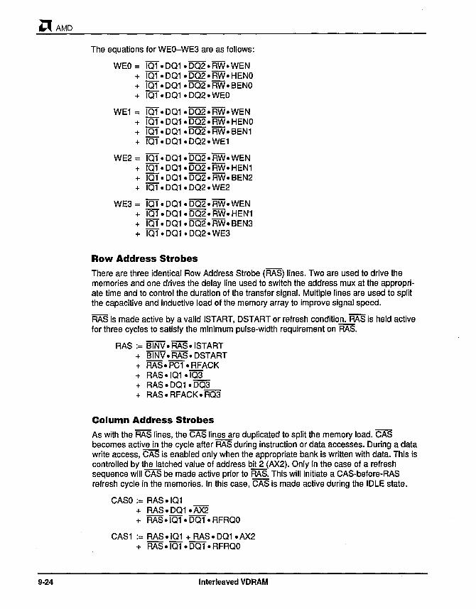
~AMD
9-24
The equations for WEO-WE3 are as follows:
WEO = IQ1. OQ1 • OQ2. RW. WEN + jQ1. OQ1 • OQ2. RW. HENO + IQ1.0Q1.0Q2.RW.BENO + jQ1.0Q1.0Q2.WEO
WE1 = IQ1. OQ1 • OQ2. RW. WEN + jQ1.0Q1.0Q2.RW.HENO + IQ1.0Q1.0Q2.RW.BEN1 + IQ1.0Q1.0Q2.WE1
WE2 = IQ1.0Q1.0Q2.RW.WEN + jQ1.0Q1.0Q2.RW.HEN1 + jQ1. OQ1 • OQ2. RW. BEN2 + jQ1.0Q1.0Q2.WE2
WE3 = jQ1.0Q1.0Q2.RW.WEN + jQ1.0Q1. OQ2. RW. HEN1 + jQ1. OQ1 • OQ2. RW. BEN3 + IQ1. OQ1 • OQ2 • WE3
Row Address Strobes
There are three identical Row Address Strobe (RAS) lines. Two are used to drive the memories and one drives the delay line used to switch the address mux at the appropriate time and to control the duration of the transfer signal. Multiple lines are used to split the capacitive and inductive load of the memory array to improve signal speed.
RAS is made active by a valid ISTART, OSTART or refresh condition. RAS is held active for three cycles to satisfy the minimum pulse-width requirement on RAS.
RAS := BINV. RAS.ISTART + BINV.RAS.OSTART + RAS.PC1.RFACK + RAS. IQ1 • IQ3 + RAS.OQ1.0Q3 + RAS.RFACK.RQ3
Column Address Strobes
As with the RAS lines, the CAS lines are duplicated to split the memory load. CAS becomes active in the cycle after RAS during instruction or data accesses. Ouring a data write access, CAS is enabled only when the appropriate bank is written with data. This is controlled by the latched value of address bit 2 (AX2). Only in the case of a refresh sequence will CAS be made active prior to RAS. This will initiate a CAS-before-RAS refresh cycle in the memories. In this case, CAS is made active during the 10LE state.
CASO := RAS .IQ1 + RAS.OQ1.AX2 + RAS.jQ1.0Q1.RFRQO
CAS1 := RAS. IQ1 + RAS • OQ1 • AX2 + RAS.jQ1.0Q1.RFRQO
Interleaved VDRAM

AMD ~
INTRA-CYCLE TIMING
This memory architecture has five timing sequences of interest. The first is a cycle used to decode the memory address and control signals from the processor. At the end of this decode cycle, the RAS registers are loaded to begin the initial access of memory if the address selects the memory block.
Following the decode cycle is the Row Address cycle, in which the row address strobe is made active at the beginning of the cycle, and the address multiplexer is later switched between the row address and the column address.
The third timing is a data access, where the CAS signal goes active to begin a read operation or perform a write operation.
The fourth is the critical timing sequence between RAS going active and the first shift clock (SAS) active edge which occurs in the row transfer of the initial access of an instruction burst.
The fifth timing is a burst access. This is the timing between SAS going High and a valid instruction being transferred to the processor. This time is designed to fit within two clock cycles.
The combination of a decode cycle followed by the row-address cycle and by a dataread access time defines a five-cycle read of data. Subsequent data-read operations may be six cycles long if the next data address appears during the PC2 precharge state.
For a data write, the access time is made up of a decode cycle followed by a data write, in which DRDY is active in the second or third cycle after decode. The write operation thus takes three to four cycles. Subsequent data-write cycles may take up to six cycles to complete if the next address appears during the data WAIT state (Le., during the memory-precharge time). A read following a write could take up to eight cycles to complete if it started during the precharge time of the previous access.
The initial access time of an instruction access is made up of a decode cycle, plus a row transfer sequence, plus the first burst access. This totals six cycles. Again, this could be extended up to nine cycles if the instruction address were to appear during the precharge time following a data-write operation or up to seven cycles if following a data read.
After the initial access, all burst instruction accesses use a two-clock-cycle timing. Because two memory banks are interleaved, the apparent access time from the viewpoint of the system bus is only one cycle per burst access following the initial access.
Decode Timing
Within the decode cycle, the address timing path is made up of:
• The Am29000 processor clock to address and control valid delay of 14 ns
• Address decode logic PAL device delay of 10 ns
• The setup time of the RAS PAL device, 10 ns.
Assuming D-speed PAL devices, those times total 34 ns, as shown in Figure 9-12.
Also, within the decode cycle time is the control Signal to response signal path. In fact, this timing path is present in every cycle in the sense that the memory response signals must be valid in every clock cycle. This delay path is made up of:
Interleaved VDRAM 9-25

~AMD
• Clock-to-output time of registers within the control logic state machine PAL device, 8 ns
• Propagation delay of the control logic PAL device, 10 ns
• Propagation delay of a logical OR gate on the response signals from each memory block, 10 ns
• Control signal set-up time of the processor, 12 ns
Again assuming D-speed PAL devices, these delay path times total 40 ns.
Row Address Timing
Referring to Figure 9-13, within the row-address cycle, the RAS line goes low, which initiates a time delay signal later causing the address multiplexer to change from the row to the column address.
Figure 9·12 VDRAM Interleaved Bank Memory Decode Cycle
Address Path ~5 tco, Am29000 Processor Output
10 tpd, Control PAL Device -....:..;:;..-
tsu, Counter PAL Device
j 34ns
10
Control Path 8 teo, Control PAL Device
10 40 ns tpd, Control PAL Device
10 tpd, Response PAL Device
tsu, Am29000 Processor Setup 12
Figure 9·13 Row Address Timing
9-26
teo, PAL Device RAS Output
tid, Memory Load Delay
tpd, Delay Line
tmux min, Address MUX Switching Delay
tmux max, Address MUX Switching Delay
tid, Memory Load Delay
Min RAS Address Hold Time
Clock Cycle Time
Max Time-to-Column Address
8
20
4
9.5
.. 17.5 ns+
, .... 1----- 40 ns
.... f------ 44 ns
Interleaved VDRAM
10623C·Q84
6.5
10623C·085

AMD ~
This delay path is made up of:
• Clock-to-output time of RAS signal registers within the control-logic state machine PAL device (8 ns) plus an added delay due to capacitive and inductive loading by the memory array of the PAL device outputs. The estimated delay is 6.5 ns. This is added to the 8 ns delay of the RAS line (standard 50 pF load) for a total of 14.5 ns, worst case.
• Mux switch control signal delay path, which runs in parallel with the memory RAS delay just described. This mux signal delay is made up of the clock-to-output delay of a lightly loaded RAS signal (8 ns) plus the delay line time (20 ns).
• Minimum and maximum switching time of the address multiplexer, 4 ns to 9.5 ns, plus added delay for heavy loading (same as calculated above), 6.5 ns.
Thus, the memory RAS signals are stable no later than 14.5 ns into the cycle, and the address mux output can change no sooner than 32 ns (assuming RAS outputs from the same PAL device will always have similar delays). So the address hold time provided after RAS goes active is 17.5 ns. This works out to satisfy the 15 ns of required address hold time after RAS goes active. Also, the column address is settled by no later than 44 ns in to the cycle. So the column address is set up prior the CAS going active in the next cycle.
CAS·to·Data Ready
In a data-read operation, the Column Address Strobe (CAS) signal-to-end of DRDY cycle is made up of:
• CAS Signal clock-to-output time, 8 ns, plus added delay for heavier-than-normal output loading, as determined above, 6.5 ns
• Memory access delay from CAS, 60 ns
• Data bus transceiver propagation delay, 10 ns
• Processor set-up time, 6 ns
This totals 80.5 ns, which translates into just a little more than two cycles. Therefore, DRDY is not made active until the second cycle following the DCAS state.
In a data-write operation, the data is written by the falling edge of CAS. But the data hold time relative to RAS going active may also have to be satisfied before DRDY is made active to free the address and data buses.
For the Fujitsu memory, only the data hold time relative to CAS is required; this is 30 ns after CAS active. The Am29000 processor will provide a minimum of 4 ns data hold time. The data transceiver will provide an additional minimum of 4 ns hold time beyond the end of the DCAS cycle. As shown in Figure 9-14, these will ensure meeting the hold time if DRDY is active in the DCAS cycle.
For the NEC memory, the hold time relative to RAS is the longer delay path; this is 95 ns from RAS going active. This implies the data must be held 29.5 ns into the WAIT state after DCAS. So in this case, DRDY must not go active until the WAIT state after DCAS as shown in Figure 9-15.
Interleaved VDRAM 9-27

~AMD
Figure 9-14
9-28
Cl[$-to-Data Ready Timing
Data Read
teo, PAL Device CAS Output
tid, Memory Load Delay
taa, Memory Access Time
tsu, Am29000 Processor Setup
Data Write
teo,
tid,
th,
PAL Device CAS Output
Memory Load Delay
Am29000 Processor Min Data Hold
Clock Cycle Time
CAS-to-Data Ready Delay
Min Data Hold Relative to CAS for Fujitsu Memory
RAs-to-Shift Clock Timing
B
6.5
60
6
B
6.5
4
4~-----BO.5 ns----.~
..- 29.5 ns --.
10623C-086
Referring to Figure 9-15, in order to maintain a six-cycle initial instruction access time, only three cycles can be used for the timing of signals between RAS and SAS. In that time, the TR signal must be active for 90 ns to 100 ns after RAS, and it must be inactive 25 ns to 10 ns before SAS goes active, depending on the memory used. It is a tight fit. The timing is as follows:
• Clock-to-memory RAS delay, 8 ns, plus the added delay for heavy output loading of 6.5 ns, for a total of 14.5 ns
• In parallel with the memory RAS, a separate copy of RAS not loaded by the memory array is used to drive the delay line determining the end of the TR signal. Its clock-tooutput delay time is 8 ns
• Delay line time of 90 ns or 100 ns
• Propagation delay of the PAL device, which generates TR from the output of the delay line, is a minimum of 3 ns and a maximum of 10 ns, plus an output loading delay of 6.5 ns
• The SAS output is combinatorial and is dependent on registered input signals. Its minimum delay is the minimum clock-to-output delay plus the minimum propagation delay of a D-speed PAL device, plus the added delay for memory loading (3 ns + 3 ns + 6.5 ns= 12.5 ns). Its maximum delay consists of 8 ns of clock-to-output delay, 10 ns of propagation delay, and a loading delay of 6.5 ns for a total delay of 24.5 ns.
Interleaved VDRAM

AMD ~ Figure 9·15 NEe Memory Write Data Hold Time
teo, PAL Device RAS Output
tid, Memory Load Delay
teo, PAL Device CAS Output
tid,
th,
Memory Load Delay
Min RAS Address Hold Time
Clock Cycle Time
Min Delay into D Wait Cycle, RAS Address Hold Time for NEC Memory
8
6.5
40 ns
8
6.5
95
29.5 ns-.
10623C-087
Assuming minimum delays in the TR and SAS signals and maximum delays in the RAS signals, the hold time for TR will just be met for either the NEC or Fujitsu memories. For the Fujitsu memory, the TR setup time before SAS will also just be met as shown in Figure 9-16. For the NEC memory there is 5 ns of margin as shown in Figure 9-17.
The above relies on the fact that all RAS outputs are implemented in the same PAL device and TR and SAS outputs reside in the same PAL device. The PAL device outputs for related signals will thus always track each other with respect to minimum or maximum delay times.
Burst Timing
Within the burst access cycle, the address to data path timing is determined by:
• The clock-to-output time of Q02E, 8 ns for a D-speed PAL device
• Propagation delay of SAS PAL, 10 .!§.plus added delay for heavy capacitive and inductive load as was done for the RAS line. The same derating delay of 6.5 ns applies.
• Memory access time for serial port, 40 ns
• F157 Multiplexer delay, 6.5 ns
• The processor set-up time, 6 ns.
Those delays produce a worst-case total of 77 ns as shown in Figure 9-18.
INTER-CYCLE TIMING
Inter-cycle timing for instruction, data-read, and data-write cycles are provided in Figures 9-19 through 9-21. In these timing diagrams, the horizontal time scale is 20 ns per division.
Interleaved VDRAM 9-29

~AMD
Figure 9·16 Fujitsu Transfer Enable Timing
Fujitsu Memory
teo,
tid,
tpd,
tpd,
tid,
teo,
tid,
9-30
PAL Device RAS Output
Memory Load Delay
Delay Line
Transfer Enable PAL device Min Delay
Memory Load Delay
PAL Device SAS Output Min Delay
Memory Load Delay
Transfer Enable Min Hold Time After RAS
Transfer Enable Min Setup Time to SAS
Clock Cycle
8
6.5
90
+-- 40 ns ---.
Interleaved VDRAM
107.5 ns
3
6.5
6
6.5
93 ns-t-----+r
~ _.::2;::.51--"
10623C-088

Figure 9-17 NEe Transfer Enable Timing
NEe Memory
teo,
tid,
tpd,
tpd,
tid,
teo,
tid,
PAL Device RAS Output
Memory Load Delay
Delay Line
Transfer Enable PAL device Min Delay
Memory Load Delay
PAL Device SAS Output Min Delay
Memory Load Delay
Transfer Enable Min Hold Time After RAS for NEC Memory
Setup Time to SAS Transfer Enable Min
Figure 9·18 Burst Access Timing
teo, PAL Device Q02E Output
tpd, PAL Device SAS Output
Tid, Memory Load Delay
8
tsa, Buffer Delay Memory SAS to Data Access Time
tpd, Multiplexer Delay
6.5
tsu, Am29000 Processor Data Setup Time
Clock Cycle Time
100
3
6.5
103 ns -"'------.~
8
10
6.5
40
6.5
6
+-- 40 ns-.+-- 40 ns-'
441------- 77 ns ----~~.
Interleaved VDRAM
AMD ~
117.5 ns
6.5 ns
~ 15 ns ~
10623C·089
10623C·090
9-31

~AMD
Figure 9·19 VDRAM Instruction Burst Timing
SYSCLK
IREO
IBACK
IBREO
IBREO.D I
IRDY
101
102
103
104
PC1
PC2
LD
X I
CNT
Q02E
RASx
CASx
TRx
SASO
Tr
SAS1
SDE
SDO
IOE
INSTR
IBACK 29Ki
9-32
~I~' ______ ~~ ____ ~ __ ~~ __ ~~ __ ~~ ____ ~ ____ ~'~~L_' __________________ ~ __ __
I I I
I II
I I I
I II
Q Q Q
I I I I I I
I
I I
I I I
X X I
*
Q
~ __________________ ~~L ____________________ __
I I I
I II
I I I
I II I I
I I
I
I
Q Q Q Q
X 10(0) X 110(0+1 )1 X 110(0 +2)110(0 +2)1 X 110(0 +3)1 I I I I I I I I I I
~~ __ ~~~ ____ ~ __ ~-J~~ __ ~~~~~~ __ ~~ ___
Ido) I 10(0) I I I I • I I i i. i) I I i
~-~---~ y" I I
generated by IBREO.D • IBACK
Interleaved VDRAM
I I
10623C·093

Figure 9·20 VDRAM Data Read Timing
SYSCLK 1
DREQ
R/W
f5EN
DRDY
DQ1
DQ2
DQ3
DQ4
PC1
PC2
AX2
RAS
CASO
CAS1
TRICE
DQE
DQa
DATA
I
New access can start in parallel to precharge
Interleaved VDRAM
AMD ~
x
x
10623C·092
9-33

~AMD
Figure 9·21 VDRAM Data Write Timing
DREQ
R/W
PEN
DRDY
DQ1
D02
D03
D04
PC1
PC2
AX2
RAS
CASO
CAS1
WEi
DOE
DOC
DATA
9-34
Early write due to WE going active before CAS active. Also at WE lis active, DATA is valid.
Interleaved VDRAM
x
x
10623C-093

Table 9·1
AMD ~
PARTS LIST
The parts list for the Am29000 Processor Interleaved VRAM Interface is provided in Table 9-1.
Interleaved VRAM Interface Parts List
Item No.
U1
U2
U3
U4
U5-U8
U9
U10
U11
U12
U13
U14-U29
U3D-U37
U38
Quantity
4
16
8
38 packages
FINAL DISCUSSION
Device Description
PALCE16V8-D
PAL20L8-B
AmPAL22V10-25
74F175
74F157
PALCE16V8-D
PAL16R4-D
PAL20R8-D
PAL20R4-D
PAL20L8-D
MB81461-12 or PD41264
74F157
XTTLDM-100
Looking at the design, there may be concerns about the size of the design, whether it is compact or large. For an objective analysis, first look at the design from a theoretical standpoint, without considering the type of processor being used.
To perform single-cycle bursts with DRAM at clock speeds up to 33 MHz, you must use two banks of interleaved DRAMs. Because of the 32-bit wide architecture, you need a minimum of 16 DRAMs (64K x 4-bit devices), eight DRAMs per bank.
You also need multiplexers and drivers for interleaving, which adds another 16 parts to the design. In this design, only the multiplexers are needed, so only eight parts are added. For a burst start on an odd address, you need one incrementer PAL device in any case.
For DRAMs, the address lines must be multiplexed. This implies the addition of four multiplexers.
A refresh counter must be implemented. This implies the addition of one PAL device.
Interleaved VDRAM 9-35

~AMD
9-36
In any case, you need either a delay line or a high-speed clocked state machine for fast generation of RAS and CAS signals.
In summary, the raw logic, which does not depend on the type of processor used, requires 31 devices. Only seven PAL devices are used for all the rest of the design, including the state machines, the generation of the RAS and CAS signals, and the interface to the Am29000 processor. By using higher-integrated PAL devices or higherdensity logic, this number could be reduced further.
Interleaved VDRAM

SINGLE-BANK VDRAM
OVERVIEW
For an overview of the relative advantages and disadvantages of VDRAM, see the first section of the previous chapter.
Currently available VDRAMs are able to support a 30-ns serial shift rate, so a single bank VDRAM system can support an Am29000 processor system running at 20 MHz.
MEMO~Y FEATURES
The VDRAM memory design described in this chapter is a reduced version of the dual-bank design in the previous chapter. The major difference is only one bank of VDRAM is used. You will find many similarities between this design and the one in the previous chapter.
Figure 10-1 is a high-level block diagram of a single-bank VDRAM memory. The bank is a minimum of 64K words deep (32 bits per word).
A non-sequential instruction access requires one cycle for address decoding plus five additional cycles for the first word accessed. The burst access timing is similar to that used in the previous chapter; each burst access is one cycle long. The end result is a memory providing a six-cycle access time for the first word of a non-sequential instruction access, and single-cycle access for subsequent words in a burst transfer. A data-read access requires one cycle for address decoding plus four additional cycles to complete the access.
A data write access requires one cycle for address decode plus two cycles or three cycles (depending on the memory used) to take data from the bus. The write operation continues internal to the memory for one or two additional cycles, but the data bus is released after data is taken from the bus.
No burst accesses are supported for data. All data read accesses are five cycles long and all write accesses are three or four cycles long. That is assuming the memory has internally completed· a write operation and/or RAS precharge before the next access begins. If write completion time or RAS precharge time has not been satisfied, a subsequent data access can require up to eight cycles to complete. This is based on the worst case, a data read immediately following a data write operation.
INTERFACE LOGIC BLOCK DIAGRAM
A block diagram of the interleaved VDRAM memory is shown in Figure 10-2. The various circuit blocks are described below.
Single-Bank VDRAM 10-1

~AMD
Figure 1 ()"1 Am29000 Processor with VDRAM Memory
10-2
Address
Controls
The Memory
I
... -~ ./
I I
Control Logic
I
I
Am29000 Processor
A
I J
Buffers
VDRAM Instruction
and Data Memory
Data
/ '\.
Instruction
I
I
~ U
r-
I -I
Transceivers
10023C-094
The memories are 64Kx4 bit VDRAMs supplied by either Fujitsu (MB81461-12) or NEC (PD41264-12). These memories have common data-in and data-out lines. Their access speed is 120 ns. Eight devices are required to form the 32-bit wide instruction word for the Am29000 processor. These are shown as devices U10 through U17.
VDRAM is used in this design to illustrate the savings in complexity, component count, and cost that the VDRAM architecture can provide. These savings come largely from the fact that the instruction and data words can reside in a common memory array still allowing concurrent dual-port access. Using one memory array, instead of split instruction and data memories, eliminates one entire set of memory control logic and data buffers. Also, the number of remaining control-logic and data-buffer circuits is reduced, since external buffers are no longer needed to support both data and instruction ports into the instruction memory.
The VDRAM structure allows the boundary between instruction and data space to be flexible and dynamic, thereby providing for more efficient use of memory than a system that splits memory. This, in turn, may lead to reduced memory requirements in general.
Single-Bank VDRAM

AMD ~ Figure 10-2 Single-Bank VDRAM Memory Block Diagram
A31-A24 PIN169
IREO IREOT OREO
DREOT1-0 2 RFROO RFACK
PC1 101
001
SYSCLK
SYSCLK RESET
I START DSTART
RiW
IREO DREO
SYSCLK RESET
BINV TEXIT
R01-R03
IBREO
U6-U9 22V10-15 20L8-10 20R8-15 20R4-15
RAS 10ns IRDY 20ns
PEN 30ns U18 40ns
101-104 XTT 50ns D01-D04 LDM 60ns PC1-PC2 -100 70ns
80ns DRDY 90ns
100ns
TR1 TRIOE
RAS1 RAS CAS1
MUX
TEXIT
32
IBREO.D WEO-WE3 CAS SO 131-100 WE (4x)
SAS SAS U10-U17
8 MB81461-12 U4-U5 (X8)
AO~A02--------~~-------M
74F157 A7-AO 32 8 (X2) SE
DQ 031-000 A 17-A 1 0 --------~t--------_M
- 10623C-095 -
Data Bus Connection
The memory random access data I/O port is connected directly to the Am29000 processor data bus lines. Isolating transceivers are not necessary so they are not used. This eliminates transceiver delays.
If higher driver currents were necessary, transceivers could be inserted between the data outputs of the VDRAMs and the Am29000 processor data bus lines.
Instruction Bus Connection
Because only one bank is used, the memory serial data outputs are also connected directly to the instruction bus of the Am29000 processor. This eliminates the buffer delays present in the dual-bank design.
Address Multiplexers
The upper and lower eight bits of memory address must be multiplexed into the address inputs of the memories. Discrete multiplexers are used to perform this function. These devices are shown as US through US.
Single-Bank VDRAM 10-3

~AMD
10-4
Note that in this design, the address is taken directly from the bus and through the multiplexers to the memories. No latching or registering of the address is done. This approach reduces the component count and complexity of the design, illustrating a lower-cost memory design. Doing this requires the memory control logic to force the Am29000 processor to hold the address stable on the bus until after the RAS and Column Address Strobes (CAS) have gone active. This is done by delaying the assertion of IBACK or PEN during instruction or data accesses, respectively.
This approach reduces system performance somewhat, at least when compared with a split instruction and data memory system, or a system with multiple blocks of VDRAM in which one block could be addressed for an instruction fetch while another block is addressed for a data access. This is because the processor must, at times, hold an address on the bus when it might otherwise have been able to begin another access on an alternate memory block, assuming a memory that latches the address.
But in a system having a single block of VDRAM, there is no benefit to latching the address from the bus. This is because the memory cannot be ready to begin another access until the access in progress is completed, and the memory has completed the precharge cycles that must occur between all non-sequential accesses.
A word of warning: Do not use inverting buffers or multiplexers on VDRAM address lines. Inverted random access I/O (DO) port addressing would conflict with the sequentially incremented addressing required by the design of the serial port.
VDRAM Shifter
Since a VDRAM uses a shift mechanism to provide the serial output of instruction code, there is no need for an address counter. The initial address for an instruction burst request determines the starting location in the memory row to be shifted out. All subsequent instruction words are read by providing a shift clock to the VDRAM. Also, because the VDRAM shifter row is 256 words, the Am29000 processor always provides a new address at the right time when a row boundary is crossed. In addition, no address counter is required for data accesses, since no burst data accesses are supported in this memory design.
Registered Control Signals
As noted earlier, the timing of the IBREO control signal requires it be registered by a low-setup-time register; a F175 register is used (U3, shown in Figure 10-2).
Interface Control Logic
This logic must generate the memory response signals, manage the loading of memory addresses, generate RAS and CAS Signals, and perform memory refresh. The logic functions needed for this require six PAL devices: one PAL20L8-B, one AmPAL22V10-25, one AmPAL22V10-15, one PAL20L8-D, one PAL20R8-B, and one PAL20R4-B.
Device U1, a PAL20L8-B, performs address decode for instruction and data accesses. Its outputs indicate when the memory block has been addressed and an access is to begin.
Device U2, an AmPAL22V1 0-25, acts as a refresh-interval counter and refresh-request logic.
Single-Bank VDRAM

AMD
Devices U6-U9, one AmPAL22V1 0-15, one PAL20L8-D, one PAL20R8-B, and one PAL20R4-B, form a state machine controlling the RAS, CAS, shift clock, transfer cycle enables, and memory-response signals.
Response Signal Gating
The memory-response signals from all system bus devices are logically ORed together by a PAL device before being returned to the Am29000 processor. The gates in this PAL device are not included in the component count of this memory design since they are shared by all the bus devices in the system, and as such, are part of the overhead needed in any Am29000 processor system.
Byte Write Capability
The interface logic supports the byte write capability of the Am29000 processor. It uses the signals OPT1 , OPTO, A 1, and AO to generate the write enable signals WEO-WE3. This design supports only big endian byte ordering.
MEMORY INTERFACE LOGIC EQUATIONS
State Machine
The control logic for this memory can be thought of as a Mealy-type state machine in which the outputs are a function of the inputs and the present state of the machine. This structure is required because some of the output signals must be based on inputs which are not valid until the same cycle in which the outputs are required to take control of the memory. As shown in Figure 10-3, this state machine can be described as having 18 states. (Note: A timing diagram is provided at the end of this chapter.)
It is important to note that in this design, the instruction burst is never preempted by the slave. The reason for this is that VDRAMs are used; no contention between instruction bursts and data accesses can occur. Also, the length of the shifters is a minimum of 256 words. After 256 words, the Am29000 processor automatically preempts the burst by itself so it does not have to be preempted by the slave.
Therefore, in this design, no logic is needed to preempt an instruction burst.
IDLE is the default state of the interface state machine. It is characterized by the lack of any instruction access, data access, or refresh activity in progress. This state serves as a way of identifying when the memory is not being accessed and could be placed into a low-power mode. This state also serves as a precharge cycle for the memory when a transition is made between instruction, data, and refresh sequences.
A transition to either the IRAS or DRAS state occurs when an address selecting this memory block is placed on the address bus. These transitions are inhibited if the BINV signal is active. A transition to the RQ1 state occurs when a refresh request is active. Refresh takes priority over any pending instruction or data-access request.
There are five Virtual States shown in Figure 10-3; they are IQ1 through IQ4 and IACCESS. These states are needed because the serial data (SD) port of the VDRAM operates independently of the random access 1/0 (DQ) port after a row transfer cycle is completed. The states help illustrate what might be called the "split personality" of the state machine. Once a transfer cycle begins, there are in effect two active states in this state machine. One state tracks the activity of the serial port control signals, and the other tracks the activity of signals associated with the random access 1/0 port.
Single-Bank VDRAM 10-5

~AMD
Figure 10-3 VDRAM Memory State Diagram
(REFRESH+ISTART +OSTART)
10-6
If BiNV is active, then these transitions never occur
IST~RT
10623C-096
The active states can be thought of as two tokens, labeled SO and DO, being moved around a game board. The DO token is never allowed to follow the dotted line to the virtual states. The SO token is always in one of the virtual states or the IDLE state; it never enters any of the other states. When the SO token enters the IDLE state, it cannot leave until the DO token is also in IDLE and the ISTART condition is true.
When both tokens are in IDLE and ISTART is true, the SO token moves to the 101 state and the DO token moves to the IRAS state. This would represent the beginnin~ row transfer to the serial-shift port. The DO token then tracks the progress of RAS, CAS, and address signals applied to the VDRAM. When the transfer sequence is finished, the DO token goes through the precharge states and returns to IDLE. The SO token proceeds
Single-Bank VDRAM

AMD ~ through the IQ states, counting off the delay needed until the first instruction is ready at the output of the SD port. In the IQ2 state, IBACK is made active to release the address bus. In IQ3 and IQ4, the shift clock and bank select signals begin operation to allow the access of the first instruction word. In IACCESS, IRDY is allowed to go active. During subsequent cycles of an instruction burst access, the active state remains IACCESS.
While the active state for instruction accessing is IACCESS, the DQ token is free to move through data access states or refresh states completely independent of the instruction access in progress. When an instruction burst ends, the SD token returns to IDLE and must wait until the DQ token completes an access or refresh sequence followed by precharge before a new transfer cycle may begin.
The IRAS state occurs during the first cycle of a row transfer to the SD port following a new instruction address being presented on the address bus. During this state, the instruction output multiplexer is enabled, Ready response lines are held inactive and the RAS lines go active. RAS is used as the input to a delay line whose output will switch the address mux to the column address after the row address hold time is satisfied. The transition to the ICAS state is unconditional.
During the ICAS state, CAS goes active to start the transfer cycle. Since the RAS minimum pulse width is 120 ns, and the minimum CAS pulse width is 60 ns, a WAIT state follows the ICAS state before the unconditional transition to the first precharge state.
During the precharge states, RAS goes inactive. The precharge period for the memory used is 100 ns, so a second and third precharge cycle is done during the PC2 and IDLE states, which unconditionally follow the PC1 cycle.
During a DQ port read sequence, the DRAS state generates RAS and the address-mux select signals. The DCAS state makes CAS active. Since the access time from CAS is 60 ns, the total of CAS-clock-to-output delay, plus access time, plus processor setup time is in excess of 95 ns. This timing will require a WAIT cycle for future upgrades, finally followed by the DACCESS cycle. During DACCESS, the DRDY signal is made active.
The DQ port write access is different only in that the DRDY signal may be made active during DCAS, since the data from the bus is written into the memory by the falling edge of the CAS signal. This is done by using the early write cycle timing of the VDRAM. Doing this allows the processor to begin a new address cycle on the address bus during the WAIT cycle. This may help improve system performance if the new address is directed at a different memory block that can immediately begin a new access. The WAIT cycle is used to fulfill the minimum CAS active time requirement. The DACCESS Simplifies the design by allowing the logic controlling the state transitions to be the same for both read and write operations.
Finally, there is the refresh sequence. Once the IDLE state is reached and a refresh is pending, the refresh sequence starts as the highest priority task of the memory. In fact, during the IDLE cycle, CAS will go active to set up a CAS-before-RAS refresh cycle. This type of refresh cycle makes use of the VDRAM internal refresh counters to supply the refresh address. During RQ1, RAS is made active as in IRAS and DRAS cycles. The RQ2 and RQ3 cycles are used to supply two additional wait states to make up the three cycles needed to satisfy the minimum RAS active time of 120 ns.
Single-Bank VDRAM 10-7

~AMD
Logic Details-Signal By Signal
The logic equations for the memory interface signals are described below. The signals, as implemented in the final PAL device outputs, are often active Low, as required by the actual circuit design. The signals are described in active High terms so the design is a little easier to follow. The PAL device definition files are shown in Figures 10-4 through 10-9; the figures are followed by descriptions of how the equations were derived.
NOTE: All PAL device equations use the following conventions:
• Where a PAL device equation uses a colon followed by an equals sign (:=), the equation signals are registered PAL device outputs .
• Where a PAL device equation uses only an equals sign (=), the equation signals are combinatorial PAL device outputs.
• The Device Pin list is shown near the top of each figure as two lines of signal names. The names occur in pin order, numbered from left to right, 1 through 20. The polarity of each name indicates the actual input or output signal polarity. Signals within the equations are shown as active High (e.g., where signal names in the pin list are: A 8 C; the equation is C = A. 8; the inputs are A = Low, 8 = Low; then the C output will be Low).
Figure 1()"4 AmPAL22V10·25 VRAM Refresh Counter/Request Generator Device U2
10-8
CLK RFACK RQ1 RQ2 RQ3 NC6 NC7 NC8 NC9 NC10 NC11 GND NC13 RFRQO RFQ2 RFQ3 RFQ4 RFQS RFQ6 RFQ7 RFQ8 RFQ10 RFQ9 VCC
RFQ2 :=RFQ2
RFQ3 :=RFQ2.RFQ3 + RFQ2.RFQ3
RFQ4 :=RFQ2.RFQ3.RFQ4 + RFQ2.RFQ4 + RFQ3.RFQ4
RFQS :=RFQ2.RFQ3.RFQ4.RFQS + RFQ2.RFQS + RFQ3.RFQS + RFQ4.RFQS
RFQ6 :=RFQ2.RFQ3.RFQ4.RFQS.RFQ6 + RFQ2.RFQ6 + RFQ3.RFQ6 + RFQ4.RFQ6 + RFQS.RFQ6
RFQ7 :=RFQ2.RFQ3.RFQ4.RFQS.RFQ6.RFQ7 + RFQ2.RFQ7 + RFQ3.RFQ7 + RFQ4.RFQ7 + RFQS.RFQ7 + RFQ6.RFQ7
Single-Bank VDRAM
10023C-097

AMD ~ Figure 1 ()'4 AmPAL22V10·25 VRAM Refresh Counter/Request Generator
Device U2 (continued)
RFQa :=RFQ2.RFQ3.RFQ4.RFQ5.RFQ6.RFQ7.RFQa + RFQ2.RFQa + RFQ3.RFQa + RFQ4.RFQa + RFQ5.RFQa + RFQ6.RFQa + RFQ7.RFQa
RFQ9 :=RFQ2.RFQ3.RFQ4.RFQ5.RFQ6.RFQ7.RFQa.RFQ9 + RFQ2.RFQ9 + RFQ3.RFQ9
. + RFQ4. RFQ9 + RFQ5.RFQ9 + RFQ6.RFQ9 + RFQ7.RFQ9 + RFQa.RFQ9
RFQ10:=RFQ2.RFQ3.RFQ4.RFQ5.RFQ6.RFQ7.RFQa.RFQ9.RFQ10 + RFQ2. RFQ1 0 + RFQ3. RFQ1 0 + RFQ4. RFQ1 0 + RFQ5. RFQ1 0 + RFQ6. RFQ1 0 + RFQ7. RFQ1 0 + RFQa. RFQ1 0 + RFQ9. RFQ1 0
SYNCHRONOUS PRESET= RFQ2.RFQ3.RFQ4.RFQ5.RFQ6.RFQ7.RFQa • RFQ9. RFQ1 0
RFRQO := RFRQO. (RFACK. RQ1)
Figure 1 ().5 PAL20L8-B VRAM State Decoder Device U1
IREQ DREQTO IREQT A31 A30 A29 A2a A27 A26 A25 A24 GND DREQ DREQT1 ISTART RFRQO RFACK PIN 169 RIT DQ1 PC1 DSTART NC23 VCC
ISTART = RIT.DQ1.RFACK.PC1.RFRQO.IME
DSTART = IQ1.DQ1.RFACK.PC1.RFRQO.OME
NOTE: In the above equations, IME and OME are used only for clarity. The actual input terms should be substituted when compiling this device.
IME = IREQ. iREQT. A31 • A30. A29. A2a. A27. A26. A25. A24. PIN169
OME = OREQ.OREQTO.OREQT1.A31.A30.A29.A2a.A27.A2S.A25.A24 • PIN169
10623C-09B
Single-Bank VDRAM 10-9

~AMD
Figure 1 ()'6 AmPAL22V1 0·15 VRAM Instruction State Generator-Single Bank Device U6
CLK IREO ISTART OSTART WE NCG IBREO.D BINV NC9 GND DE 001 002 003 004 101 102 103 104 IRDY DRDY VCC
101 :=BINV-TQT-ISTART + 101 - (103 -104)
102 :=101- (1013-104) 103 := 102 - 104
104 :=103
IRDY = 103 -104 + 101 -IBREO.O
001 :=BINV-D01-DSTART + 001-004
002 := 001 - 004
003 :=002-004
004 :=003-004
DRDY = WE - 004 + WE- 003- 004
10623C·099
Figure 1()'7 PAL20L8-D VRAM Transfer Generator-Single Bank Device U7
10-10
003 TEXIT NC3 001 002 IREO WE NCe RESET RW 103 GND SYSCLK IBREO SAS ffi WE 101 104 NC20 PEN NC22 NC23 VCC
SAS = RESET - SYSCLK + RESET- 101 -104 + RESET - 104 - iQ3 - =SY~S=C=-:-L~K + RESET -101 - SYSCLK -IBREO -IREO
TR = 001 -IREO + 001-TR-TEXIT + 002-WE
PEN = 002 - 003
WE = 101-001-D02-RW + 101-D01-D02-WE
Single-Bank VDRAM
10623C·100

Figure 1 Q.8 PAL20RS·B VRAM HAS·CAS Generator-Single Bank Device US
AMD ~
elK ISTART DSTART JQ1 DQ1 la3 D03 RC3 BINV NC10 RFRQO GND OE RFACK RASO NC16 RAS PC1 PC2 CAS NC21 NC22 NC23 VCC
RASO :=BINV.RASO.ISTART + BINV.RASO.OSTART + BINV. RASO. PC1 • RFACK + RASO. IQ1 • IQ3 + RASO. OQ1 • OQ3 + RASO.RFACK.RQ3
RAS :=BINV.RAS.ISTART + BINV.RAS.OSTART + BINV.RAS.PC1.RFACK + RAS .IQ1 • IQ3 + RAS.OQ1.0Q3 + RAS.RFACK.RQ3
PC1 :=PC1 .IQ3 + PC1.0Q3 + PC1.RQ3 + PC1. PC2
PC2 :=PC1
CAS = RAS. IQ1 + RAS.OQ1 + RAS .IQ1 • OQ1 • RFRQO
Figure 1 Q.9 PAL20R4-B Byte Write Enable Generator-Single Bank Device U9
ClK PC1 RIT OQ1 OQ2 RAS RFRQO OPT1 OPTO A 1 GNO OE AO WEO WE1 RFACK RQ1 RQ2 RQ3 WE2 WE3 NC23 VCC
WEO = IQ1 • OQ1 • OQ2 • RW. OPT1 • OPTO + IQ1.0Q1.0Q2.RW.OPT1.0PTO.A1 + IQ1.0Q1.0Q2.RW.OPT1.0PTO.A1.AO + IQ1 • OQ1 • OQ2 • WEO
WE1 = IQ1 • OQ1 • OQ2 • RW. OPT1 • OPTO + IQ1.0Q1.0Q2.RW.OPT1.0PTO.A1 + IQ1.0Q1.0Q2.RW.OPT1.0PTO.A1.AO + IQ1. OQ1 • OQ2 .WE1
WE2 = IQ1 • OQ1 • OQ2 • RW. OPT1 • OPTO + RIT. OQ1 • OQ2. RW.OPT1 .OPTO.A1 + IQ1.0Q1.0Q2.RW.OPT1.0PTO.A1.AO + IQ1 • OQ1 • OQ2 .WE2
WE3 = IQ1 • OQ1 • OQ2 • RW. OPT1 • OPTO + IQ1.0Q1.0Q2.RW.OPT1.0PTO.A1 + IQ1.0Q1.0Q2.RW.OPT1.0PTO.A1.AO + RIT.OQ1.0Q2.WE3
Single-Bank VDRAM
1 0623C-1 01
1 0623C-1 02
10-11

~AMD
Figure 10.9 PAL20R4·B Byte Write Enable Generator-Single Bank Device U9 (continued)
10-12
RFACK:= IQ1 • DQ1 • RFRQO + RFACK. (RFREQ 0 • RQ3)
RQ1 :=RQ1. PC1 • RFACK + RQ1.RQ3
RQ2 :=RQ1.RQ3
RQ3 :=RQ2.RQ3
RFQ (Refresh Request)
Dynamic memories need to be completely refreshed every 4 fls, which translates into at least one row refreshed every 15.6 flS on average. To keep track of this time, a counter is used. Once a refresh interval has passed, a latch is used to remember that a refresh is requested while the counter continues to count the next interval. Once the refresh has been performed, the latch is cleared.
The counter and refresh request latch is implemented in an AmPAL22V10-25. Nine of the outputs form the counter, which is incremented by the system clock at 20 MHz. This gives up to 512 x 50 ns = 25.6-flS refresh periods. The synchronous preset term for all the registers is programmed to go active on a count value of 389, which will produce a refresh interval of 390 cycles x 40 ns = 15.6 flS. The one remaining output is used to implement the refresh request latch. That latch function (registered output) is also set by the synchronous preset term.
The equations for the counter are shown in Figure 10-4. Below are the preset and refresh latch equations:
SYNCHRONOUS PRESET =RFQ2.RFQ3.RFQ4.RFQ5.RFQ6.RFQ7.RFQ8 • RFQ9. RFQ10
RFRQO := RFROO • (RFACK. RQ1)
Refresh Sequence Equations
A refresh of the memory requires multiple clocks so the minimum RAS active time of 120 ns can be satisfied. To manage this, the following equations are used.
RFACK
The Refresh Acknowledge (RFACK) signal is used to begin a refresh sequence and to clear the pending refresh request. The RFACK signal goes active when the state machine (DQ token) re-enters the IDLE state as controlled by 101 and 001. RFACK is held active until the refresh request is cleared, indicated by RFRQO. RQ3.
RFACK := DQ1 • iCff. RFRQO + RFACK. (RFREQ O. R03)
RQ1, RQ2, RQ3
The three cycles needed for a refresh are tracked by RQ1 , RQ2, and R03. R01 will not go active until the cycle following the IDLE state. This is controlled by
Single-Bank VDRAM

AMO
RQ1 • PC1 • RFACK, which is only true during IDLE. RQ1 is held active for all three refresh cycles to provide a single signal to identify when a refresh is in progress. RQ2 and RQ3 simply follow RQ1 with RQ3, signaling the last cycle of the refresh sequence.
IME
RQ1 := RQ1 • PC1 • RFACK + RQ1.RQ3
RQ2 := RQ1 • RQ3
RQ3 := RQ2. RQ3
The use of the Instruction for ME (IME) signal is based on the assumption that other blocks of instruction or data memory may be added later and that there may be valid addresses in address spaces other than instruction/data space.
This means this memory will only respond with IBACK or DRDY active when this block has been selected by valid addresses in the instruction/data space. This requires that at least some of the more significant address lines above the address range of this memory block be monitored to determine when this memory block is addressed. Also, it means the Instruction Request Type (IREQT), Data Request Type (DREQTO, DREQT1), and Pin 169 lines must be monitored to determine that an address is valid and lies in the instruction/data space.
IME is the indication the address of this memory block is present on the upper address lines, an instruction request is active, Pin 169 is inactive (test hardware has not taken control), and instruction/data address space is indicated. In other words, this memory block is receiving a valid instruction access request. This exam~esign will assume the address of this memory block is equal to A31 • A30. A29 • A28 • A27 • A26 • A25 • A24. The equation for this signal is:
IME = IREQ. IREQT. A31 • A30. A29. A28. A27 • A26 • A25. A24. Pin169
Note that IME is not directly implemented as a PAL device output in this design. The terms are used in the generation of the 1ST ART term.
DME
The Data for ME (DME) signal is the indication the address of this memory block is present on the upper address lines, a data request is active, Pin 169 is inactive, and instruction/data address space is indicated. In other words, this memory block is receiving a valid data access request. This example design will assume the address of this memory block is equal to A31 • A30 • A29 • A28 • A27 • A26 • A25. A24. Note that for this design, both the instruction and data blocks reside in the same address space. This is possible because of the common memory array of the VDRAM accessible to either the instruction serial port or the data I/O port.
The equation for this signal is:
DME = DREQ.DREQTO.OREQT1.A31.A30.A29.A28.A27 • A26 • A25 • A24 • Pin 169
As with IME, this term is not directly implemented.
Single-Bank VDRAM 10-13

~AMD
10-14
I START
The Instruction Start (ISTART) signal causes the transition from IDLE to IRAS and IQ1 states. It is valid only in the IDLE state with no refresh sequence starting, identified by not being in any other state via IQ1 - DQ1 - RFACK - PC1 - RFRQO. So when in the IDLE state and IME is active, ISTART is active.
ISTART = IQ1-DQ1-RFACK-PC1-RFRQO-IME
DSTART The Data Start (DSTART) signal is the same as ISTART except DME is the qualifier.
DSTART = IQ1-DQ1-RFACK-PC1-RFRQO-DME
IBACK
The instruction burst acknowledge (IBACK) signal is applied to the Am29000 processor and is, in effect, the indication the interface state machine is in an active or suspended instruction access. The equation is:
IBACK = IQ2 + IREQ -IBACK
The IBACK active state is entered during the IQ2 state. IBACK is delayed until IQ2 in order to hold the instruction address active on the bus until the CAS signal has gone active, thus eliminating the need for address latches or registers.
IBACK remains active until a new instruction access begins. The IBACK signal is combinatorial so it will go inactive in the same cycle IREQ goes active. This is required to hold the address on the bus until a new row transfer sequence can begin. The address must be held because there are no address latches or registers in this design to take the address from the bus. Address latches or registers would be required if IBACK were left active throughout the IREQ cycle.
This places a timing constraint on the IBACK response signal path that is different from earlier memory designs. IREQ is an unstable signal until 16 ns into a cycle. The D-speed PAL device logic implementing the IBACK logic has a propagation delay of 10 ns. The Am29000 processor has a response signal setup time of 15 ns. These delays total 41 ns, which means the logic OR gate used to combine all IBACK response signals in the system must have a worst-case propagation delay of 9 ns. This is not easy to achieve when several IBACK response lines in the system must be logically ORed. Therefore, seven PAL devices must be used.
A solution to this is to move a ~ the VDRAM-block IBACK logic down into the PAL device used to implement the IBACK response signal logical OR gate. That will eliminate one level of PAL device delay. The equation for the response OR-gate function would then become:
Single-Bank VDRAM

AMD l1 IBACK = IBACKO -IBREQ.D
+ IBACK1 -IBREQ.D + IBACK2 -IBREQ.D + IBACK3 - IBREQ.D + IBACK4 -IBREQ.D + IBACK5 -IBREQ.D + IQ2 -IBREQ.D + IREQ - IBACK
where the numbered IBACK inputs are the IBACK signals from other bus devices and the IQ2 + IREQ - IBACK inputs are from the VDRAM control logic.
The IBACK logic defined earlier remains to provide a version of IBACK local to the VDRAM control logic. That version of the IBACK is not as time critical because it will simply be registered. Only IBACK.D is needed by other parts of the VDRAM control logic.
IBACK.D
The IBACK Delayed (IBACK.D) signal is simply a one-cycle delayed version of IBACK. The logic for IBACK is implemented directly in the IBACK.D equation.
IBACK.D := IQ2 + IREQ-BACK
It is used in the generation of IRDY, IOEO, IOE1, and CNT.
Instruction Initial Access States
Signals IQ1, IQ2, IQ3, and IQ4 are used to control the state transitions from IQ1 to IACCESS and IRAS through WAIT during the first instruction access. The IQ1 signal goes active during the IQ1 and IRAS states, and remains active for four additional cycles. IQ1 will go active only when there is a valid ISTART.
BINV inhibits the transition to IQ1. BINV is used in this equation instead of in the ISTART equation because it only needs a 15-ns setup time for the PAL device. If it were used in the ISTART PAL device, an additional 15-ns combinatorial delay would be created, so the BINV signal could not be used correctly any more.
The IQ2, IQ3, and IQ4 signals are used to count the five cycles during which IQ1 is active. IQ3 is inactive during the fifth cycle after IQ1 goes active. This is used as a way of identifying the fifth cycle as the condition of IQ3 - IQ4. This eliminates the need for an additional signal to directly indicate the fifth cycle.
IQ1 := BINV- iQi-ISTART
+ IQ1 - (IQ3 - IQ4))
IQ2 := IQ1 - (IQ3 - IQ4) IQ2 := IQ1 - (IQ3 -IQ4)
IQ3 := IQ2 -IQ4
IQ4:= IQ3
Single-Bank VDRAM 10-15

~AMD
10-16
Data Initial Access States
These equations are similar in function to the IQ4-IQ1 signals. They control state transitions during data accesses. DQ1 goes active during the DQ1 state as a result of a valid DSTART signal during the IDLE state. DQ2 through DQ4 simply count off the four DQ states. The reason for using BINV here is the same as for the instruction side.
DQ1 := BINV.DQ1.DSTART + DQ1.DQ4
DQ2 := DQ1 • DQ4
DQ3 := DQ2. DQ4
DQ4 := DQ3. DQ4
Precharge States
At the end of any DQ port access, the RAS lines must be made inactive to precharge internal memory buses before another access with a different row address may begin. Three cycles are needed, indicated by the signals PC1 and PC2. The PC1 signal is active during the PC1 state and the PC2 state. The PC2 signal is active during the PC2 state and the first IDLE state that follows the PC2 state. PC1 goes active following the third cycle of any instruction, data, or refresh sequence. In other words, once the minimum RAS pulse width requirement is satisfied, RAS is made inactive to begin precharging for the next access. In the case of a data read where the output data must be held valid after RAS goes inactive, the CAS signal is kept active to hold the data.
PC1 := PC1 .IQ3 + PC1.DQ3 + PC1.RQ3 + PC1.PC2
PC2 := PC1
Transfer Cycle Enable and DQ Port Output Enable
On a VDRAM, there is a dual function signal, called Transfer (TR), which controls when a row transfer cycle is performed and also when the random I/O data port is output enabled. When TR is active during the active edge of RAS, a transfer cycle is performed.
The timing of TR is critical when performing this function. It must stay active for a minimum of 90 ns after RAS goes active when the Fujitsu VDRAM (MB81461-12) is used, or 100 ns after RAS goes active when the NEG VDRAM (PD41264-12) is used. The signal must also be inactive before the serial shift clock may go from Low to High, to clock out the first instruction word: 25 ns before for the Fujitsu VDRAM, or 10 ns before for the NEG VDRAM.
To make the above timing constraint fit within the six-cycle initial access time of this memory design, a delay line must be used to precisely set the duration of the TR signal. A separate RAS signal, which is not loaded by the capacitance of either memory bank, is the input to the delay line. The output for a 1 OO-ns delay is TEXIT1. More details of this timing are provided in the intra-cycle timing section of this chapter.
Single-Bank VDRAM

AMD
TR goes active with IREQ, so TR is set up before RAS goes active. TR latches itself active until the appropriate TEXIT signal goes active. The NEC input is strapped to Low when the NEC memory is used, or to High when the Fujitsu VDRAM is used.
Finally, when DQ2 is active during a non-transfer cycle of a read operation, the active TR signal enables the DQ port output.
TR DQ1.IREQ + DQ1. TR. TEXIT + DQ2.WE
Shift Clock
;Start Transfer for I-Burst ;Delay line for Transfer ;OE for Data read
The signal clocking each new instruction out of the serial port is referred to as SAS. This signal must be Low at the time TR goes inactive and it must remain Low for the 2S-ns or 10-ns period noted earlier. Once that timing constraint is satisfied, the next rising edge of SAS clocks the serial port output. SAS is held Low while IQ1 is active and IQ4 is inactive. After that time, SAS is controlled by SYSCLK so a new instruction is clocked out every system clock cycle.
There is a special requirement on SAS immediately following system power-on time. The SAS signal must be cycled at least eight times before proper device operation is achieved following a power-on sequence. To ensure this is done, the system reset signal is used to connect the system clock to SAS. This ensures SAS is cycled during the system power-on reset time.
SAS RESET.SYSCLK + RESET. IQ1 • IQ4 + RESET. IQ4. iQ3 • SYSCLK + RESET. IQ1 • SYSCLK. IBREQ
IRDY
;Start term ;Stop term
The Instruction Ready (IRDY) signal indicates there is valid read data on the instruction bus.
IRDY = IQ4 + IQ1 .IBREQ.D
This memory design is always ready with data in the IACCESS state indicated by IQ4.
The memory is also ready when IBREQ is active, following the initial instruction word access.
The reason IRDY must be a combinatorial signal is that IBREQ comes very late in the previous cycle and must be registered. There is no IBREQ qualifying time available in the previous cycle before SYSCLK rises. This means the information that IBREQ was active in the last cycle is not available until the cycle in which IRDY should go active for a resumption of a suspended burst access.
DRDY
The Data Ready (DRDY) signal is the equivalent of IRDY, except for data accesses. The difference is that since no burst accesses are supported, DRDY will go active only once in each simple access during the DACCESS state in a read, or during DCAS or WAIT in
Single-Bank VDRAM 10-17

~AMD
10-18
a write operation. Due to different data hold times for the Fujitsu and NEC VDRAMs, DRDY must be held until the WAIT state when using the NEe VDRAM.
DRDY = WE. DQ4 + WE.DQ3.DQ4
Pipeline Enable
During a read operation, the data address is no longer needed on the address bus following the DCAS state. So, to help improve system performance, the Pipeline Enable (PEN) signal response is made active during the DCAS state. This active PEN signal tells the processor the address is no longer needed and allows the processor to place a new address on the bus. In cases where the next address to be issued is for an instruction or data access from a different block of memory, the next access can begin while the current data access finishes.
PEN = DQ2. DQ3
WE
In this design, the VDRAMs are written with the early write protocol. This means WE goes active before or at the same time as the CAS signal. So data is written to the VDRAM at the time when CAS goes active. At this point, data is available on the data bus.
The Write Enable (WE) signal is not allowed to be active during the row transfer sequence that begins each non-sequential instruction access. This is because no write operations are supported for the serial port. During a data access, the read/write line is latched by the DQ2 signal at the end of the DCAS state.
WE shows that a write to the memory section is done, regardless of the half-word or byte address.
WE = iCff.DQ1.DQ2.RW + IQ1.DQ1.DQ2.WE
To make use of the byte write capability of the Am29000 processor, the following signals are used. Please note that this is true for Big endian notation only.
WEO = Enable byte write for Bits 31-24
WE 1 = Enable byte write for Bits 23-16
WE2 = Enable byte write for Bits 15-8
WE3 = Enable byte write for Bits 7-0
Single-Bank VDRAM

AMD ~
The following signals are not real signals and are used only as macros for the WE3-WEO equations shown below.
WEN = OPT1 • OPTO
HENO = OPT1 • OPTO. A 1
HEN1 = OPT1.0PTO.A1
BENO = OPT1 .OPTO.A1.AO
BEN1 = OPT1 .OPTO.A1.AO
BEN2 = OPT1.0PTO.A1.AO
BEN3 = OPT1 .OPTO.A1.AO
The equations for the WEO-WE3 are as follows:
WEO = IQ1.0Q1.0Q2.RW.WEN +IQ1.0Q1.0Q2.RW.HENO + IQ1 • OQ1 • OQ2. RW. BENO + iQT .OQ1.0Q2.WEO
WE1 = IQ1.0Q1.0Q2.RW.WEN + IQ1 • OQ1 • OQ2. RW. HENO + IQ1 • OQ1 • OQ2. RW. BEN1 + IQ1. OQ1 • OQ2 .WE1
WE2 = IQ1.0Q1.0Q2.RW.WEN + IQ1.0Q1.0Q2.RW.HEN1 + IQ1.0Q1.0Q2.RW.BEN2 + IQ1. OQ1 • OQ2 .WE2
WE3 = IQ1. OQ1. OQ2. RW.WEN + IQ1.0Q1.0Q2.RW.HEN1 + IQ1.0Q1.0Q2.RW.BEN3 + iQT. OQ1. OQ2.WE3
Row Address Strobes
;(32-bit Word Enable)
;(Half-Word Enable, Bits 31-16)
;(Half-Word Enable, Bits 15-0)
;(Byte Enable, Bits 31-24)
;(Byte Enable, Bits 23-16)
;(Byte Enable, Bits 15-8)
;(Byte Enable, Bits 7-0)
There are three identical Row Address Strobe (RAS) lines. One RAS line drives the memories and the other two RAS lines drive the delay line used to switch the address mux at the appropriate time and to control the duration of the transfer signal. Multiple lines are used to split the capacitive and inductive load of the memory array in order to improve signal speed.
RAS is made active by a valid ISTART, OSTART, or refresh condition. RAS is held active for three cycles to satisfy the minimum pulse-width requirement on RAS.
RAS :=BINV.RAS.ISTART + BINV.RAS.OSTART + RAS. PC1 • RFACK + RAS.IQ1.IQ3 + RAS. OQ1. OQ3 + RAS. RFACK. RQ3
Single-Bank VDRAM 10-19

~AMD
10-20
Column Address Strobes
CAS goes active in the cycle after RAS during instruction or data accesses. Only in the case of a refresh sequence will CAS be made active prior to RAS. This will initiate a CAS-before-RAS refresh cycle in the memories. In this case, CAS is made active during the IDLE state.
CAS := RAS • 101 + RAS. D01 + RAS. 101 • D01 • RFROO
INTRA·CYCLE TIMING
All of the following description is based on the 20-MHz Am29000 processor system; the cycle time is 50 ns.
This memory architecture has five timing sequences of interest. The first is a cycle used to decode the memory address and control signals from the processor. At the end of this decode cycle, the RAS registers are loaded to begin the initial access of memory if the address selects the memory block.
Following the decode cycle is the Row Address cycle, in which the row address strobe is made active at the beginning of the cycle, and the address multiplexer is later switched between the row address and the column address.
The third timing is a data access, where the CAS signal goes active to begin a read operation or perform a write operation.
The fourth is the critical timing sequence between RAS going active and the first shift clock (SAS) active edge which occurs in the row transfer of the initial access of an instruction burst.
The fifth timing is that of a burst access. This is the timing between SAS going High and a valid instruction being transferred to the processor. This time is designed to fit within two clock cycles.
The combination of a decode cycle followed by the row-address cycle and by a dataread access time defines a five-cycle read of data. Subsequent data-read operations may be six cycles long if the next data address appears during the PC2 precharge state.
For a data write, the access time is made up of a decode cycle followed by a data write, in which DRDY is active in the second or third cycle after decode. The write operation thus takes three to four cycles. Subsequent data-write cycles may take up to six cycles to complete if the next address appears during the data WAIT state (Le., during the memory-precharge time). A read following a write could take up to eight cycles to complete if it started during the pre charge time of the previous access.
The initial access time of an instruction access is made up of a decode cycle, plus a row transfer sequence, plus the first burst access. This totals six cycles. Again, this could be extended up to nine cycles if the instruction address were to appear during the precharge time following a data write operation, or up to seven cycles if it followed a data read.
After the initial access, all burst instruction accesses use a one-clock-cycle timing.
Single-Bank VDRAM

AMD ~ Figure 10·10 VDRAM Interleaved Bank Memory Decode Cycle
Address Path ~6 tro, Am29000 Processor Output
15 tpd, Control PAL Device -...;..;;..-
tsu, Counter PAL Device
46 ns
15
Control Path 12
tro, Control PAL Device 15
tpd, Control PAL Device 10
49 ns
tpd, Response PAL Device
tsu, Am29000 Processor Setup
Clock Cycle Time 50 ns -----l~.1 10623C-103
Decode Timing
Within the decode cycle the address timing path is made up of:
• The Am29000 processor clock to address and control valid delay of 16 ns
• Address decode logic PAL device delay of 15 ns
• The setup time of the RAS PAL device, 15 ns
Assuming B-speed PAL devices, those times total 46 ns, as shown in Figure 10-10.
Also, within the decode cycle time is the control signal to response signal path. In fact, this timing path is present in every cycle in the sense that the memory response signals must be valid in every clock cycle. This delay path is made up of:
• Clock-to-output time of registers within the control logic state machine PAL device, 12 ns
• Propagation delay of the control logic PAL device, 15 ns
• Propagation delay of a logical OR gate on the response signals from each memory block, 10 ns (D-speed PAL device)
• Control signal set-up time of the processor, 12 ns
Again assuming B-speed PAL devices, these delay path times total 49 ns.
Row Address Timing
Referring to Figure 10-11, within the row-address cycle, the RAS line goes Low, which initiates a time delay signal later causing the address multiplexer to change from the row to the column address.
This delay path is made up of:
• Clock-to-output time of RAS signal registers within the control-logic state machine PAL device (12 ns), plus an added delay due to capacitive and inductive loading by the memory array of the PAL device outputs. The estimated delay is 2 ns. This is
Single-Bank VDRAM 10-21

~AMD
Figure 10·11 Row Address Timing
10-22
teo, PAL Device RAS Output 12
tId, Memory Load Delay 2
tpd, Delay Line 20
tmux min, Address MUX Switching Delay 4 -tmux max, Address MUX Switching Delay --1:L
tId, Memory Load Delay 2
Min RAS Address Hold Time .. 22ns • Clock Cycle Time 50 ns
Max Time-to-Column Address 43.5 ns ~ 10623C-104
added to the 12-ns delay of the RAS line (standard 50 pF load) for a worst-case total of 14 ns.
• Mux switch control signal delay path, which runs in parallel with the memory RAS delay just described. This mux signal delay is made up of the clock-to-output delay of a lightly loaded RAS signal (12 ns) plus the delay line time (20 ns).
• Minimum and maximum switching time of the address multiplexer, 4 ns to 9.5 ns, plus added delay for loading (same as calculated above), 2 ns.
Thus the memory RAS signals are stable no later than 14 ns into the cycle, and the address mux output can change no sooner than 36 ns (assuming RAS outputs from the same PAL device will always have similar delays). So, the address hold time after RAS is 22 ns. This works out to satisfy the 15 ns of required address hold time after RAS goes active. Also, the column address is settled by no later than 43.5 ns into the cycle. So the column address is set up prior to the CAS going active in the next cycle.
CAS·to·Data Ready
In a data read operation, the Column Address Strobe (CAS) signal-to-end of DRDY cycle is made up of:
• CAS signal clock-to-output time, 12 ns, plus added delay for heavier-than-normal output loading, as determined above, 2 ns.
• Memory access delay from CAS, 60 ns.
• Processor set-up time, 8 ns.
This totals 82 ns, which translates into just two cycles. To allow an easy upgrade to higher frequencies, only by changing the RAMs, a three cycle access is assumed here. Therefore, DRDY is not made active until the second cycle following the DCAS state.
In a data-write operation, the data is written by the falling edge of CAS. But the data hold time relative to RAS going active may also have to be satisfied before DRDY is made active to free the address and data buses.
Single-Bank VDRAM

AMD ~
For the Fujitsu memory, only the data hold time relative to CAS is required; this is 30 ns after CAS is active. The Am29000 processor will provide a minimum of 4-ns data hold time. The data transceiver will provide an additional minimum of 4-ns hold time beyond the end of the DCAS cycle. As shown in Figure 10-12, these will ensure meeting the hold time if DRDY is active in the DCAS cycle.
For the NEC memory, the hold time relative to RAS is the longer delay path; this is 95 ns from RAS going active. This implies the data must be held 9 ns into the WAIT state after DCAS. So in this case, DRDY must not go active until the WAIT state after DCAS, as shown in Figure 10-13.
Figure 10·12 CAS-to·Data Ready Timing
Data Read
teo, PAL Device CAS Output
tid, Memory Load Delay
Taa, Memory Access Time
tsu, Am29000 Processor Setup
Data Write
teo,
tid,
th,
PAL Device CAS Output
Memory Load Delay
Am29000 Processor Min Data Hold
Clock Cycle Time
CAS-to-Data Ready Delay
Min Data Hold Relative to CAS for Fujitsu Memory
Figure 10·13 NEe Memory Write Data Hold Time
teo,
tid,
teo,
tid,
th,
PAL Device RAS Output
Memory Load Delay
PAL Device CAS Output
Memory Load Delay
Min RAS Address Hold Time
Clock Cycle Time
Min Delay into D Wait Cycle, RAS Address Hold Time for NEC Memory
12
2
50 ns
12
2
60
8
12
2
2
50 ns---I.--- 50 ns
44----- 82 ns ----.~
.- 38ns -+ 10623C-10S
12
2
95
~ 9ns ...
t DRDY is applied in this cycle
1 0623C-1 06
Single-Bank VDRAM 10-23

~AMD
10-24
RAS-to-Shift Clock Timing
Referring to Figure 10-13, in order to maintain a six-cycle initial instruction access time, only three cycles can be used for the timing of signals between RAS and SAS. In that time, the TR signal must be active for 90 ns to 100 ns after RAS, and it must be inactive 25 ns to 10 ns before SAS goes active, depending on the memory used. It is a tight fit. The timing is as follows:
• Clock-to-memory RAS delay, 12 ns, plus the added delay for heavy output loading of 2 ns, for a total of 14 ns.
• In parallel with the memory RAS, a separate copy of RAS that is not loaded by the memory array is used to drive the delay line determining the end of the TR signal. Its clock-to-output delay time is 8 ns.
• Delay line time of 100 ns.
• Propagation delay of the PAL device, which generates TR from the output of the delay line, is a minimum of 3 ns and a maximum of 10 ns, plus an output loading delay of 2 ns.
• The SAS output is combinatorial and is dependent on registered input signals (IQ1 , IQ3, IQ4). Its minimum delay is the minimum clock-to-output delay plus the minimum propagation delay of a D-speed PAL device, plus the added delay for memory loading (3 ns + 3 ns + 2 ns = 8 ns). Its maximum delay consists of 12 ns of clock-to-output delay, 10 ns of propagation delay, and a loading delay of 2 ns for a total delay of 24 ns.
Assuming minimum delays in the TR and SAS signals and maximum delays in the RAS signals, the hold time for TR will be met for either the NEC or Fujitsu memories. For the Fujitsu memory, the TR setup time before SAS will have a 16 ns margin as shown in Figure 10-14. For the NEC memory, there is 31 ns of margin as shown in Figure 10-15.
The maximum and minimum delays described above rely on the fact that all RAS outputs are implemented in the same PAL device, and TR and SAS outputs reside in the same PAL device. The PAL device outputs for related signals will always track each other with respect to minimum or maximum delay times.
Burst Timing
Within the burst access cycle, the address to data path timing is determined by:
• Propagation delay of SAS PAL device, 10 ns, plus added delay for capacitive and inductive load as was done for the RAS line. The same derating delay of 2 ns will apply.
• Memory access time for serial port, 30 ns
• The processor set-up time, 8 ns
Those delays produce a worst-case total 50 ns as shown in Figure 10-16.
INTER-CYCLE TIMING
Inter-cycle timing for instruction, data-read, and data-write cycles are provided in Figu~es 10-17 through 10-19. In these timing diagrams, the horizontal time scale is 25-ns per division.
Single-Bank VDRAM

Figure 10·14 Fujitsu Transfer Enable Timing
Fujitsu Memory
12 teo, PAL Device RAS Output
2 tid, Memory Load Delay
tpd, Delay Line
tpd, Transfer Enable PAL Device Min Delay
tid, Memory Load Delay
teo, PAL Device SAS Output Min Delay
tid, Memory Load Delay
Transfer Enable Min ~
Hold Time After RAS ~
Transfer Enable Min Setup Time to SAS
Clock Cycle Time 50ns -t
Figure 10·15 NEe Transfer Enable Timing NEe Memory
12 teo, PAL Device RAS Output
2 tid, Memory Load Delay
tpd, Delay Line
tpd, Transfer Enable PAL Device Min Delay
tid, Memory Load Delay
teo, PAL Device SAS Output Min Delay
tid, Memory Load Delay
AMD l1
100 119 ns
3
2
6 ns
2 ns
103 ns
41
1 0623C-1 07
100 117.5 ns
3
2
6 ns
2 ns
Transfer Enable Min Hold Time After RAS for NEC Memory
"'~~--I--- 1 03 ns -1----....
Setup Time to SAS Transfer Enable Min
Clock Cycle Time 50ns--+
Single-Bank VDRAM
.. _4_1i-.
1 0623C-1OB
10-25

~AMD
Figure 10-16 Burst Access Timing
10 tpd, PAL Device SAS Output
2
50 ns tid, Memory Load Delay
30 tsa, Memory SAS-to-Data Access Time
tsu, Am29000 Processor Data Setup Time
Clock Cycle Time ... ---- 50 ns ----..
1 0623C-1 09
Figure 10-17 VDRAM Instftlction Burst Timing
SYSCLK
• TREQ ;-).
mACK
TEmEQ
TBREQ])
TRDV
101
TQ2 . I TOO
TQ4
PC1
PC2
RAS ~: CAS
TR
SAS
INSTR x mAC!( ~~--~~~~i~i~:nn~~i i~~~
generated by I~. ~ 10623C-110
10-26 Single-Bank VDRAM

AMD ~ Figure 10·18 VDRAM Data Read Timing
SYSCLK
DREQ
RiW
PEN
DRDY
D01
D02
D03
D04
PC1
PC2
RAS
CAS
TRIOE
DATA X Do X X
New access can start in parallel to precharg9
10623C-111
Single-Bank VDRAM 10-27

~AMD
Figure 10·19 VDRAM Data Write Timing
SYSCLK
DREQ
RiW
PEN
DRDY
DQ1
DQ2
DQ3
DQ4
PC1
PC2
RAS
CAS
WEi
DATA Do x New access can start in parallel to precharge.
Early write, due to WE going active before CAS active. Also if WE is active, DATA is valid.
10623C-112
10-28 Single-Bank VDRAM

AMD ~
PARTS LIST
The parts list for the Am29000 Processor Single-Bank VRAM Interface is provided in Table 10-1.
Table 10-1 Single-Bank VRAM Interface Parts List
Item No.
U1
U2
U3
U4-U5
U6
U7
U8
U9
U10-U17
U18
Quantity
2
8
18 packages
FINAL DISCUSSION
Device Description
PAL20L8-B
AmPAL22V10-25
74F175
74F157
AmPAL22V10-15
PAL20L8-D
PAL20R8-B
PAL20R4-B
MB81461-12 or PD41264
XTTLDM-100
Looking at the design, there may be concerns about the size of the design, whether it is compact or large. For an objective analysis, first look at the design from a theoretical standpoint, without considering the type of processor being used.
To perform single-cycle bursts with VDRAM at clock speeds up to 20 MHz, you can use one bank of VDRAMs. Because of the 32-bit wide architecture, you need a minimum of eight VDRAMs (64K x 4-bit devices).
For DRAMs, the address lines must be multiplexed. This implies the addition of two multiplexers.
A refresh counter must be implemented. This implies the addition of one PAL device.
In any case, you need either a delay line or a high-speed clocked state machine for fast generation of RAS and CAS signals.
In summary, the raw logic, which does not depend on the type of processor used, requires 12 devices. Only six PAL devices are used for all the rest of the design, including the state machines, the generation of the RAS and CAS signals, and the interface to the Am29000 processor. By using higher-integrated PAL devices or higher-density logic, this number CQuld be reduced further.
Single-Bank VDRAM 10-29


INTEGRATED MEMORY INTERFACE CONTROLLERS
There are several types of integrated memory control devices useful in applications for the 29K Family of microprocessors. These devices often provide a simple, cost-effective implementation of the memory system. Several of these devices are introduced in this chapter.
The V29BMC Burst Mode Memory Controller, manufactured by the V3 Corporation, is a single-chip memory interface controller that works directly with the Am29000 processor and dual interleaved banks of fast page mode DRAMs.
The SCORE Peripheral Access Controller, manufactured by the Vista Controls Corporation, is a single-chip interface controller supporting a dual-bank, interleaved instruction memory and a non-burst data memory. In addition, it provides I/O ports for interfacing with DSP, D/A, AID, and other types of processors, and also provides programmable timers.
The SCORE VME Interface Controller, another product of the Vista Controls Corporation, serves as a single-chip interface between the Am29000 processor and a VME bus. This device makes it easy and economical to build a system integrating the Am29000 processor with VME-bus peripherals.
The VY86C129 29K Memory Controller and the VY86C429 Laser Printer Interface Controller are two ASIC products of VLSI Technology, Inc., which can be used to implement an Am29000 processor-based laser printer controller. The VY86C129 serves as the memory controller while the VY86C429 serves as a laser beam controller and peripheral I/O interface.
V29BMC BURST MODE MEMORY CONTROLLER
One simple, cost-effective solution to memory selection and interfacing is to use a V29BMC Burst Mode Memory Controller device, together with fast page mode DRAMs organized in two interleaved banks. This solution offers a combination of hardware design simplicity, low component count, reasonable memory costs, and high performance.
The key feature of a V29BMC-based memory system is its ability to obtain high performance with relatively low-cost DRAMs. This is accomplished by exploiting the fast page mode of DRAMs, an operating mode allowing high-speed sequential access to data stored in a single row of the DRAM. The result is that column access times of the DRAM (within a single row) are similar to expensive static RAMs; a 100-ns DRAM can behave like a 2S-ns SRAM within a given row. To further increase performance, the V29BMC handles two interleaved memory banks without the addition of external logic.
The V29BMC is a single-chip device manufactured by the V3 Corporation. It is designed to simplify the implementation of burst mode access in high-performance systems using the Am29000 processor and page mode DRAMs. The device contains the state machine and all the necessary logic to implement the memory interface, virtually eliminating the need for additional logic devices.
Integrated Memory Interface Controllers 11-1

~ AMD
The V29BMC offers the following features:
• Interfaces directly to the Am29000 processor
• Manages page mode dynamic RAM devices ranging from 64 Kbits to 16 Megabits
• Manages both instruction and data memory, using either separate or combined buses
• High-drive output buffers drive memory array directly
• Flexible instruction/data bus buffer management
• Software programmable configuration of memory size, memory location, and opera-tional parameters
• CMOS technology; very low power consumption
• Available in speeds ranging from 16 MHz to 33 MHz
• Available in a 124-pin PGA or 132-pin QFP package
The designer simply connects the V29BMC interface signals directly to those of the Am29000 processor and the memory array. No other external logic is required, except for instruction/data buffers (depending on the implementation).
Figure 11-1 is a block diagram showing the three main components of a V29BMC-based memory system: the V29BMC device, the dual-bank DRAM array, and the instruction/ data bus buffers.
Figure 11·1 V29BMC·Based Memory System Block Diagram
11-2
I I
I I
Address I I I I I I I
I I ..
"' I Control I I I I I I I I I I I I I
Instruction .. I ....
I
I I I
Data .... I ....
Am29000 Processor (Local Channel)
I I
3S _ ..
...
32., ,
3S ,
V29BMC
Bank A:
Local Address Channel Access Control
Bank B: Local Address Channel Control Control
1 !. "'
Instruction!
.. ...
Data Bus Buffers
Memory Interface
.. ....
I I 1J I
, I
I I I I I I I 1J I I
, I
I I I I I I I I I I I I
32.-I , I I I I
3S I , I I
Integrated Memory Interface Controllers
.. r
DRAM .. (Bank A) ...
DRAM .. (Bank B) ...
... ...
.. .. -
.. ...
Memory 10623C-113

AMD ~
Design Flexibility
The V29BMC handles both instruction and data accesses, and offers a highly flexible bus buffer management strategy. These features allow the system architect to select the features most appropriate for a given set of system requirements.
Here are some examples of memory system options using the V29BMC:
• Common instruction/data space
• Split instruction/data spaces
• Software-split instruction/data spaces
• Slow memory devices with two-cycle burst write
• Fast memory devices with single-cycle burst write
• Socket-compatible memory devices selected by software configuration
• Selection of buffer devices ranging from the 74F245 to the Am29C983 Bus Interchange Buffer
Interfacing the V29BMC
The V29BMC connects directly to the Am29000 processor address bus and instruction/ data bus control signals. The V29BMC-to-Am29000 processor interface handles simple, pipe lined, and burst mode accesses for both data and instructions. Because no external logic is required to implement the synchronous channel connection, propagation delays and signal skews that could affect performance are avoided.
A single V29BMC may be used to handle a combined instruction/data memory. To allow overlapped instruction and data accesses, two V29BMC devices can be used to handle separate instruction and data memories. The V29BMC processor-reply output signals are designed so they can simply be wire-ORed together and connected directly to the processor interface.
On the memory side, the V29BMC directly drives an array of DRAM devices supporting page mode accesses. (The majority of current DRAMs offer such support.) Each memory array is organized as two banks of 32 bits each. All the standard memory device sizes from 64 Kbits to 16 Megabits are supported.
Software Configuration
The V29BMC device is configured by software, using the first 32-bit memory read access following de-assertion of the device's reset input. The 32-bit word programs the V29BMC operating mode: the memory block address, the number of burst write cycles (one or two), the number of RAS access cycles (three or four), the byte order (big or little Endian), the bus buffer control mode (four different modes available), and the DRAM device size (64K to 32 Meg). Figure 11-2 shows the bit fields programming the V29BMC.
In memory systems containing two or more V29BMC devices, the V29BMCs can be daisy-chained together, with the reset-out signal from one V29BMC connected to the reset-in signal input to the next one. When one V29BMC is configured, it de-asserts its reset-out signal, allowing the next V29BMC to be configured on the next 32-bit memory read access. Once configured, a V29BMC only responds to addresses within its configured block address range.
Integrated Memory Interface Controllers 11-3

~ AMD
Figure 11·2 V29BMC Configuration Word
11-4
Block Address
For More Information
Buffer Control Mode
Byte Order
1..-__ RAS Access Cycles
Burst Write Cycles 10023C-114
For more detailed information on the V29BMC Burst Mode Memory Controller and associated development products, contact the manufacturer directly:
V3 Corporation 759 Warden Avenue Scarborough, Ontario Canada M1 L 4B5 Tel: (416) 285-9188 Fax: (416) 285-9585
SCORE PERIPHERAL ACCESS CONTROLLER
The SCORE Peripheral Access Controller, manufactured by the Vista Controls Corporation, is a 180-pin PGA CMOS gate array allowing rapid design and implementation of instruction memory, data memory, and I/O communication subsystems operating with the Am29000 processor. The major features of the device are listed below.
• Provides logic and counters to support a dual-bank, interleaved instruction memory, using three-cycle initial access and single-cycle burst access; each bank may contain up to 4 Megabytes EPROM, EEPROM, PROM, or SRAM
• Provides logic to support data memory using two-cycle (non-burst) access; up to 1 Megabyte of data memory
• Provides an I/O communication interface using a 128-by-16 dual port RAM; can be used with DSP, DIA, AID, or other type of processor
• Provides programmable watchdog timer and programmable frame-clock timer
• Provides 16 digital TTL-level inputs and outputs (eight inputs and eight outputs)
SCORE VME INTERFACE CONTROLLER
The SCORE VME Interface Controller, manufactured by the Vista Controls Corporation, is a 180-pin PGA CMOS gate array connecting directly to a VME bus, allowing rapid design and implementation of an Am29000 processor interface to the bus. The device complies with Mil-Std-883C. The major features of the device are listed below.
• Provides VME bus system control functions: system controller determination, system clock generator, system reset generator, and bus arbiter
Integrated Memory Interface Controllers

AMD
• Provides CPU support functions: RS-232 serial port, local interrupt handler, local reset generator, local bus timeout generator, and general-purpose programmable timer
• Provides VME bus data transfer functions: bus requester, local CPU bus requester, local CPU bus arbiter, master and slave handshake interfaces (both 16-bit and 24-bit address with 16-bit data), VME location monitors, VME bus timeout generator
• Supports half-word swapping between VME bus and CPU bus
• Performs address decoding and base address mapping during VME slave accesses
For More Information
For detailed information on the SCORE Peripheral Access Controller and/or VME Interface Controller, contact the manufacturer directly:
Vista Controls Corporation 27825 Fremont Court Valencia, CA 91355 Tel: (805) 257-4430 Fax: (805) 257-4782
VLSI TECHNOLOGY ASIC DEVICES
The VY86C129 29K Memory Controller and the VY86C429 Laser Printer Interface Controller, ASIC products of VLSI Technology, Inc., can be used to implement a Am29000 processor-based laser printer controller. The VY86C129 serves as the memory controller, while the VY86C429 serves as peripheral I/O interface and laser beam controller. These ASICs make it relatively simple to design the complete memory controller and I/O interface for a laser printer system. Figure 11-3 is a high-level block diagram of a laser printer controller using these devices.
VY86C129 29K Family Memory Controller Features
The VY86C129 29K Memory Controller offers the following features:
• Supports 29K Family three-bus processors (Am29000, Am29050, and Am29005 processors) and two-bus processors (Am29030 and Am29035 processors)
• Provides processor bus interface, address mapping, and control logic
• Provides swap and data isolation buffer control signals (DIR and DE)
• Supports DRAM from 512 Kbytes to 64 Mbytes in one to four banks, with built-in page-mode access logic
• Supports on-board ROM from 512 Kbytes to 16 Mbytes: one-way with four banks, two-way with two banks, or four-way with two banks
• Supports cartridge ROM (up to two HP-type ROM cartridges)
• Supports watchdog timer using bidirectional RES signal line
• Provides 8-bit peripheral expansion bus
Integrated Memory Interface Controllers 11-5

~ AMD
Figure 11-3 Am29000 Processor-Based Laser Printer Controller Block Diagram
Am29000 or
Am29005 Processor
11-6
0131-010
0[31:0]
A26-AO
D
INST ROMS CART ROMS RA 19-RA8 RA 19-RA8
16 x LS244s
RA7-RAO
4x LS245S
E07-EOO
EA3-EAO
LBCPU LBPER
CPU Support D Peripheral
Circuit Support X07-XOO Circuit
VY86C429 Laser Printer Interface Controller Features
AppleTalk
SCSII/F
Video Centronics RS-232 Front Panel Expansion
10623C-115
The VY86C429 Laser Printer Interface Controller offers the following features:
• Provides video interface for Canon and TEC printer engines (TEC 1305 and TEC 1323)
• Uses 512-byte bidirectional video FIFO
• Provides hardware counters for Top, Left Margin, and Line Length
• Interrupt controller supports two classes of IRQ (Fast and Normal)
• NVRAM interface supports external non-volatile memory
• Provides front-panel interface with programmable debouncing options
• Provides general-purpose 8-bit I/O port for LCD interface
• Provides internal UART for serial port, up to 115K baud
• Provides parallel port for printer interface
• Provides design-ID/Scratch register
For More Information
For detailed information on the VY86C129 29K Memory Controller and the VY86C429 Laser Printer Interface Controller ASICs, contact the manufacturer directly:
VLSI Technology, Inc. 11 09 McKay, MS-22 San Jose, CA 95131 Tel: (408) 434-7877
Integrated Memory Interface Controllers


ALABAMA ............................................................... (205) 882-9122 ARIZONA ................................................................ (602) 242-4400 CALIFORNIA,
Culver City ......................................................... (213) 645-1524 Newport Beach ................................................. (714) 752-6262 Sacramento(Roseville) .................................... (916) 786-6700 San Diego .......................................................... (619) 560-7030 San Jose ............................................................ (408) 452-0500 Woodland Hills .................................................. (818) 992-4155
CANADA, Ontario, Kanata ................................................................ (613) 592-0060 Willowdale ......................................................... (416) 224-5193
COLORADO ........................................................... (303) 862-9292 CONNECTICUT ..................................................... (203) 264-7800 FLORIDA,
Clearwater ......................................................... (813) 530-9971 Ft. Lauderdale ................................................... (305) 776-2001 Orlando (Longwood) ......................................... (407) 862-9292
GEORGIA ............................................................... (404) 449-7920 IDAHO ..................................................................... (208) 377-0393 ILLINOIS,
Chicago (Itasca) ............................................... (708) 773-4422 Naperville ........................................................... (708) 505-9517
MARYLAND ............................................................ (301) 381-3790 MASSACHUSETTS ............................................... (617) 273-3970 MINNESOTA .......................................................... (612) 938-0001 NEW JERSEY,
Cherry Hill .......................................................... (609) 662-2900 Parsippany ......................................................... (201) 299-0002
NEW YORK, Brewster ............................................................. (914) 279-8323 Rochester .......................................................... (716) 425-8050
NORTH CAROLINA Charlotte ............................................................. (704) 875- 3091 Raleigh ................................................................ (919) 878-8111
OHIO, Columbus (Westerville) .................................... (614) 891-6455 Dayton ................................................................ (513) 439-0268
OREGON ................................................................ (503) 245-0080 PENNSYLVANIA .................................................... (215) 398-8006 TEXAS,
Austin ................................................................. (512) 346-7830 Dallas ................................................................. (214) 934-9099 Houston .............................................................. (713) 376-8084
International __________ _ BELGIUM, Antwerpen ..... TEL ............................... (03) 248 43 00
FAX .............................. (03) 248 46 42 FRANCE, Paris ................ TEL ............................. (1) 49-75-10-10
FAX ............................. (1) 49-75-10-13 GERMANY,
Bad Homburg .............. TEL ........................... (49) 6172-24061 FAX ........................... (49) 6172-23195
MOnchen ....................... TEL .................................... (089) 4114-0 FAX ................................. (089) 406490
HONG KONG, ........... ; ........ TEL ................................ (852) 865-4525 Wanchai FAX ............................. (852) 865-1147
ITALY, Milano ................... TEL ................................. (02) 3390541 FAX .............................. (02) 38103458
JAPAN, Atsugi ......... ~ ................. TEL .............................. (0462) 29-8460
FAX ............................. (0462) 29-8458 Kanagawa .................... TEL .............................. (0462) 47-2911
FAX ............................. (0462) 47-1729 Tokyo ............................ TEL .............................. (03) 3346-7550
FAX ............................. (03) 3342-5196 Osaka ........................... TEL ................................ (06) 243-3250
FAX ............................... (06) 243-3253
International (Continued) _________ _
KOREA, Seoul .................. TEL ............................ (82) 2-784-7598 FAX ............................ (82) 2-784-8014
LATIN AMERICA, Ft. Lauderdale ............. TEL ............................. (305) 484-8600
FAX ............................. (305) 485-9736 NORWAY, Oslo area ....... TEL ................................. (02) 531324
(Hovik) FAX ................................ (02) 58 22 62 SINGAPORE ..................... TEL ................................. (65) 3481188
FAX ................................. (65) 3480161 SWEDEN, . Stockholm area ........... TEL ................................ (08) 9861 80
(Bromma) FAX ............................... (08) 980906 TAIWAN, Taipei ............... TEL ........................... (886) 2-7153536
FAX ........................... (886) 2-7122183 UNITED KINGDOM,
Manchester area ......... TEL ............................... (0925) 828008 (Warrington) FAX .............................. (0925) 827693 London area ................ TEL ............................... (0483) 740440 (Woking) FAX .............................. (0483) 756196
North American Representatives __ _ CANADA Burnaby, B.C. - DAVETEK MARKETING ........... (604) 430-3680 Kanata, Ontario - VITEL ELECTRONICS .......... (613) 592-0060 Mississauga, Ontario - VITEL ELECTRONICS .(416) 676-9720 Lachine, Quebec - VITEL ELECTRONICS ........ (514) 636-5951 ILLINOIS
Skokie -INDUSTRIAL REPRESENTATIVES,INC ................................ (708) 967-8430
INDIANA Huntington - ELECTRONIC MARKETING CONSULTANTS, INC ....................................... (317) 921-3450 Indianapolis - ELECTRONIC MARKETING CONSULTANTS, INC ....................................... (317) 921-3450
IOWA LORENZ SALES ............................................... (319) 377-4666
KANSAS Merriam - LORENZ SALES ............................... (913) 469-1312 Wichita- LORENZ SALES ................................. (316) 721-0500
KENTUCKY ELECTRONIC MARKETING CONSULTANTS, INC ....................................... (317) 921-3452
MICHIGAN Birmingham - MIKE RAICK ASSOCIATES ........ (313) 644-5040 Holland - COM-TEK SALES, INC ...................... (616) 392-7100 Novi - COM-TEK SALES, INC ........................... (313) 227-0007
MINNESOTA Mel Foster Tech. Sales, Inc ............................ (612) 941-9790
MISSOURI LORENZ SALES ............................................... (314) 997-4558
NEBRASKA LORENZ SALES ............................................... (402) 475-4660
NEW MEXICO THORSON DESERT STATES ........................ (505) 883-4343
NEW YORK East Syracuse - NYCOM, INC ....................... (315) 437-8343 Hauppauge - COMPONENT CONSULTANTS, INC ....................................... (516) 273-5050
OHIO Centerville - DOLFUSS ROOT & CO ............ (513) 433-6776 Columbus - DOLFUSS ROOT & CO ............. (614) 885-4844 Westlake - DOLFUSS ROOT & CO ............... (216) 899-9370
OREGON ELECTRA TECHNICAL SALES, INC ............. (503) 643-5074
PENNSYLVANIA RUSSELL F. CLARK CO.,INC ........................ (412) 242-9500
PUERTO RICO COMP REP ASSOC, INC ................................ (809) 746-6550
WASHINGTON ELECTRA TECHNICAL SALES ...................... (206) 821-7442
WISCONSIN Brookfield -INDUSTRIAL REPRESENTATIVES,INC ................................. (414) 789-9393
Advanced Micro Devices reserves the right to make changes In Its product without notice In order to Improve design or performance characteristics. The performance characteristics listed In this document are guaranteed by specific tests, guard banding, design and other practices common to the In.dustry. For specific testing detailS, contact your local AMD sales representative. The company assumes no responsibility for the use of any circuits described herein.
~ RECYCLED & RECYCLABLE
~ Advanced Micro Devices, Inc. 901 Thompson Place, P.O. Box 3453, Sunnyvale, CA 94088, USA Tel: (408) 732-2400 • TWX: 910-339-9280 • TELEX: 34-6306 • TOLL FREE: (800) 538-8450 ~ APPLICATIONS HOTLINE & LITERATURE ORDERING • TOLL FREE: (800) 222-9323 • (408) 749-5703
© 1992 Advanced Micro Devices, Inc. 1120/92
Cus-9M-2/92·0 Printed In USA