Unit-I Microprocessor Architecture
28
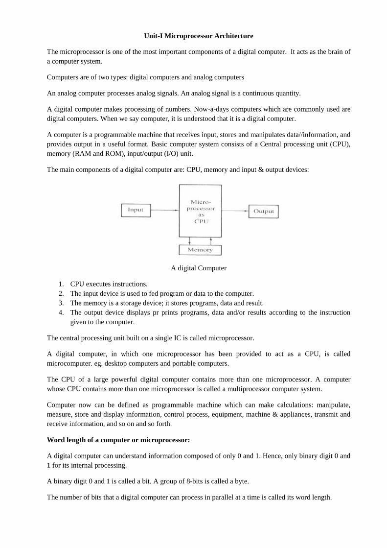
Unit-I Microprocessor Architecture The microprocessor is one of the most important components of a digital computer. It acts as the brain of a computer system. Computers are of two types: digital computers and analog computers An analog computer processes analog signals. An analog signal is a continuous quantity. A digital computer makes processing of numbers. Now-a-days computers which are commonly used are digital computers. When we say computer, it is understood that it is a digital computer. A computer is a programmable machine that receives input, stores and manipulates data//information, and provides output in a useful format. Basic computer system consists of a Central processing unit (CPU), memory (RAM and ROM), input/output (I/O) unit. The main components of a digital computer are: CPU, memory and input & output devices: A digital Computer 1. CPU executes instructions. 2. The input device is used to fed program or data to the computer. 3. The memory is a storage device; it stores programs, data and result. 4. The output device displays pr prints programs, data and/or results according to the instruction given to the computer. The central processing unit built on a single IC is called microprocessor. A digital computer, in which one microprocessor has been provided to act as a CPU, is called microcomputer. eg. desktop computers and portable computers. The CPU of a large powerful digital computer contains more than one microprocessor. A computer whose CPU contains more than one microprocessor is called a multiprocessor computer system. Computer now can be defined as programmable machine which can make calculations: manipulate, measure, store and display information, control process, equipment, machine & appliances, transmit and receive information, and so on and so forth. Word length of a computer or microprocessor: A digital computer can understand information composed of only 0 and 1. Hence, only binary digit 0 and 1 for its internal processing. A binary digit 0 and 1 is called a bit. A group of 8-bits is called a byte. The number of bits that a digital computer can process in parallel at a time is called its word length.
-
Upload
khangminh22 -
Category
Documents
-
view
1 -
download
0
Transcript of Unit-I Microprocessor Architecture
Unit-I Microprocessor Architecture
The microprocessor is one of the most important components of a digital computer. It acts as the brain of
a computer system.
Computers are of two types: digital computers and analog computers
An analog computer processes analog signals. An analog signal is a continuous quantity.
A digital computer makes processing of numbers. Now-a-days computers which are commonly used are
digital computers. When we say computer, it is understood that it is a digital computer.
A computer is a programmable machine that receives input, stores and manipulates data//information, and
provides output in a useful format. Basic computer system consists of a Central processing unit (CPU),
memory (RAM and ROM), input/output (I/O) unit.
The main components of a digital computer are: CPU, memory and input & output devices:
A digital Computer
1. CPU executes instructions.
2. The input device is used to fed program or data to the computer.
3. The memory is a storage device; it stores programs, data and result.
4. The output device displays pr prints programs, data and/or results according to the instruction
given to the computer.
The central processing unit built on a single IC is called microprocessor.
A digital computer, in which one microprocessor has been provided to act as a CPU, is called
microcomputer. eg. desktop computers and portable computers.
The CPU of a large powerful digital computer contains more than one microprocessor. A computer
whose CPU contains more than one microprocessor is called a multiprocessor computer system.
Computer now can be defined as programmable machine which can make calculations: manipulate,
measure, store and display information, control process, equipment, machine & appliances, transmit and
receive information, and so on and so forth.
Word length of a computer or microprocessor:
A digital computer can understand information composed of only 0 and 1. Hence, only binary digit 0 and
1 for its internal processing.
A binary digit 0 and 1 is called a bit. A group of 8-bits is called a byte.
The number of bits that a digital computer can process in parallel at a time is called its word length.

The word length of a computer or microprocessor is given as n-bit, where n may be 8, 16, 32, or 64.
An 8-bit microprocessor (or computer) can process 8-bit data at a time. “If data contains of more than 8-
bits, the processor takes up 8-bits of data first and makes its processing, then the next group of 8-bits of
data are taken up one by one for processing”.
A 16-bit processor handles 16-bits of data at a time. A 32-bit & a 64-bit processors process 32-bits and
64-bits data at a time respectively.
A processor of longer word length is more powerful and can process data at faster speed as compared to a
processor of shorter word length.
Microcomputer: a computer with a microprocessor as its CPU includes memory, I/O devices etc.
Microprocessor: a silicon chip which includes ALU, register circuits and control circuits.
Microcontroller: a silicon chip which includes microprocessor, memory & I/O devices in a single
package.
What is a microprocessor?
The word comes from the combination of micro and processor.
Processor means a device that processes whatever. Processor means a device that processes numbers,
specifically binary numbers 0’s and 1’s.
To process means to manipulate: It is general term that describes all manipulation. It means perform
certain operations on the numbers that depend on the microprocessor design.
What about micro?
In the early 1970s the microchip was invented. All of the components that made-up of processor were
now placed on a single piece of silicon. The size become several thousand times smaller and the speed
become several hundred times faster. The micro processor was born.
Was there ever a mini processor?
No- it went directly from discrete elements to a single chip.
Definition of the microprocessor
The microprocessor is a programmable device that takes in numbers, performs on them arithmetic
or logic operations according to the program stored in memory and then produces other numbers as a
result.
Let expand each of the underlined and bold words.
Programmable device: The microprocessor can perform different sets of operations on the data it
receives depending on the sequence of instructions supplied in the given program. By changing the
program, the microprocessor manipulates the data in different ways.
Instructions: each microprocessor is designed to execute a specific group of operations. This group of
operations is called an instruction set. This instruction set defines what the microprocessor can and
cannot do.
Takes in: The data that the microprocessor manipulates must come from some-where, it comes from
what is called “input devices”.
Numbers: The microprocessor has a very narrow view on life. It only understands binary numbers. The
microprocessor recognizes and processes a group of bits together. This group of bits is called a “word”.
The number of bits in a microprocessor’s word is a measure of its ability.
Words, Bytes etc.. The earliest microprocessor (the intel 8085) recognized 8-bit word. It processed
information 8-bit at a time. It can handle large numbers, but in order to process these numbers, they broke
them into 8-bit pieces and process each group of 8-bit separately.
Arithmetic or Logic operations: every microprocessor has arithmetic operations such as add and
subtract as part of its instruction set. Microprocessors have logic operations as well. Such as AND, OR,
XOR, shift-left, shift-right etc.
Program stored in memory: Memory is the location where information is kept while not in current
used. Memory is a collection of storage devices, usually, each storage device holds one bit. Storage
devices are grouped into groups of 8. These 8 storage latches can only be accessed together. Memory is
usually measured by the numbers of 8 bytes it can hold. It is measured in kilos, Megas & Gigas. A kilo in
computer language is 210
= 1024.
When a program is entered into a computer, it is stored in memory. Then as microprocessor starts to
execute the instructions, it brings the instruction from memory one at a time.
Memory is also used to hold the data. The microprocessor reads (brings in) the data from memory when it
needs it and writes (stores) the result into memory when it is done.
Produces: For the user to see the result of the execution of the program, the result must be presented in
human readable form. The result must be produced on an output device.
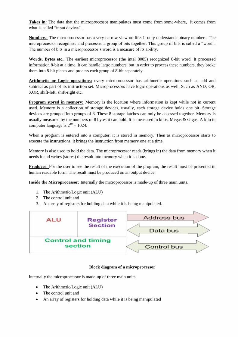
Inside the Microprocessor: Internally the microprocessor is made-up of three main units.
1. The Arithmetic/Logic unit (ALU)
2. The control unit and
3. An array of registers for holding data while it is being manipulated.
Block diagram of a microprocessor
Internally the microprocessor is made-up of three main units.
The Arithmetic/Logic unit (ALU)
The control unit and
An array of registers for holding data while it is being manipulated

Concepts of Microprocessor:
Microprocessor is a hardware component of computer, and it works as brain of the computer system
Without using microprocessor, Computer like as a plastic box
Microprocessor shape as a small chip that is made by silicon and it has to responsible to all functions of
CPU
History of Microprocessor
• First microprocessor was developed by INTEL in 1971, and its name was Intel 4004
• Intel 4004 is based on 4 bit processor; due to this it was not more popular
• Intel 4004 was able to perform only addition/subtraction operation on 4 bit at once
• Intel was announced new Intel’s 8080 in 1974 for personal computer, it is based on 8 bit
processor
• Intel 8085 was designed in 1976, it was updated version of 8080 microprocessor
• It is based on 8-bit processor
• In 1976, Intel was announced again new 8086 microprocessor
• 8086 microprocessor is better to 8085 because it is based on 16-bit
• Later, Intel was designed another new 8087 microprocessor that was first math co-
processor

• 8087 microprocessor was embedded into IBM PC
• Due to more effort of microprocessor’s companies, other new processor are come in
market
• 8088,80286,80386,80486,Pentium II, Pentium III, Pentium IV and now Core 2Duo,Dual
Core and Quad core processors • After all, i3, i5, i7……………running in our surrounding
Evolution of Microprocessor:
Microprocessor evolution is divided into five generation:
First Generation:
• It was introduced by Intel from 1971 – 1972
• Microprocessors are capable only to processed serially
• They have been done their process cycle in three steps
• Fetched, decoded and then executed
• When microprocessor completed cycle then to be update the instruction pointer
• These operations are performed consecutive for every instructions
Examples are: INTEL 4004 Rockwell, PPS-4 INTEL 8008
Second generation microprocessor was designed in 1973 – 1978 with 8-bit processor
• used various transistors on the integrated circuit
• There are three steps for processing the instructions like as overlapped fetch, decode and execute
• second generation microprocessor is five time increase to first generation in different area
• Such as in instruction, in speed, in execution and in higher chip densities
• Examples are: MC68000 Motorola microprocessor, Intel 8080, INTEL 8085, Motorola 6800
and 6801
Third generation microprocessor was developed in 1978 along with 16 bit processor
• This processor is more useful for mini-computer
• Used the HMOS technology and implement RISC-based architectures
• Examples are: MC68020, Intel’s 8086, Zilog Z8000
Fourth generation microprocessor was introduced from 1981 to 1995 with 32 bit processor
• This microprocessor is designed with million transistors, and also based on HMOS technology
• Able to process couples of instruction in per clock cycle.
• Examples are: Motorola’s 88100, Intel’s 80960CA, INTEL 80386, Motorola 68020
Fifth generation microprocessor had been come from 1995 along with 64 bit processor
• In this microprocessor, have been embedded 10 million transistors
• Due to this PCs are a low-margin, high-volume-business dominated by a single microprocessor
• Examples are: PENTIUM-I, II, III, IV, Celeron, Dual, quad and octa core processors, later i3,
i5, i7…and all latest processors
Application of Microprocessor:
Use as Single board Micro Computers: • It includes for designing small types of computers, and it useful for providing the training to
students as well.
Embedded in PC: • Used two types of microprocessor such as 8-bit microprocessor or 16 bit microprocessor
• 8 bit microprocessor is more suitable for playing games and using short term programs
• 16 bit microprocessor is helpful for word processing, payroll, business accounts.
Include in Super Minis and CAD: • It has to use of 32 bit microprocessor because its performance is superb compare to mainframe
and mini-computers
Specific & General Purposes of Microprocessor:
• Instrumentation
• Controller
• Communication Sector
• Use as an Office Automation and Publication
• Uses for Consumers

Other application segments are: Calculator machine, Accounting computation system, Games devices,
Traffic light controlling system, Complicated Industrial Controller terminals, Helping to create multiuser
and multi function environment, Military areas, Broadcasting system , Data acquisition systems
Advantages of Microprocessor:
• Perform all complex arithmetically and logically instructions
• Power to execute 3-4 billion instructions in one second, and it measure in Hertz
• Able to transfer huge data one memory location to other location
• Performed floating point number in few milliseconds
• Provide accessibility for controlling of couple of equipments with in time sharing
• Able to multiprocessing and Parallel Processing
• Easy to modification and Low cost
• Better Reliability and Versatility
• Flexible to program in nature
Disadvantages of Microprocessor:
• Microprocessors are getting more heat due to perform task
• In Microprocessor, small packet of data can be transfer
• Microprocessor does not contain any internal physical memory such as RAM or ROM
• It must not contact any external peripheral due to generate more heat
• Microprocessor is totally base on the machine language
• Degrade to 3D performance
The Microcontroller:
• Common component in modern electronic systems
• Single-chip computer
• Microprocessor-based device
• Completely self-contained with memory and I/O
Microcontrollers used in a wide number of electronic systems such as: Engine management systems in automobiles, Keyboard of a PC, Electronic measurement instruments,
Motor controls, Security systems, Cordless and cellular phones, Televisions, radios, CD players,
recording equipment, Security alarm systems, Microwave ovens, Handheld tools, Remote control
devices, etc..
Microprocessor Microcontroller
Many operation codes for moving data from
external memory to CPU One or two operation codes for moving data from
external memory to CPU
Intended to be general-purpose digital computers Intended to be special-purpose digital computers
Does not have own input memory Has its own memory
Less multifunctional pins More multifunctional pins
More Hardware Less Hardware
Rapid movement of code and data from external
addresses to the chip Rapid movement of bits within the chip
Clock rates very fast (> 1 GHz) Clock rates relatively slow (10-20 MHz)
Bus widths very wide large memory address
spaces (>4 Gbytes) lots of data (Data bus: 32, 64,
128 bits wide)
Bus widths narrow relatively small memory
address spaces (Kbytes) less data (Data bus: 4, 8,
16 bits wide)
• Microprocessor examples are: Intel 8085, 8086, 80286, 80486, Pentium etc…
• Microcontroller examples are: Intel 8251, 8253, 8255, 8259, MC33781 etc………

Intel 8085 Microprocessor:
• It is an 8-bit , NMOS microprocessor
• It is a 40-pins IC package fabricated on a single LSI chip
• It uses a single +5 Vd.c supply for its operation
• Its clock speed about 3MHZ
• The clock cycle is of 320 ns
• It has 80 basic instructions and 246 opcodes
Internally the microprocessor is made-up of three main units.
• The Arithmetic/Logic unit (ALU)
• The Timing & control unit and
• The set of registers
The control unit controls the entire operations of the microprocessor and peripheral connected to it
The control unit of the CPU acts as the brain of the computer system
• Registers are used by the microprocessor for temporary storage and manipulation of data and
instructions
• Data remain in the registers till they are sent to the memory or I/O devices
• In a large computer the number of registers is more and program requires less transfer of data
• In a small computer the number of registers is small due to limited size of chip
Functional Block Diagram of Intel 8085

Intel 8085 register description:
• One 8-bit accumulator (ACC) i.e. register A
• Six 8-bit general purpose registers. These are B, C, D, E, H and L
• One 16-bit stack pointer, SP
• One 16-bit program counter, PC
• Instruction register , 8-bit
• Temporary register, 8-bit
The combination of two 8-bit registers is known as register-pair
• The valid register pair in 8085 are: B-C, D-E, and H-L
• The register pair is used to hold 16-bit data
Intel 8085 Status Flags:
• In addition to these registers the 8085 microprocessor contains a set of five flip-flops which serve
as flags or status flags
• The flip-flops are set or reset according to the conditions which arise during an arithmetic or
logic operation
The five status flag of Intel 8085 are:
• Carry Flag (CS)
• Parity Flag (P)
• Auxiliary Carry Flag (AC)
• Zero Flag (Z)
• Sign Flag (S)
If a flip-flop for a particular flag is set, it indicates 1, when it is reset, it indicates 0
Program Status Word:
• Five bits indicate the five status flags and three bits are undefined, the combination of these 8-bits
is called PSW
• PSW and accumulator are treated as 16-bit unit for stack operation
Data and Address Buses of Intel 8085:
• Its data bus is 8-bit wide and 8-bit data can be transmitted in parallel from or to the
microprocessor
• It requires a 16-bit wide address bus as the memory addresses are of 16-bits
• The 8 MSB of the address are transmitted by the address bus, A-bus (Pins A8 to A15)
• The 8 LSB of the address are transmitted by the address/data bus, AD-bus (Pins AD0 to AD7)
• The address/data bus transmits data and address at different moments

Pin Configuration of Intel 8085:
• The 40 pins of the microprocessor 8085 can be divided into six groups such as:
• Address bus
• Data bus
• Control signals & Status signals
• Power supply & Clock signals
• Interrupts & externally initiated signals
• Serial input/output signals
Pins A8 to A15 (Output): • These are address bus and are used for the most significant 8-bits of the memory address or of
I/O address
• It carries the most significant 8-bits of memory/IO address
Pins AD0 to AD7 (Input/output): • These are time multiplexed address/data bus
• They serve dual purpose
• They are used for the least significant 8-bits of the memory address or I/O address during first
clock cycle
• It carries the least significant 8-bit address and data bus
Control & Status Signals:
• These signals are used to identify the nature of operation
• There are 3 control signal and 3 status signals
• Three control signals are , & ALE.
(Output): This signal indicates that the selected I/O or memory device is to be read
• Ready for accepting data available on the data bus.

(Output): This signal indicates that the data on the data bus is to be written into a selected memory
or IO location.
ALE (Output): It is an address latch enable
• It goes high during first clock cycle of a machine cycle
• Enables the lower 8-bits of the to be latched either into memory or external latch (address or
data)
• Three status signals are I M, S0 & S1
M (Output): It distinguishes whether the address is for memory or I/O
• When it goes high, the address on the address bus is for an I/O device
• When it goes low, the address on the address bus is for memory location
S0 & S1 (Output): These signals are used to identify the types of current operation
S1 S0 Operations
0 0 HALT
0 1 WRITE
1 0 READ
1 1 FETCH
Power Supply and Clock signals:
• There are 2 power supply signals − VCC & VSS
• VCC indicates +5v power supply and
• VSS indicates ground signal
• There are 3 clock signals, i.e. X1, X2, CLK
• X1, X2 (Output): These are terminals to be connected to an external crystal oscillator which
drives an internal circuitry
• To produce a suitable clock for the operations of microprocessor
• CLK (Output): This signal is used as the system clock for devices connected with the
microprocessor
• Its frequency is same at which processor operates
Interrupts & External Initiated signals:
• Interrupts are the signals generated by external devices to request the microprocessor to perform
a task
• There are 5 interrupt signals, i.e. TRAP, RST 7.5, RST 6.5, RST 5.5 (Input), and INTR
INTR (Input): signal sent by an external device to the microprocessor
RST 7.5, RST 6.5, RST 5.5 & TRAP (Input): these are the restart interrupts, each has a programmable
mask
• TRAP has the highest priority, it is nonmaskable interrupt
(Output): It is an interrupt acknowledgment signal issued by the microprocessor after receiving
interrupt
RESET IN (Input): This signal is used to reset the µP by setting the program counter to zero.
RESET OUT (Output): It indicates that the CPU is being reset
READY (Input): This signal indicates that the device is ready to send or receive data
• If it is low, then the CPU has to wait for READY to go high
HOLD (Input): This signal indicates that another master is requesting the use of the address and data
buses
HLDA (Output): (HOLD Acknowledge) − It indicates that the CPU has received the HOLD request
• HLDA is set to low after the HOLD signal is removed.
Serial Input/output Signals:
• There are 2 serial signals, i.e. SID and SOD and these signals are used for serial communication
SID (Input): It is data line for serial input
• The data on this line is loaded into the 7th bit of the accumulator when RIM instruction is
executed
• RIM stands for Read Interrupt Mask
SOD (Output): It is data line for serial output
• The 7th bit of the accumulator is output on SOD line when SIM instruction is executed
• SIM stands for Set Interrupt Mask

Intel 8085 Instructions:
• A computer receives data from the user, process the data and sends the result back to the user
• The computer simply performs a given task on specified data in response to certain instructions
• An instruction is a command given to the computer to perform a specified operation on given
data
• Few instructions of Intel 8085 are as follows:
• MOV r1, r2: The content of register r2 is moved to r1
• Ex: MOV A, B or MOV B, A
• MOV M, r: The content of register r is moved to memory location whose address is in H-L pair
• Ex: MOV M, A will transfer the content of A to {{H-L}}
• MVI r, data: The data given just after an instruction are moved to register r
• Ex: MVI A, 05 moves 05 to register A
• LXI rp, data 16-bit: 16-bit immediate data are moved the register pair rp
• Ex: LXI H, 2400H moves 2400 to H-L pair
• LDA addr: The content of the memory location whose address is specified within the instruction
itself is moved to the A
• Ex: LDA 2400H moves the content of the memory location 2400 to the accumulator
• STA addr: The content of the A is moved to the memory location whose address is specified
within the instruction itself
• Ex: STA 2500H moves the content of the accumulator to memory location 2500H
• ADD r: The content of register r is added to the content of the accumulator and result is placed in
accumulator
• Ex: A B [A] ← [A] + [B]
• SUB r: The content of register r is subtracted from the content of the accumulator and result is
placed in accumulator
• Ex: SUB C [A] ← [A] – [C]
• INR r: The content of the register r is incremented by one
• RAL: The content of the accumulator is rotated left one bit through carry
• IN Port-address: This instruction transfers data from input device or port EX: IN 01H
• OUT Port-address: This instruction transfers data from processor to the output port or device
EX: OUT 02H
Operation code and Operand:
• Each instruction contains two parts: operation code (opcode) and operand
• The first part of an instruction which specifies the task to be performed by the computer is called
opcode
• The second part of the instruction is the data to be operated on, and it is called operand
• The operand (or data) given in the instruction may be in various forms such
• 8-bit data or 16-bit data, 8-bit address or 16-bit address, internal register or a register or memory
location
• When operand is a register it is understood that the data is the content of register
Instruction Word Size:
• A digital computer understands instruction written in binary codes (machine codes)
• The machine code of all instructions are not of the same length
• The Intel 8085 instructions are classified into the following three types:
• 1-byte instruction • Ex: MOV A, B, A B, AL etc…
• 2-byte instruction • Ex: MVI B, 05, IN 01, UT 02 etc…
• 3-byte instruction • Ex: LXI H 2400H, L A 2400H, STA 2500H etc…
One-Byte Instruction:
• All one byte instructions contain information regarding operands in the opcode itself
• MOV A, B: Move the content of register B to register A, 78H is the opcode for MOV A, B,
written in binary as 0111 1000
• The first two bits i.e. 01 for MOV operations, the next 3-bits 111 are the binary code for register
A and

• The last 3-bit are the binary code for register B
• ADD B: Add the content of register B to content of accumulator
• 80H is the opcode for the instruction ADD B (1000 0000)
• The first five-bits i.e. 10000 specify the operation (i.e. ADD)
• The last 3-bit are the binary code for register B
• RAL: Rotate the content of the accumulator left by one-bit
• The opcode for RAL is 17H (0001 0111)
Two-Byte Instruction:
• In a two-byte instruction the first byte of the instruction is its opcode and the 2nd
byte is either
data or address
• A two byte instruction is stored in two consecutive memory locations
• MVI B, 05: Move 05 (data) to register B (06, 05)
• 06 is the opcode for MVI B, data
• First byte is 06 (opcode) and 2nd
byte is 05 (data)
• IN 01: Read data at port B (DB, 01)
• DB is the opcode for the instruction IN and 01 is the address of a port
• OUT 01: Write data at port B (D3, 01)
• D3 is the opcode for the instruction OUT and 01 is the address of a port
Three-Byte Instruction:
• In a 3-byte instruction the first byte of the instruction is its opcode and 2nd
and 3rd
bytes are either
16-bit data or address
• A three-byte instruction is stored in three consecutive memory locations
Instruction First-Byte (Opcode)
2nd
Byte (8-LSB)
3rd
Byte (8 MSB)
Description
LXI H, 2400H 21 00 24 Load H-L pair with 2400H
LDA 2500H 3A 00 25 Load accumulator direct
STA 3505H 32 05 35 Store accumulator direct
Instruction Cycle:
• An instruction is a command given to the computer to perform a specified operation on given
data
• To perform a particular task a programmer writes a sequence of instructions, called a program
• Program and data are stored in the memory
• The CPU fetches one instruction from the memory at a time and executes it
• It executes all the instructions of a program one by one to produce to the final result
• The necessary steps that a CPU carries out to fetch an instruction and necessary data from the
memory, and
• to execute it , constitute an instruction cycle
• An instruction cycle consists of a fetch cycle and execute cycle
Fetch and Execute Cycle:
• In Fetch Cycle a CPU fetches opcode (the machine code of instruction) from the memory
• The necessary steps which are carried out to fetch an opcode from the memory, constitute a fetch
cycle
• The necessary steps which are carried out to get data, if any, from the memory and
• to perform the specific operation specified in an instruction, constitute an execute cycle
• The time required to fetch an opcode (FC) is a fixed slot of time
• The time required to execute an instruction (EC) is variable which depends upon the type of
instruction to be executed
• Total time required to execute an instruction cycle is given by
IC = FC + EC

Fetch Operation:
• The Ist byte of an instruction is its opcode, an instruction may be more than one byte long
• The other bytes are data or operand address
• The program counter (PC) keeps the memory address of the next instruction to be executed
• The memory places the opcode on the data bus so as to transfer it to the CPU
• The entire operation of fetching an opcode takes three clock cycles, a slow memory can take
more time
• The clock cycle for which the CPU waits is called the wait cycle
• The speed of a computer processor, CPU, is determined by the clock cycle,
• which is amount of time between two pulses of an oscillator
Execute Operation:
• The opcode fetched from the memory goes to the data register, DR and then to instruction
register, IR
• From the instruction register it goes to the decoder circuitry which decodes the instruction
• The decoder circuitry is within the microprocessor, after the instruction is decoded, execution
begins
• The time taken in decoding and execution is one clock cycle
• If an instruction contains data or operand address which are still in the memory, the CPU has to
perform some read operation
• A read cycle similar to fetch cycle, it received the data or operand address instead of an opcode
• In some instruction write operation is performed, in write cycle data are sent from the CPU to the
memory or an output device
• An execute cycle may involve read or write cycles
Instruction Cycle
Fetch Cycle

Instruction Cycle for MVI r, data
Machine Cycle:
• The necessary steps carried out to perform the operation of accessing either memory or I/O
device, constitute a machine cycle
• Necessary steps carried out to perform a fetch, a read or a write operation constitute a Machine
cycle
• The necessary steps include to send memory or I address: I M , ALE, , or ) etc
signals
• In a machine cycle one basic operation such as opcode fetch, memory read, memory write, I/O
read or I/O write is performed
• An instruction cycle consists of several machine cycle
• The opcode of an instruction is fetched in the first machine cycle of an instruction cycle
• Most of the one-byte instructions require only one machine cycle to fetch the opcode and
execute the instruction
Timing Diagram:
• The necessary steps which are carried out in a machine cycle can be represented graphically
• Such a graphical representation is called timing diagram
• Representation of various control signals generated during execution of an instruction
• We will discuss the timing diagram for the following operations:
• Opcode Fetch, Memory Read, Memory Write, I/O Read, I/O Write • Following Buses, control & status signals must be shown in a Timing Diagram:
• CLK, I M, S1, S0, Higher order address Bus, Lower order Address ata Bus, ALE,
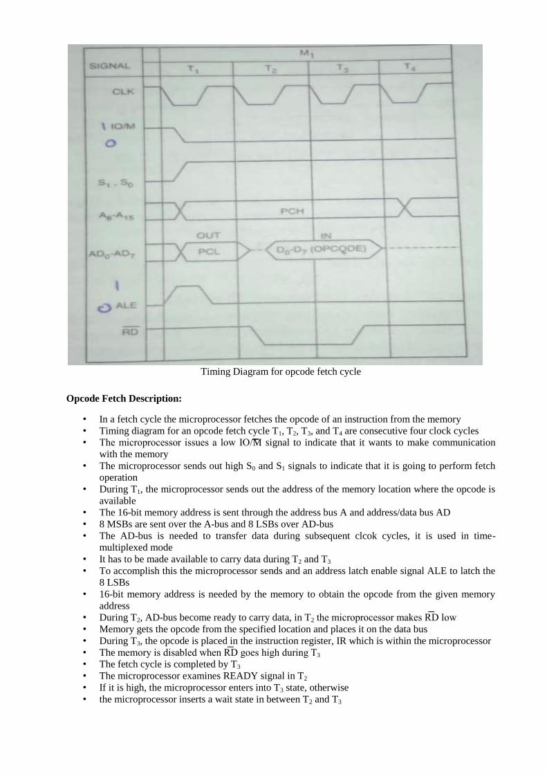
Timing Diagram for opcode fetch cycle
Opcode Fetch Description:
• In a fetch cycle the microprocessor fetches the opcode of an instruction from the memory
• Timing diagram for an opcode fetch cycle T1, T2, T3, and T4 are consecutive four clock cycles
• The microprocessor issues a low I M signal to indicate that it wants to make communication
with the memory
• The microprocessor sends out high S0 and S1 signals to indicate that it is going to perform fetch
operation
• During T1, the microprocessor sends out the address of the memory location where the opcode is
available
• The 16-bit memory address is sent through the address bus A and address/data bus AD
• 8 MSBs are sent over the A-bus and 8 LSBs over AD-bus
• The AD-bus is needed to transfer data during subsequent clcok cycles, it is used in time-
multiplexed mode
• It has to be made available to carry data during T2 and T3
• To accomplish this the microprocessor sends and an address latch enable signal ALE to latch the
8 LSBs
• 16-bit memory address is needed by the memory to obtain the opcode from the given memory
address
• During T2, AD-bus become ready to carry data, in T2 the microprocessor ma es low
• Memory gets the opcode from the specified location and places it on the data bus
• During T3, the opcode is placed in the instruction register, IR which is within the microprocessor
• The memory is disabled when goes high during T3
• The fetch cycle is completed by T3
• The microprocessor examines READY signal in T2
• If it is high, the microprocessor enters into T3 state, otherwise
• the microprocessor inserts a wait state in between T2 and T3

• If an instruction is one byte long, only one machine cycle is required to fetch and execute the
instruction
• Example of one byte long instructions are: MOV, SUB, ADD, RAL, INR etc..
• the decoding of the operation code and its execution takes only one clock cycle, T4
• If an instruction is two or three bytes long, it requires more machine cycles
• The first machine cycle M1 is for fetching opcode from memory
Memory Read Cycle:
• In memory read cycle the microprocessor reads the content of a memory location
• The content is then placed either in the accumulator or any other register of the CPU
• I M goes low indicating that the address is for memory
• S1 = 1 and S0 = 0 for read operation, the address lines A8 – A15, the 8-MSBs of the memory
address of the data are sent
• During T1, 8-LSBs of the memory address of the data are sent on AD0 – AD7
• During T2, 8-LSBs of the address is latched and AD0 – AD7 are made free for data transmission
• goes low in T2 to enable memory read operation
• During T3 the data enters into the CPU, in T3, goes high and disables the memory, only three
clock cycles for MR
Timing Diagram for Memory Read Operation
S1 = 1 and
S0 = 0
D goes low in T2
and goes high in T3
IO M goes
low
Timing Diagram for Memory Write Operation
S1 = 0 and
S0 = 1
R goes low in T2
and goes high in T3
IO M goes
low

Timing Diagram for I/O Read Operation
IO M goes
high
S1 = 1 and
S0 = 0
D goes low in T2
and goes high in T3
Timing Diagram for I/O Write Operation
IO M goes
high
R goes low in T2
and goes high in T3
S1 = 0 and
S0 = 1
Timing Diagram for few instructions:
MOV r1, r2
• In this instruction 8-bit data value in register r2 will be moved to the 8-bit register r1
• First operand specifies the destination register and the second operand specifies the source
register
• Here, r1 is the destination register and r2 is the source register
• Here, “r1” and “r2”can be any one of the following register:
r1, r2 = A, B, C, D, E, H, or L • As r1 can have any one of the seven values, and r2 can have any of the seven values
• There are 7 × 7 = 49 opcodes for this type of instruction
• It occupies only 1-Byte in memory

• It is a 1-Byte instruction
• Only one Machine Cycle (Opcode Fetch) (4 T-states)
Ex: MOV E, H
Opcode is 5CH
2004 5CH
Timing Diagram for MOV E, H
MOV r, M
• In this instruction the 8-bit data content of the memory location as pointed by H-L register pair
• Memory content moved to register r
• Thus this is an instruction to load register r with the 8-bit value from a specified memory
location
• Whose 16-bit address is in HL register pair
• As r can have any of the seven values,
r = A, B, C, D, E, H, or L • There are seven opcodes for this type of instruction
• It occupies only 1-Byte in memory
• It is a 1-Byte instruction
• It has two Machine Cycles (Opcode Fetch and Memory Read)
• 7 T-states (seven clock cycles)
Ex: MOV E, M
Opcode is 5EH
2008 5EH (OF)
H L
[40][50]
4050 AAH (MR)
Timing Diagram for MOV E, M

MOV M, r
• In this instruction the 8-bit data of the register will be occupied by the memory location as
pointed by H-L register pair
• Register content moved to moved to memory location whose 16-bit address is in HL register pair
• As r can have any of the seven values,
r = A, B, C, D, E, H, or L • There are seven opcodes for this type of instruction
• It occupies only 1-Byte in memory
• It is a 1-Byte instruction
• It has two Machine Cycles:
Opcode Fetch Cycle and
Memory Write Cycle
Ex: MOV M, E
Opcode is 73H
2008 5EH (OF)
H L
[40][50]
4050 ABH (MW)
Timing Diagram for MOV M, E
INR r
• IN is a mnemonic that stands for ‘INc ement’ and ‘r’ stands for any of the following registers
or
• memory location M pointed by HL pair.
r = A, B, C, D, E, H, L, or M • This instruction is used to add 1 with the contents of r
• So the previous value in r will get increased by amount 1 only
• INR A, INR B, INR C, INR D, INR E, INR H and INR L, all are 1-Byte instructions
• contain only one machine cycle i.e. opcode fetch cycle
• INR M is also 1-Byte instruction but contains 3 machine cycles: Opcode Fetch, Memory Read &
Memory Write
• 10 T-states (10 clock cycles)

Ex: INR M
Opcode is 34H
4105 34H (OF)
H L
[42][50]
4250 12H (MR)
4250 13H(MW)
Timing Diagram for INR M
MVI r, data
• MVI is a mnemonic, which actually means “Move Immediate”
• In this instruction “data” stands for any 8-bit data, and ‘r’ stands for any one of the registers:
r = A, B, C, D, E, H, L or M • 8-bit data is immediate moved to any register r or memory location specified by H-L pair
• 8 opcodes are possible
• It is 2-Byte instruction
• It has two machine cycles for r = A, B, C, D, E, H, L
Opcode Fetch and Memory Read, 7 T-states (7 clcok cycels)
• For MVI M, data contains 3 machine cycles and 10 T-states
Opcode Fetch, Memory Read and Memory Write Cycle
Ex: MVI E, ABH
Opcode is 1EH
2000 1EH (OF)
2001 ABH (MR)
Timing Diagram for MVI E, M

IN and OUT Instructions
• The IN instruction is used for I/O read
• It is two byte long
• It requires three machine cycles for execution
• The first machine cycle is Opcode fetch cycle (OF)
• The second machine cycle is memory read cycle (MR)
• The third machine cycle is I/O read cycle (IOR)
• The OUT instruction is used for I/O write
• It is two byte long
• It requires three machine cycles for execution
• The first machine cycle is Opcode fetch cycle (OF)
• The second machine cycle is memory read cycle (MR)
• The third machine cycle is I/O write cycle (IOW)
LXI rp, 16-bit data
• There are four instructions, which belong to the type LXI rp, data_16-bit, load 16-bit data into the
register pair
• The rp can be BC, DE, HL or SP
• There are 4 opcodes are possible for this type of instruction
• It occupies three memory addresses, the length is 3-Byte
• Three machine cycle is needed for execution (One Opcode Fetch cycle and Two Memory Read
cycle), 10 T-states
• Ex LXI D, 56FEH opcode is 11H
Memory Address Opcode/Data Machine Cycle
2000H 11H (opcode) OF
2001H FEH (8-LSB) MR
2002H 56H (8-MSB) MR
Timing Diagram for LXI D, 56FEH
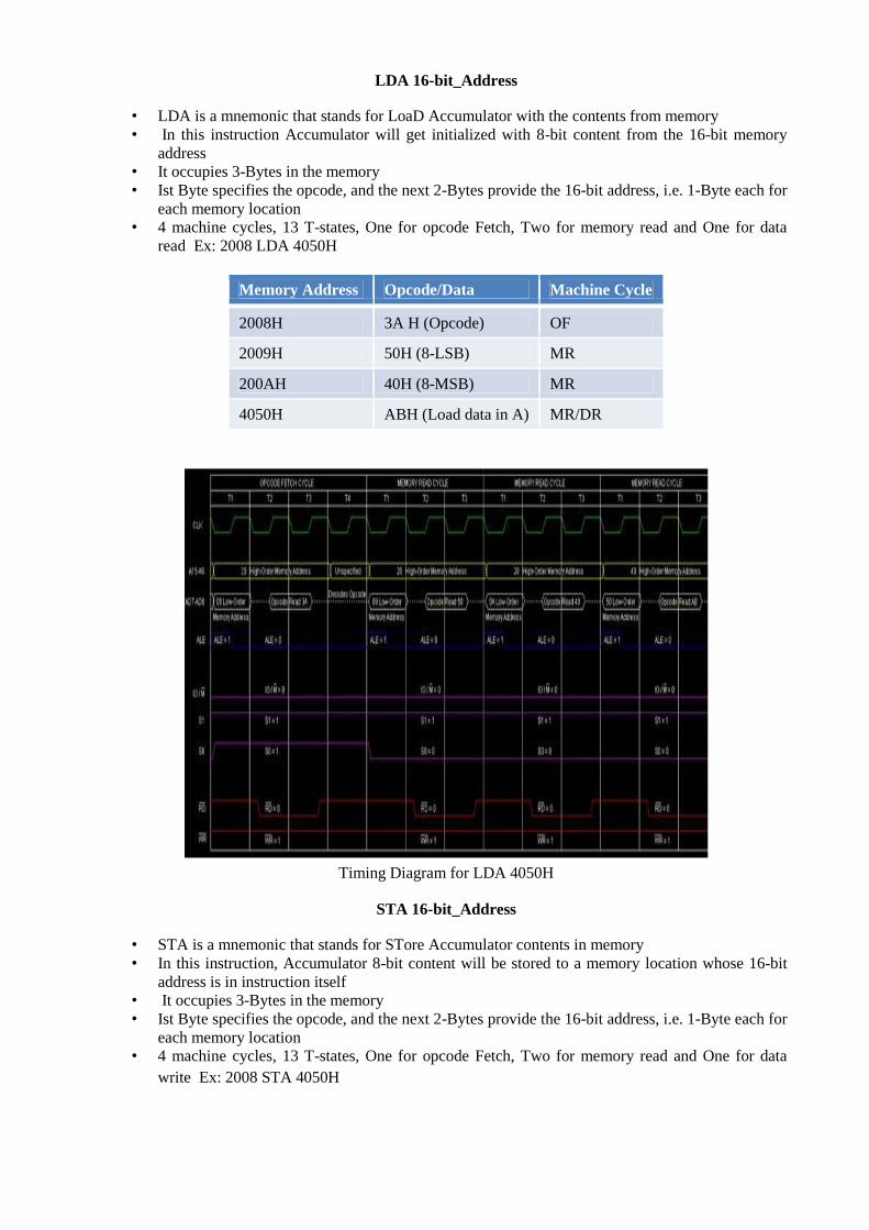
LDA 16-bit_Address
• LDA is a mnemonic that stands for LoaD Accumulator with the contents from memory
• In this instruction Accumulator will get initialized with 8-bit content from the 16-bit memory
address
• It occupies 3-Bytes in the memory
• Ist Byte specifies the opcode, and the next 2-Bytes provide the 16-bit address, i.e. 1-Byte each for
each memory location
• 4 machine cycles, 13 T-states, One for opcode Fetch, Two for memory read and One for data
read Ex: 2008 LDA 4050H
Memory Address Opcode/Data Machine Cycle
2008H 3A H (Opcode) OF
2009H 50H (8-LSB) MR
200AH 40H (8-MSB) MR
4050H ABH (Load data in A) MR/DR
Timing Diagram for LDA 4050H
STA 16-bit_Address
• STA is a mnemonic that stands for STore Accumulator contents in memory
• In this instruction, Accumulator 8-bit content will be stored to a memory location whose 16-bit
address is in instruction itself
• It occupies 3-Bytes in the memory
• Ist Byte specifies the opcode, and the next 2-Bytes provide the 16-bit address, i.e. 1-Byte each for
each memory location
• 4 machine cycles, 13 T-states, One for opcode Fetch, Two for memory read and One for data
write Ex: 2008 STA 4050H

Memory Address Opcode/Data Machine Cycle
2008H 32H (Opcode) OF
2009H 50H (8-LSB) MR
200AH 40H (8-MSB) MR
4050H ABH (write data into M) MW/DW
Timing Diagram for STA 4050H
LHLD 16-bit Data
• LHLD is a mnemonic that stands for Load HL pair direct
• Meaning: LHLD 4050H
• In [L] register the content of 4050H will be stored and
• In [H] register the content of 4051H will be stored
• It occupies 3-Bytes in the memory
• Ist Byte for opcode, and next 2-Bytes for 16-bita address read
• 5 machine cycles, 16 T-states, One for opcode Fetch, Two for memory read and Two for data
read Ex: 200B LHLD 4050H
Memory Address Opcode/Data Machine Cycle
200BH 2A H (Opcode) OF
200CH 50 (8-LSB) MR
200DH 40 (8-MSB) MR
4050H AAH (Load AA in L register) MR/DR
4051H BBH (Load BB in H register) MR/DR

Timing Diagram for LHLD 4050H
SHLD 16-bit Data
• SHLD is a mnemonic that stands for Store HL pair direct
• Meaning: SHLD 4050H
• The data of [L] register will be stored at 4050H and
• The data of [H] register will be stored at 4051H
• It occupies 3-Bytes in the memory
• Ist Byte for opcode, and next 2-Bytes for 16-bita address read
• 5 machine cycles, 16 T-states, One for opcode Fetch, Two for memory read and Two for data
write Ex: 200B SHLD 4050H
Memory Address Opcode/Data Machine Cycle
200BH 22H (Opcode) OF
200CH 50H (8-LSB) MR
200DH 40H (8-MSB) MR
4050H AAH (AA write at 4050H) MW/DW
4051H BBH (BB write at 4051H) MW/DW

Timing Diagram for SHLD 4050H
INX rp Instruction
• INX is a mnemonic that stands for “INcrementeXtended register” and rp stands for register pair
• It can be any one of the following register pairs
rp = BC, DE, or HL
• It will be used to add 1 to the present content of the rp
• It occupies only 1-Byte in memory
• As it is a 1-Byte instruction, so it will occupy single Byte location in the memory
• Let consider that the initial content of rp BC is 4050H
• So after execution of the instruction INX B, the new content of BC rp would be 4051H
• So this instruction INX B requires 1-Byte, 1-Machine Cycle (Opcode Fetch) and 6 T-States for
execution
Ex: INX B
Opcode is 03H
2003 03H
Timing Diagram for INX B
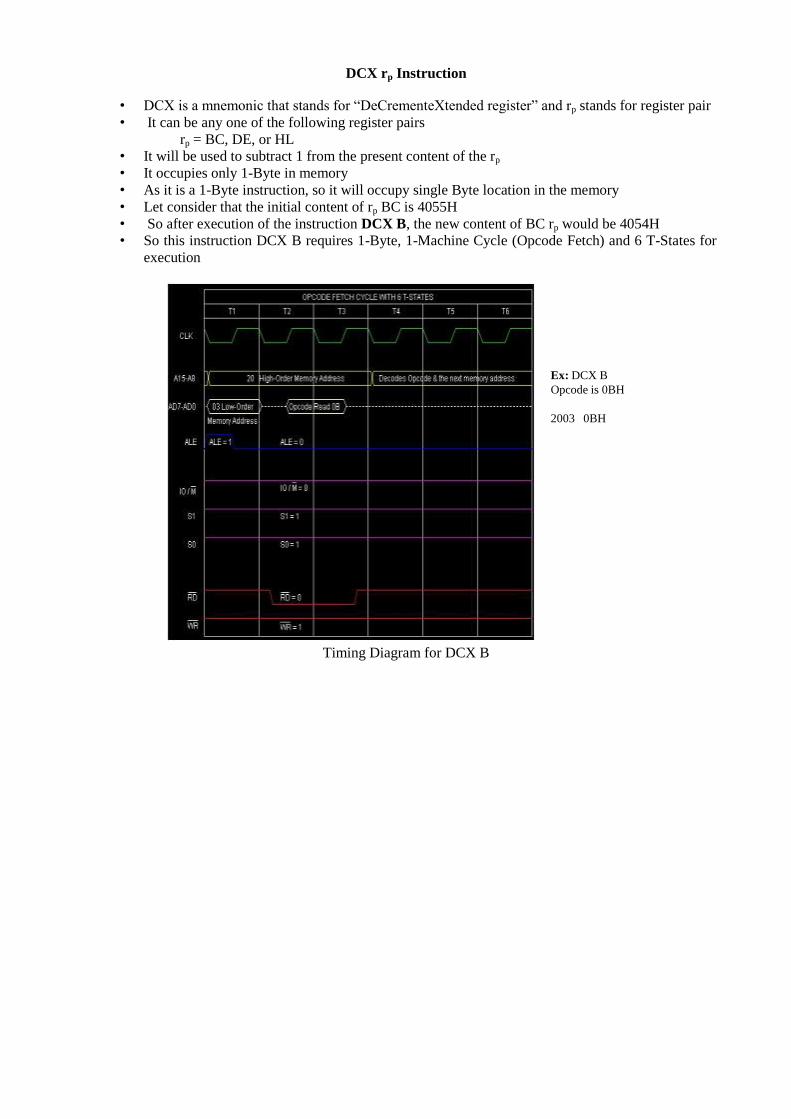
DCX rp Instruction
• CX is a mnemonic that stands for “ eCrementeXtended register” and rp stands for register pair
• It can be any one of the following register pairs
rp = BC, DE, or HL
• It will be used to subtract 1 from the present content of the rp
• It occupies only 1-Byte in memory
• As it is a 1-Byte instruction, so it will occupy single Byte location in the memory
• Let consider that the initial content of rp BC is 4055H
• So after execution of the instruction DCX B, the new content of BC rp would be 4054H
• So this instruction DCX B requires 1-Byte, 1-Machine Cycle (Opcode Fetch) and 6 T-States for
execution
Ex: DCX B
Opcode is 0BH
2003 0BH
Timing Diagram for DCX B

Assignment-I
1. Differentiate between microprocessor and microcontroller. Give examples for microprocessor
and microcontroller.
2. Draw the block diagram of Intel 8085 microprocessor. Briefly explain each component.
3. Define the following terms: Flip-flop, Register, Latch, Bus, Decoder, Nibble, Byte, Word,
Interrupt, and Tri-state logic
4. Discuss the various types of registers and status flags of Intel 8085.
5. Define the following: Instruction Cycle, Fetch Cycle, Execute Cycle, Machine Cycle, and Clock
Cycle
6. Explain the following operations: Fetch opcode, Memory read, Memory write, I/O read and I/O
write
7. How many machine cycles are required for the instruction STA 16-bit address? Draw the timing
diagram for:25FF STA 3500H. The hex code of the given instruction is 32H.
8. How many machine cycles are required for the instruction LHLD 16-bit -data? Draw the timing
diagram for: 3FFF LHLD 35FFH. The hex code of the given instruction is 2AH.
How and When to Submit Assignment?
• The assignment should be in hand written
• All questions should be completed in your notebook (or plain paper)
• The assignment should be completed by 22.09.2020
• After due date, I may ask either the complete assignment or any part of the assignment at random
to any student