
Resilient Energy-Constrained Microprocessor Architectures
136
Resilient Energy-Constrained Microprocessor Architectures for obtaining the academic degree of Doctor of Engineering Approved Dissertation Department of Informatics Karlsruhe Institute of Technology (KIT) by Anteneh Gebregiorgis from Zalanbesa, Ethiopia Oral Exam Date: 03 May 2019 Adviser: Prof. Dr. Mehdi Baradaran Tahoori, KIT Co-adviser: Prof. Dr. Said Hamdioui, Delft University of Technology
-
Upload
khangminh22 -
Category
Documents
-
view
1 -
download
0
Transcript of Resilient Energy-Constrained Microprocessor Architectures

Resilient Energy-ConstrainedMicroprocessor Architectures
for obtaining the academic degree of
Doctor of Engineering
Approved
Dissertation
Department of Informatics
Karlsruhe Institute of Technology (KIT)
by
Anteneh Gebregiorgis
from Zalanbesa, Ethiopia
Oral Exam Date: 03 May 2019
Adviser: Prof. Dr. Mehdi Baradaran Tahoori, KIT
Co-adviser: Prof. Dr. Said Hamdioui, Delft University of Technology


To My Family
iii


Acknowledgments
First fo all, I would like to express my sincere gratitude to my adviser, Prof. Mehdi Tahoori,
who has helped me relentlessly, involved me in various research projects during my PhD
journey. Also, I would like to extend my gratitude to my co-adviser Prof. Said Hamdioui for
his support and motivation.
When I found myself experiencing the feeling of fulfillment, I realized though only my name
appears on the cover of this dissertation, my loving wife had an immense contribution for
the successful completion of my journey. Thus, I extend my earnest gratitude to my wife,
Tirhas, for her continued and unfailing love, support, and understanding during my pursuit
of Ph.D degree that made everything possible. She sacrificed most of her wishes to support
and encourage me unconditionally, which I am heavily indebted for. Finally, I acknowledge
the people who mean a lot to me, my family, for showing faith in me and giving me liberty to
follow my desire. I salute you all for the selfless love, care, pain and sacrifice you did to shape
my life.
I would like to thank my colleagues at the chair of dependable nano computing for their
thoughts, helps, and companionship. I would like to especially thank my friends, Rajendra
Bishnoi, Saber Golanbari, and Arun Kumar Vijayan which I have learned a lot from them,
not only in research, but also in other aspects of life.
v

Anteneh Gebregiorgis
Kaiserallee. 109
76185 Karlsruhe
Hiermit erklare ich an Eides statt, dass ich die von mir vorgelegte Arbeit selbststandig verfasst
habe, dass ich die verwendeten Quellen, Internet-Quellen und Hilfsmittel vollstandig angegeben
haben und dass ich die Stellen der Arbeit - einschlielich Tabellen, Karten und Abbildungen -
die anderen Werken oder dem Internet im Wortlaut oder dem Sinn nach entnommen sind, auf
jeden Fall unter Angabe der Quelle als Entlehnung kenntlich gemacht habe.
Karlsruhe, May 2019
©Anteneh Gebregiorgis
vi

ABSTRACT
In the past years, we have seen a tremendous increase in small and battery-powered devices
for sensing, wireless communication, data processing, classification, and recognition tasks.
Collectively referred to as the Internet of Things (IoT), all these devices have a huge impact on
several aspects of our day-to-day life. Since IoT devices need to be portable and lightweight,
they depend on battery or environmental harvested-energy as their primary energy source.
As a result, IoT devices have to operate on a limited energy envelope in order to increase
the supply duration of their energy source. In order to meet the stringent energy-budget of
battery-powered IoT devices, extreme-low energy design has become a standard requirement.
In this regard, supply voltage downscaling has been used as an effective approach for reducing
the energy consumption of Complementary Metal Oxide Semiconductor (CMOS) circuits and
enable ultra-low power operation. Although aggressive supply voltage downscaling is a popular
approach for extreme-low power operation, it reduces the performance significantly. In this
regard, operating in the near-threshold voltage domain (commonly known as NTC) could
provide a better trade-off between performance and energy saving, as it can achieve up to 10×energy-saving at the cost of linear performance reduction. However, the broad applicability
of NTC is hindered by several barriers, such as the increase in functional failure of memory
components, performance variation, and higher sensitivity to variation effects.
For NTC processors, wide variation extent and higher functional failure rate pose a daunting
challenge to assure timing certainty of logic blocks such as pipeline stages of a processor core
and stability of memory elements (caches and registers). Moreover, due to the reduction in
noise margin of memory components, susceptibility to runtime reliability issues, such as aging
and soft errors, is also increasing with supply voltage downscaling. These challenges limit NTC
potentials and force designers to use large timing margins in order to ensure reliable operation
of different architectural blocks, which leads to significant overheads. Therefore, analyzing and
mitigating variation induced timing failure of pipeline stages and memory failures during early
design phases plays a crucial role in the design of resilient and energy-efficient microprocessor
architectures.
This thesis provides cost-effective cross-layer solutions to improve the resiliency and energy-
efficiency of energy-constrained pipelined microprocessors operating in the near-threshold volt-
age domain. Different architecture-level solutions for logic and memory components of a
pipelined processor are presented in this thesis. The solutions provided in this thesis address
the three main NTC challenges, namely increase in sensitivity to process variation, higher
memory failure rate, and performance uncertainties. Additionally, this thesis demonstrates
how to exploit emerging computing paradigms, such as approximate computing, in order to
further improve the energy efficiency of NTC designs.
vii

ZUSAMMENFASSUNG
In den letzten Jahren wurde eine starke Zunahme an miniaturisierten und batterie-betriebenen
elektronischen Systemen beobachtet, welche zur kabellosen Kommunikation, Datenverarbeitung,
Mustererkennung oder fur Sensoranwendungen eingesetzt werden. Alles deutet darauf hin,
dass solche Internet of Things-Anwendungen (IoT) einen starken Einfluss auf unseren All-
tag haben werden. Da IoT-Systeme portabel und leichtgewichtig sein mussen, ist ein Bat-
teriebetrieb oder eine autarke Energiegewinnung aus der Umgebung Voraussetzung. Aus
diesem Grund ist es notwendig, den Leistungsverbrauch des IoT-Systems zu reduzieren und
die Energiequelle wenig zu belasten um eine moglichst lange Versorgung zu gewahrleisten.
Um diese stringenten Energie-Budgets von batteriebetriebenen IoT-Systemen einzuhalten, ist
eine Niedrigenergiebauweise ist Standardvorrausetzung geworden. In diesem Zusammenhang
wurden effiziente Verfahren entwickelt, welche die Versorgungsspannung reduzieren um den
Leistungsverbrauch von Complementary Metal Oxide Semiconductor (CMOS) Schaltungen zu
senken und eine ultra-low-power Operation zu ermoglichen. Obwohl diese Energieverbrauchs-
Reduzierung durch die starke Verringerung der Versorgungsspannung sehr effektiv ist, ver-
schlechtert sich auf der anderen Seite die Performance der Schaltung signifikant. Bei der Ab-
senkung der Versorgungsspannung in den nahen Schwellspannungsbereich (auch bezeichnet als
Near-Threshold-Computing (NTC)), wird jedoch der Leistungsverbrauch um das 10-fache ver-
ringert auf Kosten einer Performance-Reduzierung mit lediglich linearem Verlauf. Damit einher
gehen jedoch weitere Probleme, wie zum Beispiel funktionale Ausfalle von Speicherbausteinen,
Performance-Variationen und hohere Sensitivitat zu weiteren Variationen, welche eine breite
Anwendung dieses Verfahrens erschweren.
Fur NTC-Prozessoren fuhren diese erhohten Variationen und funktionalen Ausfalle zu un-
tragbaren Nebeneffekten, da zeitliche Anforderungen von Logikbausteinen wie zum Beispiel
Pipeline-Stufen des Prozessorkerns, sowohl als Stabilitat von Speicherbausteinen (Caches und
Register), nicht eingehalten werden. Des weiteren, da eine Reduzierung der Noise-Margin von
Speicherelementen auftritt, erhoht sich mit der Absenkung der Versorgungsspannung auch die
Anfalligkeit zu Alterungseffekten und Soft-Errors, welche den verlasslichen Betrieb wahrend
der Laufzeit beeintrachtigen. Diese Probleme limitieren das Potential von NTC-Verfahren
und zwingen Entwickler zeitliche Anforderungen aufzulockern um den verlasslichen Betrieb
von verschiedenen Komponenten der Gesamtarchitektur zu garantieren, welches zu einem
bedeutenden Mehraufwand fuhrt. Daher ist eine Analyse und Verbesserung der variations-
induzierten zeitlichen Verstoßen von Pipeline-Stufen und Speicherausfallen in fruhen Stadien
des Entwurfs entscheidend, um verlassliche und energieeffiziente Mikroprozessorarchitekturen
zu ermoglichen.
Diese Arbeit liefert einen schichtubergreifenden und kosteneffizienten Ansatz zur Verbesserung
der Verlasslichkeit und Energieeffizienz von energiebeschrankten Mikroprozessoren mit Pipeline,
welche im nahen Schwellspannungsbereich betrieben werden. Losungen auf verschiedenen Ar-
chitekturebenen fur Logik- und Speicherkomponenten eines Prozessors mit Pipeline werden
in der hier vorliegenden Arbeit behandelt. Die erarbeiteten Losungen adressieren die drei
viii

hauptsachlichen Herausforderungen von NTC-Anwendungen, namlich die Erhohung der Sensi-
tivitat zu Prozessvariationen, hohere Ausfallwahrscheinlichkeiten von Speicherbausteinen und
Performance-Schwankungen. Erganzend wird demonstriert, wie aufkommende Paradigmen
wie das Approximate Computing eingesetzt werden um die Energieeffizienz von NTC-Designs
weiter zu verbessern.
ix


Table of Contents
ABSTRACT x
Glossary xiii
Acronyms xv
List of Figures xvii
List of Tables xxi
1 Introduction 1
1.1 Problem statement and objective . . . . . . . . . . . . . . . . . . . . . . . . . . 3
1.2 Thesis contributions . . . . . . . . . . . . . . . . . . . . . . . . . . . . . . . . . 4
1.2.1 Cross-layer memory reliability analysis and mitigation technique . . . . 4
1.2.2 Pipeline stage delay balancing and optimization techniques . . . . . . . 5
1.2.3 Exploiting approximate computing . . . . . . . . . . . . . . . . . . . . . 6
1.3 Thesis outline . . . . . . . . . . . . . . . . . . . . . . . . . . . . . . . . . . . . . 6
2 Background and State-of-The-Art 7
2.1 Near-Threshold Computing (NTC) for energy-efficient designs . . . . . . . . . . 8
2.1.1 NTC basics . . . . . . . . . . . . . . . . . . . . . . . . . . . . . . . . . . 8
2.1.2 NTC application domains . . . . . . . . . . . . . . . . . . . . . . . . . . 9
2.2 Challenges for NTC operation . . . . . . . . . . . . . . . . . . . . . . . . . . . . 11
2.2.1 Performance reduction . . . . . . . . . . . . . . . . . . . . . . . . . . . . 11
2.2.2 Increase sensitivity to variation effects . . . . . . . . . . . . . . . . . . . 12
2.2.3 Functional failure and reliability issues of NTC memory components . . 14
2.3 Existing techniques to overcome NTC barriers . . . . . . . . . . . . . . . . . . . 18
2.3.1 Solutions addressing performance reduction . . . . . . . . . . . . . . . . 18
2.3.2 Solutions addressing variability . . . . . . . . . . . . . . . . . . . . . . . 19
2.3.3 Solutions addressing memory failures . . . . . . . . . . . . . . . . . . . . 21
2.4 Emerging technologies and computing paradigm for extreme energy efficiency . 24
2.4.1 Non-volatile processor design . . . . . . . . . . . . . . . . . . . . . . . . 24
2.4.2 Exploiting approximate computing for NTC . . . . . . . . . . . . . . . . 24
2.5 Summary . . . . . . . . . . . . . . . . . . . . . . . . . . . . . . . . . . . . . . . 25
3 Reliable Cache Design for NTC Operation 27
3.1 Introduction . . . . . . . . . . . . . . . . . . . . . . . . . . . . . . . . . . . . . . 27
3.2 Cross-layer reliability analysis framework for NTC caches . . . . . . . . . . . . 28
3.2.1 System FIT rate extraction . . . . . . . . . . . . . . . . . . . . . . . . . 28
3.2.2 Cross-layer SNM and SER estimation . . . . . . . . . . . . . . . . . . . 30
3.2.3 Experimental evaluation and trade-off analysis . . . . . . . . . . . . . . 33
xi

Table of Contents
3.3 Voltage scalable memory failure mitigation scheme . . . . . . . . . . . . . . . . 41
3.3.1 Motivation and idea . . . . . . . . . . . . . . . . . . . . . . . . . . . . . 41
3.3.2 Built-In Self-Test (BIST) based runtime operating voltage adjustment . 43
3.3.3 Error tolerant block mapping . . . . . . . . . . . . . . . . . . . . . . . . 45
3.3.4 Evaluation of voltage scalable mitigation scheme . . . . . . . . . . . . . 45
3.4 Summary . . . . . . . . . . . . . . . . . . . . . . . . . . . . . . . . . . . . . . . 47
4 Reliable and Energy-Efficient Microprocessor Pipeline Design 49
4.1 Introduction . . . . . . . . . . . . . . . . . . . . . . . . . . . . . . . . . . . . . . 49
4.2 Variation-aware pipeline stage balancing . . . . . . . . . . . . . . . . . . . . . . 50
4.2.1 Pipelining background and motivational example . . . . . . . . . . . . . 51
4.2.2 Variation-aware pipeline stage balancing flow . . . . . . . . . . . . . . . 52
4.2.3 Coarse-grained balancing for deep pipelines . . . . . . . . . . . . . . . . 55
4.2.4 Experimental results . . . . . . . . . . . . . . . . . . . . . . . . . . . . . 56
4.3 Fine-grained Minimum Energy Point (MEP) tuning for energy-efficient pipeline
design . . . . . . . . . . . . . . . . . . . . . . . . . . . . . . . . . . . . . . . . . 60
4.3.1 Background . . . . . . . . . . . . . . . . . . . . . . . . . . . . . . . . . . 60
4.3.2 Fine-grained MEP analysis basics and challenges . . . . . . . . . . . . . 62
4.3.3 Motivation and problem statement for pipeline stage-level MEP assignment 64
4.3.4 Lagrange multiplier based two-phase hierarchical pipeline stage-level MEP
tuning technique . . . . . . . . . . . . . . . . . . . . . . . . . . . . . . . 67
4.3.5 Implementation issues . . . . . . . . . . . . . . . . . . . . . . . . . . . . 73
4.3.6 Experimental results . . . . . . . . . . . . . . . . . . . . . . . . . . . . . 75
4.3.7 Comparison with related works . . . . . . . . . . . . . . . . . . . . . . . 80
4.4 Summary . . . . . . . . . . . . . . . . . . . . . . . . . . . . . . . . . . . . . . . 82
5 Approximate Computing for Energy-Efficient NTC Design 85
5.1 Introduction . . . . . . . . . . . . . . . . . . . . . . . . . . . . . . . . . . . . . . 85
5.2 Background . . . . . . . . . . . . . . . . . . . . . . . . . . . . . . . . . . . . . . 86
5.2.1 Embracing errors in approximate computing . . . . . . . . . . . . . . . 86
5.2.2 Related works . . . . . . . . . . . . . . . . . . . . . . . . . . . . . . . . . 87
5.3 Error propagation aware timing relaxation . . . . . . . . . . . . . . . . . . . . . 87
5.3.1 Motivation and idea . . . . . . . . . . . . . . . . . . . . . . . . . . . . . 87
5.3.2 Variation-induced timing error propagation analysis . . . . . . . . . . . 88
5.3.3 Mixed-timing logic synthesis flow . . . . . . . . . . . . . . . . . . . . . . 91
5.4 Experimental results . . . . . . . . . . . . . . . . . . . . . . . . . . . . . . . . . 93
5.4.1 Experimental setup . . . . . . . . . . . . . . . . . . . . . . . . . . . . . . 93
5.4.2 Energy efficiency analysis . . . . . . . . . . . . . . . . . . . . . . . . . . 93
5.4.3 Application to image processing . . . . . . . . . . . . . . . . . . . . . . 96
5.5 Summary . . . . . . . . . . . . . . . . . . . . . . . . . . . . . . . . . . . . . . . 97
6 Conclusion and Remarks 99
6.1 Conclusions . . . . . . . . . . . . . . . . . . . . . . . . . . . . . . . . . . . . . . 99
6.2 Remarks . . . . . . . . . . . . . . . . . . . . . . . . . . . . . . . . . . . . . . . . 100
Bibliography 101
xii

Glossary
3D three-dimensional integrated circuit made of vertical stacked silicon wafers.
AVF Architectural Vulnerability Factor is the probability that an error in memory structure
propagates to the data path. AVF = vulnerable period / total program execution period.
ECC Error Correction Code (ECC), enables error checking and correction of a data that is
being read or transmitted, when necessary.
FinFET Fin Field Effect Transistor is non planner three dimensional transistor.
FIT Failures in Time rate is a standard value defined as the Failure Rate per billion hours of
operation.
IoT Internet of Things is the network of devices that contain sensors, actuators, and connec-
tivity which allows the devices yo connect and interact.
LLC Last Level Cache is the lowers-level cache that is usually shared by all the functional
units on the chip.
SeaMicro Low-Power, High-Bandwidth Micro-server Solutions.
SP Signal Probability is the probability of storing logic 1 in the SRAM cell.
xiii


Acronyms
ABB Adaptive Body Bias.
AI Arteficial Inteligence.
BIST Built-In Self Test.
BTI Bias Temperature Instability.
CMOS Complementary Metal Oxide Semiconductor.
CMP Chip Multiprocessing.
CPU Central Processing Unit.
DCT Discrete Cosine Transform.
DSP Digital Signal Processing.
DVFS Dynamic Voltage and Frequency Scaling.
EDA Electronics Design Automation.
FBB Forward Body Bias.
GPU Graphics Processing Unit.
IPC Instruction Per Cycle.
ITRS International Technology Roadmap for Semiconductors.
LER Line Edge Roughness.
LUT Look-Up Table.
MEP Minimum Energy Point.
NMOS Negative-channel Metal Oxide Semiconductor.
NTC Near Threshold Computing.
PDP Power Delay Product.
PMOS Postive-channel Metal Oxide Semiconductor.
RBB Reverse Body Bias.
xv

Acronyms
RDF Random Dopant Fluctuations.
SER Soft Error Rate.
SNM Static Noise Margin.
SRAM Static Random Access Memory.
SSTA Statistical Static Timing Analysis.
VLSI Very Large Scale Integrated Circuits.
xvi

List of Figures
1.1 Intel Chips Transistor count per unit area, Millions of transistor per millimeter
square (MTr/mm2) and voltage scaling of different technology nodes. . . . . . . 2
1.2 Thesis contribution summary of solutions addressing memory failure, variability
effect on pipeline stages, and exploiting emerging computing paradigm. . . . . 5
2.1 Dynamic, leakage and total energy trends of supply voltage downscaling at
different voltage levels for an inverter chain implemented with saed 32nm library. 9
2.2 Supply voltage downscaling induced performance reduction (delay increase) of
an inverter chain implementation evaluated for wide operating voltage range. . 12
2.3 Process variation induced performance/ delay variation of b01 circuit across
wide supply voltage range. . . . . . . . . . . . . . . . . . . . . . . . . . . . . . . 13
2.4 Energy-consumption characteristics of inverter chain implementation of three
different process corners; typical (TT) with regular Vth(RVT), slow (SS) with
high Vth( HVT=RVT + ∆Vth), and fast (FF) with low Vth (LVT=RVT -
∆Vth), where ∆Vth=25mV. . . . . . . . . . . . . . . . . . . . . . . . . . . . . . 14
2.5 Schematic diagram of 6T SRAM cell, where WL= word-line, BL=bit-line and
RL=read-line. . . . . . . . . . . . . . . . . . . . . . . . . . . . . . . . . . . . . . 15
2.6 Write margin (in terms of write latency) comparison of 6T and 8T SRAM cell
operating in near-threshold voltage domain (0.5V). . . . . . . . . . . . . . . . . 16
2.7 Interdependence of reliability failure mechanisms and their impact on the system
Failure In-Time (FIT) rate in NTC. . . . . . . . . . . . . . . . . . . . . . . . . 18
2.8 Variation-induce timing error detection and correction techniques for combina-
tional circuits (a) razor flip-flop based timing error detection and correction,
(b) shadow flip-flop for time borrowing, and (c) adaptive body biasing to adjust
circuit timing. . . . . . . . . . . . . . . . . . . . . . . . . . . . . . . . . . . . . . 20
2.9 Alternative bit-cell designs to improve read disturb, stability and yield of SRAM
cells in NTC domain (a) Differential 7-Transistor (7T) bit-cell deign, (b) Read/write
decoupled 8-Transistor (8T) bit-cell design, and (c) Robust and read/write de-
coupled 10-Transistor (10T) bit-cell design timing. . . . . . . . . . . . . . . . . 22
3.1 Cross-layer impact of memory system and workload application on system-level
reliability (Failure-In-Time (FIT rate)) of NTC memory components, and their
interdependence. . . . . . . . . . . . . . . . . . . . . . . . . . . . . . . . . . . . 28
3.2 Holistic cross-layer reliability estimation framework to analyze the impact of
aging and process variation effects on soft error rate. . . . . . . . . . . . . . . . 29
xvii

LIST OF FIGURES
3.3 SNM degradation in the presence of process variation and aging after 3 years
of operation, aging+PV-induced SNM degradation at NTC is 2.5× higher than
the super-threshold domain. . . . . . . . . . . . . . . . . . . . . . . . . . . . . . 31
3.4 SER rate of fresh and aged 6T and 8T SRAM cells for various Vdd values. . . . 33
3.5 SER of 6T and 8T SRAM cells in the presence of process variation and aging
effects after 3 years of operation. . . . . . . . . . . . . . . . . . . . . . . . . . . 34
3.6 Workload effects on aging-induced SNM degradation in the presence of process
variation for 6T and 8T SRAM cell based cache after 3 years of operation (a)
6T SRAM based cache (b) 8T SRAM based cache. . . . . . . . . . . . . . . . . 35
3.7 Workload effect on SER rate of 6T SRAM cell based cache memory for wide
supply voltage range. . . . . . . . . . . . . . . . . . . . . . . . . . . . . . . . . . 36
3.8 Impact of cache organization on SNM degradation in near-threshold (NTC) and
super-threshold (ST) in the presence of process variation and aging effect after
3 years of operation. . . . . . . . . . . . . . . . . . . . . . . . . . . . . . . . . . 37
3.9 FIT rate and performance design space of various cache configurations in the
super-threshold voltage domain by considering average workload effect (the blue
italic font indicates optimal configuration). . . . . . . . . . . . . . . . . . . . . 38
3.10 FIT rate and performance design space of 6T and 8T designs for various cache
configurations in the near-threshold voltage domain by considering average
workload effect (the blue italic font indicates optimal configuration). . . . . . . 39
3.11 FIT rate and performance trade-off analysis of near-threshold 6T and 8T caches
for various cache configurations and average workload effect in the presence of
process variation and aging effects. . . . . . . . . . . . . . . . . . . . . . . . . . 40
3.12 Energy consumption profile of 6T and 8T based 4K 4-way cache for wide sup-
ply voltage value ranges averaged over the selected workloads from SPEC2000
benchmarks. . . . . . . . . . . . . . . . . . . . . . . . . . . . . . . . . . . . . . . 41
3.13 Error-free minimum operating voltage distribution of 8 MB cache, Set size =
128 Byte (a) block size=32 Bytes (4 blocks per set) and (b) block size=64 Bytes
(two blocks per set), the cache is modeled as 45nm node in CACTI. . . . . . . 42
3.14 Cache access control flowchart equipped with BIST and block mapping logic. . 44
3.15 Error tolerant cache block mapping scheme (mapping failing blocks to marginal
blocks). . . . . . . . . . . . . . . . . . . . . . . . . . . . . . . . . . . . . . . . . 45
3.16 Comparison of voltage downscaling in the presence of block disabling and ECC
induce overheads for gzip, parser and mcf applications from SPEC2000 bench-
mark (a) energy comparison (b) Performance in IPC comparison . . . . . . . . 46
4.1 Variation induced delay increase in super and near threshold voltages for OpenSPARC
core (refer to Table 4.1 in Section 4.2.4 for setup of OpenSPARC). . . . . . . . 50
4.2 Impact of process variation on the delays of different pipeline stages in NTC. . 51
4.3 Variation-aware pipeline stage delay balancing synthesis flow for NTC. . . . . . 52
4.4 Time constraint modification using pseudo divide and conquer. . . . . . . . . . 54
xviii

LIST OF FIGURES
4.5 Pipeline merging and signal control illustration (a) before (b) after merging
where S2 = S2+S3 and S3 = S4. . . . . . . . . . . . . . . . . . . . . . . . . . . 55
4.6 Nominal and variation-induced delays of OpenSPARC pipeline stages (a) nomi-
nal delay balanced baseline design, (b) guard band reduction (delay optimized)
of nominal delay balanced, and (c) statistical delay balanced (power optimized). 57
4.7 Power (energy) improvement of variation-aware balancing over the baseline de-
sign for OpenSPARC core. . . . . . . . . . . . . . . . . . . . . . . . . . . . . . . 58
4.8 Nominal and variation-induced Delays of FabScalar pipeline stages (a) base-
line design, the gray boxes indicate the stages to be merged, (b) merged and
optimized design. . . . . . . . . . . . . . . . . . . . . . . . . . . . . . . . . . . . 59
4.9 Power (energy) improvement of variation-aware FabScalar design over the base-
line design. . . . . . . . . . . . . . . . . . . . . . . . . . . . . . . . . . . . . . . 60
4.10 Dynamic to leakage energy ratio of pipeline stages of FabScalar core under
different workloads synthesized using 0.5V saed 32nm library. . . . . . . . . . . 61
4.11 MEP supply voltage movement characteristics of Regular Vth (RVT), High Vth
(RVT+∆Vth) and Low Vth (RVT-∆Vth) inverter chain implementations for dif-
ferent activity rates in saed 32nm library where ∆Vth = 25mV. . . . . . . . . . 63
4.12 Energy vs MEP supply voltage for a 3-stage pipeline core with Regular Vth
(RVT), High Vth (RVT+∆Vth) and Low Vth in saed 32nm library, and ∆Vth =
25mV. . . . . . . . . . . . . . . . . . . . . . . . . . . . . . . . . . . . . . . . . . 65
4.13 Energy gain comparison of core-level vs stage-level MEP assignment for a 3-
stage pipeline core with Regular Vth (RVT), High Vth (RVT+∆Vth), and Low
Vth in saed 32nm library and ∆Vth = 25mV, target frequency = 67MHz. . . . 66
4.14 Algorithm for solving MEP of pipeline stages by using Lagrangian function and
linear algebra. . . . . . . . . . . . . . . . . . . . . . . . . . . . . . . . . . . . . . 69
4.15 Illustrative example for clustering of the MEP voltages of different pipeline
stages (a) MEP distribution on Vth, Vdd space (b) Clustering of the MEPs into
3 Vdd and 3 Vth groups. . . . . . . . . . . . . . . . . . . . . . . . . . . . . . . . 71
4.16 Dual purpose flip-flop (voltage level conversion and pipeline stage register), the
gates shaded in red are driven by VDDL. . . . . . . . . . . . . . . . . . . . . . . 74
4.17 Comparing the energy efficiency improvement of the proposed micro-block (pipeline
stage) level MEP [Proposed] and macro-block level MEP [Related work] over
baseline design of Fabscalar core. . . . . . . . . . . . . . . . . . . . . . . . . . . 76
4.18 Comparing the energy efficiency improvement of the proposed micro-block (pipeline
stage) level MEP [Proposed] and macro-block level MEPrelated work over base-
line design of OpenSPARC core. . . . . . . . . . . . . . . . . . . . . . . . . . . 77
4.19 Effect of Vdd scaling on the energy efficiency of different pipeline stages (a)
pipeline stage level MEP (Vth) (b) core-level MEPrelated work Vth (normalized
to one cycle. . . . . . . . . . . . . . . . . . . . . . . . . . . . . . . . . . . . . . . 78
xix

LIST OF FIGURES
4.20 Energy-saving and area overhead trade-off for different voltage islands for Fab-
Scalar core (three voltage islands provides better energy-saving and overhead
trade-off for FabScalar core). . . . . . . . . . . . . . . . . . . . . . . . . . . . . 80
5.1 Example of FIR filter circuit showing path classification and timing constraint
relaxation of paths. . . . . . . . . . . . . . . . . . . . . . . . . . . . . . . . . . . 88
5.2 Variation-induced path delay distribution with the assumption of normal dis-
tribution. . . . . . . . . . . . . . . . . . . . . . . . . . . . . . . . . . . . . . . . 89
5.3 Timing error generation, propagation and masking probability from error site
to primary output of a circuit. . . . . . . . . . . . . . . . . . . . . . . . . . . . 90
5.4 Proposed timing error propagation aware mixed-timing logic synthesis framework. 91
5.5 Energy efficiency improvement for different levels of approximation (% of relaxed
paths). The curves correspond to the relaxation amount as a % of the clock. . 94
5.6 Effective system error for different levels of accuracy (% relaxed paths). The
curves correspond to the amount by which the selected paths are relaxed, as a
% of the clock. . . . . . . . . . . . . . . . . . . . . . . . . . . . . . . . . . . . . 95
5.7 Energy efficiency improvement of different optimization schemes. . . . . . . . . 95
5.8 Post-synthesis Monte Carlo simulation flow. . . . . . . . . . . . . . . . . . . . . 96
5.9 PSNR distribution for different approximation levels for 35% relaxation slack. . 96
5.10 Comparison of output quality of different levels of approximation (% of relaxed
paths). . . . . . . . . . . . . . . . . . . . . . . . . . . . . . . . . . . . . . . . . . 97
xx

List of Tables
3.1 Experimental setup, configuration and evaluated benchmark applications . . . 34
3.2 ECC overhead analysis fo different block sizes and correction capabilities . . . . 43
3.3 Minimum scalable voltage analysis for different ECC schemes . . . . . . . . . . 46
4.1 Experimental setup . . . . . . . . . . . . . . . . . . . . . . . . . . . . . . . . . . 56
4.2 PDP of baseline, delay optimized, and power optimized designs . . . . . . . . . 58
4.3 Experimental setup . . . . . . . . . . . . . . . . . . . . . . . . . . . . . . . . . . 75
4.4 Energy efficiency comparison of the pipeline stage-level MEP assignment with
core-level MEP assignment and voltage over-scaling technique . . . . . . . . . . 82
xxi


1 Introduction
The number of Complementary Metal Oxide Semiconductor (CMOS) transistors on a chip has
increased exponentially for the past five decades, as predicted by Gordon Moore in the year
1965, commonly referred as Moore’s law [1]. The technology downscaling driven tremendous
increase in transistor count has served as a mainstay for the semiconductor industry’s relentless
progress in improving the performance of computing devices from generation to generation [1].
The rapid increase in computing power has touched almost all aspects of our day-to-day life
such as education, health care, and security systems. As a result, embedded devices such
as wearable and hand-held devices, smartphones, navigation systems, Artificial Intelligence
(AI) systems, and critical components in aerospace and automotive systems became abundant
at an affordable cost [2]. If Moore’s law continues to hold, we can expect further exciting
developments for all segments of society. For example, it can facilitate the availability of large
health monitoring devices, such as diagnostic imaging devices, that presently are limited in use
due to their immense cost and size [2]. With scaling to the nanoscale era, atomic scale processes
become extremely important and small imperfections have a large impact on both device
performance and reliability which limits the scaling extent. In order to sustain the benefits
of technology downscaling, new silicon-based technologies, such as FinFET devices [3, 4] and
three-dimensional (3D) integration [5], are providing new paths for increasing the transistor
count per chip area. However, due to different barriers, the increase in integration density no
longer translate into a proportionate increase in the performance or energy efficiency [6].
Although microprocessors have enjoyed significant performance improvement while main-
taining constant power density, the conventional supply voltage downscaling has slowed down
in recent years. The slower pace on supply voltage downscaling limits the processor frequency
in order to meet the power-density constraint of Very Large Scale Integrated (VLSI) chips.
This supply voltage downscaling stagnation phenomenon is commonly referred as Dennard
scaling [7]. Figure 1.1 shows the technology scaling driven increase in transistor count and
supply voltage downscaling potential of different technology nodes in the nanometer regime.
As shown in the figure, the supply voltage stagnates around 1V for all technology nodes be-
yond 90nm node. As a consequence, the dynamic energy remains constant across different
technology nodes while leakage energy continues to increase. The supply voltage stagnation
leads to higher power density which restricts further technology downscaling and integration
density due to the thermal and cooling limits. Hence, FinFET and 3D based improvements
in the integration density has a minimal impact on the performance and energy efficiency
improvement [3, 5]. Moreover, the emergence of Internet of Things (IoT) applications has
increased the need for extremely-low power design, which in turn, increases the pressure for
supply voltage downscaling.
To overcome these challenges, processor designers have added more cores without a signifi-
cant increase in the operating frequency, leading to a prevalence of chip multiprocessing (CMP)
known as dark-silicon [7]. However, because the number of cores has been increasing geomet-
1

1 Introduction
250 180 130 90 65 45 32 22Technology node [nm]
0
1
2
Supply
volt
age [
V]
0
4
8
12
16
Tra
nsi
stor
denis
ty (
MTr/
mm
2)
Figure 1.1: Intel Chips Transistor count per unit area, Millions of transistor per millimeter square
(MTr/mm2) and voltage scaling of different technology nodes.
rically with each process node while die area has remained fixed, the total chip power has
again started to increase, despite the relatively flat core operating frequencies [8]. In practice,
the power dissipation of chip multiprocessing is constrained by thermal cooling limits forcing
some cores to be idle and underutilized. Hence, the underutilized cores must be powered off
to satisfy the energy budget, limiting the number of cores that can be active simultaneously
and reduces the achievable throughput of modern chip multiprocessing [7].
Therefore, a computing paradigm shift has become a crucial step to overcome these chal-
lenges and unlock the potentials of energy-constrained wearable and hand-held devices for
different application segments [9]. In this regard, aggressive supply voltage scaling down to
the near-threshold voltage domain commonly referred as Near-Threshold Computing (NTC),
in which the supply voltage (Vdd) is set to be close to the transistor threshold voltage, has
emerged as a promising paradigm to overcome the power limitation and enable energy-efficient
operation of nanoscale devices [9, 6]. Since the dynamic power decreases quadratically with
a decrease in the supply voltage, operating in the near-threshold domain reduces the energy
consumption exponentially. The exponential energy reduction makes NTC a promising design
approach for extremely-low energy domains such as mobile devices, energy-harvested embed-
ded devices, particularly in the scope of IoT applications [6, 10].
In comparison to the conventional super-threshold voltage operation, computations in the
near-threshold voltage domain are performed in a very energy-efficient manner. Unfortunately,
the performance drops linearly in the near-threshold domain [6, 11]. However, the performance
reduction at NTC can be compensated by taking advantage of the available resource (e.g.,
multi-core chips) in combination with the inherent application parallelism [12]. In addition
to performance reduction, however, NTC comes with its own set of challenges that affects
the energy efficiency and hinder its widespread applicability. NTC faces three key challenges
that must be addressed in order to harness its benefits [6, 10, 11]. These challenges include
2

1.1 Problem statement and objective
1) performance loss, 2) increase in sensitivity to variation effects as well as increased timing
failure of logic units, and 3) higher functional failure rate of memory components. Moreover,
the contribution of leakage energy is increasing significantly with supply voltage downscaling,
which makes it a significant part of the energy consumed by NTC designs. Therefore, over-
coming these challenges and improving the energy efficiency of NTC designs is a formidable
challenge requiring a synergistic approach combining different architectural and circuit-level
design techniques addressing storage elements and logic units [10, 12, 13].
1.1 Problem statement and objective
Although performance degradation is an essential issue in the near-threshold domain, variety
of circuit and architecture-level solutions, such as parallel architectures and voltage boosting,
have been proposed to fully or partially regain the performance reduction of NTC opera-
tion [12, 14]. For processors operating in the near-threshold domain, wide variation extent
and higher functional failure rate are posing a daunting challenge for guaranteeing timing cer-
tainty of logic blocks and stability of storage elements (caches and registers) [10]. Moreover,
due to the reduction in the noise margin of memory components, susceptibility to runtime
reliability issues, such as transistor aging and soft errors, is also increasing with supply volt-
age downscaling [13]. These challenges limit NTC potentials and force designers to add large
timing margins to ensure reliable operation of different architectural blocks, which imposes
significant performance and power overheads [15]. Therefore, analyzing and mitigating varia-
tion induced timing failure of pipeline stages and memory failures during early design phases
plays a crucial role in the design of resilient and energy-efficient microprocessor architectures.
Historically process variation has always been a critical aspect of semiconductor fabrica-
tion [16]. However, the lithography process of nanoscale technology nodes is worsening the
impact of process variation [17]. As a result, systematic and random process variations are pos-
ing a significant challenge [17]. Traditional methods to deal with variability issue mainly focus
on adding design margins [10]. Although such approaches are useful in the super-threshold
domain, they are wasteful and inadequate when the supply voltage is scaled down to the
near-threshold voltage domain [6]. As a result, such methods have significant performance
and power overheads when applied to NTC designs [6, 10]. Therefore, an effective variabil-
ity mitigation technique for NTC should address the variability effects at different levels of
abstraction, including device, circuit, and architecture-levels with the consideration of the
running workload characteristics.
Variation sensitivity of NTC also increases the functional failure rate, particularly it com-
promises the state of Static Random Access Memory (SRAM) cells by making them incline for
one state over the other [18, 15, 19]. Moreover, process variation increases the susceptibility
of SRAM cells to runtime failures such as aging and soft errors [18]. As a result, variation
induced functional failure of SRAM cells is increasing exponentially with supply voltage down-
scaling [18, 20]. For instance, a typical 65nm SRAM cell has a failure probability of ≈10−7
in the super-threshold voltage domain, and it is easily addressed using simple error correction
(ECC) mechanisms [21]. However, the failure rate increases by five orders of magnitude in the
near-threshold voltage domain (e.g., 500mV) [21, 20], in which ECC based solutions become
expensive. Therefore, robust cross-layer approaches, ranging from the architecture to circuit-
levels, are crucial to address the variation-induced functional failure of memory components,
3

1 Introduction
and improve the resiliency and energy efficiency of NTC designs [18].
The goal of this thesis is to improve the resiliency and energy efficiency of energy-constrained
pipelined NTC microprocessors by using cost-effective cross-layer solutions. This thesis presents
different circuit and architecture-level solutions for logic and memory components of a pipelined
processor addressing the three main NTC challenges, namely increase in sensitivity to process
variation, higher memory failure rate, and performance uncertainties. Additionally, this thesis
demonstrates how to exploit emerging computing paradigms, such as approximate computing,
in order to further improve the energy efficiency of NTC designs.
1.2 Thesis contributions
Different reliability and energy efficiency challenges of NTC designs are explored in this thesis.
To address the reliability and energy efficiency issues, a cross-layer NTC memory reliability
analysis framework consisting of accurate circuit-level models of aging, process variation, and
soft error is developed. The framework integrates the circuit-level models with architecture-
level memory organization, and all the way to the system level workload effects. The cross-
layer framework is useful to explore the impact of the reliability failure mechanisms, their
interdependence, and workload effects on the reliability of memory arrays. The framework
is also applicable for design space exploration as it helps to understand how the reliability
issues change from the super-threshold to the near-threshold voltage domain. In addition
to the framework, different architecture-level solutions to improve the resiliency and energy
efficiency of the logic units (pipeline stages) of NTC processors are also presented in this thesis.
These solutions include variation-aware pipeline stage balancing and fine-grained minimum
energy point operation. Moreover, this thesis explores the potentials of emerging computing
paradigms, such as approximate computing, for further energy efficiency improvement of NTC
designs. As shown in Figure 1.2, the overall contributions of this thesis are classified into three
main categories; 1) cross-layer memory reliability analysis and mitigation, 2) variation-aware
pipeline stage optimization, and 3) exploiting approximate computing for energy-efficient NTC
design.
1.2.1 Cross-layer memory reliability analysis and mitigation technique
It has been widely studied that functional failure of memory components is a crucial issue
in the design of resilient energy-constrained processors. In order to address this issue, a
cross-layer reliability analysis, and mitigation framework is developed in this thesis [18]. The
framework first determines the combined effect of aging, soft error, and process variation on the
reliability of NTC memories (e.g., caches and registers). Then, a voltage scalable mitigation
scheme is developed to design resilient and energy-efficient memory architecture for NTC
operation [22, 20]. The cross-layer reliability analysis framework is applicable to:
• To study the combined effect of aging, soft error, and process variation at different levels
of abstraction. Additionally, the framework is useful for circuit and architecture-level
design space exploration.
• To understand how the impact of reliability issues change from the super-threshold to
the near-threshold voltage domain.
4

1.2 Thesis contributions
• To estimate the memory failure rate, and error-free supply voltage downscaling potentials
of memory arrays for different organizations.
• To develop error-tolerant mitigation techniques addressing aging, and variation induced
failures of memory arrays operating in the near-threshold voltage domain.
1.2.2 Pipeline stage delay balancing and optimization techniques
To address variation-induced timing uncertainty of pipelined NTC processor, different architecture-
level optimization, and delay balancing techniques are presented in this thesis [23, 24].
• Variation-aware pipeline balancing [24]: variation-aware pipeline balancing tech-
nique is a design-time solution to improve the energy efficiency and performance of
pipelined processors operating in the near-threshold voltage domain. This technique
adopts an iterative variation-aware synthesis flow in order to balance the delay of pipeline
stages in the presence of extreme delay variation.
• Pipeline stage level Minimum Energy Point (MEP) design [23]: The increas-
ing demand for energy reduction has motivated various researchers to investigate the
optimum supply voltage for minimizing power consumption while satisfying the spec-
ified performance constraints. For this purpose, a fine-grained (pipeline stage-level)
energy-optimal supply and threshold voltage (Vdd, Vth) pair assignment technique for
an energy-efficient microprocessor pipeline design is developed in this thesis. The pipeline
stage-level MEP assignment is a design-time solution to optimize the pipeline stages in-
dependently by considering their structure and activity rate variation.
Gate delay analysis
Device level
Circuit level
Architecture level
System level
Aging modeling
and Vth shift
characterization
Vth variation
modeling and
characterization
Transistor model
SRAM modeling and characterization:
- SNM
- Critical charge
- SER
- Cache organization
- AVF analysis
- Signal probability analysis
- FIT rate analysis Ca
ch
e
Approximate circuit
synthesis and
optimization
- Pipeline stage balancing
- Synthesis and optimization
- Statistical timing analysis
Running workload
characterization and
trace extraction
Processor model and workload
characterstics
Memory reliability analysis
and mitigation
Pipeline stage delay balancing
and optimization
Emerging computing
paradigm
Figure 1.2: Thesis contribution summary of solutions addressing memory failure, variability effect on
pipeline stages, and exploiting emerging computing paradigm.
5

1 Introduction
1.2.3 Exploiting approximate computing
Approximate computing has emerged as a promising alternative for energy-efficient designs [25,
26]. Approximate computing exploits the inherent application error resiliency, to achieve a de-
sirable trade-off between performance/ energy efficiency, and output quality [27, 25, 28]. In
order to exploit the advantages of approximate computing, a framework leveraging the error
tolerance potential of approximate computing is developed to improve the energy efficiency of
NTC designs. In the framework, the control logic portion of a design is identified first and
is protected from approximation. Then, the approximable and non-approximable portions
of the data-flow portion are identified with the help of error propagation analysis tool. Af-
terward, a mixed-timing logic synthesis flow which applies a tight timing constraint for the
non-approximable portion, and a relaxed timing constraint for the approximable part is used
to synthesize the design.
1.3 Thesis outline
The remainder of the thesis is organized in five chapters. A short introduction of each chapter
is given as follows:
Chapter 2 presents a detailed analysis of near-threshold computing. The chapter motivates
the need for NTC operation first. Then, the merits and challenges of NTC are discussed in
detail. Besides, the chapter discusses the strengths and shortcomings of the state-of-the-art
techniques addressing NTC challenges.
Chapter 3 presents the reliability analysis and mitigation framework for near-threshold mem-
ories. The chapter first discusses the main reliability challenges of memory elements operating
at different supply voltage levels (from super-threshold to the near-threshold voltage domain).
Then, modeling and cross-layer analysis of the reliability failure mechanisms, and their in-
terdependence is presented. Based on the analysis an energy-efficient mitigation scheme is
presented to address the reliability failures of NTC memories. Finally, the chapter summary
is presented towards the end of the chapter.
Chapter 4 presents different architecture-level optimization techniques developed to improve
the energy efficiency, and balance the delay of the pipeline stages of pipelined NTC processors.
First, the chapter discusses the impact of process variation on the delay of pipeline stages.
Then, a variation-aware balancing technique is presented to balance the delay of the pipeline
stages in the presence of extreme variation effect. Additionally, since variation has a negative
impact on the leakage power of NTC designs, the chapter presents an analytical Minimum
Energy Point (MEP) operation technique that determines optimal supply and threshold voltage
pair assignment of pipeline stages.
Chapter 5 presents the framework to exploit the potentials of approximate computing for
energy-efficient NTC designs. The chapter first discusses the error tolerance nature of ap-
proximate computing for timing relaxation of NTC designs. Then, a mixed-timing synthesis
framework is presented to exploit the inherent error tolerance nature of approximate com-
puting. Finally, Chapter 6 presents the conclusions of the thesis, and points out potential
directions for future research.
6

2 Background and State-of-The-Art
Power consumption is one of the most significant roadblocks of technology downscaling ac-
cording to a recent report by the International Technology Roadmap for Semiconductors
(ITRS) [29]. Power delivery and heat removal capabilities are already limiting the perfor-
mance improvement of modern microprocessors, and will continue to restrict the performance
severely [30]. Although the dynamic power of transistors is decreasing with technology down-
scaling, the overall power density goes up due to the increase in leakage power leading to an
increase in the overall energy consumption of modern circuits.
The most effective knob to reduce the energy consumption of nanoscale microprocessors
is by lowering their supply voltage (Vdd). Although supply voltage downscaling results in
a quadratic reduction in the dynamic power consumption, the operating frequency is also
reduced and hence, the task completion latency increases significantly [31, 32]. Despite its
performance reduction, supply voltage downscaling has been widely adopted in various Dy-
namic Voltage and Frequency Scaling (DVFS) techniques. However, since it impedes the
execution time, it is not generally applicable for high-performance applications [32]. In order
to address this issue, parallel execution is used to counteract the downside of supply voltage
downscaling by increasing the instruction throughput. In the parallel execution approach, the
user program (task) is parallelized in order to run on multiple cores (CMP) [7]. However, the
increase in power density and heat removal complexity limits the number of cores that can be
active simultaneously, which eventually limits the maximum attainable throughput of modern
CMPs. Therefore, it is necessary for a paradigm shift in order to improve the performance and
energy efficiency of microprocessor designs in the nanoscale era [7]. To this end, aggressive
downscaling of the supply voltage to the near-threshold voltage domain has emerged as an
effective approach to improve the energy efficiency of nanoscale processors with an acceptable
performance reduction.
This chapter defines and explores near-threshold computing (aka NTC), a design paradigm in
which the supply voltage is set to be close to the threshold voltage of the transistor. Operating
in the near-threshold voltage domain retains much of the energy savings of supply voltage
downscaling with more favorable performance and variability characteristics. This energy
and performance trade-off makes near-threshold voltage operation applicable for broad range
of power-constrained computing segments from sensors to high-performance servers. This
chapter first presents a detailed discussion of NTC operation. Then, the main challenges
of NTC operation are discussed in detail followed by the discussion of the state-of-the-art
solutions to overcome the challenges of NTC operation.
7

2 Background and State-of-The-Art
2.1 Near-Threshold Computing (NTC) for energy-efficient designs
2.1.1 NTC basics
The power consumption of CMOS circuits has three main components; that is, dynamic power,
leakage power, and short circuit power [33]. Equation (2.1) shows the contribution of the three
power components to the overall power consumption of CMOS circuits.
Ptotal = Pdynamic + Pshort + Pleakage (2.1)
Dynamic power (Pdynamic) of CMOS devices mainly steams from the charging and discharging
of the internal node capacitance when the output of a CMOS gate is switching [34]. The
switching is a strong function of the input signal switching activity and the operating clock
frequency [35, 36]. Therefore, the dynamic power of CMOS circuits is modeled as shown in
Equation (2.2) [35, 36].
Pdynamic = α× Cload × V 2dd × f (2.2)
where α is the input signal switching activity, Cload is the load capacitance, Vdd is the supply
voltage, and f is the operating clock frequency.
Leakage power, the power dissipated due to the current leaked when CMOS circuits are
in an idle state, is also another critical component of the total power consumption of CMOS
circuits [37]. The leakage power is also dependent on the supply voltage of CMOS circuit and
it is expressed as shown in Equation (2.3) [37].
Pleakage = Ileak × Vdd (2.3)
where Ileak is the leakage current during the idle state of CMOS circuits.
Although dynamic and leakage powers are the dominant components of the CMOS circuit
power consumption, the short circuit power is also important component as it has a strong
dependency on the supply voltage [34]. However, since the dynamic power, which contributes
almost 80% of the total CMOS power consumption, has a quadratic dependency on the supply
voltage, reducing the supply voltage reduces the power consumption quadratically as shown
in Equation (2.2) [21, 24, 38]. Moreover, since the other components of total power (leakage
and short circuit powers) have a linear relation to the supply voltage, they are also reduced
linearly with supply voltage downscaling [10, 38].
Therefore, supply voltage downscaling is the most effective method to improve the energy ef-
ficiency of CMOS circuits. Since CMOS circuits can function properly at very low voltages even
when the Vdd drops below the threshold voltage (Vth), they provide huge voltage downscaling
potential to reduce the energy consumption. With such broad voltage downscaling potential,
it has become an important issue to determine the optimal operation region in which the power
consumption of CMOS circuits is reduced significantly with minimal impact on other circuit
characteristics [39]. Thus, scaling the supply voltage down to the near-threshold voltage regime
(Vdd ≈ Vth), known as NTC, provides more than 10× energy reduction at the expense of linear
performance reduction. However, further scaling the supply voltage down to the sub-threshold
8

2.1 Near-Threshold Computing (NTC) for energy-efficient designs
0.2 0.3 0.4 0.5 0.6 0.7 0.8 0.9 1.0 1.1Supply voltage [V]
0.0
0.2
0.4
0.6
0.8
1.0
Norm
alize
d en
ergy
per
cyc
le
LeakageDynamicTotal
Figure 2.1: Dynamic, leakage and total energy trends of supply voltage downscaling at different voltage
levels for an inverter chain implemented with saed 32nm library.
voltage domain (Vdd << Vth) reduces the energy saving potential due to the rapid increase
in the leakage power and delay of CMOS circuits. Therefore, in the sub-threshold voltage
domain, the increase in leakage energy eventually dominates any reduction in dynamic energy
which increases the overall energy consumption when compared to the near-threshold voltage
domain.
To demonstrate the benefits and drawbacks of supply voltage downscaling, the dynamic
energy and leakage energy characteristics of an inverter chain implemented using the saed
32nm library is extracted for different supply voltage values as shown in Figure 2.1. the figure
shows that the dynamic energy of the inverter chain decreases quadratically with supply voltage
downscaling. As shown in the figure, the leakage energy has a rather minimal contribution to
the total energy in the super-threshold voltage domain. However, its contribution increases
when the supply voltage is scaled down to the near-threshold voltage domain, and becomes
dominant in the sub-threshold voltage domain. As a result, the leakage increase in the sub-
threshold voltage domain nullifies the energy reduction benefits of supply voltage downscaling.
An essential consideration for operating in the near-threshold domain is that the optimal
operating point is usually set to be close the transistor threshold voltage; however, the exact
optimal point varies from design to design depending on several parameters. Determining
the exact optimal point is referred to as Minimum Energy Point (MEP) operation, and it is
discussed in detail in Chapter 4 of this thesis.
2.1.2 NTC application domains
Graphics based workload applications are among the primary beneficiaries of NTC operation.
Since graphics processors (e.g., image processing units, and DSP accelerators commonly found
9

2 Background and State-of-The-Art
in hand-held devices such as tablets and smart-phones) are inherently throughput focused, indi-
vidual thread performance has rather minimal importance [40]. Thus, highly parallel ultra-low
power processing units and DSP accelerators operating in the near-threshold voltage domain
can deliver the required performance and throughput with a limited energy budget [41]. As a
result, the battery supply duration of those hand-held devices can be improved significantly by
taking advantage of NTC operation. Similarly, Graphics Processing Units (GPUs) for mobile
devices which usually run at a relatively low frequency benefits from NTC operation [24, 6].
Moreover, since GPU’s are mostly power limited, an improvement in energy efficiency with the
help of NTC operation can be directly translated into performance gain, as NTC enables to
power on multiple GPU units at the same time, and improve the throughput without exceeding
the thermal constraints [7, 42].
Additionally, the inherent error tolerance nature of various workload applications can be ex-
ploited to further improve the energy efficiency with the help of emerging computing paradigms
such as approximate computing [25, 43, 27, 44]. Floating point intensive workload applications
are inherently tolerant to various inaccuracies [25, 43]. The inherent error tolerance nature of
float point intensive workload applications makes them the best fit for NTC operation with
less emphasis on computation accuracy in order to improve the energy efficiency [43]. The
issue of exploiting inherent error tolerance nature of applications with the help of approximate
computing for energy-efficient NTC designs is discussed in detail in Chapter 5 of this thesis.
With the increasing demand for Internet of Things (IoT) applications, sensor-based systems
consisting of single or multiple nodes are becoming abundant in our day-to-day life [45]. A
sensor node typically consists of data processing and storage unit, off-chip communication,
sensing elements, and a power source [46]. These devices are usually placed in remote areas
(eg., to collect weather data) or implanted in the human body, such as pacemakers, designed
to sense and adjust the rhythm of the heart. Since these devices are mainly powered through
a battery or harvested energy, energy reduction is crucial while performance is not a major
constraint [46, 45]. Therefore, energy efficiency is the critical limiting constraint in the design
of IoT based battery-powered sensor node devices. As a result, those devices benefits from
energy-efficient NTC design techniques.
The energy efficiency achieved by near-threshold voltage operation techniques could vary
from one application to another application. For instance, general purpose processors for laptop
and desktop computers are less likely to benefit from NTC operation due to their demand
for higher performance. Thus, while energy efficiency is essential for longer battery supply
duration of laptop computers, sacrificing performance is not desirable from their overall design
purpose [32]. In such application domains user programs are executed in a time sliced manner,
and hence, the responsiveness of the system is mostly determined by the latency [15, 32].
Therefore, NTC is not beneficiary for such application domains as the modern CPUs designed
for laptop and desktop applications usually need to run at higher frequencies (e.g., 2-4GHz).
One potentially way of adopting NTC for these application domains is basically by increasing
the throughput via parallel execution while the frequency is sacrificed [7, 12]. However, due to
the limitation in the parallel portion of workload applications (commonly knowns as Amdahl’s
law) the throughput improvement of parallel execution cannot fully regain the performance
reduction imposed by NTC operation. Moreover, these systems are extremely cost sensitive,
and hence, the extra area and power overheads of the additional units can nullify the benefits
gained through NTC based parallel execution.
10

2.2 Challenges for NTC operation
Similarly, high-performance processors designed for high-end server applications are not best
fit for NTC operation, mainly because several applications require high single-threaded per-
formance with a limited response time [47]. Massive server farms are often power hungry, and
if single thread performance is not critical, then the performance is traded-off for energy effi-
ciency improvement by using controlled supply voltage downscaling [48, 49]. Hence, massively
parallel workloads, like those targeted by low-power cloud servers (e.g., SeaMicro), benefits
from NTC operation [50]. However, they have several challenges, such as the need for software
redesign to handle clustered configurations, to be addressed in order to harness the full-fledged
NTC benefits.
2.2 Challenges for NTC operation
Although NTC is a promising way to provide better trade-off for performance and energy
efficiency, its widespread applicability is limited by the challenges that come along with it. The
main challenges for NTC operation are 1) performance reduction, 2) increase in sensitivity to
variation effects, and 3) higher functional failure rate of storage elements. Therefore, these
three key challenges must be addressed adequately in order to get the full NTC benefits.
2.2.1 Performance reduction
In smaller technology nodes, the transistor threshold voltage is scaled down slowly in order to
reduce the leakage power of the transistor. Therefore, it necessitates for the supply voltage
to be considerably higher than the transistor threshold voltage in order to achieve better
performance. The dwindling threshold voltage scaling slowed down the pace of supply voltage
downscaling, which eventually leads to energy inefficiency [51]. As a consequence, energy-
efficient operation in the NTC regime comes at the cost of performance reduction. To study the
performance reduction of NTC operation, it is crucial to investigate the delay characteristics of
CMOS circuits operating in the near-threshold voltage domain. For this purpose, the voltage
downscaling induced delay increase of an inverter chain implemented using the saed 32nm
library is studied for different supply voltage values (from super-threshold down to the sub-
threshold voltage domain) given in Figure 2.2. As shown in the figure, the delay increases
linearly when the supply voltage is scaled down to the near-threshold regime (1.1V to 0.5V).
With further downscaling to the sub-threshold domain, however, the circuit delay increases
exponentially due to the exponential dependence of the transistor drain current on the node
voltages (VGS and VDS) as shown in Equation (2.4) [52].
IDS = IS × eVGS−Vth
nVT ×(
1− e−VDSVT
)(2.4)
where Vth is the threshold voltage, VT is the thermal voltage, and n is a process dependent term
called slope factor, and it is typically in the range of 1.3-1.5 for modern CMOS processes [52].
VGS and VDS parameters are the gate-to-source and drain-to-source voltages, respectively.
The parameter IS is the specific current which is given by Equation (2.5) [52].
IS = 2nµCoxV2T
W
L(2.5)
11

2 Background and State-of-The-Art
0.2 0.3 0.4 0.5 0.6 0.7 0.8 0.9 1.0 1.1Supply voltage [V]
100
101
102
103
104
100
102
104
Dela
y in
[ns]
Figure 2.2: Supply voltage downscaling induced performance reduction (delay increase) of an inverter
chain implementation evaluated for wide operating voltage range.
where µ is the carrier mobility, Cox is the gate capacitance per unit area, and WL is the transistor
aspect ratio [52].
Although the performance reduction observed in NTC is not as severe as the reduction in the
sub-threshold voltage domain, it is still one of the formidable challenges for the widespread ap-
plicability of NTC designs. There have been several recent advances in circuit and architecture-
level techniques to regain some of the loss in performance [6, 15, 21]. Most of these techniques
mainly focus on massive parallelism with an NTC oriented memory hierarchy design. The
data transfer and routing challenges in these architectures is addressed by the use of 3D inte-
gration [15, 5]. Additionally, the use of deeply pipelined processor architectures can effectively
regain the performance loss of NTC design as it enables to increase the operating frequency [53].
However, the data dependency among instruction streams as well as conditional and uncon-
ditional branch instructions results in frequent pipeline flushing which eventually reduces the
overall throughput.
2.2.2 Increase sensitivity to variation effects
Another primary challenge for operating at reduced supply voltage values is the increase in
sensitivity to process variation which affects the circuit delay and energy efficiency signifi-
cantly [54, 55]. As a result, NTC designs display a dramatic increase in performance uncer-
tainty. Based on the nature of manufacturing, process variation is classified into two main
categories; local (intra-die) and global (inter-die) variations [17, 16, 56]. Local variation is
defined as the change (difference) in the parameters of the transistors in a single die, and it
can be systematic or random [17]. Random local variation due to Random Dopant Fluctua-
tions (RDF) and Line Edge Roughness (LER) results in variation in the transistor threshold
12

2.2 Challenges for NTC operation
voltage [16]. For nanoscale designs operating in the near-threshold voltage domain, the impact
of random local variation on circuit performance is becoming increasingly important [57, 58].
The primary reasons behind this trend are the reduction in transistor gate dimensions, reduced
pace of gate oxide thickness scaling, as well as dopant-ion fluctuations [17, 58].
To illustrate the impact of local process variation on the performance uncertainty of NTC
circuits, a Monte Carlo simulation based circuit delay analysis is performed for the b01 circuit
from ITC’99 benchmark suite [59]. The circuit has been synthesized with the Nangate 45nm
Open Cell Library [60] characterized for different supply voltages, ranging from 0.4V to 0.9V,
with Cadence Liberate Variety statistical characterization tool [61]. Monte Carlo analysis is
done using 1000 samples by considering local variation induced threshold voltage shift as shown
in Figure 2.3.
Figure 2.3 shows local process variation has minimum impact on the circuit delay when
operating at higher supply voltage values. However, the impact of local variation increases
exponentially when the supply voltage is scaled down to the near/sub-threshold voltage do-
mains. For example, the delay variation due to process variation alone increases by 6× from
≈20% in the super-threshold voltage domain (0.8V and above) to 120% at NTC (0.5V). The
delay variation even increases by 8× when the supply voltage is further scaled down to the
sub-threshold voltage domain.
Similar to the local variation, global (inter-die) variation affects the performance of dif-
ferent chips. Global variation is usually related to the process corners often called process
Monte Carlo [62]. Process corners are provided by the foundry, and are typically determined
by library characterization data [63]. Process corner is represented statistically (e.g., ±3σ) to
designate Fast (FF), Typical (TT), and Slow (SS) corners. These corners are used to represent
global process variation that designers must consider in their designs. Global (process corner)
0.4 0.5 0.6 0.7 0.8 0.9Vdd (V)
0
20
40
60
80
100
120
140
dela
y (n
s)
Mean ( delay)Standard deviation (3 delay)
Figure 2.3: Process variation induced performance/ delay variation of b01 circuit across wide supply
voltage range.
13

2 Background and State-of-The-Art
0.5
1
1.5
2
2.5
3
3.5
4
0.4 0.45 0.5 0.55 0.6 0.65 0.7 0.75 0.8 0.85 0.9
En
erg
y (
µJ)
Vdd
High VthRegular Vth
Low Vth
Figure 2.4: Energy-consumption characteristics of inverter chain implementation of three different pro-
cess corners; typical (TT) with regular Vth(RVT), slow (SS) with high Vth( HVT=RVT +
∆Vth), and fast (FF) with low Vth (LVT=RVT - ∆Vth), where ∆Vth=25mV.
variation causes significant change in the duty cycle and signal slew rate, and significantly
affect the energy efficiency of chips [63, 62]. In order to illustrate this scenario, the impact of
global process variation (process corner) on the energy consumption of inverter chain imple-
mented using three different process corners of the saed 32nm library is evaluated as shown
in Figure 2.4. The three process corners of the inverter chain are implemented using the SS,
TT, and FF process corners. In the TT corner implementation, both NMOS and PMOS tran-
sistor types are in a typical (T) process corner (Regular Vth). The FF corner implementation
represents the condition where both NMOS and PMOS transistors are faster, with lower Vth
value (Low Vth) when compared to the typical process corner (TT). Similarly, the SS process
corner implementation represents the condition where both NMOS and PMOS transistors are
slower, with higher Vth value (High Vth) than the TT process corner.
The energy consumption result given in Figure 2.4 shows that for a given activity rate, the
energy consumption varies for different process corners with different threshold voltage values.
For all implementations, the overall energy consumption reduces with a decrease in the supply
voltage (e.g., Vdd range of 0.9-0.65 V for SS corner (HVT)). When the supply voltage is reduced
further (e.g., Vdd≤0.6V for HVT), the propagation delay increases rapidly which increases the
overall energy consumption.
The increased local and global variation induced performance and energy fluctuation of
NTC circuits looms a daunting challenge that forces designers to passover low voltage design
entirely. In the super-threshold voltage domain, those variation issues are easily addressed by
adding conservative margins. For NTC designs, however, local and global process variations
reduce the performance of chips by up to 10×. Hence, conservative margin approaches are
inefficient for NTC operation due to the wide variation extent.
2.2.3 Functional failure and reliability issues of NTC memory components
The increase in sensitivity to process variation of NTC circuits affects not only the performance
but also functionality. Notably, the mismatch in device strength due to process variation
14

2.2 Challenges for NTC operation
affects the state of positive feedback loop based storage elements (SRAM cells) [21, 64, 65].
The mismatch in the transistors makes SRAM cells to incline for one state over the other, a
characteristic that leads to hard functional failure or soft timing failure [22, 13]. The variation-
induced functional failure rate of SRAM cells is more pronounced in the nanoscale era as highly
miniaturized devices are used to satisfy the density requirements [66]. SRAM cells mainly
suffer from three main unreliability sources: 1) aging effects, 2) radiation-induced soft error,
and 3) variation-induced functional failures [18]. The SRAM cell susceptibility to these issues
increases with supply voltage downscaling.
A) Aging effects in SRAM cells
Accelerated transistor aging is one of the main reliability concerns in CMOS devices. Among
various mechanisms, Bias Temperature Instability (BTI) is the primary aging mechanism in
nanoscale devices [67]. BTI gradually increases the threshold voltage of a transistor over a
long period, which in turn increases the gate delay [67]. BTI-induced threshold voltage shift
is a strong function of temperature as it has an exponential dependency. Hence, BTI-induced
aging rate is higher at high operating voltage and temperature values. In SRAM cells, BTI
reduces the Static Noise Margin (SNM)1 of an SRAM cell, and makes it more susceptible to
failures. BTI-induced SNM degradation is higher when the cell stores the same value for a
longer period (e.g., storing ‘0’ at node ‘A’ of the SRAM cell shown in Figure 2.5). Hence, the
effect of BTI on an SRAM cell is a strong function of the cell’s Signal Probability (SP)2.
VDD
WL
BLBL
P1
N1 N2
P2
GND
WL
VL = 1
VR = 0
NR
NLB
A
Figure 2.5: Schematic diagram of 6T SRAM cell, where WL= word-line, BL=bit-line and RL=read-line.
B) Process variation in SRAM cells
Variation in transistor parameters such as channel length, channel width, and threshold voltage
results in a mismatch in the strength of the transistors in an SRAM cell, and in extreme cases
it makes the cell to fail [6]. The variation-induced memory failure rate increases significantly
with supply voltage downscaling, for instance, SRAM cells operating at NTC (0.5V) have 5×higher failure rate than the cells operating at a nominal voltage [6]. Process variation affects
several aspects of SRAM cells, and the main variation-induced SRAM cell failures are:
Read failure: Read failure/ disturb is a phenomenon where the stored value is distorted
during read operation. For example, when reading the value of the cell shown in Figure 2.5,
1SNM is the minimum amount of DC noise that leads to a loss of the stored value2Probability of storing logic ‘1’ in the SRAM cell
15

2 Background and State-of-The-Art
(VL=‘1’ and VR=‘0’), due to the voltage difference between the access transistor NR and
pull-down transistor N2, the voltage at node VR increases [68, 69]. If this voltage is higher
than the trip voltage (Vtrip) of the left inverter, then the stored value of the cell is changed.
Hence, the condition for read failure is be expressed as [70]:
read failure =
{1, if VR>Vtrip
0, otherwise
where Vtrip=VP1-VN1 (here VP1 and VN1 indicate the voltages of the PMOS and NMOS
transistors of the left inverter shown in Figure 2.5 where P1 and N1 are the corresponding
PMOS and NMOS transistors of the inverter).
Write failure: Write failure occurs when the cell is not able to write/ change its state
with the applied write voltage. For example, during a write operation (e.g., writing ‘0’ to the
SRAM cell shown in Figure 2.5), the node VL is discharged through the bit-line BL. Write
failure occurs when the node VL is not reduced to be lower than Vtrip of the right inverter
(VR) [70, 69]. In the standard 6T SRAM cell, write failure is a challenging issue as the cell
cannot be optimized without reducing its read margin [70, 69, 68]. However, this is improved
with the help of read/write assist circuitries or differential read/write access as it is done in
the 7T, 8T, and 10T SRAM cell designs [64, 65, 19]. In order to illustrate the write failure
issue, the write margin behaviors of 6T and 8T NTC SRAM cells are studied and compared
in Figure 2.6. As shown in the figure, the 6T SRAM cell has a smaller write margin as it has
longer write latency. On the other hand, the short write latency of the 8T design enables it
to have a relatively larger write margin. The improvement in the write margin is because the
8T cell is optimized to improve the write operation without affecting its read operation, as the
write and read operations are decoupled.
Hold failure: Hold failure commonly known as metastability issue, is a reliability issue that
occurs when the SRAM cell is not able to store the value for a longer period [22, 70]. This
problem happens during a standby mode if the voltage at nodes VL or VR is smaller (smaller
SNM value), then the stored value is easily destroyed by a noise voltage due to various sources
such as particle strike and leakage current [22, 70].
0
0.25
0.5
WL
(V
)
0
0.25
0.5
A &
B n
od
es
fo
r 6
T (
V)
0
0.25
0.5
9.8 10.1 10.4 10.7 11
A &
B n
od
es
fo
r 8
T (
V)
Time [ns]
Figure 2.6: Write margin (in terms of write latency) comparison of 6T and 8T SRAM cell operating in
near-threshold voltage domain (0.5V).
16

2.2 Challenges for NTC operation
C) Soft error rate in SRAM cells
In SRAM cells, soft error is a transient phenomenon that occurs when charged particles pene-
trate the cell’s cross junction creating an aberrant charge that changes the state of the cell [71].
The primary source of soft errors is related to cosmic ray events such as neutrons and alpha
particles. Atmospheric neutrons are one of the higher flux components, and their reaction
has a high energy transfer. Thus, neutrons are the most likely cosmic radiations to cause soft
errors [72, 18]. Neutrons do not generate electron-hole pairs directly. However, their inter-
action with the Si-atoms generates secondary particles. These secondary particles produce
charges/electron-hole pairs [72]. If the generated charges are larger than the critical charge3
of an SRAM cell, then the internal value of the cell is inverted, this phenomenon is commonly
referred to as soft error.
Radiation-induced Soft Error Rate (SER) of an SRAM cell increases significantly with de-
crease in the supply voltage. Previous experiments have shown that the radiation-induced
SER increases by 50% for just 20% decrease in the supply voltage [73]. Moreover, the SER of
NTC designs is affected by variation and aging-induced SNM degradation.
D) Interdependence and combined effects
Analyzing failures based on a particular reliability failure mechanism is insufficient for esti-
mating the system level reliability as the interdependence among different failure mechanisms
(such as aging, soft error, and process variation) has a considerable impact on the overall
system reliability [74, 18, 22]. Figure 2.7 shows how the interdependence between different
reliability mechanisms (aging, SER, and process variation) affects the overall system reliabil-
ity of memory components in terms of Failure In Time (FIT rate). As shown in the figure,
variation-induced threshold voltage shift increases both aging and SER by reducing the SNM
and critical charge of the cell. Similarly, aging-induced SNM degradation increases the sen-
sitivity of SRAM cell to soft errors. The problem is more pronounced when the SRAM cell
is operating at NTC domain due to the wide variation extent and higher sensitivity to aging
effects [18]. It has been observed that aging has ≈5% SNM and critical charge degradation at
NTC while process variation induced SNM degradation reaches as high as 60% [18]. In the
super-threshold voltage domain (1.0V), however, the aging effect increases by 3× to be 15%
while variation effect is reduced significantly.
Moreover, the running workload affects the aging rate and SER of memory components, as
it determines the signal probability and the Architectural Vulnerability Factor (AVF)4 of the
memory elements [18]. Therefore, to overcome these reliability challenges and improve the
overall system reliability, combined analysis of the reliability failure mechanisms at different
levels of abstraction is imperative. Besides, the cross-layer analysis should consider the im-
pact of workload on signal probability as well as architectural vulnerability factor of memory
components, and their circuit-level consequences on critical charge and SNM degradation.
3minimum amount of charge required to upset the stored value, of an SRAM cell4AVF is the probability that an error in memory structure propagates to the data path. AVF = vulnerable
period / total program execution period.
17

2 Background and State-of-The-Art
Supply voltage
scalingPerformance
Aging SER PV
FIT rate
Reduce
ReduceReduce
Increase
Figure 2.7: Interdependence of reliability failure mechanisms and their impact on the system Failure
In-Time (FIT) rate in NTC.
E) Technology scaling effects on SRAM reliability
Reliability has been an essential issue with the miniaturization of CMOS technology, as differ-
ent design-time and runtime failures are among the limiting factors of technology scaling [75].
At smaller technology nodes, process variation increases the permanent and transient failures
of memory components significantly [6, 76]. Authors in [6] show that SRAM cell failure rate
increases by more than 2× with downscaling from 90nm to 65nm technology node. Similarly,
authors in [77] demonstrated that technology downscaling increases the radiation-induced soft
error rate of SRAM cells significantly.
2.3 Existing techniques to overcome NTC barriers
2.3.1 Solutions addressing performance reduction
As it has been discussed in Section 2.2.1, performance reduction has a significant challenge
for the widespread applicability of NTC operation. As a result, the low clock frequency
dictates the use of highly-parallel architectures to improve the throughput of NTC designs [78,
41]. Moreover, in order to maximize the energy efficiency of NTC operation, configurable
architectures are essential and must rely on efficient control, such as vector execution for
Single Instruction Multiple Data (SIMD) [79, 80]. Unfortunately, due to process variation,
SIMD architectures with a large number of processing units exacerbate the timing variability
problem and hence, limiting their performance improvement [81, 82].
Voltage boosting, increasing the supply voltage to increase the frequency of cores, is another
technique used to improve the performance of NTC operation. Various 2D [14] and 3D [15]
architectures have utilized voltage boosting to improve the performance of their design. The
3D based multi-core NTC design work in [15], for instance, adopts dividing task into serial
and parallel portions, and use clustered boosting architecture to increase the supply voltage of
one core by disabling the remaining cores in the cluster in order to accelerate the execution of
serial portion of a program. For real applications, however, the process of dividing a task into
serial and parallel portions incurs parallelization overhead [42, 83]. Moreover, as shown by
Amdahl’s law [42] the speedup achieved by task division is limited by the sequential portion.
18

2.3 Existing techniques to overcome NTC barriers
Therefore, the performance does not improve with the increase in parallelization as the serial
portion eventually dominates.
Increasing the number of pipeline stages is another alternative for power-performance trade-
off in NTC [24]. In a deeply pipelined architectures, the amount of logic and latches in
a single stage is rather minimal, and hence the stages have shorter Fan-out of four (FO4)
delay [84], where FO4 delay is the delay of one inverter driving four equal-sized inverters.
Thus, deep-pipelined NTC designs can potentially run at higher clock frequency without a
significant increase on the energy consumption [85, 24, 82]. However, deep-pipelined NTC
designs face two main challenges; the first challenge is the reduction in throughput due to data
dependency and branch miss-prediction induced pipeline flushing and stalling. The second
challenge is that deeper pipeline stages have higher sensitivity to variation effects. Since the
pipeline stages have shorter logic depth, the impact of variation on their delay is higher [53].
In shallow pipeline design, however, the stages have longer logic depth, and hence, they exhibit
significantly reduced variability due to the averaging effect.
2.3.2 Solutions addressing variability
Higher sensitivity to global and local process variation poses a formidable challenge for NTC
designs. Therefore, design time and runtime solutions addressing variability issues are crucial
for a highly energy-efficient NTC operation. This subsection assesses the existing techniques
for dealing with variability effect at NTC and their shortcomings. The existing solutions are
broadly classified into three main groups. These groups are 1) Timing error detection and
correction techniques, 2) Time-borrowing techniques, and 3) Device optimization and tuning
techniques.
A) Timing error detection and correction techniques
Timing error detection and correction approaches aim at reducing the excessive guard band
for NTC, or enabling better than worst-case design by using additional circuitries to detect
timing errors in a circuit [86, 87, 88, 89]. These class of techniques typically are reactive runtime
approaches as they wait for the timing error to happen and rollback the computation [55].
Architectural level shadow flip-flop based techniques have been proposed to detect and
correct timing errors at runtime, commonly know as Razor flip-flop [87, 88, 89]. These Razor
based techniques employ shadow flip-flops with a delayed clock to speculatively operate tasks
without adding conservative timing margins as shown in Figure 2.8(a). When an error is
detected, i.e., when the outputs of the main and shadow flip-flops are different, then it stalls
the operation and reloads the correct value from the shadow flip-flop into the main flip-flop.
However, these razor based techniques do not scale well since the global signal has to be
propagated across the entire circuit in a single clock cycle. Moreover, the variation extent
at NTC results in more timing errors forcing the use of shadow flip-flop for almost all paths
which adds significant area and power overheads. Bubble Razor [90, 86] partially address
the problem by utilizing a two-phase latch as opposed to the shadow flip-flop. When an
error is detected, it propagates bubbles to the neighboring latches to clock gate the erroneous
signals from propagating. Bubble razor implements a local stalling scheme by using one extra
cycle for the correct data to arrive. Although bubble razor offers 1-cycle error correction, its
19

2 Background and State-of-The-Art
Q
QSET
CLR
D
Q
QSET
CLR
D
Clk
01
Delayed Clk
Data in
Main
FF
Shadow
FF
Data out
Error
(a) Razor flip-flop [88]
t
CLK
CLKS
CLKM
(b) Soft-edge clocking [91]
NMOS
PMOS
Vdd
GND
(c) Adaptive body biasing [92]
Figure 2.8: Variation-induce timing error detection and correction techniques for combinational circuits
(a) razor flip-flop based timing error detection and correction, (b) shadow flip-flop for time
borrowing, and (c) adaptive body biasing to adjust circuit timing.
effectiveness is limited at NTC due to the wide variation extent.
B) Time-borrowing techniques
Another potential approach to address variation-induced timing error at NTC is to use clock
stretching and time-borrowing techniques [91, 93, 94]. Time-borrowing techniques correct the
timing errors by using Soft-edge Flip-Flop (SFF), which has a small transparency window, or
softness [91, 93, 95]. In these approaches, a tunable inverter chain is used in a master-slave
flip-flop to delay the master clock edge with respect to the slave edge in order to create the
transparency window (t) as shown in Figure 2.8(b). The transparency window is used to mask
timing errors in the logic paths that were too slow for the normal clock period [91, 93]. The
transparency window allows time borrowing within an edge-triggered flip-flop. Hence, time-
borrowing (soft-edge) flip-flop balances the delay of shorter and longer paths, and is effective
at mitigating random delay variation in the super-threshold voltage domain. However, for
NTC operation, it requires a very conservative time-borrowing margin which forces designers
to stretch the clock cycle significantly, and eventually introduce high performance and energy
overheads. Authors in [94] presented a more systematic time-borrowing method that uses a
special flip-flop (with a time-borrowing detection) and a clock shifter. The time-borrowing
flip-flop uses clock shifter circuits to allow time borrowing on the critical paths, and generate
the time-borrowing signal for clock shifter to stretch the clock period dynamically. It pays
back the borrowed time in the next clock cycle; therefore, no error recovery is needed and
20

2.3 Existing techniques to overcome NTC barriers
has less performance overhead as the clock is only stretched when timing errors are detected.
However, due to the wide variation extent at NTC, the clock needs to be stretched significantly
which increases the complexity and overheads.
C) Device optimization and tuning techniques
Device tuning and optimization approaches change the electrical characteristics (e.g., power
and delay) of a circuit by dynamically tuning CMOS transistor parameters such as threshold
voltage [92, 96]. In this regard, Adaptive Body Biasing (ABB) is the most widely used runtime
approach to carefully tune the threshold voltage of a transistor [97]. ABB carefully selects an
appropriate positive or negative bias voltage, and apply it to the body of a transistor to tune
the threshold voltage of the transistor [92, 96] as shown in Figure 2.8(c). The applied bias
voltage can be negative (Forward (FBB)), which reduces the threshold voltage (Vth), or positive
voltage (Reverse body bias (RBB)) to increases the Vth [92, 96]. Decreasing the Vth improves
the performance (lower delay) at the expense of additional leakage power while increasing the
Vth reduces both performance and leakage power. Therefore, slow circuit blocks are forward
biased, whereas leaky circuit blocks are reverse biased. These approaches are dynamic in
nature, and enable post-fabrication tuning of circuit parameters.
Circuit optimization is another method that utilizes design-time optimizations to reduce
the timing error of circuits [98]. It is effective in voltage downscaling based approaches where
there is a wall of equally critical paths that are subjected to timing errors [98]. To address
this issue, the work in [81] focus on timing variation-aware circuit optimizations such as gate
sizing (W/L ratio) and use of multiple Vth cells to balance the delay distribution of the paths.
These device optimization and tuning techniques are orthogonal to the solutions proposed in
this thesis, and can be applied together for further energy efficiency improvement.
2.3.3 Solutions addressing memory failures
With the increase in reliability challenges, various researchers have focused on developing
mitigation schemes to address reliability and process variation issues of memory components
independently [74]. In the super-threshold voltage regime, several works are available in the
literature to address these reliability issues such as [67, 72, 99, 100, 101, 102, 103, 104], to
name a few. In NTC, however, most of the existing techniques address performance loss and
variability of logic components by using design-time solutions such as multiple supply and
threshold voltage assignment [23]. Existing techniques to address memory failure at NTC
are classified into four main categories; alternative bit-cell design, heterogeneous cache design,
strong error correction, and cache capacity reduction based redundancy solutions.
A) Alternative SRAM bit-cell topologies for NTC operation
The conventional 6T SRAM cell design shown in Figure 2.5 has been commonly used as the
basic unit of memory arrays operating in the super-threshold voltage domain [22, 18]. Due
to higher sensitivity to variation effects at NTC, however, the standard 6T SRAM design
faces several challenges. Operating below nominal voltage reduces the write, read, and hold
margins of the 6T SRAM cell, and eventually leads to functional failures. Among these, read
21

2 Background and State-of-The-Art
VDDWL
BLBL
P1
N1 N2
P2
GND
RLW
(a) 7T SRAM cell design [64]
VDD
WL
BLBL
P1
N1 N2
P2
GND
WL
N3
N4
N5
N6
RL
AB
(b) 8T SRAM cell design [106]
VDD
WL
BLBL
P1
N1 N2
P2
GND
WLRWL
RBL
N3N4
N5
P3
N6
N7
(c) 10T SRAM cell design [19]
Figure 2.9: Alternative bit-cell designs to improve read disturb, stability and yield of SRAM cells in
NTC domain (a) Differential 7-Transistor (7T) bit-cell deign, (b) Read/write decoupled
8-Transistor (8T) bit-cell design, and (c) Robust and read/write decoupled 10-Transistor
(10T) bit-cell design timing.
stability (or read upset), which cannot be solved without a significant transistor up-sizing is
the fundamental problem of the 6T SRAM cell at NTC [105]. Various alternative SRAM cell
designs have been proposed in order to address the reliability issues and improve the robustness
of SRAM cells operating in the near-threshold voltage domain [4, 64, 106, 19]. A 7-transistor
(7T) SRAM cell design that utilizes differential read access is proposed in [64] to improve the
read stability as shown in Figure 2.9(a). Authors in [107, 65, 108, 106] proposed an 8T SRAM
design (as shown in Figure 2.9(b)) to decouple the read and write accesses. The read/write
decoupling allows separate sizing and optimization of the 8T SRAM cell to improve its read
and write margins without affecting to one another. A 10T SRAM cell design (as shown in
Figure 2.9(c)) has been proposed in [19] to improve the read and write margins of near/sub-
threshold SRAM cells by using separate read and write word-lines. However, these alternative
designs have a negative impact on memory array density as they have two or more additional
transistors over the standard 6T design.
B) Heterogeneous cache design
Various researchers proposed the use of mixed SRAM cells (i.e., conventional (e.g., 6T) and 8T
or 10T) for designing reliable and high-performance caches [109, 110]. This scheme enables to
complement both designs (e.g., 6T and 8T SRAM cell designs), and harness their benefits while
suppressing their shortcomings. Authors in [109] presented a heterogeneous cache designed
22

2.3 Existing techniques to overcome NTC barriers
using both 6T and 10T transistors. They show how an 8-way cache is designed using 6T cells
only, or with six 6T and two 10T ways in order to make different area-reliability trade-offs at
NTC.
Similarly, a low-voltage Last Level Cache (LLC) architecture is proposed in [110]. The low-
voltage LLC exploits DVFS and workload characteristics of various applications to achieve
better performance and energy efficiency trade-offs. When the workload has higher cache
activity, the processor spends significant time in high frequency/voltage mode. In this scenario,
the LLC portions with smaller cell size are activated. At low voltages, however, only larger
cells (cells with up-sized transistors) are used to achieve low failure rates. This approach
achieves better performance and energy efficiency trade-off as the performance penalty of
having reduced LLC capacity is small when the processor runs at a lower frequency. Although
these heterogeneous design techniques mitigate design-time variability effects, they fail to
address runtime reliability issues such as aging and soft-errors which have significant impact.
C) Error Correction Codes (ECC)
Error detection and correction codes are widely used at the system level to prevent the propaga-
tion of erroneous data [111]. Simple ECC schemes such as single error correction are sufficient
enough to protect caches operating in the super-threshold voltage domain [112]. Due to the
wide variation extent at NTC, cache memories require more robust ECC schemes to detect and
correct multiple bit errors [113]. However, such sophisticated ECC schemes incur significant
area and power overheads which potentially nullify the energy gains of NTC operation.
Authors in [113] proposed turbo product codes based Forward Error Correction (FEC)
technique to enable low-voltage operation of caches. In their approach, the cache trade-off
some cache capacity to store error correction information of the adopted ECC scheme. A
technique to mitigate the overhead of robust ECC schemes for enabling reliable low-voltage
operation is presented in [114]. The authors use a fast mechanism to predict ECC information,
and the robust error correction scheme is employed in parallel to verify the correctness of the
predicted value. Then, the predicted ECC value is fed to the subsequent stages. When the
predicted value is the same as the output of strong error correction, that means the prediction
hides the latency of strong error correction. When the value is miss-predicted, instructions
are flushed and restarted using the corrected value. Thus, in their approach miss-prediction
imposes an additional delay and energy overhead which affects the energy efficiency of NTC
caches significantly.
D) Cache capacity reduction based redundancy approaches
A generic and relatively low-cost solution to cache failures is to use column/ row redun-
dancy [115]. Although redundancy is a low-cost solution to address memory failures, it is not
adequate for NTC caches as the memory failure rate is higher, and multiple failing rows and
columns at a time could not be effectively handled with a low-cost redundancy [13]. Similarly,
cache capacity reduction is another technique used to address memory failures in NTC by
disabling the faulty cache lines or blocks. The techniques presented in [116, 66] disable the
faulty cache blocks, and map their access to the fault-free blocks. These techniques address
permanent failures as the failing portions are disabled. However, they cannot address runtime
23

2 Background and State-of-The-Art
failures such as soft errors which are high at NTC.
Authors in [117] proposed two techniques to enable ultra-low voltage cache operation. The
first technique, referred to as word-disabling, disables several words that have one or more
failing cells. Then, it combines the non-failing words in two consecutive ways to form a logical
cache line, and the position of failing/non-failing words is stored in the tag. Their second
approach, called bit-fix, uses some portion of the cache ways to store both the location and
correct value of defective bits in other cache ways. The limitation of these techniques is that
the cache size is reduced significantly. Additionally, these techniques does not protect the
cache from runtime failures.
2.4 Emerging technologies and computing paradigm for extreme
energy efficiency
Despite the recent advances in semiconductor technology and the development of energy-
efficient computing techniques, the overall energy consumption is still increasing significantly.
To further reduce the energy consumption of different circuits, designers are looking for emerg-
ing technologies and computing paradigms. Thus, non-volatile memory technologies and ap-
proximate computing have emerged as viable alternatives for energy-efficient design [118, 27,
119, 120].
2.4.1 Non-volatile processor design
Leakage power, the power consumed statically when devices are not operating, has become
the most pressing design issues [119]. Until recently, it was considered as a second-order effect;
however, nowadays it starts to dominate the total power consumption of modern System-on-
Chips (SoCs) [118]. Therefore, leakage power reduction is extremely important, especially
for the design of battery-powered hand-held devices. Non-volatile on-chip storage technologies
play a vital role in dealing with this issue by enabling their normally-off computing capabilities.
In this regard, several non-volatile processor designs have been proposed using various non-
volatile memory technologies such as Flash, Ferroelectric Random Access Memory (FRAM),
Resistive Random Access Memory (RRAM), Phase-Change Random Access Memory (PCRAM)
and spintronic technologies [121, 122, 119, 123]. Among these technologies, spintronic tech-
nology, in particular, Spin-Orbit Torque (SOT), is the most promising candidate as it has
the edge over other non-volatile technologies in terms of fast accesses, high endurance, and
better scalability [124]. In addition to that, this technology has various other advantageous
features, such as high density, CMOS compatibility, and immunity to radiation-induced soft
errors [124].
2.4.2 Exploiting approximate computing for NTC
As computer systems become pervasive, their interaction with the physical world and data
processing requirements are increasing significantly. Consequently, large number of applica-
tions such as recognition, mining, and synthesis (RMS) applications, have emerged in a broad
computing platform spectrum [120]. Fortunately, such applications are inherently error re-
24

2.5 Summary
silient. The inherent error tolerance nature of such applications motivates designers to exploit
approximate computing to improve the energy efficiency of their designs [120]. Approximate
computing deliberately allows “acceptable errors” of the computing process in order to achieve
significant improvement in the energy efficiency [27]. This approach is discussed in detail in
Chapter 5 of this thesis.
2.5 Summary
Aggressive supply voltage downscaling to the near-threshold voltage regime (NTC) is a promis-
ing approach to reduce the energy consumption of circuits. However, NTC comes with its own
set of challenges, most importantly performance reduction, variation effect, and higher func-
tional failure rate. These challenges are the main bottlenecks for the widespread applicability
of NTC. Although various techniques have been proposed to address these issues and improve
the energy efficiency, holistic cross-layer analysis and solutions addressing both logic and mem-
ory components are off decisive importance. This thesis provides various cross-layer solutions
to mitigate the impact of process variation and runtime failures in combinational logic and
memory components operating in the near-threshold voltage domain. The solutions provided
in this thesis target both cache unit and pipeline stages of pipelined processor architecture to
enable resilient and energy-efficient operation of NTC microprocessors.
25


3 Reliable Cache Design for NTC Operation
Near-threshold computing plays a vital role in reducing the energy consumption of modern
VLSI circuits. However, NTC designs suffer from high functional failure rate of memory
components. Understanding the characteristics of the functional failures and variability effects
is of decisive importance in order to mitigate their effects, and get the full NTC benefits. This
chapter presents a comprehensive cross-layer reliability analysis framework to assess the impact
of soft error, aging, and variation-induced failures on NTC caches. The goal of this chapter
is first to quantify the reliability of cache memories designed using different SRAM cells and
evaluate the voltage downscaling potential of caches. Then, a reliability and performance trade-
off is performed to determine the optimal cache organization for NTC operation. Moreover,
the chapter presents a proper mitigation scheme to enable reliable operation of NTC caches.
3.1 Introduction
SRAM based memory elements have been the prominent limiting factor in the near-threshold
voltage domain as the supply voltage of SRAM cells does not easily downscale, as it is done
for combinational logic. The supply voltage downscaling limitation is due to the significant
increase in the failure rate of SRAM cells operating at lower supply voltage values, which in
turn severely affects the yield. Various state-of-the-art solutions addressing this issue have
been discussed in Chapter 2. These solutions, such as variation tolerant SRAM cell design [4,
64, 106] and heterogeneous cache design [109], improve the robustness of cache memories.
However, the improvement comes at the cost of increased area and power overheads. Moreover,
these approaches mostly ignore the impact of runtime failure mechanisms, such as aging and
soft error, on the reliability of memory components. Therefore, design-time reliability failure
analysis and mitigation schemes are crucial for the reliable operation of near-threshold caches.
Analyzing failures based on a particular reliability failure mechanism is insufficient for esti-
mating the system-level reliability, as the interdependence among different failure mechanisms
has a considerable impact on the overall system reliability. Moreover, the running workload
affects the aging and SER of memory components as it determines the SP and AVF of the
memory elements. Therefore, performing a combined analysis on the reliability failure mech-
anisms across different layers of abstraction (as shown in Figure 3.1) is crucial, and it helps
designers to choose the most reliable components at each abstraction layer, and tackle the
reliability challenges of NTC operation.
For this purpose, a comprehensive cross-layer reliability analysis framework addressing the
combined effect of aging, process variation, and soft error on the reliability of NTC cache
designs is presented in this chapter. Moreover, the chapter presents the advantages and limi-
tations of two different NTC SRAM cell designs (namely, 6T and 8T cells) in terms of reliability
(SER and SNM) improvement, area, and energy overheads. The framework presented in this
27

3 Reliable Cache Design for NTC Operation
Memory system Effects
Workload
Cache organization
SRAM
PV
AVF, SNM
Critical
chargeSER
FIT rate
System
Architecture
Circuit
Device
Ab
str
actio
n la
ye
r
Figure 3.1: Cross-layer impact of memory system and workload application on system-level reliability
(Failure-In-Time (FIT rate)) of NTC memory components, and their interdependence.
chapter helps to explore the cross-layer impact of different reliability failure mechanisms, and
it is useful to study the combined effect of workload and cache organization on the SER and
SNM of cache memories. The framework is also helpful to understand how the reliability
issues change from super-threshold to the near-threshold voltage domain. Furthermore, it is
important for architectural-level design space exploration to find the best cache organization
for better reliability and performance trade-offs of NTC caches. Based on the comprehensive
analysis using the framework, a memory failure mitigation scheme is developed to improve the
energy efficiency of NTC caches.
3.2 Cross-layer reliability analysis framework for NTC caches
The comprehensive cross-layer reliability estimation framework that abstracts the impact of
workload, cache organization, and reliability failure mechanisms at different levels of abstrac-
tion is illustrated in Figure 3.2. The reliability analysis and simulation conducted in this work
use the symmetric six-transistor (6T) and 8T SRAM cells shown in Figures 2.5 and 2.9(b). In
this work, the device-level critical charge characterization is modeled according to the analyt-
ical model presented in [71].
This section presents the cross-layer reliability estimation framework in a top-down manner.
The system-level Failure In-Time (FIT) rate and SNM extraction are described in Section 3.2.1
followed by the cross-layer SNM and SER estimation in Section 3.2.2.
3.2.1 System FIT rate extraction
The system-level FIT rate of a cache memory is the sum of the FIT rate of each row (cache
line). The row FIT rate is calculated as the product of the row-wise SER (extracted based
on the circuit-level SER information) and its Architectural Vulnerability Factor (AVF). Cache
AVF is a metrics used to determine the probability that an error in a cache memory propagates
to the datapath, and results in a visible error in a program’s final output [125]. Equation (3.1)
28

3.2 Cross-layer reliability analysis framework for NTC caches
SRAM
model
BTI
model
SNM, Vth (µ and σ)
Critical charge estimation as a function of
Vth, Vdd
Transistor parameter (SNM, and Vth)
calculation in the presence of aging
Critical charge Flux distribution
SER estimation
SER distribution
WorkloadProcessor
model
Trace data Cache
organization
AVF analysis and Signal
Probability (SP) calculation
AVF value SP values
System FIT rate and
SNM calculation
Arc
hite
ctu
ral le
ve
lDe
vic
e le
ve
lC
ircu
it le
ve
l
Pro
ce
ss v
aria
tio
nGEM5 (System level)
Figure 3.2: Holistic cross-layer reliability estimation framework to analyze the impact of aging and
process variation effects on soft error rate.
shows the system-level FIT rate calculation of cache memories.
FIT system =
N−1∑i=0
AV F i × SERi (3.1)
where N is the total number of rows in the cache.
A) Architecture-level AVF analysis
One step of determining the failure rate of memory (cache) due to soft errors is to determine
the AVF value of the memory. AVF of a memory array is measured by the ratio of vulnerable
periods, time interval in which the memory content is exposed to particle strike, to the total
program execution period, and the probability of the erroneous value being propagated [125].
Hence, the vulnerability factor of a memory array is computed based on the liveness analysis
commonly known as Architectural Correct Execution (ACE) analysis which is the ratio of
ACE (vulnerable) cycles to the total number of operational cycles [126]. Therefore, the AVF
value of a memory array with M cells is computed as shown in Equation (3.2).
AV F array =
∑M−1i=0 ACEiT ×M
(3.2)
where T is the total number of cycles.
B) Architecture-level SNM analysis
Aging-induced SNM degradation of an SRAM cell strongly depends on the Signal Probability
(SP) of the cell. Thus, BTI-induced SNM degradation is minimized when the signal probability
of the cell is balanced (close to 0.5) [67]. In order to determine the aging-induced SNM
degradation, the worst case SP of the memory row is obtained as the maximum SP distance
29

3 Reliable Cache Design for NTC Operation
from 0.5 (D = |SP − 0.5|) as shown in Equation (3.3). Then, the worst-case SP is used by the
SNM estimation tool given in Figure 3.2 to determine the corresponding aging-induced SNM
degradation.
SPworst−case = MAXZi=1Di (3.3)
where Di = |SP i − 0.5| and Z is the total number of cells in the memory row.
In order to extract the AVF and SNM of a cache unit, first, it is necessary to extract the trace
of the data stored in the cache, read-write accesses, and the duration (number of cycles) of the
running workload. Once the information is available, the reliability analysis tool uses it along
with the cache organization to determine the AVF and SP of the cache memory according to
Equations (3.2) and (3.3), and generates the SNM LUT for different signal probability values.
The cache organization (size and associativity) has significant impact on the SER and SNM
of the cache, as it determines the hit ratio and the duration data is stored in a cache entry.
Hence, different cache size and associativity combinations results in different SER and SNM
values for the same workload application. Additionally, SER and SNM are highly dependent
on the running workload. In order to explore the impact of cache organization and workload,
various organizations and workload applications are investigated.
3.2.2 Cross-layer SNM and SER estimation
A) SNM degradation estimation
Device-level aging analysis
BTI-induced aging degrades the carrier mobility of CMOS transistors, and leads to transistor
threshold voltage (Vth) shift. In an SRAM cell, the Vth shift reduces the noise tolerance margin
of the cell, and makes it more susceptible to failures. In the reliability analysis framework, the
BTI-induced threshold voltage shift of the transistors in an SRAM cell is evaluated at device-
level using a Reaction-Diffusion (RD) model [127]. Then, the device-level Vth shift results are
used to estimate the corresponding SNM degradation of an SRAM cell at the circuit-level.
Circuit-level SNM estimation
The SNM of an SRAM cell is extracted by conducting a circuit-level SPICE simulation. The
SPICE simulation uses device-level aging and architecture-level SP results to determine the
SNM of the SRAM cell. Finally, the SNM degradation of a particular SP value is obtained
according to Equation (3.4).
DEGSP =SNMSP − SNMfresh
SNMfresh× 100% (3.4)
where SNMSP is the SNM of the SRAM cell for a particular signal probability value and
SNMfresh is the SNM of a fresh (new) SRAM cell.
Aging and process variation induced SNM degradation analysis
BTI-induced SNM degradation of an SRAM cell depends not only on the cell signal probability,
but also on process parameters, such as channel length and oxide thickness, which are highly
30

3.2 Cross-layer reliability analysis framework for NTC caches
affected by manufacturing variabilities. Due to low operating temperature at NTC, aging
has relatively less impact on the SNM degradation of near-threshold voltage SRAM cells.
However, in combination with variation-induced threshold voltage shift, aging degrades the
SNM of SRAM cells significantly.
Figure 3.3 shows the worst case aging (SP=0.0) and variation-induced SNM degradation
of 6T and 8T SRAM cells after three years of operation for wide supply voltage range. The
obtained SNM degradation confirms the analytical expectation as the SNM degradation in
NTC is 2.5× higher than the degradation in the super-threshold voltage domain (as shown
by the gray boxes). While the use of 8T instead of 6T SRAM cells in super-threshold voltage
domain has limited improvement in SNM degradation (only 7.7%), it achieves more than 14%
reduction in the SNM degradation in the near-threshold voltage domain.
B) SER estimation
The SER of an SRAM cell depends on two main factors, the critical charge of the cell and the
flux rate of the strike. To determine SRAM cell SER, first, the critical charge of an SRAM
cell is obtained from a circuit-level model. Then, the SER value is calculated by combining
the critical charge, flux distribution, and the area sensitive to strike.
Device-level critical charge characterization
The sensitivity of an SRAM cell to radiation-induced soft errors is determined by the critical
charge (Qcritical) of the cell, as it determines the minimum amount of charge required to
alter the state of the cell. The Qcritical of an SRAM cell depends on several factors such as
supply voltage, threshold voltage, and strength of the transistors of the SRAM cell [128]. The
critical charge of an SRAM cell is computed using analytical models or circuit simulators. An
analytical model developed in [71] is used to determine the Qcritical.
15%
30%
45%
60%
75%
0.5 0.6 0.7 0.8 0.9 1.0 1.1
2.5
X
X
SN
M d
egra
dat
ion
Vdd
6T8T
Figure 3.3: SNM degradation in the presence of process variation and aging after 3 years of opera-
tion, aging+PV-induced SNM degradation at NTC is 2.5× higher than the super-threshold
domain.
31

3 Reliable Cache Design for NTC Operation
As shown in Figure 3.2, the SPICE model of an SRAM cell along with the BTI model
is employed to evaluate the impact of BTI on the threshold voltage (Vth) of the transistors
of an SRAM cell. The BTI analysis uses the SP values of the memory array from higher
(architecture-level) analysis to determine the BTI-induced Vth shift of the running workload.
In this way, the aging effect of the workload is incorporated into the framework. Once the
fresh and aged Vth values are available, the impact of process variation is incorporated as a
normal distribution (µ± 3σ) of the transistor threshold voltage where µ is the mean Vth value
and the standard deviation (σ) which is obtained using an industrial standard, measurement
based, model (the “Pelgrom model”) given in Equation (3.5) [17]. Finally, all these parameters
are used by the model given in [71] to extract the Qcritical.
σ∆Vth =AV T√L×W
(3.5)
where L and W are the length and width of transistors, and AV T is process specific parameter
(the “Pelgrom coefficient”).
Circuit-level SER analysis
The circuit-level SER analysis is conducted using the SER extraction module of the framework
given in Figure 3.2. First, the critical charge of the SRAM cell is extracted using the device-
level model [71]. Afterward, the critical charge along with the neutron-induced flux distribution
is used to determine the SER of the cell using an experimentally verified empirical model given
in Equation (3.6) [129]. As shown in Equation (3.6), the SER of an SRAM cell has an inverse
exponential relation with its critical charge (Qcritical). Hence, the higher the Qcritical, the lower
the SER will be.
SER ∝ FAe(−QcriticalQs
)(3.6)
where F is the flux in particles/cm2-s with energy higher than 1MeV [130]; A is the area
sensitive to a strike in cm2, and QS is the charge collection efficiency.
The main observations from Equation (3.6) are:
• The SER of an SRAM cell has an inverse exponential relation to its critical charge.
Hence, a small decrease in the Qcritical leads to an exponential increase in the cell SER.
• For the same atmospheric neutrons, a small drift in Qcritical leads to a significant increase
in the SER. Furthermore, transistor up-sizing increases the area which is sensitive to
particle strike and hence, higher SER.
SER of 6T and 8T SRAM cells
In the conventional 6T SRAM cell, the cell must maintain the stored value and it should be
stable during read/write accesses. SRAM cell stability is a challenging task when the cell is
operating in the near-threshold voltage domain, as the cell mainly suffers from read-disturb.
To address this issue, either a read-write assist circuitry should be employed, or the pull-down
(NMOS) transistors of the SRAM cell should be strengthened by transistor up-sizing [53].
However, the up-sizing also increases the area of the cell that is sensitive to soft errors. Since
the read-disturb of the 6T SRAM cell is worst when it operates at lower voltage values,
32

3.2 Cross-layer reliability analysis framework for NTC caches
0
0.004
0.008
0.012
0.016
0.02
0.5 0.6 0.7 0.8 0.9 1.0 1.1
SE
R
Vdd
Fresh6TFresh8TAged6TAged8T
Figure 3.4: SER rate of fresh and aged 6T and 8T SRAM cells for various Vdd values.
transistor up-sizing cannot adequately mitigate the read disturb issue which makes the 6T
design less desirable for near-threshold voltage operation.
This issue is addressed by using alternative SRAM cell designs (such as 8T [107] and 10T [19]
SRAM cells). For example, The read failure issue is solved in the 8T design by decoupling
the read and write lines using two additional NMOS access transistors. The decoupling allows
to downsize the pull-down NMOS transistors, and reduce the area sensitive to soft errors.
Therefore, alternative SRAM designs (e.g., 8T) are recommended for NTC operation, which is
verified by studying the reliability and energy efficiency improvement of the 8T SRAM design
over the conventional 6T design. The transistor sizing specified in [107] is used for the design
of the 6T and 8T SRAM cells used in this study.
Figure 3.4 shows the fresh and aged SER of the 6T and 8T SRAM designs for different
supply voltage values. In the super-threshold voltage domain, (0.9V-1.1V) the 6T and 8T
designs have negligible differences in their SER. In NTC, however, the 6T design has higher
SER than the 8T design due to the effects of transistor up-sizing which increases the area
sensitive to radiation. The combined effect of aging and process variation on 6T and 8T
SRAM cells is shown in Figure 3.5. Figure 3.5 shows variation effect has severe impact at
NTC, as the SER of the 6T and 8T SRAM cell designs in the near-threshold voltage domain
is 4× higher than their SER in the super-threshold voltage domain.
3.2.3 Experimental evaluation and trade-off analysis
A) Experimental setup
The reliability analysis is conducted using an ALPHA implementation of an embedded in-
order core on the Gem5 architectural simulator [131]. Since cache memories are the main
focus, various cache sizes (4KByte-16KByte) and wide associativity range from simple directly
33

3 Reliable Cache Design for NTC Operation
Figure 3.5: SER of 6T and 8T SRAM cells in the presence of process variation and aging effects after
3 years of operation.
mapped to 4-way set associative caches are assessed to perform a reliability and performance
trade-off analysis. The evaluation is conducted using several workload applications from the
SPEC2000 CPU benchmark suite [132]. The workload applications were executed for 5 million
cycles by fast-forwarding to the memory intensive phases. The experimental setup used in this
work is presented in Table 3.1.
The BTI-induced Vth shift is extracted by assuming 10% BTI-induced aging after three
years of operation [133]. First, the 45nm 6T and 8T SRAM cells are modeled using the PTM
model. Afterward, the BTI-induced Vth shift LUT and the corresponding SNM degradation
Table 3.1: Experimental setup, configuration and evaluated benchmark applications
Simulation environment Gem5
Core configuration Near-threshold Super-threshold
Processor model Embedded Embedded
Architecture Single in-order core Single in-order core
ISA ALPHA ALPHA
Supply voltage 0.5V 1.1V
Frequency 100MHz 1GHz
Technology node 45nm PTM 45nm PTM
Cache configuration Near-threshold Super-threshold
L1 Cache
Sizes=4, 8, and 16 KByte Sizes=4, 8, and 16 KByte
Associativity=1,2, and 4
way
Associativity=1,2, and 4
way
Replacement policy=LRU Replacement policy=LRU
SRAM cells=6T and 8T SRAM cell=6T
Benchmark SPEC2000 SPEC2000
34

3.2 Cross-layer reliability analysis framework for NTC caches
for various SP values (0.0-1.0) is obtained using a SPICE simulation. The impact of process
variation is considered as a normal distribution of the transistor threshold voltage with a
mean (µ = Vth, 300mV) and standard deviation (σ) obtained using the Pelgrom model given
in Equation (3.5).
To demonstrate the effect of soft error, neutron-induced soft errors are considered as they
are the dominant soft error mechanisms at terrestrial altitudes. In order to ensure the proper
functionality of both 6T and 8T SRAM cells in the near-threshold voltage domain, their tran-
sistors are sized according to the transistor sizing used to model and fabricate near-threshold
6T and 8T SRAM cells specified in [107]. It should be noted that L1 cache is used for illustra-
tion purpose only as most embedded NTC processors have limited cache hierarchy. However,
the framework is generic, and it is applicable to any cache levels such as L2 and L3.
B) Workload effect analysis
As discussed in Section 3.2.2, BTI-induced SNM degradation of SRAM cell highly depends
on the cell’s signal probability and the residency time of valid data which varies from one
workload application to another. Similarly, the SER of memory components is dependent on
the data residency period which is commonly measured using AVF. Hence, for SER analysis,
the AVF of different workloads is obtained based on the workload application’s data residency
period. In order to show the effect of workload variation on SER and SNM degradation, the
AVF and signal probabilities of the cache memory are extracted by running different workload
applications from the SPEC2000 benchmark suite. Then, the corresponding SNM and SER of
the cache memory are obtained using the SER and SNM models presented in Section 3.2.2.
Aging and variation-induced SNM degradation
SNM degradation affects the metastability of SRAM cells. Metastability of SRAM cell de-
termines the stability of the stored value, and it is highly dependent on the worst case SNM
degradation [67]. Therefore, for any workload application, the aging-induced SNM degradation
should be evaluated based on the first cell to fail (worst case SNM degradation).
The impact of workload on the SNM degradation of 6T and 8T based caches across wide
supply voltage range is shown in Figures 3.6(a) and 3.6(b), respectively. For both cases, the
SNM degradation increases significantly with supply voltage downscaling. Although the aging
0%
10%
20%
30%
40%
50%
60%
70%
0.5 0.6 0.7 0.8 0.9 1.0 1.1
SN
M d
egra
dat
ion
Vdd
AppluBzip2
LucasMesa
ParserAverage
(a) 6T based cache
0%
10%
20%
30%
40%
50%
60%
70%
0.5 0.6 0.7 0.8 0.9 1.0 1.1
SN
M d
egra
dat
ion
Vdd
AppluBzip2
LucasMesa
ParserAverage
(b) 8T based cache
Figure 3.6: Workload effects on aging-induced SNM degradation in the presence of process variation
for 6T and 8T SRAM cell based cache after 3 years of operation (a) 6T SRAM based cache
(b) 8T SRAM based cache.
35

3 Reliable Cache Design for NTC Operation
0.5 0.6 0.7 0.8 0.9 1.0 1.1Vdd [V]
10 6
10 5
10 4
10 3
10 2
10 1
100
101
SER
[Fai
lure
s in
5M c
ycle
s]
ParserMesaBzip2
LucasAppluAverage
Figure 3.7: Workload effect on SER rate of 6T SRAM cell based cache memory for wide supply voltage
range.
rate is slower at lower supply voltage values due to the lower temperature, the wide variation
extent in NTC leads to higher aging sensitivity. Hence, in NTC the impact of process variation
on SNM is more severe and leads to a significant increase in the aging sensitivity of SRAM
cells.
Soft error rate analysis
In order to analyze the impact of workload variation on the soft error rate of cache memories,
the architectural vulnerability factor of each workload is extracted and combined with the
circuit-level information. Figure 3.7 shows the contribution of the SPEC2000 workload appli-
cations on the SER of the 6T SRAM based cache. As shown in the figure, for all workload
applications the SER increases significantly with supply voltage downscaling. For example,
the SER of all workload applications increases by five orders of magnitude when the supply
voltage is downscaled from the super-threshold voltage (1.1V) to the near-threshold voltage
domain (0.5V).
Additionally, the workload variation has a considerable impact on the soft error rate. For
example, the SER of Bzip2 is almost two orders of magnitude higher than the SER of Mesa
and Parser workload applications. The workload variation impact is observed because Bzip2
application has higher locality and hit rate which increases the data residency period when
compared to the other workload applications. Although the higher hit rate of Bzip2 leads to
a better performance measured in Instructions Per Cycle (IPC), it has a significant impact
on the soft error rate of the cache. Hence, it is essential to exploit the workload variation in
order to downscale the supply voltage of the cache memory in per-application bases for a given
target error rate. For a given target FIT rate (e.g., 10−2) the cache has to operate at 0.6V
for Mesa and Parser workload applications. However, for Bzip2 the cache has to operate at a
higher voltage (0.7V) for the same target error rate.
36

3.2 Cross-layer reliability analysis framework for NTC caches
C) Cache organization impact on system FIT rate
Cache organization has a significant impact on the performance of embedded processors [134].
Similarly, the organization has an impact on the reliability of cache units. In NTC, the
reliability impact of cache organization is even more pronounced. Hence, a proper cache size
and associativity selection should consider both performance and reliability as target metrics.
The system failure probability (FIT rate and SNM) of a cache unit is highly dependent on the
architectural vulnerability factor and the values stored in the cache as well as their residency
time intervals, which is in turn is a strong function of the read-write accesses of the cache.
Hence, these parameters are influenced by cache size and associativity.
The performance and reliability impacts of different cache organizations in the near and
super-threshold voltage domains are evaluated using the configurations described in Table 3.1.
For near-threshold voltage (0.5V) the processor core frequency is set to 100MHz, and the
cache latency is set to 1 cycle as gate delay is the dominant factor in the near-threshold
voltage domain [135]. In the super-threshold voltage domain, however, the cache latency and
interconnect delay has a significant impact on the overall delay. Thus, the cache hit latency is
set to 2 cycles for 4K and 8K cache sizes and 3 cycles for the 16K cache size [136].
Cache organization and SNM degradation
Since cache organization determines the data residency period, it has a direct impact on
the SNM degradation. Figure 3.8 illustrates the impact of cache organization on the SNM
degradation of near and super-threshold voltage 6T and 8T SRAM cell based memory arrays
in the presence of process variation and aging effects after three years of operation. The figure
shows smaller cache size with higher associativity (4k-4w) has less impact on SNM degradation
as the data resides in the cache for a smaller duration.
20%
30%
40%
50%
60%
70%
4kdm 4k2w 4k4w 8kdm 8k2w 8k4w 16kdm 16k2w 16k4w
SN
M d
egra
dat
ion
Vdd
6TST 6TNT 8TNT
Figure 3.8: Impact of cache organization on SNM degradation in near-threshold (NTC) and super-
threshold (ST) in the presence of process variation and aging effect after 3 years of operation.
37

3 Reliable Cache Design for NTC Operation
8
16
24
32
40
0.3
9
0.4
2
0.4
35
0.4
6
0.4
67
0.4
7
0.4
78
0.4
81
0.4
83
0.4
9
0.5
FIT
rate
IPC
8k-4w
4k-4w
4k-2w
8k-2w
4k-dm
8k-dm16k-4w
16k-2w
16k-dm
Figure 3.9: FIT rate and performance design space of various cache configurations in the super-threshold
voltage domain by considering average workload effect (the blue italic font indicates optimal
configuration).
Cache organization and SER FIT rate
The cache size and associativity also affect the ACE cycles of cache lines and their failure
probabilities. The impact of the cache organization on the FIT rate and performance (IPC)
varies along various supply voltage domains. In the super-threshold voltage, an increase in
cache size and associativity improves the performance. However, from a FIT rate point of
view, an increase in the cache size has a negative impact on FIT rate as it increases the
AVF of the cache. Smaller cache sizes, however, have lower performance and better FIT
rate. Figure 3.9 shows the design space of FIT rate and performance (IPC) impact of various
cache organizations in the super-threshold voltage domain. In the figure, the FIT rate and
performance optimal configuration is (8k-4w) as indicated by the blue italic font in Figure 3.9.
In the near-threshold voltage domain, the performance is mainly dominated by the delay of
the logic unit and the memory failure rate is significantly high. Therefore, it is essential to
select a cache organization that gives better reliability (FIT rate and SNM) than performance.
Hence, in NTC a smaller cache size with higher associativity gives the best reliability and
performance trade-off. Figure 3.10 shows the design space for the FIT rate and performance
trade-off for 6T and 8T designs in NTC.
D) Reliability-aware optimal cache organization
The experimental results reported in Figures 3.8, 3.9, 3.10, and 3.11 shows an increase in
the cache associativity improves the performance and reliability (both FIT rate and SNM).
Hence, in the super-threshold voltage domain, medium cache size (e.g., 8 KByte) with higher
associativity has a better reliability and performance trade-off. In NTC, however, smaller
cache sizes with higher associativity are preferable for two main reasons: 1) The performance
is mainly dominated by the processor core, not by the cache units and hence, cache latency is
38

3.2 Cross-layer reliability analysis framework for NTC caches
200
400
600
800
1000
0.2
5
0.3
0.3
1
0.3
4
0.3
45
0.3
5
0.3
51
0.3
59
0.3
67
0.3
75
0.4
FIT
rate
IPC
8k-4w
4k-4w
4k-2w
8k-2w
4k-dm
8k-dm 16k-4w
16k-2w
16k-dm
6T 8T
Figure 3.10: FIT rate and performance design space of 6T and 8T designs for various cache configu-
rations in the near-threshold voltage domain by considering average workload effect (the
blue italic font indicates optimal configuration).
not an important issue. 2) The soft error rate and SNM degradation are higher in NTC than
in the super-threshold voltage domain. Hence, the cache size is reduced by half to obtain a
better reliability and performance trade-off in NTC.
In the NTC domain, the selection of an optimal cache organization for the 6T SRAM cell
based caches is different from the 8T based caches, depending on the FIT rate and performance
requirement. For example, for a target tolerable FIT rate of 350 at NTC (as shown by the
dotted line in Figures 3.11(a) and 3.11(b)), only 4 KByte 4-way associative cache organization
is within the acceptable zone for the 6T-based cache. In the 8T-based cache, however, three
additional cache organizations (4K-dm, 4k-2w and 8k-4w) are within the acceptable zone.
Hence, the 8k-4w cache is used in the 8T-based cache to get ≈10% performance improvement
without violating the reliability constraint.
To implement the suggested cache organizations for a specific supply voltage value (only
near-threshold or super-threshold) is straightforward. For caches that are expected to operate
in both super and near-threshold voltage domains, the reliability-performance optimum cache
organization in the super-threshold voltage (e.g., 4-way 8 KByte in this case) is preferable.
Then, when switching to the near-threshold voltage domain, some portion of the cache is
disabled (power gated) in order to maintain the reliability-performance trade-off at NTC.
E) Overall energy saving analysis of 6T and 8T caches
The energy saving potential of supply voltage downscaling is evaluated by extracting the aver-
age energy consumption profile of the 4K-Byte 4-way set associative cache (i.e., the reliability
performance optimal cache configuration) using 6T and 8T implementations. The energy con-
39

3 Reliable Cache Design for NTC Operation
(a) Near-threshold 6T (b) Near-threshold 8T
Figure 3.11: FIT rate and performance trade-off analysis of near-threshold 6T and 8T caches for various
cache configurations and average workload effect in the presence of process variation and
aging effects.
sumption of the cache memory consists of three different components. These components are
peripheries, row and column decoders, and bit-cell array energy consumptions. Since the en-
ergy consumption of the periphery and row/column decoder is independent of the bit-cell used,
they are assumed to be uniform for both 6T and 8T based caches. Hence, the energy-saving
comparison is done based only on the energy consumption of the bit-cell array.
Figure 3.12 compares the total energy consumption of the 6T and 8T based cache memories
for a wide supply voltage range. As shown in the figure, the 8T based cache has slightly
higher energy consumption in the super-threshold voltage domain (0.7V-1.1V) than the 6T
based cache. The slightly higher energy consumption is because of the additional transistors
used for read/write decoupling. However, due to the increase in the failure rate in the near-
threshold domain, the 6T based cache consumes more energy than the corresponding 8T based
implementation. The energy cost of the higher failure rate is considered as an increase in the
read/write latency of the cache. This shows addressing the failures of the 6T cache in NTC
results in additional energy cost which makes it less attractive for operating at lower supply
voltage values (e.g., below 0.6V).
F) Reliability improvement and area overhead analysis of 8T based caches
In a near-threshold voltage SRAM design, the 8T cell improves the soft error rate in the
presence of aging and variation effects by up to 25%. Similarly, the SNM is improved by
≈15% using 8T SRAM cells in NTC caches. However, it is expected that the 8T SRAM
design has 30% area overhead than the 6T design due to the two additional access transistors.
In practice, however, the overhead is much less. Since the 6T SRAM has to be up-sized to
increase its read stability, the up-sizing increases the cell area of the 6T design to the extent
of being larger than the area of 8T design, as experimentally demonstrated in [107].
40

3.3 Voltage scalable memory failure mitigation scheme
Figure 3.12: Energy consumption profile of 6T and 8T based 4K 4-way cache for wide supply voltage
value ranges averaged over the selected workloads from SPEC2000 benchmarks.
3.3 Voltage scalable memory failure mitigation scheme
As shown in the analysis presented in Section 3.2, process variation has a significant impact
on the failure rate of memory components operating in the near-threshold voltage domain.
Hence, addressing variation-induced memory failures plays an essential role in harnessing NTC
benefits. One way of mitigating variation-induced memory failures is by determining the
voltage downscaling potential of cache memories without surpassing the tolerable/correctable
error margins. For this purpose, the operating voltage of caches should be gracefully reduced
so that the number of failing bits due to permanent and transient failures remains tolerable.
This section presents a BIST based voltage scalable mitigation technique to determine an
error-free supply voltage downscaling potential of caches at runtime. In order to reduce the
runtime configuration complexities, the cache organization such as size, associativity, and
block size are determined during design time. In this work, the block size is considered as
the smallest unit used to transfer data to and from the cache. Then, a BIST based runtime
cache operating voltage downscaling analysis is performed for a given cache organization. To
illustrate the impact of block size selection, the voltage downscaling potential of two block
sizes is studied.
3.3.1 Motivation and idea
Due to the wide variation extent in NTC, different memory cells have different SNM values; as
a result, their minimum operating voltages for a proper functionality varies significantly. The
cells with smaller SNM values need to operate at a higher supply voltage than the cells with
larger SNM values. Therefore, the supply voltage of some cells (cells with smaller SNM value)
should be scaled down more conservatively than the cells with larger SNM in order to maintain
the overall reliability. This idea is exploited in order to minimize the effect of process variation
41

3 Reliable Cache Design for NTC Operation
0.435
0.45
0.465
0.48
0.495
0.51
0.525
0.54
0.555
Scala
ble
Vd
d i
n [
V]
Set 63
Set 62
Set 61
.
Set 4
Set 3
Set 2
Set 1
Set 0
.
.
Block 0 Block 1 Block 2 Block 3
(a) Block size=32 Byte
0.435
0.45
0.465
0.48
0.495
0.51
0.525
0.54
0.555
Set 63
Set 62
Set 61
.
Set 4
Set 3
Set 2
Set 1
Set 0
.
.
Block 0 Block 1
Scala
ble
Vdd in
[V
]
(b) Block size=64 Byte
Figure 3.13: Error-free minimum operating voltage distribution of 8 MB cache, Set size = 128 Byte (a)
block size=32 Bytes (4 blocks per set) and (b) block size=64 Bytes (two blocks per set),
the cache is modeled as 45nm node in CACTI.
and determine error tolerant/error-free voltage downscaling potential of near-threshold caches.
Since cache memories are divided into several blocks, block size selection has a significant
impact on the supply voltage downscaling potential of cache memories. Hence, one need to
analyze the impact of process variation and supply voltage downscaling potential of cache
memories in a per block bases.
Cache block size has a substantial impact on the miss rate and miss penalty of caches at the
same time. In order to reduce the cache miss rate and its associated penalty, a larger block
size is preferable as it improves locality and reduces the miss rate. From a reliability point of
view, however, larger block sizes have wide variation extent, and as a result more failing cells
in NTC, which makes the entire block fail. These failures forces the cache memory to operate
at a much higher voltage (i.e., more conservative scaling) leading to a significant reduction in
the energy efficiency. However, this is addressed by decreasing the cache block size in order
to reduce cache operating voltage as the variation extent is minimal in comparison to larger
block sizes.
To exploit this fact, the impact of block size selection on the supply voltage downscaling
potential of a near-threshold voltage 8KB cache is evaluated as shown in Figure 3.13. The
cache is modeled in CACTI [137] with 128 Byte set size and two different block sizes, and
the impact of process variation is modeled using the threshold voltage variation model given
in Equation (3.5). As shown in the figure, the smaller block size (Figure 3.13(a)) has narrow
variation extent, and hence, it has more supply voltage downscaling potential than its larger
block size counterpart (Figure 3.13(b)) at design time. During operation time, the supply
voltage downscaling potential of the larger block size cache is reduced further due to various
runtime factors such as aging-induced SNM degradation and SER. Moreover, smaller block
sizes have lower multiple bit failure rates, and hence, simpler ECC schemes are adopted at
a minimum cost [138]. Table 3.2 shows the ECC overhead comparison for 64 and 32 Byte
block sizes according to [138]. The table shows dividing the cache into smaller blocks has
42

3.3 Voltage scalable memory failure mitigation scheme
Table 3.2: ECC overhead analysis fo different block sizes and correction capabilities
ECC Block size=64 Byte Block size=32 Byte
schemes Area
overhead
Storage
overhead
Latency
overhead
Area
overhead
Storage
overhead
Latency
overhead
SECDED 13k gates 11 bits 2 cycle ≈4k gates 10 bits 1 cycle
DECTED >50k
gates
21 bits 4 cycles ≈10k
gates
19 bits 2 cycle
4EC5ED ≈60k
gates
41 bits 15 cycles ≈50k
gates
37 bits 9 cycle
an advantage in terms of ECC overhead. Therefore, appropriate cache block size selection
should consider both performance and reliability effects at the same time in order to achieve
maximum performance while operating within the tolerable reliability margin. Once the cache
block size is determined, the cache supply voltage should be tuned at runtime to incorporate
the runtime reliability effects such as aging. For this purpose, a BIST based supply voltage
tuning is used, and its concept is discussed in the following subsection.
3.3.2 Built-In Self-Test (BIST) based runtime operating voltage adjustment
Built-In Self Test (BIST) is a widely used technique to test VLSI system on chip [139]. Since
memory components occupy majority of the chip area, BIST plays a significant role in testing
large and complex memory arrays easily [139, 140]. In order to determine the runtime supply
voltage downscaling potential of caches, it is essential to assume a cache memory is equipped
with BIST infrastructure to test the entire memory.
In a conventional BIST, the BIST controller generates the test addresses and test patterns
(finite number of read/write operations). Then, the test is performed, and the test result is
compared with the expected response to determine the failing cells [140]. In this case, however,
since the BIST module has to determine the minimum scalable voltage of each block, the test
controller has to be modified in order to iteratively test and generate the minimum scalable
voltages of each block. The goal is first to determine the error-free minimum scalable voltage
of each cache block with/without error correction hardware. Then, the cache operating voltage
is determined based on the block with higher operational voltage as shown in Equation (3.7),
such that the runtime memory failure is minimized.
V cachedd = max
0≤i≤N−1V Bidd (3.7)
where N is the total number of cache blocks, and VBidd is the runtime minimum scalable voltage
of block Bi obtained using the iterative BIST.
Algorithm 1 presents the iterative BIST technique used to determine the minimum scalable
voltage of cache memory by considering permanent and runtime memory failures. The algo-
rithm takes cache size (Cs), operating voltage (Vdd), block size (Bs), and tolerance margin
(Fm) as its input. Then, the number of cache blocks is determined by dividing the cache size
by the block size (Step 2). Afterward, the minimum scalable voltage of each block is obtained
by gradually reducing the operating voltage, and conducting block-level BIST to determine
the total number of failing bits at each operating voltage level (Steps 3-10). It should be noted
43

3 Reliable Cache Design for NTC Operation
Algorithm 1 Runtime cache operating voltage adjustment
1: function Cache-Vdd-scaling (Cs, Vdd, Bs, Fm ) . Cs=cache size, Vdd= operating voltage, Bs=block size,
Fm=tolerable margin of failing bits
2: Bt←CsBs
; . Bt=total number of cache blocks
3: for block i←1 to Bt do
4: Fc ←0; . Fc=failing cells counter
5: Vnewdd ← Vdd; . Vnew
dd =voltage used to perform BIST
6: while Fc≤Fm do
7: Perform BIST using Vnewdd ;
8: Fc ← failing cells; . total number of failing cells per block
9: Vnewdd ←Vnew
dd -∆Vdd; . reduce operating voltage by ∆Vdd
10: end while
11: end for
12: Vcachedd ← max
1≤i≤Bt
V newddi
; . Vnewddi
new operating voltage of blocki
that, the supply voltage is reduced as long as the number of failing bits per block is within
the tolerable/ correction capability of the adopted error correction scheme. For example, a
cache memory equipped with a Single Error Correction Double Error Detection (SECDED)
infrastructure tolerates two failing bits per block (hence Fm=2) as SECDED corrects only one
bit and detects two erroneous bits at a time. Hence, whenever two failing bits are detected the
error-free version is loaded from the lower-level memory which makes SECDED sufficient solu-
tion for tolerating two failing bits per block. Finally, the algorithm determines the operating
voltage of the cache based on the block with the highest voltage as shown in Step 12.
The overall flow of the cache access control logic along with the BIST infrastructure as well
as mapping logic is presented in Figure 3.14. The cache controller first decodes the address
and identifies the requested block. Then, it determines if the requested block is functional or
failing block for the specified operating voltage. If the requested block is functional, then a
conventional block access is performed. In case the requested block is a failing one, the error
tolerant block mapping scheme is employed to redirect the access request.
Since this approach considers the effect of permanent and transient failure mechanisms, it is
orthogonal with different dynamic cache mitigation schemes such as block disabling [116, 66]
and strong ECC schemes [138]. For energy-critical systems, block disabling technique is applied
in combination with this approach to downscale the cache operating voltage aggressively by
Failing block?
Block mapping
Hit?
Respond request
Normal block
access
Hit? Access lower memory
Yes
Yes
No No
No
BIST
Cache access control
Failure map
Address decoder/ block identification
Mapped marginal block
Yes
Figure 3.14: Cache access control flowchart equipped with BIST and block mapping logic.
44

3.3 Voltage scalable memory failure mitigation scheme
Block mapping stack frame
B0 B1 B2
B3 B4 B5
B6 B7 B8
B9 B10 B11
B12 B13 B14
Memory array
BIST module
B14
B13B7B3
B9B10B0B8
B11
B6
B1B4
B14
B13B7B3
B9
B10B0B8
B11
B6B1
B14
B13B7
B3
B9
B10B0B8
B11
B6
Failure map and Vdd_min
B0 B1 B2
B3 B4 B5
B6 B7 B8
B9 B10 B11
B12 B13 B14
Requested
B5
Map B5 to B4 and update
stack pointer
Requested
B12
Map B12 to B1 and update stack pointer
Robust blocks Marginal blocks Failing blocks
Figure 3.15: Error tolerant cache block mapping scheme (mapping failing blocks to marginal blocks).
disabling the failing blocks at lower operating voltages at the cost of performance reduction
(increase in miss rate).
3.3.3 Error tolerant block mapping
Once the minimum scalable voltages of the cache blocks are determined, the next task is
to disable the failing blocks, and map their read/write accesses to the corresponding non-
failing blocks in order to ensure reliable cache operation. Additionally, in order to reduce
the vulnerability to runtime failures (such as noise and soft errors), the non-failing blocks are
stored in a stack frame sorted by their minimum scalable voltage values. Since the marginal
blocks (blocks with less voltage downscaling potential) are more sensitive to runtime failures,
they are stored at the top of the stack. Then, access to a disabled block is mapped to the
marginal blocks in the stack. The mapping enables to reduce soft error vulnerability of the
marginal blocks by reducing their data residency period. Since a stack is a linear data structure
in which the insertion and deletion operations are performed at only one end commonly known
as “top”, the marginal blocks need to be at the top (upper half) of the stack to ensure their
fast replacement.
The mapping process is illustrated in Figure 3.15 by using an illustrative example. As shown
in the figure, the cache blocks are divided into three categories: i) red blocks are failing blocks.
ii) yellow blocks are marginal blocks (non-failing but with limited supply voltage downscaling
potential). iii) blue blocks are robust blocks (i.e., non-failing with higher supply voltage
downscaling potential). Hence, the marginal blocks are stored at the top of the stack frame.
Then, when a disabled (failing) block is requested (e.g., B5) its access request is mapped to
a marginal block at the top of the stack frame (e.g., B4), and the stack pointer is updated
to point to the next element in the stack. This process continues until all the disabled blocks
are mapped. It should be noted that once a block is mapped, it is removed from the mapping
stack when updating the stack pointer. For example, when block B5 is mapped to block B4,
then, block B4 is removed from the stack as shown by the empty slot in Figure 3.15.
3.3.4 Evaluation of voltage scalable mitigation scheme
A) Variation-aware voltage scaling analysis
The supply voltage scalability of three different block sizes (16, 32, and 64 Byte) with different
error correction schemes is compared in order to analyze the impact of block size selection on
the supply voltage downscaling potential of cache memories with and without error correction
45

3 Reliable Cache Design for NTC Operation
schemes. The error-free (correctable error) minimum voltage of three block sizes is studied
for 8 KByte cache memory without ECC, parity, and Single Error Correction Double Error
Detection (SECDED) configurations. Table 3.3 shows the supply voltage downscaling potential
of the studied block sizes. For all ECC schemes (given in Table 3.3), the cache operating voltage
has to be downscaled more conservatively when the block size is larger (64 Bytes). However,
larger block sizes help to reduce the cache miss rate that results in a better cache performance.
Therefore, for an aggressive supply voltage downscaling, the block size should be selected as
small as possible by making performance and energy-saving trade-off analysis.
Table 3.3: Minimum scalable voltage analysis for different ECC schemes
ECC-SchemeMinimum Scalable voltage in [V]
Block size=16Byte Block size=32Byte Block size=64Byte
No-ECC 0.50 0.53 0.54
Parity 0.47 0.51 0.53
SECDED 0.43 0.48 0.50
B) Energy and performance evaluation of voltage scalable cache different ECC schemes
The average energy reduction and performance comparison of voltage scaled cache memory
with and without ECC are given in Figures 3.16(a) and 3.16(b) by running selected workloads
(gzip, parser and mcf ) from the SPEC2000 benchmark. The energy results in Figure 3.16(a)
are extracted from CACTI by considering block disabling, and ECC induced delay and energy
overheads. As shown in the figure, supply voltage downscaling improves the energy efficiency
significantly. However, the overheads of this scheme, namely ECC energy overhead, block dis-
abling induced cash miss rate, and ECC encoding/decoding delay overhead outweigh the energy
gain of supply voltage downscaling when the cache operating voltage is below 0.7V. There-
fore, the energy per access of Double Error Correction Tripple Error Retection (DECTED) is
higher than SECDED when the supply voltage is scaled down to 0.7V or below. Similarly,
Figure 3.16(b) shows the cache performance (IPC) is reduced significantly with the supply
voltage downscaling as more blocks are disabled for reliable operation.
0.5 0.6 0.7 0.8 0.9 1.0 1.1Vdd [V]
1
2
3
4
5
Energ
y p
er
access (
nJ)
No-ECC
SECDED
DECTED
(a) Energy consumption comparison
0.5 0.6 0.7 0.8 0.9 1.0 1.1Vdd [V]
0.7
0.8
0.9
1.0
Norm
aliz
ed IPC
No-ECC
SECDED
DECTED
(b) Performance (IPC) comparison
Figure 3.16: Comparison of voltage downscaling in the presence of block disabling and ECC induce
overheads for gzip, parser and mcf applications from SPEC2000 benchmark (a) energy
comparison (b) Performance in IPC comparison
46

3.4 Summary
3.4 Summary
Embedded microprocessors, particularly for battery-powered mobile applications, and energy-
harvested Internet of Things (IoT) are expected to meet stringent energy budgets. In this
regard, operating in the near-threshold voltage domain provides better performance and energy
efficiency trade-offs. However, NTC faces various challenges among which increase in functional
failure rate of memory components is the dominant issue. This chapter analyzed the combined
effect of aging, process variation, and soft error on the reliability of cache memories in super and
near-threshold voltage domains. It is observed that the combined effect of process variation and
aging has a massive impact on the soft error rate and SNM degradation of NTC memories.
Experimental results shows process variation and aging-induced SNM degradation is 2.5×higher in NTC than in the super-threshold voltage domain while SER is 8× higher. The
use of 8T instead of 6T SRAM cells reduces the system-level SNM and SER by 14% and
22% respectively. Additionally, workload and cache organization have a significant impact
on the FIT rate and SNM degradation of memory components. This chapter demonstrated
that the reliability and performance optimal cache organization changes when going from the
super-threshold voltage to the near-threshold voltage domain.
47


4 Reliable and Energy-Efficient Microprocessor
Pipeline Design
This chapter presents techniques to mitigate variation-induced delay imbalance and energy in-
efficiency of pipelined processor core. The techniques are variation-aware pipeline stage design
and minimum energy point operation of pipeline stages for energy-efficient design of pipelined
NTC processor cores. The first technique illustrates the variation-induced delay imbalance of
pipeline stages and develop a pipeline stage delay balancing strategy in the presence of ex-
treme variation. The second technique studies the energy-optimal minimum energy operation
of pipeline stages and assigns pipeline stage-level optimal supply and threshold voltage pairs
which is determined based on the structure, functionality, and workload dependent activity
rate of the pipeline stages.
4.1 Introduction
For a processor operating in NTC, the wide variation extent affects the delay of the pipeline
stages significantly [82, 90]. Due to the difference in the logic depth and type of gates used,
the impact varies widely among different pipeline stages of NTC processor [56]. Moreover,
circuit parameters such as threshold voltage and activity rate have a direct impact on the
delay, dynamic, and leakage power consumption of the pipeline stages. The dynamic power
consumption of pipeline stages increases linearly with an increase in the activity rate. Similarly,
transistor threshold voltage has a significant impact on the leakage power consumption and
delay of pipeline stages. Therefore, adding timing margins for delay variation, as it is done
in the super-threshold voltage domain, is not effective approach for NTC operation. Hence,
addressing variation effects and determining the optimum supply and threshold voltage pairs
is of decisive importance for energy-efficient NTC operation [141, 11].
For this purpose, this chapter presents two pipeline stage designing and balancing method-
ologies to tackle the impact of process variation, and improve the energy efficiency of pipelined
NTC processors. The first approach employs a variation-aware pipeline stage balancing and
synthesis technique to balance the delay of pipeline stages in the presence of extreme delay
variation. The variation-aware balancing approach, presented in Section 4.2, improves the
energy efficiency of the pipeline stages significantly by using slower, but energy-efficient gates
in the implementation of the faster pipeline stages so that their delay is balanced with the
delay of the slower pipeline stages. The second technique presents a fine-grained pipeline
stage level Minimum Energy Point (MEP), supply and threshold voltage pair, assignment for
pipeline stages in order to improve their energy efficiency. The MEP assignment determines
the energy-optimal supply and threshold voltage (Vdd, Vth) pairs of pipeline stages based
on their structure and activity rates. The optimal supply and threshold pairs assignment of
individual pipeline stages is useful to attain extreme energy efficiency at NTC.
49

4 Reliable and Energy-Efficient Microprocessor Pipeline Design
0%
20%
40%
60%
80%
IF TSel
Dec
ExeM
emW
B
Del
ay i
ncr
ease
Stages
ST NTC
Figure 4.1: Variation induced delay increase in super and near threshold voltages for OpenSPARC core
(refer to Table 4.1 in Section 4.2.4 for setup of OpenSPARC).
The rest of the chapter is organized as follows. Section 4.2 presents the variation-aware
processor pipeline optimization technique, in which the pipeline stages are balanced by con-
sidering the impact of process variation during earlier design phases. Section 4.3 presents a
fine-grained (pipeline stage level) energy-optimal MEP, supply and threshold voltage (Vdd,
Vth) pair, assignment technique for an energy-efficient microprocessor pipeline design. Finally,
the chapter is summarized in Section 4.4.
4.2 Variation-aware pipeline stage balancing
The impact of variation on the delay of pipeline stages in NTC is illustrated by comparing the
variation-induced delay increase of the OpenSPARC core at the super-threshold (1.1V) and
near-threshold (0.45V) voltage domains as shown in Figure 4.1. The pipeline stages of the
processor core are synthesized with 45nm Nangate library and the impact of process variation
is incorporated as threshold voltage variation, and it is modeled by the Pelgrom model [17].
As shown in Figure 4.1, the variation-induced delay increase of pipeline stages is <20% in
the super-threshold voltage domain, while it escalates to 73% at NTC. Moreover, there is
substantial variation between the delays of the pipeline stages in the near-threshold voltage
domain.
In order to address the variation-induced delay variation of pipeline stages, a variation-aware
pipeline stage balancing technique, which is a design-time solution that improves the energy
efficiency, and minimizes the performance uncertainty of pipelined NTC processors is presented
in this section. In the super-threshold voltage domain, the design-time balancing techniques
such as, [142] does not necessarily have to be variation-aware, as the variation impact is easily
addressed by adding timing margins. However, due to the wide variation extent at NTC,
delay variation cannot be effectively handled by adding conservative timing margins. Hence,
variation-aware pipeline balancing techniques are crucial to improve the energy efficiency, and
50

4.2 Variation-aware pipeline stage balancing
IF
DecRRExe
Mem
WB(a) nominal
delay balanced(c) variation-
aware balancedTD TOP
TOP
IF
DecRRExe
Mem
WB
Nominal delay Variation-induced delay
IF
DecRRExe
Mem
WB(b) guard band
reductionTD TOPTnew
Figure 4.2: Impact of process variation on the delays of different pipeline stages in NTC.
avoid pessimistic margins of NTC designs. Therefore, an iterative variation-aware synthesis
flow is adopted in order to balance the delay of the pipeline stages in the presence of extreme
delay variations. By doing so, the variation-aware balancing approach has dual advantages:
i) It assures timing certainty and avoids the need for conservative timing margins. ii) It
improves the energy efficiency by balancing the delays of the pipeline stages using slower, but
energy-efficient gates in the implementation of the fast pipeline stages.
For this purpose, the pipeline stages are optimized and synthesized independently using NTC
standard cell library, and Statistical Static Timing Analysis (SSTA) is performed to obtain the
statistical delays of the pipeline stages. Afterward, the statistical delays of the pipeline stages
are provided to the synthesis tool in order to iteratively balance the pipeline stages accordingly.
The variation-aware synthesis flow enables the synthesis tool to use energy-efficient gates (e.g.,
INVX1) in the faster stages in order to improve the energy efficiency without violating any
timing requirements, while faster gates (e.g., INVX32) are used to implement the slower (timing
critical) stages.
4.2.1 Pipelining background and motivational example
Pipelining is mainly used to increase the clock frequency and instruction throughput of mod-
ern processors. Thus, balancing the delay of the pipeline stages is helpful to achieve better
performance. However, due to the wide variation extent in the near-threshold voltage domain,
the classical design-time pipeline balancing approaches are not sufficient anymore, unless a
new variation-aware balancing objective is incorporated.
As shown by the example in Figure 4.2, the energy efficiency of a nominal delay balanced
design is improved by two different approaches; one way of improving the energy efficiency is to
minimize the delays of the pipeline stages by using delay as the primary target of optimization.
Another way is to keep the delay constant, and minimize the power consumption by using
slower, but energy-efficient gates in the implementation of the faster pipeline stages. For
instance, the pipeline stages in Figure 4.2(a) are balanced based on their nominal delays (the
green bars) with TD as the target delay. However, due to process variation (the gray bars),
the actual post manufacturing delays (TOP ) of the pipeline stages are highly unbalanced. The
post-manufacturing delay imbalance has two consequences; on the one hand, it leads to a large
timing guard band requirement which affects the performance significantly; on the other hand,
some of the pipeline stages (e.g., WB) are over-designed with a considerably large timing slack
51

4 Reliable and Energy-Efficient Microprocessor Pipeline Design
Individual stageRTL code
Cell library database (.db)
Constraint file
Synthesis tool
Synthesized netlist
SSTA tool
Timing and power report
Variation-aware library (.lib)
No improvementModify
constraints
Yes
End
No
Figure 4.3: Variation-aware pipeline stage delay balancing synthesis flow for NTC.
that leads to higher leakage energy consumption which eventually reduces the overall energy
efficiency.
Hence, in order to minimize the leakage energy consumption and improve the energy effi-
ciency of the design, one should consider the impact of process variation during early design
phases. In Figure 4.2(b), the design is optimized to reduce the post-manufacturing delay TOP
to Tnew by using delay as the main target of the optimization. In Figure 4.2(c), however, the
pipeline stages are balanced based on their statistical delays instead of their nominal delays
(i.e., post-manufacturing statistical delay (TD), information is incorporated during synthesis
phase). Hence, in Figure 4.2(c) the worst-case delay is kept constant and the delays of the
faster stages are increased by using slower, but energy-efficient gates in order to improve the
energy efficiency.
4.2.2 Variation-aware pipeline stage balancing flow
A) Variation-aware cell library for NTC
Before discussing the variation-aware pipeline stage balancing flow, it is essential to discuss
the appropriate variation-aware cell library used in the balancing flow. The variation-aware
cell library is a library that extends the standard cell library with variation information of the
standard cell parameters such as delay, power, capacitance, and current of the standard gates.
The variation-aware library is characterized using Cadence Virtuoso Variety tool based on the
SPICE netlist of the standard gates and the threshold voltage variation information obtained
from the Pelgrom model [17]. It should be noted that the variation-aware library can be also
characterized using other tools, such as PrimeTime Advanced On-Chip Variation (AOCV)
tool [143]. The characterized variation-aware cell library is used by the SSTA tool to obtain
the statistical delay values of the standard cells. The statistical delay values of the standard
cells are used to create a combined variation-aware library which is used by the variation-aware
synthesis flow shown in Figure 4.3.
52

4.2 Variation-aware pipeline stage balancing
Algorithm 2 Iterative optimization algorithm for variation-aware pipeline stage balancing
1: function Iterative-optimization(Stage-RTL,PV library, Constraint-file)
2: . Synthesisflow is a tcl script that invokes the Synopsys design compiler
3: . Di = statistical delay of stagei;
4: for stage i←1 to n do
5: . balance nominal delays as shown in Figure 4.3
6: Di = Synthesisflow(RTL-codei, library, Constraints)
7: end for
8: . Obtain DPVi using SSTA tool
9:
10: DPVmax = max
1≤j≤nDPVi ; . DPV
i = Dnomi + ∆Di
11: for stage i←1 to n-1 do . balance the stages based on their statistical delay
12: while DPVi < DPV
max do
13: update constraint-file
14: Synthesisflow(RTLcodei, library, constraints)
15: DPVi = SSTA(synthesized netlisti, library, variation library)
16: end while
17: end for
18: return timing and power profiles of the balanced design
B) Iterative variation-aware pipeline stage optimization
The variation-aware synthesis flow presented in Figure 4.3 is the core part of the iterative
optimization technique. As shown in the figure, the synthesis tool is provided with the RTL
description of the pipeline stages along with their constraint files. The constraint files contain
the design constraints (such as area and power optimization requirements) and timing assign-
ments of the pipeline stages. Then, the synthesis tool uses the standard cell library database
(.db file) to synthesize the design and generate the synthesized netlist that satisfy the specified
constraints. Afterward, the SSTA tool uses the variation-aware library (.lib file) to generate
the statistical timing and power reports of the synthesized netlist. At this stage, the statisti-
cal delay of the pipeline stage (obtained from the timing report) is compared with the target
delay. If the delay is less than the target delay (i.e., positive slack), then the constraint file is
updated by relaxing the timing constraint, and the synthesis flow is repeated by using slower,
but energy-efficient gates (e.g., INVX1). However, if the delay is larger than the target delay
(i.e., negative slack), the constraint file is modified by making tighter timing constraint, and
the synthesis flow is repeated by using faster gates (e.g., INVX8) in order to meet the timing
constraint.
Algorithm 2 presents the iterative pipeline stage optimization. First, the pipeline stages
are balanced based on their nominal delays (Steps 4-7). The Synthesisflow function is a tcl
script that invokes the synthesis tool (Synopsys design compiler in this case) to synthesize the
behavioral code of the pipeline stages satisfying the specified constraints. Then, the statistical
delays of the stages are extracted using the SSTA tool, and the critical delay DPVmax is updated
accordingly (Steps 9-10). Once the worst case statistical delay, DPVmax, is obtained, the algorithm
re-balances the delays of the pipeline stages by using DPVmax as a target delay. A tcl script is
used to automatically modify the constraint file for the next iteration by analyzing the timing
53

4 Reliable and Energy-Efficient Microprocessor Pipeline Design
Slack S0
TD
Step-0
Step-1
Step-2
Step-3
T1 = T0+ S0/2
S1
T2 = T1 - S1/2 S2
T3 = T2 + S2/2
Critical Stage
optimized Stage
T0
T1
T2
T3
Figure 4.4: Time constraint modification using pseudo divide and conquer.
slack of the current iteration. In the iterative synthesis, the remaining n-1 stages (where n is
the total number of stages) are optimized iteratively (Steps 11-16) in order to balance their
delays, DPVi ’s, with the delay of the critical stage (DPV
max).
Algorithm stopping condition: For each pipeline stage, the iterative optimization flow
considers the delay of the stage as balanced, and stops the iteration if and only if the timing
slack is positive (i.e., no timing violation) and one of the following conditions are satisfied:
• Dmax - Di ≤ ε: the delay of the stage is nearly balanced with the target delay. This
condition guarantees that the stage has a reasonably balanced delay with respect to the
critical stage. The value of ε can be changed to meet design specific requirements such
as area and power minimization.
• Di cannot be improved anymore: in this case, the delay of the pipeline stage cannot
be improved further by applying more synthesis iterations. Hence, the delay of the last
iteration (Di−1) such that Di−1<Dmax is used as its delay.
C) Timing constraint modification
Modifying the constraint file is an integral part of the iterative algorithm, as it affects the
runtime of the algorithm. Thus, a pseudo divide and conquer approach in which the timing
constraint is tightened or relaxed by half of the timing slack of the previous iteration is used to
iteratively modify the constraint file. The pseudo divide and conquer approach is illustrated
in Figure 4.4, using an illustrative example for balancing the delay of a representative stage
with the delay of the critical stage. As shown in Figure 4.4, the statistical delay of the critical
stage (TD), the statistical delay of representative stage (T0) and the slack of the representative
stage (S0) are extracted during the first synthesis iteration (Step-0). It should be noted that
the slack Si in the ith iteration is either positive or negative. If the slack is positive, the timing
constraint of the next iteration is relaxed; otherwise, tight timing constraint is applied in order
to satisfy the timing requirement of the design.
In the example given in Figure 4.4, since S0 is a positive slack, the timing constraint is
relaxed by half of the slack (i.e., T1= T0 + S02 ) which allows the synthesis tool to use slower,
but energy-efficient gates. Then, during the next synthesis iteration (Step-1), the synthesis
tool generates the synthesized design and timing report, from which the timing slack (S1) is
obtained. Now since the slack S1 is negative, the timing constraint of the next iteration is
tightened (T2= T1 - S12 ), and the synthesis tool uses faster gates to generate a design that
54

4.2 Variation-aware pipeline stage balancing
satisfy the timing requirement (Step-2). The iterative timing constraint modification is applied
until the delay of the stage is fully/ nearly balanced to the target delay, or the slack is positive,
but the delay cannot be improved further.
D) Algorithm runtime analysis
The runtime of Algorithm 1 is mainly determined by; i) variation-aware synthesis time; ii) the
number of synthesis iterations. The former case, (variation-aware synthesis time) is determined
by the synthesis tool, and is improved by using different synthesis optimization techniques.
For example, in Synopsys design compiler -map−effort low option can be used to specify low
optimization effort for faster synthesis. However, the latter case (the number of synthesis
iterations), is determined by how fast the algorithm reaches the target delay (i.e., Di ≈ Dmax)
when balancing the delays of the pipeline stages. Since the runtime is highly determined by
the technique used to modify the timing constraints, the pseudo divide and conquer approach
discussed in the above subsection is used to modify the timing constraint. In comparison to a
naive incremental approach where the timing constraint is modified by adding or subtracting
the entire slack (Ti=Ti−1±Si−1), the pseudo divide and conquer approach converges to the
optimal solution with fewer iterations as it always gets closer to the solution. The algorithm
runtime also varies from design to design depending on the number and complexity of the
pipeline stages in the design.
4.2.3 Coarse-grained balancing for deep pipelines
Pipeline merging is a coarse-grained configuration technique used to balance the delays of
pipeline stages, particularly for deep pipelines. The idea is to selectively merge consecutive
small (fast) stages by disabling the intermediate registers between the consecutive pipeline
stages [144]. However, pipeline stage merging is a very challenging and complex task; and it
may not be applied to any consecutive pipeline stages due to several complexities. For example,
there are interrupt, stall, forward, and feedback loop signals generated by a pipeline stage
which are fed to the previous/next stages in order to control the proper instruction execution.
During pipeline stage merging, however, the generation and propagation of these signals can
be delayed or completely masked, which affects the proper functionality of the merged design.
Hence, in order to maintain the proper functionality, the generation and propagation flow of
these control signals should be handled appropriately. Moreover, the delay constraint of the
design should be maintained during the merging process in order not to affect the operational
clock frequency of the design. The example given in figure 4.5 illustrates the cases of feedback
loop control signal handling and delay constraints. However, the same concept applies to other
S1 S2 S3 S4 S1 S2 S3
(a) (b)
Figure 4.5: Pipeline merging and signal control illustration (a) before (b) after merging where S2 =
S2+S3 and S3 = S4.
55

4 Reliable and Energy-Efficient Microprocessor Pipeline Design
cases as well.
• Maintaining feedback signals: For example, consider the design in Figure 4.5(a) which
has four stage (S1-S4) with a feedback signal loop from stage 2 to stage 1. During merging
of stages S2 and S3 to create S2, the feedback signals have to be maintained in order to
have a fully functional design as shown in Figure 4.5(b).
• Delay constraint: The delay of the merged stage should not exceed the critical stage
delay. This constraint assures that the frequency is not affected by the merging process.
It is observed that some of the pipeline stages of the FabScalar core (such as Dispatch, Issue
Queue, Write Back, and Retire) are faster than the other stages which leads to higher energy-
inefficiency. However, the inter-stage delay variation is minimized by using pipeline merging
before applying the variation-aware balancing flow. Hence, the rename and dispatch stages
are merged, and named as RD stage. Similarly, the Issue Queue and Register Read stages are
merged to form IRR stage. However, the Write Back and Retire stages are not merged due to
the complexity of bypass and out-of-order commit signals. For brevity, the merging process of
rename, dispatch stages is discussed.
In the baseline 4-issue out-of-order design, the rename stage receives four decoded instruc-
tions from the previous (decode) stage, and it performs logical to physical register mapping
(renaming). Afterward, the renamed instructions are dispatched to the issue and load/store
queue in the dispatch stage. To merge these stages a new top-level module, RD, is created
with the input ports of Rename and output ports of Dispatch stages. Then, the Rename and
Dispatch stages are instantiated and connected via wires within the top-level module to create
a single combined stage. Finally, the newly merged stages are added to the pipeline of the
FabScalar core and the core is synthesized, and debugged for functional verification before
using it in the case study.
4.2.4 Experimental results
A) Experimental setup
To illustrate the effectiveness of pipeline stage merging and variation-aware delay balancing
on deep and shallow pipeline designs, two case studies are conducted using OpenSPARC [145]
and FabScalar [146] cores. The architectural description and simulation setup of the two
processor cores is presented in Table 4.1. The impact of process variation on the delays of the
pipeline stages is extracted by an SSTA tool that uses variation-aware library characterized by
Table 4.1: Experimental setup
Configuration OpenSPARC T1 FabScalar
Processor model Embedded Embedded
Architecture in-order core out-of-order
Nominal voltage Frequency 1.4 GHz 800 MHz
NTC Frequency 230 MHz 67 MHz
Supply voltage 0.45V 0.45V
Technology node 45nm Nangate 45nm Nangate
Pipeline depth 6 11
56

4.2 Variation-aware pipeline stage balancing
0
1
2
3
4
5
IF TSEL
DEC
EXE
MEM
WB
Del
ay [
ns]
Stages
NominalVariation-induced
(a) Baseline design
0
1
2
3
4
5
IF TSEL
DEC
EXE
MEM
WB
Del
ay [
ns]
Stages
NominalVariation-induced
(b) Delay optimized
0
1
2
3
4
5
IF TSEL
DEC
EXE
MEM
WB
Del
ay [
ns]
Stages
NominalVariation-induced
(c) Power optimized
Figure 4.6: Nominal and variation-induced delays of OpenSPARC pipeline stages (a) nominal delay
balanced baseline design, (b) guard band reduction (delay optimized) of nominal delay
balanced, and (c) statistical delay balanced (power optimized).
Cadence Virtuoso Variety tool as discussed in Section 4.2.2. The power results are obtained
using Synopsys design compiler.
B) Case study using OpenSPARC core
OpenSPARC T1 is an open source version of the industrial UltraSPARC T1 processor, a
64-bit multi-core processor that runs up to 1.4 GHz of frequency when operating in the super-
threshold voltage domain (Vdd=1.1V). When operating at NTC (Vdd=0.45V), it runs up to
230MHz. As discussed in Section 4.2.2, the energy efficiency is improved either by reducing
the delay or by keeping the delay constant, and reducing the power consumption using energy-
efficient gates.
Balancing for delay improvement
The target of timing margin reduction, delay improvement, is to improve the statistical post-
manufacturing delays of the pipeline stages in order to boost the overall frequency. The
delay balancing optimization approach is demonstrated in Figure 4.6. In the baseline design
(Figure 4.6(a)), the stages are designed to have balanced nominal delays of ≈2.6ns. Due to
process variation, the stages become highly unbalanced, and the delay of the critical stage
becomes 4.3ns, which limits the core to run at a frequency of ≈230MHz. However, the core
frequency is improved by tightening the timing constraint, and optimizing the delay of the
decode stage. Figure 4.6(b) shows the delays of the pipeline stages after optimizing the critical
stage (decode stage). As shown in Figure 4.6(b), the critical stage delay is 3.75ns which is
≈15% lower than the baseline delay. Hence the core can run at a higher frequency (267MHz),
which gives 15% improvement over the baseline frequency. As shown in Table 4.2, the 15%
delay reduction of the delay optimized design leads to 13% improvement in the Power Delay
Product (PDP) of the design.
Balancing for power improvement
In this approach, the energy efficiency is improved by using slower, but more energy-efficient
gates in the faster pipeline stages. In order to reduce the power consumption, the delay of the
57

4 Reliable and Energy-Efficient Microprocessor Pipeline Design
0%
15%
30%
45%
60%
75%
IF TSel
Dec
ExeMem
WB
Total
Improvem
ent
Stages
Figure 4.7: Power (energy) improvement of variation-aware balancing over the baseline design for
OpenSPARC core.
faster pipeline stages is increased and balanced with the delay of the slowest (critical) stage.
Although the power balancing approach increases the delay of all individual stages except the
critical stage (decode stage), it does not affect the overall clock frequency as the frequency is
determined by the delay of the critical stage (decode stage). The power balancing scenario
is illustrated in Figure 4.6 with a comparison to the baseline design (nominal delay balanced
design) and delay balanced designs.
The energy efficiency of the nominal delay balanced design is improved using the variation-
aware pipeline stage balancing flow. Hence, the pipeline stages are balanced based on their
statistical delays (4.3ns as a target critical delay). The usage of such relaxed timing constraint
enables the synthesis tool to use slower, but more energy-efficient gates in the fast stages. This
optimization is illustrated in Figure 4.6(c). In the optimized design (Figure 4.6(c)), all the
pipeline stages have nearly balanced statistical delays which makes the design more energy-
efficient as it uses slower gates in the faster stages. Hence, in comparison to the baseline design,
the variation-aware design is more energy-efficient.
The power improvement of the variation-aware design over the baseline is shown in Fig-
ure 4.7. Figure 4.7 shows the power consumption of all stages is improved except for the
decode stage as it is the critical stage. The Write Back (WB) and Thread Select (TSel) stages
have significant improvement (>70%) since they have considerably larger slack in the baseline
design. In total, the variation-aware delay balancing approach improves the power consump-
tion of the OpenSPARC core by 55%. Additionally, since PDP is a function of power and
Table 4.2: PDP of baseline, delay optimized, and power optimized designs
Design IF TSel Dec Exe Mem WB Avg
Baseline design 0.232 0.256 0.316 3.117 1.036 0.318 0.881
Delay optimized 0.202 0.22 0.303 2.718 0.903 0.277 0.776
% Improvement 14.8 16.4 4.2 14.6 14.7 14.8 13.25
Power optimized 0.144 0.147 0.316 1.995 0.649 0.185 0.572
% Improvement 62.0 74.1 0 56.2 59.6 72.1 54.2
58

4.2 Variation-aware pipeline stage balancing
0
5
10
15
20
FS1FS2
DEC
REN
DIS
ISQRR
EXE
LSUW
BRET
Del
ay [
ns]
RD IRR
Stages
NominalVariation-induced
(a) Baseline (non optimized)
0
5
10
15
20
FS1FS2
DEC
RD
IRR
EXE
LSUW
BRET
Del
ay [
ns]
Stages
NominalVariation-induced
(b) Merged and optimized
Figure 4.8: Nominal and variation-induced Delays of FabScalar pipeline stages (a) baseline design, the
gray boxes indicate the stages to be merged, (b) merged and optimized design.
delay, the achieved power improvement can be interpreted to PDP improvement. As shown in
Table 4.2, the power optimized design improves the average PDP by 54.2% which is 4× better
than the PDP improvement achieved by delay optimization (timing margin reduction).
C) Case study using FabScalar core
FabScalar is an open source pipelined out-of-order core developed by academia. In NTC
FabScalar runs up to 67 MHz. The frequency of Fabscalar is limited by the load store unit
(LSU). Since FabScalar is highly unbalanced design, pipeline stage merging is necessary before
applying the proposed variation-aware pipeline balancing technique.
Delay balancing for power improvement
To balance the delay of the FabScalar core, first, the faster pipeline stages of the baseline design
are merged, and the merged design is validated as discussed in Section 4.2.3. Rename (Ren)
and Dispatch (Dis) stages are merged to create RenameDispatch (RD) stage. While Issue
Queue (ISQ) and Register Read (RR) stages are merged to form IssueRegisterRead (IRR)
stage. Hence, the baseline design has 11 stages, whereas the merged design has 9 stages as
shown in Figure 4.8. Afterward, the proposed variation-aware balancing flow is employed to
balance the delay of the pipeline stages.
Figure 4.8 shows the nominal and variation-induced delays of the FabScalar pipeline stages.
As shown in Figure 4.8(a) the stages have highly unbalanced delays with the LSU stage being
the critical stage having a delay of 15ns. However, due to process variation, the execute stage
becomes critical with a delay of ≈20ns. The problem is addressed in Figure 4.8(b) by applying
pipeline merging, and balancing the stages based on their statistical delays. Figure 4.8(a)
shows the pipeline stage of the design have highly unbalanced nominal and statistical delay
distribution, while the stages in the proposed approach (4.8(b)) are well balanced in the
presence of extreme variation.
59

4 Reliable and Energy-Efficient Microprocessor Pipeline Design
0%
30%
60%
90%
120%
150%
180%
FS1FS2
DEC
RD
IRR
EXE
LSUWB
RET
Total
Improvem
ent
Stages
Figure 4.9: Power (energy) improvement of variation-aware FabScalar design over the baseline design.
Power improvement
Unlike the optimization of the OpenSPARC core, optimizing the FabScalar core has two-fold
gain in power. On the one hand, the design is simplified, and power consumption is minimized
by disabling the stage flip-flops of the merged stages. On the other hand, the synthesis tool
uses slower, but more energy-efficient gates in the stages that have positive time slacks to
improve the overall energy efficiency.
The power improvement of the variation-aware pipeline balancing and merging of FabScalar
core is shown in Figure 4.9. Since LSU is the critical stage, it has no improvement over the
baseline. As shown in the figure, the variation-aware balancing technique improves the total
power consumption of the core by ≈85%. Since energy is the product of power and delay,
measured in Watt-hours (Wh), the 85% power reduction improves the energy efficiency by the
same amount.
4.3 Fine-grained Minimum Energy Point (MEP) tuning for
energy-efficient pipeline design
4.3.1 Background
With supply voltage downscaling, not only the dynamic power reduces quadratically, but also
the leakage power is reduced in a linear fashion leading to a significant energy reduction.
However, in addition to the delay increase, the practical energy benefit of supply voltage
downscaling is limited by several barriers, such as an increase in sensitivity to process and
performance variations [147, 18]. Therefore, downscaling the supply voltage beyond a certain
point no longer improve the energy efficiency, as the delay increases significantly leading to
an increase in the leakage power which eventually dominates the energy consumption. The
transistor threshold voltage is increased in order to reduce the leakage power; however, this
increases the circuit delay, and eventually reduces the energy efficiency. Therefore, both supply
and threshold voltages should be tuned simultaneously in order to co-optimize the delay and
power consumption of a circuit. Hence, the supply voltage, leading to the maximum energy
efficiency, known as Minimum Energy Point (MEP), is obtained by tuning both supply and
threshold voltages at the same time [148]. For energy-constrained devices such as IoT applica-
60

4.3 Fine-grained Minimum Energy Point (MEP) tuning for energy-efficient pipeline design
Fs1 Fs2 Dec Dis Exe Isq Lsu
RegreadRen Ret
Wback
Pipeline stages
Bzip
Gap
Gzip
McfParse
rVerto
x
Work
load
0.8
1.6
2.4
3.2
4.0
4.8
5.6
6.4
Dynam
ic t
o leaka
ge r
ati
o
Figure 4.10: Dynamic to leakage energy ratio of pipeline stages of FabScalar core under different work-
loads synthesized using 0.5V saed 32nm library.
tions, where performance is not the primary concern, MEP operation plays a significant role
in minimizing the energy consumption and hence, increase the supply duration of their energy
source (battery or harvested energy).
In addition to the supply and threshold voltages, the MEP of a circuit depends on vari-
ous technology, design, and operation parameters, such as transistor size, activity rate and
structure of the circuit [149]. For macro-structures, such as pipelined processors, consisting
of several micro blocks, the activity rate1 and circuit structure (number and type of gates of
individual blocks) have a significant impact on the MEP. The dynamic power is determined
by the supply voltage, activity rate, and structure of the circuit. However, the leakage power
is a strong function of the circuit structure, supply voltage, and threshold voltage. Therefore,
tracking MEP not only require optimizing supply and threshold voltages, but also a compre-
hensive analysis and understanding of the micro block structures, and their intrinsic inter-block
activity rate variation under the same/ different workload applications is essential [39].
Although operating at MEP is an effective solution for energy-constrained designs, the state-
of-the-art MEP techniques [148, 150, 83, 151] are applied either at core-level or circuit-level.
The circuit-level solutions [151] are significantly under-optimized when applied to a pipelined
processor due to their lack of high-level information including functionality, structure, and
accurate activity rate of the pipeline stages. Similarly, the core-level MEP solutions [148, 150]
ignore the impact of the difference in the circuit structure and intrinsic activity rate variations
among different processor components such as pipeline stages.
To analyze the impact of functionality, workload, and inter block/stage activity rate variation
on energy efficiency, the dynamic and leakage power consumptions of the pipeline stages are
studied using FabScalar core synthesized with saed 32nm NTC library (0.5V). The heatmap
in Figure 4.10 shows the ratios of the dynamic to leakage power consumptions of the pipeline
stages of FabScalar core for six different workload applications from the SPEC2000 benchmark
suite. Due to the difference in their structure and functionality, the pipeline stages have wide
activity rate variation. The intrinsic inter-stage activity rate variation leads to a wide variation
extent in the dynamic and leakage power consumption (D/L ratio) of the pipeline stages as
shown in Figure 4.10.
1Switching activity or toggle rate
61

4 Reliable and Energy-Efficient Microprocessor Pipeline Design
The D/L ratio of the pipeline stages has a significant impact on the MEP of the individual
pipeline stages. For example, since dynamic power is dominant in the stages with higher
D/L ratios (e.g., writeback (WB)), lower supply and threshold voltage values are required for
a better energy efficiency. However, stages with lower D/L ratios (e.g., execute (Exe)) are
dominated by leakage power, in which relatively higher supply and threshold voltage values
improve the energy efficiency of these stages. Another important observation is that the
functionality of the pipeline stages has more influence on the D/L ratio of the stages than the
impact of activity rate variation due to running different workloads. Therefore, a design-time
solution based on the stage functionality is more effective than a complicated runtime tracking
of workload variation to adjust the MEP.
For a given circuit with a specific activity rate, the MEP supply voltage varies depending
on the threshold voltage. The MEP variation shows the MEP is not only dependent on the
supply voltage, but it also depends on threshold voltage as it has a strong impact on the
leakage power consumption. Hence, the threshold voltage serves as an additional knob for
energy optimization [152]. Various industrial and academic researches [153, 152, 154] have
explored the leakage power reduction potentials of threshold voltage tuning, by employing a
multi-threshold design technique at gate and circuit-levels. Therefore, simultaneous tuning of
supply and threshold voltages is of decisive importance in order to co-optimize the dynamic
and leakage powers.
4.3.2 Fine-grained MEP analysis basics and challenges
A) Minimum energy point analysis
For a given activity rate and threshold voltage value, the energy consumption is decreased
significantly by reducing the supply voltage. However, when the supply voltage is reduced the
delay and leakage power consumption of the circuit increases remarkably, which minimizes the
overall energy gain. Similarly, for a fixed activity rate and supply voltage, the leakage power
is reduced by increasing the threshold voltage. However, as the threshold voltage approaches
the supply voltage, the delay increases significantly leading to an increase in the leakage power
consumption, which eventually reduces the overall energy saving. These phenomena indicate
that there exists a unique MEP, Vdd, Vth pair, that result in a minimum energy consumption.
The MEP of a design has voltage and energy components. The voltage component (consisting
of supply and threshold voltages) is a value at which the MEP occurs. While energy component
is the energy consumed at the MEP point. Therefore, MEP analysis should consider the
movement of both supply and threshold voltage components with respect to the resulting
energy consumption of the design.
To validate the above idea and illustrate the dependency of the MEP supply voltage on
the threshold voltage (Vth) and activity rate, an experiment is conducted using three different
implementations of an inverter chain for a wide range of activity rates. First the three instances
of the inverter chain are designed with three different process corners (threshold voltage values),
namely typical corner (TT) with Regular Vth (RVT), slow corner (SS) with High Vth (HVT),
and fast corner (FF) with Low Vth (LVT) from the saed 32nm library. Afterward, the MEP
Vdd movements of these designs are tracked for different activity rates as shown in Figure 4.11.
Figure 4.11 shows that at lower activity rates the slow corner (HVT), high Vth, implemen-
62

4.3 Fine-grained Minimum Energy Point (MEP) tuning for energy-efficient pipeline design
0.4
0.5
0.6
0.7
0.8
0.9
0.0 0.1 0.2 0.3 0.4 0.5 0.6 0.7 0.8 0.9 1.0
ME
P (
V)
Activity rate
High VthRegular Vth
Low Vth
Figure 4.11: MEP supply voltage movement characteristics of Regular Vth (RVT), High Vth
(RVT+∆Vth) and Low Vth (RVT-∆Vth) inverter chain implementations for different ac-
tivity rates in saed 32nm library where ∆Vth = 25mV.
tation has a lower MEP supply voltage than both typical corner (RVT) and fast corner (LVT),
implementations. However, when the activity rate increases (≥0.3), the MEP of the high Vth
increases rapidly, while the MEPs’ of regular and low Vth implementations decreases. Another
observation from the figure is that the MEP of the high Vth implementation starts to decrease
when the activity rate is higher than 0.8. The drop in MEP of the high Vth implementation is
because the leakage energy remains constant while the dynamic energy always escalates with
an increase in the supply voltage.
B) Analytical delay and energy approximation for MEP
In order to analytically approximate the minimum energy point, (Vdd, Vth) pair of a circuit,
the dynamic power (Pd), leakage power (Pl), and delay (D) are determined as a function of
the supply voltage (Vdd), threshold voltage (Vth), and activity rate (β) of the circuit. Then,
the energy consumption is analytically approximated as the product of total power and delay
(i.e., E = (Pd + Pl) × D). For CMOS circuits, dynamic power is the power consumed by
charging and discharging of node capacitance, and it has a linear relation to the activity rate
and quadratic relation to the supply voltage.
In current technology nodes operating in the near-threshold voltage domain, the leakage
power is dominated by the sub-threshold drain-to-source current. Hence, the traditional alpha-
power law based leakage power model cannot sufficiently depict this phenomenon. For this
purpose, authors in [155] presented a more accurate trans-regional drain current based leak-
age and delay approximation models for NTC, by evaluating the dominant terms for circuit
delay and energy at three different operating regions; strong, weak, and moderate inversion
regions. In order to obtain an analytical model that work across these three regions, a second-
degree polynomial approximation and curve fitting approaches are used to incorporate the
drain current effects in the three regions [155]. Therefore, the usage of such accurate near-
threshold delay and energy models are vital to analytically approximate the MEP, and reduce
63

4 Reliable and Energy-Efficient Microprocessor Pipeline Design
the synthesis time and library characterization effort of synthesis based MEP extraction.
C) Multi-threshold fabrication and challenges
Multi-threshold CMOS devices are used to reduce the leakage energy while maintaining the
performance requirements. A multi-threshold design uses high threshold voltage transistors
in the non-critical paths for leakage reduction, while low threshold voltage transistors are
used in the critical paths to maintain the performance requirements [152]. These high and
low threshold voltage transistors are used at different levels of abstraction, such as at a gate,
circuit, and architecture level [153, 154]. Multi-threshold circuits are fabricated by implanting
different amount of dopant ions on the surface of the substrate. The implanted ions increase
or decrease the amount of charge accumulated at the surface of the channel region, which in
turn shifts the transistor threshold voltage [156].
Although the usage of multi-threshold design reduces the leakage energy significantly, the
maximum number of threshold voltages in a design is typically limited, e.g., only three [152],
due to different fabrication and design challenges. For example, during the fabrication process,
more additional masks are required to control the dopant ions which increases the fabrication
cost and effort. Additionally, multi-threshold designs impose several design challenges, such as
proximity problems during place and route, and an increase in the optimization effort required
by computer-aided design tools.
4.3.3 Motivation and problem statement for pipeline stage-level MEP assignment
A) Motivational example
To show the advantages of fine-grained (pipeline stage-level) MEP, (Vdd, Vth) pair assignment,
let us consider a simplified version of the Fabscalar core with only three stages, i.e., decode,
execute, and writeback stages. As shown in Figure 4.10, the dynamic to leakage ratio (D/L) of
the writeback stage is much higher than the D/L ratios of the decode and execute stages (i.e.,
D/Lwb >> D/Ldec >> D/Lexe). The higher D/L ratio indicates that the writeback stage is
dominated by dynamic energy while leakage is dominant in the execute stage. In the case of
the decode stage, however, both dynamic and leakage energies have almost equal contribution.
Hence, assigning core-level (single) MEP for a pipelined processor with such wide D/L ratio
variation is highly energy inefficient.
In order to compare the energy efficiency of the core-level and pipeline stage-level MEPs,
first, the three stages are synthesized using a core-level MEP (regular Vth, Vdd=0.5V pair).
For this configuration, the total energy per cycle of the core, i.e., the sum of the three stages,
is 1.92 µJ as shown by the global MEP curve in Figure 4.12. For energy efficiency improvement
of the simplified core, the pipeline stages should be designed, and operate at different (pipeline
stage-level) MEPs that is determined based on their structure and activity rates. In order
to maintain the operating frequency (i.e., pipeline stage-level delay ≤ core-level delay), the
stage-level MEPs of the pipeline stages are extracted by using the baseline delay as the upper
bound of the delay of the pipeline stages. The delay constraint is useful to improve the overall
energy efficiency by reducing the power consumption. Therefore, the writeback stage should
operate at lower supply and threshold voltages (Vddwb,Vthwb
pair) to decrease its dynamic
64

4.3 Fine-grained Minimum Energy Point (MEP) tuning for energy-efficient pipeline design
Vdd
Global MEP (Regular-Vth)Execute MEP (High-Vth)Decode MEP (Regular-Vth)Writeback MEP (Low-Vth)
0.4V 0.55V 0.6V
0.33
0.41
1.92
0.5V
0.38
Ener
gy p
er c
ycle
(u
J)
Figure 4.12: Energy vs MEP supply voltage for a 3-stage pipeline core with Regular Vth (RVT), High
Vth (RVT+∆Vth) and Low Vth in saed 32nm library, and ∆Vth = 25mV.
energy. In order to reduce the leakage energy, both execute and decode stages should operate
at a relatively higher supply and threshold voltage pairs. Hence, The MEPs of the pipeline
stages are related as follows:
Vddexe>Vdddec>Vddwb
and
Vthexe>Vthdec>Vthwb
Thus, in the pipeline stage-level MEP assignment, the writeback stage is implemented using
low Vth, low Vdd (0.4V) library, while high Vth, high Vdd(0.6V) library is used for the execute
stage. Similarly, regular Vth, Vdd=0.55V library is used for the decode stage as shown in
Figure 4.12. From the figure, it is clear that the stages obtain their minimum energy when
operating on their local MEP, and leads to a reduction in the overall energy.
Figure 4.13 shows the energy efficiency improvement of the pipeline stage-level MEP over the
core-level MEP assignment. For all stages, the pipeline stage-level MEP assignment consumes
less energy per cycle than the core-level MEP counterpart. As a result, the total energy per
cycle of the pipeline stage-level MEP implementation is 1.13 µJ which is 40% less than the
core-level MEP.
B) Problem statement
Energy-constrained devices usually have specific minimum performance requirements. For
such systems, the MEP, (Vdd, Vth) pair, should be selected so that the minimum system
performance requirement is satisfied. Therefore, determining the minimum target delay (Td)
requirement is crucial to optimize the MEP of the pipeline stages of a processor core. Hence,
for a given target delay Td, the MEP optimization problem is formulated as a function of Vdd,
65

4 Reliable and Energy-Efficient Microprocessor Pipeline Design
0
0.3
0.6
0.9
1.2
1.5
1.8
Decode Execute Writeback Total
En
erg
y p
er c
ycl
e (u
J)
Stages
Core-levelStage-level
Figure 4.13: Energy gain comparison of core-level vs stage-level MEP assignment for a 3-stage pipeline
core with Regular Vth (RVT), High Vth (RVT+∆Vth), and Low Vth in saed 32nm library
and ∆Vth = 25mV, target frequency = 67MHz.
Vth, and activity rate (β) as given in Equation (4.1):
MinimizeN∑i=1
Pti | max1≤i≤N
Di ≤ Td (4.1)
where N is the number of pipeline stages, D is the delay, and Pt the total power (Pt = Pd+Pl)
of the stages approximated analytically [155], and Td is the target delay constraint, which is
determined by the application designer or obtained from the baseline design. Since the total
power and delay are functions of Vdd, Vth, and activity rate (β), the energy minimization
problem is simplified into a dual variable optimization problem in order to approximate the
optimal Vdd, Vth pair. The target delay constraint (Td) in Equation (4.1) is necessary in order
to ensure that the performance requirement is satisfied while reducing the overall energy (i.e.,
reducing power without exceeding the delay constraint so that solving Equation (4.1) gives the
optimal MEP for that particular delay constraint). It has been observed that the energy-delay
curve is flat in the MEP area and hence, the delay of a design is reduced to gain substantial
performance improvement without introducing energy overhead [149]. Thus, the delay of the
pipeline stages is co-optimized in order to track the MEP that satisfies the given performance
requirement.
Since the optimization problem given in Equation (4.1) is an equality constrained multi-
variable optimization problem with two unknowns (Vdd and Vth), Lagrange multiplier (solver)
is applied to solve the multi-variable problem and determine the MEPs of the pipeline stages
subjected to a target delay constraint. Lagrange multiplier is a powerful method for solv-
ing equality constrained multi-variable optimization problems without the need to solve the
conditions explicitly.
66

4.3 Fine-grained Minimum Energy Point (MEP) tuning for energy-efficient pipeline design
4.3.4 Lagrange multiplier based two-phase hierarchical pipeline stage-level MEPtuning technique
A) Phase-one: analytical MEP approximation
The analytical MEP approximation uses the activity rate and circuit structure (gate compo-
nents and effective capacitance) information of the pipeline stages to determine their individual
MEPs, Vdd Vth pairs. Since the energy and delay of a pipeline stage are strongly dependent on
the supply and threshold voltages, a Lagrange multiplier based optimization strategy is used to
analytical approximate the pipeline stage-level MEP of pipeline stages. The usage of analytical
approximation model helps us to reduce the solution space analytically, and minimize library
characterization effort required by the synthesis based energy and delay extraction approach
given in the second phase of the proposed MEP extraction.
Lagrange solver
Since the objective is to minimize the overall energy consumption of a pipelined processor,
the optimization problem is simplified to minimizing the power consumption of the individual
pipeline stages subjected to a delay constraint as shown below.
minimize Pt(Vdd1 , Vth1 , Vdd2 , Vth2 , ..., VddN , VthN )
Subjected to
D(Vdd1 , Vth1Vdd2 , Vth2 , ..., VddN , VthN ) ≤ Td
For a pipelined processor with N stages, the optimal Vdd, Vth pairs of the stages are obtained
using the Lagrange multiplier technique. First, the Lagrangian multiplier technique is dis-
cussed for solving the optimization problem of a single block (pipeline stage). Then, a similar
technique is applied to the other stages in order to obtain their MEP’s independently. For
simplicity, the term P it (Vidd, Vi
th) is used to represent the total power of a pipeline stage i
(P it = P id + P il ). Similarly, the term Dic(V
idd, Vi
th) is used to represent the delay constraint
of the ith pipeline stage. The Lagrangian based solution has three main steps. The Lagrange
function is defined first using a constant multiplier (λ). The constant λ is required to show
the rate of change of the solution (Vdd and Vth) with respect to the equality constraint (Td).
Changing the constant λ leads to a different solution that satisfies the optimization constraint.
Then, the gradient of the function is determined by differentiating the Lagrange function with
respect to the unknown variables (Vdd and Vth). The problem is converted into a system of
linear equation by further differentiating the gradient of the function. Finally, the Vdd, Vth
pair are approximated by solving the linear equation.
Step 1: Lagrange function definition
A Lagrange function (Li) of stage i is defined by introducing a new variable λi, commonly
known as Lagrange multiplier as follows:
Li(V idd, V
ith, λ
i) = P it (Vidd, V
ith)− λi(Di
c(Vidd, V
ith)− T id) (4.2)
67

4 Reliable and Energy-Efficient Microprocessor Pipeline Design
Step 2: Gradient function formulation
For minimum power consumption, set the gradient of the Li equal to zero (i.e., 5Li = 0), and
solve for Vidd and Vi
th using the partial differential of Li with respect to Vidd and Vi
th. Hence:
∂Li
∂V idd
=∂(P it (V
idd, V
ith)− λi(Di
c(Vidd, V
ith)− T id))
∂V idd
= 0 (4.3)
By applying fundamental rules of differentiation, Equation (4.3) is simplified further as follows:
∂P it (vidd, V
ith)
∂V idd
−∂(λi ×Di
c(vidd, V
ith))
∂V idd
= 0 (4.4)
Similarly the optimal Vith is obtained by differentiating 5Li with respect to Vi
th as shown in
Equations (4.5) and (4.6).
∂Li
∂V ith
=∂P it (V
idd, V
ith)− λi(Di
c(Vidd, V
ith)− T id)
∂V ith
= 0 (4.5)
Further differentiating Equation(4.5) gives:
∂P it (vidd, V
ith)
∂V ith
−∂(λi ×Di
c(vidd, V
ith))
∂V ith
= 0 (4.6)
The differentiation results of Equations (4.4) and (4.6) are simplified into a system of linear
equation with two variables and two unknowns.
Step 3: Combining the equalities
In the previous steps, the multi-variable optimization problem is simplified into a system of
linear equations by using Lagrange function. The next step is to solve the linear equations
obtained at step 2, and determine the optimal (Vidd, Vi
th) pair of stage i. A solution to the
linear system is an assignment of values to the variables such that all the equations are satisfied
simultaneously. The linear system with two equations and two unknown variables, (Vdd and
Vth), is easily solved using a linear algebra. This analytical solution is applied to all pipeline
stages to obtain their optimal Vdd and Vth pairs based on their state dependent parameters
such as activity rate (β). It should be noted that the system of linear equations have multiple
solutions that satisfy the optimization constraint but lead to different λ values. Since the value
of λ does not impact the optimization, the algorithm iteratively solves the linear equations in
order to obtain the optimal MEP (Vdd,Vth pair) of the pipeline stages.
Generalized implementation flow
The mathematical solution for the optimization problem is implemented as shown in Fig-
ure 4.14. First, the baseline total power and delay values of the pipeline stages are approxi-
mated analytically. Then, the worst case (overall) delay is determined as the maximum delay
of the individual pipeline stages. Afterward, the multi-variable optimization problem (formu-
lated in Equation (4.1)) is simplified to a system of linear equations by applying the Lagrangian
function, and the optimal Vdd, Vth pairs are approximated by solving the simplified system of
linear equations.
68

4.3 Fine-grained Minimum Energy Point (MEP) tuning for energy-efficient pipeline design
Start
Input: - Fitting parameters, - Vdd, Vth pairs, - Average effective capacitance (C), and –
Average activity rate (ᵝ) of each stage
Obtain initial N energy and delay (D) values where N = total stages,
Obtain target (worst) delay as Td = Max1≤i≤N Di
Employ Lagrange multiplier to simplify the multi-variable optimization problem to system of
linear equalities (∇L(Vdd,Vth, λ)) i.e.,
∂L(Vdd,Vth ,λ)/∂Vdd
∂L(Vdd,Vth ,λ)/∂Vth
Solve linear equations to get optimal Vdd,Vth pairs
Obtain delay (d) value using new Vdd,Vth
Is d ≤ Td ?
Output: optimal Vdd,Vth pairs
End
Yes
No
Ap
ply
fo
r e
ach
sta
ge
Figure 4.14: Algorithm for solving MEP of pipeline stages by using Lagrangian function and linear
algebra.
Once the optimal Vdd, Vth pair is obtained, the new delay value is approximated using the
new Vdd, Vth pair and compared to the delay constraint. If the constraint is satisfied the Vdd,
Vth pair is considered as the optimal MEP approximation for the particular stage. Otherwise,
the algorithm re-solves the linear equation in order to get new Vdd, Vth pair that satisfy the
specified delay constraint. The flow is applied to all pipeline stages in order to approximate
their MEP Vdd, Vth pairs independently.
69

4 Reliable and Energy-Efficient Microprocessor Pipeline Design
B) Second-level optimization: synthesis based MEP clustering
Due to the difference in the structure and activity rate of the pipeline stages, the analytical
MEP approximation technique provides a distinct supply and threshold voltage pair approx-
imation for each pipeline stage. However, these approximated supply and threshold voltage
pairs might have different values for each pipeline stages, which makes the practical imple-
mentation of the pipeline stage-level MEP assignment challenging. Therefore, the number of
Vdd, Vth pairs per design should be limited in order to avoid the barriers of multi-supply and
multi-threshold designs. Thus, clustering the MEPs of the pipeline stages into smaller groups
is essential in order to minimize the number of Vdd, Vth islands in a design. The second-level
synthesis based optimization helps to limit the number of Vdd, Vth pairs of the pipeline stages,
depending on their energy and delay values extracted with the help of an industrial synthesis
tool. Therefore, before presenting the synthesis based clustering approach, it is crucial to start
by discussing the complexity and implementation challenges of a multiple Vdd, Vth design.
Afterward, the industrial synthesis tool based accurate estimation of delay and energy values
of the pipeline stages is performed in order to determine the optimal MEP clusters of the
pipeline stages.
MEP clustering to voltage groups/ islands
To illustrate the need for grouping of pipeline stages MEP to limited (fewer) Vdd, Vth islands,
let us consider the MEP distribution of K (e.g., K = 12) pipeline stages given in the supply
and threshold voltage space of Figure 4.15(a). As shown in the figure, each pipeline stage has
a unique MEP which demands the designer to use 12 distinct Vdd, Vth pairs. Please note that
each symbol in the figure represents the MEP of a single pipeline stage. The different colors
and shapes are used to represent Vdd and Vth islands as shown in Figure 4.15(b). Hence,
stages with the same color (e.g., red) have relatively close threshold voltage values, and similar
symbol (e.g., star) indicates the stages with close Vdd values which are clustered into one
voltage island.
Assume a feasible multi-supply multi-threshold design has only n supply voltage and m
threshold voltage pairs where n << K and m << K. The values of n and m are deter-
mined by considering various factors including fabrication cost and implementation constraints.
Therefore, to cluster the pipeline stages into n Vdd and m Vth islands, the energy and delay
information of the pipeline stages should be accurately extracted by synthesizing the stages
using commercial EDA tools such as Synopsys design compiler. For this purpose, various li-
braries are characterized according to the analytically approximated MEP Vdd, Vth pairs of
the pipeline stages. The MEP of the pipeline stages obtained using the synthesis tool should
be sorted based on their supply and threshold voltage values. Since the pipeline depth, K,
is limited due to several barriers such as limited degree of instruction-level parallelism and
pipeline hazards (e.g., a maximum of 30 stages for commercial processors [157, 85]), a sim-
ple sorting algorithm is applied to sort the stages with respect to their supply and threshold
voltage values.
The sorted supply and threshold voltages of the pipeline stages are clustered into n supply
and m threshold voltage groups. To cluster the sorted MEP’s of the pipeline stages given in
Figure 4.15(a), let us consider a design can have only three supply voltage and three threshold
voltage islands (i.e., the value of n and m = 3). The division/ clustering of the supply
70

4.3 Fine-grained Minimum Energy Point (MEP) tuning for energy-efficient pipeline design
0.2 0.25 0.3 0.35 0.4 0.45Vth [V]
0.2
0.25
0.3
0.35
0.4
0.45
0.5
0.55Vdd[V]
(a) Pipeline stages MEP distribution
0.2 0.25 0.3 0.35 0.4 0.45Vth [V]
0.2
0.25
0.3
0.35
0.4
0.45
0.5
0.55
Vdd[V]
Vth island 1 Vth island 2 Vth island 3
Vdd
isla
nd 1
Vdd
isla
nd 2
Vdd
isla
nd 3
(b) Clustered MEP
Figure 4.15: Illustrative example for clustering of the MEP voltages of different pipeline stages (a) MEP
distribution on Vth, Vdd space (b) Clustering of the MEPs into 3 Vdd and 3 Vth groups.
71

4 Reliable and Energy-Efficient Microprocessor Pipeline Design
Algorithm 3 MEP grouping for cost reduction
1: function MEP-clustering(K libraries (LK) characterized for K different Vdd, Vth pairs,
S (number of islands), ε)
2: Divide LK into S groups of sizeS
K; . here boundaries are multiples of
S
K3: Obtain total energy (Et) using single library per groups;
4: do
5: Move the boundaries KS by ε;
6: new boundaries ← current boundaries ±KS ;
7: Obtain Etnew ;
8: if Etnew<Et then
9: Et ← Etnew ;
10: while Etnew ≤ Et11: return Clustered S islands;
and threshold voltages is depicted in Figure 4.15(b), where the threshold voltage islands are
marked using red, gray and green colors while the three supply voltage islands are indicated
by different shapes (i.e., the stages with the same symbol are assigned the same Vdd island).
In the clustering process, the decision in the total number of islands and their boundaries
has a direct impact on implementation overhead and energy efficiency of the pipeline stages.
Therefore, the selection of n and m should be according to:
Maximize n,m | Ic ≤ Tc
where Ic is implementation cost (overhead) of n,m islands and Tc is the target cost.
Synthesis algorithm for clustering
To determine the optimal boundaries (division points) of the supply and threshold voltage
islands, an iterative synthesis algorithm is developed as shown in Algorithm 3. The input to
the algorithm are, K libraries (LK) characterized for K different Vdd, Vth pairs, number of
voltage islands (S where S=n or S=m), and shifting scale ε. The algorithm first divides the list
elements into S groups with a boundary of KS and assigns single supply and threshold voltage
per group to obtain the baseline total energy (Et) (Steps 1 and 2). Then, the division boundary
is shifted iteratively by a small interval ε in order to find the energy-optimal clustering (Steps
3-10).
The iterative process enables to group the pipeline stages neighboring to the division point
to the most optimum side. At this stage, different clustering techniques such as K-means
clustering can be applied to cluster the pipeline stages into different groups. However, since the
dataset and number of clusters are small, the adopted grouping algorithm effectively clusters
the pipeline stages with minimum runtime (O(n×k)), where n is the number of entities (pipeline
stages) to cluster and k is the number of clusters. K-means clustering, however, takes O(nk+1)
time. Moreover, due to the smaller dataset size, the clustering outcome of the computationally
costly K-means clustering algorithm may not differ from the result of the adopted simple
algorithm.
72

4.3 Fine-grained Minimum Energy Point (MEP) tuning for energy-efficient pipeline design
Once the pipeline stages are clustered, the cluster libraries (Vdd, Vth pairs) are used by the
synthesis tool (e.g., Synopsys design compiler) to synthesize the pipeline stages, and extract
their energy and delay values. To further enhance the energy efficiency, various design opti-
mization and post-synthesis tuning are applicable at this stage. Hence, although the pipeline
stages are operating at different supply and threshold voltage islands, the clock frequency
remains the same for all stages as it is determined by the target delay (Td).
4.3.5 Implementation issues
A) Memory subsystem for low voltage operation
As discussed in Chapter 3, the functional failure rate of memory components is a challenging
issue for low voltage operation. At lower voltage values, SRAM cells suffer from variation
induced read, write, and hold failures. Additionally, runtime issues, such as soft error and
aging, also significantly increase the failure rate of memory components. The problem of
SRAM cells is aggravated as the SNM of the cells is reduced significantly due to aging and
variation effects. As a result, the supply voltage downscaling potential of embedded memories
is limited by either read SNM (cell stability during a read operation) or write SNM (stability
during a write operation). Hence, memory components should operate at a relatively higher
supply voltage values than the logic blocks.
In order to guarantee reliable memory operation at lower supply voltage values, an 8T SRAM
cell can be used to implement the memory array. For pipeline stage registers, dual-purpose low
power flip-flops are used to serve as storage elements as well as voltage level converter between
two pipeline stages in a different voltage islands. The usage of a dual-purpose flip-flop helps to
avoid the use of complex voltage level converters and the overhead associated with them. In
order to further enhance the energy efficiency, the low voltage cache implementations discussed
in Chapter 3 can be used for pipeline stage-level MEP designs. However, since pipeline design
is the main focus of this chapter, the energy results and comparison is done for the pipeline
stages of the cores used in the case studies.
B) Implementation challenges of multi-threshold design
Voltage level conversion
In a multi-voltage design, if a low voltage (VDDL) gate drives a high voltage (VDDH) gate, it
generates a leakage current as the PMOS in the VDDH gate will not be completely turned-
off [158, 159]. The leakage current affects the output signal swing of the VDDH gate. In order
to address this issue, voltage level converters are placed on the boundary between low voltage
and high voltage regions to prevent the leakage, and restore the VDDH swing with a minimal
area and power overheads.
In the stage-level MEP approach, the level converters should be at the corresponding stage
registers between the VDDL and VDDH stages. Therefore, the overhead is minimized by using
level converting flip-flops [158, 160, 161] (as shown in Figure 4.16) [158] between VDDL and
VDDH stages which serves both as a level converter and stage register. In comparison to
the conventional flip-flip (e.g. C2MOS flip-flop [162]) the level converting flip-flop has four
additional transistors. It is worth mentioning that level converters are not required when a
73

4 Reliable and Energy-Efficient Microprocessor Pipeline Design
VDD_H
CLK
D
D
D
Q
D
CLK
CLK
Q
Figure 4.16: Dual purpose flip-flop (voltage level conversion and pipeline stage register), the gates
shaded in red are driven by VDDL.
VDDL gate is driven by a VDDH gate as the PMOS in the VDDL gate will completely turned-off
with high input voltage.
Threshold voltage limitations per design
The goal of a multi-threshold circuit is to selectively scale the threshold voltage for low-power
operation. As presented in Section 4.3.1, granularity (number of threshold voltage domains)
determines the fabrication cost of multi-threshold circuits. Various industrial and academic
research works demonstrated that the feasible maximum number of threshold voltages per
design is three [152, 156]. Therefore, the usage of more than 3 Vdd and Vth islands per design
is not an efficient approach from fabrication cost, overhead and design challenges perspective.
As a result, a maximum of 3 voltage islands per design is considered as a de facto standard
for multi-threshold multi-supply voltage designs. The limitation is elaborated more in Sec-
tion 4.3.6 with the help of Figure 4.20 to illustrate energy-gain and area overhead of different
voltage islands per design. For this purpose, the Vth group size (S) of the adopted clustering
given in Algorithm 2 is limited to 3. However, body biasing technique [163] are useful for
further threshold voltage tuning, and increase the granularity at a low cost. Thus, combining
body biasing and multi-threshold devices helps to create more fine-grained threshold voltage
islands.
74

4.3 Fine-grained Minimum Energy Point (MEP) tuning for energy-efficient pipeline design
C) Forward and feedback loop signals and their challenges
Although pipeline stages are designed as sequential and separate by intermediate stage reg-
isters, in practice, however, feedback loop signals are generated by different stages to control
the proper instruction execution. These signals introduce timing challenges in the design of
a multi-supply/ multi-threshold voltage system. Inter-stage feedback signals have no impact
on the timing of the stages as their values are latched, and made available in the subsequent
clock cycle. However, intra-stage feedback signals can potentially affect the timing of circuits.
Hence, the stages with intra-stage feedback signals require a more extensive timing analysis in
order to avoid timing problems and set an appropriate clock latency.
D) Physical design and power planning
In a multiple supply voltage design, a voltage island represents a design block with unique
powering and supply voltage rails. The circuit components within a voltage island are primarily
powered from the island voltage. Hence, a dedicated supply voltage rail is required to power-on
different voltage islands. In the conventional design flow, this is achieved during partitioning
and floorplanning phases of VLSI design flow. During partitioning and floorplanning, different
voltage islands are identified, and a dedicated supply voltage rail is assigned to each voltage
island [164, 78]. This technique is applied in order to add dedicated power rail for the pipeline
stages (voltage islands), and simplify the power planning issue. However, it requires additional
effort on the design phase as the design has to satisfy timing requirements [164].
4.3.6 Experimental results
A) Setup and implementation flow
To validate the effectiveness of the pipeline stage-level MEP assignment technique, the La-
grange multiplier based analytical MEP solver is implemented in C++. Different EDA tools
such as Synopsys design compiler are employed to synthesize the stages and extract the power
and delay results of the pipeline stages. For a proof of concept, FabScalar and OpenSPARC
cores are used as a case study, and their results are compared with a state-of-the-art coarse-
grained core-level MEP technique presented in [165] as well as a baseline near-threshold voltage
implementations of the two processor cores. The experimental setup, tools, and configurations
Table 4.3: Experimental setup
Configuration OpenSPARC FabScalar
Architecture In-order out-of-order
Technology Saed 32nm Saed 32nm
Simulation tool ModelSim NCSim
Synthesis tool Synopsys design compiler Synopsys design compiler
Workload Regression SPEC2000
Target frequency 230MHz 67MHz
Cache latency 2 cycles 1 cycle
75

4 Reliable and Energy-Efficient Microprocessor Pipeline Design
used in this work are summarized in Table 4.3. Since the cores are designed to operate in
the near threshold voltage domain, the target frequencies used in this work are 230MHz and
67MHz for OpenSPARC and FabScalar, respectively. Therefore, the target delay (Td) used in
Equation (4.1) is 4.35ns for OpenSPARC core, and 15ns for FabScalar core.
The impact of various workload applications on the energy consumption of the two processor
cores is analyzed. For FabScalar, six different workload applications, namely Bzip, Gap, Gzip,
Mcf, Parser, and Vortex are used from SPEC2000 benchmark suite [132]. The activity rate
profile (SAIF-files) of the stages are extracted by conducting post-synthesis simulation using
Cadence NCSim simulation engine [166]. Then, the SAIF-files are used as an input to the
power compiler for accurate power estimation. In the case of OpenSPARC, Several regression
tests are used to extract the switching activity profiles of the pipeline stages. The results show
that the workload variation has a negligible impact on the energy consumption of the pipeline
stages.
B) Case studies for energy efficiency improvement
The impact of activity rate and circuit structure variation on the MEP and energy efficiency
of the FabScalar and OpenSPARC cores is investigated per pipeline stage bases. As discussed
in the previous sections, since workload variation has a minimum impact on the activity rate
variation in particular, and MEP in general, analyzing the energy efficiency improvement by
considering average workload effects is sufficient. For comparison with the related works, a
macro-block (core) level MEP implementation of the two processor cores according to [165] is
studied. This core-level MEP solves the optimal Vdd, Vth pairs of a processor by considering
average activity rate. However, such an approach is not efficient as the inherent inter-block
activity rate and structural variation of the pipeline stages are not considered.
Fs1 Fs2 Dec Ren Dis Isq RR Exe LSU WB Ret TotalStages
0
20
40
60
80
Energ
y p
er
cycl
e (
uJ)
BaselineMacro-block MEP[Related work]Micro-block MEP[Proposed]
Figure 4.17: Comparing the energy efficiency improvement of the proposed micro-block (pipeline stage)
level MEP [Proposed] and macro-block level MEP [Related work] over baseline design of
Fabscalar core.
76

4.3 Fine-grained Minimum Energy Point (MEP) tuning for energy-efficient pipeline design
Energy efficiency improvement of FabScalar core
Figure 4.17 compares the energy consumption of the pipeline stages of FabScalar core im-
plemented using baseline NTC library, macro-block (core-level) MEP [165], and micro-block
(pipeline stage) level MEP techniques. In general, both core-level [165] and pipeline stage-level
MEP approaches improve the total energy consumption of the core by 30% and 47% respec-
tively. When compared to the core-level MEP [165], the pipeline stage-level MEP has ≈24%
improvement in energy efficiency.
As discussed in the previous sections, due to the intrinsic activity rate variation of pipeline
stages, the core-level MEP has less improvement as it uses the same Vdd, Vth pairs for all
pipeline stages regardless of their variations. The core-level assignment affects the dynamic
and leakage energy consumption of several pipeline stages, which eventually reduces the overall
energy efficiency. When the intrinsic variation is considered during MEP optimization, the
energy efficiency of the pipeline stages is improved significantly with a minimal area and
power overheads.
Energy efficiency improvement of OpenSPARC core
Similar to the FabScalar core, the effectiveness of the pipeline stage-level MEP assignment
technique is verified using OpenSPARC core which has fewer pipeline stages when compared
to the FabScalar core. Figure 4.18 compares the energy consumption of the pipeline stages
of OpenSPARC core implemented using baseline NTC library, core-level MEP and pipeline
Fetch Decode Pick Execute Memory Wback TotalStages
0
5
10
15
20
25
30
35
40
Energ
y p
er
cycl
e (
uJ)
BaselineMacro-block MEP[Related work]Micro-block MEP[Proposed]
Figure 4.18: Comparing the energy efficiency improvement of the proposed micro-block (pipeline stage)
level MEP [Proposed] and macro-block level MEPrelated work over baseline design of
OpenSPARC core.
77

4 Reliable and Energy-Efficient Microprocessor Pipeline Design
0.0 0.2 0.4 0.6 0.8 1.0Vdd [V]
10−7
10−6
10−5
10−4
10−3
10−2
10−1
100
101N
orm
aliz
ed E
nerg
y/o
pera
tion (µJ)
Fetch
Decode
Pick
Execute
Memory
Wback
(a) Pipeline stage-level MEP
0.0 0.2 0.4 0.6 0.8 1.0Vdd [V]
10−6
10−5
10−4
10−3
10−2
10−1
100
101
Norm
aliz
ed E
nerg
y/o
pera
tion (µJ)
Fetch
Decode
Pick
Execute
Memory
Wback
(b) core-level MEP
Figure 4.19: Effect of Vdd scaling on the energy efficiency of different pipeline stages (a) pipeline stage
level MEP (Vth) (b) core-level MEPrelated work Vth (normalized to one cycle.
78

4.3 Fine-grained Minimum Energy Point (MEP) tuning for energy-efficient pipeline design
stage-level MEP techniques. The figure shows both core-level and pipeline stage-level MEP
approaches improve the total energy consumption of the core by 32% and 48% respectively.
In comparison to the core-level MEP [165], the pipeline stage-level MEP assignment technique
has ≈20% improvement in energy efficiency. Since OpenSPARC has fewer stage and less
activity rate variation than Fabscalar, the energy-improvement of the pipeline stage-level MEP
assignment technique over the core-level MEP is slightly lower for OpenSPARC core (20%)
than the improvement achieved for the FabScalar core (24%).
The impact of supply voltage tunning on the energy consumption of the individual pipeline
stages of OpenSPARC core is compared using core-level and stage-level MEP techniques as
shown in Figure 4.19. It should be noted that the optimal threshold voltage of both tech-
niques is obtained first, then supply voltage sweeping technique is used to compare the energy
consumption behavior of the individual pipeline stages in a wide voltage range. Hence, for the
pipeline stage-level MEP assignment technique, there are three activity rate dependent opti-
mal threshold voltage values of the pipeline stages, while there is only one optimal threshold
voltage value for the core-level MEP technique as it is determined for the entire core.
Figure 4.19(a) shows the energy consumption of the pipeline stages of the OpenSPARC core
using the pipeline stage-level MEP assignment approach. Since, the stage-level MEP has three
different Vth classes, i.e., HVT for Decode and Pick, RVT for Fetch and Write back, and LVT
for Execute and Memory stages, the optimal supply voltages of the stages also varies. In the
case of core-level MEP approach shown in Figure 4.19(b), however, the pipeline stages are
less energy-efficient as the contribution of leakage energy increase differently for each stage.
Therefore, the intrinsic activity rate variation of pipeline stages has a significant impact on
the energy efficiency. Hence, considering the impact of variation during early design phases is
of decisive importance for the design of energy-efficient systems.
C) Overhead analysis
Area overhead
An important challenge when using multi-voltage designs is the overhead induced by level
converters. However, two potential solutions are employed to minimize the overhead of voltage
level converters depending on the difference between the VDDH and VDDL regions. Authors
in [167] presented a voltage level converter free dual voltage design. This technique is applied
to the pipeline stage-level MEP assignment technique which has fine-grained voltage islands.
However, for a higher VDD granularity (i.e., voltage islands with more than 100mV difference
in their Vdd), voltage level converter flip-flops, presented in Section 4.3.5, is employed with a
minimum overhead. In comparison to the total chip area (area of all stages and stage registers),
the usage of voltage level converting flip-flops between VDDL and VDDH regions have a small
area overhead (up to 1.6%) for fewer voltage islands (≤3) as shown in Figure 4.20. However,
with increasing the number of voltage islands, the overhead of level converting flip-flops also
increases.
As shown in the figure, with an increase in the number of voltage-islands the energy-saving
and area overhead increases. However, with further increase in the voltage-islands (> 3) the
energy-saving saturates while the overhead escalates. Hence, a maximum of three voltage-levels
provide better energy saving and overhead trade-off.
79
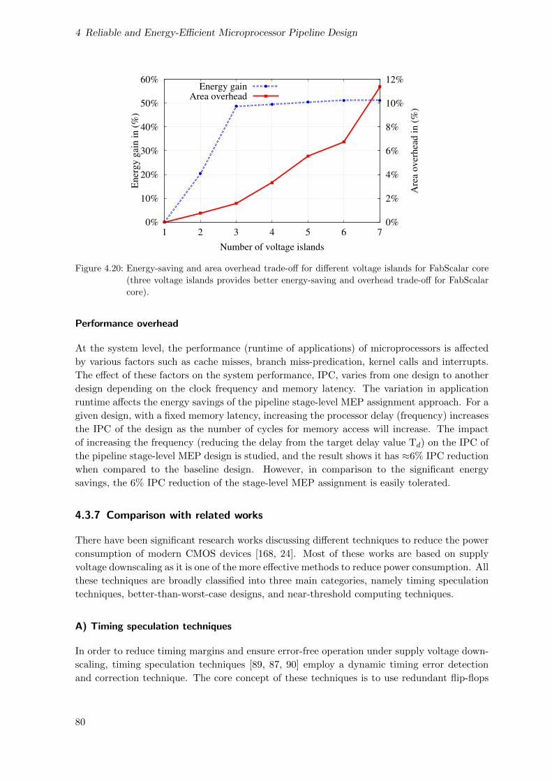
4 Reliable and Energy-Efficient Microprocessor Pipeline Design
0%
10%
20%
30%
40%
50%
60%
1 2 3 4 5 6 70%
2%
4%
6%
8%
10%
12%
Ener
gy g
ain i
n (
%)
Are
a over
hea
d i
n (
%)
Number of voltage islands
Energy gainArea overhead
Figure 4.20: Energy-saving and area overhead trade-off for different voltage islands for FabScalar core
(three voltage islands provides better energy-saving and overhead trade-off for FabScalar
core).
Performance overhead
At the system level, the performance (runtime of applications) of microprocessors is affected
by various factors such as cache misses, branch miss-predication, kernel calls and interrupts.
The effect of these factors on the system performance, IPC, varies from one design to another
design depending on the clock frequency and memory latency. The variation in application
runtime affects the energy savings of the pipeline stage-level MEP assignment approach. For a
given design, with a fixed memory latency, increasing the processor delay (frequency) increases
the IPC of the design as the number of cycles for memory access will increase. The impact
of increasing the frequency (reducing the delay from the target delay value Td) on the IPC of
the pipeline stage-level MEP design is studied, and the result shows it has ≈6% IPC reduction
when compared to the baseline design. However, in comparison to the significant energy
savings, the 6% IPC reduction of the stage-level MEP assignment is easily tolerated.
4.3.7 Comparison with related works
There have been significant research works discussing different techniques to reduce the power
consumption of modern CMOS devices [168, 24]. Most of these works are based on supply
voltage downscaling as it is one of the more effective methods to reduce power consumption. All
these techniques are broadly classified into three main categories, namely timing speculation
techniques, better-than-worst-case designs, and near-threshold computing techniques.
A) Timing speculation techniques
In order to reduce timing margins and ensure error-free operation under supply voltage down-
scaling, timing speculation techniques [89, 87, 90] employ a dynamic timing error detection
and correction technique. The core concept of these techniques is to use redundant flip-flops
80

4.3 Fine-grained Minimum Energy Point (MEP) tuning for energy-efficient pipeline design
(commonly known as razor) which are derived by a delayed clock in order to detect timing
errors. Whenever a timing error is detected an error signal is raised, and rollback mechanism
is used to ensure the correct execution. However, due to the increasing amount of timing
errors these techniques are not effective in terms of performance and energy efficiency when
the supply voltage is downscaled aggressively to the near/sub-threshold voltage domain.
B) Better-than-worst-case techniques
Several better-than-worst-case designs have been proposed to reduce the power consumption
by embracing quality degradation of designs. Better-than-worst case techniques are mainly
utilized in a signal processing domain by exploiting the noise tolerance nature of applications.
For example, an algorithmic noise tolerance based technique [169] exploits the error tolerance
capability of applications to reduce the power consumption. However, the level of supply
voltage downscaling and power saving benefit of such better-than-worst-case designs is limited
by the error rate and correction overheads.
C) Near threshold techniques
Near-threshold designs rely on downscaling of the supply voltage (Vdd) close to the transistor
threshold voltage in order to reduce the dynamic power quadratically. Various researchers
proposed different NTC based techniques in order to minimize the power consumption of
CMOS devices [148, 6, 18]. Unfortunately, the energy efficiency of these techniques is limited
by several factors, such as performance degradation, variability effects, and increase in leakage
energy contribution. Identifying and operating at minimum energy point is crucial in order
to overcome these challenges [165, 83, 151]. Authors in [151] demonstrated that the minimum
energy point of a given circuit could vary depending upon the activity rate of the circuit. Hence,
for a pipelined processor with different functional blocks, using a single minimum energy point
is less energy-efficient as the functional blocks have wide variation in the activity rate. Hence,
applying a global MEP for a pipelined processor is not effective. Instead, a pipeline stage-
level optimal MEP assignment, as presented in this chapter, improves the energy efficiency of
pipelined processor cores significantly.
In order to demonstrate the advantages of the pipeline stage-level MEP assignment tech-
nique, it is compared with the core-level MEP technique as well as slack redistribution based
voltage over-scaling techniques. The core-level MEP technique is discussed in the previous
subsection. The second technique presented in [170] is based on slack distribution and voltage
over-scaling for energy reduction. The voltage over-scaling technique iteratively reduces the
supply voltage by tolerating timing errors or using error correction mechanisms.
Table 4.4 compares the energy consumption of different pipeline stages optimized using
stage-level MEP, core-level MEP, and voltage over-scaling techniques. The table shows for
all stages, both MEP optimization method have smaller energy consumption than the voltage
over-scaling approach. This is because the timing errors in the voltage over-scaling approach
increases when the supply voltage is reduced, which limits the level of voltage downscaling.
The table also shows the under optimization of the core-level MEP [165] and voltage over-
scaling technique [170] when compared to the pipeline stage-level MEP assignment approach.
81

4 Reliable and Energy-Efficient Microprocessor Pipeline Design
Table 4.4: Energy efficiency comparison of the pipeline stage-level MEP assignment with core-level
MEP assignment and voltage over-scaling technique
Stages
Energy per cycle (µJ)
Stage-level Core-level Voltage
MEP MEP over-scaling
Fetch 1.07 1.52 (42.1%) 2.05 (91.5%)
Decode 0.38 0.45 (18.4%) 0.98 (157.8%)
Pick 0.09 0.1 (11.1%) 0.197 (118.8%)
Execute 13.95 18.23 (30.6%) 21.7 (55.5%)
Memory 4.56 5.33 (16.8%) 6.85 (50.2%)
WriteBack 2.45 3.08 (25.7%) 4.61 (88.2%)
Total 22.5 28.71 (27.6%) 36.38 (61.7%)
Area overhead 1.6% 0% 2.7%
Hence, the total energy of the core-level MEP [165] is 27.6% less optimized than the stage-level
MEP technique. Similarly, voltage over-scaling [170] is under optimized by more than 60%.
Moreover, the table shows the pipeline stage-level MEP assignment technique has less area
overhead than voltage over-scaling technique [170]. Although core-level MEP [165] has zero
area overhead, its energy efficiency is much less than the stage-level MEP technique (27% less
efficient) which eventually nullify the area overhead savings.
4.4 Summary
Energy reduction has become the primary design issue in the design of energy-constrained
applications such as energy-harvested devices for IoT applications. In order to address the
variation-induced timing uncertainty and improve the overall energy efficiency of pipelined
NTC processors, two architectural level optimization techniques are presented in this chapter.
The first solution employs a variation-aware pipeline balancing technique, which is a design-
time solution to improve the energy efficiency and minimize performance uncertainty of NTC
microprocessors. The variation-aware balancing technique adopts an iterative synthesis flow
in order to balance the stages in the presence of extreme delay variation. The pipeline stages
are synthesized independently using variation-aware NTC standard cell library, and SSTA
is performed to obtain their statistical delay information. Afterward, the statistical delays
of the stages are provided to the synthesis tool in order to iteratively balance the pipeline
stages accordingly. Experimental results show that the variation-aware pipeline balancing
technique improves the energy efficiency of OpenSPARC and FabScalar cores by 55% and
85%, respectively.
The second technique illustrated the dependency of MEP on the threshold voltage, structure,
and activity rate of a circuit. Thus, it demonstrated the limitations and energy inefficiency
of using single (core-level) MEP for pipelined processor cores, in which the pipeline stages
have intrinsic structure and activity rate variation. The issue is addressed by using a pipeline
82

4.4 Summary
stage-level MEP tuning technique, in which the pipeline stages are designed to operate at
different MEPs by using an activity rate dependent supply and threshold voltage tuning. In
the pipeline stage-level MEP assignment approach, first, the MEPs of the pipeline stages are
approximated analytically. Then, to reduce the implementation cost and overhead, the MEPs
of the pipeline stages are clustered into smaller groups. The effectiveness of the pipeline stage-
level MEP assignment technique is validated by using FabScalar and OpenSPARC cores, and
simulation results show that the stage-level MEP technique improves the energy efficiency of
both FabScalar and OpenSPARC cores by almost 50%.
83


5 Approximate Computing for Energy-Efficient
NTC Design
Most of the energy-constrained portable and handheld devices employ various signal processing
algorithm and architectures, and are an integral part of many multimedia applications, such as
video, audio, and image processing algorithms. Fortunately, these multimedia applications are
inherently error-resilient and create room for erroneous computation with the aim of improving
the performance and energy efficiency of the design. Based on this context, approximate
computing is adopted to aggressively reduce the supply voltage of CMOS circuits by exploiting
the inherent error tolerance nature of multimedia applications. This chapter shows how to
exploit approximate computing to improve the energy efficiency of near-threshold designs.
5.1 Introduction
Approximate computing is a promising approach to tolerate timing errors and get utmost
NTC benefit, as it embraces non-important timing errors to improve the energy efficiency [25].
Approximate computing relies on the ability of applications to tolerate a loss in quality for
performance and energy efficiency improvement [25]. Since approximate computing relaxes
the traditional exact computation requirements, it naturally fits with NTC by effectively tol-
erating most of the variation-induced timing errors and improve the performance/ energy
efficiency [26]. Therefore, approximate NTC is an attractive alternative in energy-constrained
domains, such as signal processing and big data analysis, as many applications in these domains
have inherent error tolerance [25, 26].
Recent works have explored the use of circuit and algorithmic level approximate computing
for low-power designs [171, 172, 173, 174]. These techniques mainly rely on supply voltage
downscaling and exploit the algorithmic noise tolerance to embrace the resulting errors. Such
techniques are sufficient in the super-threshold voltage domain as process variation has a small
impact and hence, the resulting errors are effectively tolerated by approximate computing. In
the near-threshold voltage domain, however, such techniques are not sufficient anymore as the
variation-induced timing errors surpass the error tolerance capability of various applications.
Other works in [43, 44, 175, 176] employ logic simplification techniques to design inaccurate
low-power functional components such as adders and multipliers. However, on top of their
inherent inaccuracy, the wide range of variation-induced timing errors in NTC aggravate the
error rate and eventually lead to an unacceptable output quality.
In order to apply approximate computing to NTC designs, it is imperative to identify the
approximable and non-approximable portions of the design based on a quantitative analysis
of timing errors, and their structural and functional propagation probabilities. Therefore, a
detailed analysis of statistical timing errors, as well as structural and functional error prop-
agation probabilities is of decisive importance for approximate NTC design. This chapter
85

5 Approximate Computing for Energy-Efficient NTC Design
presents a technique to exploit approximate computing in order to improve the energy effi-
ciency of NTC designs. The proposed approximate NTC design technique uses an integrated
framework consisting of statistical timing error analysis and error propagation analysis tools.
In the framework, first, the control logic part of a design is identified and protected from
approximation. Then, the data flow portion of the design is classified into approximable and
non-approximable portions. Afterward, a mixed-timing logic synthesis which applies a tight
timing constraint for the non-approximable portion, and a relaxed timing constraint for the
approximable part is used to synthesize the design. The mixed-timing logic synthesis has two
features:
• It forces the synthesis tool to use faster gates in order to guarantee timing certainty of
the non-approximable portion by applying a tight timing constraint.
• In contrary to the tight constraint, a relaxed timing constraint is used in the approximable
portion of the design, so that timing errors are embraced for energy saving. The relaxed
timing constraint allows the synthesis tool to use more energy-efficient gates.
Experimental results show that exploiting approximate computing for NTC improves the en-
ergy efficiency of Discrete Cosine Transform (DCT) application by more than 30%. Further-
more, the effectiveness of the approximate computing based NTC design is demonstrated using
an image compression application, and it is observed that the energy efficiency improvement
is achieved at an acceptable output quality reduction.
The rest of the chapter is organized as follows: approximate computing background and
related works are presented in Section 5.2. Error propagation aware timing relaxation frame-
work for approximate NTC is presented in Section 5.3, followed by the experimental results in
Section 5.4. Finally, Section 5.5 presents the chapter summary.
5.2 Background
5.2.1 Embracing errors in approximate computing
A) Approximate computing basics
Digital Signal Processing (DSP) is the building block of several multimedia applications. Most
of these multimedia applications implement image and video processing algorithms, where the
final output is either an image or a video. The perceptual limitation of human vision allows the
outputs of these algorithms to be numerically approximate. The relaxation on the accuracy
requirement gives a room for imprecise or approximate computation. Hence, approximate
computation is exploited to come up with low-power designs at different levels of abstraction,
such as algorithmic, architecture and logic level approximation.
Reliable and accurate operations dictate the performance and energy efficiency of modern
computing platforms. However, several applications in the domain of signal processing, ma-
chine vision, and big data analysis have intrinsic tolerance to inaccuracy as the inaccurate
computations may have a minor impact on the final output quality. Therefore, approximate
computing exploits the inherent applications error resiliency, to achieve a desirable trade-off
between performance/ energy efficiency and output quality. Since approximate computing
relaxes the need for exact computation, it adds another dimension to the energy-performance
86

5.3 Error propagation aware timing relaxation
optimization space enabling better performance and energy efficiency trade-off by embracing
timing and memory errors.
B) Approximation in near-threshold computing
Variation-induced timing errors prevent NTC designs from operating at their designated nom-
inal frequency. Hence, to guarantee error-free operation, NTC designs should operate at a
lower frequency by constituting large timing guard-band which affects both energy efficiency
and performance. In several applications, however, the effect of variation-induced errors are
tolerated by using approximate computing. As shown in this chapter, combining approximate
computing and NTC has a significant impact on improving the energy efficiency of various
designs with inherent error tolerance capabilities.
5.2.2 Related works
Most of the works in the field of approximate computing rely on algorithmic noise toler-
ance [171, 172, 173, 174], voltage downscaling and design of inaccurate functional components
(such as adders and multiplier) [43, 44, 175, 176]. However, all these works are targeting the
nominal voltage domain where the impact of variation is minimal. Authors in [28] employed
the concept of decoupling control and data operations into different cores, in which the con-
trol cores are operated at a higher voltage. However, their technique requires voltage level
converter, and a dedicated power delivery network which imposes significant overhead. Addi-
tionally, they have zero protection for all data operations and rely on checkpoint and rollback
mechanism for error recovery. These affect the performance and energy efficiency significantly.
In the proposed error propagation-aware timing relaxation approach, however, there is no over-
head, and all control and important data operations are performed in an error-free manner,
as errors are only allowed in the approximable data-flow portion of the design.
5.3 Error propagation aware timing relaxation
5.3.1 Motivation and idea
Variation-induced timing errors significantly reduce the performance and energy efficiency of
NTC designs. In this regard, leveraging approximate computing along with NTC improves
the energy efficiency of designs by embracing the timing errors of NTC designs. From timing
criticality perspective, circuit paths are categorized as critical (longer delay) and non-critical
(shorter delay) paths. Similarly, they are classified as important (error sensitive) and non-
important (error tolerant) paths based on the error generation and propagation probabilities.
The “importance” of the paths depends on their structural and functional error propagation
probabilities. This concept is elaborated using an example circuit by classifying the paths
into different groups. For example, Figure 5.1(a) shows the classification of FIR filter circuit
paths into different groups (critical, non-critical, important and non-important) based on their
timing criticality and importance. These classifications are used to relax the timing constraint
of the non-important and non-critical group in order to improve the energy efficiency and
performance of the circuit.
87

5 Approximate Computing for Energy-Efficient NTC Design
Critical
Non-critical
ImportantNon-important
386
214
350700
0
00
0
(a) Path distribution
Top Trelax
P1P2P3P4P5P6P7P8
Variation-induced delayNominal delay
(b) Path relaxation
Figure 5.1: Example of FIR filter circuit showing path classification and timing constraint relaxation
of paths.
Figure 5.1(b) shows the variation-induced delay distribution and timing constraint relaxation
of non-important representative paths. In the conventional design approach, regardless of
their importance and criticality, all paths should be designed and operate at a designated
clock period (Top) which is defined according to the delay of the longest path of the circuit
including variation guard-band. However, it is observed that not all paths of a circuit are
equally important to the final output. Therefore, the energy efficiency and performance are
improved by relaxing the timing constraint of the less critical/ important paths. For this
purpose, first, the data-flow paths/ endpoints of a circuit are classified into approximable
(non-critical or non-important) and non-approximable (critical and important) groups based
on their timing criticality and correctness (error propagation probability). Then, a mixed-
timing logic synthesis is applied to improve the energy efficiency of the circuit.
To illustrate the mixed-timing logic synthesis scenario, let us consider the delay of the paths
given in Figure 5.1(b). Based on timing error and propagation analysis, assume the paths P1,
P6, and P7 are non-approximable, while paths P2, P3, P4, P5, and P8 are approximable.
Therefore, in the mixed-timing logic synthesis, paths P1, P6, and P7 are subjected to a tight
timing constraint (Top) in order to ensure timing correctness of the non-approximable portion.
However, a loose timing constraint Trelax is used for the remaining approximable portion for
energy efficiency improvement. The relaxation amount for the approximable paths depends
on the residual timing errors of the paths, which is obtained from a statistical timing error
analysis, as well as the target error rate for the entire circuit.
5.3.2 Variation-induced timing error propagation analysis
Since the objective is to relax the timing constraint of the approximable paths and to use tight
timing constraint for the non-approximable paths, the identification of the approximable and
non-approximable portions of a circuit is crucial. Hence, a statistical timing error analysis
tool is used to analyze the occurrence probability and distribution of variation-induced timing
errors. Afterward, an error-propagation probability analysis tool is employed to study the
propagation probability of timing errors to the important portion of the circuit.
88

5.3 Error propagation aware timing relaxation
nominal delay variation-inducedTclk
shift
Timing error
Figure 5.2: Variation-induced path delay distribution with the assumption of normal distribution.
A) Statistical timing error rate analysis
In a static timing analysis, where paths have discrete delay values, the timing error rate is
obtained by analyzing the arrival time of the signals. Thus, for a given circuit with a clock
period of Tclk, the timing error probability (Ep) of the circuit is calculated as a weighted sum
of the paths with a delay greater than the clock period (Tclk) over the total number of paths
as shown in Equation (5.1).
Ep =
N∑i=1
Pi
M(5.1)
where N is the number of paths with delay Di>Tclk, and M is the total number of paths in
the circuit.
Due to the wide variation extent in NTC, however, the delay of the paths becomes a dis-
tribution rather than a discrete value, which makes the weighted sum based error probability
calculation an optimistic approach. Therefore, an accurate error probability estimation based
on Statistical Static Timing Analysis (SSTA) is required. For this purpose, an SSTA based
timing error analysis framework is developed to determine timing error of NTC designs. In
the statistical timing error analysis framework, the variation-induced delay shift is modeled
by a normal distribution (e.g., µ ± 3σ). To show the operation of the statistical timing error
analysis, let us consider the delay distributions of tight and relaxed paths (indicated by the
green and yellow shades) shown in Figure 5.2. Assume (µT , σT ) are the mean and standard
deviation of the tight constraint (green shade), and (µR, σR) are the mean and standard de-
viation pairs for the relaxed path (yellow shade). Therefore, the timing error probability of
the relaxed path is the probability where the path delay is longer than the operational clock
(Tclk), which is equivalent to the triangular area shown by grid pattern in Figure 5.2. Hence,
the statistical timing error probability (EP ) is modeled mathematically as the integral of the
probability density function over the interval [Tclk, µR+3σR], as shown in Equation (5.2) [177].
EP ≈µR+3σR∫Tclk
f (x| µR, σR)dx (5.2)
where the probability density f (x) is given in Equation (5.3) [177].
f(x| µR, σ2R) =
1
σR√
2πexp(−(x− µR)2
2σ2R
) (5.3)
89

5 Approximate Computing for Energy-Efficient NTC Design
Combinational logic
Combinational logic
Q
QSET
CLR
D
Q
QSET
CLR
D
Q
QSET
CLR
D
Combinational logic
Combinational logic
Q
QSET
CLR
D
Q
QSET
CLR
D
Q
QSET
CLR
D
Q
QSET
CLR
DCombinational logic
Combinational logic
Combinational logic
Erroneous data
Erroneous blockError free blockPropagating block
Error propagation Masked error pathMasking block
Input
Output
Figure 5.3: Timing error generation, propagation and masking probability from error site to primary
output of a circuit.
B) Structural error propagation analysis
In a circuit with various combinational and sequential components, timing errors are mani-
fested as delayed signals which cannot be latched by storage elements, such as flip-flops or
latches, during a specific clock period. The delayed signals lead to the latching of erroneous
value with a possibility of propagating to the primary output or consecutive flip-flops in the
next cycles. Therefore, an erroneous flip-flop value is either:
• Propagated to the primary output and give an erroneous result or system failure.
• Masked in one of the stages before it reaches the primary output. Thus, the error has
no observable effect, and the system functionality is not affected by the error.
To illustrate the propagation and masking probability of timing errors, let us consider the
circuit shown in Figure 5.3. As shown in the figure, a timing error from the erroneous com-
binational blocks (blocks indicated by red) could lead to the storage of wrong values in the
sequential elements (flip-flops). The erroneous data can be propagated further to the pri-
mary output (as indicated by the error propagation forward cone, purple blocks) or may not
propagate due to logic masking (as shown by the error masking backward cone from the yel-
low blocks). Since sequential circuits are the error sites for timing errors, variation-induced
timing error is modeled and analyzed using the existing sequential circuit error modeling tech-
niques [178]. Therefore, a model for soft error rate estimation of sequential circuits is adopted
to analyze the propagation probabilities of timing errors and their effect on the system func-
tionality [179]. Hence, for a design with k primary outputs the system failure probability
(observability of an error from any reachable primary output) due to a wrong flip-flop value
is obtained using Equation (5.4) [179]:
Sfp = 1−k∏j=1
[1− EP × POj × Pprop] (5.4)
where EP is the statistical timing error probability obtained using Equation (5.2), POj is
reachability of primary output j from the error site and Pprop is the error propagation proba-
bility.
90

5.3 Error propagation aware timing relaxation
Tim
ing
err
or
an
aly
sis
fra
me
wo
rk
Pre
-syn
the
sis
sim
ula
tio
nMixed-timing logic synthesis
Simulation
input
Design
(RTL)
VCD file
NTC standard
cell libraryConstraint file
Synopsys design compiler / power
compiler
Synthesized
netlistSdf, ddc
files
Power
profile
Simulation engine
Cadence SSTA engine
Statistical delay per
endpointStatistical timing error
analysis tool
Operational
clock
Structural error propagation
analysis tool
Functional error analysis
tool
System failure analysis (Sysfp)Update constraint file and re-synthesis
Start
Figure 5.4: Proposed timing error propagation aware mixed-timing logic synthesis framework.
C) Functional error propagation analysis
In many signal processing algorithms, all variables and instructions are not equally important
to the final output [180]. For example, control flow instructions are more important than
data flow instructions and hence, any small error in these instructions have a catastrophic
effect, such as system crashing or freezing. Similarly, in data flow instructions, high order
output bits are more critical for output accuracy than the lower order bits and the fractional
portion of mantissa in floating point values. Therefore, for data-intensive applications, the
energy efficiency is improved further by using functionality based approximation ( i.e., by
approximating the lower order bits).
To utilize the functionality based approximation, first, analyzing the role of the bit posi-
tions to the correctness of the final output of a given design (e.g., DCT application detailed
in Section 5.4.3) is essential. From the analysis, a weight vector (Wi) is determined, and as-
signed to the primary outputs to indicate their importance to the output accuracy and level
of approximation. For example, for an integer or mantissa of a floating point value with N-bit
width primary output, the weight vector is assigned within the closed interval [0-1], where 1
indicates important (no approximation), and 0 represents the less important output bits (see
Equation (5.5)).
∀i ∈1...N−1 Wi =1
2N−1−i (5.5)
Therefore, the weight vector of the primary output bits is coupled with the error propagation
model presented in Equation (5.4) to increase the level of approximation.
In order to maintain correct program execution flow, protecting all bit positions of variables
related to control flow instructions is essential. Hence, for all control flow related outputs the
weight is set to 1 to indicate that approximation is not allowed as there is no tolerance for
control flow errors.
5.3.3 Mixed-timing logic synthesis flow
The overall flow of the timing error propagation aware mixed-timing logic synthesis framework
is presented in Figure 5.4. The analysis starts with a pre-synthesis simulation to extract the
Value Change Data (VCD) file for accurate power estimation. Then, the design is synthesized
to obtain the baseline power consumption, timing, and variation-induced delay information.
Afterward, the Statistical timing error rate, structural error propagation, and functional error
91

5 Approximate Computing for Energy-Efficient NTC Design
propagation analysis are conducted to identify the approximable portion of the design. Finally,
the approximable portion information is used to update the timing constraint and perform
mixed-timing logic synthesis and power optimization iteratively.
In the mixed-timing logic synthesis, the paths endpoints (i.e., flip-flops and primary outputs)
are assigned tight/relaxed timing constraints based on the statistical timing error as well as
structural and functional error propagation analysis presented in the previous subsection.
Therefore, once the approximable and non-approximable endpoints are identified, the mixed-
timing logic synthesis assigns tight timing constraint (Ttight) to the non-approximable portion
of the design, and a loose constraint for the approximable portion. Finally, the design operates
with a clock period of Ttight.
A) Tight timing constraint for a non-approximable portion
For all endpoints within this group, a tighter timing constraint (Ttight) is assigned so that
the operational clock always bounds the variation-induced delay. The tight timing constraint
guarantees post manufacturing timing certainty and error-free operation of the important
portion of the design. The tight timing constraint forces the synthesis tool to reduce the delay
of the paths by using faster gates. In order to consider the impact of process variation during
design time, the SSTA tool is provided with a variation characterized standard cell library so
that the operational clock is sufficient enough, even in the presence of variation.
In cases where a non-approximable endpoint has a statistical delay less than the tighter
delay constraint (i.e., Di<Ttight), then the endpoint is relaxed for energy improvement by
using slower, but energy-efficient gates. However, if there is a timing violation in any of
the non-approximable endpoints, then the tight constraint (operational clock) is relaxed by a
small interval δ (i.e., Ttight + δ), and the synthesis flow resumes iteratively ensuring timing
correctness of the non-approximable portion.
B) Loose timing constraint for an approximable portion
Unlike the non-approximable portion, the approximable part of a design is allowed to violate
the operational clock by using loose timing constraint (Tloose) during synthesis time, which
increase the delay for energy efficiency improvement. In other words, harmless timing errors
are allowed systematically in order to save energy. Therefore, since the timing constraint is
not essential for this group (Tloose>Ttight), the synthesis tool is forced to save energy by using
energy-efficient gates. It should be noted that the relaxation amount for the approximable
paths depends on the target system error rate and effective timing error rate obtained by
statistical structural and functional propagation analysis.
Mixed-timing synthesis runtime analysis
To obtain a basic mixed-timing design, the flow depicted in Figure 5.4 has to iterate twice in
the best case (once with tight timing, Ttight, and once with loose timing constraint, Tloose). If
there are timing violations in the non-approximable portion (Ttight), then the tight constraint
is relaxed by a small interval δ (i.e., Ttight + δ) iteratively. Hence, the number of iterations
becomes higher; for example, the mixed-timing optimization of DCT circuit took 6 iterations.
92

5.4 Experimental results
5.4 Experimental results
5.4.1 Experimental setup
The timing error propagation aware mixed-timing logic synthesis framework composing of
statistical timing error analysis and functional error propagation analysis is implemented in
C++. The analysis tool presented in [179] is integrated to the error propagation-aware timing
relaxation framework for structural error propagation analysis. Synopsys design compiler is
employed for synthesis and optimization. Timing analysis in the presence of variation effect is
conducted by Cadence SSTA tool that uses a variation characterized saed 32nm NTC library
(0.5V supply voltage). For power analysis, first, Modelsim is used to extract the switching
activities in Value Change Dump (VCD) formate and parsed to a Switching Activity Interface
Format (SAIF) file. Then, the SAIF file is used by the synthesis tool to obtain an accurate
power estimation.
The effectiveness of the technique is demonstrated using a DCT as a case study. DCT is
widely used in image compression techniques to transform signal (image data) from a spatial
domain into a frequency domain. The Lena image is used as a representative benchmark for
image compression.
5.4.2 Energy efficiency analysis
To determine the optimal level of approximation in terms of energy efficiency and effective
system timing error rate, the statistical error rate (Ep) (Equation (5.2)), structural propagation
(Sfp) (Equation (5.4)), and functional propagation (FP) (Equation (5.5)) probabilities of all
paths are obtained first. Afterward, for each path, the effective error rate is determined as
the product of its Sfp and FP values as shown in Equation (5.6). Since the structural and
functional error propagation probabilities are considered independent, i.e., a failure occurs
when an error is propagated to functionally important output, then the joint probability is the
product of the structural and functional probabilities, i.e., P(Sfp & FP) = P(Sfp) × P(FP).
∀i ∈ path Eeffi = Sfpi × FPi (5.6)
Once the effective error rates are obtained, the paths are sorted in ascending order based on
their effective error rate (Eeff ), where paths with small Eeff are more suitable for approx-
imation. Finally, different percentages of the sorted paths are relaxed (starting with paths
that have smaller Eeff ) to determine the optimal approximable portion. Hence, sweeping the
percentage of relaxed paths from 0% to 100% with a step of 10% is used to study the impact
of relaxed paths. For example, if the relaxed paths (approximable portion) is 10%, then it
means that 10% of the paths with the smallest Eeff are relaxed. Hereinafter the term “relaxed
paths” refers to the percentage of paths that are subjected to loose timing constraint during
synthesizing the circuit. Since the paths of DCT have unbalanced delays, i.e., some paths are
longer while others are shorter even with a tighter clock, the energy efficiency improvement
does not always increase with an increase in the number of relaxed paths. Therefore, the in-
crease in the number of relaxed paths no longer improve the energy efficiency beyond a certain
point (e.g., 70%) and it eventually saturate.
93

5 Approximate Computing for Energy-Efficient NTC Design
0%
5%
10%
15%
20%
25%
30%
35%
0 10 20 30 40 50 60 70 80 90 100
Ener
gy i
mpro
vem
ent
(%)
Relaxed paths (in %)
Slack 10%Slack 20%Slack 25%
Slack 35%Slack 50%
Figure 5.5: Energy efficiency improvement for different levels of approximation (% of relaxed paths).
The curves correspond to the relaxation amount as a % of the clock.
A) Optimal relaxation slack analysis
The impact of using different slacks on the energy efficiency and effective system error rate of
a given circuit for different approximation levels is quantified through extensive error analysis
and simulation. In this analysis, the energy efficiency improvement and timing error rate
of 10%, 20%, 35%, and 50% relaxation slacks are presented. It should be noted that 10%
relaxation represents that the relaxed clock is 10% longer than the tight (operational clock).
Hence, Trelax = 1.1×Ttight, the other relaxation slacks 20%, 25%, 35% and 50% also have
similar relation to the operational clock.
The energy efficiency improvement and effective system timing error rate of the five relax-
ation slacks for different percentage of relaxed paths of DCT circuit are given in Figures 5.5
and 5.6. As shown in Figure 5.5, the energy efficiency improvement increases with an increase
in the percentage of relaxed paths. However, it saturates when the relaxed paths exceed
70%. The saturation is because some paths cannot be optimized further regardless of the
optimization effort.
The effective system timing error rate (see Figure 5.6) is obtained as the sum of the effective
error rate (Eeff ) of the relaxed paths (i.e., SystemEER =N∑i=1
Eeff , where N is the total number
of relaxed paths). The two figures shows 35% relaxation slack provides the best trade-off
between energy efficiency and error rate than the other relaxation slacks. Additionally, for all
relaxation slacks, there is a sharp increase in the effective system timing error rate when the
relaxed paths exceed 60% while the energy efficiency improvement is saturating. Hence, 60%
relaxed paths provides a good balance between energy and effective system error rate.
94

5.4 Experimental results
0
0.1
0.2
0.3
0.4
0.5
0.6
0 10 20 30 40 50 60 70 80 90 100
Eff
ecti
ve
syst
em e
rror
rate
Relaxed paths (in %)
Slack 10%Slack 20%Slack 25%
Slack 35%Slack 50%
Figure 5.6: Effective system error for different levels of accuracy (% relaxed paths). The curves corre-
spond to the amount by which the selected paths are relaxed, as a % of the clock.
B) Energy efficiency improvement of different optimization methods
Depending on the classification scheme used (timing criticality or error propagation), the
approximable portion of a design varies from one scheme to other. For example, if timing
criticality is the only metric then, all non-critical paths are approximated regardless of their
error propagation probability and impact on the final output. Therefore, the energy efficiency
improvement of three optimizations, namely timing criticality based, importance based (struc-
tural and functional error propagation), and a combination of both are studied.
Figure 5.7 shows the energy improvement of timing criticality, importance, and criticality
and importance based optimization methods for the same system error rate (0.08 or 60%
0%
5%
10%
15%
20%
25%
30%
10% 20% 25% 35% 50%
En
erg
y i
mp
rov
emen
t (%
)
Relaxiation slack
Timing criticalityImportance
Timing criticality & importance
Figure 5.7: Energy efficiency improvement of different optimization schemes.
95

5 Approximate Computing for Energy-Efficient NTC Design
Post-syntheis Monte Carlo simulation
Synthesized
netlist NTC library HDL
Standard delay
format (sdf) file
DCT operation
Transformed image
Pixel extraction and down
sampling
Random timing error insertion
Input Image
Partitioning into 8X8 block Image reconstruction
Modify sdf file to inject errors
PSNR analysis toolPSNR distribution
Figure 5.8: Post-synthesis Monte Carlo simulation flow.
relaxed paths) of DCT using different relaxation slacks. The figure shows for all slacks applying
timing criticality or importance based optimization only has less energy saving as the level of
approximation is limited. However, it is observed that better energy saving (more than 30%
over a non-approximate NTC) is obtained when all optimization techniques (timing, structural,
and functional) are applied in combination as they provide more approximation freedom.
5.4.3 Application to image processing
Approximate computing is widely employed in many DSP algorithms used in audiovisual ap-
plications as they are inherently error-resilient. Among various multimedia systems, an image
compression algorithm is used to show the effectiveness of the timing error propagation-aware
approximation technique. However, it should be noted that the proposed error propagation-
aware timing relaxation technique is generic and can be applied to any error resilient systems,
which have an approximation freedom. DCT algorithm linearly transforms input data into
a frequency domain where a set of coefficients represent it. It is an integral part of different
multimedia applications such as JPEG.
20% 40% 60% 80% 100%
Relaxed paths
10
15
20
25
30
35
PSN
R (
dB
)
Figure 5.9: PSNR distribution for different approximation levels for 35% relaxation slack.
96

5.5 Summary
Since variation-induced timing errors are stochastic in nature, a Monte Carlo based post-
synthesis simulation flow is developed to quantify the effect of statistical timing errors on the
output quality of image compression by using the error propagation-aware timing relaxation
approach. Figure 5.8 presents the post-synthesis simulation framework which is composed
of preprocessing, post-synthesis simulation, and post-processing. First, the input grayscale
image is preprocessed by converting it to a pixel array and partitioning it into 8×8 blocks.
Then, one thousand Monte Carlo post-synthesis simulations are performed by modifying the
timing constraint SDF file, and randomly injecting timing errors based on the SSTA delay
distributions of the relaxed paths. Finally, in the post-processing phase, the compressed images
are decompressed by applying inverse DCT (IDCT), and the corresponding Peak Signal to
Noise Ratio (PSNR) values are extracted. Figure 5.9 shows the PSNR distribution of different
percentage of relaxed paths with a 35% relaxation slack. Figure 5.10 shows the examples of the
output images for the baseline (a non-approximate NTC implementation), 20% 60%, and 80%
relaxed paths. Since the 80% relaxed paths has a higher error rate, the output image given in
Figure 5.10(d) has lower quality than the output images presented in Figures 5.10(a), 5.10(b),
and 5.10(c).
(a) PSNR=34.1
baseline (0%)
SEER=0.0
(b) PSNR=28.1
20% relaxation
SEER=0.01
(c) PSNR=21.2
60% relaxation
SEER=0.08
(d) PSNR=16.5
80% relaxation
SEER=0.29
Figure 5.10: Comparison of output quality of different levels of approximation (% of relaxed paths).
5.5 Summary
The widespread applicability of NTC is hindered by several barriers such as increase in
variation-induced timing errors. These problems are addressed in the scope of approximate
computing by tolerating non-important variation-induced timing errors. The chapter presented
a framework that exploits the error tolerance potential of approximate computing for energy-
efficient NTC designs. In the framework, statistical timing error analysis, as well as structural
and functional error propagation analysis, is performed to identify the approximable portion
of a design. Then, a mixed-timing logic synthesis is employed to improve energy efficiency by
embracing errors in the approximable portion of the design. Experimental results show that
the technique improves energy efficiency of approximate NTC design by more than 30%.
97


6 Conclusion and Remarks
6.1 Conclusions
With the abundance of battery-powered devices for IoT applications, the demand for energy
efficiency and longer battery lifetime has increased significantly. The most effective way to
reduce the energy consumption of CMOS circuits is to decrease the dynamic and static powers
consumed by the circuits. Dynamic and leakage power reduction is achieved by aggressively
downscaling the supply voltage of CMOS circuits. Therefore, supply voltage downscaling is
a promising approach to realize energy-efficient operation for energy-constrained application
domains such as IoT. This dissertation studied the potentials of supply voltage downscaling
to reduce the energy consumption with a main emphasis on near-threshold computing (NTC),
where the supply voltage is set to be close to the threshold voltage of a transistor, for energy-
efficient operation. NTC enables energy savings on the order of 10×, with a linear performance
degradation, providing a much better energy/performance trade-off. However, in addition to
performance reduction, NTC comes with its own set of challenges that hinder its widespread
applicability. The main challenges for energy-efficient NTC operation are: 1) performance
loss; 2) increased sensitivity to variation effects; and 3) high functional failure rate of storage
elements. This dissertation started with the analysis of the main NTC barriers and state-of-the-
art solutions to overcome them. Then, the dissertation provided different architecture-level
solutions to tackle those barriers and improve the reliability and energy efficiency of NTC
designs. In general, the main contributions of this dissertation is summarized as follows:
• Memory failure analysis framework for wide supply voltage ranges is presented. The
framework helps to study the impact of different memory failure mechanisms and thier
interdependence across different supply voltage values (from the super-threshold to near-
threshold voltage domain). Moreover, the dissertation presented memory failure mitiga-
tion techniques in order to enable reliable NTC operation.
• The impact of process variation on the performance and energy efficiency of NTC proces-
sor pipeline stages is studied, and a variation-aware pipeline delay balancing technique
is adopted to reduce the impact of process variation, and improve the energy efficiency
of pipeline stages operating in the near-threshold voltage domain. In order to further
improve the energy efficiency of pipeline stages, a fine-grained Minimum Energy Point
(MEP) tuning technique is presented in the dissertation. In the presented MEP assign-
ment technique, the individual pipeline stages of a processor are designed to operate at
local MEPs obtained through pipeline stage-level supply and threshold voltage tuning.
• The dissertation also explored the potentials of emerging computing paradigm, approx-
imate computing, in improving the energy efficiency of NTC designs. Thus, the disser-
tation demonstrated how to achieve a desirable trade-off between energy efficiency and
output quality reduction of NTC designs with the help of approximate computing.
99

6 Conclusion and Remarks
In conclusion, the methodologies and solutions presented in this dissertation are viable alter-
natives towards resilient and energy-efficient NTC processor design. Other published works
not included in this dissertation [118, 38] also explore the potentials of power gating and non-
volatile microprocessor design for energy-efficient ultra-low power processor design. Therefore,
all these contributions are crucial steps in the design and implementation of resilient and
energy-constrained microprocessor architectures.
6.2 Remarks
It should be noted that the solutions and methodologies presented in this dissertation are
generic and can be applied to different designs in the context of resilient and energy-efficient de-
sign. Among the various application domains, brain-inspired neuromorphic computing benefits
from the solutions presented in this dissertation. Neuromorphic systems which are prevalent
and employed in a wide variety of classification and recognition tasks have high computa-
tional energy demand, and hence, their energy-efficient implementation is of great interest.
Therefore, energy-efficient design approaches such as the solutions presented in this disser-
tation are crucial for the widespread applicability and the deployment of cognitive tasks in
energy-constrained embedded and IoT platforms.
100

Bibliography
[1] Chris A Mack. Fifty years of moore’s law. IEEE Transactions on semiconductor manu-
facturing, 2011.
[2] Chris Mack. The multiple lives of moore’s law. IEEE Spectrum, 2015.
[3] Chi-Wen Liu and Chao-Hsiung Wang. Finfet device and method of manufacturing same,
May 13 2014. US Patent 8,723,272.
[4] Yen-Huei Chen, Wei-Min Chan, Wei-Cheng Wu, Hung-Jen Liao, Kuo-Hua Pan, Jhon-
Jhy Liaw, Tang-Hsuan Chung, Quincy Li, Chih-Yung Lin, Mu-Chi Chiang, et al. A 16
nm 128 mb sram in high-k metal-gate finfet technology with write-assist circuitry for
low-vmin applications. IEEE Journal of Solid-State Circuits, 2015.
[5] Abbas Sheibanyrad, Frederic Petrot, Axel Jantsch, et al. 3D integration for NoC-based
SoC Architectures. Springer, 2011.
[6] Ronald G Dreslinski, Michael Wieckowski, David Blaauw, Dennis Sylvester, and Trevor
Mudge. Near-threshold computing: Reclaiming moore’s law through energy efficient
integrated circuits. Proceedings of the IEEE, 2010.
[7] Hadi Esmaeilzadeh, Emily Blem, R St Amant, Karthikeyan Sankaralingam, and Doug
Burger. Dark silicon and the end of multicore scaling. IEEE Micro, 2012.
[8] Timothy Normand Miller. Architectural Solutions for Low-power, Low-voltage, and Un-
reliable Silicon Devices. PhD thesis, The Ohio State University, 2012.
[9] Himanshu Kaul, Mark Anders, Steven Hsu, Amit Agarwal, Ram Krishnamurthy, and
Shekhar Borkar. Near-threshold voltage (ntv) design: opportunities and challenges. In
Proceedings of the 49th Annual Design Automation Conference, 2012.
[10] Mohammad Saber Golanbari, Anteneh Gebregiorgis, Fabian Oboril, Saman Kiamehr,
and Mehdi Baradaran Tahoori. A cross-layer approach for resiliency and energy effi-
ciency in near threshold computing. In Computer-Aided Design (ICCAD), IEEE/ACM
International Conference on, 2016.
[11] Ulya R Karpuzcu, Nam Sung Kim, and Josep Torrellas. Coping with parametric variation
at near-threshold voltages. IEEE Micro, 2013.
[12] Ulya R Karpuzcu, Abhishek Sinkar, Nam Sung Kim, and Josep Torrellas. Energysmart:
Toward energy-efficient manycores for near-threshold computing. In High Performance
Computer Architecture (HPCA), IEEE 19th International Symposium on, 2013.
[13] Anteneh Gebregiorgis and Mehdi B Tahoori. Reliability and performance challenges of
ultra-low voltage caches: A trade-off analysis. In IEEE 24th International Symposium
on On-Line Testing And Robust System Design (IOLTS), 2018.
[14] Nathaniel Pinckney, Ronald G Dreslinski, Korey Sewell, David Fick, Trevor Mudge,
101

BIBLIOGRAPHY
Dennis Sylvester, and David Blaauw. Limits of parallelism and boosting in dim silicon.
IEEE Micro, 2013.
[15] Ronald G Dreslinski, David Fick, Bharan Giridhar, Gyouho Kim, Sangwon Seo, Matthew
Fojtik, Sudhir Satpathy, Yoonmyung Lee, Daeyeon Kim, Nurrachman Liu, et al. Cen-
tip3de: A 64-core, 3d stacked near-threshold system. IEEE Micro, 2013.
[16] Kelin J Kuhn. Reducing variation in advanced logic technologies: Approaches to process
and design for manufacturability of nanoscale cmos. In Electron Devices Meeting, IEDM.
IEEE International, 2007.
[17] Kelin J Kuhn, Martin D Giles, David Becher, Pramod Kolar, Avner Kornfeld, Roza
Kotlyar, Sean T Ma, Atul Maheshwari, and Sivakumar Mudanai. Process technology
variation. IEEE Transactions on Electron Devices, 2011.
[18] Anteneh Gebregiorgis, Saman Kiamehr, Fabian Oboril, Rajendra Bishnoi, and Mehdi B
Tahoori. A cross-layer analysis of soft error, aging and process variation in near threshold
computing. In Design, Automation & Test in Europe Conference & Exhibition (DATE),
2016.
[19] Benton H Calhoun and Anantha Chandrakasan. A 256kb sub-threshold sram in 65nm
cmos. In Solid-State Circuits Conference. ISSCC. Digest of Technical Papers. IEEE
International, 2006.
[20] Anteneh Gebregiorgis and Mehdi B Tahoori. Reliability analysis and mitigation of near
threshold caches. In Mixed Signals Testing Workshop (IMSTW), International, 2017.
[21] Ronald Dreslinski, Michael Wieckowski, D Sylvester Blaauw, and T Mudge. Near thresh-
old computing: Overcoming performance degradation from aggressive voltage scaling. In
Proc. Workshop Energy-Efficient Design, 2009.
[22] Anteneh Gebregiorgis, Rajendra Bishnoi, and Mehdi B Tahoori. A comprehensive reli-
ability analysis framework for ntc caches: A system to device approach. IEEE Transac-
tions on Computer-Aided Design of Integrated Circuits and Systems, 2018.
[23] Anteneh Gebregiorgis and Mehdi B Tahoori. Fine-grained energy-constrained micro-
processor pipeline design. IEEE Transactions on Very Large Scale Integration (VLSI)
Systems, 2018.
[24] Anteneh Gebregiorgis, Mohammad Saber Golanbari, Saman Kiamehr, Fabian Oboril,
and Mehdi B Tahoori. Maximizing energy efficiency in ntc by variation-aware micro-
processor pipeline optimization. In Proceedings of the International Symposium on Low
Power Electronics and Design, 2016.
[25] Jie Han and Michael Orshansky. Approximate computing: An emerging paradigm for
energy-efficient design. In Test Symposium (ETS), 18th IEEE European, 2013.
[26] Haider AF Almurib, T Nandha Kumar, and Fabrizio Lombardi. Inexact designs for
approximate low power addition by cell replacement. In Design, Automation & Test in
Europe Conference & Exhibition (DATE), 2016.
[27] Anteneh Gebregiorgis, Saman Kiamehr, and Mehdi B Tahoori. Error propagation aware
timing relaxation for approximate near threshold computing. In Proceedings of the 54th
Annual Design Automation Conference, 2017.
102

BIBLIOGRAPHY
[28] Ismail Akturk, Nam Sung Kim, and Ulya R Karpuzcu. Decoupled control and data
processing for approximate near-threshold voltage computing. IEEE Micro, 2015.
[29] Mark Neisser and Stefan Wurm. Itrs lithography roadmap: 2015 challenges. Advanced
Optical Technologies, 2015.
[30] Rich McGowen, Christopher A Poirier, Chris Bostak, Jim Ignowski, Mark Millican,
Warren H Parks, and Samuel Naffziger. Power and temperature control on a 90-nm
itanium family processor. IEEE Journal of Solid-State Circuits, 2006.
[31] Vivek De, Sriram Vangal, and Ram Krishnamurthy. Near threshold voltage (ntv) com-
puting: Computing in the dark silicon era. IEEE Design & Test, 2017.
[32] Ali Pahlevan, Javier Picorel, Arash Pourhabibi Zarandi, Davide Rossi, Marina Zapater,
Andrea Bartolini, Pablo G Del Valle, David Atienza, Luca Benini, and Babak Falsafi.
Towards near-threshold server processors. In Design, Automation & Test in Europe
Conference & Exhibition (DATE), 2016, 2016.
[33] Nam Sung Kim, Todd Austin, David Baauw, Trevor Mudge, Krisztian Flautner, Jie S Hu,
Mary Jane Irwin, Mahmut Kandemir, and Vijaykrishnan Narayanan. Leakage current:
Moore’s law meets static power. computer, 2003.
[34] Pushpa Saini and Rajesh Mehra. Leakage power reduction in cmos vlsi circuits. Inter-
national Journal of Computer Applications, 2012.
[35] Andrew B Kahng, Bin Li, Li-Shiuan Peh, and Kambiz Samadi. Orion 2.0: A fast
and accurate noc power and area model for early-stage design space exploration. In
Proceedings of the conference on Design, Automation and Test in Europe, 2009.
[36] Liang Wang and Kevin Skadron. Dark vs. dim silicon and near-threshold computing
extended results. University of Virginia Department of Computer Science Technical
Report TR-2013-01, 2012.
[37] Xuning Chen and Li-Shiuan Peh. Leakage power modeling and optimization in inter-
connection networks. In Proceedings of the 2003 international symposium on Low power
electronics and design, 2003.
[38] Mohammad Saber Golanbari, Anteneh Gebregiorgis, Elyas Moradi, Saman Kiamehr,
and Mehdi B Tahoori. Balancing resiliency and energy efficiency of functional units
in ultra-low power systems. In Proceedings of the 23rd Asia and South Pacific Design
Automation Conference, 2018.
[39] Yogesh K Ramadass and Anantha P Chandrakasan. Minimum energy tracking loop with
embedded dc-dc converter delivering voltages down to 250mv in 65nm cmos. In IEEE
International Solid-State Circuits Conference. Digest of Technical Papers, 2007.
[40] Surhud Khare and Shailendra Jain. Prospects of near-threshold voltage design for green
computing. In VLSI Design and 2013 12th International Conference on Embedded Sys-
tems (VLSID), 2013 26th International Conference on, 2013.
[41] Ronald Dreslinski Jr. Near threshold computing: From single core to many-core energy
efficient architectures. 2011.
[42] Mark D Hill and Michael R Marty. Amdahl’s law in the multicore era. Computer, 2008.
[43] Vaibhav Gupta, Debabrata Mohapatra, Anand Raghunathan, and Kaushik Roy. Low-
103

BIBLIOGRAPHY
power digital signal processing using approximate adders. IEEE Transactions on
Computer-Aided Design of Integrated Circuits and Systems, 2013.
[44] Zhixi Yang, Ajaypat Jain, Jinghang Liang, Jie Han, and Fabrizio Lombardi. Approximate
xor/xnor-based adders for inexact computing. In Nanotechnology (IEEE-NANo), 13th
IEEE Conference on, 2013.
[45] Farzad Samie, Lars Bauer, and Jorg Henkel. Iot technologies for embedded computing:
A survey. In Proceedings of the Eleventh IEEE/ACM/IFIP International Conference on
Hardware/Software Codesign and System Synthesis, 2016.
[46] Imran Khan, Fatna Belqasmi, Roch Glitho, Noel Crespi, Monique Morrow, and Paul Po-
lakos. Wireless sensor network virtualization: A survey. IEEE Communications Surveys
& Tutorials, 2016.
[47] Trevor Mudge. Power: A first-class architectural design constraint. Computer, 2001.
[48] David Meisner, Brian T Gold, and Thomas F Wenisch. Powernap: eliminating server
idle power. In ACM sigplan notices, 2009.
[49] Wes Felter, Karthick Rajamani, Tom Keller, and Cosmin Rusu. A performance-
conserving approach for reducing peak power consumption in server systems. In Pro-
ceedings of the 19th annual international conference on Supercomputing, 2005.
[50] Ashutosh Dhodapkar, Gary Lauterbach, Sean Lie, Dhiraj Mallick, Jim Bauman, Sundar
Kanthadai, Toru Kuzuhara, Gene Shen, Min Xu, and Chris Zhang. Seamicro sm10000-64
server: building datacenter servers using cell phone chips. In Hot Chips 23 Symposium
(HCS), 2011 IEEE, 2011.
[51] Thomas N Theis and H-S Philip Wong. The end of moore’s law: A new beginning for
information technology. Computing in Science & Engineering, 2017.
[52] Christian Piguet. Low-power electronics design. CRC press, 2004.
[53] Mingoo Seok, Gregory Chen, Scott Hanson, Michael Wieckowski, David Blaauw, and
Dennis Sylvester. Cas-fest 2010: Mitigating variability in near-threshold computing.
IEEE Journal on Emerging and Selected Topics in Circuits and Systems, 2011.
[54] Saman Kiamehr, Mojtaba Ebrahimi, Mohammad Saber Golanbari, and Mehdi B
Tahoori. Temperature-aware dynamic voltage scaling to improve energy efficiency of
near-threshold computing. IEEE Transactions on Very Large Scale Integration (VLSI)
Systems, 2017.
[55] David Bull, Shidhartha Das, Karthik Shivashankar, Ganesh S Dasika, Krisztian Flaut-
ner, and David Blaauw. A power-efficient 32 bit arm processor using timing-error detec-
tion and correction for transient-error tolerance and adaptation to pvt variation. IEEE
Journal of Solid-State Circuits, 2011.
[56] Bo Liu, Hamid Reza Pourshaghaghi, Sebastian Moreno Londono, and Jose Pineda
de Gyvez. Process variation reduction for cmos logic operating at sub-threshold sup-
ply voltage. In 14th Euromicro Conference on Digital System Design, 2011.
[57] Juergen Pille, Chad Adams, Todd Christensen, Scott R Cottier, Sebastian Ehrenreich,
Fumihiro Kono, Daniel Nelson, Osamu Takahashi, Shunsako Tokito, Otto Torreiter,
et al. Implementation of the cell broadband engine in 65 nm soi technology featuring
104

BIBLIOGRAPHY
dual power supply sram arrays supporting 6 ghz at 1.3 v. IEEE Journal of Solid-State
Circuits, 2008.
[58] Xiaoyao Liang, David Brooks, and Gu-Yeon Wei. Process variation tolerant circuit with
voltage interpolation and variable latency, February 23 2010. US Patent 7,667,497.
[59] Luis Basto. First results of itc’99 benchmark circuits. IEEE Design & Test of Computers,
2000.
[60] Jesper Knudsen. Nangate 45nm open cell library. CDNLive, EMEA, 2008.
[61] Liberate variety statistical characterization. https://www.cadence.com/
content/cadence-www/global/en_US/home/tools/custom-ic-analog-rf-design/
library-characterization/variety-statistical-characterization-solution.
html. Accessed: 2019-01-14.
[62] Sparsh Mittal. A survey of architectural techniques for managing process variation. ACM
Computing Surveys (CSUR), 2016.
[63] Mohammad Saber Golanbari, Saman Kiamehr, Fabian Oboril, Anteneh Gebregiorgis,
and Mehdi B Tahoori. Post-fabrication calibration of near-threshold circuits for energy
efficiency. In Quality Electronic Design (ISQED), 2017 18th International Symposium
on, 2017.
[64] Ramy E Aly, Md Ibrahim Faisal, and Magdy A Bayoumi. Novel 7t sram cell for low
power cache design. In SOC Conference. Proceedings. IEEE International, 2005.
[65] Leland Chang, Robert K Montoye, Yutaka Nakamura, Kevin A Batson, Richard J Eick-
emeyer, Robert H Dennard, Wilfried Haensch, and Damir Jamsek. An 8t-sram for vari-
ability tolerance and low-voltage operation in high-performance caches. IEEE Journal
of Solid-State Circuits, 2008.
[66] Amit Agarwal, Bipul Chandra Paul, Hamid Mahmoodi, Animesh Datta, and Kaushik
Roy. A process-tolerant cache architecture for improved yield in nanoscale technologies.
IEEE Transactions on Very Large Scale Integration (VLSI) Systems, 2005.
[67] Anteneh Gebregiorgis, Mojtaba Ebrahimi, Saman Kiamehr, Fabian Oboril, Said Ham-
dioui, and Mehdi B Tahoori. Aging mitigation in memory arrays using self-controlled
bit-flipping technique. In Design Automation Conference (ASP-DAC), 20th Asia and
South Pacific, 2015.
[68] Koichi Takeda, Yasuhiko Hagihara, Yoshiharu Aimoto, Masahiro Nomura, Yoetsu
Nakazawa, Toshio Ishii, and Hiroyuki Kobatake. A read-static-noise-margin-free sram
cell for low-vdd and high-speed applications. IEEE journal of solid-state circuits, 2006.
[69] Evelyn Grossar, Michele Stucchi, Karen Maex, and Wim Dehaene. Read stability and
write-ability analysis of sram cells for nanometer technologies. IEEE Journal of Solid-
State Circuits, 2006.
[70] Saibal Mukhopadhyay, Hamid Mahmoodi, and Kaushik Roy. Modeling of failure prob-
ability and statistical design of sram array for yield enhancement in nanoscaled cmos.
IEEE transactions on computer-aided design of integrated circuits and systems, 2005.
[71] Shah M Jahinuzzaman, Mohammad Sharifkhani, and Manoj Sachdev. An analytical
model for soft error critical charge of nanometric srams. IEEE Transactions on Very
105

BIBLIOGRAPHY
Large Scale Integration (VLSI) Systems, 2009.
[72] Mojtaba Ebrahimi, Adrian Evans, Mehdi B Tahoori, Razi Seyyedi, Enrico Costenaro,
and Dan Alexandrescu. Comprehensive analysis of alpha and neutron particle-induced
soft errors in an embedded processor at nanoscales. In Proceedings of the conference on
Design, Automation & Test in Europe, 2014.
[73] Jorge Tonfat, Jose Rodrigo Azambuja, Gabriel Nazar, Paolo Rech, Christopher Frost,
Fernanda Lima Kastensmidt, Luigi Carro, Ricardo Reis, Juliano Benfica, Fabian Vargas,
et al. Analyzing the influence of voltage scaling for soft errors in sram-based fpgas.
In Radiation and Its Effects on Components and Systems (RADECS), 14th European
Conference on, 2013.
[74] Hussam Amrouch, Victor M van Santen, Thomas Ebi, Volker Wenzel, and Jorg Henkel.
Towards interdependencies of aging mechanisms. In Proceedings of the IEEE/ACM In-
ternational Conference on Computer-Aided Design, 2014.
[75] Jorg Henkel, Lars Bauer, Nikil Dutt, Puneet Gupta, Sani Nassif, Muhammad Shafique,
Mehdi Tahoori, and Norbert Wehn. Reliable on-chip systems in the nano-era: Lessons
learnt and future trends. In Proceedings of the 50th Annual Design Automation Confer-
ence, 2013.
[76] I Chatterjee, B Narasimham, NN Mahatme, BL Bhuva, RA Reed, RD Schrimpf,
JK Wang, N Vedula, B Bartz, and C Monzel. Impact of technology scaling on sram
soft error rates. IEEE Transactions on Nuclear Science, 2014.
[77] Guillaume Hubert, Laurent Artola, and D Regis. Impact of scaling on the soft error
sensitivity of bulk, fdsoi and finfet technologies due to atmospheric radiation. Integration,
2015.
[78] Wai-Kei Mak and Jr-Wei Chen. Voltage island generation under performance require-
ment for soc designs. In Proceedings of the Asia and South Pacific Design Automation
Conference, 2007.
[79] Ronny Krashinsky, Christopher Batten, Mark Hampton, Steve Gerding, Brian Pharris,
Jared Casper, and Krste Asanovic. The vector-thread architecture. ACM SIGARCH
Computer Architecture News, 2004.
[80] Mark Woh, Sangwon Seo, Scott Mahlke, Trevor Mudge, Chaitali Chakrabarti, and Krisz-
tian Flautner. Anysp: anytime anywhere anyway signal processing. In ACM SIGARCH
Computer Architecture News, 2009.
[81] Keith A Bowman, James W Tschanz, Shih-Lien L Lu, Paolo A Aseron, Muhammad M
Khellah, Arijit Raychowdhury, Bibiche M Geuskens, Carlos Tokunaga, Chris B Wilker-
son, Tanay Karnik, et al. A 45 nm resilient microprocessor core for dynamic variation
tolerance. IEEE Journal of Solid-State Circuits, 2011.
[82] Eric Chun, Zeshan Chishti, and TN Vijaykumar. Shapeshifter: Dynamically changing
pipeline width and speed to address process variations. In Proceedings of the 41st annual
IEEE/ACM International Symposium on Microarchitecture, 2008.
[83] Bo Zhai, David Blaauw, Dennis Sylvester, Dennis Sylvester, and Krisztian Flautner.
Theoretical and practical limits of dynamic voltage scaling. In Proceedings of the 41st
annual Design Automation Conference, 2004.
106

BIBLIOGRAPHY
[84] Tilak Agerwala and Siddhartha Chatterjee. Computer architecture: Challenges and
opportunities for the next decade. IEEE Micro, 2005.
[85] Viji Srinivasan, David Brooks, Michael Gschwind, Pradip Bose, Victor Zyuban, Philip N
Strenski, and Philip G Emma. Optimizing pipelines for power and performance.
In Microarchitecture,(MICRO-35). Proceedings. 35th Annual IEEE/ACM International
Symposium on, 2002.
[86] Matthew Fojtik, David Fick, Yejoong Kim, Nathaniel Pinckney, David Money Harris,
David Blaauw, and Dennis Sylvester. Bubble razor: Eliminating timing margins in an
arm cortex-m3 processor in 45 nm cmos using architecturally independent error detection
and correction. IEEE Journal of Solid-State Circuits, 2013.
[87] Shidhartha Das, David Roberts, Seokwoo Lee, Sanjay Pant, David Blaauw, Todd Austin,
Krisztian Flautner, and Trevor Mudge. A self-tuning dvs processor using delay-error
detection and correction. IEEE Journal of Solid-State Circuits, 2006.
[88] Dan Ernst, Nam Sung Kim, Shidhartha Das, Sanjay Pant, Rajeev Rao, Toan Pham,
Conrad Ziesler, David Blaauw, Todd Austin, Krisztian Flautner, et al. Razor: A low-
power pipeline based on circuit-level timing speculation. In Proceedings of the 36th
annual IEEE/ACM International Symposium on Microarchitecture, 2003.
[89] Shidhartha Das, Carlos Tokunaga, Sanjay Pant, Wei-Hsiang Ma, Sudherssen Kalaiselvan,
Kevin Lai, David M Bull, and David T Blaauw. Razorii: In situ error detection and
correction for pvt and ser tolerance. IEEE Journal of Solid-State Circuits, 2009.
[90] Matthew Fojtik, David Fick, Yejoong Kim, Nathaniel Pinckney, David Harris, David
Blaauw, and Dennis Sylvester. Bubble razor: An architecture-independent approach
to timing-error detection and correction. In Solid-State Circuits Conference Digest of
Technical Papers (ISSCC), IEEE International, 2012.
[91] Mihir R Choudhury, Vikas Chandra, Robert C Aitken, and Kartik Mohanram. Time-
borrowing circuit designs and hardware prototyping for timing error resilience. IEEE
transactions on Computers, 2014.
[92] Klaus Von Arnim, Eduardo Borinski, Peter Seegebrecht, Horst Fiedler, Ralf Brederlow,
Roland Thewes, Joerg Berthold, and Christian Pacha. Efficiency of body biasing in
90-nm cmos for low-power digital circuits. IEEE Journal of Solid-State Circuits, 2005.
[93] Mihir Choudhury, Vikas Chandra, Kartik Mohanram, and Robert Aitken. Timber: Time
borrowing and error relaying for online timing error resilience. In Design, Automation
& Test in Europe Conference & Exhibition (DATE), 2010.
[94] Kwanyeob Chae, Saibal Mukhopadhyay, Chang-Ho Lee, and Joy Laskar. A dynamic tim-
ing control technique utilizing time borrowing and clock stretching. In Custom Integrated
Circuits Conference (CICC), IEEE, 2010.
[95] Michael Wieckowski, Young Min Park, Carlos Tokunaga, Dong Woon Kim, Zhiyoong
Foo, Dennis Sylvester, and David Blaauw. Timing yield enhancement through soft edge
flip-flop based design. In Custom Integrated Circuits Conference, 2008. CICC. IEEE,
2008.
[96] Siva Narendra, James Tschanz, Joseph Hofsheier, Bradley Bloechel, Sriram Vangal,
Yatin Hoskote, Stephen Tang, Dinesh Somasekhar, Ali Keshavarzi, Vasantha Erraguntla,
107

BIBLIOGRAPHY
et al. Ultra-low voltage circuits and processor in 180nm to 90nm technologies with a
swapped-body biasing technique. In Solid-State Circuits Conference. Digest of Technical
Papers. ISSCC IEEE International, 2004.
[97] Le Yan, Jiong Luo, and Niraj K Jha. Combined dynamic voltage scaling and adaptive
body biasing for heterogeneous distributed real-time embedded systems. In Proceedings
of the 2003 IEEE/ACM international conference on Computer-aided design, 2003.
[98] Shankar Ganesh Ramasubramanian, Swagath Venkataramani, Adithya Parandhaman,
and Anand Raghunathan. Relax-and-retime: A methodology for energy-efficient recovery
based design. In Proceedings of the 50th Annual Design Automation Conference, 2013.
[99] V Huard, D Angot, and Florian Cacho. From bti variability to product failure rate: A
technology scaling perspective. In Reliability Physics Symposium (IRPS), IEEE Inter-
national, 2015.
[100] Anteneh Gebregiorgis, Fabian Oboril, Mehdi B Tahoori, and Said Hamdioui. Instruction
cache aging mitigation through instruction set encoding. In Quality Electronic Design
(ISQED), 17th International Symposium on, 2016.
[101] Abbas BanaiyanMofrad, Mojtaba Ebrahimi, Fabian Oboril, Mehdi B Tahoori, and Nikil
Dutt. Protecting caches against multi-bit errors using embedded erasure coding. In Test
Symposium (ETS), 20th IEEE European, 2015.
[102] Mohammad Sadeghi and Hooman Nikmehr. Aging mitigation of l1 cache by exchanging
instruction and data caches. Integration, 2018.
[103] Nezam Rohbani, Mojtaba Ebrahimi, Seyed-Ghassem Miremadi, and Mehdi B Tahoori.
Bias temperature instability mitigation via adaptive cache size management. IEEE
Transactions on Very Large Scale Integration (VLSI) Systems, 2017.
[104] Dominic Oehlert, Arno Luppold, and Heiko Falk. Mitigating data cache aging through
compiler-driven memory allocation. In Proceedings of the 21st International Workshop
on Software and Compilers for Embedded Systems, 2018.
[105] Yang Chen, Zuochang Ye, and Yan Wang. Yield driven design and optimization for
near-threshold voltage sram cells. In Semiconductor Technology International Conference
(CSTIC), China, 2016.
[106] Chengzhi Jiang, Dayu Zhang, Song Zhang, He Wang, Zhong Zhuang, and Faming Yang.
A yield-driven near-threshold 8-t sram design with transient negative bit-line scheme.
In 7th IEEE International Conference on Electronics Information and Emergency Com-
munication (ICEIEC), 2017.
[107] Yasuhiro Morita, Hidehiro Fujiwara, Hiroki Noguchi, Yusuke Iguchi, Koji Nii, Hiroshi
Kawaguchi, and Masahiko Yoshimoto. An area-conscious low-voltage-oriented 8t-sram
design under dvs environment. In VLSI Circuits, IEEE Symposium on, 2007.
[108] Jaydeep P Kulkarni, John Keane, Kyung-Hoae Koo, Satyanand Nalam, Zheng Guo, Eric
Karl, and Kevin Zhang. 5.6 mb/mm2 1r1w 8t sram arrays operating down to 560 mv
utilizing small-signal sensing with charge shared bitline and asymmetric sense amplifier
in 14 nm finfet cmos technology. J. Solid-State Circuits, 2017.
[109] Bojan Maric, Jaume Abella, and Mateo Valero. Adam: An efficient data management
mechanism for hybrid high and ultra-low voltage operation caches. In Proceedings of the
108

BIBLIOGRAPHY
great lakes symposium on VLSI, 2012.
[110] Hamid Reza Ghasemi, Stark C Draper, and Nam Sung Kim. Low-voltage on-chip cache
architecture using heterogeneous cell sizes for high-performance processors. In High
Performance Computer Architecture (HPCA), 2011 IEEE 17th International Symposium
on, 2011.
[111] Charles W Slayman. Cache and memory error detection, correction, and reduction
techniques for terrestrial servers and workstations. IEEE Transactions on Device and
Materials Reliability, 2005.
[112] Charles Slayman. Soft error trends and mitigation techniques in memory devices. In
Reliability and Maintainability Symposium (RAMS), Proceedings-Annual, 2011.
[113] Timothy N Miller, Renji Thomas, James Dinan, Bruce Adcock, and Radu Teodorescu.
Parichute: Generalized turbocode-based error correction for near-threshold caches. In
Proceedings of the 43rd Annual IEEE/ACM International Symposium on Microarchitec-
ture, 2010.
[114] Henry Duwe, Xun Jian, and Rakesh Kumar. Correction prediction: Reducing error
correction latency for on-chip memories. In High Performance Computer Architecture
(HPCA), IEEE 21st International Symposium on, 2015.
[115] Stanley E Schuster. Multiple word/bit line redundancy for semiconductor memories.
IEEE Journal of Solid-State Circuits, 1978.
[116] Chris Wilkerson, Hongliang Gao, Alaa R Alameldeen, Zeshan Chishti, Muhammad Khel-
lah, and Shih-Lien Lu. Trading off cache capacity for reliability to enable low voltage
operation. In ACM SIGARCH computer architecture news, 2008.
[117] Farrukh Hijaz, Qingchuan Shi, and Omer Khan. A private level-1 cache architecture
to exploit the latency and capacity tradeoffs in multicores operating at near-threshold
voltages. In Computer Design (ICCD), IEEE 31st International Conference on, 2013.
[118] Anteneh Gebregiorgis, Rajendra Bishnoi, and Mehdi B Tahoori. Spintronic normally-off
heterogeneous system-on-chip design. In Design, Automation & Test in Europe Confer-
ence & Exhibition (DATE), 2018.
[119] Albert Lee, Chieh-Pu Lo, Chien-Chen Lin, Wei-Hao Chen, Kuo-Hsiang Hsu, Zhibo
Wang, Fang Su, Zhe Yuan, Qi Wei, Ya-Chin King, et al. A reram-based nonvolatile
flip-flop with self-write-termination scheme for frequent-off fast-wake-up nonvolatile pro-
cessors. IEEE Journal of Solid-State Circuits, 2017.
[120] Yen-Kuang Chen, Jatin Chhugani, Pradeep Dubey, Christopher J Hughes, Daehyun
Kim, Sanjeev Kumar, Victor W Lee, Anthony D Nguyen, and Mikhail Smelyanskiy.
Convergence of recognition, mining, and synthesis workloads and its implications. Pro-
ceedings of the IEEE, 2008.
[121] Yiqun Wang, Yongpan Liu, Shuangchen Li, Daming Zhang, Bo Zhao, Mei-Fang Chiang,
Yanxin Yan, Baiko Sai, and Huazhong Yang. A 3us wake-up time nonvolatile processor
based on ferroelectric flip-flops. In ESSCIRC (ESSCIRC), Proceedings of the, 2012.
[122] S Bartling, S Khanna, M Clinton, S Summerfelt, J Rodriguez, and H McAdams. An
8mhz 75 ua/mhz zero-leakage non-volatile logicbased cortex-m0 mcu soc exhibiting 100lt;
400ns wakeup and sleep transitions. In Solid-State Circuits Conference Digest of Tech-
109

BIBLIOGRAPHY
nical Papers (ISSCC), 2013.
[123] H Koike, T Ohsawa, S Ikeda, T Hanyu, H Ohno, T Endoh, N Sakimura, R Nebashi,
Y Tsuji, A Morioka, et al. A power-gated mpu with 3-microsecond entry/exit delay
using mtj-based nonvolatile flip-flop. In Solid-State Circuits Conference (A-SSCC), IEEE
Asian, 2013.
[124] Fabian Oboril, Rajendra Bishnoi, Mojtaba Ebrahimi, and Mehdi B Tahoori. Evalua-
tion of hybrid memory technologies using sot-mram for on-chip cache hierarchy. IEEE
Transactions on Computer-Aided Design of Integrated Circuits and Systems, 2015.
[125] Vilas Sridharan and David R Kaeli. Using hardware vulnerability factors to enhance avf
analysis. ACM SIGARCH Computer Architecture News, 2010.
[126] Mark Wilkening, Vilas Sridharan, Si Li, Fritz Previlon, Sudhanva Gurumurthi, and
David R Kaeli. Calculating architectural vulnerability factors for spatial multi-bit tran-
sient faults. In Proceedings of the 47th Annual IEEE/ACM International Symposium on
Microarchitecture, 2014.
[127] Kjell O Jeppson and Christer M Svensson. Negative bias stress of mos devices at high
electric fields and degradation of mnos devices. Journal of Applied Physics, 1977.
[128] Jose Manuel Cazeaux, Daniele Rossi, Martin Omana, Cecilia Metra, and Abhijit Chat-
terjee. On transistor level gate sizing for increased robustness to transient faults. In
On-Line Testing Symposium, IOLTS. 11th IEEE International, 2005.
[129] Peter Hazucha and Christer Svensson. Impact of cmos technology scaling on the atmo-
spheric neutron soft error rate. IEEE Transactions on Nuclear science, 2000.
[130] Jean-Luc Autran, S Serre, Daniela Munteanu, S Martinie, S Semikh, S Sauze, S Uznanski,
G Gasiot, and P Roche. Real-time soft-error testing of 40 nm srams. In Proc. IEEE
IRPS, 2012.
[131] Nathan Binkert, Bradford Beckmann, Gabriel Black, Steven K Reinhardt, Ali Saidi,
Arkaprava Basu, Joel Hestness, Derek R Hower, Tushar Krishna, Somayeh Sardashti,
et al. The gem5 simulator. ACM SIGARCH Computer Architecture News, 2011.
[132] John L Henning. Spec cpu2000: Measuring cpu performance in the new millennium.
Computer, 2000.
[133] Taniya Siddiqua, Sudhanva Gurumurthi, and Mircea R Stan. Modeling and analyzing
nbti in the presence of process variation. In Quality Electronic Design (ISQED), 12th
International Symposium on, 2011.
[134] Oluleye Olorode and Mehrdad Nourani. Improving performance in sub-block caches with
optimized replacement policies. ACM Journal on Emerging Technologies in Computing
Systems (JETC), 2015.
[135] Hu Chen, Dieudonne Manzi, Sanghamitra Roy, and Koushik Chakraborty. Opportunistic
turbo execution in ntc: exploiting the paradigm shift in performance bottlenecks. In
Proceedings of the 52nd Annual Design Automation Conference, 2015.
[136] Understanding cpu caching and performance. http://http://arstechnica.com/
gadgets/2002/07/caching/2/, 2015.
[137] Premkishore Shivakumar and Norman P Jouppi. Cacti 3.0: An integrated cache timing,
110

BIBLIOGRAPHY
power, and area model. Technical Report, Compaq Computer Corporation, 2001.
[138] Alaa R Alameldeen, Ilya Wagner, Zeshan Chishti, Wei Wu, Chris Wilkerson, and Shih-
Lien Lu. Energy-efficient cache design using variable-strength error-correcting codes. In
ACM SIGARCH Computer Architecture News, 2011.
[139] Said Hamdioui, Zaid Al-Ars, Georgi Nedeltchev Gaydadjiev, and Adrianus Van de Goor.
Generic march element based memory built-in self test, December 9 2014. US Patent
8,910,001.
[140] Albert Au, Artur Pogiel, Janusz Rajski, Piotr Sydow, Jerzy Tyszer, and Justyna Zawada.
Quality assurance in memory built-in self-test tools. In DDEC, 2014.
[141] Nathaniel Pinckney, Korey Sewell, Ronald G Dreslinski, David Fick, Trevor Mudge,
Dennis Sylvester, and David Blaauw. Assessing the performance limits of parallelized
near-threshold computing. In Proceedings of the 49th Annual Design Automation Con-
ference, 2012.
[142] Fabian Oboril and Mehdi B Tahoori. Aging-aware design of microprocessor instruction
pipelines. TCAD, 2014.
[143] Sunil Walia. Primetime® advanced ocv technology. Synopsys, Inc, 2009.
[144] Jinson Koppanalil, Prakash Ramrakhyani, Sameer Desai, Anu Vaidyanathan, and Eric
Rotenberg. A case for dynamic pipeline scaling. In Proceedings of the international
conference on Compilers, architecture, and synthesis for embedded systems, 2002.
[145] Opensparc t1. http://www.oracle.com/technetwork/systems/opensparc/index.
html. Accessed: 2016-01-30.
[146] Niket Choudhary, Salil Wadhavkar, Tanmay Shah, Hiran Mayukh, Jayneel Gandhi,
Brandon Dwiel, Sandeep Navada, Hashem Najaf-abadi, and Eric Rotenberg. Fabscalar:
Automating superscalar core design. IEEE Micro, 2012.
[147] Sparsh Mittal. A survey of architectural techniques for near-threshold computing. Jour-
nal Emerging Technologies, 2015.
[148] Bo Zhai, Ronald G Dreslinski, David Blaauw, Trevor Mudge, and Dennis Sylvester.
Energy efficient near-threshold chip multi-processing. In Proceedings of the international
symposium on Low power electronics and design, 2007.
[149] Dejan Markovic, Cheng C Wang, Louis P Alarcon, Tsung-Te Liu, and Jan M Rabaey.
Ultralow-power design in near-threshold region. Proceedings of the IEEE, 2010.
[150] Benton H Calhoun and Anantha Chandrakasan. Characterizing and modeling minimum
energy operation for subthreshold circuits. In Proceedings of the international symposium
on Low power electronics and design, 2004.
[151] Alice Wang, Anantha P Chandrakasan, and Stephen V Kosonocky. Optimal supply and
threshold scaling for subthreshold cmos circuits. In Proceedings. IEEE Computer Society
Annual Symposium on, 2002.
[152] Farzan Fallah and Massoud Pedram. Standby and active leakage current control and
minimization in cmos vlsi circuits. IEICE transactions on electronics, 2005.
[153] J Buurma and L Cooke. Low-power design using multiple vt h asic libraries. SoC central,
Aug, 2004.
111

BIBLIOGRAPHY
[154] Frank Sill, Frank Grassert, and Dirk Timmermann. Low power gate-level design with
mixed-v th (mvt) techniques. In Proceedings of the 17th symposium on Integrated circuits
and system design, 2004.
[155] Sean Keller, David Money Harris, and Alain J Martin. A compact transregional model
for digital cmos circuits operating near threshold. IEEE Transactions on Very Large
Scale Integration (VLSI) Systems, 2014.
[156] Kangguo Cheng, Bruce B Doris, Ali Khakifirooz, Qing Liu, Nicolas Loubet, and Scott
Luning. Simplified multi-threshold voltage scheme for fully depleted soi mosfets, Decem-
ber 22 2015. US Patent 9,219,078.
[157] Allan Hartstein and Thomas R Puzak. The optimum pipeline depth for a microprocessor.
In Computer Architecture, Proceedings. 29th Annual International Symposium on, 2002.
[158] Jizhong Shen, Liang Geng, Guangping Xiang, and Jianwei Liang. Low-power level con-
verting flip-flop with a conditional clock technique in dual supply systems. Microelec-
tronics Journal, 2014.
[159] Peiyi Zhao, Jason B McNeely, Pradeep K Golconda, Soujanya Venigalla, Nan Wang,
Magdy A Bayoumi, Weidong Kuang, and Luke Downey. Low-power clocked-pseudo-
nmos flip-flop for level conversion in dual supply systems. IEEE Transactions on Very
Large Scale Integration (VLSI) Systems, 2009.
[160] Hamid Mahmoodi-Meimand and Kaushik Roy. Self-precharging flip-flop (spff): A new
level converting flip–flop. In Solid-State Circuits Conference, ESSCIRC. Proceedings of
the 28th European, 2002.
[161] Radu Zlatanovici. Contention-free level converting flip-flops for low-swing clocking, 2015.
US Patent 9,071,238.
[162] Nikola Nedovic, Marko Aleksic, and Vojin G Oklobdzija. Comparative analysis of double-
edge versus single-edge triggered clocked storage elements. In IEEE international sym-
posium on circuits and systems, 2002.
[163] Benton H Calhoun, Frank A Honore, and Anantha Chandrakasan. Design methodology
for fine-grained leakage control in mtcmos. In Proceedings of the international symposium
on Low power electronics and design, 2003.
[164] David E Lackey, Paul S Zuchowski, Thomas R Bednar, Douglas W Stout, Scott W
Gould, and John M Cohn. Managing power and performance for system-on-chip designs
using voltage islands. In Proceedings of the IEEE/ACM international conference on
Computer-aided design, 2002.
[165] Benton H Calhoun, Alice Wang, and Anantha Chandrakasan. Modeling and sizing
for minimum energy operation in subthreshold circuits. IEEE Journal of Solid-State
Circuits, 2005.
[166] NcSim:. http://www.cadence.com/, 2016.
[167] Mohammad Reza Kakoee, Ashoka Sathanur, Antonio Pullini, Jos Huisken, and Luca
Benini. Automatic synthesis of near-threshold circuits with fine-grained performance
tunability. In Proceedings of the 16th ACM/IEEE international symposium on Low
power electronics and design, 2010.
112

BIBLIOGRAPHY
[168] Scott Hanson, Bo Zhai, Kerry Bernstein, David Blaauw, Andres Bryant, Leland Chang,
Koushik K Das, Wilfried Haensch, Edward J Nowak, and Dinnis M Sylvester. Ultralow-
voltage, minimum-energy cmos. IBM journal of research and development, 2006.
[169] Sai Zhang and Naresh R Shanbhag. Embedded algorithmic noise-tolerance for signal pro-
cessing and machine learning systems via data path decomposition. IEEE Transactions
on Signal Processing, 2016.
[170] Andrew B Kahng, Seokhyeong Kang, Rakesh Kumar, and John Sartori. Slack redis-
tribution for graceful degradation under voltage overscaling. In Design Automation
Conference (ASP-DAC), 15th Asia and South Pacific, 2010.
[171] Vinay K Chippa, Debabrata Mohapatra, Anand Raghunathan, Kaushik Roy, and Sri-
mat T Chakradhar. Scalable effort hardware design: Exploiting algorithmic resilience
for energy efficiency. In Proceedings of the 47th Design Automation Conference, 2010.
[172] Jongsun Park, Jung Hwan Choi, and Kaushik Roy. Dynamic bit-width adaptation in
dct: An approach to trade off image quality and computation energy. IEEE Trans. VLSI
Syst., 2010.
[173] Byonghyo Shim, Srinivasa R Sridhara, and Naresh R Shanbhag. Reliable low-power
digital signal processing via reduced precision redundancy. IEEE Transactions on Very
Large Scale Integration (VLSI) Systems, 2004.
[174] Rajamohana Hegde and Naresh R Shanbhag. Soft digital signal processing. IEEE Trans-
actions on Very Large Scale Integration (VLSI) Systems, 2001.
[175] Ajay K Verma, Philip Brisk, and Paolo Ienne. Variable latency speculative addition: A
new paradigm for arithmetic circuit design. In Proceedings of the conference on Design,
automation and test in Europe, 2008.
[176] Khaing Yin Kyaw, Wang Ling Goh, and Kiat Seng Yeo. Low-power high-speed multiplier
for error-tolerant application. In Electron Devices and Solid-State Circuits (EDSSC),
IEEE International Conference of, 2010.
[177] Karlin. A first course in stochastic processes. Tutorial, 2014.
[178] G. Asadi and M.B. Tahoori. An analytical approach for soft error rate estimation in
digital circuits. In ISCAS, 2005.
[179] H. Asadi and M.B. Tahoori. Soft error modeling and protection for sequential elements.
In DFT, 2005.
[180] Adrian Sampson, Werner Dietl, Emily Fortuna, Danushen Gnanapragasam, Luis Ceze,
and Dan Grossman. Enerj: Approximate data types for safe and general low-power
computation. In ACM SIGPLAN Notices, 2011.
113