Microprocessor and Microcontroller - Educaterer India
51
Biyani's Think Tank Concept based notes Microprocessor and Microcontroller (B.Tech) Purva Asst. Professor Deptt. of Engineering Biyani International Institute of Engineering and Technology
-
Upload
khangminh22 -
Category
Documents
-
view
0 -
download
0
Transcript of Microprocessor and Microcontroller - Educaterer India

Biyani's Think Tank
Concept based notes
Microprocessor and
Microcontroller (B.Tech)
Purva Asst. Professor
Deptt. of Engineering Biyani International Institute of Engineering and Technology

2
For free study notes log on: www.gurukpo.com
Published by :
Think Tanks
Biyani Group of Colleges
Concept & Copyright :
Biyani Shikshan Samiti
Sector-3, Vidhyadhar Nagar,
Jaipur-302 023 (Rajasthan)
Ph : 0141-2338371, 2338591-95 Fax : 0141-2338007
E-mail : [email protected]
Website :www.gurukpo.com; www.biyanicolleges.org
Edition : 2013
Price :
Leaser Type Setted by :
Biyani College Printing Department
While every effort is taken to avoid errors or omissions in this Publication, any mistake or
omission that may have crept in is not intentional. It may be taken note of that neither the
publisher nor the author will be responsible for any damage or loss of any kind arising to
anyone in any manner on account of such errors and omissions.

Microprocessor 3
For free study notes log on: www.gurukpo.com
Preface
I am glad to present this book, especially designed to serve the needs of the students.
The book has been written keeping in mind the general weakness in understanding the
fundamental concepts of the topics. The book is self-explanatory and adopts the “Teach
Yourself” style. It is based on question-answer pattern. The language of book is quite easy and
understandable based on scientific approach.
Any further improvement in the contents of the book by making corrections, omission and
inclusion is keen to be achieved based on suggestions from the readers for which the author
shall be obliged.
I acknowledge special thanks to Mr. Rajeev Biyani, Chairman & Dr. Sanjay Biyani, Director
(Acad.) Biyani Group of Colleges, who are the backbones and main concept provider and also
have been constant source of motivation throughout this Endeavour. They played an active role
in coordinating the various stages of this Endeavour and spearheaded the publishing work.
I look forward to receiving valuable suggestions from professors of various educational
institutions, other faculty members and students for improvement of the quality of the book. The
reader may feel free to send in their comments and suggestions to the under mentioned
address.
Note: A feedback form is enclosed along with think tank. Kindly fill the feedback
form and submit it at the time of submitting to books of library, else NOC from
Library will not be given.
Author
4
For free study notes log on: www.gurukpo.com
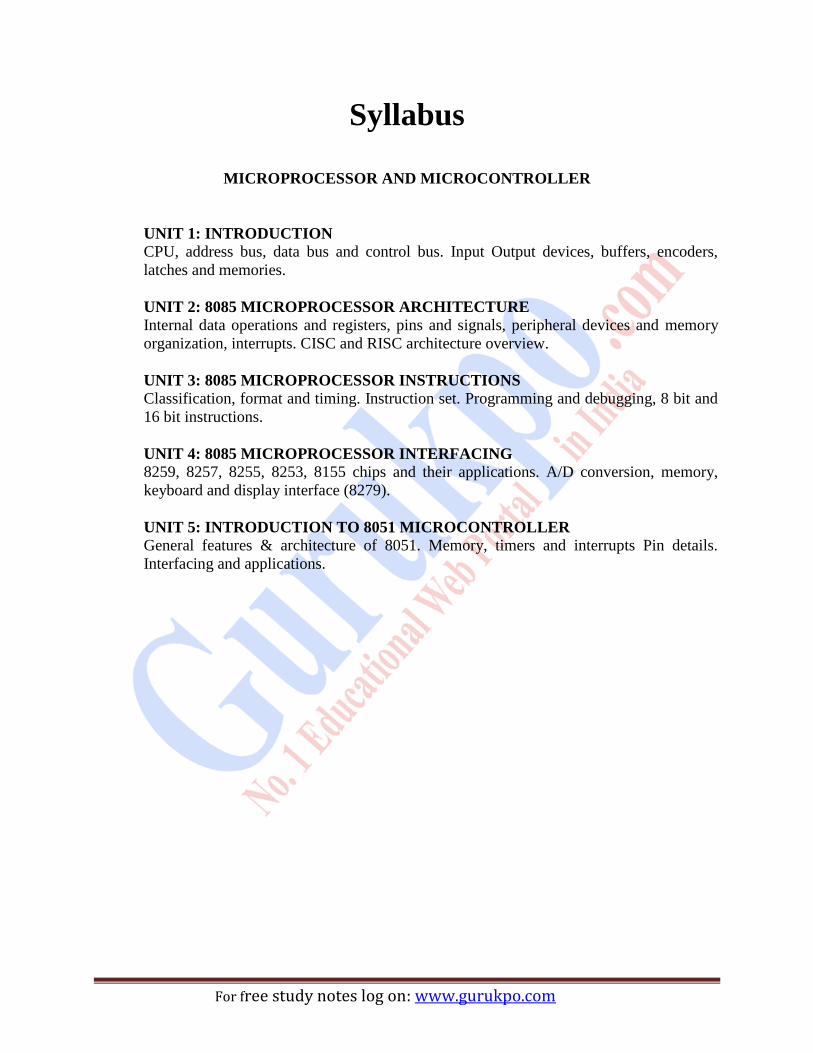
Syllabus
MICROPROCESSOR AND MICROCONTROLLER
UNIT 1: INTRODUCTION
CPU, address bus, data bus and control bus. Input Output devices, buffers, encoders,
latches and memories.
UNIT 2: 8085 MICROPROCESSOR ARCHITECTURE
Internal data operations and registers, pins and signals, peripheral devices and memory
organization, interrupts. CISC and RISC architecture overview.
UNIT 3: 8085 MICROPROCESSOR INSTRUCTIONS
Classification, format and timing. Instruction set. Programming and debugging, 8 bit and
16 bit instructions.
UNIT 4: 8085 MICROPROCESSOR INTERFACING
8259, 8257, 8255, 8253, 8155 chips and their applications. A/D conversion, memory,
keyboard and display interface (8279).
UNIT 5: INTRODUCTION TO 8051 MICROCONTROLLER
General features & architecture of 8051. Memory, timers and interrupts Pin details.
Interfacing and applications.
Microprocessor 5
For free study notes log on: www.gurukpo.com
Unit 1
Introduction
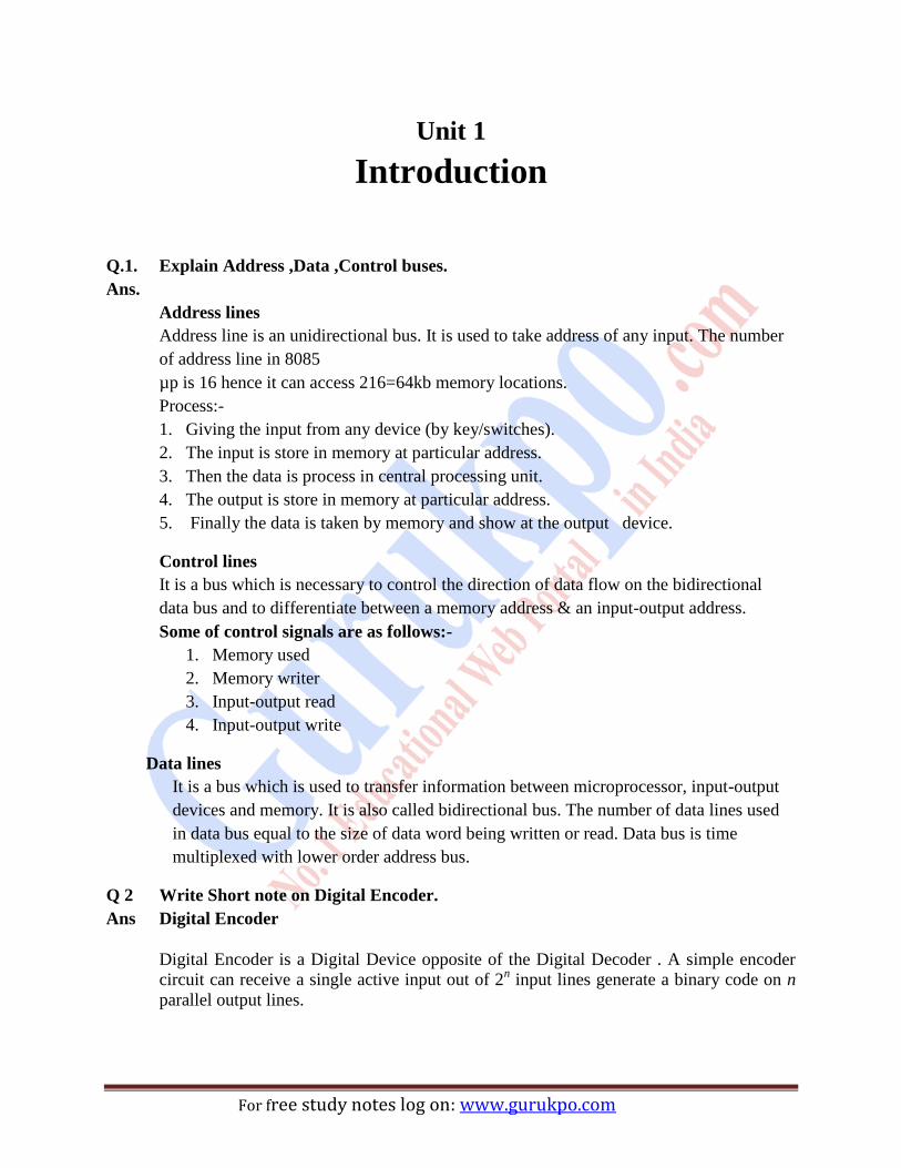
Q.1. Explain Address ,Data ,Control buses.
Ans.
Address lines
Address line is an unidirectional bus. It is used to take address of any input. The number
of address line in 8085
µp is 16 hence it can access 216=64kb memory locations.
Process:-
1. Giving the input from any device (by key/switches).
2. The input is store in memory at particular address.
3. Then the data is process in central processing unit.
4. The output is store in memory at particular address.
5. Finally the data is taken by memory and show at the output device.
Control lines
It is a bus which is necessary to control the direction of data flow on the bidirectional
data bus and to differentiate between a memory address & an input-output address.
Some of control signals are as follows:-
1. Memory used
2. Memory writer
3. Input-output read
4. Input-output write
Data lines
It is a bus which is used to transfer information between microprocessor, input-output
devices and memory. It is also called bidirectional bus. The number of data lines used
in data bus equal to the size of data word being written or read. Data bus is time
multiplexed with lower order address bus.
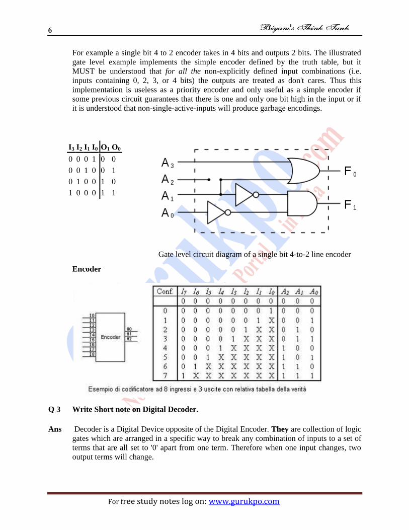
Q 2 Write Short note on Digital Encoder.
Ans Digital Encoder
Digital Encoder is a Digital Device opposite of the Digital Decoder . A simple encoder
circuit can receive a single active input out of 2n input lines generate a binary code on n
parallel output lines.
6
For free study notes log on: www.gurukpo.com
For example a single bit 4 to 2 encoder takes in 4 bits and outputs 2 bits. The illustrated
gate level example implements the simple encoder defined by the truth table, but it
MUST be understood that for all the non-explicitly defined input combinations (i.e.
inputs containing 0, 2, 3, or 4 bits) the outputs are treated as don't cares. Thus this
implementation is useless as a priority encoder and only useful as a simple encoder if
some previous circuit guarantees that there is one and only one bit high in the input or if
it is understood that non-single-active-inputs will produce garbage encodings.
I3 I2 I1 I0 O1 O0
0 0 0 1 0 0
0 0 1 0 0 1
0 1 0 0 1 0
1 0 0 0 1 1
Encoder
Q 3 Write Short note on Digital Decoder.
Ans Decoder is a Digital Device opposite of the Digital Encoder. They are collection of logic
gates which are arranged in a specific way to break any combination of inputs to a set of
terms that are all set to '0' apart from one term. Therefore when one input changes, two
output terms will change.
Gate level circuit diagram of a single bit 4-to-2 line encoder

Microprocessor 7
For free study notes log on: www.gurukpo.com
Let’s say we have N inputs to a decoder, the number of outputs will be equal to 2^N.
Thus there will be one line at the output for each possible input.
The truth table for the considered example can be shown as follows.
A B Y0 Y1 Y2 Y3
0 0 1 0 0 0
0 1 0 1 0 0
1 0 0 0 1 0
1 1 0 0 0 1
Due to the way many logic IC's are made, it is cheaper to purchase inverted decoders. These
decoders use NAND gates instead of the AND gates we have seen in the decoder example. In
these cases the output to an inverted 2-4 line decoder would be like this:
A B Y0 Y1 Y2 Y3
0 0 0 1 1 1
0 1 1 0 1 1
1 0 1 1 0 1
1 1 1 1 1 0
Q. 4 Write Short note on Digital Buffer.
Ans A Buffer is single input device that does no invert or perform any type of logical
operation on its input signal as its output exactly matches that of its input. In other words,
it does nothing as its output state equals its input state. The digital buffer is a "non-
inverting" device and so will give us the Boolean expression of: Q = A.
Then we can define the logical operation of a single input Digital Buffer as being:

8
For free study notes log on: www.gurukpo.com
"If A is true, then Q is true"
The Digital Buffer
Symbol Truth Table
A Digital Buffer
A Q
0 0
1 1
Boolean Expression Q = A Read as: A gives Q
The Buffer can also be made by connecting together two NOT gates as shown below.
The first will "invert" the input signal A and the second will "re-invert" it back to its
original level performing a double inversion of the input.
Double Inversion using NOT Gates
5.
Q 5 Explain processors & memory.
Ans Processors and Memory
There are two main components which processor (known also as the Central Processing
Unit or CPU)and memory. The processor is the part of a computer system which does the
actual computing. That is, the part which adds, subtracts, multiplies and divides. Most
processors can also compare values and perform conditional actions as a result of such
comparisons. Many processors have instructions which perform various types of
conversions between different representations of data.
The processor itself is divided into three components that controller. The controller acts
as a foreman that oversees the tasks of the processor. The last component of the processor
is a collection of one or more registers. Registers are special named memory cells in the
processor where information is temporarily stored during various stages of a
computation.
The memory unit of a computer is the place were both data and programs are stored. A
computer memory system is accessed (or read) by specifying the location (called an
address) of the memory cell. The memory system then responds by producing a copy of
the contents of that cell..
Microprocessor 9
For free study notes log on: www.gurukpo.com
A computer memory system is changed (or written) by specifying the location of the
memory cell together with the new value for that cell. The previous value stored in the
cell is replaced by the new value..
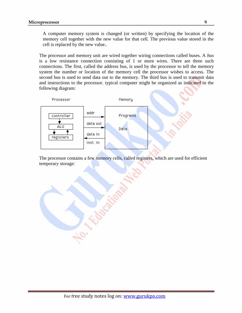
The processor and memory unit are wired together wiring connections called buses. A bus
is a low resistance connection consisting of 1 or more wires. There are three such
connections. The first, called the address bus, is used by the processor to tell the memory
system the number or location of the memory cell the processor wishes to access. The
second bus is used to send data out to the memory. The third bus is used to transmit data
and instructions to the processor. typical computer might be organized as indicated in the
following diagram:
The processor contains a few memory cells, called registers, which are used for efficient
temporary storage:

10
For free study notes log on: www.gurukpo.com
Unit – 2
8085 Microprocessor Architecture
Q. 1 Describe Programming model of 8085 mp.
Ans. 8085 Microprocessor
8085 microprocessor is 40pins .
It operates with 3-MHZ clock frequency.
8085 microprocessor have 8 data buses and 16 Address buses.
The block diagram showing internal structure of
8085 is an 8-bit general purpose microprocessor.
Microprocessor is known as Programming model.
Programming model of 8085 Microprocessor
Description of programming model
8o85 model consist of 8 data buses and 16 address buses.
It have various types of Registers.
Registers are:-
1. Accumulator(A)
2. General purpose Registers

Microprocessor 11
For free study notes log on: www.gurukpo.com
3. Flag registers
Flag registers are classified as:-
(a)Sign flag(S)
(b)Zero flag(Z)
(c)Auxiliary carry flag(AC)
(d)Parity flag(P)
(e)Carry flag(CY)
4.Program counter(PC)
5.Stack Pointer(Sp)
1. Accumulator :-
It is 8-bit register.
It store the output of arithmetic and logical operation.
It receive data from input port ad send it to output port.
It is referred as A in any program
2. General purpose register :-
B,C,D,E,H and L are general purpose register.
These registers store 8-bit data temporarily.
BC,DE and HL are register pair and used to store 16-bit data
3. Flag register
It is also 8-bit register.
It indicates the status of accumulator so it is also known as status register.
There are 5 type of flag registers.
4. Program counter:-
It is memory pointer with 16-bit.
To execute these register the address is copied in program counter
5. Stack pointer:-
It is similar to program counter.
The memory address stores at the top of stack
The concept of LIFO is used(last in first out).
Q. 2 Explain the pin diagram of 8085 micro processor
Ans The 8085 microprocessor pin diagram:
The 8085 is an 8-bit general-purpose microprocessor capable of addressing 64K of
memory.
The device has 40 pins, requires a +5 V signal power supply, and can operate with a 3
MHZ signal-phase clock.
It has 8 data buses and 16 address lines.
It has five interrupt.
It has 16-bit program counter and stack pointer.

12
For free study notes log on: www.gurukpo.com
It has internal timer, counter and encryption circuit.
It has 2-math register A and B.
Above figure shows the logic pinout of the 8085 microprocessor.
All the signal classified into six groups:
1. Address bus
2. Multiplexed address bus/data bus
3. Control and status signal
4. Power supply and frequency signal
5. Externally initiated signals
6. serial input output port
Block diagram of 8085 microprocessor
1. Address bus
We have 16-address line in 8085, which divided into two parts. First part higher order
address line A8 to A15 at pin 21-28. Another is lower order address line (A0-A7) at pin
12-19. Lower address lines are multiplex with data lines.
2. Multiplexed address bus/data bus
The signal lines AD7-AD0 are bidirectional: they serve a dual purpose. They are use as
the low-order bus as well as the data bus.

Microprocessor 13
For free study notes log on: www.gurukpo.com
3. Control and status signal
This group of signal includes two-control signal (WR compliment & RD compliment),
three-status signal (IO/M compliment, S1, and S0) to identify the nature of the operation,
and one special signal (ALE) to indicate the beginning of the operation. These signals are
as follows:
ALE (Address Latch Enable): This is use for demultiplexing of multiplexed
address bus/ data bus.
ALE signal Lines
0 (low signal) Pin no 12-19 are data lines
1 (high signal) Pin no. 12-19 are address line
RD compliment (Read): This is a read control signal (active low). RD compliment
is connecting at pin no. 32. These pin is use to indicates that selected I/O or
memory device is to be read.
WR compliment (Write): This is a write control signal (active low). WR
compliment is connecting at pin 32. These pin is use for permanent storage in
memory.
IO/M compliment: This is a status signal use to differentiate between I/O and
memory operation. When it is high, it indicates an I/O operation. When it is low,
it indicates a memory operation.
S1 and S2: These status signals, similar to IO/M compliment, can identify various
operations, but they are rarely use in small systems.
4. Power supply and clock frequency
The power supply and frequency signal are as follows:
Vcc: +5 V power supply.
Vss: Vss is use to Ground reference.
X1, X2; A crystal is connected at these two pins. Two internally divides the
frequency; therefore, to operate a system at 3 MHZ, the crystal should have a
frequency of 6 MHZ.
CLK (OUT)-Clock output: This signal can be use as the system clock for other
devices.
5. Externally initiated signal, including interrupts
The 8085 interrupts and externally initiated signals
Interrupts: We have five-interrupt signal in 8085 microprocessor. There signal
are use for generate barrier in any program under execution.
1. INTR (Interrupt request): This is use as a general purpose interrupt.

14
For free study notes log on: www.gurukpo.com
2. INTA compliment (Interrupt acknowledge): This is use to
acknowledge an interrupt.
3. RST 7.5, RST 6.5, RST 5.5 (Restart interrupt): These vectored
interrupts transfer the program control to specific memory location.
4. TRAP: This is a nonmaskable interrupt and has the highest priority.
HOLD: These pin is use for hold the program in mid way.
HLDA (Hold acknowledge): This signal acknowledges the HOLD
request.
RESET: RESET OUT is use for reset all program which is store in
microprocessor. This is on by signal 1 or at high signal. RESET IN
compliment is also use for reset all program for external chip. This
is on by signal 0 or at low signal.
READY: This shows, the status signal is ON or OFF.
6. Serial I/O ports
The 8085 has two signals to implement the serial transmission: SID (Serial Input Data)
and SOD (Serial Output Data).
Q. 3 Explain the flags in 8085, give example.
Ans
The arithmetic/logic unit performs the computing functions; it includes the
accumulator, the temporary register, the arithmetic and logic circuits, and five flags.
The flags are set or reset according to the result of the operation.
The flags generally reflect data conditions in the accumulator. The descriptions and
conditions of the flags are as follows:
SIGN FLAG: After the execution of an arithmetic or logic operation, if bit D7 of the
result is 1, the sign flag is said to be set. This flag is used with signed numbers. If in a
given byte, if D7 is 1, the number will be viewed as a negative number, if it is 0, the
number will be considered positive. This flag is irrelevant for the operations of unsigned
numbers.
ZERO FLAG: The zero flag is set if the arithmetic operation results in 0 and the flag is
reset if the result is not 0. This flag is modified by the results in the accumulator as well
as in other registers.
AUXILIARY CARRY FLAG: In an arithmetic operation, when a carry is generated by
digit D3 and passed on to the digit D4, the AC flag is said to be set. The flag is used
internally for binary coded decimal operations and is not available for the programmer to
change the sequence of a program with a jump instruction.

Microprocessor 15
For free study notes log on: www.gurukpo.com
Generalized Flags
SF ZF X AF X PF X CF
Sign Flag
Carry Flag
Zero Flag Parity Flag
Auxiliary Flag
PARITY FLAG: After an arithmetic or logical operation, if the result has an even
number of 1s, the flag is set. If it has an odd number of 1s, the flag is reset.
CARRY FLAG: If an arithmetic operation results in a carry, the carry flag is set:
otherwise it resets. The carry flag also serves as a borrow flag for subtraction.
Example:
Add 59 + 26
1 1 1 1
59 = 0101 1100 0101 1100
+
26 = 0010 0110 0010 0110
1000 0010
Representation of the arithmetic operation in different registers:
Since D7 bit is 1
No carry is
created,so resets
Since all the values is since it has even
no.
Not zero A carry is transferred from of 1s.
D3 to D4 bit so it sets.
SF ZF AF PF CF
0 1 1 0 1

16
For free study notes log on: www.gurukpo.com
Q. 4 Explain the Architecture of 8085 mp.
Ans 8085-MICROPROCESSOR
Chip which consists of complete circuit of ALU(arithmetic and logical unit) and
CU(control unit) is called microprocessor. Microprocessor/microcontroller based
systems may b used in almost every field of life and their applications are incresing day
by day. It can be used for temperature control of furnace, speed of electric motor, radars,
tanks, etc.
Architecture Of Micro Processor:
The architecture means structural design of the digital circuit responsible for computing.
The features which affect the architecture of microprocessors are length of its data word,
which is decided by size of data buses, the size of memory accessed by microprocessor,
which depends on size of address buses, no. of registers, type of instructions etc.
The 8085-microprocessor is an 8-bit general purpose microprocessor.8- bit processor
means it can read, write, and process 8- bit data at a time. The 8085- microprocessor has
40 pins, requires +5v power supply and can operate with a 3-Mhz clock frequency.
Data storage and processing in microprocessor:
8085-microprocessor includes various 8-bit and 16-bit registers. Registers are setoff flip
flops and used to store data temporarily for processing. Enormous data is stored in
memory, which is separate to microprocessor; hence the data which need to process is
copied into registers to save the processing time.
Accumulator(8) Flag register
B register (8) C register (8)
D register (8) E register(8)
H register (8) L register(8)
Stack pointer (16)
Program counter (16)
Various register have different task to perform in 8085-microprocessor. Accumulator is
an 8-bit register and the results of arithmetic or logical operations are stored in this. It is
also used to receive and send data from input and output port respectively. Flag register is
to define status of accumulator; hence it is also called status register. Registers
B,C,D,E,H,L are general purpose registers and stores 8-bit data temporarily for
Data buses(8 lines)
(bidirectional) Address buses(16 lines)
(unidirectional)

Microprocessor 17
For free study notes log on: www.gurukpo.com
processing. Program counter is a memory pointer and stores memory address of the next
byte of the program to be executed. It is of 16-bit.when the first statement is executed it
increments itself by 1 and points to the next statement. Stack pointer is same as program
counter and holds the memory address at top of the stack. Data stored in stack pointer is
read in LIFO manner, which means last entered data, is read first.
Bus Organisation:
Communication lines in microprocessor, which carry bits from microprocessor to peripherals
(memory, input/output ports, and other chips and devices connected to microprocessor) and
also from peripherals to microprocessor, called buses. There are three sets of buses:
1. Address bus
2. Data bus
3. Control bus
Address bus: it is group of 16 lines. It is used to carry the address of memory location
and addresses of input and output ports. It is a unidirectional bus. Means bits can flow
only in one direction i.e. microprocessor to peripherals.
Data bus: It is group of 8 lines, used to carry data. These lines are bidirectional. Data can
flow in both directions i.e. microprocessor to peripherals and vice versa. Since the size of
data buses is of 8-bits, the 8085-microproccesor is called 8-bit microprocessor
Control bus: It comprises of various single lines that carry various control signals for
synchronizing various devices and performing different tasks. The microprocessor
generates specific control signals for different operations.
Basic Operations Of 8085-Microprocesor:
It performs following five basic operations:
Opcode fetch: Reading and decoding operation code of an instruction
Memory Read: Reading data from memory.
Memory Write : Writing data into memory
I/O Read: Accepting data from input port
I/O Write: sending data to output port.
Pins and Signals:
8085-microprocessor chip has 40-pins.Fig shows various pins and signals of 8085-
microprocessor.signals can be classified into following groups:
1) Higher order address buses
2) Multiplexed address/data buses
3) Control signals
4) Status signals

18
For free study notes log on: www.gurukpo.com
5) Power supply and clock frequency
6) Interrupt signals
7) Other externally initiated signals
8) Serial input/output ports
Description Of Pin Diagram:
Pin 1and 2: It is used for oscillator (crystal oscillator). It generate clock frequency for
oscillation. The required clock frequency is 3MHz.The crystal oscillator generates
frequency of 6Mhz because it is divided into two equal frequencies internally.
Pin 3 and 36: Pin 3 is used for Reset Out means to reset all programs which are stored in
the microprocessor. The pin is on by (1) or high signal. Pin no 36 is also used to reset the
program for external chip. This is on by signal (0) or low signal.
Pin 20: Pin 20 is required for grounding purpose.
Pin 40: Pin 40 is power supply pin ,at this we give +5V supply.
Pin 37: clock out is used for generation clock in external chip connected to
microprocessor.
Pin 33 and 29(status signal): We have two status signals at 33 and 29. These signals are
used for telling the status of external chip.
Address Lines: We have 16 address lines in 8085 which is divided in two parts:
Higher order address line (A8-A15) -[Pin 21-28]
Lower order address line (A0-A7) -[Pin 12-19]
The lower order address line is multiplexed with data lines.
Pin 30(Address latch enable): It is used for demultiplexing
0 12-19, treat as data lines
1 12-19, treat as address lines
Control Signals: Basically we have 3 types of control signals:
WR (write)
RD(read)
ALE

Microprocessor 19
For free study notes log on: www.gurukpo.com
Fig: Pins and signals of 8085-microprocessor
Pin 31: WR is connected at Pin 31. This Pin is used for permanent storage of data in
memory.
Pin 32: RD is used for temporary storage of data in memory (read only).
Intrupt Signal: We have five intrupt signal in 8085. These signals are used to generate
barrier in any program under execution.
Intrupt will work only whenever the INTR signal at Pin 10 is on.These interrupts works
in theirown different way. When all interrupts are on,they work in their priority
order.TRAP has highest priority amongst all other interuupts following RST 7.5,RST 6.5,
RST 5.5 respectively.RST interrupt restart the execution of program.
Pin 38 and 39: First pin is used to hold the program in mid way and second is used as an
acknowledgement signal for HOLD.
20
For free study notes log on: www.gurukpo.com
Pin 4 and 5: Both the pins are used for serial communication where SOD is used for
output and SID is used for input.
Q. 5 Explain the role of following in micro processor ?
1. Accumulator
2.ALE
3.Ready signal
4.program counter
5.stack pointer
Ans
1. Accumulator :-
It is the most important part of the airthmetic and logic unit.
It is an 8 bit register which can store 8 bit data.
8 bits are referred as D7-D0.
Result of any airthmetic operations are store in the accumulator.
It is also used to receive data from input port and sending data to output port from
microprocessor.
2. Address latch enable :-
This pin is used for demultiplexing.
In microprocessor 12 to 19 pins are called data lines if ALE is off (0) a nd address
lines if ALE is on (1).
It is an active high signal which enables the latch used to demultiplex.
3. Ready signal:-
This signal is used to communicate with other peripherals of microprocessor like
input ports output ports and memory.
If this signal is high means peripheral is ready to send or accept data.
If it is low means peripheral is not ready to execute so it will wait until it goes
high.
4. Stack pointer:-
It’s a 16 bit register and a memory pointer.
For holding the address it uses stack which is the part of memory.
It stores the data temporarily.
It follows the LIFO concept last in first out.
Microprocessor 21
For free study notes log on: www.gurukpo.com
5. Program counter:-
It is also a 16 bit register and a memory pointer means it can store 16 bit data.
It stores the memory address of the next byte of the program to be executed.
Whenever program is to be executed program counter incremented by 1 and after
executing the first statement it points to next statement then it gets the address of
the second statement automatically.
Above process is repeated until the program is over.
Q.6 Explain the following pins:-
Ans
1. ALE 2.READY 3.HOLD 4.RESET IN.
.ALE :- Address latch enable signal is an active high signal. It goes high during first
clock cycle and enables the latch used to demultiplex address bus from data bus.
2.READY :- Microprocessor has to communicate with other peripherals ,which are slow
as compared to the microprocessor .
READY signal is used to synchronies these peripherals with microprocessor. If this
signal is high it means the peripheral is ready to send/accept data. If it is low it means
peripheral is not ready and microprocessor will wait until it goes high.
3.HOLD :- This signal (when goes high)indicates that some other device (such as DMA
controller) is requesting the use of address and data buses.
4.RESET IN :- It is an active low signal. When it goes low, program counter is reset to
zero and buses are tri-stated.
It also resets interrupt enable flip-flop and instruction register. No other flag and register
is affected.

22
For free study notes log on: www.gurukpo.com
Unit – 3
8085 Microprocessor Instructions
Q.1 Explain control signals for 8085 mp.
Ans Control Signals and Status Signals :-
Control Signals:
In Microprocessor 8085 ,there are three control signals whose pin no. and name are listed
blow:
Pin no:30,31,32
Signal: ALE, RD , WR
CONTROL SIGNALS
PIN NO.30 PIN NO.31 PIN NO.32
A.L.E WR RD
29
33
34
32
31
30
8085
MICROPROCESSOR
S0
S1
IO/M
RD
WR
A.L.E
STATUS
SIGNALS
CONTROL
SIGNALS

Microprocessor 23
For free study notes log on: www.gurukpo.com
ALE (Address Latch Enable): It is an active high signal in which a positive going pulse
generated every time the 8085 begins an operation (machine cycle) that indicates that the
bits on AD7-AD0 are address bit s and it is used primarily to latch the low-order address
from the multiplexed bus and used to generate a separate set of eight address line i.e A7-
A0.Its pin no. in microprocessor is 30.
RD (Read): This is a Read control signal or we can say active low control signal which
indicates that the selected I/O or memory device is to be read and its data are available on
the data bus.Its pin no. in microprocessor is 32.
WR (Write): This is a write control signal or we can say active low signals whichl indicates
that the data on the data bus are to be written into a selected memory or I/O location and
its pin no. in microprocessor is 31.
Status signals:
Status signal in microprocessor is of three type and these signals are output signals. These
signals are listed blow:
Pin no: 29, 33, 34.
Signals: IO/M , S0 ,S1.
STATUS SIGNALS
PIN NO.39 PIN NO.33 PIN NO. 34
S0 S1 IO/M
IO/M: This is a status signal used to differentiate between I/O and memory operations.
When it is high, it indicates an I/O operation: when it is low, it indicates a memory
operation. This signal is combined with RD (read) and WR (Write) to generate I/O and
memory control signals.IIts pin no. in microprocessor is 34.
S1 and S0: It is almost similar to IO/M signals and used to identify various operations,
but they are rarely used in small systems.
Q. 2 Why address and data lines are are multiplexed? Explain how these lines are
demultiplexed.
Ans Multiplexing of the data and address buses is done to reduce the pin count on the
microprocessor chip. The address information is emitted at the beginning of a memory

24
For free study notes log on: www.gurukpo.com
cycle, and external logic is expected to latch that address. Then the bus becomes the data
bus and the required data is transferred to or from memory using the latched address. In the
8085, this saves 8 pins at the cost of 1 pin, ALE.
De-multiplexing address/data bus
We know that lower order address bus is multiplexed with data bus. Ale (address latch
enable) signal is used to de-multiplexed these address/data bus. Ale goes high during
earlier part of operation, which enables the latch when the latch (74LS373), the address
supplied by the microprocessor is available on the other side of the latch on low order
address bus. The high order address lines are dedicated for high-order address only. In
this way complete address is available in the address bus, which will locate the memory
location on the primary memory of the microprocessor, once the memory address is
located, ale goes low, which disables the latch, hence blocks the bits available on
multiplexed lines to go towards address bus, now data may be multiplexed lines, which
may flow from microprocessor to memory input-output.
Diagrammatic representation of de-multiplexing of address and data lines
Q: 3 Write an assembly language program to add the two 8-bit no. and use the
unconditional jump in this program.
Ans
Microprocessor 25
For free study notes log on: www.gurukpo.com
1) MVI A, # 25H;
/*move the data 25H in the accumulator.
2) ADI, # 26H;
/*add the data of accumulator with immediate data 26H and the result will be
Store in accumulator.
3) MOV, #01H;
/* the data in accumulator will transfer to the location 01H.
4) OUT 01H;
/* display the result at pin 01H.
5) JMP POOJA;
/* apply unconditional jump to repeat the procedure.
Q: 4 Write an assembly language program to add the two 8-bit no store in A & B . and
use the RST1INSTEAD OF HLT for terminate the program.
Ans. MVI A, 20H;
MVI B, 30H;
ADD B;
RST1;

26
For free study notes log on: www.gurukpo.com
Unit-4
8085 Microprocessor Interfacing
Q.1. Describe Programmable Peripheral Interface.?
Ans. The 8255 is used to taking extra parallel peripheral /input and output pins. This is easily
interface almost with all microprocessor.8255 works in various modes i.e. simple input &
output mode. I/O with handshaking mode, Bi-directional I/O mode. 8255 have 40 pins
out of 40 pins 24 pins is used for I/O. 2 pins for power supply, 8 pins for data lines,
remaining 6 pins for control signals. The 24 pins are divide into three ports i.e. Port A,
Port B, Port C.
Pin Diagram of 8255
Read/Write and Control Logic
The function of this block is to manage all of the internal and external transfers of both
Data and Control or Status words means it provide whole control. It accepts inputs from
the CPU Address and Control busses and send it to peripheral devices.
(RD) Read. It is active at low signal. the function of this pin is to send the data to CPU t
through the data buses for read the data.
(WR) Write. It is active at low signal. The function of this pin is to write the data in CPU
register.
(CS) Chip Select. It is active at low signal. The function of this pin is to active the whole
8255 chip.
Microprocessor 27
For free study notes log on: www.gurukpo.com
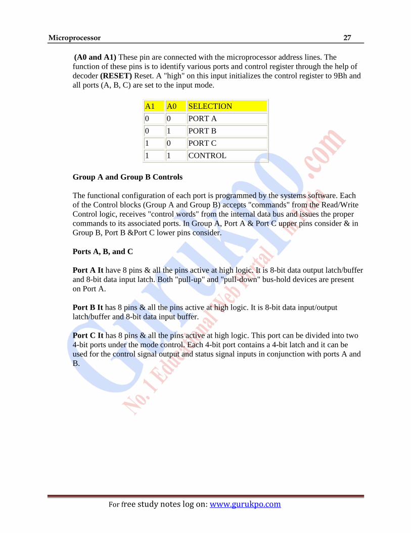
(A0 and A1) These pin are connected with the microprocessor address lines. The
function of these pins is to identify various ports and control register through the help of
decoder (RESET) Reset. A "high" on this input initializes the control register to 9Bh and
all ports (A, B, C) are set to the input mode.
A1 A0 SELECTION
0 0 PORT A
0 1 PORT B
1 0 PORT C
1 1 CONTROL
Group A and Group B Controls
The functional configuration of each port is programmed by the systems software. Each
of the Control blocks (Group A and Group B) accepts "commands" from the Read/Write
Control logic, receives "control words" from the internal data bus and issues the proper
commands to its associated ports. In Group A, Port A & Port C upper pins consider & in
Group B, Port B &Port C lower pins consider.
Ports A, B, and C
Port A It have 8 pins & all the pins active at high logic. It is 8-bit data output latch/buffer
and 8-bit data input latch. Both "pull-up" and "pull-down" bus-hold devices are present
on Port A.
Port B It has 8 pins & all the pins active at high logic. It is 8-bit data input/output
latch/buffer and 8-bit data input buffer.
Port C It has 8 pins & all the pins active at high logic. This port can be divided into two
4-bit ports under the mode control. Each 4-bit port contains a 4-bit latch and it can be
used for the control signal output and status signal inputs in conjunction with ports A and
B.
28
For free study notes log on: www.gurukpo.com
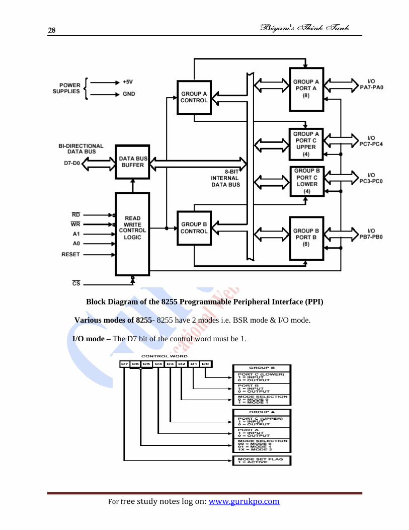
Block Diagram of the 8255 Programmable Peripheral Interface (PPI)
Various modes of 8255- 8255 have 2 modes i.e. BSR mode & I/O mode.
I/O mode – The D7 bit of the control word must be 1.

Microprocessor 29
For free study notes log on: www.gurukpo.com
Mode Definition Format
BSR mode - The D7 bit of the control word must be 0. This mode used to set/reset a
single bit of port C.
Q.2. Describe Programmable Interval timer and Programmable Interrupt controller?
Ans PIC provides 8 additional interrupts. This IC is designed to work with 80’s family
microprocessor. It provides 8 level of interrupt priorities in different modes i.e. fully
nested mode, Automatic Rotation mode & Specific Rotation mode.
Pin Diagram of 8259
8259 have 28 pins and out of 24, 8 pins for data lines, 8 pins for Interrupt Request Inputs,
2 pins for power supply, 3 pins for cascade lines, 4 for contrl signals & remainid for
master slave , address lines.
D7- D0- these pins known as data buses & active at high logic.

30
For free study notes log on: www.gurukpo.com
Ao- It is known as Command select address & used to connect the microprocessor
address line.
IR0-IR7 - It is known as Interrupt Request Inputs & used to generate the request for any
interrupt.
INT – This is an Interrupt signal & active at high logic. Whenever any interrupt is
recognised by 8259 then this pin goes high.
INTA - This is an Interrupt Acknowledgement signal & active at low logic. This signal is
used to generate the Acknowledgement signal for Interrupt generation.
CAS0-CAS2 - It is known as Cascade lines& used to connect more then one 8259s in
cascade mode.
SP/EN - It is known as Slave Program/ Enable Buffer & used to define the master – slave
mode. It is active at low logic, when single 8259 is used , it operate as a master.
(RD) - Read. It is active at low signal. the function of this pin is to send the data to CPU
through the data buses for read the data.
(WR) - Write. It is active at high signal. The function of this pin is to write the data in
CPU register.
(CS) - Chip Select. It is active at low signal. The function of this pin is to active the
whole 8255 chip.
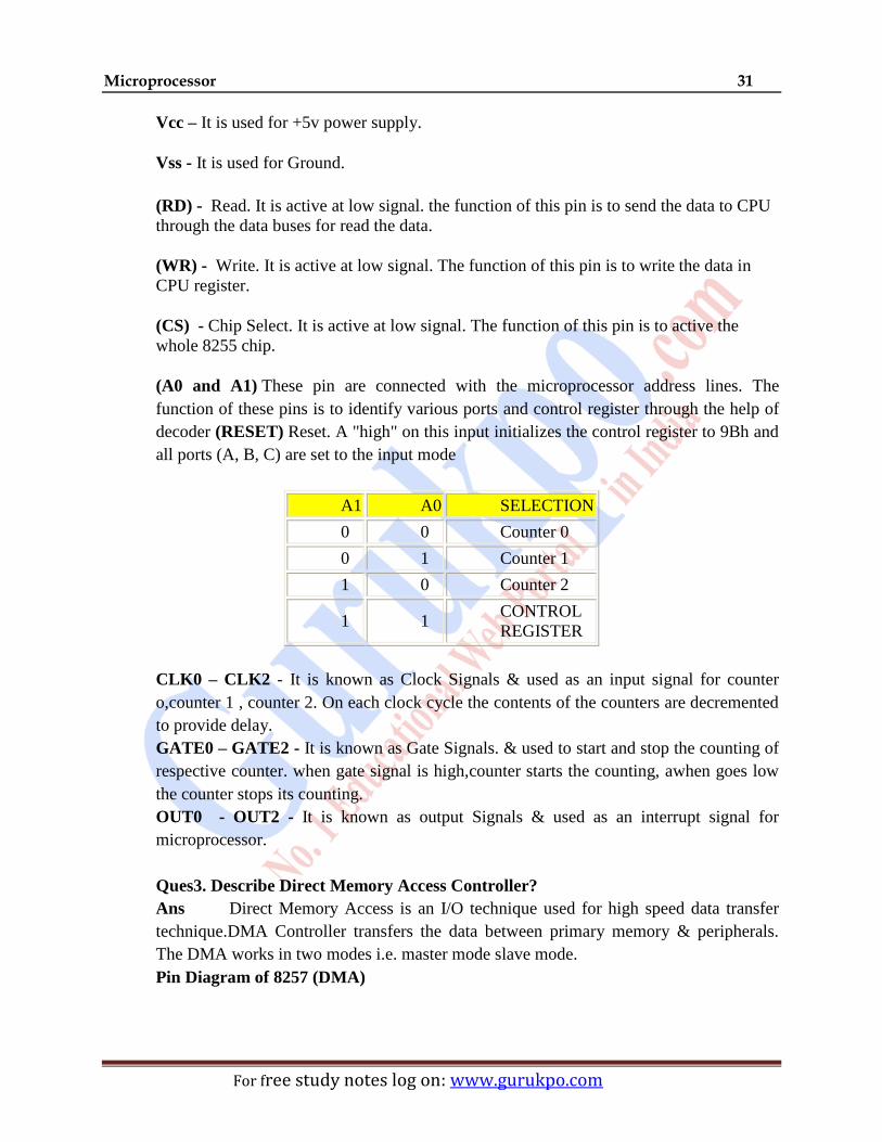
Vcc – It is used for +5v power supply.
Vss - It is used for Ground.
Programmable Interrupt controller – PIT is used to provide accurate time delay &
have 16 bit counters. This IC is basically used to provide the real time delay, square wave
generator, complex waveform generator.
D7- D0- these pins known as data buses & active at high logic.
Microprocessor 31
For free study notes log on: www.gurukpo.com
Vcc – It is used for +5v power supply.
Vss - It is used for Ground.
(RD) - Read. It is active at low signal. the function of this pin is to send the data to CPU
through the data buses for read the data.
(WR) - Write. It is active at low signal. The function of this pin is to write the data in
CPU register.
(CS) - Chip Select. It is active at low signal. The function of this pin is to active the
whole 8255 chip.
(A0 and A1) These pin are connected with the microprocessor address lines. The
function of these pins is to identify various ports and control register through the help of
decoder (RESET) Reset. A "high" on this input initializes the control register to 9Bh and
all ports (A, B, C) are set to the input mode
A1 A0 SELECTION
0 0 Counter 0
0 1 Counter 1
1 0 Counter 2
1 1 CONTROL
REGISTER
CLK0 – CLK2 - It is known as Clock Signals & used as an input signal for counter
o,counter 1 , counter 2. On each clock cycle the contents of the counters are decremented
to provide delay.
GATE0 – GATE2 - It is known as Gate Signals. & used to start and stop the counting of
respective counter. when gate signal is high,counter starts the counting, awhen goes low
the counter stops its counting.
OUT0 - OUT2 - It is known as output Signals & used as an interrupt signal for
microprocessor.
Ques3. Describe Direct Memory Access Controller?
Ans Direct Memory Access is an I/O technique used for high speed data transfer
technique.DMA Controller transfers the data between primary memory & peripherals.
The DMA works in two modes i.e. master mode slave mode.
Pin Diagram of 8257 (DMA)

32
For free study notes log on: www.gurukpo.com
The DMA CONTROLLER IS 40 PIN IC
Out of 40 pins, 8 for data lines, 8 for address lines, 2 for power supply, 12 for controll &
status & remaining 10 for DMA channels.
D7- D0- these pins known as data buses & active at high logic.
Vcc – It is used for +5v power supply.
Vss - It is used for Ground.
A7- A0 - These pins known as address buses & active at high logic.
DRQ3–DRQ0 - It is known as DMA Request Signals & used for activation of channel.
The peripherals send DRQ signal to the respective channel, whenever they are ready for
data transfer.
DACK3-DACK0 - It is known as DMA Acknowledgement Signals & used for receiving
HLDA signal from microprocessor, the DMA sends dack (low) signal to the respective
peripheral.
AEN – Known as Address Enable used to enable the address lines after receiving the
HLDA SIGNAL.
ADSTB - Known as Address Strobe & worked with AEN.
TC - Known as terminal count and used to count the data transfer ,when data transfer is
over than the TC goes high.
(IOR) - Read. It is active at low signal. the function of this pin is to send the data to CPU
through the data buses for read the data.
(IOW) - Write. It is active at LOW signal. The function of this pin is to write the data in
CPU register.

Microprocessor 33
For free study notes log on: www.gurukpo.com
(CS) - Chip Select. It is active at low signal. The function of this pin is to active the
whole 8255 chip.
Ques4. Describe Keyboard/Display Controller (8279)?
Ans It is used to simultaneously control the display of the system & interfaces a
keyboard with the microprocessor. A programmable keyboard and display interfacing
chip.
Scans and encodes up to a 64-key keyboard. Controls up to a 16-digit numerical display.
Keyboard section has a built-in FIFO 8 character buffer. The display is controlled from
an internal 16x8 RAM that stores the coded display information.
It is 40 pin IC.
PIN DIAGRAM OF 8279
A0: Selects data (0) or control/status (1) for reads and writes between
Microprocessor and 8279.
BD: It is known as Blank Display & used as an Output that blanks the displays.
CLK: known as clock signal & Used internally for timing. Max is 3 MHz.
CN/ST: Known as Control/strobe, connected to the control key on the keyboard.
CS: Chip select that enables programming, reading the keyboard, etc.
DB7-DB0: Consists of bidirectional pins that connect to data bus on
micro.
IRQ: Interrupt request, becomes 1 when a key is pressed, data is available.
OUT A3-A0/B3-B0: Outputs that sends data to the most significant/least
significant nibble of display.
RD(WR): Connects to micro’s IORC or RD signal, reads data/status
registers.
34
For free study notes log on: www.gurukpo.com
RESET: Connects to system RESET.
RL7-RL0: Return lines are inputs used to sense key depression in the
Keyboard matrix.
Shift: Shift connects to Shift key on keyboard.
SL3-SL0: Scan line outputs scan both the keyboard and displays.
keyboard working modes – four modes for keyboard working i.e. scanned keyboard
mode, sensor matrix mode, strobe mode.
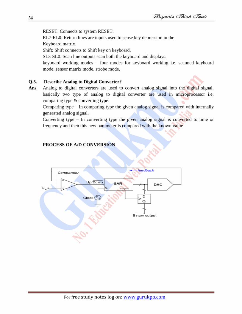
Q.5. Describe Analog to Digital Converter?
Ans Analog to digital converters are used to convert analog signal into the digital signal.
basically two type of analog to digital converter are used in microprocessor i.e.
comparing type & converting type.
Comparing type – In comparing type the given analog signal is compared with internally
generated analog signal.
Converting type – In converting type the given analog signal is converted to time or
frequency and then this new parameter is compared with the known value
PROCESS OF A/D CONVERSION

Microprocessor 35
For free study notes log on: www.gurukpo.com
36
For free study notes log on: www.gurukpo.com
Unit 5
Introduction to 8051 Microcontroller
Q.1 Write short note on 8051 microcontroller?
Ans It may be called ‘computer on chip’, since it has basic features of microprocessor with
internal ROM, RAM, parallel and serial I/O ports within single chip. The basic use of a
microcontroller is to control the operation of machine using a fixed program stored in its
internal ROM, which cannot change.
The microcontroller has following features:
1. 8-bit CPU with register A (Accumulator) and B.
2. 16-bit Program Counter (PC) and Data Pointer (DPTR) register.
3. 8-bit Stack Pointer (SP).
4. 8-bit Program Status Word (PSW) – flag register.
5. 4KB internal ROM.
6. The 128 byte internal RAM.
7. Four 8-bit ports (P0-P3), i.e., 32 I/O pins.
8. Full duplex, serial data transmitter/receiver (SBUF).
9. Two 16-bit timer/counters (T0 and T1).
10. Control Register.
11. Interrupt sources (2 external and 3 internal).
12. Oscillator and clock.

Microprocessor 37
For free study notes log on: www.gurukpo.com
P1.0 VCC
P1.1 P0.0
P1.2 P0.1
P1.3 P0.2
P0.3
P1.4 P0.4
P1.5
P1.6 P0.5
P1. P0.6
RST P0.7
P3.0 Vm/ EA
P3.1 ALE
P3.2 PSEN
P3.3
P3.4 P2.7
P3.5 P2.6
P3.6 P2.5
P3.7 P2.4
XTAL2 P2.3
XTAL1 P2.2
VSS P2.1
P2.0
CPU registers(A and B)
These registers are use to store the result of various arithmetical and logical operations.
The register A is more important register ,used for addition , subtraction, multiplication
1 40
2 39
3 38
4 37
5 36
6 35
7 34
8 33
9 32
10 31
11 30
12 29
13 28
14 27
15 26
16 25
17 24
18 23
19 22
20 21

38
For free study notes log on: www.gurukpo.com
and division the register B is used with the accumulator for multiplication and division or
to store data and has no other a functions.
Program status word and flags
Flags are flip flops, grouped together inside program status word (PSW) and power mode
control (PCON) registers. The bit definitions of PSW and PCON registers are:
D7 D6 D5 D4 D3 D2 D1 D0
CY AC F0 RS1 RS0 OV - P
The PSW has four math flags (CY), auxiliary flag(AC), overflow flag (OV)and parity
flag(P).
Program counter (PC)
1. It is a 16 bit register, used to hold the addresses range from 0000H to 0FFFH.
2. Additional external ROM, for addresses exceeding 0FFFH upto FFFFH…
3. Totally external ROM, addresses range from 0000H to FFFFH.
Data pointer (DPTR)
It is made up of two 8-bit registers DPH and DPL, used to provide memory address for 1
internal and external code access and 2 external data access.
Stack and Stack Pointer (SP)
Stack refers to an area of internal RAM that is use to store and retrieve data during execution
of the program.
The stack pointer is an 8 bit registers, used to store 8 bit address of one of the locations in
RAM, called the top of the stack.
The stack and stack pointer are used in the same way as in 8085 microprocessor, usingPUSH
and POP instructions. In 8051 microprocessor 8-bit data are pushed and poped at one instant,
instead of 16-bit data in case of 8085 microprocessor.
Internal Memory (RAM and ROM)
The ROM is used to store program code for the application at the time of manufacturing
and cannot be altered.
RAM is used to store the data during the execution of the program. 8051 has 4K of ROM
and 128 bytes of RAM.
Internal RAM is organised in three distinct areas:

Microprocessor 39
For free study notes log on: www.gurukpo.com
1. Registers Bank.
2. Bit Addressable Registers
3. General Purpose Area.
Using Input / Output Ports
Input / Output pin are used to connect the 8051 to the outside world. The 8051 has four
ports (P0, P1, P2 and P4) each with 8 pins.
The function, a pin performs at a given instant depends on:
1. Physical connections.
2. Instruction used to configure the pin.
Interrupts of 8051
In 8051, five interrupts are available. Three of which is generated depending on the status
of TF0 (Timer flag 0) and TF1 (Timer flag 1), Serial Port interrupt flags (TI/RI). Two
interrupt are triggered by sending external signal to INT0 and INT1.
Q.2 Draw the internal architecture of 8051and briefly explain?
Ans INTERNAL ARCHITECTURE OF 8051 MICROCONTROLER-
The 8051 microcontroller houses in 40 DIP , operates at 1- 16 MHz clock frequency. The
8051 microcontroller has following features-
1: The 8 bit cpu with register A (accumulator) and. B.
2: 16 bit program counter (PC) and data pointer (DPTR) register.
3: 8 bit stack pointer(SP).
4: 8 bit program status word (PSW)- the flag register.
5: 4 KB internal rom.
6: 128 byte internal ram.
7: Four 8 bit ports (po-p3), i.e.; I/O pins.
8: Full duplex, serial data transmitter / receiver (SPUF).
9: Two 16 bit timer / counter (T0 anT1).
10: CONTROL REGISTOR
a) TCON
b) TMOD
c) SCON
d)PCON
e) IP
f) IE
11: Interrupt sources(2 external and 3 internal)
12: Oscillator and clock.

40
For free study notes log on: www.gurukpo.com
DIAGRAM OF INTERNAL ARCHITECTURE OF 8051-

Microprocessor 41
For free study notes log on: www.gurukpo.com
Q.3. Briefly describe the interrupt system of microcontroller..
Ans In 8051, five interrupt are available. A computer program has only two ways to
determine the conditions that exist in internal and external circuits. One method uses
software instructions that jump on the states of flags and port pins. The second responds
to hardware signals called interrupts.
Interrupt
IE₀ TF₀ IE₁ TF₁ Serial Interrupt
Three of which are generated depending on the status of TF₀ (Timer flag 0) and TF₁
(Timer flag 1), Serial Port interrupt flag (T1/R1). Two interrupt are triggered by sending
external singles to ₀ (Pin 3.2) and ₁ (Pin 3.3)
Programmer can control all the interrupt by modifying the interrupt control bits of
enable register (IE), Interrupt Priority register (IP) and Timer Control register (TCON).
IE Register:-
The IE register is used to enable/ disable various interrupt.
IP register:-
The IP register is used to set priority of various interrupts.
The bit definition of IE and IP register are shown in fig. 1 & 2 respectively.
Interrupt Enable Register
D₇ D₆ D₅ D₄ D₃ D₂ D₁ D₀
EA - ET₂ ES ET₁ EX₁ ET₀ EX₀
Fig. 1 Interrupt enable register (IE)
Bit 7.
symbol of bit 7 is EA.
Function of bit 7 is interrupt enable bit. if 0 all, interrupt are disable.
Bit 6:
Symbol of bit 6 is - .
Function of bit 6 is not implemented.
42
For free study notes log on: www.gurukpo.com
Bit 5:
Symbol of bit 5 is ET₂.
Function of bit 5 is to reserved for future use.
Bit 4:
Symbol of bit 4 is ES.
Function of bit 4 is to Enable/ Disable Serial Port Interrupts.
1= Enable
0= Disable
Bit 3:
symbol of bit 3 is ET₁.
Function of bit 3 is to Enable/ Disable Timer Interrupts-1.
1= Enable
0= Disable
Bit 2:
symbol of bit 2 is EX₁.
Function of bit 2 is to Enable/Disable External Interrupts-1.
1=Enable
0= Disable
Bit 1:
symbol of bit 1 is ET₀.
Function of bit 2 is to Enable/Disable Timer Interrupts-0.
1=Enable
0= Disable
Bit 0:
symbol of bit 0 is EX₀.
Function of bit 0 is to Enable/Disable External Interrupts-0.
1= Enable
0= Disable
Interrupt Priority Register (IP)
D₇ D₆ D₅ D₄ D₃ D₂ D₁ D₀
- - PT₂ PS PT₁ PX₁ PT₀ PX₀
Fig. 2 Interrupt Priority Register (IP)
Bit 7.
Symbol of bit 7 is - .
Function of bit 7 is not implemented.
Bit 6:
Symbol of bit 6 is - .
Function of bit 6 is not implemented.

Microprocessor 43
For free study notes log on: www.gurukpo.com
Bit 5:
Symbol of bit 5 is PT₂.
Function of bit 5 is reserved for future use.
Bit 4:
Symbol of bit 4 is PS.
Function of bit 4 is Priority of Serial Port Interrupts .
1= high
0= low
Bit 3:
Symbol of bit 3 is PT₁.
Function of bit 3 is to Priority of Timer Interrupts-1 (TF1 of TCON) .
1=high
0= low
Bit 2:
Symbol of bit 2 is PX₁.
Function of bit 2 is to Priority of External Interrupts-1 (IE₁ OF TCON).
1- high
0= low
Bit 1:
Symbol of bit 1 is PT₀.
Function of bit 2 is to Priority of Timer Interrupts-0 ( TF₀ of TCON).
1=high
o= low
Bit 0:
Symbol of bit 0 is PX₀.
Function of bit 0 is to Priority of External Interrupts-0 (IE₀ of TCON).
1= high
0=low
This register is Bit addressable as IP.0 to IP.7
Interrupt Priority:
The bits of IP register determine whether any interrupt has high priority or low priority.
If any bit is set to 1, indicates that interrupt is high priority; if reset to 0, indicates that the
interrupt is a low priority. A high priority interrupt can interrupt another low priority
interrupt. The lower priority interrupt continues after the higher priority interrupt is over.
if two interrupts with the same priority occur at the same time, then they have the
following order of priority.
1. IE₀
2. TF₀

44
For free study notes log on: www.gurukpo.com
3. IE₁
4. TF₁
5. serial interrupt (RI/TI).
MCQS ON MICROPROCESSOR
Unit 1
Q.1 Which of the following is true with respect to EEPROM?
(A)contents can be erased byte wise only.
(B)contents of full memory can be erased together.
(C)contents can be erased using ultra violet rays
(D)contents can not be erased
Ans (C).
Q.2 Pseudo instructions are basically
(A)false instructions.
(B)instructions that are ignored by the microprocessor.
(C)assembler directives.
(D)instructions that are treated like comments.
Ans (C).
Q.3 EPROM is generally erased by using
(A) Ultraviolet rays
(B)infrared rays
(C)12 V electrical pulse
(D) 24 V electrical pulse
Ans (A)
UNIT 2
1. Which interrupt is not level sensitive in 8085?
a) RST6.5 is a raising edge-trigging interrupt.
b) RST7.5 is a raising edge-trigging interrupt.
c) a & b.
Ans (B)
2. What are software interrupts?
a) RST 0 - 7 b) RST 5.5 - 7.5 c) INTR, TRAP
Ans (A)
3. Which stack is used in 8085?
a) FIFO b) LIFO c) FILO
Ans (B)

Microprocessor 45
For free study notes log on: www.gurukpo.com
4. Why 8085 processor is called an 8 bit processor?
a) Because 8085 processor has 8 bit ALU.
b) Because 8085 processor has 8 bit data bus.
c) a & b.
Ans (A)
5. What is SIM?
a) Select Interrupt Mask b) Sorting Interrupt Mask c) Set Interrupt Mask.
Ans (C)
6. RIM is used to check whether, ______
a) The write operation is done or not
b) The interrupt is Masked or not
c) a & b
Ans (B)
7. What is meant by Maskable interrupts?
a) An interrupt which can never be turned off.
b) An interrupt that can be turned off by the programmer.
c) none
Ans (B)
46
For free study notes log on: www.gurukpo.com
UNIT 3
1 Number of the times the instruction sequence below will loop before coming out
ofloop is MOV AL, 00h
A1: INC AL
JNZ A1
(A)00
(B) 01
(C) 255
(D)256
Ans (D)
2 What will be the contents of register AL after the following has been executed
MOV BL, 8C
MOV AL, 7E
ADD AL, BL
(A)0A and carry flag is set
(B)0A and carry flag is reset
(C)6A and carry flag is set
(D)6A and carry flag is reset
Ans, (A).
3 These are two ways in which a microprocessor can come out of Halt state.
(A)When hold line is a logical 1.
(B)When interrupt occurs and the interrupt system has been enabled.
(C) When both
Ans (A)
4 In the instruction FADD, F stands for
(A) Far.
(B)Floppy.
(C)Floating.
(D) File.
Ans (C).
5 SD RAM refers to
(A)Synchronous DRAM
(B) Static DRAM
(C)Semi DRAM
(D) Second DRAM
Ans (A)
6 In case of DVD, the speed is referred in terms of n X (for example 32 X). Here, X
refers to
Microprocessor 47
For free study notes log on: www.gurukpo.com
(A)150 KB/s
(B) 300 KB/s
(C) 1.38 MB/s
(D)2.4 MB/s
Ans (C).
7 Itanium processor of Intel is a
(A)32 bit microprocessor.
(B)64 bit microprocessor.
(C)128 bit microprocessor.
(D)256 bit microprocessor.
Ans (B).
8 LOCK prefix is used most often
(A) during normal execution.
(B) during DMA accesses
(C) during interrupt servicing.
(D) during memory accesses.
Ans (C).
9 The Pentium microprocessor has______execution units.
(A)1
(B) 2
(C) 3
(D) 4
Ans (C).
Ans (B)
UNIT 4
1. Which interrupt has the highest priority?
a) INTR b) TRAP c) RST6.5
Ans (C)
2. In 8085 name the 16 bit registers?
a) Stack pointer b) Program counter c) a & b
Ans( C)
3. Which of the following is hardware interrupts?
a) RST5.5, RST6.5, RST7.5 b) INTR, TRAP c) a & b
Ans (C )
4. What is the RST for the TRAP?
a) RST5.5 b) RST4.5 c) RST4
Ans (B)
48
For free study notes log on: www.gurukpo.com
5. What are level Triggering interrupts?
a) INTR&TRAP b)RST6.5&RST5.5 c)RST7.5&RST6.5
Ans (B )
UNIT 5
1 Direction flag is used with
(A)String instructions.
(B)Stack instructions.
(C)Arithmetic instructions.
(D)Branch instructions.
Ans (A).
2 EPROM is generally erased by using
(A) Ultraviolet rays
(B)infrared rays
(C)12 V electrical pulse
(D) 24 V electrical pulse
Ans (A)
3 Signal voltage ranges for a logic high and for alogic low in RS-232C standard are
(A) Low = 0 volt to 1.8 volt, high = 2.0 volt to 5 volt
(B) Low =-15 volt to –3 vol, high = +3 volt to +15 volt
(D) Low = +3 volt to +15 volt, high = -3 volt to -15 volt
(E) Low = 2 volt to 5.0 volt, high = 0 volt to 1.8 volt
4 Ready pin of a microprocessor is used
(A)to indicate that the microprocessor is ready to receive inputs.
(B)to indicate that the microprocessor is ready to receive outputs.
(C)to introduce wait states. AC23 Microprocessor Based System Design 3
(D)to provide direct memory access.
Ans (C).

Microprocessor 49
For free study notes log on: www.gurukpo.com
Keyterm
ROM-Read Only Memory
RAM- Random access memory
LIFO –Last in first out
FIFO-First in first out
PROM-Programmable read only memory
EEPROM –Electronically erasable prom

50
For free study notes log on: www.gurukpo.com
Bibliography
• 8051 Microcontroller: Hardware, Software And Application., V Udayashankara, M
Mallikarjunaswamy, TMH
• Introduction To Microprocessors, Mathur, TMH
• Modern Microprocessors, Korneev, Wiley
• The 8085 Microprocessor: Architecture, Programming And Interfacing, K. Udaya
Kumar, Pearson
• Microprocessor Interfacing And Applications, B.P.Singh, New Age
• Microprocessor: Architecture, Programming And Application For 8085, Goankar,
Penram International
• Microprocessor: Architecture, Programming And System Featuring In 8085, William
A.Routt, Delmur Pub
• The 8051 Microcontrollers & Embedded Systems, Mazidi, Pearson
• Microprocessor & microcontroller by genius publication.
• www.nptel.com
• www.wekepedia.com

Microprocessor 51
For free study notes log on: www.gurukpo.com