A third-generation SPARC V9 64-b microprocessor
13
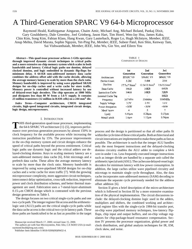
1526 IEEE JOURNAL OF SOLID-STATE CIRCUITS, VOL. 35, NO. 11, NOVEMBER 2000 A Third-Generation SPARC V9 64-b Microprocessor Raymond Heald, Kathirgamar Aingaran, Chaim Amir, Michael Ang, Michael Boland, Pankaj Dixit, Gary Gouldsberry, Dale Greenley, Joel Grinberg, Jason Hart, Tim Horel, Wen-Jay Hsu, James Kaku, Chin Kim, Song Kim, Fabian Klass, Hang Kwan, Gary Lauterbach, Roger Lo, Hugh McIntyre, Member, IEEE, Anup Mehta, David Murata, Sophie Nguyen, Yet-Ping Pai, Member, IEEE, Subeer Patel, Ken Shin, Kenway Tam, Sai Vishwanthaiah, Member, IEEE, John Wu, Gin Yee, and Eileen You Abstract—This quad-issue processor achieves 1-GHz operation through improved dynamic circuit techniques in critical paths and a more extensive on-chip memory system which scales in both bandwidth and latency. Critical logic paths use domino, delayed clocked domino, and logic embedded in dynamic flip-flops for minimum delay. A 64-KB sum-addressed memory data cache combines the address offset add with the cache decode, allowing the average memory latency to scale by more than the clock ratio. Memory bandwidth is improved by using wave pipelined SRAM designs for on-chip caches and a write cache for store traffic. Memory power is controlled without increased latency by use of delayed-reset logic decoders. The chip operates at 1000 MHz and dissipates less than 80 W from a 1.6-V supply. It contains 23 million transistors (12 million in RAM cells) on a 244 mm die. Index Terms—Computer architecture, CMOS integrated circuits, high-speed integrated circuits, integrated circuit design, logic design, microprocessors. I. INTRODUCTION T HIS third-generation quad-issue processor, implementing the 64-b SPARC V9 architecture [1]–[5], improves perfor- mance over previous generation processors by almost 150% in clock frequency for the available process while increasing the instruction parallelism by 15%. The processor improvements in the on-chip memory system and circuit designs enhance the speed of critical paths beyond the process entitlement. Critical logic paths use dynamic logic and the critical adders use de- layed-clocking domino. Keys to scaling memory latency are a sum-addressed memory data cache [6], 8-bit microtags and a prefetch data cache. These allow the average memory latency to scale by more than the clock ratio. Memory bandwidth is improved by using wave-pipelined SRAM designs for on-chip caches and a write cache for store traffic [7]. With the growing microprocessor complexity, more aggressive circuit techniques, interconnect delay optimization, cross-talk reduction, improved power and clock distribution schemes, and better thermal man- agement are used. Fabrication uses a 7-metal-layer-aluminum 0.15- m CMOS design which is contrasted with the previous design generations in Table I. The design focuses on two critical single-cycle paths and one two-cycle path. The integer register file access and the arithmetic- logic unit (ALU) paths are the critical single-cycle paths while the data cache access is the critical two-cycle latency path. These three paths are handcrafted to be as fast as possible in the target Manuscript received March 17, 2000; revised June 15, 2000. The authors are with Sun Microsystems, Palo Alto, CA 94303 USA (e-mail: [email protected]). Publisher Item Identifier S 0018-9200(00)09432-4. TABLE I COMPARISON OF DESIGNS process and the design is partitioned so that all other paths fit within the cycle time of these critical paths. Both architectural and circuit innovations are implemented to make these paths as fast as possible. The architecture is such that the integer ALU handles only the most frequent instructions and the delayed-clocking domino circuitry enables the ALU adder to complete a 64-b ADD in under 1 ns. Less frequently executed integer instructions such as integer divide are handled by a separate unit called the arithmetic/special unit (ASU). The caches use delayed-reset logic decoders for minimum latency with low power consumption. In addition, the large caches utilize wave pipelined circuitry and microtags to maintain single cycle throughput. Also, the data cache incorporates sum-addressed memory (SAM) decoding to eliminate the separate cycle previously needed for the address offset addition [6]. Section II gives a brief description of the micro-architecture which is followed in Section III by a more extensive examina- tion of the physical implementation. The circuit discussions in- clude: the delayed-clocking domino logic used in the adders, multipliers and shifters, the combined working and architec- tural register files with the single-cycle 1984-bit transfer port, on-chip wave pipelined memory techniques, low-latency flip- flops, chip input and output buffers, and on-chip voltage reg- ulators for chip-package-board resonance compensation. Sec- tion IV presents the processor organization, global power and clock distribution, and global analysis techniques for IR, EM, clock skew, and noise. 0018–9200/00$10.00 © 2000 IEEE
-
Upload
independent -
Category
Documents
-
view
0 -
download
0
Transcript of A third-generation SPARC V9 64-b microprocessor
1526 IEEE JOURNAL OF SOLID-STATE CIRCUITS, VOL. 35, NO. 11, NOVEMBER 2000
A Third-Generation SPARC V9 64-b MicroprocessorRaymond Heald, Kathirgamar Aingaran, Chaim Amir, Michael Ang, Michael Boland, Pankaj Dixit,Gary Gouldsberry, Dale Greenley, Joel Grinberg, Jason Hart, Tim Horel, Wen-Jay Hsu, James Kaku,
Chin Kim, Song Kim, Fabian Klass, Hang Kwan, Gary Lauterbach, Roger Lo, Hugh McIntyre, Member, IEEE,Anup Mehta, David Murata, Sophie Nguyen, Yet-Ping Pai, Member, IEEE, Subeer Patel, Ken Shin, Kenway Tam,
Sai Vishwanthaiah, Member, IEEE, John Wu, Gin Yee, and Eileen You
Abstract—This quad-issue processor achieves 1-GHz operationthrough improved dynamic circuit techniques in critical pathsand a more extensive on-chip memory system which scales in bothbandwidth and latency. Critical logic paths use domino, delayedclocked domino, and logic embedded in dynamic flip-flops forminimum delay. A 64-KB sum-addressed memory data cachecombines the address offset add with the cache decode, allowingthe average memory latency to scale by more than the clock ratio.Memory bandwidth is improved by using wave pipelined SRAMdesigns for on-chip caches and a write cache for store traffic.Memory power is controlled without increased latency by useof delayed-reset logic decoders. The chip operates at 1000 MHzand dissipates less than 80 W from a 1.6-V supply. It contains23 million transistors (12 million in RAM cells) on a 244 mm2 die.
Index Terms—Computer architecture, CMOS integratedcircuits, high-speed integrated circuits, integrated circuit design,logic design, microprocessors.
I. INTRODUCTION
T HIS third-generation quad-issue processor, implementingthe 64-b SPARC V9 architecture [1]–[5], improves perfor-
mance over previous generation processors by almost 150% inclock frequency for the available process while increasing theinstruction parallelism by 15%. The processor improvementsin the on-chip memory system and circuit designs enhance thespeed of critical paths beyond the process entitlement. Criticallogic paths use dynamic logic and the critical adders use de-layed-clocking domino. Keys to scaling memory latency are asum-addressed memory data cache [6], 8-bit microtags and aprefetch data cache. These allow the average memory latencyto scale by more than the clock ratio. Memory bandwidth isimproved by using wave-pipelined SRAM designs for on-chipcaches and a write cache for store traffic [7]. With the growingmicroprocessor complexity, more aggressive circuit techniques,interconnect delay optimization, cross-talk reduction, improvedpower and clock distribution schemes, and better thermal man-agement are used. Fabrication uses a 7-metal-layer-aluminum0.15- m CMOS design which is contrasted with the previousdesign generations in Table I.
The design focuses on two critical single-cycle paths and onetwo-cyclepath.The integer register fileaccessandthearithmetic-logic unit (ALU) paths are the critical single-cycle paths whilethe data cache access is the critical two-cycle latency path. Thesethree paths are handcrafted to be as fast as possible in the target
Manuscript received March 17, 2000; revised June 15, 2000.The authors are with Sun Microsystems, Palo Alto, CA 94303 USA (e-mail:
[email protected]).Publisher Item Identifier S 0018-9200(00)09432-4.
TABLE ICOMPARISON OFDESIGNS
process and the design is partitioned so that all other paths fitwithin thecycle timeof thesecriticalpaths.Botharchitecturalandcircuit innovations are implemented to make thesepaths as fast aspossible. The architecture is such that the integer ALU handlesonly the most frequent instructions and the delayed-clockingdomino circuitry enables the ALU adder to complete a 64-bADD in under 1 ns. Less frequently executed integer instructionssuch as integer divide are handled by a separate unit called thearithmetic/specialunit (ASU).Thecachesusedelayed-reset logicdecoders for minimum latency with low power consumption. Inaddition, the large caches utilize wave pipelined circuitry andmicrotags to maintain single cycle throughput. Also, the datacache incorporates sum-addressed memory (SAM) decoding toeliminate the separate cycle previously needed for the addressoffset addition [6].
Section II gives a brief description of the micro-architecturewhich is followed in Section III by a more extensive examina-tion of the physical implementation. The circuit discussions in-clude: the delayed-clocking domino logic used in the adders,multipliers and shifters, the combined working and architec-tural register files with the single-cycle 1984-bit transfer port,on-chip wave pipelined memory techniques, low-latency flip-flops, chip input and output buffers, and on-chip voltage reg-ulators for chip-package-board resonance compensation. Sec-tion IV presents the processor organization, global power andclock distribution, and global analysis techniques for IR, EM,clock skew, and noise.
0018–9200/00$10.00 © 2000 IEEE

HEALD et al.: THIRD-GENERATION SPARC V9 64-b MICROPROCESSOR 1527
II. M ICRO-ARCHITECTURE
The architecture is driven by performance, scalability andcompatibility. The design is SPARC V9 compliant, main-taining binary compatibility with all 10 000 existing SPARCapplications [7]. Scalability is a two-fold goal: the designmust permit the clock frequency to scale as the manufacturingprocess improves. In addition, the off-chip interface must allowmultiprocessor (MP) systems to scale to over 1000 processors.Leading-edge performance is achieved in multiple ways. Clockfrequency improvement is given priority over improvementsin instructions per cycle (IPC). Compared to the previousgeneration design, the clock is increased by 1.5 for a givenprocess. The IPC is improved by 15% by using a four-way64-KB data cache in place of the 16-KB directed mappedcache of previous generations and doubling both the size andassociativity of the instruction cache to a four-way 32-KBcache. These improvements plus compiler improvements of15% give a doubling of overall performance [8]. This requiresdifferent approaches to the micro-architecture, as well as moreaggressive circuit and physical design compared to previousgeneration processors. Clock speed is addressed by budgetingeight stages of static logic gates, NAND3 with fanout of 3,for each of the 14 pipeline stages in place of nine stages and20 static gates/stage for the previous generation. Timing ismost critical in the instruction fetch, integer execution, andfloating-point areas, where dynamic logic is used liberally.In the memory system, delayed reset logic provides the lowlatency while wave pipelining provides the throughput needed.IPC is improved by minimizing the execution latency of shortdependency chains such as the load-test-branch.
The six major functional units are: instruction issue unit(IIU), floating point unit (FPU), integer execution unit (IEU),data cache unit (DCU), external interface unit (EIU), andsystem interface unit (SIU). Four instructions are fetched fromthe instruction cache (I) which is located in the IIU and is de-coupled from the execution pipelines by a 20-deep instructionqueue. The execution pipelines support concurrent launch of upto six instructions, which can consist of: two integer operations,two FP operations, one memory operation (load/store), onespecial purpose memory operation (prefetch cache load only),and one control transfer instruction (CTI). However, onlyfour IPC can be executed in a sustained manner. The FPUcontains two fully pipelined units: add/subtract and multiply,which also support execution of two partitioned fixed pointgraphics operations per cycle. The independent divide unit usesa multiplicative iteration algorithm, the Goldschmidt algorithm[9], providing 20-cycle latency for an IEEE double-precisionresult, and can execute in parallel with the pipelined units.An on-chip memory controller supports up to 4-GB SDRAM,providing 2.4-GB/s memory bandwidth per processor in MPconfigurations. The system shares a 144-b 150-MHz DTLexternal data bus with SDRAM data, multiplexed by an externalbit-sliced switch. A dedicated 288-b 200-MHz HSTL data businterfaces to the external cache (E), built from eight 36-Mblate-write synchronous SRAMs. Fig. 1 shows the pipelinediagram identifying the instruction and execution sections. Theinstruction fetch pipeline encompasses stages A-P-F-B-I-J; the
Fig. 1. 14-stage processor pipeline.
execution pipeline begins in the R-stage, where instructions aredispatched and the integer-register file, made up of a working(WRF) and an architectural register file (ARF), is accessed.
SPARC V9 architecture provides a windowed register filewhich is implemented in this family of designs as eight over-lapping register windows mapping 32 virtual 64-b registers into128 64-b physical registers and four sets of eight global regis-ters which are not part of any window [1]. This third-generationdesign achieves single-cycle 1-GHz register file access by ex-tending the conceptual three-dimensional array of the previousgenerations by overlaying a working register file containing thecurrent window and global registers. The WRF allows the re-moval of the result bypass buses from most integer executionpipe stages. Without the bypass buses, the integer data path isshorter and the bypass multiplexing is narrower. Both contributeto a shorter cycle time. This working and architectural registerfile, WARF, is described in detail in Section III-C.
The high IPC penalty that can be seen on a deep pipelinewith branch-intensive code is offset by two techniques: asignificantly better branch predictor and queueing instructionsfrom the sequential not-predicted path. The branch predictoruses a 16-k entry, 2-b per entry, dual-port RAM indexed bya hash function of program counter and branch history bits(referred to as gshare predictor [10]). Misprediction requires allyounger instructions from that instruction stream to be flushed,so both prediction rate and latency to recover the correct streamat the A-stage (eight cycles) are important. Branch resolutionis in the E-stage, to reduce latency and to prevent the WRFfrom being corrupted. This requires the various componentsthat determine a mispredict to be calculated in parallel withcondition codes (both ALUs generate condition codes forpredicted branches) and computations. One cycle alone of themisprediction penalty is dedicated to the wide distributionof the "mispredict" signal needed to restart the fetch stream.When branches predicted taken are mispredicted, the first fewinstructions from the sequential stream are available to startexecution at the I-stage from the mispredict queue (physicallyintegrated with the 20-entry instruction queue), significantlyreducing the misprediction penalty.
III. PHYSICAL IMPLEMENTATION
A. Design Approach
For minimum power dissipation and simplified verification,the primary circuit style is static CMOS using synthesis andautomatic place and route. Where synthesis is not enoughand full custom design not appropriate, as in control blocks,

1528 IEEE JOURNAL OF SOLID-STATE CIRCUITS, VOL. 35, NO. 11, NOVEMBER 2000
domino cells are manually placed and CAD tools shield allwires, route clocks, insert power and ground and completesignal routing. For the most critical paths, custom dynamiclogic design is used. Critical circuits are built either with tra-ditional domino logic or with delayed-clocking domino logic,an overlapping multiphase nonblocking clocking scheme. Inthis scheme, critical signals are never gated by clocks, creatinga pseudotransparent evaluation phase that results in maximumspeed. This technique enhances the speed of the dynamicadders, multipliers and shifters. Delayed reset logic, used inthe SRAM structures, minimizes the power use and simplifiesthe clock distribution while achieving very fast access. Largecaches utilize a self-timed latency control circuit techniquefor one-cycle throughput and two-cycle latency operation.Also, some blocks incorporate a predecode flip-flop circuitwhich combines the predecode logic and flip-flop functions,eliminating two logic levels and significantly speeding up theaddress decoding critical path.
B. Dynamic Logic Circuits
In designing the instruction steering control block, dominologic standard cells are used instead of static CMOS for aperformance improvement within the same area. After hand-synthesis and placement, an internal tool is used to automati-cally insert shields on all nets in the design. The tool also insertsclocks, power and ground wires. A commercial router is used tocomplete the routing of signals. The methodology takes advan-tage of automation tools where practical and possible, and hassince been used on other microprocessor projects. The noise onall nets is less than 3.5% of using the shielding tool. Theshields also provide extra and wires, return paths andcapacitance, while providing consistent timing since capacitivecoupling is almost entirely to dc nodes.
The high-performance adder needed for the single-cycleALU path is kept lean by including only the circuitry and wiringneeded for the most critical execution. The adder within thisALU incorporates delayed-clocking domino logic to meet theperformance target. A set of clocks as shown in Fig. 2 controlthe adder’s domino logic sequentially so that theADD operationripples through the logical stages with no clock blockages.Consecutive logic stages are clocked by delayed phases withenough overlap to guarantee safe signal transition. To assuresafe signal transfer to the next clock cycle, the final delayedclock of the cycle, , overlaps with the primary clock ofthe following cycle, , and stretches as the clock frequencyis reduced to achieve proper operation at any clock frequency.While ripple through operation eliminates the need for preciseclock timing, all delayed clocks used are generated within theblock in which they are used. Local generation eliminates theneed for global generation and distribution of many clock wireswith the resultant skew problems. This adder uses a modifiedKogge–Stone carry chain with separate chains for the carryandcarry to minimize delay. This carry section, together withthe sum stage, and the output multiplexer, make up the threephysical sections of the adder. Standard dominoXOR andNAND
structures controlled by the delayed-clocking produce 64-bitADD results in under 1 ns. Similar delayed-clocking domino
Fig. 2. Delayed clocking for domino logic.
circuits are also used in the multipliers and shifters. Verificationand power constraints confine dynamic design chiefly to fullyshielded full-custom structures. In these structures, designerscarefully check for safe operation with noise tools describedin a later section.
C. Combined Working and Architectural Register Files
The integer execution unit is built around the working/ar-chitectural register file (WARF) shown in Fig. 3. Although theWARF is physically one block, it is logically composed of twodistinct register files. The processor accesses the WRF in thepipeline’s R stage and supplies integer operands to the executionunit. The WRF consists of 32 64-bit registers, each with threewrite ports, seven read ports and a 1984-bit (2048 minus 64)write port to transfer data from the Architectural Register File(ARF). The 160 entry ARF has three write ports and a 1984-bitread port to transfer data to the WRF. The ARF has only 156physical registers, since the GLOBAL0 register, G0, of the WRFis always 0. Sixty-four of the 156 ARF registers are eight reg-ister windows, each exclusively for the eight LOCAL registers.Another 64 registers are eight sets, each shared between the 16IN/OUT registers. These 64 IN/OUT registers represent eightwindows for the INs and eight windows for the OUTs, but thememory space is overlapped. In the WRF, the INs and OUTs canbe swapped via address remapping to support the SWAPSAVEand SWAPRESTORE operations. The remaining 28 ARF reg-isters are four sets each dedicated to the seven GLOBAL reg-isters other than G0. The global registers support fast trap pro-cessing and are transferred independently from the windowingof the INs, OUTs, and LOCALs.
The WRF manages a single active window and is updated asresults are computed. Most operations complete in one cycle,with results immediately written into the WRF in the pipelineC stage. If an exceptional event occurs, the immediately writtenresult must be undone. This is done with a broadside copy of allinteger registers from the appropriate ARF window. The ARFmaintains the architectural state of all eight windows and isplaced at the end of the pipe, ensuring updates occur only whenan instruction successfully completes. The ARF fills 16 WRFentries after a window change. On an exception, however, up to31 nonzero registers may need to be restored from the ARF ifa speculative update of an arbitrary WRF entry needs to be un-done. This is done in a single cycle using the 1984-bit transfer

HEALD et al.: THIRD-GENERATION SPARC V9 64-b MICROPROCESSOR 1529
Fig. 3. Working and architectural register file block diagram.
port. WRF access is a single-cycle operation which is kept fastby the use of flat 32-entry addressing rather than the more com-plicated windowed 160-register decoding. To facilitate single-cycle 1984-bit transfers, the WRF and the ARF are interleavedinto one physical memory array.
The WARF is implemented using domino decoding and fre-quency dependent pulses to simplify timing. Write and transferoperations require one clock phase, with the precharge occur-ring in the next phase. Read is a two-phase operation, with thesense amplifier acting as the half-cycle latch. The circuit realiza-tion of an ARF eight-cell group shown in Fig. 4 uses pseudodif-ferential writing to save bitlines and a differential transfer port towrite to an adjacent WRF cell, Fig. 5. The Data andData signalsat the right of Fig. 4 and the bottom of Fig. 5 are the method oftransferring data from the ARF to the WRF cell. The assemblyof nine memory cells shown in Figs. 4 and 5 are built as a unit tosave area and transfer delay. The cells shown are for a LOCALregister. For the IN/OUT register cells, a second transfer port isused to connect the eight ARF cells to a second WRF cell. Thegrouping of four or eight single port memory cells with windowdecoding interfacing to three write and seven read ports has beenused in previous designs to save area and reduce the transistorcount over a flat 10-port register design [1]. There, the area sav-ings is estimated by comparing number of wordlines used overeight 10-port register file cells with the wordlines overan eight memory cell assembly. The eight-cell group height isonly that of eight 10-port register cells. Also, the bitline ca-pacitance is reduced substantially since fewer cells are attachedand each bitline is significantly shorter. The current design ex-tends this concept by adding the full WRF cell adjacent to theseARF cells. This allows transfer wires of under 100 mm ratherthan several millimeters to connect to a separate array. Sinceadded decoding is needed for the transfer port, the area savingsis not as great as with the previous design. The total number ofwordlines is just over half that of a flat register file. Still, theinterleaving of these two register files allows the single-cycletransfer of 1984 bits without a huge area and power cost. In ad-
dition, the WRF access is much faster than would be possiblewith a flat array of 160 registers.
D. On-Chip RAM
The RAM blocks include an on-chip 64-KB four-way asso-ciative data cache, a 32-KB four-way associative instructioncache, a 2-KB four-way associative prefetch cache and a 2-KBfour-way associative write-cache. Memory bandwidth is alsoimproved by using the prefetch cache for data expected to beused soon and the write cache for store traffic. The on-chipmemory system also includes separate instruction and datacache tag arrays and translation-lookaside-buffer (TLB) arrays.There are separate tag copies for snoop operations and theTLBs are further separated into 16-entry fully associativearrays for all block sizes and two-way set associative arrays for8-KB pages (512-entry for the data-TLB and 128-entry for theinstruction-TLB). The largest RAM on the chip is the 88-KBexternal cache tag array. This memory also uses delayed-resetlogic decoders and wave pipelining to support external cachesizes up to 8 MB.
The SAM data cache combines the address offset addwith the cache decode, allowing the average memory latencyto scale by more than the clock ratio. This SAM approachreduces the load address computation time from almost 1ns tounder 200 ps, allowing the data cache increase from 16-KBto 64-KB while maintaining the two-cycle latency of previousgenerations [6]. An 8-b virtual-address microtag selects oneof four ways without incurring a cycle time penalty due to itsvery small size compared to the large data cache. This microtagconcept together with the delayed-reset decoder and wavepipelining allow single-cycle access with two-cycle latency inthe instruction cache as well as the data cache. Wave pipeliningdistributes the access over two cycles without the latencypenalty or complexity of awkwardly placed intermediateregister points. The flip-flops driving the decoder begin thepipeline by generating address pulses rather than levels. Thesepulses propagate through the delayed reset decoder, drive theselected wordline and a delayedAND-OR of the predecoderpulses enable the sense amplifiers. The data output pulses areconverted to levels in the output buffers where latency latcheshold the output data until the correct cycle begins at slow clockfrequencies. These latches control only the output data clockalignment and are combined with other logic for minimal addeddelay during high speed flow through operation.
E. Flip-Flops
With a limited number of logic levels per pipeline stage,flip-flop delay minimization is critical. To address this, a newfamily of edge-triggered flip-flops [11] is used having verylow D-to-Q delays. This family includes dynamic flip-flopsproducing monotonic outputs for domino logic. Members ofthis family also embed a full logic level while maintaining avery low input-to-output delay, allowing a pipeline with onlyeight logic stages per clock cycle.
In the I/O region, a soft error hazard exists due to alpha parti-cles emitted from the nearby solder bumps. An energetic alphaparticle which travels through a transistor source or drain can

1530 IEEE JOURNAL OF SOLID-STATE CIRCUITS, VOL. 35, NO. 11, NOVEMBER 2000
Fig. 4. Architectural register file group of eight 3-write/1-read cells, one from each of the eight register windows. One 1-transfer-out port is shared by the eightcells.
Fig. 5. Working register file cell including 1-transfer-in, 3-write, and 7-read ports.
charge or discharge the node, resulting in an incorrect logicstate. To protect against this, soft-error resistant or alpha-hard-ened flip-flops are used. Circuit hardening involves increasingthe charge stored at sensitive nodes and increasing the avail-able current to restore the correct state following a alpha interac-tion before the faulty logic is latched by a storage element. The5.3-MeV alpha emitted from solder bumps loses over half ofits energy before it reaches the silicon. Hence, it can only upsetnodes with less than a combination of roughly 100-fC chargestorage or 5 mA of recovery current. The flip-flop shown inFig. 6 is a basic flip-flop of the family discussed above in whichstrong latches protect nodes X and Q and P1, P2, and P4 areadded to cut off the strong hold only when new data must be
accepted. When and CK rises, P2-3 holds node X high.After three gate delays, P1 is enabled, holding X high even iffalls. When , N1-2 and INV1 form a latch that holds Xlow. N3-4, P4-5, and INV2 work as a clocked latch for storagenode Q.
While delayed reset RAM decoders are extremely fast lowpower circuits for accessing large RAM blocks, the use ofpulsed addresses results in the need for dynamic flip-flopspreceding each such decoder. For some midsize RAM blocks,the added flip-flop buffering is not needed and the added delayis not acceptable. For these instances, a special flip-flop isused which includes the first stage of the predecoder. The highavailable fan-out of delayed-reset circuitry allows this logic

HEALD et al.: THIRD-GENERATION SPARC V9 64-b MICROPROCESSOR 1531
Fig. 6. Alpha hard flip-flop.
to be added in a single stack as shown in Fig. 7. The clockedfooter begins the cycle causing a positive transition on one ofthe eight outputs, . Assume the addresses aresuch that node A falls causing node B, , to rise. Fourgate delays following the Ck positive edge, the combined resetand power-down signal, rstpd, goes high. SinceCk dly goeslow three gate delays after the clock rising edge, nodeis alsohigh so node E falls causing pMOS P1 to pull-up node A andnMOS N1 to pull down node B, producing an output pulse offive gate delays. The output fall will cause node C to rise, butCk dly blocks the cut off path, preventing the reset devicesP1 and N1 from shutting off until the next clock phase. Thisallows the output drive inverters, INV0 and INV1, to be highlyskewed while still having a strong hold device on the outputsthroughout the remainder of the positive clock phase. A fourthcontrol signal, rstsel, switches high two gate delays after theinitial Ck transition. This disables the inputs, assuring a shortinput hold time, and prevents a crowbar situation. Followingthe Ck falling transition, theCk dly and rstsel transitions aredelayed an additional two gate delays to prevent any glitch atthe output due to charge sharing. To initialize the outputs afterpower is applied, rstpd is pulsed high when the power andclock have stabilized.
F. Chip I/Os
The chip input receiver compares the pad voltage input witha reference using a differential sense amplifier and producesa single-ended output (Fig. 8). During precharge (CK1 low),nodes S andS are pulled high and equalized through P3-5. CK3rises during precharge, equalizing nodes X1-2. When CK0 fallsand CK1 rises, the precharge/equalization turns off, and N3-6turn on to pull-down nodes X1-2 with different currents de-pending on IN and REF voltages. When CK2 falls, the smalldifferential voltage on S/S is amplified. The various clocks pro-vide precise timing, resulting in zero setup, low hold time andCK-to-Q delay, no dc current, and high immunity to noise andimbalance.
The high speed chip output drivers use dynamic terminationlogic (DTL) to control the output impedance, linearity and slewrate [12]. The circuit reduces the settling time to a one-waydelay by having the driver at the receiving end terminate thesignal, raising the signaling frequency to 150–200 MHz. Thisone-way propagation delay for the line to settle functions evenwhen a bus turn-around low-to-low switch occurs withoutan intervening dead-cycle. The signal voltage is to
, where is the separate power supply voltage for
the push-pull output drivers. An off-chip source is used toprovide a common reference for the microprocessor system.The DTL output driver functions as both a driver and apull-up terminator and is linearized, impedance-controlled, andslew-rate controlled. The output resistance of the pull-up andpull-down units are matched to the characteristic impedance ofthe transmission line. Each pull-up and pull-down output unitconsists of multiple elements of varying widths, one of whichis permanently enabled. The others are enabled or disabledaccording to an impedance-control code to give a desired netdc output impedance across temperature, voltage, and processvariations. This code follows a “thermometer code”—only onedigit changes per code update, and the order of bit changesis fixed. Unlike binary code, traditional undesired states areavoided, minimizing glitches on the output signal.
G. Global Voltage Regulator
Voltage regulation requirements of each succeeding genera-tion of microprocessor are more critical as the on-chip voltagedecreases and the ac current increases. Distributed thin oxidecapacitors are used for supporting instantaneous current varia-tions within the die but are insufficient to compensate for thetank circuit formed by the parasitic LC in-line with the supplydistribution. Simulations show nearly an order of magnitude in-crease in supply-network ac impedance seen by an internal gateat resonance. This resonant frequency is much lower than thesystem clock frequency but can be excited by an instruction loopwhose repetition rate coincides with this resonant frequency andcontains a large current step. The excursions ultimately limitspeed performance and could compromise hold-time marginsand oxide integrity.
A special voltage regulator circuit [13] is placed 99 timesto reduce the chip-package-board resonance. The voltageregulator circuit increases the charge stored or delivered bya given amount of added decoupling capacitance by activelyincreasing the voltage across the capacitor’s terminals. Theoperation, in principle, is done by stacking fully charged equalvalue capacitors in series as a voltage multiplier to supplycharge into the on-chip power and ground grid.The depleted voltage in each capacitor is thenwhere is the stack height. Reversing this process, unstackingthese capacitors, then stores charge from the on-chip powerand ground grid until the terminals across each capacitor is at
. Fig. 9 shows a simplified block diagram of the regulatorfor the case where . Also shown is roughly how theinternal nodes vary as the circuit operates. Mutually exclusiveCMOS switches configure the capacitors to either be in thecharging phase (shunt across ) or in the dischargingphase (in series between and ). Their sizes are chosento exhibit the proper equivalent series resistance (ESR) which,along with the ESR of the capacitors, are matched with theresonating tank to provide maximum power transfer. In order toensure a full reservoir at quiescence, the capacitors are poisedin the charging phase. The switches are driven by two sets ofcomplementary drivers, each of which provide two outputswith enough voltage offset to ensure minimal crowbar leakagethrough both charge and discharge switches during switchingactivity. For the example shown in Fig. 9, the instantaneous

1532 IEEE JOURNAL OF SOLID-STATE CIRCUITS, VOL. 35, NO. 11, NOVEMBER 2000
Fig. 7. Dynamic flip-flop and predecoder.
Fig. 8. Off-chip input buffer.
difference between and begins at the same valueas the average . In this condition, N2 and P2,the shunt switches, are weakly on with gate-to-source voltagesof each while N1 and P1, the series switches, arecompletely off. Then drops causing node B to fall, cuttingoff N2. Slightly later, node A falls turning on P1. This changesC2 from being in shunt with C1 to being in series. Similarly,the mirror devices, P2 and N1, are being cut off and turned onrespectively. This allows the now series connected C1 and C2to discharge into the power grid, forcing up. In the nexttime section, where , node A rises cutting off P1and then node B rises turning on N2. Similarly, N1 turns offand then P2 turns on. This switches C1 and C2 into the shuntmode allowing them to be charged by and forceto drop. Once , node B returns to whichreturns the circuit to the weakly charging mode. Akin to ClassAB operation, the offsets need not be present when driving thecharge transistor to full rail. A simple disable function allowsthe loops to be disabled and leaves the capacitors connected inshunt for test purposes.
Fig. 9. Charge pump simplified block diagram with voltage levels versus timefor nodes A and B.
The switched capacitors are enhancement mode mosfet de-vices, laid out in a waffle-type structure to maximize capacity.To preserve power-grid homogeneity, the regulator is evenlydistributed across the chip in 99 instances which are directlyhooked up to the main global power grid. Care has been takenin shielding sensitive signals and in managing high current den-sity paths. Substantially blocking only metal-1, the regulatorsare placed underneath the global routing channels and will notresult in a smaller die size if taken out.
Fig. 10 shows the measured performance of the regulatorswhen the chip is excited at resonance. This shows no tendencyfor any regulator-induced instability. The damped behaviorwith respect to power-ramp, cross-regulator interaction, andstability across process and operating conditions has beenvalidated through extensive regulator-on versus regulator-offtests. Only tests designed to excite the resonance show anydifference in CPU performance when the regulator is switched

HEALD et al.: THIRD-GENERATION SPARC V9 64-b MICROPROCESSOR 1533
Fig. 10. Voltage regulator operation controlling on-chip power supply voltageat resonance.
on or off. The on-chip peak-to-peak variation of about260 mV in Fig. 10 is reduced to about 60 mV when the regulatoris enabled. Since the period of this resonance is much longerthan a CPU clock cycle, the CPU clock speed is limited by theminimum voltage supplied during this resonance. However, themaximum supply voltage must still be fixed at 1.6 V to assurelong term reliability. Hence, the effective power supply must be200-mV lower when the regulator is disabled. From the shmooplot shown in Fig. 11, one can calculate a 16% to 20% CPUspeed improvement for this 200-mV power supply difference.
IV. PROCESSORORGANIZATION AND ANALYSIS
A. Chip Floor Plan
With wire delay now a major part of total cycle delay, thechip floor plan is designed around the critical paths. The WRFcommunicates with the two integer execution units in a singlecycle and the data cache two-cycle path begins and ends at thesame integer execution units. This creates a layout challenge asall four units cannot have port-aligned edges. The compromiseshown in Fig. 12 places the data cache above the execution pipesand the register file at the right. The other units are assembled tokeep other speed critical paths short. Where close placement isoccupied by other blocks, critical wires are routed in metal-5 andmetal-6 where the resistance is lower and wire-to-wire spacingis greater, resulting in lower coupling capacitance. Note that theIIU is also close to the execution units while the less timingcritical EIU is at the far side of the die.
B. Global Power and Clock
The die, having 750 I/O signals and 1735 power bumps, isflip-chip attached to a multilayered ceramic land grid arraypackage. The package lid is mated to an air-cooled heat sinkcontaining a heat pipe structure to control the die temperature.Power-bumps over the chip core minimize IR and drops.The on-chip power distribution begins at the power and groundsolder bumps, placed primarily in channels to minimize softerrors from the solder, and proceeds through the metal-7distribution to the metal-6 and metal-5 grid. This grid extends
Fig. 11. Processor core power supply voltage versus clock frequency shmooplot at 60 C.
Fig. 12. Die micrograph.
continuously over the processor core excluding the large RAMblocks so that any circuit block can be connected verticallyto a good power source. In addition to distributing the power,this paired grid reduces the power supply and signal loopinductance on the die. Gate-oxide capacitors, occupying allunused silicon area under wiring, connect to the power gridto increase the on-chip bypass capacitance by 220 nF. Thistogether with the distributed voltage regulators reduces the IRand drop that would otherwise be seen by the blocks.
The processor clock originates at a dual-loop phase-locked-loop (PLL) with in-loop dividers enabling the coreclock to switch from 1 to of the voltage-controlled-oscil-lator (VCO) frequency [14]. The mode is the energy-starmode, allowing very low standby power while still fullyoperational. The VCO frequency is itself an integer multiplierof the external reference frequency. Measured PLL jitter is 62

1534 IEEE JOURNAL OF SOLID-STATE CIRCUITS, VOL. 35, NO. 11, NOVEMBER 2000
Fig. 13. StaticV IR drop plot.
ps peak-to-peak and the lock range is 400–1100 MHz. Theclock output from the PLL drives a balanced tree networkterminated by a global clock grid to reduce skew. The gridoutput is locally buffered to control the global grid loadingand gated, for testability, to form a unique local clock withineach of the major blocks on the die. These local clocks drivethe nearly 80 000 flip-flops on the chip. Blocks also have localgrids, further reducing the local skew. Clock buffers are laid outto minimize the impact of process variations. The metal linesused in the distribution network have uniform width and lengthand are shielded to reduce both induced jitter and global skew.Metal layers 5 and 6 (lowRC) are used as much as possible.The modeling of this distribution for skew and race control isdiscussed in the following section.
C. Analysis Techniques and Tools
The power distribution system is verified for IR and EM com-pliance using Simplex. This commercially available tool checksthe power distribution in both static and dynamic modes. The re-sult of one static simulation is shown in Fig. 13. This simulationwas done shortly after the core was attached to the pad ring andshows a black region in the bottom right of the die. This large IRdrop being highlighted is where the power supply connectionsbetween the core and the pad ring are incomplete. This hook-uphad been completed by the time the Simplex results were avail-able but the results validated the analysis method.
The chip level timing depends upon an accurate model of theclock distribution delay. Since some uncertainties are reducedby the clock grid at the end of the balanced tree and increasedby uneven loading of the grid, a simulation procedure is used toobtain the clock delay layout dependency. The Spice simulateddelay from the PLL output to this global grid varies from 590to 640 ps as shown in Fig. 14. To obtain this delay as a functionof position on the die, extracted clock networks of each blockare simulated and the reduced results are combined in clock dis-tribution simulation of the entire die. These results are then fedback into the block level simulations to give correct delay versus
Fig. 14. Clock grid delay variation with die position.
position data. This analysis allows distributed grid drivers to besized for minimum delay variations. In this simulation, the min-imum delay is to the grid over the external cache tag array. Sincethis block has a very limited clock load, the standard sized clockdistribution buffers have less delay than elsewhere. Since this re-gion is remote, the skew difference is of little concern. The re-gions of highest slope are of most concern and are balanced toavoid timing extremes. Overall skew is less than 80 ps includingthis layout skew and on-die variations in process, voltage, andtemperature.
A timing verification methodology is used across all levels ofthe design for maximum and minimum time delays (min-time).It is based on a combination of Pearl for static timing, StarDCfor delay calculation, and manual analysis. Special attention isput into preventing signal race through conditions, min-timeproblems, using strict methodology and margin. Min-time fixesare done using slow double and quad-inverter delay elementsand special slow flip-flops which fit the layout outline of theflip-flops being replaced.
With wire dimensions continuing to decrease, capacitance toneighboring wires is now dominant (to keep R low, wires arenow taller than they are wide). High coupling ratio and fast edgerates produce noise levels high enough to create failures in bothdynamic and static CMOS circuits. Detection of sensitive nodesto coupling is done using an internal tool. Legal time windows ofsignal switching are used to further refine the identified nodes.The methodology is applied hierarchically to all blocks, and tothe top level interconnect after post-layout parasitic extraction.Noise violations are identified and fixed using a combination ofwire spacing, buffer insertion/resizing and shielding. Repeaterinsertion, using an in-house tool, is used to correct both noiseand timing problems in long wires.
The performance realized by the overall design is shown inFig. 11. This shmoo plot shows the maximum processor oper-ating frequency as a function of core voltage at 60C. The rangeof maximum operating frequencies shown is from 1.2 GHz at1.8 V to 760 MHz at 1.2 V. At the target operating voltage of1.6 V, this test suite functions correctly for operating frequen-cies up to 1.05 GHz.

HEALD et al.: THIRD-GENERATION SPARC V9 64-b MICROPROCESSOR 1535
V. CONCLUSION
This 23 million transistor microprocessor contains many de-sign styles to fit the individual path needs. Dynamic logic stylesin speed critical paths include domino and delayed-clockingdomino logic in the main logic paths while delayed-reset logicand wave pipelining enable the throughput of the RAM blocksto equal that of the logic. Chip floorplan organization keeps thecritical paths short while metal-5 and metal-6 signal routingkeeps the delay of critical longer routes to as low latency aspossible. These circuit design enhancements together with themethodology improvements result in a 64-bit microprocessorwhich can be scaled and enhanced as technology advances andis operating at over 1 GHz.
ACKNOWLEDGMENT
The authors acknowledge contributions from all the Ultra-SPARC-III design team, including logic, verification, CAD,mask design, emulation, test and product engineers, and TexasInstruments Incorporated for fabrication.
REFERENCES
[1] L. A. Lev, A. Charnas, M. Tremblay, A. R. Dalal, B. A. Frederick, C.R. Srivatsa, D. Greenhill, D. L. Wendell, D. D. Pham, E. Anderson, H.K. Hingarh, I. Razzack, J. M. Kaku, K. Shin, M. E. Levitt, M. Allen,P. A. Ferolito, R. L. Bartolotti, R. K. Yu, R. J. Melanson, S. I. Shah, S.Nguyen, S. S. Mitra, V. Reddy, V. Ganesan, and W. J. de Lange, “A 64-bmicroprocessor with multimedia support,”J. Solid-State Circuits, vol.30, pp. 1227–1238, Nov. 1995.
[2] D. Greenhill, E. Anderson, J. Bauman, A. Charnas, R. Cheerla, H. Chen,M. Doreswamy, P. Ferolito, S. Gopaledhine, K. Ho, W. Hsu, P. Konge-tira, R. Melanson, V. Reddy, R. Salem, H. Sathianathan, S. Shah, K.Shin, C. Srivatsa, and R. Weisenbach, “A 330-MHz 4-way superscalarmicroprocessor,” inISSCC Dig. Tech. Papers, vol. 449, Feb. 1997, pp.166–167.
[3] T. Horel and G. Lauterbach, “UltraSPARC-III: Designing third-genera-tion 64-bit performance,” inIEEE MICRO, May/June 1999, pp. 73–85.
[4] G. Lauterbach, D. Greenley, S. Ahmed, M. Boffey, J. Chamdani,S. Chang, D. Chen, Y. Fang, K. Holdbrook, M. Hsieh, B. Keish, R.Melanson, C. Narasimhaiah, J. Petolino, T. Pham, L. Quach, K. Tam,D. Tong, L. Yang, and K. Yau, “UltraSPARC-III: A third-generation64-b SPARC microprocessor,” inISSCC Dig. Tech. Papers, Feb. 2000,pp. 410–411.
[5] R. Heald, K. Aingaran, C. Amir, M. Ang, M. Boland, A. Das, P. Dixit, G.Gouldsberry, J. Hart, T. Horel, W. Hsu, J. Kaku, C. Kim, S. Kim, F. Klass,H. Kwan, R. Lo, H. McIntyre, A. Mehta, D. Murata, S. Nguyen, Y. Pai,S. Patel, K. Shin, K. Tam, S. Vishwanthaiah, J. Wu, G. Yee, and H. You,“Implementation of a third-generation SPARC V9 64 b microprocessor,”in ISSCC Dig. Tech. Papers, Feb. 2000, pp. 412–413.
[6] R. Heald, K. Shin, V. Reddy, I.-F. Kao, M. Khan, W. L. Lynch, G. Lauter-bach, and J. Petolino, “64-Kbyte sum-addressed-memory cache with1.6-ns cycle and 2.6-ns latency,”J. Solid-State Circuits, vol. 33, pp.1682–1689, Nov. 1998.
[7] D. Weaver and T. Germond, Eds.,The SPARC Architecture Manual, Ver-sion 9. Englewood Cliffs, NJ: Prentice-Hall, 1994.
[8] D. Greenleyet al., “UltraSPARC: The next generation superscalar 64-bitSPARC,” inCompcom’95 Dig. Papers, Mar. 1995, pp. 442–451.
[9] S.-T. Pan, K. So, and J. Rameh, “Improving branch prediction accuracyusing branch correlation,” inProc. 5th Conf. Architectural Support forProgramming Languages and Operating Systems, 1992, pp. 1682–1689.
[10] F. Klass, C. Amir, A. Das, K. Aingaran, C. Truong, R. Wang, A. Mehta,R. Heald, and G. Yee, “A new family of semidynamic and dynamic flip-flops with embedded logic for high-performance processors,”J. Solid-State Circuits, vol. 34, pp. 712–716, May 1999.
[11] R. E. Goldschmidt, “Applications of Division by Convergence,”Master’s Thesis, Mass. Inst. Technol., Cambridge, MA, June 1964.
[12] S. Vishwanthaiah, M. Ang, J. Starr, and A. Taylor, “Dynamic termina-tion output driver for a 600-MHz microprocessor,” inISSCC Dig. Tech.Papers, Feb. 2000, pp. 248–249.
[13] M. Ang, R. Salem, and A. Taylor, “An on-chip voltage regulator usingswitched decoupling capacitors,” inISSCC Dig. Tech. Papers, Feb. 2000,pp. 438–439.
[14] R. Bhagwan and A. Rogers, “A 1-GHz dual-loop microprocessor PLLwith instant frequency shifting,” inISSCC Dig. Tech. Papers, Feb. 1997,pp. 336–337.
Raymond Healdreceived the B.S., M.S., and Ph.D.degrees in electrical engineering from the Universityof California, Berkeley.
He is a Distinguished Engineer and the TechnicalLead for the Global SRAM Design Group at SunMicrosystems Microelectronics, Sunnyvale, CA.He has been involved with the UltraSPARC IIIproject since the physical implementation workcommenced, defining the circuit design realizationof the RAM blocks and advising on other phasesof the design. Prior to joining Sun, Ray designed
RAM blocks and other circuitry for the Clipper family of microprocessors atFairchild and Intergraph.
Kathirgamar Aingaran received the B.S.E.E. degree from the University ofSouthern California, Los Angeles, in 1994, and the M.S.E.E. degree from Stan-ford University, Stanford, CA, in 1996.
Since 1996, he has been working for Sun Microsystems, Inc., Palo Alto, CA,on the UltraSPARC III and UltraSPARC V design teams. His interests and workhave been related to high-speed circuit design for floating-point arithmetic. Hehas also worked on noise analysis for digital circuits and power-supply integrity.His current interests are in low power and mobile computing devices.
Chaim Amir was born in Israel. He received the B.S.degree from the Technion Institute of Technology, Is-rael, and the M.S. degree from Santa Clara Univer-sity, Santa Clara, CA, both in electrical engineering.
He joined Sun Microsystems, Palo Alto, CA, in1995 and in 1996 he became the Circuit Design LeadEngineer for the UltraSPARC III microprocessor.Currently, he is a Hardware Design Manager,responsible for the design of memory arrays andprocess migration for Sun’s new MAJC architecturemicroprocessors. Prior to joining Sun, he was
involved with microprocessor design, debug, and test at Hewlett-Packard. Heis a co-holder of six patents and a co-author of five papers in the area of circuitand microprocessor design.
Michael Ang received the B.S. degree in electronicsand communications engineering from De La SalleUniversity, Manila, Philippines, in 1987, and theM.S. degree in electrical engineering from StanfordUniversity, Stanford, CA, in 1988.
He is currently a Technical Consultant in the areasof IO, PLL, SRAM, analog and mixed signal highperformance designs. He has more than 30 patentsissued or pending, ranging in scope from microarchi-tecture to low-power circuit techniques. His currentinterests include current-mode on-chip signalling and
bitline powered memory structures.

1536 IEEE JOURNAL OF SOLID-STATE CIRCUITS, VOL. 35, NO. 11, NOVEMBER 2000
Michael Bolandwas born in Liverpool, U.K., on February 6, 1960. He receivedthe B.Eng. degree in electronic engineering from Liverpool University, Liver-pool, U.K., in 1982, and the M.Sc. degree in microelectonic sytems from BrunelUnversity, U.K., in 1984.
From 1984 to 1988, he was with British Telecom Research Laboratoriesworking on high-speed telecommunication products. From 1988 to 1996,he was with SGS-Thomson Microelectronics, Bristol, U.K., working onfull-custom and semi-custom 32- bit microprocessors. He joined Sun Mi-crolectronics, Palo Alto, CA, in 1996, where he is currently manages afull-custom circuit design group for Sparc micropocessor development. Hisinterests include full-custom circuit design techniques and processor designmethodologies.
Pankaj Dixit received the Ph.D. degree from Syracuse University in 1985 insolid-state science and technology, the M.Tech. degree from the Indian Instituteof Technology, Bombay, India, and the M.S. degree from Meerut University,India.
He is Director of Technology at Sun Microelectronics, Palo Alto, CA,defining the process technology roadmap jointly with Sun’s silicon partners.He is responsible for ensuring the technology availability for high-performanceSPARC microprocessors. Prior to joining Sun, Pankaj worked at CrosspointSolutions developing antifuse process technology, and AMD working inprocess development area. He holds 13 patents and is co-author of severaltechnical papers.
Gary Gouldsberry received the B.S. degree in E.E.C.S. from the University ofCalifornia, Berkeley, in 1981.
He is currently a Staff Engineer and Technical Lead in the physical design ofmicroprocessors at Sun Microsystems, Sunnyvale, CA. Previously, he designedGaAs PLDs and other chips at TriQuint Semiconductor and Gazelle Microcir-cuits from 1986 to 1995. He designed bipolar PROMs and PLDs at MonolithicMemories from 1982 to 1986. He has been awarded twelve patents.
Dale Greenleymanages several groups on the Ultra-SPARC III and IV projects at Sun: logic design, func-tional verification, and timing analysis/optimization.From 1991 to 1995, he was a Lead Design Engineeron the team that conceived of and delivered Sun’s Ul-traSPARC I. Prior to working with Sun, he worked onCPU designs at Amdahl and Nexgen. He has co-au-thored a number of papers and holds 13 patents.
Joel Grinberg received the Engineering degree from the National PolytechiqueInstitute, Grenoble, France, and the M.S.E.E degree from the University of Cal-ifornia, Berkeley.
He has been engaged in nonvolatile memory design at several companies.At Sun Microsystems, Palo Alto, CA, he has done circuit design on several ofthe SuperSPARC and UltraSPARC processors. He has also been extensivelyinvolved the DFT (design for testability) area.
Jason Hart was born in San Diego, CA, on December 21, 1971. He receivedthe B.S.E.E. from the University of Idaho, Boise, in 1994.
From 1992 to 1994, he worked as an Intern Product Engineer at Micron Tech-nology, working on 4-M and 16-M DRAMs. He also was Test Engineer for theMicroelectronics Research Center, University of Idaho, during 1994. He joinedSun Microsystems, Palo Alto, CA, in 1995 as a Designer working on the firstUltraSPARC microprocessor, and then moved to the UltraSparc III micropro-cessor doing full custom circuit design. Since then, he has continually workedon Cheetah and it’s derivatives.
Tim Horel received the B.S.E.E. from the State University of New York, Buf-falo.
He is Megacell Group Manager for the UltraSPARC III development teamat Sun Microsystems, Palo Alto, CA. He previously held product developmentand engineering positions at AMCC and IBM.
Wen-Jay Hsu received the M.S. and Ph.D. degreesin electrical engineering from University of SouthernCalifornia, Los Angeles, CA, in 1987 and 1991, re-spectively.
In 1994, he joined Sun Microsystems, Palo Alto,CA, where he has been involved in the designof SRAMs and TLB structures for UltraSPARCII and UltraSPARC III processors. Currently, heis a Technical Lead on the implementation ofmemory management unit for the next-generationSPARC processor. Prior to joining Sun, he was with
Intergraph engaging in device modeling and circuit design for the Clippermicroprocessor products.
James Kakureceived the B.S.E.E. degree from San Jose State University, SanJose, CA, in 1980.
He is currently the Global SRAM Design Manager for the UltraSPARC pro-cessor family at Sun Microsystems, Palo Alto, CA. Prior to joining Sun, he wasinvolved in the design of various nMOS and CMOS logic and memory chips.
Chin Kim , biography and photograph not available at time of publication.
Song Kim received the B.S. degree in electrical engineering from Texas A&MUniversity, College Station, TX, in 1991, and the M.S. degree in electrical en-gineering from the University of California, Los Angeles, in 1992.
Since 1992, he has been engaged in embedded memory design for variousmicroprocessors. He joined Sun Microsystems Inc., Sunnyvale, CA, in 1996,working on TLB design of UltraSPARC III. Currently, he is involved in designand development of UltraSPARC V data cache unit.
Fabian Klassreceived the E.E. degree from Univer-sidad Nacional de Tucuman, Argentina, in 1985, theM.S.E.E. degree from Technion, Israel, in 1989, andthe Ph.D. in electrical engineering from Delft Univer-sity, The Netherlands, in 1994.
From 1992 to 1994, he was a Visiting Scholar atStanford University, Stanford, CA, where he joinedthe Computer Systems Laboratory, working on thearea of high-speed CMOS digital circuits (wavepipelining). In 1994, he joined Sun MicrosystemsInc., Palo Alto, CA, where he is currently a Circuit
Design manager working on the UltraSPARC III microprocessor and itsderivatives. During 1998–1999, he taught VLSI courses at Santa ClaraUniversity, Santa Clara, CA. His current areas of interest include high-speedCMOS design, on-chip interconnect, clocking and latching, and computerorganization. He has published over a dozen technical papers on fast CMOScircuit techniques, and holds eleven patents with three pending.
Hang Kwan received the B.S. degree in electrical engineering from the Univer-sity of Houston, Houston, TX, in 1971.
He has been with Sun Microelectronics, Palo Alto, CA, since 1990, and hasworked in the timing, integration, and logic groups on UltraSPARC micropro-cessors. Prior to 1990, he was with Fairchild Semiconductor and Aspen/CypressSemiconductor.

HEALD et al.: THIRD-GENERATION SPARC V9 64-b MICROPROCESSOR 1537
Gary Lauterbach received the B.S.E.E. degree from the New Jersey Instituteof Technology, Newark.
He is a Distinguished Engineer at Sun Microsystems, Palo Alto, CA, andChief Architect of the UltraSPARC III microprocessor. In addition to micropro-cessor design, he has worked on operating system design, CAE tools, processcontrol systems and microwave communication systems.
Roger Lo received the B.S. from the University of California, Berkeley, in elec-trical engineering in 1977, and the M.S. degree from the University of Cali-fornia, Los Angeles, in computer science in 1979.
From 1980 to 1996, he was with Intel Corporation working on CAD, SRAMdesign, and microprocessor designs. From 1996 to 1997, he worked in InvoxTechnology to develop analog NVM memory products. He joined SUN Mi-crosystems, Palo Alto, CA, in 1997 managing the I/O design, power grid design,and clock distribution for the UltraSPARC III microprocessors.
Hugh McIntyre (M’92) was born in Church Village,South Wales, U.K., in December, 1965. He receivedthe B.A. degree in engineering and electrical and in-formation sciences in 1987, the M.A. degree in 1991,and the Diploma in computer science in 1988, fromCambridge University, Cambridge, U.K.
From 1988 to 1996, he was with Inmos Limited,then ST Microelectronics, working on productengineering and then design of high-speed SRAMs,Flash EPPROMs, and a media processor. Since1996, he has been with Sun Microsystems, Palo
Alto, CA, working on embedded SRAMs and other custom circuit blocksfor the UltraSPARC-III processor, and is now leading the implementation ofthe on-chip memory section of UltraSPARC-V. His current research interestsinclude circuit and CAD techniques for high-performance processors andmemories.
Anup S. Mehta was born in Mumbai, India, in1967. He received the B.S. degree in electronicsengineering from the University of Baroda, India, in1988, and the M.S. degree in computer engineeringfrom the University of Southwestern Louisiana,Lafayette, LA, in 1991.
From 1991 to 1995, he was with Intel Corporationon various 486 and Itanium microprocessor design.Since 1995, he has been with Sun Microsystems, PaloAlto, CA, in different areas of UltraSPARC micro-processor design. His areas of interest include high-
performance microprocessor circuit design.
David Murata , photograph and biography not available at time of publication.
Sophie Nguyenreceived the B.S. degree in electrical engineering and computerscience from the University of California, Davis, and the M.S.E.E. degree fromthe University of California, Berkeley.
From 1985 to 1989, she was a Circuit Designer at LSI Logic and PerformanceSemiconductor. Since 1989, she has been with Sun Microsystems, Palo Alto,CA, working on datapaths and cell libraries. Currently, she is working on theUltraSPARC proessor family.
Yet-Ping Pai (S’74–M’78) received the B.S.E.E.degree from Chung-Yuan University, Taiwan, in1970, the M.S. degree in electronics from NationalChiao-Tung University, Hsinchu, Taiwan, in 1972,and the Ph.D. degree in electrical engineering fromthe University of Maryland, College Park, in 1978.
From 1978 to 1981, he was with AmericanMicrosystem Inc., Santa Clara, CA, working ondevice modeling and memory circuit design. From1981 to 1991, he was with Data General, Sunnyvale,CA, where he did various circuit design work in
two generations of nMOS and CMOS CPU chips. From 1991 to 1996, he waswith Samsung Semiconductor, San Jose, CA, where he managed the RISCmicrocontroller design. He was later responsible for the cache subsystemdesign of the multimedia CPU chip development. In 1996, he joined SunMicrosystems, Sunnyvale, CA. He is currently Manager for Chip Integrationfor the UltraSPARC III CPU chip development.
Subeer K. Patelwas born in Ahmedabad, India, in1966. He received the B.S.E.E degree from MaharajaSayajirao University, India, in 1988 and the M.S.E.E.degree from the University of Wisconsin, Madison,in 1991. His thesis exploited the high computionalpower and programmability of the Intel N10(i860)microprocessor to implement systolic/wavefront ar-rays and presented architecure of i860 based mul-tiprocessor array for performing high-speed matrixcomputations.
He is currently with Sun Microsystems, Inc., PaloAlto, CA, working on SRAM, sense amplifiers, and memory array designs forthe high-performance UltraSPARC microprocessors. In 1991, he joined IntelCorporation, and from 1991 to 1996, he worked on logic and circuit designs ofIntel’s i386-SL, i486, and PentiumII microprocessors.
Ken Shin received the B.S.E.E. degree from Rensselaer Polytechnic Institute,Troy, NY, in 1986.
Since 1987, he has been involved in circuit design of various processor chipsat IBM and Texas Instruments Incorporated. In 1995, he joined Sun Microsys-tems, Palo Alto, CA, where he has been involved in circuit designs for the Ul-traSPARC processors. He is currently a SRAM Design Manager for the Ultra-SPARC III derivative processors.
Kenway Tam was born in Hong Kong in 1970. Hereceived the B.S. and M.S. degrees in electrical engi-neering and computer science from the University ofCalifornia, Berkeley, in 1992 and 1994, respectively.
He is a Staff Engineer with the MicroprocessorDesign Group of Sun Microsystems Inc., Sunnyvale,CA. Since 1994, he has been working on the designof megacell and SRAM for two generations of theUltraSPARC family processors. He is currently in-volved in high-speed cache design for UltraSPARCIV microprocessor. He has received three U.S.
patents.
Sai Vishwanthaiah (S’88–M’90) received the B.E. degree in electronics andcommunication engineering from University of Mysore, India, in 1987, and theM.S. degree in electrical engineering from the State University of New York,Stony Brook, in 1990.
From 1990 to 1995, he worked on the circuit design of several digital signalprocessors at Motorola Inc., Austin, TX. Since 1996, he has been working on theI/O circuits for the third-generation SPARC microprocessor at Sun Microsys-tems, Inc., Palo Alto, CA. His interests include digital and analog circuit designfor microprocessors and high-speed interchip communication.

1538 IEEE JOURNAL OF SOLID-STATE CIRCUITS, VOL. 35, NO. 11, NOVEMBER 2000
John Wu joined Sun Microsystems, Palo Alto, CA, in May 1995 and worked onBlackbird TLB power IR/EM and flop characterization. He was transitioned toCheetah nine months later as the project leader for four TLBs. He was involvedin circuit design methodology and detailed design of pre-fetch buffer. He laterworked on next generation design as memory-scheduling-window implementa-tion lead after Cheetah T/O.
Gin S. Yeereceived the B.S., M.S., and Ph.D. degreesfrom the University of Washington, Seattle, in 1995,1997, and 1999, respectively.
From 1994 to 1996 he was with Cypress Semi-conductor, PICCO and Silicon Reality, and workedon PLL silicon debug, SRAM design, and customarithmetic units, respectively. Since joining Sun Mi-crosystems, Palo Alto, CA, in 1997, he worked on theUltraSPARC III and V. This work includes dynamiccircuit design, synthesis and CAD tools, clock dis-tribution, and clock generation. He also co-taught the
graduate VLSI design course at the University of Washington in 1998 and 1999.Dr. Yee is a member of Tau Beta Pi and Eta Kappa Nu. He received the Na-
tional Science Foundation Graduate Fellowship and the Tau Beta Pi GraduateFellowship for his graduate studies.
Eileen You received the M.S. and Ph.D. degrees inelectrical engineering from the University of Wash-ington, Seattle, in 1986 and 1990, respectively.
From 1990 to 1995 she worked for National Semi-conductor, where she was responsible for simulation,modeling and characterization of interconnectson-chip, in package and on-board. Since 1996 shehas been a member of the UltraSPARC III andUltraSPARC V microprocessors design teams at SunMicrosystems, Palo Alto, CA. Her present researchinterests include physical design methodologies
for deep-submicron ICs, timing analysis, interconnect modeling and signalintegrity simulation.