Ultrafast acousto-plasmonic control and sensing in complex nanostructures
Upload
independentCategory
view
0download
0
Metamaterial-Plasmonic Absorber Structure for High EfficiencyAmorphous Silicon Solar CellsYang Wang,*,†,# Tianyi Sun, ‡,# Trilochan Paudel, ‡ Yi Zhang, ‡ Zhifeng Ren,*, ‡ and Krzysztof Kempa*, ‡
†Institute for Advanced Materials (IAM), School of Physics and Telecommunication Engineering, South China Normal University,Higher Education Mega Center, Guangzhou 510006, China‡Department of Physics, Boston College, Chestnut Hill, Massachusetts 02467, United States
ABSTRACT: We show that a planar structure, consisting of an ultrathinsemiconducting layer topped with a solid nanoscopically perforated metallic filmand then a dielectric interference film, can highly absorb (superabsorb)electromagnetic radiation in the entire visible range, and thus can become aplatform for high-efficiency solar cells. The perforated metallic film and the ultrathinabsorber in this broadband superabsorber form a metamaterial effective film, whichnegatively refracts light in this broad frequency range. Our quantitative simulationsconfirm that the superabsorption bandwidth is maximized at the checkerboardpattern of the perforations. These simulations show also that the energy conversionefficiency of a single-junction amorphous silicon solar cell based on our optimizedstructure can exceed 12%.
KEYWORDS: Solar cells, thin films, metamaterial, plasmonics, nanooptics
Amorphous silicon (a-Si) solar cells have experienced aremarkable progress with stable energy conversion
efficiencies exceeding 10% and very low manufacturingcosts.1−4 However, while the leading solar technology basedon crystalline silicon (c-Si) provides efficiencies approachingthe theoretical limit of about 30%,5 the a-Si cells are still about afactor of 2 less efficient than their respective theoreticalefficiency limit (about 25%).1,4,5 Thus, the challenge is todouble the efficiency of the a-Si solar cells in order to fullyexploit their advantages in lowering manufacturing costs, andthus dramatically improve the outlook of this environmentallyfriendly solar energy technology. The main problem with a-Si inthis context is the very short carrier mean-free path (<100 nm),which requires the corresponding p-i-n junctions to be muchthinner than that. Thin a-Si junctions are also needed toeliminate the deleterious light degradation (the Staebler−Wronski effect), which plagues the conventional a-Si solarcells.2 However, thin junctions make it difficult to trap light, asthe mean-free path of photons in the red part of the spectrumin a-Si is >1000 nm. The usual “solution” to this “thick-thin”dilemma is a compromise: 250−300 nm thick p-i-n junctions,and an aggressive texturing of the interfaces to improve lighttrapping through scattering (diffuse transmission and reflec-tion). The excessively thick junctions and the defects associatedwith the textured interfaces, result in large carrier trapping andrecombination, and ultimately are responsible for the relativelylow efficiency. What is needed is a highly efficient light trappingscheme that would allow for a very thin (≪100 nm) and planara-Si absorbers. In this work, we propose a metamaterial−plasmonic structure, which satisfies these conditions. We showby quantitative simulations that a single-junction a-Si solar cellbased on this structure can yield stable efficiency exceeding
12%. This work was inspired by the pioneering work ofEbbesen et al.6 and other works on surface plasmonicphotovoltaics and ultrathin absorbers.7−12
A cross-section of a fragment of our proposed structure isshown schematically in Figure 1a. It has a basic form of a typicalphotovoltaic device in a simple planar configuration: a Agsubstrate (bottom electrode), an absorber film (the p-i-njunction) of thickness d′, an electrically continuous andnanoscopically perforated metallic film (NPMF) of thicknesss′, which acts as a transparent “window” electrode of the cell,and finally an interference film (IF) of thickness t. We expectexcellent reflection suppression in this structure, based on thesimplified analysis described below. We confirm theseconclusions and estimate the efficiency of a solar cell basedon this analysis by employing quantitative first principlessimulations.We begin by noticing that for d and the NPMF perforation
dimensions ≪λ (subwavelength limit), one can employ theeffective medium model and represent our structure as a simpleplanar layer stack shown in Figure 1b for which an analyticsolution is available. In this stack, the absorber-NPMF pair isrepresented by a metamaterial effective film (MEF) with εeff,μeff.By employing the Fresnel method, we find that the total
reflection coefficient from our model structure with IF (atnormal incidence, at the air-IF interface) is given by
Received: October 25, 2011Revised: December 15, 2011Published: December 20, 2011
Letter
pubs.acs.org/NanoLett
© 2011 American Chemical Society 440 dx.doi.org/10.1021/nl203763k | Nano Lett. 2012, 12, 440−445

=ελ
⎛⎝⎜
⎞⎠⎟r f r r
t, ,1 2
1
(1)
= − = | | αr f r r r i( , , 0) exp( )2 1 3 2 2 (2)
= −λ
⎛⎝⎜
⎞⎠⎟r f r
n d, 1,3 eff
eff
(3)
where the auxiliary function
=+ − π
+ − π
≈ + − π≪
f x y zx y i z
xy i z
x y i z
( , , )exp( 4 )
1 exp( 4 )
exp( 4 )xy 1 (4)
In these formulas, r1 is the Fresnel reflection coefficient for theair−IF interface, given by r1 = (1 − (ε1)
1/2)/(1 + (ε1)1/2) = |r1|
exp(iα1), r2 is the reflection coefficient for the structure at theIF−MEF interface, r3 is the total reflection coefficient from ourstructure without IF, and reff = (1 − ηeff)/(1 + ηeff) is theFresnel coefficient at the air−MEF interface. The refractiveindex of the MEF is neff = (εeffμeff)
1/2 (Im[neff] > 0),13 and thewave impedance is given by ηeff = (εeff/μeff)
1/2 (Re[ηeff] > 0).13
Note, that in addition to the dielectric function εeff, MEF canhave a magnetic permeability μeff ≠ 1, which is a result of thecoupling between NPMF and the metallic substrate. A free-standing, strictly two-dimensional NPMF would have neces-
sarily μeff = 1, since the in-plane magnetic field of the incomingwave cannot induce any currents in the film: the Lorentz forcein this case has only a perpendicular (to the film) component.However, in the presence of the metallic substrate, currents canbe induced between NPMF and the substrate (via capacitivecoupling), which subsequently form closed loops that can leadto nonzero magnetic susceptibility. This effect has recentlybeen demonstrated.14
Since x and y are in general complex, the approximated partof eq 4 represents a vector sum of x and y in a complex plane,and then vanishing r according to eq 1 requires that the sum ofvectors r1 and r2 vanishes (see Figure 1c). Expanding aroundthe wavelength λ0 at which this vanishing occurs, assuming thatr1 and r2 are wavelength independent, we find that thereflectance
= * ∝− λλ
⎛⎝⎜
⎞⎠⎟R rr
1 02
(5)
Numerical evaluation of this equation shows that, surpris-ingly, the reflectance suppression is broadband, with R < 10% inthe entire visible range (provided that λ0 is chosen in themiddle of this range). In addition, from Figure 1c we find that
| | + | | ≥ | | ≥ | | − | |r r r r r1 2 1 (6)
This inequality shows that the overall suppression is alsotolerant of the specific values of |r2|. For example, suppressing Rbelow 10%, while employing a typical dielectric with n1 =
Figure 1. Proposed high-efficiency solar cell structure (a), and its effective medium model (b). The vector model of the reflection coefficients in thecomplex plane, which yields inequality (c).
Nano Letters Letter
dx.doi.org/10.1021/nl203763k | Nano Lett. 2012, 12, 440−445441

(ε1)1/2 ≈ 2 (i.e., |r1| ≈ 0.3), requires only that |r2| < 0.6. If r2 is
frequency (ω) independent (or slowly varying), this essentialvector cancellation can be always assured by adjusting t, whichlinearly controls the angle between the two vectors. Thus, aslow r2 variation with frequency is important for achieving thebroadband reflectance suppression in our structure.According to eq 2, r2 independency on ω follows from
independency of r3 on ω. r3 is given by eq 3 and represents thereflection coefficient of our model structure without theinterference film. It is clear that r3 is independent of ω only if
ε μ ∝ ω−andeff eff1
(7)
Figure 2a shows R3 = r3r3*, calculated from eq 3 versusnormalized frequency for the structure of Figure 1b (butwithout IF) with εeff and μeff modeled to have the approximateω−1 dependency: A − [B/(ω + iγ)], where A, B, and γ areconstant. Plotted are also the corresponding εeff, μeff, and neff.The resulting R3 is small (<10%) in a very broad frequencyrange, as expected. The broadband suppression of R follows.Note, that for vanishing r3, r2 ≈ −r1 and finally r ≈ r1 − r1exp(−i4π(ε1)1/2t/λ), which vanishes if λ0 = 2(ε1)
1/2t. Thisaction of IF resembles that of the usual antireflection coating(ARC),15 except for different λ0. Most importantly, however, eq5 holds, assuring a broadband suppression of R as well, even ifr3 is not very small. The broadening of the reflectionsuppression by the interference film will be further demon-strated below.
The ω−1 dependency of εeff and μeff is highly unusual for aneffective medium.16 Figure 2b shows R3 for a structure with theusual dependency of εeff and μeff:
17 sum of Lorentzian terms,each representing a localized plasmonic resonance (e.g., electricMie resonance) A + ∑[B/(C − ω(ω + iγ))], where A, B, C,and γ are constant. In contrast to Figure 2a, the reflectancesuppression occurs now in a very narrow band. The modelparameters have been adjusted here to represent the structurein which such narrow band superabsorption (R very close to 0)was recently demonstrated, both by simulations and experi-ments.14 In this structure the reflectance suppression relies on astrong interaction between the magnetic and electricresonances in the effective film; note that in this case (seeFigure 2b) the two resonances are very close together, and theminimum of R3 occurs at the normalized frequency Ω ≈ 1,which is simultaneously the delocalized electric bulk plasmonfrequency (Re[εeff] = 0), and the localized magnetic plasmonfrequency (Im[μeff] = maximum). The resonant character ofthe reflectance suppression in this case, comes directly from theresonant character of this plasmonic interaction.Clearly, the ω−1 dependency, required for the broadband
operation, can approximately occur only in properly engineeredstructures and only in a limited frequency band away fromthese plasmonic resonances. To test this idea, we changed themodel parameters leading to Figure 2b, by substantiallyincreasing the C parameter in εeff, that is, by blue shifting theelectric plasmonic resonance, away from the magnetic
Figure 2. The total reflectance R3 = r3r3* versus normalized frequency Ω = ω/ω0 = 6 μm/λ, calculated from eq 3 (black bold line), and thecorresponding extracted εeff, μeff and neff for (a) structure with a modeled response ω−1, (b) structure with resonant (plasmonic) resonances, and (c)modified structure with separated plasmonic resonances. (d) R3 = r3r3* taken from panel c (dashed line), and the corresponding |r2| (solid line)obtained from eq 2 for the modified structure with separated plasmonic resonances. The shaded region in (d) is the corresponding range of R < 0.1,for this structure with an added interference film; this range is very broad, and exceeds the entire frequency range in this plot.
Nano Letters Letter
dx.doi.org/10.1021/nl203763k | Nano Lett. 2012, 12, 440−445442

resonance (still at Ω ≈ 1). Now, the delocalized electric bulkplasmon occurs at Ω ≈ 2.2. Thus, a window opens up in-between these resonances, in which both εeff and μeffmonotonically decay, resembling the ω−1 dependency, asshown in Figure 2c. The resulting R3, also shown in thisfigure, is suppressed in a much broader band as expected, andclearly in a nonresonant region. We also note that Re(neff) isnegative in the window, indicating that the structure is anegatively refracting (left-handed) metamaterial in thisfrequency range. The same happens for the case shown inFigure 2a. This is related to the fact, that the coexistence ofpropagating bulk and surface plasmon modes in the effectivefilm is required to facilitate an efficient reflectance suppression.Such coexistence of modes can be assured only in a left-handedmaterial.18
The presence of the IF film helps to broaden this responsefurther. To show that, we have calculated the corresponding |r2|from eq 2. Figure 2d shows both, R3 = r3r3*, and |r2|. Clearly,while R3 is suppressed to below 10% only in a relatively narrowband (1 < Ω < 1.5), |r2| is less than 0.6 in the entire frequencyrange shown, and beyond. Thus, as discussed below theinequality (eq 6), this assures less than 10% overall reflectanceR in this very broad frequency range (see the shaded region inFigure 2d), that is, much broader superabsorption band thanthat of the structure alone without the interference film.The key task now is to discover a specific NPMF structure,
which will yield the desired effective ω−1 dependency of εeff and
μeff, at least approximately. A good candidate is a percolationthreshold structure from a series of periodic structures evolvingfrom islands to holes, as shown in Figure 3a,b. This evolution isan analog of the percolation problem,19−22 and thus it issingular/critical at the percolation threshold pattern.22 Theeffective dielectric function of such structures consists of, asdiscussed above, electric and magnetic plasmonic resonances. Itwas shown that these resonances at the percolation thresholdrapidly shift away from their original frequency locations,leaving a smoothly varying εeff and μeff, which resemble therequired ω−1 dependency. A particularly singular series ofstructures is generated from the checkerboard pattern20
(percolation pattern of this series) by uniformly changing thesizes of the checkerboard squares (W × W) but leaving thecheckerboard period a unchanged (see Figure 3b). Note thatthe patterns to the right and left of the checkerboard patternform Babinet complementary pairs23 and that the checkerboardpattern itself is a self-Babinet complementary structure. It wasshown20 that the checkerboard pattern can be represented byan effective thin film with εeff ∼ ω−1, which is the idealdependency for the broadband superabsorbance. In ourstructure configuration, the NPMF would be designed to benot far from the percolation threshold pattern (checkerboard),and thus μeff should at least be smoothly varying. Thus, thecheckerboard pattern should be a good candidate for theNPMF.
Figure 3. (a) Structures evolving from honeycomb arrays of quasi-triangular islands, to hexagonal arrays of circular holes, to a solid film. (b)Checkerboard series. (c) The in-plane unit cell of our optimized checkerboard superabsorber structure. The parameters are substrate (Ag, 50 nm),absorber (a-Si, 15 nm), NPMF (Ag, 20 nm, a = 280 nm, W = 145 nm), IF (ITO, 55 nm). (d) The color-encoded map of R vs W and λ. (e) R vs λ(bold-solid black line) simulated for the structure of panel c and various modifications of this structure without IF (thin-solid line), without NPMF(dashed-dotted line), without IF and NPMF (dotted line). A result for the structure of panel c but with a = 750 nm and W = 390 nm (dashed-boldline). (f) The total absorbance of the structure of panel c and the partial absorbances in the absorber, silver substrate, and NPMF (marked byarrows). IF is made of the lossless ITO εITO = 3.8), and the dielectric function of Ag is taken from ref 30.
Nano Letters Letter
dx.doi.org/10.1021/nl203763k | Nano Lett. 2012, 12, 440−445443
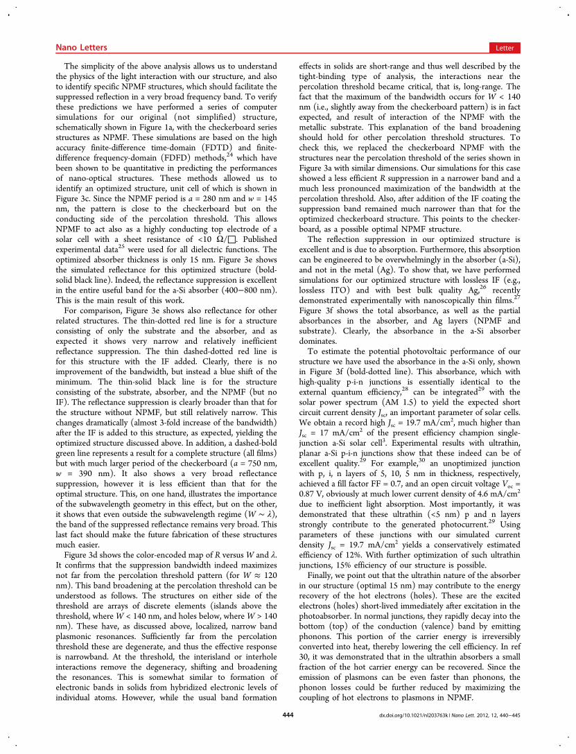
The simplicity of the above analysis allows us to understandthe physics of the light interaction with our structure, and alsoto identify specific NPMF structures, which should facilitate thesuppressed reflection in a very broad frequency band. To verifythese predictions we have performed a series of computersimulations for our original (not simplified) structure,schematically shown in Figure 1a, with the checkerboard seriesstructures as NPMF. These simulations are based on the highaccuracy finite-difference time-domain (FDTD) and finite-difference frequency-domain (FDFD) methods,24 which havebeen shown to be quantitative in predicting the performancesof nano-optical structures. These methods allowed us toidentify an optimized structure, unit cell of which is shown inFigure 3c. Since the NPMF period is a = 280 nm and w = 145nm, the pattern is close to the checkerboard but on theconducting side of the percolation threshold. This allowsNPMF to act also as a highly conducting top electrode of asolar cell with a sheet resistance of <10 Ω/□. Publishedexperimental data25 were used for all dielectric functions. Theoptimized absorber thickness is only 15 nm. Figure 3e showsthe simulated reflectance for this optimized structure (bold-solid black line). Indeed, the reflectance suppression is excellentin the entire useful band for the a-Si absorber (400−800 nm).This is the main result of this work.For comparison, Figure 3e shows also reflectance for other
related structures. The thin-dotted red line is for a structureconsisting of only the substrate and the absorber, and asexpected it shows very narrow and relatively inefficientreflectance suppression. The thin dashed-dotted red line isfor this structure with the IF added. Clearly, there is noimprovement of the bandwidth, but instead a blue shift of theminimum. The thin-solid black line is for the structureconsisting of the substrate, absorber, and the NPMF (but noIF). The reflectance suppression is clearly broader than that forthe structure without NPMF, but still relatively narrow. Thischanges dramatically (almost 3-fold increase of the bandwidth)after the IF is added to this structure, as expected, yielding theoptimized structure discussed above. In addition, a dashed-boldgreen line represents a result for a complete structure (all films)but with much larger period of the checkerboard (a = 750 nm,w = 390 nm). It also shows a very broad reflectancesuppression, however it is less efficient than that for theoptimal structure. This, on one hand, illustrates the importanceof the subwavelength geometry in this effect, but on the other,it shows that even outside the subwavelength regime (W ∼ λ),the band of the suppressed reflectance remains very broad. Thislast fact should make the future fabrication of these structuresmuch easier.Figure 3d shows the color-encoded map of R versusW and λ.
It confirms that the suppression bandwidth indeed maximizesnot far from the percolation threshold pattern (for W ≈ 120nm). This band broadening at the percolation threshold can beunderstood as follows. The structures on either side of thethreshold are arrays of discrete elements (islands above thethreshold, whereW < 140 nm, and holes below, whereW > 140nm). These have, as discussed above, localized, narrow bandplasmonic resonances. Sufficiently far from the percolationthreshold these are degenerate, and thus the effective responseis narrowband. At the threshold, the interisland or interholeinteractions remove the degeneracy, shifting and broadeningthe resonances. This is somewhat similar to formation ofelectronic bands in solids from hybridized electronic levels ofindividual atoms. However, while the usual band formation
effects in solids are short-range and thus well described by thetight-binding type of analysis, the interactions near thepercolation threshold became critical, that is, long-range. Thefact that the maximum of the bandwidth occurs for W < 140nm (i.e., slightly away from the checkerboard pattern) is in factexpected, and result of interaction of the NPMF with themetallic substrate. This explanation of the band broadeningshould hold for other percolation threshold structures. Tocheck this, we replaced the checkerboard NPMF with thestructures near the percolation threshold of the series shown inFigure 3a with similar dimensions. Our simulations for this caseshowed a less efficient R suppression in a narrower band and amuch less pronounced maximization of the bandwidth at thepercolation threshold. Also, after addition of the IF coating thesuppression band remained much narrower than that for theoptimized checkerboard structure. This points to the checker-board, as a possible optimal NPMF structure.The reflection suppression in our optimized structure is
excellent and is due to absorption. Furthermore, this absorptioncan be engineered to be overwhelmingly in the absorber (a-Si),and not in the metal (Ag). To show that, we have performedsimulations for our optimized structure with lossless IF (e.g.,lossless ITO) and with best bulk quality Ag,26 recentlydemonstrated experimentally with nanoscopically thin films.27
Figure 3f shows the total absorbance, as well as the partialabsorbances in the absorber, and Ag layers (NPMF andsubstrate). Clearly, the absorbance in the a-Si absorberdominates.To estimate the potential photovoltaic performance of our
structure we have used the absorbance in the a-Si only, shownin Figure 3f (bold-dotted line). This absorbance, which withhigh-quality p-i-n junctions is essentially identical to theexternal quantum efficiency,28 can be integrated29 with thesolar power spectrum (AM 1.5) to yield the expected shortcircuit current density Jsc, an important parameter of solar cells.We obtain a record high Jsc = 19.7 mA/cm2, much higher thanJsc = 17 mA/cm2 of the present efficiency champion single-junction a-Si solar cell3. Experimental results with ultrathin,planar a-Si p-i-n junctions show that these indeed can be ofexcellent quality.29 For example,30 an unoptimized junctionwith p, i, n layers of 5, 10, 5 nm in thickness, respectively,achieved a fill factor FF = 0.7, and an open circuit voltage Voc =0.87 V, obviously at much lower current density of 4.6 mA/cm2
due to inefficient light absorption. Most importantly, it wasdemonstrated that these ultrathin (<5 nm) p and n layersstrongly contribute to the generated photocurrent.29 Usingparameters of these junctions with our simulated currentdensity Jsc = 19.7 mA/cm2 yields a conservatively estimatedefficiency of 12%. With further optimization of such ultrathinjunctions, 15% efficiency of our structure is possible.Finally, we point out that the ultrathin nature of the absorber
in our structure (optimal 15 nm) may contribute to the energyrecovery of the hot electrons (holes). These are the excitedelectrons (holes) short-lived immediately after excitation in thephotoabsorber. In normal junctions, they rapidly decay into thebottom (top) of the conduction (valence) band by emittingphonons. This portion of the carrier energy is irreversiblyconverted into heat, thereby lowering the cell efficiency. In ref30, it was demonstrated that in the ultrathin absorbers a smallfraction of the hot carrier energy can be recovered. Since theemission of plasmons can be even faster than phonons, thephonon losses could be further reduced by maximizing thecoupling of hot electrons to plasmons in NPMF.
Nano Letters Letter
dx.doi.org/10.1021/nl203763k | Nano Lett. 2012, 12, 440−445444

In conclusion, we have demonstrated, by calculation andsimulations, that a structure consisting of a multilayer stackdeposited on a metallic substrate can be made to superabsorbelectromagnetic radiation in the entire visible range. One of thelayers in the stack is a nanoscopically perforated metallic film ofa patterned checkerboard structure. This film, in addition tobeing an integral part of the superabsorber, is also veryconductive and thus can function as a window electrode in thephotovoltaic device. We also show that the nanoscopicallyperforated metallic film and the ultrathin absorber form ametamaterial effective medium that shows negative refraction inthe frequency range of interest. Our simulations confirm thatthe bandwidth of the superabsorption is maximized at thecheckerboard pattern. Simulations show that the energyconversion efficiency of the proposed specific structure shouldexceed 12% in practice. Our scheme also generally applies toother absorber materials.
■ AUTHOR INFORMATION
Corresponding Author*E-mail: (Y.W.) [email protected]; (K.K.) [email protected]; (Z.R.) [email protected].
Author Contributions#Equal contributors,
■ ACKNOWLEDGMENTS
The work carried out at South China Normal University byY.W. is funded by NSFC under Contract No. 61106061. Thework performed at Boston College is funded by the U.S.Department of Energy under Contract Number DOE DE-FG02-00ER45805 (Z.F.R.).
■ REFERENCES(1) Green, M. A.; Emery, K.; Hishikawa, Y.; Warta, W. Prog.Photovolt: Res. Appl. 2009, 17, 320−326.(2) Rech, B.; Wagner, H. Appl. Phys. A 1999, 69, 155−167.(3) Meier, J.; Spitznagel, J.; Kroll, U.; Bucher, C.; Fay, S.; Moriarty,T.; Shah, A. Thin Solid Films 2004, 451−452, 518−524.(4) (a) Luque, A.; Hegedus, S. Handbook of photovoltaic science andengineering; John Wiley & Sons Ltd.: New York, 2003. (b) Lewis, N. S.;Crabtree, G. Basic Research Needs for Solar Energy Utilization: report ofthe Basic Energy Sciences Workshop on Solar Energy Utilization; U.S.Department of Energy: Washington, DC, April 18−21, 2005. www.er.doe.gov/bes/reports/abstracts.html#SEU.(5) Shockley, W.; Queisser, H. J. J. Appl. Phys. 1961, 32, 510.(6) Ebbesen, T. W.; Lezec, H. J.; Ghaemi, H. F.; Thio, T.; Wolff, P.A. Nature 1998, 391, 667−669.(7) Catchpole, K. R.; Polman, A. Opt. Express 2008, 16, 21793.(8) Schaadt, D. M.; Feng, B.; Yu, E. T. Appl. Phys. Lett. 2005, 86,063106.(9) Battaglia, C.; Escarre, J.; Soderstrom, K.; Charriere, M.;Despeisse, M.; Haug, F.-J.; Ballif, C. Nat. Photonics 2011, 5, 538.(10) Yu, Z.; Raman, A.; Fan, S. Proc. Natl. Acad. Sci. U.S.A. 2010, 107,17491.(11) Aydin, K.; Ferry, V. E.; Briggs, R. M.; Atwater, H. A. Nat.Commun. 2011, DOI: DOI: 10.1038/ncomms1528.(12) Sefunc, M. A.; Okyay, A. K.; Demir, H. V. Appl. Phys. Lett. 2011,98, 093117.(13) Smith, D. R.; Schultz, S.; Markos, P.; Soukoulis, C. M. Phys. Rev.B 2002, 65, 195104.(14) Hao, J.; Wang, J.; Liu, X.; Padilla, W. J.; Zhou, L.; Qiu, M. Appl.Phys. Let. 2010, 96, 251104.(15) Heavens, O. S. Optical properties of thin solid films; DoverPublications, Inc.: New York, 1965.
(16) In fact, this form cannot be correct in the entire frequencyrange, since it violates the f-sum rule.(17) Kempa, K. Phys. Rev. B 2006, 74, 033411.(18) Ruppin, R. Phys. Lett. A 2000, 277, 61−64.(19) Peng, Y.; Paudel, T.; Chen, W.-C.; Padilla, W. J.; Ren, Z. F.;Kempa, K. Appl. Phys. Lett. 2010, 97, 041901.(20) Kempa, K. Phys. Status Solidi (RRL) 2010, 4, 218−220.(21) With vanishing fluctuations, thus the mean-field models areapplicable.(22) Bergman, D. J.; Imry, Y. Phys. Rev. Lett. 1977, 39, 1222−1225.(23) Jackson, J. D. Classical Electrodynamics, 3rd ed; John Wiley &Sons Ltd.: New York, 1998.(24) (a) Taflove, A. Computational Electrodynamics: The Finite-Difference Time-Domain Method. Artech House; Norwood, MA, 1995.(b) Wang, X.; Kempa, K. Phys. Rev. B 2005, 71, 233101. (c) Thefollowing computer software was employed: CST Microwave Studiofrom the Computer Simulation Technology AG, and MEEP fromMassachusetts Institute of Technology.(25) (a) Palik, D. Data for Ag. Handbook of Optical Constants ofSolids; Academic Press: Boston, 1985. (b) Data for a-Si and ITO:Sopralab basic n&k files database (http://www.sopra-sa.com/index.php, August, 2011.(26) Johnson, P. B.; Christy, R. W. Phys. Rev. B 1972, 6, 370.(27) Chen, W.; Thoreson, M. D.; Ishii, S.; Kildishev, A. V.; Shalaev,V. M. Opt. Express 2010, 18, 5124.(28) Springer, J.; Poruba, A.; Vanecek, M. J. Appl. Phys. 2004, 96,5329.(29) Krc, J.; Smole, F.; Topic, M. Prog. Photovoltics 2003, 11, 15.(30) Kempa, K.; Naughton, M. J.; Ren, Z. F.; Herczynski, A.;Kirkpatrick, T.; Rybczynski, J.; Gao, Y. Appl. Phys. Lett. 2009, 95,233121.
Nano Letters Letter
dx.doi.org/10.1021/nl203763k | Nano Lett. 2012, 12, 440−445445
Copyright © 2022 FDOKUMEN