Engineering and Applied Science Research - ThaiJO
8
*Corresponding author. Email address: [email protected] doi: 10.14456/easr.2021.6 Engineering and Applied Science Research 2021;48(1):48-55 Research Article Engineering and Applied Science Research https://www.tci-thaijo.org/index.php/easr/index Published by the Faculty of Engineering, Khon Kaen University, Thailand Design of isolated IGBT driving and control circuits for an interleaved boost converter Mustafa Fawzi Mohammed* 1) , Ali Husain Ahmad 2) and Abdulrahim Thiab Humod 3) 1) BIT Department, Business Informatics Collage, University of Information Technology & Communications, Baghdad 10001, Iraq 2) Department of Medical Devices Technology Engineering, Al-Hadi University Collage, Baghdad 10001, Iraq 3) Electrical Engineering Department, University of Technology, Baghdad 10001, Iraq Received 23 November 2019 Revised 15 June 2020 Accepted 23 June 2020 Abstract An IGBT/MOSFET driver circuit works at a low voltage, between 5-15 V of its gate voltage to drive power converter switching devices that work at higher voltages. If there is no isolation between the driver and power converter circuits, any damage that may occur to the power converter circuit at high voltage will damage the driver circuit as well. This paper presents a design of an isolated IGBT/MOSFET driver circuit for an interleaved DC/DC boost converter using a TL494 IC to generate the required pulses for the converter’s circuit. Isolation is done using optocouplers. An IC IR2117 driver is also used to produce smooth rise and fall t imes for the pulses for each IGBT. The designed driver circuit is modelled using a co-simulation employing Multisim and LabVIEW software and then implemented experimentally with the help of a NI PCI-DAQ 6259. A P-I controller is implemented to regulate the output voltage of the boost converter, as well at the desired set point. Keywords: Boost, DC/DC, DAQ, Interleaved, LabVIEW, P-I controller 1. Introduction An interleaved DC/DC boost converter performs better than a single stage boost converter. It produces very small ripples in its input current while handling more power conversion with higher efficiency [1, 2]. IGBT/MOSFET switching devices should have their pulses at the proper switching frequency to obtain the best converter performance. There should be a phase shift between the pulses of each switch to reduce the ripples of the converter’s input current. The pulses can be obtained from a function generator, micro-controllers, or timing ICs. An IC TL494 [3] is a good choice to achieve the desired pulses for an interleaved boost converter circuit. This IC can be regulated to control the frequency of the generated pulses, the pulse width duration, and the dead time between the pulses. Regulation can be made by an external circuit using a microcontroller or a computer with data acquisition (DAQ) cards. In boost converter design, the generated pulses for each switching device should be isolated before passing the gates of the IGBT/MOSFET. Isolation can be done magnetically using a pulse transformer or optically with optocouplers [4]. This is necessary to isolate the voltage and grounding between the circuit and power circuits of the converter that run switching devices. Previous work [5-7] includes designs of driver circuits using pulse transformers. Yet, this did not solve the problem of slow rise and fall times for the pulses that drive the IGBT/MOSFET gates. The use of a pulse transformer requires many considerations. These include the inductance of the primary and secondary leads of the transformer, the size of its core, and the frequency of the pulses. When the switching frequency is low, the inductance of the transformer coils should be higher with a bigger core size to overcome the saturation problem of the core. When the switching frequency is high, the transformer size can be reduced [8]. Otherwise, an increased pulse frequency may increase the losses of the switching devices [9]. Optocouplers can be a good option since to they do not depend on coils or core size. However, they do need a separate DC power supply to optically isolate the pulses [10]. This paper presents a design of an isolated IGBT driver circuit for an interleaved boost converter based on optocouplers for pulse isolation with driver ICs. The results are very short rise and fall times for each pulse to reduce the switching losses of the power transistors. Pulses are generated by an IC TL494. This paper is organized as follows. An introduction is given with summary information about boost converters. Then, the proposed isolated IGBT driver circuit is presented. After that, the simulation and experimental results are given. Finally, the conclusions are put forth. 2. Interleaved boost converter A simple interleaved boost converter has only two channels (two-phases). It contains two parallel-connected boost converters. Other devices may contain many channels (phases) as well [11]. There are four modes of operation of two-phase interleaved boost converters as follows [12]: a. Mode (1) when IGBT1 is ON and IGBT2 is OFF. b. Mode (2) when IGBT1 is ON and IGBT2 is ON. c. Mode (3) when IGBT1 is OFF and IGBT2 is ON. d. Mode (4) when IGBT1 is ON and IGBT2 is ON. When a particular IGBT switch is conducting (ON-state), the corresponding connected inductor is charging. The opposite is true as well. When the switch is open (OFF-state) then its corresponding inductor is discharging. If the pulses fed to each IGBT switch are shifted by 180 o , then only modes (1) and (3) are possible. Practically, this happens when a pulse generating IC, such as a TL494, is used. A dead time should be added to these
-
Upload
khangminh22 -
Category
Documents
-
view
1 -
download
0
Transcript of Engineering and Applied Science Research - ThaiJO
*Corresponding author. Email address: [email protected] doi: 10.14456/easr.2021.6
Engineering and Applied Science Research 2021;48(1):48-55 Research Article
Engineering and Applied Science Research
https://www.tci-thaijo.org/index.php/easr/index
Published by the Faculty of Engineering, Khon Kaen University, Thailand
Design of isolated IGBT driving and control circuits for an interleaved boost converter Mustafa Fawzi Mohammed*1), Ali Husain Ahmad2) and Abdulrahim Thiab Humod3)
1)BIT Department, Business Informatics Collage, University of Information Technology & Communications, Baghdad 10001, Iraq 2)Department of Medical Devices Technology Engineering, Al-Hadi University Collage, Baghdad 10001, Iraq 3)Electrical Engineering Department, University of Technology, Baghdad 10001, Iraq
Received 23 November 2019
Revised 15 June 2020
Accepted 23 June 2020
Abstract
An IGBT/MOSFET driver circuit works at a low voltage, between 5-15 V of its gate voltage to drive power converter switching devices
that work at higher voltages. If there is no isolation between the driver and power converter circuits, any damage that may occur to the
power converter circuit at high voltage will damage the driver circuit as well. This paper presents a design of an isolated
IGBT/MOSFET driver circuit for an interleaved DC/DC boost converter using a TL494 IC to generate the required pulses for the
converter’s circuit. Isolation is done using optocouplers. An IC IR2117 driver is also used to produce smooth rise and fall times for the
pulses for each IGBT. The designed driver circuit is modelled using a co-simulation employing Multisim and LabVIEW software and
then implemented experimentally with the help of a NI PCI-DAQ 6259. A P-I controller is implemented to regulate the output voltage
of the boost converter, as well at the desired set point.
Keywords: Boost, DC/DC, DAQ, Interleaved, LabVIEW, P-I controller
1. Introduction
An interleaved DC/DC boost converter performs better than
a single stage boost converter. It produces very small ripples in
its input current while handling more power conversion with
higher efficiency [1, 2]. IGBT/MOSFET switching devices
should have their pulses at the proper switching frequency to
obtain the best converter performance. There should be a phase
shift between the pulses of each switch to reduce the ripples of
the converter’s input current. The pulses can be obtained from a
function generator, micro-controllers, or timing ICs. An IC
TL494 [3] is a good choice to achieve the desired pulses for an
interleaved boost converter circuit. This IC can be regulated to
control the frequency of the generated pulses, the pulse width
duration, and the dead time between the pulses. Regulation can
be made by an external circuit using a microcontroller or a
computer with data acquisition (DAQ) cards. In boost converter
design, the generated pulses for each switching device should be
isolated before passing the gates of the IGBT/MOSFET. Isolation
can be done magnetically using a pulse transformer or optically
with optocouplers [4]. This is necessary to isolate the voltage and
grounding between the circuit and power circuits of the converter
that run switching devices. Previous work [5-7] includes designs
of driver circuits using pulse transformers. Yet, this did not solve
the problem of slow rise and fall times for the pulses that drive
the IGBT/MOSFET gates. The use of a pulse transformer
requires many considerations. These include the inductance of
the primary and secondary leads of the transformer, the size of its
core, and the frequency of the pulses. When the switching
frequency is low, the inductance of the transformer coils should
be higher with a bigger core size to overcome the saturation
problem of the core. When the switching frequency is high, the
transformer size can be reduced [8]. Otherwise, an increased
pulse frequency may increase the losses of the switching devices
[9]. Optocouplers can be a good option since to they do not
depend on coils or core size. However, they do need a separate
DC power supply to optically isolate the pulses [10]. This paper
presents a design of an isolated IGBT driver circuit for an
interleaved boost converter based on optocouplers for pulse
isolation with driver ICs. The results are very short rise and fall
times for each pulse to reduce the switching losses of the power
transistors. Pulses are generated by an IC TL494. This paper is
organized as follows. An introduction is given with summary
information about boost converters. Then, the proposed isolated
IGBT driver circuit is presented. After that, the simulation and
experimental results are given. Finally, the conclusions are put
forth.
2. Interleaved boost converter
A simple interleaved boost converter has only two channels
(two-phases). It contains two parallel-connected boost
converters. Other devices may contain many channels (phases)
as well [11]. There are four modes of operation of two-phase
interleaved boost converters as follows [12]:
a. Mode (1) when IGBT1 is ON and IGBT2 is OFF.
b. Mode (2) when IGBT1 is ON and IGBT2 is ON.
c. Mode (3) when IGBT1 is OFF and IGBT2 is ON.
d. Mode (4) when IGBT1 is ON and IGBT2 is ON.
When a particular IGBT switch is conducting (ON-state), the
corresponding connected inductor is charging. The opposite is
true as well. When the switch is open (OFF-state) then its
corresponding inductor is discharging. If the pulses fed to each
IGBT switch are shifted by 180o, then only modes (1) and (3) are
possible. Practically, this happens when a pulse generating IC,
such as a TL494, is used. A dead time should be added to these
Engineering and Applied Science Research 2021;48(1) 49
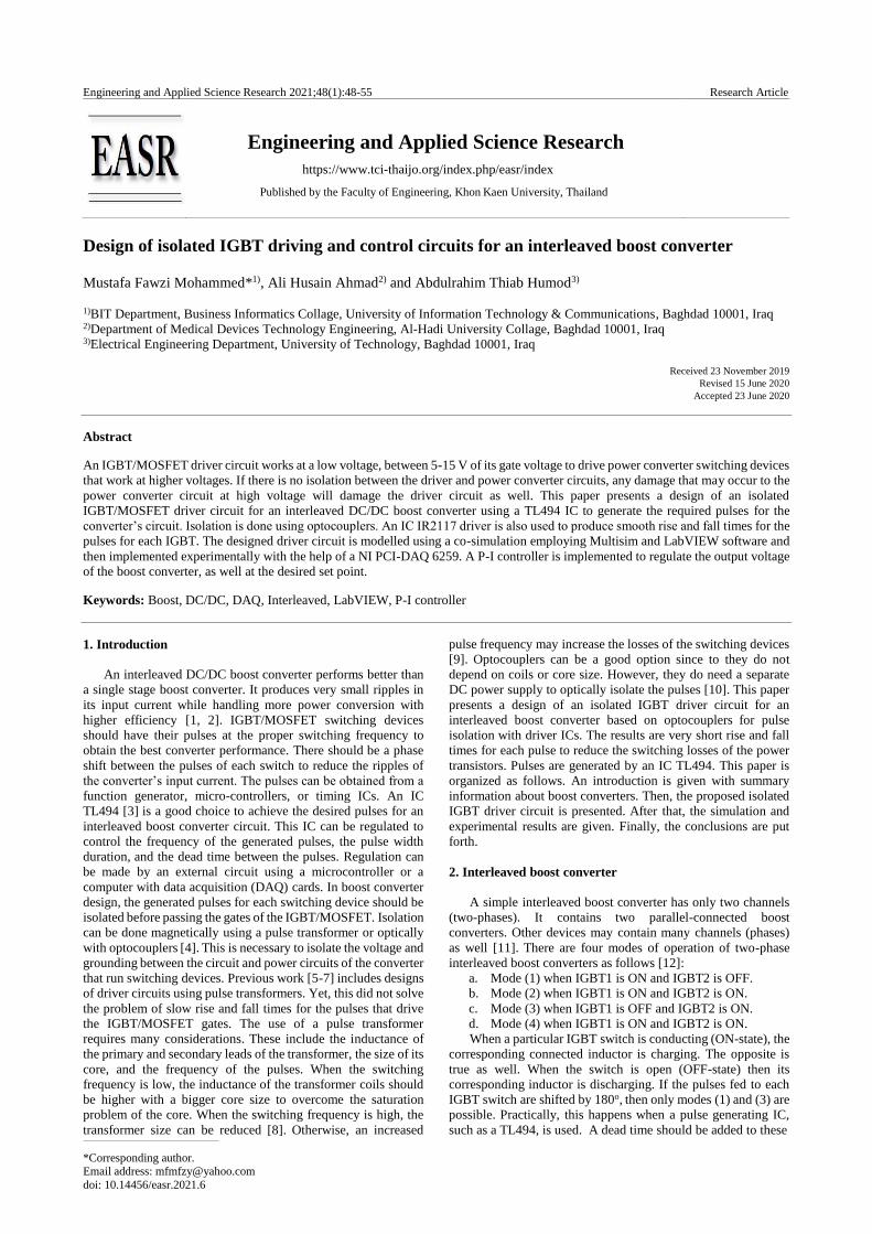
Figure 1 An interleaved boost converter circuit (two-phase)
Figure 2 The proposed isolated IGBT driver circuit for an interleaved boost converter
50 Engineering and Applied Science Research 2021;48(1)
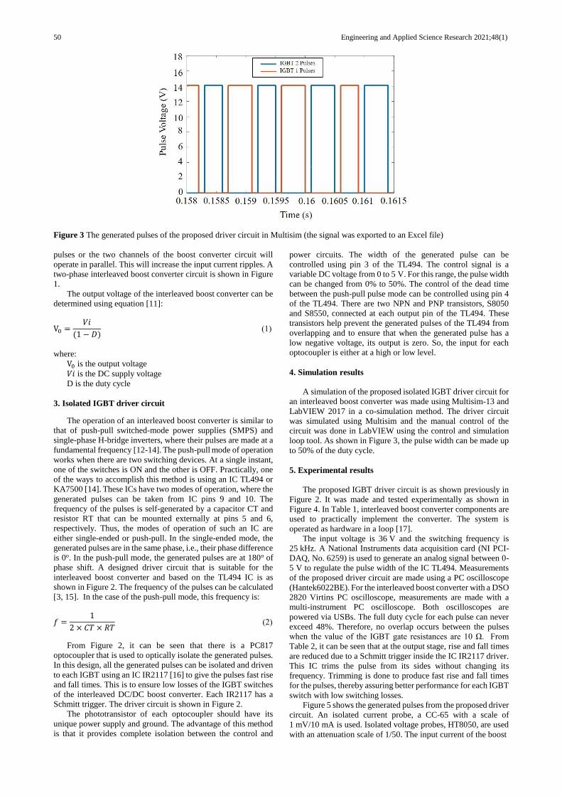
Figure 3 The generated pulses of the proposed driver circuit in Multisim (the signal was exported to an Excel file)
pulses or the two channels of the boost converter circuit will
operate in parallel. This will increase the input current ripples. A
two-phase interleaved boost converter circuit is shown in Figure
1.
The output voltage of the interleaved boost converter can be
determined using equation [11]:
V0 =𝑉𝑖
(1 − 𝐷) (1)
where:
V0 is the output voltage
𝑉𝑖 is the DC supply voltage
D is the duty cycle
3. Isolated IGBT driver circuit
The operation of an interleaved boost converter is similar to
that of push-pull switched-mode power supplies (SMPS) and
single-phase H-bridge inverters, where their pulses are made at a
fundamental frequency [12-14]. The push-pull mode of operation
works when there are two switching devices. At a single instant,
one of the switches is ON and the other is OFF. Practically, one
of the ways to accomplish this method is using an IC TL494 or
KA7500 [14]. These ICs have two modes of operation, where the
generated pulses can be taken from IC pins 9 and 10. The
frequency of the pulses is self-generated by a capacitor CT and
resistor RT that can be mounted externally at pins 5 and 6,
respectively. Thus, the modes of operation of such an IC are
either single-ended or push-pull. In the single-ended mode, the
generated pulses are in the same phase, i.e., their phase difference
is 0o. In the push-pull mode, the generated pulses are at 180o of
phase shift. A designed driver circuit that is suitable for the
interleaved boost converter and based on the TL494 IC is as
shown in Figure 2. The frequency of the pulses can be calculated
[3, 15]. In the case of the push-pull mode, this frequency is:
𝑓 =1
2 × 𝐶𝑇 × 𝑅𝑇 (2)
From Figure 2, it can be seen that there is a PC817
optocoupler that is used to optically isolate the generated pulses.
In this design, all the generated pulses can be isolated and driven
to each IGBT using an IC IR2117 [16] to give the pulses fast rise
and fall times. This is to ensure low losses of the IGBT switches
of the interleaved DC/DC boost converter. Each IR2117 has a
Schmitt trigger. The driver circuit is shown in Figure 2.
The phototransistor of each optocoupler should have its
unique power supply and ground. The advantage of this method
is that it provides complete isolation between the control and
power circuits. The width of the generated pulse can be
controlled using pin 3 of the TL494. The control signal is a
variable DC voltage from 0 to 5 V. For this range, the pulse width
can be changed from 0% to 50%. The control of the dead time
between the push-pull pulse mode can be controlled using pin 4
of the TL494. There are two NPN and PNP transistors, S8050
and S8550, connected at each output pin of the TL494. These
transistors help prevent the generated pulses of the TL494 from
overlapping and to ensure that when the generated pulse has a
low negative voltage, its output is zero. So, the input for each
optocoupler is either at a high or low level.
4. Simulation results
A simulation of the proposed isolated IGBT driver circuit for
an interleaved boost converter was made using Multisim-13 and
LabVIEW 2017 in a co-simulation method. The driver circuit
was simulated using Multisim and the manual control of the
circuit was done in LabVIEW using the control and simulation
loop tool. As shown in Figure 3, the pulse width can be made up
to 50% of the duty cycle.
5. Experimental results
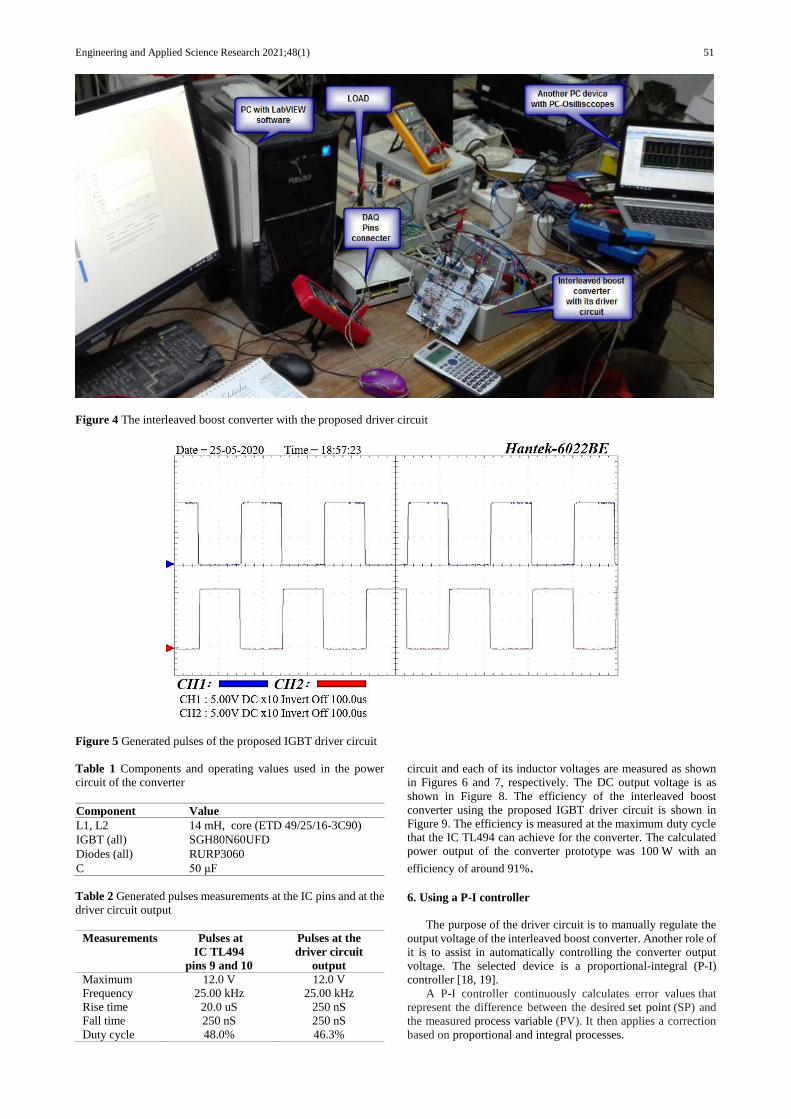
The proposed IGBT driver circuit is as shown previously in
Figure 2. It was made and tested experimentally as shown in
Figure 4. In Table 1, interleaved boost converter components are
used to practically implement the converter. The system is
operated as hardware in a loop [17].
The input voltage is 36 V and the switching frequency is
25 kHz. A National Instruments data acquisition card (NI PCI-
DAQ, No. 6259) is used to generate an analog signal between 0-
5 V to regulate the pulse width of the IC TL494. Measurements
of the proposed driver circuit are made using a PC oscilloscope
(Hantek6022BE). For the interleaved boost converter with a DSO
2820 Virtins PC oscilloscope, measurements are made with a
multi-instrument PC oscilloscope. Both oscilloscopes are
powered via USBs. The full duty cycle for each pulse can never
exceed 48%. Therefore, no overlap occurs between the pulses
when the value of the IGBT gate resistances are 10 Ω. From
Table 2, it can be seen that at the output stage, rise and fall times
are reduced due to a Schmitt trigger inside the IC IR2117 driver.
This IC trims the pulse from its sides without changing its
frequency. Trimming is done to produce fast rise and fall times
for the pulses, thereby assuring better performance for each IGBT
switch with low switching losses.
Figure 5 shows the generated pulses from the proposed driver
circuit. An isolated current probe, a CC-65 with a scale of
1 mV/10 mA is used. Isolated voltage probes, HT8050, are used
with an attenuation scale of 1/50. The input current of the boost
Engineering and Applied Science Research 2021;48(1) 51
Figure 4 The interleaved boost converter with the proposed driver circuit
Figure 5 Generated pulses of the proposed IGBT driver circuit
Table 1 Components and operating values used in the power
circuit of the converter
Component Value
L1, L2 14 mH, core (ETD 49/25/16-3C90)
IGBT (all) SGH80N60UFD
Diodes (all) RURP3060
C 50 μF
Table 2 Generated pulses measurements at the IC pins and at the
driver circuit output
Measurements Pulses at
IC TL494
pins 9 and 10
Pulses at the
driver circuit
output
Maximum 12.0 V 12.0 V
Frequency 25.00 kHz 25.00 kHz
Rise time 20.0 uS 250 nS
Fall time 250 nS 250 nS
Duty cycle 48.0% 46.3%
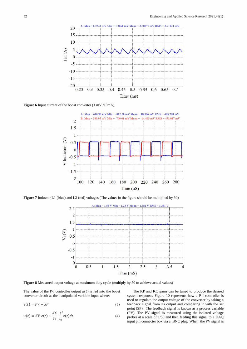
circuit and each of its inductor voltages are measured as shown
in Figures 6 and 7, respectively. The DC output voltage is as
shown in Figure 8. The efficiency of the interleaved boost
converter using the proposed IGBT driver circuit is shown in
Figure 9. The efficiency is measured at the maximum duty cycle
that the IC TL494 can achieve for the converter. The calculated
power output of the converter prototype was 100 W with an
efficiency of around 91%.
6. Using a P-I controller
The purpose of the driver circuit is to manually regulate the
output voltage of the interleaved boost converter. Another role of
it is to assist in automatically controlling the converter output
voltage. The selected device is a proportional-integral (P-I)
controller [18, 19].
A P-I controller continuously calculates error values that
represent the difference between the desired set point (SP) and
the measured process variable (PV). It then applies a correction
based on proportional and integral processes.
52 Engineering and Applied Science Research 2021;48(1)
Figure 6 Input current of the boost converter (1 mV /10mA)
Figure 7 Inductor L1 (blue) and L2 (red) voltages (The values in the figure should be multiplied by 50)
Figure 8 Measured output voltage at maximum duty cycle (multiply by 50 to achieve actual values)
The value of the P-I controller output 𝑢(𝑡) is fed into the boost
converter circuit as the manipulated variable input where:
𝑒(𝑡) = 𝑃𝑉 − 𝑆𝑃 (3)
𝑢(𝑡) = 𝐾𝑃 𝑒(𝑡) +𝐾𝐶
𝑇𝑖 ∫ 𝑒(𝑡)𝑑𝑡 (4)
𝑡
0
The KP and KC gains can be tuned to produce the desired
system response. Figure 10 represents how a P-I controller is
used to regulate the output voltage of the converter by taking a
feedback signal from its output and comparing it with the set
point (SP). The feedback signal is known as a process variable
(PV). The PV signal is measured using the isolated voltage
probes at a scale of 1/50 and then feeding this signal to a DAQ
input pin connecter box via a BNC plug. When the PV signal is

Engineering and Applied Science Research 2021;48(1) 53
Figure 9 Efficiency of the converter with various loads at a 36 V supply voltage (enlarged)
Figure 10 Regulation of the output voltage using the P-I controller
captured in the LabVIEW environment, it is compared with the
SP to determine an error “e” signal. For any error value, the P-I
controller will act accordingly. After tuning the gains, the value
of the proportional gain KP is 0.06 and the integral time TI is 0.01
min. The output signal from the DAQ is a 0-5 V analog signal.
This signal is fed to pin 3 of the IC TL494. The output voltage
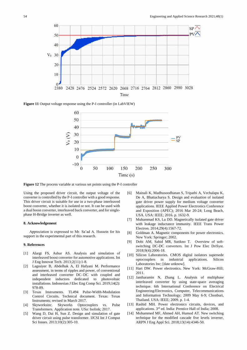
response is as shown in Figure 11, where the SP value is 50 V.
Figure 12 represents the P-I controller operation. Various set
points (SP) were applied in LabVIEW and the response (PV)
represents the output voltage of the interleaved boost converter.
The SP values were 10, 28, 42 and 50 V. The data is recorded in
LabVIEW through as a tdms_index filetype that can be opened
in either Microsoft Excel or DIAdem software. In this figure, it
can be seen that there are some fluctuations in the PV data. This
occurs due to the low sampling speed of the DAQ used in these
experiments.
The PC used in the experimental work was configured as
follows. It had a Core-i7 processor, 8 GB RAM, 250 GB SSD
hard disk, and ran on a Windows 10 operating system.
7. Conclusions
In this paper, an isolated IGBT driver and control circuit for
a two-phase interleaved DC/DC boost converter is successfully
designed, simulated, and experimentally implemented. There are
several DC grounded electrical supplies that are isolated to
ensure that each IGBT of the boost converter circuit will have its
own individual gate emitter voltage (VGE). Furthermore, the
source that generates the pulses is not connected at the same
ground with the IGBT switching devices. This isolation helps to
ensure that any problem or malfunction of the boost converter
circuit will not damage or even affect the isolated driver circuit.
54 Engineering and Applied Science Research 2021;48(1)
Figure 11 Output voltage response using the P-I controller (in LabVIEW)
Figure 12 The process variable at various set points using the P-I controller
Using the proposed driver circuit, the output voltage of the
converter is controlled by the P-I controller with a good response.
This driver circuit is suitable for use in a two-phase interleaved
boost converter, whether it is isolated or not. It can be used with
a dual boost converter, interleaved buck converter, and for single-
phase H-Bridge inverter as well.
8. Acknowledgement
Appreciation is expressed to Mr. Sa’ad A. Hussein for his
support in the experimental part of this research.
9. References
[1] Alargt FS, Ashur AS. Analysis and simulation of
interleaved boost converter for automotive applications. Int
J Eng Innovat Tech. 2013;2(11):1-8.
[2] Lagssiyer B, Abdelhak A, El Hafyani M. Performance
assessment, in terms of ripples and power, of conventional
and interleaved converter DC–DC with coupled and
independent inductors dedicated to photovoltaic
installations. Indonesian J Elec Eng Comp Sci. 2019;14(2):
978-89.
[3] Texas Instruments. TL494 Pulse-Width-Modulation
Control Circuits. Technical document. Texas: Texas
Instruments; revised in March 2017.
[4] Skyworksinc. Skyworks Optocouplers vs. Pulse
Transformers. Application note. USa: Isolink; 2017.
[5] Wang D, Dai H, Sun Z. Design and simulation of gate
driver circuit using pulse transformer. IJCSI Int J Comput
Sci Issues. 2013;10(2):305-10.
[6] Mainali K, Madhusoodhanan S, Tripathi A, Vechalapu K,
De A, Bhattacharya S. Design and evaluation of isolated
gate driver power supply for medium voltage converter
applications. IEEE Applied Power Electronics Conference
and Exposition (APEC); 2016 Mar 20-24; Long Beach,
USA. USA: IEEE; 2016. p. 1632-9.
[7] Muhammad KS, Lu DD. Magnetically isolated gate driver
with leakage inductance immunity. IEEE Trans Power
Electron. 2014;29(4):1567-72.
[8] Goldman A. Magnetic components for power electronics.
New York: Springer; 2002.
[9] Dobi AM, Sahid MR, Sutikno T. Overview of soft-
switching DC-DC converters. Int J Pow Elec DriSyst.
2018;9(4):2006-18.
[10] Silicon Laboratories. CMOS digital isolators supersede
optocouplers in industrial applications. Silicon
Laboratories Inc; [date unknow].
[11] Hart DW. Power electronics. New York: McGraw-Hill;
2011.
[12] Jantharamin N, Zhang L. Analysis of multiphase
interleaved converter by using state-space averaging
technique. 6th International Conference on Electrical
Engineering/Electronics, Computer, Telecommunications
and Information Technology; 2009 May 6-9; Chonburi,
Thailand. USA: IEEE; 2009. p. 1-4.
[13] Rashid MH. Power electronics circuits, devices, and
applications. 3rd ed. India: Prentice Hall of India; 2008.
[14] Mohammed MF, Ahmed AH, Humod AT. New switching
technique for the modified cascade five levels inverter,
ARPN J Eng Appl Sci. 2018;13(14):4346-50.

Engineering and Applied Science Research 2021;48(1) 55
[15] Fairchild. KA7500C datasheet [Internet]. 2009 [cited 2019 Nov 1]. Available from:
https://www.mouser.com/datasheet/2/149/KA7500C-8950
1.pdf.
[16] International Rectifier. IR2117(S)/IR2118(S). Data Sheet
No. PD60146 Rev O [Internet]. [cited 2019 Nov 3].
Available from: https://www.infineon.com/dgdl/Infineon-
ir2117-DS-v01_00-EN.pdf?fileId=5546d462533600a4015
355c84331168d.
[17] Sharma HN. Hardware-in-the-loop simulator of wind
turbine emulator using LabVIEW. Int J Pow Elec Dri Syst.
2019;10(2):971-86.
[18] Ogata K. Modern control engineering. 3rd ed. New Jersey:
Prentice Hall Inc; 1997.
[19] Rajaji VD, Sekhar KC. Power applications for fuel-cell
using switching regulators. Indonesian J Elec Eng Comp
Sci. 2019;15(1):71-9.