Differential Power Processing System for the Capacitor ...
11
Journal of Power Electronics, Vol. 17, No. 4, pp. 1037-1047, July 2017 1037 https://doi.org/10.6113/JPE.2017.17.4.1037 ISSN(Print): 1598-2092 / ISSN(Online): 2093-4718 JPE 17-4-19 Differential Power Processing System for the Capacitor Voltage Balancing of Cost-effective Photovoltaic Multi-level Inverters Young-Tae Jeon * , Kyoung-Tak Kim * , and Joung-Hu Park † *,† Department of Electrical Engineering, Soongsil University, Seoul, Korea Abstract The Differential Power Processing (DPP) converter is a promising multi-module photovoltaic inverter architecture recently proposed for photovoltaic systems. In this paper, a DPP converter architecture, in which each PV-panel has its own DPP converter in shunt, performs distributed maximum power point tracking (DMPPT) control. It maintains a high energy conversion efficiency, even under partial shading conditions. The system architecture only deals with the power differences among the PV panels, which reduces the power capacity of the converters. Therefore, the DPP systems can easily overcome the conventional disadvantages of PCS such as centralized, string, and module integrated converter (MIC) topologies. Among the various types of the DPP systems, the feed-forward method has been selected for both its voltage balancing and power transfer to a modified H-bridge inverter that needs charge balancing of the input capacitors. The modified H-bridge multi-level inverter had some advantages such as a low part count and cost competitiveness when compared to conventional multi-level inverters. Therefore, it is frequently used in photovoltaic (PV) power conditioning system (PCS). However, its simplified switching network draws input current asymmetrically. Therefore, input capacitors in series suffer from a problem due to a charge imbalance. This paper validates the operating principle and feasibility of the proposed topology through the simulation and experimental results. They show that the input-capacitor voltages maintain the voltage balance with the PV MPPT control operating with a 140-W hardware prototype. Key words: Charge balancing, Differential power processing, Feed-forward, Flyback converter, Multiple winding I. INTRODUCTION Due to advances in PV technology, the capacity of solar systems has been increased in terms of variety of applications such as grid-scale solar plants, rooftop solar systems, and building integrated photovoltaic (BIPV) modules. The cost, size, and efficiency of systems are decisive factors in PV power conditioning systems (PCS). To optimize these elements, a large number of researches have been proposed so far [1], [2]. Centralized PV power conditioning architectures are the first-generation. They are the simplest and cheapest. However, they have a low energy efficiency due to their lack of individualized control during climate changes such as partial shading or increases and decreases in temperature [3]-[5]. The next generation are multi-string systems. This architecture achieves an improvement for shading conditions by dividing a single PV string into multi-strings. However, it still cannot overcome the drawback of the partial shading condition [6]. The third generation are Module-Integrated Converter (MIC) systems. They can perform Distributed Maximum Power Point Tracking (DMPPT) control, since they have an individual MPPT controller in a modularized converter for each PV panel. If the converter and a centralized inverter have a high efficiency, this system can maintain a higher efficiency than the previous generation systems, even under partial shading conditions, by operating the DMPPT controller [7]-[13]. However, the entire generated power of the PV array passes through the MIC and is transfered to the centralized inverter. Thus, a significant power loss occurs depending on the efficiency of the MIC. This loss has a negative influence on the total system efficiency. As a result, reducing the loss is an important design factor of the MIC. However, there are fundamental trade-offs in achieving the loss reduction and Manuscript received Nov. 30, 2016; accepted May 2, 2017 Recommended for publication by Associate Editor Yihua Hu. † Corresponding Author: [email protected] Tel: +82-2-820-0645, Fax: +82-2-827-7961, Soongsil University * Department of Electrical Engineering, Soongsil University, Korea © 2017 KIPE
-
Upload
khangminh22 -
Category
Documents
-
view
1 -
download
0
Transcript of Differential Power Processing System for the Capacitor ...

Journal of Power Electronics, Vol. 17, No. 4, pp. 1037-1047, July 2017 1037
https://doi.org/10.6113/JPE.2017.17.4.1037
ISSN(Print): 1598-2092 / ISSN(Online): 2093-4718
JPE 17-4-19
Differential Power Processing System for the Capacitor Voltage Balancing of Cost-effective
Photovoltaic Multi-level Inverters
Young-Tae Jeon*, Kyoung-Tak Kim*, and Joung-Hu Park†
*,†Department of Electrical Engineering, Soongsil University, Seoul, Korea
Abstract
The Differential Power Processing (DPP) converter is a promising multi-module photovoltaic inverter architecture recently proposed for photovoltaic systems. In this paper, a DPP converter architecture, in which each PV-panel has its own DPP converter in shunt, performs distributed maximum power point tracking (DMPPT) control. It maintains a high energy conversion efficiency, even under partial shading conditions. The system architecture only deals with the power differences among the PV panels, which reduces the power capacity of the converters. Therefore, the DPP systems can easily overcome the conventional disadvantages of PCS such as centralized, string, and module integrated converter (MIC) topologies. Among the various types of the DPP systems, the feed-forward method has been selected for both its voltage balancing and power transfer to a modified H-bridge inverter that needs charge balancing of the input capacitors. The modified H-bridge multi-level inverter had some advantages such as a low part count and cost competitiveness when compared to conventional multi-level inverters. Therefore, it is frequently used in photovoltaic (PV) power conditioning system (PCS). However, its simplified switching network draws input current asymmetrically. Therefore, input capacitors in series suffer from a problem due to a charge imbalance. This paper validates the operating principle and feasibility of the proposed topology through the simulation and experimental results. They show that the input-capacitor voltages maintain the voltage balance with the PV MPPT control operating with a 140-W hardware prototype.
Key words: Charge balancing, Differential power processing, Feed-forward, Flyback converter, Multiple winding
I. INTRODUCTION
Due to advances in PV technology, the capacity of solar systems has been increased in terms of variety of applications such as grid-scale solar plants, rooftop solar systems, and building integrated photovoltaic (BIPV) modules. The cost, size, and efficiency of systems are decisive factors in PV power conditioning systems (PCS). To optimize these elements, a large number of researches have been proposed so far [1], [2].
Centralized PV power conditioning architectures are the first-generation. They are the simplest and cheapest. However, they have a low energy efficiency due to their lack of individualized control during climate changes such as partial shading or increases and decreases in temperature [3]-[5]. The
next generation are multi-string systems. This architecture achieves an improvement for shading conditions by dividing a single PV string into multi-strings. However, it still cannot overcome the drawback of the partial shading condition [6]. The third generation are Module-Integrated Converter (MIC) systems. They can perform Distributed Maximum Power Point Tracking (DMPPT) control, since they have an individual MPPT controller in a modularized converter for each PV panel. If the converter and a centralized inverter have a high efficiency, this system can maintain a higher efficiency than the previous generation systems, even under partial shading conditions, by operating the DMPPT controller [7]-[13]. However, the entire generated power of the PV array passes through the MIC and is transfered to the centralized inverter. Thus, a significant power loss occurs depending on the efficiency of the MIC. This loss has a negative influence on the total system efficiency. As a result, reducing the loss is an important design factor of the MIC. However, there are fundamental trade-offs in achieving the loss reduction and
Manuscript received Nov. 30, 2016; accepted May 2, 2017 Recommended for publication by Associate Editor Yihua Hu.
†Corresponding Author: [email protected] Tel: +82-2-820-0645, Fax: +82-2-827-7961, Soongsil University
*Department of Electrical Engineering, Soongsil University, Korea
© 2017 KIPE
1038 Journal of Power Electronics, Vol. 17, No. 4, July 2017
cost-effectiveness at the same time [14].
A. Differential Power Processor System
In order to reduce the cost and size, and to retain all of the advantages of the previous PV PCSs, a new topology referred to as the Differential Power Processing (DPP) architecture has been proposed [2]. Figure 1 shows a typical unidirectional power flow DPP system.
In this architecture, the PV panels are connected in series and the same number of DPP converters are arranged in shunt with each of the PV panels, bypassing an extra PV current from the PV string conducted to the main central converter. The DPP converters only deal with the power differences caused by the temperature or irradiation mismatch among the panels instead of the total power of the summation of all of the PV panels. This fractional power is transmitted unidirectionally from the PV to the DC-link through the DPPs. In addition, most of the power commonly generated at the PV goes through the main string converter at a low voltage-conversion ratio to the DC-link. Therefore, the overall power conversion losses can be far lower than those of the MIC structures. For example, in the full radiation condition in all of the PV panels, the DPPs do not operate at all. However, the central main converter works to achieve the whole power transfer. In addition to the feed-forward type of DPP systems, there are many other kinds of DPP architectures distinguished by their power directions and by the structure between the PV and DC-bus. They have all of the advantages of conventional architectures such as DMPPT operation like the MIC. They also have distinguished features such as add-on installation and fractional power process instead of the entire one. The PV-to-bus (PV-bus), PV-to-PV (PV-PV) and PV-to-Isolated Port (PV-IP) are referred to as three basic structures [14]. In addition, various topologies have been proposed for the DPP architecture, including bidirectional buck-boost converters [2], bidirectional flyback converters [16], [17] switched capacitors [18], ladder converters [19], shuffling converters [20], and so on. These are categorized into three groups depending on the power-flow control strategies called feed-forward, feed-back and bi-direction depending on the DPP power-flow path in the PV-bus system [14]. This paper focuses on the control of the feed-forward DPP system which is a PV-bus architecture with a multi-level grid-connected inverter which has a low cost but occurs a voltage imbalance of the DC-link capacitor voltages at the input of the inverter.
B. Multi-Level Photovoltaic Inverter
The multi-level inverter has been used very often in high-power industrial applications because of its advantages such as low distortion, decreasing electromagnetic (EM) compatibility problems, and reduced dv/dt stresses [3]. Although traditional multi-level inverters, such as cascaded H-bridge and flying capacitor asymmetric H-bridge (FCAH), have various merits in high-power applications. However,
Fig. 1. Typical DPP system (the arrows refer to the direction of the power flows).
they have weaknesses such as the use of numerous high power switches, which increases the complexity and installation cost of the gate driver circuit. Therefore, recent studies for multi-level inverters try to overcome this drawback by developing new topologies that minimize the elements and maximize the output levels of inverters that generates a high quality AC output voltage. This paper chooses a modified 5-level H-bridge inverter, which consists of the input capacitor connected in series, fewer switching elements when compared to other conventional H-bridge multi-level inverters. The topology makes it possible to reduce both the manufacturing cost and switching losses influencing the system efficiency [3].
Fig. 2 shows a circuit diagram and an output waveform of the modified H-bridge inverter stage used for the grid connection. Table I shows the switch states for all of the individual switches that correspond to the output voltage levels. SPWM is used since it is a very simple and widely used modulation technique. Instead of using the rudimentary form of the SPWM technique, a technique combined with a modified unipolar switching strategy has been employed in this study [15].
Fig. 3 presents the operation modes of the inverter SPWM strategy. The inverter has three operation modes in a half cycle, and the other half cycle is the same due to symmetry. In mode 1, switches 2 and 4 turn on and the current of the inverter freewheels. There is current iD at mode 2, which causes a power imbalance between C1 and C2. The discharge current of the capacitor iC2 flows through the diodes, S1, and S4. Mode 3 shows that there are discharge currents iC1 and iC2 of both C1 and C2, respectively. The operating principle tells that iD in mode 2 is the differential current between iC1 and iC2. This modulation method effectively helps in obtaining the low switching losses that occur in the inverter and the attenuated high-frequency EM Interference (EMI) noises through 60-Hz switching in a leg. However, because the average and instantaneous currents of SH and D are completely different from each other, a reliable external voltage balancing circuit is necessary to maintain each of the capacitor voltages [3]. Fig. 4 shows an example of the

Differential Power Processing System for the Capacitor Voltage Balancing of … 1039
(a) Modified H-bridge topology.
(b) 5-level output voltage waveform.
Fig. 2. Low-power 5-level inverter topology and output voltage before a filter.
TABLE I
SWITCHING STATES OF THE INDIVIDUAL SWITCHES DEPENDING ON
THE OUTPUT VOLTAGE LEVELS (1 = ON, 0 = OFF).
Vbridge S1 S2 S3 S4 SH
VDC 1 0 0 1 1
VDC/2 1 0 0 1 0
0 0 1 0 1 0
˗VDC/2 0 1 1 0 0
˗VDC 0 1 1 0 1
100-W operating parameters of the inverter. The average current difference between C1 and C2 is 0.2352 A, which is exactly the same as the diode’s average current iD. If the current-second balance condition at the capacitors is not satisfied, then the capacitor voltage cannot find the equilibrium point. Then the inverter sees a large voltage imbalance at the input, which leads to a huge distortion at the output waveform. Figure 5 shows the unbalanced power between the input
capacitors according to the total inverter power. When the inverter power increases, the unbalance power and current also increase. A conventional PCS circuit, as shown in Fig. 6, using a multiple-output flyback converter with same turn-ratio between the secondary windings has been presented to maintain the charge balance among the DC-link capacitors at
(a) Mode 1.
(b) Mode 2.
(c) Mode 3.
Fig. 3. Operation mode of the modified-H bridge inverter circuit (half cycle).
Fig. 4. Single cycle current waveforms of capacitors and diodes (100W).
the H-bridge inverter input [3]. However, the pre-stage flyback converter handles all of the power of the PV sources. Therefore, a serious amount of losses occurs that is almost the same level as the common loss flyback converters. In conclusion, there are some critical drawbacks in the
pre-stage DC-DC power conversion and in the DC-AC of Fig. 6. This paper overcomes these problems by proposing a DPP

1040 Journal of Power Electronics, Vol. 17, No. 4, July 2017
Fig. 5. Unbalanced power and current depending on the inverter power.
Fig. 6. Circuit diagram of the previous small scale PCS.
system which can maintain the charge balance for the following multilevel inverter. This paper is organized as follows. Section II and III explain
the proposed circuit and operating characteristics in detail. Section IV presents simulation results and Section V presents experimental results with a 140-W hardware prototype. Finally, some conclusions are discussed in Section VI.
II. OPERATION OF THE PROPOSED DPP SYSTEM
A. Proposed PV-bus-DPP System
A DPP converter has a purpose of minimizing the power losses in the power conversion process through differential power processing and controls such as Least Power Point Tracking (LPPT) [14]. In this paper, a new operation of the charge balancing function is added to DPP PV power conditioning systems for high efficiency with a low part count. The DPP architecture is applied to a grid-connected system
using a centralized inverter as shown in Fig. 7. This system is composed of a central converter which applies a boost converter, made up of multiple DPP converters which carries out MPPT control along with output voltage balancing using a small power-capacity unidirectional power-flow multi-output flyback converter, and of a 5-level inverter with two input capacitors which require charge-balancing.
Fig. 7. Grid-connected PCS system using DPP converters and a simply modified 5-level H-bridge inverter.
The power flow control is done as follows. Between the PV
string and the DC-link, a boost converter works the main-string current control as a central converter [14]. Between them, another converter in shunt with each of the PV panels transfers the extra PV power directly to the DC-link to achieve local MPP by compensation of the local mismatch in each of the PV panels, using small-capacity power converters [7]-[13], [21]. For the MPPT control, all of the DPPs receive the control information from a central controller. The DPP system can also achieve output balancing automatically using a same turn-ratio secondary winding transformer without any extra controllers. The DC-link voltage is regulated by the following grid-connected inverter.
B. Operating Principle of the Proposed System
This section shows how the proposed DPP system can decrease the power capacity of DPP converters by controlling the current in the main PV string. As an example, a feed-forward power-flow DPP method is shown in Fig. 8. Let the MPP current of PV1 be 2.74 A and that of PV2 be 2.0 A. The string current Istring can be below, between, or above these two MPP values. Then the DPPs will add or take away some current from the string based on the amount of the deviation in order to operate each of the PVs at its MPP, or they will be paused when the string current matches the PV current. In Fig. 8, the string current is 2.0 A, which is the same as the PV current of PV1. Then there is no current flow in the DPP1 converter and the DPP2 converter draws the excess current (0.74 A) from PV2. The operating condition is the optimal bias from the perspective of the power stress, because both of the DPP converter currents increase as the string current is reduced from this condition. At the optimal operating condition, DPP1 consumes no power, and DPP2 achieves a factional power in the middle of processing just 27% of the total PV2 power generation. Usually, non-isolation converters have higher efficiencies than isolation types. Therefore, the partial power processing through the DPP contributes to the power capacity reduction of the modularized DC-DC converters, and to the loss reduction.

Differential Power Processing System for the Capacitor Voltage Balancing of … 1041
Fig. 8. Example of a feed-forward DPP structure (the arrows refer to the directions of the power flows).
A PV-Bus DPP architecture that utilizes two multi-output
flyback converters as DPPs is shown in Fig. 9. The proposed system enables the 5-level inverter to maintain input-voltage balance by using a couple of multi-output flyback converters operating under the continuous current mode (CCM) condition, which has a constant input-output voltage gain regardless of the load status. Assuming that each of the flyback secondary windings has the same turn ratio, all of the output voltages become identical, even when the flyback converters meet a power difference caused by the inverter. Therefore, the multi-output flyback converters used for the DPP converter simultaneously perform the output voltage balancing along with the MPPT control. In Fig. 9, the 5-level inverter at the end is replaced by a couple of equivalent resistances Req1 and Req2, which are the top and bottom input resistances of the inverter, respectively. If the load difference can be covered by a summation of the DPP-delivery power, the voltage balancing at the load is achieved. However, when there is no power difference between the PV panels, all of the power in PVs is directly delivered to the DC-link through the central boost converter. Then those DPPs do not work for balancing. For this case, a special control method to forcefully conduct the minimum current for the balance through the DPP converters is required to achieve the balance. The string-current controller regulates the current in real time according to a periodically updated reference and checks to see if the voltage balancing is achieved or not. This method is a new variation of the conventional optimal-point searching strategy called the Least Power Point Tracking (LPPT) technique [14]. An efficiency analysis will be presented in the following section.
C. Efficiency
In order to confirm the feasibility of the proposed DPP system, the efficiency of an entire system consisting of a couple of multi-output flyback converters, and a boost converter is estimated. The efficiency is a parameter that divides the total input power from the PV modules into the
Fig. 9. Circuit diagram of the proposed PCS with a feed-forward structure (the inverter stage is replaced by the equivalent resistors Req1 and Req2).
total output power conducted to the inverter. The DPP system efficiency in the two PV module case is expressed as:
ηη η η
(1)
where and are the powers for each of the PV
panel, which makeup the system input power. , ,
and are boost converters and each DPP converter
power. In addition, η , η , and η are the efficiencies for each of them, respectively. The input power in the denominator is fixed by external environment conditions. According to numerator of equation (1), commonly, η is greater than η , and η . Therefore, a higher system efficiency is possible in the proposed method when compared with that of the recent Module-Integrated Converter (MIC) topology which transfers the entire power through the flyback converter The generalized case of n number of PV modules is derived as follows. The overall efficiency of the DPP system equation (1) is expanded in the following two formulas (2) and (3).
ηη ∑ η ,
, (2)
η , ∑ η , ,
∑ , ,
(3) where is the power efficiency of PV k. Equation (2) is represented by the power forms and equation (3) is represented by the voltage and current forms.
III. LOCAL MISMATCH OPERATION ANALYSIS
A. Balancing Condition Analysis – Two PV Module Case
When a power difference occurs among PV panels because
of partial shading or a temperature difference in PV1, only

1042 Journal of Power Electronics, Vol. 17, No. 4, July 2017
the differential power passes through the multi-output flyback
converter DPP2 with the same secondary turn-ratio [22]. In
this case, DPP1 does not operate and the boost converter
performs the MPPT control for PV1, instead of DPP1. Then,
DPP2 supports the MPPT control for PV2 while it provides
power to each of the capacitors C1 and C2 separately for
balancing. The power of the DPP multi-output flyback
converters maintain the voltage balancing of C1 and C2.
Therefore, when a differential power among the PV panels
occurs due to partial shading, as shown in Fig. 10, both
DMPPT and balancing power control methods are necessary.
This paper focuses on a condition where the power difference
among the PV panels is greater than the load power
imbalance (P ∆P ). In the two-PV module case, when
PV1 power is smaller than PV2, DPP1 processes no power
and DPP2 processes the differential power for balancing as
follows:
P , ∆ (4)
where I I and Pdpp,1 = 0. According to the
conventional DPP system operation, most of the power generated from the PV is transmitted to the DC-link by the string boost converter, and only a small differential power maintaining the charge balancing of the load passes through DPP converter 2. Let the unbalance power between the multilevel inverter’s equivalent resistance be ∆P , let the differential power of PV be ∆P , and let the power
processed by DPP converters be P . Both the PV and load
specification are as follows: Vpv1 = 26 V, Vpv2 = 28.5 V, Ipv1 = 2.0 A, Ipv2 = 2.74 A, Ppv1 = 52 W, Ppv2 = 78 W, ∆P = 11 W, ∆P = 26 W.
In this case, the DPP power of Pdpp,2 = 21.1 W is greater than ∆P 11W. Thus, balancing is possible. In addition, this DPP architecture allows for a small power capacity of the isolated DPP converters such as 21.1 W, instead of the total PV2 power, 78 W. Therefore, as the number of PV modules increases, the total DPP cost and size become lower when compared to the state-of-the-art conventional MIC multi-output flyback topology [22].
B. Balancing Condition Analysis-Generalized N Module Case
In this section, the balancing condition is considered for n PV modules and the DPP converters. The general balancing condition for an arbitrary (n) number of DPP converters and the PVs can be derived from an extension of the 2 PV module case in eq. (4). The final derivation is as follows:
P , , , , ∆ (5)
where Vpv,k and Ipv,k are the voltage and current of the kth PV
Fig. 10. Circuit diagram of the proposed PCS with a feed-forward structure (excluding the inverter stage).
module, respectively. In addition, I , I and Pdpp,n =
0, corresponding to nth PV module, which is the lowest power among the PV panels. If the total power ∑P , transferred
by DPP is larger than ∆ , the charge balancing between the DC-link capacitors is maintained. If eq. (5) is not satisfied, where ∑P , ∆ , then it needs a new control
configuration that fixes the string current to an arbitrary value to make the total DPP enough for balancing. In addition, it needs to transfers its own MPPT control priority to other DPP converters. This charge balancing feature can balance other applications such as battery cell balancing in battery management systems [23].
IV. PSIM SIMULATION
Fig. 11 shows a disadvantage of the conventional modified H-bridge inverter circuit through a PSIM simulation. If there is no external active balancing circuit, VC2 sinks down up to zero while VC1 goes up to 160V as expected in the operating principles of the multilevel inverter. However, in the proposed scheme, the multi-turn flyback DPP converters provide a consistent constant voltage balancing even with a load resistance imbalance and a difference in the power between C1 and C2. In this simulation, the power difference between PV1 and PV2 is presented as Vpv1=26 V, Vpv2=28.5 V, Ipv1=2.0 A, and Ipv2=2.74 A. In this case, DPP1 is not operating, and DPP2 takes charge of the MPPT operation of PV2. The central boost converter conducts the MPPT control instead of DPP1. Most of the power is delivered by the boost converter’s string current, and the remaining power (the current difference between Ipv2-Ipv1) is delivered by DPP2. Since the remaining power delivered by DPP2 enables the CCM mode condition of the multi-output flyback converter, the DC-Link output voltages VC1 and VC2 are well balanced (80 V). The first waveforms in Fig. 12 are Vpv1 and Vpv2. Each of the PV voltages oscillate by three MPPT steps using a P&O
Differential Power Processing System for the Capacitor Voltage Balancing of … 1043
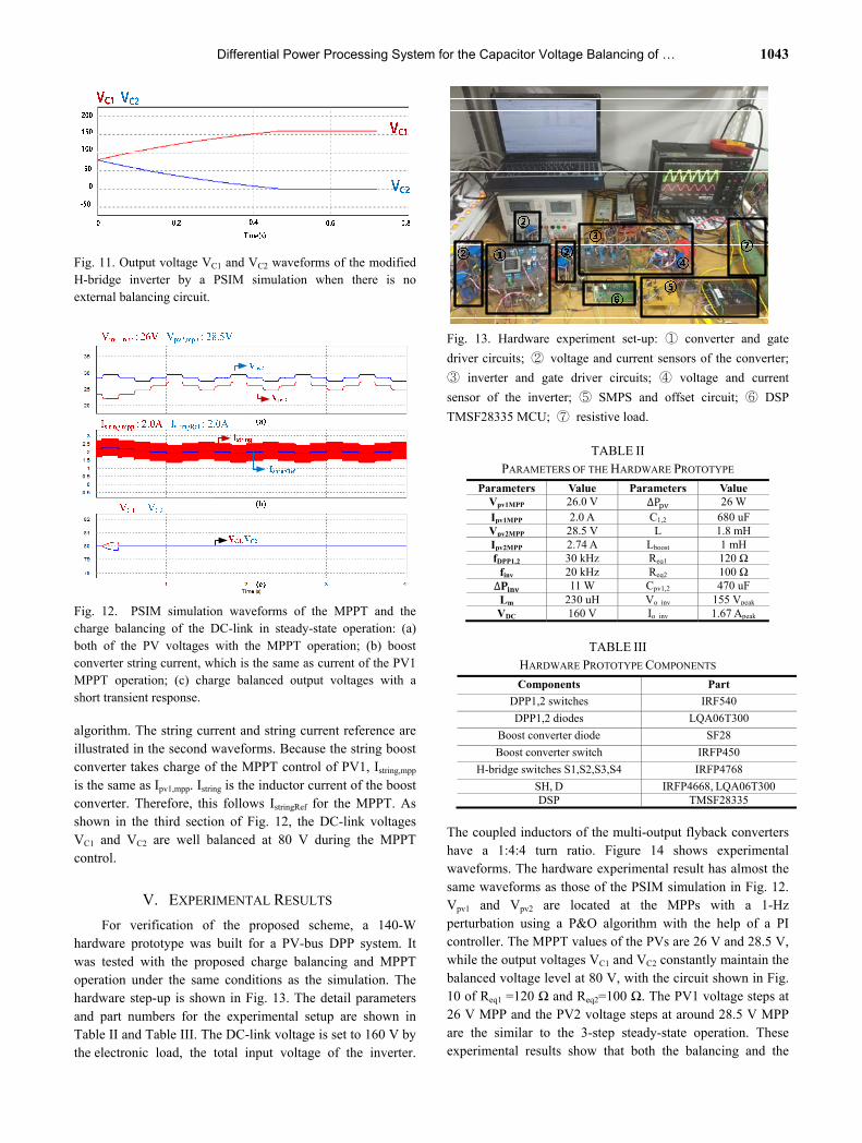
Fig. 11. Output voltage VC1 and VC2 waveforms of the modified H-bridge inverter by a PSIM simulation when there is no external balancing circuit.
Vpv1,mpp : 26V Vpv2,mpp : 28.5V
Istring,mpp : 2.0A IstringRef
Vc1 : 80V Vc2 : 80V
Fig. 12. PSIM simulation waveforms of the MPPT and the charge balancing of the DC-link in steady-state operation: (a) both of the PV voltages with the MPPT operation; (b) boost converter string current, which is the same as current of the PV1 MPPT operation; (c) charge balanced output voltages with a short transient response. algorithm. The string current and string current reference are illustrated in the second waveforms. Because the string boost converter takes charge of the MPPT control of PV1, Istring,mpp is the same as Ipv1,mpp. Istring is the inductor current of the boost converter. Therefore, this follows IstringRef for the MPPT. As shown in the third section of Fig. 12, the DC-link voltages VC1 and VC2 are well balanced at 80 V during the MPPT control.
V. EXPERIMENTAL RESULTS
For verification of the proposed scheme, a 140-W hardware prototype was built for a PV-bus DPP system. It was tested with the proposed charge balancing and MPPT operation under the same conditions as the simulation. The hardware step-up is shown in Fig. 13. The detail parameters and part numbers for the experimental setup are shown in Table II and Table III. The DC-link voltage is set to 160 V by the electronic load, the total input voltage of the inverter.
Fig. 13. Hardware experiment set-up: ① converter and gate
driver circuits; ② voltage and current sensors of the converter;
③ inverter and gate driver circuits; ④ voltage and current
sensor of the inverter; ⑤ SMPS and offset circuit; ⑥ DSP
TMSF28335 MCU; ⑦ resistive load.
TABLE II
PARAMETERS OF THE HARDWARE PROTOTYPE
Parameters Value Parameters Value Vpv1MPP 26.0 V ∆P 26 W Ipv1MPP 2.0 A C1,2 680 uF Vpv2MPP 28.5 V L 1.8 mH Ipv2MPP 2.74 A Lboost 1 mH fDPP1,2 30 kHz Req1 120 Ω
finv 20 kHz Req2 100 Ω ∆ 11 W Cpv1,2 470 uF
Lm 230 uH Vo_inv 155 Vpeak VDC 160 V Io_inv 1.67 Apeak
TABLE III
HARDWARE PROTOTYPE COMPONENTS
Components Part
DPP1,2 switches IRF540
DPP1,2 diodes LQA06T300
Boost converter diode SF28
Boost converter switch IRFP450
H-bridge switches S1,S2,S3,S4 IRFP4768
SH, D IRFP4668, LQA06T300 DSP TMSF28335
The coupled inductors of the multi-output flyback converters have a 1:4:4 turn ratio. Figure 14 shows experimental waveforms. The hardware experimental result has almost the same waveforms as those of the PSIM simulation in Fig. 12. Vpv1 and Vpv2 are located at the MPPs with a 1-Hz perturbation using a P&O algorithm with the help of a PI controller. The MPPT values of the PVs are 26 V and 28.5 V, while the output voltages VC1 and VC2 constantly maintain the balanced voltage level at 80 V, with the circuit shown in Fig. 10 of Req1 =120 Ω and Req2=100 Ω. The PV1 voltage steps at 26 V MPP and the PV2 voltage steps at around 28.5 V MPP are the similar to the 3-step steady-state operation. These experimental results show that both the balancing and the
1044 Journal of Power Electronics, Vol. 17, No. 4, July 2017
(a) PV MPPT operation voltages Vpv1 and Vpv2 (Ch1 and Ch3, respectively) with balanced output voltages Vc1 and Vc2 (Ch4 and
Ch2, respectively).
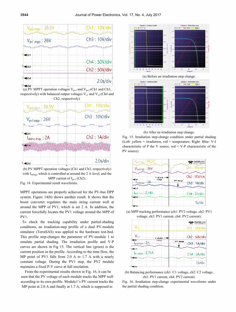
(b) PV MPPT operation voltages (Ch1 and Ch3, respectively) with Istring, which is controlled at around the 2 A level, and the
MPP current of Ipv1 (Ch2). Fig. 14. Experimental result waveforms. MPPT operations are properly achieved for the PV-bus DPP system. Figure 14(b) shows another result. It shows that the boost converter regulates the main string current well at around the MPP of PV1, which is set 2 A. In addition, the current forcefully locates the PV1 voltage around the MPP of PV1.
To check the tracking capability under partial-shading conditions, an irradiation-step profile of a dual PV-module simulator (TerraSAS) was applied to the hardware test-bed. This profile step-changes the parameter of PV-module 1 to emulate partial shading. The irradiation profile and V-P curves are shown in Fig 15. The vertical line (green) is the current position in the profile. According to the time flow, the MP point of PV1 falls from 2.0 A to 1.7 A with a nearly constant voltage. During the PV1 step, the PV2 module maintains a fixed P-V curve at full insolation.
From the experimental results shown in Fig. 16, it can be seen that the PV voltage of each module tracks the MPP well according to its own profile. Module1’s PV current tracks the MP point at 2.0 A and finally at 1.7 A, which is supposed to
(a) Before an irradiation step change.
(b) After an irradiation step change.
Fig. 15. Irradiation step-change condition under partial shading (Left: yellow = irradiation, red = temperature; Right: Blue: V-I characteristic of P the V source, red = V-P characteristic of the PV source).
(a) MPP tracking performance (ch1: PV2 voltage, ch2: PV1
voltage, ch3: PV1 current, ch4: PV2 current).
(b) Balancing performance (ch1: C1 voltage, ch2: C2 voltage,
ch3: PV1 current, ch4: PV2 current). Fig. 16. Irradiation step-change experimental waveforms under the partial shading condition.
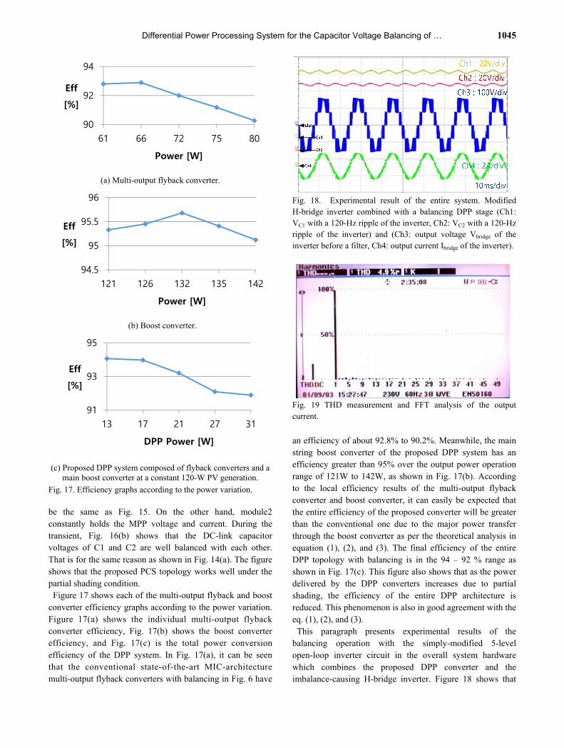
Differential Power Processing System for the Capacitor Voltage Balancing of … 1045
(a) Multi-output flyback converter.
(b) Boost converter.
(c) Proposed DPP system composed of flyback converters and a
main boost converter at a constant 120-W PV generation.
Fig. 17. Efficiency graphs according to the power variation. be the same as Fig. 15. On the other hand, module2 constantly holds the MPP voltage and current. During the transient, Fig. 16(b) shows that the DC-link capacitor voltages of C1 and C2 are well balanced with each other. That is for the same reason as shown in Fig. 14(a). The figure shows that the proposed PCS topology works well under the partial shading condition.
Figure 17 shows each of the multi-output flyback and boost converter efficiency graphs according to the power variation. Figure 17(a) shows the individual multi-output flyback converter efficiency, Fig. 17(b) shows the boost converter efficiency, and Fig. 17(c) is the total power conversion efficiency of the DPP system. In Fig. 17(a), it can be seen that the conventional state-of-the-art MIC-architecture multi-output flyback converters with balancing in Fig. 6 have
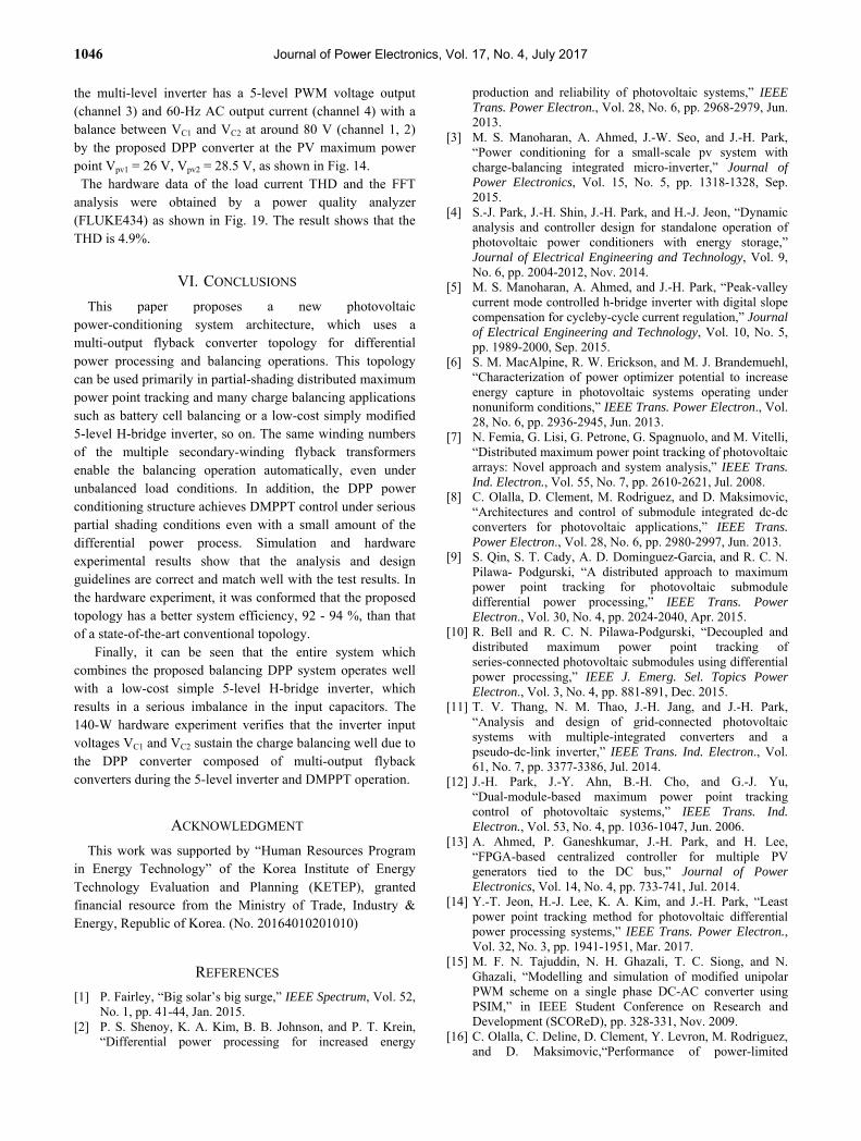
Fig. 18. Experimental result of the entire system. Modified H-bridge inverter combined with a balancing DPP stage (Ch1: VC1 with a 120-Hz ripple of the inverter, Ch2: VC2 with a 120-Hz ripple of the inverter) and (Ch3: output voltage Vbridge of the inverter before a filter, Ch4: output current Ibridge of the inverter).
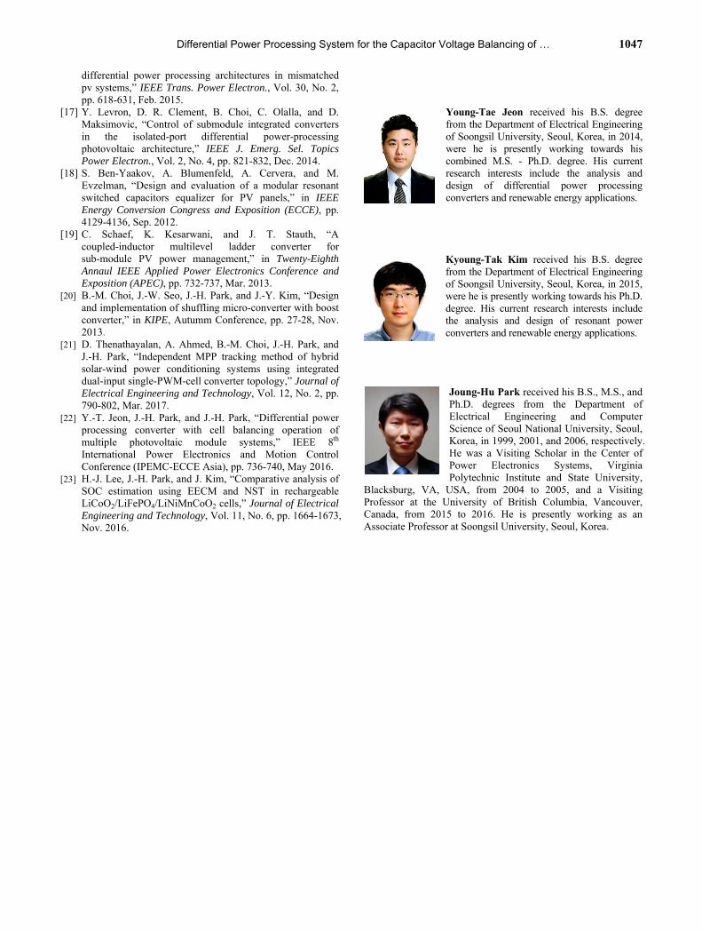
Fig. 19 THD measurement and FFT analysis of the output current.
an efficiency of about 92.8% to 90.2%. Meanwhile, the main string boost converter of the proposed DPP system has an efficiency greater than 95% over the output power operation range of 121W to 142W, as shown in Fig. 17(b). According to the local efficiency results of the multi-output flyback converter and boost converter, it can easily be expected that the entire efficiency of the proposed converter will be greater than the conventional one due to the major power transfer through the boost converter as per the theoretical analysis in equation (1), (2), and (3). The final efficiency of the entire DPP topology with balancing is in the 94 – 92 % range as shown in Fig. 17(c). This figure also shows that as the power delivered by the DPP converters increases due to partial shading, the efficiency of the entire DPP architecture is reduced. This phenomenon is also in good agreement with the eq. (1), (2), and (3). This paragraph presents experimental results of the
balancing operation with the simply-modified 5-level open-loop inverter circuit in the overall system hardware which combines the proposed DPP converter and the imbalance-causing H-bridge inverter. Figure 18 shows that
90
92
94
61 66 72 75 80
Eff
[%]
Power [W]
94.5
95
95.5
96
121 126 132 135 142
Eff
[%]
Power [W]
91
93
95
13 17 21 27 31
Eff
[%]
DPP Power [W]
1046 Journal of Power Electronics, Vol. 17, No. 4, July 2017
the multi-level inverter has a 5-level PWM voltage output (channel 3) and 60-Hz AC output current (channel 4) with a balance between VC1 and VC2 at around 80 V (channel 1, 2) by the proposed DPP converter at the PV maximum power point Vpv1 = 26 V, Vpv2 = 28.5 V, as shown in Fig. 14.
The hardware data of the load current THD and the FFT analysis were obtained by a power quality analyzer (FLUKE434) as shown in Fig. 19. The result shows that the THD is 4.9%.
VI. CONCLUSIONS
This paper proposes a new photovoltaic power-conditioning system architecture, which uses a multi-output flyback converter topology for differential power processing and balancing operations. This topology can be used primarily in partial-shading distributed maximum power point tracking and many charge balancing applications such as battery cell balancing or a low-cost simply modified 5-level H-bridge inverter, so on. The same winding numbers of the multiple secondary-winding flyback transformers enable the balancing operation automatically, even under unbalanced load conditions. In addition, the DPP power conditioning structure achieves DMPPT control under serious partial shading conditions even with a small amount of the differential power process. Simulation and hardware experimental results show that the analysis and design guidelines are correct and match well with the test results. In the hardware experiment, it was conformed that the proposed topology has a better system efficiency, 92 - 94 %, than that of a state-of-the-art conventional topology.
Finally, it can be seen that the entire system which combines the proposed balancing DPP system operates well with a low-cost simple 5-level H-bridge inverter, which results in a serious imbalance in the input capacitors. The 140-W hardware experiment verifies that the inverter input voltages VC1 and VC2 sustain the charge balancing well due to the DPP converter composed of multi-output flyback converters during the 5-level inverter and DMPPT operation.
ACKNOWLEDGMENT
This work was supported by “Human Resources Program in Energy Technology” of the Korea Institute of Energy Technology Evaluation and Planning (KETEP), granted financial resource from the Ministry of Trade, Industry & Energy, Republic of Korea. (No. 20164010201010)
REFERENCES
[1] P. Fairley, “Big solar’s big surge,” IEEE Spectrum, Vol. 52, No. 1, pp. 41-44, Jan. 2015.
[2] P. S. Shenoy, K. A. Kim, B. B. Johnson, and P. T. Krein, “Differential power processing for increased energy
production and reliability of photovoltaic systems,” IEEE Trans. Power Electron., Vol. 28, No. 6, pp. 2968-2979, Jun. 2013.
[3] M. S. Manoharan, A. Ahmed, J.-W. Seo, and J.-H. Park, “Power conditioning for a small-scale pv system with charge-balancing integrated micro-inverter,” Journal of Power Electronics, Vol. 15, No. 5, pp. 1318-1328, Sep. 2015.
[4] S.-J. Park, J.-H. Shin, J.-H. Park, and H.-J. Jeon, “Dynamic analysis and controller design for standalone operation of photovoltaic power conditioners with energy storage,” Journal of Electrical Engineering and Technology, Vol. 9, No. 6, pp. 2004-2012, Nov. 2014.
[5] M. S. Manoharan, A. Ahmed, and J.-H. Park, “Peak-valley current mode controlled h-bridge inverter with digital slope compensation for cycleby-cycle current regulation,” Journal of Electrical Engineering and Technology, Vol. 10, No. 5, pp. 1989-2000, Sep. 2015.
[6] S. M. MacAlpine, R. W. Erickson, and M. J. Brandemuehl, “Characterization of power optimizer potential to increase energy capture in photovoltaic systems operating under nonuniform conditions,” IEEE Trans. Power Electron., Vol. 28, No. 6, pp. 2936-2945, Jun. 2013.
[7] N. Femia, G. Lisi, G. Petrone, G. Spagnuolo, and M. Vitelli, “Distributed maximum power point tracking of photovoltaic arrays: Novel approach and system analysis,” IEEE Trans. Ind. Electron., Vol. 55, No. 7, pp. 2610-2621, Jul. 2008.
[8] C. Olalla, D. Clement, M. Rodriguez, and D. Maksimovic, “Architectures and control of submodule integrated dc-dc converters for photovoltaic applications,” IEEE Trans. Power Electron., Vol. 28, No. 6, pp. 2980-2997, Jun. 2013.
[9] S. Qin, S. T. Cady, A. D. Dominguez-Garcia, and R. C. N. Pilawa- Podgurski, “A distributed approach to maximum power point tracking for photovoltaic submodule differential power processing,” IEEE Trans. Power Electron., Vol. 30, No. 4, pp. 2024-2040, Apr. 2015.
[10] R. Bell and R. C. N. Pilawa-Podgurski, “Decoupled and distributed maximum power point tracking of series-connected photovoltaic submodules using differential power processing,” IEEE J. Emerg. Sel. Topics Power Electron., Vol. 3, No. 4, pp. 881-891, Dec. 2015.
[11] T. V. Thang, N. M. Thao, J.-H. Jang, and J.-H. Park, “Analysis and design of grid-connected photovoltaic systems with multiple-integrated converters and a pseudo-dc-link inverter,” IEEE Trans. Ind. Electron., Vol. 61, No. 7, pp. 3377-3386, Jul. 2014.
[12] J.-H. Park, J.-Y. Ahn, B.-H. Cho, and G.-J. Yu, “Dual-module-based maximum power point tracking control of photovoltaic systems,” IEEE Trans. Ind. Electron., Vol. 53, No. 4, pp. 1036-1047, Jun. 2006.
[13] A. Ahmed, P. Ganeshkumar, J.-H. Park, and H. Lee, “FPGA-based centralized controller for multiple PV generators tied to the DC bus,” Journal of Power Electronics, Vol. 14, No. 4, pp. 733-741, Jul. 2014.
[14] Y.-T. Jeon, H.-J. Lee, K. A. Kim, and J.-H. Park, “Least power point tracking method for photovoltaic differential power processing systems,” IEEE Trans. Power Electron., Vol. 32, No. 3, pp. 1941-1951, Mar. 2017.
[15] M. F. N. Tajuddin, N. H. Ghazali, T. C. Siong, and N. Ghazali, “Modelling and simulation of modified unipolar PWM scheme on a single phase DC-AC converter using PSIM,” in IEEE Student Conference on Research and Development (SCOReD), pp. 328-331, Nov. 2009.
[16] C. Olalla, C. Deline, D. Clement, Y. Levron, M. Rodriguez, and D. Maksimovic,“Performance of power-limited
Differential Power Processing System for the Capacitor Voltage Balancing of … 1047
differential power processing architectures in mismatched pv systems,” IEEE Trans. Power Electron., Vol. 30, No. 2, pp. 618-631, Feb. 2015.
[17] Y. Levron, D. R. Clement, B. Choi, C. Olalla, and D. Maksimovic, “Control of submodule integrated converters in the isolated-port differential power-processing photovoltaic architecture,” IEEE J. Emerg. Sel. Topics Power Electron., Vol. 2, No. 4, pp. 821-832, Dec. 2014.
[18] S. Ben-Yaakov, A. Blumenfeld, A. Cervera, and M. Evzelman, “Design and evaluation of a modular resonant switched capacitors equalizer for PV panels,” in IEEE Energy Conversion Congress and Exposition (ECCE), pp. 4129-4136, Sep. 2012.
[19] C. Schaef, K. Kesarwani, and J. T. Stauth, “A coupled-inductor multilevel ladder converter for sub-module PV power management,” in Twenty-Eighth Annaul IEEE Applied Power Electronics Conference and Exposition (APEC), pp. 732-737, Mar. 2013.
[20] B.-M. Choi, J.-W. Seo, J.-H. Park, and J.-Y. Kim, “Design and implementation of shuffling micro-converter with boost converter,” in KIPE, Autumm Conference, pp. 27-28, Nov. 2013.
[21] D. Thenathayalan, A. Ahmed, B.-M. Choi, J.-H. Park, and J.-H. Park, “Independent MPP tracking method of hybrid solar-wind power conditioning systems using integrated dual-input single-PWM-cell converter topology,” Journal of Electrical Engineering and Technology, Vol. 12, No. 2, pp. 790-802, Mar. 2017.
[22] Y.-T. Jeon, J.-H. Park, and J.-H. Park, “Differential power processing converter with cell balancing operation of multiple photovoltaic module systems,” IEEE 8th International Power Electronics and Motion Control Conference (IPEMC-ECCE Asia), pp. 736-740, May 2016.
[23] H.-J. Lee, J.-H. Park, and J. Kim, “Comparative analysis of SOC estimation using EECM and NST in rechargeable LiCoO2/LiFePO4/LiNiMnCoO2 cells,” Journal of Electrical Engineering and Technology, Vol. 11, No. 6, pp. 1664-1673, Nov. 2016.
Young-Tae Jeon received his B.S. degree from the Department of Electrical Engineering of Soongsil University, Seoul, Korea, in 2014, were he is presently working towards his combined M.S. - Ph.D. degree. His current research interests include the analysis and design of differential power processing converters and renewable energy applications.
Kyoung-Tak Kim received his B.S. degree from the Department of Electrical Engineering of Soongsil University, Seoul, Korea, in 2015, were he is presently working towards his Ph.D. degree. His current research interests include the analysis and design of resonant power converters and renewable energy applications.
Joung-Hu Park received his B.S., M.S., and Ph.D. degrees from the Department of Electrical Engineering and Computer Science of Seoul National University, Seoul, Korea, in 1999, 2001, and 2006, respectively. He was a Visiting Scholar in the Center of Power Electronics Systems, Virginia Polytechnic Institute and State University,
Blacksburg, VA, USA, from 2004 to 2005, and a Visiting Professor at the University of British Columbia, Vancouver, Canada, from 2015 to 2016. He is presently working as an Associate Professor at Soongsil University, Seoul, Korea.