Switched-Capacitor-Based High Boost DC-DC Converter - MDPI
15
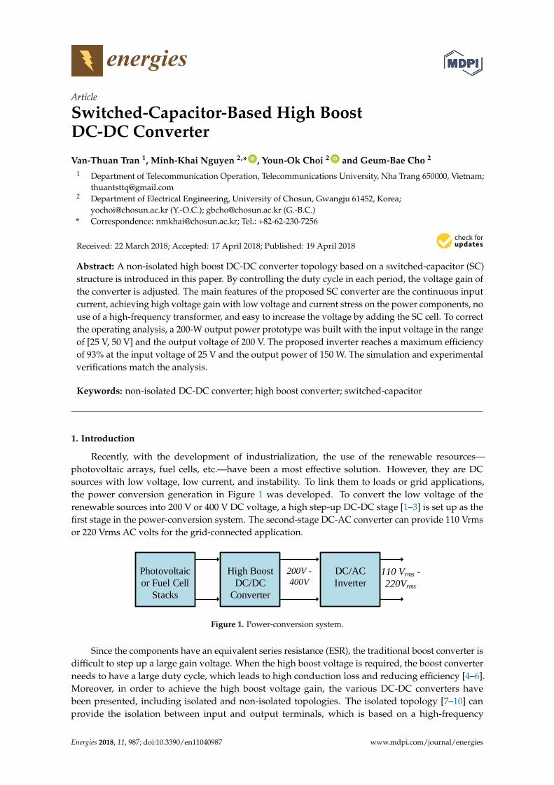
energies Article Switched-Capacitor-Based High Boost DC-DC Converter Van-Thuan Tran 1 , Minh-Khai Nguyen 2, * ID , Youn-Ok Choi 2 ID and Geum-Bae Cho 2 1 Department of Telecommunication Operation, Telecommunications University, Nha Trang 650000, Vietnam; [email protected] 2 Department of Electrical Engineering, University of Chosun, Gwangju 61452, Korea; [email protected] (Y.-O.C.); [email protected] (G.-B.C.) * Correspondence: [email protected]; Tel.: +82-62-230-7256 Received: 22 March 2018; Accepted: 17 April 2018; Published: 19 April 2018 Abstract: A non-isolated high boost DC-DC converter topology based on a switched-capacitor (SC) structure is introduced in this paper. By controlling the duty cycle in each period, the voltage gain of the converter is adjusted. The main features of the proposed SC converter are the continuous input current, achieving high voltage gain with low voltage and current stress on the power components, no use of a high-frequency transformer, and easy to increase the voltage by adding the SC cell. To correct the operating analysis, a 200-W output power prototype was built with the input voltage in the range of [25 V, 50 V] and the output voltage of 200 V. The proposed inverter reaches a maximum efficiency of 93% at the input voltage of 25 V and the output power of 150 W. The simulation and experimental verifications match the analysis. Keywords: non-isolated DC-DC converter; high boost converter; switched-capacitor 1. Introduction Recently, with the development of industrialization, the use of the renewable resources— photovoltaic arrays, fuel cells, etc.—have been a most effective solution. However, they are DC sources with low voltage, low current, and instability. To link them to loads or grid applications, the power conversion generation in Figure 1 was developed. To convert the low voltage of the renewable sources into 200 V or 400 V DC voltage, a high step-up DC-DC stage [1–3] is set up as the first stage in the power-conversion system. The second-stage DC-AC converter can provide 110 Vrms or 220 Vrms AC volts for the grid-connected application. High Boost DC/DC Converter 200V - 400V DC/AC Inverter 110 V rms - 220V rms Photovoltaic or Fuel Cell Stacks Figure 1. Power-conversion system. Since the components have an equivalent series resistance (ESR), the traditional boost converter is difficult to step up a large gain voltage. When the high boost voltage is required, the boost converter needs to have a large duty cycle, which leads to high conduction loss and reducing efficiency [4–6]. Moreover, in order to achieve the high boost voltage gain, the various DC-DC converters have been presented, including isolated and non-isolated topologies. The isolated topology [7–10] can provide the isolation between input and output terminals, which is based on a high-frequency Energies 2018, 11, 987; doi:10.3390/en11040987 www.mdpi.com/journal/energies
-
Upload
khangminh22 -
Category
Documents
-
view
1 -
download
0
Transcript of Switched-Capacitor-Based High Boost DC-DC Converter - MDPI
energies
Article
Switched-Capacitor-Based High BoostDC-DC Converter
Van-Thuan Tran 1, Minh-Khai Nguyen 2,* ID , Youn-Ok Choi 2 ID and Geum-Bae Cho 2
1 Department of Telecommunication Operation, Telecommunications University, Nha Trang 650000, Vietnam;[email protected]
2 Department of Electrical Engineering, University of Chosun, Gwangju 61452, Korea;[email protected] (Y.-O.C.); [email protected] (G.-B.C.)
* Correspondence: [email protected]; Tel.: +82-62-230-7256
Received: 22 March 2018; Accepted: 17 April 2018; Published: 19 April 2018
Abstract: A non-isolated high boost DC-DC converter topology based on a switched-capacitor (SC)structure is introduced in this paper. By controlling the duty cycle in each period, the voltage gain ofthe converter is adjusted. The main features of the proposed SC converter are the continuous inputcurrent, achieving high voltage gain with low voltage and current stress on the power components, nouse of a high-frequency transformer, and easy to increase the voltage by adding the SC cell. To correctthe operating analysis, a 200-W output power prototype was built with the input voltage in the rangeof [25 V, 50 V] and the output voltage of 200 V. The proposed inverter reaches a maximum efficiencyof 93% at the input voltage of 25 V and the output power of 150 W. The simulation and experimentalverifications match the analysis.
Keywords: non-isolated DC-DC converter; high boost converter; switched-capacitor
1. Introduction
Recently, with the development of industrialization, the use of the renewable resources—photovoltaic arrays, fuel cells, etc.—have been a most effective solution. However, they are DCsources with low voltage, low current, and instability. To link them to loads or grid applications,the power conversion generation in Figure 1 was developed. To convert the low voltage of therenewable sources into 200 V or 400 V DC voltage, a high step-up DC-DC stage [1–3] is set up as thefirst stage in the power-conversion system. The second-stage DC-AC converter can provide 110 Vrmsor 220 Vrms AC volts for the grid-connected application.
Energies 2018, 11, x; doi: FOR PEER REVIEW www.mdpi.com/journal/energies
Review
Switched-Capacitor-Based High Boost DC-DC
Converter
Van-Thuan Tran 1, Minh-Khai Nguyen 2,*, Youn-Ok Choi 2 and Geum-Bae Cho 2
1 Department of Telecommunication Operation, Telecommunications University, Nha Trang 650000, Viet
Nam; [email protected] 2 Department of Electrical Engineering, University of Chosun, Gwangju 61452, Korea; [email protected]
(Y.-O.C.); [email protected] (G.-B.C.)
* Correspondence: [email protected]; Tel.: +82-62-230-7256
Received: 22 March 2018; Accepted: 17 April 2018; Published: date
Abstract: A non-isolated high boost DC-DC converter topology based on a switched-capacitor (SC)
structure is introduced in this paper. By controlling the duty cycle in each period, the voltage gain
of the converter is adjusted. The main features of the proposed SC converter are the continuous
input current, achieving high voltage gain with low voltage and current stress on the power
components, no use of a high-frequency transformer, and easy to increase the voltage by adding the
SC cell. To correct the operating analysis, a 200-W output power prototype was built with the input
voltage in the range of [25 V, 50 V] and the output voltage of 200 V. The proposed inverter reaches
a maximum efficiency of 93% at the input voltage of 25 V and the output power of 150 W. The
simulation and experimental verifications match the analysis.
Keywords: non-isolated DC-DC converter; high boost converter; switched-capacitor
1. Introduction
Recently, with the development of industrialization, the use of the renewable resources—
photovoltaic arrays, fuel cells, etc.—have been a most effective solution. However, they are DC
sources with low voltage, low current, and instability. To link them to loads or grid applications, the
power conversion generation in Figure 1 was developed. To convert the low voltage of the renewable
sources into 200 V or 400 V DC voltage, a high step-up DC-DC stage [1–3] is set up as the first stage
in the power-conversion system. The second-stage DC-AC converter can provide 110 Vrms or 220
Vrms AC volts for the grid-connected application.
High Boost
DC/DC
Converter
200V -
400V
DC/AC
Inverter110 Vrms -
220Vrms
Photovoltaic
or Fuel Cell
Stacks
Figure 1. Power-conversion system.
Since the components have an equivalent series resistance (ESR), the traditional boost converter
is difficult to step up a large gain voltage. When the high boost voltage is required, the boost converter
needs to have a large duty cycle, which leads to high conduction loss and reducing efficiency [4–6].
Moreover, in order to achieve the high boost voltage gain, the various DC-DC converters have been
presented, including isolated and non-isolated topologies. The isolated topology [7–10] can provide
the isolation between input and output terminals, which is based on a high-frequency transformer.
Figure 1. Power-conversion system.
Since the components have an equivalent series resistance (ESR), the traditional boost converter isdifficult to step up a large gain voltage. When the high boost voltage is required, the boost converterneeds to have a large duty cycle, which leads to high conduction loss and reducing efficiency [4–6].Moreover, in order to achieve the high boost voltage gain, the various DC-DC converters havebeen presented, including isolated and non-isolated topologies. The isolated topology [7–10] canprovide the isolation between input and output terminals, which is based on a high-frequency
Energies 2018, 11, 987; doi:10.3390/en11040987 www.mdpi.com/journal/energies
Energies 2018, 11, 987 2 of 15
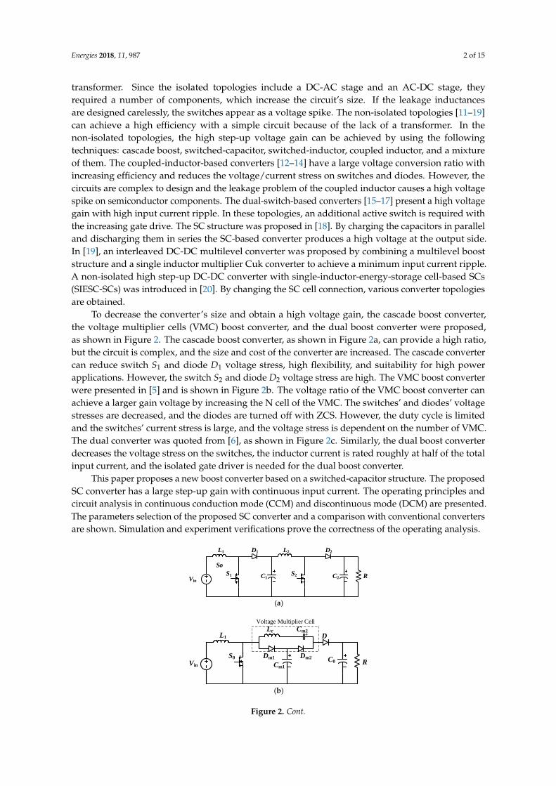
transformer. Since the isolated topologies include a DC-AC stage and an AC-DC stage, theyrequired a number of components, which increase the circuit’s size. If the leakage inductancesare designed carelessly, the switches appear as a voltage spike. The non-isolated topologies [11–19]can achieve a high efficiency with a simple circuit because of the lack of a transformer. In thenon-isolated topologies, the high step-up voltage gain can be achieved by using the followingtechniques: cascade boost, switched-capacitor, switched-inductor, coupled inductor, and a mixtureof them. The coupled-inductor-based converters [12–14] have a large voltage conversion ratio withincreasing efficiency and reduces the voltage/current stress on switches and diodes. However, thecircuits are complex to design and the leakage problem of the coupled inductor causes a high voltagespike on semiconductor components. The dual-switch-based converters [15–17] present a high voltagegain with high input current ripple. In these topologies, an additional active switch is required withthe increasing gate drive. The SC structure was proposed in [18]. By charging the capacitors in paralleland discharging them in series the SC-based converter produces a high voltage at the output side.In [19], an interleaved DC-DC multilevel converter was proposed by combining a multilevel booststructure and a single inductor multiplier Cuk converter to achieve a minimum input current ripple.A non-isolated high step-up DC-DC converter with single-inductor-energy-storage cell-based SCs(SIESC-SCs) was introduced in [20]. By changing the SC cell connection, various converter topologiesare obtained.
To decrease the converter’s size and obtain a high voltage gain, the cascade boost converter,the voltage multiplier cells (VMC) boost converter, and the dual boost converter were proposed,as shown in Figure 2. The cascade boost converter, as shown in Figure 2a, can provide a high ratio,but the circuit is complex, and the size and cost of the converter are increased. The cascade convertercan reduce switch S1 and diode D1 voltage stress, high flexibility, and suitability for high powerapplications. However, the switch S2 and diode D2 voltage stress are high. The VMC boost converterwere presented in [5] and is shown in Figure 2b. The voltage ratio of the VMC boost converter canachieve a larger gain voltage by increasing the N cell of the VMC. The switches’ and diodes’ voltagestresses are decreased, and the diodes are turned off with ZCS. However, the duty cycle is limitedand the switches’ current stress is large, and the voltage stress is dependent on the number of VMC.The dual converter was quoted from [6], as shown in Figure 2c. Similarly, the dual boost converterdecreases the voltage stress on the switches, the inductor current is rated roughly at half of the totalinput current, and the isolated gate driver is needed for the dual boost converter.
This paper proposes a new boost converter based on a switched-capacitor structure. The proposedSC converter has a large step-up gain with continuous input current. The operating principles andcircuit analysis in continuous conduction mode (CCM) and discontinuous mode (DCM) are presented.The parameters selection of the proposed SC converter and a comparison with conventional convertersare shown. Simulation and experiment verifications prove the correctness of the operating analysis.
Energies 2018, 11, x FOR PEER REVIEW 2 of 15
Since the isolated topologies include a DC-AC stage and an AC-DC stage, they required a number of
components, which increase the circuit’s size. If the leakage inductances are designed carelessly, the
switches appear as a voltage spike. The non-isolated topologies [11–19] can achieve a high efficiency
with a simple circuit because of the lack of a transformer. In the non-isolated topologies, the high
step-up voltage gain can be achieved by using the following techniques: cascade boost, switched-
capacitor, switched-inductor, coupled inductor, and a mixture of them. The coupled-inductor-based
converters [12–14] have a large voltage conversion ratio with increasing efficiency and reduces the
voltage/current stress on switches and diodes. However, the circuits are complex to design and the
leakage problem of the coupled inductor causes a high voltage spike on semiconductor components.
The dual-switch-based converters [15–17] present a high voltage gain with high input current ripple.
In these topologies, an additional active switch is required with the increasing gate drive. The SC
structure was proposed in [18]. By charging the capacitors in parallel and discharging them in series
the SC-based converter produces a high voltage at the output side. In [19], an interleaved DC-DC
multilevel converter was proposed by combining a multilevel boost structure and a single inductor
multiplier Cuk converter to achieve a minimum input current ripple. A non-isolated high step-up
DC-DC converter with single-inductor-energy-storage cell-based SCs (SIESC-SCs) was introduced in
[20]. By changing the SC cell connection, various converter topologies are obtained.
To decrease the converter’s size and obtain a high voltage gain, the cascade boost converter, the
voltage multiplier cells (VMC) boost converter, and the dual boost converter were proposed, as
shown in Figure 2. The cascade boost converter, as shown in Figure 2a, can provide a high ratio, but
the circuit is complex, and the size and cost of the converter are increased. The cascade converter can
reduce switch S1 and diode D1 voltage stress, high flexibility, and suitability for high power
applications. However, the switch S2 and diode D2 voltage stress are high. The VMC boost converter
were presented in [5] and is shown in Figure 2b. The voltage ratio of the VMC boost converter can
achieve a larger gain voltage by increasing the N cell of the VMC. The switches’ and diodes’ voltage
stresses are decreased, and the diodes are turned off with ZCS. However, the duty cycle is limited
and the switches’ current stress is large, and the voltage stress is dependent on the number of VMC.
The dual converter was quoted from [6], as shown in Figure 2c. Similarly, the dual boost converter
decreases the voltage stress on the switches, the inductor current is rated roughly at half of the total
input current, and the isolated gate driver is needed for the dual boost converter.
This paper proposes a new boost converter based on a switched-capacitor structure. The
proposed SC converter has a large step-up gain with continuous input current. The operating
principles and circuit analysis in continuous conduction mode (CCM) and discontinuous mode
(DCM) are presented. The parameters selection of the proposed SC converter and a comparison with
conventional converters are shown. Simulation and experiment verifications prove the correctness of
the operating analysis.
Vin
So
C1 C2
D2D1L1 L2
S1 S2 R
(a)
Vin
L1
S0
Lr
Dm1 Dm2
Cm2
D
C0 RCm1
Voltage Multiplier Cell
(b)
Figure 2. Cont.
Energies 2018, 11, 987 3 of 15Energies 2018, 11, x FOR PEER REVIEW 3 of 15
L1
L2
S1
S2
D1
D2
C1
C2
RVin
(c)
Figure 2. Conventional boost converter topologies. (a) The cascade boost topology, (b) the boost
topology with voltage multiplier cells (VMC), and (c) dual boost converter.
2. Proposed SC Converter Topology
2.1. Proposed Topology
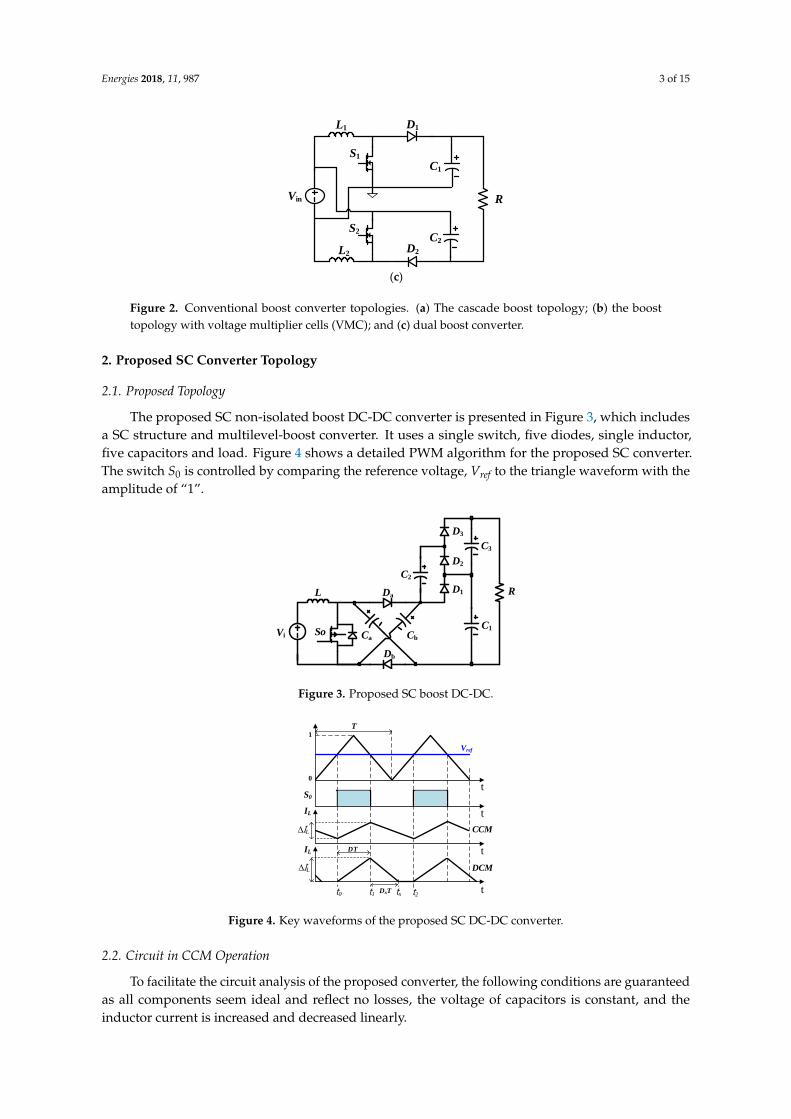
The proposed SC non-isolated boost DC-DC converter is presented in Figure 3, which includes
a SC structure and multilevel-boost converter. It uses a single switch, five diodes, single inductor,
five capacitors and load. Figure 4 shows a detailed PWM algorithm for the proposed SC converter.
The switch S0 is controlled by comparing the reference voltage, Vref to the triangle waveform with the
amplitude of “1”.
Vi CbCa
Da
Db
So
L
C2
D1
D2
D3
C1
C3
R
Figure 3. Proposed SC boost DC-DC.
t
t
S0
Vref
1
0
T
DT t
t
∆IL
IL
CCM
∆IL
IL
DCM
DxTt0 t1 t2tx
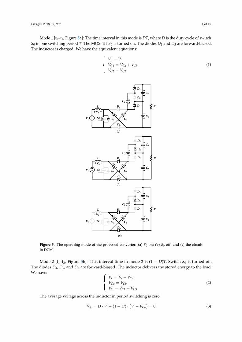
Figure 4. Key waveforms of the proposed SC DC-DC converter.
2.2. Circuit in CCM Operation
To facilitate the circuit analysis of the proposed converter, the following conditions are
guaranteed as all components seem ideal and reflect no losses, the voltage of capacitors is constant,
and the inductor current is increased and decreased linearly.
Figure 2. Conventional boost converter topologies. (a) The cascade boost topology; (b) the boosttopology with voltage multiplier cells (VMC); and (c) dual boost converter.
2. Proposed SC Converter Topology
2.1. Proposed Topology
The proposed SC non-isolated boost DC-DC converter is presented in Figure 3, which includesa SC structure and multilevel-boost converter. It uses a single switch, five diodes, single inductor,five capacitors and load. Figure 4 shows a detailed PWM algorithm for the proposed SC converter.The switch S0 is controlled by comparing the reference voltage, Vref to the triangle waveform with theamplitude of “1”.
Energies 2018, 11, x FOR PEER REVIEW 3 of 15
L1
L2
S1
S2
D1
D2
C1
C2
RVin
(c)
Figure 2. Conventional boost converter topologies. (a) The cascade boost topology, (b) the boost
topology with voltage multiplier cells (VMC), and (c) dual boost converter.
2. Proposed SC Converter Topology
2.1. Proposed Topology
The proposed SC non-isolated boost DC-DC converter is presented in Figure 3, which includes
a SC structure and multilevel-boost converter. It uses a single switch, five diodes, single inductor,
five capacitors and load. Figure 4 shows a detailed PWM algorithm for the proposed SC converter.
The switch S0 is controlled by comparing the reference voltage, Vref to the triangle waveform with the
amplitude of “1”.
Vi CbCa
Da
Db
So
L
C2
D1
D2
D3
C1
C3
R
Figure 3. Proposed SC boost DC-DC.
t
t
S0
Vref
1
0
T
DT t
t
∆IL
IL
CCM
∆IL
IL
DCM
DxTt0 t1 t2tx
Figure 4. Key waveforms of the proposed SC DC-DC converter.
2.2. Circuit in CCM Operation
To facilitate the circuit analysis of the proposed converter, the following conditions are
guaranteed as all components seem ideal and reflect no losses, the voltage of capacitors is constant,
and the inductor current is increased and decreased linearly.
Figure 3. Proposed SC boost DC-DC.
Energies 2018, 11, x FOR PEER REVIEW 3 of 15
L1
L2
S1
S2
D1
D2
C1
C2
RVin
(c)
Figure 2. Conventional boost converter topologies. (a) The cascade boost topology, (b) the boost
topology with voltage multiplier cells (VMC), and (c) dual boost converter.
2. Proposed SC Converter Topology
2.1. Proposed Topology
The proposed SC non-isolated boost DC-DC converter is presented in Figure 3, which includes
a SC structure and multilevel-boost converter. It uses a single switch, five diodes, single inductor,
five capacitors and load. Figure 4 shows a detailed PWM algorithm for the proposed SC converter.
The switch S0 is controlled by comparing the reference voltage, Vref to the triangle waveform with the
amplitude of “1”.
Vi CbCa
Da
Db
So
L
C2
D1
D2
D3
C1
C3
R
Figure 3. Proposed SC boost DC-DC.
t
t
S0
Vref
1
0
T
DT t
t
∆IL
IL
CCM
∆IL
IL
DCM
DxTt0 t1 t2tx
Figure 4. Key waveforms of the proposed SC DC-DC converter.
2.2. Circuit in CCM Operation
To facilitate the circuit analysis of the proposed converter, the following conditions are
guaranteed as all components seem ideal and reflect no losses, the voltage of capacitors is constant,
and the inductor current is increased and decreased linearly.
Figure 4. Key waveforms of the proposed SC DC-DC converter.
2.2. Circuit in CCM Operation
To facilitate the circuit analysis of the proposed converter, the following conditions are guaranteedas all components seem ideal and reflect no losses, the voltage of capacitors is constant, and theinductor current is increased and decreased linearly.
Energies 2018, 11, 987 4 of 15
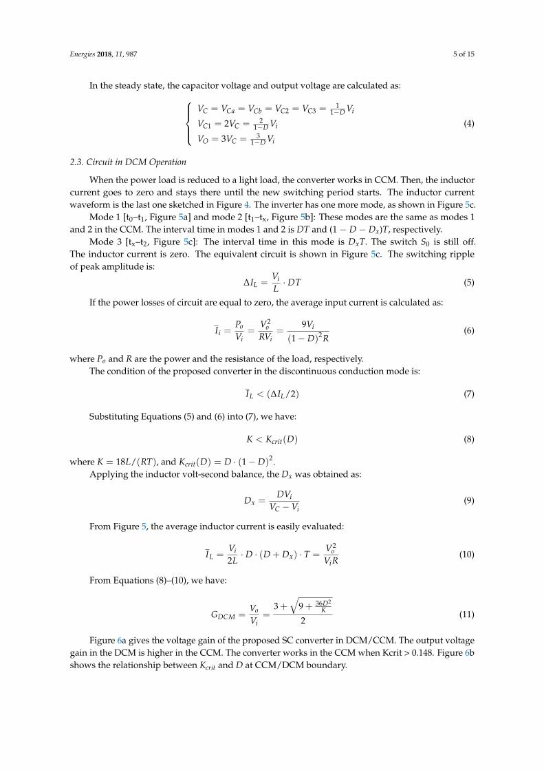
Mode 1 [t0–t1, Figure 5a]: The time interval in this mode is DT, where D is the duty cycle of switchS0 in one switching period T. The MOSFET S0 is turned on. The diodes D1 and D3 are forward-biased.The inductor is charged. We have the equivalent equations:
VL = ViVC1 = VCa + VCbVC2 = VC3
(1)
Energies 2018, 11, x FOR PEER REVIEW 4 of 15
Mode 1 [t0–t1, Figure 5a]: The time interval in this mode is DT, where D is the duty cycle of switch
S0 in one switching period T. The MOSFET S0 is turned on. The diodes D1 and D3 are forward-biased.
The inductor is charged. We have the equivalent equations:
1
2 3
L i
C Ca Cb
C C
V V
V V V
V V
(1)
Vi CbCa
Da
Db
So
L
C2
D1
D2
D3
C1
C3
R
Vi CbCa
Da
Db
So
L
C2
D1
D2
D3
C1
C3
R
Vi CbCa
Da
Db
So
L
C2
D1
D2
D3
C1
C3
R
VL
VL
VL
(a)
(b)
(c)
Figure 5. The operating mode of the proposed converter: (a) S0 on, (b) S0 off, and (c) the circuit in
DCM.
Mode 2 [t1–t2, Figure 5b]: This interval time in mode 2 is (1 − D)T. Switch S0 is turned off. The
diodes Da, Db, and D2 are forward-biased. The inductor delivers the stored energy to the load. We
have:
1 3
L i Ca
Ca Cb
O C C
V V V
V V
V V V
(2)
The average voltage across the inductor in period switching is zero:
(1 ) ( ) 0L i i CaV D V D V V (3)
In the steady state, the capacitor voltage and output voltage are calculated as:
Figure 5. The operating mode of the proposed converter: (a) S0 on; (b) S0 off; and (c) the circuitin DCM.
Mode 2 [t1–t2, Figure 5b]: This interval time in mode 2 is (1 − D)T. Switch S0 is turned off.The diodes Da, Db, and D2 are forward-biased. The inductor delivers the stored energy to the load.We have:
VL = Vi − VCaVCa = VCbVO = VC1 + VC3
(2)
The average voltage across the inductor in period switching is zero:
VL = D · Vi + (1 − D) · (Vi − VCa) = 0 (3)
Energies 2018, 11, 987 5 of 15
In the steady state, the capacitor voltage and output voltage are calculated as:VC = VCa = VCb = VC2 = VC3 = 1
1−D Vi
VC1 = 2VC = 21−D Vi
VO = 3VC = 31−D Vi
(4)
2.3. Circuit in DCM Operation
When the power load is reduced to a light load, the converter works in CCM. Then, the inductorcurrent goes to zero and stays there until the new switching period starts. The inductor currentwaveform is the last one sketched in Figure 4. The inverter has one more mode, as shown in Figure 5c.
Mode 1 [t0–t1, Figure 5a] and mode 2 [t1–tx, Figure 5b]: These modes are the same as modes 1and 2 in the CCM. The interval time in modes 1 and 2 is DT and (1 − D − Dx)T, respectively.
Mode 3 [tx–t2, Figure 5c]: The interval time in this mode is DxT. The switch S0 is still off.The inductor current is zero. The equivalent circuit is shown in Figure 5c. The switching rippleof peak amplitude is:
∆IL =ViL· DT (5)
If the power losses of circuit are equal to zero, the average input current is calculated as:
Ii =Po
Vi=
V2o
RVi=
9Vi
(1 − D)2R(6)
where Po and R are the power and the resistance of the load, respectively.The condition of the proposed converter in the discontinuous conduction mode is:
IL < (∆IL/2) (7)
Substituting Equations (5) and (6) into (7), we have:
K < Kcrit(D) (8)
where K = 18L/(RT), and Kcrit(D) = D · (1 − D)2.Applying the inductor volt-second balance, the Dx was obtained as:
Dx =DVi
VC − Vi(9)
From Figure 5, the average inductor current is easily evaluated:
IL =Vi2L
· D · (D + Dx) · T =V2
oViR
(10)
From Equations (8)–(10), we have:
GDCM =Vo
Vi=
3 +√
9 + 36D2
K
2(11)
Figure 6a gives the voltage gain of the proposed SC converter in DCM/CCM. The output voltagegain in the DCM is higher in the CCM. The converter works in the CCM when Kcrit > 0.148. Figure 6bshows the relationship between Kcrit and D at CCM/DCM boundary.
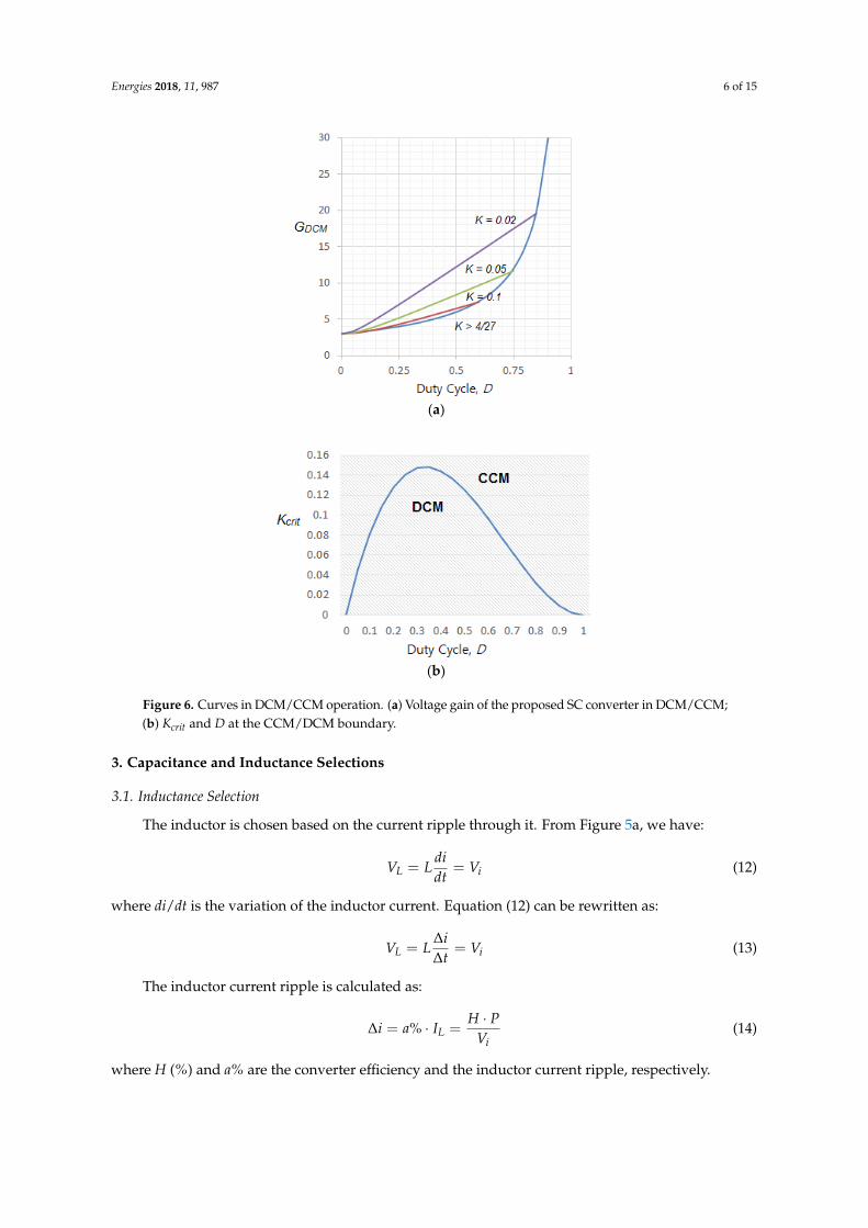
Energies 2018, 11, 987 6 of 15Energies 2018, 11, x FOR PEER REVIEW 6 of 15
(a)
(b)
Figure 6. Curves in DCM/CCM operation. (a) Voltage gain of the proposed SC converter in
DCM/CCM. (b) Kcrit and D at the CCM/DCM boundary.
3. Capacitance and Inductance Selections
3.1. Inductance Selection
The inductor is chosen based on the current ripple through it. From Figure 5a, we have:
L i
diV L V
dt (12)
where di/dt is the variation of the inductor current. Equation (12) can be rewritten as:
L i
iV L V
t (13)
The inductor current ripple is calculated as:
% L
i
H Pi a I
V (14)
where H (%) and a% are the converter efficiency and the inductor current ripple, respectively.
Based on the inductor current ripple in D.T interval and Equations (13) and (14), the inductance
is calculated as:
2
i
o
VL DT
a H P (15)
Figure 6. Curves in DCM/CCM operation. (a) Voltage gain of the proposed SC converter in DCM/CCM;(b) Kcrit and D at the CCM/DCM boundary.
3. Capacitance and Inductance Selections
3.1. Inductance Selection
The inductor is chosen based on the current ripple through it. From Figure 5a, we have:
VL = Ldidt
= Vi (12)
where di/dt is the variation of the inductor current. Equation (12) can be rewritten as:
VL = L∆i∆t
= Vi (13)
The inductor current ripple is calculated as:
∆i = a% · IL =H · P
Vi(14)
where H (%) and a% are the converter efficiency and the inductor current ripple, respectively.
Energies 2018, 11, 987 7 of 15
Based on the inductor current ripple in DT interval and Equations (13) and (14), the inductance iscalculated as:
L =V2
ia · H · Po
· DT (15)
3.2. Capacitance Selection
In mode 2, the peak current flows to capacitor C3 calculated as:
IC3 = C3dvdt
= Io (16)
The capacitance is chosen as C = Ca = Cb = C2 = C3 = 0.5C1. From Equation (16), we obtain:
C =3DT%bR
(17)
where %b is the capacitor C3 voltage ripple.
3.3. Calculation of Power Loss
Power Loss of Switch:
The power loss of switch are the conduction loss and the switching loss. The MOSFET conductionloss of switch S0 is:
PcS = RDSon · D · I2in/4 (18)
where RDSon is the drain-source resistance of the MOSFET.The MOSFET switching loss is determined as [21]:
PswS = VC · Iin2
· fs ·(
tru + t f i2
+tri + t f u
2
)(19)
where tru, tfu, tri, and tfi are the rising time, falling time of voltage, rising time, and falling time ofcurrent, respectively, and the parameters are obtained from the datasheet.
Power Loss of the Diodes:
The conduction loss of diodes D0, D1, and D2 is:
PCD = 2 ·[uDx · Iin/2 + RDx · I2
in/4]· (1 − D)
+2(uDx · Io/2 + RDx · I2
o /4)· D
+(uDx · Io/2 + RDx · I2
o /4)· (1 − D)
(20)
where uDx and RDx are the drop voltage and the resistance of the Da, Db, D1–D3, respectively.The reverse recovery loss of the diodes is:
PrrD = 5Qrr f · VC · fs (21)
where Qrrf is the reverse recovery charge of diodes.
Power Loss in the Capacitor:
The capacitor power loss is calculated by:
PC = rCa · I2Ca + rCb · I2
Cb + rC1 · I2C1 + rC2 · I2
C2 + rC3 · I2C3 (22)
where rCa, rCb, rC1, rC2, and rC3 are the internal resistances of C1, C2, and C3 capacitors.
Energies 2018, 11, 987 8 of 15
The current of capacitors Ca, Cb, C1, C2, and C3 are defined by:
ICa = ICb = Iin2
IC1 =
√(Io − Iin/2)2 · D +
(Io2
)2· (1 − D)
IC2 = Io2
IC3 =
√(Io2
)2· D + I2
o · (1 − D)
(23)
Power Loss of the Inductor:
The power loss of the inductor is such as the loss of core and copper wire. The inductor core lossis expressed as:
Pf e = K f e · ∆Bβ · Ac · lm (24)
where Kfe is a constant, β is selected from the core datasheet; Ac is the core cross-sectional area; and lmis the core mean magnetic path length.
The inductor copper losses are given by:
Pcu = RL · I2L_RMS (25)
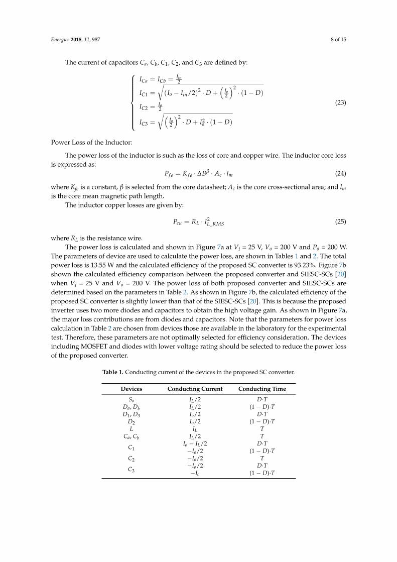
where RL is the resistance wire.The power loss is calculated and shown in Figure 7a at Vi = 25 V, Vo = 200 V and Po = 200 W.
The parameters of device are used to calculate the power loss, are shown in Tables 1 and 2. The totalpower loss is 13.55 W and the calculated efficiency of the proposed SC converter is 93.23%. Figure 7bshown the calculated efficiency comparison between the proposed converter and SIESC-SCs [20]when Vi = 25 V and Vo = 200 V. The power loss of both proposed converter and SIESC-SCs aredetermined based on the parameters in Table 2. As shown in Figure 7b, the calculated efficiency of theproposed SC converter is slightly lower than that of the SIESC-SCs [20]. This is because the proposedinverter uses two more diodes and capacitors to obtain the high voltage gain. As shown in Figure 7a,the major loss contributions are from diodes and capacitors. Note that the parameters for power losscalculation in Table 2 are chosen from devices those are available in the laboratory for the experimentaltest. Therefore, these parameters are not optimally selected for efficiency consideration. The devicesincluding MOSFET and diodes with lower voltage rating should be selected to reduce the power lossof the proposed converter.
Table 1. Conducting current of the devices in the proposed SC converter.
Devices Conducting Current Conducting Time
So IL/2 D·TDa, Db IL/2 (1 − D)·TD1, D3 Io/2 D·T
D2 Io/2 (1 − D)·TL IL T
Ca, Cb IL/2 T
C1Io − IL/2 D·T−Io/2 (1 − D)·T
C2 −Io/2 T
C3−Io/2 D·T−Io (1 − D)·T
Energies 2018, 11, 987 9 of 15
Table 2. Parameters of the devices.
Devices SIESC-SCs [20] Proposed SC Converter
MOSFET S0 STW88N65M5 (650 V, 84 A, 24 m Ω)Diodes DSEI30-06A (600 V, 37 A) DSEI30-06A (600 V, 37 A)
ESR of capacitors 280 mΩ 280 mΩESR of C1 (470 µF/400 VDC) 130 mΩ 130 mΩ
Inductor core CM777125 (142 nH/N2) CM777125 (142 nH/N2)Copper wire resistivity (ρ) 1.724 µΩ-cm 1.724 µΩ-cm
Energies 2018, 11, x FOR PEER REVIEW 9 of 15
Table 2. Parameters of the devices.
Devices SIESC-SCs [20] Proposed SC Converter
MOSFET S0 STW88N65M5 (650 V, 84 A, 24 m Ω)
Diodes DSEI30-06A (600 V, 37 A) DSEI30-06A (600 V, 37 A)
ESR of capacitors 280 mΩ 280 mΩ
ESR of C1 (470 µF/400 VDC) 130 mΩ 130 mΩ
Inductor core CM777125 (142 nH/N2) CM777125 (142 nH/N2)
Copper wire resistivity (ρ) 1.724 µΩ-cm 1.724 µΩ-cm
Figure 7. Power loss calculation. (a) Power loss of the proposed SC converter, and (b) comparison of
the calculated efficiency.
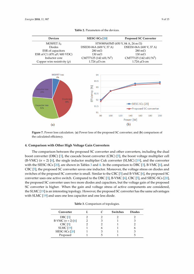
4. Comparison with Other High Voltage Gain Converters
The comparison between the proposed SC converter and other converters, including the dual
boost converter (DBC) [3], the cascade boost converter (CBC) [5], the boost voltage multiplier cell (B-
VMC) (n = 2) [6], the single inductor multiplier Cuk converter (SLMC) [19], and the converter with
the SIESC-SCs [20], are shown in Tables 3 and 4. In the comparison to DBC [3], B-VMC [6], and CBC
[5], the proposed SC converter saves one inductor. Moreover, the voltage stress on diodes and
switches of the proposed SC converter is small. Similar to the CBC [5] and B-VMC [6], the proposed
SC converter uses one active switch. Compared to the DBC [3], B-VMC [6], CBC [5], and SIESC-SCs
[20], the proposed SC converter uses two more diodes and capacitors, but the voltage gain of the
proposed SC converter is higher. When the gain and voltage stress of active components are
considered, the SLMC [19] is an interesting topology. However, the proposed SC converter has the
same advantages with SLMC [19] and uses one less capacitor and one less diode.
Table 3. Comparison of topologies.
Converter L C Switches Diodes
DBC [3] 2 2 2 2
B-VMC (n = 2) [6] 2 3 1 3
CBC [5] 2 2 1 2
SLMC [19] 1 6 1 6
SIESC-SCs [20] 1 3 1 3
Proposed 1 5 1 5
Figure 7. Power loss calculation. (a) Power loss of the proposed SC converter; and (b) comparison ofthe calculated efficiency.
4. Comparison with Other High Voltage Gain Converters
The comparison between the proposed SC converter and other converters, including the dualboost converter (DBC) [3], the cascade boost converter (CBC) [5], the boost voltage multiplier cell(B-VMC) (n = 2) [6], the single inductor multiplier Cuk converter (SLMC) [19], and the converterwith the SIESC-SCs [20], are shown in Tables 3 and 4. In the comparison to DBC [3], B-VMC [6], andCBC [5], the proposed SC converter saves one inductor. Moreover, the voltage stress on diodes andswitches of the proposed SC converter is small. Similar to the CBC [5] and B-VMC [6], the proposed SCconverter uses one active switch. Compared to the DBC [3], B-VMC [6], CBC [5], and SIESC-SCs [20],the proposed SC converter uses two more diodes and capacitors, but the voltage gain of the proposedSC converter is higher. When the gain and voltage stress of active components are considered,the SLMC [19] is an interesting topology. However, the proposed SC converter has the same advantageswith SLMC [19] and uses one less capacitor and one less diode.
Table 3. Comparison of topologies.
Converter L C Switches Diodes
DBC [3] 2 2 2 2B-VMC (n = 2) [6] 2 3 1 3
CBC [5] 2 2 1 2SLMC [19] 1 6 1 6
SIESC-SCs [20] 1 3 1 3Proposed 1 5 1 5
Energies 2018, 11, 987 10 of 15
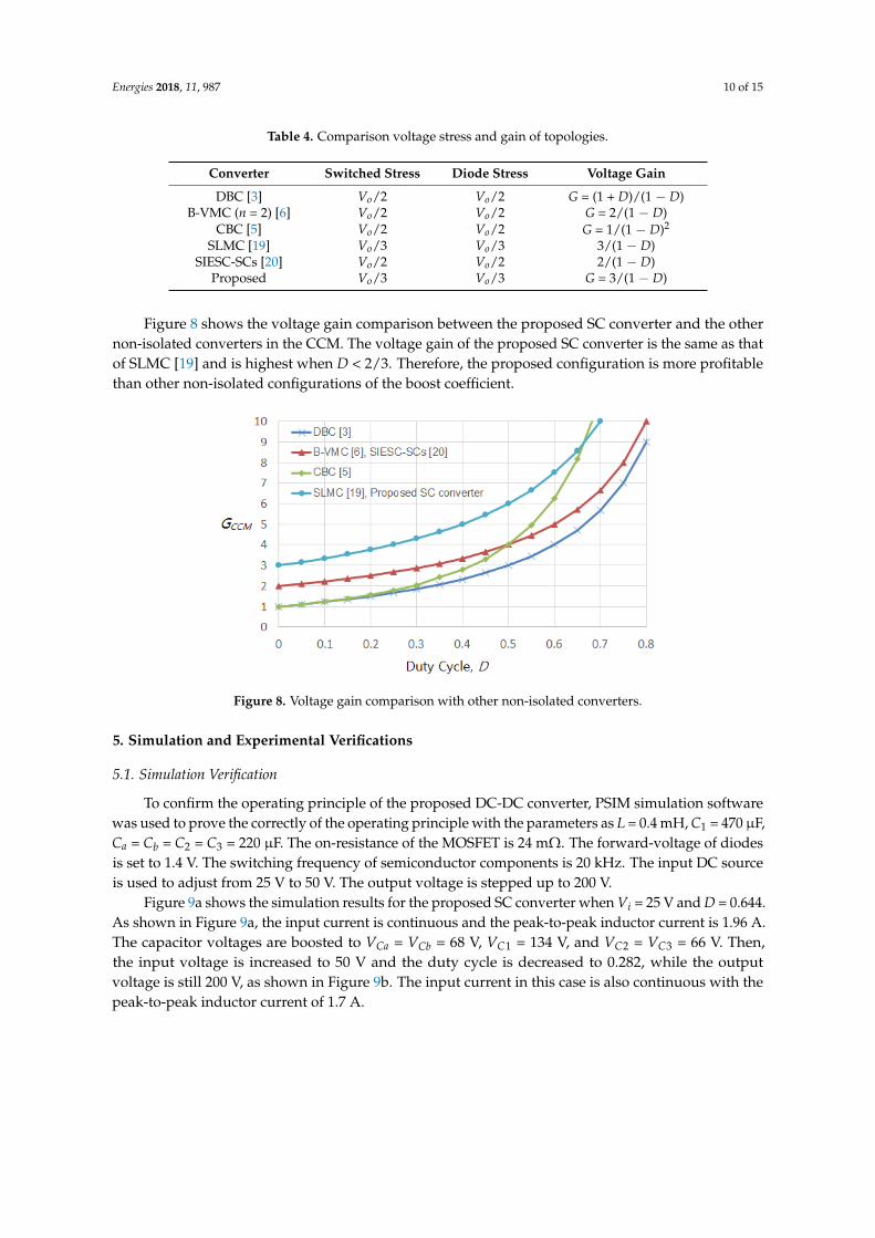
Table 4. Comparison voltage stress and gain of topologies.
Converter Switched Stress Diode Stress Voltage Gain
DBC [3] Vo/2 Vo/2 G = (1 + D)/(1 − D)B-VMC (n = 2) [6] Vo/2 Vo/2 G = 2/(1 − D)
CBC [5] Vo/2 Vo/2 G = 1/(1 − D)2
SLMC [19] Vo/3 Vo/3 3/(1 − D)SIESC-SCs [20] Vo/2 Vo/2 2/(1 − D)
Proposed Vo/3 Vo/3 G = 3/(1 − D)
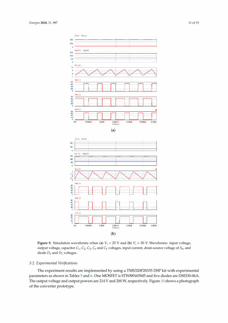
Figure 8 shows the voltage gain comparison between the proposed SC converter and the othernon-isolated converters in the CCM. The voltage gain of the proposed SC converter is the same as thatof SLMC [19] and is highest when D < 2/3. Therefore, the proposed configuration is more profitablethan other non-isolated configurations of the boost coefficient.
Energies 2018, 11, x FOR PEER REVIEW 10 of 15
Table 4. Comparison voltage stress and gain of topologies.
Converter Switched Stress Diode Stress Voltage Gain
DBC [3] Vo/2 Vo/2 G = (1 + D)/(1 − D)
B-VMC (n = 2) [6] Vo/2 Vo/2 G = 2/(1 − D)
CBC [5] Vo/2 Vo/2 G = 1/(1 − D)2
SLMC [19] Vo/3 Vo/3 3/(1 − D)
SIESC-SCs [20] Vo/2 Vo/2 2/(1 − D)
Proposed Vo/3 Vo/3 G = 3/(1 − D)
Figure 8 shows the voltage gain comparison between the proposed SC converter and the other
non-isolated converters in the CCM. The voltage gain of the proposed SC converter is the same as
that of SLMC [19] and is highest when D < 2/3. Therefore, the proposed configuration is more
profitable than other non-isolated configurations of the boost coefficient.
Figure 8. Voltage gain comparison with other non-isolated converters.
5. Simulation and Experimental Verifications
5.1. Simulation Verification
To confirm the operating principle of the proposed DC-DC converter, PSIM simulation software
was used to prove the correctly of the operating principle with the parameters as L = 0.4 mH, C1 = 470
µF, Ca = Cb = C2 = C3 = 220 µF. The on-resistance of the MOSFET is 24 mΩ. The forward-voltage of
diodes is set to 1.4 V. The switching frequency of semiconductor components is 20 kHz. The input
DC source is used to adjust from 25 V to 50 V. The output voltage is stepped up to 200 V.
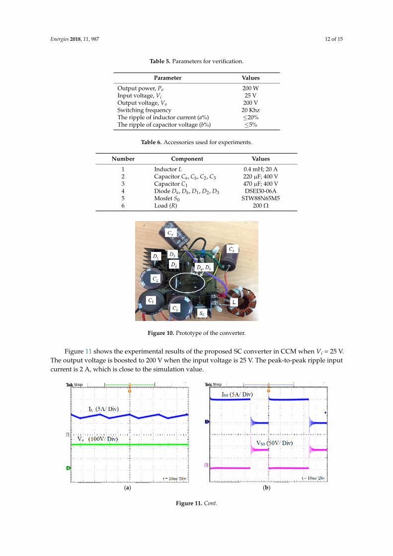
Figure 9a shows the simulation results for the proposed SC converter when Vi = 25 V and D =
0.644. As shown in Figure 9a, the input current is continuous and the peak-to-peak inductor current
is 1.96 A. The capacitor voltages are boosted to VCa = VCb = 68 V, VC1 = 134 V, and VC2 = VC3 = 66 V. Then,
the input voltage is increased to 50 V and the duty cycle is decreased to 0.282, while the output voltage
is still 200 V, as shown in Figure 9b. The input current in this case is also continuous with the peak-
to-peak inductor current of 1.7 A.
Figure 8. Voltage gain comparison with other non-isolated converters.
5. Simulation and Experimental Verifications
5.1. Simulation Verification
To confirm the operating principle of the proposed DC-DC converter, PSIM simulation softwarewas used to prove the correctly of the operating principle with the parameters as L = 0.4 mH, C1 = 470 µF,Ca = Cb = C2 = C3 = 220 µF. The on-resistance of the MOSFET is 24 mΩ. The forward-voltage of diodesis set to 1.4 V. The switching frequency of semiconductor components is 20 kHz. The input DC sourceis used to adjust from 25 V to 50 V. The output voltage is stepped up to 200 V.
Figure 9a shows the simulation results for the proposed SC converter when Vi = 25 V and D = 0.644.As shown in Figure 9a, the input current is continuous and the peak-to-peak inductor current is 1.96 A.The capacitor voltages are boosted to VCa = VCb = 68 V, VC1 = 134 V, and VC2 = VC3 = 66 V. Then,the input voltage is increased to 50 V and the duty cycle is decreased to 0.282, while the outputvoltage is still 200 V, as shown in Figure 9b. The input current in this case is also continuous with thepeak-to-peak inductor current of 1.7 A.
Energies 2018, 11, 987 11 of 15Energies 2018, 11, x FOR PEER REVIEW 11 of 15
(a)
(b)
Figure 9. Simulation waveforms when (a) Vi = 25 V and (b) Vi = 50 V. Waveforms: input voltage, output
voltage, capacitor C1, C2, C3, Ca and Cb voltages, input current, drain-source voltage of S0, and diode
Da and D1 voltages.
5.2. Experimental Verifications
The experiment results are implemented by using a TMS320F28335 DSP kit with experimental
parameters as shown in Tables 5 and 6. One MOSFET is STW88N65M5 and five diodes are DSEI30-
06A. The output voltage and output powers are 214 V and 200 W, respectively. Figure 10 shows a
photograph of the converter prototype.
Figure 9. Simulation waveforms when (a) Vi = 25 V and (b) Vi = 50 V. Waveforms: input voltage,output voltage, capacitor C1, C2, C3, Ca and Cb voltages, input current, drain-source voltage of S0, anddiode Da and D1 voltages.
5.2. Experimental Verifications
The experiment results are implemented by using a TMS320F28335 DSP kit with experimentalparameters as shown in Tables 5 and 6. One MOSFET is STW88N65M5 and five diodes are DSEI30-06A.The output voltage and output powers are 214 V and 200 W, respectively. Figure 10 shows a photographof the converter prototype.
Energies 2018, 11, 987 12 of 15
Table 5. Parameters for verification.
Parameter Values
Output power, Po 200 WInput voltage, Vi 25 VOutput voltage, Vo 200 VSwitching frequency 20 KhzThe ripple of inductor current (a%) ≤20%The ripple of capacitor voltage (b%) ≤5%
Table 6. Accessories used for experiments.
Number Component Values
1 Inductor L 0.4 mH; 20 A2 Capacitor Ca, Cb, C2, C3 220 µF; 400 V3 Capacitor C1 470 µF; 400 V4 Diode Da, Db, D1, D2, D3 DSEI30-06A5 Mosfet S0 STW88N65M56 Load (R) 200 Ω
Energies 2018, 11, x FOR PEER REVIEW 12 of 15
Table 5. Parameters for verification.
Parameter Values
Output power, Po 200 W
Input voltage, Vi 25 V
Output voltage, Vo 200 V
Switching frequency 20 Khz
The ripple of inductor current (a%) ≤20%
The ripple of capacitor voltage (b%) ≤5%
Table 6. Accessories used for experiments.
Number Component Values
1 Inductor L 0.4 mH; 20 A
2 Capacitor Ca, Cb, C2, C3 220 µF; 400 V
3 Capacitor C1 470 µF; 400 V
4 Diode Da, Db, D1, D2, D3 DSEI30-06A
5 Mosfet S0 STW88N65M5
6 Load (R) 200 Ω
Figure 10. Prototype of the converter.
Figure 11 shows the experimental results of the proposed SC converter in CCM when Vi = 25 V.
The output voltage is boosted to 200 V when the input voltage is 25 V. The peak-to-peak ripple input
current is 2 A, which is close to the simulation value.
Figure 12 shows the measured efficiency of the proposed SC converter when the output power
is changed from 80 W to 200 W. The WT230 digital power meter is set up to connect the input and
output. The maximum measured efficiency is 93% at 150 W. The efficiency for the experiment can be
improved with the optimal selection of components. The experimental results are slightly similar
from the theoretical and simulation results.
(a) (b)
Figure 10. Prototype of the converter.
Figure 11 shows the experimental results of the proposed SC converter in CCM when Vi = 25 V.The output voltage is boosted to 200 V when the input voltage is 25 V. The peak-to-peak ripple inputcurrent is 2 A, which is close to the simulation value.
Energies 2018, 11, x FOR PEER REVIEW 12 of 15
Table 5. Parameters for verification.
Parameter Values
Output power, Po 200 W
Input voltage, Vi 25 V
Output voltage, Vo 200 V
Switching frequency 20 Khz
The ripple of inductor current (a%) ≤20%
The ripple of capacitor voltage (b%) ≤5%
Table 6. Accessories used for experiments.
Number Component Values
1 Inductor L 0.4 mH; 20 A
2 Capacitor Ca, Cb, C2, C3 220 µF; 400 V
3 Capacitor C1 470 µF; 400 V
4 Diode Da, Db, D1, D2, D3 DSEI30-06A
5 Mosfet S0 STW88N65M5
6 Load (R) 200 Ω
Figure 10. Prototype of the converter.
Figure 11 shows the experimental results of the proposed SC converter in CCM when Vi = 25 V.
The output voltage is boosted to 200 V when the input voltage is 25 V. The peak-to-peak ripple input
current is 2 A, which is close to the simulation value.
Figure 12 shows the measured efficiency of the proposed SC converter when the output power
is changed from 80 W to 200 W. The WT230 digital power meter is set up to connect the input and
output. The maximum measured efficiency is 93% at 150 W. The efficiency for the experiment can be
improved with the optimal selection of components. The experimental results are slightly similar
from the theoretical and simulation results.
(a) (b)
Figure 11. Cont.
Energies 2018, 11, 987 13 of 15Energies 2018, 11, x FOR PEER REVIEW 13 of 15
(c) (d)
Figure 11. Experimental results when Vi = 25 V and D = 0.65. From top to bottom: (a) input current
and output voltage; (b) drain-source current and voltage of switch S0; and (c)–(d) all diodes’ voltage.
Figure 12. Converter efficiency with different output powers.
Figure 13 shows the voltage gain between the calculated values and simulated values. The
simulated values are slightly lower than the calculated values because the parasitics on the devices
were set in the simulation.
Figure 13. Voltage gain comparison between calculation and simulation.
6. Conclusions
A non-isolated boost DC-DC converter was proposed in this paper. The major advantages of the
proposed SC converter are as follows: high voltage gain; decrease voltage and current stress on the
power device, which helps reduce the loss; and being easy to increase the voltage gain and control
using one switch. The operating principles in the CCM and DCM, parameters design, power loss
analyses, and the comparison with the other non-isolated high boost converters are discussed. The
experimental results of the proposed converter at 25 V input voltage are presented to produce the
output voltage of 200 V. The maximum measured efficiency of the converter is 93% at 150 W. The
experimental and simulation verifications were shown to verify the theoretical analysis.
Figure 11. Experimental results when Vi = 25 V and D = 0.65. From top to bottom: (a) input currentand output voltage; (b) drain-source current and voltage of switch S0; and (c,d) all diodes’ voltage.
Figure 12 shows the measured efficiency of the proposed SC converter when the output poweris changed from 80 W to 200 W. The WT230 digital power meter is set up to connect the input andoutput. The maximum measured efficiency is 93% at 150 W. The efficiency for the experiment can beimproved with the optimal selection of components. The experimental results are slightly similar fromthe theoretical and simulation results.
Energies 2018, 11, x FOR PEER REVIEW 13 of 15
(c) (d)
Figure 11. Experimental results when Vi = 25 V and D = 0.65. From top to bottom: (a) input current
and output voltage; (b) drain-source current and voltage of switch S0; and (c)–(d) all diodes’ voltage.
Figure 12. Converter efficiency with different output powers.
Figure 13 shows the voltage gain between the calculated values and simulated values. The
simulated values are slightly lower than the calculated values because the parasitics on the devices
were set in the simulation.
Figure 13. Voltage gain comparison between calculation and simulation.
6. Conclusions
A non-isolated boost DC-DC converter was proposed in this paper. The major advantages of the
proposed SC converter are as follows: high voltage gain; decrease voltage and current stress on the
power device, which helps reduce the loss; and being easy to increase the voltage gain and control
using one switch. The operating principles in the CCM and DCM, parameters design, power loss
analyses, and the comparison with the other non-isolated high boost converters are discussed. The
experimental results of the proposed converter at 25 V input voltage are presented to produce the
output voltage of 200 V. The maximum measured efficiency of the converter is 93% at 150 W. The
experimental and simulation verifications were shown to verify the theoretical analysis.
Figure 12. Converter efficiency with different output powers.
Figure 13 shows the voltage gain between the calculated values and simulated values.The simulated values are slightly lower than the calculated values because the parasitics on thedevices were set in the simulation.
Energies 2018, 11, x FOR PEER REVIEW 13 of 15
(c) (d)
Figure 11. Experimental results when Vi = 25 V and D = 0.65. From top to bottom: (a) input current
and output voltage; (b) drain-source current and voltage of switch S0; and (c)–(d) all diodes’ voltage.
Figure 12. Converter efficiency with different output powers.
Figure 13 shows the voltage gain between the calculated values and simulated values. The
simulated values are slightly lower than the calculated values because the parasitics on the devices
were set in the simulation.
Figure 13. Voltage gain comparison between calculation and simulation.
6. Conclusions
A non-isolated boost DC-DC converter was proposed in this paper. The major advantages of the
proposed SC converter are as follows: high voltage gain; decrease voltage and current stress on the
power device, which helps reduce the loss; and being easy to increase the voltage gain and control
using one switch. The operating principles in the CCM and DCM, parameters design, power loss
analyses, and the comparison with the other non-isolated high boost converters are discussed. The
experimental results of the proposed converter at 25 V input voltage are presented to produce the
output voltage of 200 V. The maximum measured efficiency of the converter is 93% at 150 W. The
experimental and simulation verifications were shown to verify the theoretical analysis.
Figure 13. Voltage gain comparison between calculation and simulation.
6. Conclusions
A non-isolated boost DC-DC converter was proposed in this paper. The major advantages ofthe proposed SC converter are as follows: high voltage gain; decrease voltage and current stress
Energies 2018, 11, 987 14 of 15
on the power device, which helps reduce the loss; and being easy to increase the voltage gain andcontrol using one switch. The operating principles in the CCM and DCM, parameters design, powerloss analyses, and the comparison with the other non-isolated high boost converters are discussed.The experimental results of the proposed converter at 25 V input voltage are presented to producethe output voltage of 200 V. The maximum measured efficiency of the converter is 93% at 150 W.The experimental and simulation verifications were shown to verify the theoretical analysis.
Acknowledgments: This work was supported by the Korea Institute of Energy Technology Evaluationand Planning (KETEP) and the Ministry of Trade, Industry and Energy (MOTIE) of the Republic of Korea(no. 20164010201020).
Author Contributions: Van-Thuan Tran and Minh-Khai Nguyen conceived and designed the experiments;Van-Thuan Tran performed the experiments; Minh-Khai Nguyen and Youn-Ok Choi analyzed the data;Van-Thuan Tran and Geum-Bae Cho wrote the paper; Minh-Khai Nguyen revised the paper.
Conflicts of Interest: The authors declare no conflict of interest.
Nomenclature
B-VMC Boost voltage multiplier cellCBC Cascade boost converterCCM Continuous conduction modeD Duty cycleDBC Dual boost converterDCM Discontinuous conduction modeESR Equivalent series resistancePWM Pulse width modulationSC Switched-capacitorSCs Switched-capacitor basedSIESC Single-inductor-energy-storage cell-basedSLMC Single inductor multiplier Cuk converterT Period timeVMC Voltage multiplier cellsVMC Voltage multiplier cellsZCS Zero current switching
References
1. Toffoli, F.L.; Pereira, D.C.; Paula, W.J.; Junior, D.S.O. Survey on non-isolated high-voltage step-up DC–DCtopologies based on the boost converter. IET Power Electron. 2015, 8, 2044–2057. [CrossRef]
2. Nymand, M.; Andersen, M.A.E. High-efficiency isolated boost DC–DC converter for high-power low-voltagefuel-cell applications. IEEE Trans. Ind. Electron. 2010, 57, 505–514. [CrossRef]
3. Jin, K.; Yang, M.; Ruan, X.; Xu, M. Three-level bidirectional converter for fuel-cell/battery hybrid powersystem. IEEE Trans. Ind. Electron. 2010, 57, 1976–1986. [CrossRef]
4. Li, W.; He, X. Review of nonisolated high-step-up DC/DC converters in photovoltaic grid-connectedapplications. IEEE Trans. Ind. Electron. 2011, 58, 1239–1250. [CrossRef]
5. Bratcu, A.I.; Munteanu, I.; Bacha, S.; Picault, D.; Raison, B. Cascaded DC–DC converter photovoltaic systems:power optimization issues. IEEE Trans. Ind. Electron. 2011, 58, 403–411. [CrossRef]
6. Garcia, F.S.; Pomilio, J.A.; Spiazzi, G. Modeling and control design of the interleaved double dual boostconverter. IEEE Trans. Ind. Electron. 2013, 60, 3283–3290. [CrossRef]
7. Nguyen, M.K.; Lim, L.C.; Choi, J.H.; Cho, G.B. Isolated High Step-up DC-DC Converter Based onQuasi-Switched-Boost Network. IEEE Trans. Ind. Electron. 2016, 63, 7553–7562. [CrossRef]
8. Ouyang, Z.; Sen, G.; Thomsen, O.C.; Andersen, M.A.E. Analysis and design of fully integrated planarmagnetics for primary–parallel isolated boost converter. IEEE Trans. Ind. Electron. 2013, 60, 494–508.[CrossRef]
Energies 2018, 11, 987 15 of 15
9. Nguyen, M.K.; Duong, T.D.; Lim, L.C.; Kim, Y.J. Isolated boost DC–DC converter with three switches.IEEE Trans. Power Electron. 2018, 33, 1389–1398. [CrossRef]
10. Shi, X.; Jiang, J.; Guo, X. An efficiency-optimized isolated bidirectional DC-DC converter with extendedpower range for energy storage systems in microgrids. Energies 2013, 6, 27–44. [CrossRef]
11. Prudente, M.; Pfitscher, L.L.; Emmendoerfer, G.; Romaneli, E.F.; Gules, R. Voltage multiplier cells applied tonon-isolated DC-DC converters. IEEE Trans. Power Electron. 2008, 23, 871–887. [CrossRef]
12. Hsieh, Y.P.; Chen, J.F.; Yang, L.S.; Wu, C.Y.; Liu, W.S. High-conversion-ratio bidirectional DC/DC converterwith couple inductor. IEEE Trans. Ind. Electron. 2014, 61, 1311–1319. [CrossRef]
13. Tang, Y.; Fu, D.; Kan, J.; Wang, T. Dual switches DC/DC converter with three-winding-coupled inductor andcharge pump. IEEE Trans. Power Electron. 2016, 31, 461–469. [CrossRef]
14. Padmanaban, S.; Bhaskar, M.S.; Maroti, P.K.; Blaabjerg, F.; Fedák, V. An original transformer andswitched-capacitor (T & SC)-based extension for DC-DC boost converter for high-voltage/low-currentrenewable energy applications: hardware implementation of a new T & SC boost converter. Energies 2018,11, 783. [CrossRef]
15. Tang, Y.; Wang, T.; Fu, D. Multicell switched-inductor/switched-capacitor combined active-networkconverters. IEEE Trans. Power Electron. 2015, 30, 2063–2072. [CrossRef]
16. Yang, L.S.; Liang, T.J.; Chen, J.F. Transformerless DC-DC converters with step-up voltage gain. IEEE Trans.Ind. Electron. 2009, 56, 3144–3152. [CrossRef]
17. Nguyen, M.K.; Duong, T.D.; Lim, L.C. Switched-capacitor-based dual-switch high-boost DC–DC converter.IEEE Trans. Power Electron. 2018, 33, 4181–4189. [CrossRef]
18. Axelrod, B.; Berkovich, Y.; Ioinovici, A. Switched-capacitor/switched-inductor structures for gettingtransformerless hybrid DC-DC PWM converters. IEEE Trans. Circuits Syst. I 2008, 55, 687–696. [CrossRef]
19. Hernandez, C.A.V.; Maldonado, J.C.M.; Resendiz, J.E.V.; Caro, J.C.R. Modeling and control of an interleavedDC-DC multilevel boost converter. In Proceedings of the IEEE 18th Workshop on Control and Modeling forPower Electronic (COMPEL), Stanford, CA, USA, 9–12 July 2017; pp. 1–6. [CrossRef]
20. Wu, G.; Ruan, X.; Ye, Z. Nonisolated high step-up DC-DC converters adopting switched-capacitor cell.IEEE Trans. Ind. Electron. 2015, 62, 383–393. [CrossRef]
21. Graovac, D.; Pürschel, M.; Kiep, A. MOSFET power losses calculation using the datasheet parameters.Infineon Appl. Note 2006, 1, 1–23.
© 2018 by the authors. Licensee MDPI, Basel, Switzerland. This article is an open accessarticle distributed under the terms and conditions of the Creative Commons Attribution(CC BY) license (http://creativecommons.org/licenses/by/4.0/).