Automatic symbolic analysis of switched-capacitor filtering networks using signal flow graphs
1376 IEEE TRANSACTIONS
TOSCA: ON COMPUTER-AIDED DESIGN OF INTEGRATED CIRCUITS AND SYSTEMS, VOL. 12, NO. 9, SEPTEMBER 1993
A Simulator for Switched-Capacitor Noise-Shaping A/D Converters
Valentino Liberali, Victor F. Dias, Marco Ciapponi, and Franco Maloberti, Senior Member, ZEEE
Abstract-Today’s trends in mixed analog-digital circuit de- sign show that oversampling techniques will probably be pre- ferred over traditional approaches for implementing high-res- olution data converters. Two main factors have limited their widespread use: common analytical as simulation tools are in- adequate for exact analysis because these circuits are inher- ently nonlinear, and conventional electrical simulators are not suitable for simulation because very long transient analyses are required. A software tool named TOSCA (Tool for Oversam- pled Switched-Capacitor A/D Converter Analysis) has been de- veloped in order to overcome these drawbacks. The simulator is behavioral, general purpose and fully user-friendly. Because a set of basic building blocks is available, generic switched-ca- pacitor noise-shaping AID converters can be analyzed simply by building a netlist file. Two hierarchial levels have been con- sidered for circuit description: block-level for sub-circuits like quantizers and digital filters, and component-level for sub-cir- cuits like the integrators where switches, capacitors and oper- ational amplifiers are used as building elements. The developed models allow the most relevant non-ideal parameters of the components to be taken into account and a set of post-process- ing facilities allow extensive analysis of the circuits. The pro- gram is written in C language, uses dynamic memory allocation and is very fast.
I. INTRODUCTION N RECENT YEARS oversampled data converters have I become very popular for implementing analog-to-digi-
tal (A/D) and digital-to-analog (D/A) interfaces in stan- dard CMOS processes [1]-[6]. It is well known that their main advantage over conventional Nyquist-rate data con- verters comes from the possibility they have to trade speed for resolution. Because the analog processing required is limited to low-accuracy operations such as integration and low-resolution quantization and D/A conversion, these circuits allow to shift the resolution limits from the ac- curacy-matching properties of the components to the more convenient trade-off between speed and thermal noise [7]- [9]. Moreover, these advantages are considered crucial by circuit designers who must use CMOS technologies which are optimized for digital circuitry. Recent theoretical works and IC implementations indicate that with state-of-
Manuscript received March 9 , 1992; revised September 8, 1992. This work was supported by the European Community, EEC-Joint Research Centre, and by the Italian Research Council, CNR-Progetto Finalizzato Telecomunicazioni. This paper was recommended by Associate Editor A. Ruehli.
V. Liberali and F. Maloberti are with the Department of Electronics, University of Pavia, 27100 Pavia, Italy.
M. Ciapponi was with the Department of Electronics, University of Pavia. He is now with Boffi S.r.l., 23018 Talamona (Sondrio), Italy.
V. F. Dias is with Instituto Superior TCchnico, SecqHo de Electronica, 1096 Lisboa Codex, Portugal.
IEEE Log Number 9207805.
the-art technologies more than 16 bits of resolution can be achieved for digital-audio signals [6]-[8].
Up until now, two main factors have limited the effi- cient design of oversampled data converters: the intrinsic nonlinear nature of the circuits, and the lack of general purpose simulators suitable for the analysis of tens of thousands of sampling periods [lo]-[ 161.
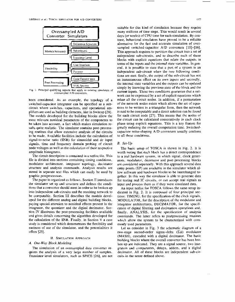
As illustrated in Fig. 1, existing tools for the simulation of oversampled data converters can be classified by con- sidering three principal qualifying aspects [ 181: the ac- curacy of the models used in the modulator and decimator (transistor-level, behavioral, or simple difference equa- tion level modeling), the ease and the flexibility of use of the tool (the tool can be or not be user-friendly and limited or not to the simulation of a finite number of modulator and decimator structures) and finally, the postprocessing algorithm used for the evaluation of system performance. An optimum tradeoff of the above-mentioned aspects de- termines the features of the simulator TOSCA. It has been developed in order to meet the following four key fea- tures.
Since the modulator performance is evaluated on the basis of the statistical average of a very large num- ber of samples, it should be possible to simulate the long data stream, and consequently to perform the very long time analysis in reasonable CPU time. Since the simulator is dedicated to the analysis of switched-capacitor networks, it should be able to take the nonideal effects of the components into consideration and to accurately evaluate the signal samples at the end of each clock phase; Since the circuit performance is better expressed in terms of the signal-to-noise ratio (SNR), rather than non-linearity parameters, the simulator should con- tain a specific postprocessor. Code density tests could also be applied but at the expense of yet more time consuming simulations [ 191-[20]. The simulator should be general purpose in order to be able to simulate generic modulator/decimator structures, and to have a simple interface for the de- scription of the circuit and for the analysis com- mands (netlist interface as in common electrical simulators).
TOSCA is based on a set of building blocks which al- low generic oversampled modulators and digital decima- tors to be built up as a block-level network [22]-[25]. For cases where flexibility inside a specific block is essential, the possibility for component level description has also
0278-0070/93$03.00 0 1993 IEEE
LIBERAL1 er al . : TOSCA: SIMULATOR FOR AID CONVERTERS 1311
I Oversamp!ed A/D Converter Srmulators
Difference Equation
User Interface
Code Density tests Pos t-Processing 1 SNR, Spectra
Fig. 1. Principal qualifying aspects that apply to existing simulators of oversampled AID converters.
been considered. As an example, the topology of a switched-capacitor integrator can be specified as a sub- circuit where switches, capacitors, and operational am- plifiers are used as building elements, like in Switcap [28] . The models developed for the building blocks allow the most relevant nonideal parameters of the components to be taken into account, a fact which makes simulation re- sults quite realistic. The simulator contains post-process- ing routines that allow extensive analysis of the circuits to be made. Available facilities include the calculation of signal-to-noise ratio (SNR) for sinusoidal and dc input signals, time and frequency domain probing of circuit node voltages as well as the calculation of their respective amplitude histograms.
The circuit description is contained in a netlist file. This file is divided into sections containing timing conditions, modulator architecture, integrator topology, decimator structure and analysis commands. Analysis results are stored in separate text files which can easily be used by graphic postprocessors.
The paper is organized as follows. Section I1 introduces the simulator set up and structure and defines the condi- tions that a converter should meet in order to be broken up into independent sub-circuits and the resulting network to be computable. Section I11 describes the models devel- oped for the different analog and digital building blocks, paying special attention to nonideal effects present in the integrator, the quantizer and the digital decimator. Sec- tion IV illustrates the post-processing facilities available and gives details concerning the algorithm developed for the calculation of the SNR. Finally, in Section V a case study is considered which demonstrates the flexibility and easiness of use of the simulator, and the potentialities it offers [ 2 5 ] .
11. SIMULATION APPROACH A. One- Way Block Modeling
The simulation of an oversampled data converter re- quires the analysis of a very large number of samples. Transistor level simulators, such as SPICE [26], are not
suitable for this kind of simulation because they require many millions of time steps. This would result in several days (or weeks) of CPU time for each simulation. By con- trast, behavioral simulators have proved to be a reliable alternative for the fast and accurate simulation of over- sampled switched-capacitor A/D converters [ 1014 161. This approach requires to partition the circuit into a set of independent sub-circuits, and to describe each of these blocks with explicit equations that relate the outputs in terms of the inputs and the internal state variables. In gen- eral, it is possible to state that a part of a system is an independent sub-circuit when the two following condi- tions are met: firstly, the output of the sub-circuit has not an instantaneous effect on its own inputs and secondly, the internal state variables and the outputs can be updated simply by knowing the previous state of the block and the current inputs. These two conditions guarantee that a net- work can be expressed by a set of explicit equations which relate all the circuit nodes. In addition, if a permutation of the network nodes exists which allows the set of equa- tions to be written in a triangular form, then the network is said to be computable and a direct solution can be found for each circuit node [ 2 7 ] . This means that the nodes of the circuit can be calculated consecutively in each clock phase using explicit equations. This is a key feature for greatly reducing the overall computation time. Switched- capacitor noise-shaping A/D converters usually conform to all these conditions.
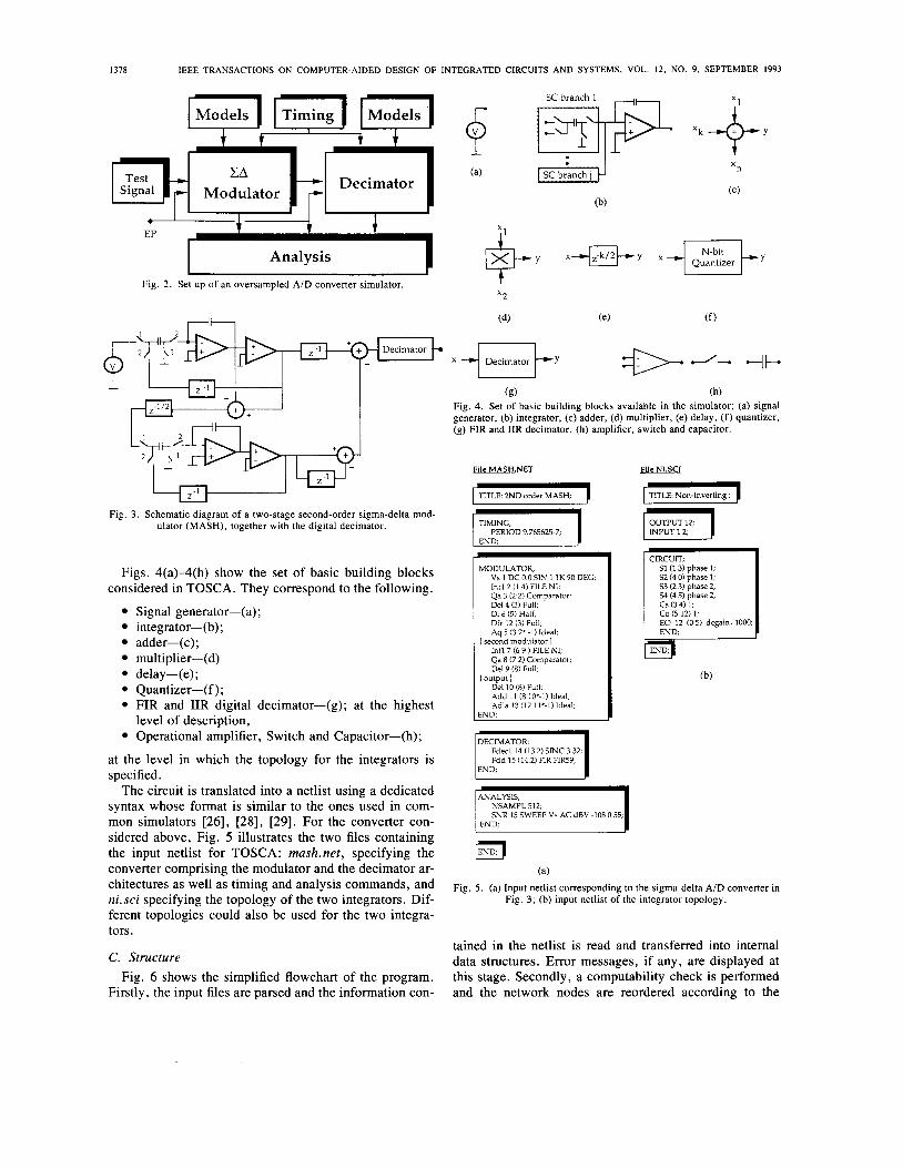
B. Set-Up The basic setup of TOSCA is shown in Fig. 2. It is
worth noting that each block has a direct correspondence to a real hardware system, in which signal, clock gener- ators, modulator, decimator and post-processing blocks are considered separately. With this approach several data entry points (EP) are available in the simulator which al- low software and hardware blocks to be interchanged to- gether. In this way the simulator is able to generate data for testing real IC circuits, or can accept real signals as input and process them as if they were simulated data.
An input netlist for TOSCA follows the same setup in- dicated in Fig. 2 . It is composed of four principal sec- tions: TIMING, for the specification of the clock signals, MODULATOR, for the description of the modulator and integrator architectures, DECIMATOR, for the specifi- cation of digital filtering and decimation operations and, finally, ANALYSIS, for the specification of analysis commands. The latter refers to postprocessing routines which allow the system to be characterized with com- monly used parameters.
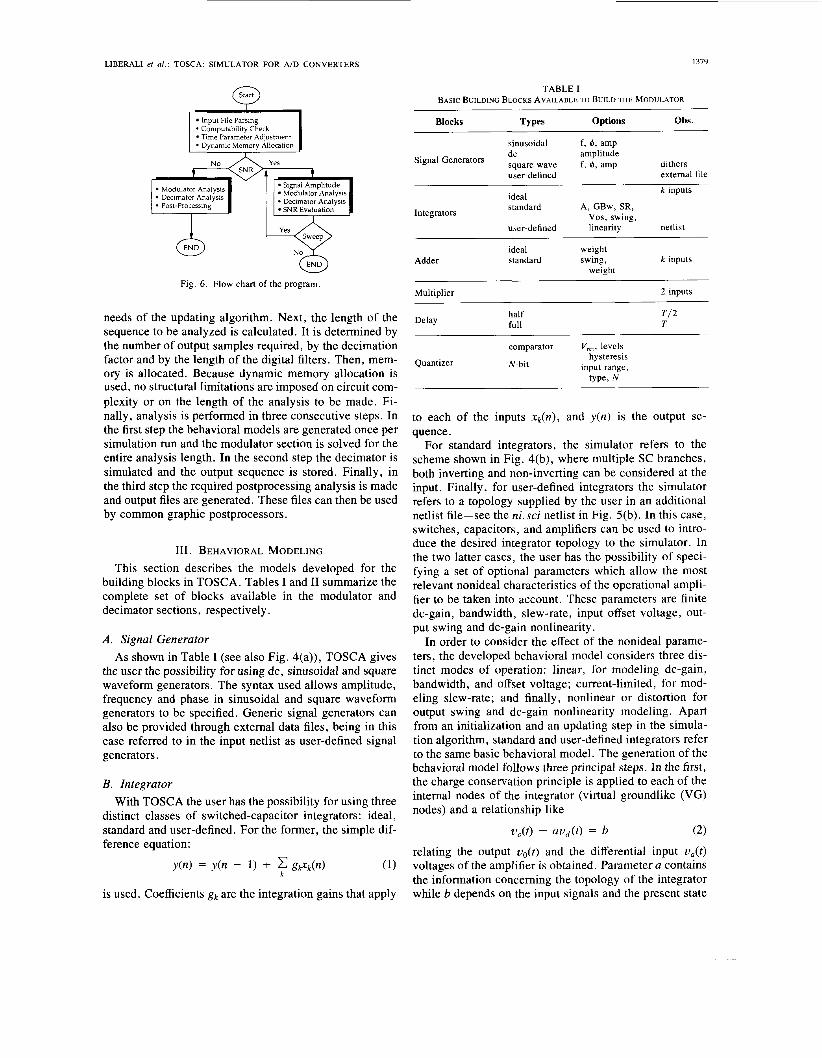
Let us consider in Fig. 3 the schematic diagram of a two-stage second-order sigma-delta (EA) modulator (MASH), cascaded with a digital decimator. The basic building blocks where the overall converter has been bro- ken up are indicated. They are a signal source, two inte- grators and comparators, delays, adders, and 'a digital decimator. All of these blocks are independent sub-cir- cuits in the sense defined above.
1378 IEEE TRANSACTIONS ON COMPUTER-AIDED DESIGN OF INTEGRATED CIRCUITS AND SYSTEMS, VOL. 12, NO. 9, SEPTEMBER 1993
SC branch I I 1-1 Y
ator-~7-T (b)
+ r f e xk+ X
:Models I (a) SC branch 1
(C) -----) Decimator
Analysis Quantizer I I
Fig. 2. Set up of an oversampled AID converter simulator. t x2
1 I
l>L* z
Fig. 3 . Schematic diagram of a two-stage second-order sigma-delta mod- ulator (MASH), together with the digital decimator.
Figs. 4(a)-4(h) show the set of basic building blocks considered in TOSCA. They correspond to the following.
Signal generator-(a); integrator-(b); adder-(c); multiplier- (d) delay -(e) ; Quantizer-(f); FIR and IIR digital decimator-(g); at the highest
Operational amplifier, Switch and Capacitor-(h);
at the level in which the topology for the integrators is specified.
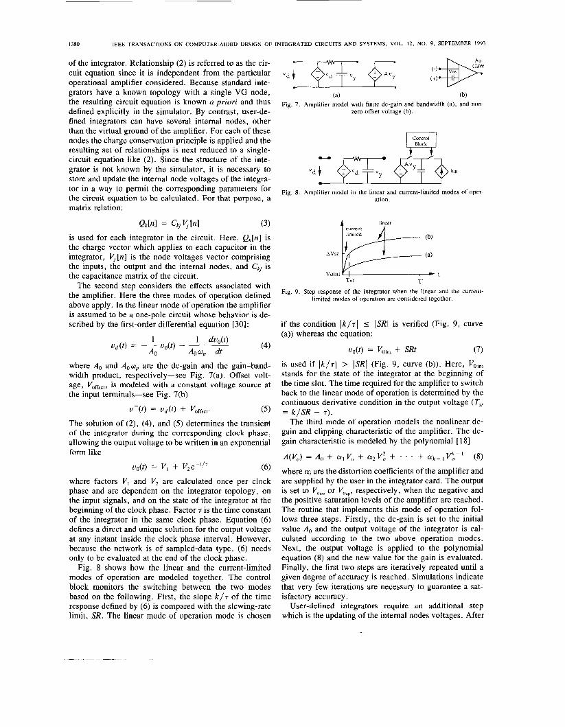
The circuit is translated into a netlist using a dedicated syntax whose format is similar to the ones used in com- mon simulators [26], [28], [29]. For the converter con- sidered above, Fig. 5 illustrates the two files containing the input netlist for TOSCA: mash.net, specifying the converter comprising the modulator and the decimator ar- chitectures as well as timing and analysis commands, and ni. sci specifying the topology of the two integrators. Dif- ferent topologies could also be used for the two integra- tors.
level of description,
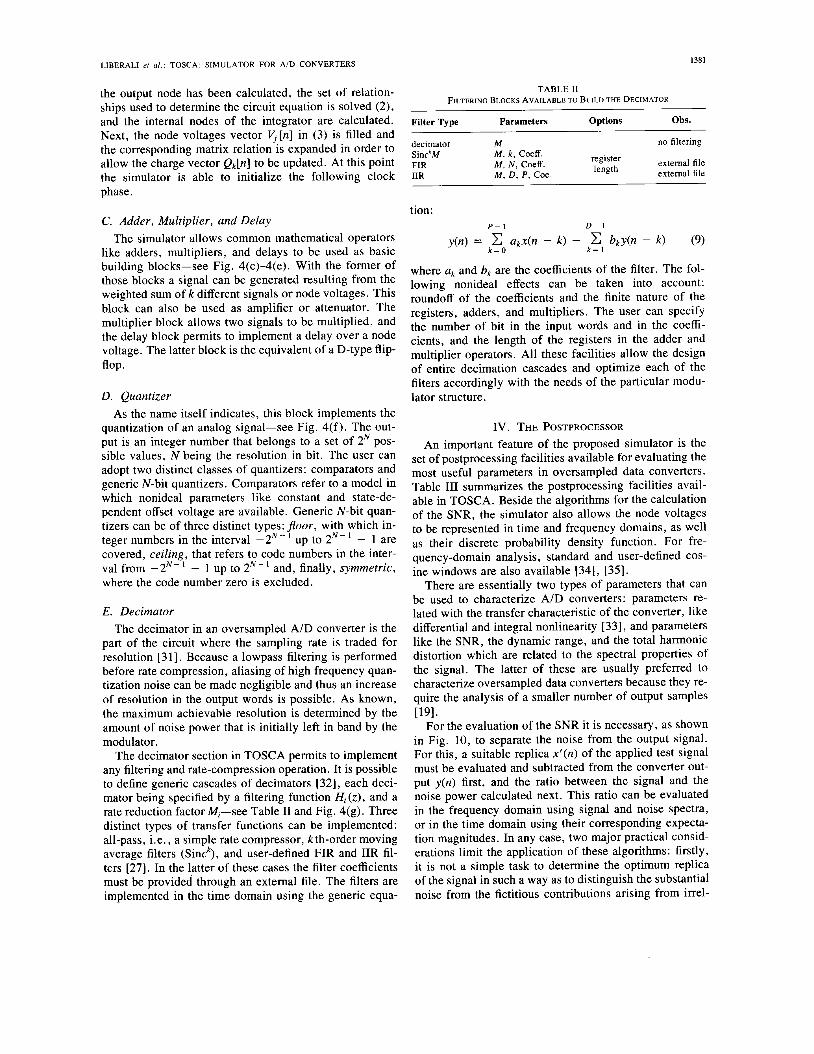
C. Structure Fig. 6 shows the simplified flowchart of the program.
Firstly, the input files are parsed and the information con-
(g) (h) Fig. 4. Set of basic building blocks available in the simulator; (a) signal generator, (b) integrator, (c) adder, (d) multiplier, (e) delay, (f) quantizer, (g) FIR and IIR decimator, (h) amplifier, switch and capacitor.
Eile MASH.NET File NI.SU
I TITLE: 2ND order MASH; 1
TIMING; PERIOD 9.765625-7;
I MODULATOR; Vs 1 DC 0 OSlN 1 1K 90 DEG, Intl 2 (1 4) FILE NI;
I Qa 3 (2.2) Comparator; Del 4 (3) Full; DI 6 (5) Half, Dfr 12 (3) Full; Aq 5 (3 2' -1) Ideal,
[second modulator I Intl 7 (6 9 FILE NI; Qa 8 (72) Comparator; Del 9 (8) Full;
Del 10 (8) Full; Add 11 (8 lO*-l) Ideal, Adla 13 (12 l l*-l) Ideal;
I output I
END;
I DECIMATOR; Fdecl 14 (13:2) SINC 3 32; Fdd 15 (142) FIR FIR59;
END;
CIRCUIT; 51 (1 3) phase 1; 52 (4 0 ) phase 1; S3 (2 3) phase 2; 54 (4 5) phase 2; c s (3 4) 1: CO (5 12) 1; EO 12 (05) dcgain=1000,
NSAMPL 512; SNR 15 SWEEP Vs AC dBV -108 0 55;
(a) Fig. 5 . (a) Input netlist corresponding to the sigma-delta A/D converter in
Fig. 3; (b) input netlist of the integrator topology.
tained in the netlist is read and transferred into internal data structures. Error messages, if any, are displayed at this stage. Secondly, a computability check is performed and the network nodes are reordered according to the
LIBERAL1 et al . : TOSCA: SIMULATOR FOR AID CONVERTERS 1379
TABLE I BASIC BUILDING BLOCKS AVAILABLE TO BUILD THE MODULATOR
I ~~~ ~~~
Input File Parsing
Time Parameter Adjustment Computability Check
Dynamic Memory Allocation
Modulator Analysis - Decimator Analysis SNR Evaluation
@
Fig. 6 . Flow chart of the program.
needs of the updating algorithm. Next, the length of the sequence to be analyzed is calculated. It is determined by the number of output samples required, by the decimation factor and by the length of the digital filters. Then, mem- ory is allocated. Because dynamic memory allocation is used, no structural limitations are imposed on circuit com- plexity or on the length of the analysis to be made. Fi- nally, analysis is performed in three consecutive steps. In the first step the behavioral models are generated once per simulation run and the modulator section is solved for the entire analysis length. In the second step the decimator is simulated and the output sequence is stored. Finally, in the third step the required postprocessing analysis is made and output files are generated. These files can then be used by common graphic postprocessors.
111. BEHAVIORAL MODELING This section describes the models developed for the
building blocks in TOSCA. Tables I and I1 summarize the complete set of blocks available in the modulator and decimator sections, respectively.
A . Signal Generator As shown in Table I (see also Fig. 4(a)), TOSCA gives
the user the possibility for using dc, sinusoidal and square waveform generators. The syntax used allows amplitude, frequency and phase in sinusoidal and square waveform generators to be specified. Generic signal generators can also be provided through external data files, being in this case referred to in the input netlist as user-defined signal generators.
B. Integrator With TOSCA the user has the possibility for using three
distinct classes of switched-capacitor integrators: ideal, standard and user-defined. For the former, the simple dif- ference equation:
k
is used. Coefficients gk are the integration gains that apply
Blocks Types Options Obs.
sinusoidal f , 8, amp dc amplitude
user-defined
ideal standard A, GBw, SR,
Vos, swing, linearity user-defined
Signal square wave f , 8 , amp dithers external file
k inputs
Integrators
netlist ~~
ideal weight Adder standard swing, k inputs
weight
Multiplier 2 inputs
Delay half full
T / 2 T
Quantizer
comparator V,,, levels
N-bit hysteresis
input range, type, N
to each of the inputs xk(n), and y (n) is the output se- quence.
For standard integrators, the simulator refers to the scheme shown in Fig. 4(b), where multiple SC branches, both inverting and non-inverting can be considered at the input. Finally, for user-defined integrators the simulator refers to a topology supplied by the user in an additional netlist file-see the ni.sci netlist in Fig. 5(b). In this case, switches, capacitors, and amplifiers can be used to intro- duce the desired integrator topology to the simulator. In the two latter cases, the user has the possibility of speci- fying a set of optional parameters which allow the most relevant nonideal characteristics of the operational ampli- fier to be taken into account. These parameters are finite dc-gain, bandwidth, slew-rate, input offset voltage, out- put swing and dc-gain nonlinearity.
In order to consider the effect of the nonideal parame- ters, the developed behavioral model considers three dis- tinct modes of operation: linear, for modeling dc-gain, bandwidth, and offset voltage; current-limited, for mod- eling slew-rate; and finally, nonlinear or distortion for output swing and dc-gain nonlinearity modeling. Apart from an initialization and an updating step in the simula- tion algorithm, standard and user-defined integrators refer to the same basic behavioral model. The generation of the behavioral model follows three principal steps. In the first, the charge conservation principle is applied to each of the internal nodes of the integrator (virtual groundlike (VG) nodes) and a relationship like
v,(t) + avd( t ) = b (2) relating the output vo(t) and the differential input v,(t) voltages of the amplifier is obtained. Parameter a contains the information concerning the topology of the integrator while b depends on the input signals and the present state
1380 IEEE TRANSACTIONS ON COMPUTER-AIDED DESIGN OF INTEGRATED CIRCUITS AND SYSTEMS, VOL. 12, NO. 9, SEPTEMBER 1993
of the integrator. Relationship (2) is referred to as the cir- cuit equation since it is independent from the particular operational amplifier considered. Because standard inte- grators have a known topology with a single VG node, the resulting circuit equation is known a priori and thus defined explicitly in the simulator. By contrast, user-de- fined integrators can have several internal nodes, other than the virtual ground of the amplifier. For each of these nodes the charge conservation principle is applied and the resulting set of relationships is next reduced to a single- circuit equation like (2). Since the structure of the inte- grator is not known by the simulator, it is necessary to store and update the internal node voltages of the integra- tor in a way to permit the corresponding parameters for the circuit equation to be calculated. For that purpose, a matrix relation:
(3) is used for each integrator in the circuit. Here, Qk[n] is the charge vector which applies to each capacitor in the integrator, q [ n ] is the node voltages vector comprising the inputs, the output and the internal nodes, and c k j is the capacitance matrix of the circuit.
The second step considers the effects associated with the amplifier. Here the three modes of operation defined above apply. In the linear mode of operation the amplifier is assumed to be a one-pole circuit whose behavior is de- scribed by the first-order differential equation [30] :
where A. and Aoup are the dc-gain and the gain-band- width product, respectively-see Fig. 7(a). Offset volt- age, VoRset, is modeled with a constant voltage source at the input terminals-see Fig. 7(b)
f ( t ) = ud(t) + Voffset. (5) The solution of (2), (4), and ( 5 ) determines the transient of the integrator during the corresponding clock phase, allowing the output voltage to be written in an exponential form like
vo(t) = V , + ~ ~ e - ~ / ~ (6) where factors VI and V2 are calculated once per clock phase and are dependent on the integrator topology, on the input signals, and on the state of the integrator at the beginning of the clock phase. Factor r is the time constant of the integrator in the same clock phase. Equation (6) defines a direct and unique solution for the output voltage at any instant inside the clock phase interval. However, because the network is of sampled-data type, (6) needs only to be evaluated at the end of the clock phase.
Fig. 8 shows how the linear and the current-limited modes of operation are modeled together. The control block monitors the switching between the two modes based on the following. First, the slope k / r of the time response defined by (6) is compared with the slewing-rate limit, SR. The linear mode of operation mode is chosen
Ao
. I I I
(a) (b) Fig. 7 . Amplifier model with finite dc-gain and bandwidth (a), and non-
zero offset voltage (b).
Control I ~ Block ~ 1
0 I I I I I
Fig. 8 . Amplifier model in the linear and current-limited modes of oper- ation.
linear current limited
(a)
t
AVsr p: (b;
Voini Tsr T'
Fig. 9. Step response of the integrator when the linear and the current- limited modes of operation are considered together.
if the condition l k / ~ I 5 ISR( is verified (Fig. 9, curve (a)) whereas the equation:
z/o(t) = Voini + SRt (7) is used if lk/rI > \SRI (Fig. 9, curve (b)). Here, VO,,,, stands for the state of the integrator at the beginning of the time slot. The time required for the amplifier to switch back to the linear mode of operation is determined by the continuous derivative condition in the output voltage (T,,
The third mode of operation models the nonlinear dc- gain and clipping characteristic of the amplifier. The dc- gain characteristic is modeled by the polynomial [ 181
= k / S R - 7).
Vk- 1 A(vo) = A0 + Vo + 012 v: + * + ak-1 0 (8)
where ai are the distortion coefficients of the amplifier and are supplied by the user in the integrator card. The output is set to V,, or Voup, respectively, when the negative and the positive saturation levels of the amplifier are reached. The routine that implements this mode of operation fol- lows three steps. Firstly, the dc-gain is set to the initial value A. and the output voltage of the integrator is cal- culated according to the two above operation modes. Next, the output voltage is applied to the polynomial equation (8) and the new value for the gain is evaluated. Finally, the first two steps are iteratively repeated until a given degree of accuracy is reached. Simulations indicate that very few iterations are necessary to guarantee a sat- isfactory accuracy.
User-defined integrators require an additional step which is the updating of the internal nodes voltages. After
LIBERAL1 et al.: TOSCA: SIMULATOR FOR AID CONVERTERS 1381
the output node has been calculated, the set of relation- ships used to determine the circuit equation is solved (2), and the internal nodes of the integrator are calculated. Next, the node voltages vector y [ n ] in ( 3 ) is filled and the corresponding matrix relation is expanded in order to allow the charge vector Qk[n] to be updated. At this point the simulator is able to initialize the following clock phase.
C. Adder, Multiplier, and Delay The simulator allows common mathematical operators
like adders, multipliers, and delays to be used as basic building blocks-see Fig. 4(c)-4(e). With the former of those blocks a signal can be generated resulting from the weighted sum of k different signals or node voltages. This block can also be used as amplifier or attenuator. The multiplier block allows two signals to be multiplied, and the delay block permits to implement a delay over a node voltage. The latter block is the equivalent of a D-type flip- flop.
D. Quantizer As the name itself indicates, this block implements the
quantization of an analog signal-see Fig. 4(f) . The out- put is an integer number that belongs to a set of 2N pos- sible values, N being the resolution in bit. The user can adopt two distinct classes of quantizers: comparators and generic N-bit quantizers. Comparators refer to a model in which nonideal parameters like constant and state-de- pendent offset voltage are available. Generic N-bit quan- tizers can be of three distinct types: JEoor, with which in- teger numbers in the interval -2N- ' up to 2N- ' - 1 are covered, ceiling, that refers to code numbers in the inter- val from -2N-' - 1 up to 2N- ' and, finally, symmetric, where the code number zero is excluded.
E. Decimator The decimator in an oversampled A/D converter is the
part of the circuit where the sampling rate is traded for resolution [3 13. Because a lowpass filtering is performed before rate compression, aliasing of high frequency quan- tization noise can be made negligible and thus an increase of resolution in the output words is possible. As known, the maximum achievable resolution is determined by the amount of noise power that is initially left in band by the modulator.
The decimator section in TOSCA permits to implement any filtering and rate-compression operation. It is possible to define generic cascades of decimators [32], each deci- mator being specified by a filtering function Hi(z), and a rate reduction factor Mi-see Table I1 and Fig. 4(g). Three distinct types of transfer functions can be implemented: all-pass, i.e., a simple rate compressor, kth-order moving average filters (Sinck), and user-defined FIR and IIR fil- ters [27]. In the latter of these cases the filter coefficients must be provided through an external file. The filters are implemented in the time domain using the generic equa-
TABLE I1 FILTERING BLOCKS AVAILABLE TO BUILD THE DECIMATOR
Filter Type Parameters Options Obs.
decimator M no filtering
external file external file
register length
SinckM M, k , Coeff. M, N , Coeff. FIR
IIR M, D, P, Coe.
tion: P- 1 D- 1
where ak and bk are the coefficients of the filter. The fol- lowing nonideal effects can be taken into account: roundoff of the coefficients and the finite nature of the registers, adders, and multipliers. The user can specify the number of bit in the input words and in the coeffi- cients, and the length of the registers in the adder and multiplier operators. All these facilities allow the design of entire decimation cascades and optimize each of the filters accordingly with the needs of the particular modu- lator structure.
IV. THE POSTPROCESSOR An important feature of the proposed simulator is the
set of postprocessing facilities available for evaluating the most useful parameters in oversampled data converters. Table I11 summarizes the postprocessing facilities avail- able in TOSCA. Beside the algorithms for the calculation of the SNR, the simulator also allows the node voltages to be represented in time and frequency domains, as well as their discrete probability density function. For fre- quency-domain analysis, standard and user-defined cos- ine windows are also available [34], [35].
There are essentially two types of parameters that can be used to characterize A/D converters: parameters re- lated with the transfer characteristic of the converter, like differential and integral nonlinearity [ 3 3 ] , and parameters like the SNR, the dynamic range, and the total harmonic distortion which are related to the spectral properties of the signal. The latter of these are usually preferred to characterize oversampled data converters because they re- quire the analysis of a smaller number of output samples
For the evaluation of the SNR it is necessary, as shown in Fig. 10, to separate the noise from the output signal. For this, a suitable replica x'(n) of the applied test signal must be evaluated and subtracted from the converter out- put y(n) first, and the ratio between the signal and the noise power calculated next. This ratio can be evaluated in the frequency domain using signal and noise spectra, or in the time domain using their corresponding expecta- tion magnitudes. In any case, two major practical consid- erations limit the application of these algorithms: firstly, it is not a simple task to determine the optimum replica of the signal in such a way as to distinguish the substantial noise from the fictitious contributions arising from irrel-
~ 9 1 .
1382 IEEE TRANSACTIONS ON COMPUTER-AIDED DESIGN OF INTEGRATED CIRCUITS AND SYSTEMS. VOL. 12, NO. 9, SEPTEMBER 1993
Estimator
y(n) Q?&+ SNR
Fig. 10. Flowchart of an algorithm for the calculation of the SNR.
TABLE I11 POST-PROCESSING FACILITIES AVAILABLE FOR THE ANALYSIS
Command TY Pe Options Obs.
Window common cosine coeff. list
voltage clock phase histogram clock phase Time
Frequency Power Spect' clock phase Ampl. Spect clock phase
ac sweep source to SNR
frequency sweep mode SlTHD SNR dc sweep sweep and DR
Fig. 11. Flowchart of the algorithms used to calculate the SNR.
and the signal power, and the ratio:
evaluated as the SNR. Because the DFT routine is used, adequate windows can be applied to the signal to better estimate tones in the presence of noise, while the use of dynamic length sequences allows the adjustment of the input test frequency to one of the bins from the DFT basis set. In this case the whole Nyquist band is considered for noise integration.
evant variations of the unity gain and zero delay. Sec- ondly, the sequences to be analyzed are finite and thus windowing effects need to be considered.
The solution proposed in [lo] estimates x ' (n ) with a emplate consisting of a summation of a dc term and si- nusoids at the input frequency and its harmonics (up to a given order rn) is assumed
m
x'(n) = k = c -m X(k)eJ2"k"/N (10)
and the coefficients X ( k ) are calculated by minimizing the mean squared error E{ p 2 ( k ) ) between the template and the converter output y(n). These coefficients coincide with the discrete Fourier transform (DFT) ones when the num- ber of output samples cover an integer number of c: cles of the input frequency, i.e., they coincide with the bins of the DFT basis set.
The approach used in TOSCA, simpler (and faster) than the one proposed in [lo], permits to use two distinct types of algorithms-see Fig. 11. In the simpler one, common FFT routines are used to calculate the spectra of the out- put signal, being the SNR parameter calculated as the ra- tio between the signal and the noise power contained in the signal band specified by the user; this leads to rough measures of the ratio signal-to-noise + distortion ratio parameter. The second method is more accurate and makes uses of the expectation magnitudes of the signal and the noise. Because the length of the vector analysed is a free parameter, the frequency components of the out- put signal at dc, at the input frequency and, eventually, at its harmonics are calculated using common DFT rou- tines. The sequence x'(n) expressed by (10) is generated and subtracted from y(n) in time domain in order to de- termine the remaining noise component p ( n ) . The mean squared values E { p 2 ( k ) } and E { x ' ~ ( ~ ) ) define the noise
V. A DESIGN EXAMPLE In this section simulation results showing the main fea-
tures of TOSCA are presented. With this example we in- tend to show how the noise-shaping A/D converter illus- trated above in Fig. 3 can be analyzed. Special attention will be paid to pointing out the three principal features of the tool: how the different postprocessing facilities can be used to perform extensive analysis of the converter, how the models developed for the basic building blocks can be used to define the specifications of the components and, finally, how fast the simulator is. For simulation purposes the decimator has been assumed as a cascade of two fil- ters, respectively, a third-order moving average filter that decimates by 32, and a 59-tap low-pass FIR filter that decimates by four. The output rate is assumed to be 8 kHz. The netlist presented above in Fig. 5 is the input for the simulator. A DECstation 3100 was chosen as working machine, and a typical analysis length of 216 input-rate clock periods was considered (two-phase clock).
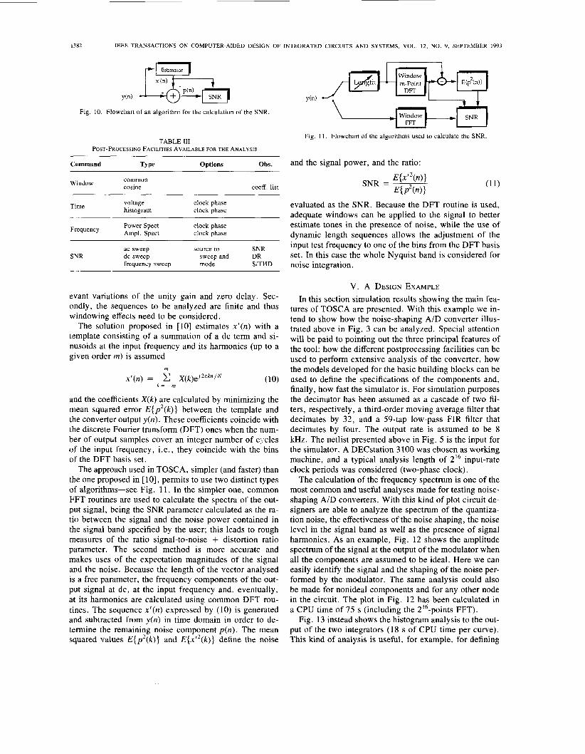
The calculation of the frequency spectrum is one of the most common and useful analyses made for testing noise- shaping A/D converters. With this kind of plot circuit de- signers are able to analyze the spectrum of the quantiza- tion noise, the effectiveness of the noise shaping, the noise level in the signal band as well as the presence of signal harmonics. As an example, Fig. 12 shows the amplitude spectrum of the signal at the output of the modulator when all the components are assumed to be ideal. Here we can easily identify the signal and the shaping of the noise per- formed by the modulator. The same analysis could also be made for nonideal components and for any other node in the circuit. The plot in Fig. 12 has been calculated in a CPU time of 75 s (including the 216-points FFT).
Fig. 13 instead shows the histogram analysis to the out- put of the two integrators ( 1 8 s of CPU time per curve). This kind of analysis is useful, for example, for defining
LIBERAL1 er al.: TOSCA: SIMULATOR FOR AID CONVERTERS
Modulator Output Spectra
1383
0 ki Y
Frequency [Hzl
Fig. 12. Amplitude spectrum of the signal at the output of the modulator. The input is a 1-kHz sinewave of full dynamic amplitude.
Histogram 4.00et03 , 1
a 3 .
2.
1 .
-2 -1 0 1 2
Amplitude [ V I
Fig. 13. Amplitude histogram of the signal at the output of the two integrators in the conditions of Fig. 13; (a) 1st integra- tor and (b) 2nd integrator.
the swing specifications for the amplifiers and also to help designers in optimizing the integration gain together with the feedback reference voltages (D/A output levels) [36] .
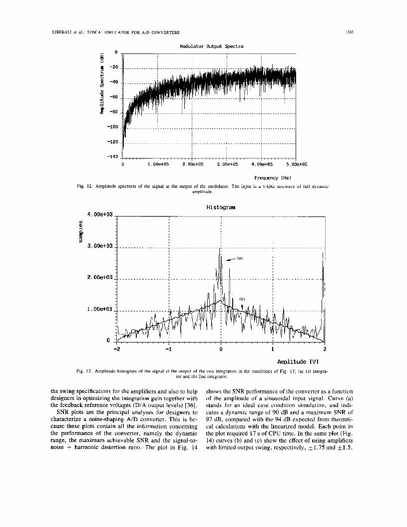
SNR plots are the principal analyses for designers to characterize a noise-shaping A/D converter. This is be- cause these plots contain all the information concerning the performance of the converter, namely the dynamic range, the maximum achievable SNR and the signal-to- noise + harmonic distortion ratio. The plot in Fig. 14
shows the SNR performance of the converter as a function of the amplitude of a sinusoidal input signal. Curve (a) stands for an ideal case condition simulation, and indi- cates a dynamic range of 90 dB and a maximum SNR of 97 dB, compared with the 94 dB expected from theoreti- cal calculations with the linearized model. Each point in the plot required 17 s of CPU time. In the same plot (Fig. 14) curves (b) and (c) show the effect of using amplifiers with limited output swing, respectively, f 1.75 and f 1.5,

1384 IEEE TRANSACTIONS ON COMPUTER-AIDED DESIGN OF INTEGRATED CIRCUITS AND SYSTEMS, VOL. 12, NO. 9, SEPTEMBER 1993
100
90
80
70
60
50
40
30
20
10
0
Input Amplitude CdBl Fig. 14. SNR performance of the converter as a function of the amplitude of sinusoidal input signal; (a) ideal components;
(b) and (c) swing limited operational amplifiers, f 1.75 and f 1.5 of the maximum amplitude of the input, respectively.
100
90
80
70
60
50
40
30
20
10
0
Fig.
-90 -80 -70 -60 -50 -40 -30 -20 -10 0
Input Amplitude CdBl 5 . SNR performance of the converter as a function of the amplitude of sinusoidal input signal; (a) ideal componer s;
(b) 60 dB and (c) 40 dB dc-gain amplifiers.
relative to the maximum amplitude of the input test sig- nal. Together with the histogram analysis plotted above in Fig. 13 it is then possible to define the minimum output swing required by the amplifiers for which there is no sig- nificant degradation of the SNR performance.
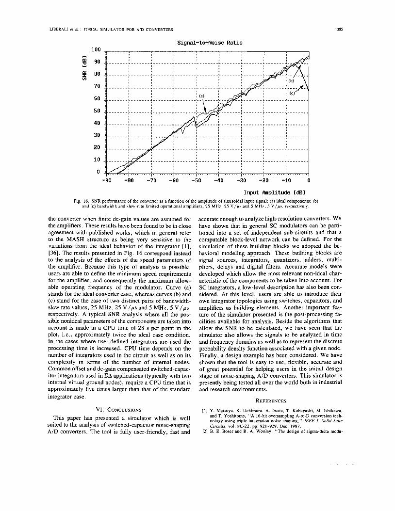
Figs. 15 and 16 show some more simulation results concerning the analysis of the effects of the non-ideal characteristics associated with the operational amplifiers. The parameters considered are the dc-gain, the bandwidth and the slew-rate. Fig. 15 plots the SNR performance of
LIBERAL1 ef al.: TOSCA: SIMULATOR FOR AID CONVERTERS 1385
Signal-to-Noise Ratio
Y G K m
100
90
80
70
60
50
40
30
20
10
0
-90 -80 -70 -60 -50 -40 -30 -20 -10 0
Input Amplitude [dB1 Fig. 16. SNR performance of the converter as a function of the amplitude of sinusoidal input signal; (a) ideal components;
and (c) bandwidth and slew-rate limited operational amplifiers, 25 MHz, 25 V / p s and 5 MHz, 5 V / p s , respectively.
the converter when finite dc-gain values are assumed for the amplifiers. These results have been found to be in close agreement with published works, which in general refer to the MASH structure as being very sensitive to the variations from the ideal behavior of the integrator [l], [36]. The results presented in Fig. 16 correspond instead to the analysis of the effects of the speed parameters of the amplifier. Because this type of analysis is possible, users are able to define the minimum speed requirements for the amplifier, and consequently the maximum allow- able operating frequency of the modulator. Curve (a) stands for the ideal converter case, whereas curves (b) and (c) stand for the case of two distinct pairs of bandwidth- slew rate values, 25 MHz, 25 V/ps and 5 MHz, 5 V/ps, respectively. A typical SNR analysis where all the pos- sible nonideal parameters of the components are taken into account is made in a CPU time of 28 s per point in the plot, i.e., approximately twice the ideal case condition. In the cases where user-defined integrators are used the processing time is increased. CPU time depends on the number of integrators used in the circuit as well as on its complexity in terms of the number of internal nodes. Common offset and dc-gain compensated switched-capac- itor integrators used in EA applications (typically with two internal virtual ground nodes), require a CPU time that is approximately five times larger than that of the standard integrator case.
VI. CONCLUSIONS This paper has presented a simulator which is well
suited to the analysis of switched-capacitor noise-shaping A/D converters. The tool is fully user-friendly, fast and
accurate enough to analyze high-resolution converters. We have shown that in general SC modulators can be parti- tioned into a set of independent sub-circuits and that a computable block-level network can be defined. For the simulation of these building blocks we adopted the be- havioral modeling approach. These building blocks are signal sources, integrators, quantizers, adders, multi- pliers, delays and digital filters. Accurate models were developed which allow the most relevant non-ideal char- acteristic of the components to be taken into account. For SC integrators, a low-level description has also been con- sidered. At this level, users are able to introduce their own integrator topologies using switches, capacitors, and amplifiers as building elements. Another important fea- ture of the simulator presented is the post-processing fa- cilities available for analysis. Beside the algorithms that allow the SNR to be calculated, we have seen that the simulator also allows the signals to be analyzed in time and frequency domains as well as to represent the discrete probability density function associated with a given node. Finally, a design example has been considered. We have shown that the tool is easy to use, flexible, accurate and of great potential for helping users in the initial design stage of noise-shaping A/D converters. This simulator is presently being tested all over the world both in industrial and research environments.
REFERENCES [ l ] Y. Matsuya, K. Uchimura, A. Iwata, T. Kobayashi, M. Ishikawa,
and T. Yoshitome, “A 16-bit oversampling A-to-D conversion tech- nology using triple-integration noise shaping,” IEEE J . Solid-Srace Circuirs, vol. SC-22, pp. 921-929, Dec. 1987.
[2] B. E. Boser and B . A. Wooley, “The design of sigma-delta modu-
1386 IEEE TRANSACTIONS ON COMPUTER-AIDED DESIGN OF INTEGRATED CIRCUITS AND SYSTEMS, VOL. 12, NO. 9, SEPTEMBER 1993
lation analog-to-digital converters,” IEEE J . Solid-State Circuirs, vol. 23, pp. 1298-1308, Dec. 1988. D. R. Welland, B. P. del Signore, E. J . Swanson, T . Tanaka, K. Hamashita, S. Hara, and K. Takasuka, “A stereo 16-bit delta-sigma AID converter for digital audio,” J . Audio Eng. Soc., vol. 37, pp. 476-486, June 1989. M. Rebeschini, N. R. Van Bavel, P. Rakers, R. Greene, J. Caldwell, and J. R. Haugh, “A 16-b 160 kHz CMOS AID converter using sigma-delta modulation,” IEEE J . Solid-State Circuits, vol. 25, pp. 431-440, Apr. 1990. B. Signore, D. Kerth, N. Sooch, and E. Swanson, “A monolithic 20-b delta sigma AID converter,” IEEE J . Solid-State Circuits, vol. 25, pp. 1311-1316, Dec. 1990. R. W . Adams, P. F. Ferguson Jr., A. Ganesan, S. Vincelette, A. Volpe, and R. Libert, “Theory and practical implementation of a fifth- order sigma-delta A/D converter,” J . Audio Eng. Soc., vol. 39, no.
V. F. Dias, G. Palmisano, P. O’Leary, and F. Maloberti, “Funda- mental limitations of switched-capacitor sigma-delta modulators, ” in Inst. Elect. Eng. Proc.-Part G , vol. 139, no. I , pp. 27-32, Feb. 1992. V. F. Dias, G. Palmisano, F. Maloberti, “Noise in mixed continu- ous-time switched-capacitor sigma-delta modulators,” to appear in Inst. Elect. Eng. Proc.-Part G, vol. 139, no. 6, pp. 680-684, Dec. 1992. M. W . Hauser, “Technology scaling and performance limitations in delta-sigma analog-digital converters,” in Proc. fEEE fnt. Symp. Circuits and Systems, 1990, pp. 356-359. B. E. Boser, K.-P. Karmann, H. Martin, and B. A. Wooley, “Sim- ulating and testing oversampled analog-to-digital converters,” IEEE Trans. Computer-Aided Design, vol. 7, pp. 668-674, June 1988. C. M. Wolf and L. R . Carley, “Simulation of S-D modulators using behavioural models,” in Proc. IEEE Int. Symp. Circuits and Systems, 1990, pp. 376-379. T . Ritoniemi, T. Karema, H. Tenhunen, M. Lindell, “Fully differ- ential CMOS sigma-delta modulator for high-performance analog-to- digital conversion with 5 V operating voltage,” in Proc. IEEE Int. Symp. Circuits and Systems, pp. 2321-2326, 1988.
718, pp. 515-528, JulyIAug. 1991.
[I31 K. C.-H. Chao, S . Nadeem, W-. L. Lee, and C. G. Sodini, “A higher order topology for interpolative modulators for oversampling AID converters,” IEEE Trans. Circuits Syst . , vol. CAS-37, pp. 309-318, Mar. 1980.
[14] Saber Users Guide. Analogy Inc., 1989. [ 151 ELDO-Electrical Circuit Simulator. Ulm, Germany: Anacad
Computer Systems, 1991. [161 G. Brauns, R. Bishop, M. Steer, J. Paulos, and S. Ardalan, “A table-
based modeling of delta-sigma modulators using ZSIM,” IEEE Trans. Computer-Aided Design, vol. 9 , pp. 142-150, Feb. 1990.
[I71 F. Medeiro, B. Verdu, A. Vizquez, and J. Huertas, “A tool for au- tomated design of sigma-delta modulators using statistical optimiza- tion,” in Proc. fEEE Int. Symp. Circuits and Sysrems, Chicago, IL, May 1993.
(181 V. F. Dias, “A design environment for switched-capacitor noise- shaping AID converters,” Ph.D. dissertation, University of Pavia, Italy, 1991.
[I91 J. Doernberg, H. Lee, and D. Hodges, “Full-speed testing of A/D converters,” IEEE J . Solid-State Circuits, vol. SC-19, pp. 820-827, Dec. 1984.
[20] M. Bossche, J . Schoukens, J . Reneboog, “Dynamic testing and di- agnostics of AID converters,” IEEE Trans. Circuits and Systems,
[21] M. F. Wagdy and S. S . Awad, “Determining ADC effective number of bits via histogram testing,” fEEE Trans. Instrum. Meas., vol. 40, pp. 770-772, Aug. 1991.
1221 V. F . Dias, F. Maloberti, “Design and performance evaluation of high-resolution oversampling A/D converters,” in Proc. Fourth CSII IEEE fnr. Symp. VLSI Design, New Delhi, India, Jan. 1991.
[23] V. F. Dias, V. Liberali, F. Maloberti, “TOSCA: A simulator for oversampling converters with behavioural modeling, ” in Proc. fEEE CompEuro ’91, Bologna, Italy, May 1991.
[24] V. F. Dias, V. Liberali, F. Maloberti, “TOSCA: A user-friendly behavioural simulator for oversampling AID converters,” in Proc. IEEE Int. Symp. Circuits and Systems, Singapore, June 1991.
[25] V. F. Dias, V. Liberali, and F. Maloberti, “TOSCA User’s Guide,” Internal Rep., Dep. Electron., Univ. Pavia, Italy, 1991.
[26] L. W . Nagel, D. 0. Pederson, “SPICE simulation program with in- tegrated circuit emphasis,’’ presented at the 19th Midwest Synip. on Circuit Theory, Waterloo, U.K., Apr. 1973.
vol. CAS-33, pp. 775-785, Aug. 1986.
A. V. Oppenheim and R. W. Schafer, Digital Signal Processing. Englewood Cliffs, NJ: Prentice-Hall, 1986. S . C. Fang, Switcap Users Guide. New York: Columbia University, 1982. K. Suyama, S.-C. Fang, and Y . Tsividis, “Simulation of mixed switched-CapacitorIdigital networks with signal-driven switches,” IEEEJ. Solid-State Circuits, vol. 25, pp. 1403-1413, Dec. 1990. V. F. Dias, J. Franca, “A comparative study of FIR switched-capac- itor decimator structures for high-frequency applications,” in Proc. 3Ist Midwest Symp. on Circuits and Systems, St. Louis, MO, Aug. 1988. I . Candy, “Decimation for sigma-delta modulation,” IEEE Trans. Commun., vol. COM-34, pp. 72-76, Jan. 1986. R. Crochiere, L. Rabiner, Multirate Digital Signal Processing. En- glewood Cliffs, NJ: Prentice-Hall, 1983. The Engineering Staff of Analog Devices Inc., Analog-Digital Con- version Handbook. F. J . Harris, “On the use of windows for harmonic analysis with discrete fourier transform,” in Proc. IEEE, vol. 66, pp. 51-83, Jan. 1978. A. H. Nuttall, “Some windows with very good sidelobe behaviour,” IEEE Trans. Acoustics, Speech, and Signal Processing, vol. ASSP-29, pp. 84-91, Feb. 1981. D. B. Ribner, “A comparison of modulator networks for high-order oversampled ZA analog-to-digital converters, ” IEEE Trans. Circuits Syst., vol. 38, pp. 145-159, Feb. 1991.
Valentino Liberali received the Laurea degree in electronics from Universitl degli Studi di Pavia, Pavia, Italy in 1986.
From 1987 to 1990 he was with Italian Nuclear Physics Institute (INFN) working on the devel- opment and testing of low-noise electronics for particle detectors. In 1990 he joined the Depart- ment of Electronics of the University of Pavia, It- aly, where presently he is Assistant Professor. His main research interests are the design of analog/ digital interfaces and the behavioral modelling and
Englewood Cliffs, NJ: Prentice-Hall, 1986.
simulation of CMOS integrated circuits. Victor F. Dias received the Licenciatura and the Mestrado in electrical and computer engineering from Instituto Superior TCcnico, Lisbon, Portu- gal, in 1986 and 1989, respectively, and the Dot- toraro di Ricerca in electronics and informatics from Universitl degli Studi di Pavia, Pavia, Italy in 1992.
Since March 1992 he has been an Assistant Pro- fessor at IST, Lisbon, Portugal, and a researcher at INESC-Lisbon where he is involved in the de- velopment of mixed analog-digital ASIC’s. His
current research interests are in mixed analog-digital integrated circuits based on oversampled sigma-delta modulation techniques and dedicated software tools for simulation and testing.
Franco Maloberti (A’84-SM’87) received the Luurea degree in physics in 1968 from University of Parma.
From 1968 to 1969 he was a research assistant with the University of Aquila. In 1969 he joined the University of Pavia, Department of Electron- ics, where he is currently a full Professor and head of the university’s microelectronic laboratory. He has published more than 90 papers, holds 11 pat- ents and is co-editor of the book Analogue-Digital ASICS. Circuit Techniaues. Design Tools and AD-
plications, (London, UK: IEE Press).
tronic Society) and a senior member of IEEE. Prof. Maloberti is a member of AEI (Italian Electrotechnical and Elec-
Copyright © 2022 FDOKUMEN