schemes for higher efficiency switched-mode power converters
190
NOVEL DESIGN TECHNIQUES AND CONTROL SCHEMES FOR HIGHER EFFICIENCY SWITCHED-MODE POWER CONVERTERS CHI WA TSANG Thesis submitted to the Department of Electronic and Electrical Engineering in partial fulfilment of the requirements for the degree of Doctor of Philosophy Supervised by Dr. Martin P. Foster and Prof. David A. Stone June 2014
-
Upload
khangminh22 -
Category
Documents
-
view
1 -
download
0
Transcript of schemes for higher efficiency switched-mode power converters

NOVEL DESIGN TECHNIQUES AND CONTROL
SCHEMES FOR HIGHER EFFICIENCY SWITCHED-MODE
POWER CONVERTERS
CHI WA TSANG
Thesis submitted to the
Department of Electronic and Electrical Engineering
in partial fulfilment of the requirements for the degree of
Doctor of Philosophy
Supervised by Dr. Martin P. Foster and Prof. David A. Stone
June 2014

ii
Summary
This thesis details novel control schemes and design techniques with the aim of improving the
performance of several switched-mode power converter topologies. These improvements include
higher steady-state and transient efficiencies for hard-switching converters and the automatic
current limiting provision for LLC resonant converters.
The thesis initially attempts to use linear closed-loop controllers to improve the transient response
of synchronous buck converters, enabling them to be designed with a lower open-loop bandwidth
so that the system can achieve higher efficiency. Three types of controllers were investigated viz:
the PID, the state-feedback and the predictive controller. All three controllers exhibit similar step
responses, which are the maximum transient responses achievable by the linear controllers with
the given requirements.
The thesis then examines the parallel converter (i.e. a converter with two parallel connected power
modules (PMs)) in detail with a view to improve the efficiency and to minimise the current ripple
experienced by the output capacitor. Two control schemes and a design technique for the parallel
converter are proposed, to simultaneously improve its efficiency and power density. The parallel
converter in this research consists of two non-identical rated PMs (termed main PM and auxiliary
PM), with the transient response requirement allocated to the auxiliary PM, thereby allowing the
main PM to operate at a lower frequency for higher steady-state efficiency.
The first control scheme activates the auxiliary PM only when a pre-determined deviation in
load/output voltage is exceeded under a load step. Thus, eliminating the losses contributed by the
low efficiency auxiliary PM for small load step changes. The second control scheme shapes the
auxiliary PM inductor current to be equal and opposite to the main PM current ripple, which when
combined reduce the current ripple as experienced by the output filter capacitor, thereby allowing
a lower value (and hence physically smaller) capacitor to be selected for higher power density. In
order to improve the converter's steady-state efficiency further, the minimum load condition is

iii
allocated to the auxiliary PM in the new design technique. These allow both the main PM
inductance and its switching frequency to be lower for higher efficiency.
In recent years, the LLC has received much attention owing to its favourable operating
characteristics including high efficiency and high power density. Usually one chooses to operate
at or very close to the load independent point (LIP) since very little control effort is required to
regulate the converter's output voltage in response to changes in the load. However under fault
conditions where the load tends towards a short circuit, excessive currents can flow and thus
control action need to be taken to protect both the converter and the load. The final topic of the
thesis hence studies the characteristics of an LLC resonant converter with current-limiting
capacitor-diode clamp and develops a new equivalent circuit model to predict the behaviour under
overload conditions. A detailed analysis of the converter is presented using the proposed model,
from which a design methodology is derived allowing the optimum circuit components to be
selected to achieve the required current limiting/protection characteristics.

iv
Publications
Some of the work contained in this thesis has been disseminated at the following international
conferences and in learned society journals:
[P1] C.-W. Tsang, M.P. Foster and D.A. Stone, ‘Parallel buck converter with non-identical
power module for improved transient efficiency’, Power Control and Intelligent Motion
(PCIM) 2013.
[P2] C.-W. Tsang, M.P. Foster and D.A. Stone, ‘New design approach for higher energy
efficiency with parallel converter’, IET PEMD conf., 2012, pp 1-6.
[P3] C.-W. Tsang, M.P. Foster, D.A. Stone and D. Gladwin, ‘Active current ripple
cancellation in parallel connected buck converter modules’, IET Power Electron., 2013,
6, pp 721-731.
[P4] C.-W. Tsang, M.P. Foster, D.A. Stone and D. Gladwin, (In Press) ‘Analysis and design
of the LLC resonant converter with capacitor-diode clamp current-limiting’, IEEE Trans.
Power Electron., accepted April 2014.

v
Acknowledgements
First, I would like to thank my supervisors Martin Foster and Dave Stone for their valuable
support and guidance throughout the work, particularly, their patience and tolerance. I am
indebted to you for all that I have learned.
I would like to acknowledge the EPSRC for providing funding to this research.
Many thanks all members for the Electrical Machines and Drives group for making the Mappin
Building a friendly environment to conduct research in. In particular, Dan Gladwin, James Green,
Andrew Fairweather, Daniel Schofield, Daniel Rogers, and those who have helped proof read my
work.
Special thanks to Dalil Benchebra, Jonathan Davidson, David Hewitt, Sami Saad Abuzed, Huw
Price, Jonathan Gomez, Shahab Nejad, Glynn Cooke and Rui Zhao for their constructive feedback
and for helping me to prepare for the viva.
Finally, I would like to thank my parents and colleagues for all their support.

vi
Table of Contents
Summary .................................................................................................................................... ii
Publications ............................................................................................................................... iv
Acknowledgements .................................................................................................................... v
Nomenclature ........................................................................................................................... ix
List of figures ............................................................................................................................ xv
List of tables ........................................................................................................................... xvii
1. Introduction .......................................................................................................................... 1
1.1. Background ................................................................................................................... 1
1.2. Switched-mode power converters ................................................................................ 2
1.2.1. Non-isolated converter .............................................................................................. 3
1.2.2. Isolated power converter .......................................................................................... 7
1.2.3. Load resonant converters .......................................................................................... 9
1.2.4. Design considerations and challenges .................................................................... 12
1.3. Thesis outline .............................................................................................................. 13
1.4. Contribution ................................................................................................................ 15
2. Control schemes and switched-mode power converter topologies for high efficiency ..... 16
2.1. Introduction ................................................................................................................ 16
2.2. Mathematical modelling ............................................................................................. 16
2.3. Closed-loop controllers ............................................................................................... 18
2.4. Transient efficiency of a parallel converter ................................................................ 20
2.5. Steady-state efficiency of a parallel converter ........................................................... 22
2.6. Active current ripple cancellation schemes ................................................................ 22
2.7. LLC resonant converter with capacitor-diode clamp .................................................. 24
2.8. Summary ..................................................................................................................... 25
3. Closed-loop controllers for buck converters ...................................................................... 27
3.1. Introduction ................................................................................................................ 27
3.2. Circuit operation and component selection ............................................................... 27
3.3. Equivalent circuit model ............................................................................................. 32
3.4. Controller design ......................................................................................................... 39
3.4.1. Performance indices ................................................................................................ 40
3.4.2. Robust PID control ................................................................................................... 42
3.4.3. State feedback control ............................................................................................ 44

vii
3.4.4. Predictive control .................................................................................................... 46
3.4.5. Digital implementation ........................................................................................... 49
3.5. Design examples and experimental results ................................................................ 49
3.5.1. Robust PID controller .............................................................................................. 50
3.5.2. State feedback controller ........................................................................................ 52
3.5.3. Predictive controller ................................................................................................ 54
3.5.4. Converter prototype ................................................................................................ 56
3.6. Summary ..................................................................................................................... 61
4. Improvements in transient response with parallel converters .......................................... 63
4.1. Introduction ................................................................................................................ 63
4.2. Circuit configuration and components selection ......................................................... 63
4.3. Control schemes for transient condition .................................................................... 66
4.3.1. FRDB scheme ........................................................................................................... 68
4.3.2. SCM-PCM scheme ................................................................................................... 70
4.3.3. Proposed FRHE scheme ........................................................................................... 72
4.4. Controller design ......................................................................................................... 74
4.5. Design example and experimental results .................................................................. 76
4.5.1. Settling time and on-duration characteristics ......................................................... 77
4.5.2. Converter prototype ................................................................................................ 80
4.6. Summary ..................................................................................................................... 82
5. Improvements in steady-state efficiency with parallel connected converters .................. 83
5.1. Introduction ................................................................................................................ 83
5.2. Two-switch forward converter (2SFC) ........................................................................ 83
5.2.1. Circuit operation...................................................................................................... 84
5.3. Design techniques for parallel converter .................................................................... 87
5.3.1. Proposed (HSSE) design technique .......................................................................... 88
5.4. Loss analysis ................................................................................................................ 90
5.5. Design examples and experimental results ................................................................ 94
5.5.1. Interleaved converter design ................................................................................... 94
5.5.2. Converter designed by the proposed HSSE technique ............................................. 95
5.5.3. Prototype converters ............................................................................................... 99
5.6. Summary ................................................................................................................... 102
6. Active current ripple cancellation using a high frequency auxiliary converter ................ 103
6.1. Introduction .............................................................................................................. 103

viii
6.2. Active current ripple cancellation ............................................................................. 103
6.2.1. Theory of operation ............................................................................................... 104
6.2.2. Inductor current ripple and rate of change ........................................................... 105
6.2.3. Generation of the cancellation current ................................................................. 108
6.3. Design consideration................................................................................................. 110
6.3.1. Auxiliary PM inductor and duty cycle selection ..................................................... 110
6.3.2. Ripple reduction ratio ............................................................................................ 114
6.3.3. Efficiency comparison ........................................................................................... 114
6.3.4. Practical consideration .......................................................................................... 116
6.4. Design example and experimental results ................................................................ 117
6.4.1. Switching frequencies and component value selection ........................................ 118
6.4.2. Prototype converter .............................................................................................. 122
6.5. Summary ................................................................................................................... 126
7. LLC resonant converter with capacitor-diode clamp ........................................................ 127
7.1. Introduction .............................................................................................................. 127
7.2. Circuit operation ....................................................................................................... 127
7.3. Equivalent circuit model ........................................................................................... 133
7.3.1. Diode-clamp inactive ............................................................................................. 133
7.3.2. Diode-clamp active ................................................................................................ 135
7.3.3. Diode-clamp conduction point .............................................................................. 138
7.3.4. Nominalised gain with active diode-clamp ........................................................... 139
7.4. Analysis of converter operating characteristic ......................................................... 140
7.4.1. Capacitor diode-clamp characteristics .................................................................. 142
7.4.2. Converter Voltage-Current (VI) characteristics ..................................................... 145
7.5. Design example ......................................................................................................... 148
7.6. Summary ................................................................................................................... 153
8. Conclusion and future work .............................................................................................. 154
8.1. Conclusion ................................................................................................................. 154
8.2. Future work ............................................................................................................... 155
Reference .................................................................................................................................. 158
Appendix A - Isolated MOSFET gate driver ............................................................................ 169
Appendix B - rms current ......................................................................................................... 169
Appendix C - Calorimeter for efficiency measurement ............................................................ 171

ix
Nomenclature
Subscript m, x and i are also used with the list of symbol above to distinguish the parameters for
the main PM, auxiliary PM and interleaved converter PMs (e.g. δm, δx and δi are the duty cycles
for the main PM, auxiliary PM and interleaved PM respectively).
𝑨, 𝑩, 𝐶, 𝑫, 𝑬, 𝑲 matrices, bold font represents vector
𝐴𝑐 inductor core area
𝐴𝑠 resonant tank inductor ratio (= 𝐿𝑝 𝐿𝑠⁄ )
𝐴𝑤 winding cross-sectional area
𝐵𝑊 system bandwidth
𝐵𝑓 flux density
𝐵𝑝𝑒𝑎𝑘 peak flux density
𝐵𝑠 capacitance sharing ratio (= 𝐶𝑟 𝐶𝑠⁄ )
𝑩′ augmented input vector, bold font represents vector
𝐶𝐶𝑀 continuous conduction mode
𝐶𝑀𝐶 current mode control
𝐶𝑐, 𝐶𝑠 resonant tank capacitors
𝐶𝑔𝑠, 𝐶𝑟𝑠𝑠, 𝐶𝑜𝑠𝑠 parasitic capacitors of MOSFET
𝐶𝑖 input capacitor
𝐶𝑜 output capacitor
𝐶𝑟 equivalent resonant capacitance (with inactive diode-clamp)
𝐷𝑇 dead-time
𝐷𝑘 predictive controller’s control gain
𝐷𝑐1, 𝐷𝑐2 diode-clamp diode
𝐷1, 𝐷2, 𝐷3, 𝐷4 diodes
𝑑
𝑑𝑡𝐼𝑚,
𝑑
𝑑𝑡𝐼𝑥,
𝑑
𝑑𝑡𝐼𝑚+𝑥 rate of inductor currents
𝑑
𝑑𝑡𝐼𝑚(+) ,
𝑑
𝑑𝑡𝐼𝑥(+) rate of rise of inductor currents
𝑑
𝑑𝑡𝐼𝑚(−),
𝑑
𝑑𝑡𝐼𝑥(−) rate of fall of inductor currents
𝑑
𝑑𝑡𝐼𝑚(𝑛𝑒𝑡),
𝑑
𝑑𝑡𝐼𝑥(𝑛𝑒𝑡) net rate of inductor currents
𝑑
𝑑𝑡𝐼𝑥(𝑛𝑒𝑡+) net rate of rise of inductor current
𝑑
𝑑𝑡𝐼𝑥(𝑛𝑒𝑡−) net rate of fall of inductor current

x
𝐸𝑆𝑅 equivalent series resistance
𝑒 error signal, 𝑒 = 𝑟 − 𝑦
𝑒ss steady-state error
𝐹𝐻𝐴 fundamental harmonic approximation
𝐹𝑅𝐷𝐵 fast response double buck scheme
𝐹𝑅𝐻𝐸 fast recovery with high transient efficiency scheme
𝑓𝑠𝑚, 𝑓𝑠𝑥, 𝑓𝑠𝑖 switching frequencies
𝑓𝑠(𝑚𝑖𝑛) minimum switching frequency
𝑓𝑠(𝑚𝑎𝑥) maximum switching frequency
𝑓𝑛 nominalised frequency (𝑓𝑛 = 𝑓𝑠/𝑓0)
𝑓0 resonant frequency
𝐻𝑆𝑆𝐸 high steady-state efficiency design technique
𝐼𝐴𝐸 integral of the absolute magnitude of the error
𝐼𝑆𝐸 integral of the squared of the error
𝐼𝑇𝐴𝐸 integral of time multiplied by absolute error
𝐼𝑇𝑆𝐸 integral of time multiplied by the squared error
𝐼 identity matrix
𝐼𝑐𝑜 current reference
𝐼(𝑑𝑐) dc current
𝐼𝑖 input current
𝐼𝑚(𝑟𝑚𝑠), 𝐼𝑥(𝑟𝑚𝑠), 𝐼𝑖(𝑟𝑚𝑠) rms currents
𝐼𝑟𝑒𝑓 current reference
𝐼𝑛 normalised output current (= 𝐼𝑜(𝑜𝑣𝑒𝑟) 𝐼𝑜(𝑟𝑎𝑡𝑒)⁄ )
𝐼𝑚, 𝐼𝑥 inductor current
𝐼𝑜 output current
𝐼𝑜(𝑟𝑎𝑡𝑒) maximum rated output current
𝐼𝑜(𝑜𝑣𝑒𝑟) overloading output current
𝐼𝑝𝑒𝑎𝑘 peak current
𝐼𝑟 compensation ramp
𝐼𝑠 current step
𝐽 cost function
𝑘𝑖𝑚 imaginary component used in 𝑀𝑔(𝑐𝑙𝑚𝑝)
𝑘𝑟𝑒 real component used in 𝑀𝑔(𝑐𝑙𝑚𝑝)
𝐾𝑉𝐿 Kirchhoff’s voltage law
𝐾𝐶𝐿 Kirchhoff’s current law
𝐾𝑐 input voltage compensation gain

xi
𝐾𝑒 Euler’s equation gain
𝐾𝑔 instrumentation amplifier gain
𝐾𝑃, 𝐾𝑃𝑚, 𝐾𝑃𝑥 proportional gains of PID controller
𝐾𝐼, 𝐾𝐼𝑚, 𝐾𝐼𝑥 integral gains of PID controller
𝐾𝐷, 𝐾𝐷𝑚, 𝐾𝐷𝑥 derivative gains of PID controller
𝐾1, 𝐾2, 𝐾𝑖 state feedback controller gains
𝐾PWM PWM gain
𝐾Id discrete-time equivalent of integrator gain
𝐾𝑠 system gain
𝐿𝐼𝑃 load independent point
𝐿, 𝐿𝑚, 𝐿𝑥, 𝐿𝑖 inductors
𝐿𝑝, 𝐿𝑠 resonant tank inductors
𝐿𝑚𝑚, 𝐿𝑚𝑥 magnetising inductors
𝑙 legth of wire
𝑀𝑔 nomalised gain (with inactive diode-clamp)
𝑀𝑔(𝑚𝑎𝑥) maximum nomalised gain (with inactive diode-clamp)
𝑀𝑔(𝑚𝑖𝑛) minimum normalised gain (with inactive diode-clamp)
𝑀𝑔(𝑐𝑙𝑚𝑝) nomalised gain (with activated diode-clamp)
𝑚 number of auxiliary PM cycles with respect to main PM cycle
𝑚𝑛 number of phases
𝑁𝑘 predictive controller’s feedback gain
𝑁𝐿 inductor number of turns
𝑁𝑝 transformer primary number of turns
𝑁𝑠 transformer secondary number of turns
𝑛 transformer turn ratio
𝑛𝑦 predictive controller’s output horizon
𝑛𝑢 predictive controller’s input horizon
𝑃𝐶𝑀 peak current mode
𝑃𝑀 power module
𝑃𝑊𝑀 pulse-width modulation
𝑃𝑔𝑚 gate drive loss
𝑃𝑐𝑚 MOSFET conduction loss
𝑃𝑠𝑚 MOSFET switching loss
𝑃𝑐𝐿 inductor conduction loss
𝑃𝑠𝐿 inductor switching loss
𝑃𝑐𝑑 diode conduction loss
𝑃(𝑛) total loss ratio

xii
𝑃𝑐(𝑛) conduction loss ratio
𝑃𝑠(𝑛) switching loss ratio
𝑃𝑔𝑚(𝑛) gate drive loss ratio
𝑃𝑐𝑚(𝑛) MOSFET conduction loss ratio
𝑃𝑠𝑚(𝑛) MOSFET switching loss ratio
𝑃𝑐𝐿(𝑛) inductor conduction loss ratio
𝑃𝑠𝐿(𝑛) inductor switching loss ratio
𝑃𝑐𝑑(𝑛) diode conduction loss ratio
𝑃𝑐𝑚 MOSFET conduction loss
𝑃𝑟 predictive controller feedforward gain
𝑝 ripple reduction ratio
𝑄 quality factor (= √𝐿𝑠 𝐶𝑟⁄ 𝑅𝑒𝑞⁄ )
𝑄𝑔 MOSFET gate charge
𝑄𝑛 normalised Q-factor (= 𝑄𝑜𝑣𝑒𝑟 𝑄𝑟𝑎𝑡𝑒⁄ )
𝑄𝑜𝑣𝑒𝑟 Q-factor at overloading
𝑄𝑟 charge due to current ripple
𝑄𝑟𝑎𝑡𝑒 Q-factor at maximum rated load
𝑄𝑟𝑟 reverse recovery charge
𝑄𝑢𝑠 charge due to load step
𝑅 real component of 𝑍𝑐
𝑅𝐶 parasitic capacitor resistance
𝑅𝑑𝑠 MOSFET on-state resistance
𝑅𝑒𝑞 equivalent load resistance
𝑅𝑔 instrumentation amplifier gain resistor
𝑅𝐿 parasitic inductor resistance
𝑅𝑙 load resistance
𝑅𝑤 winding resistance
𝑟 reference signal
𝑆𝐵𝐶 synchronous buck converter
𝑆𝐶𝑀 sensorless current mode
𝑆𝐶𝑀 − 𝑃𝐶𝑀 sensorless and peak current mode scheme
𝑆𝑀𝑃𝐶 switched-mode power converter
𝑆𝑆𝐴 state-space averaging
𝑆1, 𝑆2 MOSFETs
𝑠 complex frequency (= 𝑗𝜔𝑠)
𝑇, 𝑇𝑠 switching period
𝑇𝐷 derivative time constant

xiii
𝑇𝐼 integral time constant
𝑇𝑓 MOSFET fall time
𝑇𝑟 MOSFET rise time
𝑇𝑝 time period
𝑇𝑠𝑒𝑡 settling time
𝑇𝑥 auxiliary PM switching period
𝑇1 transformer
𝑡 time
𝑡𝑚(𝑜𝑛), 𝑡𝑥(𝑜𝑛) on-periods
𝑡𝑚(𝑜𝑓𝑓), 𝑡𝑚(𝑜𝑓𝑓) off-periods
𝑡𝑚(𝑐𝑓) cut-off period
𝑢 intput signal
𝑉𝑀𝐶 voltage mode control
𝑉𝑅 voltage regulator
𝑉𝐶 voltage across capacitor 𝐶𝑜
𝑉𝑐 voltage across capacitor 𝐶𝑐
𝑉𝑓 diode forward voltage drop
𝑉𝑔𝑠 MOSFET gate-source voltage
𝑉𝑔 MOSFET gate drive voltage
𝑉𝑖 input voltage
𝑉𝑖(𝑚𝑖𝑛) minimum input voltage
𝑉𝑖(𝑚𝑎𝑥) maximum input voltage
𝑉𝑖(𝑛𝑜𝑟𝑚) nominal input voltage
𝑉𝐿𝑚 voltage across inductor 𝐿𝑚
𝑉𝑛 normalised output voltage (= 𝑉𝑜(𝑜𝑣𝑒𝑟) 𝑉𝑜(𝑟𝑎𝑡𝑒)⁄ )
𝑉𝑅𝐶, 𝑉𝑅𝐿, 𝑉𝑅𝑑𝑠 voltage across parasitic components 𝑅𝑐, 𝑅𝐿, 𝑅𝑑𝑠.
𝑉𝑜 output voltage
𝑉𝑜𝑠 voltage overshoot
𝑉𝑜(𝑟𝑎𝑡𝑒) maximum rated output voltages
𝑉𝑜(𝑜𝑣𝑒𝑟) overloading output voltage
𝑉𝑟𝑒𝑓 voltage reference
𝑉𝑡ℎ MOSFET threshold voltage
𝑉𝑢𝑠 voltage undershoot
𝑣𝑐𝑜 control signal
𝑣𝑑𝑠 MOSFET drain-source voltage
𝑣𝑠 sawtooth signal

xiv
X imaginary component of 𝑍c
𝒙 state vector, bold font represents vector
𝒙′ augmented state equation
�̇� (𝑑 𝑑𝑡⁄ )𝒙
�̇�′ (𝑑 𝑑𝑡⁄ )𝒙′
𝒙 state vector 𝑥 with disturbance
�̇� (𝑑 𝑑𝑡⁄ )𝒙 with disturbance
𝑦 output signal
�̃� output signal 𝑦 with distribute
𝑍1 resonant tank impedance (with inactive diode-clamp)
𝑍2 resonant tank impedance (with activated diode-clamp)
𝑍𝑐 equivalent clamping capacitance impedance (with activated
diode-clamp)
𝛼 load sharing ratio
𝛼𝑐 , 𝛽𝑐 , 𝑘𝑐 inductor core loss constants
𝛼𝑑 damping factor
𝛽 frequency ratio 𝑓𝑠𝑚 𝑓𝑠𝑖⁄
𝛾 frequency ratio 𝑓𝑠𝑥/𝑓𝑠𝑖
δ diode-clamp non-conduction angle
𝛿(+) desired duty cycle for 𝑡(𝑜𝑛)
𝛿(−) desired duty cycle for 𝑡(𝑜𝑓𝑓)
𝛿𝑚, 𝛿𝑥, 𝛿𝑖 duty cycles
𝛿𝑚 duty cycle 𝛿𝑚 with distribute
𝛿𝑚(𝑠𝑠), 𝛿𝑥(𝑠𝑠) steady-state duty cycles
𝛿′𝑚 complemented main PM duty cycle
𝜁 damping ratio
𝜃 angle
𝜆 weighting function
𝜌 wire resistivity
𝜔𝑛 system natural frequency
𝜔𝑠 angular switching frequency (= 2𝜋𝑓𝑠)
𝛥 tolerant
𝛥𝑉𝑜 output voltage ripple
𝛥𝐼𝑚 current ripple
2𝑆𝐹𝐶 two-switch forward converter

xv
List of figures
Fig. 1.1 Schematic of a linear DC power supply. ......................................................................... 1
Fig. 1.2 Schematic of main connected power supply with SMPC. ............................................... 2
Fig. 1.3 The three most basic SMPC. (a) Buck converter (b) Boost converter (c) Buck-boost
converter ....................................................................................................................................... 4
Fig. 1.4 Inverting and non-inverting step up/down converters. (a) Cuk converter (a) SEPIC
converter (b) Zeta converter. ......................................................................................................... 6
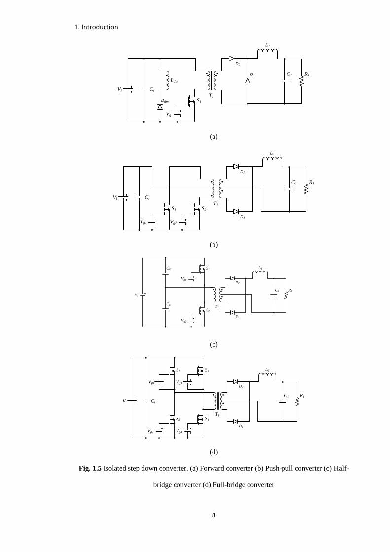
Fig. 1.5 Isolated step down converter. (a) Forward converter (b) Push-pull converter (c) Half-
bridge converter (d) Full-bridge converter .................................................................................... 8
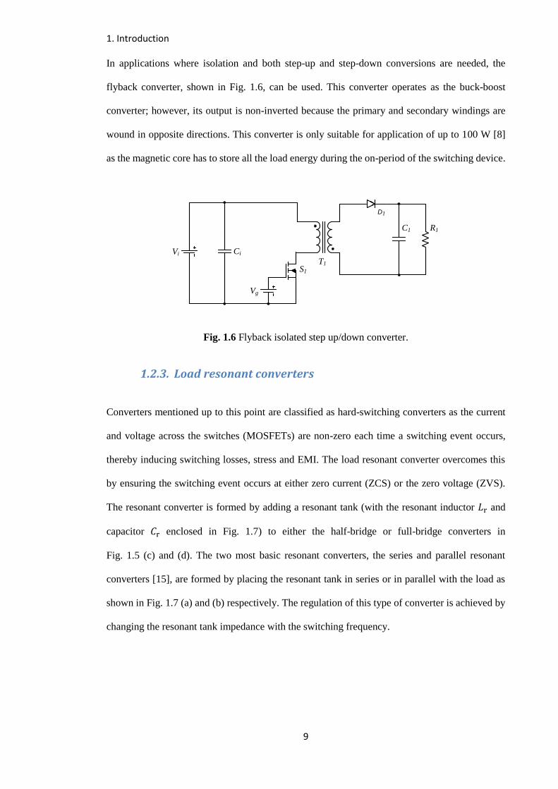
Fig. 1.6 Flyback isolated step up/down converter......................................................................... 9
Fig. 1.7 Half-bridge resonant converter. (a) Series resonant converter (b) Parallel resonant
converter ..................................................................................................................................... 10
Fig. 1.8 Two-switch forward converter. ..................................................................................... 11
Fig. 3.1 Circuit diagram of the synchronous buck converter. ..................................................... 28
Fig. 3.2 MOSFETs drive signals with dead-times. ..................................................................... 28
Fig. 3.3 Circuit diagram of SBC under the dead-time period. .................................................... 29
Fig. 3.4 Circuit diagrams showing the two subintervals. (a) on-period (b) off-period. .............. 30
Fig. 3.5 Steady state inductor current and output voltage waveforms. ....................................... 31
Fig. 3.6 Equivalent circuit model under different subintervals. (a) on-period (b) off-period. .... 32
Fig. 3.7 Block diagram of system in state-space form. ............................................................... 37
Fig. 3.8 Block diagram of system in transfer function form. ...................................................... 38
Fig. 3.9 Block diagram of closed-loop system. ........................................................................... 39
Fig. 3.10 Operation of PWM, 𝑢 = 1 if vs < vco otherwise 𝑢 = 0. ........................................... 40
Fig. 3.11 Example of a system step response. ............................................................................ 41
Fig. 3.12 Block diagram of system with robust PID controller. ................................................. 42
Fig. 3.13 Block diagram of system with state feedback with integral control. ........................... 44
Fig. 3.14 Block diagram of system with predictive controller. ................................................... 46
Fig. 3.15 Simulink model of system with the robust PID controller. ......................................... 51
Fig. 3.16 Simulated system step responses with PID controller. ................................................ 52
Fig. 3.17 Simulink model of system with the state feedback control with integral control. ....... 53
Fig. 3.18 Simulated system step response with state feedback controller. ................................. 53
Fig. 3.19 Simulink model of system with predictive controller. ................................................. 54
Fig. 3.20 Simulated system responses with predictive controllers. ............................................ 55
Fig. 3.21 Simulated system step responses with the three controllers. ....................................... 56
Fig. 3.22 Schematic of the prototype converter. (a) synchronous buck converter and (b) current
sensing circuit. ............................................................................................................................ 57
Fig. 3.23 Schematic of the microcontroller in the prototype converter. ..................................... 58
Fig. 3.24 Image of the prototype converter. ................................................................................ 58
Fig. 3.25 Simulated and practical system responses. (a) PID controller (b) State feedback
controller (c) Predictive controller .............................................................................................. 60
Fig. 3.26 Practical system responses with different controller with time delay. ......................... 61
Fig. 4.1 Parallel converter with two parallel connected SBC. .................................................... 64
Fig. 4.2 Current and voltage waveforms of converter subjected to load step. ............................ 66
Fig. 4.3 Block diagram of closed-loop current mode control. .................................................... 67

xvi
Fig. 4.4 Current mode control current and PWM waveforms. .................................................... 67
Fig. 4.5 Block diagram of a converter with the SCM control. .................................................... 68
Fig. 4.6 Auxiliary PM with nonlinear hysteretic control. ........................................................... 69
Fig. 4.7 Block diagram of the converter with FRDB. ................................................................. 69
Fig. 4.8 Voltage waveform and auxiliary PM timing diagram with FRDB. ............................... 70
Fig. 4.9 Block diagram of the converter with SCM-PCM. ......................................................... 71
Fig. 4.10 Voltage waveform with SCM-PCM. ........................................................................... 72
Fig. 4.11 Block diagram of the converter with the proposed control scheme. ............................ 73
Fig. 4.12 Voltage waveform and auxiliary PM timing diagram with the proposed scheme. ...... 74
Fig. 4.13 Flow chart of the GA tuning process. .......................................................................... 75
Fig. 4.14 Simulink model of the converter with the proposed control schemes. ........................ 77
Fig. 4.15 Simulated transient responses with auxiliary PM enabled and disabled. .................... 78
Fig. 4.16 Converter settling times with the auxiliary PM enabled and disabled. ........................ 79
Fig. 4.17 On-duration of the auxiliary PM with the different control schemes. ......................... 79
Fig. 4.18 Image of the prototype converter. ................................................................................ 80
Fig. 4.19 Image of the control board and programmer. .............................................................. 80
Fig. 4.20 Practical transient responses under different schemes. ................................................ 81
Fig. 4.21 Practical converter efficiency under different schemes. .............................................. 82
Fig. 5.1 Circuit diagram of two-switch forward converter (2SFC). ............................................ 84
Fig. 5.2 Circuit diagrams of a parallel converter with two parallel connected 2SFC. (a) on-
period (b) off-period (c) cut-off period ....................................................................................... 85
Fig. 5.3 Inductor current waveform in DCM. ............................................................................. 86
Fig. 5.4 Parallel connected two-switch forward converters. ....................................................... 86
Fig. 5.5 Current waveforms of the parallel converter. (a) non-identical PM (b) identical PM ... 88
Fig. 5.6 Current waveforms of converter with the proposed design technique. ......................... 89
Fig. 5.7 Circuit diagram of MOSFET with the three parasitic capacitors. ................................. 91
Fig. 5.8 MOSFET switching waveforms .................................................................................... 92
Fig. 5.9 Main PM transformer losses under different 𝐵peak. .................................................... 96
Fig. 5.10 Main PM inductor losses under different 𝛥𝐼m. ........................................................... 97
Fig. 5.11 Main PM components losses. ...................................................................................... 98
Fig. 5.12 Prototype of the 2SFC (proposed HSSE design technique). ..................................... 100
Fig. 5.13 The calculated efficiency curves for the two converters. .......................................... 101
Fig. 5.14 Measured efficiency curves of the two converters. ................................................... 102
Fig. 6.1 Active current ripple cancellation with identical PMs. ................................................ 104
Fig. 6.2 Main PM, auxiliary PM and resultant current waveforms. .......................................... 105
Fig. 6.3 Current waveforms of the auxiliary PM under one auxiliary PM cycle. (a) 𝛿x = 0.75
(b) 𝛿x = 0.25 ............................................................................................................................ 107
Fig. 6.4 Current waveforms of the main and auxiliary PMs over one main PM cycle. ............ 109
Fig. 6.5 Ratio of the two inductors against 𝛿𝑚 and 𝛿𝑥. ............................................................ 110
Fig. 6.6 Effect on 𝛿x and 𝛥𝐼x with different 𝐿x at 𝛿xss = 0.48. (a) 𝛿x (b) 𝛥𝐼x ....................... 112
Fig. 6.7 Effect on 𝛿x and 𝛥𝐼x with different 𝐿x at 𝛿xss = 0.3. (a) 𝛿x (b) 𝛥𝐼x ......................... 113
Fig. 6.8 Frequency ratios of the two PMs under different 𝛿m and 𝑝. ....................................... 114
Fig. 6.9 Loss ratio between the propose converter and interleaved converter. ......................... 117
Fig. 6.10 Main PM calculated losses. (a) Inductor losses (b) Total losses ............................... 119

xvii
Fig. 6.11 Calculated efficiencies. (a) Efficiencies of the different PMs (b) Efficiencies of the
proposed converter and interleaved converter ........................................................................... 121
Fig. 6.12 Prototype of the converter with the proposed scheme. .............................................. 122
Fig. 6.13 Prototype output current and voltage waveforms with and without ripple cancellation.
(a) Main and auxiliary PMs current waveforms (b) Output current waveforms (c) Output voltage
waveforms ................................................................................................................................. 124
Fig. 6.14 Measured efficiency of the proposed and interleaved converters. .............................. 126
Fig. 7.1 Half-bridge LLC resonant converter............................................................................ 128
Fig. 7.2 Gain characteristics of LLC converter under different conditions. ............................. 128
Fig. 7.3 Half-bridge LLC resonant converter with capacitor-diode clamp. .............................. 129
Fig. 7.4 Resonant capacitor voltage waveforms. (a) normal operation and (b) overloading
operation ................................................................................................................................... 131
Fig. 7.5 Equivalent circuit under different diode-clamp conduction states. (a) diode clamp
inactive (b) conduction state 1 𝛿c < 𝜃 ≤ 𝜋 (c) conduction state 2) 𝜋 + 𝛿c < 𝜃 ≤ 2𝜋 ............ 132
Fig. 7.6 Flowchart describing the interactive procedure for finding the load current during
overloading conditions (i.e. 𝑉c > 𝑉i). ...................................................................................... 139
Fig. 7.7 Converter gain characteristics. (a) 𝑄 = 0.5, 3 ≤ 𝐴s ≤ 9 (b) 0.3 ≤ 𝑄 ≤ 0.9, 𝐴s = 5 141
Fig. 7.8 Converter gain characteristics with 𝐴s = 5 and 𝑄rate = 0.5. (a) 𝐵s = 1 and (b) 𝐵s = 0
.................................................................................................................................................. 143
Fig. 7.9 Converter gain characteristics with 𝐴s = 5 and 𝑄rate = 0.5. (a) 𝐵s = 0.25 (b) 𝐵s = 0.5
(c) 𝐵s = 0.75 ............................................................................................................................. 144
Fig. 7.10 Converter VI characteristics. (a) 𝐵s = 1 (b) 𝐵s = 0 (c) 𝐵s = 0.25 (d) 𝐵s = 0.5 (e) 𝐵s =
0.75 ........................................................................................................................................... 147
Fig. 7.11 Measured resonant capacitor voltage waveform 𝑣c. (a) normal operation and (b)
overloading operation ............................................................................................................... 150
Fig. 7.12 Comparison of the theoretical and practical results. (a) voltage gain characteristics (b)
VI characteristics ...................................................................................................................... 152
Fig. 8.1 Block diagram of the converter with average current mode control. ............................ 156
Fig. 8.2 Circuit diagram of the proposed dual capacitor-diode clamp. ..................................... 157
Fig. A1 Circuit diagram of the two stages transformer coupled isolated gate driver. .............. 169
Fig. B1 Current waveform of auxiliary PM in ripple cancellation mode. ................................ 170
Fig. C1 Bespoke calorimeter. .................................................................................................... 172
Fig. C2 Calorimeter with fan for heat spread. ........................................................................... 172
Fig. C3 Calibration curves. (a) small box (b) large box. ........................................................... 173
List of tables
Table 1.1 Summary of the topologies characteristics. ................................................................ 11
Table 3.1 Predictive control laws with different tuning factors. ................................................. 54
Table 5.1 Interleaved PM transformer losses under different 𝐵peak. ........................................ 95
Table 5.2 Auxiliary PM transformer losses under different 𝐵peak. ........................................... 99
Table 5.3 Summary of parameter for the interleaved and the proposed converters. ................... 99
Table 6.1 Summaries of the duty cycles at different input voltages and load currents. ............ 125
1
1. Introduction
1.1. Background
The proliferation of electrical systems in modern society has put an increasing emphasis on power
supply (converter) design, owing to the growing requirement to interface a multitude of devices
with different specifications to the standard mains utility supply. Some examples of these devices
include televisions (TVs) and personal computers (PCs), which, in the year 2012, have worldwide
shipments of 238 million and 341 million, respectively [1].
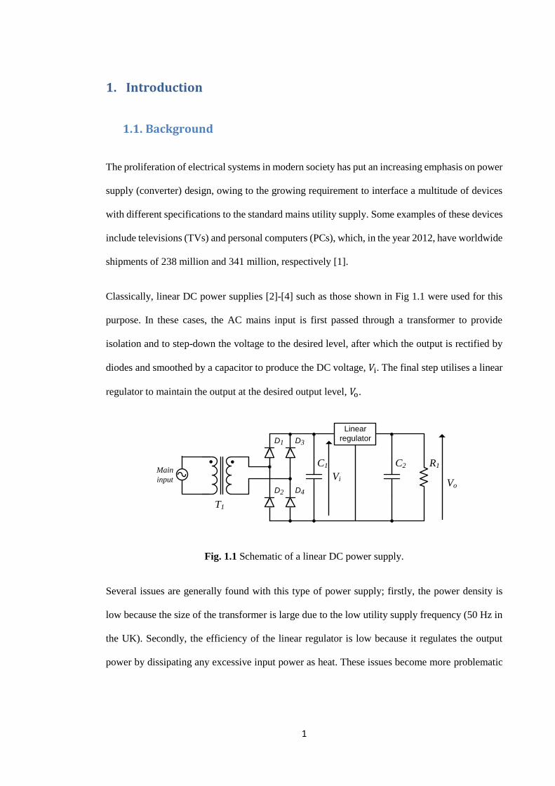
Classically, linear DC power supplies [2]-[4] such as those shown in Fig 1.1 were used for this
purpose. In these cases, the AC mains input is first passed through a transformer to provide
isolation and to step-down the voltage to the desired level, after which the output is rectified by
diodes and smoothed by a capacitor to produce the DC voltage, 𝑉i. The final step utilises a linear
regulator to maintain the output at the desired output level, 𝑉o.
C2 R1
D4D2
T1
Linear
regulatorD3D1
C1Main
input Vo
Vi
Fig. 1.1 Schematic of a linear DC power supply.
Several issues are generally found with this type of power supply; firstly, the power density is
low because the size of the transformer is large due to the low utility supply frequency (50 Hz in
the UK). Secondly, the efficiency of the linear regulator is low because it regulates the output
power by dissipating any excessive input power as heat. These issues become more problematic
1. Introduction
2
in battery operated portable devices such as mobile phone and tablet computers, where efficient
operation leads to longer battery life.
1.2. Switched-mode power converters
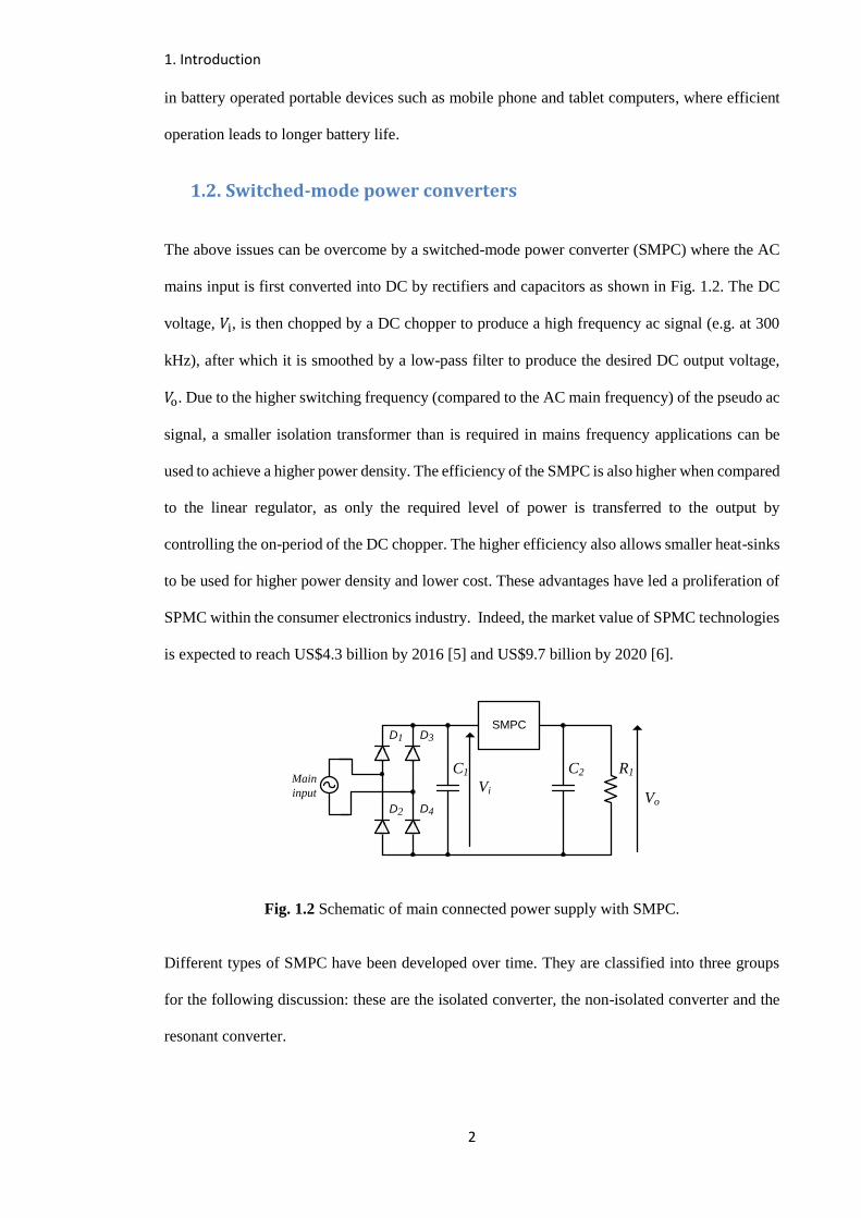
The above issues can be overcome by a switched-mode power converter (SMPC) where the AC
mains input is first converted into DC by rectifiers and capacitors as shown in Fig. 1.2. The DC
voltage, 𝑉i, is then chopped by a DC chopper to produce a high frequency ac signal (e.g. at 300
kHz), after which it is smoothed by a low-pass filter to produce the desired DC output voltage,
𝑉o. Due to the higher switching frequency (compared to the AC main frequency) of the pseudo ac
signal, a smaller isolation transformer than is required in mains frequency applications can be
used to achieve a higher power density. The efficiency of the SMPC is also higher when compared
to the linear regulator, as only the required level of power is transferred to the output by
controlling the on-period of the DC chopper. The higher efficiency also allows smaller heat-sinks
to be used for higher power density and lower cost. These advantages have led a proliferation of
SPMC within the consumer electronics industry. Indeed, the market value of SPMC technologies
is expected to reach US$4.3 billion by 2016 [5] and US$9.7 billion by 2020 [6].
C2 R1
D4D2
D3D1
C1Main
input Vo
SMPC
Vi
Fig. 1.2 Schematic of main connected power supply with SMPC.
Different types of SMPC have been developed over time. They are classified into three groups
for the following discussion: these are the isolated converter, the non-isolated converter and the
resonant converter.

1. Introduction
3
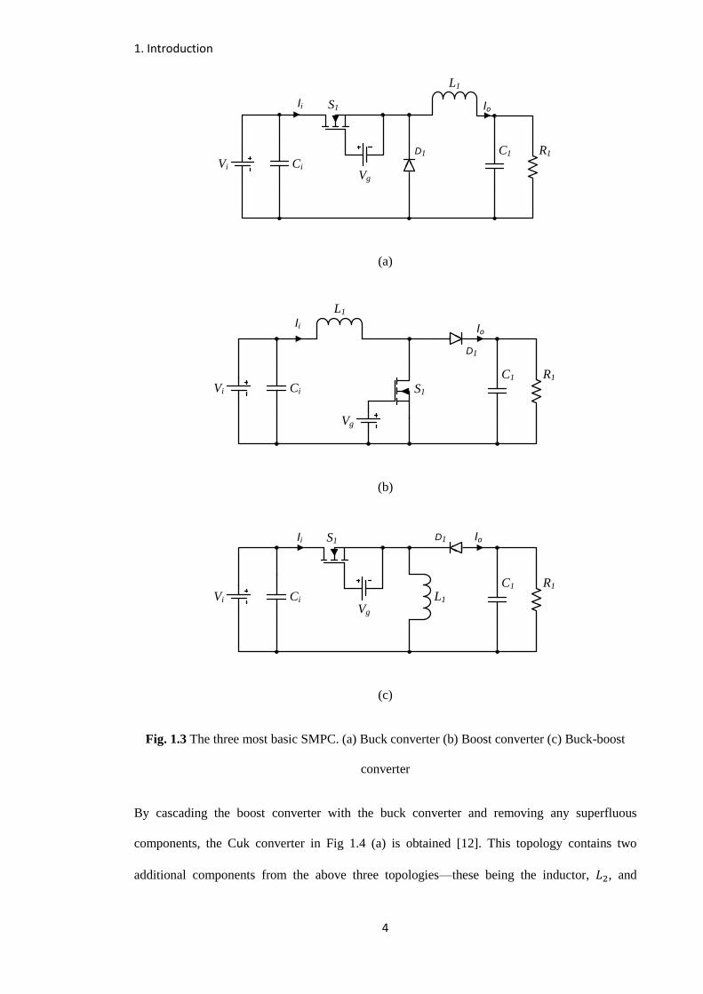
1.2.1. Non-isolated converter
To use one of the six non-isolated topologies [7][8] in this section, the conversion ratios must be
small (e.g. for a 5 V to 3.3 V step-down converter) with no isolation requirement, as these
converters are either pre-regulated with an isolated converter (discussed in section 1.2.2) or are
battery powered. The three most basic SMPCs—the buck converter [9], the boost converter [10]
and the buck-boost converter [11]—are formed by four main components. These being a power
electronic switch (𝑆1), a diode (𝐷1), an inductor (𝐿1) and a capacitor (𝐶1) as shown in Fig. 1.3.
In the buck converter shown in Fig. 1.3 (a), power is transferred to the output from the input
during the on-period of the switching device (MOSFET), and is cut-off during the off-period. The
output voltage is proportional to the ratio of the on-period to the overall switching period. This
ratio is always smaller than unity and so the output voltage is always lower than the input voltage
in a practical system (i.e. this is a step-down converter). The inductor stores energy during the on-
period which is then released during the off-period to smooth the pulsated (discontinuous) input
current, 𝐼𝑖, forming a DC (continuous) output current, 𝐼𝑜, perturbed by a small ripple (n.b. 𝐷1 is
commonly replaced by a MOSFET to reduce the converter’s loss. The buck converter with this
modification is called the synchronous buck converter (SBC), for which more detail will be given
in chapter 3). The boost converter in Fig. 1.3 (b) stores energy in the inductor during the on-period
which is then released together with power directly from the input during the off-period,
producing an output voltage that is always greater than the input voltage (i.e. this is a step-up
converter). With the inductor in series with the input source, the input current is continuous while
the output current is discontinuous. The operation of the buck-boost converter in Fig. 1.3 (c) is
similar to the boost converter, where the inductor stores energy during the on-period and releases
it during the off-period. However since the input is not connected to the load during the off-period,
the output voltage can both be lower or higher than the input voltage (i.e. this can operate in either
step-down or step-up mode) dependent on the amount of energy stored. Both the input and output
current of the buck-boost topology are discontinuous and the output voltage is inverted.
1. Introduction
4
Vi
L1
C1 R1
Ci
S1
D1
Vg
Ii Io
(a)
Vi
L1
C1 R1
Ci S1
D1
Vg
IoIi
(b)
Vi L1
C1 R1
Ci
S1 D1
Vg
IoIi
(c)
Fig. 1.3 The three most basic SMPC. (a) Buck converter (b) Boost converter (c) Buck-boost
converter
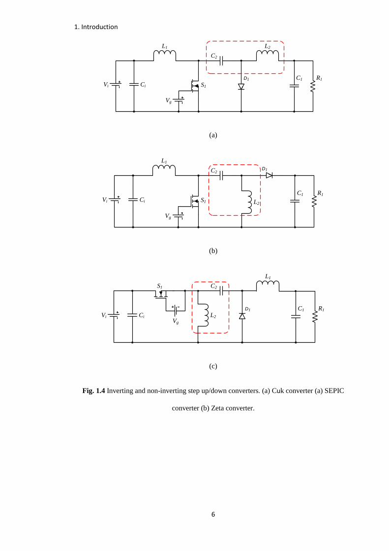
By cascading the boost converter with the buck converter and removing any superfluous
components, the Cuk converter in Fig 1.4 (a) is obtained [12]. This topology contains two
additional components from the above three topologies—these being the inductor, 𝐿2, and

1. Introduction
5
capacitor, 𝐶2—which make this topology more complicated. The capacitor 𝐶2 acts as an energy
transfer medium, charging up from the input and 𝐿1 during the off-period and releasing energy to
𝐿2 during the on-period. By controlling the amount of energy stored in 𝐶2, both
step-up and step-down conversion can be achieved. The output voltage of this topology is also
inverted. The advantage of this topology is that the two inductors are in series with the input and
output; both the input and output currents are continuous. As the output polarity in most
applications is non-inverted, two further topologies with the same components as in the Cuk
converter were developed. These are the SEPIC [13] and ZETA [14] converters shown in Fig. 1.4
(b) and (c) respectively. The operation of these converters is similar to the Cuk converter with the
capacitor acting as the transfer medium. The output voltage can both be higher or lower than the
input by virtue of controlling the charge to the capacitor. The configurations of the SEPIC and
ZETA converters are identical to the boost and buck converters respectively, without the two
additional components enclosed by a dashed box in the figures, hence they have the same input
and output current characteristics respectively.
1. Introduction
6
Vi
L1
C1 R1
Ci S1
D1
Vg
L2
C2
(a)
Vi
L1
C1 R1
Ci S1
D1
Vg
L2
C2
(b)
Vi L2
C1 R1
Ci
S1
D1
Vg
L1
C2
(c)
Fig. 1.4 Inverting and non-inverting step up/down converters. (a) Cuk converter (a) SEPIC
converter (b) Zeta converter.

1. Introduction
7
1.2.2. Isolated power converter
In applications where isolation is required (e.g. to prevent electrical shock) and the output voltage
is always significantly lower than the input voltage, a transformer can be added to the buck
converter topology to form the four isolated step-down converters [7][8] shown in Fig. 1.5: the
forward, push-pull, half-bridge and full-bridge converters (n.b. step-up conversion can be
achieved with a greater than unity transformer turns ratio). The forward converter shown in Fig.
1.5 (a) operates in a similar manner to the buck converter where power is only transferred during
the on-period. The additional demagnetising winding, 𝐿dm and the diode 𝐷dm in parallel with the
transformer primary, are needed to reset the transformer core by removing stored flux in each
cycle. The additional diode 𝐷2 ensures the transformer secondary is cut-off from the output during
the off-period of the switching device. This topology is only suitable for applications of up to
100 W [8] due to the high voltage stress seen by the switch.
In the push-pull converters, Fig. 1.5 (b), a demagnetising winding is not required as a flux balance
in the transformer primary is achieved with an ‘ac’ excitation signal through a
centre-tapped transformer. Since this converter only uses half of the primary winding at any one
time, the utilisation of the transformer is low which makes it only suitable for application with
power rating of up to 500 W [8]. In the half-bridge converter in Fig. 1.5 (c), an ‘ac’ signal in the
transformer primary is formed by taking the mid-point input voltage as a reference. With the
elimination of the need for two primary windings, transformer utilisation has increased, however
as only half of the input voltage is available, the required input current is twice as large for the
same output power requirement, which makes it also only suitable for application of up to 500 W
[8]. In the full-bridge converter shown in Fig. 1.5 (d), the two capacitors in half-bridge are
replaced by two switches. By switching the diagonal legs of the bridge in pairs, the full input
voltage, 𝑉i, is made available across the transformer primary, making it suitable for use in
applications of up to and above 5 kW [8].
1. Introduction
8
Vi
L1
C1 R1
Ci
S1
D1
Vg
D2
T1
Ldm
Ddm
(a)
Vi
L1
C1 R1
Ci
S2
D1
Vg2
D2
T1S1
Vg1
(b)
Vi
L1
C1 R1
S2
D1
Vg2
D2
T1
S1
Vg1
Ci3
Ci2
(c)
Vi
L1
C1 R1
Ci
S4
D1
Vg4
D2
T1S2
Vg2
S3
Vg3
S1
Vg1
(d)
Fig. 1.5 Isolated step down converter. (a) Forward converter (b) Push-pull converter (c) Half-
bridge converter (d) Full-bridge converter
1. Introduction
9
In applications where isolation and both step-up and step-down conversions are needed, the
flyback converter, shown in Fig. 1.6, can be used. This converter operates as the buck-boost
converter; however, its output is non-inverted because the primary and secondary windings are
wound in opposite directions. This converter is only suitable for application of up to 100 W [8]
as the magnetic core has to store all the load energy during the on-period of the switching device.
C1 R1
D1
Ci
S1
Vg
T1
Vi
Fig. 1.6 Flyback isolated step up/down converter.
1.2.3. Load resonant converters
Converters mentioned up to this point are classified as hard-switching converters as the current
and voltage across the switches (MOSFETs) are non-zero each time a switching event occurs,
thereby inducing switching losses, stress and EMI. The load resonant converter overcomes this
by ensuring the switching event occurs at either zero current (ZCS) or the zero voltage (ZVS).
The resonant converter is formed by adding a resonant tank (with the resonant inductor 𝐿r and
capacitor 𝐶r enclosed in Fig. 1.7) to either the half-bridge or full-bridge converters in
Fig. 1.5 (c) and (d). The two most basic resonant converters, the series and parallel resonant
converters [15], are formed by placing the resonant tank in series or in parallel with the load as
shown in Fig. 1.7 (a) and (b) respectively. The regulation of this type of converter is achieved by
changing the resonant tank impedance with the switching frequency.

1. Introduction
10
Vi
L1
C1 R1
S2
D1
Vg2
D2
T1
S1
Vg1
Ci3
Ci2
Lr
Cr
(a)
Vi
L1
C1 R1
S2
D1
Vg2
D2
T1
S1
Vg1
Ci3
Ci2
Lr
Cr
(b)
Fig. 1.7 Half-bridge resonant converter. (a) Series resonant converter (b) Parallel resonant
converter
1. Introduction
11
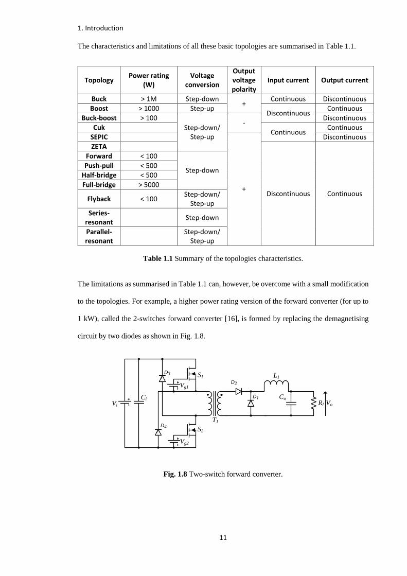
The characteristics and limitations of all these basic topologies are summarised in Table 1.1.
Topology Power rating
(W) Voltage
conversion
Output voltagepolarity
Input current Output current
Buck > 1M Step-down +
Continuous Discontinuous
Boost > 1000 Step-up Discontinuous
Continuous
Buck-boost > 100
Step-down/ Step-up
- Discontinuous
Cuk Continuous
Continuous
SEPIC
+
Discontinuous
ZETA
Discontinuous Continuous
Forward < 100
Step-down Push-pull < 500
Half-bridge < 500
Full-bridge > 5000
Flyback < 100 Step-down/
Step-up
Series-resonant
Step-down
Parallel-resonant
Step-down/
Step-up
Table 1.1 Summary of the topologies characteristics.
The limitations as summarised in Table 1.1 can, however, be overcome with a small modification
to the topologies. For example, a higher power rating version of the forward converter (for up to
1 kW), called the 2-switches forward converter [16], is formed by replacing the demagnetising
circuit by two diodes as shown in Fig. 1.8.
Vi
L1
CoRl
CiVo
D2
D4
D3
D1
S2
S1
Vg1
Vg2
T1
Fig. 1.8 Two-switch forward converter.

1. Introduction
12
1.2.4. Design considerations and challenges
The design of a converter starts by selecting a suitable topology based on the application’s
specifications, which can be achieved with the help of Table 1.1. Other factors affecting the
topology selection include engineer expertise, available literature, design guidelines, compatibility
to the existing product portfolio, converter complexity and reliability, to name but a few.
Having selected the topology, the engineer can then focus on the design and selection of the
converter’s components to meet the steady-state and the transient response requirements of the
application. Attention must also be paid tosize, weight, cost and efficiency. For certain
applications, the implications of these requirements are contradictory and, therefore, a suitable
compromise must be found. For example, a computer voltage regulator (VR) must provide
excellent transient response, whilst achieving high efficiency. The fast transient response in buck
converters can be achieved by selecting its low-pass filter with a higher bandwidth (corner
frequency), this however requires the converter to operate at a higher switching frequency, leading
to a reduction in efficiency due to the increase in switching losses in the semiconductor switching
device and magnetic components. Even through some of the losses in the semiconductors can be
mitigated to a certain extent by employing resonance (as in the resonant converters or the resonant
switch converter [17]), these converters require a different set of design and control techniques.
Solutions utilising the same set of design and control techniques as the original converter are a
more attractive alternative. Some of these solutions include connecting multiple converters in
series [18], in parallel [19], or both in series and parallel [20].
With energy efficiency becoming more important in recent years due to rising energy prices and
tightening regulations from environmental protection agencies, this thesis primary focuses on
identifying control schemes and design techniques to improve the efficiency of the converter.
These control schemes and design techniques utilise the same set of design and control techniques
as the original converter, similar to the approach in [18]-[20]. Step-down converters (i.e. buck and
forward converters) are selected for the investigation as the majority of applications have a step-

1. Introduction
13
down conversion ratio. These new control schemes and design techniques also work with step-up
converters. Resonant converters, like the LLC resonant converter, are becoming increasingly
popular, due to their low switching losses. One of the issues that prevents this converter from being
widely adapted is the low impedance around the operating frequency, allowing excessive current
to flow under overload or short circuit conditions. This thesis also develops an equivalent circuit
model to predict the overloading issue experienced in the LLC resonant converter which allows
the desired clamping capacitor to be selected.
1.3. Thesis outline
The work in this thesis is divided into eight chapters:
Chapter 1 introduces the characteristics and applications of the most commonly used converters.
The research focus, thesis outline and contribution are also presented.
Chapter 2 reviews the different modelling techniques and the design and control techniques that
have been developed to improve the efficiency of step-down converters. New design and control
techniques that could lead to higher converter efficiency and power density are identified. Also
included in the review is the overloading issue of LLC resonant converters.
Chapter 3 explores the use of closed-loop controllers to improve the transient performance of
synchronous buck converters (SBCs). The full derivation of the converter’s equivalent circuit
models (in both the state-space and the transfer function forms) and the complete design procedures
for the three types of controllers (the PID, the state feedback and the predictive controllers) are
presented. The step responses of the converter with the three different types of controllers are
compared to identify the best controllers.
Chapter 4 investigates the characteristics of the two control schemes developed to improve the
transient performance of the parallel converter, the fast response double buck (FRDB) scheme and
sensorless and peak current mode control (SCM-PCM) scheme. By combining the advantages of
the two schemes, a new control scheme—the fast recovery with high transient efficiency (FRHE)

1. Introduction
14
scheme—is proposed to improve the converter efficiency during transient operation without
unduly increasing the transient response time.
Chapter 5 studies the effects of the different system requirements on the parallel converter’s
efficiency to assist the development of a new design technique, the high steady-state efficiency
(HSSE) technique. In HSSE, the design specifications and requirements that prevent the main
power module (PM) from having high steady-state efficiency are conveniently allocated to an
auxiliary PM, to allow the main PM be optimised for conduction loss for high steady-state
efficiency.
Chapter 6 demonstrates a new active current ripple cancellation (ACRC) scheme, which shapes
the auxiliary PM current to reduce the main PM current ripple and hence reduce the current ripple
seen by the output capacitor, allowing a lower value output capacitor to be selected. The selection
of the auxiliary PM components and duty cycle under different operating conditions are also given.
Chapter 7 presents a design methodology for LLC resonant converters with a capacitor-diode
clamp. A new fundamental harmonic approximation (FHA) based equivalent circuit model is
obtained through the application of describing function techniques by examining the fundamental
behaviour of the capacitor-diode clamp. The current limiting performance of the converter under
overload condition is studied and design guidelines are given.
Chapter 8 concludes the thesis and details any further work.

1. Introduction
15
1.4. Contribution
This thesis proposes novel control and design techniques to improve both the steady-state and
transient efficiencies of the parallel converter and addresses the overload issue of the LLC resonant
converter. In particular, the work presented herein has been disseminated in internationally
recognised journals and conferences. The main contribution are summarised below:
A novel fast recovery with high transient efficiency (FRHE) scheme [P1] is proposed to
improve the transient efficiency of the converter with two parallel connected SBCs. By
activating the auxiliary PM only when the threshold voltage or settling time are to be exceeded,
the transient efficiency of the prototype converter is improved by as much as 4.7% under
continuous load step.
A novel high steady-state efficiency (HSSE) design technique [P2] is proposed to improve the
steady-state efficiency of the converter with two parallel connected 2SFCs. By allocating both
the transient response requirement and the minimum load condition to the auxiliary PM, the
main PM can then be optimised for steady-state operation. The steady-state efficiency of the
prototype converter is improved by up to 12%.
A novel active current ripple cancellation (ACRC) scheme [P3] is proposed to reduce the
current ripple as seen by the output capacitor. Through shaping of the current waveform of the
auxiliary PM, the current ripple of the prototype converter is reduced by 67% and the efficiency
is also improved under most load conditions.
A new equivalent circuit model for a LLC resonant converter with the capacitor-diode clamp
[P4] is developed to predict the overload current. By extracting the fundamental behaviour of
the capacitor-diode clamp using a describing function technique, the converter current limiting
characteristic under different operating frequency and overload conditions are predicted,
allowing the optimum clamping capacitors to be selected.

16
2. Control schemes and switched-mode power converter
topologies for high efficiency
2.1. Introduction
The previous chapter introduced different switched-mode power converter topologies usually
employed within industry, and highlighted the focus of the thesis. This chapter provides a
thorough review of different types of modelling techniques, control schemes and design and
control techniques developed and employed by power supply designer for SMPCs. It also
proposes new control schemes and design techniques that allow higher efficiency, higher power
density and overload protection to be achieved. From the review of existing literatures, five areas
are identified as suitable for further research:
1) Effect on the converter’s transient responses with different feedback controllers
2) Control schemes that provide lower losses under transient conditions.
3) Design techniques that improve the efficiency under steady-state conditions.
4) Reduction in current ripple for higher power density
5) Overload characteristics of an LLC converter with capacitor-diode clamp.
This chapter commences by examining the mathematical modelling techniques employed to
predict both the steady-state and the transient behaviour of converters before applying some of
the techniques to the analysis and design of converters and their feedback controllers.
2.2. Mathematical modelling
In order to study the converter’s behaviour, system (converter) mathematical models are essential.
As the buck converter is a nonlinear system due to the switching action in each period, equivalent
LTI models must be obtained in order to design suitable feedback controllers using linear control
systems theory. Dependent on whether the system is to be controlled in either voltage mode (VMC)

2. Control schemes and switched-mode power converter topologies for high efficiency
17
or current mode (CMC), differing modelling techniques must be utilised [2]. VMC is a single loop
control system where the output voltage is regulated directly through a linear controller. CMC is a
dual loop control system where the output voltage is regulated indirectly through the inductor
current. The outer voltage loop sets the current reference of the inner-loop through a linear
controller to regulate the inductor current. CMC is widely employed as it gives better performance,
but due to its complexity and issues with noise, VMC is still popular, and in the case where high
performance is desired, state feedback control can be utilised in VMC to give similar overall
performance to the CMC approach.
The two most popular VMC modelling techniques are the state-space averaging (SSA) and the
PWM switched model. The SSA was developed by Cuk and Middlebrook [21] in the mid 1970’s,
by first writing the piecewise linear circuits equations into sets of linear state equations, and then
taking the time weighted average of these equations, a linear system model can be obtained.
Vorperian [22] realised that the only nonlinear elements in the system are the switching elements
(diodes, MOSFETs, etc.) and this led to the development of the PWM switched model, where
linear system models are obtained by only linearising the switches. Although both methods were
proved to model converters equally well, after the subsequent identification of the ‘duty-ratio
constraint’ for SSA [23][24], the PWM switch model still has the following advantages over the
SSA:
The complexity of the linearisation is reduced as only the switches and not the whole circuit is
included in the linearisation
The invariant structure of the switches implies that once it has been linearised, it can be
substitute into any converter topology directly.
Other work connected to the PWM switch model includes:
(1) An extension to model converters with switches that are not connected back to back [25]

2. Control schemes and switched-mode power converter topologies for high efficiency
18
(2) The introduction of two alternative forms of PWM transformers allowing analysis by
inspection [26].
Other modelling techniques include: (1) the MISSCO technique where a minimum separable
switching configuration of the circuit is first identified, the low frequency behaviour of the
MISSCO is than obtained by taking the average of its impulse response [27]. (2) The invariant
structure models, where different converters can be organised in a table as in the canonical circuit
model proposed by Cuk [21], where parameters of the converters are modified to fit into the four
fixed parts (i.e. e(s), j(s), µ and He(s)), and the average power-stage model [28] where the same
buck converter like structure (i.e. voltage source, three resistors, a inductor and a capacitor
without the switch and diode) can be derived for any converter topology. (3) The graphical
approach where the physical systems are represented graphically as in signal flow graph [29] and
its modification, the bond graph [30], these modelling techniques make modelling of complex
systems like the cascaded or multi-phase converters easier, and (4) The sampled-data model
where the evolution of system states is calculated from the initial condition instead of averaging,
as in SSA, to preserve the exact system dynamics [31]-[34]. (5) The Energy Factor (EF) method,
proposed by Luo and Ye [35] where a model is obtained by identifying the input energy (PE),
energy in the reactive elements (SE), capacitor /inductor stored energy ratio (CIR) and the energy
losses (EL), without the use of elementary circuit analysis. (6) System identification which is used
in the cases where the internal structure of the circuit is inaccessible or for complex system
[36][37].
2.3. Closed-loop controllers
In order to obtain the desired output voltage, the duty cycle of a converter can be calculated and
set directly [2]-[4]. This is open-loop control which is sensitive to system variation and changes in
operating conditions. To overcome this, the duty cycle can instead be set by a controller which
produces an error signal (difference between a reference and the output voltages) where the error
signal itself is driven to zero using some form of compensator.

2. Control schemes and switched-mode power converter topologies for high efficiency
19
One of the most widely used controllers is the PID controller [38][39], due to its ease of use and
its ability to give good performance in the vast majority of applications. This controller contains
three terms: ‘P’ - the proportional gain, ‘I’ – the integral gain and the derivative gain ‘D’. Different
combinations of the three terms can be selected according to the system need, the common
combinations are the P, I, PI, PD and PID. The PID is the most complex of all, but produces the
best performance for systems characterised by dominant second order behaviour where, based on
the system model, one can often independently control damping factor, overshoot and settling
time within certain bounds. If the system mathematical equation is not available, PID parameter
values can often be obtained empirically based on the Ziegler-Nichols tuning methodology. This
method can be based on the system step response or the system frequency response where in both
cases, the specified parameters (i.e. au & 𝐿𝑢 and 𝐾u & 𝑇u respectively) are first found and then
substituted into their corresponded look up table to obtain appropriate PID parameter values [40].
Other empirical tuning methods have been developed by engineers through experience [3][41].
On-line auto-tuning, where the PID control loop is tuned automatically given the desired
characteristics [42][43] are also popular. When the mathematical equations are available,
controllers can be designed by utilising a root locus plot as in pole-zero cancellation or using a
pole-placement technique as in the robust PID controller [38].
The second most common control technique is state feedback control, similar to the robust PID
controller, it is also a pole-placement technique, but unlike PID, the feedback signal is applied
through pure gain terms and an additional integrator is usually required to ensure adequate steady-
state behaviour. Since it may not be possible to obtain measurements of all states in practical
systems, state-observer techniques can be employed to estimate the unknown / inaccessible states.
When the practical system model is unavailable, the state-feedback controller can be obtained
through the use of a genetic algorithm, where the controller parameters are obtained through the
natural selection process [41], and when the model is available, state feedback with an integrator
[38] or the LQR control where gains are selected through minimise the user define cost function

2. Control schemes and switched-mode power converter topologies for high efficiency
20
[44] may be employed. In predictive controllers, in addition to the system error signal(s), past
knowledge and the future response are also stored and predicted to form the control input [45].
Other control techniques, described in the literature, which do not require the linear model include
sliding-mode control [46], artificial neural networks [47], and fuzzy logic controllers. These have
also been successfully employed to provide a robust system [48].
All of the controllers aim to improve both the steady-state and the transient performance of the
converter and this improvement permits converters to be designed with a lower open-loop
performance allowing it to operate at lower frequency and, hence, higher efficiency. In this regard
Chapter 3 investigates the transient response of the synchronous buck converter with the different
types of controller (i.e. the PID controller, the state feedback controller and predictive control) all
designed to improve transient performance whilst achieving high-efficiency.
2.4. Transient efficiency of a parallel converter
Numerous control techniques have been developed with the aim of improving part-load efficiency
of converters. Some of these techniques include reducing the converter switching frequency and/or
skipping some of the switching cycles during light load conditions [49]-[54]. The improvements
from these techniques are, however limited, since the converter still has to satisfy all the system
requirements across the different load conditions. One way to overcome this limitation is by adding
a dedicated circuit to the converter to decouple the conflicting requirements such as the transient
performance requirement from the efficiency requirement [55]-[61]. The parallel converter [58]-
[61] has received much attention since the loading requirements can partitioned across a number
of power modules (PMs) all of which can be designed and controlled using similar techniques,
expediting the development process of the overall system.
With identical power modules connected in parallel [58], the converter’s bandwidth (i.e. corner
frequency) is increased proportional to the number of PMs in parallel without any increase in
switching frequency. Unfortunately, paralleling becomes impractical with the ever increasing

2. Control schemes and switched-mode power converter topologies for high efficiency
21
transient performance requirement, since either the switching frequency or the numbers of PM
utilised have to be high. An alternative scheme is to connect non-identical PMs together [59]. In
this scheme, one PM, a ‘main PM’, can be designed to operate at a low switching frequency for
high efficiency under steady-state conditions, while the second PM, an ‘auxiliary PM’, can be
designed to run at a high switching frequency for high BW under transient conditions. Since the
auxiliary PM is only enabled during the transient conditions, high bandwidth and efficiency can
both be obtained.
Different ways of utilising the auxiliary PM under transient conditions have been suggested. In
the fast response double buck converter (FRDB) [60], the auxiliary PM only operates when the
output voltage drops below a threshold level. Even though the voltage undershoot requirement is
met, the extra bandwidth available from the auxiliary PM is not fully exploited. In the sensorless
and peak current mode controlled converter (SCM-PCM) [61], the auxiliary PM operates when a
transient condition is detected. It remains in operation until the main PM recovers from the
transient condition. The wide bandwidth of the auxiliary PM is fully exploited in this scheme.
However, since the efficiency of the auxiliary PM is lower than the main PM, due to the auxiliary
power modules’ higher switching frequency, the longer operating duration leads to lower overall
efficiency under transient conditions in comparison to the FRDB scheme.
Chapter 4 combines the high efficiency characteristic associated with the FRDB and fast transient
response characteristic associated with the SCM-PCM to achieve an equitable compromise
between the transient response and efficiency.

2. Control schemes and switched-mode power converter topologies for high efficiency
22
2.5. Steady-state efficiency of a parallel converter
To improve the converter steady-state efficiency, multiple converters can be connected in series
[18], in parallel [19] or a combination of the two [20] to process the power more efficiently. The
majority of research in this area has again been focussed on the parallel converter arrangement. In
the interleaved converter [59], identical PMs are designed to minimise both switching and
conduction losses across the whole load range. High efficiency at heavy load is achieved through
a reduction in conduction loss by sharing current between the identical PMs which reduces the
𝐼o2𝑅l loss to 𝑚n(𝐼/𝑚n)
2𝑅l (where 𝐼o is the load current, 𝑅l is the load resistance and 𝑚n is the
number of PM in parallel). High efficiency at light load is achieved by disabling some of the PMs.
With two or more converters connected in parallel, there are a number of possible variations on
the design of the converter. In [59], multiple converters, optimised for different load conditions,
are operated in parallel to achieve high efficiency across a wide range of load. Alternatively,
without increasing the need to parallel as many PMs together as in [19][20][59], a single PM can
be designed to run at low frequency for high efficiency, without being constrained by the transient
response requirement which is fulfilled by the second PM [62].
Chapter 5 extends the design approach in [62], where, apart from the transient response
requirement, the minimum load condition is also allocated to the auxiliary PM, hence allowing the
main PM to be designed with a larger inductor current ripple to reduce the conduction loss for
higher efficiency. The unfulfilled requirements are met by the auxiliary PM in this case.
2.6. Active current ripple cancellation schemes
An important issue with a larger inductor current ripple as proposed in section 2.5 is the need for
a greater output capacitance in order to meet the voltage ripple design requirement, thereby
potentially increasing both the cost and size of the overall converter.
Instead of increasing the capacitance, ripple cancellation techniques [63] may be utilised. Over
time, numerous techniques have been developed for cancelling the input current ripple [64][65] or

2. Control schemes and switched-mode power converter topologies for high efficiency
23
the output current ripple [66][67]. In passive ripple cancellation techniques [64], the current ripple
in the filter inductor is reflected to a secondary inductor which is coupled in anti-parallel to the
filter inductor. The combination of these two current waveforms produce an output current that is
free of current ripple. The setback of this scheme is the size of the required filter and also, since
the coupled inductor is fixed at the design stage, the technique is sensitivity to parameter drift.
In active ripple cancellation techniques [65]-[67], current is first sensed using a current transformer
or Rogowski coil, it is then amplified to the correct amplitude by a linear amplifier for injection
back into the converter. The system complexity is higher in this scheme but they have, however,
been shown to have higher ripple attenuation at the low frequency range, and with closed-loop
control these methods are robust against parameter drift. The combination of the two, the hybrid
filter, which has advantages from both type of filters have also been demonstrated in [68].
An alternate approach to the above active filtering techniques, which requires no current ripple
sensing, are demonstrated in [69]-[72]. In these approaches, a switched-mode power converter is
designed to operate complementarily to the main converter, producing a current waveform that is
exactly the opposite to the main converter current ripple to achieve ripple cancellation [69]-[72].
In [69]-[71], a dedicated converter is added for ripple cancellation, while in [72], the interleaved
converter is modified to achieve ripple cancellation without the need for any extra components.
Chapter 6 explores a way of achieving ripple cancellation in the parallel converter with
non-identical power modules without any extra components beyond the PMs, by reusing the
auxiliary power module of the converter to inject a complimentary current into the output capacitor
in addition to improving overall system transient response as described earlier.

2. Control schemes and switched-mode power converter topologies for high efficiency
24
2.7. LLC resonant converter with capacitor-diode clamp
As electronic systems are miniaturised, power supply designers are placed under increasing
pressure to reduce the size of their designs, imposing strict requirements on the chosen power
supply topology, components, efficiency and cooling requirements. Size reduction in
hard-switching converters (e.g. buck converters) can be achieved by increasing the switching
frequency, which reduces the size of passive components. The drawback of this approach is the
increase in switching losses, ultimately compromising converter efficiency.
Resonant converters such as series resonant, parallel resonant and multi-resonant converters
[73][74] overcome this drawback by soft-switching, where the switching devices are switched
under zero voltage (ZVS) or zero current (ZCS) conditions. One variation of the multi-resonant
converter, the LLC resonant converter [75]-[80], has become popular due to its narrow range of
operating frequency for wide input voltage and load ranges when operated around the converter’s
(series) resonant frequency, also referred as the load independent point (LIP). The narrow
frequency range is the result of the resonant tank components, 𝐿s and 𝐶r becoming a virtual short-
circuit (zero impedance) at the resonant frequency. The operating frequency is adjusted mainly to
compensate for the change in the input voltage. It is not overly necessary to adjust the frequency
to compensate for changes in the load. Unfortunately, due to the low impedance around the LIP,
excessive current can flow to the load during transient and overload conditions, and so a current
protection mechanism must be included.
For LLC resonant converters, current-limiting can be achieved by i) reducing the MOSFET
conduction times, ii) increasing the switching frequency [81][82], iii) operating at a sub-harmonic
of the switching frequency [83], or iv) by changing the resonant frequency characteristics of the
converter by switching in (or out) the resonant tank components [81][82][84]-[87]. Although
methods i) to iii) provide adequate protection, a current sensor is needed to detect the overload
condition and some action by the controller is required to adjust the MOSFET timings. Method
iv), in contrast, does not necessarily require any direct action to be taken by the controller assuming
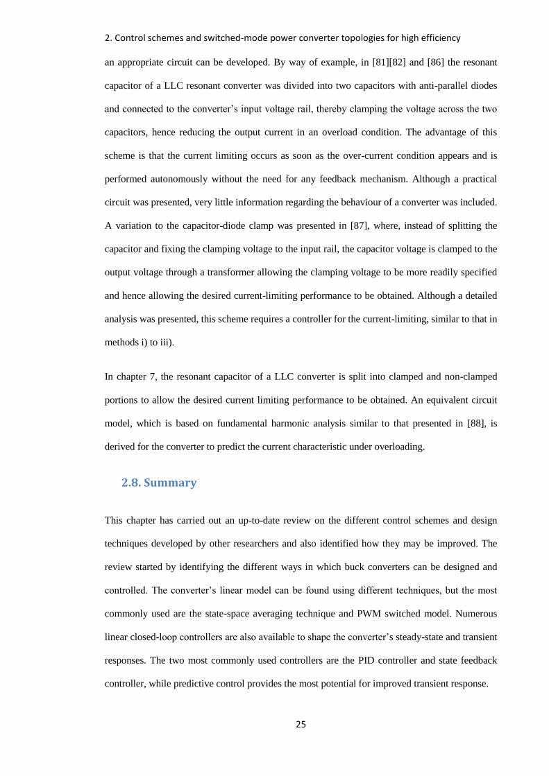
2. Control schemes and switched-mode power converter topologies for high efficiency
25
an appropriate circuit can be developed. By way of example, in [81][82] and [86] the resonant
capacitor of a LLC resonant converter was divided into two capacitors with anti-parallel diodes
and connected to the converter’s input voltage rail, thereby clamping the voltage across the two
capacitors, hence reducing the output current in an overload condition. The advantage of this
scheme is that the current limiting occurs as soon as the over-current condition appears and is
performed autonomously without the need for any feedback mechanism. Although a practical
circuit was presented, very little information regarding the behaviour of a converter was included.
A variation to the capacitor-diode clamp was presented in [87], where, instead of splitting the
capacitor and fixing the clamping voltage to the input rail, the capacitor voltage is clamped to the
output voltage through a transformer allowing the clamping voltage to be more readily specified
and hence allowing the desired current-limiting performance to be obtained. Although a detailed
analysis was presented, this scheme requires a controller for the current-limiting, similar to that in
methods i) to iii).
In chapter 7, the resonant capacitor of a LLC converter is split into clamped and non-clamped
portions to allow the desired current limiting performance to be obtained. An equivalent circuit
model, which is based on fundamental harmonic analysis similar to that presented in [88], is
derived for the converter to predict the current characteristic under overloading.
2.8. Summary
This chapter has carried out an up-to-date review on the different control schemes and design
techniques developed by other researchers and also identified how they may be improved. The
review started by identifying the different ways in which buck converters can be designed and
controlled. The converter’s linear model can be found using different techniques, but the most
commonly used are the state-space averaging technique and PWM switched model. Numerous
linear closed-loop controllers are also available to shape the converter’s steady-state and transient
responses. The two most commonly used controllers are the PID controller and state feedback
controller, while predictive control provides the most potential for improved transient response.

2. Control schemes and switched-mode power converter topologies for high efficiency
26
For higher efficiency, a dedicated circuit can be added to the original converter to share the system
requirements. The most popular is by connecting another power converter in parallel, which allows
similar control and design techniques to be used. To improve the transient efficiency of the parallel
converter configuration, two schemes, the FRDB and SCM-PCM schemes, have been developed.
It was found that one scheme focus on the efficiency while the other on the transient response, a
new approach which combined the advantage of the two schemes can be obtained. For higher
steady-state efficiency, converters that are optimised for different load conditions can be put in
parallel and be enabled according to the load conditions. Alternatively, the transient response
requirement can be allocated to the auxiliary PM to allow the main PM to be designed for higher
efficiency. A new design technique which looks at the allocation of the different system
requirements to the different power modules can be developed to enhance the steady-state
efficiency. In order to reduce the current ripple, hence the size of the capacitor, current ripple
cancellation scheme can be used. Numerous types of passive and active current ripple cancellation
techniques have been developed to reduce the input and/or output current ripples. None of which
are currently based on the parallel converter with non-identical power modules, a new active
current ripple cancellation is needed to be developed for the parallel converter.
The LLC resonant converter has the advantage of high power density, higher efficiency and low
EMI in comparison to the hard-switching converter. It has however got load related issues where
large currents can flow under overload conditions. A capacitor-diode clamp was shown to be able
to limit this current automatically, but no mathematical modelling or design guidelines have been
developed so far. A new mathematical model and design guideline are therefore provided here.

27
3. Closed-loop controllers for buck converters
3.1. Introduction
The previous chapter reviewed the different types of controller available for buck converters and
discussed the extra transient response performance that can be obtained from the selection of one
type of controller over the other. This chapter investigates the transient performance of the buck
converter with three different types of controller, to identify the one that provides the best
transient performance. From the analysis of the converter's operation, equivalent circuit models
in both state-space and transfer function forms are obtained. With these models, a PID controller,
a state feedback controller and a predictive controller are designed for a 5 W
(i.e. 𝑉o = 5 V, 𝐼o = 1 A) converter. The step responses of the converter with each of the three
controllers are compared in both simulation and experiment.
3.2. Circuit operation and component selection
A standard synchronous buck converter (SBC) is shown in Fig. 3.1, containing two sub-circuits:
(i) a dc chopper which is formed by the MOSFETs, 𝑆1 and 𝑆2, allowing power to be
periodically transferred to the filter in (ii)
(ii) a low-pass filter that is formed by the inductor 𝐿m and capacitor 𝐶o which attenuates
the higher harmonic components to produce a DC output voltage (𝑉o).
Capacitor 𝐶i is the DC-link reservoir capacitor and 𝑅l is the load resistance.
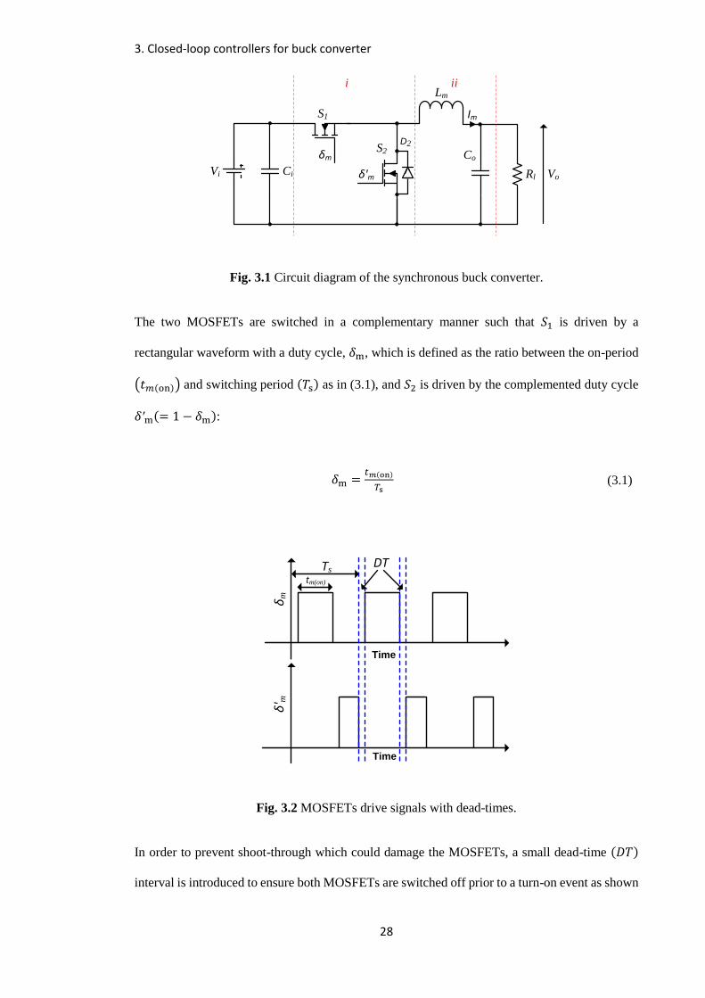
3. Closed-loop controllers for buck converter
28
Vi
Lm
Co
RlCi Vo
S2
S1 Im
δm
D2
δ'm
i ii
Fig. 3.1 Circuit diagram of the synchronous buck converter.
The two MOSFETs are switched in a complementary manner such that 𝑆1 is driven by a
rectangular waveform with a duty cycle, 𝛿m, which is defined as the ratio between the on-period
(𝑡𝑚(on)) and switching period (𝑇s) as in (3.1), and 𝑆2 is driven by the complemented duty cycle
𝛿′m(= 1 − 𝛿m):
𝛿m =𝑡𝑚(on)
𝑇s (3.1)
δm
Time
Time
δ' m
tm(on)
TsDT
Fig. 3.2 MOSFETs drive signals with dead-times.
In order to prevent shoot-through which could damage the MOSFETs, a small dead-time (𝐷𝑇)
interval is introduced to ensure both MOSFETs are switched off prior to a turn-on event as shown
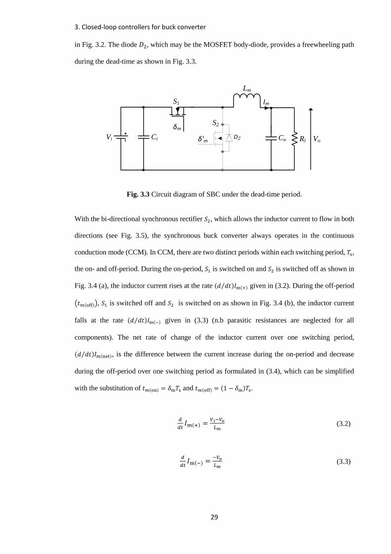
3. Closed-loop controllers for buck converter
29
in Fig. 3.2. The diode 𝐷2, which may be the MOSFET body-diode, provides a freewheeling path
during the dead-time as shown in Fig. 3.3.
Vi
Lm
Co RlCi Vo
S2
S1 Im
D2
δm
δ'm
Fig. 3.3 Circuit diagram of SBC under the dead-time period.
With the bi-directional synchronous rectifier 𝑆2, which allows the inductor current to flow in both
directions (see Fig. 3.5), the synchronous buck converter always operates in the continuous
conduction mode (CCM). In CCM, there are two distinct periods within each switching period, 𝑇s,
the on- and off-period. During the on-period, 𝑆1 is switched on and 𝑆2 is switched off as shown in
Fig. 3.4 (a), the inductor current rises at the rate (𝑑 𝑑𝑡⁄ )𝐼m(+) given in (3.2). During the off-period
(𝑡𝑚(off)), 𝑆1 is switched off and 𝑆2 is switched on as shown in Fig. 3.4 (b), the inductor current
falls at the rate (𝑑 𝑑𝑡⁄ )𝐼m(−) given in (3.3) (n.b parasitic resistances are neglected for all
components). The net rate of change of the inductor current over one switching period,
(𝑑 𝑑𝑡⁄ )𝐼m(net), is the difference between the current increase during the on-period and decrease
during the off-period over one switching period as formulated in (3.4), which can be simplified
with the substitution of 𝑡𝑚(on) = 𝛿m𝑇s and 𝑡𝑚(off) = (1 − 𝛿m)𝑇s.
𝑑
𝑑𝑡𝐼m(+) =
𝑉i−𝑉o
𝐿m (3.2)
𝑑
𝑑𝑡𝐼m(−) =
−𝑉o
𝐿m (3.3)

3. Closed-loop controllers for buck converter
30
𝑑
𝑑𝑡𝐼m(net) =
𝑉i−𝑉o𝐿m
𝑡𝑚(on)+−𝑉o𝐿m
𝑡𝑚(off)
𝑇𝑠=
𝑉i𝛿m−𝑉o
𝐿m (3.4)
Vi
Lm
Co RlCi Vo
S2
S1 Im
D2
δm
δ'm
(a)
Vi
Lm
Co RlCi Vo
S2
S1 Im
D2
δm
δ'm
(b)
Fig. 3.4 Circuit diagrams showing the two subintervals. (a) on-period (b) off-period.
The converter reaches steady state if the net rate of change of inductor current over one switching
period is zero (volt-second balance) as shown in Fig. 3.5. By equating (3.4) to zero and solving
for 𝑉o, (3.5) is obtained which shows that for a given input voltage, there is a duty cycle for each
output voltage where the converter reaches steady state (𝛿m(ss)).
𝑉o = 𝛿m𝑉i (3.5)
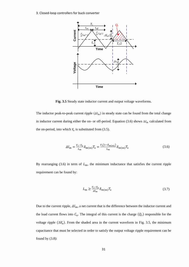
3. Closed-loop controllers for buck converter
31
Cu
rre
nt
Time
Ts
toffton
ΔIm/2
Io Ts/2
d
dt Im(+)
d
dt Im(-)
ΔVo
Time
Qr
Vo
lta
ge
Fig. 3.5 Steady state inductor current and output voltage waveforms.
The inductor peak-to-peak current ripple (𝛥𝐼m) in steady state can be found from the total change
in inductor current during either the on- or off-period. Equation (3.6) shows Δ𝐼m calculated from
the on-period, into which 𝑉o is substituted from (3.5).
𝛥𝐼m =𝑉i−𝑉o
𝐿m𝛿m(ss)𝑇s =
𝑉i(1−𝛿m(ss))
𝐿m𝛿m(ss)𝑇s (3.6)
By rearranging (3.6) in term of 𝐿m, the minimum inductance that satisfies the current ripple
requirement can be found by:
𝐿m ≥𝑉i−𝑉o
𝛥𝐼m𝛿m(ss)𝑇s (3.7)
Due to the current ripple, 𝛥𝐼m, a net current that is the difference between the inductor current and
the load current flows into 𝐶o. The integral of this current is the charge (𝑄r) responsible for the
voltage ripple (Δ𝑉o). From the shaded area in the current waveform in Fig. 3.5, the minimum
capacitance that must be selected in order to satisfy the output voltage ripple requirement can be
found by (3.8):
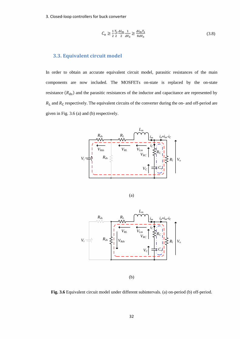
3. Closed-loop controllers for buck converter
32
𝐶o ≥1
2
𝑇s
2
𝛥𝐼m
2
1
𝛥𝑉o ≥
𝛥𝐼m𝑇s
8𝛥𝑉o (3.8)
3.3. Equivalent circuit model
In order to obtain an accurate equivalent circuit model, parasitic resistances of the main
components are now included. The MOSFETs on-state is replaced by the on-state
resistance (𝑅ds) and the parasitic resistances of the inductor and capacitance are represented by
𝑅L and 𝑅C respectively. The equivalent circuits of the converter during the on- and off-period are
given in Fig. 3.6 (a) and (b) respectively.
Vi
Lm
Co
Rl Vo
im
Rds
Rds RL
RC
iC
io=im-iC
VC
VRds VRL VLm
VRC
(a)
Vi
Lm
Co
Rl Vo
im
Rds
Rds RL
RC
iC
VC
io=im-iC
VRds
VRL VLm
VRC
(b)
Fig. 3.6 Equivalent circuit model under different subintervals. (a) on-period (b) off-period.

3. Closed-loop controllers for buck converter
33
From Fig. 3.6 (a) or (b), the output voltage for the on- and off-period are identical and can be
found by Ohm’s law. With Kirchhoff’s current law (𝐾𝐶𝐿), the following equation is obtained:
𝑣o = 𝑅l𝑖o = 𝑅l (𝑖m − 𝐶o𝑑
𝑑𝑡𝑣C)
(3.9)
where 𝑣C is the voltage across the output capacitor.
Applying Kirchhoff’s voltage law (𝐾𝑉𝐿) around the inner loop in dash-dotted line and the outer
loop in dashed line in Fig. 3.6 (a) yield two first order differential equations in (3.10) and (3.11)
for the on-period:
where 𝑣RC, 𝑣Rds, 𝑣RL are the voltages across 𝑅C, 𝑅ds, 𝑅L respectively and 𝑣Lm is the voltage
across 𝐿m.
By applying a similar procedure to the off-period equivalent circuit model in Fig. 3.6 (b), two first
order equations for the off-period can also be found. Since the inner loop in Fig. 3.6 (b) is identical
to that in Fig. 3.6 (a), the first equation is identical to (3.10). The second equation is:
Using the above equations, the equivalent circuit model in state-space form is obtained with the
following three steps:
𝑣c = −𝑣RC + 𝑣o = −𝑅C𝐶o𝑑
𝑑𝑡𝑣C + 𝑅l (𝑖m − 𝐶o
𝑑
𝑑𝑡𝑣C) (3.10)
𝑣i = 𝑣Rds + 𝑣RL + 𝑣Lm + 𝑣o = 𝑖m(𝑅ds + 𝑅L) + 𝐿m𝑑
𝑑𝑡𝑖m + 𝑅l (𝑖m − 𝐶o
𝑑
𝑑𝑡𝑣C) (3.11)
0 = 𝑖m(𝑅ds + 𝑅L) + 𝐿m𝑑
𝑑𝑡𝑖m + 𝑅l (𝑖m − 𝐶o
𝑑
𝑑𝑡𝑣C) (3.12)

3. Closed-loop controllers for buck converter
34
Step 1: System state and output equations
In state-space modelling, the system (converter) is modelled by a state equation and an output
equation which are formed by organising a set of first order differential equations in term of state
variables. The state variables are variables that sufficiently describe the system future behaviour
given the present state of the system and the excitation signal. With the two
energy-storage elements in the converter, two state variables are required which are selected to
be the inductor current, 𝑖m, and capacitor voltage, 𝑣c, (n.b. the state variables are non-unique,
voltage across the inductor, 𝑣Lm, and many other variables may also be selected [38]).
With the choice of the state variables as 𝑖m and 𝑣c, the state equation for the on-period is obtained
in (3.13) by rearranging (3.10) and (3.11) in terms of the state vector 𝒙 = [𝑖m 𝑣c]𝑇 and the input
signal 𝑢 = 𝑉i. Similarly, with (3.10) and (3.12), the state equation for the
off-period is found in (3.14):
�̇� = 𝑨1𝒙 + 𝑩1𝑢 = [−(𝑅l(𝑅ds+𝑅L+𝑅C)+𝑅C(𝑅ds+𝑅L))
Lm(𝑅l+𝑅C)−
𝑅l
𝐿m(𝑅l+𝑅C)
𝑅l
𝐶o(𝑅l+𝑅C)−
1
𝐶o(𝑅l+𝑅C)
] 𝒙 + [1
𝐿m
0]𝑢 (3.13)
�̇� = 𝑨2𝒙 + 𝑩2𝑢 = [−(𝑅l(𝑅ds+𝑅L+𝑅c)+𝑅C(𝑅ds+𝑅L))
𝐿m(𝑅l+𝑅C)−
𝑅l
𝐿m(𝑅l+𝑅C)
𝑅l
𝐶o(𝑅l+𝑅c)−
1
𝐶o(𝑅l+𝑅C)
] 𝒙 + [00] 𝑢
(3.14)
By isolating (3.9) also in term of the state variables and with the output signal 𝑦 = 𝑉𝑜, the output
equation for the on- and off-period is obtained as followed:
𝑦 = 𝑪1𝒙 = 𝑪2𝒙 = [𝑅l𝑅C
𝑅l+𝑅C
𝑅l
𝑅l+𝑅C] 𝒙 (3.15)
The compact state and output equations are given in (3.14) and (3.15) respectively:

3. Closed-loop controllers for buck converter
35
�̇� = 𝑨𝑖𝒙 + 𝑩𝑖𝑢 (3.16)
𝑦 = 𝑪𝑖𝒙 + 𝐷𝑖𝑢 (3.17)
where the subscript 𝑖 is 1 for the on-period and 2 for the off-period. 𝑨, 𝑩, 𝑪 and 𝒙 in bold represent
vectors. 𝒙 is the state vector, 𝑢 is the input signal and 𝐷 is the direct feed-forward term which is
not applicable in this system and is therefore set to zero.
Step 2: State-space averaging
Equations (3.13)-(3.15) form a system piecewise-linear set of equations that require a switching
function to model the DC chopper (inverter) to allow the trajectories of the state-variables to be
obtained. For control purposes such a detailed model of the switching process is not usually
necessary and one often employs an averaging technique to simplify the analysis. In order to
obtain the average behaviour of the converter over one period, the state and output equations are
combined using a state-space averaging technique [38]. Each of the two state and output equations
for the on- and off-period are weighted over their corresponding duration as follows:
�̇� = (𝑨1𝛿m + 𝑨2(1 − 𝛿m))𝒙 + (𝑩1𝛿m +𝑩2(1 − 𝛿m))𝑢 (3.18)
𝑦 = (𝑪1𝛿m + 𝑪2(1 − 𝛿m))𝒙 (3.19)
From (3.13) and (3.14), 𝑨1 is identical to 𝑨2, the average behaviour of the state matrix (𝑨) in
(3.18) is simplified to 𝑨2. Similarly, 𝑪1 is identical to 𝑪2, the average behaviour of the output
matrix (𝑪) is simplified to 𝑪2. The average behaviour of the input matrix (𝑩) is found as follows:
𝑩 = [1
𝐿m
0]𝛿m + [
00] (1 − 𝛿m) = 𝑩1𝛿m
(3.20)

3. Closed-loop controllers for buck converter
36
Substituting the average matrices into (3.13) and (3.14), the state-space averaged state and output
equations are found:
�̇� = 𝑨𝑥 + 𝑩𝑢 = [−(𝑅l(𝑅ds+𝑅L+𝑅C)+𝑅c(𝑅ds+𝑅L))
𝐿m(𝑅l+𝑅C)−
𝑅l
𝐿m(𝑅l+𝑅C)
𝑅l
𝐶o(𝑅l+𝑅C)−
1
𝐶o(𝑅l+𝑅C)
] 𝒙 + [1
𝐿m
0] 𝛿m𝑢 (3.21)
𝑦 = 𝑪𝒙 = [𝑅l𝑅C
𝑅l+𝑅C
𝑅l
𝑅l+𝑅C] 𝒙 (3.22)
Step 3: Small-signal model
The state-space averaged model found in step 2 describes the system’s steady state (DC)
behaviour. However, for the controller design, the relationship between a small change in system
output and a small change in duty cycle, or the transient behaviour (AC) is needed. This is
obtained by introducing perturbation terms to the state vector 𝒙, the output signal 𝑦 and the duty
cycle 𝛿m as in (3.23). The original 𝒙, 𝑦 and 𝛿m are rewritten in upper case 𝑿, 𝑌 and Δm
respectively and the terms with tilde are the perturbations.
𝒙 = 𝑿 + �̃�
𝑦 = 𝑌 + �̃�
𝛿m = 𝛥m + 𝛿m
(3.23)
By substituting the new variables in (3.23) into (3.21) and (3.22), the following equations are
obtained:
�̇̃� = 𝑨(𝑿 + �̃�) + 𝑩1𝑉𝑖(𝛥m + 𝛿m) (3.24)

3. Closed-loop controllers for buck converter
37
𝑌 + �̃� = 𝑪(𝑿 + �̃�) (3.25)
As only the effects of perturbations are of concern, the terms belonging to the DC state and output
equations (i.e. 𝑨𝑿+ 𝑩𝛥m and 𝑌 = 𝑪𝑿) are set to zero. After substituting �̃� = �̃�o the system’s
small-signal model in state-space form is found as follows:
�̇̃� = 𝑨�̃� + 𝑩1𝑉i𝛿m = [−(𝑅l(𝑅ds+𝑅L+𝑅C)+𝑅C(𝑅ds+𝑅L))
𝐿m(𝑅l+𝑅c)−
𝑅l
𝐿m(𝑅l+𝑅C)
𝑅l
𝐶o(𝑅l+𝑅C)−
1
𝐶o(𝑅l+𝑅C)
] �̃� + [1
𝐿m
0]𝑉i𝛿m
(3.26)
�̃�o = 𝑪�̃� = [𝑅l𝑅C
𝑅l+𝑅C
𝑅l
𝑅l+𝑅c] �̃� (3.27)
The state and output equations in (3.26) and (3.27) can be represented in the block diagram in
Fig. 3.7 (n.b. in Fig. 3.7 𝑢 = 𝛿m and 𝑦 = �̃�o):
y
A
B1Vi C+
+
u x x.
ʃ~ ~
Fig. 3.7 Block diagram of system in state-space form.
The transfer function form of the small-signal model can be obtained by applying a Laplace
transform to (3.26) which is solved in term of �̃�(𝑠) and to (3.27) as follows:
�̃�(𝑠) = [𝑠𝑰 − 𝑨]−1𝑩1𝑉i𝛿m(𝑠) (3.28)
�̃�o(𝑠) = 𝑪�̃�(𝑠) (3.29)
where 𝑰 is the identity matrix and 𝑠 is the complex frequency.
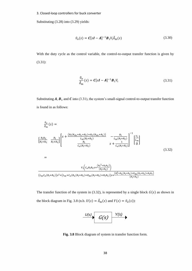
3. Closed-loop controllers for buck converter
38
Substituting (3.28) into (3.29) yields:
�̃�o(𝑠) = 𝑪[𝑠𝑰 − 𝑨]−1𝑩1𝑉i𝛿m(𝑠) (3.30)
With the duty cycle as the control variable, the control-to-output transfer function is given by
(3.31):
�̃�o
𝛿m(𝑠) = 𝑪[𝑠𝑰 − 𝑨]−1𝑩1𝑉i (3.31)
Substituting 𝑨, 𝑩1 and 𝑪 into (3.31), the system’s small-signal control-to-output transfer function
is found in as follows:
�̃�o
�̃�m(𝑠) =
[𝑅l𝑅C
𝑅l+𝑅C
𝑅l
𝑅l+𝑅C] [𝑠 +
(𝑅l(𝑅ds+𝑅L+𝑅C)+𝑅C(𝑅ds+𝑅L))
𝐿m(𝑅l+𝑅C)−
𝑅l
𝐿m(𝑅l+𝑅C)
𝑅l
𝐶o(𝑅l+𝑅C)𝑠 +
1
𝐶o(𝑅l+𝑅C)
]
−1
[𝑉i
𝐿m
0]
=
𝑉i(𝐶o𝑅l𝑅C𝑠+(𝑅l
2+𝑅l𝑅C)
(𝑅l+𝑅C))
(𝐿m𝐶o(𝑅l+𝑅C))𝑠2+(𝐿m+𝐶o(𝑅L(𝑅l+𝑅C)+𝑅ds(𝑅l+𝑅C)+𝑅l𝑅C))𝑠+
(𝑅l2+𝑅L(𝑅l+𝑅C)+𝑅ds(𝑅l+𝑅C)+𝑅l𝑅c)
(𝑅l+𝑅C)
(3.32)
The transfer function of the system in (3.32), is represented by a single block 𝐺(𝑠) as shown in
the block diagram in Fig. 3.8 (n.b. 𝑈(𝑠) = 𝛿m(𝑠) and 𝑌(𝑠) = �̃�o(𝑠)):
Y(s)U(s)G(s)
Fig. 3.8 Block diagram of system in transfer function form.
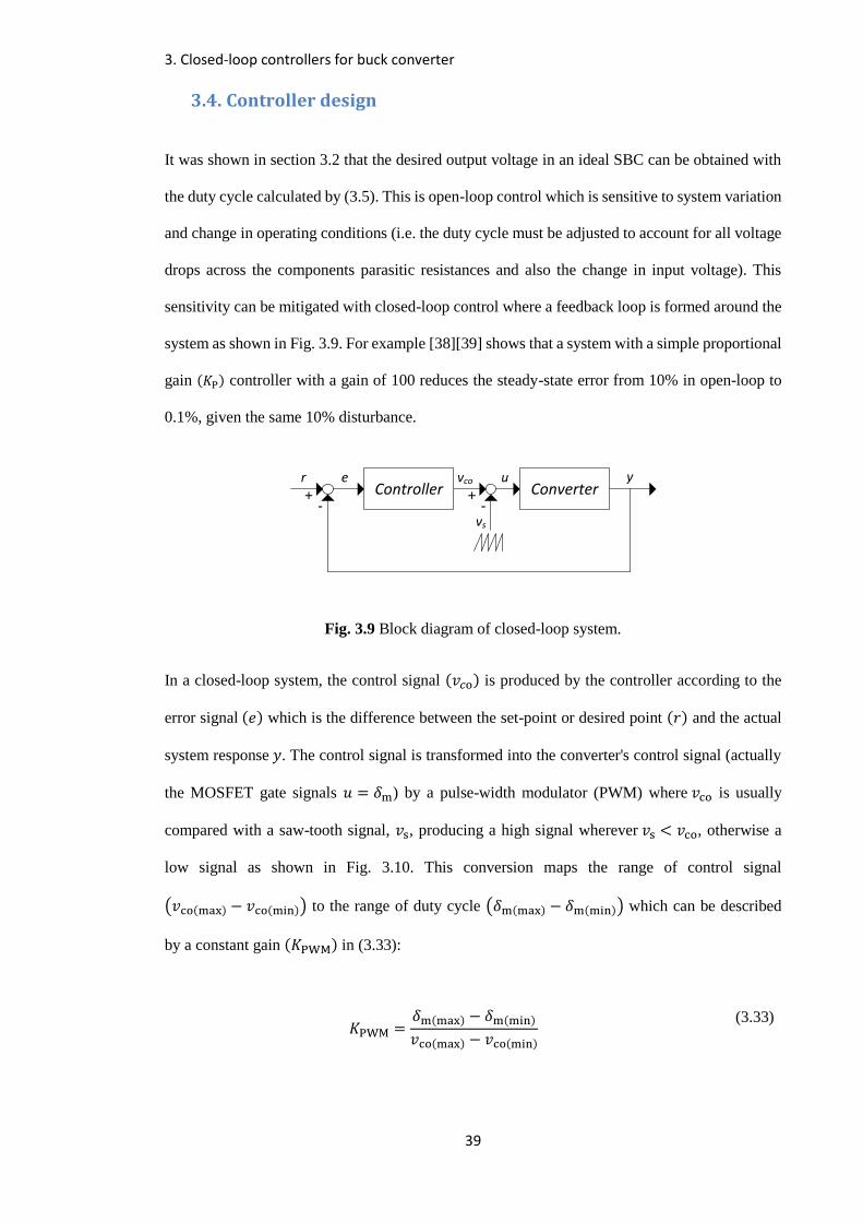
3. Closed-loop controllers for buck converter
39
3.4. Controller design
It was shown in section 3.2 that the desired output voltage in an ideal SBC can be obtained with
the duty cycle calculated by (3.5). This is open-loop control which is sensitive to system variation
and change in operating conditions (i.e. the duty cycle must be adjusted to account for all voltage
drops across the components parasitic resistances and also the change in input voltage). This
sensitivity can be mitigated with closed-loop control where a feedback loop is formed around the
system as shown in Fig. 3.9. For example [38][39] shows that a system with a simple proportional
gain (𝐾P) controller with a gain of 100 reduces the steady-state error from 10% in open-loop to
0.1%, given the same 10% disturbance.
-+
-+
r vcoConverterController
u
vs
e y
Fig. 3.9 Block diagram of closed-loop system.
In a closed-loop system, the control signal (𝑣𝑐o) is produced by the controller according to the
error signal (𝑒) which is the difference between the set-point or desired point (𝑟) and the actual
system response 𝑦. The control signal is transformed into the converter's control signal (actually
the MOSFET gate signals 𝑢 = 𝛿m) by a pulse-width modulator (PWM) where 𝑣co is usually
compared with a saw-tooth signal, 𝑣s, producing a high signal wherever 𝑣s < 𝑣co, otherwise a
low signal as shown in Fig. 3.10. This conversion maps the range of control signal
(𝑣co(max) − 𝑣co(min)) to the range of duty cycle (𝛿m(max) − 𝛿m(min)) which can be described
by a constant gain (𝐾PWM) in (3.33):
𝐾PWM =𝛿m(max) − 𝛿m(min)
𝑣co(max) − 𝑣co(min)
(3.33)
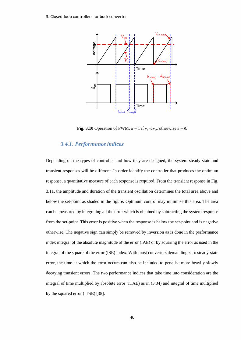
3. Closed-loop controllers for buck converter
40
Vo
lta
ge
Time
Time
δm
VcoVco(max)
Vco(min)Vs
δm(min) δm(max)
tm(on) tm(off)
Fig. 3.10 Operation of PWM, 𝑢 = 1 if vs < vco otherwise 𝑢 = 0.
3.4.1. Performance indices
Depending on the types of controller and how they are designed, the system steady state and
transient responses will be different. In order identify the controller that produces the optimum
response, a quantitative measure of each response is required. From the transient response in Fig.
3.11, the amplitude and duration of the transient oscillation determines the total area above and
below the set-point as shaded in the figure. Optimum control may minimise this area. The area
can be measured by integrating all the error which is obtained by subtracting the system response
from the set-point. This error is positive when the response is below the set-point and is negative
otherwise. The negative sign can simply be removed by inversion as is done in the performance
index integral of the absolute magnitude of the error (IAE) or by squaring the error as used in the
integral of the square of the error (ISE) index. With most converters demanding zero steady-state
error, the time at which the error occurs can also be included to penalise more heavily slowly
decaying transient errors. The two performance indices that take time into consideration are the
integral of time multiplied by absolute error (ITAE) as in (3.34) and integral of time multiplied
by the squared error (ITSE) [38].
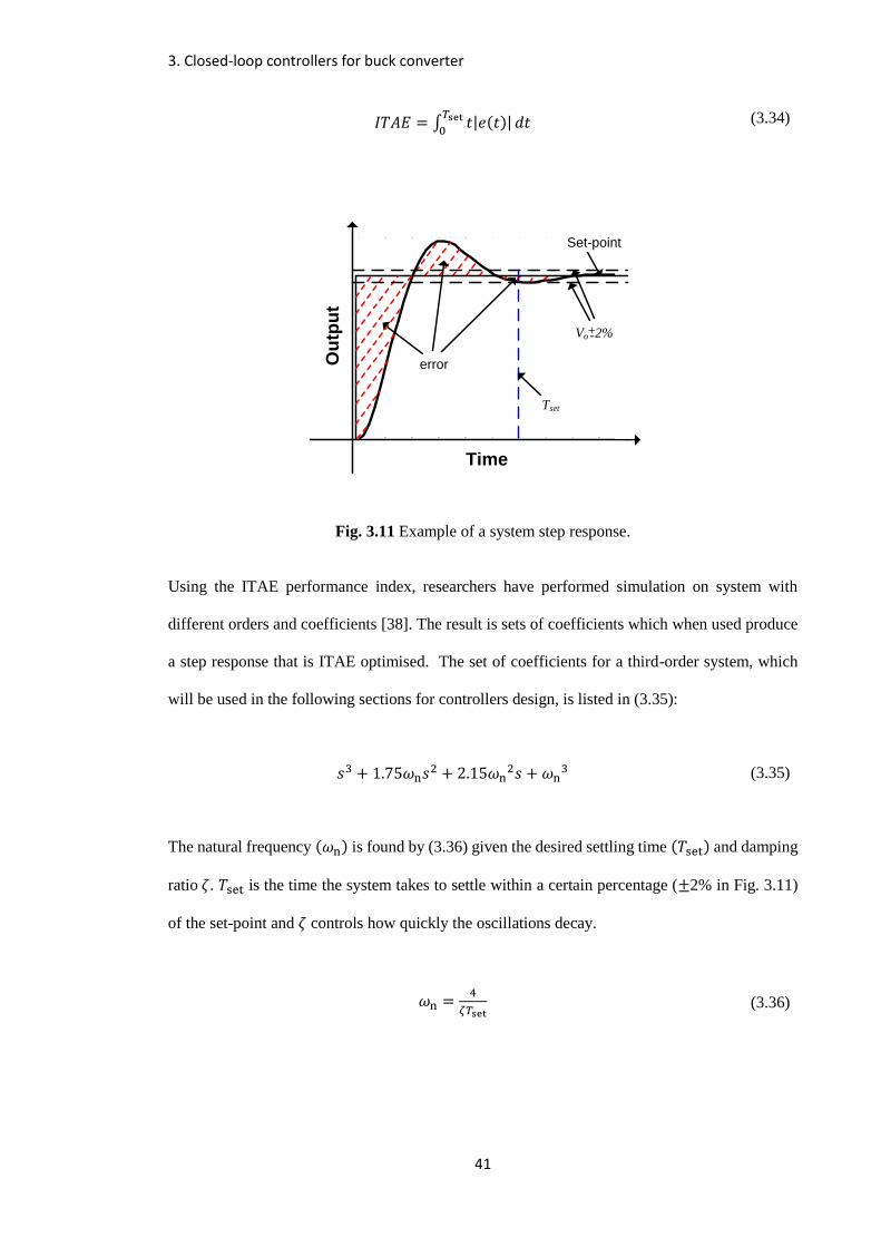
3. Closed-loop controllers for buck converter
41
0 0.5 1 1.5 2 2.5 3 3.5 4 4.5 50
0.05
0.1
0.15
0.2
0.25
Step Response
Time (sec)
Am
plit
ude
Ou
tpu
t
Time
Set-point
error
Tset
Vo 2% -+
Fig. 3.11 Example of a system step response.
Using the ITAE performance index, researchers have performed simulation on system with
different orders and coefficients [38]. The result is sets of coefficients which when used produce
a step response that is ITAE optimised. The set of coefficients for a third-order system, which
will be used in the following sections for controllers design, is listed in (3.35):
𝑠3 + 1.75𝜔n𝑠2 + 2.15𝜔n
2𝑠 + 𝜔n3 (3.35)
The natural frequency (𝜔n) is found by (3.36) given the desired settling time (𝑇set) and damping
ratio 𝜁. 𝑇set is the time the system takes to settle within a certain percentage (±2% in Fig. 3.11)
of the set-point and 𝜁 controls how quickly the oscillations decay.
𝜔n =4
𝜁𝑇set (3.36)
𝐼𝑇𝐴𝐸 = ∫ 𝑡|𝑒(𝑡)|𝑇set0
𝑑𝑡 (3.34)
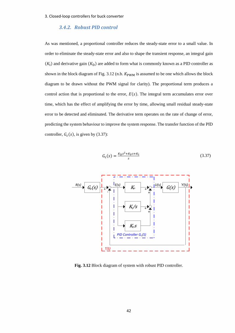
3. Closed-loop controllers for buck converter
42
3.4.2. Robust PID control
As was mentioned, a proportional controller reduces the steady-state error to a small value. In
order to eliminate the steady-state error and also to shape the transient response, an integral gain
(𝐾I) and derivative gain (𝐾D) are added to form what is commonly known as a PID controller as
shown in the block diagram of Fig. 3.12 (n.b. 𝐾PWM is assumed to be one which allows the block
diagram to be drawn without the PWM signal for clarity). The proportional term produces a
control action that is proportional to the error, 𝐸(𝑠). The integral term accumulates error over
time, which has the effect of amplifying the error by time, allowing small residual steady-state
error to be detected and eliminated. The derivative term operates on the rate of change of error,
predicting the system behaviour to improve the system response. The transfer function of the PID
controller, 𝐺𝑐(𝑠), is given by (3.37):
𝐺c(𝑠) =𝐾D𝑠
2+𝐾P𝑠+𝐾I
𝑠 (3.37)
KP
KDs
R(s) Y(s)
KI/s
Gp(s) G(s)-
+
PID Controller Gc(S)
U(s)+
++
+
E(s)
T(S)
Fig. 3.12 Block diagram of system with robust PID controller.

3. Closed-loop controllers for buck converter
43
For ease of manipulation, the system transfer function in (3.32) is substituted by the generalised
notation as in (3.38). With (3.37) and (3.38), the compensated system transfer function (𝑇(𝑠)) is
found to be a third-order function as in (3.39):
𝐺(𝑠) =𝐾𝑠
𝑠2+2𝜁𝜔𝑛𝑠+𝜔𝑛2 (3.38)
𝑇(𝑠) =𝐺𝐺c(𝑠)
1+𝐺𝐺c(𝑠) =
𝐾s(𝐾D𝑠2+𝐾P𝑠+𝐾I)
𝑠3+(2𝜁𝜔n+𝐾1𝐾D)𝑠2+(𝜔n
2+𝐾1𝐾P)𝑠+𝐾1𝐾I (3.39)
With a robust PID controller, the transient response is ITAE optimised. The coefficients of the
compensated system characteristic equation (i.e. denominator) should follow that given in (3.35),
leading to the following compensated system transfer function:
𝑇ITAE(𝑠) =𝜔n
3
𝑠3+1.75𝜔n𝑠2+2.15𝜔n
2𝑠+𝜔n3
(3.40)
The denominator of (3.40) can be obtained by selecting the three PID parameters, 𝐾P, 𝐾I and 𝐾D
through matching the coefficients in (3.39) to those in (3.40) as in (3.41):
2𝜁𝜔n + 𝐾s𝐾D = 1.75𝜔n
𝜔n2 + 𝐾s𝐾P = 2.15𝜔n
2
𝐾s𝐾I = 𝜔n3
(3.41)
The numerator of (3.40) can be obtained by cancelling the zeros introduced by the controller with
a pre-filter, 𝐺p(𝑠), with the following transfer function:
𝐺p(𝑠)𝜔n
3
𝐾s(𝐾D𝑠2+𝐾P𝑠+𝐾I)
(3.42)
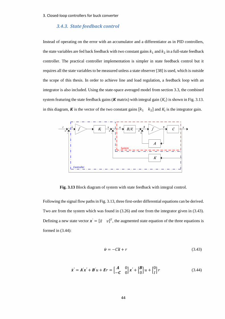
3. Closed-loop controllers for buck converter
44
3.4.3. State feedback control
Instead of operating on the error with an accumulator and a differentiator as in PID controllers,
the state variables are fed back feedback with two constant gains 𝑘1 and 𝑘2 in a full-state feedback
controller. The practical controller implementation is simpler in state feedback control but it
requires all the state variables to be measured unless a state observer [38] is used, which is outside
the scope of this thesis. In order to achieve line and load regulation, a feedback loop with an
integrator is also included. Using the state-space averaged model from section 3.3, the combined
system featuring the state feedback gains (𝑲 matrix) with integral gain (𝐾𝑖) is shown in Fig. 3.13.
in this diagram, 𝑲 is the vector of the two constant gains [𝑘1 𝑘2] and 𝐾i is the integrator gain.
K
vr y
A
B1Vi C+
+-
+-
+
v u x x. .
Controller
System
ʃʃ Ki
~~
Fig. 3.13 Block diagram of system with state feedback with integral control.
Following the signal flow paths in Fig. 3.13, three first-order differential equations can be derived.
Two are from the system which was found in (3.26) and one from the integrator given in (3.43).
Defining a new state vector 𝒙′ = [�̃� 𝑣]𝑇, the augmented state equation of the three equations is
formed in (3.44):
�̇� = −𝐶�̃� + 𝑟 (3.43)
�̇�′ = 𝑨′𝒙′ +𝑩′𝑢 + 𝑬𝑟 = [𝑨 0−𝑪 0
]𝒙′ + [𝑩0]𝑢 + [
0𝐼] 𝑟 (3.44)

3. Closed-loop controllers for buck converter
45
Following again the signal flow path in Fig. 3.13, 𝑢 is found as in (3.45). After substituting into
(3.44), the compensated system equation is found as in (3.46):
𝑢 = −𝑲′𝒙′ = [𝑲 −𝐾i]𝒙′ (3.45)
�̇�′ = 𝑨′𝒙′ −𝑩′𝑲′𝒙′ + 𝑬𝑟 = (𝑨′ −𝑩′𝑲′)𝒙′ + 𝑬𝑟 (3.46)
By expanding (3.46), the following state equation is obtained:
�̇�′ = 𝑨′′𝒙′ +𝑬𝑟 = ([
𝐴11 𝐴12 0𝐴21 𝐴22 0−𝐶11 −𝐶12 0
] − [𝐵1100] [𝑘1 𝑘2 −𝐾i])𝒙
′ + [001] 𝑟
= [𝐴11 − 𝐵11𝑘1 𝐴12 − 𝐵11𝑘2 𝐵11𝐾i
𝐴21 𝐴22 0−𝐶11 −𝐶12 0
]𝒙′ + [001] 𝑟
(3.47)
The compensated system characteristic can be found from the determinant of (3.47) as follows:
𝑑𝑒𝑡(𝑠𝑰 − 𝑨′′) = [𝑠 − (𝐴11 − 𝐵11𝑘1) −𝐴12 + 𝐵11𝑘2 −𝐵11𝐾i
−𝐴21 𝑠 − 𝐴22 0𝐶11 𝐶12 𝑠
]
= 𝑠3 + (−𝐴22 − 𝐴11 + 𝐵11𝑘1)𝑠2
+ (𝐴11𝐴22 − 𝐴22𝐵11𝑘1 + 𝐴12𝐴21 − 𝐴21𝐵11𝑘2 + 𝐵11𝐶11𝐾i)𝑠
− (𝐴21𝐶12 + 𝐴22𝐶11)𝐵11𝑘i
(3.48)
Just as in robust PID control, the coefficients of the compensated system characteristic equation
are given in (3.35). The three gains of the state feedback control with integral control, 𝑘1, 𝑘2 and
𝐾i, are found by matching the coefficients in (3.48) to that in (3.35) as in (3.49):

3. Closed-loop controllers for buck converter
46
−𝐴22 − 𝐴11 + 𝐵11𝑘1 = 1.75𝜔n
𝐴11𝐴22 − 𝐴22𝐵11𝑘1 − 𝐴12𝐴21 + 𝐴21𝐵11𝑘2 + 𝐵11𝐶11𝐾i = 2.15𝜔n2
(−𝐴21𝐶12 − 𝐴22𝐶11)𝐵11𝐾i = 𝜔n3
(3.49)
3.4.4. Predictive control
In predictive control, the control law can be derived with the system expressed in either
state-space and transfer function form. The transfer function form is chosen here for the reason
of personal preference. The configuration of the system with the predictive controller is shown in
Fig. 3.14. The control law contains three gains, the feedback gain 𝑁k, the feedforward gain 𝑃r and
control gain 𝐷k. The block 𝑧 (𝑧 − 1)⁄ is the discrete-time equivalent of an integrator.
Dk
-
r(z)
+
y(z)u(z)G(z)
Nk
Pr z /z-1
Controller Gc(Z)
Fig. 3.14 Block diagram of system with predictive controller.
The three tuning factors of a predictive controller are as followed:
𝑛y, the output horizon which determines how many steps ahead the system response is
predicted, and should be greater than the system settling time, 𝑇set, which can be found by
(3.50)
𝑛y =𝑇set
𝑇s (3.50)

3. Closed-loop controllers for buck converter
47
𝑛u, the input horizon which determines how many steps of control move is predicted, three
should be enough for most system.
𝜆, the weighting function of the control input, the larger its value, the smaller the input change
is allowed, reducing the settling time.
In order to form the prediction equation, the system transfer function with integrator is rearranged
in incremental form as follows:
(1 + 𝐴1𝑧−1 + 𝐴2𝑧
−2 +⋯+ 𝐴n+1𝑧−𝑛−1)𝑦k
= (𝑏1𝑧−1 + 𝑏2𝑧
−2 +⋯+ 𝑏n+1𝑧−𝑛)𝛥𝑢k
(3.51)
The difference equations for the next sample and the ones that follow the so-called 𝑘-step ahead
predictor, are formulated in (3.52), which can be organised into matrices as in (3.53):
𝑦k+1 + 𝐴1𝑦k +⋯+ 𝐴n+1𝑦k−n = 𝑏1𝛥𝑢k + 𝑏2𝛥𝑢k−1 +⋯+ 𝑏n𝛥𝑢k−n+1
𝑦k+2 + 𝐴1𝑦k+1 +⋯+ 𝐴n+1𝑦k−n+1 = 𝑏1𝛥𝑢k+1 + 𝑏2𝛥𝑢k +⋯+ 𝑏n𝛥𝑢k−n+2
:
𝑦k+ny +⋯+ 𝐴n+1𝑦k+ny+1−n = 𝑏1𝛥𝑢k+ny−1 +⋯+ 𝑏n𝛥𝑢k+ny−n
(3.52)
[
1 0 . . 0𝐴1 1 . . 0𝐴2 𝐴1 . . 0: : : :
] [
𝑦k+1𝑦k+2:
𝑦k+ny
] + [
𝐴1 𝐴2 . . 𝐴n+1𝐴2 𝐴3 . . 0𝐴3 𝐴4 . . 0: : : :
] [
𝑦k𝑦k−1:
𝑦k−n
]
= [
𝑏1 0 . . 0𝑏2 𝑏1 . . 0𝑏3 𝑏2 . . 0: : : :
]
[
𝛥𝑢k𝛥𝑢k+1:
𝛥𝑢k+ny−1] + [
𝑏2 𝑏3 . . 𝑏n𝑏3 𝑏4 . . 0𝑏4 𝑏5 . . 0: : : :
] [
𝛥𝑢k−1𝛥𝑢k−2:
𝛥𝑢k−n+1
]
(3.53)
With the use of Toeplitz/Hankel notation [45] (arrow pointing right representing the future value
and arrow pointing left representing the current and past values), the output prediction in (3.53)
can be simplified to (3.54):

3. Closed-loop controllers for buck converter
48
𝐶A𝑦 →k +𝐻A𝑦
←k = 𝐶zb𝛥𝑢
→k−1 +𝐻zb𝛥𝑢
←k−1 (3.54)
By rearranging (3.54) in term of 𝑦 →k and substituting 𝐻 = 𝐶A
−1𝐶zb, 𝑃 = 𝐶A−1𝐻zb and
𝑄 = −𝐶A−1𝐻A, the following equation is obtained:
𝑦 →k = 𝐶A
−1[𝐶zb𝛥𝑢 →k−1 +𝐻zb𝛥𝑢
←k−1 −𝐻A𝑦
←k]
= 𝐻𝛥𝑢 →k−1 + 𝑃𝛥𝑢
←k−1 + 𝑄𝑦
←k
(3.55)
The control law is obtained by minimising the error and control input as in the cost function (𝐽)
in (3.56). Where ||. ||2 is the 2- norm which minimise area of a plane.
𝐽 = ‖𝑟 → − 𝑦
→‖2
2 + 𝜆‖𝛥𝑢 →‖2
2 (3.56)
By minimising the future change in control move 𝛥𝑢 → and locating the minimum by setting the
rate of change to zero (i.e. 𝑑𝐽 𝑑𝛥𝑢 →⁄ = 0). The control law in (3.57) is obtained.
𝛥𝑢k = (𝐻𝑇𝐻 + 𝜆𝐼)−1𝐻𝑇(𝑟
→ −Q𝑦 ← − 𝑃𝛥𝑢
←)
= 𝑃r𝑟 → −𝑁k𝑦
← −𝐷k𝛥𝑢
←
(3.57)
where 𝑃r = (𝐻𝑇𝐻 + 𝜆𝐼)−1𝐻𝑇, 𝑁k = (𝐻
𝑇𝐻 + 𝜆𝐼)−1𝐻𝑇𝑃 and 𝐷K = (𝐻𝑇𝐻 + 𝜆𝐼)−1𝐻𝑇𝑄.
For a second-order system, the incremental form of the control law in (3.57) is as follows:
𝑢(𝑘) = 𝑟(𝑘) + 𝑢(𝑘 − 1) + 𝑦(𝑘) + 𝑦(𝑘 − 1) + 𝑦(𝑘 − 2) (3.58)

3. Closed-loop controllers for buck converter
49
3.4.5. Digital implementation
Due to the number of controllers designed in this work, it is more convenient to implement them
using a microcontroller. The robust PID controller, the PID control law in (3.38) can be written
in time constant form in (3.59), which can then be converted to the discrete-time domain by
Euler’s method [89] as in (3.60):
𝐾D𝐾I𝑠2+
𝐾P𝐾I𝑠+1
𝑠=
𝑇I𝑇D𝑠2+𝑇I𝑠+1
𝑠 (3.59)
𝑥(𝑘) = 𝑥[𝑘 − 1] + 𝐾𝑒 [(1 +𝑇s
𝑇I+𝑇D
𝑇s) 𝑒[𝑘] − (1 + 2
𝑇D
𝑇s) 𝑒[𝑘 − 1] +
𝑇D
𝑇s𝑒[𝑘 − 2]]
(3.60)
where 𝑇I is the integral time constant and 𝑇D is the derivative time constant.
For the state feedback controller, the discrete-time equivalent of the integrator gain ( 𝐾Id) is
obtained by (3.61):
𝐾Id = 𝐾I𝑇s (3.61)
3.5. Design examples and experimental results
In order to compare the transient response of the converter with the three controllers, a converter
was designed with the following specification: input voltage 𝑉i = 12 V, output voltage 𝑉o = 5 V,
output current 𝐼o = 1 A, switching frequency 𝑓s = 20 kHz, output voltage ripple
∆𝑉o < 1%, steady-state error 𝑒ss = 0, settling time 𝑇set = 1 ms and percentage overshoot
< 1%.
Using Ohm’s law, for the given 𝐼o, the load resistance, 𝑅l, is found to be 5 Ω. For the given 𝑉o,
the duty cycle is calculated by (3.5) to be 41.7%. With this 𝛿m and 𝑇s = 50 μs, the filter inductor
𝐿m and capacitor 𝐶o are calculated by (3.7) and (3.8) to be 365 μH and 50 μF respectively. The
component’s parasitic resistances, 𝑅C and 𝑅L are measured with a milliohm meter to be

3. Closed-loop controllers for buck converter
50
36 mΩ, 34 mΩ respectively and MOSFET 𝑅ds is given in manufacturer’s datasheet to be 540
mΩ. Substituting all the parameters into the (3.26) and (3.27), and (3.32), the system state and
output equations are found in (3.62) and (3.63) respectively, and the transfer function is found in
(3.64):
�̇̃� = [−1648 −268219840 −4337
] �̃� + [27010
] 𝛿m (3.62)
�̃� = [0.036 0.992]�̃� (3.63)
𝐺(𝑠) =8.153𝑥10−6𝑠+4.529
8.531𝑥10−8𝑠2+5.106𝑥10−4𝑠+5.149 (3.64)
3.5.1. Robust PID controller
For the design of the robust PID controller, (3.64) is nominalised against 𝑠2, the high frequency
zero from the capacitor ESR is also removed to yield:
𝐺(𝑠) =5.5𝑥107
𝑠2+5985𝑠+6𝑥107 (3.65)
By combining (3.65) with the transfer function of the PID controller in (3.37), the
control-to-output transfer function is found:
𝑇(𝑠) =5.5𝑥107(𝐾D𝑠
2+𝐾P𝑠+𝐾I)
𝑠3+(5985+5.5𝑥107𝐾D)𝑠2+(6𝑥107+5.5𝑥107𝐾P)𝑠+5.5𝑥10
7𝐾I
(3.66)
With 𝑇set and 𝜁 selected to be 1 ms and is 0.71 respectively, 𝜔n is calculated by (3.36) to be 5676.
After substituting into the third-order equation in (3.35), the desired control-to-output transfer
function is:
𝑇𝐼𝑇𝐴𝐸(𝑠) =1.811𝑥1011
𝑠3+9901𝑠2+6.88𝑥107𝑠+1.811𝑥1011 (3.67)

3. Closed-loop controllers for buck converter
51
Equating the coefficients of (3.66) with those in (3.67) as in (3.68), the three parameters of the
PID controller are found: 𝐾P = 0.16, 𝐾I = 3293 and 𝐾D = 7.12 x 10⁻⁵.
5985 + 5.5 x 10⁷𝐾D = 9901
6 x 10⁷ + 5.5 x 10⁷𝐾P = 6.88 x 10⁷
5.5 x 10⁷𝐾I = 1.811 x 10¹¹
(3.68)
A converter with this controller is simulated in Matlab/Simulink as in the block diagram in
Fig. 3.15. Included in the block diagram are the converter transfer function, the PID controller,
the PWM gain which is detailed in (3.33), the ADC gain which maps the range of measured
voltage into the range of the saw-tooth signal, the dead-time of 1% of duty cycle and the saturation
block which prevents duty cycle from exceeding 100%.
Fig. 3.15 Simulink model of system with the robust PID controller.
The system step responses with and without the pre-filter are shown in solid and dashed lines in
Fig. 3.16 respectively, the effect of the pre-filter is small so will not be implemented practically.
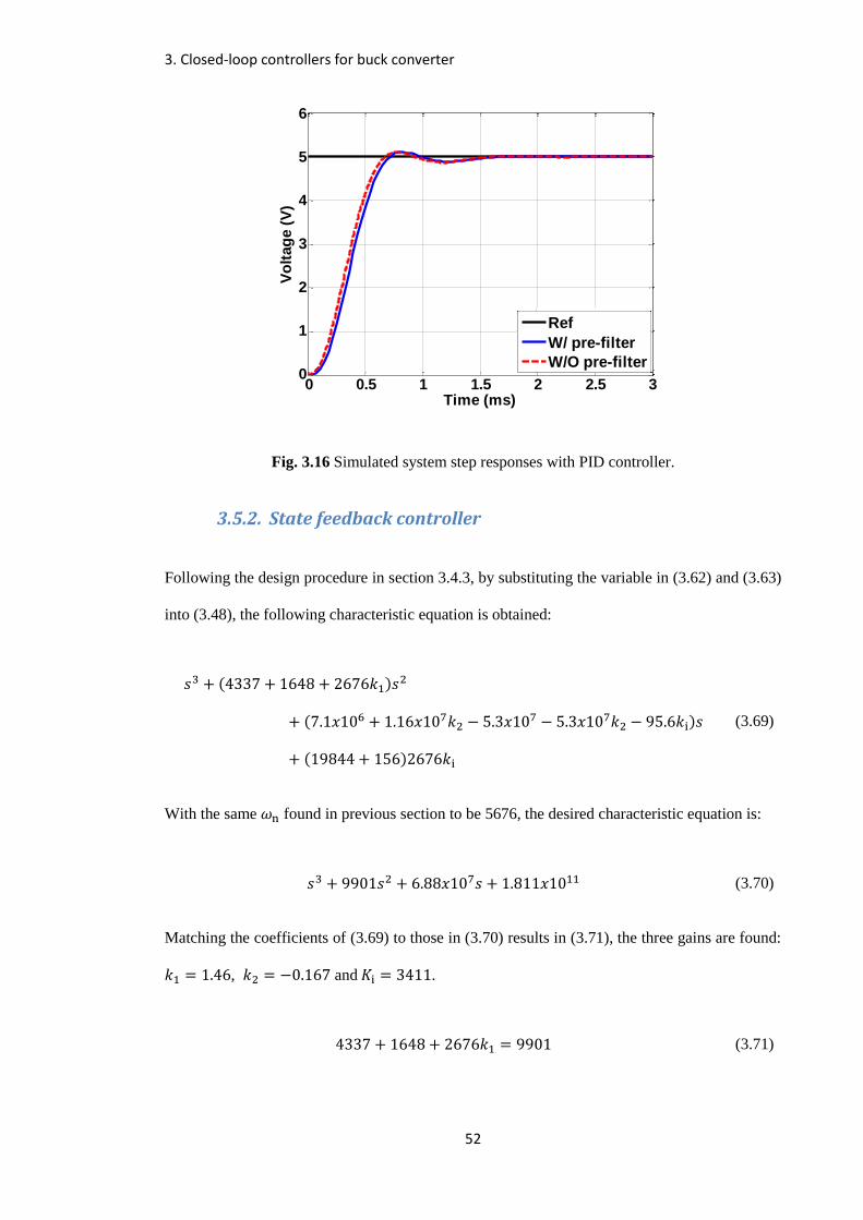
3. Closed-loop controllers for buck converter
52
Fig. 3.16 Simulated system step responses with PID controller.
3.5.2. State feedback controller
Following the design procedure in section 3.4.3, by substituting the variable in (3.62) and (3.63)
into (3.48), the following characteristic equation is obtained:
𝑠3 + (4337 + 1648 + 2676𝑘1)𝑠2
+ (7.1𝑥106 + 1.16𝑥107𝑘2 − 5.3𝑥107 − 5.3𝑥107𝑘2 − 95.6𝑘i)𝑠
+ (19844 + 156)2676𝑘i
(3.69)
With the same 𝜔n found in previous section to be 5676, the desired characteristic equation is:
𝑠3 + 9901𝑠2 + 6.88𝑥107𝑠 + 1.811𝑥1011 (3.70)
Matching the coefficients of (3.69) to those in (3.70) results in (3.71), the three gains are found:
𝑘1 = 1.46, 𝑘2 = −0.167 and 𝐾i = 3411.
4337 + 1648 + 2676𝑘1 = 9901 (3.71)
0 0.5 1 1.5 2 2.5 30
1
2
3
4
5
6
Time (ms)
Vo
ltag
e (
V)
Ref
Step response
0 0.5 1 1.5 2 2.5 30
1
2
3
4
5
6
System response
Time (ms) (sec)
Am
plit
ude (
V)
0 1 2 30
1
2
3
4
5
6
Time (ms)
Am
plitu
de (
V)
System response
Ref
W/ pre-filter
W/O pre-filter

3. Closed-loop controllers for buck converter
53
7.1𝑥106 + 1.16𝑥107𝑘1 − 5.3𝑥107 − 5.3𝑥107𝑘2 − 95.6𝑘i = 6.88𝑥10
7
(19844 + 156)2676𝑘i = 1.811𝑥1011
A converter with this state feedback controller is simulated in Simulink with the block diagram
in Fig. 3.17. As with PID controller, the ADC, the PWM, dead-time and saturation block are also
include:
Fig. 3.17 Simulink model of system with the state feedback control with integral control.
The system step response with the state feedback controller is shown by the dotted line in
Fig. 3.18. The response is only marginally better than that with the robust PID controller, which
is expected as both controllers are designed base on the same ITAE optimised coefficients.
Fig. 3.18 Simulated system step response with state feedback controller.
0 0.5 1 1.5 2 25 30
1
2
3
4
5
6
Time (ms)
Vo
ltag
e (
V)
Ref
PID controller
State feedback controller
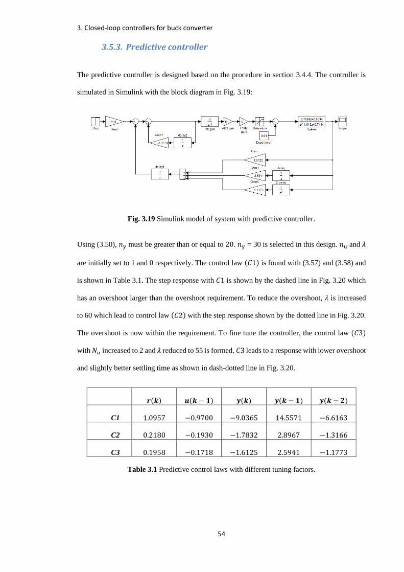
3. Closed-loop controllers for buck converter
54
3.5.3. Predictive controller
The predictive controller is designed based on the procedure in section 3.4.4. The controller is
simulated in Simulink with the block diagram in Fig. 3.19:
Fig. 3.19 Simulink model of system with predictive controller.
Using (3.50), 𝑛y must be greater than or equal to 20. 𝑛y = 30 is selected in this design. 𝑛u and 𝜆
are initially set to 1 and 0 respectively. The control law (𝐶1) is found with (3.57) and (3.58) and
is shown in Table 3.1. The step response with 𝐶1 is shown by the dashed line in Fig. 3.20 which
has an overshoot larger than the overshoot requirement. To reduce the overshoot, 𝜆 is increased
to 60 which lead to control law (𝐶2) with the step response shown by the dotted line in Fig. 3.20.
The overshoot is now within the requirement. To fine tune the controller, the control law (𝐶3)
with 𝑁𝑢 increased to 2 and 𝜆 reduced to 55 is formed. 𝐶3 leads to a response with lower overshoot
and slightly better settling time as shown in dash-dotted line in Fig. 3.20.
𝒓(𝒌) 𝒖(𝒌 − 𝟏) 𝒚(𝒌) 𝒚(𝒌 − 𝟏) 𝒚(𝒌 − 𝟐)
C1 1.0957 −0.9700 −9.0365 14.5571 −6.6163
C2 0.2180 −0.1930 −1.7832 2.8967 −1.3166
C3 0.1958 −0.1718 −1.6125 2.5941 −1.1773
Table 3.1 Predictive control laws with different tuning factors.

3. Closed-loop controllers for buck converter
55
Fig. 3.20 Simulated system responses with predictive controllers.
The simulated step responses of the three controllers, the robust PID, the state feedback controller
with integrator and the predictive controller are plotted together in dashed line, dotted line and
dash-dotted line respectively in Fig. 3.21. The response with the predictive controller is almost
identical to that with the other two controllers, this is because both the PID controller and state
feedback controller are ITAE optimised, therefore, the transient response cannot be improved for
the same system requirements.
0 0.5 1 1.5 2 2.5 30
1
2
3
4
5
6
7
Time (ms)
Vo
ltag
e (
V)
Ref
ny=30, n
u=1, =0
ny=30, n
u=1, =60
ny=30, n
u=2, =55
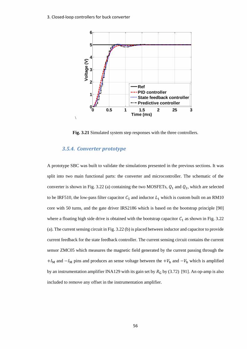
3. Closed-loop controllers for buck converter
56
\
Fig. 3.21 Simulated system step responses with the three controllers.
3.5.4. Converter prototype
A prototype SBC was built to validate the simulations presented in the previous sections. It was
split into two main functional parts: the converter and microcontroller. The schematic of the
converter is shown in Fig. 3.22 (a) containing the two MOSFETs, 𝑄1 and 𝑄2, which are selected
to be IRF510, the low-pass filter capacitor 𝐶5 and inductor 𝐿1 which is custom built on an RM10
core with 50 turns, and the gate driver IRS2186 which is based on the bootstrap principle [90]
where a floating high side drive is obtained with the bootstrap capacitor 𝐶1 as shown in Fig. 3.22
(a). The current sensing circuit in Fig. 3.22 (b) is placed between inductor and capacitor to provide
current feedback for the state feedback controller. The current sensing circuit contains the current
sensor ZMC05 which measures the magnetic field generated by the current passing through the
+𝐼M and −𝐼M pins and produces an sense voltage between the +𝑉b and −𝑉b which is amplified
by an instrumentation amplifier INA129 with its gain set by 𝑅G by (3.72) [91]. An op-amp is also
included to remove any offset in the instrumentation amplifier.
0 0.5 1 1.5 2 25 30
1
2
3
4
5
6
Time (ms)
Vo
ltag
e (
V)
Ref
PID controller
State feedback controller
Predictive controller
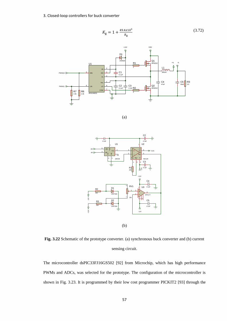
3. Closed-loop controllers for buck converter
57
𝐾g = 1 +49.4𝑥103
𝑅g (3.72)
(a)
(b)
Fig. 3.22 Schematic of the prototype converter. (a) synchronous buck converter and (b) current
sensing circuit.
The microcontroller dsPIC33FJ16GS502 [92] from Microchip, which has high performance
PWMs and ADCs, was selected for the prototype. The configuration of the microcontroller is
shown in Fig. 3.23. It is programmed by their low cost programmer PICKIT2 [93] through the
C550uF
D1
1N5820
C10.1uF
C20.1uF
C32.2uF
R32.5
VDD+12V
R73.3k
R83.3k
R1
3
R2
3
L1
365uH
Q1IRF8252
Q2IRF8252
HIN5
LIN6
Vs4
Vb2
LO8
COM7
Vcc1
HO3
U1
IRS2186(S)
C447uF
+IL -IL
PWM1H
PWM1L
3
2
Vo6
+V
7
Rg-
1
Rg+
8
-V
4
Ref5
U2
INA129
R1499
3
2
6
74 1 5
U3
OPA177
Iout1
R2
500
R3
500
12
3
RV1
10k
-12V
+1
2V
+12V
-12V
-12V
+12V
C2
0.1uF
C3
0.1uF
C1
0.1uF
D1
1N4733A
D2
1N4733A
C4
0.1uF
C5
0.1uF
+V
b7
-Vb
4
+Vo2
-Vo
5
+IM6
-IM3
1/8
U1
ZMC05
+IM
-IM
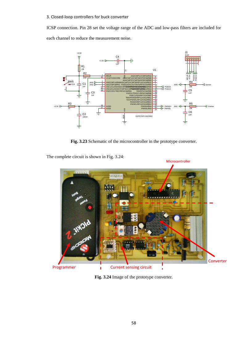
3. Closed-loop controllers for buck converter
58
ICSP connection. Pin 28 set the voltage range of the ADC and low-pass filters are included for
each channel to reduce the measurement noise.
Fig. 3.23 Schematic of the microcontroller in the prototype converter.
The complete circuit is shown in Fig. 3.24:
Fig. 3.24 Image of the prototype converter.
MCLR1
VCAP/VDDCORE20
AN0/CMP1A/RA02
AN1/CMP1B/RA13
OSC1/CLKIN/AN6/CMP3C/CMP4A/RP1/CN1/RB19
OSC2/CLK0/AN7/CMP3D/CMP4B/RP2/CN2/RB210
PGEC2/EXTREF/RP4/CN4/RB412
AVDD28
AVSS27
AN2/CMP1C/CMP2A/RA24
AN5/CMP2D/CMP3B/RP10/CN10/RB107
PGED2/DACOUT/INT0/RP3/CN3/RB311
CN8/RB8/PGED3/RP8/CN8/RB814
PGEC3/RP15/CN15/RB1515
TD0/RP5/CN6/RB516
PGED1/TDI/SCL/RP6/CN6/RB617
PGEC1/SDA/RP7/CN7/RB718
TMS/PWM3H/RP11/CN11/RB1121
TCK/PWM3L/RP12/CN12/RB1222
PWM2H/RP13/CN13/RB1323
PWM2L/RP14/CN14/RB1424
PWM1H/RA425
PWM1L/RA326
AN3/CMP1D/CMP2B/RP0/CN0/RB05
AN4/CMP2C/CMP3A/RP9/CN9/RB96
VS
S8
/19
VD
D13 U1
DSPIC33FJ16GS502
R110k
R2
470
C11nF
R3
10
C2100nF
C4
1nF
C31nF
MC
LR
+3
.3V
PG
ED
3
PG
EC
3
PWM1H
PWM1L
Vsense
Isense
+3.3V
+3.3V
+3.3V
1 2 3 4 5 6
J1ICSP
12
SW5SWITCH
C51nF
R4
10k
R5
10k
C61nF
AN0
AN1
PGED3
PGEC3
AN0
AN1
Programmer
Converter
Current sensing circuit
Microcontroller

3. Closed-loop controllers for buck converter
59
For the practical implementation, the discrete-time control law of the robust PID controller is
obtained by (3.60) in (3.73) and of the state feedback controller with (3.61) in (3.74). The
predictive controller is already in the incremental form in (3.75):
𝑢(𝑘) = 𝑢(𝑘 − 1) + 0.16[10.9𝑒(𝑘) − 18.8𝑒(𝑘 − 1) + 8.9𝑒(𝑘 − 2)] (3.73)
𝑢(𝑘) = 1.46𝑥1(𝑘) − 0.17𝑥2(𝑘) + 0.17𝑟(𝑘) (3.74)
𝑢(𝑘) = 0.20𝑟(𝑘) − 0.17𝑢(𝑘 − 1) − 1.61𝑦(𝑘) + 2.59𝑦(𝑘 − 1) − 1.18𝑦(𝑘 − 2) (3.75)
With the switching frequency of the PWM at 20 kHz, the control bandwidth is also limited to
20 kHz (i.e. the duty cycle can only be changed once every cycle). With the different length of
time needed for the microcontroller to calculate the above control laws under different operating
conditions, the control input is applied at the next cycle, introducing a constant time-delay of
50 μs. With this time delay, the system responses with the three controllers are re-simulated. The
system responses with the PID controller, the state feedback controller and the predictive
controller without the time delay are shown in dash line in Fig. 3.25 (a), (b) and (c) respectively.
Also shown in the figures are the simulated and practical responses with the time delay in the
dotted line and dash-dotted line respectively. The practical responses of the system with time
delay are in excellent agreement with the simulation.
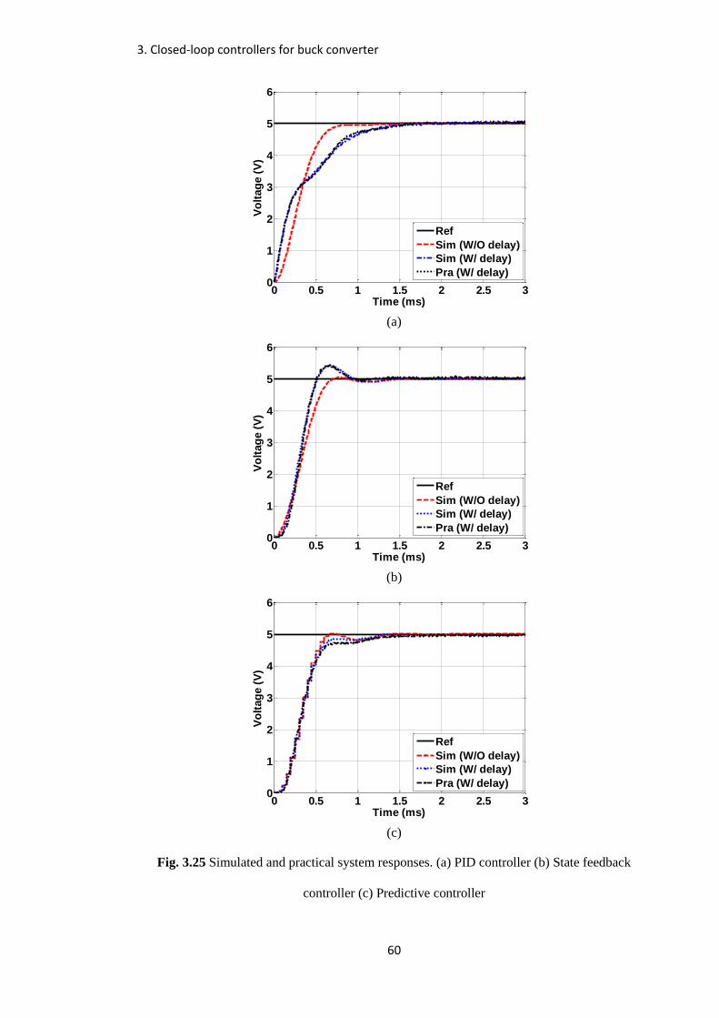
3. Closed-loop controllers for buck converter
60
(a)
(b)
(c)
Fig. 3.25 Simulated and practical system responses. (a) PID controller (b) State feedback
controller (c) Predictive controller
0 0.5 1 1.5 2 2.5 30
1
2
3
4
5
6
Time (ms)
Vo
ltag
e (
V)
Ref
Sim (W/O delay)
Sim (W/ delay)
Pra (W/ delay)
0 0.5 1 1.5 2 2.5 30
1
2
3
4
5
6
Time (ms)
Vo
ltag
e (
V)
Ref
Sim (W/O delay)
Sim (W/ delay)
Pra (W/ delay)
0 0.5 1 1.5 2 2.5 30
1
2
3
4
5
6
Time (ms)
Vo
ltag
e (
V)
Ref
Sim (W/O delay)
Sim (W/ delay)
Pra (W/ delay)

3. Closed-loop controllers for buck converter
61
The practical result of the three controllers are plotted in Fig. 3.26, showing that different types
of controller respond to the time delay differently, with the predictive controller being affected
the least.
Fig. 3.26 Practical system responses with different controller with time delay.
3.6. Summary
From the steady state operation of synchronous buck converters, the equations defining the
required filter inductance and capacitance, and the sets of first-order differential equations for
state-space modelling are obtained. From the differential equations, the state-space form of the
equivalent circuit model is arrived at through a state-space averaging technique. This equivalent
circuit model is converted to the transfer function through the use of a Laplace transform. The
closed-loop system configuration is briefly discussed before the details of the robust PID
controller, the state feedback controller with integrator and the predictive controller are given. A
5 W converter is designed to allow the step responses with the three controllers to be compared.
Before the inclusion of the time delay, simulation results show that the step responses of the
converter with the three controllers are almost identical; no major transient performance
advantage is gained. When the time delay is included in the simulation, the step responses are
0 0.5 1 1.5 2 2.5 30
1
2
3
4
5
6
Time (ms)
Vo
ltag
e (
V)
Ref
PID controller
State feedback controller
Predictive controller

3. Closed-loop controllers for buck converter
62
shown being affected differently depending on the type of controller, with the converter with the
predictive controller being the least affected. A prototype converter is built and implemented with
the three controllers. The measurements from the prototype show excellent agreement with the
simulation with and without the time delay.

63
4. Improvements in transient response with parallel converters
4.1. Introduction
Chapter 3 has shown that the improvement in transient response performance of a synchronous
buck converter withdifferent types of linear controller is limited. This chapter investigates the
transient performance of a parallel converter (i.e. converter with two parallel connected power
modules). A detailed analysis of two control schemes, the fast response double buck (FRDB) [60]
and sensorless and peak current mode control (SCM-PCM) [61], presented in the literature is
undertaken, from which a new control scheme which combines the high efficiency characteristic
of the FRDB and fast transient performance characteristic of the SCM-PCM is proposed. A 25 W
(𝑉o = 5 V, 𝐼o = 5 A) parallel converter is designed and controlled by the proposed scheme. Its
transient performance and efficiency are compared with a similar converter implemented with the
FRDB and the SCM-PCM schemes to show the advantages of the proposed scheme.
4.2. Circuit configuration and components selection
The parallel converter discussed in this chapter is formed by two parallel connected power modules
(PMs), each of which is based on the synchronous buck converter detailed in section 3.2. One
power module is called the main PM, while the other called the auxiliary PM as shown in Fig. 4.1.
The subscript m and x are used to represent the parameters for the main and auxiliary PM
respectively. For example, 𝛿m is the duty cycle of the main PM while 𝛿x is the duty cycle of the
auxiliary PM.

4. Improvements in transient response with parallel converters
64
Fig. 4.1 Parallel converter with two parallel connected SBC.
With the two PMs connected in parallel as in Fig. 4.1 (i.e. sharing the same input and output
connections), the total rate of change of inductor current ((𝑑 𝑑𝑡⁄ )𝐼𝑚+𝑥) at any given instant is
simply the sum of the rates of change of the main and auxiliary PMs inductor currents at that
instant as in (4.1):
𝑑
𝑑𝑡𝐼m+x =
𝑑
𝑑𝑡𝐼m +
𝑑
𝑑𝑡𝐼x (4.1)
Under the maximum load step (increases) or drop (reduction), the duty cycles of both PMs are set
to the maximum or minimum respectively to minimise the transient recovery time. Under these
conditions, the inductors of the two PMs can be represented by the equivalent inductance, 𝐿,
which is found by the parallel law as followed:
𝐿 =1
1
𝐿m+1
𝐿x
(4.2)
Due to the limited rate of change of inductor current, an excess or deficit in charge is provided to
the output during the load changes which must be absorbed or released by the output capacitor.
Depending on the magnitude of the load step or drop, the capacitance calculated by (3.8) for the
Vi
Lm
Co RlCi Vo
S2
S1 Im
D2
Lx
S4
S3 Ix
D4
Main PM
Auxiliary PM
Im+x
Point of common connection
dx
d'x
dm
d'm

4. Improvements in transient response with parallel converters
65
steady state output voltage ripple requirement is often too low to satisfy the voltage overshoot
(𝑉os) and undershoot (𝑉us) requirements for the supply. For clarity, the remaining chapter focuses
on the load step (increases) case, similar procedures can however be applied for the load drop
(reduction).
The typical current and voltage waveforms of a converter subjected to a load step change are
shown in Fig. 4.2. At time, 𝑡1, a load current step of magnitude 𝐼𝑠 is introduced, the inductor
current is temporarily below the new load current level due to the limited rate of change of
inductor current, until 𝑡2. The integral of this current is the charge (𝑄us) responsible for the voltage
drop in the capacitor. The total voltage drop, 𝑉us, during this period can be found by the charge
equation as follows:
𝑉s =𝑄us
𝐶o=
𝐼s𝑇𝑝
2𝐶o
(4.3)
where 𝑇p is the time taken for 𝐼o to reach the new load current.
With the load current step during the period, 𝑡1 < 𝑡 < 𝑡2, described by (4.4), an expression for the
minimum capacitance is obtained by rearranging (4.4) in term of 𝑇p and substituting into (4.3),
then rearranging in term of 𝐶o as in (4.5) [94] (n.b. for load drop, 𝑉i − 𝑉o in (4.5) is replaced by
𝑉o):
𝐼𝑠 =(𝑉i−𝑉o)𝑇p
𝐿 (4.4)
𝐶o ≥𝐿𝐼s
2
2𝑉us(𝑉i−𝑉o)
(4.5)
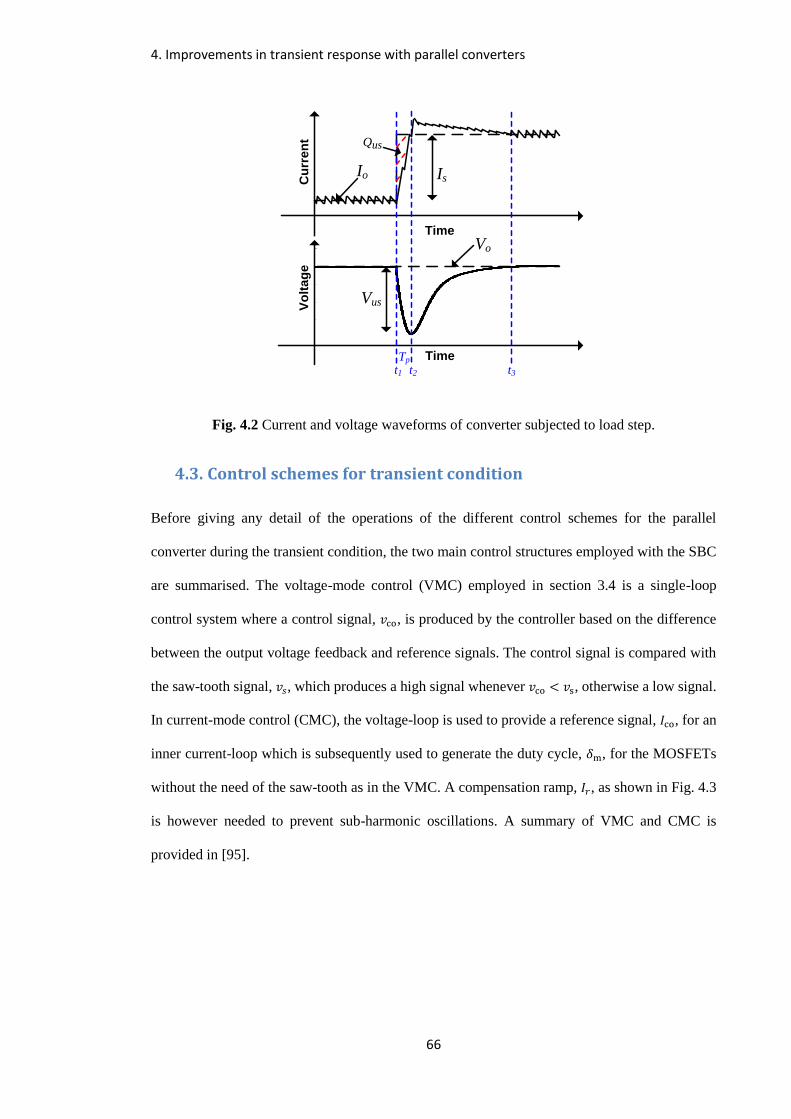
4. Improvements in transient response with parallel converters
66
0 0.5 1 1.5 2 2.5 3 4.5
4.6
4.7
4.8
4.9
5
5.1
Time (ms)
Volta
ge (V
)
Vo
lta
ge
Time
Time
Cu
rre
nt
Is
Vus
Vo
Io
t1 t2
Qus
t3
Tp
Fig. 4.2 Current and voltage waveforms of converter subjected to load step.
4.3. Control schemes for transient condition
Before giving any detail of the operations of the different control schemes for the parallel
converter during the transient condition, the two main control structures employed with the SBC
are summarised. The voltage-mode control (VMC) employed in section 3.4 is a single-loop
control system where a control signal, 𝑣co, is produced by the controller based on the difference
between the output voltage feedback and reference signals. The control signal is compared with
the saw-tooth signal, 𝑣𝑠, which produces a high signal whenever 𝑣co < 𝑣s, otherwise a low signal.
In current-mode control (CMC), the voltage-loop is used to provide a reference signal, 𝐼co, for an
inner current-loop which is subsequently used to generate the duty cycle, 𝛿m, for the MOSFETs
without the need of the saw-tooth as in the VMC. A compensation ramp, 𝐼𝑟, as shown in Fig. 4.3
is however needed to prevent sub-harmonic oscillations. A summary of VMC and CMC is
provided in [95].
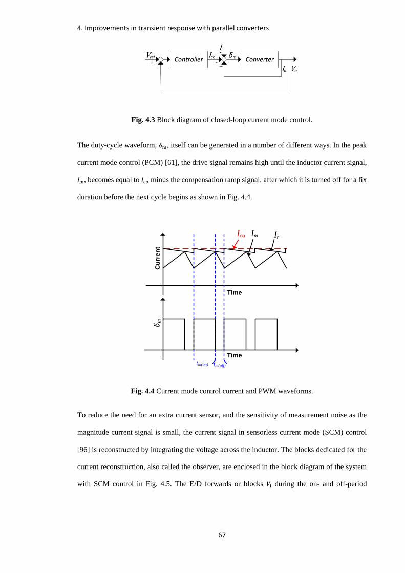
4. Improvements in transient response with parallel converters
67
Vo+
--
+Im
Vref Ico ConverterControllerδm
Ir-
Fig. 4.3 Block diagram of closed-loop current mode control.
The duty-cycle waveform, 𝛿m, itself can be generated in a number of different ways. In the peak
current mode control (PCM) [61], the drive signal remains high until the inductor current signal,
𝐼m, becomes equal to 𝐼co minus the compensation ramp signal, after which it is turned off for a fix
duration before the next cycle begins as shown in Fig. 4.4.
Cu
rre
nt
Time
Time
δm
Ico Im
tm(on) tm(off)
Ir
Fig. 4.4 Current mode control current and PWM waveforms.
To reduce the need for an extra current sensor, and the sensitivity of measurement noise as the
magnitude current signal is small, the current signal in sensorless current mode (SCM) control
[96] is reconstructed by integrating the voltage across the inductor. The blocks dedicated for the
current reconstruction, also called the observer, are enclosed in the block diagram of the system
with SCM control in Fig. 4.5. The E/D forwards or blocks 𝑉i during the on- and off-period

4. Improvements in transient response with parallel converters
68
respectively, to emulate the voltage across the inductor, which is 𝑉i − 𝑉o during the on-period and
−𝑉o during the off-period (n.b. neglecting parasitic resistances).
Vo
-
-
VL -ʃVref
-+
E/D
Controller
Vref
Converter
Vi
+
-
+
Observer
Ir
Ico δm
Fig. 4.5 Block diagram of a converter with the SCM control.
Although CMC has been shown to provide superior performance in certain applications it requires
an extra feedback loop and can impact on noise and stability. Therefore, for consistency, VMC is
employed for the majority of the work presented here with the exception of section 4.3.2 where
CMC is employed to implement the SCM-PCM control scheme.
4.3.1. FRDB scheme
In the first control scheme being studied in the chapter, the fast response double buck (FRDB)
scheme [60], the main PM remains in operation at all time with its duty cycle, 𝛿m, sets by a linear
controller, while the auxiliary PM is only in operation when the output voltage exceeds the
threshold voltage, 𝑉us, as detected by the threshold logic. The auxiliary PM duty cycle, 𝛿x, is set
by a non-linear controller (hysteretic control) [97] which generates a high or low drive signal
whenever the output voltage exceeds the hysteresis band (±𝛥) as shown in Fig. 4.6. The threshold
logic produces two signals, the signal ‘E/D’ enables or disables the auxiliary PM while the signal
‘Sat’ saturates the main PM linear controller. The block diagram of the converter with the FRDB
scheme is shown in Fig. 4.7.

4. Improvements in transient response with parallel converters
69
Vo
lta
ge
Time
δx
Vus+Δ
Vus-Δ
Vus
Fig. 4.6 Auxiliary PM with nonlinear hysteretic control.
Parallelconverter
Linear controller
Non-linear controller
-
Vref
+Vo
δm
δx
Threshold logic
Vo Sat
E/D
Fig. 4.7 Block diagram of the converter with FRDB.
Under steady-state operation, the output voltage is within the undershoot threshold level, 𝑉us, and
so the auxiliary PM is disabled. 𝑉o is regulated by the main PM as in the standard SBC in previous
chapter. A load step applied at time 𝑡1 in Fig. 4.8, causes the output voltage to drop. With a large
enough load step, the voltage drop exceeds the threshold voltage at time 𝑡2, the threshold logic
carry out the following two actions: 1) saturate the main PM duty cycle (i.e. 𝛿m = 1) to allow its
current to recover at the maximum rate, and 2) enable the auxiliary PM to provide any extra charge
needed to keep the voltage within the 𝑉us ± 𝛥. At time 𝑡3, the main PM current has reached a level
where it alone can maintains the output voltage within the threshold level, the main PM control
input is unsaturated and the auxiliary PM is disabled. The transient response ends as soon as the
output voltage reaches the set-point at time 𝑡4, with a similar response to the standard SBC, the
auxiliary PM has no effect on the settling time. The duration over which the main PM is saturated
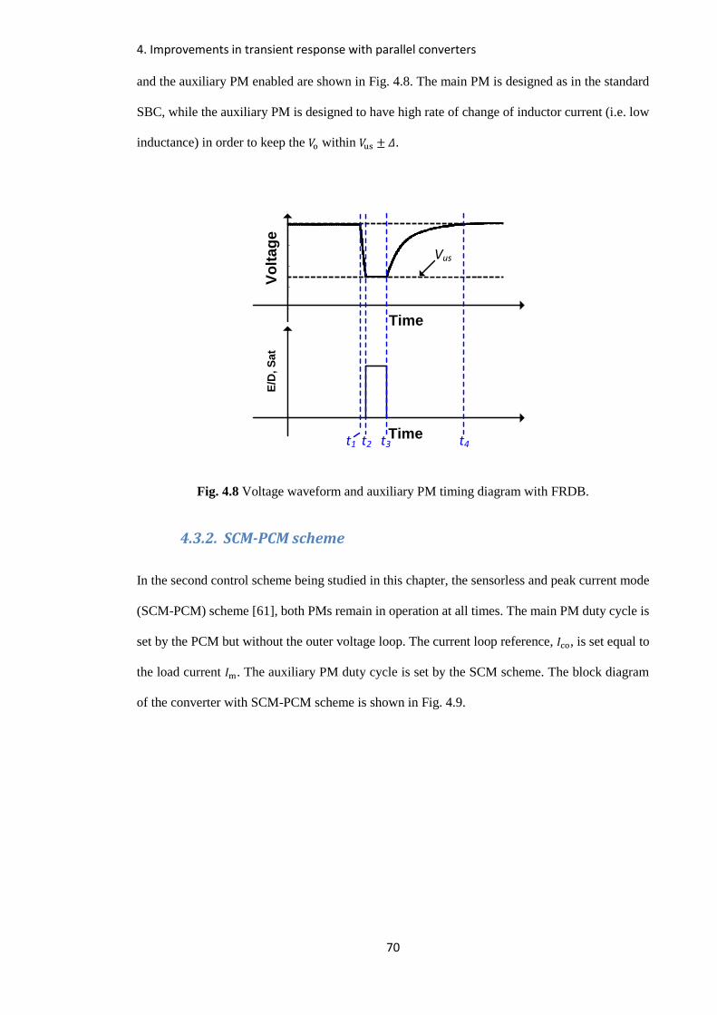
4. Improvements in transient response with parallel converters
70
and the auxiliary PM enabled are shown in Fig. 4.8. The main PM is designed as in the standard
SBC, while the auxiliary PM is designed to have high rate of change of inductor current (i.e. low
inductance) in order to keep the 𝑉o within 𝑉us ± 𝛥.
0 0.5 1 1.5 2 2.5 3 4.5
4.6
4.7
4.8
4.9
5
5.1
Time (ms)
Vol
tage
(V)
Vo
lta
ge
Time
E/D
, S
at
t1 t2 t3
Time
t4
Vus
Fig. 4.8 Voltage waveform and auxiliary PM timing diagram with FRDB.
4.3.2. SCM-PCM scheme
In the second control scheme being studied in this chapter, the sensorless and peak current mode
(SCM-PCM) scheme [61], both PMs remain in operation at all times. The main PM duty cycle is
set by the PCM but without the outer voltage loop. The current loop reference, 𝐼co, is set equal to
the load current 𝐼m. The auxiliary PM duty cycle is set by the SCM scheme. The block diagram
of the converter with SCM-PCM scheme is shown in Fig. 4.9.

4. Improvements in transient response with parallel converters
71
Parallelconverter
Ico
-+
Im
δm
δx
-ʃVref-
--
+
E/D
Controller
Vref
Vi
+
Vo
-Ir
Fig. 4.9 Block diagram of the converter with SCM-PCM.
Under steady-state condition, 𝐼m matches the load demand, the auxiliary PM sees no voltage error,
injecting an average current of zero. When the load demand is suddenly increased, time 𝑡1 in Fig.
4.10, the output voltage drops due to the deficit in charge as 𝐼m is rising to the new load demand.
The auxiliary PM sees the voltage drop and starts providing the extra charge required to bring the
output voltage back to its steady-sate value. At time 𝑡2, while the main PM current is still
recovering to the new demand, the extra charge from the auxiliary PM has brought the output
voltage back to the steady-state level. The transient response as perceived at the output ends here.
After time 𝑡2, the main PM current continuous to rise to the new level, the charge required by the
auxiliary PM to keep the output voltage at the set-point is reduced. At time 𝑡3, 𝐼m has settled to
the new load demand and 𝐼x has returned to the average of zero and this is the instant where the
converter’s actual response to the transient event is complete. The main and auxiliary PMs are
designed such that their equivalent inductor, 𝐿, and capacitor together prevent the threshold
voltage to be exceeded under the maximum rated load step.

4. Improvements in transient response with parallel converters
72
0 0.5 1 1.5 2 2.5 3 4.5
4.6
4.7
4.8
4.9
5
5.1
Time (ms)
Vo
ltag
e (
V)
Vo
lta
ge
Time
t1 t3t2
Vus
Fig. 4.10 Voltage waveform with SCM-PCM.
4.3.3. Proposed FRHE scheme
In the FRDB scheme, the auxiliary PM only operates when the main PM is unable to sustain the
output voltage within the undershoot voltage threshold level and so the extra bandwidth available
in the auxiliary PM is not exploited. In the SCM-PCM scheme, the auxiliary PM remains in
operation at all time and so the wide bandwidth of the auxiliary PM is fully exploited. However,
since the efficiency of the auxiliary PM is lower than the main PM due to its higher operating
frequency (more detail will be given in chapter 5 and 6), the continual operation of the auxiliary
PM leads to lower system efficiency in transient conditions in comparison to the FRDB scheme.
A new scheme, the fast recovery with high transient efficiency (FRHE) scheme, which combining
the advantages of the FRDB and SCM-PCM schemes, is proposed in this section to achieve the
compromise between the transient performance and efficiency.
In the proposed (FRHE) scheme, the main PM remains in operation at all time to regulate the
output voltage. In order to prevent current diversion through the auxiliary PM (during the transient
condition), the 𝑉o is regulated indirectly through 𝐼m with its reference, 𝐼ref, obtained through
Ohm’s law (i.e. 𝐼ref = 𝑉ref/𝑅l where 𝑅l is given in this work). The operation of the auxiliary PM
is similar to the FRDB scheme, which is enabled to prevent the threshold voltage from being
exceeded. However, instead of having the threshold logic which demands the auxiliary PM

4. Improvements in transient response with parallel converters
73
inductance to be low, it is replaced by the load detection block which enables the auxiliary PM
when a specific load change is exceeded. In order to shape both the transient and steady-state
responses as in the SCM-PCM scheme, two PID controllers, 𝑃𝐼𝐷m and 𝑃𝐼𝐷x, are required. The
block diagram of the converter with the proposed scheme is shown in Fig. 4.11.
Parallelconverter
PIDm
PIDx
Iref
-
-+
Vref
+
Im Vo
δm
δx
1/Rl
Load detection
E/D
Fig. 4.11 Block diagram of the converter with the proposed control scheme.
Under steady-state conditions or with a small load steps, the load detection block disables the
auxiliary PM, the output voltage is regulated by the main PM alone as in the FRDB scheme. With
a large enough load step, the main PM alone is unable to prevent the threshold voltage from being
exceeded and so, the load detection block enables the auxiliary PM to provide the extra current
required to bring the output to the set-point with the minimum time as in the
SCM-PCM scheme. The transient response under the maximum load step is identical to that in
the SCM-PCM, that is, the transient response starts at time 𝑡1, and perceived to end by the output
at time 𝑡2 while the actual converter’s response to the transient event ends at time 𝑡3 as shown in
Fig. 4.12. The interval for which the auxiliary PM is active is defined as 𝑇p in
Fig. 4.12. In the case where the auxiliary is enabled only once the threshold voltage is exceeded,
the on-duration is reduced only slightly to 𝑇p1. The main and auxiliary PMs are designed as in the
SCM-PCM scheme, where their equivalent inductance and capacitor are selected to prevent the
threshold voltage from being exceeded under the maximum load step.

4. Improvements in transient response with parallel converters
74
0 0.5 1 1.5 2 2.5 3 4.5
4.6
4.7
4.8
4.9
5
5.1
Time (ms)
Volta
ge (V
)
Vo
lta
ge
Time
Time
E/D
Tp
Tp1
Vus
t1 t3t2
Fig. 4.12 Voltage waveform and auxiliary PM timing diagram with the proposed scheme.
4.4. Controller design
In section 3.4.2, each of the PID controllers investigated contained the proportional gain 𝐾P, the
integral gain 𝐾I and the derivative gain 𝐾D, which were found using the set of ITAE optimised
coefficients. This is not possible for the multi-input single-output converters described in this
chapter due to the interaction between the two inputs. The controller parameters are instead found
using the genetic algorithm (GA) [98], which searches for an optimum solution through a process
akin to evolution, allowing an optimal solution to be identified irrespective of the interaction of
the system’s inputs. Genetic algorithms are inspired by natural selection processes and use the
evaluation of a cost function across a population. The population evolves over many generations
and converges to optimum solutions for the problem. GA typically uses the following three main
operators:
Selection: retain the best solutions for the next generation, which are to be improved by the
following two operators.
Crossover: two solutions are combined together to extract the best parts in each of the two
solutions.
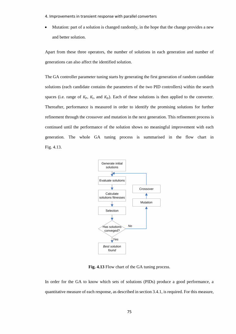
4. Improvements in transient response with parallel converters
75
Mutation: part of a solution is changed randomly, in the hope that the change provides a new
and better solution.
Apart from these three operators, the number of solutions in each generation and number of
generations can also affect the identified solution.
The GA controller parameter tuning starts by generating the first generation of random candidate
solutions (each candidate contains the parameters of the two PID controllers) within the search
spaces (i.e. range of 𝐾P, 𝐾I, and 𝐾D). Each of these solutions is then applied to the converter.
Thereafter, performance is measured in order to identify the promising solutions for further
refinement through the crossover and mutation in the next generation. This refinement process is
continued until the performance of the solution shows no meaningful improvement with each
generation. The whole GA tuning process is summarised in the flow chart in
Fig. 4.13.
Has solutions
conveged?
Evaluate solutions
Generate initial
solutions
Selection
Best solution
found
Crossover
Yes
No
Mutation
Calculate
solutions fitnesses
Fig. 4.13 Flow chart of the GA tuning process.
In order for the GA to know which sets of solutions (PIDs) produce a good performance, a
quantitative measure of each response, as described in section 3.4.1, is required. For this measure,

4. Improvements in transient response with parallel converters
76
the converter is subjected to repeat load step and drop, the transient responses from each of these
changes in load conditions cause the measurable errors in the two PMs which are measured by
the ITAE performance index (see section 3.4.1). The combined errors (ITAE score) of the two
PMs accumulated over numbers of the load changes to allow the best controllers, with the
minimum errors, to be identified.
4.5. Design example and experimental results
To demonstrate the difference in transient response and efficiency of the converter with the
proposed control scheme over the FRDB and SCM-PCM schemes, a 25 W (𝑉o = 5 V, 𝐼o = 5 A)
parallel connected SBCs has been designed and built. The maximum current step 𝐼s is 4 A, the
current ripple 𝛥𝐼m is 0.5 A and the maximum undershoot 𝑉us is 0.25 V.
Following the design procedure outlined in [61], the switching frequency of the main PM, 𝑓sm,
that produces the highest efficiency is 40 kHz. In this work, the switching frequency of the
auxiliary PM, 𝑓sx, is selected to be five times that of the main PM at 200 kHz. With these switching
frequencies, the filter inductors of the main and auxiliary PMs are calculated by (3.7) to be 𝐿m ≥
146 μH and 𝐿x ≥ 29 μH respectively. With the equivalent inductance of the two PMs calculated
by (4.2) to be 24 μH, the filter capacitor 𝐶o is calculated by (4.5) to be 620 μF. The two practical
inductors and capacitor used are: 𝐿m =172 μH, 𝐿x = 31μH and 𝐶o = 660 μF.
A converter with the component values defined as above and with the closed-loop configuration
in Fig. 4.11 is simulated in a Matlab/Simulink with the ‘SimPowerSystems’ toolbox as shown in
Fig. 4.14. The derivative gain of the main PM, 𝐾Dm, is set to zero in order to reduce the need of
computation power and susceptibility to noise. This is justified as this power module does not
required tight control.
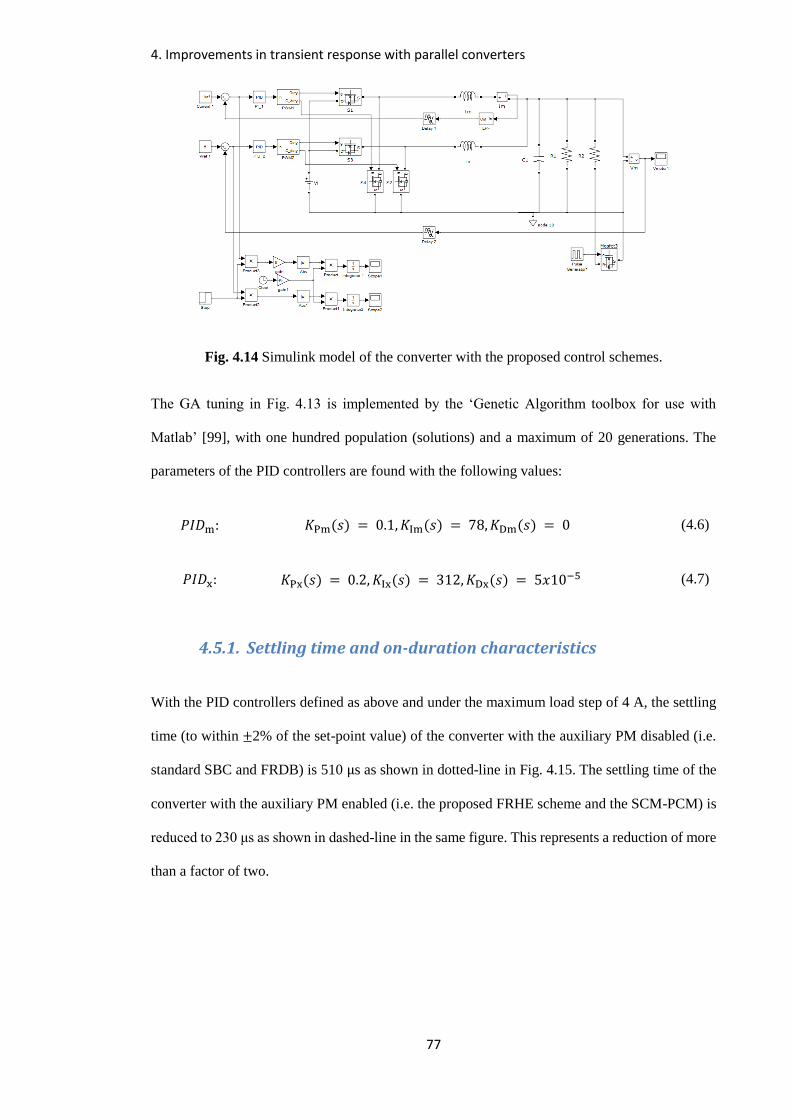
4. Improvements in transient response with parallel converters
77
Fig. 4.14 Simulink model of the converter with the proposed control schemes.
The GA tuning in Fig. 4.13 is implemented by the ‘Genetic Algorithm toolbox for use with
Matlab’ [99], with one hundred population (solutions) and a maximum of 20 generations. The
parameters of the PID controllers are found with the following values:
𝑃𝐼𝐷m: 𝐾Pm(𝑠) = 0.1, 𝐾Im(𝑠) = 78,𝐾Dm(𝑠) = 0
(4.6)
𝑃𝐼𝐷x: 𝐾Px(𝑠) = 0.2, 𝐾Ix(𝑠) = 312,𝐾Dx(𝑠) = 5𝑥10−5
(4.7)
4.5.1. Settling time and on-duration characteristics
With the PID controllers defined as above and under the maximum load step of 4 A, the settling
time (to within ±2% of the set-point value) of the converter with the auxiliary PM disabled (i.e.
standard SBC and FRDB) is 510 μs as shown in dotted-line in Fig. 4.15. The settling time of the
converter with the auxiliary PM enabled (i.e. the proposed FRHE scheme and the SCM-PCM) is
reduced to 230 μs as shown in dashed-line in the same figure. This represents a reduction of more
than a factor of two.
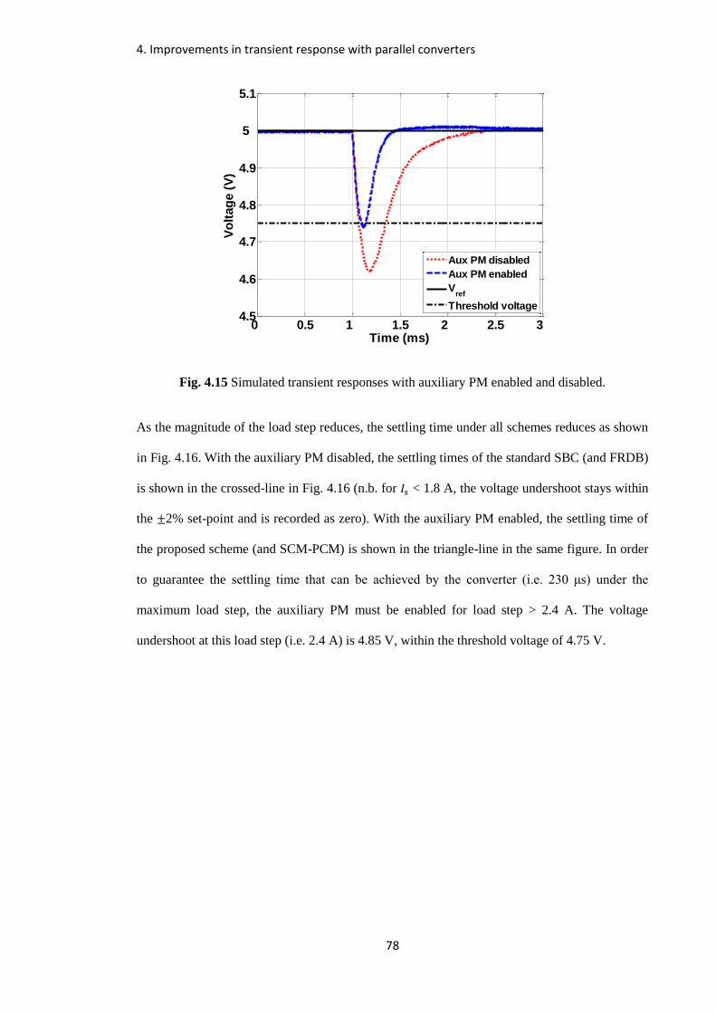
4. Improvements in transient response with parallel converters
78
Fig. 4.15 Simulated transient responses with auxiliary PM enabled and disabled.
As the magnitude of the load step reduces, the settling time under all schemes reduces as shown
in Fig. 4.16. With the auxiliary PM disabled, the settling times of the standard SBC (and FRDB)
is shown in the crossed-line in Fig. 4.16 (n.b. for 𝐼s < 1.8 A, the voltage undershoot stays within
the ±2% set-point and is recorded as zero). With the auxiliary PM enabled, the settling time of
the proposed scheme (and SCM-PCM) is shown in the triangle-line in the same figure. In order
to guarantee the settling time that can be achieved by the converter (i.e. 230 μs) under the
maximum load step, the auxiliary PM must be enabled for load step > 2.4 A. The voltage
undershoot at this load step (i.e. 2.4 A) is 4.85 V, within the threshold voltage of 4.75 V.
0 0.5 1 1.5 2 2.5 3 4.5
4.6
4.7
4.8
4.9
5
5.1
Time (ms)
Vo
ltag
e (
V)
Aux PM disabled
Aux PM enabled
Vref
Threshold voltage
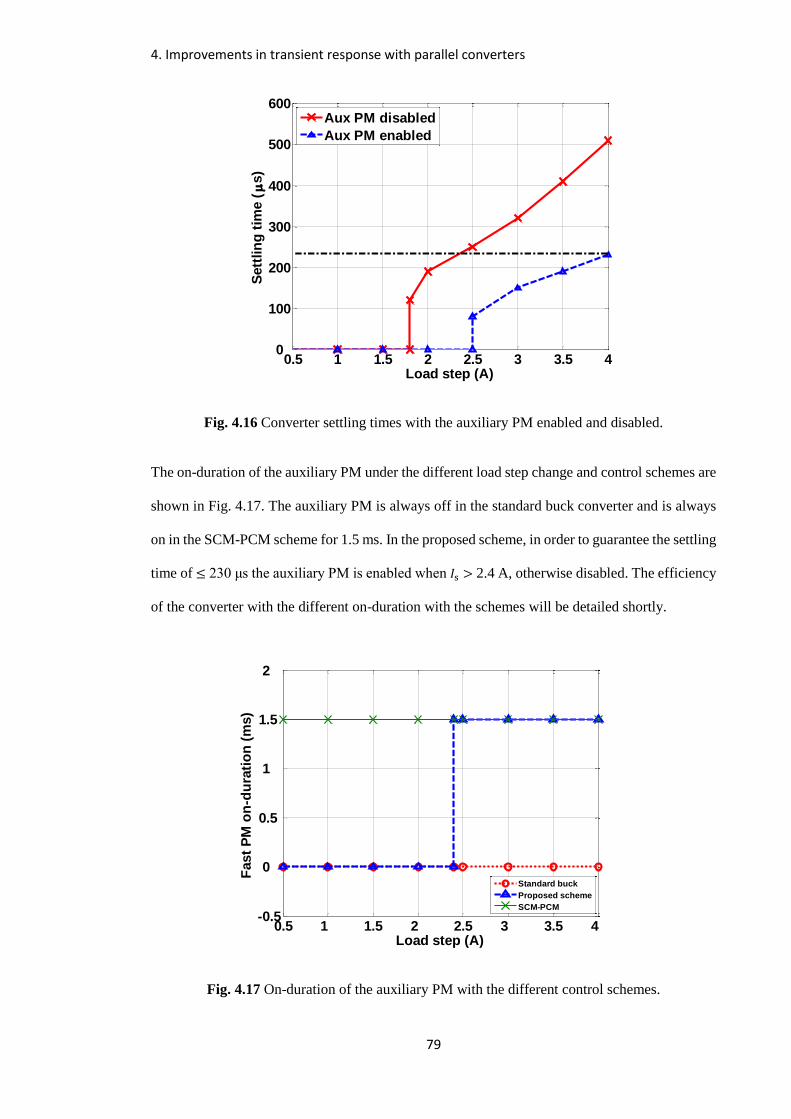
4. Improvements in transient response with parallel converters
79
Fig. 4.16 Converter settling times with the auxiliary PM enabled and disabled.
The on-duration of the auxiliary PM under the different load step change and control schemes are
shown in Fig. 4.17. The auxiliary PM is always off in the standard buck converter and is always
on in the SCM-PCM scheme for 1.5 ms. In the proposed scheme, in order to guarantee the settling
time of ≤ 230 μs the auxiliary PM is enabled when 𝐼s > 2.4 A, otherwise disabled. The efficiency
of the converter with the different on-duration with the schemes will be detailed shortly.
Fig. 4.17 On-duration of the auxiliary PM with the different control schemes.
0.5 1 1.5 2 2.5 3 3.5 40
100
200
300
400
500
600
Load step (A)
Sett
lin
g t
ime (
s)
Aux PM disabled
Aux PM enabled
0.5 1 1.5 2 2.5 3 3.5 4 -0.5
0
0.5
1
1.5
2
Load step (A)
Fast
PM
on
-du
rati
on
(m
s)
Standard buck
Proposed scheme
SCM-PCM
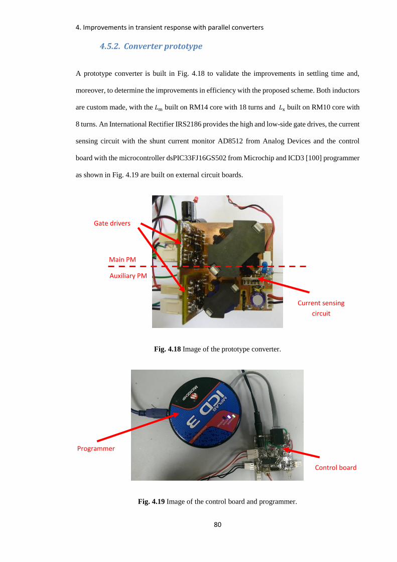
4. Improvements in transient response with parallel converters
80
4.5.2. Converter prototype
A prototype converter is built in Fig. 4.18 to validate the improvements in settling time and,
moreover, to determine the improvements in efficiency with the proposed scheme. Both inductors
are custom made, with the 𝐿m built on RM14 core with 18 turns and 𝐿x built on RM10 core with
8 turns. An International Rectifier IRS2186 provides the high and low-side gate drives, the current
sensing circuit with the shunt current monitor AD8512 from Analog Devices and the control
board with the microcontroller dsPIC33FJ16GS502 from Microchip and ICD3 [100] programmer
as shown in Fig. 4.19 are built on external circuit boards.
Fig. 4.18 Image of the prototype converter.
Fig. 4.19 Image of the control board and programmer.
Auxiliary PM
Main PM
Gate drivers
Current sensing
circuit
Programmer
Control board
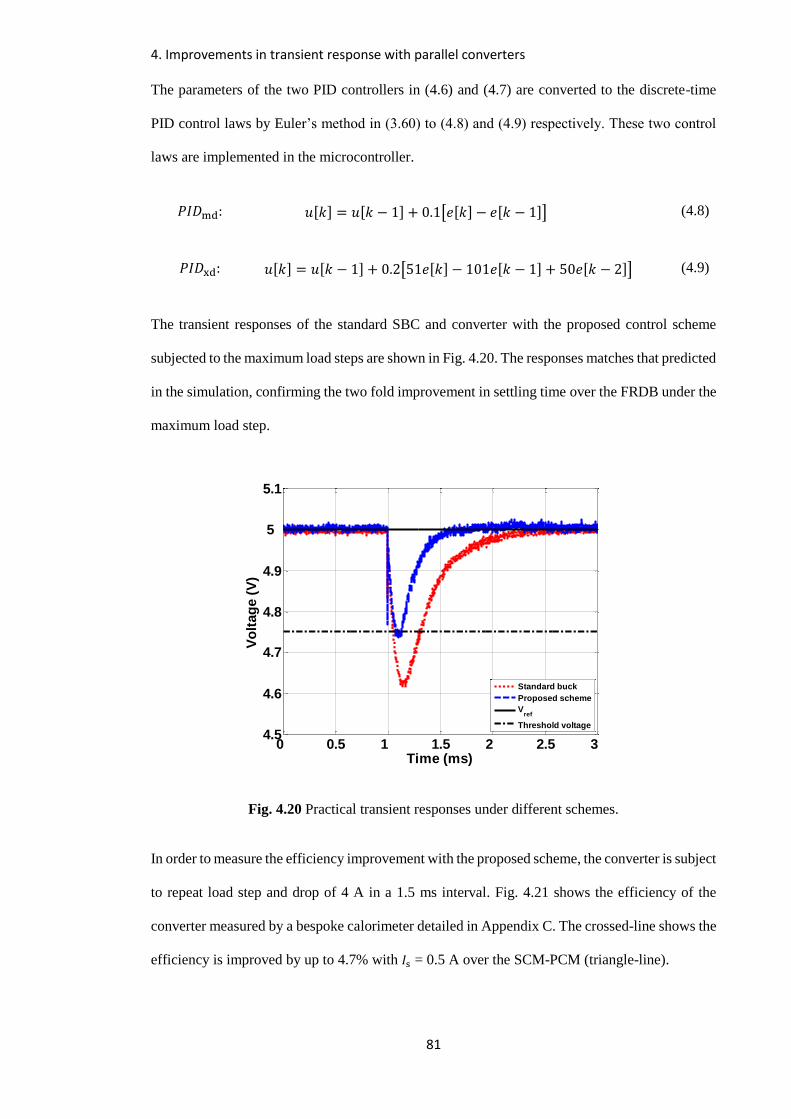
4. Improvements in transient response with parallel converters
81
The parameters of the two PID controllers in (4.6) and (4.7) are converted to the discrete-time
PID control laws by Euler’s method in (3.60) to (4.8) and (4.9) respectively. These two control
laws are implemented in the microcontroller.
𝑃𝐼𝐷md: 𝑢[𝑘] = 𝑢[𝑘 − 1] + 0.1[𝑒[𝑘] − 𝑒[𝑘 − 1]]
(4.8)
𝑃𝐼𝐷xd: 𝑢[𝑘] = 𝑢[𝑘 − 1] + 0.2[51𝑒[𝑘] − 101𝑒[𝑘 − 1] + 50𝑒[𝑘 − 2]]
(4.9)
The transient responses of the standard SBC and converter with the proposed control scheme
subjected to the maximum load steps are shown in Fig. 4.20. The responses matches that predicted
in the simulation, confirming the two fold improvement in settling time over the FRDB under the
maximum load step.
Fig. 4.20 Practical transient responses under different schemes.
In order to measure the efficiency improvement with the proposed scheme, the converter is subject
to repeat load step and drop of 4 A in a 1.5 ms interval. Fig. 4.21 shows the efficiency of the
converter measured by a bespoke calorimeter detailed in Appendix C. The crossed-line shows the
efficiency is improved by up to 4.7% with 𝐼s = 0.5 A over the SCM-PCM (triangle-line).
0 0.5 1 1.5 2 2.5 3 4.5
4.6
4.7
4.8
4.9
5
5.1
Time (ms)
Vo
ltag
e (
V)
Standard buck
Proposed scheme
Vref
Threshold voltage
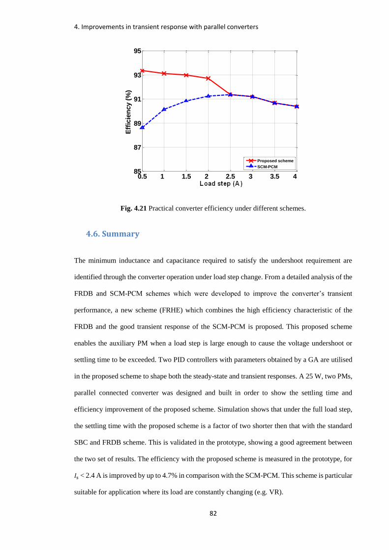
4. Improvements in transient response with parallel converters
82
Fig. 4.21 Practical converter efficiency under different schemes.
4.6. Summary
The minimum inductance and capacitance required to satisfy the undershoot requirement are
identified through the converter operation under load step change. From a detailed analysis of the
FRDB and SCM-PCM schemes which were developed to improve the converter’s transient
performance, a new scheme (FRHE) which combines the high efficiency characteristic of the
FRDB and the good transient response of the SCM-PCM is proposed. This proposed scheme
enables the auxiliary PM when a load step is large enough to cause the voltage undershoot or
settling time to be exceeded. Two PID controllers with parameters obtained by a GA are utilised
in the proposed scheme to shape both the steady-state and transient responses. A 25 W, two PMs,
parallel connected converter was designed and built in order to show the settling time and
efficiency improvement of the proposed scheme. Simulation shows that under the full load step,
the settling time with the proposed scheme is a factor of two shorter then that with the standard
SBC and FRDB scheme. This is validated in the prototype, showing a good agreement between
the two set of results. The efficiency with the proposed scheme is measured in the prototype, for
𝐼s < 2.4 A is improved by up to 4.7% in comparison with the SCM-PCM. This scheme is particular
suitable for application where its load are constantly changing (e.g. VR).
0.5 1 1.5 2 2.5 3 3.5 4 85
87
89
91
93
95
Load stepping (A)
Eff
icie
ncy (
%)
Proposed scheme
SCM-PCM

83
5. Improvements in steady-state efficiency with parallel
connected converters
5.1. Introduction
The previous chapter has shown that both shorter settling time and higher efficiency can be
achieved by enabling the auxiliary power module (PM) during a load step transient event that
would otherwise have led to the output voltage contravening the undershoot voltage design
specification requirement. In this chapter the improvements in steady-state operating efficiency
facilitated by the parallel converter is examined and a new design procedure, the high steady-state
efficiency (HSSE) design technique, is proposed for a converter featuring two parallel connected
PMs. From a detailed investigation of the operation of a two-switch forward converter, and by
analysing the division of work between the two PMs, the HSSE design technique is derived to
allow higher steady-state efficiency to be achieved with the parallel converter. Following a
component loss analysis, two 360 W (𝑉o = 24 V, 𝐼o = 15 A) converters are designed and built to
demonstrate the efficiency improvement using the proposed HSSE technique over that of an
interleaved converter. Detailed simulation and experimental studies highlight the advantages of
the proposed method.
5.2. Two-switch forward converter (2SFC)
Before describing the parallel converter with the proposed design technique, the circuit
configuration and operating characteristics of the two-switch forward converter (2SFC) will first
be reviewed. The primary reason of selecting the 2SFC over the SBC is that this converter
contains an extra transformer that provides a greater degree of freedom over the choice of the
circuit parameters during the design phase.

5. Improvements in steady-state efficiency with parallel connected converters
84
Vi
Lm
CoRl
CiVo
D1
D4
D3
D2
S2
S1δm
δm
Vi VsLmm
T1
Switch node
Fig. 5.1 Circuit diagram of two-switch forward converter (2SFC).
The circuit diagram of a 2SFC is shown in Fig. 5.1, containing three main sections:
(i) a DC chopper formed by two MOSFETs, 𝑆1 and 𝑆2, that are used to control power flow from
the input to the output and two freewheeling diodes, 𝐷1 and 𝐷2, that allow the pseudo AC
waveform to be formed at the switch-node
(ii) a transformer, 𝑇1, that provides galvanic isolation and also allows the input voltage to be
scaled according to the output voltage requirement, and the two demagnetising diodes, 𝐷3 and
𝐷4, allow the transformer core flux to be reset during the MOSFETs’ off-period
(iii) a LC low-pass filter, 𝐿m and 𝐶o, that attenuates the higher harmonic components present in
the switch-node voltage to produce a DC output.
5.2.1. Circuit operation
The 2SFC can operate in both the continuous conduction mode (CCM) or discontinuous
conduction mode (DCM) as characterised by current flow through the filter inductor 𝐿m. In the
case of CCM, two distinct periods (the on and off-periods) are observed within a single cycle
whereas for DCM, an extra period (the cut-off period (𝑡cf)) is also observed. During the
on-period the two MOSFETs are switched on, thus a voltage, 𝑉se, equal to 𝑛𝑉i is induced in the
transformer secondary winding. This voltage forward biases diode 𝐷1 and reverse biases diode
𝐷2 as shown in Fig. 5.2 (a), allowing power to be transferred to the load as well as charging the
inductor, 𝐿m, with energy. The magnetising inductance, 𝐿mm, is also charged by 𝑉i in this period.
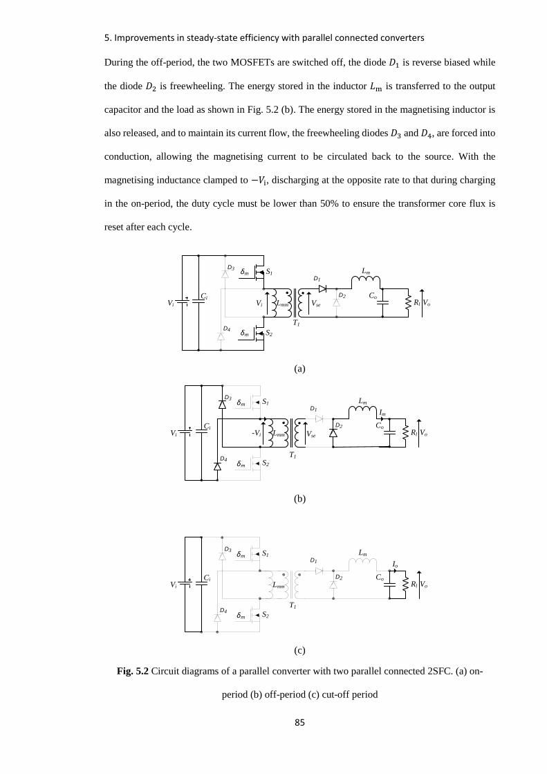
5. Improvements in steady-state efficiency with parallel connected converters
85
During the off-period, the two MOSFETs are switched off, the diode 𝐷1 is reverse biased while
the diode 𝐷2 is freewheeling. The energy stored in the inductor 𝐿m is transferred to the output
capacitor and the load as shown in Fig. 5.2 (b). The energy stored in the magnetising inductor is
also released, and to maintain its current flow, the freewheeling diodes 𝐷3 and 𝐷4, are forced into
conduction, allowing the magnetising current to be circulated back to the source. With the
magnetising inductance clamped to −𝑉i, discharging at the opposite rate to that during charging
in the on-period, the duty cycle must be lower than 50% to ensure the transformer core flux is
reset after each cycle.
Vi
Lm
CoRl
CiVo
D1
D4
D3
D2
S2
S1δm
δm
Vi VseLmm
T1
(a)
Vi
Lm
Co
Rl
CiVo
D1
D4
D3
D2
S2
S1δm
δm
T1
Lmm Vse-Vi
Im
(b)
Vi
Lm
CoRl
CiVo
D1
D4
D3
D2
S2
S1δm
δm
Lmm
Io
T1
(c)
Fig. 5.2 Circuit diagrams of a parallel converter with two parallel connected 2SFC. (a) on-
period (b) off-period (c) cut-off period
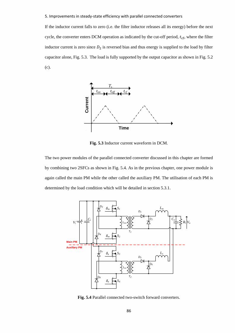
5. Improvements in steady-state efficiency with parallel connected converters
86
If the inductor current falls to zero (i.e. the filter inductor releases all its energy) before the next
cycle, the converter enters DCM operation as indicated by the cut-off period, 𝑡cf, where the filter
inductor current is zero since 𝐷2 is reversed bias and thus energy is supplied to the load by filter
capacitor alone, Fig. 5.3. The load is fully supported by the output capacitor as shown in Fig. 5.2
(c).
Cu
rre
nt
Ts
toffton
Time
tcf
Fig. 5.3 Inductor current waveform in DCM.
The two power modules of the parallel connected converter discussed in this chapter are formed
by combining two 2SFCs as shown in Fig. 5.4. As in the previous chapter, one power module is
again called the main PM while the other called the auxiliary PM. The utilisation of each PM is
determined by the load condition which will be detailed in section 5.3.1.
Vi
Lm
CoRl
CiVo
T1
D1
D4
D3
D2
Lx
T2
D5
D8
D7
D6
Main PM
Auxiliary PM
S4
S3
S2
S1δm
δx
δm
δx
Lmm
Lmx
Fig. 5.4 Parallel connected two-switch forward converters.
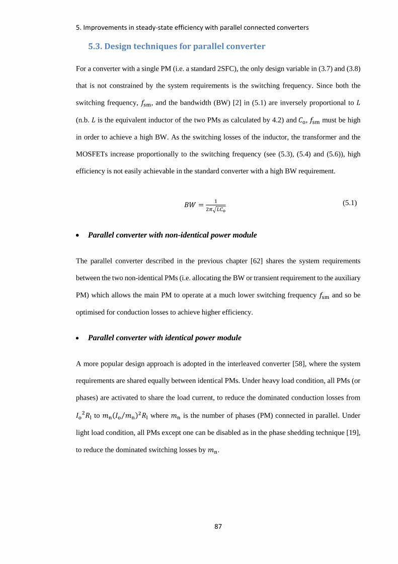
5. Improvements in steady-state efficiency with parallel connected converters
87
5.3. Design techniques for parallel converter
For a converter with a single PM (i.e. a standard 2SFC), the only design variable in (3.7) and (3.8)
that is not constrained by the system requirements is the switching frequency. Since both the
switching frequency, 𝑓sm, and the bandwidth (BW) [2] in (5.1) are inversely proportional to 𝐿
(n.b. 𝐿 is the equivalent inductor of the two PMs as calculated by 4.2) and 𝐶o, 𝑓sm must be high
in order to achieve a high BW. As the switching losses of the inductor, the transformer and the
MOSFETs increase proportionally to the switching frequency (see (5.3), (5.4) and (5.6)), high
efficiency is not easily achievable in the standard converter with a high BW requirement.
𝐵𝑊 =1
2𝜋√𝐿𝐶o (5.1)
Parallel converter with non-identical power module
The parallel converter described in the previous chapter [62] shares the system requirements
between the two non-identical PMs (i.e. allocating the BW or transient requirement to the auxiliary
PM) which allows the main PM to operate at a much lower switching frequency 𝑓sm and so be
optimised for conduction losses to achieve higher efficiency.
Parallel converter with identical power module
A more popular design approach is adopted in the interleaved converter [58], where the system
requirements are shared equally between identical PMs. Under heavy load condition, all PMs (or
phases) are activated to share the load current, to reduce the dominated conduction losses from
𝐼o2𝑅l to 𝑚n(𝐼o 𝑚n⁄ )2𝑅l where 𝑚n is the number of phases (PM) connected in parallel. Under
light load condition, all PMs except one can be disabled as in the phase shedding technique [19],
to reduce the dominated switching losses by 𝑚n.
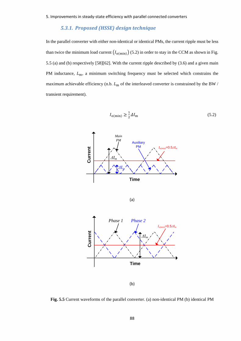
5. Improvements in steady-state efficiency with parallel connected converters
88
5.3.1. Proposed (HSSE) design technique
In the parallel converter with either non-identical or identical PMs, the current ripple must be less
than twice the minimum load current (𝐼o(min)) (5.2) in order to stay in the CCM as shown in Fig.
5.5 (a) and (b) respectively [58][62]. With the current ripple described by (3.6) and a given main
PM inductance, 𝐿m, a minimum switching frequency must be selected which constrains the
maximum achievable efficiency (n.b. 𝐿m of the interleaved converter is constrained by the BW /
transient requirement).
𝐼o(min) ≥1
2𝛥𝐼m (5.2)
Cu
rre
nt
Time
Io(min)=0.5ΔIm
Auxiliary
PM
Main
PM
ΔIm
ΔIx
(a)
Cu
rre
nt
Time
Io(min)=0.5ΔIm
Phase 2Phase 1
ΔIm
(b)
Fig. 5.5 Current waveforms of the parallel converter. (a) non-identical PM (b) identical PM

5. Improvements in steady-state efficiency with parallel connected converters
89
To overcome the above constraint, a new design technique, the high steady-state efficiency
(HSSE) design technique, is proposed for a parallel converter with two non-identical PMs. Using
the HSSE design technique, both the BW requirement and the minimum load conditions are
allocated to the auxiliary PM, allowing a larger main PM current ripple 𝛥𝐼m (with respect to the
𝐼o(min)) and a lower main PM switching frequency 𝑓sm to be selected as shown in Fig. 5.6.
Cu
rre
nt
Time
Io(min)=0.5ΔIm
Auxiliary
PM
Main
PM
ΔIm ΔIx
Fig. 5.6 Current waveforms of converter with the proposed design technique.
Larger 𝛥𝐼m allows a lower value filter inductor 𝐿m to be used for the same switching frequency
𝑓sm, reducing the conduction loss of the main PM inductor (lower value inductor → less turns
(5.11)). Furthermore the switching losses in the auxiliary PM reduce since a lower switching
frequency 𝑓sx can be employed as a direct results of the extra BW gained by the main PM from
the use of a lower value inductor 𝐿m. With the main PM optimised for conduction losses, where
the majority of the load current can be processed efficiently, the auxiliary PM only needs to
process a small portion of load current, permitting this PM to be optimised for switching losses.
Instead of sharing the load current equally as is done in the interleaved converter, the main PM is
designed to handle up to 90% of the load current and is in operation for load currents above 10%,
while the auxiliary PM is designed to handle up to 10% load current and is in operation when load
current is below 10% or above 90% (n.b. the auxiliary PM must also be able to temporary support
a large current during transient condition).

5. Improvements in steady-state efficiency with parallel connected converters
90
5.4. Loss analysis
All the components present within a converter incur losses during operation [101]. In general
there are two types of losses that are related to the repetitive switching nature of the circuit
(switching losses) and conduction losses which are related to current flow and voltage drops.
Switching losses
For the magnetic components (i.e. transformer and inductor), there are two types of switching
related losses: i) the hysteresis loss and ii) eddy current loss (which is usually considered
negligible for ferrite cores). The hysteresis loss is a result of not being able to recover the energy
required to magnetise the core within each cycle. Hysteresis loss, 𝑃sL, increases with flux density
(𝐵f) and switching frequency, 𝑓s, as described by (5.3). The constants 𝑘𝑐, α𝑐 and 𝛽𝑐 are material
specific values and are usually provided by the manufacturer. For example, the core material 3F3
has the constants as follows: 𝑘c = 1.5𝑥10−6 𝛼c =1.3 and 𝛽c = 2.5.
𝑃sL = 𝑘c𝑓sαc𝐵𝛽c (5.3)
For the MOSFETs, the switching related losses consisted of two main parts, the gate drive loss
(𝑃gm) and switching losses (𝑃sm) due to the overlapping of the drain-source voltage and current,
𝑉ds and 𝐼d, that occurs during a switching event (turn-on or turn-off). The loss 𝑃gm is caused by the
three parasitic capacitors, 𝐶gs, 𝐶rss and 𝐶oss, across the three terminals of the MOSFET as shown
in Fig. 5.7, which need to be charged or discharged to change the voltages at these terminals. The
power required to switch on a MOSFET can be found by (5.4). To switch off a MOSFET, a low
impedance path is provided to drain this charge away.
𝑃gm = 𝑄g𝑉g𝑓s (5.4)
where 𝑄g is the total gate charge, 𝑉g is the gate drive voltage.

5. Improvements in steady-state efficiency with parallel connected converters
91
Coss
S1
Crss
CgsVgs
Vds
Id
Ig
Fig. 5.7 Circuit diagram of MOSFET with the three parasitic capacitors.
The overlapping nature of 𝑉ds and 𝐼d during a MOSFET switching event [90] is the result of finite
time taken to charge or discharge the three parasitic capacitors. The switching waveform of a
MOSFET over one complete switching cycle period is shown in Fig. 5.8. When the gate signal is
applied to switch on the MOSFET at 𝑡1, the capacitor 𝐶gs is charged and 𝐶rss is discharged by the
gate current, 𝐼g, causing the gate voltage (𝑉gs) to rise. Both 𝑉ds and 𝐼d remain unchanged until 𝑉gs
reaches the MOSFET threshold voltage (𝑉th) at 𝑡2, at which point the MOSFET begins to conduct
with 𝐼d starts rising proportionally to the gate voltage while 𝑉ds remains unchanged, this
overlapping leads to the first term in the loss equation (5.5). This period (𝑡r1) end as soon as 𝐼d
reaches the load current level at 𝑡3, at which point 𝑉ds start to fall. The 𝐼d remains unchanged,
leading to the second overlapping described by the second term of (5.5). Due to the need to
discharge 𝐶rss during this period (𝑡r2), the gate voltage remains constant until 𝑡4 when 𝑉ds~0𝑉.
After 𝑡4, the gate voltage continuous to rise to the gate drive voltage to guarantee the MOSFET to
stay on and also to reduce the on-state resistance. Without detailing the switch-off procedure as for
the switch-on, the same equation in (5.5) with 𝑡r1 and 𝑡r2 replaced by 𝑡f2 and 𝑡f1 can be obtained
for the switch-off:
𝑃s(on) = 𝑡r1
𝑇𝑠𝑉i𝐼(rms)
2+
𝑡𝑟2
𝑇𝑠
𝑉i
2𝐼(rms) (5.5)
where 𝐼(rms) is the rms current through the MOSFET.
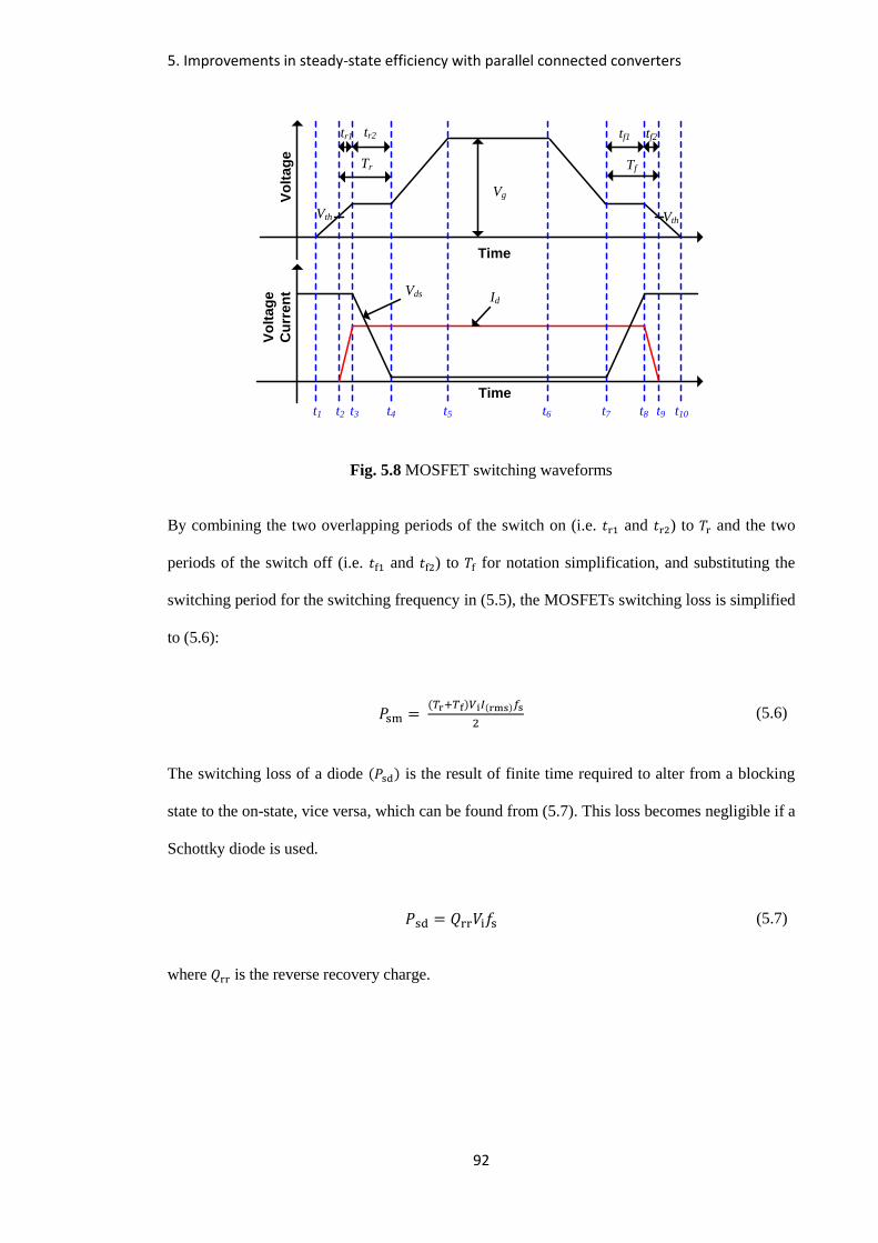
5. Improvements in steady-state efficiency with parallel connected converters
92
Vo
lta
ge
Cu
rre
nt
Time
Time
Vo
lta
ge
Vth
Vg
Id
Vth
Vds
t8t1 t2 t3 t4 t5 t7t6 t9 t10
Tr Tf
tr1 tr2 tf1 tf2
Fig. 5.8 MOSFET switching waveforms
By combining the two overlapping periods of the switch on (i.e. 𝑡r1 and 𝑡r2) to 𝑇r and the two
periods of the switch off (i.e. 𝑡f1 and 𝑡f2) to 𝑇f for notation simplification, and substituting the
switching period for the switching frequency in (5.5), the MOSFETs switching loss is simplified
to (5.6):
𝑃sm = (𝑇r+𝑇f)𝑉i𝐼(rms)𝑓s
2 (5.6)
The switching loss of a diode (𝑃sd) is the result of finite time required to alter from a blocking
state to the on-state, vice versa, which can be found from (5.7). This loss becomes negligible if a
Schottky diode is used.
𝑃sd = 𝑄rr𝑉i𝑓s (5.7)
where 𝑄rr is the reverse recovery charge.

5. Improvements in steady-state efficiency with parallel connected converters
93
Conduction losses
The conduction losses (𝑃c) in the parasitic resistances of each of the components can be found by
Ohm’s law as in (5.8):
𝑃c = 𝐼(rms)2𝑅𝑖 (5.8)
where 𝐼(rms) = √𝐼(𝑑𝑐)2 +
𝛥𝐼𝑚2
12 for a triangular waveform [101] and the subscript 𝑖 in 𝑅𝑖
representing the resistance of the different components.
The parasitic resistances of the transformer and inductor are the winding resistances which are
proportional to the length, 𝑙, and the resistivity of the wire, 𝜌, and is inversely proportional to the
cross-sectional area, 𝐴𝑤, as in (5.9):
𝑅w =𝜌𝑙
𝐴𝑤 (5.9)
With 𝐴𝑤 selected to satisfy a specific current density, the number of turns should be low to
minimise the resistance. For the transformer, the minimum number of primary turns, 𝑁p, that must
be selected in order to prevent the transformer core from saturation is given in (5.10):
𝑁p =𝑉i
𝐵peak𝐴c𝜔 (5.10)
where 𝐴c is the core area, 𝐵peak is the peak flux density and 𝜔 = 2𝜋𝑓s.
For the inductor, the minimum number of inductor turns (𝑁𝐿) required to create the desired
inductance is given in (5.11):
𝑁L = 𝐿m𝐼peak
𝐵𝐴c (5.11)
where 𝐼peak is the peak current.

5. Improvements in steady-state efficiency with parallel connected converters
94
To ensure low conduction losses, the number of turns should be kept to a minimum. However,
for low switching losses, the number of turns should be high as both 𝑁p and 𝑁L are inversely
proportional to the flux density. So, there is a compromise associated with the number of turns
and the core and winding losses.
The conduction loss of the capacitor is assumed negligible. The conduction loss of the diodes can
be calculated by (5.12):
𝑃 = 𝑉𝑓𝐼𝑎𝑣𝑔 (5.12)
With the components’ losses equations given above, the effect of the different components’ design
and selection can be tested out and compared, allowing the ones that produce the least losses to be
identified as potentially suitable for high efficiency designs. This loss analysis forms a critical part
of the proposed HSSE design scheme.
5.5. Design examples and experimental results
To demonstrate the difference in efficiency of a parallel converter designed with the proposed
design technique over the interleaved converter, two 360 W parallel converters were designed
and built. The interleaved converter is used as benchmark with the switching frequency (𝑓si) of
each PM selected to be 200 kHz. The other system requirements are as follows: input and output
voltages, 𝑉i = 400 V and 𝑉o = 24 V, minimum load current 𝐼o(min) = 0.5 A and 𝑉os < 1 V under
the maximum load drop.
5.5.1. Interleaved converter design
For the interleaved converter with 𝑓si = 200 kHz, the LC filter parameters are calculated as
follows: the inductances of each individual PM, 𝐿i, is calculated by (3.7) to be 68 μH, this gives
the equivalent inductance, 𝐿, of the two PMs to be 34 μH as calculated by (4.2), the output
capacitance and the BW are calculated by (4.5) and (5.1) to be 159 μF and 2.16 kHz respectively.
The number of turns on the filter inductor with RM12 core is calculated by (5.11) to be 13. In

5. Improvements in steady-state efficiency with parallel connected converters
95
order to find the transformer primary number of turns that leads to the lowest losses, the total
transformer switching and conduction losses for the four different flux densities, 𝐵peak, between
25 mT and 200 mT are calculated by (5.3) and (5.8)-(5.10) respectively. The results are listed in
Table 5.1, showing that the transformer has the lowest losses when 𝐵peak = 50 mT. The number
of turns on the primary winding of the transformer wound using an ETD34 core is calculated by
(5.10) to be 66.
Bpeak (mT) 25 50 100 200
Losses (W) 0.74 0.55 2.48 10.71
Table 5.1 Interleaved PM transformer losses under different 𝑩𝐩𝐞𝐚𝐤.
5.5.2. Converter designed by the proposed HSSE technique
For a parallel converter designed using the proposed HSSE technique, the main PM is designed
to minimising its losses while satisfying most of the system specifications. After finalising the
main PM design, the auxiliary PM may be designed to meet the unfulfilled requirements. The
design process is detailed as followed:
Main power module design
Since the switching frequency of the main PM is selectable, the number of turns for transformer
primary winding is determined by two variables, the 𝑓sm and 𝐵peak. The switching and conduction
losses of the transformer under different 𝑓sm and 𝐵peak are calculated by (5.3) and (5.8)-(5.10)
respectively. The sum of the two losses under the different conditions are plotted in Fig. 5.9,
which shows that for 𝐵peak below 50 mT, the transformer losses are inversely proportional to the
𝑓sm; however, when the 𝐵peak goes above 100 mT, the switching losses outweighs the conduction
losses, the transformer losses is proportional to 𝑓sm.

5. Improvements in steady-state efficiency with parallel connected converters
96
Fig. 5.9 Main PM transformer losses under different 𝐵peak.
The current ripple of the main PM filter inductor is also selectable and so the number of turns is
determined by the two variables, 𝛥𝐼m and 𝑓sm. The influence of 𝑓sm and 𝛥𝐼m on the inductor
losses are shown in Fig. 5.10. For 𝛥𝐼m at 4 A, the increase in core loss outweighs the reduction
in conduction loss, the inductor losses increase proportionally to 𝑓sm. For 𝛥𝐼m values at and below
3 A, the inductor losses reduce gradually with increasing in 𝑓sm, but whenever a smaller core is
selected, which is possible with the lower inductance value due to the increase in 𝑓sm, a jump in
the losses are observed as more turns are required for the same inductance value with a smaller
core, which in-turn increases the conduction losses.
50 100 150 200 2500
5
10
15
Switching frequency (kHz)
Lo
sses (
W)
Bpeak
= 25mT
Bpeak
= 50mT
Bpeak
= 100mT
Bpeak
= 200mT

5. Improvements in steady-state efficiency with parallel connected converters
97
Fig. 5.10 Main PM inductor losses under different 𝛥𝐼m.
In order to finalise the selection of flux density 𝐵peak for the transformer and current ripple 𝛥𝐼m
for the inductor, a good value of switching frequency 𝑓sm must be selected. A spreadsheet was
built to calculate the different component losses under different 𝑓sm as detailed in section 5.4. The
losses due to the MOSFETs, the transformer, the inductor, and the total of the three losses are
plotted in Fig. 5.11. It was found that the minimum losses occur at 𝑓sm of 80 kHz, but since
increasing 𝑓sm to 100 kHz only increases the losses by 2 % but the BW is increased by almost 30
%, 100 kHz is selected.
50 100 150 200 2500
1
2
3
4
5
Switching frequency (kHz)
Lo
sses (
W)
Im
= 2A
Im
= 3A
Im
= 4A
Example of core size changing
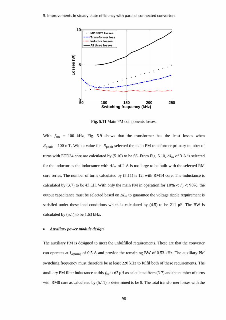
5. Improvements in steady-state efficiency with parallel connected converters
98
Fig. 5.11 Main PM components losses.
With 𝑓sm = 100 kHz, Fig. 5.9 shows that the transformer has the least losses when
𝐵peak = 100 mT. With a value for 𝐵peak selected the main PM transformer primary number of
turns with ETD34 core are calculated by (5.10) to be 66. From Fig. 5.10, 𝛥𝐼m of 3 A is selected
for the inductor as the inductance with 𝛥𝐼m of 2 A is too large to be built with the selected RM
core series. The number of turns calculated by (5.11) is 12, with RM14 core. The inductance is
calculated by (3.7) to be 45 μH. With only the main PM in operation for 10% < 𝐼o < 90%, the
output capacitance must be selected based on 𝛥𝐼m to guarantee the voltage ripple requirement is
satisfied under these load conditions which is calculated by (4.5) to be 211 μF. The BW is
calculated by (5.1) to be 1.63 kHz.
Auxiliary power module design
The auxiliary PM is designed to meet the unfulfilled requirements. These are that the converter
can operates at 𝐼𝑜(min) of 0.5 A and provide the remaining BW of 0.53 kHz. The auxiliary PM
switching frequency must therefore be at least 220 kHz to fulfil both of these requirements. The
auxiliary PM filter inductance at this 𝑓sx is 62 μH as calculated from (3.7) and the number of turns
with RM8 core as calculated by (5.11) is determined to be 8. The total transformer losses with the
50 100 150 200 2500
5
10
Switching frequency (kHz)
Lo
sses (
W)
MOSFET losses
Transformer loss
Inductor losses
All three losses

5. Improvements in steady-state efficiency with parallel connected converters
99
four 𝐵peak are calculated by (5.3), (5.8)-(5.10) and are listed in Table 5.2. 𝐵peak of
25 mT should be selected for the minimum losses. The transformer primary number of turns with
this 𝐵peak is calculated by (5.10) to be 153, with an ETD 29 core.
Bpeak (mT) 25 50 100 200
Losses (W) 0.1 0.33 2.05 9.24
Table 5.2 Auxiliary PM transformer losses under different 𝐵peak.
The parameters of the transformers and inductors of the interleaved converter and the converter
with designed with the HSSE technique are summarised in Table 5.3.
Standard design
method
Proposed HSSE design
method
Interleaved PM Main PM Auxiliary PM
Switching frequency (kHz) 200 100 220
Filter capacitor (μF) 159 211
Filter inductor (μH) 68 45 62
Inductor number of turns, NL,
& core type 13, RM12 12, RM14 8, RM8
Transformer number of turns, NP
& core type 66, ETD34 66, ETD34 153, ETD29
Table 5.3 Summary of parameter for the interleaved and the proposed converters.
5.5.3. Prototype converters
Prototypes of the two converters are built with the similar double layered PCB. The converter
with the proposed HSSE design technique is shown in Fig. 5.12. The inductors, transformers and
isolated gate drivers are distributed on the top layer while the MOSFETs and diodes are in the
bottom layer attached with a heat sink. MOSFET IPP60R160C6 is selected for the converter due
to its low 𝑅ds, 𝑡r, 𝑡f and 𝑄g. The duty cycles of the two PMs are controlled by the same Microchip
PIC-based control board described in Chapter 4 (Fig. 4.18).

5. Improvements in steady-state efficiency with parallel connected converters
100
Fig. 5.12 Prototype of the 2SFC (proposed HSSE design technique).
The predicted efficiencies of the interleaved converter under different load conditions are shown
in dashed line in Fig. 5.13. The efficiency of the converter with the proposed design technique
contains three parts: 1) in dashed line for load conditions between the minimum load to 10% load
where only the auxiliary PM is utilised; 2) dotted line for load conditions above 10% to 90%
where only the main PM is utilised; 3) solid line for load conditions above 90% to full load where
both PMs are utilised. Results show that the efficiency of the converter with the proposed design
technique is improved under all load conditions. For load conditions below 10%, the improvement
ranges between 6% to 12%, for load conditions between 10% to 90% the improvement ranges
between 2% to 12% and for load condition above 90%, due to the lower efficiency of the auxiliary
PM, the improvement ranges between 1.5% to 2%.
Auxiliary PM
Main PM
Isolated gate drivers
(see Appendix A)
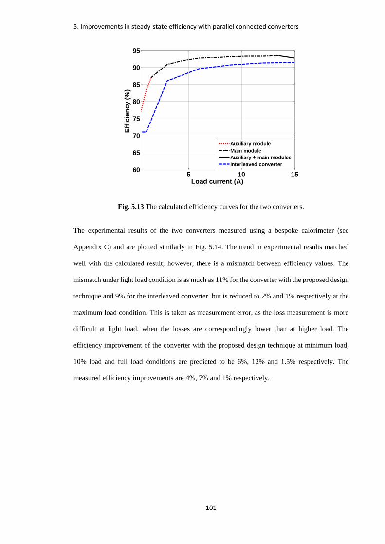
5. Improvements in steady-state efficiency with parallel connected converters
101
Fig. 5.13 The calculated efficiency curves for the two converters.
The experimental results of the two converters measured using a bespoke calorimeter (see
Appendix C) and are plotted similarly in Fig. 5.14. The trend in experimental results matched
well with the calculated result; however, there is a mismatch between efficiency values. The
mismatch under light load condition is as much as 11% for the converter with the proposed design
technique and 9% for the interleaved converter, but is reduced to 2% and 1% respectively at the
maximum load condition. This is taken as measurement error, as the loss measurement is more
difficult at light load, when the losses are correspondingly lower than at higher load. The
efficiency improvement of the converter with the proposed design technique at minimum load,
10% load and full load conditions are predicted to be 6%, 12% and 1.5% respectively. The
measured efficiency improvements are 4%, 7% and 1% respectively.
5 10 1560
65
70
75
80
85
90
95
Load current (A)
Eff
icie
ncy (
%)
Auxiliary module
Main module
Auxiliary + main modules
Interleaved converter

5. Improvements in steady-state efficiency with parallel connected converters
102
Fig. 5.14 Measured efficiency curves of the two converters.
5.6. Summary
This chapter has proposed a new design technique termed HSSE, to improve the steady-state
efficiency of a parallel converter with two non-identical PMs. From the analysis of the existing
design techniques, it was found that the efficiency is constrained by the minimum current ripple
needed to keeps the converter operating in the CCM under the minimum load condition. The new
design technique overcomes this constraint by allocating both the bandwidth and minimum load
requirements to the auxiliary PM, allowing a larger 𝛥𝐼m and a lower 𝑓sm to be selected for higher
efficiency. For the purpose of showing the efficiency improvement with the proposed design
technique, an interleaved converter and a converter with the proposed design technique are
designd and built. The calculated results show the efficiency improvement is in the range of 1.5-
12% dependent on the load conditions. The trends of experimental results match that of the
theoretical one. Efficiencies from the prototypes are however lower at all load conditions. At light
load, the efficiency are mismatched by 11%, while at maximum load, the efficiency mismatch are
only 2%. This mismatch does not alter the trend in the efficiency improvement from the proposed
design technique which ranged 1% to 7% across the load range, and is attributable to the
difficulties in measuring low values of losses.
5 10 1560
65
70
75
80
85
90
95
Load current (A)
Eff
icie
ncy (
%)
Auxiliary module
Main module
Auxiliary + main modules
Interleaved converter

103
6. Active current ripple cancellation using a high frequency
auxiliary converter
6.1. Introduction
The previous chapter has shown that the steady-state efficiency of the parallel converter can be
improved by allocating the transient response requirement and minimum load condition to the
auxiliary PM. One disadvantage of this technique is that the required filter capacitance is high due
to the larger current ripple produced by the main PM. This chapter presents a novel active current
ripple cancellation scheme that allows the filter capacitor value to be reduced. From the operation
of the two PMs under steady-state condition, guidelines for selecting the inductor for each PM and
the duty cycle profiles required to shape the inductor currents are obtained. Through the component
losses analysis, two 20 W (𝑉o = 3.3 V, 𝐼o = 6 A) converters are designed and built to demonstrate
the effectiveness of the active current ripple cancellation schemes. The efficiencies of the two
converters are compared through simulation and experimentation.
6.2. Active current ripple cancellation
The HSSE design technique proposed in the previous chapter required the main PM to be designed
with a large current ripple to achieve high efficiency, which demands a large output capacitor to
satisfy the output voltage ripple requirement. To reduce the size of the capacitor, the large current
ripple seen by the output capacitor, due to the large 𝛥𝐼m, is reduced by the auxiliary PM through
a novel ripple cancellation technique which is detailed in the next section. The parallel converter
utilised in this chapter is given in Fig. 4.1. To avoid current circulation between the two PMs, the
synchronous rectifier (i.e. MOSFET 𝑆1) of the auxiliary module is not utilised for the work in this
chapter.

6. Active current ripple cancellation using a high frequency auxiliary converter
104
6.2.1. Theory of operation
Current ripple cancellation by switched-mode power converters have been demonstrated
[69]-[72]. The parallel converter in these schemes contains two identical PMs, with the main PM
operating complementarily to the auxiliary PM, producing two current ripple waveforms as shown
in solid and dash-dotted lines in Fig. 6.1. The combination of the two current ripples lead to a
resultant current with almost no current ripple as shown in the dotted line Fig. 6.1.
Time
Cu
rre
nt
Resultant current
(Im+x)
Auxiliary PM
(cancellation)
current (Ix)
Main PM
current (Im)
Fig. 6.1 Active current ripple cancellation with identical PMs.
The scheme proposed here differs from the above schemes by employing two non-identical PMs,
reusing the auxiliary PM, the primary purpose of which was to improve the converter’s transient
response. Fig. 6.2 shows the main concept of the proposed ripple cancellation technique, where the
cancellation current (𝐼x), which is equal and opposite to the main PM current (𝐼m), is generated by
the auxiliary PM and is summed with the main PM current (at the point of common connection in
Fig. 4.1), to produce the resultant current (𝐼m+x). Since the auxiliary PM is a unidirectional buck
converter and is operating at a higher switching frequency than the main PM, 𝐼x is always positive.
The resultant current seen by the capacitor therefore has the current ripple of the auxiliary PM and
an amplitude of 𝐼m + 𝐼x.

6. Active current ripple cancellation using a high frequency auxiliary converter
105
Cu
rre
nt
Resultant current
(Im+x)
Auxiliary PM
(cancellation)
current (Ix)
Main PM
current (Im)
Time
Fig. 6.2 Main PM, auxiliary PM and resultant current waveforms.
6.2.2. Inductor current ripple and rate of change
The four parameters that determine the effectiveness of the ripple cancellation scheme are the rate
of change of inductor current ((𝑑 𝑑𝑡⁄ )𝐼), the net rate of change of inductor current ((𝑑 𝑑𝑡⁄ )𝐼(net)),
the duty cycles (𝛿) and the inductor current ripple (𝛥𝐼) (n.b. the analysis in the following sections
assumes all component losses are negligible). The five equations found in chapter 3 for the main
PM are recapped as followed:
𝑑
𝑑𝑡𝐼m(+) =
𝑉i−𝑉o
𝐿m (3.2)
𝑑
𝑑𝑡𝐼m(−) =
−𝑉o
𝐿m (3.3)
𝑑
𝑑𝑡𝐼m(net) =
𝑉i−𝑉o𝐿m
𝑡m(on)+−𝑉o𝐿m
𝑡m(off)
𝑇𝑠= 𝑉i𝛿m−𝑉o
𝐿m (3.4)
𝑉o = 𝛿m𝑉i (3.5)
𝛥𝐼m =𝑉i−𝑉o
𝐿m𝛿m(ss)𝑇s =
𝑉i(1−𝛿m(ss))
𝐿m𝛿m(ss)𝑇s
(3.6)

6. Active current ripple cancellation using a high frequency auxiliary converter
106
For the main PM operating in steady state, the duty cycle, 𝛿m(ss) is described by (3.5), the rate of
current rise, (𝑑 𝑑𝑡⁄ )𝐼m(+), and rate of current fall, (𝑑 𝑑𝑡⁄ )𝐼m(−), and current ripple, 𝛥𝐼m, can be found
using (3.2), (3.3) and (3.6) respectively.
For the auxiliary PM, the duty cycle is set to cancel the current ripple of the main PM detailed in
section 6.3.1, the net rate of change of inductor current ((𝑑 𝑑𝑡⁄ )𝐼x(net)) over one switching period
is non-zero and is calculated by (3.4) (n.b. the subscript of m in (3.4) is replaced by x). Defining
𝛿x(ss) to be the auxiliary PM duty cycle for no net rate of change of inductor current, for 𝛿x > 𝛿x(ss),
a net increase in rate of change of current, (𝑑 𝑑𝑡⁄ )𝐼x(net+), is observed as shown in Fig. 6.3 (a), for
𝛿x < 𝛿x(ss) a net decrease in rate of change of current occurs, as shown by (𝑑 𝑑𝑡⁄ )𝐼x(net−) in Fig. 6.3
(b).
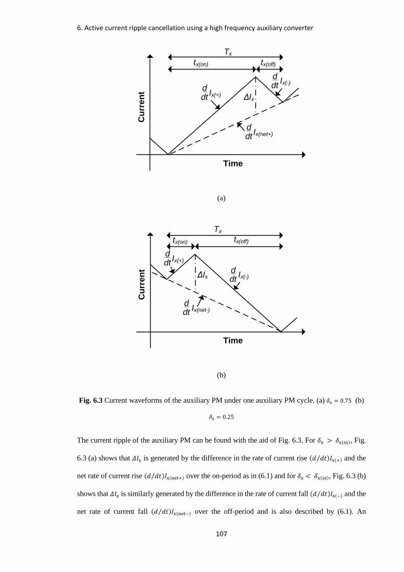
6. Active current ripple cancellation using a high frequency auxiliary converter
107
Cu
rre
nt
Time
tx(on) tx(off)
ΔIxIx(+)
ddt_
ddt_
Ix(-)
Ix(net+)ddt_
Tx
(a)
Cu
rre
nt
Time
tx(on) tx(off)
ΔIx
Ix(+)ddt_
ddt_
Ix(-)
Ix(net-)ddt_
Tx
(b)
Fig. 6.3 Current waveforms of the auxiliary PM under one auxiliary PM cycle. (a) 𝛿x = 0.75 (b)
𝛿x = 0.25
The current ripple of the auxiliary PM can be found with the aid of Fig. 6.3. For 𝛿x > 𝛿x(ss), Fig.
6.3 (a) shows that 𝛥𝐼x is generated by the difference in the rate of current rise (𝑑 𝑑𝑡⁄ )𝐼x(+) and the
net rate of current rise (𝑑 𝑑𝑡⁄ )𝐼x(net+) over the on-period as in (6.1) and for 𝛿x < 𝛿x(ss), Fig. 6.3 (b)
shows that 𝛥𝐼x is similarly generated by the difference in the rate of current fall (𝑑 𝑑𝑡⁄ )𝐼x(−) and the
net rate of current fall (𝑑 𝑑𝑡⁄ )𝐼x(net−) over the off-period and is also described by (6.1). An

6. Active current ripple cancellation using a high frequency auxiliary converter
108
interesting result is that (6.1) is the same as the second expression in (3.6), while the 𝛥𝐼m is affected
by the output voltage through 𝛿m(ss), the 𝛥𝐼x is affected by the desired net rate of change of the
auxiliary PM inductor current through 𝛿x.
𝛥𝐼x = (𝑉i−𝑉o
𝐿x−𝑉i𝛿x−𝑉o
𝐿x)𝛿x𝑇x
=𝑉i(1−𝛿x)
𝐿x𝛿x𝑇x
(6.1)
From (3.4), it can be shown that the net rate of change of the auxiliary PM inductor current,
(𝑑 𝑑𝑡⁄ )𝐼x(net), increases linearly from the minimum of 0 at 𝛿x = 𝛿x(ss) to the maximum net rate of
rise or fall of the inductor current at 𝛿x of 1 and 0 respectively (see Fig. 6.6 (a)) and from (6.1), the
current ripple, 𝛥𝐼𝑥 is reduced symmetrically from the maximum at 𝛿x = 𝛿x(ss) to the minimum of 0
at 𝛿x of 1 and 0 (see Fig. 6.6 (b)).
6.2.3. Generation of the cancellation current
The inductor current waveforms of the two PMs over one main PM cycle is shown in Fig. 6.4
(from an expansion of Fig. 6.3). Fig. 6.4 shows that in order to achieve exact current ripple
cancellation, the net rate of the auxiliary PM inductor current fall (3.4) (n.b. the second expression
in (3.4) with subscript of m in those equations replaced by x) must match the rate of main PM
inductor current rise (3.2) during the main PM on-period as in (6.2). Similarly, the net rate of
auxiliary PM inductor current rise (3.4) must match the rate of the main PM inductor current fall
in (3.3) during the main PM off-periods as in (6.3).

6. Active current ripple cancellation using a high frequency auxiliary converter
109
Cu
rre
nt
Time
tm(on) tm(off)
ddt_
Im(+) Im(-)ddt_
Ix(net+)d
dt_
Ix(net-)ddt_
Ix
δx = δx(-)δx = δx(+)
1 2 3 4 5 6 7 8
Fig. 6.4 Current waveforms of the main and auxiliary PMs over one main PM cycle.
−𝑉i𝛿x−𝑉o
𝐿x=
𝑉i−𝑉o
𝐿m (6.2)
𝑉i𝛿x−𝑉o
𝐿x= −
−𝑉o
𝐿m (6.3)
From (3.2) and (3.3), or the right hand side of (6.2) and (6.3), it can be seen that (𝑑 𝑑𝑡⁄ )𝐼m(+)
depends on both the 𝑉i and 𝑉o, while the (𝑑 𝑑𝑡⁄ )𝐼m(−) depends only on the 𝑉o, the two main PM rates
of inductor current are asymmetric except at 𝑉o = 0.5 𝑉i. For 𝑉o > 0.5𝑉𝑖, 𝑑
𝑑𝑡𝐼m(−) is higher and
for 𝑉o < 0.5𝑉i, (𝑑 𝑑𝑡⁄ )𝐼m(+) is higher.
With 𝑚 auxiliary PM cycles (see section 6.3.2) contained within each main PM cycle (eight in the
case of Fig. 6.4), and the adjustable net rate of change of the auxiliary PM inductor current through
𝛿x, the cancellation current (𝐼x) during the main PM on- and off-period can be generated by the
auxiliary PM by setting 𝛿x for each auxiliary PM cycle, provided that 𝐿x can produce the higher of
the two net rates as detailed in the next section. The 𝛿x that produces the desired (𝑑 𝑑𝑡⁄ )𝐼x(net−) is
termed 𝛿x(−), and the 𝛿x that produces the desired (𝑑 𝑑𝑡⁄ )𝐼x(net+) is termed 𝛿x(+).

6. Active current ripple cancellation using a high frequency auxiliary converter
110
6.3. Design consideration
This section develops several relationships that allow suitable auxiliary PM inductor to be selected.
6.3.1. Auxiliary PM inductor and duty cycle selection
By rearranging (6.2) and (6.3) in terms of the ratio between the two inductors, 𝐿m 𝐿x⁄ , and the
substitution of 𝑉o by (3.5), the relationship between the main and auxiliary duty cycles (𝛿m and
𝛿x) and the inductor ratio 𝐿m 𝐿x⁄ for the main PM on- and off-period are obtained in (6.4) and (6.5)
respectively.
𝐿m
𝐿x|𝑡sm(on)
= −1−𝛿m
𝛿x−𝛿m (6.4)
𝐿m
𝐿x|𝑡sm(off)
=𝛿m
𝛿x−𝛿m (6.5)
Since (𝑑 𝑑𝑡⁄ )𝐼m(+) is higher for 𝑉o < 0.5𝑉i (𝛿m < 0.5), the 𝐿x (for a given 𝐿m) is selected based on
(6.4) which is plotted in region 1 (Fig. 6.5). Similarly, since (𝑑 𝑑𝑡⁄ )𝐼m(−) is higher for
𝑉o > 0.5𝑉i (𝛿m > 0.5) , 𝐿x is selected based on (6.5) and is plotted in region 2 (Fig. 6.5).
Fig. 6.5 Ratio of the two inductors against 𝛿𝑚 and 𝛿𝑥.
Region 2
from (6.5)
Region 1
from (6.4)

6. Active current ripple cancellation using a high frequency auxiliary converter
111
Fig. 6.5 shows that dependent on 𝛿m, there is a range of 𝛿x, and hence 𝐿x, that can be selected to
allow the desired net rate of change of the auxiliary PM inductor current to be produced (e.g.
for 𝛿m = 0.45, any 𝛿x < 0.45 can be selected, as labelled in the feasible range in Fig. 6.5).
Fig. 6.6 (a) shows the net rate of change of auxiliary PM inductor current as a function of 𝛿x for
two different inductors, 𝐿x(1) and 𝐿x(2) (𝐿x(1) < 𝐿x(2)), and also the two (𝑑 𝑑𝑡⁄ )𝐼x(net) during the main
PM on- and off-period for a given 𝐿m and 𝛿m(ss) in the horizontal lines
(n.b. 𝛿m(ss) = 𝛿x(ss) = 0.48 in this example, which is also the auxiliary PM duty cycle where
(𝑑 𝑑𝑡⁄ )𝐼x(net) = 0). The interception points are the duty cycles (𝛿x(1−) and 𝛿x(1+) for 𝐿x(1), and 𝛿x(2−)
and 𝛿x(2+) for 𝐿x(2)) where the auxiliary PM produces the two desired net rate of change of inductor
currents (𝑑 𝑑𝑡⁄ )𝐼x(net−) and (𝑑 𝑑𝑡⁄ )𝐼x(net+). The values of 𝛿x(−) (i.e. 𝛿x(1−) and 𝛿x(2−)) and 𝛿x(+) (i.e.
𝛿x(1+) and 𝛿x(2+)) together with the different 𝐿x values determine the 𝛥𝐼x as illustrated in Fig. 6.6
(b), where 𝐿x(1) has the larger current ripple of 0.59 p.u. during the main PM off-period
(𝛿x(+) = 0.82), while 𝐿x(2) has the larger current ripple of 0.32 p.u. during 𝑡sm(off) (𝛿x(+) = 0.90).
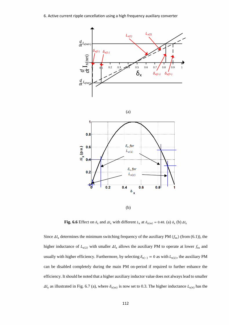
6. Active current ripple cancellation using a high frequency auxiliary converter
112
I x(n
et)
δx
0.1 0.2 10.90.80.70.60 0.40.3 0.5
d dt_
Lx(2)Lx(1)
δx(1+) δx(2+)
δx(1-)δx(2-)
Ix(net+)ddt_
Ix(net-)ddt_
(a)
(b)
Fig. 6.6 Effect on 𝛿x and 𝛥𝐼x with different 𝐿x at 𝛿x(ss) = 0.48. (a) 𝛿x (b) 𝛥𝐼x
Since 𝛥𝐼x determines the minimum switching frequency of the auxiliary PM (𝑓sx) (from (6.1)), the
higher inductance of 𝐿x(2) with smaller 𝛥𝐼x allows the auxiliary PM to operate at lower 𝑓sx and
usually with higher efficiency. Furthermore, by selecting 𝛿x(−) = 0 as with 𝐿x(2), the auxiliary PM
can be disabled completely during the main PM on-period if required to further enhance the
efficiency. It should be noted that a higher auxiliary inductor value does not always lead to smaller
𝛥𝐼x as illustrated in Fig. 6.7 (a), where 𝛿x(ss) is now set to 0.3. The higher inductance 𝐿x(4) has the

6. Active current ripple cancellation using a high frequency auxiliary converter
113
maximum current ripple of 0.99 p.u. in comparison to 𝐿x(3) which has a current of only 0.95 p.u.
as shown in Fig. 6.7 (b).
10.90.80.70.60.50.40 0.1 0.30.2
δx
I x(n
et)
d dt_
δx(3+)
Ix(net+)ddt_
Ix(net-)ddt_
Lx(3)Lx(4)
δx(4+)
δx(3-)
δx(4-)
(a)
(b)
Fig. 6.7 Effect on 𝛿x and 𝛥𝐼x with different 𝐿x at 𝛿x(ss) = 0.3. (a) 𝛿x (b) 𝛥𝐼x
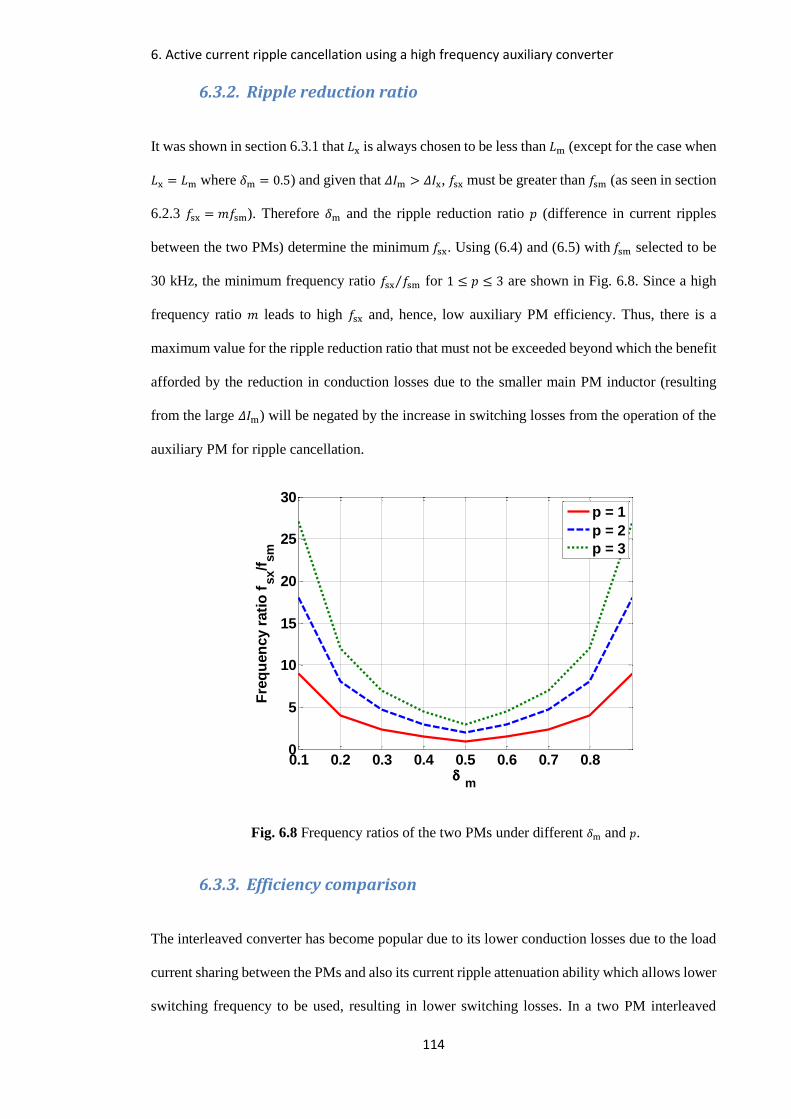
6. Active current ripple cancellation using a high frequency auxiliary converter
114
6.3.2. Ripple reduction ratio
It was shown in section 6.3.1 that 𝐿x is always chosen to be less than 𝐿m (except for the case when
𝐿x = 𝐿m where 𝛿m = 0.5) and given that 𝛥𝐼m > 𝛥𝐼x, 𝑓sx must be greater than 𝑓sm (as seen in section
6.2.3 𝑓sx = 𝑚𝑓sm). Therefore 𝛿m and the ripple reduction ratio 𝑝 (difference in current ripples
between the two PMs) determine the minimum 𝑓sx. Using (6.4) and (6.5) with 𝑓sm selected to be
30 kHz, the minimum frequency ratio 𝑓sx 𝑓sm⁄ for 1 ≤ 𝑝 ≤ 3 are shown in Fig. 6.8. Since a high
frequency ratio 𝑚 leads to high 𝑓sx and, hence, low auxiliary PM efficiency. Thus, there is a
maximum value for the ripple reduction ratio that must not be exceeded beyond which the benefit
afforded by the reduction in conduction losses due to the smaller main PM inductor (resulting
from the large 𝛥𝐼m) will be negated by the increase in switching losses from the operation of the
auxiliary PM for ripple cancellation.
Fig. 6.8 Frequency ratios of the two PMs under different 𝛿m and 𝑝.
6.3.3. Efficiency comparison
The interleaved converter has become popular due to its lower conduction losses due to the load
current sharing between the PMs and also its current ripple attenuation ability which allows lower
switching frequency to be used, resulting in lower switching losses. In a two PM interleaved
0.1 0.2 0.3 0.4 0.5 0.6 0.7 0.80
5
10
15
20
25
30
m
Fre
qu
en
cy r
ati
o f
sx/f
sm
p = 1
p = 2
p = 3

6. Active current ripple cancellation using a high frequency auxiliary converter
115
converter, the effectiveness of the ripple attenuation, whilst ideal with a duty cycle of 0.5 on both
converters, diminishes as the duty cycle approaches the minimum or maximum value allowable.
The efficiency improvement from the proposed converter scheme becomes more apparent under
these extreme duty cycle conditions.
Component loss ratio
In order to investigate the difference in the component losses between the two converters, the loss
ratio for each of the components in the converters, with the proposed scheme, is divided by the
losses in the interleaved converter to normalise the measurements to that of the interleaved
converter. With the RMS current of the main and auxiliary PMs and interleaved converter PMs
defined as 𝐼m(rms), 𝐼x(rms) and 𝐼i(rms) respectively (the three currents are detailed in Appendix B),
and the switching frequencies of the main and auxiliary PMs β and γ times that of the interleaved
converter respectively. The MOSFET switching loss ratio 𝑃sm(𝑛) is obtained (5.6) as follows:
𝑃sm(𝑛) =
(𝑡r+𝑡f)𝑉i𝐼m(rms)𝛽𝑓si
2+(𝑡r+𝑡f)𝑉i𝐼x(rms)𝛾𝑓si
2
2(𝑡r+𝑡f)𝑉i𝐼i(rms)𝑓si
2
=𝐼m(rms)𝛽+𝐼x(rms)𝛾
2𝐼i(rms)
(6.6)
Similarly, the MOSFET gate drive and conduction losses, inductor switching and conduction
losses and diode conduction losses ratios using (5.4) and (5.8), (5.3) and (5.8) and (5.12) are found
as in (6.7) to (6.11) respectively:
𝑃gm(𝑛) =2𝛽+𝛾
4 (6.7)
𝑃cm(𝑛) = 𝐼m(rms)
2𝑅ds+𝐼x(rms)2𝑅ds𝛿x+𝑉f𝐼x(rms)(1−𝛿x)
2𝐼i(rms)2𝑅ds
(6.8)
𝑃sL(𝑛) = (𝛽+𝛾)𝛼c
2 (6.9)
𝑃cL(𝑛) = 𝐼m(rms)
2+𝐼x(rms)2
2𝐼i(rms)2 (6.10)

6. Active current ripple cancellation using a high frequency auxiliary converter
116
𝑃cd(𝑛) =𝛽
2 (6.11)
To identify the difference in losses between the two converters, the total conduction loss ratio
𝑃c(𝑛) is formulated by multiplying the components’ conduction loss ratios in (6.8), (6.10) and
(6.11) with loss corresponding to the components to give (6.12) For example, the difference in
the diode conduction loss between the two converters can be found by
(𝑃cd(𝑛)𝑃cd) (𝑃cd + 𝑃cm + 𝑃cL)⁄ , where 𝑃cd(𝑛) is the diode conduction loss ratio, 𝑃cd is the diode
conduction loss and (𝑃cd + 𝑃cm + 𝑃cL) is the total conduction losses of the interleaved converter.
Similarly, the total switching loss ratio can be found with (6.6), (6.7) and (6.9) to give (6.13). For
proposed parallel converter to achieve higher efficiency than the interleave converter, the sum of
𝑃c(𝑛) and 𝑃s(𝑛) calculated from (6.12) and (6.13) must be less than 1.
𝑃c(𝑛) =𝑃cd(𝑛)𝑃cd+𝑃cm(𝑛)𝑃cm+𝑃cL(𝑛)𝑃cL
𝑃cd+𝑃cm+𝑃cL (6.12)
𝑃𝑠(𝑛) =𝑃gm(𝑛)𝑃gm+𝑃sm(𝑛)𝑃sm+𝑃sL(𝑛)𝑃sL
𝑃gm+𝑃sm+𝑃sL (6.13)
6.3.4. Practical consideration
In a practical system, both the input voltage and load vary. The input voltage affects the rate of
rise of the main and auxiliary PM inductor currents (3.2) and (3.4). With a fixed output voltage,
(3.5) shows that as the input voltage changes, the duty cycle changes inversely to provide
regulation. The change in 𝛿m, 𝛿x(−) and 𝛿x(+) due to the change in input voltage (𝑉i 𝑉i(nom)⁄ ) can
thus be compensated by a gain that is the inverse of the change, or 𝑘𝑐 = 𝑉i(nom) 𝑉i⁄ . For example,
assuming the main PM duty cycle 𝛿m(nom) calculated for the nominal input voltage, 𝑉i(nom), of 12
V is 0.4, if the input voltage is increased to 13.2 V, the new duty cycle is 𝛿m = 𝑘c𝛿m(nom) =
0.9𝑥0.4 = 0.36. The change in load condition affects the voltage drop across the parasitic
resistances of components, leading to the change in 𝛿m, 𝛿x(−) and 𝛿x(+) which can be similarly
compensated.
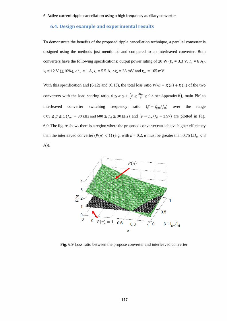
6. Active current ripple cancellation using a high frequency auxiliary converter
117
6.4. Design example and experimental results
To demonstrate the benefits of the proposed ripple cancellation technique, a parallel converter is
designed using the methods just mentioned and compared to an interleaved converter. Both
converters have the following specifications: output power rating of 20 W (𝑉o = 3.3 V, 𝐼o = 6 A),
𝑉i = 12 V (±10%), 𝛥𝐼m = 1 A, 𝐼s = 5.5 A, 𝛥𝑉o = 33 mV and 𝑉os = 165 mV.
With this specification and (6.12) and (6.13), the total loss ratio 𝑃(𝑛) = 𝑃c(𝑛) + 𝑃s(𝑛) of the two
converters with the load sharing ratio, 0 ≤ 𝛼 ≤ 1 (6 ≥𝛥𝐼𝑚
2≥ 0 𝐴, see Appendix B), main PM to
interleaved converter switching frequency ratio (𝛽 = 𝑓sm 𝑓si⁄ ) over the range
0.05 ≤ 𝛽 ≤ 1 (𝑓sm = 30 kHz and 600 ≥ 𝑓si ≥ 30 kHz) and (𝛾 = 𝑓sx 𝑓si⁄ = 2.57) are plotted in Fig.
6.9. The figure shows there is a region where the proposed converter can achieve higher efficiency
than the interleaved converter (𝑃(𝑛) < 1) (e.g. with β = 0.2, 𝛼 must be greater than 0.75 (𝛥𝐼m < 3
A)).
Fig. 6.9 Loss ratio between the propose converter and interleaved converter.
𝑃(𝑛)
𝑃(𝑛) = 1

6. Active current ripple cancellation using a high frequency auxiliary converter
118
6.4.1. Switching frequencies and component value selection
Having proved that the proposed converter can achieve better performance, one now has to select
the main PM switching frequency 𝑓sm and ripple current 𝛥𝐼m (≤ 3 A) to achieve the highest
efficiency. The main PM inductor losses with 𝑓sm between 20 kHz to 150 kHz and 𝛥𝐼m between 1
A and 3 A when operating under full load condition are calculated from (5.3) and (B1) and are
plotted in Fig. 6.10 (a). Results show that the inductor losses reduce gradually with an increase in
𝑓sm and also with larger 𝛥𝐼m. One would usually expect the inductor losses to be a continuous
function of frequency for a single core size, however, the curves presented in Fig. 6.10 (a) were
generated using different core sizes as determined by the core area loss product inequality, hence
the discontinuities observed as the core size changes. For 𝑓sm < 70 kHz, 𝛥𝐼m of 3 A produces the
lowest losses. Combining the inductor losses at 𝛥𝐼m = 3 𝐴 with the gate drive losses in (5.4) and
MOSFET losses (i.e. MOSFET switching loss in (5.6), MOSFET conduction loss and diode
conduction loss [101]), Fig. 6.10 (b) shows that the lowest losses are produced at 𝑓sm = 30 kHz and
so this is selected for the main PM. For 𝑓sm = 30 kHz, the inductance 𝐿m is calculated by (3.7) to
be 27 μH.

6. Active current ripple cancellation using a high frequency auxiliary converter
119
(a)
(b)
Fig. 6.10 Main PM calculated losses. (a) Inductor losses (b) Total losses
For the auxiliary PM, the inductor 𝐿x is selected so that the current ripple seen by the output
capacitor is reduced from 3 A to 1 A. Considering the maximum input voltage 𝑉i(max), also inductor
tolerance of 10%, the minimum 𝐿x is found by (6.4) to be 8 μH. The minimum 𝑓sx that satisfies the
20 40 60 80 100 120 1400
0.1
0.2
0.3
0.4
Switching frequency (kHz)
Lo
sses (
W)
I = 1 A
I = 2 A
I = 3 A
20 40 60 80 100 120 1400
0.2
0.4
0.6
0.8
1
Switching frequency (kHz)
Lo
sses (
W)
Gate drive losses
MOSFETs losses
Inductor losses
Total losses

6. Active current ripple cancellation using a high frequency auxiliary converter
120
𝛥𝐼x and is 𝑚 (𝑚 ∈ ℤ+) times higher than 𝑓sm is calculated by (6.1) to be 360 kHz. The output
capacitor that satisfies the overshoot requirement 𝑉os is calculated by (4.5) to be
347 μF, 330 μF was therefore selected practically.
For the interleaved converters, with the ripple attenuation of 37% at interleaved PM duty cycle
𝛿i = 0.275 [94], the current in each of the interleaved PM, 𝛥𝐼i, must be less than 1.6 A in order to
produce the net current ripple less than 1 A. With the same capacitance and from (5.1) and (3.7),
the minimum interleaved PM switching frequency, 𝑓si, that produces the same BW as the proposed
converter is 140 kHz. The interleaved PM inductance 𝐿i is calculated from (3.7) to be 12 μH.
The predicted efficiencies of the individual PMs are shown in Fig 6.11 (a) as a function of output
power. In order to satisfy the current ripple requirement while achieving high efficiency, both PMs
of the proposed converter are active for output powers above 6.5 W. With the auxiliary PM
performing the ripple cancellation and processing an average power of 5 W. The main PM
processes any remaining power. When the output power is below 6.5 W, only the auxiliary PM is
enabled and the converter is operating without ripple cancellation. For the interleaved converter,
both PMs are in operation at all times to maintain the current ripple requirement. The phase
dropping technique is not implemented [58], as this would increase the output ripple.
The efficiencies of the proposed converter and interleaved converter operating under the conditions
described above are shown in Fig 6.11 (b). The results show that the efficiency gain due to the
large 𝛥𝐼m and loss due to the ripple cancellation produce an efficiency that is higher than that of
the interleaved converter under light and heavy load conditions by as much as 6%. The efficiency
under mid-range load is about 1.5% lower than that of the interleaved converter.
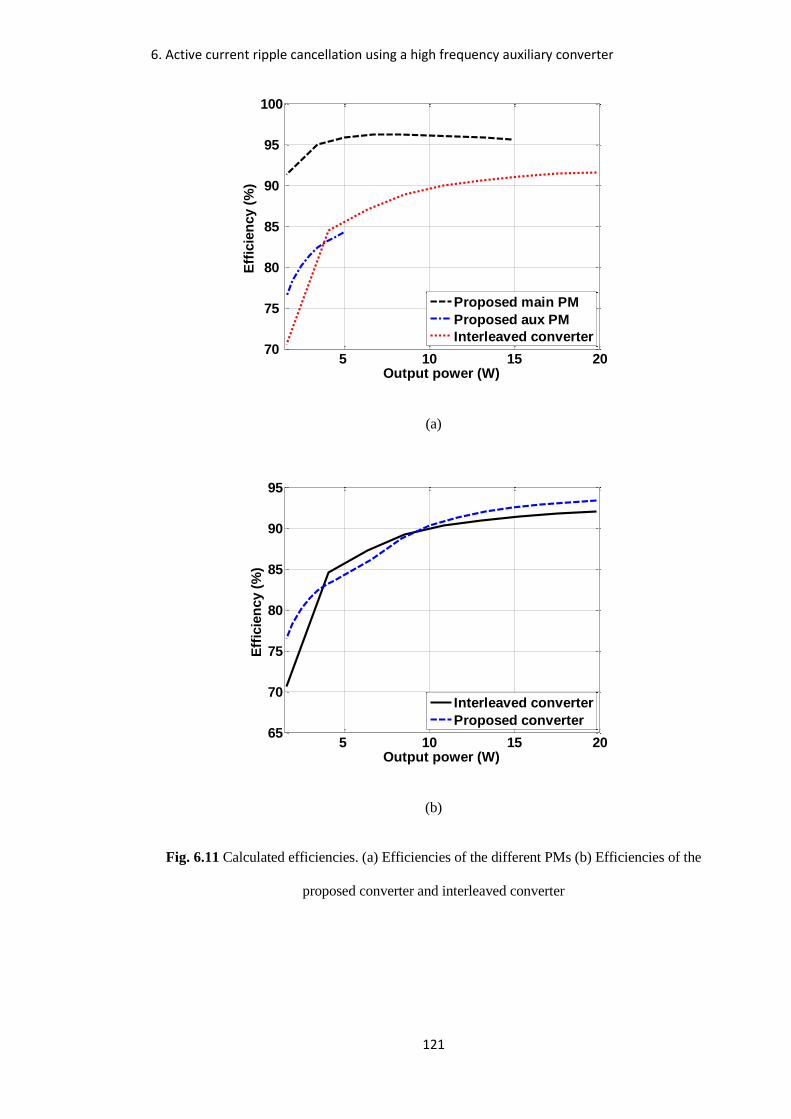
6. Active current ripple cancellation using a high frequency auxiliary converter
121
(a)
(b)
Fig. 6.11 Calculated efficiencies. (a) Efficiencies of the different PMs (b) Efficiencies of the
proposed converter and interleaved converter
5 10 15 2070
75
80
85
90
95
100
Output power (W)
Eff
icie
ncy (
%)
Proposed main PM
Proposed aux PM
Interleaved converter
5 10 15 2065
70
75
80
85
90
95
Output power (W)
Eff
icie
ncy (
%)
Interleaved converter
Proposed converter
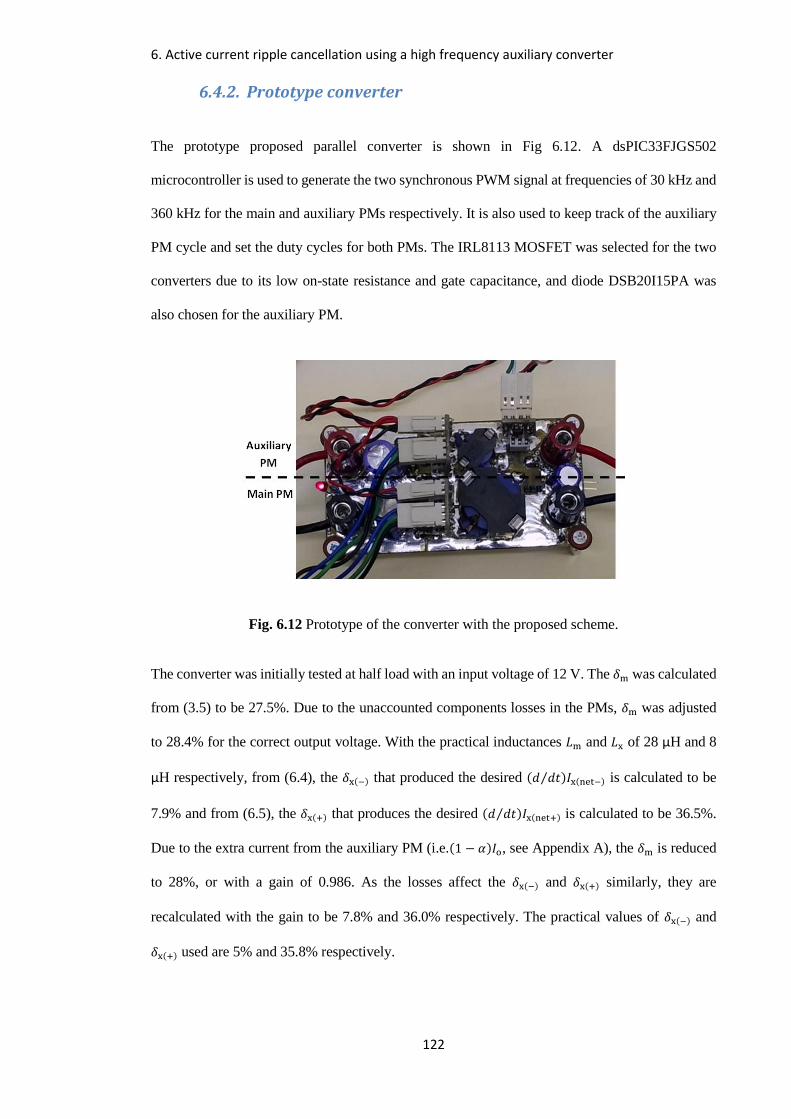
6. Active current ripple cancellation using a high frequency auxiliary converter
122
6.4.2. Prototype converter
The prototype proposed parallel converter is shown in Fig 6.12. A dsPIC33FJGS502
microcontroller is used to generate the two synchronous PWM signal at frequencies of 30 kHz and
360 kHz for the main and auxiliary PMs respectively. It is also used to keep track of the auxiliary
PM cycle and set the duty cycles for both PMs. The IRL8113 MOSFET was selected for the two
converters due to its low on-state resistance and gate capacitance, and diode DSB20I15PA was
also chosen for the auxiliary PM.
Fig. 6.12 Prototype of the converter with the proposed scheme.
The converter was initially tested at half load with an input voltage of 12 V. The 𝛿m was calculated
from (3.5) to be 27.5%. Due to the unaccounted components losses in the PMs, 𝛿m was adjusted
to 28.4% for the correct output voltage. With the practical inductances 𝐿m and 𝐿x of 28 μH and 8
μH respectively, from (6.4), the 𝛿x(−) that produced the desired (𝑑 𝑑𝑡⁄ )𝐼x(net−) is calculated to be
7.9% and from (6.5), the 𝛿x(+) that produces the desired (𝑑 𝑑𝑡⁄ )𝐼x(net+) is calculated to be 36.5%.
Due to the extra current from the auxiliary PM (i.e.(1 − 𝛼)𝐼o, see Appendix A), the 𝛿m is reduced
to 28%, or with a gain of 0.986. As the losses affect the 𝛿x(−) and 𝛿x(+) similarly, they are
recalculated with the gain to be 7.8% and 36.0% respectively. The practical values of 𝛿x(−) and
𝛿x(+) used are 5% and 35.8% respectively.

6. Active current ripple cancellation using a high frequency auxiliary converter
123
The current waveforms of the two PMs of the converter with the proposed scheme are shown in
Fig. 6.13 (a). The output currents and voltages with the above duty cycles, operating with and
without ripple cancellation, are shown in Fig. 6.13 (b) and (c) respectively. After the ripple
cancellation, the peak to peak current ripple of 3 A is reduced to 1 A as shown in Fig. 6.13 (b) and
the output voltage ripple is reduced from 50 mV to 30 mV as shown in Fig 6.13 (c).
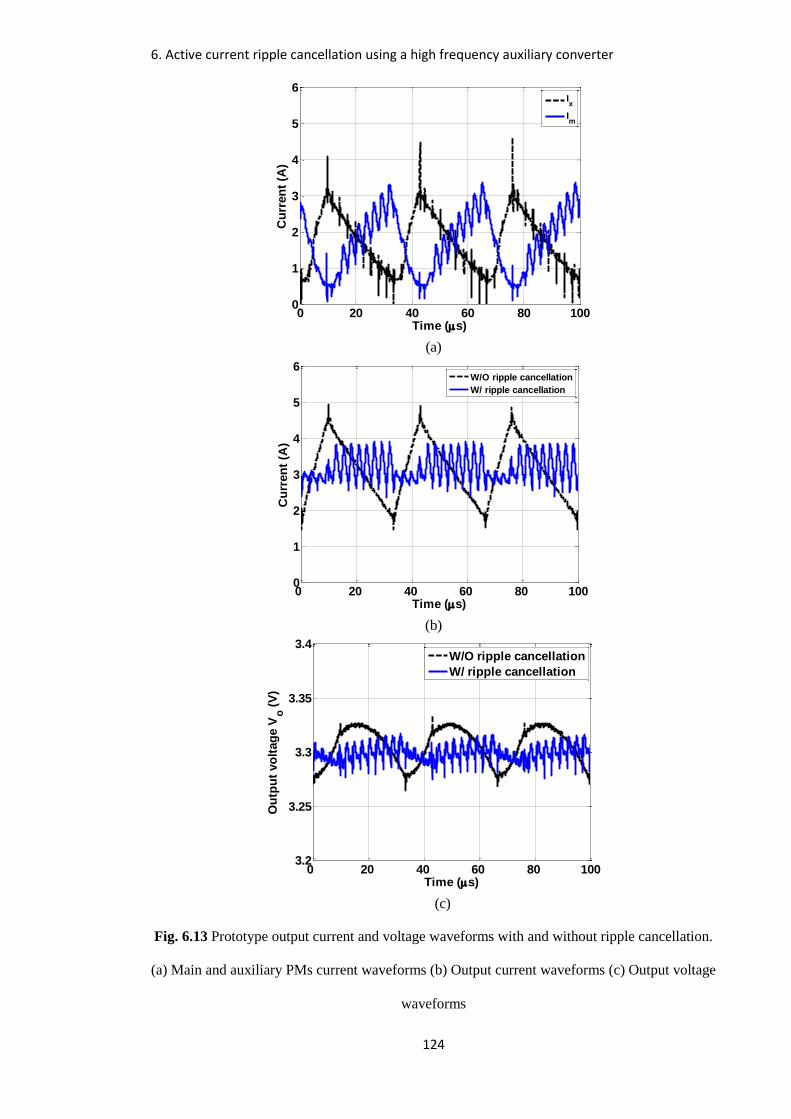
6. Active current ripple cancellation using a high frequency auxiliary converter
124
(a)
(b)
(c)
Fig. 6.13 Prototype output current and voltage waveforms with and without ripple cancellation.
(a) Main and auxiliary PMs current waveforms (b) Output current waveforms (c) Output voltage
waveforms
0 20 40 60 80 1000
1
2
3
4
5
6
Time (s)
Cu
rren
t (A
)
Ix
Im
0 20 40 60 80 1000
1
2
3
4
5
6
Time (s)
Cu
rren
t (A
)
W/O ripple cancellation
W/ ripple cancellation
0 20 40 60 80 1003.2
3.25
3.3
3.35
3.4
Time (s)
Ou
tpu
t vo
ltag
e V
o (
V)
W/O ripple cancellation
W/ ripple cancellation
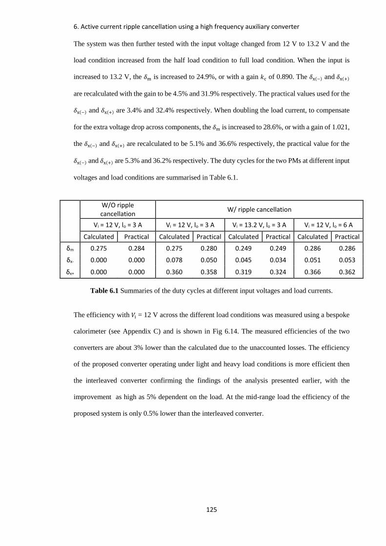
6. Active current ripple cancellation using a high frequency auxiliary converter
125
The system was then further tested with the input voltage changed from 12 V to 13.2 V and the
load condition increased from the half load condition to full load condition. When the input is
increased to 13.2 V, the 𝛿m is increased to 24.9%, or with a gain 𝑘c of 0.890. The 𝛿x(−) and 𝛿x(+)
are recalculated with the gain to be 4.5% and 31.9% respectively. The practical values used for the
𝛿x(−) and 𝛿x(+) are 3.4% and 32.4% respectively. When doubling the load current, to compensate
for the extra voltage drop across components, the 𝛿m is increased to 28.6%, or with a gain of 1.021,
the 𝛿x(−) and 𝛿x(+) are recalculated to be 5.1% and 36.6% respectively, the practical value for the
𝛿x(−) and 𝛿x(+) are 5.3% and 36.2% respectively. The duty cycles for the two PMs at different input
voltages and load conditions are summarised in Table 6.1.
Table 6.1 Summaries of the duty cycles at different input voltages and load currents.
The efficiency with 𝑉i = 12 V across the different load conditions was measured using a bespoke
calorimeter (see Appendix C) and is shown in Fig 6.14. The measured efficiencies of the two
converters are about 3% lower than the calculated due to the unaccounted losses. The efficiency
of the proposed converter operating under light and heavy load conditions is more efficient then
the interleaved converter confirming the findings of the analysis presented earlier, with the
improvement as high as 5% dependent on the load. At the mid-range load the efficiency of the
proposed system is only 0.5% lower than the interleaved converter.
W/O ripple cancellation
W/ ripple cancellation
Vi = 12 V, lo = 3 A Vi = 12 V, lo = 3 A Vi = 13.2 V, lo = 3 A Vi = 12 V, lo = 6 A
Calculated Practical Calculated Practical Calculated Practical Calculated Practical
δm 0.275 0.284 0.275 0.280 0.249 0.249 0.286 0.286
δx- 0.000 0.000 0.078 0.050 0.045 0.034 0.051 0.053
δx+ 0.000 0.000 0.360 0.358 0.319 0.324 0.366 0.362

6. Active current ripple cancellation using a high frequency auxiliary converter
126
Fig. 6.14 Measured efficiency of the proposed and interleaved converters.
6.5. Summary
This chapter has demonstrated a design and control technique for achieving higher efficiency in a
parallel converter and shown how they can be designed to reduce the current ripple seen by the
filter capacitor. The analysis has shown that by allowing the current ripple cancellation to be
handled by the auxiliary PM operating at a higher frequency, both switching and conduction losses
in the main PM can be reduced. Using a 20 W converter as an example, predictions show efficiency
improvements over the interleaved converter of up to 6% are achievable under light and heavy
load conditions and efficiency in the mid-range is only slightly lower. Experimental measurements
taken on a prototype converter confirm this trend with the mid-range load efficiencies only
dropping by 0.5%. This chapter also shows that non-identical PMs can be used for ripple
cancellation, provided that the selected auxiliary PM inductor can produce a higher net rate of
change of inductor current than the rates of the current ripple. Using the equations in section 6.2
and 6.3, the current ripple seen by the filter capacitor is successfully reduce from 3 A to 1 A under
different input voltages and load conditions. The proposed converter design technique also works
for other power rating and the ripple cancellation technique can reduce the current ripple to a
smaller amplitude.
5 10 15 2065
70
75
80
85
90
95
Output power (W)
Eff
icie
ncy (
%)
Interleaved converter
Proposed converter

127
7. LLC resonant converter with capacitor-diode clamp
7.1. Introduction
The previous four chapters have described the control schemes and design techniques through
which the efficiencies of the hard-switching converter can be improved, this chapter addresses
the overloading issue of the high efficiency LLC resonant converter. A new fundamental
harmonic approximation (FHA) based equivalent circuit model for LLC resonant converters with
capacitor-diode clamp is obtained through the application of describing function techniques, and
by examining the fundamental behaviour of the capacitor-diode clamp. Using the new circuit
model, a new design methodology for achieving the best current limiting characteristics is
proposed. A prototype 90 W (𝑽𝐨 = 36V, 𝑰𝐨 = 2.5 A) LLC converter is designed using the proposed
methodology and comparisons of the voltage gain and the voltage-current characteristics under
different overload conditions and operating frequencies are presented to show the performance of
the proposed model.
7.2. Circuit operation
The circuit diagram of a half-bridge LLC resonant converter is shown in Fig. 7.1. It consists of
three main functional parts:
(i) a DC chopper formed by two complementary switched MOSFETs 𝑆1 and 𝑆2, converting
the DC input voltage, 𝑉i, into a square waveform of frequency 𝑓s (n.b. 𝐷s1 and 𝐷s2 are the
body diodes of the MOSFETs which are critical for ZVS),
(ii) a resonant tank formed by resonant inductors and capacitor 𝐿p, 𝐿s, 𝐶r allowing the
fundamental component of the square waveform to pass through,
(iii) a transformer, bridge rectifier and output filter formed by diodes 𝐷1 − 𝐷4 and capacitor 𝐶o,
converting the AC waveform produced in (ii) into the isolated DC output.

7. LLC resonant converter with capacitor-diode clamp
128
Vi
Lp
C RlD1 D3
D2 D4
Ls Cr
ii
Ds2
Ds1S1
S2
Vo
i ii
iii
Fig. 7.1 Half-bridge LLC resonant converter.
The typical gain characteristics of a LLC resonant converter under different load conditions (i.e.
𝑄) are shown in Fig. 7.2. Figure shows that at the load independent point (LIP), the nominalised
gain curves remain at unity irrespective to the load conditions. This is a major issue where
destructive current can flow through the converter.
Fig. 7.2 Gain characteristics of LLC converter under different conditions.
A previous approach [82] has split the resonant capacitor into two which are then clamped by
clamping diodes. The approach proposed in this chapter splits the resonant capacitor into the
0 0.5 1 1.5 2 0
0.4
0.8
1.2
1.6
Nominalised frequency, fn
Gain
, M
g
Q = 0.3
Q = 0.5
Q = 0.7
Q = 0.9LIP

7. LLC resonant converter with capacitor-diode clamp
129
clamped portion (as in [82]) and a non-clamped portion, to allow the desired clamping
characteristic to be obtained. A half-bridge LLC resonant converter with the proposed capacitor-
diode clamp is shown in Fig. 7.3, the resonant capacitor is split into 2𝐶c and 𝐶s, and containing one
extra functional part (iv):
(iv) diodes 𝐷c1 and 𝐷c2 which clamp the voltage, 𝑉c, to the input voltage rail under high-current
operation.
Vi
Lp
C RlD1
Cc
D3
D2 D4
Cc
Ls Cs
Dc1
Dc2
Ds2
Ds1
VC
ii
i ii iv
iii
S1
S2
Vo
Fig. 7.3 Half-bridge LLC resonant converter with capacitor-diode clamp.
Under normal operation (i.e. below what is termed the current limit), the capacitor common point
voltage 𝑉c operates within the two clamping voltage levels, 0 and 𝑉i, as shown in Fig. 7.4 (a). Since
the clamping diodes 𝐷c1 and 𝐷c2 do not conduct during the switching period and the circuit can be
simplified to Fig. 7.5 (a), thus the two capacitors, 𝐶c, are effectively connected in parallel such that
2𝐶c is connected in series with 𝐶𝑠 which together form the resonant capacitor 𝐶r found in the
standard LLC resonant converter. With these capacitors, 𝐶s can be found by (7.1):
𝐶s = (2𝐶c𝐶r) (2𝐶c − 𝐶r)⁄ (7.1)
The range of 𝐶s, and hence 𝐶c, is controlled by the capacitance sharing ratio 𝐵s as given in (7.2).
The capacitance sharing ratio can take on values in the range 0 ≤ 𝐵s ≤ 1, with 𝐵s = 1 being the

7. LLC resonant converter with capacitor-diode clamp
130
extreme where no capacitance is clamped by the diodes 𝐷c1 and 𝐷c2 and 𝐵s = 0 being where the
whole resonant capacitor is clamped. The effect of the capacitor ratio 𝐵s to the current limiting
performance will be detailed in section 7.4.
𝐵s =𝐶r
𝐶s (7.2)
Under overload condition (i.e. the pre-designed load current is exceeded), the diode-clamp
becomes active since 𝑉c exceeds the input voltage rail, causing 𝐷c1 and 𝐷c2 to conduct momentarily,
this has the effect of reducing the circuit's resonant frequency. Under this condition there is an
apparent increase in the switching frequency to resonant frequency ratio that has the effect of
reducing the current flow in the circuit. The conduction state for each clamping diode can be
determined as follows:
1) 𝐷c1 conducts when 𝑉c > 𝑉𝑖, clamping 𝑉c to 𝑉i
2) 𝐷c2 conducts when 𝑉c < 0 𝑉, clamping 𝑉c to 0 𝑉
In either case the clamping diode ceases conduction when the resonant circuit input current
𝐼i = 0 A. When the diode clamp is inactive 𝑉c takes on a cosinsoidal shape, assuming the resonant
circuit current is sinusoidal. The quasi cosine-square waveform of 𝑉c under current-limited
operating conditions is shown in Fig. 7.4 (b), with the diode clamp conduction states 1) and 2)
described above found in intervals 𝐼𝐼 and 𝐼𝑉 respectively and diode clamp non-conduction states
in intervals 𝐼 and 𝐼𝐼𝐼. The sub-circuits for the converter with 𝐷c1 and 𝐷c2 conducting are shown in
Fig. 7.5 (b) and (c) respectively.
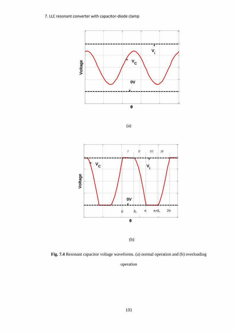
7. LLC resonant converter with capacitor-diode clamp
131
(a)
(b)
Fig. 7.4 Resonant capacitor voltage waveforms. (a) normal operation and (b) overloading
operation
Vo
ltag
e
Vi
0V
VC
Vo
ltag
e
Vi
0V
VC
π π+δc 2π δc 0
𝐼 𝐼𝐼 𝐼𝐼𝐼 𝐼𝑉
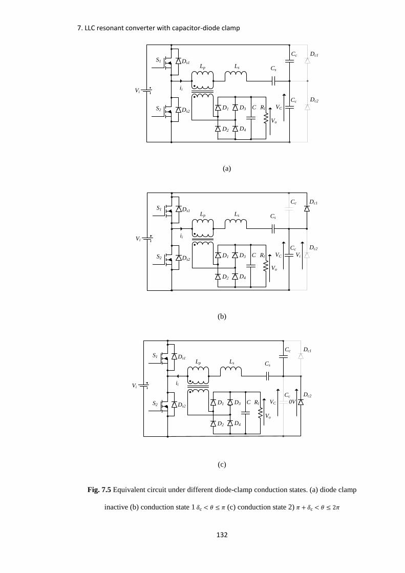
7. LLC resonant converter with capacitor-diode clamp
132
Vi
Lp
C RlD1
Cc
D3
D2 D4
Cc
Ls Cs
Dc1
Dc2
VC
ii
Ds2
Ds1S1
S2
Vo
(a)
Vi
Lp
C RlD1
Cc
D3
D2 D4
Cc
Ls Cs
Dc1
Dc2
VC
ii
ViDs2
Ds1S1
S2
Vo
(b)
Vi
Lp
C RlD1
Cc
D3
D2 D4
Cc
Ls Cs
Dc1
Dc2
VC
ii
0VDs2
Ds1S1
S2
Vo
(c)
Fig. 7.5 Equivalent circuit under different diode-clamp conduction states. (a) diode clamp
inactive (b) conduction state 1 𝛿c < 𝜃 ≤ 𝜋 (c) conduction state 2) 𝜋 + 𝛿c < 𝜃 ≤ 2𝜋
7. LLC resonant converter with capacitor-diode clamp
133
7.3. Equivalent circuit model
When the diode-clamp is inactive, the static behaviour of the converter can be predicted using a
variety of methods, including fundamental harmonic approximation (FHA) [102], describing
function [103] and state-plane techniques [104] depending on the required modelling accuracy.
Although the methods presented in [103] and [104] can predict the static behaviours more
accurately across a wide range of switching frequencies, they can be difficult to use when multiple
operating modes are encountered and therefore the equivalent circuit models derived here are based
on FHA which has been shown to provide reasonable prediction accuracy when the converter is
operating in the vicinity of the load independent point [105].
With FHA one assumes the resonant current can be approximated to a sinusoidal current since the
resonant circuit operates similar to a band-pass filter responding only to the fundamental
component of the input voltage and attenuating the higher frequency components. With this
assumption, the input current 𝑖i can be defined as in (7.3), with a peak value of 𝐼i when the converter
is operating at a frequency 𝑓s. To simplify the analysis that follows, angles are used to remove the
time dependences such that 2𝜋𝑓s𝑡 = 𝜃:
𝑖i = 𝐼i𝑠𝑖𝑛(𝜔s𝑡) = 𝐼i𝑠𝑖𝑛(2𝜋𝑓s𝑡) = 𝐼i𝑠𝑖𝑛(𝜃) (7.3)
7.3.1. Diode-clamp inactive
Employing FHA techniques similar to those applied in [73] and [102], the magnitude of the input
current (𝐼i) and output voltage (𝑉o) can be calculated using (7.4) and (7.5) respectively (n.b. in the
following analysis, the non-ideality of diodes and of components parasitic resistances are
neglected).
𝐼i =2𝑉i
𝜋𝑍1 (7.4)

7. LLC resonant converter with capacitor-diode clamp
134
𝑉o =𝜋𝐼i(𝑅eq||𝑠𝐿𝑝)
4𝑛 (7.5)
where 𝑍1 = 𝑅eq||𝑠𝐿p + 𝑠𝐿s +1
𝑠𝐶s+
1
2𝑠𝐶𝑐, is the input impedance of the resonant circuit and the load,
𝑠 = 𝑗𝜔s, is the complex frequency and 𝑅eq =8𝑛2𝑅l
𝜋2 is the equivalent resistance presented by the
rectifier, output filter and load reflected through a transformer with a primary turns (𝑁p) to
secondary turns (𝑁s) ratio 𝑛 = 𝑁p 𝑁s⁄ .
In order to study the converter’s general behaviour, irrespective of the resonant tank components
selection, the nominalised gain 𝑀g is obtained by substituting (7.4) into (7.5), and rearranging in
terms of (2𝑛𝑉o) 𝑉i⁄ . Applying normalising terms for inductor ratio 𝐴s = 𝐿p 𝐿s⁄ , loaded quality factor
𝑄 = √𝐿s 𝐶r⁄ 𝑅eq⁄ and normalised switching frequency (against the series resonant frequency) 𝑓n =
𝑓s 𝑓0⁄ leads to (7.6), allowing the output voltage to be predicted.
𝑀g =2𝑛𝑉o
𝑉i=
𝐴s𝑓𝑛2
𝐴s𝑓𝑛2+𝑓𝑛
2−1+𝑗(𝑓𝑛3𝑄𝐴s−𝑓n𝑄𝐴s)
(7.6)
where 𝑓0 is converter resonant frequency.
Further analysis of the equivalent circuit Fig. 7.5 (a) allows one to obtain the peak voltage and
current stresses on the components. For example, since the capacitors 𝐶c excited by the sinusoidal
input current, the capacitor common point voltage as shown in Fig. 7.4 (a), at any given instant can
be found using (7.7). The time dependence is removed by substituting 𝜔s𝑡 for 𝜃 (with 𝜔s = 2𝜋𝑓s
being the angular switching frequency and 𝑡 is time), the capacitor branch voltage 𝑣c as a function
of 𝜃 is given by (7.8):
𝑣c(𝑡) =1
2𝐶c∫ 𝐼i𝑠𝑖𝑛(𝜔s𝑡) 𝑑𝑡 = −
𝐼i
2𝜔s𝐶c𝑐𝑜𝑠(𝜔s𝑡) + 𝑉n (7.7)
𝑣c(𝜃) = −𝐼i
2𝜔s𝐶c𝑐𝑜𝑠(𝜃) + 𝑉n (7.8)
where 𝑉n is the initial condition for a given conduction state starting at 𝜃 = 𝑛.

7. LLC resonant converter with capacitor-diode clamp
135
Due to the DC blocking property of capacitors, the DC component of the DC chopper (the
half-bridge inverter) is superimposed onto 𝑣c as in (7.9).
𝑣c(𝜃) = −𝐼i
2𝜔s𝐶c𝑐𝑜𝑠(𝜃) +
𝑉i
2 (7.9)
7.3.2. Diode-clamp active
In this section, a describing function is developed to represent the effects of the diode-
clamp/capacitor combination by an equivalent impedance 𝑍c. This impedance is then combined
with a FHA analysis similar to that described in the previous section providing a complete model
of the converter when the diode-clamp is active (i.e. when operating under overload conditions).
Further analysis of the equivalent circuits in Fig. 7.5 (b) and (c), the derivation of 𝑍c is given in the
three steps as follows:
Step 1: a piecewise equation describing the capacitor voltage 𝒗𝐜 (Fig. 4 (b)) representing the
circuit conduction states is obtained assuming a sinusoidal resonant current
Since there are two intervals during a single cycle when the diode-clamp is inactive, two separate
values for the initial condition 𝑉n in (7.8) are needed. In the first interval 𝐼 (0 < 𝜃 ≤ 𝛿c), the
capacitor voltage, 𝑣c, is zero at 𝜃 = 0, by substituting the known quantities in (7.8), the initial
condition, 𝑉0, is found in (7.10):
0 = −𝐼i
2𝜔s𝐶c𝑐𝑜𝑠(0) + 𝑉0
𝑉0 =𝐼i
2𝜔s𝐶c
(7.10)
For interval, 𝐼𝐼𝐼 (𝜋 < 𝜃 ≤ 𝜋 + 𝛿c), 𝑣c has been charged to 𝑉i and now begins discharging towards 0
V. By applying similar arguments as before, the initial condition for this interval is also found in
(7.11),

7. LLC resonant converter with capacitor-diode clamp
136
𝑉i = −𝐼i
2𝜔s𝐶c𝑐𝑜𝑠(𝜋) + 𝑉π
𝑉π = 𝑉i −𝐼i
2𝜔s𝐶c
(7.11)
Combining the initial conditions found in (7.10) and (7.11) with (7.8) and accounting for the two
clamping levels, the piecewise description of the capacitor voltage is given in (7.12):
𝑣C(𝜃) =
{
𝐼i
2𝜔s𝐶c(1 − 𝑐𝑜𝑠(𝜃))
𝑉i
𝑉𝑖 −𝐼i
2𝜔s𝐶c(1 + 𝑐𝑜𝑠(𝜃))
0
0 < 𝜃 ≤ 𝛿c𝛿c < 𝜃 ≤ 𝜋
𝜋 < 𝜃 ≤ 𝜋 + 𝛿c𝜋 + 𝛿c < 𝜃 ≤ 2𝜋
(7.12)
The diode-clamp non-conduction angle, 𝛿c, is found by evaluating the change in capacitor voltage
over the diode-clamp non-conduction period. At the end of the first interval, the capacitor voltage
has charged from 0 to 𝑉i, therefore, substituting 𝑣C(𝛿c) = 𝑉i into (7.12) and rearranging provides,
𝛿c = 𝑐𝑜𝑠−1 (1 −
2𝜔s𝐶c𝑉i
𝐼i) (7.13)
Step 2: the fundamental component of 𝒗𝐜 is determined via Fourier analysis
A describing function for 𝑣𝑐 is now developed based on the piecewise equation that has just been
developed. The Fourier series representation of a repetitive waveform is defined in (7.14) where
𝑓(𝑡) is the original time domain signal 𝑣c(𝑡), 𝑎0 is the DC component, 𝑎𝑛 & 𝑏𝑛 are harmonic
components of the waveform and 𝑇 is the period of one cycle:
𝑓(𝑡) = 𝑎0 + ∑ (𝑎n𝑐𝑜𝑠(𝑛𝜔s𝑡) + 𝑏n𝑠𝑖𝑛(𝑛𝜔s𝑡))∞𝑛−1
𝑎0 =1
2𝜋∫ 𝑓(𝑡)𝑑𝑡𝑇2⁄
−𝑇 2⁄
𝑎n =1
𝜋∫ 𝑓(𝑡)𝑐𝑜𝑠(𝑛𝜔𝑠𝑡)𝑑𝑡𝑇2⁄
−𝑇 2⁄
(7.14)

7. LLC resonant converter with capacitor-diode clamp
137
𝑏n =1
𝜋∫ 𝑓(𝑡)𝑠𝑖𝑛(𝑛𝜔𝑠𝑡)𝑑𝑡𝑇2⁄
−𝑇 2⁄
For AC equivalent circuit analysis, the DC component, 𝑎0, is ignored and since the converter’s
behaviour is dominated by the fundamental component, the Fourier series can be simplified to a
describing function as shown below:
𝑓(𝜃) = 𝑎1𝑐𝑜𝑠(𝜃) + 𝑏1𝑠𝑖𝑛(𝜃)
𝑎1 =1
𝜋∫ 𝑓(𝜃)𝑐𝑜𝑠(𝜃)𝑑𝜃2𝜋
0
𝑏1 =1
𝜋∫ 𝑓(𝜃)𝑠𝑖𝑛(𝜃)𝑑𝜃2𝜋
0
(7.15)
By substituting (7.12) into (7.15) the fundamental component of 𝑣c is:
𝑣C(𝜃) = [2
𝜋𝑉i cos(𝛿c) +
𝐼i2𝜋𝜔s𝐶c
(1 + cos(𝛿c) (cos(𝛿c) − 2))] sin(𝜃)
+[−2
𝜋𝑉i sin(𝛿c) −
𝐼i
2𝜋𝜔s𝐶c(𝛿c + sin (𝛿c)(cos(𝛿c) − 2))] cos (𝜃)
(7.16)
Step 3: an equivalent impedance for diode-clamp/capacitor combination is found by dividing the
expression obtained in step 2 by the sinusoidal input current 𝒊𝐢 = 𝑰𝐢𝒔𝒊𝒏(𝜽)
The equivalent impedance of the diode-capacitor combination is obtained by applying the
transform 𝑐𝑜𝑠(𝜃) = 𝑗𝑠𝑖𝑛(𝜃) and then dividing by resonant current as follows:
𝑍C = [2𝑉i𝜋𝐼i
cos(𝛿c) +1
2𝜋𝜔s𝐶c(1 + cos(𝛿c) (cos(𝛿c) − 2))]
+𝑗 [−2𝑉i
𝜋𝐼isin(𝛿c) −
1
2𝜋𝜔s𝐶c(𝛿c + sin (𝛿c)(cos(𝛿c) − 2))]
(7.17)

7. LLC resonant converter with capacitor-diode clamp
138
By substituting 𝑍c into the FHA model provides (7.18) where the effect of the diode-clamp is
accounted for allowing the magnitude of the resonant tank current under clamping (i.e. overload)
to be found. The output voltage can be found by substituting (7.18) into (7.5).
𝐼i =2𝑉i
𝜋𝑍2 (7.18)
where 𝑍2 = 𝑅eq||𝑠𝐿p + 𝑠𝐿s +1
𝑠𝐶s+ 𝑍c, which 𝑠 and 𝑅eq are as defined in previous section.
7.3.3. Diode-clamp conduction point
Since (7.18) cannot be solved analytically owing to the dependence on 𝐼i for determining both 𝛿c
and 𝑍c, an iterative procedure similar to that employed in [88] is used: the value for the resonant
tank current is first estimated using (7.4) by assuming the diode-clamp is inactive. Once a value
for 𝐼i has been obtained, the non-conduction angle, 𝛿c, and capacitor-diode clamp equivalent
impedance, 𝑍c, are found by (7.13) and (7.17), after which a refined value for 𝐼i is found by (7.18).
The refinement of 𝛿c, 𝑍c and 𝐼i are achieved through an iterative loop, flowchart shown in Fig. 7.6,
where a new value for the current 𝐼i[𝑘 + 1] is reapplied to (7.13) and (7.17) until they converge.
To ensure satisfactory convergence, a damping factor 𝛼d should be used to determine the new
resonant tank current value, 𝐼i[𝑘 + 1], in a similar manner to the technique commonly employed
with Newton’s method [106].
𝐼i[𝑘 + 1] = 𝐼i[𝑘] + 𝛼d(𝐼DC[𝑘 + 1] − 𝐼i[𝑘]) (7.19)
where 𝐼i[𝑘 + 1] and 𝐼i[𝑘] is the new value and old value of resonant tank current respectively,
𝐼DC[𝑘 + 1] is the present refined resonant tank current predicted by (7.18) and 𝛼d is the damping
factor with a value between 0 and 1.

7. LLC resonant converter with capacitor-diode clamp
139
Has Ii
converged?
Calculate
δ by (7.13) and
ZC by (7.17)
Initiate Ii[k=1]
by (7.4)
Calculate the
refined Ii by (7.18)
Ii is found
Calculate the new
Ii[k+1] by (7.19)
Yes
No
Fig. 7.6 Flowchart describing the interactive procedure for finding the load current during
overloading conditions (i.e. 𝑉c > 𝑉i).
7.3.4. Nominalised gain with active diode-clamp
Similar to the inactive diode-clamp case (i.e. normal non-current limited operation), the converter
gain with an active diode-clamp, 𝑀g(clmp), is obtained by substituting (7.18) into (7.5) and
rearrange in terms of (2𝑛𝑉o) 𝑉i⁄ as in (7.20), after which substituting 𝑠 = 𝑗𝜔, using 𝑍c = 𝑅 + 𝑗𝑋
(where 𝑅 and 𝑋 are the real and imaginary part of 𝑍c in (7.17) respectively), and introducing
the 𝑗𝜔𝐶r term into both the numerator and denominator as in (7.21):
𝑀g(clmp) =𝑉o
𝑉i2𝑛 =
𝑅eq||𝑠𝐿p
𝑅eq||𝑠𝐿p+𝑠𝐿s+1
𝑠𝐶s+𝑍c
(7.20)
𝑀g(clmp) =𝑗2𝜔2𝐿p𝐶r
𝑗2𝜔2𝐿p𝐶r+𝑗3𝜔3𝐿s𝐿p𝐶r
𝑅eq+𝑗2𝜔2𝐿s𝐶r+
𝑗𝜔𝐿p𝐶r
𝐶s𝑅eq+𝐶r𝐶s+𝑗2𝜔2𝑅𝐿p𝐶r
𝑅eq+𝑅𝑗𝜔𝐶r+
𝑗3𝜔2𝐶r𝑋𝐿p
𝑅eq+𝑗2𝑋𝜔𝐶r
(7.21)

7. LLC resonant converter with capacitor-diode clamp
140
The final step involves substituting the following normalising factors 𝐿p = 𝐴s𝐿s, 𝐿s𝐶r = 1 𝜔02⁄ ,
𝐿s 𝑅eq⁄ = 𝑄 𝜔0⁄ , 𝑓n = 𝜔 𝜔0⁄ and 𝐵s = 𝐶r 𝐶s⁄ , to obtain:
𝑀g(clmp) =𝑓n2𝐴s
𝑓n2𝐴s+𝑓n
2−𝐵s+𝑘re+𝑗(𝑓n3𝐴s𝑄−𝑓n𝐴s𝑄𝐵s+𝑘im)
(7.22)
where 𝑘re = 𝜔𝐶r(𝑓n𝐴s𝑄𝑅 + 𝑋) and 𝑘im = 𝜔𝐶r(−𝑅 + 𝑓n𝐴s𝑄𝑋), are terms accounting for the
change in the effective impedance of the 𝐶c caused by the diode-clamp when it is active and it is
assumed that the values for 𝑅 and 𝑋 have converged.
Without the diode-clamp (i.e. normal operation), 𝑅 = 0, and 𝐵s can either be zero (i.e.
𝐶c = 0.5𝐶r) or one (i.e. 𝐶s = 𝐶r,). When 𝐵s = 0, 𝑋 = −1
2ω𝐶c, 𝑘re = −1 and 𝑘im = −𝑓n𝐴s𝑄, and when
𝐵s = 1, 𝑋 = 0 𝑘re = 0 and 𝑘im = 0. In both cases, (7.22) can be simplified to (7.6).
7.4. Analysis of converter operating characteristic
Before giving detailed discussion on the characteristic of the capacitor-diode clamp, the converter
operating under normal non-overload conditions is briefly described.
Assuming the capacitor-diode clamp has been designed such that it only becomes active when the
load current exceeds the maximum rated load current, the converter can be treated as standard LLC
resonant converter up to the maximum load condition. When the standard LLC converter is
operated at the series resonant frequency, 𝑓0, its voltage gain, 𝑀g, is fixed and is unaffected by
changes in the load (i.e. operation at the LIP). Thus, one popular method for designing LLC
converters [102][107] is to select the transformer turn ratio, n, such that the voltage gain at the
series resonant frequency under the nominal operating condition is unity, 𝑀g(𝑓0) = 1. The
resonant tank components are then selected through the normalised variables 𝐴s and 𝑄 using (7.6)
to accommodate the 𝑀g requirement for changes in the input voltage over a given frequency range.
In practice small changes in frequency are also required to compensate for inevitable voltage drops
caused by changes in the load.
7. LLC resonant converter with capacitor-diode clamp
141
With the nominal input voltage, 𝑉i(nom), at the LIP, the converter gain from (7.6) with inductor
ratio 3 ≤ 𝐴s ≤ 9 and load 0.3 ≤ 𝑄 ≤ 0.9 are plotted in Fig. 7.7 (a) and (b) respectively. Fig. 7.5
(a) shows that smaller 𝐴s values lead to higher gain while Fig. 7.7 (b) shows that smaller 𝑄 values
lead to higher gain. If 𝐴s is selected to be 5, the maximum 𝑄 that satisfies the gain requirement,
𝑀g(max), can be identified with Fig. 7.7 (b). The 𝑓s(min) and 𝑓s(max) in Fig. 7.7 are the minimum
and maximum frequencies the converter used for the line and load regulations.
(a)
(b)
Fig. 7.7 Converter gain characteristics. (a) 𝑄 = 0.5, 3 ≤ 𝐴s ≤ 9 (b) 0.3 ≤ 𝑄 ≤ 0.9, 𝐴s = 5
0 0.5 1 1.5 2 0
0.4
0.8
1.2
1.6
Nominalised frequency, fn
Gain
, M
g
A = 3
A = 5
A = 7
A = 9LIP
fs(max)
fs(min)
fs
0 0.5 1 1.5 2 0
0.4
0.8
1.2
1.6
Nominalised frequency, fn
Gain
, M
g
Q = 0.3
Q = 0.5
Q = 0.7
Q = 0.9
Mg(max)
LIP
fs(min)

7. LLC resonant converter with capacitor-diode clamp
142
Since 𝑄 = √𝐿s 𝐶r⁄ 𝑅eq⁄ , changing 𝑄 is equivalent to changing in load resistance 𝑅eq, or load
condition, the gain curves under overload conditions can be studied through the nominalised
Q-factor, 𝑄n, as calculated by (7.23). For example, assuming 𝐴s is selected to be 5 and the
Q-factor under the rated load condition, 𝑄rate, is 0.3, gain curve with 𝑄 = 0.9 equals to 𝑄𝑛 = 3,
representing three times overloading.
𝑄n =𝑄
𝑄rate (7.23)
7.4.1. Capacitor diode-clamp characteristics
This section compares voltage gain under normal and overload conditions when operating in the
vicinity of LIP.
In the case where the diode-clamp is inactive, with 𝐴s = 5 and 𝑄rate = 0.5, the converter voltage
gain characteristic for 1 ≤ 𝑄n ≤ 10 and 0.5 ≤ 𝑓n ≤ 1.5 is calculated using (7.6) and is plotted in
Fig. 7.8 (a). As expected there is little change in the gain around the LIP (𝑓n = 1) for
increasing 𝑄n.
Assuming all of the resonant capacitor (calculated for the above 𝐴s and 𝑄rate) is now split into
the two clamping capacitors 𝐶c(= 1 (2𝐶r)⁄ ) and is clamped by 𝐷c1 and 𝐷c2 to the input voltage
under overload, the voltage gain 𝑀g(clmp) under the same 𝑓n and 𝑄n range is calculated by (7.22)
and is plotted in Fig. 7.8 (b). For each operating points, 𝑘re and 𝑘im are calculated by the
procedure highlighted in Fig. 7.6. The results show that in the diode-clamp inactive region (to
the right of the diode-clamp active-inactive boundary solid black line), the gain is unaffected,
whereas in the diode-clamp active region the gain around the LIP (𝑓n = 1) is dramatically reduced
for increasing 𝑄n and thereby reducing the current that would otherwise flow under overloading
conditions. Fig. 7.8 (b) also shows the peak gain at 𝑓n = 0.6 is reduced below the required
𝑀g(max), and so load regulation at the rated load (𝑄n = 1) may no longer be achievable with low
input voltages.
7. LLC resonant converter with capacitor-diode clamp
143
(a)
(b)
Fig. 7.8 Converter gain characteristics with 𝐴s = 5 and 𝑄rate = 0.5. (a) 𝐵s = 1 and (b) 𝐵s = 0
Therefore, to retain regulation (that is to achieve the required 𝑀g(max)) for the rated load condition,
the diode-clamp active region must be reduced. This can be achieved by increasing 𝐶c, by choosing
a larger value for 𝐵s, which reduces the voltage 𝑉c for the same load current and, thus, a larger
current is required to activate the diode-clamp.
Using (7.22) the voltage gain characteristic with 𝐵s of 0.25, 0.5 and 0.75 are plotted in Fig. 7.9 (a),
(b) and (c) respectively. The figures show that as 𝐵s increases, the diode-clamp active region
reduces. For 𝐵s ≥ 0.5, the 𝑀g(max) is retained for this particular example, allowing normal
0.50.75
11.25
1.5 10
7
4
10
0.4
0.8
1.2
Qnf
n
Gain
, M
g
0.50.75
11.25
1.5 10
7
4
10
0.4
0.8
1.2
Qnf
n
Gain
, M
g
𝑀g(max)
diode-clamp
inactive region
diode-clamp
active region
𝑀g(max)
unachievable
7. LLC resonant converter with capacitor-diode clamp
144
regulation at the full rated load condition. The penalty with the higher 𝐵s is the diode-clamp
becomes less effective at reducing the voltage gain, hence overload current.
(a)
(b)
(c)
Fig. 7.9 Converter gain characteristics with 𝐴s = 5 and 𝑄rate = 0.5. (a) 𝐵s = 0.25 (b) 𝐵s = 0.5 (c) 𝐵s
= 0.75
0.50.75
11.25
1.5 10
7
4
10
0.4
0.8
1.2
Qnf
n
Gain
, M
g
0.50.75
11.25
1.5 10
7
4
10
0.4
0.8
1.2
Qnf
n
Gain
, M
g
0.50.75
11.25
1.5 10
7
4
10
0.4
0.8
1.2
Qnf
n
Gain
, M
g
diode-clamp
inactive region
diode-clamp
active region
diode-clamp
inactive region
diode-clamp
active region
diode-clamp
inactive region
diode-clamp
active region

7. LLC resonant converter with capacitor-diode clamp
145
The design task involves the selection of the lowest 𝐵s that retains the 𝑀g(max) operating point while
providing the current-limiting action when operating with overload conditions (𝑄n > 1).
7.4.2. Converter Voltage-Current (VI) characteristics
To illustrate how the reduction in voltage gain by the action of diode-clamp leads to the reduction
in overload current, the converter voltage gain 𝑀g under different 𝑄n and 𝑓n, for the different 𝐵s,
are first normalised against the unclamped rated full load gain (i.e. 𝐵s = 1, 𝑄n = 1) at the
corresponding frequency 𝑓n, after which the converter normalised output voltage 𝑉n and normalised
current 𝐼n for 1 ≤ 𝑄n ≤ 10 are calculated and plotted in Fig. 7.10 (a)-(e).

7. LLC resonant converter with capacitor-diode clamp
146
(a)
(b)
Fig. 7.10 Converter VI characteristics. (a) 𝐵s = 1 (b) 𝐵s = 0
02
46
810 0.5
0.75
1
1.25
1.50
0.2
0.4
0.6
0.8
1
fnI
n
Vn
0 2
4 6
8 10 0.5
0.75
1
1.25
1.5 0
0.2
0.4
0.6
0.8
1
fnI
n
Vn
𝑄𝑛 = 1
𝑄𝑛 = 10
𝑉𝑛 = 1, 𝐼𝑛 = 10
𝑩𝐬 = 𝟎
𝑓n where 𝑉n < 1
𝑄𝑛 = 10
𝑉𝑛 = 0.29,
𝐼𝑛 = 2.9
𝑩𝐬 = 𝟏
7. LLC resonant converter with capacitor-diode clamp
147
(c)
(d)
(e)
Fig. 7.10 Converter VI characteristics. (a) 𝐵s = 1 (b) 𝐵s = 0 (c) 𝐵s = 0.25 (d) 𝐵s = 0.5
(e) 𝐵s = 0.75
02
46
810 0.5
0.75
1
1.25
1.50
0.2
0.4
0.6
0.8
1
fnI
n
Vn
02
46
810 0.5
0.75
1
1.25
1.50
0.2
0.4
0.6
0.8
1
fnI
n
Vn
02
46
810 0.5
0.75
1
1.25
1.50
0.2
0.4
0.6
0.8
1
fnI
n
Vn
𝑩𝐬 = 𝟎. 𝟓
𝐼𝑛 = 6.9
𝑩𝐬 = 𝟎. 𝟕𝟓
𝐼𝑛 = 3.1
𝑩𝐬 = 𝟎. 𝟐𝟓

7. LLC resonant converter with capacitor-diode clamp
148
Fig. 7.10 (a) shows operation with no clamping action (𝐵s = 1), the voltage 𝑉𝑛 at the LIP for
different values of 𝑄n is unaffected and is equal to unity as expected. Thus, ten times overloading
(𝑄n = 10) leads to ten times increase in the current 𝐼n when operating at 𝑓n = 1. Fig. 7.8 (b) shows
that with the resonant capacitance fully clamped (𝐵s = 0), the reduction in 𝑀g(clmp) by the diode-
clamp in Fig. 7.8 (b) leads to the reduction of 𝑉n to 0.29, and 𝐼n to 2.9 (at the LIP with 𝑄n = 10).
The figure also shows there is a range of 𝑓n where the 𝑉n < 1. This means regulation is not
achievable for low input voltages as discussed in section 7.4.1. The 𝑉n𝐼n characteristic for 𝐵s =
0.25, 0.5 and 0.75 are plotted in Fig. 7.10 (c), (d) and (e) respectively. Fig. 7.10 (d) and (e) show
that for 𝐵s ≥ 0.5, regulation is achieved at all 𝑓n. Comparing Fig. 7.10 (c) to (e), the 𝐼n at the LIP
with 𝑄n = 10 is increased from 3.1 to 6.9, showing the reduction in the effectiveness diode-clamp
to reduce the current as 𝐵s increases. Fig. 7.10 shows that with a suitably chosen value for 𝐵s the
overload current can be limited without the need for any external control action.
7.5. Design example
To validate the accuracy of the proposed equivalent circuit model and analysis presented in the
previous sections, a LLC resonant converter with power rating of 90 W (𝑉o =36 V, 𝐼o = 2.5 A),
𝑉i = 390𝑉 ± 4% and 𝑓0 =147 kHz is designed and constructed.
Following the design procedure in [102] and with the converter operating at the LIP under the
nominal input voltage of 390 V, the transformer turn ratio 𝑛 is selected to be 5.5, the minimum
gain for the minimum input voltage is calculated to be 1.09. With the inductor ratio, 𝐴𝐬, selected
to be 5 (a good compromise to achieve a narrow operating frequency range a low circulating
currents), the maximum quality factor that satisfies the required gain is 𝑄 = 0.52. This leads to the
selection of the following resonant tank components: 𝐿s = 236 µH, 𝐿p = 1.2 mH and
𝐶r = 5 nF with the minimum and maximum operating frequencies of 100 kHz and 152 kHz
respectively. The 𝐶c that provides the optimum current limiting performance is found empirically
using the model to be 3.6 nF. The 𝐶s is calculated to be 17 nF and the 𝐵s is 0.3 from (7.2).

7. LLC resonant converter with capacitor-diode clamp
149
With the resonant tank components above, the capacitor common point voltage 𝑣c under full load
and ten times overloading at the nominal input voltage of 390V are plotted in Fig. 7.11 (a) and (b)
respectively. Fig. 7.11 (a) shows that under the full load condition, the peak-to-peak value of 𝑣c is
below the input voltage and therefore the diode-clamp is inactive. It should be noted that the 𝑣c
waveform shown Fig. 7.11 (a) has a different DC offset to the ideal case presented in
Fig. 7.4 (a), the reason for this is the additional DC path created by the oscilloscope probe causing
an imbalance in the capacitor branch- its peak-to-peak value is unaffected. The voltage waveform
across capacitor 𝐶c at ten times overloading is clamped between the 0 and 𝑉i as shown in Fig. 7.9
(b). From Fig. 7.11 (b), the conduction angle 𝛿c is found to be 91°, in comparison to the value of
𝛿c = 95° found by the procedure in section 3.3, an error of just 4%.
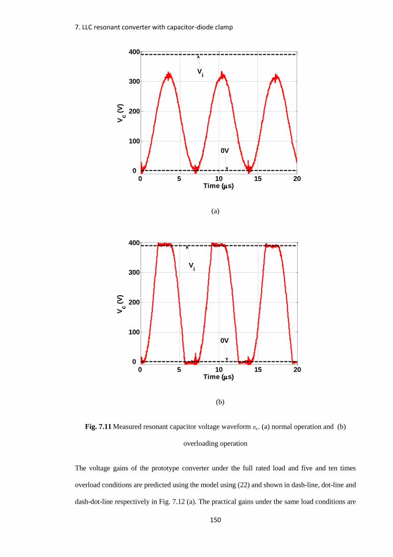
7. LLC resonant converter with capacitor-diode clamp
150
(a)
(b)
Fig. 7.11 Measured resonant capacitor voltage waveform 𝑣c. (a) normal operation and (b)
overloading operation
The voltage gains of the prototype converter under the full rated load and five and ten times
overload conditions are predicted using the model using (22) and shown in dash-line, dot-line and
dash-dot-line respectively in Fig. 7.12 (a). The practical gains under the same load conditions are
0 5 10 15 200
100
200
300
400
Time (s)
Vc (
V)
Vi
0V
0 5 10 15 200
100
200
300
400
Time (s)
Vc (
V)
Vi
0V

7. LLC resonant converter with capacitor-diode clamp
151
plotted in circle, square and triangle in Fig. 7.12 (a) respectively, showing a good match to the
theoretical result.
The converter’s VI characteristic, from full rated load to ten times overload conditions, under the
𝑓s(min), 𝑓s and 𝑓s(max) are plotted in dash-line, dot-line and dash-dot-line respectively in Fig. 7.12
(b) (n.b. 𝑉i is select according to 𝑓s (𝑉i(max) ≥ 𝑉i ≥ 𝑉i(min) ↦ 𝑓s(min) ≤ 𝑓n ≤ 𝑓s(max)) to maintain the
desired output voltage at the maximum rate load under different 𝑓s). At ten times overload, the
current is limited by the diode-clamp to 8 A for the three input voltages. The measured practical
𝑉𝐼 characteristics under the three input voltages from the prototype converter are plotted as circle,
square and triangle markers in respectively Fig. 7.12 (b). The trends agree well with the model
predictions.
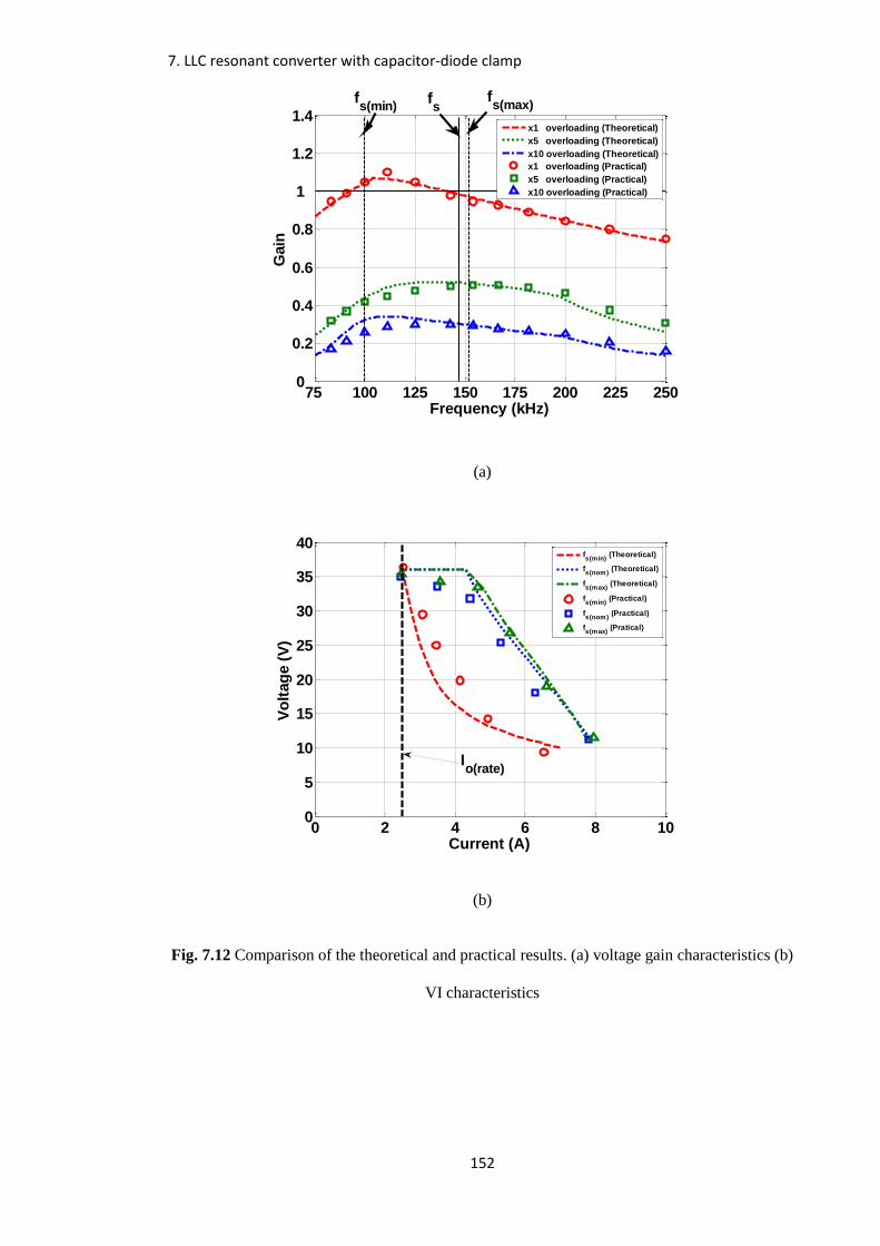
7. LLC resonant converter with capacitor-diode clamp
152
(a)
(b)
Fig. 7.12 Comparison of the theoretical and practical results. (a) voltage gain characteristics (b)
VI characteristics
75 100 125 150 175 200 225 2500
0.2
0.4
0.6
0.8
1
1.2
1.4
Frequency (kHz)
Gain
x1 overloading (Theoretical)
x5 overloading (Theoretical)
x10 overloading (Theoretical)
x1 overloading (Practical)
x5 overloading (Practical)
x10 overloading (Practical)
fs(min)
fs(max)f
s
0 2 4 6 8 100
5
10
15
20
25
30
35
40
Current (A)
Vo
ltag
e (
V)
fs(min)
(Theoretical)
fs(nom)
(Theoretical)
fs(max)
(Theoretical)
fs(min)
(Practical)
fs(nom)
(Practical)
fs(max)
(Pratical)
Io(rate)

7. LLC resonant converter with capacitor-diode clamp
153
7.6. Summary
An FHA equivalent circuit model describing the behaviour of the LLC resonant converter with
the capacitor-diode clamp has been derived using describing function techniques, where the
equivalent impedance of the diode/capacitor, 𝑍c, is first obtained using a three step process, after
which it is combined with the FHA to allow the resonant current to be found. An iterative
procedure for determining the conduction point of the diode-clamp has also been detailed. A
resonant capacitance sharing ratio 𝐵s has been introduced to allow the best current-limiting
performance to be investigated. The presented analysis has shown that in order to achieve the best
current limiting characteristic in overload condition, the clamped portion of the resonant
capacitors 𝐶c must be selected such that the current-clamp starts operating as soon as the maximum
load current under the minimum input voltage, is exceeded. A 90 W converter and its diode-clamp
was designed with 𝐴𝐬 = 5, 𝑄rate = 0.52 and 𝐵s = 0.3. Using the proposed equivalent circuit model,
converter static gain characteristics and the 𝑉𝐼 characteristics between the rated load and ten times
overloading are predicted using the new nominalised gain equation 𝑀g(clmp). When compared with
the experimental measurements taken from the prototype, the overall trend of the practical results
follow that of the prediction, at ten times overloading, output current was successfully reduced
from 25 A to 8 A.

154
8. Conclusion and future work
8.1. Conclusion
The work described in this thesis has demonstrated significant improvements in the efficiency of
buck converters based on the application of a parallel converter strategy.
After verifying the modelling and control processes in chapter 3, chapter 4 developed a new
control scheme for parallel converters, the fast recovery with high transient efficiency (FRHE)
scheme [P1], which combines the fast transient response characteristic of the fast response double
buck (FRDB) scheme and the high efficiency characteristic of the sensorless and peak current
mode (SCM-PCM) scheme, to achieve higher efficiency in transient condition. From a 25 W
prototype converter implemented with the FRHE, the efficiency in transient condition was
improved by as much as 5% when compared to conventional control schemes – a 40% reduction
in dissipated thermal energy.
Chapter 5 demonstrated a novel design technique for parallel converters, the high steady-state
efficiency (HSSE) design technique [P2]. In this new design technique, both the transient
performance requirement and minimum load condition are allocated to the auxiliary power
modules to allow the dominant conduction losses in steady-state condition to be reduced. From a
360 W prototype converter designed with the HSSE, the efficiency in steady-state condition under
all load conditions was improved. At 10% load condition, the efficiency is significantly improved
by 7% in comparison to the interleaved converter, extending the 85 plus percent efficiency to
lighter load conditions.
Chapter 6 presented a new current ripple reduction technique, the active current ripple
cancellation (ACRC) [P3] for parallel converters, to reduce the current ripple while maintaining
high efficiency. In this technique, the current waveform of the auxiliary PM was engineered to be
the exact opposite to the main PM current ripple which, when combined, reduced the current
ripple to the desired level. For a 20 W prototype converter, the current ripple as seen by the output

8. Conclusion and future work
155
capacitor is reduced by 67%, allowing smaller filter capacitor to be used. The efficiency under
the light and heavy load conditions is also improved by as much as 6% in comparison to the
interleaved converter, but is 1.5% lower under the mid-range load condition.
Despite the high efficiency of LLC resonant converters, the overloading issue prevents this
topology to be more widely adapted. Chapter 7 addresses this issue by utilising a capacitor diode-
clamp and develops a new fundamental harmonic approximation (FHA) based equivalent circuit
model for LLC resonant converters with capacitor-diode clamp [P4] through the application of
describing function techniques. Using the equivalent circuit model, the effects of the converter
with the different capacitor clamp are illustrated, allowing the best current limiting property to be
identified. From a 90 W converter, the load currents under different overloading conditions are
predicted, the measured results validated the accuracy of the model. With the capacitor diode-
clamp, the converter overloading current with ten times overloading is successfully reduced from
25 A to 8 A. The ability to limit overload current in this way reduces stresses on components
during overload and hence allows the use of smaller, and hence more cost effective active devices.
8.2. Future work
1) The approach of this thesis is to develop multiple control schemes and design techniques to
improve converter performance. This has been achieved with the proposal of the FRHE
scheme in Chapter 4, the HSSE design technique in Chapter 5 and ACRC scheme in Chapter
6. All these schemes and techniques have so far been tested on the different converters as a
stand-alone solution to improve the different aspect of converter performance. Further
research would implement all the proposed schemes and technique together in a single
converter, allowing high steady-state and transient efficiencies and high power density to be
achieved simultaneously. In this thesis, the parasitic resistance of components are also
assumed negligible; the inclusion of the parasitic resistance will improve the prediction
accuracy.
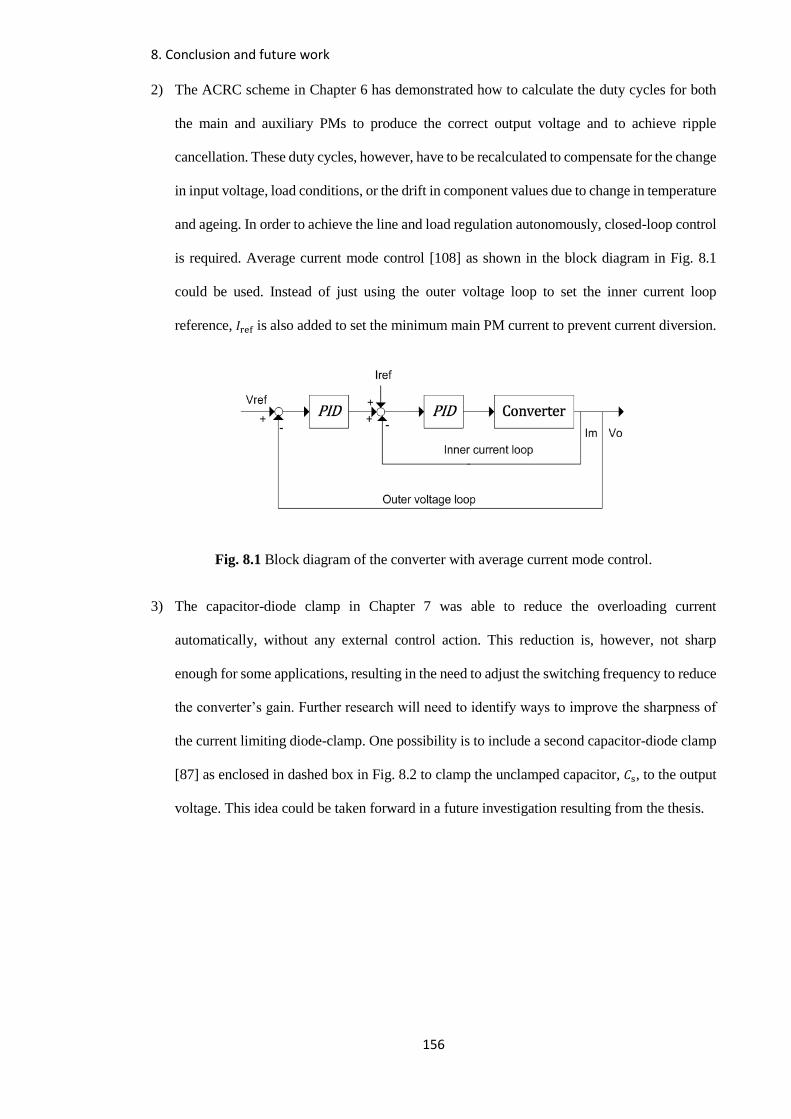
8. Conclusion and future work
156
2) The ACRC scheme in Chapter 6 has demonstrated how to calculate the duty cycles for both
the main and auxiliary PMs to produce the correct output voltage and to achieve ripple
cancellation. These duty cycles, however, have to be recalculated to compensate for the change
in input voltage, load conditions, or the drift in component values due to change in temperature
and ageing. In order to achieve the line and load regulation autonomously, closed-loop control
is required. Average current mode control [108] as shown in the block diagram in Fig. 8.1
could be used. Instead of just using the outer voltage loop to set the inner current loop
reference, 𝐼ref is also added to set the minimum main PM current to prevent current diversion.
Fig. 8.1 Block diagram of the converter with average current mode control.
3) The capacitor-diode clamp in Chapter 7 was able to reduce the overloading current
automatically, without any external control action. This reduction is, however, not sharp
enough for some applications, resulting in the need to adjust the switching frequency to reduce
the converter’s gain. Further research will need to identify ways to improve the sharpness of
the current limiting diode-clamp. One possibility is to include a second capacitor-diode clamp
[87] as enclosed in dashed box in Fig. 8.2 to clamp the unclamped capacitor, 𝐶s, to the output
voltage. This idea could be taken forward in a future investigation resulting from the thesis.

8. Conclusion and future work
157
Vi
Lp
C RlD1
Cc
D3
D2 D4
Cc
Ls Cs
Dc1
Dc2
Ds2
Ds1
ii
Second diode-clamp
S1
S2
Vo
D7D5
D8D6
T1T2
Fig. 8.2 Circuit diagram of the proposed dual capacitor-diode clamp.

158
Reference
[1] Gartner press release, October 2013. Available at:
http://www.gartner.com/newsroom/id/2610015
[2] Mohan, N., Underland, T.M., and Robbins, W.P., ‘Power Electronics: Converters,
Application, and Design, Third Edition’, John Wiley & Sons.
[3] Rashid, M.H., ‘Power Electronics Handbook, Second edition’, Academic Press.
[4] Basso, C.P., ‘Switch-Mode Power Supplies: SPICE Simulations and Practical Designs’,
McGrawHill.
[5] Worldwide DC-DC converter modules Forecasts: Power architectures, product tpes,
voltage trends, and applications, Eleventh Edition, June 2011. Available at:
http://www.prnewswire.com/news-releases/worldwide-dc-dc-converter-modules-
forecasts-power-architectures-product-types-voltage-trends-and-applications-eleventh-
edition-124765603.html
[6] World market for direct current power systems for commercial buildings to b USD 10bn
by 2020, December 2013. Available at: http://www.electronics-eetimes.com/en/world-
market-for-direct-current-power-systems-for-commercial-buildings-to-be-usd10bn-by-
2020.html?cmp_id=7&news_id=222919256&vID=209#
[7] Kamil, M., ‘Switch Mode Power Supply (SMPS) Topologies (Part I)’, Microchip Literature
DS01114A, 2007.
[8] Ridley, R., ‘The Nine Most Useful Power Topologies’, Power system Design Europe, Oct
2007, pp. 15-18.
[9] Rogers, E., ‘Understanding buck power stages in switchmode power supplies: Application
report’, TI literature number SLVA057, 1999.
[10] Rogers, E., ‘Understanding boost power stages in switchmode power supplies: Application
report’, TI literature number SLVA061, 1999.

Reference
159
[11] Rogers, E., ‘Understanding buck-boost power stages in switchmode power supplies:
Application report’, TI literature number SLVA059A, 1999.
[12] Cuk, S., Middlebrook, R.D., ‘Advances in switched-mode power conversion Part I’, IEEE
Trans. Ind. Electron., Vol.30, No.1, 1983, pp.10-19.
[13] Ridley, R., ‘Analyzing the SEPIC converter’, Power system design europe, Nov 2006,
pp. 14-18.
[14] Falin, J., ‘Designing DC/DC converters based on ZETA topology’, Texas Instruments
Incorporated analog application journal, 2Q 2010, pp. 16-21.
[15] Mammano, B., ‘Resonant mode converter topologies’, Unitrode corporation application
note, 2001.
[16] Tan, F.D., ‘The forward Converter: from the classic to the contemporary’, IEEE APEC
conf., 2002, pp. 857-863.
[17] Liu, K. W. and Lee, F. C., ‘Resonant switches-A unified approach to improve performances
of switching converters’, IEEE INTELEC conf., 1984, pp. 344-351.
[18] Takagi, M., Shimize, K., and Zaitsu, T., ‘Ultra high efficiency of 95% for DC/DC converter
- considering theoretical limitation of efficiency’, IEEE APEC conf., 2002,
pp. 735-741.
[19] Consoli, A., Testa, A., Giannetto, G., and Gennaro, F., ‘A new VRM topology for next
generation microprocessors’, IEEE PESC conf., 2001, pp. 339-344.
[20] Wei, J., and Lee, F.C., ‘Two-stage voltage regulator for laptop computer CPUs and the
corresponding advanced control schemes to improve light-load rerformance’, IEEE APEC
conf., 2004, pp. 1294-1300.
[21] Middlebrook, R.D. and Cuk, S., ‘A general unified approach to modelling switching-
converter power stages’, IEEE PESC conf., 1976, pp. 18-34.
[22] Vorperian, V., ‘Simplified analysis of PWM converters using model of PWM switch part
I: Continuous Conduction Mode’, IEEE Trans. on Aerosp. and Electron. Syst., Vol.26,
No.3, 1990, pp. 490-496.

Reference
160
[23] Sun, J., Mitchell, D.M., Greuel, M.F., Krein, P.T. and Bass, R.M., ‘Averaged modeling of
PWM converters operating in Discontinuous Conduction Mode’, IEEE Trans. Power
Electron., Vol.16, No.4, 2001, pp. 482-492.
[24] Davoudi, A., Jatskevich, J. and De Rybel, T., ‘Numerical state-space average-value
modeling of PWM DC-DC converters operating in DCM and CCM’, IEEE Trans. Power
Electron., Vol.21, No.4, 2006, pp. 1003-1012.
[25] Van Dijk, E., Spruijt, J.N., O’Sullivan, D.M. and Klaassens, H.B., ‘PWM-switch modeling
of DC-DC converters’ IEEE Trans. Power Electron., Vol.10, No.6, 1995,
pp. 659-665.
[26] Ngo, K.D.T., ‘Alternate forms of the PWM switch models’, IEEE Trans. on Aerosp. and
Electron. Syst., Vol.35, No.4, 1999, pp. 1283-1292.
[27] Lee, Y.S., ‘A systematic and unified approach to modeling switches in switch-mode power
supplies’, IEEE Trans. Ind. Electron., Vol.32, No.4, 1985, pp. 445-448.
[28] Wester, G.W. and Middlebrook, R.D., ‘Low-frequency characterization of switched dc-dc
converters’, IEEE Trans. on Aerosp. and Electron. Syst., Vol.9, No.3, 1973, pp. 376-385.
[29] Chetty, P.R.K., ‘Current injected equivalent circuit approach to modeling switching DC-
DC Converters’, IEEE Trans. on Aerosp. and Electron. Syst., Vol.17, No.6, 1981,
pp. 802-808.
[30] Umarikar, A.C., and Umanand, L., ‘Modelling of switched mode power converters using
bond graph’, IEEE Proc.-Electr. Power Appl., Vol. 152, No.1, 2005, pp. 51-60.
[31] Visser, H.R., P.P.J. van den Bosch, ‘Modelling of periodically switching networks’, IEEE
PESC conf., 1991, pp. 67-73.
[32] Lee, F.C.Y. and Yu, Y., ‘Modeling of switching regulator power stages with and without
zero-inductor-current dwell time’, IEEE Trans. Ind. Electron., Vol. 26, No.3, 1979,
pp. 142-150.

Reference
161
[33] Bartoli, M., Reatti, A. and Kazimierczuk, M.K., ‘Open Loop small-signal control-to-output
transfer function of PWM buck converter for CCM: Modeling and measurements’, IEEE
MELECON conf., 1996, pp. 1203-1205.
[34] Natarajan, K. and Qiu, J., ‘Sampled-data modeling of PWM boost converters in Continuous
and Discontinuous inductor current modes’, IEEE CCECE conf., 2006,
pp. 247-250.
[35] Luo, F.L. and Ye, H., ‘Energy factor and mathematical modelling for DC/DC converters’,
IEEE Proc.-Electr. Power Appl., Vol. 152, No.2, 2005, pp. 191-198.
[36] Maksimovic, D., ‘Computer-aided small-signal analysis based on impulse response of
DC/DC switching power converters’, IEEE Trans. Power Electron., Vol. 15, No.6, 2000,
pp. 1183-1191.
[37] Valdivia, V., Barrado, A., Lazaro, A., Fernandez, C. And Zumel, P., ‘Black-box modeling
of DC-DC converters based on transient response analysis and parametric identification
methods’, IEEE APEC conf., 2010, pp. 1131-1138.
[38] Drop, R.C. and Bishop, R., ‘Modern control systems, Tenth Edition’, Prentice Hall.
[39] Golnaraghi, F. and Kuo, B.K., ‘Automatic Control Systems, 9th Edition’, John Wiley &
sons.
[40] Astrom, K. and Hagglund, T., ‘PID controllers: theory, eesign, and tuning, 2nd Edition’,
The Instrumentation, Systems, and Automation Society.
[41] Wilkie, K.D., Foster, M.P., Stone, D.A. and Bingham, C.M., ‘Hardware-in-the-loop tuning
of a feedback controller for a buck converter using a GA’, International Symposium on
Power Electronics, Electrical Drives, Automation and Motion, 2008,
pp. 680-684.
[42] Shirazi, M., Zane, R. and Maksimovic, D., ‘An autotuning digital controller for DC-DC
power converters based on online frequency-response measurement’, IEEE Trans. Power
Electron., Vol.24, No.11, 2009, pp. 2578-2588.
Reference
162
[43] Stefanutti, W., Saggini, S., Tedeschi, E., Mattavelli, P. and Tenti, P., ‘Simplified model
reference tuning of PID regulators of digitally controlled DC-DC converters based on
crossover frequency analysis, IEEE PESC conf., 2007, pp. 785-791.
[44] Hejati, R., Eshtehardiha, S. and Poudeh, M. B., ‘Improvement of step-down converter
performance with optimum LQR and PID controller with applied genetic algorithm’,
International Conference on Power Control and Optimization, 2008, pp. 129-134.
[45] Rossiter, J.A., ‘Model-based predictive control: A practical approach’, CRC Press.
[46] Tan, S.-C., Lai, Y.M., Cheung, M.K.H. and Tse, C.K., ‘On the practical design of a sliding
mode voltage controlled buck converter’, IEEE Trans. Power Electron., Vol.20, No.2,
2005, pp. 425-437.
[47] Diaz, N.L. and Soriano, J.J., ‘Study of two control strategies based in fuzzy logic and
artificial neural network compared with an optimal control strategy applied to a buck
converter’, IEEE NAFIPS conf., 2007, pp. 313-318.
[48] Effler, S., Kelly, A., Halton, M. and Rinne, K., ‘Automated optimization of generalized
model predictive control for DC-DC converters’, IEEE PESC conf., 2008, pp. 134-139.
[49] Zhou, X., Donati, M., Amoroso, L., and Lee, F.C., ‘Improved light-load efficiency for
synchronous rectifier voltage regulator module’, IEEE Trans. Power Electron., Vol.15, No.
5, 2000, pp. 826-834.
[50] Sahu, B., and Rincon-Mora, G.A., ‘An accurate, low-voltage, CMOS switching power
supply with adaptive on-time pulse-frequency modulation (PFM) control’, IEEE Trans.
Circuit and Systems., Vol.54, No.2, 2007, pp. 312-321.
[51] Al-Hoor, W., Abu-Qahouq, J.A., Huang, L., Mikhael, W.B., and Batarseh, H., ‘Adaptive
digital controller and design considerations for a variable switching frequency voltage
regulator’, IEEE Trans. Power Electron., Vol.24, No.11, 2009, pp. 2589-2602.
[52] Tsai, J.-C., Huang, T.-Y., Lai, W.-W., and Chen, K.-H., ‘Dual modulation technique for
high efficiency in high-switching buck converters over a wide load range’, IEEE Trans.
Circuit and Systems., Vol.58, No.7, 2011, pp. 1671-1680.
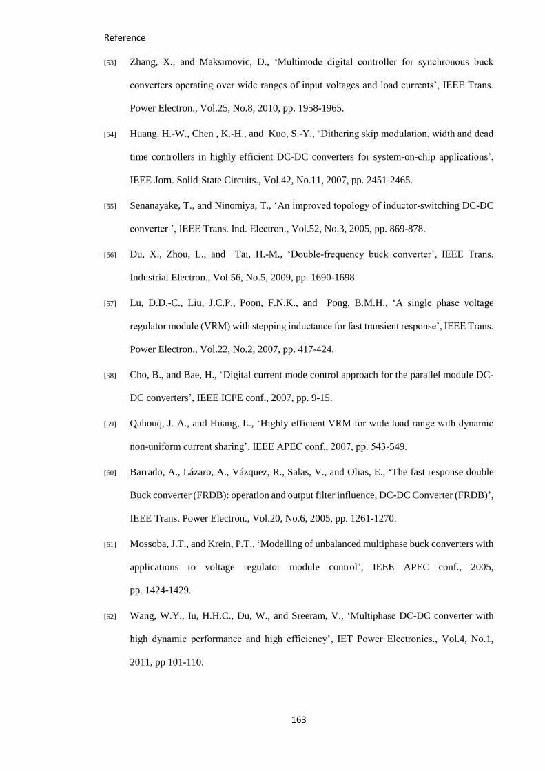
Reference
163
[53] Zhang, X., and Maksimovic, D., ‘Multimode digital controller for synchronous buck
converters operating over wide ranges of input voltages and load currents’, IEEE Trans.
Power Electron., Vol.25, No.8, 2010, pp. 1958-1965.
[54] Huang, H.-W., Chen , K.-H., and Kuo, S.-Y., ‘Dithering skip modulation, width and dead
time controllers in highly efficient DC-DC converters for system-on-chip applications’,
IEEE Jorn. Solid-State Circuits., Vol.42, No.11, 2007, pp. 2451-2465.
[55] Senanayake, T., and Ninomiya, T., ‘An improved topology of inductor-switching DC-DC
converter ’, IEEE Trans. Ind. Electron., Vol.52, No.3, 2005, pp. 869-878.
[56] Du, X., Zhou, L., and Tai, H.-M., ‘Double-frequency buck converter’, IEEE Trans.
Industrial Electron., Vol.56, No.5, 2009, pp. 1690-1698.
[57] Lu, D.D.-C., Liu, J.C.P., Poon, F.N.K., and Pong, B.M.H., ‘A single phase voltage
regulator module (VRM) with stepping inductance for fast transient response’, IEEE Trans.
Power Electron., Vol.22, No.2, 2007, pp. 417-424.
[58] Cho, B., and Bae, H., ‘Digital current mode control approach for the parallel module DC-
DC converters’, IEEE ICPE conf., 2007, pp. 9-15.
[59] Qahouq, J. A., and Huang, L., ‘Highly efficient VRM for wide load range with dynamic
non-uniform current sharing’. IEEE APEC conf., 2007, pp. 543-549.
[60] Barrado, A., Lázaro, A., Vázquez, R., Salas, V., and Olias, E., ‘The fast response double
Buck converter (FRDB): operation and output filter influence, DC-DC Converter (FRDB)’,
IEEE Trans. Power Electron., Vol.20, No.6, 2005, pp. 1261-1270.
[61] Mossoba, J.T., and Krein, P.T., ‘Modelling of unbalanced multiphase buck converters with
applications to voltage regulator module control’, IEEE APEC conf., 2005,
pp. 1424-1429.
[62] Wang, W.Y., Iu, H.H.C., Du, W., and Sreeram, V., ‘Multiphase DC-DC converter with
high dynamic performance and high efficiency’, IET Power Electronics., Vol.4, No.1,
2011, pp 101-110.

Reference
164
[63] Poon, N.K., Liu, J.C.P., Tse, C.K., and Pong, M.H., ‘Techniques for Input ripple current
cancellation: classification and implementation [in SMPS]’ IEEE Trans. Power Electron.,
Vol.15, No.6, 2000, pp. 1144-1152.
[64] Hamill, D.C., and Krein, P.T., ‘A `zero' ripple technique applicable to any DC converter’
IEEE PESC conf., 1999, pp. 1165-1171.
[65] Hamill, D.C., ‘An efficient active ripple filter for use in DC-DC conversion’, IEEE Trans.
on Aerosp. and Electron. Syst., Vol.32, No.3, 1996, pp. 1077-1084.
[66] Zhu, M., Perreault, D.J., Caliskan, V., Neugebauer, T.C., Guttowski, S., and Kassakian,
J.G., ‘Design and evaluation of feedforward active ripple filters’, IEEE Trans. Power
Electron., Vol.20, No.2, 2005, pp. 276-285.
[67] Kapun, A., Milanovic, M., and Korelic, J., ‘Voltage Ripple cancellation in buck converter
based on hybrid structured connection’. IEEE EPE-PEMC Conf., 2006, pp 112-117.
[68] Ostroznik, S., Dajec, P., and Zajec, P., ‘A study of a hybrid filter’, IEEE Trans. Ind.
Electron., Vol.57, No.3, 2010, pp.935-942.
[69] Wibben, J., and Harjani, R., ‘A high-efficiency DC-DC converter using 2 nH integrated
inductor’, IEEE Trans. Solid-State Circuits., Vol.43, No.4, 2008, pp.844-854.
[70] Shahin, A., Gavagsaz-Ghoachani, R., Martin, J.-P., Piefederici, s., Davat, B., and Meibody-
Tabar, F., ‘New method to filter HF current ripples generated by current-fed DC/DC
converters’, IEEE Trans. Power Electron., Vol.26, No.12, 2011, pp. 3832-3842.
[71] Pan, C.-T., Liang, S.-K., and Lai, C.-M., ‘A zero input current ripple boost converter for
fuel cell applications by using a mirror ripple circuit’, IEEE IPEMC conf., 2009,
pp.787-793.
[72] Rosas, J., Mancilla-David, F., Mayo-Maldonado, J., Gonzalez Lopez, J., Torres-Espinosa,
H., and Valdez-Resendiz, J., ‘A transformer-less high–gain boost converter with input
current ripple cancelation at a selectable duty cycle’ IEEE Trans. Ind. Electron., Vol.60,
No.10, 2013, pp.4492-4499.

Reference
165
[73] Steigerwald, R. L., ‘A comparison of half-bridge resonant converter topologies’, IEEE
Trans. Power Electron., Vol.3, No.2, 1988, pp. 174-182.
[74] Batarseh, I., ‘Resonant converter topologies with three and four energy storage elements’,
IEEE Trans. Power Electron., Vol.9, No.1, 1994, pp. 64-73.
[75] ‘An introduction to LLC resonant half-bridge Converter’, ST Application note AN2644
(rev 2), 2008.
[76] Hu, H., Fang, X., Chen, F., Shen, Z. J. and Batarseh, I., ‘A modified high
efficiency LLC converter with two transformers for wide input voltage range applications’,
IEEE Trans. Power Electron., Vol.28, No.4, 2013, pp. 1946-1960.
[77] Kim, B. –C., Park, K. –B., Kim, C.-E., Lee, B. -H., and Moon, G. –W., ‘LLC resonant
converter with adaptive link-voltage variation for a high-power-density adapter’, IEEE
Trans. Power Electron., Vol.25, No.9, 2012, pp. 2248-2252.
[78] Lee, I. –O. and Moon, G. –W., ‘Analysis and design of a three level LLC series resonant
converter for high- and wide-input-voltage applications’, IEEE Trans. Power Electron.,
Vol.27, No.6, 2012, pp. 2966-2979.
[79] Fang, X., Hu, H., Chen, F., Somani, U., Auadisian, E., Shen, J., and Batarseh,
I., ‘Efficiency-oriented optimal design of the LLC resonan converter
based on peak gain placement ’, IEEE Trans. Power Electron., Vol.28, No.5, 2013, pp.
2285-2296.
[80] Beiranvand, R., Rashidian, B., Zolghadri, M. R., and Alavi, S. M. H., ‘A design procedure
for optimizing the LLC resonant converter as a wide output range voltage source’, IEEE
Trans. Power Electron., Vol.27, No.8, 2012, pp.3749-3763.
[81] Yang, B., Lee, F. C., and Concannon, M., ‘Over current protection methods for LLC
resonant converter’, IEEE APEC conf., 2003, pp. 605-609.
[82] Yang, B., ‘Topology Investigation for Front End DC/DC Power Conversion for Distributed
Power System’, PhD thesis, Virginia Polytechnic Institute and Stage University, 2003.

Reference
166
[83] Gould, C. R., Bingham, C. M., Foster, M. P., and Stone, D. A., ‘CLL resonant converters
with output short-circuit protection strategy’, IEE Electric Power Applications, Vol.152,
No.5, 2005, pp. 1296-1306.
[84] Hu, Z., Qiu, Y., Wang, L., and Liu, Y. –F., ‘An interleaved LLC resonant converter
operating at constant switching frequency’, in Proc. IEEE ECCE, 2012, pp. 3541-3548.
[85] Alonso, J. M., Perdigao, S., Vaquero, D. G., Calleja, A. J., and Saraiva, E. S., ‘Analysis,
design, and experimentation on constant frequency DC-DC resonant converters with
magnetic control’, IEEE Trans. Power Electron., Vol.27, No.3, 2012, pp. 1369-1382.
[86] Zhao, C., Xie, X., Wu, X., Zhang, J., and Qian, Z., ‘The design consideration comparisons
of two clamping modes over current protection for LLC converter’, IEEE INTELEC conf.,
2006, pp. 1-5.
[87] Xie, X., Zhang, J., Zhao, C., Zhao, Z., and Qian, Z., ‘Analysis and optimization of LLC
resonant converter with a novel over-current protection circuit’, IEEE Trans. Power
Electron., Vol.22, No.2, 2007, pp. 435-443.
[88] Foster, M. P., and Stone, D. A., ‘Describing function model of series resonant inverter with
current limiting diode-clamp’, IET Electron. Lett., Vol.47, No.25, 2011,
pp.1363-1364.
[89] Franklin, G.F.; Powell, J.D.; Workman, M.: Digital Control of Dynamics Systems, third
ed. Addison-Wesley. 1998.
[90] L. Balogh, ‘Design and application guide for high speed MOSFET gate drive circuits’,
Proc. Power supply design seminar (SEM 1400), 2001, Texas instruments.
[91] Texas instruments datesheet, INA129 precision, lowpower instrumentation amplifiers,
2005. Available at: http://www.ti.com/lit/ds/sbos051b/sbos051b.pdf.
[92] Microchip datasheet, dsPIC33FJ06GS101/X02 and dsPIC33FJ16GSX02/X04, 2008-2012.
Available at: http://ww1.microchip.com/downloads/en/DeviceDoc/70318F.pdf
[93] Microchip PICkit 2 programmer/debugger user’s guide, 2008. Available at:
http://ww1.microchip.com/downloads/en/DeviceDoc/51553E.pdf.

Reference
167
[94] Texas Instruments datasheet, LM3754 Scalable 2-Phase Synchronous Buck Controller w/
FET (Rev.A), Feb, 2012. Available at: http://www.ti.com/product/lm3754
[95] Ridley, R.B.: Power Supply Design Volume 1: Control. Ridley Design. 2012.
[96] Midya, P., Krein, P.T., and Greuel, M.F. ‘Seneorless current mode control-An observer-
based technique for DC-DC converters’, IEEE Tran. Power Electron., Vol.16, No.4, 2001,
pp. 522-526.
[97] Wang, X., Li, Q., and Batarseh, I., ‘Transient response improvement in isolated DC-DC
converter with current injection circuit’ IEEE APEC conf., 2005, pp. 706-710.
[98] An Introduction to Genetic Algorithms (Complex Adaptive Systems), new edition. MIT
press. 1998.
[99] Fleming, P: Genetic Algorithm toolbox for use with Matlab.
[100] Microchip MPLAB ICD 3 in-circuit debugger user’s guide, 2010, Available at:
http://ww1.microchip.com/downloads/en/DeviceDoc/51766B.pdf.
[101] Lynch, B., and Hesse, K.: ‘Under the Hood oa Low-Voltage DC/DC Converters’, Texas
Instruments Seminar. [Online]. Available: http://www.ti.com/seminar.
[102] Huang, H., ‘Designing an LLC resonant half-bridge power converter’, Texas Instruments
2010-2011 power supply design seminar, SEM1900, 2011.
[103] Foster, M. P., Gould, C. R., Gilbert, A.J., Stone, D. A. and Bingham, C. M., ‘Analysis of
CLL voltage-output resonant converters using describing functions’, IEEE Trans. Power
Electron., Vol.23, No.4, 2008, pp. 1772-1781.
[104] Feng, W., Lee, F. C., and Mattavelli, P., ‘Optimal trajectory control of burst mode for LLC
resonant converter’, IEEE Tran. Power Electron., Vol.28, No.1, 2013, pp. 457-466.
[105] Oeder, C., Bucher, A., Stahl, J., and Duerbaum, T., ‘A comparison of different design
methods for the multiresonant LLC converter with capacitive output filter’, in Proc. IEEE
COMPEL conf., 2010, pp. 1-7.
[106] James, G., Advanced modern engineering mathematics, 3 edition. Prentice hall, 2004.

Reference
168
[107] Foster, M. P., Stone, D. A. and Bingham, C. M., ‘An automated design methodology for
LLC resonant converters using a genetic algorithm’, in Proc. Conference for Power
Electronics, Intelligent Motion, Power Quality (PCIM), Nuremberg, Germany, 2009.
[108] Dixon, L.: ‘Average current mode control of switching power supplies’, Unitrode Power
Design Seminar, SEM-700, 1990.
[109] Patterson, D.J.: ‘An efficiency optimized controller for a bruchless DC machine, and loss
measurement using a simple calorimetric technique’ IEEE PESC conf., 1995, pp. 22-27.
[110] Platinum and Nickel thin-film chip sensor: http://www.farnell.com/datasheets/57422.pdf
[111] RedLab 1208FS user’s guide, 2008. Available at:
http://www.meilhaus.org/downloadserver/redlab/manual/RedLab%201208FS_en.pdf.
[P1] C.-W. Tsang, M.P. Foster and D.A. Stone, ‘Parallel buck converter with non-identical
power module for improved transient efficiency’, Power Control and Intelligent Motion
(PCIM) 2013.
[P2] C.-W. Tsang, M.P. Foster and D.A. Stone, ‘New design approach for higher energy
efficiency with parallel converter’, IET PEMD conf., 2012, pp 1-6.
[P3] C.-W. Tsang, M.P. Foster, D.A. Stone and D. Gladwin, ‘Active current ripple
cancellation in parallel connected buck converter modules’, IET Power Electron., 2013,
6, pp 721-731.
[P4] C.-W. Tsang, M.P. Foster, D.A. Stone and D. Gladwin, (In Press) ‘Analysis and design
of the LLC resonant converter with capacitor-diode clamp current-limiting’, IEEE Trans.
Power Electron., accepted April 2014.
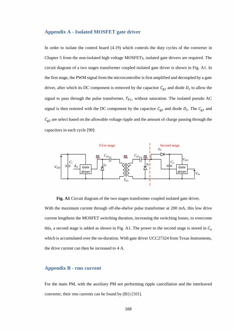
169
Appendix A - Isolated MOSFET gate driver
In order to isolate the control board (4.19) which controls the duty cycles of the converter in
Chapter 5 from the non-isolated high voltage MOSFETs, isolated gate drivers are required. The
circuit diagram of a two stages transformer coupled isolated gate driver is shown in Fig. A1. In
the first stage, the PWM signal from the microcontroller is first amplified and decoupled by a gate
driver, after which its DC component is removed by the capacitor 𝐶g1 and diode 𝐷1 to allow the
signal to pass through the pulse transformer, 𝑇P1, without saturation. The isolated pseudo AC
signal is then restored with the DC component by the capacitor 𝐶g2 and diode 𝐷2. The 𝐶g1 and
𝐶g2 are select based on the allowable voltage ripple and the amount of charge passing through the
capacitors in each cycle [90]:
VS1
D3
D1D2
Gate driver
Cg2Cg1
Co
VDD
Gate driver
Ci
VDDδm
First stage Second stage
TP1
Fig. A1 Circuit diagram of the two stages transformer coupled isolated gate driver.
With the maximum current through off-the-shelve pulse transformer at 200 mA, this low drive
current lengthens the MOSFET switching duration, increasing the switching losses, to overcome
this, a second stage is added as shown in Fig. A1. The power to the second stage is stored in 𝐶o
which is accumulated over the on-duration. With gate driver UCC27324 from Texas Instruments,
the drive current can then be increased to 4 A.
Appendix B - rms current
For the main PM, with the auxiliary PM not performing ripple cancellation and the interleaved
converter, their rms currents can be found by (B1) [101].
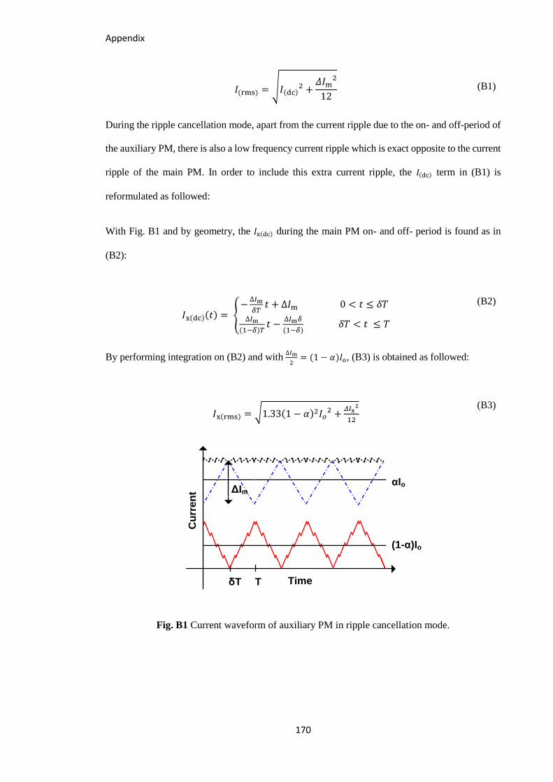
Appendix
170
𝐼(rms) = √𝐼(dc)2 +
𝛥𝐼m2
12 (B1)
During the ripple cancellation mode, apart from the current ripple due to the on- and off-period of
the auxiliary PM, there is also a low frequency current ripple which is exact opposite to the current
ripple of the main PM. In order to include this extra current ripple, the 𝐼(dc) term in (B1) is
reformulated as followed:
With Fig. B1 and by geometry, the 𝐼x(dc) during the main PM on- and off- period is found as in
(B2):
𝐼x(dc)(𝑡) = {−∆𝐼m
𝛿𝑇𝑡 + ∆𝐼m 0 < 𝑡 ≤ 𝛿𝑇
∆𝐼m
(1−𝛿)𝑇𝑡 −
∆𝐼m𝛿
(1−𝛿) 𝛿𝑇 < 𝑡 ≤ 𝑇
(B2)
By performing integration on (B2) and with ∆𝐼m
2= (1 − 𝛼)𝐼o, (B3) is obtained as followed:
𝐼x(rms) = √1.33(1 − 𝛼)2𝐼𝑜
2 +𝛥𝐼x
2
12
(B3)
Cu
rre
nt
αIo
(1-α)Io
δT T Time
ΔIm
Fig. B1 Current waveform of auxiliary PM in ripple cancellation mode.

Appendix
171
Appendix C - Calorimeter for efficiency measurement
Due to the switching nature and high efficiency of SMPCs, measuring the difference between the
input and output powers through their corresponded voltages and currents can lead to a high
margin of error. Instead, the calorimetric method measures the losses through the heat generated
by the converter to allow higher measurement accuracy to be achieved.
The calorimetry used in this thesis is the indirect calorimetric method detailed in [109]. In this
method, a well insulated box is built and the internal temperature rise is calibrated against the
known power losses generated by a power resistor, to produce a calibration curve as in Fig. C3
(a) and (b). To measure the power losses of the converter, the power resistor is replaced by the
converter and set to operate at the desired operating condition. The temperature rise generated by
the converter is measured and compared against a calibration curve to determine the losses at the
tested operating condition.
Two bespoke calorimeter were built for this thesis:
a large one with the internal diameters of 250 mm x 250 mm x 250 mm with a layer of 22
mm thick expanded polystyrene sheets. This is used for the high power converter in Chapter
5.
a small one with the internal diameters of 150 mm x 150 mm x 150 mm with three layers of
10 mm thick expanded polystyrene sheets as shown in Fig. C1.
Holes were added for wires; the hole were then sealed with PVA glue. One possible source of
error is heat conducted out of the box through the connection wires, but the wiring was kept
constant between tests to try to include this in the calibration curves.
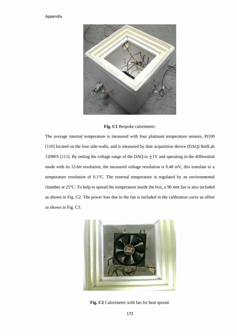
Appendix
172
Fig. C1 Bespoke calorimeter.
The average internal temperature is measured with four platinum temperature sensors, Pt100
[110] located on the four side-walls, and is measured by date acquisition device (DAQ) RedLab
1208FS [111]. By setting the voltage range of the DAQ to ±1V and operating in the differential
mode with its 12-bit resolution, the measured voltage resolution is 0.48 mV, this translate to a
temperature resolution of 0.1°C. The external temperature is regulated by an environmental
chamber at 25°C. To help to spread the temperature inside the box, a 90 mm fan is also included
as shown in Fig. C2. The power loss due to the fan is included in the calibration curve as offset
as shown in Fig. C3.
Fig. C2 Calorimeter with fan for heat spread.

Appendix
173
The calibrating curve for this setup is shown in Fig. C3.
(a)
(b)
Fig. C3 Calibration curves. (a) small box (b) large box.
0 0.5 1 1.5 2 2.50
2
4
6
8
10
12
14
16
Power (W)
Tem
pera
ture
ris
e (C
)
0 5 10 15 200
5
10
15
20
25
30
Power (W)
Tem
pera
ture
ris
e (C
)