Static switched output feedback stabilization for linear discrete-time switched systems
Upload
khangminh22Category
view
0download
0
AN ABSTRACT OF THE THESIS OF
Vineet R. Dalai for the degree of Master of Science in Electrical and Computer
Engineering presented on June 16, 1993.
Title: A Switched-Current Bandpass Delta-Sigma Modulator
Abstract approved:Richard Schreier
Oversampled delta-sigma (AZ) data converters have become the method of choice
for high-resolution conversion of low frequency signals. Such converters employ noise-
shaping techniques and exhibit high linearity and reduced anti-aliasing filter complexity
compared to Nyquist rate converters. Bandpass AZ converters generalize the concept of
noise-shaping to allow high-resolution conversion of high frequency narrowband signals.
Such converters are well suited for use in AM radio receivers, cellular communication,
spectrum analyzers and any special purpose instrumentation employing narrow band
sources.
Switched-current (SI) circuit design is a relatively new technique for analog signal
processing. In contrast to other signal processing techniques such as the switched-capacitor
(SC) circuits which are traditionally used to implement AZ modulators, SI circuits
represent signals by currents rather than voltages. The principal advantage of SI circuits is
that they are fully compatible with the standard digital CMOS VLSI technologies which
are needed to implement the digital portion of a AI A/D.
This thesis applies the SI technique to the design of oversampled bandpass AI
modulators. The intent of this work is to demonstrate that the SI technique is viable in this
Redacted for Privacy
context. To accomplish this a new SI architecture which implements pseudo N-path
structures is required. The thesis develops a differential pseudo 2-path resonator capable of
being clocked at 10 MHz to address this need. Not only does this new circuit demonstrate
that SI techniques can be used to make bandpass Si converters, but the high speed
operation of the circuit indicates that an SI implementation is better suited to high
frequency operation than a more conventional SC implementation.
A Switched-Current Bandpass Delta-Sigma Modulator
by
Vineet R. Dalal
A THESIS
submitted to
Oregon State University
in partial fulfillment of
the requirements for thedegree of
Master of Science
Completed June 16, 1993
Commencement June 1994

APPROVED:
Professor of Ele g in charge of major
Head of Departm t of Electrical & Computer Engineering
Dean of Graduate Sc
Date thesis is presented
Typed by
June 16, 1993
Vineet R. Dalai
Redacted for Privacy
Redacted for Privacy
Redacted for Privacy

ACKNOWLEDGEMENTS
To my parents: thank-you for everything that you have done for me. Without your
love, support and constant encouragement I would not be where I am today.
With the upmost respect and gratitude, I wish to thank my advisor Dr. Richard
Schreier for introducing me to the wonderful world of delta-sigma modulation and
switched-currents. Without his able guidance, unendless enthusiasm and constant
encouragement this work would not have been possible.
I would also like to thank the members of my graduate committee for their time and
effort: Dr. Gabor Temes, Dr. Shih-Lien Lu and Dr. Milo Koretsky.
Thanks to P. V. S. Srinivas for helping with the clock generation and the IC layout.
Thanks to my friends and colleagues Gin Rangan and Karthik Ramamurthy for
their interest in my work. Thanks also for the many intelligent and some not so intelligent
conversations that I had the honor of sharing with them.
To the rest of the gang: Jyoti Bhaskar, Alna Chandnani, Anupama Deshmukh,
Jayant Bhaskar, Vishakhadatta Diwakar and Sridhar Jasti. Thanks for keeping me sane.

TABLE OF CONTENTS
CHAPTER 1 INTRODUCTION 1
1.1 Motivation 1
1.2 Outline of the Thesis 2
CHAPTER 2 PRIOR ART 3
2.1 Delta-Sigma in a Nutshell 3
2.2 Bandpass Delta-Sigma Data Converters 5
2.3 Switched-Current Circuits 8
2.4 Summary 12
CHAPTER 3 THE BANDPASS MODULATOR 13
3.1 N-path Structures 13
3.2 The Modulator 15
3.3 The 2-path Resonator 16
CHAPTER 4 PRACTICAL ISSUES 23
4.1 The Regulated Cascode Current Memory Cell 23
4.2 The Differential SI 2-Path Resonator 32
4.3 The Current Comparator 36
4.4 The SI Digital to Analog Converter 38
4.5 Clock Generation 39
4.6 The Second-Order Bandpass Modulator 40
4.7 Layout Considerations 42
CHAPTER 5 CONCLUSIONS 44
5.1 Summary 44
5.2 Future Work 45
BIBLIOGRAPHY 46
APPENDICES
APPENDIX A
APPENDIX B
48
51

LIST OF FIGURES
Fig. 2.1 A first-order delta-sigma A/D converter.
Fig. 2.2 A delta-sigma modulator based A/D converter. 5
Fig. 2.3 Comparison of pole and zero placements of error transfer functionsfor (a) a second-order lowpass modulator and (b) a fourth-orderbandpass modulator. 6
Fig. 2.4 The cascade of resonators structure. 8
Fig. 2.5 A current track and hold circuit. 9
Fig. 2.6 A dynamic current copier. 10
Fig. 2.7 The regulated cascode current memory cell. 11
Fig. 3.1 A two-integrator loop. 13
Fig. 3.2 A 2-path circuit using a two-phase clock with each block clocked at
f12. 15
Fig. 3.3 The eight-order bandpass modulator. 16
Fig. 3.4 An SNR versus input power curve for an eight-order modulator. 16
Fig. 3.5 Block level model of a current memory cell (CMC). 17
Fig. 3.6 Block-level SI implementation of the bandpass resonator. 18
Fig. 3.7 Graphical illustration of the operation of the bandpass resonator. 19
Fig. 3.8 The globally differential scheme. 20
Fig. 3.9 The locally differential scheme. 20
Fig. 3.10 A differential SI bandpass resonator employing a common-modenulling scheme. 21
Fig. 4.1 A regulatory mechanism for the dynamic current copier. 23
Fig. 4.2 A small-signal model for the circuit in Figure 4.1. 24
LIST OF FIGURES

LIST OF FIGURES (continued)
Fig. 4.3 The regulated cascode current memory cell. 25
Fig. 4.4 Small-signal model of the regulated cascode current memory cellfor the settling time analysis. 25
Fig. 4.5 The regulated cascode current memory cell. 27
Fig. 4.6 Regulation of the drain voltage Vdsi of transistor M1, independentof the variations in the output voltage Vd3. 31
Fig. 4.7 Current versus time curves for a 5MHz, 2001.tA (peak to peak)squarewave input. 32
Fig. 4.8 Current versus time curves for a 1MHz, 20011A sinusoidal input. 33
Fig. 4.9 A differential switched-current 2-path resonator with improvedcommon-mode nulling. 34
Fig. 4.10 Impulse response of a single ended switched-current 2-pathresonator. 35
Fig. 4.11 Impulse response of a differential switched-current 2-path
resonator. 35
Fig.4.12 Operation of the common-mode nulling mechanism during phases
1 and 2. 37
Fig.4.13 A current comparator. 38
Fig. 4.14 A 1-bit differential switched-current D/A converter. 38
Fig. 4.15 Logic circuit for generation of clock signals 1, 2, I ', 2', /am and
2cmn 39
Fig. 4.16 Logic circuit for generation of clock signals A, B and C. 40
Fig. 4.17 Clock waveforms for the 2-path resonator. 41
Fig. 4.18 A second-order bandpass modulator. 42

A Switched-Current Bandpass Delta-Sigma Modulator
Chapter 1. Introduction
This thesis examines the feasibility of using the switched-current technique to
implement oversampled bandpass delta-sigma (SE) analog-digital data converters. Such
converters exhibit potential for performing high-resolution data conversion of narrowband
high frequency signals. Existing switched-current topologies are investigated and new
structures are developed for the implementation of such data converters.
1.1 Motivation
Signals in the real world are analog in nature. However, digital signals are more
amenable to processing with integrated circuits than are analog signals. This necessitates
transformation of the signal from an analog form to a digital form. This transformation is
performed by an analog-to-digital (A/D) converter, which ideally converts a continuous-
time analog signal into a digital signal containing all the information present in the original
signal.
Oversampled delta-sigma (SE) A/D converters have become the method of choice
for high-resolution conversion of low frequency signals and so are ideally suited for use in
audio applications. These converters employ noise-shaping techniques and exhibit high
linearity, high tolerance to circuit imperfections and reduced anti-aliasing filter complexity
compared to Nyquist rate converters.
The A/D conversion of high frequency signals, such as those encountered in video
and radio applications, is quite demanding and until now could only be performed by
2
Nyquist-rate A/D converters. The advantages of the AI technique in such applications is
the primary motivation for the development of bandpass AZ data converters. Bandpass AI
A/D converters retain many of the advantages of traditional AZ converters, while
providing the means to perform high-resolution conversion of narrow-band signals at high
frequencies.
The most common approach to realizing AI modulators is with switched-capacitor
(SC) circuits. While switched-capacitor modulators achieve high resolution, they require
highly linear capacitors and so many mixed signal integrated circuits use a process with
additional steps to make the linear capacitors. In a strictly digital integrated circuit these
steps are not needed. Thus switched-capacitor circuits add expense to the process
development and to the wafer costs of mixed-signal integrated circuits. Switched-current
(SI) circuits provide an alternative to SC circuits. In contrast to SC circuits, SI circuits
represent signals by currents rather than voltages. The principal advantage of switched-
current circuits is that they do not require linear capacitors and hence the resulting circuits
are fully compatible with standard digital CMOS VLSI technologies.
1.2 Outline of the Thesis
Chapter 2 provides the reader with the necessary background information on
bandpass delta-sigma modulation. In addition, switched-current circuits are introduced and
existing topologies and structures are explained in more detail. Chapter 3 describes the
implementation of the modulator from a theoretical standpoint and Chapter 4 deals with
more practical concerns involved in circuit design and layout. Chapter 5 concludes the
thesis and gives directions for future work.

3
Chapter 2. Prior Art
This chapter reviews the state-of-the-art for bandpass delta-sigma converters and
switched-current circuits.
2.1 Delta-Sigma in a Nutshell
Oversampling techniques are based on sampling the input signal at a rate much
greater than the Nyquist rate, and have gained acceptance since they allow high-resolution
conversion while providing high tolerance to circuit imperfections. The most popular
approach to oversampling is delta-sigma (AE) modulation, which by feeding back the
quantized signal produces a greater reduction in quantization noise than would occur
through oversampling alone. To understand how this is possible, consider the first-order
oversampled AI A/D converter shown in Figure 2.1. The modulator consists of an analog
integrator, a single-bit A/D converter, or quantizer, and a feedback path comprising a
single-bit D/A converter. Such an analog feedback loop around a low-resolution quantizer
has the ability to shape the spectrum of the quantization noise away from an arbitrary
passband [1]. The high degree to which this is feasible has made delta-sigma the premier
A/D technique for narrowband signals.
x
Figure 2.1: A first-order delta-sigma A/D converter.
Decimator
ADCOutput

Referring to Figure 2.1, the output of the modulator is given by
Y(z) = X (z) +E(z),
where
,--i'X(z) = , [U(z) Y(z)J .
(1 -z i)
Multiplying Eq. (2.1) by (1 z-1) yields
(1 -z-1) Y(z) = (1 -z-1)X(z) + (1 -z-1)E(z)
(1 -z-1) Y(z) = z -1 [U(z) V(z)] + (1 -z-1)E(z) .
So that
Y(z) = z- 1 U(z) + (1 -z-1)E(z) .
(2.1)
(2.2)
(2.3)
(2.4)
(2.5)
4
From the above relationship it is apparent that the output is just a delayed version
of the input plus the quantization noise filtered by the noise transfer function (1 z-1).
Thus the first-order modulator nulls the quantization noise at low frequencies and so
preserves the low frequency content of the input u. Applying a digital lowpass filter to y
removes the bulk of the quantization noise and yields a high-resolution digital
representation of the input as shown in Figure 2.2. It is worthwhile to note that the use of
single-bit quantization makes the modulator immune to differential nonlinearities. With a
single-bit quantizer, the only possible errors are gain and offset errors. There is no
differential nonlinearity. Delta-sigma modulation thus offers the means to make inherently
linear analog-digital and digital-analog data converters.
This approach can be extended to higher order modulators. More specifically, the
output of an Lth-order AI modulator is

Y (z) = z-1 U (z) +D (z)
(1-z-1)LE(z)(2.6)
5
where D(z) is chosen to ensure modulator stability. One of the problems faced in the use of
AE modulators is that the clock frequency must be many times higher than the upper
frequency of interest. That is the oversampling ratio must be large. For high frequency
signals this is unpractical. The need for a high oversampling ratio can be alleviated by
using higher-order modulators, making high-frequency operation feasible. Adopting a
higher-order structure also suppresses the limit-cycle tones that are present in the first-
order modulator.
2.2 Bandpass Delta-Sigma Data Converters
The previous section explained how quantization noise can be suppressed in a
narrow band around DC by placing the noise transfer function zeros near 6.) = 0 . This
concept of noise shaping can be extended to the bandpass case, wherein the noise transfer
function zeros are placed at some other frequency, coo* 0 [5] [10]. The quantization noise
is thereby suppressed in a narrow band of frequency centered at coo so that the output signal
is an accurate digital representation of the input signal in this narrow band. Figure 2.3
AEanalog Modulator
y/1 bit @fs
LowpassFilter &Decimator
/ ow digital output
n bits @ fN
kitgnal noiseN uist-ratePC
fd2 f.9; hi2 fd2
Figure 2.2:. A delta-sigma modulator based A/D converter.

6
Lowpass Modulator
a
Bandpass Modulator
Figure 2.3: Comparison of pole and zero placements of error transfer functionsfor (a) a second-order lowpass modulator and (b) a fourth-order bandpassmodulator.
illustrates the pole and zero placement of the noise transfer functions for lowpass and
bandpass delta-sigma modulators. For narrow-band signals away from DC, the noise
shaping of the bandpass AI modulator results in high signal to noise (SNR) at much lower
sampling rates than would be required by a lowpass AI converter for the same signal, since
a high oversampling ratio (OSR) can be achieved without a high ratio of sampling to center
frequency. The OSR is defined as one half the sampling rate divided by the width of the
band of interest. Thus a center frequency of n/2 with a bandwidth of it corresponds to an
oversampling ratio of one. Bandpass AI A/D converters are well suited for use in the
front-end of AM radio receivers, allowing direct conversion to digital at either intermediate
or radio frequency. An early conversion to digital results in a more robust system and
provides opportunities for dealing with the multitude of standards present in commercial
AM stereo broadcasting. Other applications include cellular radio, spectrum analyzers and
any special purpose instrumentation employing narrow band sources.
Current state of the art circuits include a fourth-order modulator by Jantzi et al. [61
for bandpass signals centered at 455 kHz with 10 kHz bandwidth, numbers quite typical of
7
AM broadcasting. The modulator is clocked at 1.82 MHz and realizes an SNR of 63 dB.
The modulator was implemented by modifying a commercial digital-audio delta-sigma
converter and is the first reported fully monolithic implementation of bandpass noise
shaping. Another design by Troster et al. [14], converts bandpass signals centered at 6.5
MHz with 200 kHz bandwidth. The modulator is implemented on a 1.2µm/7 GHz
BiCMOS analog/digital array, and achieves an SNR of 55 dB. A more recent
implementation by Longo et al. [7] achieves 15 bit dynamic range over a 30 kHz bandwidth
centered at 1.8 MHz using a 7.2 MHz sampling frequency and operating on a single 5V
supply.
Lowpass modulators are normally realized using the cascade-of-resonators
structure, illustrated in Figure 2.4. The performance of the Al modulator depends heavily
on the accuracy of the noise transfer function (NTF) zeros, which in turn are determined by
the y coefficients. In lowpass modulators, these coefficients are very close to zero and
small percentage errors in the yi do not significantly affect the performance of the
modulator.
In bandpass modulators, the y coefficients are on the order of unity and small errors
can produce significant effects. For the component errors to have only a marginal effect,
the tolerance on the yi must be approximately 1/R, where R is the oversampling ratio. For
narrowband applications, R can be as large as 1000 and hence the component precision
required to achieve accurate NTF zero placement can be excessive. In such cases, using an
N-path structure is more practical.
However, N-path circuits have their own set of problems. Clock feedthrough can
cause noise peaks in the center of the passband. Also mismatch between the paths can cause
out-of-band quantization noise to mix into the signal band and degrade the SNR. These
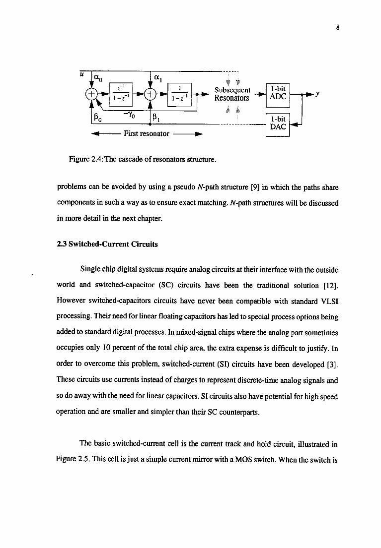
1
1 -zSubsequent 1-bitResonators ADC
First resonator
Figure 2.4: The cascade of resonators structure.
1-bit Fe...DAC
ND Y
8
problems can be avoided by using a pseudo N-path structure [9] in which the paths share
components in such a way as to ensure exact matching. N-path structures will be discussed
in more detail in the next chapter.
2.3 Switched-Current Circuits
Single chip digital systems require analog circuits at their interface with the outside
world and switched-capacitor (SC) circuits have been the traditional solution [12].
However switched-capacitors circuits have never been compatible with standard VLSI
processing. Their need for linear floating capacitors has led to special process options being
added to standard digital processes. In mixed-signal chips where the analog part sometimes
occupies only 10 percent of the total chip area, the extra expense is difficult to justify. In
order to overcome this problem, switched-current (SI) circuits have been developed [3].
These circuits use currents instead of charges to represent discrete-time analog signals and
so do away with the need for linear capacitors. SI circuits also have potential for high speed
operation and are smaller and simpler than their SC counterparts.
The basic switched-current cell is the current track and hold circuit, illustrated in
Figure 2.5. This cell is just a simple current mirror with a MOS switch. When the switch is

Figure 2.5: A current track and hold circuit.
iota = -lit + i2)
9
closed the circuit acts as a simple current mirror. The gate-to-source capacitances of both
transistors are charged to a voltage 178., which causes both transistors to sink a current
'bias + 11 cut =i2 . Consequently the output current is given by (i1 + i2) . This is
called the track mode. When the switch is opened, the output is isolated from the input. This
is the hold mode. A voltage close to 178, is held on the Cgs of transistor M2, and sustains
a current close to ( + i2) at the output. The circuit shown above can therefore perform1
addition, inversion and delay [3]. Multiplication by a constant is also possible by suitably
scaling the transistors, but it is not very accurate.
One of the biggest problems with this type of circuit is the precise matching
required between the two transistors. Any mismatch due to process variations in either the
dimensions or the threshold voltages of the two transistors can introduce errors in the
output current. One way to get around this problem is to use a dynamic current copier [15]
illustrated in Figure 2.6. This configuration uses only one transistor to first track and then
hold the input current. Thus transistor matching is not required. On phase 1, the transistor
is diode connected and conducts a current 'bias + im and, as before, Vgs is stored on the Cgs
of the transistor. On phase 2, the transistor maintains its current and lout =

Figure 2.6: A dynamic current copier.
lout.---
1 2 1 2 1 2
Two-phase non-overlapping clock
10
Both the track and hold circuit and the dynamic current copier circuit display a
current memory property. This results from the voltage Vgs being stored on the Cgs of the
transistor and this highlights a crucial distinction from SC circuits. SC circuits require
linear floating capacitors to perform linear transfer of voltages. In contrast, a SI memory
cell requires only a grounded capacitor, which need not be linear, to hold Vgs at the value
imposed by the current I bias+ tin.
To make switched-current circuits competitive with switched-capacitor circuits
they must have both comparable accuracy and be equally amenable to design-automation
techniques. Since the operations of addition, multiplication and delay are essentially the
same for both, design automation is straightforward. However, the simple current copier
cell, comprising only a transistor and a switch, produces unacceptably large errors. If the
drain-to-source voltage of the transistor in phase 2 (imposed by the load) differs from that
occurring on phase 1 then there will be an error in the output current due to the channel
length modulation effect. The need to overcome this problem motivated the search for
alternative structures.

11
1 2 1 2 1 _ 2
two-phase non-overlapping clock
Figure 2.7: The regulated cascode current memory cell.
The structure chosen as the starting point for this work is the regulated cascode
current memory cell [13], illustrated in Figure 2.7. The operation of this cell is quite similar
to that of the dynamic current copier. On phase 1, transistor M1 is in essence diode
connected and its gate to source capacitance Cgs/ charges until it can sustain a drain current
equal to (ibias + iin). During phase 2, the voltage Vgsj is held on Cgs/ and same amount of
current is sustained in transistor M1. The advantage of this circuit is the regulatory
mechanism comprising transistors M2 and M3. Transistor M2 senses the drain to source
voltage Vds/ of M1, but since M2 carries a constant current /fi any difference between Vds1
and the gate to source voltage needed to sustain the current /ref is detected and amplified in
the feedback loop comprising transistors M2 and M3. Thus the drain to source voltage Vds1
of the memory transistor is regulated at a constant value equal to Vgs2. Any changes in Vds1
due to output voltage variations are reduced by approximately a factor of (gmrds)2, and with
all transistors operating in saturation this quantity can be as high as 10,000. One of the key
features of this circuit is the high ratio between output and input resistances. In the track

12
mode, the input resistance is 1 /g., which is normally in the k f2 range. In the hold mode
though, the output resistance is approximately which is normally in the Mfg range.
Thus carefree interconnection of modules is possible.
2.4 Summary
Oversampled delta-sigma data converters and their advantages were discussed. Due
to their high linearity, reduced anti-aliasing filter complexity and high tolerance to circuit
imperfections, these converters have become the method of choice for high resolution
conversion of low frequency signals. This chapter also reviewed the state-of-art for
bandpass delta-sigma data converters and switched-current circuits. In the remaining
chapters these concepts will be combined to yield a balanced, switched-current bandpass
delta-sigma modulator.

13
Chapter 3. The Bandpass Modulator
In this chapter the design of the bandpass delta-sigma modulator is discussed. The
circuit implementation is also discussed from a high-level perspective. Lower level details
will be dealt with in Chapter 4.
3.1 N-path Structures
In the previous chapter, the need for N-path structures was mentioned. The primary
motivation for using N-path structures is that the key component of any modulator is a high
quality resonator, that is, a block with poles precisely on the unit circle. In a lowpass
modulator, the resonators have poles at or near z=1. Since the SC integrator has a pole
precisely at z=1, this block is ideally suited for building lowpass modulators. The fact that
the integrator pole is determined by the structure of the circuit and not by its component
values makes the circuit tolerant of component errors. To place poles slightly offset from
z=1, a two-integrator loop such as the one illustrated in Figure 3.1 is used. This works
satisfactorily because the feedback coefficient is determined by the difference between the
desired pole location and z=1. Writing the loop equation,
z 1( y) = 1,z 1 z 1
we find that the poles are the roots of
zz 1
1
z 1
Figure 3.1: A two-integrator loop.

14
z2 (2 y) z + 1 = 0
For y> 0, the poles are complex with real parts equal to 1 y/2. Hence for a pole
near z=1, y is small. Small percentage errors in this coefficient lead to small errors in pole
location. What happens when this scheme is used to implement poles elsewhere on the unit
circle?
Let us consider the case where the poles have to be at z = ±j. In this case y = 2,
which is no longer small compared to 1. Now a small percentage change in y causes an
equal sized change in the pole location. For an oversampling ratio of 128, y must be
accurate to a fraction of a percent. Clearly an alternative structure is needed for the
realization of modulators with high oversampling ratios.
The resonator in question has a transfer function of
R (z) = 1/ (1 +z-2) . (3.1)
The corresponding time domain equation is
Vout(n) = Vout(n 2) + Vin (n) ,
which has a form reminiscent of an integrator.
(3.2)
Now consider a 1/ (1 + z -1) block clocked at f5/2 with the clock phasing chosen
so that the block is clocked on even cycles. Then, for even clock cycles,
Vout(n) = Vout(n 2) + Vin (n) ,
and for odd clock cycles,
Vout(n) = Vout(n 1)
(3.3)
(3.4)

15
Vin
T=1Ifs
even
you:
odd even II odd
Figure 3.2: A 2-path circuit using a two-phase clock with each block clockedat fs/2.
If two such blocks are connected in parallel, one which operates for even clock
phases and one for odd clock phases, then the required transfer function can be obtained.
This is illustrated in Figure 3.2. Here, the structure of the circuit determines the zero
locations, so the zeros are almost perfectly placed. However, such a structure is very
sensitive to matching between the two paths. The pseudo N-path structure [9] provides a
solution to the mismatch problem by sharing hardware among the various paths.
3.2 The Modulator
An existing fourth-order lowpass modulator design [11] was modified using a
z > -z -2 transformation to obtain a bandpass design. The lowpass design is a fourth order
cascade of resonators structure, so the resulting bandpass design is eighth-order. It is
illustrated in Figure 3.3. This design has been optimized and scaled with an eye for the
upcoming SI implementation. In particular, some of the delays have been absorbed into the
feedback path so as to arrive at a single resonator transfer function which is amenable to a
switched-current implementation. A signal to noise ratio (SNR) versus input power curve

16
1 + z
0.235
1 + z-
Figure 3.3: The eight-order bandpass modulator.
-1 + z 2
-0.537
1 + z
for an OSR of 64 is given in Figure 3.4. It is observed that the SNR peaks at 91.8dB for an
input power of -9 dB where an input power of -3 dB corresponds to a full scale sine wave.
3.3 The 2-Path Resonator
1
The most crucial block in the entire modulator is the resonator or -zblock.
1 + zThe time domain equation for the resonator is given by
100
75 -
50 -
cr 25zco
0-
-25 -
SNR, OSR=64
50 , t-120 -100 -80 -60 -40
Input Power (dB)
t
.i,
-20 0
Figure 3.4: An SNR versus input power curve for an eight-order modulator.
1/0
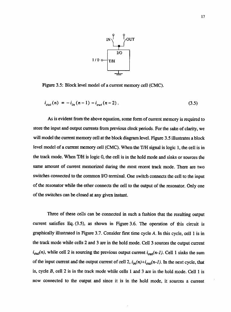
Figure 3.5: Block level model of a current memory cell (CMC).
cut (n) i in (n - 1) - cut (n 2) (3.5)
17
As is evident from the above equation, some form of current memory is required to
store the input and output currents from previous clock periods. For the sake of clarity, we
will model the current memory cell at the block diagram level. Figure 3.5 illustrates a block
level model of a current memory cell (CMC). When the T/H signal is logic 1, the cell is in
the track mode. When T/H is logic 0, the cell is in the hold mode and sinks or sources the
same amount of current memorized during the most recent track mode. There are two
switches connected to the common I/O terminal. One switch connects the cell to the input
of the resonator while the other connects the cell to the output of the resonator. Only one
of the switches can be closed at any given instant.
Three of these cells can be connected in such a fashion that the resulting output
current satisfies Eq. (3.5), as shown in Figure 3.6. The operation of this circuit is
graphically illustrated in Figure 3.7. Consider first time cycle A. In this cycle, cell 1 is in
the track mode while cells 2 and 3 are in the hold mode. Cell 3 sources the output current
iodn), while cell 2 is sourcing the previous output current iout(n-/). Cell 1 sinks the sum
of the input current and the output current of cell 2, iin(n)+iouin-1). In the next cycle, that
is, cycle B, cell 2 is in the track mode while cells 1 and 3 are in the hold mode. Cell 1 is
now connected to the output and since it is in the hold mode, it sources a current

18
lout-.11.
Cell 1 Cell 2 Cell 3
A U B U C
clocking scheme
Figure 3.6: Block-level SI implementation of the bandpass resonator. The `+'sign indicates the logical OR operation.
iout(n+1)=-iidn)-iodn-1). This expression is essentially that given in Eq. (3.5) with n
replaced by n+1. During this cycle, cell 2 is connected to the input and tracks a current
equal to -iin(n+/)-iout(n). In the next cycle, that is, cycle C, cell 2 will be connected to the
output and will source a current iont(n+2)=-iidn+1)-iodn). This pattern repeats itself and
thus this structure implements the desired time-domain equation. The currents are
circulated between the three current memory cells and since this structure is based on a
pseudo 2-path structure, the individual memory cells need not be perfectly matched with
each other. This makes transistor level design much simpler.
Although the single-ended version of the resonator described above realizes the
desired time domain equation, it is desirable in practical implementations to have a
differential implementation. This is a result of the fact that non-ideal effects such as clock
feedthrough and power-supply noise have large common-mode components which can be
suppressed by using a differential structure.

19
Cycle A
itn(n)
1 o-
(I jouln-1)t
0 0
fI/O
T/H T/H
Cycle B
iin(n+1)
0 o
Cycle C
itu(n+2)
Celli
tout(n)
rUO
Cell 2
0 o-UO
T/H
Cell 3
loan+ /)
1-iin(n)-jout(n-1)
-itn(n+1)-ioulnj ?1/0
Cell 1
1 o- T/H
Cell 2
0 o-T/H
Cell 3
itan+2)
iout(n+1)1
00Cell 1
0 0 T/H
t-itin+1)-iout(n)
itu(n+2)-iouin+11I/O
Cell 2
CABUCLU
n-1-11- n -411+1-+-n+2d
clocking scheme
1 oT/H
Cell 3
Figure 3.7: Graphical illustration of the operation of the bandpass resonator.

20
i+
SIblock
SIblock
SIblock
lout
____
Diff.tosingleended
converter
0
0SI
blockSI
blockSI
block04--
i
Figure 3.8: The globally differential scheme. Common mode control only atthe output.
There are two ways of achieving differential operation with SI circuits. The first is
the globally differential scheme, illustrated in Figure 3.8. In this scheme the two paths are
distinct until the last stage, which normally is a differential to single-ended converter. The
disadvantage of this strategy is that there is no common-mode control mechanism and since
each block is unstable in isolation, internal states may become unbounded. It is the author's
belief that this scheme is not very effective in performing common-mode rejection because
it is only performed at the output.
An alternative scheme is the locally differential scheme, illustrated in Figure 3.9.
Each SI block is differential in nature and hence common mode control is possible in each
stage. Cascading of the common-mode errors is prevented and thus the possibility of
i+
Diff.to
single
endedconverter
loutSI
block
SI
block
SI
block
--*0
0 04-
Figure 3.9:The locally differential scheme. Common mode control in eachblock.

21
Common-modenulling mechanism
1 U A2 U 1 U B2 U 1 U C2
A B C
2-phase clocking scheme
Figure 3.10: A differential SI bandpass resonator employing a common -modenulling scheme.
internal states becoming unbounded is eliminated. The author believes that a significantly
higher common mode rejection ratio (CMRR) can thereby be obtained.
A differential version of the SI bandpass resonator is illustrated in Figure 3.10. This
structure employs the locally differential scheme. In order to implement common-mode
control, the clocking scheme had to be modified by dividing each cycle into two phases.
The memory cells are controlled such that they can track the input current only during

22
phase 2 of each time-cycle. Phase 1 is used for performing common-mode nulling. The
structure comprises two single ended structures and some extra circuitry involving two
additional current memory cells and a switch. The operation of the cell is as follows.
During phase 1 of each clock period the two halves of the circuit get connected to
each other through the switch S. Any imbalance in the currents flowing in the two halves
is ideally split equally between the two additional current memory cells. Such an imbalance
could be a result of non-ideal effects such as clock feedthrough or mismatch between the
two halves of the differential circuit. During phase 2 of each clock period the two halves
are isolated from each other. Since the additional memory cells sink a current which is one
half the error current, the currents flowing into both halves are equal in magnitude. Any
imbalance in the currents is evened out, thereby eliminating the common-mode component.
One potential shortcoming of this structure is the need for matching between the
two additional current memory cells. Since these cells need only absorb the small common-
mode component, they can be made very small relative to the main cells and thus mismatch
becomes a second-order effect. Also, since common-mode nulling is only needed to
prevent an unrestricted build-up of common-mode current, nulling can be done
infrequently, thereby reducing the errors caused by mismatch even further.
We now have a way to implement the resonator using current track and hold blocks.
In the next chapter the transistor level implementation of the differential 2-path resonator
will be presented.

23
Chapter 4. Practical Issues
This chapter discusses the circuit implementation from a transistor-level
perspective. The memory cell is used to implement the resonator and the common-mode
nulling scheme. Simulations show that the circuit is viable provided the common-mode
sensing is done properly. The other, less critical, blocks needed in a bandpass AI
modulator are also briefly described.
4.1 The Regulated Cascode Current Memory Cell
The regulated cascode current memory cell was introduced in chapter 2. In this
section we will examine this circuit in more detail. The design and simulation results will
also be presented. As was discussed earlier, to allow carefree interconnection of modules
we need a circuit with a high output to input resistance ratio. An ordinary cascode scheme
is not sufficient, and hence some form of a feedback loop is required. Figure 4.1 shows one
way to implement such a feedback mechanism.
Figure 4.1: A regulatory mechanism for the dynamic current copier.

24
Figure 4.2: A small-signal model for the circuit in Figure 4.1.
Figure 4.2 illustrates the small signal model for this circuit in phase 2. From this figure, it
can be seen that if A is large
V3 E gm3 rds3A VI
Since, i = viirdsi,
V3
Rout = .7.. g qr . , ,Ar _ , siout 1 M.) USJ U
(4.1)
(4.2)
The amplifier can be implemented by a MOS transistor with a current source load, yield-
ing the regulated cascode current memory cell [13] shown in Figure 4.3. Here transistor
M2 acts as an amplifier. Assuming the current source is ideal, the gain A of this transistor
is gm2rds2. Thus the output resistance of the cell is now gm3rds3gn2rds2rds, and an output
to input resistance ratio of more than 104 can be easily achieved.
A small-signal model for the settling behavior of this circuit is fairly complex due
to the presence of a feedback loop and three potentially significant gate-to-source

25
bias
'in boutINN- 1 2 -4
0 0
'ref
J-1--I2IFi 2 1_ 1 12--Two-phase non-overlapping clock
Figure 4.3: The regulated cascode current memory cell.
IICP
Figure 4.4: Small-signal model of the regulated cascode current memory cellfor the settling time analysis.
26
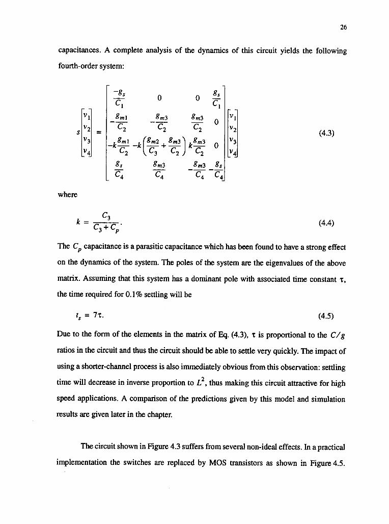
capacitances. A complete analysis of the dynamics of this circuit yields the following
fourth-order system:
s
where
_ -V1
V2
V3
V4
gs0 0
C1
gml gm3 gm3C2 ... 2 C2
gsC1
0
Lgrni L. (gM2 gm3)Lgm3 nIL C21 --7., -,- ,.., A. ,,-, ut., 2 t., 3 t... 2 t., 2
gs gm3 gm3 gsC4 C4 C4 C4
C3k =
C3 + Cp
V1
V2
V3
V4
(4.3)
(4.4)
The CP capacitance is a parasitic capacitance which has been found to have a strong effect
on the dynamics of the system. The poles of the system are the eigenvalues of the above
matrix. Assuming that this system has a dominant pole with associated time constant r,
the time required for 0.1% settling will be
is = 7t. (4.5)
Due to the form of the elements in the matrix of Eq. (4.3), t is proportional to the C/g
ratios in the circuit and thus the circuit should be able to settle very quickly. The impact of
using a shorter-channel process is also immediately obvious from this observation: settling
time will decrease in inverse proportion to L2, thus making this circuit attractive for high
speed applications. A comparison of the predictions given by this model and simulation
results are given later in the chapter.
The circuit shown in Figure 4.3 suffers from several non-ideal effects. In a practical
implementation the switches are replaced by MOS transistors as shown in Figure 4.5.

yin
1
1'
2 1
1'
2
27
modified two-phase clocking scheme
Figure 4.5:The regulated cascode current memory cell. Ideal switches havebeen replaced with MOS transistors.
However a MOS switch is not an ideal switch. A finite amount of mobile carriers are stored
in the channel when a MOS transistor conducts and must be absorbed by the circuit when
the transistor turns off. When the transistor turns off, the channel charge exits through the
source, the drain, and to some degree through the substrate. The charge transferred to the
data node during the switch turning-off period superimposes an error component on the
sampled voltage. In addition to the charge injected from the intrinsic channel, the charge
associated with the feedthrough effect caused by the gate-to-diffusion overlap capacitance
also enlarges the error voltage after the switch turns off [16].
28
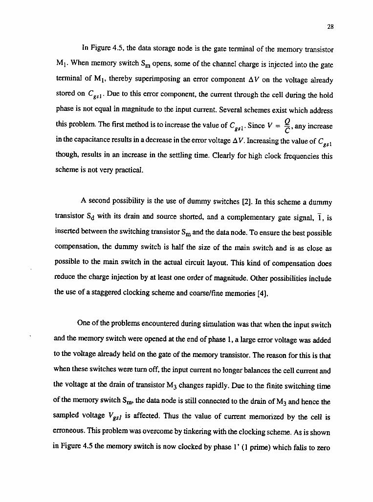
In Figure 4.5, the data storage node is the gate terminal of the memory transistor
M1. When memory switch Sm opens, some of the channel charge is injected into the gate
terminal of M1, thereby superimposing an error component A V on the voltage already
stored on Cgsl Due to this error component, the current through the cell during the hold
phase is not equal in magnitude to the input current. Several schemes exist which address
this problem. The first method is to increase the value of Cssi . Since V = Q , any increase
in the capacitance results in a decrease in the error voltage A V. Increasing the value of Cgs1
though, results in an increase in the settling time. Clearly for high clock frequencies this
scheme is not very practical.
A second possibility is the use of dummy switches [2]. In this scheme a dummy
transistor Sd with its drain and source shorted, and a complementary gate signal, 1, is
inserted between the switching transistor Sm and the data node. To ensure the best possible
compensation, the dummy switch is half the size of the main switch and is as close as
possible to the main switch in the actual circuit layout. This kind of compensation does
reduce the charge injection by at least one order of magnitude. Other possibilities include
the use of a staggered clocking scheme and coarse/fine memories [4].
One of the problems encountered during simulation was that when the input switch
and the memory switch were opened at the end of phase 1, a large error voltage was added
to the voltage already held on the gate of the memory transistor. The reason for this is that
when these switches were turn off, the input current no longer balances the cell current and
the voltage at the drain of transistor M3 changes rapidly. Due to the finite switching time
of the memory switch Sm, the data node is still connected to the drain of M3 and hence the
sampled voltage V8s1 is affected. Thus the value of current memorized by the cell is
erroneous. This problem was overcome by tinkering with the clocking scheme. As is shown
in Figure 4.5 the memory switch is now clocked by phase 1' (1 prime) which falls to zero

29
before phase 1. The memory switch is now opened before the input switch, and so isolates
the data node from the rest of the circuit. Thus any change in the voltage at the drain of M3
does not affect the sampled voltage Vgs/. The input and output switches, namely Sin and
Sout, are implemented as CMOS switches or transmission gates. This has been done in
order to ensure low on-resistance under all operating conditions.
The design of this cell was done keeping in mind the various compensation schemes
that had to be used. The cell was designed for an input current range of ±1001tA and a clock
frequency of 10 MHz. The design was done so that the voltage at the drain of transistor M3
is limited to the range of 1.5 - 3 Volts. This upper limit ensures that the bias current source
transistors are maintained in saturation. The memory switch size has been kept as small as
possible. The minimum transistor width that the Mosis SCMOS process permits is 4
microns. Since the dummy switch Sd is half the size of the memory switch Sm, the
minimum dimensions that transistor Sm could have are 8 microns by 2 microns.The input
and output switches are made wide and short in order to keep the voltage drops across these
transistors to a minimum. The current sources Ibias and Iref have been implemented as
regulated cascode current sources and are biased using a totem-pole transistor structure.
These current sources have a very high output resistance and thus provide a stable and
accurate source of current.
The transistor sizes for the regulated cascode current cell are given in Table 1. The
dimensions of the memory transistor M1 are determined by two factors, one is the
transconductance gm of the transistor and the other is the gate to source capacitance Cgs j.
Having a very high value of transconductance is undesirable since it tends to increase the
effect of clock feedthrough. On the other hand increasing the value of Cgs/ tends to
suppress the effect of clock feedthrough but increase the settling time, thereby reducing the
maximum frequency of operation. A good design has to strike a balance between these two

30
factors. In this case a combination of a dummy switch and twice the minimum length
Table 1: Transistor dimensions
Transistor Width inmicrons
Length inmicrons
M1 28 4
M2 60 2
M3 80 2
Sm 8 2
Sd 4 2
Sm 20 2
Sout 20 2
memory transistor provided a satisfactory amount of clock feedthrough suppression. The
factor that influenced the dimensions of the remaining two transistors was the need for
regulating the drain voltage of transistor M1. illustrates the voltage regulation mechanism
of this cell. The voltage at the drain of M1, Vdsi, is not affected by the variations in the
output voltage Vd3. Thus, the influence of channel length modulation on the current flowing
through the cell is prevented.
Figure 4.7 illustrates the current versus time curves for a 5 MHz square wave input.
The cell is clocked at 10MHz. Notice that the input is sampled during phase 1 and that the
output is held at the sampled value during phase 2. The slight discrepancy between the
desired and the actual value of output current is due to residual clock feedthrough.
Figure 4.8 illustrates the output response for a sinusoidal input. Here both the continuous-
time and the discrete-time input current signals have been illustrated. Notice that the
sample and hold operation is inherent to the current memory cell.

31
In order to measure the settling time of the circuit, two current memory cells
clocked in opposition are connected in such a fashion that the output of the first cell forms
the input to the next. The first cell tracks an input current of 100gA during phase 1. During
phase 2, cell 1 is in the hold mode and sources a current close to 100 g A, which in turn is
tracked by cell 2. The time required for the this current to settle to within 0.1% of its final
value is the settling time of the circuit. Simulations measure this time at 10 ns, which is
quite close to the theoretical value of 10.2 ns predicted by Eq. (4.5) when the HSPICE-
determined parameters were fed into Eq. (4.3). These numbers indicate that this circuit
could be operated at frequencies approaching 50 MHz. Appendix B contains a listing of the
HSPICE output files for the regulated cascode current memory cell.
VdslVd3
le-07 2e-07 3e-07 4e-07
time (s)
Figure 4.6:Regulation of the drain voltage VII of transistor M1, independentof the variations in the output voltage V.

32
1.0e-04 -
5.0e-05
-5.0e-05
-1.0e-04 -
5.0e+00
COW
a)
a.
5
inputoutput
1e 07 2e-07 3e-07 4e-07 5e-07
1 e -07 2e-07 3e-07 4e-07 5e-07
0 1e-07 2e-07 3e-07
Time (s)
4e-07 5e-07
Figure 4.7:Current versus time curves for a 5 MHz, 200µA (peak to peak)squarewave input.
4.2 The Differential SI 2-Path Resonator
In the previous sections we discussed the design and operation of the regulated
cascode current memory cell. This cell is used as the basic current memory cell in the
design of the resonator.

33
C92
1.0e-04
5.0e-05 -
-5.0e-05 -
-1.0e-040
/
t
2.5e-07
cts. time inputdiscrete time inputoutput
1
I
yL
5.0e-07
Ti me (s)
1.0e-06
Figure 4.8: Current versus time curves for a 1MHz, 200µA sinusoidal input.
In Section 3.3 the block-level implementation of the resonator was presented. The
current memory blocks in that design need to be replaced with regulated cascode current
memory cells in order to get a transistor-level design. This circuit is illustrated in
Figure 4.9. As is evident from the figure, the basic topology remains the same, but there are
some minor modifications within the common-mode nulling block. Since a MOS switch
has a nonzero "ON" resistance, a small voltage drop appears across it during phase 1 when
the differential current is flowing through it. This results in a voltage differential between
the two input terminals of the common-mode nulling current memory cells, causing
unequal currents to flow through them. In order to solve this problem an idea similar to
Kelvin sensing is employed. The switch connecting the two halves is replaced by the more
elaborate network of switches shown in Figure 4.9. During phase 1 the input terminals of
the two common-mode nulling current memory cells are connected by a virtual short, thus
ensuring that there is no voltage drop between the I/O terminals. Equal amounts of current
flow into each cell thus ensuring good common-mode nulling.

Iin
; +lout
lout
Common modenulling mechanism
1 A2 1 UB2u1 uCA
Clock waveforms
34
Figure 4.9: A differential switched-current 2-path resonator with improvedcommon-mode nulling.
Figure 4.10 illustrates the impulse response of a single ended 2-path resonator. The
1001.1A input current pulse results in alternating output current pulses occurring on odd
clock cycles, which is in accordance with the time domain equation of Eq. (3.5). Compare
this with Figure 4.11 which illustrates the current versus time curves for a differential 2-
path resonator. To demonstrate the common-mode nulling mechanism, iin+ is made greater
than iin" by 201.1.A. As can be seen from the graph, the difference in the input current is
evened out and the output currents in the subsequent cycles are balanced. The output
waveform therefore has the desired differential behavior with a common-mode component
equal to zero.

35
1.0000e-04 -
5.0000e-05 -
::"i
E o -----.2'50
-5.0000e-05 -
-1.0000e-04 -
0
i
inputoutput
r
2.5e-07
.
r
5.0e-07 7.5e-07
Ti me (s)
1.0e-06
Figure 4.10:Impulse response of a single ended switched-current 2-pathresonator.
1.0000e-04 -
5.0000e-05 -
a48e 0
1
iU
-5.0000e-05
1
4
i
I-
I
-1.0000e-04 - I i
Input1- input2outputsoutput2
1
I0 2.5e-07 5.0e-07 7.5e-07 1.0e-06
Time (s)
Figure 4.11:Impulse response of a differential switched-current 2-pathresonator.

36
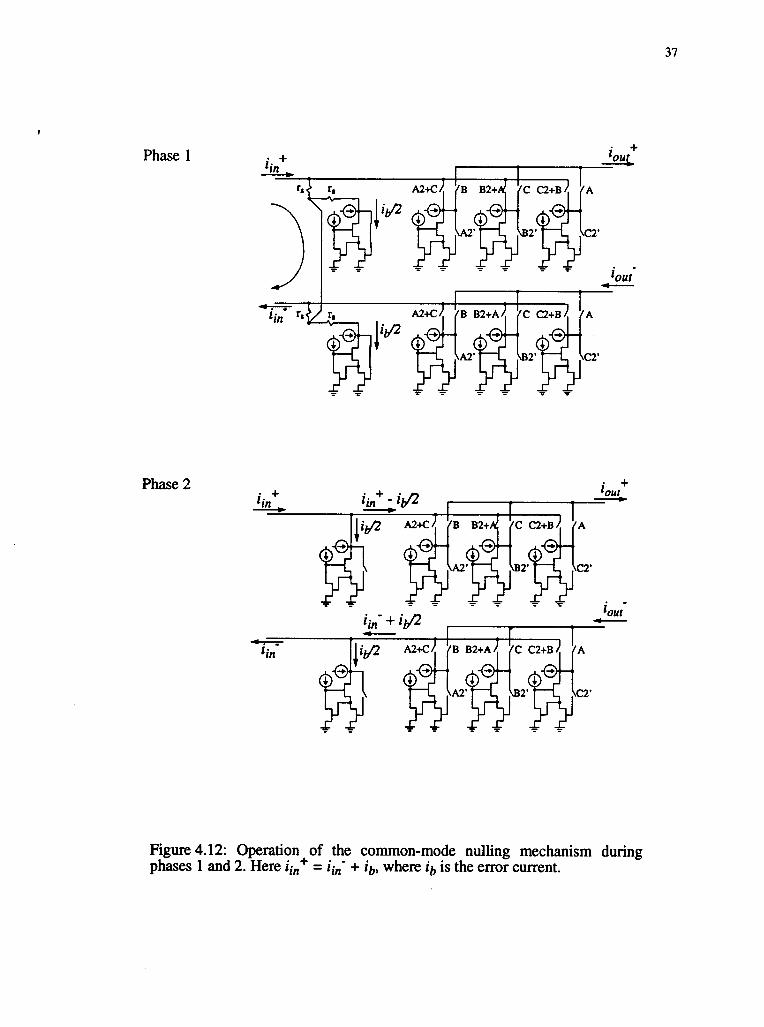
The operation of the common-mode nulling mechanism is graphically illustrated in
Figure 4.12. Let iin+ be greater than iin" by an amount equal to ib, where ib is the imbalance
in the current due to non-ideal effects. During phase 1 of each cycle, the two halves are
shorted to each other and the error current is equally distributed between the two common-
mode nulling current memory cells. During phase 2 these cells hold the current memorized
during phase 1 and thus even out the imbalance between the input currents.
A key feature of this circuit is that the output current is available in both the clock
phases, thus making common-mode nulling feasible. The disadvantages are the complexity
of the clocks and the requirement for matching between the common-mode nulling
memory cells. As can be seen from the circuit, the clocking is fairly complex. We need 12
distinct clocks and their complements since most of the switches are implemented as
transmission gates. For good common-mode rejection, the two common-mode nulling
blocks have to be perfectly matched with each other since mismatch between the two cells
results in uneven currents flowing through the two halves. Special layout techniques must
be relied upon to achieve the required matching.
43 The Current Comparator
One of the blocks needed to build a delta-sigma modulator is the single-bit
quantizer, which in this case is a current comparator. Figure 4.13 shows one potential
implementation. It consists of two inverters connected in a back to back configuration.
During phase 1, switch S is closed so as to equalize the voltages at the input and output of
both inverters. During phase 2, the switch is opened. Imbalance caused by the currents
being fed into the gates of the two inverters will cause the output voltage to settle to either
logic '1' or '0' extremely quickly.
37
Phase 1
Phase 2
r,
...-.-7.-tin
tout
A2+C) B B2+A7
Figure 4.12: Operation of the common-mode nulling mechanism duringphases 1 and 2. Here iin+ = jilt- + ib, where ib is the error current.

38
Figure 4.13:A current comparator.
4.4 The SI Digital to Analog Converter
The other auxiliary block required is the single-bit switched-current digital to
analog converter (DAC). Here the digital input is a voltage signal, while the analog output
is a current signal whose polarity depends upon the polarity of the input digital voltage.
This block can be implemented as shown in Figure 4.14. The circuit consists oftwo current
sources and four switches connected in a cross coupled configuration. The current sources
Figure 4.14:A 1-bit differential switched current D/A converter.

39
are implemented using regulated cascode current sources. The high output resistance
exhibited by such current sources enables their easy connection to the low resistance input
of the resonator. The switches are clocked by the digital output voltage Vo of the modulator.
Due to the cross coupled switch configuration, the polarities of the feedback currents can
controlled by the value of the digital voltage Vo.
4.5 Clock Generation
In the previous section the need for non-overlapping and complementary clock
signals was noted. These signals can be divided into two types, basic and derived. The basic
clock signals are phases 1, 2, A, B, C. These signals are derived from a master reference
clock signal. As is observed from Figure 4.9, the memory switches need to be opened prior
to the input switch. These switches are clocked by either 1' (1 prime) or a signal derived
from 2' (2 prime). Since 2' is the more widely used signal amongst the two, it is the first
signal to be generated from the master clock signal. Using the logic illustrated in
Figure 4.15, signal 1' is also generated. The cross-coupled logic ensures non-overlap
between the two signals. Signals 1 and 2 can then be generated by delaying / and 2' by a
CL
)0-
CVIN
1C11:111
-*-02
--lb 2cnin
Figure 4.15:Logic circuit for generation of clock signals 1, 2, / ', 2', 1arm and2cmn

40
0 A
R
CL
-CD
>c
. B
0
C>c
Figure 4.16:Logic circuit for generation of clock signals A, B and C
few gate delays so as to obtain a few nanoseconds delay. This structure also provides the
complements of the various signals. The rest of the basic signals are generated using the
logic illustrated in Figure 4.16. These signals need not necessarily be non-overlapping. As
long as the memory switch in each cell is opened before either the input switch opens or
the output closes, overlap is permissible. The rest of the signals such as A2', A2+C, B2',
etc. are derived from the basic signals by means of simple combinational logic gates. The
resulting waveforms are illustrated in Figure 4.17. Provision has been made for a reset
signal R and a common-mode nulling disable signal CMN. The CMN signal controls the
input and the output switches of the common-mode nulling current memory cells. Making
CMN active, that is high, disables the common-mode nulling mechanism.
4.6 The Second-Order Bandpass Modulator
Due to lack of time the entire eight-order modulator could not be laid out. Instead,
a second-order bandpass modulator comprising a resonator, the current comparator,l-bit
current DAC and supporting clock generation logic was laid out in a Tiny Chip. The block
diagram for the second-order modulator is shown in Figure 4.18.

Cl
0
51
I.
1
21
I
I.0
05
1'I I
._
2'0
0__L
15
"1
00
2
0 -II-0
A2+C
0
1
0
5B2+A
B2'
0
5C2+B
C2'o
0
300 600
--t
300
300
300
300
I
600
I
11_1_600
1 1-71 I
II
600
1
1
1
11600
300
300
-1
600
1
1
1
7 -11
I
900
900
I
900
1
-
I
900
900
900
1
600
Figure 4.17:Clock waveforms for the 2-path resonator.
Li900
600 900
41

42
-0.537
-z
1 + z-
Figure 4.18:A second-order bandpass modulator.
4.7 Layout Considerations
In section 4.2 the differential switched-current 2-path resonator was discussed. The
need for matching between the two common-mode nulling current memory cells was
explained. This has been addressed by careful layout of the circuit. The approach is to
match every transistor with its counterpart from the other cell. This can be accomplished
by adopting the comb or the inter-digitated arrangement [8]. In this type of layout, the
transistors are broken up into smaller sized equal width transistors. For two transistors that
share a common source terminal, the source is laid out in a serpentine fashion. The two
drain and gate regions are then laid out alternately such that any gradient due to process
variations affects both the transistors equally. Dummy transistors are used at each end of
the structure. Thus each transistor in the structure has similar shaped structures on either
side and sees the same amount of capacitance on either side. Though only the two common-
mode nulling cells need to be matched, the layout strategy explained above was applied to
all the cells, ensuring matching between the two halves of the differential structure.
The switches on the other hand are so laid out that the clock lines can be brought
out on one side of the circuit. Clock lines and signal lines have been kept as far as possible
from each other. Metal lines connected to ground are laid out between any two signal lines.
This ensures that there is no coupling between the lines. The memory switch and the

43
dummy switch are laid as close to each other as possible. The process used for the layout
is a 2-micron p-well process. This process has been chosen because the crucial n-channel
transistors can then be placed in a p-well, which can be then biased to ground. This limits
the substrate noise injection. Guards rings are used to isolate the analog and digital
circuitry. Separate power supplies connections for the analog and digital sections are also
used in order to reduce the noise through power supply coupling. Appendix A contains
plots of the layout. As can be seen from the plots, the layouts of the cells are quite complex
and this is the price one has to pay for simplicity in design.

44
Chapter 5. Conclusions
This chapter summarizes the contributions of this thesis, and outlines possible
directions for future work.
5.1 Summary
Chapter two presented a brief introduction to oversampling delta-sigma
modulation. Bandpass AE conversion was introduced as a modification of lowpass Al
conversion, and its application in conversion of narrow-band signals at high frequencies
was discussed. Switched - current circuits were presented as an alternative to switched-
capacitor circuits for use in analog signal processing applications. Various switched-
current circuit structures were examined for their feasibility in practical implementations.
Chapter three looked at the system level design concerns of the bandpass
modulator. The various modulator structures were examined, and the need for pseudo N-
path structures was emphasized. The design of the bandpass modulator from its lowpass
prototype was briefly discussed. The bulk of the chapter dealt with the switched-current
implementation of the modulator structure. A block level design approach was adopted and
a new SI architecture for the pseudo 2-path resonator was developed.
Chapter four dealt with the transistor level implementation of the SI resonator and
the other auxiliary blocks. The regulated cascode current memory cell was analyzed and
the simulation results presented. The problems faced in SI circuit design due to non-
idealities were enumerated and circuit techniques to work around these problems were
explained. The main contribution of this thesis was the development of the differential SI
2-path resonator. This resonator uses dynamic current copiers and hence overcomes to a
large extent the device matching problems faced by earlier generation resonator designs.

45
The clock generation circuitry and layout issues were also discussed. The beauty of this
design is that the use of the basic cell throughout the entire circuit makes the circuit
modular. This technique can be easily generalized to implement transfer functions of the
form1
1 + Z-141
It has been demonstrated via simulation that switched-current circuits can be used
to make bandpass delta-sigma modulators. The circuit presented here is nominally capable
of being clocked at 50 MHz. Another feature of this design is its ability to use a standard
digital CMOS process. The disadvantages of this approach are the lack of accuracy and the
high power consumption (9 mW per resonator).
5.2 Future Work
Although a new SI architecture has been developed, there still remains a lot to be
done. The higher-order modulator needs to be completed, fabricated and tested for
accuracy. Converting the design to a 1µm or a sub-micron technology could mean smaller
chip sizes and higher operating speeds. The author believes that by using shorter device
lengths the clock frequency could be beyond 100 MHz, which by present day standards is
difficult even in switched-capacitor circuits. Another area of research is the scalability of
the circuit to lower voltage operations, which could lead to lower power consumption.
Better clock feedthrough cancellation schemes or design techniques which cope with the
problem are also needed. The effect of thermal noise on these circuits likewise needs to be
investigated. Lastly a structured methodology for the design and optimization of SI circuits
needs to be developed and documented.

46
BIBLIOGRAPHY
[1] J. C. Candy and G. C. Temes, "Oversampling methods for AID and D/Aconversion," in Oversampling Delta-Sigma Data Converters, J. C. Candy and G. C.Temes, Eds. New York: IEEE Press, 1991.
[2] R. Gregorian and G. C. Temes, Analog MOS Integrated Circuits for SignalProcessing, pp. 363-387, John Wiley and Sons, 1986.
[3] J. B. Hughes, N. C. Bird and I. C. Macbeth, "Switched currents -a new technique foranalogue sampled-data signal processing," Proceedings of the 1989 IEEEInternational Symposium on Circuits and Systems, pp. 1584-1587, May 1989.
[4] J. B. Hughes and K. W. Moulding, "S2I A two-step approach to switched-currents,"Proceedings of the 1993 IEEE International Symposium on Circuits and Systems, pp1235-1238, May 1993.
[5] S. A. Jantzi, R. Schreier, and M. Snelgrove, "Bandpass sigma-delta analog-to-digitalconversion," IEEE Transactions on Circuits and Systems, vol. 38, no. 23, pp. 1406-1409, November 1991.
[6] S. A. Jantzi, M. Snelgrove and P. F. Ferguson, Jr., "A 4th-order bandpass sigma-deltamodulator," Proceedings of the IEEE 1992 Custom Integrated Circuits Conference,Boston, MA, pp. 16.5.1 16.5.4, May 3-6 1992.
[7] L. Longo and B. Horng, "A 15b 30kHz bandpass sigma-delta modulator,"Proceedings of the IEEE 1993 International Solid-State Circuits Conference, SanFrancisco, CA, pp. 226-227, March 1993.
[8] F. Maloberti,"Practical problems for the design of mixed A-D systems: a tutorialintroduction," Department of Electronics, University of Pavia, Italy, 1990.
[9] G. Palmisano and F. Montecchi, "Simplified pseudo-N-path cells for z to -zNtransformed SC active filters," IEEE Transactions on Circuits and Systems, Vol. 35,No. 4, pp. 409-415, April 1988.
[10] R. Schreier and W. M. Snelgrove, "Bandpass sigma-delta modulation," ElectronicsLetters, vol. 25, no. 23, pp. 1560-1561, November 9 1989.
[11] R. Schreier,"A high-order AI modulator - Assignment no. 5," ECE 619:Oversampling AID and DIA Converters, Department of Electrical and ComputerEngineering, Oregon State University, Fall Term 1992.
[12] G. C. Temes, Ph. Deval and V. Valencic, "SC circuits: state of the art compared to SItechniques," Proceedings of the 1993 IEEE International Symposium on Circuitsand Systems, pp 1231-1234, May 1993.
[13] C. Toumazou, J. B. Hughes and D. M. Pattullo, "A regulated cascode switched-current memory cell," Electronics Letters, vol. 26, no. 5, pp. 303-305, March 1990.

47
[14] G. Tr Oster, P. Sieber, K. Schoppe, A. Wedel, E. Zocher and J. Arndt, "Aninterpolative bandpass converter on a 1.2 p.m BiCMOS analog/digital array,"Symposium on VLSI Circuits Digest of Technical Papers, pp. 102-103, June 1992.
[15] G. Wegmann and E. A. Vittoz, "Very accurate dynamic current mirrors," ElectronicsLetters, vol. 25, no. 10, pp. 644-646, May 1989.
[16] G. Wegmann, E. A. Vittoz and F. Rahali, "Charge injection in analog MOSswitches," IEEE Journal of Solid-State Circuits, vol. sc-22, no. 6, pp 1091-1097,December 1987.

APPENDICES

48
Appendix A
The plots of the layout are illustrated on the following pages.
The first plot is that of the interdigitated layout of a differential pair. Note that the
source for both the transistors is common and is laid out in a serpentine fashion. The two
drain and gate regions are interdigitated for matching purposes. Dummy transistors are
used at each end.
The second plot illustrates the layout of the differential pseudo 2-path resonator. The
clocks busses are brought out on one side for easy connection. The n-channel transistors
are placed in a p-well that is connected to Vss


f-Z --.NI ;_-,.
0 g

51
Appendix B
Selected parts of the HSPICE output file for the transient simulation of the regulated
cascode current memory cell are listed below. Parameters values from the operating point
analysis were substituted in Eq. (4.3) in order to compute the settling time of the circuit.
* the regulated cascode current copier****** copyright 1990 meta-software,inc. *****site:****** input listing
.include '-/hspice/models/pwell_bsim.1'
.include '-/bpsd/layout/clock.10mhz'
.include '-/hspice/stage/options'
.global vdd
.subckt irc io scale=1ml di gate vdd vdd pcl_pml_du2 w=4u 1=2um2 g3 dl vdd vdd pcl_pml_du2 w=8u 1=2um3 d3 g3 dl dl pcl_pm1_du2 w=8u 1=2um4 g3 g4 s4 s4 pcl_nml_dul w=4u 1=2um5 s4 s4 0 0 pcl_nml_dul w=4u 1=2uvg4 g4 0 3vgg gate 0 3.3vrc d3 io 0.ends
$ include model file$ include clocks$ include options file
$ iref subcircuit
.subckt ibs io $ ibias subcircuitml dl gate vdd vdd pcl_pml_du2 w=27u 1=2um2 g3 dl vdd vdd pcl_pml_du2 w=40u 1=2um3 d3 g3 dl dl pcl_pml_du2 w=40u 1=2um4 g3 g4 s4 s4 pcl_nml_dul w=4u 1=2um5 s4 s4 0 0 pcl_nml_dul w=4u 1=2uvg4 g4 0 3vgg gate 0 3vbs d3 io 0.ends
.subckt switch it i2 cl c2msn it cl i2 0 pcl_nml_dul w=20u 1=2umsp it c2 i2 vdd pcl_pml_du2 w=20u 1=2u.ends
$ cmos switch
.subckt cth_0.1m i o cml cm2 $ reg. cascode c.c.ml dl gl 0 0 pcl_nml_dul w=28u 1=4u $ memory transistorm2 g3 dl 0 0 pcl_nml_dul w=60u 1=2um3 d3 g3 dl dl pcl_nml_dul w=80u 1=2ums_sw gl cml d3 0 pcl_nml_dul w=8u 1=2u $ memory switchms_sw_d gl cm2 gl 0 pcl_nml_dul w=4u 1=2u $ dummy switchxirc g3 ircxibias io ibsvmem io d3 0

vin i io 0vout io 0 0.ends
* circuit descriptionxcthi inl ol pine p2ne cth_0.1mxcth2 in2 o2 pipe p2pe cth_0.1m
xsl inl c1 pin pip switchxs2 in2 c2 p2n p2p switchxs3 out c3 pin pip switch
* bypass mechanismmup cl pin vdd vdd pcl_pml_du2 w=20u 1=2umdown cl plp 0 0 pcl_nml_dul w=20u 1=2u
$ cmc #1$ cmc #2
$ switch #1$ switch #2$ switch #3
52
* independent sourcesvdd vdd 0 5iin 0 inn pwl(On 100u 99n 100u 100n -100u 199n -100u 200n 100u) r
* voltage sourcesvinn inn cl 0vol ol c2 0vo2 o2 c3 0vout out 0 2.5
.op 190n
.tran in 200n
.print i(vol)
.end
******circuit number to circuitnumber circuitname
0 main circuit
name directorydefinition multiplier
1 xcthl. cth_0.1m 1.002 xcth2. cth_0.1m 1.003 xsl. switch 1.004 xs2. switch 1.005 xs3. switch 1.006 xcthl.xirc. irc 1.007 xcthl.xibias. ibs 1.008 xcth2.xirc. irc 1.009 xcth2.xibias. ibs 1.00
****** operating point information tnom= 25.000 temp= 25.000*********** operating point status simulation time is 1.900000e-07
node = voltage node = voltage node = voltage
+0:c1 = 5.934382e-01 0:c2 = 2.524614e+00 0:c3 = 2.394082e+00+0:inl = 2.524614e+00 0:in2 = 2.394082e+00 0:inn = 5.934382e-01+0:01 = 2.524614e+00 0:o2 = 2.394082e+00 0:out = 2.500000e+00+0:pin = O. 0:pine= O. 0:plp = 5.000000e+00+0:plpe= 5.000000e+00 0:p2n = 5.000000e+00 0:p2ne= 5.000000e+00+0:p2p = O. 0:p2pe= O. 0:vdd = 5.000000e+00+1:d1 = 1.057783e+00 1:d3 = 2.524614e+00 1:g1 = 1.744273e+00

53
+1:g3 = 2.271718e+00 1:io = 2.524614e+00 2:d1 = 1.055629e+00+2:d3 = 2.394082e+00 2:g1 = 2.394082e+00 2:g3 = 2.509777e+00+2:io = 2.394082e+00 6:d1 = 3.865688e+00 6:d3 = 2.271718e+00+6:g3 = 2.544107e+00 6:g4 = 3.000000e+00 6:gate= 3.300000e+00+6:s4 = 1.493356e+00 7:d1 = 4.193644e+00 7:d3 = 2.524614e+00+7:g3 = 2.592782e+00 7:g4 = 3.000000e+00 7:gate= 3.000000e+00+7:s4 = 1.494094e+00 8:d1 = 3.866757e+00 8:d3 = 2.509777e+00+8:g3 = 2.528368e+00 8:g4 = 3.000000e+00 8:gate= 3.300000e+00+8:s4 = 1.493115e+00 9:d1 = 4.193174e+00 9:d3 = 2.394082e+00+9:g3 = 2.603299e+00 9:g4 = 3.000000e+00 9:gate= 3.000000e+00+9:s4 = 1.494253e+00
nodal capacitance tablenode = cap node = cap
+0:c1 = 4.714232e-14 0:c2 = 5.433566e-14+0:inl = 1.307081e-14 0:in2 = 5.568331e-14
node = cap
0:c3 = 1.307081e-140:inn = 0.
+0:ol = 0. 0:02 = 0. 0:out = 1.307081e-14+0:pin = 8.797911e-14 0:pine= 1.205583e-14 0:plp = 8.033732e-14+0:plpe= 1.602751e-14 0:p2n = 3.918877e-14 0:p2ne= 8.261420e-15+0:p2p = 3.723417e-14 0:p2pe= 6.338023e-15 0:vdd = 3.506999e-13+1:d1 = 2.895702e-13 1:d3 = 3.662455e-14 1:g1 = 9.874538e-14+1:g3 1.590221e-13 1:io = 0. 2:d1 = 2.891111e-13+2:d3 = 4.526898e-14 2:g1 = 9.831297e-14 2:g3 = 1.591044e-13+2:io 0. 6:d1 = 2.848177e-14 6:d3 = 1.916064e-15+6:g3 1.587931e-14 6:g4 = 7.196414e-15 6:gate= 6.531946e-15+6:s4 = 1.869222e-14 7:d1 = 1.530927e-13 7:d3 = 9.455552e-15+7:g3 6.950175e-14 7:g4 = 7.196413e-15 7:gate= 4.665609e-14+7:s4 = 1.869231e-14 8:d1 = 2.847801e-14 8:d3 = 1.916064e-15+8:g3 1.587931e-14 8:g4 = 7.196414e-15 8:gate= 6.531946e-15+8:s4 = 1.869219e-14 9:d1 = 1.531029e-13 9:d3 = 9.455552e-15+9:g3 6.950175e-14 9:g4 = 7.196413e-15 9:gate= 4.664995e-14+9:s4 = 1.869233e-14
total voltage source power dissipation= 8.674306e-03 watts
total current source power dissipation= -5.934382e-05 watts
**** mosfets
subcktelementmodelidibs
0:mup0:pcl_pml_
-1.238446e-030.
0:mdown0:pcl_nml_
1.138446e-030.
xcthl1:m10:pcl_nml_
9.781839e-050.
xcthl1:m20:pcl_nml_
2.154292e-050.
ibd 4.406562e-14 -5.934382e-15 -1.057783e-14 -2.271719e-14vgs -5.000000e+00 5.000000e+00 1.744273e+00 1.057783e+00vds -4.406561e+00 5.934382e-01 1.057783e+00 2.271718e+00vbs 0. 0. 0. 0.with -5.331764e-01 9.508899e-01 9.331427e-01 9.319862e-01vdsat -3.103065e+00 2.413697e+00 5.846000e-01 9.110324e-02beta 2.181342e-04 5.837230e-04 4.114734e-04 2.623843e-03gam eff 4.768494e-01 1.073972e+00 1.104212e+00 1.062491e+00gm 3.590319e-04 2.388962e-04 2.297313e-04 2.338926e-04gds 7.880300e-05 1.576895e-03 2.434883e-06 2.141873e-06gmb 4.949198e-05 1.355122e-04 1.337150e-04 1.348404e-04cdtot 4.743372e-15 2.932814e-14 1.165571e-14 2.496883e-14

54
cgtotcstotcbtotcgscgd
2.957350e-142.860302e-146.353853e-152.421650e-144.743372e-15
3.925720e-143.405266e-141.368191e-142.022961e-141.855013e-14
8.331726e-149.687384e-144.507955e-145.999599e-141.165571e-14
9.756327e-148.803911e-143.700056e-145.999788e-142.496883e-14
subckt xcthl xcthl xcthl xcth2element 1:m3 l:ms_sw l:ms_sw_d 2:m1model 0:pcl_nml_ 0:pcl_nml_ 0:pcl_nml_ 0:pcl_nml_id 9.781840e-05 0. 0. 2.976345e-04ibs 0. -2.524615e-14 -1.744274e-14 0.ibd -1.466831e-14 -1.744274e-14 -1.744274e-14 -1.055630e-14vgs 1.213935e+00 -2.524614e+00 3.255726e+00 2.394082e+00vds 1.466831e+00 -7.803408e-01 0. 1.055629e+00vbs 0. -2.524614e+00 -1.744273e+00 0.vth 9.355824e-01 1.698010e+00 1.772094e+00 9.331458e-01vdsat 1.995330e-01 0. 1.083438e+00 1.044570e+00beta 3.270915e-03 3.045259e-04 1.329575e-04 3.955627e-04gam eff 1.061055e+00 1.069311e+00 1.108779e+00 1.104212e+00gm 6.173961e-04 0. 0. 3.809397e-04gds 9.230487e-06 0. 0. 6.412481e-06gmb 3.511916e-04 0. 0. 2.086094e-04cdtot 3.328953e-14 3.335013e-15 5.937731e-15 1.165571e-14cgtot 1.340532e-13 1.205583e-14 8.261420e-15 8.331726e-14cstot 1.295286e-13 3.335013e-15 6.155374e-15 9.687384e-14cbtot 5.082256e-14 5.385802e-15 2.132568e-15 4.372365e-14cgs 8.714646e-14 3.335013e-15 3.898757e-15 6.135189e-14cgd 3.328953e-14 3.335013e-15 3.898757e-15 1.165571e-14
subckt xcth2 xcth2 xcth2 xcth2element 2:m2 2:m3 2:ms_sw 2:ms_sw_dmodel 0:pcl_nml_ 0:pcl_nml_ 0:pcl_nml_ 0:pcl_nml_id 2.153911e-05 2.976345e-04 2.415754e-12 0.ibs 0. 0. -2.394082e-14 -2.394082e-14ibd -2.509777e-14 -1.338453e-14 -2.394082e-14 -2.394082e-14vgs 1.055629e+00 1.454147e+00 2.605917e+00 -2.394082e+00vds 2.509777e+00 1.338452e+00 1.025173e-08 0.vbs 0. 0. -2.394082e+00 -2.394082e+00vth 9.307729e-01 9.363653e-01 1.904590e+00 1.970539e+00vdsat 9.039723e-02 3.649046e -01 5.396758e-01 0.beta 2.664553e-03 3.176994e-03 2.862331e-04 1.487468e-04gam eff 1.062491e+00 1.061055e+00 1.061031e+00 1.099582e+00gm 2.356036e-04 1.049883e-03 2.749189e-12 0.gds 2.073298e-06 2.309359e-05 2.356434e-04 0.gmb 1.356446e-04 5.821868e-04 7.591837e-13 0.cdtot 2.496883e-14 3.328953e-14 1.165396e-14 1.670873e-15cgtot 9.73880de-14 1.341355e-13 1.602751e-14 6.338023e-15cstot 8.752266e-14 1.297710e-13 1.197945e-14 1.670873e-15cbtot 3.691564e-14 5.029641e-14 3.313235e-15 2.996276e-15cgs 5.970776e-14 8.784862e-14 7.781802e-15 1.670873e-15cgd 2.496883e-14 3.328953e-14 7.781802e-15 1.670873e-15
Copyright © 2022 FDOKUMEN