The Data Vortex Optical Packet Switched Interconnection Network
13
JOURNAL OF LIGHTWAVE TECHNOLOGY, VOL. 26, NO. 13, JULY 1, 2008 1777 The Data Vortex Optical Packet Switched Interconnection Network Odile Liboiron-Ladouceur, Member, IEEE, Assaf Shacham, Member, IEEE, Benjamin A. Small, Member, IEEE, Benjamin G. Lee, Student Member, IEEE, Howard Wang, Student Member, IEEE, Caroline P. Lai, Student Member, IEEE, Aleksandr Biberman, Student Member, IEEE, and Keren Bergman, Senior Member, IEEE Invited Paper Abstract—A complete review of the data vortex optical packet switched (OPS) interconnection network architecture is pre- sented. The distributed multistage network topology is based on a banyan structure and incorporates a deflection routing scheme ideally suited for implementation with optical components. An implemented 12-port system prototype employs broadband semi- conductor optical amplifier switching nodes and is capable of successfully routing multichannel wavelength-division multi- plexing packets while maintaining practically error-free signal integrity (BER 10 ) with median latencies of 110 ns. Packet contentions are resolved without the use of optical buffers via a distributed deflection routing control scheme. The entire pay- load path in the optical domain exhibits a capacity of nearly 1 Tb/s. Further experimental measurements investigate the OPS interconnection network’s flexibility and robustness in terms of optical power dynamic range and network timing. Subsequent experimental investigations support the physical layer scalability of the implemented architecture and serve to substantiate the merits of the data vortex OPS network architectural paradigm. Finally, modified design considerations that aim to increase the network throughput and device-level performance are presented. Index Terms—Interconnection networks (multiprocessor), optical interconnections, packet switching, photonic switching systems, wavelength-division multiplexing. I. INTRODUCTION N EARLY all contemporary large-scale high-performance information systems, including supercomputers, high-ca- pacity data storage, and telecommunications core routers, require high-bandwidth low-latency interconnection networks. In these systems, performance is highly dependent upon the efficiency of vast information exchanges between sometimes thousands of clients (e.g., processors, memory, network hosts). 1 It is therefore critical for the interconnect infrastructure to Manuscript received August 15, 2007; revised November 9, 2007. Published August 29, 2008 (projected). This work was supported in part by the National Science Foundation under Grant ECS-0322813 and by the U.S. Department of Defense under Subcontract B-12-664. O. Liboiron-Ladouceur is with McGill University, Montreal, PQ, Canada. A. Shacham is with Aprius Inc., Sunnyvale, CA 94085 USA. B. A. Small, B. G. Lee, H. Wang, C. P. Lai, A. Biberman, and K. Bergman are with the Electrical Engineering Department, Columbia University, New York, NY 10027 USA. Digital Object Identifier 10.1109/JLT.2007.913739 1 TOP500 List for June 2006, http:www.top500.org/lists/2006/06 support high-bandwidth low-latency communications that are highly scalable, thus transparently facilitating overall system performance [1]. With the immense growth in data traffic and required computation capacities, conventional electronic interconnection networks utilized for these applications are reaching capacity limits in their ability to meet the increased demands of the surrounding clients. While it is well established that optical data encoding and the utilization of fiber-optic and photonic media possess the po- tential to provide orders of magnitude more bandwidth at near speed-of-light transmission latencies [2], critical optical tech- nology shortcomings must be addressed. The key challenge for optical interconnection networks is to fully leverage the im- mense bandwidth of the fiber-optic components through tech- niques such as wavelength-division multiplexing (WDM) while avoiding the inadequacies of photonic technologies, particularly the absence of robust optical buffers and registers. The data vortex architecture was specifically designed as a packet switched interconnection network for optical implemen- tation; the topology supports large port counts scalable to thou- sands of communicating terminals. In order to accommodate scalability and to address the problematic absence of reliable dynamic photonic buffers, the conventional butterfly network topology is modified to contain integrated deflection routing pathways. The primary consideration in the architecture’s or- ganization is enabling the optical packets to approach speed-of- light time-of-flight latencies. The switching nodes are therefore designed to be as simple as possible and to contain very little routing logic; in this way, the packets do not sit in buffers while routing decisions are made. These design considerations nat- urally result in a modular architecture, which is scalable and self-similar in such a way that a small system implementation can predict the performance of significantly larger networks. The data vortex design differs markedly from the conven- tional approaches to optical packet switched (OPS) networks, in which electronic architectures are often simply mapped into the optical media in a manner that can fail to capitalize on the unique properties of optical transmission. In the data vortex architec- ture, when processing and routing decisions are required, high- speed digital electronic circuitry is employed in a way that com- plements the semiconductor optical amplifier (SOA) wide-band photonic switching elements. This allows the high-bandwidth optical payload, which is encoded on multiple wavelengths in 0733-8724/$25.00 © 2008 IEEE
-
Upload
independent -
Category
Documents
-
view
0 -
download
0
Transcript of The Data Vortex Optical Packet Switched Interconnection Network
JOURNAL OF LIGHTWAVE TECHNOLOGY, VOL. 26, NO. 13, JULY 1, 2008 1777
The Data Vortex Optical Packet SwitchedInterconnection Network
Odile Liboiron-Ladouceur, Member, IEEE, Assaf Shacham, Member, IEEE, Benjamin A. Small, Member, IEEE,Benjamin G. Lee, Student Member, IEEE, Howard Wang, Student Member, IEEE,
Caroline P. Lai, Student Member, IEEE, Aleksandr Biberman, Student Member, IEEE, andKeren Bergman, Senior Member, IEEE
Invited Paper
Abstract—A complete review of the data vortex optical packetswitched (OPS) interconnection network architecture is pre-sented. The distributed multistage network topology is based ona banyan structure and incorporates a deflection routing schemeideally suited for implementation with optical components. Animplemented 12-port system prototype employs broadband semi-conductor optical amplifier switching nodes and is capable ofsuccessfully routing multichannel wavelength-division multi-plexing packets while maintaining practically error-free signalintegrity (BER 10 ��) with median latencies of 110 ns. Packetcontentions are resolved without the use of optical buffers viaa distributed deflection routing control scheme. The entire pay-load path in the optical domain exhibits a capacity of nearly 1Tb/s. Further experimental measurements investigate the OPSinterconnection network’s flexibility and robustness in terms ofoptical power dynamic range and network timing. Subsequentexperimental investigations support the physical layer scalabilityof the implemented architecture and serve to substantiate themerits of the data vortex OPS network architectural paradigm.Finally, modified design considerations that aim to increase thenetwork throughput and device-level performance are presented.
Index Terms—Interconnection networks (multiprocessor),optical interconnections, packet switching, photonic switchingsystems, wavelength-division multiplexing.
I. INTRODUCTION
N EARLY all contemporary large-scale high-performanceinformation systems, including supercomputers, high-ca-
pacity data storage, and telecommunications core routers,require high-bandwidth low-latency interconnection networks.In these systems, performance is highly dependent upon theefficiency of vast information exchanges between sometimesthousands of clients (e.g., processors, memory, network hosts).1
It is therefore critical for the interconnect infrastructure to
Manuscript received August 15, 2007; revised November 9, 2007. PublishedAugust 29, 2008 (projected). This work was supported in part by the NationalScience Foundation under Grant ECS-0322813 and by the U.S. Department ofDefense under Subcontract B-12-664.
O. Liboiron-Ladouceur is with McGill University, Montreal, PQ, Canada.A. Shacham is with Aprius Inc., Sunnyvale, CA 94085 USA.B. A. Small, B. G. Lee, H. Wang, C. P. Lai, A. Biberman, and K. Bergman are
with the Electrical Engineering Department, Columbia University, New York,NY 10027 USA.
Digital Object Identifier 10.1109/JLT.2007.913739
1TOP500 List for June 2006, http:www.top500.org/lists/2006/06
support high-bandwidth low-latency communications that arehighly scalable, thus transparently facilitating overall systemperformance [1]. With the immense growth in data trafficand required computation capacities, conventional electronicinterconnection networks utilized for these applications arereaching capacity limits in their ability to meet the increaseddemands of the surrounding clients.
While it is well established that optical data encoding andthe utilization of fiber-optic and photonic media possess the po-tential to provide orders of magnitude more bandwidth at nearspeed-of-light transmission latencies [2], critical optical tech-nology shortcomings must be addressed. The key challenge foroptical interconnection networks is to fully leverage the im-mense bandwidth of the fiber-optic components through tech-niques such as wavelength-division multiplexing (WDM) whileavoiding the inadequacies of photonic technologies, particularlythe absence of robust optical buffers and registers.
The data vortex architecture was specifically designed as apacket switched interconnection network for optical implemen-tation; the topology supports large port counts scalable to thou-sands of communicating terminals. In order to accommodatescalability and to address the problematic absence of reliabledynamic photonic buffers, the conventional butterfly networktopology is modified to contain integrated deflection routingpathways. The primary consideration in the architecture’s or-ganization is enabling the optical packets to approach speed-of-light time-of-flight latencies. The switching nodes are thereforedesigned to be as simple as possible and to contain very littlerouting logic; in this way, the packets do not sit in buffers whilerouting decisions are made. These design considerations nat-urally result in a modular architecture, which is scalable andself-similar in such a way that a small system implementationcan predict the performance of significantly larger networks.
The data vortex design differs markedly from the conven-tional approaches to optical packet switched (OPS) networks, inwhich electronic architectures are often simply mapped into theoptical media in a manner that can fail to capitalize on the uniqueproperties of optical transmission. In the data vortex architec-ture, when processing and routing decisions are required, high-speed digital electronic circuitry is employed in a way that com-plements the semiconductor optical amplifier (SOA) wide-bandphotonic switching elements. This allows the high-bandwidthoptical payload, which is encoded on multiple wavelengths in
0733-8724/$25.00 © 2008 IEEE
1778 JOURNAL OF LIGHTWAVE TECHNOLOGY, VOL. 26, NO. 13, JULY 1, 2008
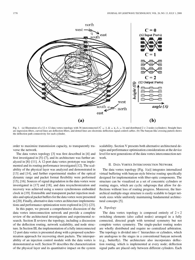
Fig. 1. (a) Illustration of a 12� 12 data vortex topology with 36 interconnected �� � ��� � ��� � �� and distributed 2� 2 nodes (cylinders). Straight linesare ingression fibers, curved lines are deflection fibers, and dotted lines are electronic deflection signal control cables. (b) The banyan-like crossing pattern showsthe deflection path connectivity for each cylinder.
order to maximize transmission capacity, to transparently tra-verse the network.
The data vortex topology [3] was first described in [4] andfirst investigated in [5]–[7], and its architecture was further an-alyzed in [8]–[11]. A 12-port data vortex prototype was imple-mented and its routing performance investigated [12]. The scal-ability of the physical layer was analyzed and demonstrated in[13] and [14], and further experimental studies of the opticaldynamic range and packet format flexibility were performed[15], [16]. Sources of signal degradation in the data vortex wereinvestigated in [17] and [18], and data resynchronization andrecovery was achieved using a source synchronous embeddedclock in [19]. Extensible and transparent packet injection mod-ules and optical packet buffers for the data vortex were presentedin [20]. Finally, alternative data vortex architecture implementa-tions and performance optimization were explored in [21]–[23].
In this paper, we present a comprehensive discussion of thedata vortex interconnection network and provide a completereview of the architectural investigations and experimental re-search. Section II reviews the topology, including a discussionof the deflection routing, network scalability, and node struc-ture. In Section III, the implementation of a fully interconnected12-port data vortex is presented along with a proposed synchro-nization approach for recovering short packets. The interoper-ability of an injection control module with the data vortex isdemonstrated as well. Section IV describes the characterizationof the physical layer and its quantitative impact on the system
scalability. Section V presents both alternative architectural de-signs and performance optimization considerations at the devicelevel for next generations of the data vortex interconnection net-work.
II. DATA VORTEX INTERCONNECTION NETWORK
The data vortex topology [Fig. 1(a)] integrates internalizedvirtual buffering with banyan-style bitwise routing specificallydesigned for implementation with fiber-optic components. Thestructure can be visualized as a set of concentric cylinders orrouting stages, which are cyclic subgroups that allow for de-flections without loss of routing progress. Moreover, the hier-archical multiple-stage structure is easily scalable to larger net-work sizes while uniformly maintaining fundamental architec-tural concepts [5].
A. Topology
The data vortex topology is composed entirely of 2 2switching elements (also called nodes) arranged in a fullyconnected, directed graph with terminal symmetry but notcomplete vertex symmetry. The single-packet routing nodesare wholly distributed and require no centralized arbitration.The topology is divided into hierarchies or cylinders, whichare analogous to the stages in a conventional banyan network(e.g., butterfly). The architecture also incorporates deflec-tion routing, which is implemented at every node; deflectionsignal paths are placed only between different cylinders. Each
LIBOIRON-LADOUCEUR et al.: THE DATA VORTEX OPTICAL PACKET SWITCHED INTERCONNECTION NETWORK 1779
cylinder (or stage) contains nodes around its circumferenceand nodes down its length. The topology con-tains a total of switching elements, or nodes,with possible input terminal nodes and an equivalentnumber of possible output terminal nodes. The position ofeach node is conventionally given by the triplet , where
.The switching nodes are interconnected using a set of ingres-
sion fibers, which connect nodes of the same height in adjacentcylinders; and deflection fibers, which connect nodes of dif-ferent heights within the same cylinder. The ingression fibersare of the same length throughout the entire system, as are thedeflection fibers. The deflection fibers’ height crossing patterns[Fig. 1(b)] direct packets through different height levels at eachhop to enable banyan routing (e.g., butterfly, omega) to a desiredheight and assist in balancing the load throughout the system,mitigating local congestion [5]–[7], [12].
Incoming packets are injected into the nodes of the outermostcylinder and propagate within the system in a synchronous,time-slotted fashion. The conventional nomenclature illustratespackets routing to progressively higher numbered cylindersas moving inward toward the network outputs. During eachtimeslot, each node either processes a single packet or remainsinactive. As a packet enters node , the th bit of thepacket header is compared to the th most significant bit in thenode’s height coordinate . If the bits match, the packet in-gresses to node through the node’s south output.Otherwise, it is routed eastward within the same cylinder tonode , where defines a transformationwhich expresses the above-mentioned height crossing patterns(for cylinder ) [6], [7]. Thus, packets progress to a highercylinder only when the th address bit matches, preserving the
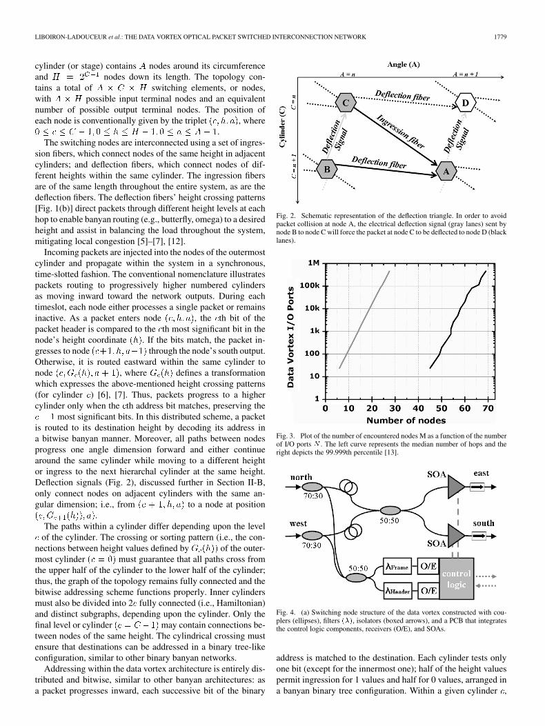
most significant bits. In this distributed scheme, a packetis routed to its destination height by decoding its address ina bitwise banyan manner. Moreover, all paths between nodesprogress one angle dimension forward and either continuearound the same cylinder while moving to a different heightor ingress to the next hierarchal cylinder at the same height.Deflection signals (Fig. 2), discussed further in Section II-B,only connect nodes on adjacent cylinders with the same an-gular dimension; i.e., from to a node at position
.The paths within a cylinder differ depending upon the level
of the cylinder. The crossing or sorting pattern (i.e., the con-nections between height values defined by of the outer-most cylinder must guarantee that all paths cross fromthe upper half of the cylinder to the lower half of the cylinder;thus, the graph of the topology remains fully connected and thebitwise addressing scheme functions properly. Inner cylindersmust also be divided into 2 fully connected (i.e., Hamiltonian)and distinct subgraphs, depending upon the cylinder. Only thefinal level or cylinder may contain connections be-tween nodes of the same height. The cylindrical crossing mustensure that destinations can be addressed in a binary tree-likeconfiguration, similar to other binary banyan networks.
Addressing within the data vortex architecture is entirely dis-tributed and bitwise, similar to other banyan architectures: asa packet progresses inward, each successive bit of the binary
Fig. 2. Schematic representation of the deflection triangle. In order to avoidpacket collision at node A, the electrical deflection signal (gray lanes) sent bynode B to node C will force the packet at node C to be deflected to node D (blacklanes).
Fig. 3. Plot of the number of encountered nodes M as a function of the numberof I/O ports � . The left curve represents the median number of hops and theright depicts the 99.999th percentile [13].
Fig. 4. (a) Switching node structure of the data vortex constructed with cou-plers (ellipses), filters ���, isolators (boxed arrows), and a PCB that integratesthe control logic components, receivers (O/E), and SOAs.
address is matched to the destination. Each cylinder tests onlyone bit (except for the innermost one); half of the height valuespermit ingression for 1 values and half for 0 values, arranged ina banyan binary tree configuration. Within a given cylinder ,
1780 JOURNAL OF LIGHTWAVE TECHNOLOGY, VOL. 26, NO. 13, JULY 1, 2008
nodes at all angles at a particular height (i.e., ) match thesame ( )th significant bit value, while the paths guaranteepreservation of the most significant address bits. Thus, witheach ingression to a successive cylinder, progressively more pre-cision is guaranteed in the destination address. Finally, on thelast cylinder , each node in the angular dimensionis assigned a least significant value in the destination addressso that the packets circulate within that cylinder until a matchis found for the last (A) bits (so-called angle-resolutionaddressing) [12].
As will be discussed in Section II-D, each switching node isbufferless and is designed to check exactly one bit of the des-tination address, in addition to the packet frame. When the se-lected address bit matches the value assigned to the node due toits position within the cylinder, the packet is allowed to ingressinto the next cylinder on the ingression fiber unless a deflectionsignal is received. When the selected address bit does not match,or when a deflection signal is received, the packet is routedwithin the same cylinder on the deflection fiber and the nodesends a deflection signal indicating that the next node will soonbe busy with the deflected packet. Therefore, every switchingelement always has an available deflection fiber (east) and in-gression fiber (south) used for routing matches.
While it may seem wasteful to have twice as many opticalpaths as necessary, having a guaranteed deflection fiber pathwayallows for an extraordinarily simple routing logic that can beexecuted extremely quickly [12], [24]. The distributed bitwiseaddressing scheme also helps to ensure that routing decisionsdo not dominate network latency. No buffers are used, so thenetwork latency can be reduced to approach optical time-of-flight.
B. Deflection Routing
Although packets can originate from either of the two inputports (north or west), recall that the node design is capable ofrouting only one packet at a time. This fundamental constraintyields a simplistic construction of the node but requires an archi-tectural implementation of internal blocking or deflection. De-flection within the data vortex thus differs from conventional de-flection routing topologies that allow for deflection routing at thecompletion of each discrete node hop. Instead, the data vortexdeflection implementation prevents two packets from simulta-neously entering the same switching node, and thus colliding,by controlling or blocking one of the two nodes connected up-stream of the input ports.
Therefore, a packet deflection in cylinder occurs for onlytwo reasons: 1) a packet is deflected in the adjacent cylinder
1, or 2) the packet in cylinder cannot be injected due to amismatch between its destination address and the node’s heightvalue. A packet that would otherwise ingress into that node oncylinder 1 from cylinder (when address bits match) canthus be required to remain in cylinder when the deflectionsignal indicates that the desired node is busy. This deflectionstructure results in “backpressure” from the inner cylinders
to the outer cylinders . Adeflected packet must traverse two additional node hops beforethe address matches again, as a consequence of the crossingpatterns.
The deflection signaling structure incorporates the output andinput terminals such that output nodes can receive busy sig-nals from the output queuing subsystem, and the input nodescan transmit similar busy signals to the input interface. Thus,packets that attempt input at the first cylinder may re-ceive a signal that indicates that the desired input node is busy;the packet must then be queued to reattempt injection or be dis-carded. The deflection signal relationship can be representedgeometrically as a triangle. In fact, this triangular deflectionunit is the fundamental building block of the entire data vortextopology. Only the arrangement of each leg differs from cylinderto cylinder, in accordance with the specific crossing patternsused. The deflection signal’s crossing pattern must be the sameas that of the deflection fiber since connections between cylin-ders do not undergo height translation.
In order to maintain correct timing for deflection signaling,particular latency conditions must be satisfied. Since implemen-tations of this architecture avoid buffering within the switchingelements, latencies are caused entirely by the optical and elec-trical (for control signals only) paths’ times-of-flight. To main-tain accurate deflection signaling, deflection signals must betransmitted sufficiently early such that the node receiving the de-flection signal can direct its packet appropriately. The timing ofcylinder 1 containing the node initiating the deflection musttherefore precede the timing of cylinder containing the nodereceiving the deflection signal. Thus, the ingression fibers mustbe shorter than the deflection fibers by an amount equal to theprocessing and transmission time of the deflection signal [24].Consequently, the timing cycles of the inner cylinders precedethose of the outer ones.
When the aforementioned timing condition is met for the datavortex implementation, global clocking for every switching ele-ment is not required. If packets are only injected at timeslots thatcorrespond to the deflection fiber latency, packets will maintainthis slotted arrival schedule at every position within the hierar-chal topology. Again, recall that no buffers or storage devicesare utilized; hence when physical time-of-flight requirementsare met, they hold for all packets at each node.
C. Scalability of the Topology
The data vortex topology exhibits a flexible modular architec-ture that is scalable to large numbers of input and output ports( ). To increase the size of the interconnection network,the number of ports can be augmented by increasing the cylin-ders , angles , or height parameters. Per the topology dis-cussion in Section II-A, the number of ports is defined as theproduct of the number of angles and heights
(1)
The cylinders represent the stages of the data vortex. Thecylinder number is defined by and corresponds to one plusthe base-two logarithm of , as each routing node consist oftwo inputs (west and north) and two outputs (south and east)
(2)
LIBOIRON-LADOUCEUR et al.: THE DATA VORTEX OPTICAL PACKET SWITCHED INTERCONNECTION NETWORK 1781
Following the above two equations, a topology can be appropri-ately designed. The modular architecture enables several pos-sible topologies for the same number of I/O ports. It has beenshown that for a given number of ports, a shorter height andgreater number of angles provide lower latencies as comparedto taller (large ) and narrower (small ) topologies [10].
In optical multistage interconnection networks, an importantparameter is the number of routing nodes a packet will tra-verse before reaching its destination. For the data vortex uti-lizing 2 2 switching elements, the number of nodes scaleslogarithmically with the number of ports [25], [26]
(3)
Packets will propagate through cascaded nodes; generally,increases with the network size but is also tightly cou-
pled to the network load. Various scenarios have been simu-lated to illustrate the effect of the topology and network loadon [9], [11]. The number of cascaded nodes directly affectsthe overall network latency. Due to the deflection character-istic of the network, the number of cascaded nodes has anon-Gaussian statistical distribution arising from the contentionresolution scheme [5], [7]. Simulations of the data vortex asa large-scale switching fabric have shown that for a heavilyloaded 10 k 10 k port data vortex implementation, 99.999%of the injected packets propagate through fewer than 58 internalswitching nodes with a median hop count of 19 (Fig. 3) [13].
D. Packet Self-Routing
The modular architecture of the data vortex and its im-pressive scalability are made possible by the simplicity of therouting node structure (Fig. 4). The nodes are evenly distributedacross the data vortex topology in a manner that facilitates con-tention resolution while minimizing latency and maximizingthroughput. Packets propagate from one of the two inputs of thenode (north or west) to one of the two outputs (east or south).Two SOAs are used to select one of the two outputs based onthe control information encoded along with the payload datawithin the optical packet (see Section II-E).
The two SOA gates are enabled by laser drivers that are con-trolled by the electronic decision circuitry internal to each node,producing the routing decisions on a per-packet basis withoutthe need of a central scheduler. To produce the routing deci-sion, the nodes in the first cylinder detect the presenceof Header 0, the nodes in the second cylinder detectHeader 1, and so forth. The frame information is used to vali-date the presence of a packet in the routing node. If the headerbit does not match the user-programmed value for the node, or ifthe interconnected node in an inner cylinder is busy, the packetis deflected to the next angle in the same cylinder. Here, cur-rent is supplied to the east SOA only. If the header bit matchesthat of the node and no deflection signal is received, then thepacket ingresses to the angle in the next cylinder (or stage), ascurrent is supplied to the south SOA only. In this distributedscheme, a packet is routed by decoding its address in a bitwisebanyan manner to its destination height. Once a packet reaches
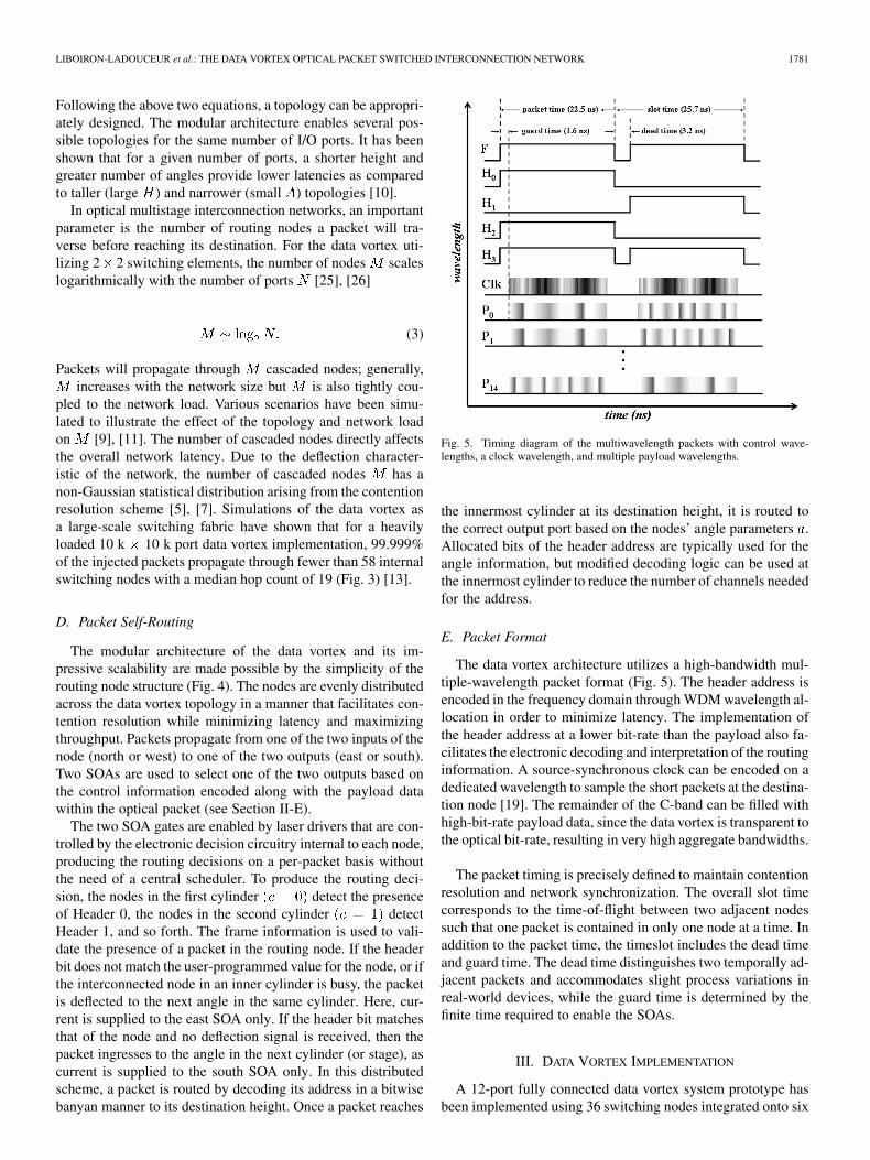
Fig. 5. Timing diagram of the multiwavelength packets with control wave-lengths, a clock wavelength, and multiple payload wavelengths.
the innermost cylinder at its destination height, it is routed tothe correct output port based on the nodes’ angle parameters .Allocated bits of the header address are typically used for theangle information, but modified decoding logic can be used atthe innermost cylinder to reduce the number of channels neededfor the address.
E. Packet Format
The data vortex architecture utilizes a high-bandwidth mul-tiple-wavelength packet format (Fig. 5). The header address isencoded in the frequency domain through WDM wavelength al-location in order to minimize latency. The implementation ofthe header address at a lower bit-rate than the payload also fa-cilitates the electronic decoding and interpretation of the routinginformation. A source-synchronous clock can be encoded on adedicated wavelength to sample the short packets at the destina-tion node [19]. The remainder of the C-band can be filled withhigh-bit-rate payload data, since the data vortex is transparent tothe optical bit-rate, resulting in very high aggregate bandwidths.
The packet timing is precisely defined to maintain contentionresolution and network synchronization. The overall slot timecorresponds to the time-of-flight between two adjacent nodessuch that one packet is contained in only one node at a time. Inaddition to the packet time, the timeslot includes the dead timeand guard time. The dead time distinguishes two temporally ad-jacent packets and accommodates slight process variations inreal-world devices, while the guard time is determined by thefinite time required to enable the SOAs.
III. DATA VORTEX IMPLEMENTATION
A 12-port fully connected data vortex system prototype hasbeen implemented using 36 switching nodes integrated onto six
1782 JOURNAL OF LIGHTWAVE TECHNOLOGY, VOL. 26, NO. 13, JULY 1, 2008
TABLE IDATA VORTEX IMPLEMENTATION WAVELENGTH ASSIGNMENT
printed circuit boards (PCBs) and interconnected by passive op-tics modules, single-mode fiber, and electronic cables. The de-sign of this system along with improvements for data recoveryand packet injection is discussed below.
A. Design of a Functional 12-Port Data Vortex
In this section, we discuss the design specifications used todemonstrate a fully functional optical packet switched intercon-nection network. Note that only off-the-shelf components wereused in the experimental implementation of the data vortex.
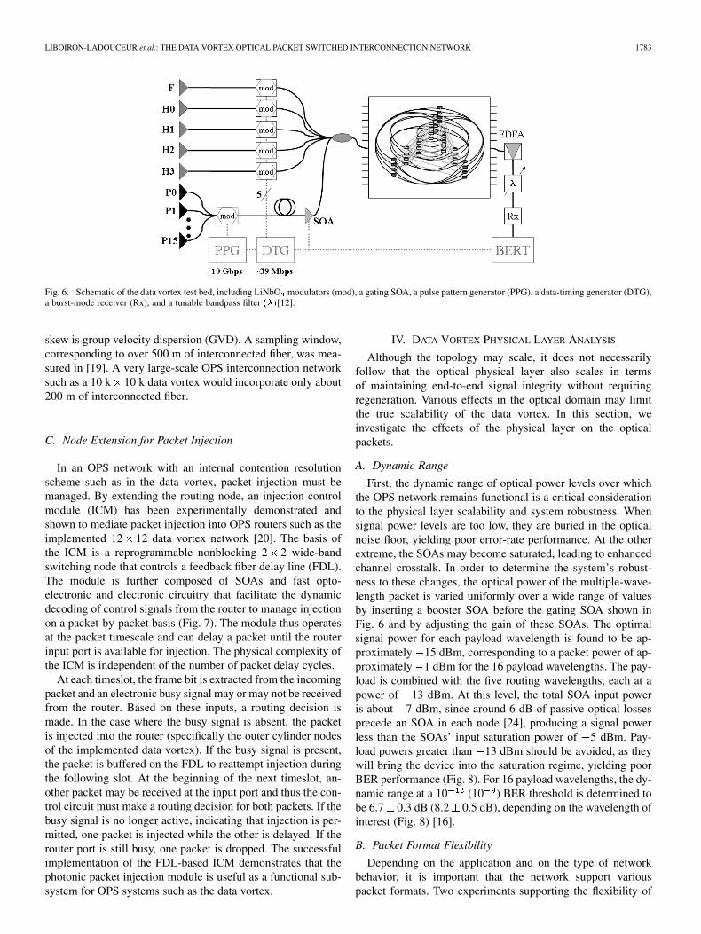
In the case of the 12-port data vortex , a4-bit header encoded on four header wavelengths is requiredto address each system output. For a 10 000-port system, 14headers would be required to route packets individually fromeach input port to each output port. While the packet is transpar-ently routed through the node, the header address is decoded ateach node by filtering a frame wavelength and one cylinder-spe-cific header wavelength. Upon entering the node from eitherinput port, 30% of the input packet’s power is extracted for con-trol signal decoding. The control wavelengths are filtered with100-GHz optical bandpass filters and directed to photodetectors.The receiver data path is designed to be dc-coupled to accom-modate bursty packet arrival. The remainder of the packet power(70%) is routed through a fixed length optical delay line and a50:50 coupler, which combines the two input ports and splits theoptical packet to the two SOAs. The SOAs are followed by iso-lators in order to mitigate counter-propagating amplified spon-taneous emission (ASE) noise.
The entire node’s measured latency is 15.8 ns [24]. A packetslot time of 25.7 ns is determined by the total time-of-flight la-tency between two nodes within the same cylinder and the de-flection-timing requirement. Each packet is 22.5 ns long and in-cludes a guard time of 1.6 ns inserted at both the beginning andthe end of the packet, yielding a net payload window of 19.3 ns(Fig. 5). A guard time is required for the SOA switching transi-tion time, which is approximately 1 ns. The control informationrequired to route the packets consists of one frame and a 4-bitheader. Sixteen payload channels are modulated at 10 Gb/s for160 Gb/s of aggregated bandwidth. Packet payload bandwidthsapproaching terabit/second can be straightforwardly achievedby increasing the channel count and modulated data rates (e.g.,25 channels modulated at 40 Gb/s). The selected address fieldwavelength channels are shown in Table I. In the innermostcylinder , a decoding logic uses both header 2 and header3 to determine the output port address.
In the experimental test bed illustrated in Fig. 6, the pay-load wavelengths are generated by distributed feedback lasers(DFBs) modulated with a 2 1 pseudorandom bit sequence
at 10 Gb/s and decorrelated with a length of optical fiber byapproximately 450 ps/nm. An SOA segments the continuousdata stream into packets. Prior to injection in the data vortex,the header and frame information is independently modulatedand coupled to the multiwavelength packet to meet the requiredpacket structure (Fig. 5). The timing of all the signals are closelycalibrated using the data-timing generator (DTG). At the outputport, the packets are preamplified with an erbium-doped fiberamplifier, filtered for a specific payload channel, and convertedto an electrical signal through a dc-coupled receiver module.The error rate of the data contained within the individual pay-load wavelengths of each packet is measured using a bit-error-rate (BER) tester (BERT). The BERT, which enables extensiveanalysis of the performance of the data vortex network, is exter-nally gated and synchronized with the pulse pattern generator(PPG).
To validate the design, routing experiments were performedto demonstrate the correct addressing of packets through thesystem and to verify the functionality of its contention resolutionscheme [3]. All 12 output ports are addressed and contentionsare resolved between switching nodes according to the datavortex internal deflection routing mechanism. The system iscapable of routing packets with 160 Gb/s (10 Gb/s 16 WDMchannels) payloads from any one of the 12 input ports toany one of the 12 output ports. The average (and median)latency for the system is 110 ns, corresponding to five nodehops [27].
The emulation of realistic network traffic utilizing a super-computing interconnection network traffic workload was alsodemonstrated [28]. The evaluation workload uses processor-memory accesses from an application in a SPLASH-2 parallelcomputing benchmark suite [29]. The methodology captures thebehavior of shared memory parallel execution, providing mes-sage traffic typically found in a similarly configured multipro-cessor system. The simulation results show that all packets arerouted correctly; furthermore, appropriate deflections and ad-dress decoding are also observed.
B. Resynchronization and Recovery
Data traffic in interconnection networks such as the datavortex often consists of short and bursty message exchanges.One of the key challenges is resynchronization and recoveryof data at the destination node without the use of conventionalphase-locked loop designs. In the data vortex, a clock syn-chronous to the data payload can be embedded in the packetand used as the timing reference at the destination node [19].The embedded clock avoids the complexity of low-skew clockdistribution through large-scale synchronous interconnectionnetworks and simplifies the message recovery circuitry ascompared to asynchronous networks.
This approach has been demonstrated in the implementeddata vortex network by recovering WDM messages routedthrough five switching nodes. The messages are entirely recov-ered and processed at the destination node using an embeddedclock signal. The clock-to-data skew, defined as the relativetiming between the payload and the embedded clock, mustremain within the setup-time and hold-time requirements ofthe deserializer. However, a main contributor to clock-to-data
LIBOIRON-LADOUCEUR et al.: THE DATA VORTEX OPTICAL PACKET SWITCHED INTERCONNECTION NETWORK 1783
Fig. 6. Schematic of the data vortex test bed, including LiNbO modulators (mod), a gating SOA, a pulse pattern generator (PPG), a data-timing generator (DTG),a burst-mode receiver (Rx), and a tunable bandpass filter ���[12].
skew is group velocity dispersion (GVD). A sampling window,corresponding to over 500 m of interconnected fiber, was mea-sured in [19]. A very large-scale OPS interconnection networksuch as a 10 k 10 k data vortex would incorporate only about200 m of interconnected fiber.
C. Node Extension for Packet Injection
In an OPS network with an internal contention resolutionscheme such as in the data vortex, packet injection must bemanaged. By extending the routing node, an injection controlmodule (ICM) has been experimentally demonstrated andshown to mediate packet injection into OPS routers such as theimplemented 12 12 data vortex network [20]. The basis ofthe ICM is a reprogrammable nonblocking 2 2 wide-bandswitching node that controls a feedback fiber delay line (FDL).The module is further composed of SOAs and fast opto-electronic and electronic circuitry that facilitate the dynamicdecoding of control signals from the router to manage injectionon a packet-by-packet basis (Fig. 7). The module thus operatesat the packet timescale and can delay a packet until the routerinput port is available for injection. The physical complexity ofthe ICM is independent of the number of packet delay cycles.
At each timeslot, the frame bit is extracted from the incomingpacket and an electronic busy signal may or may not be receivedfrom the router. Based on these inputs, a routing decision ismade. In the case where the busy signal is absent, the packetis injected into the router (specifically the outer cylinder nodesof the implemented data vortex). If the busy signal is present,the packet is buffered on the FDL to reattempt injection duringthe following slot. At the beginning of the next timeslot, an-other packet may be received at the input port and thus the con-trol circuit must make a routing decision for both packets. If thebusy signal is no longer active, indicating that injection is per-mitted, one packet is injected while the other is delayed. If therouter port is still busy, one packet is dropped. The successfulimplementation of the FDL-based ICM demonstrates that thephotonic packet injection module is useful as a functional sub-system for OPS systems such as the data vortex.
IV. DATA VORTEX PHYSICAL LAYER ANALYSIS
Although the topology may scale, it does not necessarilyfollow that the optical physical layer also scales in termsof maintaining end-to-end signal integrity without requiringregeneration. Various effects in the optical domain may limitthe true scalability of the data vortex. In this section, weinvestigate the effects of the physical layer on the opticalpackets.
A. Dynamic Range
First, the dynamic range of optical power levels over whichthe OPS network remains functional is a critical considerationto the physical layer scalability and system robustness. Whensignal power levels are too low, they are buried in the opticalnoise floor, yielding poor error-rate performance. At the otherextreme, the SOAs may become saturated, leading to enhancedchannel crosstalk. In order to determine the system’s robust-ness to these changes, the optical power of the multiple-wave-length packet is varied uniformly over a wide range of valuesby inserting a booster SOA before the gating SOA shown inFig. 6 and by adjusting the gain of these SOAs. The optimalsignal power for each payload wavelength is found to be ap-proximately 15 dBm, corresponding to a packet power of ap-proximately 1 dBm for the 16 payload wavelengths. The pay-load is combined with the five routing wavelengths, each at apower of 13 dBm. At this level, the total SOA input poweris about 7 dBm, since around 6 dB of passive optical lossesprecede an SOA in each node [24], producing a signal powerless than the SOAs’ input saturation power of 5 dBm. Pay-load powers greater than 13 dBm should be avoided, as theywill bring the device into the saturation regime, yielding poorBER performance (Fig. 8). For 16 payload wavelengths, the dy-namic range at a 10 (10 ) BER threshold is determined tobe 6.7 0.3 dB (8.2 0.5 dB), depending on the wavelength ofinterest (Fig. 8) [16].
B. Packet Format Flexibility
Depending on the application and on the type of networkbehavior, it is important that the network support variouspacket formats. Two experiments supporting the flexibility of

1784 JOURNAL OF LIGHTWAVE TECHNOLOGY, VOL. 26, NO. 13, JULY 1, 2008
Fig. 7. The injection control module is composed of SOAs, optical couplers,filters, p-i-n photodetectors, optical fiber, and an electronic control circuit [20].
Fig. 8. Measured BER versus received power for the 16 payload wavelengthsillustrating the dynamic power range at BERs of 10 and 10 [16].
the data vortex packet format have been presented [15], [16].These confirm that the system can simultaneously route packetscontaining variable-sized payloads by altering the number ofpayload wavelengths in the packet and the time duration ofthe payload data stream. The first experimental demonstrationutilizes a variable number of payload wavelengths, while thesecond utilizes a variable payload time duration while varyingthe relative location within the timeslot. Specifically, packetswith payloads composed of 4, 8, 12, or 16 wavelengths,and time durations of 9.6 and 19.3 ns, are simultaneouslyrouted through a five-node path in the network. Therefore, ina single 25.7-ns timeslot, the data capacity can range from48 to 384 bytes, corresponding to a net bandwidth in therange of 15–120 Gb/s. The 6-dB variation in power betweenthe packets of 4 and 16 payload wavelengths falls withinthe previously discussed 6.7-dB dynamic range. As a result,BERs of 10 or better were verified for all possible packetformats (4, 8, 12, or 16 wavelengths and 9.6- or 19.3-nsdurations). The demonstrated flexibility very clearly illustratesthe transparent nature of the implemented architecture andswitching node design.
Fig. 9. Power penalty of each of the 16 payload wavelengths for a five-nodepath through the network [16].
C. Routing Node Power Penalty
In many OPS networks, the predominant switching elementused is the commercially available SOA, which has a fastswitching time, high extinction ratio, broad gain bandwidth,and high potential for integration. The primary function of theSOA is to efficiently and transparently route a broadband packetas well as to compensate for small switching node losses. TheSOA, however, introduces ASE noise along with the amplifiedsignal, causing degradation of the optical signal-to-noise ratio(OSNR). In [18], the eye diagram quality factor Q of a typicalpacket payload channel ( 1547 nm) is shown to degrade from21.2 dB before injection to 19.0 dB after propagation througha five-node path in the network, which indicates an averagedecline of approximately 0.4 dB per node. Measurements havealso indicated an average OSNR degradation of 2.7 dB pernode for a five-node path [16]. Although the SOA’s noise is notexpected to increase linearly for a large number of nodes, theprecise scaling is difficult to quantify in a concise manner [31].The total power penalty at the receiver for a five-node pathis found to vary between 1.7 and 4.1 dB, measured at a BERof 10 , for all 16 payload wavelengths; the average powerpenalty is 2.6 dB (Fig. 9).
D. Node Cascadability
The node cascadability ultimately determines the physicallayer size scalability of an SOA-based optical switching net-work. Node cascadability is influenced by the launched inputpower of the packets, the power per channel, the number ofchannels, and the bandwidth across which the channels are dis-tributed. The scalability of a packet-switched optical intercon-nection network using SOA switching elements has been previ-ously investigated [13]. Using a recirculating loop test-bed en-vironment, the SOA switching nodes were constructed in ac-cordance with the data vortex network architecture. Here, it wasshown that BERs lower than 10 can be maintained through58 node hops (sufficient for a 10 k 10 k port interconnectionnetwork) for eight wavelength channels spanning 24.2 nm of
LIBOIRON-LADOUCEUR et al.: THE DATA VORTEX OPTICAL PACKET SWITCHED INTERCONNECTION NETWORK 1785
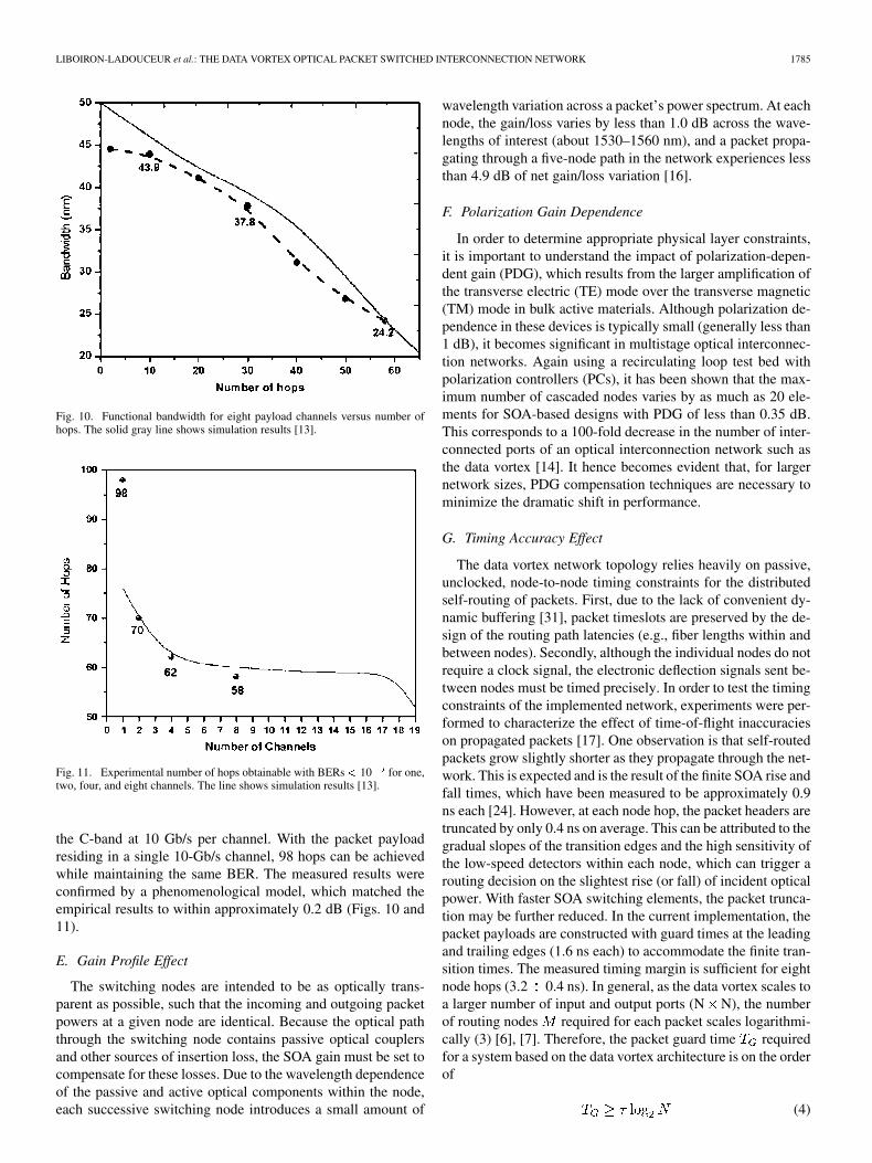
Fig. 10. Functional bandwidth for eight payload channels versus number ofhops. The solid gray line shows simulation results [13].
Fig. 11. Experimental number of hops obtainable with BERs� 10 for one,two, four, and eight channels. The line shows simulation results [13].
the C-band at 10 Gb/s per channel. With the packet payloadresiding in a single 10-Gb/s channel, 98 hops can be achievedwhile maintaining the same BER. The measured results wereconfirmed by a phenomenological model, which matched theempirical results to within approximately 0.2 dB (Figs. 10 and11).
E. Gain Profile Effect
The switching nodes are intended to be as optically trans-parent as possible, such that the incoming and outgoing packetpowers at a given node are identical. Because the optical paththrough the switching node contains passive optical couplersand other sources of insertion loss, the SOA gain must be set tocompensate for these losses. Due to the wavelength dependenceof the passive and active optical components within the node,each successive switching node introduces a small amount of
wavelength variation across a packet’s power spectrum. At eachnode, the gain/loss varies by less than 1.0 dB across the wave-lengths of interest (about 1530–1560 nm), and a packet propa-gating through a five-node path in the network experiences lessthan 4.9 dB of net gain/loss variation [16].
F. Polarization Gain Dependence
In order to determine appropriate physical layer constraints,it is important to understand the impact of polarization-depen-dent gain (PDG), which results from the larger amplification ofthe transverse electric (TE) mode over the transverse magnetic(TM) mode in bulk active materials. Although polarization de-pendence in these devices is typically small (generally less than1 dB), it becomes significant in multistage optical interconnec-tion networks. Again using a recirculating loop test bed withpolarization controllers (PCs), it has been shown that the max-imum number of cascaded nodes varies by as much as 20 ele-ments for SOA-based designs with PDG of less than 0.35 dB.This corresponds to a 100-fold decrease in the number of inter-connected ports of an optical interconnection network such asthe data vortex [14]. It hence becomes evident that, for largernetwork sizes, PDG compensation techniques are necessary tominimize the dramatic shift in performance.
G. Timing Accuracy Effect
The data vortex network topology relies heavily on passive,unclocked, node-to-node timing constraints for the distributedself-routing of packets. First, due to the lack of convenient dy-namic buffering [31], packet timeslots are preserved by the de-sign of the routing path latencies (e.g., fiber lengths within andbetween nodes). Secondly, although the individual nodes do notrequire a clock signal, the electronic deflection signals sent be-tween nodes must be timed precisely. In order to test the timingconstraints of the implemented network, experiments were per-formed to characterize the effect of time-of-flight inaccuracieson propagated packets [17]. One observation is that self-routedpackets grow slightly shorter as they propagate through the net-work. This is expected and is the result of the finite SOA rise andfall times, which have been measured to be approximately 0.9ns each [24]. However, at each node hop, the packet headers aretruncated by only 0.4 ns on average. This can be attributed to thegradual slopes of the transition edges and the high sensitivity ofthe low-speed detectors within each node, which can trigger arouting decision on the slightest rise (or fall) of incident opticalpower. With faster SOA switching elements, the packet trunca-tion may be further reduced. In the current implementation, thepacket payloads are constructed with guard times at the leadingand trailing edges (1.6 ns each) to accommodate the finite tran-sition times. The measured timing margin is sufficient for eightnode hops (3.2 0.4 ns). In general, as the data vortex scales toa larger number of input and output ports (N N), the numberof routing nodes required for each packet scales logarithmi-cally (3) [6], [7]. Therefore, the packet guard time requiredfor a system based on the data vortex architecture is on the orderof
(4)
1786 JOURNAL OF LIGHTWAVE TECHNOLOGY, VOL. 26, NO. 13, JULY 1, 2008
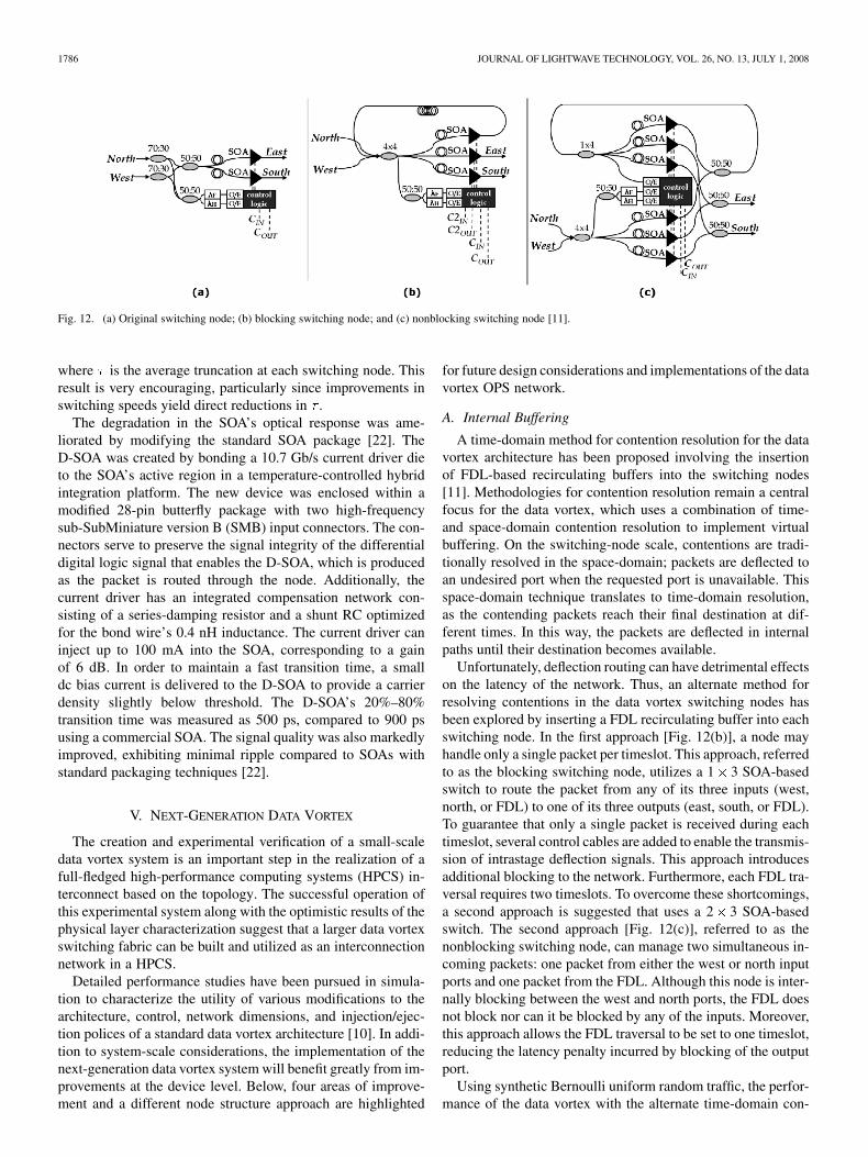
Fig. 12. (a) Original switching node; (b) blocking switching node; and (c) nonblocking switching node [11].
where is the average truncation at each switching node. Thisresult is very encouraging, particularly since improvements inswitching speeds yield direct reductions in .
The degradation in the SOA’s optical response was ame-liorated by modifying the standard SOA package [22]. TheD-SOA was created by bonding a 10.7 Gb/s current driver dieto the SOA’s active region in a temperature-controlled hybridintegration platform. The new device was enclosed within amodified 28-pin butterfly package with two high-frequencysub-SubMiniature version B (SMB) input connectors. The con-nectors serve to preserve the signal integrity of the differentialdigital logic signal that enables the D-SOA, which is producedas the packet is routed through the node. Additionally, thecurrent driver has an integrated compensation network con-sisting of a series-damping resistor and a shunt RC optimizedfor the bond wire’s 0.4 nH inductance. The current driver caninject up to 100 mA into the SOA, corresponding to a gainof 6 dB. In order to maintain a fast transition time, a smalldc bias current is delivered to the D-SOA to provide a carrierdensity slightly below threshold. The D-SOA’s 20%–80%transition time was measured as 500 ps, compared to 900 psusing a commercial SOA. The signal quality was also markedlyimproved, exhibiting minimal ripple compared to SOAs withstandard packaging techniques [22].
V. NEXT-GENERATION DATA VORTEX
The creation and experimental verification of a small-scaledata vortex system is an important step in the realization of afull-fledged high-performance computing systems (HPCS) in-terconnect based on the topology. The successful operation ofthis experimental system along with the optimistic results of thephysical layer characterization suggest that a larger data vortexswitching fabric can be built and utilized as an interconnectionnetwork in a HPCS.
Detailed performance studies have been pursued in simula-tion to characterize the utility of various modifications to thearchitecture, control, network dimensions, and injection/ejec-tion polices of a standard data vortex architecture [10]. In addi-tion to system-scale considerations, the implementation of thenext-generation data vortex system will benefit greatly from im-provements at the device level. Below, four areas of improve-ment and a different node structure approach are highlighted
for future design considerations and implementations of the datavortex OPS network.
A. Internal Buffering
A time-domain method for contention resolution for the datavortex architecture has been proposed involving the insertionof FDL-based recirculating buffers into the switching nodes[11]. Methodologies for contention resolution remain a centralfocus for the data vortex, which uses a combination of time-and space-domain contention resolution to implement virtualbuffering. On the switching-node scale, contentions are tradi-tionally resolved in the space-domain; packets are deflected toan undesired port when the requested port is unavailable. Thisspace-domain technique translates to time-domain resolution,as the contending packets reach their final destination at dif-ferent times. In this way, the packets are deflected in internalpaths until their destination becomes available.
Unfortunately, deflection routing can have detrimental effectson the latency of the network. Thus, an alternate method forresolving contentions in the data vortex switching nodes hasbeen explored by inserting a FDL recirculating buffer into eachswitching node. In the first approach [Fig. 12(b)], a node mayhandle only a single packet per timeslot. This approach, referredto as the blocking switching node, utilizes a 1 3 SOA-basedswitch to route the packet from any of its three inputs (west,north, or FDL) to one of its three outputs (east, south, or FDL).To guarantee that only a single packet is received during eachtimeslot, several control cables are added to enable the transmis-sion of intrastage deflection signals. This approach introducesadditional blocking to the network. Furthermore, each FDL tra-versal requires two timeslots. To overcome these shortcomings,a second approach is suggested that uses a 2 3 SOA-basedswitch. The second approach [Fig. 12(c)], referred to as thenonblocking switching node, can manage two simultaneous in-coming packets: one packet from either the west or north inputports and one packet from the FDL. Although this node is inter-nally blocking between the west and north ports, the FDL doesnot block nor can it be blocked by any of the inputs. Moreover,this approach allows the FDL traversal to be set to one timeslot,reducing the latency penalty incurred by blocking of the outputport.
Using synthetic Bernoulli uniform random traffic, the perfor-mance of the data vortex with the alternate time-domain con-

LIBOIRON-LADOUCEUR et al.: THE DATA VORTEX OPTICAL PACKET SWITCHED INTERCONNECTION NETWORK 1787
Fig. 13. Simulation results showing the effect of the FDL hop limit on accep-tance rate at injection rates of 0.3 and 0.7 [21].
tention resolution technique has been simulated with a C++program, and the results were compared to the original datavortex virtual buffering mechanism. Each of the new switchingnode design approaches (blocking and nonblocking) was evalu-ated with respect to the following metrics: acceptance rate andthroughput, mean latency, and latency distribution.
Simulations demonstrate that the acceptance rate monotoni-cally decreases with the injection rate and that the FDL-basedconfigurations improve the acceptance rate only at medium-to-high injection rates, while asymmetric injection (injecting ononly a fraction of the angles) improves the acceptance rate at lowinjection rates (Fig. 13). Additionally, for a data vortex realiza-tion (with given H, C, and A parameters), simulated throughputresults indicate that the network utilizing the nonblocking nodeyields the highest throughput saturation value.
The latency of the data vortex architecture is also animportant metric. Simulations show that a network incorpo-rating FDL-based buffers has lower subsaturation latency andperforms better than an original data vortex network with sym-metric and asymmetric injections. More performance metricswere simulated in [21] and demonstrated the advantages ofusing FDL-based recirculating buffers as an alternate techniquefor contention resolution.
B. Nondeterministic Latency
Due to the nondeterministic nature of the paths traversed bypackets propagating through the data vortex network, packet re-ordering is a common occurrence. Thus, the application spaceof the original data vortex interconnection network is limitedby this topological characteristic. Furthermore, nondetermin-istic routing through the network gives rise to the possibility ofunbounded latency distributions; these not only are detrimentalto latency sensitive applications, such as memory accesses, butalso contribute to physical-layer-induced limitations on networkscalability. Investigations have explored the utility of variationson the traditional data vortex network in an attempt to alleviatethis shortcoming [11].
C. Optimization of the Node
In addition to considering the node routing efficiency, self-routed networks rely on error-free routing through the internal
Fig. 14. Schematic of the multistage-optimized switching node with Schmitttrigger comparators in the routing logic and fast-switching D-SOAs, optical re-ceivers (O/E), and fiber delay lines [22].
switching nodes. Bit errors in payload data may be tolerabledue to data encoding and forward error-correction techniquesemployed at the source and destination devices. However, anyerrors manifested as the result of misroutes at a node will havefatal effects on the operation of the network (i.e., packet loss andcollisions with other packets). As packets propagate through acascade of switching nodes, ASE noise and nonlinear effectssuch as cross-gain modulation can create erratic behavior in theoptical signal. Further, slight changes in incident optical powerat the photodetectors in each node will be interpreted as glitchesin the electrical routing signals gating the SOAs and may leadto packet truncation and/or collision.
In order to increase the noise immunity of our switchingnodes, a dual thresholding scheme has been implementedvia the use of a Schmitt trigger comparator circuit followingthe header receivers [22]. A prototype evaluation switchingnode (Fig. 14) has been implemented with the aforementionedSchmitt trigger comparator circuitry, the D-SOA devices men-tioned in Section IV-G, and the control logic by means ofcomplex programmable logic devices [22]. The addition of ahysteric response increases the noise margins of the electronicdecision logic by maintaining exaggerated transition thresh-olds. Thus, low swing glitches in the routing signal due to noiseat the switching node receivers are eliminated. This improve-ment maintains correct routing functionality in the presence ofglitches, yielding increased switching node robustness.
D. Faster Switching Node
The switching time and latency of the current node struc-ture are limited by the electrical signal processing time. To in-crease the node throughput and minimize the packet truncation(Section IV-G), an all-optical node structure approach can po-tentially minimize the processing time of the current node struc-ture [32]. The logic performed by the switching node wouldbe performed in the optical domain. In fact, an all-optical self-routing switching node for the data vortex architecture has beenimplemented [33]. The node uses two Mach–Zehnder interfer-ometers (MZIs) integrated with SOAs to perform the routinglogic on the extracted header signal and the control signal fromthe inner cylinder node. A 1-dB power penalty (BER 10 )
1788 JOURNAL OF LIGHTWAVE TECHNOLOGY, VOL. 26, NO. 13, JULY 1, 2008
was measured partly due to the additional ASE of the MZI-SOAstructure, compared to 0.4 dB for the current node structure(Section IV-C). Hence, more work is required to enable the ap-plication of all-optical node structures to large OPS networksizes.
E. Packet Structure
Although improvements to the aforementioned characteris-tics of the SOA can be implemented, modifications to the packetformat may also mitigate the limitations imposed by imperfectoptical switching devices. First, the routing wavelengths can beoptimally assigned following the characterization of the spec-tral gain profile of the chosen SOAs. This will serve to mitigatethe wavelength-dependent gain mismatches introduced by thedevices to different channels in a multiple-wavelength packet.Specifically, channels experiencing less gain through the SOAdevices will be relegated to contain higher order address infor-mation, since destination tag routing employed by the networkarchitecture will utilize these channels first. Secondly, gain-flat-tening filters can be implemented to further compensate for theapparent gain imbalance.
VI. CONCLUSION
A novel paradigm for high-capacity low-latency OPS in-terconnection networks based on the data vortex architecturehas been enunciated. The architectural design capitalizes onthe immense bandwidth provided by optical signals encodedand transmitted over contemporary fiber-optic componentsand avoids common pitfalls and shortcomings of photonictechnologies. A comprehensive discussion of the data vortextopology, switching node design, packet routing, and controlhas been provided. Further, an experimental system implemen-tation, which shows the feasibility of large-scale data vortexinterconnection networks, has been discussed. A completecharacterization of the implemented network’s physical layerhas provided additional performance information, especiallyhighlighting the cascadability of the individual switching nodes.Finally, design considerations for the topology and componentsof the next-generation data vortex have been addressed.
REFERENCES
[1] W. J. Dally and B. Towles, Principles and Practices of InterconnectionNetworks. San Francisco, CA: Morgan Kaufmann, 2004.
[2] R. Ramaswami and K. N. Sivarajan, Optical Networks: A PracticalPerspective, 2nd ed. San Francisco, CA: Morgan Kaufmann, 2002.
[3] C. Reed, “Multiple level minimum logic network,” U.S. Patent5 996 020, Nov. 30, 1999.
[4] N. F. Maxemchuk, “Regular and mesh topologies in local andmetropolitan area networks,” AT&T Tech. J., vol. 64, no. 7, pp.1659–1686, Sep. 1985.
[5] Q. Yang, K. Bergman, G. D. Hughes, and F. G. Johnson, “WDM packetrouting for high-capacity data networks,” J. Lightw. Technol., vol. 19,pp. 1420–1426, Oct. 2001.
[6] Q. Yang and K. Bergman, “Traffic control and WDM routing in thedata vortex packet switch,” IEEE Photon. Technol. Lett., vol. 14, pp.236–238, Feb. 2002.
[7] Q. Yang and K. Bergman, “Performance of the data vortex switch ar-chitecture under nonuniform and bursty traffic,” J. Lightw. Technol.,vol. 20, pp. 1242–1247, Aug. 2002.
[8] B. A. Small, A. Shacham, K. Bergman, K. Athikulwongse, C. Hawkins,and D. S. Wills, “Emulation of realistic network traffic patterns onan eight-node data vortex interconnection network subsystem,” J. Opt.Netw., vol. 3, no. 11, pp. 802–809, Nov. 2004.
[9] C. Hawkins, B. A. Small, D. S. Wills, and K. Bergman, “The datavortex, an all optical path multicomputer interconnection network,”IEEE Trans. Parallel Distrib. Syst., vol. 18, pp. 409–420, Mar. 2007.
[10] C. Hawkins and D. S. Wills, “Impact of number of angles on the perfor-mance of the data vortex optical interconnection network,” J. Lightw.Technol., vol. 24, pp. 3288–3294, Sep. 2006.
[11] A. Shacham and K. Bergman, “On contention resolution in the datavortex optical interconnection network,” J. Opt. Netw., vol. 6, no. 6,pp. 777–788, Jun. 2007.
[12] A. Shacham, B. A. Small, O. Liboiron-Ladouceur, and K. Bergman,“A fully implemented 12� 12 data vortex optical packet switching in-terconnection network,” J. Lightw. Technol., vol. 23, pp. 3066–3075,Oct. 2005.
[13] O. Liboiron-Ladouceur, B. A. Small, and K. Bergman, “Physical layerscalability of a WDM optical packet interconnection network,” J.Lightw. Technol., vol. 24, pp. 262–270, Jan. 2006.
[14] O. Liboiron-Ladouceur, K. Bergman, M. Boroditsky, and M. Brodsky,“Polarization-dependent gain in SOA-based optical multistage inter-connection networks,” J. Lightw. Technol., vol. 24, pp. 3959–3967,Nov. 2006.
[15] B. A. Small, B. G. Lee, and K. Bergman, “Flexibility of optical packetformat in a complete 12� 12 data vortex network,” IEEE Photon.Technol. Lett., vol. 18, pp. 1693–1695, Aug. 2006.
[16] B. A. Small, T. Kato, and K. Bergman, “Dynamic power considerationin a complete 12� 12 optical packet switching fabric,” IEEE Photon.Technol. Lett., vol. 17, pp. 2472–2474, Nov. 2005.
[17] B. A. Small and K. Bergman, “Slot timing consideration in opticalpacket switching networks,” IEEE Photon. Technol. Lett., vol. 17, pp.2478–2480, Nov. 2005.
[18] B. G. Lee, B. A. Small, and K. Bergman, “Signal degradation througha 12� 12 optical packet switching network,” in Proc. Eur. Conf. Opt.Commun., Sep. 2006, paper We3.P.131.
[19] O. Liboiron-Ladouceur, C. Gray, D. C. Keezer, and K. Bergman, “Bit-parallel message exchange and data recovery in optical packet switchedinterconnection networks,” IEEE Photon. Technol. Lett., vol. 18, pp.770–781, Mar. 15, 2006.
[20] A. Shacham, B. A. Small, and K. Bergman, “A wideband photonicpacket injection control module for optical packet switching routers,”IEEE Photon. Technol. Lett., vol. 17, pp. 2778–2780, Dec. 2005.
[21] A. Shacham and K. Bergman, “Optimizing the performance of adata vortex interconnection network,” J. Opt. Netw., vol. 6, no. 4, pp.369–374, Apr. 2007.
[22] O. Liboiron-Ladouceur and K. Bergman, “Optimized switchingnode for optical multistage interconnection networks,” IEEE Photon.Technol. Lett., vol. 19, pp. 1658–1660, Oct. 15, 2007.
[23] Q. Yang, “Improved performance using shortcut path routing withindata vortex switch network,” Electron. Lett., vol. 41, no. 22, pp.1253–1254, Oct. 2005.
[24] B. A. Small, A. Shacham, and K. Bergman, “Ultra-low latency op-tical packet switching node,” IEEE Photon. Technol. Lett., vol. 17, pp.1564–1566, Jul. 2005.
[25] Y. Pan, C. Qiao, and Y. Yang, “Optical multistage interconnection net-works: New challenges and approaches,” IEEE Commun. Mag., vol.37, pp. 50–56, Feb. 1999.
[26] H. Ahmadi and W. E. Denzel, “A Survey of modern high-performanceswitching techniques,” IEEE J. Sel. Areas Commun., vol. 7, pp.1091–1103, Sep. 1989.
[27] B. A. Small, O. Liboiron-Ladouceur, A. Shacham, J. P. Mack, and K.Bergman, “Demonstration of a complete 12-port terabit capacity op-tical packet switching fabric,” in Proc. Opt. Fiber Commun. Conf., Mar.2005, paper OWK1.
[28] B. A. Small, A. Shacham, K. Bergman, K. Athikulwongse, C. Hawkins,and D. S. Wills, “Emulation of realistic network traffic patterns on aneight-node data vortex interconnection network subsystems,” J. Opt.Netw., vol. 3, no. 11, pp. 802–809, Nov. 2004.
[29] J. M. Arnold, “The SPLASH-2 software environment,” J. Super-comput., vol. 9, no. 3, pp. 277–290, Sep. 1995.
[30] H. A. Haus, “The noise figure of optical amplifiers,” IEEE Photon.Technol. Lett., vol. 10, pp. 1602–1604, Nov. 1998.
[31] R. S. Tucker, K. Pei-Chen, and C. J. Chang-Hasnon, “Slow-light opticalbuffers: Capabilities and fundamental limitations,” J. Lightw. Technol.,vol. 23, pp. 4046–4066, Dec. 2005.
[32] C. K. Yow, Y. J. Chai, R. V. Reading-Picopoulos, I. H. White, C. G.Leburn, A. McWilliam, A. A. Lagatsky, C. T. A. Brown, W. Sibbett,G. Maxwell, and R. McDougall, “Experimental demonstration of fem-tosecond switching of a fully packaged all-optical switch,” in Proc.Opt. Fiber Commun. Conf., Mar. 2005, paper OThE4.
LIBOIRON-LADOUCEUR et al.: THE DATA VORTEX OPTICAL PACKET SWITCHED INTERCONNECTION NETWORK 1789
[33] H.-D. Jung, I. T. Monroy, A. M. J. Koone, and E. Tangdiongga,“All-optical data vortex node using an MZI-SOA switch array,” IEEEPhoton. Technol. Lett., vol. 19, pp. 1777–1779, Nov. 15, 2007.
Odile Liboiron-Ladouceur (M’95) was born inMontréal, QC, Canada. She received the B. Engdegree in electrical engineering from McGill Uni-versity, Montréal, in 1999 and the M.S. and Ph.D.degrees from Columbia University, New York,in 2003 and 2007, respectively, all in electricalengineering.
Her thesis work was related to the data plane andphysical layer analysis of optical interconnectionnetworks. She is currently a Postdoctoral Researcherwith the Photonics Systems group, McGill Univer-
sity, where she works on ultra-high-data-rate optical transport networks. She isthe author or coauthor of 30 papers in peer-reviewed journal and conferences.
Dr. Liboiron-Ladouceur received a postdoctoral fellowship from the NaturalSciences and Engineering Research Council of Canada.
Assaf Shacham (S’03–M’07) received the B.Sc. de-gree (cum laude) in computer engineering from TheTechnion—Israel Institute of Technology, Haifa, in2002 and the M.S. and Ph.D. degrees in electrical en-gineering from Columbia University, New York, in2004 and 2007, respectively.
He is now with Aprius Inc, Sunnyvale, CA, wherehe is engaged in the development of high-perfor-mance computer interconnects. In the past he waswith Intel Inc. and Charlotte’s Web Networks, bothin Israel, as an IC Design Engineer. He has authored
or coauthored more than 25 papers in peer-reviewed journal and conferences.His research interests are computer architecture, high-performance opticalcomputer interconnects, interconnection networks, and networks-on-chip.
Benjamin A. Small (S’98–M’06) received the B.S.(with honors) and M.S. degrees in electrical andcomputer engineering from the Georgia Institute ofTechnology, Atlanta, in 2001 and 2002, respectively,and the M.Phil. and Ph.D. (with distinction) degreesin electrical engineering from Columbia University,New York, in 2005.
He is currently a Postdoctoral Research Scientistwith the Department of Electrical Engineering,Columbia University. His interests include optoelec-tronic device physics and modeling as well as optical
packet switching interconnection network traffic analysis and system-levelbehavior.
Benjamin G. Lee (S’04) received the B.S. degree in electrical engineering fromOklahoma State University, Stillwater, in 2004 and the M.S. degree in electricalengineering from Columbia University, New York, in 2008, where he is cur-rently pursuing the Ph.D. degree in electrical engineering.
His research interests include silicon photonic devices, integrated opticalswitches, and semiconductor optical amplifiers in packet-switching applica-tions.
Howard Wang (S’03) received the B.S. and M.S. degrees in electrical engi-neering from Columbia University, New York, in 2006 and 2008, respectively,where he is currently pursuing the Ph.D. degree in electrical engineering.
Caroline P. Lai (S’07) received the B.A.Sc. degree (with honors) in electricalengineering from the University of Toronto, Toronto, ON, Canada, in 2006 andthe M.Sc. degree in electrical engineering from Columbia University, New York,in 2008, where she is currently pursuing the Ph.D. degree in electrical engi-neering.
Aleksandr Biberman (S’05) received the B.S. degree (with honors) in electricaland computer and systems engineering from Rensselaer Polytechnic Institute,Troy, NY, in 2006, and the M.S. degree in electrical engineering from ColumbiaUniversity, New York, in 2008, where he is currently pursuing the Ph.D. degreein electrical engineering.
Keren Bergman (S’87–M’93–SM’07) received theB.S. degree from Bucknell University, Lewisburg,PA, in 1988 and the M.S. and Ph.D. degrees from theMassachusetts Institute of Technology, Cambridge,in 1991 and 1994, respectively, all in electricalengineering.
She is currently a Professor of electrical engi-neering at Columbia University, New York, whereshe also directs the Lightwave Research Laboratory.Her current research programs involve opticalinterconnection networks for advanced computing
systems, photonic packet switching, and nanophotonic networks-on-chip. Sheis the Editor-in-Chief of the Journal of Optical Networking
Dr. Bergman is a Fellow of the Optical Society of America. She is currentlyan Associate Editor of IEEE PHOTONICS TECHNOLOGY LETTERS.