Blue Gene/L torus interconnection network
10
Blue Gene/L compute chip: Memory and Ethernet subsystem M. Ohmacht R. A. Bergamaschi S. Bhattacharya A. Gara M. E. Giampapa B. Gopalsamy R. A. Haring D. Hoenicke D. J. Krolak J. A. Marcella B. J. Nathanson V. Salapura M. E. Wazlowski The Blue Genet/L compute chip is a dual-processor system-on-a-chip capable of delivering an arithmetic peak performance of 5.6 gigaflops. To match the memory speed to the high compute performance, the system implements an aggressive three-level on-chip cache hierarchy. The implemented hierarchy offers high bandwidth and integrated prefetching on cache hierarchy levels 2 and 3 (L2 and L3) to reduce memory access time. A Gigabit Ethernet interface driven by direct memory access (DMA) is integrated in the cache hierarchy, requiring only an external physical link layer chip to connect to the media. The integrated L3 cache stores a total of 4 MB of data, using multibank embedded dynamic random access memory (DRAM). The 1,024-bit-wide data port of the embedded DRAM provides 22.4 GB/s bandwidth to serve the speculative prefetching demands of the two processor cores and the Gigabit Ethernet DMA engine. To reduce hardware overhead due to cache coherence intervention requests, memory coherence is maintained by software. This is particularly efficient for regular highly parallel applications with partitionable working sets. The system further integrates an on-chip double-data-rate (DDR) DRAM controller for direct attachment of main memory modules to optimize overall memory performance and cost. For booting the system and low-latency interprocessor communication and synchronization, a 16-KB static random access memory (SRAM) and hardware locks have been added to the design. Introduction Blue Gene * /L (BG/L) is a massively parallel supercomputer based on the system-on-a-chip (SoC) approach. The guiding principle for the design was to use highly integrated building blocks that can be replicated and ‘‘gluelessly’’ interconnected to form a tightly coupled computing system. The basic building block is a single chip that requires only nine external double-data-rate dynamic random access memory (DDR DRAM) modules, an optional physical interface chip for Gigabit Ethernet capabilities, and the BG/L link chip (BLL) to communicate over long cables between racks. The Blue Gene/L compute (BLC) chip integrates two 32-bit PowerPC * 440 cores (PPC440) operating at 700 MHz. Both cores feature an integrated 32-KB level 1 (L1) cache for instructions and 32-KB L1 cache for data. Each PPC440 is extended by a special two-way single-instruction multiple-data (SIMD) double-precision floating-point unit (FPU). In our highly integrated approach, all components of the memory system except for the main memory modules are integrated on-chip, including the three levels of cache, the DDR DRAM interface, a direct memory access (DMA) controller, and memory-mapped devices. Multiple network interfaces for internode communication are integrated on-chip as well. To ensure the high memory bandwidth required by typical scientific applications—our target application ÓCopyright 2005 by International Business Machines Corporation. Copying in printed form for private use is permitted without payment of royalty provided that (1) each reproduction is done without alteration and (2) the Journal reference and IBM copyright notice are included on the first page. The title and abstract, but no other portions, of this paper may be copied or distributed royalty free without further permission by computer-based and other information-service systems. Permission to republish any other portion of this paper must be obtained from the Editor. IBM J. RES. & DEV. VOL. 49 NO. 2/3 MARCH/MAY 2005 M. OHMACHT ET AL. 255 0018-8646/05/$5.00 ª 2005 IBM
-
Upload
independent -
Category
Documents
-
view
0 -
download
0
Transcript of Blue Gene/L torus interconnection network
Blue Gene/Lcompute chip:Memory andEthernetsubsystem
M. OhmachtR. A. Bergamaschi
S. BhattacharyaA. Gara
M. E. GiampapaB. GopalsamyR. A. HaringD. HoenickeD. J. Krolak
J. A. MarcellaB. J. Nathanson
V. SalapuraM. E. Wazlowski
The Blue Genet/L compute chip is a dual-processorsystem-on-a-chip capable of delivering an arithmetic peakperformance of 5.6 gigaflops. To match the memory speed to thehigh compute performance, the system implements an aggressivethree-level on-chip cache hierarchy. The implemented hierarchyoffers high bandwidth and integrated prefetching on cachehierarchy levels 2 and 3 (L2 and L3) to reduce memory access time.A Gigabit Ethernet interface driven by direct memory access(DMA) is integrated in the cache hierarchy, requiring only anexternal physical link layer chip to connect to the media. Theintegrated L3 cache stores a total of 4 MB of data, usingmultibank embedded dynamic random access memory (DRAM).The 1,024-bit-wide data port of the embedded DRAM provides22.4 GB/s bandwidth to serve the speculative prefetching demandsof the two processor cores and the Gigabit Ethernet DMA engine.To reduce hardware overhead due to cache coherence interventionrequests, memory coherence is maintained by software. This isparticularly efficient for regular highly parallel applications withpartitionable working sets. The system further integrates anon-chip double-data-rate (DDR) DRAM controller for directattachment of main memory modules to optimize overall memoryperformance and cost. For booting the system and low-latencyinterprocessor communication and synchronization, a 16-KB staticrandom access memory (SRAM) and hardware locks have beenadded to the design.
IntroductionBlue Gene*/L (BG/L) is a massively parallel
supercomputer based on the system-on-a-chip (SoC)
approach. The guiding principle for the design was to use
highly integrated building blocks that can be replicated
and ‘‘gluelessly’’ interconnected to form a tightly coupled
computing system. The basic building block is a single
chip that requires only nine external double-data-rate
dynamic random access memory (DDR DRAM)
modules, an optional physical interface chip for Gigabit
Ethernet capabilities, and the BG/L link chip (BLL) to
communicate over long cables between racks.
The Blue Gene/L compute (BLC) chip integrates two
32-bit PowerPC* 440 cores (PPC440) operating at
700 MHz. Both cores feature an integrated 32-KB level 1
(L1) cache for instructions and 32-KB L1 cache for
data. Each PPC440 is extended by a special two-way
single-instruction multiple-data (SIMD) double-precision
floating-point unit (FPU). In our highly integrated
approach, all components of the memory system except
for the main memory modules are integrated on-chip,
including the three levels of cache, the DDR DRAM
interface, a direct memory access (DMA) controller, and
memory-mapped devices. Multiple network interfaces for
internode communication are integrated on-chip as well.
To ensure the high memory bandwidth required by
typical scientific applications—our target application
�Copyright 2005 by International Business Machines Corporation. Copying in printed form for private use is permitted without payment of royalty provided that (1) eachreproduction is done without alteration and (2) the Journal reference and IBM copyright notice are included on the first page. The title and abstract, but no other portions,of this paper may be copied or distributed royalty free without further permission by computer-based and other information-service systems. Permission to republish any
other portion of this paper must be obtained from the Editor.
IBM J. RES. & DEV. VOL. 49 NO. 2/3 MARCH/MAY 2005 M. OHMACHT ET AL.
255
0018-8646/05/$5.00 ª 2005 IBM
domain—we provide, on-chip, 4 MB of L3 cache using
embedded DRAM.
In this paper, we present the memory architecture of
the Blue Gene/L compute chip, its components, design
methodology, and performance data. We give a
motivation and overview of the memory and Ethernet
subsystem architecture and describe the L1 cache of the
PPC440 core and its interface with the next memory
hierarchy. We then present the prefetching L2 and L3
caches and the interface to external DDR DRAM
memory, followed by a discussion of the additional
memory architecture components, static random access
memory (SRAM), lockbox, and DMA-driven Ethernet
interface. Finally, we present system performance data
and derive our conclusions.
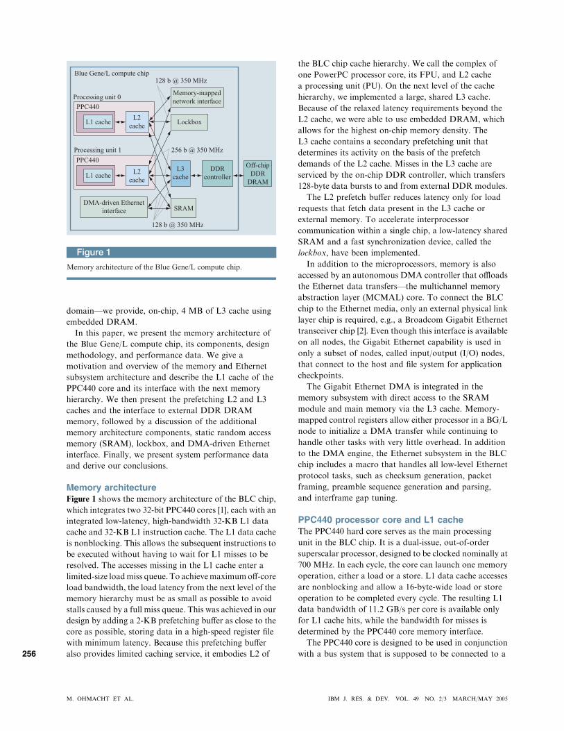
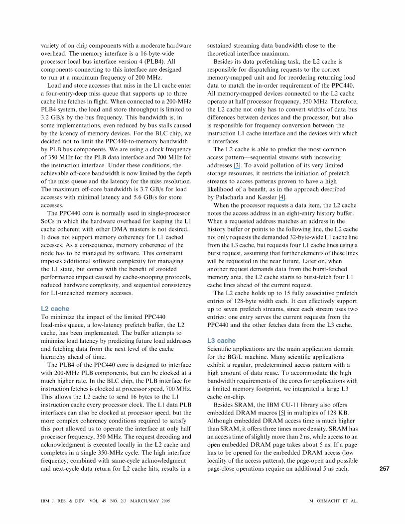
Memory architectureFigure 1 shows the memory architecture of the BLC chip,
which integrates two 32-bit PPC440 cores [1], each with an
integrated low-latency, high-bandwidth 32-KB L1 data
cache and 32-KB L1 instruction cache. The L1 data cache
is nonblocking. This allows the subsequent instructions to
be executed without having to wait for L1 misses to be
resolved. The accesses missing in the L1 cache enter a
limited-size loadmiss queue. To achievemaximumoff-core
load bandwidth, the load latency from the next level of the
memory hierarchy must be as small as possible to avoid
stalls caused by a full miss queue. This was achieved in our
design by adding a 2-KB prefetching buffer as close to the
core as possible, storing data in a high-speed register file
with minimum latency. Because this prefetching buffer
also provides limited caching service, it embodies L2 of
the BLC chip cache hierarchy. We call the complex of
one PowerPC processor core, its FPU, and L2 cache
a processing unit (PU). On the next level of the cache
hierarchy, we implemented a large, shared L3 cache.
Because of the relaxed latency requirements beyond the
L2 cache, we were able to use embedded DRAM, which
allows for the highest on-chip memory density. The
L3 cache contains a secondary prefetching unit that
determines its activity on the basis of the prefetch
demands of the L2 cache. Misses in the L3 cache are
serviced by the on-chip DDR controller, which transfers
128-byte data bursts to and from external DDR modules.
The L2 prefetch buffer reduces latency only for load
requests that fetch data present in the L3 cache or
external memory. To accelerate interprocessor
communication within a single chip, a low-latency shared
SRAM and a fast synchronization device, called the
lockbox, have been implemented.
In addition to the microprocessors, memory is also
accessed by an autonomous DMA controller that offloads
the Ethernet data transfers—the multichannel memory
abstraction layer (MCMAL) core. To connect the BLC
chip to the Ethernet media, only an external physical link
layer chip is required, e.g., a Broadcom Gigabit Ethernet
transceiver chip [2]. Even though this interface is available
on all nodes, the Gigabit Ethernet capability is used in
only a subset of nodes, called input/output (I/O) nodes,
that connect to the host and file system for application
checkpoints.
The Gigabit Ethernet DMA is integrated in the
memory subsystem with direct access to the SRAM
module and main memory via the L3 cache. Memory-
mapped control registers allow either processor in a BG/L
node to initialize a DMA transfer while continuing to
handle other tasks with very little overhead. In addition
to the DMA engine, the Ethernet subsystem in the BLC
chip includes a macro that handles all low-level Ethernet
protocol tasks, such as checksum generation, packet
framing, preamble sequence generation and parsing,
and interframe gap tuning.
PPC440 processor core and L1 cacheThe PPC440 hard core serves as the main processing
unit in the BLC chip. It is a dual-issue, out-of-order
superscalar processor, designed to be clocked nominally at
700 MHz. In each cycle, the core can launch one memory
operation, either a load or a store. L1 data cache accesses
are nonblocking and allow a 16-byte-wide load or store
operation to be completed every cycle. The resulting L1
data bandwidth of 11.2 GB/s per core is available only
for L1 cache hits, while the bandwidth for misses is
determined by the PPC440 core memory interface.
The PPC440 core is designed to be used in conjunction
with a bus system that is supposed to be connected to a
Figure 1
Memory architecture of the Blue Gene/L compute chip.
Processing unit 0PPC440
Blue Gene/L compute chip
LockboxL1 cacheL2
cache
L2cache
L3cache
SRAM
256 b @ 350 MHz
DDRcontroller
Off-chipDDR
DRAM
Memory-mappednetwork interface
128 b @ 350 MHz
128 b @ 350 MHz
L1 cache
DMA-driven Ethernetinterface
PPC440
Processing unit 1
M. OHMACHT ET AL. IBM J. RES. & DEV. VOL. 49 NO. 2/3 MARCH/MAY 2005
256
variety of on-chip components with a moderate hardware
overhead. The memory interface is a 16-byte-wide
processor local bus interface version 4 (PLB4). All
components connecting to this interface are designed
to run at a maximum frequency of 200 MHz.
Load and store accesses that miss in the L1 cache enter
a four-entry-deep miss queue that supports up to three
cache line fetches in flight. When connected to a 200-MHz
PLB4 system, the load and store throughput is limited to
3.2 GB/s by the bus frequency. This bandwidth is, in
some implementations, even reduced by bus stalls caused
by the latency of memory devices. For the BLC chip, we
decided not to limit the PPC440-to-memory bandwidth
by PLB bus components. We are using a clock frequency
of 350 MHz for the PLB data interface and 700 MHz for
the instruction interface. Under these conditions, the
achievable off-core bandwidth is now limited by the depth
of the miss queue and the latency for the miss resolution.
The maximum off-core bandwidth is 3.7 GB/s for load
accesses with minimal latency and 5.6 GB/s for store
accesses.
The PPC440 core is normally used in single-processor
SoCs in which the hardware overhead for keeping the L1
cache coherent with other DMA masters is not desired.
It does not support memory coherency for L1 cached
accesses. As a consequence, memory coherence of the
node has to be managed by software. This constraint
imposes additional software complexity for managing
the L1 state, but comes with the benefit of avoided
performance impact caused by cache-snooping protocols,
reduced hardware complexity, and sequential consistency
for L1-uncached memory accesses.
L2 cacheTo minimize the impact of the limited PPC440
load-miss queue, a low-latency prefetch buffer, the L2
cache, has been implemented. The buffer attempts to
minimize load latency by predicting future load addresses
and fetching data from the next level of the cache
hierarchy ahead of time.
The PLB4 of the PPC440 core is designed to interface
with 200-MHz PLB components, but can be clocked at a
much higher rate. In the BLC chip, the PLB interface for
instruction fetches is clocked at processor speed, 700MHz.
This allows the L2 cache to send 16 bytes to the L1
instruction cache every processor clock. The L1 data PLB
interfaces can also be clocked at processor speed, but the
more complex coherency conditions required to satisfy
this port allowed us to operate the interface at only half
processor frequency, 350 MHz. The request decoding and
acknowledgment is executed locally in the L2 cache and
completes in a single 350-MHz cycle. The high interface
frequency, combined with same-cycle acknowledgment
and next-cycle data return for L2 cache hits, results in a
sustained streaming data bandwidth close to the
theoretical interface maximum.
Besides its data prefetching task, the L2 cache is
responsible for dispatching requests to the correct
memory-mapped unit and for reordering returning load
data to match the in-order requirement of the PPC440.
All memory-mapped devices connected to the L2 cache
operate at half processor frequency, 350 MHz. Therefore,
the L2 cache not only has to convert widths of data bus
differences between devices and the processor, but also
is responsible for frequency conversion between the
instruction L1 cache interface and the devices with which
it interfaces.
The L2 cache is able to predict the most common
access pattern—sequential streams with increasing
addresses [3]. To avoid pollution of its very limited
storage resources, it restricts the initiation of prefetch
streams to access patterns proven to have a high
likelihood of a benefit, as in the approach described
by Palacharla and Kessler [4].
When the processor requests a data item, the L2 cache
notes the access address in an eight-entry history buffer.
When a requested address matches an address in the
history buffer or points to the following line, the L2 cache
not only requests the demanded 32-byte-wide L1 cache line
from the L3 cache, but requests four L1 cache lines using a
burst request, assuming that further elements of these lines
will be requested in the near future. Later on, when
another request demands data from the burst-fetched
memory area, the L2 cache starts to burst-fetch four L1
cache lines ahead of the current request.
The L2 cache holds up to 15 fully associative prefetch
entries of 128-byte width each. It can effectively support
up to seven prefetch streams, since each stream uses two
entries: one entry serves the current requests from the
PPC440 and the other fetches data from the L3 cache.
L3 cacheScientific applications are the main application domain
for the BG/L machine. Many scientific applications
exhibit a regular, predetermined access pattern with a
high amount of data reuse. To accommodate the high
bandwidth requirements of the cores for applications with
a limited memory footprint, we integrated a large L3
cache on-chip.
Besides SRAM, the IBM CU-11 library also offers
embedded DRAM macros [5] in multiples of 128 KB.
Although embedded DRAM access time is much higher
than SRAM, it offers three times more density. SRAMhas
an access time of slightly more than 2 ns, while access to an
open embedded DRAM page takes about 5 ns. If a page
has to be opened for the embedded DRAM access (low
locality of the access pattern), the page-open and possible
page-close operations require an additional 5 ns each.
IBM J. RES. & DEV. VOL. 49 NO. 2/3 MARCH/MAY 2005 M. OHMACHT ET AL.
257
The latency of the PPC440 PLB interface alone
contributes 14 ns of latency for an L1 miss or L2 cache
hit. The emphasis of the architecture is on a good
prefetching performance of the L2 cache with a lower
emphasis on L3 cache latency, assuming that the L3 cache
latency allows for uninterrupted prefetch streaming at
the maximum bandwidth defined by the PPC440 core
interface. The embedded DRAM latency is small enough
to be hidden by the L2 prefetch, while allowing large
memory footprint processing. As a result, it reduces
contention on the interface to external DDR DRAM and
thus also reduces the power consumed by switching I/O
cells.
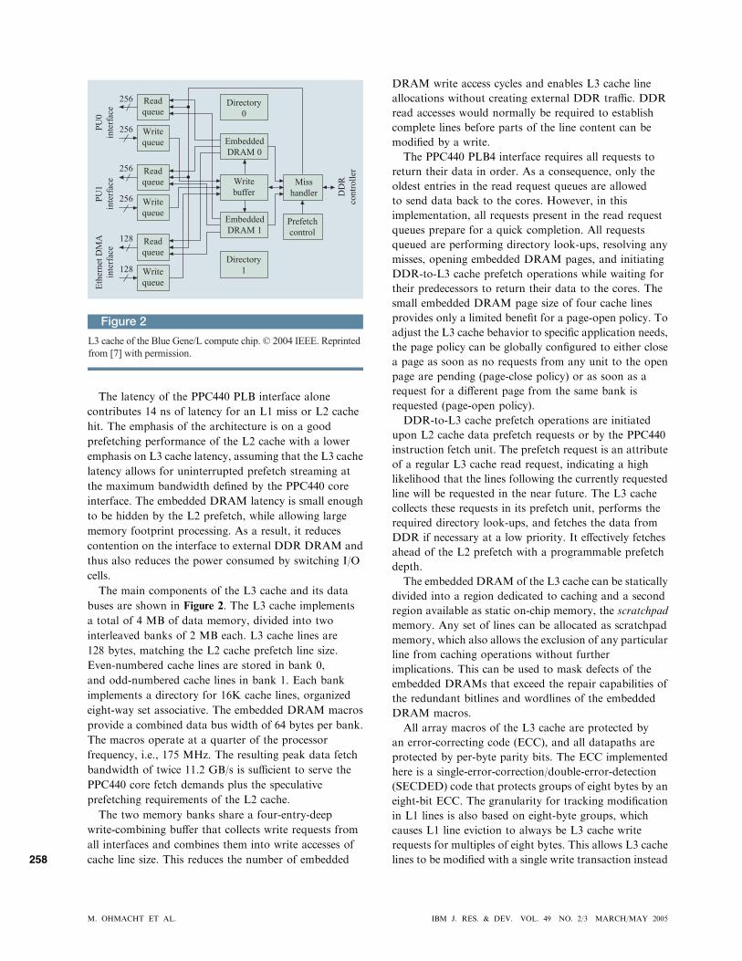
The main components of the L3 cache and its data
buses are shown in Figure 2. The L3 cache implements
a total of 4 MB of data memory, divided into two
interleaved banks of 2 MB each. L3 cache lines are
128 bytes, matching the L2 cache prefetch line size.
Even-numbered cache lines are stored in bank 0,
and odd-numbered cache lines in bank 1. Each bank
implements a directory for 16K cache lines, organized
eight-way set associative. The embedded DRAM macros
provide a combined data bus width of 64 bytes per bank.
The macros operate at a quarter of the processor
frequency, i.e., 175 MHz. The resulting peak data fetch
bandwidth of twice 11.2 GB/s is sufficient to serve the
PPC440 core fetch demands plus the speculative
prefetching requirements of the L2 cache.
The two memory banks share a four-entry-deep
write-combining buffer that collects write requests from
all interfaces and combines them into write accesses of
cache line size. This reduces the number of embedded
DRAM write access cycles and enables L3 cache line
allocations without creating external DDR traffic. DDR
read accesses would normally be required to establish
complete lines before parts of the line content can be
modified by a write.
The PPC440 PLB4 interface requires all requests to
return their data in order. As a consequence, only the
oldest entries in the read request queues are allowed
to send data back to the cores. However, in this
implementation, all requests present in the read request
queues prepare for a quick completion. All requests
queued are performing directory look-ups, resolving any
misses, opening embedded DRAM pages, and initiating
DDR-to-L3 cache prefetch operations while waiting for
their predecessors to return their data to the cores. The
small embedded DRAM page size of four cache lines
provides only a limited benefit for a page-open policy. To
adjust the L3 cache behavior to specific application needs,
the page policy can be globally configured to either close
a page as soon as no requests from any unit to the open
page are pending (page-close policy) or as soon as a
request for a different page from the same bank is
requested (page-open policy).
DDR-to-L3 cache prefetch operations are initiated
upon L2 cache data prefetch requests or by the PPC440
instruction fetch unit. The prefetch request is an attribute
of a regular L3 cache read request, indicating a high
likelihood that the lines following the currently requested
line will be requested in the near future. The L3 cache
collects these requests in its prefetch unit, performs the
required directory look-ups, and fetches the data from
DDR if necessary at a low priority. It effectively fetches
ahead of the L2 prefetch with a programmable prefetch
depth.
The embedded DRAM of the L3 cache can be statically
divided into a region dedicated to caching and a second
region available as static on-chip memory, the scratchpad
memory. Any set of lines can be allocated as scratchpad
memory, which also allows the exclusion of any particular
line from caching operations without further
implications. This can be used to mask defects of the
embedded DRAMs that exceed the repair capabilities of
the redundant bitlines and wordlines of the embedded
DRAM macros.
All array macros of the L3 cache are protected by
an error-correcting code (ECC), and all datapaths are
protected by per-byte parity bits. The ECC implemented
here is a single-error-correction/double-error-detection
(SECDED) code that protects groups of eight bytes by an
eight-bit ECC. The granularity for tracking modification
in L1 lines is also based on eight-byte groups, which
causes L1 line eviction to always be L3 cache write
requests for multiples of eight bytes. This allows L3 cache
lines to be modified with a single write transaction instead
Figure 2
L3 cache of the Blue Gene/L compute chip. © 2004 IEEE. Reprinted from [7] with permission.
Readqueue
Writequeue
Writebuffer
Directory0
EmbeddedDRAM 1
EmbeddedDRAM 0
Misshandler
Readqueue
PU0
inte
rfac
ePU
1in
terf
ace
Eth
erne
t DM
Ain
terf
ace
DD
Rco
ntro
ller
Prefetchcontrol
256
256
256
256
128
128
Writequeue
Readqueue
Writequeue
Directory1
M. OHMACHT ET AL. IBM J. RES. & DEV. VOL. 49 NO. 2/3 MARCH/MAY 2005
258
of a slower read–modify–write operation, since the old
content for an eight-byte group does not have to be read
when computing the new ECC.
As part of the reliability, availability, and serviceability
(RAS) effort, all arrays of the L3 cache unit are accessible
via a secondary access port controlled by the device
control register (DCR) interface. This port allows both
the two on-chip cores and the service host to read and
modify any array location, which is essential for
hardware bring-up and diagnostics, stress testing,
program debugging, and establishing additional
communication paths between the host processor
and the PPC440 cores. Because the read accesses are
nondestructive and can be issued anytime, the port
can also serve for runtime monitoring.
DDR controllerThe BLC memory subsystem implements an on-chip
DDR DRAM controller. The controller supports
8-bit-wide and 16-bit-wide external DRAM modules in
single- and dual-bank configurations up to 2 GB of total
memory per node. Its 144-bit-wide data bus supports
transfer rates of up to 5.6 GB/s and protects the data
stream with a strong ECC and additional redundant
bitlines.
The controller operates at either a half or a third of the
PPC440 core frequency. This clock frequency defines the
data transfer rate. The DDR module command bus is
operated at half this frequency. Data is transferred
between the external memory modules and the cache
hierarchy in L3 cache line granules. All transfers are
eight-deep bursts of 16-byte-wide data parts. Each
16-byte part is protected by a 12-bit-wide ECC. The ECC
divides the data part into a set of 32 four-bit-wide
symbols. Any error pattern within a single symbol can be
forward-corrected, assuming no error in other symbols of
the same part. The 144-bit-wide memory port contains
an additional four-bit-wide spare symbol that can be
remapped to any other symbol of the same part. This
allows the memory to continue to function properly even
in the presence of two failing four-bit-wide symbols,
because one of them can be remapped to the spare symbol
and the other one can be corrected via the ECC.
The ECC-based correction is complemented by the
DDR controller capability of continuously monitoring
and correcting the main memory content. This scrub
mechanism reads main memory lines in the background,
checks the ECC for errors, corrects single-symbol errors,
keeps track of error locations and frequencies, and replaces
failing symbols with the redundant symbol on-the-fly.
Lockbox and SRAMThe latency of the L3 cache cannot be hidden by the
L2 cache when the two PPC440 cores attempt to
communicate via memory. To reduce the latency for
standard semaphore operations, barrier synchronization,
and control information exchange, two additional
memory-mapped devices have been added to the BLC
chip architecture.
The first device we call the lockbox. It is a very small
register set with optimized access and state transition for
mutual exclusion semaphores and barrier operations. It
consists of 256 single-bit registers that can be atomically
probed and modified using a standard noncached load
operation. The lockbox unconditionally accepts access
requests every cycle from both processor core units
without blocking. In a single cycle, the state of all
accessed registers is atomically updated and returned.
The second device for interprocessor communication
is a shared low-latency SRAM memory device used
primarily during initial program load (IPL) and for
low-latency exchange of control information between
the two PPC440 cores. It is an arbitrated unit using a
single-port SRAM macro of 16-byte data width and two
bytes ECC. Its low complexity allows it to use a single
two-stage pipeline running at 350 MHz that consists of an
arbitration and SRAM macro setup stage and an SRAM
access and ECC checking stage. The SRAM is mapped
to the highest addresses of the memory space, and its
content can be accessed directly via the JTAG (IEEE
Standard 1149.1 developed by the Joint Test Action
Group) interface. This path is used in the primary boot,
which loads boot code into SRAM and then releases the
processor cores from reset; the cores then start fetching
instructions from SRAM. The boot code can either wait
for more code to be deposited into SRAM or use the
collective or Ethernet interfaces to load the full program
image into main memory.
Ethernet subsystemThe on-chip Ethernet subsystem allows for Gigabit
Ethernet data transmission between the BG/L machine
and the application host computer and file system. Access
to the Ethernet subsystem is completely symmetric from
both PPC440 processor cores on the BLC chip, allowing
both processors to initiate transmission or reception of
Ethernet traffic. The Ethernet system is integrated in
the cache hierarchy with direct access to the L3 cache
through a PLB that exists parallel to the point-to-point
connection of the PPC440 core complexes to the L3
cache. The subsystem contains a dedicated DMA engine
to ensure high-performance, high-bandwidth access to the
memory system.
The building blocks of the Gigabit Ethernet system
and its integration in the overall chip are illustrated in
Figure 3(a). The Ethernet subsystem consists of several
modules from the IBM SoC CoreConnect* standard
element library. In the figure, PU0 and PU1 stand for
IBM J. RES. & DEV. VOL. 49 NO. 2/3 MARCH/MAY 2005 M. OHMACHT ET AL.
259
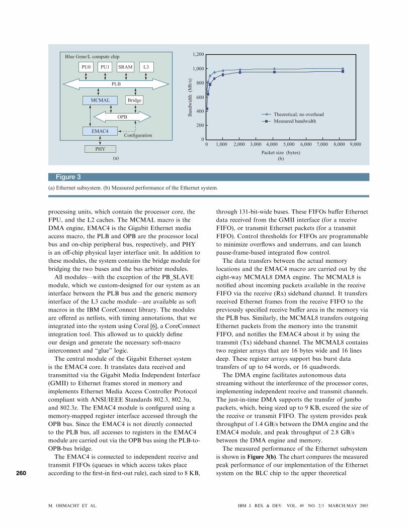
processing units, which contain the processor core, the
FPU, and the L2 caches. The MCMAL macro is the
DMA engine, EMAC4 is the Gigabit Ethernet media
access macro, the PLB and OPB are the processor local
bus and on-chip peripheral bus, respectively, and PHY
is an off-chip physical layer interface unit. In addition to
these modules, the system contains the bridge module for
bridging the two buses and the bus arbiter modules.
All modules—with the exception of the PB_SLAVE
module, which we custom-designed for our system as an
interface between the PLB bus and the generic memory
interface of the L3 cache module—are available as soft
macros in the IBM CoreConnect library. The modules
are offered as netlists, with timing annotations, that we
integrated into the system using Coral [6], a CoreConnect
integration tool. This allowed us to quickly define
our design and generate the necessary soft-macro
interconnect and ‘‘glue’’ logic.
The central module of the Gigabit Ethernet system
is the EMAC4 core. It translates data received and
transmitted via the Gigabit Media Independent Interface
(GMII) to Ethernet frames stored in memory and
implements Ethernet Media Access Controller Protocol
compliant with ANSI/IEEE Standards 802.3, 802.3u,
and 802.3z. The EMAC4 module is configured using a
memory-mapped register interface accessed through the
OPB bus. Since the EMAC4 is not directly connected
to the PLB bus, all accesses to registers in the EMAC4
module are carried out via the OPB bus using the PLB-to-
OPB-bus bridge.
The EMAC4 is connected to independent receive and
transmit FIFOs (queues in which access takes place
according to the first-in first-out rule), each sized to 8 KB,
through 131-bit-wide buses. These FIFOs buffer Ethernet
data received from the GMII interface (for a receive
FIFO), or transmit Ethernet packets (for a transmit
FIFO). Control thresholds for FIFOs are programmable
to minimize overflows and underruns, and can launch
pause-frame-based integrated flow control.
The data transfers between the actual memory
locations and the EMAC4 macro are carried out by the
eight-way MCMAL8 DMA engine. The MCMAL8 is
notified about incoming packets available in the receive
FIFO via the receive (Rx) sideband channel. It transfers
received Ethernet frames from the receive FIFO to the
previously specified receive buffer area in the memory via
the PLB bus. Similarly, the MCMAL8 transfers outgoing
Ethernet packets from the memory into the transmit
FIFO, and notifies the EMAC4 about it by using the
transmit (Tx) sideband channel. The MCMAL8 contains
two register arrays that are 16 bytes wide and 16 lines
deep. These register arrays support bus burst data
transfers of up to 64 words, or 16 quadwords.
The DMA engine facilitates autonomous data
streaming without the interference of the processor cores,
implementing independent receive and transmit channels.
The just-in-time DMA supports the transfer of jumbo
packets, which, being sized up to 9 KB, exceed the size of
the receive or transmit FIFO. The system provides peak
throughput of 1.4 GB/s between the DMA engine and the
EMAC4 module, and peak throughput of 2.8 GB/s
between the DMA engine and memory.
The measured performance of the Ethernet subsystem
is shown in Figure 3(b). The chart compares the measured
peak performance of our implementation of the Ethernet
system on the BLC chip to the upper theoretical
Figure 3
(a) Ethernet subsystem. (b) Measured performance of the Ethernet system.
MCMAL
PHY
Bridge
Configuration
L3SRAMPU1PU0
Blue Gene/L compute chip
OPB
PLB
0
200
400
Ban
dwid
th (
Mb/
s)
600
800
1,000
1,200
0 1,000 2,000 3,000 4,000 5,000 6,000 7,000 8,000 9,000
(a)
Theoretical; no overheadMeasured bandwidth
Packet size (bytes)(b)
EMAC4
M. OHMACHT ET AL. IBM J. RES. & DEV. VOL. 49 NO. 2/3 MARCH/MAY 2005
260
bandwidth that would be possible if there were no
overhead associated with packet transfer and processing.
The bandwidth of useful data transmitted is a function
of packet size, since more bandwidth is lost for smaller
packets because of the packet header and trailer overhead
associated with data transfer. The measurements show
that the Ethernet system achieves a peak bandwidth of
up to 97% of the theoretical limit.
Performance of the memory subsystemThe memory subsystem of the BLC delivers very high
bandwidth because of its multilevel on-chip cache
hierarchy with prefetch capabilities on multiple levels.
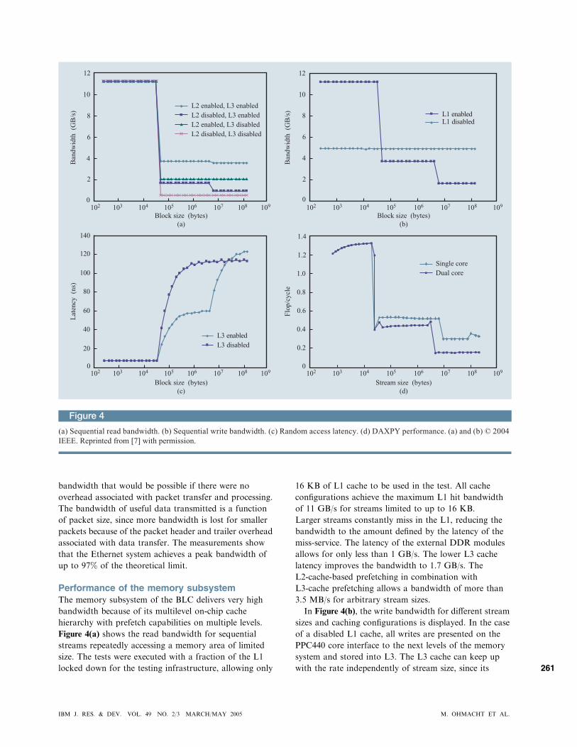
Figure 4(a) shows the read bandwidth for sequential
streams repeatedly accessing a memory area of limited
size. The tests were executed with a fraction of the L1
locked down for the testing infrastructure, allowing only
16 KB of L1 cache to be used in the test. All cache
configurations achieve the maximum L1 hit bandwidth
of 11 GB/s for streams limited to up to 16 KB.
Larger streams constantly miss in the L1, reducing the
bandwidth to the amount defined by the latency of the
miss-service. The latency of the external DDR modules
allows for only less than 1 GB/s. The lower L3 cache
latency improves the bandwidth to 1.7 GB/s. The
L2-cache-based prefetching in combination with
L3-cache prefetching allows a bandwidth of more than
3.5 MB/s for arbitrary stream sizes.
In Figure 4(b), the write bandwidth for different stream
sizes and caching configurations is displayed. In the case
of a disabled L1 cache, all writes are presented on the
PPC440 core interface to the next levels of the memory
system and stored into L3. The L3 cache can keep up
with the rate independently of stream size, since its
Figure 4
(a) Sequential read bandwidth. (b) Sequential write bandwidth. (c) Random access latency. (d) DAXPY performance. (a) and (b) © 2004 IEEE. Reprinted from [7] with permission.
0
2
4
6
8
10
12
Block size (bytes)(a)
Block size (bytes)(b)
Block size (bytes)(c)
Ban
dwid
th (
GB
/s)
Ban
dwid
th (
GB
/s)
L2 enabled, L3 enabledL2 disabled, L3 enabledL2 enabled, L3 disabledL2 disabled, L3 disabled
102 103 104 105 106 107 108 109 102 103 104 105 106 107 108 109
102 103 104 105 106 107 108 109 102 103 104 105 106 107 108 109
0
2
4
6
8
10
12
L1 enabledL1 disabled
L3 enabledL3 disabled
0
20
40
60
80
100
120
140
0
0.2
0.4
0.6
0.8
1.0
1.2
1.4
Stream size (bytes)(d)
Flop
/cyc
le
Single coreDual core
Lat
ency
(ns
)
IBM J. RES. & DEV. VOL. 49 NO. 2/3 MARCH/MAY 2005 M. OHMACHT ET AL.
261
write-combining buffer forms complete L3 cache lines out
of eight subsequent write requests; thus it reduces the
number of accesses to embedded DRAM.
If the L1 cache is enabled, the write-back strategy of
the L1 cache allows 11 GB/s throughput for streams that
fit into L1. For larger sizes, the accesses cause constant L1
misses, leading to evictions of modified lines and fetches
from the next cache hierarchy to complete writes to form
full L1 cache lines (write allocation). For streams up to
the size of the L3 cache, the PPC440 read interface limits
the bandwidth to 3.7 GB/s. As soon as the L3 cache
begins to evict lines for even larger streams, the constant
alterations of read and write traffic to DDR, along with
bank collisions in the DDR modules, reduce the write
performance further, down to 1.6 GB/s.
In Figure 4(c), the load latency is shown for random
reads from a limited memory area. Since the random
reads access different embedded DRAM pages with a
very high probability when hitting in the L3 cache, the
latency does not reflect the page mode benefit exploited
when streaming data. Note that the latency for accesses
with L3 cache disabled is lower than for L3 cache misses,
because no directory look-ups have to be performed in
the uncached case.
Figure 4(d) shows the achievable floating-point
performance for the L1 Basic Linear Algebra
Subprograms routine DAXPY, measured in floating-
point operations per 700-MHz processor cycle. For
each fused multiply–add (FMA) operation pair (two flops
per cycle), 16 bytes must be loaded from memory and
eight bytes must be stored back. For a floating-point
performance of one flop per cycle, i.e., 700 Mflops, an
aggregate load/store bandwidth of 12 bytes per cycle, i.e.,
8.4 GB/s, is required.
For stream sizes that fit into L1, the memory
bandwidth approaches the theoretical limit of 11.2 GB/s.
Single-core streams of up to 4 MB fit into the L3 cache
and achieve a bandwidth of 4.3 GB/s, while dual-core
performance for streams of up to 2 MB each achieves
3.7 GB/s because of banking conflicts within the L3
cache. For even larger stream sizes, the performance
drops further as a result of bank collisions in the
external DDR memory modules.
ConclusionsThe Blue Gene/L system-on-a-chip is a very attractive
solution for scalable supercomputing. The low-power
processing approachpairedwith ahigh-bandwidth on-chip
memory hierarchy using embedded DRAM delivers
outstanding performance results. Embedded DRAM
allows memory densities more than three times higher
than SRAM while delivering high bandwidth because of
its wide interface. A fast, small L2 prefetch compensates
for latencies incurred by the use of embedded DRAM.
Furthermore, the high bandwidth and prefetching
capabilities of the on-chip caches enable seamless
integration of a DMA-driven 1-Gb/s Ethernet interface,
which takes advantage of the large on-chip caches to
sustain a bandwidth very close to the theoretical
maximum. Blue Gene/L establishes a new design
principle that enables previously unachieved performance
on a high-density, low-power system.
AcknowledgmentsThis work has benefited from the cooperation of many
individuals in IBM Research (Yorktown Heights, New
York), IBM Engineering and Technology Services
(Rochester, Minnesota), IBM Microelectronics
(Burlington, Vermont), and IBM India (Bangalore). In
particular, we thank Dan Beece, Ralph Bellofatto, Matt
Blumrich, Arthur Bright, Jose Brunheroto, Luis Ceze,
Paul Coteus, Monty Denneau, Marc Boris Dombrowa,
Dong Chen, Jim Goldade, Philip Heidelberger, Gerard V.
Kopcsay, Bob Lembach, James C. Sexton, Sarabjeet
Singh, Richard Swetz, Li Shang, Burkhard Steinmacher-
Burow, Pavlos Vranas, and Chris Zoellin.
The Blue Gene/L project has been supported and
partially funded by the Lawrence Livermore National
Laboratory on behalf of the United States Department of
Energy under Lawrence Livermore National
Laboratory Subcontract No. B517552.
*Trademark or registered trademark of International BusinessMachines Corporation.
References1. The PowerPC 440 Core, IBM Microelectronics Division,
Hopewell Junction, NY, 2004; see http://www-306.ibm.com/chips/techlib/techlib.nsf/techdocs/F72367F770327F8A87256E63006CB7EC/$file/PPC440Core3-24.pdf.
2. IEEE Standard 802.3, IEEE, Piscataway, NJ, 2000.3. S. P. Vanderwiel and D. J. Lilja, ‘‘Data Prefetch Mechanisms,’’
ACM Computing Surv. 32, No. 2, 174–199 (2000).4. S. Palacharla and R. E. Kessler, ‘‘Evaluating Stream Buffers as
a Secondary Cache Replacement,’’ Proceedings of the 21stAnnual International Symposium on Computer Architecture,1994, pp. 24–33.
5. J. E. Barth, Jr., J. H. Dreibelbis, E. A. Nelson, D. L. Anand,G. Pomichter, P. Jakobsen, M. R. Nelms, J. Leach, and G. M.Belansek, ‘‘Embedded DRAM Design and Architecture for theIBM 0.11-lm ASIC Offering,’’ IBM J. Res. & Dev. 46, No. 6,675–689 (November 2002).
6. J. A. Darringer, R. A. Bergamaschi, S. Bhattacharya, D. Brand,A. Herkersdorf, J. K. Morrell, I. I. Nair, P. Sagmeister, and Y.Shin, ‘‘Early Analysis Tools for System-on-a-Chip Design,’’IBM J. Res. & Dev. 46, No. 6, 691–707 (November 2002).
7. M. Ohmacht et al. ‘‘The eDRAM Based L3-Cache of theBlueGene/L Supercomputer Processor Node,’’ Proceedingsof the SBAC-PAD’04, 2004, pp. 18–22.
Received June 1, 2004; accepted for publicationSeptember 16,
M. OHMACHT ET AL. IBM J. RES. & DEV. VOL. 49 NO. 2/3 MARCH/MAY 2005
262
2004; Internet publication April 12, 2005
Martin Ohmacht IBM Research Division, Thomas J. WatsonResearch Center, P.O. Box 218, Yorktown Heights, New York10598 ([email protected]). Dr. Ohmacht received hisDipl.-Ing. and Dr.-Ing. degrees in electrical engineering from theUniversity of Hannover, Germany, in 1994 and 2001, respectively.He joined the IBM Research Division in 2001 and has worked onmemory subsystem architecture and implementation for the BlueGene project. His research interests include computer architecture,design and verification of multiprocessor systems, and compileroptimizations.
Reinaldo A. Bergamaschi IBM Thomas J. Watson ResearchCenter, P.O. Box 218, Yorktown Heights, New York 10598([email protected]). In 1982 Dr. Bergamaschi graduatedin electronics engineering from the Aeronautics Institute ofTechnology, Brazil. He received an M.A. degree in electronicsengineering from the Philips International Institute, Eindhoven,the Netherlands, and in 1989 a Ph.D. degree in electronics andcomputer science from the University of Southampton, England,joining IBM that same year. Dr. Bergamaschi has worked on avariety of design automation projects including high-levelsynthesis, release-to-layout (RTL) sign-off techniques, earlyestimation of area, timing, and power, system-on-a-chip designautomation, and system-level modeling.
Subhrajit Bhattacharya IBM Thomas J. Watson ResearchCenter, P.O. Box 218, Yorktown Heights, New York 10598([email protected]). Dr. Bhattacharya has been a ResearchStaff Member at the IBM Thomas J. Watson Research Centersince 1999. He received his B.S. degree in computer science andengineering from the Indian Institute of Technology, Kharagpur,and his Ph.D. degree from the Department of Computer Science ofDuke University. He was a Research Staff Member at the NECComputer and Communications Research Laboratory, Princeton,New Jersey, before joining IBM. His research interests are in VLSIcircuits, design, and design automation. He has worked primarilyin design automation areas of high-level synthesis, system-leveldesign automation, low power, design-for-test, and verification.Dr. Bhattacharya holds three U.S. patents.
Alan Gara IBM Research Division, Thomas J. Watson ResearchCenter, P.O. Box 218, Yorktown Heights, New York 10598([email protected]). Dr. Gara is a Research Staff Memberat the IBM Thomas J. Watson Research Center. He receivedhis Ph.D. degree in physics from the University of Wisconsinat Madison in 1986. In 1998 Dr. Gara received the GordonBell Award for the QCDSP supercomputer in the most cost-effective category. He is the chief architect of the Blue Gene/Lsupercomputer. Dr. Gara also led the design and verification of theBlue Gene/L compute ASIC as well as the bring-up of the BlueGene/L prototype system.
Mark E. Giampapa IBM Research Division, Thomas J.Watson Research Center, P.O. Box 218, Yorktown Heights, NewYork 10598 ([email protected]). Mr. Giampapa is a SeniorEngineer in the Exploratory Server Systems Department. Hereceived a B.A. degree in computer science from ColumbiaUniversity. He joined the IBM Research Division in 1984 to workin the areas of parallel and distributed processing, and has focusedhis research on distributed memory and shared memory parallelarchitectures and operating systems. Mr. Giampapa has received
three IBM Outstanding Technical Achievement Awards for hiswork in distributed processing, simulation, and parallel operatingsystems. He holds 15 patents, with several more pending, and haspublished ten papers.
Balaji Gopalsamy IBM Engineering and TechnologyServices, Golden Enclave, Airport Road, Bangalore 560 017([email protected]). Mr. Gopalsamy is a Staff Research andDevelopment Engineer. He received a B.E. degree in electrical andelectronics engineering from Madurai Kamraj University, India,in 1998. He joined IBM in 2000, working on verification andmodeling of ASICs. Mr. Gopalsamy was involved in theverification of the memory subsystem and test interface modulesof the Blue Gene/L compute chip design.
Ruud A. Haring IBM Research Division, Thomas J. WatsonResearch Center, P.O. Box 218, Yorktown Heights, New York10598 ([email protected]). Dr. Haring is a Research Staff Memberat the IBM Thomas J. Watson Research Center. He received B.S.,M.S., and Ph.D. degrees in physics from Leyden University, theNetherlands, in 1977, 1979, and 1984, respectively. Upon joiningIBM in 1984, he initially studied surface science aspects of plasmaprocessing. Beginning in 1992, he became involved in electroniccircuit design on both microprocessors and ASICs. He is currentlyresponsible for the synthesis, physical design, and test aspects ofthe Blue Gene chip designs. Dr. Haring has received an IBMOutstanding Technical Achievement Award for his contributionsto the z900 mainframe, and he holds several patents. His researchinterests include circuit design and optimization, design fortestability, and ASIC design. Dr. Haring is a Senior Member ofthe IEEE.
Dirk Hoenicke IBM Research Division, Thomas J. WatsonResearch Center, P.O. Box 218, Yorktown Heights, New York10598 ([email protected]). Mr. Hoenicke received a Dipl.Inform. (M.S.) degree in computer science from the Universityof Tuebingen, Germany, in 1998. Since then, he has worked ona wide range of aspects of two prevalent processor architectures:ESA/390 and PowerPC. He is currently a member of the CellularSystems Chip Development Group, where he focuses on thearchitecture, design, verification, and implementation of the BlueGene system-on-a-chip (SoC) supercomputer family. In particular,he was responsible for the architecture, design, and verificationeffort of the collective network and defined and implementedmany other parts of the BG/L ASIC. Mr. Hoenicke’s areasof expertise include high-performance computer systems andadvanced memory and network architectures, as well as power-,area-, and complexity-efficient logic designs.
David J. Krolak IBM Engineering and TechnologyServices, 3605 Highway 52 N., Rochester, Minnesota 55901([email protected]). Mr. Krolak received a B.S. degree inelectrical engineering from the University of Wisconsin at Madisonin 1979. He joined IBM in 1980 at Essex Junction, Vermont, wherehe worked on DRAM controllers for various IBM computers. In1988 he moved to IBM Rochester, where he has worked primarilyon high-performance L2 cache and system bus architectures. Mr.Krolak received an IBM Outstanding Technical AchievementAward for his design of the RS/6000 S80 L2 cache. He holdsnine patents and is currently working on processor systems.
IBM J. RES. & DEV. VOL. 49 NO. 2/3 MARCH/MAY 2005 M. OHMACHT ET AL.
263
James A. Marcella IBM Engineering and TechnologyServices, 3605 Highway 52 N., Rochester, Minnesota 55901([email protected]). Mr. Marcella is a Senior Engineerworking in the area of custom and SoC design andimplementation. His primary interest is in symmetricmultiprocessor memory subsystem design. He joined IBM in1980 after receiving his B.S.E.E. degree from the University ofMinnesota. He has received three IBM Outstanding TechnicalAchievement Awards for his work on memory controller designsfor the iSeries, pSeries, and xSeries servers. Mr. Marcella has 11issued U.S. patents and 19 published disclosures.
Ben J. Nathanson IBM Research Division, Thomas J. WatsonResearch Center, P.O. Box 218, Yorktown Heights, New York10598 ([email protected]). Mr. Nathanson joined the IBMResearch Division in 1985 and has worked on the parallelcomputers RP3, Vulcan, SP1, SP2, and Blue Gene/L. He hasreceived IBM Outstanding Technical Achievement Awards forhardware contributions to SP1 and SP2 and Research DivisionAwards for RP3 bring-up and verification work on memorycompression hardware. Mr. Nathanson holds M.S. and B.S.degrees in electrical engineering from Columbia University andis a member of Tau Beta Pi and Eta Kappa Nu. His currentfocus is hardware verification.
Valentina Salapura IBM Thomas J. Watson ResearchCenter, P.O. Box 218, Yorktown Heights, New York 10598([email protected]). Dr. Salapura is a Research Staff Memberwith the IBM Thomas J. Watson Research Center, where she hascontributed to the architecture and implementation of threegenerations of Blue Gene systems (BG/C, BG/L, and BG/P),focusing on multiprocessor interconnect and synchronization andmultithreaded architecture design and evaluation. She received aPh.D. degree from the Vienna University of Technology in 1996.Before joining IBM in 2000, she was a faculty member with theComputer Engineering Department at the Vienna University ofTechnology. In addition to her work on high-performance systems,she has been a driving force in the design and evaluation of theSanLight network multiprocessor architecture. Dr. Salapura isthe author of more than 50 papers on design methodology,configurable architectures, network processors, and high-performance computer systems; she holds one patent and has19 patents pending.
Michael E. Wazlowski IBM Research Division, Thomas J.Watson Research Center, P.O. Box 218, Yorktown Heights, NewYork 10598 ([email protected]). Dr. Wazlowski is a ResearchStaff Member; he is responsible for high-performance memorysystem architecture and design and has led the verification effortsfor two ASICs. He received a B.S. degree in computer engineeringfrom the University of Massachusetts at Amherst in 1990, andM.S. and Ph.D. degrees in electrical sciences from BrownUniversity in 1992 and 1996, respectively. Dr. Wazlowski receivedan IBM Outstanding Technical Achievement Award for hiscontributions to IBM Memory Expansion Technology (MXT).He holds several patents. His research interests include computerarchitecture, memory systems, and ASIC design. He is currentlyworking on cache and memory systems. Dr. Wazlowski is amember of the IEEE.
M. OHMACHT ET AL. IBM J. RES. & DEV. VOL. 49 NO. 2/3 MARCH/MAY 2005
264