
Generalized Structures for Switched-Capacitor Multilevel ...
20
applied sciences Article Generalized Structures for Switched-Capacitor Multilevel Inverter Topology for Energy Storage System Application Mu Anas 1 , Adil Sarwar 1 , Anzar Ahmad 1 , Afroz Alam 1 , Shafiq Ahmad 2, * , Mohamed Sharaf 2 , Mazen Zaindin 3 and Muhammad Firdausi 2 Citation: Anas, M.; Sarwar, A.; Ahmad, A.; Alam, A.; Ahmad, S.; Sharaf, M.; Zaindin, M.; Firdausi, M. Generalized Structures for Switched-Capacitor Multilevel Inverter Topology for Energy Storage System Application. Appl. Sci. 2021, 11, 1319. https://doi.org/10.3390/ app11031319 Academic Editors: Gaind P. Pandey and Amjad Anvari-Moghaddam Received: 24 October 2020 Accepted: 25 January 2021 Published: 1 February 2021 Publisher’s Note: MDPI stays neutral with regard to jurisdictional claims in published maps and institutional affil- iations. Copyright: © 2021 by the authors. Licensee MDPI, Basel, Switzerland. This article is an open access article distributed under the terms and conditions of the Creative Commons Attribution (CC BY) license (https:// creativecommons.org/licenses/by/ 4.0/). 1 Department of Electrical Engineering, Aligarh Muslim University, Aligarh 202002, India; [email protected] (M.A.); [email protected] (A.S.); [email protected] (A.A.); [email protected] (A.A.) 2 Industrial Engineering Department, College of Engineering, King Saud University, P.O. Box 800, Riyadh 11421, Saudi Arabia; [email protected] (M.S.); [email protected] (M.F.) 3 Department of Statistics and Operations Research, College of Science, King Saud University, P.O. Box 2455, Riyadh 11451, Saudi Arabia; [email protected] * Correspondence: ashafi[email protected]; Tel.: +966-543-200-930 Abstract: The apparent advantages of Multilevel Inverter (MLI) topologies in handling medium and high power with less loss in switching and lower harmonic distortion in an output voltage waveform makes it better than the conventional inverter. However, the MLI topologies utilize a large number of DC power supplies and power semiconductor devices. They also have a higher value of total standing voltage (TSV). Moreover, capacitor voltage balancing problems, self-voltage boosting inability, and complex control techniques require a relook and improvement in their structure. More recently, Switched-Capacitor Multilevel Inverter (SCMLI) topologies have been proposed to overcome the shortcomings of MLIs. In this paper, a generalized structure for a single-phase switched capacitor multilevel inverter (SCMLI) with self-voltage boosting and self-voltage balancing capability is proposed. A detailed analysis of a general structure of SCMLI is presented. The comparative analysis of the structures is carried out with recently reported topologies to demonstrate superiority. An optimized low-frequency modulation controls the output voltage waveform. The simulation and experimental results are included in the paper for single-unit symmetric (9-level voltage) and asymmetric (17-level voltage) configurations. Keywords: energy storage; total harmonic distortion; switched-capacitor multilevel inverter (SCMLI); total standing voltage 1. Introduction Nowadays, the alteration of power from DC to AC is an important process and per- forms a vital task in modern power system network and industrial processes powered by electric drives [1]. DC to AC conversion is carried out by power electronics converters. Due to high harmonic losses in two-level inverters, multilevel inverters are used in order to have highly efficient power electronics and drive systems [2]. The main property of the Multilevel Inverter (MLI) is to generate an output voltage waveform resembling a staircase using several voltage sources at the input, which results in the low value of total harmonics distortion (THD) and minimal values of electromagnetic interference (EMI) and voltage stress across switches [3]. The three classical topologies of MLI are Cascaded H-bridge inverter (CHB), Flying Capacitor Clamped inverter (FC), and Neutral Point Clamped inverter (NPC) [4]. Due to easy control and unique characteristics, they are practically implemented as alteration technology in various applications ranging from small- to large-scale industries. In order to achieve higher voltage levels, a large number of devices are required, which enhances the size and cost of MLIs [5]. At higher voltage levels, NPC and FC show capacitor voltage unbalancing problems besides the requirement Appl. Sci. 2021, 11, 1319. https://doi.org/10.3390/app11031319 https://www.mdpi.com/journal/applsci
-
Upload
khangminh22 -
Category
Documents
-
view
0 -
download
0
Transcript of Generalized Structures for Switched-Capacitor Multilevel ...

applied sciences
Article
Generalized Structures for Switched-Capacitor MultilevelInverter Topology for Energy Storage System Application
Mu Anas 1 , Adil Sarwar 1 , Anzar Ahmad 1, Afroz Alam 1, Shafiq Ahmad 2,* , Mohamed Sharaf 2,Mazen Zaindin 3 and Muhammad Firdausi 2
Citation: Anas, M.; Sarwar, A.;
Ahmad, A.; Alam, A.; Ahmad, S.;
Sharaf, M.; Zaindin, M.; Firdausi, M.
Generalized Structures for
Switched-Capacitor Multilevel
Inverter Topology for Energy Storage
System Application. Appl. Sci. 2021,
11, 1319. https://doi.org/10.3390/
app11031319
Academic Editors: Gaind P. Pandey
and Amjad Anvari-Moghaddam
Received: 24 October 2020
Accepted: 25 January 2021
Published: 1 February 2021
Publisher’s Note: MDPI stays neutral
with regard to jurisdictional claims in
published maps and institutional affil-
iations.
Copyright: © 2021 by the authors.
Licensee MDPI, Basel, Switzerland.
This article is an open access article
distributed under the terms and
conditions of the Creative Commons
Attribution (CC BY) license (https://
creativecommons.org/licenses/by/
4.0/).
1 Department of Electrical Engineering, Aligarh Muslim University, Aligarh 202002, India;[email protected] (M.A.); [email protected] (A.S.); [email protected] (A.A.);[email protected] (A.A.)
2 Industrial Engineering Department, College of Engineering, King Saud University, P.O. Box 800,Riyadh 11421, Saudi Arabia; [email protected] (M.S.); [email protected] (M.F.)
3 Department of Statistics and Operations Research, College of Science, King Saud University, P.O. Box 2455,Riyadh 11451, Saudi Arabia; [email protected]
* Correspondence: [email protected]; Tel.: +966-543-200-930
Abstract: The apparent advantages of Multilevel Inverter (MLI) topologies in handling mediumand high power with less loss in switching and lower harmonic distortion in an output voltagewaveform makes it better than the conventional inverter. However, the MLI topologies utilize a largenumber of DC power supplies and power semiconductor devices. They also have a higher value oftotal standing voltage (TSV). Moreover, capacitor voltage balancing problems, self-voltage boostinginability, and complex control techniques require a relook and improvement in their structure.More recently, Switched-Capacitor Multilevel Inverter (SCMLI) topologies have been proposed toovercome the shortcomings of MLIs. In this paper, a generalized structure for a single-phase switchedcapacitor multilevel inverter (SCMLI) with self-voltage boosting and self-voltage balancing capabilityis proposed. A detailed analysis of a general structure of SCMLI is presented. The comparativeanalysis of the structures is carried out with recently reported topologies to demonstrate superiority.An optimized low-frequency modulation controls the output voltage waveform. The simulationand experimental results are included in the paper for single-unit symmetric (9-level voltage) andasymmetric (17-level voltage) configurations.
Keywords: energy storage; total harmonic distortion; switched-capacitor multilevel inverter (SCMLI);total standing voltage
1. Introduction
Nowadays, the alteration of power from DC to AC is an important process and per-forms a vital task in modern power system network and industrial processes poweredby electric drives [1]. DC to AC conversion is carried out by power electronics converters.Due to high harmonic losses in two-level inverters, multilevel inverters are used in orderto have highly efficient power electronics and drive systems [2]. The main property ofthe Multilevel Inverter (MLI) is to generate an output voltage waveform resembling astaircase using several voltage sources at the input, which results in the low value of totalharmonics distortion (THD) and minimal values of electromagnetic interference (EMI)and voltage stress across switches [3]. The three classical topologies of MLI are CascadedH-bridge inverter (CHB), Flying Capacitor Clamped inverter (FC), and Neutral PointClamped inverter (NPC) [4]. Due to easy control and unique characteristics, they arepractically implemented as alteration technology in various applications ranging fromsmall- to large-scale industries. In order to achieve higher voltage levels, a large numberof devices are required, which enhances the size and cost of MLIs [5]. At higher voltagelevels, NPC and FC show capacitor voltage unbalancing problems besides the requirement
Appl. Sci. 2021, 11, 1319. https://doi.org/10.3390/app11031319 https://www.mdpi.com/journal/applsci

Appl. Sci. 2021, 11, 1319 2 of 20
for a significant number of clamping diodes and capacitors, respectively [6]. CascadedH-bridge is the most feasible and flexible among the conventional topologies, utilizing lesscomponents, but the requirement of high DC power supply is a shortcoming, which makesMLI bulky and costly. Further, the classical topologies also do not have the ability to boostthe output voltage [7]. Many symmetric topologies with less switches have been presentedby the authors of [8–12] to overcome the problem of large switch requirements. However,as voltage levels increase considerably, DC power supplies, power semiconductor devices,gate driver circuits, and capacitors required in the topology increases. To overcome thisdrawback, reduced device count asymmetric topologies are used, which have DC powersupplies of different magnitudes. In [13–20], various reduced device count asymmetrictopologies have been presented. Both reduced device count symmetric as well as asym-metric topologies presented in [8–20] suffer from a self-voltage boosting inability and thecapacitor voltage unbalancing problem due to which these topologies are not suitablefor low-input DC voltage source applications. Some auxiliary circuits such as impedancenetwork or forehead-type boost converter are used along with MLI to achieve a self-voltageboosting capability [21]. To overcome the problem of capacitor voltage unbalancing, a com-plex control algorithm was proposed in [22,23]. However, the cost, size, and complexity inthe control mechanism are enhanced.
To overcome MLI’s shortcomings, a Switched-capacitor Multilevel Inverter (SCMLI)has recently been proposed by various researchers. SCMLIs require fewer switches anddriver circuits compared to other existing topologies, and they need less DC power suppliesbecause capacitors act as alternate DC sources. The idea of SCMLIs was first proposedby O.C. Mak and A. Ioinovici in 1998 [24]. In [25], an integrated switched-capacitor MLItopology with a voltage string was presented, which needed a low number of switches,but it suffered from high voltage stress across the backend switch H-Bridge. To overcomethis problem, the author of [26] presented an improved integrated switched-capacitorMLI topology. The author of [27] proposed an SCMLI topology using a series-parallelconversion, and it can be extended to generate a high number of voltage levels. However,it requires a significant number of components at high voltage levels. A novel stepup SCMLItopology developed by the author of [28] includes a switched capacitor DC/DC converter(SCC) and a full-bridge. SCC and full-bridge are used as a level generator and polaritygenerator, respectively. To further increase the number of output voltage levels with areduced number of devices, the authors of [29] presented an SCMLI topology. However,the topologies presented in [28,29] have high voltage stress across H- bridge switches dueto which it cannot be used in high voltage applications except medium voltage applications.Moreover, the per-unit total standing voltage (TSV) in both topologies is high. Self-balancedstep-up SCMLI topologies were presented in [30,31] to overcome these problems. Thus,there is a requirement for a generalized structure of SCMLI, which can be used to obtainthe desired number of voltage levels. In this paper, a generalized SCMLI topology structurewas proposed with the target being reduced power electronic switches, driver circuits,capacitors and reduced TSV per unit for a higher number of voltage levels. This paper isorganized as follows: Section 2 discusses the detailed analysis of the proposed generalizedstructure. In Section 3, the generalized SCMLI topology structures are compared withrecently proposed topologies. In Section 4, an analysis of the basic unit is presented.The simulation results are discussed and its experimental validation are presented inSection 5. The paper is concluded in Section 6.
2. Proposed Generalized Structures of the Switched Capacitor Multilevel Inverter
A generalized structure of MLI (GSMLI) has been proposed in this paper. It is shownin Figure 1. It is obtained by extending the modified H-bridge inverter on the left and onboth sides.

Appl. Sci. 2021, 11, 1319 3 of 20
Appl. Sci. 2021, 11, x FOR PEER REVIEW 3 of 20
1 in red. Therefore, there are 2n total basic units from which n basic units are connected to the left side of the modified H-bridge and the remaining n basic units are on the right side of the bridge.
S1,n-1
S2.n-1
D1,n-1 C1,n-1
S1,3S2.3
D1,3 C1,3
S1,nS2.n
C1,nD1,n
S1,2S2.2
D1,2 C1,2
S1,1S2.1
D1,1 C1,1
LOAD
T1
T2
T3
T4
T5
T6
+ -V0
LOAD
T1
T2
T3
T4
T5
T6
+ -V0
i0
V1,1
S3,n-1
S4.n-1
D2,n-1C2,n-1
S3,3
D2,3C2,3
S4.3
S3,n
S4.n
D2,nC2,n
S3,2
S4.2
D2,2C2,2
S3,1
S4.1
D2,1C2,1
1st Basic unit
2nd Basic unit
3rd Basic unit
(n-1)th Basic unit
nth Basic unit
V1,2
V1,3
V1,n-1
V1,n
1st Basic unit
2nd Basic unit
nth Basic unit
(n-1)th Basic unit
3rd Basic unit
V2,n
V2,n-1
V2,3
V2,2
V2,1
B1,1
B1,2
B1,n-2
B1,n-1
B2,1
B2,2
B2,n-2
B2,n
Modified H-Bridge
Figure 1. Circuit diagram of the Generalized Structure of the Multilevel Inverter
(GSMLI). GSMLI can be operated in two different methods depending on the magnitude of the
DC voltage sources of the left-side basic units. (a) First method (GSMLI.1): When the basic units 1st, 2nd, 3rd, …, nth unit connected
to the left side of the modified H-bridge have an equal magnitude of DC voltage sources and the basic units 1st, 2nd, 3rd, …, nth unit connected to the right side of the modified H-bridge have an equal magnitude of DC voltage sources but different from the left side basic units:
V1,1 = V1,2 = V1,3 = ……….V1,n−1 = V1,n = V Then, to generate the maximum possible voltage levels in this condition, the follow-
ing equation must be satisfied by the voltage sources of basic units connected to the right side:
V2,1 = V2,2 = V2,3 = ……….V2,n−1 = V2,n = (2n + 1)V The capacitors C1,1, C1,2, C1,3, …, C1,n−1, C1,n are charged to V through switches S2,1, S2,2,
S2,3, …, S2,n−1, S2,n, respectively, and switches S1,1, S1,2, S1,3, …, S1,n−1, S1,n are used for discharg-ing the capacitors. The capacitors C2,1, C2,2, C2,3, …, C2,n−1, C2,n are charged to (2n + 1)V through switches S4,1, S4,2, S4,3, …, S4,n−1, S4,n, respectively, and switches S3,1, S3,2, S3,3, …, S3,n−1, S3,n are used for discharging the capacitors.
The maximum value of the blocked voltage across switches excluding bidirectional switches B1,1, B1,2, …, B1,n−1 and B2,1, B2,2, …, B2,n−1 are given as
VSi,1 = VSi,2 = VSi,3 =……….VSi,n−1 = VSi,n = V, i = 1,2
VSi,1 = VSi,2 = VSi,3 =……….VSi,n−1 = VSi,n = (2n + 1)V, i = 3,4
VT1 = VT2 = 2nV, VT3 = VT4 = 2n(2n + 1)V
VT5 = VT6 = 4n(4n + 1)V
Figure 1. Circuit diagram of the Generalized Structure of the Multilevel Inverter (GSMLI).
GSMLI: The GSMLI is achieved by including (n − 1) basic units and (n − 1) bidirec-tional switches (B1,1, B1,2, . . . . . . , B1,n−1) to each side of the modified H-bridge, as shownin Figure 1 in red. Therefore, there are 2n total basic units from which n basic units areconnected to the left side of the modified H-bridge and the remaining n basic units are onthe right side of the bridge.
GSMLI can be operated in two different methods depending on the magnitude of theDC voltage sources of the left-side basic units.
(a) First method (GSMLI.1): When the basic units 1st, 2nd, 3rd, . . . , nth unit connectedto the left side of the modified H-bridge have an equal magnitude of DC voltage sourcesand the basic units 1st, 2nd, 3rd, . . . , nth unit connected to the right side of the modifiedH-bridge have an equal magnitude of DC voltage sources but different from the left sidebasic units:
V1,1 = V1,2 = V1,3 = . . . . . . . . . .V1,n−1 = V1,n = V
Then, to generate the maximum possible voltage levels in this condition, the followingequation must be satisfied by the voltage sources of basic units connected to the right side:
V2,1 = V2,2 = V2,3 = . . . . . . . . . .V2,n−1 = V2,n = (2n + 1)V
The capacitors C1,1, C1,2, C1,3, . . . , C1,n−1, C1,n are charged to V through switches S2,1,S2,2, S2,3, . . . , S2,n−1, S2,n, respectively, and switches S1,1, S1,2, S1,3, . . . , S1,n−1, S1,n are usedfor discharging the capacitors. The capacitors C2,1, C2,2, C2,3, . . . , C2,n−1, C2,n are chargedto (2n + 1)V through switches S4,1, S4,2, S4,3, . . . , S4,n−1, S4,n, respectively, and switches S3,1,S3,2, S3,3, . . . , S3,n−1, S3,n are used for discharging the capacitors.
The maximum value of the blocked voltage across switches excluding bidirectionalswitches B1,1, B1,2, . . . , B1,n−1 and B2,1, B2,2, . . . , B2,n−1 are given as
VSi,1 = VSi,2 = VSi,3 = . . . . . . . . . .VSi,n−1 = VSi,n = V, i = 1,2
VSi,1 = VSi,2 = VSi,3 = . . . . . . . . . .VSi,n−1 = VSi,n = (2n + 1)V, i = 3,4
VT1 = VT2 = 2nV, VT3 = VT4 = 2n(2n + 1)V
VT5 = VT6 = 4n(4n + 1)V

Appl. Sci. 2021, 11, 1319 4 of 20
The maximum value of the blocked voltage across diodes D1,1, D1,2, . . . , D1,n−1,and D2,1, D2,2, . . . , D2,n−1 are given as
VD1,1 = VD1,2 = VD1,3 = . . . . . . . . . .VD1,n−1 = VD1,n = V
VD2,1 = VD2,2 = VD2,3 = . . . . . . . . . .VD2,n−1 = VD2,n = (2n + 1)V
The maximum value of the blocked voltage across bidirectional switches B1,1, B1,2, . . . ,B1,n−1 are given as follows:
When n is odd
VB1,i = (2n − 2i)V for i = 1, 2, 3, . . . . . . . . . . . . .n − 1
2for n ≥ 2
VB1,j = 2jV for j =n − 1
2+ 1,
n − 12
+ 2, . . . . . . . . . n − 1 for n ≥ 2
When n is even
VB1,i = (2n − 2i)V for i = 1, 2, 3, . . . . . . . . . . . . .n − 2
2for n ≥ 2
VB1,j = 2jV for j =n − 2
2+ 1,
n − 22
+ 2, . . . . . . . . . n − 1 for n ≥ 2
The maximum value of blocked voltage across bidirectional switches B2,1, B2,2, . . . ,B2,n−1) are given as follows:
When n is odd
VB2,i = (2n − 2i)(2n + 1)V for i = 1, 2, . . . . . . . . . . . . .n − 1
2for n ≥ 2
VB2,j = 2(2n + 1)Vfor j =n − 1
2+ 1,
n − 12
+ 2, . . . . . . . . . n − 1 for n ≥ 2
When n is even
VB2,i = (2n − 2i)(2n + 1)V for i = 1, 2, . . . . . . . . . . . . .n − 2
2for n ≥ 2
VB2,j = 2j(2n + 1)V for j =n − 2
2+ 1,
n − 22
+ 2, . . . . . . . . . n − 1 for n ≥ 2
TSVB1 of bidirectional switches B1,1, B1,2, . . . , B1,n−1 is given as follows:When n is odd
TSVB1 = ∑n−1
2i=1 (2n − 2i)V +∑n−1
j= n−12 +1(2j)Vfor n ≥ 2
TSVB1 =
[3n2 − 4n + 1
2
]V for n ≥ 2
When n is even
TSVB1 = ∑n−1
2i=1 (2n − 2i)V + ∑n−2
j= n−12 +2(2j)V + n for n ≥ 2
TSVB1 =
[3n2 − 6n
2
]V for n ≥ 2
TSVB2 of bidirectional switches B2,1, B2,2, . . . , B2,n−1) is given as follows:When n is odd
TSVB2 = ∑n−1
2i=1 (2n − 2i)(2n + 1)V + ∑n−1
j= n−12 +1(2j)(2n + 1)V for n ≥ 2
Appl. Sci. 2021, 11, 1319 5 of 20
TSVB2 =
[3n2 − 4n + 1
2
](2n + 1)Vfor n ≥ 2
When n is even
TSVB2 = ∑n−1
2i=1 (2n − 2i)V +∑n−2
j= n−12 +2(2j)V + n for n ≥ 2
TSVB2 =
[3n2 − 6n
2
](2n + 1)V for n ≥ 2
Therefore, TSV of the proposed GSMLI.1 is given as
Appl. Sci. 2021, 11, x FOR PEER REVIEW 5 of 20
TSVB2 = ∑ (2 − 2 ) +∑ (2 ) + n for n ≥ 2
TSVB2 = [ ](2n + 1)V for n ≥ 2
Therefore, TSV of the proposed GSMLI.1 is given as
TSV = (∑ , ) + (∑ , ) + (∑ , ) + (∑ , ) + (∑ , ) + (∑ , ) + (∑ ) + TSVB1 + TSVB2
TSV = = [ ]V for odd values of n ≥ 2
TSV = = [ ]V for even values of n ≥ 2
TSV in per unit of the proposed GSMLI.1 is given as
TSVp.u = [ ] for odd values of n ≥2
TSVp.u. = [ ] for even values of n ≥ 2
(b) Second method (GSMLI.2): When the basic units 1st, 2nd, 3rd, …, nth unit con-nected to each side of the modified H-bridge have an unequal magnitude of DC voltage sources and generate the maximum possible voltage levels, the voltage magnitude of DC sources must be selected in a binary fashion as given by the following relation:
V1,j = 2 V for j = 1,2,3,……,n
V2,j = 2 .(2 −1)V for j = 1,2,3,……,n
The capacitors C1,1, C1,2, C1,3, …, C1,n−1, C1,n and capacitors C2,1, C2,2, C2,3, …, C2,n−1, C2,n are charged in binary fashion. The voltage across capacitors C1,1, C1,2, C1,3, …, C1,n−1, C1,n are given by the following equation:
VC1,j = 2 V for j = 1,2,3,……,n The voltage across capacitors C2,1, C2,2, C2,3, …, C2,n−1, C2,n are given as
VC2,j = 2 .(2 −1)V for j = 1,2,3,……,n The maximum value of the blocked voltage across switches excluding bidirectional
switches B1,1, B1,2, …, B1,n−1 are given as
VS1,j = VS2,j = 2 V for j = 1,2,3,……,n
VS3,j = VS4,j = 2 .(2 −1)V for j = 1,2,3,……,n
VT1 = VT2 = (2 −2)V, VT3 = VT4 = (2 −2)(2 −1)V
VT5 = VT6 = (2 −2) (2 )V
The maximum value of the blocked voltage across diodes D1,1, D1,2, …, D1,n−1, and D2,1, D2,2, …, D2,n−1 are given as
VD1,j = 2 V for j = 1,2,3,……,n
VD2,j = 2 .(2 −1)V for j = 1,2,3,……,n
The maximum value of the blocked voltage across bidirectional switches B1,1, B1,2, …, B1,n−1 are given as
TSV = =
[6n3 + 90n2 + 38n + 2
2
]Vfor odd values of n ≥ 2
TSV = =
[6n3 + 82n2 + 32n
2
]Vfor even values of n ≥ 2
TSV in per unit of the proposed GSMLI.1 is given as
TSVp.u =
[6n3 + 90n2 + 38n + 2
8n2 + 8n
]for odd values of n ≥ 2
TSVp.u. =
[6n3 + 82n2 + 32n
8n2 + 8n
]for even values of n ≥ 2
(b) Second method (GSMLI.2): When the basic units 1st, 2nd, 3rd, . . . , nth unitconnected to each side of the modified H-bridge have an unequal magnitude of DC voltagesources and generate the maximum possible voltage levels, the voltage magnitude of DCsources must be selected in a binary fashion as given by the following relation:
V1,j = 2j−1V for j = 1, 2, 3, . . . . . . , n
V2,j = 2j−1.(
2n+1 − 1)
V for j = 1, 2, 3, . . . . . . , n
The capacitors C1,1, C1,2, C1,3, . . . , C1,n−1, C1,n and capacitors C2,1, C2,2, C2,3, . . . ,C2,n−1, C2,n are charged in binary fashion. The voltage across capacitors C1,1, C1,2, C1,3, . . . ,C1,n−1, C1,n are given by the following equation:
VC1,j = 2j−1V for j = 1, 2, 3, . . . . . . , n
The voltage across capacitors C2,1, C2,2, C2,3, . . . , C2,n−1, C2,n are given as
VC2,j = 2j−1.(
2n+1 − 1)
V for j = 1, 2, 3, . . . . . . , n
The maximum value of the blocked voltage across switches excluding bidirectionalswitches B1,1, B1,2, . . . , B1,n−1 are given as
VS1,j = VS2,j = 2j−1V for j = 1, 2, 3, . . . . . . , n
VS3,j = VS4,j = 2j−1.(
2n+1 − 1)
V for j = 1, 2, 3, . . . . . . , n
VT1 = VT2 =(
2n+1 −2)V, VT3 = VT4 =(
2n+1 −2)(
2n+1 − 1)
V

Appl. Sci. 2021, 11, 1319 6 of 20
VT5 = VT6 =(
2n+1 −2)(
2n+1)
V
The maximum value of the blocked voltage across diodes D1,1, D1,2, . . . , D1,n−1,and D2,1, D2,2, . . . , D2,n−1 are given as
VD1,j = 2j−1V for j = 1, 2, 3, . . . . . . , n
VD2,j = 2j−1.(
2n+1 − 1)
V for j = 1, 2, 3, . . . . . . , n
The maximum value of the blocked voltage across bidirectional switches B1,1, B1,2,. . . , B1,n−1 are given as
VB1,j =(
2n+1 −2 − 2 ∑ji=1 2i−1
)V for n ≥ 2
The maximum value of the blocked voltage across bidirectional switches B2,1, B2,2,. . . , B2,n−1 are given as
VB1,j =(
2n+1 −2 − 2j
∑i=1
2i−1)(
2n+1 − 1)
V for n ≥ 2
TSVB1 of the bidirectional switches B1,1, B1,2, . . . , B1,n−1 is given as
TSVB1 =[(n − 2)2n+1 + 4
]V for n ≥ 2
TSVB2 of the bidirectional switches B2,1, B2,2, . . . , B2,n−1 is given as
TSVB2 =[(n − 2)2n+1 +4]
(2n+1 − 1
)V for n ≥ 2
The overall TSV of the proposed GSMLI.2 is given as
TSV = [(2n − 9)2n + 22n+3 + 1](
2n+1)
V for n ≥ 2
TSV in per unit of the proposed GSMLI.2 is given as
TSVp.u =
[[(2n − 9)2n + 22n+3 + 1
]2n+1 − 2
]for n ≥ 2
For n number of basic units connected to each side of the modified H-bridge, the num-bers of levels (NL), switches (Nsw), driver circuits (Ndri), diodes (Ndiode), and capacitors(Ncap) in terms of the number of stages (n) and the number of level (NL) for GSMLI.1 andGSMLI.2 are given by Table 1.
Table 1. Generalized formulas for different devices of GSMLI.
Parametersn Is the Number of Stages NL Is the Number of Levels
First Method Second Method First Method Second Method
NL 8n2 + 8n + 1 22n+3 − 2n+3 + 1 NL NLNsw 8n + 2 8n + 2 2[−3+
√2(NL + 1)] 8log2[2 +
√2(NL + 1)] − 14
Ndri 6n + 4 6n + 4 [−2 + 32
√2(NL + 1)] 6log2[2 +
√2(NL + 1)] − 8
Ndiode 2n 2n [−2 + 12
√2(NL + 1)] 2log2[2 +
√2(NL + 1)] − 4
Ncap 2n 2n [−2 + 12
√2(NL + 1)] 2log2[2 +
√2(NL + 1)] − 4

Appl. Sci. 2021, 11, 1319 7 of 20
3. Comparative Analysis of the Proposed GSMLI Topology
The proposed generalized structure was compared with other recent topologies.The performance of various parameters such as numbers of diodes (Ndiode), switches(Nsw), capacitors (Ncap), drivers (Ndri), and TSVp.u., and cost function per level (CF/NL),are shown in Figure 2. It may be noted that all these topologies are designed to generateseventeen levels of output voltage. Cost function per level (CF/NL) is defined as
CF = (Nsw + Ncap + Ndri + Ndiode + α*TSV) × NsourceAppl. Sci. 2021, 11, x FOR PEER REVIEW 7 of 20
(a)
(b)
(c)
(d)
Figure 2. Comparison curves: (a) number of switches vs. number of levels, (b) number of switches vs. number of levels, (c) number of switches vs. number of levels, and (d) total standing voltage (TSV) (per unit) vs. the number of levels.
Figure 2. Comparison curves: (a) number of switches vs. number of levels, (b) number of switchesvs. number of levels, (c) number of switches vs. number of levels, and (d) total standing voltage(TSV) (per unit) vs. the number of levels.

Appl. Sci. 2021, 11, 1319 8 of 20
Here, α represents the contribution of TSV in the cost functionThe comparisons are carried out among the levels of generalized structure of the
proposed topology and other topologies. The comparison is conducted in terms of numbersof switches, drivers, capacitors, diodes, and TSV when all generated the same levels.From Figure 2a, it can be observed that the number of switches required in the generalizedstructure in both methods (first and second) is less than the number of switches requiredby other topologies for the same number of levels. It can also be seen from Figure 2athat the number of switches required in the second method generalized structure is lessthan the switches required by the first method of generalized structure. From Figure 2b,c,it is clear that the number of driver circuits and capacitors required in GSMLI in bothmethods (first and second) is less than the number of drivers and capacitors required byother topologies for the same number of levels. In [28], there is no capacitor, which is whyit is not shown in Figure 2c.
From Figure 2d, it is clear that the TSV (in per unit) in GSMLI (second method) is lessthan the other topologies when all generated the same number of levels. TSV (in per unit)in the GSMLI (first method) is higher than the CHB and in [30] when all generated thesame number of levels; however, it requires less switches, drivers, and capacitors comparedto CHB and in [30].
4. Analysis of the Basic Unit of GSMLI
The generalized topology presented in this work was simulated and experimentallyverified by considering one unit in symmetric and asymmetric mode. It has also beentested for TSV, and optimal capacitance was calculated in this section. The basic unitsact as a level generator that can produce two voltage levels from a solitary DC powersupply. Figure 3 shows the conducting paths of the proposed topology for asymmetricconfiguration. Switches S2 and S4 and diodes D1 and D2 of the basic units are utilized forthe charging purpose of capacitors C1 and C2, respectively, while switches S1 and S3 areused for discharging capacitors C1 and C2, respectively, in order to take the participation ofthe capacitor voltages into consideration in voltage level generation. The switches used inthe modified H-Bridge are T1, T2, T3, T4, T5, and T6. Positive voltage levels are generated byutilizing switches T1, T4, and T6, whereas negative voltage levels are generated by utilizingswitches T2, T3, and T5. Thus, the operation of switch pairs (T1, T2), (T3, T4), (T5, T6),(T7, T8), (S1, S2), and (S3, S4) are complementary. This topology is capable of generating0V, ±V1, ±(V1 + VC1), ±V2, ±(V1 + V2), ±(V1 + VC1 + V2), ±(V2 + VC2), ±(V1 + V2 + VC2),and ±(V1 + VC1 + V2 + VC2) voltage levels. This topology is self-balancing for capacitorvoltage because charging and discharging take place in an alternate manner and, if thereis any voltage drop in capacitors voltage due to discharging, then it is regained duringcharging. This topology can damp out the disparate voltage between the capacitor andpower supply, due to which it acts as a practically effective power circuit.
Appl. Sci. 2021, 11, x FOR PEER REVIEW 8 of 20
From Figure 2d, it is clear that the TSV (in per unit) in GSMLI (second method) is less than the other topologies when all generated the same number of levels. TSV (in per unit) in the GSMLI (first method) is higher than the CHB and in [30] when all generated the same number of levels; however, it requires less switches, drivers, and capacitors com-pared to CHB and in [30].
4. Analysis of the Basic Unit of GSMLI The generalized topology presented in this work was simulated and experimentally
verified by considering one unit in symmetric and asymmetric mode. It has also been tested for TSV, and optimal capacitance was calculated in this section. The basic units act as a level generator that can produce two voltage levels from a solitary DC power supply. Figure 3 shows the conducting paths of the proposed topology for asymmetric configura-tion. Switches S2 and S4 and diodes D1 and D2 of the basic units are utilized for the charging purpose of capacitors C1 and C2, respectively, while switches S1 and S3 are used for dis-charging capacitors C1 and C2, respectively, in order to take the participation of the capac-itor voltages into consideration in voltage level generation. The switches used in the mod-ified H-Bridge are T1, T2, T3, T4, T5, and T6. Positive voltage levels are generated by utilizing switches T1, T4, andT6, whereas negative voltage levels are generated by utilizing switches T2, T3, and T5. Thus, the operation of switch pairs (T1, T2), (T3, T4), (T5, T6), (T7, T8), (S1, S2), and (S3, S4) are complementary. This topology is capable of generating 0V, ±V1, ±(V1 + VC1), ±V2, ±(V1 + V2), ±(V1 + VC1 + V2), ±(V2 + VC2), ±(V1 + V2 + VC2), and ±(V1 + VC1 + V2 + VC2) voltage levels. This topology is self-balancing for capacitor voltage because charging and discharging take place in an alternate manner and, if there is any voltage drop in capacitors voltage due to discharging, then it is regained during charging. This topology can damp out the disparate voltage between the capacitor and power supply, due to which it acts as a practically effective power circuit.
4.1. Operating States The proposed topology can be utilized in asymmetric and symmetric configurations.
Table 2 illustrates the switching states of T1 to T6 and S1 to S4, the charging and discharging states of capacitors C1 and C2 in a fastidious switching state. “C” and “D” indicate that the capacitor is charged and discharged, respectively. “-” indicates that there is no change in the states of the capacitors. “1” denotes the on state of switches, while “0” denotes the off state of switches.
When both DC voltage sources have the same magnitude (V1 = V2), then it is operated in symmetric configuration and produces 9 levels in 0V, ±V1, ±(V1 + VC1), ±(2V1 + VC1), and ±(2V1 + VC1 + VC2) output voltage waveform, which can be seen from Table 2. From Table 2, it can be observed that more levels are generated when both voltage sources have different magnitudes of voltage, i.e., asymmetric configuration.
To generate the maximum available voltage levels, it must be operated in asymmetric configuration and the magnitude of DC voltage sources V1 and V2 must be selected in a 1:3 ratio. When it is operated in asymmetric configuration (3V1 = V2), it produces 17 levels (0V, ±V1, ±(V1 + VC1), ±3V1, ±4V1, ±(4V1 + VC1), ±(3V1 + VC2), ±(4V1 + VC2), and ±(4V1 + VC1 + VC2)) in output voltage waveform, as shown in Table 2.
LOAD
T1
T2
T3
T4
T5
T6
S4S3
S1
S2V
D1 C1+-
+-
VC1
VC2 D2
3V
C2
+ -V0 = 0V
LOAD
T1
T2
T3
T4
T5
T6
S4S3
S1
S2V
D1 C1+-
+-
VC1
VC2 D2
3V
C2
+ -V0 = 1V
i0
(a) State A (V0 = 0V) (b) State B (V0 = 1V)
Figure 3. Cont.

Appl. Sci. 2021, 11, 1319 9 of 20Appl. Sci. 2021, 11, x FOR PEER REVIEW 9 of 20
LOAD
T1
T2
T3
T4
T5
T6
S4S3
S1
S2V
D1 C1+-
+-
VC1
VC2 D2
3V
C2
+ -V0 = 2V
i0
LOAD
T1
T2
T3
T4
T5
T6
S4S3
S1
S2V
D1 C1+-
+-
VC1
VC2 D2
3V
C2
+ -V0 = 3V
i0
(c) State C (V0 = 2V) (d) State D (V0 = 3V)
LOAD
T1
T2
T3
T4
T5
T6
S4S3
S1
S2V
D1 C1+-
+-
VC1
VC2 D2
3V
C2
+ -V0 = 4V
i0
LOAD
T1
T2
T3
T4
T5
T6
S4S3
S1
S2V
D1 C1+-
+-
VC1
VC2 D2
3V
C2
+ -V0 = 5V
i0
(e) State E (V0 = 4V) (f) State F (V0 = 5V)
LOAD
T1
T2
T3
T4
T5
T6
S4S3
S1
S2V
D1 C1+-
+-
VC1
VC2 D2
3V
C2
+ -V0 = 6V
i0
LOAD
T1
T2
T3
T4
T5
T6
S4S3
S1
S2V
D1 C1+-
+-
VC1
VC2 D2
3V
C2
+ -V0 = 7V
i0
(g) State G (V0 = 6V) (h) State H (V0 = 7V)
LOAD
T1
T2
T3
T4
T5
T6
S4S3
S1
S2V
D1 C1+-
+-
VC1
VC2 D2
3V
C2
+ -V0 = 8V
i0
(i) State I (V0 = 8V)
Figure 3. Conducting path for positive half-cycle modes.
Total standing voltage (TSV) is one of the most important parameters while design-ing different inverter topologies. TSV is defined as the sum of the maximum blocked volt-age (stress) across the semiconductor switches and diodes when the output voltage of all possible levels is generated at the output.
The maximum value of blocked voltage across each switch in symmetric configura-tion (V1 = V2 = V) is given as
VT1 = VT2 = 2V1 = 2V, VT3 = VT4 = 2V2 = 2V
VT5 = VT6 = 2(V1+V2) = 4V, VS1 = VS2 = V1 = V
VS3 = VS4 = V2 = V, VD1 = V1 = V, VD2 = V2 = V
where VT1, VT2, VT3, VT4, VT5, VT6, VS1, VS2, VS3, VS4, VD1, andVD2 are the blocked voltages across switches T1, T2, T3, T4, T5,T6,S1, S2, S3, and S4 respectively.
TSV = VT1 + VT2 + VT3 + VT4 + VT5 + VT6 + VS1 + VS2 + VD1 + VS3 + VD2 + VS4 = 22V
Table 2. States of switches and capacitors.
States
Output Voltage (V0)
S1 or 𝑺𝟐 S3 or 𝑺𝟒
T1 or 𝑻𝟐 T3 or 𝑻𝟒
T5 or 𝑻𝟔 T7 or 𝑻𝟖 C1 C2
(V0) Symmetric (V1=V2= VC1=
VC2=V)
(V0) Asymmetric (V1=VC1=V
&V2=VC2=3V) A 0V 0 0 0 0 0 0 c c 0V 0V B V1 0 0 1 0 0 0 - - V1 = V V1 = V C V1 + VC1 1 0 1 0 0 0 d - V1 + VC1 = 2V V1 + VC1 = 2V D V2 0 0 0 0 1 0 c - V2 = V V2 = 3V E V1 + V2 0 0 1 0 1 0 - - V1 + V2 = 2V V1 + V2 = 4V F V1 + VC1 + V2 1 0 1 0 1 0 d - V1 + VC1 + V2 = 3V V1 + VC1 + V2 = 5V
Figure 3. Conducting path for positive half-cycle modes.
4.1. Operating States
The proposed topology can be utilized in asymmetric and symmetric configurations.Table 2 illustrates the switching states of T1 to T6 and S1 to S4, the charging and dischargingstates of capacitors C1 and C2 in a fastidious switching state. “C” and “D” indicate that thecapacitor is charged and discharged, respectively. “-” indicates that there is no change inthe states of the capacitors. “1” denotes the on state of switches, while “0” denotes the offstate of switches.
When both DC voltage sources have the same magnitude (V1 = V2), then it is operatedin symmetric configuration and produces 9 levels in 0V, ±V1, ±(V1 + VC1), ±(2V1 + VC1),and ±(2V1 + VC1 + VC2) output voltage waveform, which can be seen from Table 2.From Table 2, it can be observed that more levels are generated when both voltage sourceshave different magnitudes of voltage, i.e., asymmetric configuration.
To generate the maximum available voltage levels, it must be operated in asymmetricconfiguration and the magnitude of DC voltage sources V1 and V2 must be selected ina 1:3 ratio. When it is operated in asymmetric configuration (3V1 = V2), it produces 17levels (0V, ±V1, ±(V1 + VC1), ±3V1, ±4V1, ±(4V1 + VC1), ±(3V1 + VC2), ±(4V1 + VC2),and ±(4V1 + VC1 + VC2)) in output voltage waveform, as shown in Table 2.

Appl. Sci. 2021, 11, 1319 10 of 20
Table 2. States of switches and capacitors.
States OutputVoltage(V0)
S1 orS2
S3 orS4
T1 orT2
T3 orT4
T5 orT6
T7 orT8
C1 C2(V0)
Symmetric (V1 = V2 =VC1 = VC2 = V)
(V0)Asymmetric (V1 = VC1 =
V & V2 = VC2 = 3V)
A 0V 0 0 0 0 0 0 c c 0V 0VB V1 0 0 1 0 0 0 - - V1 = V V1 = VC V1 + VC1 1 0 1 0 0 0 d - V1 + VC1 = 2V V1 + VC1 = 2VD V2 0 0 0 0 1 0 c - V2 = V V2 = 3VE V1 + V2 0 0 1 0 1 0 - - V1 + V2 = 2V V1 + V2 = 4VF V1 + VC1 + V2 1 0 1 0 1 0 d - V1 + VC1 + V2 = 3V V1 + VC1 + V2 = 5VG V2 + VC2 0 1 0 0 1 0 c d V2 + VC2 = 2V V2 + VC2 = 6VH V1 + V2 + VC2 0 1 1 0 1 0 - d V1 + V2 + VC2 = 3V V1 + V2 + VC2 = 7VI V1 + VC1 + V2
+ VC21 1 1 0 1 0 d d V1 + VC1 + V2 + VC2= 4V V1 + VC1 + V2 + VC2= 8V
J −V1 0 0 0 1 0 0 c c −V1 = −V −V1 = −VK −(V1 + VC1) 1 0 0 1 0 0 d - −(V1 + VC1) = −2V −(V1 + VC1) = −2VL −V2 0 0 0 0 0 1 c - −V2 = −V −V2 = −3VM −(V1 + V2) 0 0 0 1 0 1 - - −(V1 + V2) = −2V −(V1 + V2) = −4VN −(V1 + VC1 + V2) 1 0 0 1 0 1 d - −(V1 + VC1 + V2) = −3V −(V1 + VC1 + V2) = −5VO −(V2 + VC2) 0 1 0 0 0 1 c d −(V2 + VC2) = −2V −(V2 + VC2) = −6VP −(V1 + V2 + VC2) 0 1 0 1 0 1 - d −(V1 + V2 + VC2) = −3V −(V1 + V2 + VC2) = −7VQ −(V1 + VC1 + V2
+ VC2) 1 1 0 1 0 1 d d −(V1 + VC1 + V2 + VC2)= −4V
−(V1 + VC1 + V2 + VC2)= −8V
Total standing voltage (TSV) is one of the most important parameters while designingdifferent inverter topologies. TSV is defined as the sum of the maximum blocked voltage(stress) across the semiconductor switches and diodes when the output voltage of allpossible levels is generated at the output.
The maximum value of blocked voltage across each switch in symmetric configuration(V1 = V2 = V) is given as
VT1 = VT2 = 2V1 = 2V, VT3 = VT4 = 2V2 = 2V
VT5 = VT6 = 2(V1+V2) = 4V, VS1 = VS2 = V1 = V
VS3 = VS4 = V2 = V, VD1 = V1 = V, VD2 = V2 = V
where VT1, VT2, VT3, VT4, VT5, VT6, VS1, VS2, VS3, VS4, VD1, andVD2 are the blocked voltagesacross switches T1, T2, T3, T4, T5, T6, S1, S2, S3, and S4 respectively.
TSV = VT1 + VT2 + VT3 + VT4 + VT5 + VT6 + VS1 + VS2 + VD1 + VS3 + VD2 + VS4 = 22V
TSV in per unit is defined as
TSVp.u. =TSV
Vo,max
where Vo,max is the maximum value of output voltageTSVp.u in symmetric configuration is given as
TSVp.u. =22V4V
= 5.5
The maximum value of the blocked voltage across each switch in asymmetric configu-ration (V1 = V and V2 = 3V) is given as
VT1 = VT2 = 2V1 = 2V, VT3 = VT4 = 2V2 = 6V
VT5 = VT6 = 2(V1+V2) = 8V, VS1 = VS2 = V1 = V
VS3 = VS4 = V2 = 3V, VD1 = V1 = V, VD2 = V2 = 3V
TSV = 44V

Appl. Sci. 2021, 11, 1319 11 of 20
TSVp.u in asymmetric configuration is given as
TSVp.u. =44V8V
= 5.5
4.2. Capacitance Selection
The optimal value of capacitances for both switched capacitors (C1 and C2) is calcu-lated based on the longest discharge time (LDT) over a complete cycle of the fundamentaloutput voltage. The maximum quantity of charges from switched capacitors is dischargedduring LDT. Figure 4 shows the output voltage of this proposed topology (asymmetric)along with the LDT for both switched capacitors. The LDT for C2 is high compared to C1.
Appl. Sci. 2021, 11, x FOR PEER REVIEW 11 of 20
Figure 4. Waveform of output voltage (inverted negative half-cycle) along with the longest dis-charge time (LDT) of capacitors in asymmetric configuration.
Due to the application of a fundamental frequency scheme, the time t8, t7, and t6 can be given as
t6 =Sin−1(11/16) *
t7 =Sin−1(13/16) * (3)
t8 =Sin−1(15/16) *
From Equations (1)–(3), we get QC2 as
QC2 = (4)
The value of optimal capacitance for switched capacitor C2 can be calculated as
C2opt≥ × (5)
From Equations (4) and (5),
C2opt≥ × × (6)
The amount of discharge during LDT for switched capacitor C1 can be calculated as
QC1 = 2× 𝑖/ (t)dt (7)
From Equations (2), (3), and (7), we get QC1 as
QC = (8)
From Equations (5) and (8), the optimal capacitance (C1opt) for switched capacitor C1 is given:
C1opt ≥ × × (9)
where p is the maximum allowable output voltage ripple in percentage, RL is load re-sistance, and V is input source voltage. From Equations (6) and (9), it can be observed that the optimal value of capacitances depends on the ripple in voltage, load resistance, and operating frequency. The variation of the optimal capacitance C2opt with frequency (at RL = 100 Ω) for different values of voltage ripples are shown in Figure 5a. The variation in the optimal capacitances (C1opt and C2opt) with load resistance for different values of voltage rip-ples is shown in Figure 5b,d, respectively. From Figure 5b,d, it is clear that, for a particular value of voltage ripple, the values of optimal capacitances (C1opt and C2opt) decrease as the load resistance increases.
For R-L load, the output current can be expressed as
i0(t) = I0max sin(𝜔𝑡 − 𝜑) (10)
Figure 4. Waveform of output voltage (inverted negative half-cycle) along with the longest dischargetime (LDT) of capacitors in asymmetric configuration.
The amount of discharge during LDT for switched capacitor C2 can be calculated as
QC2 = 2 ×∫ T/4
t6
i0(t)dt (1)
For resistive load, the output current during LDT can be expressed as
i0(t) =6VRL
f or t6 < t < t7i0(t) =7VRL
f or t7 < t < t8 (2)
i0(t) =8VRL
f or t8 < t < T/4
Due to the application of a fundamental frequency scheme, the time t8, t7, and t6 canbe given as
t6 = Sin−1(11/16) ∗ 12π f
t7 = Sin−1(13/16) ∗ 12π f
t8 = Sin−1(15/16) ∗ 12π f
(3)
From Equations (1)–(3), we get QC2 as
QC2 =12V
2π f RL(4)
The value of optimal capacitance for switched capacitor C2 can be calculated as
C2opt ≥QC1 or QC2
p × V(5)
From Equations (4) and (5),
C2opt ≥12
2π f × RL × p(6)

Appl. Sci. 2021, 11, 1319 12 of 20
The amount of discharge during LDT for switched capacitor C1 can be calculated as
QC1 = 2 ×∫ T/4
t8
i0(t)dt (7)
From Equations (2), (3), and (7), we get QC1 as
QC =6V
2π f RL(8)
From Equations (5) and (8), the optimal capacitance (C1opt) for switched capacitor C1is given:
C1opt ≥6
2π f × RL × p(9)
where p is the maximum allowable output voltage ripple in percentage, RL is load re-sistance, and V is input source voltage. From Equations (6) and (9), it can be observedthat the optimal value of capacitances depends on the ripple in voltage, load resistance,and operating frequency. The variation of the optimal capacitance C2opt with frequency(at RL = 100 Ω) for different values of voltage ripples are shown in Figure 5a. The variationin the optimal capacitances (C1opt and C2opt) with load resistance for different values ofvoltage ripples is shown in Figure 5b,d, respectively. From Figure 5b,d, it is clear that,for a particular value of voltage ripple, the values of optimal capacitances (C1opt and C2opt)decrease as the load resistance increases.
Appl. Sci. 2021, 11, x FOR PEER REVIEW 12 of 20
where φ is the phase angle between the fundamental output voltage and output current From Equations (1), (3), and (10), we get QC2 as
QC2 = 2× 𝐼 𝑠𝑖𝑛 (𝜔𝑡 − 𝜑)/ dt
QC2 = [cos (0.75− 𝜑) − sin (𝜑)] (11)
From Equations (5) and (11),
C2opt≥ × × [cos (0.75−𝜑) − sin (𝜑)] (12)
From Equations (3), (7), and (10), we get QC1 as
QC1 = 2× 𝐼 𝑠𝑖𝑛 (𝜔𝑡 − 𝜑)/ dt
QC1 = [cos (1.21− 𝜑) − sin (𝜑)] (13)
From Equations (5) and (13), we get the optimal value of capacitance C1opt:
C2opt≥ × × [cos (1.21− 𝜑) − sin (𝜑)] (14)
For plotting the graph between the optimal capacitance and phase angle for different values of voltage ripple, we take I0max = 4A and V = 20 volt. Figure 5c,e show the variation in optimal capacitances (C1opt and C2opt) with phase angle for different voltage ripples. From these figures, it is clear that, for a particular value of voltage ripple, the optimal capaci-tance decreases as the phase angle increases.
0.05 0.08 0.1 0.14 0.2
50 150 250 350 450 550 650
8000
6000
4000
2000
0
C 2op
t (µF
)
Frequency (Hz) (a)
50 100 150 200 250 300 350 400 450 500
18000
14000
10000
6000
2000
RL (in ohm)
C 2op
t (in
µF)
(b)
0 10 20 30 40 50 60 70
2000
4000
6000
10000
8000
0
Phase angle (in degree)
C 2op
t (in
µF)
(c)
50 100 150 200 250 300 350 400 450
1000
3000
5000
7000
9000
RL (in ohm)
C 1op
t (in
µ F
)
(d)
0 10 20 30 40 50 60 70
5000
4000
3000
2000
1000
0
Phase angle (in degree)
C 1op
t (in
µ F
)
(e)
Figure 5. Variation in optimal capacitance C2opt with (a) frequency (f ), (b) load resistance (RL), (c) and phase angle fordifferent values of ripple in capacitor voltage and variation in optimal capacitance C1opt with (d) load resistance (RL) and (e)phase angle for different values of ripple in a capacitor voltage.
Appl. Sci. 2021, 11, 1319 13 of 20
For R-L load, the output current can be expressed as
i0(t) = I0maxsin(ωt − ϕ) (10)
where ϕ is the phase angle between the fundamental output voltage and output current.From Equations (1), (3), and (10), we get QC2 as
QC2 = 2 ×∫ T/4
tt6I0maxsin(ωt − ϕ)dt
QC2 = I0max2π f [cos (0.75 − ϕ ) − sin (ϕ)]
(11)
From Equations (5) and (11),
C2opt ≥I0max
2π f × V × p[cos (0.75 − ϕ ) − sin (ϕ)] (12)
From Equations (3), (7), and (10), we get QC1 as
QC1 = 2 ×∫ T/4
tt8
I0maxsin(ωt − ϕ)dt
QC1 =I0max
2π f[cos (1.21 − ϕ ) − sin (ϕ)] (13)
From Equations (5) and (13), we get the optimal value of capacitance C1opt:
C2opt ≥I0max
2π f × V × p[cos (1.21 − ϕ ) − sin (ϕ)] (14)
For plotting the graph between the optimal capacitance and phase angle for differentvalues of voltage ripple, we take I0max = 4A and V = 20 volt. Figure 5c,e show the variationin optimal capacitances (C1opt and C2opt) with phase angle for different voltage ripples.From these figures, it is clear that, for a particular value of voltage ripple, the optimalcapacitance decreases as the phase angle increases.
4.3. Modulation Scheme
Different modulation schemes are used for controlling the MLI output voltage.Apart from reducing THD, fundamental frequency switching schemes are also capableof minimizing the switching losses. Fundamental switching frequency schemes such asSelective Harmonic Elimination (SHE), nearest level control, and space vector control arepreferred for high power applications. The main disadvantage of SHE is to solve the systemof nonlinear trigonometric transcendental equations, which consume more computationaltime. Hence, the SHE technique is not concerned with real-time (closed-loop) applications.The nearest control techniques can eliminate this drawback of SHE. Nearest Level Con-trol (NLC) can be classified as (1) the nearest space vector control and (2) nearest levelcontrol [26]. In this work, an optimized nearest level control is utilized for controllingthe output voltage and different carrier signals are compared with a reference signal [26].The level generation method and block scheme are shown in Figures 6 and 7, respectively,for the NLC.

Appl. Sci. 2021, 11, 1319 14 of 20
Appl. Sci. 2021, 11, x FOR PEER REVIEW 13 of 20
Figure 5. Variation in optimal capacitance C2opt with (a) frequency (f), (b) load resistance (RL), (c)
and phase angle for different values of ripple in capacitor voltage and variation in optimal capaci-
tance C1opt with (d) load resistance (RL) and (e) phase angle for different values of ripple in a capac-
itor voltage.
4.3. Modulation Scheme
Different modulation schemes are used for controlling the MLI output voltage. Apart
from reducing THD, fundamental frequency switching schemes are also capable of mini-
mizing the switching losses. Fundamental switching frequency schemes such as Selective
Harmonic Elimination (SHE), nearest level control, and space vector control are preferred
for high power applications. The main disadvantage of SHE is to solve the system of non-
linear trigonometric transcendental equations, which consume more computational time.
Hence, the SHE technique is not concerned with real-time (closed-loop) applications. The
nearest control techniques can eliminate this drawback of SHE. Nearest Level Control
(NLC) can be classified as (1) the nearest space vector control and (2) nearest level control
[26]. In this work, an optimized nearest level control is utilized for controlling the output
voltage and different carrier signals are compared with a reference signal [26]. The level
generation method and block scheme are shown in Figures 6 and 7, respectively, for the
NLC.
0
1
2
(N-1)/2
θ1 θ2 θ3
V0
Vref
1
1.4
2
Vdc
ωt
C1=0.4
C2=1.4O
utp
ut
Vo
lta
ge
Figure 6. Level generation method of the optimized nearest level control.
1/Vdc round0.4 ( )
Inverter
switching
logic
Vref
Nearest voltage level
Gating pulses
Figure 7. Block diagram of an Optimized Nearest Level Control (ONLC).
The equation for output voltage is shown below:
Vout = M * (Nlevel − 1)/2 * Vdc * cos (wt)
where m is the modulation index and is expressed as
M = Vref (max)/nVdc
where n = (Nlevel − 1)/2
Figure 6. Level generation method of the optimized nearest level control.
Appl. Sci. 2021, 11, x FOR PEER REVIEW 13 of 20
Figure 5. Variation in optimal capacitance C2opt with (a) frequency (f), (b) load resistance (RL), (c) and phase angle for different values of ripple in capacitor voltage and variation in optimal capaci-tance C1opt with (d) load resistance (RL) and (e) phase angle for different values of ripple in a capac-itor voltage.
4.3. Modulation Scheme Different modulation schemes are used for controlling the MLI output voltage. Apart
from reducing THD, fundamental frequency switching schemes are also capable of mini-mizing the switching losses. Fundamental switching frequency schemes such as Selective Harmonic Elimination (SHE), nearest level control, and space vector control are preferred for high power applications. The main disadvantage of SHE is to solve the system of non-linear trigonometric transcendental equations, which consume more computational time. Hence, the SHE technique is not concerned with real-time (closed-loop) applications. The nearest control techniques can eliminate this drawback of SHE. Nearest Level Control (NLC) can be classified as (1) the nearest space vector control and (2) nearest level control [26]. In this work, an optimized nearest level control is utilized for controlling the output voltage and different carrier signals are compared with a reference signal [26]. The level generation method and block scheme are shown in Figures 6 and 7, respectively, for the NLC.
0
1
2
(N-1)/2
θ1 θ2 θ3
V0
Vref
1
1.4
2
Vdc
ωt
C1=0.4
C2=1.4O
utpu
t Vol
tage
Figure 6. Level generation method of the optimized nearest level control.
1/Vdc round0.4 ( )Inverter
switching logic
Vref
Nearest voltage level
Gating pulses
Figure 7. Block diagram of an Optimized Nearest Level Control (ONLC).
The equation for output voltage is shown below:
Vout = M * (Nlevel − 1)/2 * Vdc * cos (wt)
where m is the modulation index and is expressed as
M = Vref (max)/nVdc
where n = (Nlevel − 1)/2
Figure 7. Block diagram of an Optimized Nearest Level Control (ONLC).
The equation for output voltage is shown below:
Vout = M * (Nlevel − 1)/2 * Vdc * cos (wt)
where m is the modulation index and is expressed as
M = Vref (max)/nVdc
where n = (Nlevel − 1)/2.
5. Simulation and Hardware Realization of the Basic Unit of the ProposedGSMLI Topologies
To assert the feasibility of the topologies, a MATLAB®/Simulink-based simulationwas carried out. For the simulation of this topology in symmetric configuration, V1 andV2 were taken equal to 12 volts and the other parameters were taken according to Table 3.For simulation of the proposed topology in asymmetric configuration, V1 and V2 weretaken equal to 12 and 36 volts, respectively, and the other parameters were taken accordingto Table 3.
Table 3. Parameters used in the simulation of the symmetrical and asymmetrical configurations.
Parameters Attributes
Switches (T1 to S4) IGBT/DiodeSwitching frequency (fs) 50 HzLoad (purely resistive) 100 Ω,
Capacitors C1,C2 2200 µF, 4300 µF
Figure 8 shows the output voltage waveform and load current for the symmetricconfiguration (9 levels) of the proposed topology under R load for M at unity. Figure 9a

Appl. Sci. 2021, 11, 1319 15 of 20
shows the output voltage and current for dynamic change in modulation index andFigure 9b shows the total harmonics distortion (THD) in output voltage for symmetricconfiguration. Figure 10 show the voltage across capacitor C1 (2.5% ripple) and capacitor C2(2.5% ripple) under the symmetric configuration. Figure 11 shows the waveforms of loadcurrent and output voltage for the asymmetric configuration (17 levels) of this topology atM = 1.0 with a purely resistive load. From these figures, it is confirmed that the proposedtopology has the capability to generate all positive and negative voltage levels. A gainfactor of 40 was taken to multiply the load current in order to have its scale be the same asthat of the output voltage. While Figure 12a shows the voltage and current during dynamicchange in the load from resistive to resistive-inductive, Figure 12b shows the voltage andcurrent for the asymmetric case for a varying modulation index. THD in output voltage is9.06% and 4.63% under the symmetric (9 levels) and asymmetric (17 levels) configurations,respectively. Due to the resistive load, the current harmonic spectrum is the same as theload voltage. Figure 13 show the voltage across capacitor C1 (2.5% ripple) and capacitor C2(2.5% ripple) under the asymmetric configuration.
Appl. Sci. 2021, 11, x FOR PEER REVIEW 14 of 20
5. Simulation and Hardware Realization of the Basic Unit of the Proposed GSMLI Topologies
To assert the feasibility of the topologies, a MATLAB®/Simulink-based simulation was carried out. For the simulation of this topology in symmetric configuration, V1 and V2 were taken equal to 12 volts and the other parameters were taken according to Table 3. For simulation of the proposed topology in asymmetric configuration, V1 and V2 were taken equal to 12 and 36 volts, respectively, and the other parameters were taken accord-ing to Table 3.
Table 3. Parameters used in the simulation of the symmetrical and asymmetrical configurations.
Parameters Attributes Switches (T1 to S4) IGBT/Diode
Switching frequency (fs) 50 Hz Load (purely resistive) 100 Ω,
Capacitors C1,C2 2200 µF, 4300 µF
Figure 8 shows the output voltage waveform and load current for the symmetric con-figuration (9 levels) of the proposed topology under R load for M at unity. Figure 9a shows the output voltage and current for dynamic change in modulation index and Figure 9b shows the total harmonics distortion (THD) in output voltage for symmetric configura-tion. Figures 10 show the voltage across capacitor C1 (2.5% ripple) and capacitor C2 (2.5% ripple) under the symmetric configuration. Figure 11 shows the waveforms of load cur-rent and output voltage for the asymmetric configuration (17 levels) of this topology at M = 1.0 with a purely resistive load. From these figures, it is confirmed that the proposed topology has the capability to generate all positive and negative voltage levels. A gain factor of 40 was taken to multiply the load current in order to have its scale be the same as that of the output voltage. While Figure 12a shows the voltage and current during dy-namic change in the load from resistive to resistive-inductive, Figure 12b shows the volt-age and current for the asymmetric case for a varying modulation index. THD in output voltage is 9.06% and 4.63% under the symmetric (9 levels) and asymmetric (17 levels) con-figurations, respectively. Due to the resistive load, the current harmonic spectrum is the same as the load voltage. Figure 13 show the voltage across capacitor C1 (2.5% ripple) and capacitor C2 (2.5% ripple) under the asymmetric configuration.
Figure 8. Output voltage and load current for symmetric configuration. Figure 8. Output voltage and load current for symmetric configuration.
Appl. Sci. 2021, 11, x FOR PEER REVIEW 15 of 20
(a)
(b)
Figure 9. (a) Output voltage and current for dynamic change in modulation index and (b) total harmonics distortion (THD) in output voltage for symmetric configuration.
Figure 10. Voltage across capacitors C1 and C2 for symmetric configuration.
Figure 11. Output voltage and load current for asymmetric configuration.
Figure 9. (a) Output voltage and current for dynamic change in modulation index and (b) totalharmonics distortion (THD) in output voltage for symmetric configuration.

Appl. Sci. 2021, 11, 1319 16 of 20
Appl. Sci. 2021, 11, x FOR PEER REVIEW 15 of 20
(a)
(b)
Figure 9. (a) Output voltage and current for dynamic change in modulation index and (b) total harmonics distortion (THD) in output voltage for symmetric configuration.
Figure 10. Voltage across capacitors C1 and C2 for symmetric configuration.
Figure 11. Output voltage and load current for asymmetric configuration.
Figure 10. Voltage across capacitors C1 and C2 for symmetric configuration.
Appl. Sci. 2021, 11, x FOR PEER REVIEW 15 of 20
(a)
(b)
Figure 9. (a) Output voltage and current for dynamic change in modulation index and (b) total harmonics distortion (THD) in output voltage for symmetric configuration.
Figure 10. Voltage across capacitors C1 and C2 for symmetric configuration.
Figure 11. Output voltage and load current for asymmetric configuration. Figure 11. Output voltage and load current for asymmetric configuration.
A laboratory prototype was developed in order to verify the simulation results andperformance of the proposed SCMLI topology. Figure 14 shows the setup of the laboratoryprototype for the proposed topology. In this experimental work, an Insulated Gate BipolarTransistor (IGBT) (FGA25N120AND) with rating 1200 V/25 A was utilized as the powerelectronic switch signals to the switches by interfacing with SIMULINK.
Diode BEC0141 with a rating of 10A was used as the power diodes, an electrolytecapacitor with a rating of 4700 µF/63V was utilized as the switched capacitors, and TMS320F28335 (Texas Instruments) was used as a controller for the generation of the gatingprototype and controller isolated by using the TLP 250 (TOSHIBA) optocoupler. A DigitalStorage Oscilloscope (TPS2024B TEKTRONIX) was employed for the measurement ofthe waveforms of voltage and current. For the experimental results of the symmetricconfiguration, voltage sources V1 and V2 were taken equal to 12 volts each. This resultedin a 9-level staircase output voltage with a 48-volt peak value, as shown in Figure 15a.Figure 15a also shows the load current when a purely resistive load of 100 Ω was connectedat the output. Figure 15b shows the waveform of output voltage and load current whenthe DC voltage sources were connected across capacitors C1 and C2 in the symmetricconfiguration. Figure 15c,d show the waveform of voltage across capacitors C1 and C2and the waveform of the blocked voltage across switches S1 and T1, respectively, in thesymmetric configuration. The peak values of voltage across capacitors C1 and C2 are12 volts. The peak value of the blocked voltage across switches S1 and T1 are 12 and 24 volts,respectively, which verify the equations for maximum blocked voltage by switches. For theexperimental results of asymmetric configuration, voltage sources V1 and V2 were taken12 volts and 36 volts, respectively. This resulted in a 17-level staircase output voltage with a96-volt peak value, as shown in Figure 15e under the no-load condition. Figure 15f showsthe output voltage and load current waveform when a purely resistive load of 100 Ω wasconnected at the output. Figure 15g shows the waveform of output voltage (17 levels) andload current to observe the levels clearly. Figure 15h–j show the waveform of the voltageacross capacitors C1 and C2, the waveform of blocked voltage across switches S1 andS3, and the waveform of blocked voltage across switches T1 and T3, respectively, in anasymmetric configuration. The peak values of voltage across capacitors C1 and C2 are 12
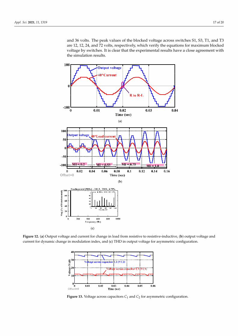
Appl. Sci. 2021, 11, 1319 17 of 20
and 36 volts. The peak values of the blocked voltage across switches S1, S3, T1, and T3are 12, 12, 24, and 72 volts, respectively, which verify the equations for maximum blockedvoltage by switches. It is clear that the experimental results have a close agreement withthe simulation results.
Appl. Sci. 2021, 11, x FOR PEER REVIEW 16 of 20
(a)
(b)
(c)
Figure 12. (a) Output voltage and current for change in load from resistive to resistive-inductive, (b) output voltage and current for dynamic change in modulation index, and (c) THD in output voltage for asymmetric configuration.
Figure 13. Voltage across capacitors C1 and C2 for asymmetric configuration.
Figure 12. (a) Output voltage and current for change in load from resistive to resistive-inductive, (b) output voltage andcurrent for dynamic change in modulation index, and (c) THD in output voltage for asymmetric configuration.
Appl. Sci. 2021, 11, x FOR PEER REVIEW 16 of 20
(a)
(b)
(c)
Figure 12. (a) Output voltage and current for change in load from resistive to resistive-inductive, (b) output voltage and current for dynamic change in modulation index, and (c) THD in output voltage for asymmetric configuration.
Figure 13. Voltage across capacitors C1 and C2 for asymmetric configuration. Figure 13. Voltage across capacitors C1 and C2 for asymmetric configuration.

Appl. Sci. 2021, 11, 1319 18 of 20
Appl. Sci. 2021, 11, x FOR PEER REVIEW 17 of 20
A laboratory prototype was developed in order to verify the simulation results and performance of the proposed SCMLI topology. Figure 14 shows the setup of the labora-tory prototype for the proposed topology. In this experimental work, an Insulated Gate Bipolar Transistor (IGBT) (FGA25N120AND) with rating 1200 V/25 A was utilized as the power electronic switch signals to the switches by interfacing with SIMULINK.
Figure 14. Experimental setup.
Diode BEC0141 with a rating of 10A was used as the power diodes, an electrolyte capacitor with a rating of 4700 µF/63V was utilized as the switched capacitors, and TMS320F28335 (Texas Instruments) was used as a controller for the generation of the gat-ing prototype and controller isolated by using the TLP 250 (TOSHIBA) optocoupler. A Digital Storage Oscilloscope (TPS2024B TEKTRONIX) was employed for the measure-ment of the waveforms of voltage and current. For the experimental results of the sym-metric configuration, voltage sources V1 and V2 were taken equal to 12 volts each. This resulted in a 9-level staircase output voltage with a 48-volt peak value, as shown in Figure 15a. Figure 15a also shows the load current when a purely resistive load of 100 Ω was connected at the output. Figure 15b shows the waveform of output voltage and load cur-rent when the DC voltage sources were connected across capacitors C1 and C2 in the sym-metric configuration. Figure 15c,d show the waveform of voltage across capacitors C1 and C2 and the waveform of the blocked voltage across switches S1 and T1, respectively, in the symmetric configuration. The peak values of voltage across capacitors C1 and C2 are 12 volts. The peak value of the blocked voltage across switches S1 and T1 are 12 and 24 volts, respectively, which verify the equations for maximum blocked voltage by switches. For the experimental results of asymmetric configuration, voltage sources V1 and V2 were taken 12 volts and 36 volts, respectively. This resulted in a 17-level staircase output volt-age with a 96-volt peak value, as shown in Figure 15e under the no-load condition. Figure 15f shows the output voltage and load current waveform when a purely resistive load of 100 Ω was connected at the output. Figure 15g shows the waveform of output voltage (17 levels) and load current to observe the levels clearly. Figure 15h–j show the waveform of the voltage across capacitors C1 and C2, the waveform of blocked voltage across switches S1 and S3, and the waveform of blocked voltage across switches T1 and T3, respectively, in an asymmetric configuration. The peak values of voltage across capacitors C1 and C2 are 12 and 36 volts. The peak values of the blocked voltage across switches S1, S3, T1, and T3 are 12, 12, 24, and 72 volts, respectively, which verify the equations for maximum blocked voltage by switches. It is clear that the experimental results have a close agree-ment with the simulation results.
Figure 14. Experimental setup.Appl. Sci. 2021, 11, x FOR PEER REVIEW 18 of 20
(a)
(b)
(c)
(d)
(e)
(f)
(g)
(h)
(i)
(j)
Figure 15. Waveform of (a) output voltage (25V/div) and load current (1.5 A/div). (b) Output voltage (20 V/div) and load current (0.5 A/div) when the voltage supply of 12V was connected across both capacitors. (c) Voltage across capacitors C1 and C2 (12 V/div). (d) Blocked voltage across switches S1 and T1 (12 V/div) in symmetric configuration. Waveform of (e) output voltage (60 V/div) under the no-load condition. (f) Output voltage (20V/div) and load current (0.75 A/div). (g) Output voltage (20V/div) and load current (0.75 A/div) for showing one complete cycle (f). Voltage across capacitors C1 and C2 (25 V/div). (i) Blocked voltage across switches S1 and S3 (25 V/div). (j) Blocked voltage across switches T1 and T3 (24 V/div) in asymmetric configuration.
6. Conclusions In this paper, a generalized structure for the MLI topology was presented. The gen-
eralized structures including various basic units and bidirectional switches, and a detailed analysis of this structure for two different methods depending on the selection of voltage sources are also presented. In the topology, capacitor voltages are self-balanced, due to
Figure 15. Waveform of (a) output voltage (25 V/div) and load current (1.5 A/div). (b) Output voltage (20 V/div) and loadcurrent (0.5 A/div) when the voltage supply of 12 V was connected across both capacitors. (c) Voltage across capacitors C1and C2 (12 V/div). (d) Blocked voltage across switches S1 and T1 (12 V/div) in symmetric configuration. Waveform of(e) output voltage (60 V/div) under the no-load condition. (f) Output voltage (20 V/div) and load current (0.75 A/div).(g) Output voltage (20 V/div) and load current (0.75 A/div) for showing one complete cycle (h). Voltage across capacitorsC1 and C2 (25 V/div). (i) Blocked voltage across switches S1 and S3 (25 V/div). (j) Blocked voltage across switches T1 andT3 (24 V/div) in asymmetric configuration.

Appl. Sci. 2021, 11, 1319 19 of 20
6. Conclusions
In this paper, a generalized structure for the MLI topology was presented. The gener-alized structures including various basic units and bidirectional switches, and a detailedanalysis of this structure for two different methods depending on the selection of voltagesources are also presented. In the topology, capacitor voltages are self-balanced, due towhich no voltage balancing algorithm is needed. The comparative study of the generalizedstructure was performed, and the results show superior performance under various per-formance parameters. The generalized structure needs less switches, capacitors, drivers,and TSV (in per unit) for a higher level of voltage output. Finally, to validate the perfor-mance, the simulation and experimental results were presented for symmetric (9-levelvoltage) and asymmetric (17-level voltage) configurations for a basic unit. The experi-mental results validate the performance obtained by simulation. The proposed modularstructure is suitable for solar PV application. Moreover, the 9 levels can find applicationin electric vehicle driven applications. The number of DC power sources becomes higherfor a higher level of operation. Future research should focus on the replacement of the DCpower supplies with capacitors for a cost-effective solution for high power applications.
Author Contributions: Conceptualization, M.A.; data curation, A.S.; formal analysis, M.A., A.S.,A.A. (Anzar Ahmad), and A.A. (Afroz Alam); funding acquisition, S.A., M.S., M.Z., and M.F.; investi-gation, M.A., A.S., A.A. (Anzar Ahmad), A.A. (Afroz Alam), S.A., M.S., M.Z., and M.F.; methodology,A.S., A.A. (Anzar Ahmad), A.A. (Afroz Alam), M.S., M.Z., and M.F.; project administration, A.S., S.A.,M.S., and M.F.; supervision, A.S. and S.A.; writing—original draft, M.A. and A.S.; writing—reviewand editing, A.A. (Afroz Alam) and S.A. All authors have read and agreed to the published versionof the manuscript.
Funding: The authors extend their appreciation to the Deanship of Scientific Research at King SaudUniversity for funding this work through research group No (RG- 1438-089).
Institutional Review Board Statement: Not applicable.
Informed Consent Statement: Not applicable.
Data Availability Statement: Not applicable.
Conflicts of Interest: The authors declare no conflict of interest.
References1. Nabae, A.; Takahashi, I.; Akagi, H. A New Neutral-Point-Clamped PWM Inverter. IEEE Trans. Ind. Appl. 1981, 17, 518–523.
[CrossRef]2. Gupta, K.K.; Ranjan, A.; Bhatnagar, P.; Sahu, L.K.; Jain, S. Multilevel inverter topologies with reduced device count: A review.
IEEE Trans. Power Electron. 2016, 31, 135–151. [CrossRef]3. Alishah, R.S.; Sabahi, M.; Nazarpour, D.; Hosseini, S.H. Novel multilevel inverter topologies for medium and high-voltage
applications with lower values of blocked voltage by switches. IET Power Electron. 2014, 7, 3062–3071. [CrossRef]4. Zhang, Y.; Adam, G.P.; Lim, T.C.; Finney, S.J.; Williams, B.W. Hybrid Multilevel Converter: Capacitor Voltage Balancing Limits
and its Extension. IEEE Trans. Ind. Inform. 2013, 9, 2063–2073. [CrossRef]5. Abu-Rub, H.; Holtz, J.; Rodriguez, J.; Baoming, G. Medet alm-voltage multilevel converters; state of the art challenges and
requirements in industrial applications. IEEE Trans. Ind. Electron. 2010, 57, 2581–2596. [CrossRef]6. Rodriguez, J.; Franquelo, L.G.; Kouro, S.; Leon, J.I.; Portillo, R.C.; Prats, M.A.M.; Perez, M.A. Multilevel converters: An enabling
technology for high-power applications. Proc. IEEE 2009, 97, 1786–1817. [CrossRef]7. Roy, T.; Sadhu, P.K.; Dasgupta, A. Cross-Switched Multilevel Inverter Using Novel Switched Capacitor Converters. IEEE Trans.
Ind. Electron. 2019, 66, 8521–8532. [CrossRef]8. Babaei, E.; Hosseini, S.H. New cascaded multilevel inverter topology with minimum number of switches. J. Energy Convers. Manag.
2009, 50, 2761–2767. [CrossRef]9. Kangarlu, M.F.; Babaei, E.; Laali, S. Symmetric multilevel inverter with reduced components based on non-insulated dc voltage
sources. IET Power Electron. 2012, 5, 571–581. [CrossRef]10. Alishah, R.S.; Nazarpour, D.; Hosseini, S.H.; Sabahi, M. New hybrid structure for multilevel inverter with fewer number of
components for high-voltage levels. IET Power Electron. 2014, 1, 96–104. [CrossRef]11. Siddique, M.D.; Saad, M.; Sarwar, A.; Alam, A.; Shah, N.M. Dual asymmetrical dc voltage source based switched capacitor boost
multilevel inverter topology. IET Power Electron. 2020, 7, 1481–1486. [CrossRef]

Appl. Sci. 2021, 11, 1319 20 of 20
12. Waltrich, G.; Barbi, I. Three-phase cascaded multilevel inverter using power cells with two inverter legs in series. IEEE Trans.Ind. Electron. 2010, 57, 2605–2612. [CrossRef]
13. Alishah, R.S.; Nazarpour, D.; Hosseini, S.H.; Sabahi, M. Reduction of power electronic elements in multilevel converters using anew cascade structure. IEEE Trans. Ind. Electron. 2015, 62, 256–269. [CrossRef]
14. Babaei, E.; Laali, S.; Alilu, S. Cascaded multilevel inverter with series connection of novel H-bridge basic units. IEEE Trans.Ind. Electron. 2014, 61, 6664–6671. [CrossRef]
15. Boora, K.; Kumar, J. General topology for asymmetrical multilevel inverter with reduced number of switches. IET Power Electron.2017, 10, 2034–2041. [CrossRef]
16. Banaei, M.R.; Salary, E. Verification of new family for cascade multilevel inverter switch reduction of components. J. Electr.Eng. Technol. 2011, 6, 245–254. [CrossRef]
17. Banaei, M.R.; JannatiOskuee, M.R.; Khounjahan, H. Reconfiguration of semi-cascaded multilevel inverter to improve systemsperformance parameters. IET Power Electron. 2014, 7, 1106–1112. [CrossRef]
18. Alishah, R.S.; Hosseini, S.H. Novel topologies for symmetric, asymmetric, and cascade switched-diode mutilevel converter withminimum number of power electronic components. IEEE Trans. Ind. Electron. 2014, 61, 5300–5310. [CrossRef]
19. Hussan, M.R.; Sarwar, A.; Siddique, M.D.; Mekhilef, S.; Ahmad, S.; Sharaf, M.; Zaindin, M.; Firdausi, M. A Novel Switched-Capacitor Multilevel Inverter Topology for Energy Storage and Smart Grid Applications. Electronics 2020, 9, 1703. [CrossRef]
20. Wang, L.; Wu, Q.H.; Tang, W. Novel Cascaded Switched-Diode Multilevel Inverter for Renewable Energy Integration. IEEE Trans.Energy Convers. 2017, 32, 1574–1582. [CrossRef]
21. Abdullah, R.; Rahim, N.A.; Sheikh Raihan, S.R.; Ahmad, A.Z. Five-level diode-clamped inverter with three-level boost converter.IEEE Trans. Ind. Electron. 2014, 61, 5155–5163. [CrossRef]
22. Khazraei, M.; Sepahvand, H.; Corzine, K.A.; Ferdowsi, M. Active capacitor voltage balancing in single-phase flying-capacitormultilevel power converters. IEEE Trans. Ind. Electron. 2012, 59, 769–778. [CrossRef]
23. Shukla, A.; Ghosh, A.; Joshi, A. Control of dc capacitor voltages in diode-clamped multilevel inverter using bidirectionalbuck-boost choppers. IET Power Electron. 2012, 5, 1723–1732. [CrossRef]
24. Mak, O.C.; Ioinovici, A. Switched-capacitor inverter with high power density and enhanced regulation capability. IEEE Trans.Circuits Syst. I Fundam. Theory Appl. 1998, 45, 336–347.
25. Alishah, R.S.; Hosseini, S.H.; Babaei, E.; Sabahi, M. Optimal design of new cascaded switch-ladder multilevel inverter structure.IEEE Trans. Ind. Electron. 2017, 64, 2072–2080. [CrossRef]
26. Siddique, M.D.; Mekhilef, S.; Shah, N.; Sarwar, A.; Iqbal, A.; Tayyab, M.; Ansary, M.K. Low Switching Frequency BasedAsymmetrical Multilevel Inverter Topology with Reduced Switch Count. IEEE Access 2019, 7, 86374–86383. [CrossRef]
27. Lee, S.S.; Lee, K.; Alsofyani, I.M.; Bak, Y.; Wong, J.F. Improved Switched-Capacitor Integrated Multilevel Inverter with a DCSource String. IEEE Trans. Ind. Appl. 2019, 55, 7368–7376. [CrossRef]
28. Siddique, M.D.; Mekhilef, S.; Shah, N.M.; Sarwar, A.; Memon, M.A. A New Single-Cascaded Multilevel Inverter Topology withReduced Number of Switches and Voltage Stress. Int. Trans. Electr. Energy Syst. 2019. [CrossRef]
29. Hosseini, S.H.; Alishah, R.S.; Gharehkoushan, A.Z. Enhancement of extracted maximum power from partially shaded multi-stringPV panels using a new cascaded high step-up DC-DC-AC converter. In Proceedings of the 9th International Conference onElectrical and Electronics Engineering (ELECO 2015), Bursa, Turkey, 26–28 November 2015; pp. 644–648.
30. Taghvaie, A.; Adabi, J.; Rezanejad, M. A Self-Balanced Step-Up Multilevel Inverter Based on Switched-Capacitor Structure.IEEE Trans. Power Electron. 2018, 33, 199–209. [CrossRef]
31. Liu, J.; Zhu, X.; Zeng, J. A Seven-level Inverter with Self-balancing and Low Voltage Stress. IEEE J. Emerg. Sel. Top. Power Electron.2018, 8, 685–696. [CrossRef]