PLL-Based Readout Circuit for SiC-MOS Capacitor Hydrogen ...
Page 1
DEPT. OF EEE,GPREC
CHAPTER 1
1. INVERTER
INTRODUCTION:
A dc-to-ac converter whose output is of desired output voltage and frequency is called
an inverter.
Based on their operation the inverters can be broadly classified into
Voltage Source Inverters(VSI)
Current Source Inverters(CSI)
A voltage source inverter is one where the independently controlled ac output is a
voltage waveform.
A current source inverter is one where the independently controlled ac output is a
current waveform.
On the basis of connections of semiconductor devices, inverters are classified
as
Bridge inverters
Series inverters
Parallel inverters
Some industrial applications of inverters are for adjustable- speed ac drives, induction
heating, stand by air-craft power supplies, UPS(uninterruptible power supplies) for
computers, hvdc transmission lines etc.
1.1Comparison of the 2-level and multilevel inverters
In 2-level inverter output voltage waveform is produced by using PWM with two
voltage levels.
This causes the output voltage and current to be distorted and the THD of the voltage
is poor(Figure 1, left). In 3-level inverter output voltage and current is much more
sinusoidal and the THD is better (Figure 1, right).

Page 2
DEPT. OF EEE,GPREC
Figure 1. Comparison of the 2-level and 3-level inverter output voltages and currents .
Comparison of conventional two level inverters and
multilevel inverters
S.No Conventional Inverter Multilevel Inverter
1 Higher THD in output voltage Low THD in output voltage
2 More switching stresses on
devices
Reduced switching stresses on
Devices
3 Not applicable for high
voltageapplications
Applicable for high voltage
Applications
4 Higher voltage levels are not
produced
Higher voltage levels are
Produced
5 Since dv/dt is high, the EMI
from system is high
Since dv/dt is low, the EMI from
system is low
6 Higher switching frequency is
used hence switching losses is
high
Lower switching frequency can
be used and hence reduction in
switching losses
7 Power bus structure, control
schemes are simple
control scheme becomes
complex as number of levels increases
Table 1 Comparison of conventional two level inverters and multilevel inverters
Page 3
DEPT. OF EEE,GPREC
CHAPTER 2
2. MULTI LEVEL INVERTERS
2.1 INTRODUCTION:
Multilevel Converters has been attracted a large interest in the power industry
in the recent years. Industry has started to involve in higher power equipment, which
already reaches megawatt level. Conventional power electronic converters are only
able to switch each individual input or output link between two possible voltage
levels, especially those of the internal DC voltage link. The general structure of the
multilevel converter is to generate a sinusoidal voltage from several levels of voltages
which are usually obtained from capacitor voltage sources.
Three different topologies have been projected for multilevel converters: Diode
clamped converter; Flying capacitor converter (Capacitor Clamped); and lastly
cascaded converter. Several modulation and control strategies have been developed or
being used for multilevel converters including the following: Multilevel sinusoidal
pulse width modulation (PWM), multilevel selective harmonic elimination, and
space-vector modulation (SVM).
2.2 Advantages of multilevel converters
1. They are able to generate output voltages with very low distortion and lower
dv/dt.
2. They are able to bring in input current with very low input distortion.
3. They are able to produce smaller common mode (CM) voltage, therefore, reducing
the stress in the motoring bearings. In addition, using complicated modulation
methods, CM voltages can be eliminated.
4.They can be functioned with a much lower switching frequency.

Page 4
DEPT. OF EEE,GPREC
The only disadvantage of the multilevel converter is that it required a huge amount of
semiconductors switches. It should be pointed out that lower voltage rated switches
can be used in the multilevel converter and as a result the active semiconductor cost is
not considerably increased when compared with the two level cases. On the other
hand, each active semiconductor added requires associated gate drive circuitry and
adds further complication to the converter mechanical layout.
Another disadvantage which is to be mention is that the small voltage steps are
typically formed by isolated voltage sources or a bank of series capacitors. Isolated
voltage sources may not always be readily available and series capacitors require
voltage balance. To some extend, the voltage balancing can be addressed by using an
uncalled-for switching states, which exist due to the high number of semiconductor
devices. Nevertheless, for a complete solution to the voltage-balancing problem,
another multilevel converter maybe is required.
A multilevel converter can be implemented in many different ways,
each with advantages and disadvantages. The simplest techniques which involve the
parallel or series connection of conventional converters to form the multilevel
waveforms. Complicated structures actually insert converters within converters.
Whatever approach is being chosen, the subsequent voltage or current rating of the
multilevel converter will becomes a multiple of the individual switches, and therefore
the power rating of the converter can exceed the limit imposed by the individual
switching devices.
Power-electronic inverters are becoming popular for various industrial
drives applications. In recent years also high-power and medium-voltage drive
applications have been installed. To overcome the limited semiconductor voltage and
current ratings, some kind of series and/or parallel connection will be necessary. Due
to their ability to synthesize waveforms with a better harmonic spectrum and attain
higher voltages, multi-level inverters are receiving increasing attention in the past few
years. The multilevel inverter was introduced as a solution to increase the converter
operating voltage above the voltage limits of classical semiconductors. The multilevel
voltage source inverter is recently applied in many industrial applications such as ac
power supplies, static VAR compensators, drive systems, etc.
Page 5
DEPT. OF EEE,GPREC
One of the significant advantages of multilevel configuration is the harmonic
reduction in the output waveform without increasing switching frequency or
decreasing the inverter power output. The output voltage waveform of a multilevel
inverter is composed of the number of levels of voltages, typically obtained from
capacitor voltage sources. The so-called multilevel starts from three levels. As the
number of levels reach infinity, the output THD (Total Harmonic Distortion)
approaches zero. The number of the achievable voltage levels, however, is limited by
voltage unbalance problems, voltage clamping requirement, circuit layout, and
packaging constraints. Multilevel inverters synthesizing a large number of levels have
a lot of merits such as improved output waveform, a smaller filter size, a lower EMI
(Electro Magnetic Interference), and other advantages. The principle advantage of
using multilevel inverters is the low harmonic distortion obtained due to the multiple
voltage levels at the output and reduced stresses on the switching devices used.
2.3 MULTILEVEL VOLTAGE CONCEPT:
Recent advances in power electronics have made the multilevel concept practical. In
fact, the concept is so advantageous that several major drives manufacturers have
obtained recent patents on multilevel power converters and associated switching
techniques. It is evident that the multilevel concept will be a prominent choice for
power electronic systems in future years, especially for medium-voltage operation.
Multi-level inverters are the modification of basic bridge inverters. They are normally
connected in series to form stacks of level.
The topological structure of multilevel inverter must cope with the following points.
1) It should have less switching devices as far as possible.
2) It should be capable of enduring very high input voltage such as HVDC
transmission for high power applications.
3) Each switching device should have lower switching frequency owing to
multilevel approach.

Page 6
DEPT. OF EEE,GPREC
There are various multilevel concepts used for various applications. Various
multilevel circuits are used to generate multiple voltage levels. Some of the multilevel
concepts with various voltage levels are given below.
2.4 ADVANTAGES OF MULTILEVEL VOLTAGES :
In general, multilevel power converters can be viewed as voltage synthesizers,
in which the high output voltage is synthesized from many discrete smaller voltage
levels. The main advantages of this approach are summarized as follows:
1. The voltage capacity of the existing devices can be increased many times without
the complications of static and dynamic voltage sharing that occur in series-connected
devices.
2. Spectral performance of multilevel waveforms is superior to that of their two- level
counterparts.
3.Multilevel waveforms naturally limit the problems of large voltage transients that
occur due to the reflections on cables, which can damage the motor windings and
cause other problems.
4.In very high power application especially with very high input voltage, traditional
two-level VSIs could not avoid to sue the series connected semiconductor switches so
as to cope with limitations of device rating utilized and it may be very cumbersome
and even problematic mainly due to difficulty of device matching deteriorating
utilization factor of switching devices. The multilevel topology, however, suggests a
good solution for such a problem.
Page 7
DEPT. OF EEE,GPREC
2.5 APPLICATIONS:
DC power source utilization:
An inverter converts the DC electricity from sources such as batteries, solar panels,
or fuel cells to AC electricity. The electricity can be at any required voltage; in
particular it can operate AC equipment designed for mains operation, or rectified to
produce DC at any desired voltage.
Grid tie inverters can feed energy back into the distribution network because they
produce alternating current with the same wave shape and frequency as supplied by
the distribution system. They can also switch off automatically in the event of
a blackout.
Uninterruptible power supplies
Inverters convert low frequency main AC power to a higher frequency for use
in induction heating. To do this, AC power is first rectified to provide DC power. The
inverter then changes the DC power to high frequency AC power‟
HVDC power transmission
With HVDC power transmission, AC power is rectified and high voltage DC power is
transmitted to another location. At the receiving location, an inverter in a static
inverter plant converts the power back to AC.
Variable-frequency drives
A variable-frequency drive controls the operating speed of an AC motor by
controlling the frequency and voltage of the power supplied to the motor. An inverter
provides the controlled power. In most cases, the variable-frequency drive includes
a rectifier so that DC power for the inverter can be provided from main AC power.
Since an inverter is the key component, variable-frequency drives are sometimes
called inverter drives or just inverters.
Electric vehicle drives
Adjustable speed motor control inverters are currently used to power the traction
motors in some electric and diesel-electric rail vehicles as well as some battery
electric vehicles and hybrid electric highway vehicles such as the Toyota Prius.

Page 8
DEPT. OF EEE,GPREC
Various improvements in inverter technology are being developed specifically for
electric vehicle applications. In vehicles with regenerative braking, the inverter also
takes power from the motor (now acting as a generator) and stores it in the batteries.
Air conditioning
A transformer allows AC power to be converted to any desired voltage, but at the
same frequency. Inverters, plus rectifiers for DC, can be designed to convert from any
voltage, AC or DC, to any other voltage, also AC or DC, at any desired frequency.
The output power can never exceed the input power, but efficiencies can be high, with
a small proportion of the power dissipated as waste heat.

Page 9
DEPT. OF EEE,GPREC
CHAPTER 3
3. MULTI LEVEL INVERTER TOPOLOGIES
Multilevel power conversion technology is a very rapidly growing area of power
electronics with good potential for further development. The most attractive
applications of this technology are in the medium- to high-voltage range (2-13 kV),
and include motor drives, power distribution, power quality and power conditioning
applications. There are different types of multi level circuits involved. The first
topology introduced was the series H-bridge design. This was followed by the diode
clamped converter, which utilized a bank of series capacitors. A later invention
detailed the flying capacitor design in which the capacitors were floating rather than
series-connected. Another multilevel design involves parallel connection of inverter
phases through inter-phase reactors. In this design, the semiconductors block the
entire dc voltage, but share the load current. Several combinational designs have also
emerged some involving cascading the fundamental topologies. These designs can
create higher power quality for a given number of semiconductor devices.
INTRODUCTION
The schematic of inverter system is as shown in Fig. 3.1, in which the battery or
rectifier provides the dc supply to the inverter. The inverter is used to control the
fundamental voltage magnitude and the frequency of the ac output voltage. AC loads
may require constant or adjustable voltage at their input terminals, when such loads
are fed by inverters, it is essential that the output voltage of the inverters is so
controlled as to fulfill the requirement of the loads. For example if the inverter
supplies power to a magnetic circuit, such as a induction motor, the voltage to
frequency ratio at the inverter output terminals must be kept constant. This avoids
saturation in the magnetic circuit of the device fed by the inverter.
Fig. 3.1 : Schematic for Inverter System
Page 10
DEPT. OF EEE,GPREC
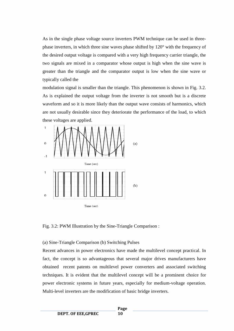
As in the single phase voltage source inverters PWM technique can be used in three-
phase inverters, in which three sine waves phase shifted by 120° with the frequency of
the desired output voltage is compared with a very high frequency carrier triangle, the
two signals are mixed in a comparator whose output is high when the sine wave is
greater than the triangle and the comparator output is low when the sine wave or
typically called the
modulation signal is smaller than the triangle. This phenomenon is shown in Fig. 3.2.
As is explained the output voltage from the inverter is not smooth but is a discrete
waveform and so it is more likely than the output wave consists of harmonics, which
are not usually desirable since they deteriorate the performance of the load, to which
these voltages are applied.
Fig. 3.2: PWM Illustration by the Sine-Triangle Comparison :
(a) Sine-Triangle Comparison (b) Switching Pulses
Recent advances in power electronics have made the multilevel concept practical. In
fact, the concept is so advantageous that several major drives manufacturers have
obtained recent patents on multilevel power converters and associated switching
techniques. It is evident that the multilevel concept will be a prominent choice for
power electronic systems in future years, especially for medium-voltage operation.
Multi-level inverters are the modification of basic bridge inverters.
Page 11
DEPT. OF EEE,GPREC
They are normally connected in series to form stacks of level. The number of levels
in an inverter bridge defines the number of direct current (DC) voltage steps that are
required by the inverter bridge in order to achieve a certain voltage level at its output.
Because power semiconductor switches have limited voltage capability, the total DC
bus voltage of an inverter bridge is divided into a number of voltage steps, such that
each voltage step can be handled by one power switch. For high power applications,
voltages and currents must be pushed up. Hence, maximum ratings of power
semiconductors become a real handicap. Paralleling devices, subsystems and systems
leads to higher current levels. On the other hand, series connections are the solution
for dealing with larger voltages. Nevertheless, given a chain of devices connected in
series, achieving static and dynamic voltage sharing among switches become a
problem. This will also affect the reliability of the system. An advantage of multilevel
inverters compared with the classical two-level topology, is that the output voltage
spectra are significantly improved due to having a greater availability of voltage
levels, Hence, the output voltages can be filtered with smaller reactive components,
and additionally, the switching frequencies of the devices can be reduced. These two
benefits, together with the ability to deal with higher voltage levels, confer on
multilevel inverters a very important role in the field of high power applications. The
intriguing feature of the multilevel inverter structures is their ability to scale up the
kilovolt-ampere (KVA) rating and also to improve the harmonic performance greatly
without having to resort to PWM techniques. The key features of a multilevel
structure follow:
•The output voltage and power increase with number of levels. Adding a voltage level
involves adding a main switching device to each phase.
•The harmonic content decreases as the number of levels increases and filtering
requirements are reduced.
•With additional voltage levels, the voltage waveform has more free-switching
angles, which can be reselected for harmonic elimination.
•In the absence of any PWM techniques, the switching losses can be avoided.
Increasing output voltage and power does not require an increase in rating of
individual device.
•Static and dynamic voltage sharing among the switching devices is built into the
structure through either clamping diodes or capacitors.

Page 12
DEPT. OF EEE,GPREC
•The switching devices do not encounter any voltage-sharing problems. For this
reason, multilevel inverters
can easily be applied for high-power applications such as large motor drives and
utility supplies.
•The fundamental output voltage of the inverter is set by the dc bus voltage Vdc,
which can be controlled through a variable dc link.
3.1 Classification of High power Converters
Page 13
DEPT. OF EEE,GPREC
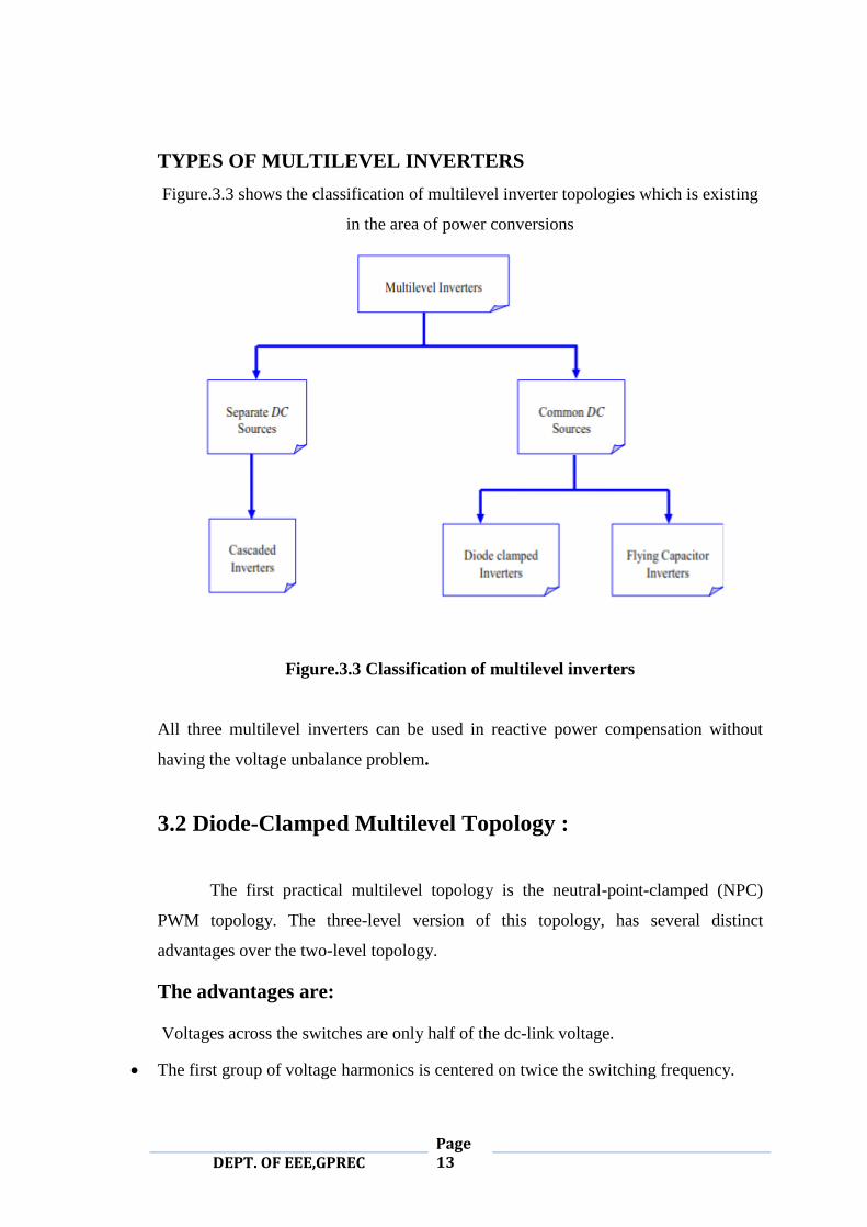
TYPES OF MULTILEVEL INVERTERS
Figure.3.3 shows the classification of multilevel inverter topologies which is existing
in the area of power conversions
Figure.3.3 Classification of multilevel inverters
All three multilevel inverters can be used in reactive power compensation without
having the voltage unbalance problem.
3.2 Diode-Clamped Multilevel Topology :
The first practical multilevel topology is the neutral-point-clamped (NPC)
PWM topology. The three-level version of this topology, has several distinct
advantages over the two-level topology.
The advantages are:
Voltages across the switches are only half of the dc-link voltage.
The first group of voltage harmonics is centered on twice the switching frequency.
Page 14
DEPT. OF EEE,GPREC
This topology can be generalized, and the principles used in the basic three-level
topology can be extended for use in topologies with any number of levels.
However, practical experience with this topology revealed several technical
difficulties that complicate its application for-high power converters.
These are as follows:
This topology requires high speed clamping diodes that must be able to carry full
load current and are subject to severe reverse recovery stress. Although measures to
alleviate this problem can be applied, this remains a serious consideration.
For topologies with more than three levels the clamping diodes are subject to
increased voltage stress equal to Vpn.(n-1)/n. Therefore, series connection of diodes
might be required.
This complicates the design and raises reliability and cost concerns.
The issue of maintaining the charge balance of the capacitors is still an open issue for
NPC topologies with more than three-levels. Although the three-level NPC topology
works well with high power factor loads, NPC topologies with more than three levels
are mostly used for static var compensation circuits.
3.3 Flying Capacitor Multilevel Topology :
The flying capacitor multilevel topology is considered to be the most serious
alternative to the diode-clamped topology.
The significant advantage of this topology is that
1) It eliminates the clamping diode problems present in the diode-clamped multilevel
topologies.
2) Additionally, this topology naturally limits the dV/dt stress across the devices and
introduces additional switching states that can be used to help maintain the charge
balance in the capacitors.
The dc-link capacitor charge controller adds complexity to the control of the whole
circuit.

Page 15
DEPT. OF EEE,GPREC
The flying capacitor topology might require more capacitance than the equivalent
diode clamped topology.
In addition, it is obvious that rather large rms currents will flow through these
capacitors. There is a potential for parasitic resonance between decoupling capacitors.
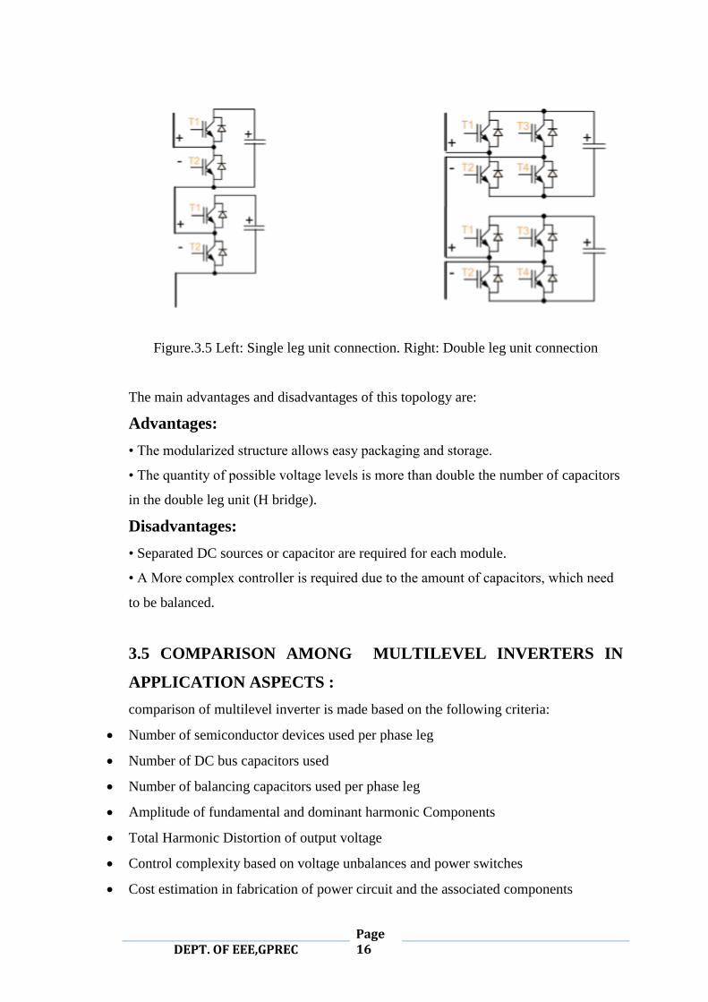
3.4 Cascaded voltage bridge inverter:
The cascaded multilevel inverter is based on the series connection of single leg
or double leg (H bridges) inverters with separate DC sources or capacitors. For each
of these two types of configurations several states exist regarding to the switches
states. Figure 3.4, the single leg unit, has 2 states for each of the two possible
current(s) directions while the double unit has 4 states.
Fig.3.4
The series connection between the modules is represented in Figure 3.5; each
module has a capacitor that is charged and discharged by a controlled DC current. The
resultant voltage waveform is made by the addition of the voltage generated in each
module that is connected.
Page 16
DEPT. OF EEE,GPREC
Figure.3.5 Left: Single leg unit connection. Right: Double leg unit connection
The main advantages and disadvantages of this topology are:
Advantages:
• The modularized structure allows easy packaging and storage.
• The quantity of possible voltage levels is more than double the number of capacitors
in the double leg unit (H bridge).
Disadvantages:
• Separated DC sources or capacitor are required for each module.
• A More complex controller is required due to the amount of capacitors, which need
to be balanced.
3.5 COMPARISON AMONG MULTILEVEL INVERTERS IN
APPLICATION ASPECTS :
comparison of multilevel inverter is made based on the following criteria:
Number of semiconductor devices used per phase leg
Number of DC bus capacitors used
Number of balancing capacitors used per phase leg
Amplitude of fundamental and dominant harmonic Components
Total Harmonic Distortion of output voltage
Control complexity based on voltage unbalances and power switches
Cost estimation in fabrication of power circuit and the associated components

Page 17
DEPT. OF EEE,GPREC
Table.2 Comparison of different multilevel inverter topologies
In high power system, the multilevel inverters can appropriately replace the exist
system that use traditional multi-pulse converters without the need for transformers.
All three multilevel inverters can be used in reactive power compensation without
having the voltage unbalance problem. Table.2 compares the power component
requirements per phase leg among the three multilevel voltage source inverter
mentioned below. It shows that the number of main switches and main diodes, needed
by the inverters to achieve the same number of voltage levels. Clamping diodes were
not needed in flying-capacitor and cascaded-inverter configuration, while balancing
capacitors were not needed in diode clamp and cascaded-inverter configuration.
Implicitly, the multilevel converter using cascaded-inverters requires the least number
of components.
Page 18
DEPT. OF EEE,GPREC
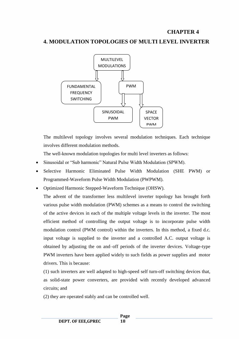
CHAPTER 4
4. MODULATION TOPOLOGIES OF MULTI LEVEL INVERTER
The multilevel topology involves several modulation techniques. Each technique
involves different modulation methods.
The well-known modulation topologies for multi level inverters as follows:
Sinusoidal or “Sub harmonic” Natural Pulse Width Modulation (SPWM).
Selective Harmonic Eliminated Pulse Width Modulation (SHE PWM) or
Programmed-Waveform Pulse Width Modulation (PWPWM).
Optimized Harmonic Stepped-Waveform Technique (OHSW).
The advent of the transformer less multilevel inverter topology has brought forth
various pulse width modulation (PWM) schemes as a means to control the switching
of the active devices in each of the multiple voltage levels in the inverter. The most
efficient method of controlling the output voltage is to incorporate pulse width
modulation control (PWM control) within the inverters. In this method, a fixed d.c.
input voltage is supplied to the inverter and a controlled A.C. output voltage is
obtained by adjusting the on and–off periods of the inverter devices. Voltage-type
PWM inverters have been applied widely to such fields as power supplies and motor
drivers. This is because:
(1) such inverters are well adapted to high-speed self turn-off switching devices that,
as solid-state power converters, are provided with recently developed advanced
circuits; and
(2) they are operated stably and can be controlled well.
FUNDAMENTAL
FREQUENCY
SWITCHING
PWM
SINUSOIDAL
PWM
SPACE
VECTOR
PWM
MULTILEVEL
MODULATIONS
Page 19
DEPT. OF EEE,GPREC
4.1 PULSE WIDTH MODULATION
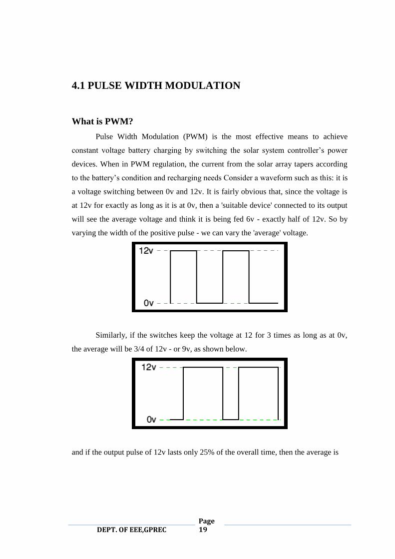
What is PWM?
Pulse Width Modulation (PWM) is the most effective means to achieve
constant voltage battery charging by switching the solar system controller‟s power
devices. When in PWM regulation, the current from the solar array tapers according
to the battery‟s condition and recharging needs Consider a waveform such as this: it is
a voltage switching between 0v and 12v. It is fairly obvious that, since the voltage is
at 12v for exactly as long as it is at 0v, then a 'suitable device' connected to its output
will see the average voltage and think it is being fed 6v - exactly half of 12v. So by
varying the width of the positive pulse - we can vary the 'average' voltage.
Similarly, if the switches keep the voltage at 12 for 3 times as long as at 0v,
the average will be 3/4 of 12v - or 9v, as shown below.
and if the output pulse of 12v lasts only 25% of the overall time, then the average is

Page 20
DEPT. OF EEE,GPREC
By varying - or 'modulating' - the time that the output is at 12v (i.e. the width
of the positive pulse) we can alter the average voltage. So we are doing 'pulse width
modulation'. I said earlier that the output had to feed 'a suitable device'. A radio would
not work from this: the radio would see 12v then 0v, and would probably not work
properly. However a device such as a motor will respond to the average, so PWM is a
natural for motor control.
Pulse Width modulator
So, how do we generate a PWM waveform? It's actually very easy, there are
circuits available in the TEC site. First you generate a triangle waveform as shown in
the diagram below. You compare this with a d.c voltage, which you adjust to control
the ratio of on to off time that you require. When the triangle is above the 'demand'
voltage, the output goes high. When the triangle is below the demand voltage, the
When the demand speed it in the middle (A) you get a 50:50 output, as in
black. Half the time the output is high and half the time it is low. Fortunately, there is
an IC (Integrated circuit) called a comparator: these come usually 4 sections in a
single package.

Page 21
DEPT. OF EEE,GPREC
One can be used as the oscillator to produce the triangular waveform and
another to do the comparing, so a complete oscillator and modulator can be done with
half an IC and maybe 7 other bits.
The triangle waveform, which has approximately equal rise and fall slopes, is
one of the commonest used, but you can use a saw tooth (where the voltage falls
quickly and rinses slowly). You could use other waveforms and the exact linearity
(how good the rise and fall are) is not too important.
Traditional solenoid driver electronics rely on linear control, which is the
application of a constant voltage across a resistance to produce an output current that
is directly proportional to the voltage. Feedback can be used to achieve an output that
matches exactly the control signal. However, this scheme dissipates a lot of power as
heat, and it is therefore very inefficient.
A more efficient technique employs pulse width modulation (PWM) to
produce the constant current through the coil. A PWM signal is not constant. Rather,
the signal is on for part of its period, and off for the rest. The duty cycle, D, refers to
the percentage of the period for which the signal is on. The duty cycle can be
anywhere from 0, the signal is always off, to 1, where the signal is constantly on. A
50% D results in a perfect square wave. (Figure 4.1)
Fig.4.1 showing different duty cycles
A solenoid is a length of wire wound in a coil. Because of this configuration,
the solenoid has, in addition to its resistance, R, a certain inductance, L. When a
voltage, V, is applied across an inductive element, the current, I, produced in that
element does not jump up to its constant value, but gradually rises to its maximum
over a period of time called the rise time (Figure 4.2).

Page 22
DEPT. OF EEE,GPREC
Conversely, I does not disappear instantaneously, even if V is removed
abruptly, but decreases back to zero in the same amount of time as
the rise time.
Fig.4.2
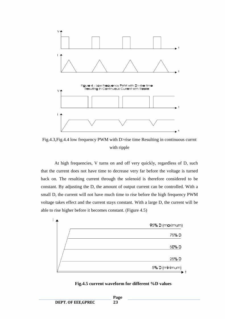
Therefore, when a low frequency PWM voltage is applied across a solenoid,
the current through it will be increasing and decreasing as V turns on and off. If D is
shorter than the rise time, we will never achieve its maximum value, and will be
discontinuous since it will go back to zero during V‟s off period (Figure 4.3). In
contrast, if D is larger than the rise time, we will never fall back to zero, so it will be
continuous, and have a DC average value. The current will not be constant, however,
but will have a ripple (Figure 4.4).
Page 23
DEPT. OF EEE,GPREC
Fig.4.3,Fig.4.4 low frequency PWM with D>rise time Resulting in continuous currnt
with ripple
At high frequencies, V turns on and off very quickly, regardless of D, such
that the current does not have time to decrease very far before the voltage is turned
back on. The resulting current through the solenoid is therefore considered to be
constant. By adjusting the D, the amount of output current can be controlled. With a
small D, the current will not have much time to rise before the high frequency PWM
voltage takes effect and the current stays constant. With a large D, the current will be
able to rise higher before it becomes constant. (Figure 4.5)
Fig.4.5 current waveform for different %D values
Page 24
DEPT. OF EEE,GPREC
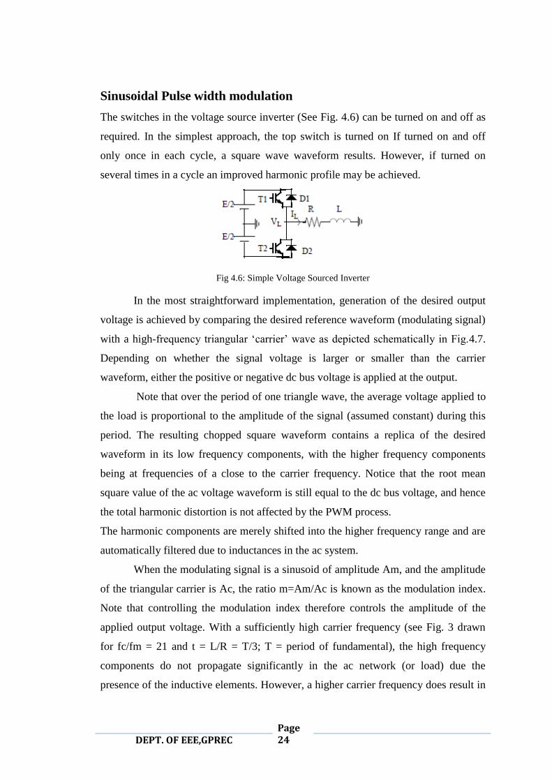
Sinusoidal Pulse width modulation
The switches in the voltage source inverter (See Fig. 4.6) can be turned on and off as
required. In the simplest approach, the top switch is turned on If turned on and off
only once in each cycle, a square wave waveform results. However, if turned on
several times in a cycle an improved harmonic profile may be achieved.
Fig 4.6: Simple Voltage Sourced Inverter
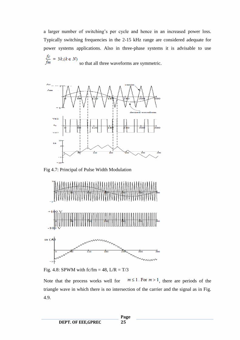
In the most straightforward implementation, generation of the desired output
voltage is achieved by comparing the desired reference waveform (modulating signal)
with a high-frequency triangular „carrier‟ wave as depicted schematically in Fig.4.7.
Depending on whether the signal voltage is larger or smaller than the carrier
waveform, either the positive or negative dc bus voltage is applied at the output.
Note that over the period of one triangle wave, the average voltage applied to
the load is proportional to the amplitude of the signal (assumed constant) during this
period. The resulting chopped square waveform contains a replica of the desired
waveform in its low frequency components, with the higher frequency components
being at frequencies of a close to the carrier frequency. Notice that the root mean
square value of the ac voltage waveform is still equal to the dc bus voltage, and hence
the total harmonic distortion is not affected by the PWM process.
The harmonic components are merely shifted into the higher frequency range and are
automatically filtered due to inductances in the ac system.
When the modulating signal is a sinusoid of amplitude Am, and the amplitude
of the triangular carrier is Ac, the ratio m=Am/Ac is known as the modulation index.
Note that controlling the modulation index therefore controls the amplitude of the
applied output voltage. With a sufficiently high carrier frequency (see Fig. 3 drawn
for fc/fm = 21 and t = L/R = T/3; T = period of fundamental), the high frequency
components do not propagate significantly in the ac network (or load) due the
presence of the inductive elements. However, a higher carrier frequency does result in
Page 25
DEPT. OF EEE,GPREC
a larger number of switching‟s per cycle and hence in an increased power loss.
Typically switching frequencies in the 2-15 kHz range are considered adequate for
power systems applications. Also in three-phase systems it is advisable to use
so that all three waveforms are symmetric.
Fig 4.7: Principal of Pulse Width Modulation
Fig. 4.8: SPWM with fc/fm = 48, L/R = T/3
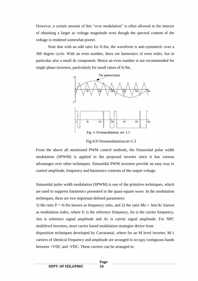
Note that the process works well for , there are periods of the
triangle wave in which there is no intersection of the carrier and the signal as in Fig.
4.9.
Page 26
DEPT. OF EEE,GPREC
However, a certain amount of this “over modulation” is often allowed in the interest
of obtaining a larger ac voltage magnitude even though the spectral content of the
voltage is rendered somewhat poorer.
Note that with an odd ratio for fc/fm, the waveform is anti-symmetric over a
360 degree cycle. With an even number, there are harmonics of even order, but in
particular also a small dc component. Hence an even number is not recommended for
single phase inverters, particularly for small ratios of fc/fm.
Fig:4.9 Overmodulation:m=1.3
From the above all mentioned PWM control methods, the Sinusoidal pulse width
modulation (SPWM) is applied in the proposed inverter since it has various
advantages over other techniques. Sinusoidal PWM inverters provide an easy way to
control amplitude, frequency and harmonics contents of the output voltage.
Sinusoidal pulse width modulation (SPWM) is one of the primitive techniques, which
are used to suppress harmonics presented in the quasi-square wave. In the modulation
techniques, there are two important defined parameters:
1) the ratio P = fc/fm known as frequency ratio, and 2) the ratio Ma = Am/Ac known
as modulation index, where fc is the reference frequency, fm is the carrier frequency,
Am is reference signal amplitude and Ac is carrier signal amplitude. For NPC
multilevel inverters, most carrier based modulation strategies derive from
disposition techniques developed by Carraraetal, where for an M level inverter, M-1
carriers of identical frequency and amplitude are arranged to occupy contiguous bands
between +VDC and -VDC. These carriers can be arranged in:
Page 27
DEPT. OF EEE,GPREC
Alternative Phase Opposition Disposition (APOD), where each carrier is phase
shifted by 1800 from its adjacent carriers.
Phase Opposition Disposition (POD) where the carriers above the reference zero
point is out of phase with those below the zero point by 1800.
Phase Disposition (PD) where all carriers are in phase.
For Cascaded Inverters, the common modulation strategy is to use continuous three
levels PWM within each individual inverter, with phase shifted carriers between the
cascaded inverters of each phase leg to achieve optimum harmonic cancellation
within the phase leg. Recent work has shown that this modulation strategy achieves
the same harmonic performance as the APOD technique for NPC inverters when the
switching frequencies are normalized so as to achieve the same overall number of
switching transitions per fundamental cycle. From this understanding, an improved
modulation strategy for Cascaded inverters has been developed using a discontinuous
three level PWM strategy with 1800 phase shifted carriers within each full bridge
inverter, Which achieves the same harmonic performance on a line- to-line basis as
does PD modulation for a NPC inverter. Since the Hybrid inverter topology is derived
from the Cascaded structure it is reasonable to expect that a similar situation exists for
the Hybrid inverter.
Page 28
DEPT. OF EEE,GPREC
CHAPTER 5
5. DIODE CLAMPED MULTI LEVEL INVERTER
The most commonly used multilevel topology is the diode clamped inverter, in
which the diode is used as the clamping device to clamp the dc bus voltage so as to
achieve steps in the output voltage. Thus, the main concept of this inverter is to use
diodes to limit the power devices voltage stress. The voltage over each capacitor and
each switch is Vdc. An n level inverter needs (n-1) voltage sources, 2(n-1) switching
devices and (n-1) (n-2) diodes. By increasing the number of voltage levels the quality
of the output voltage is improved and the voltage waveform becomes closer to
sinusoidal waveform.
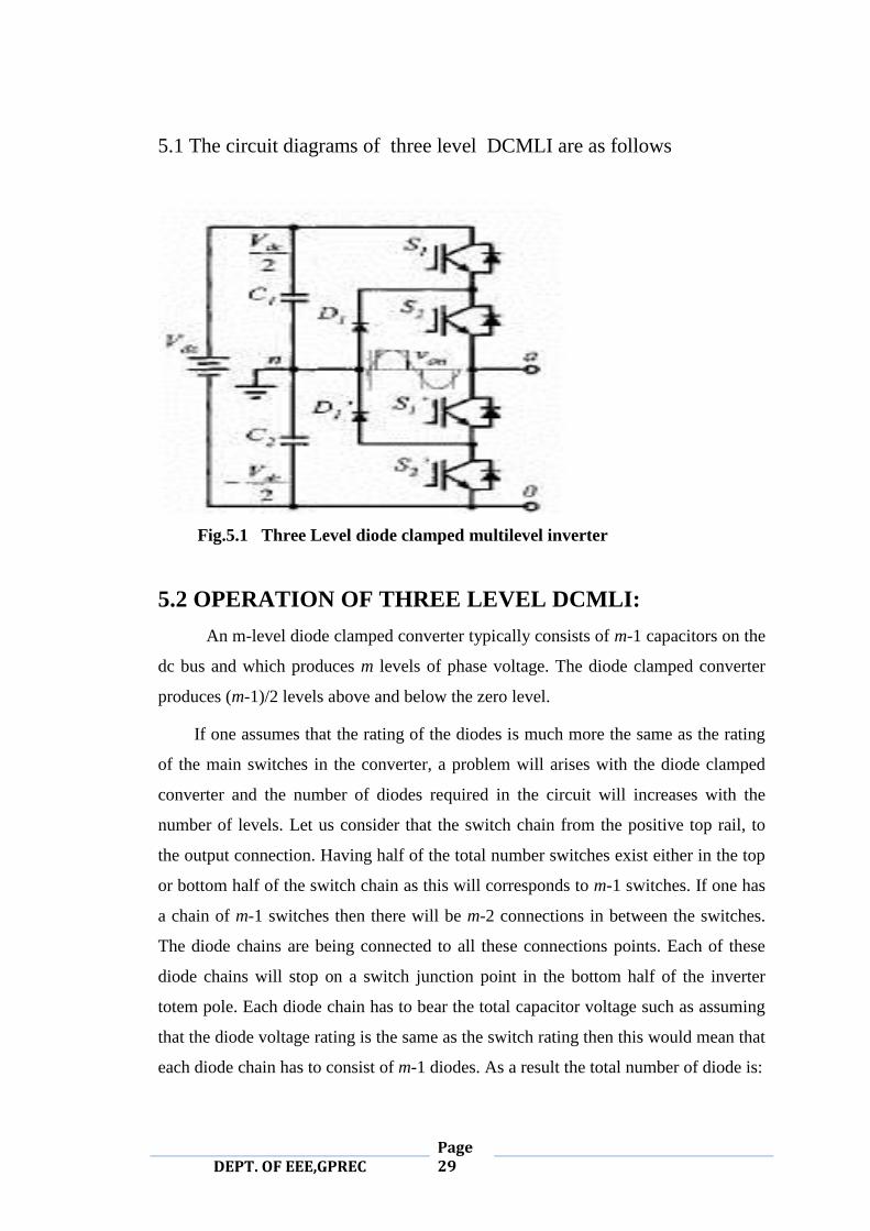
Figure below shows a three-level diode-clamped converter in which the dc bus
consists of two capacitors, C1, C2. For dc bus voltage Vdc, the voltage across each
capacitor is Vdc/2 and each device voltage stress will be limited to one capacitor
voltage level Vdc/2 through clamping diodes. To explain how the staircase voltage is
synthesized, the neutral point n is considered as the output phase voltage
reference point. There are three switch combinations to synthesize three-level
voltages across a and n.
1. Voltage level Van= Vdc/2, turn on the switches S1andS2.
2. Voltage level Van= 0, turn on the switches S2 and S1′.
3. Voltage level Van= - Vdc/2 turn on the switches S1‟,S2′.
Page 29
DEPT. OF EEE,GPREC
5.1 The circuit diagrams of three level DCMLI are as follows
Fig.5.1 Three Level diode clamped multilevel inverter
5.2 OPERATION OF THREE LEVEL DCMLI:
An m-level diode clamped converter typically consists of m-1 capacitors on the
dc bus and which produces m levels of phase voltage. The diode clamped converter
produces (m-1)/2 levels above and below the zero level.
If one assumes that the rating of the diodes is much more the same as the rating
of the main switches in the converter, a problem will arises with the diode clamped
converter and the number of diodes required in the circuit will increases with the
number of levels. Let us consider that the switch chain from the positive top rail, to
the output connection. Having half of the total number switches exist either in the top
or bottom half of the switch chain as this will corresponds to m-1 switches. If one has
a chain of m-1 switches then there will be m-2 connections in between the switches.
The diode chains are being connected to all these connections points. Each of these
diode chains will stop on a switch junction point in the bottom half of the inverter
totem pole. Each diode chain has to bear the total capacitor voltage such as assuming
that the diode voltage rating is the same as the switch rating then this would mean that
each diode chain has to consist of m-1 diodes. As a result the total number of diode is:

Page 30
DEPT. OF EEE,GPREC
Number of diodes = (m-1) (m-2)
The below table is a summary for the major components in the diode clamped
converter which is considered very helpful:
Component Number
Levels m
Switches and parallel diodes 2(m-1)
Capacitors m-1
Clamp diodes (m-1)(m-2)
Table 3: Major component table for diode clamped converter.
Switching Sequence
Let‟s refer to Figure 5.1 which is a three level diode clamped converter. In this circuit,
the dc bus voltage is being split into three levels by two series connected bulk
capacitors, C1 and C2. The middle point of the two capacitors n can be defined as the
neutral point. The clamping diodes‟ function in the circuit is to prevent the voltage
across one of the switching devices which surpass the voltage across one of the
capacitors. The output voltage Van has three states which are: Vdc/2, 0, and –Vdc/2.

Page 31
DEPT. OF EEE,GPREC
For voltage level Vdc/2 switches S1 and S2 need to be turned on; for –Vdc/2 switches
S1‟ and S2‟ need to be turned on; and for the 0 level, S2 and S1‟ need to be turn on.
The most important key component that decide this circuit from a
conventional two level converter is D1 and D1‟. These two diodes clamp the switch
voltage to half the level of the dc bus voltage. When both S1 and S2 are on, the
voltage across a and 0 is Vdc, i.e. Va0 = Vdc. In this case, D1‟ balances out the
voltage sharing between S1‟ and S2‟ with S1‟ blocking the voltage across C1 and S2‟
blocking the voltage across C2. Notice that the output voltage Van is ac and Va0 is
dc. The difference between Van and Va0 is the voltage across C2, which is Vdc/2. If
the output is being removed between a and 0, then the circuit will become a dc/dc
converter, which has three output voltage levels: Vdc, Vdc/2 and 0.
The phase a output voltage Van has three states: Vdc/2,0, - Vdc/2. The gate signals
for the chosen five level DCMLI are developed using MATLAB-SIMULINK. The
gate signal generator model developed is tested for various values of modulation
index. Diode clamped multilevel inverter is a very general and widely used topology.
DCMLI works on the concept of using diodes to
limit voltage stress on power devices.
Advantages
1.When the number of levels is high enough, harmonic content will be low enough to
avoid the need for filters.
2.Efficiency is high due to all devices which are being switched at the fundamental
frequency.
3.We are able to control the reactive power flow.
4.The control method is easy for a back to back intertie system.
Disadvantages
1.Excessive clamping diodes are being required when the number of levels get high.
2.It is hard to do a real power flow control for individual converter.
Page 32
DEPT. OF EEE,GPREC
CHAPTER 6
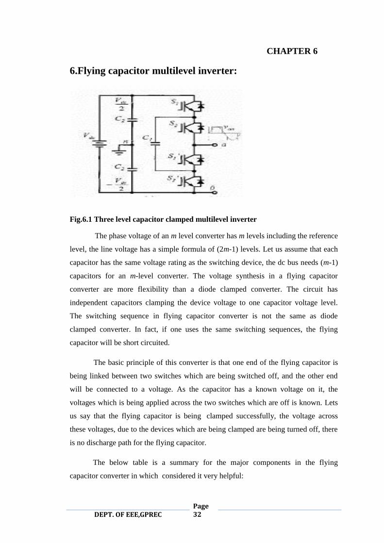
6.Flying capacitor multilevel inverter:
Fig.6.1 Three level capacitor clamped multilevel inverter
The phase voltage of an m level converter has m levels including the reference
level, the line voltage has a simple formula of (2m-1) levels. Let us assume that each
capacitor has the same voltage rating as the switching device, the dc bus needs (m-1)
capacitors for an m-level converter. The voltage synthesis in a flying capacitor
converter are more flexibility than a diode clamped converter. The circuit has
independent capacitors clamping the device voltage to one capacitor voltage level.
The switching sequence in flying capacitor converter is not the same as diode
clamped converter. In fact, if one uses the same switching sequences, the flying
capacitor will be short circuited.
The basic principle of this converter is that one end of the flying capacitor is
being linked between two switches which are being switched off, and the other end
will be connected to a voltage. As the capacitor has a known voltage on it, the
voltages which is being applied across the two switches which are off is known. Lets
us say that the flying capacitor is being clamped successfully, the voltage across
these voltages, due to the devices which are being clamped are being turned off, there
is no discharge path for the flying capacitor.
The below table is a summary for the major components in the flying
capacitor converter in which considered it very helpful:
Page 33
DEPT. OF EEE,GPREC
Component Number
Levels M
Switches and parallel diodes 2(m-1)
DC Link Capacitors m-1
Clamp capacitors (m-2) (m-1/2)
Table 4: Major component table for flying capacitor converter
Figure 6.1 shows a three level Flying Capacitor Converter. It provides three level
output voltage which is across a and n, i.e., van = Vdc/2, 0 or –Vdc/2. For voltage
level Vdc/2 switches S1 and S2 need to be switched on; for –Vdc/2 switches S1‟ and
S2‟ need to be turned on; as for the 0 level, either complementary pairs (S1‟,S1) or
(S2‟,S2) needs to be turned on. The clamping capacitor C1 is being charged when S1
and S1‟ are turned on, and is discharged when S2 and S2‟ are turned on. The charge
of C1 can be balanced by proper selection of the 0 level switch combinations.
Advantages
Huge amount of storage capacitors will provide additional ride through capabilities
during power rage.
Switch combination redundancy are provided for balancing different voltage levels.
When the number of levels is high enough, the harmonic content will be low
enough not to use the the filter.
We are able to control both the real and reactive power flow, and making a possible
voltage source converter candidate for high voltage dc transmission.
Disadvantages
When the number of converter levels get high, a huge amount of storage capacitors
is required.Those high level systems are more difficult to package and those bulky
capacitors are expensive.
The switching frequency and switching losses will sore high for real power
transmission and the converter control will get very complicated.
Page 34
DEPT. OF EEE,GPREC
CHAPTER 7
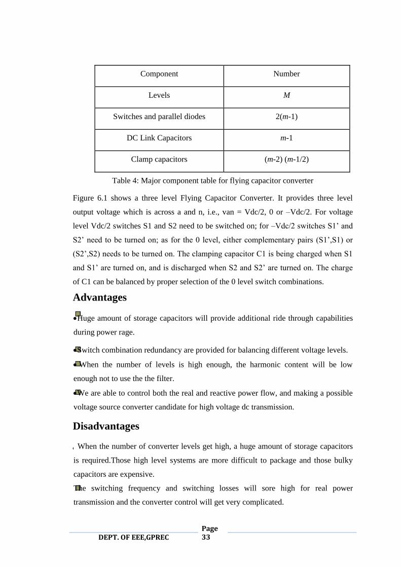
7. SIMULATION RESULTS
7.1SIMULATION OF THREE LEVEL DIODE CLAMPED MLI
7.2SIMULATION OF THREE LEVEL CAPACITOR CLAMPED
MLI
Page 35
DEPT. OF EEE,GPREC
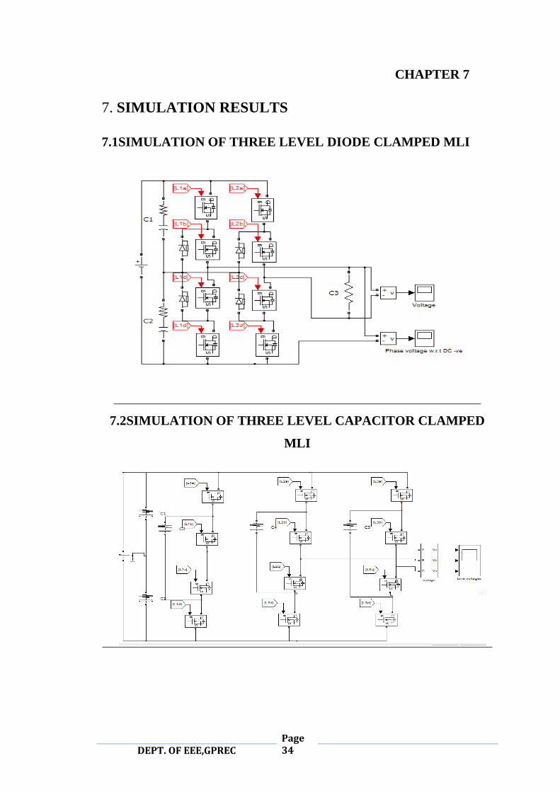
Fig 7.3. Control Pulse Generation in Three Level SPWM
Fig.7.4 OUTPUT VOLTAGE WAVEFORM FOR THREE LEVEL DIODE
CLAMPED INVERTER
Page 36
DEPT. OF EEE,GPREC
Fig.7.5 OUTPUT VOLTAGE WAVEFORM FOR THREE LEVEL CAPACITOR
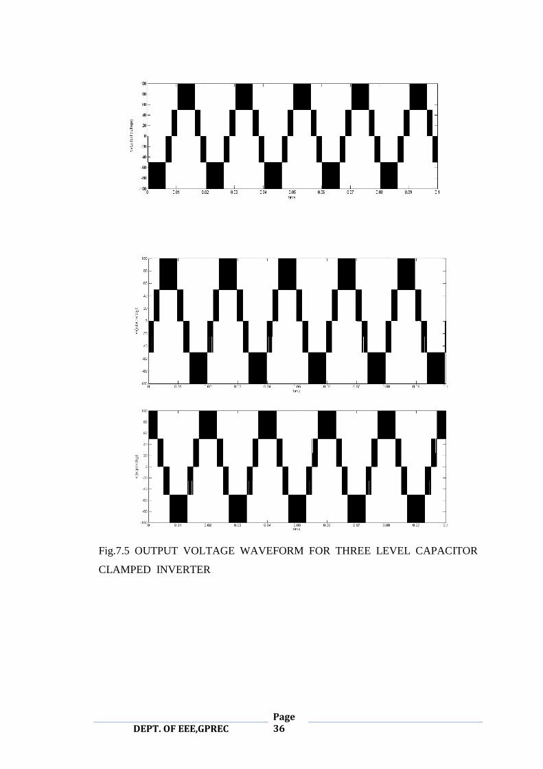
CLAMPED INVERTER
Page 37
DEPT. OF EEE,GPREC
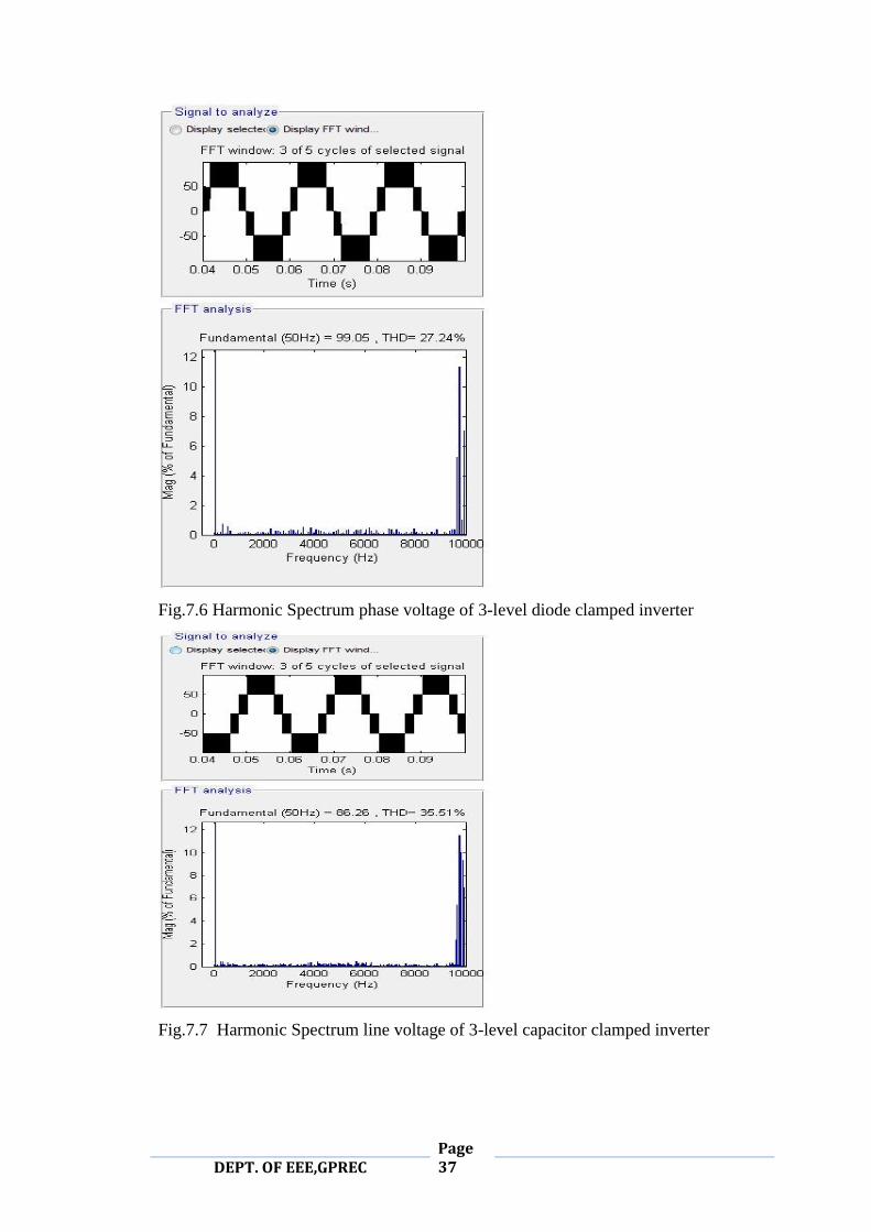
Fig.7.6 Harmonic Spectrum phase voltage of 3-level diode clamped inverter
Fig.7.7 Harmonic Spectrum line voltage of 3-level capacitor clamped inverter

Page 38
DEPT. OF EEE,GPREC
CONCLUSIONS
In this mini project thesis have presented a new topology for the diode clamped and
capacitor clamped three level inverter. This three level topology has been presented
for industrial application. The working of the inverter is explained in detail. The main
concept of this inverter is to use diodes to limit the power devices voltage stress. The
diode clamp three level inverters have become an effective and practical solution for
largest output levels and the smallest Total Harmonics Distortion percentage. The
simulation result, the output voltage waveform presents better harmonics profile. It
can be observed that there is a great reduction in THD values when compared to two
level inverters.
Page 39
DEPT. OF EEE,GPREC
REFERENCES
1. P.S.BHIMBRA, POWER ELECTRONICS.
2. M.RASHID, POWER ELECTRONICS.
3. G.CARRARA, D.CASINI, S.GARDELLA, R.SALUTARI, “OPTIMAL PWM
FOR THE CONTROL OF MULTILEVEL VOLTAGE SOURCE INVERTER”,
FIFTH ANNUAL EUROPEAN CONFERENCE ON POWER ELECTRONICS,
VOLUME 4, 1993, PP255259.
4. POWER ELECTRONICS BASED A.C.DRIVES BY B.K.BOSE, ”SPWM”,
”THREE LEVEL INVERTER”.
5. A GUIDE TO MATLAB,SECOND EDITION,BY BRAIN R.HUNT.
6. THESIS ON ANALYSIS OF TWO LEVEL AND THE THREE LEVEL
INVERTERS:PRESENTED BY PIYUSH MOHANTY AND SARANSHI SAHOO.
7. BASIC INFORMATION OF INVERTER,WIKIPEDIA.
8. A PWM SCHEME FOR A 3 LEVEL INVERTER BY V.T.SOMASEKHAR,
K.GOPAKUMAR.
Copyright © 2022 FDOKUMEN