Dynamic Modeling of Line and Capacitor Commutated ...
128
Diss. ETH No. 15269 Dynamic Modeling of Line and Capacitor Commutated Converters for HVDC Power Transmission A dissertation submitted to the SWISS FEDERAL INSTITUTE OF TECHNOLOGY ZURICH for the degree of DOCTOR OF TECHNICAL SCIENCES presented by WOLFGANG HAMMER Dipl.-Ing. (RWTH Aachen) born December 13, 1972 in Leverkusen, Germany accepted on the recommendation of Prof. Dr. G¨oran Andersson, examiner Prof. Dr. Ani Gol´ e, co-examiner 2003
-
Upload
khangminh22 -
Category
Documents
-
view
1 -
download
0
Transcript of Dynamic Modeling of Line and Capacitor Commutated ...

Diss. ETH No. 15269
Dynamic Modeling ofLine and Capacitor
Commutated Converters forHVDC Power Transmission
A dissertation submitted to theSWISS FEDERAL INSTITUTE OF TECHNOLOGY
ZURICH
for the degree ofDOCTOR OF TECHNICAL SCIENCES
presented byWOLFGANG HAMMER
Dipl.-Ing. (RWTH Aachen)born December 13, 1972in Leverkusen, Germany
accepted on the recommendation ofProf. Dr. Goran Andersson, examiner
Prof. Dr. Ani Gole, co-examiner
2003

Preface
This thesis presents the result of my research done during the yearsof 2000–2003 at the Power Systems Laboratory of the Swiss FederalInstitute of Technology (ETH) Zurich.
First of all I wish to thank Prof. Dr. Goran Andersson for his supervisionof my work and for the freedom of research that he granted me. I amparticularly indebted for his consent to the foundation of a spin-offcompany with the purpose of bringing to market a simulation softwarewhich was developed partly in the course of this thesis.
Special thanks go to Prof. Dr. Ani Gole for willing in to co-referee thisthesis.
I would also like to thank my colleagues at the Power System Labo-ratory both for the valuable discussions and for the welcome diversionfrom the research work. The coffee-breaks and the excursions will stayin my memory. Jost Allmeling, colleague and co-founder of the spin-off company, deserves special mention for relieving me of my companyduties during the final stages of this thesis.
3


Contents
Preface . . . . . . . . . . . . . . . . . . . . . . . . . . . . . . 3
Abstract . . . . . . . . . . . . . . . . . . . . . . . . . . . . . . 9
Kurzfassung . . . . . . . . . . . . . . . . . . . . . . . . . . . . 11
1 Introduction 13
2 Energy transmission by direct current 17
2.1 Line commutated converter . . . . . . . . . . . . . . . . 17
2.2 Capacitor commutated converter . . . . . . . . . . . . . 19
2.3 Voltage-sourced converter . . . . . . . . . . . . . . . . . 20
3 Modeling techniques for power electronics devices 23
3.1 Piecewise LTI models . . . . . . . . . . . . . . . . . . . 23
3.1.1 Generic system matrix . . . . . . . . . . . . . . . 25
3.1.2 State dependencies . . . . . . . . . . . . . . . . . 28
3.1.3 Undetermined switch variables . . . . . . . . . . 31
3.1.4 State inconsistencies . . . . . . . . . . . . . . . . 34
3.1.5 Implementation . . . . . . . . . . . . . . . . . . . 38
3.2 State-space averaging . . . . . . . . . . . . . . . . . . . 39
3.2.1 Local average . . . . . . . . . . . . . . . . . . . . 39
3.2.2 Local ω-component . . . . . . . . . . . . . . . . . 39
3.2.3 Generalized averaging . . . . . . . . . . . . . . . 40
3.2.4 Phasor dynamics models . . . . . . . . . . . . . . 41
5

6 Contents
3.3 Sampled-data modeling . . . . . . . . . . . . . . . . . . 42
3.3.1 Large-signal sampled data description . . . . . . 42
3.3.2 Perturbations about a nominal steady state . . . 43
4 Line commutated converter models 45
4.1 Static model . . . . . . . . . . . . . . . . . . . . . . . . . 46
4.1.1 Analysis without commutation overlap . . . . . . 46
4.1.2 Analysis including commutation overlap . . . . . 49
4.2 Dynamic model . . . . . . . . . . . . . . . . . . . . . . . 54
4.2.1 Analysis without commutation overlap . . . . . . 54
4.2.2 Analysis including commutation overlap . . . . . 55
4.3 Model validation . . . . . . . . . . . . . . . . . . . . . . 58
4.3.1 Model equations . . . . . . . . . . . . . . . . . . 59
4.3.2 Qualitative comparison . . . . . . . . . . . . . . 60
4.3.3 Quantitative comparison . . . . . . . . . . . . . . 60
4.4 Conclusions . . . . . . . . . . . . . . . . . . . . . . . . . 61
5 Capacitor commutated converter models 65
5.1 Static model . . . . . . . . . . . . . . . . . . . . . . . . . 66
5.1.1 Analysis without commutation overlap . . . . . . 66
5.1.2 Analysis including commutation overlap . . . . . 69
5.2 Dynamic model . . . . . . . . . . . . . . . . . . . . . . . 76
5.2.1 Analysis without commutation overlap . . . . . . 79
5.2.2 Analysis including commutation overlap . . . . . 86
5.3 Model validation . . . . . . . . . . . . . . . . . . . . . . 94
5.3.1 Model equations . . . . . . . . . . . . . . . . . . 94
5.3.2 Qualitative comparison . . . . . . . . . . . . . . 96
5.3.3 Quantitative comparison . . . . . . . . . . . . . . 96
5.4 Conclusions . . . . . . . . . . . . . . . . . . . . . . . . . 99

Contents 7
6 Case studies 103
6.1 HVDC control scheme . . . . . . . . . . . . . . . . . . . 104
6.1.1 Voltage dependent current order limit . . . . . . 104
6.1.2 Current controller . . . . . . . . . . . . . . . . . 104
6.1.3 Gamma controller . . . . . . . . . . . . . . . . . 104
6.1.4 Phase locked loop . . . . . . . . . . . . . . . . . 106
6.1.5 Firing pulse generator . . . . . . . . . . . . . . . 106
6.2 LCC case study . . . . . . . . . . . . . . . . . . . . . . . 108
6.3 CCC case study . . . . . . . . . . . . . . . . . . . . . . . 112
6.4 Conclusions . . . . . . . . . . . . . . . . . . . . . . . . . 113
7 Summary and Conclusions 117
A Analytical solution of the CCC commutation equations119
Bibliography 123


Abstract
Energy transmission by means of direct current is an attractive alter-native to ac transmission for a number of special applications. One ofthese applications, i. e. the use of fast HVDC controls to stabilize atransmission system, gains more and more importance as today’s powersystems are operated closer to their stability limits.
Therefore, there is an increasing need to understand the dynamic in-teractions between HVDC converters and the ac systems. Convenientmodels are needed that will both facilitate control design and allow fastand accurate transient simulations. However, the analysis of HVDCconverter systems is challenging because of their hybrid nature, as theyincorporate both continuous-time dynamics and discrete events.
In this thesis, dynamic models are developed for HVDC converters basedon turn-on devices. A new dynamic modeling approach is presentedwhich takes into account the dynamics of a variable direct current. Thisis in contrast to the standard quasi-static approach, which assumes aconstant current and therefore lacks accuracy when transient phenom-ena are of interest. The investigations are restricted to phasor-basedmodels for use with transient stability programs. The major contribu-tion of this thesis is a novel dynamic model for the capacitor commu-tated converter which considers the influences not only of a variabledirect current but also of unbalanced capacitor voltages.
Case studies demonstrate the impact of the dynamic models on thestudy of control interactions between an HVDC converter with its con-trols and an ac system. The proposed dynamic CCC model is shown tobe valid in a frequency range up to the fundamental ac frequency.
9


Kurzfassung
Hochspannungs-Gleichstrom-Ubertragung ist fur gewisse Anwendungeneine attraktive Alternative zur Drehstrom-Ubertragung, die in Energie-versorgungsnetzen ublicherweise verwendet wird. Aufgrund der immerhoheren Auslastung heutiger Ubertragungsnetze gewinnt eine solcheAnwendung, die Verwendung der schnellen HGU-Regelung zur Bekamp-fung von Stabilitatsproblemen, mehr und mehr an Bedeutung.
Vor diesem Hintergrund wird es immer wichtiger, das dynamische Wech-selspiel zwischen der HGU und dem Drehstromnetz genau zu verstehen.Es besteht ein wachsender Bedaf nach adaquaten Modellen, die sowohlfur die Auslegung von Reglersystemen verwendet werden konnen, alsauch schnelle und genaue transiente Simulationen ermoglichen. Auf-grund ihres hybriden Charakters stellen leistungselektronische Geratewie die HGU-Umrichter allerdings eine besondere Herausforderung dar,da sie kontinuierliche Vorgange und diskrete Ereignisse vereinen.
In dieser Arbeit werden dynamische Modelle fur HGU-Umrichter basie-rend auf Einschaltelementen hergeleitet. Dazu wird ein neuartiger,dynamischer Modellierungsansatz verwendet, der den Einfluss eines ver-anderlichen Gleichstromes berucksichtigt. Dies steht im Gegensatz zumherkommlichen quasi-stationaren Ansatz, bei dem der Gleichstrom alskonstant angenommen wird. Auf einer solchen Annahme beruhendeModelle sind daher zwangslaufig ungenau, wenn transiente Vorgangebetrachtet werden. Die Untersuchungen beschranken sich auf Zeiger-basierte Modelle, wie sie in Simulatoren fur transiente Stabilitatspro-bleme verwendet werden. Der Hauptbeitrag dieser Arbeit ist ein neuesModell fur den so genannten Capacitor Commutated Converter, dasnicht nur die Auswirkungen eines variablen Gleichstromes beschreibtsondern auch den von unsymmetrisch geladenen Kondensatoren.
11

12 Kurzfassung
Vergleichsrechnungen demonstrieren den Einfluss, den die Verwendungdynamischer Modelle auf die Untersuchung von Wechselwirkungen zwi-schen einer HGU-Regelung und dem Drehstromnetz hat. Das hiervorgeschlagene dynamische Model des Capacitor Commutated Converter
erweist sich als gultig uber einen weiten Frequenzbereich bis hinauf zurNetzfrequenz.

Chapter 1
Introduction
While the very first practical applications of electricity were based ondirect current, this technology was quickly replaced by three-phase al-ternating current because of various advantages. Alternating currentcan be transformed easily between different voltage levels used for gen-eration, transmission, distribution, and use. In particular, the use oftransformers made long-distance, high-voltage power transmission pos-sible. Circuit breakers for alternating current can take advantage ofthe natural current zeros that occur twice per cycle. The ac inductionmotor is cheap and robust and serves the majority of industrial and res-idential purposes. In contrast, the commutators of dc machines requiremaintenance and impose voltage, speed and size limitations [1].
Still, in spite of the principal use of alternating current in power systems,there are some applications for which direct current is the better if notonly choice, even taking into account the cost of the equipment that isnecessary to convert between ac and dc [6], [7]:
• Bulk power transmission on long overhead lines
At very long distances, ac overhead lines consume large amounts ofreactive power which furthermore are dependent on the amountof active power transfered. In addition to the additional lossescaused by the reactive current, this also gives rise to stabilityproblems. DC lines, on the other hand, do not consume reactivepower.
13

14 Chapter 1. Introduction
• Power transmission via cable
Due to its construction, a cable has a much higher capacitanceper unit length than an overhead line. This means that even for acable of moderate length (50 km), the reactive current can utilizea major part of the total current capability when transmittingac power. In the case of dc transmission, apart from the initialcharging, the cable draws no capacitive current in steady state.
• Transmission between unsynchronized ac systems
AC power transmission is physically only possible between syn-chronized systems. When two systems operate at different fre-quencies (such as 50 Hz and 60 Hz), or even when they operate atthe same nominal frequency but have divergent frequency controlregimes, the only practical way to transmit power between themis by means of a dc connection.
In addition to these more traditional applications concerning rather thestationary operation of networks, there is a fourth aspect of HVDCtransmission which gains more and more importance with the growingglobal interconnection of transmission systems:
• Parallel ac and dc transmission
In interconnected ac systems technical problems like transient in-stability or power oscillations can occur when an interconnectionbetween two parts is relatively weak. In such a case, the fastcontrols of an additional HVDC link in parallel to the ac inter-connection can be used to stabilize the system [6].
With today’s power systems being operated closer to their stability lim-its, and particularly in view of this last aspect, there is an increasingneed to understand the dynamic interactions between HVDC convertersand the ac system. Convenient models are needed that will both facil-itate control design and allow fast and accurate transient simulations.However, the analysis of HVDC converter systems is challenging be-cause of their hybrid nature, as they incorporate both continuous-timedynamics (associated with the voltages and currents of capacitors andinductors) and discrete events (due to the switching of the valves).
Transient stability programs typically use power electronics device mod-els that are based on quasi-static approximations. Such models rely onthe assumption that the ac system is in sinusoidal steady-state and,
15
in case of an HVDC current source converter, that the direct currentis ripple-free and constant. Due to these assumptions, the models arestrictly valid only in the steady state and lack accuracy when transientstability or other dynamic phenomena are of interest [8].
In order to characterize the dynamic behavior of hybrid systems, so-called sampled-data models have been developed for various power elec-tronics devices including the line commutated HVDC converter [9].Such models find application in the eigenvalue analysis of power sys-tem dynamics. While these models are quite accurate and also offer ananalytical basis for controller design, they have also some disadvantages:the model derivation is relatively complicated; due to the linearizationsinvolved the models are only valid for small perturbations around a fixedoperating point; and they do not interface well with the continuous-timetransient stability programs.
Another new approach for modeling power electronics devices is thephasor dynamics method. With this method the periodic currents andvoltages associated with a device are described in terms of time-varyingFourier coefficients. By restricting the focus to the fundamental fre-quency components a natural dynamic extension of the usual quasi-static phasor equations can be obtained. This method has been suc-cessfully demonstrated on two different FACTS devices [10].
The phasor dynamics method cannot be applied directly to HVDC con-verters. However, some of its key ideas will be used in this thesis toderive models of the line commutated converter and the capacitor com-mutated converter, which capture the dynamic behavior of these devicesand can be easily interfaced with transient stability programs.
The following chapters in this thesis are organized as follows:
• Chapter 2 gives a brief overview of the historical development ofHVDC transmission including the relatively young application ofvoltage-sourced converters.
• Chapter 3 reviews three different modeling techniques for powerelectronics devices: the sampled-data method and the phasor dy-namics method mentioned above, and piecewise LTI models thatcan be used for detailed time-domain simulations.
• In chapters 4 and 5, dynamic models for the line commutatedconverter and the capacitor commutated converter are developedstarting from standard quasi-static models.

16 Chapter 1. Introduction
• Chapter 6 presents two case studies that demonstrate the impactof the dynamic models on the study of control interactions betweenan HVDC converter with its controls and an ac system.
• Chapter 7 summarizes the contributions of this thesis and givessome suggestions for future work.

Chapter 2
Energy transmission by
direct current
Energy transmission by means of high voltage direct current has anover 100 year old history. The first system was designed by a Frenchengineer, Rene Thury, at the end of the 19th century [1]. In this systemthe direct voltage was generated at the sending end of a transmissionline by a number of dc generators connected in series, which were drivenby prime movers. At the receiving end, a comparable number of dcmotors drove low-voltage dc or ac generators. Due to the limitations ofdc machines the maximum circuit voltage achieved was 125 kV and themaximum power transfered was 19.3 MW. The last line was operateduntil 1937.
2.1 Line commutated converter
At around this time, the first experimental HVDC converters basedon controllable switches were installed. Initially, these switches weremercury-vapor filled tubes, devices which can conduct current only inone direction (which is why these devices are also often called valves).By applying an appropriate voltage to a control electrode, the valvecan be prevented from starting to conduct. However, once a valve con-ducts, conduction does not cease until the current reverses. The first
17
18 Chapter 2. Energy transmission by direct current
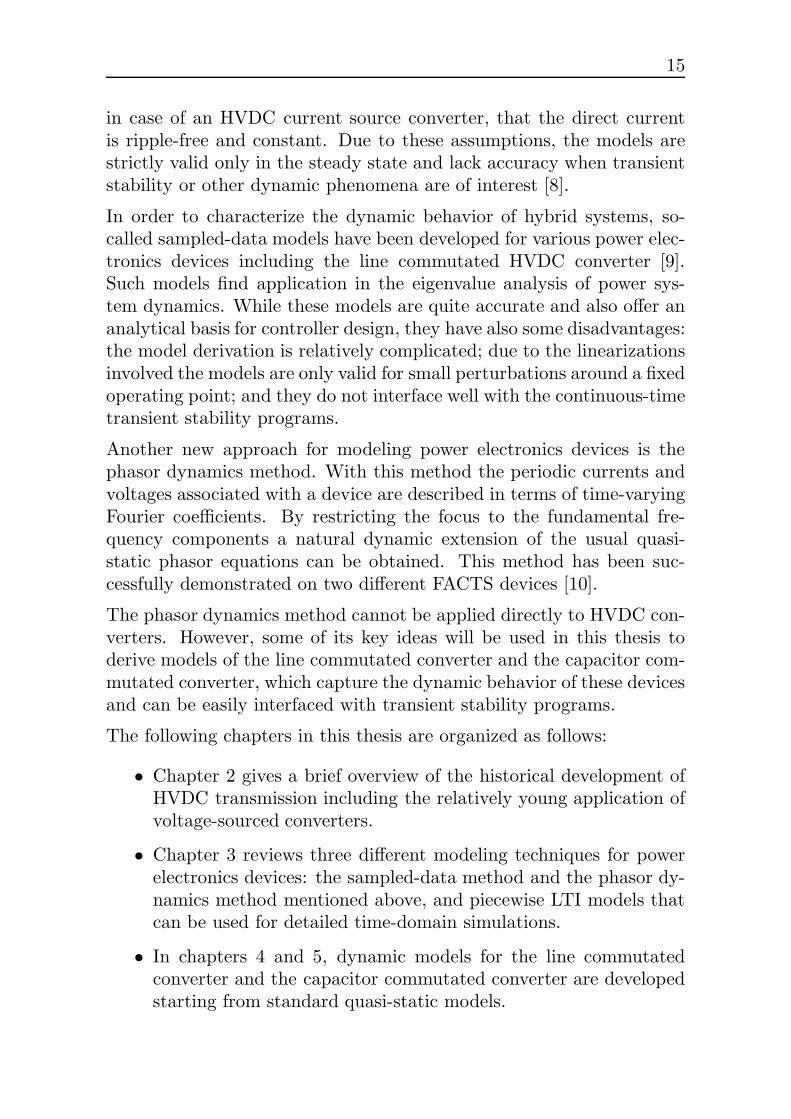
Id
Figure 2.1: Line commutated converter circuit
commercial HVDC transmission system built with mercury arc valveswas a link between the Swedish mainland and the island of Gotland.The system began service in 1954 and transmitted 20 MW at 100 kVover a distance of 96 km through a single-conductor cable, with returnpath through the sea and earth. Later systems had ratings as high as1854 MW at ±463 kV such as Bipole 1 of the Nelson River HVDCtransmission system in Manitoba, Canada, which was installed between1970 and 1977 and transmits dc power over a distance of 900 km [11].
About 1955, a new solid-state switching device called thyristor was de-veloped [12]. This device can be crudely described as a diode withan added control electrode and thus has (ideally) the same switchingcharacteristics as the mercury arc valve while being cheaper and morecompact. The thyristor was soon capable of handling the high voltagesand powers required for HVDC transmission and began to replace themercury arc valves. The first HVDC project with the new thyristorvalves was again Gotland, commissioned in 1970. The voltage of thesefirst converters was only 50 kV (6 pulse monopole), but since then thehighest ratings have grown to ±600 kV, 6300 MW (Itaipu, built 1984–1987, two 12 pulse bipoles) [13].
The basic module of a conventional HVDC converter using mercury-arcor thyristor valves is the three-phase, full-wave bridge circuit shown inFig. 2.1, also known as a Graetz-bridge. Compared with several possiblealternative configurations, this circuit provides the best utilization ofthe converter transformer and the lowest voltage across non-conductingvalves [1], [2].
2.2. Capacitor commutated converter 19
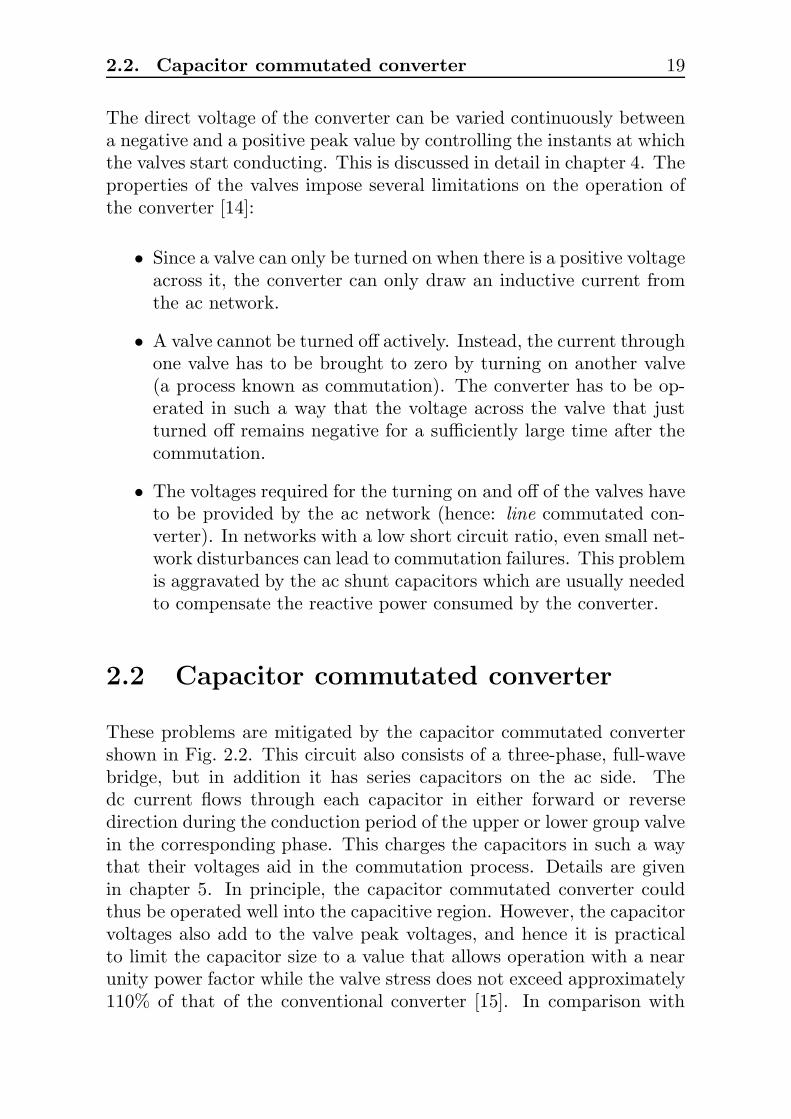
The direct voltage of the converter can be varied continuously betweena negative and a positive peak value by controlling the instants at whichthe valves start conducting. This is discussed in detail in chapter 4. Theproperties of the valves impose several limitations on the operation ofthe converter [14]:
• Since a valve can only be turned on when there is a positive voltageacross it, the converter can only draw an inductive current fromthe ac network.
• A valve cannot be turned off actively. Instead, the current throughone valve has to be brought to zero by turning on another valve(a process known as commutation). The converter has to be op-erated in such a way that the voltage across the valve that justturned off remains negative for a sufficiently large time after thecommutation.
• The voltages required for the turning on and off of the valves haveto be provided by the ac network (hence: line commutated con-verter). In networks with a low short circuit ratio, even small net-work disturbances can lead to commutation failures. This problemis aggravated by the ac shunt capacitors which are usually neededto compensate the reactive power consumed by the converter.
2.2 Capacitor commutated converter
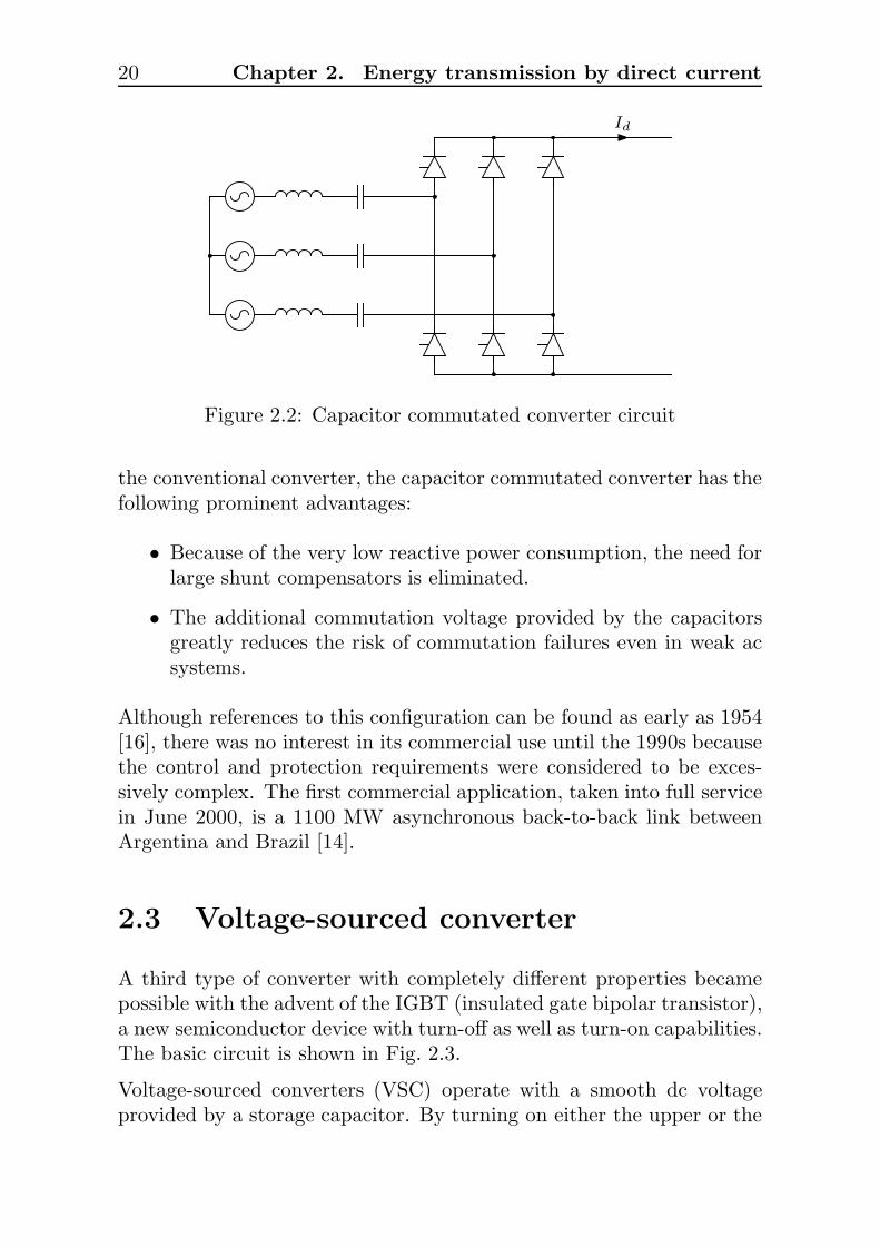
These problems are mitigated by the capacitor commutated convertershown in Fig. 2.2. This circuit also consists of a three-phase, full-wavebridge, but in addition it has series capacitors on the ac side. Thedc current flows through each capacitor in either forward or reversedirection during the conduction period of the upper or lower group valvein the corresponding phase. This charges the capacitors in such a waythat their voltages aid in the commutation process. Details are givenin chapter 5. In principle, the capacitor commutated converter couldthus be operated well into the capacitive region. However, the capacitorvoltages also add to the valve peak voltages, and hence it is practicalto limit the capacitor size to a value that allows operation with a nearunity power factor while the valve stress does not exceed approximately110% of that of the conventional converter [15]. In comparison with
20 Chapter 2. Energy transmission by direct current
Id
Figure 2.2: Capacitor commutated converter circuit
the conventional converter, the capacitor commutated converter has thefollowing prominent advantages:
• Because of the very low reactive power consumption, the need forlarge shunt compensators is eliminated.
• The additional commutation voltage provided by the capacitorsgreatly reduces the risk of commutation failures even in weak acsystems.
Although references to this configuration can be found as early as 1954[16], there was no interest in its commercial use until the 1990s becausethe control and protection requirements were considered to be exces-sively complex. The first commercial application, taken into full servicein June 2000, is a 1100 MW asynchronous back-to-back link betweenArgentina and Brazil [14].
2.3 Voltage-sourced converter
A third type of converter with completely different properties becamepossible with the advent of the IGBT (insulated gate bipolar transistor),a new semiconductor device with turn-off as well as turn-on capabilities.The basic circuit is shown in Fig. 2.3.
Voltage-sourced converters (VSC) operate with a smooth dc voltageprovided by a storage capacitor. By turning on either the upper or the

2.3. Voltage-sourced converter 21
Ud
Figure 2.3: Voltage-sourced converter circuit
lower IGBT in one leg of the converter it is possible to impose a positiveor a negative voltage on the corresponding ac phase. The fast switchingcapability of the IGBT allows to create a pulse width modulated acvoltage, the phase of which can be controlled freely and the amplitudewithin the limits given by the dc voltage. Thus, the converter canoperate in all four quadrants of the P-Q plane.
Since the commutation does not depend on the ac network voltage, theconverter can be connected with an extremely weak, or altogether blackac network. Another advantage is that the ac output voltage of theconverter can be changed extremely quickly. However, the voltage andpower ratings of IGBTs are as yet far below those of thyristors andso applications with voltage-sourced converters are limited to low andmedium power.
The first commercial project was once more commissioned on Gotlandand taken into service in November 1999 [17]. A power of 50 MW istransferred through two underground cables of 70 km length at a voltagelevel of ±80 kV from the south of the island to the north. A similarinstallation (3 × 60 MW, ±80 kV) was commissioned and brought intooperation in 2000 to connect the grids of Queensland and New SouthWales, Australia [18]. Depending on the manufacturer, voltage-sourcedconverter based HVDC systems are called HVDC Light or HVDCplus
[19].
The dynamics of the VSC are well understood because it has been usedalready for a long time, e. g. in adjustable speed drives. It is thereforenot treated in this thesis.

Chapter 3
Modeling techniques for
power electronics devices
In this chapter different ways of modeling power electronics devices willbe reviewed. The first section deals with state-space models that canbe used for simulations in the time-domain. A new method is presentedfor the easy computation of the state-space matrices.
The second section discusses a technique called state-space averagingwhich can be used to derive phasor dynamics models for power elec-tronics devices. The purpose of these models is to extend the standardphasor model, which in principle is valid only for pure sinusoidal condi-tions in steady state, to be valid over a larger frequency range.
In the third section a brief review of the theory of sampled-data modelswill be given. These models are particularly useful to study the small-signal stability of a system at a specific operating point.
3.1 Piecewise LTI models
State-space models are increasingly used in power electronics applica-tions. One reason for this is their focus on variables that are centralto describing the dynamic evolution of a system. Another reason isthat the same formalism can be applied to both continuous-time and
23

24 Chapter 3. Modeling techniques
discrete-time systems [3]. Furthermore, state-space models provide aconvenient starting point for such tasks as steady-state computationor deriving sampled-data models which are briefly reviewed in a latersection of this chapter.
Natural choices for state variables in an electrical circuit are the inductorcurrents (or flux linkages) and capacitor voltages (or charges). A circuitconsisting only of linear components can be described by one set of lineartime-invariant (LTI) differential equations
x = Ax + Bu (3.1)
where x is a vector of the state variables and u is a vector of the inputvariables, i. e. source voltages and currents. Also associated with themodel are the output variables y. If these comprise only voltages andcurrents the output equations can be written as
y = Cx + Du (3.2)
Power electronic circuits, however, by definition consist not only of lin-ear components but also of one or more semiconductor devices whichare nonlinear. When the overall system behavior is studied they canbe modeled as ideal switches which are short circuits in their on-stateand open circuits in the off-state. If a circuit contains one or moresuch switches, every combination σ of switch positions (i. e. on/off) isdescribed by a different set of equations, where each individual set ofequations is again LTI. The complete circuit can thus be described bya piecewise LTI model.
One problem with ideal switches is that they can cause the numberof state variables to change from one topology σ to the next. This isoften accompanied by impulsive currents or voltages as capacitors areshort-circuited or the currents through inductors interrupted. In orderto overcome this problem the ideal switch model is sometimes replacedby two-valued resistors. However, this easily leads to problems due tonumerical round-off errors [20].
Another approach is to monitor the number of state variables in orderto decide whether a state variable becomes discontinuous. If this isthe case, the corresponding impulse is introduced into the network bymeans of a supplementary source approximated by an arbitrary large
3.1. Piecewise LTI models 25
value [21]. The described formulation procedure is quite complex. Fur-thermore, approximating an impulse with a large value may again leadto numerical problems.
In this section, a new method is proposed based on simple matrix oper-ations which addresses the problem of impulses and a few others whichare described below.
3.1.1 Generic system matrix
The first step is setting up a generic system matrix containing the cir-cuit equations for all possible combinations of switch positions. Thealgorithm comprises the following steps [22]:
1. For a circuit with e arbitrary elements and n nodes, find thee − (n − 1) independent loop equations and n − 1 independentnode equations.
2. Eliminate the dependent variables, e. g. by applying Ohm’s law.The voltages and currents of switch elements are left undeter-mined.
3. Order the independent variables as follows:
[
x y s x u]T
(3.3)
where
x = [ vC iL ] (state derivatives)
y = [ yvmyim
] (output variables)
s = [ vS iS ] (switch variables)
x = [ vC iL ] (state variables)
u = [ vsrc isrc ] (input variables)
The variables on the left hand side are unknown, those on theright hand side known variables.
4. Calculate Mgen, the reduced row echelon form (RREF ) of theequation system. This matrix has the following general block

26 Chapter 3. Modeling techniques
structure:
x y s x u
Ix 0 X X X
0 Iy X X X
0 0 X X X
(3.4)
Ix and Iy represent identity matrices of rank N(x) and N(y), respec-tively. The matrices marked with X can contain arbitrary non-zeroentries which are specific for the individual circuit.
When deriving the state-space matrices for a particular combination σof switch positions, the voltages across closed switches and the currentsthrough open switches become zero, i. e. known variables. Hence, theyare eliminated from the equation system by setting the appropriatecolumns of M gen to zero. The thus modified equation system is denotedMσ. In its RREF it contains the state-space matrices Aσ, Bσ, Cσ andDσ as sub-matrices:
x y s x u
Ix 0 0 Aσ Bσ
0 Iy 0 Cσ Dσ
0 0 X X X
(3.5)
Example
This method is illustrated with the help of the buck converter in Fig. 3.1.The circuit has two state variables, iL and vC , and one input variable,vsrc . The independent loop and node equations are
vT − vD = vsrc (3.6)
−LiL − vD = RiL + vC (3.7)
CvC = iL − GvC (3.8)
iT + iD = iL (3.9)
In order to determine whether the diode should block or conduct, thevoltage across and the current through it must be monitored. Addi-tionally the inductor current is measured. This gives for the output
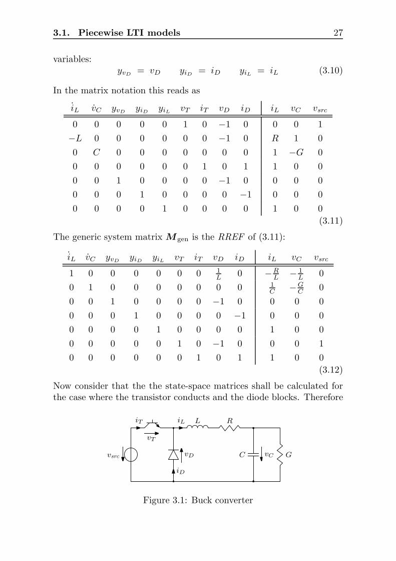
3.1. Piecewise LTI models 27
variables:yvD
= vD yiD= iD yiL
= iL (3.10)
In the matrix notation this reads as
iL vC yvDyiD
yiLvT iT vD iD iL vC vsrc
0 0 0 0 0 1 0 −1 0 0 0 1
−L 0 0 0 0 0 0 −1 0 R 1 0
0 C 0 0 0 0 0 0 0 1 −G 0
0 0 0 0 0 0 1 0 1 1 0 0
0 0 1 0 0 0 0 −1 0 0 0 0
0 0 0 1 0 0 0 0 −1 0 0 0
0 0 0 0 1 0 0 0 0 1 0 0
(3.11)
The generic system matrix Mgen is the RREF of (3.11):
iL vC yvDyiD
yiLvT iT vD iD iL vC vsrc
1 0 0 0 0 0 0 1L 0 −R
L − 1L 0
0 1 0 0 0 0 0 0 0 1C −G
C 0
0 0 1 0 0 0 0 −1 0 0 0 0
0 0 0 1 0 0 0 0 −1 0 0 0
0 0 0 0 1 0 0 0 0 1 0 0
0 0 0 0 0 1 0 −1 0 0 0 1
0 0 0 0 0 0 1 0 1 1 0 0
(3.12)
Now consider that the the state-space matrices shall be calculated forthe case where the transistor conducts and the diode blocks. Therefore
L RiLiT
vT
vsrc C
iD
vD vC G
Figure 3.1: Buck converter
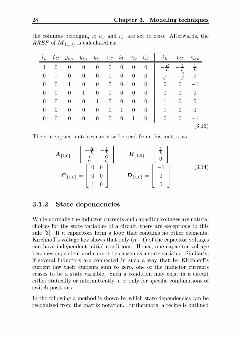
28 Chapter 3. Modeling techniques
the columns belonging to vT and iD are set to zero. Afterwards, theRREF of M1,0 is calculated as:
iL vC yvDyiD
yiLvT iT vD iD iL vC vsrc
1 0 0 0 0 0 0 0 0 −RL − 1
L1L
0 1 0 0 0 0 0 0 0 1C −G
C 0
0 0 1 0 0 0 0 0 0 0 0 −1
0 0 0 1 0 0 0 0 0 0 0 0
0 0 0 0 1 0 0 0 0 1 0 0
0 0 0 0 0 0 1 0 0 1 0 0
0 0 0 0 0 0 0 1 0 0 0 −1
(3.13)
The state-space matrices can now be read from this matrix as
A1,0 =
[
−RL − 1
L1C −G
C
]
B1,0 =
[
1L
0
]
C1,0 =
0 0
0 0
1 0
D1,0 =
−1
0
0
(3.14)
3.1.2 State dependencies
While normally the inductor currents and capacitor voltages are naturalchoices for the state variables of a circuit, there are exceptions to thisrule [3]. If n capacitors form a loop that contains no other elements,Kirchhoff’s voltage law shows that only (n−1) of the capacitor voltagescan have independent initial conditions. Hence, one capacitor voltagebecomes dependent and cannot be chosen as a state variable. Similarly,if several inductors are connected in such a way that by Kirchhoff’scurrent law their currents sum to zero, one of the inductor currentsceases to be a state variable. Such a condition may exist in a circuiteither statically or intermittently, i. e. only for specific combinations ofswitch positions.
In the following a method is shown by which state dependencies can berecognized from the matrix notation. Furthermore, a recipe is outlined
3.1. Piecewise LTI models 29
A
A
A
va
vb
vc
La
Lb
Lc
ia
ib
ic
Figure 3.2: Example circuit for state dependencies
how to resolve the dependency and eliminate the dependent states. Con-sider the three-phase circuit in Fig. 3.2. This circuit can be describedby two loop equations and one node equation:
LaiLa− LbiLb
= va − vb (3.15)
LbiLb− LciLc
= vb − vc (3.16)
0 = iLa+ iLb
+ iLc(3.17)
The three line currents are chosen as output variables:
yia= ia yib
= ib yic= ic (3.18)
The matrix notation is
iLaiLb
iLcyia
yibyic
iLaiLb
iLcva vb vc
La −Lb 0 0 0 0 0 0 0 1 −1 0
0 Lb −Lc 0 0 0 0 0 0 0 1 −1
0 0 0 0 0 0 1 1 1 0 0 0
0 0 0 1 0 0 1 0 0 0 0 0
0 0 0 0 1 0 0 1 0 0 0 0
0 0 0 0 0 1 0 0 1 0 0 0
(3.19)
Evidently the equation system is under-determined because the left sub-matrix has a rank of 5 whereas there are six unknown variables. Onthe other hand, the third row represents an equation that involves onlyknown variables. In fact this row, containing only state variables, in-dicates a dependence between these states. As a consequence, Mgen
cannot be calculated.
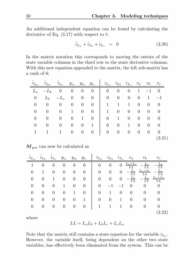
30 Chapter 3. Modeling techniques
An additional independent equation can be found by calculating thederivative of Eq. (3.17) with respect to t:
iLa+ iLb
+ iLc= 0 (3.20)
In the matrix notation this corresponds to moving the entries of thestate variable columns in the third row to the state derivative columns.With this new equation appended to the matrix, the left sub-matrix hasa rank of 6:
iLaiLb
iLcyia
yibyic
iLaiLb
iLcva vb vc
La −Lb 0 0 0 0 0 0 0 1 −1 0
0 Lb −Lc 0 0 0 0 0 0 0 1 −1
0 0 0 0 0 0 1 1 1 0 0 0
0 0 0 1 0 0 1 0 0 0 0 0
0 0 0 0 1 0 0 1 0 0 0 0
0 0 0 0 0 1 0 0 1 0 0 0
1 1 1 0 0 0 0 0 0 0 0 0
(3.21)
M gen can now be calculated as
iLaiLb
iLcyia
yibyic
iLaiLb
iLcva vb vc
1 0 0 0 0 0 0 0 0 Lb+Lc
LL − Lc
LL − Lb
LL
0 1 0 0 0 0 0 0 0 − Lc
LLLa+Lc
LL − La
LL
0 0 1 0 0 0 0 0 0 − Lb
LL − La
LLLa+Lb
LL
0 0 0 1 0 0 0 −1 −1 0 0 0
0 0 0 0 1 0 0 1 0 0 0 0
0 0 0 0 0 1 0 0 1 0 0 0
0 0 0 0 0 0 1 1 1 0 0 0
(3.22)where
LL = LaLb + LbLc + LcLa
Note that the matrix still contains a state equation for the variable iLa.
However, the variable itself, being dependent on the other two statevariables, has effectively been eliminated from the system. This can be
3.1. Piecewise LTI models 31
seen from the fact that the column for iLahas only zero-entries, except
for the last row which is the dependence equation. The fourth row showsthat the line current in phase a is calculated as ia = −iLb
− iLc.
General rule
If the system matrix is under-determined:
1. Identify the row(s) that contain non-zero entries only in the statevariable columns.
2. Copy these rows and swap the entries in the state variable columnswith those in the state derivative columns. (This corresponds tocalculating the derivative with respect to t.)
It may happen that the system matrix is under-determined and yet theabove rule does not yield enough (or any) additional equations. Thisis the case if two or more switches which are connected in series areopen at the same time so that the potential of the nodes between thembecomes floating and thus undefined. Similarly, the individual currentsthrough parallel closed ideal switches are undetermined.
3.1.3 Undetermined switch variables
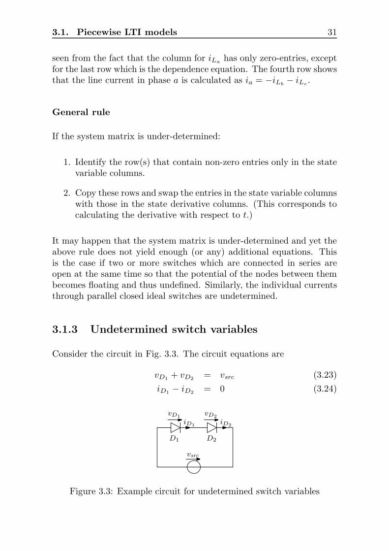
Consider the circuit in Fig. 3.3. The circuit equations are
vD1+ vD2
= vsrc (3.23)
iD1− iD2
= 0 (3.24)
vsrc
D1 D2
iD1iD2
vD1vD2
Figure 3.3: Example circuit for undetermined switch variables
32 Chapter 3. Modeling techniques
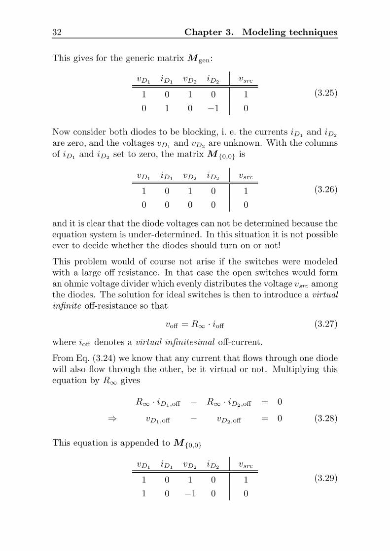
This gives for the generic matrix Mgen:
vD1iD1
vD2iD2
vsrc
1 0 1 0 1
0 1 0 −1 0
(3.25)
Now consider both diodes to be blocking, i. e. the currents iD1and iD2
are zero, and the voltages vD1and vD2
are unknown. With the columnsof iD1
and iD2set to zero, the matrix M0,0 is
vD1iD1
vD2iD2
vsrc
1 0 1 0 1
0 0 0 0 0
(3.26)
and it is clear that the diode voltages can not be determined because theequation system is under-determined. In this situation it is not possibleever to decide whether the diodes should turn on or not!
This problem would of course not arise if the switches were modeledwith a large off resistance. In that case the open switches would forman ohmic voltage divider which evenly distributes the voltage vsrc amongthe diodes. The solution for ideal switches is then to introduce a virtual
infinite off-resistance so that
voff = R∞ · ioff (3.27)
where ioff denotes a virtual infinitesimal off-current.
From Eq. (3.24) we know that any current that flows through one diodewill also flow through the other, be it virtual or not. Multiplying thisequation by R∞ gives
R∞ · iD1,off − R∞ · iD2,off = 0
⇒ vD1,off − vD2,off = 0 (3.28)
This equation is appended to M0,0
vD1iD1
vD2iD2
vsrc
1 0 1 0 1
1 0 −1 0 0
(3.29)
3.1. Piecewise LTI models 33
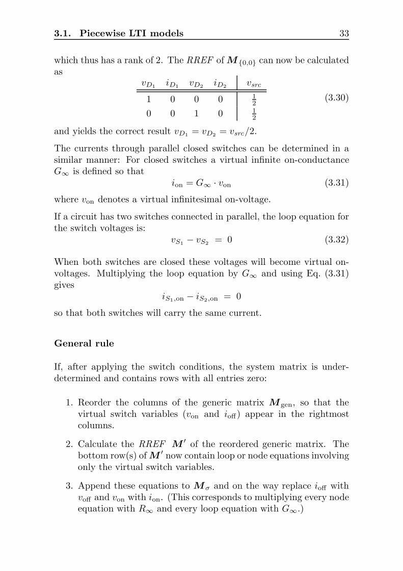
which thus has a rank of 2. The RREF of M 0,0 can now be calculatedas
vD1iD1
vD2iD2
vsrc
1 0 0 0 12
0 0 1 0 12
(3.30)
and yields the correct result vD1= vD2
= vsrc/2.
The currents through parallel closed switches can be determined in asimilar manner: For closed switches a virtual infinite on-conductanceG∞ is defined so that
ion = G∞ · von (3.31)
where von denotes a virtual infinitesimal on-voltage.
If a circuit has two switches connected in parallel, the loop equation forthe switch voltages is:
vS1− vS2
= 0 (3.32)
When both switches are closed these voltages will become virtual on-voltages. Multiplying the loop equation by G∞ and using Eq. (3.31)gives
iS1,on − iS2,on = 0
so that both switches will carry the same current.
General rule
If, after applying the switch conditions, the system matrix is under-determined and contains rows with all entries zero:
1. Reorder the columns of the generic matrix Mgen, so that thevirtual switch variables (von and ioff) appear in the rightmostcolumns.
2. Calculate the RREF M ′ of the reordered generic matrix. Thebottom row(s) of M ′ now contain loop or node equations involvingonly the virtual switch variables.
3. Append these equations to Mσ and on the way replace ioff withvoff and von with ion. (This corresponds to multiplying every nodeequation with R∞ and every loop equation with G∞.)
34 Chapter 3. Modeling techniques
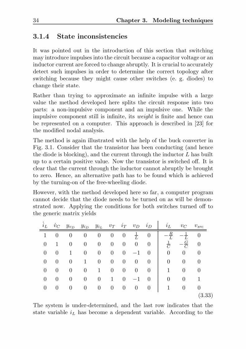
3.1.4 State inconsistencies
It was pointed out in the introduction of this section that switchingmay introduce impulses into the circuit because a capacitor voltage or aninductor current are forced to change abruptly. It is crucial to accuratelydetect such impulses in order to determine the correct topology afterswitching because they might cause other switches (e. g. diodes) tochange their state.
Rather than trying to approximate an infinite impulse with a largevalue the method developed here splits the circuit response into twoparts: a non-impulsive component and an impulsive one. While theimpulsive component still is infinite, its weight is finite and hence canbe represented on a computer. This approach is described in [23] forthe modified nodal analysis.
The method is again illustrated with the help of the buck converter inFig. 3.1. Consider that the transistor has been conducting (and hencethe diode is blocking), and the current through the inductor L has builtup to a certain positive value. Now the transistor is switched off. It isclear that the current through the inductor cannot abruptly be broughtto zero. Hence, an alternative path has to be found which is achievedby the turning-on of the free-wheeling diode.
However, with the method developed here so far, a computer programcannot decide that the diode needs to be turned on as will be demon-strated now. Applying the conditions for both switches turned off tothe generic matrix yields
iL vC yvDyiD
yiLvT iT vD iD iL vC vsrc
1 0 0 0 0 0 0 1L 0 −R
L − 1L 0
0 1 0 0 0 0 0 0 0 1C −G
C 0
0 0 1 0 0 0 0 −1 0 0 0 0
0 0 0 1 0 0 0 0 0 0 0 0
0 0 0 0 1 0 0 0 0 1 0 0
0 0 0 0 0 1 0 −1 0 0 0 1
0 0 0 0 0 0 0 0 0 1 0 0
(3.33)
The system is under-determined, and the last row indicates that thestate variable iL has become a dependent variable. According to the
3.1. Piecewise LTI models 35
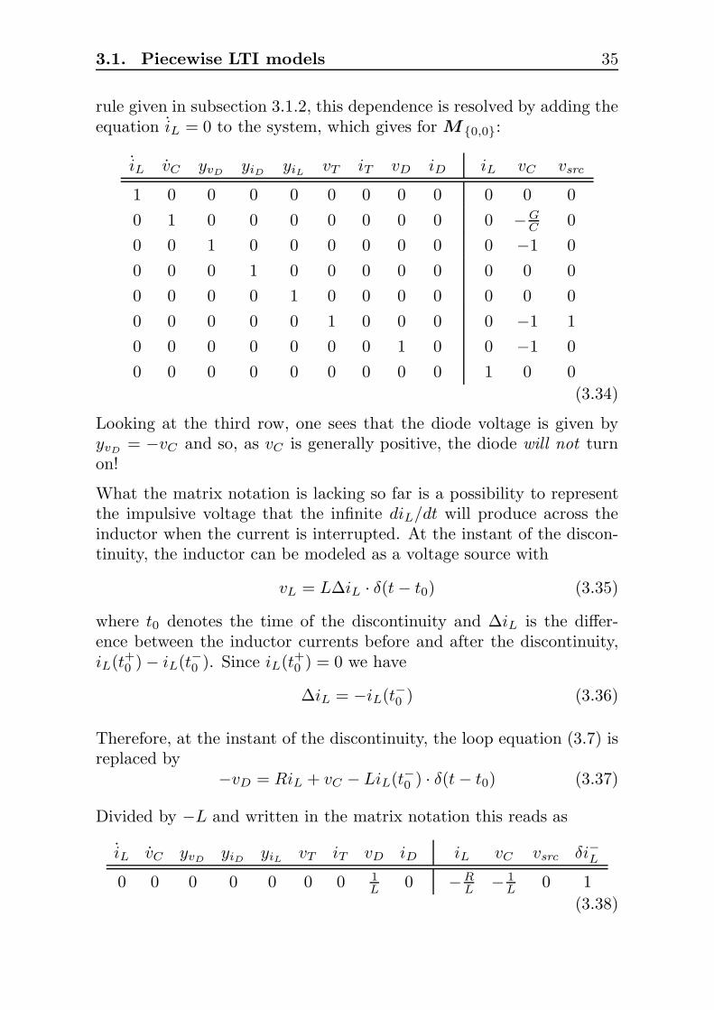
rule given in subsection 3.1.2, this dependence is resolved by adding theequation iL = 0 to the system, which gives for M 0,0:
iL vC yvDyiD
yiLvT iT vD iD iL vC vsrc
1 0 0 0 0 0 0 0 0 0 0 0
0 1 0 0 0 0 0 0 0 0 −GC 0
0 0 1 0 0 0 0 0 0 0 −1 0
0 0 0 1 0 0 0 0 0 0 0 0
0 0 0 0 1 0 0 0 0 0 0 0
0 0 0 0 0 1 0 0 0 0 −1 1
0 0 0 0 0 0 0 1 0 0 −1 0
0 0 0 0 0 0 0 0 0 1 0 0
(3.34)
Looking at the third row, one sees that the diode voltage is given byyvD
= −vC and so, as vC is generally positive, the diode will not turnon!
What the matrix notation is lacking so far is a possibility to representthe impulsive voltage that the infinite diL/dt will produce across theinductor when the current is interrupted. At the instant of the discon-tinuity, the inductor can be modeled as a voltage source with
vL = L∆iL · δ(t − t0) (3.35)
where t0 denotes the time of the discontinuity and ∆iL is the differ-ence between the inductor currents before and after the discontinuity,iL(t+0 ) − iL(t−0 ). Since iL(t+0 ) = 0 we have
∆iL = −iL(t−0 ) (3.36)
Therefore, at the instant of the discontinuity, the loop equation (3.7) isreplaced by
−vD = RiL + vC − LiL(t−0 ) · δ(t − t0) (3.37)
Divided by −L and written in the matrix notation this reads as
iL vC yvDyiD
yiLvT iT vD iD iL vC vsrc δi−L
0 0 0 0 0 0 0 1L 0 −R
L − 1L 0 1
(3.38)

36 Chapter 3. Modeling techniques
where δi−L is an abbreviation for iL(t−0 ) · δ(t − t0).
This row is now used as a replacement for the first row of the matrixin (3.33), i. e. the original loop equation. Subsequent calculation of theRREF yields
iL vC yvDyiD
yiLvT iT vD iD iL vC vsrc δi−L
0 1 0 0 0 0 0 0 0 0 −GC 0 0
0 0 1 0 0 0 0 0 0 0 −1 0 L
0 0 0 1 0 0 0 0 0 0 0 0 0
0 0 0 0 1 0 0 0 0 0 0 0 0
0 0 0 0 0 1 0 0 0 0 −1 1 L
0 0 0 0 0 0 0 1 0 0 −1 0 L
0 0 0 0 0 0 0 0 0 1 0 0 0
(3.39)
Looking at the second row, one sees that the diode voltage is now cor-rectly given as
yvD= −vC + LiL(t−0 ) · δ(t − t0) (3.40)
The inductor current iL(t−0 ) before the opening of the transistor waspositive. Hence, the impulsive component in Eq. (3.40) overrides thenegative non-impulsive component −vC . The diode will therefore cor-rectly be turned on thus creating a new path for the inductor current.
This procedure can be automatized by a slight modification of the algo-rithm for setting up the generic system matrix described in subsection3.1.1.
Modified algorithm for setting up Mgen
Set up M gen according to steps 1 to 4 as described in subsection 3.1.1.
5. Append an additional set of columns δx− = [ δv−C δi−L ] at the
3.1. Piecewise LTI models 37
right hand side and fill it with the identity matrix:
x y s x u δx−
Ix 0 X X X Ix
0 Iy X X X 0
0 0 X X X 0
(3.41)
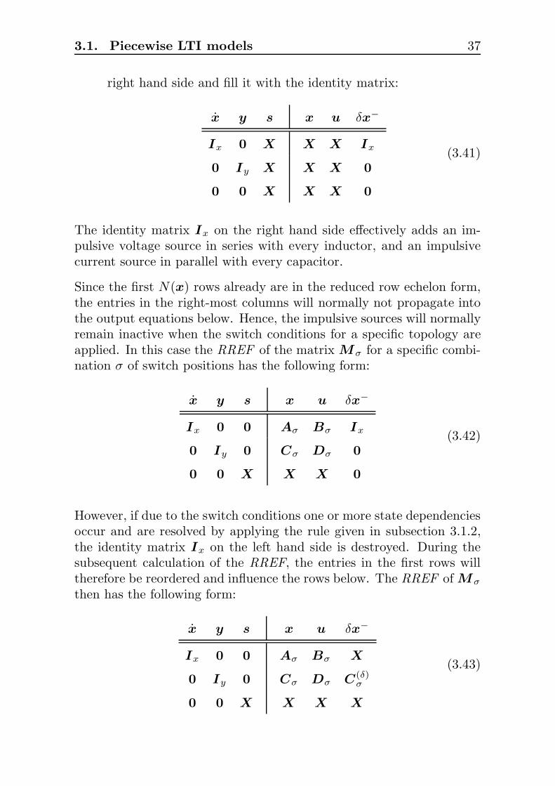
The identity matrix Ix on the right hand side effectively adds an im-pulsive voltage source in series with every inductor, and an impulsivecurrent source in parallel with every capacitor.
Since the first N(x) rows already are in the reduced row echelon form,the entries in the right-most columns will normally not propagate intothe output equations below. Hence, the impulsive sources will normallyremain inactive when the switch conditions for a specific topology areapplied. In this case the RREF of the matrix Mσ for a specific combi-nation σ of switch positions has the following form:
x y s x u δx−
Ix 0 0 Aσ Bσ Ix
0 Iy 0 Cσ Dσ 0
0 0 X X X 0
(3.42)
However, if due to the switch conditions one or more state dependenciesoccur and are resolved by applying the rule given in subsection 3.1.2,the identity matrix Ix on the left hand side is destroyed. During thesubsequent calculation of the RREF, the entries in the first rows willtherefore be reordered and influence the rows below. The RREF of Mσ
then has the following form:
x y s x u δx−
Ix 0 0 Aσ Bσ X
0 Iy 0 Cσ Dσ C(δ)σ
0 0 X X X X
(3.43)
38 Chapter 3. Modeling techniques
The evaluation of the output variables is now split in two parts:
y = Cσ x + Dσu
y(δ) = C(δ)σ x
(3.44)
Whenever an entry of y(δ) is non-zero, it will overrule the respectiveentry of y.
3.1.5 Implementation
The methods described here have been implemented in a computer pro-gram PLECS [22], an extension to the software package MATLAB/Simu-link. The program accepts circuits that consist of passive elements (R,L, C), independent voltage and current sources, voltage and currentmeters, and switches both externally controlled (e. g. ideal switches)and internally controlled (e. g. diodes) or both (e. g. thyristors, GTOsand circuit breakers).
At the beginning of a simulation, the program sets up the generic systemmatrix, determines the initial topology and calculates the correspondingstate-space matrices. During a simulation, the state derivatives arecalculated and passed on to the solver engine of Simulink. At everytime step, the state of each switch is determined from external controlsignals or from internal circuit variables such as the current trough orthe voltage across a diode. Whenever the state of a switch changes, anew set of state-space matrices is computed and afterwards all switchesare checked again to determine whether subsequent switching actionsare necessary (as in the last example of the buck converter). Once astable circuit topology is obtained, the simulation continues.
PLECS has been used for all time-domain simulations in the followingchapters.
3.2. State-space averaging 39
3.2 State-space averaging
In many cases when studying power electronics circuits the interest liesnot so much in the instantaneous values of voltages and currents butrather in their average values [3]. Obvious examples are the dc voltageand current of an HVDC converter which are normally filtered in orderto remove the ripple, before they are fed into the various controllers.This motivates the study of models that directly describe the local av-erage behavior of circuit variables even during transient conditions.
3.2.1 Local average
The local (or moving) average of a variable x is defined by
x(t) =1
T
∫ t
t−T
x(τ) dτ (3.45)
for a fixed T . An appropriate choice of T is required in order to obtainuseful results. In general, it is a multiple of the shortest regular switch-ing interval associated with the operation of the circuit being analyzed.In the special case where x is periodic, and T is chosen to equal the pe-riod, x is just the usual average. This special case is very important inpower electronics, because the steady-state waveforms in typical circuitsare indeed periodic.
3.2.2 Local ω-component
As a generalization of Eq. (3.45) the averaging operation can be done us-ing a weighing function other than a constant unity factor. Specifically,the local ω-component of x at time t can be defined as
xω(t) =1
T
∫ T
t−T
x(τ)e−jωτ dτ (3.46)
In this notation the local average x(t) of Eq. (3.45) is the local 0-component x0(t). The choices of ω and T are usually interrelated. Forinstance, with ω = 2π/T , xω in steady-state is the complex amplitudeof the fundamental frequency component for the periodic waveform x.

40 Chapter 3. Modeling techniques
3.2.3 Generalized averaging
The basis for the generalized averaging method [24] is the fact that afunction x(τ) can be approximated on the interval τ ∈ ]t − T, t] with aFourier series of the form
x(τ) =∑
k
〈x〉k(t)ejkωsτ (3.47)
where ωs = 2π/T and 〈x〉k are complex Fourier coefficients. The k-th Fourier coefficient corresponds to the local kωs-component in thenotation introduced above and is given by
〈x〉k(t) =1
T
∫ t
t−T
x(τ)e−jkωsτ dτ (3.48)
A key property of these Fourier coefficients is that the time derivativeof the k-th coefficient is
d
dt〈x〉k(t) =
⟨
d
dtx
⟩
k
(t) − jkωs 〈x〉k(t) (3.49)
It should be noted that the frequency ωs is assumed constant here. Forslowly varying ωs(t), however, Eq. (3.49) still is a good approximation.The errors involved are discussed in detail in [24].
The aim of the generalized averaging method is to determine a state-space model in which the coefficients 〈x〉k are the state variables. Start-ing from the state-space model of a system
d
dtx(t) = f
(
x(t), u(t))
(3.50)
where u(t) is some periodic input function, the relevant Fourier coeffi-cients of both sides of Eq. (3.50) are computed, i. e.
⟨
d
dtx
⟩
k
= 〈f(x, u)〉k (3.51)
for the k-th coefficient. Subsequently the rule for the derivative givenin Eq. (3.49) is applied:
d
dt〈x〉k = 〈f(x, u)〉k − jkωs 〈x〉k (3.52)
The essence of the generalized averaging method is to find a simplifiedexpression for 〈f(x, u)〉k as a function of the individual coefficients 〈x〉iand 〈u〉i, and to retain only the dominant coefficients in this process.
3.2. State-space averaging 41
3.2.4 Phasor dynamics models
Applied to power systems applications, the generalized averaging methodhas been used to extend the standard phasor model, which in principleis valid only for pure sinusoidal conditions. An attractive feature ofthe resulting phasor dynamics models is that the frequency range, overwhich it should be valid, can be chosen by retaining the appropriateFourier coefficients.
In [8] the method is used to develop a phasor dynamics model for aThyristor-Controlled Series Capacitor (TCSC). It is interesting to notethat — although the model uses only the fundamental coefficients —it is capable of taking into account the effects of higher harmonics veryaccurately.
This is achieved by using the following approximation. The steady-state
waveform xs of a variable corresponding to a certain mode of operation(in the cited example the series capacitor voltage waveform for a specificconduction angle) is decomposed into its (constant) Fourier coefficients〈xs〉′k, which are normalized with respect to the fundamental coefficient.For the evaluation of the term 〈f(x, u)〉1 as in Eq. (3.52), the dynamic
waveform x is then approximately reconstructed from only the dynamicfundamental coefficient 〈x〉1(t) and the static steady-state coefficients〈xs〉′k as
x(τ) ≈∑
k
〈xs〉′k〈x〉1(t)ejkωsτ (3.53)
This approximation turns out to be an excellent improvement over usingonly the fundamental coefficient, while it is substantially simpler thanthe full inclusion of higher harmonics.
A similar approach will be used in chapter 5 where a steady-state rela-tionship is used as an approximation for the dynamic relationship be-tween a dynamic phasor and the short-time average of a space-vector.

42 Chapter 3. Modeling techniques
3.3 Sampled-data modeling
The majority of power electronics circuits operate cyclically. Whenstudying such circuits it can be useful to work with models that in-volve quantities sampled once per cycle. A general approach to obtainsuch models for arbitrary circuits is described in [25] and reviewed herebriefly.
3.3.1 Large-signal sampled data description
In one cycle k of a cyclically operating, piecewise linear system, the statevector x(t) is governed by a succession of LTI state-space equations ofthe form
x = Aix(t) + Biu(t) tk + Tk,i−1 < t ≤ tk + Tk,i (3.54)
where tk is the starting time of the k-th cycle and the Tk,i the are relativetransition times in the k-th cycle at which the switch configuration (andthus the state-space matrices) changes.
For a given x(tk) the evolution of the system is completely determinedby the input waveforms and the transition times. These input wave-forms and transition times are in turn governed by a set of independentcontrolling parameters pk. The dependence of the transition times onthese parameters and the state vector at the beginning of a cycle canbe expressed by a set of constraint equations:
c(x(tk), pk, T k) = 0 (3.55)
where T k is a vector of all Tk,i. These equations can describe bothexternally controlled transitions, such as the turning-on of a thyristor,or transitions caused by internal circuit variables, such as the turning-offof a thyristor.
On integrating Eq. (3.54) over the interval from tk to tk+1 one obtainsa sampled-data description of the form
x(tk+1) = f(x(tk), pk, T k) (3.56)
The function f is often called advance map, as it advances the statevector from one cycle to the next, or Poincare map [26], a mathematicaltool used for the study of the nonlinear system dynamics.

3.3. Sampled-data modeling 43
3.3.2 Perturbations about a nominal steady state
If a system described by Eq. (3.54) is in cyclic steady state, it followsthat
x = f (x, p, T ) (3.57)
with x, p and T denoting constant steady-state values of the sampledstate vector, parameters and transition times.
Starting from such a steady-state solution, the dynamics of small per-turbations from the steady state can be investigated. For this purposeit is convenient to use a notation such as the following
xk = x(tk) − x
pk = pk − p
T k = T k − T
(3.58)
From Eqs. (3.55) to (3.57) it then follows that
xk+1 = f(x + xk, p + pk, T + T k) − x (3.59)
withc(x + xk, p + pk, T + T k) = 0 (3.60)
Carrying out multi-variable Taylor series expansions in these equations,retaining only linear terms, and combining the two resulting equationsin order to eliminate T k gives
xk+1 ≈ F xk + Guk (3.61)
with
F =∂f
∂x− ∂f
∂T
∂c
∂T
−1 ∂c
∂x
G =∂f
∂p− ∂f
∂T
∂c
∂T
−1 ∂c
∂p
(3.62)
This constitutes an approximate LTI sampled-data model for pertur-bations of the system from a cyclic steady state. One property of theJacobian matrix F is that if all its eigenvalues have magnitudes smallerthan one, the cyclic steady state of the system is asymptotically stablewithout further control action.

44 Chapter 3. Modeling techniques
Depending on the circuit and the nature of the constraint equations, thematrices F and G can be expressed analytically in terms of the Ai andBi from Eq. (3.54) and the parameters p, using matrix exponentials.The solution can be simplified by exploiting properties of the circuitsuch as half-cycle symmetry.
Methods based on this formalism have been used in power systems ap-plications such as a TCSC [27] and also an HVDC application [9].

Chapter 4
Line commutated
converter models
In this chapter the conventional line-commutated converter is analyzed.Its topology is the three-phase, full-wave bridge circuit shown in Fig. 4.1.The following idealizations form the basic assumptions of the analysis:
• The ac voltage is stiff and may be represented by an ideal sinu-soidal source in series with a lossless inductance.
• The direct current is ripple-free and (in steady-state operation)constant.
• The valves are ideal switches with zero on-resistance and infiniteoff-resistance. They change instantaneously between these twostates.
• The valves are fired at equal intervals of one-sixth cycle (60).
The instantaneous line-to-neutral voltages of the ac sources are takenas
ea = Em cos(ωt + 60)
eb = Em cos(ωt − 60) (4.1)
ec = Em cos(ωt − 180)
45

46 Chapter 4. LCC models
ea
eb
ec
ia
ib
ic
Lc
ud
id
①
②
③
④
⑤
⑥
Figure 4.1: Equivalent circuit for the line commutated converter. Thevalves are numbered in the order of their firing
The corresponding line-to-line voltages are then
eac = ea − ec =√
3 Em cos(ωt + 30)
eba = eb − ea =√
3 Em cos(ωt − 90)
ecb = ec − eb =√
3 Em cos(ωt + 150)
(4.2)
4.1 Static model
The development of the equations governing the steady-state operationof the converter is described in standard literature (e.g. [1], [2], [4]). Itis repeated briefly for reference in this section.
4.1.1 Analysis without commutation overlap
Fig. 4.2 shows the typical wave-forms of the converter if the ac induc-tance Lc is neglected. In the top graph the ac line-to-neutral voltagesare drawn in thin lines and, in heavy lines, the potentials of the positiveand negative dc terminals with respect to ac neutral. The middle graphshows the ac line-to-line voltages and, in a heavy line, the instantaneousdirect voltage ud. The bottom graph shows the constant dc current and,in a heavy line, the ac line current ia.
At any given instant, one valve of the upper commutation group andone of the lower row are conducting. Therefore, the instantaneous direct
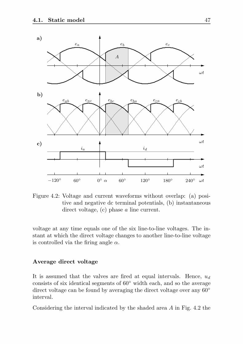
4.1. Static model 47
a)
b)
c)ia id
ea eb ec
eab eac ebc eba eca ecb
−120 0 6060 120 180 240
ωt
ωt
ωt
ωtα
A
Figure 4.2: Voltage and current waveforms without overlap: (a) posi-tive and negative dc terminal potentials, (b) instantaneousdirect voltage, (c) phase a line current.
voltage at any time equals one of the six line-to-line voltages. The in-stant at which the direct voltage changes to another line-to-line voltageis controlled via the firing angle α.
Average direct voltage
It is assumed that the valves are fired at equal intervals. Hence, ud
consists of six identical segments of 60 width each, and so the averagedirect voltage can be found by averaging the direct voltage over any 60
interval.
Considering the interval indicated by the shaded area A in Fig. 4.2 the

48 Chapter 4. LCC models
average direct voltage is given by
Ud =3
πA =
3
π
α+60
∫
α
(eb − ec) d(ωt)
=3
π
α+60
∫
α
√3Em cos (ωt − 30) d(ωt)
=3√
3
πEm
α+60
∫
α
cos (ωt − 30) d(ωt)
= Udi0
[
sin (ωt − 30)∣
∣
∣
α+60
α
= Udi0
[
sin (α + 30) − sin (α − 30)]
= Udi0 2 sin 30 cosα = Udi0 cosα (4.3)
where
Udi0 =3√
3
πEm (4.4)
is the so-called ideal no-load direct voltage.
The ignition angle α may range from 0 to 180. Outside of this range,the commutation voltage at the firing instant is negative and the com-mutation fails.
AC current magnitude and phase
Since the direct current Id is constant by assumption and each valveconducts for a period of 120, the ac currents are rectangular blockswith magnitude Id and width 120 as shown in Fig. 4.2. The phasedisplacement changes with the firing angle α.
The peak value of the fundamental frequency component of the alter-nating line current can be determined by Fourier analysis:
I(1) =2√
3
πId (4.5)

4.1. Static model 49
By assumption, the converter is lossless and therefore the ac activepower must equal the dc power:
3
2EmI(1) cosϕ = UdId
= Udi0Id cosα (4.6)
where ϕ denotes the angle by which the fundamental frequency compo-nent of the line current lags the line-to-neutral voltage.
Inserting Eqs. (4.4) and (4.5) gives:
(
3
2Em
2√
3
πId
)
cosϕ =
(
3√
3
πEmId
)
cosα
⇒ cosϕ = cosα (4.7)
That is, the firing angle α shifts the fundamental frequency componentof the ac current by an angle ϕ = α with respect to the ac line-to-neutralvoltage.
4.1.2 Analysis including commutation overlap
Because of the inductance Lc present at the ac-terminals the phase cur-rents cannot change instantaneously. Therefore, the dc current requiresa finite time to transfer from one phase to another. This phenomenonis called commutation overlap. Its effect on the voltage and currentwaveforms of the converter circuit is shown in Fig. 4.3. The angle cor-responding to the time needed for commutation is denoted by µ. Theangle δ = α + µ is called the extinction angle.
Fig. 4.4 shows the equivalent converter circuit during commutation fromvalve 1 to valve 3. At the beginning of commutation (i.e. when valve 3 isfired), the phase current ia equals the direct current while ib is still zero.The voltage eb − ea then drives a current through the loop containingvalves 1 and 3. The commutation ends when ia has decreased to zeroand ib has taken over the whole dc current:
At ωt = α : ia = Id and ib = 0At ωt = δ : ia = 0 and ib = Id
(4.8)

50 Chapter 4. LCC models
a)
b)
c)
ia
ia
ibib
ib id
ea eb ec
eab eac ebc eba eca ecb
ea+eb
2
Aµ
−120 0 6060 120 180 240
ωt
ωt
ωt
ωtα δ
Figure 4.3: Voltage and current waveforms showing the effect of overlap:(a) positive and negative dc terminal potentials, (b) instan-taneous direct voltage, (c) phase a and b line currents.
The mesh equation for the above described loop is:
eb − ea = Lcdibdt
− Lcdiadt
(4.9)
The sum of ia and ib during commutation equals the direct current;therefore,
diadt
+dibdt
=diddt
= 0
⇒ diadt
= −dibdt
(4.10)

4.1. Static model 51
ea
eb
ec
ia
ib
ic
Lc
ud
id
①
②
③
Figure 4.4: Equivalent LCC circuit during commutation from valve 1to valve 3 (non-conducting valves not shown)
Inserting Eqs. (4.2) and (4.10) into (4.9) yields
√3 Em sin(ωt) = 2Lc
dibdt
⇒ dibdt
=
√3Em
2Lcsin(ωt) (4.11)
Integration over the duration of the commutation gives
δ
ω∫
α
ω
dibdt
dt =
√3Em
2ωLc(cosα − cos δ)
and finally, inserting the boundary conditions (4.8) into the left-handside:
Id =
√3 Em
2ωLc(cosα − cos δ) (4.12)
From this equation the extinction angle δ (and ultimately the overlapangle µ) can easily be determined for a given firing angle α. It alsoallows the calculation of the ideal maximum firing angle αmax for whichthe commutation will succeed in a converter with ideal valves. Since
cos δ ≥ −1
for any angle δ:
Id ≤√
3 Em
2ωLc(cosα + 1)
52 Chapter 4. LCC models
⇒ cosαmax =2ωLc√3 Em
Id − 1 (4.13)
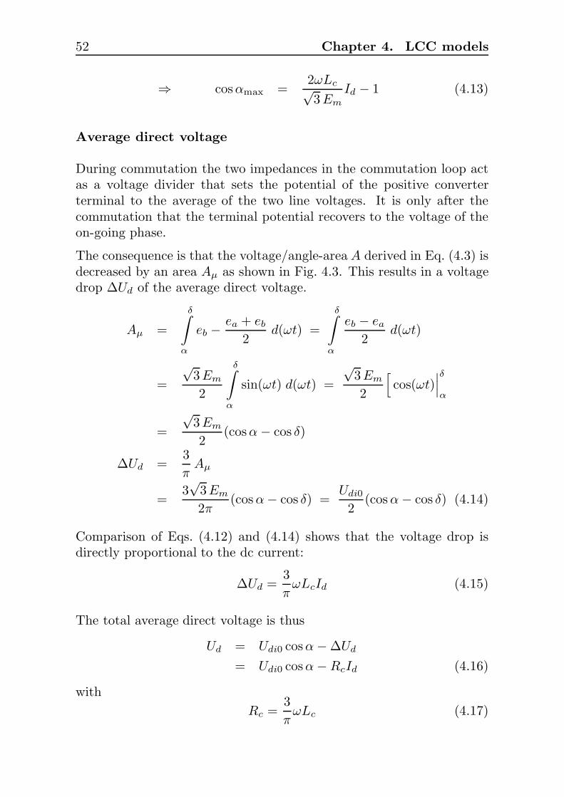
Average direct voltage
During commutation the two impedances in the commutation loop actas a voltage divider that sets the potential of the positive converterterminal to the average of the two line voltages. It is only after thecommutation that the terminal potential recovers to the voltage of theon-going phase.
The consequence is that the voltage/angle-area A derived in Eq. (4.3) isdecreased by an area Aµ as shown in Fig. 4.3. This results in a voltagedrop ∆Ud of the average direct voltage.
Aµ =
δ∫
α
eb −ea + eb
2d(ωt) =
δ∫
α
eb − ea
2d(ωt)
=
√3Em
2
δ∫
α
sin(ωt) d(ωt) =
√3Em
2
[
cos(ωt)∣
∣
∣
δ
α
=
√3Em
2(cosα − cos δ)
∆Ud =3
πAµ
=3√
3Em
2π(cos α − cos δ) =
Udi0
2(cos α − cos δ) (4.14)
Comparison of Eqs. (4.12) and (4.14) shows that the voltage drop isdirectly proportional to the dc current:
∆Ud =3
πωLcId (4.15)
The total average direct voltage is thus
Ud = Udi0 cosα − ∆Ud
= Udi0 cosα − RcId (4.16)
with
Rc =3
πωLc (4.17)
4.1. Static model 53
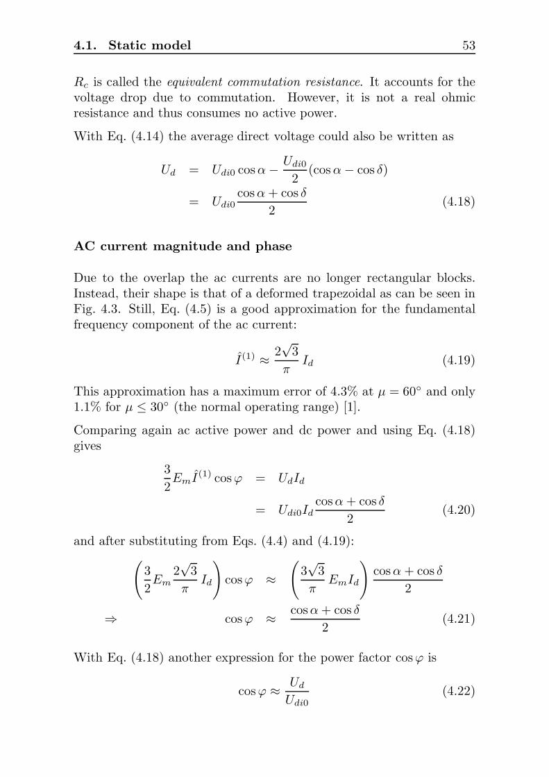
Rc is called the equivalent commutation resistance. It accounts for thevoltage drop due to commutation. However, it is not a real ohmicresistance and thus consumes no active power.
With Eq. (4.14) the average direct voltage could also be written as
Ud = Udi0 cosα − Udi0
2(cos α − cos δ)
= Udi0cosα + cos δ
2(4.18)
AC current magnitude and phase
Due to the overlap the ac currents are no longer rectangular blocks.Instead, their shape is that of a deformed trapezoidal as can be seen inFig. 4.3. Still, Eq. (4.5) is a good approximation for the fundamentalfrequency component of the ac current:
I(1) ≈ 2√
3
πId (4.19)
This approximation has a maximum error of 4.3% at µ = 60 and only1.1% for µ ≤ 30 (the normal operating range) [1].
Comparing again ac active power and dc power and using Eq. (4.18)gives
3
2EmI(1) cosϕ = UdId
= Udi0Idcosα + cos δ
2(4.20)
and after substituting from Eqs. (4.4) and (4.19):
(
3
2Em
2√
3
πId
)
cosϕ ≈(
3√
3
πEmId
)
cosα + cos δ
2
⇒ cosϕ ≈ cosα + cos δ
2(4.21)
With Eq. (4.18) another expression for the power factor cosϕ is
cosϕ ≈ Ud
Udi0(4.22)

54 Chapter 4. LCC models
and with substituting from Eq. (4.16), Ud = Udi0 cosα − RcId:
cosϕ ≈ cosα − RcId
Udi0(4.23)
Eq. (4.23) shows that with increasing load the power factor decreasesand accordingly the phase shift between the fundamental ac current andthe ac voltage increases.
4.2 Dynamic model
The static model is based on the assumption that the direct current isconstant and ripple free. This assumption is generally justified with thelarge smoothing reactor that is usually present on the dc side. However,if the dynamic interaction between the converter and the ac system isstudied, the dc current implicitly is assumed not to be constant.
In this section the original assumption will be relaxed as follows: thecurrent is still assumed to be ripple free but now it changes at a constantrate Id. The dc current can thus be written as
id(t) = id(t0) + Id · (t − t0) Id const. (4.24)
4.2.1 Analysis without commutation overlap
Average direct voltage
When overlap is neglected, the dc current always flows through two ofthe three inductances at the ac side. This produces a voltage drop of2LcId in the direct current. Since Id is assumed constant, the averagevoltage drop is also
∆Ud,Id= 2LcId (4.25)
This results in a total average direct voltage
Ud = Udi0 cosα − 2LcId (4.26)

4.2. Dynamic model 55
AC current magnitude and phase
In the dynamic model the ac current is described by the dynamic phasor
i, the fundamental component of which is given by
i(1) =2√
3
π· ej(arg(e)−α) (4.27)
where e denotes the mains voltage phasor.
4.2.2 Analysis including commutation overlap
Duration of overlap
As discussed in the previous section the duration of the commutationoverlap due to the inductance Lc is determined by the time it takesfor the on-going phase to take over the dc current. The commutationprocess with a non-constant dc current is shown in Fig. 4.5.
Hence, the conditions at the beginning and end of the commutation are
At ωt = α : ia = id(t0) −µ
2ωId and ib = 0
At ωt = δ : ia = 0 and ib = id(t0) +µ
2ωId
(4.28)
The reference time t0 is chosen as the mid-point between the beginningand end of the commutation so that the average dc current during
ia
ib
id
id(t0) − µ2ω
Id
id(t0) + µ
2ωId
ωtα δ
Figure 4.5: Currents ia and ib during commutation showing the effectof a non-constant dc current
56 Chapter 4. LCC models
commutation is equal to id(t0):
ωt0 =α + δ
2
The mesh equation for the commutation loop is again
eb − ea = Lcdibdt
− Lcdiadt
(4.29)
Using the node equationia + ib = id
one finds thatdiadt
=diddt
− dibdt
= Id − dibdt
(4.30)
Substituting for dia
dt from (4.30) in (4.29) yields
√3Em sin(ωt) = 2Lc
dibdt
− LcId
⇒ dibdt
=
√3 Em
2Lcsin(ωt) +
Id
2(4.31)
The integral over the duration of the commutation is
δ
ω∫
α
ω
dibdt
dt =
√3Em
2ωLc(cosα − cos δ) +
δ − α
ω
Id
2(4.32)
Inserting the boundary conditions (4.28) gives
id(t0) +µ
2ωId =
√3Em
2ωLc(cosα − cos δ) +
µ
2ωId
⇒ id(t0) =
√3Em
2ωLc(cosα − cos δ) (4.33)
The conclusion of this result is that the duration of a commutation isnot influenced by the derivative of the dc current. It only depends onthe average dc current during commutation.
4.2. Dynamic model 57
Average direct voltage
The instantaneous direct voltage during commutation is
ud =eb + ea
2− 1
2LcId − ec − LcId (4.34)
This can be written as
ud = ud0 − ∆ud,µ − ∆ud,Id(4.35)
where
ud0 = eb − ec
∆ud,µ =eb − ea
2− 1
2LcId
∆ud,Id= 2LcId
∆ud,µ is the additional drop of the direct voltage due to commutation.The average over a 60 interval is
∆Ud,µ =3
π
δ∫
α
∆ud,µ d(ωt)
=3
π
δ∫
α
eb − ea
2− 1
2LcId d(ωt)
=3√
3 Em
2π(cosα − cos δ) − 3µ
2πLcId (4.36)
Combining Eqs. (4.33) and (4.36) shows that the voltage drop due tooverlap depends on both the derivative of the dc current and its averagemagnitude during commutation:
∆Ud,µ =3
πωLcid −
3µ
2πLcId (4.37)
Here the average direct current during commutation id(t0) has beenreplaced by the momentary direct current of the averaged model. Thetotal average direct voltage is thus
Ud = Udi0 cosα − ∆Ud,µ − ∆Ud,Id
= Udi0 cosα −(
3
πωLcid −
3µ
2πLcId
)
− 2LcId
= Udi0 cosα − Rcid − LcId (4.38)

58 Chapter 4. LCC models
with
Rc =3
πωLc
Lc =
(
2 − 3µ
2π
)
Lc (4.39)
Rc is again the equivalent commutation resistance introduced in theprevious section. The definition of Lc agrees with the notion of a meancommutation inductance as seen from the dc side, which is proposedin [28], albeit without further explanations. During non-commutationintervals it is 2Lc and during commutation 3
2Lc, thus:
Lc =3
π
(
2Lc
(π
3− µ
)
+3
2Lcµ
)
=3
π
(
2π
3− µ
2
)
Lc
=
(
2 − 3µ
2π
)
Lc
Except for the term LcId, which is zero in steady-state, Eq. (4.38) isidentical to Eq. (4.16). The dynamic model is thus a generalization ofthe static model.
AC current magnitude and phase
Using Eqs. (4.19) and (4.21), the fundamental ac current phasor is givenby
i(1) =2√
3
π· ej(arg(e)−arccos( cos α+cos δ
2)) (4.40)
4.3 Model validation
In order to validate the static and dynamic converter models and toassess their accuracy, their behavior is compared with detailed time-domain simulations of a test circuit. The circuit used is a rectifier withohmic-inductive load as shown in Fig. 4.6.
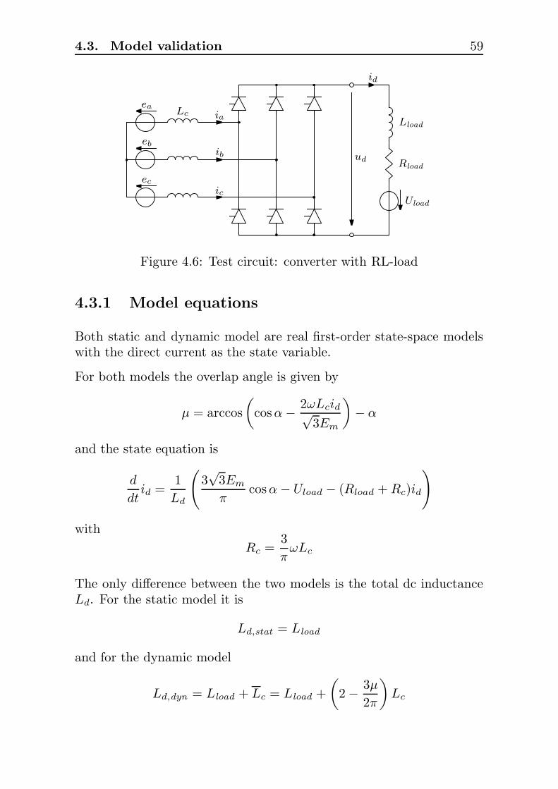
4.3. Model validation 59
ea
eb
ec
ia
ib
ic
Lc
ud
id
Rload
Lload
Uload
Figure 4.6: Test circuit: converter with RL-load
4.3.1 Model equations
Both static and dynamic model are real first-order state-space modelswith the direct current as the state variable.
For both models the overlap angle is given by
µ = arccos
(
cosα − 2ωLcid√3Em
)
− α
and the state equation is
d
dtid =
1
Ld
(
3√
3Em
πcosα − Uload − (Rload + Rc)id
)
with
Rc =3
πωLc
The only difference between the two models is the total dc inductanceLd. For the static model it is
Ld,stat = Lload
and for the dynamic model
Ld,dyn = Lload + Lc = Lload +
(
2 − 3µ
2π
)
Lc

60 Chapter 4. LCC models
0 0.02 0.04 0.06 0.08 0.1 0.12 0.14 0.16 0.18 0.2
0.75
1
1.25
i d[p
.u.]
time [s]
Figure 4.7: Simulation of a step change of the firing angle from α = 20
to α = 10. Thin continuous line: detailed simulation;heavy continuous line: dynamic model; dashed line: stan-dard model.
4.3.2 Qualitative comparison
Figure 4.7 shows the direct current response of the converter to a stepchange of the firing angle from α = 20 to α = 10. The converter isoperating in steady-state for one cycle before the step is applied. Theinstantaneous direct current of the detailed simulation is drawn with athin continuous line. A heavy continuous line is used for the dynamicmodel, and a heavy dashed line for the standard model.
In steady-state both models yield the same direct current as expectedand show good accordance with the detailed simulation. However, theincrease of the direct current after the step-change of the firing angle aspredicted by the static model is too steep because the additional volt-age drop in the commutation reactances due to di/dt is not taken intoaccount. The dynamic model, on the other hand, follows the detailedsimulation very closely.
4.3.3 Quantitative comparison
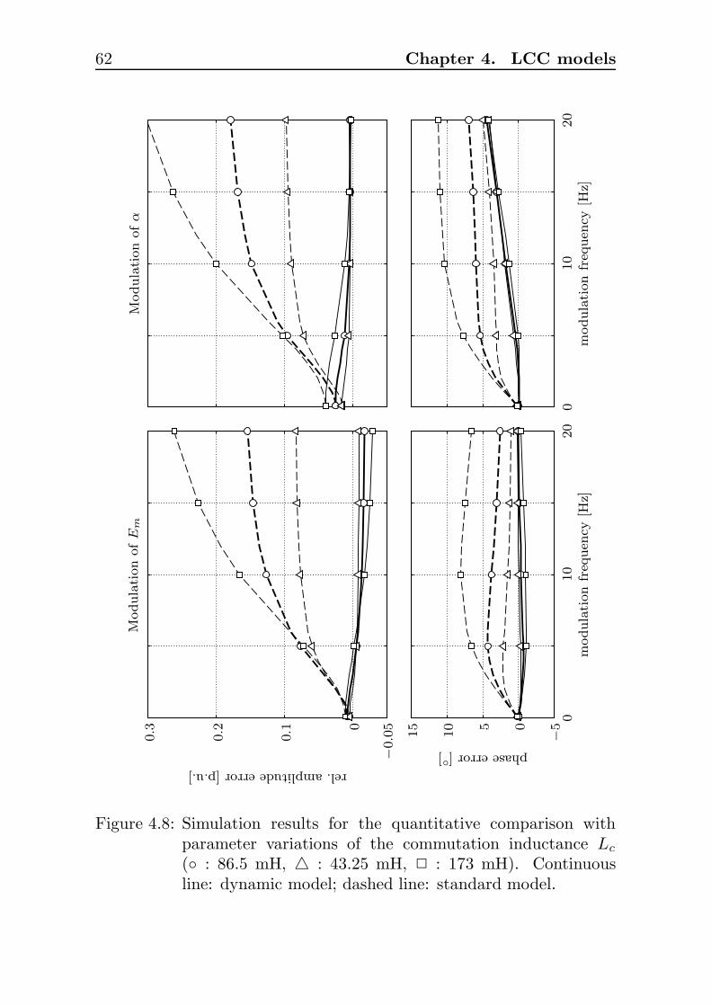
The accuracy of the models is now assessed by modulating the mag-nitude of the mains voltage and the firing angle with varying frequen-cies. Special attention has to be given to the switching nature of theconverter with its periodicity of π/3. In order to avoid interferencesonly such modulation frequencies are chosen that are integer divisors of

4.4. Conclusions 61
300 Hz. The magnitude and phase angle of the resulting modulationin the direct current are measured and compared with a detailed time-domain simulation. The parameters for the base case have been takenfrom [9] (with the commutation inductance adjusted to a fundamentalfrequency of 50 Hz): Em = 348.5717 kV, Id = 2 kA, Lc = 86.5 mH,Rload = 5 Ω, Lload = 0.8288 H, Uload = 495 kV. The converter operatesat a firing angle α = 15.
The simulation results are summarized in Fig. 4.8. The plots show therelative amplitude error (top) and the absolute phase error (bottom) ofthe ac component on the direct current yielded by the two models ascompared with the detailed simulation. The plots on the left containthe results for a modulation of the mains voltage and those one the rightfor a modulation of the firing angle.
As expected, both models have the same small error at very low mod-ulation frequencies f ≤ 0.1 Hz. For higher frequencies the amplitudeerror of the static model steadily increases. The parameter variationsshow that for larger commutation reactances the error becomes largeras suggested by Eq. (4.38). On the other hand, the amplitude error ofthe dynamic remains very small, and its magnitude never exceeds 5 %.It is also less sensitive to variations of Lc.
An interesting detail can be seen in the phase error plot for the modu-lation of the firing angle: both models exhibit a phase error that growswith the modulation frequency. A closer inspection reveals that thiserror in fact is the sum of the phase error for the modulation of themains voltage and a term proportional to the modulation frequency.Further simulations showed that the slope of this additional phase erroris dependent on the commutation inductance Lc as well as the operatingpoint firing angle. A detailed study of this phenomenon has to be leftto future work.
4.4 Conclusions
In this chapter a dynamic modeling approach for the line commutatedconverter was presented, which takes into account the dynamics of anaveraged direct current. The resulting dynamic model is shown to bean extension of the conventional quasi-static model. This extension
62 Chapter 4. LCC models
00
10
10
20
20
0 0
−55
10
15
−0.0
5
0.1
0.2
0.3
modula
tion
freq
uen
cy[H
z]m
odula
tion
freq
uen
cy[H
z]
phaseerror[]
rel.amplitudeerror[p.u.]
Modula
tion
of
Em
Modula
tion
of
α
Figure 4.8: Simulation results for the quantitative comparison withparameter variations of the commutation inductance Lc
( : 86.5 mH, : 43.25 mH, 2 : 173 mH). Continuousline: dynamic model; dashed line: standard model.

4.4. Conclusions 63
comprises an averaged commutation reactance added to the dc sidewhich is very easy to implement.
The neglect of the direct current dynamics in the static model leadsto errors when studying the dynamic response of the converter. Theseerrors are sensitive to the ratio between the commutation reactanceand the smoothing reactance on the dc side. Therefore, the proposeddynamic model is expected to have a particular impact for the study ofsystems with small dc reactances such as back-to-back HVDC links.


Chapter 5
Capacitor commutated
converter models
In this chapter the capacitor commutated converter is analyzed. Itstopology is shown in Fig. 5.1. The same basic assumptions as in theprevious chapter apply:
• The ac voltage is stiff and may be represented by an ideal sinu-soidal source in series with a lossless inductance.
• The direct current is ripple-free and (in steady-state operation)constant.
• The valves are ideal switches with zero on-resistance and infiniteoff-resistance. They change instantaneously between these twostates.
• The valves are fired at equal intervals of one-sixth cycle (60).
The instantaneous line-to-neutral voltages of the ac sources are takenas
ea = Em cos(ωt + 60)
eb = Em cos(ωt − 60) (5.1)
ec = Em cos(ωt − 180)
65
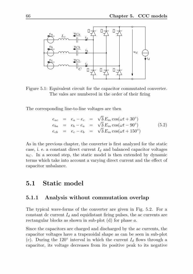
66 Chapter 5. CCC models
ea
eb
ec
ia
ib
ic
Lc
C
uCa
uCb
uCc
ud
id
①
②
③
④
⑤
⑥
Figure 5.1: Equivalent circuit for the capacitor commutated converter.The vales are numbered in the order of their firing
The corresponding line-to-line voltages are then
eac = ea − ec =√
3 Em cos(ωt + 30)
eba = eb − ea =√
3 Em cos(ωt − 90)
ecb = ec − eb =√
3 Em cos(ωt + 150)
(5.2)
As in the previous chapter, the converter is first analyzed for the staticcase, i. e. a constant direct current Id and balanced capacitor voltagesuC . In a second step, the static model is then extended by dynamicterms which take into account a varying direct current and the effect ofcapacitor unbalance.
5.1 Static model
5.1.1 Analysis without commutation overlap
The typical wave-forms of the converter are given in Fig. 5.2. For aconstant dc current Id and equidistant firing pulses, the ac currents arerectangular blocks as shown in sub-plot (d) for phase a.
Since the capacitors are charged and discharged by the ac currents, thecapacitor voltages have a trapezoidal shape as can be seen in sub-plot(c). During the 120 interval in which the current Id flows through acapacitor, its voltage decreases from its positive peak to its negative
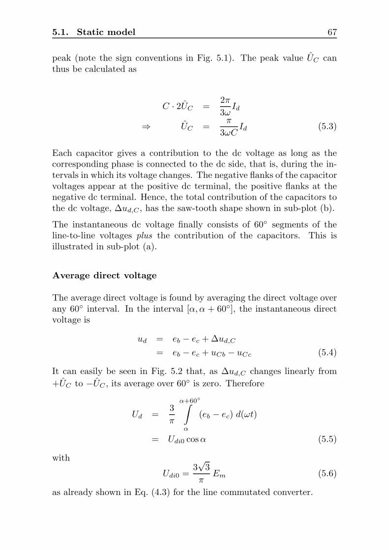
5.1. Static model 67
peak (note the sign conventions in Fig. 5.1). The peak value UC canthus be calculated as
C · 2UC =2π
3ωId
⇒ UC =π
3ωCId (5.3)
Each capacitor gives a contribution to the dc voltage as long as thecorresponding phase is connected to the dc side, that is, during the in-tervals in which its voltage changes. The negative flanks of the capacitorvoltages appear at the positive dc terminal, the positive flanks at thenegative dc terminal. Hence, the total contribution of the capacitors tothe dc voltage, ∆ud,C , has the saw-tooth shape shown in sub-plot (b).
The instantaneous dc voltage finally consists of 60 segments of theline-to-line voltages plus the contribution of the capacitors. This isillustrated in sub-plot (a).
Average direct voltage
The average direct voltage is found by averaging the direct voltage overany 60 interval. In the interval [α, α + 60], the instantaneous directvoltage is
ud = eb − ec + ∆ud,C
= eb − ec + uCb − uCc (5.4)
It can easily be seen in Fig. 5.2 that, as ∆ud,C changes linearly from
+UC to −UC , its average over 60 is zero. Therefore
Ud =3
π
α+60
∫
α
(eb − ec) d(ωt)
= Udi0 cosα (5.5)
with
Udi0 =3√
3
πEm (5.6)
as already shown in Eq. (4.3) for the line commutated converter.

68 Chapter 5. CCC models
a)
b)
c)
d)ia id
ud
∆ud,C
uCauCa uCb uCc
eab eac ebc eba eca ecb
−120 −60 0 60 120 180 240
ωt
ωt
ωt
ωt
ωtα
Figure 5.2: Voltage and current waveforms without overlap: (a) instan-taneous direct voltage, (b) total contribution of the capaci-tors to the direct voltage, (c) capacitor voltages, (d) phase aline current.

5.1. Static model 69
AC current magnitude and phase
The line current wave-forms are identical to those of the line commu-tated converter. Hence, the peak value of the fundamental frequencycomponent is
I(1) =2√
3
πId (5.7)
and the angle by which the fundamental frequency component of theline current lags the line-to-neutral voltage is
ϕ = α (5.8)
Operating range
With the average direct voltage and the line current being identical,the major difference between the line commutated converter and thecapacitor commutated converter is that the CCC can be operated atfiring angles smaller than 0 or larger than 180 because the capacitorsprovide the additional commutation voltage 2UC . This is illustrated inFig. 5.3.
The minimum (or maximum) firing angle that can theoretically beachieved is determined by
√3Em sin α + 2UC > 0
⇒ sin(αmin / max) = − 2πId
3√
3ωCEm
(5.9)
5.1.2 Analysis including commutation overlap
Fig. 5.4 shows the equivalent converter circuit during commutation fromvalve 1 to valve 3. The mesh equation for the commutation loop is
eb − ea + uCb − uCa = Lcdibdt
− Lcdiadt
(5.10)
Using Eq. (5.2) and taking into account that the direct current is con-stant this can be written as
√3 Em sin(ωt) + uCb − uCa = 2Lc
dibdt
(5.11)

70 Chapter 5. CCC models
(a)
(b)
ea + uCa
ea + uCa
eb + uCb
eb + uCb
ec + uCc
ec + uCc
ea
ea
eb
eb
ec
ec
u+
u+
u−
u−
−120 −60 0 60 120 180 240
ωt
ωt
ωt
α
α
Figure 5.3: Extended operating range of the capacitor commutated con-verter for (a) α < 0 and (b) α > 180. Line voltages atthe ac sources are drawn in dotted lines, line voltages at theconverter terminals in solid lines. Heavy lines mark the po-tentials of the positive and negative dc terminal with respectto ac neutral.
Under normal operating conditions, the capacitors in phase a and b arecharged in such a way as to accelerate the commutation. Unfortunately,the capacitor voltages themselves depend again on the current ib:
CduCa
dt= −ia = ib − Id
CduCb
dt= −ib
An analytical solution is presented in [29] and summarized in appendix A.However, the approach used there is not suitable for an extension intothe dynamic operation range. A much simpler solution which is nonethe-less quite accurate will therefore be developed here based partly on [5].
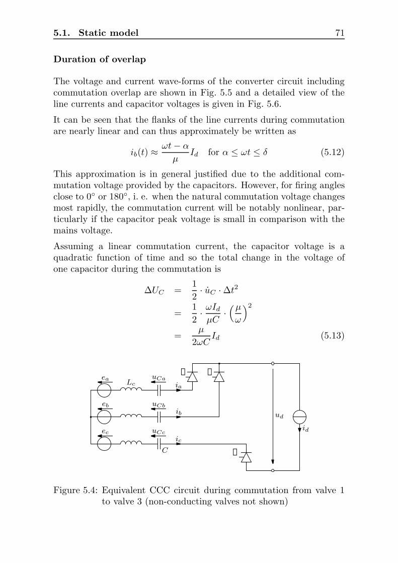
5.1. Static model 71
Duration of overlap
The voltage and current wave-forms of the converter circuit includingcommutation overlap are shown in Fig. 5.5 and a detailed view of theline currents and capacitor voltages is given in Fig. 5.6.
It can be seen that the flanks of the line currents during commutationare nearly linear and can thus approximately be written as
ib(t) ≈ωt − α
µId for α ≤ ωt ≤ δ (5.12)
This approximation is in general justified due to the additional com-mutation voltage provided by the capacitors. However, for firing anglesclose to 0 or 180, i. e. when the natural commutation voltage changesmost rapidly, the commutation current will be notably nonlinear, par-ticularly if the capacitor peak voltage is small in comparison with themains voltage.
Assuming a linear commutation current, the capacitor voltage is aquadratic function of time and so the total change in the voltage ofone capacitor during the commutation is
∆UC =1
2· uC · ∆t2
=1
2· ωId
µC·(µ
ω
)2
=µ
2ωCId (5.13)
ea
eb
ec
ia
ib
ic
Lc
C
uCa
uCb
uCc
ud
id
①
②
③
Figure 5.4: Equivalent CCC circuit during commutation from valve 1to valve 3 (non-conducting valves not shown)
72 Chapter 5. CCC models
a)
b)
c)
d)
ia
ia
ibib
ib id
ud
∆ud,C
uCauCa uCb uCc
eab eac ebc eba eca ecb
eac+ebc
2
−120 −60 0 60 120 180 240
ωt
ωt
ωt
ωt
ωtα δ
Figure 5.5: Voltage and current waveforms showing the effect of overlap:(a) instantaneous direct voltage, (b) total contribution ofthe capacitors to the direct voltage, (c) capacitor voltages,(d) phase a and b line currents.
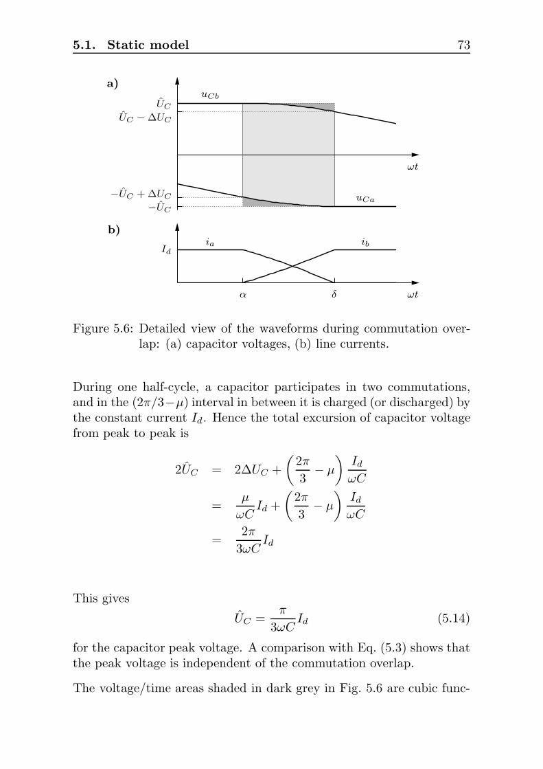
5.1. Static model 73
replacemena)
b)ia ib
Id
UC
UC − ∆UC
−UC
−UC + ∆UC uCa
uCb
ωt
ωtα δ
Figure 5.6: Detailed view of the waveforms during commutation over-lap: (a) capacitor voltages, (b) line currents.
During one half-cycle, a capacitor participates in two commutations,and in the (2π/3−µ) interval in between it is charged (or discharged) bythe constant current Id. Hence the total excursion of capacitor voltagefrom peak to peak is
2UC = 2∆UC +
(
2π
3− µ
)
Id
ωC
=µ
ωCId +
(
2π
3− µ
)
Id
ωC
=2π
3ωCId
This gives
UC =π
3ωCId (5.14)
for the capacitor peak voltage. A comparison with Eq. (5.3) shows thatthe peak voltage is independent of the commutation overlap.
The voltage/time areas shaded in dark grey in Fig. 5.6 are cubic func-

74 Chapter 5. CCC models
tions of time. For symmetry reasons, both are identical and equal to
A =1
6· uC · ∆t3
=1
6· ωId
µC·(µ
ω
)3
=µ2
6ω2CId =
µ2
2πωUC (5.15)
and so the total voltage/time area shaded in light grey is
δ
ω∫
α
ω
(uCb − uCa) dt =2µ
ωUC − 2
µ2
2πωUC
= (2π − µ)µ
πωUC (5.16)
or, in terms of Id,
δ
ω∫
α
ω
(uCb − uCa) dt = (2π − µ)µ
3ω2CId (5.17)
Thus, integrating Eq. (5.11) over the interval of overlap and insertingthe boundary conditions ib(ωt = α) = 0 and ib(ωt = δ) = Id yields
√3Em
2ωLcId(cos α − cos(α + µ)) +
µ
6ω2LcC(2π − µ) = 1 (5.18)
This equation is transcendental and needs to be solved for µ numerically.However, it can be further simplified by approximating cos(α + µ) witha second-order Taylor series:
cos(α + µ) ≈ cosα − µ sin α − µ2
2cosα (5.19)
Eq. (5.18) then reduces to a quadratic equation in µ with the solution
µ ≈√
4X + Y 2 − Y
2X(5.20)

5.1. Static model 75
where
X =
√3Em
2ωLcId
cosα
2− 1
6ω2LcC(5.21)
Y =
√3Em
2ωLcIdsinα +
2π
6ω2LcC(5.22)
Average direct voltage
During the commutation from valve 1 to valve 3, the contribution ofthe capacitors to the direct voltage is given by
∆ud,C =uCa + uCb
2− uCc (5.23)
For symmetry reasons the average of ∆ud,C taken over the commuta-tion interval is again zero. Therefore, Eq. (4.18) derived for the linecommutated converter including overlap can be applied here
Ud = Udi0cosα + cos δ
2(5.24)
It should be noted, however, that the average direct voltage of the CCCwill nonetheless differ from that of the LCC because the capacitorsinfluence the overlap angle µ and, consequently, the extinction angleδ = α + µ.
AC current magnitude and phase
Likewise, as the shape of the line currents is the same as with the LCCincluding overlap, Eqs. (4.19) and (4.21) are also applicable:
I(1) ≈ 2√
3
πId (5.25)
cosϕ ≈ cosα + cos δ
2(5.26)

76 Chapter 5. CCC models
5.2 Dynamic model
As in the analysis of the dynamic behavior of the LCC in the previouschapter, the direct current will now be assumed as ripple free but slowlyvarying at the constant rate Id:
id(t) = id(t0) + Id(t − t0) Id const. (5.27)
The first, immediate consequence of this is again an average voltagedrop ∆Ud,Id
across the commutation reactances. The analysis of thisvoltage drop is identical to that of the LCC. The voltage drop can thusbe modeled by adding an averaged commutation reactance on the dcside as given in Eq. (4.39):
Lc =
(
2 − 3µ
2π
)
Lc
A second consequence of a non-constant direct current is that the peakvalue of the capacitor voltages is no longer directly proportional to thedirect current. For arbitrary line currents the individual voltages inthe capacitors are given by the following state-space equation (note thesigning conventions in Fig. 5.1):
CduC
dt= −i (5.28)
The corresponding differential equation for the fundamental phasors is
Cdu
(1)C
dt= −i(1) − jωC u
(1)C (5.29)
In steady-state operation a relation between the magnitude of the fun-
damental capacitor voltage phasor |u(1)C | and the capacitor peak voltage
UC can be determined by means of Fourier analysis:
UC
|u(1)C |
=π2
6√
3(5.30)
The line current phasor has a magnitude of |i(1)| = 2√
3π id, and so,
by setting the left hand side of Eq. (5.29) to zero, the steady-state
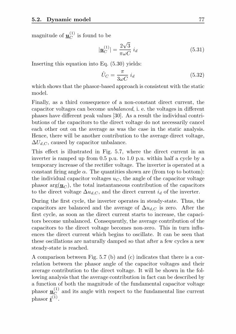
5.2. Dynamic model 77
magnitude of u(1)C is found to be
|u(1)C | =
2√
3
πωCid (5.31)
Inserting this equation into Eq. (5.30) yields:
UC =π
3ωCid (5.32)
which shows that the phasor-based approach is consistent with the staticmodel.
Finally, as a third consequence of a non-constant direct current, thecapacitor voltages can become unbalanced, i. e. the voltages in differentphases have different peak values [30]. As a result the individual contri-butions of the capacitors to the direct voltage do not necessarily canceleach other out on the average as was the case in the static analysis.Hence, there will be another contribution to the average direct voltage,∆Ud,C , caused by capacitor unbalance.
This effect is illustrated in Fig. 5.7, where the direct current in aninverter is ramped up from 0.5 p.u. to 1.0 p.u. within half a cycle by atemporary increase of the rectifier voltage. The inverter is operated at aconstant firing angle α. The quantities shown are (from top to bottom):the individual capacitor voltages uC , the angle of the capacitor voltagephasor arg(uC), the total instantaneous contribution of the capacitorsto the direct voltage ∆ud,C , and the direct current id of the inverter.
During the first cycle, the inverter operates in steady-state. Thus, thecapacitors are balanced and the average of ∆ud,C is zero. After thefirst cycle, as soon as the direct current starts to increase, the capaci-tors become unbalanced. Consequently, the average contribution of thecapacitors to the direct voltage becomes non-zero. This in turn influ-ences the direct current which begins to oscillate. It can be seen thatthese oscillations are naturally damped so that after a few cycles a newsteady-state is reached.
A comparison between Fig. 5.7 (b) and (c) indicates that there is a cor-relation between the phasor angle of the capacitor voltages and theiraverage contribution to the direct voltage. It will be shown in the fol-lowing analysis that the average contribution in fact can be described bya function of both the magnitude of the fundamental capacitor voltage
phasor u(1)C and its angle with respect to the fundamental line current
phasor i(1).
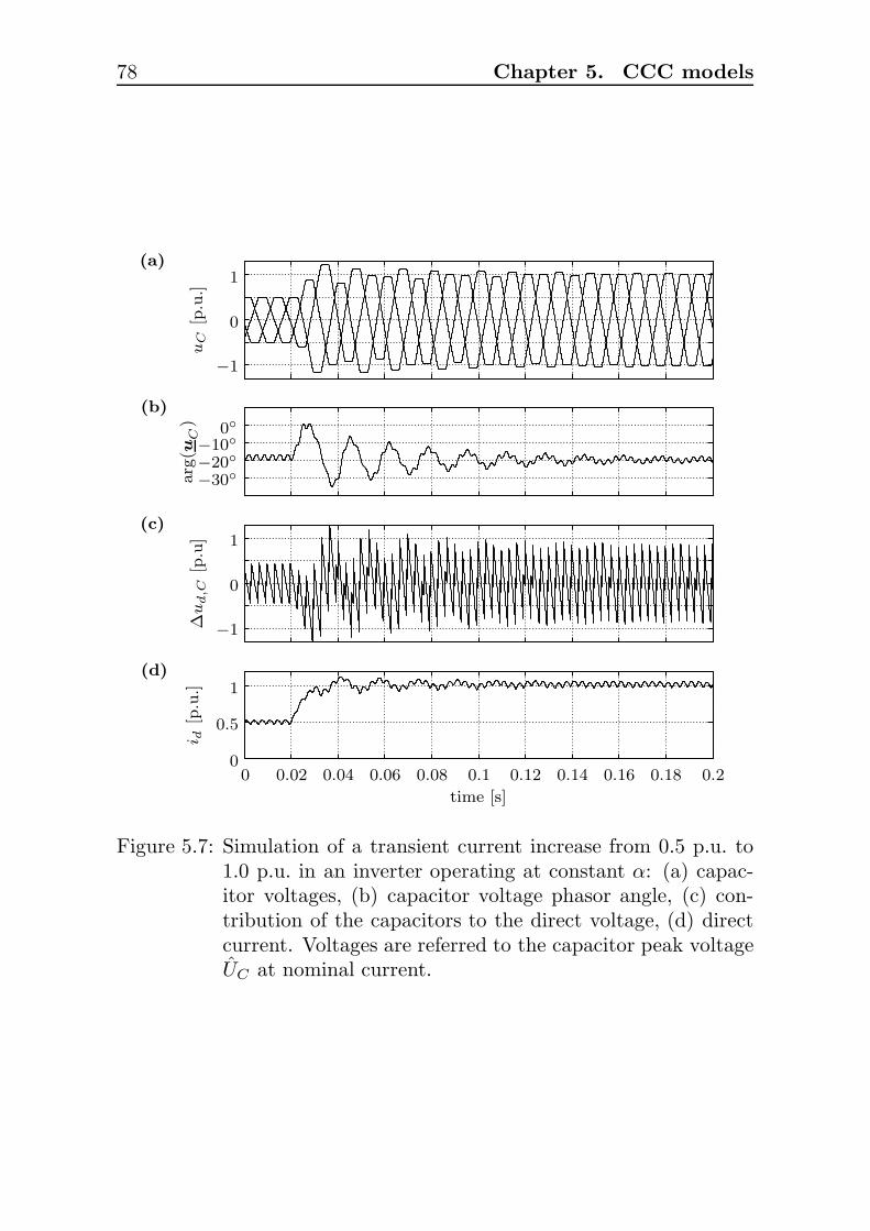
78 Chapter 5. CCC models
(a)
(b)
(c)
(d)
∆u
d,C
[p.u
]arg
(uC
)u
C[p
.u.]
i d[p
.u.]
0
−10
−20
−30
0 0.02 0.04 0.06 0.08 0.1 0.12 0.14 0.16 0.18 0.2
0
0
0
−1
−1
0.5
1
1
1
time [s]
Figure 5.7: Simulation of a transient current increase from 0.5 p.u. to1.0 p.u. in an inverter operating at constant α: (a) capac-itor voltages, (b) capacitor voltage phasor angle, (c) con-tribution of the capacitors to the direct voltage, (d) directcurrent. Voltages are referred to the capacitor peak voltageUC at nominal current.

5.2. Dynamic model 79
5.2.1 Analysis without commutation overlap
Average direct voltage – influence of capacitor unbalance
Consider the interval in which valves 5 and 6 are conducting, i. e. phasec is connected to the positive and phase b to the negative dc terminal ofthe converter. The corresponding equivalent circuit is shown in Fig. 5.8.
In this interval the line currents are
ia = 0
ib = −id (5.33)
ic = id
and so the space-vector of the line current is given by
~i =2
3
(
ia − ib2− ic
2
)
+j√3
(ib − ic)
=2
3
(
0 +id2− id
2
)
+j√3
(−id − id)
= −j2√3id (5.34)
This means that — regardless of whether the direct current is constantor not — the short-time average of the line current space-vector only
ea
eb
ec
ia
ib
ic
Lc
C
uCa
uCb
uCc
ud
id
⑤
⑥
Figure 5.8: Equivalent circuit during conduction of valves 5 and 6. Non-conducting valves not shown.

80 Chapter 5. CCC models
has a negative imaginary part, i.e.:
arg(~i) = −90 (5.35)
The space-vector of the capacitor voltage is given by
~uC =2
3
(
uCa − uCb
2− uCc
2
)
+j√3
(uCb − uCc) (5.36)
Since phase c is connected to the positive and phase b to the negativedc terminal of the converter, the contribution of the capacitors to thedc voltage is
∆ud,C = uCc − uCb (5.37)
A comparison with Eq. (5.36) shows that ∆ud,C is proportional to theimaginary part of the space-vector ~uC :
∆ud,C = −√
3 ℑ(~uC) (5.38)
Thus, the average contribution of the capacitors to the direct voltage inthe conduction interval of valves 5 and 6 is proportional to the imaginarypart of the short-time average of the space-vector in that interval:
∆Ud,C =3
π
ϑ+60
∫
ϑ
∆ud,C d(ωt)
=3
π
ϑ+60
∫
ϑ
−√
3 ℑ(~uC) d(ωt)
= −√
3 ℑ
3
π
ϑ+60
∫
ϑ
~uC d(ωt)
= −√
3 ℑ(
~uC
)
(5.39)
Considering the angle between the line current and capacitor voltagespace-vectors (and their averages), ∆Ud,C can also be interpreted as
the projection of ~uC onto ~i
∆Ud,C =√
3 |~uC | cos(
arg(~uC) − arg(~i))
(5.40)

5.2. Dynamic model 81
which has the advantage of being independent from the considered con-duction interval. This is illustrated in figures 5.9 to 5.12.
The top plots in these figures show the instantaneous values of thecapacitor voltages, their contribution to the direct voltage and the phasecurrents. The coordinate system at the bottom represents the space-vector plane and shows the loci of the instantaneous space-vectors ofcapacitor voltage and line current as well as their short-time averages.The shaded areas highlight the respective conduction intervals.
Fig. 5.9 presents the steady-state operation with balanced capacitorvoltages. Due to the trapezoidal shape of the voltage waveforms thespace-vector ~uC follows the edge of a regular hexagon. The line currentspace-vector~i, on the other hand, only assumes six discrete values owingto the block-shaped current waveforms. During the conduction intervalof valves 5 and 6, ~uC can be seen to cover an area which is symmetricwith respect to the real axis. Accordingly, its average, ~uC , is purely
real and hence encloses a 90 angle with ~i which is purely imaginary asshown above.
In figures 5.10 to 5.12 the capacitor voltages have been unbalancedby adding different dc offsets in the individual phases. As a resultthe waveform of their contribution to the direct voltage ceases to bea regular sawtooth: individual ”teeth” are shifted up or down, and sotheir average is non-zero. With regard to the voltage space-vector, theunbalance causes a shift so that the center of the hexagon lies outsidethe origin of the coordinate system. Due to this shift the angle between
~uC and ~i is larger than 90 in some intervals, and smaller in others. Itcan be seen in the figures that these are the intervals in which ∆ud,C
has a negative resp. positive average.
In order to evaluate Eq. (5.40), it is necessary to express the unknown
average space-vectors ~uC and ~i in terms of the known fundamental
phasors u(1)C and i(1). Since the capacitor voltages and the line currents
have the same fundamental frequency and due to their π/3-periodicity,the angle between their fundamental phasors is the same as the anglebetween the average space-vectors:
arg(~uC) − arg(~i) = arg(u(1)C ) − arg(i(1)) (5.41)
This only leaves the magnitude of |~uC | to be determined.
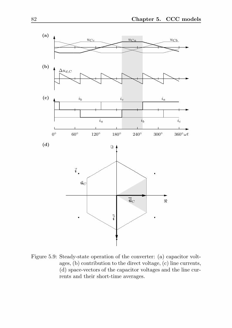
82 Chapter 5. CCC models
(a)
(b)
(c)
(d)
ia
ia
ib
ib
ic
ic
∆ud,C
uCa uCbuCc
0 60 120 180 240 300 360ωt
~uC
~uC
~i
~i
ℜ
ℑ
Figure 5.9: Steady-state operation of the converter: (a) capacitor volt-ages, (b) contribution to the direct voltage, (c) line currents,(d) space-vectors of the capacitor voltages and the line cur-rents and their short-time averages.
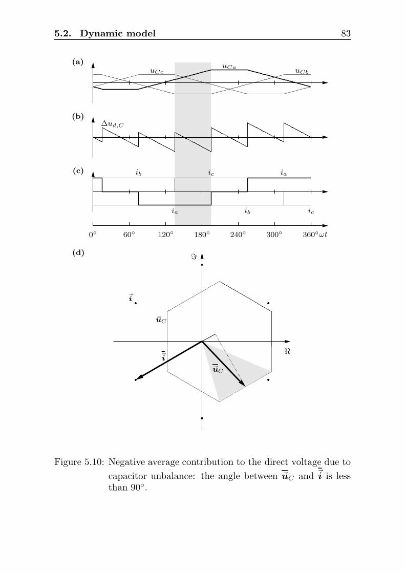
5.2. Dynamic model 83
(a)
(b)
(c)
(d)
ia
ia
ib
ib
ic
ic
∆ud,C
uCa uCbuCc
0 60 120 180 240 300 360ωt
~uC
~uC
~i
~i
ℜ
ℑ
Figure 5.10: Negative average contribution to the direct voltage due to
capacitor unbalance: the angle between ~uC and ~i is lessthan 90.
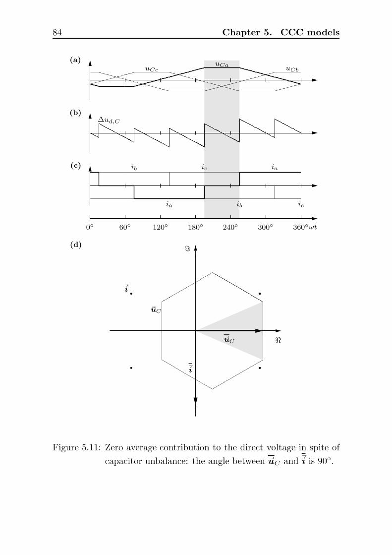
84 Chapter 5. CCC models
(a)
(b)
(c)
(d)
ia
ia
ib
ib
ic
ic
∆ud,C
uCa uCbuCc
0 60 120 180 240 300 360ωt
~uC
~uC
~i
~i
ℜ
ℑ
Figure 5.11: Zero average contribution to the direct voltage in spite of
capacitor unbalance: the angle between ~uC and ~i is 90.

5.2. Dynamic model 85
(a)
(b)
(c)
(d)
ia
ia
ib
ib
ic
ic
∆ud,C
uCa uCbuCc
0 60 120 180 240 300 360ωt
~uC~uC
~i
~i
ℜ
ℑ
Figure 5.12: Positive average contribution to the direct voltage due to
capacitor unbalance: the angle between ~uC and~i is greaterthan 90.

86 Chapter 5. CCC models
In steady-state operation with balanced capacitors, |~uC | is equal to thepeak value UC of the balanced capacitor voltages, as can be seen inFig. 5.9. Together with Eq. (5.30) this gives:
|~uC | =π2
6√
3|u(1)
C | (5.42)
Now Eq. (5.42) will be used as an approximation for the general casewith unbalanced capacitor voltages. Inserting Eqs. (5.42) and (5.41)into Eq. (5.40) finally gives for the average contribution of the capacitorsto the direct voltage:
∆Ud,C =π2
6|u(1)
C | cos(
arg(u(1)C ) − arg(i(1))
)
(5.43)
5.2.2 Analysis including commutation overlap
Fig. 5.13 shows the equivalent converter circuit during commutationfrom valve 6 to valve 2. The mesh equation for the commutation loopis √
3Em sin(ωt) + uCb − uCc = 2Lcdicdt
− LcId (5.44)
A comparison with Eq. (5.36) shows that the difference between thecapacitor voltages uCb − uCc is proportional to the imaginary part of
ea
eb
ec
ia
ib
ic
Lc
C
uCa
uCb
uCc
ud
id
①
②⑥
Figure 5.13: Equivalent CCC circuit during commutation from valve 6to valve 2 (non-conducting valves not shown)
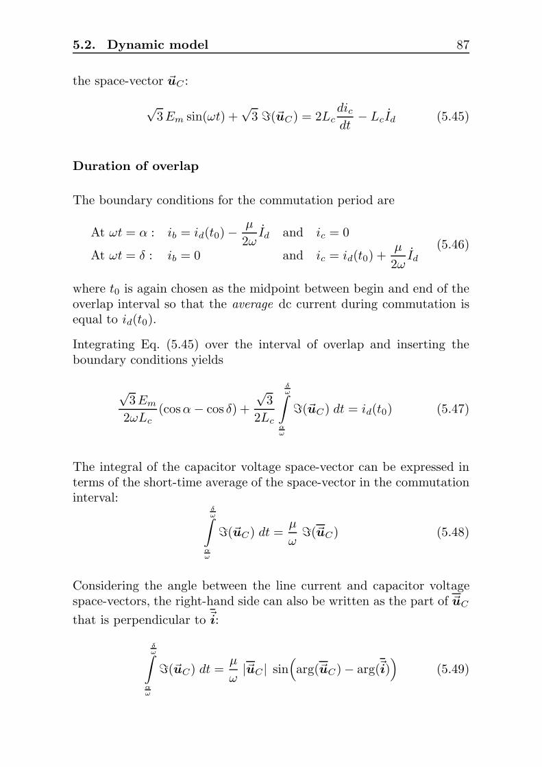
5.2. Dynamic model 87
the space-vector ~uC :
√3Em sin(ωt) +
√3 ℑ(~uC) = 2Lc
dicdt
− LcId (5.45)
Duration of overlap
The boundary conditions for the commutation period are
At ωt = α : ib = id(t0) −µ
2ωId and ic = 0
At ωt = δ : ib = 0 and ic = id(t0) +µ
2ωId
(5.46)
where t0 is again chosen as the midpoint between begin and end of theoverlap interval so that the average dc current during commutation isequal to id(t0).
Integrating Eq. (5.45) over the interval of overlap and inserting theboundary conditions yields
√3Em
2ωLc(cosα − cos δ) +
√3
2Lc
δ
ω∫
α
ω
ℑ(~uC) dt = id(t0) (5.47)
The integral of the capacitor voltage space-vector can be expressed interms of the short-time average of the space-vector in the commutationinterval:
δ
ω∫
α
ω
ℑ(~uC) dt =µ
ωℑ(~uC) (5.48)
Considering the angle between the line current and capacitor voltagespace-vectors, the right-hand side can also be written as the part of ~uC
that is perpendicular to ~i:
δ
ω∫
α
ω
ℑ(~uC) dt =µ
ω|~uC | sin
(
arg(~uC) − arg(~i))
(5.49)

88 Chapter 5. CCC models
where ~i is the short-time average of the current space-vector in thecommutation interval. This gives
√3 Em
2ωLc(cosα − cos δ) +
√3µ
2ωLc|~uC | sin
(
arg(~uC) − arg(~i))
= id(t0)
(5.50)
Figures 5.14 to 5.16 illustrate the connection between ~uC , ~i and theduration of the overlap. Since the line currents now increase or de-crease gradually from zero to the full direct current or vice versa, thelocus of the line current space-vector now is a regular hexagon. Duringcommutation~i moves gradually from one corner to the next; in the non-commutation intervals it remains fixed in one corner. The locus of thecapacitor voltage space-vector now is a hexagon with rounded corners.
The first figure again presents the steady-state operation with balancedcapacitor voltages. It can be seen that during commutation both space-vectors cover areas which are symmetric with respect to the real resp.
imaginary axis. Accordingly, ~uC is purely imaginary and ~i purely real.
In figures 5.15 and 5.16 the capacitor voltages have again been unbal-anced, and thereby the locus of ~uC has shifted into the direction of thepositive real axis. Looking at the same overlap interval as in the steady-state example of the previous figure, one sees that ~uC now is no longerpurely imaginary and its absolute value is larger than before. However,the duration of the overlap has not changed because the imaginary part
of ~uC , i. e. the part perpendicular to ~i, is the same as before. If, onthe other hand, this part decreases, which means that the commutationvoltage is smaller, a commutation will take longer, which is shown inthe last figure.
Figures 5.15 and 5.16 also demonstrate the self-balancing property of theCCC, which is effective even if the direct current is kept constant. Theendpoint of the ~uC locus lies left of the starting point one period earlier,i. e. closer to the steady-state. This is explained by the fact that withunbalanced capacitor voltages the overlap are smaller in some cases andlarger in others. This effectively modifies the peak-to-peak excursionsof the individual capacitor voltages in different overlap intervals untilthe capacitors are again balanced.
The average space-vectors ~uC and ~i in Eq. (5.50) again have to be
expressed in terms of the fundamental phasors u(1)C and i(1), and again

5.2. Dynamic model 89
the angle between the average space-vectors is assumed to be the sameas the angle between the fundamental phasors.
In steady-state during the commutation from valve 5 to valve 6, |~uC | ispurely imaginary as shown in figure 5.14. It can thus be calculated as
|~uC | =ω
µ
δ
ω∫
α
ω
uCb − uCc√3
dt
=1√3
ω
µ
δ
ω∫
α
ω
(uCb − uCc) dt (5.51)
that is, it is proportional to the voltage/time-area between the capacitorvoltages of the incoming and outgoing phase divided by the overlapduration.
In the analysis of the steady-state operation of the CCC it was shownthat this voltage/time-area can be expressed in terms of the capacitorpeak voltage (cf. Eq.(5.16) on page 74). This gives
|~uC | =1√3
ω
µ(2π − µ)
µ
πωUC
=1√3π
(2π − µ)UC (5.52)
Substituting for UC from Eq. (5.30) yields the desired steady-state re-
lation between |~uC | and |u(1)C |:
|~uC | =π
18(2π − µ)|u(1)
C | (5.53)
This relation is again used as an approximation for the general casewith unbalanced capacitor voltages. Inserting Eq. (5.53) into Eq. (5.50)finally yields√
3 Em
2ωLc(cosα− cos δ) +
πµ(2π − µ)
3√
3ωLc
|u(1)C | sin
(
arg(u(1)C ) − arg(i(1))
)
= id
(5.54)This equation has to be solved for µ using an iterative method. Itshould be noted here that the expression arg(i(1)) in Eq. (5.54) also isa function of the overlap angle µ.

90 Chapter 5. CCC models
(a)
(b)
(c)
(d)
ia
ia
ib
ib
ic
ic
∆ud,C
uCa uCbuCc
0 60 120 180 240 300 360ωt
~uC~uC
~i
~i
ℜ
ℑ
Figure 5.14: Steady-state operation of the converter including overlap:(a) capacitor voltages, (b) contribution to the direct volt-age, (c) line currents, (d) space-vectors of the capacitorvoltages and the line currents and their short-time aver-ages.

5.2. Dynamic model 91
(a)
(b)
(c)
(d)
ia
ia
ib
ib
ic
ic
∆ud,C
uCauCbuCc
0 60 120 180 240 300 360ωt
~uC~uC
~i
~i
ℜ
ℑ
Figure 5.15: Influence of capacitor unbalance on the overlap angle (I):
A large perpendicular component of ~uC with respect to ~ileads to a small overlap angle.
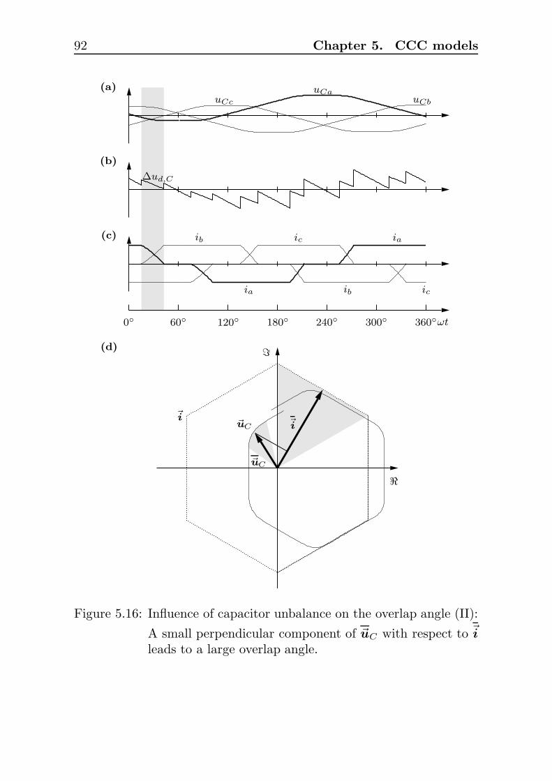
92 Chapter 5. CCC models
(a)
(b)
(c)
(d)
ia
ia
ib
ib
ic
ic
∆ud,C
uCauCbuCc
0 60 120 180 240 300 360ωt
~uC
~uC ~i~i
ℜ
ℑ
Figure 5.16: Influence of capacitor unbalance on the overlap angle (II):
A small perpendicular component of ~uC with respect to ~ileads to a large overlap angle.
5.2. Dynamic model 93
Average direct voltage – influence of capacitor unbalance
As can be seen in Fig. 5.13, the instantaneous contribution of the ca-pacitors to the direct voltage during the commutation from valve 6 tovalve 2 is
∆ud,C = uCa − uCb + uCc
2(5.55)
A comparison with Eq. (5.36) shows that ∆ud,C is proportional to thereal part of the space-vector ~uC :
∆ud,C =3
2ℜ(~uC) (5.56)
The average contribution to the direct voltage during commutation isthus
ω
µ
δ
ω∫
α
ω
∆ud,C dt =3
2ℜ(
~uC
)
(5.57)
or, in terms of the fundamental phasors,
ω
µ
δ
ω∫
α
ω
∆ud,C dt =π
12(2π − µ) |u(1)
C | cos(
arg(u(1)C ) − arg(i(1))
)
(5.58)
The overall average ∆Ud,C is then a weighted sum of the averages of∆ud,C during and outside commutation as given in Eqs. (5.58) and(5.43):
∆Ud,C =
[
π2
6·(
1 − 3µ
π
)
+π
12(2π − µ) · 3µ
π
]
·
|u(1)C | cos
(
arg(u(1)C ) − arg(i(1))
)
=
(
π2
6− µ2
4
)
|u(1)C | cos
(
arg(u(1)C ) − arg(i(1))
)
(5.59)

94 Chapter 5. CCC models
5.3 Model validation
In order to validate the dynamic model derived in this chapter and thestandard converter model proposed in [29] and to assess their accuracy,their behavior is again compared with detailed time-domain simulationsof a test circuit. As in chapter 4 the circuit used is a converter withohmic-inductive load as shown in Fig. 5.17.
ea
eb
ec
ia
ib
ic
Lc
C
uCa
uCb
uCc
ud
id
Uload
Rload
Lload
Figure 5.17: Test circuit – converter with RL load
5.3.1 Model equations
Dynamic model
The dynamic model is a real third-order state-space model. State vari-ables are the direct current id and the (complex) fundamental capacitorvoltage phasor uC (the superscript (1) is omitted here for simplicity).
The mains voltage phasor is taken as e = Em, i. e. it lies on the realaxis. The argument of the fundamental line current phasor is thenarg(i) = −ϕ = − arccos( cos α+cos δ
2 ). This gives for the overlap equation:
√3Em
2ωLc(cosα − cos δ)
+πµ(2π − µ)
3√
3ωLc
|uC | sin(
arg(uC) + arccos(cosα + cos δ
2))
= id
5.3. Model validation 95
After the overlap angle µ has been determined from this equation, theline current phasor i, the average commutation inductance Lc, and thecontribution of the capacitors to the direct voltage ∆Ud,C can be cal-culated:
i =2√
3
πid · e−j arccos( cos α+cos δ
2)
Lc =
(
2 − 3µ
2π
)
Lc
∆Ud,C =
(
π2
6− µ2
4
)
|uC | cos(arg(uC) − arg(i))
The state equations are
d
dtuC = − 1
Ci − jωuC
d
dtid =
1
Lload + Lc
(
Udi0cosα + cos δ
2
+∆Ud,C − Rload · id − Uload
)
Standard model
The standard model is a real first-order state-space model, the onlystate variable being the direct current id. The direct voltage Ud andthe overlap angle µ are determined from the equations summarized inappendix A. The state equation is
d
dtid =
1
Lload + Lc
(
Ud − Rload · id − Uload
)
where Lc is again the average commutation inductance as seen from thedc side:
Lc =
(
2 − 3µ
2π
)
Lc
The standard model is thus enhanced for this comparison by the aver-aged commutation reactance that was derived in chapter 4. Therefore,differences in the dynamic behavior of the dynamic and the static modelcan be attributed only to the modeling of the influence of the commu-tation capacitors.

96 Chapter 5. CCC models
5.3.2 Qualitative comparison
Figure 5.18 shows the behavior of the direct current in an inverter op-erating at a constant firing angle α = 165. The system is initiallyin steady-state, operating at an average direct current of 0.5 p.u. Att = 0.02 s the load (or rectifier) voltage Uload is decreased so as toquickly increase the direct current during ∆t = 0.01 s. After this pe-riod the load voltage is kept constant at a value corresponding to anaverage steady-state direct current of 1.0 p.u.
The instantaneous direct current of the detailed simulation is drawnwith a thin continuous line. A heavy continuous line is used for thedynamic model, and a heavy dashed line for the standard model. Bothmodels display a rather large dc offset in comparison with the detailedsimulation. One possible explanation for this offset is the fact that dueto the influence of the capacitors the ripple of the direct current is muchlarger than in the case of the LCC. Thus, the assumption of a smoothcurrent — which both models have in common — may lead to largererrors.
In Fig. 5.19 these offsets have been compensated by appropriate ad-justments of the load voltage. The dynamic model now very accuratelycaptures the current increase after t = 0.02 s and also the oscillationthat sets in after t = 0.03 s due to the capacitor unbalance. It canbe seen also that this oscillation fades away a bit slower than in thedetailed simulation. An explanation for this is given in the discussionof the following quantitative comparison. The current of the standardmodel, on the other hand, increases much too fast resulting in a largerovershoot. Since the model is only of first order, it cannot reproducethe oscillatory behavior of the CCC.
5.3.3 Quantitative comparison
The accuracy of the models is now assessed by modulating the magni-tude of the mains voltage and the firing angle with varying frequencies.The magnitude and phase angle of the resulting modulation in the di-rect current are measured and compared with a detailed time-domainsimulation. The parameters for the base case haven been taken from[30]: Em = 122.70 kV (corresponding to Udi0 = 203.1 kV), Id = 1.5 kA,

5.3. Model validation 97
0 0.02 0.04 0.06 0.08 0.1 0.12 0.14 0.16 0.18 0.2
0.5
1
i d[p
.u.]
time [s]
Figure 5.18: Simulation of a transient current increase from 0.5 p.u to1.0 p.u. in an inverter operating at a constant firing an-gle α = 165. Thin continuous line: detailed simulation;heavy continuous line: dynamic model; dashed line: stan-dard model.
0 0.02 0.04 0.06 0.08 0.1 0.12 0.14 0.16 0.18 0.2
0.5
1
i d[p
.u.]
time [s]
Figure 5.19: Simulation of transient current increase with correction ofthe dc offset of the phasor-based models.
98 Chapter 5. CCC models
Lc = 29.6 mH, C = 97.6 µF, Rload = 10 Ω, Lload = 0.5 H. The con-verter operates at a firing angle α = 10, the load voltage is chosen soas to obtain nominal direct current.
The simulation results are summarized in figures 5.20 and 5.21. In theplots on the left hand side the mains voltage is modulated; the plotson the right hand side show the results for a modulation of the firingangle. Fig. 5.20 also demonstrates the sensitivity of the errors to a vari-ation of the commutation reactance Lc. In Fig. 5.21 the commutationcapacitance C is varied.
At very low modulation frequencies, both models have a small relativeamplitude error. It is worth noting that the magnitude of the dynamicmodel error is not larger than that of the standard model, in spite ofthe crude assumption of a linear commutation current in Eq. (5.12). Apossible explanation is again that the assumption of a smooth directcurrent common to both models is rather crude to begin with due tothe added direct voltage ripple caused by the capacitors. In relation tothis the extra approximation of Eq. (5.12) may have less weight.
At higher modulation frequencies the amplitude error of the standardmodel steadily increases. For a modulation of the firing angle this in-crease is notably steeper than for a modulation of the mains voltage.The explanation for this is that changing the firing angle immediatelycauses the capacitor voltages to become unbalanced. A change in themains voltage in contrast only has an indirect effect via the direct cur-rent.
In comparison, the magnitude of the amplitude errors of the dynamicmodel is much smaller. For the voltage modulation they become nearlyzero at higher frequencies. This explains the behavior observed inFig. 5.19 for the qualitative comparison: the steep current increase andthe setting-in of the oscillation are accurately captured whereas the (lowfrequency) fading of the oscillation is reproduced less accurately. For thefiring angle modulation, on the other hand, the amplitude errors have aslightly larger magnitude. However, they remain below 10 % with twoexceptions: the low frequency modulation with a large reactance Lc,and the high frequency modulation with a large capacity C.
The parameter variations show that the commutation reactance Lc onlyhas a marginal influence on the amplitude errors and more notably onthe phase errors. In contrast, as expected, the errors are very sensitiveto the capacity C of the commutation capacitors. The capacity directly

5.4. Conclusions 99
influences the magnitude of the capacitor voltages and thus their con-tribution to the direct voltage in case of capacitor unbalance.
A comparison between the phase errors for the modulation of the mainsvoltage and of the firing angle reveals the same phenomenon as with theline commutated converter: the errors for the modulation of α are a sumof the errors for the voltage modulation and a term proportional to themodulation frequency. The slope of the additional phase error was foundto be dependent on the commutation inductance Lc, the commutationcapacity C and the operating point firing angle. A detailed study ofthis phenomenon has to be left to future work.
5.4 Conclusions
In this chapter a dynamic modeling approach for the capacitor commu-tated converter was presented, which takes into account the dynamicsof the additional commutation voltages provided by the capacitors. Theresulting dynamic model is compatible with the phasor-based represen-tation used for transient stability studies. Compared to the standardmodel, the dynamic approach introduces an additional complex statevariable to the system. However, the computational extra costs causedby this additional variable are probably small in relation to the cost ofthe iterative numerical solution of nonlinear equations, which is commonto both models.
The neglect of the capacitor dynamics in the standard static model leadsto substantial errors when studying the dynamic responses of the circuitto different stimuli. These errors are particularly large for dynamicchanges of the firing angle. Therefore, the proposed dynamic modelis expected to have an impact on the design of e. g. the firing anglecontroller of a CCC.

100 Chapter 5. CCC models
00
10
10
20
20
0 05
10
15
0.5
1.0
modula
tion
freq
uen
cy[H
z]m
odula
tion
freq
uen
cy[H
z]
phaseerror[]rel.amplitudeerror[p.u.]
Modula
tion
of
Em
Modula
tion
of
α
Figure 5.20: Simulation results for the quantitative comparison withparameter variations of the commutation inductance Lc
( : 29.6 mH, : 14.8 mH, 2 : 59.2 mH). Continuous line:dynamic model; dashed line: standard model.

5.4. Conclusions 101
00
10
10
20
20
0 05
10
15
0.5
1.0
modula
tion
freq
uen
cy[H
z]m
odula
tion
freq
uen
cy[H
z]
phaseerror[]rel.amplitudeerror[p.u.]
Modula
tion
of
Em
Modula
tion
of
α
Figure 5.21: Simulation results for the quantitative comparison withparameter variations of the commutation capacitance C( : 97.6 µF, : 48.8 µF, 2 : 195.2 µF). Continuous line:dynamic model; dashed line: standard model.


Chapter 6
Case studies
The purpose of developing dynamic models for HVDC converters isto extend the range of interactions that can be studied with them.The standard quasi-static converter model is used for studying electro-mechanical and quasi steady-state interactions ranging from typically0.1 Hz to 2.0 Hz. Control interactions between an HVDC converterwith its controls and an ac system are typically much faster than thisand are normally studied using detailed three-phase simulations [31].
In this chapter the new dynamic models of the LCC and CCC areused to simulate control interactions with modes of about 10 Hz and45 Hz. The results are compared with both a phasor simulation basedon the standard static models and a detailed three-phase simulation.In these studies the ac systems are represented by Thevenin equiva-lent circuits with fixed emf; transformer saturation and other nonlineareffects are neglected. The converters are 12-pulse arrangements usingthree-winding transformers in YY∆-connection. DC-side filters are notmodeled.
In the phasor-based simulations, the ac systems including the ac filtersat the converter buses are modeled using complex state-space systemswith the fundamental positive-sequence phasors as state variables. Thetransformers and their winding ratio are accounted for in the converterequations.
Since the controls have a major part in the interactions they are de-scribed in detail in the first section.
103

104 Chapter 6. Case studies
6.1 HVDC control scheme
Fig. 6.1 shows a basic control scheme for an HVDC converter. Thescheme consists of a voltage dependent (upper) current order limit(VDCOL), a current controller (CC), an extinction angle (or gamma)controller for inverter operation (GC), a phase locked loop (PLL), and afiring pulse generator. Transformer tap changer controls and the mastercontrol are not considered. The individual components are described inthe following subsections.
6.1.1 Voltage dependent current order limit
Under low voltage conditions it is not desirable to maintain the rateddirect current. Therefore, an upper limit is imposed on the currentorder depending on the filtered dc voltage as shown in Fig. 6.2. Theinstantaneous dc voltage is filtered using a first-order lag and then usedto look up the maximum permitted direct current from a table. Thelower value of this limit and the ordered current is used as reference forthe current controllers.
6.1.2 Current controller
Fig. 6.3 shows a typical current controller. The actual direct current isfiltered and its difference to the reference signal is calculated. The cur-rent error is fed to a PI controller, which outputs the firing angle order.The limits may in general be provided by other modules but are setto fixed values here. In an inverter the additional positive signal Imarg
is added to the current error, intentionally causing the PI controller tosaturate at the maximum limit αmax . Therefore, due to the minimum-value selector in the main control scheme, the active controller for aninverter is the gamma controller.
6.1.3 Gamma controller
When operating an HVDC converter as an inverter, care must be takenthat the commutation ends well before the voltage across the outgoingvalve becomes positive again. This is achieved by the gamma controller
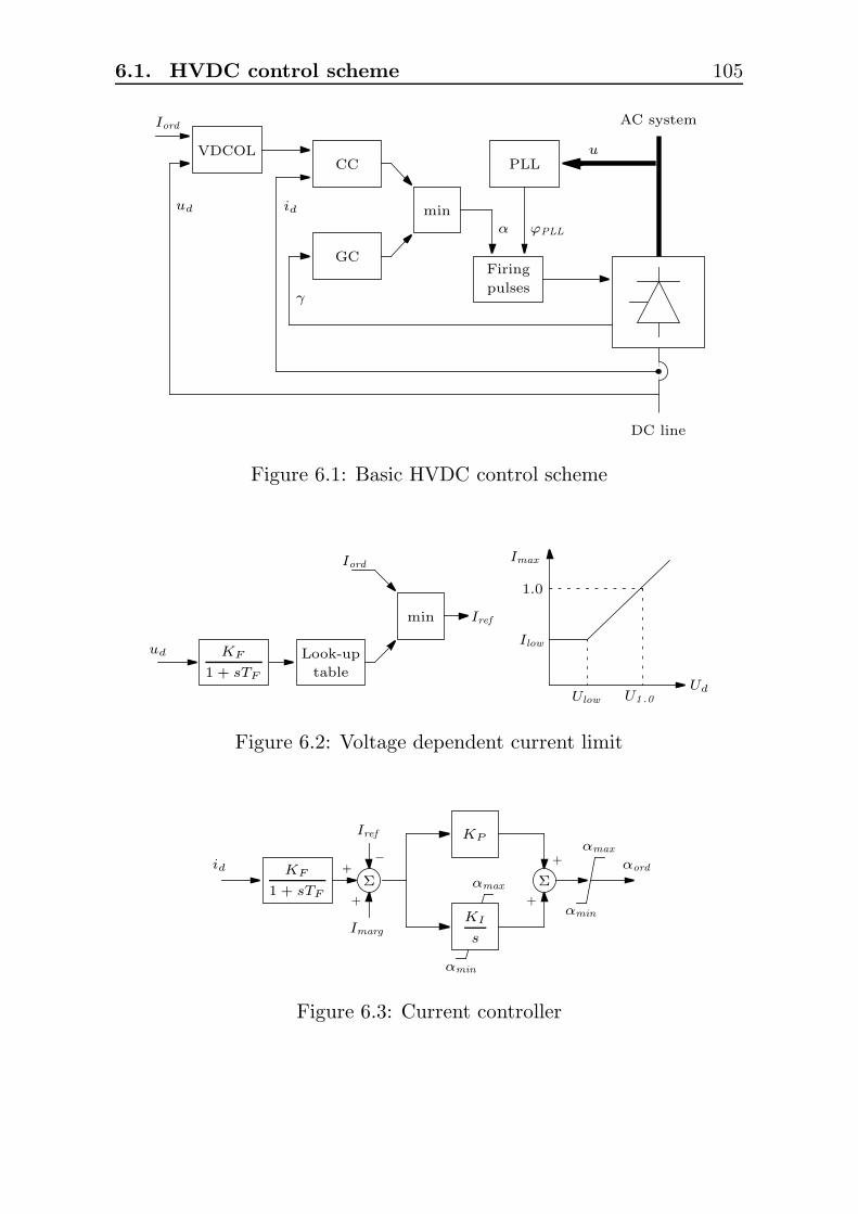
6.1. HVDC control scheme 105
α ϕPLL
Iord
ud id
γ
VDCOLCC
GC
min
PLL
Firing
pulses
u
AC system
DC line
Figure 6.1: Basic HVDC control scheme
KF
1 + sTF
min
Look-up
table
Iord
Iref
Imax
1.0
Ilowud
UdUlow U1.0
Figure 6.2: Voltage dependent current limit
ΣΣ
+
+
+
+
−
id
Iref
Imarg
KF
1 + sTF
KP
KI
s
αord
αmin
αmin
αmax
αmax
Figure 6.3: Current controller

106 Chapter 6. Case studies
shown in Fig. 6.4. The difference between the commutation margin γ,i. e. the delay between the extinction of a valve and the valve voltagebecoming positive, and a fixed set-point is used in a PI controller for thefiring angle order. If the actual margin is larger than necessary, the PIcontroller saturates at the maximum limit αmax . Otherwise, the firingangle is reduced until γ equals the set value.
In the three-phase simulation, the commutation margin can be calcu-lated from the times at which the valve currents and voltages cross thezero-line. This method introduces a certain time delay into the feedbackloop. In the phasor based simulation, the relation α +µ+ γ = π can beused to calculate the margin from the known firing and overlap angles.The above mentioned delay is modeled using a first-order lag with asuitable time constant.
6.1.4 Phase locked loop
A phase locked loop is necessary to provide a stable phase referencesignal to the firing pulse generator, which is not influenced from voltagedistortion in weak ac systems. The PLL used here is based on a space-vector technique. The reference signal is produced by an integratorwhich integrates the current angular frequency signal and is reset at 2π.This reference signal is compared with the instantaneous phase angle ofthe ac voltage and the resulting phase error is used in a PI controller toincrease or decrease the angular frequency of the PLL until the referencesignal is in synchrony with the ac voltage. This is illustrated in the topscheme in Fig. 6.5. The bottom scheme shows the PLL model in thephasor domain, which is demodulated by subtraction of the fundamentalfrequency.
6.1.5 Firing pulse generator
The firing pulses for the individual valves of the converter are generatedby comparing the reference signal from the PLL (suitably shifted foreach valve) with the firing angle order. A valve is fired when the rampsignal crosses αord.
Under stationary conditions, the PLL is in synchrony with the ac voltageand so the actual firing angle will equal the ordered firing angle. How-ever, when the PLL is not exactly locked during network transients, the

6.1. HVDC control scheme 107
ΣΣ
+
++
−
γ
γmin
∆γmaxKP
KI
s
αord
αmin
αmin
αmax
αmax
Figure 6.4: Gamma controller
ΣΣ
ΣΣ
+
++
+
+++
−
−
abc
ϕ
arg u
u
uabc
map to
] − π; π]
map to
] − π; π]
ω0KP
ω0KP
ω0KI
s
ω0KI
s
1
s
1
sw0
resetat 2π
ϕPLL
ϕPLL
Figure 6.5: Phase locked loop for the three-phase model (top) and thephasor model (bottom)
actual and ordered firing angles will differ. In order to account for thisdifference in the phasor-based simulation, the firing angle used in theconverter equations is corrected with the difference between the PLLreference angle and the voltage phasor angle:
α = αord −
ϕPLL − arg(u)
map to ]−π;π]

108 Chapter 6. Case studies
6.2 LCC case study
The electrical system used for studying the conventional line commu-tated converter is based on the first Cigre benchmark model [32] shownin Fig. 6.6. In comparison with the benchmark the inductances on thedc side have been reduced to 98.8 mH. The leakage inductance of thetransformers is lumped on the secondary (i. e. converter) side and with26.8 mH slightly larger than in the benchmark model. The purpose ofthese modifications is to enhance the differences between the static anddynamic LCC models. The controller settings are listed in Table 6.1.
Fig. 6.7 shows the response of the system to a step change of the currentorder from 0.9 p.u. to 1.0 p.u. (i. e. from 1.8 kA to 2.0 kA) at t =0.1 s. Before the change, the commutation margin of the inverter islarger than 15 and so the firing angle equals the upper limit αmax =150. Triggered by the new current order, the rectifier firing angle isimmediately reduced and the direct current increases. This causes thecommutation margin to shrink to which the gamma controller reactsby reducing the inverter firing angle. As the firing angle is reduced,the commutation margin becomes larger again. It can be seen thatthe system has a badly damped mode at roughly 10 Hz but remainsstable and will eventually reach a new steady state. The responses ofthe phasor based models match that of the detailed three-phase modelfairly well. There is a small discrepancy in the commutation marginand the oscillation frequency is somewhat larger. This latter differenceis explained by the first-order lag used to model the time delay in thecalculation of the commutation margin.
Surprisingly, however, the two phasor models do not differ much fromeach other. This is at first glance unexpected because the total dc in-ductance used in the dynamic model is between 192.6 mH and 206 mH(for overlap angles between 0 and 30) and thus about twice as large asthat used in the static model. The explanation here is that the dynam-ics of the direct current are not only governed by the dc inductance.There is also a strong interaction between the direct current and theac bus voltage as the short circuit ratio on both end with 2.5 is ratherlow. Obviously the weak ac systems are the dominating factor for thedynamics of the direct current. Nevertheless, in so far as the small dif-ference between the two phasor based models warrants such a judgment,the response of the dynamic model agrees better with that of the fullthree-phase model.
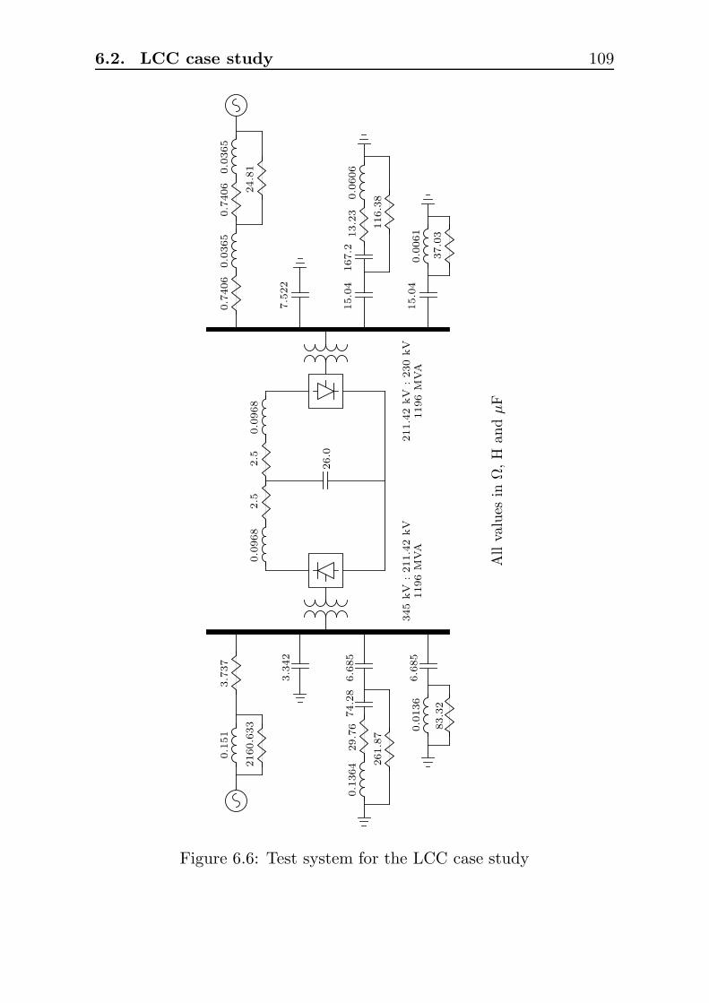
6.2. LCC case study 109
0.1
51
3.7
37
2160.6
33
3.3
42
0.1
364
29.7
674.2
8
6.6
85
6.6
85
261.8
7
0.0
136
83.3
2
0.0
968
0.0
968
2.5
2.5
26.0
0.7
406
0.7
406
0.0
365
0.0
365
24.8
1
7.5
22
15.0
4
15.0
4167.2
13.2
30.0
606
116.3
8
0.0
061
37.0
3
345
kV
:211.4
2kV
1196
MVA
211.4
2kV
:230
kV
1196
MVA
All
valu
esin
Ω,H
and
µF
Figure 6.6: Test system for the LCC case study
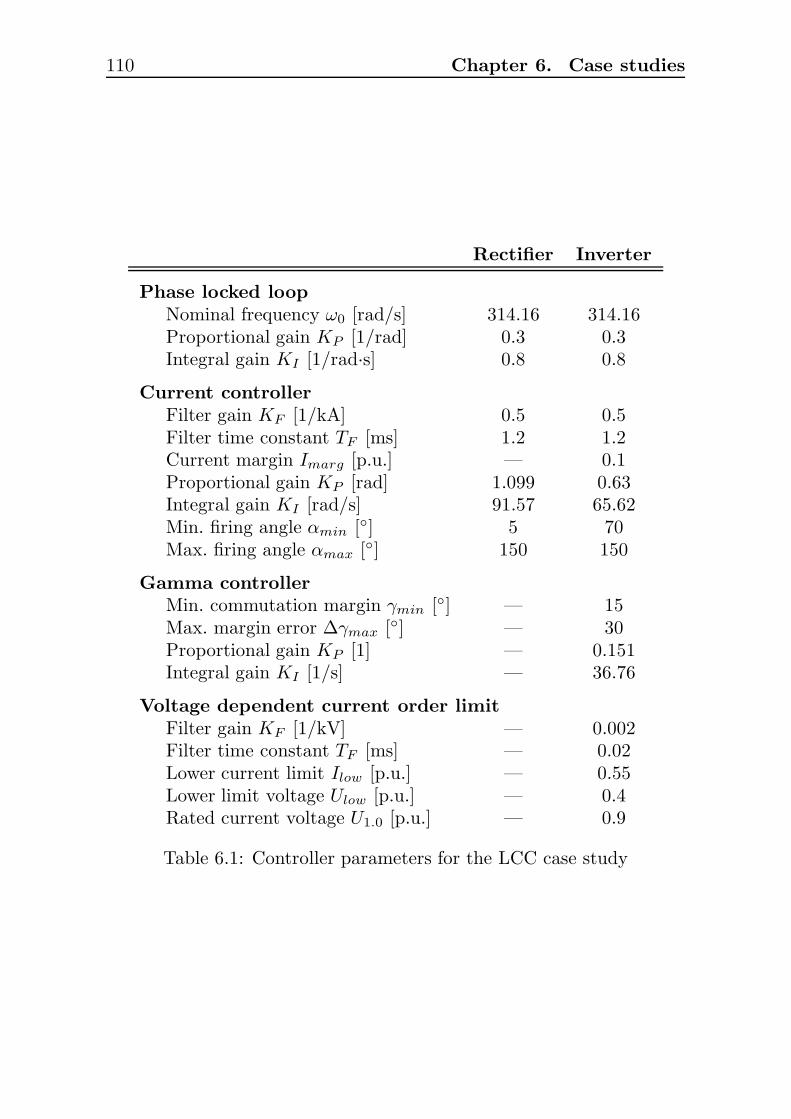
110 Chapter 6. Case studies
Rectifier Inverter
Phase locked loop
Nominal frequency ω0 [rad/s] 314.16 314.16Proportional gain KP [1/rad] 0.3 0.3Integral gain KI [1/rad·s] 0.8 0.8
Current controller
Filter gain KF [1/kA] 0.5 0.5Filter time constant TF [ms] 1.2 1.2Current margin Imarg [p.u.] — 0.1Proportional gain KP [rad] 1.099 0.63Integral gain KI [rad/s] 91.57 65.62Min. firing angle αmin [] 5 70Max. firing angle αmax [] 150 150
Gamma controller
Min. commutation margin γmin [] — 15Max. margin error ∆γmax [] — 30Proportional gain KP [1] — 0.151Integral gain KI [1/s] — 36.76
Voltage dependent current order limit
Filter gain KF [1/kV] — 0.002Filter time constant TF [ms] — 0.02Lower current limit Ilow [p.u.] — 0.55Lower limit voltage Ulow [p.u.] — 0.4Rated current voltage U1.0 [p.u.] — 0.9
Table 6.1: Controller parameters for the LCC case study
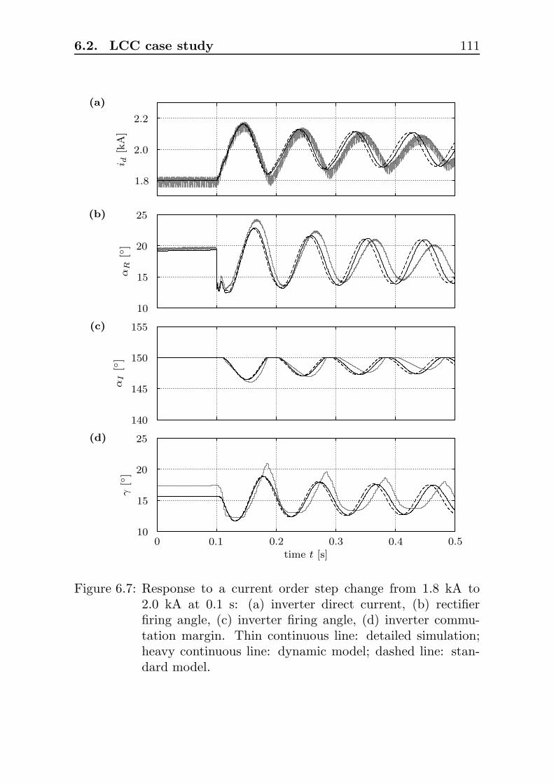
6.2. LCC case study 111
replacemen
(a)
(b)
(c)
(d)
i d[k
A]
αR
[]
αI
[]
γ[
]
time t [s]
10
10
15
15
20
20
25
25
140
145
150
155
1.8
2.0
2.2
0 0.1 0.2 0.3 0.4 0.5
Figure 6.7: Response to a current order step change from 1.8 kA to2.0 kA at 0.1 s: (a) inverter direct current, (b) rectifierfiring angle, (c) inverter firing angle, (d) inverter commu-tation margin. Thin continuous line: detailed simulation;heavy continuous line: dynamic model; dashed line: stan-dard model.
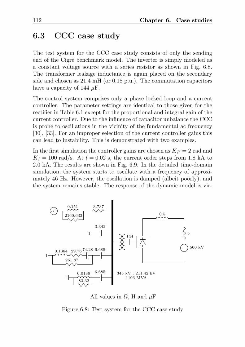
112 Chapter 6. Case studies
6.3 CCC case study
The test system for the CCC case study consists of only the sendingend of the Cigre benchmark model. The inverter is simply modeled asa constant voltage source with a series resistor as shown in Fig. 6.8.The transformer leakage inductance is again placed on the secondaryside and chosen as 21.4 mH (or 0.18 p.u.). The commutation capacitorshave a capacity of 144 µF.
The control system comprises only a phase locked loop and a currentcontroller. The parameter settings are identical to those given for therectifier in Table 6.1 except for the proportional and integral gain of thecurrent controller. Due to the influence of capacitor unbalance the CCCis prone to oscillations in the vicinity of the fundamental ac frequency[30], [33]. For an improper selection of the current controller gains thiscan lead to instability. This is demonstrated with two examples.
In the first simulation the controller gains are chosen as KP = 2 rad andKI = 100 rad/s. At t = 0.02 s, the current order steps from 1.8 kA to2.0 kA. The results are shown in Fig. 6.9. In the detailed time-domainsimulation, the system starts to oscillate with a frequency of approxi-mately 46 Hz. However, the oscillation is damped (albeit poorly), andthe system remains stable. The response of the dynamic model is vir-
0.151 3.737
2160.633
3.342
0.1364 29.7674.28
6.685
6.685
261.87
0.0136
83.32
144
0.5
5
500 kV
345 kV : 211.42 kV1196 MVA
All values in Ω, H and µF
Figure 6.8: Test system for the CCC case study

6.4. Conclusions 113
tually identical, and the plots for the various quantities can be distin-guished from the time-domain solution only due to the ripple which isabsent in the phasor-based solution. With the standard, static model,on the other hand, the oscillation frequency is approximately 66 Hz.The system becomes unstable and the oscillations are limited only bythe minimum rectifier firing angle αmin .
In the second simulation the proportional gain is set to KP = 3 radwhile the integral gain is left at KI = 100 rad/s. The current ordersteps down from 1.8 kA to 1.6 kA. The results are shown in Fig. 6.10.In this case the step change triggers an oscillation of approximately44 Hz which slowly builds up, and hence the system is unstable. Againthe response of the dynamic model is almost identical, although a smalldifference can be noticed in the oscillation frequency. On the otherhand, with the static model the system oscillates with a frequency ofaround 68 Hz. The oscillation is well damped and the system remainsstable.
6.4 Conclusions
In this chapter the standard quasi-static and the dynamic convertermodels were used to study HVDC control interactions. The frequencyrange of these interactions is normally considered outside the scope ofphasor-based models.
The LCC case study revealed a good accordance between the phasor-based simulations and a detailed three-phase simulation for a dominantinteraction frequency of approximately 10 Hz. The difference betweenthe static model and the dynamic model are only marginal in the ex-ample presented here. It should be noted, however, that for differentsystem parameters the difference between the two models might be moreprominent.
In the CCC case study the dominant mode has a frequency of approxi-mately 45 Hz. The simulations showed a nearly perfect match betweenthe detailed three-phase model and the dynamic phasor model. Thestatic model, however, led to completely wrong estimations of the sys-tem stability.
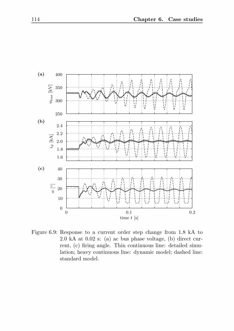
114 Chapter 6. Case studies
(a)
(b)
(c)
i d[k
A]
α[
]ubus
[kV
]
time t [s]
0
10
20
30
40
1.6
1.8
2.0
2.2
2.4
250
300
350
400
0 0.1 0.2
Figure 6.9: Response to a current order step change from 1.8 kA to2.0 kA at 0.02 s: (a) ac bus phase voltage, (b) direct cur-rent, (c) firing angle. Thin continuous line: detailed simu-lation; heavy continuous line: dynamic model; dashed line:standard model.
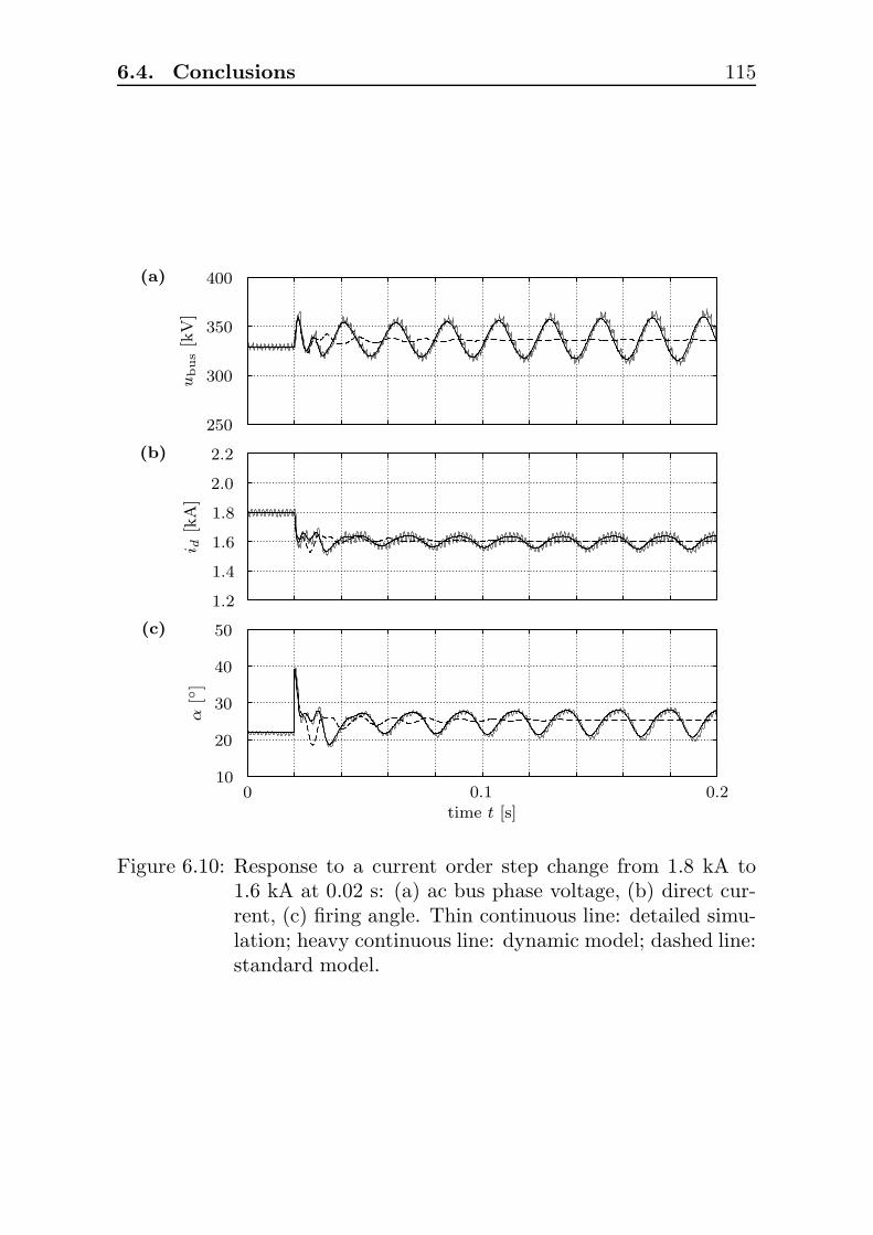
6.4. Conclusions 115
(a)
(b)
(c)
i d[k
A]
α[
]ubus
[kV
]
time t [s]
10
20
30
40
50
1.2
1.4
1.6
1.8
2.0
2.2
250
300
350
400
0 0.1 0.2
Figure 6.10: Response to a current order step change from 1.8 kA to1.6 kA at 0.02 s: (a) ac bus phase voltage, (b) direct cur-rent, (c) firing angle. Thin continuous line: detailed simu-lation; heavy continuous line: dynamic model; dashed line:standard model.

Chapter 7
Summary and
Conclusions
This thesis presents a new dynamic modeling approach for HVDC con-verters based on turn-on devices, i. e. the line commutated converterand the capacitor commutated converter. The standard models forthese converters are based on quasi-static approximations and assumea constant ripple-free direct current. In contrast to this, the dynamicapproach takes into account the dynamics of a (slowly) varying directcurrent. Slow in this context means that the current can be approxi-mated by a linear function during commutation.
The new approach was first applied to the line commutated converter.The resulting model is a natural dynamic extension of the standardmodel and both models are identical for steady-state conditions. Thedynamic model also agrees with the notion of a mean commutationinductance as seen from the dc side as proposed by another author.
The major contribution of this thesis, however, is a new dynamic modelfor the capacitor commutated converter. The dynamic model was devel-oped from a simplified static model and takes into account the influencenot only of a variable direct current but also of unbalanced capacitorvoltages. Compared to the standard model, the dynamic approach in-troduces an additional complex state variable to the system. However,the computational extra costs caused by this additional variable are
117

118 Chapter 7. Summary and Conclusions
probably small in relation to the cost of the iterative numerical solutionof nonlinear equations, which is common to both models.
The converter models were used in two case studies to simulate HVDCcontrol interactions, an application normally considered outside thescope of phasor-based simulations. For the line commutated converter,both the static and the dynamic model agreed fairly well with a detailedsimulation. There was only a marginal difference between the two mod-els. Still, the dynamic model was seen to match the detailed simulationslightly better. For the capacitor commutated converter, on the otherhand, the case study revealed the superiority of the proposed dynamicmodel over the static model. There was a nearly perfect match betweenthe responses of the dynamic model and the detailed simulation. Thestandard model, however, yielded completely different results and ledto a wrong estimation of the system stability.
The proposed dynamic CCC model was thus shown to be valid in afrequency range up to the fundamental ac frequency. It is thereforeconceivable that transient simulation programs incorporating this modelcan replace the normally used detailed time-domain simulators for thetask of studying interactions between a converter pole controller andthe ac system.
Outlook
The set up for the CCC case study was specifically designed so as topoint out the differences between the static and the dynamic model.While care was taken to keep the parameters within a realistic range,the test system does not correspond to a real installation. Studies withreal-world data would therefore be interesting.
The investigations in this thesis were restricted to phasor-based modelsfor use with transient stability programs. Future work could includethe development of a sampled-data model for the capacitor commu-tated converter. With such a model the eigenvalues of the converter atdifferent operating points could be determined and compared with theresponse of the phasor-based model to small step changes.

Appendix A
Analytical solution of
the CCC commutation
equations
The basic equations describing the steady-state operation of the Capac-itor Commutated Converter were first proposed in [29]. The differentialequation equation governing the commutation is solved in the Laplaciandomain using the circuit equivalent shown in Fig. A.1 where Vss is thephase to phase rms value of the voltage on the valve side of the convertertransformer. The voltage source LId denotes the initial condition of fulldirect current in the outgoing phase.
√2Vss
ω cos α+s sin α
s2+ω2
i1(s)
i2(s)
Id/s
sL1/sCLId VC01(s)
VC02(s)
Figure A.1: Laplacian equivalent of the CCC during commutation fromvalve 1 to valve 3
119
120 Appendix A. Solution of the CCC equations
At the beginning of the commutation the two capacitors in the incomingand outgoing phases are charged to
VC01 =π
3ωCId − ∆V1 (A.1)
VC02 = − π
3ωCId (A.2)
where ∆V1 is the change of the capacitor voltage during commutationin the outgoing phase. Correspondingly, the change of the capacitorvoltage in the incoming phase will be denoted ∆V2. The sum of thesetwo values can be shown to equal
∆V1 + ∆V2 =µ
ωCId (A.3)
With reference to Fig. A.1 and using the initial conditions given inEqs. (A.1) and (A.2) the Laplacian of the incoming phase current is
i2(s) =
s3
(
1√2L
VL sin α + Idπ
3ωLC− ∆V1
2L
)
+ s2
(
1√2L
VLω cosα +Id
2LC
)
+ s
(
πω
3LCId − ∆V1ω
2
2L
)
+ω2
2LCId
/(
s(s2 + ω2)(s2 +1
LC)
)
(A.4)
This equation is transformed to the time domain, and the variable ∆V1
is eliminated. The original equations contain a few typing errors whichhave been corrected in [33]. In the solution the following abbreviationsare used:
Udi0 =3√
2
πVss
dxl =3ωL
πdxc =
3
πωCω0 =
√
dxc
dxl
K =1
2
1
dxc − dxlE = −KUdi0 cos(α) − Id
2
F = KUdi0ω0 sin(α) +πω0
3Id − 3ω0
2πdxcω∆V1
β = arctan
(
F
E
)
Y =√
E2 + F 2
(A.5)

121
The average direct voltage Ud, the voltage change ∆V1 and the overlapangle µ are given by the following equations:
Ud = Udi0cos(α + µ) + cos(α)
2+
(
1 − 3µ
4π
)(
2∆V1 −µId
ωC
)
(A.6)
∆V1 =2πdxc
3(
1 + cos(ω0µ))
[
Idµ
2− KUdi0 sin(α + µ)
+1
ω0
(
KUdi0 cos(α) +Id
2
)
sin(ω0µ)
+ KUdi0 sin(α) cos(ω0µ)
+π
3id(
cos(ω0µ) − 1)
]
(A.7)
Id
2− KUdi0 cos(α + µ) − Y cos(ω0µ − β) = 0 (A.8)
Eqs. (A.7) and (A.8) have to be solved for ∆V1 and µ simultaneouslyby an iterative process, such as the Newton-Raphson method. Therelationships between the fundamental ac phasors and the dc variablesare given by
u =π
3√
6Udi0 (A.9)
i =
√6e−jα
π
Id
2
(
1 + e−jµ)
+KUdi0
2
[
e−jα
2(1 − e−j2µ) + jµejα
]
+Y
ω20 − 1
[
e−jµ(
cos(ω0µ − β) + jω0 sin(ω0µ − β))
− cos(β) + jω0 sin(β)
]
(A.10)
where the phase angle of u is taken as a reference.


Bibliography
Books and autographs
[1] E.W. Kimbark, ”Direct Current Transmission, Volume I”, Wiley-Interscience, 1971.
[2] E. Uhlmann, ”Power Transmission by Direct Current”, Springer-Verlag, 1975.
[3] J.G. Kassakian, M.F. Schlecht, G.C. Verghese, ”Principles of PowerElectronics”, Addison-Wesley, 1991.
[4] P. Kundur, ”Power System Stability and Control”, McGraw-Hill,1993.
[5] A. Ekstrom, ”High Power Electronics HVDC and SVC”, EKC –Electric Power Research Center, Stockholm, June 1990.
Articles
[6] T.J. Hammons, D. Woodford, J. Loughtan, M. Chamia, J. Dona-hoe, D. Povh, B. Bisewski, W. Long, ”Role of HVDC transmissionin future energy development”, IEEE Power Engineering Review,Vol. 20, Issue 2, February 2000, pp. 10–25.
[7] B. Andersen, C. Baker, ”A new era in HVDC?”, IEE Review,March 2000, pp. 33–39.
123
124 Bibliography
[8] P. Mattavelli, G.C. Verghese, A.M. Stankovic, ”Phasor Dynamicsof Thyristor-Controlled Series Capacitor Systems”, IEEE Trans.
on Power Systems, Vol. 12, No. 3, August 1997, pp. 1259–1267.
[9] B.K. Perkins, M.R. Iravani, ”Dynamic Modeling of High PowerSwitching Circuits in the dq-frame”, IEEE Trans. on Power Sys-
tems, Vol. 14, No. 2, May 1999, pp. 678–684.
[10] A.M. Stankovic, P. Mattavelli, V. Caliskan, G.C. Verghese, ”Mod-eling and analysis of FACTS devices with dynamic phasors”, IEEE
PES Winter Meeting 2000, Vol. 2, January 2000, pp. 1440–1446.
[11] R.A. Valiquette, ”HVDC Life Extension for Nelson River HVDCSystem”, Proc. IEEE PES Winter Meeting 2002, Vol. 2, January2002, pp. 1059–1062.
[12] N. Holonyak Jr., ”The silicon p-n-p-n switch and controlled rectifier(thyristor)”, IEEE Trans. on Power Electronics, Vol. 16, Issue 1,January 2001, pp. 8–16.
[13] V.F. Lescale, ”Modern HVDC: State of the art and developmenttrends”, Proc. POWERCON ’98, Vol. 1, August 1998, pp. 446–450.
[14] A.M. Gole, M. Meisingset, ”Capacitor commutated convertersfor long-cable HVDC transmission”, Power Engineering Journal,Vol. 16, Issue 3, June 2002, pp. 129–134.
[15] K. Sadek, M. Pereira, D.P. Brandt, A.M. Gole, A. Daneshpooy,”Comparison of alternative HVDC converter topologies”, Proc. 7th
European Conference on Power Electronics and Applications EPE
’97, September 1997, pp. 1266–1271.
[16] F. Busemann, ”Economic Supply of Reactive Power for H.V.D.C.Invertor Stations”, Direct Current, June 1954, pp. 8–15.
[17] U. Axelsson, A. Holm, C. Liljegren, M. Aberg, K. Eriksson,O. Tollerz, ”The Gotland HVDC Light project — experiences fromtrial and commercial operation”, Proc. CIRED 16th International
Conference and Exhibition on Energy Distribution, Vol. 1, June2001.
[18] G. Asplund, Proc. IEEE PES Winter Meeting 2002, Vol. 4, January2002, pp. 2498–2503.
Bibliography 125
[19] F. Schettler, H. Huang, N. Christl, ”HVDC Transmission Sys-tems using Voltage Sourced Converters — Design and Applica-tions”, Proc. IEEE PES Winter Meeting 2002, Vol. 2, January2002, pp. 715–720.
[20] N. Mohan, W.P. Robbins, T.M. Undeland, R. Nilssen, O. Mo,”Simulation of Power Electronic and Motion Control Systems —An Overview”, Proc. IEEE, Vol. 82, No. 8, August 1994, pp. 1287–1302.
[21] R.J. Dirkman, ”The simulation of general circuits containing idealswitches”, Proc. IEEE Power Electronics Specialists Conference,1987, pp. 185–194.
[22] J. Allmeling, W. Hammer, ”PLECS — Piecewise Linear ElectricalCircuit Simulation for Simulink”, Proc. PEDS ’99, Hong Kong,July 1999, pp. 355–360.
[23] D. Bedrosian, J. Vlach, ”Time-Domain Analysis of Networks withInternally Controlled Switches”, IEEE Trans. on Circuits and Sys-
tems — I: Fundamental Theory and Applications, Vol. 39, No. 3,March 1992, pp. 199–212.
[24] S.R. Sanders, J.M. Noworolski, X.Z. Liu, G.C. Verghese, ”Gen-eralized Averaging Method for Power Conversion Circuits”, IEEE
Trans. on Power Electronics, Vol. 6, No. 2, April 1991, pp. 251–259.
[25] G.C. Verghese, M.E. Ebuluk, J.G. Kassakian, ”A General Ap-proach to Sampled-Data Modeling for Power Electronic Circuits”,IEEE Trans. on Power Electronics, Vol. PE-1, No. 2, April 1986,pp. 76–89.
[26] I. Dobson, ”Stability of Ideal Thyristor and Diode Switching Cir-cuits”, IEEE Trans. on Circuits and Systems — I: Fundamental
Theory and Applications, Vol. 42, No. 9, September 1995, pp. 517–529.
[27] S.G. Jalali, R.H. Lasseter, I. Dobson, ”Dynamic Response of aThyristor Controlled Switched Capacitor”, IEEE Trans. on Power
Delivery, Vol. 9, No. 3, July 1994, pp. 1609–1615.
[28] E.V. Persson, ”Calculation of Transfer Functions in Grid-Con-trolled Convertor Systems”, Proc. IEE, Vol. 117, No. 5, May 1970,pp. 989–997.

126 Bibliography
[29] J. Reeve, J.A. Baron, and G.A. Hanley, ”A Technical Assessmentof Artificial Commutation of HVDC Converters with Series Capaci-tors”, IEEE Trans. on Power Apparatus and Systems, Vol. PAS-87,No. 10, October 1968, pp. 1830–1840.
[30] T. Jonsson, P.-E. Bjorklund, ”Capacitor Commutated Convertersfor HVDC”, Proc. Stockholm Power Tech Conference, June 1995,pp. 44–51.
[31] IEEE Working Group Report, ”Report on test systems for ac/dc in-teraction studies”, IEEE Trans. on Power Delivery, Vol. 10, No. 4,October 1995, pp. 2027–2034.
[32] M. Szechtman, T. Weiss, C.V. Thio, ”First benchmark model forHVDC control studies”, Electra, No. 135, April 1991, pp. 54–75.
[33] S. Gomes Jr., N. Martins, T. Jonsson, D. Menzies, R. Ljungqvist,”Modeling Capacitor Commutated Converters in Power SystemStability Studies”, IEEE Trans. on Power Systems, Vol. 17, No. 2,May 2002, pp. 371–377.

Curriculum vitae
13. Dec. 1972 Born in Leverkusen, Germany
1978 – 1982 Primary school: GGS Katterbach,Bergisch Gladbach, Germany
1982 – 1991 Secondary school: Nicolaus CusanusGymnasium, Bergisch Gladbach
1991 – 1997 Study of Electrical Engineeringat RWTH Aachen, Germany
1997 – 2000 Assistant at the Power Electronics andMetrology Laboratory, ETH Zurich,Switzerland
2000 – 2003 Assistant at the Power Systems Laboratory,ETH Zurich; PhD thesis under the supervisionof Prof. Dr. G. Andersson
2002 Co-founder of Plexim GmbH, a spin-off companyof ETH Zurich with the purpose of bringing tomarket the simulation software PLECS which wasdeveloped at the Power Systems Laboratory
127