
Comparative Study of Transformer Topologies for Distributed IPT Systems
Upload
khangminh22Category
view
1download
0
energies
Article
Fault Ride-through Power Electronic Topologies forHybrid Energy Storage Systems
Ramy Georgious 1,* , Jorge Garcia 1 , Mark Sumner 2 , Sarah Saeed 1 and Pablo Garcia 1
1 LEMUR Research Group, Deprtment of Electrical, Electronic, Computers and Systems Engineering,University of Oviedo, 33204 Gijon, Spain; [email protected] (J.G.); [email protected] (S.S.);[email protected] (P.G.)
2 PEMC Research Group, Deprtment of Electrical and Electronic Engineering, University of Nottingham,Nottingham NG7 2RD, UK; [email protected]
* Correspondence: [email protected]† This paper is an extended version of our paper published in 2016 IEEE Energy Conversion Congress and
Exposition (ECCE), Milwaukee, WI, USA, 18–22 September 2016; pp. 1–8.
Received: 4 December 2019; Accepted: 1 January 2020; Published: 4 January 2020
Abstract: This work presents a fault ride-through control scheme for a non-isolated power topologyused in a hybrid energy storage system designed for DC microgrids. The hybrid system is formed bya lithium-ion battery bank and a supercapacitor module, both coordinated to achieve a high-energyand high-power combined storage system. This hybrid system is connected to a DC bus that managesthe power flow of the microgrid. The power topology under consideration is based on the buck-boostbidirectional converter, and it is controlled through a bespoke modulation scheme to obtain low lossesat nominal operation. The operation of the proposed control scheme during a DC bus short-circuitfailure is shown, as well as a modification to the standard control to achieve fault ride-throughcapability once the fault is over. The proposed control provides a protection to the energy storagesystems and the converter itself during the DC bus short-circuit fault. The operation of the converteris developed theoretically, and it has been verified through both simulations and experimentalvalidation on a built prototype.
Keywords: hybrid; energy storage system; buck-boost converter; fault ride-through capability
1. Introduction
Power quality is a major concern in modern power systems, particularly in weak microgrids.The concern for the economic importance of power quality issues has led to the developmentof standards and regulations that define the requirements for equipment and utilities in gridapplications [1,2].
Faults in power systems are one of the major causes of power quality issues. Depending onthe proximity to the system under consideration, the effects vary substantially. From variations inthe voltage and current waveforms parameters (amplitude, frequency and phase) to voltage sagsand, in extreme cases, even to voltage outages. Therefore, a continuous research is being done inturning the electric system and its components to fault-tolerant, to boost and develop a more resilientelectric grid [3].
In particular, the effects of voltage issues in microgrids have attracted a lot of attention from theresearch community. One particular case is when the Point of Common Coupling (PCC) is implementedthough a Power Electronic Converter (PEC), which interfaces the AC grid with a DC bus. From thisDC bus, the microgrid can be supplied in AC, DC or hybrid AC/DC lines [4]. However, the controlof the DC bus voltage at the DC side of the grid interfacing converter is critical to ensure adequate
Energies 2020, 13, 257; doi:10.3390/en13010257 www.mdpi.com/journal/energies

Energies 2020, 13, 257 2 of 19
operation of the system [5]. In an increasing number of applications, Energy Storage Systems (ESSs)are connected to this DC bus through dedicated PECs, aiming to primarily provide the needed energyin case the microgrid operates in islanding mode. Additionally, the ESS balances the energy flowsof the microgrid, accounting for stochastic behavior of distributed generation and loads, thereforedecreasing this random factor in the power consumed from the grid [5]. In any case, the sizing of theaccumulator is carried out considering energy requirements [6].
Upon changes in the microgrid power flows (due variable load profiles or injection of powerfrom distributed generators), or even voltage variations in the grid, imply transient fluctuations in theDC bus. Usually, the ESSs used for energy supply in microgrids present limited dynamics, and thelarge transient power spikes reduce their operating lifetime (e.g., in electrochemical batteries) [6].In these cases, a fast, high-power capability storage system (e.g., Supercapacitor Module (SM)) canbe included, forming a Hybrid Energy Storage System (HESS) [6–8]. With an adequate coordinatedcontrol, these hybrid systems ensure a stiff behavior of the DC bus, decoupling the grid and themicrogrid sides. However, also, they enhance the system reliability by preventing the low-dynamicstorage systems to provide large current spikes, resulting in an increase of the system lifetime [9].HESSs are gaining increased research interest due to their potential benefits in power and energysupport in grid applications [5].
Fault-tolerant HESSs are intended to provide these capabilities but at the same time being ableto deal with fault conditions in the grid. Depending on the magnitude and the distance to the faultlocation, the induced variations on the DC bus might vary substantially [4]. For faults far away fromthe PCC, at distribution or even at transmission levels, the effects within the microgrid are generallylimited to voltage sags that can be solved by the regular operation of the HESS. However, for faultsat distribution level, closer to the PCC, or even at the DC bus inside the microgrid, more severevoltage variations, and even short-circuit currents might appear through the storage subsystem [4].Fault-tolerant topologies prevent these dangerous short-circuit currents to circulate across the storagesubsystem [10]. In addition, fault ride-through is also expected in this case, therefore once the fault isremoved, the system is able to automatically operate properly again in a reasonable amount of time,in accordance to the standards/regulations and the expected behavior of the microgrid [4].
Usually, fault-tolerant topologies make use of additional series switches that interrupt the currentflow if a short-circuit appears at the DC bus [4]. In addition to the increase of the system cost,larger losses appear in regular operation due these series switches. This work proposes a non-isolatedtopology for a fault-tolerant hybrid storage system with fault ride-through capability, suitable for lowto medium power applications in microgrids. Its operation is described, and a commutation scheme isproposed to keep the losses in the range of a simple, non-fault-tolerant solution. The performance ofthe system is validated through both simulations and experimental results on a working prototype of10 kW.
The simplest PEC topology for interfacing two energy storage devices that build up the HESSto a DC microgrid is the direct connection of two parallel bidirectional boost converters to the DCbus [7,11–18]. This scheme is depicted in Figure 1. This is a cost-effective and reliable solution for lowto medium power range applications if galvanic isolation is not required, as the number of elementsand devices is relatively low. The case under study considers the simple parallel connection of twodistinct energy storage devices. One port consists of a lithium-ion Battery Bank (BB), which willprovide a high energy density with slow dynamic response. The other port interfaces to a SM intendedto support a high power density and faster dynamic response [5,11–17,19–23]. Therefore, providedthat the control strategy is managed correctly, the resulting HESS has a better overall performanceas compared to any of the individual systems. This ultimately provides a sustained, high-power,high-dynamic performance of the resulting storage system, also extending the BB lifetime [11,13,21,24].

Energies 2020, 13, 257 3 of 19
Figure 1. Two parallel bidirectional boost converters connected to BB and SM and sharing the DC bus.
In addition to the lack of galvanic isolation, a major disadvantage of this system is its sensitivityto short-circuit faults at the DC bus. If a short-circuit occurs, the current drawn from both the BB andthe SM will increase without control, as the anti-parallel diodes of the upper switches in the legs ofthe boost converters would allow large short-circuit currents as depicted in Figure 2. This will causedamage to the inductors, the storage devices (BB and SM), and the switches themselves [3,4].
This work describes a new design approach for the power topology and control method whichlimits operation during DC side short-circuit faults. Even though the number of switching devicesin the system is increased in order to build the power topology, the proposed control during thehealthy condition achieves an operation without an increase in the losses compared to the two parallelbidirectional boost converters. In addition, the proposed control during the fault condition provides aprotection to the converter and the EESs and afford a fast system recovery procedure so as to chargethe DC bus once the fault has been cleared.
Figure 2. Short-circuit fault at the DC bus of the two bidirectional boost converters.
This paper is organized as follows: Section 2 proposes the buck-boost bidirectional circuit-basedtopology as a DC short-circuit fault-tolerant topology compared to the simplest boost-based solutionshown in Figure 1. The control scheme for the aforementioned boost-based topology is analyzed,in order to establish a starting point in the discussion for the fault-tolerant control adaptation.Then, the control scheme adaptation for the parallel connection buck-boost topologies underconsideration is proposed, both in healthy and fault conditions, respectively. After that, Section 3 showsthe validation of the proposed system through simulations and experimental results to demonstratethe performance of the proposed solution. In this section, a comparison is also included between theoriginal boost converters and the buck-boost solution. Finally, Section 4 summarizes the work doneand discusses future developments.
2. Fault-Tolerant Topologies
The solution to the DC bus fault behavior of the boost-based topology is the connection of a deviceable to interrupt, or at least limit, the fault currents flowing through the storage units. One option isto connect switches in series with the storage units and the inductors of the converters (see Figure 3).

Energies 2020, 13, 257 4 of 19
These switches can be opened during fault conditions to prevent the BB and SM short-circuit currents.In addition, to allow a discharge path for any current flowing through the inductors once the seriesswitches are open, additional free-wheeling switches for each leg are required. Otherwise, a voltagespike will occur, causing arcing or even destruction of the switches. This yields to a final configurationof two parallel bidirectional buck-boost converters [25,26], as shown in Figure 4. This topology has notbeen analyzed for this particular challenge, i.e., fault tolerance in HESS.
Figure 3. Two parallel bidirectional boost converters with a switch in series between the storage devicesand inductors.
Figure 4. Two parallel bidirectional buck-boost converters connected to BB and SM and sharing theDC bus.
Buck-boost converters can operate either as step-up or step-down voltage interface. In the systemunder consideration, configured as in Figure 4, the BB voltage (VBB) and the SM voltage (VSM) ratingsare less than the DC bus voltage (VDC) and therefore the buck-boost converters will always operate asstep-up converter. The main feature discussed in this work is the operation under fault condition ofthe HESS based on the buck-boost solution. Provided that a suitable control strategy is implemented,the proposed solution enables for a swift system reset once the fault is cleared. A proposal for such afault ride-through feature will also be demonstrated in the following sections.
It can be seen that the inclusion of the short-circuit fault-tolerant features in the converter addsfour more switches compared to the original topology (Figure 1), therefore resulting in higher cost andsize than in the initial case. However, as it will be demonstrated in the following sections, by using aproper control, even though the number of switches has increased, the losses of the two topologies canbe made very similar.

Energies 2020, 13, 257 5 of 19
2.1. Analysis of the Boost Topology Based Control
The case under consideration is a microgrid suitable to operate in islanding mode, with a HESSconnected to the DC bus at the PCC, as depicted in Figure 4. In these conditions, a cascaded loopapproach is used for the control of the power flows in the system. Both the BB and the SM convertersare indeed controlled. The main goal of the control of the BB converter is to maintain the DC busvoltage constant, while the aim of the control of the SM converter is to provide or absorb transientpower during load variations. The control strategy is implemented through three control loops: oneouter voltage control loop that controls the DC bus voltage, plus two inner current loops in order tocontrol the current flowing through the BB and SM inductors [12,13,16,22,27,28], as shown in Figure 5.
-
+
_.. +
-
-
+
_.. +
-
+
+
+
-
_..
_..
+
-
+
-
-+
Figure 5. Control of the two parallel bidirectional boost converters to maintain the DC bus voltageconstant (BB converter) and provide or absorb transient power during load variations (SM converter).
The outer voltage control loop is a Proportional-Integral (PI) controller to maintain the measuredDC bus voltage (VDC_meas) equal to the reference value (VDC_re f ). Then, ESS power reference (PESS_re f )is calculated from the control action of the voltage control loop ( ICDC ) and the feed-forward term(IODC_meas ) to improve the recovery of the DC bus due to load variations. The limits of the control actionare obtained as follows [29]:
ICDC_min = IBB_min + ISM_min + IN_min −PRN_max
VDC_re f(1)
ICDC_max = IBB_max + ISM_max + IN_max −PRN_min
VDC_re f(2)
where:
• ICDC_min and ICDC_max are the minimum and maximum current limits of the DC bus current in Amps,• IBB_min and IBB_max are the minimum and maximum currents of the BB in Amps,• ISM_min and ISM_max are the minimum and maximum currents of the SM in Amps,• IN_min and IN_min are the minimum and maximum currents delivered by the rest of the microgrid
in Amps,• VDC_re f is the reference DC bus voltage in Volts,• PRN_min and PRN_max are the minimum and maximum load powers in Watts.

Energies 2020, 13, 257 6 of 19
The minimum BB and SM currents are the maximum BB and SM charging currents; however,the maximum BB and SM currents are the maximum BB and SM discharging currents. Then, the SMreference power (PSM_re f ) is calculated as the difference between the references for the ESS and BBpower values (PESS_re f and PBB_re f , respectively). A limiter is used to ensure that SM power limitsare not exceeded. The BB power reference (PBB_re f ) is calculated by using a Low Pass Filter (LPF) toensure that the SM is providing or absorbing the peak transient power during load variations [28].Also another limiter is used here, to ensure that the SM provides (or absorbs) the excess power that BBcannot provide (or absorb) during steady state. The power references are calculated according to thefollowing equations [28,30]:
PESS_re f = ( ICDC + IODC_meas)VDC_meas (3)
PBB_re f =1
1 + TBBsPESS_re f (4)
PSM_re f = PESS_re f − PBB_re f (5)
where:
• PESS_re f , PBB_re f and PSM_re f are the reference powers of the ESS, BB and SM, respectively, inWatts,
• ICDC is the current in the DC bus (control action of the voltage controller) in Amps,• IODC_meas is the measured output current of the two converters in Amps,• VDC_meas is the measured DC bus voltage in Volts,• TBB is the time constant of the LPF in Secs,• s is the Laplace complex variable s = σ + jωd.
The current references of the BB and SM are obtained by dividing their power references by thecorresponding voltage. The bandwidth of the controller for the current in L2 (inductor in SM converter)(IL2) is faster than the bandwidth of the controller for inductor L1 (BB converter). This control schemeconsiders the inductors’ voltages, VL1 and VL2 in Figure 1 to be the control actions at the output of thecurrent regulators. The limits for the inductor voltages can then be calculated as [29]:
VL1_min = VBB_meas − VDC_re f (6)
VL1_max = VBB_meas (7)
VL2_min = VSM_meas − VDC_re f (8)
VL2_max = VSM_meas (9)
where:
• VL1_min, VL1_max, VL2_min and VL2_max are the minimum and maximum inductor voltages for theBB and SM boost converters, respectively, in Volts,
• VBB_meas and VSM_meas are the measured storage device voltages in Volts.
Therefore an adaptation between these control actions and the applied duty cycles in bothconverters, d1 and d3, is implemented in the control (Duty Cycle Calculation blocks in Figure 5).
d1 =VBB_meas − VL1
VDC_meas(10)
d3 =VSM_meas − VL2
VDC_meas(11)
where:
• d1 and d3 are the duty ratios of the BB and SM converters, respectively,

Energies 2020, 13, 257 7 of 19
• VL1 and VL2 are the inductor voltages (control action of the current controller) for the BB and SMboost converters, respectively, in Volts.
2.2. Fault-Tolerant Converter Control Strategy for Normal Operation
Some modifications in the previous control are required in order to calculate the duty cycle fromthe output of the regulator for the buck-boost-based solution (Duty Cycles Calculation block), as shownin Figure 6. With this direct approach, the diagonal switches (S2 and S3) and (S6 and S7) will commutatewith the values of the duty cycles for the BB and SM converters respectively, while the other diagonalswitches (S1 and S4) and (S5 and S8) will switch in a complementary scheme.
+
+
+
-
_..
_..
-+
+
_..
+-
+-
+ +
_..
+
-
+
-
-
-
+
+ +
Figure 6. Control of two parallel bidirectional buck-boost converters with the same carrier to maintainthe DC bus voltage constant (BB converter) and provide or absorb transient power during loadvariations (SM converter).
The expressions to calculate the limits for the inductor voltages in this case are as follows:
VL1_min = −VDC_re f (12)
VL1_max = VBB_meas (13)
VL2_min = −VDC_re f (14)
VL2_max = VSM_meas (15)
The same procedure is implemented to calculate the duty ratio for both the BB and SM converters:
d2 = d3 =VBB_meas − VL1
VBB_meas + VDC_meas(16)
d6 = d7 =VSM_meas − VL2
VSM_meas + VDC_meas(17)
As discussed, all the switches are commutating at High Frequency (HF). This approach, though,will increase the switching losses and therefore the total efficiency of the system will drop. In orderto maintain the efficiency, the proposed modifications in the control strategy makes use of twoindependent modes of operation for each converter during the healthy condition (Normal operation).These modes are Buck mode and Boost mode. This scheme aims to decrease the number ofcommutating switches in each converter, in order to consequently decrease the switching losses [31–33].
Energies 2020, 13, 257 8 of 19
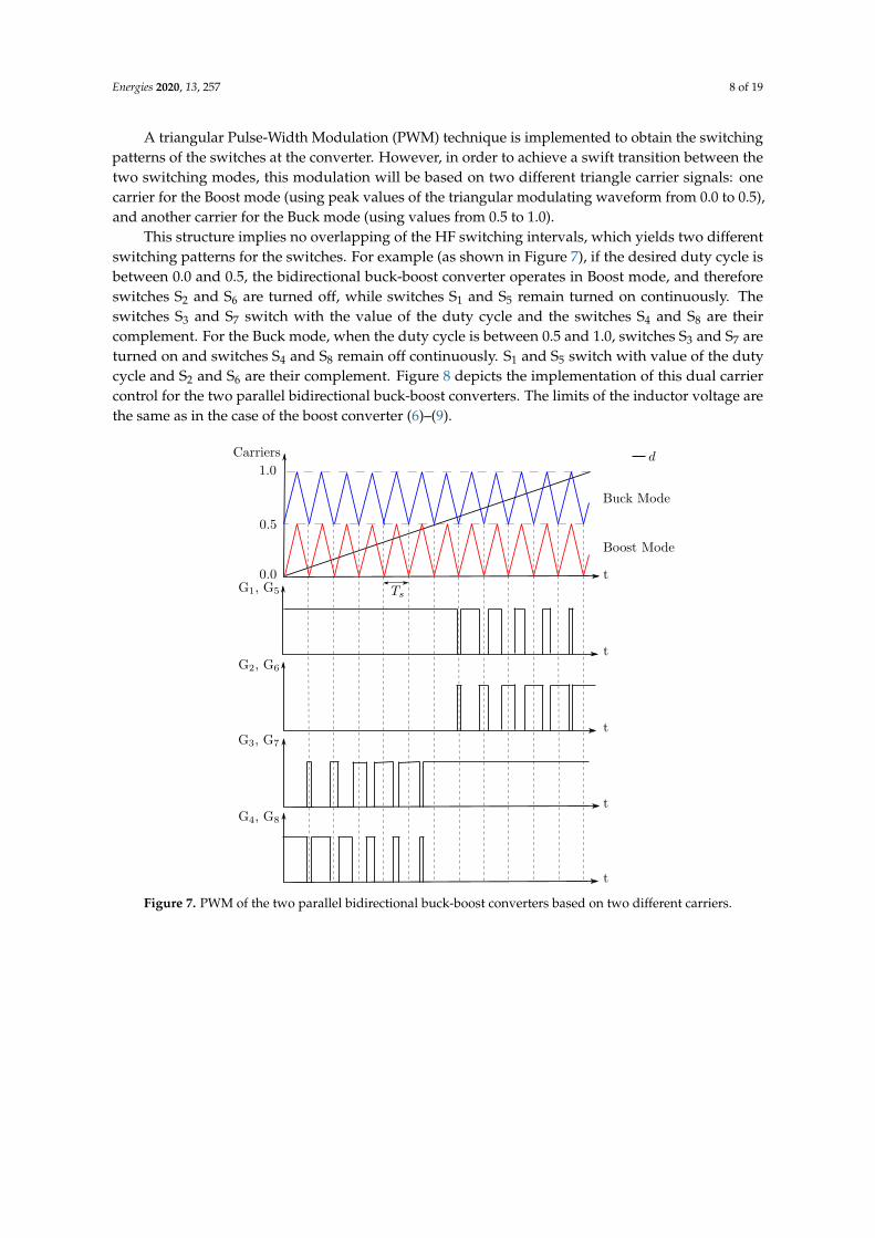
A triangular Pulse-Width Modulation (PWM) technique is implemented to obtain the switchingpatterns of the switches at the converter. However, in order to achieve a swift transition between thetwo switching modes, this modulation will be based on two different triangle carrier signals: onecarrier for the Boost mode (using peak values of the triangular modulating waveform from 0.0 to 0.5),and another carrier for the Buck mode (using values from 0.5 to 1.0).
This structure implies no overlapping of the HF switching intervals, which yields two differentswitching patterns for the switches. For example (as shown in Figure 7), if the desired duty cycle isbetween 0.0 and 0.5, the bidirectional buck-boost converter operates in Boost mode, and thereforeswitches S2 and S6 are turned off, while switches S1 and S5 remain turned on continuously. Theswitches S3 and S7 switch with the value of the duty cycle and the switches S4 and S8 are theircomplement. For the Buck mode, when the duty cycle is between 0.5 and 1.0, switches S3 and S7 areturned on and switches S4 and S8 remain off continuously. S1 and S5 switch with value of the dutycycle and S2 and S6 are their complement. Figure 8 depicts the implementation of this dual carriercontrol for the two parallel bidirectional buck-boost converters. The limits of the inductor voltage arethe same as in the case of the boost converter (6)–(9).
Figure 7. PWM of the two parallel bidirectional buck-boost converters based on two different carriers.

Energies 2020, 13, 257 9 of 19
+
+
+
-
_..
_..
-+
+
_..
+ +
_..
+
-
+
-
-
-
+
+ +
+-
+-
+-
+-
Figure 8. Control of the two parallel bidirectional buck-boost converters with two different carriers tomaintain the DC bus voltage constant (BB converter) and provide or absorb transient power duringload variations (SM converter).
2.3. Fault-Tolerant Converter Control Strategy under DC-Link Fault Operation
The most critical short-circuit fault types in DC microgrids are either short-circuit between positiveand negative bus bars, or a short-circuit between any bus bar and ground [34]. In the first approach ofthe proposed control scheme, once a DC bus short-circuit fault is detected (for instance by detecting aDC bus voltage below a threshold level), all the switches of the storage converters will be turned off.Therefore the storage devices are instantly disconnected from the DC bus while allowing a dischargepath for the inductors at the converters through the anti-parallel diodes of the switches. After theinductances are discharged, no more energy is interchanged between the HESS and the DC bus.However, this control scheme does not have ride-through capability, and therefore even if the faultis removed, the system by itself has no ability of returning to the initial operation mode, unless thecontrol is reset manually and the DC bus is charged externally. After the DC bus is back at rated values,the control scheme works again, and the HESS will remain to support the microgrid normal operation.This scheme is shown in Figure 9.
Figure 9. Control scheme including the fault detection block and the pulse disabling.
However, by making a relatively simple modification to the control scheme, the converter canstill operate in a controlled manner under fault conditions and can resume normal healthy operationonce the fault is over. This modification is introduced in Figure 10.

Energies 2020, 13, 257 10 of 19
+
-+-+
_..
-
Figure 10. Proposed control of the two parallel bidirectional buck-boost converters during the DC bus fault.
The fault sequence operation of this control scheme is outlined in Figure 11. The DC bus faultoccurs at t f . Then, the fault ride-through capability of the proposed strategy is achieved by providinga small safe current reference (IL1_ f _re f ) value for the BB converter only under DC bus short-circuit.While the DC bus fault is still present, the DC bus voltage remains nearly zero. However, this smallcurrent enables the DC bus capacitance to charge linearly once the fault is cleared at tc. Once athreshold value is reached at tn, the system gets back to the normal operation scheme, and the standardcontrol takes the system back to the steady state at tss. This current reference value must be low enoughas not to discharge the BB in a reasonable time frame. On the other side, this value must be largeenough as to allow a fast detection of the fault clearance condition. Ultimately, this reference value is afunction of the DC bus voltage rating and the DC bus capacitance.
Figure 11. Performance of the fault ride-through control sequence.
The current reference is automatically implemented considering that the voltage across theinductor is limited, and therefore the duty cycle for BB is given by (18) to (20). It also must be noticedthat if the fault is permanent, the control is designed to operate for a specific time and then the switchesof the BB converters will be turned off in order to decrease the power dissipated from the BB. Anotheradvantage is that this control can be used to charge the DC bus at system start-up. During fault andfault ride-through intervals, the switches of the SM converter are turned off, and SM current is null.
VL1_min = 0 (18)
VL1_max = VBB_meas (19)
d2 = d3 =VBB_meas − VL1
VBB_meas(20)

Energies 2020, 13, 257 11 of 19
3. System Parameters and Validation through Simulation and Experimental Results
This section covers the main specifications of the system parameters, the design of the controlparameters as well as the validation achieved through simulations of the system performance anda related experimental setup. Simulations of the full system operation have been carried out withMATLAB/SIMULINK/PLECS.
3.1. Main Operating Parameters
Although the conclusions from the prior discussion are valid in general, the validation of suchconclusions is demonstrated in a specific laboratory setup that is described in Table 1. The specificcontrol algorithms have been designed and tuned for this particular setup. Once the setup and thecontrol algorithms are defined, then the system performance can be validated through the analysis ofboth simulations and experimental results.
Table 1. Parameters of the converters.
Parameter Symbol Value Units
Nominal BB voltage VBB 300 VNominal SM voltage VSM 96 VCapacitance of the SM CSM 165 FDC bus voltage VDC 500 VCapacitance of the DC bus CDC 470 µFMaximum load power PRN_max 2 kWInductance of the inductors L1 , L2 21 mHResistance of the inductors R1 , R2 0.3 Ω
3.2. Design of the Regulators in the Control Loops
The control scheme has three PI controllers in the outer DC bus voltage control loop and the twoinner current control loops for BB and SM. Considering the ideal form of PI controller which is tunedby zero-pole cancellation, the transfer function is given by:
C(s) = Kp
(1 +
1sTi
)(21)
where:
• C(s) is the transfer function of the PI controller,• Kp is the proportional gain,• Ti is the integral time constant.
Current controllers have been tuned by zero-pole cancellation, whereas voltage controller is tunedby loop-shaping techniques.
KpBB = 2πBwBBL1 (22)
TiBB =L1
R1(23)
KpSM = 2πBwSML2 (24)
TiSM =L2
R2(25)
The control parameters of the converters are listed in Table 2. Taking into account that thebandwidth of the SM current PI controller (BwSM) is faster that the bandwidth of the BB current PIcontroller (BwBB). Both bandwidths are faster than the bandwidth of voltage PI controller (Bwv).
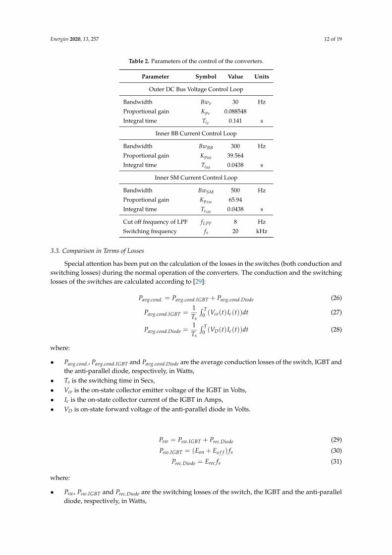
Energies 2020, 13, 257 12 of 19
Table 2. Parameters of the control of the converters.
Parameter Symbol Value Units
Outer DC Bus Voltage Control Loop
Bandwidth Bwv 30 Hz
Proportional gain KpV 0.088548
Integral time TiV 0.141 s
Inner BB Current Control Loop
Bandwidth BwBB 300 Hz
Proportional gain KpBB 39.564
Integral time TiBB 0.0438 s
Inner SM Current Control Loop
Bandwidth BwSM 500 Hz
Proportional gain KpSM 65.94
Integral time TiSM 0.0438 s
Cut off frequency of LPF fLPF 8 Hz
Switching frequency fs 20 kHz
3.3. Comparison in Terms of Losses
Special attention has been put on the calculation of the losses in the switches (both conduction andswitching losses) during the normal operation of the converters. The conduction and the switchinglosses of the switches are calculated according to [29]:
Pavg.cond. = Pavg.cond.IGBT + Pavg.cond.Diode (26)
Pavg.cond.IGBT =1Ts
∫ T0 (Vce(t)Ic(t))dt (27)
Pavg.cond.Diode =1Ts
∫ T0 (VD(t)Ic(t))dt (28)
where:
• Pavg.cond., Pavg.cond.IGBT and Pavg.cond.Diode are the average conduction losses of the switch, IGBT andthe anti-parallel diode, respectively, in Watts,
• Ts is the switching time in Secs,• Vce is the on-state collector emitter voltage of the IGBT in Volts,• Ic is the on-state collector current of the IGBT in Amps,• VD is on-state forward voltage of the anti-parallel diode in Volts.
Psw = Psw.IGBT + Prec.Diode (29)
Psw.IGBT = (Eon + Eo f f ) fs (30)
Prec.Diode = Erec fs (31)
where:
• Psw, Psw.IGBT and Prec.Diode are the switching losses of the switch, the IGBT and the anti-paralleldiode, respectively, in Watts,

Energies 2020, 13, 257 13 of 19
• Eon and Eo f f are the energy loss at IGBT turn on and turn off, respectively, in Joules,• fs is the switching frequency in Hz,• Erec is the energy loss of the reverse recovery of the anti-parallel diode in Joules.
Once these calculations are considered, a comparison between the original boost topology andthe new buck-boost topology with both switching schemes (single and dual carrier) has been carriedout in PLECS by using the datasheet of the IGBTs (2MBI200HH-120-50 from Fuji Electric) based onthe equations explained before. As can be seen from Table 3, the overall losses (both switching andconduction losses) using the fault-tolerant topology with the standard switching pattern are higherthan in the original boost-based solution. Still looking at Table 3, it can be noticed how the switchinglosses at the fault-tolerant topology using the proposed dual carrier control scheme are almost equalto the ones at the original boost-based topology converter. It can also be seen how the conductionlosses are higher in the former case, given that S1 and S5 are continuously turned on. Therefore, it canbe concluded that the total losses at the fault-tolerant solution with the dual carrier scheme are quitesimilar to the original boost converter case.
Table 3. The losses in the topologies.
Topology Conduction Losses (W) Switching Losses (W) Total losses (W)
Boost 10.67 49.93 60.61Buck-Boost (original switching mode) 29.7 96 125.7Buck-Boost (proposed control mode) 22.2 49.93 72.13
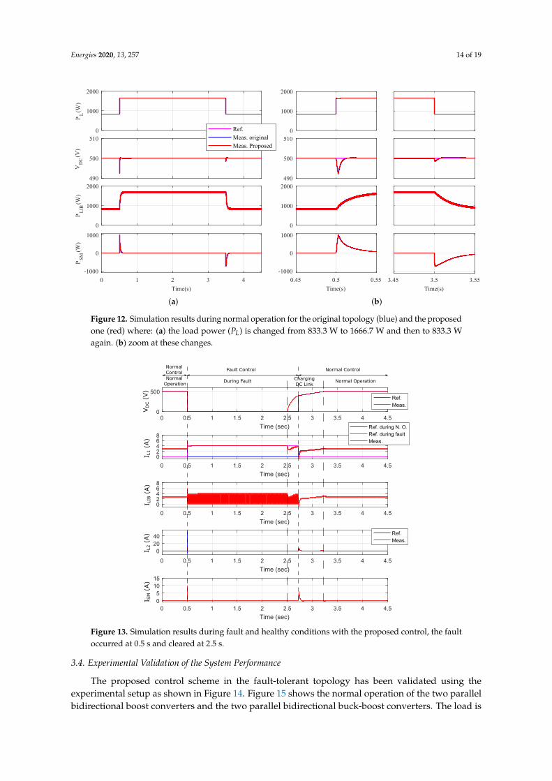
Figure 12 shows the operation of both the boost topology and the buck-boost solution with thedual carrier scheme, under healthy conditions. The figure shows that these two solutions give thesame performance during transient load steps. The BB controls the DC bus around 500 V, while theSM delivers and absorbs the transient power required during the load steps (from 833.3 W to 1666.7 Wand again to 833.3 W) to avoid DC bus voltage variation during the transients. This yields to a fastrecovery of the DC bus voltage as well as to a decrease in the power ratings and the stresses (includingcurrent ripple) in the battery.
The fault ride-through capability of the buck-boost converter with the proposed dual carriercontrol is shown in Figure 13. The converters are initially operating under normal control; however,when a DC bus fault is detected at 0.5 s (the DC bus voltage below 15 V threshold), the convertersoperate under fault control. In fault control mode, a 4 A reference current (value chosen fordemonstration purposes) is applied to the BB, while the SM leg is disconnected. When the faultis removed at 2.5 s, this reference will charge the DC bus to a specific value (500 V threshold in thiscase). Then, the system is automatically reset to the normal control. The DC bus will continue charginglinearly until the DC bus reference voltage value and the converter operate in normal mode. Thehigher current reference, the faster the DC bus charging after fault is removed. This means moreunuseful power burned during the fault. At the end, it is a tradeoff depending on the DC bus voltagevalue, the capacitance value and how fast to charge the DC bus after fault is cleared.
Energies 2020, 13, 257 14 of 19
0
1000
2000
PL
(W)
490
500
510
VD
C(V
)
Ref.Meas. originalMeas. Proposed
0
1000
2000
PL
IB(W
)
0 1 2 3 4
Time(s)
-1000
0
1000
PS
M(W
)
(a)
3.45 3.5 3.55
Time(s)
0
1000
2000
490
500
510
0
1000
2000
0.45 0.5 0.55
Time(s)
-1000
0
1000
(b)
Figure 12. Simulation results during normal operation for the original topology (blue) and the proposedone (red) where: (a) the load power (PL) is changed from 833.3 W to 1666.7 W and then to 833.3 Wagain. (b) zoom at these changes.
0 0.5 1 1.5 2 2.5 3 3.5 4 4.5
Time (sec)
0
500Ref.Meas.
0 0.5 1 1.5 2 2.5 3 3.5 4 4.5
Time (sec)
02468
Ref. during N. O.Ref. during faultMeas.
0 0.5 1 1.5 2 2.5 3 3.5 4 4.5
Time (sec)
02468
0 0.5 1 1.5 2 2.5 3 3.5 4 4.5
Time (sec)
02040
Ref.Meas.
0 0.5 1 1.5 2 2.5 3 3.5 4 4.5
Time (sec)
05
1015
I SM (
A)
I L2 (
A)
I L1 (
A)
I LIB
(A)
VD
C (
V)
During FaultNormal
OperationCharging DC Link
Normal Operation
Fault Control Normal ControlNormalControl
Figure 13. Simulation results during fault and healthy conditions with the proposed control, the faultoccurred at 0.5 s and cleared at 2.5 s.
3.4. Experimental Validation of the System Performance
The proposed control scheme in the fault-tolerant topology has been validated using theexperimental setup as shown in Figure 14. Figure 15 shows the normal operation of the two parallelbidirectional boost converters and the two parallel bidirectional buck-boost converters. The load is

Energies 2020, 13, 257 15 of 19
changed at 0.5 s from 833.3 W to 1666.7 W and at 3.6 s is changed again to 833.3W. Figure 15 fullymatches with the simulation results in Figure 12. Figure 16 show the operation of the buck-boostconverter with the proposed control during the normal operation and fault operation and again fullymatches with Figure 13 from simulations. The fault is occurred at 0.5 s and is cleared at 2.4 s.
Figure 14. Experimental setup of four legs of IGBTs and can be connected to be boost converter orbuck-boost converter.
0
1000
2000
PL(W)
480
500
520
VDC(V)
0
1000
2000
PLIB(W)
0 1 2 3 4
Time(s)
-1000
0
1000
PSM(W)
(a)
0
1000
2000
480
500
520
0
1000
2000
0.45 0.5 0.55
Time(s)
-1000
0
1000
0
1000
2000
480
500
520
0
1000
2000
3.52 3.54 3.56 3.58 3.6 3.62
Time(s)
-1000
0
1000
(b)
Figure 15. Experimental results during normal operation for the original topology (blue) and theproposed one (red) where: (a) the load power (PL) is changed from 833.3 W to 1666.7 W and then to833.3 W again. (b) zoom at these changes.

Energies 2020, 13, 257 16 of 19
Time (sec)
0 0.5 1 1.5 2 2.5 3 3.5 4 4.50
500
Time (sec)
0 0.5 1 1.5 2 2.5 3 3.5 4 4.5
0
4
8
Time (sec)0 0.5 1 1.5 2 2.5 3 3.5 4 4.5
0
5
10
15
During FaultNormal Operation
Charging DC Link
Normal Operation
Fault Control Normal ControlNormalControl
I L2 (
A)
I L1 (
A)
VD
C (
V)
Figure 16. Experimental results during fault and normal operation with the proposed control, the faultoccurred at 0.5 s and cleared at 2.4 s.
4. Conclusion and Future Developments
In this paper, a DC bus short-circuit fault-tolerant control scheme for a non-isolated topology forHESSs has been presented, analyzed, verified through simulations and experimentally demonstrated.The proposed control prevents the ESSs and the converter from the damage of the short-circuit current.The proposed strategy includes automatic fault ride-through once the DC bus short-circuit is clearedwhich helps the converter to operate smoothly in the healthy condition. This configuration has a highercomponent count than the bidirectional boost version, which is the simplest topology able to achievethe required dynamic performance. However, provided that the proposed dual carrier control schemeduring the healthy condition is used, it has been demonstrated that the inclusion of the fault-tolerant,fault ride-through feature does not significantly increase the overall power losses. The proposedconfiguration, based on the two carrier signals can operate in buck or boost mode, making this schemealso useful for different applications in which the voltage of the ESSs is higher or lower than that of theDC bus.
Future developments include the extension of the study to other fault types, for instance at thestorage units; optimization of the control parameters to minimize the energy lost during fault mode; orthe extension of this scheme to other kind of applications apart from HESS.
Author Contributions: R.G., J.G. and M.S. conceived the research, designed and performed the experiments; Allthe authors analyzed the data, and contributed in the discussion and conclusions. All authors have read andagreed to the published version of the manuscript.
Funding: This work has been partially supported by the Spanish Government, Innovation Development andResearch Office (MEC), under research grant ENE2016-77919, Project “Conciliator”, and by the EuropeanUnion through ERFD Structural Funds (FEDER). This work has been partially supported by the government ofPrincipality of Asturias, Foundation for the Promotion in Asturias of Applied Scientific Research and Technology(FICYT), under Grant FC-GRUPIN-IDI/2018/000241 and under Severo Ochoa research grants, PA-13-PF-BP13-138and PF-BP16-133.
Conflicts of Interest: The authors declare no conflict of interest. The founding sponsors had no role in the designof the study; in the collection, analyses, or interpretation of data; in the writing of the manuscript, and in thedecision to publish the results.

Energies 2020, 13, 257 17 of 19
Abbreviations
The following abbreviations are used in this manuscript:
HESS Hybrid Energy Storage SystemPCC Point of Common CouplingPEC Power Electronic ConverterESSs Energy Storage SystemsSM Supercapacitor ModuleBB Battery BankPI Proportional-IntegralLPF Low Pass FilterHF High FrequencyPWM Pulse-Width Modulation
The following symbols are used in this manuscript:
VBB BB voltage VVSM SM voltage VVDC DC bus voltage VVL1 Inductor voltages for the BB VVL2 Inductor voltages for the SM VVce On-state collector emitter voltage of the IGBT VVD On-state forward voltage of the anti-parallel diode VICDC DC bus current AIODC Output current of the two converters AIBB BB current AISM SM current AIN Current delivered by the rest of the microgrid AIc On-state collector current of the IGBT APESS ESS power kWPBB BB power kWPSM SM power kWPRN Load power kWPavg.cond. Average conduction losses of the switch kWPsw Switching losses of the switch kWd1 Duty ratio of the BB converterd3 Duty ratio of the SM converterCSM Capacitance of the SM FCDC Capacitance of the DC bus µFL1 Inductance of the inductor connected to the BB mHL2 Inductance of the inductor connected to the SM mHR1 Resistance of the inductor connected to the BB ΩR2 Resistance of the inductor connected to the SM ΩC(s) Transfer function of the PI controllers Laplace complex variableKp Proportional gainTi Integral time constant sTBB Time constant of the LPF sTs Switching time sfs Switching frequency HzBw Bandwidth of the PI controller HzEon Energy loss at IGBT turn on JEo f f Energy loss at IGBT turn off JErec Energy loss of the reverse recovery of the anti-parallel diode J

Energies 2020, 13, 257 18 of 19
References
1. Lasseter, R.H. Smart Distribution: Coupled Microgrids. Proc. IEEE 2011, 99, 1074–1082.[CrossRef]2. Dugan, R.; McGranaghan, M.; Santoso, S.; Beaty, H. Electrical Power Systems Quality; McGraw-Hill Education:
New York, NY, USA, 2012.3. Bui, D.M.; Chen, S.L.; Wu, C.H.; Lien, K.Y.; Huang, C.H.; Jen, K.K. Review on protection coordination
strategies and development of an effective protection coordination system for DC microgrid. In Proceedingsof the 2014 IEEE PES Asia-Pacific Power and Energy Engineering Conference (APPEEC), Hong Kong, China,7–10 December 2014; pp. 1–10.[CrossRef]
4. Dragicevic, T.; Lu, X.; Vasquez, J.C.; Guerrero, J.M. DC Microgrids—Part II: A Review of Power Architectures,Applications, and Standardization Issues. IEEE Trans. Power Electron. 2016, 31, 3528–3549.[CrossRef]
5. Tan, X.; Li, Q.; Wang, H. Advances and Trends of Energy Storage Technology in Microgrid. Int. J. Electr.Power Energy Syst. 2013, 44, 179–191.[CrossRef]
6. Jing, W.; Lai, C.H.; Wong, S.H.W.; Wong, M.L.D. Battery-supercapacitor hybrid energy storage system instandalone DC microgrids: A review. IET Renew. Power Gener. 2017, 11, 461–469.[CrossRef]
7. Cao, J.; Emadi, A. A New Battery/UltraCapacitor Hybrid Energy Storage System for Electric, Hybrid, andPlug-In Hybrid Electric Vehicles. IEEE Trans. Power Electron. 2012, 27, 122–132.[CrossRef]
8. Ortuzar, M.; Moreno, J.; Dixon, J. Ultracapacitor-Based Auxiliary Energy System for an Electric Vehicle:Implementation and Evaluation. IEEE Trans. Ind. Electron. 2007, 54, 2147–2156.[CrossRef]
9. Xiao, J.; Wang, P.; Setyawan, L. Multilevel Energy Management System for Hybridization of Energy Storagesin DC Microgrids. IEEE Trans. Smart Grid 2016, 7, 847–856.[CrossRef]
10. Maharjan, L.; Yamagishi, T.; Akagi, H.; Asakura, J. Fault-Tolerant Operation of a Battery-Energy-StorageSystem Based on a Multilevel Cascade PWM Converter With Star Configuration. IEEE Trans. Power Electron.2010, 25, 2386–2396.[CrossRef]
11. Tummuru, N.R.; Mishra, M.K.; Srinivas, S. Dynamic Energy Management of Hybrid Energy Storage SystemWith High-Gain PV Converter. IEEE Trans. Energy Convers. 2015, 30, 150–160.[CrossRef]
12. Kollimalla, S.K.; Mishra, M.K.; Narasamma, N.L. Design and Analysis of Novel Control Strategy for Batteryand Supercapacitor Storage System. IEEE Trans. Sustain. Energy 2014, 5, 1137–1144.[CrossRef]
13. Kollimalla, S.K.; Mishra, M.K.; N, L.N. Coordinated Control and Energy Management of Hybrid EnergyStorage System in PV System. In Proceedings of the 2014 International Conference on Computation ofPower, Energy, Information and Communication (ICCPEIC), Chennai, India, 16–17 April 2014; pp. 363–368.[CrossRef]
14. Sathishkumar, R.; Kollimalla, S.K.; Mishra, M.K. Dynamic Energy Management of Micro Grids Using BatterySuper Capacitor Combined Storage. In Proceedings of the 2012 Annual IEEE India Conference (INDICON),Kochi, India, 7–9 December 2012; pp. 1078–1083. [CrossRef]
15. Jayasinghe, S.D.G.; Vilathgamuwa, D.M.; Madawala, U.K. A Direct Integration Scheme forBattery-Supercapacitor Hybrid Energy Storage Systems with the Use of Grid Side Inverter. In Proceedingsof the 2011 Twenty-Sixth Annual IEEE Applied Power Electronics Conference and Exposition (APEC),Fort Worth, TX, USA, 6–11 March 2011; pp. 1388–1393. [CrossRef]
16. Li, W.; Joos, G.; Belanger, J. Real-Time Simulation of a Wind Turbine Generator Coupled with a BatterySupercapacitor Energy Storage System. IEEE Trans. Ind. Electron. 2010, 57, 1137–1145.[CrossRef]
17. Yoo, H.; Sul, S.K.; Park, Y.; Jeong, J. System Integration and Power-Flow Management for a Series HybridElectric Vehicle Using Supercapacitors and Batteries. IEEE Trans. Ind. Appl. 2008, 44, 108–114.[CrossRef]
18. Vazquez, S.; Lukic, S.M.; Galvan, E.; Franquelo, L.G.; Carrasco, J.M. Energy Storage Systems for Transportand Grid Applications. IEEE Trans. Ind. Electron. 2010, 57, 3881–3895.[CrossRef]
19. Li, W.; Joos, G. A Power Electronic Interface for a Battery Supercapacitor Hybrid Energy Storage Systemfor Wind Applications. In Proceedings of the 2008 IEEE Power Electronics Specialists Conference (PESC),Rhodes, Greece, 15–19 June 2008; pp. 1762–1768. [CrossRef]
20. Khaligh, A.; Li, Z. Battery, Ultracapacitor, Fuel Cell, and Hybrid Energy Storage Systems for Electric, HybridElectric, Fuel Cell, and Plug-In Hybrid Electric Vehicles: State of the Art. IEEE Trans. Veh. Technol. 2010,59, 2806–2814. [CrossRef]
21. Solero, L.; Lidozzi, A.; Pomilio, J.A. Design of Multiple-Input Power Converter for Hybrid Vehicles.IEEE Trans. Power Electron. 2005, 20, 1007–1016.[CrossRef]

Energies 2020, 13, 257 19 of 19
22. Mendis, N.; Muttaqi, K.M.; Perera, S. Active Power Management of a Super Capacitor-Battery HybridEnergy Storage System for Standalone Operation of DFIG based Wind Turbines. In Proceedings of the 2012IEEE Industry Applications Society Annual Meeting (IAS), Las Vegas, NV, USA, 7–11 October 2012; pp. 1–8.[CrossRef]
23. Gee, A.M.; Robinson, F.V.P.; Dunn, R.W. Analysis of Battery Lifetime Extension in a Small-Scale Wind-EnergySystem Using Supercapacitors. IEEE Trans. Energy Convers. 2013, 28, 24–33.[CrossRef]
24. van Voorden, A.M.; Elizondo, L.M.R.; Paap, G.C.; Verboomen, J.; van der Sluis, L. The Application of SuperCapacitors to relieve Battery-storage systems in Autonomous Renewable Energy Systems. In Proceedings ofthe 2007 IEEE Lausanne Power Tech, Lausanne, Switzerland, 1–5 July 2007; pp. 479–484.[CrossRef]
25. Tytelmaier, K.; Husev, O.; Veligorskyi, O.; Yershov, R. A Review of Non-Isolated Bidirectional DC-DCConverters for Energy Storage Systems. In Proceedings of the 2016 II International Young Scientists Forumon Applied Physics and Engineering (YSF), Kharkiv, Ukraine, 10–14 October 2016; pp. 22–28. [CrossRef]
26. Du, Y.; Zhou, X.; Bai, S.; Lukic, S.; Huang, A. Review of Non-isolated Bi-directional DC-DC Converters forPlug-in Hybrid Electric Vehicle Charge Station Application at Municipal Parking Decks. In Proceedingsof the 2010 Twenty-Fifth Annual IEEE Applied Power Electronics Conference and Exposition (APEC),Palm Springs, CA, USA, 21–25 February 2010; pp. 1145–1151. [CrossRef]
27. Silva, M.A.; de Melo, H.N.; Trovao, J.P.; Pereirinha, P.G.; Jorge, H.M. Hybrid Topologies Comparison forElectric Vehicles with Multiple Energy Storage Systems. In Proceedings of the 2013 World Electric VehicleSymposium and Exhibition (EVS27), Barcelona, Spain, 17–20 November 2013; pp. 1–8. [CrossRef]
28. Georgious, R.; García, J.; García, P.; Sumner, M. Analysis of hybrid energy storage systems with DC linkfault ride-through capability. In Proceedings of the 2016 IEEE Energy Conversion Congress and Exposition(ECCE), Milwaukee, WI, USA, 18–22 September 2016; pp. 1–8. [CrossRef]
29. Georgious, R. A Hybrid Solution for Distributed Energy Storage for Microgeneration in Microgrids: Designof the Electronic Power and Control System. Ph.D. Thesis, University of Oviedo, Oviedo, Spain, 2018.
30. Wang, C.S.; Li, W.; Wang, Y.F.; Han, F.Q.; Meng, Z.; Li, G.D. An Isolated Three-Port BidirectionalDC-DC Converter with Enlarged ZVS Region for HESS Applications in DC Microgrids. Energies 2017,10, 446.[CrossRef]
31. Lee, Y.J.; Khaligh, A.; Emadi, A. A Compensation Technique for Smooth Transitions in a NoninvertingBuck–Boost Converter. IEEE Trans. Power Electron. 2009, 24, 1002–1015.[CrossRef]
32. Aharon, I.; Kuperman, A.; Shmilovitz, D. Analysis of Dual-Carrier Modulator for Bidirectional NoninvertingBuck–Boost Converter. IEEE Trans. Power Electron. 2015, 30, 840–848.[CrossRef]
33. Wei, C.L.; Chen, C.H.; Wu, K.C.; Ko, I.T. Design of an Average-Current-Mode Noninverting Buck–BoostDC–DC Converter With Reduced Switching and Conduction Losses. IEEE Trans. Power Electron. 2012,27, 4934–4943.[CrossRef]
34. Salomonsson, D.; Soder, L.; Sannino, A. Protection of Low-Voltage DC Microgrids. IEEE Trans. Power Deliv.2009, 24, 1045–1053.[CrossRef]
c© 2020 by the authors. Licensee MDPI, Basel, Switzerland. This article is an open accessarticle distributed under the terms and conditions of the Creative Commons Attribution(CC BY) license (http://creativecommons.org/licenses/by/4.0/).
Copyright © 2022 FDOKUMEN