LM2751 Regulated 2X, 1.5X Switched Capacitor White LED ...
18
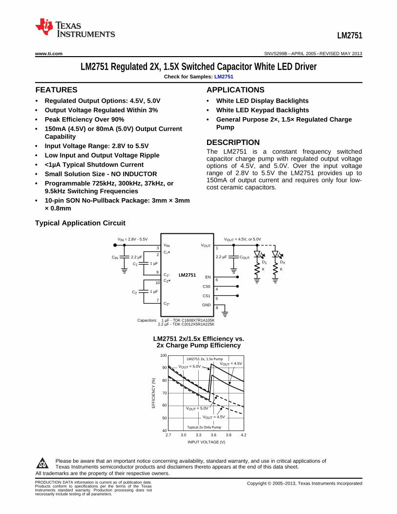
2.7 3.0 3.3 3.6 3.9 4.2 40 50 60 70 80 90 100 EFFICIENCY (%) INPUT VOLTAGE (V) Typical 2x Only Pump V OUT = 4.5V LM2751 2x, 1.5x Pump V OUT = 4.5V V OUT = 5.0V V OUT = 5.0V LM2751 V IN C 2 + C 2 - 2.2 μF 1 μF V OUT 2.2 μF C1+ C 1 - 1 μF Capacitors: 1 μF - TDK C1608X7R1A105K 2.2 μF - TDK C2012X5R1A225K V IN = 2.8V - 5.5V 3 2 9 10 7 8 1 EN 6 GND V OUT = 4.5V, or 5.0V CS0 4 CS1 5 D 1 D X R R C OUT C IN C 2 C 1 LM2751 www.ti.com SNVS299B – APRIL 2005 – REVISED MAY 2013 LM2751 Regulated 2X, 1.5X Switched Capacitor White LED Driver Check for Samples: LM2751 1FEATURES APPLICATIONS 2• Regulated Output Options: 4.5V, 5.0V • White LED Display Backlights • Output Voltage Regulated Within 3% • White LED Keypad Backlights • Peak Efficiency Over 90% • General Purpose 2×, 1.5× Regulated Charge Pump • 150mA (4.5V) or 80mA (5.0V) Output Current Capability DESCRIPTION • Input Voltage Range: 2.8V to 5.5V The LM2751 is a constant frequency switched • Low Input and Output Voltage Ripple capacitor charge pump with regulated output voltage • <1μA Typical Shutdown Current options of 4.5V, and 5.0V. Over the input voltage range of 2.8V to 5.5V the LM2751 provides up to • Small Solution Size - NO INDUCTOR 150mA of output current and requires only four low- • Programmable 725kHz, 300kHz, 37kHz, or cost ceramic capacitors. 9.5kHz Switching Frequencies • 10-pin SON No-Pullback Package: 3mm × 3mm × 0.8mm Typical Application Circuit LM2751 2x/1.5x Efficiency vs. 2x Charge Pump Efficiency 1 Please be aware that an important notice concerning availability, standard warranty, and use in critical applications of Texas Instruments semiconductor products and disclaimers thereto appears at the end of this data sheet. 2All trademarks are the property of their respective owners. PRODUCTION DATA information is current as of publication date. Copyright © 2005–2013, Texas Instruments Incorporated Products conform to specifications per the terms of the Texas Instruments standard warranty. Production processing does not necessarily include testing of all parameters.
-
Upload
khangminh22 -
Category
Documents
-
view
0 -
download
0
Transcript of LM2751 Regulated 2X, 1.5X Switched Capacitor White LED ...
2.7 3.0 3.3 3.6 3.9 4.240
50
60
70
80
90
100
EF
FIC
IEN
CY
(%
)
INPUT VOLTAGE (V)
Typical 2x Only Pump
VOUT = 4.5V
LM2751 2x, 1.5x Pump
VOUT = 4.5V
VOUT = 5.0V
VOUT = 5.0V
LM2751
VIN
C2+
C2-
2.2 µF
1 µF
VOUT
2.2 µFC1+
C1-
1 µF
Capacitors: 1 µF - TDK C1608X7R1A105K 2.2 µF - TDK C2012X5R1A225K
VIN = 2.8V - 5.5V
3
2
9
10
7
8
1
EN6
GND
VOUT = 4.5V, or 5.0V
CS04
CS15
D1 DX
R R
COUTCIN
C2
C1
LM2751
www.ti.com SNVS299B –APRIL 2005–REVISED MAY 2013
LM2751 Regulated 2X, 1.5X Switched Capacitor White LED DriverCheck for Samples: LM2751
1FEATURES APPLICATIONS2• Regulated Output Options: 4.5V, 5.0V • White LED Display Backlights• Output Voltage Regulated Within 3% • White LED Keypad Backlights• Peak Efficiency Over 90% • General Purpose 2×, 1.5× Regulated Charge
Pump• 150mA (4.5V) or 80mA (5.0V) Output CurrentCapability
DESCRIPTION• Input Voltage Range: 2.8V to 5.5VThe LM2751 is a constant frequency switched• Low Input and Output Voltage Ripple capacitor charge pump with regulated output voltage
• <1µA Typical Shutdown Current options of 4.5V, and 5.0V. Over the input voltagerange of 2.8V to 5.5V the LM2751 provides up to• Small Solution Size - NO INDUCTOR150mA of output current and requires only four low-• Programmable 725kHz, 300kHz, 37kHz, orcost ceramic capacitors.
9.5kHz Switching Frequencies• 10-pin SON No-Pullback Package: 3mm × 3mm
× 0.8mm
Typical Application Circuit
LM2751 2x/1.5x Efficiency vs.2x Charge Pump Efficiency
1
Please be aware that an important notice concerning availability, standard warranty, and use in critical applications ofTexas Instruments semiconductor products and disclaimers thereto appears at the end of this data sheet.
2All trademarks are the property of their respective owners.
PRODUCTION DATA information is current as of publication date. Copyright © 2005–2013, Texas Instruments IncorporatedProducts conform to specifications per the terms of the TexasInstruments standard warranty. Production processing does notnecessarily include testing of all parameters.

1
2
3
4
5
10
9
8
7
6
Die-Attach Pad: GND
VOUT
C1+
VIN
CS0
CS1
C2+
C1-
GND
C2-
EN
1
2
3
4
5
10
9
8
7
6
Die-Attach Pad: GND
VOUT
C1+
VIN
CS0
CS1
C2+
C1-
GND
C2-
EN
Top View Bottom View
LM2751
SNVS299B –APRIL 2005–REVISED MAY 2013 www.ti.com
DESCRIPTION (CONTINUED)The LM2751 provides excellent efficiency without the use of an inductor by operating the charge pump in a gainof 3/2 or 2. The proper gain for maintaining regulation is chosen so that efficiency is maximized over the inputvoltage range.
LM2751 uses constant frequency pre-regulation to minimize conducted noise on the input and provide apredictable switching frequency. The switching frequency is programmable to 725kHz, 300kHz, 37kHz, or9.5kHz.
LM2751 is available in a 10-pin SON No-Pullback Package.
Connection Diagram
Figure 1. 10-pin SON No Pullback Package (3mm × 3mm × 0.8mm)See Package Number DSC0010A
PIN DESCRIPTIONSPin # Name Description
1 VOUT Pre-Regulated Output.
2 C1+ Flying Capacitor C1 Connection.
3 VIN Input Supply Range: 2.8V to 5.5V.
4 CS0 Frequency Select Input 0.
5 CS1 Frequency Select Input 1.
6 EN Enable Pin Logic Input.
7 C2− Flying Capacitor C2 Connection.
8 GND Ground.
9 C1− Flying Capacitor C1 Connection.
10 C2+ Flying Capacitor C2 Connection.
These devices have limited built-in ESD protection. The leads should be shorted together or the device placed in conductive foamduring storage or handling to prevent electrostatic damage to the MOS gates.
2 Submit Documentation Feedback Copyright © 2005–2013, Texas Instruments Incorporated
Product Folder Links: LM2751

LM2751
www.ti.com SNVS299B –APRIL 2005–REVISED MAY 2013
ABSOLUTE MAXIMUM RATINGS (1) (2) (3)
VIN Pin −0.3V to 6.0V
EN, CS0, CS1 Pins −0.3V to (VIN+0.3)w/ 6.0V max
Continuous Power Dissipation (4) Internally Limited
Junction Temperature (TJ-MAX-ABS) 150°C
Storage Temperature Range −65°C to 150°C
Maximum Lead Temperature (Soldering, 10sec.) 265°C
ESD Rating (5) Human-body model 2kV
Machine model 200V
(1) Absolute Maximum Ratings indicate limits beyond which damage to the component may occur. Operating Ratings are conditions underwhich operation of the device is specified. Operating Ratings do not imply ensured performance limits. For specified performance limitsand associated test conditions, see the Electrical Characteristics tables.
(2) All voltages are with respect to the potential at the GND pin.(3) If Military/Aerospace specified devices are required, please contact the Texas Instruments Sales Office/ Distributors for availability and
specifications.(4) Internal thermal shutdown circuitry protects the device from permanent damage. Thermal shutdown engages at TJ=150°C (typ.) and
disengages at TJ=140°C (typ.).(5) The Human body model is a 100 pF capacitor discharged through a 1.5kΩ resistor into each pin. The machine model is a 200pF
capacitor discharged directly into each pin (MIL-STD-883 3015.7).
OPERATING RATINGS (1) (2)
Input Voltage Range 2.8V to 5.5V
EN, CS0, CS1 Input Voltage Range 0V to VIN
Junction Temperature (TJ) Range -40°C to 115°C
Ambient Temperature (TA) Range (3) -40°C to 85°C
Recommended Maximum Load Current
Version B Freq. = 725kHz 150mA
Freq. = 300kHz 120mA
Freq. = 37kHz 40mA
Freq. = 9.5kHz 10mA
Version A Freq. = 725kHz 80mA
Freq. = 300kHz 60mA
Freq. = 37kHz 16mA
Freq. = 9.5kHz 4mA
(1) Absolute Maximum Ratings indicate limits beyond which damage to the component may occur. Operating Ratings are conditions underwhich operation of the device is specified. Operating Ratings do not imply ensured performance limits. For specified performance limitsand associated test conditions, see the Electrical Characteristics tables.
(2) All voltages are with respect to the potential at the GND pin.(3) In applications where high power dissipation and/or poor package thermal resistance is present, the maximum ambient temperature may
have to be derated. Maximum ambient temperature (TA-MAX) is dependent on the maximum operation junction temperature (TJ-MAX-OP =115ºC), the maximum power dissipation of the device in the application (PD-MAX), and the junction-to ambient thermal resistance of thepart/package in the application (θJA), as given by the following equation:TA-MAX = TJ-MAX-OP - (θJA × PD-MAX).
THERMAL PROPERTIESJunction-to-Ambient Thermal Package (θJA) (1)
Resistance, 10-pin SON 55°C/W
(1) Junction-to-ambient thermal resistance (θJA) is taken from a thermal modeling result, performed under the conditions and guidelines setforth in the JEDEC standard JESD51-7. The test board is a 4 layer FR-4 board measuring 102mm x 76mm x 1.6mm with a 2 x 1 arrayof thermal vias. The ground plane on the board is 50mm x 50mm. Thickness of copper layers are 36µm/18µm/18µm/36µm(1.5oz/1oz/1oz/1.5oz). Ambient temperature in simulation is 22ºC, still air. Power dissipation is 1W. The value of θJA of theLM2751 in 10-pin SON could fall in a range as wide as 50ºC/W to 150ºC/W (if not wider), depending on PWB material, layout, andenvironmental conditions. In applications where high maximum power dissipation exists (high VIN, high IOUT), special care must be paidto thermal dissipation issues. For more information on these topics, see the TI AN-1187 Application Report (SNOA401) and the PowerEfficiency and Power Dissipation section of this datasheet.
Copyright © 2005–2013, Texas Instruments Incorporated Submit Documentation Feedback 3
Product Folder Links: LM2751
LM2751
SNVS299B –APRIL 2005–REVISED MAY 2013 www.ti.com
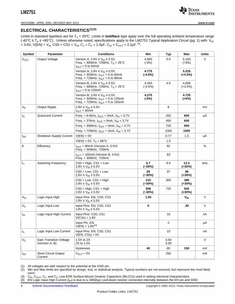
ELECTRICAL CHARACTERISTICS (1) (2)
Limits in standard typeface are for TA = 25ºC. Limits in boldface type apply over the full operating ambient temperature range(-40°C ≤ TA ≤ +85°C) . Unless otherwise noted, specifications apply to the LM2751 Typical Application Circuit (pg. 1) with: VIN
= 3.6V, V(EN) = VIN, CS0 = CS1 = VIN, C1 = C2 = 1.0µF, CIN = COUT = 2.2µF (3).
Symbol Parameter Conditions Min Typ Max Units
VOUT Output Voltage Version A, 2.8V ≤ VIN ≤ 5.5V, 4.850 5.0 5.150 VFreq. = 300kHz, 725kHz, TA = 25°C (-3%) (+3%)IOUT = 0 to 60mA
Version A, 2.8V ≤ VIN ≤ 5.5V, 4.775 5.225Freq. = 300kHz, IOUT = 0 to 60mA (-4.5%) (+4.5%)Freq. = 725kHz, IOUT = 0 to 80mA
Version B, 2.8V ≤ VIN ≤ 5.5V, 4.343 4.5 4.658Freq. = 300kHz, 725kHz, TA = 25°C (-3.5%) (+3.5%)IOUT = 0 to 120mA
Version B, 2.8V ≤ VIN ≤ 5.5V, 4.275 4.725Freq. = 300kHz, IOUT = 0 to 120mA (-5%) (+5%)Freq. = 725kHz, IOUT = 0 to 150mA
VR Output Ripple 2.8V ≤ VIN ≤ 5.5V 8 mVIOUT = 60mA
IQ Quiescent Current Freq. = 9.5kHz, IOUT = 0mA, VIN = 3.7V 425 600 µA
Freq. = 37kHz, IOUT = 0mA, VIN = 3.7V 450 640
Freq. = 300kHz, IOUT = 0mA, VIN = 3.7V 700 900
Freq. = 725kHz, IOUT = 0mA, VIN = 3.7V 1000 1500
ISD Shutdown Supply Current V(EN) = 0V 0.77 1.3 µA
V(EN) = 0V, TA = 85°C 1.0
E Efficiency IOUT = 80mA (Version A, 5.0V) 92 %Freq. = 300kHz, 725kHz
IOUT = 150mA (Version B, 4.5V) 83Freq. = 300kHz, 725kHz
fSW Switching Frequency CS0 = High, CS1 = Low 6.7 9.5 12.3 kHz2.8V ≤ VIN ≤ 5.5V (−30%) (+30%)
CS0 = Low, CS1 = Low 26 37 482.8V ≤ VIN ≤ 5.5V (−30%) (+30%)
CS0 = Low, CS1 = High 210 300 3902.8V ≤ VIN ≤ 5.5V (−30%) (+30%)
CS0 = High, CS1 = High 508 725 9422.8V ≤ VIN ≤ 5.5V (−30%) (+30%)
VIH Logic Input High Input Pins: EN, CS0, CS1 1.00 VIN V2.8V ≤ VIN ≤ 5.5V
VIL Logic Input Low Input Pins: EN, CS0, CS1 0 .30 V2.8V ≤ VIN ≤ 5.5V
IIH Logic Input High Current Input Pins: CS0, CS1 10 nAV(CSx) = 1.8V
Input Pin: EN 2 µAV(EN) = 1.8V (4)
IIL Logic Input Low Current Input Pins: EN, CS0, CS1 10 nAV(EN, CSx) = 0V
VG Gain Transition Voltage 1.5X to 2X 3.50 V(Version A, B) 2X to 1.5X 3.58
Hysteresis 40 80 150 mV
ISC Short Circuit Output VOUT = 0V 250 mACurrent
(1) All voltages are with respect to the potential at the GND pin.(2) Min and Max limits are specified by design, test, or statistical analysis. Typical numbers are not ensured, but represent the most likely
norm.(3) CIN, COUT, C1, and C2: Low-ESR Surface-Mount Ceramic Capacitors (MLCCs) used in setting electrical characteristics.(4) EN Logic Input High Current (IIH) is due to a 1MΩ(typ.) pull-down resistor connected internally between the EN pin and GND.
4 Submit Documentation Feedback Copyright © 2005–2013, Texas Instruments Incorporated
Product Folder Links: LM2751

LM2751
www.ti.com SNVS299B –APRIL 2005–REVISED MAY 2013
ELECTRICAL CHARACTERISTICS(1)(2) (continued)Limits in standard typeface are for TA = 25ºC. Limits in boldface type apply over the full operating ambient temperature range(-40°C ≤ TA ≤ +85°C) . Unless otherwise noted, specifications apply to the LM2751 Typical Application Circuit (pg. 1) with: VIN
= 3.6V, V(EN) = VIN, CS0 = CS1 = VIN, C1 = C2 = 1.0µF, CIN = COUT = 2.2µF (3).
Symbol Parameter Conditions Min Typ Max Units
tON VOUT Turn-On Time (5) 300 µs
(5) Turn-on time is measured from when the EN signal is pulled high until the output voltage on VOUT crosses 90% of its final value.
Copyright © 2005–2013, Texas Instruments Incorporated Submit Documentation Feedback 5
Product Folder Links: LM2751

SWITCH
CONTROL
SWITCHARRAY
G = 2 ,
GAIN
CONTROL
1.2V
Ref.
Soft-Start
Ramp
OSCILLATOR
EN
Enable /
Shutdown
Control
3
2
VIN
GND
EN
VOUT
C2-
C2+
C1-
C1+
LM2751
CS0
CS1
OSC
Divider
(Div 16,
Div 8)
FREQ. CTRL
72
5 k
Hz
30
0 k
Hz
Short-Circuit Protection
Thermal Shutdown
1.2V Ref.
LM2751
SNVS299B –APRIL 2005–REVISED MAY 2013 www.ti.com
BLOCK DIAGRAM
6 Submit Documentation Feedback Copyright © 2005–2013, Texas Instruments Incorporated
Product Folder Links: LM2751

2.7 3.1 3.5 3.9 4.3 4.7 5.1 5.5
INPUT VOLTAGE (V)
I Q (
mA
)
IOUT = 0FSW = 725 kHz
FSW = 300 kHz
0.50
0.70
0.90
1.10
1.30
1.50
1.70
TA = 25°C
2.7 3.1 3.5 3.9 4.3 4.7 5.1 5.5
INPUT VOLTAGE (V)
I Q (
mA
)
IOUT = 0FSW = 725 kHz
FSW = 300 kHz
TA = 25°C
0.5
0.7
0.9
1.1
1.3
1.5
0 15 30 45 60 75 90
OUTPUT CURRENT (mA)
OU
TP
UT
VO
LTA
GE
(V
)
4.98
5.01
5.03
5.06
5.08
VIN = 3.3V
VIN = 3.6V VIN = 2.8V
VIN = 4.2V
VIN = 5.5V
0 20 40 60 80 100 120 140 160
OUTPUT CURRENT (mA)
OU
TP
UT
VO
LTA
GE
(V
)
4.45
4.48
4.51
4.54
4.57
4.60
VIN = 4.2V
VIN = 2.8V
VIN = 5.5V
VIN = 3.6V
VIN = 3.3V
0 10 20 30 40 50 60 70
OUTPUT CURRENT (mA)
OU
TP
UT
VO
LTA
GE
(V
)
5.00
5.03
5.05
5.08
5.10
VIN = 3.3V
VIN = 2.8V VIN = 3.6V
VIN = 4.2V
VIN = 5.5V
0 13 26 39 52 65 78 91 104 117 130
OUTPUT CURRENT (mA)
OU
TP
UT
VO
LTA
GE
(V
)
VIN = 4.2V
VIN = 2.8V
VIN = 5.5V
VIN = 3.6V
VIN = 3.3V4.50
4.52
4.54
4.56
4.58
4.60
LM2751
www.ti.com SNVS299B –APRIL 2005–REVISED MAY 2013
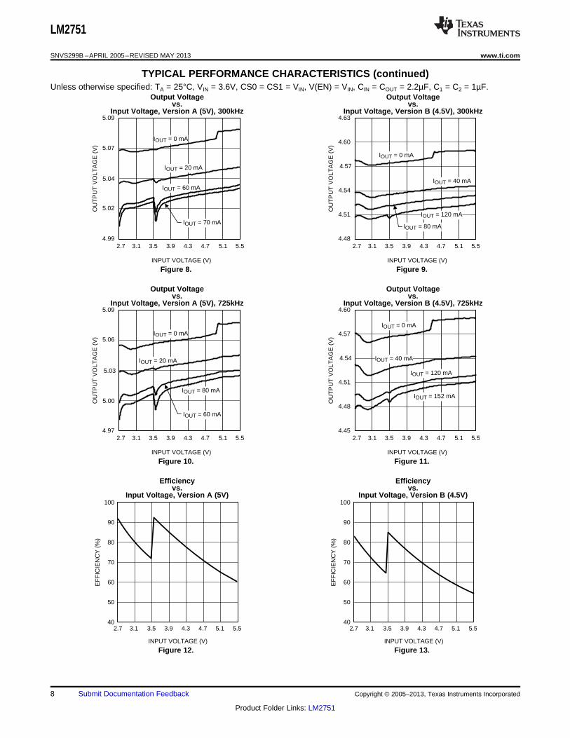
TYPICAL PERFORMANCE CHARACTERISTICSUnless otherwise specified: TA = 25°C, VIN = 3.6V, CS0 = CS1 = VIN, V(EN) = VIN, CIN = COUT = 2.2µF, C1 = C2 = 1µF.
Output Voltage Output Voltagevs. vs.
Output Current, Version A (5V), 300kHz Output Current, Version B (4.5V), 300kHz
Figure 2. Figure 3.
Output Voltage Output Voltagevs. vs.
Output Current, Version A (5V), 725kHz Output Current, Version B (4.5V), 725kHz
Figure 4. Figure 5.
Input Current Input Currentvs. vs.
Input Voltage, Version A (5V) Input Voltage, Version B (4.5V)
Figure 6. Figure 7.
Copyright © 2005–2013, Texas Instruments Incorporated Submit Documentation Feedback 7
Product Folder Links: LM2751
2.7 3.1 3.5 3.9 4.3 4.7 5.1 5.5
INPUT VOLTAGE (V)
40
50
60
70
80
90
100
EF
FIC
IEN
CY
(%
)
2.7 3.1 3.5 3.9 4.3 4.7 5.1 5.5
INPUT VOLTAGE (V)
40
50
60
70
80
90
100
EF
FIC
IEN
CY
(%
)
2.7 3.1 3.5 3.9 4.3 4.7 5.1 5.5
INPUT VOLTAGE (V)
OU
TP
UT
VO
LTA
GE
(V
)
IOUT = 0 mA
4.97
5.00
5.03
5.06
5.09
IOUT = 20 mA
IOUT = 60 mA
IOUT = 80 mA
2.7 3.1 3.5 3.9 4.3 4.7 5.1 5.5
INPUT VOLTAGE (V)
OU
TP
UT
VO
LTA
GE
(V
)IOUT = 0 mA
4.45
4.48
4.51
4.54
4.57
4.60
IOUT = 40 mA
IOUT = 120 mA
IOUT = 152 mA
2.7 3.1 3.5 3.9 4.3 4.7 5.1 5.5
INPUT VOLTAGE (V)
OU
TP
UT
VO
LTA
GE
(V
)
IOUT = 0 mA
4.99
5.02
5.04
5.07
5.09
IOUT = 20 mA
IOUT = 70 mA
IOUT = 60 mA
2.7 3.1 3.5 3.9 4.3 4.7 5.1 5.5
INPUT VOLTAGE (V)
OU
TP
UT
VO
LTA
GE
(V
)
IOUT = 0 mA
4.48
4.51
4.54
4.57
4.60
4.63
IOUT = 40 mA
IOUT = 80 mA
IOUT = 120 mA
LM2751
SNVS299B –APRIL 2005–REVISED MAY 2013 www.ti.com
TYPICAL PERFORMANCE CHARACTERISTICS (continued)Unless otherwise specified: TA = 25°C, VIN = 3.6V, CS0 = CS1 = VIN, V(EN) = VIN, CIN = COUT = 2.2µF, C1 = C2 = 1µF.
Output Voltage Output Voltagevs. vs.
Input Voltage, Version A (5V), 300kHz Input Voltage, Version B (4.5V), 300kHz
Figure 8. Figure 9.
Output Voltage Output Voltagevs. vs.
Input Voltage, Version A (5V), 725kHz Input Voltage, Version B (4.5V), 725kHz
Figure 10. Figure 11.
Efficiency Efficiencyvs. vs.
Input Voltage, Version A (5V) Input Voltage, Version B (4.5V)
Figure 12. Figure 13.
8 Submit Documentation Feedback Copyright © 2005–2013, Texas Instruments Incorporated
Product Folder Links: LM2751

3.1 3.5 3.9 4.3 4.7 5.1 5.5
INPUT VOLTAGE (V)
0
4
9
13
18
22
OU
TP
UT
VO
LTA
GE
RIP
PLE
(m
V)
2.7
CIN = 1.0 F
COUT: 10 F
Capacitance,300 kHz
COUT: 10 F
Capacitance,725 kHz
COUT: 2.2 F
Capacitance,300 kHz
COUT: 2.2 F
Capacitance,725 kHz
LM2751
www.ti.com SNVS299B –APRIL 2005–REVISED MAY 2013
TYPICAL PERFORMANCE CHARACTERISTICS (continued)Unless otherwise specified: TA = 25°C, VIN = 3.6V, CS0 = CS1 = VIN, V(EN) = VIN, CIN = COUT = 2.2µF, C1 = C2 = 1µF.
Output Voltage Ripplevs. Input Voltage Version B (4.5V), Load = 120mA Output Voltage Ripple, Version B (4.5V)
VIN = 3.6V, Load = 150mACH1: VOUT; Scale: 10mV/Div, AC CoupledTime scale: 400ns/Div
Figure 14. Figure 15.
Line Step Response, Version B (4.5V) Load Step Response, Version B (4.5V)
VIN = 3.2V - 4.2V Step, Load = 150mA VIN = 3.6V, Load = 20mA - 150mA StepCH1 (top): VIN; Scale: 1V/Div, DC Coupled CH1 (top): VOUT; Scale: 50mV/Div, AC CoupledCH2: VOUT; Scale: 50mV/Div, AC Coupled CH2: Output Current; Scale: 50mA/DivTime scale: 200µs/Div Time scale: 200µs/Div
Figure 16. Figure 17.
Start-up Behavior, Version A (5V), Load = 80mA Start-up Behavior, Version B (4.5V), Load = 150mA
CH1: EN pin; Scale: 2V/Div CH1: EN pin; Scale: 2V/DivCH2: VOUT; Scale: 2V/Div CH2: VOUT; Scale: 2V/DivTime scale: 100µs/Div Time scale: 100µs/Div
Figure 18. Figure 19.
Copyright © 2005–2013, Texas Instruments Incorporated Submit Documentation Feedback 9
Product Folder Links: LM2751
LM2751
SNVS299B –APRIL 2005–REVISED MAY 2013 www.ti.com
APPLICATION INFORMATION
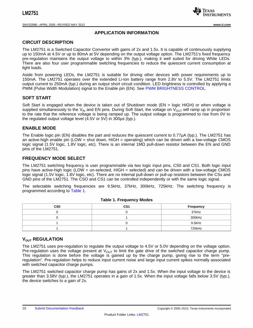
CIRCUIT DESCRIPTION
The LM2751 is a Switched Capacitor Convertor with gains of 2x and 1.5x. It is capable of continuously supplyingup to 150mA at 4.5V or up to 80mA at 5V depending on the output voltage option. The LM2751's fixed frequencypre-regulation maintains the output voltage to within 3% (typ.), making it well suited for driving White LEDs.There are also four user programmable switching frequencies to reduce the quiescent current consumption atlight loads.
Aside from powering LEDs, the LM2751 is suitable for driving other devices with power requirements up to150mA. The LM2751 operates over the extended Li-Ion battery range from 2.8V to 5.5V. The LM2751 limitsoutput current to 250mA (typ.) during an output short circuit condition. LED brightness is controlled by applying aPWM (Pulse Width Modulation) signal to the Enable pin (EN). See PWM BRIGHTNESS CONTROL.
SOFT START
Soft Start is engaged when the device is taken out of Shutdown mode (EN = logic HIGH) or when voltage issupplied simultaneously to the VIN and EN pins. During Soft Start, the voltage on VOUT will ramp up in proportionto the rate that the reference voltage is being ramped up. The output voltage is programmed to rise from 0V tothe regulated output voltage level (4.5V or 5V) in 300µs (typ.).
ENABLE MODE
The Enable logic pin (EN) disables the part and reduces the quiescent current to 0.77µA (typ.). The LM2751 hasan active-high enable pin (LOW = shut down, HIGH = operating) which can be driven with a low-voltage CMOSlogic signal (1.5V logic, 1.8V logic, etc). There is an internal 1MΩ pull-down resistor between the EN and GNDpins of the LM2751.
FREQUENCY MODE SELECT
The LM2751 switching frequency is user programmable via two logic input pins, CS0 and CS1. Both logic inputpins have active-high logic (LOW = un-selected, HIGH = selected) and can be driven with a low-voltage CMOSlogic signal (1.5V logic, 1.8V logic, etc). There are no internal pull-down or pull-up resistors between the CSx andGND pins of the LM2751. The CSO and CS1 can be controlled independently or with the same logic signal.
The selectable switching frequencies are 9.5kHz, 37kHz, 300kHz, 725kHz. The switching frequency isprogrammed according to Table 1.
Table 1. Frequency Modes
CS0 CS1 Frequency
0 0 37kHz
0 1 300kHz
1 0 9.5kHz
1 1 725kHz
VOUT REGULATION
The LM2751 uses pre-regulation to regulate the output voltage to 4.5V or 5.0V depending on the voltage option.Pre-regulation uses the voltage present at VOUT to limit the gate drive of the switched capacitor charge pump.This regulation is done before the voltage is gained up by the charge pump, giving rise to the term "pre-regulation". Pre-regulation helps to reduce input current noise and large input current spikes normally associatedwith switched capacitor charge pumps.
The LM2751 switched capacitor charge pump has gains of 2x and 1.5x. When the input voltage to the device isgreater than 3.58V (typ.), the LM2751 operates in a gain of 1.5x. When the input voltage falls below 3.5V (typ.),the device switches to a gain of 2x.
10 Submit Documentation Feedback Copyright © 2005–2013, Texas Instruments Incorporated
Product Folder Links: LM2751
LM2751
www.ti.com SNVS299B –APRIL 2005–REVISED MAY 2013
OUTPUT VOLTAGE RIPPLE
The primary contributor in keeping the output voltage ripple of the LM2751 low is its switching topology. Theoutput capacitance, input voltage, switching frequency and output current also play a significant part indetermining the output voltage ripple. Due to the complexity of the LM2751 operation, providing equations ormodels to approximate the magnitude of the ripple cannot be easily accomplished. However, the followinggeneral statements can be made.
The LM2751 has very low output ripple when compared to typical boost regulators due to its double-pumptopology, where charge is continually supplied to the output during both 2x and 1.5x modes. Combined with fixedfrequency operation modes, double-pumping allows for the use of a very small, low value ceramic capacitor onthe output node while still achieving minimal output ripple. Increasing the capacitance by adding a higher valuecapacitor or placing multiple capacitors in parallel can further reduce the ripple magnitude.
CAPACITOR SELECTION
The LM2751 requires 4 external capacitors for proper operation. Surface-mount multi-layer ceramic capacitorsare recommended. These capacitors are small, inexpensive and have very low equivalent series resistance(ESR, ≤15mΩ typ.). Tantalum capacitors, OS-CON capacitors, and aluminum electrolytic capacitors are generallynot recommended for use with the LM2751 due to their high ESR, as compared to ceramic capacitors.
For most applications, ceramic capacitors with X7R or X5R temperature characteristic are preferred for use withthe LM2751. These capacitors have tight capacitance tolerance (as good as ±10%), hold their value overtemperature (X7R: ±15% over −55°C to 125°C; X5R: ±15% over −55°C to 85°C), and typically have little voltagecoefficient when compared to other types of capacitors. However selecting a capacitor with a voltage rating muchhigher than the voltage it will be subjected to, will ensure that the capacitance will stay closer to the capacitor'snominal value. Capacitors with Y5V or Z5U temperature characteristic are generally not recommended for usewith the LM2751. Capacitors with these temperature characteristics typically have wide capacitance tolerance(+80%, −20%), vary significantly over temperature (Y5V: +22%, −82% over −30°C to +85°C range; Z5U: +22%,−56% over +10°C to +85°C range), and have poor voltage coefficients. Under some conditions, a nominal 1µFY5V or Z5U capacitor could have a capacitance of only 0.1µF. Such detrimental deviation is likely to cause Y5Vand Z5U capacitors to fail to meet the minimum capacitance requirements of the LM2751.
The voltage rating of the output capacitor should be 10V or more. All other capacitors should have a voltagerating at or above the maximum input voltage of the application.
DRIVING WHITE LEDS
The desired LED current is set by placing a resistor (R) in series with each LED, and is determined by theequation:
ILED = (VOUT - VLED) ÷R (1)
In the equation above, ILED is the current that flows through a particular LED, and VLED is the forward voltage ofthe LED at the given current. The output voltage (VOUT) of the LM2751 is tightly regulated to 4.5V or 5Vdepending on the output voltage option. However, LED forward voltage varies from LED to LED, and LED currentwill vary accordingly. Mismatch of LED currents will result in brightness mismatch from one LED to the next.Therefore it is suggested that LED groups with tightly controlled I-V characteristics ("Binned" LEDs) be used.LEDs with looser tolerance can be used in applications where brightness matching is not critical, such as inkeypad or general backlighting. The typical and maximum diode forward voltage depends highly on themanufacturer and their technology.
PWM BRIGHTNESS CONTROL
Perceived LED brightness can be adjusted using a PWM control signal on the Enable pin of the LM2751, to turnthe voltage output ON and OFF at a rate faster than perceptible by the eye. When this is done, the totalbrightness perceived is proportional to the duty cycle (D) of the PWM signal (D = the percentage of time that theLED is on in every PWM cycle). A simple example: if the LEDs are driven at 15mA each with a PWM signal thathas a 50% duty cycle, perceived LED brightness will be about half as bright as compared to when the LEDs aredriven continuously with 15mA.
Copyright © 2005–2013, Texas Instruments Incorporated Submit Documentation Feedback 11
Product Folder Links: LM2751
LM2751
SNVS299B –APRIL 2005–REVISED MAY 2013 www.ti.com
For linear brightness control over the full duty cycle adjustment range, the PWM frequency (f) should be limitedto accommodate the turn-on time (typ. TON = 300µs) of the device.
D × (1/f) > TON (2)fMAX = DMIN ÷ TON (3)
The minimum recommended PWM frequency is 100Hz. Frequencies below this may be visibly noticeable asflicker or blinking. The maximum recommended PWM frequency is 1kHz. Frequencies above this may causenoise in the audible range.
THERMAL PROTECTION
When the junction temperature exceeds 150°C (typ.), internal thermal protection circuitry disables the device.This feature protects the LM2751 from damage due to excessive power dissipation. The device will recover andoperate normally when the junction temperature falls below 140°C (typ.). It is important to have good thermalconduction with a proper layout to reduce thermal resistance.
POWER EFFICIENCY
Charge-Pump efficiency is derived in the following two ideal equations (supply current and other losses areneglected for simplicity):
IIN = G x IOUT (4)E = (VOUT x IOUT) ÷ (VIN x IIN) = VOUT ÷ (G x VIN) (5)
In the equations, G represents the charge pump gain. Efficiency is at its highest as G x VIN approaches VOUT.Refer to the efficiency graph in the Typical Performance Characteristics for the detailed efficiency data.
POWER DISSIPATION
The power dissipation (PDISSIPATION) and junction temperature (TJ) can be approximated with the equationsbelow. PIN is the product of the input current and input voltage, POUT is the power consumed by the loadconnected to the output, TAis the ambient temperature, and θJA is the junction-to-ambient thermal resistance forthe 10-pin SON package. VIN is the input voltage to the LM2751, VVOUT is the voltage at the output of the device,and IOUT is the total current supplied to the load connected to VOUT.
PDISSIPATION = PIN - POUT (6)= (VIN × IIN) − (VVOUT × IOUT) (7)TJ = TA + (PDISSIPATION × θJA) (8)
The junction temperature rating takes precedence over the ambient temperature rating. The LM2751 may beoperated outside the ambient temperature rating, so long as the junction temperature of the device does notexceed the maximum operating rating of 115°C. The maximum ambient temperature rating must be derated inapplications where high power dissipation and/or poor thermal resistance causes the junction temperature toexceed 115°C.
12 Submit Documentation Feedback Copyright © 2005–2013, Texas Instruments Incorporated
Product Folder Links: LM2751
LM2751
www.ti.com SNVS299B –APRIL 2005–REVISED MAY 2013
REVISION HISTORY
Changes from Revision A (May 2013) to Revision B Page
• Changed layout of National Data Sheet to TI format .......................................................................................................... 12
Copyright © 2005–2013, Texas Instruments Incorporated Submit Documentation Feedback 13
Product Folder Links: LM2751

PACKAGE OPTION ADDENDUM
www.ti.com 10-Dec-2020
Addendum-Page 1
PACKAGING INFORMATION
Orderable Device Status(1)
Package Type PackageDrawing
Pins PackageQty
Eco Plan(2)
Lead finish/Ball material
(6)
MSL Peak Temp(3)
Op Temp (°C) Device Marking(4/5)
Samples
LM2751SD-B/NOPB ACTIVE WSON DSC 10 1000 RoHS & Green SN Level-1-260C-UNLIM -40 to 85 L146B
(1) The marketing status values are defined as follows:ACTIVE: Product device recommended for new designs.LIFEBUY: TI has announced that the device will be discontinued, and a lifetime-buy period is in effect.NRND: Not recommended for new designs. Device is in production to support existing customers, but TI does not recommend using this part in a new design.PREVIEW: Device has been announced but is not in production. Samples may or may not be available.OBSOLETE: TI has discontinued the production of the device.
(2) RoHS: TI defines "RoHS" to mean semiconductor products that are compliant with the current EU RoHS requirements for all 10 RoHS substances, including the requirement that RoHS substancedo not exceed 0.1% by weight in homogeneous materials. Where designed to be soldered at high temperatures, "RoHS" products are suitable for use in specified lead-free processes. TI mayreference these types of products as "Pb-Free".RoHS Exempt: TI defines "RoHS Exempt" to mean products that contain lead but are compliant with EU RoHS pursuant to a specific EU RoHS exemption.Green: TI defines "Green" to mean the content of Chlorine (Cl) and Bromine (Br) based flame retardants meet JS709B low halogen requirements of <=1000ppm threshold. Antimony trioxide basedflame retardants must also meet the <=1000ppm threshold requirement.
(3) MSL, Peak Temp. - The Moisture Sensitivity Level rating according to the JEDEC industry standard classifications, and peak solder temperature.
(4) There may be additional marking, which relates to the logo, the lot trace code information, or the environmental category on the device.
(5) Multiple Device Markings will be inside parentheses. Only one Device Marking contained in parentheses and separated by a "~" will appear on a device. If a line is indented then it is a continuationof the previous line and the two combined represent the entire Device Marking for that device.
(6) Lead finish/Ball material - Orderable Devices may have multiple material finish options. Finish options are separated by a vertical ruled line. Lead finish/Ball material values may wrap to twolines if the finish value exceeds the maximum column width.
Important Information and Disclaimer:The information provided on this page represents TI's knowledge and belief as of the date that it is provided. TI bases its knowledge and belief on informationprovided by third parties, and makes no representation or warranty as to the accuracy of such information. Efforts are underway to better integrate information from third parties. TI has taken andcontinues to take reasonable steps to provide representative and accurate information but may not have conducted destructive testing or chemical analysis on incoming materials and chemicals.TI and TI suppliers consider certain information to be proprietary, and thus CAS numbers and other limited information may not be available for release.
In no event shall TI's liability arising out of such information exceed the total purchase price of the TI part(s) at issue in this document sold by TI to Customer on an annual basis.

TAPE AND REEL INFORMATION
*All dimensions are nominal
Device PackageType
PackageDrawing
Pins SPQ ReelDiameter
(mm)
ReelWidth
W1 (mm)
A0(mm)
B0(mm)
K0(mm)
P1(mm)
W(mm)
Pin1Quadrant
LM2751SD-B/NOPB WSON DSC 10 1000 178.0 12.4 3.3 3.3 1.0 8.0 12.0 Q1
PACKAGE MATERIALS INFORMATION
www.ti.com 10-Aug-2016
Pack Materials-Page 1

*All dimensions are nominal
Device Package Type Package Drawing Pins SPQ Length (mm) Width (mm) Height (mm)
LM2751SD-B/NOPB WSON DSC 10 1000 210.0 185.0 35.0
PACKAGE MATERIALS INFORMATION
www.ti.com 10-Aug-2016
Pack Materials-Page 2

MECHANICAL DATA
DSC0010A
www.ti.com
SDA10A (Rev A)
IMPORTANT NOTICE AND DISCLAIMER
TI PROVIDES TECHNICAL AND RELIABILITY DATA (INCLUDING DATASHEETS), DESIGN RESOURCES (INCLUDING REFERENCE DESIGNS), APPLICATION OR OTHER DESIGN ADVICE, WEB TOOLS, SAFETY INFORMATION, AND OTHER RESOURCES “AS IS” AND WITH ALL FAULTS, AND DISCLAIMS ALL WARRANTIES, EXPRESS AND IMPLIED, INCLUDING WITHOUT LIMITATION ANY IMPLIED WARRANTIES OF MERCHANTABILITY, FITNESS FOR A PARTICULAR PURPOSE OR NON-INFRINGEMENT OF THIRD PARTY INTELLECTUAL PROPERTY RIGHTS.These resources are intended for skilled developers designing with TI products. You are solely responsible for (1) selecting the appropriate TI products for your application, (2) designing, validating and testing your application, and (3) ensuring your application meets applicable standards, and any other safety, security, or other requirements. These resources are subject to change without notice. TI grants you permission to use these resources only for development of an application that uses the TI products described in the resource. Other reproduction and display of these resources is prohibited. No license is granted to any other TI intellectual property right or to any third party intellectual property right. TI disclaims responsibility for, and you will fully indemnify TI and its representatives against, any claims, damages, costs, losses, and liabilities arising out of your use of these resources.TI’s products are provided subject to TI’s Terms of Sale (www.ti.com/legal/termsofsale.html) or other applicable terms available either on ti.com or provided in conjunction with such TI products. TI’s provision of these resources does not expand or otherwise alter TI’s applicable warranties or warranty disclaimers for TI products.
Mailing Address: Texas Instruments, Post Office Box 655303, Dallas, Texas 75265Copyright © 2020, Texas Instruments Incorporated