Parallel PV Configuration with Magnetic-Free Switched ...
17
energies Article Parallel PV Configuration with Magnetic-Free Switched Capacitor Module-Level Converters for Partial Shading Conditions Georgios Kampitsis 1, * , Efstratios Batzelis 1 , Remco van Erp 2 and Elison Matioli 2 Citation: Kampitsis, G.; Batzelis, E.; van Erp, R.; Matioli, E. Parallel PV Configuration with Magnetic-Free Switched Capacitor Module-Level Converters for Partial Shading Conditions. Energies 2021, 14, 456. https://doi.org/10.3390/en14020456 Received: 15 December 2020 Accepted: 11 January 2021 Published: 15 January 2021 Publisher’s Note: MDPI stays neutral with regard to jurisdictional claims in published maps and institutional affil- iations. Copyright: © 2021 by the authors. Licensee MDPI, Basel, Switzerland. This article is an open access article distributed under the terms and conditions of the Creative Commons Attribution (CC BY) license (https:// creativecommons.org/licenses/by/ 4.0/). 1 Department of Electrical and Electronic Engineering, Imperial College London, London SW7 2AZ, UK; [email protected] 2 Power and Wide-Band-Gap Electronics Research Laboratory, École Polytechnique Fédérale de Lausanne, 1015 Lausanne, Switzerland; remco.vanerp@epfl.ch (R.v.E.); elison.matioli@epfl.ch (E.M.) * Correspondence: [email protected] Abstract: In this paper, a module-level photovoltaic (PV) architecture in parallel configuration is introduced for maximum power extraction, under partial shading (PS) conditions. For the first time, a non-regulated switched capacitor (SC) nX converter is a used at the PV-side conversion stage, whose purpose is just to multiply the PV voltage by a fixed ratio and accordingly reduce the input current. All the control functions, including the maximum power point tracking, are transferred to the grid-side inverter. The voltage-multiplied PV modules (VMPVs) are connected in parallel to a common DC-bus, which offers expandability to the system and eliminates the PS issues of a typical string architecture. The advantage of the proposed approach is that the PV-side converter is relieved of bulky capacitors, filters, controllers and voltage/current sensors, allowing for a more compact and efficient conversion stage, compared to conventional per-module systems, such as microinverters. The proposed configuration was initially simulated in a 5 kW residential PV system and compared against conventional PV arrangements. For the experimental validation, a 10X Gallium Nitride (GaN) converter prototype was developed with a flat conversion efficiency of 96.3% throughout the power range. This is particularly advantageous, given the power production variability of PV generators. Subsequently, the VMPV architecture was tested on a two-module 500 W P prototype, exhibiting an excellent power extraction efficiency of over 99.7% under PS conditions and minimal DC-bus voltage variation of 3%, leading to a higher total system efficiency compared to most state-of-the-art configurations. Keywords: gallium nitride; magnetic-free converters; module-level converters; parallel architecture; partial shading; photovoltaic systems; switched capacitor converters 1. Introduction Low-power residential rooftop and façade photovoltaic (PV) systems (in the range of a few kW) are expected to dominate in future distributed energy resources (DERs) and smart grid applications [1]. However, partial shading (PS) in such low-power PV systems, caused by moving clouds, neighboring buildings, trees and other objects, hinders their maximum energy production, especially in urban areas with low installation height [2,3]. In these conditions, the highly shaded panels are bypassed by the integrated antiparallel diodes that protect the panels against hotspot formation and degradation, as described in [4]. According to [5–7], PS is responsible for a reduction of the annual energy yield by 10–20% (depending on the installation type) in building-integrated PVs (BIPVs). To increase the PV energy production under PS conditions, various software and hardware solutions have been proposed over recent decades. More specifically, building- integrated PV enhanced maximum power point tracking (MPPT) algorithms have been developed, such as particle swarm optimization [8] and artificial bee colony [9], which are Energies 2021, 14, 456. https://doi.org/10.3390/en14020456 https://www.mdpi.com/journal/energies
-
Upload
khangminh22 -
Category
Documents
-
view
2 -
download
0
Transcript of Parallel PV Configuration with Magnetic-Free Switched ...

energies
Article
Parallel PV Configuration with Magnetic-Free SwitchedCapacitor Module-Level Converters for PartialShading Conditions
Georgios Kampitsis 1,* , Efstratios Batzelis 1 , Remco van Erp 2 and Elison Matioli 2
Citation: Kampitsis, G.; Batzelis, E.;
van Erp, R.; Matioli, E. Parallel PV
Configuration with Magnetic-Free
Switched Capacitor Module-Level
Converters for Partial Shading
Conditions. Energies 2021, 14, 456.
https://doi.org/10.3390/en14020456
Received: 15 December 2020
Accepted: 11 January 2021
Published: 15 January 2021
Publisher’s Note: MDPI stays neutral
with regard to jurisdictional claims in
published maps and institutional affil-
iations.
Copyright: © 2021 by the authors.
Licensee MDPI, Basel, Switzerland.
This article is an open access article
distributed under the terms and
conditions of the Creative Commons
Attribution (CC BY) license (https://
creativecommons.org/licenses/by/
4.0/).
1 Department of Electrical and Electronic Engineering, Imperial College London, London SW7 2AZ, UK;[email protected]
2 Power and Wide-Band-Gap Electronics Research Laboratory, École Polytechnique Fédérale de Lausanne,1015 Lausanne, Switzerland; [email protected] (R.v.E.); [email protected] (E.M.)
* Correspondence: [email protected]
Abstract: In this paper, a module-level photovoltaic (PV) architecture in parallel configuration isintroduced for maximum power extraction, under partial shading (PS) conditions. For the firsttime, a non-regulated switched capacitor (SC) nX converter is a used at the PV-side conversionstage, whose purpose is just to multiply the PV voltage by a fixed ratio and accordingly reducethe input current. All the control functions, including the maximum power point tracking, aretransferred to the grid-side inverter. The voltage-multiplied PV modules (VMPVs) are connectedin parallel to a common DC-bus, which offers expandability to the system and eliminates the PSissues of a typical string architecture. The advantage of the proposed approach is that the PV-sideconverter is relieved of bulky capacitors, filters, controllers and voltage/current sensors, allowingfor a more compact and efficient conversion stage, compared to conventional per-module systems,such as microinverters. The proposed configuration was initially simulated in a 5 kW residential PVsystem and compared against conventional PV arrangements. For the experimental validation, a10X Gallium Nitride (GaN) converter prototype was developed with a flat conversion efficiency of96.3% throughout the power range. This is particularly advantageous, given the power productionvariability of PV generators. Subsequently, the VMPV architecture was tested on a two-module 500WP prototype, exhibiting an excellent power extraction efficiency of over 99.7% under PS conditionsand minimal DC-bus voltage variation of 3%, leading to a higher total system efficiency compared tomost state-of-the-art configurations.
Keywords: gallium nitride; magnetic-free converters; module-level converters; parallel architecture;partial shading; photovoltaic systems; switched capacitor converters
1. Introduction
Low-power residential rooftop and façade photovoltaic (PV) systems (in the rangeof a few kW) are expected to dominate in future distributed energy resources (DERs) andsmart grid applications [1]. However, partial shading (PS) in such low-power PV systems,caused by moving clouds, neighboring buildings, trees and other objects, hinders theirmaximum energy production, especially in urban areas with low installation height [2,3].In these conditions, the highly shaded panels are bypassed by the integrated antiparalleldiodes that protect the panels against hotspot formation and degradation, as describedin [4]. According to [5–7], PS is responsible for a reduction of the annual energy yield by10–20% (depending on the installation type) in building-integrated PVs (BIPVs).
To increase the PV energy production under PS conditions, various software andhardware solutions have been proposed over recent decades. More specifically, building-integrated PV enhanced maximum power point tracking (MPPT) algorithms have beendeveloped, such as particle swarm optimization [8] and artificial bee colony [9], which are
Energies 2021, 14, 456. https://doi.org/10.3390/en14020456 https://www.mdpi.com/journal/energies

Energies 2021, 14, 456 2 of 17
able to distinguish global from local optima of the P-V characteristic. Alternative softwaretechniques presented in [10–12] propose power peak estimation through analytical PVmodels and parameter extraction via electrical measurements. Although economical andeasily applicable, software solutions can only have a limited impact since the shadedmodules will still be bypassed or will operate at sub-optimum power point.
On the contrary, hardware solutions can offer a significant improvement in PV genera-tion during PS. Various PV array interconnection schemes have been proposed, namelytotal-cross-tied (TCT), bridge-link (BL) and honey-comb (HC), that reduce the PS lossesin comparison to the conventional series-parallel (SP) architecture [11]. Other studies in-vestigated the physical relocation of individual panels, for applications where the shadingpattern is easily predictable [13], or real-time array rearrangement for addressing dynamicchanges of the shading conditions [14,15]. These solutions exhibit better performance thanthe aforementioned static interconnection schemes but require a large number of switchingdevices and a complex network of voltage/current or irradiance sensors, while local optimawill still exist in non-uniform insolation conditions.
The most effective hardware solution for PS loss mitigation relies on module-levelpower electronics (MLPEs), which aim to maximize the power yield of each individualpanel through dedicated MPPT. In this field, micro-inverter topologies have proven com-mercially successful, since they offer the flexibility to connect any number of PV modulesdirectly to the AC grid [16]. However, they exhibit low power density, due to the large com-ponent count and filter requirements imposed by the strict grid-interface regulation [17],and limited capability to provide ancillary services, which is a prerequisite for futureDERs [18]. Another popular MLPE alternative uses PV power optimizers (PVPOs), whichare buck-boost DC-DC converters, integrated with the solar panels of a typical stringarrangement [19]. According to the study performed in [5], PVPOs have lower long-termefficiency compared to micro-inverters and reduced expandability, due to the minimumrequired string length [20]. The same limitations hold true for the distributed powerprocessors [21] and voltage equalizers [22], that are connected between two panels in astring configuration.
To overcome the aforementioned limitations of the conventional MLPE approaches, analternative promotes micro-converters that allow parallel connection of the PV modules ina single DC-bus, through high step-up DC-DC converters [23]. This solution aims to exploitthe clear advantages of parallel configuration for addressing PS effects [24]. Convertertopologies with a large voltage boost ratio have been proposed for the interface betweenthe low-voltage PV module and the high-voltage DC-bus, including cascade boost [23],coupled inductors [25], switching capacitors [26] and combinations of the above [27–29].However, these topologies are known to require complicated control algorithms [15] and,most importantly, employ electrolytic capacitors and magnetic components that limit thepower density and the lifetime of the system, as found in [16,17]. They also exhibit asignificant efficiency drop in low loading conditions, which is a drawback, given that a PVgenerator operates within 30–80% of its nominal power for 80% of the time [30].
Therefore, there is a clear need for a new MLPE system that addresses PS effects inrooftop PV systems and façade BIPVs, with a high boost ratio, high efficiency throughoutthe power range and simple structure and controllability. In this paper, we aim to satisfythese requirements by introducing a new PV architecture, based on the parallel connectionof fixed-step, per-panel micro-converters. To the best of the authors’ knowledge, it is thefirst time that a magnetic-free switched capacitor (SC) “voltage amplifier” has been usedas a front-end conversion stage of a parallel PV configuration. It is a hybrid solution thatcombines the expandability of micro-inverters and the control simplicity of a single-stagegrid-side inverter. The new approach exhibits (a) a high conversion efficiency of 96.3% evenat low loading, (b) an excellent extraction efficiency of 99.7% under severe partial shading,(c) a high power density due to the omission of magnetic components and electrolyticcapacitors and (d) limited DC-bus voltage variation with the operating conditions.

Energies 2021, 14, 456 3 of 17
The operating principles of the novel PV architecture are explained in Section 2,followed by simulation results on a 5 kW grid-connected residential PV system in Section 3.The design, development and experimental validation of a 500 W prototype are presentedin Section 4. The main conclusions of this work are summarized in Section 5.
2. Proposed Module-Level PV Architecture
The foundation of the new approach relies on the combinations of a non-regulated highstep-up micro-converter with each PV panel, to form a high-voltage/low-current buildingblock. All the voltage-multiplied PV (VMPV) modules are connected in parallel at theinput of the grid-side inverter, which simultaneously regulates the operating point of all PVpanels with a central MPPT. A simplified block diagram of the proposed VMPV architectureagainst the centralized and conventional MLPE configurations, such as microinvertersand PVPOs, is presented in Figure 1a. For every architecture, the converter responsiblefor the MPPT is highlighted with a yellow background. This reveals a unique feature ofthe proposed system: that the MPPT is not performed by the DC-side converter, but isshifted to the grid-side inverter, as will be explained in Section 2.2. The schematic of theSC converter, which will be described in detail in the following subsection, is shown inFigure 1b.
Energies 2021, 14, x FOR PEER REVIEW 3 of 18
The operating principles of the novel PV architecture are explained in Section 2, fol-
lowed by simulation results on a 5 kW grid-connected residential PV system in Section 3.
The design, development and experimental validation of a 500 W prototype are presented
in Section 4. The main conclusions of this work are summarized in Section 5.
2. Proposed Module-Level PV Architecture
The foundation of the new approach relies on the combinations of a non-regulated
high step-up micro-converter with each PV panel, to form a high-voltage/low-current
building block. All the voltage-multiplied PV (VMPV) modules are connected in parallel
at the input of the grid-side inverter, which simultaneously regulates the operating point
of all PV panels with a central MPPT. A simplified block diagram of the proposed VMPV
architecture against the centralized and conventional MLPE configurations, such as mi-
croinverters and PVPOs, is presented in Figure 1a. For every architecture, the converter
responsible for the MPPT is highlighted with a yellow background. This reveals a unique
feature of the proposed system: that the MPPT is not performed by the DC-side converter,
but is shifted to the grid-side inverter, as will be explained in Section 2.2. The schematic
of the SC converter, which will be described in detail in the following subsection, is shown
in Figure 1b.
(a) (b)
Figure 1. (a) PV architectures, including (i) central inverter, (ii) PVPOs (iii) micro-inverters and (iv) the proposed VMPV
architecture. (b) Schematic diagram of the magnetic-free SC voltage amplifier.
The effect of the PV module voltage amplification can be viewed as “stretching” the
output I-V characteristic to higher voltages and lower currents, while keeping the pro-
duced power constant, as shown in Figure 2. The multiplication factor, n, should be higher
than the VDC/VMP ratio, where VDC is the required DC-link voltage for grid integration (e.g.,
400 V) and VMP is the nominal PV panel voltage at MPP (e.g., 40 V). Each module contrib-
utes additively to the total system output by injecting the power that corresponds to the
common DC-voltage, i.e., PPV-j(VPV-j = VDC/n), where PPV-j and VPV-j are the output power and
voltage, respectively, of the j panel.
1Ph/ 3Ph AC bus
MPPT functionCentralized ...
...
......
DC
AC
DC
DCor
DC
AC
Micro-inverter
DC
AC
DC
DC
VMPV
DC bus
nX
DC
AC
nX
(i) (ii) (iii) (iv)
PV Power Optimizers
...DC
AC
...
DC
DC
DC
DC
DC
DC QP 1,3,...
Qa 2,4,...
Qb 1,3,...
QN 2,4,...
QP 2,4,...
Qa 1,3,...
Qb 2,4,...
QN 1,3,...
Qa,1
QP,1
QN,1
Qb,1
Ca,1
Cb,1
VPV
VDC
Cell 1 Cell 2 Cell 3
Qa,2
QP,2
QN,2
Qb,2
Ca,2
Cb,2
Qa,3
QP,3
QN,3
Qb,3
Ca,3
Cb,3
Cin
Perd = 50%
IOUT
Figure 1. (a) PV architectures, including (i) central inverter, (ii) PVPOs (iii) micro-inverters and (iv) the proposed VMPVarchitecture. (b) Schematic diagram of the magnetic-free SC voltage amplifier.
The effect of the PV module voltage amplification can be viewed as “stretching” theoutput I-V characteristic to higher voltages and lower currents, while keeping the producedpower constant, as shown in Figure 2. The multiplication factor, n, should be higher than theVDC/VMP ratio, where VDC is the required DC-link voltage for grid integration (e.g., 400 V)and VMP is the nominal PV panel voltage at MPP (e.g., 40 V). Each module contributesadditively to the total system output by injecting the power that corresponds to the commonDC-voltage, i.e., PPV-j(VPV-j = VDC/n), where PPV-j and VPV-j are the output power andvoltage, respectively, of the j panel.
Energies 2021, 14, x FOR PEER REVIEW 4 of 18
Figure 2. Modified I-V characteristic at the output of the voltage-multiplied PV module.
The operating principles of the two stages are presented in the following subsections,
along with a short discussion on the advantageous features of the new layout.
2.1. PV-Side Voltage Multiplier
The voltage amplification function can theoretically be performed by any topology
from the high step-up converter family mentioned in the Introduction. However, these
solutions would add unnecessary complexity to the system and increase its size and
weight, given that no voltage regulation is required. As an alternative, we propose the use
of the nX converter, first introduced in [31], which combines high power density with high
conversion efficiency and a fixed voltage ratio. This feature come with the omission of all
magnetic components and the modular structure. The fixed boost ratio is not a limitation
for this application, given the inherently small voltage variation of the MPP with the en-
vironmental conditions, as will be shown in the simulation and experimental results.
An example of a six-times boost nX converter (n = 6) is depicted in Figure 1b. The
power devices constituting the nX converter can be grouped in two sets: the QP and QN
that are always connected to the input and form a bridge leg configuration, and the ones
at the top and bottom rail, Qa and Qb, that form a series connection between the different
cells. The transistors are driven by a complementary switching pattern with a fixed 50%
duty cycle, as indicated in Figure 1b, corresponding to the two operating modes: transis-
tors in black conduct in the first operating mode, while the ones depicted in red conduct
in the second operating mode. The same pattern holds for any number of cells.
The different current paths during the first operating mode are indicated with blue
lines in Figure 1b. More specifically, when transistors QP 1,3, Qb 1,3, QN 2 and Qa 2 are conduct-
ing, three current paths are formed simultaneously:
1. the input voltage source is directly connected across Cb1 (dashed blue line),
2. the source is connected in series with Ca1 to charge capacitor Ca2 (dash–dot blue line),
and
3. the source is connected in series with Cb2 to charge capacitor Cb3 (dotted blue line).
In general, the output capacitors of each cell, Ca(i) and Cb(i), are charged by connecting
the capacitor of the previous cell (i − 1) in series with the input voltage, VPV, as described
in (1).
VC(i) = VC(i − 1) + VPV, 1 < i ≤ n/2 (1)
Applying (1) to successive cells, the voltage stress across the top and bottom rail
power devices can be deduced and is equal to 2·VPV. The only exception to this rule holds
for the first cell, in which VDS-a,b(1) = VPV. On the other hand, transistors QP and QN are
always connected to the input power source, hence VDS-P,N(i) = VPV. Provided that the cur-
rent flowing through each path is equal to the output current, IOUT, it can be easily ob-
served that the current stress of the top and bottom rail transistors is ID-a,b(i) = IOUT = IPV/n
and for transistors QP and QN it is ID-P,N(i) = 2·IOUT = 2·IPV/n. An exception to this rule is the
last cell, where ID-P,N(n/2) = IOUT. These equations give an indication of the devices’ stress
and help select the components for the experimental validation in Section 4.1.
PV
Cu
rre
nt
PV Voltage10xVOCVOC
ISC
IOC/10
2x
4x6x 8x 10x
1x
Figure 2. Modified I-V characteristic at the output of the voltage-multiplied PV module.

Energies 2021, 14, 456 4 of 17
The operating principles of the two stages are presented in the following subsections,along with a short discussion on the advantageous features of the new layout.
2.1. PV-Side Voltage Multiplier
The voltage amplification function can theoretically be performed by any topologyfrom the high step-up converter family mentioned in the Introduction. However, thesesolutions would add unnecessary complexity to the system and increase its size and weight,given that no voltage regulation is required. As an alternative, we propose the use of thenX converter, first introduced in [31], which combines high power density with highconversion efficiency and a fixed voltage ratio. This feature come with the omission of allmagnetic components and the modular structure. The fixed boost ratio is not a limitationfor this application, given the inherently small voltage variation of the MPP with theenvironmental conditions, as will be shown in the simulation and experimental results.
An example of a six-times boost nX converter (n = 6) is depicted in Figure 1b. Thepower devices constituting the nX converter can be grouped in two sets: the QP and QNthat are always connected to the input and form a bridge leg configuration, and the ones atthe top and bottom rail, Qa and Qb, that form a series connection between the different cells.The transistors are driven by a complementary switching pattern with a fixed 50% dutycycle, as indicated in Figure 1b, corresponding to the two operating modes: transistors inblack conduct in the first operating mode, while the ones depicted in red conduct in thesecond operating mode. The same pattern holds for any number of cells.
The different current paths during the first operating mode are indicated with bluelines in Figure 1b. More specifically, when transistors QP 1,3, Qb 1,3, QN 2 and Qa 2 areconducting, three current paths are formed simultaneously:
1. the input voltage source is directly connected across Cb1 (dashed blue line),2. the source is connected in series with Ca1 to charge capacitor Ca2 (dash–dot blue line), and3. the source is connected in series with Cb2 to charge capacitor Cb3 (dotted blue line).
In general, the output capacitors of each cell, Ca(i) and Cb(i), are charged by connectingthe capacitor of the previous cell (i − 1) in series with the input voltage, VPV, as describedin (1).
VC(i) = VC(i − 1) + VPV, 1 < i ≤ n/2 (1)
Applying (1) to successive cells, the voltage stress across the top and bottom rail powerdevices can be deduced and is equal to 2·VPV. The only exception to this rule holds for thefirst cell, in which VDS-a,b(1) = VPV. On the other hand, transistors QP and QN are alwaysconnected to the input power source, hence VDS-P,N(i) = VPV. Provided that the currentflowing through each path is equal to the output current, IOUT, it can be easily observedthat the current stress of the top and bottom rail transistors is ID-a,b(i) = IOUT = IPV/n andfor transistors QP and QN it is ID-P,N(i) = 2·IOUT = 2·IPV/n. An exception to this rule is thelast cell, where ID-P,N(n/2) = IOUT. These equations give an indication of the devices’ stressand help select the components for the experimental validation in Section 4.1.
An advantage of the nX converter topology is that there is no need for a feedbackcontrol loop and, thus, no requirements for voltage/current sensors, micro-controllers andcommunication links. Additionally, the simplicity of the pulse width modulation (PWM)strategy allows for a cost-effective PWM integrated circuit (IC) generator, as opposed toa costly microprocessor. Further, the converter inherently operates under soft switchingconditions, resulting in low switching losses, as explained in [32,33].
In its current form, the presented nX converter has a high transistor count (2·n). How-ever, state-of-the-art Gallium Nitride (GaN) technology offers a unique potential for themonolithic integration of multiple devices on a single power chip [34]. In addition to that,the high switching frequency capability of the high electron mobility transistors (HEMTs)allows for the replacement of electrolytic capacitors, which is the most common point offailure [16,17], with robust and efficient ceramic capacitors. This technology migrationimproves the lifetime of the micro-converter to match that of the solar panels (more than

Energies 2021, 14, 456 5 of 17
25 years), an important requirement for rooftop and BIPV systems. The small footprint andlow driving requirements of GaN devices further contribute to the miniaturization of themicro-converter, as presented in [35].
By adopting the GaN transistor technology in a magnetic-free converter topology, anideal platform for future VMPV modules can be developed.
2.2. Grid-Side Inverter
Regulation of the operating point of a PV module, string or system is traditionallyperformed by the front-end converter, as indicated by the highlighted area in Figure 1a.In this study, the fixed voltage ratio at the PV-side requires that the MPPT function isperformed by the grid-side inverter, much like a single-stage system. Therefore, althoughthe proposed topology is fundamentally a two-stage system, it operates like a single-stagecentralized system in terms of MPPT function, but with higher MPP tracking efficiency.Specifically, the merits of this new architecture are:
1. The entire PV system always has a single MPP, even under mismatched irradianceand temperature conditions, due to the parallel connection of the VMPVs. As a result,no PV module is bypassed and the MPP is always successfully tracked, as opposed tothe multi-peak P-V curves in centralized architectures, leading to almost 100% powerextraction efficiency under any partial shading conditions.
2. The DC-link voltage variation is limited due to the inherently small deviation of VMPwith the environmental conditions. This makes it easy for the inverter to extractthe maximum power while meeting the input voltage requirements, in contrast tosingle-stage systems under PS.
3. Having a single grid-side inverter permits the implementation of sophisticated controlfunctions, such as ancillary services to the grid (e.g., fault ride through, reactive powerinjection, frequency regulation), as opposed to the micro-inverters that cannot affordsuch complexity.
3. Modeling and Simulation
In this section, the power extraction efficiency of the proposed architecture underPS conditions is assessed against conventional PV configurations, through simulationsin Matlab/Simulink. First, it is important to define the total system efficiency, ηsys, asthe product of conversion efficiency, ηc, and extraction efficiency, ηext (also found in theliterature as tracking or MPPT efficiency):
ηsys = ηc · ηext. (2)
ηext = PPV/PTOT = PPV/(
ΣN1 PMPj
)(3)
ηc represents the hardware’s efficiency to convert the power from the PV-side to thegrid-side and will be discussed in Section 4. ηext is given as the ratio of the average outputpower of the PV system, PPV, to the total available power from all individual modules,PTOT, as shown in (3), for N panels. This efficiency factor represents the ability of thearchitecture to extract as much of the available power as possible, regardless of the convert-ers/electronics used. The reduction of ηext is usually attributed to three factors: (a) shadedmodules operating at a sub-optimal operating point or completely bypassed, (b) MPPTlocked on a local maximum and (c) MPPT oscillating around the normal operating point.For a fair comparison of the VMPV with other conventional architectures, only component(a) of ηext should be considered. Thus, for the rest of the paper, it is assumed that the MPPTalgorithm can always find the global maximum, even in the case of multiple power peaksat PS, with negligible oscillation around the MPP.
To extract ηext for any PV configuration in real time, the PV model described in [10] isused, that expresses the module voltage and current in explicit form.
Energies 2021, 14, 456 6 of 17
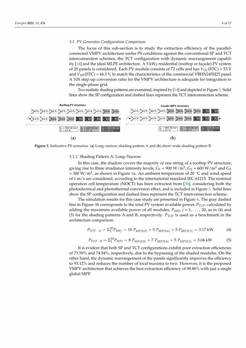
3.1. PV Generator Configuration Comparison
The focus of this sub-section is to study the extraction efficiency of the parallel-connected VMPV architecture under PS conditions against the conventional SP and TCTinterconnection schemes, the TCT configuration with dynamic rearrangement capabil-ity [14] and the ideal MLPE architecture. A 5 kWP residential (rooftop or façade) PV systemof 20 panels is considered. Each PV module consists of 72 cells and has VOC(STC) = 53 Vand VMP(STC) = 44.3 V, to match the characteristics of the commercial VBHN245SJ25 panel.A 10X step-up conversion ratio for the VMPV architecture is adequate for integration tothe single-phase grid.
Two realistic shading patterns are examined, inspired by [14] and depicted in Figure 3. Solidlines show the SP configuration and dashed lines represent the TCT interconnection scheme.
Energies 2021, 14, x FOR PEER REVIEW 6 of 18
power of the PV system, PPV, to the total available power from all individual modules,
PTOT, as shown in (3), for N panels. This efficiency factor represents the ability of the ar-
chitecture to extract as much of the available power as possible, regardless of the convert-
ers/electronics used. The reduction of ηext is usually attributed to three factors: (a) shaded
modules operating at a sub-optimal operating point or completely bypassed, (b) MPPT
locked on a local maximum and (c) MPPT oscillating around the normal operating point.
For a fair comparison of the VMPV with other conventional architectures, only component
(a) of ηext should be considered. Thus, for the rest of the paper, it is assumed that the MPPT
algorithm can always find the global maximum, even in the case of multiple power peaks
at PS, with negligible oscillation around the MPP.
To extract ηext for any PV configuration in real time, the PV model described in [10] is
used, that expresses the module voltage and current in explicit form.
3.1. PV Generator Configuration Comparison
The focus of this sub-section is to study the extraction efficiency of the parallel-con-
nected VMPV architecture under PS conditions against the conventional SP and TCT in-
terconnection schemes, the TCT configuration with dynamic rearrangement capability
[14] and the ideal MLPE architecture. A 5 kWP residential (rooftop or façade) PV system
of 20 panels is considered. Each PV module consists of 72 cells and has VOC(STC) = 53 V
and VMP(STC) = 44.3 V, to match the characteristics of the commercial VBHN245SJ25 panel.
A 10X step-up conversion ratio for the VMPV architecture is adequate for integration to
the single-phase grid.
Two realistic shading patterns are examined, inspired by [14] and depicted in Figure
3. Solid lines show the SP configuration and dashed lines represent the TCT interconnec-
tion scheme.
(a) (b)
Figure 3. Indicative PS scenarios. (a) Long–narrow shading pattern A and (b) short–wide shading pattern B.
3.1.1. Shading Pattern A: Long–Narrow
In this case, the shadow covers the majority of one string of a rooftop PV structure,
giving rise to three irradiance intensity levels, G1 = 900 W/m2, G2 = 600 W/m2 and G3 = 300
W/m2, as shown in Figure 3a. An ambient temperature of 20 °C and wind speed of 1 m/s
are considered, according to the international standard IEC-61215. The nominal operation
cell temperature (NOCT) has been extracted from [36], considering both the photoelectri-
cal and photothermal conversion effect, and is included in Figure 3. Solid lines show the
SP configuration and dashed lines represent the TCT interconnection scheme.
The simulation results for this case study are presented in Figure 4. The gray dashed
line in Figure 4b corresponds to the total PV system available power, PTOT, calculated by
adding the maximum available power of all modules, PMPj, j = 1,…,20, as in (4) and (5) for
the shading patterns A and B, respectively. PTOT is used as a benchmark in the architecture
comparison.
PTOT-A = Σ1
20PMPj = 10PMP(0.9) + 5PMP(0.6) + 5PMP(0.3) = 3.17 kW (4)
0.30.30.30.30.30.6
0.60.6
0.60.60.90.9
0.9 0.9 0.9 0.9 0.9 0.9 0.9 0.9
+
-
Rooftop PV structure
G1 = 900 W/m2
T1 = 43 oCG3 = 300 W/m2
T3 = 31 oCG2 = 600 W/m2
T2 = 37 oC
0.30.30.30.60.60.6
0.30.3
0.90.90.90.9
0.9 0.9 0.9 0.9 0.6 0.6 0.6 0.6
+
-
G1 = 900 W/m2
T1 = 51 oC
Façade BIPV structure
G3 = 300 W/m2
T3 = 38 oCG2 = 600 W/m2
T2 = 45 oC
Figure 3. Indicative PS scenarios. (a) Long–narrow shading pattern A and (b) short–wide shading pattern B.
3.1.1. Shading Pattern A: Long–Narrow
In this case, the shadow covers the majority of one string of a rooftop PV structure,giving rise to three irradiance intensity levels, G1 = 900 W/m2, G2 = 600 W/m2 and G3= 300 W/m2, as shown in Figure 3a. An ambient temperature of 20 C and wind speedof 1 m/s are considered, according to the international standard IEC-61215. The nominaloperation cell temperature (NOCT) has been extracted from [36], considering both thephotoelectrical and photothermal conversion effect, and is included in Figure 3. Solid linesshow the SP configuration and dashed lines represent the TCT interconnection scheme.
The simulation results for this case study are presented in Figure 4. The gray dashedline in Figure 4b corresponds to the total PV system available power, PTOT, calculated byadding the maximum available power of all modules, PMPj, j = 1, . . . , 20, as in (4) and(5) for the shading patterns A and B, respectively. PTOT is used as a benchmark in thearchitecture comparison.
PTOT−A = Σ201 PMPj = 10·PMP(0.9) + 5·PMP(0.6) + 5·PMP(0.3) = 3.17 kW (4)
PTOT−B = Σ201 PMPj = 8·PMP(0.9) + 7·PMP(0.6) + 5·PMP(0.3) = 3.04 kW (5)
It is evident that both SP and TCT configurations exhibit poor extraction efficienciesof 73.59% and 74.94%, respectively, due to the bypassing of the shaded modules. On theother hand, the dynamic rearrangement of the panels significantly improves the efficiencyto 93.12% and reduces the number of local maxima to two. However, it is the proposedVMPV architecture that achieves the best extraction efficiency of 99.86% with just a singleglobal MPP.

Energies 2021, 14, 456 7 of 17
Energies 2021, 14, x FOR PEER REVIEW 7 of 18
PTOT-B = Σ1
20PMPj = 8PMP(0.9) + 7PMP(0.6) + 5PMP(0.3) = 3.04 kW (5)
Figure 4. I-V and P-V curves of the examined PV architectures under (a,b) the shading pattern A
and (c,d) the shading pattern B.
It is evident that both SP and TCT configurations exhibit poor extraction efficiencies
of 73.59% and 74.94%, respectively, due to the bypassing of the shaded modules. On the
other hand, the dynamic rearrangement of the panels significantly improves the efficiency
to 93.12% and reduces the number of local maxima to two. However, it is the proposed
VMPV architecture that achieves the best extraction efficiency of 99.86% with just a single
global MPP.
3.1.2. Shading Pattern B: Short–Wide
This scenario concerns a façade PV system, partially shaded by the pattern illustrated
in Figure 3b. In contrast to an open rack rooftop structure, the BIPVs are characterized by
a higher temperature (included in Figure 3b), since only one side of the panel is in contact
with the air. The output I-V and P-V characteristics for the shading pattern B are presented
in Figure 4c,d. Even under these highly non-uniform irradiance and temperature condi-
tions, the VMPV architecture still exhibits a near-perfect efficiency of 99.8%. As a compar-
ison, the SP and TCT interconnection schemes have ηext(SP) = 69.4% and ηext(TCT) = 68.3%,
respectively, while the electrically rearranged TCT array has ηext(TCTR) = 95.5%.
Figure 4. I-V and P-V curves of the examined PV architectures under (a,b) the shading pattern A and (c,d) the shadingpattern B.
3.1.2. Shading Pattern B: Short–Wide
This scenario concerns a façade PV system, partially shaded by the pattern illustratedin Figure 3b. In contrast to an open rack rooftop structure, the BIPVs are characterized by ahigher temperature (included in Figure 3b), since only one side of the panel is in contactwith the air. The output I-V and P-V characteristics for the shading pattern B are presentedin Figure 4c,d. Even under these highly non-uniform irradiance and temperature conditions,the VMPV architecture still exhibits a near-perfect efficiency of 99.8%. As a comparison,the SP and TCT interconnection schemes have ηext(SP) = 69.4% and ηext(TCT) = 68.3%,respectively, while the electrically rearranged TCT array has ηext(TCTR) = 95.5%.
3.2. Grid-Connected VMPV System
To evaluate the time response of the whole system under variation of the atmo-spheric conditions, the proposed PV architecture is connected to a single-phase grid-sideinverter. Two scenarios are simulated, where the PV structure is initially uniformly in-solated (G1 = 900 W/m2) and gradually shaded to match shading pattern A or shadingpattern B. A linear drop of the irradiance is considered (see Figure 5), at a rate of 25 W/m2
per second, which is a representative value for rapidly changing environmental condi-tions [18]. The temperature variation of the individual PV groups is shown in Figure 5b,for both investigated shading patterns A (continuous lines) and B (dashed lines).

Energies 2021, 14, 456 8 of 17
Energies 2021, 14, x FOR PEER REVIEW 8 of 18
3.2. Grid-Connected VMPV System
To evaluate the time response of the whole system under variation of the atmospheric
conditions, the proposed PV architecture is connected to a single-phase grid-side inverter.
Two scenarios are simulated, where the PV structure is initially uniformly insolated (G1 =
900 W/m2) and gradually shaded to match shading pattern A or shading pattern B. A lin-
ear drop of the irradiance is considered (see Figure 5), at a rate of 25 W/m2 per second,
which is a representative value for rapidly changing environmental conditions [18]. The
temperature variation of the individual PV groups is shown in Figure 5b, for both inves-
tigated shading patterns A (continuous lines) and B (dashed lines).
(a) (b)
Figure 5. (a) Irradiance and (b) temperature variation with time for the three PV groups of the
VMPV architecture.
The inverter control is structured in three nested control loops, as outlined in Figure 6,
[37]. The outer control loop is a perturb and observe (P&O) MPPT that is applied at the
common high-voltage DC-bus and produces the reference DC-voltage, VDC*. In the middle
control loop, a PI controller regulates the active and reactive power reference to be injected
to the grid, P* and Q*, respectively. A proportional resonant (PR) current controller is im-
plemented in the inner control loop and the grid frequency is extracted by a second-order
generalized integrator phase locked loop (SOGI-PLL).
0 5 10 15 20 25 300
200
400
600
800
1000
Group1
Group2
Group3
Irra
dia
nce
(W
/m2)
Time (s)
12.5 W/m2 /sec
25 W/m2 /sec
900W/m2
600W/m2
300W/m2
0 5 10 15 20 25 3025
30
35
40
45
50
55
Pattern A Pattern B
Group1 Group1
Group2 Group2
Group3 Group3Mo
du
le T
emp
era
ture
(oC
)
Time (s)
Figure 5. (a) Irradiance and (b) temperature variation with time for the three PV groups of theVMPV architecture.
The inverter control is structured in three nested control loops, as outlined in Figure 6, [37].The outer control loop is a perturb and observe (P&O) MPPT that is applied at the commonhigh-voltage DC-bus and produces the reference DC-voltage, VDC*. In the middle controlloop, a PI controller regulates the active and reactive power reference to be injected to thegrid, P* and Q*, respectively. A proportional resonant (PR) current controller is imple-mented in the inner control loop and the grid frequency is extracted by a second-ordergeneralized integrator phase locked loop (SOGI-PLL).
Energies 2021, 14, x FOR PEER REVIEW 9 of 18
Figure 6. Complete control scheme of the proposed grid-connected PV system, consisting of three
nested control loops.
Figure 7a shows the active power fed to the grid, POUT, with respect to the total avail-
able PV power, PTOT. The new VMPV architecture follows closely the benchmark curve,
even when all the shaded panels have reached their steady state conditions (Time > 27 s).
For comparison purposes, the output power of the conventional SP interconnection is also
included in the same figure. Notably, the DC-link voltage variation is limited to a range
of just 4 V (from 420 V to 424 V) in the VMPV case, as can be seen in Figure 7b, despite the
significant variation of the produced power. In contrast, the voltage variation of the SP
configuration is 33 V for the same shading pattern.
(a) (b)
Figure 7. (a) Active power fed to the grid and (b) DC-bus voltage variation with time for the proposed VMPV under
shading pattern A.
DC-link
vα vβ
PI
vDC*
iDC
vDC
+ -
A
Output filter
V
CDC
DC
ACiinv
ig
V
vg
Grid
SOGIvg΄ qvg΄
αβdq
vd vq
PI
ω1/sθ
LPF
Notch
vDC-LPF
P*
Q*
Q - Grid command
ig*
θ
+ -
ω
v*PWM
SPWM
PR
A
eDC
eg
P&OMPPT
Notch
LPF
Sat
iDC
iDC-LPF
iDC- NOTCH
vDC- NOTCH
ig=f(P,Q,θ)
VMPV modules 1 - 20
PR current controller
PI vol tage control ler
A
P&O MPPT controller
Central Single-Stage Inverter
nX
nX
0 5 10 15 20 25 30
400
450
500
VMPV Architecture SP Interconnection
DC
-Lin
k V
olta
ge (V
)
Time (s)
0 5 10 15 20 25 30
400
450
500
DC
-Lin
k V
olt
age
(V
)
Time (s)
Figure 6. Complete control scheme of the proposed grid-connected PV system, consisting of threenested control loops.
Figure 7a shows the active power fed to the grid, POUT, with respect to the total avail-able PV power, PTOT. The new VMPV architecture follows closely the benchmark curve,even when all the shaded panels have reached their steady state conditions (Time > 27 s).For comparison purposes, the output power of the conventional SP interconnection is alsoincluded in the same figure. Notably, the DC-link voltage variation is limited to a range ofjust 4 V (from 420 V to 424 V) in the VMPV case, as can be seen in Figure 7b, despite the
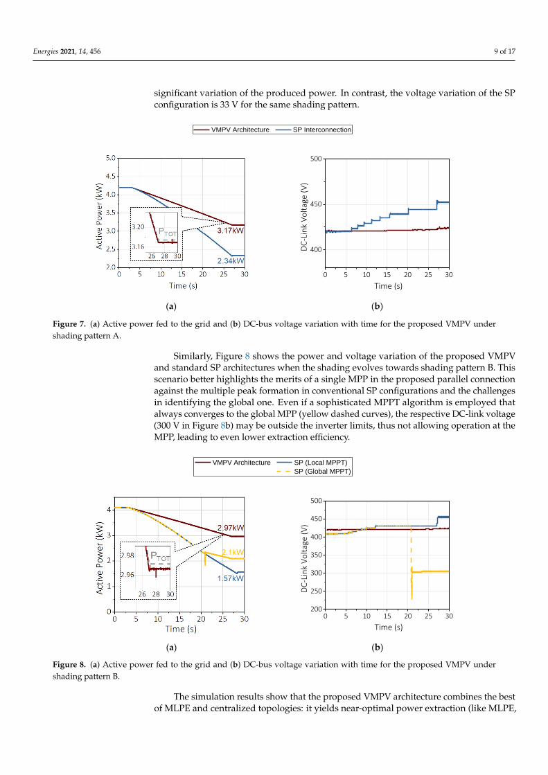
Energies 2021, 14, 456 9 of 17
significant variation of the produced power. In contrast, the voltage variation of the SPconfiguration is 33 V for the same shading pattern.
Energies 2021, 14, x FOR PEER REVIEW 9 of 18
Figure 6. Complete control scheme of the proposed grid-connected PV system, consisting of three
nested control loops.
Figure 7a shows the active power fed to the grid, POUT, with respect to the total avail-
able PV power, PTOT. The new VMPV architecture follows closely the benchmark curve,
even when all the shaded panels have reached their steady state conditions (Time > 27 s).
For comparison purposes, the output power of the conventional SP interconnection is also
included in the same figure. Notably, the DC-link voltage variation is limited to a range
of just 4 V (from 420 V to 424 V) in the VMPV case, as can be seen in Figure 7b, despite the
significant variation of the produced power. In contrast, the voltage variation of the SP
configuration is 33 V for the same shading pattern.
(a) (b)
Figure 7. (a) Active power fed to the grid and (b) DC-bus voltage variation with time for the proposed VMPV under
shading pattern A.
DC-link
vα vβ
PI
vDC*
iDC
vDC
+ -
A
Output filter
V
CDC
DC
ACiinv
ig
V
vg
Grid
SOGIvg΄ qvg΄
αβdq
vd vq
PI
ω1/sθ
LPF
Notch
vDC-LPF
P*
Q*
Q - Grid command
ig*
θ
+ -
ω
v*PWM
SPWM
PR
A
eDC
eg
P&OMPPT
Notch
LPF
Sat
iDC
iDC-LPF
iDC- NOTCH
vDC- NOTCH
ig=f(P,Q,θ)
VMPV modules 1 - 20
PR current controller
PI vol tage control ler
A
P&O MPPT controller
Central Single-Stage Inverter
nX
nX
0 5 10 15 20 25 30
400
450
500
VMPV Architecture SP Interconnection
DC
-Lin
k V
olta
ge (V
)
Time (s)
0 5 10 15 20 25 30
400
450
500
DC
-Lin
k V
olt
age
(V
)
Time (s)
Figure 7. (a) Active power fed to the grid and (b) DC-bus voltage variation with time for the proposed VMPV undershading pattern A.
Similarly, Figure 8 shows the power and voltage variation of the proposed VMPVand standard SP architectures when the shading evolves towards shading pattern B. Thisscenario better highlights the merits of a single MPP in the proposed parallel connectionagainst the multiple peak formation in conventional SP configurations and the challengesin identifying the global one. Even if a sophisticated MPPT algorithm is employed thatalways converges to the global MPP (yellow dashed curves), the respective DC-link voltage(300 V in Figure 8b) may be outside the inverter limits, thus not allowing operation at theMPP, leading to even lower extraction efficiency.
Energies 2021, 14, x FOR PEER REVIEW 10 of 18
Similarly, Figure 8 shows the power and voltage variation of the proposed VMPV
and standard SP architectures when the shading evolves towards shading pattern B. This
scenario better highlights the merits of a single MPP in the proposed parallel connection
against the multiple peak formation in conventional SP configurations and the challenges
in identifying the global one. Even if a sophisticated MPPT algorithm is employed that
always converges to the global MPP (yellow dashed curves), the respective DC-link volt-
age (300 V in Figure 8b) may be outside the inverter limits, thus not allowing operation at
the MPP, leading to even lower extraction efficiency.
(a) (b)
Figure 8. (a) Active power fed to the grid and (b) DC-bus voltage variation with time for the proposed VMPV under
shading pattern B.
The simulation results show that the proposed VMPV architecture combines the best
of MLPE and centralized topologies: it yields near-optimal power extraction (like MLPE,
in contrast to centralized) while allowing for sophisticated control functions in the inverter
(like centralized, as opposed to micro-inverters).
4. Experimental Validation
In this section, the favorable operation of the VMPV architecture under uniform and
PS conditions is experimentally validated and compared to a conventional string config-
uration.
4.1. Experimental Setup
Two 245 WP PV modules of the same type, VBHN245SJ25, are used as inputs to two
nX converters that are connected in parallel at the high-voltage side, as depicted in Figure 9.
Throughout the experiment, both PV panels are placed close to each other on a structure
of fixed inclination with respect to the horizon. Semi-transparent fabric is used to cover
one PV module completely and uniformly to emulate PS conditions.
0 5 10 15 20 25 30200
250
300
350
400
450
500
VMPV Architecture SP (Local MPPT)
SP (Global MPPT)
DC
-Lin
k V
olt
age
(V
)
Time (s)
0 5 10 15 20 25 30200
250
300
350
400
450
500
DC
-Lin
k V
olt
age
(V)
Time (s)
Figure 8. (a) Active power fed to the grid and (b) DC-bus voltage variation with time for the proposed VMPV undershading pattern B.
The simulation results show that the proposed VMPV architecture combines the bestof MLPE and centralized topologies: it yields near-optimal power extraction (like MLPE,

Energies 2021, 14, 456 10 of 17
in contrast to centralized) while allowing for sophisticated control functions in the inverter(like centralized, as opposed to micro-inverters).
4. Experimental Validation
In this section, the favorable operation of the VMPV architecture under uniformand PS conditions is experimentally validated and compared to a conventional stringconfiguration.
4.1. Experimental Setup
Two 245 WP PV modules of the same type, VBHN245SJ25, are used as inputs to twonX converters that are connected in parallel at the high-voltage side, as depicted in Figure 9.Throughout the experiment, both PV panels are placed close to each other on a structure offixed inclination with respect to the horizon. Semi-transparent fabric is used to cover onePV module completely and uniformly to emulate PS conditions.
Energies 2021, 14, x FOR PEER REVIEW 11 of 18
Figure 9. Experimental setup consisting of two VMPV modules.
The objective of these experiments is to study the first stage of the system inde-
pendently from the topology of the second stage. To this end, a DC-DC converter that
performs all control functions, including scanning of the PV curves and MPPT, feeding a
resistive load, was used as a simple substitute of the grid-tied inverter. This setup allows
for safe and repetitive testing of the new architecture, while the results are also valid for
the grid-connected system. The switching frequency of the buck converter was set to 20
kHz and the MPPT period to 250 ms. All voltage and current measurements were contin-
uously monitored with a sampling rate of 4 k samples/s and then filtered via a digital low-
pass filter (LPF) with a cutoff frequency of 100 Hz to reject the switching noise. The key
components and parameters of the experimental setup are summarized in Table 1.
Table 1. List of components of the experimental setup.
Component Parameter Value
PV modules
Part Type VBHN245SJ25
VMP 44.3 V
IMP 5.53 A
VOC 53 V
ISC 5.86 A
Module-level nX converter
Transistors in QP/N position GS61008T
Transistors in Qa/b position GS66508T
Switching capacitors 4 × 2.2 μF, X6S
Gate driver LM5114
Digital/Power isolator ISOW7842F
2nd-stage DC-DC converter
Series diodes S10KC
LDC-DC 1.5 mH
CDC-DC 50 μF
Transistor IPB65R190CFD
Switching diode C3D08065E
Micro-controller TMS320F28379D
Switching frequency (FSW-B) 20 kHz
MPPT period (TMPPT) 250 ms
Voltage/Current sampling rate 4 k samples/s
LPF cutoff frequency (F0) 100 Hz
Output Resistor Rout 0–240 Ω
2nd Stage Converter(MPPT function)
nX 1
nX 2
Parallel connection at High Voltage DC bus
PV Module 2
PV Module 1
Output
Figure 9. Experimental setup consisting of two VMPV modules.
The objective of these experiments is to study the first stage of the system indepen-dently from the topology of the second stage. To this end, a DC-DC converter that performsall control functions, including scanning of the PV curves and MPPT, feeding a resistiveload, was used as a simple substitute of the grid-tied inverter. This setup allows for safeand repetitive testing of the new architecture, while the results are also valid for the grid-connected system. The switching frequency of the buck converter was set to 20 kHz andthe MPPT period to 250 ms. All voltage and current measurements were continuously mon-itored with a sampling rate of 4 k samples/s and then filtered via a digital low-pass filter(LPF) with a cutoff frequency of 100 Hz to reject the switching noise. The key componentsand parameters of the experimental setup are summarized in Table 1.
4.2. PV-Side nX Converter
The backbone of the new architecture is the GaN-based magnetic-free nX converter,depicted in Figure 10. It has a 10-times step-up ratio to match the simulation conditions inSection 3. The developed prototype consists of two separate printed circuit boards (PCBs):the drive board, shown in Figure 10a, and the power board, in Figure 10b. One side of thepower PCB is reserved only for the GaN HEMTs, a design aspect that provides flexibilityto mount the board on any flat surface, such as a heat sink or the backside of the PV panel.Four parallel-connected multilayer ceramic capacitors (MLCCs) of 2.2 µF each, with lowinternal series resistance (ESR), constitute the output capacitance of each cell.

Energies 2021, 14, 456 11 of 17
Table 1. List of components of the experimental setup.
Component Parameter Value
PV modules
Part Type VBHN245SJ25VMP 44.3 VIMP 5.53 AVOC 53 VISC 5.86 A
Module-level nX converter
Transistors in QP/N position GS61008TTransistors in Qa/b position GS66508T
Switching capacitors 4 × 2.2 µF, X6SGate driver LM5114
Digital/Power isolator ISOW7842F
2nd-stage DC-DC converter
Series diodes S10KCLDC-DC 1.5 mHCDC-DC 50 µF
Transistor IPB65R190CFDSwitching diode C3D08065EMicro-controller TMS320F28379D
Switching frequency (FSW-B) 20 kHzMPPT period (TMPPT) 250 ms
Voltage/Current samplingrate 4 k samples/s
LPF cutoff frequency (F0) 100 Hz
Output Resistor Rout 0–240 Ω
Energies 2021, 14, x FOR PEER REVIEW 12 of 18
4.2. PV-Side nX Converter
The backbone of the new architecture is the GaN-based magnetic-free nX converter,
depicted in Figure 10. It has a 10-times step-up ratio to match the simulation conditions in
Section 3. The developed prototype consists of two separate printed circuit boards (PCBs):
the drive board, shown in Figure 10a, and the power board, in Figure 10b. One side of the
power PCB is reserved only for the GaN HEMTs, a design aspect that provides flexibility
to mount the board on any flat surface, such as a heat sink or the backside of the PV panel.
Four parallel-connected multilayer ceramic capacitors (MLCCs) of 2.2 μF each, with low
internal series resistance (ESR), constitute the output capacitance of each cell.
(a) (b) (c)
Figure 10. (a) Front side—drive board, (b) back side—power board and (c) side view of the mag-
netic-free nX converter prototype.
The switching frequency is tuned to match the circuit resonant frequency, FSW-nX = 200
kHz, to achieve zero current switching (ZCS) operation and, thus, minimize the switching
losses. The entire converter occupies just 100 mL of volume (100 mm × 100 mm × 10 mm)
and has a fixed conversion efficiency of 96.3%, throughout the power range, as shown in
Figure 11a. This is a strong point of this converter that ensures a high energy yield, even
under low irradiance conditions. In contrast, other high step-up micro-converters exhibit
efficiencies that peak from 94–98% [25,27,29], but drop significantly (below 90%) in low
loading conditions, due to higher switching losses from entering discontinuous conduc-
tion mode or exiting the soft switching window. On the other hand, the magnetic-free nX
converter is always operating at a fixed 50% duty cycle, and is inherently operating under
soft switching, as explained in [32]. Please note that the calculated conversion efficiency
does not account for any losses from the grid-side inverter or the output filter, which is
expected to introduce a non-linearity to the total system efficiency curve at light loads. It
should be mentioned that the conversion efficiency can be further improved by choosing
GaN HEMTs with even lower on-resistance and faster switching transients.
10 mm
Digital & Power Isolators
MicrocontrollerμUSB Power
Port
Cell 1 Cell 2
Cell 3 Cell 4
Cell 5
Input
Output
Figure 10. (a) Front side—drive board, (b) back side—power board and (c) side view of the magnetic-free nX converter prototype.
The switching frequency is tuned to match the circuit resonant frequency, FSW-nX = 200 kHz,to achieve zero current switching (ZCS) operation and, thus, minimize the switching losses.The entire converter occupies just 100 mL of volume (100 mm × 100 mm× 10 mm) and hasa fixed conversion efficiency of 96.3%, throughout the power range, as shown in Figure 11a.This is a strong point of this converter that ensures a high energy yield, even under low irra-diance conditions. In contrast, other high step-up micro-converters exhibit efficiencies thatpeak from 94–98% [25,27,29], but drop significantly (below 90%) in low loading conditions,due to higher switching losses from entering discontinuous conduction mode or exitingthe soft switching window. On the other hand, the magnetic-free nX converter is alwaysoperating at a fixed 50% duty cycle, and is inherently operating under soft switching, asexplained in [32]. Please note that the calculated conversion efficiency does not account forany losses from the grid-side inverter or the output filter, which is expected to introducea non-linearity to the total system efficiency curve at light loads. It should be mentioned

Energies 2021, 14, 456 12 of 17
that the conversion efficiency can be further improved by choosing GaN HEMTs with evenlower on-resistance and faster switching transients.
Energies 2021, 14, x FOR PEER REVIEW 13 of 18
(a) (b)
Figure 11. Experimental results of the developed 10X converter. (a) Efficiency curve over operat-
ing power and (b) voltage and power waveforms during operation at 250 W.
Voltage and power waveforms of the system operating at 250 W are illustrated in
Figure 11b. Under these conditions, the temperature increase in the transistors was main-
tained below 15 °C, avoiding the use of bulky heat sinks. More design details and consid-
erations regarding the component selection and test conditions can be found in [35]. The
high power density (greater than 11 kW/l) and the low cooling requirements are both key
factors that enable the integration of the nX converter with the solar panel.
4.3. Output Characteristics of the VMPV System
The I-V and P-V characteristics of the proposed PV system were recorded in two
shading patterns: (A) uniform irradiance and temperature conditions and (B) partial shad-
ing, where one panel is uniformly shaded while the other one remains unshaded. The
curves are captured by slowly changing the operating point within 5 s (scanning), which
guarantees that the measurements are not affected by transient phenomena attributed to
the second-stage inductance and output capacitance.
Figure 12a,b show the characteristic curves of the two individual PV modules
(dashed and dash–dot lines) and the combined curve of the proposed VMPV architecture
(solid red line), under uniform irradiance and temperature conditions. It should be noted
that, although the parallel connection takes place at the high-voltage side of the nX con-
verters, the I-V and P-V characteristics are translated to the PV-side for consistency with
the string topology (blue line).
0 200 400 600 800 1000 120090
92
94
96
98
100
Effi
cien
cy (
%)
Power (W)-10 -5 0 5 10
0
100
200
300
400
500
Inp
ut/
Ou
tpu
t V
olt
age
(V)
Time (µs)
0
100
200
300
400
Inp
ut/
Ou
tpu
t Po
wer
(W
)
VOUT
VIN
PIN
POUT
Figure 11. Experimental results of the developed 10X converter. (a) Efficiency curve over operatingpower and (b) voltage and power waveforms during operation at 250 W.
Voltage and power waveforms of the system operating at 250 W are illustrated inFigure 11b. Under these conditions, the temperature increase in the transistors was main-tained below 15 C, avoiding the use of bulky heat sinks. More design details and consid-erations regarding the component selection and test conditions can be found in [35]. Thehigh power density (greater than 11 kW/l) and the low cooling requirements are both keyfactors that enable the integration of the nX converter with the solar panel.
4.3. Output Characteristics of the VMPV System
The I-V and P-V characteristics of the proposed PV system were recorded in twoshading patterns: (A) uniform irradiance and temperature conditions and (B) partialshading, where one panel is uniformly shaded while the other one remains unshaded. Thecurves are captured by slowly changing the operating point within 5 s (scanning), whichguarantees that the measurements are not affected by transient phenomena attributed tothe second-stage inductance and output capacitance.
Figure 12a,b show the characteristic curves of the two individual PV modules (dashedand dash–dot lines) and the combined curve of the proposed VMPV architecture (solidred line), under uniform irradiance and temperature conditions. It should be noted that,although the parallel connection takes place at the high-voltage side of the nX converters,the I-V and P-V characteristics are translated to the PV-side for consistency with the stringtopology (blue line).
As shown in Table 2, the two modules are not identical and their MPPs differ by 3.4 Wand are spaced by 1.17 V. However, the power loss of the VMPV approach is just 0.4 W,resulting in an excellent extraction efficiency of 99.9%. In fact, both modules operate at99.9% of their respective MPPs. In this scenario, the string arrangement also has near-perfect extraction efficiency but no conversion losses. It should be noted that the totalavailable PV power PTOT = PMP1 + PMP2 and the actual extracted power PPV are measuredin successive experiments within a short time duration to ensure equal irradiance andtemperature conditions; it is impossible to measure the maximum available power of theindividual modules when they form a PV string that operates at a different operating point.

Energies 2021, 14, 456 13 of 17Energies 2021, 14, x FOR PEER REVIEW 14 of 18
(a) (b)
(c) (d)
Figure 12. Experimentally extracted I-V and P-V characteristics of the PV modules under (a,b) the shading pattern A:
uniform irradiance and (c,d) the shading pattern B: PS conditions.
As shown in Table 2, the two modules are not identical and their MPPs differ by 3.4
W and are spaced by 1.17 V. However, the power loss of the VMPV approach is just 0.4
W, resulting in an excellent extraction efficiency of 99.9%. In fact, both modules operate at
99.9% of their respective MPPs. In this scenario, the string arrangement also has near-
perfect extraction efficiency but no conversion losses. It should be noted that the total
available PV power PTOT = PMP1 + PMP2 and the actual extracted power PPV are measured in
successive experiments within a short time duration to ensure equal irradiance and tem-
perature conditions; it is impossible to measure the maximum available power of the in-
dividual modules when they form a PV string that operates at a different operating point.
Table 2. MPP data from the experimentally extracted characteristics.
Test Conditions PV Module/PV System VPV (V) IPV (A) PPV (W) Extraction
eff. (%)
Pattern A:
Uniform Conditions
Module 1 (MPP1) 41.25 4.705 194.1 -
Module 2 (MPP2) 40.08 4.757 190.7 -
VMPV Architecture (MPPVMPV) 40.52 9.475 384.4 99.9
Module 1 (@MPPVMPV) 40.52 4.785 193.9 99.9
20 40 60 80 1000
50
100
150
200
250
300
350
400
PV P
ow
er (
W)
PV Voltage (V)
VMPV Architecture Module 1
String Configuration Module 2
MPPVMPV
MPP1
MPP2
GMPPS
20 40 60 80 1000
2
4
6
8
10
12
PV C
urr
ent
(A)
PV Voltage (V)
MPPVMPV
MPP2 GMPPS
MPP1
20 40 60 80 1000
50
100
150
200
250
300
350
400
PV P
ow
er (
W)
PV Voltage (V)
MPPVMPV
MPP1
MPP2
GMPPS
20 40 60 80 1000
2
4
6
PV
Cu
rren
t (A
)
PV Voltage (V)
LMPPSMPP1
GMPPS
MPP2
MPPVMPV
20 40 60 80 1000
50
100
150
200
250PV
Po
wer
(W
)
PV Voltage (V)
MPPVMPV
MPP2
MPP1
GMPPS
LMPPS
Figure 12. Experimentally extracted I-V and P-V characteristics of the PV modules under (a,b) the shading pattern A:uniform irradiance and (c,d) the shading pattern B: PS conditions.
Table 2. MPP data from the experimentally extracted characteristics.
Test Conditions PV Module/PV System VPV (V) IPV (A) PPV (W) Extractioneff. (%)
Pattern A:Uniform
Conditions
Module 1 (MPP1) 41.25 4.705 194.1 -Module 2 (MPP2) 40.08 4.757 190.7 -
VMPV Architecture (MPPVMPV) 40.52 9.475 384.4 99.9Module 1 (@MPPVMPV) 40.52 4.785 193.9 99.9Module 2 (@MPPVMPV) 40.52 4.702 190.5 99.9
Pattern B:PS Conditions
Module 1 (MPP1) 42.5 1.145 48.7 -Module 2 (MPP2) 41.05 4.26 174.9 -
VMPV Architecture (MPPVMPV) 41.6 5.36 223 99.74Module 1 (@MPPVMPV) 41.6 1.161 48.3 99.18Module 2 (@MPPVMPV) 41.6 4.20 174.7 99.89
Series Connection (GMPPS) 39.65 4.38 174 77.8Series Connection (LMPPS) 91.3 1.255 113 50.5
Figure 12c,d show the experimentally extracted I-V and P-V traces under the shadingpattern B: Module 1 is entirely shaded, while Module 2 remains unshaded. Although

Energies 2021, 14, 456 14 of 17
PPV(MPP1) = 48.7 W is more than 3.5 times smaller than PPV(MPP2) = 174.9 W, theirrespective voltage difference is just 1.45 V, leading to an almost perfect ηext = 99.74%for the VMPV system. Taking the effect of ηc into account, the total system efficiency isηsys = 96.05%. On the other hand, the global MPP of the series connection is PPV(GMPPS)= 174 W, equal to MPP2 minus the power dissipated at the bypass diode of Module 1,resulting in an extraction efficiency of just 77.8%. Still, it is highly possible that a simpleMPPT algorithm would converge at a local MPP (LMPP), in which case half of the PVpower would be lost (ηext(LMPPS) = 50.5%).
4.4. Real-Time MPPT of the VMPV Architecture
For this experiment, a P&O algorithm was executed by the second-stage converter,with a period of 250 ms and an MPPT duty cycle step of 1%. The two PV moduleswere subjected to the two shading patterns of the previous subsection (uniform andPS conditions).
Figure 13 shows the output power and DC-bus voltage variation under real-timetracking of the MPP. The MPPT algorithm always converges to the single MPP, guaranteeingnear-perfect extraction efficiency in any conditions and effectively addressing the trackingchallenges of SP configurations. In addition, the DC-link voltage is insignificantly affectedby PS (only a 3% deviation), which allows for a narrow predetermined input voltage rangefor the grid-side inverter, in contrast to the single-stage PV systems.
Energies 2021, 14, x FOR PEER REVIEW 15 of 18
Module 2 (@MPPVMPV) 40.52 4.702 190.5 99.9
Pattern B:
PS Conditions
Module 1 (MPP1) 42.5 1.145 48.7 -
Module 2 (MPP2) 41.05 4.26 174.9 -
VMPV Architecture (MPPVMPV) 41.6 5.36 223 99.74
Module 1 (@MPPVMPV) 41.6 1.161 48.3 99.18
Module 2 (@MPPVMPV) 41.6 4.20 174.7 99.89
Series Connection (GMPPS) 39.65 4.38 174 77.8
Series Connection (LMPPS) 91.3 1.255 113 50.5
Figure 12c,d show the experimentally extracted I-V and P-V traces under the shading
pattern B: Module 1 is entirely shaded, while Module 2 remains unshaded. Although
PPV(MPP1) = 48.7 W is more than 3.5 times smaller than PPV(MPP2) = 174.9 W, their respec-
tive voltage difference is just 1.45 V, leading to an almost perfect ηext = 99.74% for the
VMPV system. Taking the effect of ηc into account, the total system efficiency is ηsys =
96.05%. On the other hand, the global MPP of the series connection is PPV(GMPPS) = 174
W, equal to MPP2 minus the power dissipated at the bypass diode of Module 1, resulting
in an extraction efficiency of just 77.8%. Still, it is highly possible that a simple MPPT al-
gorithm would converge at a local MPP (LMPP), in which case half of the PV power would
be lost (ηext(LMPPS) = 50.5%).
4.4. Real-Time MPPT of the VMPV Architecture
For this experiment, a P&O algorithm was executed by the second-stage converter, with
a period of 250 ms and an MPPT duty cycle step of 1%. The two PV modules were subjected
to the two shading patterns of the previous subsection (uniform and PS conditions).
Figure 13 shows the output power and DC-bus voltage variation under real-time
tracking of the MPP. The MPPT algorithm always converges to the single MPP, guaran-
teeing near-perfect extraction efficiency in any conditions and effectively addressing the
tracking challenges of SP configurations. In addition, the DC-link voltage is insignificantly
affected by PS (only a 3% deviation), which allows for a narrow predetermined input volt-
age range for the grid-side inverter, in contrast to the single-stage PV systems.
Figure 13. Response of the new VMPV architecture during real-time MPPT, under uniform and PS
conditions. Output power (in red) and DC-bus voltage (in blue) variation with time.
The experimental results show that the proposed VMPV architecture combines the
near-perfect extraction efficiency of MLPE with a flat conversion efficiency in any condi-
tions; this leads to a higher total system efficiency than most state-of-the-art configura-
tions, including other MLPE architectures.
5. Conclusions
In this paper, a new highly efficient architecture for residential grid-connected PV sys-
tems has been demonstrated and experimentally verified. The PV modules are connected in
0 10 20 30 40 50 60 70 800
100
200
300
400
500
Ou
tpu
t Po
wer
(W
)
Time (s)
Uniform Conditions Partial Shading
Uniform Conditions Partial Shading0
100
200
300
400
500
DC
-Lin
k V
olt
age
(V)
Figure 13. Response of the new VMPV architecture during real-time MPPT, under uniform and PSconditions. Output power (in red) and DC-bus voltage (in blue) variation with time.
The experimental results show that the proposed VMPV architecture combines thenear-perfect extraction efficiency of MLPE with a flat conversion efficiency in any condi-tions; this leads to a higher total system efficiency than most state-of-the-art configurations,including other MLPE architectures.
5. Conclusions
In this paper, a new highly efficient architecture for residential grid-connected PVsystems has been demonstrated and experimentally verified. The PV modules are con-nected in parallel through fixed-step high step-up nX converters (voltage multipliers), thuseliminating the partial shading challenges of typical series connections and deliveringalmost 100% extraction efficiency. At the same time, the nX converter features a highflat conversion efficiency of more than 96.3% irrespective of the power level, leading tobetter total system efficiency at partial shading than most centralized and distributedPV architectures.
The developed magnetic-free nX converters use GaN HEMTs that are switching athigh frequency which, in turn, allow for longer lifetime ceramic capacitors in place of theconventional bulky electrolytic capacitors. This, along with the omissions of all magneticcomponents and the low cooling requirements, lead to a very compact solution that can beintegrated with the backside of the PV panel, forming a new voltage-multiplied PV module.

Energies 2021, 14, 456 15 of 17
All control functions, including MPPT, are transferred to the inverter, simplifying theDC-DC micro-converter requirements for micro-controllers and voltage/current sensors.The high-voltage parallel connection results in a small variation of the DC-link voltage withthe environmental conditions which, in turn, simplifies the requirements for the grid-sideinverter, as in two-stage string inverters.
Author Contributions: Conceptualization, G.K. and E.B.; methodology and investigation, G.K.;experimental validation, G.K. and R.v.E.; writing—original draft preparation, G.K.; writing—reviewand editing, E.B., R.v.E. and E.M.; project administration, supervision and funding acquisition, E.M.All authors have read and agreed to the published version of the manuscript.
Funding: This research was funded by the Swiss Office of Energy, Grant No. SI501568-01, theEuropean Research Council under the European Union’s H2020 program/ERC Grant Agreement No.679425 and the Royal Academy of Engineering under the Engineering for Development ResearchFellowship scheme, Grant No. RF\201819\18\86.
Institutional Review Board Statement: Not applicable.
Informed Consent Statement: Not applicable.
Data Availability Statement: No new data were created or analyzed in this study. Data sharing isnot applicable to this article.
Conflicts of Interest: The authors declare no conflict of interest.
Abbreviations
BIPV Building-integrated photovoltaicBL Bridge-link interconnection schemeDER Distributed energy resourcesESR Capacitor’s internal series resistanceGMPP Global maximum power pointHC Honey-comb interconnection schemeHEMT High electron mobility transistorIC Integrated circuitLMPP Local maximum power pointLPF Low-pass filterMLCC Multi-layer ceramic capacitorsMLPE Module-level power electronicsMPPT Maximum power pointNOCT Nominal operation cell temperatureP&O Perturb and observe algorithmPCB Printed circuit boardPLL Phase locked loopPR Proportional resonant controllerPS Partial shadingPV PhotovoltaicPVPO Photovoltaic power optimizerPWM Pulse width modulationSC Switched capacitorSOGI Second order generalized integratorSP Series-parallel interconnection schemeSTC Standard test conditionsTCT Total-cross-tied interconnection schemeTCTR Electrically rearranged TCT arrayVMPV Voltage-multiplied photovoltaic systemZCS Zero current switching

Energies 2021, 14, 456 16 of 17
References1. Eftekharnejad, S.; Vittal, V.; Heydt, G.T.; Keel, B.; Loehr, J. Impact of Increased Penetration of Photovoltaic Generation on Power
Systems. IEEE Trans. Power Syst. 2013, 28, 893–901. [CrossRef]2. Batzelis, E.I.; Georgilakis, P.S.; Papathanassiou, S.A. Energy Models for Photovoltaic Systems under Partial Shading Conditions:
A Comprehensive Review. IET Renew. Power Gener. 2015, 9, 340–349. [CrossRef]3. Atmaja, T.D. Façade and Rooftop PV Installation Strategy for Building Integrated Photo Voltaic Application. Energy Procedia 2013,
32, 105–114. [CrossRef]4. Karatepe, E.; Boztepe, M.; Çolak, M. Development of a Suitable Model for Characterizing Photovoltaic Arrays with Shaded Solar
Cells. Solar Energy 2007, 81, 977–992. [CrossRef]5. Strache, S.; Wunderlich, R.; Heinen, S. A Comprehensive, Quantitative Comparison of Inverter Architectures for Various PV
Systems, PV Cells, and Irradiance Profiles. IEEE Trans. Sustain. Energy 2014, 5, 813–822. [CrossRef]6. Hanson, A.J.; Deline, C.A.; MacAlpine, S.M.; Stauth, J.T.; Sullivan, C.R. Partial-Shading Assessment of Photovoltaic Installations
via Module-Level Monitoring. IEEE J. Photovolt. 2014, 4, 1618–1624. [CrossRef]7. Drif, M.; Pérez, P.J.; Aguilera, J.; Aguilar, J.D. A New Estimation Method of Irradiance on a Partially Shaded PV Generator in
Grid-Connected Photovoltaic Systems. Renew. Energy 2008, 33, 2048–2056. [CrossRef]8. Li, H.; Yang, D.; Su, W.; Lu, J.; Yu, X. An Overall Distribution Particle Swarm Optimization MPPT Algorithm for Photovoltaic
System Under Partial Shading. IEEE Trans. Ind. Electron. 2019, 66, 265–275. [CrossRef]9. Sundareswaran, K.; Sankar, P.; Nayak, P.S.R.; Simon, S.P.; Palani, S. Enhanced Energy Output From a PV System Under Partial
Shaded Conditions Through Artificial Bee Colony. IEEE Trans. Sustain. Energy 2015, 6, 198–209. [CrossRef]10. Batzelis, E.I.; Kampitsis, G.E.; Papathanassiou, S.A.; Manias, S.N. Direct MPP Calculation in Terms of the Single-Diode PV Model
Parameters. IEEE Trans. Energy Convers. 2015, 30, 226–236. [CrossRef]11. Moballegh, S.; Jiang, J. Modeling, Prediction, and Experimental Validations of Power Peaks of PV Arrays Under Partial Shading
Conditions. IEEE Trans. Sustain. Energy 2014, 5, 293–300. [CrossRef]12. Jeyaprabha, S.B.; Selvakumar, A.I. Model-Based MPPT for Shaded and Mismatched Modules of Photovoltaic Farm. IEEE Trans.
Sustain. Energy 2017, 8, 1763–1771. [CrossRef]13. Shams El-Dein, M.Z.; Kazerani, M.; Salama, M.M.A. An Optimal Total Cross Tied Interconnection for Reducing Mismatch Losses
in Photovoltaic Arrays. IEEE Trans. Sustain. Energy 2013, 4, 99–107. [CrossRef]14. Babu, T.S.; Ram, J.P.; Dragicevic, T.; Miyatake, M.; Blaabjerg, F.; Rajasekar, N. Particle Swarm Optimization Based Solar PV Array
Reconfiguration of the Maximum Power Extraction Under Partial Shading Conditions. IEEE Trans. Sustain. Energy 2018, 9,74–85. [CrossRef]
15. Shams El-Dein, M.Z.; Kazerani, M.; Salama, M.M.A. Optimal Photovoltaic Array Reconfiguration to Reduce Partial ShadingLosses. IEEE Trans. Sustain. Energy 2013, 4, 145–153. [CrossRef]
16. Kjaer, S.B.; Pedersen, J.K.; Blaabjerg, F. A Review of Single-Phase Grid-Connected Inverters for Photovoltaic Modules. IEEE Trans.Ind. Appl. 2005, 41, 1292–1306. [CrossRef]
17. Meneses, D.; Blaabjerg, F.; García, Ó.; Cobos, J.A. Review and Comparison of Step-Up Transformerless Topologies for PhotovoltaicAC-Module Application. IEEE Trans. Power Electron. 2013, 28, 2649–2663. [CrossRef]
18. Batzelis, E.I.; Kampitsis, G.E.; Papathanassiou, S.A. Power Reserves Control for PV Systems With Real-Time MPP Estimation viaCurve Fitting. IEEE Trans. Sustain. Energy 2017, 8, 1269–1280. [CrossRef]
19. Chen, S.-M.; Liang, T.-J.; Hu, K.-R. Design, Analysis, and Implementation of Solar Power Optimizer for DC Distribution System.IEEE Trans. Power Electron. 2013, 28, 1764–1772. [CrossRef]
20. Vinnikov, D.; Chub, A.; Liivik, E.; Kosenko, R.; Korkh, O. Solar Optiverter—A Novel Hybrid Approach to the PhotovoltaicModule Level Power Electronics. IEEE Trans. Ind. Electron. 2019, 66, 3869–3880. [CrossRef]
21. Stauth, J.T.; Seeman, M.D.; Kesarwani, K. Resonant Switched-Capacitor Converters for Sub-Module Distributed PhotovoltaicPower Management. IEEE Trans. Power Electron. 2013, 28, 1189–1198. [CrossRef]
22. Tahmasbi-Fard, M.; Tarafdar-Hagh, M.; Pourpayam, S.; Haghrah, A.-A. A Voltage Equalizer Circuit to Reduce Partial ShadingEffect in Photovoltaic String. IEEE J. Photovolt. 2018, 8, 1102–1109. [CrossRef]
23. Li, W.; He, X. Review of Nonisolated High-Step-Up DC/DC Converters in Photovoltaic Grid-Connected Applications. IEEETrans. Ind. Electron. 2011, 58, 1239–1250. [CrossRef]
24. Gao, L.; Dougal, R.A.; Liu, S.; Iotova, A.P. Parallel-Connected Solar PV System to Address Partial and Rapidly FluctuatingShadow Conditions. IEEE Trans. Ind. Electron. 2009, 56, 1548–1556. [CrossRef]
25. Tseng, K.-C.; Huang, C.-C.; Shih, W.-Y. A High Step-Up Converter With a Voltage Multiplier Module for a Photovoltaic System.IEEE Trans. Power Electron. 2013, 28, 3047–3057. [CrossRef]
26. Ahmed, M.E.; Mousa, M.; Orabi, M. Development of High Gain and Efficiency Photovoltaic System Using Multilevel BoostConverter Topology. In Proceedings of the IEEE 2nd International Symposium on Power Electronics for Distributed GenerationSystems (PEDG), Hefei, China, 16–18 June 2010; pp. 898–903.
27. Molavi, N.; Farzanehfard, H.; Adib, E. Soft-Switched Non-Isolated High Step-up DC–DC Converter with Reduced Voltage Stress.IET Power Electron. 2016, 9, 1711–1718. [CrossRef]

Energies 2021, 14, 456 17 of 17
28. Revathi, B.S.; Prabhakar, M. High Gain High Power DC-DC Converter for Photovoltaic Application. In Proceedings of the2013 Annual International Conference on Emerging Research Areas and 2013 International Conference on Microelectronics,Communications and Renewable Energy, Kanjirapally, India, 4–6 June 2013; pp. 1–6.
29. Gu, B.; Dominic, J.; Lai, J.-S.; Zhao, Z.; Liu, C. High Boost Ratio Hybrid Transformer DC–DC Converter for Photovoltaic ModuleApplications. IEEE Trans. Power Electron. 2013, 28, 2048–2058. [CrossRef]
30. Nanakos, A.C.; Christidis, G.C.; Tatakis, E.C. Weighted Efficiency Optimization of Flyback Microinverter Under ImprovedBoundary Conduction Mode (i-BCM). IEEE Trans. Power Electron. 2015, 30, 5548–5564. [CrossRef]
31. Qian, W.; Cao, D.; Cintron-Rivera, J.G.; Gebben, M.; Wey, D.; Peng, F.Z. A Switched-Capacitor DC–DC Converter With HighVoltage Gain and Reduced Component Rating and Count. IEEE Trans. Ind. Appl. 2012, 48, 1397–1406. [CrossRef]
32. Kampitsis, G.; Chevron, M.; van Erp, R.; Perera, N.; Papathanassiou, S.; Matioli, E. Mixed Simulation-Experimental Optimizationof a Modular Multilevel Switched Capacitors Converter Cell. In Proceedings of the 2020 IEEE 21st Workshop on Control andModeling for Power Electronics (COMPEL), Aalborg, Denmark, 9 November 2020; pp. 1–6.
33. Cao, D.; Peng, F.Z. A Family of Zero Current Switching Switched-Capacitor Dc-Dc Converters. In Proceedings of the Twenty-FifthAnnual IEEE Applied Power Electronics Conference and Exposition (APEC), Palm Springs, CA, USA, 21–25 February 2010;pp. 1365–1372.
34. Uemoto, Y.; Morita, T.; Ikoshi, A.; Umeda, H.; Matsuo, H.; Shimizu, J.; Hikita, M.; Yanagihara, M.; Ueda, T.; Tanaka, T.; et al. GaNMonolithic Inverter IC Using Normally-off Gate Injection Transistors with Planar Isolation on Si Substrate. In Proceedings of the2009 IEEE International Electron Devices Meeting (IEDM), Baltimore, MD, USA, 7–9 December 2009; pp. 1–4.
35. Kampitsis, G.; van Erp, R.; Matioli, E. Ultra-High Power Density Magnetic-Less DC/DC Converter Utilizing GaN Transistors. InProceedings of the 2019 IEEE Applied Power Electronics Conference and Exposition (APEC), Anaheim, CA, USA, 17–21 March2019; pp. 1609–1615.
36. Zhang, Z.; Xiao, T.; Shen, Y.; Wang, L.; Jia, P.; Yu, J. A Method to Test Operating Cell Temperature for BIPV Modules. IEEE J.Photovolt. 2016, 6, 272–277. [CrossRef]
37. Kampitsis, G.; Batzelis, E.; Papathanassiou, S. Power Balance Control for a Two-Stage Solar Inverter with Low Voltage Ridethrough Capability. Eur. Photovolt. Solar Energy Conf. Exhib. 2016, 32, 1646–1650. [CrossRef]