Unconventional Thin-Film Thermoelectric Converters: Structure, Simulation, and Comparative Study
6
Unconventional Thin-Film Thermoelectric Converters: Structure, Simulation, and Comparative Study MACIEJ HARAS, 1,2,3 VALERIA LACATENA, 1,2 STE ´ PHANE MONFRAY, 2 JEAN-FRANC ¸ OIS ROBILLARD, 1 THOMAS SKOTNICKI, 2 and EMMANUEL DUBOIS 1,4 1.—IEMN UMR CNRS 8520, Institut d’Electronique, de Microe ´lectronique et de Nanotechnologie, Avenue Poincare ´, 59652 Villeneuve d’Ascq, France. 2.—STMicroelectronics 850, Rue Jean Monnet, 38926 Crolles, France. 3.—e-mail: [email protected]. 4.—e-mail: [email protected] Bi 2 Te 3 or Sb 2 Te 3 are the materials most widely used in thermoelectric genera- tors (TEG) operating near room temperature. These materials are, however, environmentally harmful, expensive, and incompatible with complementary metal-oxide semiconductor (CMOS) technology, in contrast to silicon (Si), ger- manium (Ge), or silicon–germanium (SiGe). Although the thermopower (S) and electrical conductivity (r) of Si and Ge are high, use in thermoelectricity is severely hindered by their high thermal conductivity (j). By altering the phonon band structure of this Si films by use of an artificial phononic pattern, specta- cular reduction of j by two orders of magnitude has been demonstrated. To take full advantage of phonon band modification and scattering in thin films, con- verter structure based on thin-film membranes is proposed for j reduction. To consolidate the position of Si-based materials, coupled charge and heat-trans- port simulations have been conducted to demonstrate the potential of the materials for thermoelectric conversion compared with such widespread materials as Bi 2 Te 3 . The effect of contact resistance on generator performance has been carefully taken into consideration to reflect integration constraints at the TEG level. For a temperature difference DT = 30 K, the maximum electrical power density reaches approximately 6 W/cm 2 for Si and Ge, and approximately 3 W/cm 2 for Si 0.7 Ge 0.3 , values which are similar to those for Bi 2 Te 3 . Finally, it is emphasized that the proposed approach is compatible with conventional Si technology and naturally provides augmented mechanical flexibility that sub- stantially widens the field of application of thermal harvesting. Key words: Thermoelectric conversion, thermal conductivity reduction, CMOS compatible materials, harvested power density, thin-film, performance simulation INTRODUCTION Current thermoelectrics suffer from a lack of materials with sufficiently high conversion efficiency. Moreover, environmentally harmful, complex, and expensive materials and materials incompatible with complementary metal-oxide semiconductor (CMOS) technology are commonly used, 1,2 making fabrication costs relatively high. For all these reasons, applica- tions of thermoelectric generators (TEG) are mainly limited to niche and sophisticated fields, e.g. automo- tive power generators, 3 spaceship generators, 4 industrial sensor feeders, 5 temperature measure- ments, 6 or advanced medical care. 7,8 Thermoelectric conversion requires materials with low thermal conductivity (j), high electrical conductivity (r), and thermopower (S) as large as possible. On the basis of these criteria, the performance of thermoelectric materials is com- (Received May 31, 2013; accepted January 2, 2014; published online January 22, 2014) Journal of ELECTRONIC MATERIALS, Vol. 43, No. 6, 2014 DOI: 10.1007/s11664-014-2982-z Ó 2014 TMS 2109
-
Upload
univ-lille1 -
Category
Documents
-
view
1 -
download
0
Transcript of Unconventional Thin-Film Thermoelectric Converters: Structure, Simulation, and Comparative Study

Unconventional Thin-Film Thermoelectric Converters:Structure, Simulation, and Comparative Study
MACIEJ HARAS,1,2,3 VALERIA LACATENA,1,2 STEPHANE MONFRAY,2
JEAN-FRANCOIS ROBILLARD,1 THOMAS SKOTNICKI,2
and EMMANUEL DUBOIS1,4
1.—IEMN UMR CNRS 8520, Institut d’Electronique, de Microelectronique et de Nanotechnologie,Avenue Poincare, 59652 Villeneuve d’Ascq, France. 2.—STMicroelectronics 850, Rue JeanMonnet, 38926 Crolles, France. 3.—e-mail: [email protected]. 4.—e-mail:[email protected]
Bi2Te3 or Sb2Te3 are the materials most widely used in thermoelectric genera-tors (TEG) operating near room temperature. These materials are, however,environmentally harmful, expensive, and incompatible with complementarymetal-oxide semiconductor (CMOS) technology, in contrast to silicon (Si), ger-manium (Ge), or silicon–germanium (SiGe). Although the thermopower (S) andelectrical conductivity (r) of Si and Ge are high, use in thermoelectricity isseverely hindered by their high thermal conductivity (j). By altering the phononband structure of this Si films by use of an artificial phononic pattern, specta-cular reduction of j by two orders of magnitude has been demonstrated. To takefull advantage of phonon band modification and scattering in thin films, con-verter structure based on thin-film membranes is proposed for j reduction. Toconsolidate the position of Si-based materials, coupled charge and heat-trans-port simulations have been conducted to demonstrate the potential of thematerials for thermoelectric conversion compared with such widespreadmaterials as Bi2Te3. The effect of contact resistance on generator performancehas been carefully taken into consideration to reflect integration constraints atthe TEG level. For a temperature difference DT = 30 K, the maximum electricalpower density reaches approximately 6 W/cm2 for Si and Ge, and approximately3 W/cm2 for Si0.7Ge0.3, values which are similar to those for Bi2Te3. Finally, it isemphasized that the proposed approach is compatible with conventional Sitechnology and naturally provides augmented mechanical flexibility that sub-stantially widens the field of application of thermal harvesting.
Key words: Thermoelectric conversion, thermal conductivity reduction,CMOS compatible materials, harvested power density,thin-film, performance simulation
INTRODUCTION
Current thermoelectrics suffer from a lack ofmaterials with sufficiently high conversion efficiency.Moreover, environmentally harmful, complex, andexpensive materials and materials incompatible withcomplementary metal-oxide semiconductor (CMOS)technology are commonly used,1,2 making fabrication
costs relatively high. For all these reasons, applica-tions of thermoelectric generators (TEG) are mainlylimited to niche and sophisticated fields, e.g. automo-tive power generators,3 spaceship generators,4
industrial sensor feeders,5 temperature measure-ments,6 or advanced medical care.7,8
Thermoelectric conversion requires materialswith low thermal conductivity (j), high electricalconductivity (r), and thermopower (S) as largeas possible. On the basis of these criteria, theperformance of thermoelectric materials is com-
(Received May 31, 2013; accepted January 2, 2014;published online January 22, 2014)
Journal of ELECTRONIC MATERIALS, Vol. 43, No. 6, 2014
DOI: 10.1007/s11664-014-2982-z� 2014 TMS
2109
monly evaluated on the basis of the dimensionlessfigure-of-merit (zT):9
zT ¼ S2 � rj� T ¼ S2 � r
je þ jp� T; (1)
je Tð Þ ¼ L � r � T; (1a)
jp ¼ vs � Ch � k=3; (1b)
where j can be separated into two contributionsassociated with heat transport by electrons andholes (je) and by phonons (jp), T is the absolutetemperature, L is the Lorenz factor, vs is the velocityof sound, Ch the specific heat, and k is the mean freepath of phonons.
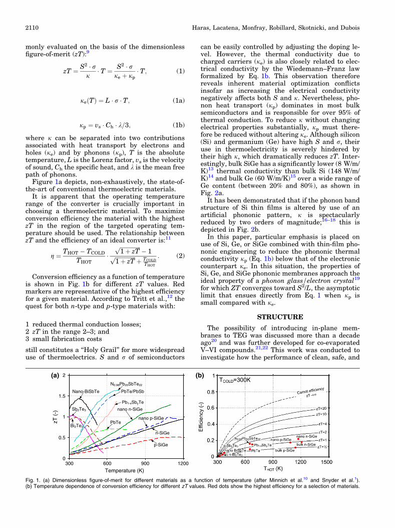
Figure 1a depicts, non-exhaustively, the state-of-the-art of conventional thermoelectric materials.
It is apparent that the operating temperaturerange of the converter is crucially important inchoosing a thermoelectric material. To maximizeconversion efficiency the material with the highestzT in the region of the targeted operating tem-perature should be used. The relationship betweenzT and the efficiency of an ideal converter is:11
g ¼ THOT � TCOLD
THOT�
ffiffiffiffiffiffiffiffiffiffiffiffiffiffiffi
1þ zTp
� 1ffiffiffiffiffiffiffiffiffiffiffiffiffiffiffi
1þ zTp
þ TCOLD
THOT
: (2)
Conversion efficiency as a function of temperatureis shown in Fig. 1b for different zT values. Redmarkers are representative of the highest efficiencyfor a given material. According to Tritt et al.,12 thequest for both n-type and p-type materials with:
1 reduced thermal conduction losses;2 zT in the range 2–3; and3 small fabrication costs
still constitutes a ‘‘Holy Grail’’ for more widespreaduse of thermoelectrics. S and r of semiconductors
can be easily controlled by adjusting the doping le-vel. However, the thermal conductivity due tocharged carriers (je) is also closely related to elec-trical conductivity by the Wiedemann–Franz lawformalized by Eq. 1b. This observation thereforereveals inherent material optimization conflictsinsofar as increasing the electrical conductivitynegatively affects both S and j. Nevertheless, pho-non heat transport (jp) dominates in most bulksemiconductors and is responsible for over 95% ofthermal conduction. To reduce j without changingelectrical properties substantially, jp must there-fore be reduced without altering je. Although silicon(Si) and germanium (Ge) have high S and r, theiruse in thermoelectricity is severely hindered bytheir high j, which dramatically reduces zT. Inter-estingly, bulk SiGe has a significantly lower (8 W/m/K)13 thermal conductivity than bulk Si (148 W/m/K)14 and bulk Ge (60 W/m/K)15 over a wide range ofGe content (between 20% and 80%), as shown inFig. 2a.
It has been demonstrated that if the phonon bandstructure of Si thin films is altered by use of anartificial phononic pattern, j is spectacularlyreduced by two orders of magnitude;16–18 this isdepicted in Fig. 2b.
In this paper, particular emphasis is placed onuse of Si, Ge, or SiGe combined with thin-film pho-nonic engineering to reduce the phononic thermalconductivity jp (Eq. 1b) below that of the electroniccounterpart je. In this situation, the properties ofSi, Ge, and SiGe phononic membranes approach theideal property of a phonon glass/electron crystal19
for which ZT converges toward S2/L, the asymptoticlimit that ensues directly from Eq. 1 when jp issmall compared with je.
STRUCTURE
The possibility of introducing in-plane mem-branes to TEG was discussed more than a decadeago20 and was further developed for co-evaporatedV–VI compounds.21,22 This work was conducted toinvestigate how the performance of clean, safe, and
300 600 900 12000
0.5
1
1.5
2
Temperature (K)
zT (
-)
Bi2Te3
Nano-BiSbTe
N0.98Pb20SbTe22
PbTe/PbSb
Pb1-xSbyTe
PbTe
nano n-SiGe
nano p-SiGe
n-SiGe
p-SiGe
Sb2Te3
(a) (b)
Fig. 1. (a) Dimensionless figure-of-merit for different materials as a function of temperature (after Minnich et al.10 and Snyder et al.1).(b) Temperature dependence of conversion efficiency for different zT values. Red dots show the highest efficiency for a selection of materials.
Haras, Lacatena, Monfray, Robillard, Skotnicki, and Dubois2110

abundant materials, for example Si, SiGe, and Ge,used in mainstream CMOS technology, could beelevated to a level similar to that of thermoelectricmaterials containing lead, antimony, and otherharmful substances. The structure of a membrane-based Seebeck generator is presented in Fig. 3. Oneprerequisite for benefitting from enhanced phononscattering is use of a thin-film membrane. A secondcondition for further reduction of jp is to superim-pose a phononic crystal pattern on this membrane toobtain the above-mentioned jp reduction.
Following this strategy, it is worth noting that thehorizontal membrane structure also redirects heatflow from the vertical to the lateral direction. Froma practical perspective, this structure also leads toconverter geometry with extremely low thickness.This remarkable feature renders this type of con-verter readily able to accommodate flexure.
Mechanical flexibility can be a crucial property ifgenerators are installed on, e.g., hot pipes, exhaustsystems, or textiles etc.
SIMULATION MODEL
To investigate performance of the proposed con-verter structure, simulations based on coupled res-olution of carriers and heat-transport equationswere performed. In our simulation current densitiesfollow the non-isothermal drift–diffusion model:23
~jn Tð Þ ¼ �rn Tð Þ � ~ruFn Tð Þ � Sn Tð Þ � ~rTh i
~jp Tð Þ ¼ �rp Tð Þ � ~ruFp Tð Þ � Sp Tð Þ � ~rTh i
8
>
<
>
:
; (3)
where
0
10
20
30
Si contents (%)
T=300KT=500KT=900K
Si κ=148 W/m/KGe κ=59.9 W/m/K
Total κ for bulk material
T>>Lph
(a)
0 20 40 60 80 100 0 100 200 3000
4
8
12
16
20
Temperature (K)
κ (W
/m/K
)
κ (W
/m/K
)
Silicon Nano-Mesh
Silicon Thin-Film
Bulk Si κSi-bulk=148W/m/K
Silicon Nano-Wires
(b)
Fig. 2. CMOS-compatible materials and their thermal conductivity. j (a) SixGe1�x thermal conductivity as a function of Si content for differenttemperatures (based on Ref. 13), (b) reduction of the thermal conductivity of silicon (from Ref. 16).
Fig. 3. Structure of a membrane Seebeck generator with use of CMOS-compatible thin-film membranes. xMAX = 10 lm (single membrane length5 lm), yMAX = 150 nm (50 nm membrane thickness), zMAX = 1 lm.
Unconventional Thin-Film Thermoelectric Converters: Structure, Simulation, and Comparative Study 2111

uFn Tð Þ ¼ /� k � Tq
lnn Tð Þni Tð Þ
� �
uFp Tð Þ ¼ /þ k � Tq
lnp Tð Þni Tð Þ
� �
8
>
>
>
<
>
>
>
:
;
rn Tð Þ ¼ q � ln Tð Þ � n Tð Þ
rp Tð Þ ¼ q � lp Tð Þ � p Tð Þ
(
and
Sn Tð Þ ¼ � k
q� 3
2þ ln
Nc Tð Þn Tð Þ
� �� �
Sp Tð Þ ¼ k
q� 3
2þ ln
Nv Tð Þp Tð Þ
� �� �
8
>
>
>
<
>
>
>
:
:
(4)
The constitutive current relationships given inEq. 3 enable such temperature-dependent propertiesas carrier mobility (ln, lp), electrical conductivity (rn,rp), carrier concentrations (n, p), or quasi-Fermilevels (/Fn, /Fp) to be taken into account. Here, thetemperature considered is the local lattice tempera-ture (T).
RESULTS
Effect of Doping Level on I–V Characteristicsin the Generator Zone
According to Fig. 3, a metallic ohmic contact islocated at every PN junction to act as an electricalshort. Figures 4a and b show the I–V characteristicsof Si membranes with high (1019 cm�3) and low(1015 cm�3) doping levels, respectively. Only thefourth quadrant of the I–V chart is represented,because it corresponds to the generator mode.Although thermopower is higher at low doping lev-els, Fig. 4b reveals a dramatic current limitation forlightly doped membranes.
Harvested Power Density for Si, Ge, and SiGe
To compare the harvesting capabilities of Si, Ge,and SiGe with those of widely used materials, for
example Bi2Te3 alloys, the power density was cal-culated as a function of the voltage generated,assuming that the temperature gradient across thegenerator is constant. By following this method, itis, therefore, possible to compare the aforemen-tioned materials on the basis of Seebeck and elec-trical conductivity performance, irrespective of theirthermal conductivity. Naturally, one prerequisitethat legitimates this method is to consider thatphononic engineering of thin membranes can beindependently used to cut thermal conductivity forSi and Ge. Beyond the electrical conductivity of theintrinsic thermoelectric material, the metal–semi-conductor contact resistance must be taken intoconsideration to properly reflect electrical perfor-mance.24 In the calculation of the power density, wehave assumed a specific contact resistivity of5 9 10�7 X cm2 for Si and SiGe. Given the maturityof Ni and Pt-based silicide and germano-silicidetechnology, this figure realistically corresponds to aworst-case analysis.25,26 Although contact resis-tance to n-type Ge has long remained a problem,because of strong Fermi level pinning close to thevalence band, recent work has shown that this effectis spectacularly alleviated by inserting an ultra-thindielectric layer between the metal and the semi-conductor.27 For this reason, the same value ofspecific contact resistivity, i.e. 5 9 10�7 X cm2, canbe reasonably assumed for Ge. The situation differsfor Bi2Te3, for which common values of specificcontact resistivity are between 1.45 9 10�7 X cm2 28
and 10�5 X cm2, the latter value being identified inRef. 29 as a representative figure when standardprocessing techniques are used for contact realiza-tion. In our analysis, simulations associated withBi2Te3 have been performed for the two extremes ofthis range, and Seebeck and electrical conductivitywere taken from the modeling work described inRef. 30. This model is temperature-dependent andfollows with good precision data measured forBi2Te3 at the same temperature difference.31–35
Variation of the harvested power density as a
0 5 10 15
-2500
-2000
-1500
-1000
-500
0
V (mV)
Cur
rent
Den
sity
(A
/cm
2 )
NA=ND=1019cm-3Silicon
V IP-type N-type
THOT
I I
II
ΔT=5K
ΔT=10K
ΔT=20K
ΔT=30K
(a) 0 25 75 100
-20
-15
-10
-5
0
V (mV)
Cur
rent
den
sity
(A
/cm
2 )
NA=ND=1015cm-3Silicon
V IP-type N-type
THOT
I I
II
ΔT=5K
ΔT=10K
ΔT=20K
ΔT=30K
(b)
Fig. 4. Harvested current density as a function of voltage for different temperatures differences (s = 50 nm 9 1 lm) in the generator zone (fourthquadrant) for (a) heavily doped silicon thin-film membranes and (b) lightly doped silicon thin-film membranes.
Haras, Lacatena, Monfray, Robillard, Skotnicki, and Dubois2112

function of output voltage for different tempera-tures is presented in Fig. 5 .
Figures 5a–c depict the harvested power densityas a function of output voltage for the proposedgenerator topology based on CMOS core materials.For comparison purposes, Fig. 5d also depicts thepower density associated with Bi2Te3 for the samegenerator geometry. Depending on contact quality,it can be observed that harvested power density forSi, SiGe, and Ge is slightly lower than that forBi2Te3, the performance of which depends criticallyon the specific contact resistivity achievable. Thisconclusion is consolidated in Fig. 6, in which themaximum harvested power densities for the mate-rials are compared. This figure was obtained underload-matching conditions36 for which the load andinternal generator resistances were equal.
Although Si, Ge, and SiGe harvest a lower powerdensity than Bi2Te3 for a same temperature gradi-ent, it is worth emphasizing that they are compati-ble with conventional CMOS technology, makingintegration of TEGs possible. It is note worthy thatSiGe harvests less power than Si or Ge for the sameDT. This can be readily explained by the lowerelectrical conductivity of SiGe compared to Si andGe at identical doping level. However, because of alower j (Fig. 2a), it is expected that SiGe will con-vert heat with higher efficiency than Si or Ge.
CONCLUSIONS
Si, Ge, and SiGe have interesting thermoelectricproperties and could be turned into good thermo-electric materials by a significant reduction of theirthermal conductivity. For this purpose, recentadvances in Si membranes fabrication and phononicengineering are promising technology. Reduction ofthe thermal conductivity of Si, Ge, and SiGe by two
0 5 10 150
2
4
6
8
10
V (mV)
Ele
ctric
Pow
er d
ensi
ty (
W/c
m2 )
Silicon
NA=ND=1019cm-3
ΔT=10K
ΔT=20K
ΔT=30K
ρcontact=5·10-7 Ω.cm2
(a)
0 5 10 150
2
4
6
V (mV)
Ele
ctric
Pow
er d
ensi
ty (
W/ c
m2 ) 10
8Germanium
NA=ND=1019cm-3ρcontact=5·10-7 Ω.cm2
ΔT=10K
ΔT=20KΔT=30K
(b)
0 5 10 150
2
4
6
8
10
V (mV)
Ele
ctric
Pow
er d
ensi
ty (
W/ c
m2 )
Si70%Ge30%
NA=ND=1019cm-3ρcontact=5·10-7 Ω.cm2
ΔT=10K
ΔT=20K
ΔT=30K
(c)
0 5 10 150
10
20
30
V (mV)
Ele
ctric
Pow
er d
ensi
ty (
W/ c
m2 )
[33][34]
[31]
[35]
[32]
Bi2Te3
For dotted lines:ρc=10-5Ω.cm2[29]NA=ND=1019cm-3
ΔT=10KΔT=20K
ΔT=30K
ΔT=30K
For continuous lines:ρc=1.45·10-7Ω.cm2[28]NA=ND=1019 cm-3
(d)
Fig. 5. Harvested electric power density as a function of generator output voltage for membrane Seebeck generator, (a) membranes made fromsilicon, (b) membranes made from germanium, (c) membranes made from Si70%Ge30%, and (d) membranes made from bismuth telluride withthermoelectric properties in accordance with Ref. 30 Isolated markers correspond to maximum harvested power density for DT = 30 K calculatedfrom the measured values of rn, rp, Sn, Sp quoted in each of the associated literature references.
0 10 20 30 400
10
20
30
Max
. Ele
ctric
Pow
er D
ensi
ty (
W/c
m2 )
ΔT (K)
SiliconGermaniumSi70%Ge30%
ρcontact=5·10-7Ω.cm2
Bi2Te3
ρcontact=1.45·10-7Ω.cm2
ρcontact=10-5Ω.cm2
Bi2Te3
Fig. 6. Maximum electric power density as a function of temperaturedifference for membrane Seebeck generators with membranesmade from the materials investigated taking into account the para-sitic effect of contact resistance.
Unconventional Thin-Film Thermoelectric Converters: Structure, Simulation, and Comparative Study 2113

order of magnitude can be achieved, making thosematerials very attractive for future TEG. In thispaper, we have proposed the innovative topology ofa Seebeck membrane generator based on thin-filmsingle-crystal CMOS-compatible materials thatcould exploit such effects. Our results show that theelectric power density of Si, Ge, and SiGe andBi2Te3 membrane-based TEGs are of the same orderof magnitude. Moreover use of Si, Ge, and SiGeenables compatibility with the production technol-ogy used for conventional semiconductor devices.
REFERENCES
1. G.J. Snyder and E.S. Toberer, Nat. Mater. 7, 105 (2008).2. T.M. Tritt, Annu. Rev. Mater. Res. 41, 433 (2011).3. J. Yang and T. Caillat, MRS Bull. 31, 224 (2006).4. D.M. Rowe, Appl. Energy 40, 241 (1991).5. P. Nenninger and U. Marco, ABB Rev. 1, 47 (2011).6. J. P. Carmo, L. M. Goncalves, and J. H. Correia, in Scanning
Probe Microscopy in Nanoscience and Nanotechnology, vol.2.2, ed. by B. Bhushan (Springer, Heidelberg, 2010), pp.791–811.
7. V. Leonov, P. Fiorini, T. Torfs, R. J. M. Vullers, and C. VanHoof, in 15th International Workshop on Thermal Investi-gations of ICs and Systems (Therminic) (2009), pp. 95–100.
8. L. Francioso, C. De Pascali, I. Farella, C. Martucci, P. Cretı,P. Siciliano, and A. Perrone, J. Power Sources 196, 3239(2011).
9. D.M. Rowe, Proc. IEE 125, 1113 (1978).10. J. Minnich, M.S. Dresselhaus, Z.F. Ren, and G. Chen,
Energy Environ. Sci. 2, 466 (2009).11. G. Min and D.M. Rowe, IEEE Trans. Energy Convers. 22,
528 (2007).12. T.M. Tritt, H. Bottner, and L. Chen, MRS Bull. 33, 366
(2008).13. B. Abeles, Phys. Rev. 131, 1906 (1963).14. W. Fulkerson, J.P. Moore, R.K. Williams, R.S. Graves, and
D.L. McElroy, Phys. Rev. 167, 765 (1968).15. C.J. Glassbrenner and G.A. Slack, Phys. Rev. 134, A1058
(1964).16. J.-K. Yu, S. Mitrovic, D. Tham, J. Varghese, and J.R. Heath,
Nat. Nano 5, 718 (2010).17. P.E. Hopkins, C.M. Reinke, M.F. Su, R.H. Olsson, E.A.
Shaner, Z.C. Leseman, J.R. Serrano, L.M. Phinney, and I.El-Kady, Nano Lett. 11, 107 (2011).
18. D. Narducci, G. Cerofolini, M. Ferri, F. Suriano, F.Mancarella, L. Belsito, S. Solmi, and A. Roncaglia, J. Mater.Sci. 48, 2779 (2012).
19. G.A. Slack, CRC Handbook of Thermoelectrics (Boca Raton:CRC Press, 1995).
20. J. Nurnus, H. Bottner, and A. Lambrecht, in Twenty-SecondInternational Conference on Thermoelectrics ICT (2003), pp.655–660.
21. L.M. Goncalves, J.G. Rocha, C. Couto, P. Alpuim, G. Min,D.M. Rowe, and J.H. Correia, J. Micromech. Microeng. 17,S168 (2007).
22. J. Kurosaki, A. Yamamoto, S. Tanaka, J. Cannon, K.Miyazaki, and H. Tsukamoto, J. Electron. Mater. 38, 1326(2009).
23. G. K. Wachutka, in IEEE Transactions on Computer-AidedDesign of Integrated Circuits and Systems, vol. 9 (IEEE,New York, 1990), p. 1141.
24. G. Min and D.M. Rowe, Solid-State Electron. 43, 923 (1999).25. N. Stavitski, M.J.H. van Dal, A. Lauwers, C. Vrancken, A.Y.
Kovalgin, and R.A.M. Wolters, IEEE Electron Device Lett.29, 378 (2008).
26. Z. Zhang, S.O. Koswatta, S.W. Bedell, A. Baraskar, M.Guillorn, S.U. Engelmann, Y. Zhu, J. Gonsalves, A. Pyzyna,M. Hopstaken, C. Witt, L. Yang, F. Liu, J. Newbury, W.Song, C. Cabral, M. Lofaro, A.S. Ozcan, M. Raymond, C.Lavoie, J.W. Sleight, K.P. Rodbell, and P.M. Solomon, IEEEElectron Device Lett. 34, 723 (2013).
27. J.-Y.J. Lin, A.M. Roy, and K.C. Saraswat, IEEE ElectronDevice Lett. 33, 1541 (2012).
28. R. Venkatasubramanian, E. Siivola, T. Colpitts, and B.O’Quinn, Nature 413, 597 (2001).
29. L. W. da Silva, and M. Kaviany, in ASME InternationalMechanical Engineering Congress and Exposition, NewOrleans, USA (ASME, New York, 2002), pp. 1–15.
30. X. Luo, M.B. Sullivan, and S.Y. Quek, Phys. Rev. B 86,184111 (2012).
31. M. Mizoshiri, M. Mikami, and K. Ozaki, Jpn. J. App. Phys.52, 06GL07 (2013).
32. H.J. Goldsmid, A.R. Sheard, and D.A. Wright, Br. J. Appl.Phys. 9, 365 (1958).
33. C.-H. Kuo, C.-S. Hwang, M.-S. Jeng, W.-S. Su, Y.-W. Chou,and J.-R. Ku, J. Alloys Compd. 496, 687 (2010).
34. L. M. Goncalves, in Thermoelectrics and Its Energy Har-vesting, ed. by D. M. Rowe (CRC Press, Boca Raton, 2012),pp. 407–426.
35. H. Scherrer and S. Scherrer, CRC Handbook of Thermo-electrics (Boca Raton: CRC Press, 1995).
36. M. Strasser, R. Aigner, C. Lauterbach, T.F. Sturm, M.Franosch, and G.K.M. Wachutka, Sensors Actuators Phys.114, 362 (2004).
Haras, Lacatena, Monfray, Robillard, Skotnicki, and Dubois2114