TMS320DM335 Digital Media System-on-Chip (DMSoC) Silicon ...
38
TMS320DM335 Digital Media System-on-Chip (DMSoC) Silicon Revision 1.1, 1.3, and 1.4 Silicon Errata Literature Number: SPRZ287B July 2008–Revised June 2010
-
Upload
khangminh22 -
Category
Documents
-
view
0 -
download
0
Transcript of TMS320DM335 Digital Media System-on-Chip (DMSoC) Silicon ...

TMS320DM335Digital Media System-on-Chip (DMSoC)Silicon Revision 1.1, 1.3, and 1.4
Silicon Errata
Literature Number: SPRZ287B
July 2008–Revised June 2010

2 SPRZ287B–July 2008–Revised June 2010
Copyright © 2008–2010, Texas Instruments Incorporated

1 Introduction ........................................................................................................................ 51.1 Device and Development Support Tool Nomenclature ............................................................. 5
1.2 Revision Identification ................................................................................................... 6
2 Silicon Revision 1.4 Usage Notes and Known Design Exceptions to Functional Specifications.......................................................................................................................................... 7
2.1 Usage Notes for Silicon Revision 1.4 ................................................................................. 72.1.1 ROM Bootloader (RBL) Functionality ..................................................................... 72.1.2 Possible Emulator Crash If TCK Frequency Is Greater than MXI Frequency ...................... 112.1.3 DM335 EVM VSS_USB_REF Pin Not Connected As Specified ............................................. 112.1.4 SD/SDIO card: How to Read M bytes (M=1, 2, 3) from SD or SDIO card ......................... 112.1.5 SD/SDIO card: How to Handle SDIO interrupt ......................................................... 122.1.6 Peripherals: Electrostatic Discharge (ESD) Sensitivity Classification ............................... 132.1.7 ASP: Transfers Should be Buffered in Internal Memory .............................................. 132.1.8 ASP: Initialization Procedure When External Device is Frame-Sync Master ...................... 132.1.9 GIO0 Low Setting During Device Boot May Cause Boot to Fail ..................................... 14
2.2 Silicon Revision 1.4 Known Design Exceptions to Functional Specifications .................................. 15
3 Silicon Revision 1.3 Usage Notes and Known Design Exceptions to Functional Specifications........................................................................................................................................ 30
3.1 Usage Notes for Silicon Revision 1.3 ............................................................................... 30
3.2 Silicon Revision 1.3 Known Design Exceptions to Functional Specifications .................................. 31
4 Silicon Revision 1.1 Usage Notes and Known Design Exceptions to Functional Specifications........................................................................................................................................ 34
4.1 Usage Notes for Silicon Revision 1.1 ............................................................................... 344.1.1 NAND Layout Assumed by RBL for Big Block NAND Does Not Match NAND Manufacturers'
Recommendations ......................................................................................... 34
4.2 Silicon Revision 1.1 Known Design Exceptions to Functional Specifications .................................. 35
Appendix A Revision History ...................................................................................................... 37
3SPRZ287B–July 2008–Revised June 2010 Table of Contents
Copyright © 2008–2010, Texas Instruments Incorporated

www.ti.com
List of Figures
1 Example, Device Revision Codes for TMS320DM335 (ZCE)......................................................... 6
2 Video Processing Front End (VPFE) Block Diagram and Data Flows ............................................. 16
3 HSYNC Cycle Period ..................................................................................................... 16
4 Valid Window Width and Horizontal Window Count Data Area ..................................................... 17
5 Paxel Width and Horizontal Paxel Count............................................................................... 17
6 Readout Patterns Comparing Timing at the Output of the Reformatter............................................ 18
7 Expected CSHOLD Behavior ............................................................................................ 22
8 Actual CSHOLD Behavior–32-Bit Writes to SPIDAT1 ................................................................ 22
9 Actual CSHOLD Behavior–Halfword Writes to SPIDAT1 ............................................................ 23
10 Workaround Assuming 32-Bit Writes to SPIDAT1 Followed by a Write Only to CSHOLD ...................... 23
11 Workaround Assuming Halfword Writes to SPIDAT1................................................................. 23
List of Tables
1 Device Silicon Revisions ................................................................................................... 6
2 NAND Devices in NAND Device ID Table (Silicon Revision 1.1)..................................................... 8
3 NAND Devices in NAND Device ID Table (Silicon Revisions 1.3 and Later) ....................................... 8
4 NAND Layout Used by Silicon Revision 1.1 ........................................................................... 10
5 NAND Layout Used by Silicon Revisions 1.3 and Later ............................................................. 10
6 ROM Version IDs .......................................................................................................... 11
7 Silicon Revision 1.4 Advisory List ....................................................................................... 15
8 Bug Summary for the 0 Wait State Configuration .................................................................... 19
9 Bug Summary for the 1 Wait State Configuration .................................................................... 19
10 USB Electrical Characteristics in Violation ............................................................................. 24
11 NAND Device ID........................................................................................................... 29
12 Silicon Revision 1.3 Advisory List ....................................................................................... 31
13 Silicon Revision 1.1 Advisory List ....................................................................................... 35
14 Revision History ........................................................................................................... 37
4 List of Figures SPRZ287B–July 2008–Revised June 2010
Copyright © 2008–2010, Texas Instruments Incorporated

Silicon ErrataSPRZ287B–July 2008–Revised June 2010
TMS320DM335 Digital Media System-on-Chip (DMSoC)Silicon Revision 1.1, 1.3, and 1.4
1 Introduction
This document describes the known exceptions to the functional specifications for the TMS320DM335Digital Media System-on-Chip (DMSoC). [See TMS320DM335 Digital Media System-on-Chip Data Manual(literature number SPRS528).]
The advisory numbers in this document may not be sequential. Some advisory numbers may be moved tothe next revision and others may have been removed and documented in the user's guide. When itemsare moved or deleted, the remaining numbers remain the same and are not resequenced.
This document also contains Usage Notes. Usage Notes highlight and describe particular situations wherethe device's behavior may not match presumed or documented behavior. This may include behaviors thataffect device performance or functional correctness. These notes will be incorporated into futuredocumentation updates for the device (such as the device-specific data sheet), and the behaviors theydescribe will not be altered in future silicon revisions.
1.1 Device and Development Support Tool Nomenclature
To designate the stages in the product development cycle, TI assigns prefixes to the part numbers of allDSP devices and support tools. Each DSP commercial family member has one of three prefixes: TMX,TMP, or TMS (e.g., TMS320DM335). Texas Instruments recommends two of three possible prefixdesignators for its support tools: TMDX and TMDS. These prefixes represent evolutionary stages ofproduct development from engineering prototypes (TMX/TMDX) through fully qualified productiondevices/tools (TMS/TMDS).
Device development evolutionary flow:TMX Experimental device that is not necessarily representative of the final device's electrical
specificationsTMP Final silicon die that conforms to the device's electrical specifications but has not
completed quality and reliability verificationTMS Fully-qualified production deviceSupport tool development evolutionary flow:TMDX Development support product that has not yet completed Texas Instruments internal
qualification testingTMDS Fully-qualified development support product
TMX and TMP devices and TMDX development support tools are shipped against the following disclaimer:"Developmental product is intended for internal evaluation purposes."
TMS devices and TMDS development support tools have been characterized fully, and the quality andreliability of the device have been demonstrated fully. TI's standard warranty applies.
Predictions show that prototype devices (TMX or TMP) have a greater failure rate than the standardproduction devices. Texas Instruments recommends that these devices not be used in any productionsystem because their expected end use failure rate still is undefined. Only qualified production devices areto be used.
5SPRZ287B–July 2008–Revised June 2010 TMS320DM335 Digital Media System-on-Chip (DMSoC) —Silicon Revision 1.1,1.3, and 1.4
Copyright © 2008–2010, Texas Instruments Incorporated
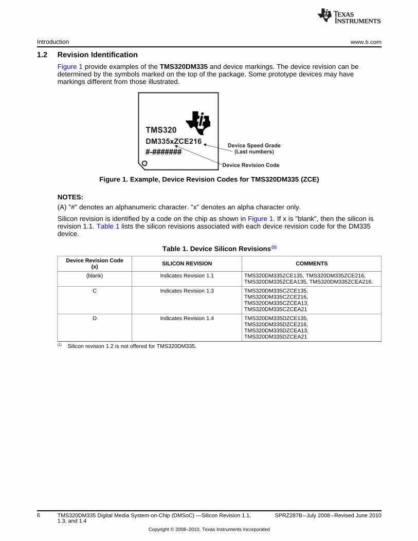
DM335xZCE216
#-#######
TMS320
Device Speed Grade(Last numbers)
Device Revision Code
Introduction www.ti.com
1.2 Revision Identification
Figure 1 provide examples of the TMS320DM335 and device markings. The device revision can bedetermined by the symbols marked on the top of the package. Some prototype devices may havemarkings different from those illustrated.
Figure 1. Example, Device Revision Codes for TMS320DM335 (ZCE)
NOTES:(A) "#" denotes an alphanumeric character. "x" denotes an alpha character only.
Silicon revision is identified by a code on the chip as shown in Figure 1. If x is "blank", then the silicon isrevision 1.1. Table 1 lists the silicon revisions associated with each device revision code for the DM335device.
Table 1. Device Silicon Revisions (1)
Device Revision Code SILICON REVISION COMMENTS(x)
(blank) Indicates Revision 1.1 TMS320DM335ZCE135, TMS320DM335ZCE216,TMS320DM335ZCEA135, TMS320DM335ZCEA216.
C Indicates Revision 1.3 TMS320DM335CZCE135,TMS320DM335CZCE216,TMS320DM335CZCEA13,TMS320DM335CZCEA21
D Indicates Revision 1.4 TMS320DM335DZCE135,TMS320DM335DZCE216,TMS320DM335DZCEA13,TMS320DM335DZCEA21
(1) Silicon revision 1.2 is not offered for TMS320DM335.
6 TMS320DM335 Digital Media System-on-Chip (DMSoC) —Silicon Revision 1.1, SPRZ287B–July 2008–Revised June 20101.3, and 1.4
Copyright © 2008–2010, Texas Instruments Incorporated

www.ti.com Silicon Revision 1.4 Usage Notes and Known Design Exceptions to Functional Specifications
2 Silicon Revision 1.4 Usage Notes and Known Design Exceptions to FunctionalSpecifications
2.1 Usage Notes for Silicon Revision 1.4
Usage Notes highlight and describe particular situations where the device's behavior may not matchpresumed or documented behavior. This may include behaviors that affect device performance orfunctional correctness. These notes will be incorporated into future documentation updates for the device(such as the device-specific data sheet), and the behaviors they describe will not be altered in futuresilicon revisions.
2.1.1 ROM Bootloader (RBL) Functionality
The only difference between silicon revision 1.1 and silicon revisions 1.3 and later is the replacement ofthe ROM Boot Loader (RBL) with a different version with different functional behavior. There are no otherfunctional changes to the device.
The Rom Boot Loader (RBL) is firmware which is stored in ROM on the DM335. It is responsible forhandling the boot process. When the boot process is initiated, it will sense the state of the BOOTSEL[1:0]pins and (based on that state) loads a User Boot Loader (UBL) from external media and branches to theentry point of the UBL. On silicon revisions 1.3 and later, the ROM Boot Loader (RBL) supports three bootmodes: NAND Boot, SD/MMC Boot, and UART Boot. On silicon revision 1.4, SPI boot mode has beenadded which is executed in NAND boot mode. If SPI fails (or there is no EEPROM), NAND boot mode isexecuted.
Silicon revisions 1.3 and later support the following changes to NAND boot functionality:• Support for 4K and 8K page size devices has been added• The NAND device ID table has been extended• Additional devices not in the Device ID table are supported through fetching characteristics from
registers stored on the NAND• The assumed layout of the data in the boot NAND has changed• The UART boot functionality has changed• A bug in the ECC error correction has been fixed
Silicon revision 1.4 have added the following changes to NAND boot functionality:• Support for 16K page size devices has been added• ONFI and Samsung 4th byte support• NAND parameters/geometry information from the SPI EEPROM• The RBL Code 4bit ECC Mode 4 error detection limitation has been fixed
Support for 4K, 8K, and 16K NAND Devices Added
The Rom Boot Loader (RBL) used in silicon revision 1.1 supported NAND page sizes of 512 bytes and2048 bytes. The RBL used in silicon revision 1.3 support page sizes of 512 bytes, 2048 bytes, 4096 bytes,and 8192 bytes. Silicon revision 1.4 also support 16384 bytes page sizes.
Note: At the time of documentation for this device, 8192-byte and 16384-byte devices were not availablefor testing. The code does contain support for these devices; however, it has not yet been tested.
The Rom Boot Loader (RBL) used in silicon 1.1 and later versions all use magic numbers to identifyNAND layout and boot options. A magic number of the form 0xA1AC EDxx was used in revision 1.1.Using a magic number in this form for revisions 1.3 and later will place the DM335 in compatibility mode.This will force the device to operate exactly as if it were silicon revision 1.1. You cannot use the largerNAND devices when operating in compatibility mode. Using a magic number of the form 0xA1BC EDxxwill place the DM335 in standard mode. Standard mode for revisions 1.3 and later allows for the use of thelarger NAND devices. For more information on specific uses of magic numbers, see the TMS320DM335Digital Media System-on-Chip Data Manual (literature number SPRS528).
NAND Device ID Table Updated
7SPRZ287B–July 2008–Revised June 2010 TMS320DM335 Digital Media System-on-Chip (DMSoC) —Silicon Revision 1.1,1.3, and 1.4
Copyright © 2008–2010, Texas Instruments Incorporated
Silicon Revision 1.4 Usage Notes and Known Design Exceptions to Functional Specifications www.ti.com
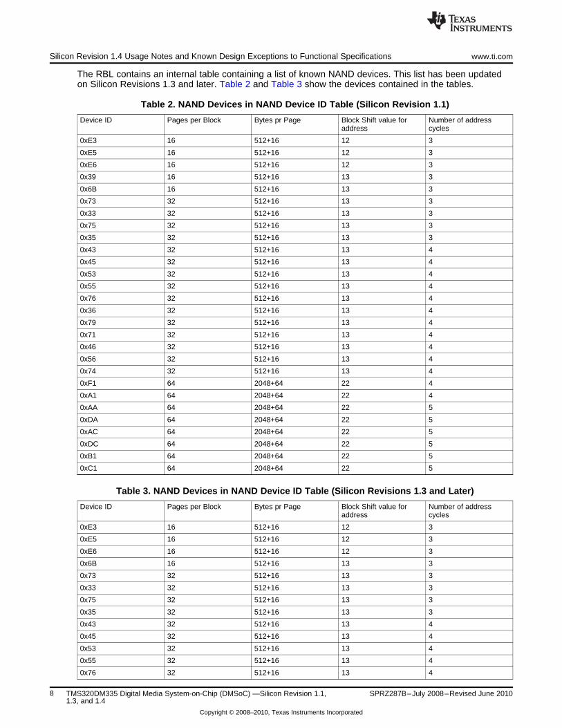
The RBL contains an internal table containing a list of known NAND devices. This list has been updatedon Silicon Revisions 1.3 and later. Table 2 and Table 3 show the devices contained in the tables.
Table 2. NAND Devices in NAND Device ID Table (Silicon Revision 1.1)
Device ID Pages per Block Bytes pr Page Block Shift value for Number of addressaddress cycles
0xE3 16 512+16 12 3
0xE5 16 512+16 12 3
0xE6 16 512+16 12 3
0x39 16 512+16 13 3
0x6B 16 512+16 13 3
0x73 32 512+16 13 3
0x33 32 512+16 13 3
0x75 32 512+16 13 3
0x35 32 512+16 13 3
0x43 32 512+16 13 4
0x45 32 512+16 13 4
0x53 32 512+16 13 4
0x55 32 512+16 13 4
0x76 32 512+16 13 4
0x36 32 512+16 13 4
0x79 32 512+16 13 4
0x71 32 512+16 13 4
0x46 32 512+16 13 4
0x56 32 512+16 13 4
0x74 32 512+16 13 4
0xF1 64 2048+64 22 4
0xA1 64 2048+64 22 4
0xAA 64 2048+64 22 5
0xDA 64 2048+64 22 5
0xAC 64 2048+64 22 5
0xDC 64 2048+64 22 5
0xB1 64 2048+64 22 5
0xC1 64 2048+64 22 5
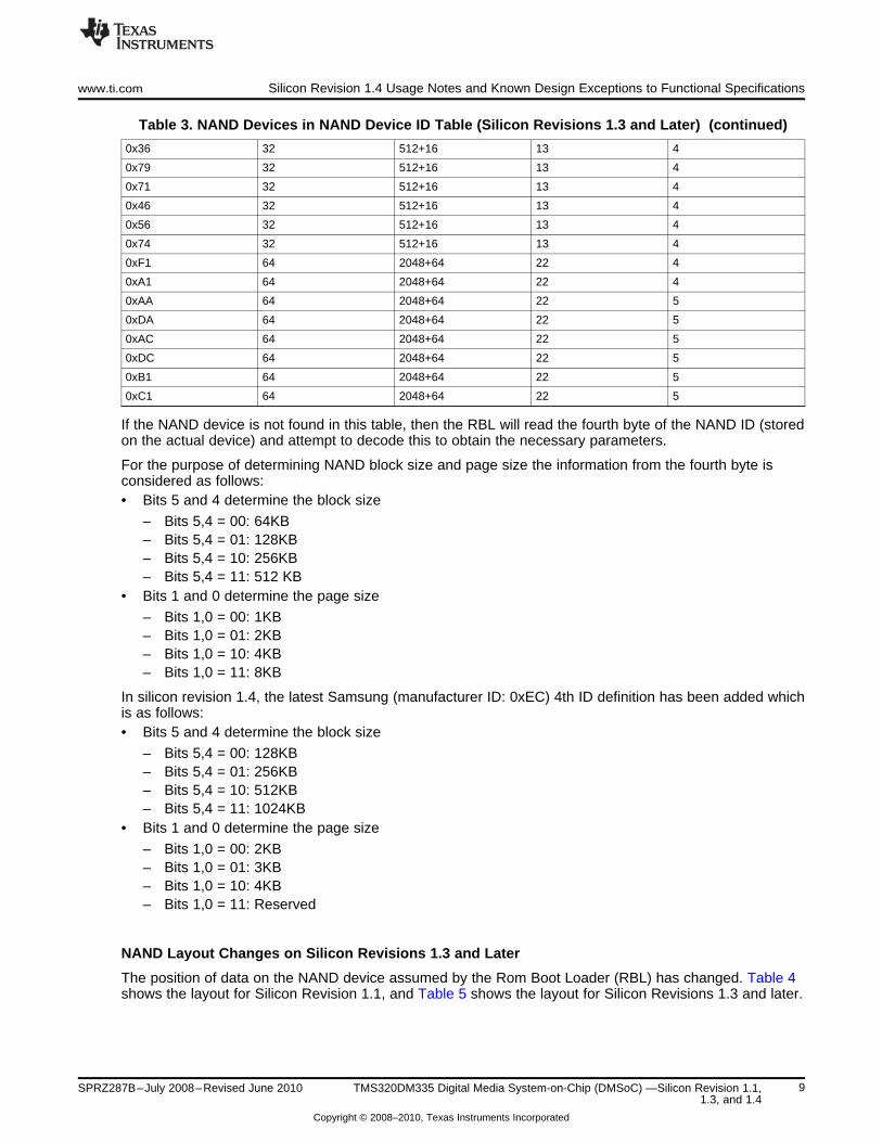
Table 3. NAND Devices in NAND Device ID Table (Silicon Revisions 1.3 and Later)
Device ID Pages per Block Bytes pr Page Block Shift value for Number of addressaddress cycles
0xE3 16 512+16 12 3
0xE5 16 512+16 12 3
0xE6 16 512+16 12 3
0x6B 16 512+16 13 3
0x73 32 512+16 13 3
0x33 32 512+16 13 3
0x75 32 512+16 13 3
0x35 32 512+16 13 3
0x43 32 512+16 13 4
0x45 32 512+16 13 4
0x53 32 512+16 13 4
0x55 32 512+16 13 4
0x76 32 512+16 13 4
8 TMS320DM335 Digital Media System-on-Chip (DMSoC) —Silicon Revision 1.1, SPRZ287B–July 2008–Revised June 20101.3, and 1.4
Copyright © 2008–2010, Texas Instruments Incorporated
www.ti.com Silicon Revision 1.4 Usage Notes and Known Design Exceptions to Functional Specifications
Table 3. NAND Devices in NAND Device ID Table (Silicon Revisions 1.3 and Later) (continued)
0x36 32 512+16 13 4
0x79 32 512+16 13 4
0x71 32 512+16 13 4
0x46 32 512+16 13 4
0x56 32 512+16 13 4
0x74 32 512+16 13 4
0xF1 64 2048+64 22 4
0xA1 64 2048+64 22 4
0xAA 64 2048+64 22 5
0xDA 64 2048+64 22 5
0xAC 64 2048+64 22 5
0xDC 64 2048+64 22 5
0xB1 64 2048+64 22 5
0xC1 64 2048+64 22 5
If the NAND device is not found in this table, then the RBL will read the fourth byte of the NAND ID (storedon the actual device) and attempt to decode this to obtain the necessary parameters.
For the purpose of determining NAND block size and page size the information from the fourth byte isconsidered as follows:• Bits 5 and 4 determine the block size
– Bits 5,4 = 00: 64KB– Bits 5,4 = 01: 128KB– Bits 5,4 = 10: 256KB– Bits 5,4 = 11: 512 KB
• Bits 1 and 0 determine the page size
– Bits 1,0 = 00: 1KB– Bits 1,0 = 01: 2KB– Bits 1,0 = 10: 4KB– Bits 1,0 = 11: 8KB
In silicon revision 1.4, the latest Samsung (manufacturer ID: 0xEC) 4th ID definition has been added whichis as follows:• Bits 5 and 4 determine the block size
– Bits 5,4 = 00: 128KB– Bits 5,4 = 01: 256KB– Bits 5,4 = 10: 512KB– Bits 5,4 = 11: 1024KB
• Bits 1 and 0 determine the page size
– Bits 1,0 = 00: 2KB– Bits 1,0 = 01: 3KB– Bits 1,0 = 10: 4KB– Bits 1,0 = 11: Reserved
NAND Layout Changes on Silicon Revisions 1.3 and Later
The position of data on the NAND device assumed by the Rom Boot Loader (RBL) has changed. Table 4shows the layout for Silicon Revision 1.1, and Table 5 shows the layout for Silicon Revisions 1.3 and later.
9SPRZ287B–July 2008–Revised June 2010 TMS320DM335 Digital Media System-on-Chip (DMSoC) —Silicon Revision 1.1,1.3, and 1.4
Copyright © 2008–2010, Texas Instruments Incorporated

Silicon Revision 1.4 Usage Notes and Known Design Exceptions to Functional Specifications www.ti.com
Table 4. NAND Layout Used by Silicon Revision 1.1
512-Byte Page Size 2048-Byte Page Size
512 bytes Data 512 bytes Data
16 bytes ECC Data 16 bytes ECC Data
512 bytes Data
16 bytes ECC Data
512 bytes Data
16 bytes ECC Data
512 bytes Data
16 bytes ECC Data
Table 5. NAND Layout Used by Silicon Revisions 1.3 and Later (1)
512-Byte Page Size 2048-Byte Page Size 4096-Byte Page Size 8192-Byte Page Size
512 bytes Data 2048 bytes Data 4096 bytes Data 8192 bytes Data
16 bytes ECC Data 64 bytes ECC Data 128 bytes ECC Data 256 bytes ECC Data(1) Silicon Revisions 1.3 and later assume that all the data on a NAND page is in a single block with the ECC and bad block data
contained in the spare bytes area.
UART Boot Functionality in Silicon Revision 1.1
The boot sequence used in silicon revision 1.1 is given below:
1. The RBL will repeatedly send a “BOOTME” string until it receives a correct response from the host.2. The host will send
• “ ACK\0”• UBL Checksum• UBL size in bytes• UBL physical start address• "0000”
3. The DM335 will send “ BEGIN”4. The Host will send the CRC-32 lookup table5. The DM335 will verify the checksum for the lookup table and send “DONE” if the checksum is correct.
If the checksum is bad, the DM335 will send “CORRUPT” and branch back to step 1.6. The Host will send the UBL7. The DM335 will verify the checksum for the UBL and send DONE if the checksum is correct. If the
checksum is bad, the DM335 will send “CORRUPT” and branch back to step 1.8. The DM335 will branch to the UBL start address.
UART Boot Functionality in Silicon Revisions 1.3 and Later
There are two functional changes to the UART boot mode:• The RBL tested for a terminating '\0' in the " ACK" string sent in step 2a. The RBL only tests for 7
characters in silicon revisions 1.3 and later, so the terminating '\0' is ignored.• If the “0000” string in step 2e is replaced by a “0001” string, then the DM335 will not check the
checksum for the CRC-32 lookup table until the UBL has been sent. After the CRC-32 lookup tableand the UBL have been sent, the DM335 will check both and send two “DONE” strings. The flow in thiscase will be:
1. The RBL will repeatedly send a “BOOTME” string until it receives a correct response from the host.2. The host will send
• “ ACK\0”• UBL Checksum• UBL size in bytes• UBL physical start address
10 TMS320DM335 Digital Media System-on-Chip (DMSoC) —Silicon Revision 1.1, SPRZ287B–July 2008–Revised June 20101.3, and 1.4
Copyright © 2008–2010, Texas Instruments Incorporated

www.ti.com Silicon Revision 1.4 Usage Notes and Known Design Exceptions to Functional Specifications
• "0001”• The Host will send the CRC-32 lookup table• The Host will send the UBL• The DM335 will verify the checksum for the lookup table and send “DONE” if the checksum is
correct. If the checksum is bad, the DM335 will send “CORRUPT” and branch back to step 1.• The DM335 will verify the checksum for the UBL and send DONE if the checksum is correct. If
the checksum is bad, the DM335 will send "CORRUPT" and branch back to step 1.• The DM335 will branch to the UBL start address
ROM Version ID
The ROM ID is stored at address 0x00009FFC and is four bytes long. To identify the silicon revision,examine the values at this address and compare with Table 6.
Table 6. ROM Version IDs
ROM Version ID Stored at 0x00009FFC
Silicon Revision 1.1 0x10040101
Silicon Revision 1.3 0x10040103
Silicon Revision 1.4 0x10040104
ECC Bug fixed
The Rom Boot Loader (RBL) used in silicon revision 1.1 contained a bug which prevented the ECChardware from detecting and correcting bit stream errors while the UBL was read from the NAND device.This bug has been fixed in silicon revision 1.4.
2.1.2 Possible Emulator Crash If TCK Frequency Is Greater than MXI Frequency
If the frequency of TCK is greater than the frequency of MXI, there is a chance the emulator will crashwhen changing the PLL1 clock frequency. This can happen while stepping through code that configuresthe PLL1 controller or while using a GEL function that configures the PLL1 controller.
Additionally, the act of applying reset could cause the clock on the TCK pin to stop being generated,thereby crashing the emulator. This condition happens if the TCK frequency is 2x or greater than the MXIfrequency during reset.
To avoid both of these issues, the MXI clock frequency must be greater than or equal to the TCK clockfrequency.
2.1.3 DM335 EVM VSS_USB_REF Pin Not Connected As Specified
On some versions of the DM335 EVM, the VSS_USB_REF pin is not connected as specified in the data sheet.This does not create any USB functional issues; however, for USB compliance, DM335 designs mustfollow the pin connection specified in the USB Reference Resistor Routing figure in the TMS320DM335Digital Media System-on-Chip (DMSoC) data sheet (literature number SPRS528).
2.1.4 SD/SDIO card: How to Read M bytes (M=1, 2, 3) from SD or SDIO card
Direction: Read from SD or SDIO
Data size: 32*N+M byte (where M=1, 2, 3 and N=0, 1, 2, 3,...) FIFO size is 32 bytes (ACCWD (FIFOCTL[4:3] = 0), FIFO trigger level is 256-bits (FIFOLEV (MMCFIFOCTL [2]) =1)
Reading from SD or SDIO when FIFO Trigger Level FIFOLEV is 256 bits causes theDRRDY(MMCST0[10]) bit not to be set for the last M bytes of the above data size equation and thereforethe DMA read event and CPU interrupt for RRDY(MMCST0[10]) are not getting asserted, but the data inFIFO is correct.
There are two possible methods to work around this limitation.
11SPRZ287B–July 2008–Revised June 2010 TMS320DM335 Digital Media System-on-Chip (DMSoC) —Silicon Revision 1.1,1.3, and 1.4
Copyright © 2008–2010, Texas Instruments Incorporated

Silicon Revision 1.4 Usage Notes and Known Design Exceptions to Functional Specifications www.ti.com
1. Include SD status checking and/or SD interrupt enable for TRNDNE (MMCST0 [12]) or DATDNE(MMCST0 [0])
2. Use 128-bit FIFO trigger level (i.e. FIFOLEV (MMCFIFOCTL [2]) =0), since this is only a problem whenFIFOLEV is 256 bits.
Note:1. To ensure the start of the MMCSD transfer correctly, the DMATRIG bit (MMCCMD [16]) should always
be set to ‘1’ when writing the command to MMCCMD registers.2. For SDIO read and write function, the MMCBLEN and MMCNBLK registers have to be set to equal the
total byte count and total block count configured by the SDIO command (CMD52 or CMD53). Forexample, to read 3 bytes using CMD53, the software has to set MMCBLEN=3 and MMCNBLK=1.
3. The FIFOFUL and FIFOEMP status bits are set based on access size(ACCWD):
• If the number of bytes stored in the FIFO is smaller than access size, FIFOEMP is 1. Otherwise,FIFOEMP is 0.
• If the size of the remaining empty spaces in FIFO is smaller than access size, FIFOFUL is 1.Otherwise, FIFOFUL is 0.
For example, when the access size (ACCWD) is 4 bytes and the FIFO level (FIFOLEV=1) is 256-bitsor 32 bytes, and if the number of bytes in FIFO is
• 0 to 3: then, FIFOFUL=0, FIFOEMP=1• 4 to 28: then, FIFOFUL=0, FIFOEMP=0• 29 to 32: then, FIFOFUL=1, FIFOEMP=0
2.1.5 SD/SDIO card: How to Handle SDIO interrupt
SDIO interrupt may be missed since SDIO interrupt processing is only done based on the IOINT (SDIOIST[0]) status.
SDIO Interrupt Detecting: SDIO interrupt is a level interrupt on SDIO protocol, but the interrupt generationlogic detects the edge of DAT1 signal inside the host controller.
SDIO Interrupt Masking: The SDIO Interrupt may be enabled or disabled by the SDIO stack at any time.
SDIO Interrupt Status Clearing: SDIO interrupt status may not be cleared in an atomic sequence since apending interrupt has to be cleared not only on the host controller but also on the SDIO module.
To guarantee that the SDIO interrupt is not missed, the host controller has to check the IOINT(SDIOIST[0]) status register as well as sample the DAT1 signal by checking the DAT1(SDIOST0[1-0])status register at a certain condition.
The following is a suggested sequence for properly handling the SDIO interrupt:
1. SDIO stack informs the SDIO host controller to enable or unmask the SDIO interrupt.2. SDIO host controller enables or unmasks the SDIO interrupt. Before enabling the SDIO interrupt, the
SDIO host controller software has to first sample the DAT1 signal (INTPRD==1 && DAT1==1) to makesure that the pending interrupt is reported to the SDIO stack and then to the SDIO client/functiondriver.Note: SDIO interrupt is enabled at the request of the client/function driver of the SDIO stack. SDIOinterrupt needs to be enabled both on the host controller and the SDIO card which may not happen inan atomic way. By the time the host controller enables the interrupt, the SDIO interrupt may be alreadypending. The SDIO controller can not detect interrupt pending before the interrupt is enabled on thecontroller.
3. When the SDIO interrupt is detected by the SDIO controller, the SDIO ISR has to process the SDIOinterrupts in the following sequence:
• Check and clear SDIO interrupt status IOINT(SDIOIST[0]) immediately.• Mask the SDIO interrupt on the SDIO host controller by setting IOINTEN (SDIOIEN[0]) =0.• Notify the Interrupt event first to the SDIO stack and then to the SDIO client/function driver.
Note: The clearing of the SDIO interrupt on the SDIO card and SDIO controller does not happen inan atomic way. To mask the SDIO interrupt, it has to be ensured that the interrupt is not mistakenlydetected by the host controller again. In addition, the client/function driver of the SDIO stack cantherefore control the occurrence of interrupt and also the readiness to process the interrupt.
12 TMS320DM335 Digital Media System-on-Chip (DMSoC) —Silicon Revision 1.1, SPRZ287B–July 2008–Revised June 20101.3, and 1.4
Copyright © 2008–2010, Texas Instruments Incorporated

www.ti.com Silicon Revision 1.4 Usage Notes and Known Design Exceptions to Functional Specifications
4. The SDIO stack client/function driver clears the SDIO interrupt status on the SDIO card.
2.1.6 Peripherals: Electrostatic Discharge (ESD) Sensitivity Classification
JESD22-A114D, Electrostatic Discharge (ESD) Sensitivity Testing Human Body Model (HBM), test resultsindicate that the TMS320DM335 device's electrostatic discharge (ESD) sensitivity classification is Class 0due to 4 reserved pins (BGA ID: J1, K1, L1, M1). All other pins meet the Texas Instruments design goalESD testing classification of Class 2. No workaround is required. Standard ESD-sensitivity device handlingprocedures provide sufficient protection.
JESD22-C101C, Field-Induced Charged-Device Model Test Method for Electrostatic-Discharge-WithstandThresholds of Microelectronic Components, testing was also conducted and results demonstrated that theTMS320DM335 device's charged-device model (CDM) sensitivity classification is Class III (500 to 1000 V).These results are consistent with the Texas Instruments CDM design goal.
2.1.7 ASP: Transfers Should be Buffered in Internal Memory
Audio Serial Port (ASP) transfers may need to originate and complete from on-chip buffers in ARMInternal RAM (TCM). This is due to the fact that there is no tolerance for audio data dropouts that mayoccur due to the delays in DDR2/mDDR accesses from other masters and from unavoidable DDR2/mDDRrefresh cycles even if the Q0/TC0 is dedicated to transfers from off-chip memories. On-chip buffers mightbe needed to ensure immunity from DDR2/mDDR latencies. DDR2/mDDR latencies aresystem-dependent, varying between applications, and are impacted by the amount and type of data trafficto DDR2/mDDR memories. Once completed, the data can be shuttled between the internal buffer and theDDR2/mDDR memory by using EDMA Q1/TC1.
If using on-chip buffers for ASP transfers, also see the following advisories:• 1.1.2 Concurrent Access to ARM Internal Memory May Result in Access Errors
2.1.8 ASP: Initialization Procedure When External Device is Frame-Sync Master
If the ASP transmitter expects a frame sync from an external device, care must be taken to ensure thatthe proper action is employed. After the transmitter comes out of reset (XRST = 1), it waits for a framesync from the external device. If the first frame sync arrives very shortly after the transmitter is enabled,the CPU or EDMA controller may not have a chance to service the ASP data transmit register (DXR). Inthis case, the transmitter shifts out the default data in the transmit shift register (XSR) instead of thedesired value, which has not yet arrived in the DXR. This causes problems in some applications such thatthe first data element in the frame is invalid. The data stream appears element-shifted (the first data wordmay appear in the second channel instead of the first).
To ensure proper operation when the external device is the frame master, you must make sure that theDXR is already serviced with the first word when a frame sync occurs. To do so, you can keep thetransmitter in reset until the first frame sync is detected. The software is set up such that it will only takethe transmitter out of reset (XRST = 1) promptly after detecting the first frame sync. This ensures that thetransmitter does not begin data transfers at the data pin during the first frame-sync period. This alsoprovides almost an entire frame period for the DM335 device to service the DXR with the first word beforethe second frame sync occurs. The transmitter only begins data transfers upon receiving the secondframe sync. At this point, the DXR is already serviced with the first word.
The ASP transmitter and receiver on the DM335 device are capable of generating an interrupt upon thedetection of frame synchronization. However, on the DM335 device, the receiver and/or transmitter mustbe out of reset to enable this feature. Therefore, instead of directly using the ASP interrupt to detect thefirst frame sync, on the DM335 device you can use the GPIO peripheral. This can be achieved byconnecting the frame-sync signal to a GPIO pin. The software can either poll the GPIO pin to detect thefirst frame sync or program the GPIO peripheral to generate an interrupt to the CPU upon detecting thefirst frame-sync edge. For more information on the GPIO peripheral, see the TMS320DM335 DMSoCGeneral-Purpose Input/Output (GPIO) User's Guide (SPRUFY8). For details on the initialization sequencewhen the external device is the frame-sync master, see the TMS320DM335 DMSoC Audio Serial Port(ASP) User's Guide (SPRUFZ3).
13SPRZ287B–July 2008–Revised June 2010 TMS320DM335 Digital Media System-on-Chip (DMSoC) —Silicon Revision 1.1,1.3, and 1.4
Copyright © 2008–2010, Texas Instruments Incorporated

Silicon Revision 1.4 Usage Notes and Known Design Exceptions to Functional Specifications www.ti.com
2.1.9 GIO0 Low Setting During Device Boot May Cause Boot to Fail
If the GIO0 pin is low during device boot from a NAND device, the DM335 will not follow the normal bootprocess. The DM335 ROM Boot Loader (RBL) will attempt to read the User Boot Loader (UBL) headerfrom a different NAND page range and will look for a different number in that header than that used in thenormal boot process, which may cause the boot to fail.
To prevent this issue from occurring, ensure that the GIO0 pin is held high during NAND boot. Detailsabout this issue will be incorporated into the next revision of the TMS320DM335 Digital MediaSystem-on-Chip (DMSoC) Data Manual (literature number SPRS528).
14 TMS320DM335 Digital Media System-on-Chip (DMSoC) —Silicon Revision 1.1, SPRZ287B–July 2008–Revised June 20101.3, and 1.4
Copyright © 2008–2010, Texas Instruments Incorporated
www.ti.com Silicon Revision 1.4 Usage Notes and Known Design Exceptions to Functional Specifications
2.2 Silicon Revision 1.4 Known Design Exceptions to Functional Specifications
Table 7. Silicon Revision 1.4 Advisory List
Title ...................................................................................................................................... Page
Advisory 1.4.1 —H3A data may get corrupted ..................................................................................... 16Advisory 1.4.2 —Concurrent Access to ARM Internal Memory May Result in Access Errors ............................... 19Advisory 1.4.3 —SPI: Receive Overrun Interrupt and Bit Error Can be Lost................................................... 20Advisory 1.4.4 —SPI: RXINTFLG Bit in SPIFLG Register May Not Get Cleared.............................................. 20Advisory 1.4.5 —SPI: A Write to SPIFLG Receiver Overrun Bit Does Not Clear the Flag ................................... 20Advisory 1.4.6 —SPI: SPIINTVECT and SPIFLG Registers are Cleared When Read in Debug Mode .................... 21Advisory 1.4.7 —SPI: SPI Master Receives Extra Bit When SPICLK Polarity Changes ..................................... 21Advisory 1.4.8 —SPI Master Mode: Extra Step Required to Use CSHOLD.................................................... 22Advisory 1.4.9 —USB: Some Electrical Parameters Violate USB Specification ............................................... 24Advisory 1.4.10 —VPBE: VENC Default Luma Interpolation Filter Does Not Clip to Zero ................................... 25Advisory 1.4.11 —USB (Device Mode): Calculated CRC Value Does Not Match Host CRC Value ........................ 26Advisory 1.4.12 —DEVICE_ID System Register DEVREV Bits [31:28] Show Incorrect Device Silicon Revision......... 28Advisory 1.4.13 —Change in ROM Boot Loader (RBL) NAND Boot Device ID Table ........................................ 29
15SPRZ287B–July 2008–Revised June 2010 TMS320DM335 Digital Media System-on-Chip (DMSoC) —Silicon Revision 1.1,1.3, and 1.4
Copyright © 2008–2010, Texas Instruments Incorporated

CCDC
ParallelImager
Input
H3A
IPIPEIF
IPIPE
BufferLogic
DDR2EMIF
VPFE
HSYNC Cycle
PCLK
HD
Advisory 1.4.1 — H3A data may get corrupted www.ti.com
Advisory 1.4.1 H3A data may get corrupted
Revision(s) Affected 1.4 and earlier.
Details This problem affects H3A auto white balance, auto exposure, and auto focus when theimage sensor data is large (i.e. greater than approximately 10 mega pixels) and the datapath is from imager to CCDC to H3A .
Figure 2. Video Processing Front End (VPFE) Block Diagram and Data Flows
When the H3A module receives more than 4096 pixel clock cycles between consecutiveHD rising edges, the H3A internal line buffer may become corrupt. The internal linebuffer address is reset to zero at HD rising edge, is incremented every pixel clock cycle,and wraps back to address zero after 4096 pixel clocks. H3A calculations may not becorrect when the line buffer is corrupt.
Figure 3. HSYNC Cycle Period
16 TMS320DM335 Digital Media System-on-Chip (DMSoC) —Silicon Revision 1.1, SPRZ287B–July 2008–Revised June 20101.3, and 1.4
Copyright © 2008–2010, Texas Instruments Incorporated

HSYNC Cycle
WINW
WINHC
B1 B2V
WINSH
PCLK
HD
Data
HSYNC Cycle
PAXW
PAXHC
B1 B2V
IIRSH
PCLK
HD
Data
PAXSH
www.ti.com Advisory 1.4.1 — H3A data may get corrupted
Workaround(s) To workaround this problem, use any of the four workarounds described below.
1. Constrain the valid AEW/AF data area. The valid data in the internal line buffer willnot become corrupt under certain constraints. In particular, the problem will not occurwhen you adhere to the follow constraints (see figures):
• B1 + V < 4096 and• B2 <= 4096 – (B1+V) + B1
Where
• B1 = Data area from HD rising edge to start of valid AEW/AF data.• V = Valid AEW/AF data area. This is the data area for AEW/AF calculations. This
area is specified using registers in the H3A module. Note that the registers aredifferent for AEW and for AF. For AEW, bits WINSH specify the horizontal startposition of the AEW windows, bits WINW specify the horizontal width of thewindows, and bits WINHC specify the total number of windows. The total numberof pixels in the valid AEW data area is equal to V=WINW*WINHC. For AF, bitsIIRSH specify the horizontal start position of the IIR filter, bits PAXSH specify thehorizontal start position of the AF paxels, bits PAXW specify the horizontal widthof the paxels, and bits PAXHC specify the total number of paxels. The totalnumber of pixels in the valid AF data area is equal to V=[ (PAXSH - IIRSH) +PAXW*PAXHC]. See the VPFE PRG for complete bit descriptions.
• B2 = Data area from end of valid AEW/AF data to next HD rising edge.
Figure 4. Valid Window Width and Horizontal Window Count Data Area
Figure 5. Paxel Width and Horizontal Paxel Count
2. Use the imager’s movie readout mode.In the imager’s movie readout mode the problem does not occur, because thenumber of horizontal pixels and blacking are is less than 4096 pixels and the H3Amodule receives less than 4096 pixel clock cycles between consecutive HD risingedges.Note that the number of pixel clock cycles between consecutive HD rising edges thatthe H3A module receives is determined by the external or internal timing generatorand also, if used, by the reformatter inside the CCDC. The reformatter is used whenimagers have special readout patterns. For example, if the readout pattern contains
17SPRZ287B–July 2008–Revised June 2010 TMS320DM335 Digital Media System-on-Chip (DMSoC) —Silicon Revision 1.1,1.3, and 1.4
Copyright © 2008–2010, Texas Instruments Incorporated

HSYNC Cycle
HSYNC Cycle HSYNC Cycle
HSYNC Cycle HSYNC Cycle HSYNC Cycle
PCLK
HD (Input)
HD (Output)2 Lines
Data (Output)2 Lines
HD (Output)3 Lines
Data (Output)3 Lines
1 -> 2 Lines
1 -> 3 Lines
Advisory 1.4.1 — H3A data may get corrupted www.ti.com
two lines of actual image data per HSYNC, then the reformatter will convert the datafrom one to two lines, internally. The number of pixel clock cycles betweenconsecutive HD rising edges that the H3A modules receives corresponds to thetiming at the output of the reformatter.
Figure 6. Readout Patterns Comparing Timing at the Output of the Reformatter
3. Use the alternative data path for H3A.There are two possible data paths for H3A:
(a) Imager->CCDC->H3A(b) Imager->CCDC->DDR->H3A
This problem is only applicable when the path is Imager->CCDC->H3A, so youmay avoid this problem completely by using the alternative pathImager->CCDC->DDR->H3A. Note that the alternative path requires raw imagedata to be store in DDR memory prior to H3A processing.
18 TMS320DM335 Digital Media System-on-Chip (DMSoC) —Silicon Revision 1.1, SPRZ287B–July 2008–Revised June 20101.3, and 1.4
Copyright © 2008–2010, Texas Instruments Incorporated

www.ti.com Advisory 1.4.2 — Concurrent Access to ARM Internal Memory May Result in Access Errors
Advisory 1.4.2 Concurrent Access to ARM Internal Memory May Result in Access Errors
Revisions Effected 1.4 and earlier.
Details ARM internal memory consists of two physical memories: RAM0 and RAM1. The ARMprocessor can access these memories over two separate busses: ITCM bus and DTCMbus. The EDMA and USB module are DMA bus masters that can access thesememories over the DMA bus, via special bus arbiters. See the TMS320DM335 DMSoCARM Subsystem Reference Guide (literature number SPRUFX7). Under certainconditions, access errors may occur when the ARM and these DMA bus masters attemptto access ARM internal memory at the same time. An access error means that data isnot written or read properly. The conditions depend on whether ARM internal memoryaccess is configured for 0 or 1 wait states and are further described below. Use bitsAIM_WAIST in the MISC register in the System Control Module to configure the waitstates [see TMS320DM335 DMSoC ARM Subsystem Reference Guide (literaturenumber SPRUFX7)].
For both the 0 and 1 wait state configurations, access errors may occur under thefollowing conditions (see Table 8 and Table 9):
• Access errors may occur in situations where an ARM DTCM access to RAM0 and aDMA bus access to RAM1 are attempted at the same time.
• Access errors may occur in situations where an ARM ITCM, an ARM DTCM, and aDMA bus access are attempted to the same physical memory (RAM0 or RAM1) atthe same time.
For only the 1 wait state configuration, access errors may occur under the followingconditions:
• Access errors may occur in situations where an ARM ITCM and a DMA bus accessare attempted to the same physical memory (RAM0 or RAM1) at the same time.
• Access errors may occur in situations where an ARM DTCM and a DMA bus accessare attempted to the same physical memory (RAM0 or RAM1) at the same time.
Workaround(s) Avoid the conditions that cause accesses errors. Design your software so that accessesto ARM internal memory are according to the Bug Summary Table 8 and Table 9). In thetables, P means that no bug will occur under the corresponding conditions.
Table 8. Bug Summary for the 0 Wait State Configuration
3 ACTIVE ACCESSES 2 ACTIVE ACCESSES 1 ACTIVE ACCESS
ARM ITCM Access R0 R0 R0 R0 R1 R1 R1 R1 R0 R0 R1 R1 R0 R0 R1 R1 n n n n R0 n n R1 n n n
ARM DTCM Access R0 R0 R1 R1 R0 R0 R1 R1 R0 R1 R0 R1 n n n n R0 R0 R1 R1 n R0 n n R1 n n
DMA Access R0 R1 R0 R1 R0 R1 R0 R1 n n n n R0 R1 R0 R1 R0 R1 R0 R1 n n R0 n n R1 n
Pass / Fail F F P P P F P F P P P P P P P P P F P P P P P P P P P
Table 9. Bug Summary for the 1 Wait State Configuration
3 ACTIVE ACCESSES 2 ACTIVE ACCESSES 1 ACTIVE ACCESS
ARM ITCM Access R0 R0 R0 R0 R1 R1 R1 R1 R0 R0 R1 R1 R0 R0 R1 R1 n n n n R0 n n R1 n n n
ARM DTCM Access R0 R0 R1 R1 R0 R0 R1 R1 R0 R1 R0 R1 n n n n R0 R0 R1 R1 n R0 n n R1 n n
DMA Access R0 R1 R0 R1 R0 R1 R0 R1 n n n n R0 R1 R0 R1 R0 R1 R0 R1 n n R0 n n R1 n
Pass / Fail F F F F F F P F P P P P F P P F F F P F P P P P P P P
19SPRZ287B–July 2008–Revised June 2010 TMS320DM335 Digital Media System-on-Chip (DMSoC) —Silicon Revision 1.1,1.3, and 1.4
Copyright © 2008–2010, Texas Instruments Incorporated

Advisory 1.4.3 — SPI: Receive Overrun Interrupt and Bit Error Can be Lost www.ti.com
Advisory 1.4.3 SPI: Receive Overrun Interrupt and Bit Error Can be Lost
Revision(s) Affected: 1.4 and earlier.
Details: Receive Overrun Interrupt (RXOVINT) and Bit Error interrupt (BITERRINT) can be lost if:Reading of the SPIFLG register coincides with the setting of these interrupt flag bits.Reading of the upper 16 bits of SPIBUF register coincides with the setting of theseinterrupt bits.
Workaround: Use the interrupt instead of the polling method to check the status of these interrupts.
Access only the lower 16 bits of the SPIBUF register to read received data.
If the polling method must be used, group the error interrupts into one Level (i.e., Level0)and the RX complete interrupt into the other Level (i.e., Level1). Use the SPIINTVECT0and SPIINTVECT1 registers to find out the interrupt status first and then only read theSPIFLG register to decode the source of the error interrupts.
Advisory 1.4.4 SPI: RXINTFLG Bit in SPIFLG Register May Not Get Cleared
Revision(s) Affected: 1.4 and earlier.
Details: The RXINTFLG bit in the SPIFLG register may not get cleared by reading the SPIBUFregister when the read coincides with the setting of the RXINTFLG bit due to new dataarrival.
Workaround: When the above condition occurs, the system is at the verge of receive overrun.Therefore, either optimize the SPIBUF servicing routine to avoid receive overrun or usethe EDMA3 to avoid the race condition from occurring.
Advisory 1.4.5 SPI: A Write to SPIFLG Receiver Overrun Bit Does Not Clear the Flag
Revision(s) Affected: 1.4 and earlier.
Details: A write to the SPIFLG receiver overrun (SPIFLG.OVRNINTFLG) bit does not clear theflag if the write coincides with the setting of the receive interrupt flag(SPIFLG.RXINTFLG).
Workaround: Write to the SPIFLG.OVRNINTFLG bit, then read back the value of the flag. If the flagdid not clear, then write to clear the flag again.
20 TMS320DM335 Digital Media System-on-Chip (DMSoC) —Silicon Revision 1.1, SPRZ287B–July 2008–Revised June 20101.3, and 1.4
Copyright © 2008–2010, Texas Instruments Incorporated

www.ti.com Advisory 1.4.6 — SPI: SPIINTVECT and SPIFLG Registers are Cleared When Read in Debug Mode
Advisory 1.4.6 SPI: SPIINTVECT and SPIFLG Registers are Cleared When Read in Debug Mode
Revision(s) Affected 1.4 and earlier.
Details Both the INTVECT and SPIFLG registers are cleared when refreshing the memorywindow in debug mode with CCS. These registers should be cleared only by regularCPU reads, not during debug/suspend mode.
Workaround(s) None
Advisory 1.4.7 SPI: SPI Master Receives Extra Bit When SPICLK Polarity Changes
Revision(s) Affected 1.4 and earlier.
Details If the polarity of the SPICLK pin is changed and the change aligns with the receive edgefor the new buffer, then it will be considered as a real SPICLK edge and the receive shiftregister shifts the data.
Workaround(s) Pre-select the SPIFMTx register by byte writing to just the DFSEL field in the SPIDAT1register before actually writing to the SPIDAT1 field of the SPIDAT1 register. Thisadditional step needs to be done only when there is going to be an SPICLK polaritychange for the new buffer.
21SPRZ287B–July 2008–Revised June 2010 TMS320DM335 Digital Media System-on-Chip (DMSoC) —Silicon Revision 1.1,1.3, and 1.4
Copyright © 2008–2010, Texas Instruments Incorporated

SPIx_CLK
SPIx_SIMO
(a) Write SPIDAT1
= 0x10001245
(CSHOLD=1)
(b) Write SPIDAT1
= 0x00005678
(CSHOLD=0)
(a) (b)
SPI_ENx
SPIx_CLK
SPIx_SIMO
(a) Write SPIDAT1
= 0x10001245
(CSHOLD=1)
(b) Write SPIDAT1
= 0x00005678
(CSHOLD=0)
(a) (b)
SPI_ENx
Advisory 1.4.8 — SPI Master Mode: Extra Step Required to Use CSHOLD www.ti.com
Advisory 1.4.8 SPI Master Mode: Extra Step Required to Use CSHOLD
Revision(s) Affected 1.4 and earlier.
Details The SPI module chip-select hold (CSHOLD) feature allows the device to instruct the SPIto keep the chip-select pin asserted between transfers. This feature applies in mastermode and is enabled by writing a '1' to SPIDAT1.CSHOLD (bit 28).
When data is written to the SPIDAT1 register with the CSHOLD bit set to '1', the masteris supposed to keep the SPI_ENx pin asserted after the transfer completes. When datais written to the SPIDAT1 register with CSHOLD set to '0', the master is supposed tode-assert the SPI_ENx pin after the transfer completes.
For example, assume that the device needs to send two 16-bit words (0x1234 and0x5678) to an SPI slave that requires its chip select to remain asserted between thetransfers. This is a common requirement when communicating with SPI memory devices.
According to the SPI specification, the following sequence should produce the expectedresult as illustrated in Figure 7:
• Write 0x10001234 to SPIDAT1 for transmission of 0X1234 (CSHOLD = 1)• Write 0x00005678 to SPIDAT1 for transmission of 0x5678 (CSHOLD = 0)
Figure 7. Expected CSHOLD Behavior
Instead, what actually occurs is that SPI_ENx is momentarily de-asserted at thebeginning of the second write, as illustrated in Figure 8.
Figure 8. Actual CSHOLD Behavior–32-Bit Writes to SPIDAT1
22 TMS320DM335 Digital Media System-on-Chip (DMSoC) —Silicon Revision 1.1, SPRZ287B–July 2008–Revised June 20101.3, and 1.4
Copyright © 2008–2010, Texas Instruments Incorporated

SPIx_CLK
SPIx_SIMO
(a) Write (8 or 16−bit)
SPIDAT1.CSHOLD=1
(c) write (8 or 16−bit)
SPIDAT1.CSHOLD=0
(d) write of
0x5678 to SPIDAT1[15:0]
(b) write of
0x1234 to SPIDAT1[15:0]
(a) (b) (c) (d)
SPI_ENx
SPIx_CLK
SPIx_SIMO
(a) Write SPIDAT1
= 0x10001245
(CSHOLD=1)
(c) Write SPIDAT1.CSHOLD=0
using 8 or 16 bit write.
(do not write to SPIDA T1[15:0])
(b) Write SPIDAT1
=0x10005678
(CSHOLD=1)
(a) (b) (c)
SPI_ENx
SPIx_CLK
SPIx_SIMO
(a) Write (8 or 16−bit)
SPIDAT1.CSHOLD=1
(d) write (8 or 16−bit)
SPIDAT1.CSHOLD=0
(c) write of
0x5678 to SPIDAT1[15:0]
(b) write of
0x1234 to SPIDAT1[15:0]
(a) (b) (c) (d)
SPI_ENx
www.ti.com Advisory 1.4.8 — SPI Master Mode: Extra Step Required to Use CSHOLD
Both Figure 7 and Figure 8 assume that SPIDAT1 is written using a single 32-bit writeinstruction. If SPIDAT1 is instead written using an 8-bit or 16-bit instruction to write to theCSHOLD field, followed by a 16-bit write to the transmit shift register field of SPIDAT1,then what actually occurs is illustrated in Figure 9. This is the same case illustrated inFigure 8 except that the de-assertion of SPI_ENx lasts for the duration between writing a'0' to the CSHOLD field and writing new data to the transmit shift register.
Figure 9. Actual CSHOLD Behavior–Halfword Writes to SPIDAT1
Workaround(s) For each word in the sequence of words during which SPI_ENx should be held low, writeto the SPIDAT1 register with the CSHOLD bit set to '1'. Follow this by a write to only theCSHOLD field of SPIDAT1, setting CSHOLD = 0 to de-assert SPI_ENx. See Figure 10for an illustration.
Figure 10. Workaround Assuming 32-Bit Writes to SPIDAT1 Followed by a Write Only to CSHOLD
Alternatively, only write to the SPIDAT1 CSHOLD field before and after the transfer totoggle the SPI_ENx pin. During the transfer, write only to the data field of SPIDAT1[15:0]using 16-bit (halfword) write commands. For an illustration, see Figure 11.
Figure 11. Workaround Assuming Halfword Writes to SPIDAT1
23SPRZ287B–July 2008–Revised June 2010 TMS320DM335 Digital Media System-on-Chip (DMSoC) —Silicon Revision 1.1,1.3, and 1.4
Copyright © 2008–2010, Texas Instruments Incorporated

Advisory 1.4.9 — USB: Some Electrical Parameters Violate USB Specification www.ti.com
Advisory 1.4.9 USB: Some Electrical Parameters Violate USB Specification
Revision(s) Affected 1.4 and earlier.
Details Some electrical characteristics violate the USB 2.0 specification; see Table 10.
Table 10. USB Electrical Characteristics in Violation
USB SPECIFICATION DM335 SPECIFICATIONUNIT
MIN MAX MIN MAX
VHSDSC USB high-speed disconnect 525 625 525 675 mVdetection threshold(differential signal amplitude)
VBUS USB external charge pump 4.75 5.25 4.85 5.25 Vinput
Workaround(s) Consider these violations and design your system accordingly.
24 TMS320DM335 Digital Media System-on-Chip (DMSoC) —Silicon Revision 1.1, SPRZ287B–July 2008–Revised June 20101.3, and 1.4
Copyright © 2008–2010, Texas Instruments Incorporated

www.ti.com Advisory 1.4.10 — VPBE: VENC Default Luma Interpolation Filter Does Not Clip to Zero
Advisory 1.4.10 VPBE: VENC Default Luma Interpolation Filter Does Not Clip to Zero
Revision(s) Affected 1.4 and earlier.
Details The Video Encoder (VENC) in the VPBE subsystem includes an optional 2x interpolationfunction for the luma signal. The default filter used for this interpolation (VMISC.YUPF =0) does not clip the Luma to zero.
Workaround(s) Do not use the default luma 2x interpolation filter (VMISC.YUPF = 0). Instead, use thealternate luma 2x interpolation filter (VMISC.YUPF = 1).
25SPRZ287B–July 2008–Revised June 2010 TMS320DM335 Digital Media System-on-Chip (DMSoC) —Silicon Revision 1.1,1.3, and 1.4
Copyright © 2008–2010, Texas Instruments Incorporated

Advisory 1.4.11 — USB (Device Mode): Calculated CRC Value Does Not Match Host CRC Value www.ti.com
Advisory 1.4.11 USB (Device Mode): Calculated CRC Value Does Not Match Host CRC Value
Revision(s) Affected: 1.4 and earlier.
Details: The USB Controller can occasionally calculate a bad CRC for a received data packet.This error is rare and only occurs when ALL of the following conditions are met:
• USB Controller is in Device Mode of Operation and is receiving data• Received data packet has a good CRC value of 0x7FF2• A timing violation caused by a synchronization error (race condition)
The timing synchronization error is caused by a race condition between two controlsignals in the PHY Clock and System Clock domains. When these two synchronizedcontrol signals are crossing a clock boundary and the received data packet has a goodCRC value of 0x7FF2, a race condition may occur causing one of the control signals tobe latched a few pico-seconds ahead of the other control signal.
The issue has been observed on both Bulk (Non-Isochronous) and Isochronous transfersand may potentially exist on Control and Interrupt transfers since the data paths for allthese transfers are the same or are very similar.
When the problem occurs in Non-Isochronous transfer types, the data that was "in-flight"to the USB Controller’s FIFO from the Host is discarded by the USB Controller. Due tothe error condition, the USB Controller also refrains from sending an ACK packet to theHost, as mandated by the USB transfer protocol. This forces the Host to re-transmit thedata packet, anticipating an error in data transmission. The problem is usually correctedwhen the Host re-transmits the data packet.
When this problem occurs in Isochronous transfer mode for either High- or Full-speed,the USB Controller flags the device application S/W that a CRC error existed but retainsthe received data within the FIFO as well as captures the received data packet sizevalue minus one byte from the actual data size. Since the magnitude of the actual timingviolated due to the synchronization problem is only in pico-seconds, the entire data sentfrom the Host is routed into the USB device receive FIFO (i.e., even though the receiveddata counter is one byte less, the full data packet is available for the USB driver).
Workaround(s): Case 1a: Non-Isochronous Transfers (High-Speed): For non-Isochronous transfersoperating in High-Speed mode, the Host and Device H/W perform the necessaryre-transmission; thererfore, the issue should be transparent to the Host driver. The issuewill also be transparent to the USB device driver since the H/W flushes the received dataand forces the Host driver to re-transmit by not sending an ACK packet. For this reason,no interrupt is generated by the H/W to signify an error condition to the device-sideapplication S/W.
Although quite rare, when both the Host and Device are operating in High-Speed modeand all the three consecutive transmissions did not occur without an error, the Host willuse a PING packet at a later time to check if the endpoint is ready for accepting data.Upon the Host receiving an ACK packet in response to the PING packet, the Hostre-initiates the previously failed transmission again. This process continues until thetransfer takes place without error. For this reason, the Non-Isochronous High-Speedtransfer is immune to this issue except for a throughput reduction for the time it takes forthe re-transmission.
Case 1b: Non-Isochronous Transfers (Full-Speed): For non-Isochronous transfersoperating in Full-Speed mode, it is recommended that the Host driver be constructed insuch a way that it invokes the transfer multiple times prior to forcing a reset to the USBdevice. When the transfer is repeated, it is expected for the transfer to complete"error-free".
If the Host driver is not "set up" to invoke multiple failed transfers then, the Host driverwill reset the USB driver, re-enumerate, and continue from where it left off.
26 TMS320DM335 Digital Media System-on-Chip (DMSoC) —Silicon Revision 1.1, SPRZ287B–July 2008–Revised June 20101.3, and 1.4
Copyright © 2008–2010, Texas Instruments Incorporated

www.ti.com Advisory 1.4.11 — USB (Device Mode): Calculated CRC Value Does Not Match Host CRC Value
Case 2: Isochronous Transfers (High- and Full-Speed): For Isochronous Transfersoperating in either High- or Full-Speed modes, upon receiving a CRC error, the USBcontroller flags the device application S/W that a CRC error existed but will retain thereceived data within the FIFO as well as capture the received data packet size valueminus one byte from the actual data packet size. Since the magnitude of the actualtiming violated due to the synchronization problem is only in pico-seconds, the entiredata sent from the Host is routed into the USB device receive FIFO (i.e., even thoughthe received data counter is one byte less, the full data packet is available for the USBdriver) and the USB driver should ignore the received CRC error and read one moreadditional byte from the receive FIFO. This one-byte counter difference is transparent tothe Host H/W and S/W.
Due to the rare occurrence of this issue and its very minimal impact on applications,there are no plans to correct this issue in future silicon revisions.
27SPRZ287B–July 2008–Revised June 2010 TMS320DM335 Digital Media System-on-Chip (DMSoC) —Silicon Revision 1.1,1.3, and 1.4
Copyright © 2008–2010, Texas Instruments Incorporated

Advisory 1.4.12 — DEVICE_ID System Register DEVREV Bits [31:28] Show Incorrect Device Silicon Revision www.ti.com
Advisory 1.4.12 DEVICE_ID System Register DEVREV Bits [31:28] Show Incorrect Device SiliconRevision
Revision(s) Affected 1.4 and earlier.
Details Ideally, the DEVREV Bits [31:28] of this DEVICE_ID register (located at address0x01c40028) should reflect the device silicon revision as listed below.
DEVREV Bits [31:28] Silicon Revision
0001 Silicon Revision 1.1
0011 Silicon Revision 1.3
0100 Silicon Revision 1.4
However, on Silicon Revision 1.4 and earlier, the DEVICE_ID register contains the valueof 0x0B73E02F, incorrectly reflecting the DEVREV Bits [31:28] as being ‘0000’.
Workaround(s) Silicon revisions 1.4 and earlier only include ROM fixes; hence a workaround to identifythe device silicon revision is to read an internal memory location in ARM ROM (ataddress 0x00009FFC) which holds the ROM Version ID. The association between thedevice silicon revisions and the ROM version ID is listed below.
Silicon Revision ROM Version ID
Silicon Revision 1.1 0x10040101
Silicon Revision 1.3 0x10040103
Silicon Revision 1.4 0x10040104
28 TMS320DM335 Digital Media System-on-Chip (DMSoC) —Silicon Revision 1.1, SPRZ287B–July 2008–Revised June 20101.3, and 1.4
Copyright © 2008–2010, Texas Instruments Incorporated

www.ti.com Advisory 1.4.13 — Change in ROM Boot Loader (RBL) NAND Boot Device ID Table
Advisory 1.4.13 Change in ROM Boot Loader (RBL) NAND Boot Device ID Table
Revision(s) Affected 1.4 and 1.3
Details The following NAND device ID table entry described in Table 11 has been removed fromthe lookup table (in the RBL for NAND bootmode) in Revision 1.3 and 1.4 (as comparedto Rev 1.1).
Table 11. NAND Device ID
Number of pages per Bytes per page Block shift value (ForDevice ID No. of address cyclesblock (including extra data) address)
0x39 16 512 + 16 12 3
The table entry provides pre-defined NAND parameters indexed by device ID (in thiscase 0x39). These parameters are used for the RBL to communicate with the NANDdevice.
As a result of this missing table entry, RBL will read the fourth byte of the NAND ID(stored on the actual device) and attempt to decode this to obtain the necessaryparameters. In silicon revision 1.4 a SPI EEPROM can be used if needed to store theNAND parameters to be read by the RBL.
Workaround(s) A workaround for this issue would be to use a SPI EEPROM (supported with Rev 1.4) tostore the NAND parameters. Rev 1.3 users are advised to move to Rev 1.4.
Another recommendation would be to use a different ROM boot mode, such as SPI (aspart of NAND bootmode in Rev 1.4), MMC/SD, AEMIF (OneNAND) or UART) to load asecondary boot loader that can correctly access the NAND and load the remainingsystem software from the NAND device.
This limitation has no impact on any of the other boot modes: MMC/SD boot mode,AEMIF/OneNAND boot mode, UART boot mode.
29SPRZ287B–July 2008–Revised June 2010 TMS320DM335 Digital Media System-on-Chip (DMSoC) —Silicon Revision 1.1,1.3, and 1.4
Copyright © 2008–2010, Texas Instruments Incorporated

Silicon Revision 1.3 Usage Notes and Known Design Exceptions to Functional Specifications www.ti.com
3 Silicon Revision 1.3 Usage Notes and Known Design Exceptions to FunctionalSpecifications
3.1 Usage Notes for Silicon Revision 1.3
Silicon revision 1.3 applicable usage notes have been found on a later silicon revision. For more details,see Section 2, Usage Notes for Silicon Revision 1.4.
30 TMS320DM335 Digital Media System-on-Chip (DMSoC) —Silicon Revision 1.1, SPRZ287B–July 2008–Revised June 20101.3, and 1.4
Copyright © 2008–2010, Texas Instruments Incorporated

www.ti.com Silicon Revision 1.3 Usage Notes and Known Design Exceptions to Functional Specifications
3.2 Silicon Revision 1.3 Known Design Exceptions to Functional Specifications
Some silicon revision 1.3 applicable advisories have been found on a later silicon revision. For moredetails, see Table 7, Silicon Revision 1.4 Known Design Exceptions to Functional Specifications.
Table 12. Silicon Revision 1.3 Advisory List
Title ...................................................................................................................................... Page
Advisory 1.3.1 —Bootloader: RBL Code 4bit ECC Mode Limitation............................................................. 32
31SPRZ287B–July 2008–Revised June 2010 TMS320DM335 Digital Media System-on-Chip (DMSoC) —Silicon Revision 1.1,1.3, and 1.4
Copyright © 2008–2010, Texas Instruments Incorporated

Advisory 1.3.1 — Bootloader: RBL Code 4bit ECC Mode Limitation www.ti.com
Advisory 1.3.1 Bootloader: RBL Code 4bit ECC Mode Limitation
Revision(s) Affected 1.3 (not present on silicon revision 1.4)
Details There is an issue with ROM NAND 4bit ECC mode.
The NAND code in the ROM should read 512-byte data chunks from NAND, and theAEMIF ECC hardware has the capability to correct up to 4 bit errors per 512 bytes ofdata. However, when 5 or more ECC errors are detected for a certain chunk of 512bytes of data, existing TI software components (UBL, U-Boot and kernel) and the RBLwill not read the NANDERRADD1/NANDERRADD2 registers. As a result, the4BITECC_ADD_CALC_START bit in NANDFCR register is not cleared.
If there are any ECC errors in the ensuing chunks of 512 bytes of data, no ECCcorrections will take place. The software workaround for this is that when the NANDdriver detects 5 bit errors, the driver will perform a dummy read of the NANDERRVAL1register or NANDERRADD1 register. This clears the 4BITECC_ADD_CALC_START (bit13 of NANDFCR register). Doing this ensures ECC error correction takes place evenafter encountering 5-bit errors for the ensuing chunks of 512 bytes of data. There is noworkaround for this issue in the RBL. This is expected to be rectified when TI comes upwith new revisions of the DM335.
TI uses a 2 stage boot loader; the RBL loads a UBL into IRAM which then loads theU-Boot to DDR.
This bug exists in the RBL. This means that if the NAND driver in the RBL encounters5-bit errors, ECC correction will stop. The UBL, which is the first software component inthe bootup sequence, will do a dummy read of the NANDERRADD1 register after settingup the AEMIF as shown below (#1 of FIXES IN TI SOFTWARE COMPONENTS) . If thisis not done, UBL will not be able to correct any errors due to the RBL bug. This willoccur if the RBL encounters 5-bit errors.
A dummy read of the NANDERRADD1 register will take place even after the NANDdriver encounters no bit errors although experiments performed did show that such adummy read was not required.
The issue is more likely to be seen in NAND devices that require 4-bit ECC.
Even though there might be ECC errors in the UBL image, it is possible to load a UBLwith errors in the UBL image. Random boot failures can occur as a result, or if bootappears to succeed, it is also possible to see system stability issues due to possiblecorrupted system configuration values (e.g., PLL multiplier, PSC domains).
This is a limitation in the RBL. This is not a limitation in the ECC hardware that is afeature of the Asynchronous EMIF (AEMIF) peripheral. Therefore any software outside ofthe RBL, such as the UBL and NAND driver in the U-Boot and kernel, can use the ECChardware to implement NAND error correction and detection.
This limitation has no impact on any of the other boot modes: MMC/SD boot mode,AEMIF (OneNAND) boot mode, UART boot mode.
FIXES IN TI SOFTWARE COMPONENTS1. Mitigation of RBL BUG in UBL
The UBL code is modified to include the sequence of code mentioned below. Thefollowing is done in the “device.c” file that is part of the UBL projects for DM335.// AEMIF Setupif (status == E_PASS) status |= DEVICE_EMIFInit();
temp = AEMIF->NANDERRADD1
This ensures that 4BITECC_ADD_CALC_START is “low” thereby ensuring that theUBL can perform ECC correction if it encounters bit errors.
2. Software Fix in NAND writer and UBLThe NAND writer and UBL both use the same NAND driver and are built from the
32 TMS320DM335 Digital Media System-on-Chip (DMSoC) —Silicon Revision 1.1, SPRZ287B–July 2008–Revised June 20101.3, and 1.4
Copyright © 2008–2010, Texas Instruments Incorporated

www.ti.com Advisory 1.3.1 — Bootloader: RBL Code 4bit ECC Mode Limitation
same source. The NAND driver for both the NAND writer and UBL has been modifiedaccording to the above explanation. Code excerpt from the NAND driver is shownbelow. The required sequence has been marked in bold.if ((corrState == 1) || (corrState > 3)){
temp = AEMIF->NANDERRADD1;return E_FAIL;
}else if (corrState == 0){
temp = AEMIF->NANDERRADD1;return E_PASS;
}
3. Software Fix in U-Boot and kernelTI makes sure that the NAND driver code in both the U-Boot and kernel are exactlythe same. The following is an excerpt from the kernel NAND driver that is part of LSP2.10 and later versions.If (iserror == ECC_STATE_NO_ERR) {
val = __raw_readl(info->emifregs + NANDERRVAL1);return 0;
}else if (iserror == ECC_STATE_TOO_MANY_ERRS) {
val = __raw_readl(info->emifregs + NANDERRVAL1);printk(KERN_ERR "%s Too many errors to be corrected!\n", __func__);return -1;
}
In the kernel and U-boot the NANDERRVAL1 register is read, but in the UBL andNAND writer the NANDERRADD1 register is read. Doing a dummy read of any ofthese registers has exactly the same effect of clearing the4BITECC_ADD_CALC_START in the NANDFCR register.NOTE: All TI Software releases for DM335 SOC’s (including the PSP 3.01releases) have been updated with the above software fixes. TI has patches forDM335 SOCs in addition to the official LSP 2.10 and later releases.
Workaround(s) Other Workaround(s) to mitigate RBL issue:
• A workaround for this issue would be to use a different ROM boot mode, such asMMC/SD, AEMIF (OneNAND or UART) to load a secondary boot loader that cancorrectly access the NAND and load the remaining system software from the NANDdevice.
• Another recommendation would be to replace the current 4-bit ECC NAND devicewith a NAND device that uses less than 4-bit ECC. By employing the 4-bit ECC in theROM we automatically cover any ECC requirements less than or equal to 4-bits(including 1-bit).
33SPRZ287B–July 2008–Revised June 2010 TMS320DM335 Digital Media System-on-Chip (DMSoC) —Silicon Revision 1.1,1.3, and 1.4
Copyright © 2008–2010, Texas Instruments Incorporated

Silicon Revision 1.1 Usage Notes and Known Design Exceptions to Functional Specifications www.ti.com
4 Silicon Revision 1.1 Usage Notes and Known Design Exceptions to FunctionalSpecifications
4.1 Usage Notes for Silicon Revision 1.1
Silicon revision 1.1 applicable usage notes have been found on a later silicon revision. For more details,see Section 2, Usage Notes for Silicon Revision 1.4.
4.1.1 NAND Layout Assumed by RBL for Big Block NAND Does Not Match NAND Manufacturers'Recommendations
Typically NAND manufactures place Bad Block information in the spare bytes area. The RBL assumes adata layout as below:
512 bytes Data16 bytes ECC Data512 bytes Data16 bytes ECC Data512 bytes Data16 bytes ECC Data512 bytes Data16 bytes ECC Data
This layout can cause real data to be placed in the spare area, which would erase meta-data that isplaced there by the NAND manufacturer. Typically, NAND programmers assume consecutive datafollowed by the meta-data in the spare areas as below:
2048 bytes Data64 bytes ECC Data
This does not affect small block NAND (512 bytes/page). Any device with page sizes larger than 512bytes will be affected.
34 TMS320DM335 Digital Media System-on-Chip (DMSoC) —Silicon Revision 1.1, SPRZ287B–July 2008–Revised June 20101.3, and 1.4
Copyright © 2008–2010, Texas Instruments Incorporated

www.ti.com Silicon Revision 1.1 Usage Notes and Known Design Exceptions to Functional Specifications
4.2 Silicon Revision 1.1 Known Design Exceptions to Functional Specifications
Some silicon revision 1.1 applicable advisories have been found on a later silicon revision. For moredetails, see Table 7, Silicon Revision 1.4 Known Design Exceptions to Functional Specifications.
Table 13. Silicon Revision 1.1 Advisory List
Title ...................................................................................................................................... Page
Advisory 1.1.1 —RBL Code ECC Limitation ........................................................................................ 36
35SPRZ287B–July 2008–Revised June 2010 TMS320DM335 Digital Media System-on-Chip (DMSoC) —Silicon Revision 1.1,1.3, and 1.4
Copyright © 2008–2010, Texas Instruments Incorporated
Advisory 1.1.1 — RBL Code ECC Limitation www.ti.com
Advisory 1.1.1 RBL Code ECC Limitation
Revision(s) Affected 1.1 (not present on silicon revision 1.3 and 1.4)
Details During NAND boot, the ROM Bootloader (RBL) does not implement error correction anddetection (ECC). In particular, during NAND boot, the RBL will neither detect nor correctbit errors while loading the user boot loader (UBL).
Once the UBL is loaded, the UBL can implement error correction and detection. Formore information on the NAND boot process, see the “NAND Boot Mode” section in theTMS320DM335 Digital Media System-on-Chip ARM Subsystem Reference Guide(literature number SPRUFX7).
This is a limitation in the RBL. This is not a limitation in the ECC hardware that is afeature of the Asynchronous EMIF(AEMIF) peripheral. Therefore any software outside ofthe RBL, such as the UBL and NAND driver, can use the ECC hardware to implementNAND error correction and detection.
Workaround(s) The impact of this problem is limited by the incidence of read errors of the NAND device.In very rare situations, a bit error could occur in the UBL transfer. The impact can belimited by choosing a NAND device with lower incidence of read errors. SLC NAND isrecommended. SLC NAND typically has a lower incidence of read errors compared toMLC NAND. The impact can also be limited by minimizing the size of the UBL. Note: themaximum UBL size is 30Kbytes.
This limitation has no impact on any of the other boot modes: MMC/SD boot mode,AEMIF/OneNAND boot mode, UART boot mode. This limitation also has no impact onmanaged NAND devices.
36 TMS320DM335 Digital Media System-on-Chip (DMSoC) —Silicon Revision 1.1, SPRZ287B–July 2008–Revised June 20101.3, and 1.4
Copyright © 2008–2010, Texas Instruments Incorporated

www.ti.com
Appendix A Revision History
This data sheet revision history highlights the technical changes made to the SPRZ287A errata to make ita B revision.
Scope: Added 1.3 and 1.4 advisories and usage notes.
Table 14. Revision History
ADDS/CHANGES/DELETES
Updated Figure 1.
Deleted first note in Section 1.2.
Added Silicon Revision 1.3 and 1.4 to Table 1.
Added Silicon Revision 1.3 and 1.4 Advisories and Usage Notes.
Moved Section 4.1.1 from Silicon Revision 1.4 to Silicon revision 1.1
37SPRZ287B–July 2008–Revised June 2010 Revision History
Copyright © 2008–2010, Texas Instruments Incorporated

IMPORTANT NOTICE
Texas Instruments Incorporated and its subsidiaries (TI) reserve the right to make corrections, modifications, enhancements, improvements,and other changes to its products and services at any time and to discontinue any product or service without notice. Customers shouldobtain the latest relevant information before placing orders and should verify that such information is current and complete. All products aresold subject to TI’s terms and conditions of sale supplied at the time of order acknowledgment.
TI warrants performance of its hardware products to the specifications applicable at the time of sale in accordance with TI’s standardwarranty. Testing and other quality control techniques are used to the extent TI deems necessary to support this warranty. Except wheremandated by government requirements, testing of all parameters of each product is not necessarily performed.
TI assumes no liability for applications assistance or customer product design. Customers are responsible for their products andapplications using TI components. To minimize the risks associated with customer products and applications, customers should provideadequate design and operating safeguards.
TI does not warrant or represent that any license, either express or implied, is granted under any TI patent right, copyright, mask work right,or other TI intellectual property right relating to any combination, machine, or process in which TI products or services are used. Informationpublished by TI regarding third-party products or services does not constitute a license from TI to use such products or services or awarranty or endorsement thereof. Use of such information may require a license from a third party under the patents or other intellectualproperty of the third party, or a license from TI under the patents or other intellectual property of TI.
Reproduction of TI information in TI data books or data sheets is permissible only if reproduction is without alteration and is accompaniedby all associated warranties, conditions, limitations, and notices. Reproduction of this information with alteration is an unfair and deceptivebusiness practice. TI is not responsible or liable for such altered documentation. Information of third parties may be subject to additionalrestrictions.
Resale of TI products or services with statements different from or beyond the parameters stated by TI for that product or service voids allexpress and any implied warranties for the associated TI product or service and is an unfair and deceptive business practice. TI is notresponsible or liable for any such statements.
TI products are not authorized for use in safety-critical applications (such as life support) where a failure of the TI product would reasonablybe expected to cause severe personal injury or death, unless officers of the parties have executed an agreement specifically governingsuch use. Buyers represent that they have all necessary expertise in the safety and regulatory ramifications of their applications, andacknowledge and agree that they are solely responsible for all legal, regulatory and safety-related requirements concerning their productsand any use of TI products in such safety-critical applications, notwithstanding any applications-related information or support that may beprovided by TI. Further, Buyers must fully indemnify TI and its representatives against any damages arising out of the use of TI products insuch safety-critical applications.
TI products are neither designed nor intended for use in military/aerospace applications or environments unless the TI products arespecifically designated by TI as military-grade or "enhanced plastic." Only products designated by TI as military-grade meet militaryspecifications. Buyers acknowledge and agree that any such use of TI products which TI has not designated as military-grade is solely atthe Buyer's risk, and that they are solely responsible for compliance with all legal and regulatory requirements in connection with such use.
TI products are neither designed nor intended for use in automotive applications or environments unless the specific TI products aredesignated by TI as compliant with ISO/TS 16949 requirements. Buyers acknowledge and agree that, if they use any non-designatedproducts in automotive applications, TI will not be responsible for any failure to meet such requirements.
Following are URLs where you can obtain information on other Texas Instruments products and application solutions:
Products Applications
Amplifiers amplifier.ti.com Audio www.ti.com/audio
Data Converters dataconverter.ti.com Automotive www.ti.com/automotive
DLP® Products www.dlp.com Communications and www.ti.com/communicationsTelecom
DSP dsp.ti.com Computers and www.ti.com/computersPeripherals
Clocks and Timers www.ti.com/clocks Consumer Electronics www.ti.com/consumer-apps
Interface interface.ti.com Energy www.ti.com/energy
Logic logic.ti.com Industrial www.ti.com/industrial
Power Mgmt power.ti.com Medical www.ti.com/medical
Microcontrollers microcontroller.ti.com Security www.ti.com/security
RFID www.ti-rfid.com Space, Avionics & www.ti.com/space-avionics-defenseDefense
RF/IF and ZigBee® Solutions www.ti.com/lprf Video and Imaging www.ti.com/video
Wireless www.ti.com/wireless-apps
Mailing Address: Texas Instruments, Post Office Box 655303, Dallas, Texas 75265Copyright © 2010, Texas Instruments Incorporated