DM3730, DM3725 Digital Media Processors Silicon Errata ...
113
DM3730, DM3725 Digital Media Processors Silicon Revisions 1.2, 1.1, 1.0 Silicon Errata Literature Number: SPRZ319F August 2010 – Revised April 2014
-
Upload
khangminh22 -
Category
Documents
-
view
0 -
download
0
Transcript of DM3730, DM3725 Digital Media Processors Silicon Errata ...

DM3730, DM3725 Digital Media ProcessorsSilicon Revisions 1.2, 1.1, 1.0
Silicon Errata
Literature Number: SPRZ319FAugust 2010–Revised April 2014

Contents
1 Introduction......................................................................................................................... 51.1 DM3730/25 Device and Development Support Tool Nomenclature............................................... 51.2 Revision Identification ................................................................................................... 6
2 All Errata Listed With Silicon Revision Numbers...................................................................... 83 All Errata Listed by Module.................................................................................................. 124 Usage Notes and Known Design Exceptions to Functional Specifications ................................ 17
4.1 Usage Notes (Limitations) ............................................................................................. 174.2 Known Design Exceptions to Functional Specifications (Bugs) .................................................. 32
Revision History ........................................................................................................................ 112
2 Table of Contents SPRZ319F–August 2010–Revised April 2014Submit Documentation Feedback
Copyright © 2010–2014, Texas Instruments Incorporated

www.ti.com
List of Figures1 Example, Device Revision Codes for DM3730/25 Digital Media Processor ......................................... 62 Synclost Interrupt........................................................................................................... 243 DM37x USB Modules ...................................................................................................... 284 Typical Uses for USB Port 0 .............................................................................................. 285 High-Speed USB Host Subsystem Highlight ........................................................................... 296 Connecting to High-Speed PHYs Using USB Ports ................................................................... 307 Connecting to a High-Speed USB Hub.................................................................................. 308 I2C Flowchart ............................................................................................................... 359 TR Submission Scheme................................................................................................... 3610 SPI Dummy DMA RX Generation........................................................................................ 4211 Dummy DMA RX Generation (No Clock Edge) ....................................................................... 4212 Dummy DMA RX Generation (Slave Mode After Clock Line Driven to Default Value) ........................... 4313 C64x+ Megamodule Block Diagram ..................................................................................... 5114 Workaround 1 Implementation Diagram................................................................................. 6015 Workaround 2 Implementation Diagram................................................................................. 61
List of Tables1 DM37x Production Device Revision Codes .............................................................................. 62 XDM37x Experimental Device Revision Codes.......................................................................... 63 Silicon Revision Variables ................................................................................................. 74 All Usage Notes (Limitations) .............................................................................................. 85 All Design Exceptions to Functional Specifications (Bugs)............................................................. 96 Errata List for the Control Module ....................................................................................... 127 Errata List for the Cortex-A8 ............................................................................................. 128 Errata List for the Display Module ....................................................................................... 129 Errata List for the DMA4 Module ........................................................................................ 1210 Errata List for the DPLL Module ......................................................................................... 1211 Errata List for the GPMC Module ........................................................................................ 1212 Errata List for the HDQ Module .......................................................................................... 1213 Errata List for the HS USB Module ...................................................................................... 1314 Errata List for the HS USB OTG Module ............................................................................... 1315 Errata List for the I2C Module ........................................................................................... 1316 Errata List for the INTC Module ......................................................................................... 1417 Errata List for the ISP Module ........................................................................................... 1418 Errata List for the IVA2 Module .......................................................................................... 1419 Errata List for the IVA2.2 Module ........................................................................................ 1420 Errata List for the JTAG Module ......................................................................................... 1421 Errata List for the McBSP Module ....................................................................................... 1422 Errata List for the MMC Module ......................................................................................... 1423 Errata List for the MPU .................................................................................................... 1524 Errata List for the PRCM Module ........................................................................................ 1525 Errata List for the ROM Code Module .................................................................................. 1526 Errata List for the SDRC Module ........................................................................................ 1527 Errata List for the SGX Module .......................................................................................... 1528 Errata List for the SPI Module ........................................................................................... 1629 Errata List for the SR Module ............................................................................................ 1630 Errata List for the TDL Module ........................................................................................... 16
3SPRZ319F–August 2010–Revised April 2014 List of FiguresSubmit Documentation Feedback
Copyright © 2010–2014, Texas Instruments Incorporated

www.ti.com
31 Errata List for the Timer Module ......................................................................................... 1632 Errata List for the UART Module ........................................................................................ 1633 Errata List for the VENC Module ........................................................................................ 1634 Errata List for Cautions .................................................................................................... 1635 DPLL5 Configurations for New Designs and Designs With 12 MHz, 19.2 MHz or 38.4 MHz Clock
Frequencies ............................................................................................................... 11136 DPLL5 Configurations With 13 MHz and 26 MHz Clock Frequencies............................................. 111
4 List of Tables SPRZ319F–August 2010–Revised April 2014Submit Documentation Feedback
Copyright © 2010–2014, Texas Instruments Incorporated

Silicon ErrataSPRZ319F–August 2010–Revised April 2014
DM3730, DM3725 Digital Media Processors(Silicon Revisions 1.2, 1.1, 1.0)
1 IntroductionThis document describes the known exceptions to the functional specifications for the DM3730/25 digitalmedia processors. [See the DM3730/25 Digital Media Processor Data Manual (literature numberSPRS685).]
For additional information, see the latest version of the AM/DM37x Multimedia Device TechnicalReference Manual (literature number SPRUGN4).
The advisory numbers in the document are not sequential. Some advisory numbers are not applicable.
This document also contains "Usage Notes." Usage Notes highlight and describe particular situationswhere the device's behavior may not match presumed or documented behavior. This may includebehaviors that affect device performance or functional correctness. These notes will be incorporated intofuture documentation updates for the device (such as the device-specific data sheet), and the behaviorsthey describe will not be altered in future silicon revisions.
1.1 DM3730/25 Device and Development Support Tool NomenclatureTo designate the stages in the product development cycle, TI assigns prefixes to the part numbers of allmicroprocessors and support tools. Each commercial platform member has one of three prefixes: X, P, ornull (no prefix). Texas Instruments recommends two of three possible prefix designators for its supporttools: TMDX and TMDS. These prefixes represent evolutionary stages of product development fromengineering prototypes (TMDX) through fully qualified production devices/tools (TMDS).
Device development evolutionary flow:X Experimental device that is not necessarily representative of the final device's electrical
specificationsP Final silicon die that conforms to the device's electrical specifications but has not
completed quality and reliability verificationNULL Fully-qualified production deviceSupport tool development evolutionary flow:TMDX Development-support product that has not yet completed Texas Instruments internal
qualification testingTMDS Fully-qualified development-support product
X and P devices and TMDX development-support tools are shipped against the following disclaimer:"Developmental product is intended for internal evaluation purposes."
Production devices and TMDS development-support tools have been characterized fully, and the qualityand reliability of the device have been demonstrated fully. TI's standard warranty applies.
Sitara is a trademark of Texas Instruments.Cortex is a trademark of ARM Limited.ARM is a registered trademark of ARM Ltd.1-Wire is a registered trademark of Maxim Integrated Products, Inc..All other trademarks are the property of their respective owners.
5SPRZ319F–August 2010–Revised April 2014 DM3730, DM3725 Digital Media Processors (Silicon Revisions 1.2, 1.1, 1.0)Submit Documentation Feedback
Copyright © 2010–2014, Texas Instruments Incorporated

DM3730 CBP
YMLLLS
Device Revision Code
Introduction www.ti.com
Predictions show that prototype devices (X or P) have a greater failure rate than the standard productiondevices. Texas Instruments recommends that these devices not be used in any production systembecause their expected end-use failure rate still is undefined. Only qualified production devices are to beused.
1.2 Revision IdentificationThe device revision can be determined by the symbols marked on the top of the package. Figure 1provides an example of the DM3730/25 Digital Media Processor device markings.
Figure 1. Example, Device Revision Codes for DM3730/25 Digital Media Processor
NOTES:(A) Non-qualified devices are marked with the letters "X" or "P" at the beginning of the device name, while
qualified devices have a "blank" at the beginning of the device name.(B) DM3730 is the device part number.(C) CBP is the package designator.(D) YM denotes year/month.(E) LLLL denotes Lot Trace Code.(F) S denotes Assembly Site Code.(G) On some "X" devices, the device speed may not be shown.
Silicon revision is identified by a code marked on the package. The code is of the format DM3730xCBP,where "x" denotes the silicon revision. Table 1 and Table 2 list the information associated with each siliconrevision for each device type. For more details on device nomenclature, see the device-specific datamanual.
Table 1. DM37x Production Device Revision Codes
DEVICE REVISION CODE (x) SILICON REVISION COMMENTS(blank) 1.2 Silicon revision is new
Table 2. XDM37x Experimental Device Revision Codes
DEVICE REVISION CODE (x) SILICON REVISION COMMENTSB 1.2 Silicon revision is new (also referred to as
ES1.2)A 1.1 Silicon revision 1.1 (also referred to as ES1.1)
(blank) 1.0 Silicon revision 1.0 (also referred to as ES1.0)
6 DM3730, DM3725 Digital Media Processors (Silicon Revisions 1.2, 1.1, 1.0) SPRZ319F–August 2010–Revised April 2014Submit Documentation Feedback
Copyright © 2010–2014, Texas Instruments Incorporated

www.ti.com Introduction
Each silicon revision uses a specific revision of Sitara™ ARM® Cortex™-A8 processor. The Sitara ARMCortex-A8 processor variant and revision can be read from the Main ID Register. The ROM code revisioncan be read from base address 4001 BFFCh. The ROM code version consists of two decimal numbers:major and minor. The major number is always 18, minor number counts ROM code version. The ROMcode version is coded as hexadecimal readable values, e.g. ROM version 18.07 will be coded as 00001807h. Table 3 shows the ROM code revision for each silicon revision of the device
Table 3. Silicon Revision Variables
SILICON Sitara ARM CORTEX-A8 ROMREVISION VARIANT/REVISION REVISION
1.2 r3p2 18.071.1 r3p2 18.071.0 r3p2 18.07
7SPRZ319F–August 2010–Revised April 2014 DM3730, DM3725 Digital Media Processors (Silicon Revisions 1.2, 1.1, 1.0)Submit Documentation Feedback
Copyright © 2010–2014, Texas Instruments Incorporated

All Errata Listed With Silicon Revision Numbers www.ti.com
2 All Errata Listed With Silicon Revision Numbers
Table 4. All Usage Notes (Limitations)
Type/Number Title 1.0 1.1 1.2Performance Limitation On LCD Read/Write Access ThroughUsage Note 2.1 X X XRFBI L4 PortIVA2: Under Hardware Emulation, IDLE Instruction Must BeUsage Note 2.2 X X XExecuted From L1P or L2 SRAMDomain Woken Up by Wake-Up Dependency Cannot TransitionUsage Note 2.3 X X Xto Inactive State
Usage Note 2.4 VENC: Last Data Line Missing in PAL X X XUsage Note 2.5 Observability Signals Not Functional in OFF Mode X X XUsage Note 2.6 Constraints on Module Clocks When Using DVFS X X X
UART: Cannot Acknowledge Idle Requests in Smartidle ModeUsage Note 2.7 X X XWhen Configured for DMA OperationsGPIO is Driving Random Values When Device Returns FromUsage Note 2.9 X X XOFF ModeMaximum 12 Bits Output (1 bit sign + 11 bits of value) IsUsage Note 2.10 X X XSupported on CAVLD of iVLCDExtra Power Consumed When Repeated Start Operation ModeUsage Note 2.11 X X XIs Enabled on I2C Interface Dedicated for Smart Reflex (I2C4)
Usage Note 2.12 SGX 192 MHz Limitation With TVOUT @ 54 MHz X X XPWDNx Bit in CLock Manager Is Reseting the DPLL4 MxUsage Note 2.13 X X XHSDIVIDER Coefficient Previously Programmed
Usage Note 2.15 MMC IOs Reliability Issue X XUsage Note 2.16 Downscaling Limitations X X XUsage Note 2.17 TVOUT Line Shift Issue When Using DSI PLL for DISPC_FCLK X X XUsage Note 2.18 HDQ™/1-Wire® Communication Constraints X X X
Avoiding Voltage Drop When Booting at 1 GHz OPP WithUsage Note 3.4 X X XTPS65950A3Undesired McBSP slave mode behavior during reset withoutUsage Note 3.5 X X XCLKR/CLKXHS USB Host Subsystem: Some Limitations Exist WhenUsage Note 4.1 X X XConnecting to External Devices"Speed Binned" Bit in Control Device Status Register NotUsage Note 4.2 X X XProgrammed in Devices Built and Tested Prior to June 2011
8 DM3730, DM3725 Digital Media Processors (Silicon Revisions 1.2, 1.1, 1.0) SPRZ319F–August 2010–Revised April 2014Submit Documentation Feedback
Copyright © 2010–2014, Texas Instruments Incorporated
www.ti.com All Errata Listed With Silicon Revision Numbers
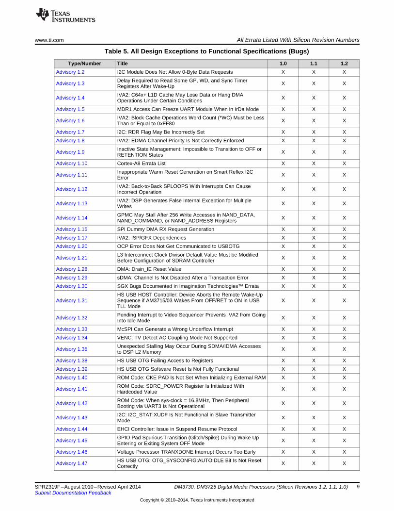
Table 5. All Design Exceptions to Functional Specifications (Bugs)
Type/Number Title 1.0 1.1 1.2Advisory 1.2 I2C Module Does Not Allow 0-Byte Data Requests X X X
Delay Required to Read Some GP, WD, and Sync TimerAdvisory 1.3 X X XRegisters After Wake-UpIVA2: C64x+ L1D Cache May Lose Data or Hang DMAAdvisory 1.4 X X XOperations Under Certain Conditions
Advisory 1.5 MDR1 Access Can Freeze UART Module When in IrDa Mode X X XIVA2: Block Cache Operations Word Count (*WC) Must be LessAdvisory 1.6 X X XThan or Equal to 0xFF80
Advisory 1.7 I2C: RDR Flag May Be Incorrectly Set X X XAdvisory 1.8 IVA2: EDMA Channel Priority Is Not Correctly Enforced X X X
Inactive State Management: Impossible to Transition to OFF orAdvisory 1.9 X X XRETENTION StatesAdvisory 1.10 Cortex-A8 Errata List X X X
Inappropriate Warm Reset Generation on Smart Reflex I2CAdvisory 1.11 X X XErrorIVA2: Back-to-Back SPLOOPS With Interrupts Can CauseAdvisory 1.12 X X XIncorrect OperationIVA2: DSP Generates False Internal Exception for MultipleAdvisory 1.13 X X XWritesGPMC May Stall After 256 Write Accesses in NAND_DATA,Advisory 1.14 X X XNAND_COMMAND, or NAND_ADDRESS Registers
Advisory 1.15 SPI Dummy DMA RX Request Generation X X XAdvisory 1.17 IVA2: ISP/GFX Dependencies X X XAdvisory 1.20 OCP Error Does Not Get Communicated to USBOTG X X X
L3 Interconnect Clock Divisor Default Value Must be ModifiedAdvisory 1.21 X X XBefore Configuration of SDRAM ControllerAdvisory 1.28 DMA: Drain_IE Reset Value X X XAdvisory 1.29 sDMA: Channel Is Not Disabled After a Transaction Error X X XAdvisory 1.30 SGX Bugs Documented in Imagination Technologies™ Errata X X X
HS USB HOST Controller: Device Aborts the Remote Wake-UpAdvisory 1.31 Sequence if AM3715/03 Wakes From OFF/RET to ON in USB X X X
TLL ModePending Interrupt to Video Sequencer Prevents IVA2 from GoingAdvisory 1.32 X X XInto Idle Mode
Advisory 1.33 McSPI Can Generate a Wrong Underflow Interrupt X X XAdvisory 1.34 VENC: TV Detect AC Coupling Mode Not Supported X X X
Unexpected Stalling May Occur During SDMA/IDMA AccessesAdvisory 1.35 X X Xto DSP L2 MemoryAdvisory 1.38 HS USB OTG Failing Access to Registers X X XAdvisory 1.39 HS USB OTG Software Reset Is Not Fully Functional X X XAdvisory 1.40 ROM Code: CKE PAD Is Not Set When Initializing External RAM X X X
ROM Code: SDRC_POWER Register Is Initialized WithAdvisory 1.41 X X XHardcoded ValueROM Code: When sys-clock = 16.8MHz, Then PeripheralAdvisory 1.42 X X XBooting via UART3 Is Not OperationalI2C: I2C_STAT:XUDF Is Not Functional in Slave TransmitterAdvisory 1.43 X X XMode
Advisory 1.44 EHCI Controller: Issue in Suspend Resume Protocol X X XGPIO Pad Spurious Transition (Glitch/Spike) During Wake UpAdvisory 1.45 X X XEntering or Exiting System OFF Mode
Advisory 1.46 Voltage Processor TRANXDONE Interrupt Occurs Too Early X X XHS USB OTG: OTG_SYSCONFIG:AUTOIDLE Bit Is Not ResetAdvisory 1.47 X X XCorrectly
9SPRZ319F–August 2010–Revised April 2014 DM3730, DM3725 Digital Media Processors (Silicon Revisions 1.2, 1.1, 1.0)Submit Documentation Feedback
Copyright © 2010–2014, Texas Instruments Incorporated

All Errata Listed With Silicon Revision Numbers www.ti.com
Table 5. All Design Exceptions to Functional Specifications (Bugs) (continued)Type/Number Title 1.0 1.1 1.2
IVA2 Does Not Wake-Up After It Goes to IDLE While DMAAdvisory 1.48 X X XRequest Is Still AssertedSoftware Reset Done While ISP Processing Is Ongoing CanAdvisory 1.49 X X XCause OCP Protocol Violations
Advisory 1.51 Accesses to DDR Stall in SDRC After a Warm-Reset X X XStandard OTG Compliance Electrical Tests for HOST Mode WillAdvisory 1.52 X X XFail
Advisory 1.54 GPMC Has Incorrect ECC Computation for 4-Bit BCH Mode XHS USB Host: ECHI and OHCI Controllers Cannot WorkAdvisory 1.56 XConcurrently
Advisory 1.57 MMC OCP Clock Not Gated When Thermal Sensor Is Used X X XContext Save Operation Randomly Failing forAdvisory 1.58 X X XCONTROL_PAD_CONF_ETK_D14
Advisory 1.59 I2C4 Does Not Meet I2C Standard AC Timing in FS Mode X X XAdvisory 1.60 I2C1 to 3 SCL Low Period Is Shorter in FS Mode X X X
Missed Dependency With McBSP External Clock PreventsAdvisory 1.61 X X XTransition to OSWRAdvisory 1.62 MPU Cannot Exit from Standby X X XAdvisory 1.63 sDMA FIFO Draining Does Not Finish X X XAdvisory 1.64 HSUSB Interoperability Issue With SMSC USB3320 PHY X
IVA2 Does Not Wake-Up After It Goes to IDLE While anAdvisory 1.65 X X XInterrupt Line Is Not ClearedIVA2 SEQ (ARM9) JTAG Failures With a Free Running ClockAdvisory 1.66 XEmulatorIsolation Issue in OFF Mode Impacting the CORE PowerAdvisory 1.67 XDomain
Advisory 1.68 Safe Mode Does Not Work on GPMC_A11 Pad XGPMC_A11 Address Bit Does Not Behave as Expected (256MBAdvisory 1.69 XNOR Flash Addressability)DM37x Device May Wake Up From Low Power Modes if IOAdvisory 1.71 XWake-Up and Pull Down Are EnabledExcessive Leakage on BRGC Memories in Cortex A8 WhenAdvisory 1.72 XPeriphery Is Turned OffJTAG Pins With bq18jtagfbpbnopm_ssbhv IO Have ESD (Advisory 1.73 XElectro Static Discharge) Weakness in Input Buffer
Advisory 1.74 Scan Shift Issues in GWG Memories XDMA4 Channel Fails to Continue With Descriptor Load When
Advisory 1.75 Pause Bit Is Cleared Through Config Port Access While in X X XStandby
Advisory 1.76 USB OTG DMA Status Register Read Return Zero X X XAdvisory 1.77 POWERVR SGX™: MMU Lockup on Multiple Page Miss X
Device Cannot Reboot if Warm Reset Occurs During MPU DPLLAdvisory 1.78 XLock SequenceAdvisory 1.79 USB Host EHCI May Stall When Exiting Smart-Standby Mode X X
USB Host EHCI May Stall When Running High Peak-BandwidthAdvisory 1.80 X XDemanding Use CasesAdvisory 1.81 USB OTG DMA May Stall Under Specific Configuration X X XAdvisory 1.82 USB OTG DMA May Stall When Entering Standby Mode X X X
DPLL3 in Manual Lock Mode Cannot Be Used When COREAdvisory 1.84 X X XGoes to OSWR or OFF StatePRCM DPLL Control FSM Removes SDRC_IDLEREQ BeforeAdvisory 1.85 X X XDPLL3 Locks
Advisory 1.86 PER Domain Reset Issue After Domain-OFF/OSWR Wake-Up X X
10 DM3730, DM3725 Digital Media Processors (Silicon Revisions 1.2, 1.1, 1.0) SPRZ319F–August 2010–Revised April 2014Submit Documentation Feedback
Copyright © 2010–2014, Texas Instruments Incorporated
www.ti.com All Errata Listed With Silicon Revision Numbers
Table 5. All Design Exceptions to Functional Specifications (Bugs) (continued)Type/Number Title 1.0 1.1 1.2
Advisory 1.87 Self-Refresh Exit Issue After OFF Mode X XAdvisory 1.88 Programming of tCKE X X X
McBSP Used in Slave Mode Can Create a Dead Lock SituationAdvisory 1.89 X X XWhen Doing Power ManagementDPLL3 Bypass Condition Does Not Consider State of SGXAdvisory 1.90 X X XFCLK
Advisory 1.91 Top Ball Compliancy With LPDDR JEDEC Standard X X XI2C: In SCCB Mode, Under Specific Conditions, the ModuleAdvisory 1.92 X X XMight Hold the Bus by Keeping SCL LowI2C: Wrong Behavior When Data With MSB 0 Is Put in the FIFOAdvisory 1.93 X X XBefore a Transfer With SBLOCK Is StartedI2C: After an Arbitration is Lost the Module Incorrectly Starts theAdvisory 1.94 X X XNext Transfer
Advisory 1.95 One Timing Does Not Follow the JEDEC Standard X X X4-cycle Saturating .M Unit Instructions May Mask 2-cycleAdvisory 1.96 X X XSaturating .M Unit
Advisory 1.97 SPLOOP CPU Cross-Path Stall X X XAdvisory 1.98 RTA Feature is Not Supported X X X
HS USB OTG Spurious IRQ When Switching From DMA Mode 1Advisory 1.99 to DMA Mode 0 or to CPU Mode for Unloading the Last Short X X X
Packet of a TransactionAdvisory 1.100 Write to OHCI Registers May Not Complete X X XAdvisory 1.101 Violation of Vix Crossing Specification X XAdvisory 1.102 HS USB OTG Bus Reset X X XAdvisory 1.104 McBSP2 Data Corruption X X XAdvisory 1.105 DSI-PLL Power Command 0x3 Not Working X X X
MPU Leaves MSTANDBY State Before IDLEREQ of InterruptAdvisory 1.106 X X XController is ReleasedSome Power Domains Cannot Go To OFF Mode After WarmAdvisory 1.107 X X XReset
Advisory 1.108 USBHOST Configured In Smart-Idle Can Lead To a Deadlock X X XUSB OTG Software Initiated ULPI Accesses To PHY RegistersAdvisory 1.109 X X XCan Halt the BusAt Context Restore, a Certain PER DPLL Programming CanAdvisory 1.110 X X XIntroduce Wake-up LatenciesUSB Peripheral Booting is Not Operational When an MMCAdvisory 1.111 X X XBooting has Been Attempted BeforeDSS: Color Phase Rotation (CPR) Breaks 2 Pixel Wide UpdatesAdvisory 1.112 X X XWhen in Stall ModeUSB HOST: Impossible To Attach a FS Device To An EHCI PortAdvisory 1.113 X X X- Handoff To OHCI Is Not FunctionalUSB Host Clock Drift Causes USB Spec Non-compliance inAdvisory 2.1 X X XCertain Configurations
11SPRZ319F–August 2010–Revised April 2014 DM3730, DM3725 Digital Media Processors (Silicon Revisions 1.2, 1.1, 1.0)Submit Documentation Feedback
Copyright © 2010–2014, Texas Instruments Incorporated

All Errata Listed by Module www.ti.com
3 All Errata Listed by ModuleTable 6. Errata List for the Control Module
Title ...................................................................................................................................... Page
Advisory 1.58 —Context Save Operation Randomly Failing for CONTROL_PAD_CONF_ETK_D14 ...................... 71Advisory 1.71 —DM37x Device May Wake Up From Low Power Modes if IO Wake-Up and Pull Down Are Enabled .. 77Advisory 1.72 —Excessive Leakage on BRGC Memories in Cortex A8 When Periphery Is Turned Off ................... 78Advisory 1.91 —Top Ball Compliancy With LPDDR JEDEC Standard .......................................................... 93
Table 7. Errata List for the Cortex-A8Title ...................................................................................................................................... Page
Advisory 1.10 —Cortex-A8 Errata List ............................................................................................... 37
Table 8. Errata List for the Display ModuleTitle ...................................................................................................................................... Page
Usage Note 2.1 —Performance Limitation On LCD Read/Write Access Through RFBI L4 Port ............................. 17Usage Note 2.12 —SGX 192 MHz Limitation With TVOUT @ 54 MHz .......................................................... 22Usage Note 2.17 —TVOUT Line Shift Issue When Using DSI PLL for DISPC_FCLK ........................................ 25Advisory 1.105 —DSI-PLL Power Command 0x3 Not Working ................................................................. 102Advisory 1.112 —DSS: Color Phase Rotation (CPR) Breaks 2 Pixel Wide Updates When in Stall Mode ................ 108
Table 9. Errata List for the DMA4 ModuleTitle ...................................................................................................................................... Page
Advisory 1.28 —DMA: Drain_IE Reset Value ....................................................................................... 46Advisory 1.29 —sDMA: Channel Is Not Disabled After a Transaction Error .................................................... 46Advisory 1.63 —sDMA FIFO Draining Does Not Finish............................................................................ 73Advisory 1.75 —DMA4 Channel Fails to Continue With Descriptor Load When Pause Bit Is Cleared Through Config
Port Access While in Standby ............................................................................................... 79
Table 10. Errata List for the DPLL ModuleTitle ...................................................................................................................................... Page
Advisory 1.78 —Device Cannot Reboot if Warm Reset Occurs During MPU DPLL Lock Sequence........................ 81Advisory 1.90 —DPLL3 Bypass Condition Does Not Consider State of SGX FCLK........................................... 92
Table 11. Errata List for the GPMC ModuleTitle ...................................................................................................................................... Page
Advisory 1.14 —GPMC May Stall After 256 Write Accesses in NAND_DATA, NAND_COMMAND, orNAND_ADDRESS Registers ................................................................................................. 41
Advisory 1.54 —GPMC Has Incorrect ECC Computation for 4-Bit BCH Mode ................................................ 69Advisory 1.68 —Safe Mode Does Not Work on GPMC_A11 Pad ............................................................... 76Advisory 1.69 —GPMC_A11 Address Bit Does Not Behave as Expected (256MB NOR Flash Addressability) .......... 76
Table 12. Errata List for the HDQ ModuleTitle ...................................................................................................................................... Page
Usage Note 2.18 —HDQ™/1-Wire® Communication Constraints................................................................. 25
12 DM3730, DM3725 Digital Media Processors (Silicon Revisions 1.2, 1.1, 1.0) SPRZ319F–August 2010–Revised April 2014Submit Documentation Feedback
Copyright © 2010–2014, Texas Instruments Incorporated

www.ti.com All Errata Listed by Module
Table 13. Errata List for the HS USB ModuleTitle ...................................................................................................................................... Page
Usage Note 4.1 —HS USB Host Subsystem: Some Limitations Exist When Connecting to External Devices ............. 28Advisory 1.31 —HS USB HOST Controller: Device Aborts the Remote Wake-Up Sequence if AM3715/03 Wakes
From OFF/RET to ON in USB TLL Mode................................................................................... 47Advisory 1.44 —EHCI Controller: Issue in Suspend Resume Protocol ......................................................... 59Advisory 1.56 —HS USB Host: ECHI and OHCI Controllers Cannot Work Concurrently .................................... 69Advisory 1.64 —HSUSB Interoperability Issue With SMSC USB3320 PHY .................................................... 74Advisory 1.79 —USB Host EHCI May Stall When Exiting Smart-Standby Mode............................................... 81Advisory 1.80 —USB Host EHCI May Stall When Running High Peak-Bandwidth Demanding Use Cases ............... 82Advisory 1.100 —Write to OHCI Registers May Not Complete ................................................................. 101Advisory 1.108 —USBHOST Configured In Smart-Idle Can Lead To a Deadlock............................................ 105Advisory 1.113 —USB HOST: Impossible To Attach a FS Device To An EHCI Port - Handoff To OHCI Is Not
Functional ..................................................................................................................... 109Advisory 2.1 —USB Host Clock Drift Causes USB Spec Non-compliance in Certain Configurations ..................... 110
Table 14. Errata List for the HS USB OTG ModuleTitle ...................................................................................................................................... Page
Advisory 1.20 —OCP Error Does Not Get Communicated to USBOTG......................................................... 45Advisory 1.38 —HS USB OTG Failing Access to Registers....................................................................... 55Advisory 1.39 —HS USB OTG Software Reset Is Not Fully Functional ........................................................ 56Advisory 1.47 —HS USB OTG: OTG_SYSCONFIG:AUTOIDLE Bit Is Not Reset Correctly ................................. 64Advisory 1.52 —Standard OTG Compliance Electrical Tests for HOST Mode Will Fail ...................................... 68Advisory 1.76 —USB OTG DMA Status Register Read Return Zero ........................................................... 79Advisory 1.81 —USB OTG DMA May Stall Under Specific Configuration....................................................... 83Advisory 1.82 —USB OTG DMA May Stall When Entering Standby Mode ..................................................... 83Advisory 1.99 —HS USB OTG Spurious IRQ When Switching From DMA Mode 1 to DMA Mode 0 or to CPU Mode
for Unloading the Last Short Packet of a Transaction .................................................................. 100Advisory 1.102 —HS USB OTG Bus Reset ....................................................................................... 102Advisory 1.109 —USB OTG Software Initiated ULPI Accesses To PHY Registers Can Halt the Bus ..................... 106
Table 15. Errata List for the I2C ModuleTitle ...................................................................................................................................... Page
Usage Note 2.11 —Extra Power Consumed When Repeated Start Operation Mode Is Enabled on I2C InterfaceDedicated for Smart Reflex (I2C4) .......................................................................................... 21
Advisory 1.2 —I2C Module Does Not Allow 0-Byte Data Requests.............................................................. 32Advisory 1.7 —I2C: RDR Flag May Be Incorrectly Set ............................................................................ 35Advisory 1.43 —I2C: I2C_STAT:XUDF Is Not Functional in Slave Transmitter Mode ........................................ 58Advisory 1.59 —I2C4 Does Not Meet I2C Standard AC Timing in FS Mode .................................................. 72Advisory 1.60 —I2C1 to 3 SCL Low Period Is Shorter in FS Mode ............................................................. 72Advisory 1.92 —I2C: In SCCB Mode, Under Specific Conditions, the Module Might Hold the Bus by Keeping SCL
Low .............................................................................................................................. 94Advisory 1.93 —I2C: Wrong Behavior When Data With MSB 0 Is Put in the FIFO Before a Transfer With SBLOCK Is
Started........................................................................................................................... 94Advisory 1.94 —I2C: After an Arbitration is Lost the Module Incorrectly Starts the Next Transfer........................... 95
13SPRZ319F–August 2010–Revised April 2014 DM3730, DM3725 Digital Media Processors (Silicon Revisions 1.2, 1.1, 1.0)Submit Documentation Feedback
Copyright © 2010–2014, Texas Instruments Incorporated

All Errata Listed by Module www.ti.com
Table 16. Errata List for the INTC ModuleTitle ...................................................................................................................................... Page
Advisory 1.62 —MPU Cannot Exit from Standby ................................................................................... 73
Table 17. Errata List for the ISP ModuleTitle ...................................................................................................................................... Page
Advisory 1.49 —Software Reset Done While ISP Processing Is Ongoing Can Cause OCP Protocol Violations .......... 66
Table 18. Errata List for the IVA2 ModuleTitle ...................................................................................................................................... Page
Usage Note 2.2 —IVA2: Under Hardware Emulation, IDLE Instruction Must Be Executed From L1P or L2 SRAM ...... 17Advisory 1.4 —IVA2: C64x+ L1D Cache May Lose Data or Hang DMA Operations Under Certain Conditions .......... 33Advisory 1.6 —IVA2: Block Cache Operations Word Count (*WC) Must be Less Than or Equal to 0xFF80 .............. 34Advisory 1.8 —IVA2: EDMA Channel Priority Is Not Correctly Enforced ....................................................... 36Advisory 1.12 —IVA2: Back-to-Back SPLOOPS With Interrupts Can Cause Incorrect Operation .......................... 38Advisory 1.13 —IVA2: DSP Generates False Internal Exception for Multiple Writes .......................................... 39Advisory 1.17 —IVA2: ISP/GFX Dependencies..................................................................................... 44Advisory 1.32 —Pending Interrupt to Video Sequencer Prevents IVA2 from Going Into Idle Mode ......................... 48Advisory 1.35 —Unexpected Stalling May Occur During SDMA/IDMA Accesses to DSP L2 Memory ...................... 50Advisory 1.96 —4-cycle Saturating .M Unit Instructions May Mask 2-cycle Saturating .M Unit Instruction Saturation
Bit Update....................................................................................................................... 96Advisory 1.97 —SPLOOP CPU Cross-Path Stall .................................................................................. 97
Table 19. Errata List for the IVA2.2 ModuleTitle ...................................................................................................................................... Page
Usage Note 2.10 —Maximum 12 Bits Output (1 bit sign + 11 bits of value) Is Supported on CAVLD of iVLCD ........... 21
Table 20. Errata List for the JTAG ModuleTitle ...................................................................................................................................... Page
Advisory 1.66 —IVA2 SEQ (ARM9) JTAG Failures With a Free Running Clock Emulator ................................... 75Advisory 1.67 —Isolation Issue in OFF Mode Impacting the CORE Power Domain........................................... 76Advisory 1.73 —JTAG Pins With bq18jtagfbpbnopm_ssbhv IO Have ESD ( Electro Static Discharge) Weakness in
Input Buffer ..................................................................................................................... 78
Table 21. Errata List for the McBSP ModuleTitle ...................................................................................................................................... Page
Usage Note 3.5 —Undesired McBSP slave mode behavior during reset without CLKR/CLKX............................... 27Advisory 1.86 —PER Domain Reset Issue After Domain-OFF/OSWR Wake-Up .............................................. 87Advisory 1.89 —McBSP Used in Slave Mode Can Create a Dead Lock Situation When Doing Power Management .... 91Advisory 1.104 —McBSP2 Data Corruption ....................................................................................... 102
Table 22. Errata List for the MMC ModuleTitle ...................................................................................................................................... Page
Usage Note 2.15 —MMC IOs Reliability Issue ...................................................................................... 23Advisory 1.57 —MMC OCP Clock Not Gated When Thermal Sensor Is Used ................................................ 70
14 DM3730, DM3725 Digital Media Processors (Silicon Revisions 1.2, 1.1, 1.0) SPRZ319F–August 2010–Revised April 2014Submit Documentation Feedback
Copyright © 2010–2014, Texas Instruments Incorporated

www.ti.com All Errata Listed by Module
Table 23. Errata List for the MPUTitle ...................................................................................................................................... Page
Advisory 1.106 —MPU Leaves MSTANDBY State Before IDLEREQ of Interrupt Controller is Released................. 103
Table 24. Errata List for the PRCM ModuleTitle ...................................................................................................................................... Page
Usage Note 2.3 —Domain Woken Up by Wake-Up Dependency Cannot Transition to Inactive State ...................... 18Usage Note 2.5 —Observability Signals Not Functional in OFF Mode........................................................... 18Usage Note 2.6 —Constraints on Module Clocks When Using DVFS ........................................................... 19Usage Note 2.9 —GPIO Is Driving Random Values When Device Returns From OFF Mode ................................ 20Usage Note 2.13 —PWDNx Bit in CLock Manager Is Reseting the DPLL4 Mx HSDIVIDER Coefficient Previously
Programmed ................................................................................................................... 23Advisory 1.9 —Inactive State Management: Impossible to Transition to OFF or RETENTION States ...................... 37Advisory 1.11 —Inappropriate Warm Reset Generation on Smart Reflex I2C Error .......................................... 38Advisory 1.21 —L3 Interconnect Clock Divisor Default Value Must be Modified Before Configuration of SDRAM
Controller........................................................................................................................ 45Advisory 1.45 —GPIO Pad Spurious Transition (Glitch/Spike) During Wake Up Entering or Exiting System OFF Mode 62Advisory 1.61 —Missed Dependency With McBSP External Clock Prevents Transition to OSWR.......................... 72Advisory 1.84 —DPLL3 in Manual Lock Mode Cannot Be Used When CORE Goes to OSWR or OFF State............. 84Advisory 1.98 —RTA Feature is Not Supported ................................................................................... 99Advisory 1.107 —Some Power Domains Cannot Go To OFF Mode After Warm Reset ..................................... 104
Table 25. Errata List for the ROM Code ModuleTitle ...................................................................................................................................... Page
Advisory 1.40 —ROM Code: CKE PAD Is Not Set When Initializing External RAM .......................................... 56Advisory 1.41 —ROM Code: SDRC_POWER Register Is Initialized With Hardcoded Value................................. 57Advisory 1.42 —ROM Code: When sys-clock = 16.8MHz, Then Peripheral Booting via UART3 Is Not Operational ..... 57Advisory 1.110 —At Context Restore, a Certain PER DPLL Programming Can Introduce Wake-up Latencies.......... 106Advisory 1.111 —USB Peripheral Booting is Not Operational When an MMC Booting has Been Attempted Before.... 107
Table 26. Errata List for the SDRC ModuleTitle ...................................................................................................................................... Page
Advisory 1.51 —Accesses to DDR Stall in SDRC After a Warm-Reset ......................................................... 67Advisory 1.85 —PRCM DPLL Control FSM Removes SDRC_IDLEREQ Before DPLL3 Locks.............................. 85Advisory 1.87 —Self-Refresh Exit Issue After OFF Mode ......................................................................... 88Advisory 1.88 —Programming of tCKE .............................................................................................. 90Advisory 1.95 —One Timing Does Not Follow the JEDEC Standard ........................................................... 95Advisory 1.101 —Violation of Vix Crossing Specification ........................................................................ 101
Table 27. Errata List for the SGX ModuleTitle ...................................................................................................................................... Page
Advisory 1.30 —SGX Bugs Documented in Imagination Technologies™ Errata............................................... 46Advisory 1.77 —POWERVR SGX™: MMU Lockup on Multiple Page Miss..................................................... 80
15SPRZ319F–August 2010–Revised April 2014 DM3730, DM3725 Digital Media Processors (Silicon Revisions 1.2, 1.1, 1.0)Submit Documentation Feedback
Copyright © 2010–2014, Texas Instruments Incorporated

All Errata Listed by Module www.ti.com
Table 28. Errata List for the SPI ModuleTitle ...................................................................................................................................... Page
Advisory 1.15 —SPI Dummy DMA RX Request Generation ...................................................................... 42Advisory 1.33 —McSPI Can Generate a Wrong Underflow Interrupt ........................................................... 49
Table 29. Errata List for the SR ModuleTitle ...................................................................................................................................... Page
Advisory 1.46 —Voltage Processor TRANXDONE Interrupt Occurs Too Early ................................................ 64
Table 30. Errata List for the TDL ModuleTitle ...................................................................................................................................... Page
Advisory 1.74 —Scan Shift Issues in GWG Memories............................................................................. 78
Table 31. Errata List for the Timer ModuleTitle ...................................................................................................................................... Page
Advisory 1.3 —Delay Required to Read Some GP, WD, and Sync Timer Registers After Wake-Up ....................... 32
Table 32. Errata List for the UART ModuleTitle ...................................................................................................................................... Page
Usage Note 2.7 —UART: Cannot Acknowledge Idle Requests in Smartidle Mode When Configured for DMAOperations ...................................................................................................................... 19
Advisory 1.5 —MDR1 Access Can Freeze UART Module When in IrDa Mode ................................................ 34
Table 33. Errata List for the VENC ModuleTitle ...................................................................................................................................... Page
Usage Note 2.4 —VENC: Last Data Line Missing in PAL.......................................................................... 18Advisory 1.34 —VENC: TV Detect AC Coupling Mode Not Supported ......................................................... 49
Table 34. Errata List for CautionsTitle ...................................................................................................................................... Page
Usage Note 3.4 —Avoiding Voltage Drop When Booting at 1-GHz OPP With TPS65950A3 ................................. 26
16 DM3730, DM3725 Digital Media Processors (Silicon Revisions 1.2, 1.1, 1.0) SPRZ319F–August 2010–Revised April 2014Submit Documentation Feedback
Copyright © 2010–2014, Texas Instruments Incorporated

www.ti.com Usage Notes and Known Design Exceptions to Functional Specifications
4 Usage Notes and Known Design Exceptions to Functional Specifications
4.1 Usage Notes (Limitations)Usage Notes highlight and describe particular situations where the device's behavior may not matchpresumed or documented behavior. This may include behaviors that affect device performance orfunctional correctness. These notes will be incorporated into future documentation updates for the device(such as the device-specific data manual), and the behaviors they describe will not be altered in futuresilicon revisions.
Note: The peripherals supported on the various microprocessors are different. The user should only referto usage notes and advisories pertaining to features supported on the specific device. For a complete listof the supported features of the microrocessors, see the device-specific data manuals.
Usage Note 2.1 Performance Limitation On LCD Read/Write Access Through RFBI L4 Port
Revision(s) Affected 1.2, 1.1 and 1.0
Details Read access to the LCD through the RFBI L4 port: The data of a Read access is sentback to the initiator of the access only at RECycleTime. RECycleTime is used as areference event for CS release as well (CS is used as an on-going access notificationsignal depending on the type of LCD panel connected). This means that any Readaccess to the LCD through the L4 interface of the RFBI will be ended by a CS release(CS going inactive at the end of the access). Therefore, the processor does not supporttwo consecutive Read accesses to the LCD (there is always 1 L4 clock cycle between 2accesses).
Write access to the LCD through the RFBI L4 port: For a Write access, the back-to-back data of a single access that has been split is supported and guaranteed (e.g., one32-bit write split in two consecutive, back-to-back, 16-bit accesses). In this case, theinternal bus CS signal will be kept active until split access completion. However, whenthere are two different write accesses from the initiator, they will not be seen as back-to-back by the LCD. At the end of the transaction corresponding to one write access fromthe initiator, the internal bus CS will be released at WECycleTime, and the nextcommand from the initiator will be accepted. Consequently, any Write access to the LCDthrough the L4 interface of the RFBI will be ended by a CS release (CS going inactive atthe end of the access). Therefore, the processor does not support two consecutive datatransmits to the LCD (corresponding to two different and consecutive Write accessesfrom the initiator).
Usage Note 2.2 IVA2: Under Hardware Emulation, IDLE Instruction Must Be Executed From L1P orL2 SRAM
Revision(s) Affected 1.2, 1.1 and 1.0
Details This limitation was fixed and is kept for silicon errata consistency only. The workaroundcan be removed from the code.
17SPRZ319F–August 2010–Revised April 2014 DM3730, DM3725 Digital Media Processors (Silicon Revisions 1.2, 1.1, 1.0)Submit Documentation Feedback
Copyright © 2010–2014, Texas Instruments Incorporated

Usage Note 2.3 — Domain Woken Up by Wake-Up Dependency Cannot Transition to Inactive State www.ti.com
Usage Note 2.3 Domain Woken Up by Wake-Up Dependency Cannot Transition to Inactive State
Revision(s) Affected 1.2, 1.1 and 1.0
Details When a domain is activated up by a wake-up dependency, it cannot transition to aninactive (RET/OFF) state until one of the following conditions are satisfied:1. If the domain has a sleep dependency with another domain, this domain and the
sleep dependency must be also activated (hard-wired or enabled by the software).2. If the domain is an initiator, it must be taken out of Standby mode.
Note: The user should ensure that when a wake-up dependency is enabled for adomain, it is expected to be fully active after the wake-up occurs. This issue happens ina case where a domain has been woken-up, but not activated and used.
This issue can be avoided by ensuring the IVA2 processor is taken out of Standby modeprior to any new sleep transition.
Usage Note 2.4 VENC: Last Data Line Missing in PAL
Revision(s) Affected 1.2, 1.1 and 1.0
Details The VENC cannot show the image data at the end of the even frames on line 623. Thisis a minor violation of the ITU-R BT.470-6. Since lines 23 and 336 are reserved for WSS,the VENC can only show 574 lines of data instead of the 576 lines defined in thestandard. One half line is missing for lines 23 (reserved for WSS) and 623, and one fullline is missing for line 336 (reserved for WSS).
Usage Note 2.5 Observability Signals Not Functional in OFF Mode
Revision(s) Affected 1.2, 1.1 and 1.0
Details Signals are routed to observability pins through a buffer powered by VDD2.Consequently, observability is not functional when VDD2 is powered off. This impactsthe observability debug feature, but has no functional drawback.
Note: Maintaining the VDD2 supply on the board has no effect since isolation cells areactivated regardless of the supplied voltage.
18 DM3730, DM3725 Digital Media Processors (Silicon Revisions 1.2, 1.1, 1.0) SPRZ319F–August 2010–Revised April 2014Submit Documentation Feedback
Copyright © 2010–2014, Texas Instruments Incorporated

www.ti.com Usage Note 2.6 — Constraints on Module Clocks When Using DVFS
Usage Note 2.6 Constraints on Module Clocks When Using DVFS
Revision(s) Affected 1.2, 1.1 and 1.0
Details Module interface timings can depend on the operating point (OPP). The timing closure isdone for one instance of a module at a particular voltage. Operating conditions whichwork on one OPP are not automatically guaranteed on another module's OPP. For moredetails on the module interface switching characteristics, see the device-specific datamanual.
Workaround(s) When Dynamic Voltage and Frequency Scaling (DVFS) is performed, the softwareshould ensure that no timing violations will occur by the two following methods:• Using software, reconfigure the module accordingly when DVFS is performed to
avoid timing violations.• Use a conservative frequency on the module interface clock corresponding to the
performance of the lower OPP used to ensure that DVFS can be performed withoutadditional software management.
Usage Note 2.7 UART: Cannot Acknowledge Idle Requests in Smartidle Mode When Configuredfor DMA Operations
Revision(s) Affected 1.2, 1.1 and 1.0
Details When configured for DMA operations using smartidle mode (SYSC[4:3].IDLEMODE =0x2), the UART module will not acknowledge incoming idle requests. As a consequence,it can prevent L4 from going to idle.
When there are additional expected transfers, the UART should be placed in force-idlemode.
19SPRZ319F–August 2010–Revised April 2014 DM3730, DM3725 Digital Media Processors (Silicon Revisions 1.2, 1.1, 1.0)Submit Documentation Feedback
Copyright © 2010–2014, Texas Instruments Incorporated

Usage Note 2.9 — GPIO Is Driving Random Values When Device Returns From OFF Mode www.ti.com
Usage Note 2.9 GPIO Is Driving Random Values When Device Returns From OFF Mode
Revision(s) Affected 1.2, 1.1 and 1.0
Details The GPIO modules in the PER (Peripheral) domain are driving random values when thedevice returns from OFF mode with the VDD2 voltage shut down. Regardless of theactive configuration of a GPIO (input or output), when coming back from OFF mode,GPIO can randomly drive the line high or low.
Root cause: The isolation at the boundary of the peripheral domain is done throughisolation latches that are supplied by VDD2. When VDD2 is shut down, the content ofthe latches is lost. When the device is waking-up from the OFF mode, the padconf isautomatically restored by the hardware and the isolation latches are driving the pin untilisolation is released (PER is woken-up). There is no reset value for the isolation latches,leading to random values driven by the GPIO.
This is not impacting the GPIO from the WU domain. Only GPIO is implementing thiskind of isolation latch, other functions are not impacted by this limitation.
Workaround(s) Workaround 1 allows software to work in software supervised mode while Workaround 2gets the benefit of hardware dependency. For both workarounds, software is used toconfigure the internal pull in the padconf register to the desired value.
Workaround1: Change padconf mode to safe mode before initiating the transition toOFF. This avoids the line being driven by the isolation latch and the desired level ismaintained by the pull.
Workaround2: Create a WU dependency between WU domain and PER domain(PM_WKDEP_PER[4]: EN_WKUP=1). This will wake up the PER domain, then releasethe isolation latch before the isolation cell is released at the pad boundary. The resetvalue of the GPIO module is configuring the GPIO in input, then the pull ensures that theline is driven to the right value until the GPIO module is restored by the applicativesoftware
20 DM3730, DM3725 Digital Media Processors (Silicon Revisions 1.2, 1.1, 1.0) SPRZ319F–August 2010–Revised April 2014Submit Documentation Feedback
Copyright © 2010–2014, Texas Instruments Incorporated
www.ti.com Usage Note 2.10 — Maximum 12 Bits Output (1 bit sign + 11 bits of value) Is Supported on CAVLD of iVLCD
Usage Note 2.10 Maximum 12 Bits Output (1 bit sign + 11 bits of value) Is Supported on CAVLD ofiVLCD
Revision(s) Affected 1.2, 1.1 and 1.0
Details While decoding DC coefficients of an Intra16x16 MB, the iVLCD is not able to handlecoefficients with range greater than 11 bits. It is observed that the value returned by theiVLCD will be the equivalent of (actual_value & 0x07FF). For example, value of 0x08A7will be decoded as 0x00A7. However, the bits consumed by the iVLCD is correct and thedecoding continues.
As per the standard, normal imagery can generate DC coeffs with range greater than 11bits (especially at low QP) and some of the test cases are failing due to this issue. Sincethe error is in DC it will not only affect the MB in question, but propagate to neighboringMBs in the slice. The impact is visually noticeable.
This issue only occurs if either of the following conditions are met:• For QP<10, Luma DC coefficients of Intra16x16 MB• For QP<4, Chroma DC coefficients
This special case must be handled with C64x+ software, which increases code size andadds extra MHz.
The estimate of the cost for the work added is: extra 3-4 MHz and 25kB of code.
Usage Note 2.11 Extra Power Consumed When Repeated Start Operation Mode Is Enabled on I2CInterface Dedicated for Smart Reflex (I2C4)
Revision(s) Affected 1.2, 1.1 and 1.0
Details On the I2C interface dedicated for Smart Reflex communication with the PowerManagement IC (I2C4), when Repeated Start operation mode is enabled(PRM_VC_I2C_CFG[SREN]=’1’), the I2C lines (SCL and SDA) are always driving a lowstate between two I2C commands (i.e. when there is no I2C traffic).
Knowing that there are external Pull-Up attached on these lines, this will impact thepower consumption.
Setting PRM_VC_I2C_CFG[SREN] register bit to ’0’ will allow the I2C4 lines driving ahigh state between two I2C commands.
21SPRZ319F–August 2010–Revised April 2014 DM3730, DM3725 Digital Media Processors (Silicon Revisions 1.2, 1.1, 1.0)Submit Documentation Feedback
Copyright © 2010–2014, Texas Instruments Incorporated

Usage Note 2.12 — SGX 192 MHz Limitation With TVOUT @ 54 MHz www.ti.com
Usage Note 2.12 SGX 192 MHz Limitation With TVOUT @ 54 MHz
Revision(s) Affected 1.2, 1.1 and 1.0
Details The siimultaneous operation of SGX530 @ 192 MHz and TVOUT clock @ 54 MHz is notpossible.
SGX functional clock can be selected from four sources:• Divided version of the CORE.CLK [by 2, 3, 4, 6]• Divided version of the COREX2.CLK [by 3, 5]• 96 MHz clock version• 192 MHz clock version
The frequency combination of SGX530 @ 192 MHz along with TVOUT @ 54 MHz is notpossible with the TVout clock divider which maximum value is 31.
TV-Out requires a 54MHz clock provided by the DPLL-PER (DPLL4) , then the DPLL-PER has to be set to 864 MHz to get the 54MHz clock. In the case of setting DPLL-PERat 1728MHz to get 192Mhz on SGX will not allow getting the 54MHz on TVOUT sincehigh-speed divider is limited to 31.
Workaround(s) Only if TVOUT@54MHz is a workaround required. The SGX clock will have to besourced from CORE-DPLL (SGX clock will scale with L3 clock). When software is usingTV-Out @ 54 Mhz, SGX functional clock has to be derived from CORE-DPLL whichallows up to 200MHz clock frequency depending on the CORE clock configuration.
22 DM3730, DM3725 Digital Media Processors (Silicon Revisions 1.2, 1.1, 1.0) SPRZ319F–August 2010–Revised April 2014Submit Documentation Feedback
Copyright © 2010–2014, Texas Instruments Incorporated

www.ti.com Usage Note 2.13 — PWDNx Bit in CLock Manager Is Reseting the DPLL4 Mx HSDIVIDER CoefficientPreviously Programmed
Usage Note 2.13 PWDNx Bit in CLock Manager Is Reseting the DPLL4 Mx HSDIVIDER CoefficientPreviously Programmed
Revision(s) Affected 1.2, 1.1 and 1.0
Details When PWRDN bit is set, it resets the internal HSDIVIDER divide-by value (Mx). Thereset value gets loaded instead of the previous value. The following HSDIVIDERs exhibitthis behavior:• DPLL4: M6 / M5 / M4 / M3 / M2 (CM_CLKEN_PLL[31:26] register bits)• DPLL3: M3 (CM_CLKEN_PLL[12] register bit).
Workaround(s) No performance impact by using the following workaround.
It is mandatory to apply the following sequence to ensure the write value will be loadedin DPLL HSDIVIDER FSM:1. Read HSDIVIDER register.2. Write HSDIVIDER + 1 (Or any other value different from the Read value).3. Write HSDIVIDER with the correct value.
The global sequence when using PWRDN bit is:1. Disable Mx HSDIVIDER clock output related functional clock enable bits (in
CM_FCLKEN_xxx / CM_ICLKEN_xxx).2. Enable PWRDN bit of HSDIVIDER.3. Disable PWRDN bit of HSDIVIDER.4. Read current HSDIVIDER register value.5. Write different value in HSDIVIDER register.6. Write expected value in HSDIVIDER register.7. Enable Mx HSDIVIDER clock output related functional clocks (CM_FCLKEN_xxx /
CM_ICLKEN_xxx).
Usage Note 2.15 MMC IOs Reliability Issue
Revision(s) Affected 1.1, 1.0
Details Design error in IOs cells used for MMC/SD/SDIO1 interfaces leading to reliability issuewhen:• Device is kept under reset with sys_nrespwron = 0.• OR device is waking up from reset until SW sets IOs power down control bit
(CONTROL_PBIAS_LITE.PBIASLITEPWRDNZ0 for MMC/SD/SDIO1).• OR IOs are in power down mode (programmed in previous registers).
The effect of this reliability issue is IO dysfunction. That is, it stays in power down ordoes not enter power down anymore. No IO performance degradation is expected.
Impact in customer application is less than 1 dppm over 5 and 7 years product life-time;assuming unreliable conditions described above are reached 100% of the time.
23SPRZ319F–August 2010–Revised April 2014 DM3730, DM3725 Digital Media Processors (Silicon Revisions 1.2, 1.1, 1.0)Submit Documentation Feedback
Copyright © 2010–2014, Texas Instruments Incorporated
Usage Note 2.16 — Downscaling Limitations www.ti.com
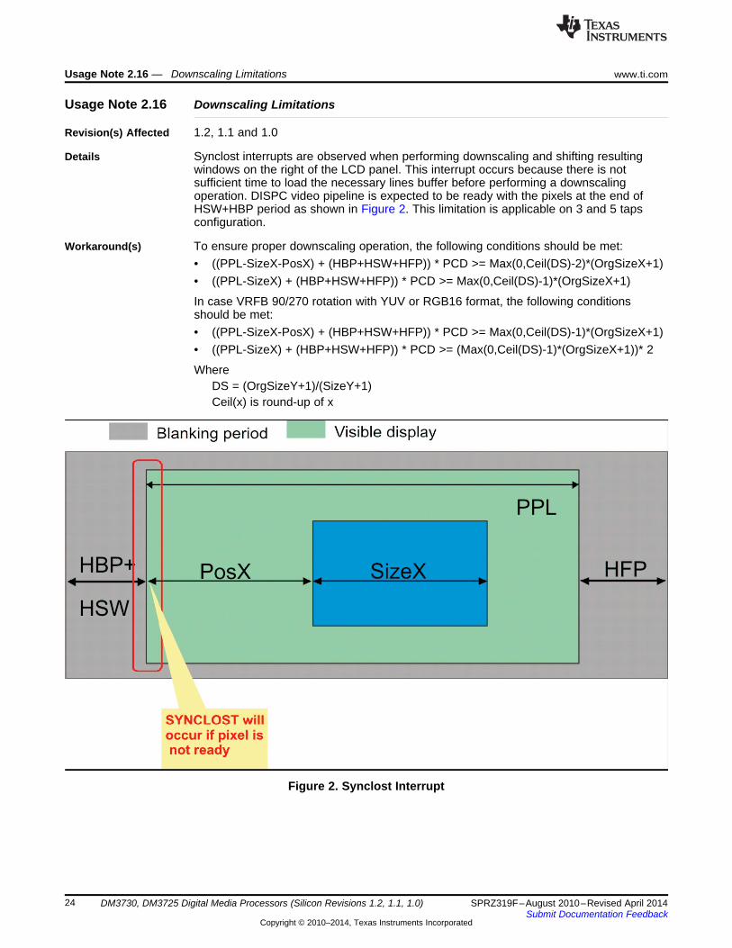
Usage Note 2.16 Downscaling Limitations
Revision(s) Affected 1.2, 1.1 and 1.0
Details Synclost interrupts are observed when performing downscaling and shifting resultingwindows on the right of the LCD panel. This interrupt occurs because there is notsufficient time to load the necessary lines buffer before performing a downscalingoperation. DISPC video pipeline is expected to be ready with the pixels at the end ofHSW+HBP period as shown in Figure 2. This limitation is applicable on 3 and 5 tapsconfiguration.
Workaround(s) To ensure proper downscaling operation, the following conditions should be met:• ((PPL-SizeX-PosX) + (HBP+HSW+HFP)) * PCD >= Max(0,Ceil(DS)-2)*(OrgSizeX+1)• ((PPL-SizeX) + (HBP+HSW+HFP)) * PCD >= Max(0,Ceil(DS)-1)*(OrgSizeX+1)
In case VRFB 90/270 rotation with YUV or RGB16 format, the following conditionsshould be met:• ((PPL-SizeX-PosX) + (HBP+HSW+HFP)) * PCD >= Max(0,Ceil(DS)-1)*(OrgSizeX+1)• ((PPL-SizeX) + (HBP+HSW+HFP)) * PCD >= (Max(0,Ceil(DS)-1)*(OrgSizeX+1))* 2
WhereDS = (OrgSizeY+1)/(SizeY+1)Ceil(x) is round-up of x
Figure 2. Synclost Interrupt
24 DM3730, DM3725 Digital Media Processors (Silicon Revisions 1.2, 1.1, 1.0) SPRZ319F–August 2010–Revised April 2014Submit Documentation Feedback
Copyright © 2010–2014, Texas Instruments Incorporated

www.ti.com Usage Note 2.17 — TVOUT Line Shift Issue When Using DSI PLL for DISPC_FCLK
Usage Note 2.17 TVOUT Line Shift Issue When Using DSI PLL for DISPC_FCLK
Revision(s) Affected 1.2, 1.1 and 1.0
Details When using the clock from DSI_PLL (DSI1_PLL_FCLK) as a functional clock for theDISPC, on TVOUT output, the pixel lines are randomly in advance of 294ns.
The failure does not occur when using the DSS1_ALWON_FCLK (from DPLL4).
The failure is random. The faulty lines have "good timing duration," meaning the lineduration is 64 us. The synchronization pulse and the burst color are also good.
Workaround(s) When TVOUT is used, the DISPC_FCLK clock source must be DPLL4 to avoid the lineshift on TVOUT.
Usage Note 2.18 HDQ™/1-Wire® Communication Constraints
Revision(s) Affected 1.2, 1.1 and 1.0
Details HDQ/1-Wire protocols use a return-to-1 mechanism that requires an external pullupresistor on the line. There is a timing limitation on this return-to-1 mechanism thatrequires a constraint on the external pullup resistor (R) and the capacitive load (C) of thewire.
Workaround(s) There is a constraint in the design for the maximum allowed rise time of the wire. Afterwriting data to the wire, the HDQ/1-Wire module samples the logic value of the wire 1FSM (finite state machine) clock cycle later. The FSM expects to read back 1 value fromthe wire. This constraint must be taken into account when calculating the pullup resistor(R) according to the capacitive load (C) of the wire.
The maximum RC (pullup resistor and capacitive load) value should be calculated as:
R < 1200 ns / (10e-12 + C)
For example, if R = 4.7K, C < 245 pF.
25SPRZ319F–August 2010–Revised April 2014 DM3730, DM3725 Digital Media Processors (Silicon Revisions 1.2, 1.1, 1.0)Submit Documentation Feedback
Copyright © 2010–2014, Texas Instruments Incorporated

Usage Note 3.4 — Avoiding Voltage Drop When Booting at 1-GHz OPP With TPS65950A3 www.ti.com
Usage Note 3.4 Avoiding Voltage Drop When Booting at 1-GHz OPP With TPS65950A3
Revision(s) Affected 1.2, 1.1 and 1.0
Details TPS65950A3 implements two separate registers for control of VDD1 voltage. Firstregister, VDD1_SEL, can be programmed through I2C1 only while second register,VDD1_SR_CONTROL, can be programmed by SR I2C, I2C4.
By default, the VDD1 DCDC is providing the voltage which is set in VDD1_SEL untilAVS is configured on the DM37x side and enabled on TPS65950A3 side. As soon asDCDC_GLOBAL_CFG is set to enable SR_I2C IOs, then DCDC reference switches toVDD1_SR_CONTROL.
The default value (also known as reset value) is corresponding to 1.2-V voltage value.
In the context of 1-GHz boot, the system is started at 1-GHz OPP with AVS disabled(using 1-GHz nominal voltage, refer to DM operating conditions addendum) and AVS willbe enabled later on when kernel has booted.
The voltage requirement to run 1-GHz OPP with AVS disabled is higher than 1.2 V(default value for VDD1_SR_CONTROL).
In that context, if user is starting boot at OPP1GHz by rising VDD1_SEL, then systemwill maintain the right voltage level until AVS is enabled. At that point, as soon as DM37xwill perform the access to DCDC_GLOBAL_CFG to enable SR) I2C IOs, then DCDC willtake the reset value of VDD1_SR_CONTROL and provide 1.2 V instead of nominalvoltage until this VDD1_SR_CONTROL is overwritten. This voltage drop to 1.2 V isunsafe if system is running 1-GHz OPP and can lead to instability.
It is not possible to overwrite SR_I2C reset value before DCDC_GLOBAL_CFG set theIOs to avoid that situation. User should avoid this situation by using a sequence which isnot running 1-GHz OPP with 1.2 V on VDD1.
Workaround(s) Solution#1: System boot at OPP100 or lower OPP (avoid booting at OPP130 andOPP1GHz is a safe option with no re-work).
Solution#2: Boot at 1 GHz but initiate the first AVS calibration for OPP100 or lowerOPP. (As soon as 1 OPP calibration happens for one OPP with nominal voltage lowerthan 1.2 V, then no restriction to perform other OPP calibration.) Sequence can be:• Boot at 1-GHZ OPP with AVS disabled• Switch to OPP100• Run OPP100 AVS calibration• Run OPP1GHz AVS calibration• Switch to OPP1GHz• etc.
Solution#3: Boot at 1-GHz OPP and stay at this OPP until AVS calibration. Right beforesetting DCDC_GLOBAL_CFG:• Change OPP to OPP100• Set DCDC_GLOBAL_CFG (voltage changed to 1.2 V, which is aligned with OPP100)• Send a bypass command corresponding to 1-GHz nominal voltage through SR_I2C• Switch back to 1-GHz OPP.
Solution#4: Before enabling OPP1GHz (this means in the bootloader), configure DM37xSR module to launch a bypass command on I2C then set DCDC_GLOBAL_CFG andlaunch 1-GHz OPP nominal voltage to VDD1_SR_CONTROL. At that point 1-GHz bootcan be launched safely.
26 DM3730, DM3725 Digital Media Processors (Silicon Revisions 1.2, 1.1, 1.0) SPRZ319F–August 2010–Revised April 2014Submit Documentation Feedback
Copyright © 2010–2014, Texas Instruments Incorporated

www.ti.com Usage Note 3.5 — Undesired McBSP slave mode behavior during reset without CLKR/CLKX
Usage Note 3.5 Undesired McBSP slave mode behavior during reset without CLKR/CLKX
Revision(s) Affected 1.2, 1.1 and 1.0
Details As described in the Technical Reference Manual, the McBSP port requires two clockcycles of CLKR/CLKX during reset to synchronize the interface configuration. When theMcBSP is configured in slave mode, the necessary clock is provided by the other device(the interface master). If the master device does not provide the necessary clock beforethe first frame pulse, then undesired behavior of the McBSP port will occur since it willonly be properly initialized during the first two clock cycles of CLKR/CLKX. Impacts ofthis situation include:• McBSP port does not receive the first frame of data from the master• Undefined output (glitch) on McBSP transmit line during the first frame pulse
Workaround(s) If possible, the master should provide CLKR/CLKX before the first frame pulse (duringMcBSP initialization) to avoid this issue. No other workaround is available.
27SPRZ319F–August 2010–Revised April 2014 DM3730, DM3725 Digital Media Processors (Silicon Revisions 1.2, 1.1, 1.0)Submit Documentation Feedback
Copyright © 2010–2014, Texas Instruments Incorporated

12/8-pin ULPI(PHY Outputs Clock) USB PHY USB OTG
CompanionChip
Device
OT
G C
on
tro
ller
Po
rt 0
12/8-pin ULPI(PHY Outputs Clock) USB OTGOTG/HS/
FS/LSDiscrete PHY
Device
OT
G C
on
tro
ller
Po
rt 0
High-speed USBOTG controller
High-speedUSB
host subsystem
Port
1P
ort
2P
ort
3
Device
Port
0
Usage Note 4.1 — HS USB Host Subsystem: Some Limitations Exist When Connecting to External Devices www.ti.com
Usage Note 4.1 HS USB Host Subsystem: Some Limitations Exist When Connecting to ExternalDevices
Revision(s) Affected 1.2, 1.1 and 1.0
Details As shown in Figure 3, the DM37x device includes a high-speed universal serial bus(USB) OTG controller and a high-speed USB host subsystem.
Workaround(s) Note: USB Port 3 is not available on CUS package.
Figure 3. DM37x USB Modules
The high-speed USB OTG controller supports a single USB port which uses a UTMI low-pin interface (ULPI) to connect to an off-chip transceiver (12-pin/8-bit single-data ratemode). As shown in Figure 4, USB Port 0 can be connected to the USB 2.0 PHYincluded in DM37x companion chips, e.g. TPS65950A3. Alternatively, USB Port 0 can beconnected to discrete USB 2.0 PHYs which include a UTMI low-pin interface (ULPI) andare capable if sourcing an output clock.
Figure 4. Typical Uses for USB Port 0
28 DM3730, DM3725 Digital Media Processors (Silicon Revisions 1.2, 1.1, 1.0) SPRZ319F–August 2010–Revised April 2014Submit Documentation Feedback
Copyright © 2010–2014, Texas Instruments Incorporated

usb-007
High-Speed USB Host subsystem
High-speed USB Host
MPU
subsystem
INTC
mm2_xxx
OHCIcontroller
OHCI_IRQ
EHCI_IRQ
hsusb2_tll_xxx
hsusb2_xxx
hsusb1_tll_xxx
hsusb1_xxxL3
interconnect
L4-Core
interconnect
Device
Interrupt requests
USBHOSTUSBHOST_MICLK HS USB Host I/F pins
USBHOST_SICLK
TLL_IRQ
L3 master interface
L4 slave interface
USBHOSTUSBHOST_FCLK1
USBHOST_FCLK2
EHCIcontroller
ULPI TLL
Serial
ULPI TLL
Serial
ULPI TLL
Serial
Channel 2
Channel 1
Channel 0
USBTLL
Serial
Serial
Serial
UTMI
UTMI
UTMI
clock
clock
Functional clock
Functional clock
controller
3
2
1
To
ple
ve
lm
ultip
lexin
gTo
ple
ve
lm
ultip
lexin
gTo
ple
ve
lm
ultip
lexin
g
mm1_xxx
hsusb3_tll_xxx
mm3_xxx
ULPI
ULPI
ULPI
ULPI
PRCM
USBTLL_ICLK
USBTLL_FCLKFunctional clock
L4 Interface clock
www.ti.com Usage Note 4.1 — HS USB Host Subsystem: Some Limitations Exist When Connecting to External Devices
As shown in Figure 5, the high-speed universal serial bus (USB) host subsystemsupports up to three USB ports, each one of which can owned by one of two controllers:• The EHCI controller, based on the Enhanced Host Controller Interface (EHCI)
specification for USB Release 1.0, is in charge of high-speed traffic (480M bit/s) overeither a UTMI port or a UTMI low-pin interface (ULPI) port.
• The OHCI controller, based on the Open Host Controller Interface (OHCI)specification for USB Release 1.0a, is in charge of full-speed/low-speed traffic(12/1.5M bit/s, respectively) over a serial interface.
Both the OHCI and EHCI controllers can operate in parallel. Each of the three USB portsis owned by exactly one of the controllers at any time. Also, when a controller uses theUTMI port, the USB TLL block converts that port to a ULPI transceiver-less link logic(TLL) format.
Please note the following functional limitations when using the high-speed USB hostsubsystem:• On silicon revision 1.0 only, if one port is configured in the ULPI mode, then all other
ports must use the same configuration. Therefore, the ports must be configured high-speed mode or full-speed/low-speed mode. For more information, see Advisory 1.55.
• USB Port 3 cannot operate in ULPI mode; it can only operate in serial or ULPI TLLmode. Furthermore, USB Port 3 is not available in the CUS package.
Figure 5. High-Speed USB Host Subsystem Highlight
29SPRZ319F–August 2010–Revised April 2014 DM3730, DM3725 Digital Media Processors (Silicon Revisions 1.2, 1.1, 1.0)Submit Documentation Feedback
Copyright © 2010–2014, Texas Instruments Incorporated

ULPI HS
PHY(A)
Device
Po
rt 1 12-pin ULPI
(Device Outputs Clock)
Po
rt 2 12-pin ULPI
( Outputs Clock)Device
Po
rt 3
Not Used
Not Used
A. USB port 3 does not support ULPI mode. Also, USB port 3 not available on CUS package.
HS USBHUB
HS/FS/LSDevice or
Receptacle
HS/FS/LSDevice or
Receptacle
HS/FS/LSDevice or
Receptacle
ULPI HS
PHY(A)
Device
HS
Ho
st
Co
ntr
oller
(EH
CI)
Po
rt 1 12-pin ULPI
(Device Outputs Clock)
Po
rt 2 12-pin ULPI
(Device Outputs Clock)
Po
rt 3
Not Used
ULPI HS
PHY(A)
A. USB port 3 does not support ULPI mode.Also, USB port 3 not available on CUS package.
Usage Note 4.1 — HS USB Host Subsystem: Some Limitations Exist When Connecting to External Devices www.ti.com
As shown in Figure 6, USB Port 1 and Port 2 can be used to connect to external high-speed PHYs which include a ULPI port. However, in this case, the external USB PHYmust be able to accept a source clock generated by the DM37x high-speed USBcontroller. Also, in this usage model the USB ports cannot support full-speed and low-speed operation. Therefore, using this approach, USB Port 1 and Port 2 cannot providea fully compliant USB 2.0 Type-A receptacle; a high-speed USB hub would be requiredin this case; please see Figure 7.
Note: USB Port 3 does not support ULPI mode. USB Port 3 is not available on CUSpackage.
Figure 6. Connecting to High-Speed PHYs Using USB Ports
Figure 7. Connecting to a High-Speed USB Hub
30 DM3730, DM3725 Digital Media Processors (Silicon Revisions 1.2, 1.1, 1.0) SPRZ319F–August 2010–Revised April 2014Submit Documentation Feedback
Copyright © 2010–2014, Texas Instruments Incorporated

www.ti.com Usage Note 4.2 — "Speed Binned" Bit in Control Device Status Register Not Programmed in Devices Built andTested Prior to June 2011
Usage Note 4.2 "Speed Binned" Bit in Control Device Status Register Not Programmed in DevicesBuilt and Tested Prior to June 2011
Revision(s) Affected 1.2, 1.1 and 1.0
Details The Speed Binned bit (bit 9) of the Control Device Status Register (0x4800 244C) maynot accurately reflect the maximum speed capabilities of the device. Some 1-GHzcapable DM37x devices built and tested before June 2011 may have a '0' for this bit.
Workaround(s) Use the device marking on the top of the package to determine the speed capabilities ofthe device. Check the device markings against the Device Nomenclature information inthe device-specific data manual.
31SPRZ319F–August 2010–Revised April 2014 DM3730, DM3725 Digital Media Processors (Silicon Revisions 1.2, 1.1, 1.0)Submit Documentation Feedback
Copyright © 2010–2014, Texas Instruments Incorporated

Usage Notes and Known Design Exceptions to Functional Specifications www.ti.com
4.2 Known Design Exceptions to Functional Specifications (Bugs)
Advisory 1.2 I2C Module Does Not Allow 0-Byte Data Requests
Revision(s) Affected 1.2, 1.1 and 1.0
Details When configured as the master, the I2C module does not allow 0-byte data transfers.
Note: Programming I2Ci.I2C_CNT[15:0]: DCOUNT = 0 will cause undefined behavior.
Workaround(s) There is no workaround for this issue. Do not use 0-byte data requests.
Advisory 1.3 Delay Required to Read Some GP, WD, and Sync Timer Registers After Wake-Up
Revision(s) Affected 1.2, 1.1 and 1.0
Details If a General Purpose Timer (GPTimer) is in posted mode (TSIRC.POSTED = 1), due tointernal resynchronizations, any values read in TCRR, TCAR1, and TCAR2 registersimmediately after the timer interface clock (L4) goes from a stopped state to an activestate may not return the expected values. This situation is most likely when theprocessor wakes up from an idle state.
Notes:• GPTimer non-posted synchronization mode is not impacted by this advisory.• This advisory also impacts reads from Watchdog timers WCRR registers.• All of the watchdog timers support only posted internal synchronization mode. There
is no capability to change the internal synchronization scheme to non-posted modevia software.
• The 32K sync timer CR and 32SYNCNT_REV registers are also impacted by thisadvisory, since the 32K sync timer is always in posted synchronization mode.
Workaround(s) The software must wait at least 2 timer interface clock cycles + 1 timer functional clockcycle after L4 clock-wake-up before reading TCRR, TCAR1, or TCAR2 registers for GPTimers in posted internal synchronization mode, and before reading the WCRR registerof the Watchdog timers. The same workaround must be applied before reading CR and32KSYNCNT_REV registers of the synctimer module.
32 DM3730, DM3725 Digital Media Processors (Silicon Revisions 1.2, 1.1, 1.0) SPRZ319F–August 2010–Revised April 2014Submit Documentation Feedback
Copyright © 2010–2014, Texas Instruments Incorporated

www.ti.com Advisory 1.4 — IVA2: C64x+ L1D Cache May Lose Data or Hang DMA Operations Under Certain Conditions
Advisory 1.4 IVA2: C64x+ L1D Cache May Lose Data or Hang DMA Operations Under CertainConditions
Revision(s) Affected 1.2, 1.1 and 1.0
Details Under certain conditions, parallel loads with predication to the same cache line maycause victims to be dropped and/or DMA to hang.All of the following conditions must be true in order for this problem to occur:1. Two LD instructions in parallel.2. Both are LDs to the same cache line (upper 26 address bits are the same).3. The LD using T1 is predicated and the predicate is false.4. The LD using T2 is either not predicated, or is predicated and the predicate is true.5. The cache line is absent from the cache.6. The two other lines in the same L1D set are valid.7. The LRU cache line in the set is dirty.
Results:• L1D informs L2 to expect a victim for the affected set.• L2 stalls DMAs with addresses that correspond to that set (DMA includes accesses
from IDMA and EDMA).
Note: DMA includes accesses from IDMA, EDMA, and any external masters, such asPCI or other CPUs.
• L1D processes the true-predicated request correctly.• L1D does not send the indicated victim.
Impact:• If the load instruction reads a cacheable location:
– The updated data in the LRU line gets dropped.– DMA accesses whose addresses match the affected set hang.
• If the load instruction reads a non-cacheable location:– L1D retains the updated data from the LRU line.– DMA reads may see stale data if the LRU line's address is in L2 memory.
Workaround(s) Use Code Gen patch 6.0.3 (available on update advisor) to recompile your source codeand avoid this issue. Libraries supplied by TI will be re-released using the 6.0.3 compilerpatch. Customer-generated libraries from TI's third-party supplier may also need to berecompiled.
For existing object code and libraries, an available Perl script can determine locations ofparallel predicated loads that may fail. The script is available at the same update advisorlocation as the Code Gen patch.
33SPRZ319F–August 2010–Revised April 2014 DM3730, DM3725 Digital Media Processors (Silicon Revisions 1.2, 1.1, 1.0)Submit Documentation Feedback
Copyright © 2010–2014, Texas Instruments Incorporated

Advisory 1.5 — MDR1 Access Can Freeze UART Module When in IrDa Mode www.ti.com
Advisory 1.5 MDR1 Access Can Freeze UART Module When in IrDa Mode
Revision(s) Affected 1.2, 1.1 and 1.0
Details Because of a glitchy structure inside the UART module, accessing the MDR1 registermay create a dummy underrun condition and freeze the UART IrDa transmission. OnlyIrDa modes Slow Infrared (SIR), Medium Infrared (MIR), and Fast Infrared (FIR) areimpacted. Even if the bug condition occurs in UART mode or IrDa CIR mode, it will haveno effect. Therefore, UART1 and UART2 are immune to this problem, and only UART3may exhibit this issue when used in one of the IrDa modes– SIR, MIR, or FIR.
Workaround(s) To ensure this problem does not occur, the following software initialization sequencemust be used each time MDR1 must be changed to one of the three failing IrDa modes:1. If needed, setup the UART by writing the required registers, except MDR1.2. Set appropriately the MDR1.MODE_SELECT bit field.3. Wait for 5 L4 clock cycles + 5 UART functional clock cycles.4. Read RESUME register to resume the halted operation.
Advisory 1.6 IVA2: Block Cache Operations Word Count (*WC) Must be Less Than or Equal to0xFF80
Revision(s) Affected 1.2, 1.1 and 1.0
Details When performing any block cache operation, such as "Writeback", "Writeback withInvalidate", or "Invalidate", for any memory controller or memory range (e.g., L1P, L2,L1D) the word count programmed must be less than or equal to 0xFF80. If a valuegreater than 0xFF80 is desired, then this must be broken into multiple operations. Thefollowing registers are affected: L2WWC, L2WIWC, L2IWC, L1PIWC, L1DWIWC,L1DWWC, and L1DIWC.
Workaround(s) There is no workaround for this issue.
34 DM3730, DM3725 Digital Media Processors (Silicon Revisions 1.2, 1.1, 1.0) SPRZ319F–August 2010–Revised April 2014Submit Documentation Feedback
Copyright © 2010–2014, Texas Instruments Incorporated

3.
ReadNbTimes = I2Cn.I2C_BUFSTAT[13:8] RXSTAT
Read I2Cn.I2C_DATA Register Nb Times
Increase I2CnCounter with Nb Times
Fix and StoreI2CnCounter
I2CnCounter = 0
4.
RDR = 1 ?
Clear RDR
No
Yes
Read I2Cn.I2C_STAT Register
BB = 0 ?No
Yes
Read I2Cn.I2C_STAT Register
2.
Clear RDR
RDR = 1 ?
Yes
1.
www.ti.com Advisory 1.7 — I2C: RDR Flag May Be Incorrectly Set
Advisory 1.7 I2C: RDR Flag May Be Incorrectly Set
Revision(s) Affected 1.2, 1.1 and 1.0
Details Under certain rare conditions, the I2C_STAT[13].RDR bit may be set as well as thecorresponding interrupt fire, even when there is no data in the receive FIFO, or the I2Cdata transfer is still ongoing. These spurious RDR events must be ignored by thesoftware.
Workaround(s) Software must filter out unexpected RDR pulses, using the flowchart illustrated inFigure 8 when receiving an I2C RDR interrupt.
Figure 8. I2C Flowchart
35SPRZ319F–August 2010–Revised April 2014 DM3730, DM3725 Digital Media Processors (Silicon Revisions 1.2, 1.1, 1.0)Submit Documentation Feedback
Copyright © 2010–2014, Texas Instruments Incorporated

C B A
F E D
Q0
Q1
When TPTC can accept anew TR, TPTC activates
empty signal
TPTC0
TPTC1
empty0
empty1
TPCC
TPTC
Specified behavior is that TRshall be submitted from each
queue as soon as thecorresponding TC becomes
available
Owing to the bug, Q1remains blocked as long
as Q0 is not empty
Advisory 1.8 — IVA2: EDMA Channel Priority Is Not Correctly Enforced www.ti.com
Advisory 1.8 IVA2: EDMA Channel Priority Is Not Correctly Enforced
Revision(s) Affected 1.2, 1.1 and 1.0
Details The EDMA channel controller (TPCC) has 2 event queues: Q0 and Q1. Each queue canbe mapped to one of the two Transfer Controllers (TPTC): TPTC0 or TPTC1. Asexplained in the AM/DM37x Multimedia Device Technical Reference Manual (literaturenumber SPRUGN4 ), the events in each event queue will be extracted as soon as thecorresponding TPTC is available for a new Transfer Request (TR) to be programmedinto the TPTC. However, due to an issue in the IVA2.2 subsystem, the requests queuedin Q1 cannot be submitted to their TPTC as long as Q0 is not empty.
Figure 9. TR Submission Scheme
Workaround(s) Infrequent short transfers (e.g., latency critical synchronized transfers to/from peripheral)must be placed in Q0, and longer transfers (e.g., block copy) in Q1. For example, whena latency critical transfer is placed in EDMA and a longer transfer in QDMA, the followingprogramming model will minimize the impact of this limitation:• EDMA Event is queued to Q0 (using IVA_TPCC.DMAQNUMn register, n from 0 to 7)• QDMA Event is queued to Q1 (using IVA_TPCC.QDMAQNUM register)• Queue to TC Mapping is Q0:TPTC1 Q1:TPTC0 (using IVA_TPCC.QUETCMAP
register)• Queue Priority is Q0 = 0x0, Q1 = 0x7 (using IVA_TPCC.QUEPRI register)
36 DM3730, DM3725 Digital Media Processors (Silicon Revisions 1.2, 1.1, 1.0) SPRZ319F–August 2010–Revised April 2014Submit Documentation Feedback
Copyright © 2010–2014, Texas Instruments Incorporated

www.ti.com Advisory 1.9 — Inactive State Management: Impossible to Transition to OFF or RETENTION States
Advisory 1.9 Inactive State Management: Impossible to Transition to OFF or RETENTION States
Revision(s) Affected 1.2, 1.1 and 1.0
Details If a power domain meets the conditions to go to an INACTIVE state (that is,POWERSTATE is programmed to 0x3 (ON) and clock can be shut off), then the domainwill transition to INACTIVE state. However, the domain cannot go to RET or OFF stateautomatically from INACTIVE state, even if software updates the POWERSTATE bit to0x1 (RET) or 0x0 (OFF). The domain must be transitioned to the ON state before it cantransition to the RET or OFF states.
Workaround(s) The following two conditions must be met:1. Do not use autostate with PM_PWSTCTRL_XXX.POWERSTATE=0x3 (ON) to put
power state in INACTIVE. Using autostate from ON to RET (or OFF) transition is notimpacted..
2. Perform wake-up event (software must force wake-up) to transition to an active statebefore transitioning to the RET or OFF states.
Advisory 1.10 Cortex-A8 Errata List
Revision(s) Affected 1.2, 1.1 and 1.0
Details This errata document does not cover the advisories associated with the ARM Cortex-A8processor. For a list of the advisories associated with each version of the ARM Cortex-A8 processor, contact your TI representative for a copy of the ARM Core Cortex-A8(AT400/AT401) Errata Notice. See Table 3 to determine which version of the ARMCortex-A8 processor is included in each AM3715/03 silicon revision.
37SPRZ319F–August 2010–Revised April 2014 DM3730, DM3725 Digital Media Processors (Silicon Revisions 1.2, 1.1, 1.0)Submit Documentation Feedback
Copyright © 2010–2014, Texas Instruments Incorporated

Advisory 1.11 — Inappropriate Warm Reset Generation on Smart Reflex I2C Error www.ti.com
Advisory 1.11 Inappropriate Warm Reset Generation on Smart Reflex I2C Error
Revision(s) Affected 1.2, 1.1 and 1.0
Details The Voltage Controller generates an I2C access error when an I2C command is sent toPowerIC during a voltage domain sleep transition. When the access error is generated,an interrupt is generated for software error handling. PRCM generates a warm_resetwhen an access error is generated by the Voltage Controller during voltage domainwake-up transition. This is to recover the full system (processor + Peripherals + PowerIC) and avoid a deadlock (processor wake-up transition stalling due to I2C access errorand VDD1/ VDD2 not supplied). Since both VDD1 and VDD2 Voltage Controllers sharethe same interrupt line, an access error for VDD2 Voltage controller is also propagatedto VDD1 Voltage controller.
Note: This bug occurs only with the I2C module used by the Smart Reflex module. Otherinstances of the I2C module are not impacted by this issue.
In the following scenario:1. VDD1 is performing a wake-up transition while VDD2 is performing a sleep transition.2. An I2C access error is generated on VDD2 sleep request and VDD1 and VDD2
share the same error line, so this access error on VDD2 is broadcasted to both VDD1and VDD2.
3. The condition for a warm_reset generation is met on VDD1, and Warm_reset isasserted inappropriately.
Workaround(s) This issue was detected in simulation, but it is a corner case which is not expected tooccur in production since the I2C access error should never occur if the PCB is safe.
Advisory 1.12 IVA2: Back-to-Back SPLOOPS With Interrupts Can Cause Incorrect Operation
Revision(s) Affected 1.2, 1.1 and 1.0
Details Back-to-back software pipeline loops (SPLOOPs) with interrupts can cause incorrectoperation during C64x+ execution when:1. The DSP code contains two contiguous SPLOOP/D/W.2. DSP is interrupted when executing the first SPLOOP/D/W.3. There are less than two execute packets between the SPKERNEL of the first
SPLOOP/D/W and the SPLOOP/D/W instruction of the second.
When this issue occurs, the first SPLOOP/D/W terminates abruptly, i.e. withoutcompleting the loop, even though the termination condition is false. The failuremechanism can be seen as a hang, or by the first SPLOOP/D/W draining for theinterrupt and starting the second SPLOOP/D/W without taking the interrupt or returningto complete the first SPLOOP/D/W.
Workaround(s) This issue can be worked around by ensuring there are at least two execute packetsbetween the SPKERNEL of the first SPLOOP/D/W and the SPLOOP/D/W instruction ofthe second.
A fix is implemented in the compiler included in version CGT6.0.6 of the CodeGeneration Tools. Starting with this revision of the CGT, the compiler ensures there aretwo cycles between SPKERNEL and SPLOOP/D/W instructions by adding theappropriate number of NOP instructions following the SPKERNEL instruction.
38 DM3730, DM3725 Digital Media Processors (Silicon Revisions 1.2, 1.1, 1.0) SPRZ319F–August 2010–Revised April 2014Submit Documentation Feedback
Copyright © 2010–2014, Texas Instruments Incorporated

www.ti.com Advisory 1.13 — IVA2: DSP Generates False Internal Exception for Multiple Writes
Advisory 1.13 IVA2: DSP Generates False Internal Exception for Multiple Writes
Revision(s) Affected 1.2, 1.1 and 1.0
Details A false internal exception can be generated by C64x+ if an interrupt happens duringDSP code flow and the instructions that will be annulled during pipeline flush aredependant. This issue occurs in the exception detection logic. It examines the DSPinstructions during the pipeline flush, even though they have been annulled. Thehardware does not detect this and incorrectly assumes that multiple write instructions tothe same register with 2 different conditional registers will be executed.
The DSP generates an incorrect internal exception in the following scenario: the CPU isdraining the pipeline as part of an interrupt context switch. During this time, it annulsinstructions in the pipeline. The first annulled execute packet changes the value of oneor more predicate registers. The second annulled execute packet has two or morepredicated instructions that use the predicates written in the previous cycle. The valuesheld in the predicate registers appear to cause the instructions in the second annulledexecute packet to write to the same register. The conflicting writes would not happen ifthe first execute packet was not annulled.
Example:ZERO A0ZERO A1------------> (interrupt occurs here)MVK 1, A0; (annulled)[!A0] MVK 2, A1; (annulled)|| [!B0] MVK 3, A1; (annulled)
Invalid exception triggers as it appears that the last two MVK will both write A1.
Even if this issue appears in a DSP code, it does not affect the code flow and does notproduce an unexpected exit routine value.
Workaround(s) The CPU only recognizes the incorrect exception while it drains the pipeline for aninterrupt. As a result, the CPU begins exception processing upon reaching the interrupthandler. The NRP (NMI Return Pointer Register) and NTSR (NMI Task State Register)will reflect the state of the machine upon arriving at the interrupt handler.
Therefore, to identify the incorrect resource conflict exception in software, verify thefollowing conditions at the beginning of the exception handler prior to normal exceptionprocessing:1. Exception occurred during an interrupt context switch.
• In NTSR, verify that INT=1, SPLX=0, IB=0, CXM=00.• Verify that NRP points to an interrupt service fetch packet. That is, (NRP &
0xFFFFFE1F) == (ISTP & 0xFFFFFE1F).2. The exception is a resource conflict exception. In IERR, verify that RCX == 1 and all
other IERR bits == 0.3. The exception is an internal exception. In EFR, verify that IXF == 1 and all other EFR
bits == 0.
Upon matching the above conditions, suppress the exception as follows:• Clear EFR.IXF by writing 2 to ECR.• Resume the interrupt handler by branching to NRP.
The above workaround identifies and suppresses all cases of the incorrect resourceconflict exception. It resumes normal program execution when the incorrect exceptionoccurs, and has minimal impact on the execution time of program code. The interruptedcode sequence runs as expected when the interrupt handler returns.
39SPRZ319F–August 2010–Revised April 2014 DM3730, DM3725 Digital Media Processors (Silicon Revisions 1.2, 1.1, 1.0)Submit Documentation Feedback
Copyright © 2010–2014, Texas Instruments Incorporated

Advisory 1.13 — IVA2: DSP Generates False Internal Exception for Multiple Writes www.ti.com
The workaround also suppresses a particular valid exception case that isindistinguishable from the incorrect case. Specifically, the code will suppress theexception generated by two instructions with different delay slots (e.g., LDW andDOTP2) writing to the same register in the same cycle, where the conflicting writes occurduring the interrupt context switch.
Example of sequence with incorrectly suppressed exception:LDW *A0, A1DOTP2 A3, A2, A1NOP-----------------> interrupt occursNOPNOP ; Both LDW and DOTP2 write to A1 this cycle
The workaround will not suppress these valid resource conflict exceptions if the multiplewrites occur outside an interrupt context switch. That is, the workaround will notsuppress the exception generated by the code above when it executes without aninterfering interrupt.
40 DM3730, DM3725 Digital Media Processors (Silicon Revisions 1.2, 1.1, 1.0) SPRZ319F–August 2010–Revised April 2014Submit Documentation Feedback
Copyright © 2010–2014, Texas Instruments Incorporated

www.ti.com Advisory 1.14 — GPMC May Stall After 256 Write Accesses in NAND_DATA, NAND_COMMAND, orNAND_ADDRESS Registers
Advisory 1.14 GPMC May Stall After 256 Write Accesses in NAND_DATA, NAND_COMMAND, orNAND_ADDRESS Registers
Revision(s) Affected 1.2, 1.1 and 1.0
Details The GPMC may stall if the following conditions are met:1. GPMC_CONFIG[0].NANDFORCEPOSTEDWRITE=1.2. Software performs more than 256 continuous write accesses in
NAND_COMMAND_x, NAND_ADDRESS_x or NAND_DATA_x registers.3. GPMC_STATUS[0].EMPTYWRITEBUFFERSTATUS is always 0 (buffer not empty)
during write accesses. This means the software has to write fast enough in GPMCregisters in order to never have the write buffer empty.
This mechanism is CS independent. If the software performs 128 write accesses inNAND_DATA_0 followed by 128 write accesses in NAND_DATA_1 then the bug willoccur.
Workaround(s) Accesses performed through the "prefetch and write posting engine" of the GPMC arenot impacted by this limitation, and software should use this mechanism for the bestperformance.
If the prefetch and write posting engine is not used, whenGPMC_CONFIG[0].NANDFORCEPOSTEDWRITE=1 and after 255 write accesses inNAND_COMMAND_x, NAND_DATA_x or NAND_ADDRESS_x registers, the softwarehas to wait until GPMC_STATUS[0].EMPTYWRITEBUFFERSTATUS=1 before sendingthe next 255 write accesses.
41SPRZ319F–August 2010–Revised April 2014 DM3730, DM3725 Digital Media Processors (Silicon Revisions 1.2, 1.1, 1.0)Submit Documentation Feedback
Copyright © 2010–2014, Texas Instruments Incorporated

SPI RX DMARequest
SPI CS
SPI CLK
2–SPI Slave Configuration
4–Enable Slave, then Master. No DummyDMA Request Generated (No Previous CLKFalling Edge)
3–SPI Master Configuration (CLK Driven Low)
1–SPI Pin Muxing Configuration (CLK Pulled Down, CS Pulled Down)
SPI RX DMARequest
SPI CS
SPI CLK
2–SPI Slave Configuration
4–Enable Slave, then Master. Dummy DMARequest is Generated Because of PreviousCLK Falling
3–SPI Master Configuration (CLK Driven Low)
1–SPI Pin Muxing Configuration (CLK Pulled Up, CS Pulled Down)
Advisory 1.15 — SPI Dummy DMA RX Request Generation www.ti.com
Advisory 1.15 SPI Dummy DMA RX Request Generation
Revision(s) Affected 1.2, 1.1 and 1.0
Details A dummy DMA RX request is generated as soon as the SPI is configured in slave modeand a SPI clock edge is detected. The dummy DMA RX request is generated duringmodule configuration, when the module is not performing an SPI transfer. The dummyDMA RX request occurs as soon as the SPI interface signal sensitivity is changedcompared to the default value.
The dummy DMA RX request is generated because the mechanism to avoid dummydata capture on a CS glitch is done regardless of channel activation.
Figure 10. SPI Dummy DMA RX Generation
Workaround(s) Avoid conditions where the SPI is in slave mode and the SPI clock toggles (seeexamples below).
Figure 11. Dummy DMA RX Generation (No Clock Edge)
42 DM3730, DM3725 Digital Media Processors (Silicon Revisions 1.2, 1.1, 1.0) SPRZ319F–August 2010–Revised April 2014Submit Documentation Feedback
Copyright © 2010–2014, Texas Instruments Incorporated

SPI RX DMARequest
SPI CS
SPI CLK
3–SPI Slave Configuration (Was Originally Step 2)
4–Enable Slave, then Master.No Dummy DMA Request Generated
2–SPI Master Configuration (CLK Driven Low)(Was Originally Step 3)
1–SPI Pin Muxing Configuration (CLK Pulled Up, CS Pulled Down)
www.ti.com Advisory 1.15 — SPI Dummy DMA RX Request Generation
Figure 12. Dummy DMA RX Generation (Slave Mode After Clock Line Driven to Default Value)
43SPRZ319F–August 2010–Revised April 2014 DM3730, DM3725 Digital Media Processors (Silicon Revisions 1.2, 1.1, 1.0)Submit Documentation Feedback
Copyright © 2010–2014, Texas Instruments Incorporated

Advisory 1.17 — IVA2: ISP/GFX Dependencies www.ti.com
Advisory 1.17 IVA2: ISP/GFX Dependencies
Revision(s) Affected 1.2, 1.1 and 1.0
Details Scenario:• IVA2 is idled.• Interrupt is propagated to the IVA2.• IVA2 INTC (WUGEN) generates a Wake-Up event to the PRCM for IVA2 Wake-Up.• A Wake-Up dependency is defined between IVA and ISP, or IVA and GFX.• PRCM wakes-up IVA2, which initiates wake-up for ISP/GFX.• Interrupt is propagated to IVA2 Core.• At this point IVA2 Core could initiate a transfer to ISP/GFX even though the ISP/GFX
module may not have finished its wake-up sequence, thus resulting in OCP transferfail.
Workaround(s) The IVA2 software should look at the ISP/GFX clock activity status bit to verify that theISP/GFX domain is ON before performing any accesses. Next, 10 NOPs should beinserted for additional margin.
44 DM3730, DM3725 Digital Media Processors (Silicon Revisions 1.2, 1.1, 1.0) SPRZ319F–August 2010–Revised April 2014Submit Documentation Feedback
Copyright © 2010–2014, Texas Instruments Incorporated

www.ti.com Advisory 1.20 — OCP Error Does Not Get Communicated to USBOTG
Advisory 1.20 OCP Error Does Not Get Communicated to USBOTG
Revision(s) Affected 1.2, 1.1 and 1.0
Details The OCP master interface of the sub-chip has a design limitation. This interfaceconnects to an OCP slave on one side and to the AHB master interface of Mentor USBOTG core, MUSBMHDRC, on the other side. It is a wrapper that converts AHB masterread/write requests to equivalent OCP read/write requests, and the OCP response/datafrom OCP slave is expected to be converted to equivalent AHB response/data. In thedesign, the AHB hresp is always set to OKAY. As a result, an OCP response is nevertranslated to an equivalent AHB response. If an OCP error response is received on themaster interface, it will be sent as AHB OKAY response and not as AHB Error response.
The DMA controller will continue with the DMA read/write transfer as it is unaware of theOCP error response that occurred for the given read/write transfer. The bus error bit inDMA_CNTL register will never be set.
Workaround(s) In an OCP error scenario, halt the DMA and terminate the DMA transfer.
Advisory 1.21 L3 Interconnect Clock Divisor Default Value Must be Modified BeforeConfiguration of SDRAM Controller
Revision(s) Affected 1.2, 1.1 and 1.0
Details The SDRAM output clock is gated when an incorrect L3 CLK_SEL ratio is set. Thisoperation is generally transparent and handled at boot time by the ROM code. Theworkaround should be implemented for the following scenario:• GP device External Fast boot is used.
Workaround(s) For External Boot or External Fast Boot which are both impacted by the issue,CM_CLKSEL_CORE[1:0].CLKSEL_L3 (bit 1:0) = 10b must be set before performingSDRC configuration. In all other cases, this programing is handled by the ROM code andno workaround is necessary.
45SPRZ319F–August 2010–Revised April 2014 DM3730, DM3725 Digital Media Processors (Silicon Revisions 1.2, 1.1, 1.0)Submit Documentation Feedback
Copyright © 2010–2014, Texas Instruments Incorporated

Advisory 1.28 — DMA: Drain_IE Reset Value www.ti.com
Advisory 1.28 DMA: Drain_IE Reset Value
Revision(s) Affected 1.2, 1.1 and 1.0
Details The Drain_IE bit in the DMA4_CICRi[12] register is not initialized after POR, and itsdefault value can be either '0' or '1' while the documentation specifies '0'.
Workaround(s) Prior to the DMA setup, the software must write 0x0 to this bit to disable the Drain_IEinterrupt in the CICR register.
Advisory 1.29 sDMA: Channel Is Not Disabled After a Transaction Error
Revision(s) Affected 1.2, 1.1 and 1.0
Details During a destination synchronized transfer on the write port (or source sync withSDMA.DMA4_CCRi[25] BUFFERING_DISABLE = 1), if a transaction error is reported atthe last element of the transaction, the channel is not automatically disabled by DMA.
Workaround(s) Whenever a transaction error is detected on the write side of the channel, the softwaremust disable the channel by writing a '0' to DMA4_CCRi[7]: ENABLE bit.
Advisory 1.30 SGX Bugs Documented in Imagination Technologies™ Errata
Revision(s) Affected 1.2, 1.1 and 1.0
Details SGX is considered as a black box for most users; therefore, no detailed informationabout SGX bugs is provided in this document. SGX bugs are detailed in erratasupported by Imagination Technologies™, which is available only for API/codedevelopers.
The reference of the issues impacting SGX instances are: To be updated further toimagination review.
The SGX errata document is not delivered by TI but Imagination technologies.
Workaround(s) There is no workaround for this issue.
46 DM3730, DM3725 Digital Media Processors (Silicon Revisions 1.2, 1.1, 1.0) SPRZ319F–August 2010–Revised April 2014Submit Documentation Feedback
Copyright © 2010–2014, Texas Instruments Incorporated

www.ti.com Advisory 1.31 — HS USB HOST Controller: Device Aborts the Remote Wake-Up Sequence if AM3715/03Wakes From OFF/RET to ON in USB TLL Mode
Advisory 1.31 HS USB HOST Controller: Device Aborts the Remote Wake-Up Sequence ifAM3715/03 Wakes From OFF/RET to ON in USB TLL Mode
Revision(s) Affected 1.2, 1.1 and 1.0
Details AM3715/03 configures the TLL and the USBHOST. PRCM is programmed for the USBand TLL save and restore. USBHOST suspends the bus and a suspend interrupt isgenerated by the TLL. 37x is programmed to go to OFF/RET mode.
Before USBHOST is switched OFF the contents of the USBHOST are saved. BeforeCORE is to switched OFF/RET TLL contents are saved. 37x transitions to OFF/RETstate.
External device initiates a remote wake-up. This is seen by the PRCM through daisychain and this wakes AM3715/03. CORE reset is released, TLL restores starts. Upon thecompletion of the TLL restore, ALT interrupt is generated by the TLL PHY to the device.This breaks the remote wake-up protocol and as a result device aborts the remote wake-up sequence.
Workaround(s) Disable the "interrupt enable fall" register ULPI_USB_INT_EN_FALL_i[4]: IDGND_FALL;from the external device side before entering the suspend state.
47SPRZ319F–August 2010–Revised April 2014 DM3730, DM3725 Digital Media Processors (Silicon Revisions 1.2, 1.1, 1.0)Submit Documentation Feedback
Copyright © 2010–2014, Texas Instruments Incorporated

Advisory 1.32 — Pending Interrupt to Video Sequencer Prevents IVA2 from Going Into Idle Mode www.ti.com
Advisory 1.32 Pending Interrupt to Video Sequencer Prevents IVA2 from Going Into Idle Mode
Revision(s) Affected 1.2, 1.1 and 1.0
Details All the interrupt events either masked or un-masked should be cleared beforetransitioning the IVA2 domain to standby. This condition is mandatory to allow the idletransition, otherwise the IVA2 is kept active.
This issue may occur if the video sequencer is not used (that is, kept under reset oralready idled) while the IVA2 idle sequence is performed. In this case, if an interrupt ispropagated to the video sequencer, it will not be handled by the interrupt handler whichis inactive but would avoid the IVA2 standby transition. The interrupt is not processedbecause the video sequencer is inactive, thus avoiding the standby transition of thewhole IVA2 domain.
The following is an example of this issue: When performing an MP3 low-power use case,the video sequencer is not used, kept under reset, and only the DSP domain of the IVA2sub-system is used. Any interrupt (even masked) to the video sequencer avoids standbytransition for the entire IVA2 domain.
Workaround(s) Any write/read to the video sequencer IRQ Register (SEQ_IRQCLR/SEQ_IRQSTATE,etc.) from the DSP or L3 interconnect resolves this issue and allows the standbytransition.
See below sample code example which can be inserted in C source code:// Definition of Constant Valuesasm("IVA2_SEQ_BASE_ADDRESS .set 0x00090000");asm("SEQ_IRQSTATE_OFFSET .set 0x0000004C");asm("EFI_READ32_REQ_CMD .set 0x02");//;; Required Code Fragment for Dummy read register in Sequencer// push registers to be usedasm(" STW A3, *SP--");asm(" STW A4, *SP--");asm(" STW B4, *SP--");asm(" SUB SP, 4, SP"); // secure 1 word for local frame generation//;; Sequencer ReadRegister() sequenceasm(" ZERO B4");asm(" MVKH IVA2_SEQ_BASE_ADDRESS, B4");asm(" DINT");asm(" ADDK SEQ_IRQSTATE_OFFSET, B4");asm(" NOP");asm(" EFSW.L1X B4, EFI_READ32_REQ_CMD");asm(" NOP 9");asm(" NOP 8");asm(" EFRW.S1 A3");asm(" STW A3, *B15[1]"); // if required to save the read dataasm(" NOP 2");asm(" RINT");// pop registersasm(" ADD SP, 4, SP");asm(" LDW *++SP, B4");asm(" LDW *++SP, A4");asm(" LDW *++SP, A3");
48 DM3730, DM3725 Digital Media Processors (Silicon Revisions 1.2, 1.1, 1.0) SPRZ319F–August 2010–Revised April 2014Submit Documentation Feedback
Copyright © 2010–2014, Texas Instruments Incorporated
www.ti.com Advisory 1.33 — McSPI Can Generate a Wrong Underflow Interrupt
Advisory 1.33 McSPI Can Generate a Wrong Underflow Interrupt
Revision(s) Affected 1.2, 1.1 and 1.0
Details In the case where:• A McSPI module is configured as master and is connected to another McSPI module
configured as a slave (on the same chip, or on a different chip)• The CS polarity is changed from the reset state (that is, changed from CS inactive
low to CS inactive high) on the master and slave sides• The slave is enabled and then the master is enabled according to the programming
guide
then the slave McSPI will generate a false underflow as soon as the first channel isenabled on the master McSPI side. This is because the master McSPI sets the rightclock and chip select polarities only when the first channel is enabled. As the CS polarityis changed on the master side, this will generate a low-to-high transition on the CSsignal. The slave McSPI will detect this transition and will try to load its shift register,which will result in an underflow interrupt being generated because there is no data toload.
If the slave is an external SPI device, then there is no issue. Only slave McSPI moduleswill be impacted.
If the CS polarity is not changed from its reset state, then there is no issue.
This issue will only occur when performing loopback tests on the same chip between twoMcSPI modules or when communicating through SPI between two McSPI modules ontwo different chips.
Workaround(s) The following initialization sequence will solve this issue:1. On the master side: Set MCSPI_MODULCTRL:SINGLE. Perform the following steps
by doing three different OCP accesses:• Configure channel I in MCSPI_CH(I)_CONF• Set MCSPI_CH(I)_CONF:FORCE• Reset MCSPI_CH(I)_CONF:FORCE• Reset MCSPI_MODULCTRL:SINGLE bit. The SPI bus polarity is now updated.
2. On the slave side : Configure channel 0 : write MCSPI_CH0_CONF Enable channel0 : set MCSPI_CH0_CTRL:EN
3. On the master side : Enable channel i : set MCSPI_CH(i)_CTRL:EN
Advisory 1.34 VENC: TV Detect AC Coupling Mode Not Supported
Revision(s) Affected 1.2, 1.1 and 1.0
Details The TV detect in AC coupling mode is not implemented accurately and is not functional;therefore, TV detection in AC mode is impossible.
Workaround(s) Use DC coupling mode only.
49SPRZ319F–August 2010–Revised April 2014 DM3730, DM3725 Digital Media Processors (Silicon Revisions 1.2, 1.1, 1.0)Submit Documentation Feedback
Copyright © 2010–2014, Texas Instruments Incorporated

Advisory 1.35 — Unexpected Stalling May Occur During SDMA/IDMA Accesses to DSP L2 Memory www.ti.com
Advisory 1.35 Unexpected Stalling May Occur During SDMA/IDMA Accesses to DSP L2 Memory
Revision(s) Affected 1.2, 1.1 and 1.0
Details Note: This exception does not apply if there are no IDMA/SDMA accesses to DSP L2memory (both cache/SRAM and shared SRAM) during run-time.
Background Information:The C64x+ Megamodule in the IVA2.2 subsystem has a Master Direct Memory Access(MDMA) bus interface and a Slave DMA (SDMA) bus interface (see Figure 13). TheMDMA interface provides DSP access to resources outside the C64x+ Megamodulesuch as external DDR memory, flash memory, and On-chip Memory (OCM) RAM. TheMDMA interface is typically used for C64x+ CPU/cache accesses to memory beyond theLevel 2 (L2) memory level. These accesses can be in the form of cache line allocates,write-backs, and non-cacheable loads and stores to/from system memories.
The SDMA interface allows other master peripherals in the system to access DSPmemories. The memories which may be accessed are Level 1 Data (L1D), Level 1Program (L1P), L2 cache/RAM, and shared L2 RAM. Examples of masters who mayaccess these memories are EDMA transfer controllers, the system DMA, and the MPU.
Note: The IVA2.2 video hardware accelerator accesses L2 shared RAM through theshared L2 interface (SL2IF). Accesses through the shared L2 SRAM are not susceptibleto this issue.
The DSP Internal DMA (IDMA) is a DMA engine within the C64x+ Megamodule which isused to move data between internal DSP memories (L1 and L2) and/or DSP peripheralconfiguration bus. The IDMA engine shares resources with the SDMA interface.
The C64x+ Megamodule has a L1D cache and L2 cache both implementing write-backdata caches. This means that it holds updated values for external memory as long aspossible. It writes these updated values to external memory either when it needs tomake room for new data, or when specifically requested to do so by the application.These write-backs are called "victims." The L1D sends its victims to L2. The cachingarchitecture has pipelining which means multiple requests could be pending between L1,L2 and MDMA.
Additional details on the C64x+ Megamodule and its MDMA and SDMA ports can befound in the TMS320C64X+ Megamodule Reference Guide (literature numberSPRU871).
Exception Description:Ideally the MDMA and SDMA/IDMA paths operate independently with minimalinterference. Normally MDMA accesses may stall for extended periods of time (clockcycles) due to expected system level delays (e.g. due to bandwidth limitations and/orDDR memory refreshes). However, due to the exception, there are cases where SDMAand/or IDMA accesses to L2/L1 experience an additional/unexpected stall during thenormal stalls seen by the MDMA interface. For latency sensitive traffic, the SDMA stallcan result in missing real time deadlines.
Note: SDMA/IDMA accesses to L1P/D will not see any unexpected stall if there are noSDMA/IDMA accesses to L2 (both cache/SRAM and shared SRAM). This is becauseunexpected SDMA/IDMA stalls to L1 happen only when they are pipelined behind L2accesses which experience stalls due to the exception.
50 DM3730, DM3725 Digital Media Processors (Silicon Revisions 1.2, 1.1, 1.0) SPRZ319F–August 2010–Revised April 2014Submit Documentation Feedback
Copyright © 2010–2014, Texas Instruments Incorporated

MidGEM
PMC
C64x+(Joule)
DMC
UMC
EMC
INTC
256
256
64 64
8x32
256
256
256
256
256
256
256 256
64 64
32
Configuration bus
L1P RAM(64KB)
L1D RAM(80KB)
Interrupts
12
INTWUGEN
PDC
Local interconnect
arbiter
SL2IF
L2 RAM(64KB)
Shared L2 RAM(32KB)
L2 ROM (16KB)
MDMA SDMA
www.ti.com Advisory 1.35 — Unexpected Stalling May Occur During SDMA/IDMA Accesses to DSP L2 Memory
Figure 13. C64x+ Megamodule Block Diagram
In the following scenarios, SDMA/IDMA stalls may possibly occur. Note that each ofthese scenarios describes expected normal DSP functionality. The only issue is that theSDMA/IDMA access potentially exhibits additional unexpected stalling during each ofthese scenarios:1. Bursts of writes to non-cacheable MDMA space (external DDR memory, flash
memory, and OCM RAM). The DSP buffers up to 4 non-cacheable writes. When thisbuffer fills, SDMA/IDMA is blocked until the buffer is non-full. Thus, bursts of non-cacheable writes longer than three writes can stall SDMA/IDMA traffic.
51SPRZ319F–August 2010–Revised April 2014 DM3730, DM3725 Digital Media Processors (Silicon Revisions 1.2, 1.1, 1.0)Submit Documentation Feedback
Copyright © 2010–2014, Texas Instruments Incorporated

Advisory 1.35 — Unexpected Stalling May Occur During SDMA/IDMA Accesses to DSP L2 Memory www.ti.com
2. Various combinations of L1 & L2 cache activity:(a) L1D read miss generating victim traffic to L2 (Cache or SRAM) or external
memory. The SDMA/IDMA may be stalled while servicing the read miss and thevictim. If the read miss also misses L2 cache, the SDMA/IDMA may be stalleduntil data is fetched from external memory to service the read miss.
(b) L1D read request missing L2 (going external) while another L1D requestbecomes pending. The SDMA/IDMA may be stalled until the external memoryaccess is complete.
(c) L2 victim traffic to external memory during any pending L1D request.SDMA/IDMA may be stalled until external memory access and the pending L1Drequest completes.
The duration of the IDMA/SDMA stalls is highly dependent on the quantity/characteristicsof the L1/L2 cache traffic and MDMA traffic present in the specific system/applicationand is not simple to quantify. In case # 2a, 2b and 2c from above, stalling may or maynot occur depending on specific state of the cache request pipelines and target locationsof the traffics. These stalling mechanisms may also interact in various ways to causecombined stalls of larger duration. Due to these factors, it is not straightforward to predictif the stalling will occur and the duration of the stalling.
The occurrence of such IDMA/SDMA stalling and/or any system impact of such stallingwill be most likely in systems with very excessive context switching and/or L1/L2 cachemiss/victim traffic and in systems with very heavily loaded EMIF, again making it difficultto predict occurrence and precise duration of individual stalls.
Determining if a real-time deadline miss is due to this exception:The steps outlined below can be used to determine if the issue described here is theculprit of real-time deadline misses for existing applications. Examples of situations inwhich real-time deadlines may be being missed include loss of McBSP samples and lowperipheral throughput.
Step 1. Determine if the transfer missing the real-time deadline is directly accessingL2 or L1D memory. If not, then this issue is not the source of the problem.
Step 2. Next, identify all SDMA transfers to/from L2 memory. An EDMA transferto/from L2 from/to a McBSP would be an example of such a transfer.Another example would be an system DMA block transfer to/from L2.
If there are no SDMA transfers going into L2, then this issue is not the source of theproblem.Step 3. Redirect all SDMA transfers to L2 memory to other memories. This can be
done several ways:• Temporarily move all the L2 SDMA transfers to L1D SRAM.• If not all L2 SDMA transfers can be moved to L1D memory, temporarily
direct some of the transfers to OCM RAM or DDR memory and keepthe rest in L1D memory. Still, there should be no L2 SDMA transfers.
If real-time deadlines are still being missed after implementing any of the options inStep 3, then the issue described here is likely not the cause of the problem. If real-time deadline misses are solved using any of the options in Step 3, then it is verylikely this issue is the source of the problem. Refer to "Workaround Description" forways to work around this issue.
Workaround(s) Method 1Entirely eliminate the exception by removing all SDMA/IDMA accesses to L2 SRAM. TheEDMA/QDMA, IDMA, system DMA, and other chip masters cannot access L2. There areno issues with the CPU itself accessing code/data in L2. Also, this issue only pertains toSDMA accesses to L2, accesses through the shared L2 interface (SL2IF) are stillallowed. Note that it is recommended to always configure the L2 cache/SRAM block as100% cache.
52 DM3730, DM3725 Digital Media Processors (Silicon Revisions 1.2, 1.1, 1.0) SPRZ319F–August 2010–Revised April 2014Submit Documentation Feedback
Copyright © 2010–2014, Texas Instruments Incorporated

www.ti.com Advisory 1.35 — Unexpected Stalling May Occur During SDMA/IDMA Accesses to DSP L2 Memory
Method 2Issues such as dropped McBSP samples can be worked around by moving latencysensitive buffers outside the C64x+ Megamodule. For example, rather than placingbuffers for the McBSP into L1/L2, those buffers can instead be placed in other memorysuch as OCM RAM.
Method 3Employ any combination of the following as appropriate/possible to reduce the systemimpact of the exception:1. Improve system tolerance on DMA side (IDMA/SDMA/MDMA):
(a) Understand and minimize latency critical SDMA/IDMA accesses to L2 or L1P/D.(b) Directly reduce critical real-time deadlines if possible at peripheral/IO level (e.g.
increase word size and/or reduce bit rates on serial ports).(c) Reduce DSP MDMA latency by:
(i) Increase priority of DSP access to external memory such that MDMA latencyof MDMA accesses causing stalls is minimized (NOTE: other masters such assystem DMA may have real-time deadlines which dictate higher priority thanDSP).
(ii) Do not perform external memory access using ready handshaking during DSPrun-time (devices using ready handshaking potentially insert very excessivelatency to external memory accesses).
2. Minimize offending scenarios on DSP/Caching side:(a) If DSP performing non-cacheable writes is causing issue, insert non-cacheable
reads every few writes to allow write buffer to drain.(b) Avoid caching from slow memories such as asynchronous memory. Instead,
page the data via the EDMA from the off-chip async memory to L2 SRAM orSDRAM space before accessing the data from the DSP. NOTE: paging cannotoccur while real-time deadlines must be met.
(c) Use explicit cache commands to trigger cache write-backs during appropriatetimes (L1D Writeback All, L2 Writeback All). Conversely, do not use thesecommands at inappropriate times (when real-time deadlines must be met).
(d) Restructure program data and data flow to minimize the offending cache activity(i) Define the read-only data as "const". The const C keyword tells the compiler
that the array will not be written to. By default, such arrays get allocated to the".const" section as opposed to BSS. With a suitable linker command file, thedeveloper can link the .const section off-chip, while linking .bss on-chip.Because programs initialize .bss at run time, this has the added benefit ofreducing the program’s initialization time and total memory image.
(ii) Explicitly allocate lookup tables and writeable buffers to their own sections.The #pragma DATA_SECTION(label, "section") directive tells the compiler toplace a particular variable in the specified COFF section. The developer canexplicitly control the layout of the program with this directive and anappropriate linker command file.
(iii) Avoid directly accessing data in slow memories (e.g. flash), copy atinitialization time to faster memories
(e) Modify troublesome code(i) Rewrite to use DMAs to minimize data cache writebacks. If the code
accesses a large quantity of data externally, consider using DMAs to bring inthe data, using double buffering and related techniques (minimizing cachewrite-back traffic and thus chance for occurrence of the exception).
(ii) Re-block the loops. In some cases, restructuring loops can increase reuse inthe cache, and reduce total traffic to external memory.
(iii) Throttle the loops. If restructuring the code is impractical, then it becomesreasonable to slow it down. What this does is reduce the likelihood that
53SPRZ319F–August 2010–Revised April 2014 DM3730, DM3725 Digital Media Processors (Silicon Revisions 1.2, 1.1, 1.0)Submit Documentation Feedback
Copyright © 2010–2014, Texas Instruments Incorporated

Advisory 1.35 — Unexpected Stalling May Occur During SDMA/IDMA Accesses to DSP L2 Memory www.ti.com
consecutive SDMA/IDMA blocks "stack up" in the cache request pipelinesresulting in a very long stall.
54 DM3730, DM3725 Digital Media Processors (Silicon Revisions 1.2, 1.1, 1.0) SPRZ319F–August 2010–Revised April 2014Submit Documentation Feedback
Copyright © 2010–2014, Texas Instruments Incorporated

www.ti.com Advisory 1.38 — HS USB OTG Failing Access to Registers
Advisory 1.38 HS USB OTG Failing Access to Registers
Revision(s) Affected 1.2, 1.1 and 1.0
Details This issue only happens under these conditions:• More than one endpoint is being used with at least one RX endpoint.• As soon as one RX endpoint is used with double packet buffering enabled.• The module's OCP master interface is completing DMA transfer.• The UTMI/ULPI interface is receiving/transmitting data.• The processor reads any USB register using the OCP slave interface.• L4_ICLK = L3_ICLK / 2
When all conditions are met, the access to the register is failing: reads return 0, andwrites fail.
Workaround(s) Disabling the DMA AutoClr feature solves the issue (RXCSRH[7]AUTOCLEAR = 0).
55SPRZ319F–August 2010–Revised April 2014 DM3730, DM3725 Digital Media Processors (Silicon Revisions 1.2, 1.1, 1.0)Submit Documentation Feedback
Copyright © 2010–2014, Texas Instruments Incorporated

Advisory 1.39 — HS USB OTG Software Reset Is Not Fully Functional www.ti.com
Advisory 1.39 HS USB OTG Software Reset Is Not Fully Functional
Revision(s) Affected 1.2, 1.1 and 1.0
Details Upon performing a software reset by setting the OTG_SYSCONFIG:SOFTRESET bit,• The hsusb_stp pin will remain low instead of going high as expected.• The reset command will not be sent to the PHY as it should be (the module should
send 0x69 or 0x61 and nothing is actually sent).
There is no real impact on the USB link functionality except for the two items above.Only software resets through the OTG_SYSCONFIG:SOFTRESET bit field are impacted(cold or warm resets are not impacted).
Workaround(s) Use the ULPI RegAddr and ULPI RegData registers to manually send the resetcommand to the PHY. As soon as this is done, LINK and PHY can begin negotiating andfunctioning normally.
Advisory 1.40 ROM Code: CKE PAD Is Not Set When Initializing External RAM
Revision(s) Affected 1.2, 1.1 and 1.0
Details By default, the CKE pad is in safe mode after Power On Reset. A pull-up is connected toit, so its default level is high. The ROM Code never configures it.
In case the booting image contains a Configuration Header which configures a CHRAMsection, the ROM Code can configure external RAM according to the parameters locatedin CHRAM section. In case the platform boots from NAND, it can allow for example theROM Code to directly copy the booting image into external RAM. Because the ROMCode does not configure this pad, the CKE signal does not reach the external RAM.
There is no functional impact at boot time. There is no limitation at run-time. TheCHRAM section defines the setting for register SDRC_POWER at physical address0x6D00 0070. The software designer must ensure that any special feature involving CKEsignaling is OFF (at boot time only).• SDRC_POWER_REG must turn OFF all Auto_cnt feature (CLKCTRL field = 0).• SDRC_POWER_REG must disable the Power Down mode of the target memory, via
CKE (PWDENA field = 0).
Workaround(s) There is no workaround for this issue. The functionality "configuration & boot fromexternal RAM" remains operational following the basic rules indicated above. Afterbooting, the application can properly configure the CKE pad and configure a moreoptimized refresh policy.
56 DM3730, DM3725 Digital Media Processors (Silicon Revisions 1.2, 1.1, 1.0) SPRZ319F–August 2010–Revised April 2014Submit Documentation Feedback
Copyright © 2010–2014, Texas Instruments Incorporated

www.ti.com Advisory 1.41 — ROM Code: SDRC_POWER Register Is Initialized With Hardcoded Value
Advisory 1.41 ROM Code: SDRC_POWER Register Is Initialized With Hardcoded Value
Revision(s) Affected 1.2, 1.1 and 1.0
Details In case the booting image contains a Configuration Header which contains itself aCHRAM section, the ROM Code can configure external RAM according to theparameters located in CHRAM section. In case the platform boots from NAND, it canallow for example the ROM Code to directly copy the booting image into external RAM.The CHRAM section contains all the values to initialize the SDRC module. When settingthe SDRC_POWER_REG register, the ROM Code does not read the value contained inthe Configuration header but applies instead a hard coded value set to 0xC1.
This value configures the SDRC as follows:• High power/High Bandwidth Mode (HPHB)• Power down mode feature disabled• Enable clock• No auto-count feature turned on• Enter self-refresh when hardware idle request• Enter self-refresh when a warm reset is applied• Auto-count = 0
There is no chance to configure SDRC_POWER register with a different value than theone described above.
Workaround(s) There is no workaround for this issue.
Advisory 1.42 ROM Code: When sys-clock = 16.8MHz, Then Peripheral Booting via UART3 Is NotOperational
Revision(s) Affected 1.2, 1.1 and 1.0
Details After Power on Reset, the following occur:• ROM Code detects the system clock.• ROM Code configures the CORE DPLL and PER DPLL.• The DPLL configuration depends on the system clock.• For a 16.8 MHz system clock, the PER DPLL is wrongly configured. DPLL locks to
828 MHz instead of 864 MHz.• For all other clocks, the configuration is correct.
The baud rate of UART3 depends on DPLL PER frequency. The UART baud rateprogrammed by ROM Code is not 115200 bauds as required by UART Host. Thus thedata sent by the Host is not understood by ROM Code. Therefore Peripheral Booting viaUART3 is not operational at sys-clock 16.8MHz. There is no possible workaround.
USB does not used this clock.
Workaround(s) There is no workaround for this issue.
57SPRZ319F–August 2010–Revised April 2014 DM3730, DM3725 Digital Media Processors (Silicon Revisions 1.2, 1.1, 1.0)Submit Documentation Feedback
Copyright © 2010–2014, Texas Instruments Incorporated

Advisory 1.43 — I2C: I2C_STAT:XUDF Is Not Functional in Slave Transmitter Mode www.ti.com
Advisory 1.43 I2C: I2C_STAT:XUDF Is Not Functional in Slave Transmitter Mode
Revision(s) Affected 1.2, 1.1 and 1.0
Details When configured in slave transmitter mode, the I2C_STAT:XUDF will not be set asexpected if an underflow occurs. Only slave transmitter mode is impacted. Mastertransmitter mode is not impacted. The impact is rather low as the user can rely onI2C_STAT:XRDY interrupt status bit instead.
Workaround(s) Use the I2C_STAT:XRDY interrupt bit instead of XUDF when in slave transmitter mode.
58 DM3730, DM3725 Digital Media Processors (Silicon Revisions 1.2, 1.1, 1.0) SPRZ319F–August 2010–Revised April 2014Submit Documentation Feedback
Copyright © 2010–2014, Texas Instruments Incorporated

www.ti.com Advisory 1.44 — EHCI Controller: Issue in Suspend Resume Protocol
Advisory 1.44 EHCI Controller: Issue in Suspend Resume Protocol
Revision(s) Affected: 1.2, 1.1 and 1.0
Details: This issue concerns HSUSBHOST controller of AM3715/03 and more specifically theEHCI controller (only HS ports are impacted). The issue occurs after a Suspend whentrying to Resume the bus (host initiating the Resume) and also when doingRemoteWake-Up (device initiating the Resume).
The HSUSBHOST exits the resume/wake-up sequence without checking the USB busLineState to ensure that it is in High Speed Idle state after having put the PHY in HighSpeed state. This error scenario will occur when there is a delay in the PHY telling thecontroller that the bus has switched to High Speed, and during the time the host is aboutto send an SOF packet.
TLL mode is impacted.
Workaround(s): The clear of the ForceResume bit in the PORTSC register must be done at thebeginning of the Port- SOF counter boundary, knowing that the PortSOF counter is outof sync after a Suspend with the GlobalSOF counter (the PortSOF counter is stoppedduring Suspend while the GlobalSOF counter continues counting). The FrameIndexcounter is based on the GlobalSOF counter (SOF counters are counting the 125µs delayof a micro-frame). Only FrameIndex counter can be accessed by Software.
Two workarounds can be listed for this issue (see the flow diagrams and softwareprogramming sequences below):• Workaround 1:
– Advantage: No limitation on the number of HS port usage.– Disadvantage: This applies to the Suspend/Resume case only; the
Suspend/RemoteWakeup case is not supported. This is because we do not knowwhere within the PortSOF counter the hardware will set the Resume bit.
• Workaround 2:– Advantage: This workaround applies to both the Suspend/Resume and
Suspend/RemoteWakeup cases.– Disadvantage: There is a limitation to have only one HS port used (no limitation
on the number of FS ports used, since the OHCI controller is not concerned). Thisis because EHCI controller has to be stopped by software before clearingportSC.FPR.
Workaround 1 detailed description:Any Write access to the Port Suspend and Port Force Resume bits in the PORTSCregister must be done at the beginning of a micro-frame. This ensures that the Clear ofthe ForceResume bit is done at the beginning of the PortSOF counter.
Workaround 1 software implementation:• Suspend/Resume case software implementation:
1. Read the FRINDEX register2. Keep polling the FRINDEX register to make sure that the register value has
incremented from the value read in Step (1)3. Set the PORTSC.suspend bit4. Wait for the required suspend time5. When software is ready to issue a Resume, read the FRINDEX register6. Keep polling the FRINDEX register to make sure that the register value has
incremented from the value read in Step (5)7. Set the PORTSC.FPR bit8. Wait for at least 20 ms (as specified by the USB 2.0 Spec)9. Read the FRINDEX register
59SPRZ319F–August 2010–Revised April 2014 DM3730, DM3725 Digital Media Processors (Silicon Revisions 1.2, 1.1, 1.0)Submit Documentation Feedback
Copyright © 2010–2014, Texas Instruments Incorporated

Suspend
Set PortSC.Suspend
Host Resume
Set PortSC.FPR
Clear PortSC.FPR
Without Workaround
Wait Until FrameIndexIncrements
Set PortSC.Suspend
Set PortSC.FPR
Wait 20 ms
Clear PortSC.FPR
- LocalSOF and GlobalSOF counters are in sync.
Wait FrameIndexIncrementsUntil
Wait FrameIndexIncrementsUntil
SuspendSuspend
Host Resume
With Workaround
(FrameIndex Increments every 125 µs)
- It is ensured that Resume bit is clearednear start of LocalSOF counter.
- LocalSOF (port-related SOF) counter startscounting from the frozen value.
- GlobalSOF and LocalSOF boundaries arealmost in sync.
Wait 20 ms
- LocalSOF (port-related SOF) counter freezesnear start of LocalSOF boundary.
- GlobalSOF counter continues counting.
Host decides to Resume the port.
Advisory 1.44 — EHCI Controller: Issue in Suspend Resume Protocol www.ti.com
10. Keep polling the FRINDEX register to make sure that the register value hasincremented from the value read in Step (9)
11. Clear the PORTSC.FPR bit• Suspend/RemoteWake-Up case software implementation: NOT APPLICABLE
Figure 14. Workaround 1 Implementation Diagram
Workaround 2 detailed description:GlobalSOF and LocalSOF counters are in sync as soon as Run/Stop bit is set.Alignment on FrameIndex SOF is required only for the clear of the Resume bit.Workaround 2 software implementation:• Suspend/Resume case software implementation:
1. Set the PORTSC.suspend bit2. Wait for the required suspend time3. When software is ready to issue resume, set the PORTSC.FPR bit4. Wait for at least 20ms (as specified by the USB 2.0 Spec)5. Clear the USBCMD.RS bit to 06. Wait until USBSTS.HCH is set to 1 by hardware7. Clear the PORTSC.FPR bit8. Set the USBCMD.RS bit to 1
• Suspend/RemoteWake-Up case software implementation:1. Set the PORTSC.suspend bit2. Wait for the required suspend time3. Wake-Up event happens and software driver handles the wake-up interrupt
60 DM3730, DM3725 Digital Media Processors (Silicon Revisions 1.2, 1.1, 1.0) SPRZ319F–August 2010–Revised April 2014Submit Documentation Feedback
Copyright © 2010–2014, Texas Instruments Incorporated

Set PortSC.Suspend
Clear USBCMD.RS
Clear PortSC.Resume
Resume (PortSC.FPR set by Host SW)OR
Remote Wakeup (PortSC.FPR set by HW)
Wait until USBSTS.HCH is set by HW
SuspendSuspend
Resume
Must be < 3 ms;
Else device will see asuspend condition.
Wait 20 ms
Host decides to Resume the port (Resume)
OR
Device decides to Resume the port (Remote Wakeup)
Set USBCMD.RS
- LocalSOF (port-related SOF) countercleared and frozen at value 0x0.
- GlobalSOF counter is continuing counting.
- LocalSOF (port-related SOF) counterrestart counting from value 0x0.
- GlobalSOF counter cleared and countingfrom value 0x0.
=> LocalSOF and GlobalSOF countersare in sync.
www.ti.com Advisory 1.44 — EHCI Controller: Issue in Suspend Resume Protocol
4. Wait for at least 20ms (as specified by the USB 2.0 Spec)5. Clear the USBCMD.RS bit to 06. Wait until USBSTS.HCH is set to 1 by HW7. Clear the PORTSC.FPR bit8. Set the USBCMD.RS bit to 1
Figure 15. Workaround 2 Implementation Diagram
61SPRZ319F–August 2010–Revised April 2014 DM3730, DM3725 Digital Media Processors (Silicon Revisions 1.2, 1.1, 1.0)Submit Documentation Feedback
Copyright © 2010–2014, Texas Instruments Incorporated

Advisory 1.45 — GPIO Pad Spurious Transition (Glitch/Spike) During Wake Up Entering or Exiting System OFF Modewww.ti.com
Advisory 1.45 GPIO Pad Spurious Transition (Glitch/Spike) During Wake Up Entering or ExitingSystem OFF Mode
Revision(s) Affected: 1.2, 1.1 and 1.0
Details: When the device is entering or exiting the system OFF mode, a spurious transition(approximately one nanosecond duration) may occur on the pads internally muxed to aGPIO. This is valid for all GPIO modules 1 to 6 and is linked to several parameters, suchas the use of the padconf OFF override feature, the use of SW or HW supervised powerdomain transitions, the GPIO module used, and the GPIO pin used. This issue is due toa combination of internal races between the signals controlling the pad and the use ofnon glitch free multiplexers on the pin-muxing and padconf OFF override logic.
Workaround(s): For the use of the padconf OFF override feature for all GPIO modules 1 to 6:• Do not configure the OFF override to the same output drive as the GPIO. This can
create glitches. (for example, do not configure the padconf OFF override to outputdrive 1 if the GPIO is already set to output drive 1).
• If you need to configure the padconf OFF override to perform a different function thanthe one the GPIO is set to (for example, setting it to output drive 0 during OFF whenthe GPIO is set as an input):– If the GPIO is driving 1 (resp. 0) and the OFF override is set to drive 0 (resp. 1),
then there is no problem, because the voltage level will transition– If the GPIO is driving 1 or 0 and the OFF override is set to the input mode
(whatever the pull direction), there can be a glitch, there is no workaround toavoid it.
– If the GPIO is in input pull up (resp. down) mode, and the OFF override is set todrive 1 (resp. 0), there can be a glitch, there is no workaround to avoid it.
– If the GPIO is in input pull up (resp. down) mode, and the OFF override is set todrive 0 (resp. 1), then there is no problem, because the voltage level will transition
For the OFF mode entry-exit glitch/spikes not related to the padconf OFF overridefeature: This only applies to GPIO modules 2 to 6. GPIO module 1 is not impacted.There is only one workaround that is 100% safe and that also takes into account :• Use PER automatic HW transitions (no SW controlled transitions) and enable a
wakeup dependency between the PER and WU domains• If the GPIO drives 1 (resp. 0), first enable the pull up (resp. down), then switch the
GPIO to input mode. There is nothing to do if the GPIO was an input.• Store the GPIO config before going to OFF• Upon wakeup, the PER is woken up automatically and the GPIO modules are reset
to input mode. If the GPIO was in output mode, the pull will now drive the line.• Restore the GPIO config. If the GPIO was in output mode before being set to OFF,
then the pull is released and the GPIO drives the line.
NOTE 1: For low input impedance devices connected to GPIO modules 2 to 6:
The workaround above implies that the level on the line is maintained by a pull for sometime and not by a strong drive. The device pull is a mirror current that has a nominalvalue of 100 µA (18K Ω) with a dispersion across PVT conditions: min 250µA (7.2K Ω),max 50 µA (36K Ω). If the IC connected to the GPIO has a high impedance input stage(>>36K Ω, which is always guaranteed for CMOS logic), then there is no problem. If theIC connected to the GPIO has a low impedance input stage (in the range of the internalpull 7.2-36K Ω), then the voltage between the device and the IC may drop below 1.8V orrise above 0V.• Action1: It is your responsibility to ensure that no component used on the board has
input impedance of 50K Ω or lower• Action2: If you are using risky components (see action1), an alternative option should
be identified or a specific electrical study is needed to validate the option (contact
62 DM3730, DM3725 Digital Media Processors (Silicon Revisions 1.2, 1.1, 1.0) SPRZ319F–August 2010–Revised April 2014Submit Documentation Feedback
Copyright © 2010–2014, Texas Instruments Incorporated

www.ti.com Advisory 1.45 — GPIO Pad Spurious Transition (Glitch/Spike) During Wake Up Entering or Exiting SystemOFF Mode
your TI representative)
NOTE 2: The use of a pull for momentarily maintaining the level on the line is notsomething new introduced by this workaround. In any case, with or without anyworkaround, because of the GPIO modules 2 to 6 being reset to input mode whencoming back from OFF, there is going to be one moment when the level on the line ismaintained by the pull.
A global workaround would be:• Do not use the padconf OFF override feature for GPIO modules 1 to 6• Apply the entire workaround to GPIO modules 2 to 6
63SPRZ319F–August 2010–Revised April 2014 DM3730, DM3725 Digital Media Processors (Silicon Revisions 1.2, 1.1, 1.0)Submit Documentation Feedback
Copyright © 2010–2014, Texas Instruments Incorporated

Advisory 1.46 — Voltage Processor TRANXDONE Interrupt Occurs Too Early www.ti.com
Advisory 1.46 Voltage Processor TRANXDONE Interrupt Occurs Too Early
Revision(s) Affected: 1.2, 1.1 and 1.0
Details: VPx_TRANXDONE_ST interrupt is generated too early (immediately in worst case) if theHW counter (in Voltage Processor) used to wait for voltage ramp duration is incorrect.The HW counter could be incorrect in the following scenarios:• The voltage update is done through Voltage Processor force-update command.• Smart-Reflex was previously enabled.
This limitation impacts the low-to-high OPP transitions as software waits forTRANXDONE interrupt generation before changing the frequencies. The risk is that highfrequency is configured while high voltage is not yet fully ramped. High-to-low OPPtransitions are not functionally impacted by this HW limitation.
Workaround(s): Upon Low-to-High OPP transitions, software shall add a delay (software wait loop) whenreceiving the VPx_TRANXDONE_ST interrupt and before increasing the frequencies.
This delay needs to be calculated according to:• PMIC slew rate for voltage ramp-up• Delta between ‘low’ voltage and ‘high’ voltage• Delay already introduced by software execution (ISR, call to
set_module_frequency...)
Advisory 1.47 HS USB OTG: OTG_SYSCONFIG:AUTOIDLE Bit Is Not Reset Correctly
Revision(s) Affected: 1.2, 1.1 and 1.0
Details: Upon any source of HW reset (at boot time or when coming back from OFF mode forexample), the reset value of the OTG_SYSCONFIG:AUTOIDLE bit is 1 (autoidle featureenabled). The behavior should be the same when applying a software reset to themodule through the OTG_SYSCONFIG:SOFTRESET bit. Because of an implementationbug, and because the AUTOIDLE and SOFTRESET bits are in the sameOTG_SYSCONFIG register, the value defined for the AUTOIDLE bit while performingthe software reset gets over-written into it after software reset is over.
For example: if the AUTOIDLE bit is 0 and a software reset is performed. AUTOIDLE bitshould be reset to 1.• If the software reset is performed by writing 0x2 in OTG_SYSCONFIG, AUTOIDLE
will be un-expectedly reset to 0.• If the software reset is performed by writing 0x3 in OTG_SYSCONFIG, AUTOIDLE
will be reset to 1 as expected.
Workaround(s): There is no workaround. When performing the software reset, just write the AUTOIDLEbit at the value you expect it to be after reset.
64 DM3730, DM3725 Digital Media Processors (Silicon Revisions 1.2, 1.1, 1.0) SPRZ319F–August 2010–Revised April 2014Submit Documentation Feedback
Copyright © 2010–2014, Texas Instruments Incorporated

www.ti.com Advisory 1.48 — IVA2 Does Not Wake-Up After It Goes to IDLE While DMA Request Is Still Asserted
Advisory 1.48 IVA2 Does Not Wake-Up After It Goes to IDLE While DMA Request Is Still Asserted
Revision(s) Affected: 1.2, 1.1 and 1.0
Details: IVA2 may go to Retention during a brief period between "a completion of an EDMA writetransfer" and "a deassertion of DMA request (MCBSP_DMA for example)" . Thedeassertion of DMA request could be delayed by making consecutive accesses (Write orRead) to the low-speed peripherals (e.g., consecutive non-posted writes to GPTimerxfrom DSP or from MPU if an EDMA write transfer and this GPTimerx use same L4thread, i.e. McBSP1 and GPTimer1) while EDMA is transferring some data.
The DMA request is then de-asserted while the IVA2 has gone to retention but WUGENmemorizes that the DMA request was asserted. When a new DMA is asserted while IVAis in IDLE state then the WUGEN can't see it because it considers that the DMA is stillasserted so it doesn't serve it and doesn't wake-up the IVA2.
Workaround(s): Workaround 1: Add a dummy Read access to the same peripheral for each EDMA writetransfer for one EDMA request to the peripheral by using EDMA chaining function. Whenthe deassertion of the EDMA request is delayed by other accesses (Write or Read) tothe low-speed peripheral, WUGEN sets IVA SS in Standby State without waiting of theactual completion of the EDMA transfer.
If a dummy Read access to the same peripheral is added after each EDMA write transferto the peripheral then WUGEN sets IVA SS in Standby State after the dummy Readaccess completion. At this time, the EDMA write transfer should be finished and also theEDMA request is deasserted absolutely. A race between IVA goes to idle and thedeassertion of the EDMA request can be avoided.
Note: A dummy Read access to the peripheral should be added for each EDMA writetransfer for one EDMA request. Therefore, there is possibility to decrease theperformance.
Workaround 2: Enable DMATRUECOMPEN, ITCINTEN and TCINTEN. All EDMA writerequest is posted-write in default. Enabling DMATRUECOMPEN changes EDMA writerequest into a non-posted write. The write request which is affected byDMATRUECOMPEN can be enabled/disabled by using ITCINTEN and TCINTEN Thatis, if ITCINTEN=1 and DMATRUECOMPEN=1 then intermediate write events can benon-posted write requests. And also if TCINTEN=1 and DMATRUECOMPEN=1 thenfinal write event can be a non-posted write request.
Therefore, even the service for EDMA write transfer is delayed by other accesses (Writeor Read) to the low-speed peripheral, WUGEN sets IVA SS in Standby State withwaiting the completion of this EDMA write transfer by enabling DMATRUECOMPEN,ITCINTEN and TCINTEN.
Note: TCC interrupt is common for both intermediate requests (enabled with ITCINTEN)and final request (enabled with TCINTEN). Therefore, there is no way to get only theinterrupt for final request when both ITCENTEN and TCINTEN are enabled.
To generate the interrupt only with final event, additional use of PaRAMs is required.The method depends on the transfer synchronization dimention (that is, ASync orABsync):• Case1: In case of Async transfer and Bcnt !=1 or Ccnt !=1, and would like to get the
interrupt only with the final event, 3 or more linked PaRAMs are needed.• Case2: In case of ABsync transfer and Ccnt !=1, and would like to get the interrupt
only with the final event, 2 or more linked PaRAM are needed.• Case3: In other case (that is, Async transfer and Bcnt =1, Async transfer and Ccnt
=1, or ABsync transfer and Ccnt =1), there is no need to care about the PaRAMsetting to get the interrupt of final event.
65SPRZ319F–August 2010–Revised April 2014 DM3730, DM3725 Digital Media Processors (Silicon Revisions 1.2, 1.1, 1.0)Submit Documentation Feedback
Copyright © 2010–2014, Texas Instruments Incorporated

Advisory 1.49 — Software Reset Done While ISP Processing Is Ongoing Can Cause OCP Protocol Violations www.ti.com
Advisory 1.49 Software Reset Done While ISP Processing Is Ongoing Can Cause OCP ProtocolViolations
Revision(s) Affected: 1.2, 1.1 and 1.0
Details: The ISP applies a software reset (ISP_SYSCONFIG[1]:SOFT_RESET orCCP2_SYSCONFIG[1] SOFT_RESET) immediately without checking if there is ongoingOCP traffic. Incomplete OCP transactions may be generated when the reset occurs inthe middle of an L3 OCP burst. Incomplete OCP transactions stalls the L3 interconnector cause a timeout condition.
Workaround(s): Software needs to first stop all ISP traffic before doing a software reset. Idea is to blockthe OCP interface to avoid transfer are on going when reset is applied. To do that, MMUmapping error mechanism is used. MMU is programmed to generate an IRQ when anaddress which is unmapped in MMU table hit the MMU. Then all MMU tables aretrashed so that IRQ will happen on the next OCP access (and access will block the OCPport). Once the IRQ happen, no transfer is on going by construction and reset can beapplied.
Following sequence should be applied:1. Configure the MMU in manual mode so that it requests translation entries from the
CPU by triggering an IRQ.2. When an access arrives, the MMU will stall the OCP port on a clean OCP boundary.3. The CPU doesn't provide the translation entry: that ensure that the OCP traffic has
been stopped.4. Wait 1000 cycles to make sure all responses have been returned.5. Issue a software reset.
66 DM3730, DM3725 Digital Media Processors (Silicon Revisions 1.2, 1.1, 1.0) SPRZ319F–August 2010–Revised April 2014Submit Documentation Feedback
Copyright © 2010–2014, Texas Instruments Incorporated

www.ti.com Advisory 1.51 — Accesses to DDR Stall in SDRC After a Warm-Reset
Advisory 1.51 Accesses to DDR Stall in SDRC After a Warm-Reset
Revision(s) Affected: 1.2, 1.1 and 1.0
Details: In some cases, user is not able to access DDR memory after warm-reset.
This situation occurs while the warm-reset happens during a read access to DDRmemory. In that particular condition, DDR memory does not respond to a corrupted readcommand due to the warm reset occurrence but SDRC is waiting for read completion.
SDRC is not sensitive to the warm reset, but the interconnect is reset on the fly, thuscausing a misalignment between SDRC logic, interconnect logic, and DDR memorystate.
Root cause description: A corrupted read transaction is issued to a closed row:(address0, bank0) instead of the expected read access, violating protocol.
Failure signature: Once the failure occurs and system has restarted, memory content isnot accessible. SDRC registers can be accessed successfully, until 1st access tomemory location is performed. After 1st access to memory is done, SDRC is stuck.
Workaround(s): Steps to perform before a software reset is triggered, if user needs to generate asoftware reset and keep DDR memory content:1. Set SDRC_POWER[SRFRONIDLEREQ]=1 //enable self-refresh on idle request2. Set PRCM CM_ICLKEN1_CORE[SDRC]=0 //put SDRC in idle3. Wait until PRCM CM_IDLEST1_CORE[SDRC]=1 //wait until SDRC goes to idle4. Generate software reset
Steps to perform after warm reset occurs:if HW warm reset is the source, apply below steps before any accesses to SDRAM1. Reset SMS and SDRC
(a) set SMS_SYSCONFIG[1].SOFTRESET=0x1, wait untilSMS_SYSSTATUS[0].RESETDONE = 0x1
(b) set SDRC_SYSCONFIG[1].SOFTRESET=0x1, wait untilSDRC_SYSSTATUS[0].RESETDONE = 0x1
2. Re-initialize SMS, SDRC and memory (if software warm reset is the source,SDRAM can be accessed reliably with no additional operation since user ensureabove sequence before applying the warm reset).
Note: DDR memory content is lost upon HW warm-reset (WDT, secure violation, …).SDRC_POWER[SRFRONRESET] value does not matter.
67SPRZ319F–August 2010–Revised April 2014 DM3730, DM3725 Digital Media Processors (Silicon Revisions 1.2, 1.1, 1.0)Submit Documentation Feedback
Copyright © 2010–2014, Texas Instruments Incorporated
Advisory 1.52 — Standard OTG Compliance Electrical Tests for HOST Mode Will Fail www.ti.com
Advisory 1.52 Standard OTG Compliance Electrical Tests for HOST Mode Will Fail
Revision(s) Affected: 1.2, 1.1 and 1.0
Details: Below is the sequence performed to observe the issue:• Perform Enumeration as a HOST.• Perform USB Reset, Read the device descriptor, check for OTG defined specific test-
VID/PID.• Set testmode according the found PID (Program the testmode register in the
USBOTGHS.)
Now the DP-DM data lines are not in the expected states.Hence programming ofTestMode J results in the Data-Lines permanently toggle between J and K state.
Workaround(s): Program the PHY OPMODE to 10 using the ulpi extended register access beforeprogramming the TESTMODE registers in HOST Mode.
68 DM3730, DM3725 Digital Media Processors (Silicon Revisions 1.2, 1.1, 1.0) SPRZ319F–August 2010–Revised April 2014Submit Documentation Feedback
Copyright © 2010–2014, Texas Instruments Incorporated

www.ti.com Advisory 1.54 — GPMC Has Incorrect ECC Computation for 4-Bit BCH Mode
Advisory 1.54 GPMC Has Incorrect ECC Computation for 4-Bit BCH Mode
Revision(s) Affected: 1.0
Details: The GPMC supports 4- or 8-bit error detection BCH code. 4-bit error mode is using awrong polynomial, as a result for this mode the GPMC will:• On page write, generate incorrect ECC parity.• On page read, generate an incorrect syndrome.
This bug prevents having correct error location.
Workaround(s): There is no workaround for this issue.
Advisory 1.56 HS USB Host: ECHI and OHCI Controllers Cannot Work Concurrently
Revision(s) Affected: 1.0
Details: An issue in the USBHOST memory access arbiter prevents EHCI and OHCI HostControllers from working simultaneously. As a result one cannot connect a HS and a FSUSB devices on the USBHOST.
Workaround(s): No workaround exists for the generic use-case. For low-throughput requirement asoftware arbitration scheme can be implemented.
69SPRZ319F–August 2010–Revised April 2014 DM3730, DM3725 Digital Media Processors (Silicon Revisions 1.2, 1.1, 1.0)Submit Documentation Feedback
Copyright © 2010–2014, Texas Instruments Incorporated

Advisory 1.57 — MMC OCP Clock Not Gated When Thermal Sensor Is Used www.ti.com
Advisory 1.57 MMC OCP Clock Not Gated When Thermal Sensor Is Used
Revision(s) Affected: 1.2, 1.1 and 1.0
Details: Once enabled (CM_FCLKEN3_CORE.EN_TS = 0x1,), the PRCM provide the 32Khzclock to the clock tree made of Thermal sensor+ MMC1/2/3.
As soon as 32Khz clock is provided to MMC module then debouncing operation isstarted. Once debouncing is completed, then interface clock is ungated at module leveland OCP clock is enabled internally to the MMC module (while MMC module is notused). This is creating unexpected overconsumption (100uA/MMC instance measured).The auto gating stays inefficient as long as module is not enabled.
Workaround(s): Each time thermal sensor is used, the MMC instances which are not used should beenabled then disabled (write CM_ICLKEN1_CORE.EN_MMCn = 0x1,CM_FCLKEN1_CORE.EN_MMCn = 0x1, wait until CM_IDLEST1_CORE.ST_MMCn =0x0 then write CM_ICLKEN1_CORE.EN_MMCn = 0x0,CM_FCLKEN1_CORE.EN_MMCn = 0x0) to avoid overconsumption due to OCP logicbeing un-necessarilly clocked.
70 DM3730, DM3725 Digital Media Processors (Silicon Revisions 1.2, 1.1, 1.0) SPRZ319F–August 2010–Revised April 2014Submit Documentation Feedback
Copyright © 2010–2014, Texas Instruments Incorporated

www.ti.com Advisory 1.58 — Context Save Operation Randomly Failing for CONTROL_PAD_CONF_ETK_D14
Advisory 1.58 Context Save Operation Randomly Failing for CONTROL_PAD_CONF_ETK_D14
Revision(s) Affected: 1.2, 1.1 and 1.0
Details: Context save operation saves the pad configuration register contents to the scratch padmemory, that will be used at the context restore operation after OFF mode exit.Sometimes randomly after context save operation, CONTROL_PAD_CONF_ETK_D14register is not saved into scratch pad memory. This register contains pad configurationinformation for 2 pads: etk_d14 and etk_d15. This is impacting onlyCONTROL_PAD_CONF_ETK_D14, all other padconf registers are saved and restoredas expected.
The failure signature is this register not saved: the scratch pad memory keep valuesaved during previous OFF transition. It is not a register content corruption. Whenwaking-up from OFF mode, CONTROL_PAD_CONF_ETK_D14 is restored with oldvalue (or non-initialized RAM value for first time).
CaseA: Issue occurs randomly when CORE_L4_ICLK/4 (default)(CONTROL_PADCONF_OFF[2]. WKUPCTRLCLOCKDIV=0, default). Caused by thepolling for context save completion. Issue does not occur if a delay is added just beforeSAVEDONE bit polling.
CaseB: Issue occurs always When CORE_L4_ICLK/2 (CONTROL_PADCONF_OFF[2].WKUPCTRLCLOCKDIV= 1). No workaround available.
Root cause description:
Case A: Failure occurs when OCP port is accessed for context save operation at sametime as last save access of the SAR mechanism is performed. The OCP access isdelaying the completion of the save of CONTROL_PAD_CONF_ETK_D14 register. Inthat case SAR never ended and SAVEDONE bit is wrongly returned.
Case B: Wake-up control clock is CORE_L4_ICLK/2, SAR is wrongly completed beforesaving last context.
For caseA and caseB, result is current CONTROL_PAD_CONF_ETK_D14 is not savedin scratchpad @0x480025F8 and previous value is kept in scratchpad.
Workaround(s): Wake-up control clock = CORE_L4_ICLK/4 AND Do not access any SCM registersbefore context save completed following recomended sequence below.1. Ts = 2*(1/core_l4_iclk_freq)* X*200 (X=4 when CONTROL_PADCONF_OFF[2].
WKUPCTRLCLOCKDIV= 0)• Example: 21.2us for 83MHz CORE_L4_ICLK
2. Enable padconf save operation: CONTROL_PADCONF_OFF[1]:STARTSAVE='1'3. Wait for Ts Delay + 10% (additional step)4. Poll SAVEDONEBIT='1'5. Read padconf_OFF save for etk_d14/15 @0x480028DC is equal to
CONTROL_PADCONF_ETK_D14 @0x480025F8(a) If padconf_OFF save equal CONTROL_PADCONF_ETK_D14 then Sequence is
completed successfully.(b) If padconf_OFF save NOT equal to CONTROL_PADCONF_ETK_D14 then Clear
SAVEDONE bit and Go back to step 1 (restart a new save).
71SPRZ319F–August 2010–Revised April 2014 DM3730, DM3725 Digital Media Processors (Silicon Revisions 1.2, 1.1, 1.0)Submit Documentation Feedback
Copyright © 2010–2014, Texas Instruments Incorporated

Advisory 1.59 — I2C4 Does Not Meet I2C Standard AC Timing in FS Mode www.ti.com
Advisory 1.59 I2C4 Does Not Meet I2C Standard AC Timing in FS Mode
Revision(s) Affected: 1.2, 1.1 and 1.0
Details: I2C4_SCL low period is fixed by hardware then cannot be modified by software. Due toIO cell influence, I2C4_SCL AC timing is shorter than expected. As a result the standardAC timing (SCL minimum low period) in FS mode is not met. Please see the DM3730/25Data Manual for exact I2C4 AC timings.
Workaround(s): There is no workaround for I2C4.
I2C4 is dedicated for SmartReflex and expected to connect with Power IC. Designreview was done and concluded that there is no problem when the DM3730/25 device isinterfaced with TPS65950.
Advisory 1.60 I2C1 to 3 SCL Low Period Is Shorter in FS Mode
Revision(s) Affected: 1.2, 1.1 and 1.0
Details: Due to IO cell influence, I2C1 to 3 SCL low period can be shorter than expected. As aresult, I2C AC timing (SCL minimum low period) in FS mode may not meet the timingconfigured by software.
Workaround(s): I2C1 to 3, SCL low period is programmable and proper adjustments to theSCLL/HSSCLL values can avoid the issue.
Advisory 1.61 Missed Dependency With McBSP External Clock Prevents Transition to OSWR
Revision(s) Affected: 1.2, 1.1 and 1.0
Details: In case of PER domain, due to a missed dependency, if the McBSP external clock is theonly enabled permanent clock of PER PD, then CORE PD is prevented fromtransitioning to idle and therefore into OSWR.
Such issue disappears if at least one other permanent clock of PER PD is enabled.
Note: A permanent clock is a functional clock that can stay active while thecorresponding entity managing it, CM, can go into idle. That is, a permanent clock canstay running while CM internal FSMs are clock-gated and even when CORE domaingoes to retention.
For WD reset and secure violation reset (SSM)PRM_VOLTSETUP2[15:0]:OFFMODESETUPTIME is ignored and formula is:RSTTIME1*32KHz.
Workaround(s): Enable a permanent clock in PER domain when McBSP external clock is used.
To minimize power consumption impact, a 32KHz clock should be selected and enabled(fclken = ‘1’) without enabling the module (iclken = ‘0’). In such way, only small 32KHzclock tree contributes to power consumption increasing.
72 DM3730, DM3725 Digital Media Processors (Silicon Revisions 1.2, 1.1, 1.0) SPRZ319F–August 2010–Revised April 2014Submit Documentation Feedback
Copyright © 2010–2014, Texas Instruments Incorporated

www.ti.com Advisory 1.62 — MPU Cannot Exit from Standby
Advisory 1.62 MPU Cannot Exit from Standby
Revision(s) Affected: 1.2, 1.1 and 1.0
Details: MPU interrupt controller is not able to sort the input interrupt under idlereq pulseapplication. The sequence which creates this situation is:1. When there is a pulse of idlereq (one or two clock cycles) applied after coming out of
idle state.2. There is change in input interrupt.
Impact: The input interrupt can not be sorted until the internal OCP clock starts running.Interrupt to CPU will be delayed till the OCP clock starts running. The OCP clock canstart running if Another Idlereq pulse greater than two clock cycles.
Workaround(s): Disabling auto-gating (INTCPS_SYSCONFIG[0]:AUTOIDLE=0) feature which will allowthe change in idlereq to be sampled. This can be done right before executing the idleinstruction to avoid power consumption impact.
Advisory 1.63 sDMA FIFO Draining Does Not Finish
Revision(s) Affected: 1.2, 1.1 and 1.0
Details: There is an issue when sDMA channel is disabled on the fly, sDMA enters standby eventhrough FIFO Drain is still in progress. software workaround is to put sDMA inNoStandby before a logical channel is disabled, then put it back to SmartStandby afterthe channel finishes FIFO draining. The issue only happens when FIFO draining is usedand sDMA is configured SRC sync, BufferingEnabled and SmartStandby.
Workaround(s): Put sDMA in NoStandby before a logical channel is disabled, then put it back toSmartStandby right after the channel finishes FIFO draining. This issue can be avoidedwhen one of the conditions (sDMA FIFO drain function enabling, SmartStandby, or On-the-fly channel disabling) is removed.
73SPRZ319F–August 2010–Revised April 2014 DM3730, DM3725 Digital Media Processors (Silicon Revisions 1.2, 1.1, 1.0)Submit Documentation Feedback
Copyright © 2010–2014, Texas Instruments Incorporated

Advisory 1.64 — HSUSB Interoperability Issue With SMSC USB3320 PHY www.ti.com
Advisory 1.64 HSUSB Interoperability Issue With SMSC USB3320 PHY
Revision(s) Affected: 1.0
Details: After suspend sequence, USB3320 USB PHY goes correctly in low-power mode:• DP Line goes High and DM line remains Low (J state)• Rbias Voltage = 0 V
Whereas Device HOST controller exit from suspend mode (while it is expected to keepin low power mode).
Device Host state (exited from low power mode) is inconsistent with PHY state (lowpower mode) resulting in a lockup situation.
Resuming the port has no effect as HOST controller has already exited from low-powermode.
Root cause: Delay in assertion of DIR causes USBHOST ULPI interface to exit ULPILow Power mode. USB3320 USB PHY assert DIR signal 3 clock cycle after STP signalis de-asserted.
Workaround(s): There is no workaround for this issue.
74 DM3730, DM3725 Digital Media Processors (Silicon Revisions 1.2, 1.1, 1.0) SPRZ319F–August 2010–Revised April 2014Submit Documentation Feedback
Copyright © 2010–2014, Texas Instruments Incorporated

www.ti.com Advisory 1.65 — IVA2 Does Not Wake-Up After It Goes to IDLE While an Interrupt Line Is Not Cleared
Advisory 1.65 IVA2 Does Not Wake-Up After It Goes to IDLE While an Interrupt Line Is NotCleared
Revision(s) Affected: 1.2, 1.1 and 1.0
Details: IVA is allowed to transition to sleep as soon as the last pending IRQ was handled andthe clear command was sent. If latency is added to clear the interrupt source due tosystem activity, then IVA2 will transition to sleep before the interrupt source is cleared,meaning that the interrupt line is not de-asserted when IVA goes to sleep but will bereleased later on.
In that particular condition (interrupt line active when IVA goes to sleep), then thisinterrupt line is no longer able to generate a WU event to the IVA. The IVA will ignore theactivity on that line until it is woken-up by another source.
Workaround(s): Whenever IVA clears interrupt, IVA needs to read back the same register. This ensuresthe interrupt is always cleared before IDLE entry. This workaround is implemented in TIDSP Bridge for GP-Timer and mailbox interrupt. Similar sequence needs to be appliedby user in the ISR to all other possible interrupt sources.
Advisory 1.66 IVA2 SEQ (ARM9) JTAG Failures With a Free Running Clock Emulator
Revision(s) Affected 1.0
Details JTAG on IVA2 SEQ is unreliable if the IVA2 SEQ functional clock is less than 8 timesthe select JTAG frequency.
There is no impact to normal device operation. In emulation mode certain JTAGclock/IVA2 SEQ functional clock combinations do not work.
Workaround(s) Reduce the JTAG clock frequency [slower emulation speed] or increase the IVA2 SEQfunctional clock frequency before the connection or use REVD XDS560 (in adaptivemode),or LAUTERBACH (in adaptive mode).
75SPRZ319F–August 2010–Revised April 2014 DM3730, DM3725 Digital Media Processors (Silicon Revisions 1.2, 1.1, 1.0)Submit Documentation Feedback
Copyright © 2010–2014, Texas Instruments Incorporated

Advisory 1.67 — Isolation Issue in OFF Mode Impacting the CORE Power Domain www.ti.com
Advisory 1.67 Isolation Issue in OFF Mode Impacting the CORE Power Domain
Revision(s) Affected 1.0
Details There is excessive current leakage in core-voltage domain in OFF mode. During OFFmode three HSDIVIDER block instances in DPLL overconsume 10uA each. Overall, thetotal overconsumption reach 30uA.
No functional issue, impacts off-mode leakage extra consumption 30uA.
Workaround(s) There is no workaround for this issue.
Advisory 1.68 Safe Mode Does Not Work on GPMC_A11 Pad
Revision(s) Affected 1.0
Details The safe mode selected in the MUXMODE field of theCONTROL.CONTROL_PADCONF register (muxmode= 7) is not supported onGPMC_A11 pad.
No functional issue, but it is impacting the off-mode leakage by an extra consumption of270uA.
Workaround(s) Software need to set GPMC_A11 muxmode to 1 ( meaning mode 1), instead of 7 (safemode) to avoid the leakage.
Advisory 1.69 GPMC_A11 Address Bit Does Not Behave as Expected (256MB NOR FlashAddressability)
Revision(s) Affected: 1.0
Details The GPMC_A11 address bit, which is only used to extend Nor flash access area, is notfunctional, so the Maximum address space is 256Mb of Nor flash memory. It is notpossible to access upper 256Mb of Nor flash memory.
Workaround(s) There is no workaround for this issue.
76 DM3730, DM3725 Digital Media Processors (Silicon Revisions 1.2, 1.1, 1.0) SPRZ319F–August 2010–Revised April 2014Submit Documentation Feedback
Copyright © 2010–2014, Texas Instruments Incorporated

www.ti.com Advisory 1.71 — DM37x Device May Wake Up From Low Power Modes if IO Wake-Up and Pull Down AreEnabled
Advisory 1.71 DM37x Device May Wake Up From Low Power Modes if IO Wake-Up and Pull DownAre Enabled
Revision(s) Affected: 1.0
Details Spurious wake up events may happen when PAD is in weak Pull down state (usingPIPD) and VDD2 is off. The DM3730/25 device may wake up from off mode and standbywhen VDD2 is OFF, if pull down and wake-up capabilities are enabled.
This issue is present on modules having IO cells with configurable wake-up capabiliyand Pull up / Pull down control setting avaliable by the MUXMODE field inCONTROL.CONTROL_PADCONF_X.
A spurious wake-up events could be generated and then causing additional softwareoverhead.
Impacted pins list:
UART: uart1_tx, uart1_rx, uart1_cts, uart1_rts, uart2_cts, uart2_rts, uart2_tx, uart2_rx,uart3_cts_rctx, uart3_rts_sd, uart3_rx_irrx, uart3_tx_irtx
SYSTEM: sys_clkout2,sys_nirq
HDQ: hdq_sio
GPMC: gpmc_a1, gpmc_a2, gpmc_a3, gpmc_a4, gpmc_a5, gpmc_a6, gpmc_a7,gpmc_a8, gpmc_a9, gpmc_a10, gpmc_d8, gpmc_d9, gpmc_d10, gpmc_d11, gpmc_d12,gpmc_d13, gpmc_d14, gpmc_d15 , gpmc_ncs1, gpmc_ncs2, gpmc_ncs3, gpmc_ncs4,gpmc_ncs5, gpmc_ncs6, gpmc_ncs7, gpmc_clk, gpmc_nbe0_cle, gpmc_nbe1,gpmc_nwp, gpmc_wait1, gpmc_wait2, gpmc_wait3
DSS: dss_pclk, dss_hsync , dss_vsync, dss_acbias, dss_data6, dss_data7, dss_data8,dss_data9, dss_data10, dss_data11, dss_data12, dss_data13, dss_data14, dss_data15,dss_data16, dss_data17 , dss_data18, dss_data19, dss_data20, dss_data21,dss_data22, dss_data23
CAMERA: cam_d2, cam_d3, cam_d4, cam_d5, cam_d10, cam_d11,cam_xclka,cam_pclk, cam_fld, cam_xclkb, cam_wen, cam_strobe
BOOT: sys_boot0, sys_boot1, sys_boot2, sys_boot3, sys_boot4, sys_boot5, sys_boot6
HS USB OTG: hsusb0_clk, hsusb0_stp, hsusb0_dir, hsusb0_nxt, hsusb0_data0,hsusb0_data1, hsusb0_data2, hsusb0_data3, hsusb0_data4 , hsusb0_data5,hsusb0_data6, hsusb0_data7
SD/MMC: sdmmc2_clk, sdmmc2_cmd, sdmmc2_dat0, sdmmc2_dat1, sdmmc2_dat2,sdmmc2_dat3, sdmmc2_dat7, sdmmc2_dat6, sdmmc2_dat5, sdmmc2_dat4
McBSP: mcbsp1_clkr, mcbsp1_fsr, mcbsp_clks, mcbsp1_dx, mcbsp1_dr, mcbsp1_fsx,mcbsp1_clkx, mcbsp2_fsx, mcbsp2_clkx, mcbsp2_dr, mcbsp2_dx, mcbsp3_dx,mcbsp3_dr, mcbsp3_clkx , mcbsp3_fsx, mcbsp4_clkx, mcbsp4_dr, mcbsp4_dx,mcbsp4_fsx
McSPI: mcspi1_clk, mcspi1_simo, mcspi1_somi, mcspi1_cs0, mcspi1_cs1, mcspi1_cs2,mcspi1_cs3, mcspi2_clk, mcspi2_simo, mcspi2_somi, mcspi2_cs0, mcspi2_cs1
TRACE: etk_clk, etk_ctl, etk_d0, etk_d1, etk_d2, etk_d3, etk_d4, etk_d5, etk_d6, etk_d7,etk_d8, etk_d9, etk_d10, etk_d11, etk_d12, etk_d13, etk_d14 , etk_d15
Workaround(s) There is no workaround for this issue.
77SPRZ319F–August 2010–Revised April 2014 DM3730, DM3725 Digital Media Processors (Silicon Revisions 1.2, 1.1, 1.0)Submit Documentation Feedback
Copyright © 2010–2014, Texas Instruments Incorporated

Advisory 1.72 — Excessive Leakage on BRGC Memories in Cortex A8 When Periphery Is Turned Off www.ti.com
Advisory 1.72 Excessive Leakage on BRGC Memories in Cortex A8 When Periphery Is TurnedOff
Revision(s) Affected: 1.0
Details The leakage is in the output stage of BRGC memories; it occurs when BRGC peripheryis turned OFF. Because of the DM3730/25 power configuration, the leakage occurswhen MPU power domain is switched OFF or OSWR (Open SWitch Retention), andVDD1 supply is ON.
There is no impact to functionality in any mode of operation.
The Leakage estimation at 1.1v is included between 6mA and 35uA depending ofmemory contents.
Workaround(s) There is no workaround for this issue.
Advisory 1.73 JTAG Pins With bq18jtagfbpbnopm_ssbhv IO Have ESD ( Electro Static Discharge)Weakness in Input Buffer
Revision(s) Affected: 1.0
Details ESD test using HBM (Human Body Model) to characterize the pad IC robustness showsweakness on AA10 and AA20 JTAG pins.
TLP ( Transmission Line Pulse ) test shows circuit failure at 150mA and 7V, on the AA10and AA20 pins.
Workaround(s) There is no workaround for this issue.
Advisory 1.74 Scan Shift Issues in GWG Memories
Revision(s) Affected: 1.0
Details Very rarely high Vmin in scan shift captured in Cortex A8 and IVA2.2. The Vmin is thelowest voltage at which a device under test can operate for a given TDL (Lower the Vminthe better the margin is).
Workaround(s) There is no workaround for this issue.
78 DM3730, DM3725 Digital Media Processors (Silicon Revisions 1.2, 1.1, 1.0) SPRZ319F–August 2010–Revised April 2014Submit Documentation Feedback
Copyright © 2010–2014, Texas Instruments Incorporated

www.ti.com Advisory 1.75 — DMA4 Channel Fails to Continue With Descriptor Load When Pause Bit Is Cleared ThroughConfig Port Access While in Standby
Advisory 1.75 DMA4 Channel Fails to Continue With Descriptor Load When Pause Bit Is ClearedThrough Config Port Access While in Standby
Revision(s) Affected: 1.2, 1.1 and 1.0
Details The channel hangs when the Pause bit (DMA4_CDPi [7] ) is cleared through config portwhile in Standby.
Workaround(s) The software Workaround is to configure DMA4 to be in No-Standby or Force-Standbybefore clearing the Pause bit (DMA4_CDPi [7] ). The DMA4 can be reverted back toSmart-Standby mode after detecting DMA4_CSR[15] of corresponding channel to be 0or ensuring DMA4_CCR[7] bit of corresponding channel to be 0, this ensures descriptorload completion or channel termination.
Advisory 1.76 USB OTG DMA Status Register Read Return Zero
Revision(s) Affected: 1.2, 1.1 and 1.0
Details When a DMA interrupt occurs, the reading of the DMA Interrupt register may fail andreturn 0x00, which means that software cannot determine which channel generate theirq. This issue happens if the register is read in the exact cycle that internal bus is beingaccessed from USB.
When a DMA transfer is complete, a DMA interrupt is generated. However, whenSoftware reads the DMA interrupt register, the register read may be incorrect and theinterrupt will be internally cleared. When the issue happens the side effect of this is thatwould never terminate the DMA transfer.
Workaround(s) On a DMA interrupt reception, software should read the interrupt register and go andread of the byte counts for each DMA channel in use. This way, software can identifywhich channel created the interrupt by checking a byte count equal to zero ( for an activechannel byte count equal zero meaning it is the channel that generate the interrupt ).
79SPRZ319F–August 2010–Revised April 2014 DM3730, DM3725 Digital Media Processors (Silicon Revisions 1.2, 1.1, 1.0)Submit Documentation Feedback
Copyright © 2010–2014, Texas Instruments Incorporated

Advisory 1.77 — POWERVR SGX™: MMU Lockup on Multiple Page Miss www.ti.com
Advisory 1.77 POWERVR SGX™: MMU Lockup on Multiple Page Miss
Revision(s) Affected: 1.0
Details: The POWERVR SGX Bus interface contains an MMU address translation function whichworks on 4KB page allocations. The page table entries are setup and located in externalDRAM memory and are fetched on demand as requests are made, there is a cachewithin the POWERVR SGX which keeps the most recently used entries. When aninternal requester makes a request in virtual space the address is tested with the cachedentries.
If there is a hit then the physical high order address bits are returned and combined withthe lower address bits of the virtual address bits to form the external physical addressaccess.
If there is a cache miss then the MMU must make an external fetch to memory to updatethe on chip cache, when this memory fetch completes the original memory access canproceed.
The POWERVR SGX has 7 parallel memory request sources that feed into the MMUtranslation logic, so at any one time there can be a maximum of 7 parallel requestsources that can all exhibit a page miss at the same time. The MMU contains a 3 bitcounter to keep track of cache-miss requests (7 requesters).
However there are scenarios where the request sources generate multiple cache miss-requests causing the 3 bit counter to overflow and miss service requests. Ultimatelymultiple passes through normal and miss phases together with various contributingmemory latency can result in the counter not returning to zero and the MMU will lockupin the MMU miss phase. This will block all further accesses and the core will lock up.
This could result in lock up of the POWERVR SGX image processing pipeline and mayresult in system hang.
Workaround(s): If the core is forced to an idle state (in terms of TA and 3D processing) before a cacheinvalidate is issued by setting , the occurrence of the lockup is substantially reduced.
80 DM3730, DM3725 Digital Media Processors (Silicon Revisions 1.2, 1.1, 1.0) SPRZ319F–August 2010–Revised April 2014Submit Documentation Feedback
Copyright © 2010–2014, Texas Instruments Incorporated

www.ti.com Advisory 1.78 — Device Cannot Reboot if Warm Reset Occurs During MPU DPLL Lock Sequence
Advisory 1.78 Device Cannot Reboot if Warm Reset Occurs During MPU DPLL Lock Sequence
Revision(s) Affected: 1.0
Details The device lockup occurs when a warm reset event happens within a specific timewindow during the MPU DPLL relock sequence. The window is 2.5 system clock cyclesbefore the lock sequence completion and 1.5 system clock cycles after the locksequence completion. The total window cycle is 4 system clock cycles.
For 26MHz system clock this translates to a window of ~150ns during which if the warmreset is asserted, it can cause this issue. This causes the MPU DPLL clock to go lowand prevents the MPU from rebooting.
In the case that warm reset happens within the 4 clock cycles window around the locksequence completion then the MPU will hang. In such case a cold reset is the onlyoption to recover.
Workaround(s) There is no workaround for this issue.
Advisory 1.79 USB Host EHCI May Stall When Exiting Smart-Standby Mode
Revision(s) Affected: 1.1 and 1.0
Details: When the USBHOST module is set to smart-standby mode, and it is ready to enter thestandby state (that is, all ports are supported and all attached devices are in suspendmode), it may incorrectly assert the Mstandby signal too early while there are ongoingresidual OCP transactions.
If this condition occurs, the internal state machine may go to an undefined state and theUSB link may be stuck upon the next resume.
Workaround(s): The software should explicitly disable (pause) the USB HOST OCP initiator activity bydisabling the schedules (USBCMD[5]ASE = 0, USBCMD[4]PSE=0) just beforesuspending the connected ports and restoring their state after the USBHOST hasentered smart-standby state.
Software workaround sequence:1. Read USBCMD register and save it.2. Clear USBCMD[5]ASE and USBCMD[4]PSE bits.3. Wait for the USBSTS[15]ASS and USBSTS[14]PSS bits to reflect this change.4. Suspend the connected ports.5. Wait for the ports suspend to take effect (~3ms).6. Restore the USBCMD register.
81SPRZ319F–August 2010–Revised April 2014 DM3730, DM3725 Digital Media Processors (Silicon Revisions 1.2, 1.1, 1.0)Submit Documentation Feedback
Copyright © 2010–2014, Texas Instruments Incorporated

Advisory 1.80 — USB Host EHCI May Stall When Running High Peak-Bandwidth Demanding Use Cases www.ti.com
Advisory 1.80 USB Host EHCI May Stall When Running High Peak-Bandwidth Demanding UseCases
Revision(s) Affected: 1.1 and 1.0
Details: The USB host module is AHB native. Therefore, there is an AHB2OCP bridge allowingto connect it to the OCP L3 interconnect.
Both AHB and OCP masters are able to generate single accesses (R/W) as well asbursts, depending on the configuration, as well as address ranges.
Under some specific L3 latency conditions, when a USB host write is followed by a USBhost single read (not burst read), then the read can be lost in the AHB/OCP bridge.When this happens, the internal state machines of the module go into an undefined stateand the EHCI stalls; ongoing transfers are stopped, and new transfers cannot bescheduled anymore.
This situation will only occur when both following conditions happen simultaneously:• The module is performing a write followed by a single AHB read.
– This can happen when processing control messages (Transfer descriptions inmemory are updated (written) by the host when being processed and an 8-bytecommand is fetched by the host (2 single AHB reads)).
– This can also happen for any OUT transfer (bulk, isochronous, interrupt)depending on data payload size and maximum Tx packet size parameter(TxMaxP).
• Congestion peaks occur in the system, generating back pressure at the hostboundary with the interconnect.– This can typically happen when high priority initiators like Display Subsystem
and/or Camera are running heavy use cases in parallel of USB transfers.
This issue does not impact IN transfers.
Workaround(s): Define ((payload size) modulo (MaxP size)) >=16 bytes. If ((payload size) modulo (MaxPsize))< 16 bytes, then dummy data can be added to the buffer in order to achieve((payload size)modulo (MaxP size)) >= 16 bytes.
However this is not always possible, typically for control transfers, for which payload sizeis fixed to 8 bytes.
In this case, it is only possible to reduce the failure occurrence by:• removing un-necessary control commands (like get_device_state upon suspend exit)• avoiding enumeration during peak-bandwidth demanding use cases
Once the issue has occurred, the only way to recover will be to reset the USB hostmodule and re-enumerate.
82 DM3730, DM3725 Digital Media Processors (Silicon Revisions 1.2, 1.1, 1.0) SPRZ319F–August 2010–Revised April 2014Submit Documentation Feedback
Copyright © 2010–2014, Texas Instruments Incorporated
www.ti.com Advisory 1.81 — USB OTG DMA May Stall Under Specific Configuration
Advisory 1.81 USB OTG DMA May Stall Under Specific Configuration
Revision(s) Affected: 1.2, 1.1 and 1.0
Details The USB OTG module is AHB native, while the interconnect is OCP native. This issueimpacts the AHB/OCP wrapper around the USB OTG module. It can only occur if atleast one Read DMA channel and one Write DMA channel are active concurrently. Thisissue does not occur with only one DMA channel active at a time.
When the bug occurs, an AHB USB DMA read will be lost in the wrapper, which will leadto a stall of all DMA active channels. The whole USB OTG DMA will appear as stalled
The following settings do not have any influence on this bug:• DMA mode 0 or 1• Double packet buffering being set or not.• Autoclear/autoset being set or not• Isochronous, bulk, interrupt or control transfers• The fact that other Tx or Rx EP may be handled by interrupt at the same time.• The fact that the module is used in host or device mode.
Workaround(s) This issue can be circumvented when three conditions are met at the same time:• Use only burst mode 3 (DMA_CTRL[10:9]DMA_BRSTM=0x3 This should be the
default configuration as it will increase the burst lengths, which in turn will improvethe throughput/bandwidth)
• The DMA address for the Tx DMA channels should be 32 bytes aligned(DMA_ADDR[4:0]=0x0)
• The payload size is constrained so that:– DMA_COUNT > 16 for short packets– (DMA_COUNT % TxMaxP) == 0 OR > 16 for large packets.
(There is no constraint on the DMA address for Rx EP.)
Note: Another workaround would be to never have an Rx and a Tx DMA channel activesimultaneously. Wait for the completion of all Rx DMA channels before starting any TxDMA channel, or Tx and Rx, respectively.
Advisory 1.82 USB OTG DMA May Stall When Entering Standby Mode
Revision(s) Affected 1.2, 1.1 and 1.0
Details If the OTG module is in SmartStandby Mode ( OTG_SYSCONFIG.MIDLEMODE = 0x2),when an OTG DMA channel is enabled ( DMA_CNTL.DMA_EN) near a USB SUSPENDcondition, the MStandby signal may assert while there is residual OCP traffic initiated bythe DMA.
This illegal traffic causes the OTG DMA to stall.
Workaround(s) Ensure the module cannot enter standby mode while DMA transfers are active.
83SPRZ319F–August 2010–Revised April 2014 DM3730, DM3725 Digital Media Processors (Silicon Revisions 1.2, 1.1, 1.0)Submit Documentation Feedback
Copyright © 2010–2014, Texas Instruments Incorporated

Advisory 1.84 — DPLL3 in Manual Lock Mode Cannot Be Used When CORE Goes to OSWR or OFF State www.ti.com
Advisory 1.84 DPLL3 in Manual Lock Mode Cannot Be Used When CORE Goes to OSWR or OFFState
Revision(s) Affected 1.2, 1.1 and 1.0
Details This issue occurs when the DPLL3 is in Manual Lock mode(CM_AUTOIDLE_PLL[AUTO_CORE_DPLL] = 0).
Due to a wrong isolation cell on the dpll3clkon signal between CM and PRM (TIE-LOWimplemented instead of ISO_LATCH), the DPLL3 Lock state signal is not taken intoaccount by the PRM when CORE goes OSWR (Open Switch Retention) or to OFF state.Consequently, PRM will consider that the DPLL3 is not locked and the DPLL3 inputclock will be stopped.
The following impacts occur:• CORE OSWR mode: DPLL3 cannot be kept Locked when CORE OSWR state if
DPLL3 is set in Manual Lock mode.• CORE OFF mode: Architecture will not support transition to OFF mode if DPLL3 is
set in Manual Lock mode.
Workaround(s) CORE OSWR and CORE OFF mode: DPLL3 must be set in Automatic mode whenCORE goes to CORE OSWR or OFF state. However, DPLL3 will need to relock afterWake-Up.
84 DM3730, DM3725 Digital Media Processors (Silicon Revisions 1.2, 1.1, 1.0) SPRZ319F–August 2010–Revised April 2014Submit Documentation Feedback
Copyright © 2010–2014, Texas Instruments Incorporated

www.ti.com Advisory 1.85 — PRCM DPLL Control FSM Removes SDRC_IDLEREQ Before DPLL3 Locks
Advisory 1.85 PRCM DPLL Control FSM Removes SDRC_IDLEREQ Before DPLL3 Locks
Revision(s) Affected 1.2, 1.1 and 1.0
Details When an internal SWAKEUP event occurs while CORE DPLL is going to bypass, PRCMmay report that DPLL3 is locked when it is not. This is due to timing path of an internalsignal which is not fitting to one L3 clock cycle.
In that case, PRCM DPLL control FSM deasserts SDRC_IDLEREQ signal before DPLL3Lock state is set.
The consequence is that SDRC is released from IDLE with the bypass clock (which istoo low) instead of the locked frequency. DLL may/may not lock based on ProcessVoltage Temperature conditions.
This issue is seen when DPLL3 Automatic mode is enabled:CM_AUTOIDLE_PLL[AUTO_CORE_DPLL] = 1 or = 5.
Workaround(s) Workaround 1Initialization (Device boot up):1. Disable DPLL3 automatic mode by default
(CM_AUTOIDLE_PLL[AUTO_CORE_DPLL] = 0).2. Issue will not be faced as DPLL3 is always locked.
Workaround 2Before CORE Voltage Domain Sleep Trasition to RETENTION or OFF mode:1. Disable Smart Reflex.2. Reduce DPLL3 M2 Frequency to get L3 running at OPP50 Frequency (by changing
M2 Divider value). This increases the period duration of one L3 clock cycle.3. Set VDD2 Voltage for OPP100. This reduces the timing duration of the critical path
signal, which will now fit to one L3 clock cycle.4. Enable DPLL3 Automatic Stop mode. This ensures proper transition to RETENTION
or OFF mode.
In summary, L3 = OPP50 + VDD2 = OPP100 combination must be used:• In case of OPP100 (L3=200MHz, VDD2=1.1375V):
1. Lower the frequency to 100MHz.2. Keep the voltage as it is (1.1375V).3. Enable DPLL3 Automatic Stop mode.
• In case of OPP50 ( L3=100MHz, VDD2=0.93V):1. Keep the frequency as it is (100MHz).2. Increase CORE voltage to 1.1375V.3. Enable DPLL3 Automatic Stop mode.
Workaround 3After CORE Voltage Domain Wake-Up Transition from RETENTION or OFF mode:
Before Enabling Smart Reflex:1. Disable DPLL3 Automatic mode.2. Restore previous DPLL3 M2 Frequency and CORE Voltage values.
85SPRZ319F–August 2010–Revised April 2014 DM3730, DM3725 Digital Media Processors (Silicon Revisions 1.2, 1.1, 1.0)Submit Documentation Feedback
Copyright © 2010–2014, Texas Instruments Incorporated

Advisory 1.85 — PRCM DPLL Control FSM Removes SDRC_IDLEREQ Before DPLL3 Locks www.ti.com
Important Notes:• Case 2 and Case 3 must be executed if Voltage Domain transition. These cases
cannot be executed if only Power Domain transition is targeted.• Due to another bug (see ), the following two scenarios need to taken into account:
– Target state is OSWR and voltage transitioning is happening: Case 2 and Case 3can be applied.
– Target state is OSWR and voltage transitioning does not happen: Case 2 andCase 3 cannot be applied; Target state must be changed from OSWR to CSWR.
86 DM3730, DM3725 Digital Media Processors (Silicon Revisions 1.2, 1.1, 1.0) SPRZ319F–August 2010–Revised April 2014Submit Documentation Feedback
Copyright © 2010–2014, Texas Instruments Incorporated

www.ti.com Advisory 1.86 — PER Domain Reset Issue After Domain-OFF/OSWR Wake-Up
Advisory 1.86 PER Domain Reset Issue After Domain-OFF/OSWR Wake-Up
Revision(s) Affected 1.1 and 1.0
Details After Peripheral Power Domain (PER-PD) is woken up from OFF/OSWR state whileCore Power Domain (CORE-PD) is kept active, write or read access to some internalmemory (UART3/4 FIFO and sidetone memory inside McBSP2/3) does not workcorrectly.
This leads to a corruption of transmit or receive data of UART3/4, or output fromMcBSP2/3 sidetone modules. Other logics behave properly.
The cause of the issue is that memory control logic of UART3/4 FIFO and McBSP2/3sidetone memory are not reset and remain uninitialized when PER-PD is woken up fromOFF or OSWR state. The logics are properly reset when CORE-PD is coming back fromOFF/OSWR state. They also get reset by warm-reset, but not reset by a module levelsoftware reset.
Workaround(s) Do not allow PER-PD to go to OSWR/OFF as long as Core-PD is not switched toOFF/OSWR.
When both CORE-PD and PER-PD goes into OSWR/OFF, PER-PD should be broughtto active before CORE-PD.
This can be done by configuring a wake-up dependency between PER-PD and WKUP-PD (PM_WKDEP_PER.EN_WKUP = 0x1) so that CORE-PD and PER-PD will wake upat the same time.
Even with the above configuration, there is a small possibillity that on transition to OFFmode,a wake-up event is generated at a time when PER-PD entered OFF/OSWR butCORE-PD is not. This timing window is very small(about 8 us at most) but to ensure thecorrect operation in this corner case, following procedure is recommended.
After waking up from CORE OFF/OSWR configuration:1. Check these conditions to see if the previous Core-PD transition to OFF/OSWR was
aborted (thus not actually reached OFF/OSWR state):• PM_PREPWSTST_PER[1:0].LASTPOWERSTATEENTERED = 0x0 (PER
domain was previously OFF)• PM_PREPWSTST_CORE[1:0].LASTPOWERSTATEENTERED = 0x3 ( CORE
domain was previously ON)2. If this corner case is detected, check the UART3/4 FIFO and/or McBSP2/3 sidetone
functionally using their internal loopback features.• For UART3/4, the internal loop back mode can be enabled by
MCR_REG[4].LOOPBACK_EN.• For McBSP2/3 sidetone feature, digital loop back can be used. Two different
words should be used (typically 0x55.. and 0xAA..) in the loop back test toconfirm correct behavior.
3. If an error is detected by the above loopback tests, execute one of these recoverysequences:• Generate warm-reset.• Put the Core-PD and PER-PD to OSWR/OFF.
87SPRZ319F–August 2010–Revised April 2014 DM3730, DM3725 Digital Media Processors (Silicon Revisions 1.2, 1.1, 1.0)Submit Documentation Feedback
Copyright © 2010–2014, Texas Instruments Incorporated

Advisory 1.87 — Self-Refresh Exit Issue After OFF Mode www.ti.com
Advisory 1.87 Self-Refresh Exit Issue After OFF Mode
Revision(s) Affected 1.1 and 1.0
Details When device is waking up from OFF mode, then SDRC state machine is sendinginappropriate sequence on the DDR interface: CKE0 toggling (Self Refresh Exit) then onthe next clock cycle (running at system clock frequency), Self Refresh entry Commandon CS0 is issued. Right after that, the exact same sequence happen on CS1 (CKE1followed by SR entry CMD). This is violating the JEDEC standard which is defining tXSRtiming as the minimal timing between CKE toggling and next DDR command.
A violation of this tXSR timing can result in partial memory corruption. Only a limitedarea in the memory will be corrupted (1 or 2 row) but the row impacted is random. Thiscan result in system instability happening after an OFF mode transition.
Due to a race condition between IO isolation release and CKE0 control, CKE0 toggling isnot propagated to the IO for system clock frequencies 26Mhz and 38.4 Mhz. All othersystem clock frequencies: 12Mhz, 13Mhz and 19.2Mhz are impacted. 26MHz isimpacted for rare hot silicon only.
Workaround(s) Hardware workaround:Only 26Mhz and 38.4Mhz system clock frequencies are supported (No internal divisionallowed) when OFF mode is used. Using 26Mhz or 38.4Mhz will mask CKE0 togglingthen DDR on CS0 won’t be affected but DDR on CS1 will still be affected. Additionally, tothis system clock frequency range limitation, the system should ensure that the VDD2power domain will always be at 100% OPP when device wake-up from OFF mode for26MHz.
Options for memory on CS1:• Production Option 1: Remove the memory on CS1 and remap all the memory
resources on CS0.• Production Option 2: Assuming the CS1 memory is always put in self refresh and
not in deep power down mode while core power domain is OFF, the Txsr violationdoes not create any other side effect than memory content corruption. So if thesoftware does not rely on CS1 memory content after core power domain OFF modeby saving critical data in CS0 memory, then memory can still be used safely duringactive mode. This option is only valid for memory in self refresh mode while corepower domain is OFF. If the memory is put in deep power down mode beforetransitioning the core power domain to OFF mode, then electrical issues may happenon memory depending on its design.
• Production Option 3: Avoid device OFF mode transition and all standby modesincluding core power domain transitioning to OFF mode. Power consumption impactassessment is needed in that case.
Software workarounds:A software workaround can be used to decrease the probability for the occurrence of thefailure. This workaround can be used for development purposes and will provide asignificant improvement for system stability. However, it cannot be guaranteed acrossDM37x and memory process distribution and Voltage/ Temperature conditions. That iswhy it is not an option for production.
Software Case 1. When two DDR are connected to the DM37x device, then a softwareworkaround should be applied on top of the hardware workaround to handle a correctSR or DPD exit when coming back from OFF mode with CS1 memory either in SR orDPD:• After pad configuration save operation completion
(CONTROL_GENERAL_PURPOSE_STATUS[0]:savedone bit = 1), software overridethe value saved in scratchpad memory by writing mode7=0x007 to @0x4800 2834before transitioning to OFF.
88 DM3730, DM3725 Digital Media Processors (Silicon Revisions 1.2, 1.1, 1.0) SPRZ319F–August 2010–Revised April 2014Submit Documentation Feedback
Copyright © 2010–2014, Texas Instruments Incorporated

www.ti.com Advisory 1.87 — Self-Refresh Exit Issue After OFF Mode
• Isolation is maintaining the value on CKE1 pin during OFF mode.• When wake-up from OFF mode occurs, the pad configuration restoration will
automatically restore the updated value that will drive high the CKE1 pin when theisolation is released. This increases the timing between CKE1 rise time and the nextvalid command; that is, reduces the timing violation.
Note: Due to that issue, ROM code can access only to CS0 after a wake-up from OFFmode since CS1 will be available only after applicative software is launched (andsoftware workaround applied). User should ensure that all the data stored in DDR andused by ROM code for context restoration will be put on CS0 only.
89SPRZ319F–August 2010–Revised April 2014 DM3730, DM3725 Digital Media Processors (Silicon Revisions 1.2, 1.1, 1.0)Submit Documentation Feedback
Copyright © 2010–2014, Texas Instruments Incorporated

Advisory 1.88 — Programming of tCKE www.ti.com
Advisory 1.88 Programming of tCKE
Revision(s) Affected 1.2, 1.1 and 1.0
Details Following resolution of the "SDRC Timings are Not Aligned With JEDEC Standard"advisory that was in DM37x, the solution eats up two clock cycles of CKE low state. Itaffects the timing parameter tCKE, min. high and low pulse width requirement.
Workaround(s) In order to meet the tCKE timing parameter requirements of the LPDDR memory, SDRCneeds to be programmed with a value of the required tCKE value plus 2.
For example, if tCKE requirement of the memory is 2, SDRC.SDRC_ACTIM_CTRLB_pneeds to be programmed with 4.
This in turn reduces the max tCKE value that can be programmed by 2.
90 DM3730, DM3725 Digital Media Processors (Silicon Revisions 1.2, 1.1, 1.0) SPRZ319F–August 2010–Revised April 2014Submit Documentation Feedback
Copyright © 2010–2014, Texas Instruments Incorporated

www.ti.com Advisory 1.89 — McBSP Used in Slave Mode Can Create a Dead Lock Situation When Doing PowerManagement
Advisory 1.89 McBSP Used in Slave Mode Can Create a Dead Lock Situation When Doing PowerManagement
Revision(s) Affected 1.2, 1.1 and 1.0
Details When using McBSP in Slave mode and doing Power management (McBSP going toIDLE state), if external CLKX clock is not provided by external peripheral component,McBSP cannot exit IDLE state. Consequence is that McBSP registers cannot beaccessed anymore (except MCBSPLP_STATUS_REG[CLKMUXSTATUS] register).
Note: There is a similar limitation on the CLKR when the module is configured as areceiver.
Workaround(s) The following workarounds are valid for CLKX as well as CLKR. There are three possibleworkarounds to avoid this situation.
Workaround 1Do not use power management features of McBSP (SIDLEMODE field inMCBSPLP_SYSCONFIG_REG register set to NO-IDLE all the time).
Impact: As McBSP transition to IDLE is avoided (SIDLEMODE=NO-IDLE); PRCM cannottransition the chip to Low Power mode
Workaround 2Keep external CLKX clock always running during application (for example during anAudio Playback).• At the beginning of the application (e.g. Audio Playback): Keep CLKX always running
by setting external peripheral component register accordingly.• At the end of the application (e.g. Audio Playback): Unload McBSP2 drivers (and set
XRST bit from SPCR2 to '0'). Then stop CLKX by software (by setting externalperipheral component register accordingly).
Impact: Serial clock kept active during whole application (e.g. Audio Playback).
Workaround 3If SIDLEMODE is used (other value than NO-IDLE) ensure McBSP registers can beaccessed by reading/polling the MCBSPLP_STATUS_REG[CLKMUXSTATUS] register.If registers cannot be accessed (CLKMUXSTATUS=1), take corrective actions insoftware, such as (re)enabling CLKX.
91SPRZ319F–August 2010–Revised April 2014 DM3730, DM3725 Digital Media Processors (Silicon Revisions 1.2, 1.1, 1.0)Submit Documentation Feedback
Copyright © 2010–2014, Texas Instruments Incorporated

Advisory 1.90 — DPLL3 Bypass Condition Does Not Consider State of SGX FCLK www.ti.com
Advisory 1.90 DPLL3 Bypass Condition Does Not Consider State of SGX FCLK
Revision(s) Affected 1.2, 1.1 and 1.0
Details DPLL3 bypass condition does not consider the state of SGX FCLK. Therefore, DPLL3can be put in bypass mode even if SGX FCLK is still active, thus causing unexpectedSGX FCLK frequency drop.
There is no issue when SGX FCLK source is DPLL4 (Selected throughCM_CLKSEL_SGX).
Workaround(s) There are two possible workarounds. Recommendation is to use Workaround 1 as it ismore efficient in terms of power consumption.
Workaround 1Clear the CM_AUTOIDLE_PLL[AUTO_CORE_DPLL] bit (that is, Auto Control Disabled)when SGX FCLK is enabled (CM_FCLKEN_SGX[EN_SGX]='1') and set it back toexpected automatic PRCM control configuration when SGX FCLK is disabled. Then L3gating will still be possible while DPLL3 is kept in locked state.
Workaround 2DPLL3 can also be forced to stay in locked state by enabling the L3 interface clock forSGX (CM_ICLKEN_SGX[EN_SGX]='1'). However, this will be less efficient in terms ofpower consumption as the L3 clock tree is enabled.
92 DM3730, DM3725 Digital Media Processors (Silicon Revisions 1.2, 1.1, 1.0) SPRZ319F–August 2010–Revised April 2014Submit Documentation Feedback
Copyright © 2010–2014, Texas Instruments Incorporated

www.ti.com Advisory 1.91 — Top Ball Compliancy With LPDDR JEDEC Standard
Advisory 1.91 Top Ball Compliancy With LPDDR JEDEC Standard
Revision(s) Affected 1.2, 1.1 and 1.0
Details JEDEC standard defined the usage of the different pins; some of them should beunconnected.
Within DM37x some of these "unconnected pins" have been used.
This is the case for CBP package pins AB14 and AB20 that are connected to VSS, andAC20 that is used for GPMC_A11. These pins may cause electrical issues according tothe usage of these pins on memory side.
Workaround(s) For AB14 and AB20, nothing can be done within DM37x. Need to check if these pins areconnected to VSS or unconnected within memories.
For AC20, when GPMC_A11 is not used, it is recommended to configure the pad in highimpedance state to be close to a not connected state.
For ES1.0, this is achieved by programmingCONTROL_PADCONF_SDRC_CKE1[31:16] to 0x0001. This means that:• The muxmode is set to undefined mode to have the default setting of the IO, which is
input. Safe_mode cannot be used due to another bug on ES1.0 (see ).• PU/PD and input are disabled to not have a source of power consumption and also to
isolate the IO.
Due to and , this pad will drive a strong '1' during reset (safe-mode), users need to checkwhat can be the impact within memory.
Starting from ES1.1, safe_mode can be used, programCONTROL_PADCONF_SDRC_CKE1[31:16] to 0x0007. This means that:• The muxmode is set to safe_mode.• PU/PD and input are disabled to not have a source of power consumption and also to
isolate the IO.
Issue has been already identified with a memory manufacturer. These three pins areconnected to VSS within the memory, though not documented.
Without above workaround, it will imply power consumption and reliability issue on theGPMC_A11.
With above workaround:• ES1.0: This consumption will appear only during reset, without any reliability impact
for regular applications.• Starting from ES1.1: No extra consumption, no reliability issue.
93SPRZ319F–August 2010–Revised April 2014 DM3730, DM3725 Digital Media Processors (Silicon Revisions 1.2, 1.1, 1.0)Submit Documentation Feedback
Copyright © 2010–2014, Texas Instruments Incorporated

Advisory 1.92 — I2C: In SCCB Mode, Under Specific Conditions, the Module Might Hold the Bus by Keeping SCL Lowwww.ti.com
Advisory 1.92 I2C: In SCCB Mode, Under Specific Conditions, the Module Might Hold the Bus byKeeping SCL Low
Revision(s) Affected 1.2, 1.1 and 1.0
Details In SCCB mode, if the XRDY/RRDY are not served during the address phase, themodule starts to hold the bus by keeping SCL low (FIFO empty or full). Then, afterserving these interrupts, the module does not continue the current transfer and blocks inthis state.
This bug appears only in applications where the module is used in SCCB mode. The bugis not appearing at all if interrupts are served before the address phase starts (quicklyenough to avoid entering this context).
Workaround(s) There is no workaround for this issue.
Advisory 1.93 I2C: Wrong Behavior When Data With MSB 0 Is Put in the FIFO Before a TransferWith SBLOCK Is Started
Revision(s) Affected 1.2, 1.1 and 1.0
Details Expected behavior: Before starting a new transfer from another I2C device, one byte ofdata is written to TX FIFO. The module is addressed on a 10bit address as a Slavetransmitter (one of his addresses) and I2C clock blocking is enabled. After, repeatedstart condition SBLOCK is activated again for the second part of the address.
Observed behavior: Given the addressing and SBLOCK conditions defined above, if thedata put in FIFO has its MSB 0, the module makes a glitch on SDA bus on the eighth bit(SDA is to '0' for a short period) that can be interpreted as an illegal start/stop condition.
Workaround(s) The scenario described is a corner case, it may very seldom happen in applications. Toavoid the situation, before a transfer is started on the I2C bus, all interrupts should havebeen cleared (part of the guideline given in the spec), or when I2C is a transmitter, nodata should be placed in the FIFO, without receiving the request to do so from the slave.
94 DM3730, DM3725 Digital Media Processors (Silicon Revisions 1.2, 1.1, 1.0) SPRZ319F–August 2010–Revised April 2014Submit Documentation Feedback
Copyright © 2010–2014, Texas Instruments Incorporated

www.ti.com Advisory 1.94 — I2C: After an Arbitration is Lost the Module Incorrectly Starts the Next Transfer
Advisory 1.94 I2C: After an Arbitration is Lost the Module Incorrectly Starts the Next Transfer
Revision(s) Affected 1.2, 1.1 and 1.0
Details Expected behavior: After a transfer on the I2C bus, where the module lost the arbitrationduring address phase, a new transfer as a Master is programmed in I2C_CON by settingMST bit to '1', having the start bit STT in the I2C_CON register still unset. The STT bitcan be set after a significant delay, to point the moment in which the transfer starts onthe I2C bus. The module should only start the transfer on I2C after setting this STT startbit in I2C_CON.
Observed behavior: The module starts the transfer on I2C before setting STT,immediately after setting MST bit in the I2C_CON to '1'.
Workaround(s) The MST and STT bits inside I2C_CON should be set to '1' at the same moment (avoidsetting the MST to '1' while STT = '0').
Advisory 1.95 One Timing Does Not Follow the JEDEC Standard
Revision(s) Affected 1.2, 1.1 and 1.0
Details tRFC is specified as Auto-refresh to Auto-refresh/Active period. This parameter is alsoused as minimum Self-refresh period in JEDEC standard. tRFC period is programmablein SDRC controller to meet the standard. In the device, tRFC is not used to determineminimum Self-Refresh period,but the minimum self-refresh period depends on the delaywith the next SDRC command and can be min. 1 clock period. In the device, theminimum self-refresh period can be controlled through tCKE (tRFCmin=tCKE).
There is no impact; the situation is tolerated by memory components (checked withmemory vendors) for both 1 cycle and 2 cycles.
Workaround(s) There is no workaround for this issue.
95SPRZ319F–August 2010–Revised April 2014 DM3730, DM3725 Digital Media Processors (Silicon Revisions 1.2, 1.1, 1.0)Submit Documentation Feedback
Copyright © 2010–2014, Texas Instruments Incorporated

Advisory 1.96 — 4-cycle Saturating .M Unit Instructions May Mask 2-cycle Saturating .M Unit Instruction Saturation BitUpdate www.ti.com
Advisory 1.96 4-cycle Saturating .M Unit Instructions May Mask 2-cycle Saturating .M UnitInstruction Saturation Bit Update
Revision(s) Affected 1.2, 1.1 and 1.0
Details If a 4-cycle instruction that can saturate is writing back its result in the same cycle that a2-cycle instruction can saturate, then only the saturation condition for the 4-cycleinstruction is recorded in the CSR.SAT bit and SSR.M1 or SSR.M2 control registers.
In other words, if the 4-cycle instruction does not saturate, but the 2-cycle instructiondoes saturate, the fact that the 2-cycle instruction is lost, and is not recorded in theCSR.SAT and SSR.Mx bit-fields.
The following list includes 4-cycle instructions that can mask the 2-cycle saturationcondition:• SMPY32• CMPYR• CMPYR1• DDOTPH2R• DDOTPL2R
The following list includes 2-cycle instructions that can set the saturation flags:• SMPY• SMPYLH• SMPYHL• SSHVL• SSHVR
The 2-cycle instruction must be started two cycles after the 4-cycle instruction in orderfor the conflict situation to occur. For example:• CMPYR .M1 A0,A1,A2• NOP• SSHVL .M1 A8,A9,A10
If the CMPYR instruction does not saturate, the saturation status of the SSHVLinstruction will not be recorded. Note also that the 2-cycle and 4-cycle instructions mustbe issued on the same .M unit for this interference to occur. If the SSHVL instructionwere on the .M2 unit, the saturated bit would be recorded correctly.
Workaround(s) Ensure that no code has scheduled any of the instructions from the 4-cycle list to writeback in the same cycle as the instructions in the 2-cycle list.
The compiler added a workaround option --enable:c64p_csr_sat_workaround. Availablein C6x compiler versions 6.1.16 and later, 7.0.2 and later, 7.1.0B2 and later, and 7.2.0Aand later.
96 DM3730, DM3725 Digital Media Processors (Silicon Revisions 1.2, 1.1, 1.0) SPRZ319F–August 2010–Revised April 2014Submit Documentation Feedback
Copyright © 2010–2014, Texas Instruments Incorporated

www.ti.com Advisory 1.97 — SPLOOP CPU Cross-Path Stall
Advisory 1.97 SPLOOP CPU Cross-Path Stall
Revision(s) Affected 1.2, 1.1 and 1.0
Details This erratum affects the IVA2 c64x core. When the following three rules are met, a stallis seen when a SPKERNEL instruction is executed:1. Cross-path instruction rule: An instruction reading a register via the cross path in the
first cycle after SPKERNEL instruction.2. Data dependence rule: An instruction in the SPLOOP body that writes to the previous
cross-path read register. This instruction can be anywhere in the SPLOOP body.3. Functional unit rule: No instruction in parallel with the SPKERNEL instruction that
uses the same functional unit as the cross-path read instruction (see Rule 1).
This results in a 1-CPU cycle stall for each iteration of the loop.
The following three examples of code are affected by this issue:
Example 1:SPLOOP 1MV .S1 A0, A1; stalls every iteration due to MV after loopSPKERNELMV .S2X A1, B2
Example 2:SPLOOP 14MV .S1 A0, A1; stalls every iteration due to MV after loopNOP 9NOP 9NOP 9NOP 9SPKERNELMV .S2X A1, B2
Example 3:SPLOOP 1MV .S1 A0, A1; stalls every iteration due to MV after loopSPKERNEL||NEG .L2 B3, B4 ; Qualifies for rule 3, function unit ruleMV .S2X A1, B2
97SPRZ319F–August 2010–Revised April 2014 DM3730, DM3725 Digital Media Processors (Silicon Revisions 1.2, 1.1, 1.0)Submit Documentation Feedback
Copyright © 2010–2014, Texas Instruments Incorporated

Advisory 1.97 — SPLOOP CPU Cross-Path Stall www.ti.com
The following three examples are not affected by this issue:
Example 1:;No stalls: No cross path in instruction after SPKERNELSPLOOP 1MV .S1 A0, A1SPKERNELMV .S1 A1, A2
Example 2:;No stalls: A1 not written to in loop bodySPLOOP 1MV .S1 A0, A2SPKERNELMV .S2X A1, B2
Example 3:;No stalls: Instruction in parallel with SPKERNEL prevents bug since it's inthe same unit as the instruction that uses the cross-pathSPLOOP 1MV .S1 A0, A1SPKERNEL||NEG .S2 B3, B4; masks the bugMV .S2X A1, B2
Workaround(s) Unfortunately, the way SPLOOP code is scheduled is beyond the application developer'scontrol and is controlled by the compiler. Therefore there are no direct workarounds fornon-assembly source code. The fix is included in the following compiler releases(versions that are listed refer to c6x compiler within Code Composer Studio):• 6.0.25 or later• 6.1.15 or later• 7.0.2 or later• 7.1.0B2 or later• 7.2.0A or later
98 DM3730, DM3725 Digital Media Processors (Silicon Revisions 1.2, 1.1, 1.0) SPRZ319F–August 2010–Revised April 2014Submit Documentation Feedback
Copyright © 2010–2014, Texas Instruments Incorporated

www.ti.com Advisory 1.98 — RTA Feature is Not Supported
Advisory 1.98 RTA Feature is Not Supported
Revision(s) Affected 1.2, 1.1 and 1.0
Details RTA (retention till access) feature is not supported and leads to device stability issueswhen enabled.
These modules are embedding memories with RTA support:• MPU subsystem (cache memories)• IVA2.2 SS: internal memories/cache, eDMA, HW accelerators• OCM RAM• SGX• ISP• Display subsystem• HS USB OTG• McBSP
Workaround(s) CONTROL_MEM_RTA_CTRL[0]:HD_MEM_RTA_SEL default value is '1' meaning RTAenabled. It must be reset to '0' as soon as device is booted for correct operation. RTAshould be disabled at boot time and then consistently kept disabled.
The RTA control register is in core power domain and will recover its default value (RTAenabled) as soon as core power domain is waking up from OFF mode. SW is in chargeof disabling the RTA feature as soon as core power domain is recovering from OFFstate.
By construction, this workaround cannot be applied before ROM code completion. ROMcode execution will be executed with RTA ON but this will not cause any stability issue.ROM code execution (including secure RAM restore in the case of HS device) isperformed in a specific controlled framework that is not exhibiting any issue with RTAON.
99SPRZ319F–August 2010–Revised April 2014 DM3730, DM3725 Digital Media Processors (Silicon Revisions 1.2, 1.1, 1.0)Submit Documentation Feedback
Copyright © 2010–2014, Texas Instruments Incorporated

Advisory 1.99 — HS USB OTG Spurious IRQ When Switching From DMA Mode 1 to DMA Mode 0 or to CPU Mode forUnloading the Last Short Packet of a Transaction www.ti.com
Advisory 1.99 HS USB OTG Spurious IRQ When Switching From DMA Mode 1 to DMA Mode 0 orto CPU Mode for Unloading the Last Short Packet of a Transaction
Revision(s) Affected 1.2, 1.1 and 1.0
Details For unloading the last short packet of a transaction received in the RXFIFO, the USBOTG module will generate an IntrRx interrupt and the software will switch from DMAmode 1 to DMA mode 0 or from DMA mode 1 to CPU mode. When this occurs, it ispossible that the HS USB OTG module will generate a spurious IntrRx IRQ. The issueonly occurs in Rx mode. (Tx mode is not impacted). The issue also occurs in device orhost mode. All other transitions between mode1/mode0/CPU mode are not impacted.
Workaround(s) When switching from DMA mode 1 to CPU mode for unloading the last short packet inthe FIFO:• Do not clear the RXCSRH[5]:DMAReqEnab and RXCSRH[3]:DMAReqMode bits
indicating that DMA mode 1 and DMA request is enabled• Unload the FIFO with CPU accesses• Clear the RXCSRL[0]:RxPktRdy bit. If needed, depending on SW programming,
update RXCSRH[5]:DMAReqEnab and RXCSRH[3]:DMAReqMode.
When switching from DMA mode 1 to DMA mode 0:• Do not clear the RxCSRH[5]DMAReqEnab and RxCSRH[3]DMAReqMode bits
indicating that DMA mode 1 and DMA request is enabled• Reprogram DMA_CNTL[2]:DMA_MODE to mode 0 and update the required value in
the DMA_COUNT register• Once the DMA interrupt is generated, clear the RXCSRL[0]:RxPktRdy bit. If needed,
depending on SW programming, update RXCSRH[5]:DMAReqEnab andRXCSRH[3]:DMAReqMode).
100 DM3730, DM3725 Digital Media Processors (Silicon Revisions 1.2, 1.1, 1.0) SPRZ319F–August 2010–Revised April 2014Submit Documentation Feedback
Copyright © 2010–2014, Texas Instruments Incorporated

www.ti.com Advisory 1.100 — Write to OHCI Registers May Not Complete
Advisory 1.100 Write to OHCI Registers May Not Complete
Revision(s) Affected 1.2, 1.1 and 1.0
Details When the L3 clock frequency is higher than 168MHz and whenUHH_SYSCONFIG[0]:AUTOIDLE is set, a write to any OHCI register may not complete.An internal clock is cut too soon, potentially leaving the last write access unfinished.
The bug can materialize under different scenarios such as:• The system is hanging when coming back from a suspend because the resume
command written to HCCONTROL[7:6]:HCFS does not complete• The system is twice detecting the same IRQ from OHCI because the write to the
HCINTERRUPTSTATUS register does not complete
EHCI and UHH registers are not impacted by this bug.
Workaround(s) One workaround consists in adding a dummy read to an OHCI register (for example,HCREVISION) after each write to any register. This dummy read will re-enable the clock,which will allow the previous write to complete.
A second workaround, easier to implement at OS level, consists in disabling the USBHOST autoidle feature in UHH_SYSCONFIG[0] AUTOIDLE. By doing this, the writes cancorrectly complete.
Advisory 1.101 Violation of Vix Crossing Specification
Revision(s) Affected 1.1 and 1.0
Details JEDEC standard specifies the voltage levels associated with the two crossing points ofthe DDR CK and NCK signals. The Vix specification range is Min: 0.4xVDDQ (V), Max:0.6xVDDQ (V). This means Min: 0.72 V, Max: 1.08 V for DM37x specification.
Due to the skew on sdrc_clk and sdrc_nclk, these crossing points are not followingJEDEC requirements. No functional issue has been reported related to this issue, onlythe violation versus the JEDEC specification
For an 8pF load at drive strength 0, the worst-case Vix-hi crossing is exactly at the speclimit and Vix-low is 40mV below the specification. For an 8pF load at drive strength 1,the worst-case Vix-hi crossing is 100mV above the limit and Vix-low is 120mV below thespecification.
Workaround(s) There is no workaround for this issue.
101SPRZ319F–August 2010–Revised April 2014 DM3730, DM3725 Digital Media Processors (Silicon Revisions 1.2, 1.1, 1.0)Submit Documentation Feedback
Copyright © 2010–2014, Texas Instruments Incorporated

Advisory 1.102 — HS USB OTG Bus Reset www.ti.com
Advisory 1.102 HS USB OTG Bus Reset
Revision(s) Affected 1.2, 1.1 and 1.0
Details When the HS USB OTG module is acting as a host (A-Dev) and the software initiates asuspend transition (by setting POWER[1]:Suspend_Mode), the bus will enter thesuspend state. If the software then tries to issue a USB reset (POWER[3]:Reset), the HSUSB OTG module will not initiate the USB reset on the bus, and will remain in thesuspend state.
This issue exists only when HS USB OTG is acting as a host. In device mode, suspendto reset detection is possible.
Workaround(s) Resume the bus (POWER[2]:Resume) before resetting it (POWER[3]:Reset).
Advisory 1.104 McBSP2 Data Corruption
Revision(s) Affected 1.2, 1.1 and 1.0
Details When McBSP2 is configured in transmit slave mode, the OCP clk is used for the audioand transmit buffers, CLKx clock is used for the Transmit Shift Register. If McBSP2 isrequested to enter idle mode, it can acknowledge this idle and in that case the logicbetween audio and transmit buffers will switch to CLKx.
A short Idle Request pulse to McBSP2 causes a glitch inside McBSP2 logic. This leadsto incorrect McBSP2 operations such as:• FIFO level corruption• FIFO pointer corruption
The glitch does not result in system freeze, only the on going frame will be corrupted.
This issue only occurs with McBSP2, as the other McBSP do not have this bufferstructure and so clock switching mechanism.
Workaround(s) 100% valid workaround is to use McBSP2 in No-Idle mode. This workaround has impactto power consumption, especially for scenarios like low-power MP3 playback.
If this workaround cannot be taken, there is no 100% valid workaround. It isrecommended to minimize the issue occurrence rate as much as possible:• Avoid repeated short idle request generation. One use case example that can lead to
such idle request generation is a small data transfer by sDMA to a peripheral FIFO.• Short idle request generation due to a random system event cannot be avoided, but
this possibility is very low in most systems.
Advisory 1.105 DSI-PLL Power Command 0x3 Not Working
Revision(s) Affected 1.2, 1.1 and 1.0
Details The DSI-PLL power commands allows user to disable/enable the clock supply toHSDIVIDER and to DSI complex IO. This setting is done in bitfieldDSI_CLK_CTRL.PLL_PWR_CMD.
Setting to 0x3 to PLL_PWR_CMD gate the clock supplied to DSI complex IO but also tothe HSDIVIDER module. This not the normal behavior, only the clock supplied to DSIcomplex IO should be gated.
Workaround(s) Software should not set 0x3 in PLL_PWR_CMD and keep a setting to 0x2 instead(command to change to ON state for both PLL and HSDIVISER).
102 DM3730, DM3725 Digital Media Processors (Silicon Revisions 1.2, 1.1, 1.0) SPRZ319F–August 2010–Revised April 2014Submit Documentation Feedback
Copyright © 2010–2014, Texas Instruments Incorporated

www.ti.com Advisory 1.106 — MPU Leaves MSTANDBY State Before IDLEREQ of Interrupt Controller is Released
Advisory 1.106 MPU Leaves MSTANDBY State Before IDLEREQ of Interrupt Controller is Released
Revision(s) Affected 1.2, 1.1 and 1.0
Details Due to a race condition when WFI instruction is executed and an interrupt is triggered atthe same time, MPU leaves MSTANDBY state while Idle Request of Interrupt Controller(INTC) is still asserted (INTC Idle Request signal is generated by the PRCM, whileMSTANDBY signal is an output from MPU). This is due to the fact that there is nohandshaking mechanism between MPU Subsystem and PRCM.
Any access to the Interrupt Controller registers during the time where INTC Idle Requestis still asserted will generate a Data Abort (The worst case window where this canhappen is 4xL3 clock cycles after Wakeup from WFI).
Workaround(s) Do a dummy read to any register from the Clock Manager (CM) after Wakeup from WFI(memory area of INTC registers must be defined as strongly-ordered in the MMU). Thisdummy read will add the required latency (> 4xL3 clock cycles) to avoid the read ofINTC registers in the critical window where Data Abort can happen. Dummy read of anyregister from the SDRC or PRM will also work fine.
103SPRZ319F–August 2010–Revised April 2014 DM3730, DM3725 Digital Media Processors (Silicon Revisions 1.2, 1.1, 1.0)Submit Documentation Feedback
Copyright © 2010–2014, Texas Instruments Incorporated

Advisory 1.107 — Some Power Domains Cannot Go To OFF Mode After Warm Reset www.ti.com
Advisory 1.107 Some Power Domains Cannot Go To OFF Mode After Warm Reset
Revision(s) Affected 1.2, 1.1 and 1.0
Details After a Warm Reset, due to the wrong value of the internal signals indicating USBHOST,SGX, CAM, DSS and PER power domains status, the clock manager FSM in the PRMcannot initiate any new sleep transition for these power domains.
As a consequence, USBHOST, SGX, CAM, DSS and PER Power Domains cannot go tooff mode after a warm Reset. Thus, device will not reach OFF mode.
This is a corner case and always occurs in the following scenario:• Device is waking up from OFF mode with an I/O wake-up event.• Warm reset is generated before clearing the PM_WKST_WKUP.ST_IO bit.
It will never occur if wake-up event is something other than an I/O wake-up event (forexample: GPTimer). Because in the other cases the wake-up events will be cleared bythe warm reset (in the I/O wakeup case,the PM_WKST_WKUP.ST_IO bit is in the PRMdomain, and then not sensitive to a warm reset).
Workaround(s) When rebooting from a warm reset, toggle USBHOST, SGX, CAM, DSS and PER sleepdependencies on MPU, and then clear them after a minimum of two SYS_CLK cycles.This unlocks the CM_FSM and allows any new power transition. The sleepdependencies are:• CM_SLEEPDEP_USBHOST = 0x2 (USB HOST domain sleep dependency with MPU
domain is enabled)• CM_SLEEPDEP_SGX = 0x2 (SGX domain sleep dependency with MPU domain is
enabled)• CM_SLEEPDEP_CAM = 0x2 (CAM domain sleep dependency with MPU domain is
enabled)• CM_SLEEPDEP_DSS = 0x2 (DSS domain sleep dependency with MPU domain is
enabled)• CM_SLEEPDEP_PER = 0x2 (PER domain sleep dependency with MPU domain is
enabled)• Wait a minimum of two SYS_CLK cycles• CM_SLEEPDEP_USBHOST = 0x0 (USB HOST domain sleep dependency with MPU
domain is disabled)• CM_SLEEPDEP_SGX = 0x0 (SGX domain sleep dependency with MPU domain is
disabled)• CM_SLEEPDEP_CAM = 0x0 (CAM domain sleep dependency with MPU domain is
disabled)• CM_SLEEPDEP_DSS = 0x0 (DSS domain sleep dependency with MPU domain is
disabled)• CM_SLEEPDEP_PER = 0x0 (PER domain sleep dependency with MPU domain is
disabled)
104 DM3730, DM3725 Digital Media Processors (Silicon Revisions 1.2, 1.1, 1.0) SPRZ319F–August 2010–Revised April 2014Submit Documentation Feedback
Copyright © 2010–2014, Texas Instruments Incorporated

www.ti.com Advisory 1.108 — USBHOST Configured In Smart-Idle Can Lead To a Deadlock
Advisory 1.108 USBHOST Configured In Smart-Idle Can Lead To a Deadlock
Revision(s) Affected 1.2, 1.1 and 1.0
Details In the following configuration:• USBHOST module is set to smart-idle mode.• PRCM asserts idle_req to the USBHOST module. (This typically happens when the
system is going to a low power mode: all ports have been suspended, the masterpart of the USBHOST module has entered the standby state, and software has cutthe functional clocks.)
• A USBHOST interrupt occurs before the module is able to answer idle_ack, typicallya remote wakeup IRQ.
Then the USB HOST module will enter a deadlock situation where it is no moreaccessible nor functional. The only way to recover will be to perform a software reset ofthe module.
Workaround(s) The best workaround consists of switching the module to force idle mode right beforecutting the module's FCLK.• The bus has reached the suspend state.• Write SYSCONFIG:Idlemode= ForceIdle and read it back to ensure the write has
been taken into account in case of posted writes.• Cut the FCLK.• Idle_req will be asserted and idle_ack answered within one L3 clock cycle.
Upon resume or remote wakeup, switch back the module to smart-idle.
This workaround reduces the failure window to only one L3 clock cycle. The probabilityfor an interrupt to fire at this exact time is considered extremely low, and the case hasnever been hit on board.
105SPRZ319F–August 2010–Revised April 2014 DM3730, DM3725 Digital Media Processors (Silicon Revisions 1.2, 1.1, 1.0)Submit Documentation Feedback
Copyright © 2010–2014, Texas Instruments Incorporated
Advisory 1.109 — USB OTG Software Initiated ULPI Accesses To PHY Registers Can Halt the Bus www.ti.com
Advisory 1.109 USB OTG Software Initiated ULPI Accesses To PHY Registers Can Halt the Bus
Revision(s) Affected 1.2, 1.1 and 1.0
Details Software initiated read/write accesses to the PHY ULPI registers (that is, when usingUSB OTG ULPIReg registers) may be wrongly mixed up with USB OTG Tx traffic. Dueto this corruption the USB OTG will detect a Vbus error or a Babble error (logged inIntrUSB register), and halts the communication.
Hardware initiated accesses to the PHY ULPI registers are not impacted because theyoccur during connect, disconnect, suspend, and resume, when there is no USB traffic.Only software initiated accesses are impacted, and only when there is on-going USB Txtransfers.(including SOF in host mode) Software initiated accesses during connect,disconnect, suspend, and resume are not impacted. Host and peripheral modes areimpacted.
Workaround(s) If possible do not use software initiated reads/writes to access the PHY ULPI registers.Depending on the PHY, there may be a possibility to access these registers by I2C.
If the USB OTG is host, another workaround consist in putting the bus in suspend modewith low-power mode disabled when willing to read/write an ULPI PHY register:• Disable PHY low-power mode (Power:EnableSuspendM=0).• Execute USB SUSPEND.• Do the ULPI register read/write.• Execute USB RESUME.• Restore Power:EnableSuspendM.
If the USB OTG is peripheral, another workaround consists in using the 1-2 us timeframe after reception of SOF, before any transfer begins on the bus:• Enable the SOF interrupt.• Program the ULPIReg registers except the ULPIRegControl:D0 bit.• When the SOF interrupt fires, set the ULPIRegControl:D0 bit to make the access.• Disable the SOF interrupt.
Advisory 1.110 At Context Restore, a Certain PER DPLL Programming Can Introduce Wake-upLatencies
Revision(s) Affected 1.2, 1.1 and 1.0
Details After OFF mode transition, among many restorations, the ROM Code restores theCM_AUTOIDLE_PLL register, and after that, it tries to relock the PER DPLL.
In case the restoration data stored in scratchpad memory contains a fieldCM_AUTOIDLE_PLL.AUTO_PERIPH_DPLL = 1, then the way the ROM Code restoresand locks the PER DPLL does not respect the PER DPLL programming scheme.
In that case, the DPLL might not lock. Meanwhile, when trying to lock the PER DPLL, theROM Code does not hang. Only extra latencies are introduced at wake-up.
Workaround(s) When saving the context-restore structure in scratchpad memory, in order to respect thePER DPLL programming scheme, it is advised to store 0 in theCM_AUTOIDLE_PLL.AUTO_PERIPH_DPLL field of the saved structure.
After wake-up, the application should store in CM_AUTOIDLE_PLL register the rightdesired value.
106 DM3730, DM3725 Digital Media Processors (Silicon Revisions 1.2, 1.1, 1.0) SPRZ319F–August 2010–Revised April 2014Submit Documentation Feedback
Copyright © 2010–2014, Texas Instruments Incorporated

www.ti.com Advisory 1.111 — USB Peripheral Booting is Not Operational When an MMC Booting has Been AttemptedBefore
Advisory 1.111 USB Peripheral Booting is Not Operational When an MMC Booting has BeenAttempted Before
Revision(s) Affected 1.2, 1.1 and 1.0
Details After Power on Reset, ROM Code reads the sys-boot pins to determine which bootingsequence it must perform. The Sys-boot pins define the following scenarios, (amongmany others):• Boot from MMC#1 or #2, and if it fails, attempt booting from USB.• These scenarios can be used in manufactory, at the programming stage, when the
embedded eMMC / eSD memory is blank.
The USB Peripheral Booting fails if each of the following conditions is respected:• The sys-boot pins configuration defines a booting scenario when MMC#1 or MMC#2
booting is attempted before any USB booting.• A TPS659xx PMIC is present on the platform.• The USB transceiver involved in the USB booting phase is the one integrated in the
PMIC.
Workaround(s) Choosing another sys-boot pin configuration forcing the USB peripheral booting firstfollowed by the memory booting is the simplest solution. Note that USB Booting will beperformed only after Power-On Reset. If it is a necessity to boot first from a memory, andif UART3 is available on board:• Choose a sys-boot configuration where UART3 peripheral booting is attempted.• Download via UART a very small piece of code which writes a Software Booting
Configuration in Scratchpad memory forcing a USB boot at software reset and thenperform a software reset by software.
A hardware workaround consisting in the use of another USB transceiver than the oneintegrated in the PMIC is also possible.
107SPRZ319F–August 2010–Revised April 2014 DM3730, DM3725 Digital Media Processors (Silicon Revisions 1.2, 1.1, 1.0)Submit Documentation Feedback
Copyright © 2010–2014, Texas Instruments Incorporated

Advisory 1.112 — DSS: Color Phase Rotation (CPR) Breaks 2 Pixel Wide Updates When in Stall Mode www.ti.com
Advisory 1.112 DSS: Color Phase Rotation (CPR) Breaks 2 Pixel Wide Updates When in Stall Mode
Revision(s) Affected 1.2, 1.1 and 1.0
Details There is a deadlock in the internal transaction pipeline when all these conditions aremet:• CPR is enabled (DSS.DISPC_CONFIG[15] CPR bit set to 1)• Stall mode is enabled (DSS.DISPC_CONTROL[11] STALLMODE bit set to 1)• There are updates of two or less pixels per line (DSS.DISPC_SIZE_LCD[10:0] PPL <
2)
Workaround(s) In stall mode when CPR is enabled, use PPL >= 2 (number of pixels per line = PPL+1).Enlarge the update area to never have updates two pixels wide or less.
108 DM3730, DM3725 Digital Media Processors (Silicon Revisions 1.2, 1.1, 1.0) SPRZ319F–August 2010–Revised April 2014Submit Documentation Feedback
Copyright © 2010–2014, Texas Instruments Incorporated

www.ti.com Advisory 1.113 — USB HOST: Impossible To Attach a FS Device To An EHCI Port - Handoff To OHCI Is NotFunctional
Advisory 1.113 USB HOST: Impossible To Attach a FS Device To An EHCI Port - Handoff To OHCIIs Not Functional
Revision(s) Affected 1.2, 1.1 and 1.0
Details It is not possible to perform USB transactions with an FS device on port USB_B1/B2.
EHCI is able to detect the device, reset it, and find that it is a FS device. SW will thenhand off the port to OHCI by setting the PORTSC[5]:PO (PORT OWNER) bit.
OHCI is able to detect the connection, but then cannot communicate with the device.
When the PHY switches to FsLsSerialMode, the ULPI DIR signal will go to 1 forever. InHS mode, if DIR is 1, then the ULPI DATA switches to input only mode. This input onlyconfiguration is wrongly kept after switching to FsLsSerialMode, so USB transactionscannot occur.
Attaching a FS device directly to an OHCI port is working fine.
Workaround(s) Only attach FS devices to OHCI ports or use an HS hub to interface between EHCI portsand LS/FS/HS devices.
109SPRZ319F–August 2010–Revised April 2014 DM3730, DM3725 Digital Media Processors (Silicon Revisions 1.2, 1.1, 1.0)Submit Documentation Feedback
Copyright © 2010–2014, Texas Instruments Incorporated

Advisory 2.1 — USB Host Clock Drift Causes USB Spec Non-compliance in Certain Configurations www.ti.com
Advisory 2.1 USB Host Clock Drift Causes USB Spec Non-compliance in Certain Configurations
Revision(s) Affected 1.2, 1.1 and 1.0
Details Certain combinations of SYS_CLKIN frequency and DPLL5 clock configurations (forexample, M and N values) can cause the USB clock coming from the EHCI controller tohave long term frequency drift. This may exceed the input clock specification of the USBPHY and may create a violation of the USB signal rate specification. Depending on thetolerance of the USB PHY, this may result in operational errors on the USB port.
The USB Host uses the EHCI controller for high speed USB operations, andcommunicates to an external USB PHY over ULPI. The EHCI controller masters theULPI clock (HSUSBx_CLK) across this interface. This clock is sourced from DPLL5,which is configured using multiply (M) and divider (N) values, as well as a post divider(DIV_120M). The values of M, N, and DIV_120M affect the PLL output characteristics,one of which is long term frequency drift. Because of the stringent USB specification fora transmit signal rate of +/-500 ppm, it is possible to configure the PLL to generate thecorrect frequency; however the ULPI clock may have enough long term frequency drift tocause an external USB PHY to generate a USB transmit signal rate outside of thespecification. To avoid this issue, recommended values for both DPLL5 configurationand device clock input frequency are provided below.
The USB EHCI logic uses a 120 MHz clock to operate its internal state machines andproduces a 60 MHz ULPI clock that becomes the clock reference for an external USBPHY. Typically, this USB PHY will use this 60 MHz reference clock and multiply it by 8 tocreate a 480 MHz USB data clock. DPLL5 sources the 120 MHz clock that the USBEHCI logic uses, so any characteristics of this 120 MHz clock will influence theperformance of other clocks or signal rates that are derived from it.
In the case of the devices affected, the major contributor to the long term frequency driftis the update rate of the VCO. The PLL was designed to update its frequency at anupdate rate = SYS_CLK/(N+1). Slower update rates allow the output clock to drift fartherfrom its desired frequency between updates, resulting in an inaccurate 60 MHz clock,and causing potential problems for the USB PHY that is using this clock. Therecommended solutions shown below maximize this update rate, and thus minimize thelong term frequency drift of the output clock. This can be used by an external USB PHYto produce a USB transmit signal rate that is within USB specification.
The PLL also has varied output performance depending on its VCO frequency. The VCOself calibrates at power-on to use one of three operating points. When the VCO isconfigured to operate in the lower portion of the specified frequency range, the selfcalibration logic may select either of two lower power operating points. The lowest poweroperating point has a high noise output and the highest power operating point has thelowest noise output. If the VCO is configured to operate in the upper portion of thespecified frequency range, the self-calibration logic would always select the highestpower operating point which provides the lowest noise output. The recommendedsolutions shown below configure the VCO (VCO output = SYS_CLK*M/N) close to its 1GHz maximum output frequency, so the self-calibration logic will always choose thelowest noise operating point.
Workaround(s) For new designs, and for existing designs with system clock frequencies of 12 MHz, 19.2MHz or 38.4 MHz, use the following table to configure the DPLL5 optimally. This willresult in the lowest long term frequency drift on the ULPI 60 MHz clock, and willeliminate the issue discussed in this alert.
110 DM3730, DM3725 Digital Media Processors (Silicon Revisions 1.2, 1.1, 1.0) SPRZ319F–August 2010–Revised April 2014Submit Documentation Feedback
Copyright © 2010–2014, Texas Instruments Incorporated
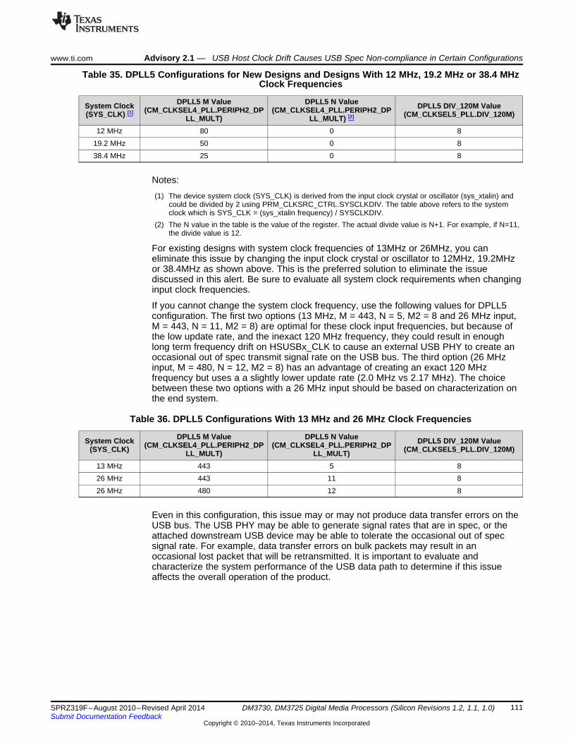
www.ti.com Advisory 2.1 — USB Host Clock Drift Causes USB Spec Non-compliance in Certain Configurations
Table 35. DPLL5 Configurations for New Designs and Designs With 12 MHz, 19.2 MHz or 38.4 MHzClock Frequencies
DPLL5 M Value DPLL5 N ValueSystem Clock DPLL5 DIV_120M Value(CM_CLKSEL4_PLL.PERIPH2_DP (CM_CLKSEL4_PLL.PERIPH2_DP(SYS_CLK) [1] (CM_CLKSEL5_PLL.DIV_120M)LL_MULT) LL_MULT) [2]
12 MHz 80 0 819.2 MHz 50 0 838.4 MHz 25 0 8
Notes:(1) The device system clock (SYS_CLK) is derived from the input clock crystal or oscillator (sys_xtalin) and
could be divided by 2 using PRM_CLKSRC_CTRL.SYSCLKDIV. The table above refers to the systemclock which is SYS_CLK = (sys_xtalin frequency) / SYSCLKDIV.
(2) The N value in the table is the value of the register. The actual divide value is N+1. For example, if N=11,the divide value is 12.
For existing designs with system clock frequencies of 13MHz or 26MHz, you caneliminate this issue by changing the input clock crystal or oscillator to 12MHz, 19.2MHzor 38.4MHz as shown above. This is the preferred solution to eliminate the issuediscussed in this alert. Be sure to evaluate all system clock requirements when changinginput clock frequencies.
If you cannot change the system clock frequency, use the following values for DPLL5configuration. The first two options (13 MHz, M = 443, N = 5, M2 = 8 and 26 MHz input,M = 443, N = 11, M2 = 8) are optimal for these clock input frequencies, but because ofthe low update rate, and the inexact 120 MHz frequency, they could result in enoughlong term frequency drift on HSUSBx_CLK to cause an external USB PHY to create anoccasional out of spec transmit signal rate on the USB bus. The third option (26 MHzinput, M = 480, N = 12, M2 = 8) has an advantage of creating an exact 120 MHzfrequency but uses a a slightly lower update rate (2.0 MHz vs 2.17 MHz). The choicebetween these two options with a 26 MHz input should be based on characterization onthe end system.
Table 36. DPLL5 Configurations With 13 MHz and 26 MHz Clock Frequencies
DPLL5 M Value DPLL5 N ValueSystem Clock DPLL5 DIV_120M Value(CM_CLKSEL4_PLL.PERIPH2_DP (CM_CLKSEL4_PLL.PERIPH2_DP(SYS_CLK) (CM_CLKSEL5_PLL.DIV_120M)LL_MULT) LL_MULT)13 MHz 443 5 826 MHz 443 11 826 MHz 480 12 8
Even in this configuration, this issue may or may not produce data transfer errors on theUSB bus. The USB PHY may be able to generate signal rates that are in spec, or theattached downstream USB device may be able to tolerate the occasional out of specsignal rate. For example, data transfer errors on bulk packets may result in anoccasional lost packet that will be retransmitted. It is important to evaluate andcharacterize the system performance of the USB data path to determine if this issueaffects the overall operation of the product.
111SPRZ319F–August 2010–Revised April 2014 DM3730, DM3725 Digital Media Processors (Silicon Revisions 1.2, 1.1, 1.0)Submit Documentation Feedback
Copyright © 2010–2014, Texas Instruments Incorporated

Revision History www.ti.com
Revision HistoryNOTE: Page numbers for previous revisions may differ from page numbers in the current version.
This silicon errata revision history highlights the technical changes made from the previous to the currentrevision.
See Additions/Modifications/DeletionsAdvisory 2.1 Updated workaround for "USB Host Clock Drift Causes USB Spec Non-compliance in Certain Configurations"
112 Revision History SPRZ319F–August 2010–Revised April 2014Submit Documentation Feedback
Copyright © 2010–2014, Texas Instruments Incorporated

IMPORTANT NOTICETexas Instruments Incorporated and its subsidiaries (TI) reserve the right to make corrections, enhancements, improvements and otherchanges to its semiconductor products and services per JESD46, latest issue, and to discontinue any product or service per JESD48, latestissue. Buyers should obtain the latest relevant information before placing orders and should verify that such information is current andcomplete. All semiconductor products (also referred to herein as “components”) are sold subject to TI’s terms and conditions of salesupplied at the time of order acknowledgment.TI warrants performance of its components to the specifications applicable at the time of sale, in accordance with the warranty in TI’s termsand conditions of sale of semiconductor products. Testing and other quality control techniques are used to the extent TI deems necessaryto support this warranty. Except where mandated by applicable law, testing of all parameters of each component is not necessarilyperformed.TI assumes no liability for applications assistance or the design of Buyers’ products. Buyers are responsible for their products andapplications using TI components. To minimize the risks associated with Buyers’ products and applications, Buyers should provideadequate design and operating safeguards.TI does not warrant or represent that any license, either express or implied, is granted under any patent right, copyright, mask work right, orother intellectual property right relating to any combination, machine, or process in which TI components or services are used. Informationpublished by TI regarding third-party products or services does not constitute a license to use such products or services or a warranty orendorsement thereof. Use of such information may require a license from a third party under the patents or other intellectual property of thethird party, or a license from TI under the patents or other intellectual property of TI.Reproduction of significant portions of TI information in TI data books or data sheets is permissible only if reproduction is without alterationand is accompanied by all associated warranties, conditions, limitations, and notices. TI is not responsible or liable for such altereddocumentation. Information of third parties may be subject to additional restrictions.Resale of TI components or services with statements different from or beyond the parameters stated by TI for that component or servicevoids all express and any implied warranties for the associated TI component or service and is an unfair and deceptive business practice.TI is not responsible or liable for any such statements.Buyer acknowledges and agrees that it is solely responsible for compliance with all legal, regulatory and safety-related requirementsconcerning its products, and any use of TI components in its applications, notwithstanding any applications-related information or supportthat may be provided by TI. Buyer represents and agrees that it has all the necessary expertise to create and implement safeguards whichanticipate dangerous consequences of failures, monitor failures and their consequences, lessen the likelihood of failures that might causeharm and take appropriate remedial actions. Buyer will fully indemnify TI and its representatives against any damages arising out of the useof any TI components in safety-critical applications.In some cases, TI components may be promoted specifically to facilitate safety-related applications. With such components, TI’s goal is tohelp enable customers to design and create their own end-product solutions that meet applicable functional safety standards andrequirements. Nonetheless, such components are subject to these terms.No TI components are authorized for use in FDA Class III (or similar life-critical medical equipment) unless authorized officers of the partieshave executed a special agreement specifically governing such use.Only those TI components which TI has specifically designated as military grade or “enhanced plastic” are designed and intended for use inmilitary/aerospace applications or environments. Buyer acknowledges and agrees that any military or aerospace use of TI componentswhich have not been so designated is solely at the Buyer's risk, and that Buyer is solely responsible for compliance with all legal andregulatory requirements in connection with such use.TI has specifically designated certain components as meeting ISO/TS16949 requirements, mainly for automotive use. In any case of use ofnon-designated products, TI will not be responsible for any failure to meet ISO/TS16949.Products ApplicationsAudio www.ti.com/audio Automotive and Transportation www.ti.com/automotiveAmplifiers amplifier.ti.com Communications and Telecom www.ti.com/communicationsData Converters dataconverter.ti.com Computers and Peripherals www.ti.com/computersDLP® Products www.dlp.com Consumer Electronics www.ti.com/consumer-appsDSP dsp.ti.com Energy and Lighting www.ti.com/energyClocks and Timers www.ti.com/clocks Industrial www.ti.com/industrialInterface interface.ti.com Medical www.ti.com/medicalLogic logic.ti.com Security www.ti.com/securityPower Mgmt power.ti.com Space, Avionics and Defense www.ti.com/space-avionics-defenseMicrocontrollers microcontroller.ti.com Video and Imaging www.ti.com/videoRFID www.ti-rfid.comOMAP Applications Processors www.ti.com/omap TI E2E Community e2e.ti.comWireless Connectivity www.ti.com/wirelessconnectivity
Mailing Address: Texas Instruments, Post Office Box 655303, Dallas, Texas 75265Copyright © 2014, Texas Instruments Incorporated