Fast Identification of Custom Instructions for Extensible Processors
Upload
khangminh22Category
view
1download
0
Motorola Master Selection Guide Digital Signal Processors2.1–1
Digital Signal Processors
In Brief . . .Page
DSP56000—24-Bit Digital Signal Processors 2.1–2. . . . . . . DSP56100—16-Bit Digital Signal Processors 2.1–4. . . . . . . DSP56300—24-Bit Digital Signal Processors 2.1–6. . . . . . . DSP56600—16-Bit Digital Signal Processors 2.1–11. . . . . . DSP56800—16-Bit Digital Signal Processors 2.1–13. . . . . . DSP96002—32-Bit Digital Signal Processors 2.1–15. . . . . . MC68175 FLEX Chip 2.1–16. . . . . . . . . . . . . . . . . . . . . . . . . . DSP Development Tools 2.1–17. . . . . . . . . . . . . . . . . . . . . . . .
Application Development Systems 2.1–17. . . . . . . . . . . . Evaluation Modules 2.1–17. . . . . . . . . . . . . . . . . . . . . . . . . . . . MC68175FDB FLEX Development Board 2.1–25. . . . . . . . . DSP Development Software 2.1–26. . . . . . . . . . . . . . . . . . . .
C Compiler Packages 2.1–26. . . . . . . . . . . . . . . . . . . . . . .
Drawing on both design excellence and expertise inmanufacturing, Motorola has created a range ofarchitecturally compatible digital signal processing chips.The philosophy behind the Digital Signal Processor (DSP)families has been to create compatibility between products,as well as to conform to international standards.
Motorola offers a complete portfolio of 16- and 24-bit fixedpoint and 32-bit floating point DSPs.
In addition, we offer a comprehensive array ofdevelopment tools to give the designer access to the fullpower and versatility of the DSPs with minimum fuss. All thetools were designed for ease of use and functionality. Theyprovide a low-cost means of evaluation and greatly simplifythe design and development phase of a DSP project.

Motorola Master Selection GuideDigital Signal Processors 2.1–2
16-/24-/32-Bit Families—Your Complete DSP Solution
DSP56000—24-Bit Digital Signal ProcessorsThe DSP56000 family of 24-bit, fixed point, general
purpose Digital Signal Processors is Motorola’s original DSPfamily and has set the standard for high end DSP devices withits triple Harvard architecture of seven internal buses andthree parallel execution units—Data ALU, AddressGeneration Unit, and Program Controller. Motorola hasretained architectural compatibility with the 24-bit family intothe 16-bit DSP56100 and 32-bit DSP96002 products helpingto preserve our customer software investment.
The DSP56000 family of HCMOS, 24-bit DSP devicesconsists of the DSP56002, DSP56L002, DSP56004,DSP56007, DSP56009, DSP56011, and the transitionalDSP56001A. All these products are source code compatibleand are used extensively in telecommunications, control, andaudio applications. The DSP56000 family’s unique 24-bitarchitecture has made these products the industry standardfor CD-quality digital audio processing.
DSP56000 Core Features
• Efficient, object code compatible, 24-bit 56000 familyDSP engine— Up to 33 Million Instructions Per Second (MIPS)— 30.3 ns instruction cycle at 66 MHz— Up to 198 Million Operations Per Second (MOPS) at
66 MHz— Performs a 1024-point complex Fast Fourier
Transform (FFT) in 59,898 clocks— Highly parallel instruction set with unique DSP
addressing modes— Two 56-bit accumulators including extension byte— Parallel 24 x 24-bit multiply-accumulate in 1
instruction cycle (2 clock cycles)— Double precision 48 x 48-bit multiply with 96-bit result
in 6 instruction cycles— 56-bit Addition/Subtraction in 1 instruction cycle— Fractional and integer arithmetic with support for
multiprecision arithmetic— Hardware support for block-floating point FFT— Hardware nested DO loops— Zero-overhead fast interrupts (2 instruction cycles)— Four 24-bit internal data buses and three 16-bit
internal address buses for maximum informationtransfer on-chip
DSP56002 Features
• On-chip Harvard architecture permitting simultaneousaccesses to program and two data memories
• Two 256 x 24-bit on-chip data RAMs• Two 256 x 24-bit on-chip data ROMs containing sine,
A-law, and µ-law tables• Two 256 x 24-bit on-chip data ROMs containing sine,
A-law, and µ-law tables• External memory expansion with 16-bit address and and
24-bit data buses• 512 x 24-bit on-chip Program RAM and 64 x 24-bit
bootstrap ROM• Two 256 x 24-bit on-chip data RAMs
• Two 256 x 24-bit on-chip data ROMs containing sine,A-law, and µ-law tables
• External memory expansion with 16-bit address and24-bit data buses
• Bootstrap loading from external data bus, Host Interface,or Serial Communications Interface
PSDSRDWRX/YBRBG
Data Bus
Address BusA0–A15
D0–D23
BusControl
DS0DS1/OS0DSCK/OS1DR
RXDTXDSCLKSC0SC1
Note2
Note3
Host Control orPort B I/O
Interrupt and Mode Control
DSP56002
HA0
HA1
HA2
HAC
KH
REQ
HEN
HR
/W
Hos
t Dat
a Bu
sM
OD
A/R
QA
MO
DB/
RQ
B
RES
ETEX
TAL
XTAL
V DD
V SS
H0–H7 orPort B I/O
SC2SCKSRDSTD
Note1
NOTES:1. On-Chip Emulation (OnCE ) port2. SCI Serial or Port C I/O3. SSI Serial or Port C I/O4. Phase Lock Loop (PLL)
BN
MO
DC
/NM
I
PINITPLOCKCKPPCAP
Note4
Peripheral and Support Circuits
• Byte-wide Host Interface (HI) with Direct Memory Accesssupport
• Synchronous Serial Interface (SSI) to communicate withcodecs and synchronous serial devices— Up to 32 software-selectable time slots in Network
mode• Serial Communication Interface (SCI) for full-duplex
asynchronous communications• 24-bit Timer/Event Counter also generates and measures
digital waveforms• On-chip peripheral registers memory mapped in data
memory space• Double buffered peripheral supply options• Up to twenty-five general purpose I/O (GPIO) pins• Three external interrupt request pins; one non-maskable

Motorola Master Selection Guide Digital Signal Processors2.1–3
DSP56000—24-Bit Digital Signal Processors (continued)
• On-Chip Emulation (OnCE ) port for unobtrusive,processor speed-independent debugging
• Software-programmable, Phase Lock Loop-based (PLL)frequency synthesizer for the core clock
• Power-saving Wait and Stop modes• Fully static, HCMOS design for operating frequencies
from 80 MHz, 66 MHz, or 40 MHz down to DC• 132-pin Ceramic Pin Grid Array (PGA) package; 13 x 13
array• 132-pin Plastic Quad Flat Pack (PQFP) surface-mount
package; 24 x 24 x 4 mm• 144-pin Thin Quad Flat Pack (TQFP) surface-mount
package; 20 x 20 x 1.4 mm• 3.3 V (DSP56L002) and 5 V (DSP56002) power supply
options
DSP56004/DSP56007 Features
Digital Signal Processing Core
• Efficient, object-code compatible, 24-bit DSP56000 familyDSP engine
Memory
• DSP56004 memory: 512 words Program RAM, 2 x 256words data RAM, 2 x 256 words data ROM
• DSP56007 memory: 6400 words Program ROM, 3200words data RAM, 1024 words data ROM
Peripheral and Support Circuits
• Serial Audio Interface (SAI) includes 2 receivers and 3transmitters, master or slave capability, andimplementation of I2S, Sony, and Matshushita audioprotocols; two sets of SAI interrupt vectors
• Serial Host Interface (SHI) features single mastercapability, 10-word receive FIFO, and support for 8-, 16-,and 24-bit words
• External Memory Interface (EMI), implemented as aperipheral supporting:— Page-mode DRAMs (one or two chips): 64 K x 4,
256 K x 4, and 4M x 4 bits— SRAMs (one to four): 256 K x 8 bits— Data bus may be 4 or 8 bits wide— Data words may be 8, 12, 16, 20, or 24 bits wide
• Four dedicated, independent, programmable GeneralPurpose I/O (GPIO) lines
• On-chip peripheral registers memory mapped in datamemory space
• Three external interrupt request pins• On-Chip Emulation (OnCE ) port for unobtrusive,
processor speed-independent debugging• Software-programmable, Phase Lock Loop-based (PLL)
frequency synthesizer for the core clock• Power-saving Wait and Stop modes• Fully static, HCMOS design for operating frequencies
from 40, 50, 66, and 80 MHz down to DC• 80-pin plastic Quad Flat Pack surface-mount package;
14 x 14 x 2.45 mm; 0.65 mm lead pitch• 3.3 V (DSP56L007) and 5 V (DSP56007) power supply
options
DSP56009 Features
Digital Signal Processing Core
• Efficient, object-code compatible, 24-bit DSP56000 familyDSP engine
• Completely pin-compatible with DSP56004 andDSP56007 for easy upgrades
• 5 V power supply
Memory
• On-chip Harvard architecture permitting simultaneousaccesses to program and two data memories
• 10240 x 24-bit on-chip Program ROM*• 4608 x 24-bit on-chip X data RAM and 3072 x 24-bit
on-chip X data ROM*• 4352 x 24-bit on-chip Y data RAM and 1792 x 24-bit
on-chip Y data ROM*• 512 x 24-bit on-chip Program RAM and 64 x 24-bit
bootstrap ROM• Up to 2304 x 24-bit from X and Y data RAM can be
switched to Program RAM giving a total of 2816 x 24 bitsof Program RAM
• Bootstrap loading from Serial Host Interface or ExternalMemory Interface
DSP56011 Features
Digital Signal Processing Core
• Efficient, object-code compatible, 24-bit DSP56000 familyDSP engine
Memory
• Modified Harvard architecture allows simultaneousaccess to program and data memories
• 12800 x 24-bit on-chip Program ROM*• 4096 x 24-bit on-chip X-data RAM and 3584 x 24-bit
on-chip X-data ROM*• 4352 x 24-bit on-chip Y-data RAM and 2048 x 24-bit
on-chip Y-data ROM*• 512 x 24-bit on-chip Program RAM and 64 x 24-bit
bootstrap ROM• As much as 2304 x 24 bits of X- and Y-data RAM can be
switched to Program RAM, giving a total of 2816 x 24 bitsof Program RAM
Peripheral and Support Circuits
• Serial Audio Interface (SAI) includes two receivers andthree transmitters, master or slave capability, andimplementation of I2S, Sony, and Matshushita audioprotocols; two sets of SAI interrupt vectors
• Serial Host Interface (SHI) features single mastercapability, SPI and I2C protocols, 10-word receive FIFO,and support for 8-, 16-, and 24-bit words
• Byte-wide Parallel Host Interface with DMA supportcapable of reconfiguration as fifteen General PurposeInput/Output (GPIO) lines
*These ROMs may be factory programmed with data/programprovided by the application developer.

Motorola Master Selection GuideDigital Signal Processors 2.1–4
DSP56000—24-Bit Digital Signal Processors (continued)
• Digital Audio Transmitter (DAX) features one serialtransmitter capable of supporting SPDIF, IEC958,CP-340, and AES/EBU formats
• Eight dedicated, independent, programmable GPIO lines• On-chip peripheral registers memory mapped in data
memory space• OnCE port for unobtrusive, processor speed-independent
debugging
• Software programmable PLL-based frequencysynthesizer for the core clock
• Power saving Wait and Stop modes• Fully static, HCMOS design for operating frequencies
from 81 MHz down to DC• 100-pin plastic Thin Quad Flat Pack (TQFP)
surface-mount package• 5 V power supply
DSP56100—16-Bit Digital Signal ProcessorsThe DSP56100 family of HCMOS, low-power, 16-bit fixed
point general purpose Digital Signal Processors (DSPs) isideal for high end speech coding, telecommunications, andcontrol applications. The first DSP56100 family member, theDSP56156, combines the high-speed core with 8 K bytesRAM, two serial ports, one parallel port, codec, Phase LockLoop (PLL), and an On-Chip Emulation (OnCE ) port. TheDSP56166, the second member of the DSP56100 family, hasidentical package and pinout to the DSP56156 with differentmemory configuration and peripherals.
2 SerialInterfacesSS10 &SS11
orPort C I/O
SC00
Timer orPort C I/O
Tout
Data Bus
Address BusA0–A15
D0–D15
BusControl
STD0SRD0SCK0SC10
STD1SRD1SCK1SC11SC01
PowerGround
Tin
HostControl
orPort B I/O
DSP56156
Interrupt andMode Control
9
9
On-ChipCodec
4
ClockandPLL
H0–H7or
Port B I/O
Hos
t Dat
a Bu
s
HA0
HA1
HA2
DSO
HAC
KH
REQ
HEN
HR
/W
MO
DA/
RQ
AM
OD
B/R
QB
MO
DC
/RQ
CR
ESET
DSC
K/O
SID
SI/O
SO DR
OnCE
DSP56156 Features
Digital Signal Processing Core
• Efficient, object code compatible, 16-bit 56100-familyDSP engine— Up to 30 Million Instructions Per Second (MIPS);
33 ns instruction cycle at 60 MHz— Up to 180 Million Operations Per Second (MOPS) at
60 MHz— Highly parallel instruction set with unique DSP
addressing modes— Two 40-bit accumulators including extension byte— Parallel 16 x 16-bit multiply-accumulate in 1
instruction cycle (2 clock cycles)— Double precision 32 x 32-bit multiply with 72-bit result
in 6 instruction cycles— Least Mean Square (LMS) adaptive loop filter in 2
instructions— 40-bit Addition/Subtraction in 1 instruction cycle— Fractional and integer arithmetic with support for
multiprecision arithmetic— Hardware support for block-floating point FFT— Hardware-nested DO loops including infinite loops— Zero-overhead fast interrupts (2 instruction cycles)— Three 16-bit internal data buses and three 16-bit
internal address buses for maximum informationtransfer on-chip
Memory
• On-chip Harvard architecture permitting simultaneousaccesses to program and memories
• 2048 x 16-bit on-chip Program RAM and 64 x 16-bitbootstrap ROM (or 12 K x 16-bit on-chip Program ROMon the DSP56156ROM)
• 2048 x 16-bit on-chip data RAM• External memory expansion with 16-bit address and data
buses• Bootstrap loading from external data bus, Host Interface,
or Synchronous Serial Interface

Motorola Master Selection Guide Digital Signal Processors2.1–5
DSP56100—16-Bit Digital Signal Processors (continued)
Peripheral and Support Circuits
• Byte-wide Host Interface (HI) with Direct Memory Access(DMA) support
• Two Synchronous Serial Interfaces (SSI) to communicatewith codecs and synchronous serial devices— Built in µ-law and A-law compression/expansion— Up to 32 software-selectable time slots in Network
mode• 16-bit Timer/Event Counter also generates and measures
digital waveforms• On-chip sigma-delta voice band codec
— Sampling clock rates between 100 kHz and 3 MHz— Four software-programmable decimation/interpolation
ratios— Internal voltage reference (2/5 of positive power
supply)— No external components required
• On-chip peripheral registers memory mapped in datamemory space
• Double buffered peripherals• Up to twenty seven General Purpose I/O pins• Two external interrupt request pins• OnCE port for unobtrusive, processor speed-independent
debugging• Software-programmable, Phase Lock Loop-based (PLL)
frequency synthesizer for the core clock
Miscellaneous Features
• Power-saving Wait and Stop modes• Fully static, HCMOS design for operating frequencies
from 40 or 60 MHz down to DC• 112-pin Ceramic Quad Flat Pack (CQFP) surface-mount
package; 20 x 20 x 3 mm• 112-pin Plastic Thin Quad Flat Pack (TQFP) surface-
mount package; 20 x 20 x 1.4 mm• 5 V power supply
DSP56167 Features
• Digital Signal Processing Core— Up to 30 Million Instructions Per Second (MIPS) at
60 MHz with 33.3 ns instruction cycle— Single-cycle 16 x 16-bit parallel Multiplier-
Accumulator (MAC)— 2 x 40-bit accumulators with extension byte— Fractional and integer arithmetic with support for
multiprecision arithmetic— Highly parallel instruction set with unique DSP
addressing modes— Nested hardware DO loops including infinite loops
and DO zero loop— Two instruction LMS adaptive filter loop— Fast auto-return interrupts— Three external interrupt request pins
— Three 16-bit internal data and three 16-bit internaladdress buses
— Individual programmable wait states on the externalbus for program, data, and peripheral memory spaces
— Programmable Absolute Short addressing mode— Off-chip memory-mapped peripheral space with
programmable access time and separate peripheralenable pin
— Peripheral Address Generation Unit (PAGU)— On-chip memory-mapped peripheral registers— On-Chip Emulation (OnCE ) port for unobtrusive,
processor speed-independent debugging with DR linestatic latch with Reset
• Memory— Modified Harvard architecture permits simultaneous
accesses to program and data memories— 2 K x 16-bit on-chip Program RAM— 4 K x 16-bit on-chip data RAM— 64 x 16-bit bootstrap ROM— External memory expansion with 16-bit address and
data buses with static latches with Reset andsoftware-controlled BG pull-down
— Bootstrap loading from external byte-wide ProgramROM, Host Interface, or 16-bit Synchronous SerialInterface (SSI0)
• Peripherals— Up to twenty-five General Purpose Input/Output
(GPIO) pins, depending on which peripherals areenabled
— Byte-wide Host Interface with Direct Memory Access(DMA) support (or up to fifteen Port B GPIO lines)
— On-chip SD voice band codec, Analog-to-Digital (A/D)and Digital-to-Analog (D/A)
• Internal voltage reference (1/2 of positive power supply)and split-voltage operation (with respect to the core)
• No off-chip components required— 16-bit SSI support: two 4-pin ports (or up to eight
Port C GPIO lines)— One 16-bit timer/event counter (or two Port C GPIO
lines)— Double-buffered peripherals— Independent external chip enables BR and PEREN
during Bus Master mode— Software-programmable, Phase Lock Loop-based
(PLL) frequency synthesizer for the DSP core clockwith a wide input frequency range (12.2 kHz to60 MHz) that initializes to a preset low frequencyoperation during hardware reset
• Energy Efficient Design— Power-saving Wait and Stop modes— Fully static, HCMOS design allows operation from
60 MHz down to DC operating frequencies— 112-pin plastic Thin Quad Flat Pack (TQFP)
surface-mount package
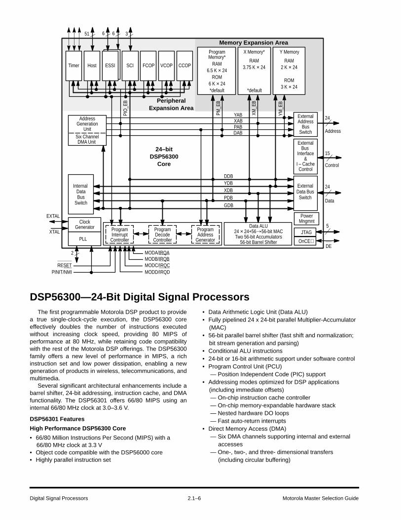
Motorola Master Selection GuideDigital Signal Processors 2.1–6
YABXABPAB
YDBXDBPDB
GDB
15
651
24
24
DDB
DAB
YM_E
B
XM_E
B
PM_E
B
PIO
_EB
6 3
2
EXTAL
XTAL
Control
Data
AddressGeneration
UnitSix ChannelDMA Unit
ProgramInterrupt
Controller
ProgramDecode
Controller
ProgramAddress
Generator
PowerMngmnt
ExternalBus
Interface &
I – CacheControl
ExternalAddress
BusSwitch
Timer Host ESSI SCI FCOP VCOP CCOP
ExternalData Bus
Switch
Address
PLL
ClockGenerator
Internal DataBus
Switch
Memory Expansion Area
24–bitDSP56300
Core
PeripheralExpansion Area
5
OnCE
JTAG
DE
RESET
MODA/IRQAMODB/IRQBMODC/IRQCMODD/IRQDPINIT/NMI
Data ALU24 × 24+56�56-bit MACTwo 56-bit Accumulators
56-bit Barrel Shifter
RAM2 K × 24
ROM3 K × 24
Y Memory
RAM6.5 K × 24
*default*default
RAM3.75 K × 24
X Memory*
ROM6 K × 24
ProgramMemory*
DSP56300—24-Bit Digital Signal ProcessorsThe first programmable Motorola DSP product to provide
a true single-clock-cycle execution, the DSP56300 coreeffectively doubles the number of instructions executedwithout increasing clock speed, providing 80 MIPS ofperformance at 80 MHz, while retaining code compatibilitywith the rest of the Motorola DSP offerings. The DSP56300family offers a new level of performance in MIPS, a richinstruction set and low power dissipation, enabling a newgeneration of products in wireless, telecommunications, andmultimedia.
Several significant architectural enhancements include abarrel shifter, 24-bit addressing, instruction cache, and DMAfunctionality. The DSP56301 offers 66/80 MIPS using aninternal 66/80 MHz clock at 3.0–3.6 V.
DSP56301 Features
High Performance DSP56300 Core
• 66/80 Million Instructions Per Second (MIPS) with a66/80 MHz clock at 3.3 V
• Object code compatible with the DSP56000 core• Highly parallel instruction set
• Data Arithmetic Logic Unit (Data ALU)• Fully pipelined 24 x 24-bit parallel Multiplier-Accumulator
(MAC)• 56-bit parallel barrel shifter (fast shift and normalization;
bit stream generation and parsing)• Conditional ALU instructions• 24-bit or 16-bit arithmetic support under software control• Program Control Unit (PCU)
— Position Independent Code (PIC) support• Addressing modes optimized for DSP applications
(including immediate offsets)— On-chip instruction cache controller— On-chip memory-expandable hardware stack— Nested hardware DO loops— Fast auto-return interrupts
• Direct Memory Access (DMA)— Six DMA channels supporting internal and external
accesses— One-, two-, and three- dimensional transfers
(including circular buffering)

Motorola Master Selection Guide Digital Signal Processors2.1–7
DSP56300—24-Bit Digital Signal Processors (continued)
— End-of-block-transfer interrupts— Triggering from interrupt lines and all peripherals
• Phase Lock Loop (PLL)— Allows change of low power Divide Factor (DF)
without loss of lock— Output clock with skew elimination
• Hardware debugging support— On-Chip Emulation (OnCE ) module— Joint Action Test Group (JTAG) Test Access Port
(TAP) port— Address Tracing mode reflects internal Program RAM
accesses at the external port
On-Chip Memories
• 4096 x 24-bit Program RAM (or, if the cache option isenabled, 1024 x 24-bit Instruction Cache and 3072 x24-bit Program RAM)
• 2048 x 24-bit X data RAM• 2048 x 24-bit Y data RAM• 192 x 24-bit bootstrap ROM
Off-Chip Memory Expansion
• Data memory expansion to two 16 M x 24-bit wordmemory spaces
• Program memory expansion to one 16 M x 24-bit wordsmemory space
• External memory expansion port• Chip Select Logic for glueless interface to SRAMs and
SSRAMs• On-chip DRAM controller for glueless interface to DRAMs
On-Chip Peripherals
• 32-bit parallel PCI/Universal Host Interface (HI32), PCIRev. 2.1 compliant with glueless interface to otherDSP563xx buses
• ISA interface requires only 74LS45-style buffer• Two Enhanced Synchronous Serial Interfaces (ESSI0
and ESSI1)• Serial Communications Interface (SCI) with baud rate
generator• Triple timer module• Up to forty-two programmable General Purpose
Input/Output pins (GPIO), depending on whichperipherals are enabled
Reduced Power Dissipation
• Very low power CMOS design• Wait and Stop low power standby modes• Fully-static logic, operation frequency down to 0 Hz (DC)• Optimized power management circuitry (instruction-
dependent, peripheral-dependent, and mode-dependent)
Target Applications
The DSP56301 is intended for general-purpose digitalsignal processing, particularly in multimedia andtelecommunication applications, such as videoconferencingand cellular telephony.
DSP56302 Features
High Performance DSP56300 Core
• 66 Million Instructions Per Second (MIPS) with a 66 MHzclock
• Object code compatible with the DSP56000 core• Highly parallel instruction set• Data Arithmetic Logic Unit (Data ALU)
— Fully pipelined 24 x 24-bit parallel Multiplier-Accumulator (MAC)
— 56-bit parallel barrel shifter (fast shift andnormalization; bit stream generation and parsing)
— Conditional ALU instructions— 24-bit or 16-bit arithmetic support under software
control• Program Control Unit (PCU)
— Position Independent Code (PIC) support— Addressing modes optimized for DSP applications
(including immediate offsets)— On-chip instruction cache controller— On-chip memory-expandable hardware stack— Nested hardware DO loops— Fast auto-return interrupts
• Direct Memory Access (DMA)— Six DMA channels supporting internal and external
accesses— One-, two-, and three-dimensional transfers (including
circular buffering)— End-of-block-transfer interrupts— Triggering from interrupt lines and all peripherals
• Phase Lock Loop (PLL)— Allows change of low power Divide Factor (DF)
without loss of lock— Output clock with skew elimination
• Hardware debugging support— On-Chip Emulation (OnCE ) module— Joint Action Test Group (JTAG) Test Access Port
(TAP) port— Address Tracing mode reflects internal accesses at
the external port
On-Chip Memories
• Program RAM, Instruction Cache, X data RAM, andY data RAM size is programmable
• 192 x 24-bit bootstrap ROM
InstructionCache
SwitchMode
ProgramRAM Size
InstructionCache Size
X DataRAM Size
Y DataRAM Size
disabled disabled 20480 × 24-bit 0 7168 × 24-bit 7168 × 24-bit
enabled disabled 19456 × 24-bit 1024 × 24-bit 7168 × 24-bit 7168 × 24-bit
disabled enabled 24576 × 24-bit 0 5120 × 24-bit 5120 × 24-bit
enabled enabled 23552 × 24-bit 1024 × 24-bit 5120 × 24-bit 5120 × 24-bit

Motorola Master Selection GuideDigital Signal Processors 2.1–8
DSP56300—24-Bit Digital Signal Processors (continued)
Off-Chip Memory Expansion
• Data memory expansion to two 256 K x 24-bit wordmemory spaces
• Program memory expansion to one 256 K x 24-bit wordsmemory space
• External memory expansion port• Chip Select Logic for glueless interface to SRAMs and
SSRAMs• On-chip DRAM controller for glueless interface to DRAMs
On-Chip Peripherals
• Enhanced DSP56000-like 8-bit parallel Host Interface(HI08) supports a variety of buses (e.g., ISA) andprovides glueless connection to a number of industrystandard microcomputers, microprocessors, and DSPs
• Two Enhanced Synchronous Serial Interfaces (ESSI0and ESSI1), each with one receiver and threetransmitters (allows six-channel home theater)
• Serial Communications Interface (SCI) with baud rategenerator
• Triple timer module• Up to thirty-four programmable General Purpose
Input/Output (GPIO) pins, depending on whichperipherals are enabled
Reduced Power Dissipation
• Very low power CMOS design• Wait and Stop low power standby modes• Fully-static logic, operation frequency down to 0 Hz (DC)• Optimized power management circuitry (instruction-
dependent, peripheral-dependent, and mode-dependent)
Target Applications
The DSP56302 is intended for applications requiring alarge amount of on-chip memory, such as wirelessinfrastructure applications. It is also intended as a RAM-basedemulation part for low-cost ROM-based solutions.
DSP56303 Features
High Performance DSP56300 Core
• 66/80 Million Instructions Per Second (MIPS) with a66/80 MHz clock at 3.3 V
• Object code compatible with the DSP56000 core• Highly parallel instruction set• Data Arithmetic Logic Unit (Data ALU)
— Fully pipelined 24 x 24-bit parallel Multiplier-Accumulator (MAC)
— 56-bit parallel barrel shifter (fast shift andnormalization; bit stream generation and parsing)
— Conditional ALU instructions— 24-bit or 16-bit arithmetic support under software
control• Program Control Unit (PCU)
— Position Independent Code (PIC) support— Addressing modes optimized for DSP applications
(including immediate offsets)— On-chip instruction cache controller— On-chip memory-expandable hardware stack— Nested hardware DO loops— Fast auto-return interrupts
• Direct Memory Access (DMA)— Six DMA channels supporting internal and external
accesses— One-, two-, and three-dimensional transfers (including
circular buffering)— End-of-block-transfer interrupts— Triggering from interrupt lines and all peripherals
• Phase Lock Loop (PLL)— Allows change of low power Divide Factor (DF)
without loss of lock— Output clock with skew elimination
• Hardware debugging support— On-Chip Emulation (OnCE ) module— Joint Action Test Group (JTAG) Test Access Port
(TAP)— Address Tracing mode reflects internal Program RAM
accesses at the external port
On-Chip Memories
• Program RAM, Instruction Cache, X data RAM, and Ydata RAM size is programmable:
• 192 x 24-bit bootstrap ROM
InstructionCache
SwitchMode
ProgramRAM Size
InstructionCache Size
X DataRAM Size
Y DataRAM Size
disabled disabled 4096 × 24-bit 0 2048 × 24-bit 2048 × 24-bit
enabled disabled 3072 × 24-bit 1024 × 24-bit 2048 × 24-bit 2048 × 24-bit
disabled enabled 2048 × 24-bit 0 3072 × 24-bit 3072 × 24-bit
enabled enabled 1024 × 24-bit 1024 × 24-bit 3072 × 24-bit 3072 × 24-bit
Off-Chip Memory Expansion
• Data memory expansion to two 256 K x 24-bit wordmemory spaces
• Program memory expansion to one 256 K x 24-bit wordsmemory space
• External memory expansion port• Chip Select Logic for glueless interface to SRAMs and
SSRAMs• On-chip DRAM controller for glueless interface to DRAMs
On-Chip Peripherals
• Enhanced DSP56000-like 8-bit parallel Host Interface(HI08) supports a variety of buses (e.g., ISA) andprovides glueless connection to a number of industrystandard microcomputers, microprocessors, and DSPs
• Two Enhanced Synchronous Serial Interfaces (ESSI0and ESSI1), each with one receiver and threetransmitters (allows six-channel home theater)

Motorola Master Selection Guide Digital Signal Processors2.1–9
DSP56300—24-Bit Digital Signal Processors (continued)
• Serial Communications Interface (SCI) with baud rategenerator
• Triple timer module• Up to thirty-four programmable General Purpose
Input/Output (GPIO) pins, depending on whichperipherals are enabled
Reduced Power Dissipation
• Very low power CMOS design• Wait and Stop low power standby modes• Fully-static logic, operation frequency down to 0 Hz (DC)• Optimized power management circuitry
(instruction-dependent, peripheral-dependent, andmode-dependent)
Target Applications
The DSP56303 is intended for use in telecommunicationapplications, such as multi-line voice/data/fax processing,videoconferencing, audio applications, control, and generaldigital signal processing.
DSP56304 Features
• High performance DSP56300 core— 66/80 Million Instructions Per Second (MIPS) with a
66/80 MHz clock— Object code compatible with the DSP56000 core— Highly parallel instruction set
— Fully pipelined 24 x 24-bit parallelMultiplier-Accumulator (MAC)
— 56-bit parallel barrel shifter— 24-bit or 16-bit arithmetic support under software
control— Position independent code support— Addressing modes optimized for DSP applications— On-chip instruction cache controller— On-chip memory-expandable hardware stack— Nested hardware DO loops— Fast auto-return interrupts— On-chip concurrent six-channel DMA controller— On-chip Phase Lock Loop (PLL) and clock generator— On-Chip Emulation (OnCE ) module— JTAG Test Access Port (TAP)— Address Tracing mode reflects internal accesses at
the external port
On-Chip Memories
• Program RAM, Instruction Cache, X data RAM, and Ydata RAM size is programmable:
• 33,792 x 24-bit Program ROM with Patch mode updatecapability using instruction cache memory space
• 9,216 x 24-bit X data ROM and 9,216 x 24-bit Y dataROM
• 192 x 24-bit bootstrap ROM Instruction Cache
InstructionCache
SwitchMode
ProgramRAM Size
InstructionCache Size
X DataRAM Size
Y DataRAM Size
disabled disabled 1024 × 24-bit 0 3328 × 24-bit 1792 × 24-bit
enabled disabled 0 1024 × 24-bit 3328 × 24-bit 1792 × 24-bit
disabled enabled 3584 × 24-bit 0 2048 × 24-bit 512 × 24-bit
enabled enabled 2560 × 24-bit 1024 × 24-bit 2048 × 24-bit 512 × 24-bit
Off-Chip Memory Expansion
• Data memory expansion to two 256 K x 24-bit wordmemory spaces
• Program memory expansion to one 256 K x 24-bit wordmemory space
• External memory expansion port• Chip select logic requires no additional circuitry to
interface to SRAMs and SSRAMs• On-chip DRAM controller requires no additional circuitry
to interface to DRAMs
On-Chip Peripherals
• 8-bit parallel Host Interface (HI08), ISA-compatible businterface, providing a cost-effective solution forapplications not requiring the PCI bus
• Two Enhanced Synchronous Serial Interfaces (ESSI0and ESSI1)
• Serial Communications Interface (SCI) with baud rategenerator
• Triple timer module• Up to thirty-four programmable General Purpose I/O pins
(GPIO), depending on which peripherals are enabled
Reduced Power Dissipation
• Very low power CMOS design• Wait and Stop low power standby modes• Fully-static logic, operation frequency down to DC• Optimized power management circuitry
Target Applications
The DSP56304 is intended for use in embeddedmultifunction DSP applications requiring large on-board ROMspaces, such as wireless products that combine standardcellular phone operation with options such as two-way digitalpaging and fax capability in one unit.

Motorola Master Selection GuideDigital Signal Processors 2.1–10
DSP56300—24-Bit Digital Signal Processors (continued)
DSP56305 Features
High Performance DSP56300 Core
• 80 Million Instructions Per Second (MIPS) with an80 MHz clock at 3.3 V
• Object code compatible with the DSP56000 core• Highly parallel instruction set• Fully pipelined 24 x 24-bit parallel Multiplier-Accumulator
(MAC)• 56-bit parallel barrel shifter• 24-bit or 16-bit arithmetic support under software control• Position independent code support• Addressing modes optimized for DSP applications• On-chip instruction cache controller• On-chip memory-expandable hardware stack• Nested hardware DO loops• Fast auto-return interrupts• On-chip concurrent six-channel Direct Memory Access
(DMA) controller• On-chip Phase Lock Loop (PLL) and clock generator• On-Chip Emulation (OnCE ) module• JTAG Test Access Port (TAP)• Address Tracing mode reflects internal accesses at the
external port• 21 mm x 21 mm, 252-pin PBGA package• Pin-compatible in 252-pin PBGA package with the
DSP56301
On-Chip Memories
• Program RAM, instruction cache, X data RAM, andY data RAM sizes are programmable:
• 6144 x 24-bit Program ROM• 3072 x 24-bit Y data ROM• 192 x 24-bit bootstrap ROM
Off-Chip Memory Expansion
• Data memory expansion to two 16 M x 24-bit wordmemory spaces
• Program memory expansion to one 16 M x 24-bit wordmemory space
• External memory expansion port• Chip select logic provides glueless interface to SRAMs
and SSRAMs• On-chip DRAM controller provides glueless interface to
DRAMs
On-Chip Peripherals
• PCI Rev. 2.1-compliant 32-bit parallel PCI/Universal HostInterface (HI32) with glueless interface to otherDSP563xx buses
• ISA interface requires only 74LS45-style buffer• Two Enhanced Synchronous Serial Interfaces (ESSI0
and ESSI1)• Serial Communications Interface (SCI) with baud rate
generator• Triple timer module• Up to forty-two programmable General Purpose Input/
Output pins (GPIO), depending on which peripherals areenabled
On-Chip Co-Processors
• The Filter Co-Processor (FCOP) implements a widevariety of convolution and correlation filtering algorithms.In GSM applications, the FCOP cross-correlates betweenthe received training sequence and a known midamblesequence to estimate the channel impulse response, andthen performs match filtering of received data symbolsusing coefficients derived from that estimated channel.
• The Viterbi Co-Processor (VCOP) implements MaximumLikelihood Sequential Estimation (MLSE) algorithm forchannel decoding and equalization (uplink) and channelconvolution coding (downlink). The VCOP supportsconstraint lengths (k) of 4, 5, 6, or 7 with number ofstates 8, 16, 32, or 64, respectively; code rates of 1/2,1/3, 1/4, or 1/6; and trace-back Trellis depth of 36.
• The Cyclic-code Co-Processor (CCOP) executes cycliccode calculations for data ciphering and deciphering, aswell as parity code generation and check. The CCOP isfully programmable and not dedicated to a specificalgorithm, but it is well suited for GSM A5.1 and A5.2data ciphering algorithms. The CCOP can generate masksequences for data ciphering, and supports Fire encodeand decode for burst error correction, as well asgeneration of Cyclic Redundancy Code (CRC) syndromefor any polynomial of any degree up to 48.
Reduced Power Dissipation
• Very low power CMOS design• Wait and Stop low power standby modes
— Fully-static logic, operation frequency down to DC• Optimized power management circuitry

Motorola Master Selection Guide Digital Signal Processors2.1–11
EXTA
L
YABXABPAB
YDBXDBPDB
GD
B
Address
4
Data
Control
24
16
YM_E
B
XM_E
B
PM_E
B
5
PCAP
ExternalBus
Interface
CLKOUT
PIO
_EB
ProgramAddress
Generator
ProgramDecode
Controller
ProgramInterrupt
Controller
ClockGenerator
PLL
PowerMngmnt
Internal DataBus
Switch
ProgramPatch
Detector
AddressGeneration
Unit
TripleTimer or
GPIO Pins
DedicatedGPIO Pins
HostInterfaceHI08 or GPIO Pins
SSIInterface or GPIO
Pins
616 63
Data ALU16 × 16+40�40-bit MACTwo 40-bit Accumulators
40-bit Barrel Shifter OnCE
JTAG
Peripheral Expansion Area
DSP56600 16-Bit
Core
Memory Expansion Area
Y-DataRAM
8192 × 16
X-DataRAM
8192 × 16
ProgramROM
3072 × 24
ProgramRAM
16.5 K × 24
DE
MODA/IRQAMODB/IRQB
MODC/IRQCMODC/IRQD
PINIT/NMIRESET
DSP56600—16-Bit Digital Signal ProcessorsThe DSP56600 core can execute one 24-bit instruction per
clock cycle using 16-bit data. The 60 MHz chip includes amixture of peripherals and memories optimized forprocessing-intensive, yet cost-effective, low powerconsumption digital mobile communications applications. TheDSP56600 core includes the Data Arithmetic Logic Unit(Data ALU), Address Generation Unit (AGU), ProgramController, program patch detector, bus interface unit,On-Chip Emulation (OnCE )/JTAG port, and a Phase LockLoop (PLL)-based clock generator.
DSP56602 Features
Digital Signal Processing Core
• High-performance DSP56600 core• Up to 60 million instructions per second (MIPS) at 2.7 V• 24-bit instructions using 16-bit data• Fully pipelined 16 x 16-bit parallel Multiplier-Accumulator
(MAC)• Two 40-bit accumulators including extension bits• 40-bit parallel barrel shifter• Highly parallel instruction set with unique DSP addressing
modes• Code-compatible with the DSP56300 core• Position-Independent Code support PIC)• Nested hardware DO loops• Fast auto-return interrupts
• On-chip support for software patching and enhancements• On-chip Phase Lock Loop (PLL) circuit• Real-time trace capability via external address bus• On-Chip Emulation (OnCE ) module• JTAG port
Memory
• 512 x 24 Program RAM• 24 K x 24 Program ROM• 4 K x 16 X data RAM• 6 K x 16 X data ROM• 4 K x 16 Y data RAM• 6 K x 16 Y data ROM• Off-chip expansion for both program fetch and program
data transfers• Glueless interface to external SRAM memories
Peripheral Circuits
• Three dedicated General Purpose Input/Output (GPIO)pins and up to thirty one additional GPIO pins(user-selectable as peripherals or GPIO pins)
• Host interface (HI) support: One 8-bit parallel port (or upto sixteen additional GPIO pins)— Direct interface to Motorola HC11, Hitachi H8, 8051
family, Thomson P6 family— Minimal logic interface to standard ISA bus, Motorola
68 K family, and Intel x86 microprocessor family

Motorola Master Selection GuideDigital Signal Processors 2.1–12
DSP56600—16-Bit Digital Signal Processors (continued)
• Synchronous Serial Interface (SSI) support: Two 6-pinports (or twelve additional GPIO pins)— Supports serial devices with one or more industry-
standard codecs, other DSPs, microprocessors, andMotorola-SPI-compliant peripherals
— Independent transmitter and receiver sections and acommon RSI clock generator
— Network mode using frame sync and up to 32 timeslots
— 8-bit, 12-bit, and 16-bit data word lengths• Three programmable timers (or up to three additional
GPIO pins)• Three external interrupt/mode control lines• One external reset pin for hardware reset
Energy Efficient Design
• Operating voltage range: 1.8 V to 3.3 V• Very low power CMOS design
— < 0.85 mA/MIPS at 2.7 V— < 0.55 mA/MIPS at 1.8 V
• Low power Wait for interrupt standby mode• Ultra low power Stop standby mode• Fully static, HCMOS design for operating frequencies
from 60 MHz down to DC• Special power management circuitry
DSP56603 Features
Digital Signal Processing Core
• High-performance DSP56600 core• Up to 60 Million Instructions Per Second (MIPS) at
2.7–3.3 V• Fully pipelined 16 x 16-bit parallel Multiplier-Accumulator
(MAC)• Two 40-bit accumulators including extension bits• 40-bit parallel barrel shifter• Highly parallel instruction set with unique DSP addressing
modes• Code-compatible with the DSP56300 core• Position-Independent Code support (PIC)• Nested hardware DO loops• Fast auto-return interrupts• On-chip support for software patching and enhancements• On-chip Phase Lock Loop (PLL) circuit• Real-time trace capability via external address bus• On-Chip Emulation (OnCE ) module and JTAG port
Memory
• Switch mode memory allows reconfiguring program,X-data, and Y-data RAM sizes
— Switch mode off— 16 K x 24-bit Program RAM— 8 K x 16-bit X data RAM— 8 K x 16-bit Y data RAM
— Switch mode on— 11 K x 24-bit Program RAM— 10.5 K x 16-bit X data RAM— 10.5 K x 16-bit Y data RAM— 3 K x 24-bit Program ROM
• Off-chip expansion for both program fetch and programdata transfers
• No additional logic needed for interface to external SRAMmemories
Peripheral Circuits
• Three dedicated General Purpose Input/Output (GPIO)pins and as many as thirty-one additional GPIO pins(user-selectable as peripherals or GPIO pins)
• Host Interface (HI) support: one 8-bit parallel port (or asmany as sixteen additional GPIO pins)— Direct interface to Motorola HC11, Hitachi H8, 8051
family, Thomson P6 family— Minimal logic interface to standard ISA bus, Motorola
68 K family, and Intel x86 microprocessor family• Synchronous Serial Interface (SSI) support: two 6-pin
ports (or twelve additional GPIO pins)— Supports serial devices with one or more industry-
standard codecs, other DSPs, microprocessors, andMotorola SPI-compliant peripherals
— Independent transmitter and receiver sections and acommon SSI clock generator
— Network mode using frame sync and up to 32 timeslots
— 8-bit, 12-bit, and 16-bit data word lengths• Three programmable timers (or as many as three
additional GPIO pins)• Three external interrupt/mode control lines• One external reset pin for hardware reset
Energy Efficient Design
• Very low power CMOS design— Operating voltage range: 1.8 V to 3.3 V— < 0.85 mA/MIPS at 2.7 V— < 0.55 mA/MIPS at 1.8 V
• Low power Wait for interrupt standby mode, and ultra lowpower Stop standby mode
• Fully static, HCMOS design for operating frequenciesfrom 60 MHz down to DC
• Special power management circuitry

Motorola Master Selection Guide Digital Signal Processors2.1–13
2
Data
16
Control
4
Address
16
ClockGen.
PGDB
PDB
CGDB
PAB
XAB1
XAB2
3
Program Controller
5
4
4 4 6 8
Program-mable
InterruptGPIO
8
GPIO
Timer/Event
Countersor GPIO
Synch.Serial
Interface(SSI)
or GPIO
SerialPeriph.
Interface(SPI1) or
GPIO
SerialPeriph.
Interface(SPI0) or
GPIO
On-ChipExpansion
AreaData Memory2048 � 16
RAM
Program Memory 1024 � 16 RAM
64 �16 ROM(boot)
16 to 32 GPIO lines
XDB2
ExternalDataBus
Switch
ExternalAddress
BusSwitch
BusControl
Bus and BitManipulation
Unit
AddressGeneration
Unit
JTAG/OnCE
Port
PLL
Data ALU16 × 16+36�36-bit MAC
Three 16-bit Input RegistersTwo 36-bit Accumulators
16-bit56800 DSP
Core
DSP56800—16-Bit Digital Signal ProcessorsThe DSP56800 core family is the first architecture
designed to enable digital signal processing and embeddedmicrocontroller functionality. This multi-functional approachsupports applications requiring both signal processing andcontrol functionality, such as wireless messaging, digitalanswering machines, feature phones, and low-cost wirelinemodems.
The first two DSP56800 family members, the DSP56L811and DSP56L812, are identical except for memoryconfiguration. The DSP56L811 contains 1 K of Program RAMand 2 K of data RAM. The DSP56L812 features 22 K ofProgram ROM, 2 K of data ROM, and 2 K of data RAM.
DSP56L811 Features
Digital Signal Processing Core
• Efficient 16-bit DSP56800 family DSP engine• Up to 20 Million Instructions Per Second (MIPS) at
40 MHz• Single-cycle 16 x 16-bit parallel Multiplier-Accumulator
(MAC)• Two 36-bit accumulators including extension bits• Parallel instruction set with unique DSP addressing
modes• Hardware DO and REP loops• DO loops nestable in software• Address buses:
— One 16-bit internal memory address bus (XAB1)
— One 16-bit internal memory address bus (XAB2)— One 19-bit internal Program Address Bus (PAB)— One 16-bit External Address Bus (EAB)
• Data buses:— One 16-bit bidirectional internal memory data bus
(CGDB)— One 16-bit unidirectional internal memory data bus
(XDB2)— One 16-bit bidirectional dedicated peripheral data bus
(PGDB)— One 16-bit bidirectional internal Program Data Bus
(PDB)— One 16-bit bidirectional External Data Bus (EDB)
• Instruction set supports both DSP and controller functions• Controller style addressing modes and instructions for
compact code• Efficient C Compiler and local variable support• Software subroutine and interrupt stack with unlimited
depth
Memory
• On-chip Harvard architecture permits up to threesimultaneous accesses to program and data memory— 1 K x 16 Program RAM— 64 x 16 bootstrap ROM— 2 K x 16 X data RAM— Programs can run out of X data RAM

Motorola Master Selection GuideDigital Signal Processors 2.1–14
DSP56800—16-Bit Digital Signal Processors (continued)
Peripheral and Support Circuits
• External Memory Interface (EMI)• Sixteen dedicated General Purpose Input/Output (GPIO)
pins (eight pins programmable as interrupts)• Serial Peripheral Interface (SPI) support: Two
configurable 4-pin ports (SPI0 and SPI1) (or eightadditional GPIO lines)— Supports LCD drivers, A/D subsystems, and MCU
systems— Supports inter-processor communications in a
multiple master system— Demand-driven master or slave devices with high
data rates• Synchronous Serial Interface (SSI) support: One 6-pin
port (or six additional GPIO lines)— Supports serial devices with one or more industry-
standard codecs, other DSPs, microprocessors, andMotorola SPI-compliant peripherals
— Asynchronous or synchronous transmit and receivesections with separate or shared internal/externalclocks and frame syncs
— Network mode using frame sync and up to 32 timeslots
— 8-bit, 10-bit, 12-bit, and 16-bit data word lengths• Three programmable timers (accessed using two I/O pins
that can also be programmed as two additional GPIOlines)
• Two external interrupt/mode control lines• One external reset for hardware reset• JTAG/On-Chip Emulation (OnCE ) 5-pin port for
unobtrusive, processor speed-independent debugging• Software-programmable, Phase Lock Loop-based (PLL)
frequency synthesizer for the DSP core clock• Computer-Operating Properly (COP) and Real-Time
Interrupt (RTI) timers
Energy Efficient Design
• Power-saving Wait and multiple Stop modes available• Fully static, HCMOS design for operating frequencies
from 40 MHz down to DC• 100-pin plastic Thin Quad Flat Pack (TQFP) surface-
mount package• 2.7 V–3.6 V power supply
DSP56L812 Features
Digital Signal Processing Core
• Efficient 16-bit DSP56800 core• Up to 20 Million Instructions Per Second (MIPS) at
40 MHz• Single-cycle 16 x 16-bit parallel Multiplier-Accumulator
(MAC)• Two 36-bit accumulators including extension bits• 16-bit bidirectional barrel shifter• Parallel instruction set with unique DSP addressing
modes• Hardware DO and REP loops• DO loops nestable in software• Address buses:
— One 16-bit internal memory address bus (XAB1)
— One 16-bit internal memory address bus (XAB2)— One 19-bit internal Program Address Bus (PAB)— One 16-bit External Address Bus (EAB)
• Data buses:— One 16-bit bidirectional internal memory data bus
(CGDB)— One 16-bit unidirectional internal memory data bus
(XDB2)— One 16-bit bidirectional dedicated peripheral data bus
(PGDB)— One 16-bit bidirectional internal Program Data Bus
(PDB)— One 16-bit bidirectional External Data Bus (EDB)
• Instruction set supports both DSP and controller functions• Controller style addressing modes and instructions for
compact code• Efficient C Compiler and structured programming support• Software subroutine and interrupt stack with unlimited
depth
Memory
• On-chip Harvard architecture permits up to threesimultaneous accesses to program and data memory— 22 K x 16 Program ROM— 2 K x 16 X data ROM and 2 K x 16 X data RAM
• Programs can run out of X data RAM
Peripheral and Support Circuits
• External Memory Interface (EMI)• Sixteen dedicated General Purpose Input/Output (GPIO)
pins (eight pins programmable as interrupts)• Serial Peripheral Interface (SPI) support: Two
configurable 4-pin ports (SPI0 and SPI1) (or eightadditional GPIO lines)— Supports LCD drivers, A/D subsystems, and MCU
systems— Supports inter-processor communications in a
multiple master system— Demand-driven master or slave devices with high
data rates• Synchronous Serial Interface (SSI) support: One 6-pin
port (or six additional GPIO lines)— Supports serial devices with one or more industry-
standard codecs, other DSPs, microprocessors, andMotorola-SPI-compliant peripherals
— Asynchronous or synchronous transmit and receivesections with separate or shared internal/externalclocks and frame syncs
— Network mode using frame sync and up to 32 timeslots
— 8-bit, 10-bit, 12-bit, and 16-bit data word lengths• Three programmable 16-bit timers (accessed using two
I/O pins that can also be programmed as two additionalGPIO lines)
• Computer-Operating Properly (COP) and Real-TimeInterrupt (RTI) timers
• Two external interrupt/mode control pins• One external reset pin for hardware reset

Motorola Master Selection Guide Digital Signal Processors2.1–15
DSP56800—16-Bit Digital Signal Processors (continued)
• JTAG/On-Chip Emulation (OnCE ) 5-pin port forunobtrusive, processor speed-independent debugging
• Software-programmable, Phase Lock Loop-based (PLL)frequency synthesizer for the DSP core clock
Energy Efficient Design• Power-saving Wait and multiple Stop modes available
• Fully static, HCMOS design for 40 MHz to DC operatingfrequencies
• 100-pin plastic Thin Quad Flat Pack (TQFP) surface-mount package
• Pin-compatible with the DSP56L811• 2.7 V–3.6 V power supply
DSP96002—32-Bit Digital Signal ProcessorsThe DSP96002 has full architecture compatibility with the
16-bit DSP56100 and 24-bit DSP56000 families. TheDSP96002 is the first in a family of 32-bit IEEE floating pointDSP devices. The DSP96002 has two identical memoryexpansion ports simplifying network configurations formultiprocessor and DSP96002 communications. These portsinterface to SRAM, DRAM (operating in their fast accessmodes), video RAM, or directly to other processors with HostInterface logic.
Although designed primarily for image processing, otherproven applications include communications, spectrumanalysis, instrumentation, speech processing, and patternrecognition.
DSP96002 Features
DSP96000 Family Architecture
• Full IEEE Standard 754 compatible for 32-bit (SP) and44-bit (SEP) arithmetic
• 20 MIPS, 50 ns instruction cycle at 40 MHz• 60 Million Floating Point Operations Per Second
(MFLOPS) at 40 MHz• Single cycle 32 x 32 � 96-bit Multiplier-Accumulator
(MAC)• Ten 96-bit general purpose data registers• Zero-overhead nested DO loops• Two instruction-cycle fast interrupts• Low-power Wait and Stop modes• On-Chip Emulation (OnCE ) port for unobtrusive,
full-speed debugging• 4 K byte instruction cache• Integer mode available• Single precision mode available• Timer/Event Counter
DSP96002 Peripherals
• Two 32-bit address and data host ports• Dual channel DMA controller
DSP96002 Memories
• 1024 x 32 Program RAM• 2 x 512 x 32 data RAM• 2 x 512 x 32 data ROM (sine and cosine tables)
DSP96002
Port A Address
DataPort A
Port A
Port A
Control
3
14
3
14
32
32
32
32
Port B
Port B
Control
HostInterface
and Control
Port B Address
DataPort B
Interrupt andMode Control
OnCE
DSO
MO
DA/
RQ
AM
OD
B/R
QB
MO
DC
/RQ
C
RES
ET
DSC
K/O
SI
DSI
/OSO
DR
CLK
SSCC
SS
Noi
sy
Noi
sy
Qui
et
Qui
et
CC
V VV V
HostInterface
and Control
DSP96002 BENCHMARKSBenchmark Instruction Cycles
RealFIR Filter with Data Shift 1 per TapV = V*S + V 2Lattice Filter with Data Shift 3 per TapCascaded IIR Biquad Filter 4 per SectionSections (4 coeff.)1024-point FFT and bit reversal 12880
ComplexV = V*V + V 4FIR Filter with Data Shift 4 per Tap1024-point FFT and bit reversal 20931
Graphics/Image ProcessingDivide (32-bit accuracy) 7Square Root (32-bit accuracy) 12Bezier Cubic Evaluation for 13Font Compilation[4 × 4][4 × 4] = [4 × 4] 67

Motorola Master Selection GuideDigital Signal Processors 2.1–16
76.8 kHz
Osc
Clock
Symbol Sync
Sync Correlator
De–Interleaver
Address
Receiver
Noise Detector
Internal Control
Error
Local Msg Filter
SPI Buffer SPI
Control/Status Registers
Unit
External
Comparator
Control
EXTS0
EXTS1
SYMCLK
XTAL
EXTAL
CLKOUT
S0–S7
TEST
RESET
LOBAT
READY
SPI
84
Control Unit
Corrector
Vdd
Vss
MC68175 FLEX ChipFLEX protocol is a multi-speed, high-performance protocol
adopted by leading service providers worldwide as a de factopaging standard. FLEX protocol gives service providers theincreased capacity, added reliability, and enhanced pagerbattery performance they need today. It also provides anupward migration path to the service provider that iscompletely transparent to the end user.
The MC68175 FLEX chip IC is part of a total solutionavailable from Motorola for providing FLEX capabilities in alow-power, low-cost system. The FLEX chip simplifiesimplementation of a FLEX paging device by interfacing withany of several off-the-shelf paging receivers, such as theMC13150 or MC3374, and any of several off-the-shelf hostmicrocontroller/microprocessors. The primary function of theFLEX chip is to process information received anddemodulated from a radio paging channel, select messagesaddressed to the paging device, and communicate themessage information to the host. The host interprets themessage information in an appropriate manner (numeric,alphanumeric, binary, etc.) and handles all the I/O activity. TheFLEX chip IC also operates the paging receiver in an efficientPower Consumption mode and enables the host to operate ina low power mode when message information for the pagingdevice is not being received.
FLEX Chip Features
• FLEX paging protocol signal processor• Sixteen programmable user address words• Sixteen fixed temporary addresses• 1600, 3200, and 6400 bits per second (bps) decoding• Any-phase decoding• Uses standard Serial Peripheral Interface (SPI) in Slave
mode• Wide operating voltage range from 3.3 V down to 1.8 V• Allows low current Stop mode operation of host processor• Highly programmable receiver control• Real time clock time base• FLEX fragmentation, and group messaging support• Real time clock over-the-air update support• Compatible with synthesized receivers• Low battery indication (external detector)• 32-pin Thin Quad Flat Pack (TQFP) package• Operating temperature range 0° to +70°C (32° to 158°F)

Motorola Master Selection Guide Digital Signal Processors2.1–17
DSP Development ToolsApplication Development Systems
Every member of the Motorola family of 16-, 24-, and 32-bitDSPs is supported by a multi-component ApplicationDevelopment System (ADS), which acts as a tool fordesigning, debugging, and evaluating real-time DSP targetsystem equipment. The ADS simplifies evaluation of theuser’s prototype hardware/software product by making all ofthe essential timing and I/O circuitry easily accessible. Usingan IBM PC , Macintosh II, a Sun-4 , or Hewlett-PackardSeries 700 as a medium between the user and the DSPhardware significantly reduces the overall complexity and costof development while increasing the capabilities of thesystem. With the ADS, DSP programs can be executed inreal-time, single-instruction-traced or multiple-instruction-stepped, with registers and/or memory block contentsdisplayed. The ADS is fully compatible with the CLASdesign-in software package for each product and may act asan accelerator for testing DSP algorithms.
All Application Development Systems offer an On-ChipEmulation (OnCE ) circuit for unobtrusive, processor speedindependent debugging. The ADS takes full advantage of thiscircuit to allow the user non-intrusive control of the target.
General ADS Features
Software
• Single/multiple stepping through DSP object programs• Conditional/unconditional software and hardware
breakpoints• Program patching using a single-line Assembler/
disassembler
• Session and/or command logging for later reference• Loading and saving of files to/from Application
Development Module (ADM) memory• Macro command definition and execution• Display enable/disable of registers and memory• Debug commands which support multiple DSP
development• Hexadecimal/decimal/binary calculator• Multiple input/output file access from DSP object
programs• On-line help screens for each command and register
Hardware
• Full speed operation• Multiple ADM support with programmable ADM
addressing• Stand-alone operation of ADM after initial development
DSP56002ADS Features
• Host operating system commands from within ADS userinterface program
• 8 K/32 K words of configurable RAM for DSP56002 codedevelopment
• 96-pin euro-card connector for accessing all DSP56002pins
• 1 K words of monitor ROM expandable to 4 K words• Separate connectors for accessing serial or host/DMA
ports
Evaluation ModulesDSP56002EVM
The DSP56002EVM Evaluation Module is a low-costplatform designed to familiarize the user with Motorola’sDSP56002 Digital Signal Processor (DSP). The 24-bitprecision of the DSP combined with the on-board 32 K wordsof external SRAM and stereo CD-quality audio codec makesthe Evaluation Module ideal for implementing anddemonstrating many audio processing algorithms, as well asfor learning the architecture and instruction set of theDSP56002 processor. The user need only supply a 7–9 voltcalculator-style power supply and an RS-232 serial cable.
The DSP56002EVM comes with Motorola’s DSP56000cross Assembler and Domain Technologies’ debug softwarewith windowed user interface. The software runs underMS-DOS on an IBM PC-compatible computer (386 class orhigher) and communicates with the Evaluation Module overan RS-232 serial port.
Hardware FeaturesFully assembled and tested Printed Circuit Board
containing:• 24-bit DSP56002 Digital Signal Processor operating at
40 MHz— Up to 20 Million Instructions Per Second (MIPS)
— 50 ns instruction cycle at 40 MHz— Up to 120 Million Operations Per Second (MOPS) at
40 MHz— Executes a 1024-point complex Fast Fourier
Transform (FFT) in 59,898 clocks— Four 24-bit internal data buses and three 16-bit
internal address buses for simultaneous accesses toone program and two data memories
— 512 x 24-bit on-chip Program RAM with bootstrapROM
— Two 256 x 24-bit on-chip data RAMs— Two 256 x 24-bit on-chip data ROMs containing sine,
A-law, and µ-law tables— External memory expansion with 16-bit address and
24-bit data buses— Byte-wide Host Interface (HI) with Direct Memory
Access support— Synchronous Serial Interface (SSI) to communicate
with codecs and synchronous serial devices— Serial Communication Interface (SCI) for full-duplex
asynchronous communications

Motorola Master Selection GuideDigital Signal Processors 2.1–18
DSP56002EVM—Evaluation Modules (continued)
— 24-bit Timer/Event Counter also generates andmeasures digital waveforms
— On-Chip Emulation (OnCE ) port for unobtrusive,processor speed-independent debugging
— Software-programmable, Phase Lock Loop-based(PLL) frequency synthesizer
• 32 K x 24-bit zero-wait-state external Static RAM forexpansion memory— Option for 32 K x 8 bits of flash EEPROM for program
bootstrapping and stand-alone operation• Crystal Semiconductor’s CS4215 stereo CD-quality
sigma-delta Analog-to-Digital and Digital-to-Analogconverter for high quality audio— 24.576 MHz crystal for audio sampling rates of 48, 32,
16, 9.6, or 8 kHz— 16-bit linear, 8-bit µ-law, 8-bit A-law, and 8-bit linear
data formats— Option for other crystals/frequencies for other sample
rates, such as 44.1 kHz• MC7805ACT voltage regulator• RS-232 interface to OnCE controller and Serial
Communications Interface (SCI)— Option for a second RS-232 connector for access to
the DSP56002 processor’s serial communicationsport (SCI)
• MC68HC705K1 microcontroller performing RS-232-to-OnCE command conversion
• MC33078 pre-amp for analog buffering• Strip connectors for external access to the DSP56002’s
memory expansion, Host Interface, and serialcommunications ports
• Jacks for stereo inputs, outputs, and headphones
• 2.1 mm jack and two screw terminals for powerconnection
• Documentation for the DSP56002, CS4215, Assembler,and debugger; plus board schematics
Software Features
• Motorola’s DSP5600x Cross Assembler— DSP56002 binary code from source code using
labels, line numbers, definitions, and titlesincorporating the architecture’s complete instructionset and addressing modes, memory spaces, andparallel data transfers
— Macros, expression evaluation, and functions forstrings, data conversion, and transcendentals
— Reports for cross-references, instruction cycle count,and memory use
— Extensive error checking and reporting• Domain Technologies’ debug software with windowed
user interface— Symbolic debugging— Four independent windows for data, disassembly,
DSP registers, and commands— Data and registers displayed as fractions, decimals,
or hexadecimals— Symbolic addressing and animated ASCII graphical
display of memory segments— Up to eight simultaneous breakpoints— Built-in Assembler and disassembler
• Installation instructions and user notes on disk• Demo software showing the advantages of 24 bits over
16 bits in audio processing• Self-test files
— Executable and source code
DSP56007EVMThe DSP56007EVM Evaluation Module is a low-cost
platform for multichannel digital audio applicationsdevelopment and prototyping. It demonstrates the capabilitiesand features of Motorola’s DSP Symphony audio productswhich include the DSP56004, the DSP56004ROM, and theDSP56007. The DSP56007EVM features a DSP56007 withembedded software including FFTs, FIRs, and IIR filters usefulin a variety of user developed audio software.
Special versions of the DSP56007EVM are available toauthorized licensees of Dolby Laboratories and LucasfilmsLtd. for supporting Dolby ProLogic� , Home THX TheaterSystem, and Dolby AC-3� Surround (using a DSP56009).
The DSP56007EVM is a complete system with high qualitystereo Analog-to-Digital conversion and Digital-to-Analogconversion. It also includes microcontroller, RS-232 toOnCE port debug interface, LCD display, memory, anddigital audio I/O. The user need only supply a dual 8-to-12 voltpower supply for analog circuits, an 8-to-15 volt power supplyfor digital circuits, and an RS-232 serial cable. TheDSP56007EVM comes with Motorola’s DSP56000 crossAssembler and Domain Technologies’ debug software, whichfeatures a windowed user interface. This software runs underMS-DOS on an IBM PC-compatible computer (386 class or
higher) and communicates with the Evaluation Module overan RS-232 serial port.
Hardware Features
Fully assembled and tested Printed Circuit Boardcontaining:
• 24-bit DSP56007 Digital Signal Processor operating at66 MHz— Up to 33 Million Instructions Per Second (MIPS)—
30.3 ns instruction cycle at 66 MHz— Four 24-bit internal data buses and three 16-bit
internal address buses for simultaneous accesses toone program and two data memories
— 2176 x 24-bit on-chip Y data RAM and 512 x 24 bitY data ROM
— 1024 x 24-bit on-chip X data RAM and 512 x 24 bitX data ROM
— 6400 x 24-bit on-chip Program ROM of which 6348words are available for the user code and theremaining 52 words include proprietary code forinitilization and boot-straps

Motorola Master Selection Guide Digital Signal Processors2.1–19
DSP56007EVM—Evaluation Modules (continued)
— 1024 x 24 bits of Y data RAM can be configured asProgram RAM, replacing 1280 x 24 bits of ProgramROM
— On-Chip Emulation (OnCE ) port for unobtrusive,processor speed-independent debugging
— Software-programmable, Phase Lock Loop(PLL)-based frequency synthesizer
• External DSP Memory— 8192 bytes SRAM, 8192 bytes non-volatile RAM— SRAM operates at zero wait states at 40 MHz DSP
clock speed and with one wait state at 50 and 66 MHz— Contents of SRAM may be block loaded into non-
volatile RAM, enabling storage of bootstrap code inthe lowest 3072 bytes
— Contents of non-volatile RAM may be block loadedinto SRAM. This occurs automatically when DSP isbootstrapped in modes 1, 2, or 3
— 30-pin SIMM slot for easy DRAM expansion;addresses up to 4 M x 8, uses a standard Macintoshor PC SIMM
• Multichannel audio conversion— Two channels (stereo) A/D audio quality conversion
with 20-bit quality— Six channels D/A audio quality conversion with 18-bit
quality— Selectable 44.1 and 48 kHz sample frequencies for
A/D and D/As— A/D may be clocked by selected sample frequency or
by received SPDIF signal• Convenient Signal I/O
— D/A outputs have programmable, analog-domainvolume attenuators. These may be used for channeltrim and master volume control to enable maximumuse of D/A dynamic range at lower output levels
— RCA jacks for all analog audio input/output— Optical and transformer-isolated electrical SPDIF/
CP340 stereo digital audio inputs and outputs— 50-pin expansion connector allows easy expansion
and/or substitution of other input/output peripherals• Complete User Interface
— MC68HC11E9 (52-pin CLCC package) allows theuser to substitute user-programmed 68HC11 andprototype custom 68HC11 code
— 2 x 16 character Liquid Crystal Display and four softswitches for user interface
— Enables use of standard 4 x 4 keypad matrix— Infrared remote control of user interface with optional
remote— MC68705 K1 microcontroller performing
RS-232-to-OnCE port command conversions• All technical information available for use as a reference
design
Software Features
• Motorola’s DSP5600x Cross Assembler— DSP56007 binary code from source code using
labels, sections, and macro definitions incorporatingthe DSP’s complete instruction set, all addressingmodes, and all memory spaces
— Offers macros, expression evaluation, and functionsfor strings, data conversion, and transcendentals
— Reports for cross-references, instruction cycle count,and memory usage
— Extensive error checking and reporting• Domain Technologies’ debug software with windowed
user interface— Symbolic debugging— Four main windows for data, code, DSP registers, and
commands— Data and registers displayed in fractional, decimal, or
hexadecimal format— Graphical display of memory segments— Up to eight simultaneous software breakpoints— Built-in in-line Assembler and disassembler
• Installation instructions and user notes on disk• Demo software illustrating the advantage of 24 bits over
16 bits in audio processing• I/O drivers and microcontroller interface software• Microcontroller code for user interface and DSP control• Sound field processing demo software
— executable and source code• Self-test files
— executable and source code
DSP56009EVMThe DSP56009EVM Evaluation Module is a low-cost
platform for multichannel digital audio applicationsdevelopment and prototyping. It demonstrates the capabilitiesand features of Motorola’s DSP Symphony audio products,which include the DSP56004, the DSP56004ROM, theDSP56007, and the DSP56009. The DSP56009EVM featuresa DSP56009 with embedded software (including FFTs, FIRfilters, and IIR filters) that is useful in a variety ofuser-developed audio software.
The DSP56009EVM is intended to provide a turnkeysolution for digital audio decoding in audio/video applications,such as stereos and television sets. It provides full support for
Dolby Pro Logic� and Dolby AC-3� Surround embedded insoftware. This on-board functionality is ready to useimmediately.
This Evaluation Module is a complete system with highquality stereo Analog-to-Digital (A/D) conversion and sixchannels of Digital-to-Analog (D/A) conversion. The onboardcircuitry includes a microcontroller, RS-232-to-On-ChipEmulation (OnCE ) port debug interface, LCD display,memory, and digital audio Input/Output (I/O). The user onlyneeds to supply a dual 8-to-12 volt power supply for analogcircuits, an 8-to-15 volt power supply for digital circuits, and anRS-232 serial cable.

Motorola Master Selection GuideDigital Signal Processors 2.1–20
DSP56009EVM—Evaluation Modules (continued)
The DSP56009EVM also includes Motorola’s DSP56000cross Assembler and Domain Technologies’ Debug-56Kdebugging software, which runs under Microsoft� Windows3.1 and Windows 95 on IBM PC-compatible computers (386class or higher) and communicates with the evaluationmodule via an RS-232 serial port.
Hardware Features
The DSP56009EVM includes a fully assembled and testedPrinted Circuit Board containing:
• 24-bit DSP56009 Digital Signal Processor operating at81 MHz— 40.5 Million Instructions Per Second (MIPS), 24.7 ns
instruction cycle at 81 MHz— Four 24-bit internal data buses and three 16-bit
internal address buses for simultaneous accesses toone program and two data memories
— 4608 x 24-bit on-chip X data RAM and 3072 x 24-bitX data ROM
— 4352 x 24-bit on-chip Y data RAM and 1792 x 24-bitY data ROM
— 512 x 24-bit Program RAM— Additional 2304 x 24-bits X and Y data RAM
configurable as Program RAM— 10240 x 24-bit on-chip Program ROM— OnCE port for unobtrusive, processor speed-
independent debugging— Software-programmable, Phase Lock Loop (PLL)-
based frequency synthesizer• External DSP memory
— 8192 bytes SRAM, 8192 bytes non-volatile RAM— SRAM operates at zero wait states at 40 MHz, one
wait state at 50, 66, and 81 MHz— Contents of SRAM and non-volatile RAM
block-loadable into non-volatile RAM— Standard 30-pin SIMM slot addresses up to 4 M x 8
for easy DRAM expansion• Complete user interface
— One-time-programmable MC68HC711E9 (socketed52-pin CLCC package) allows user-programmed68HC11 and prototyping custom 68HC11 code
— MC68705K1 performs RS-232-to-OnCE portcommand conversion
— 2 x 16 character LCD display, four soft switches, andoptional 16-key keypad
— Infrared remote control of user interface with optionalremote
• Convenient signal I/O— D/A outputs with programmable, analog-domain
attenuators for channel trim and master volumecontrol give maximum dynamic range at lower outputlevels
— RCA jacks for all analog audio I/O— Optical and transformer-isolated SPDIF/CP340 stereo
digital audio I/O— 50-pin expansion connector for expansion or
substitution of other I/O peripherals• Multi-channel audio conversion
— Two-channel (stereo) A/D audio-quality conversionwith 20-bit quality
— Six-channel D/A audio-quality conversion with 18-bitquality
— Selectable 44.1 and 48 kHz sample frequencies forA/D and D/A conversion
— A/D clocked either by selected sample frequency orby received SPDIF signal
• Reference design information (including microcontrollercode) provided on the Motorola DSP WWW site(http://www.motorola-dsp.com)
Software Features
Software included with the DSP56009EVM includes thefollowing:
• Motorola’s DSP5600x Cross Assembler— Assembles binary code from source with labels,
sections, and macro definitions using the full DSPinstruction set, all addressing modes, and all memoryspaces
— Allows using macros, expression evaluation, andfunctions for strings, data conversion, andtranscendentals
— Generates reports for cross-references, instructioncycle count, and memory usage
— Provides extensive error checking and reporting• Domain Technologies’ Debug-56K debugging software
with windowed user interface— Provides four main windows for data, code, DSP
registers, and commands— Performs symbolic debugging with eight simultaneous
software breakpoints— Displays data and registers in fractional, decimal, or
hexadecimal format— Graphically displays memory segments— Includes a built-in in-line Assembler and disassembler
• Installation instructions and user notes on disk• Demo software and example pass-through code• Interface software, drivers, and microcontroller code for
user I/F and DSP control

Motorola Master Selection Guide Digital Signal Processors2.1–21
DSP56302EVMThe DSP56302 Evaluation Module (DSP56302EVM) is
designed as a low-cost platform for developing real-timesoftware and hardware products to support a new generationof applications in wireless, telecommunications, andmultimedia products using multi-line voice/data/faxprocessing, videoconferencing, audio applications, control,and general digital signal processing. The user can downloadsoftware to on-chip or on-board RAM, then run and debug it.The user can also connect hardware, such as externalmemories and A/D or D/A converters, for productdevelopment. The 24-bit precision of the DSP56302 DigitalSignal Processor (DSP) combined with the on-board 32 K ofexternal SRAM and Crystal Semiconductor’s CS4215 stereo,CD-quality, audio codec makes the DSP56302EVM ideal forimplementing and demonstrating many communications andaudio processing algorithms, as well as for learning thearchitecture and instruction set of the DSP56302 processor.
Hardware Features
• 24-bit DSP56302 Digital Signal Processor• High Performance DSP56300 core
— 66/80 Million Instructions Per Second (MIPS) with a66/80 MHz clock
— Object-code compatible with the DSP56000 core— Highly parallel instruction set— Fully pipelined 24 x 24-bit parallel
Multiplier-Accumulator (MAC)— 56-bit parallel barrel shifter— 24-bit or 16-bit arithmetic support under software
control— Position Independent Code (PIC) Support— Unique DSP addressing modes— On-chip memory-expandable hardware stack— Nested hardware DO loops— Fast auto-return interrupts— On-chip concurrent six-channel DMA controller— On-chip Phase Lock Loop (PLL)— On-Chip Emulation (OnCE ) module— JTAG port— Address Tracing mode reflects internal Program RAM
accesses at external port• On-Chip Memories
— Program RAM, Instruction Cache, X data RAM, and Ydata RAM size is programmable:
— 192 x 24-bit bootstrap ROM• Off-Chip Memory Expansion
— Data memory expansion to two memory spaces of256 K x 24-bit words
— Program memory expansion to one memory space of256 K x 24-bit words
— External memory expansion port— Four chip-select logic lines for glueless interface to
SRAMs and SSRAMs— On-chip DRAM controller for glueless interface to
DRAMs• On-Chip Peripherals
— Enhanced DSP56000-like 8-bit parallel Host Interface(HI08)
— Two Enhanced Synchronous Serial Interfaces (ESSI0and ESSI1)
— Serial Communications Interface (SCI) with baud rategenerator
— Triple timer module— Up to thirty-four programmable General Purpose
Input/Output (GPIO) pins, depending on whichperipherals are enabled
• Reduced Power Dissipation— Very low power CMOS design— Wait and Stop low power standby modes— Fully-static logic, operation from the device maximum
frequency down to DC— 32 K x 24-bit Fast Static RAM for expansion memory— 64 K x 8-bit Flash PEROM for stand-alone operation— 16-bit CD-quality audio codec
• Two channels of 16-bit Analog-to-Digital (A/D) conversion• Two channels of 16-bit Digital-to-Analog (D/A) conversion• Software-selectable 8-bit and 16-bit data formats,
including µ-law and A-law companding• Stereo jacks for audio input, output, and headphones• Command Converter
— DSP56002 for high-speed OnCE/JTAG commandconversion software
— JTAG connector for use with the ApplicationDevelopment System (ADS) Command Convertercard
• Connectors— Host-to-ISA bus connector— Port A connector— ESSI0, ESSI1, and SCI connector
Software Features
• Motorola’s DSP56xxx Cross Assembler— Produces DSP56302 binary code from source code
using labels, sections, and macro definitionsincorporating the DSP’s complete instruction set, alladdressing modes, and all memory spaces
— Offers macros, expression evaluation, and functionsfor strings, data conversion, and transcendentals
— Creates reports for cross-references, instruction cyclecount, and memory usage
— Provides extensive error checking and reporting• Domain Technologies debug software with Windows-
based user interface— Symbolic debugging— Windows for data, code, DSP registers, commands,
peripherals, etc.— Data and registers displayed in fractional, decimal, or
hexadecimal format— Graphical display of memory segments— Up to eight simultaneous software breakpoints— Built-in-line Assembler and disassembler
• Demonstration software and example pass-through code• Self-test files
— Executable and source code (Flash PEROM ispreprogrammed with self-test and audio echosoftware)

Motorola Master Selection GuideDigital Signal Processors 2.1–22
DSP56303EVMThe DSP56303 Evaluation Module (DSP56303EVM) is
designed as a low-cost platform for developing real-timesoftware and hardware products to support a new generationof applications in wireless, telecommunications, andmultimedia products using multi-line voice/data/faxprocessing, videoconferencing, audio applications, control,and general digital signal processing. The user can downloadsoftware to on-chip or on-board RAM, then run and debug it.The user can also connect hardware, such as externalmemories and A/D or D/A converters, for productdevelopment. The 24-bit precision of the DSP56303 DigitalSignal Processor (DSP) combined with the on-board 32 K ofexternal SRAM and Crystal Semiconductor’s CS4215 stereo,CD-quality, audio codec makes the DSP56303EVM ideal forimplementing and demonstrating many communications andaudio processing algorithms, as well as for learning thearchitecture and instruction set of the DSP56303 processor.
Hardware Features
• 24-bit DSP56303 Digital Signal Processor• High Performance DSP56300 core
— 66/80 Million Instructions Per Second (MIPS) with a66/80 MHz clock
— Object-code compatible with the DSP56000 core— Highly parallel instruction set— Fully pipelined 24 x 24-bit parallel Multiplier-
Accumulator (MAC)— 56-bit parallel barrel shifter— 24-bit or 16-bit arithmetic support under software
control— Position Independent Code (PIC) support— Unique DSP addressing modes— On-chip memory-expandable hardware stack— Nested hardware DO loops— Fast auto-return interrupts— On-chip concurrent six-channel DMA controller— On-chip Phase Lock Loop (PLL)— On-Chip Emulation (OnCE ) module— JTAG port— Address Tracing mode reflects internal Program RAM
accesses at external port• On-Chip Memories
— Program RAM, Instruction Cache, X data RAM, andY data RAM size is programmable:
— 192 x 24-bit bootstrap ROM• Off-Chip Memory Expansion
— Data memory expansion to two memory spaces of256 K x 24-bit words
— Program memory expansion to one memory space of256 K x 24-bit words
— External memory expansion port— Four chip-select logic lines for glueless interface to
SRAMs and SSRAMs— On-chip DRAM controller for glueless interface to
DRAMs• On-Chip Peripherals
— Enhanced DSP56000-like 8-bit parallel Host Interface(HI08)
— Two Enhanced Synchronous Serial Interfaces (ESSI0and ESSI1)
— Serial Communications Interface (SCI) with baud rategenerator
— Triple timer module— Up to thirty-four programmable General Purpose
Input/Output (GPIO) pins, depending on whichperipherals are enabled
• Reduced Power Dissipation— Very low power CMOS design— Wait and Stop low power standby modes— Fully-static logic, operation from the device maximum
frequency down to DC• 32 K x 24-bit fast Static RAM for expansion memory• 64 K x 8-bit Flash PEROM for stand-alone operation• 16-bit CD-quality audio codec
— Two channels of 16-bit Analog-to-Digital (A/D)conversion
— Two channels of 16-bit Digital-to-Analog (D/A)conversion
— Software-selectable 8-bit and 16-bit data formats,including µ-law and A-law companding
— Stereo jacks for audio input, output, and headphones• Command Converter
— DSP56002 for high-speed OnCE/JTAG commandconversion software
— JTAG connector for use with the ApplicationDevelopment System (ADS) command converter card
• Connectors— Host-to-ISA bus connector— Port A connector— ESSI0, ESSI1, and SCI connector
Software Features
• Motorola’s DSP56xxx cross assembler— Produces DSP56303 binary code from source code
using labels, sections, and macro definitionsincorporating the DSP’s complete instruction set, alladdressing modes, and all memory spaces
— Offers macros, expression evaluation, and functionsfor strings, data conversion, and transcendentals
— Creates reports for cross-references, instruction cyclecount, and memory usage
— Provides extensive error checking and reporting• Domain Technologies debug software with
Windows-based user interface— Symbolic debugging— Windows for data, code, DSP registers, commands,
peripherals, etc.— Data and registers displayed in fractional, decimal, or
hexadecimal format— Graphical display of memory segments— Up to eight simultaneous software breakpoints— Built-in-line Assembler and disassembler
• Demonstration software and example pass-through code• Self-test files
— executable and source code (Flash PEROM ispreprogrammed with self-test and audio echosoftware.)

Motorola Master Selection Guide Digital Signal Processors2.1–23
DSP56603EVMThe DSP56603 Evaluation Module (DSP56603EVM) is
designed as a low-cost platform for developing real-timesoftware and hardware products to support a new generationof applications in wireless and wireline communications,multimedia, speech, control, and general digital signalprocessing. The user can download software to on-chip oron-board RAM, then run and debug it. The user can alsoconnect hardware, such as external memories and A/D or D/Aconverters, for product development. The 16-bit precision ofthe DSP56603 Digital Signal Processor (DSP) combined withthe on-board 32 K of external SRAM and CrystalSemiconductor’s CS4215 stereo, CD-quality, audio codecmakes the DSP56603EVM ideal for implementing anddemonstrating many communications and speech processingalgorithms, as well as for learning the architecture andinstruction set of the DSP56603 processor.
Hardware Features
• 16-bit DSP56603 Digital Signal Processor• High Performance DSP56600 core
— 60 Million Instructions Per Second (MIPS) with a60 MHz clock (at 2.7 volts)
— Object-code compatible with the DSP56000 andDSP56300 cores
— Highly parallel instruction set— Fully pipelined 16 x 16-bit parallel Multiplier-
Accumulator (MAC)— Two 40-bit accumulators including extension bits— 40-bit parallel barrel shifter— Position Independent Code (PIC) support— Unique DSP addressing modes— On-chip memory-expandable hardware stack— Nested hardware DO loops— Fast auto-return interrupts— On-chip Phase Lock Loop (PLL)— On-Chip Emulation (OnCE ) module— JTAG port— Address Tracing mode reflects internal Program RAM
accesses at external port— On-chip support for software patching and
enhancements• On-Chip Memories
— Program RAM, X data RAM, and Y data RAM size isprogrammable:
— 3 K x 24-bit bootstrap ROM— Off-Chip Memory Expansion— Program memory expansion to one memory space of
64 K x 24-bit words• On-Chip Peripherals
— Enhanced DSP56000-like 8-bit parallel Host Interface(HI08)
— Two Synchronous Serial Interfaces (SSI0 and SSI1)— Triple timer module
— As many as thirty-four programmable GeneralPurpose Input/Output (GPIO) pins, depending onwhich peripherals are enabled
• Reduced Power Dissipation— Very low power CMOS design— Wait and Stop low power standby modes— Fully static logic, operation from the device maximum
frequency down to DC• 32 K x 24-bit Fast Static RAM for external program
memory expansion• 16-bit CD-quality audio codec
— Two channels of 16-bit Analog-to-Digital (A/D)conversion
— Two channels of 16-bit Digital-to-Analog (D/A)conversion
— Software-selectable 8-bit and 16-bit data formats,including µ-law and A-law companding
— Stereo jacks for audio input, output, and headphones• JTAG Controller
— On-board DSP56002 for high-speed JTAG/OnCEserial transfers
— JTAG connector for use with the ApplicationDevelopment System (ADS) Command Convertercard
• Connectors— Host port connector— External memory expansion connector— SSI0, SSI1, and GPIO connector— RS-232 serial connector to host computer
Software Features
• Motorola’s DSP56xxx Cross Assembler— Produces DSP56603 binary code from source code
using labels, sections, and macro definitionsincorporating the DSP’s complete instruction set, alladdressing modes, and all memory spaces
— Offers macros, expression evaluation, and functionsfor strings, data conversion, and transcendentals
— Creates reports for cross-references, instruction cyclecount, and memory usage
— Provides extensive error checking and reporting• Domain Technologies debug software with Windows-
based user interface— Symbolic debugging— Windows for data, code, DSP registers, commands,
peripherals, etc.— Data and registers displayed in fractional, decimal, or
hexadecimal format— Graphical display of memory segments— Up to eight simultaneous software breakpoints— Built-in-line Assembler and disassembler
• Demonstration software and example pass-through code• Self-test files—executable and source code

Motorola Master Selection GuideDigital Signal Processors 2.1–24
DSP56L811EVMThe DSP56L811 Evaluation Module (DSP56L811EVM) is
designed as a low-cost platform for developing real-timesoftware and hardware products to support a new generationof applications in digital messaging, two-way radio, speechprocessing, and consumer electronics. The user candownload software to on-chip or on-board RAM, then run anddebug it. The 16-bit precision of the DSP56L811 Digital SignalProcessor (DSP) combined with the on-board 64 K x 16-bitexternal SRAM and Motorola’s MC145483 13-bit linear voiceaudio codec makes the DSP56L811EVM ideal for developingand implementing many messaging and audio processingalgorithms, as well as for learning the architecture andinstruction set of the DSP56L811 processor. The user canconnect hardware, such as external memories and otherdevices, A/D or D/A converters, keypads, displays, and soforth via the expansion connectors.
Hardware Features
• 16-bit DSP56L811 Digital Signal Processor• DSP56800 core
— Efficient 16-bit fixed point DSP56800 family DSPengine
— Up to 20 Million Instructions Per Second (MIPS) at40 MHz
— Single-cycle 16 x 16-bit parallel Multiplier-Accumulator (MAC)
— Two 36-bit accumulators including extension bits— 16-bit bidirectional barrel shifter— Parallel instruction set with unique DSP addressing
modes— Hardware DO and REP loops— DO loops nestable in software— Address buses:
— One 16-bit internal memory address bus (XAB1)— One 16-bit internal memory address bus (XAB2)— One 19-bit internal Program Address Bus (PAB)— One 16-bit External Address Bus (EAB)
— Data buses:— One 16-bit bidirectional internal memory data bus
(CGDB)— One 16-bit unidirectional internal memory data bus
(XDB2)— One 16-bit bidirectional dedicated Peripheral Data
Bus (PGDB)— One 16-bit bidirectional internal Program Data Bus
(PDB)— One 16-bit bidirectional External Data Bus (EDB)
— Instruction set supports both DSP and controllerfunctions
— Controller style addressing modes and instructions forcompact code
— Efficient C Compiler and local variable support— Software subroutine and interrupt stack with unlimited
depth— On-Chip Memories
— On-chip Harvard architecture permits up to threesimultaneous accesses to program and datamemory
— 1 K x 16 Program RAM— 64 x 16 bootstrap ROM
— 2 K x 16 X data RAM— Programs can run out of X data RAM
• Peripheral and Support Circuits— External Memory Interface (EMI)— Sixteen dedicated General Purpose Input/Output
(GPIO) pins (eight pins programmable as interrupts)— Serial Peripheral Interface (SPI) support: Two
configurable 4-pin ports (SPI0 and SPI1) (or eightadditional GPIO lines)— Supports LCD drivers, A/D subsystems, and MCU
systems— Supports inter-processor communications in a
multiple master system— Demand-driven master or slave devices with high
data rates— Synchronous Serial Interface (SSI) support: One 6-pin
port (or six additional GPIO lines)— Supports serial devices with one or more industry-
standard codecs, other DSPs, microprocessors,and Motorola SPI-compliant peripherals
— Asynchronous or synchronous transmit andreceive sections with separate or shared internal/external clocks and frame syncs
— Network mode using frame sync and up to 32 timeslots
— 8-bit, 10-bit, 12-bit, and 16-bit data word lengths— Three programmable 16-bit timers (accessed using
two I/O pins that can also be programmed as twoadditional GPIO lines)
— Computer-Operating Properly (COP) and Real-TimeInterrupt (RTI) timers
— Two external interrupt/mode control pins— One external reset pin for hardware reset— JTAG/On-Chip Emulation (OnCE) 5-pin port for
unobtrusive, processor speed-independent debugging— Software-programmable, Phase Lock Loop-based
(PLL) frequency synthesizer for the DSP core clock• Energy Efficient Design
— Power-saving Wait and multiple Stop modes available— Fully static, HCMOS design for 40 MHz to DC
operating frequencies— 100-pin plastic Thin Quad Flat Pack (TQFP) surface-
mount package— 2.7 V–3.6 V power supply
• 32 K x 16-bit Fast Static RAM for expansion programmemory
• 32 K x 16-bit Fast Static RAM for expansion data memory• 13-bit linear audio codec• Command Converter
— Motorola MC68HC705C4 for high-speed JTAG/OnCEcommand conversion
— JTAG connector for use with the ApplicationDevelopment System (ADS) Command Convertercard
• Connectors— RS-232 serial interface with local microcontroller
support for JTAG/OnCE port— Two 70-pin connectors that allow access to all
DSP56L811 pins— Software Features

Motorola Master Selection Guide Digital Signal Processors2.1–25
DSP56L811EVM—Evaluation Modules (continued)
• Motorola’s DSP56xxx Cross Assembler— Produces DSP56L811 binary code from source code
using labels, sections, and macro definitionsincorporating the DSP’s complete instruction set, alladdressing modes, and all memory spaces
— Offers macros, expression evaluation, and functionsfor strings, data conversion, and transcendentals
— Creates reports for cross-references, instruction cyclecount, and memory usage
— Provides extensive error checking and reporting
• Domain Technologies debug software with Windows-based user interface— Symbolic debugging— Windows for data, code, DSP registers, commands,
peripherals, etc.— Data and registers displayed in fractional, decimal, or
hexadecimal format— Graphical display of memory segments— Up to eight simultaneous software breakpoints— Built-in-line Assembler and disassembler
MC68175FDB FLEX DEVELOPMENT BOARDThe MC68175FDB FLEX Development Board is designed
as a flexible platform for developing FLEX paging devicesusing the MC68175 FLEX chip decoder in conjunction withthe Motorola FLEX 2-bit Analog-to-Digital (A/D) converter(or equivalent).
This two-chip solution simplifies the implementation of aFLEX paging device by accepting four-level audio signalsfrom a wide range of readily-available paging receiverdevices, and communicating via the Serial PeripheralInterface (SPI) port with a wide range of standardmicrocontrollers and microprocessors.
The Motorola FLEX 2-bit A/D converter accepts thefour-level audio signal from the RF front end, and converts itto a 2-bit encoded symbol format. The symbols are passeddirectly to the MC68175 FLEX chip decoder, which handlesthe FLEX protocol, assembles the message packets, andcommunicates with the host microcontroller ormicroprocessor via the SPI connector.
MC68175FDB Features
MC68175 FLEX Chip Decoder IC
• FLEX paging protocol signal processor— Sixteen programmable user address words— Sixteen fixed temporary addresses— 1600-, 3200-, and 6400-bits-per-second decoding— Any-phase or single-phase decoding— Uses standard Serial Peripheral Interface (SPI) in
Slave mode— Interrupt-driven communication allows low-current
Stop mode operation of host processor— Highly programmable receiver control— Real-time clock time base and over-the-air update
support— FLEX software fragmentation and group messaging
support— Compatible with synthesized receivers— Low Battery Indication (external detector)
— 1.8 to 3.3 V low power operation— 32-pin Thin Quad Flat Pack (TQFP) package
• Motorola FLEX 2-bit A/D Converter— 8-bit DAC peak and valley detectors— Pin-selectable 1 kHz or 2 kHz 2-pole Butterworth low
pass filter— 2-bit A/D Converter— 600 mVp-p input voltage range— 30°C to + 85°C operating temperature range— 100 mA typical operating current at VADD = 2.7 V— Three modes of operation
— Fast Track mode-fast approximation to signal peakand valley in one cycle
— Slow Track mode-precise peak and valleyacquisition in five more cycles
— Hold Acquisition— Standby mode for low power consumption— 2 V and 3 V operation, ± 10%, for both VDDD and
AVADD— 14-pin SOIC package
• FLEX Development Board Configuration Options— BNC Connector for audio (encoder) input— Receiver Interface Connector— 38.4 kHz clock output for RF module— SPI connector for host communications— Battery Low emulation switch— 2 V and 3 V operation with independent analog and
digital supply circuitry— Microprocessor/microcontroller interface buffered for
3 V or 5 V emulation support
Software
The Motorola FLEXstack software package is availablefor free download from the Motorola World-wide Web site athttp://www.mot.com/FLEXstack. This package is available asC source, and is written in ANSI C to compile easily for a widevariety of host processors.

Motorola Master Selection GuideDigital Signal Processors 2.1–26
DSP Development SoftwareThe Simulator/Macro-Assembler/Linker/Librarian software
package is a development system support tool. The Simulatorprogram imitates the operation of the DSP on a clock-cycle byclock-cycle basis and gives an accurate measurement of codeexecution time. All on-chip peripheral operations, memory andregister updates, and exception processing activities may befunctionally simulated.
User Friendly
• GUI works native to three operation systems:— SunOS— Windows 3.1— HPUX
• Multiple overlapping windows for the display of debugginginformation, command input registers, memory, andprograms
• Pull down menus for ease of use:— Dialog boxes for selecting options of complex
commands— Tool bar will provide fast access to commonly
performed actions— Keyboard accelerators will be defined for commonly
executed commands— Help viewer will be provided for viewing pre-defined
help on selected topics
Debugging Capabilities for C Language and Assembly
• Assembly language symbolic or C Language source codedebugging capabilities
The full-featured Macro Cross Assembler translates one ormore source files containing instruction mnemonics,
operands, and assembler directives into a Common ObjectFile Format (COFF) file, which is directly loadable by theSimulator. It supports the full instruction set, memory spaces,and parallel transfer fields of the DSP.
The Linker relocates and links relocatable COFF objectmodules from the Assembler to create an absolute load file,which can be loaded directly into the Simulator. The Librarianutility will merge separate, relocatable object modules into asingle file, allowing frequently used modules to be grouped forconvenient linking and storing.
The Assembler and Linker now provide support forassembly language source-level debugging via the Simulator.Global symbols, symbols local to sections, and evenunderscore labels may be referenced with all scopingconstructs intact. In addition, the Assembler generatesinformation about included files and macros. The Assemblerand Linker also support numbered counters ranging from 0 to65535.
C Compiler PackagesA full ANSI C compliant Compiler, based on GNU
technology, provides higher efficiency and implements morethan twenty major optimization techniques. It has improvedin-line assembly capability and an ANSI C preprocessor. Thepackage includes the C Compiler, a new COFF Assembler,Linker, complete ANSI C Libraries, and a new C source leveldebugger, as well as expanded user’s reference manual. Thesoftware package is available for various host computerslisted.
Copyright © 2022 FDOKUMEN


!['Pie Memorie' [An Unknown Motet by Noel Bauldeweyn]](https://static.fdokumen.com/doc/165x107/6334bb0b6c27eedec605dd06/pie-memorie-an-unknown-motet-by-noel-bauldeweyn.jpg)