advanced processors - Kopykitab
16
-
Upload
khangminh22 -
Category
Documents
-
view
0 -
download
0
Transcript of advanced processors - Kopykitab


A TEXT BOOK OF
AADDVVAANNCCEEDD PPRROOCCEESSSSOORRSS
FOR
SEMESTER – II
TTHHIIRRDD YYEEAARR DDEEGGRREEEE CCOOUURRSSEE IINN EELLEECCTTRROONNIICCSS AANNDD
TTEELLEECCOOMMMMUUNNIICCAATTIIOONN EENNGGIINNEEEERRIINNGG
Strictly According to New Revised Credit System Syllabus
of Savitribai Phule Pune University (w.e.f. June 2017)
Mrs. DEEPA S. PANDIT M. Tech (Embedded System)
Formerly, Lecturer, E&TC Deptt.
Institute of Knowledge (IOK),
College of Engineering,
Pimple Jagtap, Pune.
Price `̀̀̀ 195.00
N4209

ADVANCED PROCESSORS (TE E&TC) ISBN : 978-93-87397-52-1
First Edition : January 2018
© : Authors The text of this publication, or any part thereof, should not be reproduced or transmitted in any form or stored in any computer storage system or device for distribution
including photocopy, recording, taping or information retrieval system or reproduced on any disc, tape, perforated media or other information storage device etc., without the
written permission of Authors with whom the rights are reserved. Breach of this condition is liable for legal action.
Every effort has been made to avoid errors or omissions in this publication. In spite of this, errors may have crept in. Any mistake, error or discrepancy so noted and shall
be brought to our notice shall be taken care of in the next edition. It is notified that neither the publisher nor the authors or seller shall be responsible for any damage or loss of
action to any one, of any kind, in any manner, therefrom.
Published By : Polyplate Printed By :
NIRALI PRAKASHAN YOGIRAJ PRINTERS AND BINDERS
Abhyudaya Pragati, 1312, Shivaji Nagar, Survey No. 10/1A, Ghule Industrial Estate
Off J.M. Road, Pune – 411005 Nanded Gaon Road
Tel - (020) 25512336/37/39, Fax - (020) 25511379 Nanded, Pune - 411041
Email : [email protected] Mobile No. 9404233041/9850046517
���� DISTRIBUTION CENTRES PUNE
Nirali Prakashan : 119, Budhwar Peth, Jogeshwari Mandir Lane, Pune 411002, Maharashtra
Tel : (020) 2445 2044, 66022708, Fax : (020) 2445 1538
Email : [email protected], [email protected]
Nirali Prakashan : S. No. 28/27, Dhyari, Near Pari Company, Pune 411041
Tel : (020) 24690204 Fax : (020) 24690316
Email : [email protected], [email protected]
MUMBAI
Nirali Prakashan : 385, S.V.P. Road, Rasdhara Co-op. Hsg. Society Ltd.,
Girgaum, Mumbai 400004, Maharashtra
Tel : (022) 2385 6339 / 2386 9976, Fax : (022) 2386 9976
Email : [email protected]
���� DISTRIBUTION BRANCHES JALGAON
Nirali Prakashan : 34, V. V. Golani Market, Navi Peth, Jalgaon 425001,
Maharashtra, Tel : (0257) 222 0395, Mob : 94234 91860
KOLHAPUR
Nirali Prakashan : New Mahadvar Road, Kedar Plaza, 1st Floor Opp. IDBI Bank
Kolhapur 416 012, Maharashtra. Mob : 9850046155
NAGPUR
Pratibha Book Distributors : Above Maratha Mandir, Shop No. 3, First Floor,
Rani Jhanshi Square, Sitabuldi, Nagpur 440012, Maharashtra
Tel : (0712) 254 7129
DELHI
Nirali Prakashan : 4593/21, Basement, Aggarwal Lane 15, Ansari Road, Daryaganj
Near Times of India Building, New Delhi 110002
Mob : 08505972553
BENGALURU
Pragati Book House : House No. 1, Sanjeevappa Lane, Avenue Road Cross,
Opp. Rice Church, Bengaluru – 560002.
Tel : (080) 64513344, 64513355,Mob : 9880582331, 9845021552
Email:[email protected]
CHENNAI
Pragati Books : 9/1, Montieth Road, Behind Taas Mahal, Egmore,
Chennai 600008 Tamil Nadu, Tel : (044) 6518 3535,
Mob : 94440 01782 / 98450 21552 / 98805 82331,
Email : [email protected]
[email protected] | www.pragationline.com Also find us on www.facebook.com/niralibooks
� H$adH$adH$adH$adrrrra {Zdm{ga {Zdm{ga {Zdm{ga {Zdm{gZr (H$moëhmnya) ls ‘hmbú‘r XZr (H$moëhmnya) ls ‘hmbú‘r XZr (H$moëhmnya) ls ‘hmbú‘r XZr (H$moëhmnya) ls ‘hmbú‘r Xodr odr odr odr �
`m§À¶m`m§À¶m`m§À¶m`m§À¶m MaUr MaUr MaUr MaUr An©UAn©UAn©UAn©U


PREFACE
It gives me great pleasure to present the book ' Advanced Processor' for the students of Third Year Degree Course
in Electronics and Telecommunication Engineering of the Savitribai Phule Pune University. This book is strictly as per the
New Revised Credit System Syllabus 2015 Pattern with effect from the Academic Year (2017-18).
As per New Revised Examination Scheme which has been implemented from this academic year, In-semester
assessment carries 30 marks over first three units and End Semester Examination carries 70 marks over entire
syllabus out of which first three units will carry 20 marks and units 4, 5, 6 will carry 50 marks. The theory course
will have 4 credits.
The book is written such that all the basic concepts are explained in simplified manner. It is presented in a more
conceptual manner rather than mathematical, as required by the new examination system. It is our objective to keep the
presentation systematic, consistent, intensive and clear through explanatory notes and figures.
Main feature of this book is, Complete Coverage of the New Credit System Syllabus with large number of
Worked Solved Examples, Exercises, Model Question Papers of In Sem. and End Sem. Exams.
I am sure that this book will cater to all needs of students for this subject.
I also take this opportunity to express our sincere thanks to Shri. Dineshbhai Furia, Shri. Jignesh Furia, Mrs. Nirali
Verma, Shri. M. P. Munde and entire team of Nirali Prakashan namely Mrs. Deepali Lachake (Co-ordinator), who really have
taken keen interest and untiring efforts in publishing this text.
The advice and suggestions of my esteemed readers to improve the text are most welcomed, and will be highly
appreciated.
Pune Author


SYLLABUS
Unit I : ARM7, ARM9, ARM11 Processors (6 Hrs)
Introduction to ARM processors and its versions, ARM7, ARM9 & ARM11 features, advantages & suitability in embedded
application, registers, CPSR, SPSR, ARM and RISC design philosophy, ARM7 data flow model, programmers model, modes
of operations. Introduction to Tiva TM4C123G Series Overview, Programming model, Tivaware Library
Unit II : ARM7 Based Microcontroller (6 Hrs)
ARM7 Based Microcontroller LPC2148: Features, Architecture (Block Diagram and Its Description), System Control Block (
PLL and VPB divider) , Memory Map, GPIO, Pin Connect Block, timer, Instruction set, programming in assembly language
Unit III : Real World Interfacing with ARM7 Based Microcontroller-1 (6 Hrs)
Interrupt structure of LPC2148, Interfacing with LED, LCD, GLCD, KEYPAD, simple LPC2148 GPIO Programming examples
Using timers of LPC2148 to generate delay, serial communication programming for transmission and reception from
computer, programming for UART.
Unit IV : Real World Interfacing with ARM7 Based Microcontroller-2 (6 Hrs)
GSM and GPS module interfacing, on-chip ADC using interrupt (VIC) and without using interrupt (VIC), EEPROM using I2C,
SDCARD using SPI, on-chip DAC for waveform generation.
Unit V : Digital Signal Processors –I (6 Hrs)
Introduction, Computer Architectures for signal processing, General purpose Digital signal Processors, selecting digital
signal processors, Special purpose DSP Hardware, Architecture of TMS320C67X, Features of C67X processors, CPU, General
purpose register files, Functional units and operation, Data paths, Control register file.
Unit VI : Digital Signal Processors-II (6Hrs)
TMS320C67X Functional units,Internal memory, External memory, on chip peripherals, Interrupts, Instruction set and
addressing modes, Fixed point instructions, Floating point instructions, Conditional operations, Parallel operations, Pipeline
operations, Code Composer studio, Application programs in C67X.
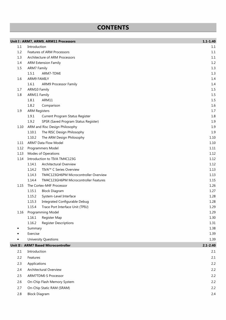
CONTENTS
Unit I : ARM7, ARM9, ARM11 Processors 1.1-1.40
1.1 Introduction 1.1
1.2 Features of ARM Processors 1.1
1.3 Architecture of ARM Processors 1.1
1.4 ARM Extension Family 1.2
1.5 ARM7 Family 1.3
1.5.1 ARM7-TDMI 1.3
1.6 ARM9 FAMILY 1.4
1.6.1 ARM9 Processor Family 1.4
1.7 ARM10 Family 1.5
1.8 ARM11 Family 1.5
1.8.1 ARM11 1.5
1.8.2 Comparison 1.6
1.9 ARM Registers 1.7
1.9.1 Current Program Status Register 1.8
1.9.2 SPSR (Saved Program Status Register) 1.9
1.10 ARM and Risc Design Philosophy 1.9
1.10.1 The RISC Design Philosophy 1.9
1.10.2 The ARM Design Philosophy 1.10
1.11 ARM7 Data Flow Model 1.10
1.12 Programmers Model 1.11
1.13 Modes of Operations 1.12
1.14 Introduction to TIVA TM4C123G 1.12
1.14.1 Architectural Overview 1.12
1.14.2 TIVA™ C Series Overview 1.13
1.14.3 TM4C123GH6PM Microcontroller Overview 1.13
1.14.4 TM4C123GH6PM Microcontroller Features 1.15
1.15 The Cortex-M4F Processor 1.26
1.15.1 Block Diagram 1.27
1.15.2 System-Level Interface 1.28
1.15.3 Integrated Configurable Debug 1.28
1.15.4 Trace Port Interface Unit (TPIU) 1.29
1.16 Programming Model 1.29
1.16.1 Register Map 1.30
1.16.2 Register Descriptions 1.31
• Summary 1.38
• Exercise 1.39
• University Questions 1.39
Unit II : ARM7 Based Microcontroller 2.1-2.40
2.1 Introduction 2.1
2.2 Features 2.1
2.3 Applications 2.2
2.4 Architectural Overview 2.2
2.5 ARM7TDMI-S Processor 2.2
2.6 On-Chip Flash Memory System 2.2
2.7 On-Chip Static RAM (SRAM) 2.2
2.8 Block Diagram 2.4

2.9 System Control Block Functions 2.3
2.9.1 Pin Description 2.4
2.9.2 Phase Locked Loop (PLL) 2.4
2.9.3 VPB Divider 2.8
2.10 Memory Maps 2.9
2.10.1 LPC2141/2142/2144/2146/2148 Memory Re-mapping and Boot Block 2.10
2.10.2 Memory Re-Mapping 2.11
2.10.3 Prefetch Abort and Data Abort Exceptions 2.11
2.11 General Purpose Input/Output Ports (GPIO) 2.12
2.11.1 Features 2.12
2.11.2 Applications 2.12
2.11.3 Pin Description 2.12
2.11.4 Register Description 2.13
2.11.5 GPIO Usage Notes 2.15
2.12 Pin Connect Block 2.17
2.12.1 Pin Function Select Register 0 (PINSEL0 - 0xE002 C000) 2.17
2.12.2 Pin Function Select Register 1 (PINSEL1 - 0xE002 C004) 2.19
2.12.3 Pin Function Select Register 2 (PINSEL2 - 0xE002 C014) 2.21
2.12.4 Register Description 2.22
2.12.5 Pin Function Select Register Values 2.22
2.13 Timer/Counter (Timer0 And Timer1) 2.22
2.13.1 Features 2.22
2.13.2 Applications 2.23
2.13.3 Description 2.23
2.13.4 Pin description 2.24
2.13.5 Example For Timer Operation 2.24
2.14 ARM Instruction Set 2.25
2.14.1 Data Processing Instructions 2.26
2.14.2 Data Transfer Instructions 2.27
2.14.3 Control Flow Instructions 2.29
2.15 Thumb Instruction Set 2.30
2.15.1 Thumb Programmer’s Model 2.30
2.16 Programming in Assembly Language 2.34
• Summary 2.38
• Exercise 2.38
• University Questions 2.39
Unit III : Real World Interfacing With ARM7 Based Microcontroller-1 3.1-3.34
3.1 Introduction 3.1
3.2 Interrupt Structure of LPC2148 3.1
3.3 VIC Registers 3.2
3.3.1 Software Interrupt Register (VICSOFTINT - 0xFFFF F018) 3.2
3.3.2 Software Interrupt Clear Register (VICSOFTINTCLEAR - 0xFFFF F01C) 3.2
3.3.3 Raw Interrupt Status Register (VICRAWINTR - 0xFFFF F008) 3.3
3.3.4 Interrupt Enable Register (VICIntEnable - 0xFFFF F010) 3.3
3.3.5 Interrupt Enable Clear Register (VICIntEnClear - 0xFFFF F014) 3.4
3.3.6 Interrupt Select Register (VICIntSelect - 0xFFFF F00C) 3.4
3.3.7 IRQ Status Register (VICIRQStatus - 0xFFFF F000) 3.5
3.3.8 FIQ Status Register (VICFIQStatus - 0xFFFF F004) 3.5
3.3.9 Vector Control registers 0-15 (VICVectCntl0-15 - 0xFFFF F200-23C) 3.6
3.3.10 Vector Address registers 0-15 (VICVectAddr0-15 - 0xFFFF F100-13C) 3.6
3.3.11 Default Vector Address Register (VICDefVectAddr - 0xFFFF F034) 3.6
3.3.12 Vector Address Register (VICVectAddr - 0xFFFF F030) 3.6
3.3.13 Protection Enable Register (VICProtection - 0xFFFF F020) 3.7

3.4 External Interrupt Inputs 3.7
3.4.1 Register Description 3.7
3.4.2 External Interrupt Flag Register (EXTINT - 0xE01F C140 3.7
3.4.3 Interrupt Wakeup Register (INTWAKE - 0xE01F C144) 3.8
3.4.4 External Interrupt Mode Register (EXTMODE - 0xE01F C148) 3.8
3.4.5 External Interrupt Polarity Register (EXTPOLAR - 0xE01F C14C) 3.9
3.5 Interfacing of Different Displays Using Lpc 2148 3.9
3.5.1 Interfacing LEDs to ARM7 Controller (LPC 2148) 3.9
3.5.2 Interfacing of Seven Segment Display with ARM7 (LPC 2148) 3.11
3.6 Interfacing of LCD With LPC 2148 (Liquid Crystal Display) 3.11
3.6.1 Interfacing 4 bit LCD with LPC2148 3.12
3.6.2 Circuit Diagram to Interface 4 bit LCD with LPC2148 3.13
3.6.3 C Program to Display a Text in 4 Bit LCD Using LPC2148 3.13
3.6.4 Testing the LCD Module with LPC2148 3.15
3.7 Interfacing of GLCD With LPC2148 3.15
3.7.1 GLCD (Graphical Liquid Crystal Display) 3.15
3.7.2 Interfacing GLCD 3.16
3.7.3 Description of GLCD 3.16
3.7.4 Interfacing GLCD with LPC2148 3.18
3.7.5 Circuit Diagram to Interface GLCD with LPC2148 3.20
3.7.6 C Program to Display a Text in GLCD using LPC2148 3.20
3.7.7 Testing the Graphical LCD Module with LPC2148 3.21
3.8 Keypad Interfacing With ARM7 LPC2148 3.22
3.8.1 Keypad 3.22
3.8.2 Interfacing Keypad with LPC2148 3.22
3.8.3 Circuit Diagram to Interface Keypad with LPC2148 3.23
3.8.4 C Program to Interface 4 ⋅ 4 Matrix Keypad Using LPC2148 3.23
3.8.5 Testing the Keypad with LPC2148 3.25
3.9 Simple LPC2148 GPIO Programming Examples 3.25
3.9.1 GPIO Related Registers in LPC2148 3.25
3.9.2 Example: Blink LED with ARM7 LPC2148 3.25
3.9.3 Program Code 3.25
3.10 Using Timers of Lpc2148 To Generate Delay 3.26
3.10.1 32 bit Timer Counter with 32 bit Prescaler 3.26
3.10.2 Timer Registers in LPC2147 ARM7 3.26
3.10.3 Example 3.26
3.10.4 Program Code 3.27
3.11 Serial Communication Programming For Transmission and Reception From Computer: (Programming For UART) 3.28
3.11.1 Serial Data Transmission in UART 3.28
3.11.2 Introduction: UART in LPC2148 ARM7 Microcontroller 3.28
3.11.3 RS232 Level Converter 3.29
3.11.4 Registers Description: UART in LPC2148 ARM7 3.29
3.11.5 Calculate Baud Rate for UART in LPC2148 ARM7 3.29
3.11.6 Example 2.30
3.11.7 Circuit Diagram: UART in LPC2148 ARM7 Microcontroller 3.30
3.11.8 Source Code: UART in LPC2148 ARM7 Microcontroller 3.30
3.11.9 Output of UART in LPC2148 ARM7 Microcontroller 3.33
• Summary 3.33
• Exercise 3.33
• University Questions 3.34

Unit IV : Real World Interfacing With ARM7 Based Microcontroller-2 4.1-4.46
4.1 Introduction 4.1
4.2 Interfacing of GSM With LPC 2148 4.1
4.2.1 Pin Assignment with LPC2148 4.1
4.2.2 Circuit Diagram to Interface GSM with LPC2148 4.1
4.2.3 C Program to Send a Message from LPC2148 4.2
4.2.4 Very Useful AT Commands Description 4.4
4.3 How to Interface Gps With Lpc2148 Arm Processor 4.5
4.3.1 Interfacing GPS 4.5
4.3.2 Interfacing GPS with LPC2148 4.5
4.3.3 Circuit Diagram to Interface GPS with LPC2148 4.6
4.3.4 C Program to Receives Data from Satellite to LPC2148 4.6
4.3.5 Testing the GPS with LPC2148 4.7
4.4 Analog to Digital Convertor Block In Lpc214x 4.7
4.4.1 Registers used for ADC Programming in LPC214x 4.8
4.4.2 ADC Input Circuit and Overvoltage Protection 4.9
4.4.3 LPC214x ADC Modes, Setup and Programming 4.10
4.5 LPC214X ADC 4.13
4.5.1 Features 4.13
4.5.2 Description 4.13
4.5.3 Pin Description 4.13
4.5.4 Register Description 4.13
4.5.5 Operation 4.16
4.6 VIC (Vectored Interrupt Controller) 4.16
4.6.1 Description 4.16
4.6.2 Register Description 4.17
4.7 I2C (Inter Integrated Circuit) 4.19
4.7.1 Features 4.19
4.7.2 Applications 4.19
4.7.3 Description 4.19
4.7.4 Pin Description 4.20
4.7.5 I2C Operating Modes 4.20
4.7.6 I2C Implementation and Operation 4.22
4.7.7 Arbitration and Synchronization Logic 4.23
4.7.8 I2C-bus Status 4.24
4.8 Interfacing I2C – EEPROM 4.24
4.8.1 Interfacing I2C – EEPROM with LPC2148 4.24
4.9 Secure Digital Memory Cards 4.32
4.9.1 Types of SD Cards 4.32
4.9.2 Inside the SD Card 4.33
4.9.3 Memory Card Class 4.34
4.9.4 Block Diagram of SD Card 4.34
4.9.5 Communication with SD Cards 4.34
4.10 DAC Interfacing with LPC2148 4.37
4.10.1 SPI Bus Interface 4.37
4.10.2 Interfacing of SPI-DAC to Microcontroller 4.41
4.10.3 Circuit Diagram to Interface SPI-DAC with LPC2148 4.42
4.10.4 C Program to Interface SPI - DAC with LPC2148 4.43

4.11 LPC 214X DAC 4.43
4.11.1 Features 4.43
4.11.2 Pin Description 4.43
4.11.3 DAC Register (DACR - 0xE006 C000) 4.43
4.11.4 Operation 4.44
• Summary 4.44
• Exercise 4.44
• University Questions 4.45
Unit V : Digital Signal Processing-I 5.1-5.38
5.1 Introduction 5.1
5.1.1 Advantages of Digital Signal Processing 5.1
5.2 Computer Architectures for Signal Processing 5.1
5.2.1 Hardware Architecture 5.2
5.2.2 Pipelining 5.3
5.2.3 Hardware Multiplier-Accumulator 5.4
5.2.4 Special Instructions 5.5
5.2.5 Replication 5.6
5.2.6 On-Chip Memory/Cache 5.6
5.3 General Purpose Digital Signal Processors 5.6
5.3.1 Texas Instruments TMS320 Family 5.6
5.3.2 Motorola DSP56000 Family 5.9
5.3.3 Analog Devices ADSP2100 Family 5.10
5.4 Selecting Digital Signal Processors 5.11
5.5 Special Purpose DSP Hardware 5.13
5.5.1 Hardware Digital Filters 5.14
5.5.2 Hardware FFT Processors 5.15
5.6 TMS320C67X DSP Processor 5.17
5.6.1 TMS320C6000 DSP Family Overview 5.17
5.6.2 TMS320C67x DSP Features and Options 5.17
5.7 Features of C67X Processors 5.18
5.8 TMS320C67x DSP Architecture 5.19
5.9 TMS320C67x CPU Data Paths 5.21
5.10 General Purpose Register Files 5.22
5.11 Functional Units 5.23
5.12 Register File Cross Paths 5.23
5.13 Memory, Load, and Store Paths 5.24
5.14 Data Address Paths 5.24
5.15 Control Register File 5.24
5.15.1 Register Addresses for Accessing the Control Registers 5.24
5.15.2 Pipeline/Timing of Control Register Accesses 5.25
5.15.3 Addressing Mode Register (AMR) 5.25
5.15.4 Control Status Register (CSR) 5.27
5.15.5 Interrupt Clear Register (ICR) 5.29
5.15.6 Interrupt Enable Register (IER) 5.29
5.15.7 Interrupt Flag Register (IFR) 5.30
5.15.8 Interrupt Return Pointer Register (IRP) 5.30
5.15.9 Interrupt Set Register (ISR) 5.30
5.15.10 Interrupt Service Table Pointer Register (ISTP) 5.31
5.15.11 Non-maskable Interrupt (NMI) Return Pointer Register (NRP) 5.31
5.15.12 E1 Phase Program Counter (PCE1) 5.32
5.16 Control Register File Extensions 5.32
5.16.1 Floating-Point Adder Configuration Register (FADCR) 5.32
5.16.2 Floating-Point Auxiliary Configuration Register (FAUCR) 5.34
5.16.3 Floating-Point Multiplier Configuration Register (FMCR) 5.36
• Summary 5.37
• Exercise 5.38
Unit VI : Digital Signal Processing−−−−II 6.1-6.46
6.1 Introduction 6.1
6.2 TMS320C67C Functional Units 6.1
6.3 Internal Memory 6.2
6.4 External Memory 6.4
6.5 On−Chip Peripherals 6.4
6.5.1 Timers 6.5
6.5.2 Multichannel Buffered Serial Port (McBSP) 6.6
6.5.3 DMA/EDMA Controller 6.7
6.5.4 External Memory Interface (EMIF) 6.8
6.5.5 Host−Port Interface (HPI) 6.8
6.5.6 Boot Configuration 6.8
6.5.7 Interrupt Selector 6.8
6.5.8 Expansion Bus 6.8
6.5.9 Power Down Logic 6.8
6.6 Interrupts 6.9
6.6.1 Types of Interrupts and Signals Used 6.9
6.6.2 Interrupt Service Table (IST) 6.10
6.6.3 Summary of Interrupt Control Registers 6.12
6.6.4 Globally Enabling and Disabling Interrupts 6.12
6.6.5 Individual Interrupt Control 6.13
6.6.6 Interrupt Detection and Processing 6.14
6.7 Addressing Modes 6.16
6.7.1 Linear Addressing Mode 6.16
6.7.2 Circular Addressing Mode 6.17
6.7.3 Syntax for Load/Store Address Generation 6.17
6.8 Fixed Point Instructions 6.18
6.8.1 Move Instructions 6.18
6.8.2 Load/Store Instructions 6.19
6.8.3 Add Instructions 6.21
6.8.4 Subtract Instructions 6.22
6.8.5 Multiply Instructions 6.23
6.8.6 Logical, Shift and Compare Instructions 6.24
6.8.7 Branch and Other Instructions 6.26
6.9 Floating Point Instructions 6.26
6.9.1 Data Formats 6.26
6.9.2 Data Format Conversion Instructions 6.27
6.9.3 Arithmetic Operation Instructions 6.28
6.9.4 Compare and Reciprocal Approximation Instructions 6.29
6.9.5 Other Instructions 6.29

6.10 Conditional Operations 6.30
6.11 Parallel Operations 6.30
6.12 Pipeline Operations 6.32
6.12.1 Fetch Operation 6.33
6.12.2 Decode Operation 6.33
6.12.3 Execute Operation 6.33
6.13 Code Composer Studio (CCS) 6.35
6.13.1 Setting up the Target Processor 6.35
6.13.2 An overview of the C6416 DSK 6.36
6.13.3 Code Generation in CCS 6.36
6.13.4 Execution of C6X Codes in Target Processor 6.37
6.14 Application Programs in C67X processors 6.37
6.14.1 Code Development in C Environment using Code Composer Studio 6.37
6.14.2 Computation of the 8−point DFT using FFT Algorithm in C Environment 6.40
6.14.3 Estimation of Clock Cycles Required for Code Execution using CCS 6.42
6.14.4 Mixing Assembly Language and C Code 6.42
6.14.5 Different Ways of Invoking Assembly Language in C Code 6.42
• Summary 6.45
• Exercise 6.46
•••• Model Question Papers
���� In-Sem. Exam. (30 Marks) P.1-P.1
���� End-Sem. Exam. (70 Marks) P.2-P.2
���

Advanced Processors
Publisher : Nirali Prakashan ISBN : 9789387397521Author : Mrs. Deepa S.Pandit
Type the URL : http://www.kopykitab.com/product/20831
Get this eBook
60%OFF