Complexity-effective superscalar embedded processors using ...
130
Technical Report Number 707 Computer Laboratory UCAM-CL-TR-707 ISSN 1476-2986 Complexity-effective superscalar embedded processors using instruction-level distributed processing Ian Caulfield December 2007 15 JJ Thomson Avenue Cambridge CB3 0FD United Kingdom phone +44 1223 763500 http://www.cl.cam.ac.uk/
-
Upload
khangminh22 -
Category
Documents
-
view
0 -
download
0
Transcript of Complexity-effective superscalar embedded processors using ...

Technical ReportNumber 707
Computer Laboratory
UCAM-CL-TR-707ISSN 1476-2986
Complexity-effective superscalarembedded processors using
instruction-level distributed processing
Ian Caulfield
December 2007
15 JJ Thomson AvenueCambridge CB3 0FDUnited Kingdomphone +44 1223 763500
http://www.cl.cam.ac.uk/

c© 2007 Ian Caulfield
This technical report is based on a dissertation submittedMay 2007 by the author for the degree of Doctor ofPhilosophy to the University of Cambridge, Queens’ College.
Technical reports published by the University of CambridgeComputer Laboratory are freely available via the Internet:
http://www.cl.cam.ac.uk/techreports/
ISSN 1476-2986

Abstract
Modern trends in mobile and embedded devices require ever increasing levels of performance,while maintaining low power consumption and silicon area usage. This thesis presents a newarchitecture for a high-performance embedded processor, based upon the instruction-level dis-tributed processing (ILDP) methodology. A qualitative analysis of the complexity of an ILDPimplementation as compared to both a typical scalar RISC CPU and a superscalar design isprovided, which shows that the ILDP architecture eliminates or greatly reduces the size of anumber of structures present in a superscalar architecture, allowing its complexity and powerconsumption to compare favourably with a simple scalar design.
The performance of an implementation of the ILDP architecture is compared to some typicalprocessors used in high-performance embedded systems. The effect on performance of a num-ber of the architectural parameters is analysed, showing that many of the parallel structuresused within the processor can be scaled to provide less parallelism with little cost to the overallperformance. In particular, the size of the register file can be greatly reduced with little averageeffect on performance – a size of 32 registers, with 16 visible in the instruction set, is shown toprovide a good trade-off between area/power and performance.
Several novel developments to the ILDP architecture are then described and analysed. Firstly,a scheme to halve the number of processing elements and thus greatly reduce silicon area andpower consumption is outlined but proves to result in a 12–14% drop in performance. Secondly,a method to reduce the area and power requirements of the memory logic in the architectureis presented which can achieve similar performance to the original architecture with a largereduction in area and power requirements or, at an increased area/power cost, can improveperformance by approximately 24%. Finally, a new organisation for the register file is proposed,which reduces the silicon area used by the register file by approximately three-quarters andallows even greater power savings, especially in the case where processing elements are powergated.
Overall, it is shown that the ILDP methodology is a viable approach for future embedded systemdesign, and several new variants on the architecture are contributed. Several areas of useful fu-ture research are highlighted, especially with respect to compiler design for the ILDP paradigm.
3

4

Acknowledgements
I would like to thank my supervisor, Simon Moore, for his advice, guidance and most particu-larly his patient support over the past few years. Thanks are also due to James Srinivasan andSimon ‘Harry’ Hollis (and to a lesser degree many other members of the Computer ArchitectureGroup) for fielding innumerable queries along the lines of “Do you know anything about . . . ?”.
I would like to give special recognition to Diana Wood for providing unconditional support andputting up with me while I completed my thesis, and for providing assistance with proofreading.Unthanks go to the members of Cambridge University Bowmen who, whilst providing manyhours of friendship and recreation, conspired to lengthen my stay at university!
My research was funded with a grant from the Engineering and Physical Sciences ResearchCouncil.
5

6

Contents
1 Introduction 151.1 Motivation . . . . . . . . . . . . . . . . . . . . . . . . . . . . . . . . . . . . .151.2 Contribution . . . . . . . . . . . . . . . . . . . . . . . . . . . . . . . . . . . .161.3 Outline . . . . . . . . . . . . . . . . . . . . . . . . . . . . . . . . . . . . . .16
2 Background 172.1 Parallelism . . . . . . . . . . . . . . . . . . . . . . . . . . . . . . . . . . . .172.2 Control-flow vs data-flow . . . . . . . . . . . . . . . . . . . . . . . . . . . . .18
2.2.1 Static data-flow . . . . . . . . . . . . . . . . . . . . . . . . . . . . . .192.2.2 Coloured data-flow . . . . . . . . . . . . . . . . . . . . . . . . . . . .192.2.3 Tagged-token data-flow . . . . . . . . . . . . . . . . . . . . . . . . . .19
2.3 Pipelining . . . . . . . . . . . . . . . . . . . . . . . . . . . . . . . . . . . . .202.3.1 Data hazards . . . . . . . . . . . . . . . . . . . . . . . . . . . . . . .212.3.2 Control hazards . . . . . . . . . . . . . . . . . . . . . . . . . . . . . .21
2.4 Superscalar architectures . . . . . . . . . . . . . . . . . . . . . . . . . . . . .222.4.1 In-order superscalar . . . . . . . . . . . . . . . . . . . . . . . . . . .222.4.2 Out-of-order superscalar . . . . . . . . . . . . . . . . . . . . . . . . .232.4.3 Parallels between out-of-order and data-flow . . . . . . . . . . . . . .25
2.5 Multithreading . . . . . . . . . . . . . . . . . . . . . . . . . . . . . . . . . .252.5.1 Simultaneous multithreading . . . . . . . . . . . . . . . . . . . . . . .25
2.6 Vector architectures . . . . . . . . . . . . . . . . . . . . . . . . . . . . . . . .262.7 Decoupled architectures . . . . . . . . . . . . . . . . . . . . . . . . . . . . . .262.8 Dependence-based architectures . . . . . . . . . . . . . . . . . . . . . . . . .272.9 Instruction-level distributed processing . . . . . . . . . . . . . . . . . . . . . .282.10 Multiprocessing . . . . . . . . . . . . . . . . . . . . . . . . . . . . . . . . . .28
2.10.1 Symmetric multiprocessing . . . . . . . . . . . . . . . . . . . . . . .292.10.2 Non-uniform memory architectures . . . . . . . . . . . . . . . . . . .292.10.3 Multicore processors . . . . . . . . . . . . . . . . . . . . . . . . . . .30
2.11 Instruction encoding . . . . . . . . . . . . . . . . . . . . . . . . . . . . . . .302.11.1 CISC . . . . . . . . . . . . . . . . . . . . . . . . . . . . . . . . . . .302.11.2 RISC . . . . . . . . . . . . . . . . . . . . . . . . . . . . . . . . . . .31
2.12 Embedded system design . . . . . . . . . . . . . . . . . . . . . . . . . . . . .312.12.1 Low cost . . . . . . . . . . . . . . . . . . . . . . . . . . . . . . . . .322.12.2 Low power consumption . . . . . . . . . . . . . . . . . . . . . . . . .33
7

Contents
2.12.3 Real-time performance . . . . . . . . . . . . . . . . . . . . . . . . . .352.13 Future developments . . . . . . . . . . . . . . . . . . . . . . . . . . . . . . .35
3 ILDP in an Embedded Context 373.1 Details of ILDP . . . . . . . . . . . . . . . . . . . . . . . . . . . . . . . . . .373.2 Instruction set . . . . . . . . . . . . . . . . . . . . . . . . . . . . . . . . . . .393.3 Programming model . . . . . . . . . . . . . . . . . . . . . . . . . . . . . . .40
3.3.1 Register assignments . . . . . . . . . . . . . . . . . . . . . . . . . . .403.3.2 Memory organisation . . . . . . . . . . . . . . . . . . . . . . . . . . .423.3.3 Function call specification . . . . . . . . . . . . . . . . . . . . . . . .42
3.4 Microarchitecture . . . . . . . . . . . . . . . . . . . . . . . . . . . . . . . . .433.5 Complexity . . . . . . . . . . . . . . . . . . . . . . . . . . . . . . . . . . . .463.6 Complexity analysis . . . . . . . . . . . . . . . . . . . . . . . . . . . . . . . .47
3.6.1 Register rename logic . . . . . . . . . . . . . . . . . . . . . . . . . .473.6.2 Issue window dependency logic . . . . . . . . . . . . . . . . . . . . .483.6.3 Instruction issue logic . . . . . . . . . . . . . . . . . . . . . . . . . .493.6.4 Register file . . . . . . . . . . . . . . . . . . . . . . . . . . . . . . . .493.6.5 Bypass paths . . . . . . . . . . . . . . . . . . . . . . . . . . . . . . .503.6.6 Data caches . . . . . . . . . . . . . . . . . . . . . . . . . . . . . . . .50
3.7 Power consumption . . . . . . . . . . . . . . . . . . . . . . . . . . . . . . . .513.8 Summary . . . . . . . . . . . . . . . . . . . . . . . . . . . . . . . . . . . . .52
4 Evaluating ILDP 534.1 Performance vs other embedded architectures . . . . . . . . . . . . . . . . . .53
4.1.1 Methodology . . . . . . . . . . . . . . . . . . . . . . . . . . . . . . .534.1.2 Compiler toolchain . . . . . . . . . . . . . . . . . . . . . . . . . . . .534.1.3 Benchmarks . . . . . . . . . . . . . . . . . . . . . . . . . . . . . . . .554.1.4 Simulation . . . . . . . . . . . . . . . . . . . . . . . . . . . . . . . .554.1.5 Results . . . . . . . . . . . . . . . . . . . . . . . . . . . . . . . . . .564.1.6 Conclusion . . . . . . . . . . . . . . . . . . . . . . . . . . . . . . . .60
4.2 Resource utilization . . . . . . . . . . . . . . . . . . . . . . . . . . . . . . . .604.2.1 Decode / Issue logic . . . . . . . . . . . . . . . . . . . . . . . . . . .604.2.2 Processing elements . . . . . . . . . . . . . . . . . . . . . . . . . . .614.2.3 Register rename logic . . . . . . . . . . . . . . . . . . . . . . . . . .62
4.3 Parameter space exploration . . . . . . . . . . . . . . . . . . . . . . . . . . .644.3.1 Issue width . . . . . . . . . . . . . . . . . . . . . . . . . . . . . . . .644.3.2 Rename bandwidth . . . . . . . . . . . . . . . . . . . . . . . . . . . .674.3.3 FIFO depth . . . . . . . . . . . . . . . . . . . . . . . . . . . . . . . .694.3.4 Register network bandwidth . . . . . . . . . . . . . . . . . . . . . . .734.3.5 Physical register file size . . . . . . . . . . . . . . . . . . . . . . . . .764.3.6 ISA register file size . . . . . . . . . . . . . . . . . . . . . . . . . . .784.3.7 Cache parameters . . . . . . . . . . . . . . . . . . . . . . . . . . . . .80
4.4 Combining approaches . . . . . . . . . . . . . . . . . . . . . . . . . . . . . .804.5 Summary . . . . . . . . . . . . . . . . . . . . . . . . . . . . . . . . . . . . .82
8

Contents
5 Architectural developments 855.1 Multiplexing instruction FIFOs onto a processing element . . . . . . . . . . .85
5.1.1 Implementation details . . . . . . . . . . . . . . . . . . . . . . . . . .865.1.2 Evaluation . . . . . . . . . . . . . . . . . . . . . . . . . . . . . . . .875.1.3 Conclusions . . . . . . . . . . . . . . . . . . . . . . . . . . . . . . . .87
5.2 Combining memory access units . . . . . . . . . . . . . . . . . . . . . . . . .905.2.1 ISA modifications . . . . . . . . . . . . . . . . . . . . . . . . . . . .915.2.2 Implementation details . . . . . . . . . . . . . . . . . . . . . . . . . .925.2.3 Evaluation . . . . . . . . . . . . . . . . . . . . . . . . . . . . . . . .935.2.4 Further developments . . . . . . . . . . . . . . . . . . . . . . . . . . .1015.2.5 Implementation details . . . . . . . . . . . . . . . . . . . . . . . . . .1015.2.6 Evaluation . . . . . . . . . . . . . . . . . . . . . . . . . . . . . . . .1035.2.7 Cache structure . . . . . . . . . . . . . . . . . . . . . . . . . . . . . .1075.2.8 Conclusions . . . . . . . . . . . . . . . . . . . . . . . . . . . . . . . .107
5.3 Register inlining . . . . . . . . . . . . . . . . . . . . . . . . . . . . . . . . . .1095.3.1 Implementation details . . . . . . . . . . . . . . . . . . . . . . . . . .1105.3.2 Complexity . . . . . . . . . . . . . . . . . . . . . . . . . . . . . . . .1125.3.3 Evaluation . . . . . . . . . . . . . . . . . . . . . . . . . . . . . . . .1125.3.4 Conclusions . . . . . . . . . . . . . . . . . . . . . . . . . . . . . . . .113
5.4 Summary . . . . . . . . . . . . . . . . . . . . . . . . . . . . . . . . . . . . .114
6 Conclusions 1156.1 Summary . . . . . . . . . . . . . . . . . . . . . . . . . . . . . . . . . . . . .1156.2 Conclusion . . . . . . . . . . . . . . . . . . . . . . . . . . . . . . . . . . . .1166.3 Future work . . . . . . . . . . . . . . . . . . . . . . . . . . . . . . . . . . . .117
Bibliography 121
9

10

List of Tables
3.1 The ILDP instruction set . . . . . . . . . . . . . . . . . . . . . . . . . . . . .413.2 Register assignments for the ILDP ABI . . . . . . . . . . . . . . . . . . . . .42
4.1 Architectural parameters for simulation . . . . . . . . . . . . . . . . . . . . .57
5.1 Instruction set modifications . . . . . . . . . . . . . . . . . . . . . . . . . . .91
11

12
List of Figures
3.1 Ways of grouping instructions by their dependencies . . . . . . . . . . . . . .383.2 Instruction encodings . . . . . . . . . . . . . . . . . . . . . . . . . . . . . . .403.3 Function stack frame layout . . . . . . . . . . . . . . . . . . . . . . . . . . . .433.4 The ILDP architecture, as outlined by Kim and Smith . . . . . . . . . . . . . .443.5 Structure of an ILDP processing element . . . . . . . . . . . . . . . . . . . . .45
4.1 Performance of ILDP compared to embedded processors . . . . . . . . . . . .584.2 Number of instructions executed, compared to ARM . . . . . . . . . . . . . .584.3 IPC of tested processors . . . . . . . . . . . . . . . . . . . . . . . . . . . . . .594.4 Number of instructions processed by the parcel, rename and steer pipeline stages614.5 Processing element activity . . . . . . . . . . . . . . . . . . . . . . . . . . . .624.6 Distribution of rename map bandwidth usage over time . . . . . . . . . . . . .634.7 Performance of ILDP at various issue widths, normalised to 4-way case . . . .654.8 Number of instructions in the parcel, rename and steer pipeline stages . . . . .664.9 Effect on performance of removing register rename map ports . . . . . . . . .674.10 Issue pipeline statistics when varying number of rename map ports . . . . . . .684.11 Distribution of instruction strand lengths in ILDP code . . . . . . . . . . . . .704.12 Instruction FIFO utilization . . . . . . . . . . . . . . . . . . . . . . . . . . . .714.13 Performance at various instruction FIFO sizes, compared to an unbounded FIFO724.14 Register network bandwidth utilization . . . . . . . . . . . . . . . . . . . . . .744.15 Performance at various register network bandwidths, compared to unbounded
case . . . . . . . . . . . . . . . . . . . . . . . . . . . . . . . . . . . . . . . .754.16 Effect of scaling physical register file size from 128 GPRs on performance . . .774.17 Effect of scaling both physical and logical register file size on performance . .794.18 Effect of increasing cache associativity from 2-way on performance . . . . . .814.19 Effect of varying several architectural parameters . . . . . . . . . . . . . . . .82
5.1 Multiplexing instruction FIFOs between processing elements . . . . . . . . . .865.2 Effect on performance of multiplexing instruction FIFOs between PEs . . . . .885.3 Processing element utilization with two FIFOs per PE . . . . . . . . . . . . . .895.4 Design of memory access unit . . . . . . . . . . . . . . . . . . . . . . . . . .915.5 Additional instruction encodings . . . . . . . . . . . . . . . . . . . . . . . . .925.6 Performance of the MAU architecture variant compared to the baseline . . . . .945.7 Performance of the MAU variant when multiple outstanding loads are imple-
mented . . . . . . . . . . . . . . . . . . . . . . . . . . . . . . . . . . . . . . .96
13

List of Figures
5.8 Effect of reducing register rename bandwidth on performance in the MAU model975.9 MAU FIFO occupancy by time . . . . . . . . . . . . . . . . . . . . . . . . . .995.10 Performance at various MAU FIFO sizes, compared to an unbounded FIFO . .1005.11 Design of memory access unit, using out-of-order issue . . . . . . . . . . . . .1025.12 Performance of various models of out-of-order memory access unit . . . . . . .1045.13 Effect of out-of-order MAU instruction window size on performance . . . . . .1065.14 Effect of increasing L1 cache size on performance (compared to 8KB size) . . .1085.15 Register tag/value portion of PE instruction FIFO . . . . . . . . . . . . . . . .111
6.1 Traditional CPU arrangements for multiprocessing . . . . . . . . . . . . . . .1186.2 An example four-way multiprocessing ILDP CPU . . . . . . . . . . . . . . . .119
14

Introduction 1
This dissertation describes a number of architectural designs aimed toward producing high-performance embedded microprocessors. These build upon the techniques of instruction-leveldistributed processing developed by Kim and Smith [30]. I show that these techniques allowprocessors to achieve high performance without many of the costs in power consumption andcircuit complexity associated with traditional superscalar architectures.
1.1 Motivation
The embedded microprocessor market is currently growing at a greater rate than the marketfor desktop and server processors. More and more products in various market sectors are beingproduced with embedded processors – a modern car can contain dozens of embedded processorscontrolling various different features within the vehicle. While the desktop microprocessormarket has the highest profit margins, the embedded processor market ships far higher volumesper year, yielding large overall profits. With large growth and revenues, and increasing demandsfor greater functionality at a lower cost, there is considerable scope for research into processorarchitecture targeted at embedded systems.
In the mobile device sector, there is an increasing trend toward ‘all-in-one’ devices that performa number of functions: a modern smart phone will be able to connect to several varieties ofwireless network, play back (and even record) audio and video, play games, take photos andbrowse the Internet. In order to perform these functions, the device must be capable of runningone or more radio protocol stacks, perform audio and video encoding and decoding, rendergraphics in real time, perform image processing and be able to execute external scripts or ap-plications. While a single-function device can be constructed using a simple low-performancemicroprocessor and some special-purpose logic, a device with such diverse usage requirementsbut similar power and size constraints will generally require a high-performance general pur-pose processor, which can easily shift from one application to another. Many of the techniquesused to achieve high performance in desktop processors are unsuitable for embedded systemsdue to their power or area requirements, and so alternative approaches are required.
15

1. Introduction
1.2 Contribution
In this thesis, I will show that instruction-level distributed processing provides an approachto designing low-complexity microprocessors providing high performance with a smaller areaand power penalty than an out-of-order superscalar approach. The ILDP model is evaluatedin depth, and several parameters which are likely to have a large effect on the complexity ofthe design are explored to find the optimum trade-off between complexity and performance.Several new developments on the architecture are proposed in order to reduce the overall designarea, and thus power consumption.
1.3 Outline
The remainder of this dissertation is structured as follows:
Chapter2 introduces and describes many of the issues present with and techniques used in mod-ern microprocessor design, particularly looking at exploiting parallelism for high performanceand the challenges of designing for embedded systems.
Chapter3 describes the instruction-level distributed processor methodology and architecture onwhich this work is based, and outlines the implementation built upon them. The complexity ofthis design is analysed, compared to typical processor architectures.
Chapter4 analyses the performance of the ILDP design and investigate the effect various archi-tectural parameters have on performance and complexity.
Chapter5 describes several new designs built upon the ILDP architecture intended to reducecircuit complexity and power consumption and make this approach more suitable for embeddedimplementation while maintaining high performance.
Finally Chapter6 summarises this work and presents conclusions drawn. The contributionsmade by this work are outlined and possible areas for future work are described.
16

Background 2
Processor performance can be reduced to the following equation [48]:
Texe=ninst
Fclk× IPC+Tmem (2.1)
whereTexegives the overall time to execute a program or set of programs,Fclk refers to the clockfrequency of the system,ninst is the total number of instructions executed, IPC is the averagenumber of instructions executed within a single clock cycle andTmem is the time spent by thesystem waiting for external activities such as I/O or memory accesses. Performance is greaterwhenTexe is smaller.
Performance can thus be increased by maximisingFclk and IPC and minimisingninst andTmem.Clock frequency can be increased by technology scaling as smaller manufacturing processesbecome available, by pipelining or by redesigning or replacing complex logic blocks in orderto reduce the critical path. IPC can be increased by exploiting more parallelism within anarchitecture. The total instruction count can be reduced by optimising the ISA or improvingthe compiler used. Memory access time is generally reduced through the use of caches andspeculatively issuing memory instructions as early as possible.
Technology scaling is creating a trend whereby the delays due to logic are becoming less ex-pensive and those due to wiring are becoming more expensive, since as feature sizes decrease,overall die sizes tend to remain the same with additional logic added. A cross-chip wire re-mains the same length, but the delay to drive a signal along it increases [28] and as clock speedsincrease the number of clock cycles required to drive a signal across a chip rises drastically.When scaling smaller structures, the transistor delay will decrease at a greater rate than the wiredelay, which means that circuit structures with long wire delays thus scale badly as feature sizesdecrease. Future architectures must be able to localise data usage and minimise, or toleratedelays in, global communication.
2.1 Parallelism
In order to increase IPC, an architecture must be able to exploit parallelism present within theworkload it is executing. An important thing to note is that a workload with little or no inherent
17

2. Background
parallelism will benefit very little from a parallel architecture – a single program that consistsof a linear sequence of dependent instructions is likely to execute just as well on a simple scalararchitecture as a complex, multithreaded, superscalar one and may actually perform better onthe scalar processor due to the lower overhead of the less complex logic. There are two mainforms of parallelism that can be exploited in hardware:
1) Instruction-level parallelism (ILP) – in general, when taking a group of instructions froma program, while there will be many interdependencies between them, there will be setsof instructions that are mutually independent and thus can be executed in parallel. Aspecial case of ILP isloop-level parallelism(LLP) – where successive iterations of a loopoperate on independent data and can therefore be executed in parallel. Such loops areparallelized to extract ILP through a process calledloop unrolling.
2) Thread-level parallelism (TLP), where more than one program (orthread) can be ex-ecuted in parallel. Since programs generally communicate via main memory, if there issome mechanism for synchronizing memory accesses then all instructions from separateprograms are independent and can be executed concurrently. Processors that take advant-age of TLP can make up for a shortfall in ILP, but rely on there being more than onethread of execution in order to make any gains. A processor that can execute more thanone thread concurrently can help reduceTmem, as when one thread stalls on a memoryaccess, another can execute in its place. TLP workloads can be further characterisedbased on how tightly coupled the threads of execution are; a highly coupled workloadwill require a lot of communication and synchronization between threads, whereas a setof completely independent programs will be very loosely coupled. Depending on theway in which an architecture exploits TLP, it may perform better for more or less coupledworkloads.
2.2 Control-flow vs data-flow
Most microprocessors use acontrol-flowarchitecture, where a program is represented as a linearsequence of instructions. The model processor executes instructions in order, using a programcounter (PC) to keep track of the current location in the program. Instructions to modify the PCare provided in order to implement conditional expressions, loops and subroutines. As programsare represented as a linear sequence, exploiting ILP is difficult, since dependencies between in-structions must be resolved in order to allow non-linear execution. Also, since the instructionscheduling is determined statically by the compiler, the processor cannot easily adapt dynamic-ally to the execution environment – for example, long latency operations such as cache missesare likely to cause a processor stall even if other operations could theoretically be executed.
Data-flow architectures represent programs as a data-flow graph: each node in the graph isan instruction, and each arc is a data dependency between instructions. There is no explicit
18

2.2 Control-flow vs data-flow
ordering of the instructions beyond that of the dependencies – any instruction whose sourceoperands are available can be executed at any time, making ILP easier to exploit. If a singleinstruction stalls (for example due to a cache miss) other operations may be issued instead whiledata for them is available. Amatching storeis used to find nodes available for execution andissue them to functional units.
2.2.1 Static data-flow
In the static data-flow model each arc can have at most one datum (ortoken) on it at any onetime. A node becomes available for execution when there are tokens on all of its input arcs. Areverse signalling mechanism is used for flow control – when a node executes, it signals to allits predecessors that it has consumed its input tokens and that they may place new tokens on thearcs.
Due to the single token per arc limitation, this model has problems implementing shared func-tions as multiple instances of the same function cannot execute concurrently, and there is usuallya limit on the number of backward signalling arcs. These kinds of functions generally need tobe implemented by replicating the function body, which is inefficient.
2.2.2 Coloured data-flow
With coloured data-flow, each arc may carry more than one token. Each token is assigned acolour and nodes that take more than one input will only match tokens with the same colour.Result tokens are given the same colour as their source tokens. A function call generates a newcolour for its tokens, allowing concurrent calls to the same function, as the different colours foreach invocation will prevent conflicts.
The circuitry required for colour-matching is complicated, expensive and difficult to pipeline,which can cause performance problems with this model.
2.2.3 Tagged-token data-flow
The tagged-token dynamic model moves the token storage intoactivation frames– each func-tion invocation creates an activation frame, similar to stack frames in a control-flow processor.When the first token arrives for a dyadic operation, its data is stored in the activation frame.When the second token arrives, the data from the first token is retrieved from the activationframe and the operation executes.
19

2. Background
This approach is much simpler to implement than the coloured dynamic model and can bepipelined.
2.3 Pipelining
Several different pieces of hardware are required in a processor – for example: a load unit tofetch the current instruction word from memory; logic to interpret the instruction’s opcode andgenerate control signals for successive hardware blocks; a register file to hold register values;an ALU to perform computation and a memory unit to load and store data values from memory.When an instruction is executed, that instruction must generally pass through these blocks insequence, and only one block will be active at one time.Pipelining is a technique that allowshigher performance by allowing multiple instructions to be passing through this sequence ofhardware blocks, known as the ‘pipeline’. Latches are placed between each block to synchron-ize the data movement to the clock. A classic example is the standard RISC pipeline, split intofive stages:
• Instruction fetch
• Instruction decode and register access
• Execute
• Memory access
• Register write-back
A pipeline of n stages increases the typical instruction latency from 1 ton clock cycles, butreduces the cycle time by nearlyn and allows (potentially)n instructions to be executed con-currently. Theoretically, this means that the frequency of the processor is increased by a factorof n while maintaining an optimum IPC of 1. In practice the latches add extra circuit delayand not all hardware blocks necessarily have equal delay – the clock period must be set to theworst-case delay of the slowest block, plus the overhead of the latches. If one pipeline stage hasa delay much longer than the others, then it can significantly limit performance.
Pipelining can introduce new issues, however, which are generally referred to ashazards. Theseare generally divided intodata hazards, where problems arise with the transfer or validity ofdata values, andcontrol hazards, where problems arise with the flow of execution of a program.
20

2.3 Pipelining
2.3.1 Data hazards
In the case of the 5-stage RISC pipeline, if an instruction depends upon a register value gen-erated by its immediate predecessor, then when it comes to read the register value during the‘register access’ pipeline stage it will incorrectly read the previous value of the register, as thepredecessor will still be in the ‘execute’ stage and will not have written its result back to theregister file.
Data hazards are generally resolved usingbypass(or forwarding) data paths. For the 5-stageRISC pipeline, the results of the ‘execute’ and ‘memory access’ pipeline stages are fed directlyinto the execute stage on the next cycle, bypassing the register file entirely. The decode logicthen uses a technique known asscoreboardingto keep track of which registers’ values shouldbe read from the register file and which are currently in the pipeline and should use the bypasspaths.
However, not all data hazards may be resolved like this – if a load instruction is immediatelyfollowed by an instruction using the result of the load, the second instruction will enter the ‘ex-ecute’ stage at the same time as the load instruction is in the ‘memory access’ stage, performingthe load. With this pipeline arrangement it is impossible to execute these instructions simultan-eously, as the second instruction requires the result of the load at the time the load commences.As such, it is impossible to resolve this hazard without delaying the second instruction. Often itis possible for the compiler to re-order instructions to remove this hazard, but when this is notpossible there are two basic strategies for dealing with this situation in the processor:
• Software interlockingThe processor does nothing to resolve this conflict – it is entirely up to the compiler toensure this situation does not occur, and to insert no-ops into the instruction stream wherenecessary.
• Hardware interlockingThe processor uses scoreboarding to determine when these hazards will arise, and insertsno-ops as necessary into the pipeline itself.
2.3.2 Control hazards
When an unconditional branch is decoded, the instruction following it in memory will alreadybe in the process of being fetched from memory. The processor can either choose to executethis instruction (the ISA would then specify that the instruction immediately following a jumpis always executed) which is then termed as being in abranch delay slot, or it can nullify it andallow a no-op to proceed down the pipeline. The advantage of using branch delay slots is thatit simplifies issue logic and can allow slightly better performance. However, branch delay slots
21

2. Background
can cause issues with code compatibility, as the the number of delay slots following a branchdepends on the pipeline organisation – a new version of an architecture may require a differentnumber of delay slots than a previous architecture yet still have to run code compiled for the oldarchitecture. The new processor would then have to emulate a different number of delay slots,negating the original issue logic complexity advantages.
A further problem arises when a conditional branch is executed – if the branch condition isresolved in the ‘execute’ pipeline stage then the new PC value will not be available until severalcycles after the branch was fetched, which can be a large penalty if the architecture uses adeep pipeline. This problem is generally tackled usingbranch prediction. In the simplestcase, all conditional branches can be assumed to be not taken, meaning that the instructionfetch stage continues fetching instructions as it would if the branch had not come up – thismeans there is a performance penalty for a taken branch, but none for one that is not taken.More sophisticated schemes include static branch prediction, where the branch opcode specifieswhether it should be predicted as taken or not taken, and dynamic branch prediction, where theprocessor maintains some state on past behaviour of branches in order to guess whether a branchwill be taken or not. Modern dynamic branch predictors can achieve an accuracy in excess of99%.
2.4 Superscalar architectures
Superscalar architectures (as opposed to standard, orscalararchitectures) increase performanceby executing multiple instructions in parallel, thereby increasing IPC. Superscalar architecturesare generally classified as either beingin-order or out-of-order.
2.4.1 In-order superscalar
In-order architectures are so named because they can only issue instructions in the order theyappear in the instruction stream. For a processor of issue widthn, up ton instructions can beissued simultaneously, but only if alln instructions are independent. An instruction cannot beissued in the same cycle as one it depends upon, and none of the instructions following it canbe issued either. For this reason, in-order architectures require good compiler support in orderto arrange the instructions in the program in such a way as to be able to maximise parallel-ism. Load stalls and other long latency operations can be a problem, as no further instructionscan be issued while the processor is waiting for the data to come back from memory, regard-less of whether they depend on the result or not. Some architectures providespeculative load(or pre-fetch) instructions which allow a compiler to insert hints as to future load instructionsearlier in the instruction stream, ahead of conditional operations – any exceptions caused by thespeculative load are ignored, as the actual load might not be executed. This allows load data to
22
2.4 Superscalar architectures
be brought into the cache ahead of the instructions that require it, potentially eliminating somestalls due to cache misses.
In-order architectures can be further divided depending on whether or not they supportout-of-order completion. Even when instructions are issued strictly in order, if different instructionshave different latencies, they can complete out of order (this is particularly true with memoryaccess or floating point instructions). This issue can also arise on single-issue processors ifinstructions are allowed to issue on the integer pipeline while slower floating-point instructionsare still executing. If a processor does not support out-of-order completion, then it will stall thepipeline when an instruction has a high latency, blocking later instructions from finishing first.
Out-of-order completion introduces additional problems, for example maintaining a consistentstate becomes difficult if an instruction causes an exception after some of its successors havealready executed. In some cases it is possible to allow this usingimprecise exceptions– forinstance, in the case of an arithmetic exception, if the process will be terminated rather thanrestarted, it may not be necessary to preserve a consistent state. Some architectures provide‘checkpoint’ instructions, where any exceptions before the checkpoint must be resolved beforeany effects of later instructions become visible. However there are many cases where preciseexception handling is required, e.g. branch mispredictions or memory page faults to pages thathave been swapped out. In these cases architectures generally use a mechanism known asin-order commit– while instructions can execute out-of-order and propagate their results to otherinstructions, their results do not become visible in the architectural state (i.e. the register fileand system memory) until they commit, a process that happens strictly in-order. In the case ofan exception, any uncommitted instructions following the instruction causing the exception areflushed and the system reverts to the last committed state at the exception point before executingany exception handlers. Smith describes two approaches to implementing in-order commit in[51]: the reorder buffer, where instruction results are stored until they can be committed to theregister file; or thehistory buffer, which holds old values of registers until they are no longerneeded, from which the register file is restored on an exception.
2.4.2 Out-of-order superscalar
Out-of-order architectures [29; 52] can scan a ‘window’ of instructions following the currentcommitted execution point, and can execute any instruction from the window whose input op-erands are available. These architectures avoid several of the bottlenecks present in in-orderarchitectures – a load instruction can be executed as soon as its address is known, rather thanwaiting until all previous instructions have executed, and if a load stalls successive instructionscan continue executing if they do not depend on the load result.
In order to maintain a sufficient level of parallel execution, large structures are necessary to ana-lyse data dependencies and identify available instructions. These hardware structures consumea lot of power, making them less suitable for embedded systems.
23

2. Background
With large instruction windows a problem arises in that there arefalse dependenciesbetweeninstructions. In the case of the instruction sequence:
R3 := R3 * R5R4 := R3 + 1R3 := R5 + 1R7 := R3 * R4
In this sequence, the fourth instruction depends upon the second and third and the second de-pends upon the first – however, since all four instructions use the register R3, the third will beidentified as depending upon the second (the second instruction must read R3 before the thirdwrites to it). The problem is particularly acute for looping code, as each iteration of the loopuses the same registers, preventing any possible parallelization of the loop.
This problem is generally solved using one of two different approaches: usingregister renamingor areorder buffer.
With register renaming the processor has a register file containing more registers than the ISAspecifies, and any instruction that writes to a register is allocated a new register from the ex-panded file. The processor maintains amap tablewhich identifies which of the actual registersare currently holding the values of the registers specified by the ISA. Since the first and thirdinstructions in the sequence above will be allocated distinct registers, the dependency betweenthem will be broken and the third instruction can be executed in parallel with the first two. Inthe case of loops, each iteration of the loop can be allocated a fresh set of registers, so a paral-lelizable loop can be unrolled and executed in parallel. Since most instructions in typical codewrite to a register, the size of the register file must be similar to that of the instruction window.
A reorder buffer holds the data from speculatively executed instructions. The register file con-tains only those values from committed instructions – on a rollback, the register file containsthe consistent architectural state. When an instruction executes, it writes its result back to thereorder buffer, then instructions commit in order from the reorder buffer and write back to theregister file. An issuing instruction can read data from either the register file or the reorderbuffer, and can issue when all its operands are available from either source. Theregister updateunit [55] is a development on the reorder buffer which handles instruction issue, dependencychecking and in-order commit in a single structure.
Reorder-buffer-based architectures have the advantage that the difficulties of maintaining pre-cise architectural state are resolved along with allowing out-of-order issue, but generally requirecontent-addressable memory in their implementation, and thus do not scale well. Register re-naming scales better, but it is necessary to be able to restore previous versions of the map tablein the event of a rollback.
24

2.5 Multithreading
To fully utilize superscalar architectures, sufficient instruction-level parallelism (ILP) must bepresent within the executed code. Smith [54] and Wall [61] explore the limits of such parallelismwithin typical processor workloads.
2.4.3 Parallels between out-of-order and data-flow
Modern superscalar architectures effectively map control-flow input onto a data-flow execu-tion engine – the reorder buffer acts as a matching store over a static data-flow program. Thesingle-token-per-arc limitation of static data-flow is resolved using register renaming and loopunrolling – an instruction that is executed multiple times concurrently is replicated with thereorder buffer, with different register numbers. The size of the instruction window limits theamount of possible parallelism as it restricts the size of the generated data-flow program.
2.5 Multithreading
Multithreaded architectures allow multiple execution threads to run on a processor concurrently.The processor is augmented with multiple ‘hardware contexts’ – consisting of the register file,program counter and any other per-thread architectural state – and can execute instructionsfrom any of the running threads, exploiting TLP. This allowsTmem to be decreased, as timespent waiting for memory access can be used to execute another thread, effectively maskingmemory latencies.
Multithreaded processors can provide performance improvements on a level comparable to su-perscalar architectures at a much reduced power usage, making them attractive options for em-bedded systems, given a sufficiently threaded workload [62; 63]. Since multithreaded architec-tures share processor resources (in particular the memory hierarchy), they perform well withtightly-coupled TLP workloads.
2.5.1 Simultaneous multithreading
Simultaneous multithreading (SMT) [10; 37; 59] architectures combine superscalar executionwith multithreaded instruction fetching. Instructions from multiple threads can be issued andexecuted simultaneously, improving the overallIPC achieved.
Most studies into SMT architectures use out-of-order superscalar techniques, to further increaseIPC. The two technologies complement each other well, as typical workloads tend to be quite‘bursty’ in the amount of ILP that can be extracted – the average utilization of the functional
25
2. Background
units within the processor tends to be quite low, but they are necessary in order to provide highpeak performance. An SMT architecture allows instructions from multiple threads to fill in thegaps.
Several high-end processors are now available which support multithreading – some models ofthe Intel Pentium 4 and Core 2 Extreme processors implement ‘Hyperthreading’ [38], the MIPS34K core implements ‘MIPS MT’ [39] and the IBM POWER5 CPU can execute two threads oneach core.
While SMT architectures allow higher utilization of processor resources, thereby increasingperformance at a relatively small complexity cost, they can also greatly increase the require-ments on the memory hierarchy, requiring highly associative caches to maintain performance[4; 15; 21; 22].
2.6 Vector architectures
While superscalar processors exploit parallelism by executing multiple instructions from ascalar instruction stream concurrently, vector architectures provide instructions that operate onvectors of data. A scalar add instruction will produce the sum of two values, while a vectoradd might sum eight pairs of values at once. This technique is known as Single Instruction,Multiple Data (SIMD) and generally exploits loop-level parallelism – if a loop operates on anarray of data, where iterations of the loop do not depend on each other’s results, then SIMDcan be used to execute several iterations of the loop simultaneously. The additional hardwarerequirements for SIMD are less than those for superscalar processing – the instruction decodeand issue logic remains the same, but register and ALU width are increased, using more siliconarea but without greatly increasing complexity.
Many modern CPU architectures include SIMD instructions in their ISA (e.g. Intel’s MMXand SSE, AMD’s 3DNow, ARM’s NEON) and combine SIMD with superscalar for additionalpotential performance gains. SIMD support in compilers has lagged behind the hardware avail-ability due to the difficulty of parallelizing linear code – many compilers are unable to generateSIMD code automatically, instead relying on the programmer to vectorize the programs manu-ally.
2.7 Decoupled architectures
Decoupled architectures [47] separate an instruction stream into two streams – one to accessmemory and the other to perform computation. This allows the memory, or ‘access’, stream to
26

2.8 Dependence-based architectures
run ahead of the ‘execute’ stream, and so helps to reduceTmem. Decoupled techniques were usedin the CRAY-I supercomputer, as well as more recent projects such as PIPE [12] and MISC [60].
Krashinsky and Sung [34] investigate the possibilities of using decoupled architectures to re-duce complexity in general-purpose processors, while Talla and John [57] look specifically atmultimedia applications.
Kudriavtsev and Kogge [35], Sung et al. [56] describe methods of combining SMT techniqueswith decoupled architectures.
Crago et al. [7] extend the basic decoupled system by adding a third processor, to manage theinteraction between the cache and main memory.
Superscalar processors can decouple the memory access and computation instructions to somedegree: if the instruction window is large enough and a separate functional unit can executememory accesses from the window, then the processor can hoist memory instructions (particu-larly loads) to execute earlier and hide some of the effect of long-latency cache misses.
2.8 Dependence-based architectures
Palacharla [42] identifies the issue window logic and data bypass paths within an out-of-ordersuperscalar as being mostly likely to form the critical path as processors scale for future designs.A set of superscalar architectures are proposed – ‘dependence-based architectures’ – that reducecomplexity compared to a standard superscalar while maintaining similar per-clock perform-ance by breaking up these critical logic blocks.
Dependence-based architectures reduce complexity by partitioning the issue window and ex-ecution resources into multiple clusters. Since each of these clusters has a smaller instructionwindow and fewer data bypasses than a single large processor would, the complexity is reduced,enabling higher clock frequencies. In order to maintain IPC, instructions are steered to clustersin such a way as to minimise inter-cluster communication while still utilising all executionresources.
One specific dependence-based architecture outlined is a FIFO-based architecture. The issuewindow in an out-of-order superscalar is replaced by a set of FIFOs into which instructions areplaced after decoding. Instructions issue from the FIFO heads, greatly reducing the complexityof the dependency-checking logic – only the instructions at the FIFO heads need to be checked,rather than all instructions as in a standard architecture. In order to maintain performance,dependent instructions are preferentially steered to the same FIFO, so as to minimise stalls atthe FIFO heads. IPC is somewhat reduced from a standard model (about 5%), but the reductionin complexity should allow higher clock speeds or reduce power consumption.
27
2. Background
2.9 Instruction-level distributed processing
Instruction-level distributed processing (ILDP) [49; 50] describes a set of techniques used tocombat the problem that, asTclk decreases and relative die sizes increase, wire delays on-chipbecome more significant to the point where it will no longer be possible to send a signal across awhole chip in one clock cycle. These techniques build upon the dependence-based architecturesoutlined in the previous section.
ILDP architectures break an instruction trace into multiple dependent execution streams, at-tempting to minimise the number of data values that must be communicated between streams.These streams can then be issued to separate functional units on-chip, with little communica-tion required between these functional units. This distributed approach, which minimises globalcommunication, reduces power consumption. The Alpha 21264 [18] uses a technique alongthese lines – there are two ALU ‘clusters’, each with its own copy of the register file. There isa one-cycle penalty for accessing a value from another stream.
Kim and Smith [30] present a specific ILDP architecture based upon the FIFO-based architec-ture from [42], using an accumulator-based instruction set to allow instruction dependenciesto be explicitly highlighted within the code, simplifying the task of the instruction issue hard-ware. The architecture specifies that each functional unit executes in-order, but that they runindependently of each other, so that performance approaches that of an out-of-order processor,without the same level of complexity. This architecture is described in much greater depth inChapter3.
2.10 Multiprocessing
Another way to exploit TLP is viamultiprocessing. If one processor can execute two programsin a certain time, two processors should theoretically be able to manage it in half that time(as long as the programs are approximately the same length). In practice communication andsynchronization delays tend to reduce the scaling to below linear. Multiprocessing producesvery good results when a workload can be represented as many independent threads. Whenthere are fewer threads than processors, when threads need to communicate frequently or a fewthreads are much longer than the rest combined, the performance can drop.
Multiprocessor architectures can be identified by how the processors are connected and theways in which they access memory.
28

2.10 Multiprocessing
2.10.1 Symmetric multiprocessing
Symmetric multiprocessing(SMP) architectures link together multiple processors on a singlememory bus. SMP architectures are relatively simple to design and provide good performancefor low numbers of processors, but do not scale well as memory contention becomes a seriousproblem for large numbers of processors. On-chip caches can cause issues for SMP systems –additional logic must be provided in order to make sure that the contents of the caches repres-ent a consistent view of memory and that processors cannot simultaneously write to the samelocation in (cached) memory.
2.10.2 Non-uniform memory architectures
Non-uniform memory architectures(NUMA) provide separate memory local to each processor– processors can access non-local memory, but at a greater latency than local memory. Whenthe programs running on the processors access mostly only local memory, there can be a greatperformance gain due to the reduced memory contention, but the programming model is moredifficult to work with and the requirements on the operating system are greater. NUMA scalesbetter than SMP – with suitable software and an appropriate communication interconnect, aNUMA can be built with hundreds of processor nodes. A specific type of NUMA is Cache-coherent NUMA (ccNUMA), where cached copies of memory regions are kept consistent. Withthese systems there can be a significant performance penalty if multiple processors attempt toaccess the same region of memory concurrently.
While having a distributed memory organisation, a NUMA still generally has a single addressspace – nodes access non-local memory in the same fashion as local memory, but at a greaterperformance penalty.Clustered computingarchitectures contain multiple processing nodes(possibly themselves multiprocessors) which communicate over a more conventional commu-nication network. Clustered architectures can be scaled to very large numbers of nodes (theIBM Blue Gene/L [14] supercomputer has 65,536 processing nodes), but typically require veryspecialised programming to fully utilize their capacity.
Some applications, typically scientific computing on very large datasets, provide enough par-allelism to be able to run effectively on a large-scale multiprocessing system – or even requireone. However, general-purpose computing often does not benefit beyond 2-4 CPUs. Someapplications can only run as a single-threaded program, and will therefore not benefit from amultiprocessor architecture. Multiprocessing provides good performance gains where there areseveral threads running independently. In the case where threads communicate a lot, memorylatencies become a performance bottleneck. Depending on the latencies involved in transfer-ring data between CPUs, and the penalties involved in concurrent access to areas of memory,multiprocessors (particularly NUMA systems) generally cannot support high levels of couplingbetween threads.
29

2. Background
2.10.3 Multicore processors
Multicore processors are a particular implementation of SMP where multiple processor coresare integrated onto a single chip. As feature sizes become smaller, placing multiple processorson a single die becomes feasible, and ameliorates the problem of global wire delays in modernprocessors becoming a limiting factor in performance, as most communication on-chip will belocal to a processor core. As feature sizes continue to shrink, more processors can be added,making a cost-effective performance scaling option. The latest generations of desktop pro-cessors (e.g. Intel’s Core Duo [16] and the AMD’s Athlon X2) have moved to providing twoprocessor cores on one die, with the cores sharing the L2 cache. Intel are planning to release aquad-core processor in the near future. Since the processors are connected at a higher level inthe memory hierarchy (between L1 and L2 caches) than SMP or NUMA systems, they performbetter with tightly-coupled threaded workloads.
Multiprocessing is not really a microarchitectural technique, as it is independent of the precisetypes of processor – almost any general-purpose CPU can be used in a multiprocessor system.Multiprocessing is more of a ‘superarchitectural’ technique. As such, it is orthogonal to thetechniques being considered in this thesis; I concentrate on the efficient extraction of ILP froma single execution thread. There is some discussion of how this research could be applied toSMT- or SMP-style applications in Chapter6.
2.11 Instruction encoding
In order for a processor to be able to execute a program, the instruction sequence must berepresented in a binary form that can be loaded into memory. The way in which instructions arerepresented by binary data is known as theinstruction encoding. There are two main categoriesof instruction encoding, relating to two different approaches to instructions sets, known as CISCand RISC.
2.11.1 CISC
Complex Instruction Set Computers, or CISCs, are generally characterised by large, feature-rich instruction sets with complicated variable-length encodings. What is now known as CISCdesign arose from previous generations of computer architectures – in very early architecturesusing core memory, memory access was slow and so implementing functionality as instructionsrather than subroutines gave a performance improvement [43]. The trend continued even withthe development of faster memories; programs written in assembly language benefited from aricher instruction set, as the effort required on the part of the programmer was reduced, andadditional instructions could be marketed as extra processor features. The classic example of
30

2.12 Embedded system design
a ‘high-level’ complex CISC instruction is the VAX ‘polynomial evaluate’ instruction, whichcomputes the result of an arbitrary size polynomial given a parameter and a table of coefficientsin memory.
The development of cache memories and high-level language compilers nullified many of theperformance advantages present in CISCs – compilers often could not take advantage of com-plicated instructions, and instead would synthesise sequences of simpler instructions. In somecases these sequences executed faster than the complicated instructions they were replacing.Analyses of code execution patterns showed that on the IBM 370 architecture, approximately15% of the instruction set accounted for over 90% of executed instructions [43]. The logic re-quired to decode and execute these complex instructions, and the extra state required in orderto service an interrupt partway through the execution of a long instruction greatly increased thecomplexity of designs, increasing their power consumption and production cost.
2.11.2 RISC
The Reduced Instruction Set Computer (RISC) was developed in response to many of the aboveproblems. By removing complex and rarely-used execution logic, and focusing on an instruc-tion set well-matched to the needs of the compiler, the cycle time could be greatly reduced. Thelogic area saved in making the execution logic simpler allowed other features such as pipeliningand on-chip caches to be included – particularly useful with the limited transistor budgets ofearly single-chip VLSI designs.
The instruction encodings chosen for RISCs typically encode all instructions as 32-bit words,since this enabled a single instruction word to be fetched each cycle from instruction memory.Fixed bitfields within the instruction word define the opcode and operands. These featuressimplify the instruction decoding logic, but decrease code density as all instructions use fourbytes regardless of the number of bits actually needed to encode them – whereas the CISC x86instruction set can encode instructions in as little as one byte and averages under four.
Modern x86 architectures tend to be implemented as a RISC processor with a code translationengine which breaks complex instructions up into smaller RISC-like operations (referred to asµ-ops on the Pentium 4 [23]).
2.12 Embedded system design
Embedded processor designs can require comparable levels of performance to standard pro-cessors, but there are often strict power or space budgets. Techniques to improve performanceon desktop systems can be entirely inappropriate for embedded systems. Until recently the fo-
31

2. Background
cus in desktop development has been on performance over almost all else, while the embeddedsector has looked into power-efficient performance: the benchmarking unit for embedded ap-plications is not MIPS – it is MIPS/Watt. In the last year or two, desktop processors have beenmoving toward more power-efficient designs – the new Intel Core line of processors is basedon the mobile variant of the Pentium 4, with the peak power consumption of the Core 2 Duo (adual-core chip) being half that of previous high-performance Pentium 4 designs.
The main constraints present with embedded processor design are the needs for low cost, lowpower consumption and often the ability to provide real-time performance guarantees.
2.12.1 Low cost
Embedded systems often have very tight cost constraints. Even some of the most costly embed-ded systems, such as modern high-specification PDAs or mobile phones, have a similar retailprice for the whole system as a high-performance desktop CPU on its own.
The recurrent cost of producing a die is equal to the cost of manufacturing a wafer, divided bythe number of functional dice that the wafer contains. Using a Poisson defect distribution thedie yield of a process depends on the area of each die,A, and the defect density of the process,D, as given in the following equation [64]:
Yield∝ e−AD (2.2)
For mature processes and reasonably small dice, the productAD is very small and the yieldscales approximately linearly with die area – this is generally true when the number of dice perwafer is much larger than the expected number of defects per wafer. For larger dice, where thenumber of dice per wafer is comparable to the expected number of defects per wafer, the yieldfalls exponentially as die size increases. For low-cost systems, it is important to keep the diearea within the high-yield linear zone.
Packaging costs are another per-unit cost on top of die costs. For a physically small system, itis advantageous to have as few chips as possible, reducing the size of the overall circuit board.Modern embedded systems often use a methodology known asSystem-on-chip(SoC), wherethe processor is combined not only with caches but also peripherals and sometimes memory allon a single die. This can give a cost advantage as well as a space advantage – as long as thedie size is relatively small, combining two designs onto a single die does not increase the diecosts significantly (and reduces mask costs), but does reduce the number of packages requiredand eliminates the need for package pins and circuit board area that would have connectedthose devices together. The additional requirement to fit various peripheral circuits on-chipin addition to the processor, while keeping the die size cost-effective, further constrains themaximum circuit complexity and size of embedded processors.
32

2.12 Embedded system design
On top of per-unit production costs, setup costs for chip production are very high, runninginto millions of dollars. In order to make the chip cost viable for a low-cost embedded designthe volume of chips manufactured must be in the order of millions. For designs with lowertarget volumes than this, a custom SoC is not possible. For these applications ‘platform chips’are used – a SoC is designed targeting a range of products, being sufficiently general to beused in various applications. For example a television set-top-box platform chip might consistof a general-purpose CPU, a video encoding/decoding hardware block, an IDE interface forDVR applications, USB and/or IEEE-1394 controllers for I/O and possibly Ethernet or othernetworking hardware. A system designer could take one of these chips and build their designaround it. Buying a generic platform chip and tailoring software to requirements greatly reducescosts.
Another aspect contributing to the cost of a system is the amount of memory present. Embeddedsystems often have very small amounts of RAM and FLASH. Better code density allows morecode to fit in the same space, or the same code to fit in less space. This factor has slowed theuptake of RISC designs for embedded systems, as RISC architectures tend to have poor codedensity. CISC-based embedded CPUs such as the Motorola 68000 family became popular as aresult of this.
To tackle this problem, various RISC architectures have been modified to include an embedded-friendly denser instruction set – for example MIPS16 [32] and ARM Thumb [3] add executionmodes where the instructions are encoded in 16 bits rather than 32. The 16-bit execution modesusually only expose a subset of the instructions and registers present in the 32-bit mode. Theseencodings reduce the size of each instruction by half, but increase the number of instructionsnecessary, so the practical savings are listed as being around 40% for MIPS16 or 25% for ARM(the 32-bit ARM instruction set is denser than that of MIPS, so the gains with ARM Thumb aresmaller). Since the insructions are less powerful and more are required, overall performance candrop using these reduced encodings, requiring a system designer to balance between code sizeand speed – although a number of embedded systems use 16-bit wide flash memory, giving anadditional performance penalty for fetching a wider instruction. The ARM Thumb-2 ISA [44]allows 16-bit and 32-bit instructions to be mixed without changing the processor operatingmode in order to provide good code density while maintaining high performance. IBM haveintroduced CodePack [13] for the embedded PowerPC architecure, which compresses blocks ofinstructions.
2.12.2 Low power consumption
A typical battery in a mobile phone or PDA may have a capacity of 1500mAh at 3V, whichtranslates to a total energy of 16200J. A modern desktop processor can draw over 100W ofpower – at 100W, that 1500mAh battery will last less than three minutes! While this is anextreme example, it highlights the vast difference in the power constraints on embedded systemscompared to desktop systems. Even ‘low-power’ desktop processors such as Intel’s latest Core
33

2. Background
2 consume in the order of 65W. A processor suitable for a battery-powered PDA or phone mustdraw less than 1W in order to last for hours on a 1500mAh battery.
Heat dissipation is another issue strongly related to power consumption. The CPU drawing100W will radiate most of that power as heat and thus will require a large heatsink. Withoutthis heatsink it will overheat and fail – tests have shown that with the heatsink removed, someAMD Athlon processors can reach a surface temperature in excess of 300◦C [41]. Embeddedsystems may have tight physical size constraints, preventing the use of large heatsinks, and mayalso have a limit to the amount of heat that can be generated, due to problems such as limitedairflow preventing heat dissipation (e.g. handheld devices being stored in users’ pockets).
Power consumption is generally represented as the sum ofdynamicpower consumption andstaticpower consumption. Dynamic power consumption represents the power consumed duringswitching activity – the power expended charging or discharging output loads as gates turn offor on. Static power consumption is any power consumed by the circuit independent of activity,through leakage currents etc. These quantities are given by the following equations [64]:
P = Pdynamic+Pstatic (2.3)
Pdynamic ∝ fCLK ·V2DD (2.4)
Pstatic = Istatic·VDD (2.5)
Power consumption can be reduced by lowering the supply voltageVDD – dynamic power scalesquadratically with supply voltage. Decreasing supply voltage increases the circuit propagationdelay, however, as given in Equation2.6[31] (α is a constant with a value of approximately 1.3with current technology). In order to maintain performance with a reducedVDD the thresholdvoltageVTH must also be lowered to reduce the propagation delay.
Tpd ∝VDD
(VDD−VTH)α(2.6)
There are problems associated with lowering the threshold voltage; reducingVTH also reducesthe noise margin and increases leakage current. Subthreshold leakage current increases expo-nentially as the threshold voltage is reduced, as shown in Equation2.7, wheren is a process-dependent constant andVθ is the thermal voltage, which is approximately 26mV at room tem-perature.
Ileak ∝ e−VTHn·Vθ (2.7)
34

2.13 Future developments
An embedded design must make a trade-off between scalingVDD to reduce power consump-tion but harm performance, and scalingVTH to regain performance but increase static powerconsumption.
Driving off-chip signals uses a large amount of power, as the I/O pads and attached circuittraces have a very high capacitance. SoC designs where memory and peripherals are integratedon-chip reduce power consumption as on-chip interconnects have a much lower capacitive loadthan off-chip connects over circuit boards. High-activity signals such as memory buses canprovide a large power saving if moved on-chip.
Inactive circuitry contributes not only to static power through leakage, but also to dynamicpower, as clock edges will still cause transistors to switch, consuming power. This is a prob-lem as such circuitry is consuming power without contributing to performance. The powerconsumed by inactive circuitry can be reduced by techniques such asclock gatingandpowergating. Clock gating reduces the dynamic power consumed by gating clock signals so that theydo not propagate into inactive blocks. Power gating removes all power to a circuit block, redu-cing both the dynamic and static consumption. The disadvantages of these methods are that theytend to increase the time required to reactivate an inactive block, depending on the granularityof the gating. Circuits using fine-grain clock gating can be powered up very quickly, and if thegating is used effectively across a chip, the power savings can be substantial.
2.12.3 Real-time performance
General-purpose processor design tends to focus on increasing average performance – for ex-ample a deep pipeline may allow a high clock speed, but will increase the branch mispredictionpenalty. The average performance will increase, but the worst case performance can actuallydrop. In many embedded systems it is necessary to provide real-time response, thus these sys-tems must meet tight worst-case performance bounds. Modern architectural techniques such asbranch prediction and memory caching can create a large disparity between typical and worst-case performance, and often operate in a non-deterministic fashion, making it very hard topredict what the actual performance will be.
2.13 Future developments
Modern high-performance processors achieve high clock speeds by increasing pipeline depthand reducing the amount of logic in each pipeline stage; the Pentium 4 [23] uses a 20-stagepipeline. Hartstein and Puzak [19] and Hrishikesh et al. [24] investigate the limits of suchdevelopments – and show that current architectures are approaching those limits. Some believethat these limits have already been reached; the AMD Athlon and the latest IBM PowerPC
35

2. Background
both provide comparable performance to the Pentium 4 with shallower pipelines and lowerclock rates. Intel’s latest generation of processors provide higher performance and lower powerconsumption at a lower clock speed.
Burger [6] provides an introduction to the problem that, over the course of the next decade, therelative increase in on-chip wire delays will require new architectures in order to achieve per-formance gains. Agarwal et al. [1] study this in more detail and it is shown that, if conventionalarchitectures continue to be used, the current annual performance improvement of 55% willdrop to the region of 12% on future technologies.
36

ILDP in an Embedded Context 3
This chapter describes the Instruction-Level Distributed Processing (ILDP) microarchitectureas outlined by Kim and Smith [30] and evaluates it in the context of an embedded system. Thecomplexity of the main architectural blocks of the design are compared qualitatively against asimple scalar architecture and a typical out-of-order superscalar architecture.
3.1 Details of ILDP
Consider the following line of C code, part of the Tiny Encryption Algorithm:
y += ((z << 4) + a) ^ (z + sum) ^ ((z >> 5) + b);
Ignoring any necessary loads/stores, this line of code can be represented by instructions withthe dependency graph shown in Figure3.1(a). In order for a standard out-of-order superscalarprocessor to execute these instructions in as few cycles as possible, it needs to identify whichinstructions are independent of each other and thus can be issued simultaneously. Figure3.1(b)redraws the graph, with instructions that can be issued together grouped. It can be seen thateach group contains no internal arcs, as there are no interdependencies between the instructionswithin a group. Two instructions within the same group can always be issued together.
Another way of representing the dependency graph is to group the instructions into streamswhere each instruction depends on its predecessor in the stream (except for the first instruction)so that the instructions in a group form a chain. This attempts to minimise the number of arcsbetween groups – an example is shown in Figure3.1(c). Here the instructions are groupedvertically rather than horizontally. Two instructions that can be executed at the same time mustcome from different groups.
The main novel feature of the ILDP architecture is the hierarchical register file – as well asa set of general purpose registers, there are several accumulator registers. ALU operationsmust target and source an accumulator, and cannot reference more than one accumulator. Touse values residing in two different accumulators, one of those values must be moved into aGPR. This contrasts to the standard RISC approach in which a three-operand model is used:
37

3. ILDP in an Embedded Context
Figure 3.1Ways of grouping instructions by their dependencies
z
<< add>>
sum
a
add
b
add
y
add
y
xor
xor
(a) Dependency graph
z
<< add>>
sum
a
add
b
add
y
add
y
xor
xor
(b) Graph with independent instructionsgrouped
z
<<
add
>> sum a
add
b
add
y
add
y
xor
xor
(c) Graph grouped into instruction streams
38

3.2 Instruction set
instructions (other than loads and stores) read one or two registers (or immediate constants) andthen write to a register, using a single (mostly) orthogonal register set. With the ILDP system,typical instructions are two-operand – the destination (an accumulator) must also appear as asource.
While a standard superscalar processor needs complex issue logic in order to identify independ-ent instructions which are ready for execution, ILDP instructions which form a dependencystream will use the same accumulator. In effect, the vertical groupings of Figure3.1(c) areexplicitly highlighted to the processor by the compiler’s register allocation; each group will beassigned a different accumulator. The processor can readily identify such dependent streamsand issue instructions from different streams separately. This simplifies instruction issue, ef-fectively turning the dependency analysis in a reorder buffer on its head.
3.2 Instruction set
Kim and Smith’s ISA specifies eight accumulators and 64 GPRs, which for this research havebeen specified as 32 bits wide. Each instruction can use a single GPR as either a source or adestination, but not both. This simplifies the register rename logic, as shown in Section3.6.1.
A stream of dependent instructions is referred to as astrand. All the instructions within a strandwill access the same accumulator register. Accumulators can belive or dead– a live accumu-lator is one that is currently being used by an instruction strand and thus contains useful data.Initially all accumulators are marked as being dead. When an instruction accesses a dead ac-cumulator, or writes to a live accumulator without reading from it, this starts a new instructionstrand. When an instruction with the ‘.c’ (for ‘close’) suffix to its opcode is executed, the accu-mulator is marked as dead – thus streams of dependent instructions can be explicitly highlightedas such within the instruction stream, simplifying the processor’s dependency analysis. This iscovered in more detail in the next section.
Instructions are encoded into 16-bit words referred to asparcels. Each instruction can be en-coded as one or two parcels – giving a variable-length instruction encoding, with 16 or 32bits per instruction. The instruction encoding formats are summarised in Figure3.2. Kim andSmith [30] does not fully describe the instruction set or encoding details, so a full instructionset and binary encoding have been created based on what is specified.
The instruction set is summarised in Table3.1. The assembler syntax specified is quite verbose,redundantly specifying source and destination operands that are the same – this was chosenfor clarity in assembly listings. In the ‘semantics’ column,Ai refers to theith accumulator,Rj refers to thejth GPR,imm is an immediate constant which, depending on the instructionformat, can be 6, 16 or 22 bits wide. The various lengths of immediate allow instructions usingsmall (common) values to be encoded in a single parcel, reducing code size. For the branch
39
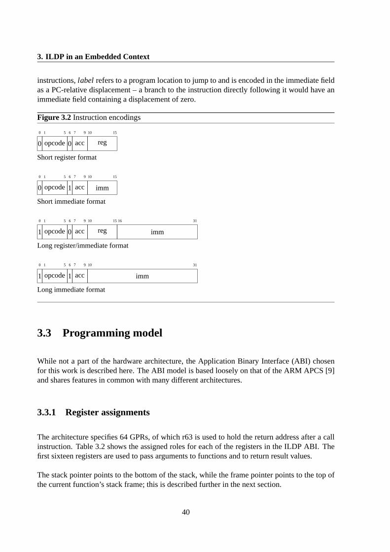
3. ILDP in an Embedded Context
instructions,label refers to a program location to jump to and is encoded in the immediate fieldas a PC-relative displacement – a branch to the instruction directly following it would have animmediate field containing a displacement of zero.
Figure 3.2 Instruction encodings
0 1 5 6 7 9 10 15
0 opcode0 acc reg
Short register format
0 1 5 6 7 9 10 15
0 opcode1 acc imm
Short immediate format
0 1 5 6 7 9 10 15 16 31
1 opcode0 acc reg imm
Long register/immediate format
0 1 5 6 7 9 10 31
1 opcode1 acc imm
Long immediate format
3.3 Programming model
While not a part of the hardware architecture, the Application Binary Interface (ABI) chosenfor this work is described here. The ABI model is based loosely on that of the ARM APCS [9]and shares features in common with many different architectures.
3.3.1 Register assignments
The architecture specifies 64 GPRs, of which r63 is used to hold the return address after a callinstruction. Table3.2 shows the assigned roles for each of the registers in the ILDP ABI. Thefirst sixteen registers are used to pass arguments to functions and to return result values.
The stack pointer points to the bottom of the stack, while the frame pointer points to the top ofthe current function’s stack frame; this is described further in the next section.
40

3.3 Programming model
Syntax Semantics
Dyadic ALU instructions ; op is one of add, sub, rsb (reverse subtract), and, ior (logical or),xor, mul<op> a<i> <= a<i>, r<j> Ai := Ai op Rj
<op> a<i> <= a<i>, #<imm> Ai := Ai op imm<op> a<i> <= r<j>, #<imm> Ai := Rj op imm<op>.c r<j> <= a<i>, #<imm> Rj := Ai op imm
Shift instructions; op is one of sll (shift left logical), srl (shift right logical),sra (shift right arithmetic), rol (rotate left)<op> a<i> <= a<i>, r<j> Ai := Ai op Rj
<op> a<i> <= a<i>, #<imm> Ai := Ai op imm
Monadic ALU instructions ; op is one of abs, inv<op> a<i> <= r<j> Ai := op Rj
<op> a<i> <= a<i> Ai := op Ai
Comparison instructions; cond is one of eq, ne, le, lt, ge, gt (all signed)c<cond> a<i> <= a<i>, r<j> Ai := Ai cond Rj
c<cond> a<i> <= a<i>, #<imm> Ai := Ai cond imm
Move instructionsmov a<i> <= r<j> Ai := Rj
mov a<i> <= #<imm> Ai := immmova a<i> <= @<label> Ai := labelmov r<j> <= a<i> Rj := Ai
mov.c r<j> <= a<i> Rj := Ai
Load/store instructionsldr a<i> <= [a<i>+#imm] Ai := MEM[Ai + imm]ldr a<i> <= [r<j>+#imm] Ai := MEM[Rj + imm]str [a<i>+#imm] <= r<j> MEM[Ai + imm] := Rj
str [r<j>+#imm] <= a<i> MEM[Rj + imm] := Ai
Branch instructionsb<cond> @<label> ? a<i>, r<j> PC := label iff Ai cond Rj
b<cond> @<label> ? a<i>, #0 PC := label iff Ai cond0br @label PC := label
Jump/call instructionsjmp a<i> PC := Ai
jmp r<j> PC := Rj
call a<i> R63 := next_PC;PC := Ai
call r<j> R63 := next_PC;PC := Rj
Other instructionsnop Does nothingsyscall System call
Table 3.1: The ILDP instruction set
41
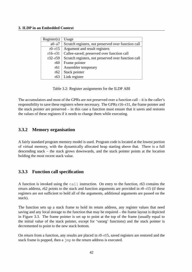
3. ILDP in an Embedded Context
Register(s) Usagea0–a7 Scratch registers, not preserved over function call
r0–r15 Argument and result registersr16–r31 Callee-saved; preserved over function callr32–r59 Scratch registers, not preserved over function call
r60 Frame pointerr61 Assembler temporaryr62 Stack pointerr63 Link register
Table 3.2: Register assignments for the ILDP ABI
The accumulators and most of the GPRs are not preserved over a function call – it is the caller’sresponsibility to save these registers where necessary. The GPRs r16–r31, the frame pointer andthe stack pointer are preserved – in this case a function must ensure that it saves and restoresthe values of these registers if it needs to change them while executing.
3.3.2 Memory organisation
A fairly standard program memory model is used. Program code is located at the lowest portionof virtual memory, with the dynamically allocated heap starting above that. There is a fulldescending stack – the stack grows downwards, and the stack pointer points at the locationholding the most recent stack value.
3.3.3 Function call specification
A function is invoked using thecall instruction. On entry to the function, r63 contains thereturn address, r62 points to the stack and function arguments are provided in r0–r15 (if theseregisters are not sufficient to hold all of the arguments, additional arguments are passed on thestack).
The function sets up a stack frame to hold its return address, any register values that needsaving and any local storage to the function that may be required – the frame layout is depictedin Figure3.3. The frame pointer is set up to point at the top of the frame (usually equal tothe initial value of the stack pointer, except for ‘vararg’ functions) and the stack pointer isdecremented to point to the new stack bottom.
On return from a function, any results are placed in r0–r15, saved registers are restored and thestack frame is popped, then ajmp to the return address is executed.
42

3.4 Microarchitecture
Figure 3.3Function stack frame layout
FP=⇒
Saved return address
Saved frame pointer
Callee-saved registers (if used)r31...r16
Local variable storage
Outgoing arguments to functions(beyond those placed in registers)
SP=⇒
3.4 Microarchitecture
The ILDP architecture is outlined in Figure3.4. The front-end fetch and issue pipeline is fourinstructions wide, and is split into four stages:
1) Instruction fetch
2) Decode (termed ‘parcel’ as the fetched parcels have to be reassembled into completeinstructions)
3) General-purpose register rename
4) Instruction issue/steering (also known as accumulator renaming)
The front-end pipeline issues instructions to a set of eight processing elements (PEs) where theyare executed, and then a standard in-order commit mechanism is used to retire instructions. Inthis implementation, all parts of the design run at the same speed from a single clock, but dueto the decoupling between the issue pipeline and the PEs, these could potentially be clocked atdifferent speeds.
43

3. ILDP in an Embedded Context
Figure 3.4The ILDP architecture, as outlined by Kim and Smith
Fetch Parcel Rename Steer
PE L1
PE L1
.
.
.
L2
FIFO
FIFO
Reg
iste
r N
etw
ork
The instruction fetch pipeline stage loads a 128-bit word from the instruction cache and placesit into a fetch buffer. The fetch buffer is 192 bits wide and holds any undecoded parcels fromthe previous cycle (the parcel logic can consume between 64 and 128 bits in a cycle) as well asthe newly fetched instruction word. The fetch logic aligns the new data correctly when placingit in the buffer, so that newly fetched parcels appear in sequence immediately after older ones.
The parcel pipeline stage analyses the fetched data in 16-bit blocks and reassembles them intofour instructions – this procedure is made relatively simple as the first bit of a parcel indicateswhether the instruction is encoded in 16 or 32 bits. Since the instructions are variable length,often not all of a 128-bit word will be consumed at once – the parcel logic can store ‘leftover’parcels back into the fetch buffer and assemble them in the following cycle along with a newlyfetched word. The parcel stage also performs decoding of the instruction opcode.
In the register rename stage, any of the 64 GPRs used by the instructions are renamed onto aphysical set of 128 registers, using rename logic as in a standard superscalar – although the factthat most instructions use one GPR (or none) rather than two or three as in a standard processorallows the rename logic to be simpler and reduces the number of ports required on the renamemap. The pipeline can stall in the rename stage if the register rename map fills – the issuepipeline will then wait for instructions to commit and free up physical registers for renaming.
The steering pipeline stage allocates instruction strands to processing elements by renamingthe eight ISA accumulator registers onto the eight physical accumulators within the processingelements. When an instruction starting a new strand is processed by the steering logic, it isallocated to a free processing element (if there is more than one, the one with the emptiestissue FIFO is chosen). Further instructions for a strand are issued to whichever PE is currentlyexecuting that strand. After issuing the final instruction of a strand (flagged as such using the‘.c’ suffix to the opcode), the PE is marked as being available for allocation once more.
44
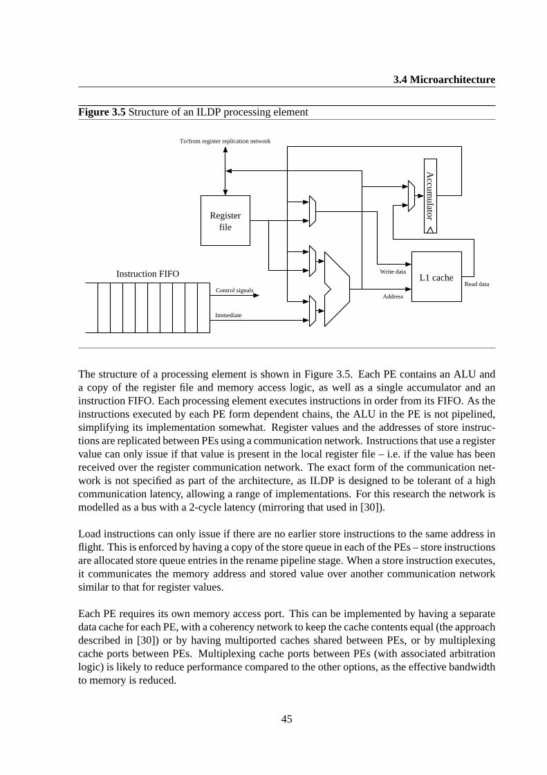
3.4 Microarchitecture
Figure 3.5Structure of an ILDP processing element
Instruction FIFO
Immediate
Control signals
To/from register replication network
L1 cache
Registerfile
Accum
ulator
Address
Write data
Read data
The structure of a processing element is shown in Figure3.5. Each PE contains an ALU anda copy of the register file and memory access logic, as well as a single accumulator and aninstruction FIFO. Each processing element executes instructions in order from its FIFO. As theinstructions executed by each PE form dependent chains, the ALU in the PE is not pipelined,simplifying its implementation somewhat. Register values and the addresses of store instruc-tions are replicated between PEs using a communication network. Instructions that use a registervalue can only issue if that value is present in the local register file – i.e. if the value has beenreceived over the register communication network. The exact form of the communication net-work is not specified as part of the architecture, as ILDP is designed to be tolerant of a highcommunication latency, allowing a range of implementations. For this research the network ismodelled as a bus with a 2-cycle latency (mirroring that used in [30]).
Load instructions can only issue if there are no earlier store instructions to the same address inflight. This is enforced by having a copy of the store queue in each of the PEs – store instructionsare allocated store queue entries in the rename pipeline stage. When a store instruction executes,it communicates the memory address and stored value over another communication networksimilar to that for register values.
Each PE requires its own memory access port. This can be implemented by having a separatedata cache for each PE, with a coherency network to keep the cache contents equal (the approachdescribed in [30]) or by having multiported caches shared between PEs, or by multiplexingcache ports between PEs. Multiplexing cache ports between PEs (with associated arbitrationlogic) is likely to reduce performance compared to the other options, as the effective bandwidthto memory is reduced.
45

3. ILDP in an Embedded Context
3.5 Complexity
This architecture should provide several benefits over an out-of-order architecture in terms ofcomplexity. Since each processing element only communicates values through the register file,far fewer forwarding paths are required – forwarding paths are only needed within a PE, notbetween them as in a standard architecture. The inter-PE communication network can be im-plemented in various ways depending on performance and area requirements, whereas standardforwarding paths scale quadratically with issue width and linearly with pipeline depth.
As instructions are issued in-order within PEs, and issued to PEs depending on their accumu-lator, the issue logic will also be far simpler than a full superscalar processor, eliminating theneed for a reorder buffer etc. Thus the complexity of the ILDP architecture should be similar tothat of an in-order superscalar architecture, but should provide performance similar to an out-of-order system [30]. This should make it well suited to embedded applications, and is analysedin greater depth in this section.
Fully analysing the complexity of a processor design is a large and complicated task, generallyrequiring implementation of the whole design at the circuit level. Most microprocessors arefull custom designs, so to accurately assess complexity of architectural modifications a fullcustom design would be necessary, which is beyond the scope of many research projects. Asimpler approach is a more qualitative analysis, breaking down the design and looking at thecomplex structures that are likely to affect the critical path and how they scale with feature sizeand architectural parameters. In such an analysis, Palacharla [42] investigated the followingcomponents of modern CPU designs:
• Register rename logic
• Issue window dependency checking logic
• Instruction issue logic
• Register file
• Data bypass paths and logic
Palacharla identifies the issue window logic and bypass paths in a superscalar processor as beingmost likely to affect performance in future architectures due to not scaling well with featuresize. The ILDP architecture eliminates the complex reorder buffer of a superscalar architecturein favour of multiple small simple issue FIFOs.
46

3.6 Complexity analysis
3.6 Complexity analysis
The following sections analyse the components listed above, looking at the blocks contribut-ing to their complexity, and how architectural parameters affect complexity. The analysis isperformed for typical examples of:
• The ILDP design
• A superscalar architecture
• A simple scalar architecture
3.6.1 Register rename logic
Register rename logic is composed of several blocks:
• The map tablewhich holds the current mappings between logical and physical registernumbers, generally implemented as a RAM indexed on logical register number. There isalso a table holding previous register mappings, used when the processor has to roll backexecution after an exception.
• A free register list, holding the tags of all physical registers available for allocation.
• Logic to allocate new registers from the free register list to instructions that write tological registers.
• Logic to detect interdependencies between instructions in the block currently being re-named and identify those that should read physical registers allocated in the current cycleinstead of those specified in the map table.
• A multiplexer to select the correct physical register numbers for each instruction and passthe results along the pipeline.
The size of the map table scales with the number of logical registers in the ISA. Its complexityalso depends on the issue width of the processor and the number of operands per instruction inthe ISA.
A typical superscalar processor of issue widthn with instructions that haver input operands andw output operands will requiren× r read ports andn×w write ports to the map table. A 4-wayissue processor with a typical 3-operand instruction set will have a map table with 8 read portsand 4 write ports.
47
3. ILDP in an Embedded Context
By contrast, the ILDP architecture can either read or write one register per instruction, so for 4-way issue just 4 read/write ports would be required, eliminating eight decoders and sets of wordlines compared to a 4-way issue processor. This reduction in logic and wires should reducepower consumption and also make the block smaller, reducing the overall delay. A separate setof renaming logic is used in the steering stage to rename the accumulator registers – this alsorequires only 4 read/write ports, and will only contain eight entries.
A scalar CPU does not use register renaming, and thus can entirely eliminate rename logic. TheILDP architecture will necessarily be more complex than a scalar processor in this regard.
3.6.2 Issue window dependency logic
In a standard superscalar, the instruction window holds all in-flight instructions. Instructionscan only be issued once all their input operands are available; the dependency checking logic isresponsible for flagging instructions ready as these operands become available. Each cycle thephysical register numbers of the data that has been computed are checked against the waitinginstructions via an associative lookup – any instructions that match are marked as such. Onceall operands are available, an instruction can be issued.
The instruction window in a superscalar processor is implemented as an associative memory.Each memory row can hold one instruction, with the associative section containing the datatags for the instruction’s operands and bits indicating when operands are available. Ann-wayissue processor requiresn associative ports for writing newly available data tags, and each rowthen needsn comparators per operand to check for matches. The larger the issue width, thelarger each row will be, and thus the length of the bitlines in the memory will grow. Overall thedelay of this block is quadratic in both the issue width and window size, and at smaller featuresizes the timing tends to become dominated by wire delays and thus scales poorly with modernprocesses.
The ILDP architecture eliminates the instruction window; instead instructions are placed intoFIFOs and issue from the FIFO heads. Dependency checking only needs to be done on theinstructions at the heads of each FIFO, and as each instruction only uses a single register oper-and, there needs to be only a single comparator per processing element, rather than 8 per row ofthe instruction window as in a 4-way superscalar (a 64-instruction window would then require512 comparators and associated logic). This should make the instruction window logic muchsmaller in the ILDP design – the total size of the instruction FIFOs will be similar to that of thesuperscalar instruction window, but the dependency checking logic is greatly reduced.
A scalar processor has no instruction window logic (and also no instruction FIFOs).
48

3.6 Complexity analysis
3.6.3 Instruction issue logic
A standard superscalar must identify instructions available for execution and allocate them tofunctional units for execution, with the oldest such instructions being executed first. The de-pendency checking logic above will mark instructions as being available, and then the issuelogic is generally constructed using anarbiter tree. This has an O(logn) time complexity, and aspace complexity of O(nlogn), with n being the instruction window size.
The ILDP architecture, in contrast, issues instructions into the set of FIFOs for the processingelements. The logic for this is basically a second set of register renaming logic, this timerenaming the accumulator registers onto the set of processing elements. As the set of FIFOswill generally be small (e.g. eight FIFOs in [30]), this logic block (termed the steering logic)should be small and fast compared to an arbiter tree for a large instruction window – it willcertainly be faster than the logic for renaming general-purpose registers, due to the smaller mapsize, so should not form part of the critical path.
Within a PE, the issue logic simply executes the instruction at the head of the FIFO if it eitherdoes not depend on a register value, or depends on a register value that is available (see3.6.4).
In a scalar processor, the issue logic generally consists of a scoreboard to track which registervalues are currently within the register file and which are in flight, along with logic to choosewhich forwarding paths (if any) to use and interlock logic to halt the pipeline, inserting a bubble,when there are data hazards requiring a stall.
3.6.4 Register file
A standard processor architecture will require one read port to the register file for each inputregister operand of each executing instruction and one write port for each output operand. Thisis basically the same as the register rename map – for a processor with a 4-way execute band-width, executing 3-operand instructions, 8 read ports and 4 write ports will be required to theregister file. In order to reduce the register file complexity, several superscalar architecturesmake multiple copies of the register file, with fewer read ports per file, e.g. an 8 read port, 4write port register file could be split into two copies with 4 read ports and 4 write ports each.Writes are replicated to each copy of the register file, while reads are distributed across thecopies. This increases the total die area usage, but reduces the delay of the register file logic.
Since each PE in the ILDP architecture has a separate register file, each individual file needsfewer ports than a superscalar processor with a single file – this is similar to a superscalarprocessor with a split register file. Each instruction can either read or write a single register, andregister values can be received over the register communication network. As such, the ILDPprocessor requires only one read/write port and enough write-only ports to handle the bandwidth
49

3. ILDP in an Embedded Context
of the register network on each register file (the read/write port could possibly be replaced bya read-only port, as register writes from the PE must go through the register network anyway,and could be written using one of the dedicated write ports).
This compares favourably with a scalar RISC architecture, which will generally have two readports and one write port. The ILDP register files should therefore be small (for the number ofregisters they contain) and fast, but require replication across each PE, increasing total siliconarea for the design.
3.6.5 Bypass paths
A standard superscalar processor with issue widthw andn pipeline stages requiring bypass (anystages from the first execution stage before register writeback) will need 2nw2 bypass paths and2n multiplexers to select the appropriate path for use. For modern systems with deep pipelines,complex logic and large issue widths this leads to having many long wires with associateddelays. As feature sizes drop, these delays scale badly and can easily become the limiting factoron performance.
The ILDP architecture separates the bypass paths into local paths within a PE and the global re-gister value communication network between PEs. Each PE requires only one or two bypasses,which should be fairly short (and thus fast). The ILDP architecture is designed to be tolerantof delays in the the register communication network – [30] shows only a small performancedegradation when the delay is increased from zero to two cycles. This tolerance allows variousdifferent implementations to be used for this interconnect, depending on area, power and cycletime constraints.
A scalar processor will also have 2nw2 bypass paths, but with aw value of 1. For a typicalfive-stage pipeline,n is 2, giving four total bypass paths.
3.6.6 Data caches
Data caches are generally hard to scale for high issue widths – adding additional ports to afirst-level cache tends to increase the delay significantly. Modern designs tend either to use asingle-cycle L1 data cache with one read and one write port or a multi-cycle pipelined cachewith two read ports and one write port. Superscalar designs often avoid the need to implementadditional read ports by usingnon-blockingcaches – a single-ported non-blocking cache doesnot need to stall when a read access causes a miss; later instructions can continue to use the readport while the miss is being serviced.
50
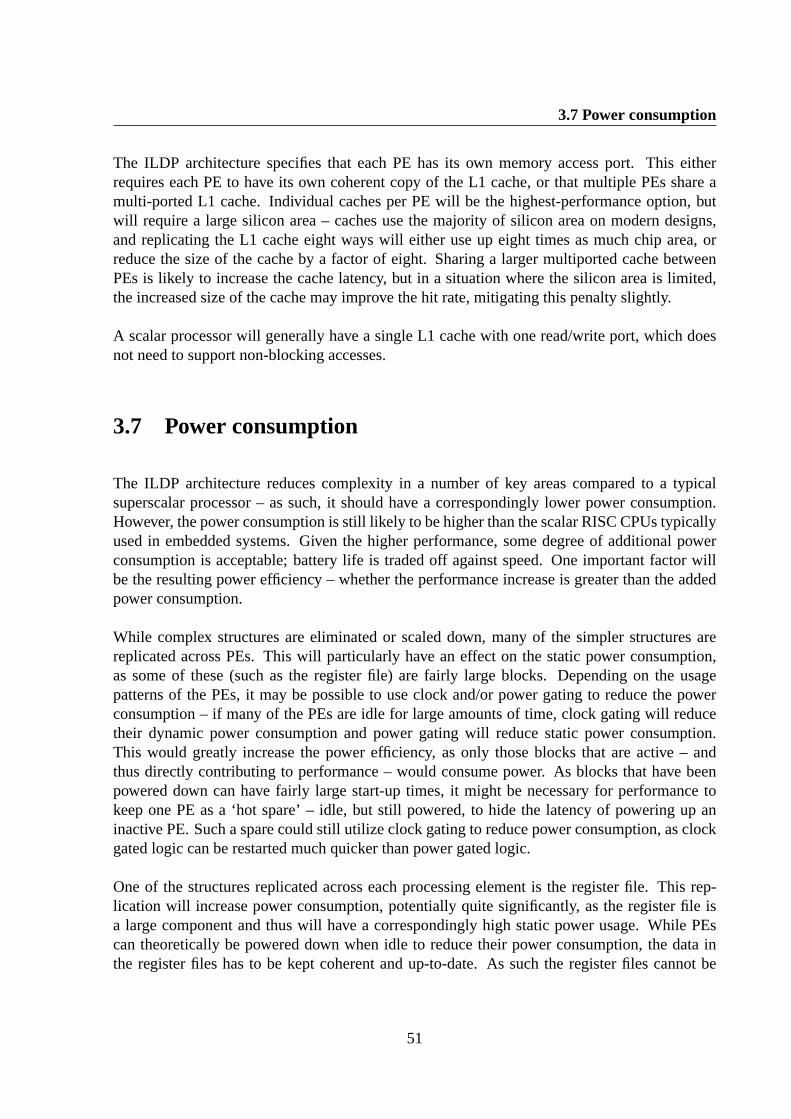
3.7 Power consumption
The ILDP architecture specifies that each PE has its own memory access port. This eitherrequires each PE to have its own coherent copy of the L1 cache, or that multiple PEs share amulti-ported L1 cache. Individual caches per PE will be the highest-performance option, butwill require a large silicon area – caches use the majority of silicon area on modern designs,and replicating the L1 cache eight ways will either use up eight times as much chip area, orreduce the size of the cache by a factor of eight. Sharing a larger multiported cache betweenPEs is likely to increase the cache latency, but in a situation where the silicon area is limited,the increased size of the cache may improve the hit rate, mitigating this penalty slightly.
A scalar processor will generally have a single L1 cache with one read/write port, which doesnot need to support non-blocking accesses.
3.7 Power consumption
The ILDP architecture reduces complexity in a number of key areas compared to a typicalsuperscalar processor – as such, it should have a correspondingly lower power consumption.However, the power consumption is still likely to be higher than the scalar RISC CPUs typicallyused in embedded systems. Given the higher performance, some degree of additional powerconsumption is acceptable; battery life is traded off against speed. One important factor willbe the resulting power efficiency – whether the performance increase is greater than the addedpower consumption.
While complex structures are eliminated or scaled down, many of the simpler structures arereplicated across PEs. This will particularly have an effect on the static power consumption,as some of these (such as the register file) are fairly large blocks. Depending on the usagepatterns of the PEs, it may be possible to use clock and/or power gating to reduce the powerconsumption – if many of the PEs are idle for large amounts of time, clock gating will reducetheir dynamic power consumption and power gating will reduce static power consumption.This would greatly increase the power efficiency, as only those blocks that are active – andthus directly contributing to performance – would consume power. As blocks that have beenpowered down can have fairly large start-up times, it might be necessary for performance tokeep one PE as a ‘hot spare’ – idle, but still powered, to hide the latency of powering up aninactive PE. Such a spare could still utilize clock gating to reduce power consumption, as clockgated logic can be restarted much quicker than power gated logic.
One of the structures replicated across each processing element is the register file. This rep-lication will increase power consumption, potentially quite significantly, as the register file isa large component and thus will have a correspondingly high static power usage. While PEscan theoretically be powered down when idle to reduce their power consumption, the data inthe register files has to be kept coherent and up-to-date. As such the register files cannot be
51

3. ILDP in an Embedded Context
powered down – they will continue to consume not only static power, but also dynamic powerdue to writes distributed over the register replication network.
3.8 Summary
This chapter has shown that while the ILDP architecture utilizes many superscalar processingtechniques, it eliminates or scales down many of the higher-complexity structures of a super-scalar processor, bringing its complexity closer to that of a typical embedded processor, at anincreased speed. The performance of the design is analysed quantitatively in the next chapter.
52

Evaluating ILDP 4
This chapter evaluates the performance of the ILDP architecture compared to typical embeddedprocessors and explores the effect various architectural parameters have on performance.
4.1 Performance vs other embedded architectures
The initial investigation was to evaluate the performance of the ILDP architecture outlined inKim and Smith [30] under embedded workloads. Their work executes Alpha binaries usingdynamic code translation in the style of the Transmeta Crusoe [8; 33]. For an embedded sys-tem, however, dynamic translation at the hardware level adds extra complexity, especially sincebinary compatibility is generally less of an issue for these applications – particularly giventhe growing popularity of bytecode languages such as Java and .NET, which require dynamicinterpretation or compilation regardless.
4.1.1 Methodology
To evaluate the ILDP architecture presented in Chapter3, a set of benchmarks were run using asimulation of the ILDP processor and compared to results of the same benchmarks run on otherarchitectures. Since the possible clock speed of a processor depends heavily on the detailedcircuit-level design, which is beyond the scope of these evaluations, the results are comparedbased on the total number of clock cycles used to execute the benchmark workloads. Based onthe complexity analysis in Section3.6, it is assumed that similar clock speeds could be attainedby ILDP and the other tested architectures.
4.1.2 Compiler toolchain
In order to evaluate the architecture, it was necessary to be able to generate instruction code toexecute; thus it was necessary to target a compiler and associated toolchain to the new ISA. TheGNU Compiler Collection (GCC) was initially evaluated but developing a new backend seemed
53

4. Evaluating ILDP
to be an overly involved process so other options were investigated. The SUIF [2] project lookedpromising, providing an open modular compiler framework, along with Machine-SUIF [53], aframework for creating compiler backends to generate machine code.
Using the SUIF framework, I created a basic compiler for the ILDP architecture. There weresome problems adapting the register allocator to handle the hierarchical register file and so anew pass was developed for the compiler which would annotate the code with hints to allowregister allocation to take place. This was able to compile simple test programs into the ILDPISA. The New Jersey Machine-Code Toolkit [45; 46] was used to generate object code – givena high-level description of the instruction encodings, the NJMCT will generate code to generateinstructions in binary format. The GNU BFD library (part of the binutils package) was thenused to generate ELF object files containing the compiled code.
In order to compile any benchmark suites, a C library was required – the uClibc library seemedlike an appropriate choice, as it is designed to be smaller and more readily portable than theusual GNU libc. When trying to compile the uClibc library however I found that my compilersystem did not function well for compiling anything larger than basic test programs due toproblems with data layout and linking, and that the library code contained a number of GCC-specific language features which were tricky to work around. I also found the C front-end toSUIF to have a number of problems compiling modern C programs. Unfortunately this front-end is based on a commercial compiler and is only available as a closed-source binary module,and thus cannot be modified. As such, I investigated alternatives to the main compiler front-endthat could alleviate these problems.
Ultimately, a toolchain based on the GNU compiler and binutils was developed (the document-ation in [40] proved invaluable), which compiles directly to the ISA of the simulated archi-tecture. The CGEN [11] tool was used to generate an assembler, disassembler and a basicfunctional simulator from a high-level description of the instruction set – similar to the NJMCTused earlier, but the description includes not only the instruction encoding, but also the assem-bler syntax and semantics – making it much simpler to generate a full toolchain with minimaladditional effort. The newlib C library was used, as this proved to be even simpler to port tonew architectures than the uClibc library, and also supports ‘multilib’ compilation which allowsseveral variants of the ISA to be used and to have toolchains automatically built for all variants;this proved useful for the work in Chapter5.
The strand allocation in the compiler was handled using the existing GCC register allocationmechanism – for each instruction in the ISA, a pattern is provided to the compiler specifying theallowable register types for each operand. The compiler contains an internal constraint solverwhich tries to allocate registers in such a way as to maximise performance – usually by minim-ising the number of move instructions that need to be inserted. In practice, the compiler provedto have a certain amount of difficulty handling some of the constraints peculiar to ILDP – inparticular, it proved very difficult to prevent the compiler from trying to generate accumulator-to-accumulator move instructions. Also, the constraint that a store instruction could either storean accumulator value to a register address or a register value to an accumulator address was
54

4.1 Performance vs other embedded architectures
impossible to specify. A number of fixups had to be created to work around these compilerissues.
Ultimately the code generated by the compiler was often not optimal for the architecture – inorder to improve the generated code the register allocator would need to made aware of theconcept of strands. Unfortunately there was not enough time within the scope of this researchto invest in further compiler developments. The performance of ILDP versus other architectures(with more mature and better optimised compiler backends) is likely to suffer as a result of this.
4.1.3 Benchmarks
I evaluated a number of benchmark suites to see which would be most suitable. The SPECint[20] suite is most commonly used for evaluating processor architectures, but is targeted at high-end systems – the SPECint2000 suite uses a working set of 256MB, too large for an embeddedsystem for which typically the total system memory will be in the order of 64MB. I felt that abenchmark suite targeted specifically at evaluating embedded systems would be more appropri-ate for my research.
The EEMBC suite is the industry standard for embedded benchmarking, but is only availableafter purchase of a closed licence with severe restrictions on the publishing of results. I felt thatthis would probably be inappropriate for my initial research, and that something more readilyavailable would be more beneficial for academic work.
MiBench [17] is a freely available embedded benchmark suite based on open-source softwarepackages. I decided to use this suite for evaluation as it was free and seemed fairly easy to setup and use.
4.1.4 Simulation
The SimpleScalar simulation environment [5] was investigated for performance evaluation, butproved to be heavily tied in to a standard superscalar processor model – while it could be usedto simulate the other architectures, it was not suitable to simulate the ILDP design. Instead, acustom cycle-accurate software simulator was created to run the code for the ILDP model. Eachcircuit block within the design was implemented as a block of software, suitably parameterizedso that architectural parameters could be changed and evaluated. An execution framework wascreated that would allow automated execution of the benchmark suite over a range of paramet-ers, and would allow running benchmarks on other architectures for comparison purposes.
For the initial experiments the architectural parameters of the ILDP model were set as in [30],i.e. with a 4-way issue/retire width and 8 FIFOs/PEs. The register communication network was
55

4. Evaluating ILDP
modelled as a simple bus between the PEs, with a latency of two cycles to transmit the valuesbetween PEs (plus an additional cycle for the PEs to write the data into the register file). Theinstruction FIFOs were set to be of unlimited size, and the register communication networkcould transmit an unlimited number of values in a single cycle. This allowed the simulationsto run assuming these parameters had been set to a suitable level to allow as close to optimumperformance as possible. Sections4.3.3and4.3.4explore the effect these parameters have onperformance.
4.1.5 Results
The performance of the baseline ILDP architecture was simulated versus a model of the ARMSA1100 and a PowerPC model, chosen to approximately represent the PPC405 core. For theSA1100 model, the Simplescalar-ARM [5] simulation system was used, and for the PowerPCsimulations Dynamic Simplescalar was used [25] – while Simplescalar-ARM is supplied with aconfiguration for the SA1100, the configuration for the PowerPC model had to be created basedon published specifications [26], and the performance of these models may be less accurate as aresult. A model for the PPC440 core [27] was attempted, but it proved difficult to set the para-meters for the superscalar execution and it was not possible to test the accuracy of the modelagainst a real implementation, thus making it impossible to use for comparison. The measuredperformance values are based on the number of cycles taken to execute each benchmark – itis assumed that the achievable clock speeds for these architectures will be similar. The bench-marks were compiled with the same libraries and toolchain for all architectures (the newlib Clibrary and GCC version 3.3.2). Due to limitations in the set of the system calls implementedin newlib, not all of the benchmark tests would link – the results presented are from the 20 testswhich could be compiled. The same set of compiler flags were used for each architecture –most of the tests were compiled using ‘-O3 ’, but due to compiler issues thetiff tests had to becompiled with ‘-O2 ’ and thejpegtests were compiled using ‘-O ’.
The results of these simulations can be seen in Figure4.1– the results shown are normalised tothe average execution time for each test. It can be seen that, on average, there is a 18.5% speedupover the ARM. Thepatricia benchmark shows the greatest improvement – about 172% – whilethe adpcm (enc)and tiffdither tests actually run approximately 10% slower than the ARM.Compared to the PPC405 model, ILDP performs on average 52.8% better, ranging from 23.3%onadpcm (enc)to 104% better ontiff2rgba.
These results show that the 4-way issue ILDP model performs better than the single-issue ARM,but not by a very large margin – this is somewhat disappointing, as [30] shows the performanceof ILDP to be similar to that of a 4-way out-of-order architecture. Figure4.2shows that in thesesimulations the ILDP architecture executed more total instructions than the other architectures –in some cases more than twice as many. This is attributed in part to the need for additional moveinstructions in the strand-based architecture, in part to the density of three-operand instructioncode over the two-operand ILDP instructions (in an extreme case, an ARM can execute an
56

4.1 Performance vs other embedded architectures
Par
amet
erIL
DP
AR
MP
PC
405
Issu
ew
idth
4-w
ay1-
way
1-w
ayE
xecu
tion
wid
th8-
way
1-w
ay1-
way
Bra
nch
pred
ictio
n16
Ken
try,
12-b
itgl
obal
hist
ory
gsha
reA
llbr
anch
espr
edic
ted
nott
aken
2Ken
try
bim
odal
L1I-
cach
eP
erfe
ct1-
cycl
ela
tenc
y16
KB
32-w
ayas
soci
ativ
e,32
Blin
esi
ze,1
-cyc
lela
tenc
y,fif
ore
plac
emen
tP
erfe
ct1-
cycl
ela
tenc
y
L1D
-cac
he8K
B2-
way
asso
ciat
ive,
64B
line
size
,1-
cycl
ela
tenc
y,ra
ndom
repl
acem
ent
16K
B32
-way
asso
ciat
ive,
32B
line
size
,1-c
ycle
late
ncy,
fifo
repl
acem
ent
32K
B2-
way
asso
ciat
ive,
32B
line
size
,1-
cycl
ela
tenc
y,LR
Ure
plac
emen
tL2
cach
e25
6KB
2-w
ayas
soci
ativ
e,12
8Blin
esi
ze,
8-cy
cle
late
ncy,
rand
omre
plac
e-m
ent
none
256K
B8-
way
asso
ciat
ive,
64B
line
size
,8-c
ycle
late
ncy,
LRU
repl
acem
ent
Mem
ory
72-c
ycle
late
ncy
72-c
ycle
late
ncy
72-c
ycle
late
ncy
Tabl
e4.
1:A
rchi
tect
ural
para
met
ers
for
sim
ulat
ion
57

4. Evaluating ILDP
Figure 4.1Performance of ILDP compared to embedded processors
Nor
mal
ised
per
form
ance
0
0.2
0.4
0.6
0.8
1
1.2
1.4
1.6
1.8
adpc
m (
dec)
adpc
m (
enc)
bitc
ount
blow
fish
(dec
)
blow
fish
(enc
)
jpeg
(en
c)
crc3
2
dijk
stra
jpeg
(de
c)
gsm
(de
c)
gsm
(en
c)
patr
icia
rijnd
ael (
dec)
rijnd
ael (
enc)
sha
strin
gsea
rch
tiff2
bw
tiff2
rgba
tiffd
ither
tiffm
edia
n
AV
ER
AG
E
PPC405 ARM ILDP
Architecture
Figure 4.2Number of instructions executed, compared to ARM
Rel
ativ
e nu
mbe
r of
inst
ruct
ions
0
0.5
1
1.5
2
2.5
3
adpc
m (
dec)
adpc
m (
enc)
bitc
ount
blow
fish
(dec
)
blow
fish
(enc
)
cjpe
g
crc3
2
dijk
stra
djpe
g
gsm
(de
c)
gsm
(en
c)
patr
icia
rijnd
ael (
dec)
rijnd
ael (
enc)
sha
strin
gsea
rch
tiff2
bw
tiffd
ither
tiffm
edia
n
AV
ER
AG
E
ILDP PPC
Architecture
58

4.1 Performance vs other embedded architectures
Figure 4.3 IPC of tested processors
IPC
0
0.5
1
1.5
2
2.5
adpc
m (
dec)
adpc
m (
enc)
bitc
ount
blow
fish
(dec
)
blow
fish
(enc
)
cjpe
g
crc3
2
dijk
stra
djpe
g
gsm
(de
c)
gsm
(en
c)
patr
icia
rijnd
ael (
dec)
rijnd
ael (
enc)
sha
strin
gsea
rch
tiff2
bw
tiff2
rgba
tiffd
ither
tiffm
edia
n
AV
ER
AG
E
PPC405 ARM ILDP
Architecture
arithmetic operation and a shift between arbitrary registers in a single instruction, while theILDP can take up to four instructions for such an operation) and in part due to the compiler.The ILDP compiler is not optimised as well as the compilers for the other architectures – inthe original simulations thecrc benchmark ran approximately 10% slower than the ARM, butmanual analysis of the code suggested two peephole optimizations which were introduced tothe compiler, thus removing two instructions from the inner loop and increasing the overallperformance. In particular, the compiler implementation proved to have problems with the lackof an accumulator-to-accumulator move instruction and the operand formats for the load/storeinstructions.
The IPC attained by the ILDP architecture is much greater than that of the other architectures(as shown in Figure4.3) but performance is limited by the increased code size. An interestingcomparison would be running the ARM tests on code compiled for the Thumb architecture, asthe Thumb ISA has a number of restrictions similar to ILDP – shifts are performed as separateinstructions and most ALU operations are represented as two-operand instructions. Unfortu-nately the SimpleScalar-ARM simulator cannot execute Thumb code, so this comparison wasnot possible.
59

4. Evaluating ILDP
4.1.6 Conclusion
Overall, while the performance of the tested ILDP architecture is only moderately greater thanthe embedded processors used for comparison, the level of IPC achieved is significantly higher– assuming that the compiler could be further optimised in order to reduce the total number ofinstructions executed, the ILDP architecture should show much better performance.
4.2 Resource utilization
As manufacturing moves to smaller feature sizes, static power consumption is becoming moreand more of an issue. Idle circuitry wastes large amounts of power – circuits should either beutilized or powered down in order to get maximum power efficiency. Investigations were thusmade into how fully hardware resources are being utilized. If a hardware block is replicated inorder to support a certain issue width or execution width, but simulation shows the utilizationto be low, then possibly the width for that block is too high and the level of replication could bereduced without significant effect on performance.
4.2.1 Decode / Issue logic
The complexity of many components in the processor scale linearly or quadratically with theissue width of the processor. If the limiting factors in performance come from other aspects ofthe system – e.g. the execution width, delays from branch mispredictions or cache misses, orcode containing too little inherent parallelism – then having too high an issue width can meanthe issue pipeline is largely idle, wasting power and can reduce overall performance if the logicis on the critical path and the added complexity increases the cycle time.
Figure4.4shows the number of instructions processed by each stage of the issue pipeline pro-portionally in time. When running the benchmark suite on the 4-way issue model, it can beseen that the parcel (decode), rename and steer (issue) pipeline stages spend on average around35% of their time completely idle. This is attributed to the level of parallelism present in thebenchmarks – there is simply not enough ILP present in the code to sustain 4-way issue, thusthe issue logic runs ahead of the execution logic and will stall waiting for instructions to beconsumed. Analysing the IPC achieved on these benchmarks corroborates this – as shown inFigure4.3, the average IPC is only 1.56, and only thebitcountandshatests achieve more than2 IPC. These results indicate that the issue pipeline is only being utilized at about half capacityand that a 2-way issue pipeline might be sufficient to maintain performance on these bench-marks. If the issue width is too high, then the issue pipeline is using more logic than necessary,which will increase static power consumption. Section4.3.1explores the effects of issue widthon pipeline utilization.
60

4.2 Resource utilization
Figure 4.4Number of instructions processed by the parcel, rename and steer pipeline stages
% o
f tim
e
0
20
40
60
80
100
p p p p p p p p p p p p p p p p p p p p pr r r r r r r r r r r r r r r r r r r r rs s s s s s s s s s s s s s s s s s s s s
adpc
m (
dec)
adpc
m (
enc)
bitc
ount
blow
fish
(dec
)
blow
fish
(enc
)
cjpe
g
crc3
2
dijk
stra
djpe
g
gsm
(de
c)
gsm
(en
c)
patr
icia
rijnd
ael (
dec)
rijnd
ael (
enc)
sha
strin
gsea
rch
tiff2
bw
tiff2
rgba
tiffd
ither
tiffm
edia
n
AV
ER
AG
E
0 1 2 3 4
Number of instructions processed per cycle
4.2.2 Processing elements
As above, if the number of processing elements is too high compared to the other architecturalparameters, then they will be idle most of the time, wasting power and silicon area. A plot ofthe activity of the individual processing elements (Figure4.5) shows that only about 21% of thetime is spent executing instructions – most of the time is spent idle, waiting on GPR values fromother PEs (data stalls), or waiting on loads that are blocked by earlier stores (load conflicts).
The fact that the PEs spend much less than half their time executing implies that complexitysavings could be made by having fewer PEs (e.g. four instead of eight), and associating twoinstruction FIFOs and accumulators with each one. The PE would then execute from bothqueues in a round-robin fashion – for most of the time one of the queues would be empty orstalled, so there would be only a minor performance impact. Since each processing elementis independent, those PEs with empty FIFOs could be powered down which would allow highpeak execution rates while saving power. This option is explored in Section5.1.
61
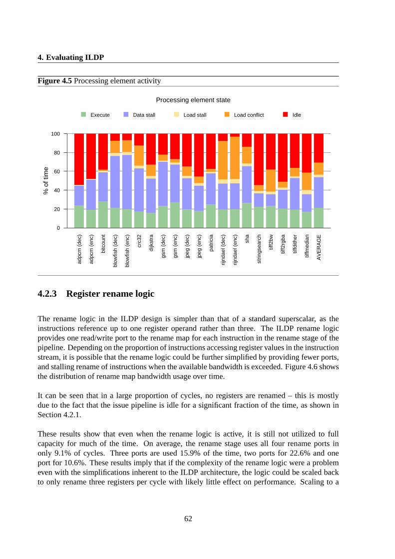
4. Evaluating ILDP
Figure 4.5Processing element activity
% o
f tim
e
0
20
40
60
80
100
adpc
m (
dec)
adpc
m (
enc)
bitc
ount
blow
fish
(dec
)
blow
fish
(enc
)
crc3
2
dijk
stra
gsm
(de
c)
gsm
(en
c)
jpeg
(de
c)
jpeg
(en
c)
patr
icia
rijnd
ael (
dec)
rijnd
ael (
enc)
sha
strin
gsea
rch
tiff2
bw
tiff2
rgba
tiffd
ither
tiffm
edia
n
AV
ER
AG
E
Execute Data stall Load stall Load conflict Idle
Processing element state
4.2.3 Register rename logic
The rename logic in the ILDP design is simpler than that of a standard superscalar, as theinstructions reference up to one register operand rather than three. The ILDP rename logicprovides one read/write port to the rename map for each instruction in the rename stage of thepipeline. Depending on the proportion of instructions accessing register values in the instructionstream, it is possible that the rename logic could be further simplified by providing fewer ports,and stalling rename of instructions when the available bandwidth is exceeded. Figure4.6showsthe distribution of rename map bandwidth usage over time.
It can be seen that in a large proportion of cycles, no registers are renamed – this is mostlydue to the fact that the issue pipeline is idle for a significant fraction of the time, as shown inSection4.2.1.
These results show that even when the rename logic is active, it is still not utilized to fullcapacity for much of the time. On average, the rename stage uses all four rename ports inonly 9.1% of cycles. Three ports are used 15.9% of the time, two ports for 22.6% and oneport for 10.6%. These results imply that if the complexity of the rename logic were a problemeven with the simplifications inherent to the ILDP architecture, the logic could be scaled backto only rename three registers per cycle with likely little effect on performance. Scaling to a
62

4.2 Resource utilization
Figure 4.6Distribution of rename map bandwidth usage over time
% o
f tim
e
0
20
40
60
80
100
adpc
m (
dec)
adpc
m (
enc)
bitc
ount
blow
fish
(dec
)
blow
fish
(enc
)
crc3
2
dijk
stra
gsm
(de
c)
gsm
(en
c)
jpeg
(de
c)
jpeg
(en
c)
patr
icia
rijnd
ael (
dec)
rijnd
ael (
enc)
sha
strin
gsea
rch
tiff2
bw
tiff2
rgba
tiffd
ither
tiffm
edia
n
AV
ER
AG
E
0 1 2 3 4
Rename map ports used
(a) Overall rename map port usage
% o
f tim
e
0
20
40
60
80
100
adpc
m (
dec)
adpc
m (
enc)
bitc
ount
blow
fish
(dec
)
blow
fish
(enc
)
crc3
2
dijk
stra
gsm
(de
c)
gsm
(en
c)
jpeg
(de
c)
jpeg
(en
c)
patr
icia
rijnd
ael (
dec)
rijnd
ael (
enc)
sha
strin
gsea
rch
tiff2
bw
tiff2
rgba
tiffd
ither
tiffm
edia
n
AV
ER
AG
E
0 1 2 3 4
Rename map ports used
(b) Rename map port write usage
63

4. Evaluating ILDP
rename width of two per cycle could have a more significant effect. This is evaluated further inSection4.3.2.
Figure4.6(b)shows the usage of the rename map for writes only. This clearly shows that farfewer ports are used for writing to the rename logic – for nearly 90% of the time one or fewerwrites are performed to the rename map, and more than two writes are performed in less than0.4% of cycles. If the complexity of implementing all read/write ports is significantly greaterthan implementing some ports as read-only, then reducing the write bandwidth to two is likelyto cause a negligible performance reduction, and reducing to a single read/write port may alsobe a reasonable performance trade-off.
4.3 Parameter space exploration
As well as evaluating the performance of the ILDP architecture using the parameters specifiedin [30], simulations were run exploring various different architectural parameters to see if aparticular combination would be better suited to the constraints of embedded design – redu-cing the potential complexity and/or power consumption without significantly impacting uponperformance.
4.3.1 Issue width
Experiments were conducted varying the issue bandwidth – as well as the original 4-way issuemodel, 2-way issue and single issue were evaluated. Figure4.7 shows the impact on perform-ance due to scaling the issue width. Going from 4-way issue to 2-way gives on average an 7.6%drop in performance, although there is a significant variation across the tests – thebitcountandshatests both lose more than 20% performance. This is unsurprising as both these tests wereable to average more than two instructions per clock on the 4-way architecture – as the testswith the highest level of parallelism achieved, they are likely to lose out most from the issuewidth reduction.
Another result of note from this graph is that thecrc32benchmark actually performs over 25%better when the issue width is width is set to 2-way issue. This result is unexpected and isreflected to a smaller degree in theblowfishtests, which show a slight performance improvementgoing from 4-way to 2-way issue. Analysis of the simulator statistics does not show any obviousexplanation for these results, and so it is assumed that for some of these tests, a larger issuewidth allowing deeper speculative execution can actually limit performance when executionpaths are mis-speculated – instructions are incorrectly executed and can, for example, causecache conflicts and pollute the cache with irrelevant data. At a lower issue width, the processorwould execute less deeply down speculative paths, and so be affected to a lesser degree. The
64
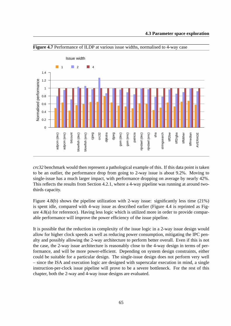
4.3 Parameter space exploration
Figure 4.7Performance of ILDP at various issue widths, normalised to 4-way case
Nor
mal
ised
per
form
ance
0
0.2
0.4
0.6
0.8
1
1.2
1.4
adpc
m (
dec)
adpc
m (
enc)
bitc
ount
blow
fish
(dec
)
blow
fish
(enc
)
cjpe
g
crc3
2
dijk
stra
djpe
g
gsm
(de
c)
gsm
(en
c)
patr
icia
rijnd
ael (
dec)
rijnd
ael (
enc)
sha
strin
gsea
rch
tiff2
bw
tiff2
rgba
tiffd
ither
tiffm
edia
n
AV
ER
AG
E
1 2 4
Issue width
crc32benchmark would then represent a pathological example of this. If this data point is takento be an outlier, the performance drop from going to 2-way issue is about 9.2%. Moving tosingle-issue has a much larger impact, with performance dropping on average by nearly 42%.This reflects the results from Section4.2.1, where a 4-way pipeline was running at around two-thirds capacity.
Figure 4.8(b) shows the pipeline utilization with 2-way issue: significantly less time (21%)is spent idle, compared with 4-way issue as described earlier (Figure4.4 is reprinted as Fig-ure4.8(a)for reference). Having less logic which is utilized more in order to provide compar-able performance will improve the power efficiency of the issue pipeline.
It is possible that the reduction in complexity of the issue logic in a 2-way issue design wouldallow for higher clock speeds as well as reducing power consumption, mitigating the IPC pen-alty and possibly allowing the 2-way architecture to perform better overall. Even if this is notthe case, the 2-way issue architecture is reasonably close to the 4-way design in terms of per-formance, and will be more power-efficient. Depending on system design constraints, eithercould be suitable for a particular design. The single-issue design does not perform very well– since the ISA and execution logic are designed with superscalar execution in mind, a singleinstruction-per-clock issue pipeline will prove to be a severe bottleneck. For the rest of thischapter, both the 2-way and 4-way issue designs are evaluated.
65

4. Evaluating ILDP
Figure 4.8Number of instructions in the parcel, rename and steer pipeline stages
% o
f tim
e
0
20
40
60
80
100
p p p p p p p p p p p p p p p p p p p p pr r r r r r r r r r r r r r r r r r r r rs s s s s s s s s s s s s s s s s s s s s
adpc
m (
dec)
adpc
m (
enc)
bitc
ount
blow
fish
(dec
)
blow
fish
(enc
)
cjpe
g
crc3
2
dijk
stra
djpe
g
gsm
(de
c)
gsm
(en
c)
patr
icia
rijnd
ael (
dec)
rijnd
ael (
enc)
sha
strin
gsea
rch
tiff2
bw
tiff2
rgba
tiffd
ither
tiffm
edia
n
AV
ER
AG
E
0 1 2 3 4
Number of instructions processed per cycle
(a) 4-way issue
% o
f tim
e
0
20
40
60
80
100
p p p p p p p p p p p p p p p p p p p p pr r r r r r r r r r r r r r r r r r r r rs s s s s s s s s s s s s s s s s s s s s
adpc
m (
dec)
adpc
m (
enc)
bitc
ount
blow
fish
(dec
)
blow
fish
(enc
)
cjpe
g
crc3
2
dijk
stra
djpe
g
gsm
(de
c)
gsm
(en
c)
patr
icia
rijnd
ael (
dec)
rijnd
ael (
enc)
sha
strin
gsea
rch
tiff2
bw
tiff2
rgba
tiffd
ither
tiffm
edia
n
AV
ER
AG
E0 1 2
Number of instructions processed per cycle
(b) 2-way issue
66

4.3 Parameter space exploration
Figure 4.9Effect on performance of removing register rename map ports
Per
form
ance
diff
eren
ce
−15%
−10%
−5%
0%
5%
adpc
m (
dec)
adpc
m (
enc)
bitc
ount
blow
fish
(dec
)
blow
fish
(enc
)
jpeg
(en
c)
crc3
2
dijk
stra
jpeg
(de
c)
gsm
(de
c)
gsm
(en
c)
patr
icia
rijnd
ael (
dec)
rijnd
ael (
enc)
sha
strin
gsea
rch
tiff2
bw
tiff2
rgba
tiffd
ither
tiffm
edia
n
AV
ER
AG
E
2 3
Number of register rename map ports
4.3.2 Rename bandwidth
If the added complexity of the rename logic due to issue width turns out to be greater thanthat of the other pipeline stages, it may be beneficial to reduce the width of the rename stagewhile leaving the rest of the issue pipeline at a 4-way width. Section4.2.3shows that for muchof the time the full number of ports on the register rename map are not used. This sectionevaluates the effect on performance of reducing the number of ports on the map, thus limitingthe peak rename bandwidth. If instructions enter the rename stage requiring more ports than areavailable, the later instructions will have to be stalled. Experiments were conducted varying thenumber of rename map ports.
Figure4.9shows the effect on performance of reducing the number of ports implemented in therename map. When the number of ports is reduced to three, very little variation in performancecan be observed. The worst affected test isadpcm (dec)which performs slightly under 3%slower. On average, the three-port case achieves 99.8% of the performance of the baseline 4-port case. With only two rename map ports, a larger performance reduction is observed – whilemany tests perform to within 1% of the baseline model, some tests are more than 10% slower(theshatest performs 14% worse). On average, with only two rename map ports, 97% of the4-port performance is still achieved.
Analysing the number of instructions processed per cycle in the issue pipeline shows that the3-port model (Figure4.10(a)) is, on average, still able to process four instructions in a cycle
67

4. Evaluating ILDP
Figure 4.10Issue pipeline statistics when varying number of rename map ports
% o
f tim
e
0
20
40
60
80
100
p p p p p p p p p p p p p p p p p p p p pr r r r r r r r r r r r r r r r r r r r rs s s s s s s s s s s s s s s s s s s s s
adpc
m (
dec)
adpc
m (
enc)
bitc
ount
blow
fish
(dec
)
blow
fish
(enc
)
crc3
2
dijk
stra
gsm
(de
c)
gsm
(en
c)
jpeg
(de
c)
jpeg
(en
c)
patr
icia
rijnd
ael (
dec)
rijnd
ael (
enc)
sha
strin
gsea
rch
tiff2
bw
tiff2
rgba
tiffd
ither
tiffm
edia
n
AV
ER
AG
E
0 1 2 3 4
Number of instructions processed per cycle
(a) 3 rename map ports
% o
f tim
e
0
20
40
60
80
100
p p p p p p p p p p p p p p p p p p p p pr r r r r r r r r r r r r r r r r r r r rs s s s s s s s s s s s s s s s s s s s s
adpc
m (
dec)
adpc
m (
enc)
bitc
ount
blow
fish
(dec
)
blow
fish
(enc
)
crc3
2
dijk
stra
gsm
(de
c)
gsm
(en
c)
jpeg
(de
c)
jpeg
(en
c)
patr
icia
rijnd
ael (
dec)
rijnd
ael (
enc)
sha
strin
gsea
rch
tiff2
bw
tiff2
rgba
tiffd
ither
tiffm
edia
n
AV
ER
AG
E0 1 2 3 4
Number of instructions processed per cycle
(b) 2 rename map ports
68

4.3 Parameter space exploration
approximately 35% of the time (compared to 40% in the base model), and the 2-port model(Figure4.10(b)) processed four instructions in 18% of cycles, and three or more instructionsin 37% of cycles on average. This indicates that there are are many instructions that utilize noGPRs (e.g. monadic instructions or those using an immediate operand) in the instruction stream,and that they are distributed fairly evenly within the code.
The reduced dependence of ILDP instructions upon the general-purpose register file means thatimplementing fewer ports into the register rename map does not cause a significant variation inperformance in most tests. If the cycle time in a particular implementation were limited by thecomplexity of the register rename map and the additional logic required to arbitrate for fewerports were not a problem, reducing the number of ports into the map would be a performance-effective approach to reducing complexity.
4.3.3 FIFO depth
The depth of the instruction FIFOs can affect performance in two ways. If the FIFOs aretoo small and fill, instruction issue will halt while they drain. If the FIFOs are too large, theadditional complexity of the control logic and the greater wire delays from the larger structurecould increase the cycle time and reduce overall performance.
It is important that a typical length instruction strand be able to fit within one of the instruc-tion FIFOs, as all instructions from one strand must issue to the same FIFO. When the firstinstruction of a new strand is issued, it is steered to the emptiest FIFO, in order to distribute theload across all FIFOs. If a strand cannot fit within a FIFO, the issue logic will stall and laterstrands cannot be issued until enough instructions are executed from the FIFO in order to allowthe remainder of the strand to issue, and thus instructions from later strands cannot be executedconcurrently. Figure4.11shows the distribution of strand lengths in the executed code. Theseresults show that over 90% of strands are eight or fewer instructions long, although some areactually much longer, up to thousands of instructions – further analysis shows that these longstrands tend to be used as loop counters, and thus stay live over all iterations of the loop code (incases where the inner code of the loop requires fewer than eight accumulators concurrently). Ifthe instruction FIFOs are to be able to hold most instruction strands, then these results indicatethat they should have at least eight entries.
Experiments were conducted to analyse the level of FIFO usage; the FIFOs were set to have un-limited capacity for these simulations. The simulator collected statistics on each FIFO, countingin how many cycles each level of occupancy occurred, and then averaging this data across eachFIFO as a percentage of the simulation time. Figure4.12shows the distribution of FIFO util-ization for the benchmark tests, for both 2-way and 4-way issue. The results show that there isa significant variation in the level of FIFO usage between the different benchmark tests; some,such as theadpcmtests, have very low FIFO usage, rarely exceeding eight entries, while otherspend large portions of time with more than 20 instructions in their FIFOs. The simulations
69

4. Evaluating ILDP
Figure 4.11Distribution of instruction strand lengths in ILDP code
Instruction strand length (cumulative)0 4 8 12 16
% o
f tim
e
0
20
40
60
80
100
adpcm (dec)
adpcm (enc)
bitcount
blowfish (dec)
blowfish (enc)
jpeg (enc)
crc32
dijkstra
jpeg (dec)
gsm (dec)
gsm (enc)
patricia
rijndael (dec)
rijndael (enc)
sha
stringsearch
tiff2bw
tiff2rgba
tiffdither
tiffmedian
AVERAGE
of the 2-way issue system show generally a much lower FIFO occupancy than the 4-way issueresults – this is unsurprising, as the tests from the previous section have shown that typicallythe execution rate through the processing elements is not high enough to sustain 4-way issue,and as a result unexecuted instructions accumulate in the FIFOs; with 2-way issue the FIFOsare filled at a lower rate, closer to that at which they are drained.
These results show that, for the majority of the time, there are fewer than 32 values in eachinstruction FIFO, particularly in the 2-way issue model. On average, for 90% of the time,the 2-way issue machine has a FIFO occupancy of 29 entries or less, while the 4-way issueresults average 44 FIFO entries or less 90% of the time. From these results, it seems likely thata 32-entry FIFO will be necessary to avoid limiting performance – while the 4-way machinegenerally has a higher FIFO occupancy, a smaller FIFO may still not end up becoming a limitingfactor. A smaller FIFO might still be sufficient – the important factor in the FIFO size is thata single PE stalling (on a load, etc) should not halt issue – instructions for that PE queue inits FIFO while other PEs continue executing. If all the FIFOs are filling up, it will not be asignificant problem to halt the issue pipeline, although a buffer of queued instructions in theFIFOs can help mask latency caused by instruction cache misses etc. Further experimentswere conducted, setting the FIFO size to 4, 8, 16, 32 and 48 entries. Figure4.13 shows theperformance obtained for these parameter settings.
These results show that there is very little overall effect on performance due to reducing theFIFOs from unlimited size all the way down to eight entries on both the 4-way and 2-way issuemachines. Setting the FIFOs to a maximum depth of four entries causes performance to drop by5.4% in the 4-way case and 8% with 2-way issue. This would suggest that it is sufficient to havethe FIFOs sized to hold a single instruction strand – this allows later strands to issue afterwards
70

4.3 Parameter space exploration
Figure 4.12Instruction FIFO utilization
Number of entries used in FIFO (cumulative)0 4 8 12 16 20 24 28 32 36 40 44 48 52 56 60 64 68 72 76 80 84 88 92 96
% o
f tim
e
0
20
40
60
80
100
adpcm (dec)
adpcm (enc)
bitcount
blowfish (dec)
blowfish (enc)
cjpeg
crc32
dijkstra
djpeg
gsm (dec)
gsm (enc)
patricia
rijndael (dec)
rijndael (enc)
sha
stringsearch
tiff2bw
tiff2rgba
tiffdither
tiffmedian
AVERAGE
(a) 4-way issue
Number of entries used in FIFO (cumulative)0 4 8 12 16 20 24 28 32 36 40 44 48 52 56 60 64 68 72 76 80 84 88 92 96
% o
f tim
e
0
20
40
60
80
100
adpcm (dec)
adpcm (enc)
bitcount
blowfish (dec)
blowfish (enc)
cjpeg
crc32
dijkstra
djpeg
gsm (dec)
gsm (enc)
patricia
rijndael (dec)
rijndael (enc)
sha
stringsearch
tiff2bw
tiff2rgba
tiffdither
tiffmedian
AVERAGE
(b) 2-way issue
71

4. Evaluating ILDP
Figure 4.13Performance at various instruction FIFO sizes, compared to an unbounded FIFO
Per
form
ance
diff
eren
ce
−20%
−15%
−10%
−5%
0%
5%
10%
adpc
m (
dec)
adpc
m (
enc)
bitc
ount
blow
fish
(dec
)
blow
fish
(enc
)
crc3
2
dijk
stra
gsm
(de
c)
gsm
(en
c)
jpeg
(de
c)
jpeg
(en
c)
patr
icia
rijnd
ael (
dec)
rijnd
ael (
enc)
sha
strin
gsea
rch
tiff2
bw
tiff2
rgba
tiffd
ither
tiffm
edia
n
AV
ER
AG
E
4 8 16 32 48
FIFO Depth
(a) 4-way issue
Per
form
ance
diff
eren
ce
−30%
−25%
−20%
−15%
−10%
−5%
0%
5%
10%
adpc
m (
dec)
adpc
m (
enc)
bitc
ount
blow
fish
(dec
)
blow
fish
(enc
)
crc3
2
dijk
stra
gsm
(de
c)
gsm
(en
c)
jpeg
(de
c)
jpeg
(en
c)
patr
icia
rijnd
ael (
dec)
rijnd
ael (
enc)
sha
strin
gsea
rch
tiff2
bw
tiff2
rgba
tiffd
ither
tiffm
edia
n
AV
ER
AG
E4 8 16 32 48
FIFO Depth
(b) 2-way issue
72

4.3 Parameter space exploration
but execute concurrently. Since there are eight instruction FIFOs, even for an issue width offour instructions per cycle, the extra room in a FIFO to hold two strands of eight instructionsis not necessary. For shorter instruction strands (on average 79% of strands contain four orfewer instructions) an 8-entry FIFO will be able to hold two strands. As with the results inSection4.3.1, some of the benchmarks actually perform better with a reduced FIFO depth, inparticular for the 8-entry case.
4.3.4 Register network bandwidth
The number of values that can be simultaneously communicated over the register value networkis an architectural parameter, which affects the complexity of the network logic and the registerfile logic – for a communication widthn there must ben write ports to the register files in addi-tion to any used by the PEs. If more values are produced in one cycle than can be communicatedover the network then either some processing elements must be stalled until they can transmittheir data, or excess values must be buffered.
Initially the simulator was set up to allow an unlimited number of values to be broadcast withinthe same cycle, and tests were run to determine the average bandwidth utilization. Figure4.14shows the results of these tests.
These results show that, on average in the 4-way issue case, in 38% of cycles the registercommunication network is idle, carrying no data. In a further 40% of cycles a single value istransmitted over the network and in 15% two values are communicated. The 2-way issue resultsshow a very similar distribution. Overall, for 77% of the time in the 4-way case and 81% ofthe time in the 2-way case, the register value network is carrying only one value or none at all.These results suggest that a register network bandwidth of one value per cycle will be sufficientto maintain performance, although this will depend on how critical to overall performance areany values that will be delayed by a bandwidth limitation.
Further tests were then conducted, setting the maximum bandwidth to both one value and twovalues per cycle and evaluating the resultant impact on performance. The results are shown inFigure4.15, with the performance figures normalised to the unlimited bandwidth simulations.
These results show that the setting the register network bandwidth at two instructions per cyclehas very little effect on performance compared to having unlimited bandwidth – this is unsur-prising, as in the earlier tests more than two values were communicated in a single cycle forless than 4% of the simulation time in the 2-way case, and less than 7% in the 4-way case.The single-value bandwidth results show a performance reduction of approximately 3% onthe 4-way issue tests, indicating that delaying some register updates by a cycle when there iscontention on the communication network does not have a critical influence on the overall per-formance. In the 2-way issue tests, the single-value case performs less than 1.4% worse than
73

4. Evaluating ILDP
Figure 4.14Register network bandwidth utilization
% o
f tim
e
0
20
40
60
80
100
adpc
m (
dec)
adpc
m (
enc)
bitc
ount
blow
fish
(dec
)
blow
fish
(enc
)
cjpe
g
crc3
2
dijk
stra
djpe
g
gsm
(de
c)
gsm
(en
c)
patr
icia
rijnd
ael (
dec)
rijnd
ael (
enc)
sha
strin
gsea
rch
tiff2
bw
tiff2
rgba
tiffd
ither
tiffm
edia
n
AV
ER
AG
E
0 1 2 3 4+
Number of values communicated in one cycle
(a) 4-way issue
% o
f tim
e
0
20
40
60
80
100
adpc
m (
dec)
adpc
m (
enc)
bitc
ount
blow
fish
(dec
)
blow
fish
(enc
)
cjpe
g
crc3
2
dijk
stra
djpe
g
gsm
(de
c)
gsm
(en
c)
patr
icia
rijnd
ael (
dec)
rijnd
ael (
enc)
sha
strin
gsea
rch
tiff2
bw
tiff2
rgba
tiffd
ither
tiffm
edia
n
AV
ER
AG
E0 1 2 3 4+
Number of values communicated in one cycle
(b) 2-way issue
74

4.3 Parameter space exploration
Figure 4.15Performance at various register network bandwidths, compared to unbounded case
Per
form
ance
diff
eren
ce
−15%
−10%
−5%
0%
5%
adpc
m (
dec)
adpc
m (
enc)
bitc
ount
blow
fish
(dec
)
blow
fish
(enc
)
jpeg
(en
c)
crc3
2
dijk
stra
jpeg
(de
c)
gsm
(de
c)
gsm
(en
c)
patr
icia
rijnd
ael (
dec)
rijnd
ael (
enc)
sha
strin
gsea
rch
tiff2
bw
tiff2
rgba
tiffd
ither
tiffm
edia
n
AV
ER
AG
E
1 2
Register network bandwidth
(a) 4-way issue
Per
form
ance
diff
eren
ce
−10%
−8%
−6%
−4%
−2%
0%
2%
4%
adpc
m (
dec)
adpc
m (
enc)
bitc
ount
blow
fish
(dec
)
blow
fish
(enc
)
crc3
2
dijk
stra
gsm
(de
c)
gsm
(en
c)
jpeg
(de
c)
jpeg
(en
c)
patr
icia
rijnd
ael (
dec)
rijnd
ael (
enc)
sha
strin
gsea
rch
tiff2
bw
tiff2
rgba
tiffd
ither
tiffm
edia
n
AV
ER
AG
E
1 2
Register network bandwidth
(b) 2-way issue
75

4. Evaluating ILDP
the unlimited case, indicating that for 2-way issue, a single-value register network is likely tobe sufficient.
Overall, given the added complexity of implementing register communication logic capable ofcarrying two values in one cycle, which will require an additional register write port, it seemslikely that the best performance/complexity trade-off is to limit the register network bandwidthto a single value per cycle.
4.3.5 Physical register file size
Experiments were conducted to see the effect of varying the size of the register file in each ofthe processing elements – in the reference ILDP architecture the 64 GPRs are renamed ontoa register file with 128 entries. A smaller register file consumes less power and has a smallerlogic delay ([42] shows that register file delay scales linearly with the number of registers), butreduces the number of possible in-flight instructions and can therefore reduce performance.
Simulations were conducted with a register file size of 80 and 96, in addition to the baselinemodel with 128 registers. After analysing the results from these simulations, very little perform-ance variation between 128, 96 and 80 registers is displayed. It was decided to run a further setof tests was run with the size set to 72, 70 and 67 physical registers (due to the implementationof the simulator, there must be at least three more physical registers than logical ones, thus 67is the minimum). The results from these simulations are shown in Figure4.16.
Once again, thecrc32benchmark gives anomalous results in the 4-way issue case – reducing thenumber of physical registers to 80 results in a 25% performance increase. As in Section4.3.1,this result is taken as an outlier, and not counted in the average.
On average, there is very little performance difference between the tests with a 72-entry registerfile and those with a 128-entry file. Performance drops on average by 4% when the registerfile size is reduced to 70 entries, and the minimal 67-entry case performs 18.7% worse than thebaseline 128 register model. This implies that there are generally very few live registers at onetime within typical workloads – probably often between six and eight, given the performancedifference between the 70-entry and 72-entry cases. This is attributed to the accumulator-basedISA – most values are communicated locally in the accumulators, reducing the level of usageof the general-purpose register file. Given this, it seems likely that the register file size could bereduced considerably by also reducing the logical register file size exposed in the ISA, which isinvestigated in the next section.
76

4.3 Parameter space exploration
Figure 4.16Effect of scaling physical register file size from 128 GPRs on performance
Per
form
ance
diff
eren
ce
−35%
−25%
−15%
−5%
5%
15%
25%
adpc
m (
dec)
adpc
m (
enc)
bitc
ount
blow
fish
(dec
)
blow
fish
(enc
)
crc3
2
dijk
stra
gsm
(de
c)
gsm
(en
c)
jpeg
(de
c)
jpeg
(en
c)
patr
icia
rijnd
ael (
dec)
rijnd
ael (
enc)
sha
strin
gsea
rch
tiff2
bw
tiff2
rgba
tiffd
ither
tiffm
edia
n
AV
ER
AG
E
67 70 72 80 96
Number of GPRs
(a) 4-way issue
Per
form
ance
diff
eren
ce
−30%
−25%
−20%
−15%
−10%
−5%
0%
5%
10%
adpc
m (
dec)
adpc
m (
enc)
bitc
ount
blow
fish
(dec
)
blow
fish
(enc
)
crc3
2
dijk
stra
gsm
(de
c)
gsm
(en
c)
jpeg
(de
c)
jpeg
(en
c)
patr
icia
rijnd
ael (
dec)
rijnd
ael (
enc)
sha
strin
gsea
rch
tiff2
bw
tiff2
rgba
tiffd
ither
tiffm
edia
n
AV
ER
AG
E
67 70 72 80 96
Number of GPRs
(b) 2-way
77

4. Evaluating ILDP
4.3.6 ISA register file size
There is a limit to how much the physical register file can be scaled, as it must still contain allof the logical registers, even if the majority of them are dead. If too many logical registers arespecified in the ISA then those registers that are dead for most (or all) of the time will wastespace in the physical register file, and possibly limit performance as the register rename mapwill fill sooner. Too few logical registers will force unnecessary stack spills to be inserted inthe instruction stream, limiting performance due to the additional instructions. It is thereforeimportant to find an appropriate register file size, sufficient to hold most of the live data in mostcases, but small enough to ease implementation.
The ILDP ISA specifies 64 GPRs – this is due to the design in [30] being targeted at executingAlpha binaries via dynamic translation. The Alpha ISA contains 32 GPRs which are mappedto ILDP registers r0–r31, and an additional 32 registers are provided for the use of the binarytranslation software. In my evaluations, without the additional register requirements of thedynamic binary translation system, it seems likely that fewer logical registers will be sufficient.Having fewer logical registers also reduces the complexity of the register rename logic slightly.
Experiments were thus conducted varying the architectural register file size to see if it couldbe reduced without significant impact on performance – finding the optimum trade-off betweenhaving enough architectural registers to hold live values and avoid stack spills, but not so manythat the physical register file is filled with dead values or the cycle time is compromised. Thecompilation system was modified to generate code using only a subset of either 16 or 32 of theGPRs, and the simulator was modified so that only these subsets were actually implemented.Figure4.17shows the results of these tests, with several sizes of both the logical and physicalregister files evaluated. There were some problems getting thetiffdither test to compile with thereduced register file – this test has been omitted from these results.
It can be seen that for most tests there is little performance difference with the reduced registerfiles. The most notable exception to this is thegsm (enc)benchmark, which consistently per-forms more than 20% worse in each of the tested configurations. Analysis of the simulationstatistics show that for this test, 21% more instructions are being committed in total – while theIPC drop for this test is not overly severe, the added spill instructions generated by the compilerdue to the reduced register file cause a significant performance hit. Theadpcmtest shows asignificant performance increase in all the tested configurations – this is due to a higher branchprediction accuracy than the baseline results, though it is not obvious why this is the case; it isassumed that the baseline test contains a sequence of code that is badly predicted by the branchprediction scheme, and the reduction of the register file size changes this code sufficiently toavoid this. In the 4-way configuration, thecrc32 test once again shows a large performanceimprovement when the logical register file size is reduced.
Both the tests with 32 logical registers and 48 physical registers and with 16 logical registersand 32 physical registers provide comparable performance to the base 64-logical, 128-physical
78

4.3 Parameter space exploration
Figure 4.17Effect of scaling both physical and logical register file size on performance
Per
form
ance
diff
eren
ce
−35%
−25%
−15%
−5%
5%
15%
25%
adpc
m (
dec)
adpc
m (
enc)
bitc
ount
blow
fish
(dec
)
blow
fish
(enc
)
crc3
2
dijk
stra
gsm
(de
c)
gsm
(en
c)
jpeg
(de
c)
jpeg
(en
c)
patr
icia
rijnd
ael (
dec)
rijnd
ael (
enc)
sha
strin
gsea
rch
tiff2
bw
tiff2
rgba
tiffm
edia
n
AV
ER
AG
E
16/32 16/48 32/48 32/64 16/128 32/128
Number of logical/physical registers
(a) 4-way issue
Per
form
ance
diff
eren
ce
−30%
−25%
−20%
−15%
−10%
−5%
0%
5%
10%
adpc
m (
dec)
adpc
m (
enc)
bitc
ount
blow
fish
(dec
)
blow
fish
(enc
)
crc3
2
dijk
stra
gsm
(de
c)
gsm
(en
c)
jpeg
(de
c)
jpeg
(en
c)
patr
icia
rijnd
ael (
dec)
rijnd
ael (
enc)
sha
strin
gsea
rch
tiff2
bw
tiff2
rgba
tiffm
edia
n
AV
ER
AG
E
16/32 16/48 32/48 32/64 16/128 32/128
Number of logical/physical registers
(b) 2-way issue
79

4. Evaluating ILDP
case on average, and should allow for a great reduction in the size and complexity of the registerfile and rename logic. Some tests suffer from the modified ISA – it is possible that this could beat least partially rectified through compiler optimizations, but ultimately the specific workloadan application would be using will dictate whether reducing the register file size is beneficialfor a particular design.
A further potential benefit of a smaller logical register file, which is not explored here, is thatfewer bits are required in the instruction encoding in order to specify the register number forregister operands, allowing more bits to be used on the opcode or immediate fields. This wouldmake the instruction encoding more efficient and hopefully allow for a reduction in code size.
4.3.7 Cache parameters
High performance processors with deep pipelines and short cycle times generally have a first-level cache with low associativity to reduce circuit complexity so that the cache can meet thetiming requirements with a single-cycle latency. By contrast, embedded processors are gen-erally less aggressively pipelined and tend to have longer cycle times. In these conditions,first-level caches can be made more associative, improving their hit rates.
Since the work in [30] is targeted at high performance, low cycle time design, the baselineILDP architecture uses an 8KB 2-way set associative cache. I evaluated performance of theILDP architecture with the cache associativity increased to both 16 and 32 ways, to analysehow sensitive the performance is to cache associativity.
Figure4.18shows these results. It can be seen that across most of the tests there is very littleperformance variation when the associativity is increased – only therijndael and tiffmediantests show more than a 1% difference. These results would seem to indicate that, for this set ofbenchmarks, a 2-way associativity on the cache is sufficient in the ILDP architecture. This isattributed to the characteristics of the MiBench benchmark suite – most tests have a fairly lowmemory footprint, and thus tend to get high hit rates to the L1 cache even with the restrictedparameters present; increasing the associativity thus has little effect.
4.4 Combining approaches
In the previous section various architectural parameters were identified and analysed, and thensimulations were run to evaluate how each of these parameters affect performance when alteredin isolation. In this section results are presented when those parameters are set to the valueslikely to reduce circuit area and power consumption without significantly impacting upon per-formance.
80

4.4 Combining approaches
Figure 4.18Effect of increasing cache associativity from 2-way on performance
Per
form
ance
diff
eren
ce
−5%
−3%
−1%
1%
3%
5%
adpc
m (
dec)
adpc
m (
enc)
bitc
ount
blow
fish
(dec
)
blow
fish
(enc
)
jpeg
(en
c)
crc3
2
dijk
stra
jpeg
(de
c)
gsm
(de
c)
gsm
(en
c)
patr
icia
rijnd
ael (
dec)
rijnd
ael (
enc)
sha
strin
gsea
rch
tiff2
bw
tiff2
rgba
tiffd
ither
tiffm
edia
n
AV
ER
AG
E
16−way 32−way
L1 cache associativity
(a) 4-way issue
Per
form
ance
diff
eren
ce
−5%
−3%
−1%
1%
3%
5%
adpc
m (
dec)
adpc
m (
enc)
bitc
ount
blow
fish
(dec
)
blow
fish
(enc
)
jpeg
(en
c)
crc3
2
dijk
stra
jpeg
(de
c)
gsm
(de
c)
gsm
(en
c)
patr
icia
rijnd
ael (
dec)
rijnd
ael (
enc)
sha
strin
gsea
rch
tiff2
bw
tiff2
rgba
tiffd
ither
tiffm
edia
n
AV
ER
AG
E
16−way 32−way
L1 cache associativity
(b) 2-way issue
81

4. Evaluating ILDP
Figure 4.19Effect of varying several architectural parameters
Per
form
ance
diff
eren
ce
−30%
−20%
−10%
0%
10%
20%
30%
adpc
m (
dec)
adpc
m (
enc)
bitc
ount
blow
fish
(dec
)
blow
fish
(enc
)
jpeg
(en
c)
crc3
2
dijk
stra
jpeg
(de
c)
gsm
(de
c)
gsm
(en
c)
patr
icia
rijnd
ael (
dec)
rijnd
ael (
enc)
sha
strin
gsea
rch
tiff2
bw
tiff2
rgba
tiffd
ither
tiffm
edia
n
AV
ER
AG
E
2−way/16 log/32 phys 2−way/32 log/48 phys 2−way/64 log/80 phys
4−way/16 log/32 phys 4−way/32 log/48 phys 4−way/64 log/80 phys
Figure4.19 shows the results of combining several sets of architectural parameters. Severalconfigurations of register file size were tested at both 2-way and 4-way issue widths, with themaximum FIFO depth set at 8 entries and the bandwidth of the register value communicationnetwork set at one value per cycle. The results obtained are as expected – they reflect closely theresults obtained earlier when the parameters were investigated in isolation, indicating that nounanticipated performance changes arise when multiple paramters are altered. The next sectiondiscusses suitable final choices for values of each of the tested parameters.
4.5 Summary
In this chapter, the ILDP architecture has been analysed compared to several typical embeddedprocessors, and shows good, but not exceptional performance. However, the overall IPC ofILDP is more than double that of the other architectures investigated, and shows scope forconsiderable performance improvements from compiler improvements.
The architectural parameters set for this architecture were also explored; it is shown that scalingthe issue width from 4-way to 2-way has the potential to reduce logic complexity, but comes ata 9% performance penalty that may be too great for certain applications. The best trade-off forthe instruction FIFO size was found to be eight entries and the register network performs bestwhen it can communicate two values concurrently, but a reduction to a bandwidth of one doesnot significantly impact upon performance, giving a 3% drop for the 4-way issue model. The128-register GPR file and 64-register ISA were found to be excessively large for the test suite
82

4.5 Summary
used; a logical register file of 16 entries and a 32-register physical register file were found toprovide performance within 3% of the original model in most cases.
A further observation that can be made from the data presented in this chapter is that increasingthe parallelism of certain components within a processor can, without considering the effect oncycle time, actually decrease performance per clock. In particular, if the issue pipeline is able torun too far ahead of the execution logic, performance can suffer as the chances of mispredictionor cache pollution increase. This highlights the need to balance the parallelism of the variouscomponents within a design.
83

84

Architectural developments 5
This chapter details new developments on the ILDP architecture in order to make it more suitedto embedded systems.
5.1 Multiplexing instruction FIFOs onto a processing element
As is shown in section4.2.2, the processing elements spend most of their time idle, eitherbecause their instruction FIFOs are empty or because they are stalled on a memory accessor register value. While inactive PEs can potentially be clock gated or powered down, thosewaiting on data or memory dependencies must remain at least partially powered up. Even whena PE is powered down, it must either maintain and update the contents of its register file bykeeping the register file and update logic powered, or it must synchronise the contents of itsregister file on power-up, increasing the latency of restarting a PE and potentially negating thepower savings achieved by powering the PE down. This indicates that power savings could bemade by reducing the number of PEs – since each instruction queue is stalled most of the time,multiple queues can be assigned to each PE, which can interleave execution of the two withhopefully very little performance penalty.
This section evaluates the potential of this approach. Since the PEs spend slightly more thanhalf the execution time in an idle state, a FIFO:PE ratio of 2:1 seems like the best option toreduce hardware requirements without unduly affecting performance. This ratio would halvethe number of register files and ALUs on-chip, and reduce the memory access requirements –either half the number of L1 caches would be required, or each L1 cache would need half asmany ports.
Since there are half the number of PEs, the peak execution width is also reduced by half, but itis hoped that this will not significantly impact performance (the average execution rate is muchlower than the theoretical maximum execution rate) and that the reduction in total silicon area– and thus power consumption – will outweigh any degradation. If half the PEs are eliminatedwhilst maintaining performance, this should greatly improve the power efficiency by betterutilising the remaining logic.
85

5. Architectural developments
Figure 5.1Multiplexing instruction FIFOs between processing elements
Steer
PE
.
.
.
FIFOs
PEFIFOs
5.1.1 Implementation details
The basic structure of the multiplexed FIFO architecture is shown in Figure5.1. The front-end issue pipeline does not need to be changed in order to implement multiplexed processingelements; instructions are still issued to the tails of the eight FIFOs, although the steering logicshould probably be tweaked so that new instruction strands are preferentially steered to PEswherebothFIFOs are empty.
Each processing element is modified by adding a second accumulator register and FIFO. Mul-tiplexers are added to select between the two FIFOs and accumulators. Some logic is requiredin order to decide which FIFO to execute from – for this a second set of dependency logic isrequired, to indicate if the head instruction of the additional FIFO is ready for execution. If onlyone of the instructions from the FIFO heads is ready, the arbitration logic selects that instructionfor execution. If both are ready, the instruction is taken from the opposite FIFO to that last used– a single bit of storage is required to indicate which FIFO was previously executed from.
In terms of complexity, the multiplexers on the outputs from the FIFOs and the accumulatorswill add some additional delay in the PEs, which could potentially increase the critical path.The additional logic will also increase the silicon area of each PE somewhat, although the areabenefits of halving the number of PEs will greatly outweigh this small increase.
86
5.1 Multiplexing instruction FIFOs onto a processing element
5.1.2 Evaluation
The simulation environment was modified to support sharing a processing element betweenmultiple instruction FIFOs. The processing element has one accumulator per FIFO. If only oneof the instructions at the FIFO heads is ready for execution, then it will be issued. If more thanone is ready, the instructions are issued in a round-robin fashion. Experiments were conductedreducing the number of PEs to four, with each PE having two instruction FIFOs.
The results in Figure5.2show that there is a significant performance hit using this configuration– on average the 4-way case is 14.5% slower, while the 2-way results average 13.1% worse. Itseems that, while overall the PEs are idle most of the time, the access pattern is ‘bursty’ and thefull execution width is required to meet the peak performance requirements. In the 2-way case,the best result (theadpcm (dec)test) is only 1.5% slower, while with 4-way issue the best result(adpcm (enc)) is 7.2% worse. This is attributed to the lower peak issue rate of the 2-way issuemodel – with a lower issue rate, the reduced peak execution rate will be a limiting factor lessoften.
The utilization statistics for the processing elements in the multiplexed FIFO model are shownin Figure5.3. The average time spent executing instructions has increased from approximately21% to 36%, showing that better overall utilization is being made of the execution logic.
5.1.3 Conclusions
Multiplexing FIFOs between processing elements allows for large area savings – only half thenumber of execution units, register files and memory access ports are required. There will alsobe potentially large power savings – even if PEs can be extensively clock and power gated, theregister files (and associated synchronization logic) must be powered up at all times consumingpower, and halving the number of these will reduce power consumption. If clock/power gating isnot used, then halving the number of PEs will give an even more significant reduction in overallpower usage. These savings come at the cost of a significant 12–14% performance impact(although the reduction in the overall complexity of the memory access logic could potentiallyreduce the cycle time and slightly mitigate the performance drop), which may well prove toogreat a cost for the power and area savings achieved. Section5.3presents an alternative methodof reducing the power consumed by the register file logic that limits the effect of power gating.
87

5. Architectural developments
Figure 5.2Effect on performance of multiplexing instruction FIFOs between PEs
Per
form
ance
diff
eren
ce
−30%
−25%
−20%
−15%
−10%
−5%
0%
5%
adpc
m (
dec)
adpc
m (
enc)
bitc
ount
blow
fish
(dec
)
blow
fish
(enc
)
crc3
2
dijk
stra
gsm
(de
c)
gsm
(en
c)
jpeg
(de
c)
jpeg
(en
c)
patr
icia
rijnd
ael (
dec)
rijnd
ael (
enc)
sha
strin
gsea
rch
tiff2
bw
tiff2
rgba
tiffd
ither
tiffm
edia
n
AV
ER
AG
E
(a) 4-way issue
Per
form
ance
diff
eren
ce
−35%
−30%
−25%
−20%
−15%
−10%
−5%
0%
adpc
m (
dec)
adpc
m (
enc)
bitc
ount
blow
fish
(dec
)
blow
fish
(enc
)
crc3
2
dijk
stra
gsm
(de
c)
gsm
(en
c)
jpeg
(de
c)
jpeg
(en
c)
patr
icia
rijnd
ael (
dec)
rijnd
ael (
enc)
sha
strin
gsea
rch
tiff2
bw
tiff2
rgba
tiffd
ither
tiffm
edia
n
AV
ER
AG
E
(b) 2-way issue
88

5.1 Multiplexing instruction FIFOs onto a processing element
Figure 5.3Processing element utilization with two FIFOs per PE (compare to Figure4.5)
% o
f tim
e
0
20
40
60
80
100
adpc
m (
dec)
adpc
m (
enc)
bitc
ount
blow
fish
(dec
)
blow
fish
(enc
)
jpeg
(en
c)
crc3
2
dijk
stra
jpeg
(de
c)
gsm
(de
c)
gsm
(en
c)
patr
icia
rijnd
ael (
dec)
rijnd
ael (
enc)
sha
strin
gsea
rch
tiff2
bw
tiff2
rgba
tiffd
ither
tiffm
edia
n
AV
ER
AG
E
Execute Data stall Load stall Load conflict Idle
Processing element state
(a) 4-way issue
% o
f tim
e
0
20
40
60
80
100
adpc
m (
dec)
adpc
m (
enc)
bitc
ount
blow
fish
(dec
)
blow
fish
(enc
)
jpeg
(en
c)
crc3
2
dijk
stra
jpeg
(de
c)
gsm
(de
c)
gsm
(en
c)
patr
icia
rijnd
ael (
dec)
rijnd
ael (
enc)
sha
strin
gsea
rch
tiff2
bw
tiff2
rgba
tiffd
ither
tiffm
edia
n
AV
ER
AG
E
Execute Data stall Load stall Load conflict Idle
Processing element state
(b) 2-way issue
89

5. Architectural developments
5.2 Combining memory access units
The baseline ILDP architecture has a memory port for each PE – this requires either replicatinga single-ported L1 data cache across each PE, or implementing multi-ported caches which areshared between PEs. Neither of these options is particularly space- or power-efficient, as thecaches are configured to have identical contents replicated between them, so the silicon areaand power used by the additional caches is effectively wasted – a configuration with four dual-ported caches will be wasting 75% of the L1 cache silicon area and using four times as muchpower as a single cache.
To maintain ordering of memory references and prevent loads from overtaking earlier stores,each PE must contain a copy of the store address queue. When a load executes, it checks thequeue for any earlier stores to the same address and, if these or any earlier store instructionswith unknown addresses are present, the load will stall. In order to keep the store addressqueues synchronised between PEs, a second set of replication logic similar to the register filereplication logic is needed. As with the register file logic, if a PE is powered down, the storeaddress queue, cache and associated logic must remain powered up in order to keep their statesynchronised with the other PEs.
This section proposes a development on the ILDP architecture where memory accesses arehandled by an additional processing element solely for memory access, called thememory ac-cess unit(MAU). All memory access instructions in the ISA are modified to operate on generalpurpose register operands only, instead of using any of the accumulator registers. The structureof this unit is shown in Figure5.4; the MAU contains a simple ALU for performing addresscomputation, and the sole copy of the L1 cache. This modification removes the need for replic-ation of the cache (and the associated logic for maintaining cache coherency) and the replicationnetwork for synchronising the store address queues between PEs. There is no need for a storeaddress queue in the MAU, as all memory instructions are naturally ordered in the instructionFIFO.
There is the potential for performance issues to arise from the ISA modifications – since memoryaccess instructions do not use accumulator registers, they can no longer form part of strandsand thus the average strand length will possibly be shorter, which may hamper performance asa higher proportion of the instructions will be used to transfer data between PEs and the registerfile than to actually perform computation. There are some cases which benefit from the changesthough – an example is restoring GPR values from the stack, e.g. at the end of a function call, asthe original ISA required registers to be loaded into accumulators and then moved into GPRs.
This approach could allow a more sophisticated issue system to be used for the memory accessunit than the main logic – a full out-of-order issue window could be implemented, with thereduced size of the window hopefully making the complexity/performance trade-off acceptable.This would more easily allow load instructions to be hoisted ahead of non-conflicting stores.Since memory operations are more likely to cause long delays, they will benefit more from
90

5.2 Combining memory access units
Figure 5.4Design of memory access unit
Registerfile
L1 cacheInstruction FIFO
Write data
Address
Read data
Immediate
Control signals
To/from register replication network
an advanced issue system than the main processing elements. This approach is investigated inSection5.2.4.
5.2.1 ISA modifications
The load and store instructions are modified to access only GPR operands. The encoding forthese instructions was chosen so that the stack pointer (r62 in the chosen ABI) can be specifiedas the base register using fewer bits, allowing more bits to be allocated to the immediate offset.The new instructions are described in Table5.1. Since these instructions have two registeroperands, they will require alterations to the register rename logic – either additional ports willhave to be added to the rename map, or renaming of a memory instruction will cause a drop inissue bandwidth. It may be possible to implement the stack pointer as a special case in thesecircumstances, mitigating the penalty for the common case of memory operations using thestack pointer as the base register.
Syntax Semantics
Load/store instructionsldr r<i> <= [r<j>+#imm] Ri := MEM[Rj + imm]str [r<j>+#imm] <= r<i> MEM[Rj + imm] := Ri
Table 5.1: Instruction set modifications
91

5. Architectural developments
Figure 5.5Additional instruction encodings
0 1 5 6 7 9 10 15
0 opcode0 imm reg
Short load/store format (stack pointer is base register)
0 1 5 6 7 9 10 15 16 31
1 opcode0 imm reg imm-lo
Long stack-based load/store format
0 1 5 6 7 9 10 15 16 21 22 31
1 opcode1 imm reg0 reg1 imm-lo
Long register-based load/store format
5.2.2 Implementation details
For this approach, the issue logic is modified to issue all memory operations to the MAU –all other instructions are issued as normal to the standard PEs. The processing elements havetheir memory access logic eliminated, along with their copies of the store queue. The cachecoherency logic and the communication network for updating store queue entries between PEsare also removed.
The register rename logic must be changed to handle the new memory instructions, whichrequire either reading two GPRs, or reading one and writing one. This necessitates either addingmore ports to the rename map to increase the peak rename bandwidth, or keeping the samenumber of read ports and stalling some instructions when memory instructions are renamed.Both implementations are investigated.
The new memory access unit contains an instruction FIFO and a copy of the register file likethe other PEs. There is a simple ALU (basically just an adder) to perform address computation,the L1 data cache and the write buffer. Load instructions can read data not yet written to thecache from the write buffer.
In terms of complexity, in this design the main processing elements become slightly simpleras the memory logic is removed. The memory PE instead has this logic, but without the needfor load/store dependency checking as memory operations are issued in order. The adder in thememory PE will have lower complexity than the full ALU in each PE. Eliminating replicatedcaches and/or reducing the number of memory ports per cache will reduce total silicon areausage and hopefully also cache complexity – even if the caches were originally single-ported,the cache replication logic can still be eliminated. There is likely to be a (modest) reduction inthe overall delay through the processing elements, which, if on the critical path, could allow a
92
5.2 Combining memory access units
higher clock frequency. The changes in cache architecture should allow either a large reductionin cache power consumption due to the reduction in area, or a greatly increased cache size withpower reductions from decreased traffic on the external memory bus (or some trade-off betweenthe two) – either way the power efficiency should be increased.
5.2.3 Evaluation
A new machine variant was created in the ILDP toolchain to support the modified ISA; the‘multilib’ feature of the GNU binutils made this a simple process, as the standard libraries areautomatically built for both ISA variants, and a single compiler switch is used to select the ISAversion to use. The simulator was augmented to simulate the architectural changes described inthe previous section – again, a command-line switch was implemented to select the appropriatearchitecture, to make side-by-side comparisons easier.
Figure5.6shows the performance of the separated memory version of the architecture, with in-order issue in the MAU. In both the 2-way and 4-way issue width cases the average performanceis 2–3% lower than the original ILDP model, but there is a significant variation within theresults. In both cases thetiffdither test performs significantly (more than 25%) better, and in the2-way issue case thejpeg (dec)test shows a similar improvement. Several tests perform at least10% worse – in particular thecrc32test performs 18.4% worse on the 4-way model and 35.5%worse on the 2-way model.
Several possible causes are attributed to the large performance variation:
• The removal of the store queue replication logic holding issue of loads until previousstores had executed – as all memory instructions are executed in order in the MAU, thereis no need to stall loads as all earlier stores will have already executed and there is nodelay induced by the need to communicate store address values between PEs. Since theMAU only executes memory operations, it is possible that it can execute further ahead inthe instruction stream that the PEs and thus possibly resolve these loads sooner.
• The change in the instruction set – since the operands used in memory accesses are nowdifferent, some code may compile into longer or shorter code sequences. If this happenswithin a heavily-executed inner loop in a program, it can have a significant impact onperformance.
• All memory operations are now serialised and must execute one at a time in order in theMAU, whereas the standard ILDP model can have an active memory access in each PE– these accesses are not required to execute in order with respect to each other. Thus aload causing a cache miss need not stall processor execution in the original model – thePE executing the load will stall, as will any that then depend on results from the stalledstrand. In the in-order MAU model, a cache miss will cause all memory operations tostall, and thus any PEs depending on any data from memory will block.
93

5. Architectural developments
Figure 5.6Performance of the MAU architecture variant compared to the baseline
Per
form
ance
diff
eren
ce
−20%
−10%
0%
10%
20%
30%
adpc
m (
dec)
adpc
m (
enc)
bitc
ount
blow
fish
(dec
)
blow
fish
(enc
)
jpeg
(en
c)
crc3
2
jpeg
(de
c)
dijk
stra
gsm
(de
c)
gsm
(en
c)
patr
icia
rijnd
ael (
dec)
rijnd
ael (
enc)
sha
strin
gsea
rch
tiff2
bw
tiff2
rgba
tiffd
ither
tiffm
edia
n
AV
ER
AG
E
(a) 4-way issue
Per
form
ance
diff
eren
ce
−40%
−30%
−20%
−10%
0%
10%
20%
30%
adpc
m (
dec)
adpc
m (
enc)
bitc
ount
blow
fish
(dec
)
blow
fish
(enc
)
jpeg
(en
c)
crc3
2
jpeg
(de
c)
dijk
stra
gsm
(de
c)
gsm
(en
c)
patr
icia
rijnd
ael (
dec)
rijnd
ael (
enc)
sha
strin
gsea
rch
tiff2
bw
tiff2
rgba
tiffd
ither
tiffm
edia
n
AV
ER
AG
E
(b) 2-way issue
94

5.2 Combining memory access units
In order to evaluate the impact that stalling on cache misses has on the MAU model additionalsimulations were performed, assuming the implementation of a non-blocking L1 data cachewhich allows further memory accesses to execute while a miss is being serviced. Tests wererun with a memory system that would allow ‘hit-under-miss’ functionality where a load can beissued while there is a single miss active, and one supporting ‘miss-under-miss’ where a loadcan complete if up to three earlier loads have missed.
These results are presented in Figure5.7. There is no significant difference between the originalmodel and the models which permit non-blocking access to the cache – thepatricia test showsa performance improvement of approximately 0.9%, while all other tests show a performancedifference of less than 0.1%. This is attributed to two main factors:
1) The hit rate on the L1 cache is very high – in many cases greater than 99.5%. With sucha low proportion of misses, the performance improvement of non-blocking cache accesswill be negligible.
2) The memory accesses causing cache misses may well show significant spatial locality– if a benchmark attempts to load an array of data and the first access misses, then thesubsequent accesses to nearby memory locations are also likely to miss, thus negatingany benefit from being able to continue issuing loads after a miss.
Rename map bandwidth
Further simulations were performed, analysing the effect that the register rename bandwidthhas on performance with the MAU model. The simulator was configured for one set of tests tohave full rename bandwidth, allowing a full set of instructions to be renamed if they access tworegisters (this is the configuration used in the previous section). The other set of tests limits therename bandwidth to be the same as the standard ILDP architecture – a memory operation inthe rename pipeline stage will limit the rename bandwidth for that cycle. Figure5.8shows theresults of these simulations.
The results show that there is very little performance impact caused by reducing the renamemap bandwidth to four ports in the 4-way issue model (less than 1% across all tests) or threeports in the 2-way issue model (less than 1% on average, up to 2.3% for thepatricia test) –the proportion of memory accesses in the instruction stream is sufficiently low and the numberof instructions that do not access the register file is sufficiently high that the vast majority ofinstructions are not affected by reducing the bandwidth. The 2-way issue model with only tworename map ports does suffer from a noticable performance reduction – on average it performs4.2% worse, with the worst affected test beingstringsearchwhich performs 9.6% worse.
Ultimately these results show that changing the ISA over to the MAU model does not requireadding many ports to the rename map, and thus increasing its complexity – virtually identical
95

5. Architectural developments
Figure 5.7Performance of the MAU variant when multiple outstanding loads are implemented
Per
form
ance
diff
eren
ce
−5%
−3%
−1%
1%
3%
5%
adpc
m (
dec)
adpc
m (
enc)
bitc
ount
blow
fish
(dec
)
blow
fish
(enc
)
jpeg
(en
c)
crc3
2
jpeg
(de
c)
dijk
stra
gsm
(de
c)
gsm
(en
c)
patr
icia
rijnd
ael (
dec)
rijnd
ael (
enc)
sha
strin
gsea
rch
tiff2
bw
tiff2
rgba
tiffd
ither
tiffm
edia
n
AV
ER
AG
E
ILDP−MAU miss−under−miss ILDP−MAU hit−under−miss
(a) 4-way issue
Per
form
ance
diff
eren
ce
−5%
−3%
−1%
1%
3%
5%
adpc
m (
dec)
adpc
m (
enc)
bitc
ount
blow
fish
(dec
)
blow
fish
(enc
)
jpeg
(en
c)
crc3
2
jpeg
(de
c)
dijk
stra
gsm
(de
c)
gsm
(en
c)
patr
icia
rijnd
ael (
dec)
rijnd
ael (
enc)
sha
strin
gsea
rch
tiff2
bw
tiff2
rgba
tiffd
ither
tiffm
edia
n
AV
ER
AG
E
ILDP−MAU miss−under−miss ILDP−MAU hit−under−miss
(b) 2-way issue
96

5.2 Combining memory access units
Figure 5.8Effect of reducing register rename bandwidth on performance in the MAU model
Per
form
ance
diff
eren
ce
−5%
−3%
−1%
1%
3%
5%
adpc
m (
dec)
adpc
m (
enc)
bitc
ount
blow
fish
(dec
)
blow
fish
(enc
)
jpeg
(en
c)
crc3
2
jpeg
(de
c)
dijk
stra
gsm
(de
c)
gsm
(en
c)
patr
icia
rijnd
ael (
dec)
rijnd
ael (
enc)
sha
strin
gsea
rch
tiff2
bw
tiff2
rgba
tiffd
ither
tiffm
edia
n
AV
ER
AG
E
4 6
Number of register rename ports
(a) 4-way issue
Per
form
ance
diff
eren
ce
−10%
−8%
−6%
−4%
−2%
0%
2%
4%
adpc
m (
dec)
adpc
m (
enc)
bitc
ount
blow
fish
(dec
)
blow
fish
(enc
)
jpeg
(en
c)
crc3
2
jpeg
(de
c)
dijk
stra
gsm
(de
c)
gsm
(en
c)
patr
icia
rijnd
ael (
dec)
rijnd
ael (
enc)
sha
strin
gsea
rch
tiff2
bw
tiff2
rgba
tiffd
ither
tiffm
edia
n
AV
ER
AG
E
2 3
Number of register rename ports
(b) 2-way issue
97
5. Architectural developments
performance is achieved with no additional ports in the 4-way issue case and only a single extraport with 2-way issue.
Instruction FIFO size
Experiments were also performed to find the optimum FIFO depth for the MAU. Since the ratioof memory instructions to non-memory instructions is not 1:1 and the non-memory instructionsare distributed across several queues, the optimum depth for the MAU will likely be differentfrom the other PEs. First the distribution of MAU FIFO occupancy over time was analysedby running simulations where the MAU FIFO depth is unbounded, as shown in Figure5.9.These results show that on average for 90% of the time in the 4-way issue model there are42 or fewer instructions in the MAU instruction FIFO, and with the 2-way model there are41 or fewer instructions in the MAU FIFO 90% of the time. The various tests show a rangeof behaviours – theadpcmtests run using very few FIFO entries (less than four for the vastmajority of simulation time), while thedijkstra andcrc32 tests show a much higher usage –crc32rarely dips below a MAU FIFO level of 40 entries. These results imply that a MAU FIFOdepth of 32 entries should be sufficient for most tests, with a smaller size likely to perform welldepending on what other factors in the system will limit performance. Section4.3.3showedthat a PE FIFO depth of 8 entries was sufficient for the PE instruction queues, as they need tobe able to hold a complete instruction strand; the MAU FIFO will need to be deep enough tohold all the memory access operations encountered in the instruction stream when reading in acomplete instruction strand per PE. Simulations were run fixing the MAU FIFO size at 1, 2, 4,8, 16 and 32 entries – all tests were run with the PE instruction FIFO size set to 8 entries; theresults are presented in Figure5.10compared to the unbounded case.
In general there is little performance difference going from an unbounded MAU FIFO down toone with only eight entries - theblowfishtests actually show a performance increase with an8-entry MAU FIFO using 4-way issue, as does thecrc32 test with 2-way issue, but in generalthe performance is within 1% of the case where the MAU FIFO size is unrestricted. With a 4-entry MAU FIFO the performance is generally similar to the 8-entry case, but a couple of testsstart to show slight performance degradation (although thetiff2bw test actually performs better).When the MAU FIFO size is reduced below four entries a number of tests show a significantperformance reduction, although thecrc32test stands out once again, as it performs better witha single MAU FIFO entry than with an unbounded MAU FIFO size. Overall these results implythat the optimum size for the MAU instruction FIFO is between four and eight entries, whichprovides performance very close to the unbounded MAU FIFO model.
98

5.2 Combining memory access units
Figure 5.9MAU FIFO occupancy by time
Number of entries used in FIFO (cumulative)0 4 8 12 16 20 24 28 32 36 40 44 48 52 56 60 64 68 72 76 80 84 88 92 96
% o
f tim
e
0
20
40
60
80
100
adpcm (dec)
adpcm (enc)
bitcount
blowfish (dec)
blowfish (enc)
jpeg (enc)
crc32
dijkstra
jpeg (dec)
gsm (dec)
gsm (enc)
patricia
rijndael (dec)
rijndael (enc)
sha
stringsearch
tiff2bw
tiff2rgba
tiffdither
tiffmedian
AVERAGE
(a) 4-way issue
Number of entries used in FIFO (cumulative)0 4 8 12 16 20 24 28 32 36 40 44 48 52 56 60 64 68 72 76 80 84 88 92 96
% o
f tim
e
0
20
40
60
80
100
adpcm (dec)
adpcm (enc)
bitcount
blowfish (dec)
blowfish (enc)
jpeg (enc)
crc32
dijkstra
jpeg (dec)
gsm (dec)
gsm (enc)
patricia
rijndael (dec)
rijndael (enc)
sha
stringsearch
tiff2bw
tiff2rgba
tiffdither
tiffmedian
AVERAGE
(b) 2-way issue
99

5. Architectural developments
Figure 5.10Performance at various MAU FIFO sizes, compared to an unbounded FIFO
Per
form
ance
diff
eren
ce
−20%
−15%
−10%
−5%
0%
5%
10%
adpc
m (
dec)
adpc
m (
enc)
bitc
ount
blow
fish
(dec
)
blow
fish
(enc
)
jpeg
(en
c)
crc3
2
dijk
stra
jpeg
(de
c)
gsm
(de
c)
gsm
(en
c)
patr
icia
rijnd
ael (
dec)
rijnd
ael (
enc)
sha
strin
gsea
rch
tiff2
bw
tiff2
rgba
tiffd
ither
tiffm
edia
n
AV
ER
AG
E
1 2 4 8 16 32
FIFO Depth
(a) 4-way issue
Per
form
ance
diff
eren
ce
−30%
−25%
−20%
−15%
−10%
−5%
0%
5%
10%
adpc
m (
dec)
adpc
m (
enc)
bitc
ount
blow
fish
(dec
)
blow
fish
(enc
)
jpeg
(en
c)
crc3
2
dijk
stra
jpeg
(de
c)
gsm
(de
c)
gsm
(en
c)
patr
icia
rijnd
ael (
dec)
rijnd
ael (
enc)
sha
strin
gsea
rch
tiff2
bw
tiff2
rgba
tiffd
ither
tiffm
edia
n
AV
ER
AG
E1 2 4 8 16 32
FIFO Depth
(b) 2-way issue
100

5.2 Combining memory access units
5.2.4 Further developments
In order to improve performance of memory accesses, which can form a bottleneck for processorperformance, a further development on the separated memory architecture is to implement fullout-of-order execution for the memory access unit, turning the instruction FIFO into a smallinstruction window. Instructions execute in two phases – the address computation executesas soon as the source operands for the address are ready, without having to wait for memoryresources to be available. Loads can potentially take their results from earlier stores in thewindow to the same address, although this option has not been investigated here. If the L1cache permits non-blocking accesses, then load instructions need not be forced to wait by earlierloads that caused a cache miss – loads that miss are flagged as such in the window and are eitherallocated a miss handling register, or wait for one to become available so they can be reissued.This allows loads that hit in the cache to execute ahead of several earlier accesses that miss.
The MAU approach is analogous to a decoupled architecture [47], where the memory accessand general processing instructions are handled by separate processors. Since memory accessinstructions are more likely to involve long latency operations, they may well benefit more froman out-of-order execution engine, while the other instructions will execute well on the simplerlogic of the distributed processing elements.
5.2.5 Implementation details
The memory access unit is set up as a small out-of-order issue processor, as shown in Fig-ure 5.11. The front-end pipeline of the main processor issues instructions into an instructionwindow in place of the instruction FIFO in the earlier MAU design. Instructions execute out-of-order onto three functional units: an ALU for address calculation, a read unit to fetch fromthe cache and a write unit to place data into the write buffer.
Two types of load/store dependency handling are evaluated. The simpler method is to preventissue of any loads ahead of earlier stores – while loads can execute out of order with respect toeach other, they must wait for stores to resolve in order. In the more complex approach, loadscan issue ahead of earlier stores once the address has been resolved and found not to match. Inboth models the address computation is performed fully out of order.
The address calculation functional unit scans the instruction window for operations with avail-able address operands, then selects the earliest such instruction, performs the address calculationand finally stores the resulting address back into the instruction window. When instructions areplaced in the window they are flagged to indicate they require an address computation and toindicate whether the register they depend upon is currently available. When registers becomeavailable, instructions depending on them are flagged as being ready for address computation.The selection logic for the ALU generates request signals for all instructions that have both the
101
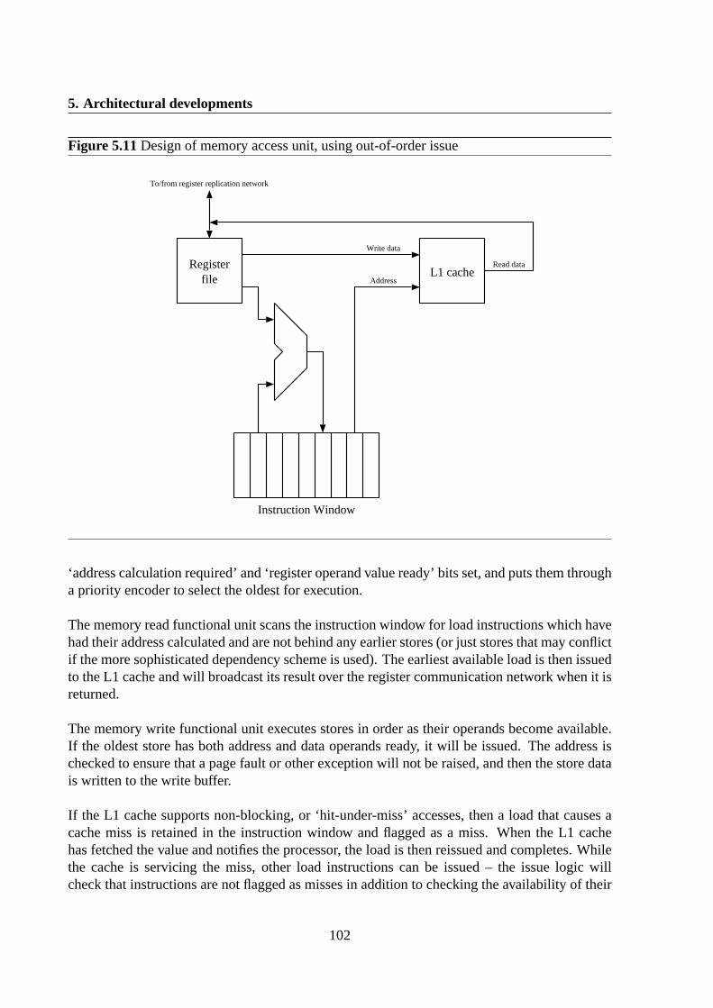
5. Architectural developments
Figure 5.11Design of memory access unit, using out-of-order issue
Registerfile
L1 cache
Instruction Window
Write data
Address
Read data
To/from register replication network
‘address calculation required’ and ‘register operand value ready’ bits set, and puts them througha priority encoder to select the oldest for execution.
The memory read functional unit scans the instruction window for load instructions which havehad their address calculated and are not behind any earlier stores (or just stores that may conflictif the more sophisticated dependency scheme is used). The earliest available load is then issuedto the L1 cache and will broadcast its result over the register communication network when it isreturned.
The memory write functional unit executes stores in order as their operands become available.If the oldest store has both address and data operands ready, it will be issued. The address ischecked to ensure that a page fault or other exception will not be raised, and then the store datais written to the write buffer.
If the L1 cache supports non-blocking, or ‘hit-under-miss’ accesses, then a load that causes acache miss is retained in the instruction window and flagged as a miss. When the L1 cachehas fetched the value and notifies the processor, the load is then reissued and completes. Whilethe cache is servicing the miss, other load instructions can be issued – the issue logic willcheck that instructions are not flagged as misses in addition to checking the availability of their
102

5.2 Combining memory access units
address operands. If a subsequent load misses to a different cache line while the L1 cache isstill processing the first miss, the load is written back to the window and flagged as a subsequentmiss – when the data from the first miss is returned, the first ‘subsequent miss’ is unflagged,making it eligible to be reissued.
If hoisting loads ahead of stores is implemented, the following additions are made to the depend-ency logic: when an address is calculated and written back to the window, an associative lookupis performed to locate other instructions accessing the same address (to reduce implementationcomplexity, only a low-order subset of the address bits are compared – this will identify somefalse dependencies, but is safe). For a store, this operation is used to resolve loads which mightdepend on the result of that store. For a load, earlier stores are checked for whether the loadmay depend on them.
To resolve these dependencies each load is masked by a number of dependency bits. Whena store is placed in the window, it is allocated one of these bits and loads issued after thestore have this bit set to indicate a possible dependency on that store. When a store address iscomputed, the address is compared against the addresses of later loads and any that differ havetheir dependency bit corresponding to the store cleared as they cannot depend on that store.Similarly, when a load address is computed, the address is compared to earlier stores – forany stores with a different address, the corresponding bits are cleared in the load’s dependencymask. When a store retires, all loads have the bit corresponding to that load cleared (anotheroption is that the bits are cleared when the store executes, if loads can read data from the writebuffer). A load is only eligible for issue when it has a clear dependency mask.
5.2.6 Evaluation
The implementation in the previous section was added to the simulator and the performancecompared to the baseline and MAU architectures. The performance was evaluated both withand without non-blocking access to the cache and with both models of load/store dependencyresolution (whether or not loads can overtake independent stores). Figure5.12shows the resultsof these tests.
These results show that the out-of-order MAU model provides comparable performance to thein-order model when loads are not allowed to issue ahead of stores (in some cases the per-formance is worse – this is likely due to subtle differences in the implementations within thesimulator model). When loads are permitted to overtake independent stores, several tests showa marked improvement in performance (up to 72% faster than the in-order MAU). In particu-lar, those tests that performed worse under the in-order MAU model than in the baseline ILDPmodel regain or exceed the original baseline performance – the out-of-order MAU model aver-ages 23.9% faster than the original ILDP model. This would indicate that the critical factor inthe memory system performance is resolving dependencies between loads and stores, in orderto allow loads to issue as early as possible.
103
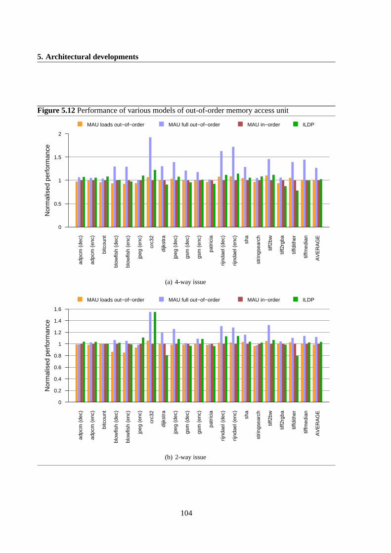
5. Architectural developments
Figure 5.12Performance of various models of out-of-order memory access unit
Nor
mal
ised
per
form
ance
0
0.5
1
1.5
2
adpc
m (
dec)
adpc
m (
enc)
bitc
ount
blow
fish
(dec
)
blow
fish
(enc
)
jpeg
(en
c)
crc3
2
dijk
stra
jpeg
(de
c)
gsm
(de
c)
gsm
(en
c)
patr
icia
rijnd
ael (
dec)
rijnd
ael (
enc)
sha
strin
gsea
rch
tiff2
bw
tiff2
rgba
tiffd
ither
tiffm
edia
n
AV
ER
AG
E
MAU loads out−of−order MAU full out−of−order MAU in−order ILDP
(a) 4-way issue
Nor
mal
ised
per
form
ance
0
0.2
0.4
0.6
0.8
1
1.2
1.4
1.6
adpc
m (
dec)
adpc
m (
enc)
bitc
ount
blow
fish
(dec
)
blow
fish
(enc
)
jpeg
(en
c)
crc3
2
dijk
stra
jpeg
(de
c)
gsm
(de
c)
gsm
(en
c)
patr
icia
rijnd
ael (
dec)
rijnd
ael (
enc)
sha
strin
gsea
rch
tiff2
bw
tiff2
rgba
tiffd
ither
tiffm
edia
n
AV
ER
AG
E
MAU loads out−of−order MAU full out−of−order MAU in−order ILDP
(b) 2-way issue
104

5.2 Combining memory access units
The out-of-order MAU approach will necessarily have higher complexity than implementingan in-order memory PE. The smaller size of the instruction window for the memory accessunit as compared to that for a full superscalar processor means that the resulting complexitywill not be as great as using a superscalar implementation for the whole processor. Contrastingthe complexity of the out-of-order MAU design with the baseline ILDP architecture is moredifficult – the added complexity of the issue logic for the MAU is offset somewhat by theremoval of the store queue replication network and the replicated L1 caches and their associationcoherency logic. This approach should either use less die area, or use the same die area moreefficiently – even with the more complex memory issue logic, the need for replication of cachesor implementation of multiported caches is removed.
Instruction window size
Since the complexity of the issue window logic scales quadratically [42] in the size of thewindow, it is important to keep this window size small. Section5.2.3 indicates that a depthof between four and eight entries for the instruction FIFO is sufficient with the in-order MAU.Experiments were conducted to investigate the effect of window size on performance, the resultsof which are presented in Figure5.13.
These results show that, on average for the 2-way model, a 16-entry instruction window provides99.6% of the performance of an unbounded window, while a 12-entry window achieves 99.2%.Scaling back to eight entries reduces performance by 1.5%, and a 4-entry window performs7.8% worse than one with no limit; the results in the 4-way case are similar. These results im-ply that a window size of twelve entries is ample to achieve nearly optimal performance, whilea reduction to eight entries still provides good performance with a large potential complexityreduction. Thetiff2bw test actually runs 17.6% faster with a 4-entry window – this result issomewhat unexpected, and further examination has been unable to explain the reason for thisapparent discrepancy. Since this is the only data point to display this behaviour, it is consideredto be an outlier and has been discounted.
If the instruction window size proves to be a critical point when it comes to trading off betweencomplexity and performance, another possible approach is to use a smaller instruction windowfed by a simple instruction FIFO. This will have lower performance than a large instructionwindow as fewer instructions can be reordered (although the relative sizes can potentially beoptimised so that this performance drop is minimal) but will have much lower complexity thana full window. The performance will be greater than a single small instruction window as theissue logic does not need to stall when the window becomes full – the instruction can be placedinto the FIFO, and will be moved into the window when space becomes available. Based on theresults presented in this section, if this approach were to be implemented, an instruction FIFOof 4-8 entries feeding a 4-entry window seems like a suitable trade-off.
105

5. Architectural developments
Figure 5.13Effect of out-of-order MAU instruction window size on performance
Per
form
ance
diff
eren
ce
−30%
−20%
−10%
0%
10%
20%
adpc
m (
dec)
adpc
m (
enc)
bitc
ount
blow
fish
(dec
)
blow
fish
(enc
)
jpeg
(en
c)
crc3
2
dijk
stra
jpeg
(de
c)
gsm
(de
c)
gsm
(en
c)
patr
icia
rijnd
ael (
dec)
rijnd
ael (
enc)
sha
strin
gsea
rch
tiff2
bw
tiff2
rgba
tiffd
ither
tiffm
edia
n
AV
ER
AG
E
4 8 12 16
MAU instruction window size
(a) 4-way issue
Per
form
ance
diff
eren
ce
−25%
−20%
−15%
−10%
−5%
0%
5%
adpc
m (
dec)
adpc
m (
enc)
bitc
ount
blow
fish
(dec
)
blow
fish
(enc
)
jpeg
(en
c)
crc3
2
dijk
stra
jpeg
(de
c)
gsm
(de
c)
gsm
(en
c)
patr
icia
rijnd
ael (
dec)
rijnd
ael (
enc)
sha
strin
gsea
rch
tiff2
bw
tiff2
rgba
tiffd
ither
tiffm
edia
n
AV
ER
AG
E4 8 12 16
MAU instruction window size
(b) 2-way issue
106

5.2 Combining memory access units
5.2.7 Cache structure
In section4.3.7 the effect of varying the associativity of the L1 cache is analysed. Scalingthe design from multiple replicated caches to a single cache makes it more feasible to increasethe cache size. This section investigates the effect cache size has on performance in the MAUdesign. The original ILDP design contains a total of 64KB of L1 cache, partitioned into eightblocks of 8KB each. Experiments were conducted with a single L1 cache of 64KB total size, aswell as a smaller cache of 32KB or 16KB. The performance of each of these configurations wasthen compared to the results with a single 8KB cache. All tests were run using the out-of-orderMAU model, with an 8-entry instruction window.
The results from these tests are presented in Figure5.14. As in section4.3.7, there is only asmall variation in performance. When using 2-way issue, thedijkstra andrijndael (dec)testsperform slightly over 1% better with the larger cache sizes. The 4-way issue case seems morebound by the cache parameters – in particular thetiffmediantest (which was the only test toshow a noticable performance improvement when the associativity was increased) is 5.8% fasterwhen run with a 64KB cache. Overall, the performance improvements are marginal, which isagain attributed to the low memory footprint of the MiBench suite.
5.2.8 Conclusions
The approach of separating memory accesses out into a different processing unit is explored indetail using several approaches. A simple implementation issuing memory operations in ordercan result in a large reduction in silicon area usage and provide a very similar overall level ofperformance. More sophisticated schemes can be used that allow reordering of load instructionsto prevent stalls on register values or cache misses. At the cost of higher complexity, these moreadvanced designs provide greater performance (up to a 24% improvement over the base modelusing 4-way issue) while still having a greatly reduced area.
107

5. Architectural developments
Figure 5.14Effect of increasing L1 cache size on performance (compared to 8KB size)
Per
form
ance
diff
eren
ce
−5%
−3%
−1%
1%
3%
5%
7%
9%
adpc
m (
dec)
adpc
m (
enc)
bitc
ount
blow
fish
(dec
)
blow
fish
(enc
)
jpeg
(en
c)
crc3
2
dijk
stra
jpeg
(de
c)
gsm
(de
c)
gsm
(en
c)
patr
icia
rijnd
ael (
dec)
rijnd
ael (
enc)
sha
strin
gsea
rch
tiff2
bw
tiff2
rgba
tiffd
ither
tiffm
edia
n
AV
ER
AG
E
16KB 32KB 64KB
L1 cache size
(a) 4-way issue
Per
form
ance
diff
eren
ce
−5%
−3%
−1%
1%
3%
5%
adpc
m (
dec)
adpc
m (
enc)
bitc
ount
blow
fish
(dec
)
blow
fish
(enc
)
jpeg
(en
c)
crc3
2
dijk
stra
jpeg
(de
c)
gsm
(de
c)
gsm
(en
c)
patr
icia
rijnd
ael (
dec)
rijnd
ael (
enc)
sha
strin
gsea
rch
tiff2
bw
tiff2
rgba
tiffd
ither
tiffm
edia
n
AV
ER
AG
E16KB 32KB 64KB
L1 cache size
(b) 2-way issue
108

5.3 Register inlining
5.3 Register inlining
The base ILDP architecture replicates the register file, having a copy in each of the processingelements. With 128 physical registers and 8 PEs this means there are a total of 1024 registerson the processor. Even if the size of the physical register file is scaled back to 32 registers, theoverall processor will require a total of 256 registers. Since all register values are replicated toall PEs, but most values will be used by only one or two PEs, most of the values in the registerfiles will be effectively dead – this amounts to a huge waste of both area and power, both interms of static consumption from holding these useless values and dynamic consumption fromwriting them into the register files. Even if power gating is utilized on inactive PEs, the registerfile and replication logic must still be powered and kept up-to-date, in order that register filecontents are valid when PEs are awakened.
Lipasti et al. [36] describe a scheme for improving the performance of superscalar architectureswhereby registers containing small values can be stored directly in the reorder buffer in placeof the register number. This bypasses the register file access when the instruction is executed,reducing the latency of instructions using registers containing small values (which form the ma-jority of data values held in registers). While their work is targeted on improving performance,this approach can be used to reduce complexity, as it potentially allows the register file to havefewer ports, or allows a multi-cycle latency register file to be implemented using less aggressivelogic. While such a design would reduce the register file performance, this would be mitigatedby the reduced access frequency. The lower complexity could also possibly reduce overall cycletime, improving overall performance.
Using a similar technique, this section proposes a development to the ILDP architecture to re-duce the overall silicon area usage. The register file in each PE is eliminated and instead theinstruction FIFO is augmented with an associative memory for holding the register operandtags. Rather than using inlining to reduce register file latency, here it is used to reduce stor-age replication and thus save die area and reduce power consumption. When a register valueis received by the PE, rather than being written into the register file, an associative lookup isperformed on the instruction FIFO to find any instructions depending on that value. For thoseentries that match, the data value is then written into the FIFO alongside the matching instruc-tions. In this scheme, only live data would actually be stored within each processing element –while some values may be replicated within the FIFO, energy is not spent storing data valueswhich ultimately are not used. As the FIFO size (e.g. 8 entries) is much smaller than the overallregister file size (32–128 entries), this should greatly reduce overall silicon area.
A single copy of the full register file is maintained – this contains the only copies of old registersthat no longer hold the values of any architectural registers at the issue point, and thus arespeculatively dead, but may actually be needed in the case of an exception causing rollback toa point where they are in scope. This register file is accessed by the issue logic after registerrenaming and before the instruction is steered. Instructions depending on data values alreadyavailable in the register file read them at that point in the pipeline, while those requiring data
109

5. Architectural developments
not yet computed are issued to the processing elements along with the tag of the register theydepend upon, and are updated later in the instruction FIFO when the value becomes available.
This system should allow for large power savings, as any idle processing elements can be en-tirely powered down, without needing to keep a register file and update logic active. Even activePEs will consume less static power, as the memory for storing operand values inline in the FIFOis smaller than a copy of the register file.
5.3.1 Implementation details
In this scheme, each processing element is modified by removing the register file and replacingit with an enhanced version of the instruction FIFO. In addition to the standard FIFO controllogic, the augmented instruction FIFO contains several blocks of RAM and some logic forperforming the associative lookup. The FIFO must store, for each instruction:
• A tag identifying the individual instruction
• The opcode of the instruction
• If the instruction writes to a general-purpose register, a tag identifying that register
• Any immediate operand value it may have
• For instructions accessing a register operand, either the tag identifying the register provid-ing the operand or the value of the register operand itself
• A flag to indicate whether the instruction is waiting on a register value
The tag, opcode and immediate values are stored as in a standard FIFO: in a RAM with onewrite and one read port and some logic to generate the address pointers for these ports and tohandle empty/full notification. The register values and register tags are stored in separate RAMarrays, sharing the read and write ports of the main FIFO, with an additional write port forregister value updates from the inter-PE communication network.
When a register value is received, the register tag is asserted onto the associative lookup portof the register tag array. Comparators in each row compare the incoming tag with the storedtag, and all entries that match drive an associated wordline. These wordlines drive the addi-tional write port on the register value array, writing the new register value into each locationof the instruction FIFO that depends on the register being updated. A one-bit array of flags ismaintained to indicate whether a row is waiting on a register value – this bit is cleared when theregister value arrives, and an instruction will only issue if it is not waiting on data.
110

5.3 Register inlining
Figure 5.15Register tag/value portion of PE instruction FIFO
r21
r5
xxx
FIFO readpointer
FIFO writepointer
r21
xxx
xxxxxxxx
xxxxxxxx
12345678
Register valueto PE
Register tag from replication networkRegister value from replication network
Register value from issue pipeline(if value known at issue)
Register tag from issue pipeline(if value not known at issue)
Match lines
00000042
xxxxxxxx
Figure5.15illustrates the organisation of the register value and tag portions of the instructionFIFO. In the figure there are five instructions currently stored in the FIFO. The instructionat the head of the FIFO has already had its register value resolved, and is thus available forissue; the third instruction also has its source operand present in the FIFO. The second, fourthand fifth instructions are all still waiting on data to become available. If, in the next cycle, thevalue of r21 becomes available, then the tag for r21 will be asserted to the associative tag RAM.This will match the two entries containing the r21 tag, and thus drive the associated match lineshigh. The value of r21 will be asserted to the write port for the value RAM, and thus the valueentries corresponding to the second and fourth instructions in the FIFO will be updated, whilethe entries will be marked to indicate that the values have been resolved and thus the instructionscan execute.
A small lookaside buffer is maintained in each PE to store any values received in the last cycle ortwo (depending on the delay between the register lookup in the issue pipeline and an instructionbeing written into the PE’s instruction FIFO), so that instructions that are ‘in flight’ betweenthe register access stage in the issue pipeline and the tail of the instruction FIFOs do not missregister updates. When an instruction is written to the tail of a FIFO, this buffer is accessed tosee if it holds the value of any source registers of the instruction.
111
5. Architectural developments
While in the baseline architecture there are copies of the register file in each PE, in this approachthere is a single register file, accessed in the issue pipeline (probably in the ‘steer’ stage, but de-pending on timing an additional stage might need to be inserted between ‘rename’ and ‘steer’).If an instruction being steered reads a register value that has already been computed, that valueis read from the register file at this point and the instruction is placed into the destination FIFOhaving already had its input dependencies resolved. This register file is updated as it receivesthe data broadcast over the register communication network. Thus the file requires one readport for each instruction that can be in the steering stage at once (although theoretically fewerports could be implemented; see Section4.2.3) and one write port per value that can be sentover the register network in a single cycle.
5.3.2 Complexity
The logic required to implement the associative FIFOs is analogous to the associative logicon an instruction window in a superscalar processor to tag ready instructions, but with only asingle associative write port. The reduced size of the individual instruction FIFOs compared toa superscalar instruction window (the size of all the FIFOs added together is comparable to thesize of a full instruction window) should reduce the delay of this structure – the delay of suchan associative memory is quadratic in the number of words, although for small issue widths thequadratic term is not very significant and the scaling is closer to linear [42].
The main delays through this structure are the bitline delays on the read and write ports, thewordline delays and the delay through decoder or comparator logic. For the non-associativeaccesses on a FIFO pop, the delay consists first of the delay through the address decoder, thenthrough the wordline from the decoder, and finally through the bitlines to the output connec-tions. For a FIFO push, the bitline drive time can occur concurrently with the decoder andwordline delays. With an associative write, first the bitlines into the tag memory must be driven,then the comparators must drive the appropriate wordlines. The bitlines into the register valuememory can also be driven concurrently with the other delays.
The main register file accessed in the issue pipeline needs to have as many read ports as theregister rename map, plus as many write ports as are needed by the register replication logic.Given the number of ports required, this register file could become a problem meeting timing re-quirements, although the number of ports required is still far less than for a standard superscalarprocessor of the same issue width.
5.3.3 Evaluation
At the architectural level, this technique should provide the same per-clock performance as thebaseline ILDP architecture – this design simply rearranges the storage mechanism for GPRs
112

5.3 Register inlining
and does not introduce any additional delays at the clock cycle level, unless the added registeraccess in the issue pipeline requires adding an additional pipeline stage. At the circuit level,the new FIFO arrangement is more complex than the previous multiple register file design, butthe additional complexity is mostly from extra logic; the bitline delays of the instruction FIFOswill be smaller than those of the original register files as there are fewer words in the memory.By reducing wire delays at the expense of greater logic delays, this design should scale betterat smaller feature sizes than a register file (as logic delays scale better than wire delays), thusthe overall cycle time is unlikely to be significantly affected by this change, as the associativememory should not form part of the critical path.
There should be a significant reduction in power consumption using this technique, as the 128-entry register file in each PE is replaced by a single register file in the issue logic and a smallerassociative file alongside the existing instruction FIFO – with a FIFO depth of eight, the as-sociative register memory will contain only eight entries, rather than the original 128. Greaterbenefits can be realised if clock gating or power gating are also used – since only live data isstored within the PEs then, when an inactive PE is powered down, the register memory and theregister file update logic can also be powered down, giving a large power saving if PEs are shutdown for much of the time.
5.3.4 Conclusions
Inlining the register file into the instruction FIFOs reduces overall silicon area, decreases staticpower consumption and should not significantly affect performance, although the performanceeffect is hard to judge without performing a full circuit synthesis. Rather than being replicatedacross all the PEs in case it will be required, data is only stored within a PE if it is definitelygoing to be used in the future. If a PE has an empty instruction FIFO, it contains no live dataand thus register file inlining enables further power savings by allowing all of the PEs to bepowered down if power gating is used.
Given that using register file inlining allows a PE to be completely powered down, this techniquecould be used in combination with the FIFO multiplexing from Section5.1 to allow a highlyscalable power management system to be implemented. If some of the PEs are augmented to beable to have more than one strand currently assigned to them, then it is possible to power downindividual PEs when the processor is in a low power mode, allowing the remaining poweredPEs to handle execution. For example, with four PEs capable of executing two strands and fourcapable of only one, the core could be configured to run with anywhere between four and eightPEs activated at one time, trading off power consumption versus performance.
113
5. Architectural developments
5.4 Summary
Several developments on the ILDP architecture are described to reduce the overall complexityof the architecture. Reducing the number of processing elements and assigning multiple in-struction FIFOs to them can greatly reduce the total silicon area of the design (the area used byexecution resources and L1 cache would be halved), but has a significant performance penaltyof 12–14%.
Adding an additional processing element to handle memory accesses and removing the memorylogic from the original processing elements greatly reduces area by removing the need for thestore queue replication logic and maintaining only one copy of the L1 cache, providing similarpeformance with simple in-order issue logic, or a 24% speedup with more sophisticated issuelogic.
Eliminating the replicated register file in each processing element and replacing them with asingle register file and an associative operand memory in the instruction FIFO allows the totalsilicon area to be reduced and also allows potentially very good power savings, with hopefullya negligible performance impact.
114

Conclusions 6
This thesis has evaluated the performance and complexity of the ILDP architecture in the con-text of an embedded environment. Numerous performance simulations have been run, evalu-ating the effect of a range of architectural parameters and analysing the suitability of variousdevelopments upon the architecture. This chapter summarizes these results and presents severalavenues for potential future research based on this work.
6.1 Summary
In Chapter3 I gave a detailed overview of the ILDP microarchitecture and instruction set, andI provided a qualitative analysis of the complexity of an ILDP implementation, as compared toboth a typical scalar RISC CPU and a superscalar design. The ILDP architecture eliminates orgreatly reduces the size of a number of structures present in a superscalar architecture, allowingits complexity to compare favourably with a simple scalar design.
In Chapter4 I compared the performance of an implementation of the ILDP architecture to sometypical processors used in high-performance embedded systems. The results show potential, buthighlight the need for a better compiler implementation than the one used for these tests. I wenton to analyse the effect on performance of a number of the architectural parameters; I haveshown that many of the parallel structures used within the processor can be scaled to provideless parallelism with little cost to the overall performance, for example the register renamingstage can be scaled from being able to process four instructions per cycle to three with a drop inperformance of less than 0.2%. In particular, the size of the register file can be greatly reducedwith little average effect on performance.
I presented several possible developments to the ILDP architecture in Chapter5. A schemeto halve the number of processing elements, and thus greatly reduce silicon area and powerconsumption, was outlined but proved to have a significant effect on performance. I presenteda method to reduce the area and power requirements of the memory logic in the architecture byadding a new processing element with sole responsibility for handling memory accesses. If thisnew unit is configured to execute instructions in order, then similar performance to the originalarchitecture is achieved with a large reduction in area and power requirements. If the new unitis set up to execute memory operations out of order then, at an increased area/power cost, a
115

6. Conclusions
significant improvement in performance is possible. Finally, a new organisation for the registerfile was proposed, which greatly reduces the overall area used and has the potential to reducepower consumption, especially in the presence of clock or power gating.
6.2 Conclusion
It has been shown that the ILDP architecture is able to achieve a high degree of instruction-level parallelism – the IPC attained in benchmarks was more than double that of the otherarchitectures modelled. The overall performance compared to these models is less impressive– a 53% improvement over the PowerPC model and a 19% improvement over the ARM model.This is due to the ILDP code for the benchmarks requiring many more instructions than theother architectures, which is attributed in part to the basic features of the ISA, in part to specificchoices made in this implementation which could be altered, and in part to the prototype natureof the compiler backend, being unable to optimise as efficiently as the backends for ARMand PowerPC. While it was not possible to simulate against an out-of-order architecture, Kimand Smith [30] show that the baseline ILDP performance is comparable to an out-of-orderprocessor. Overall it is shown that ILDP has the potential for high performance, without muchof the overhead present in traditional out-of-order superscalar architectures.
The initial ILDP model was based closely on that presented by Kim and Smith [30], whichhas fairly hefty resource requirements, which will come at a cost in silicon area and powerconsumption. I have shown that many of these structures – in particular the general-purposeregister file – can be reduced in size (with associated power and area benefits) without undulyimpacting upon performance: reducing the register file from 128 to 32 GPRs only results in a4% drop in performance whilst reducing the area used by the register file by 75%. If the band-width of the issue pipeline is then reduced from four instructions per cycle to two, performancefalls by a further 8.1%, but the area used by the issue pipeline will be approximately halved, andthe reduction in complexity in the issue logic could well allow the cycle time to be decreased,allowing the design to be clocked faster.
I have proposed several advancements to the architecture that can improve performance, reduceresource requirements and in particular allow the design to be very scalable, allowing the trade-off between performance and area/power to be chosen both at design time and, with appropriatepower gating techniques, dynamically while executing. Moving the memory access logic fromthe individual PEs to a specialized memory access unit eliminates any need for replicatingcopies of the L1 cache (saving area and power) and, if using more sophisticated schedulinglogic than the main processing elements, can improve performance by 23.9%. Removing thereplicated register files from the processing elements and instead using a more dataflow-orientedtechnique akin to Tomasulo’s reservation stations [58] allows individual processing elements tobe powered down without loss of useful state – this enables fine-grained power/performancescaling by controlling the number of active PEs.
116

6.3 Future work
It seems unlikely that this particular architecture will be used commercially in the near future –in the present high-performance embedded processor market code compatibility is still a largeissue and moving to a new, incompatible, ISA is difficult. However, there is currently a trendtowards the use of intermediate bytecode languages such as Java and .NET which are eitherinterpreted or converted to native code using just-in-time compilation, so a switch to an ISAusing some of these ideas may well be more likely in a few years. This could provide a numberof performance advantages – currently software designed to be portable between various imple-mentations and revisions of an architecture must usually be compiled for the lowest commondenominator (x86 binaries are often compiled for the old Pentium architecture in order to en-sure compatibility with a wide range of processors), but the compiler is thus unable to use anyof the features of newer architectures, or to perform core-specific scheduling. If just-in-timecompilation is used then optimizations can be performed for the specific model of processorbeing targeted.
Ultimately, it has been shown that there is definite merit in an instruction set which allows thecompiler to more obviously indicate instruction data dependencies to the processor, groupingdependent instructions into strands which can execute in close proximity. This type of instruc-tion set allows simpler issue logic for out-of-order execution using information provided bythe compiler, without the need for the detailed microarchitectural knowledge required when thecompiler must perform static scheduling, as in the IA64 architecture.
6.3 Future work
There are a number of areas in which future research could continue upon the work presentedwithin this dissertation. In particular, while detailed analysis has been performed on processorperformance in terms of number of cycles executed, there is scope for more investigation intothe impact various architectural features have upon cycle time. There would probably be meritin synthesizing a design of the ILDP architecture in order to identify where the critical timingpaths lie.
Another area which could be further developed is that of the chosen instruction set architecture.It would be useful to perform an analysis showing which features of the instruction set couldaffect performance, particularly when comparing the performance of the ILDP architecture tothat of other architectures. Several of the features of the instruction set proved to cause diffi-culties when adapting the GCC compiler to generate code for ILDP – some of these featurescould possibly be changed to allow improved compiler efficiency.
There is considerable scope for investigating how to perform compilation for the accumulator-based ILDP architecture. This research was based on a GCC backend targeted to ILDP, withappropriate fixups and some optimizations in order to support register allocation for the hier-archical register file. A strategy that might be able to generate better code out of the compiler
117

6. Conclusions
Figure 6.1Traditional CPU arrangements for multiprocessing
IP
FU
FU
FU
FU
(a) A single superscalar CPU
IP
IP
FU
FU
FU
FU
(b) A two-way SMT CPU
IP
FU
FU
FU
FU
IP
FU
FU
FU
FU
(c) A two-way SMP CPU
might utilize an additional compiler pass to organise instructions into strands, identifying whichvalues would be allocated to GPRs and which to accumulators.
The organisation of the ILDP architecture allows for future research into more flexible schemesof multiprocessing compared to the current approaches of symmetric multithreading and sym-metric multiprocessing. Figure6.1(a)shows a 4-way superscalar CPU, with the issue pipelinedepicted as ‘IP’, and each functional unit represented as ‘FU’. When a superscalar processorimplements SMT, typically the issue logic will be replicated and then share the original execu-tion resources (Figure6.1(b)), while an SMP solution will replicate both issue and executionresources with no sharing (Figure6.1(c)).
A multiprocessing ILDP system could take a hybrid approach, where two issue pipelines feed aset of e.g. twelve PEs – while the issue logic has been replicated twice, there is only 50% moreexecution logic. As some processing elements are dedicated to one issue pipeline and some areshared (rather than the fully shared approach of SMT or the fully dedicated approach of SMP),some of the performance issues present with SMT should be avoided, without the full cost ofan SMP solution.
As the number of issue pipelines is increased, more interesting arrangements of execution re-sources could potentially be devised – e.g. the arrangement in Figure6.2 with four issue unitsand 20 processing elements, where each issue unit has two dedicated PEs and two PEs sharedwith each other issue unit. This reduces the overall logic replication compared to a full 4-waySMP implementation, which would require 32 PEs, but limits the additional complexity of the
118

6.3 Future work
Figure 6.2An example four-way multiprocessing ILDP CPU
IP
IP
FU
FU
FU
IP
IP
FU FU
FU
FU
FU
FU
FU
FU
FU
FU
FU
FU
FU
FU FU
FU FU
PEs and the interconnection logic, as each PE need only communicate with a maximum of twoof the issue pipelines and a limited subset of the other PEs. Performance should potentially beon par with a fully replicated SMP, as each issue pipeline has two dedicated PEs and need onlycontend with one other pipeline for each of the others – allocation strategies can be chosen tominimise conflicts as much as possible. This type of organisation would allow for very fine-grained power control, as individual processing elements and issue pipelines could be poweredon or off, with the processor performance hopefully scaling well as the number of resources isincreased or decreased. This is in marked contrast to current SMP solutions, which typicallyonly allow power control at the level of an entire core.
119

120

Bibliography
[1] Vikas Agarwal, M S Hrishikesh, Stephen W Keckler, and Doug Burger.Clock rate versus IPC: the end of the road for conventional microarchitectures.In Proceedings of the 27th Annual International Symposium on Computer Architecture,
pages 248–259. IEEE Computer Society, 2000.http://citeseer.ist.psu.edu/agarwal00clock.html
Referenced on page36.
[2] Gerald Aigner, Amer Diwan, David L Heine, Monica S Lam, David L Moore, Brian RMurphy, and Constantine Sapuntzakis.
An overview of the SUIF2 compiler infrastructure.http://suif.stanford.edu/suif/suif2/doc-2.2.0-4/overview.ps
Referenced on page54.
[3] ARM Ltd.An introduction to Thumb .Technical Report ARM DVI-0001A, Advanced RISC Machines Ltd, March 1995Referenced on page33.
[4] Florin Baboescu and Dean M Tullsen.Memory subsystem design for multithreaded processors.Technical report, University of California, San Diego, 1997.http://citeseer.ist.psu.edu/577904.html
Referenced on page26.
[5] Doug Burger, Todd M Austin, and Steve Bennett.Evaluating future microprocessors: The SimpleScalar tool set.Technical Report CS-TR-1996-1308, University of Wisconsin-Madison, July 1996.http://citeseer.ist.psu.edu/burger96evaluating.html
Referenced on pages55and56.
121

Bibliography
[6] Doug Burger and James R Goodman.Billion-transistor architectures .IEEE Computer, volume 30 issue 9, pages 46–49, September 1997.http://citeseer.ist.psu.edu/534110.html
Referenced on page36.
[7] Stephen P Crago, Apoorv Srivastava, Kevin Obenland, and Alvin M Despain.A high-performance, hierarchical decoupled architecture.Technical Report ACAL-TR-96-07, Advanced Computer Architecture Laboratory,
University of Southern California, November 1996.http://citeseer.ist.psu.edu/crago96highperformance.html
Referenced on page27.
[8] J Dehnert, B Grant, J Banning, R Johnson, T Kistler, A Klaiber, and J Mattson.The Transmeta Code Morphing software: Using speculation, recovery, and adaptive
retranslation to address real-life challenges.In Proceedings of the International Symposium on Code Generation and Optimization,
pages 15–24. IEEE Computer Society, 2003.citeseer.ist.psu.edu/dehnert03transmeta.html
Referenced on page53.
[9] Richard Earnshaw.Procedure call standard for the ARM architecture.Technical Report GENC-003534, ARM, May 2006.http://www.arm.com/miscPDFs/8031.pdf
Referenced on page40.
[10] Susan J Eggers, Joel S Emer, Henry M Levy, Jack L Lo, Rebecca L Stamm, and Dean MTullsen.
Simultaneous multithreading: A platform for next-generation processors.IEEE Micro, volume 17 issue 5, pages 12–19, September/October 1997.http://citeseer.ist.psu.edu/eggers97simultaneous.html
Referenced on page25.
[11] Douglas J Evans.The Cpu tools GENerator, CGEN, Mar 2001.http://sources.redhat.com/cgen/docs-1.0/cgen.html
Referenced on page54.
[12] Matthew K Farrens and Andrew R Pleszkun.Overview of the PIPE processor implementation.In Proceedings of the 24th Annual Hawaii International Conference on System Sciences,
pages 433–443. IEEE Computer Society, January 1991.http://citeseer.ist.psu.edu/farrens91overview.html
Referenced on page27.
122

Bibliography
[13] Mark Game and Alan Booker.Codepack: Code compression for PowerPC processors.International Business Machines (IBM) Corporation, 1998Referenced on page33.
[14] A Gara, M A Blumrich, D Chen, G L-T Chiu, P Coteus, M E Giampapa, R A Haring,P Heidelberger, D Hoenicke, G V Kopcsay, T A Liebsch, M Ohmacht, B DSteinmacher-Burow, T Takken, and P Vranas.
Overview of the Blue Gene/L system architecture.IBM Journal of Research and Development, volume 49 issue 2, pages 195–212, 2005.http://www.research.ibm.com/journal/rd/492/gara.pdf
Referenced on page29.
[15] Montse García, José González, and Antonio González.Data caches for multithreaded processors.In Workshop on MultiThreaded Execution Architecture and Compilation, January 2000.http://citeseer.ist.psu.edu/396929.html
Referenced on page26.
[16] Simcha Gochman, Avi Mendelson, Alon Naveh, and Efraim Rotem.Introduction to Intel Core Duo processor architecture.Intel Technology Journal, volume 10 issue 2, pages 89–98, May 2006.http://download.intel.com/technology/itj/2006/volume10issue02/
vol10_art01.pdf
Referenced on page30.
[17] Matthew R Guthaus, Jeffrey S Ringenberg, Dan Ernst, Todd M Austin, Trevor Mudge,and Richard B Brown.
MiBench: A free, commercially representative embedded benchmark suite.In Proceedings of the IEEE 4th Annual Workshop on Workload Characterization. IEEE
Computer Society, December 2001.http://www.eecs.umich.edu/mibench/Publications/MiBench.pdf
Referenced on page55.
[18] Linley Gwennap.Digital 21264 sets new standard.Microprocessor Report, volume 10 issue 14, pages 11–16, October 1996.http://www.cs.virginia.edu/~dp8x/alpha21264/paper/new%
20standard.pdf
Referenced on page28.
123

Bibliography
[19] Allan M Hartstein and Thomas R Puzak.The optimum pipeline depth for a microprocessor.In Proceedings of the 29th Annual International Symposium on Computer Architecture,
pages 7–13. IEEE Computer Society, May 2002.http://systems.cs.colorado.edu/ISCA2002/FinalPapers/
hartsteina_optimum_pipeline_color.pdf
Referenced on page35.
[20] John L Henning.SPEC CPU2000: Measuring CPU performance in the new millennium.IEEE Computer, volume 33 issue 7, pages 28–35, July 2000.http://www.spec.org/cpu2000/papers/COMPUTER_200007.JLH.pdf
Referenced on page55.
[21] S Hily and A Seznec.Standard memory hierarchy does not fit simultaneous multithreading.In Workshop on MultiThreaded Execution Architecture and Compilation, January 1998.http://citeseer.ist.psu.edu/hily98standard.html
Referenced on page26.
[22] Sébastien Hily and André Seznec.Contention on 2nd level cache may limit the effectiveness of simultaneous
multithreading .Technical Report PI-1086, Institut de Recherche en Informatique et Systèmes Aléatoires
(IRISA), 1997.http://citeseer.ist.psu.edu/hily97contention.html
Referenced on page26.
[23] Glenn Hinton, Dave Sager, Mike Upton, Darrell Boggs, Doug Carmean, Alan Kyker, andPatrice Roussel.
The microarchitecture of the Pentium 4 processor.Intel Technology Journal, volume 5 issue 1, February 2001.http://www.intel.com/technology/itj/q12001/pdf/art_2.pdf
Referenced on pages31and35.
[24] M S Hrishikesh, Norman P Jouppi, Keith I Farkas, Doug Burger, Stephen W Keckler, andPremkishore Shivakumar.
The optimal logic depth per pipeline stage is 6 to 8 FO4 inverter delays.In Proceedings of the 29th Annual International Symposium on Computer Architecture,
pages 14–24. IEEE Computer Society, May 2002.http://systems.cs.colorado.edu/ISCA2002/FinalPapers/
hrishikeshm_optimal_revised.ps
Referenced on page35.
124

Bibliography
[25] Xianglong Huang, J Eliot B Moss, Kathryn S McKinley, Steve Blackburn, and DougBurger.
Dynamic Simplescalar: Simulating Java virtual machines.Technical Report TR-03-03, University of Texas, 2003.http://www.cs.utexas.edu/ftp/pub/techreports/tr03-03.ps.gz
Referenced on page56.
[26] IBM Microelectronics Division.The PowerPC 405 Core, February 1998.http://www-306.ibm.com/chips/techlib/techlib.nsf/techdocs/
852569B20050FF77852569970063B427/$file/405cr_wp.pdf
Referenced on page56.
[27] IBM Microelectronics Division.The PowerPC 440 Core, September 1999.http://www-306.ibm.com/chips/techlib/techlib.nsf/techdocs/
852569B20050FF77852569970063431C/$file/440_wp.pdf
Referenced on page56.
[28] ITRS.International Technology Roadmap for Semiconductors: Interconnect, 2006.http://www.itrs.net/Links/2006Update/FinalToPost/
09_Interconnect2006Update.pdf
Referenced on page17.
[29] Robert M Keller.Look-ahead processors.ACM Computing Surveys, volume 7 issue 4, pages 177–195, 1975.http://portal.acm.org/citation.cfm?id=356657
Referenced on page23.
[30] Ho-Seop Kim and James E Smith.An instruction set and microarchitecture for instruction level distributed processing.In Proceedings of the 29th Annual International Symposium on Computer Architecture,
pages 71–81. IEEE Computer Society, May 2002.http://citeseer.ist.psu.edu/kim02instruction.html
Referenced on pages15, 28, 37, 39, 45, 46, 49, 50, 53, 55, 56, 64, 78, 80, and116.
[31] Nam Sung Kim, Todd Austin, David Blaauw, Trevor Mudge, Kristián Flautner, Jie S Hu,Mary Jane Irwin, Mahmut Kandemir, and Vijaykrishnan Narayanan.
Leakage current: Moore’s law meets static power.IEEE Computer, volume 36 issue 12, pages 68–75, 2003Referenced on page34.
125

Bibliography
[32] K Kissell.MIPS16: High-density MIPS for the embedded market.Silicon Graphics MIPS Group, 1997Referenced on page33.
[33] Alexander Klaiber.The technology behind Crusoe processors: Low-power x86-compatible processors
implemented with Code Morphing software.Technical report, Transmeta Corporation, 2000.http://www.transmeta.com/pdfs/paper_aklaiber_19jan00.pdf
Referenced on page53.
[34] Ronny Krashinsky and Michael Sung.Decoupled architectures for complexity-effective general purpose processors.http://citeseer.ist.psu.edu/krashinsky00decoupled.html .Advanced VLSI Computer Architecture term project, Massachusetts Institute of
Technology, December 2000Referenced on page27.
[35] Alexei Kudriavtsev and Peter Kogge.SMT possibilities for decoupled architecture.In Technical Committee on Computer Architecture (TCCA) Newsletter: Papers from
MEmory access DEcoupling for superscalar and multiple issue Architectures(MEDEA-2000) Workshop. IEEE Computer Society, January 2001.
http://tab.computer.org/tcca/NEWS/jan2001/kudriavtsev.pdf
Referenced on page27.
[36] Mikko H Lipasti, Brian R Mestan, and Erika Gunadi.Physical register inlining.In Proceedings of the 31st Annual International Symposium on Computer Architecture,
pages 325–335. IEEE Computer Society, June 2004.http://www.ece.wisc.edu/~pharm/papers/isca2004_egunadi.pdf
Referenced on page109.
[37] Jack L Lo, Susan J Eggers, Joel S Emer, Henry M Levy, Rebecca L Stamm, and Dean MTullsen.
Converting thread-level parallelism to instruction-level parallelism via simultaneousmultithreading .
ACM Transactions on Computer Systems, volume 15 issue 3, pages 322–354, August1997.
http://www.cs.washington.edu/research/smt/papers/
tlp2ilp.final.pdf
Referenced on page25.
126

Bibliography
[38] Deborah T Marr, Frank Binns, David L Hill, Glenn Hinton, David A Koufaty, J AlanMiller, and Michael Upton.
Hyper-threading technology architecture and microarchitecture.Intel Technology Journal, volume 6 issue 1, pages 4–15, February 2002.http://download.intel.com/technology/itj/2002/volume06issue01/
art01_hyper/vol6iss1_art01.pdf
Referenced on page26.
[39] MIPS Technologies, Inc.The MIPS MT application-specific extension to the MIPS32 architecture.Technical Report MD00378, 2005Referenced on page26.
[40] Hans-Peter Nilsson.Porting GCC for dunces, May 2000.http://ftp.axis.se/pub/users/hp/pgccfd/pgccfd.pdf
Referenced on page54.
[41] Thomas Pabst and Frank Völkel.Hot Spot: How modern processors cope with heat emergencies.Tom’s Hardware Guide, September 2001.http://tomshardware.co.uk/2001/09/17/hot_spot/
Referenced on page34.
[42] Subbarao Palacharla.Complexity-effective superscalar processors.PhD thesis, University of Wisconsin-Madison, 1998.http://www.ece.wisc.edu/~jes/papers/subba.thesis.pdf
Referenced on pages27, 28, 46, 76, 105, and112.
[43] David A Patterson and David R Ditzel.The case for the reduced instruction set computer.SIGARCH Computer Architecture News, volume 8 issue 6, pages 25–33, 1980.http://portal.acm.org/citation.cfm?id=641917
Referenced on pages30and31.
[44] Richard Phelan.Improving ARM code density and performance.Technical report, ARM, June 2003.http://www.arm.com/pdfs/
Thumb-2CoreTechnologyWhitepaper-Final4.pdf
Referenced on page33.
127

Bibliography
[45] Norman Ramsey and Mary F Fernández.The New Jersey machine-code toolkit.In Proceedings of the 1995 USENIX Technical Conference, pages 289–302. USENIX
Association, January 1995.http://www.eecs.harvard.edu/~nr/pubs/tk-usenix.ps
Referenced on page54.
[46] Norman Ramsey and Mary F Fernández.Specifying representations of machine instructions.ACM Transactions on Programming Languages and Systems, volume 19 issue 3, pages
492–524, May 1997.http://www.eecs.harvard.edu/~nr/pubs/specifying.ps
Referenced on page54.
[47] James E Smith.Decoupled access/execute computer architectures.In Proceedings of the 9th Annual International Symposium on Computer Architecture,
pages 231–238. IEEE Computer Society, 1982.http://www.cs.berkeley.edu/~yatish/prelim/daeca.pdf
Referenced on pages26and101.
[48] James E Smith.Characterizing computer performance with a single number.Communications of the ACM, volume 31 issue 10, pages 1202–1206, 1988Referenced on page17.
[49] James E Smith.Instruction level distributed processing: Adapting to shifting technology.In Proceedings of the 7th International Conference on High Performance Computing,
pages 245–258. Springer, December 2000.http://www.ece.wisc.edu/~jes/papers/hipc.00.pdf
Referenced on page28.
[50] James E Smith.Instruction-level distributed processing.IEEE Computer, volume 34 issue 4, pages 59–65, April 2001.http://citeseer.ist.psu.edu/534110.html
Referenced on page28.
[51] James E Smith and Andrew R Pleszkun.Implementation of precise interrupts in pipelined processors.In Proceedings of the 12th Annual International Symposium on Computer Architecture,
pages 36–44, Los Alamitos, CA, USA, 1985. IEEE Computer Society.http://portal.acm.org/citation.cfm?id=327125
Referenced on page23.
128

Bibliography
[52] James E Smith and Gurindar S Sohi.The microarchitecture of superscalar processors.Proceedings of the IEEE, volume 83, pages 1609–1624, 1995.http://citeseer.ist.psu.edu/35243.html
Referenced on page23.
[53] Michael D Smith and Glenn Holloway.An introduction to Machine SUIF .http://www.eecs.harvard.edu/hube/software/nci/overview.html
Referenced on page54.
[54] Michael D Smith, Mike Johnson, and Mark A Horowitz.Limits on multiple instruction issue.In Proceedings of the 3rd International Conference on Architectural Support for
Programming Languages and Operating System (ASPLOS), pages 290–302, NewYork, NY, 1989. ACM Press.
http://citeseer.ist.psu.edu/smith89limits.html
Referenced on page25.
[55] Gurindar S Sohi and Sriram Vajapeyam.Instruction issue logic for high-performance, interruptable pipelined processors.In Proceedings of the 14th Annual International Symposium on Computer Architecture,
pages 27–34. IEEE Computer Society, 1987.http://www.eecs.harvard.edu/~dbrooks/cs146/sohi-ruu.pdf
Referenced on page24.
[56] Michael Sung, Ronny Krashinsky, and Krste Asanovic.Multithreading decoupled architectures for complexity-effective general purpose
computing.SIGARCH Computer Architecture News, volume 29 issue 5, pages 56–61, 2001.http://citeseer.ist.psu.edu/sung01multithreading.html
Referenced on page27.
[57] Deependra Talla and Lizy K John.Mediabreeze: A decoupled architecture for accelerating multimedia applications.SIGARCH Computer Architecture News, volume 29 issue 5, pages 62–67, 2001.http://citeseer.ist.psu.edu/526028.html
Referenced on page27.
[58] R M Tomasulo.An efficient algorithm for exploiting multiple arithmetic units .IBM Journal of Research and Development, volume 11 issue 1, pages 25–33, 1967.http://www.research.ibm.com/journal/rd/111/tomasulo.pdf
Referenced on page116.
129

Bibliography
[59] Dean M Tullsen, Susan Eggers, and Henry M Levy.Simultaneous multithreading: Maximizing on-chip parallelism.In Proceedings of the 22nd Annual International Symposium on Computer Architecture.
IEEE Computer Society, 1995.http://citeseer.ist.psu.edu/tullsen95simultaneous.html
Referenced on page25.
[60] Gary Tyson, Matthew Farrens, and Andrew R Pleszkun.MISC: a multiple instruction stream computer .In Proceedings of the 25th Annual International Symposium on Microarchitecture
(MICRO 25), pages 193–196. IEEE Computer Society, 1992.http://citeseer.ist.psu.edu/tyson92misc.html
Referenced on page27.
[61] David W Wall.Limits of instruction-level parallelism .In Proceedings of the 4th International Conference on Architectural Support for
Programming Languages and Operating System (ASPLOS), pages 176–189, NewYork, NY, 1991. ACM Press.
http://citeseer.ist.psu.edu/wall90limits.html
Referenced on page25.
[62] Panit Watcharawitch and Simon Moore.JMA: The Java-Multithreading Architecture for embedded processors.In International Conference on Computer Design (ICCD). IEEE Computer Society,
September 2002.http://www.srcf.ucam.org/~pw240/Project/JMA_long.pdf
Referenced on page25.
[63] Panit Watcharawitch and Simon Moore.MulTEP: MultiThreaded Embedded Processors.In An International Symposium on Low-Power and High-Speed Chips (Cool Chips) IV,
volume I. IEEE/IEICE/IPSJ/ACM SIGARCH Computer Society, April 2003.http://www.cl.cam.ac.uk/~pw240/Coolchip_MulTEP.pdf
Referenced on page25.
[64] Neil H E Weste and David Harris.CMOS VLSI design: A Circuits and Systems Perspective.Pearson/Addison-Wesley, 3rd edition, 2005Referenced on pages32and34.
130