
Superconducting quantum circuits at the surface code threshold for fault tolerance
Upload
khangminh22Category
view
5download
0
FAULT TOLERANCE OF ON-BOARD PROCESSORS
COMMUNICATION SATELLITES
A ThesisSubmitted to the University of Surrey
for the degree of MASTER OF PHILOSOPHY
Centre for Satellite Engineering Research Department of Electronic and Electrical Engineering
University of Surrey Guildford, ENGLAND
United Kingdom
FOR
ByK.RAGHUNANDAN
JUNE 1991

ProQuest Number: 11012758
All rights reserved
INFORMATION TO ALL USERS The quality of this reproduction is dependent upon the quality of the copy submitted.
In the unlikely event that the author did not send a com p le te manuscript and there are missing pages, these will be noted. Also, if material had to be removed,
a note will indicate the deletion.
uestProQuest 11012758
Published by ProQuest LLC(2018). Copyright of the Dissertation is held by the Author.
All rights reserved.This work is protected against unauthorized copying under Title 17, United States C ode
Microform Edition © ProQuest LLC.
ProQuest LLC.789 East Eisenhower Parkway
P.O. Box 1346 Ann Arbor, Ml 48106- 1346

In memory o f my father
whose vision
was a compelling source o f inspiration to this work

This thesis is dedicated to
my lovely wife Samidheni and
my children Aditya and Gowri,
who have shared with me the
ups-and-downs o f life, throughout
the period o f this thesis work

ACKNOWLEDGEMENTS
I sincerely thank my research supervisors, Prof.B.G.Evans, Director, Centre for Satellite Engineering Research and F.P.Coakley, Dept of Electronic and Electrical Engineering, University of Surrey, for their guidance, encouragement and support.
I am thankful to Dr.C.R.Shashidhar for his guidance particularly in the initial phase of this work and to Dr.Guoan Bi for his encouragement, keen interest in this work and helpful suggestions.
I sincerely thank Dr. R. Chillerege, Manager, T.J. Watson Research Centre, IBM, New York, for reviewing this thesis and offering valuable comments. I am thankful to Prof.Jacob Abraham, University of Texas, for reviewing my publications and offering useful comments. At the DFT91 Workshop of the IEEE at Pennsylvania,
Prof.Ken Fuchs, Univ of Illinois and Prof.A.K.Somani, Univ of Washington, offered their valuable comments on the reconfiguration aspects presented in this thesis; I am thankful to them. I am also obliged to Prof.Hermann Kopetz, Tech University of Vienna, Austria, for his helpful comments on the real-time error detection methods presented in this thesis.
I am thankful to the European Space Technology Research Centre (ESTEC), Netherlands (part of European Space Agency) and the Committee of Vice-Chancellors and Principals (CVCP), U.K (responsible for ORS awards), for their financial assistance towards this work.
I am thankful to many of my colleagues in the department of Electronic and Electrical Engineering, University of Surrey, for their assistance and helpful discussions. In particular, I am glad to acknowledge the assistance rendered by W.H.Yim of our On-Board Processing group.
Guildford K.RAGHUNANDAN

ABSTRACT
This thesis is concerned with an industrial problem related to fault tolerance, on board satellites. At present, faults on-board satellites are recognised by humancontrollers at ground stations, who receive signals through telemetry channels.They correlate these signals with fault models, analyse them and then send back commands to the satellite, in an attempt to correct the situation. This task can take
half a day to several days. Instead, if an autonomous fault tolerance system is
provided on-board, this task could be accomplished in a matter of seconds (typically 5 seconds). This work attempts to provide such an autonomous fault tolerance system, for the on-board processor to be used in future communication satellites.
The thesis begins with an emphasis on the need for fault-tolerance in satellitecommunication systems to achieve high reliability and uninterrupted operation. With a brief review of satellite technology, the advantages of On-Board Processing (OBP) in the satellite communications system are outlined and the limitations of providing reliable service with the current configuration are described. Since the concept of OBP in communication satellites is relatively new, a review of satellitecommunication describes the limitations of existing technology and highlights the role of Digital Signal Processing (DSP) in OBP. An overview of the fault tolerance methods describes the differences between the techniques used for mainframe computers and DSP. The techniques available for DSP circuits are reviewed, since OBP uses digital filters as its Processing Elements (PEs). An important element of the OBP, known as a Digital Channeliser (DCH) is chosen as the target system for which fault tolerance techniques are developed in this thesis.
A to D Converters (ADCs), which are needed to convert analog signals into the digital domain of a DCH, have limitations in terms of fault detection since its input and output are in different domains, making a direct comparison difficult. However, test methods to characterise errors in ADCs are well developed and these are examined to evolve a procedure for fault simulation of the on-board ADCs. Simulation results indicate that the bit length of ADCs can be reduced, for fault detection in real-time.
Multipliers are perhaps the most important elements in all DSP circuits, including the DCH. Fault detection schemes currently available for multipliers are based on specific configurations of the multiplier hardware and these schemes do not offer
real-time error detection. A novel software based space search scheme is developed

i i
in this thesis to overcome these limitations and extended to the other functional elements of a digital filter. The new space search scheme not only needs a smaller hardware count for implementation, but also provides a universal method to detect errors in real-time in all configurations of tw o’s complement m ultipliers. A Programmable Logic Array (PLA) is used to implement the space search scheme onboard. The PLA is used to check for errors in the multiplier and other elements in real-time; it is provided with a self-check facility, which enhances the confidence in the checking process.
Multiplexers and Adders/Subtractors are extensively used in DSP circuits. Error detection in such operators may also be achieved by an extension of the new space search method. Techniques of software fault-tolerance such as data diversity, are applied to provide an effective means of error detection in real-time. The algorithms for error detection are developed using an AI programming language called Prolog, whose inherent capabilities are used to provide a simple approach in order to detect
errors in real-time on-board circuits such as the DCH.
The DCH is implemented as a time-multiplexed binary tree structure. Reconfiguration techniques currently available for binary tree structures are based on modular schemes but need many redundant Processing Elements (PEs). A new Serial-Module (SM) scheme for a time-multiplexed binary tree is developed so as to reduce the number of redundant PEs but at the same time to improve the reliability of DCH.
The DCH is an on-board system and its diagnostics requirements at the sub-system and system level are outlined. An existing diagnostics system is used to integrate the
error detection schemes evolved in this thesis and provide fault tolerance to the DCH.
Concluding remarks on the features of fault-tolerant schemes developed are highlighted and the scope for further work in this new and promising area of “autonomous fault-tolerant communication system” is outlined.
FEATURES
A comprehensive scheme for fault tolerance in satellite communication sub-system
is developed using the DCH as a candidate. The techniques proposed for fault tolerance in a DCH are suitable for real-time implementation in communication satellites without much increase in hardware or software complexity. The methods

developed in this thesis can be extended to other DSP circuits in other satellites, since these are general (universal) in nature. The techniques do not call for major modification or redesign of the sub-systems. By providing an uninterrupted service, these techniques enhance the utility, quality of service and improve the probability of mission success.
It may be mentioned that the fault tolerance scheme proposed in this thesis is meant for implementation in future communication satellites of ESA (European Space Agency), which are required to provide service to mobile users.

i v
FAULT TOLERANCE OF ON-BOARD PROCESSORS FOR COMMUNICATION SATELLITES
CONTENTS
Page No.
A bstrac t iList of Tables ixList of Figures xList of Symbols x iiiA cronym s x iv
1 INTRODUCTION 11.1 Objectives of Research effort 11.2 Emergence of On-Board Processing Satellites 11.2.1 On-Board Processing - adds to complexity 31.3 Importance of reliability in space 6
1.4 Need for Fault diagnostics and Fault tolerance 71.5 Fault tolerance in communication system - Review 91.5.1 Space systems - constraints 101.6 The proposed fault tolerant system 10R efe ren c es 14
2 SATELLITE COMMUNICATION SYSTEM: AN OVERVIEW 162.1 Introduction 162.2 Satellite functions 162.3 Satellite communication - principles 172.4 Satellite accessing schemes 20
2.4.1 Frequency Division Multiple Access 212.4.2 Time Division Multiple Access 232.5 On-board processing functions 242.6 Baseband switches 25
2.7 On board Digital Channelisers (DCHs) 282.7.1 Digital Channeliser configurations 292.7.1.1 Digital filters 302.7.1.2 Band-Splitting Filters (BSFs) used in DCH 32
2.7.1.3 Pipelined configuration 332.7.2 Fault tolerance of the pipelined DCH 34
2.8 What is fault tolerance 35

V
2.9 Conclusion 37
R efe ren c es 403 FAULT TOLERANCE : REVIEW 4 2
3.1 Introduction 423.2 Fault tolerance: concepts 433.3 Faults - General classification 443.3.1 Faults due to Space radiation 453.4 Circuit levels of fault tolerance 483.5 Software reliability 503.5.1 Software fault tolerance 503.6 Fault tolerance in DSP circuits - constraints 533.6.1 Fault detection techniques for DSP 543.6.1.1 Fault detection in FFT network - space redundancy 553.6.1.2 Fault detection in FFT network - time + space redundancy 553.6.1.3 Fault detection in FFT network - compromise approach 563.6.1.4 Error detection in arithmetic units - using codes 56
3.6.2 Fault correction techniques 58
3.6.2.1 Weighted checksum technique for fault correction 593.6.2.2 Fault correction in systolic arrays 593.6.2.3 Fault correction using convolution codes 603.6.3 Reconfiguration schemes 613.6.3.1 Reconfiguration with “no repair” 613.6.3.2 Reconfiguration using sequential fault diagnosis 62
3.6.4 Constraints of on-board usage 623.7 Design For Test (DFT) 63
3.7.1 Controllability and Observability 643.7.2 DFT approaches 643.7.2.1 The ad-hoc approach 643.7.2.2 The structured approach 653.8 Self-test 663.8.1 The Boundary-Scan 67
3.9 Conclusions 69R efe ren ces 71
4 ANALOG TO DIGITAL CONVERTERS-TESTING AND FAULT SIMULATION 7 44.1 Introduction 744.2 Survey of ADCs 744.2.1 Reduction of components 79

v i
4.2.1.1 Folding technique 79i
4.2.1.2 Interpolation technique 804.2.1.3 Combined implementation of interpolation and folding 804.2.1.4 Pipelined implementation 804.2.2 Trends in high speed versions 824.2.3 Some schemes to reduce errors 834.3 Testing of A to D Converters (ADCs) 8 3
4.3.1 Why test ADCs 834.3.1.1 ADC error summary 84
Quantization error 84Differential Non-Linearity (DNL) 85
Missing Codes 8 6Integral Non-Linearity (INL) 86Aperture uncertainty (jitter) 86
Signal to Noise Ratio (SNR) 86Gain error 86
Offset error 8 64.3.1.2 Relationship between ADC errors 874.3.2 Test methods for ADC 87
4.3.2.1 Beat frequency test 884.3.2.2 Histogram test 894.3.2.3 Sine wave curve fitting 904.3.2.4 FFT (Fast Fourier Transform) test 91
4.3.2.5 Envelope test (modified beat frequency test) 924.3.2.6 Analog bandwidth test (modified beat frequency test) 924.3.2.7 Locked histogram test (modified histogram test) 934.3.3 Summary of tests 93
4.3.3.1 Which test method 934.3.3.2 Which errors are important for on-board ADC 954.4 Fault simulation on ADCs 95
4.4.1 Fault modelling 96
4.4.2 Error detection 964.5 Development of a fault model and simulations 974.5.1 Significance of faults 994.5.2 Effect of faults on other circuits 1024.5.3 Fault simulation results 1064.5.4 Comments on the results 109

v i i
4.6 Conclusion 1094.6.1 Discussion and Recommendations 1094.6.2 Fault simulation method - comments 113
R efe ren c es 1155 ERROR DETECTION IN MULTIPLIERS 117
5.1 Introduction 1175.2 Function of the Processing Element (PE) 119
5.3 Multipliers for DSP 1235.3.1 Two’s complement multipliers 1255.4 Error detection in Two’s complement Multipliers 127
5.4.1 Error detection using space search method 128Prolog clauses fo r searching the input!output 131
5.5 On-board implementation 1375.5.1 Self-checking of the PLA 1405.5.2 On-board error detection scheme 1425.5.3 Estimation of Overheads 1435.5.4 Comparison with other schemes 1485.6 Self-test schemes for Multipliers 1515.7 Conclusion 153
5.7.1 Recommendations 154R efe ren ces 156
6 ERROR DETECTION IN DIGITAL FILTERS 1586.1 Introduction 1586.2 Digital Filter elements 1596.3 The Multiplex and Preprocessing unit 1636.4 Error detection in Digital Filters 166
Prolog clauses for searching Adder "sum" and Subtractor " remainder” 165
6.5 On board considerations 170
6.6 Conclusion 173R efe ren ces 175
7 RECONFIGURATION ISSUES IN DIGITAL CHANNELISERS 1777.1 Introduction 1777.2 Binary trees and the time-multiplexed pipeline 1797.3 Reconfiguration of binary trees 1817.4 Reconfiguration of pipelined structure 1827.4.1 Reconfiguration of Band Splitting Filter 1867.4.2 VLSI implementation and restructuring 188
vi i i
7.5 Reliability considerations 1897.5.1 Reliability models 1897.5.2 Redundancy using modular schemes 190
7.5.3 Comparison of redundancy schemes 1937.5.4 Redundancy at the functional level 1947.6 Conclusion 1967.6.1 Recommendations 197R efe ren c es 198
8 SYSTEM CONSIDERATIONS 199
8.1 Introduction 1998.2 Fault tolerance of a DCH 1998.3 Diagnostics sytstem functions 2018.3.1 Functional level Diagnostics 2018.3.2 Sub-system level Diagnostics 2028.3.3 System level Diagnostics 2038.4 A Diagnostics system for the DCH 2048.5 Implementation of the centralised diagnostics system 2058.6 Conclusions and Recommendations 210R efe ren ces 212
9 CONCLUSIONS AND SUGGESTIONS FOR FUTURE WORK 2 1 39.1 Summary 2139.2 Suggestions for future work 2169.3 Applications 217R efe ren ces 219
A A ppendix 1 2 2 0B A ppendix 2 2 25C A ppendix 3 2 29
D P u b l i c a t i o n s 2 3 2

j X
LIST OF TABLES
Table Title Page No2.1 Comparison of requirements for Satellite Communication 252.2 Digital channeliser parameters 344.1 Advantages and limitations of ADC methods (3 pages) 754.2 Speed and accuracy of A to D Converter 784.3 Suitability of tests for different errors in ADC 944.4 Simulation results - jitter 1064.5 Simulation results - Stuck-at-1 1084.6 Simulation results - Missing codes 1085.1 Distinctions between Database and Knowledge Base 1185.2 Analysis of Two’s Complement Multiplier 129a5.3 Representation of Multiplier inputs in a PLA 1405.4 Test vector generation for the PLA block in Fig 5.6(a) 1415.5 Comparison - Error detector, Multiplier and half band filter 1475.6 Comparison of fault detection schemes 1495.7 Test vector generation for Self-test 1526.1 M ultiplexer Signals 1657.1 Fault propagation through a binary tree structure 1807.2 Four-level Structure - Processing element requirements 1837.3 Reliability of Four-level pipelined structure with X = 1 1927.4 Reliability for Four-level binary structures c = 1, t = 0.5 193
7.5 Reliability values considering component redundancy X = 0.03 195
Ap3.1 o u t values for any combination of a ,b and in 230

X
LIST OF FIGURES
F i g u r e s T i t le Page No
1.1 Regenerative Satellite System (RSS) 4
1.2 RSS with different up/down link Multiple access mode 5
1.3 Fault tolerance of on-board DCH 12
2.1 Principle of multiplexing signals for telecommunication 17
2.2(a) Conventional transparent Repeater 18
2.2(b) Regenerative Repeater 19
2.3 Signal flow in a Multiple-access Satellite System 212.4 A simplified diagram of SCPC/FDMA system 22
2.5 Basic configuration of TDM A 23
2.6(a) Receiver Time stage of TST 27
2.6(b) Space stage 282.7 Digital FDM/TDM translation 29
2.8 Multi-Carrier Demodulator (MCD) 30
2.9 Transmultiplexer - Approaches 31
2.10 Time Multiplexed (Pipelined) Transmultiplexer 342.11 Configuration of the Processing Element 353.1 Taxonomy of faults in ICs 44
3.2 A view of the system design process 46
3.3 Fault tolerance scheme 47
3.4(a) Retry Block (Data Diversity) 51
3.4(b) N - Copy programming (Data Diversity) 51
3.5 Error detection at the overall level 57
3.6 RRNS processor model with concurrent error detection 60
3.7 JTAG architecture and test access port 684.1 Full Parallel Flash A to D Converter 784.2 Analog preprocessing of ADC 79
4.3 Multi step ADC architecture 814.4 Comparator count versus resolution 82
4.5 ADC transfer characteristics - Definition of errors 854.6 Aperture uncertainty 85
4.7 Linearity error 854.8 Gain error 854.9 Offset error 85

8788
89909198
)0 , 1(
102
103)4,1(
107112
113119121
126130134136139139142144
146148162164
166170172177179
181181183
X i
Relationship between ADC errors
Beat frequency testBeat frequency test set upFlow chart for histogram programTest set up for an FFT testAlgorithm for fault detection of A to D converters Distribution of Stuck-at-faults Block diagram of the simulation set up Effect of Jitter and Missing codesComparison of Stuck-at-0 and Stuck-at-1 faults, 8 bit ADC Scatter diagrams (SMSP)Comparison of Stuck-at-0 and Stuck-at-1 faults, 4 bit ADC ADC performance for different bit lengths Concept of a Band-Splitting Filter (BSF)Block diagram of Band Splitting FilterTwo’s Complement Multiplier, bit-serial pipelined schemeDistribution of codes in each set of combinationsSearch path for finding the Multiplier’s “product”Software Space Search routinePLA programmed with simple combination logic
PLA notationsSchematic for the error detection scheme using PLA Timing diagrams for the PLA based error detector Floor plan of the Error detector system Comparison of chip area Block diagram of Band Splitting Filter
Simplified model for Multiplexer/Shift Register Adder/Subtractor search routines Schematic for the error detection scheme using PLA
Fault tolerance of the Processing Element Conversion - Frequency to Time domain Multistage Digital Channeliser - Tree Structure Configuration of PE Digital Channeliser - pipelined version
Reconfiguration of the serial pipeline Reconfigurable module for pipelined version Block diagram of Band Splitting Filter

XII
7.7 Reconfiguration of Multiplier and other elements 187
7.8 Processing Element with complete redundancy 189
7.9 Reliability with redundancy at PE level 192
7.10 Reliabilities of different schemes 194
7.11 Test simulations on Two’s complement Multipliers 195
8.1 Fault tolerance of digital channeliser 200
8.2 Schematic of a centralised diagnostics system 207
8.3 ASIC implementation of DCH 208
8.4 Fault tolerant DCH - overheads in terms of chip area 209
A p3(a) Logic cell 229
A p3(b) A typical TDA 229
A p3(c) Floor plan of the diagnostics system 231

LIST OF SYMBOLS AND ACRONYMS
ADC Analog to Digital Converter ADD A dderAI A rtificial IntelligenceASIC Application Specific Integrated CircuitBER Bit Error RateIB Data BaseDCH Digital ChanneliserDNL Differential Non LinearityFDI Fault Detection and Identification/IsolationFDMA Frequency Division Multiple AccessFFT Fast Fourier TransformFT Fault ToleranceINL Integral Non LinearityJTAG Joint Test Action Group
KB Knowledge BaseLSB Least Significant BitMAC Multiply and Accumulate
MOD M odulatorMULT M u ltip lie rMUX M ultip lexer
QPSK Quadrature Phase Shift KeyingRXR R ece iv erSEU Single Event UpsetTDM Time Division Multiplex
TDMA Time Division Multiple AccessTMUX T ran sm u ltip lex e rTST Time Space Time (switch)TXR T ran sm itte rVLSI Very Large Scale Integration
SYMBOLS
c Coverage factor
c i Output “carry” of a bit-serial adder at the instant iejrc/4 Shifting factor to transform a low pass prototype into low-pass filterej 3 7c/4 Shifting factor to transform a low pass prototype into high-pass filterh ( i ) Filter coefficientX Failure Rate (million hours)R R eliab ility
si Output “sum” of a bit-serial adder at the instant iy (m ) Filter output, index (2m) of the input reflects a decimation operation
x r Input data segment (Real)xj Input data segment (Imaginary)x ’r Processed Data segment (Real)x ’j Processed Data segment (Imaginary)

1
“In a complex system, i f something can go wrong, it will, at the worst possible moment” - Murphy’s law
1
INTRODUCTION
1.1 OBJECTIVES OF RESEARCH EFFORT
This thesis was motivated by the need to develop new fault diagnostic and tolerance techniques suitable for implementation in future on-board processing satellites. Fault detection and reconfiguration of Digital Signal Processing (DSP) circuits is a topic of fairly recent interest. An on-board Digital Channeliser (DCH) which makes extensive use of DSP and is an essential OBP (On Board Processing) component, wasconsidered a suitable candidate on which to study fault diagnostic and tolerance of
DSP systems.
During 1985-88, the University of Surrey, pioneered studies on on-board processing schemes suitable for future communication satellites and implemented a working model of the transmultiplexer part of an MCD (Multi Carrier Demodulator), whose complexity indicated a need to study its fault tolerance aspects. Further, during 1987- 88, the University investigated on-board switching systems in terms of hardware complexity, degradation capability and test times. This work was motivated by a project on the fault tolerance and diagnostic aspects of digital on-board switches for processing satellites, suggested by the European Space Agency (ESA), for their
future OBP satellite programmes. To build further on this work, fault tolerance and
diagnostic aspects of the on-board digital channeliser (transm ultiplexer) were
studied, which are presented in this thesis.
1.2 Emergence of On-Board Processing Satellites
Satellites play a variety of roles in modern society. Important functions include telecommunication and broadcasting, as well as remote sensing to help in landsurvey and weather forecasting. In its simplest form, communication using satellites
could be visualised as a one way link between two earth stations, one used for

2
transmission and the other for reception. Such a scheme would need two differentcarrier frequencies, one for the up-link and another for the downlink, in order to ensure isolation of the satellite amplifier between the two links. This is useful for the purpose of broadcasting where there are several receivers, but continuous communication between two users would require a two way link. In its simplest form, the two way link could be achieved by doubling the elements of a single link i.e two up-links and two down-links with four frequencies; the first commercial satelliteINTELSAT I used this principle. Subsequent generations of communication satellites reflected signals sent from the ground after shifting their frequency, so that the uplink and down-link signals did not interfere with each other. Such a frequency shifting operation together with amplification was carried out on-board the satelliteby electronic equipment known as transponders. To achieve multiple two-way links, a bank of transponders each catering for a part of the allocated frequency spectrum were used for the required frequency shifting operation. This provides improved reliability over the use of a single wide band transponder.
Each transponder can simultaneously carry traffic from a number of users which must be separated by a multiple access technique (eg., FDMA, TDMA, CDMA), which provides access to the satellite by a number of earth stations. Access to each earth station by a number of users is resolved in a similar manner to those in terrestrial networks, by the techniques of multiplexing and demultiplexing (eg., FDM, TDM).The second problem, which is specific to satellite communications, is solved by
multiple access techniques. A further description of the multiple access techniques, will be found in chapter 2.
The equipment used in the earlier generation of satellites, retained a relatively simple design, but the phenomenal growth in the demand for satellite circuits as well as for new types of data services such as computer-to-computer services,electronic mail, electronic funds transfer plus a range of video services e.g,facsimile, video conferencing, slow scan TV etc., has resulted in considerable
increase in the complexity of current satellite systems.
The evolution of satellite technology, started from initial satellites that were of simple design with the complicated part of the system being placed at the earthstations. Over the years as the space industry has matured, confidence in building and launching more complex satellites has also improved and there has been a greater emphasis on handling complex tasks on-board satellites to facilitate simpler

3
and smaller earth stations. Whilst this approach has advantages for the user who needs smaller and mobile equipment to access the satellite, the satellite itself becomes far more difficult to design and operate; in particular to achieve higher reliability [COHE84]. It is necessary to introduce fault tolerant features in the telecommunication systems on-board satellites so that customers can obtain a reliable service from the satellite.
1.2.1 ON-BOARP PROCESSING ■ ADDS TO COMPLEXITY
The most important constraint to a satellite system designer has been the restricted bandwidth available via satellites. Various techniques have been applied to use theavailable bandwidth efficiently, the important ones being frequency re-use by orthogonal polarisation and shaped beams to separate geographically dispersed user locations. To match the satellite's design, large (upto 30 m diameter) and expensive earth stations which acted as gateways to the national telecommunication network, were required. The increasing competition from fibre-optic links as well as reducedbandwidth requirement on speech channels due to advances in digital signal processing, has started to reduce the competitiveness of conventional satellite systems, except between a very large number of point to point users. At the same time, a new market is opening up for business services and mobile users
(maritime/aeronautical/land mobile) who primarily need small (less than 2 m diameter) and cheaper earth stations to access the satellite. To offer such a service, on-board processing provides a promising solution [EVAN85]. On-board processing includes the following functions:
(i) Channel-to-beam routing (message routing)(ii) Regenerative transponders (signal processing)(iii) Overall or partial network control (resource sharing)
Channel-to-beam routing is possible at different levels (i.f, r.f, baseband), but baseband sw itching combined with regenerative transponders w ill require demodulation and decoding of the traffic on-board. In order to appreciate the complexity of a communication satellite, a block diagram showing the various subsystems on-board is shown in Fig 1.1. A brief reference to some of these sub-systemswill be made, as required, but the key aspect to remember is that many of the systemsexcept the baseband processor (part of the communication payload) have redundant elements (not shown) to ensure higher reliability. Current satellite payloads do not
include OBP and obtain reliability from redundant sub-systems in the payload.

4
SWITCH
>UPLINK
ANTENNAS TWTAs
AUTOTRACK
DOWNLINKANTENNAS
PROPULSION ^ ___ATTITUDECONTROL HIGH RATE ! THERMAL *
SYSTEM ELECTRONICS COMMANDS i J* SYSTEM \t i !
To satellite TELECOMMAND T/CBus and MCP EQUIPMENT RECEIVER
From satellite TELEMETRY T/MBus and MCP EQUIPMENT TRANSMITTER
hi TT & C
MULTICOUPLER - (ANTENNA
MCP - MULTIBEAMCOMMUNICATIONPACKAGE
BEACON/ RANGE RATE ELECTRONICS
SOLARARRAY SOLAR-►DRIVE ARRAY
POWERSUPPLY i i ~
ELECTRONICS
\
SATELLITE
MCP POWER BATTERYFIG 1.1 REGENERATIVE SATELLITE SYSTEM
Fig 1.1 shows the block diagram of an advanced communication satellite system
where the concept of on-board processing has been applied using a basebandprocessor and switch m atrix. Using baseband processors, the regenerative
transponders demodulate incoming uplink signals into baseband signals and thenremodulate them for retransmission. Such a regeneration has the effect of separating the satellite uplink and downlink, so that only the bit stream errors
propagate from the uplink to the downlink. Therefore, the uplink and downlink are no longer noise additive, but only the bit errors are cumulative. Due to the regeneration of signals, on-board power saving becomes possible, which means
smaller dishes for the customer. On-board resource allocation using a switch matrix

5
will mean that each user can be allocated resources (channels of different bandwidths for example) as and when needed and a dynamically bandwidth allocated system can be realised. Due to their ability to regenerate signals on-board and offer a flexible service to customers, these satellites have been termed "intelligent", as opposed to the conventional ones, which have been termed as "dumb".
To take advantage of the flexibility offered by the regenerative processing function just described, the communication system may need a repeater that can also transform signals between frequency and time formats, in addition to regeneration. A study has shown that frequency division multiplexed signals for the uplink and a single division multiplexed time signal for the downlink is possible if signals are transformed on board the satellite using sub-systems known as Multi Carrier Demodulators [GARD85]. This concept is illustrated in Fig 1.2 [KNIC81] where the users have separate uplink frequencies and receive the downlink signals during different
time slots as indicated.SATELLITE
DOWNLINK TIME SLOTS
DEMODULATOR REMODULATOR
UPLINKTIME
1FREQUENCY SLOTS
¥Terminal Terminal
USERS USERSFIG 1.2 REGENERATIVE SATELLITE SYSTEM WITH DIFFERENT UP/DOWN
LINK MULTIPLE ACCESS MODE

6
In terrestrial communication systems, such transformations on signal carriers have been perform ed by analogue circu its whose key elem ents were calledTransm ultiplxers (TMUXs). Since group dem odulators are to be used for transformations on-board satellites, it would be preferable to refer to the TMUX for such applications as a Frequency Channeliser or in general terms, as a " D ig i ta l C han n e lise r (DCH)". This term will be used to refer to the equivalent of a TMUX, throughout this thesis. Thus an MCD consists of a digital channeliser followed by demodulators which may be shared between channels. Such a system is essential forlarge number of low date rate users.
Due to the complex transformations needed, Digital Signal Processing (DSP) has been perceived as a useful initial means to implement the DCH. Since the number of elements in such a DSP circuit would be very large, VLSI design methods offer a better solution to the design for flight models. It is well known that the probability of failure due to space radiation in any circuit is proportional to its component density [PEAS88]. Due to the increased component density and consequently higherprobability of failure, it is necessary to ensure proper functioning of VLSI chips, by
fault tolerant methods. Although 'fault avoidance' procedures like the use of radiation hardened components, extensive testing on ground, built-in self test for components etc., are a part of the current quality assurance procedure in spaceprogrammes [ARVA81], they essentially offer solutions to faults which occur due topredictable conditions. Faults due to unexpected radiation like Single Event Upsets (SEUs), catastrophic component failure etc., will continue to cause faults whichcannot be prevented by such methods [KERN88]. The result of such unexpected faults, may range from, a temporary interruption in service, to degraded performance or even catastrophic failure of the entire communication system.
1.3 Importance of Reliability in Space
A good survey of computers used in space applications and their reliability aspects is
available in [COOP76]. However, this does not cover the aspects of software reliability. The earlier generation of satellites, had redundancy at the circuit component level which restricted their use to the satellite's critical systems such as the control and power systems. Early implementation of an autonomous fault tolerance system onboard was in the Voyager spacecraft from NASA, where error detection in the
attitude, command and control systems were implemented using considerable

7
redundancy [JONE79]. Unlike the Voyager mission which had planetary encounters of 100 days each, communication satellites are expected to perform reliably over several years and their commercial operations do not encourage extensive redundancy. Whilst Voyager was a rare and prestigious mission with a “reliability at any cost” approach, commercial satellites operate on a “cost per channel” basis, where an increase in mass due to redundancy will also mean an increase in the overall cost. An autonomous fault tolerant system for a commercial satellite’s attitude control system has been successfully implemented with limited spares in the Indian Remote-sensing Satellite (IRS), which has been in operation since 1988 and is reported in [MURU85]. Implementation of a similar system for communication satellites has not been reported and this forms the main objective of the work in this
th esis.
1.4 Need for Fault diagnostics and Fault tolerance
To tolerate the effects of unexpected failures and provide an uninterrupted servicewithout human intervention, an autonomous fault tolerant satellite communication system is needed. To design such a system, fault tolerant signal processing elements with functional level redundancy would be necessary. Redundancy at the component level is not practical in VLSI circuits, due to the large number of components.
To manage failures in the communication system of commercial satellites, groundcontrollers analyse data received through the telemetry channels, simulate the fault models on ground for confirmation and then execute the appropriate actions
through the telecommand uplink channels. These are not always successful and
often the time taken for such analysis [PEDA81] precludes immediate actions to save
the system from catastrophic failures. Examples of failures can be found in references [RSRE83,JANE87], wherein some recent casualties reported were the TDRS-1 (USA), BS2 (Japan) and Palapa B2 (Indonesia). Due to the nature of the complexity in the future generation of satellites, such a ground based failure
management is not feasible due to the following reasons:
1) Satellite system designers normally assign higher priority to mission critical onboard systems such as the Power and Control systems [MURU85], indicated in Fig 1.1. This reduces the degree of redundancy to be applied to the communication payload
systems, which further justifies the need for an autonomous fault tolerant
8
communication system, since such a system can significantly improve the reliability using a limited number of spares.
2) Faults in high speed communication switching circuits can be hardware based or softw are based. High speed switching on-board sate llites com bined with transformation of digital data from frequency to time domain need detailed analysis by ground controllers [PARK79] as well as test commands to confirm the analysis. This could result in considerable delays to resume normal operations, which is costly both in terms of the elaborate computation required for analysis and the revenue lost due to interruption in service.
3) To a customer, the on-board reconfiguration due to a fault would seem like a short interruption in service (of a few seconds) rather than the complete cutoff normally experienced when ground based analysis and reconfiguration are attempted.
4) Autonomous redundancy management can also sim plify ground station operations. The ground controllers need not have intricate diagnosis skills and they can attend to the more essential customer services rather than satellite subsystem performance monitoring [LESS82].
5) At present, there is a dependency on the telemetry and telecommand channels, for fault tolerance. The telemetry link is meant for periodically monitoring health signals such as temperature, voltage etc., at different points in the satellite, which do not vary significantly with time (low frequency inputs). Data from various locations in the satellite are multiplexed and transmitted using a narrow band telemetry signal. The high data rate of the on-board processor signals requires a larger bandwidth which can be a constraint to failure management [MARC83, MBBE84]. Whilst the telemetry and telecommand systems have system level redundancy in
terms of two independent frequency bands (not indicated in Fig 1.1), the communication payload itself can only have limited subsystem redundancy.
A fault tolerant communication payload system can use a limited number of spares, if on-board error detection can be implemented to help in isolation of the suspected unit and perform diagnostics to confirm the . failure. This will elim inate the possibility of discarding units due to transient faults. Often, a fault could be due to reversible changes and it is possible to recover the suspected unit and bring it back

9
into normal operation by hardware reconfiguration at the system or sub-system
level.
1.5 FAULT TOLERANCE IN COMMUNICATION SYSTEMS ■ REVIEW
Concepts of fault tolerance have been used in computers for over 20 years, most of which are developed for hardware. One might expect their usage in on-board communication systems which have similar functions. However, in the on-board switching and signal processing circuits, failure modes as well as redundancy management are quite different from those used in conventional mainframe computers. Digital Signal Processing (DSP), whether relating to digital filters or signal transform ations, is arithmetic intensive with the predominant operation being multiply/accumulate. As a result, the key to performance lies in translatingthe basic algebraic procedures of addition and multiplication into fast, compact digital operations. Due to the real-time operations of on-board digital signal processing systems, mainframe computer concepts such as batch processing, system software etc., are replaced by dedicated hardware to efficiently handle the repetitivetasks of multiplication, addition, subtraction and multiplexing. Because of this difference, the algorithms for error detection, isolation and reconfiguration differ from those used in mainframe computers. A data retry method for instance, cannot be performed on-board since the data could be a user's voice signal in digitised realtime format, which cannot be repeated.
Therefore, the third chapter of this thesis presents a review of the fault tolerance techniques available for DSP circuits and reconfiguration strategies under "no repair" conditions. Techniques recently developed for DSP circuits are extensively
reviewed and may be found in [RAGH91]. Having reviewed the currently available techniques, their application at the functional level and sub-system level are developed and further validated by computer simulation. Since the DCH is a key element in the transformation of data from the frequency domain to time domainand has not previously been studied for reliability. Most of the work in this thesis isdevoted to fault tolerance of DCHs, as a typical application. The ideas presented can be extended to other on-board equipment.

10
1.5.1 Space systems - Constraints
In circuits designed for space applications, there are severe restrictions on the mass, volume, geometry and power consumption [RAMU88], which places limits on the number of redundant units that can be made available to each sub-system. Early approaches to fault tolerance suggested schemes using static redundancy. In static redundant systems, the output of a faulty module is masked/rejected automatically by the other fault-free modules, which means that redundant correct information outweighs incorrect information, if any, and 'hides' the effects of failures. A well known static redundancy scheme is the Triple Modular Redundancy (TMR) withmajority voting which was used in the STAR (Self-Test and Repair) computer by the
Jet Propulsion Laboratory of NASA for the “Grand Tour” mission [AVIZ71]. The TARP (Test And Repair Processor) used in STAR was critical to the error detection, reconfiguration and recovery activities of a prestigious mission and the use of TMR in the TARP was justified; but it cannot be justified for on-board use in a commercial satellite due to cost, mass and volume constraints. In addition, the error detection methods used, need to detect errors by observing the random input/output of achosen block and this requires comparison with other, blocks in general, which may not be possible due to the high speed switching operations of the DSP circuit.
In an autonomous fault tolerant system, a self-test method can only be used after error detection, for detailed diagnosis to help the management of spares on-board. It is therefore necessary to have some form of dynamic redundancy which needs a minimum number of redundant units for on-board processors. A dynamic redundancy scheme consists of a set of spare modules apart from the primarymodule. The spare modules are used only after an error is detected in one of theprimary modules and the spare can be in either 'hot' or 'cold' standby condition. A'hot' standby is powered and processes the inputs without contributing to the finaloutput, while a 'cold' standby is not powered and is in a dormant state [MURU85]!Dynamic redundancy requires an autonomous on-board fault tolerant system to perform the tasks of error detection and identification, isolation, reconfiguration
using limited spares, as well as graceful degradation of the communication system.
1.6 THE PROPOSED FAULT TOLERANT SYSTEM
The proposed fault tolerant system for the DCH would be suitable for implementation
in fu tu re m obile /business sa te llites w ithout a s ign ifican t increase in

11
hardware/software complexity. The schemes described in this thesis are general in nature and could be applied to other types of satellites which have on-board DSP systems. The techniques described here are meant to provide an uninterrupted service using dynamic redundancy, thereby enhancing the utility and improvingthe reliability of the communication systems in particular, leading to a higherprobability of success of the mission. Error detection and identification algorithmsfor the processors are kept as simple as possible and are based on available
configurations, without needing additional test points or major design changes. The reconfiguration schemes suggested are modular and need a limited number of spares
for reconfiguring a time-multiplexed binary tree structure.
In Fig 1.3 we show the schematic for a “road-map” of the fault tolerance features (here applied to the DCH), which are made possible as a result of work performed in this thesis. Also indicated are the chapters of the thesis in which the detailed work is presented. Several new results and techniques have been produced and these form
the original content of the Ph.D thesis, they are as follows:
(i) The simulations on the A to D Converter (ADC) confirm that the current version which uses 8 bits is an overdesign and an ADC with just 4 bits is sufficient to provide the same DCH with no performance degradation. This conclusion represents considerable savings in terms of the overall circuitiy. The simulation also reveals that monitoring of Bit Error Rate (BER) which is routinely performed, would providesufficient indication on the health of the ADC. This implies that no additionalcircuitry is needed to provide fault tolerance to the ADC.
(ii) A new real-time error detection technique for two’s complement multipliers has been developed in this thesis. An inherent difficulty in all the current detection techniques is that they are based on a certain hardware configuration and conform only to that particular configuration of m ultipliers. The feedback paths and manipulation of the sign bit in “two’s complement multipliers”, make it impossible to devise such hardware based methods to provide error detection in real-time. Hence a software based method is first developed, to analyse the input/output relations in a “two’s complement multiplier” which is then implemented as a “look-up” table in hardware by PLA (Programmable Logic Array), to provide real-time error detection
on-board. The PLA is also provided with a self-checking feature, which answers the
classic question in Fault Tolerance which is “Who will check the checker”.
12
chapters 2,3
Identify DCH modules
and error detection
observeoutputs
nf i i i
Random# » Input / \ Data ! Introduce faults
\ L
i _
ADC fault model
' chapters 5,6
L
Acceptableouput
N orm al o p e ra tio n
Chapters 4,5,6
Unacceptableoutput
Gracefuldegradationn
Chapter 7
chapter 7
Reconfiguration using spare elements
iiiiiiii
spares available
?
chapter 8
Analyse Input/O utput relations for multiplier,
Adder, Subtractor Multiplexer, Shift Reg
Disconnect ■suspected i
part■ .... .....
chapter 8
DATABASE
chapter 3
chapter 7Include as
a spare
suspected
chapters 3,5,6 change to alternate version of controls
chapter 3 Run alternate controls
Permanent disconnection
chapters 3,8
Bumgm® s i t e s S y s t e m
Fig 1.3 Fault tolerance of on-board DCH
(iii) While multipliers are the most important elements in a DCH and their error
detection needs priority , the other functional elem ents v iz ., m ultip lexer,
adder/subtractor also offer considerable challenge in providing error detection. Since the digital filter in a DCH forms a closed loop with a continuous circulation of
data, integrity of the data as well as its timing are important in error detection. The

13
software based method is applied in a novel way to provide error detection in realtime to these functional elements.
(iv) The DCH uses a binary tree structure, but it is implemented as a pipeline structure by time-multiplexing. The pipelined version requires fewer processing elements. However, current methods of reconfiguration are applicable to binary trees only. The reconfiguration of a pipeline therefore needs a more efficient scheme. Such a scheme is evolved in this thesis and has been called the “Serial Module (SM)” scheme which provides a simple reconfiguration to the DCH using a limited number of spares. This scheme also proves that a DCH using serial structure (pipeline) can be as reliable as a DCH using a serial-parallel structure (binary tree),even though it needs fewer spares.
These newly developed methods are interfaced with an existing central diagnostics system to provide fault tolerance to the DCH, as indicated in Fig 1.3. Self-test schemes for each functional element are assumed to exist. Self-test schemes currently available are normally based on the philosophy of Design For Test (DFT) and are described in chapter 3. Based on the error reports from the ADC or Multiplier orother functional elements, the central diagnostics system initiates reconfiguration
and self-test, thereby providing fault tolerance to the DCH.
It must be noted however that the solution offered in this thesis is developed under constraints that are inherent to the design chosen. There can be other options,which have not been explored, due to limitations of time as well as the limited amount of data available at this stage. In general, any option chosen has tradeoffs
and a satellite system designer has to choose a scheme bearing in mind the
advantages and limitations of each option.

14
R e f e r e n c e s :
[ARVA81] R.Arvamudan and J.Raja, "System-Reliability effort at the Indian SpaceResearch Organisation", IEEE Tran Reliability, Vol.R-30, No.l, April 1981, pp 11 - 14. [AVIZ71] A.Avizienis, G.C.Gilley, F.P.Mathur, D.A.Rennels, J.A.Rohr and D.K.Rubin,
“The STAR (Self-Testing and Repairing) Computer: an investigation on the theory and practice of fault-tolerant computer design”, IEEE Trans. Computers, Vol.C-20, N o .ll, Nov 1971, pp 1312-1321.[COHE84] H.Cohen, "Space reliability technology: a historical perspective", IEEE Tran. Reliability, Vol. R-33, No.l, April 1984, pp 36-40.[COOP76] A.E.Cooper and W.T.Chow, “Development of on-board space computer
systems”, IBM J. Research and Development 20 (1), Jan 1976, pp 5-19.[EVAN85] B.G.Evans, "Towards the Intelligent Satellite", Conf. Proc. Satellite communications - Int'l communications & Broadcasting, held in London, On-line
Publications, December 1985, pp 137 - 153.[GARD85] F.M. Gardner, "On-board processing for mobile satellite communications", ESTEC contract No.5889/84/NL/GM, European Space Agency, May 1985.[JANE87] Jane’s Spaceflight directory 1987, Jane's Publications, London.[JONE79] C.P.Jones, “Automatic fault protection in the Voyager spacecraft”, Proc. ofthe Int’l conference AIAA, 1979, paper No.79-1919, pp 541 - 557.[KERN88] S.E.Kems, B.D.Shafer (editors),"The design of radiation-hardened ICs for Space: a compendium of approaches", Proc IEEE, Vol.76, N0.11, Nov 1988, pp 1470-1509. [KNIC81] E.B.Knick, G.Kowalski and R.Singh, “User capacity of a demand assigned satellite communication with a hybrid TD/FDMA uplink and a TDM downlink, In t’l
Communications Conf (ICC), 1981, Denver, pp 5.6.1-5.6.6.[LESS82] J.D.Lessels, "Numerical calculation of mean mission duration", IEEE Tran
Reliability, Vol-TR31, No.5, Dec 1982, pp 420-422.[MARC83] TM/TC Processor study report, ESA contract No. 5564/83/NL/BS (Sc) Nov1983, prepared by Marconi Space & Defence systems Ltd, UK.[MBBE84] TM/TC Processor study, Final report, ESA Contract No.5563/83/NL/BS, March
1984, prepared by MBB/ERNO, W.Germany.[MURU85] S.Murugesan, "Autonomous fault-tolerant spacecraft attitude control system through reconfiguration", Ph.D thesis, School of Automation, Indian Institute
of Science, Bangalore, India, 1985.[PARK79] Y.J.Park, S.Tanaka, " Reliability evaluation of a network with delay" , IEEE
Tran Reliability, Vol. R-28, No.4, Oct 1979, pp 320 - 324.

15
[PEAS88] R .L .Pease,A .H . Johnston and J.L .A zarew icz,"R adiation testing of semiconductor devices for space electronics", Proc IEEE, Vol.76, N o .ll, Nov 1988, pp 1510-1525.[PEDA81] A.Pedar, V.V.S.Sarma, "Phased mission analysis for evaluating the effectiveness of Aerospace computing systems", IEEE Tran. Reliability, Vol.R-30, No.5, Dec 1981, pp 429 - 437.[RAGH91] K.Raghunandan, F.P.Coakley and B.G.Evans, "Fault tolerance of on-board digital signal processing circuits", Int'l J of Satellite communications, Vol.9, pp 399- 413. Dec 1991, John Wiley Publications, U.K.[RAMU88] R.D.Rasmussen, "Spacecraft electronics design for radiation tolerance",
Proc IEEE, Vol.76, N o.ll, Nov 1988, pp 1527-1537.[RSRE83] The R.S.R.E Table of earth satellites 1957-82, Macmillan Publishers, London 1983.

16
"Everything must be made as simple as possiblef but not simpler" - Albert Einstein
2
SATELLITE COMMUNICATION SYSTEM: AN OVERVIEW
2.1 INTRODUCTION
The first chapter of this thesis introduced satellite technology along with the basic features of a fault tolerant system, indicating the need to review these topics before a fault tolerant system is developed. In this chapter, a review of communication systems using satellites is described, featuring on-board processing concepts and possible configurations for the Digital Channeliser (DCH). This is followed by an example to describe in simple terms, the meaning of fault tolerance.
2.2 SATELLITE FUNCTIONS
Depending on their functions satellites are generally categorised under three functional types viz.,:
1) Communication satellites,2) Remote-sensing satellites,
3) Scientific satellites.
In all satellites, there are various units used for communications. These units convey the status of important parameters of the satellite sub-systems to ground stations and receive in turn specific commands sent by ground stations. Briefly, every satellite will have a telemetry downlink and a telecommand uplink; the downlink is used to
send parameters measured on-board and the uplink is used in-turn to receive
commands from ground stations to control some sub-system on the satellite. In addition, a remote sensing satellite will have a separate communication downlink to continuously transm it the image signals to ground. Often, there are other
communication links used in estimating the satellite’s range and orbital information.

17
However, when one refers to a communication system in a communication satellite, it normally refers to the primary payload unit whose function is to provide a telecommunication link between users of this satellite. Throughout this thesis, theterm ‘communication system’ refers to this specific case alone.
Information relevant to satellite communication, from a communication systemperspective may be found in several texts, some of which are indicated here [WU84, MEAD89, RODD89, BHAR81, FEHE83, EVAN86]. Building a communications satellite is in itself quite a complex task where reliability is given considerable importance; this is well explained in [WILL90]. In the following sections, general principles ofcommunication using satellites are described and some schemes for future mobilecommunication satellites are mentioned. The work in this thesis is based on aspecific system, which is described later in this chapter. In particular, the sections
on DCHs is of importance to the fault tolerance schemes developed in this thesis.
2.3 SATELLITE COMMUNICATION - PRINCIPLES
Telecommunication is an area of technology by which, signals of various types aresent, by different users, over long distances.
(Television
TelephonyTransmissionmedium
Data
Fax & Text
r video > conference Multiplexer
e.g.Satellite link, terrestrial micro- L_ wave, submarine cable etc.,
Demultiplexer
Fig 2.1. Principle of multiplexing signals for telecommunication
Whether the medium of transmission is a terrestrial link or a satellite link, the basic
scheme of multiplexing these signals and their transmission, has been well

18
established. Fig 2.1 shows the general scheme, for all telecommunication systems. Telecommunication using a satellite consists of an uplink, a downlink and the communication system on-board the satellite. The communication system on-board the satellite is normally referred to as a payload, which consists of the satellite antennas and the repeater. The repeater has low-noise r.f receiver front end amplifiers (LNAs), mixers and a power amplifier which boosts the signal powerusing devices known as Travelling Wave Tube Amplifiers (TWTAs) before the signal is transmitted back to earth. Two distinct types of repeaters known as the "transparent" and the "regenerative" [WILL90] repeaters are shown in Fig 2.2. Till now, all the satellite systems in use, have the transparent type shown in Fig 2.2(a). This system uses an r.f front end, a frequency conversion unit and a power amplifier as described earlier. In this case, all operations such as filtering and frequencyconversion are performed on the carrier. There are some limitations in this system,particularly in terms of its adaptability to user needs.
LNAs TWTAsM ixers
rG X O'C
Fig 2.2(a) Conventional transparent repeater
Inherently the limitations are due to non-linear operation of the power amplifier
which spreads the spectrum of the previously filtered modulated signal. To reduce
spillover into adjacent channels, RF filters have to be used. Several components in the system like the input multiplex filter, TWT amplifier etc., contribute to further degradation of the bandlimited signal. The degradation in turn has a negative impact on the economy of building earth stations. An innovative solution to these problems
is the use of regenerative satellite repeaters using on-board processing, instead of the conventional translating repeaters. The regenerative satellite demodulates the incoming uplink signals into baseband data and then remodulates them for retransmission, so that only the bit stream errors propagate from the uplink to the downlink. By splitting the total satellite link into two distinct parts in the sense that
noise of the two links are not additive, on-board regeneration provides gains of up to
3 dB, in addition to increased interference protection m argins. On-board

19
regeneration can therefore provide the same performance with reduced power levels at the satellite and the earth station. It also allows system capabilities beyond
those achievable with simple translating satellites. The Advanced Communications Technology Satellite (ACTS), a NASA venture, is expected to become the first satellite to use on-board processing. The ACTS satellite is expected to operate in the 20/30 GHz Ka-band, with electronically hopped spot-beams and on-board message switching [GRAE90]. A baseband processor containing demodulators, buffering, forward error correction, memory, baseband switching and remodulation circuits, is expected to be used on ACTS.
By the use of On-Board Processing (OBP), improvement in performance in several key aspects have been envisaged [WU84]. These are as follows.
(i) Error rate reduction,
(ii) Efficiency improvement,(iii) Capacity enhancement,(iv) Interrogation and polling,(v) Frequency reuse,(vi) Response time reduction and(vii) Multiple beams usage.
While some of these aspects, particularly frequency reuse and multiple beam usage, have been attempted in the transparent or passive type of repeaters, they seem to offer lim ited improvements due to the system 's lim itations. Future traffic requirem ents particularly in the mobile communications and small business communications areas suggest the use of an on-board processing system, which can offer significant benefits to the satellite users.
In a regenerative repeater, the signal (known as the baseband signal) is stripped from its carrier and then various operations are performed on it; finally the signal
is replaced on the carrier for the downlink transmission. The stripping of carrier and replacing the signal on the carrier are functions known as demodulation and modulation respectively, as shown in Fig 2.2(b). In this scheme therefore, baseband switching which was being performed earlier at the ground stations, is proposed to be carried out on-board the satellite. This reduction to baseband although is applicable only to digital transmissions, allows the characteristics of the signal to be
"regenerated” on the satellite, thereby correcting errors caused by thermal noise
20
and avoiding transmission of the errors into the downlink beam. In effect, regeneration prevents the accumulation of noise, co-channel and adjacent-channel interference. By using such a scheme, performance of the uplink can be isolated from the downlink performance; therefore, the receive and transmit chains can be
designed more independently.
LNAs M ixers Demods Mods JWTAsX
Fig 2.2(b) Regenerative repeater
For instance, each link may be individually equalised to reduce intersymbol-interference and different modulation methods may be used for the two links toefficiently utilise the available bandwidth. The bandwidth handled by such a system can be segmented into smaller groups of 40-80 MHz, using on-board demultiplexersand each such group may be efficiently operated by separate repeaters [EVAN86].
2.4 Satellite Accessing schemes
When a large number of users access a satellite via different earth stations, it is necessary to access the satellite in an equitable manner. Two basic schemes to access the satellite have been used viz., Frequency Division Multiple Access (FDMA) and the Time Division Multiple Access (TDMA). The signal path in a multiple-access satellite network is shown in Fig 2.3 [FEHE83]. In this generalised diagram, messagewaveforms are modulated onto each multiple-access carrier waveform and the multiple-access modulator "addresses" the modulated message to the receiver. In FDMA systems, the multiple-access modulator determines the carrier frequency of the modulated signal. In the single-channel-per-carrier (SCPC) version of FDMA systems, each modulated signal has a separate carrier frequency. In TDMA systems, the multiple-access modulator provides the time-gating function, which locates each transmission burst within its preassigned time slot.

21
Earth transmitting stationsMessage
modulationMessagesource Transmitter
DownUpMultiple-accessmodulator
Satellite repeaterlinklink
IF RFTWT
L.OL.O
Satellite Receiver thermal noise kT Satellite repeaterlink
Earth Receiving stationsDownlink
Multiple-accesscarrier
demodulatorMessagedetector
Receiver thermal n o i s e T ( k T ^ i
Note: The diamonds enclosing a generic terms (P j G)mrepresents the effective receive power at the satellite repeater input.
Fig 2.3 Signal flow in a multiple-access satellite system
Basic operations of the FDMA/SCPC and the TDMA systems are described in the following paragraphs.
2.4.1 Frequency Division Multiple Access
Frequency Division Multiplex (FDM) has been used throughout the world for many
years to transmit long distance telephone calls. FDM stacks voiceband signals of

22
adjacent 4 KHz channels into 12 channel groups and 60 channel supergroups using single sideband (SSB) - amplitude modulation. The FDMA mentioned earlier is the FDM applied to satellite repeaters, wherein each uplink RF carrier occupies its own frequency band and is assigned a specific location within the repeater bandwidth.
The SCPC operation makes it possible to adjust the transmitted power of each modulated carrier to an appropriate level for the of the earth station for which it is destined. A simplified diagram of SCPC/FDMA system is shown in Fig 2.4 where the
analog signal input by each user is converted into digital format and further modulated using QPSK and mounted on a carrier for transmission. Each bandpass filter bandlimits the signals of each carrier and sends each carrier for onward transmission using a power amplifier. On the downlink the reverse operation takes place to recover, each signal (not shown in the figure).
Multiplexed signal
PCM (A/D) convert
QPSKmod
BandpassFilter
Analog signal i carrier fiPCM(A/D) convert
QPSKmod
BandpassFilter
^ carrier fPCM(A/D) convert
QPSKmod
T
BandpassFilter
m 11\ i ■% i n \ r i t i
r it \ r i l l r i l l r i l l
i i i i i i
Dp Power*Converter Amplifier
Tcarrier f
Multiplex Signal
Carrier, f
W \Receive/TransmitStations
Fig 2.4. A simplified diagram of SCPC/FDMA system
In a SCPC/FDMA system, to provide the same signal quality, the power level destined to smaller earth stations has to be increased. Since only the carriers assigned to sm aller earth stations are increased, the number of channels per satellite
transponder is higher than if power for all the links had to be increased. A feature known as voice activation can be used on each carrier to provide considerable (4 dB) satellite power saving [FEHE83]. The voice activation feature provides a means to switch on a carrier only if a user voice is detected on that channel. Although the a
power-saving advantage could be achieved by using analog single-channel FM carriers, QPSK(Quadrature Phase Shift Keying) modulated signals are spectrally more
efficient in terms of single-channel operation. Therefore, the digital SCPC approach

23
using QPSK provides more channels per transponder [FEHE83]. For more flexibility and fast response, SCPC/FDMA (Single Carrier Per Channel/FDMA) is very useful and it also offers significant cost effectiveness and less maintenance in digitalimplementations using VLSI. Due to these features, the SCPC/FDMA scheme is very attractive to small mobile users [ALAR85]. In FDMA systems, all earth stationstransmitting to the satellite have their output power controlled so that the satellitehigh-power amplifier continues to operate in its linear region. As the received power at the satellite input decreases because of the controlled power from the earth stations, the high-power amplifier (TWT) is "backed off" from saturation in order to provide a linear output response and reduce spectral spreading [FEHE83]. But such a "back off" by the TWT, reduces the output power from satellite and the satellitechannel capacity.
2.4.2 Time Division Multiple Access
In TDM, each voice channel is digitized using Pulse Code Modulation (PCM). The pulsestreams which result, are then interleaved in time and transmitted. TDMA is thesharing of a satellite repeater by several earth stations which transmit in bursts, timed and interleaved so that they do not overlap at the repeater. When the terrestrial link is digital such as a PCM time division multiplexed link, a TDMA satellite link can be directly connected with the terrestrial link at the multiplexed level without demultiplexing the incoming signals by an interface called directdigital interface.
CO R1 A1 B1 Cl R2 A2 B2I— i Burst ■ 1- Allocation
on the satelliteA2R1 TDMA FrameA1
R2Reference burst
COB2
• B1 Cl
EarthStations
Reference Station
Fig 2.5. Basic configuration of TDMA

24
The basic configuration of a typical TDMA is shown in Fig 2.5, where the signals sent by each station as pulses is placed within a time slot assigned to the respective earthstation. The time burst signals from the earth stations are placed on the satellite asshown in Fig 2.5 and sent back to the earth where each station receives and extracts the channels addressed to it. The transmit timing of each burst is determined withrespect to the timing of the reference burst transmitted from reference station. Each station follows the reference burst and controls its burst transmit timing by a process called burst synchronisation, which is an indispensable function for TDMA operation. One of the major factors contributing to the cost of TDMA is the generation of high transmitted power at both the earth station and the satellite. High power is needed to offset the large propagation losses and as a consequence,large transmit and receive antennas are required for economic reasons.
2.5 On-Board Processing functions
To reduce the overall transmission errors to a minimum and also to reduce the requirements on the satellite transmitted power, the uplinks tend to providesubstantially more EIRP than would be necessary if on-board regeneration werepossible. On-board regeneration needs the detection of the incoming series of pulses, the correction of any errors, and the exact regeneration of the series of pulses.
For a multi-beam satellite system, on-board regeneration offers the following advantages compared to the conventional one (see Table 2.1 for further details):(a) Higher level of tolerance to interference for a given BER performance(b) Lower uplink power needed in a situation where the uplink power is greaterthan the downlink power.(c) Eliminates station to station and Doppler differences encountered on the uplink,since on-board remodulation permits the carrier to be derived from a common
source for all down-link bursts.(d) Different up-link and down-link multiplexing/multiple access mode(e) On-board regeneration allows for baseband processing facilities which are not
available from a non-regenerative repeater.(f) Allows on-board storage involving rate conversion and baseband switching. Rate conversion allows merging traffic from trunk terminals and customer premises service terminals. Baseband switching is useful for scheduling effectively the received bits stored in the satellite buffers before retransmission on the various
dow n-links.

25
Table 2.1 Com parison of requirem ents for Satellite Com m unication
Conventional Market New Market
L arge in te rn a tio n a l gatew ay earth station feeding back into a national telecom m unication network.
(a) Small Station business systems(b) Mobile - land/maritime/aeronautical Requires transmission of small capacity traffic which mixes speech, data and video to sm aller and cheaper earth stations. Such earth stations terminals will be in very large numbers in both
sectors mentioned above, making new
access schemes necessary.
Access Schemes: FDMA and TDMA. Limitations: will not lead to reduced cost of earth terminal and the lower space segment tariff required.
New schemes possible are:(a) Frequency and Spatial reuse(b) Regenerative transponders(c) Multi-spot beam coverage antennas(d) On-board Processing(e) Use of 20/30 GHz bands.Combination (a) and (b) may lead to more expensive earth stations, (e) can provide extra capacity but millim etre wave equipments are expensive and propagation fades are excessive. Thus for both the new markets (b) (c) and (d) would together provide the solution to ease severe constraints on allocated bandwidth (thus frequency reuse in a spatial sense). A satellite with multi-spot beam coverage and a channel-to-beam routing facility will enable connectivity betw een beams. Possible levels of
switching are at (i) R.F, (ii) IF and (iii) Baseband.R.F and I.F were introduced for SS TDMA in INTELSAT -IV. But they cannot cope with mixed bit-rate services and do not provide flexible routing. Hence baseband switching is preferred.

26
From the descriptions of FDMA and TDMA systems, it is seen that SCPC FDMA (Single Channel Per Carrier - Frequency Division Multiple access) allows low cost low power transmitters for mobile users while TDM (Time Division Multiplexing) needing no back-off, makes maximum use of power limited satellite transmitter. In mobile and small fixed station business satellites with a large number of small capacity, multiservice users, studies have shown that the use of SCPC/FDMA on the up-link and TDM on the down-link can offer high satellite resource utilisation and low space-segment tariffs resulting in simple and cheap earth terminals for the users [ELAM86]. Tooperate a satellite link in such a configuration involving different access schemes,systems employing FDM and those employing TDM must communicate. To make this possible, Digital Signal Processing (DSP) must provide a translation, known as "the FDM/TDM Transmultiplexer (TMUX)” or the “Digital Channeliser (DCH)" .
2.6 Baseband switches
The idea of on-board switching was mentioned earlier in the context of multi-beam satellites. On-board switching can be at the RF, IF or baseband signal levels amongst which baseband switching combined with regenerative transponder offers some important benefits: On-board switching performed at the baseband level allows theuse of VLSI techniques ensuring miniature and very light circuitry, as opposed to the heavier microwave switches needed if switching is to be done at RF level as in conventional systems [FEHE83].
A baseband switch allows interchannel switching and is helpful to mobile/business
users who will need a large number of small capacity links [ALAR85]. Basebandswitching can be incorporated using either a memory switch or a TST structure. A
TST switch differs from other interconnection networks in its ability to interconnect
time multiplexed data (information field) at a very high speed and at a much reduced cost [SHAS88]. It is therefore regarded as a possible option [ALAR85] and has been found to offer several advantages which are:(i) Earth stations can have cheaper traffic terminals due to the reduction ofcomplexity of these terminals.(ii) With on-board time stages, traffic from beam A can be transmitted to beam B, as long as there are some free time-slots in the uplink and downlink, which may not
necessarily be at the same moment. The delay-throughput performance of the
system can therefore be improved.

27
(iii) A higher frame efficiency can be achieved because it is possible for a station to group its traffic to different stations together and it can be transmitted in one burst per frame.(iv) Time stages can be realised as memory buffer stages and bit-rate conversion can be implemented using these buffers.(v) Due to the bit-rate conversion on board, low-data rate terminal users cancommunicate with a high-data rate terminal users.
In order to understand the on-board switching functions on the TDM signals at the baseband, the basic functions of a TST switch are now described.
The basic function of a time switch is to allow data to be routed from any receiver toany transmitter without any time-plan constraints. Fig 2.6(a) shows the time stageused by the receiver and Fig 2.6(b) shows the space stage. The final stage is another time stage used by the transmitter, which is not shown, details of which may be found in [ALAR85].
FROM RX INTERFACETO DAUMDECODER
P/SCONVERTEROUTPUT
INTERFACE
P/SSWITCHINGCONVERTERMEMORY
SPACE STAGERX time stageSWITCHINGMULTIPLEXERCOMMAND
RX ADDERSS CONVERTER
TIMINGS/P
INTERFACE MULTIPLEXER
Fig 2.6(a) Receiver Time Stage of TST
The receiver time stage indicated in Fig 2.6(a) receives 32 bit parallel flow from the
receiver interfaces and switches it in the time domain. To perform the time
28
switching function, the reading of the time stage is controller by another memory called receiver address converter which contains the following information:
* time stage switching map* position of the local unique word* switching map for one of the Base Band Switch Matrix (BBSM) multiplexers.The switching memory is arranged in a double rack, which is read and written alternately. The 2048 time slots of one frame are written sequentially and by time interleaving the time slots of the previous frame are read and sent to the space stage. The Rx time stage also contains its own internal timing, a serial interface to the BBSM for data and commands and the parallel output and serial input interfaces with the Demand Assignment Updating Message (DAUM) decoder.
I N P U T SO U T PU T S
S/PCONVERTER
■►Q
CONVERTER
S/PCONVERTER
Rx TIME STAGE
Fig 2.6(b) Space stage
The space stage shown in Fig 2.6(b) is a dual 8 X 8 BBSM which receives two (I and Q)
data links from the Tx time stages and after space switching them to the transmitter

29
time stages. The BBSM is implemented with eight dual 8:1 multiplexers. The switching commands come serially in eight lines from the Rx time stages and eachhas a 4 bit format to allow a BBSM matrix expansion to 16 X 16.
The transmitter time stage (final stage of the TST) receives an I and Q serial flow
from the space stage. After a serial-to-parallel conversion the data are stored in memory and switched in the time domain. At the memory output, the data areparallel-to-serial converted and sent to the Tx interface. The switching memory is arranged in a double stack, the two elements being alternately read and written in the same way as the Rx time stage indicated in Fig 2.6(a). In addition to the switching memory, the Tx time stage includes the Tx address converter with the DAUM decoder
interface, the internal timing and the reference unique word generator.
Fault tolerance studies on TST switches as a reconfigurable network, have been carried out earlier and the Benes network has been proposed as an efficient scheme from a fault tolerant point of view [SHAH88].
2.7 On hoard Digital Channelisers (DCHs)
While the routing of signals is accomplished by baseband switches, the essential function of signal conversion between the frequency and time formats is achieved
by transmultiplexers on board the satellite. Analogue implementations o f the transmultiplexer have been in use for sometime in the terrestrial communication
networks, but the digital implementations are of more recent origin [SCHE81]. Thebasic function of a Digital Channeliser (DCH) is to act an interface between FDM and
TDM signals and has been shown in Fig 2.7 as a simplified modification of its analogue counterpart. The Digital signal processor shown here could be a standard one or it could be implemented with application specific hardware [TERR80].
FDM AnalogFilter
A to D Digital TDM Digital D to A Analog
signalConverter
■ signal processor
------->signal
signalprocessor
► Converter
► Filter
Fig 2.7. Digital FDM/TDM translation
The versions with dedicated hardware are useful when(i) the system is required in a compact form with reduced chip area,(ii) to perform a well defined filtering operation,

30
(iii) normally using fixed point binary arithmetic and(iv) offering a relatively simple self-contained autonomous digital system.
The DCH is proposed to be implemented using dedicated hardware in the form of anASIC to offer benefits from VLSI design methods and bit-serial structures [BI90].
In satellite communication systems the DCH forms a part of the on-board processing unit known Multicarrier demodulator (MCD), which performs the entire process of channelising the data and dem odulating the data stream s. M ulti-C arrier
Demodulators (MCDs) have been proposed as a means of perform ing the transmultiplexing and demodulation functions [YIM88].
TDM Phase correctionSignalsFDMsignal TMUX DEMODULATOR
^ 1 Baseband^ of Different Bandwidth
Fig 2.8.Timing Synchronisation
Multi-Carrier DemodulatorA simplified block diagram of the MCD is shown in Fig 2.8, where the transmultiplexer/DCH demultiplexes the FDM signals into a number of slots, each containing TDM information related to only one communication channel. The demodulator performs further processing on these signals for phase correction, timing synchronisataion etc., to recover the baseband channels. Distribution of the MCD output is proposed to be carried out by baseband switching networks like Memory or TST switches.
2.7.1 Digital Channeliser configurations
A brief historical note on the development of Transmultiplexers (or the DCH) is available in [MARS82], where a number of papers on this topic are found. The DCH can be implemented by various configurations of which two have been extensively investigated - one is based on the FFT (Fast Fourier Transform) and the other is based on a tree approach using successive frequency band-splitting and decimation, both are illustrated in Fig 2.9. Of the two, the FFT approach is more efficient in terms of the number of multiplications and additions. The Fourier transform has a unique
property in that the output signal is a time analogue of the frequency spectrum of

31
the input signal. When the input is a group of FDMA carriers, continuous operation is achieved by repetitive cycling of the transformation process. Due to the global data communication in the FFT as well as filtering calculations, a high speed single input stream is needed. Its output is distributed into a number of parallel low speed data streams, thereby making extensive high speed data buffering necessary. When the number of channels handled is quite large, the FFT approach is suitable.
Polyphasefilters
QPSK y Input n
FIR
FIR
FIR FFT
FIR
outputs BandSplittingfilter
QPSKInput
FIR t 2FIR f 2
FIR ♦ 2FIR ♦ 2
FIR i2FIR t2
CO4J3a-P3o
stage 1 stage 2 -N(a) FFT Approach (b) Tree Approach
Fig 2.9. Transmultiplexor - ApproachesIn contrast, the multi-stage tree approach provides a higher degree of modularity, making it attractive for VLSI implementations. This modularity is also useful from the reliability view-point since a faulty FIR element can be easily reconfigured by a simple switch-over. In addition, the tree approach allows processing of baseband channels with different bandwidths, which is very important for any operational satellite system. The channeliser is virtually independent of modulation format; second order effects due to allocated phase/amplitude changes and adjacent channel effects. In both approaches the input signal uses QPSK as the modulation scheme
since simple algorithms to use QPSK, exist. Since both versions make extensive use of FIR filters to obtain signal transformation, a brief note on filters and their use in the
multistage tree structure are in place.
2.7.1.1 Digital filters
There are several advantages in using digital filters, details of which are available in standard texts on digital filters, like [TERR80]. Digital filters perform the function of filtering out certain frequency components of a given input, like their analogue
counterparts, but offer more flexibility in their operations. It is possible to change the filter characteristics by changing the filter coefficients, which is not easy in
analogue filters. There are two types of digital filters in use, the Finite Impulse

32
Response (FIR) filter and the Infinite Impulse Response (HR) filter. Often, the term
FIR, to indicate their functions. The FIR type of filters are often used in practice due to the following advantages:(i) they are always stable because there is no feedback between input and output and the impulse response is finite.(ii) the amplitude and phase characteristics may be arbitrarily specified - the design starting off from this specification. Hence, it is possible to specify such that the FIR filter has a linear phase characteristic, thereby eliminating the possibility of phase distortion in the output waveform.
There are however, two main disadvantages of FIR filter which are:(i) compared with an HR filter, it generally uses more memory and arithmetic for its im p lem en ta tion .(ii) The frequency transformations used in recursive filters are not generally suitable for the design of FIR filters because in applying them a recursive configuration will normally be produced. An interesting exception is the low-pass to high-pass transformation, in which the linear phase characteristic of the low- pass prototype is preserved. This transformation is achieved by simply changing the sign of alternate weights in the impulse response weighting sequence.
This important transformation property has been used in the implementation of Band-Pass Filters (BPF) of the Digital Channeliser (DCH). In general, the disadvantages mentioned, easily outweigh the advantages and consequently, the FIR filter has been used in the DCH.
The array multiplications performed by a digital signal processor or a digital filter can be expressed in the form,
where dk is the set of constant filter coefficients, and Bk are input or output
sampled-data values like x(n)T, y(n)T. The input and output sampled-data values may be simple integers or complex numbers. When complex numbers are involved (like in a DCH) it is necessary to process separately the real and imaginary parts of
the data, throughout the filtering operation. If the sampled data values are restricted
Recursive Filter is used for the HR and the term Non-Recursive Filter is used for the
I... (2.1)
k=l
33
in amplitude such that IB^I < 1, then it is possible to represent them as a signed
decimal fraction using a (w+1) bit binary number in two's complement form, asshown in equation 2.2.
w(N)lO = - Co + £ C j2 - j ... (2.2)
j = 1Using the notation in equation 2.2, the array multiplications of equation 2.1 may berewritten as,
I w iA = - £ d k (C0)k + [ £ d k ( C j ) k ] ... (2.3)
k = 1 j = 1 k = 1I
Since both (Co)k and (Cj)k are either 0 or 1, then correspondingly Tl.dk (Co)k andk = 1
I2 )d k (C j)k will each have 2 values.In practice, in the implementation of the filter
k = 1the 2 values are normally stored in a Read Only Memory (ROM). Using the addressed stored values held in ROM the computation of A (as in equation 2.3) may be simply
stated as:w
A = - [ addressed stored value (j = 0)] + [ T,2~j (addressed stored value)] . . . (2.4)j = 1
By a regular operation of the Multiply and Accumulate (MAC) functions, the digitalfilter performs the filtering of the input signal and the output is obtained after several cycles as defined by the filter's design [TERR80].
2.7.1.2 Band-splitting filters (BSFs) used in DCH
The multistage tree configuration processes input bytes by using bandlimited FIRfilters and distributes alternate bytes of the input signal into high and lowfrequency branches (decimation by a factor of two). Therefore, each succeeding
stage has to operate at half the bit rate as the previous one. This process of filtering and decimation are expressed by the following two equations [BI90] :
N /2-1yiow(m) = X x(2m_1) h (i)eJ7ci/ 4 — (2 *^)
i=-N/2+l
N/2-1yhigh(m) = X x ( 2m -1) h(i)eJ*37C1/ 4
i=-N/2+l
(2.6)

34
where x(i) = xr (i) + jxj(i) is the complex input, h(i) the filter coefficient and N the
length of the filter. The index (2m) represents a decimation operation by two and the exponents eJni/4 an(j ^3 7 ^ /4 are shifting factors to transform a low pass prototype
filte r into low and high frequency branch filters, respectively . Typical specifications indicating some of the key parameters used in DCH simulation [BI90], are shown in Table 2.2.
Table 2.2 D igital C hanneliser p a ram ete rs
Bit rate (kb/s) 9.6
M odulation OPSK
Channel spacing (KHz) 8.4
No of channels 8 16 32
Length of filter 7 7 7
Length of input data (bits/word) 10 11 11
Length of coefficient (bits) 9 10 10
From the input data length it is seen that 10 bits has been assumed as the length ofeach byte or word. This has important implications for the A to D converter, from afault tolerance view point, which is discussed later in chapter 4. The number ofchannels shown in Table 2.2, reflect the small numbers for which the tree version is suitable and also indicates that the number of channels that can be handled by a
multistage tree structure is always 2n where n is the number of stages.
2.7.1.3 PIPELINED CONFIGURATION
To implement the DCH as a tree structure (like the one shown in Fig 2.8), requires n-1Band Splitting Filters (BSFs) arranged in log2n stages with each stage in the tree
being operated at a different sampling frequency. It can be shown that the totalprocessing throughput at any stage is the same as that of the input of the DCH i.e log2n
^sam ple outputs = co n s ta n t. This suggests the use of a time multiplexingstage=ltechnique to transform the tree structure into a pipelined one dimensional array to reduce the number of elements as well as the interconnections, in an ASICimplementation [BI90]. Application of systolic array concept, results in a pipelinedtime-multiplexed version of the tree structure shown in Fig 2.10. Like the heart, systolic arrays pass data from one processor to its neighbour in a regular, rhythmic
p a tte rn .
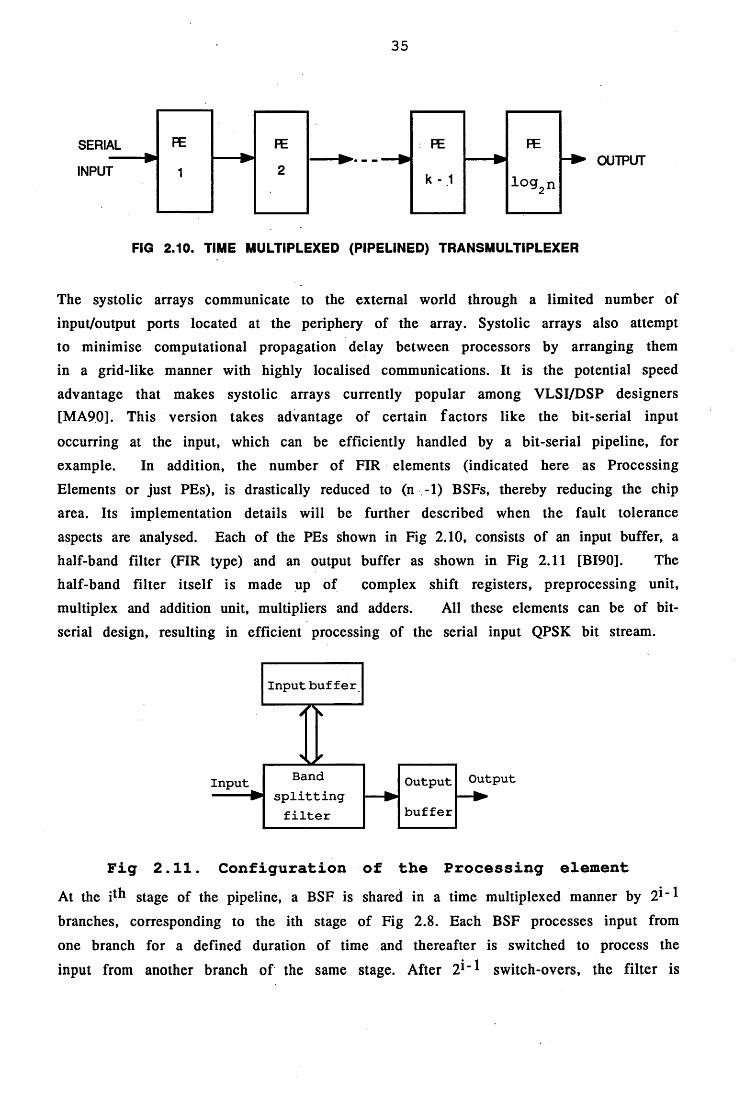
35
SERIALOUTPUT
INPUT
PE
FIG 2.10. TIME MULTIPLEXED (PIPELINED) TRANSMULTIPLEXER
The systolic arrays communicate to the external world through a limited number of input/output ports located at the periphery of the array. Systolic arrays also attempt to minimise computational propagation delay between processors by arranging them in a grid-like manner with highly localised communications. It is the potential speed advantage that makes systolic arrays currently popular among VLSI/DSP designers [MA90]. This version takes advantage of certain factors like the bit-serial input
occurring at the input, which can be efficiently handled by a bit-serial pipeline, for example. In addition, the number of FIR elements (indicated here as Processing Elements or just PEs), is drastically reduced to (n -1) BSFs, thereby reducing the chip area. Its implementation details will be further described when the fault tolerance aspects are analysed. Each of the PEs shown in Fig 2.10, consists of an input buffer, a half-band filter (FIR type) and an output buffer as shown in Fig 2.11 [BI90]. The half-band filter itself is made up of complex shift registers, preprocessing unit, multiplex and addition unit, multipliers and adders. All these elements can be of bit- serial design, resulting in efficient processing of the serial input QPSK bit stream.
Input buffer --------
Input Band Output Outputsplitting — ► — ►filter buffer
Fig 2.11. Configuration of the Processing elementAt the i1*1 stage of the pipeline, a BSF is shared in a time multiplexed manner by 21 ~ ^ branches, corresponding to the ith stage of Fig 2.8. Each BSF processes input from
one branch for a defined duration of time and thereafter is switched to process the
input from another branch o f the same stage. After 2 switch-overs, the filter is
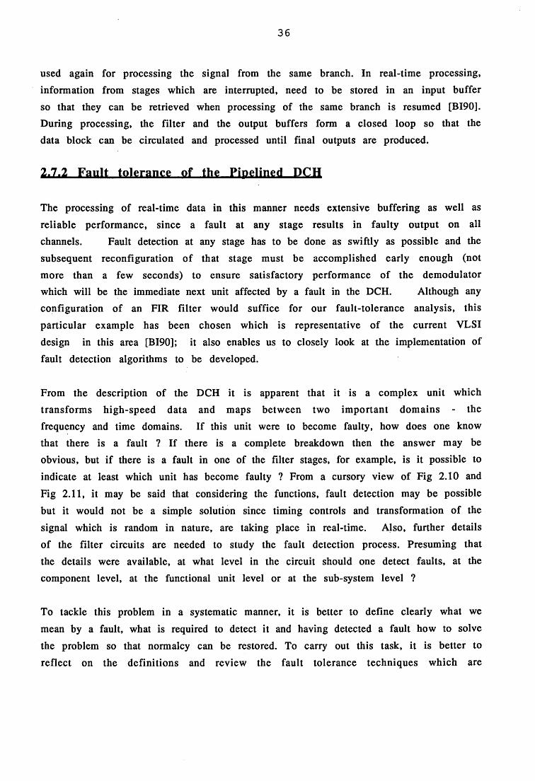
36
used again for processing the signal from the same branch. In real-time processing, information from stages which are interrupted, need to be stored in an input bufferso that they can be retrieved when processing of the same branch is resumed [BI90].During processing, the filter and the output buffers form a closed loop so that the data block can be circulated and processed until final outputs are produced.
2.7.2 Fault tolerance of the Pipelined DCH
The processing of real-time data in this manner needs extensive buffering as well as reliable performance, since a fault at any stage results in faulty output on all channels. Fault detection at any stage has to be done as swiftly as possible and the subsequent reconfiguration of that stage must be accomplished early enough (notmore than a few seconds) to ensure satisfactory performance of the demodulator which will be the immediate next unit affected by a fault in the DCH. Although any configuration of an FIR filter would suffice for our fault-tolerance analysis, this particular example has been chosen which is representative of the current VLSI design in this area [BI90]; it also enables us to closely look at the implementation offault detection algorithms to be developed.
From the description of the DCH it is apparent that it is a complex unit whichtransforms high-speed data and maps between two important domains - the frequency and time domains. If this unit were to become faulty, how does one know that there is a fault ? If there is a complete breakdown then the answer may beobvious, but if there is a fault in one of the filter stages, for example, is it possible to indicate at least which unit has become faulty ? From a cursory view of Fig 2.10 and
Fig 2.11, it may be said that considering the functions, fault detection may be possible but it would not be a simple solution since timing controls and transformation of the signal which is random in nature, are taking place in real-time. Also, further details of the filter circuits are needed to study the fault detection process. Presuming that the details were available, at what level in the circuit should one detect faults, at thecomponent level, at the functional unit level or at the sub-system level ?
To tackle this problem in a systematic manner, it is better to define clearly what we
mean by a fault, what is required to detect it and having detected a fault how to solvethe problem so that normalcy can be restored. To carry out this task, it is better toreflect on the definitions and review the fault tolerance techniques which are

37
currently available. Before introducing the topic of fault tolerance, a simple exampleto illustrate “what is fault tolerance” and “how is it useful”, is appropriate.
2.8 What is Fault tolerance ?
Fault tolerance is a concept which has been with us for a long time, perhaps used since the industrial revolution. To understand the concept, let us consider the motor car, which is extensively used. When we use a motor car, we know that there are certain parts which are likely to fail in time due to wear and tear. The most common part which wears out or is likely to become '’faulty", is the tyre. It therefore makes sense to carry a spare tyre in the boot, so that an immediate replacement is possible when necessary. Some users will perhaps carry a spare spark plug or a bulb. A set of tools to assist us in changing to a spare is very helpful when carried in the car. What are the factors which prompted the user to carry such things in the car ? The answer is that the manufacturers and service engineers, over the years found that these are the basic items necessary to assist the user, in case of a breakdown or faulty condition.
Does this mean that it is not necessary to carry anything else which could be of help in case of a breakdown ? The answer is not very simple, since it is a compromisesolution - a compromise between the number of spares carried (to increase theprobability of recovering the car to normal condition after a breakdown) and the
weight and volume of such spares which directly affect the economic running of the car. Such a compromise dictates the number of spares carried, depending on the road conditions and the travel needs. A passenger car in an urban area thereforecarries the minimum number of spares, while a military vehicle executing a journey
through harsh terrains carries the maximum.
Delving further into the process of fault detection, repair and reuse, it is apparentthat the driver detects the fault first, in most cases. Having detected a fault, thedriver subjects the suspected part to some kind of test, which may be a visual inspection in most cases. If found faulty, the part may be replaced if a spare is available, otherwise a compromise solution accepting degraded performance, may be found (low tyre pressure, for example). Often the suspected part can not be subjectedto simple visual tests for confirmation, since this requires experience as well as additional tools in many cases. Therefore, after suspecting a fault, the driver simply

38
decides to change the part and use a spare instead, leaving the job of testing to an experienced service engineer.
We can now relate our understanding of the motor car, to the basic concepts of classical fault tolerance as it is applied to electronic systems today. The sensing of a fault by the driver, is called fault detection in classical terms, while testing of the part (visually or otherwise) is called testing or self-test in certain cases. The spares are often termed as redundant units, while the process of changing over to a spare is known as reconfiguration.
Minor adjustments sometimes needed to put the car into normal running condition,
is known as recovery. Accepting degraded performance is termed as graceful
degradation. The precautions taken by m anufacturers/service engineers (like quality control during manufacture and periodic servicing of the car) so that a part does not fail easily on the road, is called fault avoidance. The whole aspect of finding a faulty part, its replacement and recovering back to normal use, is termed as fault tolerance. Although, the terms have been described in a very general sense, it helps us in understanding the classical concepts, which are described at length, in the next chapter.
2.9 CONCLUSION
Various schemes used for providing connections to the users of communication satellites, were described in this chapter. Limitations of the existing schemes, and the advantages provided by on-board processing of signals were described. After a general introduction to regenerative satellites which provide on-board processing, two conventional schemes to access the satellites viz., FDMA and TDMA were described. On-board processing using these two schemes, and the possibility of using one of them for the uplink and the other for the downlink, were indicated. The
equipment needed on-board to handle such a situation, was described at length
indicating the various units which help in transforming data from one format to the other. The reasons for using on-board processing with baseband switching are summarised in Table 2.2, where the conventional and new markets for satellite communication are compared. Fault tolerance studies performed earlier on one of the units called the TST switch described in section 2.6, brought out the need to conduct similar studies on the other complex units. The Digital Channeliser (DCH)
which is the key unit to transform signals from the frequency domain to the time

39
domain, was chosen for fault tolerance studies and its functions under normal conditions were described. Before applying fault tolerance techniques to the DCH, it
was considered helpful to provide a general overview of what is fault tolerance; a motor car was chosen as an example to describe the basic concept in section 2.8.
This chapter introduced the problem area in section 2.7, which is an on-board DigitalChanneliser. Its need, functions, the units associated with it, were described. Due toits complex nature, the need to provide fault tolerance has been stressed and ageneral introduction to fault tolerance, was provided in simple terms. Formal definitions in the area of fault tolerance, techniques used to detect and correct faults, management of spares etc., are the topic of the next chapter.

40
R e f e r e n c e s :
[ALAR85] G.Alaria, P.Destefanis, G.Guaschino, F.Pattini, G.Pennoni, P.Porzio Giusto, “On-board processor for TST/SS-TDMA satellite telecommunications”, ESA Journal, Vol.9, No.l, Jan 1985.[BHAR81] V.K.Bhargava, D.Haccoun, R.Matyas and P.Nuspl, "Digital communications by satellite", Wiley-Interscience publication, USA, 1981.[BI90] G.Bi and F.P.Coakley, "The design of Transmultiplexers for on-board processing satellites using bit-serial processing technique", 13th AIAA Int'l Communication
satellites systems conference, March 1990, pp 613-622.[ELAM86] M.H.M.El-Amin, B.G.Evans and L.N.Chung, "An access protocol for On-Board Processing Business Satellite System", Proc. 7th Int'l Conference on Digital SatelliteCommunications (ICDSC), Munich 1986.[EVAN86] B.G. Evans (Editor), "Satellite Communication", IEE Press, U.K, 1986.[FEHE83] K.Feher, "Digital communications - Satellite/earth station engineering",
Prentice Hall, N.J, USA 1983.[GRAE90] J.C.Graebner and W.F.Cashman, “ACTS Multibeam communication package- Technology for the 1990s”, Proc. 13th AIAA Int’l communication satellite systemsconference, Los Angelis, U.S.A, Mar 11-15, 1990, Paper AIAA-90-0835-CP, pp 497-503. [MEAD89] R.G. Meadows and A.J.Parsons, "Satellite Communications", Hutchinson Education, London, 1989.[MA90] G.K.Ma and F.J.Taylor, “Multiplier policies for digital signal processing”, IEEE
ASSP magazine, Jan 1990, pp 6-20.[MARS82] T.G.Marshall,C.M.Puckette,“prologue - Special issue on Transmultiplexers”,
IEEE Tran. Communications, Vol.COM-30, No.7, July 1982, pp 1457-1460.
[RODD89] D.Roddy, " Satellite Communications", Prentice-Hall, New Jersy, USA, 1989. [SCHE81] H.Scheumermann and H.Gockler, "A comprehensive survey of digital transmultiplexing methods", Proc IEEE, Vol.69, N o .ll, Nov 1981, pp 1419 - 1450.[WU84] W.W.Wu, "Elements of Digital Satellite Communication", Computer Science
Press, Maryland, USA, 1984.[SHAS88] C.R.Shashidhar and F.P.Coakley, "Concurrent fault detection in TST switches for on-board satellite systems", Electronics Letters,7th Jan 1988, Vol.24, No.l,pp 10-11. [TERR80] T.J.Terrell, "Introduction to digital filters", Macmillan Press, London, 1980. [WILL90] M. W illiamson, "The communications satellite", Adam Hilger - IOP
Publishing Ltd, Bristol, England. 1990.

41
[YIM88] W.H.Yim, C.C.Kwan, F.P.Coakley and B.G.Evans, "Multi-carrier Demodulators for on-board Processing Satellites", Int'l J. of Satellite Communications, Vol.6, 1988, pp 243-251.

42
“A n y l a s t m i n u t e i m p r o v e m e n t s i n d e s i g n d o n o t h e l p i n i m p r o v i n g t h e s y s t e m s i n c e s u c h i m p r o v e m e n t s a r e n o t e v a l u a t e d a n d p r o v e n f o r r e l i a b i l i t y " - Quality control guidelines in space industry.
3
FAULT TOLERANCE : REVIEW
3.1 INTRODUCTION
The importance of fault tolerance was explained at the end of the previous chapter using the analogy of a motor car. In this chapter, principles o f. fault tolerance
applied to electronic circuits are described followed by a review of the methods usedto achieve fault tolerance. A considerable part of the work done in the area of faulttolerance is applicable to computer systems, although significant contributions have been made to other systems used in . critical applications demanding high reliability. The concepts of fault tolerance are now introduced by taking off from where we left the motor car example, in the previous chapter.
Unlike the motor car, most electronic systems today do not have a driver to detect thefault. They use fault detection circuits which indicate that something is faulty and further self-test circuits are used for confirm ation purposes. The enormous experience gained over the years in the manufacture of motor cars as well as their servicing, is certainly not available to electronic systems which are of relatively recent origin. It is therefore necessary to conduct detailed analysis of the limited amount of data gathered over these years and use them effectively to provide a higher reliability in future. In satellites, the problem is further compounded by the fact that no human being can personally go to a satellite to carry out repairs. Although the space shuttle has demonstrated this possibility in near-earth orbits, it is not considered economically feasible to carry out repairs in other orbits, where the majority of the commercial satellites are found. There are many instances where a particular type of circuit has never been used earlier under critical operating environments like nuclear, space etc., a situation often encountered while using electronic components of a recently developed technology. In such instances, it is
necessary to apply the environmental constraints to the circuit under question and carry out simulations to ascertain the possible failure modes, fault detection methods,

43
and reconfiguration strategy. These aspects are described in the following sections of this chapter, which forms the background to our thesis work.
There are several well written texts on fault tolerance in circuits, of which acomprehensive example is edited by Pradhan [PRAD86]. Different aspects of fault tolerance may be found in other texts [LALA85, ANDE81, JOHN89, WAKE78]. In this chapter, we review the techniques currently available to meet the requirements and their suitability to our work. The classification of faults, fault models, fault tolerance techniques etc will be presented, followed by a section on software reliability. After the general review, some techniques applicable to DSP circuits are surveyed and their application to the DCH circuit is presented. A detailed version of this survey can be found in TRAGH911. Finally, an overview of 'Design for test' and 'self-test'
techniques is presented, since this is an area of considerable importance to diagnostics and important milestones have been recently reached in this area.
3.2 Fault tolerance - concepts
Fault tolerance principles have been applied to many electronic systems for over 20 years. Principal areas of application include computers, aircraft and satellite systems, military and nuclear systems as well as others where reliability has been an important criterion. Reliability is achieved both by design selection (using tested components whose reliability figures are available) and by providing spare
elements in the actual system.
When faults develop in an operating system, the first requirement is obviously todetect it, which may require a simple comparison check or a sophisticated algorithm,
depending on the system in question. The next requirement is that spares should be available to a well defined process which switches out the faulty element and
switches in (or substitutes) the spare one by a process called reconfiguration. The techniques which use redundancy, work only when the redundant part has not also failed. The third requirement is to analyse the suspected part and decide whether thepart is reusable in some way or is to be discarded altogether. Fault tolerant techniques are cost effective only when the probability of a failure is very small;they are most effective when applied with components which are already as reliable
as they can be made [JOHN89].

44
Although the terms "fault" and "error" are used frequently to refer to the samesituation in digital circuits, in classical terms they are defined as the cause and its effect [ANDE81]. A "fault" is defined as an anomalous physical condition, whereas an error is the manifestation of a fault in a system, in which the logical state of anelement differs from its intended value. As a further effect, an error in the systemresults in the "failure" of that system. A fault in a system does not necessarily resultin an error, since an error occurs only when a fault is sensitized. A fault which is not sensitized is referred to as a latent fault and need not manifest itself into an error (eg: a faulty relay whose faulty position is currently not required by the circuit).The term "soft error" refers to a situation where an error persists even after theoriginating fault disappears; however, after correction of the soft error, the system is usually left undamaged. This aspect is explained later in connection with the faults that occur due to radiation in the space environment.
3.3 FAULTS - GENERAL CLASSIFICATION
The general fault classification in Integrated Circuits (ICs) is shown in Fig 3.1, wherethe source of errors in ICs is traced [RUSS89]. Faults have been categorised into design and physical faults which are applicable to any circuit.
Fault types
r
I-Design
I _ 1Database errors Design errors
Schematic Model Input entry errors waveform errors errors
IPhysical
+Temporary Fabrication
defects
I —Electrical EMI
Noise
“ 1Softerrors
1Wearout
Electron overstress migration
I I Redundancy1 | I iLogical Timing Inadequate Inelegant sh<ms 0pens Dxide
errors errors testability design defects
Permanent +
Intermittent
Fig 3.1 Taxonomy of faults in ICs
The faults inherent to design may be reduced by quality assurance procedures like
component screening, testing of sub-systems and integrated systems within known

45
environments [MATH81]. After a product is fabricated and tested, while working in the field (space environment in our case) physical faults continue to affect itsoperation. The soft errors which are temporary in nature, are of particular interest
to circuits operating in the space environment, as explained in the next section.
3.3.1 Faults due to Space Radiation
In the space environment there are two types of faults which are induced byradiation [SROU88], viz.,
(i) Total radiation dose failures(ii) Single event upsets
Total radiation dose is the overall radiation absorbed by a circuit component during its life time in the space environment. In silicon devices, holes trapped in interface
junctions are stable over a period of time and are a major cause of circuit failure for ICs exposed to the slow radiation dose in space, as it leads to a shift in the gatethreshold level. Another effect is the increased leakage in junctions leading to a reduced gain in bipolar devices and an increase in the overall chip leakage [PEAS88]. Radiation induced failure mechanisms have been classified into three categories: power-supply related failures, logic-level failures and timing failures [BHUV86].Shielding and radiation hardening are techniques commonly used to reduce theeffect of total radiation [KERN88]. One can expect to see complex silicon MOS ICs with very thin (below 100 A0) gate oxides in the 1990s, which should inherently reduce
their susceptibility to threshold shifts [KERN88].
Single Event Upsets (SEUs) are normally reversible changes in the digital logic state due to a hit by an energetic particle, which results in errors called "soft errors".Particularly latch up conditions due to SEUs can lead to bum out of ICs. With higher levels of integration, smaller areas are used per device, making them more vulnerable to SEUs. The soft-error rate problem has been tackled by either physical
or system level approaches [SAVA86]. Physical approaches include for example coating a DRAM chip with a layer of material, or aluminium alloy shielding forspacecraft. System level approaches are the redundancy schemes which have been tried by several researchers, for example the application of codes or the use of spares and self-checking circuits in microprocessors [MAIE83] or the use of
duplication to detect errors in a memory [ABRA83].
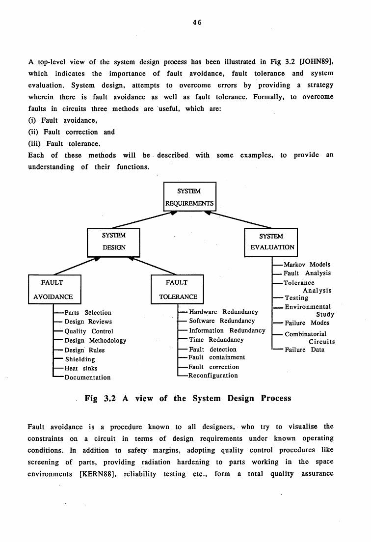
46
A top-level view of the system design process has been illustrated in Fig 3.2 [JOHN89], which indicates the importance of fault avoidance, fault tolerance and system evaluation. System design, attempts to overcome errors by providing a strategy
wherein there is fault avoidance as well as fault tolerance. Formally, to overcome faults in circuits three methods are useful, which are:(i) Fault avoidance,(ii) Fault correction and(iii) Fault tolerance.Each of these methods will be described with some examples, to provide an understanding of their functions.
SYSTEM
REQUIREMENTS
SYSTEM SYSTEMDESIGN EVALUATION
-Parts Selection— Design Reviews— Quality Control— Design Methodology— Design Rules— Shielding — Heat sinks “ “ Documentation
FAULT FAULT
AVOIDANCE TOLERANCE
— Hardware Redundancy— Software Redundancy— Information Redundancy■“ Time Redundancy
- Fault detection -Fault containment
— Fault correction — Reconfiguration
• Markov Models . Fault Analysis•Tolerance
Analysis-Testing- Environmental
Study- Failure Modes■ Combinatorial
Circuits■ Failure Data
Fig 3.2 A view of the System Design Process
Fault avoidance is a procedure known to all designers, who try to visualise the constraints on a circuit in terms of design requirements under known operating conditions. In addition to safety margins, adopting quality control procedures like screening of parts, providing radiation hardening to parts working in the space
environments [KERN88], reliability testing etc., form a total quality assurance

47
procedure [MATH81], which may together be referred to as "fault avoidance", indicated in Fig 3.2. There are also specific circuits which could be used as a general precaution, to provide fault avoidance; the soft-error filtering [SAVA86] and other schemes to tolerate SEUs in microprocessors [MAIE83] , or memories [ABRA83] are good examples to minimise the design faults indicated in Fig 3.1.
Fault correction is a method by which an input is coded by different schemes, each of which is injected into a different stream and the output of these streams is fed to a voting circuit which selects the correct output using a majority voting circuit [COSE88]. Therefore, reconfiguration will not be necessary in such circuits. Often, this method is included as a part of the fault tolerance strategy, to provide a more comprehensive means of achieving reliability. However, in DSP circuits this method in itself can serve as a means to achieve fault tolerance, as will be explained later.
Fault tolerance is an overall strategy whereby a fault is detected, reconfiguration isapplied and the management of spares is effected with the assistance of self-test and diagnostics. The highest levels of reliability can therefore be achieved using an optimum number of redundant units, using the fault tolerance strategy. There aresix elements, one or more of which are used in a fault tolerance strategy [NELS90],viz.,(a) Masking: Dynamic correction of generated errors (fault correction),(b) Detection: Detection of an error - a symptom of a fault,(c) Containment: Prevention of error propagation across defined boundaries,(d) Diagnosis: Identification of the faulty module responsible for a detected error,(e) Repair/Reconfiguration: Elimination or replacement of a faulty component, or a
mechanism for bypassing it,(f) Recovery: Correction of the system to a state acceptable for continued operation.
Revert to normal
Faultdetected
MonitorFaults
NoFault Fault
detected
Normal
Self-test
RecoveryFaultdetection
Diagnostics
Reconfiguration
Fig 3.3 Fault tolerance scheme
48
The general scheme used in the fault tolerance of circuits is shown in Fig 3.3. A fault detection circuit monitors the performance of a normal circuit, on a regular basisand unless an error is detected no action is taken. If an error is detected then thesystem reconfiguration and recovery states are effected. A self-test is also initiatedon the suspected part; if the part passes the test then the diagnostics routine initiates actions to list the part as a spare and informs the reconfiguration scheme. If the part fails the self-test then the diagnostics will declare the part as unusable and informs the reconfiguration scheme accordingly. If a fault correction scheme is used thenthe detection may be done by coding circuits and the reconfiguration and recovery
steps are replaced by fault correction circuits using a voting mechanism.
3.4 Circuit Levels of Fault tolerance
In the previous section, the sources of fault and the basic approaches to overcome them were described. Before considering fault tolerance in a given circuit, it isnecessary to ask "at what level in the circuit should fault tolerance be applied". It is
not easy to decide the level, unless the implications of such a decision are understood. Application at logical or component level, generally increases the protection achieved, but also increases the amount of specialised circuitry required. Fault avoidance is normally applied at the component level since the design process involves the selection of components. With the advent of VLSI it is difficult to say whether the components in the design process are discrete components, logicalblocks or functional blocks. Application of fault avoidance circuits like the soft-error filter described earlier, are therefore, not restricted to the lowest (component) level. Fault correction and fault tolerance can be applied at any level depending on
the level at which reliability is needed. The level at which redundancy is needed is obtained by a trade-off between accuracy and ease of modelling and analysis [NELS90]. The three levels at which redundancy can be provided are at thecomponent, logical and functional levels, each of which have their implications as
follows:
Component level: At the component level, faults are technology dependent. Some of
the physical faults indicated in Fig 3.1, such as shorts or opens in metal orpolysilicon signal lines can be detected and corrected at this level. Faults due toexternal disturbances like electrical noise, EMI and soft errors (eg: due to radiation),can be detected at this level. It is therefore best suited for circuits using a new

49
technology or in situations where the detailed evaluation of the circuit under faulty
conditions, is needed.
Logical level: Any digital system can be modelled with gates and memory elements,
with all the signals represented as binary values. Any error in the logical values can then be detected and corrective action can be taken. "Stuck-at" faults are the most common models used at this level, although models of "bridging" faults which occur due to a coupling between signal lines, are used occasionally [PRAD86]. Most
combinational circuits could benefit from a fault detection at this level.
Functional level: At the functional level, faults which occur at functional blocks like
registers, arithmetic units, logic units etc., appear as changes in the module's behaviour as indicated by the truth tables. Fault tolerance at this level is usually helpful for fault simulations at the behavioural level [NELS90]. For circuits having a large number of components like in a VLSI, this is the only practical solution to accurately model the failures of complex chips [GHOS88].
3.4.1 Effect of fault tolerance - all levels
The effects of fault-tolerant design strategy on system reliability can be expressed as follows [NELS90]:
R system = (no fault} + Pr {correct operation/fault} * Pr {fault} ... (3 .1)
where Pr{no fault} is the probability that no fault will occur, which must be maximised by fault avoidance; Pr{correct operation/fault} is the conditional
probability that a system will continue to operate correctly given the occurrence of a fault, which represents the coverage of the fault-tolerance mechanism. Each coverage term is weighted by Pr{fault} i.e the probability that the corresponding fault will occur. If the probability of occurrence of a particular fault is high, then
the system may be able to tolerate all of a given set of faults and yet not be sufficiently reliable for the application.
Fault tolerance in a digital system can achieved, at any circuit level, through redundancy in hardware, software, information (codes) and/or computations as indicated in Fig 3.2. A fault-tolerant system designer must therefore consider the
performance, complexity, cost, size and other constraints. So far, the fault tolerance

50
approaches to hardware were discussed. While these are essential to all digital systems, it is necessary to consider the approaches in software reliability in order
to complement the fault tolerance efforts in hardware.
3.5 Software reliability
Although it is not known as to when software reliability or probabilistic modelling of software errors began, it is clear that by the late 1960's software designers had begun to think a lot about reliable software [SH0084]. The basic problem in the
software area is that the complexity of the tasks which software performs has grown faster than the technology for designing, testing and m anaging softw are development. Due to lack of a sufficient database concerning the study of reliability models as well as testing and demonstrating their accuracy, there has been considerable controversy in this field. Some researchers have studied the successful efforts in small experiments to collect software reliability and error data andevolved the necessary conditions to establish a software reliability database, as described in [SH0084]. Obviously, these conditions are basic guide-lines and do not in themselves suggest particular models or approaches to reliable software. There have been some attempts to provide software fault tolerance, which are described
nex t.
3.5.1 Software fault tolerance
Attempts to provide reliable software for critical applications have assumed "diversity" as the guiding principle by providing alternate versions of software toachieve the same objective. The diversity may be in the design methods(algorithms, for example) used or the data used, which can be provided by multiple versions of software or by generating logically equivalent data sets, respectively. Two methods of design diversity are well known, viz.,(a) Recovery blocks(b) N -version programming.
In the recovery block method [RAND75], results of an algorithm are submitted to an
acceptance test, failing which, the system restores the state of the machine to thatprior to execution of the algorithm and then executes an alternate algorithm. Theprocess of reexecution is repeated until all the set of alternate algorithms are
exhausted, or a satisfactory output is produced.
51
In the N-version programming method, separate, independent versions (N versions) of a program are prepared [AVIZ85, ANDE81]. All the versions are executed in parallel, receiving identical inputs and producing its version of the required output. A majority voter collects the outputs and the results of the majority are sent as the correct output. The N - version programming has been applied using the A d a language, in the HERMES project for manned space missions, where reliability of the mission is considered critical [SIMO90].
Data diversity on the other hand, is an approach orthogonal to design diversity, in the sense that in addition to design diversity, diversity of the input data can be used to execute the same software on a set of related data points [AMMA88]. To obtain diversity of the input data, a simple method known as data reexpression which generates logically equivalent data sets, is used. Normally, an input x is given directly to a program P to produce an output P(x). A reexpression algorithm R transforms the original input x to produce a new input y , where y = R(x). The input y may contain the same information as the input x, but in a different form, or y may approximate the information in input x .
System^Input
System Output
Execute Re-expressAlgorithm Data
ValidOutput?
Deadline ^ - Yes Invoke E x p ire d ? ^ Backup
Fig 3.4(a) Retry block
Fig 3.4 Data DiversityCopy 1
Copy 2 SystemOutput
SystemInput
Re-expressData
Copy N Voter
synchronisation information
Fig 3.4(b) N-copy programming

52
Often data is reexpressed naturally in circuits when samples are taken at different points which are connected by passive circuit elements that do not transform data;samples at different points along a shift register chain, for example.The design diversity methods of Recovery blocks and N-version programming, can be modified to use data diversity and have been renamed as Retry blocks and N-copyprogramming, respectively and Fig 3.4 shows the two modified versions [AMMA88]. The retry block scheme uses only one algorithm where the acceptance test has thesame form and purpose as that of the original recovery block scheme. However, if the acceptance test fails, the same algorithm is executed after the data have been
reexpressed. The execution is repeated until either the deadline expires or a satisfactory output is produced.
The N-copy scheme is similar to the N-version programming, where although N copies of a program are executed in parallel, each acts on a set of data produced by reexpression. The voter has the same function as in the N-version programming
which is to accept the output of the majority.
Data diversity could be a useful technique in many situations, since digital circuits often have the same data expressed at different points in the circuit. Its application in fault detection circuits could prove useful to reconfirm the operation of the detection circuit itself, as will be explained in the later chapters. In general, it is the system reliability which is of concern while designing a fault tolerant system and the system reliability is a product of the hardware reliability, the software reliability and the operator reliability [SH0088], as expressed by the following simple equation.
Rsy = Rh -Rs -Ro — (3-2)
Reliability of the operator is a function which is of concern particularly in complex
satellite systems, as explained earlier in chapter 1. The aim of an autonomous fault
tolerant system on-board, is indeed, to reduce if not eliminate, the probability of failure due to an operator.
Software and hardware reliabilities are terms which may be separately expressed, but improving both, using fault tolerance is the final goal. In this respect, a recent effort to consider faults irrespective of their source (hardware or software) provides
a useful direction [KIM89]. If the detection schemes in DSP circuits apply this

53
principle to enable a quick detection, then diagnostics and self-test may be used later
for detailed fault analysis.
3.6 Fault tolerance in DSP circuits - constraints
Our interest is in DSP circuits as explained in the previous chapter and it must be mentioned here that the majority of fault tolerance methods available to computersand conventional combinational circuits, are not readily applicable to DSP circuits
for the following reasons:
1) DSP c ircu its perform the tasks of repe titive m u ltip lica tio n and
addition/subtraction, on real-tim e data using dedicated hardware. Therefore, techniques like data retry, initialising all the input ports and injecting test vectors etc are not practical, since the flow of real-time data has to interrupted to perform any of these. Often data retry is not be possible since it may be the digitised format of a user’s voice signal. Initialising all the input ports will mean an interruption of the real-time data. Having initialised, a test sequence needs to be initiated in order to verify the existence of errors, if any. Until the test sequence is complete and theresults are analysed, the real-time data flow will have to be stored or would be lost.The pseudo random test sequence for a multiplier described in [DENY85] for example, needs 2046 clock cycles, in addition to which the time needed to cut-off the multiplier must be accounted for. It still leaves the basic question as to how a particular element, say multiplier, came under suspicion in the first place. Data retry andrunning a test sequence, may be carried in mainframe computers, since users do notexpect real-time operations on a continuous basis. To schedule such tests, the user’s tasks can be rearranged in a main frame, which is not possible in DSP circuits
dedicated for real-time operations on a satellite.
2) During multiplication and addition, multiplexing operations on the input data followed by recycling, referred to as the “multiply and accumulate” process, to obtain the final output, which is common in DSP algorithms like convolutions, FIRfilters, DFTs. This will mean that tests generated for conventional computers, must also incorporate a multiplexer in order to coordinate the monitoring of output data.
This complicates the sequence of the test since the test circuit itself becomes susceptible to the multiplexing faults, unless a totally self-checking circuit is used [WAKE78].

54
3) Assuming the availability of a reliable test system, the number of tests required inDSP circuits becomes quite large since the data is available at different ports, atdifferent times. For a real-time distributed system of this nature, the correctness of the system depends on its behaviour with respect to time. Therefore, multiple fault
detection circuits would be necessary.
Fault detection and correction schemes for DSP circuits is an area of considerable interest in the recent years, a detailed survey of which is available in [RAGH90]. The fault avoidance procedures explained earlier, are applicable to DSP circuits as well,but fault detection and correction schemes concerning DSP circuits like FFT, arithmetic units etc., and reconfiguration under "no repair" conditions as insatellites, which have developed in the recent past, will be reviewed in this section. After the review, techniques which are useful for on-board circuits will be described by discussing the constraints, suggesting modifications, where necessary.
3.6.1 Fault detection techniques for DSP
In DSP circuits the Fast Fourier Transform (FFT) is one of the well known methods used for signal transformation. Some techniques for error detection and location in FFT circuits have been described in the literature. The Fourier Transform (FT) is an algorithm for transforming data from the time to the frequency domain. Toimplement a FT, a “time record’ of ‘n ’ consecutive, equally spaced, samples of the input signal are taken as a block and are transformed into a block of frequency l i n e s . To compute the Fourier transform digitally, numerical integration needs to be performed, to give us an approximation to a Fourier Transform. Such an
approximation is called the Discrete Fourier Transform (DFT). Before the development of the FFT, the DFT required excessive amounts of computation time, particularly when the number of samples ‘n ’ is large. FFT assumes ‘n ’ to be a multiple of 2, for instance 1024. This allows certain symmetries to occur, reducingthe number of calculations (multiplications) required. Further details on the FFT are
available from any standard text on DSP.
It may be recalled that FFT was mentioned in chapter 2 (Fig 2.9) as one of the methods to implement the tasks of a Transmultiplexer/Digital Channeliser (DCH) in the onboard processing system. Therefore, some methods which provide fault detection in FFT circuits can serve as useful pointers to our work. The conventional method of dynamic redundancy with “hot” standby units, can be used to detect errors in FFT

55
circuits as well. An alternative to this method is the use of codes to detect errors in DSP circuits. Both methods to provide fault detection, have been described .
Four techniques of fault detection have been described in this section. The first technique uses data retry to detect errors in a particular type of FFT circuit known as
butterfly networks [JOU88]. The second technique uses time and hardware redundancy to provide detection in similar FFT circuits [CHOI88]. The third one is a compromise between the first two approaches [JOU88]. The fourth technique restricts detection to the arithmetic unit and illustrates the application of codes to achieve fault detection [BROS88].
3.6.1.1 Fault detection in FFT network - space redundancy
To arrive at an optimal error coverage without compromising throughput, spaceredundancy has been suggested by Jou and Abraham [JOU88]. This approach uses thesuperposition principle and circular shift properties to detect errors in FFT networks. For fault location and distinguishing between roundoff and functional errors, a data retry method has been proposed by them. A simplified fault model of the FFT butterfly module is developed, which assumes that faulty adders can be modelled as those causing errors on the output lines and that failure would be confined to a single complex multiplier or adder or one set of input/output lines (orregisters). The fault model is further simplified by reducing the errors to an
equivalent set of errors at the input/output ports of each module. A DFT (Discrete Fourier Transform) algorithm is used in a matrix form to develop a concurrent error detection scheme, which is described in [JOU88]. A limitation of this scheme seems to be that only a single error in any of the elements in a butterfly module can be detected. Also, the error latency would be equal to the computation time of summation of the outputs. The cost of total hardware implementation in floating point number systems becomes very high.
3.6.1.2 Fault detection in FFT network- time + snace redundancy
The second approach by Choi and Malek [CHOI88] suggests the use of time and space redundancy thereby achieving 100% error coverage but with a lower throughput rate than the first method. They assume that due to limited memory space, there would be no information exchange between butterfly computation units, resulting
in a fault detection scheme that uses recomputation with a single cycle delay. The

56
fault detection scheme has been called “recomputing by alternate path", which is a concurrent error detection technique based on time and space redundancy. The FFT computation is repeated on different butterflies using a special reconfiguration scheme and an additional stage in the FFT network. Most computations are duplicated and compared, to detect faults in the butterfly computation units. For the purpose of diagnostics and reconfiguration, cell bypass links or cell bypass registers have been assumed. Comparators to compare the outputs from the last two stages, have also been assumed in their design. A simple graceful degradation scheme using an external data separator, buffer memory and an internal control circuitry has been suggested
by them [CHOI88].
3.6.1.3 Fault detection in FFT network - compromise approach
A compromise between the two approaches described in the previous sub-sections, has been suggested by Jou and Abraham, as the third approach [JOU88]. By modifying their butterfly network (removing the encoding, decoding and checking parts), recomputation using an alternate path has been accomplished. In the modified network, on the first attempt, normal input data is used and during the second attempt, input sequences are multiplied by j and the corresponding output sequences
multiplied by -j. This is done by swapping the real and imaginary part and by changing the sign, without using an arithmetic unit. Error detection and location procedures have been applied to the two sets of outputs. Using the compromise approach, hardware overhead has been shown to be the additional comparators and switches, which are considered small compared to the overhead of butterfly units used in the redundant stage proposed by them, as described earlier in section 3.6.1.1.
3.6.1.4 Error detection in arithmetic units - using codes
A modular error detection technique by Brosnan and Strader provides an example of the use of codes in arithmetic units. They have used error detecting codes in multipliers [BROS88]. For arithmetic error detection AN codes and Residue codes are commonly used [PRAD86, WAKE78].
Residue codes have the advantage in that data and the check bits can be handled in
parallel, therefore the speed of a system would not be reduced because of the checking circuit. A particular class of residue codes, known as "low-cost residue
codes", which have an error detection capability comparable to AN codes but require
57
less hardware than conventional residue codes, have been used by them to detect errors in individual functional processing elements [BROS88]. Check bits have beenformed using the formula r - x mod m , where x is the data, m is the check modulus and r is the residue or check* bits.
MULTIPLIER re su lt
se r ia l mod 3
g e n e ra to r
t *mod 3
m u ltip lie r
se r ia l mod 3
g e n e ra to r
r’l = rl b i + r2 bi
W 2 V r2 bi
nSerial mod 3 generator
co m p ara to r e r r o r
b mod 3
Fig 3.5 Error detection at the overall level
Error checking at the overall level is shown in Fig 3.5 [BROS88], where a simplemethod to form the residue of each input operand is illustrated. When a product is produced, its residue can be calculated separately and the product of input residues are also computed in parallel. On completion of a multiplication process, the residue
of the product can be compared with the 'product of the residues'. In normalcircumstances they must be equal, otherwise an error signal is produced. Since the
error checking circuit assumes correct operation of the comparator and checks onlythe operation of the multiplier, it is essential that a self-checking comparator beused. Another limitation would be that the hardware required to form the residues ofthe input/output may become quite complex.
The four techniques described, have certain limitations in their application to the
DCH. The first three methods exploit certain properties which are specific to the FFT and assume some form of data retry, which is not practical in a real-time circuit like
A #the DCH as explained at the beginning of this section. The fourth method is useful mthe sense that it applies to a general arithmetic unit. Its limitation however, is the
use of codes and multiple paths of redundant hardware. In addition, the question of

58
how reliable the coding and decoding circuits are, remains. Methods to make circuits Totally Self-Checking (TSC), are available [WAKE78], but at the cost of further addition of hardware. Coding schemes in general, require about 20% of additional space to implement coding and decoding circuits, which is not acceptable for space applications. In addition there is the requirement of space for the redundant paths. While they hold good prospects for ground applications, for space applications some means to avoid the redundant paths and keep the error detection advantages of codes, if possible, could be a good solution. It is also necessary to ask ourselves whether fault detection during every arithmetic cycle (m ultiplication for example) is necessary ? If there could be a compromise on this, would it save hardware required for the detection circuit ? These aspects are discussed further in chapter 5, where a fault detection scheme for the multiplier, is developed.
The next sub-section describes fault correction techniques, which in addition to detection, also correct the output, based on the information available in codes. After an introduction to the Residue Number System from which all error correction codes
are derived, three techniques of applying codes for error correction are presented.
3.6.2 Fault correction techniques
Residue arithmetic has been used for over 40 years in various types of circuits, a good tutorial on which is available in [TAYL84]. In DSP circuits, error correction properties of residue numbers have been used to avoid reconfiguration. The Chinese remainder theorem has provided a base for the extensive work carried out on the Residue Number System (RNS) which seems well suited to high speed circuits. However, a limitation in RNS is that the dynamic range overflow which can occur during multiplication operations has to be detected by a magnitude comparison, which makes it unattractive for conventional computing systems [TAYL84]. In digital filters, convolvers and DFTs, this would be an acceptable constraint, since high speed multiplication of a 16 or 32 bit wordlength is of prime importance. Data is first converted into the required number systems during which several alternative
radices could be obtained and used in parallel for arithmetic operations at the end of which they would be reconverted and compared. Unlike other error detection techniques, error detection in these techniques does not lead to reconfiguration of
the hardware, but leads only to a selection of the correct output; such techniques are often termed as error correction techniques.

59
Arithmetic codes used in each configuration could be different and error detection and correction abilities vary considerably [WAKE78]. To illustrate some of these variations^ three techniques are reviewed [JOU86, COSE88, ZAGA88], which are the Weighted Checksum Coding scheme (WCC), the Redundant Residual Number System (RRNS) for systolic arrays and finally the Finite field architectures for digital filters.
3.6.2.1 W eighted-checksum technique for fault correction
DSP algorithms like convolutions, FIR filters, DFTs etc., involve a "multiply and accumulate" type of expression which could be formulated as a matrix-vector multiplication problem. The WCC technique by Jou and Abraham, uses distance-3 codes which have the property of representing code outputs as separate information matrix and check vectors [JOU86]. Residue arithmetic properties help in reducing the number of weighted checksums and the computed output may be viewed as a distance-3 code which has error correction properties. Such a matrix also has the property of preserving the weighted checksum property even after a full row or a full colum n is m anipulated during m athem atical operations. T herefore, manipulations are effected on full rows or full columns depending on the type of operation viz., addition, multiplication, LU decomposition, transpose, product o f a matrix with a scalar etc., to take advantage of the matrix’s property. Application of the WCC techniques in operations like the FIR filter, DFT etc., for error checking has been illustrated by Jou and Abraham [JOU86], using fixed point number systems. Considering a typical matrix element a y , it may be expected that this element can be
stored in the local memory of the i1*1 processor at the j 1*1 time step. At the j1*1 time step the value of xj could be broadcast to each processor. Since each processor multiplies n pairs of a y and xj and accumulates the product in a register, each could
calculate one element of the result vector. Therefore, a faulty processor would affect only one element of the matrix, which can be corrected using distance-3 codes.
3.6.2.2 Fault correction in systolic arrays
Systolic structures divide a processing task into many simple tasks which are performed by small, identical, easily designed processors. In such a structure, every processor communicates only with its nearest neighbour, which sim plifies the interconnection, reduces signal delays and clock skew problems. The RNS can reduce computations by resolving a problem into a set o f parallel, independent
computations which are performed by module-controlled processing channels as

60
shown in Fig 3.6 [COSE88]. A combination of RNS and systolic features is used by
Cosentino who tries to exploit the regularity of systolic arrays and utilise some of the potential for redundancy in two level pipelining, to provide fault tolerance [COSE88].
<x.>MODULO 17
<x.>17.19.23MODULO 19
Binaryx j+ i - *In p u t
<x.>•o
MODULO 23<x> <y.> -< y >
BaseExtension,<x.>
MODULO 31 29Error
Calculator
-<yi>L = Filter length
<h >
Fig 3.6 RRNS processor model with concurrent error detection
In Fig 3.6, two redundant channels are used to correct one erroneous residue of aresidue-output n-tuple. The binary representation of an input as well as its residues modulo 29 and 31, are used for comparison with the product residues from the output of the modulo 29 and modulo 31 channels. Normally, all the five residue outputs would be correct and corresponding pairs of output product residues would agree. Assuming the residue output of one of the channels, say modulo 29, is in error, then
the two modulo 29 product residues would not agree but product residues of the other, say modulo 31 would agree. The system output would then be determined by ignoring the modulo 29 channel. An FIR filter using this model has been described in [COSE88].
3.6.2.3 Fault correction using convolution codes
Digital filtering operations are normally carried out on data sequences which arebroken into segments, to help in applying fast cyclic convolution techniques on
individual sections. Cyclic convolution of segmented sequences has been suggested

61
by Zagar and Redinbo as a technique useful for fault tolerance in system design[ZAGA88]. Using the residue number system, these convolutions could be decomposed into into many parallel realizations, and they suggest the use of cyclic codes in a distributed manner throughout the architecture [ZAGA88]. A normal filter systemhas been augmented with parallel watchdog circuits whose output values are compared against parity quantities recalculated from the normal system's output. Parallel watchdog circuits seem to have an advantage in terms of speed performance of the filter, but it is largely compensated by the redundancy required, making them unattractive for systems using a large number of filters.
The error correction methods use codes and redundant channels for fault detection and subsequent selection of the correct output. The methods are suitable for a wide range of DSP circuits, but the limitation in space applications is the restriction on
space and weight. Additional size due to the number conversion circuits and a further increase in size due to the number of redundant channels, makes the error correction schemes unattractive for space applications, although for groundapplications these methods hold good promise particularly due to their ability toselect the correct output, avoiding the need for reconfiguration using spares.
3.6.3 Reconfiguration schemes
Reconfiguration is needed only for the systems which use fault detection techniques and not for those using fault correction, as described earlier. For fault detection, onboard satellite systems must take into account the fact that the elements discarded out during reconfiguration, cannot be repaired. Two schemes, one suggesting thereconfiguration strategy in such a situation and another which develops a theoremfor diagnosis and reconfiguration under sequential fault occurrence, are described
in literature [RAMA86, SOMA90], both of which are reviewed in this sub-section.
3.6.3.1 Reconfiguration with “no repair”
An optimal reconfiguration strategy for systems with "no repair", has been suggested by Ramamoorthy and Eva [RAMA86]. The basic assumption is that if a system functions correctly, its state is termed as 'operational' else its state is termedas 'dead'. A failed system has been classified into 'reconfigurable' state if it is possible to reconfigure, otherwise as 'dead'. For each operational state, there may be more than one failed state that the system can enter into, caused by failure of different

62
components in that state. For each reconfigurable state, there could be more thanone operational state that the system could enter into, since it depends on the ability to reconfigure in more than one way. Since there would be no repair, the system would start with an operational state, go through a sequence of reconfigurable and operational states and finally would enter a dead state. A polynomial time algorithm has been used by them to find an optimal reconfiguration strategy [RAMA86]. An optim ising criterion for choosing the best reconfiguration strategy could be
maximising of expected sum of one performance index, with some given constraints on the other performances indexes.
3.6.3.2 Reconfiguration using sequential fault diagnosis
In most practical systems, several faults do not occur simultaneously and the systemcan keep a watch on the occurrence of faults, detecting and isolating them during reconfiguration. But conventional diagnosis schemes expect that any normal system has to tolerate a set of faults all of which are assumed to occur at the same time. In most mission-oriented applications like satellites, space vehicles etc., the system is required to be operational without maintenance, throughout the life-time of the mission. Therefore, it is reasonable to assume that faults occur in a series of sequences and faulty units can be isolated before the occurrence of the next set offaults. Somani has derived a theorem to prove that sequential fault diagnosabilitycan tolerate more faults than those with normal assumptions [SOMA90]. An implication of this theorem is that less spares need be carried on a mission, since
faulty units are diagnosed and isolated as faults occur.
Both the reconfiguration methods described, can be applied to on-board systems and their implications are considered in chapter 7, where reconfiguration of the DCH is described. The exact reliability figures needed for the algorithms in these schemes are not available at this stage, but the general principle described in these methods
are used in the reconfiguration of DCH.
3.6.4 Constraints of on-board usage
The methods reviewed for fault detection, correction and reconfiguration, must be
considered in the context of the constraints imposed by our on-board DCH. The first
of such constraints concern the use of codes, which implies that a coding anddecoding circuit has to be added at every stage of the network. In terms of hardware

63
overhead, this would mean an increase of at least 20% due to fault detection circuits like those in [JOU88, CHOI88], and well over 100% in all others using RNS having several channels of redundant information for fault correction. The schemes using
codes for fault detection in FFT networks [JOU88, CHOI88], are based on the properties inherent to Fourier Transforms (FT), which are not easily extendible to the binary tree network suggested in chapter 2. But they do offer a useful guide-line in that fault detection in some form certainly is a better approach in terms of hardware
overhead. Use of RNS described in the fault correction schemes [JOU86,COSE88, ZAGA88], though attractive to ground based systems, poses a major constraint for onboard systems in terms of the large additional hardware required as well as theadditional complexity needed, due to codes. Both the reconfiguration strategies reviewed [RAMA88, SOMA90], are useful in developing a reconfiguration scheme for the DCH, which will be described later in chapter 7.
Diagnosis and reconfiguration strategies presume that the suspected unit can be tested and if found acceptable, will be reused later. Therefore, it is essential to look at the test methods and some means of incorporating them in the circuits used onboard. Testing is an extensively researched area and has attained considerable maturity over the years in its application to a wide range of circuits, as will be seen in the next section.
3.7 Design For Test (DFT')
Testing was indicated as an important part of system evaluation in Fig 3.2. A largenumber of papers addressing test problems can be found in the proceedings of the
Annual International Test Conferences (ITC) held by the IEEE. Ground based testing is used in the production process for product evaluation purposes and severallimitations in the testing of VLSI circuits have been noticed in recent years. In addition to the large number of tests required, it is often impossible to test all thepossible logic patterns in a circuit, since the test patterns required increasedramatically as the number of bits increase. Also, the test points which must be
accessible during a test are mostly embedded in the VLSI chip, making the job of testing very difficult. To overcome these limitations, an approach known as Design For Test (DFT) was evolved over the years, a good survey of which is available in[WILL82]. DFT proposes that the designer must consider some aspects of testing while designing the chip, so that test ports and test circuits are incorporated as part of thechip itself. Testing of VLSI has two inherent problem areas, viz., (i) test generation

64
and (ii) test verification via fault simulation. In test generation, the problem is that as logic networks get larger, it becomes more difficult to generate tests autom atically, as mentioned earlier. Test verification, which involves fault simulation, also faces limitations since fault coverage is determined for a specific set of input test patterns.
3-7.1 Controllability and Observability
There are two important concepts in DFT: controllability and observability, which are central to implementing a test procedure for a network. Controllability denotes the ability to control a line to a logic 0 or 1 value by specifying the primary inputs ofthe circuit, while observability denotes the ability to observe the value on a lineinternal to a circuit by looking at the primary outputs of that circuit [LALA85, WILL82]. To illustrate these two concepts, let us consider a simple two input AND gate with inputs 'A* and 'B* and output 'C'. Assuming the condition that input 'A' is stuck-at 1, it is necessary to control the 'A' input to 0 and the 'B1 input to 1 and observe the 'C1 output, to determine whether a 0 is observed or a 1 is observed. If the AND gate is good, then the output will be 0, otherwise it will be 1. If this AND gate becomes a part of a much larger sequential network in a VLSI, even then the requirement of being able to control the inputs 'A' and 'B' to 0 and 1 respectively, as well as observe the output 'C \ even if it is through some other logic block, still remains. This is the major part of the problem in generating tests for a network.
3.7.2 DFT Approaches
DFT employs two approaches to solve the problem of testing; the first one is the ad- hoc approach applied to a given product, but not directed at solving the general sequential problem. The second one is the structured approach which requires thattesting should be a part of the design environment in LSI and VLSI designs and solves the testing problem in a structured manner. Obviously, the structured
approach offers better results and can be applied in some form to all circuits.
3-7.2.1 The Ad-hoc Approach
The Ad-hoc approach, as the name suggests, is a patch-up solution offered by test personnel, to a problem left behind by the designer. Some have grave reservations
about calling the Ad-hoc method “an approach” [DENY85], since it is really not a

65
methodical approach, but only tries to offer solutions to come out of the “test-crisis”. W ithout delving further into this controversy, the name ad-hoc approach is retained, at least for historic reasons, since the Ad-hoc approach has been used in three techniques which have evolved from MSI to LSI and VLSI : Partitioning, Test points, and Bus Architecture. Partitioning uses the "divide and conquer" approach which involves either the mechanical separation of the circuit for test convenience or degating certain modules using logic gates. Test points uses the idea of providing pins in the circuit to control and observe the primary input/output points. Often a "bed of nails" are used to select the necessary points on underside of a circuit board.Bus Architecture is common in microprocessors where the address bus can be used tocontrol test patterns to the microcomputer board.
A technique known as Signature Analysis, which can be categorised as an "in between" of the Ad-hoc and Structured approaches, has been used for sometime particularly in test instrumentation. An important feature of this technique is to design a network which can simulate itself (eg: microprocessor based boards). A Linear Feedback Shift Register (LFSR), which is external to the network, is used as a
tool. A particular network can be probed using LFSR which will have a unique signature or pattern, after a known number of clock periods have elapsed. This unique signature for a good machine is stored, to be later compared with a machine
under test, providing a "go/no go" test.
3.7.2.2 The Structured Approach
In the structured approach, the emphasis is on incorporating test methods and requirements at the design stage, such that testing of the product becomes methodical and simple. It extends the chip capability by offering a “self-test”, which can be performed by the user, even during field trials. Structured approach is used in four techniques: Level Sensitive Scan Design (LSSD), Scan path, Scan/Set Logic and Random Access Scan. These are built on the concept that if the value in all
the latches in a circuit can be controlled to a specific value and if they can be observed in a straight forward manner, then the test generation and fault simulation can be reduced to that for a combinational network. Testing of combinational network using the structured approach is a well understood and tractable problem [WILL82, JOHN89].LSSD and Scan design are techniques developed by IBM and NEC respectively, both of which use specially designed, clocked flip flops which can
operate in either the o p e r a t e or t e s t mode.

66
The difference between these two techniques lies in the design of the flip flops. In the o p e r a t e mode, the flips flops operate as totaliy independent elements, performing normal system functions. In the t e s t mode, each flip flop is loaded with test vectors sent as bit serial inputs and provide a parallel output of the state variables, which are observed. Details of designs using these techniques can be found in [JOHN89], as well as in many of the ITC proceedings.
The Scan/Set Logic is another technique developed by Sperry-Univac, which differs from LSSD and Scan path in the type of shift register used. In this technique a shift register is not an integral part of the system, but provides a completely independent circuit. The system flip-flops are modified to accept multiplexed inputs through which test inputs provided by the shift register are entered. Normally, the shift registers are provided in a separate module, so that the designer has the choice to use
them. Since the extra logic required for the shift register provided can not be used for performing any system function, additional redundancy is a major limitation.
In Random Scan Access, instead of a shift register, an addressing scheme similar tothe one in a RAM is used; thereby each flip flop can be uniquely selected so that itcan be controlled or observed. Two basic data ports known as Scan Data In (SDI) andScan Data Out (SDO) are used for serial clocking of the data and observing its output. The SDI port is the primary input while SDO is the primary output; several set of ports may be provided for each independent section of a circuit.
As a natural extension of the structured approach, self-test and built-in self test have become areas of considerable interest which are described in the next section.
2*2 Self-test
Due to the complexity of VLSI chips, it has been felt necessary to have circuits, which allow tests to be performed in the field, by the chip itself. Such tests are extensions of the DFT approach, incorporated on the chip and commonly termed as Built-in-Self Test (BIST) or self-test for short. Incorporating the features of LSSD and Scan path with signature analysis, a versatile technique known as Built-In-LogicBlock-Observation (BILBO) has been developed [WILL82]. However, for bit-serial
digital signal processing systems which are of interest to us, the versatility of BILBO is considered neither useful nor desirable [DENY85]. There is an extension of the

67
Random Access Scan technique, which is considered useful for DSP circuits anddescribed in detail in [DENY85]. Due to the long felt need to implement a BISTuniformly in all devices, a new committee called the Joint Action Test Group (JTAG)
was formed by major chip manufacturers in 1985, which has evolved a newprocedure known as Boundary-Scan [DETT89]. The new IEEE standard PI 149.1.1990 on test scan port and boundary scan architecture, is an important milestone in this direction since it has been adopted as a universal standard by all the major VLSImanufacturers (implemented in TMS320C40 DSP chip, for example). This standardprescribes the basic architecture and test ports needed on devices/boards which were recommended by JTAG, so that a uniform BIST becomes possible. Testing ofdevices therefore becomes a responsibility of the designer as well, who will besupported by the test engineer, to evolve a chip design incorporating test features.Some features of the boundary scan technique are described in the next sub-section.
3.8.1 The Boundarv-scan
Due to considerable difficulties experienced in the testing of Printed Circuit Boards (PCBs) in recent years as well as the complex nature of components used, it became necessary to treat PCBs as ICs and incorporate on-board test features so that DFT techniques could be used at the board level [DETT89]. An important requirement for the effective testing of PCBs is to convey test data to or from the boundaries ofindividual components so that they can be tested as if they are free standing devices. A number of boundary-scan cells could be located in the board (or IC) such that they form a continuous chain called the boundary-scan path. Each cell would in turn contain shift-register latches forming a continuous shift register, which allows test
data to be scanned to any part of the board as required.
Each boundary-scan cell can then be configured into one of the three test modes viz., external test, internal test and sample test. The external test can be used to test the integrity of the board's (IC's) connections, while the internal test can be used to test individual components as if they were free standing devices. The sample test can be used to perform a system logic test at a predefined instant of time. The sample test could also be used for system-level fault diagnosis, if preallocated times are available for conducting the test. This test is of interest to us for diagnostic purposes, since
system logic can be tested using a full implementation of JTAG architecture, needing 3 % of extra area [DETT89]. However, the important point is to note that a sample test

68
will be conducted as an exhaustive self-test of the part, on a regular basis, irrespective of whether the part is working normally or otherwise.
A typical JTAG test sequence begins with the scanning of instructions into the instruction register. Thereafter, test data is scanned into boundary-scan/user data
registers, the self-test sequences are initiated and its results are scanned out. Obviously, a sequence of this nature requires considerable time, which has to be allocated on a regular basis (by the DCH operating on real-time data), if the sample test were to be adopted. Alternatively, one could adopt a more realistic approach wherein, a fault detection mechanism is used to detect faults and thereafter verify either the working of that part or the interconnections using either the internal or external test mentioned earlier. In such a situation, partial implementation of the
JTAG architecture would suffice, which seems to be more realistic. A partial implementation would reduce the extra chip area required, as well as eliminate the
need to allocate time for an exhaustive test on a regular basis [DETT89].
TEST ACCESS <
PORT
PCTTTTTTTTTTTTT^‘ . *\\\\\\\> kT A P\\w n w \vController:; to other user
\reg iste rs
system logic
boundary-scan path
FIG 3.7 JTAG architecture and test access port
A full implementation of the JTAG architecture is shown in Fig 3.7 [DETT89], where the test access port needs four serial inputs viz., Test Data In (TDI), Test Mode Select (TMS), Test Clock (TCK) and Test Data Out (TDO). The various shift-registers are
organised as parallel paths having . common TDI and TDO serial-data ports, selected by a multiplexer (MUX). Selection of the shift register path is determined by the TestAccess Port (TAP) controller and the contents of the instruction register. Theinstruction register is used to select the test mode and/or access to the test data. A
one bit wide bypass register provides a "short cut" through a device, saving on the

69
multiple clock cycles needed to scan data along the length of the boundary-scan path. The use of boundary scan self-test in diagnostics will be described later in chapters 7 and 8, where the reconfiguration and system considerations are discussed.
3.9 Conclusions
In this chapter, after an introduction to fault tolerance the sources of faults in circuits and classification of fault tolerance methods were reviewed. Amongst radiation induced faults, only the SEUs are likely to be of concern. Total radiation dosage is a well understood problem and has been solved using current technology [KERN88]. Fault detection and correction techniques suggested by various researchers were reviewed alongwith reconfiguration strategies. Fault detection techniques offer a better option for the DCH in view of the on-board limitations. The detection techniques described do not monitor the circuit without intervention, which in current thinking is a better approach to error detection [TSAI90]. This approach needs to be adopted to provide a qualitatively better form of fault detection; its application will be seen in chapters 5 and 6 for error detection in digital filters.
Three criteria have been identified by Anderson and Lee for an ideal fault detection [ANDE81]: firstly, the check should be derived solely from the system specification; secondly, the check should be a complete check on the behaviour of the system; and thirdly, the system and its check should be independent. In practice, such rigourous checking cannot be attained for most systems [ANDE81]. In our case, for example, the system specifications are not exact, which leads to checks having to be based partly on the implementation of the system. Keeping this limitation in mind, an error
detection method without the use of codes is felt suitable, to reduce the size of additional circuitry needed for error detection. It is also necessary to remember that any circuit used for error detection should itself be testable, so that the classic question of “Who will check the checker” is effectively answered.
The constraints of on-board processing indicate that fault correction methods cannot be incorporated due to the large number of redundant channels required. Finally, important aspects of Design For Test (DFT) were reviewed leading to their extension
in Self-test circuits. Many Self-test methods are available for important elements used in DSP circuits [DENY85], which are also directly applicable to DCH and these are mentioned during further discussions on the system diagnostic aspects. A brief
overview of the recently adopted Boundary-scan standard was presented, to indicate

70
the milestones reached and its impact on the future trends. To implement the DCH as an ASIC, would require the application of boundary-scan’s partially, in the form of
implementing the internal/external test features.
To implement fault tolerance in the on-board DCH, developing fault models etc., is thefirst stage in the development of this thesis work. Analogue to Digital Converter(ADC) is the input component of a DCH and the development of a fault model usingsimulation and fault detection in the ADC will be the topic of the next chapter.

71
R e f e r e n c e s :
[ABRA83] J.A.Abraham, E.S.Davidson and J.H.Patel, "Memory system design for tolerating single event upsets", IEEE Tran.Nuclear Science, Vol.NS-30, No.6, Dec 1983, 4339-4344.[AMMA88] P.E.Ammann and J.C.Knight, "Data diversity: An approach to software fault tolerance", IEEE Tran. Computers, Vol.37, No.4, Apr 1988, pp 418 - 425.[ANDE81] T.Anderson and P.A.Lee, "Fault tolerance - Principles and Practice",
Prentice-Hall International, London, 1981.[AVIZ85] A.Avizenis, "The N-version approach to fault-tolerant software", IEEE Tran.
Software Eng., Vol.SE-11, Dec 1985.[BHUV86] B.L.Bhuva, J.J.Paulos and S.E.Diehl, "Simulation o f worst-case radiationeffects in CMOS VLSI circuits",IEEE Tran. Nuclear Science, Vol.NS-33, No.5, May 1986,
pp 669-683.[BROS88] T.J.Brosnan and N.R.Strader II, "Modular error detection for bit-serialmultiplication", IEEE Tran.Computers, Vol.37, No.9, Sept 1988, pp 1043-1052.[CHOI88] Y.H.Choi and M.Malek, "A fault-tolerant FFT processor", IEEE Tran.Computers,
Vol.37, No.5, May 1988, pp 617-621.[COSE88] R.J.Cosentino, "Fault tolerance in a systolic residue arithmetic processor array", IEEE Tran. Computers, Vol.37, No.7, July 1988, pp 886 - 890.[DENY85] P.Denyer and D.Renshaw, "VLSI signal processing: a bit-serial approach",Addis Wiley publishing Co, UK, 1985.[DETT89] R.Dettmer, "JTAG setting the standard for boundary-scan testing", IEE
Review, Feb 1989, pp 49-52.[GHOS88] S.Ghosh, "BehavioraMevel fault simulation", IEEE Design & Test of
Computers, June 1988, pp 31 - 42.[JOHN89] B.W.Johnson, "Design & Analysis of fault tolerant digital systems", Addison
Wesley Publishing Company, U.S.A, 1989.[JOU86] J.Y.Jou and J.A.Abraham, "Fault-tolerance matrix and signal processing on highly concurrent computing structures", Proc IEEE, Vol.74, No.5, May 1986, pp 732- 741.[JOU88] J.Y.Jou and J.A.Abraham, "Fault tolerant FFT Networks", IEEE Tran.Computers,
Vol.37, No.5, May 1988, pp 548-561.[KERN88] S.E.Kerns and B.D.Shafer (editors), “The design of radiation-hardened ICs for Space: a compendium of approaches”, Proc IEEE, Vol.76, Nov 1988, pp 1470-1509.

72
[KIM89] K.H.Kim and H.O.Welch, "Distributed Execution of Recovery Blocks: An approach for uniform treatment of hardware and software faults in real-time
applications", IEEE Tran Computers, Vol.38, No.5, May 1989, pp 626 - 636.[LALA85] P.K.Lala, "Fault tolerant & Fault testable hardware design", Prentice-Hall
International, London, 1985.[MAIE83] R.J.Maier, "Low power error correction architecture for space", IEEE Tran.Nuclear Science, Vol.NS-30, No.6, Dec 1983, pp 4333-4338.[MATH81] M.C.Mathur, N.K.Debnath and A.K.Sinha, "Application o f Reliability techniques to Indian Rocket systems", IEEE Tran Reliability, Vol.R-30, N o.l, Apr 1981,
pp 15-17.[NELS90] V.P.Nelson, "Fault-tolerant computing: Fundamental concepts", IEEEComputer, July 1990, pp 19 - 25.[PEAS88] R .L.Pease, A.H.Johnston and J.L.Azarewicz, “Radiation testing of semiconductor devices for space electronics”, Proc.IEEE, Vol.76, N o .ll, Nov 1988, pp
1510-1525.[PRAD86] D.K.Pradhan (Editor), "Fault tolerant computing - theory and techniques",
Vols.I and II, Prentice Hall, N.J, U.S.A, 1986.[RAGH91] K.Raghunandan, F.P.Coakley and B.G.Evans, "Fault tolerance of on-boarddigital signal processing circuits", Int'l J of Satellite communications, Vol.9, pp 399-
413. Dec 1991, John Wiley Publications, U.K.[RAMA86] C.V.Ramamoorthy and Y.W.Eva Ma, "Optimal reconfiguration strategies forreconfigurable computer systems with no repair", IEEE Tran.Computers, Vol.35, No.3,
Mar 1986, pp 278-280.[RAND75] B.Randell, "System structure for software fault tolerance," IEEE Tran.
Software Eng., Vol.SE-1, June 1975.[RUSS89] G.Russell and I.L.Sayers, "Advanced simulation and test methodologies forVLSI design", Van Nostrand Reinhold (Int'l), London, 1989.[SAVA86] Y.Savaria, N.C.Rumin, J.F.Hayes and V.K.Agarwal, "Soft-error Filtering: Asolution to the reliability problem of future VLSI circuits", Proc. IEEE, Vol.74, No.5,
May 1986, pp 669 - 683.[SH0084] M.L.Shooman, "Software reliability: a historical perspective", IEEE Tran
Reliability, Vol.R-33, No.l Apr 1984, pp 48 - 55.[SIMO90] D.Simon, C.Hourtolle, H .Biondi, J.Bernelas, P.D uverneuil, S.G allet,P.Vielcanet, S.De Viguerie, F.Gsell, J.N .Chelotti, “A software fault tolerance experiment for space experiments”, Proc. 20th In t’l Symp. Fault tolerant computing(FTCS-20), June 1990, Newcastle upon Tyne, ENGLAND, pp 28-35.

73
[SOMA90] A.K.Somani, "Sequential Fault occurrence and reconfiguration in system level diagnosis", IEEE Tran.Computers, Vol.39, No.12, Dec 1990, pp 1472-1475.[SROU88] J.R.Srour and J.M.Mcgrarrity, "Radiation effects of semiconductor devices
for space electronics", Proc. IEEE, Vol.76, N o .ll, Nov 1988, pp 1510-1525.[TAYL84] F.J.Taylor, "Residue Arithmetic - a tutorial with examples", IEEE Computer, May 1984, pp 50 -62.[TSAI90] J.J.P.Tsai, K.Y.Fang and H.Y.Chen, “A noninvasive architecture to monitor real-time distributed systems”, IEEE Computer, Vol.23, No.3, pp 11-23, March 1990. [WAKE78] J.F .W akerly, "Error detecting codes, self-checking circuits and applications", Elsevier North Holland, New York, 1978.[WILL82] T.W.Williams and K.P.Parker, "Design for Testability - a survey", IEEE Tran.Computers, Vol.C-31, No.l, Jan 1982, pp 2-15.[ZAGA88] B.Zagar and G.R.Redinbo,"Watchdog parity channels for digital filter protection", Proc. of 18th Int'l conf on Fault Tolerant Computing Systems, (FTCS-18, IEEE), Tokyo, pp 186-191, 1988.

74
"Be prepared fo r the unexpected” Motto of the U.S. Scout
4
ANALOG TO DIGITAL CONVERTERS
TESTING AND FAULT SIMULATION
4.1 INTRODUCTION
Analog to Digital Converters (ADCs) are used in various circuits, to convert an analog signal into a digital form which represents the signal by several bits of digital data. Due to the wide range of applications in which ADCs are used, new versions are reported in the literature almost every month. This chapter starts with a general survey indicating the types of ADC, their characteristics and perform ance improvement schemes. A summary of test methods available are described in section
3, which are interpreted to classify the faults which are important to the on-board application. From the faults thus classified a fault model for the on-board ADC is developed. Simulation of various faults are conducted using the fault model and its im plications on the Digital Channeliser (DCH) are presented in section 4. Interpretation of these simulation results for the purpose of on-line fault detection
and diagnosis are indicated in section 5. The simulations conducted on the fault model suggest a drastic reduction in the number of bits used in the current design in order to facilitate proper fault detection, without sacrificing performance. This aspect is highlighted in the concluding section under “discussions and recommendations”. Most of the material presented in this chapter is based on the simulation work for a17.2 MHz ADC which is a typical example of a design for the DCH [YIM88]; results of the simulation are contained in an internal report [RAGH88].
4.2 SURVEY OF ADCs
A to D conversion can be accomplished using two principle techniques [MALM74], which are:• Quantum counting
• Digital servoUsing "Quantum counting" principle, many methods for conversion are available:
• Voltage ramp method

75
• Dual slope method• Voltage to frequency conversion• Charge balance methodSimilarly, using the "Digital servo" principle several methods for conversion exist:• Staircase digital servo• Tracking digital servo
• Successive approximation• Over-sampling conversion using triple integration• Full parallel flash converter• Partially cascadedIn all of these methods, speed and accuracy are the two major factors which must be traded off. The advantages and limitations of some methods are shown in Table 4.1, where some of the methods compromise speed to achieve higher accuracy whilst others do the opposite. Symbols used in this table are standard and have their usual meanings in terms of electrical circuits, details of which may be found in [MALM74]and other texts. To meet the requirements of an 8 bit, 17.28 MHz ADC for the on-boardDCH, it is necessary to consider a high speed method and compromise on accuracy [WP121].
Table. 4.1 Advantages and lim itations of ADC methods
M ethod A dvantages L im ita tions
Ramp method Simple and Fairly fast - 3 digit BCD is converted in 2000 clock pulses
Dependence on stability of R, C, fc and Vr . Accuracy
is 0.1% to 1%.
Dual slope method Accurate, simple. Input is integrated over the period n i / f c . Hence input noise
gets can ce lled /red u ced . Used in high resolution ADCs.
Because of the integration
period , the speed o f operation has limits. High
speed and accuracy are required in the integrator, c o m p a r a to r , c u r r e n t source and Sam ple/Hold circuits. Hence requires a high F t • In B ipo lar
technology, 16 bit is the limit for S/H circuit.
Table 4.1 is continued on the next two pages.

76
V oltage-to-frequency- to- (D igital)
In integration technique u sed , the in te g ra tio n
period = frequency meter gating period. Resolution varied by varying gating time. Used to transm it v o lta g e s o v e r lo n g distances (since it is converted to frequency). Offers convenient single line frequency dom ain tran sm issio n .
Accuracy of V to F is dependent on constancy of e le c tr ic a l ch arg e qu *
which is d ifficu lt. The charge generator for qu is
u su a lly d ep en d en t on tem perature, aging etc. Accuracy in the range 0.1% to 1%. A second oscillator used for temp compensation, but makes the circuit more complex.
Charge Balance Method Integrates over the entire measurement period. Can be quite fast for a counting tvpe of ADC.
Output reading dependent on the stability of voltage reference Vr .
Staircase digital servo Extremely simple to build. Accuracy of 0.1% with 10 bit DAC. High speed - 10000 conversions per second.
Slowest of the digital servo types. Input voltage range and ou tpu t code are
determined by DAC.
Tracking digital servo C ontinuous output and updating at the clock rate. Very simple to build. Very fast - with 10 bit DAC, 10 V output range at 10 MHz elk
- can follow input changes at 10^ V per Sec.
High speed digital servo, b u t i n p u t / o u t p u t
d e te rm in e d by th e accuracy of the DAC, which is a lim itation, to
the accuracy attainable.
Successive Approximation digital servo
N eeds one c lo c k /b it conversion. Fairly fast and very accurate. Used for high resolution ADCs.
Input to be held constant d u r in g th e e n t i r e conversion, using S/H at
input. DAC must settle to < 1/2 LSB within half elk cycle time. 16 bit accuracy is the limit - beyond this, sampling capacitor leaks through base im pedance
of Bipolar transistor.

77
Over-sam pling conversion using triple integration
Highly stable, accuracy of 16 bit attainable. Needs no S/H devices, tolerance can
be re la x e d w ith o u t reducing accuracy. Very low noise SNR+THD = -91dB.
Speed is lim ited since sam pling rate must be higher than signal band width, to keep quatization
noise outside the signal b andw id th .
P r o g r a m m a b l e s e l f calibrating type
On-line self calibration of gain assures lin ea rity . Auto zero cycle used at the beginning to reduce offset errors. Since inputs are m ultiplexed before entry
to ADC, there is a choice of redundancy. Low noise with SNR = 84 dB.
Sensitive to offsets in the loop. Speed limitation due to op-amp’s settling time.
Video Frequency ADC Very high speed (upto a few GHz). Very low power c o n s u m p t i o n . Med iu m noise SNR = 33 dB at 20 MHz.
6 bits is the lim it o f accuracy. Needs a large n u m b e r o f i n p u t comparators, 2 ^ for N bit
ADC
Ful l P a r a l l e l f l a sh c o n v e r t e r
Very high sampling speed. Low SNR - below -60dB at 5M Hz input . Var ious c i r cu i t s ava i l ab l e to reduce the num ber of comparators, latches etc.
Accuracy is traded off for pow er consum ption and speed, but new designs may im prove accuracy. Needs adjustment of V Re f
to keep distortion low. S/H is sensitive to parasitic, hence high f requency sampling becomes poor.
From the characteristics noted in Table 4.1, the video converter as well as the parallel flash converter types of ADC meet the high speed specifications for a Digital Channeliser (DCH). The difference between these two lies in the noise performance and the speed offered by the parallel flash converter type being sufficient for the DCH operating at 17.2 MHz. Therefore, an ultra high speed ADC using the flash converter method seems to be the most suitable of all the types available, as indicated
by the typical parameters shown in Table 4.2 [SCHM70]. Although the speed accuracy

78
product improves with technology, the basic fact remains that this product is almost constant for a given technology. Full parallel flash converters achieve the ultra high speed by using one comparator for each decoding level. A 6 bit ADC for example, would have = 64 comparators. Since the number of comparators become large as the word size increases, several techniques have been developed to reduce the total number of components, as well as improve the accuracy [VAN87, LEWI87, POUL87]. A 1 GHz, 6 bit ADC described by Poulton et al [POUL87] is a typical example of attaining speed at the cost of accuracy, whilst the other methods [VAN87, LEWI87] offer a compromise between these two parameters.
Table 4.2 Speed and Accuracy of A to D C onverters
C o n v e r s i o n
M e t h o dTypica l accu r acy Typical Speed Speed A ccuracy
P r o d u c t
1 part in conver s i ons / s ec
Successive Approximation ADC
4000 20,000 8 X 10⁷
Partially Cascaded ADC
4000 200,000 8 X 10⁸
Ultrahigh speed ADC
100 10,000,000 10 X 108
The conventional implementation of a full parallel flash ADC is shown in Fig 4.1, where an array of comparators provide a fast comparison between the analog input signal and a number of reference voltages. The output is latched by sample latches which decide the comparator's condition at the instant when the converter is
clocked and holds that condition till the next sampling instant. An encoder is used
for coding the information into the desired output code.
m+12 nm
i■12
DIGITAL2 n - l ENCODER
OUTPUTi■i1
Fig 4.1 Full parallel Flash A to D Converter

79
There are several disadvantages in this implementation viz.,
• many components, hence large chip area• high power consumption• many lines between noise generating digital circuit and sensitive analog circuit
To overcome some of these disadvantages, certain techniques have been developed,which are described briefly in the next section. Although such designs represent a futuristic trend, there is no denying the fact that ADCs required to meet thespecifications for digital channeliser applications (17.2 MHz with 8 bits or less)would certainly be available with current technology and both the speed and the bit resolution required do not seem to pose any major constraints.
4.2.1 Reduction of components
From Fig 4.1, it may be observed that when the output of a comparator *m' is high, all the comparator outputs below 'm' would be "high" and those of 'm +l1 and above wouldbe "low". Therefore, there is a considerable amount of redundant information whichcould be reduced using some of the techniques described below.
4.2.1.1 Folding technique to reduce components
The redundant information in the comparators can be reduced by an analog preprocessing circuit, for example [VAN87]. Such a circuit may use a "folding amplifier", to "fold" the outputs of several comparators onto a single latch, as shown in Fig 4.2. By this technique one sample latch is provided with information from more than one comparator, allowing it to handle more quantization levels of the full
scale input range.
v v V V va b o d e
;v - ■ .......................1
\ rv —2 n
. -2 n - l
V J\ r/ J \ r
v — 1 / J\ rvrl
i n
? J
folding
amplifier
sampleclock
isamplelatch
DIGITALOUTPUT
Analog vm
Fig 4.2 Analog preprocessing of ADC

80
The comparators which are combined must have reference voltages that are well separated, such that the output signals of these comparators do not affect each other. The folding amplifier uses circuits similar to the normal amplifier, but adjacent differential pairs of transistors have their collector resistors connected together to allow the folding of outputs. In addition, outputs from an emitter follower are
connected to only two lines instead of one per comparator.
4.2.1.2 Interpolation technique
Interpolation is another technique which could be used to reduce the number of comparators. The principle is to omit three out of every four comparators and then recover the missing signals, by interpolating between two available output signals. Since comparators are non ideal, they follow the input signal over a limited range almost linearly and do not switch from low to high instantaneously as in the idealcondition. The interpolation technique by Grift et al [VAN87], exploits this feature by inserting a resistive interpolation ladder network of 4 resistors between the outputs of the remaining two comparators. The missing information is expected to be tapped from the resistors. They estimate that the signal distortion of theinterpolated signal would not be of any consequence, so long as the zero crossing is properly maintained.
4.2.1.3 Combined implementation of Interpolation and folding
A combination of the two methods described earlier could be used as a third method to
obtain a reduction in the number of comparators. By the addition of an interpolation ladder before the folding amplifier, a considerable reduction in comparators hasbeen claimed by Grift et al [VAN87]. The expection that the interpolation will allow omission of three out of every four folding amplifier blocks and further, only four folding amplifier blocks containing 16 comparators can be used for an 8 bit ADC. Interpolation performed by the resistor network has been shown to recover 12
"missing signals" in the 8 bit ADC.
4.2.1.4 Pipelined implementation
A pipelined implementation of the flash parallel converter by Lewis and Gray offers another method of reducing the number comparators [LEWI87]. An ADC has been

81
implemented in several stages such that a prefixed part of the output bits would be handled by each stage and sample/hold circuits are proposed to be used to combine the output of the different stages to obtain the final output. By operating the stages concurrently, high throughput rate may be achieved. The authors also suggested the use of digital correction in order to reduce the errors due to non-linearity as well as to improve accuracy.
The four methods described above, provide a representative sample of the efforts being made to reduce the number of comparators whilst maintaining or improving the accuracy of flash parallel converters. Methods to improve the performance of the flash parallel, using a different type of architecture have also been attempted, an example of which may be found in [HAYE89]. The multistep architecture described by Mayes and Chin attempts to perform the conversion in steps, rather than by a conventional parallel group of comparators. This indicates the use o f "Voltage Estimator (VE)" circuits to predict the range of analog input signals, Vin* so that the
conversion time can be reduced. In order to decrease the overall conversion time, some techniques that are needed to improve the speed performance of the VE have been described [HAYE89].
t
2- BIT VOLTAGE ESTIMATOR
N/2-1 BIT FLASH
N/2-1
3- / M
DECODERDIGITAL
CORRECTION
N/2-1
N
Fig 4.3 Multistep ADC architecture
Fig 4.3 [HAYE89] shows the architecture of a multistep 10 bit ADC consisting of a VE, an (N/2) - 1 bit flash converter, a DAC and a digital correction circuit. The VE determines the range of Vin such that the resolution of the flash converter is
reduced. The output of the VE is corrected digitally using the result of the first flash conversion. The result is then combined with the result of the first flash conversion in order to obtain the first six MSBs of data. An automatic D/A could be performed on these bits and the residue could be recirculated back to the 4-bit flash converter
where the final 4 bits are expected to be determined. The authors claim a substantial

82
reduction in the number of comparators as well as reduced cost and size, compared to the conventional flash converters as indicated graphically in Fig 4.4 [HAYE89].
w< 4096.. w 2 0 4 8 . . FULL-FLASHK 1024. .
512..256-- HALF-FLASH128"
MULTISTEP
4 6 8 10ADC RESOLUTIONS (BITS)
FIG 4.4 COMPARATOR COUNT VERSUS RESOLUTION
There appears to be a general trend towards power reduction and a quantum increase in speed in the ADC using different types of manufacturing technology.
This is reviewed in the next section in order to indicate the current trend.
4.2.2 Trends in high speed ADCs
Methods which attempt to reduce the size of an ADC tend to use either topology or a specific technology to reduce chip area and consumption. For example, a 6 bit ADC consuming about 12 mW has been described by Hotta et al., in [HOTT87], in which
SICOS (Sidewall base Contact Structure) technology has been used to reduce the area and provide an ADC useful for ASIC applications. A SQUID (Superconducting Quantum
Interference Device) version of the ADC has been described by Ko and Duzer provides a quantum jump in the speed performance [K088], featuring a 4 bit ADC with a sampling rate of 20 GHz having an Analog bandwidth of 10 GHz.
Having reviewed representative examples of ADCs in order to meet the requirements, it would now be useful to review the test methods available for evaluating the performance of ADCs. The next section addresses this aspect by first defining the parameters of an ADC and then discuss test methods in order to measure their
p e r fo rm an c e .
83
4.2.3 Some schemes to reduce errors
There exist some schemes which operate at high sample rates, without sample and hold [PEET86]. These schemes must be considered since the sample/hold circuit introduces errors at high speed and their elimination would in addition, contribute
to reduction in the component count.
There are two schools of thought on the analog bandwidth of an ADC; one viewpoint is that it should be narrow, relative to the maximum sampling rate. This would, it is pointed out, reduce errors due to aliasing i.e the narrow bandwidth of the ADC input acts as an anti-aliasing filter [PEET86]. But a limitation would be that the bandwidth of the ADC would not be adjustable, hence the anti-aliasing function is onlyperformed at a particular sampling rate. The other viewpoint is to use separate antialiasing filters designed for that purpose, keeping the ADC bandwidth as large as possible. Although this increases the component count, a wider bandwidth wouldensure a reduction in the amplitude roll-off [SCHM70]. Therefore, retaining the S/H
circuit in an ADC must take into account these advantages and limitations.
4.3 TESTING OF A to D Converters
All of the test methods currently in use are off-line tests which have been developed by manufacturers for terrestrial use and are not directly applicable to on-board testing. However, these test methods are described in this section in order tounderstand the principles so that possible means of on-board testing and diagnosis can be further explored.
4.3.1 Why test ADCs
Testing of an ADC is important to in order bring out its dynamic performancecharacteristics [UCHI82,SHEI86]. There will be a wide discrepancy between the static and dynamic characteristics of an ADC due to the following parameters:• Response time• Settling time
• Slew rate limitations of active devices• Timing jitte r (aperture uncertainty)To understand how these parameters are related and what errors contribute to the
discrepancies, the potential errors in an ADC are summarised in the next sub-section.
84
4.3.1.1 ADC error summary
The ADC errors are best described by its transfer function, illustrated with the inputvoltage amplitude on the X - axis and the corresponding output codes on the Y - axis.There will always be an input threshold level corresponding to each output codechange, commonly known as quantization band edge [MCIN86]. Alternatively,quantization band edge is defined as the input voltage at which two adjacent outputcodes have each a 50% probability of occurrence. A quantization step (or band) is
FSRdefined as Q = (ideal case), where FSR= Full Scale Range and N = No. of bits in the
ADC. However, the slew rate of the signal handled by the ADC causes its dynamiccharacteristics to have the following errors:• Quantization error• Differential non-linearity• Missing codes
• Integral non-linearity• Aperture uncertainty• Signal to Noise Ratio (SNR)• Gain error
• Offset error
Figures 4.5, 4.6, 4.7, 4.8, and 4.9 display these errors in the transfer characteristics of the ADC, which are defined and explained individually in the following paragraphs:
Quantizat ion errorThis is the fundamental, irreducible error associated with the perfect quantization of
an analog signal into finite number of digital bits. Fig 4.5(a) shows the ADC transfer
characteristic where, ideally an "N" bit ADC can have an uncertainty of ^ , but in
practice any ADC under dynamic operating conditions could have a quantization or a
band that could be significantly larger than the ideal. Such non-ideal bands represent differential non-linearity errors.

85
Quantizationstep (or band)
Outputcode
Threshold level (Band edge)
0 0 -001 - -
FIG 4.5.(a)
Inputvjoltpge
Integral non-linearity v (Y -1 /2LSB) ^ |YO utput..
code
<H-H-Missed^- codes
• i f ::— X 1^- t
D ifferentia l non-linearity= Ot - 1 LSB)
Fig 4.5(b)
111 111
error dt
Aperture uncertainty
Fig 4.6
GainError010
001
1/2 FS1/2 FS
111Fig 4.7
offseterror
1/2 FS
Fig 4.8
Fig 4.9
ERRORS IN A to D Converters Di f f e r e n t i al n o n - l i nea r i t v (P N L )
The variation between the actual quantization step and the ideal quantization step
shown in Fig 4.5(b) as X -1 LSB, is a measure of the differential non-linearity. If a

86
low level input signal happens to fall in that part of the ADC transfer function with a large differential non-linearity error, the effect would be significant.
Missing codesMissing codes represent a special case of differential non-linearity as indicated in Fig 4.5(b). In the case of missing codes, the quantization step width is zero.
Therefore, a differential non-linearity = - 1 LSB, is caused if the converter's internal DAC becomes non-monotonic.
Integral non-linearitv (INL)
It is the maximum deviation of the ADC transfer function from the best fit straight
line as indicated in Fig 4.5(b) as (Y - j L S B ) . INL does not include gain or offset
error and is detrimental while digitising full scale signals. Small signals which fall within a small portion of the transfer characteristics are not much affected by this e r ro r .
Aperture___uncertainty__ (Jitter)
Aperture uncertainty is the time jitter at the sample point as indicated by Fig 4.6. It is caused by short term stability errors in the time-base, generating the sample
command to the ADC. The approximate voltage error due to jitter depends on the slew rate of the signal at the sampling point.
Signal to Noise Ratio (SNR)
Any non-idealness in the ADC degrades the SNR (see Fig 4.7). "Noise" referred to in
SNR is to be considered as the sum of quantization error and harmonic distortion
[MALM74]. Sometimes instead of specifying the SNR, the 'effective bits’ is specified.
In principle, both contain the same information.
g a in errorGain error is the difference (indicated in Fig 4.8) between the ideal transfercharacteristic and the dynamic transfer characteristic which has horizontal
F S Rsegments (quanta) that are larger or smaller than •
Offset error
Offset error as the name implies, produces an offset throughout the transfer
function characteristic (see Fig 4.9). It is caused by an offset in the D to A converter
(DAC) which is internal to the ADC.

8 7
4.3.1.2 Relationship between ADC errorsThe errors defined and described so far are related to each other as shown in Fig 4.10. It may be observed that DNL, missing codes and SNR are related to the quantization error as shown in the figure.
ADC ERRORS
t T }GainError
Quanitization Error (QE)
I---------S.N.R
(most useful for high frequency applications
Q.E + harmonic distorsion
Integral non-linearity
(deviation from best fit transfer characteristic)
Aperture uncertainty (jitter atsampling point)
offseterror
Differential Non-Linearity (DNL) Q.E(ideal)- Q.E (dynamic)
tMissing Code (when DNL = -1 LSB)
jBipolar zero error
Fig 4.10 Relationship between ADC errors
Detailed error allocation and error analysis have long been available in the
literature [SCHM70, HOER68, SHEI86], and these are relevant to designers of ADCs.
4.3.2 Test methods for ADC
Dynamic performance testing of ADCs [PEET83, HP, SHEI86] have been traditionally performed using laboratory test equipment both with or without automated test equipment (ATE). There are four dynamic tests for the characterisation of ADCs,
which are as follows:
• Beat frequency test• Histogram test
• Sine wave curve fitting• Discrete finite Fourier Transform analysis

88
In addition to the above, two test methods which are variations of the beat frequency test, are also commonly used viz.,• Envelope test• Analog bandwidthAnother variation of the Histogram test known as "Locked histogram test”, is also used to characterise the aperture uncertainty or jitter. These methods are explained in the following sub-sections. Later it will be necessary to look at these tests to determine which of them can be adopted on-board and their respective limitations.
4.3.2.1 Beat frequency test
This is a qualitative test in order to quickly determine whether or not there are gross problems with the ADC [HOTT87].
Fig 4.11 Beat frequency test
A full scale sinusoid of a frequency which is a multiple of the sample frequency plus a small incremental frequency, is chosen as the input. This frequency is so chosen
that the ADC output would ideally change by 1 LSB at the point of maximum slope,
hence allowing the sample point to "walk" through the input signal. Fig 4.11 [HP] shows the sampling and the beat frequencies. The aliased input appears as the beatfrequency Af. DNL shows up as horizontal lines in the observed beat frequency
waveform and the missing codes show up as gaps. The offset frequency for 1 LSB change on the successive samples of an N bit ADC can be computed (assuming a full
scale input sinewave) using the formula:
Df = _£&N 2ic2N
where Af is the offset frequency, f0 is the sample rate, f0 + Af is the input frequency
and N is the number of bits in the ADC. Fig 4.12 [HP] shows one possible test set up for
the beat frequency test.

89
Waveform Recorder
► To Display
Timebasef chosen for
1 LSB change every sample
ADC
MemorySynthesised
Signal Generator
Fig 4.12 Beat frequency test set up
When the data stored in the memory is reconstructed using a low speed, accurateDAC, the beat frequency Af can be observed on a display.
4.3.2.2 Histogram test
The histogram test provides both localised error description and some globaldescription of the performance of the ADC. A statistically significant number of samples of the input sine wave is taken as a record [DORN84]. Then the frequency of code occurrence in the record is plotted as a function of the code. A flow-chart for the histogram program is shown Fig 4.13. For an ideal ADC the plot would have been the probability density function (PDF) of a sine wave, if the input and samplefrequencies are relatively independent i.e they have a common factor whose period
is long as compared with the data record.
For a sine wave the PDF is given by P(V) = — . * where A - Amplitude of sineW a 2-B2
wave, V - random input variable and P(V) - the probability of occurrence at avoltage V. If a particular step is wider than the ideal width, then the code associatedwith that step would have accumulated more counts than the ideal. A missing code,would hence be apparent since it will show up as zero count. Differential non-linearity is a measure of how each code bin would vary in size with respect to the ideal. DNL = {actual P (nth code)/ ideal P (nth code)} - 1. The probability for each
code in the actual data record = {no. of occurrences for each bin} / {no. of samples in
record}.

90
( DIM A (1024)-N,
0 -►N )▼
INPUT N MAX
READ ADC
A(K)+1 ►A(K)
Array A is the code array for a 10 bit ADC, allocate 1024 locations
N MAX is total number of samples.
Increment sample counter N. Read ADC into K. Range of K -0 to 1023 for a 10 bit ADC.Use K as a pointer to code array A. Increment A(K)
For K = 0 To 1023 Plot K , A(K)
NEXT K
PLOTHISTOGRAM
Fig 4.13 Flow chart for Histogram program
To avoid large differences in code probability at sine peaks, the sine amplitude is
chosen to slightly overdrive the ADC range.
4.3.2.3 Sine wave curve fitting
In this test all errors of the ADC are averaged and a global error estimation of the
ADC is produced. Hence it may be taken as a general model of the transfer
characteristic [VAN87]. A full scale sine wave is digitised by the ADC using least square error minimisation technique. Software calculates an idealised sine wave to fit the data. The difference between a data record from the ADC and the best fit curve is assumed to be the error. The standard deviation of the error thus calculated is
compared with the error of an ideal ADC having the same no. of bits. Based on the errors computed, the "effective number of bits" is derived [HP], by the formula:
Effective bits = N . r m s e r r o r ( a c t u a l ) 1r m s e r r o r ( i d e a l )

91
Gain, offset and phase errors do not affect the result since they are ignored by the curve fitting process. But harmonic distortion, noise and aperture uncertainty do affect this test since they are non-linear effects.
This method needs three important considerations in order to obtain useful results [HP]:
• the number of data points should be large enough to eliminate the possibility that a curve fitting program would produce a sine wave whose frequency has been altered
by ADC errors.• the test frequency should not be harmonically related to the sample rate of the ADC. This would avoid certain codes occurring over and over again (if harmonically related) and thereby giving apparently "good" results if these codes happen to be
"good" codes. Another reason to avoid the sub-harmonic frequencies is that certain harmonics can be aliased back into the fundamental, leading to higher SNR and thus giving a higher effective number of bits.• the input signal should be of full scale in order to exercise the complete dynamic range and all possible codes in the ADC.
4.3.2.4 FFT (Fast Fourier Transform) test
The Discrete Fourier Transform (DFT) can be used fto characterise an ADC in thefrequency domain. When implemented using the FFT algorithm, the DFT converts a finite time sequence of sampled data into frequency domain spectrum from whichthe linearity of ADC dynamic transfer function can be measured.
ADC
TERMINAL
parallelinterface
computer
Fig 4.14 Test set up for an FFT test
Fig 4.14 shows a test set up for performing the FFT test, where a spectrally pure
sinewave of full scale magnitude is input to the ADC. A record of sufficient samples
(1024 or 4096 points is typical) at the maximum sampling rate is input to the

92
computer. Harmonics of the input sine wave caused by integral non-linearity of theADC are aliased into the baseband spectrum, but can be identified. The input frequency must be so chosen that harmonics aliased into the baseband do not
coincide with the fundamental.
An 'Nf bit ADC having only quantization noise, can theoretically have an rms SNR of (6N + 1.8) dB as an upper bound [PEET83]; if the noise is greater, then we may say that error contribution of the integral non-linearity is negligible since the amplitude of the harmonic would be smaller than the ADC's LSB. Even very low level harmonics can still cause encoding errors by forcing a voltage near the threshold level into an adjacent quantization band. From the frequency spectrum obtained using the FFTtest, it is possible to compute the signal to noise ratios. By summing the magnitudes of spectral lines due to the fundamental (=S) and summing the magnitudes of the
remaining spectral lines (=N), it is possible to compute 20 log S/N, which is the SNR expressed in dB. For all practical considerations, 6N dB below fundamental carrier is taken as the limit for harmonics.
4.3.2.5 Envelope test (modified beat frequency test)
In this test the extremes of an input signal are digitised on adjacent samples. A full
scale sine wave input and its positive full scale value are digitised followedimmediately by the negative full scale value. Thus, all of the bits of the ADC are exercised together and the settling time of the ADC is tested more stringently. It is useful for examining slew rate problems that might appear when successive samples are at adjacent codes. The frequency of sine wave can be slightly offset from the half sampling rate and used as an input to the ADC. This would ensure that samples are
taken on alternate half full cycles of the input.
4.3.2.6 Analog bandwidth test (modified beat frequency test)
For measuring the analog bandwidth using the beat frequency test, the inputfrequency is increased until amplitude of the displayed beat signal is 3 dB below the low frequency full scale value.Narrow analog bandwidth (relative to the input signal bandwidth) can produce amplitude error and rise-time error. When digitisingtransients these errors can produce time delay distortion due to non-linear phase. Non linear phase causes a differential time delay in the high frequency spectral

93
components as compared to the low frequency spectral components. Hence, this leads
to distortion in the waveform shape.
4.3.2.7 Locked histogram test (modified histogram test)
This test is used for estimating the aperture uncertainty and noise. In this test, the encoding signal to the ADC must be locked (synchronised) to the test signal being digitised. An ideal method would be to split the signal (using a power splitter) and use one of the outputs for external time base clock to synchronise the input samplecommand. In such a situation, a perfect ADC with zero noise and no timinguncertainty would sample precisely at the same point on each test signal and would do so every time. It is known that noise and jitter cause the sample point to vary. By taking several hundred thousand samples and producing a histogram plot, the
aperture jitter and noise can be estimated, by observing the spread of histogram as it increases at higher slew rates [HP]. The standard deviation of the histogram provides the RMS value of the spread in terms of LSB. It must be noted that aperture uncertainty is proportional to the slew rate but 'noise* would be that portion of thespread which is constant and does not change as the slew rate changes.
4.3.3 Summary of tests
Table 4.3 gives a comparative summary in terms of suitability of each test for evaluating the errors in an ADC, which is useful in exploring the test methods suitable to the on-board ADC. At this stage, it is pertinent to ask the question "which test method" is suitable for on-board applications and which errors need to be
considered. These questions are addressed in the next sub-section.
4.3.3.1 Which test method to use?
The specific application and non-linearity errors of the ADC will dictate the type of test to be performed. If the application is one of high accuracy (like measurements), then errors to be tested for are the differential and integral non-linearity;therefore, the histogram test would be ideal. If the application is for a digital audiosystem, the appropriate tests would be in the frequency domain, in which case the FFT test could be used to interpret harmonic distortion, frequency response, SNR etc [DORN84], Histogram and FFT tests can be performed with an input frequency as high
as is desired, in order to observe frequency dependent errors [LEWI87].
94
Table 4.3 Suitability of tests for different errors in ADC
E r r o r s H is to g r a m FFT Sine wave curve fit
B ea tf r e q u e n c y
D iffe ren tia l non linearity
Yes - shows up as spikes
Yes - shows up as an elevated
floor noise
Yes - part of the rms error
Yes - show up as horizontal
l in e s
Missing codes Yes - show up as bins with zero counts
Yes - show up as an elevated noise floor *
Yes - part of the rms error
Yes - show up as gaps
Integral non lin e a r ity
Yes - can be measured with
a highly linear ramp
w aveform
Yes - shows up as harmonics
of fundamental aliased to the
b aseband
Yes - part of the rms error
Yes - shows up as a deviation
from the normal curve
A p e rtu reu n c e r ta in ty
No - averaged out; measured
with locked h is to g ram
Yes - shown as elevated floor noise; error a
input slew rate
Yes - part of the rms error
No - input rate is nearly the sample rate
Noise No - averaged
out; measured with locked h is to g ram
Yes - shows up as elevated floor noise
Yes - part of the rms error
No - gets averaged out as input rate is «
the sample rate
B andw idthe r ro r s
No - test is conducted at a
s in g le
f re q u e n c y
No - but can be interpreted for
f re q u e n c y
No - since it uses a single
test frequency
Yes - used to measure analog
bandwidth as amplitd. rolloff
Gain errors Yes - show up in peak to peak
d is tr ib u tio n
No - gain is non linear and
flattens input;it may give
harmon comp
No - since it takes the rms
v a lu e
No - it is a qualitative test. Detection only
possible for gross errors
Offset errors Yes - show up in offset of d is trib u tio n
av e rag e
No - spectrum
can not
account for offset errors
No - since it
takes the rms va lu e
No - it's quality test. Detection possible only
for gross error
* Since they are sharp discontinuities in the time domain, they result in a broad
spectrum, raising the height of the noise floor level.

95
The integral and differential non-linearities specified for many ADCs pertain to lowfrequency operation. Moreover, these errors are not very useful as a figure of meritand they have to be converted into more useful figures for many applications, which
is tedious. Unlike linearity figures, SNR of the output signal is a good and versatile measure of performance [VAN87, SHE86]. Either the SNR or "effective bits” can be useful. While both of these contain the same information, it may be important insome high frequency applications to give explicit information on the harmonic distortion (which is defined as a part of SNR). Therefore, only two methods seem to be useful for high frequency testing of an ADC viz., FFT and Histogram.
4.3.3.2 Which errors are important for on-board ADC ?
Since the use of an ADC in an on-board digital channeliser is not meant for instrumentation applications (eg.,on-board telemetry measurement application) we may restrict our search to the functional performance tests which can quickly reveal the problems in case of failure or degradation in the ADC.
From Table 4.3, a combination of Histogram and FFT tests would seem to cover all the errors except for analog bandwidth errors. It must be noted that analog bandwidth is basically a parameter which is tested on ground when the ADC is screened for onboard use. It is reasonable to presume that the ADC bandwidth will not be dramatically altered during the life time of the satellite. Hence, these two tests would seem to be quite adequate, although the "histogram test" is not essential since the application does not demand very high accuracy. In addition, there is an advantage
in using the FFT test method in that, some of the on-board digital filters are likely to use an FFT algorithm. At later stages of the design process, one could examine the possibility of using some common elements.
4.4 Fault simulation on ADCs
Various test methods to detect the errors in an ADC have been reviewed bringing out
the limitations of each of the approaches. The approaches suggested by various schemes, underline the need to measure the SNR at the output of an ADC as an overallmeans of ensuring error detection in the high frequency circuits. Therefore,
simulation of faults in an ADC will have to consider the faults that are likely to reflect on the SNR. The next sub-section takes a brief look at fault models in CMOS circuits, since CMOS is likely to be employed in on-board applications.

96
4.4.1 Fault modelling
Physical failures in CMOS circuits and their fault models have been studied in [ALAR87] under three main categories viz., short faults, open faults and Input/Output stuck-at faults. Short circuits appear as corresponding logical faults or as stuck-atfaults in certain cases whilst in other cases they may appear as stuck-open faults,resulting in a fault model which considers either the stuck-open or the stuck-at faults, in the CMOS transistors. At the functional block level, such faults in the transistor level further translate themselves into stuck-at-1 or stuck-at-0 faults.
Based on the study of the circuit behaviour as indicated in [ALAR87], the ADC coulduse a similar fault model, but there are certain limitations. Unlike other circuits, theinput to an ADC is analog while its output is digital. Therefore, stuck-at-faults can beassumed only at the output and not at the input. In addition, other faults such asmissing codes, jitte r etc., need to be considered, since these result in visibledegradation of the SNR, which may be considered in the context of equivalent checks
performed in a computer system, described in the next sub-section.
4.4.2 Error detection
For the process of error detection in a computer system, the commonly used checks
are as follows [ANDE81]:
• Replication checks• Timing checks
• Reversal checks• Coding checks• Reasonable checks• Structural checks
• Diagnostic checks
Some of these are applicable to the on-board ADC. A replication check may not be possible on-board since we must have an identical ADC system with which to cross check. Although several ADCs may be functioning in the on-board channeliser, they will probably be handling real-time data and will not therefore be available for a replication check. Timing checks are possible and their implementation on ground

97
is the commonly known time-out signal or watchdog timer. On-board this may beimplemented as a part of the overall monitoring routine. Reversal checks are difficult to implement for an ADC since it is not straight forward to deduce the input from analysing the output i.e by inverse computation (unless a self-checking DAC is used).
Coding checks/parity checks are not directly applicable to an ADC. However, thecoding error of the ADC itself may be checked by one of the test methods such as the FFT or Histogram test described earlier. Reasonable checks take the form of a ”6 N dB limit" in an FFT test. Structural checks are usually performed on complex datastructures, which may not be relevant to an ADC. Diagnostic checks are concernedspecifically with checking the behaviour of the components from which the ADCsystem is constructed, rather than checking the behaviour of the system itself.Hence it is not a part of the FFT or Histogram tests. Digital error correction logicdescribed in [LEWI87] partially performs the diagnostic check since it considers theerrors of the previous stages. But it does not deal with all types of fault in these components, indicating the need for a separate diagnostic check. The diagnostic
checks are usually implemented in computers as programs which test faults in theh a rd w are .
The fault models and the error detection checks described, indicate the need to simulate faults in the ADC such that its effect on the overall system may bediagnosed, thus suggesting a suitable means of detection. Such a model is developed
and the simulation methods are described in the next section.
4.5. Development of a Fault model and simulations
An ADC fault model for simulation purposes should have an option to specify the number of bits. The stuck-at faults as well as missing codes and jitter need to be introduced as per selection, for which a mask would be needed. The application of the selected mask would enable the selection of a fault model. The fault model selected must receive normal input data from a file to produce faulty output, which could be put into an output file for further analysis. Fig 4.15 shows an algorithmic view of a typical simulation process. Having selected the number of bits of the ADC, thealgorithm checks for the existence of the input file and creates an output data file.

98
I------1 Select ADC fault model of 'N' bits
Request input Data filename
Fig 4.15 ALGORITHM FOR FAULT SIMULATION OF A TO D CONVERTER
Request output filename
create output file & open input file
I
mis
Request type of fault simulation
JitterMissing code Soft error Stuck-at-fault
1
fault mask ANDed with data
fault mask ORed with data
sampling time altered randomly(by +/- 10%)
subtract 1 LSB fromdata, at random
Yes fault mask ORed for limited time
5HSJ® faulty data putinto output file
Fig 4.15 Algorithm for Fault detection of A to D C onverter

99
The mask consists of a register having the same number of bits as that of the ADC and the bits of the mask are selectively chosen to be a O' or 1 depending on the type of fault. The type of sutck-at-fault selected is applied using bitwise logical ANDing or ORing of the mask with the ADC output, as indicated. For simulating jitter, the input data sampling is altered by 10% in a random manner, in effect altering the output
(jitter would have caused the same effect).
Missing codes have the effect of reducing the quantization step by 1 LSB, which has been simulated by reducing the ADC output by 1LSB. Soft errors, which are encountered in the space radiation environment, have the effect of stuck-at-1 fault for a limited period of time. This has been simulated randomly, considering the random nature of single event upsets which cause soft errors in circuits.
4.5.1 Significance of faults
Although the occurrence of stuck-at-0 and stuck-at-1 faults have equal probability in an ADC, its effects on the other circuits connected to its output could be different. While the stuck-at-1 fault would affect an equal number of samples and thereby introduce errors, it is the stuck-at-0 faults which produce errors equivalent to thenon-existence of an ADC bit. If the output LSB bits 1 and 2 were stuck-to-0, forexample, then it would mean an ADC with two fewer bits.
Fig 4.16 shows the graphical representation of the percentage of faults unaffectedby the different types of stuck-at-0 faults. The results match well with the probability predictions that a single bit stuck-at-fault would have a 50% probability of affecting the data whilst two bits stuck together would be half of this (25%) and three bits stuck together would be one third the probability of a single bit fault (16.67%); the results also indicate that about 1000 samples would fairly represent the effect of faults. Since missing codes, jitter and soft errors affect fewer number of
samples due to their random nature, they have not been indicated.

100
Fig 4.16 Distr ibution ofS t u c k - a t - f a u l t s ( c o n t in u e d )
o
©
t
O Wp«p«l «un Mfjum jo
o
£ 2 2 3 8
009 00>
00C

101i
Fig 4.16 Distr ibution ofStuck-at-faults
§
§
8
8
8
§ J
§ «
8
8
8
O8O O s o o o o o o o o
8 o *
8 I
p«V3*u«un Mfdun* /o p o io ajjru n catduuct fo •O iju o a jo j
§
2 2 2 8»-*»««
'00
200
300
*00
600
600
700
600
000
1000
0
100
200

102
The effect of faults (in the ADC) on the digital channeliser must not only indicate the significance of each type of fault, but also indicate the susceptibility of the system. In order to undertake such simulations, software models of the system have been used with QPSK modulated input data as indicated in Fig 4.17.
SIMULATE FAULTS
QPSK DATA FROM INPUT FILE ”
FAULTY DATA TOOUTPUT FILE
DOWN MIXERMODEL *
DEMULTIPLEXERMODEL *
A TO D CONVERTERFAULT MODEL
DEMODULATORMODEL *
* Models indicated in [YIM88]Fig 4.17. Block diagram of the simulation set-up
Normally, measurements are made with gaussian noise added to the input data. In this case however, we are interested in the noise contributed by faults. Hence theQPSK data itself has been injected at the input of the ADC in which faults aresimulated and measurements have been made at the output of the demodulator. The p ro b ab ility density function f(x) of a continuous random variable X is such that Probability [x < X < x+8x] = f(x)8x for small 8x. The expected value p. of a
OOprobability density function is Jxf(x)dx and the variance a 2 is the expected value
_oo
of ( X - p.2). In the subsequent sections, the values of variance and X for each simulation have been indicated in the tables.
4.5.2 Effect of faults on other circuits
Any abrupt change in the data pattern from the ADC has an perturbing effect on the demodulator which needs a certain settling time [YIM88]. The effect of jitter or missing codes in the ADC can be clearly observed at the demodulator output, as sharp discontinuities in terms of the bit error rate shown in Fig 4.18. If these errors persist, obviously the demodulator would not be able to lock at all, which would be an
extreme situation.

Bit
erro
r r*t
e X
10 e
-02
1 U J
toOooxxJ o/p with Missing codes from AOC
250 3 0 050 100 150 2000No o f Samples
Fig 4.18 Effect of Jitter and Missing codes
15
12
n<?«o*■ 9X
S < ■ho
55 6
3
00 5 0 100 150 200 250 3 0 0 3 5 0 400
Domod o/p with Jitter «n ADC sampling

104
Fig 4.19 C o m p a r i so n of Stuck-at- 0and Stuck-at-1 faults, 8 bit ADC
(continued)
8
IO3
O
20“ • Ol X xxlm jig # 0L £ jeyum vg
|
o«o
o
88
IO3
O oo
to — o i x •»«* ue to -* oi x *>**•

105
Fig 4.19 C om par ison of Stuck-at- 0and Stuck-at-1 faults, 8 bit ADC
51O5
o o
k « J « o «) «o r£
2 0 ~ * 01 X • » « V9 • ro ~ » 04 X J O ± m US2

106
If jitter or missing codes occur once in 500 samples, for example, it would still allow the demodulator to be in lock and recover from errors to near normal, as indicated by the exponential recovery slopes in Fig 4.18. In contrast, the stuck-at errors do not
have such discontinuities and allow the demodulator to be in lock but with increased bit error rate, as may be expected. The comparative graphs for stuck-at-faults in Fig4.19 indicate the difference between the stuck-at-1 and stuck-at-0 error (note thedifferent scales used for the bit error rate, in each case). The stuck-at-0 errors not only introduce a higher error rate, but their effect is consistent irrespective of the bit pattern chosen, confirming our earlier argument.
4.5.3 Fault simulation results
The simulation of faults on QPSK data has been carried out on an 8 bit ADC and the results have been obtained after the faulty data was passed through the chain (seeFig 4.17) consisting of a downmixer, demultiplexer and demodulator (demodulator
parameters being kt = 0.0625, kp =64 , kf = j q q q q ) • The variance of data, which
account for the noise power have been tabulated, in table 4.4. It may be observed that jitter has a considerable effect on the data. Typical instances of jitter in the sampling rate and their effect on the noise power and the consequent bit error rate (referred from a table of error functions, available in standard texts) have been tabulated, for a total of 3065 input samples. Normally every 10th sample was selected from the input data. Sometimes either the 9th or the 11th sample was selected to simulate
jitter in the sampling rate, which are indicated as and + Jq of sample point
respectively, in table 4.4.
Table 4.4 Sim ulation resu lts - jitte r
No. of samples a t -1/10 of sam ple
p o i n t
No. of samples at +1/10 of sam ple
p o i n t
V a r i a n c e Bit e r ro r ra te
1193 741 0.0124824 1.16 X 10⁻⁵
580 459 0.0109204 1.52 X lO'6
339 278 0.0092792 1.67 X lO'7
990 667 0.0098785 3.56 X lO'7
The scatter diagram (or SMSP) for one of the simulations indicated in table 4.4, is shown in Fig 4.20, along with an SMSP for stuck-at-0 faults.

107
V a r i a n c e - 0 . 0 1 0 9 2 0 4
4
iI< J£ jrU1
i
Ij
Scatter diagram (SMSP) with jitter
Fig 4.20 Scatter diagrams (SMSP)
V a r i a n c e * 0 . 0 0 0 7 3 5 6 1 7
S c a t t e r d i a g r a m (SMSP) w i t h b i t s 1 , 2 s t u c k - a t - 0

108
Although the stuck-at-1 faults are equivalent to raising the noise level, it is evident from Table 4.5 that even when 4 LSB bits are stuck to 1, the effect on noise power (variance) would hardly be detectable in an 8 bit ADC (standard error function tables have values of ' X ' up to 5 only, equivalent to a bit error rate of 1.54 X 10"*2).
Table 4.5 S im ulation resu lts - S tuck-at-1
B its s tu ck -a t-1 V a r i a n c e X Bit e r ro r ra te
N one 0.000668127 14.22 to be interpolated
1 0.000684428 13.51
2 0.000790607 12.57 * *> *1 and 2 0.00834063 12.24
1, 2 and 3 0.00119482 10.2 * ** *1,2,3 and 4 0.00295535 6.5
5 0.00595167 4.58 7.75 X 10“11
1,2,3,4 and 5 0.0107629 3.41 1.52 X IQ"6
Another type of fault in the ADC is the missing code, which occurs randomly but always reduces the data by a constant quantity of -1 LSB. Because of this small deviation, it is difficult to detect missing codes in terms of the bit error rate even with a large number of samples. Although there is a change in the varianceindicated in Table 4.6, it is not significant even when a large number of missingcodes are introduced. There is a specific reason for this perplexing situation. Unless the magnitude of the input is small at that instant, a missing code will not produce a significant variance or spread in the cluster. Normally 10,000 samples are used for
such tests, but the 7874 samples selected adequately represent the effect of randomly selected missing codes. In practice, the number of missing codes increases with the
sampling frequency.
Table 4.6 Sim ulation resu lts - M issing codes
No. of M issing codes in a total of 7874 sam ples
V a r i a n c e X Bit e r ro r ra te
3988 0.000695993 13.4 to be interpolated
4012 0.000665637 13.7
499 0.000682485 13.53
3934 0.000697852 13.38 »> _

109
The simulations results shown in table 4.6 are based on the sampling frequency being used in our system [YIM88].
4.5.4 Comments on the results
Since 4 LSB bits do not have a significant effect on the demodulator output, the 8 bit ADC used in the system does not seem to utilise the LSB bits effectively. If a 4 bit flash parallel ADC could be effectively used, then from a fault detection point of view it would be a good solution. Simulations on a 4 bit ADC, with stuck-at-faults, have produced a considerable error rate as shown in Fig 4.21. The dynamic range and the number of channels in a DCH are important considerations which decide the number
of bits needed by the ADC. These are addressed in the next section.
4.6 Conclusion
Various types of ADCs and their errors have been reviewed in this chapter. Test methods and possible reasons for using them have also been reviewed. The reviews suggest that the current technology is quite capable of meeting the specifications of an ADC for the on-board digital channeliser. The fault simulation study is concerned with the detection of faults on-board using the information available from the test methods as well as from fault tolerance principles. The results from the simulation present a notable pattern in the stuck-at-faults. Not only is the system with an 8 bit ADC insensitive to such faults, the bit length of the ADC also indicates a case of overdesign. Simulations on a 4 bit ADC reiterate this point by indicating a significant change in error rate even with one LSB stuck-at-faults. This point has been further
supported by another independent study [JESU91], which has recently concluded that an “A to D converter used before the matched filter, is less sensitive to quantisation since in general it has more samples/symbol. The quantisation noise is spread over a
wider frequency range”.
4.6.1 Discussion and Recommendations
A 4 bit ADC seems to be the minimum bit length needed for the DCH application. The reduction in bit length saves considerable hardware, and provides a good indication of stuck-at faults in terms of the output Bit Error Rate (B.E.R). Simulations have shown (Fig 4.19) that ADCs of 8 bits or more, will not provide a noticeable change in
BER when the LSB is stuck-at-0 or 1.

110
In 1988 when this work was carried out, the above recommendation was received, with caution within our research group. The group was then using an 8 bit ADC and the recommendation for a 50% reduction in bit length seemed rather dramatic. However, in the course of time, 6 bit and later 5 bit ADCs were investigated with
complete success. For quite some time now, 5 bit ADCs have been regularly used. A few years later, in 1991, an independent investigation by ESA [JESU91] provided a further supporting evidence to this study. In their report Jesupret et. al, have again established that a 4 bit ADC can adequately provide the A to D conversion in
demodulators, without loss of performance in terms of BER etc.
It is important to understand the inherent limitations in the design of an ADC, as well as the effect of reduction in the bit length of an ADC. Speed and accuracy are two important parameters which counteract each other in any ADC (see Table 4.2). If a higher accuracy is needed, it is necessary to wait for a longer period of time before making a comparison with the reference input. The reference source has inherent short term instability which is compensated by longer sampling periods in digital voltmeters, for example. Sampling times ranging from 100 ms to 10 seconds are typical in such situations where accuracy is the prime consideration. Larger
sampling periods are used to average out the short term instability of the reference source, using up to 10,000 samples for each measurement.
In communication circuits, speed is the prime consideration and sampling times of a few ps are typical. In such a short period of time how well settled would the input signal be, even if sample and hold is used ? How much does the instability of the reference source contribute to the error ? With these arguments and by applying the simulation results, it is obvious that using a large number of bits to provide higher accuracy in such situations is simply a waste of resources. It is more reasonable to argue that the relative of the signal and its variation are important,
rather than the true value.
The effect of a reduction in the bit length of the ADC, is a decrease in the SNR (Signal to Noise Ratio) in the demodulator. The other effect is on the dynamic range. Even here, a 4 bit ADC does provide sufficient dynamic range to represent the variations in the input QPSK signal which is normalised to within ± 1 V. The dynamic range as well as filter length required for the interpolant, contribute to the cost of an implementation. The general interpolant form, resembles a modulated (by fc)
function, so that the dynamic range and filter length are related, although the
relationship is not simple [VAUG91]. The dynamic range needed is minimum for
I l l
quadrature sampling when the interpolant assumes its maximum value at t = 0, and is described in [VAUG91] using the following equation :
„ sin 7cBt _ „Sq (T) = ~---- cos 27Cfct
TtBt
where Sq (T) is the Quadrature sampling property, B - Passband bandwidth, and fc -
Carrier frequency. The interpolant length increases if the choice of k is poor where1 in
k =4 f^"± » m = 0,1,2... Details of results when k is poor, may be found in [VAUG91].
As well as providing a reduction in the number of signal lines, the 4 bit ADC isadequate to notice a change in the BER due to stuck-at faults (see Fig 4.21).
The accurate construction of the bandpass signal from its samples also depends onthe accuracy of the sampling rate and k [VAUG91]. It is therefore evident that jitter, which is perceived as a transient change in the sampling rate, affects the output.Theresults of our simulation indicated that if jitter or missing codes occur once in 500samples, then the demodulator would still be in lock and recover from error to nearnormal quite quickly as indicated by the slopes in Fig 4.18. Analysis of the variation in sampling rate and its effect on the expected spectrum is presented in [VAUG91].
A conservative approach in any new area is readily understood. But, evaluationssuch as the one presented in this chapter, bring out the nature of a device andsupport a new design. In this sense, the new work presented in sections 4 and 5 of this chapter has provided a better insight to the designers of future OBP systems. The bit error rate is expected to be monitored at earth stations and would indicate the stuck-at-faults in the ADC. Jitter and missing codes may not indicate a significant
increase in the bit error rate in the long term, but the instability of the demodulator
output, possibly with a loss of lock would offer a sufficient means of indication. In general, mechanisms to detect faults in an on-board ADC are available within the system and there seems to be no need for additional test points or detection circuitry. Therefore, the monitoring is carried out in earth stations using BER registers; the BER is then reported in percentages to the on-board central diagnostics system, using the telecommand link [DURK91]. This is a limitation in respect of the ADC since o n - b o a r d m o n i t o r i n g of the BER is not feasible with small and simple circuitry.
Details of the central diagnostics system where this information is received and reconfiguration of the ADC in case of a fault, are described further in chapter 8.

112
Fig 4.21 C o m par iso n of Stuck-at- 0and Stuck-at-1 faults, 4 bit ADC
o
o«no
£
io~* oi x va 10-® 01 X V8
o8
10- • oi X UQ !<>-• ot X l«Q
**l<Xun )0
oh

113
The simulation also indicated that a bit length of 4 for the ADC would perhaps be the minimum required for the DCH. A graphic representation of the BER as a function of the bit length is indicated in Fig 4.22, where the estimated values have been obtained by interpolation from Fig 4.21 and Table 4.5.
0.5« 10-203Pi
g 10-8 Wa 10-14 SQ
£ IO-20
a 10-26
10-32
ADC - bit length
Fig 4.22 ADC performance for different bit lengths
The BER indicates the performance of the ADC under stuck-at-1 fault condition with the LSB being stuck-at-1. It may be observed that a 4 bit ADC is at the knee at theperformance curve and thus represents the minimum bit length for satisfactoryperformance. Studies on the deterioration in performance at a bit length of 2 havebeen indicated in [JESU91J. In ADCs with a shorter bit length, quatization error may contribute to a significant factor, but missing codes and jitter are likely to be the
predominant sources of error. Due to their random nature these two errors cancontribute to a significant change in the signal level since -1 LSB (missing codes)would form a significant part of the signal in a 4 bit ADC, for example.
4.6.2 Fault simulation method - comments
Regarding the simulation method itself, certain observations at this stage can be made. Whilst the ADC has certain limitations for simulation in the sense that the input is analog and the output is digital thereby making a direct comparisonimpossible, other parts of the Digital Channeliser (DCH) do not have such limitations. Also, the multiplexing operation inherent to other parts of the channeliser, pose difficulties in developing simple stuck-at models at the component level as was done for the ADC. It is therefore better to use a functional model for the digital filter parts
o f the channeliser, since functional elements such as the multiplier, adder, and

114
subtractor, do modify digital data. In this context, it seems reasonable to adopt the use of an artificial intelligence programming language such as Prolog, for the purpose of simulation and analysis, due to the following advantages:
(i) An artificial intelligence language such as Prolog offers a powerful pattern- matching facility , called unification, which makes data retrieval from the specification database very efficient.(ii) It provides a practical tool for programming in predicate logic which is effective for representing knowledge about the functional specifications and conditional constraints, of different circuits.(iii) Due to the multiplexing operations, it is often not practical to compare the functional elements of a digital filter, to confirm errors. An artificial intelligencelanguage allows the input/output relations of a functional element to be specified allowing it to locate faults irrespective of the source and without any need for comparison with similar functional elements.(iv) In future, when the fault patterns are better understood by analysing data from an operational satellite system over a period of time and are specified in terms of the output pattern trends, it would be easier to form a knowledge base and implement anexpert system. Such an expert system could use logical inference to locate faults, byobserving deviation trends from the normal output.
The next two chapters will therefore address the problem of fault location in digital filter elements using simulations in Prolog. The lim itations of existing error detection methods and some of the advantages of using an artificial intelligencelanguage to solve the error detection problem are highlighted.

115
R e f e r e n c e s :
[ALAR87] S.A.Al-Arian and D.P.Agarwal, “Physical failures and fault models of CMOS circuits” IEEE Tran, on Circuits and Systems, Vol.CAS-34, No.3, Mar 1987, pp 269-279. [ANDE81] T.Anderson and P.A.Lee, "Fault tolerance - principles and practice",
Prentice Hall, UK, 1981.[DORN84] J.Domberg, H.S.Lee and D.A.Hodges, "Full speed testing of A/D converters",
IEEE J Solid State Circuits, Vol.SC-19, No.6, Dec 1984, pp 820-827.[DURK91] J.Durkin, D.Tallo and E.Patrik, “FIDEX: An expert system for satellite diagnostics”, Proc. Conf. on Space Communications Technology - Onboard Processing and Switching, Ohio, Nov 12-14, 1991, pp 143-152. NASA conference Pulbication 3132. [HAYE89] M.K.Hayes and S.W.Chin, "A Multistep A/D Converter Family with efficient architecture", IEEE J of Solid State circuits, Vol.SC-24, No.6, Dec 1989, pp 1492-1497. [HOER68] D.F.Hoerschele Jr, "Analog-to-Digital / D igital-to-Analog conversion
techniques", John Wiley & Sons Inc, 1968.[HOTT87] M.Hotta, T.Shimizu, K.Maio, K.Nakazato and S.Ueda, "A 12mW 6 bit video- frequency A/D converter", IEEE J of Solid State circuits, Vol.SC-22, No.6, Dec 1987, pp
939-943.[HP] Dynamic performance testing of A to D converters", Hewlett Packard product
note 5180A-2, USA.[JESU91] T .Jesupret, M .M oeneclaey and G .A scheid, “D igital D em odulator Synchronization”, Final report on ESTEC contract No.8437, Noordjwijk, Netherlands,
19 Feb 1991.[K088] H.Ko and T.Van Duzer, "A new high-speed periodic-threshold comparator for use in a Josephson A/D converter", IEEE J Solid State Circuits, SC-23, No.4, Aug 1988,
pp 1017-1021.[LEWI87] S.H.Lewis and P.R.Gray, "A pipelined 5 M Sample/s 9 bit Analog to Digital
converter", IEEE J of Solid State Circuits, Dec 1987, pp 962-970.[MALM74] H.V.Malmstadt, C.G.Enke and G.Horlick, "Electronic measurements for scientists - module -3", Published W.A.Benjamin Inc, UK, 1974.[MCIN86] S.M.McIntyre, "Testing 10-bit A/D converter with a digital VLSI tester", IEEE
Int’l Test conference, 1986, paper 18.2, pp 660-664.[PEET83] Peetz, "Dynamic testing of waveform recorders", IEEE Tran.Instrumentation
and Measurement, Vol.IM-32, No.l, March 1983, pp 12-17.[PEET86] B.Peetz, B.Hamilton and J.Kang, "An 8 bit 250 megasample per second
analog-to-digital converter: operation without a sample and hold" IEEE J of Solid State
Circuits, Vol.SC-21, No.6, Dec 1986, pp 997-1002.

116
[POUL87] K.Poulton, JJ.Corcom and T.Homak, "A 1 GHz 6 bit ADC system”, IEEE J of Solid State Circuits, Vol.SC-22,No.6, Dec 1987, pp 962-970.[RAGH88] K.Raghunandan, "Fault simulation of A to D converters", internal report, Dept of Electronic and Electrical Engineering, University of Surrey, Oct 1988. [SCHM70] H.Schmid, "Electronic Analog/Digital conversions", Van Nostrand Reinhold Co, 1970.[SHEI86] D.H.Sheingold (editor), "Analog-Digital conversion handbook", published by Prentice Hall and Analog Devices Inc, 1986.[UCHI82] K.Uchida, "Testing the dynamic performance of high A/D converters" Dig. IEEE Test conference, 1982, pp 435-450.
[VAN87] R.E.I.Van de Grift, I.W.J.M.Rutten and M.V.D.Veen, "An 8 bit video ADC incorporating folding and interpolation techniques", IEEE J of Solid State Circuits, Vol.SC-22, No.6, Dec 1987, pp 944-953.
[VAUG91] R.G.Vaughan, N.L.Scott and R.White, “The theory of Bandpass sampling”, IEEE Tran.Signal processing, Vol.39, No.9, pp 1973-1984, Sept 1991.[WP121] Working report "On-board processing Architecture - Transm ultiplexer
implications", No.WP 121 (ESTEC), May 1985, Department of Electronic and Electrical Engineering, University of Surrey.[YIM88] W.Yim, C.C.D.Kwan, F.P.Coakley and B.G.Evans, "Multi-carrier demodulators for on-board processing satellites", Int'l Journal of Satellite Communications, Vol.6, 1988, pp 243-251.

117
"The improvement of Quality is a combination of innovation and incremental improvements in product and process"W.Edwards Deming.
ERROR DETECTION IN MULTIPLIERS
5.1 INTRODUCTION
In the previous chapter, simulation of faults in an A to D converter were described and in the concluding comments it was pointed out that error detection methods at a functional level can provide a better solution to the problem of achieving fault
tolerance in Digital Channelisers (DCHs). The use of artificial intelligence methods, it was argued, would provide a more flexible, yet simpler system of monitoring errors. Error detection using a software based method, offers the flexibility to adapt todifferent circuit configurations which a hardware based method cannot offer. Hardware based detection methods are implemented to closely match the operations of a particular configuration and enable high-speed detection of a specified set offaults, which are localised to that particular element’s configuration. A softwarebased method proposed here, on the other hand offers, error detection of a general function irrespective of the configuration. As we progress through this chapter, it
will be seen that although a specific configuration is chosen for the sake of
understanding the circuit functions, the error detection scheme is kept general, so that it can be applied to other circuits with different configurations.
This chapter begins with an introduction to digital filters which are used toimplement the DCH. This is followed (in section 3) by a review of the number systems used in signal processing and the multipliers used in digital filters. Section 4 begins
with a review of specific methods used for error detection in multipliers. It is shown
that none of these methods are applicable to two’s complement multipliers. A uniquespace search method is then developed in order to allow error detection in tw o’s
complement multipliers. In section 5, a PL A (Programmable Logic Array) basedscheme to implement the space search method on-board satellites, is developed. It is shown that this on-board scheme is “self-checking”, thereby answering the classic

118
question of “who will check the checker”. A comparison between the existing approaches and the PLA based scheme is made in the later part of section 5. Some of the Self-test schemes used for multipliers and their limitations are described in section 6. The concluding section highlights the contributions of this chapter andmakes specfic recommendations on the use of the methods developed in this chapter. Part of the material in this chapter is to be found in [RAGH91].
Earlier, after a review of fault tolerance methods in chapter 3, it was concluded that monitoring real-time circuits with the minimum of intervention, was the currenttrend towards offering qualitatively better solutions to the problem of testing and fault detection. In order to conform to these requirements, the use o f an AI programming language such as Prolog, with facilities for database and objective programming, provides a method of error detection based on the space search technique. The use of a database as opposed to knowledge-base, has limitations in terms of the error detection capability [FREU90]. For example, it cannot point out the location of the fault to a particular area within the multiplier. A database uses facts and rules to arrive at conclusions while the knowledge base uses higher level information provided by experts. However, it is really the first step towards aneventual progress to an expert diagnostic system [LEUN88]. At present, the “datatrends” needed for a knowledge base, to classify failures purely in terms of the “data trend”, are not available. They are likely to become available in future as sufficient data becomes available from operating satellites which use a DCH. Four attempts made by researchers to distinguish between database and knowledge-base are shown in Table 5.1 [FREU90]. Further discussions on the correctness of each are found in
[FREU90].
Table 5.1 D istinctions between database and Knowledge base
D iffe re n tia to r Database Knowledge Base
C ollector Clerk E xpert
Use Ret r i eval M ultip leType of information Facts Higher level
Theoretical requirem ents Computational theory Semantic interpretation
Before developing an error detection mechanism using the artificial intelligence approach, it is necessary to consider the functions of the Processing Element (PE) in a DCH, so that its important elements and their operations are identified. This can
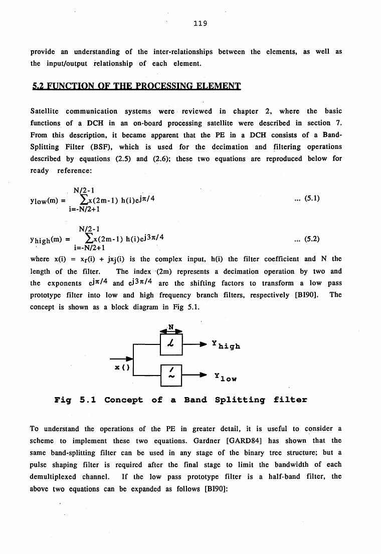
119
provide an understanding of the inter-relationships between the elements, as well as the input/output relationship of each element.
5.2 FUNCTION OF THE PROCESSING ELEMENT
Satellite communication systems were reviewed in chapter 2, where the basic functions of a DCH in an on-board processing satellite were described in section 7. From this description, it became apparent that the PE in a DCH consists of a Band- Splitting Filter (BSF), which is used for the decimation and filtering operations described by equations (2.5) and (2.6); these two equations are reproduced below for ready reference:
N /2-1yiowCm) = I x (2m -1) h (i)eJ7C/ 4 —
i=-N/2+l
N/2-1yhigh(m) = X xC2111’ 1) h ( i) e i37C/ 4 ... (5.2)
i=-N /2+lwhere x(i) = xr (i) + jxj(i) is the complex input, h(i) the filter coefficient and N the
length of the filter. The index (2m) represents a decimation operation by two and the exponents eJ71 and eJ3n/4 are the shifting factors to transform a low pass prototype filter into low and high frequency branch filters, respectively [BI90]. The concept is shown as a block diagram in Fig 5.1.
N
x<)
high
Y low
Fig 5.1 Concept of a Band Splitting filter
To understand the operations of the PE in greater detail, it is useful to consider a scheme to implement these two equations. Gardner [GARD84] has shown that the same band-splitting filter can be used in any stage of the binary tree structure; but a pulse shaping filter is required after the final stage to limit the bandwidth of each demultiplexed channel. If the low pass prototype filter is a half-band filter, the
above two equations can be expanded as follows [BI90]:

120
yiow(m) = h^°) / 2 {[x'r(2m) + x'j(2m)] + j[x,r(2m) - x'j(2m)] }+ h(l)/2x/2 {[x’r(2m + 1) .+ x'j(2m - 1)] - j[x'j(2m + 1) - x’r(2m - 1)] }- h(3)/2V2 {[x’j(2m + 3) + x'r(2m - 3)] + j[x’r(2m + 3) - x’j(2m - 3)] } ...(5.3)
yhighCm) = h(0) / 2 {[x,r(2m) + x’j(2m)] + j[x'r(2m) - x,j(2m)] )- h (l)/2x/2 {[x'j(2m + 1) + x’r(2m - 1)] + j[x’r (2m + 1) - x,j(2m - 1)] )
+ h(3)/2x/2 {[x'r(2m + 3) + x'j(2m - 3)] - j[x'j(2m + 3) - x’r(2m - 3)] ) ...(5.4)
where x'r (i) = xr(i) + xj(i), x’j(i) = xr (i) - xj(i), and h(i) are the coefficients of a low
pass prototype half band filter. To implement equations (5.3) and (5.4) as a digital filter, four important points must be noted, which are as follows:
(a) The filter requires real coefficients, which can be obtained from calculationsusing h(i).
(b) Each filter coefficient gets associated with a complex quantity by real m ultiplications (therefore the real and imaginary parts are to be processed separately, throughout).(c) Both high and low branch processing requires the same set of filter coefficientsexcept that there is a difference in their sign (i.e certain items in these equations need sign inversion depending on whether the data is from low or high branch).(iv) h(0) is associated with data having an even index, common to both high and lowbranches, while h (l) and h(3) are associated with data having odd indices which areseparate for the low and high branches.
A digital filter incorporating these features is described by Bi and Coakley in [BI90]. The block diagram shown in Fig 5.2 [BI90], represents a 7 tap filter (indicated earlier as the filter length), and is used to implement equations (5.3) and (5.4). In the figure,
the real-time input in the form of a complex number has real and imaginary data
streams, which are first processed by the addition and subtraction unit (centre left),to obtain the terms x'r (i) = xr (i) + xj(i) and x'j(i) = xr (i) - xj(i), respectively. Thedata bytes of the terms x'r (i) and x'j(i) are then moved through a shift register
(indicated by a dashed line box) wherein the input buffer is involved in thebuffering operations. This data is shifted through shift-registers made up of delay units (marked D) and 2:1 multiplexers (marked M). The data is bit serial but is
represented as bytes (words) in the equations, for example, x ( 2 m ) in the equation will mean the word at the input of shift-register 4, for m = 2. The bit serial data will

121
therefore be received at the input of ‘m ultiplexer and adder* units in synchronisataion with the word mark signal. When one byte is input bit-serially, and processed the terms pertaining to the low output yiow are produced; at this point the control switches to receive the other set of terms to get the output yhigh* This
process repeats producing time interleaved output data words at the output buffer. In the next paragraph, details of these basic operations are described further, in terms of equations (5.3) and (5.4).
Input Buffer
InputBufferControl
1 . . . . 1
IIIIL
III
III
Jl
-1 f i n1 1 1 1 1 I I I I • i j
R0.«
r 1 __I Add "TT D
‘ t — : ^
WordMark
Sub
Multiplex control
M
Multiplex &
r
M
M
SHIFT REGISTER
Multiplex &
h ' ( 3 )
|— h 1 (1 ) L - t
= n 1 n ~
Multiplex &
OSGI L. „ , 1
Word
h ’ ( 0 )
Add Add
Mul
Delay
Addi _ cAdd
n uOutputBuffer
Fig 5.2 Block diagram of Band Splitting Filter (BSF)In each pass associated with a filter coefficient, the data from shift registers is
preprocessed by the ‘multiplex and preprocessing’ unit which has multiplexers to

122
select the appropriate data bytes, as well as adders, subtractors and sign inversion units, whose operations will be described further in the next chapter. For the present, it is sufficient to state that the output from these units will be the individual terms in the braces of equations (5.3) and (5.4). Depending on whether the data is for the low or high branch, the corresponding filter coefficients h ’(0), h*(l) and h ’(3) are precalculated and applied at the multiplier inputs, to produce the real and imaginary parts respectively. Therefore, at the output of each multiplier pair, the data will correspond to one line of the equation (either 5.3 or 5.4 depending on the low or high branch). The outputs of multipliers are then added repeatedly (subtraction is effected if a negative sign is incorporated in the precalculation of the filter coefficient), to obtain the RHS of ylow and yhigh terms. All of these operations
are performed bit-serially, throughout the network. Switching occurs at a defined instant, when the inputs are switched to receive data pertaining to another branch. At that instant the partially processed data is stored in the buffers, so that it can be used again when the processing of data pertaining to the same branch is resumed. Briefly, when a switch over occurs, the following actions are taken by the BSF:(a) the data elements (processing states) in the complex shift register of the filter stage, will not have been processed and thus need to be preserved in order tocontinue the processing when the filter processes data from the same branch.(b) In the input buffer, the processing states are shifted into one end of the shiftregisters and the previously stored processing states at the other end of the registers are shifted back to the BSF.(c) The output buffer accumulates the interleaved outputs in high and low branch shift registers.
During processing, the filter and the output buffers form a closed loop so that the
data block can be circulated and processed until final outputs are produced.
From the description of the PE and its operations in a pipelined DCH, it can be
inferred that timing and control play a crucial role in the function of a PE and that all the stage PEs are identical in design but operate on the data in a time-multiplexed manner. The inputs to a PE consist of data bytes which represent the signal in theform of a two’s complement number. Since the input signal is from the satellite user
(voice, text etc) it will be random in nature, thereby generating a stream of random patterns of complex number inputs. In terms of data manipulation, the shift
registers, multiplexers and buffers act as passive elements since they do not transform the data. Their operation is essentially confined to data flow in response

123
to control signals. However, the other functional elements viz., adders, subtractors and multipliers, transform the data; any fault in these elements is therefore, difficult to detect. Multipliers in particular are the most complex elements since they comprise multiple adders which are further controlled in a complex manner, depending on the sign of the input numbers. In the TMS32020 DSP chip, for example, a 16 x 16 bit 200nS multiplier occupies about 40% of the chip area [MA90]. Therefore, our major task is to develop a method to detect faults in multipliers, which would also reveal certain aspects of error detection in adders/sub tractors. As a precursor to fault detection in multipliers, a brief review of their configuration and the fault detection schemes currently available, is appropriate.
5.3 Multipliers for DSP
A good tutorial on the multipliers used in DSP applications, is available in [MA90]. In any multiplier unit, the two inputs are designated as ‘multiplier’ and ‘multiplicand’ whilst the output is designated as the ‘product’. Traditionally, the two’s complement number system has been used in computing systems, due to the advantage of simpler addition and subtraction operations on signed numbers. However, multiplication using two’s complement numbers is not straight forward, since in the tw o’scomplement representation the sign bit is embedded in the number. Therefore, bitmanipulations are necessary to account for the sign bit when numbers of different sign are multiplied. In 1951, an algorithm was developed by Booth, to multiplysigned binary numbers [BOOT51] using shift-add operations. This algorithm uses repeated additions and sign bit manipulation with the “divide and conquer” principle; it is extensively used in the implementation of tw o’s complement multipliers. Later, Baugh and Wooley provided an improvised algorithm to form the
two’s complement product using array addition technique [BAUG73]. Multipliers using these algorithms can be implemented using the parallel array type of architecture where n bit numbers are multiplied using an array of n^ adders,arranged in a matrix form with n rows and n columns. The input data is injected in a bit-parallel, byte serial manner, with carry propagation between the adder stages. A typical example of this structure may be found in [SHEN84], as well as in many of the commercially available DSP chips. On the other hand, systolic array structures can
also be used to implement two’s complement multiplication; they provide a hardware efficient architecture by reducing the number of adders, whilst retaining the speed of multiplication. This is accomplished by limiting the number of I/O ports to the array boundaries and allowing highly localised com m unication between its

124
processing elements. Systolic features, combined with bit-serial architecture and a higher clock rate, can offer a multiplier performance comparable to the parallel array multipliers. The serial-parallel multiplier described in [LYON76] and thecompletely bit-serial multiplier, described in [GNAN83], illustrate the considerable reduction in the number of adders required. For the DCH, described in [BI90], a bit- serial, real-time two’s complement multiplier needing just n adders [BI88], wasproposed as an option for two reasons. Firstly, the bits of the multiplicand and multiplier arrive serially in the on-board DCH and a bit-serial multiplier receives and processes them efficiently, as they arrive. Secondly, the bit-serial multiplier consists of n adders for a n bit number, as opposed to n^ adders required for a parallel array multiplier, saving considerable hardware. However, parallel array multipliers offer faster operations for a given clock rate and have real-time
capabilities; they have also been used extensively in computers.
In addition to the two’s complement number system, other number systems are also used for fast multiplication of signed numbers. These non-conventional number
systems are generically, classified as follows [MA90]:* Canonic signed digit number systems* Logarithmic number systems* Residue number systemsEach of these number systems offer an unique solution to a particular DSP problem. The canonic number system, is ternary and was popular with vacuum tube
technology in which, it was easy to implement the <, =, > tests. Due to the advancem ents in sem iconductor technology, o ther binary-valued num bering systems have rapidly replaced the canonical system. The Logarithmic Number System (LNS) provides a word format X = ± r±ex, where r is the radix and ex is the
signed fractional exponent. The LNS has a wide dynamic range and the operations of multiply, divide, square and square root only require exponent manipulation. However, addition and subtraction can only be accomplished indirectly. Further, the precision and dynamic range capabilities of an LNS are limited by the available
address space.
The Residue Number System (RNS), has already been described in chapter 3, where
some of its advantages and limitations were pointed out. A survey of the redundant number systems used in adders and a generalised format for number representations are presented in [PARH90]. The advantage of Signed Digit (SD) number representations for multipliers is that they possess sufficient redundancy to allow
125
for the annihilation of carry or borrow chains and hence result in propagation-free addition and subtraction [AVIZ61]. Several algorithm s for iterative array multiplication, using both the binary and SD number systems, have been described by Nakamura [NAKA86]. Multipliers using the redundant number system, and their error detection have been described by Takagi and Yajima [TAKA87], where a three rail logic is used to represent the digits 0, +1 and -1. An inherent limitation of the redundant binary representation is the number conversion circuits needed. Like the use of codes in the fault correction techniques described in chapter 3, the encoding and decoding circuits introduce additional hardware, and a further increase in hardware is needed to provide Total Self-Checking (TSC). The algorithms used in redundant number systems, generate ‘n ’ n-bit partial products in the first step, which are later added pairwise to obtain the product. To implement these steps, use of a parallel array multiplier structure with n^ adder blocks, is necessary.
5.3.1 Two’s complement M ultipliers
In view of the limitations in the other number systems, it was decided to limit our attention to multipliers which use the two’s complement system. Bit-serial [LYON76, GNAN83, BI88], as well as the bit-parallel versions [SHEN84] of two’s complement m ultipliers, use established algorithms with some being capable of real-time operations. Before considering error detection, the basic operations of a tw o’s complement multiplier are described, using the bit-serial version as an example. The functional block diagram of a bit-serial, real-time multiplier which can be used in DCH, is shown in Fig 5.3; it accepts 4 bit inputs (5 bits including the sign bit) and
produces an eight bit output (nine bits including the sign bit).
The product outputs emerge separately, with 4 LSB bits at the storage point shown below, whilst the other five MSB bits (including the sign bit) appear at the terminal yout* These two outputs are later combined to produce the final product (not shown
in Fig 5.3). Five adder stages are connected in a pipelined manner to handle the five bit inputs as shown in Fig 5.3, where the final stage adder is modified to act as a subtractor. Whilst each of the ‘multiplier’ bits arrive bit-serially and are routed to a particular adder stage, the ‘multiplicand’ bits are injected bit-serially into the AND gates in the order of their arrival (LSB first). Details of timing delay and multiplier bit routing have not been shown in the figure, to retain simplicity. Each adder has an ‘x ’ input which is an ANDed combination of the input multiplier bit (bO to b4
depending on the stage) and the multiplicand bit (aO to a4 which are used by all the

126
stages at different time intervals). The other input to each adder is the partial product sum y, generated by the previous stage adder (except the first stage). Each adder has two outputs, one for the 'sum' where the partial product sum is generated and the other for 'carry' which is reused as an input (after a time delay)by the same adder stage during the next addition.
Multiplicand 'a' bits in the order 34 ,33 ,82,31,80 arriving bit serially (aO first)
Multiplier Multiplier Multiplier Multiplier Multiplierbit 1 bit 2 bit 3 bit 4 bit 5
bo » i
, 1 , , I b 3
. 1. tPartialproduct
Partialproduct
Partialproduct
Partialproduct
Partialproduct
sum4sum2 sum 3y4 Adder 4 c4
y 2 Adder 2 c2
y3Adder 3 c3
Adder 1 subtractor
Product MS bits
yout
Product LS bits - ►Store
Fig 5.3 Tw o's Com plem ent M ultip lier, b it-se ria l p ipelined scheme
The operations of this multiplier, can be visualised by noting that in the first cycle the bits bO and aO are ANDed by the first AND gate; in the next cycle bO and al areANDded by the first while b l and aO are ANDed by the second gate, and so on.The firstfour LS bits of the product (partial product sums: suml to sum4) are routed into the LSB product storage, at the end of the first five cycles. When the fifth bit (the sign bit a4) of the multiplicand arrives, the sign indicated by the fifth bit is noted and all
the further product bits are manipulated depending on the sign indicated by the
fifth multiplicand bit. As a consequence, in the next four cycles the manipulated MS bits arrive serially, from the output y0ut ° f final stage. In the mean time, during the
sixth cycle, the LSB of the next pair of inputs arrive and are processed by adderl,whilst the remaining 4 product bits of the previous input set are still beingprocessed as partial sums: sum2 to sum4. This pipeline action continues till the end of the ninth cycle when final product bit of the previous input set emerges from the output yout-

127
The operations of the multiplier follow the well known Booth’s algorithm [BOOT51], although certain implementation details differ. From the operations of the multiplier, it is clear that a fault in any of the adder stages, results in an erroneous
output. The fault could be in an adder block, interconnections, or the gates which select the inputs. In addition, the bit manipulation circuit can also contribute to afaulty output. The fault could be due to a failure of the hardware blocks just described or due to variations in timing signals used for control, delay etc., which may be generally designated as software. The error detection scheme must take into account these factors, in order to ensure reliable performance. Some of the existing error detection schemes are described in the next section, which is followed by a
description of the proposed space search method.
5.4 Error detection in Two’s complement M ultipliers
The fault detection schemes for linear arithmetic arrays proposed by Wu and Wu [WU87] as well as the testable multipliers described by Shen and Ferguson [SHEN84], are based on hardware detection. A fixed set of fault conditions in one of the adder stages are considered and their detection using test sequences are described therein. In order to use a sequence of test vectors to detect faults in the adder stages, certain initial conditions for the input states of adders are necessary, which are assumed in
both schemes.
Based on the test patterns needed to exhaustively test the multiplier, certainmodifications in the adder stages of array multipliers are proposed by Shen and Ferguson [SHEN84], so as to reduce the length of the test sequence. The modifications proposed necessitate seven different configurations of the adder cell for differentrows and diagonals of the array, but they increase the controllability of the inputs to the subarray making it C-testable using 55 test patterns. An array structure is
classified as C-testable, if the number of test patterns needed to completely test thestructure, is constant and is independent of the size of the array. However, theschemes proposed are not extendible to either serial-parallel or bit-serial
multipliers, where the carry bit of each adder stage is not propagated to the next adder stage as is done in parallel array multipliers. It is also not possible to use the proposed seven modified cells, since these cells receive specific bits of themultiplicand; the multiplicand bits in a bit-serial multiplier, are available to all the
adder stages at different time intervals.

128
The scheme proposed by Wu and Wu [WU87], is applicable to a bit-serial pipeline of arithmetic processors. Their detection scheme, also requires test vectors which areinjected into the processor inputs. When a fault is detected, a data retry followed by a recomputation using a redundant processor is suggested, based on which, a method to correct the output has been developed. Assuming certain initial states at theprocessor inputs, an analysis of fault propagation and error recovery are suggested. However, this scheme is not applicable to the bit-serial or serial-parallel multipliers due to one key assumption that none of the processors in the linear array can have a feedback path. It is known that the adders in bit-serial and serial-parallelmultipliers do have a feedback path whereby the ‘carry’ is fed back after a time
delay, to be used by the same adder in the next cycle.
An inherent limitation in both these schemes is that the detection is based on certain preconditions. These preconditions include an initial state for each adder as well as a known set of test vectors which must be injected into each adder. In a real-time situation, the multiplier handles random inputs and the terminals of adders cannotbe set to known conditions unless they are cut off from the actual circuit. Both schemes aim at fault detection in the individual adder stages, which preclude faultsdue to timing delay, software (control signals etc.), sign-bit modification circuit and breaks in line connections between adders. Whilst a considerable increase inhardware due to these fault detection circuits is suggested, the schemes do not offer complete fault detection since the preconditions assumed are not likely to occur inpractice. In effect, both of these schemes are intended for test purposes, rather than for fault detection per se. Since each filter section contains several multipliers
which must work in a synchronised manner, it is better to detect faults at themultiplier level rather than at the individual adder levels, within the multiplier.
5.4.1 Error detection using space search method
Due to the nature of two’s complement numbers, it is not possible to devise hardware schemes by which the two inputs (‘a’ and ‘b ’) to the multiplier can be directly used to check the product, unless another circuit as complex as the multiplier itself, isused. We therefore propose a software based space search scheme wherein each set of 4 the two inputs and their product’ are tabulated and the entire table is placed in a database. Using an AI language like Prolog, it becomes a simple task to search out the

129
product, for a given set of two input numbers (by monitoring the inputs), sinceProlog allows facts and rules to be defined as clauses.
The product searched out by the Prolog’s unification process, can thereafter be compared with the multiplier’s output (also being monitored) to detect faults. The problem therefore reduces to preparing a compact table, so that the total set ofinput/output combinations to be stored as relations in the database, is reduced to a reasonable size. To provide a reduction and yet maintain a good balance betweendatabase storage capacity and the search time, it is necessary that the database structure be made a combination of the bushy tree and skinny tree structure asdescribed by Wong, Suda and Bic [WONG90]. In order to provide such a structure, it isbetter to divide the multiplier’s output product (9 bits in this case) into the LSB (4bits) and MSB parts (5 bits including the sign bit).
In Table 5.2, the product LSB (4 bits) codes for each of the possible positive input combinations have been listed. These listings are applicable only to the positiveinput number combinations and similar tables can be constructed for the otherthree input combinations viz.,
(i) multiplicand being positive and the multiplier negative(ii) multiplicand negative and multiplier positive(iii) both multiplicand and multiplier being negative,
which accounts for a total of 225 X 4 = 900 combinations. Similar tables for the fiveMSB product bits can be constructed (another 900 combinations), which gives the
complete group of tables to be stored in the database. A careful perusal of table 5.2 reveals the symmetry of combinations on either side of the central 1000 column,which helps in reducing the number of entries actually to be made into the database. This fact is also illustrated in the bar code graph shown in Fig 5.4. Although the combinations in Table 5.2 are written in decimal, it must be remembered that onlythe equivalent tw o’s complement bits are entered into the database. The tw o’scomplement numbers are entered into the database as lists, where each bitrepresents the elements of a list. This format is convenient for all the AIprogramming languages where the primary capability of list processing, is crucial
to all the operations performed on the database. The AI language LISP also uses list processing in its basic form, but Prolog is based on symbolic logic and provides certain features which are useful for diagnostics and test purposes. Virtual relationsin relational databases can be represented by rules in Prolog programs. Using its

129a
Table 5.2 Analysis o f T w o’s Complement Multiplier
Input Foar LSB Codes of the Output Product
Inputs a.b 0000 0001 0010 0011 0100 0101 0110 0111 1000 1001 1010 1011 1100 1101 1110 1111
1. b varies 1.1 U2 1 4 1.8 14 1.8 1.7 14 14 1.10 1.11 142 1.13 1.18 LIS
2. b varies 24 2.1 24 24 2.8 24 24 2,7
2.9 240 2.11 2.12 2.13 2.18 245
2. b varies 3,11 3,<S 34 3.12 3.7 34 3.13 34 34 3.18 34 3.8 345 340 34
<, b varies 8.8 <1 84 84
4A <4 <8 8.7
<12 84 < 10 <11
843 <18 8.1S
5, b varies 5.13 S.10 3.7 3.8 54 5.18 341 34 34 34 5.15 342 54 54 34< b varies <8 <3 84 84 <8 8.7 84 84
8.11 8.18 84 8.12 8.1 S <10 843
7. b varies 7.7 7.14 74 7.12 74 740 7.1 74 7.15 74 7,13 7.8 7.11 74 748, b varies *a «4
6.4 84
8.8 84
«4 8.7
8.10 84
«42 8.11
<18 843
8.15
9. b varies >4 9a >.11 9,4 >.13 >4 >43 >4 9.1 >.10 9.3 >42 >4 >48 9.7
10, b varies 10.8 1 04 10 4 10,7 10.8 10.1 104 104
10.13 1040 10.15 10.12 104 10.18 104111, b varies IU 11.8 11,12 11.15 114 114 114 1141 1148 11.1 11.8 11.7 1140 11.13
12, b varies 12.4 124 124 12,1
124 12.7 124 12412,12 12.11 12,10 12.9
12.1S 12.18 12.13
13, b varies 134 13,10 13,IS 13,< 13.9 13.H 134 13.8 13.13 13.2 13.7 13.12 13.1 13 4 13.11
li, b varies 18.S I <7 184 18.5 18.8 18.3 184 18,1
M.IS 18.18 18.13 18.12 18.11 18.10 18.9
IS. b varies 1S.IS 1S.H 1S.13 15.12 IS.ll 1S.I0 1S4 IS4 1S.7 1S.< 1S4 1S.8 1S.3 15,2 ISA

130
inference mechanism, Prolog performs deductive inference over a database of rules and facts.
ao03a
X£oo
»EJ8 32 a
8 24au
o 1 ' O 16
Input numbers
OXXXX. OXXXX
1XXXX, 1XXXX
OXXXX. 1XXXX
1XXXX, OXXXX
Dutput product
OXXXXXXX}
oxxxxxxxx
1XXXXXXXX
1XXXXXXXX
Combinations
Both inputs +ve, +ve product
Both inputs -ve, +ve product
’a' +ve, b ' -ve, -ve product
'a' -ve, 'b* +ve, ■ve product
1000
0100
0000 0010
0001 0011
01 10
0101 0111
1100
1010
1001 1011
1110
1101 1111
Four LSB bits of the output product
Fig 5.4 Distribution of codes in each set of combinations
An additional feature is that the unification mechanism used by Prolog helps to deduce additional facts from a given set of facts and rules. These are described laterin this section, when the Prolog clauses and database are listed and typical examples of queries are illustrated. The order in which the rules are stated in the database, influence the Prolog inference and can result in delays to complete the search. This is important since the first relation satisfying the rule, would be picked up as theanswer. The database must therefore ensure that each input/output combination is carefully reduced, to avoid multiple answers, since we wish to receive a unique
answer to each set of inputs, after each search. The combinations are written in the

131
database as virtual relations, which are used with a logic formula known as a ‘clause’. The Prolog clause, defines the rules to be applied to evaluate the relations between the inputs and output.
Fig 5.4 shows the occurrence of the 4 LSB bits in various two’s complement number types. During this search only 4 bits of the input are available and the corresponding 4 bits of the output need to be searched. The bits selected during an LSB search are indicated for each combination, in the inset indicated in Fig 5.4. The LSB code bits 1000 occurs most often (in 32 X 4 = 128, of the total 900 input combinations). With the exception of the 0000 code which occurs 17 times for each combination, all the other codes have a symmetry of occurrence mirrored on either
side of the 1000 code. The code 0000 is used to represent both -0 and +0, which accounts for the apparent discrepancy.
Many of these combinations collapse into a much smaller group due to several factors some of which are due to (a) the commutative law, (b) several combinations reducing to don’t care bits etc. Just 45 of such reduced relations are sufficient to indicate all the relations needed to represent the four LSB bits. Although further reductions are possible, it defeats the exercise since additional statements would be necessary in the Prolog clauses and the overall detection time would not improve because of the additional calls required when Prolog executes the search [STOB89]. All the Prolog clauses and the 45 relations which are to be stored in the database, are shown below:
% P r o l o g c l a u s e s f o r s e a r c h i n g t h e i n p u t / o u t p u t
s e a r c h ( F , p r o d u c t l ( A , B , P ) , P r o d u c t ) : -s e t o f ( B , p r o d u c t l ( A , B , P r o d u c t ) , P ) .
s e a r c h ( F , p r o d u c t l ( A , B , P ) , P r o d u c t ) : -s e t o f ( A , p r o d u c t l ( B , A , P r o d u c t ) , P ) .
% L S B p r o d u c t a n d i n p u t r e l a t i o n s h i p s % M u l t i p l i c a n d / M u l t i p l i e r / p r o d u c t L S B /% / / / / / /
p r o d u c t l ( [ X , Y , Z , 0 ] , [ I , 0 , 0 , 0 ] , [ 0 , 0 , 0 , 0 ] ) . p r o d u c t l ( [ X , Y , 0 , 0 ] , [ M , N , 0 , 0 ] , [ 0 , 0 , 0 , 0 ] ) .

132
p r o d u c t l ( [ M , X , X , 1 ] , [ M , X , X , 1 ] , [ 0 , 0 , 0 , 1 ]) . p r o d u c t l ( [ 0 , 0 , 1 , 1 ] , [ 1 , 0 , 1 , 1 ] , [ 0 , 0 , 0 , 1 ] ) . p r o d u c t l ( [ 0 , 1 , 0 , 1 ] , [ 1 , 1 , 0 , 1 ] , [ 0 , 0 , 0 , 1 ] ) .
p r o d u c t l ( [ X , 0 , 1 , 1 ] , [ 0 , 1 , 1 , 0 ] , [ 0 , 0 , 1 , 0 ] ) . p r o d u c t l ( [ X , 1 , 1 , 1 ] , [ 1 , 1 , 1 , 0 ] , [ 0 , 0 , 1 , 0 ] ) . p r o d u c t l ( [ X , 0 , 1 , 0 ] , [ Y , X , 0 , 1 ] , [ 0 , 0 , 1 , 0 ] ) .
p r o d u c t l ( [ X , Y , 0 , 1 ] , [ X , Y , 1 , 1 ] , [ 0 , 0 , 1 , 1 ] ) .
p r o d u c t l ( [ X , Y , 0 , 1 ] , [ 0 , 1 , 0 , 0 ] , [ 0 , 1 , 0 , 0 ] ) . p r o d u c t l ( [ X , 0 , 1 , 0 ] , [ Y , 0 , 1 , 0 ] , [ 0 , 1 , 0 , 0 ] ) . p r o d u c t l ( [ X , Y , 1 , 1 ] , [ 1 , 1 , 0 , 0 ] , [ 0 , 1 , 0 , 0 ] ) . p r o d u c t l ( [ X , 1 , 1 , 0 ] , [ Y , 1 , 1 , 0 ] , [ 0 , 1 , 0 , 0 ] ) . p r o d u c t l ( [ X , 0 , 0 , 1 ] , [ X , 1 , 0 , 1 ] , [ 0 , 1 , 0 , 1 ] ) . p r o d u c t l ( [ X , 0 , 1 , 1 ] , [ X , 1 , 1 , 1 ] , [ 0 , 1 , 0 , 1 ] ) .
p r o d u c t W , X , 0 , 1 ] , [ X , 1 , 1 , 0 ] , [ 0 , 1 , 1 , 0 ] ) . p r o d u c t W , 0 , 1 , 0 ] , [ X , 0 , 1 , 1 ] , [ 0 , 1 , 1 , 0 ] ) .p r o d u c t l ( [ X , 1 , 0 , 1 ] , [ 1 , 1 , 1 , 0 ] , [ 0 , 1 , 1 , 0 ] ) . p r o d u c t l ( [ l , 0 , 1 , 0 ] , [ X , 1 , 1 , 1 ] , [ 0 , 1 , 1 , 0 ] ) . p r o d u c t l ( [ 0 , 1 , 1 , 0 ] , [ 1 , 0 , 0 , 1 ] , [ 0 , 1 , 1 , 0 ] ) .
p r o d u c t l ( [ X , 0 , 0 , 1 ] , [ X , 1 , 1 , 1 ] , [ 0 , 1 , 1 , 1 ] ) . p r o d u c t l ( [ 0 , 0 , 1 , 1 ] , [ 1 , 1 , 0 , 1 ] , [ 0 , 1 , 1 , 1 ] ) . p r o d u c t l ( [ 0 , 1 , 0 , 1 ] , [ 1 , 0 , 1 , ] ] , [ 0 , 1 , 1 , 1 ] ) .
p r o d u c t W , 0 , 0 , 0 ] , [ X , Y , Z , 1 ] , [ 1 , 0 , 0 , 0 ] ) . p r o d u c t l ( [ 0 , 0 , 1 , 0 ] , [ X , 1 , 0 , 0 ] , [ 1 , 0 , 0 , 0 ] ) . p r o d u c t l ( [ Z , 1 , 0 , 0 ] , [ X , Y , 1 , 0 ] , [ 1 , 0 , 0 , 0 ] ) .
p r o d u c t l ( [ X , 0 , X , 1 ] , [ 1 , 0 , X , 1 ] , [ 1 , 0 , 0 , 1 ] ) .p r o d u c t W , X , 1 , 1 ] , [ X , X , 1 , 1 ] , [ ] , 0 , 0 , ] ] ) . p r o d u c t l ( [ X , 1 , 0 , 1 ] , [ X , 1 , 0 , 1 ] , [ 1 , 0 , 0 , 1 ] ) .
p r o d u c t l ( [ X , 0 , Y , 1 ] , [ 1 , Y , 1 , 0 ] , [ 1 , 0 , 1 , 0 ] ) . p r o d u c t W . Y , 1 , 0 ] , [ X , 1 , Y , 1 ] , [ 1 , 0 , 1 , 0 ] ) .

133
p r o d u c t l ( [ 0 , X , 0 , 1 ] , [ 1 , X , 1 , 1 ] , [ 1 , 0 , 1 , 1 ] ) .p r o d u c t l ( [ 0 , X , 1 , 1 ] , [ 1 , X , 0 , 1 ] , [ 1 , 0 , 1 , 1 ] ) .
p r o d u c t l ( [ X , 0 , 1 , 0 ] , [ Y , 1 , 1 , 0 ] , [ 1 , 1 , 0 , 0 ] ) . p r o d u c t l ( [ l , 1 , 0 , 0 ] , [ X , Y , 0 , 1 ] , [ 1 , 1 , 0 , 0 ] ) . p r o d u c t l ( [ 0 , 1 , 0 , 0 ] , [ X , Y , 1 , 1 ] , [ 1 , 1 , 0 , 0 1 ) .
p r o d u c t l ( [ 0 , 0 , X , 1 ] , [ 1 , 1 , X , 1 ] , [ 1 , 1 , 0 , 1 ] ) . p r o d u c t l ( [ 0 , 1 , X , 1 ] , [ 1 , 0 , X , 1 ] , [ 1 , 1 , 0 , 1 ] ) .
p r o d u c t l ( [ X , 0 , 0 , 1 ] , [ 1 , 1 , 1 , 0 ] , [ 1 , 1 , 1 , 0 ] ) . p r o d u c t l ( [ 0 , 0 , 1 , 0 ] , [ X , 1 , 1 , 1 ] , [ 1 , 1 , 1 , OJ). p r o d u c t l ( [ X , 1 , 0 , 1 ] , [ 0 , 1 , 1 , 0 ] , [ 1 , 1 , 1 , 0 ] ) . p r o d u c t W , 0 , 1 , 0 ] , [ X , 0 , 1 , 1 ] , [ 1 , 1 , 1 , 0 ] ) .
p r o d u c t l ( [ 0 , 0 , 0 , 1 ] , [ 1 , 1 , 1 , 1 ] , [ 1 , 1 , 1 , 1 ] ) . p r o d u c t l ( [ 0 , 1 , 1 , 1 ] , [ 1 , 0 , 0 , 1 ] , [ 1 , 1 , 1 , 1 ] ) .p r o d u c t l ( [ X , 0 , 1 , 1 ] , [ X , 1 , 0 , 1 ] , [ 1 , 1 , 1 , 1 ] ) . % t o t a l o f 4 5 r e l a t i o n s
The capital letters in square brackets, denote an uninstantiated variable. Initially, when the Prolog clause (rule) is applied, the output bits (in the third square bracket) are bound but the inputs (in the first two square brackets) are unbound. The variables in the input combinations are then instantiated and if the goal succeeds (rule obeyed), then the inputs also become bound to the output and are brought out as the answer. If however, the goal does not succeed, then Prolog makes a recursion
with new values instantiated to the variables and tries again for a success. This recursion continues until all the possible values for the variables have beenexhausted. If the goal succeeds in any of the recursions (called backtracking), then Prolog emerges with the answer and no further attempts are made to satisfy the rules. A query can be framed, to look for any of the inputs or the output. Forexample, the querys e a r c h ( F , p r o d u c t l ( A , [ 1 , 1 , 0 , 1 ] , [ 1 , 1 , 1 , 1 J ) , P r o d u c t ) .means what is input A, when input B is 1101 and the product is 1111, which would give us the answer, A = 1011.
We could also raise a query
s e a r c h ( F , p r o d u c t l ( [ l , 0 , 0 , 1 ] , [ 1 , 0 , 0 , 1 ] , P ) , P r o d u c t ) .

134
which means that if the inputs are A = 1001 and B = 1001, what is the output product, to which the answer will be P = 0001. The Prolog built-in predicate “setof” has been used in the clauses to advantage, in that it searches for all the possible combinations;when we get a single answer each time it assures us that one and only one producthas satisfied the rules, for a given set of inputs.
Instead, we could simply state the product and ask for the possible inputcombinations, using a querys e a r c h ( F , p r o d u c t l ( A J 3 , [ 0 , 0 , 1 , 1 ] ) , P r o d u c t ) .which would give us the possible input combinations viz.,A = 0001, B = 0011; A = 0101, B = 0111; A = 1001, B = 1011 and A = 1101, B = 1111; which could be used for diagnostics. The combination of A and B is important, but the
order is not, since the first Prolog clause is for a search of combination A and B, andif an answer is not found, then the second clause is used to search for a combination
of B and A.
Input 4 bits each of multiplicand and multiplier
Fig 5.5 Search path for finding the multiplier's "product”
For routine checks the most commonly used query would be to look for the correct product, given the inputs. One heuristic to reduce the search time would be to reorder the database so that the products with the most instantiated variables are
executed First [LEUN88]. The 45 relations shown could be rearranged in this way
Input 5 bits each of multiplicand ---------------- and m ultipliersingle clock delay
P roductP roduct
P roduct v LSB Positive
P roduct N egative \ P ro d u ct
P roduct MSB v
P roductMSB
1 2 3 4 5 .. 125 1 2 3 4 5 . . 110
135
(those which do not have variables like X, Y etc., being put at the beginning), but it is also observed from Fig 5.4 that the maximum likelihood for a routine search is likely to be for the product bits 1000 which occurs as many as 32 times out of the 225 combinations. It is better therefore, to re-order the database in the order of maximum likelihood, so that the search time is reduced. Normally, Prolog is used to search for multiple answers to a given query, since there could be several relations which satisfy a certain rule, which increases the search time. In terms of search completion time there is some advantage in our example, since we are expecting “only one answer for the product” (although more than one answer may be selected during backtracking, only one correct answer for the product will become bound) from our search routine.
In the PE the input bits arrive serially and Fig 5.5 shows the search path, where the starting node has been indicated by two separate points to denote the time delay which occurs while the fifth bit (sign) arrives. For the MSB however, there must be two such groupings, one for the positive product MSB (sign bit 0) and another for negative product MSB (sign bit 1). The Prolog clauses and the relations to be stored in database (123 for positive MSB and 110 for negative MSB) are shown in Appendix 1
and Appendix 2, respectively.
Although this scheme works well for all types of two’s complement multipliers, the bit-serial version has some difference with the bit-parallel version in terms of search sequence, since a search for the product LSB can begin as soon as the first four bits have arrived; this is indicated in Fig 5.6 as the starting point.
By the time this search is completed, the product LSB would be available at the
multiplier’s LS output. After the fifth bit arrives the MSB search can begin which can be completed at the end of the ninth cycle when the product MSB bits would have arrived at the multiplier’s MS output, ready for comparison. In the meantime, during the sixth cycle, the first LSB of the second word arrives and the four LSB bits
of the second word would have arrived at the end of the ninth cycle; the LSB search can then begin again. At the end of the tenth cycle the fifth bit of the second word arrives and the MSB search can begin again and so on, as shown in Fig 5.6. In bit-
parallel array multipliers all the input five bits are available to begin with, therefore LSB and MSB searching can begin simultaneously. However, the multiplier output bits arrive sequentially, hence the search can continue and comparison may
be completed only after the multiplier’s output product bits become available. In the

136
meantime the next set of input bits arrive and there must be another search routineto handle them or else multitasking will be necessary, even if the search routine is
assumed to complete its task as fast as the hardware executes multiplication, t = 4 t = 91 1
Input 4 bits of multiplier and multiplicand
t = 5 ,t= 10 Input 5 bits of multiplier and multiplicand
Start StartLSB search MSB search
routine routine
LSB product bits
found ?
LSB product bits
found ?
Yes"
t > 15sampleOUtDUt
MSBsampleOUtDUt
LSB
combine LSB + MSB
compare CK 9
compareOK 9
send as correc ted productReturn Return
Fig 5.6 Software space search routine
In practice, error detection cannot be completed as quickly as the computation itself,
and particularly in a high speed real-time circuit such as the multiplier, the time difference between the main circuit and its fault detection mechanism would be considerable. Irrespective of whether a detection scheme comprises hardware or software based search, there is always a certain amount of time required to complete
fault detection and report a success or failure. This time is known as “fault latency”,

137
during which the main circuit would have performed a few more operations propagating the fault to other circuits further down stream. The total time allowed to detect a fault and reconfigure the system, depends on the criticality of the system in question and for a DCH this time has been estimated at a few seconds, based on the telecommunication traffic estimates. This aspect was mentioned earlier in chapter 1, where the requirements for an autonomous fault tolerant system were specified. A fault in the BSF, affects both the high and low filter banks discussed earlier andduring the time taken to detect faults, errors in both the data streams can be
expected. In this respect, the conventional binary tree would offer a better solution, since only data pertaining to that branch would become affected, unless the first stage PE develops a fault. This aspect, is further discussed in the next chapter, where performance of the BSF as a whole, and also in chapter 8, where the systemconsiderations are described. The possibility of implementing a space search based detection system with an acceptable performance, on-board a satellite, is explored in
the next section.
5.5 On-board implementation
In the previous section, the method described to detect errors in multipliers, resulted in several sets of input/output com binations. These com binations can be implemented as “look up” tables using simple methods such as hardwired logic or using a Programmable Read Only Memory (PROM) in a processor based system. To implement the “look-up” table on-board a satellite, factors such as mass, area, powerconsumption etc., must be considered. The PROM, when viewed as a logical device,has the notable feature that every possible input combination, is present in the memory matrix. This feature becomes apparent when one considers a scheme where
the PROM table is constructed by making the PROM address to correspond with the input; the output data which is the “answer” to a given input set, is stored in the corresponding memory location. In the multiplier example, to obtain the product LSB, a set of 8 input bits and 4 output bits are needed. Therefore, 2^ = 256 memory locations are needed to implement the 45 combinations. Further, the m ultiplier’s product MSB has 125 combinations for the negative product MSB and 110 combinations for the positive product MSB. To implement this part, 10 input bits and 5 output bits are necessary. Again, if a PROM based system were used, 2*0 = 1024 memory locations for each product MSB (positive and negative) are necessary. In addition, circuits to decode the input, the processor and the I/O devices are the inherent overheads in a PROM based system. PROMs are usually available with either
four or eight outputs. In the MSB detector of our example, 3 output pins would remain

138
unused. In the combinations described in the previous section, note that the input combinations for the LSB and MSB fall into distinctly different areas of the memory address location, leaving a large areas of memory location unused. The complexity of PROMs makes them costlier than simple logic circuits; a 256 X 8 PROM contains over 100 gates plus a 2048 fuse matrix. The performance of a PROM is also inferior to discrete logic circuits in the same technology. In terms of delay, a typical PROM causes 30 ns of time delay at a current consumption of over 100 mA (bipolar, 8P8,
MMI), while a logic circuit with the same number of gate delays would cause a delay of about 10 ns with a current consumption of less than 50 mA (bipolar,PAL 8L8,MMI).
A straight forward method to implement a look-up table in real-time is throughhard-wired logic. Hard-wired logic provides the speed needed for real-time detection and the number of logic stages is not more than 3 or 4. From a cursory look to provide the 16 sets (45 combinations) of LSB, it was found that at least 9 gates/set, would be needed. To implement the MSB, logic gates with multiple inputs are often needed. Instead of using discrete logic devices of various types, a regular structure can provide a modular approach to design.
It was therefore decided to explore the possibility of using a Programmable Logic Array (PLA) to implement the “look up” table. In addition to providing savings in the overall component count, it is also possible to provide a self-checking facility forthe PLA. The PLA systems do not have the limitations of a PROM as described earlier
and can be designed more efficiently, to implement the LSB and MSB tables of the multiplier. A PLA has two programmable sections. The first part connects the inputs to a set of AND gates and is known as the AND matrix. The second part determines which of the AND gates are ORed together to form the output function. This part is known as the OR matrix. In a PLA, the inputs are made programmable and the number of AND gates is reduced. At first, such a reduction in the gate count can be optimised by logical minimisation of the inputs using Karnaugh maps and
De’Morgan’s laws. At the second stage of reduction, inputs are carefully analysed and
those having a consistent “don’t care” condition for a particular set need not be connected; or input pins maintaining a particular logic level for all combinations, can be grouped and only one AND gate may be used to represent the group.
Fig 5.7 shows a typical structure and the notation used in a PLA. The connections shown in Fig 5.7(a), represent the input combinations which correspond to the product LSB “0000”. The connections shown can be easily programmed in a PLA by

139
blowing the corresponding fuses. The cross-over points marked in Fig 5.7(a) indicate the signal levels which would be used to make the output of the AND gates ‘HIGH”.
AO
BO ,
CO i
DO O—£
B1
Cl
D1
>
J?
b j\ ""J
b 3
) j
[> 3* 1
f k
Aa“ t£
WW•LOW 'A' 'A' HIGH'
taPu,s J Don't careunconnected condition
(b) PLA notations
0 07» »[ 8 T1* i 2i> -o 9
Fig 5.7(a) PLA programmed with simple combination logic
The standard nomenclature used in a PLA is shown in Fig 5.7(b), where the four possible ways of programming the AND gate are illustrated. These are:
(i) If both the programmable fuses at cross-over points are blown, then the output is
A * A _ LOW. Therefore, the input will not be selected and the AND gate is inactive.
(ii) If the complement fuse is blown, the true sense of the input (A) is included in the equation for that AND gate.
(iii) If the inverted input is connected, the complement ^ appears in the equation.
(iv) When neither the input nor its complement is connected, that signal does not appear at all in the equation for that gate; this is the ‘‘don’t care” condition.
Considering the first two combinations for the multiplier product LSB “0000”, the
inputs (multiplicand, multiplier) can be represented as follows:

140
Table 5.3 Representation of multiplier inputs in a PLA
A0 B0 GO DO A1 B1 Cl D1
X Y Z 0 1 0 0 0
X Y 0 0 M N 0 0
In table 5.3, AO..DO represent the multiplicand input and A1..D1 represent the
multiplier input. X,Y,Z,M,N represent variables which can take values of 0 or 1, effectively meaning that they are “don’t care” conditions of the input. The logical expression for output LSB “0000” would be:
O utput0 = DO * A1 *B1 *C1 * m + C 0 * DO *C1 *D1
where O u t p u t O represents the multiplier’s product LSB term 0000.
5.5.1 Self-checking of the PLA
The two requirements for fault detection in a PLA are fault sensitization (fault excitation) followed by fault propagation. Sensitization ensures that the crosspoint atwhich a fault is assumed to exist is made critical. A line variable becomes critical if when that variable is toggled, the output of the entire line is toggled. Once acrosspoint has been sensitized, a propagation path to some output must be established which guarantees that the fault is not masked. Two types of tests are normally used to
detect faults in simple combination circuits [BOST88]. The first of these is known as type-1 tests. Type-1 tests are used to ensure that the output goes to HIGH when it should. The second type is known as type-2 tests which ensure that the output stays LOW when the inputs are not in an active combination. Type-2 tests therefore ensure that a fault on one input will not be masked by other inputs, so that the output does
not erroneously go HIGH .
The Karnaugh map can be used in the mechanical process of defining output levelscorresponding to the input vectors, in complex systems. Karnaugh maps will show
that the type-2 vectors are all adjacent to the type-1 vectors. The ultimate aim ofthese two tests is to ensure that all possible s t u c k - a t - o n e and s t u c k - a t - z e r o faults are tested using the minimum number of test vectors. A complete table of vectors to
cover all the possible faults in Fig 5.7(a) is as follows:
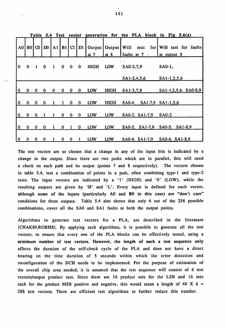
141
Table S .A Test vector generation for the PLA block in Fig 5.6(a)
AO BO GO DO A1 B1 Cl D1 Output at 7
Output at 8
W ill test for faults at 7 -
Will test for faults at output 8
0 0 1 0 1 0 0 0 HIGH LOW SAO-3,7,9
SAl-2,4,5,6
SA0-1,
SA1-1.2.5.6
0 0 0 0 0 0 0 0 LOW HIGH SAl-3,7,9 SAl-1.2,5,6. SAO-8,9
0 0 0 0 1 1 0 0 LOW HIGH SAO-4. SAl-7,9 SAl-1,5,6
0 0 0 1 1 0 0 0 LOW LOW SAO-2. SAl-7,9 SAO-2
0 0 0 0 1 0 1 0 LOW LOW SAO-5. SAl-7,9 SAO-5. SAl-8,9
0 0 0 0 1 0 0 1 LOW LOW SAO-6. SAl-7,9 SAO-6. SAl-8,9
The test vectors are so chosen that a change in any of the input bits is indicated by a change in the output. Since there are two paths which are in parallel, this will need a check on each path and its output (points 7 and 8 respectively). The vectors chosen in table 5.4, test a combination of points in a path, often combining type-1 and type-2 tests. The input vectors are indicated by a *1* (HIGH) and ‘0 ’ (LOW), while the resulting outputs are given by ‘H ’ and ‘L \ Every input is defined for each vector, although some of the inputs (particularly AO and BO in this case) are “don’t care” conditions for these outputs. Table 5.4 also shows that only 6 out of the 256 possible combinations, cover all the SAO and SA1 faults at both the output points.
Algorithms to generate test vectors for a PLA, are described in the literature
[CHAK89,ROBI88]. By applying such algorithms, it is possible to generate all the test vectors, to ensure that every one of the PLA blocks can be effectively tested, using a
minimum number of test vectors. However, the length of such a test sequence only affects the duration of the self-check cycle of the PLA and does not have a direct bearing on the time duration of 5 seconds within which the error detection and reconfiguration of the DCH needs to be implemented. For the purpose of estimation of the overall chip area needed, it is assumed that the test sequence will consist of 6 test vectors/output product sets. Since there are 16 product sets for the LSB and 16 sets each for the product MSB positive and negative, this would mean a length of 48 X 6 =
288 test vectors. There are efficient test algorithms to further reduce this number.

142
5.5.2 On-board error detection scheme
Having explored the use of a PLA to implement the error detection in a multiplier, a scheme is proposed in this section to define each module of the overall error detection system for all the multipliers of the half-band digital filter. In order to use the same PLA block for all of the multipliers, an input multiplexer and an output m ultiplexer are needed. The input m ultiplexer samples the m ultiplicand andmultiplier terms using bit serial lines. It also samples both the real and imaginary
parts at the same time, though each part is checked by the PLA in a time multiplexed fashion. The output multiplexer, on the other hand, maintains a constant delay withthe input multiplexer, the delay being equal to the latency of the multiplier. Theoutput multiplexer samples the output product through a serial line. Fig 5.8 shows the schematic of the overall error detection system, in which for simplicity details of the real and imaginary parts are not shown separately.
M M M M M M
Iserial line
o f MuxPositions
Serial to parallel Converter
Product storage buffer
Generator! Test ■ Bus ! L
M - Multiplier
2 sets of serial lines (multiplicand,
Serial to parallel Converter
multiplier)
. - j k i 0. - - . ;s £ 1 o
1 1 .1 . - f j -ii PLA PLA PLAi Block Block Block■i Pos. MSB Neg. MSB LSBi
r**i f 52:1 Multiplexer Buffer
Searched product storage Buffer
Test passed r comDaratcomparator ■+■ /
To diagnostics
" Cells
Fig 5.8 Schematic for the error detection scheme using PLA

143
The error detection system works as follows. The input multiplexer receives the bit serial inputs from the multiplicand and multiplier streams of the real and imaginary
parts and this is injected into the Serial to Parallel (SP) converter. The SP converter converts the serial bit stream into parallel bit stream and only one of the two (real or imaginary) parts is taken up for conversion, using time multiplexing (not shown in the diagram). The PLA circuit is divided into three blocks, one each for the product LSB terms, MSB positive terms and MSB negative terms. A method for generating a single output term was shown in Fig 5.7. It is easy to show that the actual product terms can be generated by using an OR array at the output of the PLA, with standard designs available for any PLA. After generating the actual MSB product terms in one of the MSB blocks, the appropriate MSB term is selected by a 2:1 multiplexer, which receives a selection control signal from these two blocks. Finally, the MSB and LSB terms are stored together in a buffer, whose output is used by the comparator, for checking with the actual product bits. The actual product bits are received from the output multiplexer whose serial output is converted into parallel by an SP converter, before being sent to the comparator.
A test generator is used to check the PLA blocks and the comparator, during each test cycle. The test generator consists of a psuedo-random signal generator which generates a sequence of at least 288 test vectors, as explained earlier. A bank of 10 shift registers can be used to generate these test vectors. After successful completionof each test sequence, a t e s t O K signal is sent to the diagnostics. The comparator alsosends regularly a confirmation signal to the diagnostics. In addition, the multiplexer also sends the position information to the diagnostics system, so that the actual multiplier module sampled can be identified by the diagnostics, in case of a fault.
5.5.3 Estimation of overheads
Estimates in terms of additional power, chip area etc., due to the error detection system, are provided in this section. The estimates are based on Solo 1400 simulations.For the purpose of keeping the number of input lines to a minimum, it was decidedthat the input and output multiplexers must be kept within the main system i.ewithin the DCH chip. The error detector would then have only two sets of input serial lines from the multiplexer. The position information could be directly connected to
the diagnostics system using one serial line. The detector chip will have four input
serial lines from the input multiplexer (two each from the real and imaginary parts) and two serial lines from the output multiplexer. The test generator is contained
completely within the detector chip. The test bus is tristated to send test stimuli and to

144
receive the response. The test bus needs 10 data lines to send inputs to the PLA blocks and the comparator and to receive their responses. In addition, two control lines are used to select the appropriate block.
In terms of time overhead, the detector system does not interfere with thecomputational tasks of the DCH. Since it is essentially used for monitoring, themonitoring sequence can be arranged to synchronise with the w o r d m a r k signal from the half-band filter (see Fig 5.3). The operational sequence followed by the PLA based error detector, is shown in Fig 5.9, where its tasks are grouped into major andm inor cycles. Timing diagram s for d ifferent operational cycles m ust besynchronised such that the operations are carried out smoothly. The following are important considerations in achieving synchronization:
1. The inputs to the comparator must be synchronised, so that a comparison becomes
possible.
Input multliplexer (1/6 X filter clock rate)
DQDUL nnnnnM ultiplicand,M ultiplier inputs,
nnnnn ^ l t scr*ah at fiber clock rate
output multliplexer (1/10 X filter clock rate)
nnnnnnnnn- nnnnnnnnnProduct input
nnnnnnnnn bit serial, at filter clock rate
Minor cycle
Testcycle
Major cycle
Fig 5.9 Timing diagrams for the PLA based error detector

145
2. Latency in the multiplier will be a multiple of the input bit rate and determines the synchronization of input and output multiplexers. Latency is directly related to the type of structure used in the multiplier.
3. In the error detector, the PLA block is a combinational circuit which has a typical propagation delay of 45 nS. Therefore, the highest clock rate at which the detector
circuit can be operated at 90 nS (135 nS would be typical).
There is a gaurd time between each minor cycle which allows for synchronization ofthe multiplexers with the w o r d m a r k signal, as well as uncertainties in the propagation delays of the path. After every three minor cycles, the fourth minorcycle is used as a test cycle, such that it occurs towards the end of each major cycle. A part of the test vector sequence is generated and its response analysed. Since the test vectors must pass through the combinational circuits in PLA blocks, a constant delay of about 45 nS can be expected between test vector injection and its response at the PLA outputs. This limits the number of test vectors injected in each test cycle to typically not more than two vectors/cycle. The complete test sequence, wouldnormally take 288 major cycles, if only one test vector/cycle is injected. Such a long test duration does not affect the error detection process, since successful completion of a test sequence is separately informed to the diagnostics system through the t e s t O K line. Since one major cycle is likely to be of the order of a few pS, even a few hundred major cycles can easily be accomplished in mS. There is sufficient time for reconfiguration and recovery to normal operation, within the stipulated time of 5 seconds. With these conditions, the estimates of the chip area were derived from a
Solo 1400 simulation and are as follows:
Error detector system
overall chip area (including interconnections) = 1.70 X 1.89 = 3.22 sq.mm
Rows in column 1 = 7
Size of row = 94
Rows in column 2 = 7
Size of row = 94
Physical stages required = 1511
Total number of unused stages = 295

146
PLA blocks
Block name Area -sq.mm t(m in im u m ) t(m axim um ) I (static) mA +I(mA/M Hz)
LSB 0.25 X0.51 30.47 nS 31.63 nS 4.47 mA 0.05 mA
MSB Positive 0.30 X 1.37 44.06 nS 47.59 nS 15.01 mA 0.10 mA
MSB Negativ 0.30 X 1.25 42.48 nS 45.53 nS 13.56 mA 0.10 mA
Other blocks
Comparator : Chip area : 0.65 X 0.18 =0.12 sq.mm
SP converter (5 bit, input mux) : 0.40 X 0.38 = 0.15 sq.mm
SP converter (9 bit, output mux) : 0.66 X 0.40 = 0.26 sq.mm
Test generator : 0.67 X 0.40 = 0.27 sq.mm
Interconnections, test bus and pads etc., = 1.5065 sq.mm
1 2
7
6
5
4
3
2
1
Fig 5.10 Floor plan of the E rro r detector system
Fig 5.10 shows the floor plan of the Error detector system chip as derived from the Solo 1400 simulation. The individual blocks shown in this plan correspond to those indicated in the schematic of Fig 5.8. From the details given, it is seen that the PLA area increases nearly 3 times with every additional bit. The MSB block of the PLA is 3
times the size of the LSB block and the number of combinations needed also indicate
J Psuedo-Random Test Generator S eria l-P aralle l '
' Look-up table - Product LSB ' (PLA block)t
| vUllVvl IC1 A
M UXs i (Input stage) <i *
Buffers £ <
*
z Look-up table - Negative Product MSB / (PLA block)
i ^' > i /
i <Com parator J /
Look-up table - Positive Product MSB (PLA block)
S eria l-P ara lle l £ C onverter /
(O utput stage) /

147
a similar feature. The other blocks do not substantially increase as bit length of the multiplier is increased. An example is the Serial-Parallel (SP) converter, which requires 0.15 sq.mm for 5 bits and 0.26 sq.mm for 9 bits (additional 73% for 4 bits increase i.e 18% per every bit increased). In table 5.5, the size of the error detection system for different bit lengths is compared with that of a single multiplier as well as with the 6 multipliers in a half-band filter. The TMS32020 digital signal processor, has a chip area of 16 X 15 = 240 sq.mm, of which half is occupied by the CPU. About 40% of the CPU is occupied by a 16 X 16 parallel multiplier [MA90]. The 16 X 16 multiplier would therefore occupy an area of 48 sq.mm, and values for other bit lengths indicated in table 5.5 are derived, using this value.Using the values in table 5.5, a comparative graph is shown in Fig 5.11. It may be seen from this graph that the error detector scheme uses about the same area as compared to a single multiplier, so long as the bit length is 5 or less. The detector also uses less area compared to the multipliers in a half-band filter, so long as the bit length is 8 bits or less. However, this must be seen in the context of the self-checking capability of the PLA blocks and comparator, which a normal multiplier does not provide. The area of the detector system also includes the input and output multiplexers, comparator and other circuits, which were shown in Fig 5.8.
Table 5.5 Com parison - E rro r detector, M ultip lier and half-band filte r
Number of bits Error detector (sq .m m )
Single Multiplier (sq.m m )
Half-band filter (sq .m m )
4 3 .2 2 3 18
5 5.69572 4.69 28.25
6 12.33372 6.75 40.5
7 30.5561 9.188 55.125
8 84.7711 12 72
9 246.17475 15.187 91.12322
The results suggest the use of combination logic to replace the multiplier blocks, when the bit length of the filter is less than 9 bits. This aspect is being studied within the research group and attempts to design half-band filters without
multipliers, have been made with considerable success.

1 4 8
300-1
0
Detector system Multiplier Half-band filter
4 5 6 7 8 9Bit length
Fig 5.11 Com parison of chip area
In terms of chip area, even if 9 bits are used in the half-band filter, the detector system would occupy less area than providing a TMR (Triple Modular Redundancy) for the filter multipliers.
5.5.4 Comparison with other schemes
The error detection scheme described in this chapter applies to two’s complement multipliers. As of now, none of the other error detection or test schemes apply totwo’s complement multipliers. Therefore, for the sake of comparison, it is sufficientto point out the limitations of other schemes, as compared to the PLA schemeproposed in this chapter.
The coding scheme using residual number system, was described in chapter 3. The self-checking parallel multiplier described in section 3.6.1.4, is based on the theorem that if: c = a X b , then,
res3(c) = res3(res3(a) X res3(b)) ... (5.5)
where res3 is the residue modulo 3 function. The circuit shown in Fig 3.5 computes
the left-hand and right-hand sides of this equation separately and compares them
continuously. If a fault develops in the device, the equality no longer holds.
The limitation in this scheme is that the sign of the input numbers are not
considered. For example, a residue 3 encoder gives the remainder when its input is

149
divided by 3. Since the sign of the number is not taken into account, a set of two’s complement numbers cannot be handled. Also, in the actual implementation, the residue encoder and decoder are not checked. Therefore, the classic problem of “who will check the checker” remains.
Table 5.6 Com parison of F au lt detection schemes
F eatu res C-testable, Modified
C arry-Save AoDroach rSHEN841
Concurrent Error Correction [WU87]
PLA based error detector with selfcheck capability
Fault detection By comparison, using test patterns
By comparison, using a redundant
p ro cesso r
By comparison
using product generated bv PLA
O verhead Seven types of adder cells, test
pattern generator
M ultip lexers, Redundant PEs, latches, adders
PLA blocks, multiplexers, test
generator, buffers
Speed of detection 33 test patterns for a minimal test and
55 for a full test
Twice the normal computation time
Typically a few pS self-checking of
PLA in a few mS
Conditions to detect fau lts
Inputs must be isolated to allow test
pattern injection
Concurrent but with data retry
Concurrent and with a self-check
feature on the PLA
Detection of Soft errors due to SEUs
Not possible, since circuit may recover
before test com pletion
Possible, but with data retry the
probability of correction is low
Possible, two co n secu tiv e ly
faulty samples checked before
switch over
Types of hardware faults detected
Only permanent
fau lts
Certain types of
permanent and transient faults
Permanent faults, transients, line
breaks, time delay
Applicable to - M u ltip lie r
co n fig u ra tio n s
Parallel array type with modified
c a r ry -sa v e
Linear array type with no feedback
All types
Simple duplication is sometimes used in ground based computers in order to provide additional reliability in a situation where good maintenance support is available. A typical example is the StrataBUS architecture [STEV 90], where continuous
duplication and comparator logic on self-checking boards is provided. There is also a

150
method to check every board so that no board which is faulty is put on the bus. Whilethis level of sophistication is desired in any high reliability system, the Stratussystem often requires four times the amount of hardware, compared to a conventional system. After all, if simple duplication is provided, there would be no way of knowing w h i c h m o d u l e h a s f a i l e d „ unless each module is provided withfeatures like a flag, self-checking circuit etc., which add to the overheads. It is
helpful in ground based systems, where a faulty module can be replaced, but not in a space system where indication of a fault can only be used by the diagnostics systemfor reconfiguration. Even so, it can be seen from Fig 5.11 that, s i m p l e d u p l i c a t i o nw i t h o u t a n y t h i n g e l s e , itself requires more area than the error detection system proposed, for a digital filter with 8 bits. —
Triple Modular Redundancy (TMR) is another classical method in which a majority voting circuit is used to select the correct output. This method was described insection 1.6.1, where it was pointed out that the constraints on-board commercial satellites would rule out the possibility of triplication of each module. It is for thisreason that TMR has not been used in on-board applications for over 20 years now.
While TMR could provide error detection in tw o’s complement multipliers, theoverhead in terms of synchronization of several signals, comparison at each clock
cycle etc., make it impractical to implement it in the half-band filters of a DCH.
In table 5.6, two schemes which use test patterns or error correction techniques are compared with the proposed PLA based error detector. These two schemes are also not directly applicable to two’s complement multipliers. But they have been applied tobit parallel multiplier and pipelined arithmetic structures respectively. Bit-parallel and bit-serial multipliers were the main structures that were considered during the
analysis and implementation of the error detection method in this chapter. In this
sense, the comparison in table 5.6 is between systems of similar capability.
In signal processing operations, multiplication is accompanied by a summation (also subtraction) of the products and the fault due to a multiplication, for example, would be reflected at the DCH operational level after a considerable time delay. The tradeoff between the additional chip area and the number of multiplications being checked per second is therefore quite important. The fact that most VLSI chips manufactured in the coming years will provide self-test features using boundary scan prescribed
in the new IEEE standard 1149.1-1990, would mean that fault detection becomes anessential pre-requisite before executing self-test on any VLSI chip. After all, if a
self-test has to be performed, the chip in question has to be first cut off from the

151
circuit by some means and this should not be done unless there is some evidence to suspect the part (eg. the evidence provided by the fault detection scheme). Some of the schemes available for self-test on multipliers is described in the next section.
5.6 Self-Test schemes for Multipliers
The issue of self-test was discussed as a part of the review of the fault tolerance methods, in chapter 3, where self-test was described as an extension of the Design For Test (DFT) approach. Over the years many self-test schemes for exhaustive tests on multipliers have been described, examples of which may be found in the International Test Conference (IEEE) proceedings. For a complete test on any device, the number of test patterns increase drastically as the number of bits handled increase. To overcome this problem, a common approach is to use pseudo-random test patterns which provide a wider fault-coverage using a limited number of testpatterns. A multiplier produces a random output if the applied input numbers arerandom in nature. The multiplier can therefore be conceived to have a property of propagative randomness. The psuedo-random test sequence in effect activates most
of the bit combinations, providing a good fault-coverage. The scheme described byMurray in [DENY85], for example, provides 99.9% fault capture after 3000 clock cycles, in a test run. Most self-test schemes are implemented as a part o f the chip design, and the circuit under test also needs modifications in its input/output terminals. For on-board usage, the primary concern would be the additional arearequired. Depending on the type of approach, self-test circuits require an additionalarea of 2% to 10% of the circuit under test. Usually, self-test schemes are provided for a complete module; since the half-band filter may be considered as a module in the DCH, the application of self-test features are described further in the next chapter,where fault detection in all the elements of the band-splitting filter, are described.
Use of Expert systems with a Knowledge base have been applied to fault diagnostics for simulation and test purposes [RUSS89]. The primary advantages in using a
software based fault detection scheme are obviously the flexibility offered by the database for a particular application and the possibility of using the same system for error detection, diagnostics and reconfiguration management [RAGH90]. Software reliability is currently an area of extensive study and it is possible to developreliable software for error detection purposes using standard software development practices [SCOT87]. The representation of knowledge in a database is another important consideration which affects implementation of the overall system. In the

152
Prolog clauses indicated, for example, the position o f each statement makes a considerable difference in the performance, affecting the search time.
The schemes available do not provide error detection in many situations and arelimited in their capability to detect fault in a particular circuit configuration. The problem is partly inherent to the hardware scheme used as well as other restrictions imposed by the real-time nature of the multipliers. While comparing the detectionschemes, it must be pointed out that the other two methods are based on detection, which use test vectors to perform exhaustive checks on the adders, with someinherent limitations. Let us consider, for example, the bit-serial adders shown in Fig 5.3, whose outputs are given by the logical expressions:
Sj- 2 = X; ffi y; ffi (RjCj-j) ...(5 .5 )
Ci-2 = Xjyj + XjRjCj.j + yiRjCj.j ...(5 .6 )
where xi, yi, and Ri are the ith bits of the addend, augend and a word mark control
respectively; s and c are the sum and carry.
Table 5.7 Test vector generation for self-test
Fault INPUTS OUTPUTS R em arks
x stuck at X y c i- l sum ci on fault*
stuck-to-1 0 0 0 1* 0 detected
stuck-to-1 0 0 1 0* 1* detected
stuck-to-1 0 i 0 0* 1* detected
stuck-to-1 0 l 1 1* 1 detected
stuck-to-1 1 0 0 1 0 not detected
stuck-to-1 1 0 1 0 1 not detected
stuck-to-1 1 1 0 0 1 not detected
stuck-to-1 1 1 1 1 1 not detected
stuck-to -0 0 0 0 0 0 not detectedstuck-to -0 0 0 1 1 0 not detected
To develop test vectors for such adders, different inputs must be injected to each
adder; a typical sequence for the first stage adder is shown in Table 5.7, where it can be seen that many input combinations will not result in fault detection. It is possible to extend these to the complete multiplier, but multiple faults can create complex
situations. It must also be noted that many test vectors are invalid for the first adder

153
stage, since the first stage is set up with y = 0, therefore c = 0 always. In terms of circuit partitioning, it is not feasible to reconfigure by taking adders as the basic elements for redundancy. It is better to replace the multiplier as a whole, since any self-test assumes that there will be no faults in the propagation path between adders. For this reason, the space search method is better suited for fault detection, since it detects faults without attributing the cause of failure to software (control signal generation) or hardware (individual adder stages, timing faults etc). Because of these limitations, many of the self-test schemes prefer the use of psuedo-random input sequences, rather than an exhaustive one.
5.7 Conclusion
The application of database search as a novel approach to error detection in two’s complement multipliers, was established in this chapter. Implementation of the error detection circuit using PLAs shows considerable reduction in the overhead needed for on-board application. The example chosen uses CMOS, 2 micron technology (similar to the one used in TMS32020) and very conservative values were used in the Solo 1400 simulation environment to provide a good design margin.
The impact of such efficient alternatives to execute the multiplication function has been felt in the design of digital filters. In our research group, designs which completely avoid the use of a separate multiplier have been explored and are found to be a distinct possibility. It is also possible to reduce the number of bits per word, as well as the filter length, if the design parameters are well chosen; for detailed discussions refer to [VAUG91].
Since each digital filter uses many multipliers, considerable reduction in the chip
area and power consumption are possible when the PLA based scheme is used. However, as the number of bits increase, the number of input/output relations
increase, though not in the geometric order. This implies that the combination logic approach (as in a PLA) is useful so long as the number of bits handled is not large (typically less than 8 bits). A solution to this problem, probably must come from the theory of numbers. Additional research in this branch of pure mathematics is needed to efficiently represent the m u l t i p l i c a t i o n function using 2 ’s complement number system. A generalised equation to represent the relation between the two
inputs and the output, would then provide a compact PLA module which can be used to implement multiplication of 2 ’s complement numbers of bit length “n”.

154
The distinct advantage of the PLA over the conventional multiplier structure is thatit is easier to provide a s e l f - c h e c k feature in a PLA. The reason is that the PLA isessentially a combinational circuit with no feedback. The conventional multiplier structure on the other hand uses many feedback and control lines, which makes the task of generating test sequences, much more difficult compared to a PLA. Circuitswith feedback are often treated as sequential circuits and problems with racing conditions during a test sequence are common. To avoid racing problems, longer test sequences are needed. Each time, before starting a test sequence, it is necessary to bring the circuit to a known i n i t i a l s t a t e . This limitation on i n i t i a l s t a t e implies that test sequences can not be carried out on a periodic basis.
5.7.1 Recom m endations
Following are the important recommendations based on the new work developed in this chapter. Recommendations 1 and 2 are based on the assumption that anadditional overhead of less than 100% in chip area is acceptable, in order to provide error detection with a high reliability.
1. The PLA based scheme to provide error detection, is strongly recommended for all digital filters which use 8 bits or less, since the detector occupies less area than the six multipliers used in a half-band filter (see Table 5.5). Even for a DCH using 9 bits for the coefficient (see Table 2.2), the PLA scheme is more efficient than TMR, interms of chip area.
2. Any two’s complement multiplier with 6 bits or less, will certainly benefit from the PLA based scheme, since even simple duplication requires more chip area than
the error detector system (see Table 5.5).
3. The self-checking feature for the PLA, provides improved reliability and alsoanswers the classical question of w h o w i l l c h e c k t h e c h e c k e r .
4. Although the test-sequence is not executed in real-time, error detection is executedin real-time and covers a major part of the data sample. For any DCH with data ratesof several Kb/Sec, a time multiplexed scheme recurring every few ps covers a large
part of the input samples and provides adequate checking of the data samples.
5. The error detector and test-generator together support the diagnostics system in identifying a faulty multiplier and help in reconfiguring the system back to
normality, within the stipulated 5 seconds.

155
The next chapter extends this detection scheme to all the other elements of the band splitting filter and in particular examines the detection of errors in the “multiplex
and addition” unit which consists of adders, subtractors and multiplexers. The levels at which detection should be made and how it effects the system performance, the number of spares required etc., are other important areas which are described later in chapters 7 and 8.

156
R e f e r e n c e s
[AVIZ61] A.Avizienis, “Signed-Digit number representations for fast parallel arithmetic”, IRE Tran. Electronic Computers, Vol. EC-10, No.8, Sept 1961, pp 389-400. [BAGH73] C.R.Baugh and B.A.Wooley, “A tw o’s complement parallel array multiplication algorithm”, IEEE Tran Computers, Vol.C-22, No. 12, Dec 1973, pp 1045 - 1047.[BI88] G.Bi and E.V.Jones, “High speed bit-serial adders and multipliers for real-time processing”, submitted to IEEE Tran Computers, Aug 1988. (revised - Mar 1990).[BI90] G.Bi, F.P.Coakley, “The design of Transmultiplexers for on-board processing sate llites using b it-seria l processing technique”, Proc. 13th AIAA In t’l
Communication Satellite System conference, Los Angeles, CA Mar 11-15, 1990, pp 613- 622.[BOOT51] A.D.Booth, “A signed binary multiplication technique”, Quarterly J.
Mechanics and Applied Mathematics (UK), Vol.VI, Pt.2, 1951, 236-240.
[BOST88] G.Bostock, “Programmable logic devices - Theory and applications”, McGraw Hill Book Co, 1988, New York[CHAK89] S.Chakravarthy, H.B.Hunt III, S.S.Ravi and J.Rosenkrantz, “The complexity of generating minimum test sets for PLA’s and monotone combinational circuits”, IEEE Tran.Computers, Vol.38, No.6, June 1989, pp 865-869.[DENY85] P.Denyer and D.Renshaw, “VLSI Signal Processing: a bit-serial approach”,
Chapter 7, Addison-Wesley Publishing Co., England, 1985.[FREU90] Y.Freundlich, “Knowledge Bases and Databases”, Computer (IEEE), Nov 1990,
pp 51-57.[GARD84] F.M.Gardner, “on board processing for mobile-satellite communications”,
final technical report, ESTEC contract No.5889/84/NL/GM.[GNAN83] R.Gnanasekaran, “On a bit-serial input and bit serial output multiplier”, IEEE Tran Computers, Vol.C-32, No.9, Sept 1983, pp 878 - 880.[LEE90] Lee,K.H., Leung,K.S. and Cheang, S.M. A Microprogrammable list processor -
for personal computers, IEEE Micro, pp 50-61, August 1990.[LEIN87] Leinweber, D. Expert systems in Space, IEEE Expert, pp 26-36, Spring 1987. [LEUN88] Y.Y.Leung and D.L.Lee, “Logic approaches for deductive databases”, IEEE
Expert, Winter 1988, pp 64-75.[LYON76] R .F.Lyon, “Tw o’s complement pipeline m ultip liers”, IEEE Tran
Communications, Apr 1976, pp 418 - 425.[NAKA86] S.Nakamura, “Algorithms for iterative array multiplication”, IEEE Tran.
Computers, Vol. C-35, No.8, Aug 1986, pp 713-719.

157
[MA90] G.K.Ma and F.J.Taylor, “Multiplier policies for digital signal processing”, IEEEASSP magazine, pp 6-20, January 1990.[RAGH90] K.Raghunandan and F.P.Coakley, “Fault tolerance of on-board processors”, Proc 2nd In t’l workshop on Digital Signal Processing techniques applied to SpaceCommunications, Paper 3.5, DSP 90, ESA-WPP-019, Turin, Italy, 24-25 Sept 1990. [RAGH91] K.Raghunandan and F.P.Coakley, “Fault detection in digital filters for satellite systems”, Proc. 6th Int’l conf. on the application of artificial intelligence in engineering (AIENG-6), Oxford University, Oxford, 2-4 July 1991, pp 769-788. Elsevier
Applied Science, London.
[ROBI88] M.Robinson and J.Rajski, “An Alorithm branch and bound method for PLA Test Pattern Generation** Proc of the ITC 1988 (IEEE), Paper 37.3, pp 784-795.[RUSS89] G.Russel and I.J.Sayers, “Advanced simulation and test methodologies forVLSI design”, Van Nostrand Reinhold (Int’l), London 1989.[SCOT87] R.K.Scott, J.W.Gault, D.F.M callister, “Fault-tolerant software reliability modeling”, IEEE Tran Software Engineering, Vol.SE-13, No.5, May 1987, pp 582 - 592. [SHEN84] J.P.Shen and F.J.Ferguson, “The design of easily testable VLSI array
Multipliers”, IEEE Tran Computers, Vol.C-33„ No.6, June 1984, pp 554 - 560.[STEV88] Steve Webber, “The Stratus Architecture - Technical Report TR-1” Stratus
Computers Inc., Massachussetts, USA, 1991.[STOB89] J.Stobo, “Problem solving with PROLOG”, Pitman Publishing, London 1989. [TAKA87] N.Takagi and S.Yajima, “On-line error-detectable high-speed multiplier using redundant binary representation and three-rail logic”, IEEE Tran Computers,
Vol.C-36, N o.ll, Nov 1987, 1310 - 1317.[TOGA86] Togai, M. and Watanabe, H. Expert system on a chip: An engine for real-time
approximate reasoning, IEEE Expert, pp 55-62, Fall 1986.[WU87] C.C.Wu and T.S.Wu, “Concurrent error correction in unidirectional linear arithmetic arrays”, Proc 17th Int’l Symposium Fault Tolerant Computing, IEEE (FTCS -
17), July 6 -8, 1987, Pittsburgh, USA, pp 136 - 141.[WONG90] W.C.Wong, T.Suda and L.Bic, “Performance analysis of a message-oriented Knowledge-Base”, IEEE Tran Computers, Vol.39, No.7, July 1990, pp 951 - 957.

158
"Everything must be made as simple as possible, but not simpler" - Albert Einstein
6
ERROR DETECTION IN DIGITAL FILTERS
6.1 INTRODUCTION
In the previous chapter, error detection in multipliers was described. The method used for detection brought out the unique nature of error detection using AI basedspace search techniques. An extension of such a technique to other elements of thedigital filter in the Processing Element (PE) of a Digial Channeliser (DCH) isdescribed in this chapter. Adders and Subtractors are the other non-trivial elementsin the Band-Splitting Filter (BSF) used in conjunction with multiplexers, shift registers and buffers. W hilst the adders/subtractors transform data, the other elements only aid the flow of data by selecting the appropriate data blocks for each
computation. The detection method described, considers all the elements but confinesthe space search to the input/output combinations of adders and subtractors. Theunique ability of a multiplexer to provide the same data block at diferent input points at the appropriate time, is well utilised by the detection mechanism. The multiplexerstages are regarded as a means of providing data diversity. During the review of fault tolerant techniques in chapter 3, it was pointed out that one of the reasons for notusing conventional methods for DSP applications was that the multiplexing and iterative process of “multiply and accumulate” in DSP, make error detection difficult. Such a process becomes evident in this chapter, when operations of the BSF and
error detection at various stages are explained in the further sections.
The detection of errors in adders and subtractors could be developed using well
known test methods. However, in a BSF their inputs are selected by shift-registers

159
and multiplexers, which suggests the development of a simplified functional model to include the data selection elements. Using the functional model, it would be easier to apply error detection methods, to monitor errors in the BSF as a whole. Since digital filters use the technique of “multiply and accumulate” to produce output data blocks, it is necessary to consider this iterative process, in order to have meaningful cycles of monitoring to detect and locate errors.
The first section provided a brief introduction to the BSF in the PE. The secondsection provides an overview of the elements used in the BSF, from a fault tolerance point of view. The third section describes the operation of the “multiplex andpreprocessing” unit used in the BSF and explains its role in the overall operations of the PE. In the fourth section a new error detection method is proposed based on a space search. The fifth section describes the on-board implementation of the overall detection mechanism using Programmable Logic Array (PLA). Concluding remarks on the detection mechanism for the PE as a whole, are made in the final section. Part of the material in this chapter is found in [RAGH91].
6.2 Digital filter elements
Generally, adders and subtractors are key components of computer ALUs and have been extensively studied. An n-bit adder performs a binary addition S = A+B where the a d d e n d A = An- lA n-2 — A1A 0 and the a u g e n d B = Bn- iB n-2 — B 1B 0 are n-bit numbers. The s u m S = CnS n- i S n-2 ••• Si So is an ( n + 1 ) - bit number. At the ith bit
position, a sum bit Si = Aj © Bj © Q is formed and a carry output bit represented by
Cn+1 = A iB i+C i(A j+B i) is added to the next higher order bit. If there is a carry in the
highest order bit, then an overflow is to be assumed. Some form of scaling operation is often used to prevent overflow.
There are many implementations of the basic addition operation in digital circuits, some of the popular versions being the serial adder, serial-parallel adder, carry-look
ahead adder, block-carry adder etc., which are described in standard texts. The primary advantage of using the two’s complement number system in the addition and subtraction of signed numbers is that an end-around carry is not required. The subtraction operation is often achieved by a simple inversion of the addend bit before and subsequent to the addition operation. Such an approach was illustrated in the final stage of the multiplier configuration indicated in Fig 5.3 of the previous

160
chapter, where the partial product sum of the previous stage was used as the a d d e n d by each adder stage.
In terms of speed, a parallel adder using the block-carry technique can make a very fast adder. Although the serial adder is relatively slow on its own, its speed may not be a limitation if the operands are obtained from a relatively slow store, like adistributed array. The advantage in terms of economy is often more important in larger systems where many adder/subtractor units are used. The serial-parallel
technique represents a threefold improvement in speed for little increase in cost [GOSL82]. In each Processing Element (PE) of a 7 tap Band-Splitting Filter (BSF) described in the previous chapter, as many as four adder/subtractor combinations
and two adder pairs are used, in addition to the adder stages in the multipliers. Theuse of a serial or serial-parallel adder, in such a situation is to be expected and theBSF described in [BI90] proposes the use of a serial adder.
In addition to the two’s complement number system, other representations are used to provide in particular, a higher level of redundancy. One of the popularrepresentations is the Signed Digit number representation, which is often used in
special implementations for DSP applications.
In 1961, Avizienis proposed different number representations to eliminate carry-propagation chains in addition and subtraction operations [AVIZ61]. This class of number representation is known as the Signed Digit (SD) representation, which limits carry-propagation to one position to the left, during operations of addition and subtraction in computers. Several im plem entations of adders using the SD representation are described, examples of which may be found in [CHOW78] and [TAKA85]. The limitations of using this representation for on-board systems, were discussed in the previous chapter under the Residue number systems, the main
disadvantage being the considerable increase in hardware.
Multiplexers can be used to select the appropriate data for the purpose of addition and subtraction. They not only reduce the number of dedicated data connection paths but also provide a means to select the right data at the right time, reducing the overall memory requirement of the system. In addition to serving as a system component to select signal sources, the m ultiplexer can be very useful for generating and simplifying logic functions. Multiplexer trees are made of more
than one multiplexer connected in a series of stages; they are used when a large
161
number of inputs are to be selected and also when a sets of inputs are to be selectively connected in a time shared manner to another set of outputs. Such a group selection is needed in the BSF since the ‘high’ and ‘low’ branches need the same set of data, but at different output points. This becomes obvious from equations (5.3) and (5.4) of the previous chapter, which are reproduced below:
yiow(m) = h(0) / 2 {[x’r (2m) + x’j(2m)] + j[x'r(2m) - x’j(2m)] }+ h(l)/2!/2 {[x'r(2m + 1) + x'j(2m - 1)] - j[x’j(2m + 1) - x'r(2m - 1)] }
- h(3)/2!/2 {[x'j(2m + 3) + x'r(2m - 3)] + j[x'r(2m + 3) - x’j(2m - 3)] } ...(6.1)
yhigh(m) = h(0) / 2 {[x'r(2m) + x'j(2m)] + j[x'r(2m) - x’j(2m)] )
- h (l) /2 !/2 ([x’j(2m + 1) + x’r(2m - 1)] + j[x’r (2m + 1) - x'j(2m - 1)] )+ h(3)/2!/2 {[x'r(2m + 3) + x’j(2m - 3)] - j[x'j(2m + 3) - x'r(2m - 3)] ) ...(6.2)
where x’r (i) = xr (i) + xj(i), x'j(i) = xr (i) - xj(i) and h(i) are the coefficients of a low
pass prototype half band filter. From equations (6.1) and (6.2), it may be seen that the first lines in both are identical, while in the first term of the second line, the data block x 'r at position (2m+l) of the shift register, is used for the real part in the output yiow> while x’r at the same position of the shift register, is used for the imaginary part in the output yhigh- A two stage multiplexer tree is convenient for
such selections and its functions are described in the next section.
The buffers used in the BSF are of the Random Access type (RAM), for which several known fault tolerant techniques exist. Some of the fault avoidance circuits to prevent single event upsets due to radiation which were described in chapter 3, are applicable to memories. The most commonly used tests for memories are the Walking one’s and zero’s and the March Pattern test. Error correcting codes are often used to correct errors which are likely to occur in RAM memories. A software technique to
provide error correction and diagnosis without the use of codes has been described in [LISS86]. Since the input and output buffers are involved in the circulation of data being processed within the BSF, self-tests such as those described in [LISS86] can
only be done off-line during diagnostics, when the buffers can be cut off from the BSF and made available for self-test procedures.
Shift registers are commonly used in all digital circuits, as basic elements to store and propagate data. Particularly in test generation, shift registers form the basis to generate bit patterns which provide test vectors for various circuits. Examples of

162
such applications are often found in self-test procedures, one of the popular procedures being the Level Sensitive Scan Design or LSSD. Using a shift register of length n, the generation of bit patterns for exhaustive self-tests in certain VLSI
devices has been described in [BARZ83].
Input Buffer
InputBufferControl M J SHIFT
REGISTER
Add
Sub
Multiplexcontrol
Multiplex & PreprocessMultiplex &
PreprocessMultiplex & Preprocess
WordCSGMark Word
Mark Mul I Mul MulMul MulMul
DelayAddAdd
AddAdd
OutputBuffer Output
Fig 6.1 Block diagram of the Band-Splitting Filter (BSF)
The number of shift registers used in theBSF is equal to the filter length and each
shift register is assumed to shift one byte of data at each cycle. Two identical rows of shift registers, each having the same length is assumed in the BSF; one row is used for the real part of the input and the other, for the imaginary. The inputs to the
shift register are derived from the adder/subtractor unit, indicated in Fig 5.2 of the

163
previous chapter. Since this figure is frequently referred to in this chapter, it is reproduced here as Fig 6.1.
The other extensively used elements are the delay units, which are essential to maintain the timing of data sequences. Faults due to time delay are caused normally by physical faults, which are described in chapter 3. Another cause for timing faults
can be due to the use of t i g h t or statistical, design procedures. Fault models fortiming delays have been proposed by Malaiya and Narayanaswamy in [MALA84]. The abnormal delay in combinational networks have been categorised into three types viz., Moderate delay fault, Negative delay fault and Massive delay fault. A Moderate delay fault occurs when the delay is more than normal range, but not more than a few times the normal delay. A Negative delay fault occurs when the delay is less than the normal range but bounded by zero. A Massive delay fault occurs when the delay is more than several times the normal range. Using these fault models, the requirements for proper handling of flip-flop to flip-flop delay, path selection, initialisation, error propagation, race around and anomalous behaviour have been
suggested, using examples of typical circuits. The Control Signal Generator (CSG) and the elements which receive its synchronization signals like word mark, as well asthe buffer control signals, are assumed to conform to the suggestions made in [MALA84].
The functions of various elements used in the BSF have been described in this section from a fault tolerance view point; the next section describes the operations of the multiplex and preprocessing unit indicated in Fig 6.1.
6.3 The Multiplex and Preprocessing Unit
The multiplex and preprocessing unit consists of adder/substractors whose inputs are selected using multiplexers. The multiplexers are used in two stages as a tree structure, in order to select the appropriate data blocks for the low and highbranches of the BSF [BI90].
The multiplexer tree selects the data from shift registers, whose inputs are connected to the the real and imaginary data blocks of x'r(i) and x'j(i) as shown in Fig 6.2. In
view of the configuration of the elements in the multiplex and preprocessing unit, it would be better to consider the operations of Adders/Subtractors along with the shift
registers and multiplexers which select the appropriate data inputs for these

164
arithmetic units. Since shift registers and multiplexers do not modify the data but only provide a means of data selection, we need to derive a simplified functional model so that data can be represented at the appropriate points in the unit purely from an error detection point of view, as indicated in Fig 6.2.
rll rl3X'
X'
SRI SR22m-3
jll
Mux
S I 1 v SI2
M Mcontrol I I
M
nM
SR3rl4
2m -1L3
SI3
SR4rl5 rl7
2m
SI4
M
M
w ord
m a rk
A B
M
M□M
SUBE
SR5 SR62m+l
L5
Mn
S15
M
M
DADD
SR72m+3
j|17SI6|^>[si7|^
M
M
M
M
E
Delay
SUBE
M
N egation
♦ ♦To Mult ipl ier 1
ADDn :
X LM
I JSUB
N egation
* fTo Mult ipl ier 2
va
Ico
W
Ico
KADD
t fTo Mult 3
FUNCTIONAL BLOCK DIAGRAM OF MUX1TIPLEX/ADDITION UNITrll rl2 rl4 rl5 rl7
jll jl2 jl4 jl5 jl7
MULTIPLEX/SHIFT FUNCTIONAL MODEL
A B C D E F G H I J K L
Fig 6.2.Simplified model formultiplexer/shift register

165
In Fig 6.2, two separate sequences of shift registers are shown for the real (SRI .. SR7) and imaginary (SI1 .. SI7) parts of the complex data input. The multiplexers are of the 2:1 selection type and it can be observed from Fig 6.2 that the first stage of
multiplexers (left to right) select inputs in the sequence r l l , j l l , j 17, and rl7 when the multiplex control signal (also indicated in Fig 6.1) is “high” and j l7 , rl7 , r l l , j l l when the control signal is “low”. For simplicity, the control signals are indicated only on the first multiplexer, but similar connections to all the units are assumed. The second stage multiplexers are used to swop the data between the inputs A,B and C,D during alternate cycles of the control signal, as shown in Table 6.1.
TABLE 6.1 M ultiplexer signals (see Fig 6.2)
Observation points Control signal HIGH Control signal LOW R em arks
M ultip lexer 1,Stage 1 r l l i 17 goes to 1 & 4 stg 2
M u ltip lex ed , Stage 1 i l l r l 7 goes to 2 & 3 stg 2
M ultip lexers,S tage 1 1*17 r l l goes to 3 & 2 stg 2
M u ltip lex er^ Stage 1 r l 7 i l l goes to 4 & 1 stg 2
M u ltip lex ed ,Stage2 r l l i l l goes to input A
M u ltip lexed ,S tage2 i l l r l l goes to input C
M ultip lexers, Stage2 i 17 r l 7 goes to input B
M ultiplexer4,Stage2 r 17 ii7 goes to input D
The purpose of this selection is to access the appropriate data, conforming to the terms in equations (6.1) and (6.2), as described earlier. Further, the adder/subtractor units for each branch, provide each of the complete terms in the parentheses of
(6.1) and (6.2), which is the function of the “multiplex and preprocessing” unit. The outputs of this unit are passed to the multipliers through negation units for theterms associated with coefficients other than h(0); for the terms associated with the coefficients of h(0) the negation unit is not used. Outputs of the multiplier are used
for further processing of the product indiated by each complete line in equations(6.1) and (6.2), using the configuration indicated in Fig 6.1.
The operations of the BSF, except for the details in the ‘multiplex and preprocessing” unit, were described along with error detection of the multipliers in the previouschapter. In the next section, the detection of errors in the other elements are considered, so that an overall detection scheme can be implemented.

166
6.4 Error detection in digital filters
To detect errors in shift registers and multiplexers it is sufficient to compare the relevant input/output pairs shown in the functional model of Fig 6.2. Since data is not expected to be transformed in any way by these two elements, a directcomparison would reveal any anomaly.
Such a comparison can be avoided if we are not particularly interested in the exact location of the fault within the multiplex and preprocessing unit. It is sufficient to observe the outputs of the adder/subtractors since we know the data block combinations expected. In chapter 3, the levels at which error detection could beimplemented were described and the advantages of detection at the functional level were pointed out. Considering the multiplex and preprocesing unit as a functional block, we could restrict our monitoring to the shift register points ( r l l , j l l etc.) andthe adder/subtractor outputs. The two search routines can therefore take the inputsonce and proceed with the search for the “sum”(for adders) and “remainder” (for
sub tractors), respectively. One input set would be common to both routines but after the search, a comparison in the first is possible straight away whilst the second routine will have wait till the end of next cycle, for comparison.
Adder inputs Addend, Augend
Subtractor inputs Minuend,Subtractend
taken as minuend, subtractend
taken as addend, augend
RemainderSum Sum Remainder
1 2 . . N 1 2 . . Q1 2 . . M 1 2 . . PPositive Negative Positive Negative
Fig 6.3 Adder/Subtractor search routines
In the search routines indicated in Fig 6.3, if we start with the inputs to the adder as
our reference, for example, then the search for the s u m will be completed first and it

167
can be compared with the adder output, while the search for r e m a i n d e r can begin simultaneously but the subtractor output can be compared only in the next cycle.
The Prolog predicates and the relational database will be similar to those described in the previous chapter. Before the reduction of the number of relations, it must be noted that in adders the Addend (say, a) and Augend (say, b) conform to the commutative law i.e a+b = b+a, which is not true for a subtractor i.e a-b ^ b-a. It is
important that in all the routines the terms a and b are not interchanged. The search routines shown in Fig 6.3, have to specifically relate the a d d e n d in an adder to the m i n u e n d of the subtractor and the a u g e n d to the s u b t r a c t e n d . These relations are indicated in the predicate clause for searching both the Sum and Remainder, as shown below:
% c l a u s e s f o r s e a r c h i n g A d d e r “s u m " b i t s a n d t h e s u b t r a c t o r “ r e m a i n d e r " b i t s % t h e f i r s t c l a u s e i s u s e d f o r s e a r c h , w h i l e t h e s e c o n d o n e i s e x e c u t e d o n l y i f t h e r e i s % a n o v e r f l o w
s e r c h ( F , s u m r e m ( A , B , R , S ) , S p , R m ) s e a r c h ( F , s u b ( A , B , R ) , R m ) , s e a r c h ( F , s u m ( A , B , S ) , S p ) , ! .
s e r c h ( F , s u m r e m ( A , B , R , S ) , S p , R m ) w r i t e ( ‘ . . . A d d e r o v e r f l o w ’ ) , n l , w r i t e ( ‘. . . S u b t r a c t o r v a l u e s a r e ’ ) , n l , s e a r c h ( F , s u b ( A , B , R ) , R m ) .
% c l a u s e s f o r t h e A d d e r “s u m " b i t s
s e a r c h ( F , s u m ( A , B , S ) , S p )s e t o f ( B , s u m ( A , B , S p ) , S ) .
s e a r c h ( F s u m ( A , B , S ) , S p )s e t o f ( A , s u m ( B , A , R m ) , S ) .
% c l a u s e f o r t h e S u b t r a c t o r “s u b " b i t s ( r e m a i n d e r )
s e a r c h ( F , s u m ( A , B , S ) , S p ) : -s e t o f ( B , s u b ( A , B , R m ) , R ) .

168
% T y p i c a l r e l a t i o n s i n t h e d a t a b a s e f o r t h e a d d e r a n d s u b t r a c t o r% A d d e r ’s P o s i t i v e a d d e n d , P o s i t i v e A u g e n d , P o s i t i v e S u m
s u m ( [ 0 , 0 , 0 , 0 , 0 ] , [ 0 , W , X , Y , Z ] , [ 0 , W , X , Y , Z ] ) .
/s u m ( [ 0 , 0 , 1 , 1 , 0 ] , [ 0 , 1 , 0 , 0 , 1 ] , [ 0 , 1 , 1 , 1 , 1 ] ) .
% S u b t r a c t o r ’ s + v e M i n u e n d , + v e S u b t r a c t e n d , + v e R e m a i n d e r s u b ( [ 0 , W , X , Y , Z ] , [ 0 , W , X , Y , Z ] , [ 0 , 0 , 0 , 0 , 0 ] ) .
/S u b ( [ 0 , 1 , 1 , 1 , 1 ] , [ 0 , 0 , 0 , 1 , 0 ] , [ 0 , 1 , 1 , 0 , 1 ] ) .
% A d d e r ’s P o s i t i v e A d d e n d , - v e A u g e n d p o s i t i v e S u ms u m ( [ 0 , 0 , 0 , 0 , X I , [ 1 , X , X , X , X ] , [ 0 , 0 , 0 , 0 , 0 ] ) .
/s u m ( [ 0 , 1 , 1 , 1 , 1 ] , [ 1 , 1 , 1 , 1 , 0 ] , [ 0 , 1 , 1 , 0 , 1 ] ) .
% S u b t r a c t o r ’ s P o s i t i v e M i n u e n d , - v e S u b t r a c t e n d , + v e R e m a i n d e r s u b ( [ 0 , W , X , Y , Z ] , [ 1 , 0 , 0 , 0 , 0 ] , [ 0 , W , X , Y , Z ] ) .
/s u b ( [ 0 , 1 , 1 , 1 , 0 ] , [ 1 , 1 , 1 , 1 , 1 ] , 0 , 1 , 1 , 1 , 1 ] ) .
% A d d e r ’s P o s i t i v e A d d e n d , N e g a t i v e A u g e n d , N e g a t i v e S u m s u m ( [ 0 , 0 , 0 , 0 , 0 ] , [ 1 , W , X , Y , Z ] , [ 1 , W , X , Y , Z ] ) .
/s u m ( [ 0 , 1 , 1 , 1 , 0 ] , [ 1 , 0 , 0 , 0 , 1 ] , 1 , 1 , 1 , 1 , 1 ] ) .
% S u b t r a c t o r ’ s + v e M i n u e n d , - v e S u b t r a c t e n d , - v e R e m a i n d e r s u b ( [ l , W , X , Y , Z ] , [ 0 , 0 , 0 , 0 , 0 ] , [ 1 , W , X , Y , Z ] ) .
/s u b ( [ l , 1 , 1 , 1 , 1 ] , . [ 0 , 0 , 0 , 0 , 1 ] , [ 1 , 1 , 1 , 1 , 0 ] ) .
% A d d e r ’s N e g a t i v e A d d e n d , n e g a t i v e a u g e n d , n e g a t i v e s u m s u m ( [ l , W , X , Y , Z ] , [ 1 , 0 , 0 , 0 , 0 ] , [ 1 , W , X , Y , Z ] ) .
/s u m ( [ l , 1 , 1 , 1 , 1 ] , [ 1 , 1 , 1 , 1 , 1 ] , [ 1 , 1 , 1 , 1 , 0 ] ) .
169
% S u b t r a c t e r ’ s + v e M i n u e n d , + v e S u b t r a c t e n d , - v e R e m a i n d e rs u b ( [ 0 , 0 , 0 , 0 , 0 ] , [ 0 , 1 , 1 , 1 , 1 ] , [ 1 , 0 , 0 , 0 , 1 ] ) .
/
s u b ( [ 0 , 1 , 1 , 1 , 0 ] , [ 0 , 1 , 1 , 1 , 1 ] , [ 1 , 1 , 1 , 1 , 1 ] ) .
% S u b t r a c t e r ’ s - v e m i n u e n d , - v e s u b t r a c t e n d , p o s i t i v e p r o d u c ts u b ( [ l , W , X , Y , Z ] , [ 1 , W , X , Y , Z ] , [ 0 , 0 , 0 , 0 , 0 ] ) .
/s u b ( [ l , 1 , 1 , 1 , 1 ] , [ 1 , 0 , 0 , 0 , 1 ] , [ 0 , 1 , 1 , 1 , 0 ] ) .
% S u b t r a c t e r ’ s - v e m i n u e n d , - v e s u b t r a c t e n d , n e g a t i v e p r o d u c ts u b ( [ l , W , X , Y , Z ] , [ 1 , 0 , 0 , 0 , 0 ] , [ 1 , W , X , Y , Z ] ) .
/s u b ( [ l , 0 , 0 , 0 , 1 ] , [ 1 , 1 , 1 , 1 , 1 ] , [ 1 , 0 , 0 , 1 , 0 ] ) .
As explained in the previous chapter, many of these relations collapse into a smaller number of relations, making it possible to keep the size of the database within a reasonable limit. Since the same search method is used for all the active elements in the BSF, the overall system can be configured for error detection in a PE.
In practice, the adder/subtractor will execute the sequence much faster than our search routine and only the cycle timing will be important for comparison. The search routine will not only ensure proper working of all the multiplexer and shift registers, but also checks the normal functions of the adder/subtractor. To prepare a database for adder and subtractor using the relations shown above, it is necessary to construct tables similar to the ones for the multiplier. However, the difference is that there is no need to split the output sum into LSB and MSB parts, since both the input and output have the same number of bits, unless there is an overflow. Instead, it would be advantageous to group the positive sum and negative sum (similarly positive and negative remainders) as shown in Fig 6.3. Such a grouping ensures a shorter search time since the database will again have a combination of bushy and
skinny structures as suggested in [WONG90].
Self-tests on adders and subtractors have been in use for sometime and one of the approaches based on random and pseudo-exhaustive test sequences is described in [ILLM85]. However, the need to have a separate self-test for adders is reduced by the
fact that most self-test procedures for multipliers are also applicable to adders. The

170
negation stage shown in Fig 6.2, which succeeds the adder/subtractors associated with data for coefficients other than h(0), can be checked by deriving a two’s complement table and Prolog clauses can once again be used to search for the right va lue.
6.5 On-board considerations
The search routines described in the previous section of this chapter and in section 4 of the previous chapter, need to operate in synchronization, for the purpose of onboard error detection. The PLA based error detector scheme described earlier in chapter 5 can be extended to the adder/subtrators as well. Fig 6.4 shows the schematic for such an error detection method for the adders and Subtractors. The functions of this scheme are identical to the one described in the previous chapter; therefore only the details of the estimated chip area are given below.
M M M M
nM MWPS
serial line
Serial to parallel Converter
Product storage buffer
Generator* Test \* Bus ! L
f Mux Positions
M - Multiplier
2 sets of serial lines (multiplicand,
Serial to parallel Converter
multiplier)
^ 10 :5.
* o
1 1 .1 u 1 1 1
PLA PLA PLABlock Block Block
Pos. MSB Neg. MSB LSB
4 52:1 Multiplexer Buffer
*5
Searched product storage Buffer
Test passed r c o m n a ra tcomparator
To diagnostics
" Cells
Fig 6.4 Schem atic - A dder/S ub trac to r e r ro r detection using PLA

171
The chip area (2 micron technology) for the scheme shown in Fig 6.4 have been estimated using Solo 1400 simulation and are as follows:Adder/Subtractor error detector (PLA based, includes self-test of PLA) = 2.37 sq.mm.
No. of columns = 2Rows in column 1 = 7Size of row = 158Rows in column 2 = 7size of row = 48Physical stages required = 1230 Total No. of unused stages = 212
The signals which report the errors to the diagnostics system are almost identical to the ones used in the multiplier error detector scheme. The differences are mainly in the number of bits at the output. While the multiplier block’s output product had a bit length of 9, the sum or remainder in this case has a bit length of 5; this reduces the size of some of the blocks as well as the interconnections. It also reduces the need to have separate buffers to collect the 4 LSB and 5 MSB bits and to combine these.
An error in the PE could be due to either the BSF or the Input/Output Buffers or it could be due to both. While error detection in the BSF is possible on-line using the PLA, it is not easy to implement an on-line detection scheme for the buffer memory, which is why self-tests are used on the memory. The need for such a test arises if a faulty output from the PE is observed and the self-test routines activated during diagnostics confirm that the elements of the BSF are found to be normal. Due to a fault in a certain segment of the memory, a data block stored, may get altered and
when subsequently fetched the altered data will be used for processing. The error
detection mechanism is based on the assumption that the inputs to each element in the BSF are correct. Therefore, the data altered due to a fault in the memory cannot be detected by the search routine but an indication of the bit-error rate of the PE could be used, instead. However, the number of interconnections between the BSF and the input/output buffers dictate that both must be placed on the same chip, in
order to limit the number of pads to the chip.
Testing of uncorrectable errors in the memory are possible using the “walking one’s and zero’s” pattern and a “March” test. The two algorithms described in [LISS86] could be used, to determine whether reconfiguration or using a spare would correct
the memory fault.
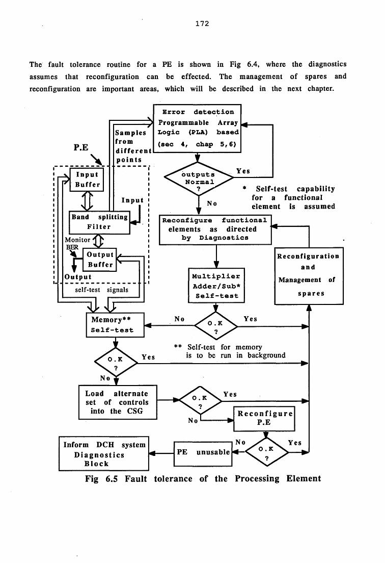
172
The fault tolerance routine for a PE is shown in Fig 6.4, where the diagnostics assumes that reconfiguration can be effected. The management of spares and reconfiguration are important areas, which will be described in the next chapter.
P.E
I n p u tB u f f e r
*S a m p l e sf r o md i f f e r e n tp o i n t s
Error detectionP rog ram m ab le ArrayLogic (PLA) based(sec 4r chap 5,6)
I n p u t
Band spl i t t ing F i l t e r
Monitor BERX
JO u t p u tB u f f e r
O u t p u t
self-test signals
* S elf-test c ap a b ility fo r a func tiona l elem ent is assum ed
Reconfigure functional elem ents as d irec ted
by Diagnostics
Multiplier Adder/Sub* Self-test
R e c o n f i g u r a t i o n
a n d
Management of
s p a r e s
M em ory** Self-test
Load a lte rn a te set of controls
into the CSG
Inform DCH system D i a g n o s t i c s
B l o c k
** Self-test for memoryis to be run in background
Yes? ✓
R e c o n f i g u r e--------- ► P. E
PE unusab le
Fig 6.5 Fault tolerance of the Processing Element

173
The self-test approach for multipliers described in [DENY85], can also be used on adders and subtractors. Subsequently, several new procedures have been reported
in the proceedings of the International Test Conference (ITC) of the IEEE, where an important example concerns the use of a built-in self-test for a complete digital signal processor; it is described by Sakashita et al., who report tests on a 24-bit floating point processor [SAKA90]. By using a pair of Linear Feedback Shift Registers (LFSRs) and 253 words of normal instruction, testing of 95% of the functional blocks is claimed. The disadvantage however is that 35 million test vectors are used, which need about 2.6 seconds to execute, even at a fast machine cycle of 75 ns; this is not surprising since it is clearly the basic limitation in any self-test. Whilst such tests
are very useful for ground based applications, their usage on-board are unlikely in
the near future, due to the vast resources required to conduct such exhaustive tests. Detection of errors on the other hand, is the first step towards fault tolerance as described in chapter 3 and the methods developed in this and the previous chapter are indicated in Fig 6.4. The circuits needed for detection, occupy 10% of the chip area needed for Fault Tolerance (FT), as already described in the previous chapter.
6.6 CONCLUSION
The application of a database search is a useful means to analyse error detection in a Digital Channeliser. The special nature of the error detection procedure offered by Artificial Intelligence search techniques has been brought out in terms of a compact database as well as the simple algorithms used. Im portant advantages of implimenting a PLA based error detection scheme on-board are obviously the inherent self-test feature and compact, simple circuits which can report errors to diagnostics and reconfiguration systems [RAGH90].
Software reliability is an area of extensive study as described earlier in chapter 3. For space applications, the data diversity method seems to offer a good approach to
attain software reliability, since data diversity only needs the effective use of the
available data sources to attain better reliability [AMMA88]. Since DSP circuits largely use hardware to improve speed and efficiency, software is not used extensively in the DCH. However, a direct application of the data diversity scheme is implemented in our adder/subtractor search routine where the sources of data are the adder input as well as the subtractor input, during alternate cycles. Additionally, the flow of data through the shift registers and multiplexers is verified by the
adder/subtractor search routines at the three adder/subtractor groups.

174
In high speed circuits used for real-time applications, the time taken for errordetection is always larger than the execution time. Assuming a uniform data flow, itis likely that faults which introduce massive delay faults as described in [MALA84],would upset the equilibrium of data flow. Although, such faults are expected to cause a deterioration in the performance, a complete blockage on any channel is unlikely, unless there is a physical break in the link between elements. An increase in noise or a garbled message are the more likely effects of faults in the DCH and a marginally slower detection mechanism is therefore acceptable. In computers which handle transactions in an asynchronous manner, error recovery mechanisms are provided to restore the system to normality [CAMP86]. However, most of the taskshandled by software in computers, are replaced by dedicated hardware in DSP. Therefore, error recovery in a DCH is best provided by reconfiguration and initiation of the system to normal operations after substituting a spare.
After detection of errors (described in this and the previous chapter), the next step in the fault tolerance procedure is the reconfiguration of the system, using spares. This is the subject of the next chapter, where new schemes are developed to reconfigure the PE, assuming that an error has been detected using the procedures described in this and the previous chapter.

175
R e f e r e n c e s
[AMMA88] P.E.Ammann and J.C.Knight, “Data diversity: an approach to software fault tolerance”, IEEE Tran Computers, Vol.37, No.4, Apr 1988, pp 418 - 425.[AVIZ61] A .A vizienis, “Signed-digit number representations for fast parallel arithmetic”, IRE Tran. Electronic Computers, Vol.EC.10, No.9, pp 389-400, Sept 1961. [BI90] G.Bi, F.P.Coakley, “The design of Transmultiplexers for on-board processing
sate llites using b it-seria l processing technique”, Proc. 13th AIAA In t’l Communication Satellite System conference, Los Angeles, CA Mar 11-15, 1990, pp 613- 622.[BARZ83] Z.Barzilai, D.Coppersmith and A.L.Rosenberg, “Exhaustive generation of bit patterns with applications to VLSI testing”, IEEE Tran. Computers, Vol.Cr32, No.2, Feb 1983, pp 190-194.[CAMP86] R.H.Campbell and B.Randell, “Error Recovery in Asynchronous Systems”,
IEEE Tran. Software Engineering, Vol.SE-12, No.8, Aug 1986, pp 811-826.[CHOW78] C.Y.Chow and J.E.Robertson, Proc. 4th Int’l Symp. on Computer arithmetic
(IEEE), Oct 1978, pp 109-115.[DENY85] P.Denyer and D.Renshaw, “VLSI Signal Processing: a bit-serial approach”, Chapter 7, Addison-Wesley Publishing Co., England, 1985.[GOSL82] J.B.Gosling, “Design of Arithmetic units for digital computers”, Macmillan
Computer Science series, London, 1982.[ILLM85] R.J.Illman, “Self-tested data flow logic: a new approach”, IEEE Design & Test,
April 1985, pp 50-58.[LISS86] J.Liss, “A software technique for diagnosing and correction memory errors”, IEEE Tran. Reliability, Vol.R-35, No.l, April 1986, pp 12-18.[MALA84] Y.K.Malaiya and R.Narayanaswamy, “Modeling and testing for timing faults in synchronous sequential circuits”, IEEE Design & Test, Nov 1984, pp 62-74. [RAGH90] K.Raghunandan and F.P.Coakley, “Fault tolerance of on-board processors”, Proc 2nd In t’l workshop on Digital Signal Processing techniques applied to Space Communications, Paper 3.5, DSP 90, ESA-WPP-019, Turin, Italy, 24-25 Sept 1990. [RAGH91] K.Raghunandan and F.P.Coakley, “Fault detection in digital filters for satellite systems”, Proc. 6th Int’l conf. on the application of artificial intelligence in engineering (AIENG-6), Oxford University, Oxford, 2-4 July 1991, pp 769-788. Elsevier Applied Science, Computation Mechanics Publications, UK and USA.[SAKA90] N.Sakashita, H.Sawai, E.Teraoka, T.Fujiyama, T.Kengaku, Y.Shimazu and T.Tokuda, “Built-in Self-test in a 24bit floating point digital singal processor” Proc. Int’l Test Conference (IEEE), Washington DC, Sept 10-14, 1990, pp 880-885.

176
[TAKA85] N.Takagi, H.Yasuura and S.Yajima, “High-speed VLSI m ultiplication algorithm with a redundant binary addition tree”, IEEE Tran.Computers, Vol.C-34, No.9, Sept 1985, pp 789-796.[WONG90] W.C.Wong, T.Suda and L.Bic, "Performance analysis of a message-oriented Knowledge-Base", IEEE Tran Computers, Vol.39, No.7, July 1990, pp 951-957.

177
“It is a feature o f most, if not all, systems that they are only really noticed when they go wrong” - A.J.Samecki
7
RECONFIGURATION ISSUES IN DIGITAL CHANNELISERS
Z j_1 INTRODUCTION
In the previous chapters the detection of errors in the various elements of a Digital Channeliser (DCH) were described. From the review of fault tolerance in chapter 3, it became evident that some form of reconfiguration is necessary after a fault has been detected. Chapter 2, described the use of DCHs in communication satellites, where it was pointed out that a DCH is used to convert singals from the frequency domain to the time domain. The data from various users would be sent using FDMA (Frequency Division Multiple Access), converted on-board the satellite using a DCH and the outputs sent back in a TDM (Time Division Multiplex) channel, as shown in Fig 7.1. Further, it was pointed out that a DCH could have different configurations one of which, the binary tree structure, was considered for this fault tolerance study. The configuration chosen for the DCH uses a pipelined structure, which is the time multiplexed version of a binary tree where a Band-Splitting filter (BSF) with input/output buffers is assumed as the basic Processing Element (PE).
M A MFDMA
CO
TDM
FIG 7.1 Conversion - Frequency to time domain
Reconfiguration issues in such a pipelined structure are considered in this chapter.
The reconfiguration of functional components which make up a PE are also

178
considered in this chapter. New schemes are proposed, to substitute the faulty elements with a spare so that restoration to normality becomes possible.
There are two aspects which are important in the reconfiguration of the time- multiplexed pipeline:(i) Being a serial structure, it is normally expected to be less reliable than a conventional binary tree structure, which has a serial-parallel structure; serial at each stage of the tree and parallel within each stage. The assumption is based on the knowledge that when elements are connected in series, the reliability decreases as a product of the reliability of individual elements. Further discussion on the reliability aspects will be found in section 4 of this chapter.(ii) The reconfiguration scheme proposed benefits not only the DCH, but is also useful to other applications of the binary tree as well. The binary tree is widely used in hierarchical computing systems and back-end storage networks. The tree structure in general, offers good speed of information exchange between any two nodes in an n-node system.
Conventionally, reconfiguration of binary tree structures comprise schemes to evolve a modular structure where each module consists of a binary stage with spares and switches. In this chapter, a novel scheme called the S e r i a l M o d u l e ( S M ) s c h e m e for the pipelined version of the binary tree is developed. In terms of reliability it is shown that the SM scheme requires fewer spares to provide the same performance as
that of an equivalent conventional reconfiguration scheme. Since the BSF has a serial structure, the SM scheme is extended to the functional elements of the filter
and the issues of providing spares at the functional level and sub-system level are discussed. Some of the reconfiguration issues concerning a time-multiplexed version
of the binary tree are addressed.
The first section provided an introduction to the issue of reconfiguration in a DCH. In section 2, the difference between a binary tree structure and its time-multiplexed equivalent, in terms of fault detection and reconfiguration, is described. Section 3
reviews the schemes available for reconfiguring a binary tree. A Serial-Module reconfiguration scheme is proposed in section 4 for a time-multiplexed version of the binary tree. The reliability analysis of this new scheme is addressed in section 5, and is also compared with the other redundancy schemes. Concluding remarks on the proposed scheme are summarised in the final section. Part of the material in this chapter may be found in [RAGH91b].

179
7.2 BINARY TREES AND THE TTME-MIJLTTPLEXED PIPELINE
Reconfiguration schemes improve the reliability of a system by the use of spares. The management of spares, the manner in which they are incorporated in the system layout, isolation of the faulty element etc., are the issues addressed in a reconfiguration scheme. In order to evolve such a scheme let us look at the basic concept of fault detection in a binary tree structure described in chapter 2 and relate it to the pipelined (time-multiplexed version) configuration. We can consider the DCH structure and analyse the effects of simple stuck-at faults on its various PEs shown in the binary tree of Fig 7.2.
2 DECIMATION BY 2 » HI
SERIALINPUT
|2 HEc r
i i
aHI branch LOW branch
i2LH
LO1 J
OUT 1 OUT 2
OUT 3 OUT 4
OUT 5 OUT 6
OUT 7
OUT 8|^-STAGE 1 ►J*-STAGE2-*|*-STAGE3^|
Fig 7.2 MULTISTAGE Digital Channeliser - TREE STRUCTURE
If the output of any stage is stuck-at-HI or stuck-at-LOW branch, the pattern at various outputs would provide a direct indication of the stage at which the fault has occured. This is shown in Table 7.1, where a ‘0 ’ in the output indicates a fault. The stuck-at faults are assumed to indicate a situation in which the control to switch over at a predesignated time, is stuck to a particular position. However, sim ilar outputs
could also occur if there is a fault in any stage PE. The general idea is to illustrate
the flow of signals through a binary network and to relate faulty signals at the
different stages, to faults in a particular PE. The flow indicates one major weakness of the binary tree structure which is that the operation of different processors and
links is very inter-dependent.

180
Table 7.1 Fault propagation through a binary tree structure
Simulated fault Outputs in different stages
Fault condition HI LO HH HL LH LL OUT1 OUT2 OUT3 OUT4 OUT 5 OUT6 OUT7 OUT8
No fault 1 1 1 1 1 1 1 1 1 1 1 1 1 1
1st stage S-a-H 1 o* 1 1 0* 0* 1 1 1 1 0* 0* 0* 0*
1st stage S-a-L 0* 1 0* 0* 1 1 0* 0* o* 0* 1 1 1 1
2nd HI st S-a-H 1 1 1 0* 1 1 1 1 0* 0* 1 1 1 1
2nd HI st S-a-L 1 1 0* 1 1 1 0* 0* 1 1 1 1 1 1
2nd LO S-a-H 1 1 1 1 1 0* 1 1 1 1 1 1 0* 0*
2nd LO S-a-L 1 1 1 1 0* 1 1 1 1 0* 0* 1 1
3rd UU S-a-H 1 1 1 1 1 1 1 0* 1 1 1 1 1 1
3rd UU S-a-L 1 1 1 1 1 1 0* 1 1 1 1 1 1 1
3rd UL S-a-H 1 1 1 1 1 1 1 1 0* 1 1 1 1 1
3rd UL S-a-L 1 1 1 1 1 1 1 0* 1 1 1 1 1 1
3rd LU S-a-H 1 1 1 1 1 1 1 1 1 1 0* 1 1 1
3rd LU S-a-L 1 1 1 1 1 1 1 1 1 0* 1 1 1
3rd LL S-a-H 1 1 1 1 1 1 1 1 1 1 1 1 1 0* I3rd LL S-a-L 1 1 1 1 1 1 1 1 1 1 1 1 [ 0* 1
* Faulty output or no output.
In the time-multiplexed version of the binary tree since each stage processes signals belonging to all channels (though in different time slots), thus a failure of any PE results in faulty outputs on all the channels. Consider a fault in the PE at second stage HI, leading to a faulty output at HH, for example. In the pipelined version shown in Fig 7.3 (b), such a fault can be represented in PE-2 during the time period when PE-2 is processing the data belonging to the stream HH. However, such a
possibility is remote in a pipeline and it is reasonable to presume that if a fault occurs in PE-2, then all its output streams viz., HH, HL, LH and LL would be faulty.
The argument therefore, points to increased need to provide redundancy in the pipelined version. Redundancy can improve reliability of the system, if it is accompanied by fault detection and location in addition to self-test diagnostics [JO H N 89]. The next section reviews a representative sample of the reconfiguration
procedures available for binary trees. The general concepts in these procedures are
later applied to the time-multiplexed version of the DCH.

181
Input
Input buffer
Splitting Buffer
Output
Input PE PE PE PE— » -► -► >
1 2 k k-1
Output
Fig 7.3(a) Configuration of PE
i' P E \ Processing Element
Fig 7.3(b) Digital Channeliser - Pipelined version
7.3 RECONFIGURATION OF BINARY TREES
The binary tree structure is particularly straight forward to implement because each node has at most two descendants; in general, any tree can be represented as a binary tree. Reconfiguration is a procedure by which a faulty element is isolated, a spare is substituted in its place and the system is configured to resume normal operation. Different approaches for the reconfiguration of a binary tree structure are suggested [HASS86,RAE84,LOWR87], all of which assume the use of spare PEs at each node of the tree and additional switch connections to allow isolation of the faulty PE. Reliability analysis indicates the tradeoff between the reliability expected and the number of spares allocated. Briefly, the schemes are as follows:
Hassan and Agarwal [HASS86], suggest that two interconnected stages of the binary tree be treated as a module with spares and switches provided for reconfiguration at
the module level. Each module is assumed to tolerate a single fault, thereby reducing the number of spares required. Such modules are expected to be connected together to form a complete binary tree. For the purpose of isolation and reconfiguration, two types of connections have been suggested by them: a link to connect processor nodes and a link to bypass a processor. Using these links a local restructuring scheme has been developed, to bypass the faulty processor and to maintain a tree structure after each fault occurrence.
Two schemes have been suggested by Raghavendra, Avizienis and Ercegovac [RAE84]; the first scheme addresses the issue of reconfiguration using spares while the second scheme allows a performance degradation in the event of a failure. The scheme using spares, suggests one spare for every k = 2J nodes, where the integer
value assigned to j, depends on the redundancy required. The scheme with performance degradation, uses one spare node for the root together with extra links
from each node. When a failure occurs, the neighbouring processor is expected to

182
carry out the tasks of the faulty processor, in addition to its own, reducing thethroughput. The amount of degradation would then depend on the level at whichfailure occurs.
The Subtree Oriented Fault tolerance (SOFT) approach by Lowrie and Fuchs [LOWR87], suggests the use of spare processors located at specially designated leaves of the tree. Additional links between processors are provided to ensure tree topology in the event of multiple processor failures and link failures. Although the redundancy interms of spare processors and links is reduced, a series of displacements (of nodes and links) are required in the event of a failure, until a spare is configured into the tre e .
These reconfiguration schemes provide a useful direction to consider a scheme for the pipelined array structure shown in Fig 7.3. However, they have certain limitations in terms of the large number of spares needed as well as the number of
additional links required to effect reconfiguration.
7.4 RECONFIGURATION OF PIPELINED STRUCTURE
Since the pipelined structure implements a binary tree structure in a time multiplexed form, the branch nodes as well as the processors of each tree stage, collapse in terms of hardware into an equivalent single stage PE. Each PE can thus be regarded as a stage and provided with a spare, which would be a straight forward approach with 100% redundancy to the pipeline. Despite this the redundant-pipeline would need fewer PEs than an equivalent non-redundant binary tree. Table 7.2 provides a comparison of PEs required for a four-level structure (16 channels) using
the pipeline and the binary tree indicated in [HASS86].
In practice, failures rarely occur simultaneously; occurrence of faults in a sequenceconstitutes a more realistic model as discussed by Somani [SOMA90], in which
sequential fault occurrence is used . It is assumed that a fault may not be repaired right away, which is the case in satellite applications. In satellites although repair isnot possible, provision can be made to test the suspected PE using fault detection and
self-test diagnostics, which encourages the use of limited spares [RAGH90]. If thesuspected PE is confirmed to be normal (after self-test), then it could again be included as a spare.

183
T able 7.2. Four-level s tru c tu re - Processing E lem ent R equirem ents
Binary Tree Strut (Modular stages as in \]
:ture.HASS861)
Pipelined Structure with (100%) complete redundancy for each PE
Module size Spare PEs Total PEs Module size Spares Total PEs
(1 + 2) 5 20 (2 + 2) 4 8
(1+2+4) 2 17 (3 + 1) 4 8
(1+2+4+8) 1 16 4 4 8
It may be mentioned that hilst 100% redundancy is indicated for the pipeline structure, the spares indicated for a binary tree in [HASS86] offer less than 100% redundancy. It is often not necessary to provide 100% redundancy in terms of spares, due to the lower failure rate provided by VLSI technology, which are typically in the range of 0.05 to 0.1 failures per million hours of operation. Hence, it is worth considering reconfiguration schemes which utilise less than 100% redundancy.
Such a Serial-Module (SM) scheme is described next, where one spare is allocated for
the 4 PEs of a 16 channel pipelined structure.
The modular approach results in a regular structure, as shown in Fig 7.4. The lim itation in this circuit is the large number o f switches and the twointerconnecting branches (Brl and Br2). Although these are necessary for isolation of the faulty element and inclusion of a spare, some means to reduce the number of
switches is necessary. The input to each filter stage comprises separate serial paths for the real and imaginary parts, as shown in Fig 5.2. The actual number of
input/output switches in Fig 7.4, will therefore be doubled.
TO SPARE PROCESSING ELEMENT
^-Processing Element
BrlINPUT PEPE
•-OUTPUT
Br2
PE
a,coPEPE
FROM SPARE PROCESSING ELEMENT
Fig 7.4 Reconfiguration of the serial pipeline

184
The other reason to seek a reduction in the number of switches is the inherent improvement in reliability due to simpler links and limited number of switches. Failures in communication links as well as stuck-open and closed faults in the switches has been analysed in [LOWR87], where the following conclusions have been
draw n:
(i) if any redundant link is isolated, then its failure is reconfigurable(ii) if a switch is isolated then its failure is reconfigurable(iii) A stuck-open fault in a switch is reconfigurable as a failure of the processing
e lem en t.
A reduction can be brought about if the functions of these switches are considered as: (a) connection of a spare element and (b) isolation of the faulty element. These two functions can be achieved if the input and output switches (II ..14 and 01 ...04) are
connected directly between the elements. The number of switches can be reduced by more than half; a scheme which uses just eight switches, has been developed and is
described next.
In the SM configuration shown in Fig 7.5, the input switch SI1 is coupled to the output switch SOI, to isolate the faulty element A and replace it by connecting the input and output of the spare element S. Other output switches S02 .. S04 as well as input switches SI2 .. SI4, are shown in the normal position, to connect the nodes
(01,12), (02,13) and (03,14) directly using input switches SI. The logic used in switchselection is assumed to ensure that only one SI switch can select the spare at any
given time.
The entire circuit can then act as a module and additional modules may be added, by connecting the output of the previous module to the next. Although, the module shown in Fig 7.5, assumes a spare for every 4 PEs, it is easy to show that modules ofdifferent sizes (varying the number of PEs, as well as spares) can be similarlyformed. A graceful degradation switch is incorporated in the module primarily to cater for the general applications of the binary tree. In a DCH since the processing elements are digital filters, graceful degradation is more difficult to achieve as compared to conventional computing systems. The 'graceful degradation switch' is used to by-pass the spare as well as the faulty element, which is useful when there
are no spares. In such an event, the successor PE would carry out the the tasks of the
faulty one, in addition to its own.

185
TO SPARE PROCESSING ELEMENT _____________ A ______________
SA SB SC SO
r — \ -----»INPUT . ! PE! ( ! PE! J■ i P E i <
-----Ofr J--® o-l l-o0 1 i A ,
t i1 2
SWITCH DETAILS
SA (to Spare)
SI1
2 3 ii v il. — a
| r e ! OUTPUT 1 i - o
3 4 J D Jt — — -i
r j hV« o—4- 1
____'
t * --;^ P E ;~ Processing Element
from spare r j fJL-T r S01
SB SC GRACEFULDEGRADATION
SWITCH
INPUTPROCESSING
ELEMENTSSWITCHES
SPARE
OUTPUT SWITCHES
Fig 7.5 RECONFIGURABLE MODULE FOR THE PIPELINED VERSION
In the graceful degradation scheme suggested by Raghavendra et al., use of spares and graceful performance degradation at the upper stages of the tree, and only performance degradation at the leaf nodes of the tree has been recommended. In the pipelined version, the successor PE handles data from the channels of the
preceeding stage. Since all stages operate at the input sampling rate, there is no particular advantage in designating more spares to the the top level PEs. Due to a fault in the previous stage and lack of spares, the first task of the successor PE would
be to initially produce two output words of each channel, which was the job of the

186
proceeding stage which is now faulty. This must be followed by its own task oftaking these two words to produce one word for each channel. A consequentreduction in the throughput must be expected since the system has to trade time for hardware failures.
In a DCH, if we assume the task of producing one word on a channel as one instruction cycle, then the succeeding stage has to perform three instruction cycles,instead of one. Hence, the system throughput would be one third its normal, in termsof performance degradation. However, it is difficult to implement these operations in a digital filter. Each PE in the pipeline must operate at a different clock rate and a programmable clock module is necessary. Even so, the module which must perform
operations of the previous stage as well as its own, must operate alternatively at the two different clock rates. These problems need changes at the design level.
7.4.1 RECONFIGURATION OF BAND SPLITTING FILTER
Each PE consists of a Band-Splitting Filter (BSF) and buffers is shown in Fig 7.6.
Real
Imaginary
Add
Sub
Input Buffer>>'V
SHIFT REGISTERS
2Multiplex & Preprocess
JL
Mul
h ' (3 )
1
2
Mul
Multiplex & Preprocess
1 1
(1)Mul Mul
J
Multiplex & Preprocess
h' (0)Mul
Add Add
1—Vi r:
Mul
Delay
eztAdd AddREH
OutputBuffer
Fig 7.6 Block diagram of Band Splitting Filter

187
A simplified version is illustrated to develop a model for the purpose ofreconfiguration. Generally such filters (FIR type) are expected to handle complexnumber inputs which require separate processing of the real and imaginary parts,as indicated in Fig 7.6. Details of their operation may be found in chapters 5 and 6.
MRS - Multiplier, Real, Spare
MIS - Multiplier, Imaginary, Spare
MULTIPLIERSPARE
Multiplicand
(Mnd)
Multiplier
(M ir)
Product
Real Mnd1REAL
Real Mlr1 PDCT1Subtractend
ImaginaryMnd1------Imaginary
M lri
Imag Remainder(Snd)PDCT1
MinuendMULTIPLIER 1 (Med)
Real Mnd2Addend
(Add)
Augend
REALReal Mlr2 SumPDCT2
(S)ImaginaryMnd2------Imaginary
Mlr2
Imag (Aug)PDCT2
MULTIPLIER 2
MR2
MR1
MI2
MIS
MRS
MI1 Subtractor
MULTIPLIER
ADDER
To o t h e r Mult ip liers
Fig 7.7 Reconfiguration of Multiplier and other components
From a reconfiguration point of view, three active components viz., multipliers, adders-subtractors, as well as the "multiplex & preprocessing" module are important. Each of the active components can be modelled as a two input, single output device. The adders shown in Fig 7.6, are connected in series and a SM scheme similar to the one described earlier, would be useful for their reconfiguration. The input "Adder- Subtractor" combination is best served by a direct spare substitution. The 'Multiplex
& Preprocess" module has multiple inputs/outputs depending on the word length and

188
the length of the filter. However, its reconfiguration can have a scheme similar to that for multipliers, shown in Fig 7.7; the multiplexer with shift register would be
considered as one module for the purpose of providing spares.
The number of components used, depends on the filter length; the BSF shown in Fig 7.6 assumes a filter length of 7; details on the design of such filters may be found in [BI90a], Since all the components simultaneously handle the real and imaginary parts, they are grouped in pairs and the reconfiguration scheme for multipliers
shown in Fig 7.7, indicates this aspect. Of the three multiplier pairs in the BSF, only two pairs are indicated in Fig 7.7 and the first pair is assumed "faulty" and "isolated"; therefore the input and output lines are connected to the spare multiplier pair.
Again, switching logic is assumed to ensure the selection of only one pair at any time. Other modules such as the buffers and delay units, do not transform the dataand their fault detection as well as built-in redundancy features have been discussed in standard texts on Fault tolerant computing, for example [JOHN89], as well as in the
previous chapter.
7.4.2 VLSI implementation and restructuring
To implement reconfigurable binary tree structures in VLSI, a layout resembling theletter “H” is recommended in [HASS86,LOWR87]. Such a pattern provides efficient
interconnections to the spare element for a binary tree stage. For a linear array with pipelined structure, it is better to configure the PEs along with the input andoutput buffers. In Fig 7.7, it may be seen that a data bus consisting of many signallines connect the input and output buffers. The task of providing switches on each ofthese lines can be avoided if the buffers are implemented along with the BSFs. Design of a 4 channel DCH is described in [BI90b] where a single stage has been used
with time multiplexing to implement the 4 channels. If several stages are used, it
may be necessary to place the spare element on a separate chip. Even in such a situation, a considerable reduction in the number of lines to the buffers, offers large savings in the pad interconnections. Further discussion on the layout and chip area of the overall system, will be found in chapter 8.
Most of the layout schemes described for VLSI, are relevant at the stage of
manufacturing when defective PEs can be eliminated and the good ones can be

189
configured into the system. For failures which occur in the operating environment, the connections that are already available in the layout, may be used in the
reconfiguration of the system.
7.5 RELIABILITY CONSIDERATIONS
In this section, a brief review of the reliability expressions relevent to the time- multiplexed version of the binary tree are presented, followed by a derivation of the reliability models. The reliabilities of individual components are used in order to calculate the reliability of a PE and further the overall reliability of the Digital Channeliser (DCH).
7.5.1 RELIABILITY MODELS
Since the reliability, Ri(t) of any component is less than unity, a serial system will
always have a reliability smaller than the reliability of the individual components. In a pipelined DCH, each of the component PEs is in itself made up of a HBF which may be considered as a serial system, with non-identical components such as Adder- Subtractor, Shift register, Multiplex & preprocess, Multipliers and Adders (buffer memory lements are not included in this assumption). Consider the first case where 100% redundancy can be provided for each of the non-identical components shown
in Fig 7.8.
OUTPUTINPUT
A d d e r s
A d d e r s
S h i f t
R e g i s t e r s
S h i f t
R e g i s t e r s
S u b t r a c t o r
Adde r andM u l t i p l i e r s
M u l t i p l i e r sS u b t r a c t o r
Adder an d
Multiplex &
P r e p r o c e s s
Mult ip lex &
P r e p r o c e s s
Fig 7.8 Processing element with complete redundancy
Each of the components in Fig 7.8 form a parallel system where normal performance of one of the two, ensures correct operation. Assuming a reliability of 0.9900 for each of the components, the system reliability is given by the expression [JOHN89]:
RpE = [1 - (1 - .99)2 ][1 - (1 - .99)2][1 - (1 - .99)2][1 - (1 - ,99)2][1 - (1 - ,99)2] = 0.9995.

190
Without the use of redundancy, a PE would have yielded a reliability of (.99)5 = 0.9510.
With the complete redundancy scheme the reliability of a PE is 0.9995, showing an improvement gained by the use of 100% additional hardware.
7.5.2 Redundancy using modular schemes
The modular scheme described for multipliers, may be visualised as a M-of-N system, where at least M blocks out of a total of N blocks are needed for normal functioning of the system. For the multiplier pairs, 3 out of 4 blocks must work in a normal HBF, whose reliability can be written as:
R M = R l ( t ) R 2 (t )R 3 ( t )R s (t) + R i ( t ) R 2 ( t ) R 3 ( t ) ( l - R s (t)) + R i ( t ) ( l - R 2 (t ) )R 3 (t )R s (t) +
(1 -R 1 (t))R 2 (t)R 3 (t)R s(t) + R i(t)R 2 (t) ( l-R 3(t))R s(t) . . . 7 .1where Rm is the reliability of the multiplier module, Rj the reliability of theindividual pairs and Rs - the reliability of the spare. Assuming that all the multiplierpairs have the same reliability Rm (including the spare), equation 7.1 reduces to:
RM = Rm4 (0 + 4 Rm 3 (t)(l-R m (t)) = 4 Rm3(t) - 3Rm4 (t) . . . 7 .2
Similarly, the "multiplex & preprocess" would have an identical equation for its module reliability Rm P- The "Adder-Subtractor" with its spare, can be visualised as a
parallel system with its reliability expressed as:
RAS = R l(0 + (l-R l(t))C R s(t) . . . 7 .3
where RAS is the reliability of the module and C is the "coverage factor" for the
normal unit. If the reliability of the spare and normal units are assumed to beequal, with a coverage factor C =1, the system reduces to a parallel unit having a reliability of RAS = (1 - (1 - R)^). Further, we have two adders which are connected
in series, with a spare in parallel with one of them; assuming the spare to be in parallel with the second unit, and further assuming that the reliability of the normal and spare units are equal, the simplification would be:
R a = Rl(t)[R2(t)RS(t) + 2 CR2(t) (1 -Rs(t))] = 2CR2a(t) - CR3a(t) ... 7 .4
where Ra is the module reliability and Ra represents the reliability of the normal as
well as the spare unit. For simplification, the delay unit and memory buffers are not

191
considered. Finally, there is a shift register in the BSF, which we have assumed to be without spares due to its inherent fault tolerance capability. The reliability of such a shift-register may be assumed as RSR-
The final expression for reliability of the proposed Redundant PE (RPE), is a serial
combination of all the elements described above which could be expressed in reliability symbols (LHS terms in the equations 7.1, 7.2, 7.3 and 7.4):
Rr p e = (Ra s ) • (Rs r ) • (Rm p ) • (Rm ) • (Ra ) • •• 7 .5
The reliability of the RPE can be calculated using the same value, assuming acoverage factor C = 1, yielding Rr p e = 0.9787, which is lower than the version with
complete redundancy (as expected) due to the considerable reduction in spares.
An expression for reliability of the time multiplexed DCH module with 4 PEs, will be
the series reliability function incorporating a spare, similar to equation (7.4).
Generally the exponential failure law is assumed to calculate the reliability of a component using the formula R(t) = e”^* , where X is the failure rate of the
component. With the advent of VLSI and reliable manufacturing methods, the expression for X is adapted to failures in million hours, which is often indicated as Failure In Time or FIT [SABN90]. In future, the expressions for X refer to failures in million hours.
Assuming that one of the PEs has a spare in parallel at any given time and that the failure rate of all the PEs (including the spare) are equal, the reliability expression
would be:Rchanneliser = e ' V [ e '2 *-‘ + 2 C e ( l - e- ^ t ) ] . . . 7 .6where X i = X + X+X=- 3 A, . Substituting Rr p e (0 = 0.9787 in equation (7.6),
R ch a n n e lise r = 0.9371, showing an improvement over the non-redundant value of
the channeliser ((0.99)5)4 = 0.8179. Obviously, an improvement in reliabilty "using spares, has to consider the number of spares used as a function of the improved
reliability, which is illustrated by the graphs for various schemes in Fig 7.9. The figure shows a graphical comparison for a four-level channeliser structure with
only one spare provided at the PE level as well as 100% redundancy, assuming X = 0.1 failures per million hours. These reliability figures are better than the ones claimed for redundant binary tree structures described earlier.

192
Reliability improvement with redundancy
100% redundancy’-> * * * • •......
^ <- Serial-Module scheme
*8 0.7
non-redundant
1 1.5 2time - million hours
Fig 7.9 R eliability with redundancy a t PE level
The system reliability variations with different coverage factors used in the SM
scheme (1 spare for 4 PEs) has been shown in Table 7.3. Apart from the SM scheme the pipelined channeliser can incorporate complete redundancy (indicated earlier in Table 7.2), thereby offering a further improvement in reliability over the schemes for the binary tree suggested in [HASS86,RAE84,LOWR87].
time in mil.hours
R eliab ility ( non-red)
R sm for c = 1
Rsm for c = 0.99
R sm for c = 0.98
R s m for c = 0.95
R s m for c = 0.90
0.00 1.0000 1.0000 1.0000 1.0000 1.0000 1.0000
0.1 0.9607 0.9703 0.9701 0.9699 0.9693 0.9684
0.2 0.9231 0.9413 0.9410 0.9406 0.9395 0.9377
0.3 0.8869 0.9131 0.9126 0.9120 0.9105 0.9078
0.4 0.8521 0.8855 0.8848 0.8842 0.8822 0.8788
0.5 0.8187 0.8586 0.8578 0.8570 0.8546 0.8506
0.6 0.7866 0.8324 0.8315 0.8306 0.8278 0.8232
0.7 0.7557 0.8068 0.8058 0.8048 0.8017 0.7966
0.8 0.7261 0.7819 0.7808 0.7797 0.7763 0.7708
0.9 0.6976 0.7577 0.7565 0.7553 0.7517 0.7457
1.0 0.6703 0.7341 0.7328 0.7315 0.7277 0.7213

193
7.5.3 C om parison o f redundancy schem es
Table 7.4 gives a comparison of the reliability values of the SM scheme with otherschemes, at X = 0 . 1 and t = 0.5 and c = 1 (these values are assumed in[HASS86,RAE84,LOWR87], for comparisons). The SM scheme proposed, compares well with the other schemes and when four spares are used, the SM scheme represents100% redundancy. The SM scheme has a linear characteristic in terms of reliabilityimprovement with spares and has better reliability than the m odular and Raghavendra et al schemes.
The SOFT scheme indicates a higher reliability value than the SM scheme when more than one spare is used. However, the higher reliability attained by SOFT is offset by the increased complexity of the special leaf, multiple links as well as the displacement procedure necessary for the SOFT scheme.
Table 7.4. R eliability fo r four-level b inary s tru c tu res
Scheme used Module used Number of spares Rsvs
M odular 2-M 5 0.9349
scheme [HASS86] 3-M 2 0.84994-M 1 0.8179
Raghavendra et al 1+2 8 0.9504 '
scheme [RAE84] 1+2+4 5 0.9280
1+2+4+8 4 0.9033
S O F T SOFT-1 4 0.9974
scheme [LOWR87] SOFT-2 2 0.9528
SOFT-4 1 0.8179
Serial Module 100% Redundancy 4 0.9905
Schem e SM-3 3 0.9445SM-2 2 0.9005SM-1 1 0.8586
=1, t = 0.5
Using the values of Table 7.4, a graphical representation of the number of spare PEs used and the reliability attained by the various schemes is shown Fig 7.10, where
only the integer values for the spares have to be considered.

194
Reliability curves for a four-level structure
SOFT scheme -> / Serial-Module scheme0.95
& 0.9
I0.85
<- Modular scheme
0.8102 4 6 80
Number of spares
Fig 7.10 R eliabilities of d ifferen t schemes
The 100% redundancy scheme provides “hot” redundancy, in that all thecomputations are simultaneously carried out both the chains, but only the output ofthe main chain is seleceted, until a switch-over occurs. In the event of a failure in any PE, the redundant chain is selected and data is not lost. In the SM schemes with limited spares, the spare is essentially a "cold" standby, used for replacement.Therefore, the pipeline needs to be flushed before normal operations can beresumed. The redundancy schemes described in [HASS86,RAE84,LOWR87], assume a "cold" standby, since a "hot" standby inherently needs 100% redundancy. A "cold"standby may be acceptable in many situations and the binary tree structure would also require a similar flushing operation in the event of a failure in the first stage.
7.5.4 Redundancy at the Functional level
From a system design point of view there is a need to introduce redundancy at thefunctional level, since a filter consists of functional components connected in series.In addition to the fault detection schemes described in earlier chapters, if self-test
were to be used as a means of fault diagnostics, then different self-test methods provide coverage factors as a function of test length, which could be important toattain a specified level of reliability. A typical simulation curve for a 16 bitmultiplier is shown in Fig 7.11 [DENY85] indicating the percentage of faults covered.

195
Sixteen bit multiplier - fault coverage simulation100
73s
u
500100 200 300 4000clock cycles
Fig 7.11 Test sim ulations on tw o's com plem ent m ultip liers
This curve indicates that 100% coverage is obtained after 414 cycles where, over 90% coverage is obtained in nearly 100 clock cycles of self-test. Therefore, coverage factor and test time are the two parameters between which a trade-off is needed.Reliability values for the PE and Channeliser using redundancy at the functional level are shown in Table 7.5 for a four-level structure, where values of X = 0.03 andcoverage factor c = 1 are assumed for each component of the HBF. To obtainreliability values comparable to those assumed for a PE in the previous section, a failure rate of 0.03 is assumed here. Since current failure rate figures quoted bymanufacturers (Intel, Texas Instruments etc.,) are always less than one failure per million components manufactured, a value of X = 0.03, seems realistic.
Table 7.5 Re iab ility values considering com ponent redundancy , X = 0.03
time(mil. hour) RpE(non-redl RpEfredundant) RCH(non-red) RCH(redundant)
0.1 0.9851 0.9939 0.9417 0.9817
0.2 0.9704 0.9875 0.8869 0.9629
0.3 0.9560 0.9810 0.8352 0.9437
0.4 0.9417 0.9742 0.7866 0.9240
0.5 0.9277 0.9673 0.7408 0.9040
0.6 0.9139 0.9601 0.6977 0.8837
0.7 0.9003 0.9528 0.6570 0.8631
0.8 0.8869 0.9453 0.6188 0.8422
0.9 0.8737 0.9377 0.5827 0.8212
1.0 0.8607 0.9298 0.5488 0.8000

196
Irrespective of the configuration used in a binary tree, the underlying filterstructure (serial at the functional level) needs redundancy to improve reliability. The formulae described earlier in section 7.5.2 have been used to calculate thereliability values indicated in Table 7.5. It is possible to obtain the required reliability by improving the product quality (indicated by the lower failure rate, in this case) as well as redundancy, both of which have been attempted.
7.6 CONCLUSION
Reconfiguration schemes to improve the system reliability of a DCH have been described, using the pipelined configuration of a binary tree structure. A Serial- Module (SM) scheme is developed for efficient reconfiguration of the pipelined DCH. In comparison with the binary tree structures, reliability figures for the pipelined version indicate an improvement. This is particularly interesting because the bit- serial structure offers a higher reliability compared to a serial-parallel binary tree structure. The improvement in reliability is partly due to the reduction in the number of switches and interconnecting links and to an extent due to the simpler interconnections in a pipeline. Another attraction of the proposed SM scheme is the considerable reduction in the number of spare processing elements (indicated in Table 7.2). Redundancy schemes described in this chapter use simple, modularstructures, which can be easily incorporated into the design, w ithout major modifications. The Raghavendra et al, Modular and SOFT [HASS86,RAE84,LOWR87] schemes for reconfiguration of binary-tree structures have assumed a general PE asthe basic building block, while the SM scheme described here has in addition chosen
the PE to be a digital filter with buffers. Such an assumption helps to highlight the
inherent functional limitations due to the serial structure of a filter and extends the Serial-Module redundancy scheme to the components of the filter as well.
The reconfiguration of the ADC was not considered in this chapter, since it can have
100% redundancy, similar to the input adder/subtractor stage. However, since the ADC will be an input element for the DCH, it must be considered as another element in the series model for a DCH, resulting in a slight decrease in the overall reliability figures. Like the buffers and shift registers, built-in redundancy features are available in many versions of ADCs, which is encouraging, from the reliability view
po in t.

197
7.6.1 Recom m endations
The SM scheme is recommended for reconfiguration of the DCH at both the functional element level and at the PE level. Details of how this can be implemented, are shown in the next chapter. In addition to saving considerable chip area in terms of limited spares and switches, the SM scheme provides good reliability. In terms of interconnections to the spares, the time-multiplexed bit-serial version needs fewer interconnecting lines, making the overall design simpler.
Even for other applications of the binary tree such as the hierarchical computing systems or the back-end storage networks, the pipelined version is recommended for its reliability and simple structure. Although latency is an inherent characteristic of the pipeline, the availability of high speed processors, makes the time-multiplexed pipeline an attractive candidate for binary tree applications, while the SM scheme proposed in this chapter demonstrates that reconfiguration can be achieved efficiently, thus providing a good, simple and fault tolerant design.

198
R e f e r e n c e s
[BI90a] G.Bi, F.P.Coakley, “The design of Transmultiplexers for on-board processing sate llites using b it-seria l processing technique” , Proc. 13th AIAA In t’l Communication Satellite System conference, Los Angeles, CA, USA, Mar 11-15, 1990, pp 613-622.[BI90b] G.Bi, F.P.Coakley, “A gate array design of a 4-channel Transmultiplexer”, Report on Work Package 203, MSS contract, Dept Of Elec Eng, University of Surrey, May 1990.[DENY85] P.Denyer and D.Renshaw, "VLSI signal p rocessings bit-serial approach",Addison-Wesley Publishing Co, England, 1985.[HASS86] A.S.M.Hassan and V.K.Agarwal, "A fault-tolerant modular architecture for binary trees", IEEE Tran Computers, Vol.C-35, No.4, Apr 1986, pp 356-361.[JOHN89] B.W.Johnson, "Design and Analysis of Fault tolerant digital systems",
Addison Wesly Publishing Co., USA, 1989.[LOWR87] M.B.Lowrie and W.K.Fuchs, "Reconfigurable tree architectures using subtree oriented fault tolerance", IEEE Tran. Computers, Vol.C-36, No. 10, Oct 1987, pp 1172-1182.[RAE84] C.S.Raghavendra, A.Avizienis and M.D.Ercegovac, "Fault tolerance in binary tree architectures", IEEE Tran. Computers, Vol.C-33, No.6, June 1984, pp 568-572. [RAGH90] K.Raghunandan and F.P.Coakley, "Fault tolerance of on-board processors", Proc. of 2nd Int'l Workshop on Digital Signal Processing Techniques Applied to Space Communications, DSP -90,Italy, 24-25 Sept 1990, (European Space Agency ,ESA-WPP- 019), Paper No.3-5.[RAGH91a] K.Raghunandan and F.P.Coakley, "Fault detection in digital filters forsatellite systems", Int'l conf on Application of Artificial Intelligence in Engineering (AIENG 6), Univ of Oxford, Oxford, 2-3 July 1991, Elsevier Applied Science, UK. [RAGH91b] K.Raghunandan, F.P.Coakley, “Reconfiguration issues in d igital channelisers for satellite applications”, Proc. Pacific Rim Int’l Symposium on FaultTolerant Systems (PRFTS), 25-26 Sept 1991, Kawasaki, Japan, Session 1, Paper 2, IEEE
Computer Society Press.[SABN90] A.K.Sabnis, “VLSI reliability” VLSI Electronics Microstructure Science,
Vol.22, Academic Press in arrangement with AT & T, USA, 1990.[SOMA90] A.K.Somani, "Sequential fault occurrence and reconfiguration in system
level diagnosis", IEEE Tran. Computers, Vol.39, No. 12, Dec 1990, pp 1472-1475.

199
"Quality in a product in not measured, but is built into” - Watch word for Quality control
8S y s t e m C o n s i d e r a t i o n s
8.1 Introduction
The objective of this chapter is to show how the different fault tolerance aspects can be applied to a DCH using a centralised diagnostics system described in [CHU89]. For this purpose a 4 channel DCH [BI90b] is chosen; fault tolerance methods which were developed earlier in this thesis are integrated and the overall chip areas are estimated. This chapter also defines the diagnostics system objectives, in terms of interaction and control. A. diagnostics system is perceived as the central unit to
which all others viz., error monitoring, reconfiguring systems report to and receive commands from. Therefore, viewing the DCH as a system from this central unit provides a clear understanding of how fault tolerance is provided to the DCH as a whole, in terms of chip area and design trade-off.
Most of the error detection systems available until now, concentrated on the use of t e s t p a t t e r n s to detect errors. The very nature of a te s t , demands that the unit be c u t
o ff either physically or electrically from the main system, before a te s t can begin. The concept of error detection in real-time systems, runs contrary to this approach. Error detection in any real-time system, must be limited to “monitoring” and not “cut-off’ of the circuit under question. In this sense, the approach provided in this
thesis provides for the first time, an error detection method for tw o’s complement
multipliers, digital filters and the input ADC. These aspects have been highlighted in this chapter.
8.2 Fault tolerance of a DCH
The overall approach to provide fault tolerance to the DCH is illustrated in Fig 8.1, which was illustrated as Fig 1.3 at the beginning of this thesis. The purpose of introducing this figure again, is to illustrate that the objectives set out at the
beginning of this thesis, have been achieved. Whilst the review in chapters 2 and 3
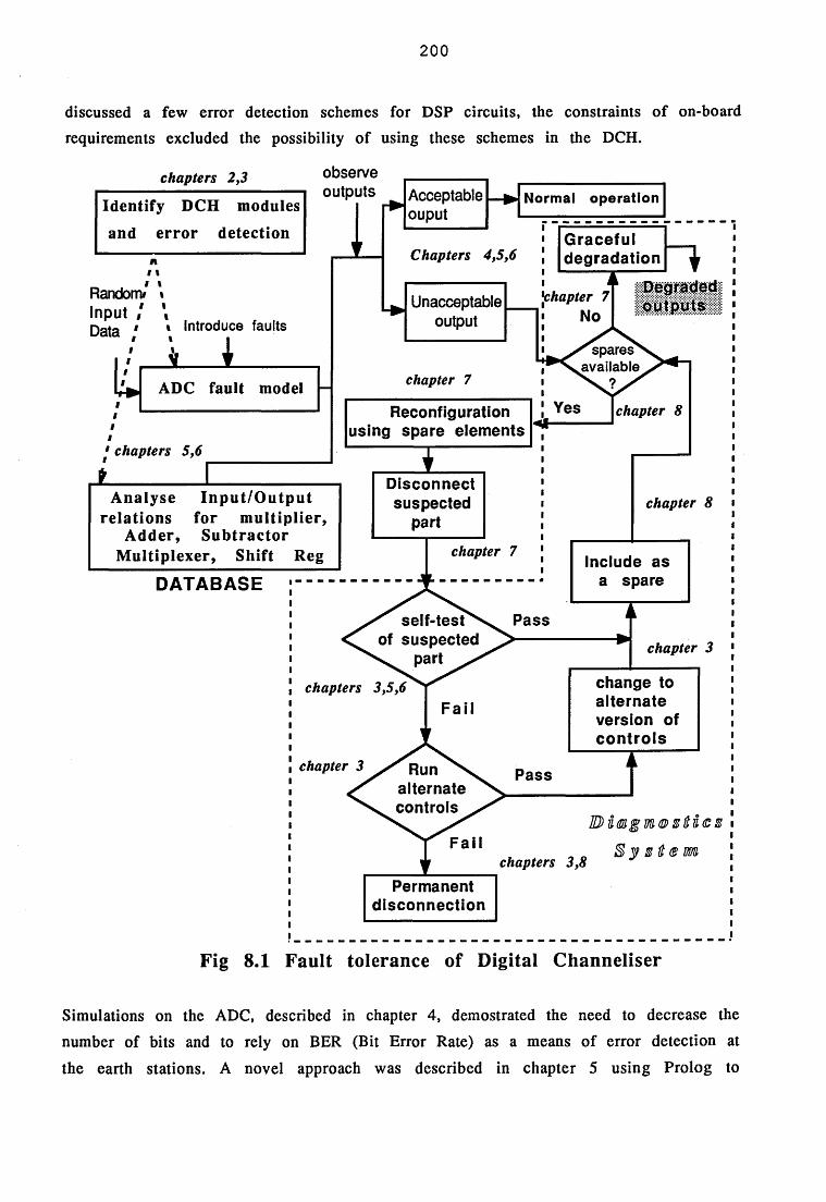
200
discussed a few error detection schemes for DSP circuits, the constraints of on-board requirements excluded the possibility of using these schemes in the DCH.
observeoutputs
c h a p t e r s 2 ,3
C h a p t e r s 4 , 5 , 6
DegradedlllillliRandom# »
Input / ' Data /
C h a p te r 7 ! NoIntroduce faults
c h a p te r 7
Yes c h a p t e r 8
c h a p t e r s 5 , 6
c h a p t e r 8
c h a p te r 7
DATABASE
Passc h a p t e r 3
c h a p t e r s 3 , 5 , 6Fail
c h a p te r 3 Pass
B n m g map s t i n e s
S y s i t ® mFailc h a p te r s 3 ,8
^ spares^ available
Run > alternate controls
^ self-test^ of suspected v part
Acceptableouput
Gracefuldegradation
Normal o p e r a t i o n
Unacceptableoutput
Permanentdisconnection
Include as a spare
Disconnectsuspected
part
ADC fault modelReconfiguration
using spare elements
change to alternate version of controls
Identify DCH modules
and error detection
A nalyse Input/O utput relations for m ultiplier,
Adder, Subtractor M ultiplexer, Shift Reg
Fig 8.1 Fault tolerance of Digital Channeliser
Simulations on the ADC, described in chapter 4, demostrated the need to decrease the number of bits and to rely on BER (Bit Error Rate) as a means of error detection at
the earth stations. A novel approach was described in chapter 5 using Prolog to

201
detect errors in multipliers, which lead to an implementation using ProgrammableLogic Array (PLA). This approach made possible, the real-time detection of errors in two’s complement multipliers. In chapter 6, this scheme was further extended to the other elements of the Half-Band Filter (HBF). The inherent capability of a multiplexer stage to provide data diversity, was utilized as a means to cross-check the performance of the filter. Issues concerning reconfiguration of the DCH in its pipelined version, were described in chapter 7. The results showed that the novel scheme proposed (Serial Module scheme), has higher reliability than its equivalent reconfigured binary tree structures. The improvement in reliability was brought
about by reducing the number of switches used for isolation of the faulty element and the inclusion of the standby element. In the next section, functional requirements of a diagnostics system for the DCH are presented. Methods proposed inchapters 4,5,6 and 7 are applied to a typical diagnostics system in order to establishthe feasibility of providing fault tolerance to the DCH.
8.3 Diagnostics System functions
Functions of the diagnostics system are now described, viewing the incoming signalsfrom different units as periodic reports. The diagnostics system has the task of interpreting these signals and sending commands, whenever the reports received indicate abnormal behaviour. The interpretation of incoming signals and the
appropriate actions needed, are described in the following paragraphs. These diagnostic actions are described at three levels viz., f u n c t i o n a l e l e m e n t l e v e l , s u b s y s t e m l e v e l a n d s y s t e m l e v e l .
8.3.1 Functional level diafnogticg
1. ADC errors
* Receive the B.E.R (Bit Error Rate) monitor signal from the ADC from the earth
stations through the telecommand link.
* If BER is consistently high over a few seconds, send a signal to the reconfiguration unit which will reconfigure the ADC using a redundant unit.
* System specification for an acceptable limit to the B.E.R is currently not available
and must be specified.
2. Multiplier
* Receive error detection system signals, t e s t O K and M u l t i p l e x e r p o s i t i o n etc.,

202
* If an error is reported, note the multiplexer position, send the signal to thereconfiguration unit to replace the multiplier with a spare, using the SM Scheme.
3 (a) Multiplex and Preprocessing Unit
* If the signals at the inputs of Adder-Subtractor units do not match those at the inputs of shift register, in a time frame as indicated by table 6.1, then the monitoring system sends an error message. A signal is to be sent to the reconfiguration unit
which will replace the entire unit with a spare.
3(b) Adders. Subtractors
* If an error is reported in adder/subtractor units, note the monitoring multiplexer
position, send a signal to reconfiguration unit to replace the faulty unit using the SM schem e.
In all the above cases (1 to 3), wait for two consecutive reports of error for confirmation. Avoid reconfiguration if error reports are not consistent. But monitor T e s t O K signals for the next 5 test cycles, since test cycles can be of varying length and it is assumed that 5 consecutive cycles would be the maximum needed to complete test sequence. If errors are reported by the t e s t O K signals or if spares are not
available, then proceed to sub-system level diagnostics. If a unit has been
reconfigured, send a command to initiate a “self-test” on the suspected unit. This “self-test” is an additional capability which depends on the DFT (Design For Test) procedures adopted by the manufacturers; details of DFT are found in chapter 3.
8.3.2 Sub-System level diaftnogtica
Reconfiguration of a P.E
* Reconfiguration of a P.E with its input and output buffers, must be attempted when
any one of the PEs is unable to function due to lack of functional spares or due to an
error reported by the t e s t O K signal.
* Prior to switching in a spare PE, it is necessary to ensure that the clock rate isprogrammed to meet the specification of that stage.
If spare PEs are no longer available, then diagnostics will move on to the final phase of providing fault tolerance, which is “Graceful Degradation”.
203
Graceful Degradation
To implement a graceful degradation, one of the following conditions must exist:
(i) No spare PEs available. A functional element in one of the PEs has failed. No spares of that element are available.
(ii) No spare PEs available. Several functional elements of a stage have failed - no spare of these elements available.
(iii) No spare PEs available. No functional element spares available. Self- test on a suspected element reveals that it cannot be salvaged.
In all of the above cases, a succeeding stage must perform the operations o f a previous stage. This is a standard feature expected in the graceful degradation of binary trees. However, when the PEs are half-band filters, several problems need tobe addressed [RAGH91]. Firstly, each stage PE has a different clock rate, which will mean that the succeeding stage must process signals at the clock rate of the previous stage. The frequent switching of clock rate, during on-line processing is a problem. Having processed the data on behalf of the previous stage, it must produce at least two words, before it can take up its own stage processing to produce one word output using the two words from the previous stage. Such a shuttling operation between stages, is contrary to the normal switching control which is pre-allocated by the
Control Signal Generator (CSG).
These problems can not be solved at the system level and need to be addressed at the design level. The half-band filter and its inter-connection with other stages, need tobe re-examined, from a graceful degradation point of view. Sharing the tasks of the previous stage needs to be built in as a sub-task, which must be made optional.
8.3.3 System level diagnostics
This is the final stage of diagnostics. At this stage, one section (sub-system) of the DCH is known to be inoperable and is cut off from the main DCH. Before a sub-system is cut off, it is ensured that graceful degradation of that sub-system is not possible.
The only useful measure at the system level, is to explore the possibility of using thememory/other functions in the diagnostics system which are not affected by the fault, since the half-band filters are assumed faulty and unusable. A DCH with several sub-systems of 8 or 16 channels each, is described in [BI90a], where a sub

204
system functionally similar to the one described in the earlier paragraphs is illu s tra ted .
With these requirements, it is worth while to seek an existing diagnostics scheme to suit the needs of a DCH. Diagnosis of systems in which faulty elements can be replaced by spares or are repaired is known as sequential diagnosis [BLOU90] and many schemes are suggested in [LEE90,SOMA90,CHU89].
Some diagnostic schemes for multi-element systems are suggested in [LEE90], for situations where multiple faults are present. A generalisation of classical sequential diagnosis with a probabilistic model for the faults and test outcomes in the system, is available in [BLOU90]. The probabilistic model covers four important fault situations, which are listed below in the increasing order of difficulty, in terms of diagnosis
and replacement with spares:
(i) permanent faults, with perfect spares(ii) permanent faults, with imperfect spares(iii) intermittent faults, with perfect spares(iv) intermittent faults, with imperfect spares
The permanent and intermittent fault models can also be viewed as models of perfect and imperfect test coverage. The one-step diagnosis approach described in [BLOU90], attempts to provide correct diagnosis and spares replacem ent with a high probability, and could be executed in two phases. In the first phase, a core group of fault-free processors is identified. In the second phase these fault-free processorsare utilised to determine the state of other processors, replacing those that are foundto be faulty and adding those that found to be fault-free to the core group. The limitation of this approach however, is that extensive tests on all the processors is necessary; these tests are therefore used further to select and classify processors. The exhaustive tests needed for such an approach, would require large resources
both in terms of test time as well as additional hardware, which makes them
unattractive for on-board use. The diagnostics scheme described in [CHU89] is
considered suitable to our DCH system and will be described in the next section.
8.4 A Diagnostics System for the DCH
In designing a sequential diagnosis system, two important assumptions are normally made. Firstly, it is assumed that there exists a trustworthy component to carry out the

205
diagnosis. Secondly, it is assumed that the time complexity of a diagnosis algorithmcan be significantly reduced if it can be fully implemented in hardware. A centrallymanaged diagnostics mechanism using a simple handware based device with a
testable array of logic cells called the TDA (Testable Diagnosis Array), has been proposed in [CHU89], to meet these two assumptions. The TDA performs the fault diagnosis function of a system [CHU89] , details of which may be found in Appendix 3.
The error detection systems described in chapters 5 and 6, can directly feed theinformation on individual functional elements to the a and b inputs of a cell in the TDA. The in is an important input to the cell which has the over-riding property that the information to this input comes from a spares management unit which keeps count of the faulty elements in the reconfiguration scheme. The TDA receives these inputs and initiates the appropriate actions such as reconfiguration, self-test and control signal for self-tests. Each cell in the CDE can be assigned to a functional element in the PE of the DCH (e.g, adder or multiplier) so that collective diagnosis can be done. The implementation of a TDA in a DCH is described next.
8.5 Implementation of the centralised diagnostics system
Since the TDA uses cells having a simple combination logic, its implementation is quite straight forward. The logic indicated in Table Ap3.1 (Appendix-3) can besummarised by the equations of input/output. Equations 8.1 and 8.2 give the logicaloutput bits of each cell, which can be realised by a simple combination logic. The
inputs in , b and the output o u t have three levels viz., 0, 1 and 2, which are
represented by two bits in the equations.
out! = bi in! + bo in! .. (8.1)
outo = bjj b inja + ino . . (8 .2 )
The shift registers are of serial to parallel type, which may be implemented from the
standard library of logic elements in Solo 1400. Buffers are used to facilitate
sy n ch ro n isa tio n .Estimates of the chip layout area required (2 micron technology) are given below.
Individual cell of Appendix 3
Chip area = 0.24 X 0.16 = 0.04 sq.mm
No. of columns = 1 Rows in column 1 = 1

206
Size of Row = 20Physical stages required = 20Total No. of unused stages = 0
Testable Diagnostics Array (TDA^ of Appendix 3
Overall chip area (including interconnections) = 1.07 X 0.68 = 0.73 sq.mmNo. of columns = 1Rows in column 1 = 5Size of Row =112
Physical stages required = 518Total No. of unused stages = 42
From the details of the chip area for a diagnostics system, it can be concluded thatthe area and power requirements of the diagnostics system are not significant as compared to the error detection systems. Only in terms of its function does thediagnostics system assumes a central role. The overall FT (Fault Tolerance) scheme tobe implemented on a separate single chip is shown in Fig 8.2. Inputs to thediagnostics are shown by solid lines while the control command lines fromdiagnostics are shown by dotted lines. The overhead to provide fault tolerance for the DCH, can be summarised as follows:
ADC - BER monitoring (estimated as inter-connections from Telecommand)=0.5 sq.mm Multiplier error detector (PLA based, includes self-test of PLA) = 3.22 sq.mm
Adder/Subtractor error detector (PLA based, includes self-test of PLA) = 2.37 sq.mmReconfiguration switches = 0.3 sq.mm
Diagnostics system = 0.73 sq.mm The total F.T system area = 7.12 sq.mm, which does not include the spares used by the different functional elements. The area occupied by the spares depends on the
structure of the functional element.For example, a parallel multiplier would occupy considerably more area than a bit-serial multiplier.
Also, in parallel multipliers the area increases as a square of the increase in the number of bits, hence this multiplier is worse off. The increase is just linear and hence not considerable for other elements like multiplexers, shift registers.

207
ADCB.E.R
MONITOR
/ 100% \* *•Redundancy!
D iagn osticsS y stemAppendix 3
o /v. Ic©
s, o' ?
360
I?
«o *
' 3
MULTIPLIER ERROR
DETECTORFig 5.7
/Redundancy* w i t h J
** SM Scheme /
RECONFIGURATIONFigs 7.5 and 7.7 for SM
Fig 7.8 for 100% redundancy
/ SM Scheme i'for Add/Sub\ 100% for #<
\ Mux /
ADDER SUBTRACTOR MUX - ERROR
DETECTORFig 6.4
FIG 8.2 SCHEMATIC OF A CENTRALISED DIAGNOSTICS SYSTEM
As a useful reference, typical areas of some functional elements are given below:Bit parallel Multiplier (4 bits) = 3 sq.mm [MA90]
Bit serial Multiplier = 0.7 sq.mm [BI90b] Bit parallel Adder/Subtractor = 0.18 sq.mm [BI90b]
Bit serial Adder/Subtractor = 0.14 sq.mm [BI90b] Multiplexer stage (Fig 6.2) = 0.36 sq.mm per stage (derived from simulations)
Using the SM scheme described in chapter 7, the number of spares may be estimated. If we select one of each functional elements (bit serial) shown above, an additional area of 7.12 + 5 ~ 12 sq.mm, is needed. To keep the interconnections and pad area to a
minimum, it is advisable to provide spares on the same chip in which the DCH is implemented. In addition, the multiplexers used for sampling the input/outputs of functional elements like multipliers, adder/subtractors also must be placed on the same chip. Using two such multiplexers for the input and two for output will mean an additional area of 0.15 X 4 = 0.60 sq.mm. The FT features must be implemented on a
separate chip and also provided with a separate power supply to isolate line induced
transient errors. This philosophy is in line with the standard test procedures

208
followed in the industry. Fig 8.3 shows ASIC implementation of a DCH [BI90b], which is further time multiplexed to incorporate 4 channels (1.2 micron technology).
The DCH shown in Fig 8.3 represents an extreme situation in terms o f time multiplexed design. It uses just a single Band-Splitting Filter to perform thefunctions of three filter stages. However, the memory (I/O buffers) used for the three stages are indeed, used separately. In terms of chip area, memory occupiesabout 60% of the total, while the BSF occupies 30% of the area. Therefore, in order to
provide a spare PE for such a DCH, an area equal to j X 60 = 20%, and 20% + 30% = 50%
of the total is necessary. In terms of fault tolerance, such a design is attractive fortwo reasons:-
(i) The processing element (BSF) needs complex control since it has to perform the functions of three equivalent stages. However the increase in the control complexity is compensated by a considerable reduction in the overall chip area, thereby offering a lower probability of being affected by SEU’s (Single Event Upsets).(ii) In terms of the additional area needed for a spare, a 50% addition due to one spare alone, indicates a substantial increase. However, the overall area needed including
spares, will be less than the overhead that would be needed by conventional stages.
1
zzjiS r.tzvuzir j ~TY3,3i:
iprea 1PF60 tPFas IPF03
C h ip Im ag e D a ta
T o ta l n um ber o f s t a g e s = 16830 n u m b er o f c o lu m n s z 5 ro w s p e r c o lu m n = 33s t a g e s p e r ro w = 102nu m b er o f p a d s = 22a r r a y a r e a (mm) ; 5 .9 7 x 5 .2 5a r r a y a r e a ( m i l ) z 2 3 -1 .05 x 20-c h i p a r e a (mm) = 0.^17 x 5 .7 7c h i p a r e a ( m i l ) = 2 5 4 . C3 x 2 2 i
.2 5 = 3 1 .3 4 sq.nwn 2 0 G .0 3 - 405 7 G .S 2 s q .m i l 77 z 3 7 .3 2 s q .n n 2 2 7 .1 3 z 5 7 0 4 6 . 9 3 s q .m i l
Fig 8.3 ASIC implementation of the DCH
^

209
But a limitation is that the buffer memory cannot be shared and the increased complexity of mulplexers seems to limit the time sharing attraction.
It must be noted that Fig 8.3 indicates a layout using the 1.2 micron technology whilst all the chip areas indicated so far assume 2 micron technology (as in TMS32020). Therefore, the 48 sq.mm indicated in this figure, would in effect be at least 72 sq.mm, if 2 micron technology were used. A total area ~ 48 sq.mm is required to provide fault
tolerance for the 4 channel DCH shown in Fig 8.3. This represents an overall increase of almost 67% in the chip area. A pie-graph of the overhead is provided in Fig 8.4 where the additional chip area needed by each unit is indicated.
Fig 8.4 Fault tolerant DCH - overhead in terms of chip area
Other designs of the DCH are being developed within the research group using the pipelined concept, but implemented conventionally by several stages of PEs. For example, a design using distributed arithmetic uses 30% of the chip area for the
three BSF stages and about 68% of the area for the 7 buffers. To provide a spare PE for such a design would need only 20% additional chip area. Assuming that such a chip would occupy only 50 sq.mm, an overall increase of 45% is needed to provide fault tolerance features. However, such assumptions are not likely to hold good in practice since the initial layout area itself will be larger as the number of PEs depend on the number of channels needed. In the space environment, a smaller chip area
represents a lower probability of failure due to Single Event Upsets (SEUs). Hence the time multiplexed version is a good candidate for space applications, even though its
spares occupy a larger area.
HH Reconfig - switches (0.3 sq.mm) 0.26%
m Func spares - Adder, Mux,. (1.44 sq.mm) 1.2%
^ | | P.E spare - incl buffers (36 sq.mm) 31%
HI Normal DCH of Fig 8.4 (72 sq.mm) 62%
| ADC error Monitor (0.5 sq.mm) 0.4%
[23 Error detector - Mult (3.22 sq.mm) 2.8%
Error detector - Add/Sub (2.37 sq.mm) 2%
Diagnostics System (0.73 sq.mm) 0.63%

210
Provision of fault tolerance features is well worth the investment considering theextreme difficulties that will be experienced if an error were to occur. Neither detection nor recovery would be possible if a fault tolerance scheme is not provided.
8.6 Conclusions and recommendations
In this chapter we have considered the overall aspect of providing fault tolerant features in a DCH. Examples of designs from our research group were considered and the requirements o f a diagnostics scheme were identified. A suitable diagnostic
system was chosen and it was seen that in terms of chip area and power it does not contribute to a significant increase. It was also seen that designs which extensively use time-multiplexing features, offer significant savings in the overall chip area. The following are the important conclusions:
(i) From a fault tolerance point of view, DCHs which use time-multiplexed pipeline stages are a good choice, in terms of reliability, cost effective spares management and error detection. Further time-multiplexing in order to reduce the number of stages to a single PE and thereby overall chip area, does indicate a good design, both
in terms of reliability as well as the overall chip area.
(ii) The spare PE contributes to a significant part of the overhead; usually, it needsmore chip area than the overall FT system. Therefore, the number of spare PEs mustbe kept to a minimum, preferably just one spare.
(iii) Since the SM scheme proposed in the previous chapter indicated a four-levelpipeline as a good choice, it is better to restrict the length of the pipeline to just fourstages (16 channels). Increasing the length of the pipeline further, decreases the reliability and also creates problems in terms of providing more spare PEs resulting
in a significant overhead.
(iv) A systematic procedure has been drawn up to deal with the different fault conditions that are likely to occur in a DCH. It was shown that the procedure can be implemented on a TDA.
Following are the recommendations which will result in an efficient FT system for the DCH:
(a) Error detection systems in terms of major functional elements, provide good
performance for real-time applications. A self-test feature for such an error detector

211
is essential so as to improve their reliability and provide information to diagnostics regarding the level at which diagnostics must operate.
(b) The diagnostics must be inherently testable, in order to ensure their reliability.
The TDA provides such a design.
(c) Length of the pipeline, number of spares, size of the reconfigurable module (SM), are all important factors which affect the performance of the fault tolerant DCH. A pipeline length = 4, 1 spare for the PE (SM-1) and 2 spares for functional elements (SM-2) is recommended (see Tables 7.4 and 7.5 for details).

212
R e f e r e n c e s
[BI90a] G.Bi, F.P.Coakley, “The design of Transmultiplexers for on-board processing
sate llites using b it-se ria l processing technique” , Proc. 13th AIAA In t’l Communication Satellite System conf, Los Angeles, CA, Mar 11-15, 1990, pp 613-622.
[BI90b] G.Bi, F.P.Coakley, “A gate array design of a 4-channel Transmultiplexer”, Report on Work Package 203, MSS contract, Dept Of Elec Eng, University of Surrey, May 1990.
[BLOU90] D.M.Blough and A.Pele, “Reliable diagnosis and repair in constant-degree multiprocessor systems”, Proc. 20th Int’l Symp. Fault Tolerant computing (FTCS-20), Newcastle upon Tyne, England, June 1990, pp 316-323.
[CHU89] S.C.Chu and J.R.Armstrong, “t-TDA-Diagnosable systems” , IEEE Tran. Computers, Vol.38, No.6, June 1989, pp 914-920.
[DENY85] P.Denyer and D.Renshaw, "VLSI signal processings bit-serial approach",
Addison-Wesley Publishing Co, England, 1985.
[LEE90]J.H.Lee and J.T.Butler,“A characterization of t/s-Diagnosability and sequential t-Diagnosability in designs”, IEEE Tran. Computers,Vol.39,No. 10,Oct 1990,pp 1298-1304. [SOMA90] Arun.K.Somani, “Sequential Fault Occurrence and reconfiguration in system level diagnosis”, IEEE Tran. Computers, Vol.39, No. 12, Dec 1990, pp 1472-1475.
[RAGH91] K.Raghunandan and F.P.Coakley, “Reconfiguration of time-multiplexed
binary trees for satellite communication”, Proc. IEEE Int’l workshop on Defect and Fault tolerance in VLSI systems, pp 274-287, Nov 18-20, 1991, Pennsylvania, U.S.A.

2 1 3
“A t t h e p h i l o s o p h i c a l l e v e l , i n e v e r y p r o g r e s s i v e s o c i e t y , a p e r s o n m u s t h a v e t o l e r a n c e t o f a u l t s c o m m i t t e d b y i n d i v i d u a l s o f t h e s o c i e t y . I n t h a t s e n s e i t i s t h e v e r y e s s e n c e o f g r o w t h a n d p r o g r e s s i n e v e r y s o c i e t y . T o d e t e c t f a u l t s , c o r r e c t t h e m , o r e v e n r e c o n f i g u r e c e r t a i n i n s t i t u t i o n s i f t h e f a u l t i s i r r e p a r a b l e - i s w h a t w e a r e d o i n g a l l t h e t i m e . F a u l t t o l e r a n c e to m e , i s t h e e s s e n c e o f s o c i a l l i v i n g , p r a c t i c e d b y m e n a n d w o m e n , e v e r y w h e r e ” - Author
9
CONCLUSIONS AND SUGGESTIONS FOR FUTURE WORK
9.1 Summary
In this work the task of providing fault diagnostics and fault tolerance to the Digital Channeliser (DCH) on-board future communication satellites was addressed. The use of on-board processors in the payload of a communication satellite increases the complexity of the circuits, making the task of fault diagnostics from earth stations, difficult. At the same time, reliability of the payload is very important since it is an important resource needed by all the satellite users. Therefore, providing fault diagnostics and fault tolerant features to the DCH became essential. When a fault occurs the task of reconfiguring the DCH to revert to normal operation becomes
quicker when an autonomous Fault Tolerant (FT) system is used on-board. The FT system can reconfigure the DCH in 5 seconds, while ground based diagnostics would need half a day or several days in some instances, to reconfigure the system to normal. The features of such an autonomous FT system include error detection in all the sub-systems of the DCH. A central diagnostics system was used to diagnose and reconfigure the DCH by using spare elements of the sub-system.
In order to evolve such a fault tolerant DCH, the following mechanisms were needed:
(i) A study of the A to D Converter under faulty conditions and the system’s response to faults such as those occuring within the ADC as well as those induced by the external environment. A mechanism by which faults in the ADC can be recognised
and the spare ADCs can be introduced to restore the DCH to normal operation.
2 1 4
(ii) An error detection system to recognise errors in two’s complement multipliers,irrespective of the internal structure of the multiplier. The internal structure of the multiplier can vary depending on the design, hence the method should be applicable to any multiplier handling two’s complement numbers. The error detector must havea self-checking feature, such that a totally self-checking system is provided on
board .(iii) An error detection system to recognise errors in all the major elements of adigital filter used in the DCH; the important elements include Adders, Subtractors and M ultip lexers.(iv) A scheme to reconfigure a time-multiplexed binary tree structure used by the DCH. The scheme has to provide good reliability to the system but has to use fewer spares, since the spares occupy considerable chip area.(v) A diagnostics system which can utilise the information provided by the error detection scheme of each sub-system. Using this information, the diagnostics has to confirm failures by initiating self-tests on the suspected sub-system. If a fault isconfirmed, the diagnostics could use spare elements to replace the faulty element in that sub-system and reconfigure the DCH and revert it to normal operation.
The needs indicated above were fulfilled by the contributions from this thesis, which are m ostly oriented tow ards developing error detection m echanism s and reconfiguration schemes. A brief summary of the novel methods developed are
provided in the following paragraphs.
In Chapter 4, the results of simulations on an A to D converter used in the Digital Channeliser, showed that the number of bits used in the ADC could be reduced to 5 or 6 bits and still provide acceptable system performance. The results also point to an inherent ability of the system to quickly recover from faults, such as jitter and missing codes. An inherent limitation in the detection of faults in an ADC is that the input and output are in different domains viz., analog and digital. Since Bit Error
Rate (BER) monitoring needs a comparison of the reference data stream with the data
available at some point in the DCH (the ADC output in this case), the monitoring
circuit would be located at earth stations and only the BER information can be communicated to the on-board diagnostics using the telecommand link.
Although hardware based test methods are used for fault detection in arithmetic elements, some of the limitations such as inability to detect errors in different
circuit configurations, inability to detect communication breaks etc., are strongly

215
felt in real-time circuits. There are other problems in transferring the information about errors, to the diagnostics system. To overcome these limitations, a black box approach of using only the input and output of a functional element to detect errors,was used in chapter 5; a software based space search method was evolved based onsuch a black box approach. Results of this new approach are very encouraging both in terms of the smaller size required for the detection circuit, as well as improved error detection capability under any fault condition. Another benefit of this approach is its versatility, since it is applicable to a functional element irrespective of the hardware configuration of the element. The compact Data Base (DB) derived by
the space search method, allowed the extension of space search to a variety of functional elements. Capabilities of the Prolog programming language was made use of to provide off-line diagnosis in order to detect errors in multipliers. The DB which
was derived using space search, provided a look-up table (see Appendix 1 and 2) for the tw o’s complement multiplier, which was implemented in hardware using the Programmable Logic Array (PLA). The PLA needs a smaller chip area and being a combinational circuit, it is easier to provide self-checking features to the PLA. The primary task of the error detection circuit (PLA) is to monitor the m ulplier’s operations in real-tim e. Therefore, the self-checking test routine can be
implemented on a periodic basis where each test cycle can be executed in sequence, over several main task cycles. Such a sequential execution is prefered in real-time systems, since self-checking is assigned a lower priority and needs longer time intervals to check the PLA, but at the same time allows the PLA to monitor the operations of the multiplier in real-time.
The importance of error detection as the first step in the process of providing fault tolerance was emphasised in chapter 6. Considerable time and effort was devoted towards this goal during the work. Whilst an off-line error detection was used the Prolog based search scheme, its on-board implementation used PLAs with self-test capability provided a simple method for on-board implementation. The PLA based scheme was again used to implement error detection of the Adder, Subtractor and
Multiplexer elements of the half-band filter.
Reconfiguration schemes for the binary tree structure suggested a modular approach by considering each stage as a module and providing spare elements at the each stage. Since the DCH uses a time-multiplexed version of the binary tree, a new Serial-Module reconfiguration scheme was developed in chapter 7. Reconfiguration
schemes for the lower level functional elements as well as for the processing

216
elements at the system level are all based on the SM scheme (Fig 7.5 and 7.7). Reliability of the Serial-Module improves linearly with the number of spares available and SM scheme uses fewer spares compared to all other existing schemes. For a given number of spares, the Serial-Module scheme also has a better reliability compared to the other schemes. The SM scheme proposed, showed that a time multiplexed serial structure has better reliability characteristics than the original series-parallel structured binary tree.
A simple diagnostic system based on hardwired combination logic was considered in chapter 8. It was shown that error detection and reconfiguration schemes developed in this thesis can provide fault tolerance to the DCH, which would not have been otherwise possible. The fault tolerance system suggested for the DCH uses simple schemes developed in this thesis, which can be implemented in the future satellites for mobile and business applications.
9.2 Suggestions for future work
Although this study covers all the major failures in the various elements of the Digital Channeliser system which are critical to the On-Board Processor (OBP) performance, for want of time, aspects such as further experiments of fault injection to study the filter circuit behaviour, evaluation of the self-test schemes to arrive at an optimum test pattern etc., were not considered. The use of Markov models to study the reconfiguration schemes can further improve the accuracy of the results as well as provide a more flexible means to use the coverage factor to calculate reliabilities of all the functional elements.
Design of the Digital Channeliser is in an evolutionary phase and recent studies
indicate the use of All-digital Multicarrier demodulators [YIM91], based on a unified approach involving Multistage polyphase FFT and the binary tree structure. From a fault tolerance point of view, some aspects of the detection schemes for FFT networks [JOU88] could be applicable to the all-digital structures. It is also important that all future designs must preferably be based on the Design For Test (DFT) approach, using the IEEE standard PI 149.1.1990. However, the use of space search method is
recommended, due to the limitations in the existing error detection schemes.
When a particular configuration is chosen and implemented, the use of an expert
system, albeit in a simple form, is worth exploring. Important pointers for fault

217
indication can be initially placed in the Knowledge Base (KB), to be extended later as the system performance features become clearer. Database and KB are seen as two converging technologies with diverging interests [FREU90]. Efforts in this direction are underway but are currently the investigations are limited to satellite power systems [STEP91]. KB-systems programming differs from conventional programming
primarily in its methodology, the core of which is a concern for making explicit, the knowledge embedded in the program. Explicit knowledge means that it is open todirect manipulation, which can be better understood by the following example.
A knowledge engineer constructing an automobile diagnostic system considers such statements as “Fuel clogging is a possible malfunction” along with statements about the possible and necessary symptoms of fuel clogging. Similarly in a Digital Channeliser, if the output of a multiplier has only negative products in its output, then “sign bit stuck-at 1 is a possible malfunction” which must be considered with statements about the possible and necessary symptoms of faults leading to negative products. Similar malfunctions in other circuits could be classified to correlate a certain “trend” in the output, to its possible and necessary symptoms.
9.3 Applications
The relatively new area of using an Artificial Intelligence (AI) approach to provide fault tolerance in circuits is gaining importance in both ground and spaceapplications. While large, mainframe based expert systems dominate the groundapplications, the smaller and simpler versions will be candidates for space applications. For satellites in particular, the Programmable logic array (PLA) currently provides a good solution. Although the PLA has no AI capability, field programmable PLAs offer considerable flexibility. Its application to fault diagnosis in space systems is likely to find increasing interest and can provide cost effective solutions. If single chip inference engines become faster in future, they could
provide a better alternative.
The work presented in this thesis encompasses some areas in the fast growing field
of fault tolerant computing. To an extent it complements the work done on the TST
switches [SHAS88], to provide fault tolerance for the on-board processing system. Together, the two studies have made efforts to provide fault tolerance in the onboard switching and Multi-Carrier Demodulator (MCD) systems of the communication payload. It is only an example of the application of fault tolerance and by no means

218
an exhaustive exercise. Implementation of any concept into a practical system is a long and challenging task which needs many changes as well as compromises. Particularly in space programmes, the implementation of a new concept takes considerable time and effort in terms of proving its reliability. This thesis provides sufficient justification to implement an autonomous fault tolerance system for the
communication payload in future satellites.
219
R e f e r e n c e s :
[FREU90] Y.Freundlich, “Knowledge bases and databases: converging technologies, diverging interests”, IEEE Computer, Vol.23, N o .ll, Nov 1990, pp 51-57.[JOU88] J.Y.Jou and J.A.Abraham, "Fault tolerant FFT Networks", IEEE Tran.Computers, Vol.37, No.5, May 1988, pp 548-561.[SHAS88] C.R.Shashidhar and F.P.Coakley, "Concurrent fault detection in TST switches for on-board satellite systems", Electronics Letters,7th Jan 1988, Vol.24, No.l,pp 10-11. [STEP91] A.Stephen and C.A.Erikson, “Getting Expert systems off the ground - Lessons learned integrating Model-based Diagnostics with Prototype Flight Hardware”, Proc. Conf. on Space communications Technology - Onboard Processing and Switching, Ohio, Nov 12-14, 1991, pp 135-141. NASA conference publication 3132.[YIM91] W.H.Yim and F.P.Coakley, “All-digital Multicarrier demodulators for onboard processing satellite system s”, 3rd Bangor Communications Symposium,
University of Wales, UK, May 1991.

220
A ppendix 1
% P r o l o g c l a u s e s a n d r e l a t i o n s h i p s f o r p o s i t i v e M S B “p r o d u c t ” b i t s
s e a r c h ( F , p r o d u c t m P ( A , B , S ) , S p ) : -s e t o f ( B , p r o d u c t m P ( A , B , S p ) , S ) , n o t ( e x c l u d e ( A , B , S p ) ) .
s e a r c h ( F , p r o d u c t m P ( A , B , S ) , S p ) : - n o t ( e q u a l ( A , B ) ) , s e t o f ( B , p r o d u c t m P ( B , A , S p ) , S ) , n o t ( e x c l u d e ( B , A , S p ) ) .
e q u a l ( A , B ) : - A = = B .
% Imultiplicandlmultiplierl +ve product MSB% I I I Iexclude(A, B, Sp):-
(A, B, Sp) = ([1, 1, 1, 1, 0], [1, 1, 0, 0, 0], [0, 0, 0, 0, 0]);(A, B, Sp) = ([1, 1, 1, 1, 0], [1, 0, 0, 0, 0], [0, 0, 0, 0, 1]);(A, B, Sp) = ([0, 0, 0, 1, 0], [0, 0, 0, 1, 1], [0, 0, 0, 0, 1]);
(A, B, Sp) = ([0, 0, 0, 1, 1], [0, 1, 0, 1, 1], [0, 0, 0, 0, 1]);
(A, B, Sp) = ([0, 0, 1, 0, 1], [0, 0, 1, 1, 1], [0, 0, 0, 0, 1]);(A, B, Sp) = ([1, 1, 1, 0, 1], [1, 1, 0, 1, 1], [0, 0, 0, 0, 1]);
(A, B, Sp) = ([1, 1, 1, 0, 0], [1, 1, 0, 0, 0], [0, 0, 0, 0, 1]);(A, B, Sp) = ([1, 1, 1, 0, 1], [1, 0, 0, 0, 0], [0, 0, 0, 1, 0]);(A, B, Sp) = ([1, 1, 1, 0, 0], [1, 0, 1, 0, 0], [0, 0, 0, 1, 0]);(A, B, Sp) = ([1, 1, 0, 1, 0], [1, 1, 0, 1, 1], [0, 0, 0, 1, 0]);(A, B, Sp) = ([1, 1, 1, 0, 0], [1, 0, 0, 0, 0], [0, 0, 0, 1, 1]);(A, B, Sp) = ([1, 1, 0, 1, 1], [1, 0, 1, 1, 1], [0, 0, 0, 1, 1]);
(A, B, Sp) = ([1, 1, 0, 1, 1], [1, 0, 0, 0, 0], [0, 0, 1, 0, 0]).
% positive product MSB relations begin
productmP([0, 0, 0, 0, M], [0, W, X, Y, Z], [0, 0, 0, 0, 0]).

221
productmPtfS, S, S, 1, 0], [S, S, X, Y, Z], [0, 0, 0, 0, 0]). productmPtfS, S, S, X, 1], [S, S, 0, 1, 1], [0, 0, 0, 0, 0]). productmPtfO, 0, 0, 1, 1], [0, 0, 1, 0, X], [0, 0, 0, 0, 0]). productmP([l, M, M, M, M], [1, W, X, Y, Z], [0, 0, 0, 0, 0]). productmP([l, 1, 1, 0, 1], [1, 1, 1, X, Y], [0, 0, 0, 0, 0]).
productmPtfl, 1, 1, 1, 0], [1, 0, X, Y, Z], [0, 0, 0, 0, 1]).productmPtfO, 0, 0, 1, 0], [0, 1, X, Y, Z], [0, 0, 0, 0, 1]).productmP([0, 0, 0, 1, 1], [0, 1, 0, X, Y], [0, 0, 0, 0, 1]).productmPtfO, 0, 1, 0, Z], [0, 0, 1, X, Y], [0, 0, 0, 0, 1]).productmP([l, 1, 1, 1, 0], [1, 1, 0, 0, 0], [0, 0, 0, 0, 1]). productmPtfl, 1, 1, 0, S], [1,1, 0, X, Y], [0, 0, 0, 0, 1]). productmP([l, 1, 1, 0, 1], [1, 0, 1, 1, X], [0, 0, 0, 0, 1]).productmP([l, 1, 1, 0, 0], [1, 1, 1, 0, 0], [0, 0, 0, 0, 1]).productmP([l, 1, 0, 1,1], [1, 1, 0, 1, X], [0, 0, 0, 0, 1]). productmPtfO, 0, 0, 1, 1], [0, 0, 1, 1, X], [0, 0, 0, 0, 1]).
productmP([l, 1, 0, 1, 1], [1, 0, 1, 1, 1], [0, 0, 0, 1, 0]).productmPtfO, 0, 0, 1, 1], [0, 1, 0, 1, 1], [0, 0, 0, 1, 0]).productmPtfl, 1, 1, 0, 0], [1, 0, 1, X, Y], [0, 0, 0, 1, 0]).productmP([0, 0, 0, 1, 1], [0, 1, 1, X, Y], [0, 0, 0, 1, 0]).
productmPtfl, 1, 1, 0, 1], [1, 0, 0, X, Y], [0, 0, 0, 1, 0]).productmPtfO, 0, 1, 0, 0], [0, 1, 0, X, Y], [0, 0, 0, 1, 0]).productmPtfO, 0, 1, 0, 1], [0, 0, 1, 1, 1], [0, 0, 0, 1, 0]).productmPtfl, 1, 0, 1, 1], [1, 1, 0, 0, X], [0, 0, 0, 1, 0]).
productmPtfO, 0, 1, 0, 1], [0, 1, 0, 0, X], [0, 0, 0, 1, 0]).productmPtfl, 1, 1, 0, 1], [1, 0, 1, 0, X], [0, 0, 0, 1, 0]).
productmPtfO, 0, 1, 1, 0], [0, 0, 1, 1, X], [0, 0, 0, 1, 0]).productmPtfl, 1, 1, 0, 0], [1, 1, 0, 0, 0], [0, 0, 0, 1, 0]).productmPtfl, 1, 0, 1, 0], [1, 1, 0, 1, 0], [0, 0, 0, 1, 0]).productmPtfl, 1, 0, 1, 0], [1, 1, 0, 0, 1], [0, 0, 0 ,1 , 0]).
productmPtfO, 0, 1, 0, 0], [0, 1, 1, X, Y], [0, 0, 0, 1, 1]).productmPtfl, 1, 0, 0, 1], [1, 1, 0, 0, X], [0, 0, 0, 1, 1]).productmPtfO, 0, 1, 0, 1], [0, 1, 0, 1, X], [0, 0, 0, 1, 1]).productmPtfl, 1, 1, 0, 0], [1, 0, 1, 0, 0], [0, 0, 0, 1, 1]).
productmPtfO, 0, 1, 0, 1], [0, 1, 1, 0, 0], [0, 0, 0, 1, 1]).

222
productmP([0, 0 1 1 Y], [0, 1 0, 0, X] [0 0 0 1 1]).productmP([l, 1 0 1 0], [1, 1, 0, 0, 0], [0, 0, 0, 1, 1]).productmP([l, 1 0 0 1], [1, 0, 1, 1, 1], [0, 0, 0, 1, 1]).productmP([0, 0 1 1 1]. [0, 0, 1, 1, 1], [0, 0, 0, 1, 1]).productmP([l, 1 1 0 0], [1, 0, 0, X, Y] [0 0, 0 1 1]).productmP([l, 1 0 1 1]. [1, 0, 1, X, Y] [0 0, 0 1 1]).productmP([l, 1 0 1 0], [1, 0, 1, 1, Y], [0, 0 , 0 1, 1]).
productmP([l, 1 0 0 1], [1, 0, 1, 0, 1], [0, 0, 1, 0, 0]).productmP([0, 0 1 0 1], [0, 1, 1, 0 , 1], [0, 0, 1, 0 , 0]).productmP([0, 0 1 0 1], [0, 1, 1, 1, X], [0, 0, 1, 0, 0]).productmP([l, 1 0 1 0], [1, 0, 0, 1, 1], [0, 0, 1, 0, 0]).productmP([0, 0 1 1 0], [0, 1, 0, 1, 1], [0, 0, 1, 0 , 0]).productmP([l, 1 0 1 0], [1, 0, 1, 0, X], [0, 0, 1, 0, 0]).productmP([0, 0 1 1 0], [0, 1, 1, 0, X], [0, 0, 1, 0, 0]).productmP([0, 0 1 1 1], [0, 1, 0, 1, X], [0, 0, 1, 0, 03).productmP([0, 1 0 0 0], [0, 1, 0, 0, X], [0, 0, 1, 0, 03).productmP([l, 1 0 1 1], [1, 0, 0, X, Y], [0, 0, A J 0, 03).productmP([l, 1 0 0 1], [1, 0, 1, 1, 0], [0, 0, 1, 0, 0]).productmP([l, 1 0 0 0], [1, 0, 0, 0, 0], [0, 0, 1, 0, 0]).productmP([l, 1 0 0 0], [1, 0, 1, 1, 1], [0, 0, 1, 0, 03).
productmP([l, 0 1 1 1], [1, 0, 1, 1, X], [0, 0, 1, 0, 13).productmP([0, 0 1 1 0], [0, 1, 1, 1, X], [0, 0, 1, 0, 13).productmP([0, 0 1 1 1], [0, 1, 1, 0, X], [0, 0, 1, 0, 13).productmP([0, 0 0 0 0], [0, 1, 0, 1, X], [0, 0, 1, 0, 13).productmP([X, 1 0 0 1], [1. 0, 0, 1, 1], [0, 0, 1, 0, 13).productmP([0, 1 0 0 1], [0, 1, 0, 0, 1], [0, 0, 1, 0, 1]).productmP([l, 1 0 0 0], [1, 0, 1, 1, 0], [0, 0, 1, 0, 1]).productmP([0, 1 0 0 1], [0, 1, 0, 1, 0], [0, 0, 1, 0, 13).productmP([l, 1 0 1 0], [1, 0, 0, 1, 0], [0, 0, 1, 0, 13).productmP([l, 1 0 1 0], [1, 0, 0, 0, 1], [0, 0, 1, 0, 13).productmP([l, 1 0 0 1], [1, 0, 1, 0, 0], [0, 0, 1, 0, 1]).productmP([l, 1 0 0 0], [1, 0, 1, 0, 1], [0, 0, 1, 0, 13).
productmP([0, 0, 1, 1, 1], [0, 1, 1, 1, X], [0, 0, 1, 1, 03).productmP([l, 0, 1, 1, 1], [0, N, 1, 0, X], [0, 0, 1, 1, 03).

productmP([0, 1 productmP([l, 1
productmP([0, 1 productmP([l, 1 productmP([0, 1 productmP([0, 1 productmP([l, 1 productmP([l, 1
productmP([l, 0 productmP([l, 0
productmP([0, 1 productmP([l, 0 productmP([0, 1 productmP([l, 1 productmP([0, 1 productmP([l, 0
productmP([0, 1 productmP([l, 1 productmP([0, 1 productmP([l, 0
productmP([l, 0 productmP([0, 1 productmP([l, 0
productmP([0, 1
productmP([0, 1 productmP([0, 1 productmP([l, 0
productmP([l, 0
productmP([l, 0 productmP([0, 1 productmP([l, 0
productmP([0, 1
productmP([0, 1 productmP([l, 0
0, 0 0] [0, 1, 1, 0,0, 0 1] [1, 0, 0, 0,0, 0 1] [0, 1, 0, 1,0, 0 1] [1, 0, 0, 1,0, 0 1] [0, 1, 1, 0,0, 1 0] [0, 1, 0, 1,0, 0 0] [1, 0, 1, 0,0, 0 0] [1, 0, 0, 1,1, 1 0] [1, 0, 1, 1,1, 1 0] [1, 0, 1, 0,
0, 0 0] [0, 1, 1, 1,1, 0 1] [1, 0, 1, 0,0, 0 1] [0, 1, 1, 0,0, 0 0] [1, 0, 0, 1,0, 0 1] [0, 1, 1, 1,1, 1 0] [1, 0, 1, 0,0, 1 0] [0, 1, 1, 0,0, 0 0] [1, 0, 0, 0,0, 1 1] [0, 1, 0, 1,1, 1 1] [1, 0, 0, 1,
1, 0 1] [1, 0, 0, 1,0, 0 1] [0, 1, 1, 1,1, 1 1] [1, 0, 0, 0,0, 1 0] [0, 1, 1, 0,0, 1 0] [0, 1, 1, 1,0, 1 1] [0, 1, 1, 0,
1, 1 0] [1, 0, 0, 1,1, 0 1] [1, 0, 1, 0,
1, 0 0] [1, 0, 0, 1,0, 1 0] [0, 1, 1, 1,1, 0 1] [1, 0, 0, 1,0, 1 1] [0, 1, 1, 1,1, 0 0] [0, 1, 1, 0,
1, 1 0] [1, 0, 0, 0,
LU, u, i 1
1] [0, 0, 1 1 0]).
1] [0, 0, 1 1 0]).0] [0, 0, 1 1 0]).0] [0, 0, 1 1 0]).X] [0, 0, 1 1 0]).0] [0, 0, 1 1 0]).
1] [0, 0, 1 1 0]).
0] [0, 0, 1 1 0]).
1] [0, 0, 1 1 0]).
X] [0, 0, 1 1 1]).1] [0, 0, 1 1 1]).1] [0, 0, 1 1 1]).0] [0, 0, 1 1 1]).0] [0, 0, 1 1 1]).0] [0,0, 1 1 1]).0] [0, 0, 1 1 1]).1] [0, 0, 1 1 1]).1] [0, 0, 1 1 1]).X] [0,0, 1 1 1]).
1] [0,1, 0 0 0]).
1] [0 ,1 , 0 0 0]).
1] [0, 1, 0 0 0]).
1] [0, 1, 0 0 0]).
0] [0, 1, 0 0 0]).X] [0, 1, 0 0 0]).X] [0,1, 0 0 03).
0] [0, 1, 0 0 03).
1] [0,1, 0 0 13).1] [0,1, 0 0 13).0] [0,1, 0 0 13).0] [0, 1, 0 0 1]).X] [0, 1, 0 0 13).1] [0, 1, 0 0 13).

224
productmP([l, 0, 1, 0, 0], [1, 0, 1, 0, 0], [0, 1, 0, 0, 1]).
productmP([lproductmP(productmP([lproductmP(productmP([lproductmP(
productmP([l productmP( productmP([l productmP(
productmP([lproductmP(productmP(productmP(
productmP(
productmP([0
productmP([l
productmP([0
0, 0, 1, 1
1, 0, 1, 10, 1, 0, 0
1, 1, 0, 00, 1, 0, 1
1, 1, 0, 1
0, 1, 0, 0
1, 1, 0, 00, 1, 1, 1
1, 1, 0, 1
0, 0, 1, 1
1, 1, 0, 10, 0, 1, 01, 1, 1, 0
0, 0, 1, 01, 1, 1, 0
[1, 0, 0, 1, 1 , [0, 1, 0, 1 0]).
[0, 1, 1, 1, 1 , [0, 1, 0, 1 0]).
[1, 0, 0, 1, 0 , [0, 1, 0, 1 0]).
[0, 1, 1, 1, 0 , [0, 1, 0, 1 0]).
[1, 0, 0, 0, 1 . [0, 1, 0, 1 0]).
[0, 1, 1, 0, 1 , [0, 1, 0, 1 0]).
[1, 0, 0, 0, 1 , [0, 1. 0, 1 1]).[0, 1, 1, 1, 1 , [0, 1, 0, 1 1]).
[1, 0, 0, 1, 0 , [0, 1, 0, 1 1]).[0, 1, 1, 1 0 1, 0, 1 1]).
[1, 0, 0, 0, 1 , [0, 1, 1, 0 0]).
[0, 1, 1, 1, 1 , [0, 1, 1, 0 0]).
[1, 0, 0, 1, 0 , [0, 1, 1, 0 0]).
[0, 1, 1, 1, 0 , [0, 1, 1, 0 0]).
[1, 0, 0, 0, 1 , [0, 1, 1, 0 1]).[0, 1, 1, 1, 1 , [0, 1, 1, 0 1]).
[1, 0, 0, 0, 1 , [0, 1, 1, 1, 0]).
[0, 1 1, 1♦ ], [0, 1, 1, 1, 0])

225
Appendix 2
% Clauses for the negative MSB product bits
s e a r c h ( F , p r o d u c t m N ( A , B , S ) , S p ) : -s e t o f ( B , p r o d u c t m N ( A , B , S p ) , S ) , n o t ( e x c l u d e ( A , B , S p ) ) .
s e a r c h ( F , p r o d u c t m N ( A , B , S ) , S p ) : -s e t o f ( B , p r o d u c t m N ( B , A , S p ) , S ) , n o t ( e x c l u d e ( B , A , S p ) ) .
% Imultiplicandlmultiplierl -ve product MSB
% I I I I
exclude(A, B, Sp):-
(A, B, Sp) = ([1, 1, 1, 0, 0], [0, 1, 0, 0, 0], [1, 1, 1, 0, 1]);(A, B, Sp) = ([1, 1, 1, 1, 0], [0, 1, 0, 0, 0], [1, 1, 1, 1, 0]);(A, B, sp) = ([1, 1, 1, 0, 1], [0, 1, 0, 1, 1], [1, 1, 1, 1, 0]);(A, B, sp) = ([1, 1, 1, 0, 0], [0, 0, 1, 0, 0], [1, 1, 1, 1, 0]);(A, B, sp) = ([1, 1, 0, 1, 1], [0, 0, 0, 1, 1], [1, 1, 1, 1, 0]);(A, B, sp) = ([1, 1, 0, 1, 1], [0, 0, 1, 1, 1], [1, 1, 1, 1, 0]);(A, B, Sp) = ([1, 1, 1, 1, 1], [0, 0, 0, 0, 0], [1, 1, 1, 1, 1]);(A, B, sp) = ([1, 1, 1, 1, 0], [0, 0, 0, 0, 0], [1, 1, 1, 1, 1]).
% Negative product MSB relations begin
productmN([l, 0, 0, 0, 0], [0, W, X, Y, Z], [1, 0, 0, 0, 0]). productmN([l, W, X, Y, Z], [0, 0, 0, 0, 0], [1, 0, 0, 0, 0]).
productmN([l, 0, 0, 0, 1], [0, 1, 1, 1, 1], [1, 0, 0, 0, 1]).
productmN([l, 0, 0, 1, 0], [0, 1, 1, 1, 1], [1, 0, 0, 1, 0]).productmN([l, 0, 0, 0, 1], [0, 1, 1, 1, 0], [1, 0, 0, 1, 0]).
productmN([l, 0, 0, 1, X], [0, 1, 1, 1, X], [1, 0, 0, 1, 1]).productmN([l, 0, 0, 0, 1], [0, 1, 1, 0, 1], [1, 0, 0, 1, 1]).
productmN([l, 0, 1, 0, 0], [0, 1, 1, 1, 1], [1, 0, 1, 0, 0]).

226
productmN([l, 0, 0, 0, 1], [0, 1 productmN([l, 0, 0, 1, 1], [0, ] productmN([l, 0, 0, 1, 0], [0, 1
productmN([l, 0, 1, 0, X], [0, 1
productmN([l, 0, 0, 1, X], [0, ] productmN([l, 0, 0, 0, 1], [0, 1
productmN([l, 0, X, 1, 0], [0, 1 productmN([l, 0, X, 0, 1], [0, 1 productmN([l, 0, 1, 0, 0], [0, 1 productmN([l, 0, 0, 1, 1], [0, 1
productmN([l, 0, 1, X, X], [0, ! productmN([l, 0, 1, X, 0], [0, 1 productmN([l, 0, X, 1, 0], [0, 1 productmN([l, 0, 1, 0, 1], [0, 1 productmN([l, 0, 0, 1, 1], [0, 1 productmN([l, 0, 0, 0, 1], [0, 1,
productmN([l, 1, 0, 0, 0], [0, 1, productmN([l, 0, 1, 1, X], [0, 1, productmN([l, 0, 1, X, X], [0, 1, productmN([l, 0, X, 0, 1], [0, 1, productmN([l, 0, 0, 1, X], [0, 1,
productmN([l, 1, 0, 0, 1], [0, 1,
productmN([l, 0, 1, 1, 0], [0, 1, productmN([l, 1, 0, 0, 0], [0, 1, productmN([l, 0, 0, 1, 0], [0, 0, productmN([l, 1, 0, 0, 0], [0, 1, productmN([l, 0, 1, 0, 1], [0, 1, productmN([l, 0, X, 1, 1], [0, 1, ' productmN([l, 0, X, 1, X], [0, 1,
productmN([l, 0, 1, 0, X], [0, 1, productmN([l, 0, 0, 0, 1], [0, 0,
I, 1, 0, 0], [1, 0, 1, 0, 0]).
I, 1, 1, 0], [1, 0, 1, 0, 0]).I, 1, 0, 1], [1, 0, 1, 0, 0]).
L, 1, 1, X], [1, 0, 1, 0, 1]).I, 1, 0, X], [1, 0, 1, 0, 1]).I, 0, 1, 1], [1, 0, 1, 0, 1]).
I, X, 1, 1], [1, 0, 1, 1, 0]).L, X, 1, 0], [1, 0, 1, 1, 0]).L, 1, 0, 1], [1, 0, 1, 1, 0])., 1, 0, 0], [1, 0. 1, 1, 0]).
I, X, 1, 1], [1, 0, 1, 1, 1]).1, 0, X], [1, 0, 1, 1, 1]).X, 1, 0], [1, 0, 1, 1, 1]).
, 1, 0, X], [1, 0, 1, 1, 1])., 0, 1, X], [1, 0, 1, 1, 1]).
0, 0, 1], [1, 0, 1, 1, 1]).
1, 1, 1], [1, 1, 0, 0, 0]).1, 0, X], [1, 1, 0, 0, 0]).X, 1, 0], [1, 1, 0, 0, 0]).0, X, X], [1, 1, 0, 0, 0]).0, 0, 1], [1, 1, 0, 0, 0]).
1, 1, X], [1, 1, 0, 0, 1]).
0, 1, X], [1, 1, 0, 0, 1]).1, 0, 1], [1, 1, 0, 0, 1]).1, 1, 1], [1, 1, 0, 0, 1]).1, 1, 0], [1, 1, 0, 0, 1]).0, 1, 0], [1, 1, 0, 0, 1]).), X, X], [1, 1, 0, 0, 1]).
X, 0, 0], [1, 1, 0, 0, 1]).0, 0, 1], [1, 1, 0, 0 , 1]).1, 1, 1], [1, 1, 0, 0, 1]).

227
productmNtfl, 1, 0, 1, 0], [0, 1, 1, 1, X], [1, 1, 0, 1, 0]).productmN([l, 1, 0, 0, 1], [0, 1, 1, 0, X], [1, 1, 0, 1, 0]).productmN([l, 1, 0, 0, 0], [0, 1, 0, 1, 1], [1, 1, 0, 1, 0]).productmNtfl, 0, 1, 0, 0], [0, 0, 1, 1, 1], [1, 1, 0, 1, 0]).productmN([l, 1, 0, 0, 0], [0, 1, 1, 0, 0], [1, 1, 0, 1, 0]).productmN([l, 0, 1, Y, X], [0, 1, 0, 0, Y], [1, 1, 0, 1, 0]).
productmN([l, 0, 1, 1, 1], [0, 1, 0, 1, 0], [1, 1, 0, 1, 0]).productmNtfl, 0, 0, 0, 1], [0, 0, 1, 1, 0], [1, 1, 0, 1, 0]).
productmNtfl, 0, 0, 1, X], [0, 0, 1, 1, X], [1, 1, 0, 1, 0]).
productmNtfl, 1, 0, X, X], [0, 1, X, 0, 1], [1, 1, 0, 1, 1]).productmNtfl, 1, 0, 1, Y], [0, 1, 1, Y, X], [1, 1, 0, 1, 1]).productmNtfl, 1, 0, X, 0], [0, 1, 0, 1, X], [1, 1, 0, 1, 1]).productmNtfl, 1, 0, 0, 1], [0, 1, 0, 1, X], [1, 1, 0, 1, 1]).productmNtfl, 0, 1, 1, X], [0, 1, 0, 0, 0], [1, 1, 0, 1, 1]).
productmNtfl, 0, 1, X, 0], [0, 0, 1, 1, X], [1, 1, 0, 1, 1]).productmNtfl, 0, 1, 0, 1], [0, 0, 1, 1, X], [1, 1, 0, 1, 1]).productmNtfl, 0, 0,1, X], [0, 0, 1, 0, 1], [1, 1, 0, 1, 1]).
productmNtfl, 0, 0, 1, 1], [0, 0, 1, 1, 0], [1, 1, 0, 1, 1]).productmNtfl, 0, 0, 0, 1], [0, 0, 1, 0, 1], [1, 1, 0, 1, 1]).
productmNtfl, 1, 1, 0, 0], [0, 1, 1, 0, 1], [1, 1, 1, 0, 0]).productmNtfl, 1, 0, 1, 0], [0, 1, 0, 0, 1], [1, 1, 1, 0, 0]).productmNtfl, 1, 1, 0, 0], [0, 1, 1, 1, X], [1, 1, 1, 0, 0]).
productmNtfl, 0, 1, 1, 1], [0, 0, 1, 1, X], [1, 1, 1, 0, 0]).productmNtfl, 1, 0, Y, 1], [0, 1, 0, Y, X], [1, 1, 1, 0, 0]).
productmNtfl, X, 0, X, 1], [0, X, 1, 0, 0], [1, 1, 1, 0, 0]).productmNtfl, 1, 0, X, 0], [0, 1, 0, X, 0], [1, 1, 1, 0, 0]).productmNtfl, 1, 0, 0, X], [0, 0, 1, 1, 1], [1, 1, 1, 0, 0]).productmNtfl, 0, 1, 0, X], [0, 0, 1, 0, 1], [1, 1, 1, 0, 0]).productmNtfl, 0, 1, 1, 0], [0, 0, 1, 1, 0], [1, 1, 1, 0, 0]).productmNtfl, 0, 0, 1, X], [0, 0, 1, 0, 0], [1, 1, 1, 0, 0]).
productmNtfl, 1, 1, 0, 1], [0, 1, 0, 1, 1], [1, 1, 1, 0, 1]).productmNtfl, 1, 1, 0, Z], [0, 1, Z, X, Y], [1, 1, 1, 0, 1]). productmNtfl, 0, 1, 0, X], [0, 0, 0, 1, 1], [1, 1, 1, 0, 1]).
productmNtfl, 0, 0, 1, X], [0, 0, 0, 1, 1], [1, 1, 1, 0, 1]).

228
productmN([l, 0, 0, 0, 1], [0, 0, 0, 1, 1], [1, 1, 1, 0, 1]).productmN([l, 1, 1, 0, 0], [0, 1, 1, 0, 0], [1, 1, 1, 0, 1]).productmNtfl, 0, 1, 0, X], [0, 0, 1, 0, 0], [1, 1, 1, 0, 1]).productmN([l, 1, 0, 1, 1], [0, 0, 1, 1, 1], [1, 1, 1, 0, 1]).productmN([l, 0, 1, 1, 1], [0, 0, 1, 0, X], [1, 1, 1, 0, 1]).productmN([l, 1, 0, 1, 0], [0, 0, 1, 1, X], [1, 1, 1, 0, 1]).
productmN([l, 1, 1, 0, 0], [0, 1, 1, 0, 0], [1, 1, 1, 0, 1]).productmN([l, 1, 0, 1, 0], [0, 1, 0, 0, 0], [1, 1, 1, 0, 1]).productmN([l, 0, 1, 1, 0], [0, 0, 1, 0, 0], [1, 1, 1, 0, 1]).productmN([l, 1, 0, 0, X], [0, 0, 1, 0 ,1 ], [1, 1, 1, 0, 1]).productmNtfl, 1, 0, 0, X], [0, 0, 1, 1, 0], [1, 1, 1, 0, 1]).productmNtfl, 0, 0, 1, X], [0, 0, 1, 0, 0], [1, 1, 1, 0, 1]).
productmNtfl, 1, 1, 1, 0], [0, 1, X, Y, Z], [1, 1, 1, 1, 0]).productmNtfl, 0, X, Y, Z], [0, 0, 0, 1, 0], [1, 1, 1, 1, 0]). productmNtfl, 1, 0, X, Y], [0, 0, 0, 1, 1], [1, 1, 1, 1, 0]). productmNtfl, 1, 0, 0, X], [0, 0, 1, 0, 0], [1, 1, 1, 1, 0]). productmNtfl, 0, 1, 1, X], [0, 0, 0, 1, 1], [1, 1, 1, 1, 0]). productmNtfl, 1, 1, 0, 1], [0, 0, 1, 1, X], [1, 1, 1, 1, 0]).productmNtfl, 1, 1, 0, 1], [0, 1, 0, X, Y], [1, 1, 1, 1, 0]).productmNtfl, 1, 1, 0, 0], [0, 0, 1, X, Y], [1, 1, 1, 1, 0]).productmNtfl, 1, 1, 0, 0], [0, 1, 0, 0, 0], [1, 1, 1, 1, 0]). productmNtfl, 1, 0, 1, 0], [0, 0, 0, 1, 1], [1, 1, 1, 1, 0]). productmNtfl, 1, 0, 1, 1], [0, 0, 1, X, Y], [1, 1, 1, 1, 0]).
productmNtfl, 1, 0, 1, 0], [0, 0, 1, 0, X], [1, 1, 1, 1, 0]).
productmNtfl, 1, 1, 1, 1], [0, W, X, Y, Z], [1, 1, 1, 1, 1]).
productmNtfl, W, X, Y, Z], [0, 0, 0,0, 1], [1, 1, 1, 1, 1]). productmNtfl, 1, 1, 1, 0], [0, 0, X, Y, Z], [1, 1, 1, 1, 1]). productmNtfl, 1, 1, 1, 0], [0, 1, 0, 0, 0], [1, 1, 1, 1, 1]). productmNtfl, 1, Z, X, Y], [0, 0, 0, 1, 0], [1, 1,1, 1, 1]). productmNtfl, 1, 1, X, Y], [0, 0, 0, 1, 1], [1, 1, 1, 1, 1]). productmNtfl, 1, 0, 1, 1], [0, 0, 0, 1, 1], [1, 1, 1, 1, 1]). productmNtfl, 1, 1, 0, 1], [0, 0, 1, 0, X], [1, 1, 1, 1, 1]). productmNtfl, 1, 1, 0, 0], [0, 0, 1, 0, 0], [1, 1, 1, 1, 1]). productmNtfl, 1, 0, X, Y], [0, 0, 0, 1, 0], [1, 1, 1, 1, 1]). productmNtfl, 1, 0, 1, 1], [0, 0, 0, 1, 1], [1, 1, 1, 1, 1]). 110 combinations

229
APPENDIX 3
An array is said to be testable, if the correct operations of the array can be verified by external means. Each cell in the array is a simple combinational logic circuit which has three inputs and one output. The details of a cell and the TDA (Testable Diagnosis Array) are shown in Fig Ap3(a) and 3(b) [CHU89]. All lines in a logical cell, except the input a can have either one of the values of the set R = {0-good, 1- faulty, 2-blocked}, and input a takes either 0 or 1 value. The cells are connected in series, to form one of the rows of a TDA and each row is set to a given value b jj such
that the cell is initially blocked. The operation of a TDA is controlled by clock pulses which are fed into storage registers as shown. The logical states of the cells in a TDA are tabulated, where the value of the output o u t for the given inputs are listed. The
output o u t is expressed as a function of three inputs, namely, in , a and b.
b a
o u t
- f Y i" H■rY H
Y H
J_L
J__L
J__L
J___ I
v61)CB
O
¥c l o c k
Fig Ap3(a)Logic cell Fig Ap3(b) A typical TDA
From Table 8.1 it can be noted that if the in value is 0 or 1, the o u t value is the same
irrespective of the values of b and a , which is called the o v e r r i d i n g p r o p e r t y of a cell [CHU89].

230
Table Ap3.1 Out values for any combination of a,b, and in
o u t
>J » A. \7UI> f U
(b,a)1
pairs
i n 2,0 2,1 0,0 0,1 1,0 1,10 0 0 0 0 0 0
1 1 1 1 1 1 1
2 2 2 0 1 2 2
An n X n table known as the B table is defined, where an entry by represents the value at row i and column j. The value by represents the decision of the status of element ci on element cj, where cj is the neighbour of ci. The basic idea behind the
TDA is to correctly resolve all or most of the blocked values to either 0 or 1. Once all possible blocked values are resolved, each column of the B table is summed. If a value of 2 is found in the final B table, it represents an unsolved opinion and would
not contribute to the overall result; it will be summed as 0. If the sum of, say, column i, is greater than the value of t, then the component cj can be deduced to be faulty.
By theorem proving this conclusion has been shown to be correct [CHU89].
Since cells are connected serially to form one of the rows in a TDA, each row derives a given value by such that it is initially blocked. For each unit cj, there would be llil number of b y ’s that are blocked initially. Therefore, there would be llil rows in the
TDA that are specifically used for resolving blocked values in row i in the B table. This group of rows in the TDA is known as c o m p o n e n t d i a g n o s i s e l e m e n t (CDE). In general, there would be n CDE’s to a TDA and the number of cells in each row also
depends on the testing assignments.
Using theorem proving, it is shown in [CHU89] that a final B table can be constructed which guarantees that the TDA generates correct results on all the components in a fault set F, which uses at least t+1 components. An example is shown in [CHU89] to illustrate the implementation of a TDA for a system with 8 PEs and the B table is used to resolve potential conflicts in a cluster. In a DCH the B table can be used to resolve
conflicts arising out of non-availability of functional element spares.
The Solo 1400 simulation provided an estimate of the chip area and the layout pattern for implementing the central diagnostics system shown in Figs App3 (a) and (b). The combinational logic in each cell was implemented using the equations (8.1) and (8.2) indicated in chapter 8. Since the entire diagnostics system consists of hardwired
combinational logic, evolving a test sequence is assumed as simple and not described.

231
Cell array ■ blank stgs
Cell array
Cell arrayRegister storage
Cell arrayCell array
EZOzIlDiagnostics block
Note: Floor plans are not to scale
I 11 cell
celliii
cell
celliii
Cell arrayj MUMMin iifu n m n m •! nor ! and
■[ nor i and■ i
iii
or ;
cell
Fig App3(c) Floor plan of the diagnostics system
Fig App3(c) shows the floor plan of the central diagnostics system, which shows the following details. Each cell shown in Fig App 3(a) can be implemented by simple logic gates, a cell array is constructed out of such cells as indicated by each row in Fig App3(b). The diagnostics block indicated in Fig App3(c) represents the entire circuit shown in Fig App2(b) and therefore the complete diagnostics system.

MATERIAL REDACTED AT REQUEST OF UNIVERSITY
Copyright © 2022 FDOKUMEN