
Complexity-effective superscalar processors
13
Complexity-Effective Superscalar Processors Subbarao Palacharla Norman P. Jouppi J. E. Smith Computer Sciences Department University of Wisconsin-Madison Madison, WI 53706, USA [email protected] Western Research Laboratory Digital Equipment Corporation Palo Alto, CA 94301, USA [email protected] Dept. of Electrical and Computer Engg. University of Wisconsin-Madison Madison, WI 53706, USA [email protected] Abstract The performance tradeoff between hardware complexity and clock speed is studied. First, a generic superscalar pipeline is de- fined. Then the specific areas of register renaming, instruction win- dow wakeup and selection logic, and operand bypassing are ana- lyzed. Each is modeled and Spice simulated for feature sizes of , , and . Performance results and trends are expressed in terms of issue width and window size. Our analysis in- dicates that window wakeup and selection logic as well as operand bypass logic are likely to be the most critical in the future. A microarchitecture that simplifies wakeup and selection logic is proposed and discussed. This implementation puts chains of de- pendent instructions into queues, and issues instructions from mul- tiple queues in parallel. Simulation shows little slowdown as com- pared with a completely flexible issue window when performance is measured in clock cycles. Furthermore, because only instructions at queue heads need to be awakened and selected, issue logic is simpli- fied and the clock cycle is faster – consequently overall performance is improved. By grouping dependent instructions together, the pro- posed microarchitecture will help minimize performance degrada- tion due to slow bypasses in future wide-issue machines. 1 Introduction For many years, a major point of contention among microproces- sor designers has revolved around complex implementations that at- tempt to maximize the number of instructions issued per clock cycle, and much simpler implementations that have a very fast clock cy- cle. These two camps are often referred to as “brainiacs” and “speed demons” – taken from an editorial in Microprocessor Report [7]. Of course the tradeoff is not a simple one, and through innovation and good engineering, it may be possible to achieve most, if not all, of the benefits of complex issue schemes, while still allowing a very fast clock in the implementation; that is, to develop microarchitec- tures we refer to as complexity-effective. One of two primary ob- jectives of this paper is to propose such a complexity-effective mi- croarchitecture. The proposed microarchitecture achieves high per- formance, as measured by instructions per cycle (IPC), yet it permits a design with a very high clock frequency. Supporting the claim of high IPC with a fast clock leads to the second primary objective of this paper. It is commonplace to mea- sure the effectiveness (i.e. IPC) of a new microarchitecture, typ- ically by using trace driven simulation. Such simulations count clock cycles and can provide IPC in a fairly straightforward man- ner. However, the complexity (or simplicity) of a microarchitecture is much more difficult to determine – to be very accurate, it requires a full implementation in a specific technology. What is very much needed are fairly straightforward measures of complexity that can be used by microarchitects at a fairly early stage of the design pro- cess. Such methods would allow the determination of complexity- effectiveness. It is the second objective of this paper to take a step in the direction of characterizing complexity and complexity trends. Before proceeding, it must be emphasized that while complexity can be variously quantified in terms such as number of transistors, die area, and power dissipated, in this paper complexity is measured as the delay of the critical path through a piece of logic, and the longest critical path through any of the pipeline stages determines the clock cycle. The two primary objectives given above are covered in reverse order – first sources of pipeline complexity are analyzed, then a new complexity-effective microarchitecture is proposed and eval- uated. In the next section we describe those portions of a microar- chitecture that tend to have complexity that grows with increasing instruction-level parallelism. Of these, we focus on instruction dis- patch and issue logic, and data bypass logic. We analyze potential critical paths in these structures and develop models for quantifying their delays. We study the variation of these delays with microarchi- tectural parameters of window size (the number of waiting instruc- tions from which ready instructions are selected for issue) and the is- sue width (the number of instructions that can be issued in a cycle). We also study the impact of the technology trend towards smaller feature sizes. The complexity analysis shows that logic associated with the issue window and data bypasses are likely to be key lim- iters of clock speed since smaller feature sizes cause wire delays to dominate overall delay [20, 3]. Taking sources of complexity into account, we propose and eval- uate a new microarchitecture. This microarchitecture is called dependence-based because it focuses on grouping dependent in- structions rather than independent ones, as is often the case in super- scalar implementations. The dependence-based microarchitecture simplifies issue window logic while exploiting similar levels of par- allelism to that achieved by current superscalar microarchitectures using more complex logic. The rest of the paper is organized as follows. Section 2 describes the sources of complexity in a baseline microarchitecture. Section 3 describes the methodology we use to study the critical pipeline 1
Transcript of Complexity-effective superscalar processors

Complexity-Effective Superscalar Processors
Subbarao Palacharla Norman P. Jouppi J. E. Smith
Computer Sciences DepartmentUniversity of Wisconsin-Madison
Madison, WI 53706, [email protected]
Western Research LaboratoryDigital Equipment Corporation
Palo Alto, CA 94301, [email protected]
Dept. of Electrical and Computer Engg.University of Wisconsin-Madison
Madison, WI 53706, [email protected]
AbstractThe performance tradeoff between hardware complexity and
clock speed is studied. First, a generic superscalar pipeline is de-fined. Then the specific areas of register renaming, instruction win-dow wakeup and selection logic, and operand bypassing are ana-lyzed. Each is modeled and Spice simulated for feature sizes of��� �����
,��� �����
, and���� ������
. Performance results and trends areexpressed in terms of issue width and window size. Our analysis in-dicates that window wakeup and selection logic as well as operandbypass logic are likely to be the most critical in the future.
A microarchitecture that simplifies wakeup and selection logicis proposed and discussed. This implementation puts chains of de-pendent instructions into queues, and issues instructions from mul-tiple queues in parallel. Simulation shows little slowdown as com-pared with a completely flexible issue window when performance ismeasured in clock cycles. Furthermore, because only instructions atqueue heads need to be awakened and selected, issue logic is simpli-fied and the clock cycle is faster – consequently overall performanceis improved. By grouping dependent instructions together, the pro-posed microarchitecture will help minimize performance degrada-tion due to slow bypasses in future wide-issue machines.
1 IntroductionFor many years, a major point of contention among microproces-
sor designers has revolved around complex implementations that at-tempt to maximize the number of instructions issued per clock cycle,and much simpler implementations that have a very fast clock cy-cle. These two camps are often referred to as “brainiacs” and “speeddemons” – taken from an editorial in Microprocessor Report [7]. Ofcourse the tradeoff is not a simple one, and through innovation andgood engineering, it may be possible to achieve most, if not all, ofthe benefits of complex issue schemes, while still allowing a veryfast clock in the implementation; that is, to develop microarchitec-tures we refer to as complexity-effective. One of two primary ob-jectives of this paper is to propose such a complexity-effective mi-croarchitecture. The proposed microarchitecture achieves high per-formance, as measured by instructions per cycle (IPC), yet it permitsa design with a very high clock frequency.
Supporting the claim of high IPC with a fast clock leads to thesecond primary objective of this paper. It is commonplace to mea-
sure the effectiveness (i.e. IPC) of a new microarchitecture, typ-ically by using trace driven simulation. Such simulations countclock cycles and can provide IPC in a fairly straightforward man-ner. However, the complexity (or simplicity) of a microarchitectureis much more difficult to determine – to be very accurate, it requiresa full implementation in a specific technology. What is very muchneeded are fairly straightforward measures of complexity that canbe used by microarchitects at a fairly early stage of the design pro-cess. Such methods would allow the determination of complexity-effectiveness. It is the second objective of this paper to take a stepin the direction of characterizing complexity and complexity trends.
Before proceeding, it must be emphasized that while complexitycan be variously quantified in terms such as number of transistors,die area, and power dissipated, in this paper complexity is measuredas the delay of the critical path through a piece of logic, and thelongest critical path through any of the pipeline stages determinesthe clock cycle.
The two primary objectives given above are covered in reverseorder – first sources of pipeline complexity are analyzed, then anew complexity-effective microarchitecture is proposed and eval-uated. In the next section we describe those portions of a microar-chitecture that tend to have complexity that grows with increasinginstruction-level parallelism. Of these, we focus on instruction dis-patch and issue logic, and data bypass logic. We analyze potentialcritical paths in these structures and develop models for quantifyingtheir delays. We study the variation of these delays with microarchi-tectural parameters of window size (the number of waiting instruc-tions from which ready instructions are selected for issue) and the is-sue width (the number of instructions that can be issued in a cycle).We also study the impact of the technology trend towards smallerfeature sizes. The complexity analysis shows that logic associatedwith the issue window and data bypasses are likely to be key lim-iters of clock speed since smaller feature sizes cause wire delays todominate overall delay [20, 3].
Taking sources of complexity into account, we propose and eval-uate a new microarchitecture. This microarchitecture is calleddependence-based because it focuses on grouping dependent in-structions rather than independent ones, as is often the case in super-scalar implementations. The dependence-based microarchitecturesimplifies issue window logic while exploiting similar levels of par-allelism to that achieved by current superscalar microarchitecturesusing more complex logic.
The rest of the paper is organized as follows. Section 2 describesthe sources of complexity in a baseline microarchitecture. Section3 describes the methodology we use to study the critical pipeline
1

structures identified in Section 2. Section 4 presents a detailed anal-ysis of each of the structures and shows how their delays vary withmicroarchitectural parameters and technology parameters. Section5 presents the proposed dependence-based microarchitecture andsome preliminary performance results. Finally, we draw conclu-sions in Section 6.
2 Sources of ComplexityIn this section, specific sources of pipeline complexity are consid-
ered. We realize that it is impossible to capture all possible microar-chitectures in a single model, however, and any results have someobvious limitations. We can only hope to provide a fairly straight-forward model that is typical of most current superscalar processors,and suggest that analyses similar to those used here can be extendedto other, more advanced techniques as they are developed.
Fetc
h
Dec
ode
Ren
ame
Byp
ass
Reg
iste
r fi
le
Wak
eup
win
dow
Issu
e
FETCH DECODE RENAME WAKEUPSELECT
EXECUTEBYPASS
DCACHEACCESS
REG WRITECOMMIT
REG READ
Sele
ct
Dat
a-ca
che
Figure 1: Baseline superscalar model.
Figure 1 shows the baseline model and the associated pipeline.The fetch unit reads multiple instructions every cycle from the in-struction cache, and branches encountered by the fetch unit are pre-dicted. Next, instructions are decoded and their register operandsare renamed. Renamed instructions are dispatched to the instructionwindow, where they wait for their source operands and the appro-priate functional unit to become available. As soon as these condi-tions are satisfied, instructions are issued and executed in the func-tional units. The operand values of an instruction are either fetchedfrom the register file or are bypassed from earlier instructions in thepipeline. The data cache provides low latency access to memoryoperands.
2.1 Basic StructuresAs mentioned earlier, probably the best way to identify the pri-
mary sources of complexity in a microarchitecture is to actually im-plement the microarchitecture in a specific technology. However,this is extremely time consuming and costly. Instead, our approachis to select certain key structures for study, and develop relativelysimple delay models that can be applied in a straightforward man-ner without relying on detailed design.
Structures to be studied were selected using the following crite-ria. First, we consider structures whose delay is a function of issuewindow size and/or issue width; these structures are likely to be-come cycle-time limiters in future wide-issue superscalar designs.Second, we are interested in dispatch and issue-related structuresbecause these structures form the core of a microarchitecture andlargely determine the amount of parallelism that can be exploited.Third, some structures tend to rely on broadcast operations overlong wires and hence their delays might not scale as well as logic-intensive structures in future technologies with smaller feature sizes.
The structures we consider are:
� Register rename logic. This logic translates logical registerdesignators into physical register designators.
� Wakeup logic. This logic is part of the issue window and isresponsible for waking up instructions waiting for their sourceoperands to become available.
� Selection logic. This logic is another part of the issue windowand is responsible for selecting instructions for execution fromthe pool of ready instructions.
� Bypass logic. This logic is responsible for bypassing operandvalues from instructions that have completed execution, buthave not yet written their results to the register file, to subse-quent instructions.
There are other important pieces of pipeline logic that are not con-sidered in this paper, even though their delay is a function of dis-patch/issue width. In most cases, their delay has been consideredelsewhere. These include register files and caches. Farkas et. al. [6]study how the access time of the register file varies with the numberof registers and the number of ports. The access time of a cache is afunction of the size of the cache and the associativity of the cache.Wada et. al. [18] and Wilton and Jouppi [21] have developed de-tailed models that estimate the access time of a cache given its sizeand associativity.
2.2 Current ImplementationsThe structures identified above were presented in the context
of the baseline superscalar model shown in Figure 1. The MIPSR10000 [22] and the DEC 21264 [10] are real implementations thatdirectly fit this model. Hence, the structures identified above applyto these two processors.
On the other hand, the Intel Pentium Pro [9], the HP PA-8000[12], the PowerPC 604 [16], and the HAL SPARC64 [8] do notcompletely fit the baseline model. These processors are based ona microarchitecture where the reorder buffer holds non-committed,renamed register values. In contrast, the baseline microarchitec-ture uses the physical register file for both committed and non-committed values. Nevertheless, the point to be noted is that the ba-sic structures identified earlier are present in both types of microar-chitectures. The only notable difference is the size of the physicalregister file.
Finally, while the discussion about potential sources of complex-ity is in the context of an out-of-order baseline superscalar model,it must be pointed out that some of the critical structures identifiedapply to in-order processors, too. For example, part of the registerrename logic (to be discussed later) and the bypass logic are presentin in-order superscalar processors.
3 MethodologyThe key pipeline structures were studied in two phases. In the
first phase, we selected a representative CMOS circuit for the struc-ture. This was done by studying designs published in the literature(e.g. ISSCC
�
proceedings) and by collaborating with engineers atDigital Equipment Corporation. In cases where there was more thanone possible design, we did a preliminary study of the designs todecide in favor of one that was most promising. By basing our cir-cuits on designs published by microprocessor vendors, we believethe studied circuits are similar to circuits used in microprocessor de-signs. In practice, many circuit tricks could be employed to optimizecritical paths. However, we believe that the relative delays betweendifferent structures should be more accurate than the absolute de-lays.
�
International Solid-State and Circuits Conference.
2

In the second phase we implemented the circuit and optimized thecircuit for speed. We used the Hspice circuit simulator [14] fromMeta-Software to simulate the circuits. Primarily, static logic wasused. However, in situations where dynamic logic helped in boost-ing the performance significantly, we used dynamic logic. For ex-ample, in the wakeup logic, a dynamic 7-input NOR gate is usedfor comparisons instead of a static gate. A number of optimizationswere applied to improve the speed of the circuits. First, all the tran-sistors in the circuit were manually sized so that overall delay im-proved. Second, logic optimizations like two-level decompositionwere applied to reduce fan-in requirements. We avoided using staticgates with a fan-in greater than four. Third, in some cases transis-tor ordering was modified to shorten the critical path. Wire para-sitics were added at appropriate nodes in the Hspice model of thecircuit. These parasitics were computed by calculating the lengthof the wires based on the layout of the circuit and using the valuesof
���������and � ��� ���
, the resistance and parasitic capacitance ofmetal wires per unit length.
To study the effect of reducing the feature size on the delaysof the structures, we simulated the circuits for three different fea-ture sizes:
� � � ���,��� �����
, and� � � ���
respectively. Layouts forthe
��� � ����and
� � � ���process were obtained by appropriately
shrinking the layouts for the��� � ���
process. The Hspice modelsused for the three technologies are tabulated in [15].
4 Pipeline ComplexityIn this section, we analyze the critical pipeline structures. The
presentation for each structure begins with a description of the log-ical function being implemented. Then, possible implementationschemes are discussed, and one is chosen. Next, we summarize ouranalysis of the overall delay in terms of the microarchitectural pa-rameters of issue width and issue window size; a much more de-tailed version of the analysis appears in [15]. Finally, Hspice circuitsimulation results are presented and trends are identified and com-pared with the earlier analysis.
4.1 Register Rename LogicRegister rename logic translates logical register designators into
physical register designators by accessing a map table with the log-ical register designator as the index. The map table holds the cur-rent logical to physical mappings and is multi-ported because mul-tiple instructions, each with multiple register operands, need to berenamed every cycle. The high level block diagram of the renamelogic is shown in Figure 2. In addition to the map table, dependencecheck logic is required to detect cases where the logical register be-ing renamed is written by an earlier instruction in the current groupof instructions being renamed. The dependence check logic detectssuch dependences and sets up the output MUXes so that the appro-priate physical register designators are selected. At the end of everyrename operation, the map table is updated to reflect the new logicalto physical mappings created for the result registers written by thecurrent rename group.
4.1.1 StructureThe mapping and checkpointing functions of the rename logic
can be implemented in at least two ways. These two schemes, calledthe RAM scheme and the CAM scheme, are described next.
� RAM schemeIn the RAM scheme, implemented in the MIPS R10000 [22],the map table is a register file where the logical register desig-nator directly accesses an entry that contains the physical reg-
.
.
.
.
.
.
.
.
.
(SLICE)LOGICCHECK
MUXREGS
SOURCELOGICAL
REGSDEST
LOGICAL
DESTREGS
PHYSICAL
REG MAPPED
LOGICAL
PHYSICAL
TO LOGICALREG R
PHYSICAL
SOURCE REG R
SOURCEREGS
DEPENDENCE
TABLEMAP
Figure 2: Register rename logic.
ister to which it is mapped. The number of entries in the maptable is equal to the number of logical registers.
� CAM schemeAn alternate scheme for register renaming uses a CAM(content-addressable memory) [19] to store the current map-pings. Such a scheme is implemented in the HAL SPARC [2]and the DEC 21264 [10]. The number of entries in the CAM isequal to the number of physical registers. Each entry containstwo fields: the logical register designator that is mapped to thephysical register represented by the entry and a valid bit that isset if the current mapping is valid. Renaming is accomplishedby matching on the logical register designator field.
In general, the CAM scheme is less scalable than the RAM schemebecause the number of CAM entries, which is equal to the numberof physical registers, tends to increase with issue width. Also, forthe design space we are interested in, the performance was found tobe comparable. Consequently, we focus on the RAM method below.A more detailed discussion of the trade-offs involved can be foundin [15].
The dependence check logic proceeds in parallel with the map ta-ble access. Every logical register designator being renamed is com-pared against the logical destination register designators of earlierinstructions in the current rename group. If there is a match, thenthe physical register assigned to the result of the earlier instruction isused instead of the one read from the map table. In the case of mul-tiple matches, the register corresponding to the latest (in dynamicorder) match is used. Dependence check logic for issue widths of2, 4, and 8 was implemented. We found that for these issue widths,the delay of the dependence check logic is less than the delay of themap table, and hence the check can be hidden behind the map tableaccess.
4.1.2 Delay AnalysisAs the name suggests, the RAM scheme operates like a standard
RAM. Address decoders drive word lines; an access stack at the ad-dressed cell pulls a bitline low. The bitline changes are sensed by asense amplifier which in turn produces the output. Symbolically therename delay can be written as,
��� � �������� ��������������������� � � "!#�$�%�&��'(!#�)"!#�$�%�*��+ � � + ����%,
The analysis presented here and in following subsections focuseson those parts of the delay that are a function of the issue width andwindow size. All sources of delay are considered in detail in [15].In the rename logic, the window size is not a factor, and the issuewidth affects delay through its impact on wire lengths. Increasing
3

the issue width increases the number of bitlines and wordlines ineach cell thus making each cell bigger. This in turn increases thelength of the predecode, wordline, and bitline wires and the associ-ated wire delays. The net effect is the following relationships for thedelay components:
��� �(����� � � ����� � � "!#�$� � ��'(!#�)"!#�$� ����� � ������ � ��� � �
�
where � is the issue width and� �
,�
� , and� �
are constants that arefixed for a given technology and instruction set architecture; deriva-tion of the constants for each component is given in [15]. In eachcase, the quadratic component, resulting from the intrinsic RC de-lay of wires, is relatively small for the design space and technolo-gies we explored. Hence, the decode, wordline, and bitline delaysare effectively linear functions of the issue width.
For the sense amplifier, we found that even though its structuralconstitution is independent of the issue width, its delay is a functionof the slope of the input – the bitline delay – and therefore varieslinearly with issue width.
4.1.3 Spice ResultsFor our Hspice simulations, Figure 3 shows how the delay of the
rename logic varies with the issue width i.e. the number of instruc-tions being renamed every cycle for the three technologies. Thegraph includes the breakdown of delay into components discussedin the previous section.
A number of observations can be made from the graph. The to-tal delay increases linearly with issue width for all the technologies.This is in conformance with our analysis, summarized in the previ-ous section. Furthermore, each of the components shows a linearincrease with issue width. The increase in the bitline delay is largerthan the increase in the wordline delay as issue width is increasedbecause the bitlines are longer than the wordlines in our design. Thebitline length is proportional to the number of logical registers (32 inmost cases) whereas the wordline length is proportional to the widthof the physical register designator (less than 8 for the design spacewe explored).
Another important observation that can be made from the graph isthat the relative increase in wordline delay, bitline delay, and hence,total delay as a function of issue width worsens as the feature size isreduced. For example, as the issue width is increased from 2 to 8,the percentage increase in bitline delay shoots up from 37% to 53%as the feature size is reduced from
� � � ���to
���� ������. Logic delays
in the various components are reduced in proportion to the featuresize, while the presence of wire delays in the wordline and bitlinecomponents cause the wordline and bitline components to fall at aslower rate. In other words, wire delays in the wordline and bitlinestructures will become increasingly important as feature sizes are re-duced.
4.2 Wakeup LogicWakeup logic is responsible for updating source dependences for
instructions in the issue window waiting for their source operands tobecome available.
4.2.1 StructureWakeup logic is illustrated in Figure 4. Every time a result is pro-
duced, a tag associated with the result is broadcast to all the instruc-tions in the issue window. Each instruction then compares the tagwith the tags of its source operands. If there is a match, the operandis marked as available by setting the rdyL or rdyR flag. Once all theoperands of an instruction become available (both rdyL and rdyRare set), the instruction is ready to execute, and the ready flag is set
0
400
800
1200
1600
2 4
0.8
8 2 4
0.35
8 2 4
0.18
8
Ren
ame
dela
y (p
s)
Sense Amp delay
Bitline delay
Wordline delay
Decoder delay
Figure 3: Rename delay versus issue width.
to indicate this. The issue window is a CAM array holding one in-struction per entry. Buffers, shown at the top of the figure, are usedto drive the result tags ����� to ����� � , where I is the issue width.Each entry of the CAM has � ��� comparators to compare eachof the results tags against the two operand tags of the entry. The ORlogic ORs the comparator outputs and sets the rdyL/rdyR flags.
.
.....
==
OR==
inst0
OR
tag1
opd tagR rdyRrdyL opd tagL
tagIW
instN-1opd tagR rdyRrdyL opd tagL
. . .
Figure 4: Wakeup logic.
4.2.2 Delay AnalysisThe delay consists of three components: the time taken by the
buffers to drive the tag bits, the time taken by the comparators in apull-down stack corresponding to a mismatching bit position to pullthe matchline low
�, and the time taken to OR the individual match
signals (matchlines). Symbolically,
����� �� � ������� � � !�� � �&������������ �! ������ ����! #"%$
The time taken to drive the tags depends on the length of the taglines and the number of comparators on the tag lines. Increasing thewindow size increases both these terms. For a given window size,�
We assume that only one pull-down stack is turned on since we are in-terested in the worst-case delay.
4

increasing issue width also increases both the terms in the follow-ing way. Increasing issue width increases the number of matchlinesin each cell and hence increases the height of each cell. Also, in-creasing issue width increases the number of comparators in eachcell. Note that we assume the maximum number of tags producedper cycle is equal to the maximum issue width.
In simplified form (see [15] for a more detailed analysis), the timetaken to drive the tags is:
������� � � !�� � � � � � � ��� � � ����� �� �����%��� �
� ��� � �� � � � ��� � ��� � ����� ����
�
The above equation shows that the tag drive time is a quadratic func-tion of the window size. The weighting factor of the quadratic termis a function of the issue width. The weighting factor becomes sig-nificant for issue widths beyond 2. For a given window size, the tagdrive time is also a quadratic function of the issue width. For cur-rent technologies (
��� � ����and longer) the quadratic component is
relatively small and the tag drive time is largely a linear function ofissue width. However, as the feature size is reduced to
���� � ���, the
quadratic component also increases in significance. The quadraticcomponent results from the intrinsic RC delay of the tag lines.
In reality, both issue width and window size will be simulta-neously increased because a larger window is required for find-ing more independent instructions to take advantage of wider issue.Hence, the tag drive time will become significant in future designswith wider issue widths, bigger windows, and smaller feature sizes.
The tag match time is primarily a function of the length of thematchline, which varies linearly with the issue width. The matchOR time is the time taken to OR the match lines, and the number ofmatchlines is a linear function of issue width. Both of these (referto [15]) have a delay:
��������������� � ������ �! #"%$ ����� � ���� � � ��� � �
�
However, in both cases the quadratic term is very small for the de-sign space we consider, so these delays are linear functions of issuewidth.
0
50
100
150
200
250
300
350
8 16 24 32 40 48 56 64
Wak
eup
Del
ay (
ps)
Window Size
8-way4-way2-way
Figure 5: Wakeup logic delay versus window size.
4.2.3 Spice ResultsThe graph in Figure 5 shows how the delay of the wakeup logic
varies with window size and issue width for���� ������
technology. As
expected, the delay increases as window size and issue width are in-creased. The quadratic dependence of the total delay on the windowsize results from the quadratic increase in tag drive time as discussedin the previous section. This effect is clearly visible for issue widthof 8 and is less significant for issue width of 4. We found similarcurves for
��� � ���and
� � �����technologies. The quadratic depen-
dence of delay on window size was more prominent in the curves for� � � ���technology than in the case of the other two technologies.
Also, issue width has a greater impact on the delay than windowsize because increasing issue width increases all three componentsof the delay. On the other hand, increasing window size only length-ens the tag drive time and to a small extent the tag match time. Over-all, the results show that the delay increases by almost 34% goingfrom 2-way to 4-way and by 46% going from 4-way to 8-way fora window size of 64 instructions. In reality, the increase in delayis going to be even worse because in order to sustain a wider issuewidth, a larger window is required to find independent instructions.
Figure 6 shows the effect of reducing feature sizes on the vari-ous components of the wakeup delay for an 8-way, 64-entry win-dow processor. The tag drive and tag match delays do not scale aswell as the match OR delay. This is expected since tag drive and tagmatch delays include wire delays whereas the match OR delay onlyconsists of logic delays. Quantitatively, the fraction of the total de-lay contributed by tag drive and tag match delay increases from 52%to 65% as the feature size is reduced from
��� � ���to
���� ������. This
shows that the performance of the broadcast operation will becomemore crucial in future technologies.
0
300
600
900
1200
1500
0.8 0.35 0.18 Feature size
Wak
eup
dela
y (p
s) Match OR delay
Tag match delay
Tag drive delay
Figure 6: Wakeup delay versus feature size.
4.3 Selection LogicSelection logic is responsible for choosing instructions for execu-
tion from the pool of ready instructions in the issue window. Someform of selection logic is required because the number and types ofready instructions may exceed the number and types of functionalunits available to execute them.
Inputs to the selection logic are request (REQ) signals, one perinstruction in the issue window. The request signal of an instructionis raised when the wakeup logic determines that all its operands areavailable. The outputs of the selection logic are grant (GRANT) sig-nals, one per request signal. On receipt of the GRANT signal, theassociated instruction is issued to the functional unit.
A selection policy is used to decide which of the requesting in-structions is granted. An example selection policy is oldest first -the ready instruction that occurs earliest in program order is granted
5
the functional unit. Butler and Patt [5] studied various policies forscheduling ready instructions and found that overall performance islargely independent of the selection policy. The HP PA-8000 usesa selection policy that is based on the location of the instruction inthe window. We assume the same selection policy in our study.
ISSUE WINDOW
ARBITER CELLPriority
enableanyreq
gran
t0re
q0
req1
gran
t1re
q2
req3
gran
t3
enableanyreq anyreq enable enableanyreq
gran
t2
from/to other subtrees
req0
req1
req2
req3
gran
t0gr
ant1
gran
t2gr
ant3
EncoderOR
req0
gran
t0
req3
gran
t3
enable
root cellgran
t0re
q0
anyreq enable
enableanyreq
gran
t2re
q2gr
ant1
req1
Figure 7: Selection logic.
4.3.1 StructureThe basic structure of selection logic is shown in Figure 7. Modi-
fications to this scheme for handling multiple functional units of thesame type are discussed in [15]. Selection logic consists of a tree ofarbiters that works in two phases. In the first phase, request signalsare propagated up the tree. Each cell raises the � � ��� ��� signal if anyof its input request signals is high. This in turn raises the input re-quest signal of its parent arbiter cell. At the root cell one or moreof the input request signals will be high if there are one or more in-structions that are ready. The root cell grants the functional unit toone of its children by raising one of its grant outputs. This initiatesthe second phase where the grant signal is propagated down the treeto the instruction that is selected. The enable signal to the root cell ishigh whenever the functional unit is ready to execute an instruction.
The selection policy implemented is static and based strictly onlocation of the instruction in the issue window. The leftmost entriesin the window have the highest priority. The oldest first policy canbe implemented using this scheme by compacting the issue windowto the left every time instructions are issued and by inserting new in-structions at the right end. However, it is possible that the complex-ity of compaction could degrade performance. In this case, somerestricted form of compacting can be used – so that overall perfor-mance is not affected. We did not analyze the complexity of com-pacting in this study.
4.3.2 Delay AnalysisThe delay of the selection logic is the time it takes to generate the
grant signal after the request signal has been raised. This is equal tothe sum of three terms: the time taken for the request signal to prop-agate to the root of the tree, the delay of the root cell, and the timetaken for the grant signal to propagate from the root to the selectedinstruction. Hence, the selection delay depends on the height of thearbitration tree and can be written as (see [15] for a more detailedanalysis):
� + � "�����)! ��� � � ��� �� � ��� � � ����� ���� �
where���
and�
� are constants determined by the propagation delaysof a single arbiter. We found the optimal number of arbiter inputs tobe four in our case, so the logarithm is base 4. The selection logicin the MIPS R10000, described in [17], is also based on four-inputarbiter cells.
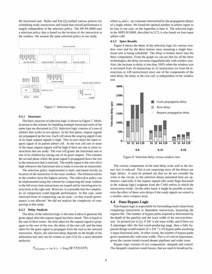
4.3.3 Spice ResultsFigure 8 shows the delay of the selection logic for various win-
dow sizes and for the three feature sizes assuming a single func-tional unit is being scheduled. The delay is broken down into thethree components. From the graph we can see that for all the threetechnologies, the delay increases logarithmically with window size.Also, the increase in delay is less than 100% when the window sizeis increased from 16 instructions to 32 instructions (or from 64 in-structions to 128 instructions) since one of the components of thetotal delay, the delay at the root cell, is independent of the windowsize.
0
500
1000
1500
2000
2500
3000
16 32 64
0.8
128 16 32 64
0.35
128 16 32 64
0.18
128
Sele
ctio
n de
lay
(ps) Grant propagation delay
Root delay
Request propagation delay
Figure 8: Selection delay versus window size.
The various components of the total delay scale well as the fea-ture size is reduced. This is not surprising since all the delays arelogic delays. It must be pointed out that we do not consider thewires in the circuit, so the selection delays presented here are op-timistic, especially if the request signals (the ready flags discussedin the wakeup logic) originate from the CAM entries in which theinstructions reside. On the other hand, it might be possible to mini-mize the effect of these wire delays if the ready signals are stored ina smaller, more compact array.
4.4 Data Bypass LogicData bypass logic is responsible for forwarding result values from
completing instructions to dependent instructions, bypassing theregister file. The number of bypass paths required is determined bythe depth of the pipeline and the issue width of the microarchitec-ture. As pointed out in [1], if � is the issue width, and if there are� pipestages after the first result-producing stage, then a fully by-passed design would require
� � � �� � � � bypass paths assuming
2-input functional units. In other words, the number of bypass pathsgrows quadratically with issue width. This is of critical importance,given the current trends toward deeper pipelines and wider issue.
Bypass logic consists of two components: datapath and control.The datapath comprises result busses, that are used to broadcast by-
6

pass values from each functional unit source to all possible des-tinations. Buffers are used to drive the bypass values on the re-sult busses. In addition to the result busses, the datapath comprisesoperand MUXes. Operand MUXes are required to gate in the appro-priate result on to the operand busses. The control logic is responsi-ble for controlling the operand MUXes. It compares the tags of theresult values with the tag of source value required at each functionalunit. If there is a match, the MUX control is set so that the resultvalue is driven on the appropriate operand bus. The key factor thatdetermines the speed of the bypass logic is the delay of the resultwires that are used to transmit bypassed values, not the control.
4.4.1 Structure
A commonly used structure for bypass logic is shown in Figure 9.The figure shows a bit-slice of the datapath. There are four func-tional units marked FU0 to FU3. Consider the bit slice of FU0. Itgets its two operand bits from the opd0-l and opd0-r wires. The re-sult bit is driven on the res0 result wire by the result driver. Tris-tate buffers are used to drive the result bits on to the operand wiresfrom the result wires of the functional units. These buffers imple-ment the MUXes shown in the figure. To bypass the result of func-tional unit FU1 to the left input of functional unit FU0, the tristatedriver marked A is switched on. The driver A connects the res1 wireand the opd0-l wire. In the case where bypasses are not activated,operand bits are placed on the operand wires by the register file readports
�. The result bits are written to the register file in addition to
being bypassed.
FU3
FU2
FU0
FU1
res3
res2
res1
res0
opd0
-l
opd0
-r
opd1
-l
opd1
-r
A
resultwires
Regfile
mux
mux
mux
Figure 9: Bypass logic.
4.4.2 Delay Analysis
The delay of the bypass logic is largely determined by the amountof time it takes for the driver at the output of each functional unitto drive the result value on the corresponding result wire. This inturn depends on the length of the result wires. From the figure it isapparent that the length of the wires is a function of the layout. Forthe layout presented in the figure, the length of the result wires isdetermined by the height of the functional units and the register file.�In a reservation-station based microarchitecture, the operand bits come
from the data field of the reservation station entry.
Issue Wire Delaywidth length (
�) (ps)
4 20500 184.98 49000 1056.4
Table 1: Bypass delays for a 4-way and a 8-way processor.
Considering the result wires as distributed RC lines, the delay isgiven by
��'�� , � + + � ��� � � ��� ��� � � ��� ��� ��� �
where � is the length of the result wires, and� ��� � �
and � ��� � �are the resistance and parasitic capacitance of metal wires per unitlength respectively.
Increasing issue width increases the length of the result wires,and hence causes the bypass delay to grow quadratically with issuewidth. Increasing the depth of the pipeline also increases the delayof the bypass logic in the following manner. Making the pipelinedeeper increases the fan-in of the operand MUXes connected to agiven result wire. This in turn increases the amount of capacitanceon the result wires, and hence adds to the delay of the result wires.However, this component of the delay is not captured by our simplemodel. This component of the delay is likely to become relativelyless significant as feature size is reduced.
4.4.3 Spice Results
We computed the wire delays for hypothetical 4-way and 8-waymachines assuming common mixes of functional units and func-tional unit heights reported in the literature. Table 1 shows the re-sults. Wire lengths are shown in terms of
�, where
�is half the fea-
ture size. The delays are the same for the three technologies sincewire delays are constant according to the scaling model assumed.See [15] for the detailed data and analysis.
4.4.4 Alternative Layouts
The results presented above assume a particular layout; the func-tional units are placed on either side of the register file. However,as mentioned before, the length of the result wires is a function ofthe layout. Hence, VLSI designers will have to study alternative lay-outs in order to reduce bypass delays. Alternative layouts alone willonly decrease constants; the quadratic delay growth with number ofbypasses will remain.
In the long term, microarchitects will have to consider clusteredorganizations where each cluster of functional units has its own copyof the register file and bypasses within a cluster complete in a sin-gle cycle while inter-cluster bypasses take two or more cycles. Thehardware or the compiler or both will have to ensure that inter-cluster bypasses occur infrequently. In addition to mitigating the de-lay of the bypass logic, this organization also has the advantage offaster register files since there are fewer ports on each register file.
4.5 Summary of Delays and Pipeline IssuesWe now summarize the pipeline delay results and consider the
implications for future complexity-effective microarchitectures. Itis easiest to frame this discussion in terms of satisfying the goal ofpermitting a very fast pipeline clock while, at the same time, exploit-ing high ILP through relatively wide, out-of-order superscalar oper-ation.
7

Issue Window Rename Wakeup+Select Bypasswidth size delay (ps) delay (ps) delay (ps)
0.8�
m technology4 32 1577.9 2903.7 184.98 64 1710.5 3369.4 1056.4
0.35�
m technology4 32 627.2 1248.4 184.98 64 726.6 1484.8 1056.4
0.18�
m technology4 32 351.0 578.0 184.98 64 427.9 724.0 1056.4
Table 2: Overall delay results.
To aid in this discussion, consider the overall results for a 4-wayand a 8-way microarchitecture in
� �� �� ���technology shown in Ta-
ble 2. We chose the���� ������
technology because of our interest infuture generation microarchitectures. For the 4-way machine, thewindow logic (wakeup + select) has the greatest delay among all thestructures considered, and hence determines the critical path delay.The register rename delay comes next; it is about 39% faster thanthe delay of the window logic. The bypass delay is relatively smallin this case. The results are similar for the 8-way machine, with onevery notable exception: the bypass delay grows by a factor of over5, and is now worse than the (wakeup + select) delay.
Now, let’s turn to the problem of designing a future generationmicroarchitecture with a faster clock cycle. Of the structures wehave examined here, the window logic and the bypasses seem topose the largest problems. Moreover, both of these cause difficultiesif we wish to divide them into more pipeline segments; these diffi-culties will be discussed in the following paragraphs. All the otherstructures either will not cause a clock cycle problem, or if they do,they can be pipelined. The pipelining aspects of these structures isdiscussed in [15]. This additional pipelining can cause some per-formance impact, although it is beyond the scope of this paper toevaluate the exact impact.
. . .
. . .
. . .
. . .
. . .
. . .
WAKEUP SELECT EXEC
SELECT EXEC
SELECT EXEC
add r10, r1, r2
sub r1, r10, 2
bubbleWAKEUP
WAKEUP
Figure 10: Pipelining wakeup and select.
Wakeup and select together constitute what appears to be anatomic operation. That is, if they are divided into multiple pipelinestages, dependent instructions cannot issue in consecutive cycles.Consider the pipeline example shown in Figure 10. Theadd and thesub instructions cannot be executed back-to-back because the re-sult of the select stage has to feed the wakeup stage. Hence, wakeupand select together constitute an atomic operation and must be ac-complished in a single cycle, at least if dependent instructions are tobe executed on consecutive cycles.
Data bypassing is another example of what appears to be anatomic operation. In order for dependent operations to execute inconsecutive cycles, the bypass value must be made available to thedependent instruction within a cycle. Results presented in table Ta-ble 2 show that this is feasible for a 4-way machine. However, by-pass delay can easily become a bottleneck for wider issue-widths.
One solution is to include only a proper subset of bypass paths
[1], and take a penalty for those that are not present. For an 8-waymachine with deep pipelines, this would exclude a large number ofbypass paths. Another solution is to generalize the method used inthe DEC 21264 [10] and use multiple copies of the register file. Thisis the “cluster” method referred to in Section 4.4.
In the following section we tackle both the window logic andbypass problems by proposing a microarchitecture that simplifieswindow logic and which naturally supports clustering of functionalunits.
5 A Complexity-Effective MicroarchitectureFrom the analysis presented in the previous sections we see that
the issue window logic is one of the primary contributors of com-plexity in typical out-of-order microarchitectures. Also, as archi-tects employ wider issue-widths and deeper pipelines, the delay ofthe bypass logic becomes even more critical. In this section, we pro-pose a dependence-based microarchitecture that replaces the issuewindow with a simpler structure that facilitates a faster clock whileexploiting similar levels of parallelism. In addition, the proposedmicroarchitecture naturally lends itself to clustering and helps miti-gate the bypass problem to a large extent.
. . . .
. . . .
. . .
.
FIFOS
Reg
iste
r fi
le
Fetc
h
Dec
ode
Stee
rR
enam
e
Sele
ctW
akeu
p
Byp
ass
Dat
a-ca
che
FETCH DECODE RENAMESTEER
WAKEUPSELECT
EXECUTEBYPASS
DCACHEACCESS
REG WRITECOMMIT
REG READ
Figure 11: Dependence-based microarchitecture.
The idea behind the dependence-based microarchitecture is to ex-ploit the natural dependences among instructions. A key point isthat dependent instructions cannot execute in parallel. In the pro-posed microarchitecture, shown in Figure 11, the issue window isreplaced by a small number of FIFO buffers. The FIFO buffers areconstrained to issue in-order, and dependent instructions are steeredto the same FIFO. This ensures that the instructions in a particularFIFO buffer can only execute sequentially. Hence, unlike the typ-ical issue window where result tags have to be broadcast to all theentries, the register availability only needs to be fanned out to theheads of the FIFO buffers. The instructions at the FIFO heads mon-itor reservation bits (one per physical register) to check for operandavailability. This is discussed in detail later. Furthermore, the selec-tion logic only has to monitor instructions at the heads of the FIFObuffers.
The steering of dependent instructions to the FIFO buffers isperformed at run-time during the rename stage. Dependence in-formation between instructions is maintained in a table called theSRC FIFO table. This table is indexed using logical register des-ignators. SRC FIFO(Ra), the entry for logical register Ra, con-tains the identity of the FIFO buffer that contains the instructionthat will write register Ra. If that instruction has already completedi.e. register Ra contains its computed value, then SRC FIFO(Ra)is invalid. This table is similar to the map table used for reg-ister renaming and can be accessed in parallel with the renametable. In order to steer an instruction to a particular FIFO, theSRC FIFO table is accessed with the register identifiers of thesource operands of an instruction. For example, for steering the in-struction add r10,r5,1 where r10 is the destination register,
8

the SRC FIFO table is indexed with 5. The entry is then used tosteer the instruction to the appropriate FIFO.
5.1 Instruction Steering HeuristicsA number of heuristics are possible for steering instructions to
the FIFOs. A simple heuristic that we found to work well for ourbenchmark programs is described next.
LetI be the instruction under consideration. Depending upon theavailability of I’s operands, the following cases are possible:
� All the operands of I have already been computed and are re-siding in the register file. In this case, I is steered to a new(empty) FIFO acquired from a pool of free FIFOs.
� I requires a single outstanding operand to be produced by in-struction Isource residing in FIFO Fa. In this case, if thereis no instruction behind Isource in Fa then I is steered toFa, else I is steered to a new FIFO.
� I requires two outstanding operands to be produced by in-structions Ileft and Iright residing in FIFOs Fa and Fbrespectively. In this case, apply the heuristic in the previousbullet to the left operand. If the resulting FIFO is not suitable(it is either full or there is an instruction behind the source in-struction), then apply the same heuristic to the right operand.
If all the FIFOs are full or if no empty FIFO is available then thedecoder/steering logic stalls. A FIFO is returned to the free poolwhen the last instruction in the FIFO is issued. Initially, all the FI-FOs are in the free pool. Figure 12 illustrates the heuristic on a codesegment from one of the SPEC benchmarks.
TIME
0 1
4 2
3
5
7
8
14
11
6
9
10
6: lw $3,-32676($28)
0: addu $18,$0,$2
2: beq $18,$2,L23: lw $4,-32768($28)4: sllv $2,$18,$205: xor $16,$2,$19
7: sll $2,$16,0x28: addu $2,$2,$239: lw $2,0($2)
10: sllv $4,$18,$411: addu $17,$4,$1912: addiu $3,$3,113: sw $3,-32676($28)14: beq $2,$17,L3
0,1,3 issue
2,4,6 issue
5,10 issue
7,11,12 issue
1: addiu $2,$0,-1
13
12
1110
5789
11
78914
1213
02
1
3
2
457
6
Figure 12: Instruction steering example.
This figure shows how instructions are steered to FIFOs using the heuristicpresented in Section 5.1 for a sample code segment. Instructions can issueonly from the heads of the four FIFOs. The steering logic steers four instruc-tions every cycle and a maximum of four instructions can issue every cycle.
5.2 Performance ResultsWe compare the performance of the dependence-based microar-
chitecture against that of a typical microarchitecture with an issuewindow. The proposed microarchitecture has 8 FIFOs, with eachFIFO having 8-entries. The issue window of the conventional pro-cessor has 64 entries. Both microarchitectures can decode, rename,and execute a maximum of 8 instructions per cycle. The timing sim-ulator, a modified version of SimpleScalar [4], is detailed in Table 3.
Fetch width any 8 instructionsI-cache Perfect instruction cacheBranch Predictor McFarling’s gshare [13]
4K 2-bit counters, 12 bit historyunconditional control instructionspredicted perfectly
Issue window size 64Max. in-flight 128instructionsRetire width 16Functional Units 8 symmetrical unitsFunctional Unit Latency 1 cycleIssue Mechanism out-of-order issue of up to 8 ops/cycle
loads may execute when all priorstore addresses are known
Physical Registers 120 int/120 fpD-cache 32KB, 2-way SA
write-back, write-allocate32 byte lines,1 cycle hit,6 cycle missfour load/store ports
Table 3: Baseline simulation model.
An aggressive instruction fetch mechanism is used to stress the is-sue and execution subsystems. We ran seven benchmarks from theSPEC’95 suite, using their training input datasets. Each benchmarkwas run for a maximum of 0.5B instructions.
0.0
0.5
1.0
1.5
2.0
2.5
3.0
3.5
4.0
compress gcc go li perl m88ksim vortex
Inst
ruct
ions
Per
Cyc
le
Baseline microarch.
Dependence-based microarch.
Figure 13: Performance (IPC) of dependence-based microarchitec-ture.
The performance results (in terms of instructions committed percycle) are shown in Figure 13. The dependence-based microarchi-tecture is nearly as effective (extracts similar parallelism) as the typ-ical window-based microarchitecture. The cycle count numbers arewithin 5% for five of the seven benchmarks and the maximum per-formance degradation is 8% in the case of li.
5.3 Complexity AnalysisFirst, consider the delay of the wakeup and selection logic.
Wakeup logic is required to detect cross-FIFO dependences. For ex-ample, if the instruction Ia at the head of FIFO Fa is dependent onan instruction Ibwaiting in FIFOFb, then Ia cannot issue until Ibcompletes. However, the wakeup logic in this case does not involvebroadcasting the result tags to all the waiting instructions. Instead,only the instructions at the FIFO heads have to determine when all
9

Issue No. physical No. table Bits per Totalwidth registers entries entry delay (ps)
4 80 10 8 192.18 128 16 8 251.7
Table 4: Delay of reservation table in���� � ���
technology.
their operands are available. This is accomplished by interrogatinga table called the reservation table. The reservation table contains asingle bit per physical register that indicates whether the register iswaiting for its data. When an instruction is dispatched, the reserva-tion bit corresponding to its result register is set. The bit is clearedwhen the instruction executes and the result value is produced. Aninstruction at the FIFO head waits until the reservation bits corre-sponding to its operands are cleared. Hence, the delay of the wakeuplogic is determined by the delay of accessing the reservation table.The reservation table is relatively small in size compared to the re-name table and the register file. For example, for a 4-way machinewith 80 physical registers, the reservation table can be laid out as a10-entry table with each entry storing 8 bits
. Table 4 shows the
delay of the reservation table for 4-way and 8-way machines. Forboth cases, the wakeup delay is much smaller than the wakeup delayfor a 4-way, 32-entry issue window-based microarchitecture. Also,this delay is smaller than the corresponding register renaming delay.The selection logic in the proposed microarchitecture is simple be-cause only the instructions at the FIFO heads need to be consideredfor selection.
Instruction steering is done in parallel with register renaming.Because the SRC FIFO table is smaller than the rename table, weexpect the delay of steering to be less than the rename delay. In casea more complex steering heuristic is used, the extra delay can easilybe moved into the wakeup/select stage, or a new pipestage can beintroduced – at the cost of an increase in branch mispredict penalty.
In summary, the complexity analysis presented above shows thatby reducing the delay of the window logic significantly, it is likelythat the dependence-based microarchitecture can be clocked fasterthan the typical microarchitecture. In fact, from the overall delayresults shown in Table 2, if the window logic (wakeup + select)is reduced substantially, register rename logic becomes the criticalstage for a 4-way microarchitecture. Consequently, the dependence-based microarchitecture can improve the clock period by as much as(an admittedly optimistic) 39% in 0.18
���technology. Of course,
this may require that other stages not studied here be more deeplypipelined. Combining the potential for a much faster clock with theresults in Figure 13 indicates that the dependence-based microarchi-tecture is capable of superior performance relative to a typical super-scalar microarchitecture.
5.4 Clustering the Dependence-based Microarchi-tecture
The real advantage of the proposed microarchitecture is for build-ing machines with issue widths greater than four where, as shownby Table 2, the delay of both the large window and the long bypassbusses can be significant and can considerably slow the clock. Clus-tered microarchitectures based on the dependence-based microar-chitecture are ideally suited for such situations because they sim-plify both the window logic and the bypass logic. We describe onesuch microarchitecture for building an 8-way machine next. A column MUX is used to select the appropriate bit from each entry.
RE
NA
ME
D I
NST
RU
CT
ION
S
STE
ER
ING
LO
GIC
BY
PASS
RE
G F
ILE
1
FU4
FU5
FU6
FU7
RE
G F
ILE
0
FU0
FU1
FU2
FU3
BY
PASS
LOCAL BYPASSES
LOCAL BYPASSES
INT
ER
-CL
UST
ER
BY
PASS
ES
CLUSTER 1
CLUSTER 0
FIFOs
FIFOs
Figure 14: Clustering the dependence-based microarchitecture: 8-way machine organized as two 4-way clusters (2 X 4-way).
Consider the 2x4-way clustered system shown in Figure 14. Twoclusters are used, each of which contains four FIFOs, one copy ofthe register file, and four functional units. Renamed instructions aresteered to a FIFO in one of the two clusters. Local bypasses within acluster (shown using thick lines) are responsible for bypassing resultvalues produced in the cluster to the inputs of the functional units inthe same cluster. As shown by the delay results in Table 2, localbypassing can be accomplished in a single cycle. Inter-cluster by-passes are responsible for bypassing values between functional unitsresiding in different clusters. Because inter-cluster bypasses requirelong wires, it is likely that these bypasses will be relatively slowerand take two or more cycles in future technologies. The two copiesof the register file are identical, except for the one or more cyclesdifference in propagating results from one cluster to another.
This clustered, dependence-based microarchitecture has a num-ber of advantages. First, wakeup and selection logic are simplifiedas noted previously. Second, because of the heuristic for assigningdependent instructions to FIFOs, and hence indirectly to clusters,local bypasses are used much more frequently than inter-cluster by-passes, reducing overall bypass delays. Third, using multiple copiesof the register file reduces the number of ports on the register file andwill make the access time of the register file faster.
5.5 Performance of Clustered Dependence-basedMicroarchitecture
The graph in Figure 15 compares performance, in terms of in-structions committed per cycle (IPC), for the 2x4-way dependence-based microarchitecture against that of a conventional 8-way mi-croarchitecture with a single 64-entry issue window. For thedependence-based system, instructions are steered using the heuris-tic described in Section 5.1 with a slight modification. Instead ofusing a single free list of empty FIFOs, we maintain two free listsof empty FIFOs, one per cluster. A request for a free FIFO is sat-isfied if possible from the current free list. If the current free list isempty, then the second free list is interrogated for a new FIFO andthe second free list is made current. This scheme ensures that in-structions adjacent in the dynamic stream are assigned to the samecluster to minimize inter-cluster communication. Local bypassestake one cycle while inter-cluster bypasses take 2 cycles. Also, inthe conventional 8-way system, all bypasses are assumed to com-
10

plete in a single cycle. From the graph we can see that for most ofthe benchmarks, the dependence-based microarchitecture is nearlyas effective as the window-based microarchitecture even though thedependence-based microarchitecture is handicapped by slow inter-cluster bypasses that take 2 cycles. However, for two of the bench-marks, m88ksim and compress, the performance degradation is closeto 12% and 9% respectively. We found that this degradation ismainly due to extra latency introduced by the slow inter-cluster by-passes.
0.00.20.40.60.81.01.21.41.61.82.02.22.42.62.83.03.23.43.63.84.0
compress gcc go li m88ksim perl vortex
Inst
ruct
ions
Per
Cyc
le
64-entry window-based 8-way
2-cluster dependence-based 8-way
Figure 15: Performance of clustered dependence-based microarchi-tecture.
Because the dependence-based microarchitecture will facilitate afaster clock, a fair performance comparison must take clock speedinto account. The local bypass structure within a cluster is equiva-lent to a conventional 4-way superscalar machine, and inter-clusterbypasses are removed from the critical path by taking an extra clockcycle. Consequently, the clock speed of the dependence-based mi-croarchitecture is at least as fast as the clock speed of a 4-way, 32-entry window-based microarchitecture, and is likely to be signifi-cantly faster because of the smaller (wakeup + selection) delay com-pared to a conventional issue window as discussed in Section 5.3.Hence, if � ��� ,
is the clock speed of the dependence-based microar-chitecture, and � � ! �
is the clock speed of the window-based mi-croarchitecture, then from Table 2 for 0.18
�m technology:
� ��� ,� � ! � ��� ��� �� ��� ��� ����� � � � ��� ��� � � � �
� ��� �� ��� � ��� � � � � � ��� ��� � � � �� � � �
In other words, the dependence-based microarchitecture is capa-ble of supporting a clock that is 25% faster than the clock ofthe window-based microarchitecture. Taking this factor into ac-count (and ignoring other pipestages that may have to be moredeeply pipelined), we can estimate the potential speedup with adependence-based microarchitecture. The performance improve-ments vary from 10% to 22% with an average improvement of 16%.
5.6 Other Clustered MicroarchitecturesThe microarchitecture presented in the previous section is one
point in the design space of clustered superscalar microarchitec-tures. The dependence-based microarchitecture simplifies both thewindow logic and naturally reduces the performance degradationdue to slow inter-cluster bypass paths. In order to further explorethe space, we studied the performance of some other interesting de-
signs. In each case there are two clusters with inter-cluster bypassestaking an extra cycle to complete.
STEE
RIN
G L
OG
IC
(b)
CLUSTER 0
CLUSTER 1
CLUSTER 0
CLUSTER 1
INST
RU
CTI
ON
STR
EAM
CENTRAL WINDOW
(a)
INST
RU
CTI
ON
STR
EAM
Figure 16: Clustered microarchitectures.
5.6.1 Single Window, Execution-Driven Steering
In the dependence-based microarchitecture described above, in-structions are pre-assigned to a cluster when they are dispatched; werefer to this as dispatch-driven instruction steering. In contrast, Fig-ure 16(a) illustrates a microarchitecture where instructions reside ina central window while waiting for their operands and functionalunits to become available. Instructions are assigned to the clustersat the time they begin execution; this is execution-driven instructionsteering.
With this method, cluster assignment works as follows. The reg-ister values in the clusters become available at slightly differenttimes; that is, the result register value produced by a cluster is avail-able in that cluster one cycle earlier than in the other cluster. Conse-quently, an instruction waiting for the value may be enabled for exe-cution one cycle earlier in one cluster than in the other. The selectionlogic monitors the instructions in the window and attempts to assignthem to the cluster which provides their source values first (assum-ing there is a free functional unit in the cluster). Instructions thathave their source operands available in both clusters are first con-sidered for assignment to cluster 0. Static instruction order is usedto break ties in this case.
The execution-driven approach uses a greedy policy to minimizethe use of slow inter-cluster bypasses while maintaining a high uti-lization of the functional units. It does so by postponing the as-signment of instructions to clusters until execution time. While thisgreedy approach may gain some IPC advantages, this organizationsuffers from the previously discussed drawbacks of a central win-dow and complex selection logic.
5.6.2 Two Windows, Dispatch-Driven Steering
This microarchitecture, shown in Figure 16(b), is identical tothe dependence-based clustered microarchitecture except that each
11

cluster has a completely flexible window instead of FIFOs. Instruc-tions are steered to the windows using a heuristic that takes both de-pendences between instructions and the relative load of the clustersinto account. We tried a number of heuristics and found a simple ex-tension of the FIFO heuristic presented in Section 5.1 to work best.In our scheme the window is modeled as if it is a collection of FI-FOs with instructions capable of issuing from any slot within eachindividual FIFO. In this particular case, we treat each 32-entry win-dow as eight FIFOs with four slots each. Note that these FIFOs are aconceptual device used only by the assignment heuristic – in reality,instructions issue from the window with complete flexibility.
Kemp and Franklin [11] studied an organization called PEWs(Parallel Execution Windows) for simplifying the logic associatedwith a central window. PEWs simplifies window logic by splittingthe central instruction window among multiple windows much likethe clustered microarchitecture described above. Register values arecommunicated between clusters (called pews) via hardware queuesand a ring interconnection network. In contrast, we assume a broad-cast mechanism for the same purpose. Instructions are steered tothe pews based on instruction dependences with a goal to minimizeinter-pew communication. However, for their experiments they as-sume that each of the pews has as many functional units as the cen-tral window organization. This assumption implies that the reduc-tion in complexity achieved is limited since the wakeup and selec-tion logic of the windows in the individual pews still have the sameporting requirements as the central window.
5.6.3 Two Windows, Random SteeringThis microarchitecture, using the structure presented in Fig-
ure 16(b), is a basis for comparisons. Instructions are steered ran-domly to one of the clusters. If the window for the selected clusteris full, then the instruction is inserted into the other (free) cluster.This design point was evaluated in order to determine the degree towhich clustered microarchitectures are capable of tolerating the ex-tra latency introduced by slow inter-cluster bypasses and the impor-tance of dependence-aware scheduling. Each window has 32 entriesin this case.
5.6.4 Performance of Clustered MicroarchitecturesThe top graph in Figure 17 shows the performance of various mi-
croarchitectures in terms of instructions committed per cycle (IPC).The leftmost bar in each group shows the performance of the idealmicroarchitecture: a single 64-entry window with single cycle by-pass between all functional units. A number of observations canbe made from the figure. First, random steering consistently per-forms worse than the other schemes. The performance degradationwith respect to the ideal case varies from 17% in the case of vor-tex to 26% in the case of m88ksim. Hence, it is essential for thesteering logic to consider dependences when routing instructions.Second, the microarchitecture with a central window and execution-driven steering performs nearly as well as the ideal microarchitec-ture with a maximum degradation of 6% in the case of m88ksim.However, as discussed earlier in Section 5.6.1, this microarchitec-ture requires a centralized window with complex selection logic.Third, both the dependence-based microarchitecture and the flex-ible window microarchitecture using dispatch-driven steering per-form competitively in comparison to the ideal microarchitecture.
The bottom graph in Figure 17 shows the frequency of inter-cluster communication for each organization. We measure inter-cluster communication in terms of the fraction of total instructionsthat exercise inter-cluster bypasses. This does not include caseswhere an instruction reads its operands from the register file in the
cluster i.e. cases in which the operands arrived from the remote clus-ter in advance. As expected, we see that there is a high correlationbetween the frequency of inter-cluster communication and perfor-mance - organizations that exhibit higher inter-cluster communica-tion commit fewer instructions per cycle. The inter-cluster commu-nication is particularly high in the case of random steering, reachingas high as 35% in the case of m88ksim.
0.0
0.4
0.8
1.2
1.6
2.0
2.4
2.8
3.2
3.6
4.0
compress gcc go li m88ksim perl vortex
Inst
ruct
ions
Per
Cyc
le
1-cluster.1window
2-cluster.FIFOs.dispatch_steer
2-cluster.windows.dispatch_steer
2-cluster.1window.exec_steer
2-cluster.windows.random_steer
0
5
10
15
20
25
30
35
40
compress gcc go li m88ksim perl vortexInte
r-C
lust
er B
ypas
s F
requ
ency
(%)
Figure 17: Performance of clustered microarchitectures.
Overall, the above results show that clustered microarchitecturesusing distributed windows coupled with dispatch-driven steeringcan deliver performance similar, in terms of instructions committedper cycle, to that of an ideal microarchitecture with a large windowand uniform single cycle bypasses between all functional units.
6 ConclusionsWe studied the variation of delays of key structures in a generic
superscalar processor with two important microarchitectural param-eters: issue width and issue window size. We also analyzed the im-pact of advanced technologies with smaller feature sizes on the de-lay of these structures. Our results show that the logic associatedwith the issue window and the data bypass logic are going to becomeincreasingly critical as future designs employ wider issue widths,bigger windows, and smaller feature sizes. Furthermore, both ofthese structures rely on broadcasting values on long wires, and infuture technologies wire delays will increasingly dominate total de-lay.
This is not to say that the delay of other structures, for exam-ple register files and caches, will not cause problems. However,
12

these structures can be pipelined to some extent. In contrast, win-dow logic and data bypass logic implement atomic operations thatcannot be pipelined while allowing dependent instructions to exe-cute in successive cycles. This characteristic makes the delay of thewindow logic and the data bypass logic even more crucial.
Hence, as architects build machines with wider issue widths andlarger window sizes in advanced technologies, it is essential to con-sider microarchitectures that are complexity-effective i.e. microar-chitectures that facilitate a fast clock while exploiting similar levelsof ILP as an ideal large-window machine.
In the second half of the paper, we proposed one such mi-croarchitecture called the dependence-based microarchitecture. Thedependence-based microarchitecture detects chains of dependent in-structions and steers the chains to FIFOs which are constrained toexecute in-order. Since only the instructions at the FIFO heads haveto be monitored for execution, the dependence-based microarchitec-ture simplifies window logic. Furthermore, the dependence-basedmicroarchitecture naturally lends itself to clustering by grouping de-pendent instructions together. This grouping of dependent instruc-tions helps mitigate the bypass problem to a large extent by usingfast local bypasses more frequently than slow inter-cluster bypasses.We compared the performance of a 2x4-way dependence-based mi-croarchitecture with a typical 8-way superscalar. Our results showtwo things. First, the proposed microarchitecture has IPC perfor-mance close to that of a typical microarchitecture (average degra-dation in IPC performance is 6.3%). Second, when taking the clockspeed advantage of the dependence-based microarchitecture into ac-count the 8-way dependence-based microarchitecture is 16% fasterthan the typical window-based microarchitecture on average.
AcknowledgementsThis work was supported in part by an internship at DEC West-
ern Research Laboratory, and by grants from the NSF Grant MIP-9505853, and the U.S. Army Intelligence Center and Fort Huachucaunder Contract DABT63-95-C-0127 and ARPA order no. D346.The views and conclusions contained herein are those of the authorsand should not be interpreted as necessarily representing the officialpolicies or endorsements, either expressed or implied, of the U. S.Army Intelligence Center and Fort Huachuca, or the U.S. Govern-ment.
We thank the staff at DEC-WRL, especially Annie Warren andJason Wold, for providing us with the CAD tools used in this study.Thanks to Andy Glew for answering specific questions regarding theimplementation of the Intel Pentium Pro and for related discussions.Thanks also to Todd Austin, Scott Breach, and Shamik Das Sharmafor comments on a draft of this paper.
References
[1] P. S. Ahuja, D. W. Clark, and A. Rogers. The Performance Impact ofIncomplete Bypassing in Processor Pipelines. In Proceedings of the28th Annual International Symposium on Microarchitecture, Novem-ber 1995.
[2] C. Asato, R. Montoye, J. Gmuender, E. W. Simmons, A. Ike, and J. Za-sio. A 14-port 3.8ns 116-word 64b Read-Renaming Register File.In 1995 IEEE International Sold-State Circuits Conference Digest ofTechnical Papers, pages 104–105, February 1995.
[3] Mark T. Bohr. Interconnect Scaling - The Real Limiter to High Perfor-mance ULSI. In 1995 International Electron Devices Meeting Techni-cal Digest, pages 241–244, 1995.
[4] Doug Burger, Todd M. Austin, and Steve Bennett. Evaluating FutureMicroprocessors: The Simplescalar Tool Set. Technical Report CS-
TR-96-1308 (Available from http://www.cs.wisc.edu/trs.html), Uni-versity of Wisconsin-Madison, July 1996.
[5] M. Butler and Y. N. Patt. An Investigation of the Performance of Var-ious Dynamic Scheduling Techniques. In Proceedings of the 25th An-nual International Symposium on Microarchitecture, pages 1–9, De-cember 1992.
[6] Keith I. Farkas, Norman P. Jouppi, and Paul Chow. Register File De-sign Considerations in Dynamically Scheduled Processors. In Pro-ceedings of the Second IEEE Symposium on High-Performance Com-puter Architecture, February 1996.
[7] Linley Gwennap. Speed Kills? Not for RISC Processors. Micropro-cessor Report, 7(3):3, March 1993.
[8] Linley Gwennap. HAL Reveals Multichip SPARC Processor. Micro-processor Report, 9(3), March 1995.
[9] Linley Gwennap. Intel’s P6 Uses Decoupled Superscalar Design. Mi-croprocessor Report, 9(2), February 1995.
[10] Jim Keller. The 21264: A Superscalar Alpha Processor with Out-of-Order Execution, October 1996. 9th Annual Microprocessor Forum,San Jose, California.
[11] Gregory A. Kemp and Manoj Franklin. PEWs: A Decentralized Dy-namic Scheduler for ILP Processing. In Proceedings of the Interna-tional Conference on Parallel Processing, volume I, pages 239–246,1996.
[12] Ashok Kumar. The HP-PA8000 RISC CPU: A High Performance Out-of-Order Processor. In Proceedings of the Hot Chips VIII, pages 9–20,August 1996.
[13] Scott McFarling. Combining Branch Predictors. DEC WRL TechnicalNote TN-36, DEC Western Research Laboratory, 1993.
[14] Meta-Software Inc. HSpice User’s Manual, June 1987.
[15] Subbarao Palacharla, Norman P. Jouppi, and James E. Smith. Quanti-fying the Complexity of Superscalar Processors. Technical Report CS-TR-96-1328 (Available from http://www.cs.wisc.edu/trs.html), Uni-versity of Wisconsin-Madison, November 1996.
[16] S. Peter Song, Marvin Denman, and Joe Chang. The PowerPC 604RISC Microprocessor. In IEEE Micro, pages 8–17, October 1995.
[17] N. Vasseghi et al. 200 MHz Superscalar RISC Processor Circuit De-sign Issues. In 1996 IEEE International Sold-State Circuits Confer-ence Digest of Technical Papers, pages 356–357, February 1996.
[18] Tomohisa Wada, Suresh Rajan, and Steven A. Przybylski. An Analyt-ical Access Time Model for On-Chip Cache Memories. IEEE Journalof Solid-State Circuits, 27(8):1147–1156, August 1992.
[19] Neil H.E. Weste and Kamran Eshraghian. Principles of CMOS VLSIDesign. Addison Wesley, second edition, 1993.
[20] Neil C. Wilhelm. Why Wire Delays Will No Longer Scale for VLSIChips. Technical Report SMLI TR-95-44, Sun Microsystems Labora-tories, August 1995.
[21] Steven J. E. Wilton and Norman P. Jouppi. An Enhanced Access andCycle Time Model for On-Chip Caches. Technical Report 93/5, DECWestern Research Laboratory, July 1994.
[22] K. C. Yeager. MIPS R10000 Superscalar Microprocessor. In IEEEMicro, April 1996.
13