Processing Unit Design Intel Processors Generations
28
Processing Unit Design Intel Processors Generations Intel 8086 The 8086 is a 16-bit microprocessor chip designed by Intel between early 1976 and 1978, when it was released. The Intel 8088, released July 1979, is a slightly modified chip with an external 8-bit data bus. The 8086 gave rise to the x86 architecture, which eventually became Intel's most successful line of processors. On June 5th 2018, Intel released a limited-edition CPU celebrating the anniversary of the Intel 8086, called the Intel Core i7-8086K.
-
Upload
khangminh22 -
Category
Documents
-
view
0 -
download
0
Transcript of Processing Unit Design Intel Processors Generations

Processing Unit Design
Intel Processors Generations Intel 8086
The 8086 is a 16-bit microprocessor chip designed by Intel between
early 1976 and 1978, when it was released. The Intel 8088, released
July 1979, is a slightly modified chip with an external 8-bit data bus.
The 8086 gave rise to the x86 architecture, which eventually became
Intel's most successful line of processors.
On June 5th 2018, Intel released a limited-edition CPU celebrating
the anniversary of the Intel 8086, called the Intel Core i7-8086K.

Processing Unit Design
Intel Processors Generations Intel 8086
Memory Program, data and stack memories occupy the same memory space. The total addressable memory size is 1MB KB. As the most of the processor instructions use 16-bit pointers the processor can effectively address only 64 KB of memory. To access memory outside of 64 KB the CPU uses special segment registers to specify where the code, stack and data 64 KB segments are positioned within 1 MB of memory (see the "Registers" section below). 16-bit pointers and data are stored as: address: low-order byte address+1: high-order byte 32-bit addresses are stored in “ segment: offset " format as: address: low-order byte of segment address+1: high-order byte of segment address+2: low-order byte of offset address+3: high-order byte of offset Physical memory address pointed by segment: offset pair is calculated as: address = (<segment> * 16) + <offset>

Processing Unit Design
Intel Processors Generations Intel 8086
• Program memory : program can be located anywhere in memory. • Data memory : the 8086 processor can access data in any one out of 4 available segments, which limits the size of accessible memory to 256 KB (if all four segments point to different 64 KB blocks). Accessing data from the Data, Code, Stack or Extra segments can be usually done by prefixing instructions with the DS, CS, SS or ES (some registers and instructions by default may use the ES or SS segments instead of DS segment). • Stack memory: can be placed anywhere in memory

Processing Unit Design
Intel Processors Generations Intel 8086
Interrupts The processor has the following interrupts: • INTR is a maskable hardware interrupt. • NMI is a non-maskable interrupt. Software interrupts can be caused by: • INT instruction - breakpoint interrupt. This is a type 3 interrupt. • INT <interrupt number> instruction - any one interrupt from
available 256 interrupts. • INTO instruction - interrupt on overflow
I/O ports 65536 8-bit I/O ports. These ports can be also addressed as 32768 16-bit I/O ports.

Processing Unit Design
Intel Processors Generations Intel 8086
Registers Most of the registers contain data/instruction offsets within 64 KB
memory segment. There are four different 64 KB segments for instructions, stack, data and extra data. To specify where in 1 MB of processor memory these 4 segments are located the 8086
microprocessor uses four segment registers: • Code segment (CS) is a 16-bit register containing address of 64 KB
segment with processor instructions. The processor uses CS segment for all accesses to instructions referenced by instruction pointer (IP) register.

Processing Unit Design
Intel Processors Generations Intel 8086
• Stack segment (SS) is a 16-bit register containing address of 64KB segment with program stack. • Data segment (DS) is a 16-bit register containing address of 64KB segment with program data. By default, the processor assumes that all data referenced by general registers (AX, BX, CX, DX) and index register(SI, DI) is located in the data segment. DS register can be
changed directly using POP and LDS instructions. • Extra segment (ES) is a 16-bit register containing address of 64KB segment, usually with program data

Processing Unit Design
Intel Processors Generations Intel 8086
All general registers of the 8086 microprocessor can be used for arithmetic and logic operations. The general registers are: • Accumulator register consists of 2 8-bit registers AL and AH, which
can be combined together and used as a 16-bit register AX. AL in
this case contains the low-order byte of the word, and AH contains the high order byte. Accumulator can be used for I/O operations and string manipulation.
• Base register consists of 2 8-bit registers BL and BH, which can be
combined together and used as a 16-bit register BX. BL in this case
contains the low-order byte of the word, and BH contains the high- order byte. BX register usually contains a data pointer used for based, based indexed or register indirect addressing.

Processing Unit Design
Intel Processors Generations Intel 8086
• Count register consists of 2 8-bit registers CL and CH, which can be
combined together and used as a 16-bit register CX. When combined, CL register contains the low-order byte of the word, and CH contains the high-order byte. Count register can be used as a counter in string manipulation and shift/rotate instructions.
• Data register consists of 2 8-bit registers DL and DH, which can be
combined together and used as a 16-bit register DX. When combined, DL register contains the low-order byte of the word, and DH contains the high-order byte. Data register can be used as a port number in I/O operations

Processing Unit Design
Intel Processors Generations Intel 8086
The following registers are both general and index registers: • Stack Pointer (SP) is a 16-bit register pointing to program stack. • Base Pointer (BP) is a 16-bit register pointing to data in stack
segment. BP register is usually used for based, based indexed or register indirect addressing.
• Source Index (SI) is a 16-bit register. SI is used for indexed, based
indexed and register indirect addressing, as well as a source data
address in string manipulation instructions.
• Destination Index (DI) is a 16-bit register. DI is used for indexed, based indexed and register indirect addressing, as well as a destination data address in string manipulation instructions.

Processing Unit Design
Intel Processors Generations Intel 8086
Other registers: Instruction Pointer (IP) is a 16-bit register. Flags is a 16-bit register containing 9 1-bit flags: 1. Overflow Flag (OF) 2. Direction Flag (DF) 3. Interrupt-enable Flag (IF) 4. Single-step Flag (TF) 5. Sign Flag (SF) 6. Zero Flag (ZF) 7. Auxiliary carry Flag (AF) 8. Parity Flag (PF) 9. Carry Flag (CF)

Processing Unit Design
Intel Processors Generations Intel 8086
Instruction Set Instruction set of Intel 8086 processor consists of the following
instructions: 1. Data moving instructions. 2. Arithmetic - add, subtract, increment, decrement, convert
byte/word and compare. 3. Logic - AND, OR, exclusive OR, shift/rotate and test. 4. String manipulation - load, store, move, compare and scan for
byte/word. 5. Control transfer - conditional, unconditional, call subroutine and
return from subroutine. 6. Input / Output instructions. 7. Other - setting/clearing flag bits, stack operations, software
interrupts, etc.

Processing Unit Design
Intel Processors Generations Intel 8086
Addressing modes 1. Implied - the data value/data address is implicitly associated with
the instruction. 2. Register - references the data in a register or in a register pair. 3. Immediate - the data is provided in the instruction. 4. Direct - the instruction operand specifies the memory address
where data is located. 5. Register indirect - instruction specifies a register containing an
address, where data is located. This addressing mode works with
SI, DI, BX and BP registers.

Processing Unit Design
Intel Processors Generations Intel 8086
6. Based - 8-bit or 16-bit instruction operand is added to the contents of a base register (BX or BP), the resulting value is a pointer to location where data resides.
7. Indexed - 8-bit or 16-bit instruction operand is added to the contents of an index register (SI or DI), the resulting value is a pointer to location where data resides.
8. Based Indexed - the contents of a base register (BX or BP) is added to the contents of an index register (SI or DI), the resulting value is a pointer to location where data resides.
9. Based Indexed with displacement - 8-bit or 16-bit instruction operand is added to the contents of a base register (BX or BP) and index register (SI or DI), the resulting value is a pointer to location where data resides.

Processing Unit Design
Intel Processors Generations Intel 8086

Processing Unit Design
Intel Processors Generations Intel 8088
The Intel 8088 ("eighty-eighty-eight") microprocessor is a variant of
the Intel 8086. Introduced on July 1979, the 8088 had an eight-bit
external data bus instead of the 16-bit bus of the 8086. The 16-bit
registers and the one megabyte address range were unchanged,
however. In fact, according to the Intel documentation, the 8086 and
8088 have the same execution unit (EU) only the bus interface unit
(BIU) is different. The original IBM PC was based on the 8088.

Processing Unit Design
Intel Processors Generations Intel 8088
CPU Basics A typical CPU has three major components:
(1) Register set (2) Arithmetic logic unit (ALU) (3) Control unit (CU) • The register set differs from one computer architecture to another. It is usually a
combination of general-purpose and special purpose registers. • General-purpose registers are used for any purpose, hence the name general
purpose. • Special-purpose registers have specific functions within the CPU. For example,
the program counter (PC) is a special-purpose register that is used to hold the address of the instruction to be executed next. Another example of special-purpose registers is the instruction register (IR), which is used to hold the instruction that is currently executed.

Processing Unit Design
Intel Processors Generations Intel 8088
• The ALU provides the circuitry needed to perform the arithmetic, logical and shift operations demanded of the instruction set.
• The control unit is the entity responsible for fetching the instruction to be executed from the main memory and decoding and then executing it.
Figure below shows the main components of the CPU and its interactions with the memory system and the input/ output devices.
Memory System
Registers Control Unit
ALU
CPU
Input / output
Instructions Data
Processing Unit Design
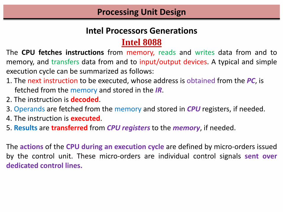
Intel Processors Generations Intel 8088
The CPU fetches instructions from memory, reads and writes data from and to memory, and transfers data from and to input/output devices. A typical and simple execution cycle can be summarized as follows: 1. The next instruction to be executed, whose address is obtained from the PC, is
fetched from the memory and stored in the IR. 2. The instruction is decoded. 3. Operands are fetched from the memory and stored in CPU registers, if needed. 4. The instruction is executed. 5. Results are transferred from CPU registers to the memory, if needed.
The actions of the CPU during an execution cycle are defined by micro-orders issued by the control unit. These micro-orders are individual control signals sent over dedicated control lines.

Processing Unit Design
Intel Processors Generations Intel 8088
For example • Let us assume that we want to execute an instruction that moves the contents of
register X to register Y. • Let us also assume that both registers are connected to the data bus, D. • The control unit will issue a control signal to tell register X to place its contents
on the data bus D. After some delay, • another control signal will be sent to tell register Y to read from data bus D. The
activation of the control signals is determined using either hardwired control or microprogramming.

Processing Unit Design
Intel Processors Generations Intel 8088
Register Set Registers are essentially extremely fast memory locations within the CPU that are used to create and store the results of CPU operations and other calculations. Different computers have different register sets. Memory Access Registers Two registers are essential in memory write and read operations: the memory data register (MDR) and memory address register (MAR). In order to perform a write operation into a specified memory location, the MDR and MAR are used as follows: 1. The word to be stored into the memory location is first loaded by the CPU into
MDR. 2. The address of the location into which the word is to be stored is loaded by the
CPU into a MAR. 3. A write signal is issued by the CPU.

Processing Unit Design
Intel Processors Generations Intel 8088
To perform a memory read operation, the MDR and MAR are used
as follows:
1. The address of the location from which the word is to be read is
loaded into the MAR.
2. A read signal is issued by the CPU.
3. The required word will be loaded by the memory into the MDR
ready for use by the CPU.
Processing Unit Design
Intel Processors Generations Intel 8088
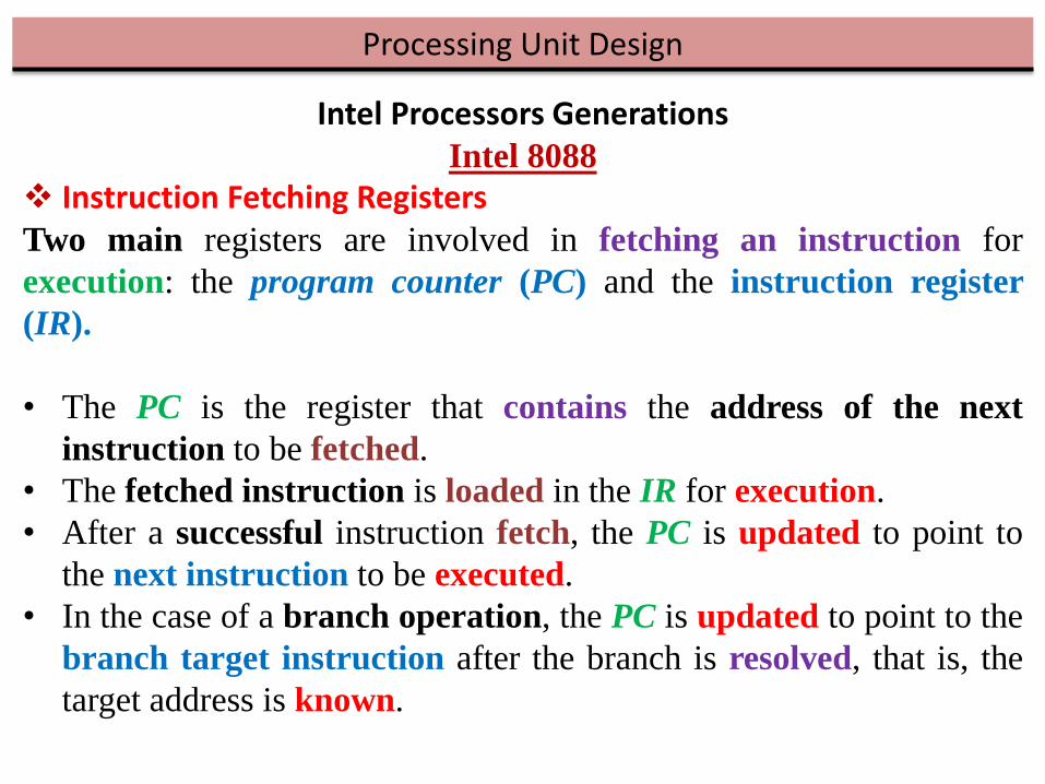
Instruction Fetching Registers Two main registers are involved in fetching an instruction for
execution: the program counter (PC) and the instruction register
(IR).
• The PC is the register that contains the address of the next
instruction to be fetched.
• The fetched instruction is loaded in the IR for execution.
• After a successful instruction fetch, the PC is updated to point to
the next instruction to be executed.
• In the case of a branch operation, the PC is updated to point to the
branch target instruction after the branch is resolved, that is, the
target address is known.

Processing Unit Design
Intel Processors Generations Intel 8088
Condition Registers
Condition registers, or flags, are used to maintain status information.
Some architectures contain a special program status word (PSW)
register.
The PSW contains bits that are set by the CPU to indicate the current
status of an executing program. These indicators are typically for
arithmetic operations, interrupts, memory protection information,
or processor status.

Processing Unit Design
Intel Processors Generations Intel 8088
Special-Purpose Address Registers
• Index Register: The index register holds an address displacement. Index addressing is indicated in the instruction by including the name of the index register in parentheses and using the symbol X to indicate the constant to be added.
• Segment Pointers: the address issued by the processor should consist of a segment number (base) and a displacement (or an offset) within the segment. A segment register holds the address of the base of the segment.
• Stack Pointer: Two specific operations can be performed on a stack. These are the Push and the Pop operations. A specific register, called the stack pointer (SP), is used to indicate the stack location that can be addressed. In the stack push operation, the SP value is used to indicate the location (called the top of the stack). After storing (pushing) this value, the SP is incremented.

Processing Unit Design
Intel Processors Generations Intel 8088
The Bus The CPU communicates with the other components via a bus.
A bus is a set of wires that acts as a shared but common data path to connect
multiple subsystems within the system. It consists of multiple lines, allowing the
parallel movement of bits.
Internal to the CPU, data move from one register to another and between ALU and
registers.
Internal data movements are performed via local buses, which may carry data,
instructions, and addresses.
Externally, data move from registers to memory and I/O devices, often by means of
a system bus.
Internal data movement among registers and between the ALU and registers may be
carried out using different organizations including one-bus, two-bus, or three-bus
organizations.

Processing Unit Design
Intel Processors Generations Intel 8088
One-Bus Organization
Using one bus, the CPU registers and the ALU use a single bus to move outgoing and
incoming data. Since a bus can handle only a single data movement within one clock
cycle, two-operand operations will need two cycles to fetch the operands for the
ALU. Additional registers may also be needed to buffer data for the ALU.
Program counter (PC) , and ALU
General Purpose Registers
Memory Bus
PC
IR
MAR
MDR
A B
ALU

Processing Unit Design
Intel Processors Generations Intel 8088
Two-Bus Organization Using two buses is a faster solution than the one-bus organization. In this case, general-purpose
registers are connected to both buses. Data can be transferred from two different registers to
the input point of the ALU at the same time. Therefore, a two-operand operation can fetch both
operands in the same clock cycle. An additional buffer register may be needed to hold the
output of the ALU when the two buses are busy carrying the two operands.
General Purpose Registers
Memory
PC
IR
MAR
MDR A
ALU
Bus 2
Bus 1

Processing Unit Design
Intel Processors Generations Intel 8088
Three-Bus Organization In a three-bus organization, two buses may be used as source buses while the third is used as
destination. The source buses move data out of registers (out-bus), and the destination bus may
move data into a register (in-bus). Each of the two out-buses is connected to an ALU input
point. The output of the ALU is connected directly to the in-bus. As can be expected, the more
buses we have, the more data we can move within a single clock cycle. However, increasing
the number of buses will also increase the complexity of the hardware.
General Purpose Registers
Memory Bus
PC
IR
MAR
MDR
ALU
Out-Bus 1
In-Bus
Out-Bus 2