TLE9015DQU - Infineon Technologies
26
TLE9015DQU iso UART transceiver IC Features • Compatibility for ring mode topology • Two UART ports for serial communication to host microcontroller • Two iso UART interfaces for communication to other BMS ICs • 2 Mbit/s data rate for fast communication • Fully transparent communication scheme from UART to iso UART • Integrated internal logic for minimizing pin count on the UART side • Differential current edge triggered iso UART communication interface • High robustness against external noise • Two external fault inputs (EMM and ERRQ_ext) • Latching error output pin for triggering external microcontroller • Internal supply monitoring • Green Product (RoHS compliant) Potential applications Multi-cell battery monitoring and balancing system IC designed for Li-ion battery packs used in hybrid electric vehicles (HEV), plug-in hybrid electric vehicles (PHEV), battery electric vehicles (BEV) as well as in 12 V Li-ion batteries. Product validation Qualified for automotive applications. Product validation according to AEC-Q100. Description The TLE9015DQU is a iso UART transceiver IC. The TLE9015DQU is a general purpose transceiver IC to be used in battery systems for enabling the communication between the main host microcontroller and the cell supervision ICs which are usually connected to the battery module potential. The IC is designed for Li-Ion battery packs used in hybrid electric vehicles (HEV), plug-in hybrid electric vehicles (PHEV), battery electric vehicles (BEV) as well as stationary Li-Ion batteries. Additionally to the physical layer translation, the TLE9015DQU offers the possibility to communicate potential detected errors in a cell inside the battery pack to the main microcontroller. Type Package Marking TLE9015DQU PG-TQFP-48 TLE9015DQU Datasheet Please read the sections "Important notice" and "Warnings" at the end of this document Rev. 1.0 www.infineon.com/battery-management-systems 2022-01-24
-
Upload
khangminh22 -
Category
Documents
-
view
5 -
download
0
Transcript of TLE9015DQU - Infineon Technologies
TLE9015DQUiso UART transceiver IC
Features• Compatibility for ring mode topology• Two UART ports for serial communication to host microcontroller• Two iso UART interfaces for communication to other BMS ICs• 2 Mbit/s data rate for fast communication• Fully transparent communication scheme from UART to iso UART• Integrated internal logic for minimizing pin count on the UART side• Differential current edge triggered iso UART communication interface• High robustness against external noise• Two external fault inputs (EMM and ERRQ_ext)• Latching error output pin for triggering external microcontroller• Internal supply monitoring• Green Product (RoHS compliant)
Potential applicationsMulti-cell battery monitoring and balancing system IC designed for Li-ion battery packs used in hybrid electricvehicles (HEV), plug-in hybrid electric vehicles (PHEV), battery electric vehicles (BEV) as well as in 12 V Li-ionbatteries.
Product validationQualified for automotive applications. Product validation according to AEC-Q100.
DescriptionThe TLE9015DQU is a iso UART transceiver IC.The TLE9015DQU is a general purpose transceiver IC to be used in battery systems for enabling thecommunication between the main host microcontroller and the cell supervision ICs which are usuallyconnected to the battery module potential. The IC is designed for Li-Ion battery packs used in hybrid electricvehicles (HEV), plug-in hybrid electric vehicles (PHEV), battery electric vehicles (BEV) as well as stationary Li-Ionbatteries.Additionally to the physical layer translation, the TLE9015DQU offers the possibility to communicate potentialdetected errors in a cell inside the battery pack to the main microcontroller.
Type Package Marking
TLE9015DQU PG-TQFP-48 TLE9015DQU
Datasheet Please read the sections "Important notice" and "Warnings" at the end of this document Rev. 1.0www.infineon.com/battery-management-systems 2022-01-24
Table of contents
Features . . . . . . . . . . . . . . . . . . . . . . . . . . . . . . . . . . . . . . . . . . . . . . . . . . . . . . . . . . . . . . . . . . . . . . . . . . . . . . . 1
Potential applications . . . . . . . . . . . . . . . . . . . . . . . . . . . . . . . . . . . . . . . . . . . . . . . . . . . . . . . . . . . . . . . . . . 1
Product validation . . . . . . . . . . . . . . . . . . . . . . . . . . . . . . . . . . . . . . . . . . . . . . . . . . . . . . . . . . . . . . . . . . . . . 1
Description . . . . . . . . . . . . . . . . . . . . . . . . . . . . . . . . . . . . . . . . . . . . . . . . . . . . . . . . . . . . . . . . . . . . . . . . . . . . 1
Table of contents . . . . . . . . . . . . . . . . . . . . . . . . . . . . . . . . . . . . . . . . . . . . . . . . . . . . . . . . . . . . . . . . . . . . . . . 2
1 Block diagram . . . . . . . . . . . . . . . . . . . . . . . . . . . . . . . . . . . . . . . . . . . . . . . . . . . . . . . . . . . . . . . . . . . . . . . . . 3
2 Pin configuration . . . . . . . . . . . . . . . . . . . . . . . . . . . . . . . . . . . . . . . . . . . . . . . . . . . . . . . . . . . . . . . . . . . . . . .42.1 Pin assignment . . . . . . . . . . . . . . . . . . . . . . . . . . . . . . . . . . . . . . . . . . . . . . . . . . . . . . . . . . . . . . . . . . . . . . . . . 42.2 Pin definitions and functions . . . . . . . . . . . . . . . . . . . . . . . . . . . . . . . . . . . . . . . . . . . . . . . . . . . . . . . . . . . . . 4
3 General product characteristics . . . . . . . . . . . . . . . . . . . . . . . . . . . . . . . . . . . . . . . . . . . . . . . . . . . . . . . . . 73.1 Absolute maximum ratings . . . . . . . . . . . . . . . . . . . . . . . . . . . . . . . . . . . . . . . . . . . . . . . . . . . . . . . . . . . . . . .73.2 Functional range . . . . . . . . . . . . . . . . . . . . . . . . . . . . . . . . . . . . . . . . . . . . . . . . . . . . . . . . . . . . . . . . . . . . . . . . 93.3 Thermal resistance . . . . . . . . . . . . . . . . . . . . . . . . . . . . . . . . . . . . . . . . . . . . . . . . . . . . . . . . . . . . . . . . . . . . . 10
4 Power Management Unit (PMU) . . . . . . . . . . . . . . . . . . . . . . . . . . . . . . . . . . . . . . . . . . . . . . . . . . . . . . . . 114.1 Functional description . . . . . . . . . . . . . . . . . . . . . . . . . . . . . . . . . . . . . . . . . . . . . . . . . . . . . . . . . . . . . . . . . .114.2 Electrical characteristics power management unit (PMU) . . . . . . . . . . . . . . . . . . . . . . . . . . . . . . . . . . 11
5 Watchdog and wake-up function (WD) . . . . . . . . . . . . . . . . . . . . . . . . . . . . . . . . . . . . . . . . . . . . . . . . . .145.1 Functional description . . . . . . . . . . . . . . . . . . . . . . . . . . . . . . . . . . . . . . . . . . . . . . . . . . . . . . . . . . . . . . . . . .145.2 Electrical characteristics watchdog and wake-up function (WD) . . . . . . . . . . . . . . . . . . . . . . . . . . . . 15
6 Communication . . . . . . . . . . . . . . . . . . . . . . . . . . . . . . . . . . . . . . . . . . . . . . . . . . . . . . . . . . . . . . . . . . . . . . . 166.1 Functional description . . . . . . . . . . . . . . . . . . . . . . . . . . . . . . . . . . . . . . . . . . . . . . . . . . . . . . . . . . . . . . . . . .166.2 Electrical characteristics communication . . . . . . . . . . . . . . . . . . . . . . . . . . . . . . . . . . . . . . . . . . . . . . . . . 17
7 Emergency mode (EMM) and ERR pin (ERR) . . . . . . . . . . . . . . . . . . . . . . . . . . . . . . . . . . . . . . . . . . . . . 197.1 Functional description . . . . . . . . . . . . . . . . . . . . . . . . . . . . . . . . . . . . . . . . . . . . . . . . . . . . . . . . . . . . . . . . . .197.2 Electrical characteristics emergency mode (EMM) and ERR pin (ERR) . . . . . . . . . . . . . . . . . . . . . . . . 19
8 Application information . . . . . . . . . . . . . . . . . . . . . . . . . . . . . . . . . . . . . . . . . . . . . . . . . . . . . . . . . . . . . . .228.1 External circuitry and components . . . . . . . . . . . . . . . . . . . . . . . . . . . . . . . . . . . . . . . . . . . . . . . . . . . . . . .22
9 Package information . . . . . . . . . . . . . . . . . . . . . . . . . . . . . . . . . . . . . . . . . . . . . . . . . . . . . . . . . . . . . . . . . . 24
Revision history . . . . . . . . . . . . . . . . . . . . . . . . . . . . . . . . . . . . . . . . . . . . . . . . . . . . . . . . . . . . . . . . . . . . . . .25
Disclaimer . . . . . . . . . . . . . . . . . . . . . . . . . . . . . . . . . . . . . . . . . . . . . . . . . . . . . . . . . . . . . . . . . . . . . . . . . . . . 26
TLE9015DQUiso UART transceiver ICTable of contents
Datasheet 2 Rev. 1.02022-01-24
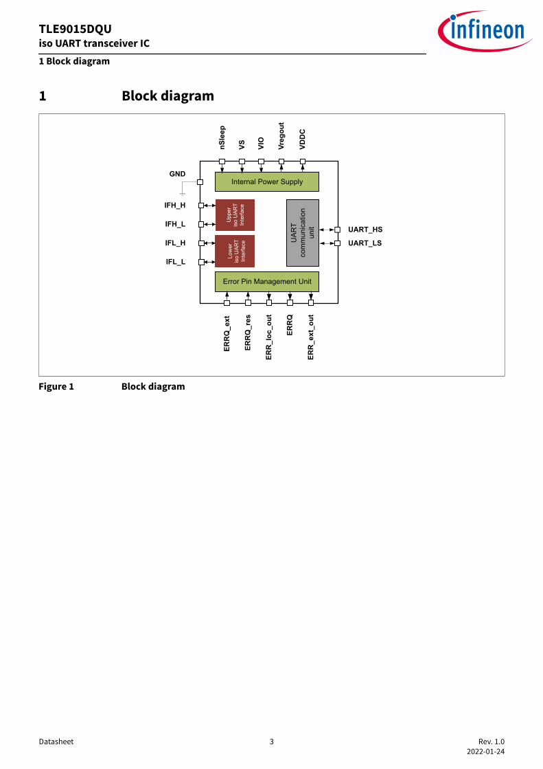
1 Block diagram
VIO
Error Pin Management Unit
IFH_L
IFH_H
Upp
er
iso
UAR
T In
terfa
ce
GND
UAR
Tco
mm
unic
atio
n un
it
UART_LS
UART_HS
IFL_L
IFL_H
Low
eris
o U
ART
Inte
rface
Internal Power Supply
ERR
Q_e
xt
ERR
_loc
_out
ERR
Q_r
es
ERR
Q
ERR
_ext
_out
VDD
C
Vreg
out
VSnSle
ep
Figure 1 Block diagram
TLE9015DQUiso UART transceiver IC1 Block diagram
Datasheet 3 Rev. 1.02022-01-24
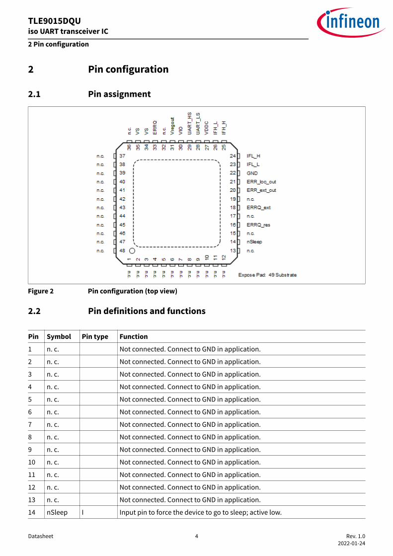
2 Pin configuration
2.1 Pin assignment
Figure 2 Pin configuration (top view)
2.2 Pin definitions and functions
Pin Symbol Pin type Function
1 n. c. Not connected. Connect to GND in application.
2 n. c. Not connected. Connect to GND in application.
3 n. c. Not connected. Connect to GND in application.
4 n. c. Not connected. Connect to GND in application.
5 n. c. Not connected. Connect to GND in application.
6 n. c. Not connected. Connect to GND in application.
7 n. c. Not connected. Connect to GND in application.
8 n. c. Not connected. Connect to GND in application.
9 n. c. Not connected. Connect to GND in application.
10 n. c. Not connected. Connect to GND in application.
11 n. c. Not connected. Connect to GND in application.
12 n. c. Not connected. Connect to GND in application.
13 n. c. Not connected. Connect to GND in application.
14 nSleep I Input pin to force the device to go to sleep; active low.
TLE9015DQUiso UART transceiver IC2 Pin configuration
Datasheet 4 Rev. 1.02022-01-24
Pin Symbol Pin type Function
15 n. c. Not connected. Connect to GND in application.
16 ERRQ_res I Reset the ERRQ pin; active low.
17 n. c. Not connected. Connect to GND in application.
18 ERRQ_ext I Input for external ERRQ. If not used, connect to VREGOUT.
19 n. c. Not connected. Connect to GND in application.
20 ERR_ext_out
O Output for external ERRQ; active high.
21 ERR_loc_out
O Output pin to indicate local ERRQ; active high.
22 GND GND Local GND of the device.
23 IFL_L D_I / O Lower isolated UART (iso UART) L pin.
24 IFL_H D_I / O Lower isolated UART (iso UART) H pin.
25 IFH_H D_I / O Upper isolated UART (iso UART) H pin.
26 IFH_L D_I / O Upper isolated UART (iso UART) L pin.
27 VDDC Supply Buffer capacitor pin for internal iso UART supply.
28 UART_LS D_I / O UART LS channel.
29 UART_HS D_I / O UART HS channel.
30 VIO S Supply for UART interface.
31 VREGOUT S Output pin for the internal regulator.
32 n.c. n.c. Not connected. Connect to GND in application.
33 ERRQ HV_D_O Error pin; open drain NMOS. This pin is latching.
34 VS S Supply pin.
35 VS S Supply pin.
36 n. c. Not connected. Connect to GND in application.
37 n. c. Not connected. Connect to GND in application.
38 n. c. Not connected. Connect to GND in application.
39 n. c. Not connected. Connect to GND in application.
40 n. c. Not connected. Connect to GND in application.
41 n. c. Not connected. Connect to GND in application.
42 n. c. Not connected. Connect to GND in application.
43 n. c. Not connected. Connect to GND in application.
44 n. c. Not connected. Connect to GND in application.
45 n. c. Not connected. Connect to GND in application.
46 n. c. Not connected. Connect to GND in application.
47 n. c. Not connected. Connect to GND in application.
48 n. c. Not connected. Connect to GND in application.
TLE9015DQUiso UART transceiver IC2 Pin configuration
Datasheet 5 Rev. 1.02022-01-24
Pin Symbol Pin type Function
49 ExposedPad
GNDA Cooling tab. Connect to GND in the application.
Pin types: A = analog, D = digital, HV = high-voltage, I = input, O = output, I/O = bidirectional, P = power, S =supply
TLE9015DQUiso UART transceiver IC2 Pin configuration
Datasheet 6 Rev. 1.02022-01-24
3 General product characteristicsWithin the functional or operating range, the IC operates as described in the circuit description. The electricalcharacteristics are specified within the conditions given in the electrical characteristics table.This thermal data was generated in accordance with JEDEC JESD51 standards. For more information, go towww.jedec.org.
3.1 Absolute maximum ratings
Table 1 Absolute maximum ratingsTj = -40°C to +150°C, all voltages with respect to GND, positive current flowing into pin (unless otherwisespecified)
Parameter Symbol Values Unit Note or condition P-NumberMin. Typ. Max.
Voltages
Supplyvoltage VS
VVS_max -0.3 – 45 V – PRQ-1368
Supplyvoltage VSrelative
VVS_rel_max VVREG
OUT -0.3
– – V – PRQ-489
Supplyvoltage VIO
VVIO_max -0.3 – 5.5 V – PRQ-488
RegulatoroutputVREGOUT
VVREGOUT_
max
-0.3 – 3.6 V – PRQ-490
Regulatoroutput VDDC
VVDDC_max -0.3 – 3.6 V Assuming IVDDC ≤ 1 mA continuous current PRQ-491
iso UARTinterfaceIFL_x
VIFL_L_max
VIFL_H_max
-4.1 – 6.6 V 1) BCI test maximum 300 mA injected viatwisted pair cable onto iso UART interface(maximum pin current 150 mA)
PRQ-493
iso UARTinterfaceIFH_x
VIFH_L_max
VIFH_H_max
-4.1 – 6.6 V 1)
BCI test maximum 300 mA injected viatwisted pair cable onto iso UART interface(maximum pin current 150 mA)
PRQ-492
Ground pinGND
VGND 0 – 0 V Absolute GND PRQ-511
High voltageinput pinnSleep
VnSleep_max -0.3 – 45 V 2) PRQ-524
(table continues...)
1 Positive and negative transients with a maximum duration of 100 ns allowed between ± 8 V; This shouldsimulate ESD events; however, during normal and steady-state condition voltage on these pins must stayinside the maximum ratings specified.
2 Not subject to production test, specified by design.
TLE9015DQUiso UART transceiver IC3 General product characteristics
Datasheet 7 Rev. 1.02022-01-24
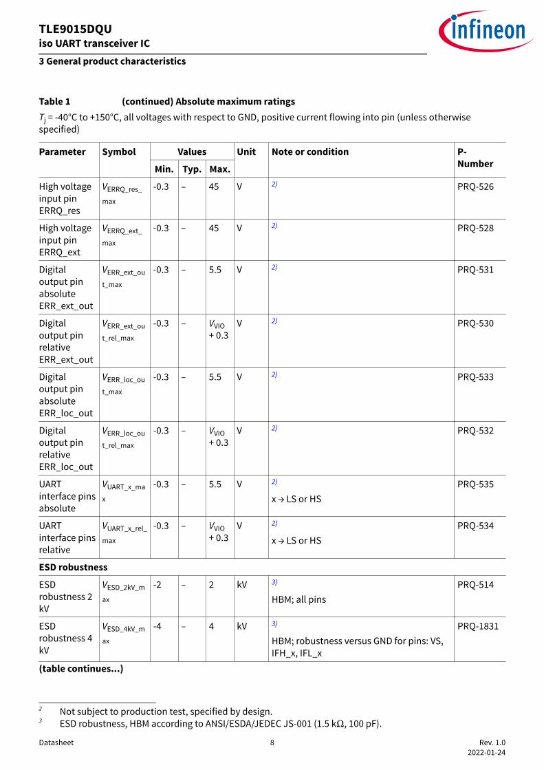
Table 1 (continued) Absolute maximum ratingsTj = -40°C to +150°C, all voltages with respect to GND, positive current flowing into pin (unless otherwisespecified)
Parameter Symbol Values Unit Note or condition P-NumberMin. Typ. Max.
High voltageinput pinERRQ_res
VERRQ_res_
max
-0.3 – 45 V 2) PRQ-526
High voltageinput pinERRQ_ext
VERRQ_ext_
max
-0.3 – 45 V 2) PRQ-528
Digitaloutput pinabsoluteERR_ext_out
VERR_ext_ou
t_max
-0.3 – 5.5 V 2) PRQ-531
Digitaloutput pinrelativeERR_ext_out
VERR_ext_ou
t_rel_max
-0.3 – VVIO + 0.3
V 2) PRQ-530
Digitaloutput pinabsoluteERR_loc_out
VERR_loc_ou
t_max
-0.3 – 5.5 V 2) PRQ-533
Digitaloutput pinrelativeERR_loc_out
VERR_loc_ou
t_rel_max
-0.3 – VVIO + 0.3
V 2) PRQ-532
UARTinterface pinsabsolute
VUART_x_ma
x
-0.3 – 5.5 V 2)
x → LS or HSPRQ-535
UARTinterface pinsrelative
VUART_x_rel_
max
-0.3 – VVIO + 0.3
V 2)
x → LS or HSPRQ-534
ESD robustness
ESDrobustness 2kV
VESD_2kV_m
ax
-2 – 2 kV 3)
HBM; all pinsPRQ-514
ESDrobustness 4kV
VESD_4kV_m
ax
-4 – 4 kV 3)
HBM; robustness versus GND for pins: VS,IFH_x, IFL_x
PRQ-1831
(table continues...)
2 Not subject to production test, specified by design.3 ESD robustness, HBM according to ANSI/ESDA/JEDEC JS-001 (1.5 kΩ, 100 pF).
TLE9015DQUiso UART transceiver IC3 General product characteristics
Datasheet 8 Rev. 1.02022-01-24
Table 1 (continued) Absolute maximum ratingsTj = -40°C to +150°C, all voltages with respect to GND, positive current flowing into pin (unless otherwisespecified)
Parameter Symbol Values Unit Note or condition P-NumberMin. Typ. Max.
ESDrobustnessCDM 500 V
VESD_cdm_al
l_max
-500 – 500 V 4)
CDM; all pinsPRQ-516
ESDrobustnessCDM 750 V
VESD_Corner
_max
-750 – 750 V 4)
CDM; corner pinsPRQ-517
Temperatures
Junctiontemperature
Tj_max -40 – 150 °C – PRQ-512
Storagetemperature
Tstg_max -55 – 150 °C – PRQ-513
Notes:1. Stresses above the ones listed here may cause permanent damage to the device. Exposure to absolutemaximum rating conditions for extended periods may affect device reliability.2. Integrated protection functions are designed to prevent IC destruction under fault conditions described in thedatasheet. Fault conditions are considered as outside normal operating range. Protection functions are notdesigned for continuous repetitive operation.
3.2 Functional range
Table 2 Functional rangeTj = -40°C to +150°C, all voltages with respect to GND, positive current flowing into pin (unless otherwisespecified)
Parameter Symbol Values Unit Note or condition P-NumberMin. Typ. Max.
Supplyvoltage VS
VVS_function
al
4.75 – 45 V – PRQ-1367
Supplyvoltage VIO
VVIO_functio
nal
3 – 5.5 V – PRQ-520
4 ESD robustness, Charged Device Model JESD22-C101.
TLE9015DQUiso UART transceiver IC3 General product characteristics
Datasheet 9 Rev. 1.02022-01-24
3.3 Thermal resistance
Table 3 Thermal resistanceVVS = VVS_functional, Tj = -40°C to +150°C, all voltages with respect to GND, positive current flowing into pin (unlessotherwise specified)
Parameter Symbol Values Unit Note or condition P-NumberMin. Typ. Max.
Junction tocase
RthJC – 20 – K/W PRQ-1846
Junction toambient
RthJA – 48 – K/W 5)
PRQ-1847
5 Specified RthJA value is according to JEDEC JESD51-5,-7 at natural convection on FR4 2s2p board; Theproduct (chip and package) was simulated on a 76.2 × 114.3 × 1.5 mm board with 2 inner copper layers(2 × 70 µm Cu, 2 × 35 µm Cu). The thermal via array under the exposed pad consists of 16 vias with adiameter of 0.3 mm and a plating thickness of 25 µm.
TLE9015DQUiso UART transceiver IC3 General product characteristics
Datasheet 10 Rev. 1.02022-01-24
4 Power Management Unit (PMU)
4.1 Functional descriptionThe transceiver IC can be powered from an external LDO via VS pin or any other source which can supply thevoltage VVS.To supply the communication interface, the device provides a regulated output voltage VVDDC on pin VDDC.The device provides a regulated output voltage VVREGOUT with an output current IVREGOUT on pin VREGOUT whichcan supply the GPIOs of the device or other loads.The voltage at the VIO pin sets the logic levels and supplies the GPIOs. The pin can be connected directly to theVREGOUT pin or to another desired voltage level using an external regulator.
IC enters sleep mode
IVREGOUT
IVREGOUT_th_OC
VVDDC
VVDDC_th_UV
deglitch tPS_fault_Deg
deglitch tPS_fault_Deg
VVIO
VVIO_th_UV
UART interface is deactivated
deglitch(tPS_fault_deg)
Figure 3 Power supply monitoring
The IC is forced to go to sleep mode via the nSleep pin. The pin is edge triggered from "high" to "low" and hasan internal pull-up resistor RnSleep_PU.
4.2 Electrical characteristics power management unit (PMU)
Table 4 Electrical characteristicsVVS = VVS_functional, Tj = -40°C to +150°C, all voltages with respect to GND, positive current flowing into pin (unlessotherwise specified)
Parameter Symbol Values Unit Note or condition P-NumberMin. Typ. Max.
Internal regulators
VREGOUTinternalregulatoroutputvoltage
VVREGOUT 3.3 3.45 3.6 V – PRQ-544
VDDC outputvoltage
VVDDC 2.42 2.5 2.63 V – PRQ-549
(table continues...)
TLE9015DQUiso UART transceiver IC4 Power Management Unit (PMU)
Datasheet 11 Rev. 1.02022-01-24
Table 4 (continued) Electrical characteristicsVVS = VVS_functional, Tj = -40°C to +150°C, all voltages with respect to GND, positive current flowing into pin (unlessotherwise specified)
Parameter Symbol Values Unit Note or condition P-NumberMin. Typ. Max.
Supply currents
VS sleepmode current
IVS_sleep – 3 23 µA 1. typical value Tj = 25°C2. -40°C < Tj < 50°C
PRQ-1341
VS idlecurrent
IVS_idle – 4.9 6.5 mA IC in idle mode PRQ-557
VREGOUTcurrentconsumptionmultipurposesupply
IVREGOUT – – 5 mA No load on VIO PRQ-1373
VIO currentconsumptionduring UARTcommunication
IVIO_comm – – 5 mA No load on VREGOUT PRQ-695
VS currentconsumptionduringcommunication
IVS_comm – IVS_idl
e_typ
+ 0.9
IVS_idl
e_max+ 1.2
mA • UART communication. • Current to charge external interface
components not included.
PRQ-694
VS currentconsumptionduring isoUARTcommunication includingexternalinterfacecomponents
IVS_comm_is
oU
– – IVS_co
mm +7.6
mA 6)
1. Cser = 1 nF2. BRiso_U = 2 Mbit/s3. Rser = 39 Ω4. CisoUART_F = 220 pF5. Valid for one iso UART interface in
TX mode
PRQ-562
Protection and Detection
VREGOUTovercurrentthreshold
IVREGOUT_th
_OC
31 40 60 mA Tested during idle mode PRQ-545
VIOundervoltagethresholdfalling
VVIO_th_UV_f
all
2.2 – 2.76 V – PRQ-546
(table continues...)
6 Not subject to production test; verified by design or characterization.
TLE9015DQUiso UART transceiver IC4 Power Management Unit (PMU)
Datasheet 12 Rev. 1.02022-01-24
Table 4 (continued) Electrical characteristicsVVS = VVS_functional, Tj = -40°C to +150°C, all voltages with respect to GND, positive current flowing into pin (unlessotherwise specified)
Parameter Symbol Values Unit Note or condition P-NumberMin. Typ. Max.
VIOundervoltagethresholdrising
VVIO_th_UV_r
ise
2.24 – 2.9 V – PRQ-547
VIOundervoltagethresholdhysteresis
VVIO_th_UV_
hys
40 100 160 mV – PRQ-548
VDDCundervoltagethreshold
VVDDC_th_U
V
2.15 – 2.42 V – PRQ-550
VDDCundervoltagethresholdhysteresis
VVDDC_th_U
V_hys
80 100 140 mV – PRQ-551
Power supplyerrordetectiondeglitch time
tPS_ERR_deg 8 15 24 µs 6) PRQ-552
nSleep pin
nSleep inputrange voltage"low"
VnSleep_LOW 0 – 0.99 V – PRQ-690
nSleep inputrange voltage"high"
VnSleep_HIG
H
2.52 – VVS V – PRQ-691
nSleepinternal pullup resistor
RnSleep_PU 200 300 400 kΩ connected to an internal 3.3 V supply PRQ-692
nSleep inputdeglitch
tnSleep_degli
tch
19.85
21.82
24 us 6) PRQ-693
6 Not subject to production test; verified by design or characterization.
TLE9015DQUiso UART transceiver IC4 Power Management Unit (PMU)
Datasheet 13 Rev. 1.02022-01-24
5 Watchdog and wake-up function (WD)
5.1 Functional descriptionThe IC generates the wake-up pattern on: • IFL, if the IC received a valid wake-up pattern on interface UART_HS.
- (1) indicates the source of wake-up, (2) indicates the propagation on IFL_x- Ring mode: (5) indicates propagated wake-up signal received on IFH_x and (6) forwarded to UART_LS.
• IFH, if the IC received a valid wake-up pattern on interface UART_LS.- (3) indicates the source of wake-up, (4) indicates the propagation on IFH_x
Transceiver IC
Sleep modeRX
UART_LS
UART_HSIFL_L
IFL_H
IFH_L
IFH_H RX
Transceiver IC
TX – RXDirection set
RX - TX Direction set
RX
RX
UART_LS
UART_HSIFL_L
IFL_H
IFH_L
IFH_H
TX
RX
RX
RX
Transceiver IC
TX – RXDirection set
RX- TX Dircetion setRX
UART_LS
UART_HSIFL_L
IFL_H
IFH_L
IFH_H RX
Transceiver IC
TX - RX Direction set
RX- TX Dircetion set
TX
RX
UART_LS
UART_HSIFL_L
IFL_H
IFH_L
IFH_H
TX
RX
TX
TX
Primary on Top Ring Mode (direction PoT)
Transceiver IC
Sleep modeRX
UART_LS
UART_HSIFL_L
IFL_H
IFH_L
IFH_H RX
Transceiver IC
RX - TX Dircetion set
TX – RXDirection set
RX
RX
UART_LS
UART_HSIFL_L
IFL_H
IFH_L
IFH_H
RX
TX
RX
RX
Primary on Bottom
Transceiver IC
Sleep modeRX
UART_LS
UART_HSIFL_L
IFL_H
IFH_L
IFH_H RX
Transceiver IC
TX – RXDirection set
RX- TX Dircetion set
RX
RX
UART_LS
UART_HSIFL_L
IFL_H
IFH_L
IFH_H
TX
RX
RX
RX
(1)
(2)
(3)
(4)
(1)
(2)
(5)
(6)
Figure 4 Wake-up signal propagation
TLE9015DQUiso UART transceiver IC5 Watchdog and wake-up function (WD)
Datasheet 14 Rev. 1.02022-01-24
5.2 Electrical characteristics watchdog and wake-up function (WD)
Table 5 Electrical characteristicsVVS = VVS_functional, Tj = -40°C to +150°C, all voltages with respect to GND, positive current flowing into pin (unlessotherwise specified)
Parameter Symbol Values Unit Note or condition P-NumberMin. Typ. Max.
Wake-up function
WD wake-upsignalfrequency
fWAKEUP 48 50 1040 kHz – PRQ-572
WD devicewake-uptime
tWAKE 200 370 500 µs 48 kHz wake-up frequency.From the first falling edge of the inputpattern to the first edge of the propagatedwake-up sequence.
PRQ-573
WD wake-up- number ofdetectedperiods
nWAKE_det 4 – 8 periods
– PRQ-574
WD wake-uppropagation -length inperiods
nWAKE 8 – 8 periods
– PRQ-575
TLE9015DQUiso UART transceiver IC5 Watchdog and wake-up function (WD)
Datasheet 15 Rev. 1.02022-01-24
6 Communication
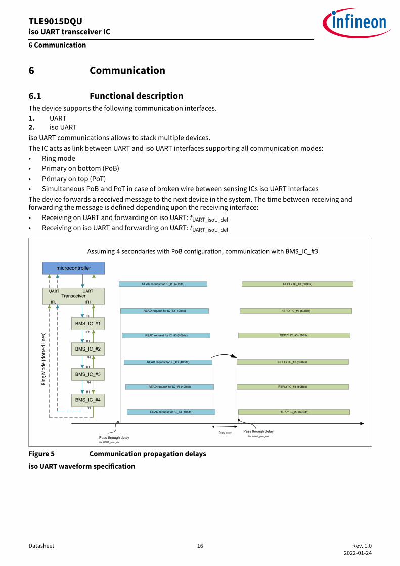
6.1 Functional descriptionThe device supports the following communication interfaces.1. UART2. iso UARTiso UART communications allows to stack multiple devices.The IC acts as link between UART and iso UART interfaces supporting all communication modes:• Ring mode • Primary on bottom (PoB)• Primary on top (PoT)• Simultaneous PoB and PoT in case of broken wire between sensing ICs iso UART interfacesThe device forwards a received message to the next device in the system. The time between receiving andforwarding the message is defined depending upon the receiving interface:• Receiving on UART and forwarding on iso UART: tUART_isoU_del• Receiving on iso UART and forwarding on UART: tUART_isoU_del
READ request for IC_#3 (40bits)
BMS_IC_#1
microcontroller
Transceiver
BMS_IC_#2
BMS_IC_#3
BMS_IC_#4
treply_delay
Pass through delay tisoUART_prop_del
REPLY IC_#3 (50Bits)
READ request for IC_#3 (40bits)
READ request for IC_#3 (40bits)
READ request for IC_#3 (40bits)
READ request for IC_#3 (40bits)
READ request for IC_#3 (40bits) REPLY IC_#3 (50Bits)
REPLY IC_#3 (50Bits)
REPLY IC_#3 (50Bits)
REPLY IC_#3 (50Bits)
Pass through delay tisoUART_prop_del
IFL IFH
UARTUART
IFL
IFH
IFL
IFH
IFL
IFH
IFL
IFH
Assuming 4 secondaries with PoB configuration, communication with BMS_IC_#3
Ring
Mod
e (d
otte
d lin
es)
REPLY IC_#3 (50Bits)
Figure 5 Communication propagation delays
iso UART waveform specification
TLE9015DQUiso UART transceiver IC6 Communication
Datasheet 16 Rev. 1.02022-01-24
0.001
0.002
0.003
0.004
0.005
0.006
0.007
0.008
0.009
1.00E-08 2.00E-08 3.00E-08 4.00E-08 5.00E-08 6.00E-08 7.00E-08 8.00E-08 9.00E-08 1.00E-07
i odin
A
tpulse in s
Overdrive current
Pulse correctly detected
Pulse not detected
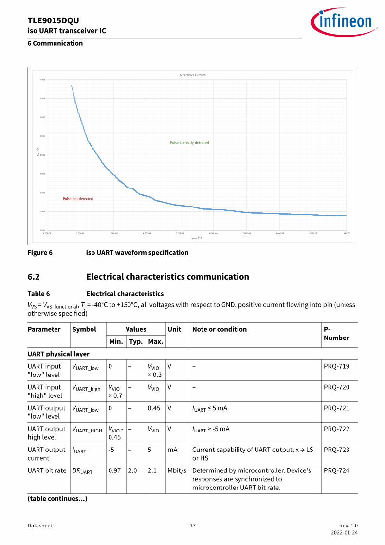
Figure 6 iso UART waveform specification
6.2 Electrical characteristics communication
Table 6 Electrical characteristicsVVS = VVS_functional, Tj = -40°C to +150°C, all voltages with respect to GND, positive current flowing into pin (unlessotherwise specified)
Parameter Symbol Values Unit Note or condition P-NumberMin. Typ. Max.
UART physical layer
UART input"low" level
VUART_low 0 – VVIO × 0.3
V – PRQ-719
UART input"high" level
VUART_high VVIO × 0.7
– VVIO V – PRQ-720
UART output"low" level
VUART_low 0 – 0.45 V IUART ≤ 5 mA PRQ-721
UART outputhigh level
VUART_HIGH VVIO -0.45
– VVIO V IUART ≥ -5 mA PRQ-722
UART outputcurrent
IUART -5 – 5 mA Current capability of UART output; x → LSor HS
PRQ-723
UART bit rate BRUART 0.97 2.0 2.1 Mbit/s Determined by microcontroller. Device'sresponses are synchronized tomicrocontroller UART bit rate.
PRQ-724
(table continues...)
TLE9015DQUiso UART transceiver IC6 Communication
Datasheet 17 Rev. 1.02022-01-24
Table 6 (continued) Electrical characteristicsVVS = VVS_functional, Tj = -40°C to +150°C, all voltages with respect to GND, positive current flowing into pin (unlessotherwise specified)
Parameter Symbol Values Unit Note or condition P-NumberMin. Typ. Max.
Externalcapacitanceon UART pin
CUART_ext – – 30 pF – PRQ-725
UART to isoUARTpropagationdelay
tUART_isoU_
del
– 25 70 ns Propagation delay from UART to iso UART PRQ-828
iso UARTcurrentthreshold"high"
IisoU_th_high 2.25 4.5 6.5 mA (IIFx_H - IIFx_L) / 2IIFx_H: Current in the iso UART high pinIIFx_L: Current in the iso UART low pin
PRQ-832
iso UARTcurrentthreshold"low"
IisoU_th_low -6.5 -4.5 -2.25 mA (IIFx_H - IIFx_L) / 2IIFx_H: Current in the iso UART high pinIIFx_L: Current in the iso UART low pin
PRQ-833
iso UARTpropagationdelay
tisoU_prop_d
el
– 25 70 ns 7) Propagation delay from IFH to IFL and IFLto IFH
PRQ-834
iso UARToverdrivecurrent
Iod 3 – – mA 8)
with tpulse = 38 nsPRQ-1370
Reply delaytime
treply_delay 0 1.7 3 μs 8)
internal reply delay time of one ICPRQ-837
iso UART bitrate
BRisoU 0.97 2 2.1 Mbit/s – PRQ-838
Seriesresistor value
Rser 37.05
39 40.95
Ω 8) 9) PRQ-836
Seriescapacitorvalue
Cser 0.95 1 1.05 nF 8) 9) PRQ-835
TransceiverRon @100mA
RON 19 22 27 Ω – PRQ-1845
7 Tested with standard external circuit (Cser, Rser).8 Not subject to production test; verified by design or characterization.9 External RC network needs to be adjusted depending on the application constraints, for example cable
length.
TLE9015DQUiso UART transceiver IC6 Communication
Datasheet 18 Rev. 1.02022-01-24
7 Emergency mode (EMM) and ERR pin (ERR)
7.1 Functional descriptionThe following events trigger the ERRQ pin:• Incoming emergency mode signal (EMM) via iso UART interface• Fault input pin ERRQ_extThe emergency signal is an alternating signal with the frequency fEMM. In case of an incoming EMM signal, the ICenters EMM and starts the fault handling.The EMM signal has a duration of nEMM periods. The number of periods the IC needs to detect an EMM signal isdepending on the operation mode:1. Idle mode: nEMM_dect2. Straight after wake-up caused by EMM: nEMM_dect_wake-up
The output of the ERRQ pin is open drain. The "low" state is latching and can be reset by the ERRQ_res pin. The ERR_loc_out pin indicates, whether an incoming EMM signal triggered the error handling procedure. Ondetection of an EMM signal, the device sets the ERR_loc_out pin "high" for the duration of tERR_loc_out. The logiclevels of the pin are VIO and GND.The ERR_ext_out pin is an output pin. It indicates that the fault was triggered by the ERRQ_ext pin andrepresents the deglitched and inverted ERRQ_ext signal. The pin is active high and the logic levels are VIO andGND.The ERRQ_ext pin is an input pin to trigger the ERRQ pin externally. The pin is level triggered active low witha deglitch time of tERRQ_ext_deglitch. The pin has an internal pull-up resistor RERRQ_ext_PU to the internal 3.3 Vsupply implemented.The ERRQ_res pin is the input pin to reset the ERRQ pin function. The pin is level triggered active low. The pinhas an internal pull-up resistor RERRQ_res_PU to the internal 3.3 V supply implemented and includes a deglitchfilter with deglitch time defined by tERRQ_res_deglitch.
7.2 Electrical characteristics emergency mode (EMM) and ERR pin (ERR)
Table 7 Electrical characteristicsVVS = VVS_functional, Tj = -40°C to +150°C, all voltages with respect to GND, positive current flowing into pin (unlessotherwise specified)
Parameter Symbol Values Unit Note or condition P-NumberMin. Typ. Max.
EMM numberof periods todetect EMMsignal -straight afterwake-up
nEMM_dect_
wake-up
4 – 4 periods
10)
IC just entered IDLE state straight afterwake-up procedure.
PRQ-739
EMM numberof periods todetect EMMsignal - idlemode
nEMM_dect 16 – 16 periods
10)
IC is in idle modePRQ-741
(table continues...)
10 Not subject to production test; verified by design or characterization.
TLE9015DQUiso UART transceiver IC7 Emergency mode (EMM) and ERR pin (ERR)
Datasheet 19 Rev. 1.02022-01-24
Table 7 (continued) Electrical characteristicsVVS = VVS_functional, Tj = -40°C to +150°C, all voltages with respect to GND, positive current flowing into pin (unlessotherwise specified)
Parameter Symbol Values Unit Note or condition P-NumberMin. Typ. Max.
ERRQ pins
ERRQfunctionalvoltage range
VERRQ 4.75 – VVS V VVS ≤ 20 V PRQ-718
ERRQactivatedoutputvoltage
VERRQ_low 0 – 0.3 V IERRQ ≤ 1.5 mA PRQ-717
ERRQ sinkcurrent
IERRQ – – 1.5 mA 10) PRQ-1340
ERRQ_resinput voltagerange "low"
VERRQ_res_l
ow
0 – 0.99 V – PRQ-704
ERRQ_resinput voltagerange "high"
VERRQ_res_h
igh
2.52 – VVS V – PRQ-705
ERRQ_extinput voltagerange "low"
VERRQ_ext_l
ow
0 – 0.99 V – PRQ-706
ERRQ_extinput voltagerange "high"
VERRQ_ext_h
igh
2.52 – VVS V – PRQ-707
ERR_loc_outoutputvoltage
VERR_loc_ou
t_low
0 – 0.45 V IERR_loc_out ≤ 5 mA PRQ-708
ERR_loc_outoutputvoltage"high"
VERR_loc_ou
t_high
VVIO -0.45
– VVIO V IERR_loc_out ≥ -5 mA PRQ-709
ERR_ext_outoutputvoltage "low"
VERR_ext_ou
t_low
0 – 0.45 V IERR_ext_out ≤ 5 mA PRQ-710
ERR_ext_outoutputvoltage high
VERR_ext_ou
t_high
VVIO -0.45
– VVIO V IERR_ext_out ≥ -5 mA PRQ-711
(table continues...)
10 Not subject to production test; verified by design or characterization.
TLE9015DQUiso UART transceiver IC7 Emergency mode (EMM) and ERR pin (ERR)
Datasheet 20 Rev. 1.02022-01-24
Table 7 (continued) Electrical characteristicsVVS = VVS_functional, Tj = -40°C to +150°C, all voltages with respect to GND, positive current flowing into pin (unlessotherwise specified)
Parameter Symbol Values Unit Note or condition P-NumberMin. Typ. Max.
ERRQ_extinternal pull-up resistor
RERRQ_ext_p
u
200 300 400 kΩ Connected to an internal 3.3 V supply PRQ-712
ERRQ_resinternal pull-up resistor
RERRQ_res_p
u
200 300 400 kΩ Connected to an internal 3.3 V supply PRQ-713
ERRQ_extinputdeglitch
tERRQ_ext_d
eglitch
47.26
49.74
52.42
ms 10) PRQ-714
ERRQ_resinputdeglitch
tERRQ_res_d
eglitch
844 951 1067 µs 10) PRQ-715
ERR_loc_outactive time
tERR_loc_out 281.32
293.74
307.2
ms 10) PRQ-716
10 Not subject to production test; verified by design or characterization.
TLE9015DQUiso UART transceiver IC7 Emergency mode (EMM) and ERR pin (ERR)
Datasheet 21 Rev. 1.02022-01-24
8 Application information
8.1 External circuitry and components
Communication
Other supporting componentsOther supporting components
Communication
Transceiver IC35
34
25
VDDC
Vregout
VS
RUART
Transceiver
HS_TXHS_RX
RUART LS_TXLS_RX
GND22
CVDDC CVREGOUT
31
30
27
IFH_H
IFH_L
UART_HS
UART_LS
29
28
26
RSER
CSER
RSER
CSER
24IFL_H
IFL_L 23
RSER
CSER
RSER
CSER
RN
RN
L
RN
L
RN
CVIO
VS-IN
CVS
VS RVS
VIO
VDDD
Only needed for ring communication on system level (optional)
Only needed for ring communication on system level
(Optional)
14
16
20
ERRQ_res
ERR_ext_out
21
ERRQ
21
ERR_loc_out
18
ERRQ_ext
nSleep
RERR
VDDC
Connected to host controller
CisoUART_F
CisoUART_F
CisoUART_F
CisoUART_F
Figure 7 External circuitry transceiver IC
Table 8 External components
Buffer capacitor VS CVS 100 nF
Filtering resistor VS RVS 5.1 Ω
Buffer capacitor onVREGOUT
CVREGOUT 100 nF
Buffer capacitor onVIO
CVIO 100 nF If VIO is connectedto VREGOUT,then CVIO is omitted.
Buffer capacitor onVDDC
CVDDC 330 nF
Bypass capacitor oniso UART
CisoUART_F 220 pF
(table continues...)
TLE9015DQUiso UART transceiver IC8 Application information
Datasheet 22 Rev. 1.02022-01-24
Table 8 (continued) External components
Damping resistor RN 1 kΩ WithPulse HM2116ANLtransformer
UART network RUART 1 kΩ τ ≤ 50 ns
Transformer L – – Transformer L fromPulse HM2116ANL.
TLE9015DQUiso UART transceiver IC8 Application information
Datasheet 23 Rev. 1.02022-01-24
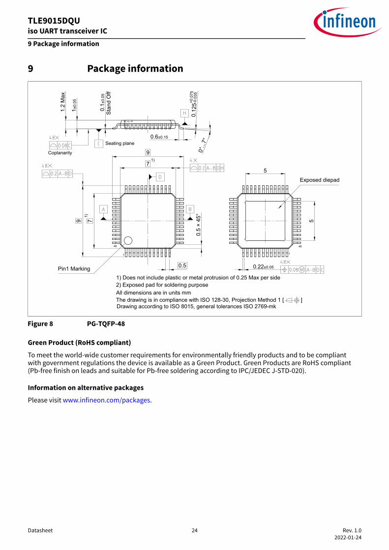
9 Package information
1
4848
1
The drawing is in compliance with ISO 128-30, Projection Method 1 [ ]
All dimensions are in units mm
9
7
79
5
5
1±0.05
1.2 M
ax
0.6±0.15
0.1
±0.05
0.5 ×
45°
1)
1)
1) Does not include plastic or metal protrusion of 0.25 Max per side
Exposed diepad
Stand O
ff
0
°
.
.
.
7
°
0.125
+0.075
-0.035
0.5
0.22±0.05
Pin1 Marking
Seating plane
Coplanarity
2) Exposed pad for soldering purpose
Drawing according to ISO 8015, general tolerances ISO 2769-mk
Figure 8 PG-TQFP-48
Green Product (RoHS compliant)
To meet the world-wide customer requirements for environmentally friendly products and to be compliantwith government regulations the device is available as a Green Product. Green Products are RoHS compliant(Pb-free finish on leads and suitable for Pb-free soldering according to IPC/JEDEC J-STD-020).
Information on alternative packages
Please visit www.infineon.com/packages.
TLE9015DQUiso UART transceiver IC9 Package information
Datasheet 24 Rev. 1.02022-01-24
Revision historyRevision Date Changes
1.0 2022-01-24 Initial release of datasheet
TLE9015DQUiso UART transceiver ICRevision history
Datasheet 25 Rev. 1.02022-01-24
TrademarksAll referenced product or service names and trademarks are the property of their respective owners.
Edition 2022-01-24Published byInfineon Technologies AG81726 Munich, Germany © 2022 Infineon Technologies AGAll Rights Reserved. Do you have a question about anyaspect of this document?Email: [email protected] Document referenceIFX-Z8F80064981
IMPORTANT NOTICEThe information given in this document shall in noevent be regarded as a guarantee of conditions orcharacteristics (“Beschaffenheitsgarantie”).With respect to any examples, hints or any typicalvalues stated herein and/or any information regardingthe application of the product, Infineon Technologieshereby disclaims any and all warranties and liabilitiesof any kind, including without limitation warranties ofnon-infringement of intellectual property rights of anythird party.In addition, any information given in this document issubject to customer’s compliance with its obligationsstated in this document and any applicable legalrequirements, norms and standards concerningcustomer’s products and any use of the product ofInfineon Technologies in customer’s applications.The data contained in this document is exclusivelyintended for technically trained staff. It is theresponsibility of customer’s technical departments toevaluate the suitability of the product for the intendedapplication and the completeness of the productinformation given in this document with respect to suchapplication.
WARNINGSDue to technical requirements products may containdangerous substances. For information on the typesin question please contact your nearest InfineonTechnologies office.Except as otherwise explicitly approved by InfineonTechnologies in a written document signed byauthorized representatives of Infineon Technologies,Infineon Technologies’ products may not be used inany applications where a failure of the product orany consequences of the use thereof can reasonablybe expected to result in personal injury.