CY8CKIT-062-BLE PSoC 6 BLE Pioneer Kit Guide - Infineon ...
66
www.infineon.com Please note that Cypress is an Infineon Technologies Company. The document following this cover page is marked as “Cypress” document as this is the company that originally developed the product. Please note that Infineon will continue to offer the product to new and existing customers as part of the Infineon product portfolio. Continuity of document content The fact that Infineon offers the following product as part of the Infineon product portfolio does not lead to any changes to this document. Future revisions will occur when appropriate, and any changes will be set out on the document history page. Continuity of ordering part numbers Infineon continues to support existing part numbers. Please continue to use the ordering part numbers listed in the datasheet for ordering.
-
Upload
khangminh22 -
Category
Documents
-
view
1 -
download
0
Transcript of CY8CKIT-062-BLE PSoC 6 BLE Pioneer Kit Guide - Infineon ...
www.infineon.com
Please note that Cypress is an Infineon Technologies Company.The document following this cover page is marked as “Cypress” document as this is the company that originally developed the product. Please note that Infineon will continue to offer the product to new and existing customers as part of the Infineon product portfolio.
Continuity of document contentThe fact that Infineon offers the following product as part of the Infineon product portfolio does not lead to any changes to this document. Future revisions will occur when appropriate, and any changes will be set out on the document history page.
Continuity of ordering part numbersInfineon continues to support existing part numbers. Please continue to use the ordering part numbers listed in the datasheet for ordering.
CY8CKIT-062-BLE
PSoC 6 BLE Pioneer Kit Guide
Document Number. 002-17040 Rev. *K
Cypress Semiconductor198 Champion Court
San Jose, CA 95134-1709www.cypress.com
Copyrights
CY8CKIT-062-BLE PSoC 6 BLE Pioneer Kit Guide, Document Number. 002-17040 Rev. *K 2
Copyrights
© Cypress Semiconductor Corporation, 2017–2020. This document is the property of Cypress Semiconductor Corporationand its subsidiaries (“Cypress”). This document, including any software or firmware included or referenced in this document(“Software”), is owned by Cypress under the intellectual property laws and treaties of the United States and other countriesworldwide. Cypress reserves all rights under such laws and treaties and does not, except as specifically stated in thisparagraph, grant any license under its patents, copyrights, trademarks, or other intellectual property rights. If the Software isnot accompanied by a license agreement and you do not otherwise have a written agreement with Cypress governing the useof the Software, then Cypress hereby grants you a personal, non-exclusive, nontransferable license (without the right tosublicense) (1) under its copyright rights in the Software (a) for Software provided in source code form, to modify andreproduce the Software solely for use with Cypress hardware products, only internally within your organization, and (b) todistribute the Software in binary code form externally to end users (either directly or indirectly through resellers anddistributors), solely for use on Cypress hardware product units, and (2) under those claims of Cypress’s patents that areinfringed by the Software (as provided by Cypress, unmodified) to make, use, distribute, and import the Software solely foruse with Cypress hardware products. Any other use, reproduction, modification, translation, or compilation of the Software isprohibited.
TO THE EXTENT PERMITTED BY APPLICABLE LAW, CYPRESS MAKES NO WARRANTY OF ANY KIND, EXPRESS ORIMPLIED, WITH REGARD TO THIS DOCUMENT OR ANY SOFTWARE OR ACCOMPANYING HARDWARE, INCLUDING,BUT NOT LIMITED TO, THE IMPLIED WARRANTIES OF MERCHANTABILITY AND FITNESS FOR A PARTICULARPURPOSE. No computing device can be absolutely secure. Therefore, despite security measures implemented in Cypresshardware or software products, Cypress shall have no liability arising out of any security breach, such as unauthorizedaccess to or use of a Cypress product. CYPRESS DOES NOT REPRESENT, WARRANT, OR GUARANTEE THATCYPRESS PRODUCTS, OR SYSTEMS CREATED USING CYPRESS PRODUCTS, WILL BE FREE FROM CORRUPTION,ATTACK, VIRUSES, INTERFERENCE, HACKING, DATA LOSS OR THEFT, OR OTHER SECURITY INTRUSION(collectively, “Security Breach”). Cypress disclaims any liability relating to any Security Breach, and you shall and hereby dorelease Cypress from any claim, damage, or other liability arising from any Security Breach. In addition, the productsdescribed in these materials may contain design defects or errors known as errata which may cause the product to deviatefrom published specifications. To the extent permitted by applicable law, Cypress reserves the right to make changes to thisdocument without further notice. Cypress does not assume any liability arising out of the application or use of any product orcircuit described in this document. Any information provided in this document, including any sample design information orprogramming code, is provided only for reference purposes. It is the responsibility of the user of this document to properlydesign, program, and test the functionality and safety of any application made of this information and any resulting product.“High-Risk Device” means any device or system whose failure could cause personal injury, death, or property damage.Examples of High-Risk Devices are weapons, nuclear installations, surgical implants, and other medical devices. “CriticalComponent” means any component of a High-Risk Device whose failure to perform can be reasonably expected to cause,directly or indirectly, the failure of the High-Risk Device, or to affect its safety or effectiveness. Cypress is not liable, in wholeor in part, and you shall and hereby do release Cypress from any claim, damage, or other liability arising from any use of aCypress product as a Critical Component in a High-Risk Device. You shall indemnify and hold Cypress, its directors, officers,employees, agents, affiliates, distributors, and assigns harmless from and against all claims, costs, damages, and expenses,arising out of any claim, including claims for product liability, personal injury or death, or property damage arising from anyuse of a Cypress product as a Critical Component in a High-Risk Device. Cypress products are not intended or authorized foruse as a Critical Component in any High-Risk Device except to the limited extent that (i) Cypress’s published data sheet forthe product explicitly states Cypress has qualified the product for use in a specific High-Risk Device, or (ii) Cypress has givenyou advance written authorization to use the product as a Critical Component in the specific High-Risk Device and you havesigned a separate indemnification agreement.
Cypress, the Cypress logo, Spansion, the Spansion logo, and combinations thereof, WICED, PSoC, CapSense, EZ-USB, F-RAM, and Traveo are trademarks or registered trademarks of Cypress in the United States and other countries. For a morecomplete list of Cypress trademarks, visit cypress.com. Other names and brands may be claimed as property of theirrespective owners.
CY8CKIT-062-BLE PSoC 6 BLE Pioneer Kit Guide, Document Number. 002-17040 Rev. *K 3
Contents
Safety and Regulatory Compliance Information 5
1. Introduction 81.1 Kit Contents .................................................................................................................81.2 Board Details ...............................................................................................................91.3 PSoC Creator ............................................................................................................20
1.3.1 PSoC Creator Code Examples ......................................................................211.3.2 Kit Code Examples.........................................................................................211.3.3 PSoC Creator Help ........................................................................................21
1.4 Getting Started...........................................................................................................221.5 Additional Learning Resources..................................................................................221.6 Technical Support......................................................................................................221.7 Documentation Conventions......................................................................................221.8 Acronyms...................................................................................................................23
2. Software Installation 252.1 Before You Begin.......................................................................................................252.2 Install Software ..........................................................................................................25
3. Kit Operation 28
3.1 Theory of Operation...................................................................................................283.1.1 CY8CKIT-028-EPD E-INK Display Shield ......................................................34
3.2 KitProg2 .....................................................................................................................353.2.1 Programming and Debugging using PSoC Creator .......................................353.2.2 Programming using PSoC Programmer.........................................................363.2.3 Mass Storage Programmer ............................................................................363.2.4 USB-UART Bridge..........................................................................................363.2.5 USB-I2C Bridge..............................................................................................373.2.6 USB-SPI Bridge .............................................................................................37
3.3 EZPD CCG3 Type-C Power Delivery ........................................................................38
4. Code Examples 40
4.1 Using the Kit Code Examples ....................................................................................404.2 Code Examples .........................................................................................................42
A. Appendix 43A.1 Schematics ................................................................................................................43A.2 Hardware Functional Description...............................................................................43
A.2.1 PSoC 6 MCU (U1)..........................................................................................43A.2.2 PSoC 5LP (U2) ..............................................................................................43A.2.3 Serial Interconnection between PSoC 5LP and PSoC 6 MCU ......................44
CY8CKIT-062-BLE PSoC 6 BLE Pioneer Kit Guide, Document Number. 002-17040 Rev. *K 4
Contents
A.2.4 EZ-PD CCG3 Power Delivery System ...........................................................45A.2.5 Power Supply System ....................................................................................46A.2.6 Expansion Connectors ...................................................................................49A.2.7 CapSense Circuit ...........................................................................................50A.2.8 LEDs ..............................................................................................................50A.2.9 Push Buttons..................................................................................................51A.2.10 Cypress NOR Flash .......................................................................................51A.2.11 Cypress Ferroelectric RAM (F-RAM) .............................................................52A.2.12 Crystal Oscillators ..........................................................................................52
A.3 PSoC 6 BLE Pioneer Board Rework .........................................................................53A.3.1 Bypassing protection circuit on PSoC 6 MCU Program
and Debug Header (J11)................................................................................53A.3.2 PSoC 6 MCU User Button (SW2) ..................................................................54A.3.3 CapSense Shield ...........................................................................................54A.3.4 CSH................................................................................................................55A.3.5 U.FL ...............................................................................................................55A.3.6 LiPo Battery Charger......................................................................................56A.3.7 Multiplexed GPIOs .........................................................................................56
A.4 Bill of Materials ..........................................................................................................57A.5 Frequently Asked Questions......................................................................................57
Revision History 63
CY8CKIT-062-BLE PSoC 6 BLE Pioneer Kit Guide, Document Number. 002-17040 Rev. *K 5
Safety and Regulatory Compliance Information
The CY8CKIT-062-BLE PSoC 6 BLE Pioneer Kit is intended for development purposes only. Usersare advised to test and evaluate this kit in an RF development environment.
Safety evaluation for this kit is done in factory default settings using default accessories shipped withthe kit. All evaluations for safety are carried out using a 5-V (USB 2.0, @500 mA) supply. Attachingadditional wiring to this product or modifying the product operation from the factory default mayaffect its performance and cause interference with other apparatus in the immediate vicinity. If suchinterference is detected, suitable mitigating measures should be taken.
This kit is not a finished product and when assembled may not be resold or otherwise marketedunless all required authorizations are first obtained. Contact [email protected] for details.
General Safety Instructions
ESD Protection
ESD can damage boards and associated components. Cypress recommends that you performprocedures only at an ESD workstation. If an ESD workstation is unavailable, use appropriate ESDprotection by wearing an anti-static wrist strap attached to a grounded metal object.
Handling Boards
CY8CKIT-062-BLE PSoC 6 BLE Pioneer Kit is sensitive to ESD. Hold the board only by its edges.After removing the board from its box, place it on a grounded, static-free surface. Use a conductivefoam pad, if available. Do not slide the board over any surface.
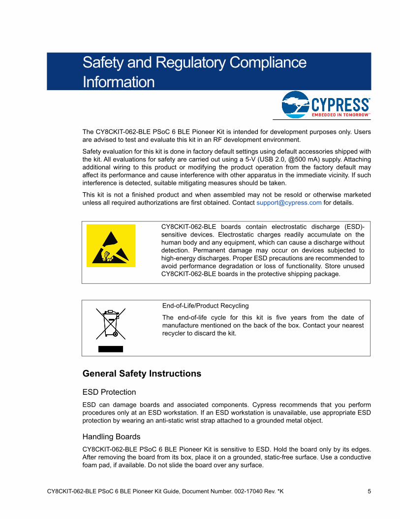
CY8CKIT-062-BLE boards contain electrostatic discharge (ESD)-sensitive devices. Electrostatic charges readily accumulate on thehuman body and any equipment, which can cause a discharge withoutdetection. Permanent damage may occur on devices subjected tohigh-energy discharges. Proper ESD precautions are recommended toavoid performance degradation or loss of functionality. Store unusedCY8CKIT-062-BLE boards in the protective shipping package.
End-of-Life/Product Recycling
The end-of-life cycle for this kit is five years from the date ofmanufacture mentioned on the back of the box. Contact your nearestrecycler to discard the kit.
CY8CKIT-062-BLE PSoC 6 BLE Pioneer Kit Guide, Document Number. 002-17040 Rev. *K 6
Regulatory Compliance Information
The CY8CKIT-062-BLE PSoC 6 BLE Pioneer Kit contains devices that transmit and receive radiosignals in accordance with the spectrum regulations for the 2.4-GHz unlicensed frequency range.
Cypress Semiconductor Corporation has obtained regulatory approvals for this kit to be used inspecific countries. These countries include Europe (ETSI/CE), USA (FCC), Canada (ISEDC) andJapan (TELC). Additional regional regulatory agency approval may be required to operate thesethroughout the world.
The CY8CKIT-062-BLE PSoC 6 BLE Pioneer Kit as shipped from the factory has been verified tomeet with requirements for the following compliances:
■ As a Class A compliant product meeting requirement for CE
■ As a Class B digital device, pursuant to part 15 of the FCC Rules
■ As a Class B digital apparatus, compliant with Canadian ICES-003
Regulatory Statements and Product Labeling
United States (FCC)
The modular transmitter in the CY8CKIT-062-BLE PSoC 6 BLE Pioneer Kit complies with Part 15 ofthe Federal Communications Commission (FCC) Rules.
The FCC ID for this device is WAP-CY8CKIT-062.
Operation is subject to the following three conditions:
■ This device may not cause harmful interference.
■ This device must accept any interference received, including interference that may cause undesired operation.
■ Class 2 Permissive Change (C2PC) will be required if this module is built into a each Host Device or each Host Enclosure.
RF Exposure Statement
This equipment complies with FCC radiation exposure limits set forth for an uncontrolledenvironment. This equipment must be installed and used with a minimum distance of 20 cm betweenthe device and the user or third parties.
This module is labeled with its own FCC ID: WAP-CY8CKIT-062. If the FCC ID is not visible wheninstalled inside another device, the device must display the label on the attached reference module.In this case, the final product must be labeled in a visible place by the following text:
“FCC ID: WAP-CY8CKIT-062”
OR
“Contains FCC ID: WAP-CY8CKIT-062”
CAUTION: Any changes or modifications not expressly approved by theparty responsible for compliance could void the user’s authority tooperate the equipment.
Only the PCB antenna(s) that were certified with the module may beused. Other antennas may be used only if they are of the same type andhave the same or lower gain.
CY8CKIT-062-BLE PSoC 6 BLE Pioneer Kit Guide, Document Number. 002-17040 Rev. *K 7
Canada (ISEDC)
Le présent appareil est conforme aux CNR d' Innovation, Science and Economic DevelopmentCanada applicables aux appareils radio exempts de licence. L'exploitation est autorisée aux deuxconditions suivantes:
(1) l'appareil ne doit pas produire de brouillage, et
(2) l'utilisateur de l'appareil doit accepter tout brouillage radioélectrique subi, même si le brouillageest susceptible d'en compromettre le fonctionnement.:
Cet équipement est conforme aux limites d'exposition aux radiofréquences définies par Innovation,Science and Economic Development Canada pour un environnement non contrôlé. Cet équipementdoit être installé et utilisé avec un minimum de 20cm de distance entre le dispositif et l'utilisateur oudes tiers.
Ce module est étiqueté avec son propre IC: 7922A-CY8CKIT062. Si le numéro de certification IC,n'est pas visible lorsqu'il est installé à l'intérieur d'un autre appareil, l'appareil doit afficher l'étiquettesur le module de référence ci-joint. Dans ce cas, le produit final doit être étiqueté dans un endroitvisible par le texte suivant:
“IC: 7922A-CY8CKIT062”
OR
“Contains IC: 7922A-CY8CKIT062”
Japan (TELEC)
005‐101696
CY8CKIT‐062‐BLE
CY8CKIT-062-BLE PSoC 6 BLE Pioneer Kit Guide, Document Number. 002-17040 Rev. *K 8
1. Introduction
Thank you for your interest in the CY8CKIT-062-BLE PSoC 6 BLE Pioneer Kit. The PSoC 6 BLEPioneer Kit enables you to evaluate and develop your applications using the PSoC 6 MCU withBluetooth Low Energy (BLE) Connectivity (hereafter called “PSoC 6 MCU”).
PSoC 6 MCU is Cypress’ latest, ultra-low-power PSoC specifically designed for wearables and IoTproducts. PSoC 6 MCU is a true programmable embedded system-on-chip, integrating a 150-MHz
ARM® Cortex®-M4 as the primary application processor, a 100-MHz ARM Cortex®-M0+ thatsupports low-power operations, up to 1 MB Flash and 288 KB SRAM, an integrated BLE 4.2 radio,
CapSense® touch-sensing, and programmable analog and digital peripherals that allow higherflexibility, in-field tuning of the design, and faster time-to-market.
The PSoC 6 BLE Pioneer board offers compatibility with Arduino™ shields. The board features aPSoC 6 MCU, a 512-Mb NOR flash, onboard programmer/debugger (KitProg2), USB Type-C powerdelivery system (EZ-PD™ CCG3), 5-segment CapSense slider, two CapSense buttons, one Cap-Sense proximity sensing header, an RGB LED, two user LEDs, and one push button. The boardsupports operating voltages from 1.8 V to 3.3 V for PSoC 6 MCU.
The CY8CKIT-062-BLE package includes a CY8CKIT-028-EPD E-INK Display Shield that containsa 2.7-inch E-INK display, a motion sensor, a thermistor, and a PDM microphone. The kit packagealso contains a CY5677 CySmart BLE 4.2 USB Dongle that is factory-programmed to emulate a BLEGAP Central device, enabling you to emulate a BLE host on your computer.
You can use PSoC Creator™ to develop and debug your PSoC 6 MCU projects. PSoC Creator isCypress’ standard integrated design environment (IDE). PSoC Creator also supports exporting yourdesigns to other third party firmware development tools.
If you are new to PSoC 6 MCU and PSoC Creator IDE, you can find introductions in the applicationnote AN210781 - Getting Started with PSoC 6 MCU with Bluetooth Low Energy (BLE) Connectivity.
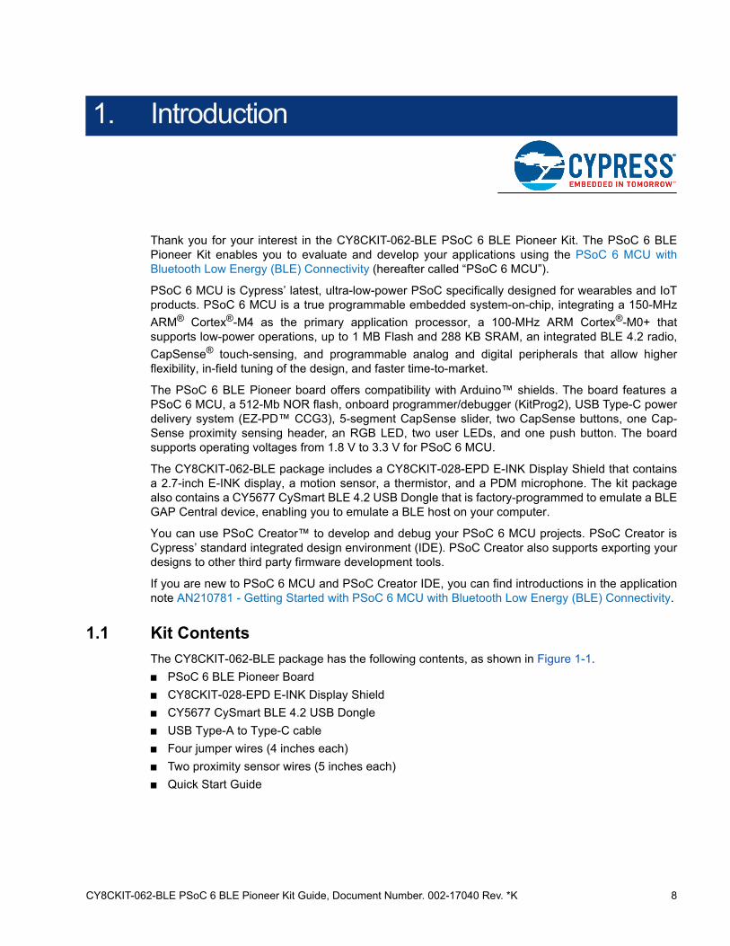
1.1 Kit Contents
The CY8CKIT-062-BLE package has the following contents, as shown in Figure 1-1.
■ PSoC 6 BLE Pioneer Board
■ CY8CKIT-028-EPD E-INK Display Shield
■ CY5677 CySmart BLE 4.2 USB Dongle
■ USB Type-A to Type-C cable
■ Four jumper wires (4 inches each)
■ Two proximity sensor wires (5 inches each)
■ Quick Start Guide
CY8CKIT-062-BLE PSoC 6 BLE Pioneer Kit Guide, Document Number. 002-17040 Rev. *K 9
Introduction
Figure 1-1. Kit Contents
Inspect the contents of the kit; if you find any part missing, contact your nearest Cypress sales officefor help: www.cypress.com/support.
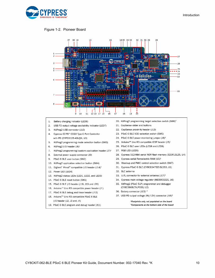
1.2 Board Details
Figure 1-2 shows the Pioneer board that has the following features:
■ PSoC 6 MCU with BLE connectivity
■ Expansion headers that are compatible with Arduino Uno™ 3.3 V shields1 and Digilent® Pmod™ modules
■ 512-Mbit external quad-SPI NOR Flash that provides a fast, expandable memory for data and code
■ KitProg2 onboard programmer/debugger with mass storage programming, USB to UART/I2C/SPI bridge functionality, and custom applications support
■ EZ-PD CCG3 USB Type-C power delivery (PD) system with rechargeable lithium-ion polymer (Li-
Po) battery support2
■ CapSense touch-sensing slider (5 elements), two buttons, all of which are capable of both self-capacitance (CSD) and mutual-capacitance (CSX) operation, and a CSD proximity sensor that let you evaluate Cypress’ fourth-generation CapSense technology
■ 1.8 V to 3.3 V operation of PSoC 6 MCU is supported. An additional 330 mF super-capacitor is provided for backup domain supply (Vbackup)
■ Two user LEDs, a RGB LED, a user button, and a reset button for PSoC 6 MCU. Two buttons and three LEDs for KitProg2
1. 5V shields are not supported2. Battery and power-delivery capable USB Type-C to Type-C cable are not included in the kit package and should be purchased separately.
CY8CKIT-062-BLE PSoC 6 BLE Pioneer Kit Guide, Document Number. 002-17040 Rev. *K 10
Introduction
Figure 1-2. Pioneer Board
CY8CKIT-062-BLE PSoC 6 BLE Pioneer Kit Guide, Document Number. 002-17040 Rev. *K 11
Introduction
Table 1-1. Selection Switches in the Pioneer Board
SwitchLocation on the
boardPurpose
Default Position
SW5 front Selects the VDD supply of PSoC 6 MCU between 1.8 V, 3.3 V, and variable 1.8 V to 3.3 V that is controlled by KitProg2.
3.3V
SW6 back In the “PSoC 6 MCU” position:
■ KitProg2 can program the onboard PSoC 6 MCU
■ In addition, the PSoC 6 MCU can be pro-grammed by an external programmer such as a MiniProg3 connected to J11
Avoid connecting any external devices to J11 in the “PSoC 6 MCU” position, as it can cause programming failure.
In the “External Device” position:
■ KitProg2 can program any PSoC 4/5/6 devices connected to J11
PSoC 6 MCU
SW7 back Selects the Vbackup supply connection of PSoC 6 MCU between VDDD and the super-capacitor. When VDDD is selected, the regulator can be turned ON/OFF by the KitProg2. When the super-capacitor is selected, PSoC 6 MCU can turn the regulator ON/OFF.
VDDD / Kit-Prog2
CY8CKIT-062-BLE PSoC 6 BLE Pioneer Kit Guide, Document Number. 002-17040 Rev. *K 12
Introduction
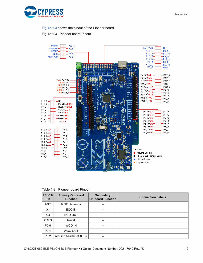
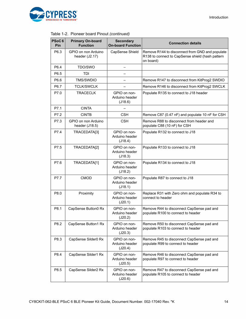
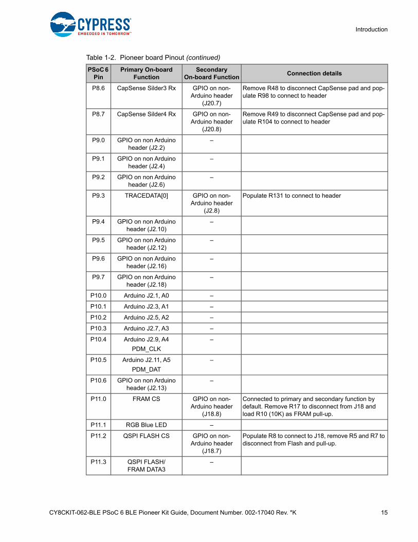
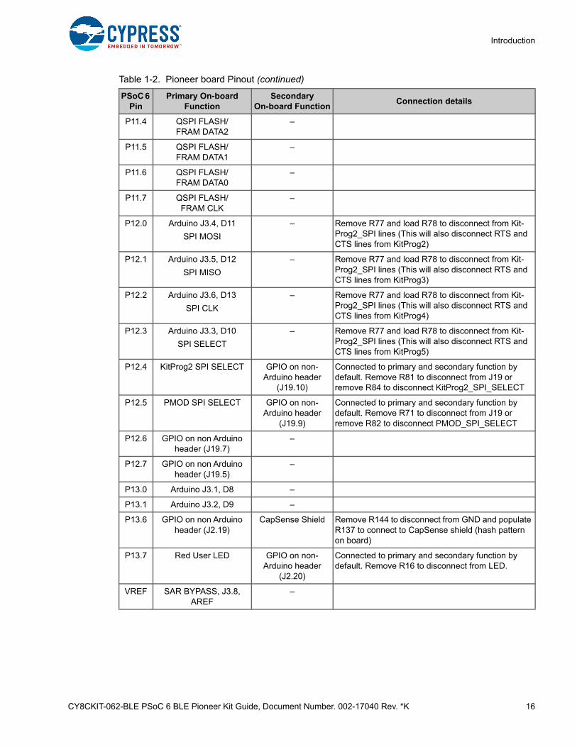
Figure 1-3 shows the pinout of the Pioneer board.
Figure 1-3. Pioneer board Pinout
Table 1-2. Pioneer board Pinout
PSoC 6 Pin
Primary On-board Function
Secondary On-board Function
Connection details
ANT RFIO, Antenna –
XI ECO IN –
XO ECO OUT –
XRES Reset –
P0.0 WCO IN –
P0.1 WCO OUT –
P0.2 Arduino header J4.8, D7 –
CY8CKIT-062-BLE PSoC 6 BLE Pioneer Kit Guide, Document Number. 002-17040 Rev. *K 13
Introduction
P0.3 RGB Red LED –
P0.4 User Button with Hibernate wakeup
capability
PMIC wake in signal Connected to ground as active low logic by default. Remove R150 and populate R149 and R148 to change the switch to active high logic. Refer to Frequently Asked Questions on page 57 (item 29) for additional information on rework, on Rev. 08 or earlier versions.
P0.5 PMIC control –
P1.0 CapSense Tx GPIO on non-Arduino header
(J19.5)
Connected to CapSense by default. Remove R43 to disconnect CapSense or add R101 to connect to header.
P1.1 RGB Green LED –
P1.2 GPIO on non Arduino header (J19.4)
–
P1.3 GPIO on non Arduino header (J19.3)
–
P1.4 GPIO on non Arduino header (J19.2)
–
P1.5 Orange User LED GPIO on non-Arduino header
(J19.1)
Connected to primary and secondary function by default. Remove R13 to disconnect from LED.
P5.0 Arduino J4.1, D0
UART RX
KitProg2 UART TX
– Remove R120 to disconnect from KitProg2 UART TX
P5.1 Arduino J4.2, D1
UART TX
KitProg2 UART RX
– Remove R119 to disconnect from KitProg2 UART RX
P5.2 Arduino J4.3, D2
UART RTS
KitProg2 UART CTS
– Remove R77 and load R78 to disconnect from KitProg2 UART CTS (This will also disconnect RTS and SPI lines from KitProg2
P5.3 Arduino J4.4, D3
UART CTS
KitProg2 UART RTS
– Remove R77 and load R78 to disconnect from KitProg2 UART CTS (This will also disconnect RTS and SPI lines from KitProg2
P5.4 Arduino J4.5, D4 –
P5.5 Arduino J4.6, D5 –
P5.6 Arduino J4.7, D6 –
P6.0 Arduino J3.10, SCL
KitProg2 I2C SCL
– Remove R109 to disconnect from KitProg2 I2C SCL
P6.1 Arduino J3.9, SDA
KitProg2 I2C SDA
– Remove R114 to disconnect from KitProg2 I2C SDA
P6.2 GPIO on non Arduino header (J2.15)
–
Table 1-2. Pioneer board Pinout (continued)
PSoC 6 Pin
Primary On-board Function
Secondary On-board Function
Connection details
CY8CKIT-062-BLE PSoC 6 BLE Pioneer Kit Guide, Document Number. 002-17040 Rev. *K 14
Introduction
P6.3 GPIO on non Arduino header (J2.17)
CapSense Shield Remove R144 to disconnect from GND and populate R138 to connect to CapSense shield (hash pattern on board)
P6.4 TDO/SWO –
P6.5 TDI –
P6.6 TMS/SWDIO – Remove R147 to disconnect from KitProg2 SWDIO
P6.7 TCLK/SWCLK – Remove R146 to disconnect from KitProg2 SWCLK
P7.0 TRACECLK GPIO on non-Arduino header
(J18.6)
Populate R135 to connect to J18 header
P7.1 CINTA –
P7.2 CINTB CSH Remove C87 (0.47 nF) and populate 10 nF for CSH
P7.3 GPIO on non Arduino header (J18.5)
CSH Remove R88 to disconnect from header and populate C88 (10 nF) for CSH
P7.4 TRACEDATA[3] GPIO on non-Arduino header
(J18.4)
Populate R132 to connect to J18
P7.5 TRACEDATA[2] GPIO on non-Arduino header
(J18.3)
Populate R133 to connect to J18
P7.6 TRACEDATA[1] GPIO on non-Arduino header
(J18.2)
Populate R134 to connect to J18
P7.7 CMOD GPIO on non-Arduino header
(J18.1)
Populate R87 to connect to J18
P8.0 Proximity GPIO on non-Arduino header
(J20.1)
Replace R31 with Zero ohm and populate R34 to connect to header
P8.1 CapSense Button0 Rx GPIO on non-Arduino header
(J20.2)
Remove R44 to disconnect CapSense pad and populate R100 to connect to header
P8.2 CapSense Button1 Rx GPIO on non-Arduino header
(J20.3)
Remove R50 to disconnect CapSense pad and populate R103 to connect to header
P8.3 CapSense Silder0 Rx GPIO on non-Arduino header
(J20.4)
Remove R45 to disconnect CapSense pad and populate R99 to connect to header
P8.4 CapSense Silder1 Rx GPIO on non-Arduino header
(J20.5)
Remove R46 to disconnect CapSense pad and populate R97 to connect to header
P8.5 CapSense Silder2 Rx GPIO on non-Arduino header
(J20.6)
Remove R47 to disconnect CapSense pad and populate R105 to connect to header
Table 1-2. Pioneer board Pinout (continued)
PSoC 6 Pin
Primary On-board Function
Secondary On-board Function
Connection details
CY8CKIT-062-BLE PSoC 6 BLE Pioneer Kit Guide, Document Number. 002-17040 Rev. *K 15
Introduction
P8.6 CapSense Silder3 Rx GPIO on non-Arduino header
(J20.7)
Remove R48 to disconnect CapSense pad and pop-ulate R98 to connect to header
P8.7 CapSense Silder4 Rx GPIO on non-Arduino header
(J20.8)
Remove R49 to disconnect CapSense pad and pop-ulate R104 to connect to header
P9.0 GPIO on non Arduino header (J2.2)
–
P9.1 GPIO on non Arduino header (J2.4)
–
P9.2 GPIO on non Arduino header (J2.6)
–
P9.3 TRACEDATA[0] GPIO on non-Arduino header
(J2.8)
Populate R131 to connect to header
P9.4 GPIO on non Arduino header (J2.10)
–
P9.5 GPIO on non Arduino header (J2.12)
–
P9.6 GPIO on non Arduino header (J2.16)
–
P9.7 GPIO on non Arduino header (J2.18)
–
P10.0 Arduino J2.1, A0 –
P10.1 Arduino J2.3, A1 –
P10.2 Arduino J2.5, A2 –
P10.3 Arduino J2.7, A3 –
P10.4 Arduino J2.9, A4
PDM_CLK
–
P10.5 Arduino J2.11, A5
PDM_DAT
–
P10.6 GPIO on non Arduino header (J2.13)
–
P11.0 FRAM CS GPIO on non-Arduino header
(J18.8)
Connected to primary and secondary function by default. Remove R17 to disconnect from J18 and load R10 (10K) as FRAM pull-up.
P11.1 RGB Blue LED –
P11.2 QSPI FLASH CS GPIO on non-Arduino header
(J18.7)
Populate R8 to connect to J18, remove R5 and R7 to disconnect from Flash and pull-up.
P11.3 QSPI FLASH/FRAM DATA3
–
Table 1-2. Pioneer board Pinout (continued)
PSoC 6 Pin
Primary On-board Function
Secondary On-board Function
Connection details
CY8CKIT-062-BLE PSoC 6 BLE Pioneer Kit Guide, Document Number. 002-17040 Rev. *K 16
Introduction
P11.4 QSPI FLASH/FRAM DATA2
–
P11.5 QSPI FLASH/FRAM DATA1
–
P11.6 QSPI FLASH/FRAM DATA0
–
P11.7 QSPI FLASH/FRAM CLK
–
P12.0 Arduino J3.4, D11
SPI MOSI
– Remove R77 and load R78 to disconnect from Kit-Prog2_SPI lines (This will also disconnect RTS and CTS lines from KitProg2)
P12.1 Arduino J3.5, D12
SPI MISO
– Remove R77 and load R78 to disconnect from Kit-Prog2_SPI lines (This will also disconnect RTS and CTS lines from KitProg3)
P12.2 Arduino J3.6, D13
SPI CLK
– Remove R77 and load R78 to disconnect from Kit-Prog2_SPI lines (This will also disconnect RTS and CTS lines from KitProg4)
P12.3 Arduino J3.3, D10
SPI SELECT
– Remove R77 and load R78 to disconnect from Kit-Prog2_SPI lines (This will also disconnect RTS and CTS lines from KitProg5)
P12.4 KitProg2 SPI SELECT GPIO on non-Arduino header
(J19.10)
Connected to primary and secondary function by default. Remove R81 to disconnect from J19 or remove R84 to disconnect KitProg2_SPI_SELECT
P12.5 PMOD SPI SELECT GPIO on non-Arduino header
(J19.9)
Connected to primary and secondary function by default. Remove R71 to disconnect from J19 or remove R82 to disconnect PMOD_SPI_SELECT
P12.6 GPIO on non Arduino header (J19.7)
–
P12.7 GPIO on non Arduino header (J19.5)
–
P13.0 Arduino J3.1, D8 –
P13.1 Arduino J3.2, D9 –
P13.6 GPIO on non Arduino header (J2.19)
CapSense Shield Remove R144 to disconnect from GND and populate R137 to connect to CapSense shield (hash pattern on board)
P13.7 Red User LED GPIO on non-Arduino header
(J2.20)
Connected to primary and secondary function by default. Remove R16 to disconnect from LED.
VREF SAR BYPASS, J3.8, AREF
–
Table 1-2. Pioneer board Pinout (continued)
PSoC 6 Pin
Primary On-board Function
Secondary On-board Function
Connection details
CY8CKIT-062-BLE PSoC 6 BLE Pioneer Kit Guide, Document Number. 002-17040 Rev. *K 17
Introduction
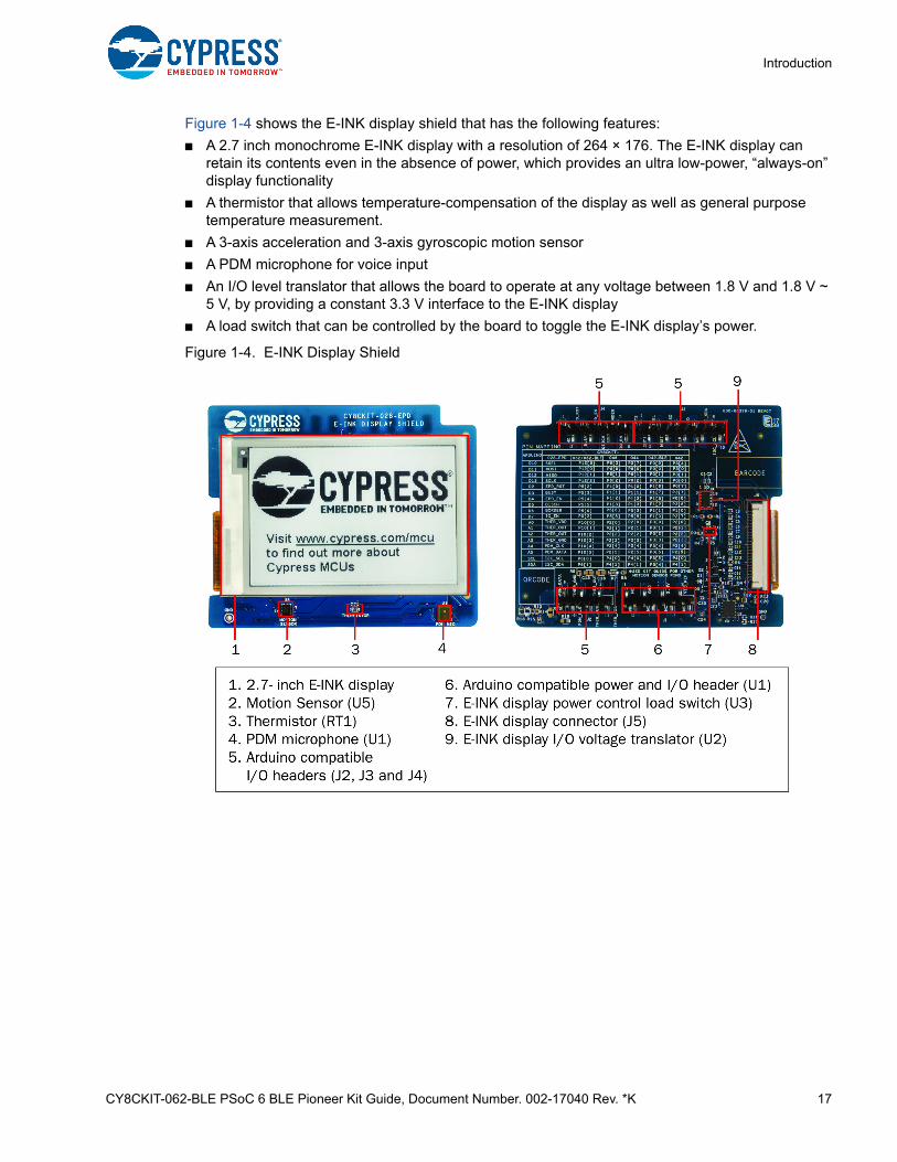
Figure 1-4 shows the E-INK display shield that has the following features:
■ A 2.7 inch monochrome E-INK display with a resolution of 264 × 176. The E-INK display can retain its contents even in the absence of power, which provides an ultra low-power, “always-on” display functionality
■ A thermistor that allows temperature-compensation of the display as well as general purpose temperature measurement.
■ A 3-axis acceleration and 3-axis gyroscopic motion sensor
■ A PDM microphone for voice input
■ An I/O level translator that allows the board to operate at any voltage between 1.8 V and 1.8 V ~ 5 V, by providing a constant 3.3 V interface to the E-INK display
■ A load switch that can be controlled by the board to toggle the E-INK display’s power.
Figure 1-4. E-INK Display Shield
CY8CKIT-062-BLE PSoC 6 BLE Pioneer Kit Guide, Document Number. 002-17040 Rev. *K 18
Introduction
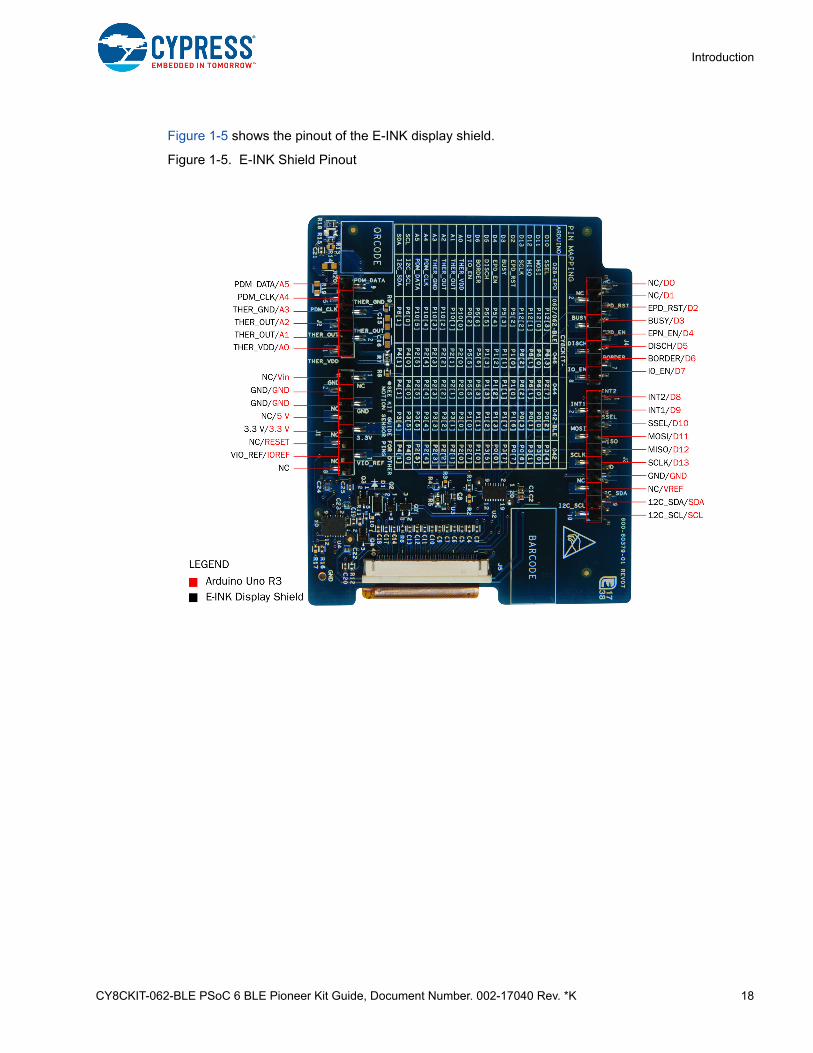
Figure 1-5 shows the pinout of the E-INK display shield.
Figure 1-5. E-INK Shield Pinout
CY8CKIT-062-BLE PSoC 6 BLE Pioneer Kit Guide, Document Number. 002-17040 Rev. *K 19
Introduction
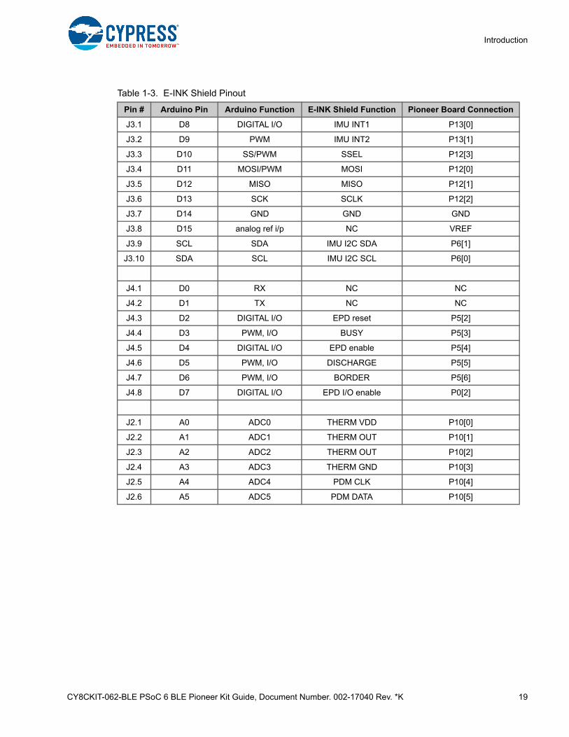
Table 1-3. E-INK Shield Pinout
Pin # Arduino Pin Arduino Function E-INK Shield Function Pioneer Board Connection
J3.1 D8 DIGITAL I/O IMU INT1 P13[0]
J3.2 D9 PWM IMU INT2 P13[1]
J3.3 D10 SS/PWM SSEL P12[3]
J3.4 D11 MOSI/PWM MOSI P12[0]
J3.5 D12 MISO MISO P12[1]
J3.6 D13 SCK SCLK P12[2]
J3.7 D14 GND GND GND
J3.8 D15 analog ref i/p NC VREF
J3.9 SCL SDA IMU I2C SDA P6[1]
J3.10 SDA SCL IMU I2C SCL P6[0]
J4.1 D0 RX NC NC
J4.2 D1 TX NC NC
J4.3 D2 DIGITAL I/O EPD reset P5[2]
J4.4 D3 PWM, I/O BUSY P5[3]
J4.5 D4 DIGITAL I/O EPD enable P5[4]
J4.6 D5 PWM, I/O DISCHARGE P5[5]
J4.7 D6 PWM, I/O BORDER P5[6]
J4.8 D7 DIGITAL I/O EPD I/O enable P0[2]
J2.1 A0 ADC0 THERM VDD P10[0]
J2.2 A1 ADC1 THERM OUT P10[1]
J2.3 A2 ADC2 THERM OUT P10[2]
J2.4 A3 ADC3 THERM GND P10[3]
J2.5 A4 ADC4 PDM CLK P10[4]
J2.6 A5 ADC5 PDM DATA P10[5]
CY8CKIT-062-BLE PSoC 6 BLE Pioneer Kit Guide, Document Number. 002-17040 Rev. *K 20
Introduction
1.3 PSoC Creator
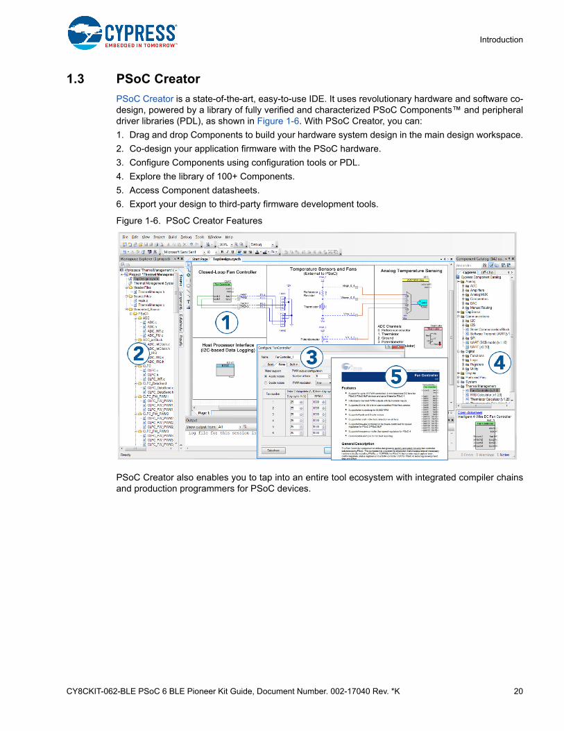
PSoC Creator is a state-of-the-art, easy-to-use IDE. It uses revolutionary hardware and software co-design, powered by a library of fully verified and characterized PSoC Components™ and peripheraldriver libraries (PDL), as shown in Figure 1-6. With PSoC Creator, you can:
1. Drag and drop Components to build your hardware system design in the main design workspace.
2. Co-design your application firmware with the PSoC hardware.
3. Configure Components using configuration tools or PDL.
4. Explore the library of 100+ Components.
5. Access Component datasheets.
6. Export your design to third-party firmware development tools.
Figure 1-6. PSoC Creator Features
PSoC Creator also enables you to tap into an entire tool ecosystem with integrated compiler chainsand production programmers for PSoC devices.
CY8CKIT-062-BLE PSoC 6 BLE Pioneer Kit Guide, Document Number. 002-17040 Rev. *K 21
Introduction
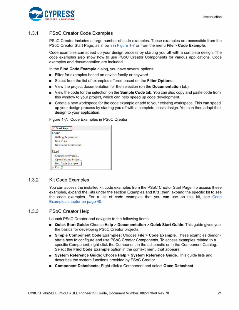
1.3.1 PSoC Creator Code Examples
PSoC Creator includes a large number of code examples. These examples are accessible from thePSoC Creator Start Page, as shown in Figure 1-7 or from the menu File > Code Example.
Code examples can speed up your design process by starting you off with a complete design. Thecode examples also show how to use PSoC Creator Components for various applications. Codeexamples and documentation are included.
In the Find Code Example dialog, you have several options:
■ Filter for examples based on device family or keyword.
■ Select from the list of examples offered based on the Filter Options.
■ View the project documentation for the selection (on the Documentation tab).
■ View the code for the selection on the Sample Code tab. You can also copy and paste code from this window to your project, which can help speed up code development.
■ Create a new workspace for the code example or add to your existing workspace. This can speed up your design process by starting you off with a complete, basic design. You can then adapt that design to your application.
Figure 1-7. Code Examples in PSoC Creator
1.3.2 Kit Code Examples
You can access the installed kit code examples from the PSoC Creator Start Page. To access theseexamples, expand the Kits under the section Examples and Kits; then, expand the specific kit to seethe code examples. For a list of code examples that you can use on this kit, see CodeExamples chapter on page 40.
1.3.3 PSoC Creator Help
Launch PSoC Creator and navigate to the following items:
■ Quick Start Guide: Choose Help > Documentation > Quick Start Guide. This guide gives you the basics for developing PSoC Creator projects.
■ Simple Component Code Examples: Choose File > Code Example. These examples demon-strate how to configure and use PSoC Creator Components. To access examples related to a specific Component, right-click the Component in the schematic or in the Component Catalog. Select the Find Code Example option in the context menu that appears.
■ System Reference Guide: Choose Help > System Reference Guide. This guide lists and describes the system functions provided by PSoC Creator.
■ Component Datasheets: Right-click a Component and select Open Datasheet.
CY8CKIT-062-BLE PSoC 6 BLE Pioneer Kit Guide, Document Number. 002-17040 Rev. *K 22
Introduction
1.4 Getting Started
This guide will help you to get acquainted with the PSoC 6 BLE Pioneer Kit:
■ The Software Installation chapter on page 25 describes the installation of the kit software. This includes the PSoC Creator IDE and PDL to develop and debug the applications, the PSoC Programmer to program the .hex files on to the device, and the CySmart to emulate a host device in the GAP central role.
■ The Kit Operation chapter on page 28 describes the major features of the PSoC 6 BLE Pioneer Kit and functionalities such as programming, debugging, and the USB-UART and USB-I2C bridges.
■ The Code Examples chapter on page 40 describes multiple PSoC 6 MCU code examples that will help you understand how to create your own PSoC 6 projects.
■ The Appendix on page 43 provides a detailed hardware description, methods to use the onboard NOR Flash and onboard EZ-PD™ CCG3 Type-C power delivery system, kit schematics, and the bill of materials (BOM).
1.5 Additional Learning Resources
Cypress provides a wealth of data at www.cypress.com/psoc6 to help you to select the right PSoCdevice for your design and to help you to quickly and effectively integrate the device into yourdesign.
1.6 Technical Support
For assistance, visit Cypress Support or contact customer support at +1(800) 541-4736 Ext. 3 (in theUSA) or +1 (408) 943-2600 Ext. 3 (International).
You can also use the following support resources if you need quick assistance:
■ Self-help (Technical Documents).
■ Local Sales Office Locations.
1.7 Documentation Conventions
Table 1-4. Document Conventions for Guides
Convention Usage
Courier New Displays file locations, user entered text, and source code:C:\...cd\icc\
Italics Displays file names and reference documentation:Read about the sourcefile.hex file in the PSoC Creator User Guide.
[Bracketed, Bold] Displays keyboard commands in procedures:[Enter] or [Ctrl] [C]
File > Open Represents menu paths:File > Open > New Project
Bold Displays commands, menu paths, and icon names in procedures:Click the File icon and then click Open.
Times New Roman Displays an equation:2 + 2 = 4
Text in gray boxes Describes cautions or unique functionality of the product.
CY8CKIT-062-BLE PSoC 6 BLE Pioneer Kit Guide, Document Number. 002-17040 Rev. *K 23
Introduction
1.8 AcronymsTable 1-5. Acronyms Used in this Document
Acronym Definition
ADC Analog-to-Digital Converter
BLE Bluetooth Low Energy
BOM Bill of Materials
CINT Integration Capacitor
CMOD Modulator Capacitor
CPU Central Processing Unit
CSD CapSense Sigma Delta
CTANK Shield Tank Capacitor
DC Direct Current
Del-Sig Delta-Sigma
ECO External Crystal Oscillator
EPD Electronic Paper Display
ESD Electrostatic Discharge
F-RAM Ferroelectric Random Access Memory
FPC Flexible Printed Circuit
GPIO General-Purpose Input/Output
HID Human Interface Device
I2C Inter-Integrated Circuit
IC Integrated Circuit
ICSP In-Circuit Serial Programming
IDAC Current Digital-to-Analog Converter
IDE Integrated Development Environment
LED Light-emitting Diode
PC Personal Computer
PD Power Delivery
PDM Pulse Density Modulation
PTC Positive Temperature Coefficient
PSoC Programmable System-on-Chip
PWM Pulse Width Modulation
RGB Red Green Blue
SAR Successive Approximation Register
SPI Serial Peripheral Interface
SRAM Serial Random Access Memory
CY8CKIT-062-BLE PSoC 6 BLE Pioneer Kit Guide, Document Number. 002-17040 Rev. *K 24
Introduction
SWD Serial Wire Debug
UART Universal Asynchronous Receiver Transmitter
USB Universal Serial Bus
WCO Watch Crystal Oscillator
Table 1-5. Acronyms Used in this Document (continued)
Acronym Definition
CY8CKIT-062-BLE PSoC 6 BLE Pioneer Kit Guide, Document Number. 002-17040 Rev. *K 25
2. Software Installation
This chapter describes the steps to install the software tools and packages on a PC for using thePSoC 6 BLE Pioneer Kit. This includes the IDE on which the projects will be built and used for pro-gramming.
2.1 Before You Begin
To install Cypress software, you will require administrator privileges. However, they are not requiredto run the software that is already installed. Before you install the kit software, close any otherCypress software that is currently running.
2.2 Install Software
Follow these steps to install the PSoC 6 BLE Pioneer Kit software:
1. Download and run the CY8CKIT-062-BLE PSoC 6 BLE Pioneer Kit software from www.cypress.com/CY8CKIT-062-BLE. The kit software is available in two different formats for download.
a. CY8CKIT-062-BLE Kit Complete Setup: This installation package contains the files related to the Kit including PSoC Creator, PSoC Programmer, PDL, and CySmart. However, it does not include the Windows Installer or Microsoft .NET framework packages. If these packages are not on your computer, the installer will direct you to download and install them from the Internet.
b. CY8CKIT-062-BLE Kit Only: This executable file installs only the kit contents, which include Kit code examples, hardware files, and user documents. This package can be used if all the software prerequisites (listed in step 5) are installed on your PC.
CY8CKIT-062-BLE PSoC 6 BLE Pioneer Kit Guide, Document Number. 002-17040 Rev. *K 26
Software Installation
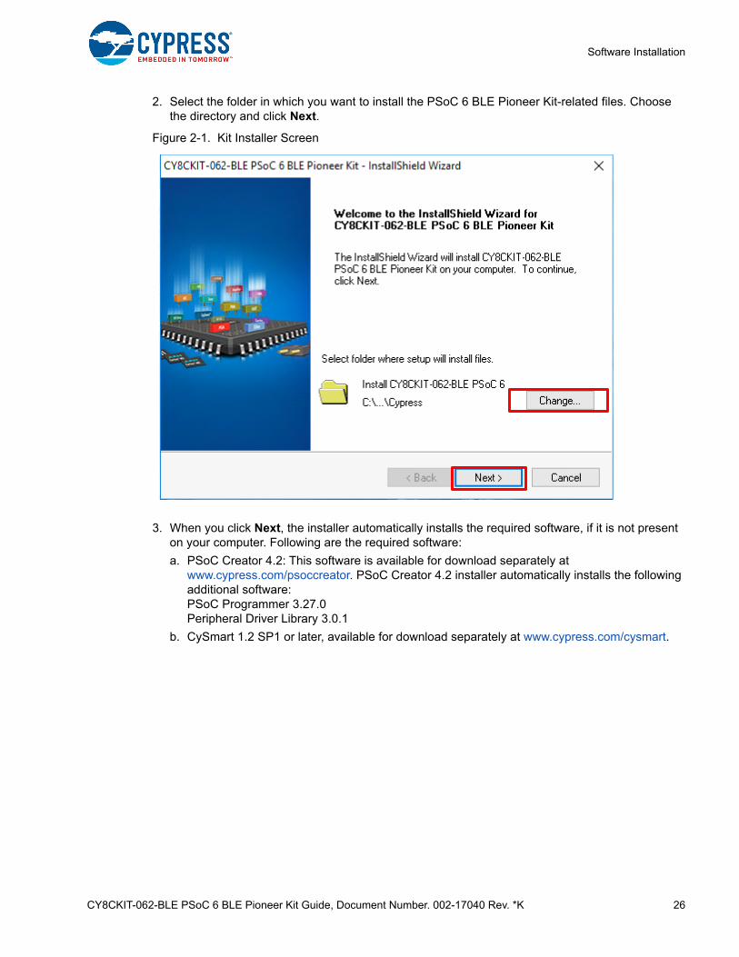
2. Select the folder in which you want to install the PSoC 6 BLE Pioneer Kit-related files. Choose the directory and click Next.
Figure 2-1. Kit Installer Screen
3. When you click Next, the installer automatically installs the required software, if it is not present on your computer. Following are the required software:
a. PSoC Creator 4.2: This software is available for download separately at www.cypress.com/psoccreator. PSoC Creator 4.2 installer automatically installs the following additional software:PSoC Programmer 3.27.0 Peripheral Driver Library 3.0.1
b. CySmart 1.2 SP1 or later, available for download separately at www.cypress.com/cysmart.
CY8CKIT-062-BLE PSoC 6 BLE Pioneer Kit Guide, Document Number. 002-17040 Rev. *K 27
Software Installation
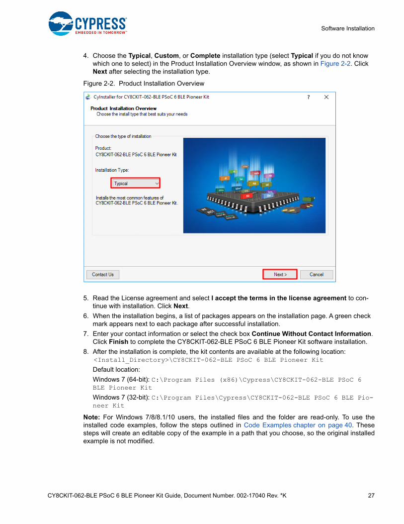
4. Choose the Typical, Custom, or Complete installation type (select Typical if you do not know which one to select) in the Product Installation Overview window, as shown in Figure 2-2. Click Next after selecting the installation type.
Figure 2-2. Product Installation Overview
5. Read the License agreement and select I accept the terms in the license agreement to con-tinue with installation. Click Next.
6. When the installation begins, a list of packages appears on the installation page. A green check mark appears next to each package after successful installation.
7. Enter your contact information or select the check box Continue Without Contact Information. Click Finish to complete the CY8CKIT-062-BLE PSoC 6 BLE Pioneer Kit software installation.
8. After the installation is complete, the kit contents are available at the following location:<Install_Directory>\CY8CKIT-062-BLE PSoC 6 BLE Pioneer Kit
Default location:
Windows 7 (64-bit): C:\Program Files (x86)\Cypress\CY8CKIT-062-BLE PSoC 6 BLE Pioneer Kit
Windows 7 (32-bit): C:\Program Files\Cypress\CY8CKIT-062-BLE PSoC 6 BLE Pio-neer Kit
Note: For Windows 7/8/8.1/10 users, the installed files and the folder are read-only. To use theinstalled code examples, follow the steps outlined in Code Examples chapter on page 40. Thesesteps will create an editable copy of the example in a path that you choose, so the original installedexample is not modified.
CY8CKIT-062-BLE PSoC 6 BLE Pioneer Kit Guide, Document Number. 002-17040 Rev. *K 28
3. Kit Operation
This chapter introduces you to various features of the PSoC 6 BLE Pioneer Kit, including the theoryof operation and the onboard programming and debugging functionality, KitProg2 USB-UART, USB-I2C, USB-SPI bridges, and USB Type-C power delivery.
3.1 Theory of Operation
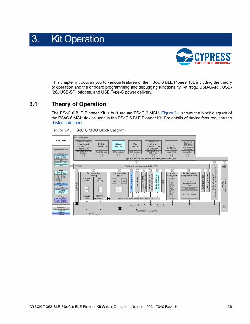
The PSoC 6 BLE Pioneer Kit is built around PSoC 6 MCU. Figure 3-1 shows the block diagram ofthe PSoC 6 MCU device used in the PSoC 6 BLE Pioneer Kit. For details of device features, see thedevice datasheet.
Figure 3-1. PSoC 6 MCU Block Diagram
CPU Subsystem
System Interconnect (Multi Layer AHB, MPU/SMPU, IPC)
ROM128 KB
ROM Controller
CRYPTODES/TDES,
AES,SHA,CRC,TRNG,RSA/ECC
Accelerator
Initiator/MMIO
SWJ/MTB/CTI
8KB Cache
Cortex M0+100 MHz (1.1V)25 MHz (0.9V)MUL, NVIC, MPU
IO Subsystem
Peripheral Interconnect (MMIO, PPU)
IOS
S G
PIO
PCLK
78x GPIO (6 of these are OVT)
EF
US
E (
10
24
bits
)
PSoC 63BL
Ser
ial M
emor
y I/
F(Q
SP
I w
ith O
TF
Enc
ryp
tion/
Dec
ryp
tion
))
DMAMMIO
US
B-F
SH
ost
+ D
evic
eF
S/L
SP
HY
FLASH1024+32 KB
FLASH Controller
SWJ/ETM/ITM/CTI
FPU, NVIC, MPU, BB
Cortex M4150 MHz (1.1V)50 MHz (0.9V)
8KB Cache
SRAM9x 32 KB
SRAM Controller
Bluetooth LowEnergy Subsystem
BLE 4.2Programmable Link
Layer
Digital Interface
BLE 2 Mbps Radio
Ene
rgy
Pro
filer
x12
UDB...
ProgrammableDigital
UDB
8x
Ser
ial C
om
m(I
2C,S
PI,U
AR
T,L
IN,S
MC
)
Cap
Sen
se
32x
TC
PW
M(T
IME
R,C
TR
,QD
, PW
M)
1x
Ser
ial C
om
m(I
2C,S
PI,
Dee
p S
leep
)
DAC(12-bit)
SAR ADC(12-bit)
x1
CTB/CTBmx12x OpAmp
ProgrammableAnalog
x1
SARMUX
LP C
ompa
rato
r
Port Interface & Digital System Interconnect (DSI)
High Speed I/O Matrix, Smart I/O, Boundary Scan
I2S
Ma
ster
/Sla
ve
PD
M/P
CM
AudioSubsystem
LCD
DMA2x 16 Ch
Initiator/MMIO
WCORTC BREG
BackupBackup Control
Digital DFT
Test
Analog DFT
System Resources
Power
Reset
Sleep Control
PWRSYS-LP/ULP
REF
Reset Control
TestMode Entry
XRES
DeepSleepHibernate
Power Modes
Backup
Active/SleepLowePowerActive/Sleep
Buck
PORLVDBOD
OVP
ClockClock Control
IMOWDT
CSV
1xPLL
ECOILO
FLL
CY8CKIT-062-BLE PSoC 6 BLE Pioneer Kit Guide, Document Number. 002-17040 Rev. *K 29
Kit Operation
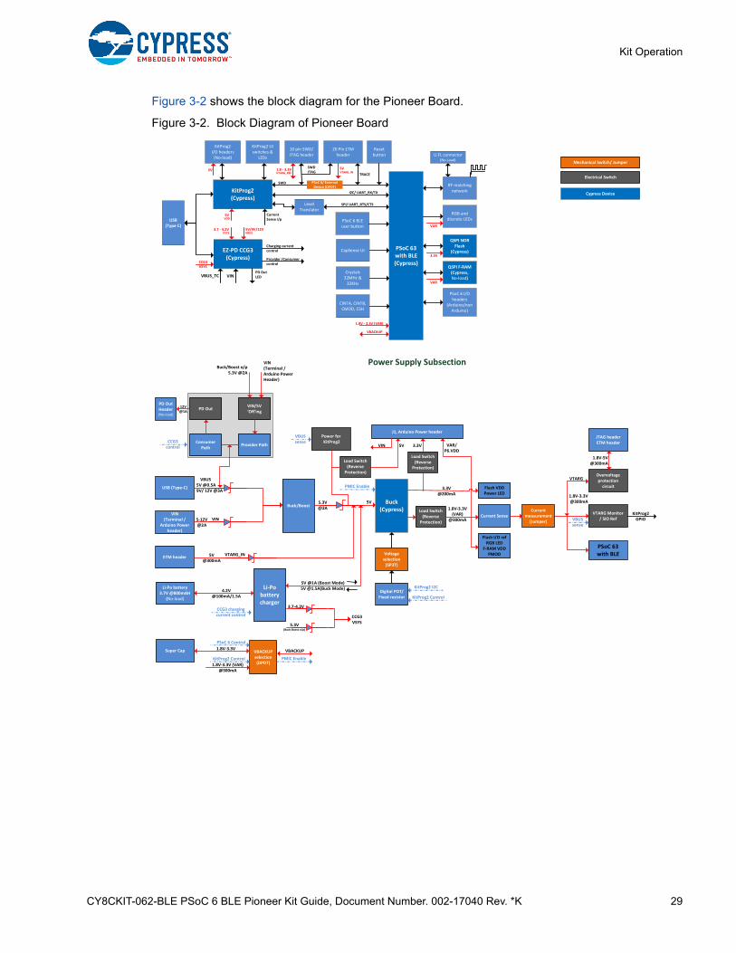
Figure 3-2 shows the block diagram for the Pioneer Board.
Figure 3-2. Block Diagram of Pioneer Board
Mechanical Switch/ Jumper
Electrical Switch
Cypress Device
EZ‐PD CCG3(Cypress)
USB (Type C)
RF matching networkKitProg2
(Cypress)
KitProg2I/O headers (No‐load)
KitProg2 UIswitches &
LEDs
PSoC 63 with BLE(Cypress)
10 pin SWD/JTAG header
Reset button
QSPI F‐RAM(Cypress, No‐load)
PSoC 6 I/O headers
(Arduino/non Arduino)
RGB and discrete LEDs
I2C/ UART_RX/TX
SWD
TRACE
QSPI NOR Flash
(Cypress)
SWDJTAG
5V
VAR
3.3V
VAR
3.7 ‐ 4.2V 5V/9V/12V
Charging current control
Provider /Consumercontrol
Current Sense i/p
1.8V ‐ 3.3V (VAR)
PSoC 6 BLE user button
CapSense UI
Crystals32MHz & 32KHz
VDD
VBUSVSYS
VIN
U.FL connector(No‐Load)
5V
PSoC 6/ External Device (DPDT)
CINTA, CINTB, CMOD, CSH
No‐load
KitProg2 GPIO
VIN (Terminal /
Arduino Power header)
ETM header
5‐12V@2A
5V @0.5A 9V/ 12V @3A
5V@300mA
VTARG Monitor / SIO Ref
USB (Type‐C)
Flash I/O refRGB LED
F‐RAM VDDPMOD
Flash VDDPower LED
PSoC 63 with BLE
Buck/Boost5.3V@2A
Buck (Cypress) 1.8V‐3.3V
(VAR)@300mA
3.3V@200mA
KitProg2 I2C
Super Cap VBACKUP selection (DPDT)
Voltage selection(SP3T)
Digital POT/Fixed resistor
J1, Arduino Power header
VIN
Li‐Po battery charger
Li‐Po battery3.7V @800mAH
(No‐load)
4.2V @100mA/1.5A
5V @1A (Boost Mode)5V @1.5A(Buck Mode)
PMIC Enable
PSoC 6 Control
VBACKUP
KitProg2 Control PMIC Enable
CCG3 charging current control
VIN
VBUS
Current Sense
VTARG_IN
1.8V‐3.3V
Provider PathConsumer
Path
VIN/5V ‘OR’ing
PD Out
Buck/Boost o/p5.3V @2A
VTARG
CCG3 control
VBUS sense
VBUS sense
Power forKitProg2
12V@1A
Overvoltage protection circuit
JTAG headerETM header
1.8V‐5V@300mA
PD Out Header(No‐load)
5V 3.3V VAR/ P6.VDD
Power Supply SubsectionVIN (Terminal / Arduino Power Header)
CCG3 VSYS
1.8V‐3.3V@300mA
1.8V‐3.3V (VAR)@300mA
5VVTARG_IN
Current measurement
(Jumper)
Level Translator
SPI/ UART_RTS/CTS
VBUS_TCPD Out LED
3.7‐4.2V
5.3V (Buck Boost o/p)
Load Switch (Reverse
Protection)
5V
Load Switch (Reverse
Protection)
Load Switch (Reverse
Protection)
KitProg2 Control
VBACKUP
20 Pin ETM header
CCG3 VSYS
1.8 ‐ 3.3VVTARG_REF
CY8CKIT-062-BLE PSoC 6 BLE Pioneer Kit Guide, Document Number. 002-17040 Rev. *K 30
Kit Operation
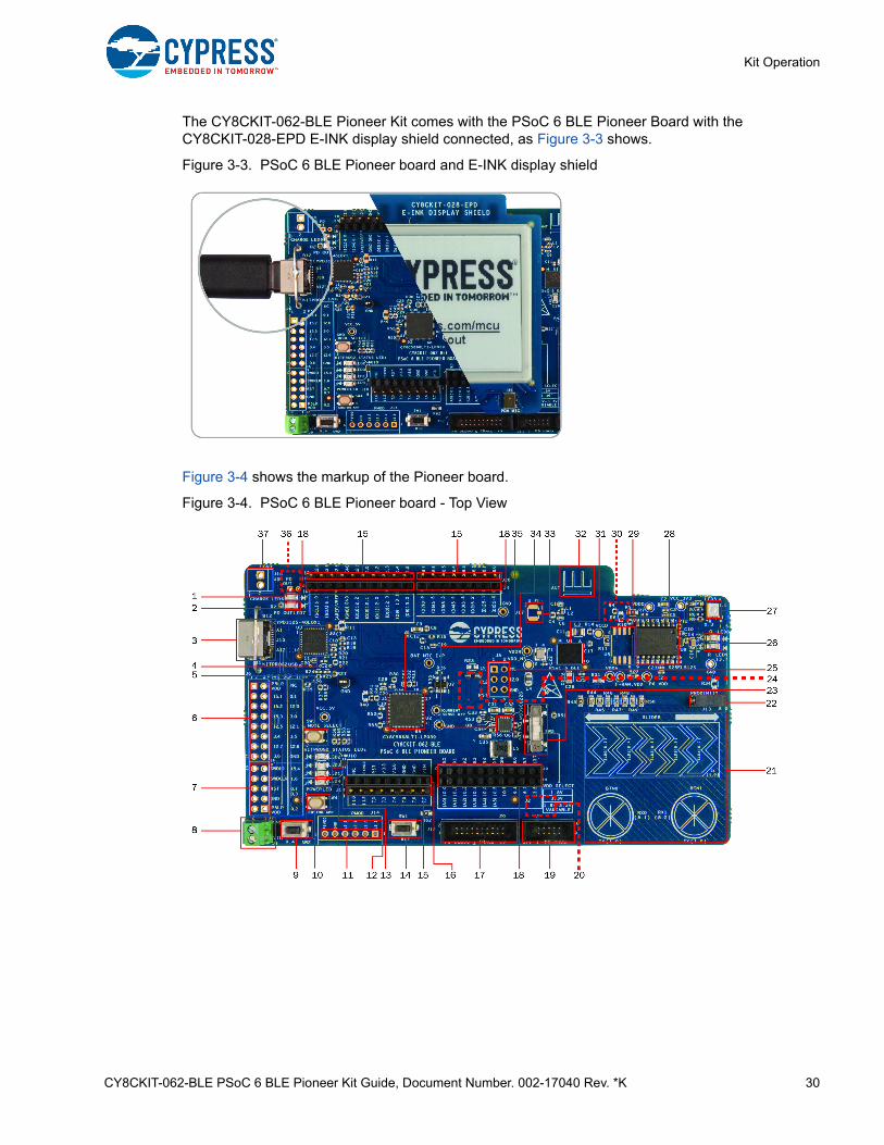
The CY8CKIT-062-BLE Pioneer Kit comes with the PSoC 6 BLE Pioneer Board with the CY8CKIT-028-EPD E-INK display shield connected, as Figure 3-3 shows.
Figure 3-3. PSoC 6 BLE Pioneer board and E-INK display shield
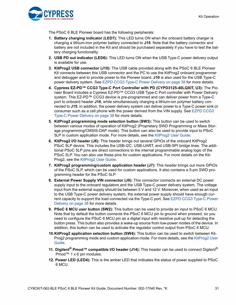
Figure 3-4 shows the markup of the Pioneer board.
Figure 3-4. PSoC 6 BLE Pioneer board - Top View
CY8CKIT-062-BLE PSoC 6 BLE Pioneer Kit Guide, Document Number. 002-17040 Rev. *K 31
Kit Operation
The PSoC 6 BLE Pioneer board has the following peripherals:
1. Battery charging indicator (LED7): This LED turns ON when the onboard battery charger is charging a lithium-iron polymer battery connected to J15. Note that the battery connector and battery are not included in the Kit and should be purchased separately if you have to test the bat-tery charging functionality.
2. USB PD out indicator (LED6): This LED turns ON when the USB Type-C power delivery output is available for use.
3. KitProg2 USB connector (J10): The USB cable provided along with the PSoC 6 BLE Pioneer Kit connects between this USB connector and the PC to use the KitProg2 onboard programmer and debugger and to provide power to the Pioneer board. J10 is also used for the USB Type-C power delivery system. See EZPD CCG3 Type-C Power Delivery on page 38 for more details.
4. Cypress EZ-PD™ CCG3 Type-C Port Controller with PD (CYPD3125-40LQXIT, U3): The Pio-neer Board includes a Cypress EZ-PD™ CCG3 USB Type-C Port controller with Power Delivery system. This EZ-PD™ CCG3 device is pre-programmed and can deliver power from a Type-C port to onboard header J16, while simultaneously charging a lithium-ion polymer battery con-nected to J15. In addition, the power delivery system can deliver power to a Type-C power sink or consumer such as a cell phone with the power derived from the VIN supply. See EZPD CCG3 Type-C Power Delivery on page 38 for more details.
5. KitProg2 programming mode selection button (SW3): This button can be used to switch between various modes of operation of KitProg2 (Proprietary SWD Programming or Mass Stor-age programming/CMSIS-DAP mode). This button can also be used to provide input to PSoC 5LP in custom application mode. For more details, see the KitProg2 User Guide.
6. KitProg2 I/O header (J6): This header brings out several GPIOs of the onboard KitProg2 PSoC 5LP device. This includes the USB-I2C, USB-UART, and USB-SPI bridge lines. The addi-tional PSoC 5LP pins are direct connections to the internal programmable analog logic of the PSoC 5LP. You can also use these pins for custom applications. For more details on the Kit-Prog2, see the KitProg2 User Guide.
7. KitProg2 programming/custom application header (J7): This header brings out more GPIOs of the PSoC 5LP, which can be used for custom applications. It also contains a 5-pin SWD pro-gramming header for the PSoC 5LP.
8. External Power Supply VIN connector (J9): This connector connects an external DC power supply input to the onboard regulators and the USB Type-C power delivery system. The voltage input from the external supply should be between 5 V and 12 V. Moreover, when used as an input to the USB Type-C power delivery system, the external power supply should have enough cur-rent capacity to support the load connected via the Type-C port. See EZPD CCG3 Type-C Power Delivery on page 38 for more details.
9. PSoC 6 MCU user button (SW2): This button can be used to provide an input to PSoC 6 MCU. Note that by default the button connects the PSoC 6 MCU pin to ground when pressed, so you need to configure the PSoC 6 MCU pin as a digital input with resistive pull-up for detecting the button press. This button also provides a wake-up source from low-power modes of the device. In addition, this button can be used to activate the regulator control output from PSoC 6 MCU.
10.KitProg2 application selection button (SW4): This button can be used to switch between Kit-Prog2 programming mode and custom application mode. For more details, see the KitProg2 User Guide.
11. Digilent® Pmod™ compatible I/O header (J14): This header can be used to connect Digilent® Pmod™ 1 x 6 pin modules.
12. Power LED (LED4): This is the amber LED that indicates the status of power supplied to PSoC 6 MCU.
CY8CKIT-062-BLE PSoC 6 BLE Pioneer Kit Guide, Document Number. 002-17040 Rev. *K 32
Kit Operation
13. KitProg2 status LEDs (LED1, LED2, and LED3): Red, amber and green LEDs (LED1, LED2, and LED3 respectively) indicate the status of KitProg2. For details on the KitProg2 status, see the KitProg2 User Guide.
14. PSoC 6 MCU reset button (SW1): This button is used to reset PSoC 6 MCU. This button con-nects the PSoC 6 MCU reset (XRES) pin to ground.
15. PSoC 6 MCU I/O headers (J18, J19, and J20): These headers provide connectivity to PSoC 6 MCU GPIOs that are not connected to the Arduino compatible headers. Majority of these pins are multiplexed with onbroad peripherals and are not connected to PSoC 6 MCU by default. For the detailed information on how to rework the kit to access these pins, see Table 1-2 on page 12.
16. Arduino compatible power header (J1): The Arduino-compatible power header powers Ardu-ino shields. This header also has a provision to power the kit though the VIN input.
17. PSoC 6 MCU debug and trace header (J12): This header can be connected to an Embedded Trace Macrocell (ETM) compatible programmer/debugger
18. Arduino Uno R3 compatible I/O headers (J2, J3, and J4): The Arduino-compatible I/O head-ers bring out pins from PSoC 6 MCU to interface with the Arduino shields. Few of these pins are multiplexed with onboard peripherals and are not connected to PSoC 6 MCU by default. For a detailed information on how to rework the kit to access these pins, see Table 1-2 on page 12
19. PSoC 6 MCU program and debug header (J11): This 10-pin header allows you to program and debug the PSoC 6 MCU using an external programmer such as MiniProg3. In addition, an exter-nal PSoC 4/5/6 device can be connected to this header and programmed using KitProg2. To program the external device, SW6 should be used to select the “External” option.
20. KitProg2 programming target selection switch (SW6, on the bottom side of the Board): This switch selects the programming target of the onboard KitProg2 between the onboard PSoC 6 MCU and an external PSoC 4/5/6 device connected to J11.
21. CapSense slider (SLIDER) and buttons (BTN0 and BTN1): CapSense touch-sensing slider and two buttons, all of which are capable of both self-capacitance (CSD) and mutual-capaci-tance (CSX) operation, let you evaluate Cypress’ fourth-generation CapSense technology. The slider and the buttons have a 1-mm acrylic overlay for smooth touch sensing.
22. CapSense proximity header (J13): A wire can be connected to this header to evaluate the proximity sensing feature of CapSense.
23. System Power VDD selection switch (SW5): This switch is used to select the PSoC 6 MCU’s VDD supply voltage between constant 1.8 V, constant 3.3 V, and variable 1.8 to 3.3 V. In the vari-able 1.8 to 3.3 V mode, the PSoC programmer software can control the voltage via the KitProg2.
24. PSoC 6 MCU current measurement jumper (J8, on the bottom side of the Board): An ammeter can be connected to this jumper to measure the current consumed by the PSoC 6 MCU.
25. Arduino compatible ICSP header (J5): This header provides an SPI interface for Arduino ICSP compatible shields.
26. PSoC 6 MCU user LEDs (LED8 and LED9): These two user LEDs can operate at the entire operating voltage range of PSoC 6 MCU. The LEDs are active LOW, so the pins must be driven to ground to turn ON the LEDs.
27. RGB LED (LED5): This onboard RGB LED can be controlled by the PSoC 6 MCU. The LEDs are active LOW, so the pins must be driven to ground to turn ON the LEDs.
28. Cypress 512-Mbit serial NOR flash memory (S25FL512SAGMFI011, U4): This kit features a Cypress NOR flash (S25FL512SAGMFI011) of 512 Mb capacity. The NOR Flash is connected to the serial memory interface (SMIF) of the PSoC 6 MCU. The NOR device can be used for both data and code memory with execute-in-place (XIP) support and encryption.
29. Cypress 4-Mbit serial Ferroelectric RAM (FM25V10, U5): Footprint to connect a FM25V10 or any other pin compatible FRAM.
CY8CKIT-062-BLE PSoC 6 BLE Pioneer Kit Guide, Document Number. 002-17040 Rev. *K 33
Kit Operation
30. Vbackup and PMIC control selection switch (SW7, on the bottom side of the Board): This switches the Vbackup supply connection to PSoC 6 MCU between VDDD and the super-capaci-tor. When VDDD is selected, the regulator ON/OFF is controlled by the KitProg2. When super-capacitor is selected, the regulator ON/OFF is controlled by PSoC 6 MCU.
31. Cypress PSoC 6 MCU (CY8C6347BZI-BLD53, U1): This kit is designed to highlight the fea-tures of the PSoC 6 MCU. For details on PSoC 6 MCU pin mapping, see Table 1-2 on page 12.
32. BLE antenna: This is the onboard wiggle antenna for BLE.
33. U.FL connector (J17): This connector can be used for conductive measurements and also to connect external antenna.
34. Cypress main voltage regulator (MB39C022GPN-G-ERE1, U6): This is the main regulator that powers PSoC 6 MCU. This regulator has two output channels. One channel provides fixed LDO-based 3.3 V output from 5 V input and the other channel is a buck DC to DC converter that is configured to provide variable voltage from 1.8 V to 3.3 V.
35. KitProg2 (PSoC 5LP) programmer and debugger (CY8C5868LTI-LP039, U2): The PSoC 5LP device (CY8C5868LTI-LP039) serving as KitProg2, is a multi-functional system, which includes a programmer, debugger, USB-I2C bridge, USB-UART bridge, and a USB-SPI bridge. KitProg2 also supports custom applications. For more details, see the KitProg2 User Guide.
36. Battery connector (J15, on the bottom side of the Board): This connector can be used to connect a lithium-ion polymer battery. Note that a battery is not included in the kit package and should be purchased separately if you want to demonstrate battery charging.
37. USB PD output (J16): This header provides a voltage output when the USB Type-C power delivery system receives power from an external host connected to J10. See EZPD CCG3 Type-C Power Delivery on page 38 for more details.
See Hardware Functional Description chapter on page 43 for details on various hardware blocks.
For some devices in the PSoC 6 MCU family, simultaneous GPIO switching with unrestricted drivestrengths and frequency can induce noise in on-chip subsystems affecting CapSense and ADCresults. For more details, see the Errata section of the corresponding device datasheet.
CY8CKIT-062-BLE PSoC 6 BLE Pioneer Kit Guide, Document Number. 002-17040 Rev. *K 34
Kit Operation
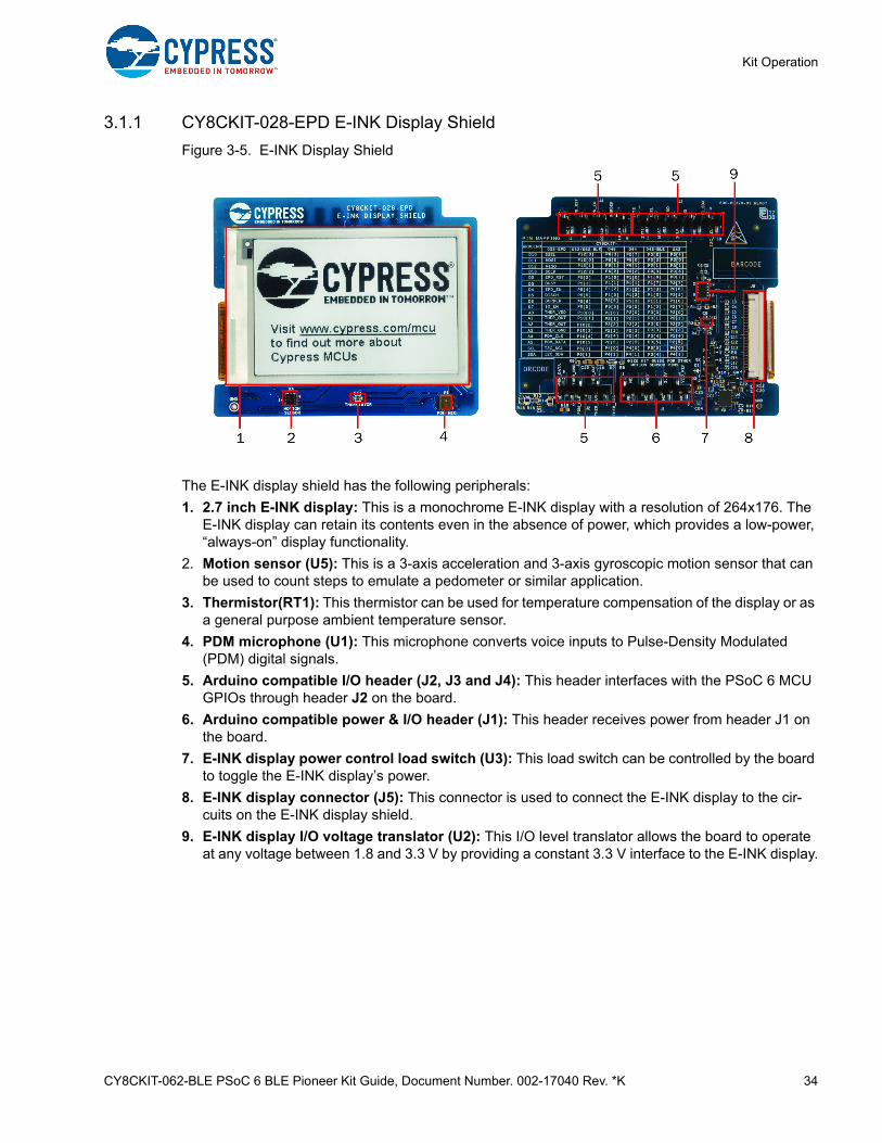
3.1.1 CY8CKIT-028-EPD E-INK Display Shield
Figure 3-5. E-INK Display Shield
The E-INK display shield has the following peripherals:
1. 2.7 inch E-INK display: This is a monochrome E-INK display with a resolution of 264x176. The E-INK display can retain its contents even in the absence of power, which provides a low-power, “always-on” display functionality.
2. Motion sensor (U5): This is a 3-axis acceleration and 3-axis gyroscopic motion sensor that can be used to count steps to emulate a pedometer or similar application.
3. Thermistor(RT1): This thermistor can be used for temperature compensation of the display or as a general purpose ambient temperature sensor.
4. PDM microphone (U1): This microphone converts voice inputs to Pulse-Density Modulated (PDM) digital signals.
5. Arduino compatible I/O header (J2, J3 and J4): This header interfaces with the PSoC 6 MCU GPIOs through header J2 on the board.
6. Arduino compatible power & I/O header (J1): This header receives power from header J1 on the board.
7. E-INK display power control load switch (U3): This load switch can be controlled by the board to toggle the E-INK display’s power.
8. E-INK display connector (J5): This connector is used to connect the E-INK display to the cir-cuits on the E-INK display shield.
9. E-INK display I/O voltage translator (U2): This I/O level translator allows the board to operate at any voltage between 1.8 and 3.3 V by providing a constant 3.3 V interface to the E-INK display.
CY8CKIT-062-BLE PSoC 6 BLE Pioneer Kit Guide, Document Number. 002-17040 Rev. *K 35
Kit Operation
3.2 KitProg2
The PSoC 6 BLE Pioneer Kit can be programmed and debugged using the onboard KitProg2. TheKitProg2 is a multi-functional system, which includes a programmer, debugger, USB-I2C bridge,USB-UART bridge, and a USB-SPI bridge. KitProg2 also supports mass storage programming andCMSIS-DAP, and custom applications. A Cypress PSoC 5LP device is used to implement KitProg2functionality. The KitProg2 is integrated in most PSoC development kits. For more details on the Kit-Prog2 functionality, see the KitProg2 User Guide.
Before programming the device, ensure that PSoC Creator and PSoC Programmer software areinstalled on the computer. See the Install Software chapter on page 25 for more information.
3.2.1 Programming and Debugging using PSoC Creator
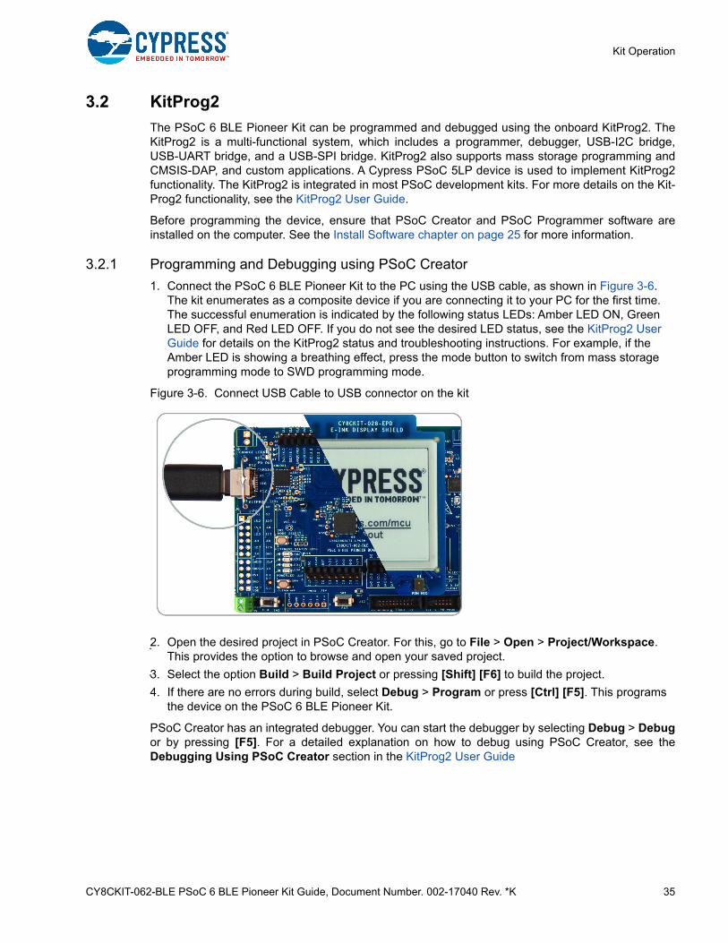
1. Connect the PSoC 6 BLE Pioneer Kit to the PC using the USB cable, as shown in Figure 3-6. The kit enumerates as a composite device if you are connecting it to your PC for the first time. The successful enumeration is indicated by the following status LEDs: Amber LED ON, Green LED OFF, and Red LED OFF. If you do not see the desired LED status, see the KitProg2 User Guide for details on the KitProg2 status and troubleshooting instructions. For example, if the Amber LED is showing a breathing effect, press the mode button to switch from mass storage programming mode to SWD programming mode.
Figure 3-6. Connect USB Cable to USB connector on the kit
2. Open the desired project in PSoC Creator. For this, go to File > Open > Project/Workspace. This provides the option to browse and open your saved project.
3. Select the option Build > Build Project or pressing [Shift] [F6] to build the project.
4. If there are no errors during build, select Debug > Program or press [Ctrl] [F5]. This programs the device on the PSoC 6 BLE Pioneer Kit.
PSoC Creator has an integrated debugger. You can start the debugger by selecting Debug > Debugor by pressing [F5]. For a detailed explanation on how to debug using PSoC Creator, see theDebugging Using PSoC Creator section in the KitProg2 User Guide
.
.
CY8CKIT-062-BLE PSoC 6 BLE Pioneer Kit Guide, Document Number. 002-17040 Rev. *K 36
Kit Operation
3.2.2 Programming using PSoC Programmer
PSoC Programmer can be used to program existing .hex files into the PSoC 6 BLE Pioneer Kit. Fora detailed explanation on how to program using PSoC Programmer, see the Programming UsingPSoC Programmer section in the KitProg2 User Guide.
The KitProg2 firmware normally does not require any update. If necessary you can use the PSoCProgrammer software to update the KitProg2 firmware. For a detailed explanation on how to updatethe KitProg2 firmware, see the Updating the KitProg2 Firmware section in the KitProg2 UserGuide.
3.2.3 Mass Storage Programmer
The KitProg2 in the PSoC 6 BLE Pioneer Kit supports programming through a USB Mass Storageinterface. This interface allows you to program PSoC 6 MCU by copying .hex files into an emulatedUSB Mass Storage device. The user can press the mode button to switch to mass storage mode. Atthat time, the Amber LED will show a breathing effect. Press the mode button again to switch to thenormal programming mode. For more details on KitProg2 Mass Storage Programmer, see the Kit-Prog2 User Guide.
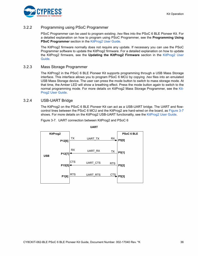
3.2.4 USB-UART Bridge
The KitProg2 on the PSoC 6 BLE Pioneer Kit can act as a USB-UART bridge. The UART and flow-control lines between the PSoC 6 MCU and the KitProg2 are hard-wired on the board, as Figure 3-7shows. For more details on the KitProg2 USB-UART functionality, see the KitProg2 User Guide.
Figure 3-7. UART connection between KitProg2 and PSoC 6
KitProg2 PSoC 6 BLE
UART
UART_TX
UART_RX
TX
TX
RX
RX
UART_CTS RTSCTS
UART_RTSRTS CTS
P12[6]
P12[7]
P15[5]
P1[6]
P5[0]
P5[1]
P5[2]
P5[3]
USB
CY8CKIT-062-BLE PSoC 6 BLE Pioneer Kit Guide, Document Number. 002-17040 Rev. *K 37
Kit Operation
3.2.5 USB-I2C Bridge
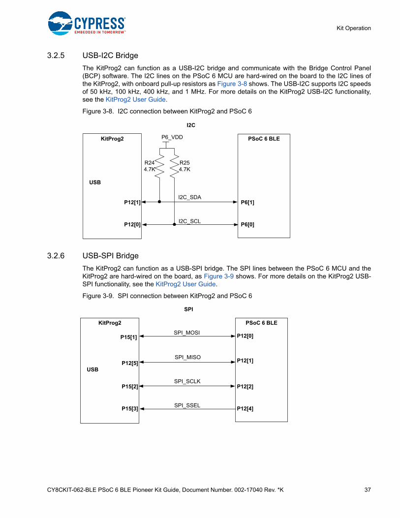
The KitProg2 can function as a USB-I2C bridge and communicate with the Bridge Control Panel(BCP) software. The I2C lines on the PSoC 6 MCU are hard-wired on the board to the I2C lines ofthe KitProg2, with onboard pull-up resistors as Figure 3-8 shows. The USB-I2C supports I2C speedsof 50 kHz, 100 kHz, 400 kHz, and 1 MHz. For more details on the KitProg2 USB-I2C functionality,see the KitProg2 User Guide.
Figure 3-8. I2C connection between KitProg2 and PSoC 6
3.2.6 USB-SPI Bridge
The KitProg2 can function as a USB-SPI bridge. The SPI lines between the PSoC 6 MCU and theKitProg2 are hard-wired on the board, as Figure 3-9 shows. For more details on the KitProg2 USB-SPI functionality, see the KitProg2 User Guide.
Figure 3-9. SPI connection between KitProg2 and PSoC 6
KitProg2 PSoC 6 BLE
I2C
I2C_SDA
I2C_SCL
P12[1]
P12[0]
P6[1]
P6[0]
P6_VDD
R244.7K
R254.7K
USB
KitProg2 PSoC 6 BLE
SPI
SPI_MOSI
SPI_MISO
SPI_SCLK
SPI_SSEL
P15[1]
P12[5]
P15[2]
P15[3]
P12[0]
P12[1]
P12[2]
P12[4]
USB
CY8CKIT-062-BLE PSoC 6 BLE Pioneer Kit Guide, Document Number. 002-17040 Rev. *K 38
Kit Operation
3.3 EZPD CCG3 Type-C Power Delivery
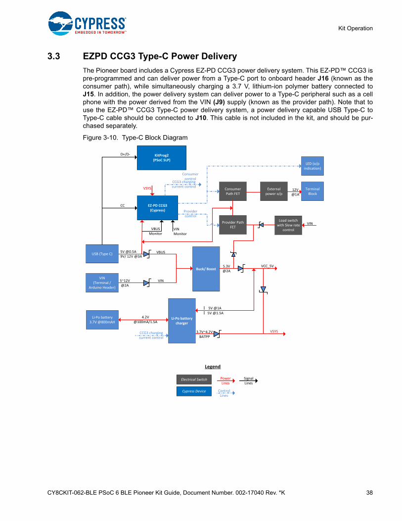
The Pioneer board includes a Cypress EZ-PD CCG3 power delivery system. This EZ-PD™ CCG3 ispre-programmed and can deliver power from a Type-C port to onboard header J16 (known as theconsumer path), while simultaneously charging a 3.7 V, lithium-ion polymer battery connected toJ15. In addition, the power delivery system can deliver power to a Type-C peripheral such as a cellphone with the power derived from the VIN (J9) supply (known as the provider path). Note that touse the EZ-PD™ CCG3 Type-C power delivery system, a power delivery capable USB Type-C toType-C cable should be connected to J10. This cable is not included in the kit, and should be pur-chased separately.
Figure 3-10. Type-C Block Diagram
VIN (Terminal /
Arduino Header)
5~12V@2A
5V @0.5A 9V/ 12V @3A
USB (Type C)
Buck/ Boost5.3V@2A
Li‐Po battery3.7V @800mAH
4.2V @100mA/1.5A
5V @1A
5V @1.5A
CCG3 charging current control
VIN
VBUS
Electrical Switch
Cypress Device
Li‐Po battery charger
Control Lines
Legend
EZ‐PD CCG3(Cypress)
KitProg2 (PSoC 5LP)
Providercontrol
VSYS
VINMonitor
VBUSMonitor
Power Lines
Signal Lines
D+/D‐
CC
VCC_5V
3.7V~4.2V BATPP
VSYS
Terminal Block
Consumer Path FET
12V@1A
Consumercontrol
CCG3 charging current control
External power o/p
Load switch with Slew rate
control
Provider Path FET
VIN
LED (o/p indication)
CY8CKIT-062-BLE PSoC 6 BLE Pioneer Kit Guide, Document Number. 002-17040 Rev. *K 39
Kit Operation
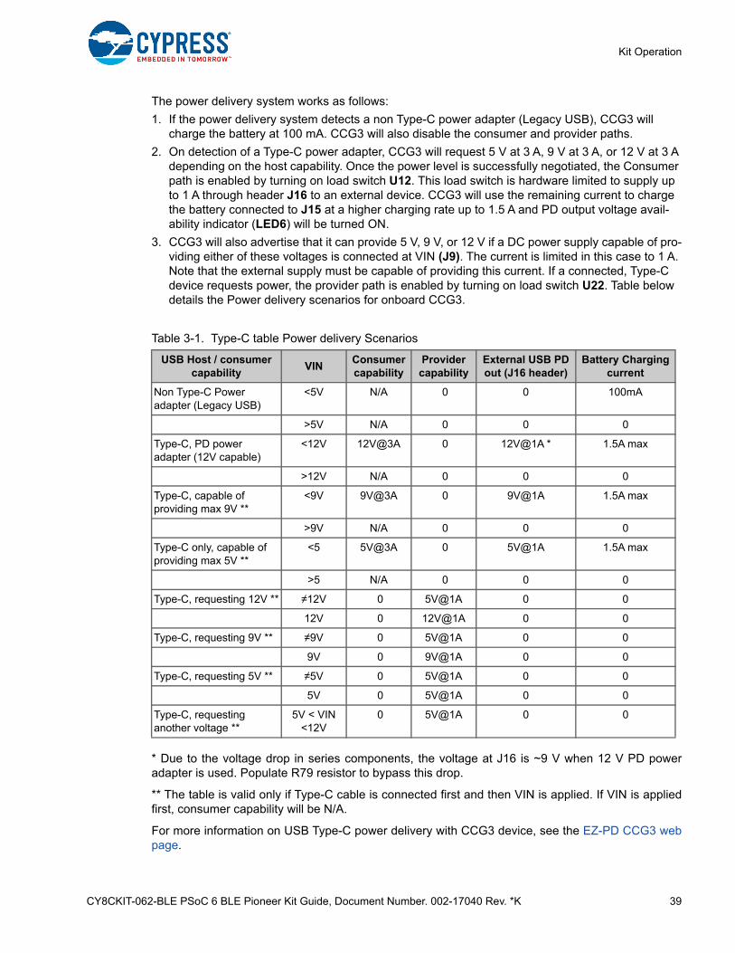
The power delivery system works as follows:
1. If the power delivery system detects a non Type-C power adapter (Legacy USB), CCG3 will charge the battery at 100 mA. CCG3 will also disable the consumer and provider paths.
2. On detection of a Type-C power adapter, CCG3 will request 5 V at 3 A, 9 V at 3 A, or 12 V at 3 A depending on the host capability. Once the power level is successfully negotiated, the Consumer path is enabled by turning on load switch U12. This load switch is hardware limited to supply up to 1 A through header J16 to an external device. CCG3 will use the remaining current to charge the battery connected to J15 at a higher charging rate up to 1.5 A and PD output voltage avail-ability indicator (LED6) will be turned ON.
3. CCG3 will also advertise that it can provide 5 V, 9 V, or 12 V if a DC power supply capable of pro-viding either of these voltages is connected at VIN (J9). The current is limited in this case to 1 A. Note that the external supply must be capable of providing this current. If a connected, Type-C device requests power, the provider path is enabled by turning on load switch U22. Table below details the Power delivery scenarios for onboard CCG3.
* Due to the voltage drop in series components, the voltage at J16 is ~9 V when 12 V PD poweradapter is used. Populate R79 resistor to bypass this drop.
** The table is valid only if Type-C cable is connected first and then VIN is applied. If VIN is appliedfirst, consumer capability will be N/A.
For more information on USB Type-C power delivery with CCG3 device, see the EZ-PD CCG3 webpage.
Table 3-1. Type-C table Power delivery Scenarios
USB Host / consumer capability
VINConsumer capability
Provider capability
External USB PD out (J16 header)
Battery Charging current
Non Type-C Power adapter (Legacy USB)
<5V N/A 0 0 100mA
>5V N/A 0 0 0
Type-C, PD power adapter (12V capable)
<12V 12V@3A 0 12V@1A * 1.5A max
>12V N/A 0 0 0
Type-C, capable of providing max 9V **
<9V 9V@3A 0 9V@1A 1.5A max
>9V N/A 0 0 0
Type-C only, capable of providing max 5V **
<5 5V@3A 0 5V@1A 1.5A max
>5 N/A 0 0 0
Type-C, requesting 12V ** ≠12V 0 5V@1A 0 0
12V 0 12V@1A 0 0
Type-C, requesting 9V ** ≠9V 0 5V@1A 0 0
9V 0 9V@1A 0 0
Type-C, requesting 5V ** ≠5V 0 5V@1A 0 0
5V 0 5V@1A 0 0
Type-C, requesting another voltage **
5V < VIN <12V
0 5V@1A 0 0
CY8CKIT-062-BLE PSoC 6 BLE Pioneer Kit Guide, Document Number. 002-17040 Rev. *K 40
4. Code Examples
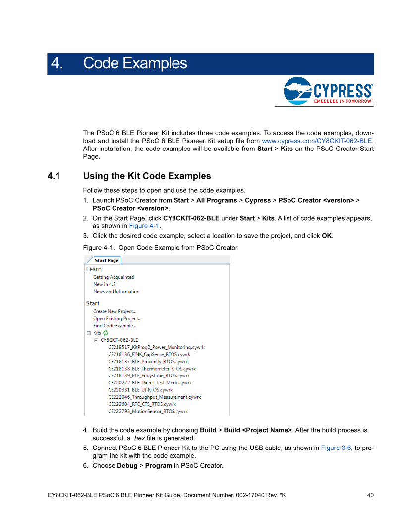
The PSoC 6 BLE Pioneer Kit includes three code examples. To access the code examples, down-load and install the PSoC 6 BLE Pioneer Kit setup file from www.cypress.com/CY8CKIT-062-BLE.After installation, the code examples will be available from Start > Kits on the PSoC Creator StartPage.
4.1 Using the Kit Code Examples
Follow these steps to open and use the code examples.
1. Launch PSoC Creator from Start > All Programs > Cypress > PSoC Creator <version> > PSoC Creator <version>.
2. On the Start Page, click CY8CKIT-062-BLE under Start > Kits. A list of code examples appears, as shown in Figure 4-1.
3. Click the desired code example, select a location to save the project, and click OK.
Figure 4-1. Open Code Example from PSoC Creator
4. Build the code example by choosing Build > Build <Project Name>. After the build process is successful, a .hex file is generated.
5. Connect PSoC 6 BLE Pioneer Kit to the PC using the USB cable, as shown in Figure 3-6, to pro-gram the kit with the code example.
6. Choose Debug > Program in PSoC Creator.
CY8CKIT-062-BLE PSoC 6 BLE Pioneer Kit Guide, Document Number. 002-17040 Rev. *K 41
Code Examples
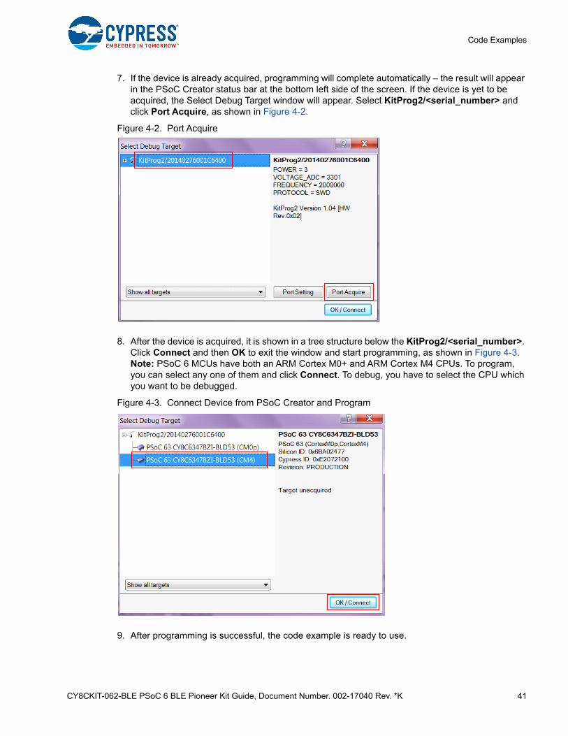
7. If the device is already acquired, programming will complete automatically – the result will appear in the PSoC Creator status bar at the bottom left side of the screen. If the device is yet to be acquired, the Select Debug Target window will appear. Select KitProg2/<serial_number> and click Port Acquire, as shown in Figure 4-2.
Figure 4-2. Port Acquire
8. After the device is acquired, it is shown in a tree structure below the KitProg2/<serial_number>. Click Connect and then OK to exit the window and start programming, as shown in Figure 4-3.Note: PSoC 6 MCUs have both an ARM Cortex M0+ and ARM Cortex M4 CPUs. To program, you can select any one of them and click Connect. To debug, you have to select the CPU which you want to be debugged.
Figure 4-3. Connect Device from PSoC Creator and Program
9. After programming is successful, the code example is ready to use.
CY8CKIT-062-BLE PSoC 6 BLE Pioneer Kit Guide, Document Number. 002-17040 Rev. *K 42
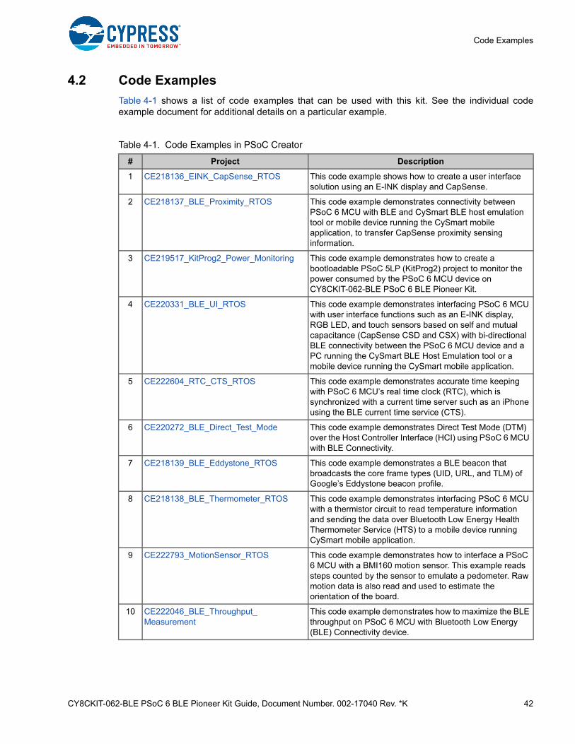
Code Examples
4.2 Code Examples
Table 4-1 shows a list of code examples that can be used with this kit. See the individual codeexample document for additional details on a particular example.
Table 4-1. Code Examples in PSoC Creator
# Project Description
1 CE218136_EINK_CapSense_RTOS This code example shows how to create a user interface solution using an E-INK display and CapSense.
2 CE218137_BLE_Proximity_RTOS This code example demonstrates connectivity between PSoC 6 MCU with BLE and CySmart BLE host emulation tool or mobile device running the CySmart mobile application, to transfer CapSense proximity sensing information.
3 CE219517_KitProg2_Power_Monitoring This code example demonstrates how to create a bootloadable PSoC 5LP (KitProg2) project to monitor the power consumed by the PSoC 6 MCU device on CY8CKIT-062-BLE PSoC 6 BLE Pioneer Kit.
4 CE220331_BLE_UI_RTOS This code example demonstrates interfacing PSoC 6 MCU with user interface functions such as an E-INK display, RGB LED, and touch sensors based on self and mutual capacitance (CapSense CSD and CSX) with bi-directional BLE connectivity between the PSoC 6 MCU device and a PC running the CySmart BLE Host Emulation tool or a mobile device running the CySmart mobile application.
5 CE222604_RTC_CTS_RTOS This code example demonstrates accurate time keeping with PSoC 6 MCU’s real time clock (RTC), which is synchronized with a current time server such as an iPhone using the BLE current time service (CTS).
6 CE220272_BLE_Direct_Test_Mode This code example demonstrates Direct Test Mode (DTM) over the Host Controller Interface (HCI) using PSoC 6 MCU with BLE Connectivity.
7 CE218139_BLE_Eddystone_RTOS This code example demonstrates a BLE beacon that broadcasts the core frame types (UID, URL, and TLM) of Google’s Eddystone beacon profile.
8 CE218138_BLE_Thermometer_RTOS This code example demonstrates interfacing PSoC 6 MCU with a thermistor circuit to read temperature information and sending the data over Bluetooth Low Energy Health Thermometer Service (HTS) to a mobile device running CySmart mobile application.
9 CE222793_MotionSensor_RTOS This code example demonstrates how to interface a PSoC 6 MCU with a BMI160 motion sensor. This example reads steps counted by the sensor to emulate a pedometer. Raw motion data is also read and used to estimate the orientation of the board.
10 CE222046_BLE_Throughput_Measurement
This code example demonstrates how to maximize the BLE throughput on PSoC 6 MCU with Bluetooth Low Energy (BLE) Connectivity device.
CY8CKIT-062-BLE PSoC 6 BLE Pioneer Kit Guide, Document Number. 002-17040 Rev. *K 43
A. Appendix
A.1 Schematics
Refer to the schematics files available in the kit installation directory under following paths:
1. <Install_Directory>\CY8CKIT-062-BLE PSoC 6 BLE Pioneer Kit\1.0\Hardware\CY8CKIT-028-EPD\CY8CKIT-028-EPD Schematic.pdf
2. <Install_Directory>\CY8CKIT-062-BLE PSoC 6 BLE Pioneer Kit\1.0\Hardware\CY8CKIT-062-BLE\CY8CKIT-062-BLE Schematic.pdf
A.2 Hardware Functional Description
This section explains in detail the individual hardware blocks of the PSoC 6 BLE Pioneer board.
A.2.1 PSoC 6 MCU (U1)
PSoC 6 MCU is Cypress’ latest, ultra-low-power PSoC specifically designed for wearables and IoTproducts. PSoC 6 MCU is a true programmable embedded system-on-chip, integrating a 150-MHz
ARM® Cortex®-M4 as the primary application processor, a 100-MHz ARM Cortex®-M0+ thatsupports low-power operations, up to 1 MB Flash and 288 KB SRAM, an integrated BLE 4.2 radio,CapSense touch-sensing, and custom analog and digital peripheral functions. The programmableanalog and digital peripheral functions allow higher flexibility, in-field tuning of the design, and fastertime-to-market.
For more information, see the PSoC 6 MCU web page and the datasheet.
A.2.2 PSoC 5LP (U2)
An onboard PSoC 5LP (CY8C5868LTI-LP039) is used as KitProg2 to program and debug PSoC 6MCU. The PSoC 5LP connects to the USB port of a PC through a USB connector and to the SWDand other communication interfaces of PSoC 6 MCU. The PSoC 5LP is a true system-level solutionproviding MCU, memory, analog, and digital peripheral functions in a single chip. The CY8C58LPxxfamily offers a modern method of signal acquisition, signal processing, and control with highaccuracy, high bandwidth, and high flexibility. Analog capability spans the range from thermocouples(near DC voltages) to ultrasonic signals.
For more information, visit the PSoC 5LP web page. Also, see the CY8C58LPxx Family Datasheet.
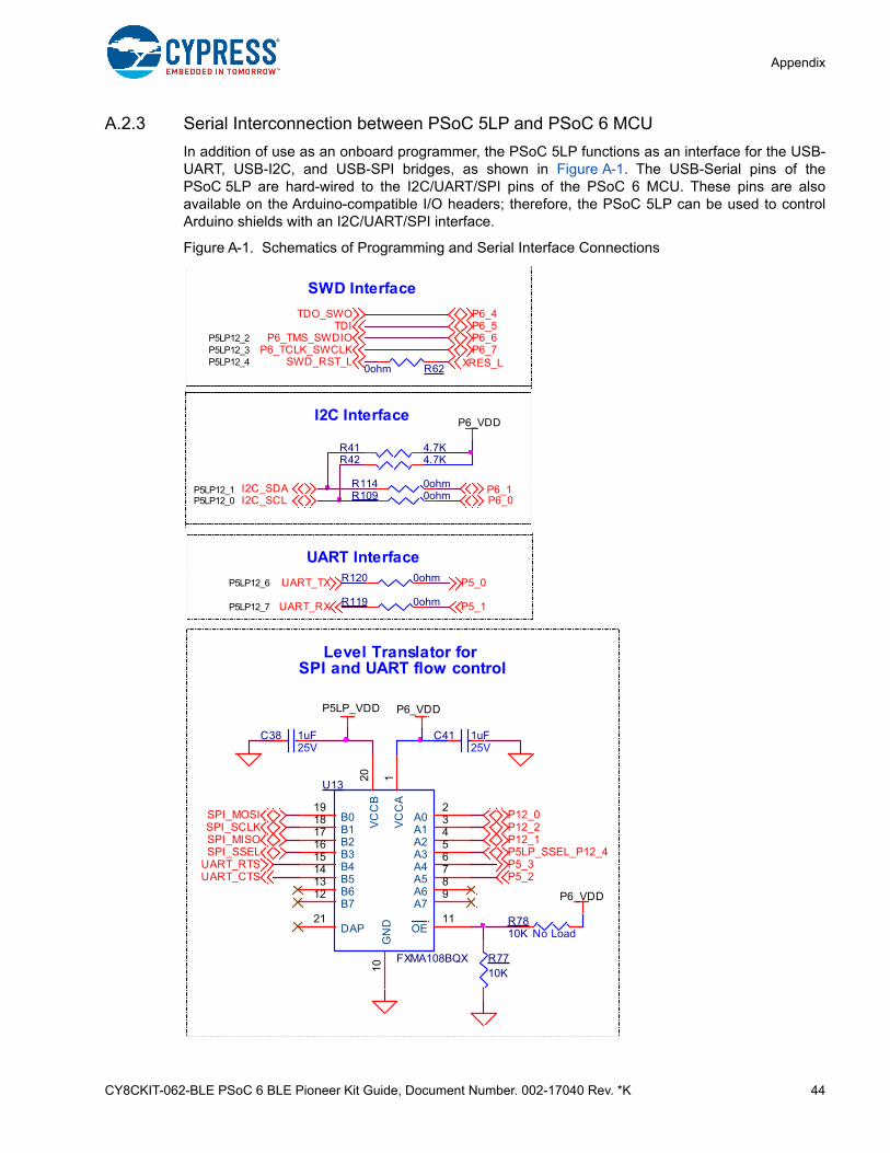
CY8CKIT-062-BLE PSoC 6 BLE Pioneer Kit Guide, Document Number. 002-17040 Rev. *K 44
Appendix
A.2.3 Serial Interconnection between PSoC 5LP and PSoC 6 MCU
In addition of use as an onboard programmer, the PSoC 5LP functions as an interface for the USB-UART, USB-I2C, and USB-SPI bridges, as shown in Figure A-1. The USB-Serial pins of thePSoC 5LP are hard-wired to the I2C/UART/SPI pins of the PSoC 6 MCU. These pins are alsoavailable on the Arduino-compatible I/O headers; therefore, the PSoC 5LP can be used to controlArduino shields with an I2C/UART/SPI interface.
Figure A-1. Schematics of Programming and Serial Interface Connections
R620ohmSWD_RST_L XRES_LP5LP12_4P5LP12_3P5LP12_2 P6_6
P6_TCLK_SWCLK
TDO_SWO
P6_TMS_SWDIO
P6_4P6_5
P6_7
TDI
SWD Interface
P5LP12_1P5LP12_0
I2C Interface
R114 0ohm
R42 4.7K
R109 0ohm
R41 4.7K
P6_VDD
P6_0P6_1I2C_SDA
I2C_SCL
P5LP12_6
P5LP12_7
UART Interface
UART_RX
UART_TX
P5_1
P5_0
R119 0ohm
R120 0ohm
C38 1uF25V
C41 1uF25V
U13
FXMA108BQX
VCC
A1
A02
A13
A24
A35
A46
A57
A68
A79
GN
D10
OE11
B019
B118
B217
B316
B415
B514
B613
B712
VCC
B20
DAP21
P6_VDDP5LP_VDD
SPI_SCLK
SPI_SSELSPI_MISO
SPI_MOSI P12_0
P5LP_SSEL_P12_4
P12_2P12_1
UART_CTSUART_RTS
P5_2P5_3
R7810K No Load
R7710K
P6_VDD
Level Translator for SPI and UART flow control
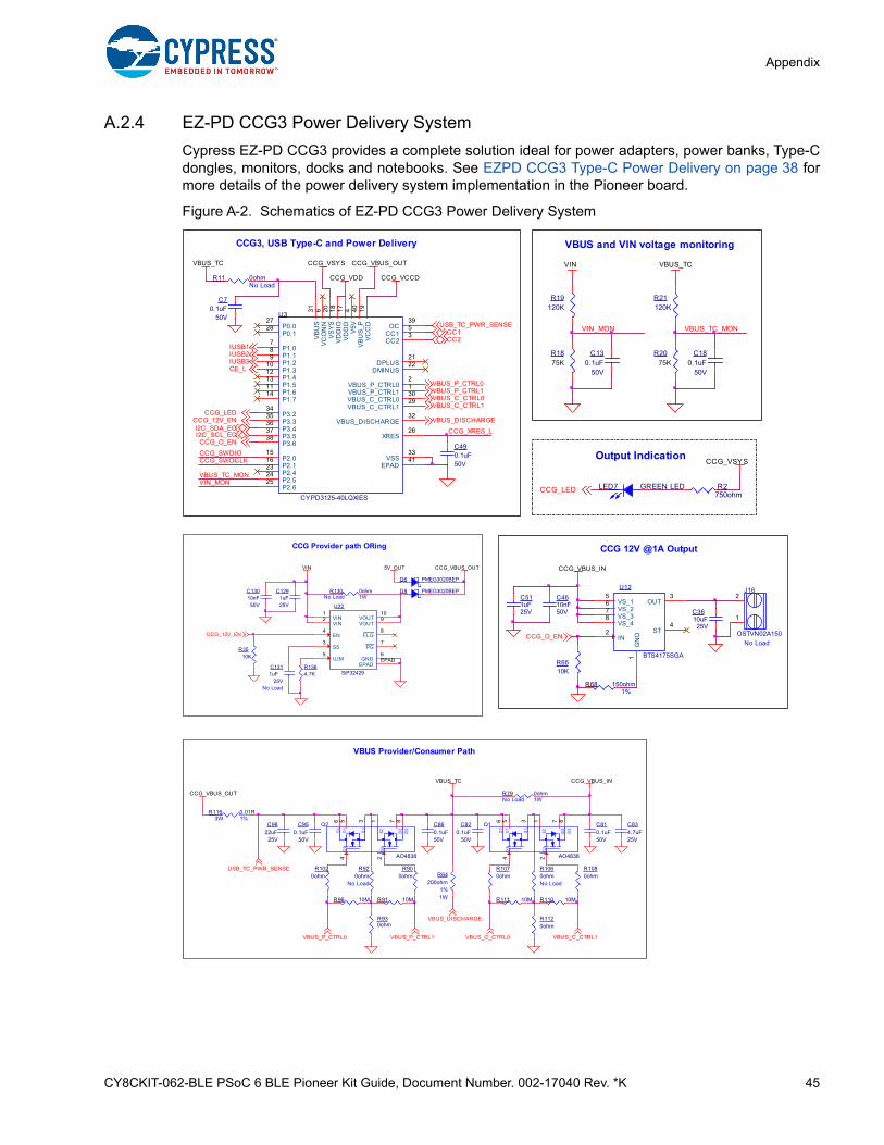
CY8CKIT-062-BLE PSoC 6 BLE Pioneer Kit Guide, Document Number. 002-17040 Rev. *K 45
Appendix
A.2.4 EZ-PD CCG3 Power Delivery System
Cypress EZ-PD CCG3 provides a complete solution ideal for power adapters, power banks, Type-Cdongles, monitors, docks and notebooks. See EZPD CCG3 Type-C Power Delivery on page 38 formore details of the power delivery system implementation in the Pioneer board.
Figure A-2. Schematics of EZ-PD CCG3 Power Delivery System
I2C_SCL_ECI2C_SDA_EC
VBUS_P_CTRL1VBUS_P_CTRL0
VBUS_C_CTRL1VBUS_C_CTRL0
VBUS_DISCHARGE
CCG_VSYS
CCG_VDD
CCG_VBUS_OUT
CCG_VCCD
U3
CYPD3125-40LQXIES
VBUS_P_CTRL11VBUS_P_CTRL02
CC23V5
V4
CC15
VCO
NN
6
P1.07
P1.18
P1.29
P1.310
P1.412
P1.513
P1.611
P1.714
P2.116 P2.015
VDD
D17
VDD
IO18
VCC
D19
VSYS
20
VBUS_C_CTRL030
VBUS_C_CTRL129
P0.128 P0.027
XRES26
P2.625 P2.524 P2.423
DMINUS22DPLUS21
VBU
S_P
40
OC39
P3.638 P3.537 P3.436 P3.335 P3.234
VSS33
VBUS_DISCHARGE32
VBU
S31
EPAD41
USB_TC_PWR_SENSE
C490.1uF50VCCG_SWDCLK
CCG_SWDIO
R11 0ohmNo Load
VBUS_TC
IUSB3
VBUS_TC_MON
IUSB1IUSB2
CC2CC1
C70.1uF
50V
CCG_XRES_L
CCG3, USB Type-C and Power Delivery
CCG_12V_ENCCG_LED
VIN_MON
CE_L
CCG_O_EN
CCG 12V @1A Output
C3610uF25V
CCG_VBUS_IN
R68 150ohm1%
U12
BTS4175SGA
GN
D1
IN2
OUT3
ST4
VS_15
VS_26
VS_37
VS_48
R6610K
C4610nF50V
C511uF25V
J16
OSTVN02A150No Load
1
2
CCG_O_EN
CCG_LED LED7 GREEN LED
Output Indication CCG_VSYS
R2750ohm
D8 PMEG3020BEP
D6 PMEG3020BEP
C1311uF
25VNo Load
R130 0ohmNo Load 1W
R1364.7K
VIN
U22
SiP32429
VIN1
VIN2
SS3
EN4
ILIM5
GND6
PG7
FLG8
VOUT9VOUT10
EPADEPAD
CCG Provider path ORing
CCG_12V_EN
5V_OUT CCG_VBUS_OUT
C13010nF
50V
C1291uF25V
R3510K
R1070ohm
R900ohm
C810.1uF50V
R1080ohm
S2G
2
D2
D2D1
S1
G1
D1
Q1
AO48384
36 12
875
R64200ohm
1%1W
C950.1uF
50V
R1120ohm
C9822uF25V
R96 10M R111 10M
C820.1uF
50V
R1020ohm
R116 0.01R1%3W
R79 0ohmNo Load 1W
S2G
2
D2
D2D1
S1
G1
D1
Q2
AO48384
36 12
875
R930ohm
C860.1uF50V
R91 10M
C834.7uF25V
R1060ohmNo Load
R110 10M
R920ohm
No Load
CCG_VBUS_OUT
CCG_VBUS_INVBUS_TC
VBUS_DISCHARGE
USB_TC_PWR_SENSE
VBUS_C_CTRL0VBUS_P_CTRL1VBUS_P_CTRL0 VBUS_C_CTRL1
VBUS Provider/Consumer Path
VBUS_TC_MON
VBUS_TC
R21120K
C180.1uF
50V
R2075K
VIN
R1875K
R19120K
C130.1uF
50V
VIN_MON
VBUS and VIN voltage monitoring
CY8CKIT-062-BLE PSoC 6 BLE Pioneer Kit Guide, Document Number. 002-17040 Rev. *K 46
Appendix
A.2.5 Power Supply System
The power supply system on this board is versatile, allowing the input supply to come from the fol-lowing sources:
■ 5 V, 9 V, or 12 V from the onboard USB Type-C connector
■ 5 V to 12 V power from an Arduino shield or from external power supply through VIN header J9 or J1
■ 3.7 V from a rechargeable Li-Po battery connected to J15
■ 5 V from an external programmer/debugger connected to J11 and J12
The power supply system is designed to support 1.8 V to 3.3 V operation of the PSoC 6 MCU. Inaddition, an intermediate voltage of 5 V is required for the operation of the power delivery circuitryand KitProg2. Therefore, three regulators are used to achieve 1.8 to 3.3 V and 5 V outputs - a buckboost regulator (U21) that generates a fixed 5 V from an input of 5 to 12 V, and a main regulator (U6)that generates a variable 1.8 V to 3.3 V and a fixed 3.3 V from the output of U21. Figure A-3 showsthe schematics of the voltage regulator and power selection circuits. In addition to this, the batterycharger U14 also functions as a boost regulator. U14 boosts the battery voltage to provide a 5 V tothe main regulator U6. This feature is enabled only when the VIN and the USB supply areunavailable.
The voltage selection is made through switch SW5. In addition, an onboard 330 mF super-capacitor(C52) can be used to power the backup domain power (Vbackup) of PSoC 6 MCU. Switch SW7selects the Vbackup supply connection of PSoC 6 MCU between VDDD and the super-capacitor.When VDDD is selected, the variable regulator ON/OFF terminal is controlled by KitProg2. When thesuper-capacitor is selected, the regulator ON/OFF terminal is controlled by PSoC 6 MCU. To ensureproper operation of PSoC 6 MCU, the super-capacitor, when selected, must be charged internally byPSoC 6 MCU before turning OFF the regulator. For more details of the PSoC 6 MCU backup systemand power supply, see the PSoC 6 BLE Technical Reference Manual.
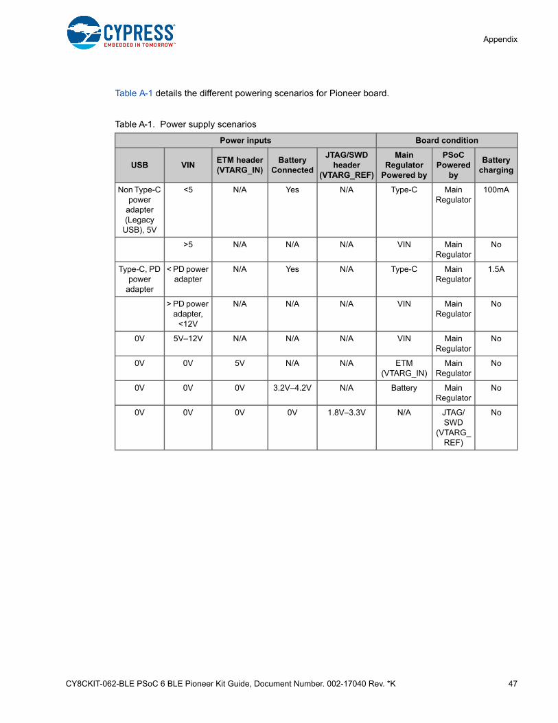
CY8CKIT-062-BLE PSoC 6 BLE Pioneer Kit Guide, Document Number. 002-17040 Rev. *K 47
Appendix
Table A-1 details the different powering scenarios for Pioneer board.
Table A-1. Power supply scenarios
Power inputs Board condition
USB VINETM header (VTARG_IN)
Battery Connected
JTAG/SWD header
(VTARG_REF)
Main Regulator
Powered by
PSoC Powered
by
Battery charging
Non Type-C power
adapter (Legacy
USB), 5V
<5 N/A Yes N/A Type-C Main Regulator
100mA
>5 N/A N/A N/A VIN Main Regulator
No
Type-C, PD power
adapter
< PD power adapter
N/A Yes N/A Type-C Main Regulator
1.5A
> PD power adapter,
<12V
N/A N/A N/A VIN Main Regulator
No
0V 5V–12V N/A N/A N/A VIN Main Regulator
No
0V 0V 5V N/A N/A ETM (VTARG_IN)
Main Regulator
No
0V 0V 0V 3.2V–4.2V N/A Battery Main Regulator
No
0V 0V 0V 0V 1.8V–3.3V N/A JTAG/SWD
(VTARG_REF)
No
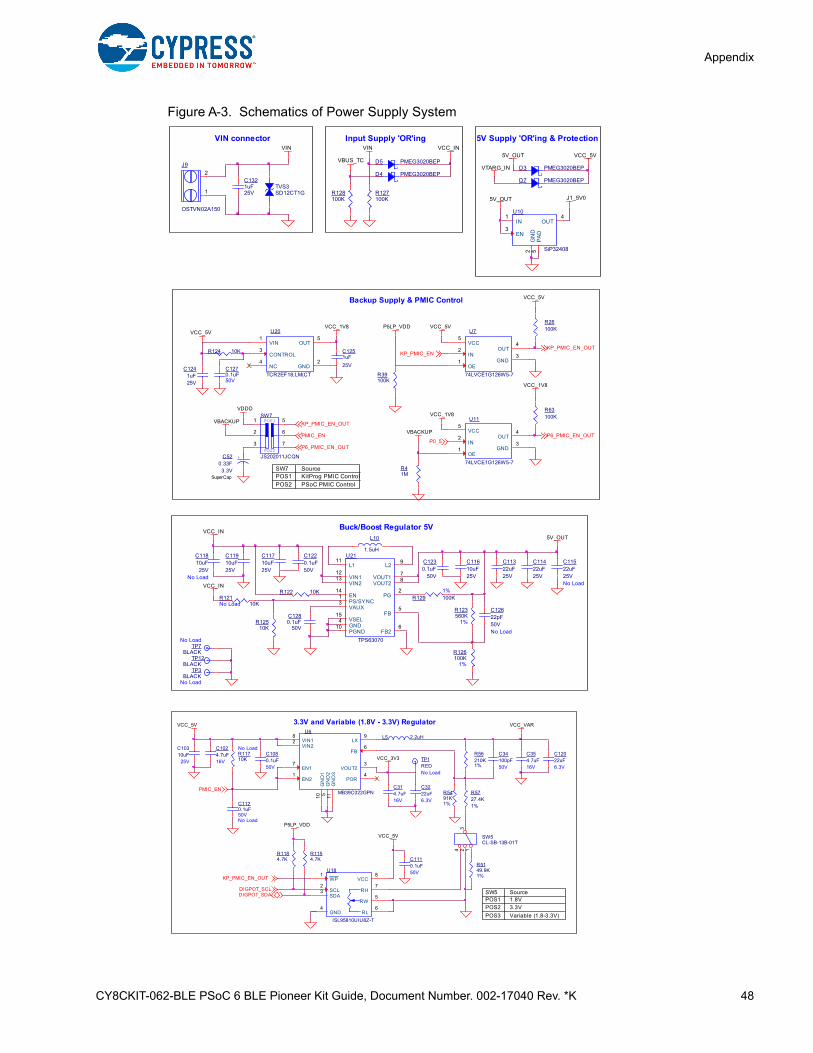
CY8CKIT-062-BLE PSoC 6 BLE Pioneer Kit Guide, Document Number. 002-17040 Rev. *K 48
Appendix
Figure A-3. Schematics of Power Supply System
D4 PMEG3020BEP
VBUS_TC
VIN
D5 PMEG3020BEP
VCC_IN
R128100K
R127100K
Input Supply 'OR'ing
TVS3SD12CT1G
J9
OSTVN02A150
1
2
VIN
C1321uF25V
VIN connector
J1_5V0
U10
SiP32408
OUT4
GN
D2
IN1
EN3
PAD
5
5V Supply 'OR'ing & Protection
D3 PMEG3020BEP
5V_OUT VCC_5V
5V_OUT
VTARG_IN
D7 PMEG3020BEP
R124 10K
U11
74LVCE1G126W5-7
OUT4
GND3
VCC5
OE1
IN2
U7
74LVCE1G126W5-7
OUT4
GND3
VCC5
OE1
IN2
U20
TCR2EF18,LM(CT
OUT5
GND2
VIN1
NC4
CONTROL3
VCC_5VVCC_1V8
VBACKUP
VCC_1V8
R41M
VCC_5V
R39100K
P5LP_VDDR26100K
VCC_5V
C1251uF25V
R63100K
C1241uF25V VCC_1V8
KP_PMIC_EN
P0_5P6_PMIC_EN_OUT
KP_PMIC_EN_OUT
PMIC_EN
POS1
POS2
SW7
JS202011JCQN
1
2
3
5
6
7
VBACKUP
+C520.33F3.3V
VDDD
SuperCap
P6_PMIC_EN_OUT
KP_PMIC_EN_OUT
Source
POS2KitProg PMIC Control
Backup Supply & PMIC Control
PSoC PMIC Control
SW7POS1
C1270.1uF50V
C1280.1uF
50V
C12622pF
No Load50V
C1220.1uF50V
C1230.1uF
50V
R12110KNo Load
R12510K
C11910uF25V
C11810uF25V
No Load
C11710uF25V
C11610uF25V
R122 10K
C11422uF25V
R129 100K1%
C11322uF25V
C11522uF
No Load25V
VCC_IN
U21
TPS63070
VOUT1 7L2 9L1
11
PGND10 GND4
FB5
EN14
PS/SYNC1
VIN112
VIN213
VSEL15
FB26
VOUT2 8
PG2
VAUX3
L10
1.5uH
VCC_IN
Buck/Boost Regulator 5V5V_OUT
R126100K
1%
R123560K
1%
TP7BLACK
No Load
TP3BLACK
No Load
TP12BLACK
R5727.4K1%
PMIC_EN
KP_PMIC_EN_OUT
VCC_3V3
U6
MB39C022GPN
EN21
VIN22
VOUT23
POR4
GN
D2
5
FB6
EN17
VIN18
LX9
GN
D1
10
GN
D3
11
R56210K1%
L5 2.2uH
C314.7uF16V
C354.7uF16V
C34100pF50V
VCC_5V
C10310uF
25V
C1024.7uF16V
3.3V and Variable (1.8V - 3.3V) Regulator
TP1REDNo Load
C1110.1uF50V
C1080.1uF50V
U18
ISL95810UIU8Z-T
WP1
SCL2
SDA3
GND4
RW5
RL6
RH7
VCC8
R5149.9K1%
R1154.7K
R1184.7K
R11710K
No Load
C1120.1uF50VNo Load
SW5CL-SB-13B-01T
123
4
P5LP_VDD
VCC_5V
DIGPOT_SDADIGPOT_SCL
VCC_VAR
SW5
3.3V1.8V
POS2
SourcePOS1
Variable (1.8-3.3V)POS3
R5491K1%
C12022uF6.3V
C3222uF6.3V
CY8CKIT-062-BLE PSoC 6 BLE Pioneer Kit Guide, Document Number. 002-17040 Rev. *K 49
Appendix
A.2.6 Expansion Connectors
A.2.6.1 Arduino-compatible Headers (J1, J2, J3, J4, and J5)
The board has five Arduino-compatible headers: J1, J2, J3, J4, and J5 (J5 is not populated bydefault). You can connect 3.3 V Arduino-compatible shields to develop applications based on theshield’s hardware. Note that 5 V shields are not supported and connecting a 5 V shield may perma-nently damage the board. See Appendix A.3 for details on PSoC 6 MCU pin mapping to these head-ers.
A.2.6.2 PSoC 6 MCU I/O Headers (J18, J19, and J20)
These headers provide connectivity to PSoC 6 MCU GPIOs that are not connected to the Arduinocompatible headers. Majority of these pins are multiplexed with onboard peripherals and are notconnected to PSoC 6 MCU by default. For the detailed information on how to rework the kit toaccess these pins, see PSoC 6 BLE Pioneer Board Rework on page 53.
A.2.6.3 PSoC 5LP GPIO Header (J6)
J6 is a 8x2 header provided on the board to bring out several pins of the PSoC 5LP to supportadvanced features such as a low-speed oscilloscope and a low-speed digital logic analyzer. Thisheader also contains the USB-UART, USB-I2C, and USB-SPI bridge pins that can be used whenthese pins are not accessible on the Arduino headers because a shield is connected. The additionalPSoC 5LP pins are connected directly to the internal programmable analog logic of PSoC 5LP. Thisheader also has GPIOs for custom application usage. J6 is not populated by default. Note that theSPI, RTS, and CTS lines on these headers are directly from PSoC 5LP (before level translator).
A.2.6.4 KitProg2 Custom Application Header (J7)
A 5x2 header is provided on the board to bring out more GPIOs of PSoC 5LP for custom applicationusage. This header also brings out the PSoC 5LP programming pins and can be programmed usingMiniProg3 and 5-pin programming connector. J7 is not populated by default.
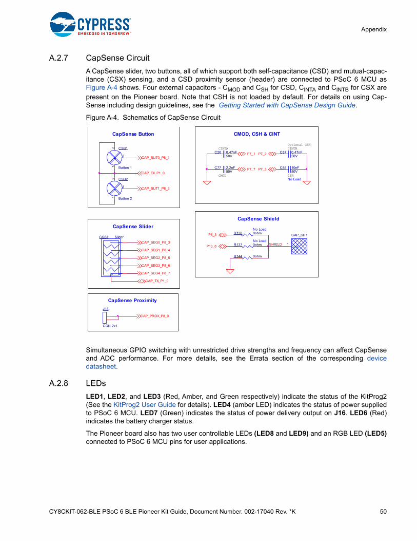
CY8CKIT-062-BLE PSoC 6 BLE Pioneer Kit Guide, Document Number. 002-17040 Rev. *K 50
Appendix
A.2.7 CapSense Circuit
A CapSense slider, two buttons, all of which support both self-capacitance (CSD) and mutual-capac-itance (CSX) sensing, and a CSD proximity sensor (header) are connected to PSoC 6 MCU asFigure A-4 shows. Four external capacitors - CMOD and CSH for CSD, CINTA and CINTB for CSX arepresent on the Pioneer board. Note that CSH is not loaded by default. For details on using Cap-Sense including design guidelines, see the Getting Started with CapSense Design Guide.
Figure A-4. Schematics of CapSense Circuit
Simultaneous GPIO switching with unrestricted drive strengths and frequency can affect CapSenseand ADC performance. For more details, see the Errata section of the corresponding devicedatasheet.
A.2.8 LEDs
LED1, LED2, and LED3 (Red, Amber, and Green respectively) indicate the status of the KitProg2(See the KitProg2 User Guide for details). LED4 (amber LED) indicates the status of power suppliedto PSoC 6 MCU. LED7 (Green) indicates the status of power delivery output on J16. LED6 (Red)indicates the battery charger status.
The Pioneer board also has two user controllable LEDs (LED8 and LED9) and an RGB LED (LED5)connected to PSoC 6 MCU pins for user applications.
CAP_TX_P1_0
P7_7 P7_3
Optional CSH
P13_6
P6_3 R138 0ohmNo Load
P7_1 P7_2
CSS1 Slider
4
3
2
1
0
5
CSB2
Button 212
3
CAP_TX_P1_0
CAP_BUT1_P8_2
CAP_BUT0_P8_1
CapSense Button
CSB1
Button 112
3
CAP_SEG3_P8_6
CAP_SEG2_P8_5
CAP_SEG1_P8_4
CAP_SEG0_P8_3
CapSense Slider
CAP_SEG4_P8_7
R137 0ohmNo Load
R144 0ohm
CapSense Shield
SHIELD
C88 10nF50V
No Load
C77 2.2nF50V
CMOD
CMOD, CSH & CINT
CSH
C26 0.47nF50V
C87 0.47nF50V
CINTBCINTA
CAP_SH1
SH1
CAP_PROX_P8_0
J13
CON 2x1
CapSense Proximity
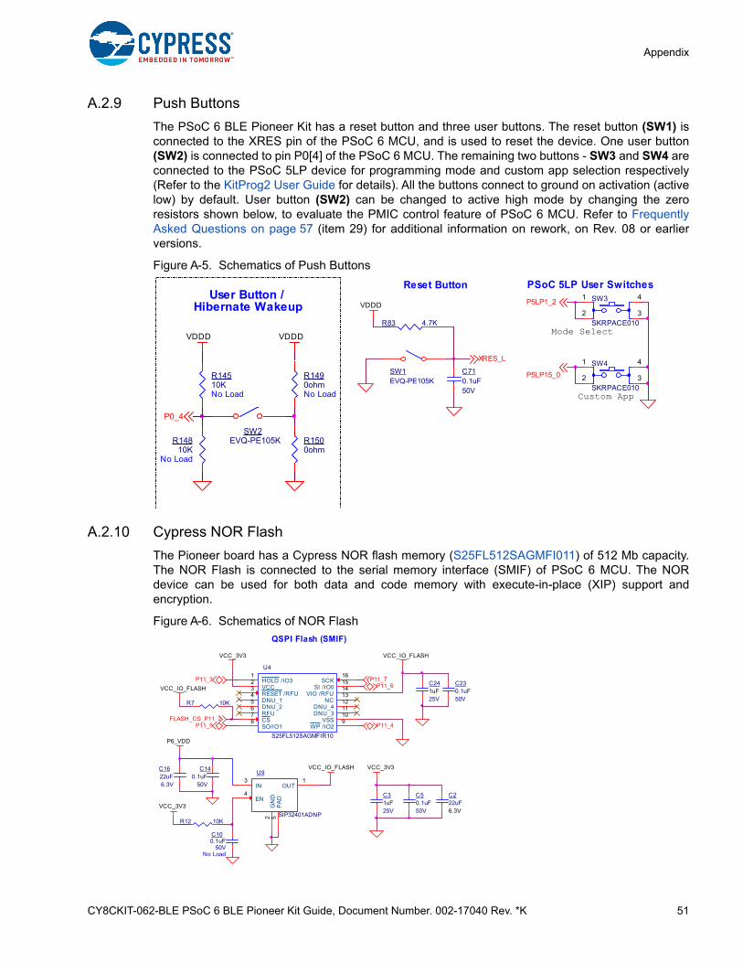
CY8CKIT-062-BLE PSoC 6 BLE Pioneer Kit Guide, Document Number. 002-17040 Rev. *K 51
Appendix
A.2.9 Push Buttons
The PSoC 6 BLE Pioneer Kit has a reset button and three user buttons. The reset button (SW1) isconnected to the XRES pin of the PSoC 6 MCU, and is used to reset the device. One user button(SW2) is connected to pin P0[4] of the PSoC 6 MCU. The remaining two buttons - SW3 and SW4 areconnected to the PSoC 5LP device for programming mode and custom app selection respectively(Refer to the KitProg2 User Guide for details). All the buttons connect to ground on activation (activelow) by default. User button (SW2) can be changed to active high mode by changing the zeroresistors shown below, to evaluate the PMIC control feature of PSoC 6 MCU. Refer to FrequentlyAsked Questions on page 57 (item 29) for additional information on rework, on Rev. 08 or earlierversions.
Figure A-5. Schematics of Push Buttons
A.2.10 Cypress NOR Flash
The Pioneer board has a Cypress NOR flash memory (S25FL512SAGMFI011) of 512 Mb capacity.The NOR Flash is connected to the serial memory interface (SMIF) of PSoC 6 MCU. The NORdevice can be used for both data and code memory with execute-in-place (XIP) support andencryption.
Figure A-6. Schematics of NOR Flash
R14810K
No Load
VDDD
R1490ohmNo Load
R1500ohm
R14510KNo Load
VDDD
User Button / Hibernate Wakeup
SW2EVQ-PE105K
P0_4
SW1EVQ-PE105K
Reset Button
XRES_L
R83 4.7K
VDDD
C710.1uF50V
P5LP15_0
P5LP1_2
SW4
SKRPACE010
1 4
2 3
Custom App
PSoC 5LP User Switches
Mode Select
SW3
SKRPACE010
1 4
2 3
C100.1uF
50VNo Load
R12 10K
VCC_IO_FLASH
C230.1uF50V
C241uF25V
P11_4
P11_6
P11_5
VCC_3V3
U4
S25FL512SAGMFIR10
HOLD /IO31
VCC2
RESET /RFU3
DNU_14
DNU_25
RFU6
CS7
SO/IO18
WP /IO29VSS10DNU_311DNU_412NC13VIO /RFU14SI /IO015SCK16
P11_7P11_3
QSPI Flash (SMIF)
FLASH_CS_P11_2
VCC_IO_FLASH
R7 10K
VCC_3V3
C50.1uF50V
C31uF25V
VCC_IO_FLASHU9
SIP32401ADNP
OUT1
GN
D2
IN3
EN4
PA
D5
VCC_3V3
P6_VDD
C222uF6.3V
C1622uF6.3V
C140.1uF
50V
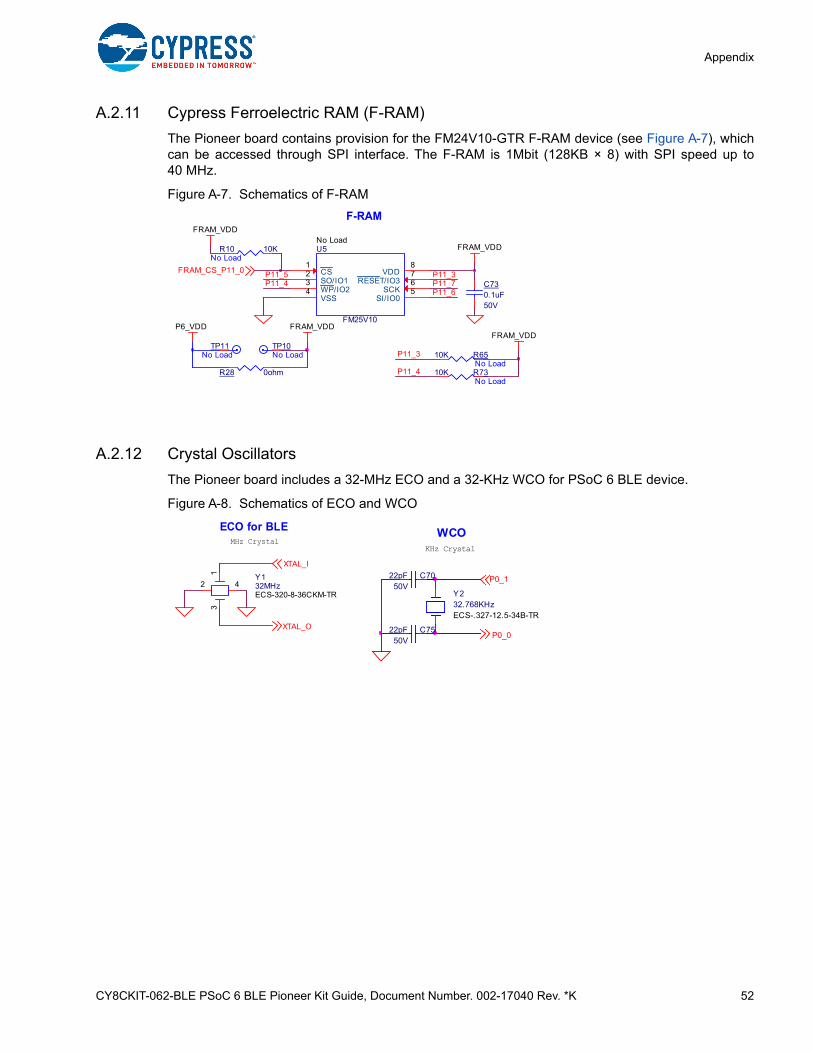
CY8CKIT-062-BLE PSoC 6 BLE Pioneer Kit Guide, Document Number. 002-17040 Rev. *K 52
Appendix
A.2.11 Cypress Ferroelectric RAM (F-RAM)
The Pioneer board contains provision for the FM24V10-GTR F-RAM device (see Figure A-7), whichcan be accessed through SPI interface. The F-RAM is 1Mbit (128KB × 8) with SPI speed up to40 MHz.
Figure A-7. Schematics of F-RAM
A.2.12 Crystal Oscillators
The Pioneer board includes a 32-MHz ECO and a 32-KHz WCO for PSoC 6 BLE device.
Figure A-8. Schematics of ECO and WCO
FRAM_VDD
P11_3 R6510KNo Load
P11_4 R7310KNo Load
P11_6
P11_5
FRAM_VDD
P11_3
U5
FM25V10
No Load
CS1
SO/IO12
WP/IO23
VSS4
SI/IO05SCK6RESET/IO37VDD8
P11_7P11_4
F-RAM
FRAM_CS_P11_0
R10 10KNo Load
FRAM_VDD
R28 0ohm
C730.1uF50V
FRAM_VDDP6_VDD
TP11No Load
TP10No Load
XTAL_I
XTAL_O
MHz Crystal
Y132MHzECS-320-8-36CKM-TR
1
2
3
4
ECO for BLE
P0_1
P0_0
Y232.768KHzECS-.327-12.5-34B-TR
C7522pF50V
C7022pF50V
KHz CrystalWCO
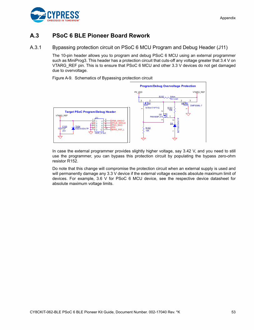
CY8CKIT-062-BLE PSoC 6 BLE Pioneer Kit Guide, Document Number. 002-17040 Rev. *K 53
Appendix
A.3 PSoC 6 BLE Pioneer Board Rework
A.3.1 Bypassing protection circuit on PSoC 6 MCU Program and Debug Header (J11)
The 10-pin header allows you to program and debug PSoC 6 MCU using an external programmersuch as MiniProg3. This header has a protection circuit that cuts-off any voltage greater that 3.4 V onVTARG_REF pin. This is to ensure that PSoC 6 MCU and other 3.3 V devices do not get damageddue to overvoltage.
Figure A-9. Schematics of Bypassing protection circuit
In case the external programmer provides slightly higher voltage, say 3.42 V, and you need to stilluse the programmer, you can bypass this protection circuit by populating the bypass zero-ohmresistor R152.
Do note that this change will compromise the protection circuit when an external supply is used andwill permanently damage any 3.3 V device if the external voltage exceeds absolute maximum limit ofdevices. For example, 3.6 V for PSoC 6 MCU device, see the respective device datasheet forabsolute maximum voltage limits.
Q5PMV48XP,215 1
23
R15115K
Q3
NTR4171PT1G1
23Q4
DMP3098L-7
1
2 3
P6_VDD VTARG_REF
R15310K
Program/Debug Overvoltage Protection
D9
BZT5
2C3V
9-7-
F
12
R152 0ohmNo Load
C1331uF25V
TVS4ESD3V3D5-TP
J11
HDR_S 5x2
22
11
44
33
66
55
88
77
99
1010
VTARG_REF
Target PSoC Program/Debug Header
TCLK_SWCLKTMS_SWDIO
TDITDO_SWO
SWD_RST_L
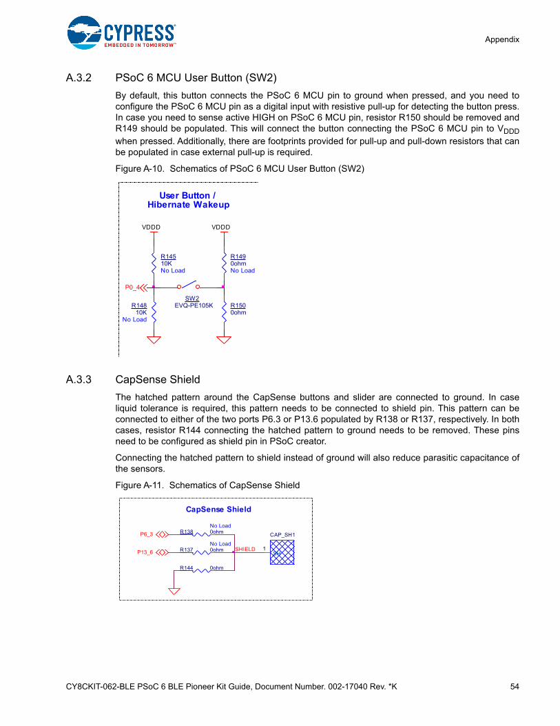
CY8CKIT-062-BLE PSoC 6 BLE Pioneer Kit Guide, Document Number. 002-17040 Rev. *K 54
Appendix
A.3.2 PSoC 6 MCU User Button (SW2)
By default, this button connects the PSoC 6 MCU pin to ground when pressed, and you need toconfigure the PSoC 6 MCU pin as a digital input with resistive pull-up for detecting the button press.In case you need to sense active HIGH on PSoC 6 MCU pin, resistor R150 should be removed andR149 should be populated. This will connect the button connecting the PSoC 6 MCU pin to VDDD
when pressed. Additionally, there are footprints provided for pull-up and pull-down resistors that canbe populated in case external pull-up is required.
Figure A-10. Schematics of PSoC 6 MCU User Button (SW2)
A.3.3 CapSense Shield
The hatched pattern around the CapSense buttons and slider are connected to ground. In caseliquid tolerance is required, this pattern needs to be connected to shield pin. This pattern can beconnected to either of the two ports P6.3 or P13.6 populated by R138 or R137, respectively. In bothcases, resistor R144 connecting the hatched pattern to ground needs to be removed. These pinsneed to be configured as shield pin in PSoC creator.
Connecting the hatched pattern to shield instead of ground will also reduce parasitic capacitance ofthe sensors.
Figure A-11. Schematics of CapSense Shield
R14810K
No Load
VDDD
R1490ohmNo Load
R1500ohm
R14510KNo Load
VDDD
User Button / Hibernate Wakeup
SW2EVQ-PE105K
P0_4
P13_6
P6_3 R138 0ohmNo Load
R137 0ohmNo Load
R144 0ohm
CapSense Shield
SHIELD
CAP_SH1
SH1
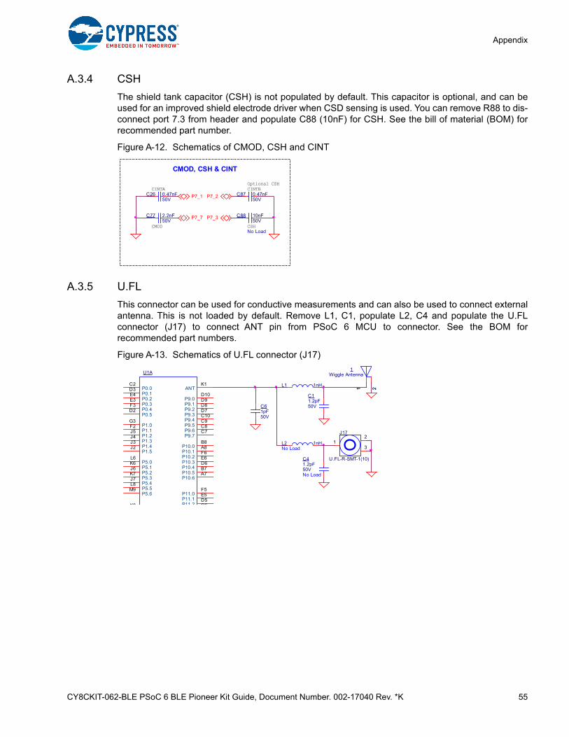
CY8CKIT-062-BLE PSoC 6 BLE Pioneer Kit Guide, Document Number. 002-17040 Rev. *K 55
Appendix
A.3.4 CSH
The shield tank capacitor (CSH) is not populated by default. This capacitor is optional, and can beused for an improved shield electrode driver when CSD sensing is used. You can remove R88 to dis-connect port 7.3 from header and populate C88 (10nF) for CSH. See the bill of material (BOM) forrecommended part number.
Figure A-12. Schematics of CMOD, CSH and CINT
A.3.5 U.FL
This connector can be used for conductive measurements and can also be used to connect externalantenna. This is not loaded by default. Remove L1, C1, populate L2, C4 and populate the U.FLconnector (J17) to connect ANT pin from PSoC 6 MCU to connector. See the BOM forrecommended part numbers.
Figure A-13. Schematics of U.FL connector (J17)
P7_7 P7_3
Optional CSH
P7_1 P7_2
C88 10nF50V
No Load
C77 2.2nF50V
CMOD
CMOD, CSH & CINT
CSH
C26 0.47nF50V
C87 0.47nF50V
CINTBCINTA
L1 1nH
L2 1nHNo Load
C41.2pF
No Load50V
J17
U.FL-R-SMT-1(10)
12
3
C11.2pF50VC6
1pF50V
1Wiggle Antenna
11 22U1A
P0.0C2
P0.1D3
P0.2E4
P0.3E3
P0.4F3
P0.5D2
P1.0G3
P1.1F2
P1.2J5
P1.3J4
P1.4J3
P1.5J2
P5.0L6
P5.1K6
P5.2J6
P5.3K7
P5.4J7
P5.5L8
P5.6M9
K8
ANTK1
P9.0D10
P9.1D9
P9.2D8
P9.3D7
P9.4C10
P9.5C9
P9.6C8
P9.7C7
P10.0B8
P10.1A8
P10.2F6
P10.3E6
P10.4D6
P10.5B7
P10.6A7
P11.0F5
P11.1E5
P11 2D5C6
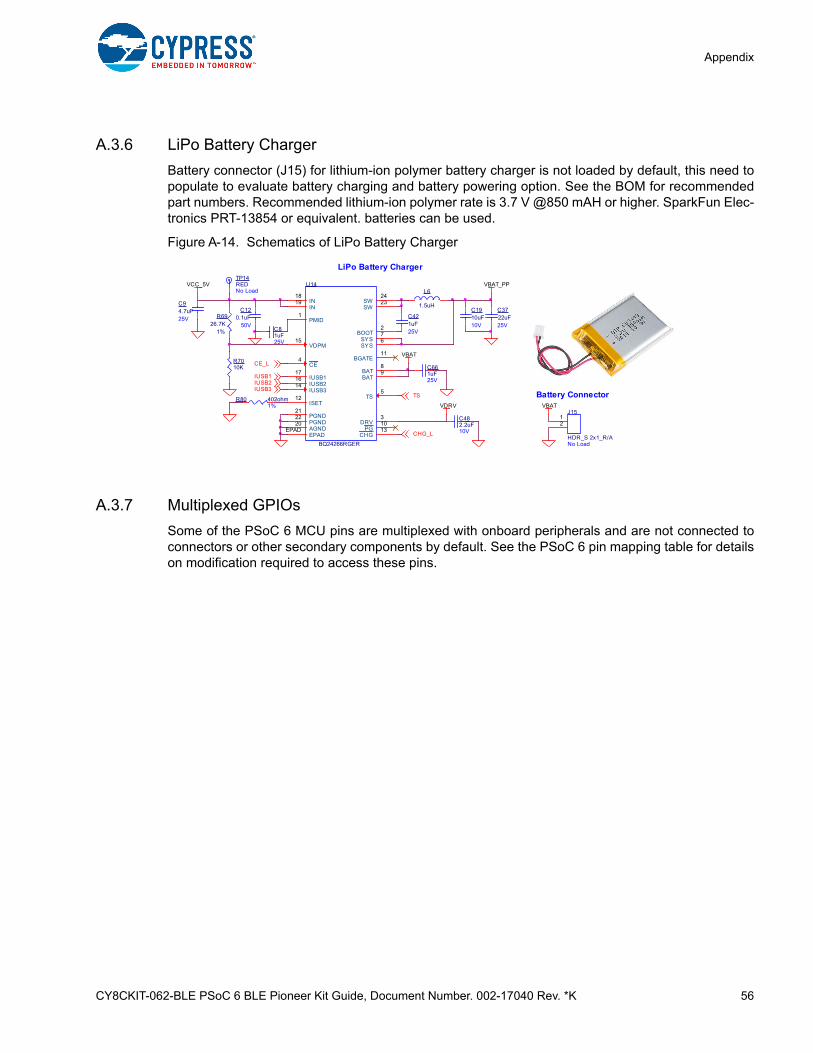
CY8CKIT-062-BLE PSoC 6 BLE Pioneer Kit Guide, Document Number. 002-17040 Rev. *K 56
Appendix
A.3.6 LiPo Battery Charger
Battery connector (J15) for lithium-ion polymer battery charger is not loaded by default, this need topopulate to evaluate battery charging and battery powering option. See the BOM for recommendedpart numbers. Recommended lithium-ion polymer rate is 3.7 V @850 mAH or higher. SparkFun Elec-tronics PRT-13854 or equivalent. batteries can be used.
Figure A-14. Schematics of LiPo Battery Charger
A.3.7 Multiplexed GPIOs
Some of the PSoC 6 MCU pins are multiplexed with onboard peripherals and are not connected toconnectors or other secondary components by default. See the PSoC 6 pin mapping table for detailson modification required to access these pins.
R80 402ohm1% VBAT
J15
HDR_S 2x1_R/ANo Load
12
LiPo Battery Charger TP14REDNo Load
Battery Connector
C482.2uF10V
C120.1uF
50V
CHG_L
TS
C1910uF10V
C94.7uF25V
VCC_5V U14
BQ24266RGER
PMID1
BOOT2
DRV3
CE4
TS5
SYS6SYS7
BAT8
BAT9
PG10
BGATE11
ISET12
CHG13
IUSB314
VDPM15
IUSB216 IUSB117
IN18
IN19
AGND20
PGND21
PGND22
SW23SW24
EPADEPAD
C81uF25V
R6926.7K
1%
VBATR7010K
L6
1.5uH
C661uF25V
VBAT_PP
C421uF25V
IUSB1
C3722uF25V
IUSB3IUSB2
CE_L
VDRV
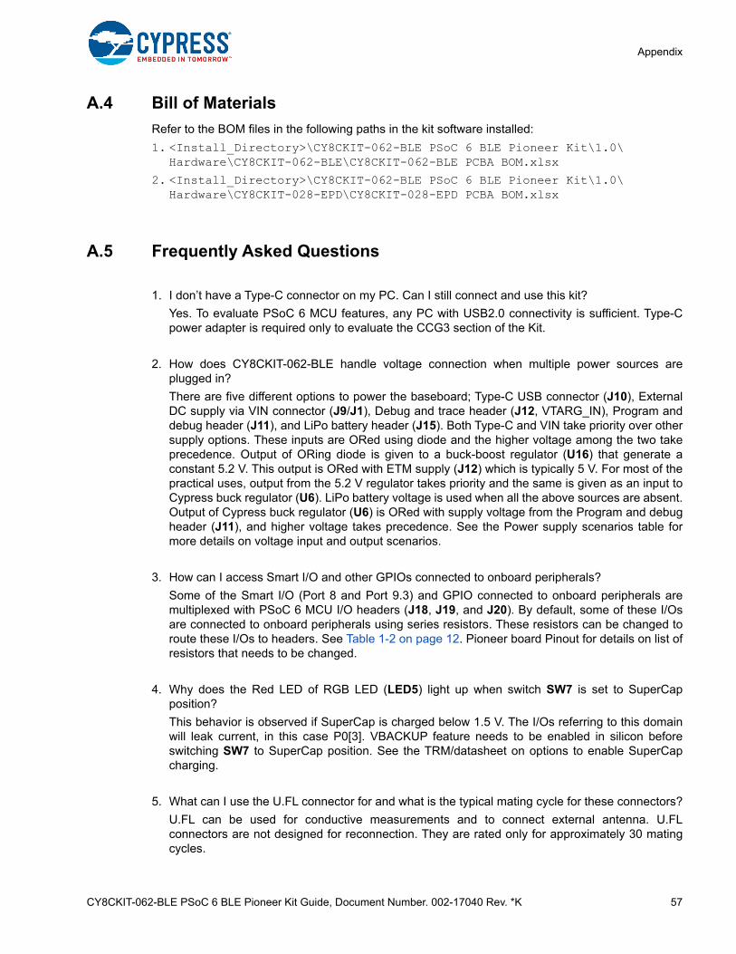
CY8CKIT-062-BLE PSoC 6 BLE Pioneer Kit Guide, Document Number. 002-17040 Rev. *K 57
Appendix
A.4 Bill of Materials
Refer to the BOM files in the following paths in the kit software installed:
1. <Install_Directory>\CY8CKIT-062-BLE PSoC 6 BLE Pioneer Kit\1.0\Hardware\CY8CKIT-062-BLE\CY8CKIT-062-BLE PCBA BOM.xlsx
2. <Install_Directory>\CY8CKIT-062-BLE PSoC 6 BLE Pioneer Kit\1.0\Hardware\CY8CKIT-028-EPD\CY8CKIT-028-EPD PCBA BOM.xlsx
A.5 Frequently Asked Questions
1. I don’t have a Type-C connector on my PC. Can I still connect and use this kit?
Yes. To evaluate PSoC 6 MCU features, any PC with USB2.0 connectivity is sufficient. Type-Cpower adapter is required only to evaluate the CCG3 section of the Kit.
2. How does CY8CKIT-062-BLE handle voltage connection when multiple power sources areplugged in?
There are five different options to power the baseboard; Type-C USB connector (J10), ExternalDC supply via VIN connector (J9/J1), Debug and trace header (J12, VTARG_IN), Program anddebug header (J11), and LiPo battery header (J15). Both Type-C and VIN take priority over othersupply options. These inputs are ORed using diode and the higher voltage among the two takeprecedence. Output of ORing diode is given to a buck-boost regulator (U16) that generate aconstant 5.2 V. This output is ORed with ETM supply (J12) which is typically 5 V. For most of thepractical uses, output from the 5.2 V regulator takes priority and the same is given as an input toCypress buck regulator (U6). LiPo battery voltage is used when all the above sources are absent.Output of Cypress buck regulator (U6) is ORed with supply voltage from the Program and debugheader (J11), and higher voltage takes precedence. See the Power supply scenarios table formore details on voltage input and output scenarios.
3. How can I access Smart I/O and other GPIOs connected to onboard peripherals?
Some of the Smart I/O (Port 8 and Port 9.3) and GPIO connected to onboard peripherals aremultiplexed with PSoC 6 MCU I/O headers (J18, J19, and J20). By default, some of these I/Osare connected to onboard peripherals using series resistors. These resistors can be changed toroute these I/Os to headers. See Table 1-2 on page 12. Pioneer board Pinout for details on list ofresistors that needs to be changed.
4. Why does the Red LED of RGB LED (LED5) light up when switch SW7 is set to SuperCapposition?
This behavior is observed if SuperCap is charged below 1.5 V. The I/Os referring to this domainwill leak current, in this case P0[3]. VBACKUP feature needs to be enabled in silicon beforeswitching SW7 to SuperCap position. See the TRM/datasheet on options to enable SuperCapcharging.
5. What can I use the U.FL connector for and what is the typical mating cycle for these connectors?
U.FL can be used for conductive measurements and to connect external antenna. U.FLconnectors are not designed for reconnection. They are rated only for approximately 30 matingcycles.
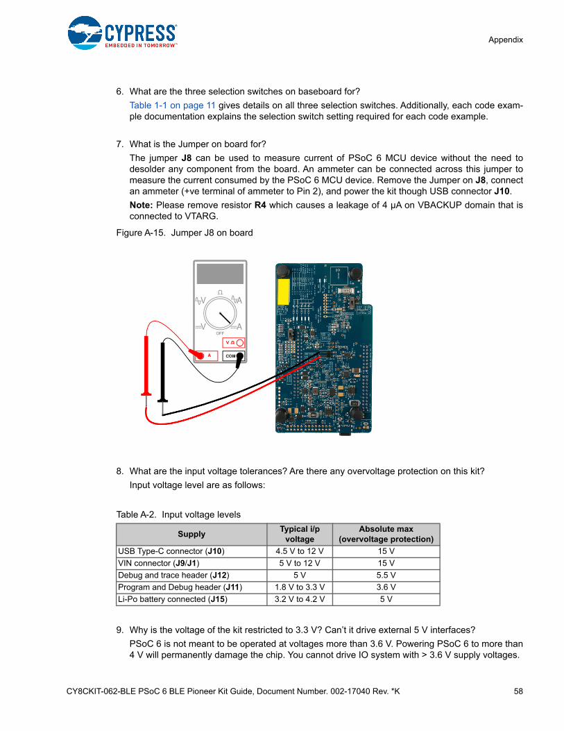
CY8CKIT-062-BLE PSoC 6 BLE Pioneer Kit Guide, Document Number. 002-17040 Rev. *K 58
Appendix
6. What are the three selection switches on baseboard for?
Table 1-1 on page 11 gives details on all three selection switches. Additionally, each code exam-ple documentation explains the selection switch setting required for each code example.
7. What is the Jumper on board for?
The jumper J8 can be used to measure current of PSoC 6 MCU device without the need todesolder any component from the board. An ammeter can be connected across this jumper tomeasure the current consumed by the PSoC 6 MCU device. Remove the Jumper on J8, connectan ammeter (+ve terminal of ammeter to Pin 2), and power the kit though USB connector J10.
Note: Please remove resistor R4 which causes a leakage of 4 µA on VBACKUP domain that isconnected to VTARG.
Figure A-15. Jumper J8 on board
8. What are the input voltage tolerances? Are there any overvoltage protection on this kit?
Input voltage level are as follows:
9. Why is the voltage of the kit restricted to 3.3 V? Can’t it drive external 5 V interfaces?
PSoC 6 is not meant to be operated at voltages more than 3.6 V. Powering PSoC 6 to more than4 V will permanently damage the chip. You cannot drive IO system with > 3.6 V supply voltages.
Table A-2. Input voltage levels
SupplyTypical i/p
voltageAbsolute max
(overvoltage protection)
USB Type-C connector (J10) 4.5 V to 12 V 15 V
VIN connector (J9/J1) 5 V to 12 V 15 V
Debug and trace header (J12) 5 V 5.5 V
Program and Debug header (J11) 1.8 V to 3.3 V 3.6 V
Li-Po battery connected (J15) 3.2 V to 4.2 V 5 V

CY8CKIT-062-BLE PSoC 6 BLE Pioneer Kit Guide, Document Number. 002-17040 Rev. *K 59
Appendix
10. By mistake, I powered my Arduino board while powering PSoC 6 MCU. Is my PSoC 6 chip alive?
Yes. The 3.3 V and 5 V on Arduino power header are not input pins and have protection circuit toprevent the voltage from entering the board. VIN is an input pin and this is routed to the regulatorthat is capable of taking an absolute maximum of 15 V. P6.VDD pin is not protected and careshould be taken not to supply voltage to this pin.
11. What type of battery can I use for this kit?
Recommended lithium-ion polymer rating is 3.7 V @850 mAH or higher. SparkFun ElectronicsPRT-13854 or equivalent batteries can be used. The LiPo battery charger can charge at 100 mAor 1.5 mA based on whether the USB connection is a legacy device or PD capable.
12. By mistake, I connected the battery with opposite polarity. Did I fry the system?
There are relevant protection circuits to protect the system from permanent damage. Prolongedconnection may lead to damage.
13. Can I charge any kind of Type-C device using this kit?
Kit is programmed to advertise the VIN voltage with 1 A current rating. 9 V and 12 V devices arethe recommended options. VIN needs to be 9 V and 12 V respectively for this to work.
14. How can I evaluate the USB Type-C provider and consumer features to get started with?
You can use any kind of Type-C laptop, mobile phone, or PD adapters based on the feature thatyou are trying to evaluate. To use as consumer, note that devices like laptop may be able toprovide only 5 V out and may not support 9 V/12 V without a docking station. To use as provider,any 5 V/9 V/12 V device that has a current requirement of less that 1 A may be used.Additionally, Cypress has its own USB Type-C evaluation Kit which can be used to evaluate theprovider and consumer features and many more. Visit http://www.cypress.com/products/usb-type-c-and-power-delivery for details on these kits.
15. Why is the screen of EPD permanently ON?
Electronic paper and e-paper are display devices that mimic the appearance of ordinary ink onpaper. Unlike conventional backlit flat panel displays that emit light, electronic paper displaysreflect light like paper. This may make it more comfortable to read and provide a wider viewingangle than most light-emitting displays. The contrast ratio in electronic displays available as of2008 approaches newspaper, and newly developed displays are slightly better. An ideal e-paperdisplay can be read in direct sunlight without the image fading. Many electronic papertechnologies hold static text and images indefinitely without electricity. To know the details, seehttps://en.wikipedia.org/wiki/Electronic_paper.
16. Why does the screen of EPD glitch from black to white during every transition?
The screen of EPD shield refreshes at every transition. It first clears all the cells of the display byspreading it with white pixels and then posts the images.
17. When I touch the resistors near the CapSense slider/button, the E-INK Display Shield and LEDare triggered. Why does this happen?
Those are the series limiting resistors which interface CapSense lines with ICs I/O lines. As youare touching CapSense lines, it triggers E-INK Display Shield which responds to CapSense.
CY8CKIT-062-BLE PSoC 6 BLE Pioneer Kit Guide, Document Number. 002-17040 Rev. *K 60
Appendix
18. The EPD shield shows white and black lines after I switched OFF the kit. Is the EPD shielddamaged?
EPD retains the image when you may have powered OFF the kit. In case the kit is powered OFFduring transition between images, lines might appear.
19. I am unable to program the target device.
a. Check SW6 to ensure it is in PSoC 6 MCU position.
b. Check SW7 to ensure it is in VDDD/KitProg2 position.
c. Make sure that no external devices are connected to J11.
d. Update your KitProg2 Version in programmer to 1.04 or later using the steps mentioned inKitProg2 User Guide.
e. Ensure that device used in PSoC Creator is CY8C6347BZI-BLD53
20. Does the kit get powered when I power the kit from another Cypress Kit through the J1 header?
Yes, VIN pin on J1 header is the supply input/output pin and can take up to 12 V.
21. What additional overlays can be used with the CapSense?
Any kind of overlays (up to 5 mm thickness) like wood, acrylic, and glass can be used with thisCapSense. Note that additional tuning may be required when the overlay is changed.
22. What is PMOD?
PMOD interface or Peripheral Module interface is an open standard defined by Digilent Inc in theDigilent Pmod Interface Specification for peripherals used with FPGAs or microcontrollers.Several types of modules are available from simple push buttons to more complex modules withnetwork interfaces, analog to digital converters or LCD displays. PMODs are available frommultiple vendors such as Diligent, Maxim Integrated, Analog Devices and a variety of hobbysites. This Kit supports only 1 x 6 pin PMOD modules.
23. With what type of shield from Cypress can I use this baseboard?
Any Arduino Uno shield which supports 3.3 V operation is compatible with this Pioneer board.Following cypress shields are pin compatible with this pioneer board:
a. CY3280-MBR3
b. CY8CKIT-022
c. CY8CKIT-024
d. CY8CKIT-026
e. CY8CKIT-040
f. CY8CKIT-046
g. CY8CKIT-048
24. Can I use this Kit as a programmer to program external PSoC devices?
Yes, the onboard KitProg2 can program any PSoC 4/5/6 devices connected to J11 header.Switch SW6 should be switched to “External Device” position to program devices connected viaJ11 header.
CY8CKIT-062-BLE PSoC 6 BLE Pioneer Kit Guide, Document Number. 002-17040 Rev. *K 61
Appendix
25. Which third-party debuggers does this Kit support?
Multiple third-party IDEs are supported; IAR and µVision are some examples. For more detailson all supported devices and procedures to export to these IDEs, see PSoC Creator ‘Help’menu.
26. Can I power PSoC 6 MCU using only external programmer at 1.8 V through the J11 header?
Yes, but there may be chance of failure as there is a voltage drop across the Overvoltageprotection circuit. R152 can be populated to bypass the protection circuit but is notrecommended due to the increased risk of damaging PSoC 6 MCU.
27. Can I power and program the PSoC 6 MCU using only MiniProg3 at 3.3 V?
The MiniProg3 Rev *B has an error in target voltage which exceeds the tolerance of theovervoltage protection circuit which can cause failure. However, this will work in MiniProg3Rev *C which has lesser error in target voltage. R152 can be populated to bypass the protectioncircuit but is not recommended due to the increased risk of damaging PSoC 6 MCU.
28. Why the on-board RGB LED (LED5) does not work when I select on a supply voltage of 1.8 Vusing SW5?
The on board RGB LED requires a supply voltage higher than 2.7 V to function correctly. Ensurethat SW5 is set to the 3.3 V or 1.8 V–3.3 V VARIABLE with PSoC Programmer selecting avoltage of 2.7 V or higher in the latter case. Using this kit with voltage lower than 2.7 V will affectthe RGB LED operation. Alternatively, you can use discrete LEDs (LED8 and LED9) if theapplication permits.
29. How to use SW2 for PMIC wake up?
SW2 is connected to the PMIC_Wakeup_In pin (P0.4) of PSoC 6 MCU. A logic high input at thePMIC_Wakeup_In pin can wake up the system and enable the PMIC. See the Backup chapter inPSoC 6 MCU Architecture Technical Reference Manual for more details of this feature.
SW2 should be externally pulled down to ground to use PMIC control. Moreover, when the switchis pressed, the active high logic should push P0.4 to the VBACKUP supply. However, the kit isconfigured by default to use active low logic. In addition, in Rev08 and earlier versions of the kit,the active high logic for SW2 pushes P0.4 to VDDD. Therefore, the following rework on the kit arerequired to use the PMIC control feature:
❐ Remove R150 and connect the common pad between R150 and R149 to the positive terminal of super-capacitor (C52).
❐ Load external pull-down resistor R148.
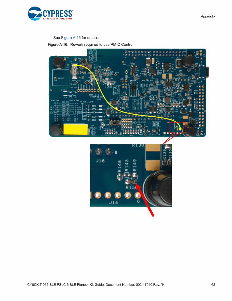
CY8CKIT-062-BLE PSoC 6 BLE Pioneer Kit Guide, Document Number. 002-17040 Rev. *K 62
Appendix
See Figure A-16 for details.
Figure A-16. Rework required to use PMIC Control
CY8CKIT-062-BLE PSoC 6 BLE Pioneer Kit Guide, Document Number. 002-17040 Rev. *K 63
Revision History
Document Revision HistoryDocument Title: CY8CKIT-062-BLE PSoC 6 BLE Pioneer Kit Guide
Document Number: 002-17040
Revision ECN Number Issue Date Description of Change
*B 5866901 09/25/2017 Initial version for public release.
*C 6028820 02/02/2018 Updated Introduction chapter on page 8:
Updated “Kit Contents” on page 8:
Updated Figure 1-1.
Updated “Board Details” on page 9:
Updated Figure 1-4.
Updated Figure 1-5.
Updated Table 1-2.
Updated “Technical Support” on page 22:
Replaced “Ext. 2” with “Ext. 3”.
Updated Software Installation chapter on page 25:
Updated “Install Software” on page 25:
Updated description.
Updated Kit Operation chapter on page 28:
Updated “Theory of Operation” on page 28:
Updated Figure 3-3.
Updated “CY8CKIT-028-EPD E-INK Display Shield” on page 34:
Updated Figure 3-5.
Updated “KitProg2” on page 35:
Updated “Programming and Debugging using PSoC Creator” on page 35:
Updated Figure 3-6.
Updated “EZPD CCG3 Type-C Power Delivery” on page 38:
Updated Table 3-1.
Updated Code Examples chapter on page 40:
Updated “Using the Kit Code Examples” on page 40:
Updated Figure 4-1.
Updated “Code Examples” on page 42:
Updated Table 4-1.
CY8CKIT-062-BLE PSoC 6 BLE Pioneer Kit Guide, Document Number. 002-17040 Rev. *K 64
Revision History
*C (cont.) 6028820 02/02/2018 Updated Appendix chapter on page 43:
Updated “Hardware Functional Description” on page 43:
Updated “Push Buttons” on page 51:
Updated Figure A-5.
Updated “Cypress NOR Flash” on page 51:
Added Figure A-6.
Added “Cypress Ferroelectric RAM (F-RAM)” on page 52.
Added “Crystal Oscillators” on page 52.
Updated “Frequently Asked Questions” on page 57:
Updated description.
Added Figure A-15.
*D 6072011 04/27/2018 Updated Safety and Regulatory Compliance Information chapter on page 5:
Replaced “Safety Information” with “Safety and Regulatory Compliance Information” in chapter heading.
Updated description.
Updated “General Safety Instructions” on page 5:
Updated “Handling Boards” on page 5:
Updated description.
Added “Regulatory Compliance Information” on page 6.
Updated Introduction chapter on page 8:
Updated “Kit Contents” on page 8:
Updated Figure 1-1.
Updated “Board Details” on page 9:
Updated Table 1-2.
Updated Appendix chapter on page 43:
Updated “Hardware Functional Description” on page 43:
Updated “Push Buttons” on page 51:
Updated description.
Updated “Frequently Asked Questions” on page 57:
Updated description.
Added Figure A-16.
Updated to new template.
*E 6163552 05/02/2018 Updated Appendix chapter on page 43:
Updated “PSoC 6 BLE Pioneer Board Rework” on page 53:
Replaced “reworks” with “rework” in heading.
Updated “Frequently Asked Questions” on page 57:
Replaced “re-works” with “rework” in all instances.
*F 6225773 07/02/2018 Updated details (Document Properties) in File > File Info.
Document Revision History (continued)Document Title: CY8CKIT-062-BLE PSoC 6 BLE Pioneer Kit Guide
Document Number: 002-17040
Revision ECN Number Issue Date Description of Change
CY8CKIT-062-BLE PSoC 6 BLE Pioneer Kit Guide, Document Number. 002-17040 Rev. *K 65
Revision History
*G 6250775 07/17/2018 Updated Code Examples chapter on page 40:
Updated “Using the Kit Code Examples” on page 40:
Updated Figure 4-1.
Updated “Code Examples” on page 42:
Updated Table 4-1.
*H 6537683 04/09/2019 Updated Kit Operation chapter on page 28:
Updated “Theory of Operation” on page 28:
Updated description.
Updated Appendix chapter on page 43:
Updated “Hardware Functional Description” on page 43:
Updated “CapSense Circuit” on page 50:
Updated description.
*I 6642215 08/26/2019 Updated Document Title to read as “CY8CKIT-062-BLE PSoC 6 BLE Pioneer Kit Guide”.
Updated Appendix chapter on page 43:
Updated “Frequently Asked Questions” on page 57:
Updated description.
Updated to new template.
*J 6782941 01/21/2020 Updated Appendix chapter on page 43:
Updated “Hardware Functional Description” on page 43:
Updated “Crystal Oscillators” on page 52:
Updated Figure A-8.
*K 6797961 02/05/2020 Updated Kit Operation chapter on page 28:
Updated “Theory of Operation” on page 28:
Updated description.
Document Revision History (continued)Document Title: CY8CKIT-062-BLE PSoC 6 BLE Pioneer Kit Guide
Document Number: 002-17040
Revision ECN Number Issue Date Description of Change