3 and PSoC 5LP – Pin Selection for Analog Designs
12
www.cypress.com Document No. 001-58304 Rev. *H 1 AN58304 PSoC ® 3 and PSoC 5LP – Pin Selection for Analog Designs Author: Mark Hastings Associated Project: No Associated Part Family: All PSoC 3 and PSoC 5LP parts Software Version: NA Related Application Notes: None AN58304 provides an overview of the analog routing matrix in PSoC ® 3 and PSoC 5LP. This matrix is used to interconnect analog blocks and GPIO pins. A good understanding of the analog routing and pin connections can help the designer make selections to achieve the best possible analog performance. Topics such as LCD and CapSense routing are not covered in this application note. Contents PSoC 3 and PSoC 5LP Internal Analog Routing ............... 1 Best Analog Ports......................................................... 2 Analog Mux Bus (AMUXBUS) ...................................... 4 Analog Globals (AGs) ................................................... 4 GPIO Connection to Analog Busses ............................ 5 Optimizing Routing Resources ..................................... 5 Analog Local Bus (abus) .............................................. 6 Routing Example .......................................................... 6 Direct Routes to GPIO Pins .......................................... 6 IDAC Pin Selection ....................................................... 6 Opamp Pin Selection .................................................... 7 Reference Voltage Pins ................................................ 7 Separating Analog and Digital Signals ......................... 8 Analog Device Editor ......................................................... 9 Summary ......................................................................... 10 About the Author ............................................................. 10 Worldwide Sales and Design Support ............................. 12 PSoC 3 and PSoC 5LP Internal Analog Routing Prior to discussing which pins are better than others for a particular operation or application, it is best to understand the underlying analog structure of the PSoC 3 and PSoC 5LP parts. This application note will help the reader understand how the basic analog structure works when adding a signal path between two points or placing an analog mux. PSoC Creator™ will do a good job routing most designs, but with some assistance from the designer, better performance can be achieved. Tools are provided in PSoC Creator to allow the user to validate and to make changes to the internal analog routing of a design if needed. This application note focuses on connections between the analog blocks and GPIO pins. Digital routing, SIO, USB, and pins used for connecting the external crystals are not discussed. PSoC 3 and PSoC 5LP can be divided into an analog and digital section. The top section of the silicon is mostly analog and the bottom section is digital. The analog section consists of several analog blocks such as a Delta-Sigma ADC (DSM), comparators, DACs, and SC/CT blocks. The digital section contains the CPU, RAM, ROM, DMA, UDBs, Clocks, and so on. The entire chip is surrounded by pins. Most of these pins are general purpose I/O or GPIO pins. The GPIO pins can be configured for eight different modes: seven digital and one analog input/output mode. This application note concentrates only on the analog mode for these pins.
-
Upload
khangminh22 -
Category
Documents
-
view
0 -
download
0
Transcript of 3 and PSoC 5LP – Pin Selection for Analog Designs

www.cypress.com Document No. 001-58304 Rev. *H 1
AN58304
PSoC® 3 and PSoC 5LP – Pin Selection for Analog Designs
Author: Mark Hastings Associated Project: No
Associated Part Family: All PSoC 3 and PSoC 5LP parts Software Version: NA
Related Application Notes: None
AN58304 provides an overview of the analog routing matrix in PSoC® 3 and PSoC 5LP. This matrix is used to
interconnect analog blocks and GPIO pins. A good understanding of the analog routing and pin connections can help
the designer make selections to achieve the best possible analog performance. Topics such as LCD and CapSense
routing are not covered in this application note.
Contents
PSoC 3 and PSoC 5LP Internal Analog Routing ............... 1
Best Analog Ports ......................................................... 2 Analog Mux Bus (AMUXBUS) ...................................... 4 Analog Globals (AGs) ................................................... 4 GPIO Connection to Analog Busses ............................ 5 Optimizing Routing Resources ..................................... 5 Analog Local Bus (abus) .............................................. 6 Routing Example .......................................................... 6 Direct Routes to GPIO Pins .......................................... 6 IDAC Pin Selection ....................................................... 6 Opamp Pin Selection .................................................... 7 Reference Voltage Pins ................................................ 7 Separating Analog and Digital Signals ......................... 8
Analog Device Editor ......................................................... 9 Summary ......................................................................... 10 About the Author ............................................................. 10 Worldwide Sales and Design Support ............................. 12
PSoC 3 and PSoC 5LP Internal Analog Routing
Prior to discussing which pins are better than others for a particular operation or application, it is best to understand the underlying analog structure of the PSoC 3 and PSoC 5LP parts. This application note will help the reader understand how the basic analog structure works when adding a signal path between two points or placing an analog mux. PSoC Creator™ will do a good job routing most designs, but with some assistance from the designer, better performance can be achieved. Tools are provided in PSoC Creator to allow the user to validate and to make changes to the internal analog routing of a design if needed.
This application note focuses on connections between the analog blocks and GPIO pins. Digital routing, SIO, USB, and pins used for connecting the external crystals are not discussed.
PSoC 3 and PSoC 5LP can be divided into an analog and
digital section. The top section of the silicon is mostly analog and the bottom section is digital. The analog section consists of several analog blocks such as a Delta-Sigma ADC (DSM), comparators, DACs, and SC/CT blocks. The digital section contains the CPU, RAM, ROM, DMA, UDBs, Clocks, and so on.
The entire chip is surrounded by pins. Most of these pins are general purpose I/O or GPIO pins. The GPIO pins can be configured for eight different modes: seven digital and one analog input/output mode. This application note concentrates only on the analog mode for these pins.

PSoC® 3 and PSoC 5LP – Pin Selection for Analog Designs
www.cypress.com Document No. 001-58304 Rev. *H 2
Analog globals (AG) and analog mux buses (AMUXBUS) provide analog connectivity between GPIOs and the various analog blocks. As shown in Figure 1, there are 16 AGs that are divided between four quadrants. Each quadrant contains four analog globals: (AGR[7:4], AGR[3:0], AGL[7:4], and AGL[3:0]). The analog mux bus may be connected to any of the GPIO pins and most of the analog block inputs and outputs. It may be divided between the left and right half of the chip or configured as a single bus that wraps around the entire chip. Together, the analog mux bus and analog globals provide up to 18 paths between the analog blocks and GPIO pins. Additionally, there are about 20 dedicated paths between GPIOs and analog blocks. The dedicated routes provide low resistive paths between GPIOs and devices such as current DACs and uncommitted opamps (operational amplifiers).
Best Analog Ports
The largest parts of the PSoC 3 and PSoC 5LP families have more than seven full 8-pin ports or 56 GPIOs that can be used for analog input and output. Of these seven ports, three have a slight analog performance advantage P0[7:0], P3[7:0], and P4[7:0]. These ports reside in the analog upper portion of the chip. The analog globals, AGL[7:4] and AGR[7:4] that connect to these ports, also reside only in the upper analog section of the part, which give these ports a slight signal-to-noise ratio advantage.
Figure 1. PSoC 3 and PSoC 5LP Analog/Digital Layout
GPIO
P3[7:0]
SIO
P12[1:0]
GPIO
P15[3:2]
GPXT
P15[1:0]
GPIO
P1[7:0]
GPIO
P5[7:0]
SIO
P12[7:6]
GPIO
P2[7:0]
GPIO
P6[7:0]
SIO
P12[5:4]
GPIO
P15[5:4]
GPIO
P0[7:0]
SIO
P12[3:2]
GPIO
P4[7:0]
USB IO
P15[7:6]
AGL[3:0] AGR[3:0]
AGL[7:4] AGR[7:4]
AM
UX
BU
SL
AM
UX
BU
SR
Lo
we
r Rig
ht Q
ua
dra
ntL
ow
er
Le
ft Q
ua
dra
nt
Up
pe
r Rig
ht Q
ua
dra
nt
Up
pe
r L
eft
Qu
ad
ran
t
Analog
Section
Digital
Section
Vddio3Vddio0
Vddio2 Vddio1

PSoC® 3 and PSoC 5LP – Pin Selection for Analog Designs
www.cypress.com Document No. 001-58304 Rev. *H 3
Figure 2. PSoC 3 and PSoC 5LP Analog Diagram
Vd
dio
0
SIO
P1
2[3
]
SIO
P1
2[2
]
GP
IO
P1
5[3
]
GP
IO
P1
5[2
]
SIO
P1
2[1
]
SIO
P1
2[0
]
GP
IO
P3
[7]
GP
IO
P3
[6]
Vd
dio
3
Vccd
Vssd
Vddd
GPIO
P6[0]
GPIO
P6[3]
GPIO
P6[2]
GPIO
P6[1]
GPIO
P15[4]GPIO
P15[5]GPIO
P2[0]
GPIO
P2[4]
GPIO
P2[3]
GPIO
P2[2]
GPIO
P2[1]
Vddio2
GP
IO
P2
[5]
GP
IO
P2
[7]
GP
IO
P2
[6]
SIO
P1
2[4
]S
IO
P1
2[5
]G
PIO
P6
[4]
GP
IO
P6
[5]
GP
IO
P6
[6]
GP
IO
P6
[7]
Vd
dio
1
SIO
P12[6]
SIO
P12[7]
USB IO
P15[6]
USB IO
P15[7]
Vddd
Vssd
Vccd
GPXT
P15[0]
GPXT
P15[1]
GPIO
P3[5]GPIO
P3[4]GPIO
P3[3]GPIO
P3[2]GPIO
P3[1]
AGR[4]
AGR[7]
AGR[6]
AGR[5]
AGL[0]
AGL[3]
AGL[2]
AGL[1]
AGR[0]
AGR[3]
AGR[2]
AGR[1]
* * *
*
*
*
*
**
*
*
* Denotes pins on all packages
DSM
v0
v2
v1
v3
i1
i3
i0
i2
VIDAC
76543210
76543210
76543210
76543210
comp0
comp2
comp1
comp3
COMPARATOR
AG
L[4
]
AG
L[7
]
AG
L[6
]
AG
L[5
]
AG
L[0
]
AG
L[3
]
AG
L[2
]
AG
L[1
] AG
R[0
]
AG
R[3
]
AG
R[2
]
AG
R[1
]
AG
R[4
]
AG
R[7
]
AG
R[6
]
AG
R[5
]
Notes:
AMUXBUSRAMUXBUSL
i1
i3i2
i0
Rev #62
26-Mar-2013
opamp0
Vssa
Vssd
Vcca
GPIO
P0[7] *
GP
IO
P1
[3]
GP
IO
P1
[2]
GP
IO
P1
[1]
GP
IO
P1
[0]
* * * *
GP
IO
P1
[4]
*G
PIO
P1
[5]
*
GPIO
P1[6]*
GPIO
P1[7]*
GPIO
P5[7]GPIO
P5[6]GPIO
P5[5]GPIO
P5[4]
GPIO
P4[4]
GPIO
P4[7]
GPIO
P4[6]
GPIO
P4[5]
GP
IO
P5
[2]
GP
IO
P5
[3]
GP
IO
P5
[1]
GP
IO
P5
[0]
GPIO
P4[3]
GPIO
P4[2]
ABUSL0
*
* **
* *
*
*
*
*
*
*
*
*
*
AGL[4]
AGL[7]
AGL[6]
AGL[5]
GP
IO
P4
[0]
GP
IO
P4
[1]
vssa
AMUXBUSL AMUXBUSR
AM
UX
BU
SL
AM
UX
BU
SR
AMUXBUSL AMUXBUSR
ABUSL1ABUSL2ABUSL3 ABUSR3
ABUSR2ABUSR1ABUSR0
ExVrefL
ExVrefR
Ind
Vssb
Vb
oo
st
XR
ES
Vssd
* * * *
Vb
at
ExVrefRExVrefL
+
-
qtz_refrefs
GPIO
P3[0]
GPIO
P0[6] *LPFin0
out0
in1
out1
sc0 sc1
sc2 sc3
VinVrefout
out
out
SC/CT
out
Mux Group
Switch Group
Connection
Large ( ~200 - 350 Ohms)
Small ( ~500 to 700 Ohms )
Switch Resistance
VinVref
VinVref
VinVref
Vss refTS
ADC
GP
IO
P0
[0] *
GP
IO
P0
[1] *
GP
IO
P0
[2] *
GP
IO
P0
[3] *
GPIO
P0[4]
*
AM
UX
BU
SR
AM
UX
BU
SL
ANALOG
GLOBALSANALOG
BUS
0123 3210ANALOG
BUS
ANALOG
GLOBALS
refbufrrefbuflin
outref
in
outref
vssa
CAPSENSE
Vssa
SAR ADC
Vp (+)
Vn (-)(+) Vp
(-) Vn
ExVrefL2ExVrefL1
refs refsVrefhi_outVrefhi_out
ExVrefL1
opamp2opamp3 opamp1
ExVrefL2
cmp0_vref
(1.024V)
vref_cmp1
(0.256V)
Vdda
sc0_bgref
(1.024V)
refbuf_vref1 (1.024V)
refbuf_vref2 (1.2V)
dac_vref (0.256V)
dsm0_vcm_vref1 (0.8V)
dsm0_qtz_vref2 (1.2V)
SAR_vref2 (1.2V)SAR_vref1 (1.024V)
abuf_vref_int
(1.024V)
32100123
LCD signals are not shown.
*
:
Vd
da *
VBE
vref_vss_ext
sc2_bgref
(1.024V)
sc1_bgref
(1.024V)
sc3_bgref
(1.024V)
dsm0_vcm_vref2 (0.7V)
vcmsel[1:0]
Vdda/3Vdda/4
refmux[2:0]
dsm0_qtz_vref1 (1.024V)
VddaVdda/2
refmux[2:0]
SAR_vref2 (1.2V)SAR_vref1 (1.024V)
VddaVdda/2
refmux[2:0]
vcm
DAC0
DAC2
DAC1
DAC3
DSM0
+-
+-
+-
+-
SAR0 SAR1
cmp_muxvn[1:0]
Vdda/2
bg_vda_swabusl0
cm
p1
_vre
f
cm
p1
_vre
f
cmp1_vref
refsel[1:0]
refb
ufl_
cm
p
refb
ufr
_
cm
p
cmp0_vref
(1.024V)
abuf_vref_int
(1.024V)
bg_vda_res_en
refbuf_vref1 (1.024V)
refbuf_vref2 (1.2V)
refsel[1:0]
swout
swin
swout
swin
swfol swfolswfolswfol
swinn
swinn
swinp
swinp
swinp
swinn
swinp
swinn
LPF
vssd
en_resvda en_resvda
*GPIO
P0[5]
PSoC 5LP Only
X- Large ( ~50 Ohms)

PSoC® 3 and PSoC 5LP – Pin Selection for Analog Designs
www.cypress.com Document No. 001-58304 Rev. *H 4
PSoC Creator routes the analog signals for the user. However, the designer can dictate a preferred route by selecting a preferred GPIO for a given signal manually. This can be accomplished in the Pins section of the Design Wide Resource Editor in PSoC Creator. The PSoC 3 and PSoC 5LP Analog Diagram in Figure 2 is a detailed view of the analog section. This diagram shows all possible analog routes and switches between analog blocks and GPIOs. It is important to take the time to understand the basic interconnection between the GPIO pins and the internal analog blocks to be able to get the most out of your design. Each package has a different combination of GPIO pins available to the user. Table 1 below lists the available pin for each of the packages available for PSoC 3 and PSoC 5LP.
Table 1. GPIOs per package
Ports
100-pin TQFP
68-pin QFN
48-pin QFN
48-pin SSOP
Port 0 P0[7:0] P0[7:0] P0[7:0] P0[7:0]
Port 1 P1[7:0] P1[7:0] P1[7:0] P1[7:0]
Port 2 P2[7:0] P2[7:0] P2[7:3] P2[7:3]
Port 3 P3[7:0] P3[7:0] NA NA
Port 4 P4[7:0] NA NA NA
Port 5 P5[7:0] NA NA NA
Port 6 P6[7:0] NA NA NA
Port 12 P12[7:0] P12[7:0] P12[3:0] P12[3:0]
Port 15 P15[7:0] P15[7:0] P15[7:6], [3:0]
P15[7:6], [3:0]
Analog Mux Bus (AMUXBUS)
There are two AMUXBUS routes in PSoC
3 and PSoC 5LP devices. The AMUXBUSL may be connected to any of the GPIOs on the left side. The AMUXBUSR can connect to all GPIOs on the right side of the device. The left and right AMUXBUS may be shorted together with an analog switch to create a single bus that can be connected to all GPIO pins. It is possible to use the AMUXBUS to connect all GPIOs to a single analog block such as the Delta-Sigma ADC.
Analog Globals (AGs)
The PSoC 3 and PSoC 5LP devices are divided into four
quadrants as shown in Figure 1. The analog global bus has eight routes on each side: AGL[7:0] on the left and AGR[7:0] on the right. Within each side, the bus is divided into two groups: AGR[3:0] and AGR[7:4] for the right side and AGL[3:0] and AGL[7:4] for the left side. The lower four globals on each side are routed to the GPIO in the lower half of the part and the upper four globals on each side are routed to the GPIO in the upper half of the device. All eight analog globals on each side get routed to analog blocks on the same side. Analog globals can be used as single ended or differential signal paths.
The globals on the left and right half may operate independently or they may be joined through the switches that are shown at the top and bottom. The analog globals AGL[3:0] and AGR[3:0] are routed down and around the digital blocks. The other busses AGL[7:4] and AGR[7:4] stay up in the analog section where there is likely to be less digital switching noise and the paths are shorter (less resistive). In the Analog Diagram, each analog block is capable of connecting to various analog busses. These connections form an analog connection matrix between analog blocks and GPIO pins. Analog blocks may be interconnected to each other or to GPIOs. The small circles indicate switches that connect the paths that intersect. The On resistance of the switches colored red is about 200 to 350 ohms. The On resistance of the white switches is about 500 to 700 ohms. Note that the connection between the pins and analog globals or AMUXBUS is with the lower resistance switches.
Most of the switches can be addressed individually, which means that any combination of switches can be connected at any time. Not all analog block connections are connected to every analog bus. Although this would provide the most routing flexibility, it would significantly impact both the performance, due to added capacitance, and the cost because of the additional size.
To achieve a good tradeoff between cost, performance and routing, analog global bus connections between GPIOs and some analog block terminals are not fully populated. The connection patterns to the analog buses often alternate between adjacent blocks and GPIOs. For example, in Figure 3, the negative input to the two comparators connects to a different set of analog globals. The negative input to comparator 0 connects to the odd analog globals and comparator 2 connects to the even analog globals.
Figure 3. Comparator Connections
76543210
AM
UX
BU
SL
comp0
comp2
comp1
comp3
COMPARATOR
90
+-
+-
+-
+-
Analog Globals
ab
us0
ab
us1
ab
us2
ab
us3

PSoC® 3 and PSoC 5LP – Pin Selection for Analog Designs
www.cypress.com Document No. 001-58304 Rev. *H 5
GPIO Connection to Analog Busses
Each GPIO pin may be connected to an analog global, the AMUXBUS, or both simultaneously. Two pins of each port share the same analog global connection. Figure 4 illustrates in two examples how the GPIOs are actually connected to the analog global busses. PSoC Creator makes these connections for the user when analog wires and muxes are placed between analog blocks and GPIOs.
Figure 4. GPIO Connection to AG[n] and AMUXBUS
GPIO
P2[0]
GPIO
P2[3]
GPIO
P2[2]
GPIO
P2[1]
GPIO
P2[4]
GPIO
P2[7]
GPIO
P2[6]
GPIO
P2[5]
AG
L[0
]
AG
L[3
]
AG
L[2
]
AG
L[1
]
Lower Quad
AM
UX
BU
S
GPIO
P0[0]
GPIO
P0[3]
GPIO
P0[2]
GPIO
P0[1]
GPIO
P0[4]
GPIO
P0[7]
GPIO
P0[6]
GPIO
P0[5]
AG
L[4
]
AG
L[7
]
AG
L[6
]
AG
L[5
]
Upper QuadA
MU
XB
US
Optimizing Routing Resources
Although PSoC
3 and PSoC 5LP contain much more analog routing resources than previous families, there is still a finite set of analog routes. Making the right pin assignments can mean the difference between a design fitting into a particular part and not having sufficient routing resources. Take the following example in Figure 5 where an analog mux is used to connect four signals to the ADC.
Figure 5. Example 1 Schematic
ADCAMux
With the pins P4[3:0] selected, Figure 6 is an example of how the signals may be routed. Notice that all four of the analog globals AGL[7:4] are used. No other signals can be routed in that section using these globals.
Figure 6. Example 1 Internal Routing
ADC
AG
L[7
]
AG
L[6
]
AG
L[5
]
AG
L[4
]
AM
UX
BU
SL
GPIO
P4[7]
GPIO
P4[6]
GPIO
P4[5]
GPIO
P4[4]
If the same schematic is used, but a different combination of pins (P0[2], P0[6], P4[2], P4[6]) selected we get a different result. See Figure 7.
Figure 7. Example 2 Schematic
ADCAMux
This time a much more efficient use of internal routing resources are used as shown in Figure 8. Notice that only one analog global, AGL[6] is used, leaving three analog globals to route other signals. This relatively small change in pin selection could easily make the difference between a design fitting in the part or running out of routing resources.
Figure 8. Example 2 Internal Routing
GPIO
P0[6]
AG
L[7
]
AG
L[6
]
AG
L[5
]
AG
L[4
]
AM
UX
BU
SL
GPIO
P4[6]
GPIO
P4[2]
GPIO
P0[2]
ADC
These two simple examples demonstrate the power of understanding the internal routing diagram.

PSoC® 3 and PSoC 5LP – Pin Selection for Analog Designs
www.cypress.com Document No. 001-58304 Rev. *H 6
Analog Local Bus (abus)
Internal to the analog section, there are eight additional analog local bus (abus) routes, four in the left half abusl[3:0] and four in the right half abusr[3:0] as shown in the Analog Diagram. These are local routes for interconnecting analog blocks but not to GPIOs. They help to save the analog globals to route to GPIOs. The left and right sides may be shorted together with four analog switches, as see in Figure 9.
Figure 9. Left and Right abus Interconnect
Routing Example
Figure 10 and Figure 11 illustrate a PSoC Creator Schematic and one possible route. Analog Global AGL[7] is used to connect GPIO P4[3] to the input of TIA_1 and the negative input to the ADC_DelSig_1. Analog bus abusl0 connects the output of TIA_1 to the positive input to ADC_DelSig_1. One of the analog globals AGL[6,4,2,0] could have been used instead of abusl0, but these are most valuable routing signals to and from GPIOs.
Figure 10. Example Signal Path Schematic
TIA_1
ADC_DelSig_1Vin
Figure 11. Example of Signal Path Route
sc0_bgref
(1.024V)
DSM
GPIO
P4[3]
+
-
sc0 sc1
sc2 sc3
VinVrefout
out
out
SC/CT
out
VinVref
VinVref
VinVref
sc2_bgref
(1.024V)
DSM0
TIA_1
ADC_DelSig_1
Vref
Vin ab
usl3
ab
usl0
76543210
AM
UX
BU
SL
ab
usl1
ab
usl2
AGL[7]
AGL[7:0]
Direct Routes to GPIO Pins
Several direct routes bypass the amuxbus, analog globals, and the analog local bus to connect analog blocks directly to GPIOs. The opamps and VIDACs both have direct connections that are used to maximize performance. Figure 12 is a simplified section of the analog routing diagram that shows some of these direct connections.
Figure 12. Dedicated GPIO Connections
AG
L[4
]
AG
L[7
]
AG
L[6
]
AG
L[5
]
i2
i0
opamp0
GPIO
P0[7]
AGL[4]
AGL[7]
AGL[6]
AGL[5]
AMUXBUSL
AM
UX
BU
SL
GPIO
P0[6]
GP
IO
P0
[0]
GP
IO
P0
[1]
GP
IO
P0
[2]
GP
IO
P0
[3]
GPIO
P0[4]
opamp2
GPIO
P0[5]
abusl
v0
v2
v1
v3
i1
i3
i0
i2
VIDACDAC0
DAC2
DAC1
DAC3
1.024V
3210
IDAC Pin Selection
Each IDAC (current DAC) output may be routed to a GPIO in several ways. Using the analog globals or the analog mux bus works fine as long as the maximum current is limited to the two lower ranges of 32 µA or 255 µA. When using the high current range of 2 mA, the resistance in the path and analog switches may cause an excessive voltage drop and limit the compliance voltage of the current source at the pin. A path through the analog globals can be 500 ohms or more. To minimize the voltage drop, make sure that one of the pins listed in Table 2 is used to connect the output of the IDAC. This dedicated route is less than 100 ohms from IDAC to GPIO. PSoC Creator selects the appropriate IDAC to make sure that connection is made. Using these dedicated pins also frees up routing resources that can be used for other parts of the design. These dedicated pins can be used no matter what IDAC range is used. Therefore, you can use the dedicated pins any time an IDAC is used to maximize routing resources. Figure 12 shows these dedicated routes for DAC0 and DAC2.
Table 2. Dedicated IDAC Connections
IDAC GPIO Pin
DAC0 P0[6]
DAC1 P3[0]
DAC2 P0[7]
DAC3 P3[1]

PSoC® 3 and PSoC 5LP – Pin Selection for Analog Designs
www.cypress.com Document No. 001-58304 Rev. *H 7
Opamp Pin Selection
The opamps are connected to the GPIOs in such a way that they can be used without any internal analog global busses, See Figure 12. If all connections to the opamp are external through the GPIOs, it is a good idea to use the dedicated pins. In many cases, the opamp may be used as a buffer to an internally generated signal, such as a buffer to a VDAC output. In this case the dedicated opamp input pins may be ignored and used for another purpose. After the opamp is enabled, the dedicated output GPIO will always be driven by the output of the opamp. This GPIO is now dedicated to the opamp output and cannot be used for another signal. Even if this signal is only used internally, the dedicated output pin will be driven by the opamp. This guarantees that the resistance between the opamp and GPIO pin is low, about 5 ohms. If you must use a different pin for the output, the dedicated output pin still outputs the signal. If the opamp is not used, it has no affect on the GPIOs directly connected to it. These GPIO pins operate as any of the other GPIOs when the opamp is disabled. The dedicated GPIO connections to the opamps are summarized in Table 3.
Table 3. Dedicated Opamp Connections
OPAMP GPIO Pin
(Non-inverting)
GPIO Pin
(Inverting)
GPIO Pin
(Output)
Opamp0 P0[2] P0[3] P0[1]
Opamp1 P3[5] P3[4] P3[6]
Opamp2 P0[4] P0[5] P0[0]
Opamp3 P3[3] P3[2] P3[7]
Reference Voltage Pins
External references can be used to enhance the accuracy or change the range of the ADCs. There are connections for external references for both the Delta-Sigma and SAR ADCs. The SAR ADC is only available in the PSoC 5LP families. The internal reference is accurate up to 0.1% over the operating temperature range depending on the device selected. An external reference can increase the accuracy beyond 0.1%. For the Delta-Sigma ADC, either pins P0[3] or P3[2] may be used for an external reference. Pins P0[2] and P0[4] can be used to used to provide an external reference for the two SAR ADCs found in the PSoC 5 and PSoC 5LP parts.
Pin P0[3] or P3[2] can also be used to attach an external bypass capacitor to the internal Delta-Sigma ADC reference to help filter out any internal low frequency noise. This capacitor value should be in the range of 1 µF to 10 µF.
When using a SAR ADCs in PSoC 5LP with a sample rate above 100 Ksps or at the same time as the Delta-Sigma ADC is used, external bypass capacitors should be used. Pins P0[2] and P0[4] are used to attach these capacitors to the SAR ADCs references.
Table 4 is a summary of all the dedicated routes to GPIO pins on ports 0 and 3. It is a good idea to keep this list in mind when selecting GPIO connections to an IDAC and opamp, or when required to connect a bypass capacitor to an ADC reference. If you look close, the analog diagram in Figure 2 details each of these connections.
Table 4. GPIO Direct Routes
Port Description
P0[0] Opamp2 output
P0[1] Opamp0 output
P0[2] Opamp0 non-inverting input
ExVrefL2 SAR ADC reference input
P0[3] Opamp0 inverting input
ExVrefL DCM (DelSig ADC) reference input
Internal Reference bypass capacitor
P0[4] Opamp2 non-inverting input
ExVrefL1 SAR ADC reference input
P0[5] Opamp2 inverting input
P0[6] VIDAC0 current sink/source connection
P0[7] VIDAC2 current sink/source connection
P3[0] VIDAC1 current sink/source connection
P3[1] VIDAC3 current sink/source connection
P3[2] Opamp3 inverting input
ExVrefL DCM (DelSig ADC) reference input
Internal Reference bypass capacitor
P3[3] Opamp3 non-inverting input
P3[4] Opamp1 inverting input
P3[5] Opamp1 non-inverting input
P3[6] Opamp1 output
P3[7] Opamp3 output

PSoC® 3 and PSoC 5LP – Pin Selection for Analog Designs
www.cypress.com Document No. 001-58304 Rev. *H 8
Separating Analog and Digital Signals
Depending on the sensor or source, many if not most analog signals tend to be relatively high impedance, at times as high as several megaohms. Digital signals on the other hand are usually low impedance on the order of 10 to 50 ohms with fast edge times of tens of nanoseconds or faster.
When these two signals are placed in close proximity on a circuit board, or are on adjacent pins, the fast rise and fall times of the digital signal can easily be capacitively coupled to the analog signal. Therefore, when selecting pins for analog and digital functions, it is recommended that analog and high speed digital signals be kept away from each other when possible. This coupling can occur both internal to the chip at the I/O pads and on the circuit board traces. Isolating these signals by at least one pin reduces this coupling both internally and externally. If possible it is good design practice to keep analog and digital signals on opposite sides of the chip. This also helps when it is time to lay out the circuit board.
A few easy steps can be used to plan a pinout for optimal analog performance.
Design Steps
1. Determine how many analog pins/ports are required for a given design.
2. Determine which signals can or should use the dedicated routes between the analog block and the GPIO pin. Make these pin assignments first.
3. Start with port 0 and work out in both directions to port 4 and port 3 and select the analog GPIO pins needed for the design.
4. Draw a line between the analog GPIO pins selected and the rest of the pins required for the design.
5. Keep all analog GPIOs on one side of the line and all digital GPIOs on the other.
Follow these simple steps to isolate the analog and digital signals on both the chip and your circuit board. Figure 13 shows an ideal separation between analog and digital ports.
Figure 13. Ideal Analog and Digital Separation
Analog Pins
Digital Pins
GPIO
P3[7:0]
SIO
P12[1:0]
GPIO
P15[3:2]
GPXT
P15[1:0]
GPIO
P1[7:0]
GPIO
P5[7:0]
SIO
P12[7:6]
GPIO
P2[7:0]
GPIO
P6[7:0]
SIO
P12[5:4]
GPIO
P15[5:4]
GPIO
P0[7:0]
SIO
P12[3:2]
GPIO
P4[7:0]
USB IO
P15[7:6]
AGL[3:0] AGR[3:0]
AGL[7:4] AGR[7:4]
AM
UX
BU
SL
AM
UX
BU
SR
Analog
Section
Digital
Section
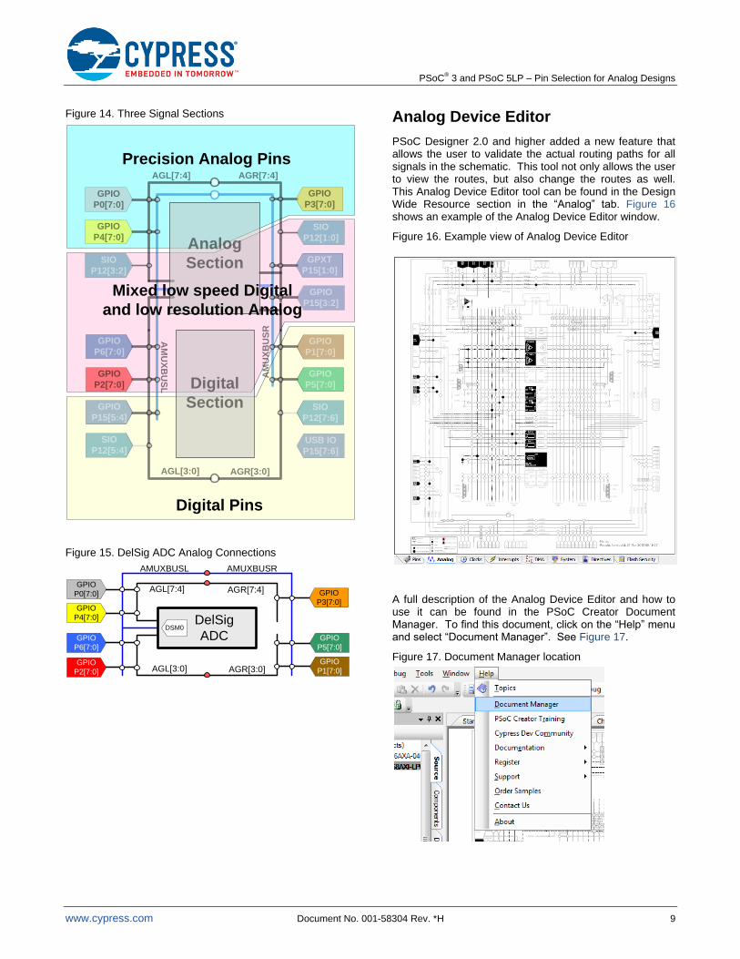
Sometimes a design may have a mix of precision analog, low resolution analog, low speed digital, and high speed digital. The low precision and low speed digital can be used to isolate the precision analog and high speed digital. See Figure 14 for an example.
Connecting to the Sigma_Delta ADC
The analog blocks are equally distributed between the left and right sides of the chip. Currently, there is just one Delta-Sigma ADC, which is placed on the left side and only has direct connections to the routing resources on the left side. Signals may be routed from the right side of the part, but only by connecting the left and right analog globals together. When pins from the right side of the part must connect to the ADC, the analog globals on the right side must be connected to the corresponding analog globals on the left side. For example, if pin P3[7] needs to be routed to the ADC, the pin is first connected to AGR[7]. Then AGL[7] must then be connected to AGR[7] to route to the ADC. However, if pin P0[7] is selected, then only analog global AGL[7] is used instead of both AGR[7] and AGL[7]. (See the top section Analog Diagram for clarity). All of the left analog globals (AGL[7:0]) may be connected to the corresponding right analog globals (AGR[7:0]). See Figure 15.
PSoC® 3 and PSoC 5LP – Pin Selection for Analog Designs
www.cypress.com Document No. 001-58304 Rev. *H 9
Figure 14. Three Signal Sections
GPIO
P3[7:0]
SIO
P12[1:0]
GPIO
P15[3:2]
GPXT
P15[1:0]
GPIO
P1[7:0]
GPIO
P5[7:0]
SIO
P12[7:6]
GPIO
P2[7:0]
GPIO
P6[7:0]
SIO
P12[5:4]
GPIO
P15[5:4]
GPIO
P0[7:0]
SIO
P12[3:2]
GPIO
P4[7:0]
USB IO
P15[7:6]
AGL[3:0] AGR[3:0]
AGL[7:4] AGR[7:4]
AM
UX
BU
SL
AM
UX
BU
SR
Analog
Section
Digital
Section
Mixed low speed Digital
and low resolution Analog
Precision Analog Pins
Digital Pins
Figure 15. DelSig ADC Analog Connections
AGL[7:4]GPIO
P0[7:0]
GPIO
P4[7:0]
GPIO
P6[7:0]
GPIO
P2[7:0]
GPIO
P5[7:0]
GPIO
P3[7:0]
GPIO
P1[7:0]
DelSig
ADCDSM0
AGR[7:4]
AMUXBUSL AMUXBUSR
AGL[3:0] AGR[3:0]
Analog Device Editor
PSoC Designer 2.0 and higher added a new feature that allows the user to validate the actual routing paths for all signals in the schematic. This tool not only allows the user to view the routes, but also change the routes as well. This Analog Device Editor tool can be found in the Design Wide Resource section in the “Analog” tab. Figure 16 shows an example of the Analog Device Editor window.
Figure 16. Example view of Analog Device Editor
A full description of the Analog Device Editor and how to use it can be found in the PSoC Creator Document Manager. To find this document, click on the “Help” menu and select “Document Manager”. See Figure 17.
Figure 17. Document Manager location
PSoC® 3 and PSoC 5LP – Pin Selection for Analog Designs
www.cypress.com Document No. 001-58304 Rev. *H 10
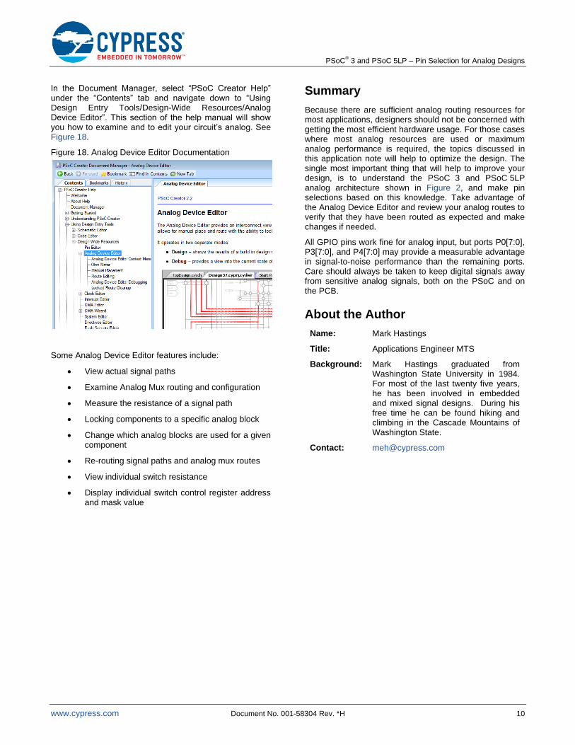
In the Document Manager, select “PSoC Creator Help” under the “Contents” tab and navigate down to “Using Design Entry Tools/Design-Wide Resources/Analog Device Editor”. This section of the help manual will show you how to examine and to edit your circuit’s analog. See Figure 18.
Figure 18. Analog Device Editor Documentation
Some Analog Device Editor features include:
View actual signal paths
Examine Analog Mux routing and configuration
Measure the resistance of a signal path
Locking components to a specific analog block
Change which analog blocks are used for a given component
Re-routing signal paths and analog mux routes
View individual switch resistance
Display individual switch control register address and mask value
Summary
Because there are sufficient analog routing resources for most applications, designers should not be concerned with getting the most efficient hardware usage. For those cases where most analog resources are used or maximum analog performance is required, the topics discussed in this application note will help to optimize the design. The single most important thing that will help to improve your design, is to understand the PSoC
3 and PSoC 5LP
analog architecture shown in Figure 2, and make pin selections based on this knowledge. Take advantage of the Analog Device Editor and review your analog routes to verify that they have been routed as expected and make changes if needed.
All GPIO pins work fine for analog input, but ports P0[7:0], P3[7:0], and P4[7:0] may provide a measurable advantage in signal-to-noise performance than the remaining ports. Care should always be taken to keep digital signals away from sensitive analog signals, both on the PSoC and on the PCB.
About the Author
Name: Mark Hastings
Title: Applications Engineer MTS
Background: Mark Hastings graduated from Washington State University in 1984. For most of the last twenty five years, he has been involved in embedded and mixed signal designs. During his free time he can be found hiking and climbing in the Cascade Mountains of Washington State.
Contact: [email protected]

PSoC® 3 and PSoC 5LP – Pin Selection for Analog Designs
www.cypress.com Document No. 001-58304 Rev. *H 11
Document History
Document Title: AN58304 - PSoC® 3 and PSoC 5LP – Pin Selection for Analog Designs
Document Number: 001-58304
Revision ECN Orig. of Change
Submission Date
Description of Change
** 2828695 MEH 12/15/2009 New application note.
*A 2991540 SRIH 07/22/2010 Fixed branding discrepancies
*B 3371422 MEH 09/14/2011 Rewrite of several paragraphs and added or updated Figures, 2, 5,6,7,8,13
*C 3655552 MEH 06/26/2012 Updated PSoC 3 and PSoC 5 Internal Analog Routing. Updated Summary. Updated in new template.
*D 3812768 MEH 11/15/2012 Updated Associated Part Family as “All PSoC 3 and PSoC 5LP parts”. Replaced PSoC 5 with PSoC 5LP in all instances across the document.
*E 3941625 MEH 04/01/2013 Update of the analog diagram. Several minor changes. Added reference to PSoC Creator Analog Editor.
*F 4391233 MEH 05/28/2014 Fixed error in Figures 1, 13 and 14 that labeled USB pins incorrectly
*G 4573140 MEH 11/18/2014 Sunset Update
*H 5723919 AESATMP8 05/02/2017 Updated logo and Copyright.

PSoC® 3 and PSoC 5LP – Pin Selection for Analog Designs
www.cypress.com Document No. 001-58304 Rev. *H 12
Worldwide Sales and Design Support
Cypress maintains a worldwide network of offices, solution centers, manufacturer’s representatives, and distributors. To find the office closest to you, visit us at Cypress Locations.
Products
ARM® Cortex
® Microcontrollers cypress.com/arm
Automotive cypress.com/automotive
Clocks & Buffers cypress.com/clocks
Interface cypress.com/interface
Internet of Things cypress.com/iot
Memory cypress.com/memory
Microcontrollers cypress.com/mcu
PSoC cypress.com/psoc
Power Management ICs cypress.com/pmic
Touch Sensing cypress.com/touch
USB Controllers cypress.com/usb
Wireless Connectivity cypress.com/wireless
PSoC® Solutions
PSoC 1 | PSoC 3 | PSoC 4 | PSoC 5LP | PSoC 6
Cypress Developer Community
Forums | WICED IOT Forums | Projects | Videos | Blogs | Training | Components
Technical Support
cypress.com/support
All other trademarks or registered trademarks referenced herein are the property of their respective owners.
Cypress Semiconductor 198 Champion Court San Jose, CA 95134-1709
© Cypress Semiconductor Corporation, 2009-2017. This document is the property of Cypress Semiconductor Corporation and its subsidiaries, including Spansion LLC (“Cypress”). This document, including any software or firmware included or referenced in this document (“Software”), is owned by Cypress under the intellectual property laws and treaties of the United States and other countries worldwide. Cypress reserves all rights under such laws and treaties and does not, except as specifically stated in this paragraph, grant any license under its patents, copyrights, trademarks, or other intellectual property rights. If the Software is not accompanied by a license agreement and you do not otherwise have a written agreement with Cypress governing the use of the Software, then Cypress hereby grants you a personal, non-exclusive, nontransferable license (without the right to sublicense) (1) under its copyright rights in the Software (a) for Software provided in source code form, to modify and reproduce the Software solely for use with Cypress hardware products, only internally within your organization, and (b) to distribute the Software in binary code form externally to end users (either directly or indirectly through resellers and distributors), solely for use on Cypress hardware product units, and (2) under those claims of Cypress’s patents that are infringed by the Software (as provided by Cypress, unmodified) to make, use, distribute, and import the Software solely for use with Cypress hardware products. Any other use, reproduction, modification, translation, or compilation of the Software is prohibited.
TO THE EXTENT PERMITTED BY APPLICABLE LAW, CYPRESS MAKES NO WARRANTY OF ANY KIND, EXPRESS OR IMPLIED, WITH REGARD TO THIS DOCUMENT OR ANY SOFTWARE OR ACCOMPANYING HARDWARE, INCLUDING, BUT NOT LIMITED TO, THE IMPLIED WARRANTIES OF MERCHANTABILITY AND FITNESS FOR A PARTICULAR PURPOSE. To the extent permitted by applicable law, Cypress reserves the right to make changes to this document without further notice. Cypress does not assume any liability arising out of the application or use of any product or circuit described in this document. Any information provided in this document, including any sample design information or programming code, is provided only for reference purposes. It is the responsibility of the user of this document to properly design, program, and test the functionality and safety of any application made of this information and any resulting product. Cypress products are not designed, intended, or authorized for use as critical components in systems designed or intended for the operation of weapons, weapons systems, nuclear installations, life-support devices or systems, other medical devices or systems (including resuscitation equipment and surgical implants), pollution control or hazardous substances management, or other uses where the failure of the device or system could cause personal injury, death, or property damage (“Unintended Uses”). A critical component is any component of a device or system whose failure to perform can be reasonably expected to cause the failure of the device or system, or to affect its safety or effectiveness. Cypress is not liable, in whole or in part, and you shall and hereby do release Cypress from any claim, damage, or other liability arising from or related to all Unintended Uses of Cypress products. You shall indemnify and hold Cypress harmless from and against all claims, costs, damages, and other liabilities, including claims for personal injury or death, arising from or related to any Unintended Uses of Cypress products.
Cypress, the Cypress logo, Spansion, the Spansion logo, and combinations thereof, WICED, PSoC, CapSense, EZ-USB, F-RAM, and Traveo are trademarks or registered trademarks of Cypress in the United States and other countries. For a more complete list of Cypress trademarks, visit cypress.com. Other names and brands may be claimed as property of their respective owners.