User Manual AURIX lite Kit V2 - Infineon Technologies
27
Microcontroller Evaluation Board For AURIX™ Family Board User‘s Manual Revision 2022-04-14 AURIX™ lite Kit V2 Document Revision 2.2
-
Upload
khangminh22 -
Category
Documents
-
view
5 -
download
0
Transcript of User Manual AURIX lite Kit V2 - Infineon Technologies
Microcontrol ler
Eva luat ion Board For AURIX™ Family
Board User ‘s Manual
Revision 2022-04-14
AURIX™ lite Kit V2 Document Revision 2.2
Edition 14. April, 2022
Published by
Infineon Technologies AG
81726 Munich, Germany
© 2022 Infineon Technologies AG
All Rights Reserved.
Legal Disclaimer
The information given in this document shall in no event be regarded as a guarantee of conditions or
characteristics. With respect to any examples or hints given herein, any typical values stated herein and/or any
information regarding the application of the device, Infineon Technologies hereby disclaims any and all
warranties and liabilities of any kind, including without limitation, warranties of non-infringement of
intellectual property rights of any third party.
Information
For further information on technology, delivery terms and conditions and prices, please contact the nearest
Infineon Technologies Office (www.infineon.com).
Warnings
Due to technical requirements, components may contain dangerous substances. For information on the types
in question, please contact the nearest Infineon Technologies Office.
Infineon Technologies components may be used in life-support devices or systems only with the express
written approval of Infineon Technologies, if a failure of such components can reasonably be expected to
cause the failure of that life-support device or system or to affect the safety or effectiveness of that device or
system. Life support devices or systems are intended to be implanted in the human body or to support and/or
maintain and sustain and/or protect human life. If they fail, it is reasonable to assume that the health of the
user or other persons may be endangered.

AURIX™ lite Kit V2
Revision October, 2020
Revision History
Page or Item Subjects (major changes since previous revision)
Revision 2020, October
Initial released Version is V2.0
Revision 2021, September
Corrected Version V2.1
Page 13 Add SO8-150 as specific package
Page 18, Figure 7 Order on X301 corrected (mirrored)
Page 26, Figure 14 Add footnote about wrong printing of P11.6
Revision 2022, April
Corrected Version V2.2
Page 12 Add description of CAN_STB
Trademarks of Infineon Technologies AG
AURIX™, C166™, CanPAK™, CIPOS™, CIPURSE™, EconoPACK™, CoolMOS™, CoolSET™, CORECONTROL™, CROSSAVE™, DAVE™, EasyPIM™, EconoBRIDGE™, EconoDUAL™, EconoPIM™, EiceDRIVER™, eupec™, FCOS™, HITFET™, HybridPACK™, I²RF™, ISOFACE™, IsoPACK™, MIPAQ™, ModSTACK™, my-d™, NovalithIC™, OptiMOS™, ORIGA™, PRIMARION™, PrimePACK™, PrimeSTACK™, PRO-SIL™, PROFET™, RASIC™, ReverSave™, SatRIC™, SIEGET™, SINDRION™, SIPMOS™, SmartLEWIS™, SOLID FLASH™, TEMPFET™, thinQ!™, TRENCHSTOP™, TriCore™.
Other Trademarks
Advance Design System™ (ADS) of Agilent Technologies, AMBA™, ARM™, MULTI-ICE™, KEIL™, PRIMECELL™, REALVIEW™, THUMB™, µVision™ of ARM Limited, UK. AUTOSAR™ is licensed by AUTOSAR development partnership. Bluetooth™ of Bluetooth SIG Inc. CAT-iq™ of DECT Forum. COLOSSUS™, FirstGPS™ of Trimble Navigation Ltd. EMV™ of EMVCo, LLC (Visa Holdings Inc.). EPCOS™ of Epcos AG. FLEXGO™ of Microsoft Corporation. FlexRay™ is licensed by FlexRay Consortium. HYPERTERMINAL™ of Hilgraeve Incorporated. IEC™ of Commission Electrotechnique Internationale. IrDA™ of Infrared Data Association Corporation. ISO™ of INTERNATIONAL ORGANIZATION FOR STANDARDIZATION. MATLAB™ of MathWorks, Inc. MAXIM™ of Maxim Integrated Products, Inc. MICROTEC™, NUCLEUS™ of Mentor Graphics Corporation. Mifare™ of NXP. MIPI™ of MIPI Alliance, Inc. MIPS™ of MIPS Technologies, Inc., USA. muRata™ of MURATA MANUFACTURING CO., MICROWAVE OFFICE™ (MWO) of Applied Wave Research Inc., OmniVision™ of OmniVision Technologies, Inc. Openwave™ Openwave Systems Inc. RED HAT™ Red Hat, Inc. RFMD™ RF Micro Devices, Inc. SIRIUS™ of Sirius Satellite Radio Inc. SOLARIS™ of Sun Microsystems, Inc. SPANSION™ of Spansion LLC Ltd. Symbian™ of Symbian Software Limited. TAIYO YUDEN™ of Taiyo Yuden Co. TEAKLITE™ of CEVA, Inc. TEKTRONIX™ of Tektronix Inc. TOKO™ of TOKO KABUSHIKI KAISHA TA. UNIX™ of X/Open Company Limited. VERILOG™, PALLADIUM™ of Cadence Design Systems, Inc. VLYNQ™ of Texas Instruments Incorporated. VXWORKS™, WIND RIVER™ of WIND RIVER SYSTEMS, INC. ZETEX™ of Diodes Zetex Limited.
Last Trademarks Update 2011-02-24
EtherCAT® is registered trademark and patented technology, licensed by Beckhoff Automation GmbH, Germany.

AURIX™ lite Kit V2
Table of Contents
Board Users Manual 4 Revision April, 2022
Table of Contents
1 Introduction ............................................................................................................................. 6
1.1 Block Diagram ...................................................................................................................................... 7
2 Hardware Description ............................................................................................................... 8
2.1 Power Supply ....................................................................................................................................... 9
2.2 User Push Buttons, User LEDs and Potentiometer ............................................................................ 10
2.3 Debugging and on board miniWiggler ............................................................................................... 11
2.3.1 USB Connector ................................................................................................................................... 11
2.3.2 Serial Connection to PC ...................................................................................................................... 11
2.3.3 miniWiggler JDS ................................................................................................................................. 12
2.4 Reset .................................................................................................................................................. 12
2.5 CAN Transceiver ................................................................................................................................. 12
2.6 I2C Eeprom ......................................................................................................................................... 12
2.7 Ethernet ............................................................................................................................................. 13
2.8 Optional Cypress Semper™ (Secure) Flash ........................................................................................ 13
2.9 Optional F-RAM .................................................................................................................................. 13
3 Configuration .......................................................................................................................... 14
3.1 Bootmode .......................................................................................................................................... 14
3.2 Config Signals ..................................................................................................................................... 14
3.3 Optional resistors ............................................................................................................................... 15
4 Connector Pin Assignment ...................................................................................................... 16
4.1 Pinout of X1 and X2 connectors ......................................................................................................... 16
4.2 Shield2Go and MikroBus™ Pinout ..................................................................................................... 17
4.3 Arduino Compatible Connector ......................................................................................................... 18
4.4 Infineon DAP Debug Connector (10-pin) ........................................................................................... 19
5 Schematics and Placement ...................................................................................................... 20

AURIX™ lite Kit V2
Table of Contents
Board Users Manual 5 Revision April, 2022
List of Figures
Figure 1 Block Diagram of the AURIX™ lite Kit V2 ............................................................................................. 7
Figure 2 AURIX™ lite Kit Board V2 View from the Top ....................................................................................... 8
Figure 3 AURIX™ lite Kit Board V2 View from the Bottom ................................................................................ 8
Figure 4 Power Supply Concept ....................................................................................................................... 10
Figure 5 Signal mapping of the pin headers X1 and X2 ................................................................................... 16
Figure 6 Signal mapping of the pin headers for Mikrobus and Shield2Go Connector 1 and 2 ........................ 17
Figure 7 Mapping of Arduino Functions to AURIX™ Pin Functions .................................................................. 18
Figure 8 Schematic: Project Overview ............................................................................................................. 20
Figure 9 Schematic: On Board miniWiggler ..................................................................................................... 21
Figure 10 Schematic: Power and Connectors .................................................................................................... 22
Figure 11 Schematic: CPU and config ................................................................................................................ 23
Figure 12 Schematic: Ethernet and memory expansion .................................................................................... 24
Figure 13 Placement: Top View ......................................................................................................................... 25
Figure 14 Placement: Bottom View ................................................................................................................... 26
List of Tables
Table 1 Overview of the Board Specification ................................................................................................... 6
Table 2 AURIX™ Pin Mapping for User LEDs .................................................................................................. 10
Table 3 miniWiggler Pin Mapping for User LEDs ........................................................................................... 11
Table 4 AURIX™ Push Buttons and Potentiometer ........................................................................................ 11
Table 5 CAN Signals and AURIX™ Pin Mapping.............................................................................................. 12
Table 6 User Startup Modes ......................................................................................................................... 14
Table 7 Config Signals .................................................................................................................................... 14
Table 8 Signal mapping of the optional resistors .......................................................................................... 15
Table 9 Pin Assignment of the DAP Debug Connector .................................................................................. 19

AURIX™ lite Kit V2 Hardware Description
Board Users Manual 6 Revision April, 2022
1 Introduction
This document describes the features and hardware details of the AURIX™ lite Kit V2 equipped with a
32-Bit Single-Chip AURIX™ TriCore™-based Microcontroller TC375, TC365, TC275 or TC265 from Infineon Technologies AG.
It can be used with a range of development tools including Infineon’s free of charge Eclipse based IDE AURIX™ Development Studio or the Eclipse based “FreeEntryToolchain” from HighTec/PLS/Infineon. AURIX™ Development Studio is a comprehensive environment, including C-Compiler and Multi-core Debugger, Infineon’s low-level driver (iLLD), with no time and code-size limitations that enables editing, compiling and debugging application code. The FreeEntryToolchain is a full C/C++ development environment which has a source-level UDE debugger from PLS included and is also based on Infineon low-level driver (iLLD).
Table 1 shows the overview specifications of the whole board.
Table 1 Overview of the Board Specification
CPU Core AURIX™ Manufacturer Order No. SAK-TC375TP-96F300W AA
Manufacturer Order No. SAK-TC365DP-64F300W AA
Manufacturer Order No. SAK-TC275TP-64F200W DC
Manufacturer Order No. SAK-TC265D-40F200W BC
Board Dimensions 66.0 x 131.0 mm
Power
• on-board miniWiggler Micro-AB USB interface
• external powering 5 V…40 V (recommended 7 V...14 V)
Connectors
• Most AURIX™ pins available on expansion connectors (X1, X2)
• Two Infineon Shield2Go connectors
• Arduino compatible connectors for 3.3 V
• mikroBUS™ connector
• Micro-USB connector
• DAP Debug connector
• CAN connector
• RJ45 connector
Others • CAN transceiver TLE9251VSJ from Infineon
• Low Power 10/100 Mbps Ethernet Physical Layer Transceiver DP83825I from TI
• 1 user push-button, 3 user LEDs
• Reset push-button
• Potentiometer (10 kOhm) for variable analog input
These boards are neither cost nor size optimized and do not serve as a reference design.
AURIX™ lite Kit V2 Hardware Description
Board Users Manual 7 Revision April, 2022
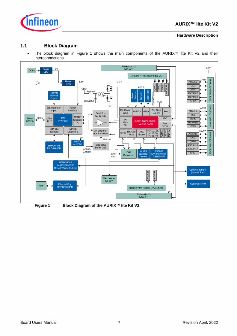
1.1 Block Diagram
• The block diagram in Figure 1 shows the main components of the AURIX™ lite Kit V2 and their interconnections.
Figure 1 Block Diagram of the AURIX™ lite Kit V2
Aurixä TC375, TC365, TC275 or TC265
Micro USB2.0
UTMIPHY
EEPROMInterface
FTDIFT2232HL
EEPROM 1kB93LC46B-I/SN
Octal BusBuf fer Gate
2 x Single-BitBus Tranceiver
Single BusBuf fer Gate
MPSSEChannel
A
OCDS
DAPConnector
Ext. Oscillator Input
2x LEDs for OCDS
Power LDO
Power Interface Ext. Power
Input
Pin Header X12x20, 0.1"
Pin Header X22x20, 0.1"
Arduinoä Pin Header (DIGITAL)
Arduinoä Pin Header (ANALOG IN)
ADC
GPIO
LED
1/L
ED
2
Butt
on 1
Rese
t
Butt
on
3.3V
VDDR35/0R
Ext.GateCtrl
Dig. CoreSupply
VDD
Ext. OsciInput
20 MHz ExternalCrystal
Port 11, 13,14, 15, 20,21, 22, 23
P00.5
/P00.6
PORSTN
Port32,33
Port 0
InfineonCAN Tranceiver
TLE9251VSJ
12 MHz ExternalCrystal
CAN0Node0
CAN Header1x2, 0.1"
QSP
I1
I2C
0
ASC
LIN
Mik
robusä
Connecto
rShie
ld2G
O S
lot1
S2G
2
I2C0
ASCLIN1
QSPI2
I2C0
ASCLIN3
QSPI0
UART
Shie
ld2G
O S
lot1
S2G
1
I2C0
ASCLIN2
QSPI0
UART
UART
ADC/AN26
ADC/AN16
ADC/AN17
ADC/AN19
ADC/AN18
GPIO
GPIO
GPIO
3.3V
AN
36-3
9
ASC
LIN
0
I2C
0
GP
IO
QSP
I1
EEPROM 2kB24AA02E48-E/OT
EUI-48ä Node Address
AN
24-2
5
Ethernet PhyDP83825IRMQR
RJ45
Power LDO
DC IN
C39/22µF
L3/3,3µH
Optional Semper(secure) Flash
Optional F-RAM
MPSSEChannel B
3.3V
5V
P00.7
DP/DM
ADBUS2
ACBUS4
ADBUS1DAP1
P21.7

AURIX™ lite Kit V2 Hardware Description
Board Users Manual 8 Revision April, 2022
2 Hardware Description
The following chapters give a detailed description of the board hardware and how it can be used. The different parts of the kits series are shown in Figure 2 and 3.
Figure 2 AURIX™ lite Kit Board V2 View from the Top
Figure 3 AURIX™ lite Kit Board V2 View from the Bottom

AURIX™ lite Kit V2 Hardware Description
Board Users Manual 9 Revision April, 2022
2.1 Power Supply
The AURIX™ lite Kit V2 must be supplied by an external DC power supply, this can be done via the DC plug X3 (recommended voltage range +7 V…+14 V) or via the micro USB plug X4 (+5 V).
The green Power LED4 indicates the presence of the generated 3.3 V supply voltage.
For X3 you can use a female DC supply plug with outside diameter of 5.5 mm and inside diameter of 2.1 mm or 2.5 mm. The inner contact is positive and the outer contact is ground.
In case that the board is powered via the micro USB plug X4, the used voltage will be always less than 5 V (~4.5 V) because the USB voltage is protected by a schottky diode (D1). Therefore also it is possible to use X3 and X4 on the same time. As long the voltage on X3 is higher than +7 V the board is powered via X3. If the voltage on X3 is less than +5.5 V the board is powered via X4. Between +5.5 V and +7 V on X3 the board is powered from X3 and X4 together.
If the board is powered via a USB plug and/or the DC plug, it’s not recommended to apply an additional power supply to one of the power pins (VEXT, +5V, +3V3, VDD_USB) on the pin headers X1, X2, the Arduino Power header X302, the Shield2GO slots or the mikroBus™ connectors, because there is no protection against reverse current into the external power supply. These power pins can furthermore be used, to power an external circuit and therefore used as an output. But care must be taken to not draw more current than USB can deliver. A PC as USB2.0 host typically can deliver up to 500 mA current and USB3.0 up to 900 mA. For best performance, we recommend to use USB3.0. If higher currents are required and in order to avoid damages on the USB host, the use of an external USB power supply unit, which is able to deliver higher currents, is possible.
Note: The LDO G1, that transfers the 5 V to 3.3 V, and LDO G2, that transfers VIN to 5 V, has a maximum output current rating of 1 A. Therefore, the maximum current consumption is limited to 1 A. Do not apply any additional voltage on the supply pins, because they are directly connected to the output of the LDO G1/G2 and further backwards voltage can damage or destroy the LDO. Furthermore, do not apply multiple sources on the power pins, otherwise you risk to damage and destroy the board.
However, more options are possible, but therefore, caution is necessary, to avoid any damage to the board and your supplies. Please ensure that X4 is not supplied by any power source or PC, for all mentioned configurations below. Otherwise, you risk to damage your source or PC.
Ensuring the mentioned points, following supply options are possible with a +5 V power source:
• Option 1: Supply +5 V on the +5V pin at X302 Arduino power connector
• Option 2: Supply +5 V on either one of the VDD_USB pins at X1 or X2 connector
• Option 3: Supply +7 V…+14 V on the VIN pin at X302 Arduino power connector

AURIX™ lite Kit V2 Hardware Description
Board Users Manual 10 Revision April, 2022
LDOInfineon
IFX27001TFV33
Pin Connector X2
Pin Connector X1
X303 X304
X301Arduino Power Connector X302
MicroUSB
S2Go Slots
S2G1/S2G2
mikroBusä
VDD_USB+5VVEXT
+3V3
VDD_USB
3V3
3V3
5V
5V
G1
X4
R27
/0R
D5
AurixäTC3X5 or TC2X5Microcontroller
On Board miniWiggler
Potentiometer
CAN Tranceiver
OptionalExternal F-RAM
U1 - U5
IC1
U6
R32
U7
+3V3
VDD_USB
Out
In
+3V3
DAPCon.
D1
LDOInfineon
IFX27001TFV50
R39/0R_opt
G2
DC plug
VIN
+3V3
+5VVINOptionalExternal Flash
U10
U11
VEXT
Out In
+3V3
I2C EepromU9
10M / 100MEthernet
U8
D2 X3+5V
Figure 4 Power Supply Concept
Note: Do not apply any voltage on the mentioned power pins, if the USB is plugged in or any voltage is applied via DC plug. Furthermore, do not apply multiple sources on the power pins, otherwise you risk to damage and destroy the board.
2.2 User Push Buttons, User LEDs and Potentiometer
The AURIX™ lite Kit V2 provides one user push button, a reset button, two LEDs and one potentiometer. Additionally, LED3 can be used for visualizing an emergency stop function at ESR0 (emergency service request). The LEDs LED5 and LED6 are used for visualizing activites via the on-board miniWiggler. The port pins used can be found in Table 2 and Table 4.
Table 2 AURIX™ Pin Mapping for User LEDs
Name AURIX™ Pin Color Active
LED1 P00.5 green Low-active (pull against GND)
LED2 P00.6 green Low-active (pull against GND)
LED3 ESR0 red Low-active (pull against GND)

AURIX™ lite Kit V2 Hardware Description
Board Users Manual 11 Revision April, 2022
Table 3 miniWiggler Pin Mapping for User LEDs
Name miniWiggler Pin Color Active
LED5 ADBUS4 (ACTIV) green Low-active (pull against GND)
LED6 ADBUS7 (RUN) green Low-active (pull against GND)
Table 4 AURIX™ Push Buttons and Potentiometer
Name AURIX™ Pin Active
Button1 P00.7 Low-active (pull against GND)
Reset /PORST Low-active (pull against GND)
R32 (10kΩ)* AN0 -
*Note: Desoldering resistor R33, enables AN0 for other functions, but disables the Potentiometer functionality.
2.3 Debugging and on board miniWiggler
The AURIX™ lite Kit V2 supports debugging via 2 different channels:
• On-board miniWiggler via the the microUSB X4
• 10-pin DAP Connector
2.3.1 USB Connector
The USB connector is used for connection to a PC. Via the USB it is possible to power the board, using the ASCLIN0 as serial connection via USB and Debugging via DAS. NOTE: Before connecting the board to the PC, make sure that the actual DAS software is installed on the PC. For actual DAS software please contact your local FAE. The software can also be found on:
DAS website
2.3.2 Serial Connection to PC
After the first connection of USB to a PC the needed driver will be installed automatically. During this there will be created a new COM port on PC. This COM port can be used to communicate with the board via ASCLIN0 of the device and ASCLIN4 (TC3X5 only) if R44 and R45 are assembled. Per default the ASCLIN0 is used on P14.0 and P14.1 (e.g. Generic Bootstrap Loader). Because ASCLIN0 is used also for the Arduino pins, you can use here also ASCLIN4 to use it in parallel, make sure that P14.0/P14.1 are not configured in this case.

AURIX™ lite Kit V2 Hardware Description
Board Users Manual 12 Revision April, 2022
2.3.3 miniWiggler JDS
The miniWiggler JDS is a low cost debug interface which allows you access to the device via DAP. Make sure that you have the latest DAS release. Debugging is possible via the DAS Server ‘UDAS‘. Please contact your preferred debug vendor for support of DAS. If you have connected the board to the PC and there runs the DAS server, then a working connection is visible via the green LED5 (ADBUS4). The status LED6 (ADBUS7/green) is switched on/off through the DAS Server, depending on the used debugger (client). IMPORTANT: Make sure that there is no or a tristated connection on the DAP connector if the LED5 (miniWiggler in use) is on.
2.4 Reset
The power on reset input pin (/PORST) of the AURIX™ family is a bi-directional input/output intended for external triggering of power-related resets. If the PORST pin remains asserted after a power event then the reset will be extended until it is deasserted. This does not replace the ESR pins functional reset. An internal pull-up resistor (2.2 kΩ) keeps the PORST# pin high during normal operation. A low level at this pin will force a hardware reset. In case of a MCU internal reset the PORST# pin will drive a low signal.
A reset signal can be issued by
• the on-board Reset Button (“RESET”)
• the on-board miniWiggler via IC FT2232HL (IC1.27 – ACBUS1)
• the on-board DAP connector (DAP.10)
• the Arduino Power Header (X302.3, “/PORST”)
• the pin header X1 (X1.30, “/PORST”)
An AURIX™ internal circuit always ensures a save Power-on-Reset. AURIX™ lite Kit V2 does not require any additional external components to generate a reset signal during power-up. For more informations, please refer to the datasheet or user manual of the assembled AURIX™ device.
2.5 CAN Transceiver
The AURIX™ lite Kit V2 provides a CAN interface via the CAN connector. The TLE9251V is the latest Infineon high-speed CAN transceiver generation, used inside HS CAN networks for automotive and also for industrial applications. It is designed to fulfill the requirements of ISO 11898-2 (2016) physical layer specification and respectively also the SAE standards J1939 and J2284. The CAN buses (signals CANH, CANL) are terminated with by a 120 Ohm resistor. The transceiver is connected to the TriCore™ device CAN node 0. The transceiver is in stand-by mode per default. To switch the transceiver to normal operating mode the pin CAN_STB must be driven low from the CPU. To use the CAN pins see Table 5.
Table 5 CAN Signals and AURIX™ Pin Mapping
Signal Name
Pin No. at CAN Pin Header
AURIX ™Pin, AURIX™ Function Ass. Reg./ I/O Line
CANH 1 - -
CANL 2 - -
CAN_TX - P20.8, CAN node 0 output TXDCAN0
CAN_RX - P20.7, CAN node 0 input RXDCAN0B
CAN_STB - P20.6, GPIO P20.6 OUT
2.6 I2C Eeprom
The AURIX™ lite Kit V2 provide a 2 Kb I2C Serial EEPROM with Pre-Programmed EUI-48™ MAC ID (Microchip 24AA02E48). The slave address of this EEPROM is fixed 0x50. The upper half of the array (80h-FFh) is permanently write-protected. Write operations to this address range are inhibited. Read operations are

AURIX™ lite Kit V2 Hardware Description
Board Users Manual 13 Revision April, 2022
not affected. This upper half contains the preprogrammed EUI-48™ node address which can be used as MAC ID for Ethernet. The other 128 bytes are writable and usable by the user.
2.7 Ethernet
The AURIX™ lite Kit V2 provide a RJ45 connector (X5) for twisted pair ethernet connections.The board use a DP83825I Low Power 10/100 Mbps Ethernet Physical Layer Transceiver from Texas Instruments as physical interface device. For more information about the ethernet modul see AURIX™ User’s Manual, about the PHY see the DP83825I datasheet from TI website. For the connection between AURIX™ and PHY is used RMII. For the MD connection (e.g. for PHY configuration) there is used P21.2 and P21.3.
2.8 Optional Cypress Semper™ (Secure) Flash
The AURIX™ lite Kit V2 provide the possibility to assemble an external flash. Usable devices are Cypress Semper™ NOR Flash Device Family S25HL and Cypress Semper™ Secure NOR Flash Device Family S35HL in SOIC-16 package. For more information about the flashs please see https://www.cypress.com/products/semper-nor-flash-memory and https://www.cypress.com/event/semper-secure-nor-flash-memories. If you assemble a flash then assemble also the ceramic capacitor C64 with 100 nF (size 0603) and the resistor R67 with 0 Ω (size 0603). In case of use a Semper™ Secure NOR Flash you can also assemble the resistor R67 with 0 Ω (size 0603) to connect the interrupt output of the flash to the AURIX™ pin P20.9 (SCU_REQ7 on TC3X5; SCU_REQ11 on TC2X5). The AURIX™ support only single SPI protocol, Dual and Quad SPI protocol is not possible.
The flash is connected to P22.0, P22.1, P22.3 (QSPI4 on TC3X5; QSPI3 on TC2X5). Pin P22.2 (Slave Select Output 3 of QSPI4 on TC3X5; Slave Select Output 12 of QSPI3 on TC2X5) is used as slave select.
Please note that the used QSPI is shared with the optional F-RAM (see Optional F-RAM).
2.9 Optional F-RAM
The AURIX™ lite Kit V2 provide the possibility to assemble an external serial F-RAM. Usable devices are Cypress F-RAM FM25VN10-G and Cypress F-RAM Serie CY15B in SOIC-8 package (SO8-150). For more information about the F-RAMs please see https://www.cypress.com/products/f-ram-nonvolatile-ferroelectric-ram.
If you assemble F-RAM then assemble also the ceramic capacitor C65 with 100 nF (size 0603).
The F-RAM is connected to P22.0, P22.1, P22.3 (QSPI4 on TC3X5; QSPI3 on TC2X5). Pin P23.1 (Slave Select Output 6 of QSPI4 on TC3X5; Slave Select Output 13 of QSPI3 on TC2X5) is used as slave select.
Unfortunately there is no connection on pin 3 (#WP) and pin 7 (#HOLD) of the F-RAM. Please check the datasheet if the used F-RAM has internal weak pull-up connected or need an external connection to VDD. If external connection is needed then make such a connection via wire wrap line.
Please note that the used QSPI is shared with the optional flash (see Optional Cypress Semper™ (Secure) Flash).
AURIX™ lite Kit V2 Hardware Description
Board Users Manual 14 Revision April, 2022
3 Configuration
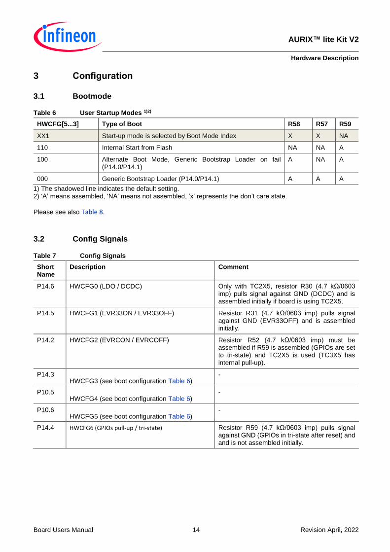
3.1 Bootmode
Table 6 User Startup Modes 1)2)
HWCFG[5...3] Type of Boot R58 R57 R59
XX1 Start-up mode is selected by Boot Mode Index X X NA
110 Internal Start from Flash NA NA A
100 Alternate Boot Mode, Generic Bootstrap Loader on fail (P14.0/P14.1)
A NA A
000 Generic Bootstrap Loader (P14.0/P14.1) A A A
1) The shadowed line indicates the default setting. 2) ‘A’ means assembled, ‘NA’ means not assembled, ’x’ represents the don’t care state.
Please see also Table 8.
3.2 Config Signals
Table 7 Config Signals
Short Name
Description Comment
P14.6 HWCFG0 (LDO / DCDC)
Only with TC2X5, resistor R30 (4.7 kΩ/0603 imp) pulls signal against GND (DCDC) and is assembled initially if board is using TC2X5.
P14.5 HWCFG1 (EVR33ON / EVR33OFF)
Resistor R31 (4.7 kΩ/0603 imp) pulls signal against GND (EVR33OFF) and is assembled initially.
P14.2 HWCFG2 (EVRCON / EVRCOFF)
Resistor R52 (4.7 kΩ/0603 imp) must be assembled if R59 is assembled (GPIOs are set to tri-state) and TC2X5 is used (TC3X5 has internal pull-up).
P14.3 HWCFG3 (see boot configuration Table 6)
-
P10.5 HWCFG4 (see boot configuration Table 6)
-
P10.6 HWCFG5 (see boot configuration Table 6)
-
P14.4 HWCFG6 (GPIOs pull-up / tri-state) Resistor R59 (4.7 kΩ/0603 imp) pulls signal against GND (GPIOs in tri-state after reset) and and is not assembled initially.

AURIX™ lite Kit V2 Hardware Description
Board Users Manual 15 Revision April, 2022
3.3 Optional resistors
Some resistors/bridges enable/disable or changing functions of specific signals in Table 8.
To disable the signals, the resistors have to be removed. To enable, the resistor has to be assembled.
For example: Desoldering the intialy assembled resistor R33, disables the Potentiometer and the analog Signal AN0 of the AURIX™, making it usable for other purposes.
Table 8 Signal mapping of the optional resistors
Resistor Res. Assembled Signal Size (imperial)
Comment
R33 0 Ω yes AN0 0603 Disassemble to disable the potentiometer
R37 0 Ω yes XTAL2 0603 Serial resistor to reduce oscillator amplitude if needed.
R39 0 Ω no +5V 0603 Assemble to connect 5V to Mikrobus and Shield2Go connector
R59 4.7 kΩ no HWCFG6/P14.4 0603 Assemble to disable the internal pull-ups with power on
R52 4.7 kΩ No HWCFG2/P14.2 0603 Assemble to enable the EVR13, only needed with TC2X5 and R59 assembled
R53 4.7 kΩ no HWCFG3/P14.3 0603 Assemble to boot from BMI, only needed with TC2X5 and R59 assembled
R56 4.7 kΩ no HWCFG3/P14.3 0603 Assemble to select boot from HWCFG4/5, valid setting on P10.5/P10.6 needed
R54 4.7 kΩ no HWCFG4/P10.5 0603 Set HWCFG4 to high, only needed with R56 assembled, not with R57
R55 4.7 kΩ no HWCFG5/P10.6 0603 Set HWCFG5 to high, only needed with R56 assembled, not with R58
R57 4.7 kΩ no HWCFG4/P10.5 0603 Set HWCFG4 to low, only needed with R56 assembled, not with R54
R58 4.7 kΩ no HWCFG5/P10.6 0603 Set HWCFG5 to low, only needed with R56 assembled, not with R55
R44 0 Ω no P14.1, P00.12 0603 Assemble to use ASCLIN4 (P00.12) instead of ASCLIN0 (P14.1) via USB, only with TC3X5, P14.1 not usable in this case
R45 0 Ω no P14.0, P00.9 0603 Assemble to use ASCLIN4 (P00.9) instead of ASCLIN0 (P14.0) via USB, only with TC3X5, P14.0 not usable in this case

AURIX™ lite Kit V2 Hardware Description
Board Users Manual 16 Revision April, 2022
4 Connector Pin Assignment
4.1 Pinout of X1 and X2 connectors
The pin headers X1 and X2 can be used to extend the evaluation board or to perform measurements on the AURIX™ TC3X5/TC2X5. Figure 5 shows the available GPIOs / signals at these pin headers. The pin table is also printed onto the bottom side of the PCB.
Pin Header X1
Pin Header X2
GND 1 2 +3V3
GND 1 2 VDD_USB
P33.11 3 4 P33.12
P00.0 3 4 P00.1
P33.13 5 6 P32.41)
P00.2 5 6 P00.3
P23.1 7 8 P23.0
LED2 P00.6 7 8 P00.5 LED1
P23.3 9 10 P23.2
P00.8 9 10 P00.7 Button1
RST_S2G2 P23.5 11 12 P23.4 RST_S2G1
P00.10 11 12 P00.9
P22.1 13 14 P22.0
P00.12 13 14 P00.11
P21.0 15 16 P22.2 VAREF1 15 16 AN47
MDC P21.2 17 18 P22.3
AN46 17 18 AN45
P21.4 19 20 P21.3 MDIO
AN44 19 20 AN7
SPICLK_S2G P20.10 21 22 P21.5
AN6 21 22 AN5
TXD_S2G2 P20.0 23 24 P20.1
AN4 23 24 AN3
RXD_S2G2 P20.3 25 26 /ESR1 ESR1
AN2 25 26 AN1
ESR0 /ESR0 27 28 P20.14 MOSI_S2G
Potentiometer AN0 27 28 P33.0
P15.5 29 30 /PORST Reset
P33.1 29 30 P33.2
P15.4 31 32 P11.12 CLK50
P33.3 31 32 P33.4
CRS_DV P11.11 33 34 P11.10 RX_D0
P33.5 33 34 P33.6
RX_D1 P11.9 35 36 P11.6 TX_EN
P33.7 35 36 P33.8 RXD_S2G1
TX_D0 P11.3 37 38 P11.2 TX_D1
TXD_S2G1 P33.9 37 38 P33.10
VDD_USB 39 40 GND
+3V3 39 40 GND
Figure 5 Signal mapping of the pin headers X1 and X2
Note: 1) Different signal compared with AURIX™ TC275 lite Kit V1.x

AURIX™ lite Kit V2 Hardware Description
Board Users Manual 17 Revision April, 2022
4.2 Shield2Go and MikroBus™ Pinout
The pin connectors for the Shield2Go Connectors 1 and 2 and the mikroBus™ can be used to extend the evaluation board or to perform measurements on the AURIX™ TC3X5/TC2X5. Figure 6 shows the available signals at these connectors. The pin table is also printed onto the top and bottom side of the AURIX™ lite Kit V2.
Shield2Go Connector 1 Shield2Go Connector 2
AURIX
™Pins
AURIX™
Pins
AURIX™
Pins
AURIX
™ Pins
1 +5V 5V 1 +5V 5V
2 AN16 AN1 RX P33.8 10 2 AN18 AN1 RX P20.3 10
3 AN17 AN2 TX P33.9 11 3 AN19 AN2 TX P20.0 11
4 P13.22) SDA RST/GPIO2 P23.41) 12 4 P13.22) SDA RST/GPIO2 P23.51) 12
5 P13.12) SCL GPIO1 P32.2 13 5 P13.12) SCL GPIO1 P32.3 13
6 GND GND CS P20.131) 14 6 GND GND CS P20.101) 14
7 +3V3 3V3 SCLK P20.111) 15 7 +3V3 3V3 SLCK P20.111) 15
8 P00.4 INT/GPIO3 MOSI P20.141) 16 8 P10.8 INT/GPIO3 MOSI P20.141) 16
9 P14.91) PWM/GPIO4 MISO P20.121) 17 9 P14.101) PWM/GPIO4 MISO P20.121) 17
mikroBus™ Connector
1 AN26 AN PWM P2.8 16
2 P10.6 RST INT P10.7 15
3 P14.71) CS RX P15.1 14
4 P15.81) SCK TX P15.0 13
5 P15.71) MISO SCL P13.12) 12
6 P15.61) MOSI SDA P13.22) 11
7 +3V3 3.3V 5V +5V 10
8 GND GND GND GND 9
Figure 6 Signal mapping of the pin headers for Mikrobus and Shield2Go Connector 1 and 2
Note: 1) Different signal compared with AURIX™ TC275 lite Kit V1.x
2) The I2C buses SCL and SDA are shared on the Shield2GOs, mikroBus™, Arduino connectors and the I2C eeprom.

AURIX™ lite Kit V2 Hardware Description
Board Users Manual 18 Revision April, 2022
4.3 Arduino Compatible Connector
The mapping of GPIOs and AURIX™ pin functions to Arduino compatible functions can be found in Figure 6. The Arduino compatible connector supports
• SPI interface (SPI_xxx)
• I2C interface (I2C_xxx)
• UART interface (UART_xxx)
• PWM signal outputs (PWM0-13)
• ADC input (ADC0-5)
• Interrupt input (INT0-1) Note that all pins are cabable of offering more functions than mentioned in Figure 6. For more information about all pin functions, we want to refer you to the corresponding datasheet.
Figure 7 Mapping of Arduino Functions to AURIX™ Pin Functions
The AURIX™ lite Kit V2 works with 3.3 V logic levels. Therefore, any board that works with 5 V logic levels, cannot be used.
Analog input signals ADC0-5 are limited to a voltage which is smaller or equal than VAREF with VAREF = VDDM = 3.3 V. Primarily, ADC0 to ADC5 should be used as analog input, because there is no additional circuit connected to these pins. Parallel operation of I2C and ADC4 / ADC5 is possible, because they don’t share anymore the same pins at the Arduino connector X301 and X303 as on previous AURIX™ lite Kit V1.
10
9 I2C_SDA: I2C0_SDA0
I2C_SCL: I2C0_SCL0
8 VAREF AREF: VAREF2/VAREF1
7 GND
6 P10.2 SPI_CLK: QSPI1.SLK1
P10.1 SPI_MISO: QSPI1.MRST1A
4 P10.3 SPI_MOSI: QSPI1.MTSR1 PWM11: GTM.TOUT105
3 P10.5 SPI_CS: QSPI1.SLSO19 PWM10: GTM.TOUT107
2 P02.7
1 P02.6
8 P02.4 IO1: P02_IN.P4 / P02_OUT.P4
7 P02.5
6 P02.3
4 P02.1 INT1: ERS2.REQ14 (ERU)
5 P10.4
3 P02.0
2 P15.2
1 P15.3
6
4
5
3P40.7
2
1
P40.6
P40.0
ADC2: AN37 / VADCG4.5
ADC3: AN36 / VADCG4.4
ADC4: AN24 / VADCG3.0
ADC5: AN25 / VADCG3.1 P40.1
7GND
GND
+5V
3.3V
N.C.
RESET
IOREF
VIN 8
4
6
5
1
2
3
(Top View)
AN
AL
OG
INP
OW
ER
DIG
ITA
L
5
ADC0: AN39 / VADCG4.7
ADC1: AN38 / VADCG4.6
SPI - Master Mode
PWM4: GTM.TOUT106
PWM7: GTM.TOUT4 /
CCU60.CC62
PWM6: GTM.TOUT5 /
CCU60.COUT62
PWM5: GTM.TOUT3 /
CCU60.COUT61
PWM3: GTM.TOUT1 /
CCU60.COUT60
INT0: ERS3.REQ6 (ERU)
IO0: P10_IN.P4 / P10_OUT.P4
UART_TXD: ASCLIN0.ATX0
UART_RXD: ASLIN0.ARX0B
IO2: P02_IN.P / P02_OUT.P6
X3
01
X3
02
X3
03
X3
04
PWM12: GTM.TOUT103
PWM13: GTM.TOUT104
PWM2: GTM.TOUT0 /
CCU60.CC60
PWM1: GTM.TOUT73
PWM0: GTM.TOUT74
PWM9: GTM.TOUT7 /
CCU60.CC61
PWM8: GTM.TOUT6 /
CCU60.CC60
VIN
/PORST
+3V3
+5V
VEXT/3.3V
P13.1
P13.2
P40.8
P40.9

AURIX™ lite Kit V2 Hardware Description
Board Users Manual 19 Revision April, 2022
4.4 Infineon DAP Debug Connector (10-pin)
Infineon’s 10-pin Device Access Port Debug Connector (DAP) is a two-wire tool access port for microcontrollers and similar devices. It allows robust high speed connections over a long cable for automotive applications. The
pin assignment of the DAP Debug Connector is shown in Table 9. The board comes with a DAP connector. You
can connect a DAP hardware here. If you use this connector make sure that the miniWiggler JDS is not activ (LED5 is off). For more information, we refer you to the DAP Connector Manual.
Table 9 Pin Assignment of the DAP Debug Connector
Pin Name AURIX™ Pin Direction Description
1 VREF VEXT O Supply voltage from the target system. The voltage has to be strong enough to supply the target side of the level shifters within the tool hardware up to about 20 MHz DAP operating frequency. The required supply current is in the range of 5 mA, mainly caused by signal switching. It can be reduced by lowering frequency and capacitance. Beyond 20 MHz the tool hardware has to supply the level shifter from another source and use this pin just as a voltage reference
2 DAP1 TMS IO DAP: Data pin.
SPD IO SPD: Data pin.
UART IO Single-wire UART. Serial communication interface (e.g. used for Bootstrap Loader BSL).
3 GND GND Recommended pin for signal return of DAP1 for high frequency impedance matching.
4 DAP0 TCK I DAP: Clock.
SUP I SPD: Optional user pin value for feedback into the target system. Otherwise reserved
5 GND GND Recommended pin for signal return of DAP0 for high frequency impedance matching.
6 DAP2 P21.7 IO DAP: Optional second data pin.
USER0 IO/O Generic signal that can be used for non specified functions.
7 KEY (GND in cable)
GND - If the recommended connector with keying shroud is not used, this pin provides another option to enforce polarization. In that instance this pin is removed from the target connector and the associated jack in the cable connector closed with a plastic pin for example.
8 DAP3 /TRST IO DAP: Optional third data pin.
USER1 IO/I Generic signal that can be used for non-specified functions.
(DAPEN) I Optional indicator that the tool is connected. This can be used to enable the DAP interface of the device
9 GND GND Supply ground.
10 RESET /PORST IO Target reset signal. Open drain active low signal. May be used bi-directionally to drive or sense the target reset signal. Usually driven by the tool to reset the target system. The target system is responsible for providing a pull-up to VREF on this signal to establish a logic one. The resistor shall not have a value less than 1 kOhms.
AURIX™ lite Kit V2 Hardware Description
Board Users Manual 20 Revision April, 2022
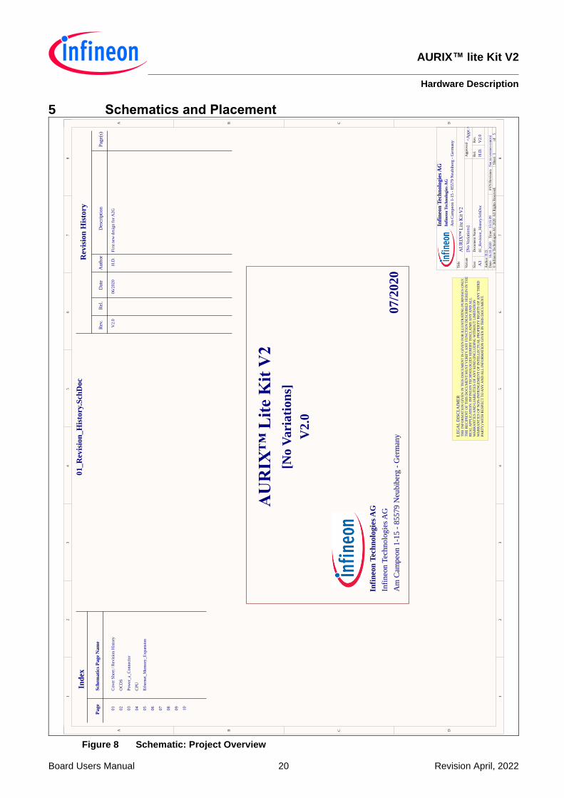
5 Schematics and Placement
Figure 8 Schematic: Project Overview
11
22
33
44
55
66
77
88
DD
CC
BB
AA
15
16.1
0.2
020
13:1
5:0
9D
ate:
Shee
tof
Tim
e:©
Infi
neo
n T
echnolo
gie
s A
G 2
020. A
ll R
ights
Res
erved
.
Au
tho
r:H
.D.
01_R
evis
ion
_H
isto
ry.S
chD
oc
Infi
neo
n T
ech
nolo
gie
s A
GIn
fin
eon
Tec
hn
olo
gie
s A
G
Am
Cam
peo
n 1
-15 -
85579 N
eubib
erg -
Ger
man
y V2.0
Tit
le
Siz
e:R
ev.
A3
Docu
men
t N
ame
01
_R
evis
ion
_H
isto
ry.S
chD
oc
Rel
.
H.D
.
Var
iant
AU
RIX
™ L
ite
Kit
V2
[No V
aria
tions]
Ap
pro
ved
<A
ppr.
>
SV
N R
evis
ion:
No
t in
ver
sio
n c
on
tro
l
AU
RIX
™ L
ite
Kit
V2
V2
.0
07
/20
20
Infi
neo
n T
ech
nolo
gie
s A
G
Infi
neo
n T
echnolo
gie
s A
G
Am
Cam
peo
n 1
-15 -
85579 N
eubib
erg -
Ger
man
y TH
E I
NF
OR
MA
TIO
N G
IVE
N I
N T
HIS
DO
CU
ME
NT
IS
GIV
EN
FO
R I
LL
US
TR
AT
ING
PU
RP
OS
ES
ON
LY
.T
HE
RE
CIP
IEN
T O
F T
HIS
DO
CU
ME
NT
MU
ST
VE
RIF
Y A
NY
FU
NC
TIO
N D
ES
CR
IBE
D H
ER
EIN
IN
TH
E
RE
AL
AP
PL
ICA
TIO
N. IN
FIN
EO
N T
EC
HN
OL
OG
IES
HE
RE
BY
DIS
CL
AIM
S A
NY
AN
D A
LL
W
AR
RA
NT
IES
AN
D L
IAB
ILIT
IES
OF
AN
Y K
IND
(IN
CL
UD
ING
WIT
HO
UT
LIM
ITA
TIO
N
WA
RR
AN
TIE
S O
F N
ON
-IN
FR
ING
EM
EN
T O
F I
NT
EL
LE
CT
UA
L P
RO
PE
RT
Y R
IGH
TS
OF
AN
Y T
HIR
DPA
RT
Y)
WIT
H R
ES
PE
CT
TO
AN
Y A
ND
AL
L I
NF
OR
MA
TIO
N G
IVE
N I
N T
HIS
DO
CU
ME
NT
.
LE
GA
L D
ISC
LA
IME
R
01
Pa
ge
Cover
Shee
t /
Rev
isio
n H
isto
ry
Sch
ema
tics
Pa
ge
Na
me
03
02
Ind
ex
04
OC
DS
05
06
07
08
09
10
Rev
isio
n H
isto
ry
Au
thor
Des
crip
tio
nD
ate
Rev
.P
age(
s)R
el.
[No
Va
ria
tio
ns]
V2.0
Fir
st n
ew d
esig
n f
or
A2G
06/2
020
H.D
.
Pow
er_a_
Connec
tor
CP
U
Eth
ernet
_M
emory
_E
xpan
sion

AURIX™ lite Kit V2 Hardware Description
Board Users Manual 21 Revision April, 2022
Figure 9 Schematic: On Board miniWiggler
11
22
33
44
55
66
77
88
DD
CC
BB
AA
25
16
.10
.20
20
13
:15
:55
Dat
e:S
hee
tof
Tim
e:©
In
fin
eon
Tec
hn
olo
gie
s A
G 2
02
0. A
ll R
igh
ts R
eser
ved
.
Au
tho
r:H
.D.
02
_O
CD
S.S
chD
oc
Infi
neo
n T
ech
nolo
gie
s A
GIn
fin
eon
Tec
hn
olo
gie
s A
G
Am
Cam
peo
n 1
-15
- 8
55
79
Neu
bib
erg
- G
erm
any V
2.0
Tit
le
Siz
e:R
ev.
A3
Do
cum
ent
Nam
e
02
_O
CD
S.S
chD
oc
Rel
.
H.D
.
Var
ian
t
AU
RIX
™ L
ite
Kit
V2
[No
Var
iati
on
s]A
pp
rov
ed<
Ap
pr.
>
SV
N R
evis
ion:
No
t in
ver
sio
n c
on
tro
l
AD
BU
S0
16
AD
BU
S1
17
AD
BU
S2
18
AD
BU
S3
19
AD
BU
S4
21
AD
BU
S5
22
AD
BU
S6
23
AD
BU
S7
24
AC
BU
S0
26
AC
BU
S1
27
AC
BU
S2
28
AC
BU
S3
29
BD
BU
S0
38
BD
BU
S1
39
BD
BU
S2
40
BD
BU
S3
41
BD
BU
S4
43
BD
BU
S5
44
BD
BU
S6
45
BD
BU
S7
46
BC
BU
S0
48
BC
BU
S1
52
BC
BU
S2
53
BC
BU
S3
54
GND1
GND5
GND11
GND15
AGND10
VCCIO31
VCCIO20
VPHY4
VPLL9
VCORE12
OS
CI
2
DM
7D
P8
RE
SE
T_N
14
EE
CS
63
EE
CL
K6
2
EE
DA
TA
61
TE
ST
13
US
B I
nte
rfac
e
PW
RE
N_
N6
0
Mis
c S
ignal
Gro
up
EE
PR
OM
In
terf
ace
Chan
nel
A
Chan
nel
B
FT
22
32
HL
DU
AL
HIG
H S
PE
ED
US
B
GND25
GND35
GND47
GND51
VCORE37
VCORE64
VCCIO42
VCCIO56
VREGIN50
VREGOUT49
AC
BU
S4
30
AC
BU
S5
32
AC
BU
S6
33
AC
BU
S7
34
BC
BU
S4
55
BC
BU
S5
57
BC
BU
S6
58
BC
BU
S7
59
OS
CO
3
SU
SP
EN
D_N
36
RE
F6
UA
RT
/F
IFO
IC
+1
.8V
+3
.3V
IC1
FT
2232H
L
C9
10
0n
F
C7
10
0n
F
C6
10
0n
F
C1
10
0n
F
GN
D
GN
D
+1
V8
C11
3.3
uF
GN
DG
ND
C3
10
0n
FC
41
00
nF
GN
D
L1
MM
Z1608R
300A
TA
00
1 2
C2
4.7
uF
R7
12
k
R6
1k
13
24
Y1
12
MH
z
C14
8p
F
VD
D_
US
B
GN
D
12345
MP
1M
P2
MP
3
MP
4M
P5
MP
6X
4
ZX62-AB-5PA(31)
VS
S5
CL
K2
DO
4
CS
1
VC
C8
DI
3
NC
16
NC
27
U5
93
LC
46
B-I
/SN
C19
10
0n
F
R17
2.2
k
GN
D
GN
D
1O
E_
N1
1Y
11
8
1Y
21
6
1Y
31
4
1Y
41
2
GN
D1
0
2Y
19
2Y
27
2Y
35
2Y
43
VC
C2
0
1A
12
1A
24
1A
36
1A
48
2A
111
2A
21
3
2A
31
5
2A
41
7
2O
E_
N1
9
U1
SN
74A
HC
244P
WR
+3
V3
C15
8p
F
GN
D
GN
D
GN
D
C13
10
0n
F
+3
V3
US
R0
/PO
RS
T
GN
D
GN
D
+3
V3
+3
V3
+3
V3
+3
V3
+3
V3
+3
V3
+3
V3
+3
V3
OE
_N
1
VC
C5
GN
D3
A2
Y4
U2
SN
74
LV
C1
G1
25
DB
VR
C17
10
0n
F
GN
D
C16
10
0n
F
GN
DG
ND
GN
DC18
10
0n
F
GN
D
+3
V3
DA
P1
+3
V3
+3
V3
GN
D
AD
BU
S0
AD
BU
S6
AC
BU
S4
AD
BU
S1
AC
BU
S5
AD
BU
S2
C21
10
0n
F
GN
D
+3
V3
C20
10
0n
F
GN
D
GN
D
+3
V3
R1
68
0R
+1
V8
+3
V3
P21.7
R5
22
RR
42
2R
C100
10
0n
F
R106
1M
EG
GN
DG
ND
+3
V3
P14.1
P14.0
AD
BU
S0
AD
BU
S1
AD
BU
S3
AD
BU
S0
AC
BU
S5
GN
D
AD
BU
S2
AD
BU
S2
AC
BU
S3
AC
BU
S3
AC
BU
S7
AC
BU
S7
AC
BU
S4
AC
BU
S1
AD
BU
S6
AD
BU
S7
AD
BU
S7
AD
BU
S4
AD
BU
S4
AD
BU
S4
AC
BU
S2
GN
D
LEDs of OCDS
OCDS
Signal Network Switches
DA
P0
BDBUS0
BDBUS1
USB Connector
1 2
C5
4.7
uF
L2
MM
Z1608R
300A
TA
00
R2
68
0R
R3
10
k
R8
10
k
R14
10
k
R12
10
k
R11
10
k
R9
10
k
R19
4.7
k
R18
4.7
k
VC
CA
1
A3
B4
GN
D2
DIR
5
VC
CB
6
0 1
U4
SN
74
LV
C1
T4
5D
BV
R
VC
CA
1
A3
B4
GN
D2
DIR
5
VC
CB
6
0 1
U3
SN
74
LV
C1
T4
5D
BV
R
+3
V3
12
LE
D5
Gre
en
12
LE
D6
Gre
en
TP
1
op
t
AC
BU
S1
GN
D
AC
BU
S2
/TR
ST
R13
10
k
+3
V3
US
R8
AC
BU
S5
TP
2
op
t
i
Pow
er
i
Pow
er
C10
10
0n
F
C12
10
0n
F
C8
10
0n
F
D_
PD
_N
US
B_
D_
PU
SB
_D
_N
R44
0R
_o
pt
R45
0R
_o
pt
P00.9
P00.1
2

AURIX™ lite Kit V2 Hardware Description
Board Users Manual 22 Revision April, 2022
Figure 10 Schematic: Power and Connectors
11
22
33
44
55
66
77
88
DD
CC
BB
AA
35
16
.10
.20
20
13
:16
:31
Dat
e:S
hee
tof
Tim
e:©
In
fin
eon
Tec
hn
olo
gie
s A
G 2
02
0. A
ll R
igh
ts R
eser
ved
.
Au
tho
r:H
.D.
03_P
ow
er_a_C
on
nec
tor.
Sch
Doc
Infi
neo
n T
ech
nolo
gie
s A
GIn
fin
eon
Tec
hn
olo
gie
s A
G
Am
Cam
peo
n 1
-15
- 8
55
79
Neu
bib
erg
- G
erm
any V
2.0
Tit
le
Siz
e:R
ev.
A3
Do
cum
ent
Nam
e
03
_P
ow
er_
a_C
on
nec
tor.
Sch
Doc
Rel
.
H.D
.
Var
ian
t
AU
RIX
™ L
ite
Kit
V2
[No
Var
iati
on
s]A
pp
rov
ed<
Ap
pr.
>
SV
N R
evis
ion:
No
t in
ver
sio
n c
on
tro
l
PWM_4
PWM_7
PWM_5
PWM_6
PWM_2
TX
RX
ARDUINO Compatible Connectors
/PO
RS
T
+3
V3
VE
XT
P02.4
P02.3
P02.0
RX
TX
SD
A0
SC
L0
SP
ICL
KM
ISO
MO
SI
P10.5
P02.7
SPICLK
MISO
MOSI
PWM_9
PWM_8
GND
AREF
P02.5
P02.1
P10.4
P02.6
SS0/PWM_10
PWM_3
AN
39
AN
38
AN
37
ADC0
ADC1
ADC2
ADC3
ADC4
ADC5
VS
S1
01
VD
D6
8
VD
D1
23
VD
D2
4
VD
D (
VD
DF
L3
)1
55
VF
LE
X1
64
VE
XT
25
VE
VR
SB
(V
EX
T)
69
VE
XT
99
VE
XT
15
3
P32.1
/ V
GA
TE
1P
85
VD
D/V
DD
SB
10
EPA
D1
77
P32.0
/ V
GA
TE
1N
84
Dig
ital
Po
wer
Su
pp
ly
Ex
tern
al
3.3
V/5
V
Dig
ita
l C
ore
S
up
py
1
.25V
Fle
x P
ow
erS
up
ply
3.3
V/5
V Ex
tern
al
Ga
te C
on
tro
l
Dig
ita
l G
rou
nd
VD
DP
31
54
Fla
sh S
up
ply
3
.3V
U6
A
VD
DM
5
4
VS
SM
5
3
VA
GN
D2
2
7
VA
RE
F1
5
2
VA
GN
D1
5
1
VA
RE
F2
2
6
An
alo
g P
ow
er S
up
ply
U6
E XT
AL
11
02
XT
AL
21
03
VE
XT
(V
DD
P3
)1
04
VD
D1
00
Main
Osc
illa
tor
Po
wer
Su
pp
ly 1
.25
V
Po
wer
Su
pp
ly 3
.3V
/5V
U6
B
1 2
Y2
20
MH
z
GN
D
VD
D+
1V
25
VE
XT
VD
DV
EX
T
VE
XT
VD
DP
3
GN
D
VA
RE
F1
VD
DM
GN
D
LED2
LED1
Reset Circuit of AURIX™
Buttons & LEDs
2mA LED
2mA LED
VE
XT C22
10
0n
F
1 234
BU
TT
ON
1 P
00
.7
FS
M2JS
MA G
ND
GN
D
PO
RS
T_N
12
1
P20_2/T
ES
TM
OD
E_
N11
8
ES
R0
_N
12
2
ES
R1
_N
12
0
Gen
era
l C
on
trol
U6
C
/ES
R0
LE
D1
LE
D2
P00.5
P00.6
P00.7
AN
0
GN
D
VA
RE
F
1
2
3
R32
10k
Potentiometer
C43
33
0n
F GN
D
Arduino Connector & X1/X2
Power
1
I3
Q2
GND/ADJ
G1
IFX
27
00
1T
FV
33
C24
10
uF
GN
DG
ND
GN
D
VE
XT
LED3
2mA LED
VA
RE
F2
GN
D
VE
XT R10
4.7
k
12
LE
D3
Red
VE
XT
/ES
R0
+3
V3
GN
D
Power
Power of the AURIX™
+5
V
GN
DR
25
1.2
RR
28
6.8
RR
29
*
R22 0
R
GN
D
GN
D
C39
22
uF
VD
D
C36 100nF GN
D
VD
D
R20
2.2
k
+3
V3
VA
RE
F1
GN
D
VA
RE
F2
GN
D
AURIX™ Capacitors
GN
D
VE
XT
GND
GND
5V
3V3
RESET
IOREF
VIN
NC
AN
36
+3
V3
GN
D
C28
47
nF
12
LE
D1
Gre
en
12
LE
D2
Gre
en
C45
10
0n
F
1 234
Res
et
FS
M2JS
MA
GN
DG
ND
VE
XT R26
2.2
k/P
OR
ST
GN
D
Pote
nti
om
eter
AREF
Pote
nti
om
eter
P00.0
P00.2
AN
44
AN
46
AN
0A
N2
AN
4A
N6
P33.1
P33.3
P33.5
P33.7
TX
D_
S2
G1
VA
RE
F1
GN
D
P00.3
P00.5
P00.7
P00.9
P0
0.1
1
AN
45
AN
47
AN
3A
N5
AN
7
AN
1P
33.0
P33.2
P33.4
P33.6
RX
D_S
2G
1
GN
D
+3
V3
/ES
R1
GN
D
P3
3.1
1P
33.1
3P
23.1
P23.3
RS
T_S
2G
2
P32.4
P23.0
P23.2
RS
T_S
2G
1
+3
V3
DA
P1
GN
D
DA
P0
P21.7
/TR
ST
/PO
RS
T
VA
RE
F
SCL0
SDA0
ANRST
CSSCK
MISO
MOSI
3.3V
GND
PWMINTRXTX
SCL
SDA5V
GND
MIKROBUS
AN
26
_M
B
AN
25
AN
24
SD
A0
SC
L0
VD
D_
US
B
+5
V
+3
V3
GN
DG
ND
RX
D0_M
BT
XD
0_
MB
SP
ICL
K_M
BM
ISO
_M
BM
OS
I_M
B
SS
_M
BR
ST
_M
BP
WM
_M
BIN
T_
MB
ADC Mikrobus
1 2 3 4 5 6 7 8 91
71
61
51
41
31
211
10
5V
AN
1A
N2
SD
AS
CL
GN
D3
V3
INT
/GP
IO3
PW
M/G
PIO
4
RX
TX
RS
T/G
PIO
2G
PIO
1C
SS
CL
KM
OS
IM
ISO
PA
SS
IVE
S2G
2
Shie
ld2G
o-2
1 2 3 4 5 6 7 8 91
71
61
51
41
31
211
10
5V
AN
1A
N2
SD
AS
CL
GN
D3
V3
INT
/GP
IO3
PW
M/G
PIO
4
RX
TX
RS
T/G
PIO
2G
PIO
1C
SS
CL
KM
OS
IM
ISO
PA
SS
IVE
S2G
1
Shie
ld2G
o-1
SC
L0
SC
L0
SD
A0
SD
A0
+3
V3
+3
V3
+5
V_
S2
G_
MB
+5
V_
S2
G_
MB
GN
D
GN
D
SP
ICL
K_S
2G
MIS
O_S
2G
MO
SI_
S2G
SP
ICL
K_S
2G
MIS
O_S
2G
MO
SI_
S2G
RX
D_S
2G
1T
XD
_S
2G
1
TX
D_
S2
G2
RX
D_S
2G
2
RS
T_S
2G
1
RS
T_S
2G
2
GP
IO1
_S
2G
1
GP
IO1
_S
2G
2C
S_S
2G
2
AN
1_
S2
G1
AN
2_
S2
G1
AN
1_
S2
G2
AN
2_
S2
G2
PW
M_
S2
G1
PW
M_
S2
G2
Butt
on1
SP
ICL
K_S
2G
P20.1
P22.0
P22.2
Mikrobus
Shield2GO Connectors
P22.1
P21.0
P22.3
P21.2
P21.3
P21.5
P21.4
/ES
R0
/PO
RS
TM
OS
I_S
2G
TX
D_
S2
G2
/ES
R1
RX
D_S
2G
2
INT
_S
2G
1
INT
_S
2G
2
P00.6
P00.8
P00.1
0P
00.1
2
P15.4
P11
.11
P11
.9P
11
.3P
11
.6
P15.5
P11
.12
+3
V3
P33.1
2
MDC
GN
D
VD
D_
US
B
P11
.10
VD
D_
US
BP
00.1
P33.1
0
GN
D
VIN
P11
.2
C42
33
0n
F
C25
33
0n
F
C29 100nF
C30 100nF
C31 100nF
C32 100nF
C34 100nF
C35 100nF
C26 2.2uF
C27 *
C23
100nF
C37 100nF
C38
10
0n
F
C41 100nF
C44
10
pF
C40
10
pF
12
934
756 8 1
0
DA
P
GP
EC
21
4-0
50
2B
00
9C
1B
C
12
LE
D4
Gre
en
12
34
56
78
91
011
12
13
14
15
16
17
18
19
20
21
22
23
24
25
26
27
28
29
30
31
32
33
34
35
36
37
38
39
40
X1
68
69
1-4
40
HL
F
12
34
56
78
91
011
12
13
14
15
16
17
18
19
20
21
22
23
24
25
26
27
28
29
30
31
32
33
34
35
36
37
38
39
40
X2
68
69
1-4
40
HL
F1 2 3 4 5 6
X3
01
12345678X
30
4
12345678910
X3
03
1 2 3 4 5 6 7 8
X3
02
VE
XT
VE
XT
R27
0R
R33
0R
R34
0R
R35
0R
R37
0R
R38
0R
L3LTF5022T-3R3N2R5-LC
23 14
5, 6
, 7, 8
Q1
BS
Z15D
C02K
D H
GN
D
C48
10
uF
GN
D
C33
33
0n
F
R16
0R
GN
D
R43
*
R42
*
GN
D
+5
V_
S2
G_
MB
R39
0R
_o
pt+5
V_
S2
G_
MB
R40
*
R41
*
VA
RE
FV
AR
EF
2V
AR
EF
1
+3
V3
+3
V3
+3
V3
1
I3
Q2
GND/ADJ
G2
IFX
27
00
1T
FV
50
12
D1
SS
24T
3G
C50
10
uF
GN
DG
ND
C49
100nF/50V
GN
D
VIN
12
D2
SS
24T
3G
13
2
X3
VIN
GN
D
+5
ViP
ow
er
iP
ow
er
i
Pow
er
i
Pow
er
iP
ow
eri
Pow
er
i
Pow
er
i
Pow
er
i
Pow
er
iP
ow
er
iP
ow
er
i
Pow
er
i
Pow
er
i
Pow
er
iP
ow
er
i
Pow
er
i
Pow
er
i
Pow
er
R21
68
0R
R23
68
0R
R24
68
0R
CS
_S
2G
1
U6
TC
37
5
Q1
04
R43
R42
TC
36
5T
C2
75
TC
26
5N
A0
R0
RN
A
U6
TC
37
5
R41
C27
TC
36
5T
C2
75
TC
26
5
NA
R40
NA
0R
R29
NA
6.8
R
0R
NA
2.2
µF
R36
68
0R
CRS_DV
RX_D1
TX_D0
CLK50
RX_D0
TX_EN
TX_D1
MDIO
INT_ETH

AURIX™ lite Kit V2 Hardware Description
Board Users Manual 23 Revision April, 2022
Figure 11 Schematic: CPU and config
11
22
33
44
55
66
77
88
DD
CC
BB
AA
45
16
.10
.20
20
13
:17
:03
Dat
e:S
hee
tof
Tim
e:©
In
fin
eon
Tec
hn
olo
gie
s A
G 2
02
0. A
ll R
igh
ts R
eser
ved
.
Au
tho
r:H
.D.
04
_C
PU
.Sch
Do
c
Infi
neo
n T
ech
nolo
gie
s A
GIn
fin
eon
Tec
hn
olo
gie
s A
G
Am
Cam
peo
n 1
-15
- 8
55
79
Neu
bib
erg
- G
erm
any V
2.0
Tit
le
Siz
e:R
ev.
A3
Do
cum
ent
Nam
e
04
_C
PU
.Sch
Doc
Rel
.
H.D
.
Var
ian
t
AU
RIX
™ L
ite
Kit
V2
[No
Var
iati
on
s]A
pp
rov
ed<
Ap
pr.
>
SV
N R
evis
ion:
No
t in
ver
sio
n c
on
tro
l
TR
ST
_N
11
4
TC
K11
5
P21_6/T
DI
111
P21_7/T
DO
11
3
TM
S11
2
OC
DS
/ J
TA
G /
DA
P C
on
trol
U6
DAN
06
7
AN
16
6
AN
26
5
AN
36
4
AN
46
3
AN
56
2
AN
66
1
AN
76
0
AN
16
50
AN
17
49
AN
18
48
AN
19
47
AN
20
46
AN
21
45
AN
24
/P4
0_
04
4
AN
25
/P4
0_
14
3
AN
26
/P4
0_
24
2
AN
27
/P4
0_
34
1
AN
28
/ P
40
_1
34
0
AN
29
/ P
40
_1
43
9
AN
32
/P4
0_
43
8
AN
33
/P4
0_
53
7
AN
35
36
AN
10
58
AN
11
57
AN
12
56
AN
13
55
AN
85
9
AN
37
/P4
0_
73
4
AN
38
/P4
0_
83
3
AN
39
/P4
0_
93
2
AN
36
/P4
0_
63
5
AN
44
31
AN
45
30
AN
46
29
AN
47
28
An
alo
g I
np
uts
AD
C G
rou
ps
Gro
up
0
Gro
up
1
Gro
up
2
Gro
up
8
Gro
up
3 /
8S
ent
/ P
ort
40
U6
F
P00_0
11
P00_1
12
P00_2
13
P00_3
14
P00_4
15
P00_5
16
P00_6
17
P00_7
18
P00_8
19
P00_9
20
P00_10
21
P0
0_
11
22
P00_12
23
Po
rt 0
GT
M/C
CU
6/A
SC
/CA
N/V
AD
C
U6
G
P02_0
1
P02_1
2
P02_2
3
P02_3
4
P02_4
5
P02_5
6
P02_6
7
P02_7
8
P02_8
9
Po
rt 2
GP
IO/G
TM
/QS
PI/
CC
U6
U6
H
P10_0
16
8
P10_1
16
9
P10_2
17
0
P10_3
17
1
P10_4
17
2
P10_5
17
3
P10_6
17
4
P10_7
17
5
P10_8
17
6
Po
rt 1
0G
PT
/GT
M/Q
SP
I1
U6
I P11
_2
16
0
P11
_3
16
1
P11
_6
16
2
P11
_9
16
3
P11
_1
01
65
P11
_11
16
6
P11
_1
21
67
Po
rt 1
1G
TM
/QS
PI/
CC
U6
/ET
H
U6
J P13_0
15
6
P13_1
15
7
P13_2
15
8
P13_3
15
9
P14_0
14
2
P14_1
14
3
P14_2
14
4
P14_3
14
5
P14_4
14
6
P14_5
14
7
P14_6
14
8
P14_7
14
9
P14_8
15
0
P14_9
15
1
P14_10
15
2
Po
rt 1
3 &
14
GT
M/I
2C
0/Q
SP
I2/C
AN
/CC
U6
/GP
T1
20
U6
K
P15_0
13
3
P15_1
13
4
P15_2
13
5
P15_3
13
6
P15_4
13
7
P15_5
13
8
P15_6
13
9
P15_7
14
0
P15_8
14
1
Po
rt 1
5G
TM
/AS
C1
/QS
PI0
,2/C
AN
2/C
CU
6/I
2C
0
U6
L
P20_0
11
6
P20_1
11
7
P20_3
11
9
P20_6
12
4
P20_7
12
5
P20_8
12
6
P20_9
12
7
P20_10
12
8
P2
0_
11
12
9
P20_12
13
0
P20_13
13
1
P20_14
13
2
P21_0
10
5
P21_1
10
6
P21_2
10
7
P21_3
10
8
P21_4
10
9
P21_5
11
0
Po
rt 2
0 &
21
GT
M/A
SC
3/H
SC
T/Q
SP
I
U6
M
P22_0
95
P22_1
96
P22_2
97
P22_3
98
P23_0
89
P23_1
90
P23_2
91
P23_3
92
P23_4
93
P23_5
94
Po
rt 2
2 &
23
GT
M/A
SC
3/Q
SP
I3
U6
N
P32_2
86
P32_3
87
P32_4
88
P33_0
70
P33_2
72
P33_4
74
P33_6
76
P33_8
78
P33_10
80
P33_12
82
P33_1
71
P33_3
73
P33_5
75
P33_7
77
P33_9
79
P3
3_
11
81
P33_13
83
Po
rt 3
2 &
33
AS
C/G
TM
/SE
NT
/QS
PI/
DS
AD
C/C
CU
6
U6
O
P02.0
P02.1
P02.3
P02.4
P02.5
P02.6
P02.7
RX
MIS
OS
PIC
LK
MO
SI
P10.4
P10.5
DA
P0
DA
P1
P21.7
AN
39
AN
38
AN
37
AN
36
P14.1
P14.0
/TR
ST
TX
P00.0
P00.1
P00.2
P00.3
P00.5
P00.6
P00.7
P00.1
0P
00
.11
BU
TT
ON
1
LE
D1
LE
D2
Pote
nti
om
eter
AN
0
ADC0
ADC1
ADC2
ADC3
ADC4
ADC5
PWM_4
PWM_5
PWM_2
PWM_3
SS0/PWM_10
PWM_9
PWM_8
BDBUS0
BDBUS1
AN
1A
N2
AN
3A
N4
AN
5A
N6
AN
7
P33.0
P33.1
P33.2
P33.3
P33.4
P33.5
P33.6
P33.7
RX
D_S
2G
1T
XD
_S
2G
1P
33.1
0P
33
.11
P33.1
2P
33.1
3
P32.4
P23.0
P23.1
P23.2
P23.3
RS
T_S
2G
1R
ST
_S
2G
2
P22.0
P22.1
P22.2
TX
D_
S2
G2
P20.1
RX
D_S
2G
2
P15.4
P15.5
P11
.3
Analog Circuit of AURIX™
DAP Control of AURIX™
Ports of AURIX™
CA
NH
CA
NL
CA
N_R
XD
CA
N_T
XD
C46
10
0n
FC
47
10
0n
F
GN
DG
ND
CA
N_S
TB
CAN Tranceiver
SD
A0
SC
L0
TX
D0
_M
BR
XD
0_M
B
RS
T_M
B
PW
M_
MB
INT
_M
B
ADC Mikrobus
GN
D
MIS
O_S
2G
CS
_S
2G
1
P21.0
P21.2
P21.3
P21.4
P21.5
P20.9
CS
_S
2G
2
GP
IO1
_S
2G
1G
PIO
1_
S2
G2
P00.8
P00.9
SP
ICL
K_S
2G
MO
SI_
S2G
AN
24
AN
25
AN
26
_M
B
1 2
CA
N
HT
SW
-10
2-0
7-L
-SR
15
12
0R
P11
.2P
11
.10
INT
_S
2G
1
INT
_S
2G
2
P00.1
2
P11
.6+
5V
P22.3
MDC
P11
.11
P11
.9
P11
.12
PWM_6
PWM_7
TX
D1
GN
D2
RX
D4
CA
NL
6
CA
NH
7
ST
B8
VC
C3
VIO
5
U7
TL
E9
25
1V
SJ
+5
VV
EX
T
VE
XT
CA
N_S
TB
CA
N_T
XD
CA
N_R
XD
GN
D
AN
44
AN
45
AN
46
AN
47
AN
1_
S2
G1
AN
1_
S2
G2
AN
2_
S2
G1
AN
2_
S2
G2
SP
ICL
K_M
BM
ISO
_M
BM
OS
I_M
B
SS
_M
B
PW
M_
S2
G2
PW
M_
S2
G1
HW
CF
G0
HW
CF
G1
HW
CF
G6
HW
CF
G3
HW
CF
G2
HW
CF
G0
HW
CF
G3
HW
CF
G3
HW
CF
G2
VE
XT
P10.5
RS
T_M
B
HW
CF
G1
HW
CF
G6
P10.5
RS
T_M
B
HW Config
R52
4.7
k_
op
t
R53
4.7
k_
op
t
R54
4.7
k_
op
t
R55
4.7
k_
op
t
R30
* R31
4.7
k
R56
4.7
k_
op
t
R57
4.7
k_
op
t
R58
4.7
k_
op
t
R59
4.7
k_
op
t
U6
TC
37
5T
C3
65
TC
27
5T
C2
65
R30
NA
4.7
K
MDIO
CRS_DV
RX_D1
TX_D0
CLK50
RX_D0
TX_EN
TX_D1
INT_ETH
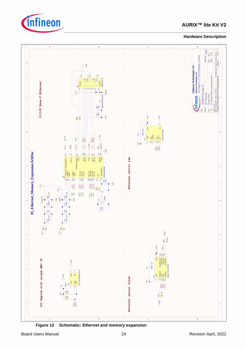
AURIX™ lite Kit V2 Hardware Description
Board Users Manual 24 Revision April, 2022
Figure 12 Schematic: Ethernet and memory expansion
11
22
33
44
55
66
77
88
DD
CC
BB
AA
55
16
.10
.20
20
13
:17
:32
Dat
e:S
hee
tof
Tim
e:©
In
fin
eon
Tec
hn
olo
gie
s A
G 2
02
0. A
ll R
igh
ts R
eser
ved
.
Au
tho
r:H
.D.
05
_E
ther
net
_M
emo
ry_
Ex
pa
nsi
on
.Sch
Do
c
Infi
neo
n T
ech
nolo
gie
s A
GIn
fin
eon
Tec
hn
olo
gie
s A
G
Am
Cam
peo
n 1
-15
- 8
55
79
Neu
bib
erg
- G
erm
any V
2.0
Tit
le
Siz
e:R
ev.
A3
Do
cum
ent
Nam
e
05
_E
ther
net
_M
emo
ry_
Ex
pan
sio
n.S
chD
oc
Rel
.
H.D
.
Var
ian
t
AU
RIX
™ L
ite
Kit
V2
[No
Var
iati
on
s]A
pp
rov
ed<
Ap
pr.
>
SV
N R
evis
ion:
No
t in
ver
sio
n c
on
tro
l
VC
C4
SD
A3
SC
L1
NC
5
VS
S2
U9
MT
_24A
A02E
48-E
/OT
VD
DA
3V
36
RD
_P
8
RD
_M
7
TD
_M
10
TD
_P
11
XO
12
XI/
50
MH
zIn
13
RB
IAS
14
MD
IO1
5
MD
C1
6
RX
_D
11
7R
X_D
01
8
VD
DIO
19
CR
S_D
V2
0R
X_E
R2
2
INT
R/P
WR
DN
3
TX
_E
N1
TX
_D
02
3
TX
_D
12
4
GN
D2
5
50
MH
zOu
t/L
ED
22
RS
T_N
5
GN
D9
LE
D0
4
GN
D2
1
U8
DP
83
82
5IR
MQ
R
GN
D
+3
V3
R60
0R
R61
0R
P21.3
P21.2
P11
.10
P11
.11
P11
.9
P11
.12
P11
.3P
11
.2
P11
.6
C53
10
0n
F
C57
10
0n
F
C51
10
uF
_o
pt
C55
10
uF
_o
pt
C56
1u
F
C52
1u
F
C58
10
nF
_o
pt
C54
10
nF
_o
pt
GN
D
GN
D
VD
DA
3V
3
VD
DIO
+3
V3
GN
D
R62
0R
/ES
R0
13
24
Y3
25
MH
zC
60
20
pF
C59
20
pF
R63
6.4
9k
/1%
GN
D
GN
D
P33.7
R66
2.2
kR
65
2.2
k
C61
10
0n
F
SD
A0
SC
L0
GN
D
+3
V3
GN
D
SH
IEL
D
TD
_P
TD
_N
RD
_P
RD
_N
C63
10
nF
C62
10
nF
GN
D
GN
D
10/100 Base-T Ethernet
I2C Eeprom with unique MAC ID
External serial flash
External serial ram
VC
C2
CS
#7
DQ
1/S
O8
DQ
2/W
P#
9
VS
S1
0
DQ
3/R
ES
ET
#1
CK
16
DQ
0/S
I1
5
RE
SE
T#
3
INT
#/D
NU
13
U1
0
op
tio
nal
Sem
per
Fla
sh
CS
1
SC
K6
SO
2
WP
3
VS
S4
SI
5
HO
LD
7
VD
D8
U11
op
tio
nal
F-R
AM
C64
10
0n
F_
op
t
C65
10
0n
F_
op
t
+3
V3
+3
V3
GN
D
GN
D
R67
0R
_o
pt
/ES
R0
P22.1
P22.1
P22.3
P22.0
P23.1
L4
BL
M18P
G600S
N1D
1 2 3 4 5 6 7 8
SH
LD
11
3
SH
LD
21
4
10
9 11
12
(gr)
(ye)
X5
74
99
01
02
11
A
R64
47
0R
i
Pow
er
i
Pow
er
i
Pow
er
P22.3
P22.0
P22.2
R68
0R
_o
pt
P20.9
CRS_DV
RX_D1
TX_D0
CLK50
RX_D0
TX_EN
TX_D1
MDC
MDIO
INT_ETH
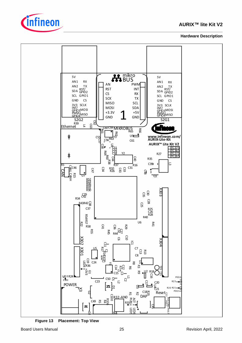
AURIX™ lite Kit V2 Hardware Description
Board Users Manual 25 Revision April, 2022
C50 C17
R3
R66
RX RX
AURIX-Lite-Kitwww.infineon.com/
TC365
AURIX Lite Kit V2
TC265TC275
TC375
Ethernet
POWER
RU
NA
CT
ESR0
+3V3
P00.5
P00.6
P0
0.7
-AN0
CAN
HC
ANL
R45
R44
X3
X5
U6
R4
Y3 U9
U8
R65
R64
R63
R62
R61
R60
L4
C63
C62
C61
C60C59
C58
C57 C56
C55
C54C53C52C51
D2
G2
D1
C49
R13
R41
R40
R59
R58
R57
R56
R55
R54
R53R52
R39
R43R42
R16
Q1
L3
C48
3V3
GND
SCL
SDA
AN2
AN1
5V
TX
GPIO1
CS
SCLK
MOSI
MISO
RST/GPIO2
PWM/GPIO4
INT/GPIO3
S2G1
X30
2
U1
R19
R17
R6
R5
R2R1
LED5
C3
C2
C1
Y2
Y1
X30
4X
303
X30
1
X4
U7
U5
U4U3
U2
MISO
MOSI
SCLK
CS
GPIO1
TX
5V
AN1
AN2
SDA
SCL
GND
3V3INT/GPIO3PWM/GPIO4
RST/GPIO2
S2G2
Reset
R10
6
TP2
TP1
R38
R37
R36
R35
R34
R33
R32
R31R30
R29
R28
R27
R26
R25
R24
R23
R22
R21R20
R18
R15
R14
R12R11
R10
R9
R8
R7
1
BUSmikro
PWMAN
+5VGND
TXRXINT
SCL
GND+3.3VMOSI
SCKMISO
CSRST
SDA
MIKROBUS
LED3
LED2
LED1
L2
L1IC1
G1
DAP
LED4
LED6
CA
N
C10
0
C47
C46
C45
C44
C42
C43
C41
C40
C39
C38
C37
C36
C35
C34
C33
C32
C31
C30
C29
C28
C27
C26
C25
C24
C23
C2
2
C21
C20
C19
C18
C16
C15
C14
C13
C12
C11
C10
C9
C8
C7
C6
C5
C4
BU
TT
ON
1 P
00.7
Figure 13 Placement: Top View

AURIX™ lite Kit V2 Hardware Description
Board Users Manual 26 Revision April, 2022
SDA0
TXD2_S2G2
RST_S2G1
S2GSPICLK_
S2G1TXD1_
AN25
AN24
RXD2_S2G2
USBVDD_
SCL0S2G1RXD1_
P33.10
GND+3V3
P33.6
P33.4
P33.2
P33.0
AN1
AN3
AN5
AN7
AN45
AN47
P00.11
P00.9
P00.7
P00.3
P00.1
GND
P00.0
P00.2
P00.6
P00.8
P00.10
P00.12
VAREF1
AN46
AN44
AN6
AN4
AN2
AN0
P33.1
P33.3
P33.5
P33.7 P32.4
P23.0
P23.2
P22.0
P22.2
P22.3
P21.3
P21.5
P20.1
/ESR1
/PORST
P11.12
P11.6
P11.6*
GND VDD_USB
P11.3
P11.9
P11.11
P15.4
P15.5
/ESR0
P21.4
P21.2
P21.0
P22.1
RST_S2G2
P23.3
P23.1
P33.13
+3V3
P33.12
GND
P33.11
VAREF
GND
SPICLK
MISO
MOSI
P10.5
P02.7
P02.6
P02.4
P02.5
P02.3
P10.4
P02.1
P02.0
TX
RX
DIG
ITA
L
+3V3
GND
AN37
AN36
/PORST
GND
AN
ALO
G I
N
VEXT
POW
ER
AN38
AN39
S2G1 S2G2
ww
w.in
fineo
n.c
om
/AU
RIX
-lit
e-K
it
USB3.0 (900mA)
P00.5
VIN
+5V
AU
RIX L
ite
Kit
V2
P11.10
MOSI_S2G
R68
U11
U10
R67C
65C
64
5V
AN1
AN2
SDA
SCL
GND
3V3
MISO
MOSI
SCLK
CS
GPIO1
TX
RX
INT/GPIO3
RST/GPIO2
PWM/GPIO4
X2 X1
RX
TX
GPIO1
CS
SCLK
MOSI
MISO
3V3
GND
SCL
SDA
AN2
AN1
5V
RST/GPIO2
INT/GPIO3PWM/GPIO41
RSTCS
MISOSCK
MOSI+3.3VGND
AN
SDASCL
INTRXTX
GND+5V
PWMBUSmikro
* Can be printed wrongly as P11.6, correct is P11.2
Figure 14 Placement: Bottom View

w w w . i n f i n e o n . c o m
Published by Infineon Technologies AG