
XC2300 Derivatives - Infineon Technologies
732
User’s Manual, V2.1, Aug. 2008 Microcontrollers XC2300 Derivatives 16/32-Bit Single-Chip Microcontroller with 32-Bit Performance Volume 2 (of 2): Peripheral Units
-
Upload
khangminh22 -
Category
Documents
-
view
1 -
download
0
Transcript of XC2300 Derivatives - Infineon Technologies

User ’s Manual , V2.1, Aug. 2008
Microcontrol lers
XC2300 Derivat ives16/32-Bi t Single-Chip Microcontrol ler wi th 32-Bi t PerformanceVolume 2 (of 2): Per ipheral Uni ts

Edition 2008-08Published byInfineon Technologies AG81726 Munich, Germany© 2008 Infineon Technologies AGAll Rights Reserved.
Legal DisclaimerThe information given in this document shall in no event be regarded as a guarantee of conditions or characteristics. With respect to any examples or hints given herein, any typical values stated herein and/or any information regarding the application of the device, Infineon Technologies hereby disclaims any and all warranties and liabilities of any kind, including without limitation, warranties of non-infringement of intellectual property rights of any third party.
InformationFor further information on technology, delivery terms and conditions and prices, please contact the nearest Infineon Technologies Office (www.infineon.com).
WarningsDue to technical requirements, components may contain dangerous substances. For information on the types in question, please contact the nearest Infineon Technologies Office.Infineon Technologies components may be used in life-support devices or systems only with the express written approval of Infineon Technologies, if a failure of such components can reasonably be expected to cause the failure of that life-support device or system or to affect the safety or effectiveness of that device or system. Life support devices or systems are intended to be implanted in the human body or to support and/or maintain and sustain and/or protect human life. If they fail, it is reasonable to assume that the health of the user or other persons may be endangered.
User ’s Manual , V2.1, Aug. 2008
Microcontrol lers
XC2300 Derivat ives16/32-Bi t Single-Chip Microcontrol ler wi th 32-Bi t PerformanceVolume 2 (of 2): Per ipheral Uni ts
XC2300 DerivativesPeripheral Units (Vol. 2 of 2)
User’s Manual V2.1, 2008-08
XC2300Revision History: V2.1, 2008-08Previous Version(s):V2.0, 2007-12V1.0, 2007-06 (XC2000)V0.1, 2007-03, Draft VersionPage Subjects (major changes since last revision)14-1ff Several formal updates and minor description improvements15-1ff Minor description improvements, ID register added17-1ff Several formal updates, ID register added
We Listen to Your CommentsAny information within this document that you feel is wrong, unclear or missing at all?Your feedback will help us to continuously improve the quality of this document.Please send your proposal (including a reference to this document) to:[email protected]

User’s Manual L-1 V2.1, 2008-08
XC2300 DerivativesPeripheral Units (Vol. 2 of 2)
Summary Of Chapters
Summary Of Chapters . . . . . . . . . . . . . . . . . . . . . . . . . . . . . . . . . . . . 0-1 [1]
Table Of Contents . . . . . . . . . . . . . . . . . . . . . . . . . . . . . . . . . . . . . . . 0-2 [1]
1 Introduction . . . . . . . . . . . . . . . . . . . . . . . . . . . . . . . . . . . . . . . . . . . . 1-1 [1]
2 Architectural Overview . . . . . . . . . . . . . . . . . . . . . . . . . . . . . . . . . . . 2-1 [1]
3 Memory Organization . . . . . . . . . . . . . . . . . . . . . . . . . . . . . . . . . . . . 3-1 [1]
4 Central Processing Unit (CPU) . . . . . . . . . . . . . . . . . . . . . . . . . . . . 4-1 [1]
5 Interrupt and Trap Functions . . . . . . . . . . . . . . . . . . . . . . . . . . . . . . 5-1 [1]
6 System Control Unit (SCU) . . . . . . . . . . . . . . . . . . . . . . . . . . . . . . . . 6-1 [1]
7 Parallel Ports . . . . . . . . . . . . . . . . . . . . . . . . . . . . . . . . . . . . . . . . . . . 7-1 [1]
8 Dedicated Pins . . . . . . . . . . . . . . . . . . . . . . . . . . . . . . . . . . . . . . . . . . 8-1 [1]
9 The External Bus Controller EBC . . . . . . . . . . . . . . . . . . . . . . . . . . 9-1 [1]
10 Startup Configuration and Bootstrap Loading . . . . . . . . . . . . . . . 10-1 [1]
11 Debug System . . . . . . . . . . . . . . . . . . . . . . . . . . . . . . . . . . . . . . . . . 11-1 [1]
12 Instruction Set Summary . . . . . . . . . . . . . . . . . . . . . . . . . . . . . . . . 12-1 [1]
13 Device Specification . . . . . . . . . . . . . . . . . . . . . . . . . . . . . . . . . . . . 13-1 [1]
14 The General Purpose Timer Units . . . . . . . . . . . . . . . . . . . . . . . . . 14-1 [2]
15 Real Time Clock . . . . . . . . . . . . . . . . . . . . . . . . . . . . . . . . . . . . . . . 15-1 [2]
16 Analog to Digital Converter . . . . . . . . . . . . . . . . . . . . . . . . . . . . . . 16-1 [2]
17 Capture/Compare Unit 2 . . . . . . . . . . . . . . . . . . . . . . . . . . . . . . . . . 17-1 [2]
18 Capture/Compare Unit 6 (CCU6) . . . . . . . . . . . . . . . . . . . . . . . . . . 18-1 [2]
19 Universal Serial Interface Channel . . . . . . . . . . . . . . . . . . . . . . . . . 19-1 [2]
20 Controller Area Network (MultiCAN) Controller . . . . . . . . . . . . . . 20-1 [2]
Keyword Index . . . . . . . . . . . . . . . . . . . . . . . . . . . . . . . . . . . . . . . . . 21-1 [2]
Register Index . . . . . . . . . . . . . . . . . . . . . . . . . . . . . . . . . . . . . . . . . 22-7 [2]
Summary Of ChaptersThis User’s Manual consists of two Volumes, “System Units” and “Peripheral Units”. Fora quick overview this table of chapters summarizes both volumes, so you immediatelycan find the reference to the desired section in the corresponding document ([1] or [2]).

XC2300 DerivativesPeripheral Units (Vol. 2 of 2)
Table Of Contents
Table Of ContentsThis User’s Manual consists of two Volumes, “System Units” and “Peripheral Units”. Foryour convenience this table of contents (and also the keyword and register index) listsboth volumes, so you can immediately find the reference to the desired section in thecorresponding document ([1] or [2]).
Summary Of Chapters . . . . . . . . . . . . . . . . . . . . . . . . . . . . . . . . . . . . 0-1 [1]
Table Of Contents . . . . . . . . . . . . . . . . . . . . . . . . . . . . . . . . . . . . . . . 0-2 [1]
1 Introduction . . . . . . . . . . . . . . . . . . . . . . . . . . . . . . . . . . . . . . . . . . . . 1-1 [1]1.1 Members of the 16-bit Microcontroller Family . . . . . . . . . . . . . . . . . . . 1-3 [1]1.2 Summary of Basic Features . . . . . . . . . . . . . . . . . . . . . . . . . . . . . . . . 1-5 [1]1.3 Abbreviations . . . . . . . . . . . . . . . . . . . . . . . . . . . . . . . . . . . . . . . . . . . 1-9 [1]1.4 Naming Conventions . . . . . . . . . . . . . . . . . . . . . . . . . . . . . . . . . . . . . 1-10 [1]
2 Architectural Overview . . . . . . . . . . . . . . . . . . . . . . . . . . . . . . . . . . . 2-1 [1]2.1 Basic CPU Concepts and Optimizations . . . . . . . . . . . . . . . . . . . . . . . 2-2 [1]2.1.1 High Instruction Bandwidth/Fast Execution . . . . . . . . . . . . . . . . . . . 2-4 [1]2.1.2 Powerful Execution Units . . . . . . . . . . . . . . . . . . . . . . . . . . . . . . . . . 2-5 [1]2.1.3 High Performance Branch-, Call-, and Loop-Processing . . . . . . . . . 2-6 [1]2.1.4 Consistent and Optimized Instruction Formats . . . . . . . . . . . . . . . . 2-7 [1]2.1.5 Programmable Multiple Priority Interrupt System . . . . . . . . . . . . . . 2-8 [1]2.1.6 Interfaces to System Resources . . . . . . . . . . . . . . . . . . . . . . . . . . . 2-9 [1]2.2 On-Chip System Resources . . . . . . . . . . . . . . . . . . . . . . . . . . . . . . . 2-10 [1]2.3 On-Chip Peripheral Blocks . . . . . . . . . . . . . . . . . . . . . . . . . . . . . . . . 2-15 [1]2.4 Clock Generation . . . . . . . . . . . . . . . . . . . . . . . . . . . . . . . . . . . . . . . . 2-32 [1]2.5 Power Management . . . . . . . . . . . . . . . . . . . . . . . . . . . . . . . . . . . . . . 2-33 [1]2.6 On-Chip Debug Support (OCDS) . . . . . . . . . . . . . . . . . . . . . . . . . . . 2-34 [1]
3 Memory Organization . . . . . . . . . . . . . . . . . . . . . . . . . . . . . . . . . . . . 3-1 [1]3.1 Address Mapping . . . . . . . . . . . . . . . . . . . . . . . . . . . . . . . . . . . . . . . . . 3-3 [1]3.2 Special Function Register Areas . . . . . . . . . . . . . . . . . . . . . . . . . . . . . 3-5 [1]3.3 Data Memory Areas . . . . . . . . . . . . . . . . . . . . . . . . . . . . . . . . . . . . . . . 3-9 [1]3.4 Program Memory Areas . . . . . . . . . . . . . . . . . . . . . . . . . . . . . . . . . . . 3-11 [1]3.4.1 Program/Data SRAM (PSRAM) . . . . . . . . . . . . . . . . . . . . . . . . . . . 3-12 [1]3.4.2 Non-Volatile Program Memory (Flash) . . . . . . . . . . . . . . . . . . . . . 3-13 [1]3.5 System Stack . . . . . . . . . . . . . . . . . . . . . . . . . . . . . . . . . . . . . . . . . . . 3-14 [1]3.6 IO Areas . . . . . . . . . . . . . . . . . . . . . . . . . . . . . . . . . . . . . . . . . . . . . . . 3-15 [1]3.7 External Memory Space . . . . . . . . . . . . . . . . . . . . . . . . . . . . . . . . . . 3-16 [1]3.8 Crossing Memory Boundaries . . . . . . . . . . . . . . . . . . . . . . . . . . . . . . 3-17 [1]3.9 Embedded Flash Memory . . . . . . . . . . . . . . . . . . . . . . . . . . . . . . . . . 3-18 [1]3.9.1 Definitions . . . . . . . . . . . . . . . . . . . . . . . . . . . . . . . . . . . . . . . . . . . 3-18 [1]
User’s Manual L-2 V2.1, 2008-08

XC2300 DerivativesPeripheral Units (Vol. 2 of 2)
Table Of Contents
3.9.2 Operating Modes . . . . . . . . . . . . . . . . . . . . . . . . . . . . . . . . . . . . . . 3-20 [1]3.9.3 Operations . . . . . . . . . . . . . . . . . . . . . . . . . . . . . . . . . . . . . . . . . . . 3-22 [1]3.9.4 Details of Command Sequences . . . . . . . . . . . . . . . . . . . . . . . . . . 3-25 [1]3.9.5 Data Integrity . . . . . . . . . . . . . . . . . . . . . . . . . . . . . . . . . . . . . . . . . 3-35 [1]3.9.6 Protection Handling Details . . . . . . . . . . . . . . . . . . . . . . . . . . . . . . 3-38 [1]3.9.7 Protection Handling Examples . . . . . . . . . . . . . . . . . . . . . . . . . . . . 3-45 [1]3.9.8 EEPROM Emulation . . . . . . . . . . . . . . . . . . . . . . . . . . . . . . . . . . . 3-47 [1]3.9.9 Interrupt Generation . . . . . . . . . . . . . . . . . . . . . . . . . . . . . . . . . . . . 3-49 [1]3.9.10 Recommendations for Optimized Flash Usage . . . . . . . . . . . . . . . 3-49 [1]3.10 On-Chip Program Memory Control . . . . . . . . . . . . . . . . . . . . . . . . . . 3-51 [1]3.10.1 Overview . . . . . . . . . . . . . . . . . . . . . . . . . . . . . . . . . . . . . . . . . . . . 3-51 [1]3.10.2 Register Interface . . . . . . . . . . . . . . . . . . . . . . . . . . . . . . . . . . . . . 3-53 [1]3.10.3 Error Reporting Summary . . . . . . . . . . . . . . . . . . . . . . . . . . . . . . . 3-64 [1]3.11 Data Retention Memories . . . . . . . . . . . . . . . . . . . . . . . . . . . . . . . . . 3-65 [1]
4 Central Processing Unit (CPU) . . . . . . . . . . . . . . . . . . . . . . . . . . . . 4-1 [1]4.1 Components of the CPU . . . . . . . . . . . . . . . . . . . . . . . . . . . . . . . . . . . 4-4 [1]4.2 Instruction Fetch and Program Flow Control . . . . . . . . . . . . . . . . . . . . 4-5 [1]4.2.1 Branch Detection and Branch Prediction Rules . . . . . . . . . . . . . . . . 4-7 [1]4.2.2 Correctly Predicted Instruction Flow . . . . . . . . . . . . . . . . . . . . . . . . 4-7 [1]4.2.3 Incorrectly Predicted Instruction Flow . . . . . . . . . . . . . . . . . . . . . . . 4-9 [1]4.3 Instruction Processing Pipeline . . . . . . . . . . . . . . . . . . . . . . . . . . . . . 4-11 [1]4.3.1 Pipeline Conflicts Using General Purpose Registers . . . . . . . . . . . 4-13 [1]4.3.2 Pipeline Conflicts Using Indirect Addressing Modes . . . . . . . . . . . 4-15 [1]4.3.3 Pipeline Conflicts Due to Memory Bandwidth . . . . . . . . . . . . . . . . 4-17 [1]4.3.4 Pipeline Conflicts Caused by CPU-SFR Updates . . . . . . . . . . . . . 4-20 [1]4.4 CPU Configuration Registers . . . . . . . . . . . . . . . . . . . . . . . . . . . . . . 4-26 [1]4.5 Use of General Purpose Registers . . . . . . . . . . . . . . . . . . . . . . . . . . 4-29 [1]4.5.1 GPR Addressing Modes . . . . . . . . . . . . . . . . . . . . . . . . . . . . . . . . 4-31 [1]4.5.2 Context Switching . . . . . . . . . . . . . . . . . . . . . . . . . . . . . . . . . . . . . 4-33 [1]4.6 Code Addressing . . . . . . . . . . . . . . . . . . . . . . . . . . . . . . . . . . . . . . . . 4-37 [1]4.7 Data Addressing . . . . . . . . . . . . . . . . . . . . . . . . . . . . . . . . . . . . . . . . 4-39 [1]4.7.1 Short Addressing Modes . . . . . . . . . . . . . . . . . . . . . . . . . . . . . . . . 4-39 [1]4.7.2 Long Addressing Modes . . . . . . . . . . . . . . . . . . . . . . . . . . . . . . . . 4-41 [1]4.7.3 Indirect Addressing Modes . . . . . . . . . . . . . . . . . . . . . . . . . . . . . . 4-44 [1]4.7.4 DSP Addressing Modes . . . . . . . . . . . . . . . . . . . . . . . . . . . . . . . . . 4-46 [1]4.7.5 The System Stack . . . . . . . . . . . . . . . . . . . . . . . . . . . . . . . . . . . . . 4-52 [1]4.8 Standard Data Processing . . . . . . . . . . . . . . . . . . . . . . . . . . . . . . . . . 4-56 [1]4.8.1 16-bit Adder/Subtracter, Barrel Shifter, and 16-bit Logic Unit . . . . 4-60 [1]4.8.2 Bit Manipulation Unit . . . . . . . . . . . . . . . . . . . . . . . . . . . . . . . . . . . 4-60 [1]4.8.3 Multiply and Divide Unit . . . . . . . . . . . . . . . . . . . . . . . . . . . . . . . . 4-62 [1]4.9 DSP Data Processing (MAC Unit) . . . . . . . . . . . . . . . . . . . . . . . . . . . 4-64 [1]4.9.1 MAC Unit Control . . . . . . . . . . . . . . . . . . . . . . . . . . . . . . . . . . . . . . 4-65 [1]
User’s Manual L-3 V2.1, 2008-08

XC2300 DerivativesPeripheral Units (Vol. 2 of 2)
Table Of Contents
4.9.2 Representation of Numbers and Rounding . . . . . . . . . . . . . . . . . . 4-65 [1]4.9.3 The 16-bit by 16-bit Signed/Unsigned Multiplier and Scaler . . . . . 4-66 [1]4.9.4 Concatenation Unit . . . . . . . . . . . . . . . . . . . . . . . . . . . . . . . . . . . . 4-66 [1]4.9.5 One-bit Scaler . . . . . . . . . . . . . . . . . . . . . . . . . . . . . . . . . . . . . . . . 4-66 [1]4.9.6 The 40-bit Adder/Subtracter . . . . . . . . . . . . . . . . . . . . . . . . . . . . . 4-66 [1]4.9.7 The Data Limiter . . . . . . . . . . . . . . . . . . . . . . . . . . . . . . . . . . . . . . 4-67 [1]4.9.8 The Accumulator Shifter . . . . . . . . . . . . . . . . . . . . . . . . . . . . . . . . 4-67 [1]4.9.9 The 40-bit Signed Accumulator Register . . . . . . . . . . . . . . . . . . . . 4-68 [1]4.9.10 The MAC Unit Status Word MSW . . . . . . . . . . . . . . . . . . . . . . . . . 4-70 [1]4.9.11 The Repeat Counter MRW . . . . . . . . . . . . . . . . . . . . . . . . . . . . . . 4-72 [1]4.10 Constant Registers . . . . . . . . . . . . . . . . . . . . . . . . . . . . . . . . . . . . . . 4-74 [1]
5 Interrupt and Trap Functions . . . . . . . . . . . . . . . . . . . . . . . . . . . . . . 5-1 [1]5.1 Interrupt System Structure . . . . . . . . . . . . . . . . . . . . . . . . . . . . . . . . . . 5-2 [1]5.2 Interrupt Arbitration and Control . . . . . . . . . . . . . . . . . . . . . . . . . . . . . 5-4 [1]5.3 Interrupt Vector Table . . . . . . . . . . . . . . . . . . . . . . . . . . . . . . . . . . . . 5-11 [1]5.4 Operation of the Peripheral Event Controller Channels . . . . . . . . . . 5-20 [1]5.4.1 The PECC Registers . . . . . . . . . . . . . . . . . . . . . . . . . . . . . . . . . . . 5-20 [1]5.4.2 The PEC Source and Destination Pointers . . . . . . . . . . . . . . . . . . 5-24 [1]5.4.3 PEC Transfer Control . . . . . . . . . . . . . . . . . . . . . . . . . . . . . . . . . . 5-26 [1]5.4.4 Channel Link Mode for Data Chaining . . . . . . . . . . . . . . . . . . . . . . 5-28 [1]5.4.5 PEC Interrupt Control . . . . . . . . . . . . . . . . . . . . . . . . . . . . . . . . . . 5-29 [1]5.5 Prioritization of Interrupt and PEC Service Requests . . . . . . . . . . . . 5-31 [1]5.6 Context Switching and Saving Status . . . . . . . . . . . . . . . . . . . . . . . . 5-33 [1]5.7 Interrupt Node Sharing . . . . . . . . . . . . . . . . . . . . . . . . . . . . . . . . . . . 5-36 [1]5.8 External Interrupts . . . . . . . . . . . . . . . . . . . . . . . . . . . . . . . . . . . . . . 5-37 [1]5.9 OCDS Requests . . . . . . . . . . . . . . . . . . . . . . . . . . . . . . . . . . . . . . . . 5-39 [1]5.10 Service Request Latency . . . . . . . . . . . . . . . . . . . . . . . . . . . . . . . . . 5-40 [1]5.11 Trap Functions . . . . . . . . . . . . . . . . . . . . . . . . . . . . . . . . . . . . . . . . . 5-42 [1]
6 System Control Unit (SCU) . . . . . . . . . . . . . . . . . . . . . . . . . . . . . . . . 6-1 [1]6.1 Clock Generation Unit . . . . . . . . . . . . . . . . . . . . . . . . . . . . . . . . . . . . . 6-2 [1]6.1.1 Overview . . . . . . . . . . . . . . . . . . . . . . . . . . . . . . . . . . . . . . . . . . . . . 6-2 [1]6.1.2 Trimmed Current Controlled Wake-up Clock (OSC_WU) . . . . . . . . 6-4 [1]6.1.3 High Precision Oscillator Circuit (OSC_HP) . . . . . . . . . . . . . . . . . . 6-4 [1]6.1.4 Phase-Locked Loop (PLL) Module . . . . . . . . . . . . . . . . . . . . . . . . . 6-5 [1]6.1.5 Clock Control Unit . . . . . . . . . . . . . . . . . . . . . . . . . . . . . . . . . . . . . 6-15 [1]6.1.6 External Clock Output . . . . . . . . . . . . . . . . . . . . . . . . . . . . . . . . . . 6-20 [1]6.1.7 CGU Registers . . . . . . . . . . . . . . . . . . . . . . . . . . . . . . . . . . . . . . . . 6-23 [1]6.2 Wake-up Timer (WUT) . . . . . . . . . . . . . . . . . . . . . . . . . . . . . . . . . . . . 6-44 [1]6.2.1 Wake-up Timer Operation . . . . . . . . . . . . . . . . . . . . . . . . . . . . . . . 6-44 [1]6.2.2 WUT Registers . . . . . . . . . . . . . . . . . . . . . . . . . . . . . . . . . . . . . . . 6-46 [1]6.3 Reset Operation . . . . . . . . . . . . . . . . . . . . . . . . . . . . . . . . . . . . . . . . . 6-49 [1]6.3.1 Reset Architecture . . . . . . . . . . . . . . . . . . . . . . . . . . . . . . . . . . . . . 6-49 [1]
User’s Manual L-4 V2.1, 2008-08
XC2300 DerivativesPeripheral Units (Vol. 2 of 2)
Table Of Contents
6.3.2 General Reset Operation . . . . . . . . . . . . . . . . . . . . . . . . . . . . . . . . 6-50 [1]6.3.3 Debug Reset Assertion . . . . . . . . . . . . . . . . . . . . . . . . . . . . . . . . . 6-53 [1]6.3.4 Coupling of Reset Types . . . . . . . . . . . . . . . . . . . . . . . . . . . . . . . . 6-53 [1]6.3.5 Reset Request Trigger Sources . . . . . . . . . . . . . . . . . . . . . . . . . . 6-54 [1]6.3.6 Module Reset Behavior . . . . . . . . . . . . . . . . . . . . . . . . . . . . . . . . . 6-56 [1]6.3.7 Reset Controller Registers . . . . . . . . . . . . . . . . . . . . . . . . . . . . . . . 6-58 [1]6.4 External Service Request (ESR) Pins . . . . . . . . . . . . . . . . . . . . . . . . 6-68 [1]6.4.1 General Operation . . . . . . . . . . . . . . . . . . . . . . . . . . . . . . . . . . . . . 6-68 [1]6.4.2 ESR Control Registers . . . . . . . . . . . . . . . . . . . . . . . . . . . . . . . . . . 6-72 [1]6.4.3 ESR Data Register . . . . . . . . . . . . . . . . . . . . . . . . . . . . . . . . . . . . 6-76 [1]6.5 Power Supply and Control . . . . . . . . . . . . . . . . . . . . . . . . . . . . . . . . . 6-77 [1]6.5.1 Supply Watchdog (SWD) . . . . . . . . . . . . . . . . . . . . . . . . . . . . . . . . 6-79 [1]6.5.2 Monitoring the Voltage Level of a Core Domain . . . . . . . . . . . . . . 6-85 [1]6.5.3 Controlling the Voltage Level of a Core Domain . . . . . . . . . . . . . . 6-92 [1]6.5.4 Handling the Power System . . . . . . . . . . . . . . . . . . . . . . . . . . . . 6-102 [1]6.6 Global State Controller (GSC) . . . . . . . . . . . . . . . . . . . . . . . . . . . . . 6-103 [1]6.6.1 GSC Control Flow . . . . . . . . . . . . . . . . . . . . . . . . . . . . . . . . . . . . 6-103 [1]6.6.2 GSC Registers . . . . . . . . . . . . . . . . . . . . . . . . . . . . . . . . . . . . . . . 6-107 [1]6.7 Software Boot Support . . . . . . . . . . . . . . . . . . . . . . . . . . . . . . . . . . . 6-112 [1]6.7.1 Start-up Registers . . . . . . . . . . . . . . . . . . . . . . . . . . . . . . . . . . . . 6-112 [1]6.8 External Request Unit (ERU) . . . . . . . . . . . . . . . . . . . . . . . . . . . . . . 6-113 [1]6.8.1 Introduction . . . . . . . . . . . . . . . . . . . . . . . . . . . . . . . . . . . . . . . . . 6-113 [1]6.8.2 ERU Pin Connections . . . . . . . . . . . . . . . . . . . . . . . . . . . . . . . . . 6-115 [1]6.8.3 External Request Select Unit (ERSx) . . . . . . . . . . . . . . . . . . . . . 6-119 [1]6.8.4 Event Trigger Logic (ETLx) . . . . . . . . . . . . . . . . . . . . . . . . . . . . . 6-120 [1]6.8.5 Connecting Matrix . . . . . . . . . . . . . . . . . . . . . . . . . . . . . . . . . . . . 6-122 [1]6.8.6 Output Gating Unit (OGUy) . . . . . . . . . . . . . . . . . . . . . . . . . . . . . 6-123 [1]6.8.7 ERU Output Connections . . . . . . . . . . . . . . . . . . . . . . . . . . . . . . 6-127 [1]6.8.8 ERU Registers . . . . . . . . . . . . . . . . . . . . . . . . . . . . . . . . . . . . . . . 6-129 [1]6.9 SCU Interrupt Generation . . . . . . . . . . . . . . . . . . . . . . . . . . . . . . . . 6-136 [1]6.9.1 Interrupt Support . . . . . . . . . . . . . . . . . . . . . . . . . . . . . . . . . . . . . 6-136 [1]6.9.2 SCU Interrupt Sources . . . . . . . . . . . . . . . . . . . . . . . . . . . . . . . . . 6-137 [1]6.9.3 Interrupt Control Registers . . . . . . . . . . . . . . . . . . . . . . . . . . . . . . 6-138 [1]6.10 Temperature Compensation Unit . . . . . . . . . . . . . . . . . . . . . . . . . . 6-157 [1]6.10.1 Temperature Compensation Registers . . . . . . . . . . . . . . . . . . . . 6-159 [1]6.11 Watchdog Timer (WDT) . . . . . . . . . . . . . . . . . . . . . . . . . . . . . . . . . . 6-161 [1]6.11.1 Introduction . . . . . . . . . . . . . . . . . . . . . . . . . . . . . . . . . . . . . . . . . 6-161 [1]6.11.2 Overview . . . . . . . . . . . . . . . . . . . . . . . . . . . . . . . . . . . . . . . . . . . 6-161 [1]6.11.3 Functional Description . . . . . . . . . . . . . . . . . . . . . . . . . . . . . . . . . 6-162 [1]6.11.4 WDT Kernel Registers . . . . . . . . . . . . . . . . . . . . . . . . . . . . . . . . . 6-166 [1]6.12 SCU Trap Generation . . . . . . . . . . . . . . . . . . . . . . . . . . . . . . . . . . . 6-170 [1]6.12.1 Trap Support . . . . . . . . . . . . . . . . . . . . . . . . . . . . . . . . . . . . . . . . 6-170 [1]6.12.2 SCU Trap Sources . . . . . . . . . . . . . . . . . . . . . . . . . . . . . . . . . . . . 6-171 [1]
User’s Manual L-5 V2.1, 2008-08
XC2300 DerivativesPeripheral Units (Vol. 2 of 2)
Table Of Contents
6.12.3 SCU Trap Control Registers . . . . . . . . . . . . . . . . . . . . . . . . . . . . 6-172 [1]6.13 Memory Content Protection . . . . . . . . . . . . . . . . . . . . . . . . . . . . . . . 6-182 [1]6.13.1 Parity Error Handling . . . . . . . . . . . . . . . . . . . . . . . . . . . . . . . . . . 6-182 [1]6.14 Register Control . . . . . . . . . . . . . . . . . . . . . . . . . . . . . . . . . . . . . . . . 6-191 [1]6.14.1 Register Access Control . . . . . . . . . . . . . . . . . . . . . . . . . . . . . . . 6-191 [1]6.14.2 Register Protection Registers . . . . . . . . . . . . . . . . . . . . . . . . . . . 6-194 [1]6.15 Miscellaneous System Registers . . . . . . . . . . . . . . . . . . . . . . . . . . . 6-196 [1]6.15.1 System Registers . . . . . . . . . . . . . . . . . . . . . . . . . . . . . . . . . . . . . 6-196 [1]6.15.2 Identification Block . . . . . . . . . . . . . . . . . . . . . . . . . . . . . . . . . . . . 6-197 [1]6.15.3 Marker Memory . . . . . . . . . . . . . . . . . . . . . . . . . . . . . . . . . . . . . . 6-202 [1]6.16 SCU Register Addresses . . . . . . . . . . . . . . . . . . . . . . . . . . . . . . . . . 6-203 [1]6.17 Implementation . . . . . . . . . . . . . . . . . . . . . . . . . . . . . . . . . . . . . . . . 6-209 [1]6.17.1 Clock Generation Unit . . . . . . . . . . . . . . . . . . . . . . . . . . . . . . . . . 6-209 [1]
7 Parallel Ports . . . . . . . . . . . . . . . . . . . . . . . . . . . . . . . . . . . . . . . . . . . 7-1 [1]7.1 General Description . . . . . . . . . . . . . . . . . . . . . . . . . . . . . . . . . . . . . . . 7-2 [1]7.1.1 Basic Port Operation . . . . . . . . . . . . . . . . . . . . . . . . . . . . . . . . . . . . 7-2 [1]7.1.2 Input Stage Control . . . . . . . . . . . . . . . . . . . . . . . . . . . . . . . . . . . . . 7-5 [1]7.1.3 Output Driver Control . . . . . . . . . . . . . . . . . . . . . . . . . . . . . . . . . . . . 7-5 [1]7.2 Port Register Description . . . . . . . . . . . . . . . . . . . . . . . . . . . . . . . . . . . 7-6 [1]7.2.1 Pad Driver Control . . . . . . . . . . . . . . . . . . . . . . . . . . . . . . . . . . . . . . 7-6 [1]7.2.2 Port Output Register . . . . . . . . . . . . . . . . . . . . . . . . . . . . . . . . . . . . 7-9 [1]7.2.3 Port Output Modification Register . . . . . . . . . . . . . . . . . . . . . . . . . 7-10 [1]7.2.4 Port Input Register . . . . . . . . . . . . . . . . . . . . . . . . . . . . . . . . . . . . . 7-12 [1]7.2.5 Port Input/Output Control Registers . . . . . . . . . . . . . . . . . . . . . . . . 7-13 [1]7.2.6 Port Digital Input Disable Register . . . . . . . . . . . . . . . . . . . . . . . . . 7-16 [1]7.3 Port Description . . . . . . . . . . . . . . . . . . . . . . . . . . . . . . . . . . . . . . . . . 7-17 [1]7.3.1 Port 0 . . . . . . . . . . . . . . . . . . . . . . . . . . . . . . . . . . . . . . . . . . . . . . . 7-18 [1]7.3.2 Port 1 . . . . . . . . . . . . . . . . . . . . . . . . . . . . . . . . . . . . . . . . . . . . . . . 7-19 [1]7.3.3 Port 2 . . . . . . . . . . . . . . . . . . . . . . . . . . . . . . . . . . . . . . . . . . . . . . . 7-20 [1]7.3.4 Port 3 . . . . . . . . . . . . . . . . . . . . . . . . . . . . . . . . . . . . . . . . . . . . . . . 7-22 [1]7.3.5 Port 4 . . . . . . . . . . . . . . . . . . . . . . . . . . . . . . . . . . . . . . . . . . . . . . . 7-23 [1]7.3.6 Port 5 . . . . . . . . . . . . . . . . . . . . . . . . . . . . . . . . . . . . . . . . . . . . . . . 7-24 [1]7.3.7 Port 6 . . . . . . . . . . . . . . . . . . . . . . . . . . . . . . . . . . . . . . . . . . . . . . . 7-25 [1]7.3.8 Port 7 . . . . . . . . . . . . . . . . . . . . . . . . . . . . . . . . . . . . . . . . . . . . . . . 7-26 [1]7.3.9 Port 8 . . . . . . . . . . . . . . . . . . . . . . . . . . . . . . . . . . . . . . . . . . . . . . . 7-27 [1]7.3.10 Port 9 . . . . . . . . . . . . . . . . . . . . . . . . . . . . . . . . . . . . . . . . . . . . . . . 7-28 [1]7.3.11 Port 10 . . . . . . . . . . . . . . . . . . . . . . . . . . . . . . . . . . . . . . . . . . . . . . 7-29 [1]7.3.12 Port 11 . . . . . . . . . . . . . . . . . . . . . . . . . . . . . . . . . . . . . . . . . . . . . . 7-31 [1]7.3.13 Port 15 . . . . . . . . . . . . . . . . . . . . . . . . . . . . . . . . . . . . . . . . . . . . . . 7-32 [1]7.4 Pin Description . . . . . . . . . . . . . . . . . . . . . . . . . . . . . . . . . . . . . . . . . . 7-33 [1]
8 Dedicated Pins . . . . . . . . . . . . . . . . . . . . . . . . . . . . . . . . . . . . . . . . . . 8-1 [1]
User’s Manual L-6 V2.1, 2008-08
XC2300 DerivativesPeripheral Units (Vol. 2 of 2)
Table Of Contents
9 The External Bus Controller EBC . . . . . . . . . . . . . . . . . . . . . . . . . . 9-1 [1]9.1 External Bus Signals . . . . . . . . . . . . . . . . . . . . . . . . . . . . . . . . . . . . . . 9-3 [1]9.2 Timing Principles . . . . . . . . . . . . . . . . . . . . . . . . . . . . . . . . . . . . . . . . . 9-4 [1]9.2.1 Basic Bus Cycle Protocols . . . . . . . . . . . . . . . . . . . . . . . . . . . . . . . . 9-4 [1]9.2.2 Bus Cycle Phases . . . . . . . . . . . . . . . . . . . . . . . . . . . . . . . . . . . . . . 9-7 [1]9.2.3 Bus Cycle Examples: Fastest Access Cycles . . . . . . . . . . . . . . . . . 9-9 [1]9.3 Functional Description . . . . . . . . . . . . . . . . . . . . . . . . . . . . . . . . . . . . 9-11 [1]9.3.1 Configuration Register Overview . . . . . . . . . . . . . . . . . . . . . . . . . . 9-11 [1]9.3.2 The EBC Mode Register 0 . . . . . . . . . . . . . . . . . . . . . . . . . . . . . . . 9-14 [1]9.3.3 The EBC Mode Register 1 . . . . . . . . . . . . . . . . . . . . . . . . . . . . . . . 9-16 [1]9.3.4 The Timing Configuration Registers TCONCSx . . . . . . . . . . . . . . 9-17 [1]9.3.5 The Function Configuration Registers FCONCSx . . . . . . . . . . . . . 9-20 [1]9.3.6 The Address Window Selection Registers ADDRSELx . . . . . . . . . 9-23 [1]9.3.7 Ready Controlled Bus Cycles . . . . . . . . . . . . . . . . . . . . . . . . . . . . 9-26 [1]9.3.8 External Bus Arbitration . . . . . . . . . . . . . . . . . . . . . . . . . . . . . . . . . 9-28 [1]9.3.9 Shutdown Control . . . . . . . . . . . . . . . . . . . . . . . . . . . . . . . . . . . . . 9-32 [1]9.4 LXBus Access Control and Signal Generation . . . . . . . . . . . . . . . . . 9-33 [1]
10 Startup Configuration and Bootstrap Loading . . . . . . . . . . . . . . . 10-1 [1]10.1 Start-Up Mode Selection . . . . . . . . . . . . . . . . . . . . . . . . . . . . . . . . . . 10-1 [1]10.2 Device Status after Start-Up . . . . . . . . . . . . . . . . . . . . . . . . . . . . . . . 10-2 [1]10.2.1 Registers modified by the Start-Up Procedure . . . . . . . . . . . . . . . 10-2 [1]10.2.2 System Frequency . . . . . . . . . . . . . . . . . . . . . . . . . . . . . . . . . . . . . 10-4 [1]10.2.3 Watchdog Timer handling . . . . . . . . . . . . . . . . . . . . . . . . . . . . . . . 10-4 [1]10.2.4 Start-up Error state . . . . . . . . . . . . . . . . . . . . . . . . . . . . . . . . . . . . 10-5 [1]10.3 Special Start-up Features . . . . . . . . . . . . . . . . . . . . . . . . . . . . . . . . . 10-6 [1]10.3.1 Supplementary Start-up Information from/to the User . . . . . . . . . . 10-6 [1]10.3.2 Support for Power-saving Modes . . . . . . . . . . . . . . . . . . . . . . . . . 10-8 [1]10.3.3 Preparing to activate Parity . . . . . . . . . . . . . . . . . . . . . . . . . . . . . . 10-8 [1]10.4 Internal Start . . . . . . . . . . . . . . . . . . . . . . . . . . . . . . . . . . . . . . . . . . 10-11 [1]10.5 External Start . . . . . . . . . . . . . . . . . . . . . . . . . . . . . . . . . . . . . . . . . . 10-11 [1]10.5.1 Specific Settings . . . . . . . . . . . . . . . . . . . . . . . . . . . . . . . . . . . . . 10-13 [1]10.6 Bootstrap Loading . . . . . . . . . . . . . . . . . . . . . . . . . . . . . . . . . . . . . . 10-14 [1]10.6.1 General Functionality . . . . . . . . . . . . . . . . . . . . . . . . . . . . . . . . . . 10-14 [1]10.6.2 Bootstrap Loaders using UART Protocol . . . . . . . . . . . . . . . . . . . 10-16 [1]10.6.3 Synchronous Serial Channel Bootstrap Loader . . . . . . . . . . . . . . 10-23 [1]10.6.4 CAN Bootstrap Loader . . . . . . . . . . . . . . . . . . . . . . . . . . . . . . . . . 10-26 [1]10.6.5 Summary of Bootstrap Loader Modes . . . . . . . . . . . . . . . . . . . . . 10-29 [1]
11 Debug System . . . . . . . . . . . . . . . . . . . . . . . . . . . . . . . . . . . . . . . . . 11-1 [1]11.1 Debug Interface . . . . . . . . . . . . . . . . . . . . . . . . . . . . . . . . . . . . . . . . . 11-2 [1]11.1.1 Routing of Debug Signals . . . . . . . . . . . . . . . . . . . . . . . . . . . . . . . 11-3 [1]11.2 OCDS Module . . . . . . . . . . . . . . . . . . . . . . . . . . . . . . . . . . . . . . . . . . 11-5 [1]11.2.1 Debug Events . . . . . . . . . . . . . . . . . . . . . . . . . . . . . . . . . . . . . . . . 11-6 [1]
User’s Manual L-7 V2.1, 2008-08
XC2300 DerivativesPeripheral Units (Vol. 2 of 2)
Table Of Contents
11.2.2 Debug Actions . . . . . . . . . . . . . . . . . . . . . . . . . . . . . . . . . . . . . . . . 11-8 [1]11.3 Cerberus . . . . . . . . . . . . . . . . . . . . . . . . . . . . . . . . . . . . . . . . . . . . . . 11-9 [1]11.3.1 Functional Overview . . . . . . . . . . . . . . . . . . . . . . . . . . . . . . . . . . . 11-9 [1]11.4 Boundary-Scan . . . . . . . . . . . . . . . . . . . . . . . . . . . . . . . . . . . . . . . . 11-11 [1]
12 Instruction Set Summary . . . . . . . . . . . . . . . . . . . . . . . . . . . . . . . . 12-1 [1]
13 Device Specification . . . . . . . . . . . . . . . . . . . . . . . . . . . . . . . . . . . . 13-1 [1]
14 The General Purpose Timer Units . . . . . . . . . . . . . . . . . . . . . . . . . 14-1 [2]14.1 Timer Block GPT1 . . . . . . . . . . . . . . . . . . . . . . . . . . . . . . . . . . . . . . 14-2 [2]14.1.1 GPT1 Core Timer T3 Control . . . . . . . . . . . . . . . . . . . . . . . . . . . . 14-4 [2]14.1.2 GPT1 Core Timer T3 Operating Modes . . . . . . . . . . . . . . . . . . . . . 14-8 [2]14.1.3 GPT1 Auxiliary Timers T2/T4 Control . . . . . . . . . . . . . . . . . . . . . 14-15 [2]14.1.4 GPT1 Auxiliary Timers T2/T4 Operating Modes . . . . . . . . . . . . . 14-18 [2]14.1.5 GPT1 Clock Signal Control . . . . . . . . . . . . . . . . . . . . . . . . . . . . . 14-27 [2]14.1.6 GPT1 Timer Registers . . . . . . . . . . . . . . . . . . . . . . . . . . . . . . . . . 14-30 [2]14.1.7 Interrupt Control for GPT1 Timers . . . . . . . . . . . . . . . . . . . . . . . . 14-31 [2]14.2 Timer Block GPT2 . . . . . . . . . . . . . . . . . . . . . . . . . . . . . . . . . . . . . 14-32 [2]14.2.1 GPT2 Core Timer T6 Control . . . . . . . . . . . . . . . . . . . . . . . . . . . 14-34 [2]14.2.2 GPT2 Core Timer T6 Operating Modes . . . . . . . . . . . . . . . . . . . . 14-38 [2]14.2.3 GPT2 Auxiliary Timer T5 Control . . . . . . . . . . . . . . . . . . . . . . . . 14-41 [2]14.2.4 GPT2 Auxiliary Timer T5 Operating Modes . . . . . . . . . . . . . . . . . 14-44 [2]14.2.5 GPT2 Register CAPREL Operating Modes . . . . . . . . . . . . . . . . . 14-48 [2]14.2.6 GPT2 Clock Signal Control . . . . . . . . . . . . . . . . . . . . . . . . . . . . . 14-54 [2]14.2.7 GPT2 Timer Registers . . . . . . . . . . . . . . . . . . . . . . . . . . . . . . . . . 14-57 [2]14.2.8 Interrupt Control for GPT2 Timers and CAPREL . . . . . . . . . . . . . 14-58 [2]14.3 Miscellaneous Registers . . . . . . . . . . . . . . . . . . . . . . . . . . . . . . . . . 14-59 [2]14.4 Interfaces of the GPT Module . . . . . . . . . . . . . . . . . . . . . . . . . . . . . 14-62 [2]
15 Real Time Clock . . . . . . . . . . . . . . . . . . . . . . . . . . . . . . . . . . . . . . . 15-1 [2]15.1 Defining the RTC Time Base . . . . . . . . . . . . . . . . . . . . . . . . . . . . . . . 15-2 [2]15.2 RTC Run Control . . . . . . . . . . . . . . . . . . . . . . . . . . . . . . . . . . . . . . . . 15-5 [2]15.3 RTC Operating Modes . . . . . . . . . . . . . . . . . . . . . . . . . . . . . . . . . . . . 15-7 [2]15.4 48-bit Timer Operation . . . . . . . . . . . . . . . . . . . . . . . . . . . . . . . . . . . 15-11 [2]15.5 System Clock Operation . . . . . . . . . . . . . . . . . . . . . . . . . . . . . . . . . 15-11 [2]15.6 Cyclic Interrupt Generation . . . . . . . . . . . . . . . . . . . . . . . . . . . . . . . 15-12 [2]15.7 RTC Interrupt Generation . . . . . . . . . . . . . . . . . . . . . . . . . . . . . . . . 15-13 [2]15.8 Miscellaneous Registers . . . . . . . . . . . . . . . . . . . . . . . . . . . . . . . . . 15-15 [2]
16 Analog to Digital Converter . . . . . . . . . . . . . . . . . . . . . . . . . . . . . . 16-1 [2]16.1 Introduction . . . . . . . . . . . . . . . . . . . . . . . . . . . . . . . . . . . . . . . . . . . . 16-1 [2]16.1.1 ADC Block Diagram . . . . . . . . . . . . . . . . . . . . . . . . . . . . . . . . . . . . 16-2 [2]16.1.2 Feature Set . . . . . . . . . . . . . . . . . . . . . . . . . . . . . . . . . . . . . . . . . . 16-3 [2]16.1.3 Abbreviations . . . . . . . . . . . . . . . . . . . . . . . . . . . . . . . . . . . . . . . . . 16-4 [2]
User’s Manual L-8 V2.1, 2008-08

XC2300 DerivativesPeripheral Units (Vol. 2 of 2)
Table Of Contents
16.1.4 ADC Kernel Overview . . . . . . . . . . . . . . . . . . . . . . . . . . . . . . . . . . 16-5 [2]16.1.5 Conversion Request Unit . . . . . . . . . . . . . . . . . . . . . . . . . . . . . . . . 16-7 [2]16.1.6 Conversion Result Unit . . . . . . . . . . . . . . . . . . . . . . . . . . . . . . . . . 16-9 [2]16.1.7 Interrupt Structure . . . . . . . . . . . . . . . . . . . . . . . . . . . . . . . . . . . . 16-10 [2]16.1.8 Electrical Models . . . . . . . . . . . . . . . . . . . . . . . . . . . . . . . . . . . . . 16-11 [2]16.1.9 Transfer Characteristics and Error Definitions . . . . . . . . . . . . . . . 16-14 [2]16.2 Operating the ADC . . . . . . . . . . . . . . . . . . . . . . . . . . . . . . . . . . . . . 16-15 [2]16.2.1 Register Overview . . . . . . . . . . . . . . . . . . . . . . . . . . . . . . . . . . . . 16-16 [2]16.2.2 Mode Control . . . . . . . . . . . . . . . . . . . . . . . . . . . . . . . . . . . . . . . . 16-19 [2]16.2.3 Module Activation and Power Saving Modes . . . . . . . . . . . . . . . 16-21 [2]16.2.4 Clocking Scheme . . . . . . . . . . . . . . . . . . . . . . . . . . . . . . . . . . . . . 16-22 [2]16.2.5 General ADC Registers . . . . . . . . . . . . . . . . . . . . . . . . . . . . . . . . 16-23 [2]16.2.6 Request Source Arbiter . . . . . . . . . . . . . . . . . . . . . . . . . . . . . . . . 16-32 [2]16.2.7 Arbiter Registers . . . . . . . . . . . . . . . . . . . . . . . . . . . . . . . . . . . . . 16-36 [2]16.2.8 Scan Request Source Handling . . . . . . . . . . . . . . . . . . . . . . . . . . 16-38 [2]16.2.9 Scan Request Source Registers . . . . . . . . . . . . . . . . . . . . . . . . . 16-42 [2]16.2.10 Sequential Request Source Handling . . . . . . . . . . . . . . . . . . . . . 16-46 [2]16.2.11 Sequential Source Registers . . . . . . . . . . . . . . . . . . . . . . . . . . . . 16-51 [2]16.2.12 Channel-Related Functions . . . . . . . . . . . . . . . . . . . . . . . . . . . . . 16-62 [2]16.2.13 Channel-Related Registers . . . . . . . . . . . . . . . . . . . . . . . . . . . . . 16-67 [2]16.2.14 Conversion Result Handling . . . . . . . . . . . . . . . . . . . . . . . . . . . . 16-77 [2]16.2.15 Conversion Result-Related Registers . . . . . . . . . . . . . . . . . . . . . 16-85 [2]16.2.16 External Multiplexer Control . . . . . . . . . . . . . . . . . . . . . . . . . . . . . 16-95 [2]16.2.17 Synchronized Conversions for Parallel Sampling . . . . . . . . . . . . 16-97 [2]16.2.18 Additional Feature Registers . . . . . . . . . . . . . . . . . . . . . . . . . . . 16-100 [2]16.3 Implementation . . . . . . . . . . . . . . . . . . . . . . . . . . . . . . . . . . . . . . . 16-103 [2]16.3.1 Address Map . . . . . . . . . . . . . . . . . . . . . . . . . . . . . . . . . . . . . . . 16-103 [2]16.3.2 Interrupt Control Registers . . . . . . . . . . . . . . . . . . . . . . . . . . . . . 16-103 [2]16.3.3 Analog Connections . . . . . . . . . . . . . . . . . . . . . . . . . . . . . . . . . . 16-104 [2]16.3.4 Digital Connections . . . . . . . . . . . . . . . . . . . . . . . . . . . . . . . . . . 16-107 [2]
17 Capture/Compare Unit 2 . . . . . . . . . . . . . . . . . . . . . . . . . . . . . . . . . 17-1 [2]17.1 The CAPCOM2 Timers . . . . . . . . . . . . . . . . . . . . . . . . . . . . . . . . . . . 17-4 [2]17.2 CAPCOM2 Timer Interrupts . . . . . . . . . . . . . . . . . . . . . . . . . . . . . . . 17-10 [2]17.3 Capture/Compare Channels . . . . . . . . . . . . . . . . . . . . . . . . . . . . . . 17-11 [2]17.3.1 Capture/Compare Registers for the CAPCOM2 (CC31 … CC16) 17-11 [2]17.4 Capture Mode Operation . . . . . . . . . . . . . . . . . . . . . . . . . . . . . . . . . 17-14 [2]17.5 Compare Mode Operation . . . . . . . . . . . . . . . . . . . . . . . . . . . . . . . . 17-15 [2]17.5.1 Compare Mode 0 . . . . . . . . . . . . . . . . . . . . . . . . . . . . . . . . . . . . . 17-16 [2]17.5.2 Compare Mode 1 . . . . . . . . . . . . . . . . . . . . . . . . . . . . . . . . . . . . . 17-16 [2]17.5.3 Compare Mode 2 . . . . . . . . . . . . . . . . . . . . . . . . . . . . . . . . . . . . . 17-19 [2]17.5.4 Compare Mode 3 . . . . . . . . . . . . . . . . . . . . . . . . . . . . . . . . . . . . . 17-19 [2]17.5.5 Double-Register Compare Mode . . . . . . . . . . . . . . . . . . . . . . . . 17-24 [2]
User’s Manual L-9 V2.1, 2008-08
XC2300 DerivativesPeripheral Units (Vol. 2 of 2)
Table Of Contents
17.6 Compare Output Signal Generation . . . . . . . . . . . . . . . . . . . . . . . . 17-27 [2]17.7 Single Event Operation . . . . . . . . . . . . . . . . . . . . . . . . . . . . . . . . . . 17-29 [2]17.8 Staggered and Non-Staggered Operation . . . . . . . . . . . . . . . . . . . . 17-31 [2]17.9 CAPCOM2 Interrupts . . . . . . . . . . . . . . . . . . . . . . . . . . . . . . . . . . . . 17-36 [2]17.10 External Input Signal Requirements . . . . . . . . . . . . . . . . . . . . . . . . 17-38 [2]17.10.1 Miscellaneous Registers . . . . . . . . . . . . . . . . . . . . . . . . . . . . . . . 17-39 [2]17.11 Interfaces of the CAPCOM Units . . . . . . . . . . . . . . . . . . . . . . . . . . . 17-42 [2]
18 Capture/Compare Unit 6 (CCU6) . . . . . . . . . . . . . . . . . . . . . . . . . . 18-1 [2]18.1 Introduction . . . . . . . . . . . . . . . . . . . . . . . . . . . . . . . . . . . . . . . . . . . . 18-1 [2]18.1.1 Feature Set Overview . . . . . . . . . . . . . . . . . . . . . . . . . . . . . . . . . . 18-2 [2]18.1.2 Block Diagram . . . . . . . . . . . . . . . . . . . . . . . . . . . . . . . . . . . . . . . . 18-3 [2]18.1.3 Register Overview . . . . . . . . . . . . . . . . . . . . . . . . . . . . . . . . . . . . . 18-4 [2]18.2 Operating Timer T12 . . . . . . . . . . . . . . . . . . . . . . . . . . . . . . . . . . . . . 18-7 [2]18.2.1 T12 Overview . . . . . . . . . . . . . . . . . . . . . . . . . . . . . . . . . . . . . . . . . 18-8 [2]18.2.2 T12 Counting Scheme . . . . . . . . . . . . . . . . . . . . . . . . . . . . . . . . . 18-10 [2]18.2.3 T12 Compare Mode . . . . . . . . . . . . . . . . . . . . . . . . . . . . . . . . . . . 18-14 [2]18.2.4 Compare Mode Output Path . . . . . . . . . . . . . . . . . . . . . . . . . . . . 18-21 [2]18.2.5 T12 Capture Modes . . . . . . . . . . . . . . . . . . . . . . . . . . . . . . . . . . . 18-26 [2]18.2.6 T12 Shadow Register Transfer . . . . . . . . . . . . . . . . . . . . . . . . . . 18-30 [2]18.2.7 Timer T12 Operating Mode Selection . . . . . . . . . . . . . . . . . . . . . 18-31 [2]18.2.8 T12 related Registers . . . . . . . . . . . . . . . . . . . . . . . . . . . . . . . . . 18-32 [2]18.2.9 Capture/Compare Control Registers . . . . . . . . . . . . . . . . . . . . . . 18-37 [2]18.3 Operating Timer T13 . . . . . . . . . . . . . . . . . . . . . . . . . . . . . . . . . . . . 18-49 [2]18.3.1 T13 Overview . . . . . . . . . . . . . . . . . . . . . . . . . . . . . . . . . . . . . . . . 18-49 [2]18.3.2 T13 Counting Scheme . . . . . . . . . . . . . . . . . . . . . . . . . . . . . . . . . 18-52 [2]18.3.3 T13 Compare Mode . . . . . . . . . . . . . . . . . . . . . . . . . . . . . . . . . . . 18-57 [2]18.3.4 Compare Mode Output Path . . . . . . . . . . . . . . . . . . . . . . . . . . . . 18-59 [2]18.3.5 T13 Shadow Register Transfer . . . . . . . . . . . . . . . . . . . . . . . . . . 18-60 [2]18.3.6 T13 related Registers . . . . . . . . . . . . . . . . . . . . . . . . . . . . . . . . . 18-62 [2]18.4 Trap Handling . . . . . . . . . . . . . . . . . . . . . . . . . . . . . . . . . . . . . . . . . 18-65 [2]18.5 Multi-Channel Mode . . . . . . . . . . . . . . . . . . . . . . . . . . . . . . . . . . . . . 18-67 [2]18.6 Hall Sensor Mode . . . . . . . . . . . . . . . . . . . . . . . . . . . . . . . . . . . . . . 18-69 [2]18.6.1 Hall Pattern Evaluation . . . . . . . . . . . . . . . . . . . . . . . . . . . . . . . . 18-70 [2]18.6.2 Hall Pattern Compare Logic . . . . . . . . . . . . . . . . . . . . . . . . . . . . . 18-72 [2]18.6.3 Hall Mode Flags . . . . . . . . . . . . . . . . . . . . . . . . . . . . . . . . . . . . . . 18-73 [2]18.6.4 Hall Mode for Brushless DC-Motor Control . . . . . . . . . . . . . . . . . 18-75 [2]18.7 Modulation Control Registers . . . . . . . . . . . . . . . . . . . . . . . . . . . . . 18-77 [2]18.7.1 Modulation Control . . . . . . . . . . . . . . . . . . . . . . . . . . . . . . . . . . . . 18-77 [2]18.7.2 Trap Control Register . . . . . . . . . . . . . . . . . . . . . . . . . . . . . . . . . 18-79 [2]18.7.3 Passive State Level Register . . . . . . . . . . . . . . . . . . . . . . . . . . . . 18-82 [2]18.7.4 Multi-Channel Mode Registers . . . . . . . . . . . . . . . . . . . . . . . . . . 18-83 [2]18.8 Interrupt Handling . . . . . . . . . . . . . . . . . . . . . . . . . . . . . . . . . . . . . . 18-88 [2]
User’s Manual L-10 V2.1, 2008-08

XC2300 DerivativesPeripheral Units (Vol. 2 of 2)
Table Of Contents
18.8.1 Interrupt Structure . . . . . . . . . . . . . . . . . . . . . . . . . . . . . . . . . . . . 18-88 [2]18.8.2 Interrupt Registers . . . . . . . . . . . . . . . . . . . . . . . . . . . . . . . . . . . . 18-90 [2]18.9 General Module Operation . . . . . . . . . . . . . . . . . . . . . . . . . . . . . . 18-102 [2]18.9.1 Mode Control . . . . . . . . . . . . . . . . . . . . . . . . . . . . . . . . . . . . . . . 18-102 [2]18.9.2 Input Selection . . . . . . . . . . . . . . . . . . . . . . . . . . . . . . . . . . . . . . 18-105 [2]18.9.3 General Registers . . . . . . . . . . . . . . . . . . . . . . . . . . . . . . . . . . . 18-106 [2]18.10 Implementation . . . . . . . . . . . . . . . . . . . . . . . . . . . . . . . . . . . . . . . 18-113 [2]18.10.1 Address Map . . . . . . . . . . . . . . . . . . . . . . . . . . . . . . . . . . . . . . . 18-113 [2]18.10.2 Interrupt Control Registers . . . . . . . . . . . . . . . . . . . . . . . . . . . . . 18-114 [2]18.10.3 Synchronous Start Feature . . . . . . . . . . . . . . . . . . . . . . . . . . . . 18-115 [2]18.10.4 Digital Connections . . . . . . . . . . . . . . . . . . . . . . . . . . . . . . . . . . 18-116 [2]
19 Universal Serial Interface Channel . . . . . . . . . . . . . . . . . . . . . . . . . 19-1 [2]19.1 Introduction . . . . . . . . . . . . . . . . . . . . . . . . . . . . . . . . . . . . . . . . . . . . 19-1 [2]19.1.1 Feature Set Overview . . . . . . . . . . . . . . . . . . . . . . . . . . . . . . . . . . 19-2 [2]19.1.2 Channel Structure . . . . . . . . . . . . . . . . . . . . . . . . . . . . . . . . . . . . . 19-5 [2]19.1.3 Input Stages . . . . . . . . . . . . . . . . . . . . . . . . . . . . . . . . . . . . . . . . . . 19-6 [2]19.1.4 Output Signals . . . . . . . . . . . . . . . . . . . . . . . . . . . . . . . . . . . . . . . . 19-7 [2]19.1.5 Baud Rate Generator . . . . . . . . . . . . . . . . . . . . . . . . . . . . . . . . . . . 19-8 [2]19.1.6 Channel Events and Interrupts . . . . . . . . . . . . . . . . . . . . . . . . . . . 19-9 [2]19.1.7 Data Shifting and Handling . . . . . . . . . . . . . . . . . . . . . . . . . . . . . . 19-9 [2]19.2 Operating the USIC . . . . . . . . . . . . . . . . . . . . . . . . . . . . . . . . . . . . . 19-13 [2]19.2.1 Register Overview . . . . . . . . . . . . . . . . . . . . . . . . . . . . . . . . . . . . 19-13 [2]19.2.2 Operating the USIC Communication Channel . . . . . . . . . . . . . . . 19-18 [2]19.2.3 Channel Control and Configuration Registers . . . . . . . . . . . . . . . 19-26 [2]19.2.4 Protocol Related Registers . . . . . . . . . . . . . . . . . . . . . . . . . . . . . 19-34 [2]19.2.5 Operating the Input Stages . . . . . . . . . . . . . . . . . . . . . . . . . . . . . 19-37 [2]19.2.6 Input Stage Register . . . . . . . . . . . . . . . . . . . . . . . . . . . . . . . . . . 19-39 [2]19.2.7 Operating the Baud Rate Generator . . . . . . . . . . . . . . . . . . . . . . 19-42 [2]19.2.8 Baud Rate Generator Registers . . . . . . . . . . . . . . . . . . . . . . . . . 19-47 [2]19.2.9 Operating the Transmit Data Path . . . . . . . . . . . . . . . . . . . . . . . . 19-52 [2]19.2.10 Operating the Receive Data Path . . . . . . . . . . . . . . . . . . . . . . . . 19-56 [2]19.2.11 Transfer Control and Status Registers . . . . . . . . . . . . . . . . . . . . 19-58 [2]19.2.12 Data Buffer Registers . . . . . . . . . . . . . . . . . . . . . . . . . . . . . . . . . 19-70 [2]19.2.13 Operating the FIFO Data Buffer . . . . . . . . . . . . . . . . . . . . . . . . . . 19-80 [2]19.2.14 FIFO Buffer and Bypass Registers . . . . . . . . . . . . . . . . . . . . . . . 19-90 [2]19.3 Asynchronous Serial Channel (ASC = UART) . . . . . . . . . . . . . . . . 19-111 [2]19.3.1 Signal Description . . . . . . . . . . . . . . . . . . . . . . . . . . . . . . . . . . . 19-111 [2]19.3.2 Frame Format . . . . . . . . . . . . . . . . . . . . . . . . . . . . . . . . . . . . . . 19-112 [2]19.3.3 Operating the ASC . . . . . . . . . . . . . . . . . . . . . . . . . . . . . . . . . . . 19-115 [2]19.3.4 ASC Protocol Registers . . . . . . . . . . . . . . . . . . . . . . . . . . . . . . . 19-123 [2]19.3.5 Hardware LIN Support . . . . . . . . . . . . . . . . . . . . . . . . . . . . . . . . 19-129 [2]19.4 Synchronous Serial Channel (SSC) . . . . . . . . . . . . . . . . . . . . . . . 19-131 [2]
User’s Manual L-11 V2.1, 2008-08

XC2300 DerivativesPeripheral Units (Vol. 2 of 2)
Table Of Contents
19.4.1 Signal Description . . . . . . . . . . . . . . . . . . . . . . . . . . . . . . . . . . . 19-131 [2]19.4.2 Operating the SSC . . . . . . . . . . . . . . . . . . . . . . . . . . . . . . . . . . . 19-139 [2]19.4.3 Operating the SSC in Master Mode . . . . . . . . . . . . . . . . . . . . . . 19-142 [2]19.4.4 Operating the SSC in Slave Mode . . . . . . . . . . . . . . . . . . . . . . . 19-149 [2]19.4.5 SSC Protocol Registers . . . . . . . . . . . . . . . . . . . . . . . . . . . . . . . 19-151 [2]19.4.6 SSC Timing Considerations . . . . . . . . . . . . . . . . . . . . . . . . . . . . 19-157 [2]19.5 Inter-IC Bus Protocol (IIC) . . . . . . . . . . . . . . . . . . . . . . . . . . . . . . . 19-160 [2]19.5.1 Introduction . . . . . . . . . . . . . . . . . . . . . . . . . . . . . . . . . . . . . . . . 19-160 [2]19.5.2 Operating the IIC . . . . . . . . . . . . . . . . . . . . . . . . . . . . . . . . . . . . 19-164 [2]19.5.3 Symbol Timing . . . . . . . . . . . . . . . . . . . . . . . . . . . . . . . . . . . . . . 19-170 [2]19.5.4 Data Flow Handling . . . . . . . . . . . . . . . . . . . . . . . . . . . . . . . . . . 19-173 [2]19.5.5 IIC Protocol Registers . . . . . . . . . . . . . . . . . . . . . . . . . . . . . . . . 19-178 [2]19.6 IIS Protocol . . . . . . . . . . . . . . . . . . . . . . . . . . . . . . . . . . . . . . . . . . 19-184 [2]19.6.1 Introduction . . . . . . . . . . . . . . . . . . . . . . . . . . . . . . . . . . . . . . . . 19-184 [2]19.6.2 Operating the IIS . . . . . . . . . . . . . . . . . . . . . . . . . . . . . . . . . . . . 19-188 [2]19.6.3 Operating the IIS in Master Mode . . . . . . . . . . . . . . . . . . . . . . . 19-193 [2]19.6.4 Operating the IIS in Slave Mode . . . . . . . . . . . . . . . . . . . . . . . . 19-197 [2]19.6.5 IIS Protocol Registers . . . . . . . . . . . . . . . . . . . . . . . . . . . . . . . . 19-198 [2]19.7 USIC Implementation in XC2300 . . . . . . . . . . . . . . . . . . . . . . . . . . 19-204 [2]19.7.1 Implementation Overview . . . . . . . . . . . . . . . . . . . . . . . . . . . . . 19-204 [2]19.7.2 Channel Features . . . . . . . . . . . . . . . . . . . . . . . . . . . . . . . . . . . 19-205 [2]19.7.3 Address Map . . . . . . . . . . . . . . . . . . . . . . . . . . . . . . . . . . . . . . . 19-205 [2]19.7.4 Module Identification Registers . . . . . . . . . . . . . . . . . . . . . . . . . 19-206 [2]19.7.5 Interrupt Control Registers . . . . . . . . . . . . . . . . . . . . . . . . . . . . . 19-208 [2]19.7.6 Input/Output Connections . . . . . . . . . . . . . . . . . . . . . . . . . . . . . 19-210 [2]
20 Controller Area Network (MultiCAN) Controller . . . . . . . . . . . . . . 20-1 [2]20.1 MultiCAN Short Description . . . . . . . . . . . . . . . . . . . . . . . . . . . . . . . . 20-1 [2]20.1.1 Overview . . . . . . . . . . . . . . . . . . . . . . . . . . . . . . . . . . . . . . . . . . . . 20-1 [2]20.1.2 CAN Features . . . . . . . . . . . . . . . . . . . . . . . . . . . . . . . . . . . . . . . . 20-2 [2]20.2 CAN Functional Description . . . . . . . . . . . . . . . . . . . . . . . . . . . . . . . . 20-3 [2]20.2.1 Conventions and Definitions . . . . . . . . . . . . . . . . . . . . . . . . . . . . . 20-3 [2]20.2.2 Introduction . . . . . . . . . . . . . . . . . . . . . . . . . . . . . . . . . . . . . . . . . . 20-3 [2]20.2.3 CAN Node Control . . . . . . . . . . . . . . . . . . . . . . . . . . . . . . . . . . . . . 20-9 [2]20.2.4 Message Object List Structure . . . . . . . . . . . . . . . . . . . . . . . . . . . 20-13 [2]20.2.5 CAN Node Analysis Features . . . . . . . . . . . . . . . . . . . . . . . . . . . 20-18 [2]20.2.6 Message Acceptance Filtering . . . . . . . . . . . . . . . . . . . . . . . . . . . 20-21 [2]20.2.7 Message Postprocessing Interface . . . . . . . . . . . . . . . . . . . . . . . 20-24 [2]20.2.8 Message Object Data Handling . . . . . . . . . . . . . . . . . . . . . . . . . . 20-28 [2]20.2.9 Message Object Functionality . . . . . . . . . . . . . . . . . . . . . . . . . . . 20-35 [2]20.3 MultiCAN Kernel Registers . . . . . . . . . . . . . . . . . . . . . . . . . . . . . . . 20-44 [2]20.3.1 Register Address Map . . . . . . . . . . . . . . . . . . . . . . . . . . . . . . . . . 20-44 [2]20.3.2 Global MultiCAN Registers . . . . . . . . . . . . . . . . . . . . . . . . . . . . . 20-49 [2]
User’s Manual L-12 V2.1, 2008-08

XC2300 DerivativesPeripheral Units (Vol. 2 of 2)
Table Of Contents
20.3.3 CAN Node Specific Registers . . . . . . . . . . . . . . . . . . . . . . . . . . . 20-62 [2]20.3.4 Message Object Registers . . . . . . . . . . . . . . . . . . . . . . . . . . . . . . 20-79 [2]20.4 General Control and Status . . . . . . . . . . . . . . . . . . . . . . . . . . . . . . 20-102 [2]20.4.1 Clock Control . . . . . . . . . . . . . . . . . . . . . . . . . . . . . . . . . . . . . . . 20-102 [2]20.4.2 Port Input Control . . . . . . . . . . . . . . . . . . . . . . . . . . . . . . . . . . . . 20-103 [2]20.4.3 Suspend Mode . . . . . . . . . . . . . . . . . . . . . . . . . . . . . . . . . . . . . . 20-104 [2]20.4.4 Interrupt Structure . . . . . . . . . . . . . . . . . . . . . . . . . . . . . . . . . . . 20-105 [2]20.5 MultiCAN Module Implementation . . . . . . . . . . . . . . . . . . . . . . . . . 20-106 [2]20.5.1 Interfaces of the CAN Module . . . . . . . . . . . . . . . . . . . . . . . . . . 20-106 [2]20.5.2 Module Clock Generation . . . . . . . . . . . . . . . . . . . . . . . . . . . . . 20-107 [2]20.5.3 Mode Control Behavior . . . . . . . . . . . . . . . . . . . . . . . . . . . . . . . 20-116 [2]20.5.4 Mode Control . . . . . . . . . . . . . . . . . . . . . . . . . . . . . . . . . . . . . . . 20-117 [2]20.5.5 Mode Control Register Description . . . . . . . . . . . . . . . . . . . . . . 20-119 [2]20.5.6 Connection of External Signals . . . . . . . . . . . . . . . . . . . . . . . . . 20-122 [2]20.5.7 MultiCAN Module Register Address Map . . . . . . . . . . . . . . . . . 20-125 [2]
Keyword Index . . . . . . . . . . . . . . . . . . . . . . . . . . . . . . . . . . . . . . . . . 21-1 [2]
Register Index . . . . . . . . . . . . . . . . . . . . . . . . . . . . . . . . . . . . . . . . . 22-7 [2]
User’s Manual L-13 V2.1, 2008-08

XC2300 DerivativesPeripheral Units (Vol. 2 of 2)
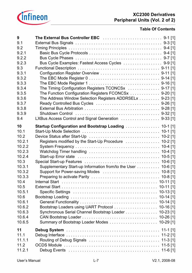
The General Purpose Timer Units
14 The General Purpose Timer UnitsThe General Purpose Timer Unit blocks GPT1 and GPT2 have very flexiblemultifunctional timer structures which may be used for timing, event counting, pulsewidth measurement, pulse generation, frequency multiplication, and other purposes.They incorporate five 16-bit timers that are grouped into the two timer blocks GPT1 andGPT2. Each timer in each block may operate independently in a number of differentmodes such as gated timer or counter mode, or may be concatenated with another timerof the same block. Each block has alternate input/output functions and specific interruptsassociated with it.Block GPT1 contains three timers/counters: The core timer T3 and the two auxiliarytimers T2 and T4. The maximum resolution is fGPT/4. The auxiliary timers of GPT1 mayoptionally be configured as reload or capture registers for the core timer. These registersare listed in Section 14.1.6.• fGPT/4 maximum resolution• 3 independent timers/counters• Timers/counters can be concatenated• 4 operating modes:
– Timer Mode– Gated Timer Mode– Counter Mode– Incremental Interface Mode
• Reload and Capture functionality• Separate interrupt linesBlock GPT2 contains two timers/counters: The core timer T6 and the auxiliary timer T5.The maximum resolution is fGPT/2. An additional Capture/Reload register (CAPREL)supports capture and reload operation with extended functionality. These registers arelisted in Section 14.2.7. The core timer T6 may be concatenated with timers of theCAPCOM units (T7 and T8).The following list summarizes the features which are supported:• fGPT/2 maximum resolution• 2 independent timers/counters• Timers/counters can be concatenated• 3 operating modes:
– Timer Mode– Gated Timer Mode– Counter Mode
• Extended capture/reload functions via 16-bit capture/reload register CAPREL• Separate interrupt lines
User’s Manual 14-1 V2.1, 2008-08GPT, V2.1

XC2300 DerivativesPeripheral Units (Vol. 2 of 2)
The General Purpose Timer Units
14.1 Timer Block GPT1 From a programmer’s point of view, the GPT1 block is composed of a set of SFRs assummarized below. Those portions of port and direction registers which are used foralternate functions by the GPT1 block are shaded.
Figure 14-1 SFRs Associated with Timer Block GPT1
All three timers of block GPT1 (T2, T3, T4) can run in one of 4 basic modes: Timer Mode,Gated Timer Mode, Counter Mode, or Incremental Interface Mode. All timers can countup or down. Each timer of GPT1 is controlled by a separate control register TxCON.Each timer has an input pin TxIN (alternate pin function) associated with it, which servesas the gate control in gated timer mode, or as the count input in counter mode. The countdirection (up/down) may be programmed via software or may be dynamically altered bya signal at the External Up/Down control input TxEUD (alternate pin function). Anoverflow/underflow of core timer T3 is indicated by the Output Toggle Latch T3OTL,whose state may be output on the associated pin T3OUT (alternate pin function). Theauxiliary timers T2 and T4 may additionally be concatenated with the core timer T3(through T3OTL) or may be used as capture or reload registers for the core timer T3.The current contents of each timer can be read or modified by the CPU by accessing thecorresponding timer count registers T2, T3, or T4, located in the non-bitaddressable SFRspace (see Section 14.1.6). When any of the timer registers is written to by the CPU inthe state immediately preceding a timer increment, decrement, reload, or captureoperation, the CPU write operation has priority in order to guarantee correct results.
mc_gpt1_registers.vsd
Data Registers Control Registers
T2CON
Interrupt Control
Tx GPT1 Timer x RegisterTxCON GPT1 Capture/Reload RegisterTxIC GPT1 Timer x Interrupt Ctrl . Reg.
T2
T3
T2IC
T3IC
T4 T2CONT4CON
T3CON
T4IC
T2CONKSCCFG
Miscellaneous
ID
KSCCFG Kernel State Configuration RegisterID Module Identification Register
User’s Manual 14-2 V2.1, 2008-08GPT, V2.1
XC2300 DerivativesPeripheral Units (Vol. 2 of 2)
The General Purpose Timer Units
The interrupts of GPT1 are controlled through the Interrupt Control Registers TxIC.These registers are not part of the GPT1 block. The input and output lines of GPT1 areconnected to pins of ports P3 and P5. The control registers for the port functions arelocated in the respective port modules.Note: The timing requirements for external input signals can be found in Section 14.1.5,
Section 14.4 summarizes the module interface signals, including pins.
Figure 14-2 GPT1 Block Diagram (n = 2 … 5)
T3Mode
Control
2n: 1fGPT
T2Mode
Control
Aux. Timer T2
ReloadCapture
T4Mode
Control Aux. Timer T4
Reload
Capture
Core Timer T3 T3OTL
U/D
T2EUD
T2IN
T3IN
T3EUD
T4IN
T4EUD
Toggle Latch
U/D
U/D
InterruptRequest(T2IRQ)
InterruptRequest(T3IRQ)
InterruptRequest(T4IRQ)
mc_gpt0101_bldiax1.vsd
T3OUT
Basic clock
T3CON.BPS1
User’s Manual 14-3 V2.1, 2008-08GPT, V2.1
XC2300 DerivativesPeripheral Units (Vol. 2 of 2)
The General Purpose Timer Units
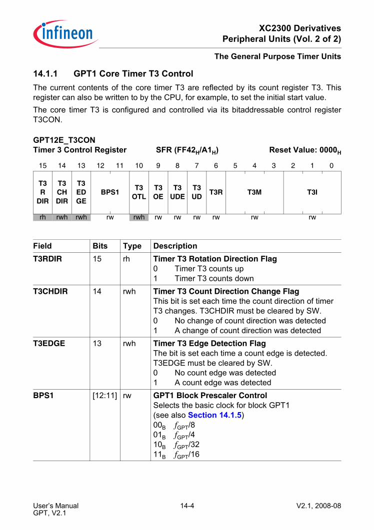
14.1.1 GPT1 Core Timer T3 Control The current contents of the core timer T3 are reflected by its count register T3. Thisregister can also be written to by the CPU, for example, to set the initial start value.The core timer T3 is configured and controlled via its bitaddressable control registerT3CON.
GPT12E_T3CON Timer 3 Control Register SFR (FF42H/A1H) Reset Value: 0000H
15 14 13 12 11 10 9 8 7 6 5 4 3 2 1 0
T3R
DIR
T3CHDIR
T3EDGE
BPS1 T3OTL
T3OE
T3UDE
T3UD T3R T3M T3I
rh rwh rwh rw rwh rw rw rw rw rw rw
Field Bits Type DescriptionT3RDIR 15 rh Timer T3 Rotation Direction Flag
0 Timer T3 counts up1 Timer T3 counts down
T3CHDIR 14 rwh Timer T3 Count Direction Change FlagThis bit is set each time the count direction of timer T3 changes. T3CHDIR must be cleared by SW.0 No change of count direction was detected1 A change of count direction was detected
T3EDGE 13 rwh Timer T3 Edge Detection FlagThe bit is set each time a count edge is detected. T3EDGE must be cleared by SW.0 No count edge was detected1 A count edge was detected
BPS1 [12:11] rw GPT1 Block Prescaler ControlSelects the basic clock for block GPT1(see also Section 14.1.5)00B fGPT/801B fGPT/410B fGPT/3211B fGPT/16
User’s Manual 14-4 V2.1, 2008-08GPT, V2.1

XC2300 DerivativesPeripheral Units (Vol. 2 of 2)
The General Purpose Timer Units
T3OTL 10 rwh Timer T3 Overflow Toggle LatchToggles on each overflow/underflow of T3. Can be set or reset by software (see separate description)
T3OE 9 rw Overflow/Underflow Output Enable0B Alternate Output Function Disabled1B State of T3 toggle latch is output on pin T3OUT
T3UDE 8 rw Timer T3 External Up/Down Enable1)
0B Input T3EUD is disconnected1B Direction influenced by input T3EUD
T3UD 7 rw Timer T3 Up/Down Control1)
0B Timer T3 counts up1B Timer T3 counts down
T3R 6 rw Timer T3 Run Bit0B Timer T3 stops1B Timer T3 runs
T3M [5:3] rw Timer T3 Mode Control (Basic Operating Mode)000B Timer Mode001B Counter Mode010B Gated Timer Mode with gate active low011B Gated Timer Mode with gate active high100B Reserved. Do not use this combination.101B Reserved. Do not use this combination.110B Incremental Interface Mode
(Rotation Detection Mode)111B Incremental Interface Mode
(Edge Detection Mode)T3I [2:0] rw Timer T3 Input Parameter Selection
Depends on the operating mode, see respective sections for encoding:Table 14-7 for Timer Mode and Gated Timer ModeTable 14-2 for Counter ModeTable 14-3 for Incremental Interface Mode
1) See Table 14-1 for encoding of bits T3UD and T3UDE.
Field Bits Type Description
User’s Manual 14-5 V2.1, 2008-08GPT, V2.1
XC2300 DerivativesPeripheral Units (Vol. 2 of 2)
The General Purpose Timer Units
Timer T3 Run ControlThe core timer T3 can be started or stopped by software through bit T3R (Timer T3 RunBit). This bit is relevant in all operating modes of T3. Setting bit T3R will start the timer,clearing bit T3R stops the timer.In gated timer mode, the timer will only run if T3R = 1 and the gate is active (high or low,as programmed).Note: When bit T2RC or T4RC in timer control register T2CON or T4CON is set, bit T3R
will also control (start and stop) the auxiliary timer(s) T2 and/or T4.
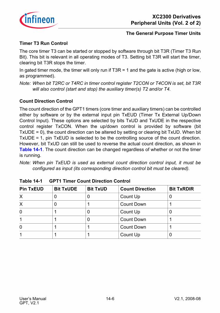
Count Direction Control The count direction of the GPT1 timers (core timer and auxiliary timers) can be controlledeither by software or by the external input pin TxEUD (Timer Tx External Up/DownControl Input). These options are selected by bits TxUD and TxUDE in the respectivecontrol register TxCON. When the up/down control is provided by software (bitTxUDE = 0), the count direction can be altered by setting or clearing bit TxUD. When bitTxUDE = 1, pin TxEUD is selected to be the controlling source of the count direction.However, bit TxUD can still be used to reverse the actual count direction, as shown inTable 14-1. The count direction can be changed regardless of whether or not the timeris running.Note: When pin TxEUD is used as external count direction control input, it must be
configured as input (its corresponding direction control bit must be cleared).
Table 14-1 GPT1 Timer Count Direction ControlPin TxEUD Bit TxUDE Bit TxUD Count Direction Bit TxRDIRX 0 0 Count Up 0X 0 1 Count Down 10 1 0 Count Up 01 1 0 Count Down 10 1 1 Count Down 11 1 1 Count Up 0
User’s Manual 14-6 V2.1, 2008-08GPT, V2.1

XC2300 DerivativesPeripheral Units (Vol. 2 of 2)
The General Purpose Timer Units
Timer 3 Output Toggle LatchThe overflow/underflow signal of timer T3 is connected to a block named ‘Toggle Latch’,shown in the timer mode diagrams. Figure 14-3 illustrates the details of this block. Anoverflow or underflow of T3 will clock two latches: The first latch represents bit T3OTL incontrol register T3CON. The second latch is an internal latch toggled by T3OTL’s output.Both latch outputs are connected to the input control blocks of the auxiliary timers T2 andT4. The output level of the shadow latch will match the output level of T3OTL, but isdelayed by one clock cycle. When the T3OTL value changes, this will result in atemporarily different output level from T3OTL and the shadow latch, which can triggerthe selected count event in T2 and/or T4.When software writes to T3OTL, both latches are set or cleared simultaneously. In thiscase, both signals to the auxiliary timers carry the same level and no edge will bedetected. Bit T3OE (overflow/underflow output enable) in register T3CON enables thestate of T3OTL to be monitored via an external pin T3OUT. When T3OTL is linked to anexternal port pin (must be configured as output), T3OUT can be used to control externalHW. If T3OE = 1, pin T3OUT outputs the state of T3OTL. If T3OE = 0, pin T3OUToutputs a high level (as long as the T3OUT alternate function is selected for the port pin).The trigger signals can serve as an input for the counter function or as a trigger sourcefor the reload function of the auxiliary timers T2 and T4.As can be seen from Figure 14-3, when latch T3OTL is modified by software todetermine the state of the output line, also the internal shadow latch is set or clearedaccordingly. Therefore, no trigger condition is detected by T2/T4 in this case.
Figure 14-3 Block Diagram of the Toggle Latch Logic of Core Timer T3
mc_gpt0106_otl.vsd
Toggle Latch Logic
TxOUT
Set/Clear (SW)
Core Timer
Overflow/Underflow Shadow
Latch
1
0
MU
X
1
TxOE
TxOTLTo Port Logic
To Aux. TimerInput Logic
User’s Manual 14-7 V2.1, 2008-08GPT, V2.1

XC2300 DerivativesPeripheral Units (Vol. 2 of 2)
The General Purpose Timer Units
14.1.2 GPT1 Core Timer T3 Operating ModesTimer T3 can operate in one of several modes.
Timer 3 in Timer Mode Timer mode for the core timer T3 is selected by setting bitfield T3M in register T3CONto 000B. In timer mode, T3 is clocked with the module’s input clock fGPT divided by twoprogrammable prescalers controlled by bitfields BPS1 and T3I in register T3CON.Please see Section 14.1.5 for details on the input clock options.
Figure 14-4 Block Diagram of Core Timer T3 in Timer Mode
Prescaler Core Timer T3 Toggle Latch
MCB05391
BPS1 T3I
MUX Up/Down0
1
T3EUD
fGPT
=1
T3UD
fT3
T3R
CountT3OUT
T3IRQ
toT2/T4
T3UDE
User’s Manual 14-8 V2.1, 2008-08GPT, V2.1

XC2300 DerivativesPeripheral Units (Vol. 2 of 2)
The General Purpose Timer Units
Gated Timer Mode Gated timer mode for the core timer T3 is selected by setting bitfield T3M in registerT3CON to 010B or 011B. Bit T3M.0 (T3CON.3) selects the active level of the gate input.The same options for the input frequency are available in gated timer mode as in timermode (see Section 14.1.5). However, the input clock to the timer in this mode is gatedby the external input pin T3IN (Timer T3 External Input).To enable this operation, the associated pin T3IN must be configured as input, that is,the corresponding direction control bit must contain 0.
Figure 14-5 Block Diagram of Core Timer T3 in Gated Timer Mode
If T3M = 010B, the timer is enabled when T3IN shows a low level. A high level at this linestops the timer. If T3M = 011B, line T3IN must have a high level in order to enable thetimer. Additionally, the timer can be turned on or off by software using bit T3R. The timerwill only run if T3R is 1 and the gate is active. It will stop if either T3R is 0 or the gate isinactive.Note: A transition of the gate signal at pin T3IN does not cause an interrupt request.
Prescaler GateCtrl. Core Timer T3 Toggle Latch
MCB05392
BPS1 T3I
MUX Up/Down0
1
T3EUD
fGPT
=1
T3UD
fT3
T3R
CountT3OUT
T3IRQ
toT2/T4
T3UDE
T3IN
User’s Manual 14-9 V2.1, 2008-08GPT, V2.1

XC2300 DerivativesPeripheral Units (Vol. 2 of 2)
The General Purpose Timer Units
Counter Mode Counter Mode for the core timer T3 is selected by setting bitfield T3M in register T3CONto 001B. In counter mode, timer T3 is clocked by a transition at the external input pinT3IN. The event causing an increment or decrement of the timer can be a positive, anegative, or both a positive and a negative transition at this line. Bitfield T3I in controlregister T3CON selects the triggering transition (see Table 14-2).
Figure 14-6 Block Diagram of Core Timer T3 in Counter Mode
For counter mode operation, pin T3IN must be configured as input (the respectivedirection control bit DPx.y must be 0). The maximum input frequency allowed in countermode depends on the selected prescaler value. To ensure that a transition of the countinput signal applied to T3IN is recognized correctly, its level must be held high or low fora minimum number of module clock cycles before it changes. This information can befound in Section 14.1.5.
Table 14-2 GPT1 Core Timer T3 (Counter Mode) Input Edge SelectionT3I Triggering Edge for Counter Increment/Decrement000B None. Counter T3 is disabled001B Positive transition (rising edge) on T3IN010B Negative transition (falling edge) on T3IN011B Any transition (rising or falling edge) on T3IN1XXB Reserved. Do not use this combination
MCB05393
Core Timer T3 Toggle Latch
MUX Up/Down0
1
T3EUD
T3IN
=1
T3UD
T3R
CountT3OUT
T3IRQ
toT2/T4
T3UDE
T3I
Edge
Select
User’s Manual 14-10 V2.1, 2008-08GPT, V2.1
XC2300 DerivativesPeripheral Units (Vol. 2 of 2)
The General Purpose Timer Units
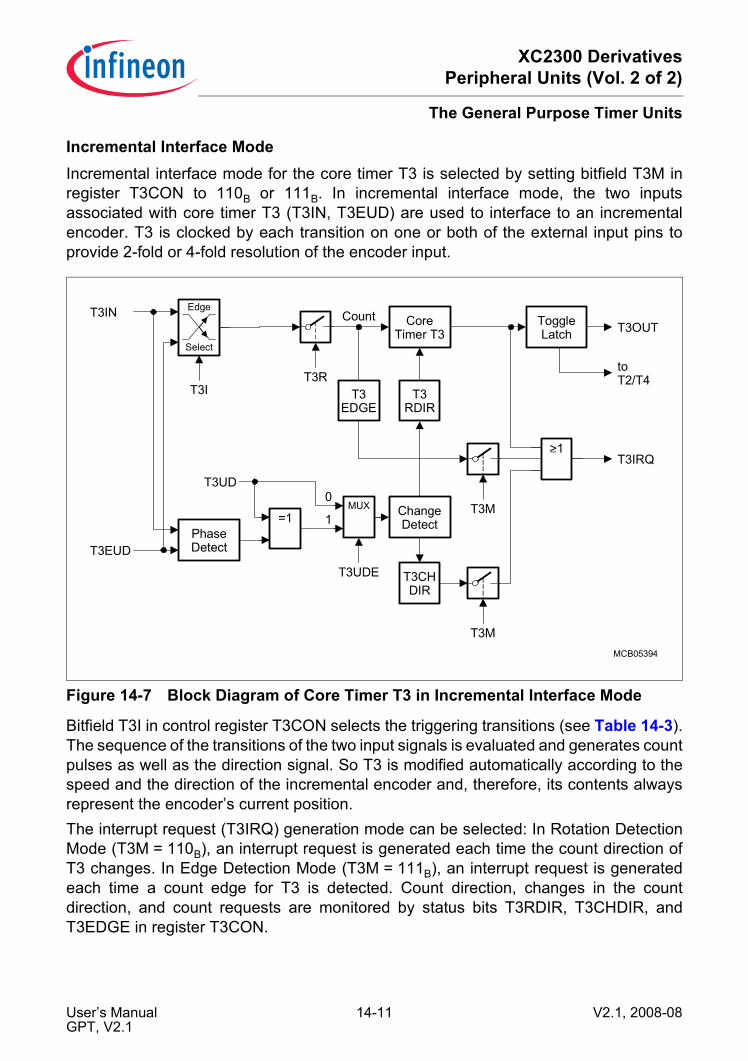
Incremental Interface Mode Incremental interface mode for the core timer T3 is selected by setting bitfield T3M inregister T3CON to 110B or 111B. In incremental interface mode, the two inputsassociated with core timer T3 (T3IN, T3EUD) are used to interface to an incrementalencoder. T3 is clocked by each transition on one or both of the external input pins toprovide 2-fold or 4-fold resolution of the encoder input.
Figure 14-7 Block Diagram of Core Timer T3 in Incremental Interface Mode
Bitfield T3I in control register T3CON selects the triggering transitions (see Table 14-3).The sequence of the transitions of the two input signals is evaluated and generates countpulses as well as the direction signal. So T3 is modified automatically according to thespeed and the direction of the incremental encoder and, therefore, its contents alwaysrepresent the encoder’s current position.The interrupt request (T3IRQ) generation mode can be selected: In Rotation DetectionMode (T3M = 110B), an interrupt request is generated each time the count direction ofT3 changes. In Edge Detection Mode (T3M = 111B), an interrupt request is generatedeach time a count edge for T3 is detected. Count direction, changes in the countdirection, and count requests are monitored by status bits T3RDIR, T3CHDIR, andT3EDGE in register T3CON.
MCB05394
Count
T3EUD
T3EDGE
T3RDIR
MUX0
1=1
T3UD
T3UDE
ChangeDetect
T3CHDIR
T3M
T3M
>1_
PhaseDetect
T3R
T3IN
T3I
T3IRQ
CoreTimer T3
ToggleLatch T3OUT
toT2/T4
Edge
Select
User’s Manual 14-11 V2.1, 2008-08GPT, V2.1

XC2300 DerivativesPeripheral Units (Vol. 2 of 2)
The General Purpose Timer Units
The incremental encoder can be connected directly to the XC2300 without externalinterface logic. In a standard system, however, comparators will be employed to convertthe encoder’s differential outputs (such as A, A) to digital signals (such as A). This greatlyincreases noise immunity.Note: The third encoder output T0, which indicates the mechanical zero position, may
be connected to an external interrupt input and trigger a reset of timer T3 (forexample via PEC transfer from ZEROS).
Figure 14-8 Connection of the Encoder to the XC2300
For incremental interface operation, the following conditions must be met:• Bitfield T3M must be 110B or 111B.• Both pins T3IN and T3EUD must be configured as input.• Pin T4IN must be configured as input, if used for T0.• Bit T3UDE must be 1 to enable automatic external direction control.The maximum count frequency allowed in incremental interface mode depends on theselected prescaler value. To ensure that a transition of any input signal is recognizedcorrectly, its level must be held high or low for a minimum number of module clock cyclesbefore it changes. This information can be found in Section 14.1.5.
Table 14-3 Core Timer T3 (Incremental Interface Mode) Input Edge SelectionT3I Triggering Edge for Counter Increment/Decrement000B None. Counter T3 stops.001B Any transition (rising or falling edge) on T3IN.010B Any transition (rising or falling edge) on T3EUD.011B Any transition (rising or falling edge) on any T3 input (T3IN or T3EUD).1XXB Reserved. Do not use this combination.
MCS04372�
Encoder� Controller�A�
B�
T0�
T3Input�
T3Input�
Interrupt�
A�
B�B�
T0�T0�
A�
Signal�Conditioning�
User’s Manual 14-12 V2.1, 2008-08GPT, V2.1

XC2300 DerivativesPeripheral Units (Vol. 2 of 2)
The General Purpose Timer Units
As in incremental interface mode two input signals with a 90° phase shift are evaluated,their maximum input frequency can be half the maximum count frequency.In incremental interface mode, the count direction is automatically derived from thesequence in which the input signals change, which corresponds to the rotation directionof the connected sensor. Table 14-4 summarizes the possible combinations.
Figure 14-9 and Figure 14-10 give examples of T3’s operation, visualizing count signalgeneration and direction control. They also show how input jitter is compensated, whichmight occur if the sensor rests near to one of its switching points.
Figure 14-9 Evaluation of Incremental Encoder Signals, 2 Count Inputs
Table 14-4 GPT1 Core Timer T3 (Incremental Interface Mode) Count DirectionLevel on Respective other Input
T3IN Input T3EUD InputRising ↑ Falling ↓ Rising ↑ Falling ↓
High Down Up Up DownLow Up Down Down Up
MCT04373�
Forward� Jitter� Backward� Jitter� Forward�
T3IN�
T3EUD�
Contents�of T3�
Up� Down� Up�
Note: This example shows the timer behaviour assuming that T3 counts upon any �transition on input, i.e. T3I = '011�B�'.�
User’s Manual 14-13 V2.1, 2008-08GPT, V2.1
XC2300 DerivativesPeripheral Units (Vol. 2 of 2)
The General Purpose Timer Units
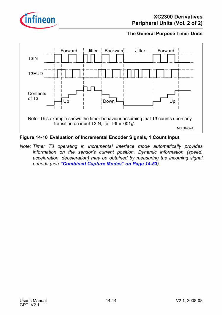
Figure 14-10 Evaluation of Incremental Encoder Signals, 1 Count Input
Note: Timer T3 operating in incremental interface mode automatically providesinformation on the sensor’s current position. Dynamic information (speed,acceleration, deceleration) may be obtained by measuring the incoming signalperiods (see “Combined Capture Modes” on Page 14-53).
MCT04374
Forward Jitter Backward Jitter Forward
T3IN
Up Down Up
T3EUD
Contentsof T3
Note: This example shows the timer behaviour assuming that T3 counts upon any transition on input T3IN, i.e. T3I = '001B'.
User’s Manual 14-14 V2.1, 2008-08GPT, V2.1
XC2300 DerivativesPeripheral Units (Vol. 2 of 2)
The General Purpose Timer Units
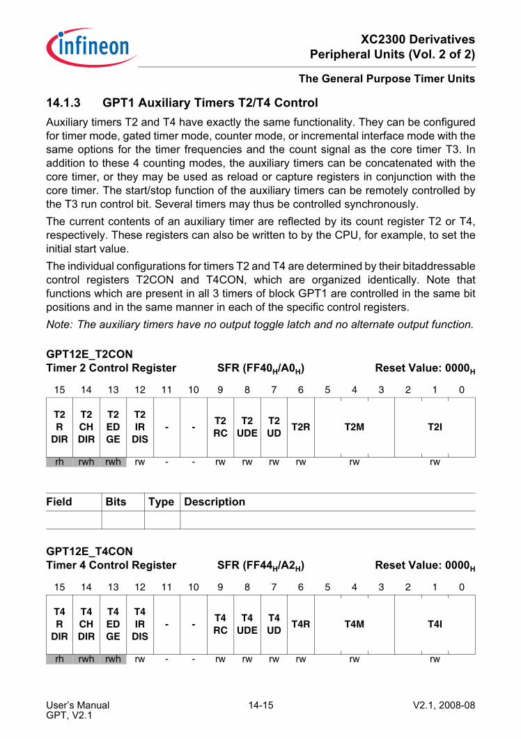
14.1.3 GPT1 Auxiliary Timers T2/T4 Control Auxiliary timers T2 and T4 have exactly the same functionality. They can be configuredfor timer mode, gated timer mode, counter mode, or incremental interface mode with thesame options for the timer frequencies and the count signal as the core timer T3. Inaddition to these 4 counting modes, the auxiliary timers can be concatenated with thecore timer, or they may be used as reload or capture registers in conjunction with thecore timer. The start/stop function of the auxiliary timers can be remotely controlled bythe T3 run control bit. Several timers may thus be controlled synchronously.The current contents of an auxiliary timer are reflected by its count register T2 or T4,respectively. These registers can also be written to by the CPU, for example, to set theinitial start value.The individual configurations for timers T2 and T4 are determined by their bitaddressablecontrol registers T2CON and T4CON, which are organized identically. Note thatfunctions which are present in all 3 timers of block GPT1 are controlled in the same bitpositions and in the same manner in each of the specific control registers.Note: The auxiliary timers have no output toggle latch and no alternate output function.
GPT12E_T2CON Timer 2 Control Register SFR (FF40H/A0H) Reset Value: 0000H
15 14 13 12 11 10 9 8 7 6 5 4 3 2 1 0
T2R
DIR
T2CHDIR
T2EDGE
T2IR
DIS- - T2
RCT2
UDET2UD T2R T2M T2I
rh rwh rwh rw - - rw rw rw rw rw rw
Field Bits Type Description
GPT12E_T4CON Timer 4 Control Register SFR (FF44H/A2H) Reset Value: 0000H
15 14 13 12 11 10 9 8 7 6 5 4 3 2 1 0
T4R
DIR
T4CHDIR
T4EDGE
T4IR
DIS- - T4
RCT4
UDET4UD T4R T4M T4I
rh rwh rwh rw - - rw rw rw rw rw rw
User’s Manual 14-15 V2.1, 2008-08GPT, V2.1

XC2300 DerivativesPeripheral Units (Vol. 2 of 2)
The General Purpose Timer Units
Field Bits Type DescriptionTxRDIR 15 rh Timer Tx Rotation Direction
0B Timer x counts up1B Timer x counts down
TxCHDIR 14 rwh Timer Tx Count Direction ChangeThis bit is set each time the count direction of timer Tx changes. TxCHDIR must be cleared by SW.0B No change in count direction was detected1B A change in count direction was detected
TxEDGE 13 rwh Timer Tx Edge DetectionThe bit is set each time a count edge is detected. TxEDGE must be cleared by SW.0B No count edge was detected1B A count edge was detected
TxIRDIS 12 rw Timer Tx Interrupt Request Disable0B Interrupt generation for TxCHDIR and
TxEDGE interrupts in Incremental Interface Mode is enabled
1B Interrupt generation for TxCHDIR and TxEDGE interrupts in Incremental Interface Mode is disabled
TxRC 9 rw Timer Tx Remote Control0B Timer Tx is controlled by its own run bit TxR1B Timer Tx is controlled by the run bit T3R of core
timer 3, not by bit TxRTxUDE 8 rw Timer Tx External Up/Down Enable1)
0B Input TxEUD is disconnected1B Direction influenced by input TxEUD
TxUD 7 rw Timer Tx Up/Down Control1)
0B Timer Tx counts up1B Timer Tx counts down
TxR 6 rw Timer Tx Run Bit0B Timer Tx stops1B Timer Tx runsNote: This bit only controls timer Tx if bit TxRC = 0.
User’s Manual 14-16 V2.1, 2008-08GPT, V2.1
XC2300 DerivativesPeripheral Units (Vol. 2 of 2)
The General Purpose Timer Units
Timer T2/T4 Run ControlEach of the auxiliary timers T2 and T4 can be started or stopped by software in twodifferent ways:• Through the associated timer run bit (T2R or T4R). In this case it is required that the
respective control bit TxRC = 0.• Through the core timer’s run bit (T3R). In this case the respective remote control bit
must be set (TxRC = 1).The selected run bit is relevant in all operating modes of T2/T4. Setting the bit will startthe timer, clearing the bit stops the timer.In gated timer mode, the timer will only run if the selected run bit is set and the gate isactive (high or low, as programmed).Note: If remote control is selected T3R will start/stop timer T3 and the selected auxiliary
timer(s) synchronously.
Count Direction ControlThe count direction of the GPT1 timers (core timer and auxiliary timers) is controlled inthe same way, either by software or by the external input pin TxEUD. Please refer to thedescription in Table 14-1.Note: When pin TxEUD is used as external count direction control input, it must be
configured as input (its corresponding direction control bit must be cleared).
TxM [5:3] rw Timer Tx Mode Control (Basic Operating Mode)000B Timer Mode001B Counter Mode010B Gated Timer Mode with gate active low011B Gated Timer Mode with gate active high100B Reload Mode101B Capture Mode110B Incremental Interface Mode (Rotation Detect.)111B Incremental Interface Mode (Edge Detection)
TxI [2:0] rw Timer Tx Input Parameter SelectionDepends on the operating mode, see respective sections for encoding:Table 14-7 for Timer Mode and Gated Timer ModeTable 14-2 for Counter ModeTable 14-3 for Incremental Interface Mode
1) See Table 14-1 for encoding of bits TxUD and TxUDE.
Field Bits Type Description
User’s Manual 14-17 V2.1, 2008-08GPT, V2.1
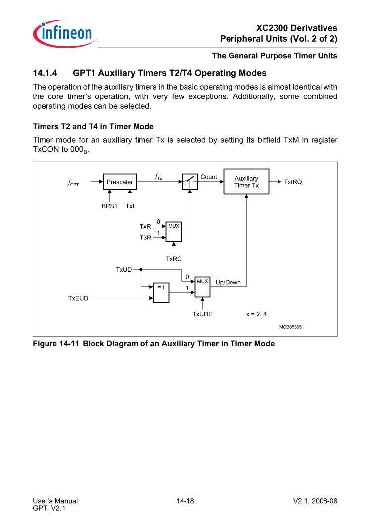
XC2300 DerivativesPeripheral Units (Vol. 2 of 2)
The General Purpose Timer Units
14.1.4 GPT1 Auxiliary Timers T2/T4 Operating ModesThe operation of the auxiliary timers in the basic operating modes is almost identical withthe core timer’s operation, with very few exceptions. Additionally, some combinedoperating modes can be selected.
Timers T2 and T4 in Timer ModeTimer mode for an auxiliary timer Tx is selected by setting its bitfield TxM in registerTxCON to 000B.
Figure 14-11 Block Diagram of an Auxiliary Timer in Timer Mode
Prescaler AuxiliaryTimer Tx
BPS1 TxI
fGPT
fTx CountTxIRQ
MCB05395
MUX Up/Down0
1
TxEUD
=1
TxUD
TxUDE
MUX
TxRC
TxR
T3R
x = 2, 4
0
1
User’s Manual 14-18 V2.1, 2008-08GPT, V2.1
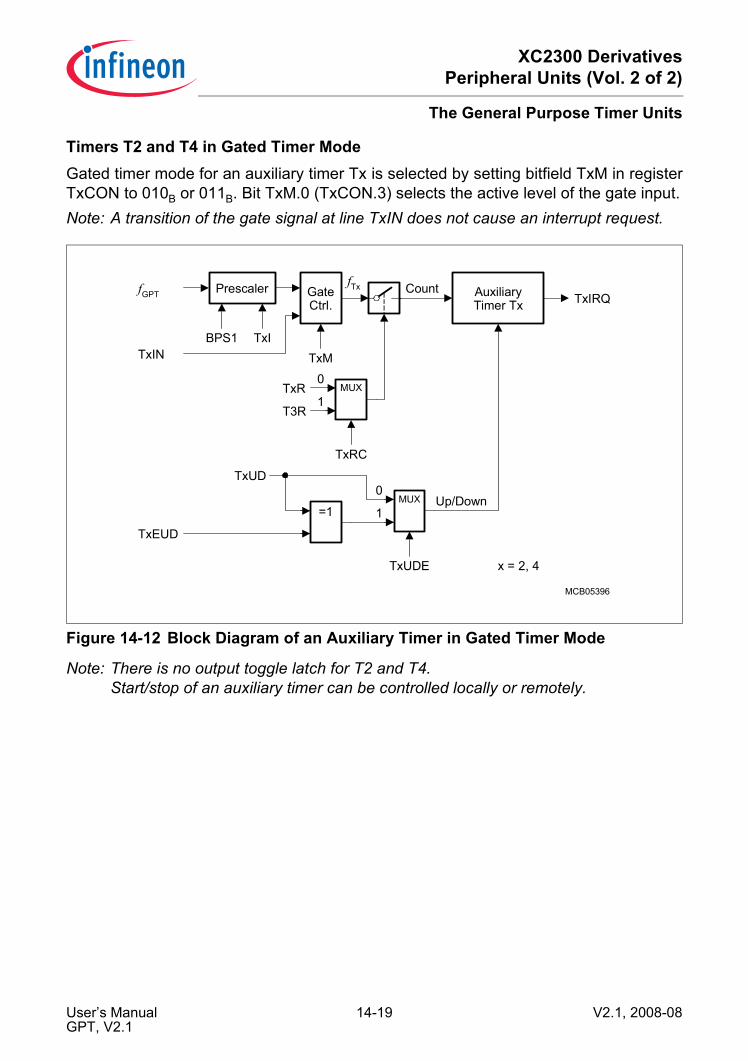
XC2300 DerivativesPeripheral Units (Vol. 2 of 2)
The General Purpose Timer Units
Timers T2 and T4 in Gated Timer ModeGated timer mode for an auxiliary timer Tx is selected by setting bitfield TxM in registerTxCON to 010B or 011B. Bit TxM.0 (TxCON.3) selects the active level of the gate input.Note: A transition of the gate signal at line TxIN does not cause an interrupt request.
Figure 14-12 Block Diagram of an Auxiliary Timer in Gated Timer Mode
Note: There is no output toggle latch for T2 and T4.Start/stop of an auxiliary timer can be controlled locally or remotely.
Prescaler GateCtrl.
AuxiliaryTimer Tx
BPS1 TxI
fGPTfTx Count
TxIRQ
TxM
MCB05396
MUX Up/Down0
1
TxEUD
=1
TxUD
TxUDE
MUX
TxRC
TxR
T3R
x = 2, 4
0
1
TxIN
User’s Manual 14-19 V2.1, 2008-08GPT, V2.1

XC2300 DerivativesPeripheral Units (Vol. 2 of 2)
The General Purpose Timer Units
Timers T2 and T4 in Counter Mode Counter mode for an auxiliary timer Tx is selected by setting bitfield TxM in registerTxCON to 001B. In counter mode, an auxiliary timer can be clocked either by a transitionat its external input line TxIN, or by a transition of timer T3’s toggle latch T3OTL. Theevent causing an increment or decrement of a timer can be a positive, a negative, or botha positive and a negative transition at either the respective input pin or at the toggle latch.Bitfield TxI in control register TxCON selects the triggering transition (see Table 14-5).
Figure 14-13 Block Diagram of an Auxiliary Timer in Counter Mode
Note: Only state transitions of T3OTL which are caused by the overflows/underflows ofT3 will trigger the counter function of T2/T4. Modifications of T3OTL via softwarewill NOT trigger the counter function of T2/T4.
Table 14-5 GPT1 Auxiliary Timer (Counter Mode) Input Edge SelectionT2I/T4I Triggering Edge for Counter Increment/DecrementX00B None. Counter Tx is disabled001B Positive transition (rising edge) on TxIN010B Negative transition (falling edge) on TxIN011B Any transition (rising or falling edge) on TxIN101B Positive transition (rising edge) of T3 toggle latch T3OTL110B Negative transition (falling edge) of T3 toggle latch T3OTL111B Any transition (rising or falling edge) of T3 toggle latch T3OTL
AuxiliaryTimer Tx
CountTxIRQ
MCB05397
MUX Up/Down0
1TxEUD
=1
TxUD
TxUDE
MUX
TxRC
TxR
T3R
x = 2, 4
TxI
MUX
TxI.2
TxIN
T3ToggleLatch
0
1
0
1
Edge
Select
User’s Manual 14-20 V2.1, 2008-08GPT, V2.1

XC2300 DerivativesPeripheral Units (Vol. 2 of 2)
The General Purpose Timer Units
For counter operation, pin TxIN must be configured as input (the respective directioncontrol bit DPx.y must be 0). The maximum input frequency allowed in counter modedepends on the selected prescaler value. To ensure that a transition of the count inputsignal applied to TxIN is recognized correctly, its level must be held high or low for aminimum number of module clock cycles before it changes. This information can befound in Section 14.1.5.
Timers T2 and T4 in Incremental Interface ModeIncremental interface mode for an auxiliary timer Tx is selected by setting bitfield TxM inthe respective register TxCON to 110B or 111B. In incremental interface mode, the twoinputs associated with an auxiliary timer Tx (TxIN, TxEUD) are used to interface to anincremental encoder. Tx is clocked by each transition on one or both of the external inputpins to provide 2-fold or 4-fold resolution of the encoder input.
Figure 14-14 Block Diagram of an Auxiliary Timer in Incremental Interface Mode
The operation of the auxiliary timers T2 and T4 in incremental interface mode and theinterrupt generation are the same as described for the core timer T3. The descriptions,figures and tables apply accordingly.
MCB05398
CountOverflow
Underflow
TxEUD
TxEdge
TxRDIR
MUX0
1=1
TxUD
TxUDE
ChangeDetect
&
TxCHDIR
TxM
TxM
&
>1_
PhaseDetect
MUX
TxRC
TxR
T3R
TxIN
TxI
TxIRDIS
TxIRQ
AuxiliaryTimer Tx
0
1
Edge
Select
User’s Manual 14-21 V2.1, 2008-08GPT, V2.1

XC2300 DerivativesPeripheral Units (Vol. 2 of 2)
The General Purpose Timer Units
Timer Concatenation Using the toggle bit T3OTL as a clock source for an auxiliary timer in counter modeconcatenates the core timer T3 with the respective auxiliary timer. This concatenationforms either a 32-bit or a 33-bit timer/counter, depending on which transition of T3OTLis selected to clock the auxiliary timer.• 32-bit Timer/Counter: If both a positive and a negative transition of T3OTL are used
to clock the auxiliary timer, this timer is clocked on every overflow/underflow of thecore timer T3. Thus, the two timers form a 32-bit timer.
• 33-bit Timer/Counter: If either a positive or a negative transition of T3OTL is selectedto clock the auxiliary timer, this timer is clocked on every second overflow/underflowof the core timer T3. This configuration forms a 33-bit timer (16-bit core timer + T3OTL+ 16-bit auxiliary timer).As long as bit T3OTL is not modified by software, it represents the state of the internaltoggle latch, and can be regarded as part of the 33-bit timer.
The count directions of the two concatenated timers are not required to be the same.This offers a wide variety of different configurations.T3, which represents the low-order part of the concatenated timer, can operate in timermode, gated timer mode or counter mode in this case.
Figure 14-15 Concatenation of Core Timer T3 and an Auxiliary Timer
MCA05399
Toggle Latch T3OUT
T3IRQCount
T3R
Core Timer T3Operating
ModeControl
BPS1 TxI
T3INfGPT
AuxiliaryTimer Tx
TxI
0
1MUX
TxI.2
TxINTxIRQ
Up/Down
Up/Down
Count
MUX
TxRC
TxR
T3R
0
1
x = 2, 4
Edge
Select
User’s Manual 14-22 V2.1, 2008-08GPT, V2.1

XC2300 DerivativesPeripheral Units (Vol. 2 of 2)
The General Purpose Timer Units
Auxiliary Timer in Reload ModeReload Mode for an auxiliary timer Tx is selected by setting bitfield TxM in the respectiveregister TxCON to 100B. In reload mode, the core timer T3 is reloaded with the contentsof an auxiliary timer register, triggered by one of two different signals. The trigger signalis selected the same way as the clock source for counter mode (see Table 14-5), i.e. atransition of the auxiliary timer’s input TxIN or the toggle latch T3OTL may trigger thereload.Note: When programmed for reload mode, the respective auxiliary timer (T2 or T4) stops
independently of its run flag T2R or T4R.The timer input pin TxIN must be configured as input if it shall trigger a reloadoperation.
Figure 14-16 GPT1 Auxiliary Timer in Reload Mode
Upon a trigger signal, T3 is loaded with the contents of the respective timer register (T2or T4) and the respective interrupt request flag (T2IR or T4IR) is set.Note: When a T3OTL transition is selected for the trigger signal, the interrupt request
flag T3IR will also be set upon a trigger, indicating T3’s overflow or underflow.Modifications of T3OTL via software will NOT trigger the counter function of T2/T4.
To ensure that a transition of the reload input signal applied to TxIN is recognizedcorrectly, its level must be held high or low for a minimum number of module clockcycles, detailed in Section 14.1.5.The reload mode triggered by the T3 toggle latch can be used in a number of differentconfigurations. The following functions can be performed, depending on the selectedactive transition:
MCA05400
Toggle Latch T3OUT
T3IRQCount
T3R
Core Timer T3Operating
ModeControl
BPS1 TxIUp/Down
T3INfGPT
AuxiliaryTimer Tx
TxI
Reload0
1MUX
TxI.2
TxINTxIRQ
x = 2, 4
Edge
Select
User’s Manual 14-23 V2.1, 2008-08GPT, V2.1
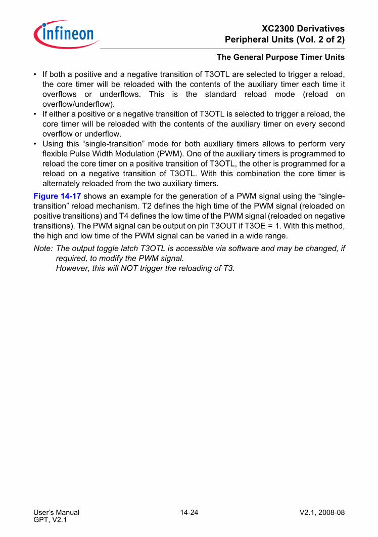
XC2300 DerivativesPeripheral Units (Vol. 2 of 2)
The General Purpose Timer Units
• If both a positive and a negative transition of T3OTL are selected to trigger a reload,the core timer will be reloaded with the contents of the auxiliary timer each time itoverflows or underflows. This is the standard reload mode (reload onoverflow/underflow).
• If either a positive or a negative transition of T3OTL is selected to trigger a reload, thecore timer will be reloaded with the contents of the auxiliary timer on every secondoverflow or underflow.
• Using this “single-transition” mode for both auxiliary timers allows to perform veryflexible Pulse Width Modulation (PWM). One of the auxiliary timers is programmed toreload the core timer on a positive transition of T3OTL, the other is programmed for areload on a negative transition of T3OTL. With this combination the core timer isalternately reloaded from the two auxiliary timers.
Figure 14-17 shows an example for the generation of a PWM signal using the “single-transition” reload mechanism. T2 defines the high time of the PWM signal (reloaded onpositive transitions) and T4 defines the low time of the PWM signal (reloaded on negativetransitions). The PWM signal can be output on pin T3OUT if T3OE = 1. With this method,the high and low time of the PWM signal can be varied in a wide range.Note: The output toggle latch T3OTL is accessible via software and may be changed, if
required, to modify the PWM signal.However, this will NOT trigger the reloading of T3.
User’s Manual 14-24 V2.1, 2008-08GPT, V2.1
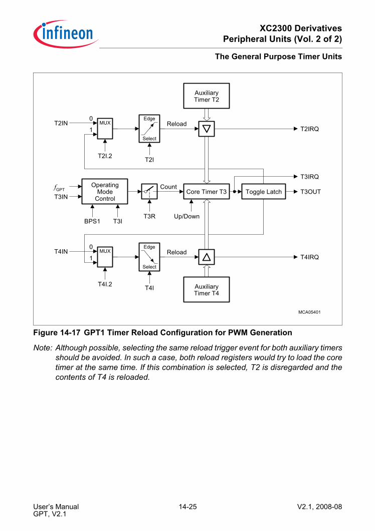
XC2300 DerivativesPeripheral Units (Vol. 2 of 2)
The General Purpose Timer Units
Figure 14-17 GPT1 Timer Reload Configuration for PWM Generation
Note: Although possible, selecting the same reload trigger event for both auxiliary timersshould be avoided. In such a case, both reload registers would try to load the coretimer at the same time. If this combination is selected, T2 is disregarded and thecontents of T4 is reloaded.
MCA05401
T2IRQ
AuxiliaryTimer T2
Edge
Select
T2I
Reload0
1MUX
T2I.2
Toggle Latch T3OUT
T3IRQCount
T3R
Core Timer T3Operating
ModeControl
BPS1 T3IUp/Down
T3INfGPT
T2IN
AuxiliaryTimer T4
Edge
Select
T4I
Reload0
1MUX
T4I.2
T4INT4IRQ
User’s Manual 14-25 V2.1, 2008-08GPT, V2.1

XC2300 DerivativesPeripheral Units (Vol. 2 of 2)
The General Purpose Timer Units
Auxiliary Timer in Capture Mode Capture mode for an auxiliary timer Tx is selected by setting bitfield TxM in the respectiveregister TxCON to 101B. In capture mode, the contents of the core timer T3 are latchedinto an auxiliary timer register in response to a signal transition at the respective auxiliarytimer’s external input pin TxIN. The capture trigger signal can be a positive, a negative,or both a positive and a negative transition.The two least significant bits of bitfield TxI select the active transition (see Table 14-5).Bit 2 of TxI is irrelevant for capture mode and must be cleared (TxI.2 = 0).Note: When programmed for capture mode, the respective auxiliary timer (T2 or T4)
stops independently of its run flag T2R or T4R.
Figure 14-18 GPT1 Auxiliary Timer in Capture Mode
Upon a trigger (selected transition) at the corresponding input pin TxIN the contents ofthe core timer are loaded into the auxiliary timer register and the associated interruptrequest flag TxIR will be set.For capture mode operation, the respective timer input pin TxIN must be configured asinput. To ensure that a transition of the capture input signal applied to TxIN is recognizedcorrectly, its level must be held high or low for a minimum number of module clockcycles, detailed in Section 14.1.5.
MCA05402
Toggle Latch T3OUT
T3IRQCount
T3R
Core Timer T3Operating
ModeControl
BPS1 T3IUp/Down
T3INfGPT
AuxiliaryTimer Tx
TxI
CaptureTxIN TxIRQ
x = 2, 4y = 4, 2
to Ty
Edge
Select
User’s Manual 14-26 V2.1, 2008-08GPT, V2.1

XC2300 DerivativesPeripheral Units (Vol. 2 of 2)
The General Purpose Timer Units
14.1.5 GPT1 Clock Signal ControlAll actions within the timer block GPT1 are triggered by transitions of its basic clock. Thisbasic clock is derived from the system clock by a basic block prescaler, controlled bybitfield BPS1 in register T3CON (see Figure 14-2). The count clock can be generated intwo different ways:• Internal count clock, derived from GPT1’s basic clock via a programmable prescaler,
is used for (gated) timer mode.• External count clock, derived from the timer’s input pin(s), is used for counter mode.For both ways, the basic clock determines the maximum count frequency and the timer’sresolution:
Internal Count Clock GenerationIn timer mode and gated timer mode, the count clock for each GPT1 timer is derived fromthe GPT1 basic clock by a programmable prescaler, controlled by bitfield TxI in therespective timer’s control register TxCON.The count frequency fTx for a timer Tx and its resolution rTx are scaled linearly with lowerclock frequencies, as can be seen from the following formula:
[14.1]
The effective count frequency depends on the common module clock prescaler factorF(BPS1) as well as on the individual input prescaler factor 2<TxI>. Table 14-7 summarizesthe resulting overall divider factors for a GPT1 timer that result from these cascadedprescalers.
Table 14-6 Basic Clock Selection for Block GPT1Block Prescaler1)
1) Please note the non-linear encoding of bitfield BPS1.
BPS1 = 01B BPS1 = 00B2)
2) Default after reset.
BPS1 = 11B BPS1 = 10B
Prescaling Factor for GPT1: F(BPS1)
F(BPS1)= 4
F(BPS1)= 8
F(BPS1)= 16
F(BPS1)= 32
Maximum External Count Frequency
fGPT/8 fGPT/16 fGPT/32 fGPT/64
Input SignalStable Time
4 × tGPT 8 × tGPT 16 × tGPT 32 × tGPT
fTxfGPT
F BPS1( ) 2<Txl>×---------------------------------------------= rTx µs[ ] F BPS1( ) 2<Txl>×
fGPT MHz[ ]---------------------------------------------=
User’s Manual 14-27 V2.1, 2008-08GPT, V2.1

XC2300 DerivativesPeripheral Units (Vol. 2 of 2)
The General Purpose Timer Units
Table 14-8 lists a timer’s parameters (such as count frequency, resolution, and period)resulting from the selected overall prescaler factor and the applied system frequency.Note that some numbers may be rounded.
Table 14-7 GPT1 Overall Prescaler Factors for Internal Count ClockIndividual Prescaler for Tx
Common Prescaler for Module Clock1)
1) Please note the non-linear encoding of bitfield BPS1.
BPS1 = 01B BPS1 = 00B BPS1 = 11B BPS1 = 10B
TxI = 000B 4 8 16 32TxI = 001B 8 16 32 64TxI = 010B 16 32 64 128TxI = 011B 32 64 128 256TxI = 100B 64 128 256 512TxI = 101B 128 256 512 1024TxI = 110B 256 512 1024 2048TxI = 111B 512 1024 2048 4096
Table 14-8 GPT1 Timer ParametersSystem Clock = 10 MHz Overall
Divider Factor
System Clock = 40 MHzFrequency Resolution Period Frequency Resolution Period
2.5 MHz 400 ns 26.21 ms 4 10.0 MHz 100 ns 6.55 ms1.25 MHz 800 ns 52.43 ms 8 5.0 MHz 200 ns 13.11 ms625.0 kHz 1.6 µs 104.9 ms 16 2.5 MHz 400 ns 26.21 ms312.5 kHz 3.2 µs 209.7 ms 32 1.25 MHz 800 ns 52.43 ms156.25 kHz 6.4 µs 419.4 ms 64 625.0 kHz 1.6 µs 104.9 ms78.125 kHz 12.8 µs 838.9 ms 128 312.5 kHz 3.2 µs 209.7 ms39.06 kHz 25.6 µs 1.678 s 256 156.25 kHz 6.4 µs 419.4 ms19.53 kHz 51.2 µs 3.355 s 512 78.125 kHz 12.8 µs 838.9 ms9.77 kHz 102.4 µs 6.711 s 1024 39.06 kHz 25.6 µs 1.678 s4.88 kHz 204.8 µs 13.42 s 2048 19.53 kHz 51.2 µs 3.355 s2.44 kHz 409.6 µs 26.84 s 4096 9.77 kHz 102.4 µs 6.711 s
User’s Manual 14-28 V2.1, 2008-08GPT, V2.1
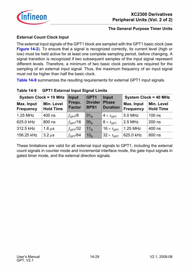
XC2300 DerivativesPeripheral Units (Vol. 2 of 2)
The General Purpose Timer Units
External Count Clock InputThe external input signals of the GPT1 block are sampled with the GPT1 basic clock (seeFigure 14-2). To ensure that a signal is recognized correctly, its current level (high orlow) must be held active for at least one complete sampling period, before changing. Asignal transition is recognized if two subsequent samples of the input signal representdifferent levels. Therefore, a minimum of two basic clock periods are required for thesampling of an external input signal. Thus, the maximum frequency of an input signalmust not be higher than half the basic clock.Table 14-9 summarizes the resulting requirements for external GPT1 input signals.
These limitations are valid for all external input signals to GPT1, including the externalcount signals in counter mode and incremental interface mode, the gate input signals ingated timer mode, and the external direction signals.
Table 14-9 GPT1 External Input Signal LimitsSystem Clock = 10 MHz Input
Frequ. Factor
GPT1 Divider BPS1
Input Phase Duration
System Clock = 40 MHzMax. Input Frequency
Min. Level Hold Time
Max. Input Frequency
Min. Level Hold Time
1.25 MHz 400 ns fGPT/8 01B 4 × tGPT 5.0 MHz 100 ns625.0 kHz 800 ns fGPT/16 00B 8 × tGPT 2.5 MHz 200 ns312.5 kHz 1.6 µs fGPT/32 11B 16 × tGPT 1.25 MHz 400 ns156.25 kHz 3.2 µs fGPT/64 10B 32 × tGPT 625.0 kHz 800 ns
User’s Manual 14-29 V2.1, 2008-08GPT, V2.1

XC2300 DerivativesPeripheral Units (Vol. 2 of 2)
The General Purpose Timer Units
14.1.6 GPT1 Timer Registers
GPT12E_T2 Timer 2 Count Register SFR (FE40H/20H) Reset Value: 0000HGPT12E_T3Timer 3 Count Register SFR (FE42H/21H) Reset Value: 0000HGPT12E_T4Timer 4 Count Register SFR (FE44H/22H) Reset Value: 0000H
15 14 13 12 11 10 9 8 7 6 5 4 3 2 1 0
Txvalue
rwh
Field Bits Type DescriptionTxvalue [15:0] rwh Current timer value
User’s Manual 14-30 V2.1, 2008-08GPT, V2.1

XC2300 DerivativesPeripheral Units (Vol. 2 of 2)
The General Purpose Timer Units
14.1.7 Interrupt Control for GPT1 TimersWhen a timer overflows from FFFFH to 0000H (when counting up), or when it underflowsfrom 0000H to FFFFH (when counting down), its interrupt request flag (T2IR, T3IR orT4IR) in register TxIC will be set. This will cause an interrupt to the respective timerinterrupt vector (T2INT, T3INT or T4INT) or trigger a PEC service, if the respectiveinterrupt enable bit (T2IE, T3IE or T4IE in register TxIC) is set. There is an interruptcontrol register for each of the three timers.
Note: Please refer to the general Interrupt Control Register description for anexplanation of the control fields.
GPT12E_T2IC Timer 2 Intr. Ctrl. Reg. SFR (FF60H/B0H) Reset Value: 0000H
15 14 13 12 11 10 9 8 7 6 5 4 3 2 1 0
- - - - - - - GPX T2IR T2IE ILVL GLVL
- - - - - - - rw rwh rw rw rw
GPT12E_T3ICTimer 3 Intr. Ctrl. Reg. SFR (FF62H/B1H) Reset Value: 0000H
15 14 13 12 11 10 9 8 7 6 5 4 3 2 1 0
- - - - - - - GPX T3IR T3IE ILVL GLVL
- - - - - - - rw rwh rw rw rw
GPT12E_T4ICTimer 4 Intr. Ctrl. Reg. SFR (FF64H/B2H) Reset Value: 0000H
15 14 13 12 11 10 9 8 7 6 5 4 3 2 1 0
- - - - - - - GPX T4IR T4IE ILVL GLVL
- - - - - - - rw rwh rw rw rw
User’s Manual 14-31 V2.1, 2008-08GPT, V2.1

XC2300 DerivativesPeripheral Units (Vol. 2 of 2)
The General Purpose Timer Units
14.2 Timer Block GPT2 From a programmer’s point of view, the GPT2 block is represented by a set of SFRs assummarized below. Those portions of port and direction registers which are used foralternate functions by the GPT2 block are shaded.
Figure 14-19 SFRs Associated with Timer Block GPT2
Both timers of block GPT2 (T5, T6) can run in one of 3 basic modes: Timer Mode, GatedTimer Mode, or Counter Mode. All timers can count up or down. Each timer of GPT2 iscontrolled by a separate control register TxCON.Each timer has an input pin TxIN (alternate pin function) associated with it, which servesas the gate control in gated timer mode, or as the count input in counter mode. The countdirection (up/down) may be programmed via software or may be dynamically altered bya signal at the External Up/Down control input TxEUD (alternate pin function). Anoverflow/underflow of core timer T6 is indicated by the Output Toggle Latch T6OTL,whose state may be output on the associated pin T6OUT (alternate pin function). Theauxiliary timer T5 may additionally be concatenated with core timer T6 (through T6OTL).The Capture/Reload register CAPREL can be used to capture the contents of timer T5,or to reload timer T6. A special mode facilitates the use of register CAPREL for bothfunctions at the same time. This mode allows frequency multiplication. The capturefunction is triggered by the input pin CAPIN, or by GPT1 timer’s T3 input lines T3IN andT3EUD. The reload function is triggered by an overflow or underflow of timer T6.Overflows/underflows of timer T6 may also clock the timers of the CAPCOM units.The current contents of each timer can be read or modified by the CPU by accessing thecorresponding timer count registers T5 or T6, located in the non-bitaddressable SFR
mc_gpt2_registers.vsd
Data Registers Control Registers
T5CON
Interrupt Control
Tx GPT2 Timer x RegisterCAPREL GPT2 Capture/Reload RegisterTxCON GPT2 Timer x Control RegisterTxIC GPT2 Timer x Interrupt Ctrl . Reg.
T5
T6
T5IC
T6IC
CAPREL
T6CON
CRIC
KSCCFG
Miscellaneous
ID
KSCCFG Kernel State Configuration RegisterID Module Identification Register
User’s Manual 14-32 V2.1, 2008-08GPT, V2.1
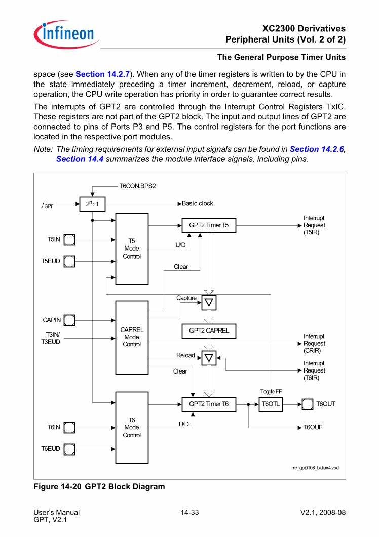
XC2300 DerivativesPeripheral Units (Vol. 2 of 2)
The General Purpose Timer Units
space (see Section 14.2.7). When any of the timer registers is written to by the CPU inthe state immediately preceding a timer increment, decrement, reload, or captureoperation, the CPU write operation has priority in order to guarantee correct results.The interrupts of GPT2 are controlled through the Interrupt Control Registers TxIC.These registers are not part of the GPT2 block. The input and output lines of GPT2 areconnected to pins of Ports P3 and P5. The control registers for the port functions arelocated in the respective port modules.Note: The timing requirements for external input signals can be found in Section 14.2.6,
Section 14.4 summarizes the module interface signals, including pins.
Figure 14-20 GPT2 Block Diagram
CAPRELModeControl
T5ModeControl
GPT2 Timer T5
T6ModeControl
GPT2 Timer T6
GPT2 CAPREL
T6OTL
T5IN
T3IN/T3EUD
CAPIN
T6IN
T6OUT
U/D
U/D
InterruptRequest(T5IR)
InterruptRequest(CRIR)
InterruptRequest(T6IR)
T6OUF
Clear
Capture
mc_gpt0108_bldiax4.vsd
Toggle FF
Clear
2n: 1fGPT Basic clock
T6CON.BPS2
Reload
T5EUD
T6EUD
User’s Manual 14-33 V2.1, 2008-08GPT, V2.1

XC2300 DerivativesPeripheral Units (Vol. 2 of 2)
The General Purpose Timer Units
14.2.1 GPT2 Core Timer T6 Control The current contents of the core timer T6 are reflected by its count register T6. Thisregister can also be written to by the CPU, for example, to set the initial start value.The core timer T6 is configured and controlled via its bitaddressable control registerT6CON.
GPT12E_T6CON Timer 6 Control Register SFR (FF48H/A4H) Reset Value: 0000H
15 14 13 12 11 10 9 8 7 6 5 4 3 2 1 0
T6SR
T6CLR - BPS2 T6
OTLT6OE
T6UDE
T6UD T6R T6M T6I
rw rw - rw rwh rw rw rw rw rw rw
Field Bits Type DescriptionT6SR 15 rw Timer 6 Reload Mode Enable
0B Reload from register CAPREL Disabled1B Reload from register CAPREL Enabled
T6CLR 14 rw Timer T6 Clear Enable Bit0B Timer T6 is not cleared on a capture event1B Timer T6 is cleared on a capture event
BPS2 [12:11] rw GPT2 Block Prescaler ControlSelects the basic clock for block GPT2(see also Section 14.2.6)00B fGPT/401B fGPT/210B fGPT/1611B fGPT/8
T6OTL 10 rwh Timer T6 Overflow Toggle LatchToggles on each overflow/underflow of T6. Can be set or reset by software (see separate description)
T6OE 9 rw Overflow/Underflow Output Enable0B Alternate Output Function Disabled1B State of T6 toggle latch is output on pin T6OUT
T6UDE 8 rw Timer T6 External Up/Down Enable1)
0B Input T6EUD is disconnected1B Direction influenced by input T6EUD
User’s Manual 14-34 V2.1, 2008-08GPT, V2.1

XC2300 DerivativesPeripheral Units (Vol. 2 of 2)
The General Purpose Timer Units
T6UD 7 rw Timer T6 Up/Down Control1)
0B Timer T6 counts up1B Timer T6 counts down
T6R 6 rw Timer T6 Run Bit0B Timer T6 stops1B Timer T6 runs
T6M [5:3] rw Timer T6 Mode Control (Basic Operating Mode)000B Timer Mode001B Counter Mode010B Gated Timer Mode with gate active low011B Gated Timer Mode with gate active high100B Reserved. Do not use this combination.101B Reserved. Do not use this combination.110B Reserved. Do not use this combination.111B Reserved. Do not use this combination.
T6I [2:0] rw Timer T6 Input Parameter SelectionDepends on the operating mode, see respective sections for encoding:Table 14-15 for Timer Mode and Gated Timer ModeTable 14-11 for Counter Mode
1) See Table 14-10 for encoding of bits T6UD and T6UDE.
Field Bits Type Description
User’s Manual 14-35 V2.1, 2008-08GPT, V2.1
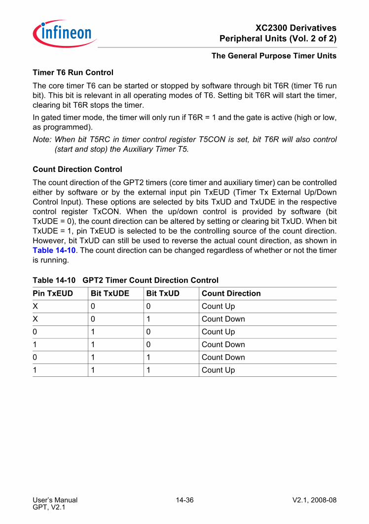
XC2300 DerivativesPeripheral Units (Vol. 2 of 2)
The General Purpose Timer Units
Timer T6 Run ControlThe core timer T6 can be started or stopped by software through bit T6R (timer T6 runbit). This bit is relevant in all operating modes of T6. Setting bit T6R will start the timer,clearing bit T6R stops the timer.In gated timer mode, the timer will only run if T6R = 1 and the gate is active (high or low,as programmed).Note: When bit T5RC in timer control register T5CON is set, bit T6R will also control
(start and stop) the Auxiliary Timer T5.
Count Direction Control The count direction of the GPT2 timers (core timer and auxiliary timer) can be controlledeither by software or by the external input pin TxEUD (Timer Tx External Up/DownControl Input). These options are selected by bits TxUD and TxUDE in the respectivecontrol register TxCON. When the up/down control is provided by software (bitTxUDE = 0), the count direction can be altered by setting or clearing bit TxUD. When bitTxUDE = 1, pin TxEUD is selected to be the controlling source of the count direction.However, bit TxUD can still be used to reverse the actual count direction, as shown inTable 14-10. The count direction can be changed regardless of whether or not the timeris running.
Table 14-10 GPT2 Timer Count Direction ControlPin TxEUD Bit TxUDE Bit TxUD Count DirectionX 0 0 Count UpX 0 1 Count Down0 1 0 Count Up1 1 0 Count Down0 1 1 Count Down1 1 1 Count Up
User’s Manual 14-36 V2.1, 2008-08GPT, V2.1

XC2300 DerivativesPeripheral Units (Vol. 2 of 2)
The General Purpose Timer Units
Timer 6 Output Toggle LatchThe overflow/underflow signal of timer T6 is connected to a block named ‘Toggle Latch’,shown in the timer mode diagrams. Figure 14-21 illustrates the details of this block. Anoverflow or underflow of T6 will clock two latches: The first latch represents bit T6OTL incontrol register T6CON. The second latch is an internal latch toggled by T6OTL’s output.Both latch outputs are connected to the input control block of the auxiliary timer T5. Theoutput level of the shadow latch will match the output level of T6OTL, but is delayed byone clock cycle. When the T6OTL value changes, this will result in a temporarily differentoutput level from T6OTL and the shadow latch, which can trigger the selected countevent in T5.When software writes to T6OTL, both latches are set or cleared simultaneously. In thiscase, both signals to the auxiliary timers carry the same level and no edge will bedetected. Bit T6OE (overflow/underflow output enable) in register T6CON enables thestate of T6OTL to be monitored via an external pin T6OUT. When T6OTL is linked to anexternal port pin (must be configured as output), T6OUT can be used to control externalHW. If T6OE = 1, pin T6OUT outputs the state of T6OTL. If T6OE = 0, pin T6OUToutputs a high level (while it selects the timer output signal).As can be seen from Figure 14-21, when latch T6OTL is modified by software todetermine the state of the output line, also the internal shadow latch is set or clearedaccordingly. Therefore, no trigger condition is detected by T5 in this case.
Figure 14-21 Block Diagram of the Toggle Latch Logic of Core Timer T6
Note: T6 is also used to clock the timers in the CAPCOM units. For this purpose, thereis a direct internal connection between the T6 overflow/underflow line and theCAPCOM timers (signal T6OUF).
mc_gpt0106_otl.vsd
Toggle Latch Logic
TxOUT
Set/Clear (SW)
Core Timer
Overflow/Underflow Shadow
Latch
1
0
MU
X
1
TxOE
TxOTLTo Port Logic
To Aux. TimerInput Logic
User’s Manual 14-37 V2.1, 2008-08GPT, V2.1
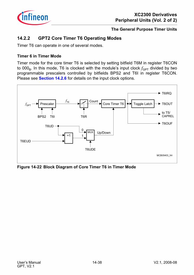
XC2300 DerivativesPeripheral Units (Vol. 2 of 2)
The General Purpose Timer Units
14.2.2 GPT2 Core Timer T6 Operating ModesTimer T6 can operate in one of several modes.
Timer 6 in Timer Mode Timer mode for the core timer T6 is selected by setting bitfield T6M in register T6CONto 000B. In this mode, T6 is clocked with the module’s input clock fGPT divided by twoprogrammable prescalers controlled by bitfields BPS2 and T6I in register T6CON.Please see Section 14.2.6 for details on the input clock options.
Figure 14-22 Block Diagram of Core Timer T6 in Timer Mode
Prescaler Core Timer T6 Toggle Latch
MCB05403_X4
BPS2 T6I
Up/Down
fGPT
fT6
T6R
CountT6OUT
T6IRQ
to T5/CAPREL
T6OUF
MUX0
1T6EUD
=1
T6UD
T6UDE
User’s Manual 14-38 V2.1, 2008-08GPT, V2.1

XC2300 DerivativesPeripheral Units (Vol. 2 of 2)
The General Purpose Timer Units
Gated Timer Mode Gated timer mode for the core timer T6 is selected by setting bitfield T6M in registerT6CON to 010B or 011B. Bit T6M.0 (T6CON.3) selects the active level of the gate input.The same options for the input frequency are available in gated timer mode as in timermode (see Section 14.2.6). However, the input clock to the timer in this mode is gatedby the external input pin T6IN (Timer T6 External Input).To enable this operation, the associated pin T6IN must be configured as input (thecorresponding direction control bit must contain 0).
Figure 14-23 Block Diagram of Core Timer T6 in Gated Timer Mode
If T6M = 010B, the timer is enabled when T6IN shows a low level. A high level at this linestops the timer. If T6M = 011B, line T6IN must have a high level in order to enable thetimer. Additionally, the timer can be turned on or off by software using bit T6R. The timerwill only run if T6R is 1 and the gate is active. It will stop if either T6R is 0 or the gate isinactive.Note: A transition of the gate signal at pin T6IN does not cause an interrupt request.
Prescaler GateCtrl. Core Timer T6 Toggle Latch
MCB05404_X4
BPS2 T6I
Up/Down
fGPTfT6
T6R
CountT6OUT
T6IRQ
to T5,CAPRELClear
T6OUFT6IN
MUX0
1
T6EUD
=1
T6UD
T6UDE
User’s Manual 14-39 V2.1, 2008-08GPT, V2.1

XC2300 DerivativesPeripheral Units (Vol. 2 of 2)
The General Purpose Timer Units
Counter Mode Counter mode for the core timer T6 is selected by setting bitfield T6M in register T6CONto 001B. In counter mode, timer T6 is clocked by a transition at the external input pinT6IN. The event causing an increment or decrement of the timer can be a positive, anegative, or both a positive and a negative transition at this line. Bitfield T6I in controlregister T6CON selects the triggering transition (see Table 14-11).
Figure 14-24 Block Diagram of Core Timer T6 in Counter Mode
For counter mode operation, pin T6IN must be configured as input (the respectivedirection control bit DPx.y must be 0). The maximum input frequency allowed in countermode depends on the selected prescaler value. To ensure that a transition of the countinput signal applied to T6IN is recognized correctly, its level must be held high or low fora minimum number of module clock cycles before it changes. This information can befound in Section 14.2.6.
Table 14-11 GPT2 Core Timer T6 (Counter Mode) Input Edge SelectionT6I Triggering Edge for Counter Increment/Decrement000B None. Counter T6 is disabled001B Positive transition (rising edge) on T6IN010B Negative transition (falling edge) on T6IN011B Any transition (rising or falling edge) on T6IN1XXB Reserved. Do not use this combination
MCB05405_X4
Core Timer T6 Toggle Latch
Up/Down
T6IN
T6R
CountT6OUT
T6IRQ
to T5,CAPREL
T6IClear
T6OUF
Edge
Select
MUX0
1
T6EUD
=1
T6UD
T6UDE
User’s Manual 14-40 V2.1, 2008-08GPT, V2.1
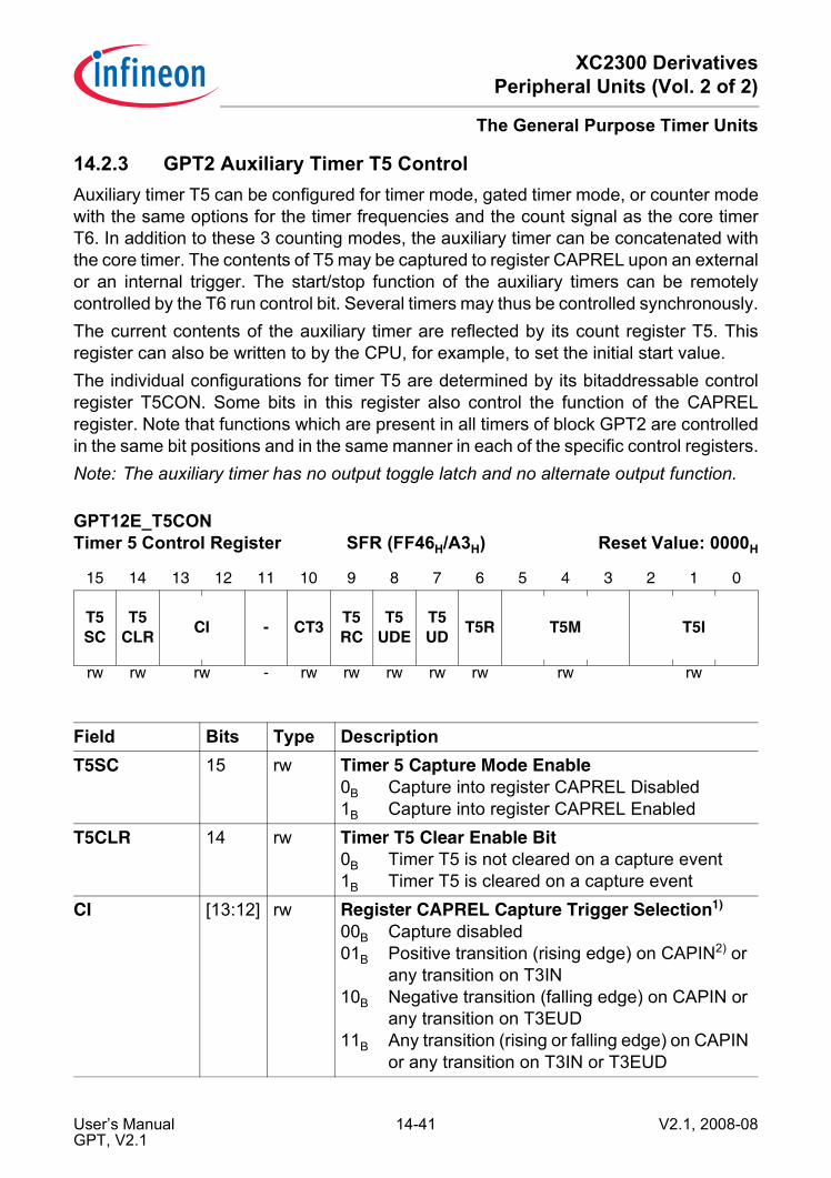
XC2300 DerivativesPeripheral Units (Vol. 2 of 2)
The General Purpose Timer Units
14.2.3 GPT2 Auxiliary Timer T5 Control Auxiliary timer T5 can be configured for timer mode, gated timer mode, or counter modewith the same options for the timer frequencies and the count signal as the core timerT6. In addition to these 3 counting modes, the auxiliary timer can be concatenated withthe core timer. The contents of T5 may be captured to register CAPREL upon an externalor an internal trigger. The start/stop function of the auxiliary timers can be remotelycontrolled by the T6 run control bit. Several timers may thus be controlled synchronously.The current contents of the auxiliary timer are reflected by its count register T5. Thisregister can also be written to by the CPU, for example, to set the initial start value.The individual configurations for timer T5 are determined by its bitaddressable controlregister T5CON. Some bits in this register also control the function of the CAPRELregister. Note that functions which are present in all timers of block GPT2 are controlledin the same bit positions and in the same manner in each of the specific control registers.Note: The auxiliary timer has no output toggle latch and no alternate output function.
GPT12E_T5CON Timer 5 Control Register SFR (FF46H/A3H) Reset Value: 0000H
15 14 13 12 11 10 9 8 7 6 5 4 3 2 1 0
T5SC
T5CLR CI - CT3 T5
RCT5
UDET5UD T5R T5M T5I
rw rw rw - rw rw rw rw rw rw rw
Field Bits Type DescriptionT5SC 15 rw Timer 5 Capture Mode Enable
0B Capture into register CAPREL Disabled1B Capture into register CAPREL Enabled
T5CLR 14 rw Timer T5 Clear Enable Bit0B Timer T5 is not cleared on a capture event1B Timer T5 is cleared on a capture event
CI [13:12] rw Register CAPREL Capture Trigger Selection1)
00B Capture disabled01B Positive transition (rising edge) on CAPIN2) or
any transition on T3IN10B Negative transition (falling edge) on CAPIN or
any transition on T3EUD11B Any transition (rising or falling edge) on CAPIN
or any transition on T3IN or T3EUD
User’s Manual 14-41 V2.1, 2008-08GPT, V2.1

XC2300 DerivativesPeripheral Units (Vol. 2 of 2)
The General Purpose Timer Units
CT3 10 rw Timer T3 Capture Trigger Enable0B Capture trigger from input line CAPIN1B Capture trigger from T3 input lines T3IN and/or
T3EUDT5RC 9 rw Timer T5 Remote Control
0B Timer T5 is controlled by its own run bit T5R1B Timer T5 is controlled by the run bit T6R of
core timer 6, not by bit T5RT5UDE 8 rw Timer T5 External Up/Down Enable3)
0B Input T5EUD is disconnected1B Direction influenced by input T5EUD
T5UD 7 rw Timer T5 Up/Down Control3)
0B Timer T5 counts up1B Timer T5 counts down
T5R 6 rw Timer T5 Run Bit0B Timer T5 stops1B Timer T5 runsNote: This bit only controls timer T5 if bit T5RC = 0.
T5M [5:3] rw Timer T5 Mode Control (Basic Operating Mode)000B Timer Mode001B Counter Mode010B Gated Timer Mode with gate active low011B Gated Timer Mode with gate active high1XXB Reserved. Do not use this combination
T5I [2:0] rw Timer T5 Input Parameter SelectionDepends on the operating mode, see respective sections for encoding:Table 14-15 for Timer Mode and Gated Timer Mode Table 14-11 for Counter Mode
1) To define the respective trigger source signal, also bit CT3 must be regarded (see Table 14-13).
2) Rising edge must be selected if capturing is triggered by the internal GPT1 read signals (see register PISELand “Combined Capture Modes” on Page 14-53).
3) See Table 14-10 for encoding of bits T5UD and T5UDE.
Field Bits Type Description
User’s Manual 14-42 V2.1, 2008-08GPT, V2.1

XC2300 DerivativesPeripheral Units (Vol. 2 of 2)
The General Purpose Timer Units
Timer T5 Run ControlThe auxiliary timer T5 can be started or stopped by software in two different ways:• Through the associated timer run bit (T5R). In this case it is required that the
respective control bit T5RC = 0.• Through the core timer’s run bit (T6R). In this case the respective remote control bit
must be set (T5RC = 1).The selected run bit is relevant in all operating modes of T5. Setting the bit will start thetimer, clearing the bit stops the timer.In gated timer mode, the timer will only run if the selected run bit is set and the gate isactive (high or low, as programmed).Note: If remote control is selected T6R will start/stop timer T6 and the auxiliary timer T5
synchronously.
User’s Manual 14-43 V2.1, 2008-08GPT, V2.1
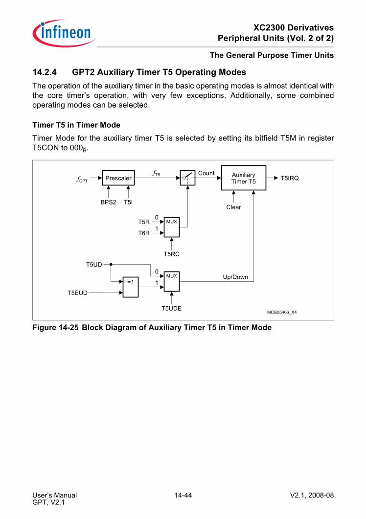
XC2300 DerivativesPeripheral Units (Vol. 2 of 2)
The General Purpose Timer Units
14.2.4 GPT2 Auxiliary Timer T5 Operating ModesThe operation of the auxiliary timer in the basic operating modes is almost identical withthe core timer’s operation, with very few exceptions. Additionally, some combinedoperating modes can be selected.
Timer T5 in Timer ModeTimer Mode for the auxiliary timer T5 is selected by setting its bitfield T5M in registerT5CON to 000B.
Figure 14-25 Block Diagram of Auxiliary Timer T5 in Timer Mode
Prescaler AuxiliaryTimer T5
BPS2 T5I
fGPT
fT5 CountT5IRQ
MCB05406_X4
Up/Down
MUX
T5RC
T5R
T6R
0
1
Clear
MUX0
1
T5EUD
=1
T5UD
T5UDE
User’s Manual 14-44 V2.1, 2008-08GPT, V2.1

XC2300 DerivativesPeripheral Units (Vol. 2 of 2)
The General Purpose Timer Units
Timer T5 in Gated Timer ModeGated timer mode for the auxiliary timer T5 is selected by setting bitfield T5M in registerT5CON to 010B or 011B. Bit T5M.0 (T5CON.3) selects the active level of the gate input.Note: A transition of the gate signal at line T5IN does not cause an interrupt request.
Figure 14-26 Block Diagram of Auxiliary Timer T5 in Gated Timer Mode
Note: There is no output toggle latch for T5.Start/stop of the auxiliary timer can be controlled locally or remotely.
Timer T5 in Counter Mode Counter mode for auxiliary timer T5 is selected by setting bitfield T5M in register T5CONto 001B. In counter mode, the auxiliary timer can be clocked either by a transition at itsexternal input line T5IN, or by a transition of timer T6’s toggle latch T6OTL. The eventcausing an increment or decrement of a timer can be a positive, a negative, or both apositive and a negative transition at either the respective input pin or at the toggle latch.Bitfield T5I in control register T5CON selects the triggering transition (see Table 14-12).
Prescaler GateCtrl.
AuxiliaryTimer T5
BPS2 T5IT5IN
fGPTfT5 Count
T5IRQ
MCB05407_X4
MUX
T5RC
T5R
T6R
Clear
Up/Down
0
1
MUX0
1
T5EUD
=1
T5UD
T5UDE
User’s Manual 14-45 V2.1, 2008-08GPT, V2.1

XC2300 DerivativesPeripheral Units (Vol. 2 of 2)
The General Purpose Timer Units
Figure 14-27 Block Diagram of Auxiliary Timer T5 in Counter Mode
Note: Only state transitions of T6OTL which are caused by the overflows/underflows ofT6 will trigger the counter function of T5. Modifications of T6OTL via software willNOT trigger the counter function of T5.
For counter operation, pin T5IN must be configured as input (the respective directioncontrol bit DPx.y must be 0). The maximum input frequency allowed in counter modedepends on the selected prescaler value. To ensure that a transition of the count inputsignal applied to T5IN is recognized correctly, its level must be held high or low for aminimum number of module clock cycles before it changes. This information can befound in Section 14.2.6.
Table 14-12 GPT2 Auxiliary Timer (Counter Mode) Input Edge SelectionT5I Triggering Edge for Counter Increment/DecrementX00B None. Counter T5 is disabled001B Positive transition (rising edge) on T5IN010B Negative transition (falling edge) on T5IN011B Any transition (rising or falling edge) on T5IN101B Positive transition (rising edge) of T6 toggle latch T6OTL110B Negative transition (falling edge) of T6 toggle latch T6OTL111B Any transition (rising or falling edge) of T6 toggle latch T6OTL
AuxiliaryTimer T5
CountT5IRQ
MCB05408_X4
Up/Down
MUX
T5RC
T5R
T6R
T5I
MUX
T5I.2
T5IN
T6ToggleLatch
0
1
Clear
0
1
Edge
Select
MUX0
1
T5EUD
=1
T5UD
T5UDE
User’s Manual 14-46 V2.1, 2008-08GPT, V2.1

XC2300 DerivativesPeripheral Units (Vol. 2 of 2)
The General Purpose Timer Units
Timer Concatenation Using the toggle bit T6OTL as a clock source for the auxiliary timer in counter modeconcatenates the core timer T6 with the auxiliary timer T5. This concatenation formseither a 32-bit or a 33-bit timer/counter, depending on which transition of T6OTL isselected to clock the auxiliary timer.• 32-bit Timer/Counter: If both a positive and a negative transition of T6OTL are used
to clock the auxiliary timer, this timer is clocked on every overflow/underflow of thecore timer T6. Thus, the two timers form a 32-bit timer.
• 33-bit Timer/Counter: If either a positive or a negative transition of T6OTL is selectedto clock the auxiliary timer, this timer is clocked on every second overflow/underflowof the core timer T6. This configuration forms a 33-bit timer (16-bit core timer + T6OTL+ 16-bit auxiliary timer).As long as bit T6OTL is not modified by software, it represents the state of the internaltoggle latch, and can be regarded as part of the 33-bit timer.
The count directions of the two concatenated timers are not required to be the same.This offers a wide variety of different configurations.T6, which represents the low-order part of the concatenated timer, can operate in timermode, gated timer mode or counter mode in this case.
Figure 14-28 Concatenation of Core Timer T6 and Auxiliary Timer T5
MCA05409
Toggle Latch T6OUT
T6IRQCount
T6R
Core Timer T6Operating
ModeControl
BPS2 T6IClear
T6INfGPT
AuxiliaryTimer T5
T5I
0
1MUX
T5I.2
T5INT5IRQ
Up/Down
Clear Up/Down
Count
MUX
T5RC
T5R
T6R
0
1
Edge
Select
User’s Manual 14-47 V2.1, 2008-08GPT, V2.1

XC2300 DerivativesPeripheral Units (Vol. 2 of 2)
The General Purpose Timer Units
14.2.5 GPT2 Register CAPREL Operating ModesThe Capture/Reload register CAPREL can be used to capture the contents of timer T5,or to reload timer T6. A special mode facilitates the use of register CAPREL for bothfunctions at the same time. This mode allows frequency multiplication. The capturefunction is triggered by the input pin CAPIN or by GPT1 timer’s T3 input lines T3IN andT3EUD. The reload function is triggered by an overflow or underflow of timer T6.In addition to the capture function, the capture trigger signal can also be used to clearthe contents of timers T5 and T6 individually.The functions of register CAPREL are controlled via several bit(field)s in the timer controlregisters T5CON and T6CON.
GPT2 Capture/Reload Register CAPREL in Capture Mode Capture mode for register CAPREL is selected by setting bit T5SC in control registerT5CON (set bitfield CI in register T5CON to a non-zero value to select a trigger signal).In capture mode, the contents of the auxiliary timer T5 are latched into register CAPRELin response to a signal transition at the selected external input pin(s). Bit CT3 selects theexternal input line CAPIN or the input lines T3IN and/or T3EUD of GPT1 timer T3 as thesource for a capture trigger. Either a positive, a negative, or both a positive and anegative transition at line CAPIN can be selected to trigger the capture function, ortransitions on input T3IN or input T3EUD or both inputs, T3IN and T3EUD. The activeedge is controlled by bitfield CI in register T5CON. Table 14-13 summarizes theseoptions.
Table 14-13 CAPREL Register Input Edge SelectionCT3 CI Triggering Signal/Edge for Capture ModeX 00B None. Capture Mode is disabled.0 01B Positive transition (rising edge) on CAPIN.0 10B Negative transition (falling edge) on CAPIN.0 11B Any transition (rising or falling edge) on CAPIN.1 01B Any transition (rising or falling edge) on T3IN.1 10B Any transition (rising or falling edge) on T3EUD.1 11B Any transition (rising or falling edge) on T3IN or T3EUD.
User’s Manual 14-48 V2.1, 2008-08GPT, V2.1

XC2300 DerivativesPeripheral Units (Vol. 2 of 2)
The General Purpose Timer Units
Figure 14-29 GPT2 Register CAPREL in Capture Mode
When a selected trigger is detected, the contents of the auxiliary timer T5 are latchedinto register CAPREL and the interrupt request line CRIRQ is activated. The same eventcan optionally clear timer T5 and/or timer T6. This option is enabled by bit T5CLR inregister T5CON and bit T6CLR in register T6CON, respectively. If TxCLR = 0 thecontents of timer Tx is not affected by a capture. If TxCLR = 1 timer Tx is cleared afterthe current timer T5 value has been latched into register CAPREL.Note: Bit T5SC only controls whether or not a capture is performed. If T5SC is cleared
the external input pin(s) can still be used to clear timer T5 and/or T6, or as externalinterrupt input(s). This interrupt is controlled by the CAPREL interrupt controlregister CRIC.
When capture triggers T3IN or T3EUD are enabled (CT3 = 1), register CAPREL capturesthe contents of T5 upon transitions of the selected input(s). These values can be usedto measure T3’s input signals. This is useful, for example, when T3 operates in
SignalSelect
AuxiliaryTimer T5 T5IRQ
MCA05410X11
Up/DownClear
T5CLR
T5SC
Capture
CAPRELRegister
T6CLR
0
1MUX
CT3
CI
CAPIN
T3IN
T3EUD
CountClock
CRIRQ
ClearT6
Edge
Select
User’s Manual 14-49 V2.1, 2008-08GPT, V2.1

XC2300 DerivativesPeripheral Units (Vol. 2 of 2)
The General Purpose Timer Units
incremental interface mode, in order to derive dynamic information (speed, acceleration)from the input signals.For capture mode operation, the selected pins CAPIN, T3IN, or T3EUD must beconfigured as input. To ensure that a transition of a trigger input signal applied to one ofthese inputs is recognized correctly, its level must be held high or low for a minimumnumber of module clock cycles, detailed in Section 14.2.6.
GPT2 Capture/Reload Register CAPREL in Reload ModeReload mode for register CAPREL is selected by setting bit T6SR in control registerT6CON. In reload mode, the core timer T6 is reloaded with the contents of registerCAPREL, triggered by an overflow or underflow of T6. This will not activate the interruptrequest line CRIRQ associated with the CAPREL register. However, interrupt requestline T6IRQ will be activated, indicating the overflow/underflow of T6.
Figure 14-30 GPT2 Register CAPREL in Reload Mode
MCA05411
CAPRELRegister
T6SR
Core Timer T6
Reload
Up/Down
CountClock Toggle Latch T6OUT
T6IRQ
T6OUF
to T5
User’s Manual 14-50 V2.1, 2008-08GPT, V2.1

XC2300 DerivativesPeripheral Units (Vol. 2 of 2)
The General Purpose Timer Units
GPT2 Capture/Reload Register CAPREL in Capture-And-Reload ModeSince the reload function and the capture function of register CAPREL can be enabledindividually by bits T5SC and T6SR, the two functions can be enabled simultaneously bysetting both bits. This feature can be used to generate an output frequency that is amultiple of the input frequency.
Figure 14-31 GPT2 Register CAPREL in Capture-And-Reload Mode
This combined mode can be used to detect consecutive external events which mayoccur aperiodically, but where a finer resolution, that means, more ‘ticks’ within the timebetween two external events is required.For this purpose, the time between the external events is measured using timer T5 andthe CAPREL register. Timer T5 runs in timer mode counting up with a frequency of e.g.fGPT/32. The external events are applied to pin CAPIN. When an external event occurs,
AuxiliaryTimer T5 T5IRQ
Up/DownClear
T5SC
Capture
CAPRELRegister
0
1MUX
CT3
CI
CAPIN
T3IN
T3EUD
CountClock
T5CLR
CRIRQ
MCA05412X11
T6SR
Core Timer T6
Clear
T6CLR
Reload
Up/Down
CountClock Toggle Latch T6OUT
T6IRQ
T6OUF
to T5
Edge
Select
Edge
Select
User’s Manual 14-51 V2.1, 2008-08GPT, V2.1

XC2300 DerivativesPeripheral Units (Vol. 2 of 2)
The General Purpose Timer Units
the contents of timer T5 are latched into register CAPREL and timer T5 is cleared(T5CLR = 1). Thus, register CAPREL always contains the correct time between twoevents, measured in timer T5 increments. Timer T6, which runs in timer mode countingdown with a frequency of e.g. fGPT/4, uses the value in register CAPREL to perform areload on underflow. This means, the value in register CAPREL represents the timebetween two underflows of timer T6, now measured in timer T6 increments. Since (in thisexample) timer T6 runs 8 times faster than timer T5, it will underflow 8 times within thetime between two external events. Thus, the underflow signal of timer T6 generates8 ‘ticks’. Upon each underflow, the interrupt request line T6IRQ will be activated and bitT6OTL will be toggled. The state of T6OTL may be output on pin T6OUT. This signal has8 times more transitions than the signal which is applied to pin CAPIN.Note: The underflow signal of Timer T6 can furthermore be used to clock one or more of
the timers of the CAPCOM units, which gives the user the possibility to setcompare events based on a finer resolution than that of the external events. Thisconnection is accomplished via signal T6OUF.
Capture CorrectionA certain deviation of the output frequency is generated by the fact that timer T5 willcount actual time units (e.g. T5 running at 1 MHz will count up to the value 64H/100D fora 10 kHz input signal), while T6OTL will only toggle upon an underflow of T6 (i.e. thetransition from 0000H to FFFFH). In the above mentioned example, T6 would count downfrom 64H, so the underflow would occur after 101 timing ticks of T6. The actual outputfrequency then is 79.2 kHz, instead of the expected 80 kHz.Another possibility is to use T6 overflows. In this case, T5 counts down and T6 countsup. Upon a signal transition on pin CAPIN, the count value in T5 is captured intoCAPREL and T5 is cleared to 0000H. In its next clock cycle, T5 underflows to FFFFH, andcontinues to count down with the following clocks. T6 is reloaded from CAPREL upon anoverflow, and continues to count up with its following clock cycles (8 times faster in theabove example). In this case, T5 and T6 count the same number of steps with theirrespective internal count frequency.In the above example, T5 running at 1 MHz will count down to the value FF9CH/-100D fora 10 kHz input signal applied at CAPIN, while T6 counts up from FF9CH through FFFFHto 0000H. So the overflow occurs after 100 timing ticks of T6, and the actual outputfrequency at T6OUT then is the expected 80 kHz.However, in this case CAPREL does not directly contain the time between two CAPINevents, but rather its 2's complement. Software will have to convert this value, if it isrequired for the operation.
User’s Manual 14-52 V2.1, 2008-08GPT, V2.1
XC2300 DerivativesPeripheral Units (Vol. 2 of 2)
The General Purpose Timer Units
Combined Capture ModesFor incremental interface applications in particular, several timer features can becombined to obtain dynamic information such as speed, acceleration, or deceleration.The current position itself can be obtained directly from the timer register (T2, T3, T4).The time information to determine the dynamic parameters is generated by capturing thecontents of the free-running timer T5 into register CAPREL:Capturing on sensor signal transitions is available for timer T3 inputs. This mode isselected by setting bit CT3 and selecting the intended signal(s) via bitfield CI in registerT5CON. CAPREL then indicates the time between two selected transitions (measuredin T5 counts).These operating modes directly support the measurement of position and rotationalspeed. Acceleration and deceleration can then be determined by evaluating subsequentspeed measurements.
User’s Manual 14-53 V2.1, 2008-08GPT, V2.1

XC2300 DerivativesPeripheral Units (Vol. 2 of 2)
The General Purpose Timer Units
14.2.6 GPT2 Clock Signal ControlAll actions within the timer block GPT2 are triggered by transitions of its basic clock. Thisbasic clock is derived from the system clock by a basic block prescaler, controlled bybitfield BPS2 in register T6CON (see Figure 14-20). The count clock can be generatedin two different ways:• Internal count clock, derived from GPT2’s basic clock via a programmable prescaler,
is used for (gated) timer mode.• External count clock, derived from the timer’s input pin(s), is used for counter mode.For both ways, the basic clock determines the maximum count frequency and the timer’sresolution:
Internal Count Clock GenerationIn timer mode and gated timer mode, the count clock for each GPT2 timer is derived fromthe GPT2 basic clock by a programmable prescaler, controlled by bitfield TxI in therespective timer’s control register TxCON.The count frequency fTx for a timer Tx and its resolution rTx are scaled linearly with lowerclock frequencies, as can be seen from the following formula:
[14.2]
The effective count frequency depends on the common module clock prescaler factorF(BPS2) as well as on the individual input prescaler factor 2<TxI>. Table 14-15summarizes the resulting overall divider factors for a GPT2 timer that result from thesecascaded prescalers.
Table 14-14 Basic Clock Selection for Block GPT2Block Prescaler1)
1) Please note the non-linear encoding of bitfield BPS2.
BPS2 = 01B BPS2 = 00B2)
2) Default after reset.
BPS2 = 11B BPS2 = 10B
Prescaling Factor for GPT2: F(BPS2)
F(BPS2)= 2
F(BPS2)= 4
F(BPS2)= 8
F(BPS2)= 16
Maximum External Count Frequency
fGPT/4 fGPT/8 fGPT/16 fGPT/32
Input SignalStable Time
2 × tGPT 4 × tGPT 8 × tGPT 16 × tGPT
fTxfGPT
F BPS2( ) 2<Txl>×---------------------------------------------= rTx µs[ ] F BPS2( ) 2<Txl>×
fGPT MHz[ ]---------------------------------------------=
User’s Manual 14-54 V2.1, 2008-08GPT, V2.1
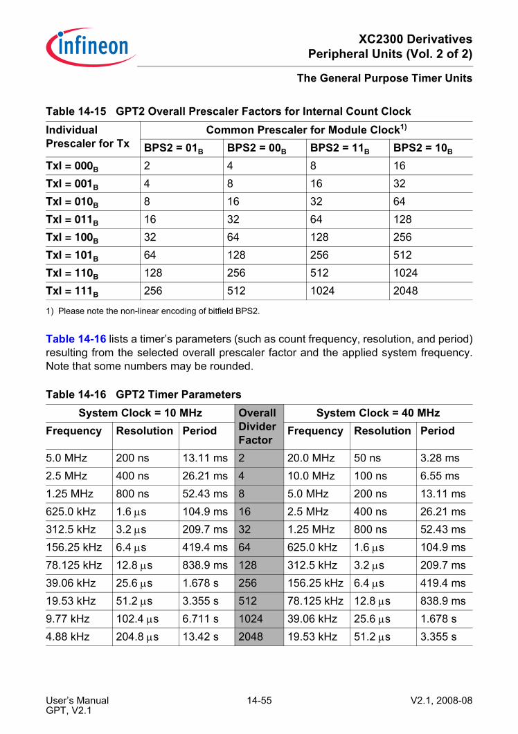
XC2300 DerivativesPeripheral Units (Vol. 2 of 2)
The General Purpose Timer Units
Table 14-16 lists a timer’s parameters (such as count frequency, resolution, and period)resulting from the selected overall prescaler factor and the applied system frequency.Note that some numbers may be rounded.
Table 14-15 GPT2 Overall Prescaler Factors for Internal Count ClockIndividual Prescaler for Tx
Common Prescaler for Module Clock1)
1) Please note the non-linear encoding of bitfield BPS2.
BPS2 = 01B BPS2 = 00B BPS2 = 11B BPS2 = 10B
TxI = 000B 2 4 8 16TxI = 001B 4 8 16 32TxI = 010B 8 16 32 64TxI = 011B 16 32 64 128TxI = 100B 32 64 128 256TxI = 101B 64 128 256 512TxI = 110B 128 256 512 1024TxI = 111B 256 512 1024 2048
Table 14-16 GPT2 Timer ParametersSystem Clock = 10 MHz Overall
Divider Factor
System Clock = 40 MHzFrequency Resolution Period Frequency Resolution Period
5.0 MHz 200 ns 13.11 ms 2 20.0 MHz 50 ns 3.28 ms2.5 MHz 400 ns 26.21 ms 4 10.0 MHz 100 ns 6.55 ms1.25 MHz 800 ns 52.43 ms 8 5.0 MHz 200 ns 13.11 ms625.0 kHz 1.6 µs 104.9 ms 16 2.5 MHz 400 ns 26.21 ms312.5 kHz 3.2 µs 209.7 ms 32 1.25 MHz 800 ns 52.43 ms156.25 kHz 6.4 µs 419.4 ms 64 625.0 kHz 1.6 µs 104.9 ms78.125 kHz 12.8 µs 838.9 ms 128 312.5 kHz 3.2 µs 209.7 ms39.06 kHz 25.6 µs 1.678 s 256 156.25 kHz 6.4 µs 419.4 ms19.53 kHz 51.2 µs 3.355 s 512 78.125 kHz 12.8 µs 838.9 ms9.77 kHz 102.4 µs 6.711 s 1024 39.06 kHz 25.6 µs 1.678 s4.88 kHz 204.8 µs 13.42 s 2048 19.53 kHz 51.2 µs 3.355 s
User’s Manual 14-55 V2.1, 2008-08GPT, V2.1
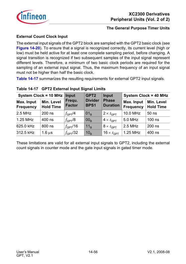
XC2300 DerivativesPeripheral Units (Vol. 2 of 2)
The General Purpose Timer Units
External Count Clock InputThe external input signals of the GPT2 block are sampled with the GPT2 basic clock (seeFigure 14-20). To ensure that a signal is recognized correctly, its current level (high orlow) must be held active for at least one complete sampling period, before changing. Asignal transition is recognized if two subsequent samples of the input signal representdifferent levels. Therefore, a minimum of two basic clock periods are required for thesampling of an external input signal. Thus, the maximum frequency of an input signalmust not be higher than half the basic clock.Table 14-17 summarizes the resulting requirements for external GPT2 input signals.
These limitations are valid for all external input signals to GPT2, including the externalcount signals in counter mode and the gate input signals in gated timer mode.
Table 14-17 GPT2 External Input Signal LimitsSystem Clock = 10 MHz Input
Frequ. Factor
GPT2 Divider BPS1
Input Phase Duration
System Clock = 40 MHzMax. Input Frequency
Min. Level Hold Time
Max. Input Frequency
Min. Level Hold Time
2.5 MHz 200 ns fGPT/4 01B 2 × tGPT 10.0 MHz 50 ns1.25 MHz 400 ns fGPT/8 00B 4 × tGPT 5.0 MHz 100 ns625.0 kHz 800 ns fGPT/16 11B 8 × tGPT 2.5 MHz 200 ns312.5 kHz 1.6 µs fGPT/32 10B 16 × tGPT 1.25 MHz 400 ns
User’s Manual 14-56 V2.1, 2008-08GPT, V2.1
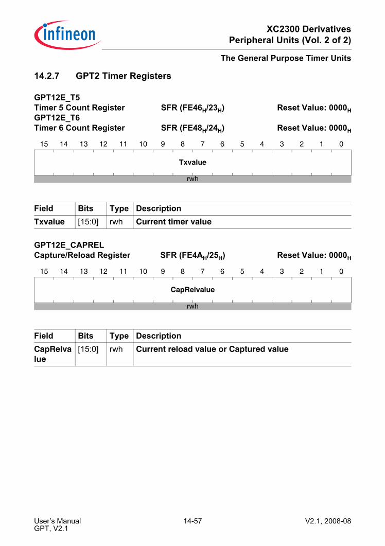
XC2300 DerivativesPeripheral Units (Vol. 2 of 2)
The General Purpose Timer Units
14.2.7 GPT2 Timer Registers
GPT12E_T5 Timer 5 Count Register SFR (FE46H/23H) Reset Value: 0000HGPT12E_T6Timer 6 Count Register SFR (FE48H/24H) Reset Value: 0000H
15 14 13 12 11 10 9 8 7 6 5 4 3 2 1 0
Txvalue
rwh
Field Bits Type DescriptionTxvalue [15:0] rwh Current timer value
GPT12E_CAPREL Capture/Reload Register SFR (FE4AH/25H) Reset Value: 0000H
15 14 13 12 11 10 9 8 7 6 5 4 3 2 1 0
CapRelvalue
rwh
Field Bits Type DescriptionCapRelvalue
[15:0] rwh Current reload value or Captured value
User’s Manual 14-57 V2.1, 2008-08GPT, V2.1

XC2300 DerivativesPeripheral Units (Vol. 2 of 2)
The General Purpose Timer Units
14.2.8 Interrupt Control for GPT2 Timers and CAPRELWhen a timer overflows from FFFFH to 0000H (when counting up), or when it underflowsfrom 0000H to FFFFH (when counting down), its interrupt request flag (T5IR or T6IR) inregister TxIC will be set. Whenever a transition according to the selection in bit field CIis detected at pin CAPIN, interrupt request flag CRIR in register CRIC is set. Setting anyrequest flag will cause an interrupt to the respective timer or CAPREL interrupt vector(T5INT, T6INT or CRINT) or trigger a PEC service, if the respective interrupt enable bit(T5IE or T6IE in register TxIC, CRIE in register CRIC) is set. There is an interrupt controlregister for each of the two timers and for the CAPREL register.
Note: Please refer to the general Interrupt Control Register description for anexplanation of the control fields.
GPT12E_T5IC Timer 5 Intr. Ctrl. Reg. SFR (FF66H/B3H) Reset Value: 0000H
15 14 13 12 11 10 9 8 7 6 5 4 3 2 1 0
- - - - - - - GPX T5IR T5IE ILVL GLVL
- - - - - - - rw rwh rw rw rw
GPT12E_T6ICTimer 6 Intr. Ctrl. Reg. SFR (FF68H/B4H) Reset Value: 0000H
15 14 13 12 11 10 9 8 7 6 5 4 3 2 1 0
- - - - - - - GPX T6IR T6IE ILVL GLVL
- - - - - - - rw rwh rw rw rw
GPT12E_CRIC CAPREL Intr. Ctrl. Reg. SFR (FF6AH/B5H) Reset Value: 0000H
15 14 13 12 11 10 9 8 7 6 5 4 3 2 1 0
- - - - - - - GPX CRIR CRIE ILVL GLVL
- - - - - - - rw rwh rw rw rw
User’s Manual 14-58 V2.1, 2008-08GPT, V2.1
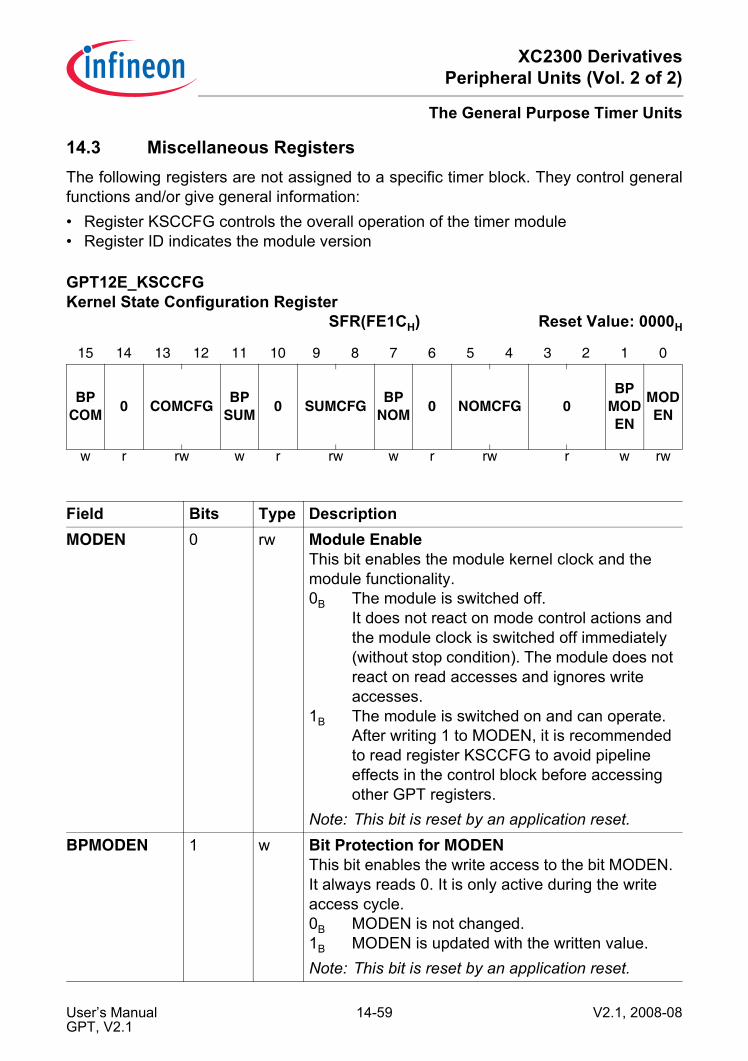
XC2300 DerivativesPeripheral Units (Vol. 2 of 2)
The General Purpose Timer Units
14.3 Miscellaneous RegistersThe following registers are not assigned to a specific timer block. They control generalfunctions and/or give general information:• Register KSCCFG controls the overall operation of the timer module• Register ID indicates the module version
GPT12E_KSCCFG Kernel State Configuration Register
SFR(FE1CH) Reset Value: 0000H
15 14 13 12 11 10 9 8 7 6 5 4 3 2 1 0
BPCOM 0 COMCFG BP
SUM 0 SUMCFG BPNOM 0 NOMCFG 0
BPMODEN
MODEN
w r rw w r rw w r rw r w rw
Field Bits Type DescriptionMODEN 0 rw Module Enable
This bit enables the module kernel clock and the module functionality.0B The module is switched off.
It does not react on mode control actions and the module clock is switched off immediately (without stop condition). The module does not react on read accesses and ignores write accesses.
1B The module is switched on and can operate. After writing 1 to MODEN, it is recommended to read register KSCCFG to avoid pipeline effects in the control block before accessing other GPT registers.
Note: This bit is reset by an application reset.BPMODEN 1 w Bit Protection for MODEN
This bit enables the write access to the bit MODEN. It always reads 0. It is only active during the write access cycle.0B MODEN is not changed.1B MODEN is updated with the written value.Note: This bit is reset by an application reset.
User’s Manual 14-59 V2.1, 2008-08GPT, V2.1

XC2300 DerivativesPeripheral Units (Vol. 2 of 2)
The General Purpose Timer Units
NOMCFG [5:4] rw Normal Operation Mode ConfigurationThis bit field defines the kernel mode applied in normal operation mode.0XB The module is switched on.1XB The module is switched off.This field is taken into account for CR = 00 or 11.Note: This bit is reset by an application reset.
BPNOM 7 w Bit Protection for NOMCFGThis bit enables the write access to the bit field NOMCFG. It always reads 0. It is only active during the write access cycle.0B NOMCFG is not changed.1B NOMCFG is updated with the written value.Note: This bit is reset by an application reset.
SUMCFG [9:8] rw Suspend Mode ConfigurationThis bit field defines the kernel mode applied in suspend mode.0XB The module is switched on.1XB The module is switched off.This field is taken into account for CR = 01.Note: This bit is reset by a debug reset.
BPSUM 11 w Bit Protection for SUMCFGThis bit enables the write access to the bit field SUMCFG. It always reads 0. It is only active during the write access cycle.0B SUMCFG is not changed.1B SUMCFG is updated with the written value.Note: This bit is reset by a debug reset.
COMCFG [13:12] rw Clock Off Mode ConfigurationThis bit field defines the kernel mode applied in clock off mode.0XB The module is switched on.1XB The module is switched off.This field is taken into account for CR = 10.Note: This bit is reset by an application reset.
Field Bits Type Description
User’s Manual 14-60 V2.1, 2008-08GPT, V2.1
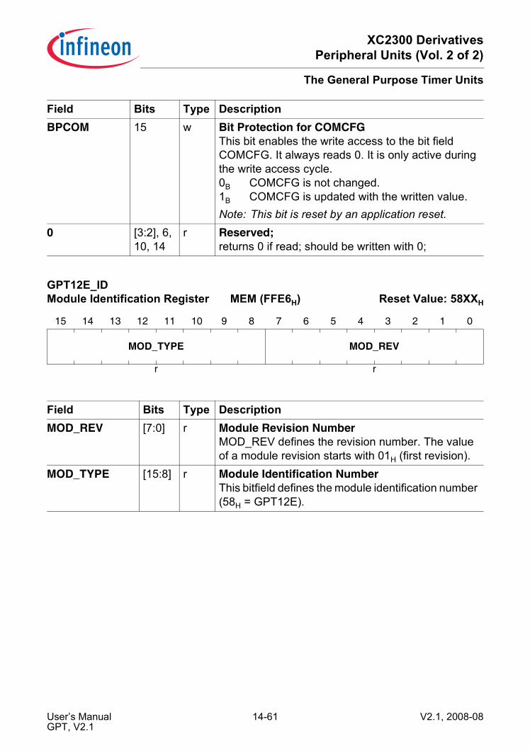
XC2300 DerivativesPeripheral Units (Vol. 2 of 2)
The General Purpose Timer Units
BPCOM 15 w Bit Protection for COMCFGThis bit enables the write access to the bit field COMCFG. It always reads 0. It is only active during the write access cycle.0B COMCFG is not changed.1B COMCFG is updated with the written value.Note: This bit is reset by an application reset.
0 [3:2], 6, 10, 14
r Reserved;returns 0 if read; should be written with 0;
GPT12E_IDModule Identification Register MEM (FFE6H) Reset Value: 58XXH
15 14 13 12 11 10 9 8 7 6 5 4 3 2 1 0
MOD_TYPE MOD_REV
r r
Field Bits Type DescriptionMOD_REV [7:0] r Module Revision Number
MOD_REV defines the revision number. The value of a module revision starts with 01H (first revision).
MOD_TYPE [15:8] r Module Identification NumberThis bitfield defines the module identification number (58H = GPT12E).
Field Bits Type Description
User’s Manual 14-61 V2.1, 2008-08GPT, V2.1
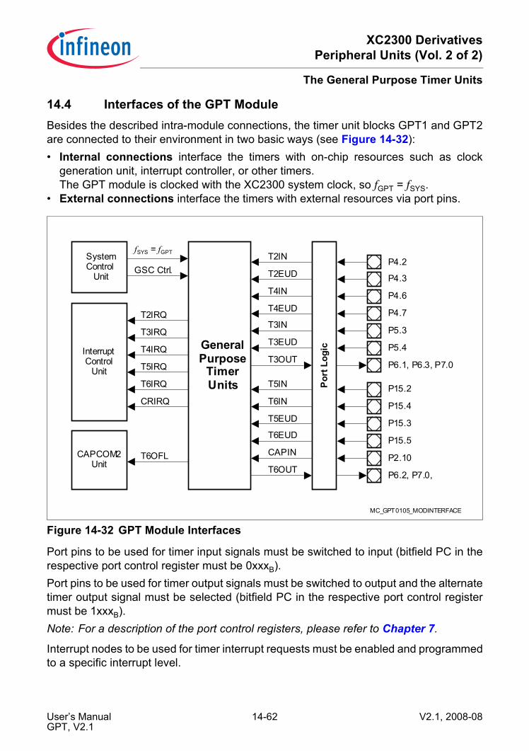
XC2300 DerivativesPeripheral Units (Vol. 2 of 2)
The General Purpose Timer Units
14.4 Interfaces of the GPT ModuleBesides the described intra-module connections, the timer unit blocks GPT1 and GPT2are connected to their environment in two basic ways (see Figure 14-32):• Internal connections interface the timers with on-chip resources such as clock
generation unit, interrupt controller, or other timers.The GPT module is clocked with the XC2300 system clock, so fGPT = fSYS.
• External connections interface the timers with external resources via port pins.
Figure 14-32 GPT Module Interfaces
Port pins to be used for timer input signals must be switched to input (bitfield PC in therespective port control register must be 0xxxB).Port pins to be used for timer output signals must be switched to output and the alternatetimer output signal must be selected (bitfield PC in the respective port control registermust be 1xxxB).Note: For a description of the port control registers, please refer to Chapter 7.
Interrupt nodes to be used for timer interrupt requests must be enabled and programmedto a specific interrupt level.
MC_GPT0105_MODINTERFACE
SystemControl
Unit
GeneralPurpose
TimerUnits
fSYS = fGPT
P4.7T4EUD
P4.2T2IN
P5.3T3IN
P4.6T4IN
P5.4T3EUD
P6.1, P6.3, P7.0T3OUT
P15.2T5IN
P15.4T6IN
P15.3T5EUD
P15.5T6EUD
P2.10CAPIN
P6.2, P7.0, T6OUT
T2IRQ
GSC Ctrl.
T3IRQ
T4IRQ
T5IRQ
T6IRQ
CRIRQ
T6OFL
InterruptControl
Unit
CAPCOM2Unit
Por
t Log
ic
P4.3T2EUD
User’s Manual 14-62 V2.1, 2008-08GPT, V2.1
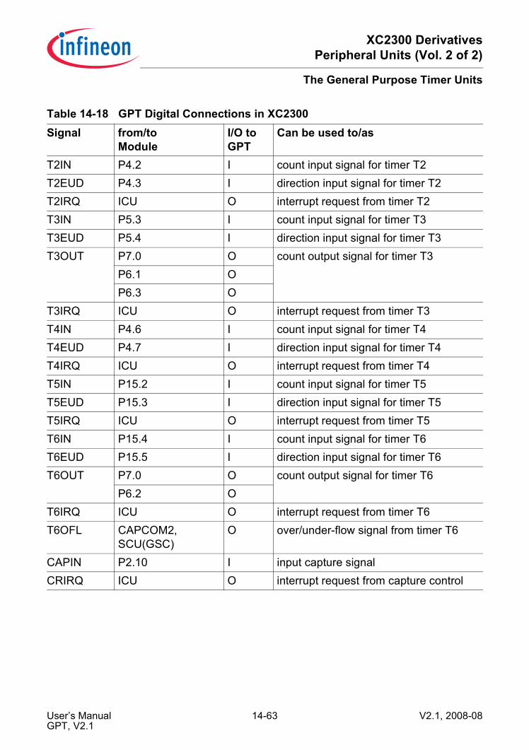
XC2300 DerivativesPeripheral Units (Vol. 2 of 2)
The General Purpose Timer Units
Table 14-18 GPT Digital Connections in XC2300Signal from/to
ModuleI/O to GPT
Can be used to/as
T2IN P4.2 I count input signal for timer T2T2EUD P4.3 I direction input signal for timer T2T2IRQ ICU O interrupt request from timer T2T3IN P5.3 I count input signal for timer T3T3EUD P5.4 I direction input signal for timer T3T3OUT P7.0 O count output signal for timer T3
P6.1 OP6.3 O
T3IRQ ICU O interrupt request from timer T3T4IN P4.6 I count input signal for timer T4T4EUD P4.7 I direction input signal for timer T4T4IRQ ICU O interrupt request from timer T4T5IN P15.2 I count input signal for timer T5T5EUD P15.3 I direction input signal for timer T5T5IRQ ICU O interrupt request from timer T5T6IN P15.4 I count input signal for timer T6T6EUD P15.5 I direction input signal for timer T6T6OUT P7.0 O count output signal for timer T6
P6.2 OT6IRQ ICU O interrupt request from timer T6T6OFL CAPCOM2,
SCU(GSC)O over/under-flow signal from timer T6
CAPIN P2.10 I input capture signalCRIRQ ICU O interrupt request from capture control
User’s Manual 14-63 V2.1, 2008-08GPT, V2.1

XC2300 DerivativesPeripheral Units (Vol. 2 of 2)
Real Time Clock
15 Real Time Clock The Real Time Clock (RTC) module of the XC2300 basically consists of a chain ofprescalers and timers. Its count clock is derived from the auxiliary oscillator or from theprescaled main oscillator. The RTC serves various purposes:• 48-bit timer for long term measurements• System clock to determine the current time and date
(the RTC’s structure supports the direct representation of time and date)• Cyclic time based interrupt (can be generated by any timer of the chain)A number of programming options as well as interrupt request signals adjust theoperation of the RTC to the application’s requirements. The RTC can continue itsoperation while the XC2300 is in certain power-saving modes, such that real time dateand time information is provided.
Figure 15-1 SFRs Associated with the RTC Module
The RTC module consists of a chain of 3 divider blocks:• a selectable 8:1 divider (on - off)• the reloadable 16-bit timer T14• the 32-bit RTC timer block (accessible via RTC_RTCH and RTC_RTCL), made of:
– the reloadable 10-bit timer CNT0– the reloadable 6-bit timer CNT1– the reloadable 6-bit timer CNT2– the reloadable 10-bit timer CNT3
All timers count upwards. Each of the five timers can generate an interrupt request. Allrequests are combined to a common node request.Note: The RTC registers are only affected by a power reset in order to maintain the
correct system time even when system or application resets are executed.
mc_rtcregx2k.vsd
Data Registers Counter Registers
RTC_T14 E
Interrupt Control
RTC_CON Real Time Clock Control RegisterRTCCLKCON RTC Clock Control RegisterRTC_ISNC Interrupt Subnode Control Reg.RTC_IC RTC Interrupt Control RegisterRTC_KSCCFG Kernel State Configuration Reg.
RTC_T14REL E
RTC_RELH E
RTC_ISNC E
RTC_IC E
RTC_RELL E T2CONRTC_RTCL E
RTC_RTCH E
Control Registers
RTC_CON E
RTCCLKCON
RTC_T14 Timer T14 Count RegisterRTC_T14REL Timer T14 Reload RegisterRTC_RTCH/L RTC Count Registers, High/LowRTC_RELH/L RTC Reload Registers High/Low
RTC_KSCCFG E
User’s Manual 15-1 V2.1, 2008-08RTC_X8, V2.2

XC2300 DerivativesPeripheral Units (Vol. 2 of 2)
Real Time Clock
15.1 Defining the RTC Time BaseThe timer chain of the RTC is clocked with the count clock signal fRTC which is derivedfrom internal sources (oscillators or PLL) or external sources (pins). The currently activeclock source is selected by bitfield RTCCLKSEL in register RTCCLKCON. Optionallyprescaled by a factor of 32 and/or 8, this is the basic RTC clock. Depending on theoperating mode, timer T14 may provide the count increments used by the applicationand thus determine the input frequency of the RTC timer, that is, the RTC time base (seealso Table 15-2).The RTC is also supplied with the system clock fSYS of the XC2300. This clock signal isused to control the RTC’s logic blocks and its bus interface. To synchronize properly tothe count clock, the system clock must run at least four times faster than the count clock,this means fSYS ≥ 4 × fCNT.
Figure 15-2 RTC Clock Supply Block Diagram
For an example, Table 15-1 lists the interrupt period range and the T14 reload values(for a time base of 1 s and 1 ms):
Table 15-1 RTC Time Base ExamplesOscillator Frequency
T14 Intr. Period Reload Value A Reload Value BMin. Max. T14REL Base T14REL Base
32.768 kHz 30.52 µs 16.0 s 8000H/F000H 1.000 s FFDFH/ FFFCH
1.007 ms/ 0.977 ms
MC_RTCCLOCK_XX
8:1 MUX
PRE
fCNT RTCCountClock
1
0
fSYS
fRTC
RUN
MUX RTCModuleClock
RTCCM
1
0Sync Mode
Async Mode
32:1 MUX0
1
REFCLK
User’s Manual 15-2 V2.1, 2008-08RTC_X8, V2.2
XC2300 DerivativesPeripheral Units (Vol. 2 of 2)
Real Time Clock
Note: Select one value from the reload value pairs, depending if the 8:1 prescaler isdisabled/enabled.
Asynchronous OperationWhen the system clock frequency becomes lower than 4 × fCNT proper synchronizationis not possible and count events may be missed. This can be the case, when the XC2300reduces the system frequency to save power consumption.In these cases the RTC can be switched to Asynchronous Mode (by clearing bit RTCCMin register RTCCLKCON). In this mode the count registers are directly controlled by thecount clock independent of the system clock (hence the name). Asynchronous operationensures correct time-keeping even during power-save modes.However, as no synchronization between the count registers and the bus interface canbe maintained in asynchronous mode, the RTC registers cannot be written. Readaccesses may interfere with count events and, therefore, must be verified (e.g. byreading the same value with three consecutive read accesses).Note: The access restrictions in asynchronous mode are only meaningful if the system
clock is not switched off, of course.
Switching Clocking ModesThe clocking mode of the RTC (synchronous or asynchronous) is selected via bitRTCCM in register RTCCLKCON. After reset, the RTC operates in Synchronous Mode(RTCCM = 1).The selected clocking mode also affects the access to RTC registers. Bit ACCPOS inregister RTC_CON indicates if full register access is possible (ACCPOS = 1, defaultafter reset) or not (ACCPOS = 0). This also indicates the current clocking mode.Attention: Software should poll bit ACCPOS to determine the proper transition to
the intended clocking mode.
After switching to Asynchronous Mode (RTCCM = 0), bit ACCPOS = 0 indicates properoperation in Asynchronous Mode. In this case the system clock can be stopped orreduced.Note: The clock source for asynchr. mode operation must be selected before switching
to asynchr. mode and must only be changed in synchronous mode.
After switching to Synchronous Mode, (RTCCM = 1), bit ACCPOS = 1 indicates properoperation in Synchronous Mode. In this case the RTC registers can again be accessedproperly (read and write).Note: The RTC might lose a counting event (edge of fCNT) when switching from
synchronous mode to asynchronous mode while the 8:1 prescaler is disabled. Forthese applications it is, therefore, recommended to set up the RTC with the 8:1prescaler enabled.
User’s Manual 15-3 V2.1, 2008-08RTC_X8, V2.2
XC2300 DerivativesPeripheral Units (Vol. 2 of 2)
Real Time Clock
Increased RTC Accuracy through Software CorrectionThe accuracy of the XC2300’s RTC is determined by the oscillator frequency and by therespective prescaling factor (excluding or including T14 and the 8:1 prescaler). Theaccuracy limit generated by the prescaler is due to the quantization of a binary counter(where the average is zero), while the accuracy limit generated by the oscillatorfrequency is due to the difference between the ideal and real frequencies (and thereforeaccumulates over time). This effect is predictable and can be compensated. The totalaccuracy of the RTC can be further increased via software for specific applications thatdemand a high time accuracy.The key to the improved accuracy is knowledge of the exact oscillator frequency. Therelation of this frequency to the expected ideal frequency is a measure of the RTC’sdeviation. The number of cycles, N, after which this deviation causes an error of ±1 cyclecan be easily computed. So, the only action is to correct the count by ±1 after each seriesof N cycles. The correction may be made cyclically, for instance, within an interruptservice routine, or by evaluating a formula when the RTC registers are read (for this therespective “last” RTC value must be available somewhere).Note: For the majority of applications, however, the standard accuracy provided by the
RTC’s structure will be more than sufficient.
Adjusting the current RTC value would require reading and then writing the complete48-bit value. This can only be accomplished by three successive accesses each. Toavoid the hassle of reading/writing multi-word values, the RTC incorporates a correctionoption to simply add or suppress one count pulse.This is done by setting bit T14INC or T14DEC, respectively, in register RTC_CON. Thiswill add an extra count pulse (T14INC) upon the next count event, or suppress the nextcount event (T14DEC). The respective bit remains set until its associated action hasbeen performed and is automatically cleared by hardware after this event.Note: Setting both bits, T14INC and T14DEC, at the same time will have no effect on the
count values.
User’s Manual 15-4 V2.1, 2008-08RTC_X8, V2.2
XC2300 DerivativesPeripheral Units (Vol. 2 of 2)
Real Time Clock
15.2 RTC Run ControlIf the RTC shall operate bit RUN in register RTC_CON must be set (default after reset).Bit RUN can be cleared, for example, to exclude certain operation phases from timekeeping.Note: A valid count clock fRTC is required for proper RTC operation, of course.
The RTC is reset by a power reset, a system/application reset does not affect the RTCregisters and its operation (RTC_IC will be reset, however). The initialization softwaremust ensure the proper RTC operating mode.
Initialization and Disabling of the RTCUpon a Power-on Reset, register RTC_CON adopts its reset value of 8003H, whichenables the RTC and both prescalers (factor = 8 × 32 = 256).The RTC’s clocking mode (synchronous/asynchronous) is selected bit RTCCM inregister RTCCLKCON. Upon a Power-on Reset, register RTCCLKCON adopts its resetvalue of 0006H, which selects synchronous operation mode and the WUT as the clocksource.For an application reset that is followed by an initialization of the RTC module, thefollowing steps are recommended:• select synchronous RTC clocking mode, i.e. set bit RTCCLKCON.RTCCM• select the intended (running) clock source• make sure that bit ACCPOS is set, before writing to RTC registers• initialize the RTCWhen the RTC module is not used and shall be disabled after a Power-on Reset, thefollowing steps are recommended:• stop the RTC by clearing its run bit RTC_CON.RUN• disable the RTC module by clearing its enable bit RTC_KSCCFG.MODEN.When the RTC module operates in asynchronous mode and shall stop in a power savingmode, software must make sure that no active clock signal is selected by the RTC clockmultiplexer.
User’s Manual 15-5 V2.1, 2008-08RTC_X8, V2.2

XC2300 DerivativesPeripheral Units (Vol. 2 of 2)
Real Time Clock
The RTC control register RTC_CON selects the basic operation of the RTC module.
RTC_CON Control Register ESFR (F110H/88H) Reset Value: 8003H
15 14 13 12 11 10 9 8 7 6 5 4 3 2 1 0
ACC POS - - - - - - - - - - REF
CLKT14 INC
T14 DEC PRE RUN
rh - - - - - - - - - - rw rwh rwh rw rw
Field Bits Type DescriptionACCPOS 15 rh RTC Register Access Possible
0 No write access is possible, only asynchronous reads
1 Registers can be read and writtenREFCLK 4 rw RTC Input Source Prescaler (32:1) Disable
0 Input Prescaler enabled1 Input Prescaler disabled
T14INC 3 rwh Increment Timer T14 ValueSetting this bit to 1 adds one count pulse upon the next count event, thus incrementing T14.This bit is cleared by hardware after incrementation.
T14DEC 2 rwh Decrement Timer T14 ValueSetting this bit to 1 suppresses the next count event, thus decrementing T14.This bit is cleared by hardware after decrementation.
PRE 1 rw RTC Input Source Prescaler (8:1) Enable0 Prescaler disabled1 Prescaler enabled
RUN 0 rw RTC Run Bit0 RTC stopped1 RTC runs
User’s Manual 15-6 V2.1, 2008-08RTC_X8, V2.2
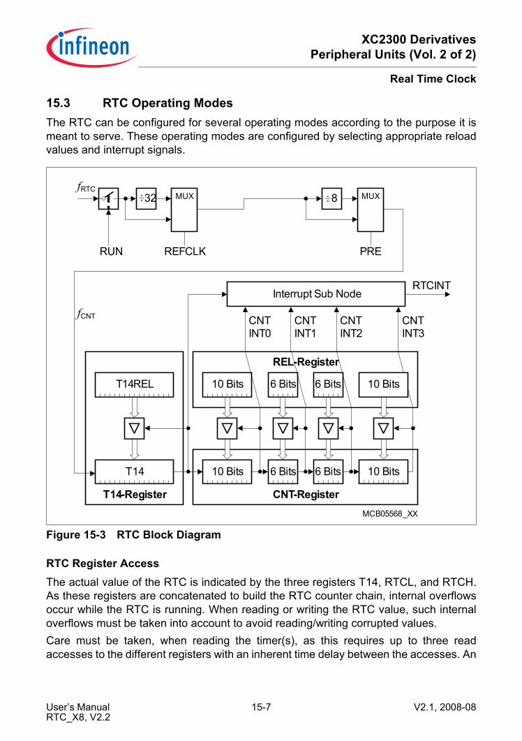
XC2300 DerivativesPeripheral Units (Vol. 2 of 2)
Real Time Clock
15.3 RTC Operating ModesThe RTC can be configured for several operating modes according to the purpose it ismeant to serve. These operating modes are configured by selecting appropriate reloadvalues and interrupt signals.
Figure 15-3 RTC Block Diagram
RTC Register AccessThe actual value of the RTC is indicated by the three registers T14, RTCL, and RTCH.As these registers are concatenated to build the RTC counter chain, internal overflowsoccur while the RTC is running. When reading or writing the RTC value, such internaloverflows must be taken into account to avoid reading/writing corrupted values.Care must be taken, when reading the timer(s), as this requires up to three readaccesses to the different registers with an inherent time delay between the accesses. An
CNT-Register
REL-Register
10 Bits6 Bits6 Bits10 BitsT14
MCB05568_XX
T14-Register
Interrupt Sub NodeRTCINT
MUX32
PRERUN
CNTINT3
CNTINT2
CNTINT1
CNTINT0
fCNT
fRTC
T14REL 6 Bits6 Bits10 Bits
: MUX 8:
REFCLK
10 Bits
User’s Manual 15-7 V2.1, 2008-08RTC_X8, V2.2
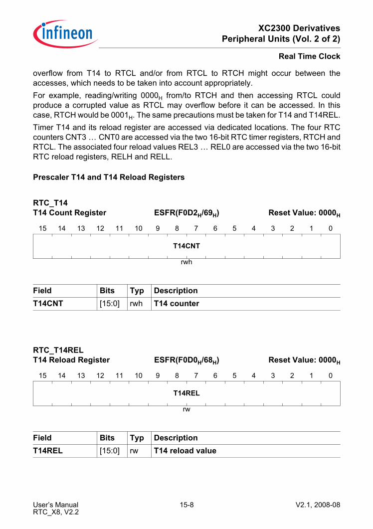
XC2300 DerivativesPeripheral Units (Vol. 2 of 2)
Real Time Clock
overflow from T14 to RTCL and/or from RTCL to RTCH might occur between theaccesses, which needs to be taken into account appropriately.For example, reading/writing 0000H from/to RTCH and then accessing RTCL couldproduce a corrupted value as RTCL may overflow before it can be accessed. In thiscase, RTCH would be 0001H. The same precautions must be taken for T14 and T14REL.Timer T14 and its reload register are accessed via dedicated locations. The four RTCcounters CNT3 … CNT0 are accessed via the two 16-bit RTC timer registers, RTCH andRTCL. The associated four reload values REL3 … REL0 are accessed via the two 16-bitRTC reload registers, RELH and RELL.
Prescaler T14 and T14 Reload Registers
RTC_T14 T14 Count Register ESFR(F0D2H/69H) Reset Value: 0000H
15 14 13 12 11 10 9 8 7 6 5 4 3 2 1 0
T14CNT
rwh
Field Bits Typ DescriptionT14CNT [15:0] rwh T14 counter
RTC_T14REL T14 Reload Register ESFR(F0D0H/68H) Reset Value: 0000H
15 14 13 12 11 10 9 8 7 6 5 4 3 2 1 0
T14REL
rw
Field Bits Typ DescriptionT14REL [15:0] rw T14 reload value
User’s Manual 15-8 V2.1, 2008-08RTC_X8, V2.2

XC2300 DerivativesPeripheral Units (Vol. 2 of 2)
Real Time Clock
RTC_RTCH RTC Timer High Register ESFR (F0D6H/6BH) Reset Value: 0000H
15 14 13 12 11 10 9 8 7 6 5 4 3 2 1 0
CNT3 CNT2
rwh rwh
Field Bits Type DescriptionCNTx(x = 3 … 2)
[15:6], [5:0]
rwh RTC Timer Count Section CNTxAn overflow of bitfield CNT2 triggers a count pulse to count section CNT3 followed by a reload of CNT2 from bitfield REL2.In addition, an interrupt request is triggered.
RTC_RTCLRTC Timer Low Register ESFR (F0D4H/6AH) Reset Value: 0000H
15 14 13 12 11 10 9 8 7 6 5 4 3 2 1 0
CNT1 CNT0
rwh rwh
Field Bits Type DescriptionCNTx(x = 1 … 0)
[15:10], [9:0]
rwh RTC Timer Count Section CNTxAn overflow of bitfield CNTx triggers a count pulse to the next count section CNTx+1 followed by a reload of CNTx from bitfield RELx.In addition, an interrupt request is triggered.
User’s Manual 15-9 V2.1, 2008-08RTC_X8, V2.2

XC2300 DerivativesPeripheral Units (Vol. 2 of 2)
Real Time Clock
Note: The registers of the RTC receive their reset values only upon a power reset.
RTC_RELH RTC Reload High Register ESFR (F0CEH/67H) Reset Value: 0000H
15 14 13 12 11 10 9 8 7 6 5 4 3 2 1 0
REL3 REL2
rw rw
Field Bits Type DescriptionRELx(x = 3 … 2)
[15:6], [5:0]
rw RTC Reload Value RELxThis bitfield is copied to bitfield CNTx upon an overflow of count section CNTx.
RTC_RELLRTC Reload Low Register ESFR (F0CCH/66H) Reset Value: 0000H
15 14 13 12 11 10 9 8 7 6 5 4 3 2 1 0
REL1 REL0
rw rw
Field Bits Type DescriptionRELx(x = 1 … 0)
[15:10], [9:0]
rw RTC Reload Value RELxThis bitfield is copied to bitfield CNTx upon an overflow of count section CNTx.
User’s Manual 15-10 V2.1, 2008-08RTC_X8, V2.2

XC2300 DerivativesPeripheral Units (Vol. 2 of 2)
Real Time Clock
15.4 48-bit Timer OperationThe concatenation of timers T14 and COUNT0 … COUNT3 can be regarded as a 48-bittimer which is clocked with the RTC input frequency, optionally divided by the prescaler.The reload registers T14REL, RELL, and RELH must be cleared to produce a true binary48-bit timer. However, any other reload value may be used. Reload values other thanzero must be used carefully, due to the individual sections of the RTC timer with theirown individual overflows and reload values.The maximum usable timespan is 248 (≈ 1014) T14 input clocks. Assuming no prescaler,this would equal more than 200 years at a count frequency of 32 kHz.
15.5 System Clock OperationA real time system clock can be maintained that keeps on running also during powersaving modes (optionally) that maintain a suitable clock signal and supply voltage andindicates the current time and date. This is possible because the RTC module is onlyreset and cleared by a power reset.The resolution for this clock information is determined by the input clock of timer T14. Byselecting appropriate reload values each cascaded timer can represent directly a part ofthe current time and/or date. Due to its width, T14 can adjust the RTC to the intendedrange of operation (time or date). The maximum usable timespan is achieved whenT14REL is loaded with 0000H and so T14 divides by 216.
System Clock ExampleThe RTC count clock is 32.768 kHz. By selecting appropriate reload values the RTCtimers directly indicate the current time (see Figure 15-4 and Table 15-2).
Figure 15-4 RTC Configuration Example
Note: This setup can generate an interrupt request every millisecond, every second,every minute, every hour, or every day.
MCA05414
Hours
REL3
3E8H
CNT3
Minutes
REL2
04H
CNT2
Seconds
REL1
04H
CNT1
1/1000Seconds
REL0
018H
CNT0
Prescaler
T14REL
FFDFH
T14
fCNT =32.768 kHz
User’s Manual 15-11 V2.1, 2008-08RTC_X8, V2.2

XC2300 DerivativesPeripheral Units (Vol. 2 of 2)
Real Time Clock
Each timer in the chain divides the clock by (2<timer_width> - <reload_value>) : 1, as thetimers count up. Table 15-2 shows the reload values which must be chosen for a specificscenario (i.e. operating mode of the RTC).
15.6 Cyclic Interrupt GenerationThe RTC module can generate an interrupt request whenever one of the timersoverflows and is reloaded. This interrupt request may be used, for example, to providea system time tick independent of the CPU frequency without loading the generalpurpose timers. The interrupt cycle time can be adjusted by choosing appropriate reloadvalues and by enabling the appropriate interrupt request.In this mode, the other operating modes can be combined. For example, a reload valueof T14REL = F9C0H (216 - 1600) generates a T14 interrupt request every 50 ms. Still thesubsequent timers can be configured to represent the time or build a binary counter,however with a different time base.
Table 15-2 Reload Value ScenariosREL3 REL2 REL1 REL0 T14REL
Tim
e of
Day
(Fig
ure
15-4
) Formula 210 - 24 26 - 60 26 - 60 210 - 1000 216 - 33Rel. Value 3E8H 04H 04H 018H FFDFH
Function h m s 1/1000 s PrescalerIntr. Period day hour minute second millisec.1)
1) T14 errors in the first example (ms) can be compensated either by choosing an adapted value for REL0, or byusing software correction.
Day
of t
heW
eek
Formula 210 - 7 26 - 24 26 - 60 210 - 60 216 - 32768Rel. Value 3F9H 28H 04H 3C4H 8000H
Function day h m s PrescalerIntr. Period week day hour minute second
User’s Manual 15-12 V2.1, 2008-08RTC_X8, V2.2

XC2300 DerivativesPeripheral Units (Vol. 2 of 2)
Real Time Clock
15.7 RTC Interrupt Generation The overflow signals of each timer of the RTC timer chain can generate an interruptrequest. The RTC’s interrupt subnode control register ISNC combines these requests toactivate the common RTC interrupt request line RTC_IRQ.Each timer overflow sets its associated request flag in register ISNC. Individual enablebits for each request flag determine whether this request also activates the commoninterrupt line. The enabled requests are ORed together on this line (see Figure 15-5).The common interrupt request signal is delayed by 2 system clock cycles due tosynchronization.The interrupt handler can determine the source of an interrupt request via the specificrequest flags and must clear them after appropriate processing (not cleared byhardware). The common node request bit is automatically cleared when the interrupthandler is vectored to.Note: If only one source is enabled, no additional software check is required, of course.
Both the individual request and the common interrupt node must be enabled.
Figure 15-5 Interrupt Block Diagram
MCB05415
>1_Interrupt RequestRTC_IRQ
&
&
&
&
&
Register RTC_ISNC
CNT3IR
CNT3IE
Set
SW Clear
CNT2IR
CNT2IE
Set
SW Clear
CNT1IR
CNT1IE
Set
SW Clear
CNT0IR
CNT0IE
Set
SW Clear
T14IR
T14IE
Set
SW Clear
CNT3 Overflow
CNT2 Overflow
CNT1 Overflow
CNT0 Overflow
T14 Overflow
User’s Manual 15-13 V2.1, 2008-08RTC_X8, V2.2
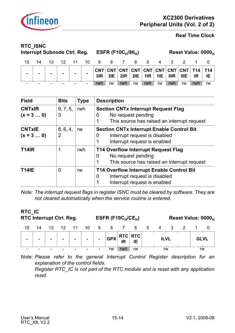
XC2300 DerivativesPeripheral Units (Vol. 2 of 2)
Real Time Clock
Note: The interrupt request flags in register ISNC must be cleared by software. They arenot cleared automatically when the service routine is entered.
Note: Please refer to the general Interrupt Control Register description for anexplanation of the control fields.Register RTC_IC is not part of the RTC module and is reset with any applicationreset.
RTC_ISNC Interrupt Subnode Ctrl. Reg. ESFR (F10CH/86H) Reset Value: 0000H
15 14 13 12 11 10 9 8 7 6 5 4 3 2 1 0
- - - - - - CNT3IR
CNT3IE
CNT2IR
CNT2IE
CNT1IR
CNT1IE
CNT0IR
CNT0IE
T14 IR
T14 IE
- - - - - - rwh rw rwh rw rwh rw rwh rw rwh rw
Field Bits Type DescriptionCNTxIR(x = 3 … 0)
9, 7, 5, 3
rwh Section CNTx Interrupt Request Flag0 No request pending1 This source has raised an interrupt request
CNTxIE(x = 3 … 0)
8, 6, 4, 2
rw Section CNTx Interrupt Enable Control Bit0 Interrupt request is disabled1 Interrupt request is enabled
T14IR 1 rwh T14 Overflow Interrupt Request Flag0 No request pending1 This source has raised an interrupt request
T14IE 0 rw T14 Overflow Interrupt Enable Control Bit0 Interrupt request is disabled1 Interrupt request is enabled
RTC_IC RTC Interrupt Ctrl. Reg. ESFR (F19CH/CEH) Reset Value: 0000H
15 14 13 12 11 10 9 8 7 6 5 4 3 2 1 0
- - - - - - - GPX RTCIR
RTCIE ILVL GLVL
- - - - - - - rw rwh rw rw rw
User’s Manual 15-14 V2.1, 2008-08RTC_X8, V2.2

XC2300 DerivativesPeripheral Units (Vol. 2 of 2)
Real Time Clock
15.8 Miscellaneous Registers
RTC_KSCCFG Kernel State Configuration Register
ESFR (F010H) Reset Value: 0001H
15 14 13 12 11 10 9 8 7 6 5 4 3 2 1 0
BPCOM 0 COMCFG BP
SUM 0 SUMCFG BPNOM 0 NOMCFG 0
BPMODEN
MODEN
w r rw w r rw w r rw r w rw
Field Bits Type DescriptionMODEN 0 rw Module Enable
This bit enables the module kernel clock and the module functionality.0B The module is switched off.
It does not react on mode control actions and the module clock is switched off immediately (without stop condition). The module does not react on read accesses and ignores write accesses.
1B The module is switched on and can operate. After writing 1 to MODEN, it is recommended to read register KSCCFG to avoid pipeline effects in the control block before accessing other RTC registers.
Note: This bit is reset by an application reset.BPMODEN 1 w Bit Protection for MODEN
This bit enables the write access to the bit MODEN. It always reads 0. It is only active during the write access cycle.0B MODEN is not changed.1B MODEN is updated with the written value.Note: This bit is reset by an application reset.
User’s Manual 15-15 V2.1, 2008-08RTC_X8, V2.2

XC2300 DerivativesPeripheral Units (Vol. 2 of 2)
Real Time Clock
NOMCFG [5:4] rw Normal Operation Mode ConfigurationThis bit field defines the kernel mode applied in normal operation mode.0XB The module is switched on.1XB The module is switched off.This field is taken into account for CR = 00 or 11.Note: This bit is reset by an application reset.
BPNOM 7 w Bit Protection for NOMCFGThis bit enables the write access to the bit field NOMCFG. It always reads 0. It is only active during the write access cycle.0B NOMCFG is not changed.1B NOMCFG is updated with the written value.Note: This bit is reset by an application reset.
SUMCFG [9:8] rw Suspend Mode ConfigurationThis bit field defines the kernel mode applied in suspend mode.0XB The module is switched on.1XB The module is switched off.This field is taken into account for CR = 01.Note: This bit is reset by a debug reset.
BPSUM 11 w Bit Protection for SUMCFGThis bit enables the write access to the bit field SUMCFG. It always reads 0. It is only active during the write access cycle.0B SUMCFG is not changed.1B SUMCFG is updated with the written value.Note: This bit is reset by a debug reset.
COMCFG [13:12] rw Clock Off Mode ConfigurationThis bit field defines the kernel mode applied in clock off mode.0XB The module is switched on.1XB The module is switched off.This field is taken into account for CR = 10.Note: This bit is reset by an application reset.
Field Bits Type Description
User’s Manual 15-16 V2.1, 2008-08RTC_X8, V2.2
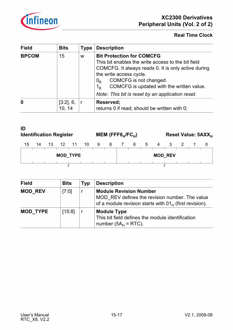
XC2300 DerivativesPeripheral Units (Vol. 2 of 2)
Real Time Clock
BPCOM 15 w Bit Protection for COMCFGThis bit enables the write access to the bit field COMCFG. It always reads 0. It is only active during the write access cycle.0B COMCFG is not changed.1B COMCFG is updated with the written value.Note: This bit is reset by an application reset.
0 [3:2], 6, 10, 14
r Reserved;returns 0 if read; should be written with 0;
IDIdentification Register MEM (FFF8H/FCH) Reset Value: 5AXXH
15 14 13 12 11 10 9 8 7 6 5 4 3 2 1 0
MOD_TYPE MOD_REV
r r
Field Bits Typ DescriptionMOD_REV [7:0] r Module Revision Number
MOD_REV defines the revision number. The value of a module revision starts with 01H (first revision).
MOD_TYPE [15:8] r Module TypeThis bit field defines the module identification number (5AH = RTC).
Field Bits Type Description
User’s Manual 15-17 V2.1, 2008-08RTC_X8, V2.2

XC2300 DerivativesPeripheral Units (Vol. 2 of 2)
Analog to Digital Converter
16 Analog to Digital ConverterThe Analog to Digital Converter module (ADC) of the XC2300 allows the conversion ofanalog input values into discrete digital values based on the successive approximationmethod. With this method, the conversion result is elaborated bit by bit, starting with themost significant bit. An analog to digital conversion requires a certain number of clockcycles (see Section 16.1.4 and the respective Data Sheet).This chapter is structured as follows:• Introduction (see Section 16.1)• Operating the ADC (see Section 16.2)• Module implementation in XC2300 (see Section 16.3)
16.1 IntroductionThis section gives an overview about the feature set of the ADC module and introducesthe general structure. It describes the:• ADC block diagram with two kernels (see Section 16.1.1)• Feature set description (see Section 16.1.2)• Abbreviations (see Section 16.1.3)• Kernel overview (see Section 16.1.4)• Conversion request handling (see Section 16.1.5)• Conversion result handling (see Section 16.1.6)• Interrupt structure (see Section 16.1.7)• Electrical models (see Section 16.1.8)• Transfer characteristics and error definitions (see Section 16.1.9)
User’s Manual 16-1 V2.1, 2008-08ADC, UM_V0.1D6

XC2300 DerivativesPeripheral Units (Vol. 2 of 2)
Analog to Digital Converter
16.1.1 ADC Block DiagramThe ADC module contains 2 independent kernels (ADC0, ADC1) that can operateautonomously or can be synchronized to each other. An ADC kernel is a unit used toconvert an analog input signal into a digital value and provides means for triggeringconversions, data handling and storage.With this structure, parallel conversion of up to two analog input channels is supported.
Figure 16-1 ADC Module Block Diagram
ADC kernel 1
ADC_2_kernels
ADconverter
conversioncontrol
ADC kernel 0
...analoginputs
data (result)handling
requestcontrol
businter-face
ADconverter
conversioncontrol
... data (result)handling
requestcontrol
analoginputs
User’s Manual 16-2 V2.1, 2008-08ADC, UM_V0.1D6

XC2300 DerivativesPeripheral Units (Vol. 2 of 2)
Analog to Digital Converter
16.1.2 Feature SetFeatures of each ADC kernel:• Analog supply voltage range from 3.3 V (minimum) to 5 V (nominal) for VDDPA• Input voltage range from 0 V to analog supply voltage VDDPA• Input multiplexer for a maximum of 16 possible analog input channels• 10-bit conversion time less than 1 µs• One standard reference input (VAREF) and one alternative reference input (CH0)
available• 3 conversion request sources for external or timer-driven events, auto-scan,
programmable sequences, SW-driven conversions, etc.• Synchronization of the ADC kernels for concurrent conversion starts and parallel
sampling and measuring of analog input signals, e.g. for phase currentmeasurements in AC drives
• Control capability for an external analog multiplexer, respecting the additional set uptime
• Adjustable sampling times to accommodate output impedance of different analogsignal sources (sensors, etc.)
• Possibility to cancel running conversions on demand with automatic restart• Flexible interrupt generation (possibility of PEC support)• Limit checking to reduce interrupt load (e.g. for temperature measurements or
overload detection, only values outside programmable boundary values lead to aninterrupt)
• Programmable data reduction filter, e.g. for digital anti-aliasing filtering, by adding aprogrammable number of conversion results
• Independent result registers (8 independent registers)• Support of conversion result FIFO mechanism to allow a longer interrupt latency• Support of suspend and power saving modes• Individually programmable reference selection for each channel, e.g. to allow
measurements of 3.3 V and 5 V signals in the full measurement range with the sameADC kernel
User’s Manual 16-3 V2.1, 2008-08ADC, UM_V0.1D6
XC2300 DerivativesPeripheral Units (Vol. 2 of 2)
Analog to Digital Converter
16.1.3 AbbreviationsThe following acronyms and terms are used in the ADC chapter:
Table 16-1 Abbreviations in ADC chapter
Abbreviation Meaning
ADC Analog to digital converter
DNL Differential non-linearity error
FIFO First-in-first-out data buffer mechanism
INL Integral non-linearity error
LSBn Finest granularity of the analog value in digital format, represented by one least significant bit of the conversion result with n bits resolution (measurement range divided in 2n equally distributed steps)
PEC Peripheral Event Controller
SCU System Control Unit of the device
TUE Total unadjusted error
User’s Manual 16-4 V2.1, 2008-08ADC, UM_V0.1D6
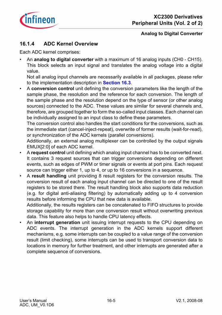
XC2300 DerivativesPeripheral Units (Vol. 2 of 2)
Analog to Digital Converter
16.1.4 ADC Kernel OverviewEach ADC kernel comprises:• An analog to digital converter with a maximum of 16 analog inputs (CH0 - CH15).
This block selects an input signal and translates the analog voltage into a digitalvalue.Not all analog input channels are necessarily available in all packages, please referto the implementation description in Section 16.3.
• A conversion control unit defining the conversion parameters like the length of thesample phase, the resolution and the reference for each conversion. The length ofthe sample phase and the resolution depend on the type of sensor (or other analogsources) connected to the ADC. These values are similar for several channels and,therefore, are grouped together to form the so-called input classes. Each channel canbe individually assigned to an input class to define these parameters.The conversion control also handles the start conditions for the conversions, such asthe immediate start (cancel-inject-repeat), overwrite of former results (wait-for-read),or synchronization of the ADC kernels (parallel conversions).Additionally, an external analog multiplexer can be controlled by the output signalsEMUX[2:0] of each ADC kernel.
• A request control unit defining which analog input channel has to be converted next.It contains 3 request sources that can trigger conversions depending on differentevents, such as edges of PWM or timer signals or events at port pins. Each requestsource can trigger either 1, up to 4, or up to 16 conversions in a sequence.
• A result handling unit providing 8 result registers for the conversion results. Theconversion result of each analog input channel can be directed to one of the resultregisters to be stored there. The result handling block also supports data reduction(e.g. for digital anti-aliasing filtering) by automatically adding up to 4 conversionresults before informing the CPU that new data is available.Additionally, the results registers can be concatenated to FIFO structures to providestorage capability for more than one conversion result without overwriting previousdata. This feature also helps to handle CPU latency effects.
• An interrupt generation unit issuing interrupt requests to the CPU depending onADC events. The interrupt generation in the ADC kernels support differentmechanisms, e.g. some interrupts can be coupled to a value range of the conversionresult (limit checking), some interrupts can be used to transport conversion data tolocations in memory for further treatment, and other interrupts are generated after acomplete sequence of conversions.
User’s Manual 16-5 V2.1, 2008-08ADC, UM_V0.1D6
XC2300 DerivativesPeripheral Units (Vol. 2 of 2)
Analog to Digital Converter
Figure 16-2 ADC Kernel Block Diagram
The time required for a conversion depends on the result width and on the selectedsample time. Both values depend on the configured ADC clock frequency, of course.Conversion time tCN = ((N + 1) × tADCI) + ((2 + STC) × tADCI) + 2 × tADC, whereN = number of result bits (10/8), STC = additional sample time (see also Section 16.2.4).
ADC_kernel _overv
ADconverter
conversioncontrol
resulthandling
requestcontrol
interruptgeneration
ADC kernel
...
analog inputchannel CH0
analog inputchannel CH15
standard analogreference VAREF
analog referenceground VAGND
external multi-plexer control
EMUX[2:0]
User’s Manual 16-6 V2.1, 2008-08ADC, UM_V0.1D6

XC2300 DerivativesPeripheral Units (Vol. 2 of 2)
Analog to Digital Converter
16.1.5 Conversion Request UnitThe conversion request unit of each ADC kernel autonomously handles the generationof conversion requests.It contains three independent request sources that are connected to several modules totrigger the start of a conversion. A request source defines the analog input channel to beconverted if a defined event occurs. For example, a trigger pulse from a timer unitgenerating a PWM signal can start the conversion of a single input channel or aprogrammed sequence of input channels.Depending on the application, the request sources can be triggered by different events,either issued by other modules or under SW control. As a consequence, there can betwo or more conversion requests pending at the same time. To allow the user to adaptthe request source mechanism to the application needs, the trigger capability, thechannel number(s) to be converted, and the priority can be individually programmed foreach request source.An arbiter block regularly scans the request sources for pending conversion requestsand acts upon the conversion request with the highest priority. This conversion requestis forwarded to the converter to start the conversion of the requested channel.
Figure 16-3 Conversion Request Unit
The functional characteristics of the request sources are adapted to the most commonapplication requirements. In all request sources, a continuous operation or a single-shotoperation can be selected. For continuous operation, the programmed sequence ofconversions requests are continuously issued (once started), whereas in single-shotmode, each sequence of conversion requests has to be explicitly started. The trigger fora conversion request or a sequence can be handled under SW control or can be
ADC_request_handling
request control
requestsource 1(16-ch scan)
requestsource 2
(4-stage queue)
requestsourcearbiter
timerunit(s)
externalrequest(s)
analog part
requestsource 0
(1-stage queue)
ADC kernel
User’s Manual 16-7 V2.1, 2008-08ADC, UM_V0.1D6

XC2300 DerivativesPeripheral Units (Vol. 2 of 2)
Analog to Digital Converter
synchronized to ADC-external events, such as timer signals or port pins. For eachrequest source, the user can select an input signal (from 4 possible signalsREQTRx[D:A]) as trigger input REQTRx and an input signal (from 4 possible signalsREQGTx[D:A]) as gating input REQGTx.• Request source 0 (1-stage sequential source) can issue a conversion request for a
single input channel. The channel number can directly be programmed.This mechanism could be used for SW-controlled conversion requests or HW-triggered conversions of a single input channel. If programmed with a high priority, itcan interrupt the sequences of the other request sources to inject a singleconversion.
• Request source 1 (16-channel scan source) can issue conversion requests for asequence of up to 16 input channels. It can be programmed which channel takes partin this sequence. The sequence always starts with the highest enabled channelnumber and continues towards lower channel numbers (order defined by the channelnumber, each channel can be converted only once per sequence).This mechanism could be used to scan input channels permanently or on a regulartime base. For example, if programmed with a low priority, some input channels canbe scanned in a background task to update information that is not time-critical.
• Request source 2 (4-stage sequential source) can issue a conversion request for asequence of up to 4 input channels. The channel numbers can be freelyprogrammed, especially multiple conversions of the same channel within thesequence are supported.This mechanism could be used to support application-specific conversion sequencesthat can not be covered by the scanning mechanism of request source 1. Especiallyfor timing-critical sequences containing multiple conversions of the same channel,request source 2 should be used. For example, if programmed with a mediumpriority, some input channels can be converted when a specified event occurs (e.g.synchronized to a PWM) while the scan of other input channels of the backgroundtask (handled by request source 1) is interrupted.
User’s Manual 16-8 V2.1, 2008-08ADC, UM_V0.1D6

XC2300 DerivativesPeripheral Units (Vol. 2 of 2)
Analog to Digital Converter
16.1.6 Conversion Result UnitThe conversion result unit comprises:• A set of 8 result registers for storing the conversion results. A pointer mechanism
for each analog input channel distributes the conversion results to the resultregisters. Especially for auto-scan applications, this feature simplifies PEC use (onlyone PEC channel needed to transfer a complete auto-scan sequence into the devicememory).
• The result registers are accompanied by valid flags to indicate if new data has beenstored since it has been read out (new data indication).
• A result FIFO mechanism for conversion results handling with a “relaxed” CPUtiming. Result registers not directly used as target for a conversion result can beconcatenated to form a result FIFO. This structure allows to store a sequence ofconversion results before the CPU has to interact.
• A digital anti-aliasing or data reduction filter, accumulating a programmablenumber of conversion results before generating a result event interrupt.This feature can be used to avoid CPU intervention on each conversion result if acertain number of conversion results are added before further treatment, especiallyfor fast conversions sequences and averaging of results.
• A wait-for-read mechanism can be enabled independently for each result registerto delay conversions targeting a result register that has not yet been read out.
• A flexible interrupt generation based on result register events. A result registerevent occurs if a new valid data word becomes available in a result register and canbe read out. Especially when using data reduction or digital anti-aliasing filtering, theresult register event indicates that the final result is available.
• Result register read view compatible to the ADC result register on XC16x devicesavailable at one address and a new read view for data reduction capability at anotheraddress.
• Debugger support for ADC result registers supporting read out of ADC conversionresults without changing the result status (new data indication).
User’s Manual 16-9 V2.1, 2008-08ADC, UM_V0.1D6

XC2300 DerivativesPeripheral Units (Vol. 2 of 2)
Analog to Digital Converter
16.1.7 Interrupt StructureEach ADC kernel provides 4 independent service request output signals (SR[3:0]) usedfor interrupt handling (SRx signals connected to interrupt control registers). The interruptgeneration inside the ADC kernel is based on three different types of events:• Channel events:
A channel event is detected if a conversion is finished and the conversion result iswithin a programmable value range.This type of event can be used to check if analog input values are inside or out of anominal operating range, especially to reduce CPU load for background tasks. Thisallows the user to interrupt the CPU only if the specified conversion result range ismet (or not met) instead of comparing each result by SW.
• Result events:A result event is detected if a new result is available in a result register and can beread out, e.g. to store the data in memory for further treatment by SW.This type of event can be used to trigger a read action by the CPU (or PEC).Especially when using data reduction or digital anti-aliasing filtering, not all finishedconversion leads to a new result. Furthermore, when using a result FIFO, a resultevent decouples the CPU (PEC) read out from the channel events and tolerates ahigher interrupt latency. The result register structure allows to use a single PECchannel for a complete auto-scan sequence by triggering the read out by a resultevent (if the conversion results of all channels taking part in the auto-scan sequencetarget the same result register, e.g. with FIFO mechanism or with a wait-for-readcondition to avoid data loss).
• Request source events:A request source event is detected if a scan source has completely finished therequested conversion sequence. For a sequential source, the user can define whereinside a conversion sequence a request source event is generated.This type of event can be used to inform the CPU that a conversion sequence hasreached a defined state and SW can start the treatment of the related results in ablock.
Each ADC event is indicated by a dedicated flag that can be cleared by SW. An interruptcan be generated (if enabled) for each event, independently from the status of thecorresponding event indication flag. This structure ensures efficient PEC handling ofADC events (the ADC event can generate an interrupt without the need to clear theindication flag). A node pointer mechanism allows the user to group interrupt events byselecting which service request output signals SRx becomes activated by which event.Each ADC event can be individually directed to one of the service request output signalsto adapt easily to application needs.Note: A conversion can lead to three interrupts, one of each type. In this case, the ADC
module first triggers the request source event interrupt, then the channel eventinterrupt, followed by the result event interrupt (all within a few fADC clock cycles).
User’s Manual 16-10 V2.1, 2008-08ADC, UM_V0.1D6

XC2300 DerivativesPeripheral Units (Vol. 2 of 2)
Analog to Digital Converter
16.1.8 Electrical ModelsEach conversion of an analog input voltage into a digital value consists of twoconsecutive phases. During the sample phase, the input voltage is sampled andprepared for the following conversion phase. A simplified model for the sample phasedescribes the input signal path, whereas a second simplified model for the conversionphase is related to the reference voltage handling.
16.1.8.1 Input Signal PathThe ADC kernel in the XC2300 is based on one switched capacitor field formeasurement with a total capacity represented by CAIN and a small static capacitor ateach input pin. During the sample phase, the capacitor field CAIN is connected to one ofthe analog input CHx via an input multiplexer. The multiplexer is modeled by idealswitches and series resistors RAIN. Only the switch to the selected analog input is closedduring the sample phase. During the conversion phase or while no conversion is running(ADC is idle), all switches are open. The voltage at the analog input channel CHx isrepresented by VAINx.
Figure 16-4 Signal Path Model
A simplified model for the analog input signal path is given in Figure 16-4. An analogvoltage source (value VS) with an internal impedance of REXT delivers the analog inputthat should be converted.During the sample phase the corresponding switch is closed and the capacitor field CAINis charged. Due to the low-pass behavior of the resulting RC combination, the voltageVC to be actually converted does not immediately follow VS. The value REXT of theanalog voltage source and the desired precision of the conversion strongly define therequired length of the sample phase.To reduce the influence of REXT and to filter input noise, it is recommended to introduce
ADC_signal_path_model
ADC kernel
......
CAIN
RAIN
VAGND
CHx
CH0
CH15
CEXT VAINx
REXT
VS VC
User’s Manual 16-11 V2.1, 2008-08ADC, UM_V0.1D6
XC2300 DerivativesPeripheral Units (Vol. 2 of 2)
Analog to Digital Converter
a fast external blocking capacitor CEXT at the analog input pin of the ADC. Like this,mainly CEXT delivers the charge during the sample phase. This structure allows asignificantly shorter sample phase than without a blocking capacitor, because the low-pass time constant defining the sample time is mainly given by the values of RAIN andCAIN.Additionally, the capacitor CAIN is automatically precharged to a voltage of approximatelythe half of the standard reference voltage VAREF to minimize the average differencebetween VAINx and VC at the beginning of a sample phase. Due to varying parametersand parasitic effects, the precharge voltage of CAIN is typically smaller than VAREF / 2.On the other hand, the charge redistribution between CEXT and CAIN leads to a voltagechange of VAINx during the sample phase. In order to keep this voltage change lowerthan 1 LSBn, it is recommended to use an external blocking capacitor CEXT in the rangeof at least 2n × CAIN.The resulting low-pass filter of REXT and CEXT should be dimensioned in a way to allowVAINx to follow VS between two sample phases of the same analog input channel.Please note that, especially at high temperatures, the analog input structure of an ADCcan lead to a leakage current and introduces an error due to a voltage drop over REXT.The ADC input leakage current increases if the input voltage level is close to the analogsupply ground VSS or to the analog power supply VDDPA. It is recommended to use anoperating range for the input voltage between approximately 3% and 97% of VDDPA toreduce input leakage values.Furthermore, the leakage is influenced by an overload condition at adjacent analoginputs. During an overload condition, an input voltage exceeding the supply range isapplied at an input and the built-in protection circuit limits the resulting input voltage. Thisleads to an overload current through the protection circuit that is translated (by a couplingfactor) into an additional leakage at adjacent inputs.
16.1.8.2 Reference PathDuring the conversion phase, parts of the capacitor field CAIN are switched to a referenceinput or to VAGND. The ADC kernel supports two possible reference inputs, VAREF asstandard reference and CH0 as alternative reference. The reference selection betweenboth possibilities is handled individually for each analog input channel. For example, thisstructure allows conversions of 5 V and 3.3 V based analog input signals with the sameADC kernel.A high accuracy of the conversion results requires a stable and noise-free referencevoltage and analog supply voltages during the conversion phase. Instable voltages ornoise on the supply or reference inputs lead to a reduced conversion accuracy. Pleasenote that noise can also be introduced into the ADC module by other modules, e.g. byswitching of neighboring pins. It is strongly recommended to carefully decouple analogfrom digital signal domains.Due to the switching of parts of CAIN, the ADC requires a dynamic current at the selectedreference input. Thus, the impedance RAREF of the reference voltage source VR has to
User’s Manual 16-12 V2.1, 2008-08ADC, UM_V0.1D6

XC2300 DerivativesPeripheral Units (Vol. 2 of 2)
Analog to Digital Converter
be low enough to supply the reference current during the conversion phase. An externalblocking capacitor CAREF should be used to supply the peak currents and to minimizethe current delivered by the reference source.Due to the charge redistribution between CAREF and parts of CAIN, the voltage VAREFdecreases during the conversion phase. In order to limit the error introduced by thiseffect to 1/2 LSBn, the external blocking capacitor CAREF for the reference input shouldbe at least 2n × CAIN.The reference current IAREF introduces a voltage drop at RAREF that should not beneglected for the calculation of the overall accuracy. The average reference currentduring a conversion depends on the reference voltage level and the time tCONV betweentwo conversion starts.IAREF = CAIN × VAREF / tCONV
Figure 16-5 Reference Path Model
ADC_ref_path_model
ADC kernel
CAIN
RAIN
VAGND
CH0
CAREF VAREF
RAREF
VR VC
VAREF
IAREF
User’s Manual 16-13 V2.1, 2008-08ADC, UM_V0.1D6

XC2300 DerivativesPeripheral Units (Vol. 2 of 2)
Analog to Digital Converter
16.1.9 Transfer Characteristics and Error DefinitionsThe ideal transfer characteristic of the ADC translates a continuous analog input voltageinto a discrete digital value out of a result range of 2n steps for n bit resolution over ameasurement range between 0 and a reference voltage. Each digital value in theavailable result range (from 0 to 2n-1) represents an input voltage range that is definedby the reference voltage divided by 2n. This range (called quantization step) representsthe smallest granularity (called LSBn) that can be handled by the ADC. Due to thediscrete character of the digital result, each ADC conversion result has a system-inherent quantization uncertainty of ± 0.5 LSBn. According to the ideal transfercharacteristics, the first digital transition (between the digital values 0 and 1) takes placewhen the analog input reaches 0.5 LSBn.An analog input voltage above the reference voltage leads to a saturation of the digitalresult at 2n-1.Deviations of the conversion result from the ideal transfer characteristics can appear:• An offset error is the deviation from the ideal transfer characteristics for an input
voltage close to 0. It describes the difference between 0.5 LSBn and the input voltagewhere the first digital transition (between the values of 0 and 1) occurs.
• A gain error is the deviation from the ideal transfer characteristics for an inputvoltage close to the reference voltage. It describes the difference between thereference voltage and the input voltage where the last digital transition (between thevalues of 2n-2 and 2n-1) occurs.
• A differential non-linearity error (DNL) describes the variations in the analog inputvoltage between two adjacent digital conversion results, over the full measurementrange. If each step between the digital conversion results x and x+1 is exactly1 LSBn, the DNL value is zero. If the DNL value is lower than 1 LSBn, the possibilityof missing codes is excluded. A missing code occurs if not all values of the possibleconversion result range can be reached.
• An integral non-linearity error (INL) describes the maximum difference betweenthe transfer characteristics between the first and the last point of the measurementrange and the real transfer characteristics (without quantization uncertainty, offsetand gain errors).
• The total unadjusted error (TUE) describes the maximum deviation between a realconversion result and the ideal transfer characteristics over a given measurementrange. Since some of these errors noted above can compensate each other, the TUEvalue generally is much less than the sum of the individual errors.The TUE also covers production process variations and internal noise effects (ifswitching noise is generated by the system, this generally leads to an increased TUEvalue).
User’s Manual 16-14 V2.1, 2008-08ADC, UM_V0.1D6

XC2300 DerivativesPeripheral Units (Vol. 2 of 2)
Analog to Digital Converter
16.2 Operating the ADCThis section describes the kernel functions and how to operate the kernel. It provides thefunctional description and the associated register descriptions.• Register overview (see Section 16.2.1)General module, kernel and arbiter operation:• Enabling the ADC module for configuration of the behavior for the different device
operating modes (see mode control description in Section 16.2.2).• Enabling the converter for operation or selecting the desired power saving mode (see
Section 16.2.3)• Selecting the appropriate frequency for the converter and for the request source
arbiter (see Section 16.2.4).• General ADC registers (see Section 16.2.5)• Configuring the request source arbiter (see Section 16.2.6)• Arbiter registers (see Section 16.2.7)Request source operation:• Scan request source handling (see Section 16.2.8)• Scan request source registers (see Section 16.2.9)• Sequential request source handling (see Section 16.2.10)• Sequential request source registers (see Section 16.2.11)Channel and result register operation:• Configuring the channel-related functions (see Section 16.2.12)• Channel-related registers (see Section 16.2.13)• Conversion result handling (see Section 16.2.14)• Conversion request handling (see Section 16.2.15)Additional features:• External multiplexer control (see Section 16.2.16)• Synchronization for parallel conversions (see Section 16.2.17)• Additional feature registers (see Section 16.2.18)
User’s Manual 16-15 V2.1, 2008-08ADC, UM_V0.1D6
XC2300 DerivativesPeripheral Units (Vol. 2 of 2)
Analog to Digital Converter
16.2.1 Register OverviewTable 16-2 shows all registers required for programming the ADC module. Itsummarizes the ADC kernel registers and defines their offsets and the reset values. Theoffsets have to be added to the base addresses for the ADC kernels (seeSection 16.3.1) to obtain the absolute address for each register.The prefix “ADCx_” has to be added to the register names in this table for each ADCkernel to distinguish registers of the different kernels. In this naming convention, xindicates the kernel number.All ADC registers (including KSCFG.NOMCFG and KSCFG.COMCFG) are reset by anapplication reset, whereas bit field KSCFG.SUMCFG is reset by a debug reset.Note: Register bits marked “w” always deliver 0 when read.
Table 16-2 ADC Module Register SummaryShort Name Description Offset 1) See Page
General RegistersPISEL Port Input Select Register 04H Page 16-30KSCFG2) Kernel State Configuration Register 0CH Page 16-23GLOBCTR Global Control Register 10H Page 16-25GLOBSTR Global Status Register 12H Page 16-27
Arbiter RegistersASENR Arbitration Slot Enable Register 18H Page 16-36RSPR0 Request Source Priority Register 0 14H Page 16-37
Channel-Related RegistersCHCTR0-15 Channel Control Register 0-15 20H … 3EH Page 16-67INPCR0 Input Class Register 0 C0H Page 16-69INPCR1 Input Class Register 1 C2H Page 16-69LCBR0 Limit Checking Boundary Register 0 84H Page 16-70LCBR1 Limit Checking Boundary Register 1 86H Page 16-70LCBR2 Limit Checking Boundary Register 2 88H Page 16-70LCBR3 Limit Checking Boundary Register 3 8AH Page 16-70CHINFR Channel Event Indication Flag Register 90H Page 16-71CHINCR Channel Event Indication Clear Register 92H Page 16-72
User’s Manual 16-16 V2.1, 2008-08ADC, UM_V0.1D6
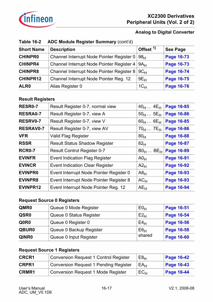
XC2300 DerivativesPeripheral Units (Vol. 2 of 2)
Analog to Digital Converter
CHINPR0 Channel Interrupt Node Pointer Register 0 98H Page 16-73CHINPR4 Channel Interrupt Node Pointer Register 4 9AH Page 16-73CHINPR8 Channel Interrupt Node Pointer Register 8 9CH Page 16-74CHINPR12 Channel Interrupt Node Pointer Reg. 12 9EH Page 16-75ALR0 Alias Register 0 1CH Page 16-76
Result RegistersRESR0-7 Result Register 0-7, normal view 40H … 4EH Page 16-85RESRA0-7 Result Register 0-7, view A 50H … 5EH Page 16-86RESRV0-7 Result Register 0-7, view V 60H … 6EH Page 16-85RESRAV0-7 Result Register 0-7, view AV 70H … 7EH Page 16-86VFR Valid Flag Register 80H Page 16-88RSSR Result Status Shadow Register 82H Page 16-87RCR0-7 Result Control Register 0-7 B0H … BEH Page 16-89EVINFR Event Indication Flag Register A0H Page 16-91EVINCR Event Indication Clear Register A2H Page 16-92EVINPR0 Event Interrupt Node Pointer Register 0 A8H Page 16-93EVINPR8 Event Interrupt Node Pointer Register 8 ACH Page 16-93EVINPR12 Event Interrupt Node Pointer Reg. 12 AEH Page 16-94
Request Source 0 RegistersQMR0 Queue 0 Mode Register E0H Page 16-51QSR0 Queue 0 Status Register E2H Page 16-54Q0R0 Queue 0 Register 0 E4H Page 16-56QBUR0 Queue 0 Backup Register E6H
sharedPage 16-58
QINR0 Queue 0 Input Register Page 16-60
Request Source 1 RegistersCRCR1 Conversion Request 1 Control Register E8H Page 16-42CRPR1 Conversion Request 1 Pending Register EAH Page 16-43CRMR1 Conversion Request 1 Mode Register ECH Page 16-44
Table 16-2 ADC Module Register Summary (cont’d)
Short Name Description Offset 1) See Page
User’s Manual 16-17 V2.1, 2008-08ADC, UM_V0.1D6
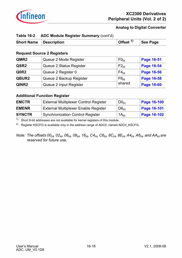
XC2300 DerivativesPeripheral Units (Vol. 2 of 2)
Analog to Digital Converter
Note: The offsets 00H, 02H, 06H, 08H, 16H, C4H, C6H, 8CH, 8EH, A4H, A6H, and AAH arereserved for future use.
Request Source 2 RegistersQMR2 Queue 2 Mode Register F0H Page 16-51QSR2 Queue 2 Status Register F2H Page 16-54Q0R2 Queue 2 Register 0 F4H Page 16-56QBUR2 Queue 2 Backup Register F6H
sharedPage 16-58
QINR2 Queue 2 Input Register Page 16-60
Additional Function RegisterEMCTR External Multiplexer Control Register D0H Page 16-100EMENR External Multiplexer Enable Register D6H Page 16-101SYNCTR Synchronization Control Register 1AH Page 16-1021) Short 8-bit addresses are not available for kernel registers of this module.2) Register KSCFG is available only in the address range of ADC0, named ADC0_KSCFG.
Table 16-2 ADC Module Register Summary (cont’d)
Short Name Description Offset 1) See Page
User’s Manual 16-18 V2.1, 2008-08ADC, UM_V0.1D6
XC2300 DerivativesPeripheral Units (Vol. 2 of 2)
Analog to Digital Converter
16.2.2 Mode ControlThe mode control concept for system control tasks, such as power saving, or suspendrequest for debugging, allows to program the module behavior under different deviceoperating conditions. The behavior of the ADC kernels can be programmed for each ofthe device operating modes, that are requested by the global state control part of theSCU. It is advantageous that the ADC kernels of an ADC module show an identicalbehavior regarding the device operating modes (e.g. to avoid that a non-suspendedkernel waits for a suspended kernel to start a synchronized conversion). Therefore, theADC module has a common associated register ADC0_KSCFG defining the behavior ofall kernels of the module in the following device operating modes:• Normal operation:
This operating mode is the default operating mode when neither a suspend requestnor a clock-off request are pending. The module clock is not switched off and theADC registers can be read or written. The kernel behavior is defined byKSCFG.NOMCFG.
• Suspend mode:This operating mode is requested when a suspend request (issued by a debugger)is pending in the device. The module clock is not switched off and the ADC registerscan be read or written. The kernel behavior is defined by KSCFG.SUMCFG.
• Clock-off mode:This operating mode is requested for power saving purposes. The module clock isswitched off automatically when all kernels of the ADC module reached theirspecified state in a stop mode. In this case, ADC registers can not be accessed. Thekernel behavior is defined by KSCFG.COMCFG.
For the ADC module, the following internal actions can be influenced by mode control:• A current conversion of an analog value:
If the request control unit has found a pending conversion request, the conversioncan be started. This start has to be enabled by the mode control. If the current kernelmode allows the conversion start (run modes 0 and 1), it will be executed. If the kernelmode does not allow a start (stop modes 0 and 1), the conversion is not started. Thestart request is not cancelled, but frozen. A “frozen” conversion is started asprogrammed if the kernel mode is changed to a run mode again.
• An arbiter round:The start of a new arbiter round has to be enabled by the kernel modes. In stopmode 1, a new arbiter round will not start.
The behavior of the ADC kernels can be programmed for each of the device operatingmodes (normal operation, suspend mode, clock-off mode). Therefore, the ADC kernelssupport four kernel modes, as shown in Table 16-3.
User’s Manual 16-19 V2.1, 2008-08ADC, UM_V0.1D6

XC2300 DerivativesPeripheral Units (Vol. 2 of 2)
Analog to Digital Converter
Generally, bit field KSCFG.NOMCFG should be configured for run mode 0 as defaultsetting for standard operation. If the ADC kernels should not react to a suspend request(and to continue operation as in normal mode), bit field KSCFG.SUMCFG has to beconfigured with the same value as KSCFG.NOMCFG. If the ADC kernels should showa different behavior and stop operation when a specific stop condition is reached, thecode for stop mode 0 or stop mode 1 has to be written to KSCFG.SUMCFG.A similar mechanism applies for the clock-off mode with the possibility to program thedesired behavior by bit field KSCFG.COMCFG.Note: The stop mode selection strongly depends on the application needs and it is very
unlikely that different stop modes are required in parallel in the same application.As a result, only one stop mode type (either 0 or 1) should be used in the bit fieldsin register KSCFG. Do not mix stop mode 0 and stop mode 1 and avoid transitionsfrom stop mode 0 to stop mode 1 (or vice versa) for the ADC module.
If the module clock is disabled by KSCFG.MODEN = 0 or in clock-off mode when thestop condition is reached (in stop mode 0 or 1), the module can not be accessed by reador write operations (except register KSCFG that can always be accessed). As aconsequence, it can not be configured.Please note that bit KSCFG.MODEN should only be set by SW while all configurationfields are configured for run mode 0.
Table 16-3 ADC Kernel BehaviorKernel Mode Kernel Behavior Coderun mode 0 kernel operation as specified, no impact on data transfer
(same behavior for run mode 0 and run mode 1)00B
run mode 1 01B
stop mode 0 A currently running AD conversion is completely finished and the result is treated. Pending conversion request to start a new conversion are not taken into account (but not deleted). They start conversions after entering a run mode as programmed.The arbiter continues as programmed.
10B
stop mode 1 Like stop mode 0, but the arbiter is stopped after it has finished its arbitration round.
11B
User’s Manual 16-20 V2.1, 2008-08ADC, UM_V0.1D6
XC2300 DerivativesPeripheral Units (Vol. 2 of 2)
Analog to Digital Converter
16.2.3 Module Activation and Power Saving ModesThe converter of the ADC supports specific power down modes allowing an automaticreduction of the power consumption between two conversions. The following modes aredetermined by bit field GLOBSTR.ANON:• ANON = 00B: Converter switched off (default after reset)
The complete converter is switched off and held in its reset state, conversions are notpossible. To start a conversion, ANON has to be programmed to the desired mode.A maximum wake-up time of about 10 µs has to be respected before starting aconversion. Furthermore, digital logic blocks are set to their initial state.
• ANON = 01B: Slow stand-by modeThe converter enters a power reduction mode after each conversion. It switchesautomatically to normal operation if a conversion is requested. A maximum wake-uptime of about 10 µs has to be added to the sample time. This leads to the lowestpower consumption for the ADC supply with wake-up capability.
• ANON = 10B: Fast stand-by modeThe converter enters a power reduction mode with less reduction than in slow stand-by mode after each conversion. It switches automatically to normal operation if aconversion is requested. A maximum wake-up time of about 3 µs has to be added tothe sample time. This leads to a reduced power consumption for the ADC supplycompared to normal operation.
• ANON = 11B: Normal operationConversions are always possible with the desired sample time. The converter staysactive permanently.
User’s Manual 16-21 V2.1, 2008-08ADC, UM_V0.1D6
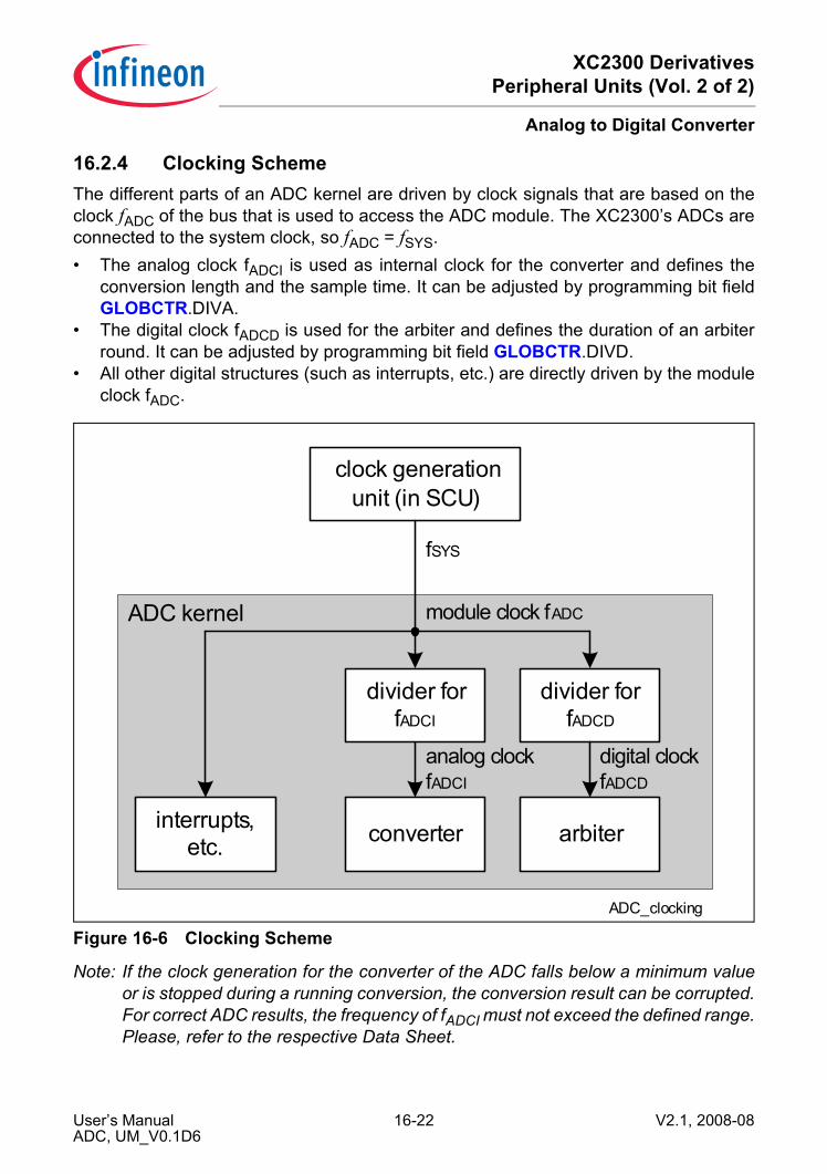
XC2300 DerivativesPeripheral Units (Vol. 2 of 2)
Analog to Digital Converter
16.2.4 Clocking SchemeThe different parts of an ADC kernel are driven by clock signals that are based on theclock fADC of the bus that is used to access the ADC module. The XC2300’s ADCs areconnected to the system clock, so fADC = fSYS.• The analog clock fADCI is used as internal clock for the converter and defines the
conversion length and the sample time. It can be adjusted by programming bit fieldGLOBCTR.DIVA.
• The digital clock fADCD is used for the arbiter and defines the duration of an arbiterround. It can be adjusted by programming bit field GLOBCTR.DIVD.
• All other digital structures (such as interrupts, etc.) are directly driven by the moduleclock fADC.
Figure 16-6 Clocking Scheme
Note: If the clock generation for the converter of the ADC falls below a minimum valueor is stopped during a running conversion, the conversion result can be corrupted.For correct ADC results, the frequency of fADCI must not exceed the defined range.Please, refer to the respective Data Sheet.
ADC_clocking
converter
analog clockfADCI
digital clockfADCD
module clock fADC
arbiter
divider forfADCD
interrupts,etc.
clock generation unit (in SCU)
divider forfADCI
ADC kernel
fSYS
User’s Manual 16-22 V2.1, 2008-08ADC, UM_V0.1D6

XC2300 DerivativesPeripheral Units (Vol. 2 of 2)
Analog to Digital Converter
16.2.5 General ADC Registers
16.2.5.1 Kernel State Configuration RegisterThe kernel state configuration register KSCFG allows the selection of the desired kernelmodes for the different device operating modes.Bit fields KSCFG.NOMCFG and KSCFG.COMCFG are reset by an application reset. Bitfield KSCFG.SUMCFG is reset by a debug reset.This register is a common register for all ADC kernels and can be accessed in theaddress range of ADC0.Note: The coding of the bit fields NOMCFG, SUMCFG and COMCFG is described in
Table 16-3.
ADC0_KSCFG Kernel State Configuration Register
XSFR(0CH) Reset Value: 0000H
15 14 13 12 11 10 9 8 7 6 5 4 3 2 1 0
BPCOM 0 COMCFG BP
SUM 0 SUMCFG BPNOM 0 NOMCFG 0
BPMODEN
MODEN
w r rw w r rw w r rw r w rw
Field Bits Type DescriptionMODEN 0 rw Module Enable
This bit enables the module kernel clock and the module functionality.0B The module is switched off immediately
(without respecting a stop condition).It does not react on mode control actions and the module clock is switched off. The module does not react on read accesses and ignores write accesses (except to KSCFG).
1B The module is switched on and can operate. After writing 1 to MODEN, it is recommended to read register KSCFG to avoid pipeline effects in the control block before accessing other ADC registers.
User’s Manual 16-23 V2.1, 2008-08ADC, UM_V0.1D6
XC2300 DerivativesPeripheral Units (Vol. 2 of 2)
Analog to Digital Converter
Note: To change a configuration bit field, the associated protection bit BPxxx must beset during the write operation. This allows modifying selected configuration bitfields with a single write operation.
BPMODEN 1 w Bit Protection for MODENThis bit enables the write access to the bit MODEN. It always reads 0.0B MODEN is not changed.1B MODEN is updated with the written value.
NOMCFG [5:4] rw Normal Operation Mode ConfigurationThis bit field defines the kernel mode applied in normal operation mode.00B Run mode 0 is selected.01B Run mode 1 is selected.10B Stop mode 0 is selected.11B Stop mode 1 is selected.
BPNOM 7 w Bit Protection for NOMCFGThis bit enables the write access to the bit field NOMCFG. It always reads 0.0B NOMCFG is not changed.1B NOMCFG is updated with the written value.
SUMCFG [9:8] rw Suspend Mode ConfigurationThis bit field defines the kernel mode applied in suspend mode. Coding like NOMCFG.
BPSUM 11 w Bit Protection for SUMCFGThis bit enables the write access to the bit field SUMCFG. It always reads 0.0B SUMCFG is not changed.1B SUMCFG is updated with the written value.
COMCFG [13:12] rw Clock Off Mode ConfigurationThis bit field defines the kernel mode applied in clock-off mode. Coding like NOMCFG.
BPCOM 15 w Bit Protection for COMCFGThis bit enables the write access to the bit field COMCFG. It always reads 0.0B COMCFG is not changed.1B COMCFG is updated with the written value.
0 [3:2], 6, 10, 14
r Reservedreturns 0 if read; should be written with 0;
Field Bits Type Description
User’s Manual 16-24 V2.1, 2008-08ADC, UM_V0.1D6
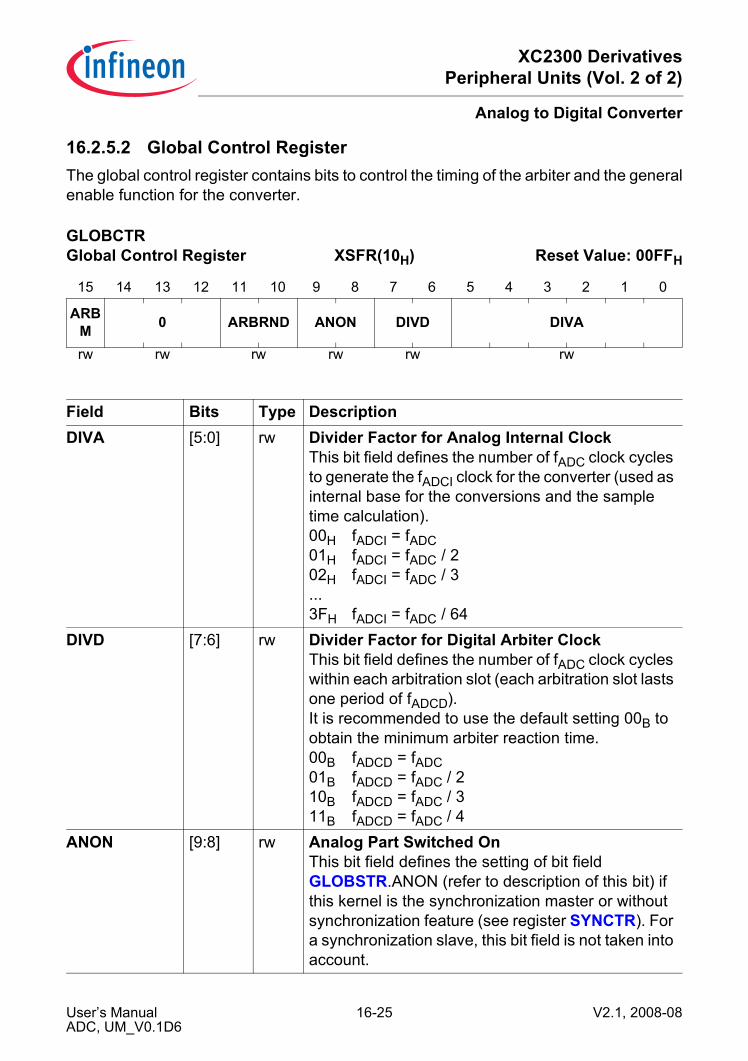
XC2300 DerivativesPeripheral Units (Vol. 2 of 2)
Analog to Digital Converter
16.2.5.2 Global Control RegisterThe global control register contains bits to control the timing of the arbiter and the generalenable function for the converter.
GLOBCTR Global Control Register XSFR(10H) Reset Value: 00FFH
15 14 13 12 11 10 9 8 7 6 5 4 3 2 1 0
ARBM 0 ARBRND ANON DIVD DIVA
rw rw rw rw rw rw
Field Bits Type DescriptionDIVA [5:0] rw Divider Factor for Analog Internal Clock
This bit field defines the number of fADC clock cycles to generate the fADCI clock for the converter (used as internal base for the conversions and the sample time calculation).00H fADCI = fADC01H fADCI = fADC / 202H fADCI = fADC / 3...3FH fADCI = fADC / 64
DIVD [7:6] rw Divider Factor for Digital Arbiter ClockThis bit field defines the number of fADC clock cycles within each arbitration slot (each arbitration slot lasts one period of fADCD).It is recommended to use the default setting 00B to obtain the minimum arbiter reaction time.00B fADCD = fADC01B fADCD = fADC / 210B fADCD = fADC / 311B fADCD = fADC / 4
ANON [9:8] rw Analog Part Switched OnThis bit field defines the setting of bit field GLOBSTR.ANON (refer to description of this bit) if this kernel is the synchronization master or without synchronization feature (see register SYNCTR). For a synchronization slave, this bit field is not taken into account.
User’s Manual 16-25 V2.1, 2008-08ADC, UM_V0.1D6

XC2300 DerivativesPeripheral Units (Vol. 2 of 2)
Analog to Digital Converter
ARBRND [11:10] rw Arbitration Round LengthThis bit field defines the number of arbitration slots per arbitration round (arbitration round length = tARB).1)
00B An arbitration round contains 4 arbitration slots (tARB = 4 / fADCD).
01B An arbitration round contains 8 arbitration slots (tARB = 8 / fADCD).
10B An arbitration round contains 16 arbitration slots (tARB = 16 / fADCD).
11B An arbitration round contains 20 arbitration slots (tARB = 20 / fADCD).
0 [14:12] rw Reserved for Future UseThis bit field is reserved for future use and has to be written with 000B.
ARBM 15 rw Arbitration ModeThis bit field defines whether the arbiter runs permanently or only while at least one conversion request is pending.0B The arbiter runs permanently. This setting has
to be chosen in a synchronization slave (see Section 16.2.17).
1B The arbiter only runs if at least one conversion request of an enabled request source is pending. This setting leads to a reproducible latency from an incoming request to the conversion start if the converter is idle. Synchronized conversions are not supported.
1) The default setting of 4 arbitration slots is sufficient for correct arbitration. The duration of an arbitration roundcan be increased if required to synchronize requests.
Field Bits Type Description
User’s Manual 16-26 V2.1, 2008-08ADC, UM_V0.1D6
XC2300 DerivativesPeripheral Units (Vol. 2 of 2)
Analog to Digital Converter
16.2.5.3 Global Status RegisterThe status control register contains bits indicating the current status of a conversion.
GLOBSTR Global Status Register XSFR(12H) Reset Value: 0000H
15 14 13 12 11 10 9 8 7 6 5 4 3 2 1 0
0 CSRC SYNRUN ANON CHNR 0 SAM
PLEBUSY
r rh rh rh rh r rh rh
Field Bits Type DescriptionBUSY 0 rh Analog Part Busy
This bit indicates that a conversion is currently running.0B The converter is idle.1B A conversion is currently running.
SAMPLE 1 rh Sample PhaseThis bit indicates that an analog input signal is currently sampled.0B The converter is not in the sampling phase.1B The converter is in the sampling phase.
CHNR [7:3] rh Channel NumberThis bit field indicates which analog input channel is currently converted. This information is updated when a new conversion is started.
User’s Manual 16-27 V2.1, 2008-08ADC, UM_V0.1D6

XC2300 DerivativesPeripheral Units (Vol. 2 of 2)
Analog to Digital Converter
ANON [9:8] rh Analog Part Switched OnThis bit field defines the operation mode of the converter. It monitors either bit field GLOBCTR.ANON of the same ADC kernel (in master mode or without synchronization feature) or bit field GLOBCTR.ANON of the ADC kernel selected as synchronization master for this kernel (in slave mode). This ensures that all kernels of a synchronization group can be controlled with a single write operation to bit field GLOBCTR of the synchronization master.00B The converter is switched off and conversions
are not possible. The arbiter finishes its current arbitration round (if running) and then remains in the idle state.
01B The converter of the ADC module is switched on and conversions are possible. The automatic power-down capability of the converter is enabled, leading to the lowest power consumption of the ADC supply with wake-up capability, but a longer wake-up time before each conversion.
10B The converter of the ADC module is switched on and conversions are possible. The automatic power-down capability of the converter is enabled, leading to a reduced power consumption of the ADC supply, but a shorter wake-up time before each conversion.
11B The converter of the ADC module is switched on and conversions are possible. The automatic power-down capability of the converter is disabled leading to the nominal power consumption of the ADC supply.
Field Bits Type Description
User’s Manual 16-28 V2.1, 2008-08ADC, UM_V0.1D6

XC2300 DerivativesPeripheral Units (Vol. 2 of 2)
Analog to Digital Converter
SYNRUN 10 rh Synchronous Conversion RunningThis bit indicates that a synchronized (= parallel) conversion is currently running.0B There is no synchronized conversion running
(either there is no conversion currently running or a synchronized conversion has not been requested). A running conversion can be cancelled and repeated in case of a new incoming conversion request with higher priority.
1B A synchronized conversion is running.This conversion can not be cancelled while running. Higher priority requests can trigger conversions only after the end of a synchronized conversion.
CSRC [13:11] rh Currently Converted Request SourceThis bit field indicates the arbitration slot number of the current conversion (if BUSY = 1, a conversion is still running) or of the last conversion (if BUSY = 0, no conversion is running). This bit field is updated with each conversion start.000B The channel requested by the request source
of arbitration slot 0 is (has been) converted.001B The channel requested by the request source
of arbitration slot 1 is (has been) converted.010B The channel requested by the request source
of arbitration slot 2 is (has been) converted.other combinations are reserved
0 2, [15:14]
r Reservedreturns 0 if read; should be written with 0;
Field Bits Type Description
User’s Manual 16-29 V2.1, 2008-08ADC, UM_V0.1D6

XC2300 DerivativesPeripheral Units (Vol. 2 of 2)
Analog to Digital Converter
16.2.5.4 Input Select RegistersRegister PISEL contains bit fields selecting the input signal for the trigger and gatinginputs of the request sources. The connections depending on the device implementation,please refer to the implementation chapter for details.Note: For signals connected to inputs with a synchronization stage, a synchronization
delay of two fADC clock cycles has to be taken into account. See Section 16.3.4for reference.
PISEL Port Input Select Register XSFR(04H) Reset Value: 0000H
15 14 13 12 11 10 9 8 7 6 5 4 3 2 1 0
0 0 REQTR2 REQGT2 REQTR1 REQGT1 REQTR0 REQGT0
r rw rw rw rw rw rw rw
Field Bits Type DescriptionREQGT0 [1:0] rw Input Select for REQGT0 of Source 0
This bit field defines the input signal used for the module input REQGT0 of the request source 0.00B The input signal REQGT0A is selected.01B The input signal REQGT0B is selected.10B The input signal REQGT0C is selected.11B The input signal REQGT0D is selected.
REQTR0 [3:2] rw Input Select for REQTR0 of Source 0This bit field defines the input signal used for the module input REQTR0 of the request source 0.00B The input signal REQTR0A is selected.01B The input signal REQTR0B is selected.10B The input signal REQTR0C is selected.11B The input signal REQTR0D is selected.
REQGT1 [5:4] rw Input Select for REQGT1 of Source 1This bit field defines the input signal used for the module input REQGT1 of the request source 1.00B The input signal REQGT1A is selected.01B The input signal REQGT1B is selected.10B The input signal REQGT1C is selected.11B The input signal REQGT1D is selected.
User’s Manual 16-30 V2.1, 2008-08ADC, UM_V0.1D6

XC2300 DerivativesPeripheral Units (Vol. 2 of 2)
Analog to Digital Converter
REQTR1 [7:6] rw Input Select for REQTR1 of Source 1This bit field defines the input signal used for the module input REQTR1 of the request source 1.00B The input signal REQTR1A is selected.01B The input signal REQTR1B is selected.10B The input signal REQTR1C is selected.11B The input signal REQTR1D is selected.
REQGT2 [9:8] rw Input Select for REQGT2 of Source 2This bit field defines the input signal used for the module input REQGT2 of the request source 2.00B The input signal REQGT2A is selected.01B The input signal REQGT2B is selected.10B The input signal REQGT2C is selected.11B The input signal REQGT2D is selected.
REQTR2 [11:10] rw Input Select for REQTR2 of Source 2This bit field defines the input signal used for the module input REQTR2 of the request source 2.00B The input signal REQTR2A is selected.01B The input signal REQTR2B is selected.10B The input signal REQTR2C is selected.11B The input signal REQTR2D is selected.
0 12 rw Reserved for Future Extensionreturns 0 if read; should be written with 0;
0 [15:13] r Reservedreturns 0 if read; should be written with 0;
Field Bits Type Description
User’s Manual 16-31 V2.1, 2008-08ADC, UM_V0.1D6
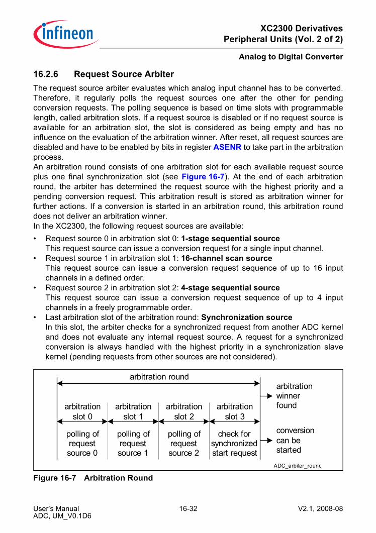
XC2300 DerivativesPeripheral Units (Vol. 2 of 2)
Analog to Digital Converter
16.2.6 Request Source ArbiterThe request source arbiter evaluates which analog input channel has to be converted.Therefore, it regularly polls the request sources one after the other for pendingconversion requests. The polling sequence is based on time slots with programmablelength, called arbitration slots. If a request source is disabled or if no request source isavailable for an arbitration slot, the slot is considered as being empty and has noinfluence on the evaluation of the arbitration winner. After reset, all request sources aredisabled and have to be enabled by bits in register ASENR to take part in the arbitrationprocess.An arbitration round consists of one arbitration slot for each available request sourceplus one final synchronization slot (see Figure 16-7). At the end of each arbitrationround, the arbiter has determined the request source with the highest priority and apending conversion request. This arbitration result is stored as arbitration winner forfurther actions. If a conversion is started in an arbitration round, this arbitration rounddoes not deliver an arbitration winner.In the XC2300, the following request sources are available:• Request source 0 in arbitration slot 0: 1-stage sequential source
This request source can issue a conversion request for a single input channel.• Request source 1 in arbitration slot 1: 16-channel scan source
This request source can issue a conversion request sequence of up to 16 inputchannels in a defined order.
• Request source 2 in arbitration slot 2: 4-stage sequential sourceThis request source can issue a conversion request sequence of up to 4 inputchannels in a freely programmable order.
• Last arbitration slot of the arbitration round: Synchronization sourceIn this slot, the arbiter checks for a synchronized request from another ADC kerneland does not evaluate any internal request source. A request for a synchronizedconversion is always handled with the highest priority in a synchronization slavekernel (pending requests from other sources are not considered).
Figure 16-7 Arbitration RoundADC_arbiter_round
arbitrationslot 0
polling ofrequestsource 0
arbitrationslot 2
arbitrationslot 3
arbitration round
arbitrationslot 1
polling ofrequestsource 1
polling ofrequestsource 2
check forsynchronizedstart request
arbitrationwinnerfound
conversioncan bestarted
User’s Manual 16-32 V2.1, 2008-08ADC, UM_V0.1D6
XC2300 DerivativesPeripheral Units (Vol. 2 of 2)
Analog to Digital Converter
The period tARB of an arbitration round is given by:tARB = N × (GLOBCTR.DIVD + 1) / fADCwith N being 4, 8, 16, or 20 as defined by GLOBCTR.ARBRND.The number of arbitration slots forming an arbitration round can be programmed toobtain a similar arbiter timing for different devices, even if the number of availablerequest sources differs from one device to another.Because the XC2300’s ADC has 3 request sources, 4 slots per arbitration round aresufficient.The period of the arbitration round introduces a timing granularity to detect an incomingconversion request signal and the earliest point to start the related conversion. Thisgranularity can introduce a jitter of maximum one arbitration round. The jitter can bereduced by minimizing the period of an arbitration round (numbers of arbitration slots andtheir length).To achieve a reproducible reaction time (constant delay without jitter) between thetrigger event of a conversion request (e.g. by a timer unit or due to an external event)and the start of the related conversion, mainly the following two options exist. For bothoptions, the converter has to be idle and other conversion requests must not be pendingfor at least one arbiter round before the trigger event occurs:• If bit GLOBCTR.ARBM = 0, the arbiter runs permanently. In this mode,
synchronized conversions of more than one ADC kernel are possible.The trigger for the conversion triggers has to be generated synchronously to thearbiter timing. Incoming triggers should have exactly n-times the granularity of thearbiter (n = 1, 2, 3, ...). In order to allow some flexibility, the duration of an arbitrationslot can be programmed in cycles of fADC.
• If bit GLOBCTR.ARBM = 1, the arbiter stops after an arbitration round when noconversion request have been found pending any more. The arbiter is started againif at least one enabled request source indicates a pending conversion request. Thetrigger of a conversion request does need not to be synchronous to the arbiter timing.In this mode, parallel conversions are not possible for synchronization slave kernels.
16.2.6.1 Request Source PriorityEach request source has an individually programmable priority to be able to adapt todifferent applications (see register RSPR0). The priorities define the order the requestsources are handled by the arbiter if two or more request sources indicate pendingconversion requests at the same time.Starting with request source 0, the arbiter checks if an enabled request source has apending request for a conversion. The arbitration winner is the request source with apending conversion request and the highest priority that has been found first in anarbitration round.
User’s Manual 16-33 V2.1, 2008-08ADC, UM_V0.1D6
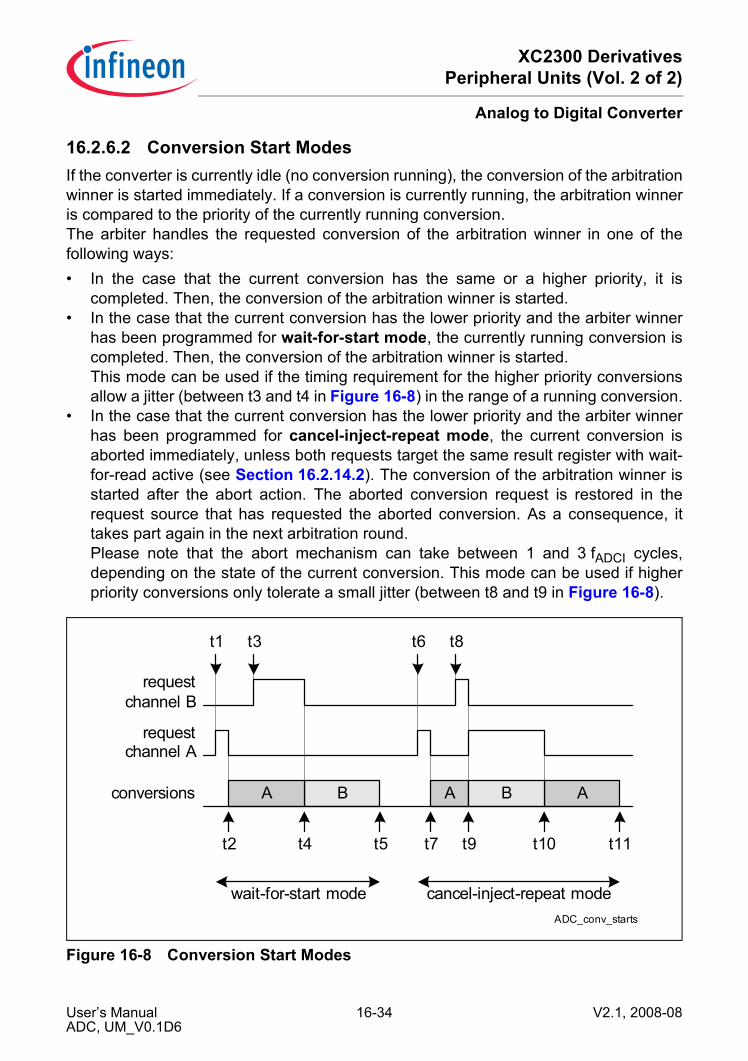
XC2300 DerivativesPeripheral Units (Vol. 2 of 2)
Analog to Digital Converter
16.2.6.2 Conversion Start ModesIf the converter is currently idle (no conversion running), the conversion of the arbitrationwinner is started immediately. If a conversion is currently running, the arbitration winneris compared to the priority of the currently running conversion.The arbiter handles the requested conversion of the arbitration winner in one of thefollowing ways:• In the case that the current conversion has the same or a higher priority, it is
completed. Then, the conversion of the arbitration winner is started.• In the case that the current conversion has the lower priority and the arbiter winner
has been programmed for wait-for-start mode, the currently running conversion iscompleted. Then, the conversion of the arbitration winner is started.This mode can be used if the timing requirement for the higher priority conversionsallow a jitter (between t3 and t4 in Figure 16-8) in the range of a running conversion.
• In the case that the current conversion has the lower priority and the arbiter winnerhas been programmed for cancel-inject-repeat mode, the current conversion isaborted immediately, unless both requests target the same result register with wait-for-read active (see Section 16.2.14.2). The conversion of the arbitration winner isstarted after the abort action. The aborted conversion request is restored in therequest source that has requested the aborted conversion. As a consequence, ittakes part again in the next arbitration round.Please note that the abort mechanism can take between 1 and 3 fADCI cycles,depending on the state of the current conversion. This mode can be used if higherpriority conversions only tolerate a small jitter (between t8 and t9 in Figure 16-8).
Figure 16-8 Conversion Start Modes
ADC_conv_starts
conversions B A AA B
requestchannel A
requestchannel B
t2
t1 t3 t6 t8
t4 t5 t7 t9 t10 t11
wait-for-start mode cancel-inject-repeat mode
User’s Manual 16-34 V2.1, 2008-08ADC, UM_V0.1D6

XC2300 DerivativesPeripheral Units (Vol. 2 of 2)
Analog to Digital Converter
The conversion start mode can be individually programmed for each request source bybits in register RSPR0 and is applied to all channels requested by the source.Figure 16-8 shows the influence of both conversion start modes on the conversionsequence if two request sources generate conversion requests. In this example, channelA is issued by a request source with a lower priority than the request source requestingthe conversion of channel B.• t1: The trigger event for channel A occurs and a conversion request is activated.• t2: At the end of the arbitration round, channel A is determined as arbitration winner,
the conversion of channel A is started. With the start of the conversion, conversionrequest A is cleared.
• t3: The trigger event for channel B occurs and a conversion request is activated. Inwait-for-read mode, the currently running conversion of channel A is finishednormally.
• t4: After the conversion of channel A is finished, the conversion of channel B isstarted. With the start of the conversion, conversion request B is cleared.
• t5: The conversion of channel B is finished.• t6: The trigger event for channel A occurs and a conversion request is activated.• t7: At the end of the arbitration round, channel A is determined as arbitration winner,
the conversion of channel A is started. With the start of the conversion, conversionrequest A is cleared.
• t8: The trigger event for channel B occurs and a conversion request is activated.• t9: At the end of the arbitration round, channel B is determined as arbitration winner.
In cancel-inject-repeat mode, the currently running conversion of channel A isaborted and the conversion of channel B is started. With the abort of conversion A,conversion request A is set again. With the start of conversion B, conversion requestB is cleared.
• t10: The conversion of channel B is finished. In the meantime, the pending requestfor channel A has been identified as arbitration winner and the conversion of channelA is started. With the start of the conversion, conversion request A is cleared.
• t11: The conversion of channel A is finished.
User’s Manual 16-35 V2.1, 2008-08ADC, UM_V0.1D6
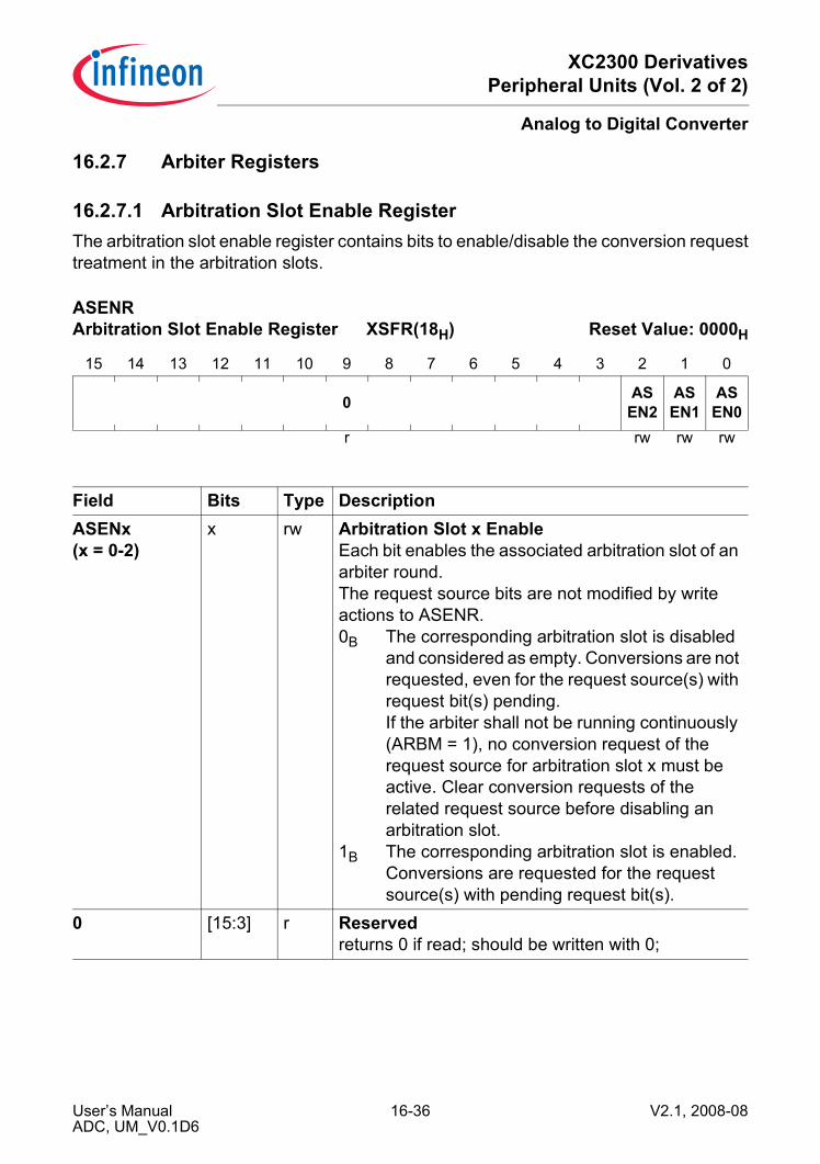
XC2300 DerivativesPeripheral Units (Vol. 2 of 2)
Analog to Digital Converter
16.2.7 Arbiter Registers
16.2.7.1 Arbitration Slot Enable RegisterThe arbitration slot enable register contains bits to enable/disable the conversion requesttreatment in the arbitration slots.
ASENR Arbitration Slot Enable Register XSFR(18H) Reset Value: 0000H
15 14 13 12 11 10 9 8 7 6 5 4 3 2 1 0
0 ASEN2
ASEN1
ASEN0
r rw rw rw
Field Bits Type DescriptionASENx(x = 0-2)
x rw Arbitration Slot x EnableEach bit enables the associated arbitration slot of an arbiter round.The request source bits are not modified by write actions to ASENR.0B The corresponding arbitration slot is disabled
and considered as empty. Conversions are not requested, even for the request source(s) with request bit(s) pending.If the arbiter shall not be running continuously (ARBM = 1), no conversion request of the request source for arbitration slot x must be active. Clear conversion requests of the related request source before disabling an arbitration slot.
1B The corresponding arbitration slot is enabled. Conversions are requested for the request source(s) with pending request bit(s).
0 [15:3] r Reservedreturns 0 if read; should be written with 0;
User’s Manual 16-36 V2.1, 2008-08ADC, UM_V0.1D6

XC2300 DerivativesPeripheral Units (Vol. 2 of 2)
Analog to Digital Converter
16.2.7.2 Request Source Priority RegisterThe request source priority register contains bits to define the request source priority andthe conversion start mode. The priority and conversion start mode settings of an enabledrequest source must not be changed by SW. If a request source is disabled, the settingcan be changed by SW if a currently running conversion requested by this source isfinished.
RSPR0 Request Source Priority Register 0
XSFR(14H) Reset Value: 0000H
15 14 13 12 11 10 9 8 7 6 5 4 3 2 1 0
0 CSM2 0 PRIO
2CSM
1 0 PRIO1
CSM0 0 PRIO
0r rw r rw rw r rw rw r rw
Field Bits Type DescriptionPRIO0,PRIO1,PRIO2
[1:0],[5:4],[9:8]
rw Priority of Request Source xThis bit field defines the priority of the conversion request source x, located in arbitration slot x.00B Lowest priority is selected....11B Highest priority is selected.
CSM0,CSM1,CSM2
3,7,11
rw Conversion Start Mode of Request Source xThis bit defines the conversion start mode of the conversion request source x, located in arbitration slot x.0B Wait-for-start mode is selected.1B Cancel-inject-repeat mode is selected.
0 2, 6, 10, [15:12]
r Reservedreturns 0 if read; should be written with 0;
User’s Manual 16-37 V2.1, 2008-08ADC, UM_V0.1D6
XC2300 DerivativesPeripheral Units (Vol. 2 of 2)
Analog to Digital Converter
16.2.8 Scan Request Source HandlingA scan request source can issue conversion requests for a sequence of up to 16 inputchannels. It can be programmed individually for each input channel if it takes part in thescan sequence. The scan sequence always starts with the highest enabled channelnumber and continues towards lower channel numbers (order defined by the channelnumber, each channel can be converted only once per sequence).
Figure 16-9 Scan Request Source
16.2.8.1 OverviewA scan request source performs the:• Conversion request control:
The conversion request control defines if an analog input channel takes part in thescan sequence (see bits in register CRCR1). The programmed register value is keptunchanged by an ongoing scan sequence.
• Conversion request pending:The pending conversion requests indicate if an input channel has to be converted inan ongoing scan sequence (see bits in register CRPR1). A conversion request canonly be issued to the request source arbiter if at least one pending bit is set. Witheach conversion start that has been triggered by the scan request source, thecorresponding pending bit is automatically cleared. The scan sequence is consideredfinished and a request source event is generated if the last conversion triggered bythe scan source is finished and all pending bits have been cleared.
• Request handling:The request handling block interfaces with the request source arbiter. It requestsconversion due to pending bits in the scan sequence and handles the conversion
ADC_scan_reqsr
conversion requestcontrol
load event
conversionrequests pending
request handling
requestsourcearbiter
request
statusrequest
source event
trigger &gating unit
gating inputsREQGTx[D:A]
trigger inputsREQTRx[D:A]
scan request source x
REQGTx
REQTRx
User’s Manual 16-38 V2.1, 2008-08ADC, UM_V0.1D6

XC2300 DerivativesPeripheral Units (Vol. 2 of 2)
Analog to Digital Converter
status information. If a conversion triggered by the scan request source is aborteddue to a conversion request from another request source with a higher priority, thecorresponding pending bit is automatically set. This mechanism ensures that anaborted conversion takes part in the next arbitration round and does not get lost. Thecontrol of the scan sequence is done based on bits in register CRMR1.
• Trigger and gating signal handling:The trigger and gating unit interfaces with signals and modules outside the ADCmodule that can request conversions. For example, a timer unit can issue a requestsignal to synchronize conversions to PWM events. A load event starts a scansequence by modifying the request pending bits according to the request control bits.
16.2.8.2 Scan Sequence OperationTo operate a scan request source, the following aspects should be taken into account:• The bits in register CRCR1 have to be programmed to define the channels
participating in the scan sequence.• If a trigger or gating function by external signals is desired, the gating and trigger
inputs have to be defined by bit fields REQTRx and REQGTx in register PISEL (thevalue of x defines the number of the arbitration slot where the scan source isconnected).
• The gating mechanism has to be defined by CRMR1.ENGT.• The corresponding arbitration slot has to be enabled to accept conversion requests
from the scan source (see register ASENR).• The load event has to be defined by bits in CRMR1 to start a scan sequence.• If a load event occurs while CRMR1.LDM = 0, the content of CRCR1 is copied to
CRPR1 (overwrite). This setting allows starting a new scan sequence and to “forget”remaining pending bits if a load event occurs while a scan sequence is running.
• If a load event occurs while CRMR1.LDM = 1, the content of CRCR1 is bit-wiselylogical OR-combined to CRPR1 (no overwrite). This setting allows starting a newscan sequence without “forgetting” remaining pending bits if a load event occurswhile a scan sequence is running.
To start a scan sequence, the following mechanisms are supported to generate a loadevent:• An external trigger signal can be selected to start a scan sequence controlled by HW
by an external module or signal, e.g. a timer unit or an input pin. The trigger featureis enabled by CRMR1.ENTR = 1. The load event is generated if a rising edge isdetected at the selected trigger input.
• A load event is generated under SW control by writing CRMR1.LDEV = 1. Thismechanism starts a scan sequence without modifying the bits in register CRCR1. Adata write action to CRCR1 does not lead to a load event (first prepare the channelcontrol, then start the sequence).
User’s Manual 16-39 V2.1, 2008-08ADC, UM_V0.1D6

XC2300 DerivativesPeripheral Units (Vol. 2 of 2)
Analog to Digital Converter
• If SW writes data to register CRPR1, the written data is stored in register CRCR1 anda load event is generated automatically. This mechanism starts a scan sequence withthe channels defined by the written data (the sequence is defined and started with asingle data write action, e.g. under PEC control).
• A load event is generated each time a scan sequence has finished and the requestsource event occurs if bit CRMR1.SCAN = 1. This setting leads to a permanentrepetition of the scan sequence.
To stop or abort an ongoing scan sequence, the following mechanisms aresupported:• An external gating signal can be selected to stop and to continue a scan sequence
at any point in time controlled by an external module or signal, e.g. a timer unit or aninput pin. The gating feature can be enabled and the polarity of the gating signalREQGTx can be selected by CRMR1.ENGT. The gating mechanism does not modifythe contents of the conversion pending bits, but only prevents the request handlingblock from issuing conversion requests to the arbiter.
• The arbiter can be disabled by SW for this arbiter slot by clearing the correspondingbit ASENR.ASENx. This mechanism does not modify the contents of the conversionpending bits, but only prevents the arbiter from accepting requests from the requesthandling block.
• The pending request bits can be cleared by writing bit CRMR1.CLRPND = 1. It isrecommended to stop the scan sequence before clearing the pending bits.
16.2.8.3 Request Source Event and InterruptA request source event of a scan source occurs if the last conversion of a scan sequenceis finished (all pending bits = 0). A request source event interrupt can be generatedbased on a request source event according to the structure shown in Figure 16-10. If arequest source event is detected, it sets the corresponding indication flag in registerEVINFR. These flags can also be set by writing a 1 to the corresponding bit position,whereas writing 0 has no effect. The indication flags can be cleared by SW by writing a 1to the corresponding bit position in register EVINCR.The service request output line SRx that is selected by the request source event interruptnode pointer bit fields in register EVINPR0 becomes activated each time the relatedrequest source event is detected or the related bit position in register EVINFR is writtenwith a 1.The request source events and the result events share the same registers. The requestsource event is located at the bit position in register EVINFR:• Event 1 (indicated by bit EVINF0):
Request source event of scan source in arbitration slot 1
User’s Manual 16-40 V2.1, 2008-08ADC, UM_V0.1D6

XC2300 DerivativesPeripheral Units (Vol. 2 of 2)
Analog to Digital Converter
Figure 16-10 Interrupt Generation of a Scan Request Source
ADC_scan_source_int
to SR0
EVINFR.EVINFx
to SR1
to SR3
request source event
request sourceevent
indication flag
to SR2
set
CRMRx.ENSI
request sourceevent
interrupt enable
EVINPRy.EVINPx
request sourceevent interruptnode pointer
scansequence
finished
User’s Manual 16-41 V2.1, 2008-08ADC, UM_V0.1D6
XC2300 DerivativesPeripheral Units (Vol. 2 of 2)
Analog to Digital Converter
16.2.9 Scan Request Source Registers
16.2.9.1 Conversion Request Control RegisterThis register contains the control and status bits of the scan request source. The index1 describes the number of the arbitration slot where the request source is taking part inthe arbitration.The conversion request control register contains the bits that are copied to the pendingregister when the load event occurs. Register CRCR1 is updated by write accesses toregister CRPR1, and can be accessed (read and written) directly.
CRCR1 Conversion Request 1 Control Register
XSFR(E8H) Reset Value: 0000H
15 14 13 12 11 10 9 8 7 6 5 4 3 2 1 0
CH15
CH14
CH13
CH12
CH11
CH10
CH9
CH8
CH7
CH6
CH5
CH4
CH3
CH2
CH1
CH0
rwh rwh rwh rwh rwh rwh rwh rwh rwh rwh rwh rwh rwh rwh rwh rwh
Field Bits Type DescriptionCHx(x = 0-15)
x rwh Channel Bit xEach bit corresponds to one analog input channel, the channel number CHx is defined by the bit position x in this register.0B The analog channel CHx will not be requested
for conversion by this scan request source.1B The analog channel CHx will be requested for
conversion by this scan request source.
User’s Manual 16-42 V2.1, 2008-08ADC, UM_V0.1D6
XC2300 DerivativesPeripheral Units (Vol. 2 of 2)
Analog to Digital Converter
16.2.9.2 Conversion Request Pending RegisterThe conversion request pending register contains the bits that are requesting aconversion of the corresponding analog channel.A write operation to CRPR1 leads to a data write to the bits in CRCR1 with an automaticload event generation. A read operation to CRPR1 delivers the pending bits.
CRPR1 Conversion Request 1 Pending Register
XSFR(EAH) Reset Value: 0000H
15 14 13 12 11 10 9 8 7 6 5 4 3 2 1 0
CHP15
CHP14
CHP13
CHP12
CHP11
CHP10
CHP9
CHP8
CHP7
CHP6
CHP5
CHP4
CHP3
CHP2
CHP1
CHP0
rwh rwh rwh rwh rwh rwh rwh rwh rwh rwh rwh rwh rwh rwh rwh rwh
Field Bits Type DescriptionCHPx(x = 0-15)
x rwh Channel Pending Bit xWrite view:A write to this address targets the bits in register CRCR1.Read view:Each bit corresponds to one analog channel, the channel number CHx is defined by the bit position in the register.0B The analog channel CHx is not requested for
conversion by this request source.1B The analog channel CHx is requested for
conversion by this request source.
User’s Manual 16-43 V2.1, 2008-08ADC, UM_V0.1D6
XC2300 DerivativesPeripheral Units (Vol. 2 of 2)
Analog to Digital Converter
16.2.9.3 Conversion Request Mode RegisterThe conversion request mode register contains bits to configure the desired operatingmode of the scan request source.
CRMR1 Conversion Request 1 Mode Register
XSFR(ECH) Reset Value: 0000H
15 14 13 12 11 10 9 8 7 6 5 4 3 2 1 0
0 LDEV
CLRPND
REQGT 0 LD
MSCAN
ENSI
ENTR ENGT
r w w rh r rw rw rw rw rw
Field Bits Type DescriptionENGT [1:0] rw Enable Gate
This bit field enables the gating functionality for the request source.00B The request source does not issue conversion
requests.01B The request source issues conversion
requests if at least one pending bit is set.10B The request source issues conversion
requests if at least one pending bit is set and the selected gating signal REQGTx = 1.
11B The request source issues conversion requests if at least one pending bit is set and the selected gating signal REQGTx = 0.
ENTR 2 rw Enable External TriggerThis bit enables the external trigger possibility. If enabled, the load event takes place if a rising edge is detected at the selected trigger input signal REQTR.0B The external trigger is disabled.1B The external trigger is enabled.
ENSI 3 rw Enable Source InterruptThis bit enables the request source interrupt generation if a request source event occurs (last pending conversion is finished).0B The request source interrupt is disabled.1B The request source interrupt is enabled.
User’s Manual 16-44 V2.1, 2008-08ADC, UM_V0.1D6

XC2300 DerivativesPeripheral Units (Vol. 2 of 2)
Analog to Digital Converter
SCAN 4 rw Autoscan EnableThis bit enables a permanent scan functionality. If enabled, the load event is automatically generated if a request source event occurs.0B The permanent scan functionality is disabled.1B The permanent scan functionality is enabled.
LDM 5 rw Load Event ModeThis bit defines the transfer mechanism triggered by the load event.0B With the load event, the value of register
CRCR1 is copied to the pending register CRPR1 (overwrite).
1B With the load event, the value of register CRCR1 is bit-wisely logical OR combined to the pending register CRPR1.
REQGT 7 rh Request Gate LevelThis bit monitors the level at the REQGT input.0B The level is 0. 1B The level is 1.
CLRPND 8 w Clear Pending Bits0B No action.1B The bits in register CRPR1 are cleared.
LDEV 9 w Generate Load Event0B No action.1B A load event is generated.
0 6, [15:10]
r Reservedreturns 0 if read; should be written with 0;
Field Bits Type Description
User’s Manual 16-45 V2.1, 2008-08ADC, UM_V0.1D6
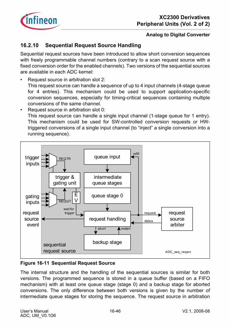
XC2300 DerivativesPeripheral Units (Vol. 2 of 2)
Analog to Digital Converter
16.2.10 Sequential Request Source HandlingSequential request sources have been introduced to allow short conversion sequenceswith freely programmable channel numbers (contrary to a scan request source with afixed conversion order for the enabled channels). Two versions of the sequential sourcesare available in each ADC kernel:• Request source in arbitration slot 2:
This request source can handle a sequence of up to 4 input channels (4-stage queuefor 4 entries). This mechanism could be used to support application-specificconversion sequences, especially for timing-critical sequences containing multipleconversions of the same channel.
• Request source in arbitration slot 0:This request source can handle a single input channel (1-stage queue for 1 entry).This mechanism could be used for SW-controlled conversion requests or HW-triggered conversions of a single input channel (to “inject” a single conversion into arunning sequence).
Figure 16-11 Sequential Request Source
The internal structure and the handling of the sequential sources is similar for bothversions. The programmed sequence is stored in a queue buffer (based on a FIFOmechanism) with at least one queue stage (stage 0) and a backup stage for abortedconversions. The only difference between both versions is given by the number ofintermediate queue stages for storing the sequence. The request source in arbitration
ADC_seq_reqsrc
intermediatequeue stages
queue stage 0
request handlingrequestsourcearbiter
request
status
requestsourceevent
trigger &gating unit
gatinginputs
triggerinputs
sequentialrequest source
REQGT
REQTR queue inputrefill
wait fortrigger
backup stage
abort restart
EV
User’s Manual 16-46 V2.1, 2008-08ADC, UM_V0.1D6

XC2300 DerivativesPeripheral Units (Vol. 2 of 2)
Analog to Digital Converter
slot 0 does not provide intermediate queue stages (1-stage queue with only queuestage 0), whereas the one in arbitration slot 2 provides 3 intermediate queue stages inadditional to queue stage 0 (leading to a 4-stage queue).
16.2.10.1 OverviewA sequential request source performs the:• Queue input:
The queue input represents the programming interface where the sequence isdefined (see QINR0, QINR2). It does not provide any buffer capability, but handlesthe filling of the queue buffer (queue stage 0 plus optional intermediate queue stages)by writing data to it. The contents of the queue stages can not be directly modified byprogram, except by the command for flushing the complete queue.The queue input also handles the refill mechanism, an automatic re-insertion of astarted conversion from queue stage 0 (including the control parameters) as newqueue input. This feature allows a single setup (by SW) of a conversion sequenceand multiple repetitions of the same sequence without the need to re-program it eachtime. A conversion sequence is repeated automatically if all queue entries of thesequence are setup for refill mode.
• Queue stage 0:The content of this queue stage defines which channel will be requested next for aconversion (see Q0R0, Q0R2). It also defines if the request should be triggered byan external event or if the requested conversion should follow the previous one assoon as possible. It also enables the request source interrupt generation after theconversion.The contents of this queue stage is cleared when the requested conversion is startedand the next queue entry can be handled (if available).
• Queue backup stage:The queue backup stage is used to store the request control parameters when aconversion requested by this request source is aborted. A validation bit indicates thatthe aborted conversion has to be requested next (before the current contents ofqueue stage 0) to maintain the original sequence (see QBUR0, QBUR2).
• Request handling:The request handling block interfaces with the request source arbiter. It requests aconversion due to valid information in queue stage 0 and handles the conversionstatus information. The control of the queue sequence is done based on bits inregisters QMR0 (for the request source in arbitration slot 0) and QMR2 (for thearbitration slot 2).
• Trigger and gating signal handling:The trigger and gating unit interfaces with signals and modules outside the ADCmodule that can request conversions. For example, a timer unit can issue a requestsignal to synchronize conversions to PWM events. A trigger event can start aconversion request for the entry in queue stage 0 (see QMR0, QMR2). An event flag
User’s Manual 16-47 V2.1, 2008-08ADC, UM_V0.1D6

XC2300 DerivativesPeripheral Units (Vol. 2 of 2)
Analog to Digital Converter
QSRx.EV indicates that a trigger event has been detected (rising edge of selectedtrigger input signal REQTRx if enabled by QMRx.ENTR or write action withQMRx.TREV = 1). This bit is cleared with each conversion start requested by thissource or by writing bits CEV = 1, FLUSH = 1, or CLRV = 1.
16.2.10.2 Sequential Source OperationTo operate a sequential request source, the following aspects should be taken intoaccount:• The sequence has to be initialized by writing to the queue input QINR0 (for arbitration
slot 0) or QINR2 (for arbitration slot 2) when using the refill mechanism. Each writeaccess corresponds to one conversion request.The desired sequence should be completely initialized before enabling the requestsource, because with enabled refill feature, write accesses by SW to QINRx are notallowed.
• If a trigger or gating function by external signals is desired, the gating and triggerinputs have to be defined by bit fields REQTRx and REQGTx in register PISEL (thevalue of x defines the number of the arbitration slot where the request source isconnected).
• The gating mechanism has to be defined by QMRx.ENGT.• If an external trigger mechanism is desired, it has to be enabled by QMRx.ENTR = 1.• The corresponding arbitration slot has to be enabled to accept conversion requests
from the sequential source (see register ASENR).To start a sequence of a sequential request source, the following mechanisms aresupported:• An external trigger signal can be selected to start a scan sequence controlled by HW
by an external module or signal, e.g. a timer unit or an input pin. The trigger featureis enabled by QMRx.ENTR = 1. The trigger event is generated if a rising edge isdetected at the selected trigger input.
• A trigger event is generated under SW control by writing QMRx.TREV = 1. Thismechanism starts a request if queue stage 0 contains valid data (or the queuebackup stage respectively).
• A write operation to a queue input leads to a (new) valid queue entry. If the queue isempty (no valid entry), the written data arrives in queue stage 0 and starts aconversion request (if enabled by QMRx.ENGT and without waiting for an externaltrigger). If the refill mechanism is used, the queue inputs must not be written while thequeue is running. Write operations to a completely filled queue are ignored.
To stop or abort an ongoing sequence of a sequential request source, the followingmechanisms are supported:• An external gating signal can be selected to stop and to continue a sequence at any
point in time controlled by an external module or signal, e.g. a timer unit or an inputpin. The gating feature can be enabled and the polarity of the gating signal can be
User’s Manual 16-48 V2.1, 2008-08ADC, UM_V0.1D6
XC2300 DerivativesPeripheral Units (Vol. 2 of 2)
Analog to Digital Converter
selected by QMRx.ENGT. The gating mechanism does not modify the queue entries,but only prevents the request handling block from issuing conversion requests to thearbiter.
• The arbiter can be disabled by SW for this arbiter slot by clearing the correspondingbit ASENR.ASENx. This mechanism does not modify the queue entries, but onlyprevents the arbiter from accepting requests from the request handling block.
• The next pending queue entry is cleared by writing bit QMRx.CLRV = 1. It isrecommended to stop the sequence before clearing a queue entry (ENGT = 00B). Ifthe queue backup stage contains a valid entry, this one is cleared, otherwise a validentry in queue register 0 is cleared.
• All queue entries are cleared by writing bit QMRx.FLUSH = 1. It is recommended tostop the sequence before clearing queue entries.
16.2.10.3 Request Source Event and InterruptA request source event occurs when a conversion that has been requested by thissource is completely finished. The interrupt enable bits are located in the queue 0register (if this has not been a repeated start after an abort) or in the queue backupregister (if this has been a repeated start after an abort).A request source event interrupt can be generated based on a request source eventaccording to the structure shown in Figure 16-12. If a request source event is detected,it sets the corresponding indication flag in register EVINFR. These flags can also be setby writing a 1 to the corresponding bit position, whereas writing 0 has no effect. Theindication flags can be cleared by SW by writing a 1 to the corresponding bit position inregister EVINCR.The service request output line SRx that is selected by the request source event interruptnode pointer bit fields in register EVINPR0 becomes activated each time the relatedrequest source event is detected or the related bit position in register EVINFR is writtenwith a 1. The request source events and the result events share the same registers. Therequest source event is located at the bit position in register EVINFR:• Event 0: Request source event of sequential source in arbitration slot 0.• Event 2: Request source event of sequential source in arbitration slot 2.
User’s Manual 16-49 V2.1, 2008-08ADC, UM_V0.1D6

XC2300 DerivativesPeripheral Units (Vol. 2 of 2)
Analog to Digital Converter
Figure 16-12 Interrupt Generation of a Sequential Request Source
ADC_seq_source_int
to SR0
EVINFR.EVINFx
to SR1
to SR3
request source event
request sourceevent
indication flag
to SR2
set
Q0Rx.ENSI
request sourceevent
interrupt enable
EVINPRy.EVINPx
request sourceevent interruptnode pointer
conversionfinished
triggered byrequestsource
QBURx.ENSI
QBURx.V
1
0
User’s Manual 16-50 V2.1, 2008-08ADC, UM_V0.1D6
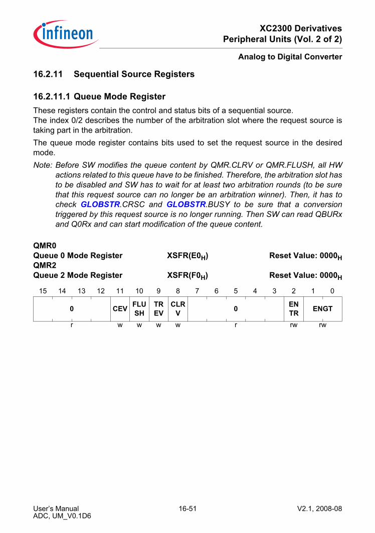
XC2300 DerivativesPeripheral Units (Vol. 2 of 2)
Analog to Digital Converter
16.2.11 Sequential Source Registers
16.2.11.1 Queue Mode RegisterThese registers contain the control and status bits of a sequential source.The index 0/2 describes the number of the arbitration slot where the request source istaking part in the arbitration.The queue mode register contains bits used to set the request source in the desiredmode.Note: Before SW modifies the queue content by QMR.CLRV or QMR.FLUSH, all HW
actions related to this queue have to be finished. Therefore, the arbitration slot hasto be disabled and SW has to wait for at least two arbitration rounds (to be surethat this request source can no longer be an arbitration winner). Then, it has tocheck GLOBSTR.CRSC and GLOBSTR.BUSY to be sure that a conversiontriggered by this request source is no longer running. Then SW can read QBURxand Q0Rx and can start modification of the queue content.
QMR0 Queue 0 Mode Register XSFR(E0H) Reset Value: 0000HQMR2Queue 2 Mode Register XSFR(F0H) Reset Value: 0000H
15 14 13 12 11 10 9 8 7 6 5 4 3 2 1 0
0 CEV FLUSH
TREV
CLRV 0 EN
TR ENGT
r w w w w r rw rw
User’s Manual 16-51 V2.1, 2008-08ADC, UM_V0.1D6
XC2300 DerivativesPeripheral Units (Vol. 2 of 2)
Analog to Digital Converter
Field Bits Type DescriptionENGT [1:0] rw Enable Gate
This bit field enables the gating functionality for the request source.00B The request source does not issue conversion
requests.01B The request source issues conversion
requests if a valid conversion request is pending in the queue 0 register or in the backup register.
10B The request source issues conversion requests if a valid conversion request is pending in the queue 0 register or in the backup register and the selected gating signal REQGTx = 1.
11B The request source issues conversion requests if a valid conversion request is pending in the queue 0 register or in the backup register and the selected gating signal REQGTx = 0.
ENTR 2 rw Enable External TriggerThis bit enables the external trigger possibility.0B The external trigger is disabled and the trigger
event is not generated.1B The external trigger is enabled and a trigger
event is generated if a rising edge is detected at the selected trigger input signal for REQTRx.
CLRV 8 w Clear V Bit0B No action.1B The next pending valid queue entry in the
sequence and the event flag EV are cleared.If there is a valid entry in the queue backup register (QBUR.V = 1), this entry is cleared, otherwise the entry in queue register 0 is cleared.
User’s Manual 16-52 V2.1, 2008-08ADC, UM_V0.1D6
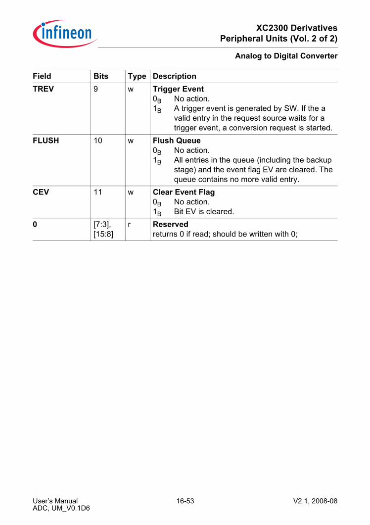
XC2300 DerivativesPeripheral Units (Vol. 2 of 2)
Analog to Digital Converter
TREV 9 w Trigger Event0B No action.1B A trigger event is generated by SW. If the a
valid entry in the request source waits for a trigger event, a conversion request is started.
FLUSH 10 w Flush Queue0B No action.1B All entries in the queue (including the backup
stage) and the event flag EV are cleared. The queue contains no more valid entry.
CEV 11 w Clear Event Flag0B No action.1B Bit EV is cleared.
0 [7:3],[15:8]
r Reservedreturns 0 if read; should be written with 0;
Field Bits Type Description
User’s Manual 16-53 V2.1, 2008-08ADC, UM_V0.1D6

XC2300 DerivativesPeripheral Units (Vol. 2 of 2)
Analog to Digital Converter
16.2.11.2 Queue Status RegisterThe queue status register contains bits indicating the status of the sequential source.The filling level and the empty information refer to the queue intermediate stages (ifavailable) and to the queue register 0. An aborted conversion stored in the backup stageis not indicated by these bits (therefore, see QBURx.V).
QSR0 Queue 0 Status Register XSFR(E2H) Reset Value: 0020HQSR2Queue 2 Status Register XSFR(F2H) Reset Value: 0020H
15 14 13 12 11 10 9 8 7 6 5 4 3 2 1 0
0 EV REQGT 0 EMP
TY 0 FILL
r rh rh r rh r rh
Field Bits Type DescriptionFILL [1:0] rh Filling Level1)
This bit field indicates how many queue entries are valid in the sequential source. It is incremented each time a new entry is written to QINRx or by an enabled refill mechanism. It is decremented each time a requested conversion has been started. A new entry is ignored if the filling level has reached its maximum value.00B EMPTY = 1:There is no valid entry in the
queue.EMPTY = 0:There is 1 valid entries in the queue.
01B There are 2 valid entries in the queue.10B There are 3 valid entries in the queue.11B There are 4 valid entries in the queue.
EMPTY 5 rh Queue EmptyThis bit indicates if the sequential source contains valid entries.0B There are FILL+1 valid entries in the queue.1B There are no valid entries (queue is empty).
User’s Manual 16-54 V2.1, 2008-08ADC, UM_V0.1D6
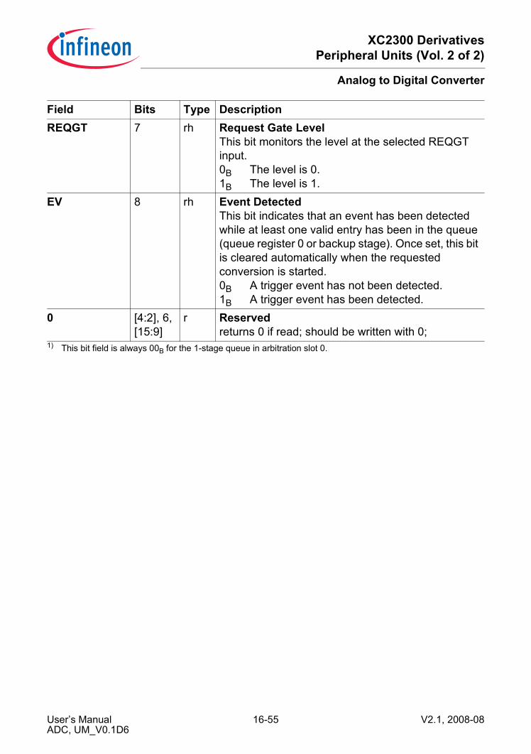
XC2300 DerivativesPeripheral Units (Vol. 2 of 2)
Analog to Digital Converter
REQGT 7 rh Request Gate LevelThis bit monitors the level at the selected REQGT input.0B The level is 0. 1B The level is 1.
EV 8 rh Event DetectedThis bit indicates that an event has been detected while at least one valid entry has been in the queue (queue register 0 or backup stage). Once set, this bit is cleared automatically when the requested conversion is started.0B A trigger event has not been detected.1B A trigger event has been detected.
0 [4:2], 6, [15:9]
r Reservedreturns 0 if read; should be written with 0;
1) This bit field is always 00B for the 1-stage queue in arbitration slot 0.
Field Bits Type Description
User’s Manual 16-55 V2.1, 2008-08ADC, UM_V0.1D6
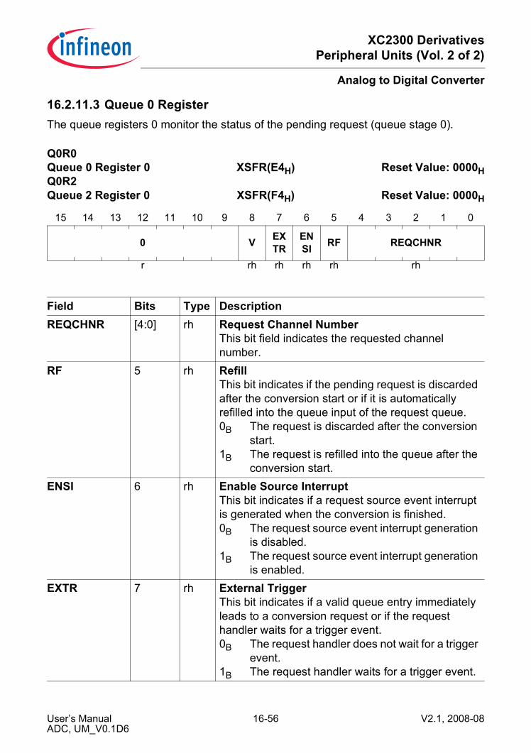
XC2300 DerivativesPeripheral Units (Vol. 2 of 2)
Analog to Digital Converter
16.2.11.3 Queue 0 RegisterThe queue registers 0 monitor the status of the pending request (queue stage 0).
Q0R0 Queue 0 Register 0 XSFR(E4H) Reset Value: 0000HQ0R2Queue 2 Register 0 XSFR(F4H) Reset Value: 0000H
15 14 13 12 11 10 9 8 7 6 5 4 3 2 1 0
0 V EXTR
ENSI RF REQCHNR
r rh rh rh rh rh
Field Bits Type DescriptionREQCHNR [4:0] rh Request Channel Number
This bit field indicates the requested channel number.
RF 5 rh RefillThis bit indicates if the pending request is discarded after the conversion start or if it is automatically refilled into the queue input of the request queue.0B The request is discarded after the conversion
start.1B The request is refilled into the queue after the
conversion start.ENSI 6 rh Enable Source Interrupt
This bit indicates if a request source event interrupt is generated when the conversion is finished.0B The request source event interrupt generation
is disabled.1B The request source event interrupt generation
is enabled.EXTR 7 rh External Trigger
This bit indicates if a valid queue entry immediately leads to a conversion request or if the request handler waits for a trigger event.0B The request handler does not wait for a trigger
event.1B The request handler waits for a trigger event.
User’s Manual 16-56 V2.1, 2008-08ADC, UM_V0.1D6
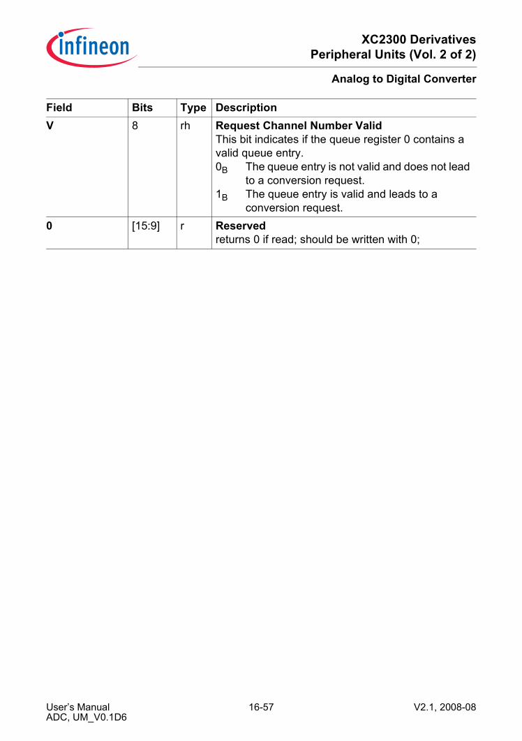
XC2300 DerivativesPeripheral Units (Vol. 2 of 2)
Analog to Digital Converter
V 8 rh Request Channel Number ValidThis bit indicates if the queue register 0 contains a valid queue entry.0B The queue entry is not valid and does not lead
to a conversion request.1B The queue entry is valid and leads to a
conversion request.0 [15:9] r Reserved
returns 0 if read; should be written with 0;
Field Bits Type Description
User’s Manual 16-57 V2.1, 2008-08ADC, UM_V0.1D6
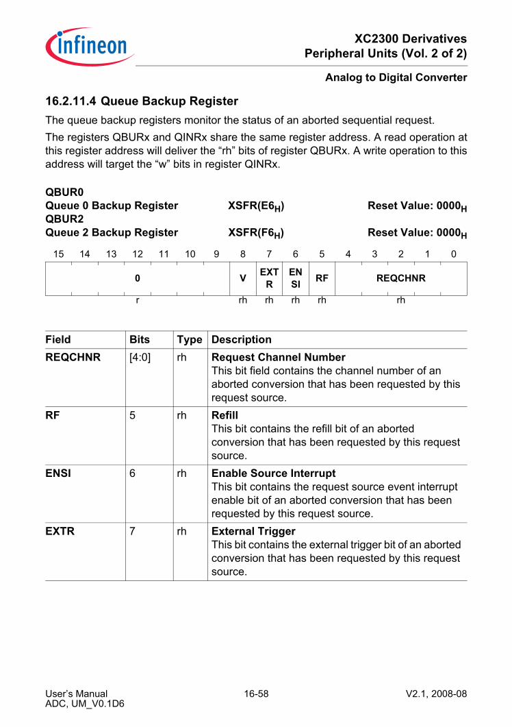
XC2300 DerivativesPeripheral Units (Vol. 2 of 2)
Analog to Digital Converter
16.2.11.4 Queue Backup RegisterThe queue backup registers monitor the status of an aborted sequential request.The registers QBURx and QINRx share the same register address. A read operation atthis register address will deliver the “rh” bits of register QBURx. A write operation to thisaddress will target the “w” bits in register QINRx.
QBUR0 Queue 0 Backup Register XSFR(E6H) Reset Value: 0000HQBUR2Queue 2 Backup Register XSFR(F6H) Reset Value: 0000H
15 14 13 12 11 10 9 8 7 6 5 4 3 2 1 0
0 V EXTR
ENSI RF REQCHNR
r rh rh rh rh rh
Field Bits Type DescriptionREQCHNR [4:0] rh Request Channel Number
This bit field contains the channel number of an aborted conversion that has been requested by this request source.
RF 5 rh RefillThis bit contains the refill bit of an aborted conversion that has been requested by this request source.
ENSI 6 rh Enable Source InterruptThis bit contains the request source event interrupt enable bit of an aborted conversion that has been requested by this request source.
EXTR 7 rh External TriggerThis bit contains the external trigger bit of an aborted conversion that has been requested by this request source.
User’s Manual 16-58 V2.1, 2008-08ADC, UM_V0.1D6
XC2300 DerivativesPeripheral Units (Vol. 2 of 2)
Analog to Digital Converter
V 8 rh Request Channel Number ValidThis bit indicates if the entry in the queue backup register is valid (REQCHNR, RF, TR and ENSI are valid). Bit V is set if a running conversion that has been requested by this request source is aborted. It is cleared when the repeated conversion is started.0B The backup register does not contain a valid
entry.1B The backup register contains a valid entry. It
will be requested before a valid entry in queue register 0 will be requested.
0 [15:9] r Reservedreturns 0 if read; should be written with 0;
Field Bits Type Description
User’s Manual 16-59 V2.1, 2008-08ADC, UM_V0.1D6
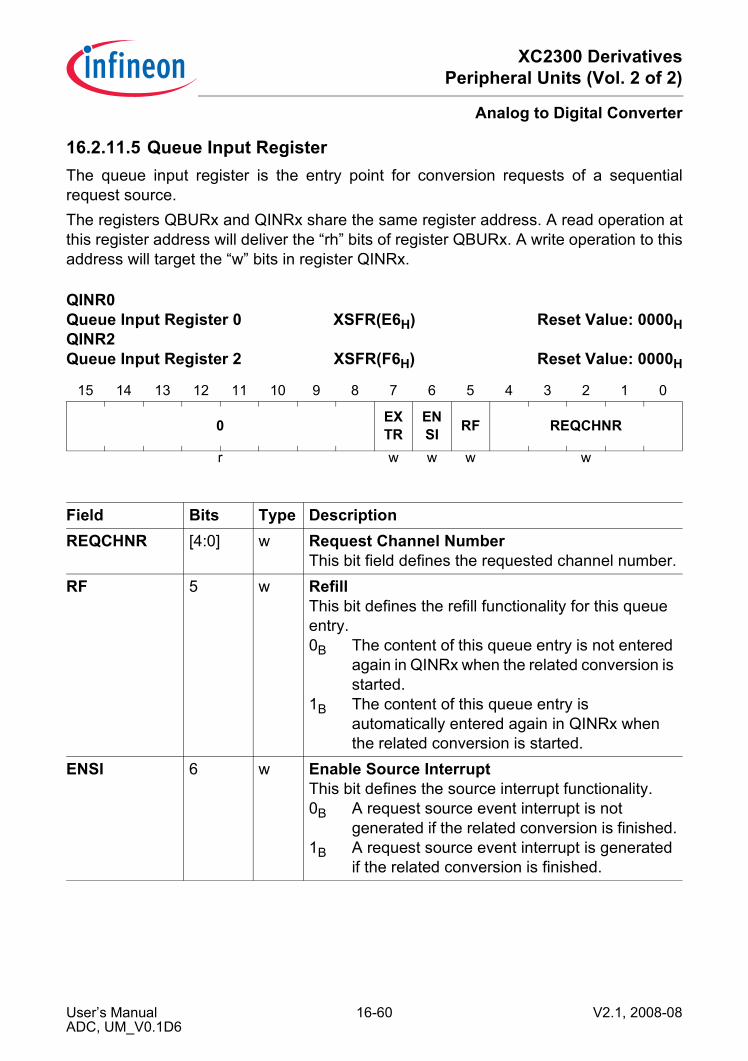
XC2300 DerivativesPeripheral Units (Vol. 2 of 2)
Analog to Digital Converter
16.2.11.5 Queue Input RegisterThe queue input register is the entry point for conversion requests of a sequentialrequest source.The registers QBURx and QINRx share the same register address. A read operation atthis register address will deliver the “rh” bits of register QBURx. A write operation to thisaddress will target the “w” bits in register QINRx.
QINR0 Queue Input Register 0 XSFR(E6H) Reset Value: 0000HQINR2Queue Input Register 2 XSFR(F6H) Reset Value: 0000H
15 14 13 12 11 10 9 8 7 6 5 4 3 2 1 0
0 EXTR
ENSI RF REQCHNR
r w w w w
Field Bits Type DescriptionREQCHNR [4:0] w Request Channel Number
This bit field defines the requested channel number.RF 5 w Refill
This bit defines the refill functionality for this queue entry.0B The content of this queue entry is not entered
again in QINRx when the related conversion is started.
1B The content of this queue entry is automatically entered again in QINRx when the related conversion is started.
ENSI 6 w Enable Source InterruptThis bit defines the source interrupt functionality.0B A request source event interrupt is not
generated if the related conversion is finished.1B A request source event interrupt is generated
if the related conversion is finished.
User’s Manual 16-60 V2.1, 2008-08ADC, UM_V0.1D6

XC2300 DerivativesPeripheral Units (Vol. 2 of 2)
Analog to Digital Converter
EXTR 7 w External TriggerThis bit defines the external trigger functionality.0B A valid queue entry immediately leads to a
conversion request.1B A valid queue entry waits for a trigger event to
occur before issuing a conversion request.0 [15:8] r Reserved
returns 0 if read; should be written with 0;
Field Bits Type Description
User’s Manual 16-61 V2.1, 2008-08ADC, UM_V0.1D6

XC2300 DerivativesPeripheral Units (Vol. 2 of 2)
Analog to Digital Converter
16.2.12 Channel-Related FunctionsThe channel control unit defines the conversion settings, that can be programmedindividually for each analog input channel. Therefore, a channel control registerCHCTRx (x = 0 - 15) is associated to each analog input channel CHx. After the arbiterhas determined the channel to be converted, the defined settings are applied to the ADconverter, comprising information about:• Conversion parameters:
Bit field ICLSEL defines which input class is taken into account for the conversion(see Section 16.2.12.1).
• Reference selection:Bit field REFSEL defines which reference input is used for the conversion (seeSection 16.2.12.2)
• Channel event handling:Bit fields LCC, BNDASEL, and BNDBSEL define which boundaries are used for limitchecking (see Section 16.2.12.4) and which channel event leads to a channel eventinterrupt (see Section 16.2.12.5).
• Synchronous conversion request:Bit SYNC defines if the channel triggers a synchronized conversion (seeSection 16.2.17).
In addition to the general channel control, the ADC kernel supports a mechanism(named alias feature, see Section 16.2.12.3) to redirect a conversion request to anotherchannel number.
16.2.12.1 Input ClassesAn input class defines the length of the sample phase and the resolution of theconversion. In most applications, the characteristics of the input circuitries (RC input low-pass filter and impedance of the signal source) are quite similar for several analog inputsignals, leading to similar timings for the sample phase of these channels. As aconsequence, input channels with similar parameters can be grouped together to forman input class.All channels with the same ICLSEL setting belong to the same input class and have thesame sample phase length and resolution. In the XC2300, 2 input classes are supported.Registers INPCRx (x = 0 - 1) can be programmed to adjust the sample time and theresolution to the application requirements independently for each input class.The default setting of these registers lead to the minimum sample phase length of 2 fADCIcycles and conversions with 10 bits resolution. If this default setting fits to the applicationrequirements, bit fields CHCTRx (x = 0 - 15).ICLSEL and registers INPCRx (x = 0 - 1)need not to be changed.
User’s Manual 16-62 V2.1, 2008-08ADC, UM_V0.1D6

XC2300 DerivativesPeripheral Units (Vol. 2 of 2)
Analog to Digital Converter
16.2.12.2 Reference SelectionThe conversion result of the ADC is always referring to a reference voltage. Themaximum digital result value (full scale) is obtained if the analog input voltage equals thereference voltage. In order to support more than one measurement range with full scaledigital representation, the user can select between the standard reference input VAREFand an alternative reference input at the analog input channel CH0 for each ADC kernel.The reference selection can be individually programmed for each input channel.This feature can be used to connect 5 V based sensors and 3.3 V based sensors to thesame ADC kernel. In this case, one set of input channels refers to the standard referenceinput, whereas the other one refers to the voltage level at input CH0.Please note that the smallest granularity 1 LSBn for n bit resolution refers to the selectedreference voltage. The granularity becomes very small if a low reference voltage isapplied, and as a consequence, the resulting TUE increases due to noise effects.Therefore, it is recommended to avoid small reference voltages.
16.2.12.3 Alias FeatureThe ADC kernel provides an alias feature, allowing a re-direction of conversion requestsfor channels CH0 or CH1 to other channel numbers. This feature can be used tomeasure the same input channel and to store the conversion results in two differentresult registers.• The same signal can be measured twice without the need to read out the conversion
result to avoid data loss. This allows triggering both conversions quickly one after theother and being independent from CPU interrupt latency.
• The sensor signal is connected to only one input channel (instead of two analoginputs). This saves input pins in low-cost applications and only the leakage of oneinput has to be considered in the error calculation.
• Even if the analog input CH0 is used as alternative reference (see Figure 16-13), theinternal trigger and data handling features for channel CH0 can be used.
• The channel settings for both conversions can be different (boundary values,interrupts, etc.).
• If a sequential conversion request source has been set up, a conversion request forchannels CH0 or CH1 can be easily directed to other input channels without flushingthe queue.
In typical low-cost AC-drive applications, only one common current sensor is used todetermine the phase currents. Depending on the applied PWM pattern, the measuredvalue has different meanings and the sample points have to be precisely located in thePWM period. Figure 16-13 shows an example where the sensor signal is connected toone input channel (CHx) but two conversions are triggered for two different channels(CHx and CH0). With the alias feature, a conversion request for CH0 leads to aconversion of the analog input CHx instead of CH0, but taking into account the settingsfor CH0. Although the same analog input (CHx) has been measured, the conversion
User’s Manual 16-63 V2.1, 2008-08ADC, UM_V0.1D6
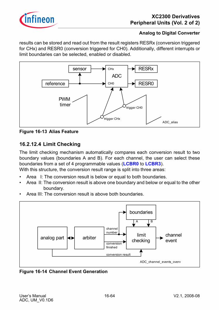
XC2300 DerivativesPeripheral Units (Vol. 2 of 2)
Analog to Digital Converter
results can be stored and read out from the result registers RESRx (conversion triggeredfor CHx) and RESR0 (conversion triggered for CH0). Additionally, different interrupts orlimit boundaries can be selected, enabled or disabled.
Figure 16-13 Alias Feature
16.2.12.4 Limit CheckingThe limit checking mechanism automatically compares each conversion result to twoboundary values (boundaries A and B). For each channel, the user can select theseboundaries from a set of 4 programmable values (LCBR0 to LCBR3).With this structure, the conversion result range is split into three areas:• Area I: The conversion result is below or equal to both boundaries.• Area II: The conversion result is above one boundary and below or equal to the other
boundary.• Area III: The conversion result is above both boundaries.
Figure 16-14 Channel Event Generation
ADC_alias
PWMtimer
RESRx
trigger CHx
RESR0
trigger CH0
sensorADC
CHx
reference CH0
ADC_channel_events_overv
channeleventarbiteranalog part
conversion result
channelnumber limit
checking
boundaries
A B
conversionfinished
User’s Manual 16-64 V2.1, 2008-08ADC, UM_V0.1D6
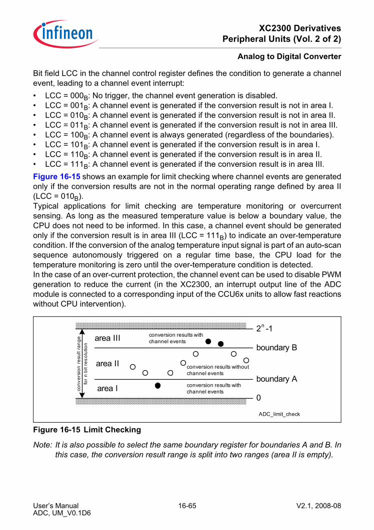
XC2300 DerivativesPeripheral Units (Vol. 2 of 2)
Analog to Digital Converter
Bit field LCC in the channel control register defines the condition to generate a channelevent, leading to a channel event interrupt:• LCC = 000B: No trigger, the channel event generation is disabled.• LCC = 001B: A channel event is generated if the conversion result is not in area I.• LCC = 010B: A channel event is generated if the conversion result is not in area II.• LCC = 011B: A channel event is generated if the conversion result is not in area III.• LCC = 100B: A channel event is always generated (regardless of the boundaries).• LCC = 101B: A channel event is generated if the conversion result is in area I.• LCC = 110B: A channel event is generated if the conversion result is in area II.• LCC = 111B: A channel event is generated if the conversion result is in area III.Figure 16-15 shows an example for limit checking where channel events are generatedonly if the conversion results are not in the normal operating range defined by area II(LCC = 010B).Typical applications for limit checking are temperature monitoring or overcurrentsensing. As long as the measured temperature value is below a boundary value, theCPU does not need to be informed. In this case, a channel event should be generatedonly if the conversion result is in area III (LCC = 111B) to indicate an over-temperaturecondition. If the conversion of the analog temperature input signal is part of an auto-scansequence autonomously triggered on a regular time base, the CPU load for thetemperature monitoring is zero until the over-temperature condition is detected.In the case of an over-current protection, the channel event can be used to disable PWMgeneration to reduce the current (in the XC2300, an interrupt output line of the ADCmodule is connected to a corresponding input of the CCU6x units to allow fast reactionswithout CPU intervention).
Figure 16-15 Limit Checking
Note: It is also possible to select the same boundary register for boundaries A and B. Inthis case, the conversion result range is split into two ranges (area II is empty).
ADC_limit_check
2 -1
conv
ersi
on r
esul
t ran
gefo
r n
bit r
esol
utio
n
n
0
boundary B
boundary Aarea I
area II
area III
conversion results withoutchannel events
conversion results withchannel events
conversion results withchannel events
User’s Manual 16-65 V2.1, 2008-08ADC, UM_V0.1D6

XC2300 DerivativesPeripheral Units (Vol. 2 of 2)
Analog to Digital Converter
16.2.12.5 Channel Event InterruptsA channel event interrupt can be generated based on a channel event according to thestructure shown in Figure 16-16. If a channel event is detected, it sets the correspondingindication flag in register CHINFR. These flags can also be set by writing a 1 to thecorresponding bit position, whereas writing 0 has no effect. The indication flags can becleared by SW by writing a 1 to the corresponding bit position in register CHINCR.
Figure 16-16 Channel Event Interrupt Generation
The service request output line SRx that is selected by the channel node pointer bit fieldsin registers CHINPR0, CHINPR4, CHINPR8, or CHINPR12 is activated each time therelated channel event is detected or the related bit position in register CHINFR is writtenwith a 1.
ADC_channel_events_routing
to SR0
FC0
FC1
FC15
to SR1
to SR3CHENP0
CHENP1
CHENP15. . .
. . .
channelnumber
channelevent
channel eventflags
channel eventnode pointers
to SR2
User’s Manual 16-66 V2.1, 2008-08ADC, UM_V0.1D6
XC2300 DerivativesPeripheral Units (Vol. 2 of 2)
Analog to Digital Converter
16.2.13 Channel-Related Registers
16.2.13.1 Channel Control RegistersThe channel control registers contain bits to select the targeted result register, to controlthe limit check mechanism and to select an input class.The channel control register 0 defines the settings for the input channel CH0, etc.
CHCTRx (x = 0 - 15) Channel x Control Register XSFR(20H + x * 2) Reset Value: 0000H
15 14 13 12 11 10 9 8 7 6 5 4 3 2 1 0
0 RESRSEL
ICLSEL
REFSEL
SYNC LCC BNDB
SELBNDASEL
r rw rw rw rw rw rw rw
Field Bits Type DescriptionBNDASEL [1:0] rw Boundary A Selection
This bit field defines which boundary will be taken as boundary A for the limit checking.00B The value given by register LCBR0 is selected.01B The value given by register LCBR1 is selected.10B The value given by register LCBR2 is selected.11B The value given by register LCBR3 is selected.
BNDBSEL [3:2] rw Boundary B SelectionThis bit field defines which boundary will be taken as boundary B for the limit checking.00B The value given by register LCBR0 is selected.01B The value given by register LCBR1 is selected.10B The value given by register LCBR2 is selected.11B The value given by register LCBR3 is selected.
LCC [6:4] rw Limit Check ControlThis bit field defines the behavior of the limit checking mechanism. Please refer to the coding in Section 16.2.12.4 on Page 16-64.
User’s Manual 16-67 V2.1, 2008-08ADC, UM_V0.1D6

XC2300 DerivativesPeripheral Units (Vol. 2 of 2)
Analog to Digital Converter
SYNC 7 rw Synchronization RequestThis bit defines if a conversion request for this channel leads to a synchronized (parallel) conversion with other ADC kernels. This bit is only taken into account if the ADC kernel is a potential conversion master (SYNCTR.STSEL = 00), otherwise it is considered to be 0.0B This channel does not request a synchronized
conversion.1B This channel requests a synchronized
conversion if the ADC kernel is a potential synchronization master.
REFSEL [9:8] rw Reference Input SelectionThis bit field defines the reference source for this channel.00B The standard reference input VAREF is
selected.01B The alternative reference input CH0 is
selected.10B reserved, do not use11B reserved, do not use
ICLSEL [11,10] rw Input Class SelectionThese bits are used to select the input class.00B The input class 0 is selected.01B The input class 1 is selected.10B reserved, do not use11B reserved, do not use
RESRSEL [14:12] rw Result Register SelectionThis bit field defines which result register will be the target of the conversion result of this channel.000B The result register 0 is selected.001B The result register 1 is selected....111B The result register 7 is selected.
0 15 r Reservedreturns 0 if read; should be written with 0;
Field Bits Type Description
User’s Manual 16-68 V2.1, 2008-08ADC, UM_V0.1D6
XC2300 DerivativesPeripheral Units (Vol. 2 of 2)
Analog to Digital Converter
16.2.13.2 Input Class RegistersThe input class registers contain bits to control the sample time and the resolution foreach input class.The input class register 0 defines the settings for the input class 0, etc.
INPCRx (x = 0 - 1) Input Class Register x XSFR(C0H + x * 2) Reset Value: 0000H
15 14 13 12 11 10 9 8 7 6 5 4 3 2 1 0
0 DW STC
r rw rw
Field Bits Type DescriptionSTC [7:0] rw Sample Time Control
This bit field defines the additional length of the sample phase, given in analog clock cycles fADCI.A minimum sample phase of 2 analog clock cycles is extended by the programmed value.sample phase length = (2 + STC) / fADCI
DW [9:8] rw Data WidthThis bit field defines how many bits are converted for the result1). The MSBs of conversion results with different DW settings are left aligned in the result bit fields. Bit positions that are not converted are 0.00B The result is 10 bits wide.01B reserved, do not use10B The result is 8 bits wide.11B reserved, do not use
1) The setting 00B is default. In case a 10-bit AD converter is used, the combinations 01B and 11B are ignoredby the converter and treated like 00B.
0 [15:10] r Reservedreturns 0 if read; should be written with 0;
User’s Manual 16-69 V2.1, 2008-08ADC, UM_V0.1D6

XC2300 DerivativesPeripheral Units (Vol. 2 of 2)
Analog to Digital Converter
16.2.13.3 Limit Check Boundary RegistersThe bit fields in these registers define compare value (boundary) for the limit checkingunit. The reset values of the boundaries are defined as 10%, 90%, 33% and 66% of thecomplete result range (in 12 bit representation).
LCBR0 Limit Check Boundary Register 0 XSFR(84H) Reset Value: 0198HLCBR1Limit Check Boundary Register 1 XSFR(86H) Reset Value: 0E64HLCBR2Limit Check Boundary Register 2 XSFR(88H) Reset Value: 0554HLCBR3Limit Check Boundary Register 3 XSFR(8AH) Reset Value: 0AA8H
15 14 13 12 11 10 9 8 7 6 5 4 3 2 1 0
0 BOUNDARY 0
r rw r
Field Bits Type DescriptionBOUNDARY [11:2] rw Boundary for Limit Checking
This bit field contains the value for the limit checking unit that is compared to the actual conversion result. The result of the limit check is used for the generation of the channel event, see Section 16.2.12.4.
0 [1:0], [15:12]
r Reservedreturns 0 if read; should be written with 0;
User’s Manual 16-70 V2.1, 2008-08ADC, UM_V0.1D6

XC2300 DerivativesPeripheral Units (Vol. 2 of 2)
Analog to Digital Converter
16.2.13.4 Channel Event Indication Flag RegisterThe channel event indication flag register CHINFR monitors the detected channelevents.
CHINFR Channel Event Indication Flag RegisterXSFR(90H) Reset Value: 0000H
15 14 13 12 11 10 9 8 7 6 5 4 3 2 1 0
CHINF15
CHINF14
CHINF13
CHINF12
CHINF11
CHINF10
CHINF9
CHINF8
CHINF7
CHINF6
CHINF5
CHINF4
CHINF3
CHINF2
CHINF1
CHINF0
rwh rwh rwh rwh rwh rwh rwh rwh rwh rwh rwh rwh rwh rwh rwh rwh
Field Bits Type DescriptionCHINFx(x = 0 - 15)
x rwh Channel x Event Indication FlagFlag CHINFx indicates that a channel event for channel x has been detected.Writing a 0 has no effect, whereas writing a 1 sets the written bit position and generates the corresponding interrupt request.0B A channel x event has not yet been detected.1B A channel x event has been detected.
User’s Manual 16-71 V2.1, 2008-08ADC, UM_V0.1D6

XC2300 DerivativesPeripheral Units (Vol. 2 of 2)
Analog to Digital Converter
16.2.13.5 Clear Channel Event Indication RegisterWriting a 1 to a bit position in the channel indication clear register CHINCR clears thecorresponding channel event indication flag CHINFx in register CHINFR. If a channelevent is detected when the corresponding bit position is written with a 1, flag CHINFx iscleared.
CHINCR Channel Event Indication Clear Register
XSFR(92H) Reset Value: 0000H
15 14 13 12 11 10 9 8 7 6 5 4 3 2 1 0
CHINC15
CHINC14
CHINC13
CHINC12
CHINC11
CHINC10
CHINC9
CHINC8
CHINC7
CHINC6
CHINC5
CHINC4
CHINC3
CHINC2
CHINC1
CHINC0
w w w w w w w w w w w w w w w w
Field Bits Type DescriptionCHINCx(x = 0 - 15)
x w Clear Channel Indication Flag0 No action.1 Flag CHINFR.x is cleared.
User’s Manual 16-72 V2.1, 2008-08ADC, UM_V0.1D6

XC2300 DerivativesPeripheral Units (Vol. 2 of 2)
Analog to Digital Converter
16.2.13.6 Channel Interrupt Node Pointer RegistersThe bit fields in these registers define the service request output ADCx_SR[3:0] that isused to signal a channel event interrupt.
CHINPR0 Channel Interrupt Node Pointer Register 0
XSFR(98H) Reset Value: 0000H
15 14 13 12 11 10 9 8 7 6 5 4 3 2 1 0
0 CHINP3 0 CHINP2 0 CHINP1 0 CHINP0
r rw r rw r rw r rw
Field Bits Type DescriptionCHINP0,CHINP1,CHINP2,CHINP3
[1:0],[5:4],[9:8],[13:12]
rw Interrupt Node Pointer for Channel xThis bit field selects which service request output indicates a channel event interrupt of channel x.00B Service request output SR0 is selected.01B Service request output SR1 is selected.10B Service request output SR2 is selected.11B Service request output SR3 is selected.
0 [3:2], [7:6], [11:10],[15:14]
r Reservedreturns 0 if read; should be written with 0;
CHINPR4Channel Interrupt Node Pointer Register 4
XSFR(9AH) Reset Value: 0000H
15 14 13 12 11 10 9 8 7 6 5 4 3 2 1 0
0 CHINP7 0 CHINP6 0 CHINP5 0 CHINP4
r rw r rw r rw r rw
User’s Manual 16-73 V2.1, 2008-08ADC, UM_V0.1D6
XC2300 DerivativesPeripheral Units (Vol. 2 of 2)
Analog to Digital Converter
Field Bits Type DescriptionCHINP4,CHINP5,CHINP6,CHINP7
[1:0],[5:4],[9:8],[13:12]
rw Interrupt Node Pointer for Channel xThis bit field selects which service request output indicates a channel event interrupt of channel x.00B Service request output SR0 is selected.01B Service request output SR1 is selected.10B Service request output SR2 is selected.11B Service request output SR3 is selected.
0 [3:2], [7:6], [11:10],[15:14]
r Reservedreturns 0 if read; should be written with 0;
CHINPR8Channel Interrupt Node Pointer Register 8
XSFR(9CH) Reset Value: 0000H
15 14 13 12 11 10 9 8 7 6 5 4 3 2 1 0
0 CHINP11 0 CHINP10 0 CHINP9 0 CHINP8
r rw r rw r rw r rw
Field Bits Type DescriptionCHINP8,CHINP9,CHINP10,CHINP11
[1:0],[5:4],[9:8],[13:12]
rw Interrupt Node Pointer for Channel xThis bit field selects which service request output indicates a channel event interrupt of channel x.00B Service request output SR0 is selected.01B Service request output SR1 is selected.10B Service request output SR2 is selected.11B Service request output SR3 is selected.
0 [3:2], [7:6], [11:10],[15:14]
r Reservedreturns 0 if read; should be written with 0;
User’s Manual 16-74 V2.1, 2008-08ADC, UM_V0.1D6
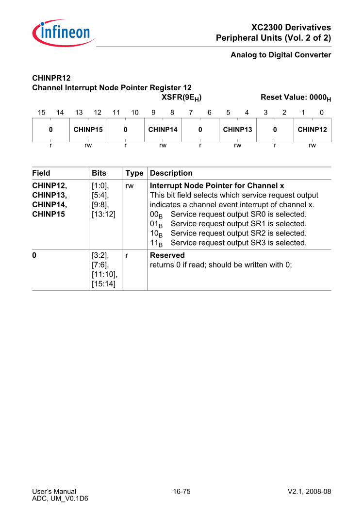
XC2300 DerivativesPeripheral Units (Vol. 2 of 2)
Analog to Digital Converter
CHINPR12Channel Interrupt Node Pointer Register 12
XSFR(9EH) Reset Value: 0000H
15 14 13 12 11 10 9 8 7 6 5 4 3 2 1 0
0 CHINP15 0 CHINP14 0 CHINP13 0 CHINP12
r rw r rw r rw r rw
Field Bits Type DescriptionCHINP12,CHINP13,CHINP14,CHINP15
[1:0],[5:4],[9:8],[13:12]
rw Interrupt Node Pointer for Channel xThis bit field selects which service request output indicates a channel event interrupt of channel x.00B Service request output SR0 is selected.01B Service request output SR1 is selected.10B Service request output SR2 is selected.11B Service request output SR3 is selected.
0 [3:2], [7:6], [11:10],[15:14]
r Reservedreturns 0 if read; should be written with 0;
User’s Manual 16-75 V2.1, 2008-08ADC, UM_V0.1D6
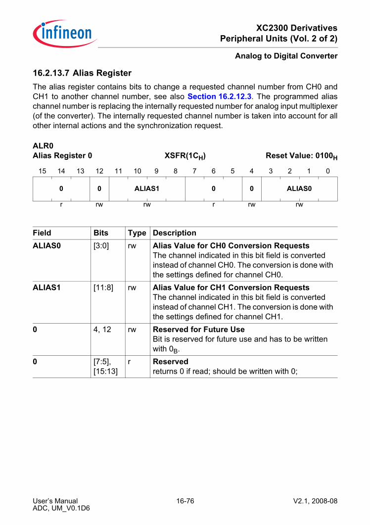
XC2300 DerivativesPeripheral Units (Vol. 2 of 2)
Analog to Digital Converter
16.2.13.7 Alias RegisterThe alias register contains bits to change a requested channel number from CH0 andCH1 to another channel number, see also Section 16.2.12.3. The programmed aliaschannel number is replacing the internally requested number for analog input multiplexer(of the converter). The internally requested channel number is taken into account for allother internal actions and the synchronization request.
ALR0 Alias Register 0 XSFR(1CH) Reset Value: 0100H
15 14 13 12 11 10 9 8 7 6 5 4 3 2 1 0
0 0 ALIAS1 0 0 ALIAS0
r rw rw r rw rw
Field Bits Type DescriptionALIAS0 [3:0] rw Alias Value for CH0 Conversion Requests
The channel indicated in this bit field is converted instead of channel CH0. The conversion is done with the settings defined for channel CH0.
ALIAS1 [11:8] rw Alias Value for CH1 Conversion RequestsThe channel indicated in this bit field is converted instead of channel CH1. The conversion is done with the settings defined for channel CH1.
0 4, 12 rw Reserved for Future UseBit is reserved for future use and has to be written with 0B.
0 [7:5],[15:13]
r Reservedreturns 0 if read; should be written with 0;
User’s Manual 16-76 V2.1, 2008-08ADC, UM_V0.1D6
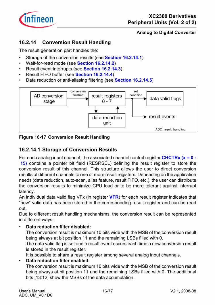
XC2300 DerivativesPeripheral Units (Vol. 2 of 2)
Analog to Digital Converter
16.2.14 Conversion Result HandlingThe result generation part handles the:• Storage of the conversion results (see Section 16.2.14.1)• Wait-for-read mode (see Section 16.2.14.2)• Result event interrupts (see Section 16.2.14.3)• Result FIFO buffer (see Section 16.2.14.4)• Data reduction or anti-aliasing filtering (see Section 16.2.14.5)
Figure 16-17 Conversion Result Handling
16.2.14.1 Storage of Conversion ResultsFor each analog input channel, the associated channel control register CHCTRx (x = 0 -15) contains a pointer bit field (RESRSEL) defining the result register to store the
conversion result of this channel. This structure allows the user to direct conversionresults of different channels to one or more result registers. Depending on the applicationneeds (data reduction, auto-scan, alias feature, result FIFO, etc.), the user can distributethe conversion results to minimize CPU load or to be more tolerant against interruptlatency.An individual data valid flag VFx (in register VFR) for each result register indicates that“new” valid data has been stored in the corresponding result register and can be readout.Due to different result handling mechanisms, the conversion result can be representedin different ways:• Data reduction filter disabled:
The conversion result is maximum 10 bits wide with the MSB of the conversion resultbeing always at bit position 11 and the remaining LSBs filled with 0.The data valid flag is set and a result event occurs each time a new conversion resultis stored in the result register.It is possible to share a result register among several analog input channels.
• Data reduction filter enabled:The conversion result is maximum 10 bits wide with the MSB of the conversion resultbeing always at bit position 11 and the remaining LSBs filled with 0. The additionalbits [13:12] show the MSBs of the data accumulation.
ADC_result_handling
result registers0 - 7
AD conversionstage data valid flags
setcondition
result eventsdata reductionunit
conversionfinished
User’s Manual 16-77 V2.1, 2008-08ADC, UM_V0.1D6
XC2300 DerivativesPeripheral Units (Vol. 2 of 2)
Analog to Digital Converter
The data valid flag is set and a result event occurs each time a data reductionsequence is finished and the final result is available in the result register.The channel number is not included in the result register read view.
In order to support a wait-for-read and FIFO buffer features, the valid flag has to becleared automatically when SW does a read access or the result is transferred intoanother FIFO element (if result FIFO buffering is enabled).This behavior is contradictory to debugging requirements. For debugging, it has to bepossible to introduce read or write commands into the normal program flow, e.g. tomonitor conversion results. If a debugger reads out a result register, it would change thestatus of the conversion result from valid = “new” (not yet read out) to “old” (already readout). This would have an undesired impact on the application.Therefore, the read views with “V” deliver the same value as the read views without “V”,but without clearing the valid bit. As a result, a debugger using read views with “V” canmonitor the conversion results without influencing their status for the application.The application requirements for results with enabled or disabled data reduction filterbeing different and debugger accesses can occur, four different scenarios with differentresult register read views are supported. The four read views refer to the same resultregister contents, but show a different behavior according to the address that has beenread:• Standard read view RESRx (x = 0-7):
The data reduction filter has to be disabled, the channel number is included to identifywhich channel has been converted, and a read action clears the corresponding validbit. This representation is compatible to the ADC result register in XC16x devices.
• Read view RESRAx (x = 0-7):The data reduction filter can be enabled, the channel number is not included, and aread action clears the corresponding valid bit.
• Read view RESRVx (x = 0-7) for debugger:The data reduction filter has to be disabled, the channel number is included, but aread action does not clear the corresponding valid bit.
• Read view RESRAVx (x = 0-7) for debugger:The data reduction filter can be enabled, the channel number is not included, but aread action does not clear the corresponding valid bit.
User’s Manual 16-78 V2.1, 2008-08ADC, UM_V0.1D6
XC2300 DerivativesPeripheral Units (Vol. 2 of 2)
Analog to Digital Converter
16.2.14.2 Wait-for-Read ModeThe wait-for-read mode is a feature of a result register allowing the CPU (or PEC) to treateach conversion result independently without the risk of data loss. Data loss could occurif the CPU does not read a conversion result from a result register before a new resultoverwrites the previous one.Especially for auto-scan conversion sequences (or other sequences with “relaxed”timing requirements), the wait-for-read offers the possibility to request a conversionsequence according to an event (HW or SW), but to start a new conversion according tothe CPU capability to read the formerly converted result.If wait-for-read mode is enabled for a result register by setting bit WFR in register RCRx(x = 0 - 7), a request source does not generate a conversion request while the targetedresult register contains valid data (indicated by the valid flag VFx = 1) or if a currentlyrunning conversion targets the same result register.A new conversion request is generated only after the targeted result register has beenread out.If two request sources target the same result register with wait-for-read selected, a lowerpriority request started before the higher priority source has requested its conversion cannot be interrupted by the higher priority request. If a higher priority request targets adifferent result register, the lower priority conversion can be cancelled and repeatedafterwards.
User’s Manual 16-79 V2.1, 2008-08ADC, UM_V0.1D6
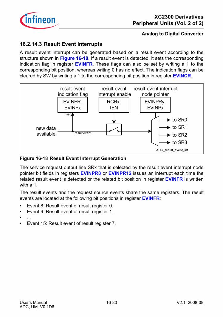
XC2300 DerivativesPeripheral Units (Vol. 2 of 2)
Analog to Digital Converter
16.2.14.3 Result Event InterruptsA result event interrupt can be generated based on a result event according to thestructure shown in Figure 16-18. If a result event is detected, it sets the correspondingindication flag in register EVINFR. These flags can also be set by writing a 1 to thecorresponding bit position, whereas writing 0 has no effect. The indication flags can becleared by SW by writing a 1 to the corresponding bit position in register EVINCR.
Figure 16-18 Result Event Interrupt Generation
The service request output line SRx that is selected by the result event interrupt nodepointer bit fields in registers EVINPR8 or EVINPR12 issues an interrupt each time therelated result event is detected or the related bit position in register EVINFR is writtenwith a 1.The result events and the request source events share the same registers. The resultevents are located at the following bit positions in register EVINFR:• Event 8: Result event of result register 0.• Event 9: Result event of result register 1.• ...• Event 15: Result event of result register 7.
ADC_result_event_int
to SR0
EVINFR.EVINFx
to SR1
to SR3
result event
result eventindication flag
to SR2
set
RCRx.IEN
result eventinterrupt enable
EVINPRy.EVINPx
result event interruptnode pointer
new dataavailable
User’s Manual 16-80 V2.1, 2008-08ADC, UM_V0.1D6

XC2300 DerivativesPeripheral Units (Vol. 2 of 2)
Analog to Digital Converter
16.2.14.4 Result FIFO BufferIf a result register is not used as direct target for a conversion result, it can beconcatenated with other result registers of the same ADC kernel to form a result FIFObuffer (first-in-first-out buffer mechanism). This allows to store measurement results andto read them out later with a “relaxed” CPU access timing. It is possible to set up morethan one FIFO buffer structure with the available result registers.A FIFO structure can be built by at least two “neighbor” result registers with the indicesx and z = x+1, where result register z represents the input and result register xrepresents the output of the FIFO buffer. The conversion result has to be delivered bythe converter stage to the FIFO input, whereas the buffered data has to be read out fromthe FIFO output.The FIFO buffer function is enabled by setting bit FEN in registers RCRx (x = 0 - 7),except for RCRz.In the example shown in Figure 16-19, the result registers have been configured to formtwo FIFO buffers with two buffer stages (result registers 0/1 and 6/7, respectively), oneFIFO buffer with three buffer stages (result registers 2/3/4), whereas result register 5 isused as “normal” result register without additional FIFO buffer functionality.
Figure 16-19 Result FIFO Buffers
If more than two result neighbor registers are concatenated to a FIFO buffer (from resultregister z to result register x, with z > x), the one with the highest index (z) is always theinput and the one with the lowest index (x) is always the output. All intermediate resultregisters y (x < y < z) are used as intermediate FIFO stages without data input or dataoutput functionality.
ADC_result_FIFO
result register 7CPU read outresult register 6
result register 5
result register 4result register 3result register 2
result register 1result register 0
CPU read out
CPU read out
CPU read out
conversion resultsCH3
AD conversionstage
conversion resultsall other channels(e.g. for scan)
conversion resultsCH8
conversion resultsCH2, 7, 10
User’s Manual 16-81 V2.1, 2008-08ADC, UM_V0.1D6

XC2300 DerivativesPeripheral Units (Vol. 2 of 2)
Analog to Digital Converter
Result register features for each FIFO buffer:• Result register z (FIFO buffer input, FEN = 0):
This result register can be enabled for data reduction. The wait-for-read mode issupported to avoid data loss if the FIFO is full. Result event interrupt generation is notsupported. Must not be read at a read view modifying the valid bit.
• Result register y (intermediate buffer stage, FEN = 1):This/these result register(s) must not be enabled neither for wait-for-read mode, norfor data reduction. Result event interrupt generation is not supported. Must not beread at a read view modifying the valid bit, nor be the target of a conversion result.
• Result register x (FIFO buffer output, FEN = 1):This result register can be enabled for result event interrupt generation to inform theCPU that new data can be read out from this register location. Data reduction andwait-for-read are not supported and have to be disabled. Must not be the target of aconversion result.If enabled, a result interrupt is generated for each data word in the FIFO.
User’s Manual 16-82 V2.1, 2008-08ADC, UM_V0.1D6

XC2300 DerivativesPeripheral Units (Vol. 2 of 2)
Analog to Digital Converter
16.2.14.5 Data Reduction FilterThe data reduction filter can be used as digital filter for anti-aliasing or decimationpurposes. It can accumulate a maximum of 4 conversion results to generate a finalresult.Each result register can be individually enabled for data reduction. The feature iscontrolled by bit field DRCTR in registers RCRx (x = 0 - 7). The actual status is given bybit field DRC (data reduction counter) in the same register.Conversions delivering results to other result registers do not influence the datareduction filter of result register x. As a consequence, other channels can be convertedbetween two conversions targeting result register x.
Figure 16-20 Data Reduction Filter
In the example given in Figure 16-20, a data reduction sequence of 4 accumulatedconversion results is shown. The data reduction is based on three rules:• Each time bit field DRC is 0 and a conversion targeting result register x is completed
(t1, t5, t9), the contents of bit field RCRx.DRCTR is loaded into bit field DRC and theconversion result is stored in result register x (i.e. the result accumulation begins).
• Each time bit field DRC is not 0 and a conversion targeting result register x iscompleted (t2, t3, t4 for the first final result and t6, t7, t8 for the next one), bit fieldDRC is decremented by 1 and the conversion result is added to the value alreadystored in result register x.
• Each time bit field DRC is 0 after decrementing or after loading it withRCRx.DRCTR = 0 (t4 for the first final result and t8 for the next one), the valid bit forthe result register x becomes set and a result register event occurs.
conversionresults forRESRAx
r0 r1 r2 r3 r4 r5 r6 r7
RCRx.DRC3 2 1 0 3 2 1 00
contents ofRESRAxr0 r0 +
r1
r0 +r1 +r2
r0 +r1 +r2 +r3
0 r4 r4 +r5
r4 +r5 +r6
r4 +r5 +r6 +r7
VFR.VFx
ADC_DRC
r8
t1 t2 t3 t4 t5 t6 t7 t8 t9
User’s Manual 16-83 V2.1, 2008-08ADC, UM_V0.1D6

XC2300 DerivativesPeripheral Units (Vol. 2 of 2)
Analog to Digital Converter
The final result of a data reduction sequence has to be read out from result register xbefore the next data reduction sequence starts (interval between t4 and t5, or t8 and t9respectively). With the read out of the final result from this register, the valid flag isautomatically cleared.If this interval is too short, it is recommended to associate a second result register z toresult register x by enabling the result FIFO mechanism for result register x, seeFigure 16-21 (z = x + 1). In this case, result register x is loaded with the final resultelaborated by result register z when a data reduction sequence is finished. The finalresult has to be read out from result register x before the next data reduction sequenceis finished (interval between t4 and t8).
Figure 16-21 Data Reduction Filter with Result FIFO
contents ofRESRAxr0 r0 +
r1
r0 +r1 +r2
r0 +r1 +r2 +r3
0 r4 r4 +r5
r4 +r5 +r6
r4 +r5 +r6 +r7
VFR.VFx
ADC_DRC_FIFOt1 t2 t3 t4 t5 t6 t7 t8 t9
contents ofRESRAx-1
r0 +r1 +r2 +r3
0
r4 +r5 +r6 +r7
VFR.VFx-1
User’s Manual 16-84 V2.1, 2008-08ADC, UM_V0.1D6

XC2300 DerivativesPeripheral Units (Vol. 2 of 2)
Analog to Digital Converter
16.2.15 Conversion Result-Related Registers
16.2.15.1 Standard Views RESRx and RESRVxThese result registers deliver the conversion result and the related channel number.The corresponding valid flag is cleared when register RESRx is read, whereas it is leftunchanged when reading RESRVx.
RESRx (x = 0-7) Result Register x XSFR(40H + 2 * x) Reset Value: 0000HRESRVx (x = 0-7) Result Register x, View V XSFR(60H + 2 * x) Reset Value: 0000H
15 14 13 12 11 10 9 8 7 6 5 4 3 2 1 0
CHNR RESULT 0
rh rh r
Field Bits Type DescriptionRESULT [11:2] rh Conversion Result
This bit field contains the left aligned conversion result.
CHNR [15:12] rh Channel NumberThis bit field contains the channel number of the latest register update. In case that the external multiplexer control is enabled, bits CHNR[3:1] are replaced by the multiplexer setting EMUX[2:0].
0 [1:0] r Reservedreturns 0 if read; should be written with 0;
User’s Manual 16-85 V2.1, 2008-08ADC, UM_V0.1D6

XC2300 DerivativesPeripheral Units (Vol. 2 of 2)
Analog to Digital Converter
16.2.15.2 Data Reduction Read Views RESRAx and RESRAVxThese result registers deliver the accumulated conversion result and no channelnumber.The corresponding valid flag is cleared when register RESRAx is read, whereas it is leftunchanged when reading RESRAVx.
RESRAx (x = 0-7) Result Register x, View A XSFR(50H + 2 * x) Reset Value: 0000HRESRAVx (x = 0-7) Result Register x, View AV XSFR(70H + 2 * x) Reset Value: 0000H
15 14 13 12 11 10 9 8 7 6 5 4 3 2 1 0
0 RESULT 0
r rh r
Field Bits Type DescriptionRESULT [13:0] rh Conversion Result
This bit field contains the result of the data reduction filter.
0 [1:0],[15:14]
rh Reservedreturns 0 if read; should be written with 0;
User’s Manual 16-86 V2.1, 2008-08ADC, UM_V0.1D6

XC2300 DerivativesPeripheral Units (Vol. 2 of 2)
Analog to Digital Converter
16.2.15.3 Result Status Shadow RegisterThe result status shadow register contains the status information related to the latestresult register (view without extension “V”) that has been read out. The update of the bitfields is done when a result register is read out.
RSSR Result Status Shadow Register XSFR(82H) Reset Value: 0000H
15 14 13 12 11 10 9 8 7 6 5 4 3 2 1 0
0 RRNR 0 CHNR
r rh r rh
Field Bits Type DescriptionCHNR [3:0] rh Channel Number
This bit field indicates the channel number related to the latest result that has been read out.
RRNR [14:12] rh Result Register NumberThis bit field indicates to which result register the information stored in CHNR belongs.
0 [11:4], 15
r Reservedreturns 0 if read; should be written with 0;
User’s Manual 16-87 V2.1, 2008-08ADC, UM_V0.1D6
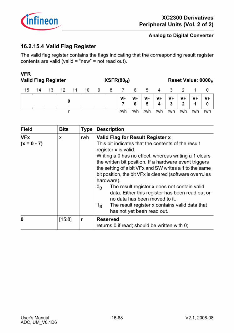
XC2300 DerivativesPeripheral Units (Vol. 2 of 2)
Analog to Digital Converter
16.2.15.4 Valid Flag RegisterThe valid flag register contains the flags indicating that the corresponding result registercontents are valid (valid = “new” = not read out).
VFR Valid Flag Register XSFR(80H) Reset Value: 0000H
15 14 13 12 11 10 9 8 7 6 5 4 3 2 1 0
0 VF7
VF6
VF5
VF4
VF3
VF2
VF1
VF0
r rwh rwh rwh rwh rwh rwh rwh rwh
Field Bits Type DescriptionVFx(x = 0 - 7)
x rwh Valid Flag for Result Register xThis bit indicates that the contents of the result register x is valid.Writing a 0 has no effect, whereas writing a 1 clears the written bit position. If a hardware event triggers the setting of a bit VFx and SW writes a 1 to the same bit position, the bit VFx is cleared (software overrules hardware).0B The result register x does not contain valid
data. Either this register has been read out or no data has been moved to it.
1B The result register x contains valid data that has not yet been read out.
0 [15:8] r Reservedreturns 0 if read; should be written with 0;
User’s Manual 16-88 V2.1, 2008-08ADC, UM_V0.1D6

XC2300 DerivativesPeripheral Units (Vol. 2 of 2)
Analog to Digital Converter
16.2.15.5 Result Control RegistersThe result control registers contain bits to control the behavior of the result registers andto monitor their status.
RCRx (x = 0 - 7) Result Control Register x XSFR(B0H + x * 2) Reset Value: 0000H
15 14 13 12 11 10 9 8 7 6 5 4 3 2 1 0
0 VF 0 DRC 0 WFR FEN IEN 0 DRCTR
r rh r rh r rw rw rw r rw
Field Bits Type DescriptionDRCTR [1:0] rw Data Reduction Control
This bit field defines how many conversion results are accumulated for data reduction (see Section 16.2.14.5). It defines the reload value for bit field DRC.00B The data reduction filter is disabled.
No accumulation is done.01B The data reduction filter is enabled.
Accumulation is done over 2 conversions.10B The data reduction filter is enabled.
Accumulation is done over 3 conversions.11B The data reduction filter is enabled.
Accumulation is done over 4 conversions.IEN 4 rw Interrupt Enable
This bit enables the result event interrupt if a result event is detected for result register x.0B The result event interrupt is disabled.1B The result event interrupt is enabled.
FEN 5 rw FIFO EnableThis bit enables the FIFO functionality for result register x, see Section 16.2.14.4.0B The FIFO functionality is disabled.
Use this for the FIFO input register.1B The FIFO functionality is enabled.
Use this for the other FIFO registers.
User’s Manual 16-89 V2.1, 2008-08ADC, UM_V0.1D6
XC2300 DerivativesPeripheral Units (Vol. 2 of 2)
Analog to Digital Converter
WFR 6 rw Wait-for-Read ModeThis bit enables the wait-for-read mode for result register x.0B The wait-for-read mode is disabled.1B The wait-for-read mode is enabled.
DRC [9:8] rh Data Reduction CounterThis bit field indicates how many conversion results have still to be accumulated to generate the final result for data reduction. The valid flag is automatically set and a result event is generated when this bit field becomes 0 (by decrementing or by reload).00B The final result is available in the result
register.01B 1 more conversion result has to be added to
obtain the final result in the result register.10B 2 more conversion results have to be added to
obtain the final result in the result register.11B 3 more conversion results have to be added to
obtain the final result in the result register.VF 12 rh Valid Flag
This flag indicates that the contents of the result register x is valid. It is another view of the corresponding bit in register VFR.0B The result register x does not contain valid
data.1B The result register x contains valid data.
0 [3:2], 7,[11:10],[15:13]
r Reservedreturns 0 if read; should be written with 0;
Field Bits Type Description
User’s Manual 16-90 V2.1, 2008-08ADC, UM_V0.1D6
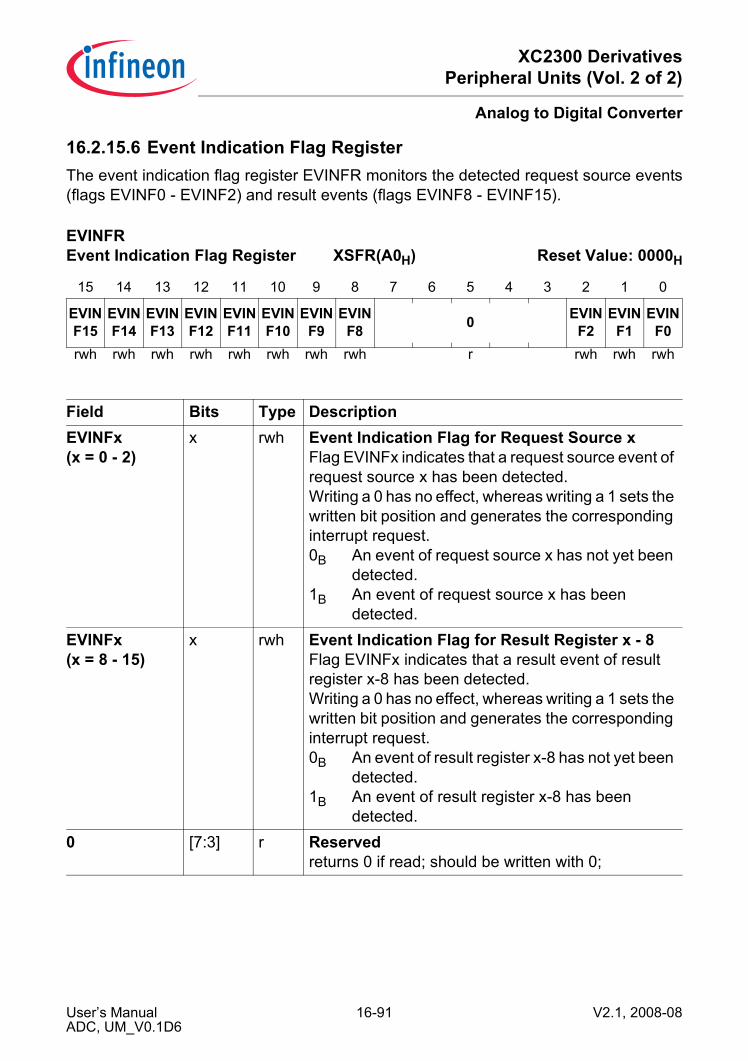
XC2300 DerivativesPeripheral Units (Vol. 2 of 2)
Analog to Digital Converter
16.2.15.6 Event Indication Flag RegisterThe event indication flag register EVINFR monitors the detected request source events(flags EVINF0 - EVINF2) and result events (flags EVINF8 - EVINF15).
EVINFR Event Indication Flag Register XSFR(A0H) Reset Value: 0000H
15 14 13 12 11 10 9 8 7 6 5 4 3 2 1 0
EVINF15
EVINF14
EVINF13
EVINF12
EVINF11
EVINF10
EVINF9
EVINF8 0 EVIN
F2EVIN
F1EVIN
F0rwh rwh rwh rwh rwh rwh rwh rwh r rwh rwh rwh
Field Bits Type DescriptionEVINFx(x = 0 - 2)
x rwh Event Indication Flag for Request Source xFlag EVINFx indicates that a request source event of request source x has been detected.Writing a 0 has no effect, whereas writing a 1 sets the written bit position and generates the corresponding interrupt request.0B An event of request source x has not yet been
detected.1B An event of request source x has been
detected.EVINFx(x = 8 - 15)
x rwh Event Indication Flag for Result Register x - 8Flag EVINFx indicates that a result event of result register x-8 has been detected.Writing a 0 has no effect, whereas writing a 1 sets the written bit position and generates the corresponding interrupt request.0B An event of result register x-8 has not yet been
detected.1B An event of result register x-8 has been
detected.0 [7:3] r Reserved
returns 0 if read; should be written with 0;
User’s Manual 16-91 V2.1, 2008-08ADC, UM_V0.1D6

XC2300 DerivativesPeripheral Units (Vol. 2 of 2)
Analog to Digital Converter
16.2.15.7 Clear Event Indication RegisterWriting a 1 to a bit position in the event indication clear register EVINCR clears thecorresponding event indication flag EVINFx in register EVINFR. If a request source orresult event is detected when the corresponding bit position is written with a 1, flagEVINFx is cleared.
EVINCR Event Indication Clear Register XSFR(A2H) Reset Value: 0000H
15 14 13 12 11 10 9 8 7 6 5 4 3 2 1 0
EVINC15
EVINC14
EVINC13
EVINC12
EVINC11
EVINC10
EVINC9
EVINC8 0 EVIN
C2EVINC1
EVINC0
w w w w w w w w r w w w
Field Bits Type DescriptionEVINCx(x = 0 - 2)
x w Clear Event Indication Flag for Request Source x0 No action.1 Bit EVINFR.x is cleared.
EVINCx(x = 8 - 15)
x w Clear Event Indication Flag for Result Reg. x-80 No action.1 Bit EVINFR.x is cleared.
0 [7:3] r Reservedreturns 0 if read; should be written with 0;
User’s Manual 16-92 V2.1, 2008-08ADC, UM_V0.1D6

XC2300 DerivativesPeripheral Units (Vol. 2 of 2)
Analog to Digital Converter
16.2.15.8 Event Interrupt Node Pointer RegistersThe bit fields in these registers define the service request output SR[3:0] that is used tosignal a request source or result event interrupt.
EVINPR0 Event Interrupt Node Pointer Register 0
XSFR(A8H) Reset Value: 0000H
15 14 13 12 11 10 9 8 7 6 5 4 3 2 1 0
0 EVINP2 0 EVINP1 0 EVINP0
r rw r rw r rw
Field Bits Type DescriptionEVINP0,EVINP1,EVINP2
[1:0],[5:4],[9:8]
rw Interrupt Node Pointer for Request Source xThis bit field selects which service request output indicates an event interrupt of request source x.00B Service request output SR0 is selected.01B Service request output SR1 is selected.10B Service request output SR2 is selected.11B Service request output SR3 is selected.
0 [3:2], [7:6],[15:10]
r Reservedreturns 0 if read; should be written with 0;
EVINPR8Event Interrupt Node Pointer Register 8
XSFR(ACH) Reset Value: 0000H
15 14 13 12 11 10 9 8 7 6 5 4 3 2 1 0
0 EVINP11 0 EVINP10 0 EVINP9 0 EVINP8
r rw r rw r rw r rw
User’s Manual 16-93 V2.1, 2008-08ADC, UM_V0.1D6

XC2300 DerivativesPeripheral Units (Vol. 2 of 2)
Analog to Digital Converter
Field Bits Type DescriptionEVINP8,EVINP9,EVINP10,EVINP11
[1:0],[5:4],[9:8],[13:12]
rw Interrupt Node Pointer for Result Event x-8This bit field selects which service request output indicates an event interrupt of result register x-8.00B Service request output SR0 is selected.01B Service request output SR1 is selected.10B Service request output SR2 is selected.11B Service request output SR3 is selected.
0 [3:2],[7:6],[11:10],[15:14]
r Reservedreturns 0 if read; should be written with 0;
EVINPR12Event Interrupt Node Pointer Register 12
XSFR(AEH) Reset Value: 0000H
15 14 13 12 11 10 9 8 7 6 5 4 3 2 1 0
0 EVINP15 0 EVINP14 0 EVINP13 0 EVINP12
r rw r rw r rw r rw
Field Bits Type DescriptionEVINP12,EVINP13,EVINP14,EVINP15
[1:0],[5:4],[9:8],[13:12]
rw Interrupt Node Pointer for Result Event x-8This bit field selects which service request output indicates an event interrupt of result register x-8.00B Service request output SR0 is selected.01B Service request output SR1 is selected.10B Service request output SR2 is selected.11B Service request output SR3 is selected.
0 [3:2],[7:6],[11:10],[15:14]
r Reservedreturns 0 if read; should be written with 0;
User’s Manual 16-94 V2.1, 2008-08ADC, UM_V0.1D6

XC2300 DerivativesPeripheral Units (Vol. 2 of 2)
Analog to Digital Converter
16.2.16 External Multiplexer ControlIf an application requires more analog inputs channels than available on the XC2300, theADC kernel supports an extension of analog channels by adding an external analogmultiplexer. Three output signals EMUX[2:0] are delivered by each ADC kernel to controlthe settings of an external analog multiplexer. They can be used to extend the numberof analog input channels by adding an external 1-out-of-8 multiplexer.The external multiplexer control behavior is defined by the bits in register EMCTR.The current setting of EMUX[2:0] is given by bit field LASTEMUX. If another extendedinput channel should be converted, bit field SETEMUX has to be programmed to thedesired value. This value is automatically applied with the start of the next conversion ofthe related analog ADC input channel.In the example shown in Figure 16-22 and in the description below, the analog inputCH7 has been extended, leading to additional analog inputs named CH70 to CH77. Ingeneral, the external multiplexer support can be enabled for each of the input channelsCH0 to CH7.
Figure 16-22 External Analog Multiplexer
If the external multiplexer is located far from the ADC analog input, it is recommended tointroduce an RC filter REXT1-CEXT1 directly at the analog input CH7 of the ADC. Ifneeded for signal filtering, local RC filters REXT2-CEXT2 can be optionally added at theinputs of the external analog multiplexer.If the external multiplexer is located close to the analog ADC input, the componentsREXT1 and CEXT1 are not necessarily needed. In this case it is strongly recommended to
. . .
ADC_ext_mux
CH0
ADC
. . .
EMUXcontrol
internal analogmultiplexer
external analog8-to-1 multiplexer
channelcontrol
EMUX[2:0]
ADC kernel
CEXT1
REXT2 CEXT2
REXT1
CEXT
CEXT
REXT
REXT
REXT2 CEXT2
REXT2 CEXT2
CH6
CH7
CH70
CH71
CH77
exte
nded
inpu
t sig
nals
dire
ctin
put s
igna
ls
User’s Manual 16-95 V2.1, 2008-08ADC, UM_V0.1D6
XC2300 DerivativesPeripheral Units (Vol. 2 of 2)
Analog to Digital Converter
introduce RC filters (REXT2, CEXT2) at the multiplexer inputs.Please note that each RC filter limits the bandwidth of the analog input signal.The RC filters used with an external multiplexer may lead to another impedance “seen”by the ADC analog input CH7 than for the other (direct) analog inputs. The adaptation ofthe sample phase length can be done by using a different input class with a differentvalue for the sample phase extension. This value can be adapted to execute conversionswith an EMUX[2:0] setting that has changed a sufficiently long time before theconversion of CH7 starts. “A sufficiently long time before” signifies that signal transitionsat the analog ADC input due to changing multiplexer setting are finished and the inputsignal is stable enough.After changing the EMUX[2:0] setting of the external multiplexer, an additional settlingtime has to elapse before the switched analog signal is stable and can be measured. Tocompensate for this settling time, an alternative sample phase length (instead of the onegiven by the input class) is automatically applied for the first conversion of CH7 afterEMUX[2:0] has changed. The alternative sample phase length can be programmed bybit field EMCTR.EMSAMPLE. If the first conversion of CH7 after the EMUX[2:0] settinghas changed is aborted due to a higher priority request, the repeated conversion of CH7also uses the value of EMSAMPLE. The settling time is considered to be finished afterthe complete conversion of CH7.The automatic control of an external analog multiplexer related to conversions of an ADCinput channel can be enabled by bits EMSELx in register EMENR. If bit EMSELx = 0,channel CHx does not influence any EMUX setting and the selected input class is alwaystaken into account.If bit EMSELx = 1, the automatic multiplexer control is enabled for channel CHx. Witheach conversion start of CHx, the value of EMCTR.SETEMUX is copied toEMCTR.LASTEMUX that is output at EMUX[2:0]. In addition, the control logic checks ifthe value of LASTEMUX has changed to adapt the sample phase length accordingly.Note: It is recommended to set only one single EMSELx bit, which triggers the update of
bit field LASTEMUX. This provides a consistent subchannel number for acomplete conversion cycle and maximum time for the software to change bit fieldSETEMUX (if required). Also, this approach is compatible with future versions ofthe ADC module.
User’s Manual 16-96 V2.1, 2008-08ADC, UM_V0.1D6
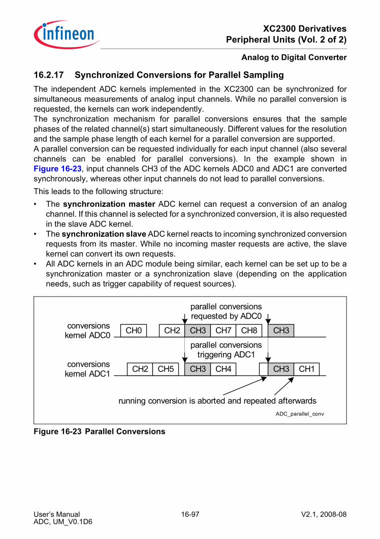
XC2300 DerivativesPeripheral Units (Vol. 2 of 2)
Analog to Digital Converter
16.2.17 Synchronized Conversions for Parallel SamplingThe independent ADC kernels implemented in the XC2300 can be synchronized forsimultaneous measurements of analog input channels. While no parallel conversion isrequested, the kernels can work independently.The synchronization mechanism for parallel conversions ensures that the samplephases of the related channel(s) start simultaneously. Different values for the resolutionand the sample phase length of each kernel for a parallel conversion are supported.A parallel conversion can be requested individually for each input channel (also severalchannels can be enabled for parallel conversions). In the example shown inFigure 16-23, input channels CH3 of the ADC kernels ADC0 and ADC1 are convertedsynchronously, whereas other input channels do not lead to parallel conversions.This leads to the following structure:• The synchronization master ADC kernel can request a conversion of an analog
channel. If this channel is selected for a synchronized conversion, it is also requestedin the slave ADC kernel.
• The synchronization slave ADC kernel reacts to incoming synchronized conversionrequests from its master. While no incoming master requests are active, the slavekernel can convert its own requests.
• All ADC kernels in an ADC module being similar, each kernel can be set up to be asynchronization master or a synchronization slave (depending on the applicationneeds, such as trigger capability of request sources).
Figure 16-23 Parallel Conversions
CH0conversionskernel ADC0
ADC_parallel_conv
conversionskernel ADC1 CH2
CH3
CH3
CH2
CH4
CH3
CH3CH5
CH7 CH8
parallel conversionsrequested by ADC0
CH1
parallel conversionstriggering ADC1
running conversion is aborted and repeated afterwards
User’s Manual 16-97 V2.1, 2008-08ADC, UM_V0.1D6
XC2300 DerivativesPeripheral Units (Vol. 2 of 2)
Analog to Digital Converter
The master kernel and the slave kernel form a “conversion group” allowing parallelsampling:• The conversion group contains exactly one synchronization master kernel that issues
a parallel conversion request and defines the internal frequencies fADCI and fADCDand the channel number for a parallel conversion of the conversion group.
• The other kernel in the conversion group is the synchronization slave and has to beprogrammed with the same values of GLOBCTR.DIVA, DIVD and ARBRND as thesynchronization master.
• If there is no need for parallel conversions, each kernel can be considered to form anown conversion group with only an ADC kernel as synchronization master, butwithout any synchronization slave.
• The channel number and the synchronization request are issued by thesynchronization master to the other kernel if a conversion is requested with CHCTRx(x = 0 - 15).SYNC = 1 in the synchronization master kernel. The synchronizationslave cannot issue synchronization requests.
• Once started, a parallel conversion can not be aborted.• A parallel conversion request is always handled with highest priority and cancel-
inject-repeat mode in the synchronization slave (see Section 16.2.6.2).• Bit GLOBCTR.ARBM has to be 0 for the synchronization slave.• The wait-for-read mode is supported for the master kernel, whereas the setting is
ignored in the slave kernel (previous results may be overwritten).The synchronization request issuing mechanism of the master to the slave is based onbit field GLOBSTR.ANON. The information given by GLOBCTR.ANON is distributed bythe synchronization master to the slave kernel (the bit fields SYNCTR.STSEL of allkernels must be programmed in a way that all kernels refer to the same information). Inaddition to the ANON information, the master delivers the requested channel number tothe slave (not explicitly shown in Figure 16-24).The start of the converters of all kernels of the conversion group is based on signalsindicating when a kernel is ready and can start the sample phase of a parallelconversion. Bit SYNCTR.EVALR1 defines if a kernel has to wait for the other kernel (toallow parallel conversions) or can start without waiting (no parallel conversions possible).To support parallel conversions, the ready signal of the other kernel of the conversiongroup has to be considered.The alias feature is independent of synchronized conversions. All kernels of aconversion group request the same channel number (defined by the master), but canconvert analog signals from different inputs. The requested channel number can beredirected by its alias setting. For example, if the channel number requested in theconversion group is channel CH0, but for a kernel, an alternative reference is connectedto this input, the actually converted analog input can be changed to any value. This canbe done by programming bit field ALIAS0 accordingly.Note: A parallel conversion in the slave ADC should not target a result register that is
already used for data reduction of other channels.
User’s Manual 16-98 V2.1, 2008-08ADC, UM_V0.1D6

XC2300 DerivativesPeripheral Units (Vol. 2 of 2)
Analog to Digital Converter
Figure 16-24 Synchronization via ANON and Ready Signals
Table 16-4 SYNCTR Setting for Kernel SynchronizationOperating Mode SYNCTR.EVALR1 SYNCTR.STSEL
ADC0 Kernel (values to be programmed to ADC0_SYNCTR)no sync 0B 00B
master of ADC1 1B 00B
slave of ADC1 1B 01B
ADC1 Kernel (values to be programmed to ADC1_SYNCTR)no sync 0B 00B
master of ADC0 1B 00B
slave of ADC0 1B 01B
ADC_ANON_sync
ADC0 kernel
kernelcontrol
GLOBCTR.ANON
ADC0_ANON
SYNCTR.STSEL
00 01 10 11
GLOBSTR.ANON
ADC1_ANON
GLOBCTR.ANON
SYNCTR.STSEL
00 01 10 11
CI1
CI1
CI2
CI2
CI3
CI3
SYNCTR.EVALR1
R1
R2
R3 ADC1 kernel
kernelcontrol
GLOBSTR.ANON
SYNCTR.EVALR1
R1
R2
R3
ADC1_READYADC0_READY
User’s Manual 16-99 V2.1, 2008-08ADC, UM_V0.1D6
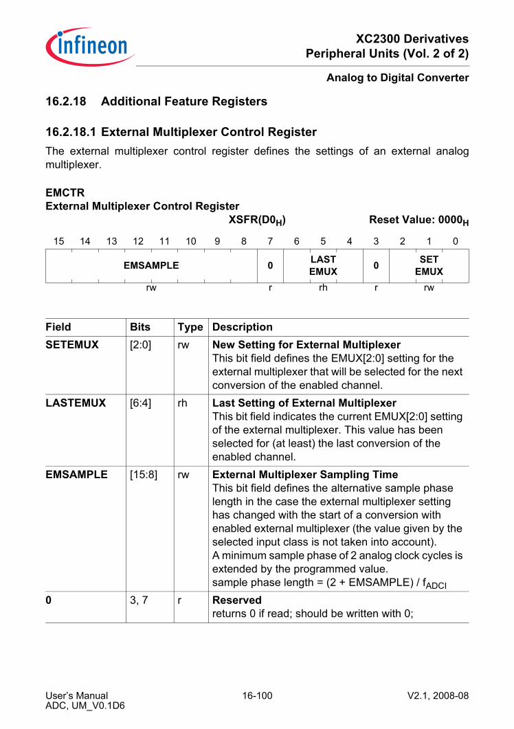
XC2300 DerivativesPeripheral Units (Vol. 2 of 2)
Analog to Digital Converter
16.2.18 Additional Feature Registers
16.2.18.1 External Multiplexer Control RegisterThe external multiplexer control register defines the settings of an external analogmultiplexer.
EMCTR External Multiplexer Control Register
XSFR(D0H) Reset Value: 0000H
15 14 13 12 11 10 9 8 7 6 5 4 3 2 1 0
EMSAMPLE 0 LASTEMUX 0 SET
EMUXrw r rh r rw
Field Bits Type DescriptionSETEMUX [2:0] rw New Setting for External Multiplexer
This bit field defines the EMUX[2:0] setting for the external multiplexer that will be selected for the next conversion of the enabled channel.
LASTEMUX [6:4] rh Last Setting of External MultiplexerThis bit field indicates the current EMUX[2:0] setting of the external multiplexer. This value has been selected for (at least) the last conversion of the enabled channel.
EMSAMPLE [15:8] rw External Multiplexer Sampling TimeThis bit field defines the alternative sample phase length in the case the external multiplexer setting has changed with the start of a conversion with enabled external multiplexer (the value given by the selected input class is not taken into account).A minimum sample phase of 2 analog clock cycles is extended by the programmed value.sample phase length = (2 + EMSAMPLE) / fADCI
0 3, 7 r Reservedreturns 0 if read; should be written with 0;
User’s Manual 16-100 V2.1, 2008-08ADC, UM_V0.1D6

XC2300 DerivativesPeripheral Units (Vol. 2 of 2)
Analog to Digital Converter
16.2.18.2 External Multiplexer Enable RegisterThe external multiplexer enable register defines if a channel is enabled to control thesettings of an external analog multiplexer. It is recommended to enable the externalmultiplexer control for only one analog input channel (see also Section 16.2.16).
16.2.18.3 Synchronization Control RegisterThe synchronization control register contains bits controlling the synchronizationbetween the kernels for parallel conversions. The programming of register SYNCTR inthe kernels of the conversion group has to be done while the bit fieldGLOBSTR.ANON = 00B in all ADC kernels of the conversion group. Bit field ANON ofthe synchronization master can be set to 11B afterwards. It is recommended to avoidpower saving modes (ANON = 01B or 10B) for parallel conversions.The bits EVALRx are only taken into account if a synchronized, parallel conversion isrequested by a master. This ensures that the conversions of the ADC kernels of thesynchronization group are started at the same time for parallel sampling (although akernel might be idle, the master and its connected slave have to wait for all of them beingready).
EMENR External Multiplexer Enable Register
XSFR(D6H) Reset Value: 0000H
15 14 13 12 11 10 9 8 7 6 5 4 3 2 1 0
0 EMSEL7 0 EMS
EL6 0 EMSEL5 0 EMS
EL4 0 EMSEL3 0 EMS
EL2 0 EMSEL1 0 EMS
EL0r rw r rw r rw r rw r rw r rw r rw r rw
Field Bits Type DescriptionEMSELx(x = 0 - 7)
2*x rw External Multiplexer Selection for Channel CHxThis bit defines if an external multiplexer will be controlled by channel CHx.0B The external multiplexer control is disabled.1B The external multiplexer control is enabled for
CHx.0 1, 3, 5,
7, 9, 11, 13, 15
r Reservedreturns 0 if read; should be written with 0;
User’s Manual 16-101 V2.1, 2008-08ADC, UM_V0.1D6

XC2300 DerivativesPeripheral Units (Vol. 2 of 2)
Analog to Digital Converter
SYNCTR Synchronization Control Register XSFR(1AH) Reset Value: 0000H
15 14 13 12 11 10 9 8 7 6 5 4 3 2 1 0
0 0 EVALR1 0 STSEL
r rw rw r rw
Field Bits Type DescriptionSTSEL [1:0] rw Start Selection
This bit field controls the synchronization mechanism of the ADC kernel.00B The kernel is a synchronization master.
The kernel’s own bit field GLOBCTR.ANON is taken into account.
01B The kernel is a synchronization slave.The control information at input CI1 is taken into account instead (see Figure 16-24).
10B reserved, do not use (kernel is switched off)11B reserved, do not use (kernel is switched off)
EVALR1 4 rw Evaluate Ready Input R1This bit defines if a kernel is considered to be part of the conversion group. Parallel conversions can only be started if the synchronization master and the slave of the conversion group indicate that they are ready to start a parallel conversion.0B The ready input R1 is not considered.1B The ready input R1 is considered for the start
of a parallel conversion of the conversion group.
0 [6:5] r Reserved for Future Usereturns 0 if read; must be written with 0;
0 [3:2],[15:7]
r Reservedreturns 0 if read; should be written with 0;
User’s Manual 16-102 V2.1, 2008-08ADC, UM_V0.1D6
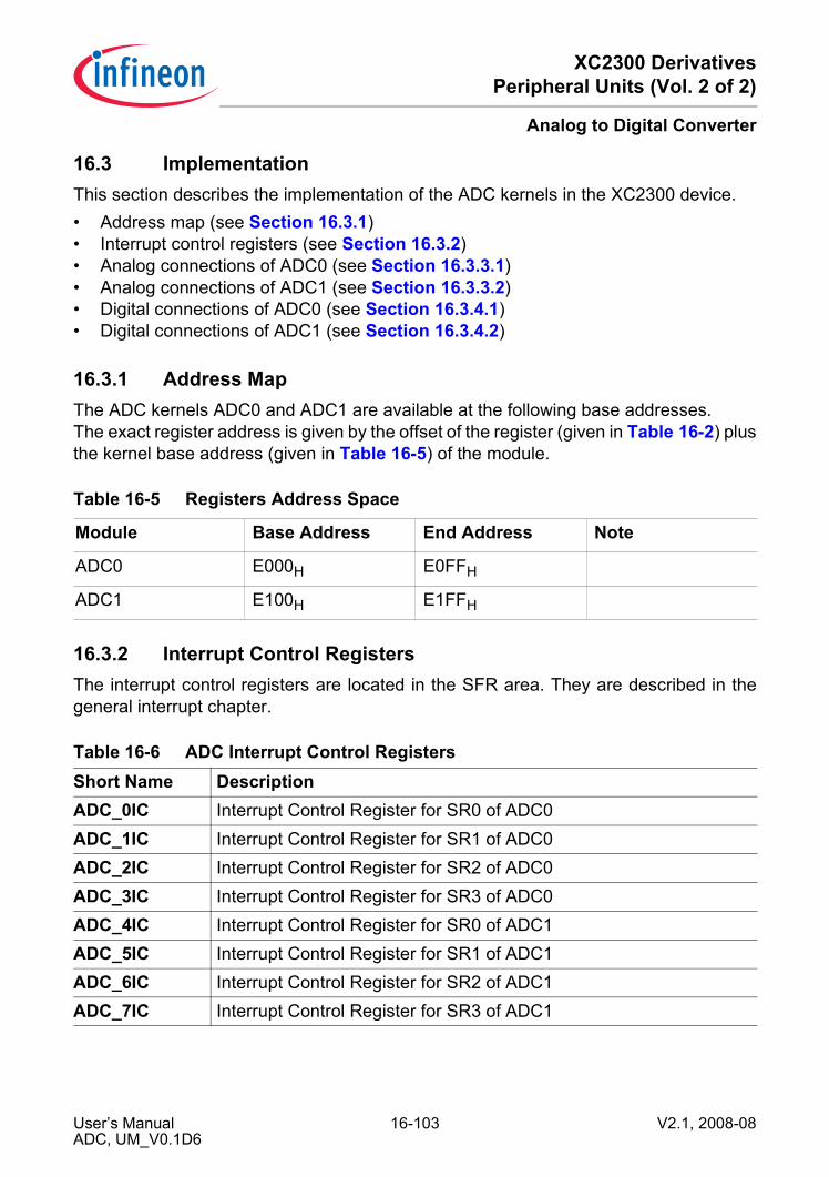
XC2300 DerivativesPeripheral Units (Vol. 2 of 2)
Analog to Digital Converter
16.3 ImplementationThis section describes the implementation of the ADC kernels in the XC2300 device.• Address map (see Section 16.3.1)• Interrupt control registers (see Section 16.3.2)• Analog connections of ADC0 (see Section 16.3.3.1)• Analog connections of ADC1 (see Section 16.3.3.2)• Digital connections of ADC0 (see Section 16.3.4.1)• Digital connections of ADC1 (see Section 16.3.4.2)
16.3.1 Address MapThe ADC kernels ADC0 and ADC1 are available at the following base addresses.The exact register address is given by the offset of the register (given in Table 16-2) plusthe kernel base address (given in Table 16-5) of the module.
16.3.2 Interrupt Control RegistersThe interrupt control registers are located in the SFR area. They are described in thegeneral interrupt chapter.
Table 16-5 Registers Address Space
Module Base Address End Address Note
ADC0 E000H E0FFH
ADC1 E100H E1FFH
Table 16-6 ADC Interrupt Control RegistersShort Name DescriptionADC_0IC Interrupt Control Register for SR0 of ADC0ADC_1IC Interrupt Control Register for SR1 of ADC0ADC_2IC Interrupt Control Register for SR2 of ADC0ADC_3IC Interrupt Control Register for SR3 of ADC0ADC_4IC Interrupt Control Register for SR0 of ADC1ADC_5IC Interrupt Control Register for SR1 of ADC1ADC_6IC Interrupt Control Register for SR2 of ADC1ADC_7IC Interrupt Control Register for SR3 of ADC1
User’s Manual 16-103 V2.1, 2008-08ADC, UM_V0.1D6

XC2300 DerivativesPeripheral Units (Vol. 2 of 2)
Analog to Digital Converter
16.3.3 Analog ConnectionsThe input channels of both ADC kernels are distributed as follows:• 16 channels of ADC0 connected to P5• 8 channels of ADC1 connected to P15• 4 channels of ADC1 connected to P5 and overlaid to ADC0 inputsEach ADC kernel has its own reference input lines VAGND and VAREFx, with x = 0, 1.Depending on the package, these lines can be available as independent pins for high pincount packages or can be combined for low pin count packages.The respective voltage supply lines of both converters are connected together.
16.3.3.1 Analog Connections of ADC0The table below lists the analog connections of ADC0.
Table 16-7 ADC0 Analog Connections in XC2300Signal from/to
ModuleI/O to ADC0
Can be used to/as
Power supply and standard referenceVDDPA see
pinning chapter
I analog power supplyVSS I analog power supplyVAREF(0) I positive analog referenceVAGND I negative analog referenceAnalog input channelsCH0 P5.0 I analog input channel 0CH1 P5.1 I analog input channel 1CH2 P5.2 I analog input channel 2CH3 P5.3 I analog input channel 3CH4 P5.4 I analog input channel 4CH5 P5.5 I analog input channel 5CH6 P5.6 I analog input channel 6CH7 P5.7 I analog input channel 7CH8 P5.8 I analog input channel 8
overlaid with ADC1 channel 8CH9 P5.9 I analog input channel 9
overlaid with ADC1 channel 9
User’s Manual 16-104 V2.1, 2008-08ADC, UM_V0.1D6
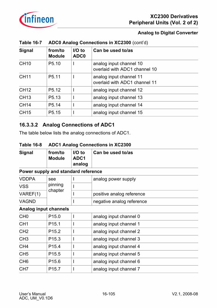
XC2300 DerivativesPeripheral Units (Vol. 2 of 2)
Analog to Digital Converter
16.3.3.2 Analog Connections of ADC1The table below lists the analog connections of ADC1.
CH10 P5.10 I analog input channel 10overlaid with ADC1 channel 10
CH11 P5.11 I analog input channel 11overlaid with ADC1 channel 11
CH12 P5.12 I analog input channel 12CH13 P5.13 I analog input channel 13CH14 P5.14 I analog input channel 14CH15 P5.15 I analog input channel 15
Table 16-8 ADC1 Analog Connections in XC2300Signal from/to
ModuleI/O to ADC1analog
Can be used to/as
Power supply and standard referenceVDDPA see
pinning chapter
I analog power supplyVSS IVAREF(1) I positive analog referenceVAGND I negative analog referenceAnalog input channelsCH0 P15.0 I analog input channel 0CH1 P15.1 I analog input channel 1CH2 P15.2 I analog input channel 2CH3 P15.3 I analog input channel 3CH4 P15.4 I analog input channel 4CH5 P15.5 I analog input channel 5CH6 P15.6 I analog input channel 6CH7 P15.7 I analog input channel 7
Table 16-7 ADC0 Analog Connections in XC2300 (cont’d)
Signal from/toModule
I/O to ADC0
Can be used to/as
User’s Manual 16-105 V2.1, 2008-08ADC, UM_V0.1D6

XC2300 DerivativesPeripheral Units (Vol. 2 of 2)
Analog to Digital Converter
CH8 P5.8 I analog input channel 8overlaid with ADC0 channel 8
CH9 P5.9 I analog input channel 9overlaid with ADC0 channel 9
CH10 P5.10 I analog input channel 10overlaid with ADC0 channel 10
CH11 P5.11 I analog input channel 11overlaid with ADC0 channel 11
CH12..15 n.c. I not available, do not request
Table 16-8 ADC1 Analog Connections in XC2300 (cont’d)
Signal from/toModule
I/O to ADC1analog
Can be used to/as
User’s Manual 16-106 V2.1, 2008-08ADC, UM_V0.1D6
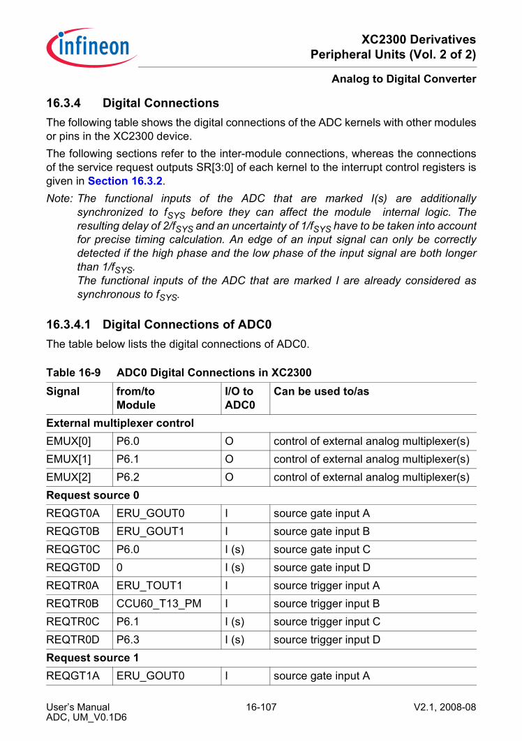
XC2300 DerivativesPeripheral Units (Vol. 2 of 2)
Analog to Digital Converter
16.3.4 Digital ConnectionsThe following table shows the digital connections of the ADC kernels with other modulesor pins in the XC2300 device.The following sections refer to the inter-module connections, whereas the connectionsof the service request outputs SR[3:0] of each kernel to the interrupt control registers isgiven in Section 16.3.2.Note: The functional inputs of the ADC that are marked I(s) are additionally
synchronized to fSYS before they can affect the module internal logic. Theresulting delay of 2/fSYS and an uncertainty of 1/fSYS have to be taken into accountfor precise timing calculation. An edge of an input signal can only be correctlydetected if the high phase and the low phase of the input signal are both longerthan 1/fSYS.The functional inputs of the ADC that are marked I are already considered assynchronous to fSYS.
16.3.4.1 Digital Connections of ADC0The table below lists the digital connections of ADC0.
Table 16-9 ADC0 Digital Connections in XC2300Signal from/to
ModuleI/O to ADC0
Can be used to/as
External multiplexer controlEMUX[0] P6.0 O control of external analog multiplexer(s)EMUX[1] P6.1 O control of external analog multiplexer(s)EMUX[2] P6.2 O control of external analog multiplexer(s)Request source 0REQGT0A ERU_GOUT0 I source gate input AREQGT0B ERU_GOUT1 I source gate input BREQGT0C P6.0 I (s) source gate input CREQGT0D 0 I (s) source gate input DREQTR0A ERU_TOUT1 I source trigger input AREQTR0B CCU60_T13_PM I source trigger input BREQTR0C P6.1 I (s) source trigger input CREQTR0D P6.3 I (s) source trigger input DRequest source 1REQGT1A ERU_GOUT0 I source gate input A
User’s Manual 16-107 V2.1, 2008-08ADC, UM_V0.1D6
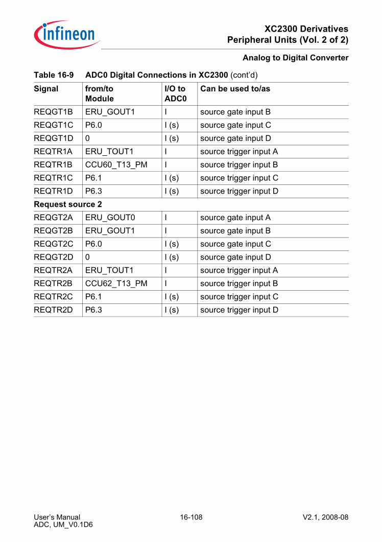
XC2300 DerivativesPeripheral Units (Vol. 2 of 2)
Analog to Digital Converter
REQGT1B ERU_GOUT1 I source gate input BREQGT1C P6.0 I (s) source gate input CREQGT1D 0 I (s) source gate input DREQTR1A ERU_TOUT1 I source trigger input AREQTR1B CCU60_T13_PM I source trigger input BREQTR1C P6.1 I (s) source trigger input CREQTR1D P6.3 I (s) source trigger input DRequest source 2REQGT2A ERU_GOUT0 I source gate input AREQGT2B ERU_GOUT1 I source gate input BREQGT2C P6.0 I (s) source gate input CREQGT2D 0 I (s) source gate input DREQTR2A ERU_TOUT1 I source trigger input AREQTR2B CCU62_T13_PM I source trigger input BREQTR2C P6.1 I (s) source trigger input CREQTR2D P6.3 I (s) source trigger input D
Table 16-9 ADC0 Digital Connections in XC2300 (cont’d)
Signal from/toModule
I/O to ADC0
Can be used to/as
User’s Manual 16-108 V2.1, 2008-08ADC, UM_V0.1D6

XC2300 DerivativesPeripheral Units (Vol. 2 of 2)
Analog to Digital Converter
16.3.4.2 Digital Connections of ADC1The table below lists the digital connections of ADC1.
Table 16-10 ADC1 Digital Connections in XC2300Signal from/to
ModuleI/O to ADC1
Can be used to/as
External multiplexer controlEMUX[0] P7.2 O control of external analog multiplexer(s)EMUX[1] P7.3 O control of external analog multiplexer(s)EMUX[2] P7.4 O control of external analog multiplexer(s)Request source 0REQGT0A ERU_GOUT0 I source gate input AREQGT0B ERU_GOUT1 I source gate input BREQGT0C P6.0 I (s) source gate input CREQGT0D 0 I (s) source gate input DREQTR0A ERU_TOUT1 I source trigger input AREQTR0B CCU61_T13_PM I source trigger input BREQTR0C P6.1 I (s) source trigger input CREQTR0D P6.3 I (s) source trigger input DRequest source 1REQGT1A ERU_GOUT0 I source gate input AREQGT1B ERU_GOUT1 I source gate input BREQGT1C P6.0 I (s) source gate input CREQGT1D 0 I (s) source gate input DREQTR1A ERU_TOUT1 I source trigger input AREQTR1B CCU61_T13_PM I source trigger input BREQTR1C P6.1 I (s) source trigger input CREQTR1D P6.3 I (s) source trigger input DRequest source 2REQGT2A ERU_GOUT0 I source gate input AREQGT2B ERU_GOUT1 I source gate input BREQGT2C P6.0 I (s) source gate input CREQGT2D 0 I (s) source gate input D
User’s Manual 16-109 V2.1, 2008-08ADC, UM_V0.1D6

XC2300 DerivativesPeripheral Units (Vol. 2 of 2)
Analog to Digital Converter
REQTR2A ERU_TOUT1 I source trigger input AREQTR2B CCU63_T13_PM I source trigger input BREQTR2C P6.1 I (s) source trigger input CREQTR2D P6.3 I (s) source trigger input D
Table 16-10 ADC1 Digital Connections in XC2300 (cont’d)
Signal from/toModule
I/O to ADC1
Can be used to/as
User’s Manual 16-110 V2.1, 2008-08ADC, UM_V0.1D6

XC2300 DerivativesPeripheral Units (Vol. 2 of 2)
Capture/Compare Unit 2
17 Capture/Compare Unit 2The XC2300 provides a Capture/Compare (CAPCOM2) unit which provides16 capture/compare channels, which interact with 2 timers. A CAPCOM2 channel cancapture the contents of a timer on specific internal or external events, or it can comparea timer’s contents with given values, and modify output signals in case of a match.
Figure 17-1 SFRs Associated with the CAPCOM Units
With this mechanism, the CAPCOM2 unit supports generation and control of timingsequences on up to 16 channels with a minimum of software intervention.
mc_capcom2_registers_xy.vsd
Data Registers Control Registers
T78CON
CC28IC-CC31IC
Interrupt Control
CC2_SEE CAPCOM Single Event En. Reg.CC2_SEM CAPCOM Single Event Mode Reg.CC2_DRM CAPCOM Double Reg. Mode Reg .CC2_OUT CAPCOM Output RegisterCC2_IOC CAPCOM Input/Outp. Control Reg .
CC2_ID Module Identification Register
T7, T7REL
T8, T8REL
E
E
CC16-CC19
CC20-CC23
CC24-CC27
CC28-CC31 CC2_M7
CC2_M6
CC2_M5
CC2_M4
CC24IC-CC27IC
CC20IC-CC23IC
CC16IC-CC19IC
E
E
E
E
T7IC
T8IC
CC2_OUT
CC2_SEE
CC2_SEM
CC2_DRM
CC2_IOC
CC16...31 CAPCOM2 Register 16...31CC16...31ICCAPCOM2 Intr. Ctrl. Reg. 16...31CCM4...7 CAPCOM2 Mode Ctrl. Reg. 4...7T78CON CAPCOM2 Timer Control Reg .T7, T8 CAPCOM2 Timer RegisterT7/8REL CAPCOM2 Timer Reload RegisterT7IC, T8IC CAPCOM2 Timer x Intr. Ctrl. Reg.
KSCCFG Kernel State Configuration Register
KSCCFG
CC2_ID
User’s Manual 17-1 V2.1, 2008-08CC12_X8, V2.3
XC2300 DerivativesPeripheral Units (Vol. 2 of 2)
Capture/Compare Unit 2
From the programmer’s point of view, the term ‘CAPCOM2 unit’ refers to a set ofregisters which are associated with this peripheral (see also Figure 17-1), including theport pins that may be used for alternate input/output functions, and their control bits.A CAPCOM2 unit is typically used to handle high speed IO tasks such as pulse andwaveform generation, pulse width modulation, or recording of the time when a specificevent occurs. It also supports the implementation of up to 16 software-controlledinterrupt events.The CAPCOM2 Unit consists of two 16-bit timers (T7, T8), each with its own reloadregister (TxREL), and a bank of sixteen dual-purpose 16-bit capture/compare registers(CCy).The input clock for the CAPCOM2 timers is programmable to several prescaled valuesof the module input clock (fCC), or it can be derived from the overflow/underflow of timerT6. T7 may also operate in counter mode (from an external input), clocked by externalevents.Each capture/compare register may be programmed individually for capture or compareoperation, and each register may be allocated to either of the two timers. Eachcapture/compare register has one signal associated with it, which serves as an inputsignal for the capture operation or as an output signal for the compare operation.The capture operation causes the current timer contents to be copied into the respectivecapture/compare register, triggered by an event (transition) on the associated inputsignal. This event also activates the associated interrupt request line.The compare operation may cause an output signal transition on the associated outputsignal, when the allocated timer increments to the value stored in a capture/compareregister. The compare match event also activates the associated interrupt request line.In Double-register compare mode a pair of registers controls one common output signal.The compare output signals are available via a dedicated output register. The outputpath can be selected.For the switching of the output signals two timing schemes (see Section 17.8) can beselected:In Staggered Mode the output signals are switched consecutively in 8 steps, whichdistributes the switching steps over a certain time. In staggered mode, the maximumresolution is 8 tCC.In Non-Staggered Mode the output signals are switched immediately at the same time.In non-staggered mode, the maximum resolution is 1 tCC.Figure 17-2 shows the basic structure of a CAPCOM unit.
User’s Manual 17-2 V2.1, 2008-08CC12_X8, V2.3
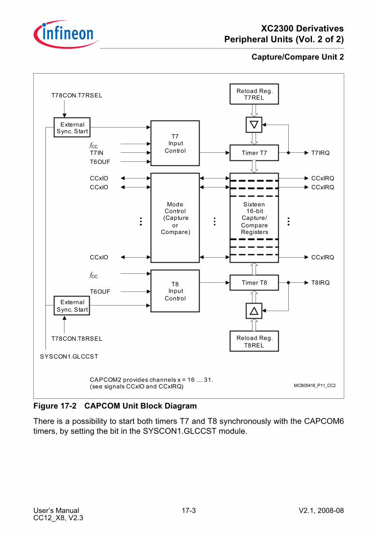
XC2300 DerivativesPeripheral Units (Vol. 2 of 2)
Capture/Compare Unit 2
Figure 17-2 CAPCOM Unit Block Diagram
There is a possibility to start both timers T7 and T8 synchronously with the CAPCOM6timers, by setting the bit in the SYSCON1.GLCCST module.
Timer T7
Sixteen16-bit
Capture/CompareRegisters
Timer T8
Reload Reg.T8REL
T7Input
Control
ModeControl(Capture
orCompare)
T8Input
Control
MCB05418_P11_CC2
Reload Reg.T7REL
T7IRQ
CCxIRQ
CCxIRQ
T8IRQ
CCxIRQ
fCCT7INT6OUF
CCxIOCCxIO
CCxIO
fCC
T6OUF
CAPCOM2 provides channels x = 16 … 31.(see signals CCxIO and CCxIRQ)
ExternalSync. Start
ExternalSync. Start
SYSCON1.GLCCST
T78CON.T7RSEL
T78CON.T8RSEL
User’s Manual 17-3 V2.1, 2008-08CC12_X8, V2.3

XC2300 DerivativesPeripheral Units (Vol. 2 of 2)
Capture/Compare Unit 2
17.1 The CAPCOM2 TimersThe primary use of the timers T7 and T8 is to provide two independent time bases forthe capture/compare channels of each unit. The maximum resolution is 8 tCC instaggered mode, and 1 tCC in non-staggered mode.The basic structure of the two timers, illustrated in Figure 17-3, is identical, except forthe input pin (see mark).
Figure 17-3 Block Diagram of a CAPCOM Timer
The functions of the CAPCOM timers are controlled via the bit-addressable controlregister T78CON. The high-byte of T78CON controls T8, the low-byte of T78CONcontrols T7. The control options are identical for all four timers (except for external input).In all modes, the timers are always counting upward. The current timer values areaccessible for the CPU in the timer registers Tx, which are non bit-addressable registers.When the CPU writes to a register Tx in the state immediately before the respective timerincrement or reload is to be performed, the CPU write operation has priority and theincrement or reload is disabled to guarantee correct timer operation.
MCB05419_4CM_CC2
TxIRQCount
TxR
ReloadReg. TxREL
Timer Tx
toCapure/Compare
Register Array
TxI
TxM
x = 7, 8
T6OUFMUX
TxI
TxIN
Prescaler
TxI
fTxfCC
Edge
Select
User’s Manual 17-4 V2.1, 2008-08CC12_X8, V2.3

XC2300 DerivativesPeripheral Units (Vol. 2 of 2)
Capture/Compare Unit 2
CC2_T78CON Timer 7/8 Control Register SFR (FF20H/90H) Reset Value: 0000H
15 14 13 12 11 10 9 8 7 6 5 4 3 2 1 0
- T8R T8RSEL T8M T8I - T7R T7RSEL T7M T7I
- rw - rw rw - rw - rw rw
Field Bits Type DescriptionTxR 14, 6 rw Timer/Counter Tx Run Control
0 Timer/Counter Tx is disabled1 Timer/Counter Tx is enabled
TxM 11, 3 rw Timer/Counter Tx Mode Selection0 Timer Mode1 Counter Mode
TxI [10:8],[2:0]
rw Timer/Counter Tx Input SelectionTimer Mode (TxM = 0):Input frequency fTx = fCC/2(<TxI>+3) or fCC/2(<TxI>), depending on (non-)staggered mode, see Table 17-1Counter Mode (TxM = 1):000 Overflow/Underflow of GPT Timer T6001 Positive (rising) edge on pin TxIN010 Negative (falling) edge on pin TxIN011 Any edge (rising and falling) on pin TxIN1XX Reserved. Do not use this combination!Note: For timer T8 the only option in counter mode is
000B. T8 stop in all other cases.T7RSEL [5:4] rw Timer T7 External Run Selection
Bit field T7RSEL defines the event of signal T7HR that can set the run bit T7R by HW.00 The external setting of T7R is disabled.01 Bit T7R is set if a rising edge of signal T7HR is
detected.10 Bit T7R is set if a falling edge of signal T7HR is
detected.11 Bit T7R is set if an edge of signal T7HR is
detected.
User’s Manual 17-5 V2.1, 2008-08CC12_X8, V2.3

XC2300 DerivativesPeripheral Units (Vol. 2 of 2)
Capture/Compare Unit 2
The timer run flags TxR allow the starting and stopping of the timers. The followingdescription of the timer modes and operation always applies to the enabled state of thetimers, i.e. the respective run flag is assumed to be set.
Timer ModeIn Timer Mode (TxM = 0), the input clock for a CAPCOM2 timer is derived from fCC,divided by a programmable prescaler. Each timer has its own individual prescaler,controlled through the individual bitfields TxI in the timer control register T78CON.The input frequency fTx for a timer Tx and its resolution rTx are determined by thefollowing formulas:Staggered Mode:
(17.1)
Non-Staggered Mode:When a timer overflows from FFFFH to 0000H, it is reloaded with the value stored in itsrespective reload register TxREL. The reload value determines the period PTx betweentwo consecutive overflows of Tx as follows:
(17.2)
Staggered Mode:
(17.3)
T8RSEL [13:12] rw Timer T8 External Run SelectionBit field T8RSEL defines the event of signal T8HR that can set the run bit T8R by HW.00 The external setting of T8R is disabled.01 Bit T8R is set if a rising edge of signal T8HR is
detected.10 Bit T8R is set if a falling edge of signal T8HR is
detected.11 Bit T8R is set if an edge of signal T8HR is
detected.
Field Bits Type Description
fTx MHz[ ]fCC MHz[ ]
2 <Txl> 3+( )--------------------------= rTx µs[ ] 2 <Txl> 3+( )
fCC MHz[ ]--------------------------=
fTx MHz[ ]fCC MHz[ ]
2<Txl>--------------------------= rTx µs[ ] 2<Txl>
fCC MHz[ ]--------------------------=
PTx µs[ ] 216 <TxREL>–( ) 2×<Txl> 3+( )
fCC MHz[ ]-------------------------------------------------------------------------=
User’s Manual 17-6 V2.1, 2008-08CC12_X8, V2.3

XC2300 DerivativesPeripheral Units (Vol. 2 of 2)
Capture/Compare Unit 2
Non-Staggered Mode:
(17.4)
After a timer has been started by setting its run flag (TxR), the first increment will occurwithin the time interval which is defined by the selected timer resolution. All furtherincrements occur exactly after the time defined by the timer resolution.Examples for timer input frequencies, resolution and periods, which result from theselected prescaler option in TxI when using a 40 MHz clock, are listed in Table 17-1below. The numbers for the timer periods are based on a reload value of 0000H. Notethat some numbers may be rounded.
PTx µs[ ] 216 <TxREL>–( ) 2×<Txl>
fCC MHz[ ]----------------------------------------------------------------=
User’s Manual 17-7 V2.1, 2008-08CC12_X8, V2.3

XC2300 DerivativesPeripheral Units (Vol. 2 of 2)
Capture/Compare Unit 2
Table 17-1 Timer Tx Input Clock Selection for Timer Mode, fCC = 40 MHzTxI Prescaler Input
FrequencyResolution Period
Staggered Mode000B 8 5 MHz 200 ns 13.11 ms001B 16 2.5 MHz 400 ns 26.21 ms010B 32 1.25 MHz 800 ns 52.43 ms011B 64 625 kHz 1.6 µs 104.86 ms100B 128 312.5 kHz 3.2 µs 209.72 ms101B 256 156.25 kHz 6.4 µs 419.43 ms110B 512 78.125 kHz 12.8 µs 838.86 ms111B 1024 39.0625 kHz 25.6 µs 1677.72 msNon-Staggered Mode000B 1 40 MHz 25 ns 1.6384 ms001B 2 20 MHz 50 ns 3.2768 ms010B 4 10 MHz 100 ns 6.5536 ms011B 8 5 MHz 200 ns 13.11 ms100B 16 2.5 MHz 400 ns 26.21 ms101B 32 1.25 MHz 800 ns 52.43 ms110B 64 625 kHz 1.6 µs 104.86 ms111B 128 312.5 kHz 3.2 µs 209.72 ms
User’s Manual 17-8 V2.1, 2008-08CC12_X8, V2.3
XC2300 DerivativesPeripheral Units (Vol. 2 of 2)
Capture/Compare Unit 2
Counter ModeIn Counter Mode (TxM = 1), the input clock of a CAPCOM2 timer is either derived froman associated external input pin, T7IN, or from the over-/underflows of GPT timer T6.Using an external signal connected to pin TxIN as a counting signal is only possible fortimer T7. The only counter option for timer T8 is using the over-/underflows of the GPTtimer T6 (selected by TxI = 000B).Bitfields T7I are used to select either a positive, a negative, or both a positive and anegative transition of the external signal at pin T7IN to trigger an increment of timer T7.Please note that certain criteria must be met for the external signal and the port pinprogramming for this mode in order to operate properly. These conditions are detailed inChapter 17.10.
Timer Overflow and ReloadWhen a CAPCOM2 timer contains the value FFFFH at the time a new count triggeroccurs, a timer interrupt request is generated, and the timer is loaded with the contentsof its associated reload register TxREL. The timer then resumes incrementing with thenext count trigger starting from the reloaded value.The reload registers TxREL are not bitaddressable. After reset, they contain the value0000H.
User’s Manual 17-9 V2.1, 2008-08CC12_X8, V2.3

XC2300 DerivativesPeripheral Units (Vol. 2 of 2)
Capture/Compare Unit 2
17.2 CAPCOM2 Timer InterruptsUpon a timer overflow the corresponding timer interrupt request flag TxIR for therespective timer will be set. This flag can be used to generate an interrupt or trigger aPEC service request, when enabled by the respective interrupt enable bit TxIE.Each timer has its own bitaddressable interrupt control register and its own interruptvector. The organization of the interrupt control registers TxIC is identical with the otherinterrupt control registers.
Note: Please refer to the general Interrupt Control Register description for anexplanation of the control fields.
CC2_T7IC CAPCOM T7 Intr. Ctrl. Reg. ESFR (FF6CH/BDH) Reset Value: 0000H
15 14 13 12 11 10 9 8 7 6 5 4 3 2 1 0
- GPX T7IR T7IE ILVL GLVL
- - - - - - - rw rwh rw rw rw
CC2_T8IC CAPCOM T8 Intr. Ctrl. Reg. ESFR (FF6EH/BEH) Reset Value: 0000H
15 14 13 12 11 10 9 8 7 6 5 4 3 2 1 0
- GPX T8IR T8IE ILVL GLVL
- - - - - - - rw rwh rw rw rw
User’s Manual 17-10 V2.1, 2008-08CC12_X8, V2.3
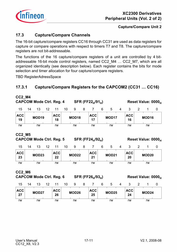
XC2300 DerivativesPeripheral Units (Vol. 2 of 2)
Capture/Compare Unit 2
17.3 Capture/Compare ChannelsThe 16-bit capture/compare registers CC16 through CC31 are used as data registers forcapture or compare operations with respect to timers T7 and T8. The capture/compareregisters are not bit-addressable.The functions of the 16 capture/compare registers of a unit are controlled by 4 bit-addressable 16-bit mode control registers, named CC2_M4 … CC2_M7, which are allorganized identically (see description below). Each register contains the bits for modeselection and timer allocation for four capture/compare registers.TBD RegisterAdressSpace
17.3.1 Capture/Compare Registers for the CAPCOM2 (CC31 … CC16)
CC2_M4 CAPCOM Mode Ctrl. Reg. 4 SFR (FF22H/91H) Reset Value: 0000H
15 14 13 12 11 10 9 8 7 6 5 4 3 2 1 0
ACC19 MOD19 ACC
18 MOD18 ACC17 MOD17 ACC
16 MOD16
rw rw rw rw rw rw rw rw
CC2_M5CAPCOM Mode Ctrl. Reg. 5 SFR (FF24H/92H) Reset Value: 0000H
15 14 13 12 11 10 9 8 7 6 5 4 3 2 1 0
ACC23 MOD23 ACC
22 MOD22 ACC21 MOD21 ACC
20 MOD20
rw rw rw rw rw rw rw rw
CC2_M6CAPCOM Mode Ctrl. Reg. 6 SFR (FF26H/93H) Reset Value: 0000H
15 14 13 12 11 10 9 8 7 6 5 4 3 2 1 0
ACC27 MOD27 ACC
26 MOD26 ACC25 MOD25 ACC
24 MOD24
rw rw rw rw rw rw rw rw
User’s Manual 17-11 V2.1, 2008-08CC12_X8, V2.3

XC2300 DerivativesPeripheral Units (Vol. 2 of 2)
Capture/Compare Unit 2
Each of the registers CCy may be individually programmed for capture mode or for oneof 4 different compare modes, and may be allocated individually to one of the two timersof the respective CAPCOM unit. A special double-register compare mode combines tworegisters to act on one common output signal. When capture or compare operations aredisabled for one of the CCy registers, it may be used for general purpose variablestorage.
CC2_M7CAPCOM Mode Ctrl. Reg. 7 SFR (FF28H/94H) Reset Value: 0000H
15 14 13 12 11 10 9 8 7 6 5 4 3 2 1 0
ACC31 MOD31 ACC
30 MOD30 ACC29 MOD29 ACC
28 MOD28
rw rw rw rw rw rw rw rw
Field Bits Type DescriptionACCy 15, 11,
7, 3rw Allocation Bit for CAPCOM Register CCy
0 CCy allocated to Timer T71 CCy allocated to Timer T8
MODy [14:12], [10:8], [6:4], [2:0]
rw Mode Selection for CAPCOM Register CCySee Table 17-2.
Table 17-2 Selection of Capture Modes and Compare ModesMode MODy Selected Operating ModeDisabled 000B Disable Capture and Compare Modes
The respective CAPCOM register may be used for general variable storage.
Capture 001B Capture on Positive Transition (Rising Edge) at Pin CCyIO010B Capture on Negative Transition (Falling Edge) at Pin CCyIO011B Capture on Positive and Negative Transition (Both Edges) at
Pin CCyIO
User’s Manual 17-12 V2.1, 2008-08CC12_X8, V2.3

XC2300 DerivativesPeripheral Units (Vol. 2 of 2)
Capture/Compare Unit 2
The detailed discussion of the capture and compare modes is valid for all thecapture/compare channels, so registers, bits and pins are only referenced by aplaceholder.
Compare 100B Compare Mode 0: Interrupt OnlySeveral interrupts per timer period.Can enable double-register compare mode for Bank2 registers.
101B Compare Mode 1: Toggle Output Pin on each MatchSeveral compare events per timer period.Can enable double-register compare mode for Bank1 registers.
110B Compare Mode 2: Interrupt OnlyOnly one interrupt per timer period.
111B Compare Mode 3: Set Output Pin on each MatchReset output pin on each timer overflow; only one interrupt per timer period.
Table 17-2 Selection of Capture Modes and Compare Modes (cont’d)
Mode MODy Selected Operating Mode
User’s Manual 17-13 V2.1, 2008-08CC12_X8, V2.3

XC2300 DerivativesPeripheral Units (Vol. 2 of 2)
Capture/Compare Unit 2
17.4 Capture Mode OperationIn Capture Mode, the current contents of a CAPCOM timer are copied (captured) into therespective capture/compare register in response to an external event. This is used, forexample, to record the time at which an external event has occurred, or to measure thedistance between two external events in timer increments.The event to cause a capture of a timer’s contents can be programmed to be either thepositive, the negative, or both the positive and the negative transition of the externalsignal connected to the input pin. This triggering transition is selected by bitfield MODyin the respective mode control register. When the selected external signal transitionoccurs, the selected timer’s contents is copied into the capture/compare register and therespective interrupt request line CCyIRQ is activated. This can cause an interrupt or PECservice request, when enabled.Note: A capture input can be used as an additional external interrupt input. The capture
operation can be disregarded in this case.
Either the contents of timer T7 or T8 can be captured, selected by the timer allocationcontrol bit ACCy in the respective mode control register.
Figure 17-4 Capture Mode Block Diagram
For capture operation, the respective pin must be programmed for input. To ensure thata transition of the input signal is recognized correctly, its level must be held high or lowfor a minimum number of module clock cycles before it changes. This information canbe found in Section 17.10.
MCB05420_4CM_CC2
MU
X
Timer T7
ACCy
Timer T8
CaptureRegister CCy
InterruptRequests
MODy
CCyIO CCyIRQ
InputClock
Edge
Select
User’s Manual 17-14 V2.1, 2008-08CC12_X8, V2.3
XC2300 DerivativesPeripheral Units (Vol. 2 of 2)
Capture/Compare Unit 2
17.5 Compare Mode OperationThe compare modes allow triggering of events (interrupts and/or output signaltransitions) or generation of pulse trains with minimum software overhead. In all comparemodes, the 16-bit value stored in a capture/compare register CCy (in the following alsoreferred to as ‘compare value’) is continuously compared with the contents of theallocated timer (T7 or T8). If the current timer contents match the compare value, theinterrupt request line associated with register CCy is activated and, depending on thecompare mode, an output signal can be generated at the corresponding output pinCCyIO.Four different compare modes are available, which can be selected individually for eachof the capture/compare registers by bitfield MODy in the respective mode controlregister. Modes 0 and 2 do not influence the output signals. In the following, each modeis described in detail.In addition to these ‘single-register’ modes, a ‘double-register’ compare mode enablestwo registers to operate on the same pin. This feature can further reduce softwareoverhead, as two different compare values can be programmed to control a sequence oftransitions for a signal. See Section 17.5.5 for details for this operation.In all Compare Modes, the comparator performs an ‘equal to’ comparison. This means,a match is only detected when the timer contents are equal to the contents of a compareregister. In addition, the comparator is only enabled in the clock cycle directly after thetimer was incremented by hardware. This is done to prevent repeated matches if thetimer does not operate with the highest possible input clock (either in timer or countermode). In this case, the timer contents would remain at the same value for several or upto thousands of cycles. This operation has the side-effect, that software modifications ofthe timer contents will have no effect regarding the comparator. If a timer is set bysoftware to the same value stored in one of the compare registers, no match will bedetected. If a compare register is set to a value smaller than the current timer contents,no action will take place.For the exact operation of the port output function, please see Section 17.6.When two or more compare registers are programmed to the same compare value1),their corresponding interrupt request flags will be set and the selected output signals willbe generated after the allocated timer is incremented to this compare value. Furthercompare events on the same compare value are disabled2) until the timer is incrementedagain or written to by software. After a reset, compare events for register CCy will onlybecome enabled, if the allocated timer has been incremented or written to by softwareand one of the compare modes described in the following has been selected for thisregister.
1) In staggered mode these interrupts and output signals are generated sequentially (see Section 17.8).2) Even if more compare cycles are executed before the timer increments (lower timer frequency) a given
compare value only results in one single compare event.
User’s Manual 17-15 V2.1, 2008-08CC12_X8, V2.3

XC2300 DerivativesPeripheral Units (Vol. 2 of 2)
Capture/Compare Unit 2
17.5.1 Compare Mode 0This is an interrupt-only mode which can be used for software timing purposes. In thismode, the interrupt request line CCyIRQ is activated each time a match is detectedbetween the contents of the compare register CCy and the allocated timer. A matchmeans, the contents of the timer are equal to (‘=’) the contents of the compare register.Several of these compare events are possible within a single timer period, if the comparevalue in register CCy is updated during the timer period. The corresponding port signalCCyIO is not affected by compare events in this mode and can be used as generalpurpose IO.Note: If compare mode 0 is programmed for one of the bank2 registers the double-
register compare mode may be enabled for this register (see Chapter 17.5.5).
17.5.2 Compare Mode 1This is a compare mode which influences the associated output signal. Besides this, thebasic operation is as in compare mode 0. Each time a match is detected between thecontents of the compare register CCy and the allocated timer, the interrupt request lineCCyIRQ is activated. In addition, the associated output signal is toggled. Several ofthese compare events are possible within a single timer period, if the compare value inregister CCy is updated during the timer period.Note: If compare mode 1 is programmed for one of the bank1 registers the double-
register compare mode may be enabled for this register (see Section 17.5.5).
For the exact operation of the port output signal, please see Section 17.6.
User’s Manual 17-16 V2.1, 2008-08CC12_X8, V2.3

XC2300 DerivativesPeripheral Units (Vol. 2 of 2)
Capture/Compare Unit 2
Figure 17-5 Compare Mode 0 and 1 Block Diagram
Note: The signal remains unaffected in compare mode 0.
Figure 17-6 illustrates a few example cases for compare modes 0 and 1.In all examples, the reload value of the used timer is set to FFF9H. When the timeroverflows, it starts counting from this value upwards.In Case 1, register CCy contains the value FFFCH. When the timer reaches this value,a match is detected, and the interrupt request line CCyIRQ is activated. In comparemode 0, this is all that will happen. In compare mode 1, additionally the associated portoutput is toggled, causing an inversion of the output signal. If the contents of register CCyare not changed, this operation will take place each time the timer reaches theprogrammed compare value.In Case 2, software reloads the compare register CCy with FFFFH after the first matchwith FFFCH has occurred. As the timer continues to count up, it finally reaches this newcompare value, and a new match is detected, activating the interrupt request line (bothmodes) and toggling the output signal (compare mode 1). If then the compare value isleft unchanged, the next match will occur when the timer reaches FFFFH again.This example illustrates, that further compare matches are possible within the currenttimer period (this is in contrast to compare modes 2 and 3).
MCB05421_4CM
MU
X
Timer T7
ACCy
Mode &Output Ctrl.
CCyIRQ
to PortLogic
Timer T8
ModeControl
SEMySEEy CompareRegister CCy
Comparator= ?MODy
T7IRQ
T8IRQ
Mode 1 only!
User’s Manual 17-17 V2.1, 2008-08CC12_X8, V2.3
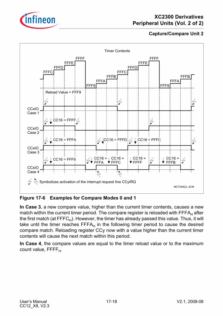
XC2300 DerivativesPeripheral Units (Vol. 2 of 2)
Capture/Compare Unit 2
Figure 17-6 Examples for Compare Modes 0 and 1
In Case 3, a new compare value, higher than the current timer contents, causes a newmatch within the current timer period. The compare register is reloaded with FFFAH afterthe first match (at FFFCH). However, the timer has already passed this value. Thus, it willtake until the timer reaches FFFAH in the following timer period to cause the desiredcompare match. Reloading register CCy now with a value higher than the current timercontents will cause the next match within this period.In Case 4, the compare values are equal to the timer reload value or to the maximumcount value, FFFFH.
MCT05422_4CM
CCxIOCase 1
CCxIOCase 2
CCxIOCase 3
CCxIOCase 4
FFFCFFFD
FFFEFFFF
FFF9FFFA
FFFBFFFC
FFFDFFFE
FFFF
FFF9FFFA
FFFB
Timer Contents
CC16 = FFFA CC16 = FFFD CC16 = FFFC
CC16 = FFF9 CC16 =FFFA
CC16 =FFFC
CC16 =FFFF
CC16 =FFFB
Symbolizes activation of the interrupt request line CCyIRQ
Reload Value = FFF9
CC16 = FFFF
User’s Manual 17-18 V2.1, 2008-08CC12_X8, V2.3
XC2300 DerivativesPeripheral Units (Vol. 2 of 2)
Capture/Compare Unit 2
17.5.3 Compare Mode 2Compare mode 2 is an interrupt-only mode similar to compare mode 0. The maindifference is that only one compare match, corresponding to one interrupt request, ispossible within a given timer period.When a match is detected in compare mode 2 for the first time within a count period ofthe allocated timer, the interrupt request line CCyIRQ is activated. In addition, all furthercompare matches within the current timer period are disabled, even if a new comparevalue, higher than the current timer contents, would be written to the register. Thisblocking is only released when the allocated timer overflows. A new compare valuewritten to the compare register after the first match will only go into effect within thefollowing timer period.
17.5.4 Compare Mode 3Compare mode 3 is based on compare mode 2, but additionally influences theassociated port pin. Only one compare event is possible within one timer period.When a match is detected in compare mode 3 for the first time within a count period ofthe allocated timer, the interrupt request line CCyIRQ is activated, and the associatedoutput signal is set to 1. In addition, all further compare matches within the current timerperiod are disabled, even if a new compare value, higher than the current timer contents,would be written to the register. This blocking is only released when the allocated timeroverflows. A new compare value written to the compare register after the first match willonly go into effect within the following timer period.The overflow signal is also used to reset the associated output signal to 0.Special attention has to be paid when the compare value is set equal to the timer reloadvalue. In this case, the compare match signal would try to set the output signal, while thetimer overflow tries to reset the output signal. This conflict is avoided such that the stateof the output signal is left unchanged in this case.Note: When the compare value is changed from a value above the current timer
contents to a value below the current timer contents, the new value is notrecognized before the next timer period.
For the exact operation of the port output signal, please see Section 17.6.
User’s Manual 17-19 V2.1, 2008-08CC12_X8, V2.3

XC2300 DerivativesPeripheral Units (Vol. 2 of 2)
Capture/Compare Unit 2
Figure 17-7 Compare Mode 2 and 3 Block Diagram
Note: The port signal remains unaffected in compare mode 2.
Figure 17-8 illustrates a few timing examples for compare modes 2 and 3.In all examples, the reload value of the used timer is set to FFF9H. When the timeroverflows, it starts counting from this value upwards.In Case 1, register CCy contains the value FFFCH. When the timer reaches this value,a match is detected, and the interrupt request line CCyIRQ is activated. In comparemode 2, this is all that will happen. In compare mode 3, additionally the associated portoutput is set to 1. The timer continues to count, and finally reaches its overflow. At thispoint, the port output is reset to 0 again. Note that, although not shown in the diagrams,the overflow signal of the timer also activates the associated interrupt request lineTxIRQ. If the contents of register CCy are not changed, the port output will be set againduring the following timer period, and reset again when the timer overflows. Thisoperation is ideal for the generation of a pulse width modulated (PWM) signal with aminimum of software overhead. The pulse width is varied by changing the comparevalue accordingly.In Case 2, the compare operation is blocked after the first match within a timer period.After the first match at FFFCH, the interrupt request is generated and the port output isset. In addition, further compare matches are disabled. If now a new compare value iswritten to register CCy, no interrupt request and no port output influence will take place,although the new compare value is higher than the current timer contents. Only after theoverflow of the timer, the compare logic is enabled again, and the next match will be
MCB05423_4CM
MU
X
MU
X
Timer T7
ACCy ACCy
Mode &Output Ctrl.
CCyIRQ
to PortLogic
Timer T8
ModeControl
SEMySEEy CompareRegister CCy
Comparator= ?MODy
T7IRQ
T8IRQ
Mode 3 only!
User’s Manual 17-20 V2.1, 2008-08CC12_X8, V2.3

XC2300 DerivativesPeripheral Units (Vol. 2 of 2)
Capture/Compare Unit 2
detected at FFFFH. One can see, that this operation is ideal for PWM generation, assoftware can write a new compare value regardless of whether this value is higher orlower than the current timer contents. It is assured that the new value (usually written tothe compare register in the appropriate interrupt service routine) will only go into effectduring the following timer period.
Figure 17-8 Timing Example for Compare Modes 2 and 3
Note: In compare mode 2, only interrupt requests are generated, in mode 3, also theoutput signals are generated.
In Case 3, further examples for the operation of the compare match blocking areillustrated.In Case 4, a new compare value is written to a compare register before the first matchwithin the timer period. One can see that, of course, the originally programmed comparematch (at FFFAH) will not take place. The first match will be detected at FFFCH. However,it is important to note that the reprogramming of the compare register took placeasynchronously - this means, the register was written to without any regard to the currentcontents of the timer. This is dangerous in the sense that the effect of such anasynchronous reprogramming is not easily predictable. If the timer would have alreadyreached the originally programmed compare value of FFFAH by the time the software
MCT05424_4CM
CCxIOCase 1
CCxIOCase 2
CC16 = FFFF
CCxIOCase 3
CCxIOCase 4
FFFCFFFD
FFFEFFFF
FFF9FFFA
FFFBFFFC
FFFDFFFE
FFFF
FFF9FFFA
FFFB
Timer Contents
CC16 = FFFA CC16 = FFFC
CC16 = FFFA CC16 = FFFC
Reload Value = FFF9
User’s Manual 17-21 V2.1, 2008-08CC12_X8, V2.3

XC2300 DerivativesPeripheral Units (Vol. 2 of 2)
Capture/Compare Unit 2
wrote to the register, a match would have been detected and the reprogramming wouldgo into effect during the next timer period.The examples in Figure 17-9 show special cases for compare modes 2 and 3. Case 1illustrates the effect when the compare value is equal to the reload value of the timer. Aninterrupt is generated in both modes. In mode 3, the output signal is not affected - itremains at the high level. Setting the compare value equal to the reload value easilyenables a 100% duty cycle signal for PWM generation. The important advantage here isthat the compare interrupt is still generated and can be used to reload the next comparevalue. Thus, no special treatment is required for this case (see Case 3).Cases 2, 4, and 5 show different options for the generation of a 0% duty cycle signal.Case 2 shows an asynchronous reprogramming of the compare value equal to thereload value. At the end of the current timer period, a compare interrupt will begenerated, which enables software to set the next compare value. The disadvantage ofthis method is that at least two timer periods will pass until a new regular compare valuecan go into effect. The compare match with the reload value FFF9H will block furthercompare matches during that timer period. This is additionally illustrated by Case 4.
Figure 17-9 Special Cases in Compare Modes 2 and 3
MCT05425_4CM
CC16 = FFF9 Int. Int.
CCxIOCase 1
Int.
CCxIOCase 2
Int.CC16 = FFF9 Int.
CCxIOCase 3
Int. CC16 = FFFB
CCxIOCase 4
Int.CC16 = FFF9 Int.
CC16 =FFFC
NoComp.
CCxIOCase 5
Int. CC16 =FFFC
Int.CC16 = FFF8
FFFCFFFD
FFFEFFFF
FFF9FFFA
FFFBFFFC
FFFDFFFE
FFFF
FFF9FFFA
FFFB
Timer Contents
Reload Value = FFF9
Int.CC16 = FFF9
User’s Manual 17-22 V2.1, 2008-08CC12_X8, V2.3

XC2300 DerivativesPeripheral Units (Vol. 2 of 2)
Capture/Compare Unit 2
Case 5 shows an option to get around this problem. Here, the compare register isreloaded with FFF8H, a value which is lower than the timer reload value. Thus, the timerwill never reach this value, and no compare match will be detected. The output signal willbe set to 0 after the first timer overflow. However, after the second overflow, softwarenow reloads the compare register with a regular compare value. As no compare blockinghas taken place (since there was no compare match), the newly written compare valuewill go into effect during the current timer period.
User’s Manual 17-23 V2.1, 2008-08CC12_X8, V2.3

XC2300 DerivativesPeripheral Units (Vol. 2 of 2)
Capture/Compare Unit 2
17.5.5 Double-Register Compare Mode The Double-Register Compare Mode makes it possible to further reduce softwareoverhead for a number of applications. In this mode, two compare registers worktogether to control one output. This mode is selected via the DRM register, or by aspecial combination of compare modes for the two registers.For double-register compare mode, the 16 capture/compare registers of a CAPCOM2unit are regarded as two banks of 8 registers each. The lower eight registers form bank1,while the upper eight registers form bank2. For double-register mode, a bank1 registerand a bank2 register form a register pair. Both registers of this register pair operate onthe pin associated with the bank1 register.The relationship between the bank1 and bank2 register of a pair and the effected outputpins for double-register compare mode is listed in Table 17-3.
The double-register compare mode can be programmed individually for each registerpair. Double-register compare mode can be selected via a certain combination ofcompare modes for the two registers of a pair. The bank1 register must be programmedfor mode 1 (with port influence), while the bank2 register must be programmed formode 0 (interrupt-only).
Table 17-3 Register Pairs for Double-Register Compare ModeCAPCOM2 Unit
Register Pair Used Output Pin Control Bitfield in CC2_DRMBank 1 Bank 2
CC16 CC24 CC16IO DR0MCC17 CC25 CC17IO DR1MCC18 CC26 CC18IO DR2MCC19 CC27 CC19IO DR3MCC20 CC28 CC20IO DR4MCC21 CC29 CC21IO DR5MCC22 CC30 CC22IO DR6MCC23 CC31 CC23IO DR7M
User’s Manual 17-24 V2.1, 2008-08CC12_X8, V2.3

XC2300 DerivativesPeripheral Units (Vol. 2 of 2)
Capture/Compare Unit 2
Double-register compare mode can be controlled (this means, enabled or disabled) foreach register pair via the associated control bitfield DRxM in register CC2_DRM.
Double-register compare mode can be controlled individually for each of the registerpairs.In the block diagram of the double-register compare mode (Figure 17-10), a bank2register will be referred to as CCz, while the corresponding bank1 register will be referredto as CCy.
CC2_DRM Double-Reg. Cmp. Mode Reg. SFR (FF2AH/95H) Reset Value: 0000H
15 14 13 12 11 10 9 8 7 6 5 4 3 2 1 0
DR7M DR6M DR5M DR4M DR3M DR2M DR1M DR0M
rw rw rw rw rw rw rw rw
Field Bits Type DescriptionDRxM [1:0],
[3:2], [5:4], [7:6], [9:8], [11:10], [13:12], [15:14]
rw Double Register x Compare Mode Selection00 DRM is controlled via the combination of compare
modes 1 and 0 (compatibility mode)01 DRM disabled regardless of compare modes10 DRM enabled regardless of compare modes11 ReservedNote: “x” indicates the register pair index in a bank.
User’s Manual 17-25 V2.1, 2008-08CC12_X8, V2.3
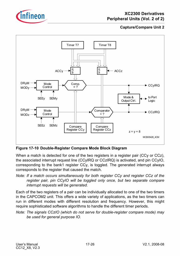
XC2300 DerivativesPeripheral Units (Vol. 2 of 2)
Capture/Compare Unit 2
Figure 17-10 Double-Register Compare Mode Block Diagram
When a match is detected for one of the two registers in a register pair (CCy or CCz),the associated interrupt request line (CCyIRQ or CCzIRQ) is activated, and pin CCyIO,corresponding to the bank1 register CCy, is toggled. The generated interrupt alwayscorresponds to the register that caused the match.Note: If a match occurs simultaneously for both register CCy and register CCz of the
register pair, pin CCyIO will be toggled only once, but two separate compareinterrupt requests will be generated.
Each of the two registers of a pair can be individually allocated to one of the two timersin the CAPCOM2 unit. This offers a wide variety of applications, as the two timers canrun in different modes with different resolution and frequency. However, this mightrequire sophisticated software algorithms to handle the different timer periods.Note: The signals CCzIO (which do not serve for double-register compare mode) may
be used for general purpose IO.
ModeControl
SEMySEEy
Comp.= ?
MUX
Timer T7 Timer T8
ACCy ACCz
DRyMMODy
CCyIRQ
MUX
Mode &Output Ctrl.
to PortLogic
MCB05426_4CM
Comparator= ?
CompareRegister CCz
CCzIRQ
z = y + 8
ModeControl
SEMzSEEz
DRyMMODz
CompareRegister CCy
User’s Manual 17-26 V2.1, 2008-08CC12_X8, V2.3

XC2300 DerivativesPeripheral Units (Vol. 2 of 2)
Capture/Compare Unit 2
17.6 Compare Output Signal GenerationThis section discusses the interaction between the CAPCOM Unit and the Port Logic.The block diagram illustrated in Figure 17-11 details the logic of the block “Mode &Output Control”, shown in Figure 17-5, Figure 17-7, and Figure 17-10.Each output signal is stored in its associated bit of the compare output registerCC2_OUT. The individual bits are updated each time an associated compare eventoccurs. The bits of these registers are connected to the respective port pins as analternate output function of a port line.
Figure 17-11 Port Output Block Diagram for Compare Modes
CC2_OUT Compare Output Reg. SFR (FF2CH/96H) Reset Value: 0000H
15 14 13 12 11 10 9 8 7 6 5 4 3 2 1 0CC31IO
CC30IO
CC29IO
CC28IO
CC27IO
CC26IO
CC25IO
CC24IO
CC23IO
CC22IO
CC21IO
CC20IO
CC19IO
CC18IO
CC17IO
CC16IO
rwh rwh rwh rwh rwh rwh rwh rwh rwh rwh rwh rwh rwh rwh rwh rwh
Field Bits Type DescriptionCCyIO [15:0] rwh Compare Output for Channel y
Alternative port output for the associated port pin.
MC_CAPCOM2_OUTPUT_XX
TxOV
OUT Reg.OutputValue
Control
MODy
CompareMatch
Control
DriverPort Pin
Pm.n
CAPCOM Logic Port Logic
User’s Manual 17-27 V2.1, 2008-08CC12_X8, V2.3

XC2300 DerivativesPeripheral Units (Vol. 2 of 2)
Capture/Compare Unit 2
Note: A compare output signal is visible at the pin only in compare modes 1 or 3.
The output signal of a compare event can either be a 1, a 0, the complement of thecurrent level, or the previous level. The block ‘Output Value Control’ determines thecorrect new level based on the compare event, the timer overflow signal, and the currentstate of the OUT register bit. For the output toggle function (e.g. in compare mode 1), thestate of the OUT register bit is read, inverted, and then written back.
User’s Manual 17-28 V2.1, 2008-08CC12_X8, V2.3

XC2300 DerivativesPeripheral Units (Vol. 2 of 2)
Capture/Compare Unit 2
17.7 Single Event OperationIf an application requires that one and only one compare event needs to take place(within a certain time frame), single event operation helps to reduce software overheadand to eliminate the need for fast reaction upon events.In order to achieve a single event operation without this feature, software would have toeither disable the compare mode or write a new value, which is outside of the countrange of the timer, into the compare register, after the programmed compare match hastaken place. Thus, usually an interrupt service routine is required to perform thisoperation. Interrupt response time may be critical if the timer period is very short - thedisable operation needs to be completed before the timer would reach the same valueagain.The single event operation eliminates the need for software to react after the firstcompare match. The complete operation can be set up before the event, and no actionis required after the event. The hardware takes care of generating only one event, andthen disabling all further compare matches.This option is programmed via the Single Event Mode register CC2_SEM and the SingleEvent Enable register CC2_SEE. Each register provides one bit for each CCy register ofa unit.
CC2_SEM Single Event Mode Ctrl. Reg. SFR (FE28H/14H) Reset Value: 0000H
15 14 13 12 11 10 9 8 7 6 5 4 3 2 1 0SEM31
SEM30
SEM29
SEM28
SEM27
SEM26
SEM25
SEM24
SEM23
SEM22
SEM21
SEM20
SEM19
SEM18
SEM17
SEM16
rw rw rw rw rw rw rw rw rw rw rw rw rw rw rw rw
Field Bits Type DescriptionSEMy [15:0] rw Single Event Mode Control
0 Single Event Mode disabled for channel y1 Single Event Mode enabled for channel y
CC2_SEE Single Event Enable Reg. SFR (FE2AH/15H) Reset Value: 0000H
15 14 13 12 11 10 9 8 7 6 5 4 3 2 1 0SEE31
SEE30
SEE29
SEE28
SEE27
SEE26
SEE25
SEE24
SEE23
SEE22
SEE21
SEE20
SEE19
SEE18
SEE17
SEE16
rwh rwh rwh rwh rwh rwh rwh rwh rwh rwh rwh rwh rwh rwh rwh rwh
User’s Manual 17-29 V2.1, 2008-08CC12_X8, V2.3

XC2300 DerivativesPeripheral Units (Vol. 2 of 2)
Capture/Compare Unit 2
To setup a single event operation for a CCy register, software first programs the desiredcompare operation and compare value, and then sets the respective bit in registerCC2_SEM to enable the single event mode. At last, the respective event enable bit inregister CC2_SEE is set.When the programmed compare match occurs, all operations of the selected comparemode take place. In addition, hardware automatically disables all further comparematches and reset the event enable bit in register CC2_SEE to 0. As long as this bit iscleared, any compare operation is disabled. To setup a new event, this bit must first beset again.
Field Bits Type DescriptionSEEy [15:0] rw Single Event Enable Control
0 Single Event disabled for channel y1 Single Event enabled for channel yNote: This bit is cleared by hardware after the event.
User’s Manual 17-30 V2.1, 2008-08CC12_X8, V2.3
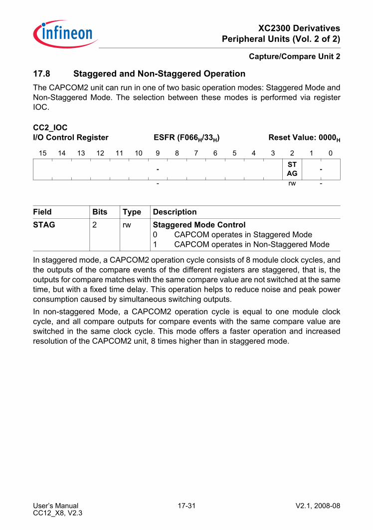
XC2300 DerivativesPeripheral Units (Vol. 2 of 2)
Capture/Compare Unit 2
17.8 Staggered and Non-Staggered OperationThe CAPCOM2 unit can run in one of two basic operation modes: Staggered Mode andNon-Staggered Mode. The selection between these modes is performed via registerIOC.
In staggered mode, a CAPCOM2 operation cycle consists of 8 module clock cycles, andthe outputs of the compare events of the different registers are staggered, that is, theoutputs for compare matches with the same compare value are not switched at the sametime, but with a fixed time delay. This operation helps to reduce noise and peak powerconsumption caused by simultaneous switching outputs.In non-staggered Mode, a CAPCOM2 operation cycle is equal to one module clockcycle, and all compare outputs for compare events with the same compare value areswitched in the same clock cycle. This mode offers a faster operation and increasedresolution of the CAPCOM2 unit, 8 times higher than in staggered mode.
CC2_IOC I/O Control Register ESFR (F066H/33H) Reset Value: 0000H
15 14 13 12 11 10 9 8 7 6 5 4 3 2 1 0
- ST AG -
- rw -
Field Bits Type DescriptionSTAG 2 rw Staggered Mode Control
0 CAPCOM operates in Staggered Mode1 CAPCOM operates in Non-Staggered Mode
User’s Manual 17-31 V2.1, 2008-08CC12_X8, V2.3

XC2300 DerivativesPeripheral Units (Vol. 2 of 2)
Capture/Compare Unit 2
Staggered ModeFigure 17-12 illustrates the staggered mode operation. In this example, all CCy registersare programmed for compare mode 3.Registers CC16, CC17, and CC18 are all programmed for a compare value of FFFEH.When the timer increments to FFFEH, the comparator detects a match for all of the threeregisters. The output CC16IO of register CC16 is switched to 1 one cycle after thecomparator match. However, the outputs CC17IO and CC18IO are not switched at thesame time, but one, respectively two cycles later. This staggering of the outputscontinues for all registers including register CC23. The number of the register indicatesthe delay of the output signal in clock cycles - the output of register CC23 is switched7 cycles later than the one of register CC16. In the example, the compare value forregister CC13 is set to FFFDH. Thus, the output is switched in the last clock cycle of theCAPCOM2 cycle in which the timer reached FFFDH.When the timer overflows, all compare outputs are reset to 0 (compare mode 3). Again,the staggering of the output signals can be seen from Figure 17-12.Looking at registers CC24 through CC31 shows that their outputs are switched in parallelto the respective outputs of registers CC16 through CC23. In fact, the staggering isperformed in parallel for the upper and the lower register bank. In this way, it is assured,that both compare signals of a register pair in double-register compare mode operatesimultaneously.Note: This is a general description and only refers to channels connected to pins.
User’s Manual 17-32 V2.1, 2008-08CC12_X8, V2.3

XC2300 DerivativesPeripheral Units (Vol. 2 of 2)
Capture/Compare Unit 2
Figure 17-12 Staggered Mode Operation
MCT05428_4CM
Timercontents= FFFD
Timer increments toFFFE
Timer increments toFFFF
Timer is reloadedwith FFFC
Timer overflow
1 CAPCOM Cycle= 8 fCC Clock Cycles
1 CAPCOM Cycle= 8 fCC Clock Cycles
CC26 = FFFE
CC27 = FFFF
CC28 = FFFE
CC29 = FFFF
CC30 = FFFF
CC31 = FFFD
CC16 = FFFE
CC17 = FFFE
CC18 = FFFE
CC19 = FFFF
CC20 = FFFE
CC21 = FFFF
CC22 = FFFF
CC23 = FFFD
CC24 = FFFE
CC25 = FFFE
User’s Manual 17-33 V2.1, 2008-08CC12_X8, V2.3

XC2300 DerivativesPeripheral Units (Vol. 2 of 2)
Capture/Compare Unit 2
Non-Staggered ModeTo gain maximum speed and resolution with the CAPCOM2 unit, it can be switched tonon-staggered mode. In this mode, one CAPCOM2 operation cycle is equal to onemodule clock cycle. Timer increment and the comparison of its new contents with thecontents of the compare register takes place within one clock cycle. The appropriateoutput signals are switched in the following clock cycle (in parallel to the next possibletimer increment and comparison).Figure 17-13 illustrates the non-staggered mode. Note that when the timer overflows, italso takes one additional clock cycle to switch the output signals.Note: This is a general description and only refers to channels connected to pins.
User’s Manual 17-34 V2.1, 2008-08CC12_X8, V2.3

XC2300 DerivativesPeripheral Units (Vol. 2 of 2)
Capture/Compare Unit 2
Figure 17-13 Non-Staggered Mode Operation
MCT05429_4CM_CC2
Timercontents= FFFD
Timer increments toFFFE
Timer increments toFFFF
Timer is reloadedwith FFFC
Timer overflow
1 CAPCOM Cycle= 1 fCC Clock Cycle
1 CAPCOM Cycle= 1 fCC Clock Cycle
CC26 = FFFE
CC27 = FFFF
CC28 = FFFE
CC29 = FFFF
CC30 = FFFF
CC31 = FFFD
CC16 = FFFE
CC17 = FFFE
CC18 = FFFE
CC19 = FFFF
CC20 = FFFE
CC21 = FFFF
CC22 = FFFF
CC23 = FFFD
CC24 = FFFE
CC25 = FFFE
User’s Manual 17-35 V2.1, 2008-08CC12_X8, V2.3
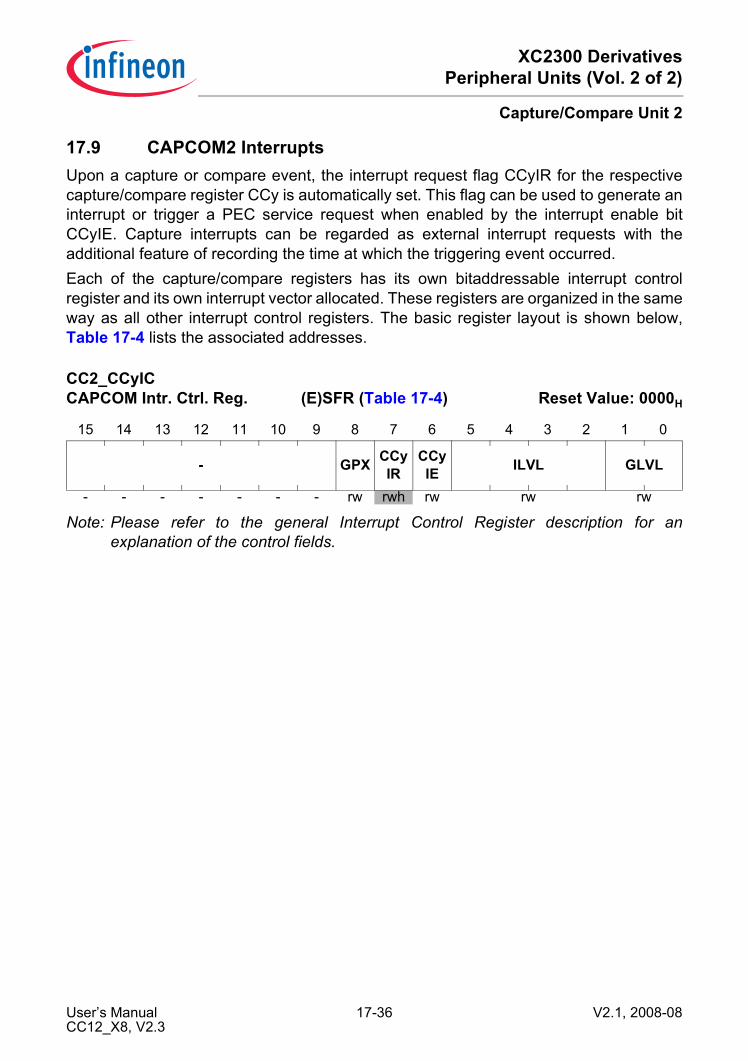
XC2300 DerivativesPeripheral Units (Vol. 2 of 2)
Capture/Compare Unit 2
17.9 CAPCOM2 InterruptsUpon a capture or compare event, the interrupt request flag CCyIR for the respectivecapture/compare register CCy is automatically set. This flag can be used to generate aninterrupt or trigger a PEC service request when enabled by the interrupt enable bitCCyIE. Capture interrupts can be regarded as external interrupt requests with theadditional feature of recording the time at which the triggering event occurred.Each of the capture/compare registers has its own bitaddressable interrupt controlregister and its own interrupt vector allocated. These registers are organized in the sameway as all other interrupt control registers. The basic register layout is shown below,Table 17-4 lists the associated addresses.
Note: Please refer to the general Interrupt Control Register description for anexplanation of the control fields.
CC2_CCyIC CAPCOM Intr. Ctrl. Reg. (E)SFR (Table 17-4) Reset Value: 0000H
15 14 13 12 11 10 9 8 7 6 5 4 3 2 1 0
- GPX CCyIR
CCyIE ILVL GLVL
- - - - - - - rw rwh rw rw rw
User’s Manual 17-36 V2.1, 2008-08CC12_X8, V2.3
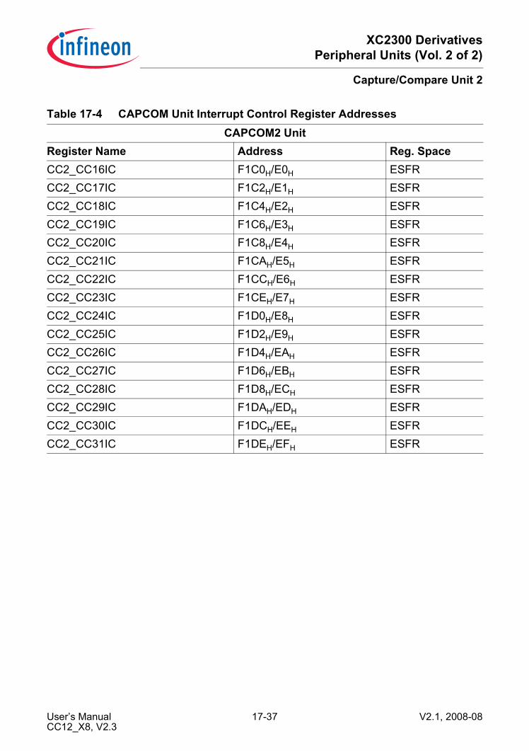
XC2300 DerivativesPeripheral Units (Vol. 2 of 2)
Capture/Compare Unit 2
Table 17-4 CAPCOM Unit Interrupt Control Register AddressesCAPCOM2 Unit
Register Name Address Reg. SpaceCC2_CC16IC F1C0H/E0H ESFRCC2_CC17IC F1C2H/E1H ESFRCC2_CC18IC F1C4H/E2H ESFRCC2_CC19IC F1C6H/E3H ESFRCC2_CC20IC F1C8H/E4H ESFRCC2_CC21IC F1CAH/E5H ESFRCC2_CC22IC F1CCH/E6H ESFRCC2_CC23IC F1CEH/E7H ESFRCC2_CC24IC F1D0H/E8H ESFRCC2_CC25IC F1D2H/E9H ESFRCC2_CC26IC F1D4H/EAH ESFRCC2_CC27IC F1D6H/EBH ESFRCC2_CC28IC F1D8H/ECH ESFRCC2_CC29IC F1DAH/EDH ESFRCC2_CC30IC F1DCH/EEH ESFRCC2_CC31IC F1DEH/EFH ESFR
User’s Manual 17-37 V2.1, 2008-08CC12_X8, V2.3
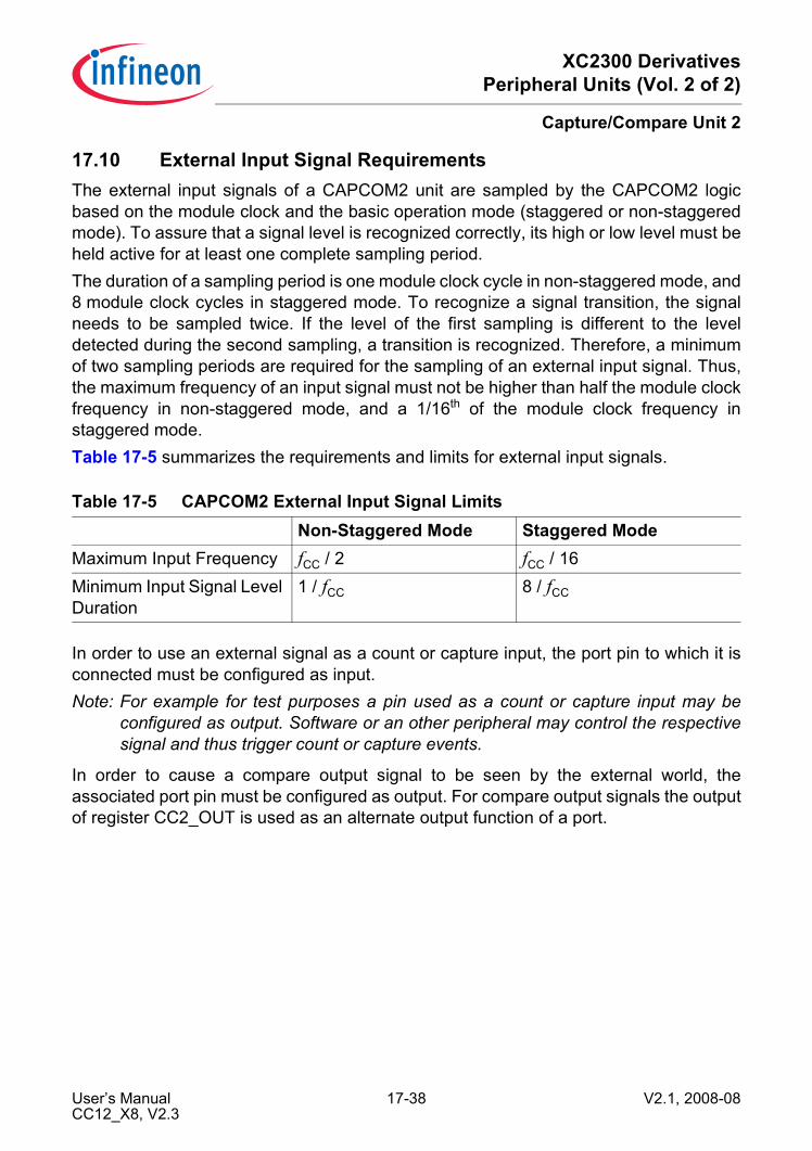
XC2300 DerivativesPeripheral Units (Vol. 2 of 2)
Capture/Compare Unit 2
17.10 External Input Signal RequirementsThe external input signals of a CAPCOM2 unit are sampled by the CAPCOM2 logicbased on the module clock and the basic operation mode (staggered or non-staggeredmode). To assure that a signal level is recognized correctly, its high or low level must beheld active for at least one complete sampling period.The duration of a sampling period is one module clock cycle in non-staggered mode, and8 module clock cycles in staggered mode. To recognize a signal transition, the signalneeds to be sampled twice. If the level of the first sampling is different to the leveldetected during the second sampling, a transition is recognized. Therefore, a minimumof two sampling periods are required for the sampling of an external input signal. Thus,the maximum frequency of an input signal must not be higher than half the module clockfrequency in non-staggered mode, and a 1/16th of the module clock frequency instaggered mode.Table 17-5 summarizes the requirements and limits for external input signals.
In order to use an external signal as a count or capture input, the port pin to which it isconnected must be configured as input.Note: For example for test purposes a pin used as a count or capture input may be
configured as output. Software or an other peripheral may control the respectivesignal and thus trigger count or capture events.
In order to cause a compare output signal to be seen by the external world, theassociated port pin must be configured as output. For compare output signals the outputof register CC2_OUT is used as an alternate output function of a port.
Table 17-5 CAPCOM2 External Input Signal LimitsNon-Staggered Mode Staggered Mode
Maximum Input Frequency fCC / 2 fCC / 16Minimum Input Signal Level Duration
1 / fCC 8 / fCC
User’s Manual 17-38 V2.1, 2008-08CC12_X8, V2.3
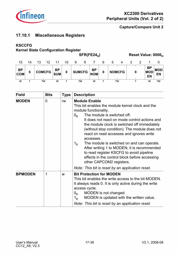
XC2300 DerivativesPeripheral Units (Vol. 2 of 2)
Capture/Compare Unit 2
17.10.1 Miscellaneous Registers
KSCCFG Kernel State Configuration Register
SFR(FE24H) Reset Value: 0000H
15 14 13 12 11 10 9 8 7 6 5 4 3 2 1 0
BPCOM 0 COMCFG BP
SUM 0 SUMCFG BPNOM 0 NOMCFG 0
BPMODEN
MODEN
w r rw w r rw w r rw r w rw
Field Bits Type DescriptionMODEN 0 rw Module Enable
This bit enables the module kernel clock and the module functionality.0B The module is switched off.
It does not react on mode control actions and the module clock is switched off immediately (without stop condition). The module does not react on read accesses and ignores write accesses.
1B The module is switched on and can operate. After writing 1 to MODEN, it is recommended to read register KSCFG to avoid pipeline effects in the control block before accessing other CAPCOM2 registers.
Note: This bit is reset by an application reset.BPMODEN 1 w Bit Protection for MODEN
This bit enables the write access to the bit MODEN. It always reads 0. It is only active during the write access cycle.0B MODEN is not changed.1B MODEN is updated with the written value.Note: This bit is reset by an application reset.
User’s Manual 17-39 V2.1, 2008-08CC12_X8, V2.3

XC2300 DerivativesPeripheral Units (Vol. 2 of 2)
Capture/Compare Unit 2
NOMCFG [5:4] rw Normal Operation Mode ConfigurationThis bit field defines the kernel mode applied in normal operation mode.0XB The module is switched on.1XB The module is switched off.This field is taken into account for CR = 00 or 11.Note: This bit is reset by an application reset.
BPNOM 7 w Bit Protection for NOMCFGThis bit enables the write access to the bit field NOMCFG. It always reads 0. It is only active during the write access cycle.0B NOMCFG is not changed.1B NOMCFG is updated with the written value.Note: This bit is reset by an application reset.
SUMCFG [9:8] rw Suspend Mode ConfigurationThis bit field defines the kernel mode applied in suspend mode.0XB The module is switched on.1XB The module is switched off.This field is taken into account for CR = 01.Note: This bit is reset by a debug reset.
BPSUM 11 w Bit Protection for SUMCFGThis bit enables the write access to the bit field SUMCFG. It always reads 0. It is only active during the write access cycle.0B SUMCFG is not changed.1B SUMCFG is updated with the written value.Note: This bit is reset by a debug reset.
COMCFG [13:12] rw Clock Off Mode ConfigurationThis bit field defines the kernel mode applied in clock off mode.0XB The module is switched on.1XB The module is switched off.This field is taken into account for CR = 10.Note: This bit is reset by an application reset.
Field Bits Type Description
User’s Manual 17-40 V2.1, 2008-08CC12_X8, V2.3
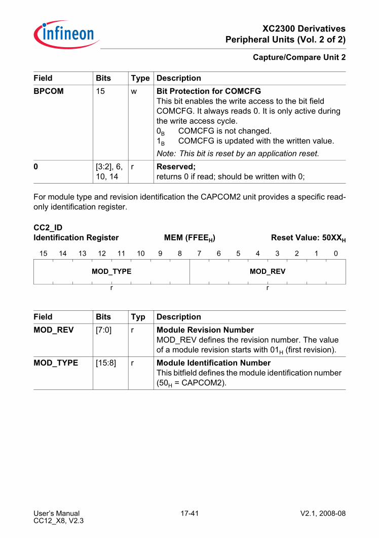
XC2300 DerivativesPeripheral Units (Vol. 2 of 2)
Capture/Compare Unit 2
For module type and revision identification the CAPCOM2 unit provides a specific read-only identification register.
BPCOM 15 w Bit Protection for COMCFGThis bit enables the write access to the bit field COMCFG. It always reads 0. It is only active during the write access cycle.0B COMCFG is not changed.1B COMCFG is updated with the written value.Note: This bit is reset by an application reset.
0 [3:2], 6, 10, 14
r Reserved;returns 0 if read; should be written with 0;
CC2_IDIdentification Register MEM (FFEEH) Reset Value: 50XXH
15 14 13 12 11 10 9 8 7 6 5 4 3 2 1 0
MOD_TYPE MOD_REV
r r
Field Bits Typ DescriptionMOD_REV [7:0] r Module Revision Number
MOD_REV defines the revision number. The value of a module revision starts with 01H (first revision).
MOD_TYPE [15:8] r Module Identification NumberThis bitfield defines the module identification number (50H = CAPCOM2).
Field Bits Type Description
User’s Manual 17-41 V2.1, 2008-08CC12_X8, V2.3
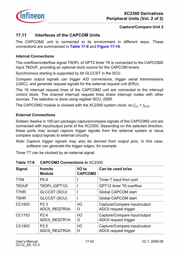
XC2300 DerivativesPeripheral Units (Vol. 2 of 2)
Capture/Compare Unit 2
17.11 Interfaces of the CAPCOM UnitsThe CAPCOM2 unit is connected to its environment in different ways. Theseconnections are summarized in Table 17-6 and Figure 17-14.
Internal ConnectionsThe overflow/underflow signal T6OFL of GPT2 timer T6 is connected to the CAPCOM2input T6OUF, providing an optional clock source for the CAPCOM timers.Synchronous starting is supported by bit GLCCST in the SCU.Compare output signals can trigger A/D conversions, trigger serial transmissions(USIC), and generate request signals for the external request unit (ERU).The 18 interrupt request lines of the CAPCOM2 unit are connected to the interruptcontrol block. The channel interrupt request lines share interrupt nodes with othersources. The selection is done using register SCU_ISSR.The CAPCOM2 module is clocked with the XC2300 system clock, so fCC = fSYS.
External ConnectionsSixteen (twelve in 100-pin package) capture/compare signals of the CAPCOM2 unit areconnected with input/output ports of the XC2300. Depending on the selected direction,these ports may accept capture trigger signals from the external system or issuecompare output signals to external circuitry.Note: Capture trigger signals may also be derived from output pins. In this case,
software can generate the trigger edges, for example.
Timer T7 can be clocked by an external signal.
Table 17-6 CAPCOM2 Connections in XC2300
Signal from/toModule
I/O to CAPCOM2
Can be used to/as
T7IN P5.9 I Timer 7 input from portT6OUF T6OFL (GPT12) I GPT12 timer T6 overflowT7HR GLCCST (SCU) I Global CAPCOM startT8HR GLCCST (SCU) I Global CAPCOM startCC16IO P2.3
ADC0_REQTR0AI/OO
Capture/Compare input/outputADC0 request trigger
CC17IO P2.4ADC0_REQTR1A
I/OO
Capture/Compare input/outputADC0 request trigger
CC18IO P2.5ADC0_REQTR2A
I/OO
Capture/Compare input/outputADC0 request trigger
User’s Manual 17-42 V2.1, 2008-08CC12_X8, V2.3
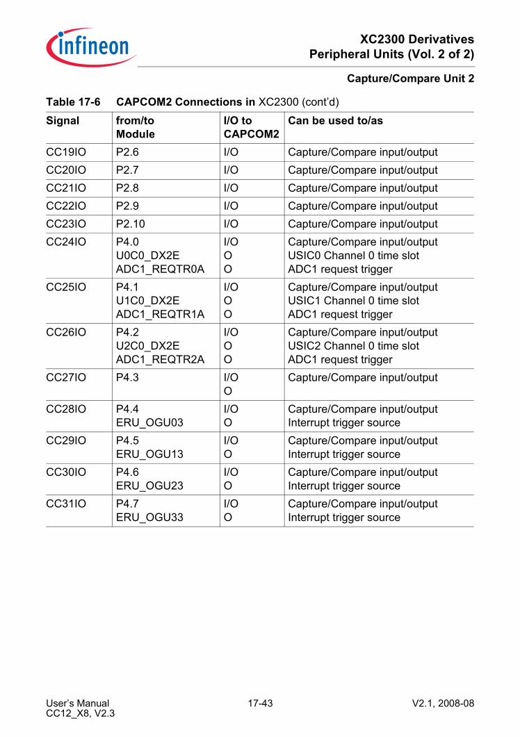
XC2300 DerivativesPeripheral Units (Vol. 2 of 2)
Capture/Compare Unit 2
CC19IO P2.6 I/O Capture/Compare input/outputCC20IO P2.7 I/O Capture/Compare input/outputCC21IO P2.8 I/O Capture/Compare input/outputCC22IO P2.9 I/O Capture/Compare input/outputCC23IO P2.10 I/O Capture/Compare input/outputCC24IO P4.0
U0C0_DX2EADC1_REQTR0A
I/OOO
Capture/Compare input/outputUSIC0 Channel 0 time slotADC1 request trigger
CC25IO P4.1U1C0_DX2EADC1_REQTR1A
I/OOO
Capture/Compare input/outputUSIC1 Channel 0 time slotADC1 request trigger
CC26IO P4.2U2C0_DX2EADC1_REQTR2A
I/OOO
Capture/Compare input/outputUSIC2 Channel 0 time slotADC1 request trigger
CC27IO P4.3 I/OO
Capture/Compare input/output
CC28IO P4.4ERU_OGU03
I/OO
Capture/Compare input/outputInterrupt trigger source
CC29IO P4.5ERU_OGU13
I/OO
Capture/Compare input/outputInterrupt trigger source
CC30IO P4.6ERU_OGU23
I/OO
Capture/Compare input/outputInterrupt trigger source
CC31IO P4.7ERU_OGU33
I/OO
Capture/Compare input/outputInterrupt trigger source
Table 17-6 CAPCOM2 Connections in XC2300 (cont’d)
Signal from/toModule
I/O to CAPCOM2
Can be used to/as
User’s Manual 17-43 V2.1, 2008-08CC12_X8, V2.3

XC2300 DerivativesPeripheral Units (Vol. 2 of 2)
Capture/Compare Unit 2
Figure 17-14 CAPCOM2 Unit InterfacesMC_CAPCOM2_CONN
CC30IO
CAPCOM2Module
fSYS = fCC
CC2DIS
T6OUF
InterruptControl
SystemControl
Unit (SCU)
GPT12
P2.3/CC16IO
P2.4/CC17IO
P2.5/CC18IO
P2.6/CC19IO
P2.7/CC20IO
P2.8/CC21IO
P5.9/T7IN
CC31IRQ
CC30IRQ
CC17IRQ
CC16IRQ
T8IRQ
T7IRQ
CC31IO
T7IN
CC29IO
CC28IO
CC21IO
CC20IO
CC19IO
CC18IO
CC17IO
CC16IO
P4.1/CC25IO
P4.0/CC24IO
P4.2/CC26IO
P4.3/CC27IOCC27IO
CC26IO
CC25IO
CC24IO
CC23IO
CC22IO
Port P5Control
Port P2Control
Port P4Control
P4.5/CC29IO
P4.4/CC28IO
P4.6/CC30IO
P4.7/CC31IO
P2.9/CC22IO
P2.10/CC23IO
GLCCST
ERU
:
ADC
USIC
User’s Manual 17-44 V2.1, 2008-08CC12_X8, V2.3
XC2300 DerivativesPeripheral Units (Vol. 2 of 2)
Capture/Compare Unit 6 (CCU6)
18 Capture/Compare Unit 6 (CCU6)The CCU6 is a high-resolution 16-bit capture and compare unit with application specificmodes, mainly for AC drive control. Special operating modes support the control ofBrushless DC-motors using Hall sensors or Back-EMF detection. Furthermore, blockcommutation and control mechanisms for multi-phase machines are supported.It also supports inputs to start several timers synchronously, an important feature indevices with several CCU6 modules.This chapter is structured as follows:• Introduction (see Section 18.1)
including the register overview (see Section 18.1.3)• Operating T12 (see Section 18.2)
including T12 related registers (see Section 18.2.8)and capture/compare control registers (see Section 18.2.9)
• Operating T13 (see Section 18.3)including T13 related registers (see Section 18.3.6)
• Trap handling (see Section 18.4)• Multi-Channel mode (see Section 18.5)• Hall sensor mode (see Section 18.6)• Modulation control registers (see Section 18.7)• Interrupt handling (see Section 18.8)
including interrupt registers (see Section 18.8.2)• General module operation (see Section 18.9)
including general registers (see Section 18.9.3)• Module implementation (see Section 18.10)
18.1 IntroductionThe CCU6 unit is made up of a Timer T12 Block with three capture/compare channelsand a Timer T13 Block with one compare channel. The T12 channels can independentlygenerate PWM signals or accept capture triggers, or they can jointly generate controlsignal patterns to drive AC-motors or inverters.A rich set of status bits, synchronized updating of parameter values via shadowregisters, and flexible generation of interrupt request signals provide means for efficientsoftware-control.Note: The capture/compare module itself is named CCU6 (capture/compare unit 6).
A capture/compare channel inside this module is named CC6x.
User’s Manual 18-1 V2.1, 2008-08CCU6, UM_V0.5D3

XC2300 DerivativesPeripheral Units (Vol. 2 of 2)
Capture/Compare Unit 6 (CCU6)
18.1.1 Feature Set OverviewThis section gives an overview over the different building blocks and their main features.
Timer 12 Block Features• Three capture/compare channels, each channel can be used either as capture or as
compare channel• Generation of a three-phase PWM supported (six outputs, individual signals for high-
side and low-side switches)• 16-bit resolution, maximum count frequency = peripheral clock• Dead-time control for each channel to avoid short-circuits in the power stage• Concurrent update of T12 registers• Center-aligned and edge-aligned PWM can be generated• Single-shot mode supported• Start can be controlled by external events• Capability of counting external events• Many interrupt request sources• Hysteresis-like control mode
Timer 13 Block Features• One independent compare channel with one output• 16-bit resolution, maximum count frequency = peripheral clock• Concurrent update of T13 registers• Can be synchronized to T12• Interrupt generation at period-match and compare-match• Single-shot mode supported• Start can be controlled by external events• Capability of counting external events
Additional Specific Functions• Block commutation for Brushless DC-drives implemented• Position detection via Hall-sensor pattern• Noise filter supported for position input signals• Automatic rotational speed measurement and commutation control for block
commutation• Integrated error handling• Fast emergency stop without CPU load via external signal (CTRAP)• Control modes for multi-channel AC-drives• Output levels can be selected and adapted to the power stage
User’s Manual 18-2 V2.1, 2008-08CCU6, UM_V0.5D3

XC2300 DerivativesPeripheral Units (Vol. 2 of 2)
Capture/Compare Unit 6 (CCU6)
18.1.2 Block DiagramThe Timer T12 can work in capture and/or compare mode for its three channels. Themodes can also be combined (e.g. a channel works in compare mode, whereas anotherchannel works in capture mode). The Timer T13 can work in compare mode only. Themulti-channel control unit generates output patterns which can be modulated by T12and/or T13. The modulation sources can be selected and combined for the signalmodulation.
Figure 18-1 CCU6 Block Diagram
CCU6 Module Kernel
CCU6_MCB05506
Input / Output Control
Port Control
Com
pare
Com
pare
2 2
Com
pare
Out
put S
elec
t
3H
all I
nput
Out
put S
elec
t
1
Trap
Inpu
t
3+3
Cap
ture
T13 CC63
Start
21
Compare
Multi-channelControl
TrapControl
Dead-Time
Control
CC60
CC61
Compare1
1
1
T12
CC62
CC
60
CO
UT6
0
T13
HR
[D:A
]
T12
HR
[D:A
]
CC
PO
S0[
D:A
]
CC
PO
S1[
D:A
]
CC
PO
S2[
D:A
]
CTR
AP
[D:A
]
ClockControl
InterruptControl
fCC6
SR[3:0]
CC
60IN
[D:A
]
CC
61
CO
UT6
1
CC
61IN
[D:A
]
CC
62
CO
UT6
2
CC
62IN
[D:A
]
User’s Manual 18-3 V2.1, 2008-08CCU6, UM_V0.5D3

XC2300 DerivativesPeripheral Units (Vol. 2 of 2)
Capture/Compare Unit 6 (CCU6)
18.1.3 Register OverviewFor the generation of the overall register table, the prefix “CCU6x_” has to be added tothe register names in this table to identify the registers of different CCU6 modules thatare implemented. In this naming convention, x indicates the module number.Table 18-1 shows all registers required for programming of a CCU6 module. Itsummarizes the CCU6 kernel registers and defines their relative addresses and thereset values.8-bit short addresses are not available for this module.
Figure 18-2 CCU6 Registers
T12 related Registers
Cap/ComControl Registers
T12 CMPSTAT
0IC1IC
CMPMODIF
Interrupt Status/Control Registers
T12PRT12DTCCC60RCC60SRCC61RCC61SRCC62RCC62SR
T13T13PRCC63R
MCMOUTMCMOUTS
PSLRTRPCTRMODCTR
TCTR4TCTR2TCTR0
IENINPISRISSIS
2IC3IC
CC63SR
MCMCTR
T12MSEL
GeneralRegisters
PISELH
KSCFG
CCU6_regs
PISELL
KSCSR
T13 related Registers
ModulationControl Registers
User’s Manual 18-4 V2.1, 2008-08CCU6, UM_V0.5D3

XC2300 DerivativesPeripheral Units (Vol. 2 of 2)
Capture/Compare Unit 6 (CCU6)
Table 18-1 CCU6 Module Register SummaryShort Name Description Rel.
Addr.Reset Value
SeePage
General RegistersPISELL Module Port Input Select Register 04H 0000H Page 18-106PISELH Module Port Input Select Register 06H 0000H Page 18-108KSCFG Kernel State Configuration Register 00H 0000H Page 18-110KSCSR Kernel State Control Sensitivity Register 0EH 0000H Page 18-112
Timer T12 related RegistersT12 Timer 12 Counter Register 10H 0000H Page 18-32T12PR Timer 12 Period Register 12H 0000H Page 18-32T12DTC Dead-Time Control Reg. for Timer T12 14H 0000H Page 18-35CC60R Capture/Compare Reg. Channel CC60 18H 0000H Page 18-33CC61R Capture/Compare Reg. Channel CC61 1AH 0000H Page 18-33CC62R Capture/Compare Reg. Channel CC62 1CH 0000H Page 18-33CC60SR Capture/Compare Shadow Register
Channel CC6020H 0000H Page 18-34
CC61SR Capture/Compare Shadow Register Channel CC61
22H 0000H Page 18-34
CC62SR Capture/Compare Shadow Register Channel CC62
24H 0000H Page 18-34
Capture/Compare Control RegistersCMPSTAT Compare State Register 28H 0000H Page 18-37CMPMODIF Compare State Modification Register 2AH 0000H Page 18-39T12MSEL T12 Capture/Comp. Mode Select Reg. 46H 0000H Page 18-40TCTR0 Timer Control Register 0 2CH 0000H Page 18-41TCTR2 Timer Control Register 2 2EH 0000H Page 18-44TCTR4 Timer Control Register 4 26H 0000H Page 18-47
Timer T13 related RegistersT13 Timer 13 Counter Register 30H 0000H Page 18-62
User’s Manual 18-5 V2.1, 2008-08CCU6, UM_V0.5D3

XC2300 DerivativesPeripheral Units (Vol. 2 of 2)
Capture/Compare Unit 6 (CCU6)
T13PR Timer 13 Period Register 32H 0000H Page 18-63CC63R Compare Register for Timer 13 34H 0000H Page 18-64CC63SR Compare Shadow Register for Timer 13 36H 0000H Page 18-64
Modulation Control RegistersMODCTR Modulation Control Register 40H 0000H Page 18-77TRPCTR Trap Control Register 42H 0000H Page 18-79PSLR Passive State Level Register 44H 0000H Page 18-82MCMOUTS Multi-Channel Mode Output Shadow
Register4AH 0000H Page 18-85
MCMOUT Multi-Channel Mode Output Register 4CH 0000H Page 18-86MCMCTR Multi-Channel Mode Control Register 4EH 0000H Page 18-83
Interrupt Status and Node RegistersIS Interrupt Status Register 50H 0000H Page 18-90ISS Interrupt Status Set Register 52H 0000H Page 18-93ISR Interrupt Status Reset Register 54H 0000H Page 18-95INP Interrupt Node Pointer Register 56H 3940H Page 18-100IEN Interrupt Node Pointer Register 58H 0000H Page 18-97
Table 18-1 CCU6 Module Register Summary (cont’d)
Short Name Description Rel.Addr.
Reset Value
SeePage
User’s Manual 18-6 V2.1, 2008-08CCU6, UM_V0.5D3

XC2300 DerivativesPeripheral Units (Vol. 2 of 2)
Capture/Compare Unit 6 (CCU6)
18.2 Operating Timer T12The timer T12 block is the main unit to generate the 3-phase PWM signals. A 16-bitcounter is connected to 3 channel registers via comparators, that generate a signal whenthe counter contents match one of the channel register contents. A variety of controlfunctions facilitate the adaptation of the T12 structure to different application needs.Besides the 3-phase PWM generation, the T12 block offers options for individualcompare and capture functions, as well as dead-time control and hysteresis-likecompare mode.This section provides information about:• T12 overview (see Section 18.2.1)• Counting scheme (see Section 18.2.2)• Compare modes (see Section 18.2.3)• Compare mode output path (see Section 18.2.4)• Capture modes (see Section 18.2.5)• Shadow transfer (see Section 18.2.6)• T12 operating mode selection (see Section 18.2.7)• T12 counter register description (see Section 18.2.8)
Figure 18-3 Overview Diagram of the Timer T12 Block
CCU6_MCA05507
Timer T12Logic
Capture/CompareChannel CC61
Capture/CompareChannel CC60
Capture/CompareChannel CC62
CC61ST
CC60ST
CC62ST
State Bits
ToDead-TimeControlandOutputModulation
Input and Control/Status Logic
T12HR CC6xIN CCPOSx
User’s Manual 18-7 V2.1, 2008-08CCU6, UM_V0.5D3

XC2300 DerivativesPeripheral Units (Vol. 2 of 2)
Capture/Compare Unit 6 (CCU6)
18.2.1 T12 OverviewFigure 18-4 shows a detailed block diagram of Timer T12. The functions of the timer T12block are controlled by bits in registers TCTR0, TCTR2, and PISELL.Timer T12 receives its input clock (fT12) from the module clock fCC6 via a programmableprescaler and an optional 1/256 divider or from an input signal T12HR. These optionsare controlled via bit fields T12CLK and T12PRE (see Table 18-2). T12 can count up ordown, depending on the selected operation mode. A direction flag, CDIR, indicates thecurrent counting direction.
Figure 18-4 Timer T12 Logic and Period Comparators
Via a comparator, the T12 counter register T12 is connected to a Period RegisterT12PR. This register determines the maximum count value for T12.In Edge-Aligned mode, T12 is cleared to 0000H after it has reached the period valuedefined by T12PR. In Center-Aligned mode, the count direction of T12 is set from ‘up’ to
CCU6_MCA05508
Comp.= ?
Period Register
Period ShadowRegister
T12_PM
Counter RegisterT12
fCC6
Write toT12PR
Read fromT12PR
T12_OMT12_ZM
= 0000 H
= 0001 H
T12_ST
256n
ClockSelection
edgedetection
T12HR
T12PRET12CLK
ISCNT12
T12STD
T12STRCTM
T12RR
T12RS
T12R CDIR
T12RES
T12SSCT12Control& Status
STE12
edgedetection
T12RSEL
T12CNT fT12
User’s Manual 18-8 V2.1, 2008-08CCU6, UM_V0.5D3
XC2300 DerivativesPeripheral Units (Vol. 2 of 2)
Capture/Compare Unit 6 (CCU6)
‘down’ after it has reached the period value (please note that in this mode, T12 exceedsthe period value by one before counting down). In both cases, signal T12_PM (T12Period Match) is generated. The Period Register receives a new period value from itsShadow Period Register.A read access to T12PR delivers the current period value at the comparator, whereas awrite access targets the Shadow Period Register to prepare another period value. Thetransfer of a new period value from the Shadow Period Register into the Period Register(see Section 18.2.6) is controlled via the ‘T12 Shadow Transfer’ control signal, T12_ST.The generation of this signal depends on the operating mode and on the shadow transferenable bit STE12. Providing a shadow register for the period value as well as for othervalues related to the generation of the PWM signal allows a concurrent update bysoftware for all relevant parameters.Two further signals indicate whether the counter contents are equal to 0000H (T12_ZM= zero match) or 0001H (T12_OM = one match). These signals control the counting andswitching behavior of T12.The basic operating mode of T12, either Edge-Aligned mode (Figure 18-5) or Center-Aligned mode (Figure 18-6), is selected via bit CTM. A Single-Shot control bit, T12SSC,enables an automatic stop of the timer when the current counting period is finished (seeFigure 18-7 and Figure 18-8).The start or stop of T12 is controlled by the Run bit T12R that can be modified by bits inregister TCTR4. The run bit can be set/cleared by software via the associated set/clearbits T12RS or T12RR, it can be set by a selectable edge of the input signal T12HR(TCTR2.T12RSEL), or it is cleared by hardware according to preselected conditions.Timer T12 can be cleared via control bit T12RES. Setting this write-only bit does onlyclear the timer contents, but has no further effects, for example, it does not stop the timer.The timer T12 run bit T12R must not be set while the applied T12 period value is zero.The generation of the T12 shadow transfer control signal, T12_ST, is enabled via bitSTE12. This bit can be set or reset by software indirectly through its associated set/clearcontrol bits T12STR and T12STD.While Timer T12 is running, write accesses to the count register T12 are not taken intoaccount. If T12 is stopped and the Dead-Time counters are 0, write actions to registerT12 are immediately taken into account.
User’s Manual 18-9 V2.1, 2008-08CCU6, UM_V0.5D3
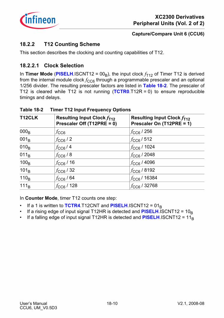
XC2300 DerivativesPeripheral Units (Vol. 2 of 2)
Capture/Compare Unit 6 (CCU6)
18.2.2 T12 Counting SchemeThis section describes the clocking and counting capabilities of T12.
18.2.2.1 Clock SelectionIn Timer Mode (PISELH.ISCNT12 = 00B), the input clock fT12 of Timer T12 is derivedfrom the internal module clock fCC6 through a programmable prescaler and an optional1/256 divider. The resulting prescaler factors are listed in Table 18-2. The prescaler ofT12 is cleared while T12 is not running (TCTR0.T12R = 0) to ensure reproducibletimings and delays.
In Counter Mode, timer T12 counts one step:• If a 1 is written to TCTR4.T12CNT and PISELH.ISCNT12 = 01B• If a rising edge of input signal T12HR is detected and PISELH.ISCNT12 = 10B• If a falling edge of input signal T12HR is detected and PISELH.ISCNT12 = 11B
Table 18-2 Timer T12 Input Frequency OptionsT12CLK Resulting Input Clock fT12
Prescaler Off (T12PRE = 0)Resulting Input Clock fT12Prescaler On (T12PRE = 1)
000B fCC6 fCC6 / 256001B fCC6 / 2 fCC6 / 512010B fCC6 / 4 fCC6 / 1024011B fCC6 / 8 fCC6 / 2048100B fCC6 / 16 fCC6 / 4096101B fCC6 / 32 fCC6 / 8192110B fCC6 / 64 fCC6 / 16384111B fCC6 / 128 fCC6 / 32768
User’s Manual 18-10 V2.1, 2008-08CCU6, UM_V0.5D3

XC2300 DerivativesPeripheral Units (Vol. 2 of 2)
Capture/Compare Unit 6 (CCU6)
18.2.2.2 Edge-Aligned / Center-Aligned ModeIn Edge-Aligned Mode (CTM = 0), timer T12 is always counting upwards (CDIR = 0).When reaching the value given by the period register (period-match T12_PM), the valueof T12 is cleared with the next counting step (saw tooth shape).
Figure 18-5 T12 Operation in Edge-Aligned Mode
As a result, in Edge-Aligned mode, the timer period is given by:
T12PER = <Period-Value> + 1; in T12 clocks (fT12) (18.1)
In Center-Aligned Mode (CTM = 1), timer T12 is counting upwards or downwards(triangular shape). When reaching the value given by the period register (period-matchT12_PM) while counting upwards (CDIR = 0), the counting direction control bit CDIR ischanged to downwards (CDIR = 1) with the next counting step.When reaching the value 0001H (one-match T12_OM) while counting downwards, thecounting direction control bit CDIR is changed to upwards with the next counting step.As a result, in Center.Aligned mode, the timer period is given by:
T12PER = (<Period-Value> + 1) × 2; in T12 clocks (fT12) (18.2)
• With the next clock event of fT12 the count direction is set to counting up (CDIR = 0)when the counter reaches 0001H while counting down.
• With the next clock event of fT12 the count direction is set to counting down(CDIR = 1) when the Period-Match is detected while counting up.
• With the next clock event of fT12 the counter counts up while CDIR = 0 and it countsdown while CDIR = 1.
CCU6_MCT05509
fT12
Zero
CC6x
Shadow Transfer
T12 Count
PeriodValue
PeriodMatch
ZeroMatch
Value n+1 Value n+2
CDIRUp Up
User’s Manual 18-11 V2.1, 2008-08CCU6, UM_V0.5D3
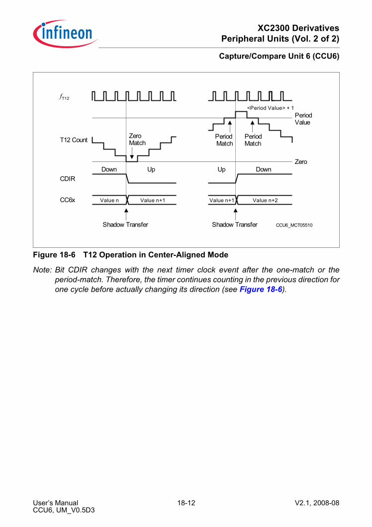
XC2300 DerivativesPeripheral Units (Vol. 2 of 2)
Capture/Compare Unit 6 (CCU6)
Figure 18-6 T12 Operation in Center-Aligned Mode
Note: Bit CDIR changes with the next timer clock event after the one-match or theperiod-match. Therefore, the timer continues counting in the previous direction forone cycle before actually changing its direction (see Figure 18-6).
CCU6_MCT05510
fT12
CC6x
Shadow Transfer
T12 Count PeriodMatch
ZeroMatch
Value n Value n+1
CDIRDown Up
Shadow Transfer
Value n+1 Value n+2
Up Down
PeriodMatch
<Period Value> + 1
Zero
PeriodValue
User’s Manual 18-12 V2.1, 2008-08CCU6, UM_V0.5D3

XC2300 DerivativesPeripheral Units (Vol. 2 of 2)
Capture/Compare Unit 6 (CCU6)
18.2.2.3 Single-Shot ModeIn Single-Shot Mode, the timer run bit T12R is cleared by hardware. If bit T12SSC = 1,the timer T12 will stop when the current timer period is finished.In Edge-Aligned mode, T12R is cleared when the timer becomes zero after havingreached the period value (see Figure 18-7).
Figure 18-7 Single-Shot Operation in Edge-Aligned Mode
In Center-Aligned mode, the period is finished when the timer has counted down to zero(one clock cycle after the one-match while counting down, see Figure 18-8).
Figure 18-8 Single-Shot Operation in Center-Aligned Mode
0
CCU6_MCT05511
CompareValue
PeriodValue
fT12
CC6xST
T12SSC
T12 Count
T12R
CCU6_MCT05512
0
CompareValue
PeriodValue
CC6xST
T12SSC
T12 Count
T12R
1
fT12
User’s Manual 18-13 V2.1, 2008-08CCU6, UM_V0.5D3
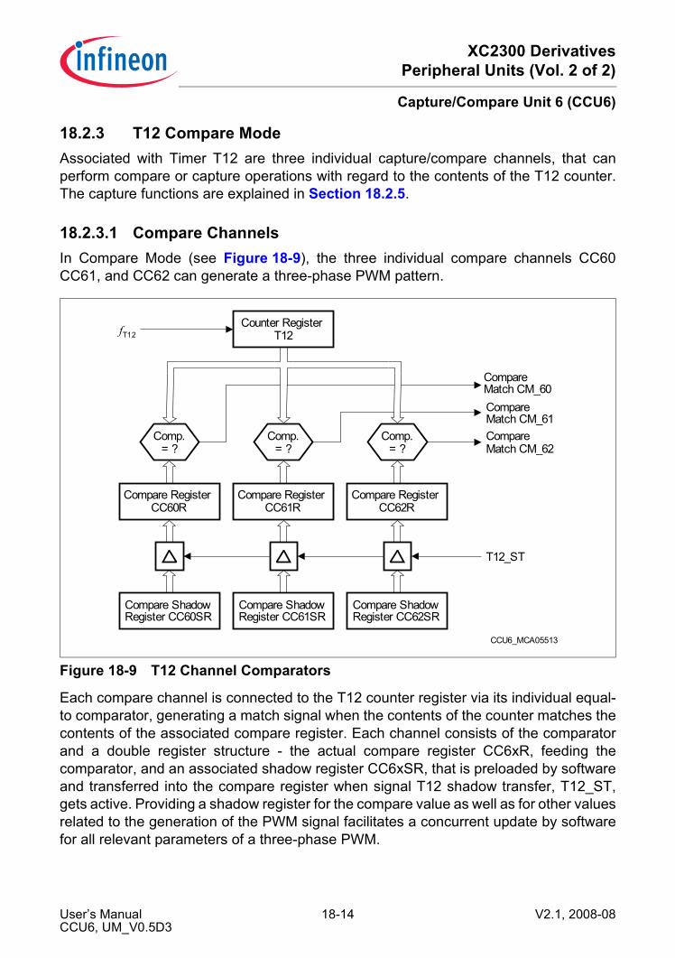
XC2300 DerivativesPeripheral Units (Vol. 2 of 2)
Capture/Compare Unit 6 (CCU6)
18.2.3 T12 Compare ModeAssociated with Timer T12 are three individual capture/compare channels, that canperform compare or capture operations with regard to the contents of the T12 counter.The capture functions are explained in Section 18.2.5.
18.2.3.1 Compare ChannelsIn Compare Mode (see Figure 18-9), the three individual compare channels CC60CC61, and CC62 can generate a three-phase PWM pattern.
Figure 18-9 T12 Channel Comparators
Each compare channel is connected to the T12 counter register via its individual equal-to comparator, generating a match signal when the contents of the counter matches thecontents of the associated compare register. Each channel consists of the comparatorand a double register structure - the actual compare register CC6xR, feeding thecomparator, and an associated shadow register CC6xSR, that is preloaded by softwareand transferred into the compare register when signal T12 shadow transfer, T12_ST,gets active. Providing a shadow register for the compare value as well as for other valuesrelated to the generation of the PWM signal facilitates a concurrent update by softwarefor all relevant parameters of a three-phase PWM.
CCU6_MCA05513
Comp.= ?
Compare RegisterCC61R
Compare ShadowRegister CC61SR
Comp.= ?
Compare RegisterCC62R
Compare ShadowRegister CC62SR
Comp.= ?
Compare RegisterCC60R
Compare ShadowRegister CC60SR
CompareMatch CM_61CompareMatch CM_62
CompareMatch CM_60
T12_ST
Counter RegisterT12fT12
User’s Manual 18-14 V2.1, 2008-08CCU6, UM_V0.5D3

XC2300 DerivativesPeripheral Units (Vol. 2 of 2)
Capture/Compare Unit 6 (CCU6)
18.2.3.2 Channel State BitsAssociated with each (compare) channel is a State Bit, CMPSTAT.CC6xST, holding thestatus of the compare (or capture) operation (see Figure 18-10). In compare mode, theState Bits are modified according to a set of switching rules, depending on the currentstatus of timer T12.
Figure 18-10 Compare State Bits for Compare Mode
The inputs to the switching rule logic for the CC6xST bits are the timer direction (CDIR),the timer run bit (T12R), the timer T12 zero-match signal (T12_ZM), and the actualindividual compare-match signals CM_6x as well as the mode control bits,T12MSEL.MSEL6x.
CCU6_MCB05514
SwitchingRuleLogic State Bit
CC60ST CM_60
To InterruptControl
CC60_R
CC60_F
To Dead_TimeCounter 0
T12_ZM
MCC60S/RMSEL60
T12R
SwitchingRuleLogic State Bit
CC61ST
To InterruptControl
CC61_R
CC61_F
To Dead_TimeCounter 1
MCC61S/RMSEL61
SwitchingRuleLogic State Bit
CC62ST
To InterruptControl
CC62_R
CC62_F
To Dead_TimeCounter 2
MCC62S/RMSEL62
CDIR
CCPOS0
CompareChannel
CC60
CM_61CompareChannel
CC61
CM_62CompareChannel
CC62
T12 Counter
CCPOS1
CCPOS2
User’s Manual 18-15 V2.1, 2008-08CCU6, UM_V0.5D3
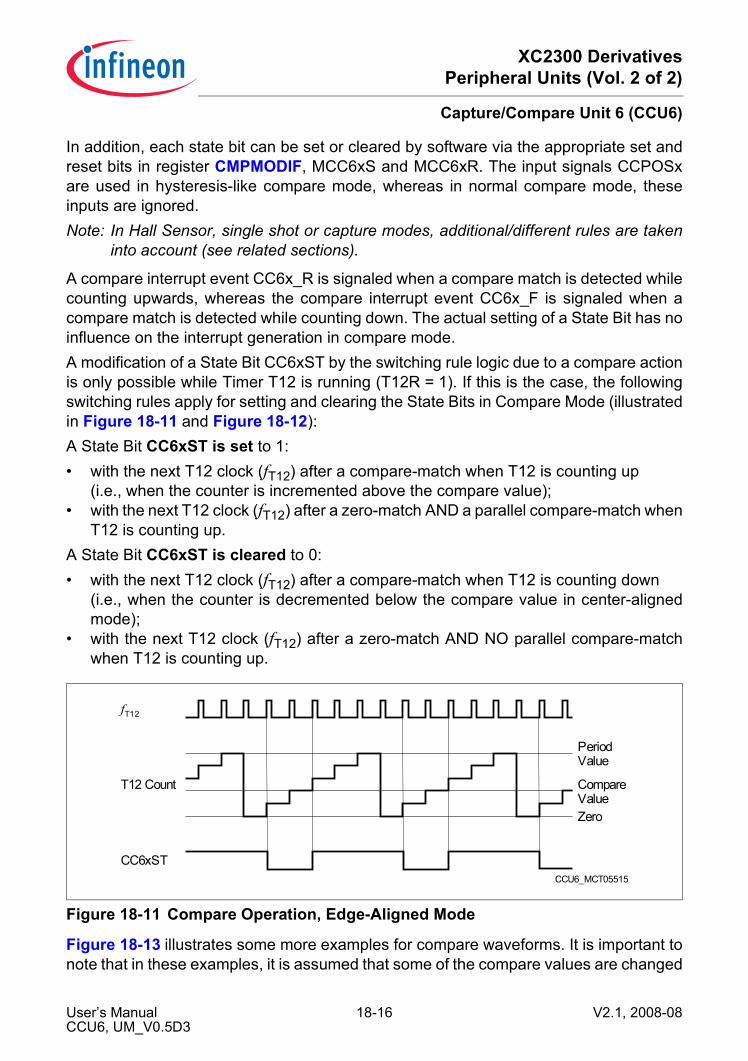
XC2300 DerivativesPeripheral Units (Vol. 2 of 2)
Capture/Compare Unit 6 (CCU6)
In addition, each state bit can be set or cleared by software via the appropriate set andreset bits in register CMPMODIF, MCC6xS and MCC6xR. The input signals CCPOSxare used in hysteresis-like compare mode, whereas in normal compare mode, theseinputs are ignored.Note: In Hall Sensor, single shot or capture modes, additional/different rules are taken
into account (see related sections).
A compare interrupt event CC6x_R is signaled when a compare match is detected whilecounting upwards, whereas the compare interrupt event CC6x_F is signaled when acompare match is detected while counting down. The actual setting of a State Bit has noinfluence on the interrupt generation in compare mode.A modification of a State Bit CC6xST by the switching rule logic due to a compare actionis only possible while Timer T12 is running (T12R = 1). If this is the case, the followingswitching rules apply for setting and clearing the State Bits in Compare Mode (illustratedin Figure 18-11 and Figure 18-12):A State Bit CC6xST is set to 1:• with the next T12 clock (fT12) after a compare-match when T12 is counting up
(i.e., when the counter is incremented above the compare value);• with the next T12 clock (fT12) after a zero-match AND a parallel compare-match when
T12 is counting up.A State Bit CC6xST is cleared to 0:• with the next T12 clock (fT12) after a compare-match when T12 is counting down
(i.e., when the counter is decremented below the compare value in center-alignedmode);
• with the next T12 clock (fT12) after a zero-match AND NO parallel compare-matchwhen T12 is counting up.
Figure 18-11 Compare Operation, Edge-Aligned Mode
Figure 18-13 illustrates some more examples for compare waveforms. It is important tonote that in these examples, it is assumed that some of the compare values are changed
CCU6_MCT05515
fT12
Zero
CompareValue
CC6xST
PeriodValue
T12 Count
User’s Manual 18-16 V2.1, 2008-08CCU6, UM_V0.5D3

XC2300 DerivativesPeripheral Units (Vol. 2 of 2)
Capture/Compare Unit 6 (CCU6)
while the timer is running. This change is performed via a software preload of theShadow Register, CC6xSR. The value is transferred to the actual Compare RegisterCC6xR with the T12 Shadow Transfer signal, T12_ST, that is assumed to be enabled.
Figure 18-12 Compare Operation, Center-Aligned Mode
CCU6_MCT05516
fT12
Zero
CompareValue
CC6xST
PeriodValue
Compare-Match Compare-Match
T12 Count
User’s Manual 18-17 V2.1, 2008-08CCU6, UM_V0.5D3
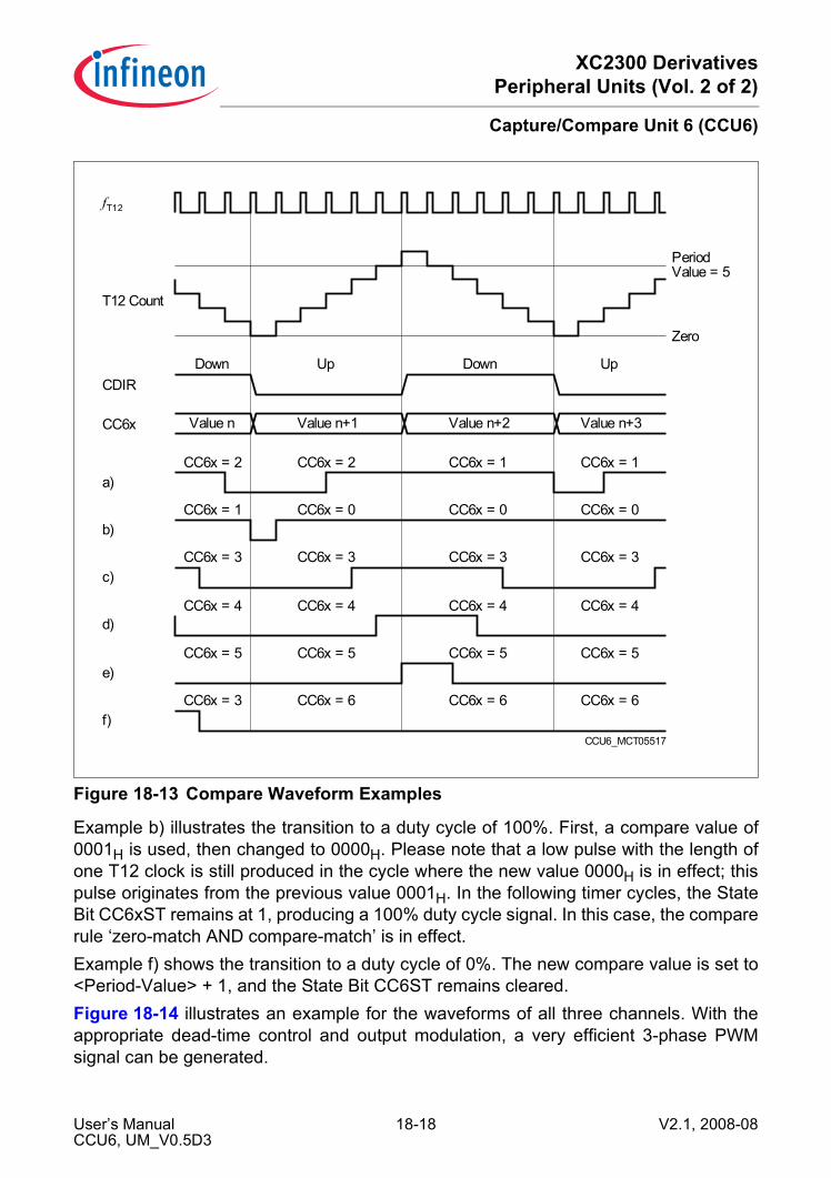
XC2300 DerivativesPeripheral Units (Vol. 2 of 2)
Capture/Compare Unit 6 (CCU6)
Figure 18-13 Compare Waveform Examples
Example b) illustrates the transition to a duty cycle of 100%. First, a compare value of0001H is used, then changed to 0000H. Please note that a low pulse with the length ofone T12 clock is still produced in the cycle where the new value 0000H is in effect; thispulse originates from the previous value 0001H. In the following timer cycles, the StateBit CC6xST remains at 1, producing a 100% duty cycle signal. In this case, the comparerule ‘zero-match AND compare-match’ is in effect.Example f) shows the transition to a duty cycle of 0%. The new compare value is set to<Period-Value> + 1, and the State Bit CC6ST remains cleared.Figure 18-14 illustrates an example for the waveforms of all three channels. With theappropriate dead-time control and output modulation, a very efficient 3-phase PWMsignal can be generated.
CCU6_MCT05517
fT12
CDIR
CC6x Value n Value n+1 Value n+2 Value n+3
T12 Count
PeriodValue = 5
Zero
CC6x = 2
Down DownUp Up
CC6x = 2 CC6x = 1 CC6x = 1a)
CC6x = 1b)
CC6x = 0 CC6x = 0 CC6x = 0
CC6x = 3 CC6x = 3 CC6x = 3 CC6x = 3c)
CC6x = 4 CC6x = 4 CC6x = 4 CC6x = 4d)
CC6x = 5 CC6x = 5 CC6x = 5 CC6x = 5e)
CC6x = 3 CC6x = 6 CC6x = 6 CC6x = 6f)
User’s Manual 18-18 V2.1, 2008-08CCU6, UM_V0.5D3
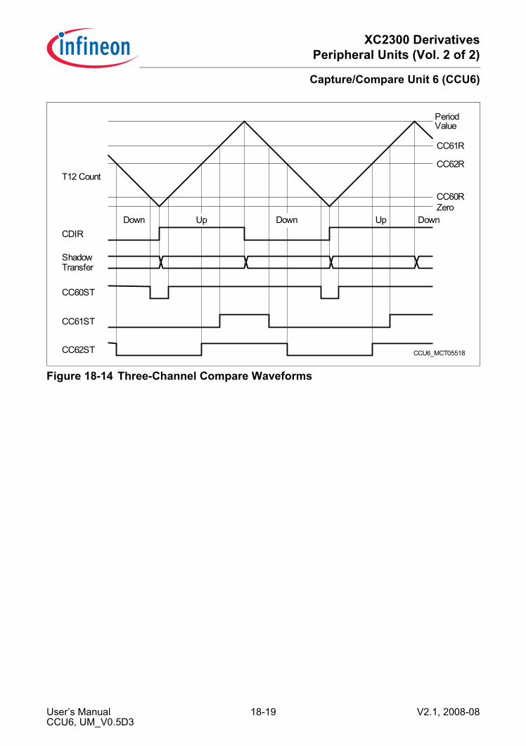
XC2300 DerivativesPeripheral Units (Vol. 2 of 2)
Capture/Compare Unit 6 (CCU6)
Figure 18-14 Three-Channel Compare Waveforms
CCU6_MCT05518
PeriodValue
UpDown Down Up DownZeroCC60R
CC61R
CC62R
CC62ST
CC61ST
CC60ST
ShadowTransfer
CDIR
T12 Count
User’s Manual 18-19 V2.1, 2008-08CCU6, UM_V0.5D3
XC2300 DerivativesPeripheral Units (Vol. 2 of 2)
Capture/Compare Unit 6 (CCU6)
18.2.3.3 Hysteresis-Like Control ModeThe hysteresis-like control mode (T12MSEL.MSEL6x = 1001B) offers the possibility toswitch off the PWM output if the input CCPOSx becomes 0 by clearing the State BitCC6xST. This can be used as a simple motor control feature by using a comparatorindicating, e.g., overcurrent. While CCPOSx = 0, the PWM outputs of the correspondingchannel are driving their passive levels, because the setting of bit CC6xST is onlypossible while CCPOSx = 1.As long as input CCPOSx is 0, the corresponding State Bit is held 0. When CCPOSx isat high level, the outputs can be in active state and are determined by bit CC6xST (seeFigure 18-10 for the state bit logic and Figure 18-15 for the output paths).The CCPOSx inputs are evaluated with fCC6.This mode can be used to introduce a timing-related behavior to a hysteresis controller.A standard hysteresis controller detects if a value exceeds a limit and switches its outputaccording to the compare result. Depending on the operating conditions, the switchingfrequency and the duty cycle are not fixed, but change permanently.If (outer) time-related control loops based on a hysteresis controller in an inner loopshould be implemented, the outer loops show a better behavior if they are synchronizedto the inner loops. Therefore, the hysteresis-like mode can be used, that combines timer-related switching with a hysteresis controller behavior. For example, in this mode, anoutput can be switched on according to a fixed time base, but it is switched off as soonas a falling edge is detected at input CCPOSx.This mode can also be used for standard PWM with overcurrent protection. As long asthere is no low level signal at pin CCPOSx, the output signals are generated in thenormal manner as described in the previous sections. Only if input CCPOSx shows a lowlevel, e.g. due to the detection of overcurrent, the outputs are shut off to avoid harmfulstress to the system.
User’s Manual 18-20 V2.1, 2008-08CCU6, UM_V0.5D3

XC2300 DerivativesPeripheral Units (Vol. 2 of 2)
Capture/Compare Unit 6 (CCU6)
18.2.4 Compare Mode Output PathFigure 18-15 gives an overview on the signal path from a channel State Bit to its outputpin in its simplest form. As illustrated, a user has a variety of controls to determine thedesired output signal switching behavior in relation to the current state of the State Bit,CC6xST. Please refer to Section 18.2.4.3 for details on the output modulation.
Figure 18-15 Compare Mode Simplified Output Path Diagram
The output path is based on signals that are defined as active or passive. The termsactive and passive are not related to output levels, but to internal actions. This mainlyapplies for the modulation, where T12 and T13 signals are combined with the multi-channel signals and the trap function. The Output level Selection allows the user todefine the output level at the output pin for the passive state (inverted level for the activestate). It is recommended to configure this block in a way that an external power switchis switched off while the CCU6 delivers an output signal in the passive state.
18.2.4.1 Dead-Time GenerationThe generation of (complementary) signals for the high-side and the low-side switchesof one power inverter phase is based on the same compare channel. For example, if thehigh-side switch should be active while the T12 counter value is above the comparevalue (State Bit = 1), then the low-side switch should be active while the counter valueis below the compare value (State Bit = 0).In most cases, the switching behavior of the connected power switches is notsymmetrical concerning the switch-on and switch-off times. A general problem arises ifthe time for switch-on is smaller than the time for switch-off of the power device. In thiscase, a short-circuit can occur in the inverter bridge leg, which may damage thecomplete system. In order to solve this problem by HW, this capture/compare unit
CCU6_MCA05519
LevelSelect
LevelSelect
CC6x
COUT6xCOUT6x_O
CC6x_O
Dead-TimeCounters
T12State Selection
CC6xST
CC6xST
CC6xPS
COUT6xPS
T12 OutputModulation
PSLy
PSLy+1
Output LevelSelection
CC61ST
Dead-TimeGeneration
T12State Bits
CC60ST
CC62ST
User’s Manual 18-21 V2.1, 2008-08CCU6, UM_V0.5D3

XC2300 DerivativesPeripheral Units (Vol. 2 of 2)
Capture/Compare Unit 6 (CCU6)
contains a programmable Dead-Time Generation Block, that delays the passive to activeedge of the switching signals by a programmable time (the active to passive edge is notdelayed).The Dead-Time Generation Block, illustrated in Figure 18-16, is built in a similar way forall three channels of T12. It is controlled by bits in register T12DTC. Any change of aCC6xST State Bit activates the corresponding Dead-Time Counter, that is clocked withthe same input clock as T12 (fT12). The length of the dead-time can be programmed bybit field DTM. This value is identical for all three channels. Writing TCTR4.DTRES = 1sets all dead-times to passive.
Figure 18-16 Dead-Time Generation Block Diagram
Each of the three dead-time counters has its individual dead-time enable bit, DTEx. Anenabled dead-time counter generates a dead-time delaying the passive-to-active edgeof the channel output signal. The change in a State Bit CC6xST is not taken into accountwhile the dead-time generation of this channel is currently in progress (active). Thisavoids an unintentional additional dead-time if a State Bit CC6xST changes too early.A disabled dead-time counter is always considered as passive and does not delay anyedge of CC6xST.Based on the State Bits CC6xST, the Dead-Time Generation Block outputs a directsignal CC6xST and an inverted signal CC6xST for each compare channel, each maskedwith the effect of the related Dead-Time Counters (waveforms illustrated inFigure 18-17).
Dead-Time ValueDTM
Dead-TimeCounter 1
Dead-TimeCounter 0
fT12
CCU6_MCB05520
Dead-TimeCounter 2
DTE1 DTE2
DTRES
DTE0 CC60ST CC61ST CC62ST
Dead-Time 0active / passive
Dead-Time 1active / passive
Dead-Time 2active / passive
CC60ST CC60ST CC61ST CC61ST CC62ST CC62ST
User’s Manual 18-22 V2.1, 2008-08CCU6, UM_V0.5D3
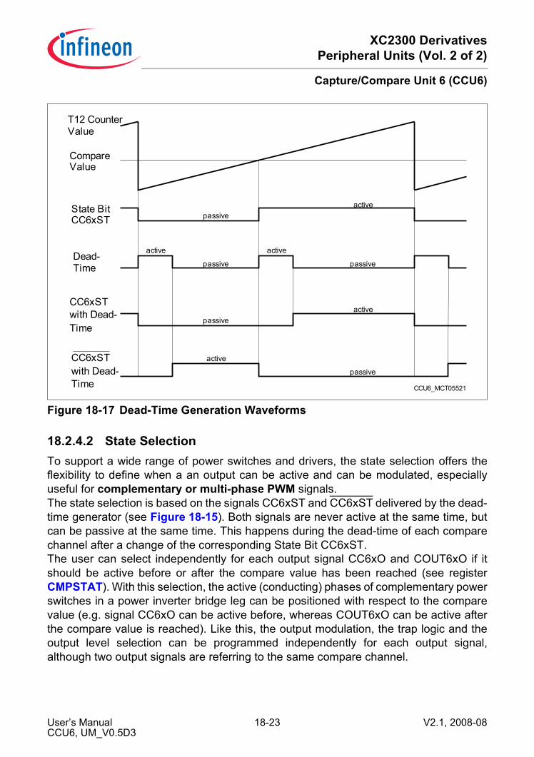
XC2300 DerivativesPeripheral Units (Vol. 2 of 2)
Capture/Compare Unit 6 (CCU6)
Figure 18-17 Dead-Time Generation Waveforms
18.2.4.2 State SelectionTo support a wide range of power switches and drivers, the state selection offers theflexibility to define when a an output can be active and can be modulated, especiallyuseful for complementary or multi-phase PWM signals.The state selection is based on the signals CC6xST and CC6xST delivered by the dead-time generator (see Figure 18-15). Both signals are never active at the same time, butcan be passive at the same time. This happens during the dead-time of each comparechannel after a change of the corresponding State Bit CC6xST.The user can select independently for each output signal CC6xO and COUT6xO if itshould be active before or after the compare value has been reached (see registerCMPSTAT). With this selection, the active (conducting) phases of complementary powerswitches in a power inverter bridge leg can be positioned with respect to the comparevalue (e.g. signal CC6xO can be active before, whereas COUT6xO can be active afterthe compare value is reached). Like this, the output modulation, the trap logic and theoutput level selection can be programmed independently for each output signal,although two output signals are referring to the same compare channel.
CCU6_MCT05521
CC6xSTwith Dead-Time
CC6xSTwith Dead-Time
State BitCC6xST
CompareValue
T12 CounterValue
Dead-Time
active active
passive passive
active
active
passive
passive
activepassive
User’s Manual 18-23 V2.1, 2008-08CCU6, UM_V0.5D3
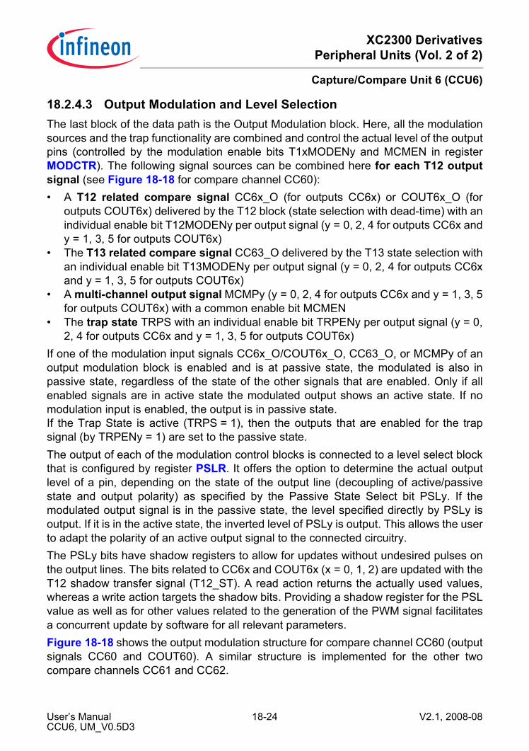
XC2300 DerivativesPeripheral Units (Vol. 2 of 2)
Capture/Compare Unit 6 (CCU6)
18.2.4.3 Output Modulation and Level SelectionThe last block of the data path is the Output Modulation block. Here, all the modulationsources and the trap functionality are combined and control the actual level of the outputpins (controlled by the modulation enable bits T1xMODENy and MCMEN in registerMODCTR). The following signal sources can be combined here for each T12 outputsignal (see Figure 18-18 for compare channel CC60):• A T12 related compare signal CC6x_O (for outputs CC6x) or COUT6x_O (for
outputs COUT6x) delivered by the T12 block (state selection with dead-time) with anindividual enable bit T12MODENy per output signal (y = 0, 2, 4 for outputs CC6x andy = 1, 3, 5 for outputs COUT6x)
• The T13 related compare signal CC63_O delivered by the T13 state selection withan individual enable bit T13MODENy per output signal (y = 0, 2, 4 for outputs CC6xand y = 1, 3, 5 for outputs COUT6x)
• A multi-channel output signal MCMPy (y = 0, 2, 4 for outputs CC6x and y = 1, 3, 5for outputs COUT6x) with a common enable bit MCMEN
• The trap state TRPS with an individual enable bit TRPENy per output signal (y = 0,2, 4 for outputs CC6x and y = 1, 3, 5 for outputs COUT6x)
If one of the modulation input signals CC6x_O/COUT6x_O, CC63_O, or MCMPy of anoutput modulation block is enabled and is at passive state, the modulated is also inpassive state, regardless of the state of the other signals that are enabled. Only if allenabled signals are in active state the modulated output shows an active state. If nomodulation input is enabled, the output is in passive state.If the Trap State is active (TRPS = 1), then the outputs that are enabled for the trapsignal (by TRPENy = 1) are set to the passive state.The output of each of the modulation control blocks is connected to a level select blockthat is configured by register PSLR. It offers the option to determine the actual outputlevel of a pin, depending on the state of the output line (decoupling of active/passivestate and output polarity) as specified by the Passive State Select bit PSLy. If themodulated output signal is in the passive state, the level specified directly by PSLy isoutput. If it is in the active state, the inverted level of PSLy is output. This allows the userto adapt the polarity of an active output signal to the connected circuitry.The PSLy bits have shadow registers to allow for updates without undesired pulses onthe output lines. The bits related to CC6x and COUT6x (x = 0, 1, 2) are updated with theT12 shadow transfer signal (T12_ST). A read action returns the actually used values,whereas a write action targets the shadow bits. Providing a shadow register for the PSLvalue as well as for other values related to the generation of the PWM signal facilitatesa concurrent update by software for all relevant parameters.Figure 18-18 shows the output modulation structure for compare channel CC60 (outputsignals CC60 and COUT60). A similar structure is implemented for the other twocompare channels CC61 and CC62.
User’s Manual 18-24 V2.1, 2008-08CCU6, UM_V0.5D3

XC2300 DerivativesPeripheral Units (Vol. 2 of 2)
Capture/Compare Unit 6 (CCU6)
Figure 18-18 Output Modulation for Compare Channel CC60
CCU6_MCA05543
CC60
OutputModulation
CC60
CC60_O
T12MODEN0
TRPEN0
PSL0
activepassive
T13 Block
T12 Block +Dead-Time
Multi-ChannelMode
CC63_O
T13MODEN0
TRPSTrap HandlingBlock
LevelSelection
COUT60
OutputModulationCOUT60
COUT60_O
T12MODEN1
TRPEN1
PSL1
activepassiveT13MODEN1 Level
Selection
MCMEN
MCMP0
MCMP1
User’s Manual 18-25 V2.1, 2008-08CCU6, UM_V0.5D3

XC2300 DerivativesPeripheral Units (Vol. 2 of 2)
Capture/Compare Unit 6 (CCU6)
18.2.5 T12 Capture ModesEach of the three channels of the T12 Block can also be used to capture T12 timeinformation in response to an external signal CC6xIN.In capture mode, the interrupt event CC6x_R is detected when a rising edge is detectedat the input CC6xIN, whereas the interrupt event CC6x_F is detected when a falling edgeis detected.There are a number of different modes for capture operation. In all modes, both of theregisters of a channel are used. The selection of the capture modes is done via theT12MSEL.MSEL6x bit fields and can be selected individually for each of the channels.
Figure 18-19 illustrates Capture Mode 1. When a rising edge (0-to-1 transition) isdetected at the corresponding input signal CC6xIN, the current contents of Timer T12are captured into register CC6xR. When a falling edge (1-to-0 transition) is detected atthe input signal CC6xIN, the contents of Timer T12 are captured into register CC6xSR.
Figure 18-19 Capture Mode 1 Block Diagram
Table 18-3 Capture Modes OverviewMSEL6x Mode Signal Active Edge CC6nSR Stored in T12 Stored in0100B 1 CC6xIN Rising – CC6xR
CC6xIN Falling – CC6xSR0101B 2 CC6xIN Rising CC6xR CC6xSR0110B 3 CC6xIN Falling CC6xR CC6xSR0111B 4 CC6xIN Any CC6xR CC6xSR
CCU6_MCB05522
fT12
Edge
Detect
CaptureMode
Selection
State BitCC6xST
CC6xIN
To Interrupt Logic
Set
Rising Falling
Shadow RegisterCC6xSRRegister CC6xR
Counter RegisterT12
MSEL6x
CC6x_R
CC6x_F
fCC6
User’s Manual 18-26 V2.1, 2008-08CCU6, UM_V0.5D3

XC2300 DerivativesPeripheral Units (Vol. 2 of 2)
Capture/Compare Unit 6 (CCU6)
Capture Modes 2, 3 and 4 are shown in Figure 18-20. They differ only in the activeedge causing the capture operation. In each of the three modes, when the selected edgeis detected at the corresponding input signal CC6xIN, the current contents of the shadowregister CC6xSR are transferred into register CC6xR, and the current Timer T12contents are captured in register CC6xSR (simultaneous transfer). The active edge is arising edge of CC6xIN for Capture Mode 2, a falling edge for Mode 3, and both, a risingor a falling edge for Capture Mode 4, as shown in Table 18-3. These capture modes arevery useful in cases where there is little time between two consecutive edges of the inputsignal.
Figure 18-20 Capture Modes 2, 3 and 4 Block Diagram
CCU6_MCB05523
fT12
Edge
Detect
CaptureMode
Selection
State BitCC6xST
CC6xIN
To Interrupt Logic
Set
Shadow RegisterCC6xSR
Register CC6xR
Counter RegisterT12
MSEL6x
CC6x_R
CC6x_F
fCC6
User’s Manual 18-27 V2.1, 2008-08CCU6, UM_V0.5D3

XC2300 DerivativesPeripheral Units (Vol. 2 of 2)
Capture/Compare Unit 6 (CCU6)
Five further capture modes are called Multi-Input Capture Modes, as they use twodifferent external inputs, signal CC6xIN and signal CCPOSx.
Figure 18-21 Multi-Input Capture Modes Block Diagram
In each of these modes, the current T12 contents are captured in register CC6xR inresponse to a selected event at signal CC6xIN, and in register CC6xSR in response toa selected event at signal CCPOSx. The possible events can be opposite inputtransitions, or the same transitions, or any transition at the two inputs. The differentoptions are detailed in Table 18-4.In each of the various capture modes, the Channel State Bit, CC6xST, is set to 1 whenthe selected capture trigger event at signal CC6xIN or CCPOSx has occurred. The StateBit is not cleared by hardware, but can be cleared by software.In addition, appropriate signal lines to the interrupt logic are activated, that can generatean interrupt request to the CPU. Regardless of the selected active edge, all edgesdetected at signal CC6xIN can lead to the activation of the appropriate interrupt requestline (see also Section 18.8).
CCU6_MCB05524
fT12
Edge
Detect
CaptureMode
Selection
State BitCC6xST
CC6xIN
To Interrupt Logic
SetShadow Register
CC6xSRRegister CC6xR
Counter RegisterT12
Set
CaptureMode
Selection
Edge
Detect
CCPOSx
MSEL6x
MSEL6x
fCC6CC6x_RCC6x_F
User’s Manual 18-28 V2.1, 2008-08CCU6, UM_V0.5D3

XC2300 DerivativesPeripheral Units (Vol. 2 of 2)
Capture/Compare Unit 6 (CCU6)
Table 18-4 Multi-Input Capture Modes OverviewMSEL6x Mode Signal Active Edge T12 Stored in1010B 5 CC6xIN Rising CC6xR
CCPOSx Falling CC6xSR1011B 6 CC6xIN Falling CC6xR
CCPOSx Rising CC6xSR1100B 7 CC6xIN Rising CC6xR
CCPOSx Rising CC6xSR1101B 8 CC6xIN Falling CC6xR
CCPOSx Falling CC6xSR1110B 9 CC6xIN Any CC6xR
CCPOSx Any CC6xSR1111B – reserved (no capture or compare action)
User’s Manual 18-29 V2.1, 2008-08CCU6, UM_V0.5D3

XC2300 DerivativesPeripheral Units (Vol. 2 of 2)
Capture/Compare Unit 6 (CCU6)
18.2.6 T12 Shadow Register TransferA special shadow transfer signal (T12_ST) can be generated to facilitate updating theperiod and compare values of the compare channels CC60, CC61, and CC62synchronously to the operation of T12. Providing a shadow register for values definingone PWM period facilitates a concurrent update by software for all relevant parameters.The next PWM period can run with a new set of parameters. The generation of this signalis requested by software via bit TCTR0.STE12 (set by writing 1 to the write-only bitTCTR4.T12STR, cleared by writing 1 to the write-only bit TCTR4.T12STD).Figure 18-22 shows the shadow register structure and the shadow transfer signals, aswell as on the read/write accessibility of the various registers.
Figure 18-22 T12 Shadow Register Overview
CCU6_MCA05546
Compare RegisterCC6xR
Compare ShadowRegister CC6xSR
>1_Other Modes(Hall, Capture, etc.)
Period RegisterT12PR
Period ShadowRegister T12PR
COUT6xPS
COUT6xPSShadow
(T12)PSLy
(T12) PSLyShadow
CC6xPS
CC6xPSShadow
T12_ST
Write
Read ReadRead Read
Write Write Write
Read
Write Read
User’s Manual 18-30 V2.1, 2008-08CCU6, UM_V0.5D3

XC2300 DerivativesPeripheral Units (Vol. 2 of 2)
Capture/Compare Unit 6 (CCU6)
A T12 shadow register transfer takes place (T12_ST active):• while timer T12 is not running (T12R = 0), or• STE12 = 1 and a Period-Match is detected while counting up, or• STE12 = 1 and a One-Match is detected while counting downWhen signal T12_ST is active, a shadow register transfer is triggered with the next cycleof the T12 clock. Bit STE12 is automatically cleared with the shadow register transfer.
18.2.7 Timer T12 Operating Mode SelectionThe operating mode for the T12 channels are defined by the bit fieldsT12MSEL.MSEL6x.
The clocking and counting scheme of the timers are controlled by the timer controlregisters TCTR0 and TCTR2. Specific actions are triggered by write operations toregister TCTR4.
Table 18-5 T12 Capture/Compare Modes OverviewMSEL6x Selected Operating Mode0000B,1111B
Capture/Compare modes switched off
0001B,0010B,0011B
Compare mode, see Section 18.2.3same behavior for all three codings
01XXB Double-Register Capture modes, see Section 18.2.51000B Hall Sensor Mode, see Section 18.6
In order to properly enable this mode, all three MSEL6x fields have to be programmed to Hall Sensor mode.
1001B Hysteresis-like compare mode, see Section 18.2.3.31010B1011B,1100B,1101B1110B
Multi-Input Capture modes, see Section 18.2.5
User’s Manual 18-31 V2.1, 2008-08CCU6, UM_V0.5D3
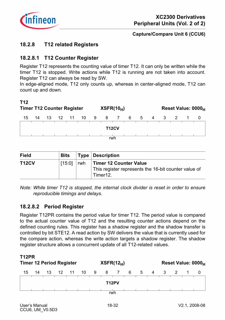
XC2300 DerivativesPeripheral Units (Vol. 2 of 2)
Capture/Compare Unit 6 (CCU6)
18.2.8 T12 related Registers
18.2.8.1 T12 Counter RegisterRegister T12 represents the counting value of timer T12. It can only be written while thetimer T12 is stopped. Write actions while T12 is running are not taken into account.Register T12 can always be read by SW.In edge-aligned mode, T12 only counts up, whereas in center-aligned mode, T12 cancount up and down.
Note: While timer T12 is stopped, the internal clock divider is reset in order to ensurereproducible timings and delays.
18.2.8.2 Period RegisterRegister T12PR contains the period value for timer T12. The period value is comparedto the actual counter value of T12 and the resulting counter actions depend on thedefined counting rules. This register has a shadow register and the shadow transfer iscontrolled by bit STE12. A read action by SW delivers the value that is currently used forthe compare action, whereas the write action targets a shadow register. The shadowregister structure allows a concurrent update of all T12-related values.
T12 Timer T12 Counter Register XSFR(10H) Reset Value: 0000H
15 14 13 12 11 10 9 8 7 6 5 4 3 2 1 0
T12CV
rwh
Field Bits Type DescriptionT12CV [15:0] rwh Timer 12 Counter Value
This register represents the 16-bit counter value of Timer12.
T12PRTimer 12 Period Register XSFR(12H) Reset Value: 0000H
15 14 13 12 11 10 9 8 7 6 5 4 3 2 1 0
T12PV
rwh
User’s Manual 18-32 V2.1, 2008-08CCU6, UM_V0.5D3

XC2300 DerivativesPeripheral Units (Vol. 2 of 2)
Capture/Compare Unit 6 (CCU6)
18.2.8.3 Capture/Compare RegistersIn compare mode, the registers CC6xR (x = 0 - 2) are the actual compare registers forT12. The values stored in CC6xR are compared (all three channels in parallel) to thecounter value of T12. In capture mode, the current value of the T12 counter register iscaptured by registers CC6xR if the corresponding capture event is detected.
Field Bits Type DescriptionT12PV [15:0] rwh T12 Period Value
The value T12PV defines the counter value for T12 leading to a period-match. When reaching this value, the timerT12 is set to zero (edge-aligned mode) or changes its count direction to down counting (center-aligned mode).
CC6xR (x = 0-2)Capture/Compare Register for Channel CC6x
XSFR(18H + 2*x) Reset Value: 0000H
15 14 13 12 11 10 9 8 7 6 5 4 3 2 1 0
CCV
rh
Field Bits Type DescriptionCCV [15:0] rh Capture/Compare Value
In compare mode, the bit fields CCV contain the values, that are compared to the T12 counter value. In capture mode, the captured value of T12 can be read from these registers.
User’s Manual 18-33 V2.1, 2008-08CCU6, UM_V0.5D3

XC2300 DerivativesPeripheral Units (Vol. 2 of 2)
Capture/Compare Unit 6 (CCU6)
18.2.8.4 Capture/Compare Shadow RegistersThe registers CC6xR can only be read by SW, the modification of the value is done bya shadow register transfer from register CC6xSR. The corresponding shadow registersCC6xSR can be read and written by SW. In capture mode, the value of the T12 counterregister can also be captured by registers CC6xSR if the selected capture event isdetected (depending on the selected capture mode).
Note: The shadow registers can also be written by SW in capture mode. In this case, theHW capture event wins over the SW write if both happen in the same cycle (theSW write is discarded).
CC6xSR (x=0-2)Capture/Compare Shadow Reg. for Channel CC6x
XSFR(20H+2*x) Reset Value: 0000H
15 14 13 12 11 10 9 8 7 6 5 4 3 2 1 0
CCS
rwh
Field Bits Type DescriptionCCS [15:0] rwh Shadow Register for Channel x Capture/
Compare ValueIn compare mode, the bit fields contents of CCS are transferred to the bit fields CCV for the corresponding channel during a shadow transfer. In capture mode, the captured value of T12 can be read from these registers.
User’s Manual 18-34 V2.1, 2008-08CCU6, UM_V0.5D3

XC2300 DerivativesPeripheral Units (Vol. 2 of 2)
Capture/Compare Unit 6 (CCU6)
18.2.8.5 Dead-time Control RegisterRegister T12DTC controls the dead-time generation for the timer T12 comparechannels. Each channel can be independently enabled/disabled for dead-timegeneration. If enabled, the transition from passive state to active state is delayed by thevalue defined by bit field DTM.The dead time counters are clocked with the same frequency as T12.This structure allows symmetrical dead-time generation in center-aligned and in edge-aligned PWM mode. A duty cycle of 50% leads to CC6x, COUT6x switched on for: 0.5 *period - dead time.Note: The dead-time counters are not reset by bit T12RES, but by bit DTRES.
T12DTCDead-Time Control Register for Timer12
XSFR(14H) Reset Value: 0000H
15 14 13 12 11 10 9 8 7 6 5 4 3 2 1 0
0 DTR2
DTR1
DTR0 0 DTE
2DTE
1DTE
0 DTM
r rh rh rh r rw rw rw rw
Field Bits Type DescriptionDTM [7:0] rw Dead-Time
Bit field DTM determines the programmable delay between switching from the passive state to the active state of the selected outputs. The switching from the active state to the passive state is not delayed.
DTE2,DTE1,DTE0
10,9,8
rw Dead Time Enable BitsBits DTE0..DTE2 enable and disable the dead time generation for each compare channel (0, 1, 2) of timer T12.0B Dead-Time Counter x is disabled. The
corresponding outputs switch from the passive state to the active state (according to the actual compare status) without any delay.
1B Dead-Time Counter x is enabled. The corresponding outputs switch from the passive state to the active state (according to the compare status) with the delay programmed in bit field DTM.
User’s Manual 18-35 V2.1, 2008-08CCU6, UM_V0.5D3

XC2300 DerivativesPeripheral Units (Vol. 2 of 2)
Capture/Compare Unit 6 (CCU6)
DTR2,DTR1,DTR0
14,13,12
rh Dead Time Run Indication BitsBits DTR0..DTR2 indicate the status of the dead time generation for each compare channel (0, 1, 2) of timer T12.0B Dead-Time Counter x is currently in the
passive state.1B Dead-Time Counter x is currently in the active
state.0 [15:11] r reserved;
returns 0 if read; should be written with 0;
Field Bits Type Description
User’s Manual 18-36 V2.1, 2008-08CCU6, UM_V0.5D3

XC2300 DerivativesPeripheral Units (Vol. 2 of 2)
Capture/Compare Unit 6 (CCU6)
18.2.9 Capture/Compare Control Registers
18.2.9.1 Channel State BitsThe Compare State Register CMPSTAT contains status bits monitoring the currentcapture and compare state and control bits defining the active/passive state of thecompare channels.
CMPSTATCompare State Register XSFR(28H) Reset Value: 0000H
15 14 13 12 11 10 9 8 7 6 5 4 3 2 1 0
T13IM
COUT63PS
COUT62PS
CC62PS
COUT61PS
CC61PS
COUT60PS
CC60PS 0 CC
63ST
CCPOS62
CCPOS61
CCPOS60
CC62ST
CC61ST
CC60ST
rwh rwh rwh rwh rwh rwh rwh rwh r rh rh rh rh rh rh rh
Field Bits Type DescriptionCC60ST,CC61ST,CC62ST,CC63ST 1)
0,1,2,6
rh Capture/Compare State BitsBits CC6xST monitor the state of the capture/compare channels. Bits CC6xST (x = 0, 1, 2) are related to T12, bit CC63ST is related to T13.0B In compare mode, the timer count is less than
the compare value.In capture mode, the selected edge has not yet been detected since the bit has been cleared by SW the last time.
1B In compare mode, the counter value is greater than or equal to the compare value.In capture mode, the selected edge has been detected.
CCPOS0,CCPOS1,CCPOS2
3,4,5
rh Sampled Hall Pattern BitsBits CCPOSx (x = 0, 1, 2) are indicating the value of the input Hall pattern that has been compared to the current and expected value. The value is sampled when the event HCRDY (Hall Compare Ready) occurs.0B The input CCPOSx has been sampled as 0.1B The input CCPOSx has been sampled as 1.
User’s Manual 18-37 V2.1, 2008-08CCU6, UM_V0.5D3
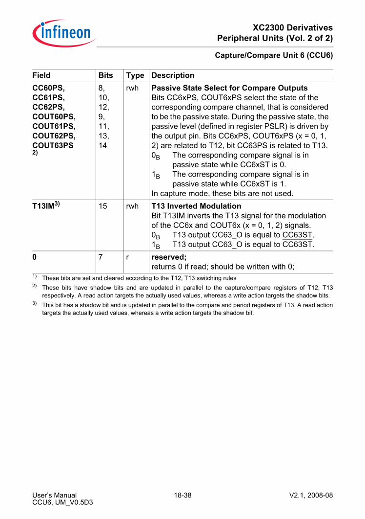
XC2300 DerivativesPeripheral Units (Vol. 2 of 2)
Capture/Compare Unit 6 (CCU6)
CC60PS,CC61PS,CC62PS,COUT60PS,COUT61PS,COUT62PS,COUT63PS2)
8,10,12,9,11,13,14
rwh Passive State Select for Compare OutputsBits CC6xPS, COUT6xPS select the state of the corresponding compare channel, that is considered to be the passive state. During the passive state, the passive level (defined in register PSLR) is driven by the output pin. Bits CC6xPS, COUT6xPS (x = 0, 1, 2) are related to T12, bit CC63PS is related to T13.0B The corresponding compare signal is in
passive state while CC6xST is 0.1B The corresponding compare signal is in
passive state while CC6xST is 1.In capture mode, these bits are not used.
T13IM3) 15 rwh T13 Inverted ModulationBit T13IM inverts the T13 signal for the modulation of the CC6x and COUT6x (x = 0, 1, 2) signals.0B T13 output CC63_O is equal to CC63ST.1B T13 output CC63_O is equal to CC63ST.
0 7 r reserved;returns 0 if read; should be written with 0;
1) These bits are set and cleared according to the T12, T13 switching rules2) These bits have shadow bits and are updated in parallel to the capture/compare registers of T12, T13
respectively. A read action targets the actually used values, whereas a write action targets the shadow bits.3) This bit has a shadow bit and is updated in parallel to the compare and period registers of T13. A read action
targets the actually used values, whereas a write action targets the shadow bit.
Field Bits Type Description
User’s Manual 18-38 V2.1, 2008-08CCU6, UM_V0.5D3
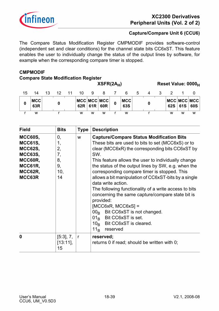
XC2300 DerivativesPeripheral Units (Vol. 2 of 2)
Capture/Compare Unit 6 (CCU6)
The Compare Status Modification Register CMPMODIF provides software-control(independent set and clear conditions) for the channel state bits CC6xST. This featureenables the user to individually change the status of the output lines by software, forexample when the corresponding compare timer is stopped.
CMPMODIFCompare State Modification Register
XSFR(2AH) Reset Value: 0000H
15 14 13 12 11 10 9 8 7 6 5 4 3 2 1 0
0 MCC63R 0 MCC
62RMCC61R
MCC60R 0 MCC
63S 0 MCC62S
MCC61S
MCC60S
r w r w w w r w r w w w
Field Bits Type DescriptionMCC60S,MCC61S,MCC62S,MCC63S,MCC60R,MCC61R,MCC62R,MCC63R
0,1,2,7,8,9,10,14
w Capture/Compare Status Modification BitsThese bits are used to bits to set (MCC6xS) or to clear (MCC6xR) the corresponding bits CC6xST by SW.This feature allows the user to individually change the status of the output lines by SW, e.g. when the corresponding compare timer is stopped. This allows a bit manipulation of CC6xST-bits by a single data write action.The following functionality of a write access to bits concerning the same capture/compare state bit is provided:[MCC6xR, MCC6xS] =00B Bit CC6xST is not changed.01B Bit CC6xST is set.10B Bit CC6xST is cleared.11B reserved
0 [5:3], 7, [13:11],15
r reserved;returns 0 if read; should be written with 0;
User’s Manual 18-39 V2.1, 2008-08CCU6, UM_V0.5D3

XC2300 DerivativesPeripheral Units (Vol. 2 of 2)
Capture/Compare Unit 6 (CCU6)
18.2.9.2 T12 Mode Control RegisterRegister T12MSEL contains control bits to select the capture/compare functionality ofthe three channels of Timer T12.
T12MSEL T12 Mode Select Register XSFR (46H) Reset Value: 0000H
15 14 13 12 11 10 9 8 7 6 5 4 3 2 1 0
DBYP HSYNC MSEL62 MSEL61 MSEL60
rw rw rw rw rw
Field Bits Type DescriptionMSEL60,MSEL61,MSEL62
[3:0],[7:4],[11:8]
rw Capture/Compare Mode SelectionThese bit fields select the operating mode of the three T12 capture/compare channels. Each channel (x = 0, 1, 2) can be programmed individually for one of these modes (except for Hall Sensor Mode).Coding see Table 18-5.
HSYNC [14:12] rw Hall SynchronizationBit field HSYNC defines the source for the sampling of the Hall input pattern and the comparison to the current and the expected Hall pattern bit fields.Coding see Table 18-11.
DBYP 15 rw Delay BypassDBYP controls whether the source signal for the sampling of the Hall input pattern (selected by HSYNC) is delayed by the Dead-Time Counter 0.0 The bypass is not active.
Dead-Time Counter 0 is generating a delay after the source signal becomes active.
1 The bypass is active.Dead-Time Counter 0 is not used for a delay.
User’s Manual 18-40 V2.1, 2008-08CCU6, UM_V0.5D3
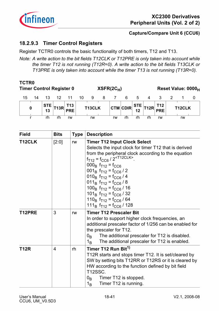
XC2300 DerivativesPeripheral Units (Vol. 2 of 2)
Capture/Compare Unit 6 (CCU6)
18.2.9.3 Timer Control RegistersRegister TCTR0 controls the basic functionality of both timers, T12 and T13.Note: A write action to the bit fields T12CLK or T12PRE is only taken into account while
the timer T12 is not running (T12R=0). A write action to the bit fields T13CLK orT13PRE is only taken into account while the timer T13 is not running (T13R=0).
TCTR0Timer Control Register 0 XSFR(2CH) Reset Value: 0000H
15 14 13 12 11 10 9 8 7 6 5 4 3 2 1 0
0 STE13 T13R T13
PRE T13CLK CTM CDIR STE12 T12R T12
PRE T12CLK
r rh rh rw rw rw rh rh rh rw rw
Field Bits Type DescriptionT12CLK [2:0] rw Timer T12 Input Clock Select
Selects the input clock for timer T12 that is derived from the peripheral clock according to the equationfT12 = fCC6 / 2<T12CLK>.000B fT12 = fCC6001B fT12 = fCC6 / 2010B fT12 = fCC6 / 4011B fT12 = fCC6 / 8100B fT12 = fCC6 / 16101B fT12 = fCC6 / 32110B fT12 = fCC6 / 64111B fT12 = fCC6 / 128
T12PRE 3 rw Timer T12 Prescaler BitIn order to support higher clock frequencies, an additional prescaler factor of 1/256 can be enabled for the prescaler for T12.0B The additional prescaler for T12 is disabled.1B The additional prescaler for T12 is enabled.
T12R 4 rh Timer T12 Run Bit1)
T12R starts and stops timer T12. It is set/cleared by SW by setting bits T12RR or T12RS or it is cleared by HW according to the function defined by bit field T12SSC.0B Timer T12 is stopped.1B Timer T12 is running.
User’s Manual 18-41 V2.1, 2008-08CCU6, UM_V0.5D3
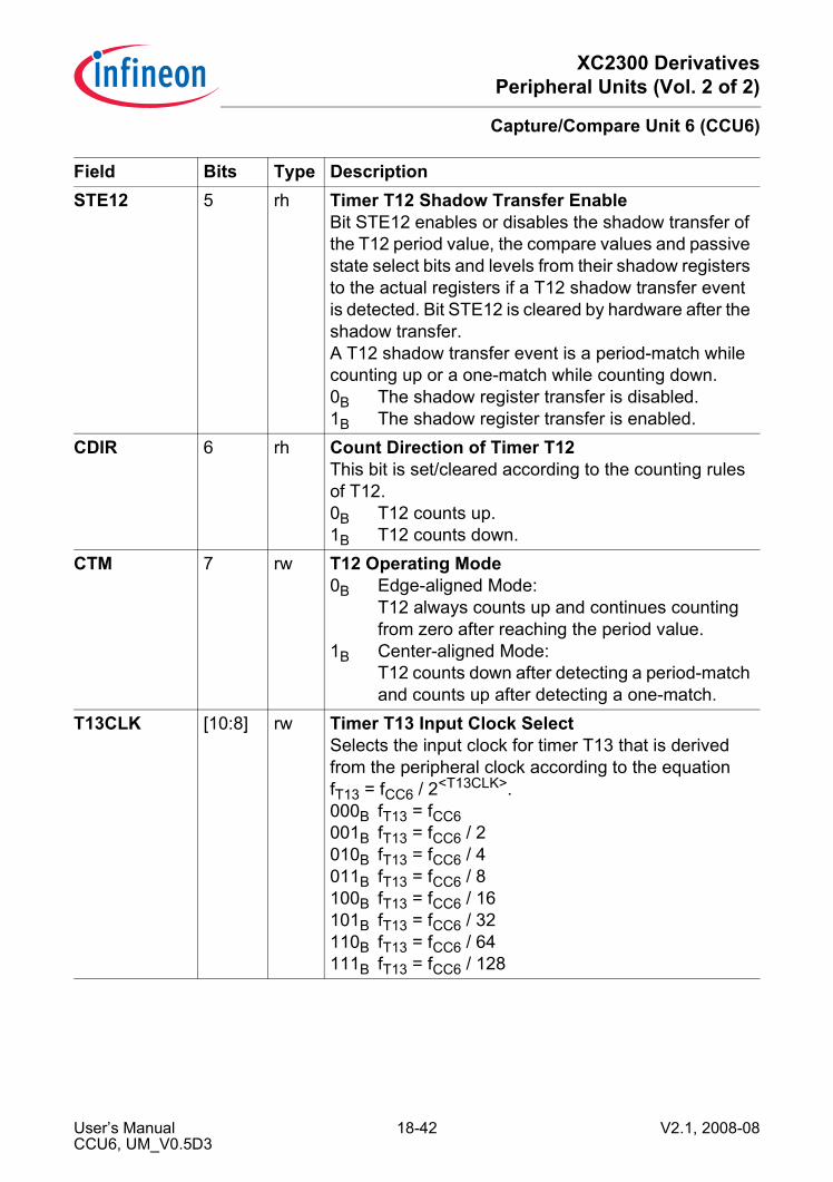
XC2300 DerivativesPeripheral Units (Vol. 2 of 2)
Capture/Compare Unit 6 (CCU6)
STE12 5 rh Timer T12 Shadow Transfer EnableBit STE12 enables or disables the shadow transfer of the T12 period value, the compare values and passive state select bits and levels from their shadow registers to the actual registers if a T12 shadow transfer event is detected. Bit STE12 is cleared by hardware after the shadow transfer.A T12 shadow transfer event is a period-match while counting up or a one-match while counting down.0B The shadow register transfer is disabled.1B The shadow register transfer is enabled.
CDIR 6 rh Count Direction of Timer T12This bit is set/cleared according to the counting rules of T12.0B T12 counts up.1B T12 counts down.
CTM 7 rw T12 Operating Mode0B Edge-aligned Mode:
T12 always counts up and continues counting from zero after reaching the period value.
1B Center-aligned Mode:T12 counts down after detecting a period-match and counts up after detecting a one-match.
T13CLK [10:8] rw Timer T13 Input Clock SelectSelects the input clock for timer T13 that is derived from the peripheral clock according to the equationfT13 = fCC6 / 2<T13CLK>.000B fT13 = fCC6001B fT13 = fCC6 / 2010B fT13 = fCC6 / 4011B fT13 = fCC6 / 8100B fT13 = fCC6 / 16101B fT13 = fCC6 / 32110B fT13 = fCC6 / 64111B fT13 = fCC6 / 128
Field Bits Type Description
User’s Manual 18-42 V2.1, 2008-08CCU6, UM_V0.5D3

XC2300 DerivativesPeripheral Units (Vol. 2 of 2)
Capture/Compare Unit 6 (CCU6)
T13PRE 11 rw Timer T13 Prescaler BitIn order to support higher clock frequencies, an additional prescaler factor of 1/256 can be enabled for the prescaler for T13.0B The additional prescaler for T13 is disabled.1B The additional prescaler for T13 is enabled.
T13R 12 rh Timer T13 Run Bit2)
T13R starts and stops timer T13. It is set/cleared by SW by setting bits T13RR orT13RS or it is set/cleared by HW according to the function defined by bit fields T13SSC, T13TEC and T13TED.0B Timer T13 is stopped.1B Timer T13 is running.
STE13 13 rh Timer T13 Shadow Transfer EnableBit STE13 enables or disables the shadow transfer of the T13 period value, the compare value and passive state select bit and level from their shadow registers to the actual registers if a T13 shadow transfer event is detected. Bit STE13 is cleared by hardware after the shadow transfer.A T13 shadow transfer event is a period-match.0B The shadow register transfer is disabled.1B The shadow register transfer is enabled.
0 [15: 14] r reserved;returns 0 if read; should be written with 0;
1) A concurrent set/clear action on T12R (from T12SSC, T12RR or T12RS) will have no effect. The bit T12R willremain unchanged.
2) A concurrent set/cleared action on T13R (from T13SSC, T13TEC, T13RR or T13RS) will have no effect. Thebit T12R will remain unchanged.
Field Bits Type Description
User’s Manual 18-43 V2.1, 2008-08CCU6, UM_V0.5D3

XC2300 DerivativesPeripheral Units (Vol. 2 of 2)
Capture/Compare Unit 6 (CCU6)
Register TCTR2 controls the single-shot and the synchronization functionality of bothtimers T12 and T13. Both timers can run in single-shot mode. In this mode they stop theircounting sequence automatically after one counting period with a count value of zero.The single-shot mode and the synchronization feature of T13 to T12 allow the generationof events with a programmable delay after well-defined PWM actions of T12.
TCTR2Timer Control Register 2 XSFR(2EH) Reset Value: 0000H
15 14 13 12 11 10 9 8 7 6 5 4 3 2 1 0
0 T13RSEL
T12RSEL 0 T13
TEDT13TEC
T13SSC
T12SSC
r rw rw r rw rw rw rw
Field Bits Type DescriptionT12SSC 0 rw Timer T12 Single Shot Control
This bit controls the single shot-mode of T12.0B The single-shot mode is disabled, no HW action
on T12R.1B The single shot mode is enabled, the bit T12R is
cleared by HW if- T12 reaches its period value in edge-aligned mode- T12 reaches the value 1 while down counting in center-aligned mode.In parallel to the clear action of bit T12R, the bits CC6xST (x=0, 1, 2) are cleared.
T13SSC 1 rw Timer T13 Single Shot ControlThis bit controls the single shot-mode of T13.0B No HW action on T13R1B The single-shot mode is enabled, the bit T13R is
cleared by HW if T13 reaches its period value.In parallel to the clear action of bit T13R, the bit CC63ST is cleared.
User’s Manual 18-44 V2.1, 2008-08CCU6, UM_V0.5D3

XC2300 DerivativesPeripheral Units (Vol. 2 of 2)
Capture/Compare Unit 6 (CCU6)
T13TEC [4:2] rw T13 Trigger Event Controlbit field T13TEC selects the trigger event to start T13 (automatic set of T13R for synchronization to T12 compare signals) according to following combinations:000B no action001B set T13R on a T12 compare event on channel 0010B set T13R on a T12 compare event on channel 1011B set T13R on a T12 compare event on channel 2100B set T13R on any T12 compare event (ch. 0, 1, 2)101B set T13R upon a period-match of T12110B set T13R upon a zero-match of T12 (while
counting up)111B set T13R on any edge of inputs CCPOSx
T13TED [6:5] rw Timer T13 Trigger Event Direction1)
Bit field T13TED delivers additional information to control the automatic set of bit T13R in the case that the trigger action defined by T13TEC is detected.00B reserved, no action01B while T12 is counting up10B while T12 is counting down11B independent on the count direction of T12
T12RSEL [9:8] rw Timer T12 External Run SelectionBit field T12RSEL defines the event of signal T12HR that can set the run bit T12R by HW.00B The external setting of T12R is disabled.01B Bit T12R is set if a rising edge of signal T12HR
is detected.10B Bit T12R is set if a falling edge of signal T12HR
is detected.11B Bit T12R is set if an edge of signal T12HR is
detected.
Field Bits Type Description
User’s Manual 18-45 V2.1, 2008-08CCU6, UM_V0.5D3
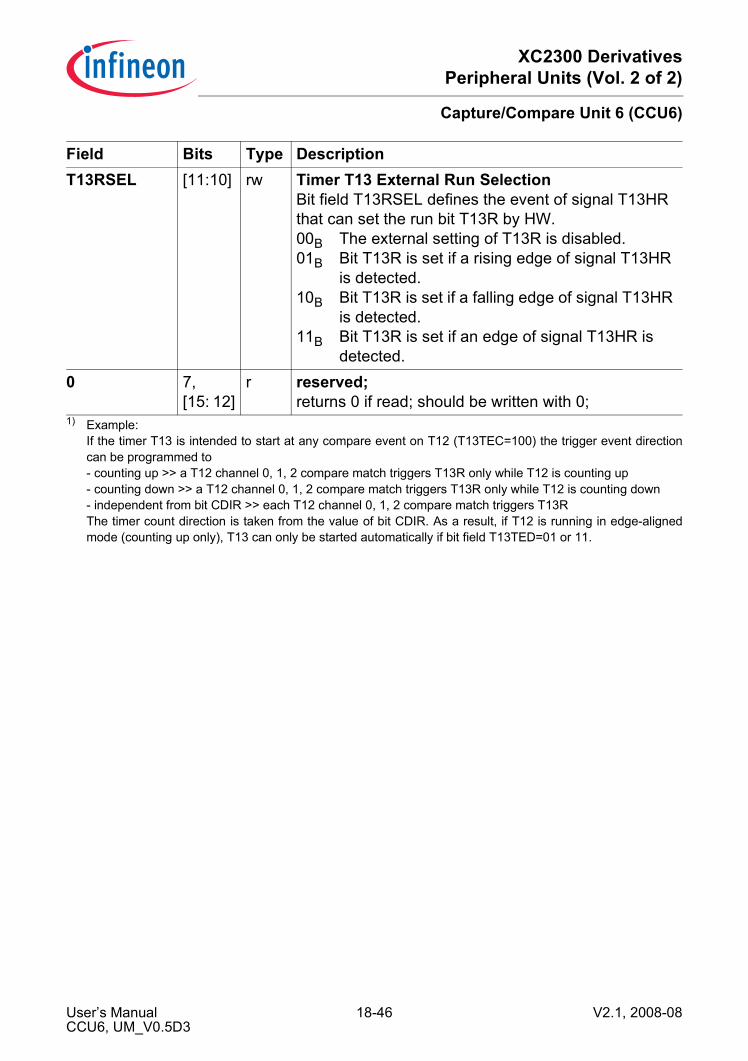
XC2300 DerivativesPeripheral Units (Vol. 2 of 2)
Capture/Compare Unit 6 (CCU6)
T13RSEL [11:10] rw Timer T13 External Run SelectionBit field T13RSEL defines the event of signal T13HR that can set the run bit T13R by HW.00B The external setting of T13R is disabled.01B Bit T13R is set if a rising edge of signal T13HR
is detected.10B Bit T13R is set if a falling edge of signal T13HR
is detected.11B Bit T13R is set if an edge of signal T13HR is
detected.0 7,
[15: 12]r reserved;
returns 0 if read; should be written with 0;1) Example:
If the timer T13 is intended to start at any compare event on T12 (T13TEC=100) the trigger event directioncan be programmed to - counting up >> a T12 channel 0, 1, 2 compare match triggers T13R only while T12 is counting up- counting down >> a T12 channel 0, 1, 2 compare match triggers T13R only while T12 is counting down- independent from bit CDIR >> each T12 channel 0, 1, 2 compare match triggers T13RThe timer count direction is taken from the value of bit CDIR. As a result, if T12 is running in edge-alignedmode (counting up only), T13 can only be started automatically if bit field T13TED=01 or 11.
Field Bits Type Description
User’s Manual 18-46 V2.1, 2008-08CCU6, UM_V0.5D3

XC2300 DerivativesPeripheral Units (Vol. 2 of 2)
Capture/Compare Unit 6 (CCU6)
Register TCTR4 provides software-control (independent set and clear conditions) for therun bits T12R and T13R. Furthermore, the timers can be reset (while running) and bitsSTE12 and STE13 can be controlled by software. Reading these bits always returns 0.
TCTR4Timer Control Register 4 XSFR(26H) Reset Value: 0000H
15 14 13 12 11 10 9 8 7 6 5 4 3 2 1 0
T13STD
T13STR
T13CNT 0 T13
REST13RS
T13RR
T12STD
T12STR
T12CNT 0 DT
REST12RES
T12RS
T12RR
w w w r w w w w w w r w w w w
Field Bits Type DescriptionT12RR 0 w Timer T12 Run Reset
Setting this bit clears the T12R bit.0B T12R is not influenced.1B T12R is cleared, T12 stops counting.
T12RS 1 w Timer T12 Run SetSetting this bit sets the T12R bit.0B T12R is not influenced.1B T12R is set, T12 starts counting.
T12RES 2 w Timer T12 Reset0B No effect on T12.1B The T12 counter register is cleared to zero. The
switching of the output signals is according to the switching rules. Setting of T12RES has no impact on bit T12R.
DTRES 3 w Dead-Time Counter Reset0B No effect on the dead-time counters.1B The three dead-time counter channels are
cleared to zero.T12CNT 5 w Timer T12 Count Event
0B No action1B If enabled (PISELH), timer T12 counts one step.
T12STR 6 w Timer T12 Shadow Transfer Request0B No action1B STE12 is set, enabling the shadow transfer.
User’s Manual 18-47 V2.1, 2008-08CCU6, UM_V0.5D3
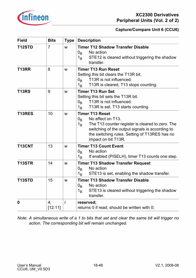
XC2300 DerivativesPeripheral Units (Vol. 2 of 2)
Capture/Compare Unit 6 (CCU6)
Note: A simultaneous write of a 1 to bits that set and clear the same bit will trigger noaction. The corresponding bit will remain unchanged.
T12STD 7 w Timer T12 Shadow Transfer Disable0B No action1B STE12 is cleared without triggering the shadow
transfer.T13RR 8 w Timer T13 Run Reset
Setting this bit clears the T13R bit.0B T13R is not influenced.1B T13R is cleared, T13 stops counting.
T13RS 9 w Timer T13 Run SetSetting this bit sets the T13R bit.0B T13R is not influenced.1B T13R is set, T13 starts counting.
T13RES 10 w Timer T13 Reset0B No effect on T13.1B The T13 counter register is cleared to zero. The
switching of the output signals is according to the switching rules. Setting of T13RES has no impact on bit T13R.
T13CNT 13 w Timer T13 Count Event0B No action1B If enabled (PISELH), timer T13 counts one step.
T13STR 14 w Timer T13 Shadow Transfer Request0B No action1B STE13 is set, enabling the shadow transfer.
T13STD 15 w Timer T13 Shadow Transfer Disable0B No action1B STE13 is cleared without triggering the shadow
transfer.0 4,
[12:11]r reserved;
returns 0 if read; should be written with 0;
Field Bits Type Description
User’s Manual 18-48 V2.1, 2008-08CCU6, UM_V0.5D3
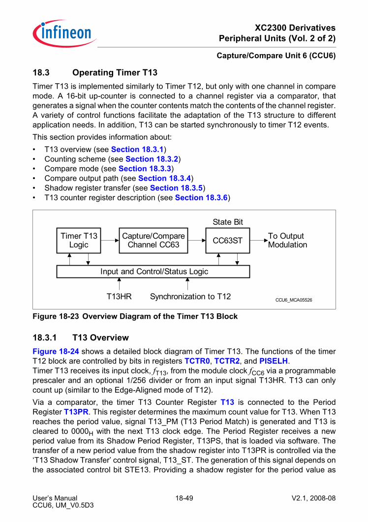
XC2300 DerivativesPeripheral Units (Vol. 2 of 2)
Capture/Compare Unit 6 (CCU6)
18.3 Operating Timer T13Timer T13 is implemented similarly to Timer T12, but only with one channel in comparemode. A 16-bit up-counter is connected to a channel register via a comparator, thatgenerates a signal when the counter contents match the contents of the channel register.A variety of control functions facilitate the adaptation of the T13 structure to differentapplication needs. In addition, T13 can be started synchronously to timer T12 events.This section provides information about:• T13 overview (see Section 18.3.1)• Counting scheme (see Section 18.3.2)• Compare mode (see Section 18.3.3)• Compare output path (see Section 18.3.4)• Shadow register transfer (see Section 18.3.5)• T13 counter register description (see Section 18.3.6)
Figure 18-23 Overview Diagram of the Timer T13 Block
18.3.1 T13 OverviewFigure 18-24 shows a detailed block diagram of Timer T13. The functions of the timerT12 block are controlled by bits in registers TCTR0, TCTR2, and PISELH.Timer T13 receives its input clock, fT13, from the module clock fCC6 via a programmableprescaler and an optional 1/256 divider or from an input signal T13HR. T13 can onlycount up (similar to the Edge-Aligned mode of T12).Via a comparator, the timer T13 Counter Register T13 is connected to the PeriodRegister T13PR. This register determines the maximum count value for T13. When T13reaches the period value, signal T13_PM (T13 Period Match) is generated and T13 iscleared to 0000H with the next T13 clock edge. The Period Register receives a newperiod value from its Shadow Period Register, T13PS, that is loaded via software. Thetransfer of a new period value from the shadow register into T13PR is controlled via the‘T13 Shadow Transfer’ control signal, T13_ST. The generation of this signal depends onthe associated control bit STE13. Providing a shadow register for the period value as
CCU6_MCA05526T13HR
Capture/CompareChannel CC63 CC63STTimer T13
Logic
State Bit
To OutputModulation
Input and Control/Status Logic
Synchronization to T12
User’s Manual 18-49 V2.1, 2008-08CCU6, UM_V0.5D3

XC2300 DerivativesPeripheral Units (Vol. 2 of 2)
Capture/Compare Unit 6 (CCU6)
well as for other values related to the generation of the PWM signal facilitates aconcurrent update by software for all relevant parameters (refer to Table 18.3.5).Another signal indicates whether the counter contents are equal to 0000H (T13_ZM).A Single-Shot control bit, T13SSC, enables an automatic stop of the timer when thecurrent counting period is finished (see Figure 18-26).
Figure 18-24 T13 Counter Logic and Period Comparators
The start or stop of T13 is controlled by the Run bit, T13R. This control bit can be set bysoftware via the associated set/clear bits T13RS or T13RR in register TCTR4, or it iscleared by hardware according to preselected conditions (single-shot mode).The timer T13 run bit T13R must not be set while the applied T13 period value is zero.Bit T13R can be set automatically if an event of T12 is detected to synchronize T13timings to T12 events, e.g. to generate a programmable delay via T13 after an edge ofa T12 compare channel before triggering an AD conversion (T13 can trigger ADC
CCU6_MCA05527
Comp.= ?
Period Register
Period ShadowRegister
T13_PM
Counter RegisterT13
Write toT13PR
Read fromT13PR
T13_ZM= 0000 H
T13_ST
fT13
edgedetection
T13HR
T13PRET13CLK
ISCNT13
T13STD
T13STR
T13RR
T13RS
T13R
T13RES
T13SSCT13Control& Status
STE13
edgedetection
T13RSEL
T13CNT
Sync. to T12
fCC6
256n
ClockSelection
User’s Manual 18-50 V2.1, 2008-08CCU6, UM_V0.5D3

XC2300 DerivativesPeripheral Units (Vol. 2 of 2)
Capture/Compare Unit 6 (CCU6)
conversions).Timer T13 can be cleared to 0000H via control bit T13RES. Setting this write-only bit onlyclears the timer contents, but has no further effects, e.g., it does not stop the timer.The generation of the T13 shadow transfer control signal, T13_ST, is enabled via bitSTE13. This bit can be set or cleared by software indirectly through its associated set/reset control bits T13STR and T13STD.Two bit fields, T13TEC and T13TED, control the synchronization of T13 to Timer T12events. T13TEC selects the trigger event, while T13TED determines for which T12 countdirection the trigger should be active.While Timer T13 is running, write accesses to the count register T13 are not taken intoaccount. If T13 is stopped, write actions to register T13 are immediately taken intoaccount.Note: The T13 Period Register and its associated shadow register are located at the
same physical address. A write access to this address targets the ShadowRegister, while a read access reads from the actual period register.
User’s Manual 18-51 V2.1, 2008-08CCU6, UM_V0.5D3

XC2300 DerivativesPeripheral Units (Vol. 2 of 2)
Capture/Compare Unit 6 (CCU6)
18.3.2 T13 Counting SchemeThis section describes the clocking and the counting capabilities of T13.
18.3.2.1 Clock SelectionIn Timer Mode (PISELH. ISCNT13 = 00B), the input clock fT13 of Timer T13 is derivedfrom the internal module clock fCC6 through a programmable prescaler and an optional1/256 divider. The resulting prescaler factors are listed in Table 18-6. The prescaler ofT13 is cleared while T13 is not running (TCTR0.T13R = 0) to ensure reproducibletimings and delays.
In Counter Mode, timer T13 counts one step:• If a 1 is written to TCTR4.T13CNT and PISELH.ISCNT13 = 01B• If a rising edge of input signal T13HR is detected and PISELH.ISCNT13 = 10B• If a falling edge of input signal T13HR is detected and PISELH.ISCNT13 = 11B
Table 18-6 Timer T13 Input Clock OptionsT13CLK Resulting Input Clock fT13
Prescaler Off (T13PRE = 0)Resulting Input Clock fT13Prescaler On (T13PRE = 1)
000B fCC6 fCC6 / 256001B fCC6 / 2 fCC6 / 512010B fCC6 / 4 fCC6 / 1024011B fCC6 / 8 fCC6 / 2048100B fCC6 / 16 fCC6 / 4096101B fCC6 / 32 fCC6 / 8192110B fCC6 / 64 fCC6 / 16384111B fCC6 / 128 fCC6 / 32768
User’s Manual 18-52 V2.1, 2008-08CCU6, UM_V0.5D3
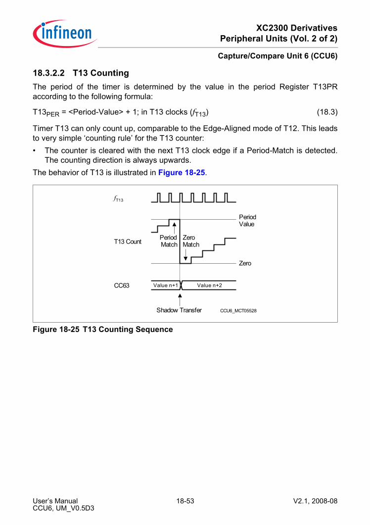
XC2300 DerivativesPeripheral Units (Vol. 2 of 2)
Capture/Compare Unit 6 (CCU6)
18.3.2.2 T13 CountingThe period of the timer is determined by the value in the period Register T13PRaccording to the following formula:
T13PER = <Period-Value> + 1; in T13 clocks (fT13) (18.3)
Timer T13 can only count up, comparable to the Edge-Aligned mode of T12. This leadsto very simple ‘counting rule’ for the T13 counter:• The counter is cleared with the next T13 clock edge if a Period-Match is detected.
The counting direction is always upwards.The behavior of T13 is illustrated in Figure 18-25.
Figure 18-25 T13 Counting Sequence
CCU6_MCT05528
fT13
Zero
CC63
Shadow Transfer
T13 Count
PeriodValue
PeriodMatch
ZeroMatch
Value n+1 Value n+2
User’s Manual 18-53 V2.1, 2008-08CCU6, UM_V0.5D3

XC2300 DerivativesPeripheral Units (Vol. 2 of 2)
Capture/Compare Unit 6 (CCU6)
18.3.2.3 Single-Shot ModeIn Single-Shot Mode, the timer run bit T13R is cleared by hardware. If bit T13SSC = 1,the timer T13 will stop when the current timer period is finished.
Figure 18-26 Single-Shot Operation of Timer T13
0
CCU6_MCT05529
CompareValue
PeriodValue
fT13
CC63ST
T13SSC
T13 Count
T13R
User’s Manual 18-54 V2.1, 2008-08CCU6, UM_V0.5D3
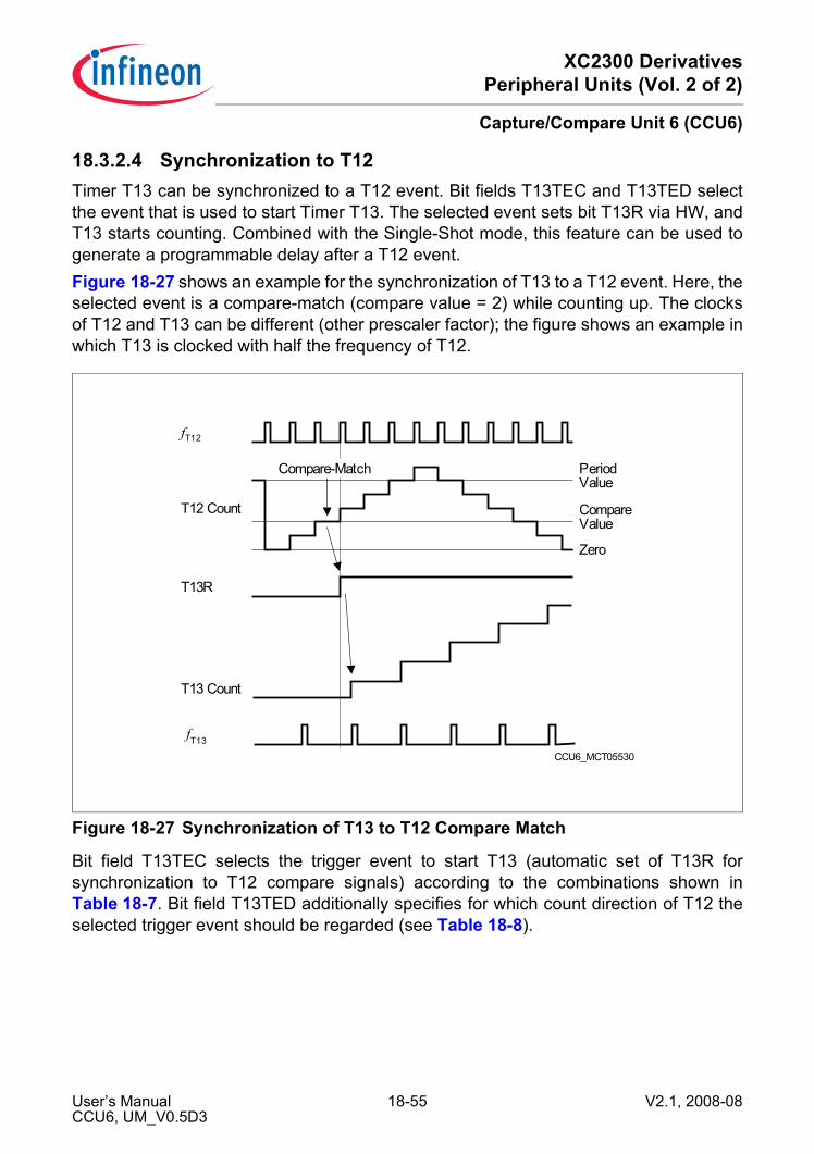
XC2300 DerivativesPeripheral Units (Vol. 2 of 2)
Capture/Compare Unit 6 (CCU6)
18.3.2.4 Synchronization to T12Timer T13 can be synchronized to a T12 event. Bit fields T13TEC and T13TED selectthe event that is used to start Timer T13. The selected event sets bit T13R via HW, andT13 starts counting. Combined with the Single-Shot mode, this feature can be used togenerate a programmable delay after a T12 event.Figure 18-27 shows an example for the synchronization of T13 to a T12 event. Here, theselected event is a compare-match (compare value = 2) while counting up. The clocksof T12 and T13 can be different (other prescaler factor); the figure shows an example inwhich T13 is clocked with half the frequency of T12.
Figure 18-27 Synchronization of T13 to T12 Compare Match
Bit field T13TEC selects the trigger event to start T13 (automatic set of T13R forsynchronization to T12 compare signals) according to the combinations shown inTable 18-7. Bit field T13TED additionally specifies for which count direction of T12 theselected trigger event should be regarded (see Table 18-8).
Zero
CompareValue
Compare-Match PeriodValue
CCU6_MCT05530
fT12
T13R
T13 Count
fT13
T12 Count
User’s Manual 18-55 V2.1, 2008-08CCU6, UM_V0.5D3

XC2300 DerivativesPeripheral Units (Vol. 2 of 2)
Capture/Compare Unit 6 (CCU6)
Table 18-7 T12 Trigger Event SelectionT13TEC Selected Event000B None001B T12 Compare Event on Channel 0 (CM_CC60)010B T12 Compare Event on Channel 1 (CM_CC61)011B T12 Compare Event on Channel 2 (CM_CC62)100B T12 Compare Event on any Channel (0, 1, 2)101B T12 Period-Match (T12_PM)110B T12 Zero-Match while counting up (T12_ZM and CDIR = 0)111B Any Hall State Change
Table 18-8 T12 Trigger Event Additional SpecifierT13TED Selected Event Specifier00B Reserved, no action01B Selected event is active while T12 is counting up (CDIR = 0)10B Selected event is active while T12 is counting down (CDIR = 1)11B Selected event is active independently of the count direction of T12
User’s Manual 18-56 V2.1, 2008-08CCU6, UM_V0.5D3
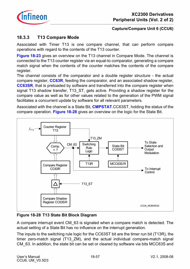
XC2300 DerivativesPeripheral Units (Vol. 2 of 2)
Capture/Compare Unit 6 (CCU6)
18.3.3 T13 Compare ModeAssociated with Timer T13 is one compare channel, that can perform compareoperations with regard to the contents of the T13 counter.Figure 18-23 gives an overview on the T13 channel in Compare Mode. The channel isconnected to the T13 counter register via an equal-to comparator, generating a comparematch signal when the contents of the counter matches the contents of the compareregister.The channel consists of the comparator and a double register structure - the actualcompare register, CC63R, feeding the comparator, and an associated shadow register,CC63SR, that is preloaded by software and transferred into the compare register whensignal T13 shadow transfer, T13_ST, gets active. Providing a shadow register for thecompare value as well as for other values related to the generation of the PWM signalfacilitates a concurrent update by software for all relevant parameters.Associated with the channel is a State Bit, CMPSTAT.CC63ST, holding the status of thecompare operation. Figure 18-28 gives an overview on the logic for the State Bit.
Figure 18-28 T13 State Bit Block Diagram
A compare interrupt event CM_63 is signaled when a compare match is detected. Theactual setting of a State Bit has no influence on the interrupt generation.The inputs to the switching rule logic for the CC63ST bit are the timer run bit (T13R), thetimer zero-match signal (T13_ZM), and the actual individual compare-match signalCM_63. In addition, the state bit can be set or cleared by software via bits MCC63S and
CCU6_MCB05532
SwitchingRuleLogic
State BitCC63ST
CM_63
To InterruptControl
To StateSelection andOutputModulation
T13_ZM
MCC63S/RT13R
Comp.= ?
Compare RegisterCC63R
Compare ShadowRegister CC63SR
T13_ST
Counter RegisterT13fT13
User’s Manual 18-57 V2.1, 2008-08CCU6, UM_V0.5D3

XC2300 DerivativesPeripheral Units (Vol. 2 of 2)
Capture/Compare Unit 6 (CCU6)
MCC63R in register CMPMODIF.A modification of the State Bit CC63ST by hardware is only possible while Timer T13 isrunning (T13R = 1). If this is the case, the following switching rules apply for setting andresetting the State Bit in Compare Mode:State Bit CC63ST is set to 1• with the next T13 clock (fT13) after a compare-match (T13 is always counting up)
(i.e., when the counter is incremented above the compare value);• with the next T13 clock (fT13) after a zero-match AND a parallel compare-match.State Bit CC63ST is cleared to 0• with the next T13 clock (fT13) after a zero-match AND NO parallel compare-match.
Figure 18-29 T13 Compare Operation
CCU6_MCT05533
fT13
Zero
CompareValue
CC63ST
Compare-Match Compare-Match PeriodValue
T13 Count
User’s Manual 18-58 V2.1, 2008-08CCU6, UM_V0.5D3
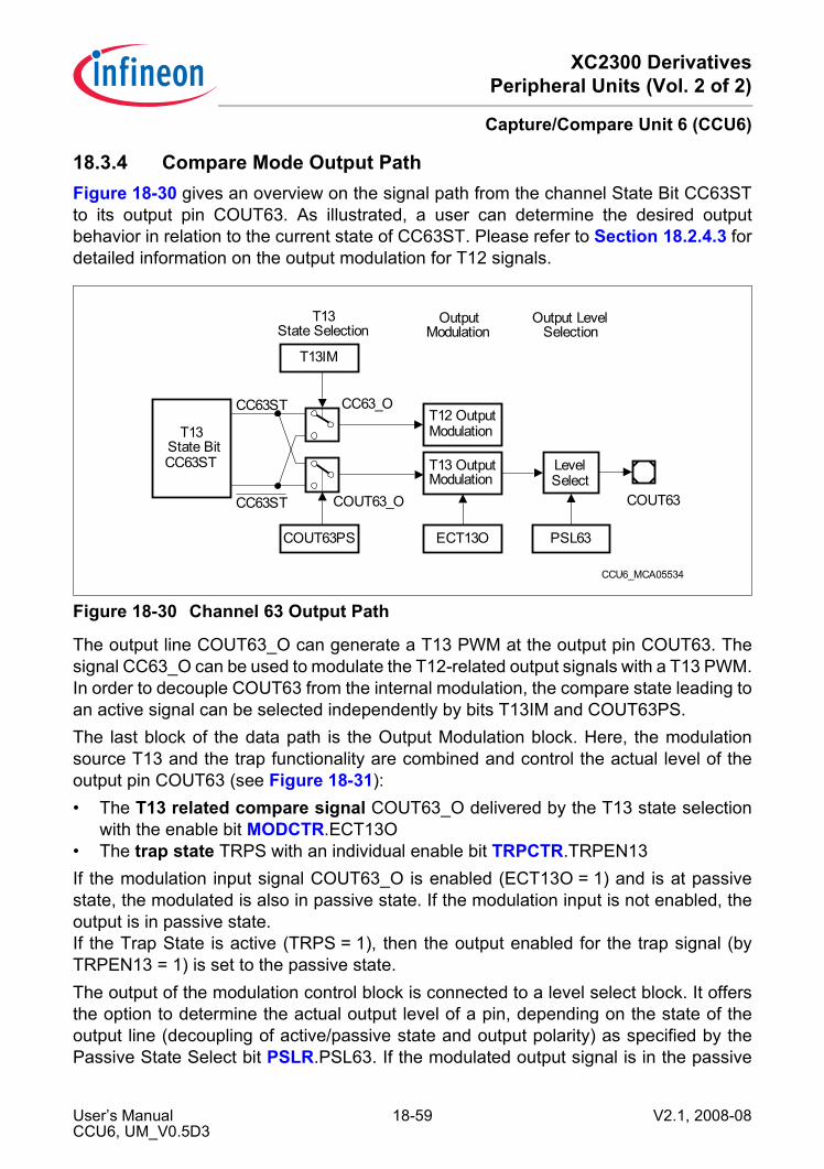
XC2300 DerivativesPeripheral Units (Vol. 2 of 2)
Capture/Compare Unit 6 (CCU6)
18.3.4 Compare Mode Output PathFigure 18-30 gives an overview on the signal path from the channel State Bit CC63STto its output pin COUT63. As illustrated, a user can determine the desired outputbehavior in relation to the current state of CC63ST. Please refer to Section 18.2.4.3 fordetailed information on the output modulation for T12 signals.
Figure 18-30 Channel 63 Output Path
The output line COUT63_O can generate a T13 PWM at the output pin COUT63. Thesignal CC63_O can be used to modulate the T12-related output signals with a T13 PWM.In order to decouple COUT63 from the internal modulation, the compare state leading toan active signal can be selected independently by bits T13IM and COUT63PS.The last block of the data path is the Output Modulation block. Here, the modulationsource T13 and the trap functionality are combined and control the actual level of theoutput pin COUT63 (see Figure 18-31):• The T13 related compare signal COUT63_O delivered by the T13 state selection
with the enable bit MODCTR.ECT13O• The trap state TRPS with an individual enable bit TRPCTR.TRPEN13If the modulation input signal COUT63_O is enabled (ECT13O = 1) and is at passivestate, the modulated is also in passive state. If the modulation input is not enabled, theoutput is in passive state.If the Trap State is active (TRPS = 1), then the output enabled for the trap signal (byTRPEN13 = 1) is set to the passive state.The output of the modulation control block is connected to a level select block. It offersthe option to determine the actual output level of a pin, depending on the state of theoutput line (decoupling of active/passive state and output polarity) as specified by thePassive State Select bit PSLR.PSL63. If the modulated output signal is in the passive
CCU6_MCA05534
LevelSelect
COUT63COUT63_O
CC63_O
T13State Selection
CC63ST
CC63ST
T13IM
COUT63PS
T12 OutputModulation
PSL63
Output LevelSelection
T13 State BitCC63ST
ECT13O
T13 OutputModulation
OutputModulation
User’s Manual 18-59 V2.1, 2008-08CCU6, UM_V0.5D3

XC2300 DerivativesPeripheral Units (Vol. 2 of 2)
Capture/Compare Unit 6 (CCU6)
state, the level specified directly by PSL63 is output. If it is in the active state, the invertedlevel of PSL63 is output. This allows the user to adapt the polarity of an active outputsignal to the connected circuitry.The PSL63 bit has a shadow register to allow for updates with the T13 shadow transfersignal (T13_ST) without undesired pulses on the output lines. A read action returns theactually used value, whereas a write action targets the shadow bit. Providing a shadowregister for the PSL value as well as for other values related to the generation of thePWM signal facilitates a concurrent update by software for all relevant parameters.
Figure 18-31 T13 Output Modulation
18.3.5 T13 Shadow Register TransferA special shadow transfer signal (T13_ST) can be generated to facilitate updating theperiod and compare values of the compare channel CC63 synchronously to theoperation of T13. Providing a shadow register for values defining one PWM periodfacilitates a concurrent update by software for all relevant parameters. The next PWMperiod can run with a new set of parameters. The generation of this signal is requestedby software via bit TCTR0.STE13 (set by writing 1 to the write-only bit TCTR4.T13STR,cleared by writing 1 to the write-only bit TCTR4.T13STD).When signal T13_ST is active, a shadow register transfer is triggered with the next cycleof the T13 clock. Bit STE13 is automatically cleared with the shadow register transfer.A T13 shadow register transfer takes place (T13_ST active):• while timer T13 is not running (T13R = 0), or• STE13 = 1 and a Period-Match is detected while T13R = 1
CCU6_MCA05545
COUT63
OutputModulationCOUT63
TRPEN13
PSL63
activepassive
T13 BlockCOUT63_O
ECT13O
TRPSTrap HandlingBlock
LevelSelection
User’s Manual 18-60 V2.1, 2008-08CCU6, UM_V0.5D3
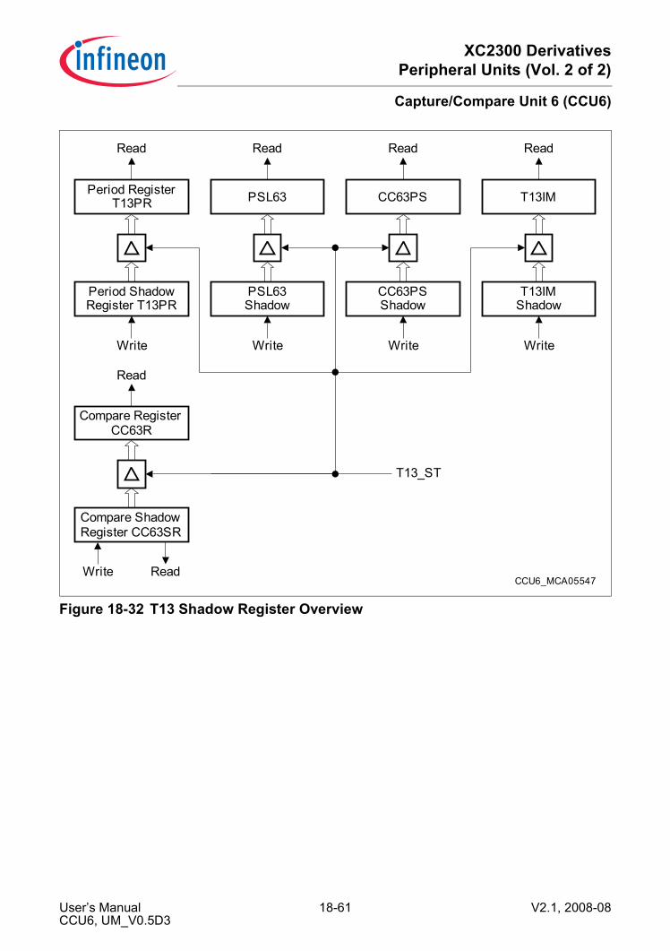
XC2300 DerivativesPeripheral Units (Vol. 2 of 2)
Capture/Compare Unit 6 (CCU6)
Figure 18-32 T13 Shadow Register Overview
CCU6_MCA05547
Compare RegisterCC63R
Compare ShadowRegister CC63SR
Period RegisterT13PR
Period ShadowRegister T13PR
T13IM
T13IMShadow
PSL63
PSL63Shadow
CC63PS
CC63PSShadow
T13_ST
Write
Read ReadRead Read
Write Write Write
Read
Write Read
User’s Manual 18-61 V2.1, 2008-08CCU6, UM_V0.5D3

XC2300 DerivativesPeripheral Units (Vol. 2 of 2)
Capture/Compare Unit 6 (CCU6)
18.3.6 T13 related Registers
18.3.6.1 T13 Counter RegisterThe generation of the patterns for a single channel pulse width modulation (PWM) isbased on timer T13. The registers related to timer T13 can be concurrently updated (withwell-defined conditions) in order to ensure consistency of the PWM signal. T13 can besynchronized to several timer T12 events.Timer T13 only supports compare mode on its compare channel CC63.Register T13 represents the counting value of timer T13. It can only be written while thetimer T13 is stopped. Write actions while T13 is running are not taken into account.Register T13 can always be read by SW.Timer T13 only supports edge-aligned mode (counting up).
Note: While timer T13 is stopped, the internal clock divider is reset in order to ensurereproducible timings and delays.
T13Timer T13 Counter Register XSFR(30H) Reset Value: 0000H
15 14 13 12 11 10 9 8 7 6 5 4 3 2 1 0
T13CV
rwh
Field Bits Type DescriptionT13CV [15:0] rwh Timer 13 Counter Value
This register represents the 16-bit counter value of Timer13.
User’s Manual 18-62 V2.1, 2008-08CCU6, UM_V0.5D3

XC2300 DerivativesPeripheral Units (Vol. 2 of 2)
Capture/Compare Unit 6 (CCU6)
18.3.6.2 Period RegisterRegister T13PR contains the period value for timer T13. The period value is comparedto the actual counter value of T13 and the resulting counter actions depend on thedefined counting rules. This register has a shadow register and the shadow transfer iscontrolled by bit STE13. A read action by SW delivers the value currently used for thecompare action, whereas the write action targets a shadow register. The shadow registerstructure allows a concurrent update of all T13-related values.
T13PR Timer 13 Period Register XSFR(32H) Reset Value: 0000H
15 14 13 12 11 10 9 8 7 6 5 4 3 2 1 0
T13PV
rwh
Field Bits Type DescriptionT13PV [15:0] rwh T13 Period Value
The value T13PV defines the counter value for T13 leading to a period-match. When reaching this value, the timer T13 is set to zero.
User’s Manual 18-63 V2.1, 2008-08CCU6, UM_V0.5D3
XC2300 DerivativesPeripheral Units (Vol. 2 of 2)
Capture/Compare Unit 6 (CCU6)
18.3.6.3 Compare RegisterRegisters CC63R is the actual compare register for T13. The values stored in CC63R iscompared to the counter value of T13. The State Bit CC63ST is located in registerCMPSTAT.
18.3.6.4 Compare Shadow RegisterThe register CC63R can only be read by SW, the modification of the value is done by ashadow register transfer from register CC63SR. The corresponding shadow registerCC63SR can be read and written by SW.
CC63RCompare Register for T13 XSFR(34H) Reset Value: 0000H
15 14 13 12 11 10 9 8 7 6 5 4 3 2 1 0
CCV
rh
Field Bits Type DescriptionCCV [15:0] rh Channel CC63 Compare Value
The bit field CCV contains the value, that is compared to the T13 counter value.
CC63SRCompare Shadow Register for T13
XSFR(36H) Reset Value: 0000H
15 14 13 12 11 10 9 8 7 6 5 4 3 2 1 0
CCS
rw
Field Bits Type DescriptionCCS [15:0] rw Shadow Register for Channel CC63 Compare
ValueThe bit field contents of CCS is transferred to the bit field CCV during a shadow transfer.
User’s Manual 18-64 V2.1, 2008-08CCU6, UM_V0.5D3
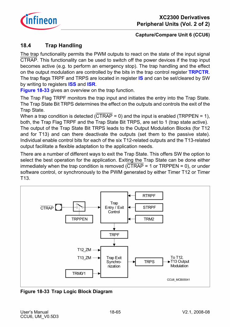
XC2300 DerivativesPeripheral Units (Vol. 2 of 2)
Capture/Compare Unit 6 (CCU6)
18.4 Trap HandlingThe trap functionality permits the PWM outputs to react on the state of the input signalCTRAP. This functionality can be used to switch off the power devices if the trap inputbecomes active (e.g. to perform an emergency stop). The trap handling and the effecton the output modulation are controlled by the bits in the trap control register TRPCTR.The trap flags TRPF and TRPS are located in register IS and can be set/cleared by SWby writing to registers ISS and ISR.Figure 18-33 gives an overview on the trap function.The Trap Flag TRPF monitors the trap input and initiates the entry into the Trap State.The Trap State Bit TRPS determines the effect on the outputs and controls the exit of theTrap State.When a trap condition is detected (CTRAP = 0) and the input is enabled (TRPPEN = 1),both, the Trap Flag TRPF and the Trap State Bit TRPS, are set to 1 (trap state active).The output of the Trap State Bit TRPS leads to the Output Modulation Blocks (for T12and for T13) and can there deactivate the outputs (set them to the passive state).Individual enable control bits for each of the six T12-related outputs and the T13-relatedoutput facilitate a flexible adaptation to the application needs.There are a number of different ways to exit the Trap State. This offers SW the option toselect the best operation for the application. Exiting the Trap State can be done eitherimmediately when the trap condition is removed (CTRAP = 1 or TRPPEN = 0), or undersoftware control, or synchronously to the PWM generated by either Timer T12 or TimerT13.
Figure 18-33 Trap Logic Block Diagram
CCU6_MCB05541
TrapEntry / Exit
Control
To T12,T13 OutputModulation
CTRAP
TRPPEN TRM2
TRPF
RTRPF
STRPF
Trap ExitSynchro-nization
TRM0/1
TRPS
T12_ZM
T13_ZM
User’s Manual 18-65 V2.1, 2008-08CCU6, UM_V0.5D3
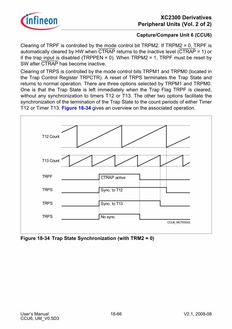
XC2300 DerivativesPeripheral Units (Vol. 2 of 2)
Capture/Compare Unit 6 (CCU6)
Clearing of TRPF is controlled by the mode control bit TRPM2. If TRPM2 = 0, TRPF isautomatically cleared by HW when CTRAP returns to the inactive level (CTRAP = 1) orif the trap input is disabled (TRPPEN = 0). When TRPM2 = 1, TRPF must be reset bySW after CTRAP has become inactive.Clearing of TRPS is controlled by the mode control bits TRPM1 and TRPM0 (located inthe Trap Control Register TRPCTR). A reset of TRPS terminates the Trap State andreturns to normal operation. There are three options selected by TRPM1 and TRPM0.One is that the Trap State is left immediately when the Trap Flag TRPF is cleared,without any synchronization to timers T12 or T13. The other two options facilitate thesynchronization of the termination of the Trap State to the count periods of either TimerT12 or Timer T13. Figure 18-34 gives an overview on the associated operation.
Figure 18-34 Trap State Synchronization (with TRM2 = 0)
CCU6_MCT05542
T12 Count
T13 Count
TRPF
TRPS
TRPS
TRPS
CTRAP active
Sync. to T12
Sync. to T13
No sync.
User’s Manual 18-66 V2.1, 2008-08CCU6, UM_V0.5D3

XC2300 DerivativesPeripheral Units (Vol. 2 of 2)
Capture/Compare Unit 6 (CCU6)
18.5 Multi-Channel ModeThe Multi-Channel mode offers the possibility to modulate all six T12-related outputsignals with one instruction. The bits in bit field MCMOUT.MCMP are used to specify theoutputs that may become active. If Multi-Channel mode is enabled (bitMODCTR.MCMEN = 1), only those outputs may become active, that have a 1 at thecorresponding bit position in bit field MCMP.This bit field has its own shadow bit field MCMOUTS.MCMPS, that can be written bysoftware. The transfer of the new value in MCMPS to the bit field MCMP can be triggeredby, and synchronized to, T12 or T13 events. This structure permits the software to writethe new value, that is then taken into account by the hardware at a well-defined momentand synchronized to a PWM signal. This avoids unintended pulses due tounsynchronized modulation sources.
Figure 18-35 Multi-Channel Mode Block Diagram
Figure 18-35 shows the functional blocks for the Multi-Channel operation, controlled bybit fields in register MCMCTR. The event that triggers the update of bit field MCMP ischosen by SWSEL. In order to synchronize the update of MCMP to a PWM generatedby T12 or T13, bit field SWSYN allows the selection of the synchronization event leadingto the transfer from MCMPS to MCMP. Due to this structure, an update takes place witha new PWM period. A reminder flag R is set when the selected switching event occurs(the event is not necessarily synchronous to the modulating PWM), and is cleared whenthe transfer takes place. This flag can be monitored by software to check for the statusof this logic block.
CCU6_MCB05535
SwitchingSynchro-nization
Shadow RegisterMCMOUTS.MCMPS
Shadow TransferMCM_ST
RegisterMCMOUT.MCMP
T12 Output Modulation
Outputs CC6x/COUT6x
T12_ZM
T13_ZM
T12_PM
CM_61
T12_OM
T13_PM
CM_CHE
SWSEL
CDIR
SWSYN
STRMCM
SwitchingEvent
Detection
Rset clear
STRset
To Interrupt Control
clear
IDLE
User’s Manual 18-67 V2.1, 2008-08CCU6, UM_V0.5D3

XC2300 DerivativesPeripheral Units (Vol. 2 of 2)
Capture/Compare Unit 6 (CCU6)
If the shadow transfer from MCMPS to MCMP takes place, bit IS.STR becomes set andan interrupt can be generated.If it is explicitly desired, the update takes place immediately with the occurrence of theselected event when the direct synchronization mode is selected. The update can alsobe requested by software by writing to bit field MCMPS with the shadow transfer requestbit STRMCM = 1. The option to trigger an update by SW is possible for all settings ofSWSEL.By using the direct mode and bit STRMCM = 1, the update takes place completely undersoftware control.The event selection and synchronization options are summarized in Table 18-9 andTable 18-10.
Table 18-9 Multi-Channel Mode Switching Event SelectionSWSEL Selected Event (see register MCMCTR)000B No automatic event detection001B Correct Hall Event (CM_CHE) detected at input signals CCPOSx
without additional delay010B T13 Period-Match (T13_PM)011B T12 One-Match while counting down (T12_OM and CDIR = 1)100B T12 Compare Channel 1 Event while counting up (CM_61 and
CDIR = 0) to support the phase delay function by CC61 for block commutation mode.
101B T12 Period-Match while counting up (T12_PM and CDIR = 0)110B,111B
Reserved, no action
Table 18-10 Multi-Channel Mode Switching SynchronizationSWSYN Synchronization Event (see register MCMCTR)00B Direct Mode: the trigger event directly causes the shadow transfer01B T13 Zero-Match (T13_ZM),
the MCM shadow transfer is synchronized to a T13 PWM10B T12 Zero-Match (T12_ZM),
the MCM shadow transfer is synchronized to a T12 PWM11B Reserved, no action
User’s Manual 18-68 V2.1, 2008-08CCU6, UM_V0.5D3

XC2300 DerivativesPeripheral Units (Vol. 2 of 2)
Capture/Compare Unit 6 (CCU6)
18.6 Hall Sensor ModeFor Brushless DC-Motors in block commutation mode, the Multi-Channel Mode hasbeen introduced to provide efficient means for switching pattern generation. Thesepatterns need to be output in relation to the angular position of the motor. For this, usuallyHall sensors or Back-EMF sensing are used to determine the angular rotor position. TheCCU6 provides three inputs, CCPOS0, CCPOS1, and CCPOS2, that can be used asinputs for the Hall sensors or the Back-EMF detection signals.There is a strong correlation between the motor position and the output modulationpattern. When a certain position of the motor has been reached, indicated by thesampled Hall sensor inputs (the Hall pattern), the next, pre-determined Multi-ChannelModulation pattern has to be output. Because of different machine types, the modulationpattern for driving the motor can vary. Therefore, it is wishful to have a wide flexibility indefining the correlation between the Hall pattern and the corresponding Modulationpattern. Furthermore, a hardware mechanism significantly reduces the CPU for block-commutation.The CCU6 offers the flexibility by having a register containing the currently assumed Hallpattern (CURH), the next expected Hall pattern (EXPH) and the corresponding outputpattern (MCMP). A new Modulation pattern is output when the sampled Hall inputsmatch the expected ones (EXPH). To detect the next rotation phase (segment for blockcommutation), the CCU6 monitors the Hall inputs for changes. When the next expectedHall pattern is detected, the next corresponding Modulation pattern is output.To increase for noise immunity (to a certain extend), the CCU6 offers the possibility tointroduce a sampling delay for the Hall inputs. Some changes of the Hall inputs are notleading to the expected Hall pattern, because they are only short spikes due to noise.The Hall pattern compare logic compares the Hall inputs to the next expected patternand also to the currently assumed pattern to filter out spikes.For the Hall and Modulation output patterns, a double-register structure is implemented.While register MCMOUT holds the actually used values, its shadow register MCMOUTScan be loaded by software from a pre-defined table, holding the appropriate Hall andModulation patterns for the given motor control.A transfer from the shadow register into register MCMOUT can take place when acorrect Hall pattern change is detected. Software can then load the next values intoregister MCMOUTS. It is also possible by software to force a transfer from MCMOUTSinto MCMOUT.Note: The Hall input signals CCPOSx and the CURH and EXPH bit fields are arranged
in the following order:CCPOS0 corresponds to CURH.0 (LSB) and EXPH.0 (LSB)CCPOS1 corresponds to CURH.1 and EXPH.1CCPOS2 corresponds to CURH.2 (MSB) and EXPH.2 (MSB)
User’s Manual 18-69 V2.1, 2008-08CCU6, UM_V0.5D3

XC2300 DerivativesPeripheral Units (Vol. 2 of 2)
Capture/Compare Unit 6 (CCU6)
18.6.1 Hall Pattern EvaluationThe Hall sensor inputs CCPOSx can be permanently monitored via an edge detectionblock (with the module clock fCC6). In order to suppress spikes on the Hall inputs due tonoise in rugged inverter environment, two optional noise filtering methods are supportedby the Hall logic (both methods can be combined).• Noise filtering with delay:
For this function, the mode control bit fields MSEL6x for all T12 compare channelsmust be programmed to 1000B and DBYP = 0. The selected event triggers Dead-Time Counter 0 to generate a programmable delay (defined by bit field DTM). Whenthe delay has elapsed, the evaluation signal HCRDY becomes activated.Output modulation with T12 PWM signals is not possible in this mode.
• Noise filtering by synchronization to PWM:The Hall inputs are not permanently monitored by the edge detection block, butsamples are taken only at defined points in time during a PWM period. This can beused to sample the Hall inputs when the switching noise (due to PWM) does notdisturb the Hall input signals.
If neither the delay function of Dead-Time Counter 0 is not used for the Hall patternevaluation nor the Hall mode for Brushless DC-Drive control is enabled, the timer T12block is available for PWM generation and output modulation.
Figure 18-36 Hall Pattern Evaluation
If the evaluation signal HCRDY (Hall Compare Ready, see Figure 18-37) becomesactivated, the Hall inputs are sampled and the Hall compare logic starts the evaluationof the Hall inputs.
CCU6_MCB05553
Edge
Detect
HallCompare
Logic
HCRDY
CC
PO
S0.
.2
CM_61
T12_OM
T12_PM
T13_PM
CM_63 Dead-TimeCounter 0
HallInputs
DelayBypass
DBYPHSYNC
EventSelection
CDIR
Hall Pattern Evaluation
fCC6
User’s Manual 18-70 V2.1, 2008-08CCU6, UM_V0.5D3

XC2300 DerivativesPeripheral Units (Vol. 2 of 2)
Capture/Compare Unit 6 (CCU6)
Figure 18-36 illustrates the events for Hall pattern evaluation and the noise filter logic,Table 18-11 summarizes the selectable trigger input signals.
Table 18-11 Hall Sensor Mode Trigger Event SelectionHSYNC Selected Event (see register T12MSEL)000B Any edge at any of the inputs CCPOSx, independent from any PWM
signal (permanent check).001B A T13 Compare-Match (CM_63).010B A T13 Period-Match (T13_PM).011B Hall sampling triggered by HW sources is switched off.100B A T12 Period-Match while counting up (T12_PM and CDIR = 0).101B A T12 One-Match while counting down (T12_OM and CDIR = 1).110B A T12 Compare-Match of compare channel CC61 while counting up
(CM_61 and CDIR = 0).111B A T12 Compare-Match of compare channel CC61 while counting down
(CM_61 and CDIR = 1).
User’s Manual 18-71 V2.1, 2008-08CCU6, UM_V0.5D3

XC2300 DerivativesPeripheral Units (Vol. 2 of 2)
Capture/Compare Unit 6 (CCU6)
18.6.2 Hall Pattern Compare LogicFigure 18-37 gives an overview on the double-register structure and the patterncompare logic. Software writes the next modulation pattern (MCMPS) and thecorresponding current (CURHS) and expected (EXPHS) Hall patterns into the shadowregister MCMOUTS. Register MCMOUT holds the actually used values CURH andEXPH. The modulation pattern MCMP is provided to the T12 Output Modulation block.The current (CURH) and expected (EXPH) Hall patterns are compared to the sampledHall sensor inputs (visible in register CMPSTAT). Sampling of the inputs and theevaluation of the comparator outputs is triggered by the evaluation signal HCRDY (HallCompare Ready), that is detailed in the next section.
Figure 18-37 Hall Pattern Compare Logic
• If the sampled Hall pattern matches the value programmed in CURH, the detectedtransition was a spike (no Hall event) and no further actions are necessary.
• If the sampled Hall pattern matches the value programmed in EXPH, the detectedtransition was the expected event (correct Hall event CM_CHE) and the MCMP valuehas to change.
• If the sampled Hall pattern matches neither CURH nor EXPH, the transition was dueto a major error (wrong Hall event CM_CWE) and can lead to an emergency shutdown (IDLE).
CCU6_MCA05536
CM_CHE
CM_WHE
MCMPS
EXPHCURH
HCRDY
CC
PO
S0.
.2
CURHS EXPHS
HP_ST MCM_ST
SW Write SW Write SW Write
MCMP
HallInputs
Hall PatternEvaluation
Multi-Channel Mode Logic
Pattern Compare
Sam
ple
Hall Compare Logic
clear
T12 OutputModulation
IDLE
User’s Manual 18-72 V2.1, 2008-08CCU6, UM_V0.5D3

XC2300 DerivativesPeripheral Units (Vol. 2 of 2)
Capture/Compare Unit 6 (CCU6)
At every correct Hall event (CM_CHE), the next Hall patterns are transferred from theshadow register MCMOUTS into MCMOUT (Hall pattern shadow transfer HP_ST), anda new Hall pattern with its corresponding output pattern can be loaded (e.g. from apredefined table in memory) by software into MCMOUTS. For the Modulation patterns,signal MCM_ST is used to trigger the transfer.Loading this shadow register can also be done by writing MCMOUTS.STRHP = 1 (forEXPH and CURH) or MCMOUTS.STRMCMP = 1 (for MCMP).
18.6.3 Hall Mode FlagsDepending on the Hall pattern compare operation, a number of flags are set in order toindicate the status of the module and to trigger further actions and interrupt requests.Flag IS.CHE (Correct Hall Event) is set by signal CM_CHE when the sampled Hallpattern matches the expected one (EXPH). This flag can also be set by SW by settingbit ISS.SCHE = 1. If enabled by bit IEN.ENCHE = 1, the set signal for CHE can alsogenerate an interrupt request to the CPU. Bit field INP.INPCHE defines which servicerequest output becomes activated in case of an interrupt request.To clear flag CHE, SWneeds to write ISR.RCHE = 1.Flag IS.WHE indicates a Wrong Hall Event. Its handling for flag setting and resetting aswell as interrupt request generation are similar to the mechanism for flag CHE.The implementation of flag STR is done in the same way as for CHE and WHE. This flagis set by HW by the shadow transfer signal MCM_ST (see also Figure 18-35).Please note that for flags CHE, WHE, and STR, the interrupt request generation istriggered by the set signal for the flag. That means, a request can be generated even ifthe flag is already set. There is no need to clear the flag in order to enable furtherinterrupt requests.The implementation for the IDLE flag is different. It is set by HW through signal CM_WHEif enabled by bit ENIDLE. Software can also set the flag via bit SIDLE. As long as bit IDLEis set, the modulation pattern field MCMP is cleared to force the outputs to the passivestate. Flag IDLE must be cleared by software by writing RIDLE = 1 in order to return tonormal operation. To fully restart from IDLE mode, the transfer requests for the bit fieldsin register MCMOUTS to register MCMOUT have to be initiated by software via bitsSTRMCM and STRHP in register MCMOUTS. In this way, the release from IDLE modeis under software control, but can be performed synchronously to the PWM signal.
User’s Manual 18-73 V2.1, 2008-08CCU6, UM_V0.5D3

XC2300 DerivativesPeripheral Units (Vol. 2 of 2)
Capture/Compare Unit 6 (CCU6)
Figure 18-38 Hall Mode Flags
CCU6_MCA05540
Set
CM_CHE
CHEClear
Set
RCHE
SCHE
ENCHE
Set
CM_WHE
WHEClearRWHE
SWHE
SIDLEIDLE
RIDLE
ClearMCMPClear
Hall CompareLogic
ENIDLE
ENWHE
>1_
>1_
>1_
INPERR
INPCHE
To SR0
To SR1To SR2To SR3
To SR0
To SR1To SR2To SR3
User’s Manual 18-74 V2.1, 2008-08CCU6, UM_V0.5D3

XC2300 DerivativesPeripheral Units (Vol. 2 of 2)
Capture/Compare Unit 6 (CCU6)
18.6.4 Hall Mode for Brushless DC-Motor ControlThe CCU6 provides a mode for the Timer T12 Block especially targeted for convenientcontrol of block commutation patterns for Brushless DC-Motors. This mode is selectedby setting all T12MSEL.MSEL6x bit fields of the three T12 Channels to 1000B.In this mode, illustrated in Figure 18-39, channel CC60 is placed in capture mode tomeasure the time elapsed between the last two correct Hall events, channel CC61 incompare mode to provide a programmable phase delay between the Hall event and theapplication of a new PWM output pattern, and channel CC62 also in compare mode asfirst time-out criterion. A second time-out criterion can be built by the T12 period matchevent.
Figure 18-39 T12 Block in Hall Sensor Mode
The signal CM_CHE from the Hall compare logic is used to transfer the new comparevalues from the shadow registers CC6xSR into the actual compare registers CC6xR,performs the shadow transfer for the T12 period register, to capture the current T12contents into register CC60R, and to clear T12.Note: In this mode, the shadow transfer signal T12_ST is not generated. Not all shadow
bits, such as the PSLy bits, will be transferred to their main registers. To programthe main registers, SW needs to write to these registers while Timer T12 isstopped. In this case, a SW write actualizes both registers.
CCU6_MCA05538
Comp.= ?
Compare RegisterCC61R
Compare ShadowRegister CC61SR
Comp.= ?
Compare RegisterCC62R
Compare ShadowRegister CC62SR
Counter RegisterT12fT12
CM_CHE
Clear
CM_61
CM_62
Capture RegisterCC60R
Hall CompareLogic
User’s Manual 18-75 V2.1, 2008-08CCU6, UM_V0.5D3
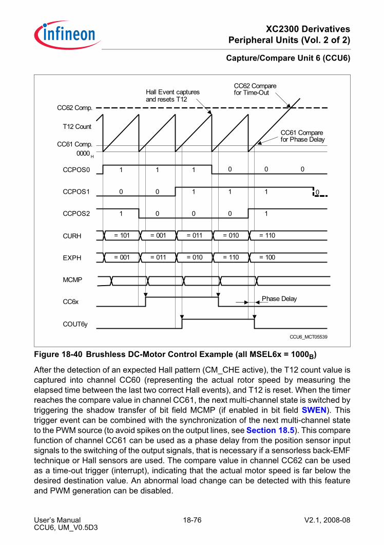
XC2300 DerivativesPeripheral Units (Vol. 2 of 2)
Capture/Compare Unit 6 (CCU6)
Figure 18-40 Brushless DC-Motor Control Example (all MSEL6x = 1000B)
After the detection of an expected Hall pattern (CM_CHE active), the T12 count value iscaptured into channel CC60 (representing the actual rotor speed by measuring theelapsed time between the last two correct Hall events), and T12 is reset. When the timerreaches the compare value in channel CC61, the next multi-channel state is switched bytriggering the shadow transfer of bit field MCMP (if enabled in bit field SWEN). Thistrigger event can be combined with the synchronization of the next multi-channel stateto the PWM source (to avoid spikes on the output lines, see Section 18.5). This comparefunction of channel CC61 can be used as a phase delay from the position sensor inputsignals to the switching of the output signals, that is necessary if a sensorless back-EMFtechnique or Hall sensors are used. The compare value in channel CC62 can be usedas a time-out trigger (interrupt), indicating that the actual motor speed is far below thedesired destination value. An abnormal load change can be detected with this featureand PWM generation can be disabled.
CCU6_MCT05539
COUT6y
CC62 Comp.
CC6x
MCMP
EXPH
CURH
= 011= 001 = 110= 010 = 100
= 001= 101 = 010= 011 = 110
CCPOS2 1 0 0 0 1
CCPOS1 0 0 1 1 1 0
CCPOS0 1 1 1 0 0 0
0000 H
CC61 Comp.
T12 Count
Hall Event capturesand resets T12
CC62 Comparefor Time-Out
CC61 Comparefor Phase Delay
Phase Delay
User’s Manual 18-76 V2.1, 2008-08CCU6, UM_V0.5D3

XC2300 DerivativesPeripheral Units (Vol. 2 of 2)
Capture/Compare Unit 6 (CCU6)
18.7 Modulation Control Registers
18.7.1 Modulation ControlThis register contains bits enabling the modulation of the corresponding output signal byPWM pattern generated by the timers T12 and T13. Furthermore, the multi-channelmode can be enabled as additional modulation source for the output signals.
MODCTR Modulation Control Register XSFR(40H) Reset Value: 0000H
15 14 13 12 11 10 9 8 7 6 5 4 3 2 1 0
ECT13O 0 T13MODEN MCM
EN 0 T12MODEN
rw r rw rw r rw
Field Bits Type DescriptionT12MODEN [5:0] rw T12 Modulation Enable
These bits enable the modulation of the corresponding output signal by a PWM pattern generated by timer T12.T12MODEN0 = MODCTR.0 for output CC60T12MODEN1 = MODCTR.1 for output COUT60T12MODEN2 = MODCTR.2 for output CC61T12MODEN3 = MODCTR.3 for output COUT61T12MODEN4 = MODCTR.4 for output CC62T12MODEN5 = MODCTR.5 for output COUT620B The modulation of the corresponding output
signal by a T12 PWM pattern is disabled.1B The modulation of the corresponding output
signal by a T12 PWM pattern is enabled.MCMEN 7 rw Multi-Channel Mode Enable
0B The modulation of the corresponding output signal by a multi-channel pattern according to bit field MCMOUT is disabled.
1B The modulation of the corresponding output signal by a multi-channel pattern according to bit field MCMOUT is enabled.
User’s Manual 18-77 V2.1, 2008-08CCU6, UM_V0.5D3

XC2300 DerivativesPeripheral Units (Vol. 2 of 2)
Capture/Compare Unit 6 (CCU6)
T13MODEN [13:8] rw T13 Modulation EnableThese bits enable the modulation of the corresponding output signal by the PWM pattern CC63_O generated by timer T13.T13MODEN0 = MODCTR.8 for output CC60T13MODEN1 = MODCTR.9 for output COUT60T13MODEN2 = MODCTR.10 for output CC61T13MODEN3 = MODCTR.11 for output COUT61T13MODEN4 = MODCTR.12 for output CC62T13MODEN5 = MODCTR.13 for output COUT620B The modulation of the corresponding output
signal by a T13 PWM pattern is disabled.1B The modulation of the corresponding output
signal by a T13 PWM pattern is enabled.ECT13O 15 rw Enable Compare Timer T13 Output
0B The output COUT63 is in the passive state.1B The output COUT63 is enabled for the PWM
signal generated by T13.0 6, 14 r reserved;
returns 0 if read; should be written with 0;
Field Bits Type Description
User’s Manual 18-78 V2.1, 2008-08CCU6, UM_V0.5D3
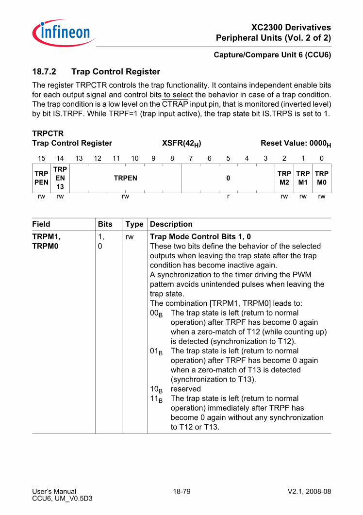
XC2300 DerivativesPeripheral Units (Vol. 2 of 2)
Capture/Compare Unit 6 (CCU6)
18.7.2 Trap Control RegisterThe register TRPCTR controls the trap functionality. It contains independent enable bitsfor each output signal and control bits to select the behavior in case of a trap condition.The trap condition is a low level on the CTRAP input pin, that is monitored (inverted level)by bit IS.TRPF. While TRPF=1 (trap input active), the trap state bit IS.TRPS is set to 1.
TRPCTR Trap Control Register XSFR(42H) Reset Value: 0000H
15 14 13 12 11 10 9 8 7 6 5 4 3 2 1 0
TRPPEN
TRPEN13
TRPEN 0 TRPM2
TRPM1
TRPM0
rw rw rw r rw rw rw
Field Bits Type DescriptionTRPM1,TRPM0
1,0
rw Trap Mode Control Bits 1, 0These two bits define the behavior of the selected outputs when leaving the trap state after the trap condition has become inactive again.A synchronization to the timer driving the PWM pattern avoids unintended pulses when leaving the trap state.The combination [TRPM1, TRPM0] leads to:00B The trap state is left (return to normal
operation) after TRPF has become 0 again when a zero-match of T12 (while counting up) is detected (synchronization to T12).
01B The trap state is left (return to normal operation) after TRPF has become 0 again when a zero-match of T13 is detected (synchronization to T13).
10B reserved11B The trap state is left (return to normal
operation) immediately after TRPF has become 0 again without any synchronization to T12 or T13.
User’s Manual 18-79 V2.1, 2008-08CCU6, UM_V0.5D3

XC2300 DerivativesPeripheral Units (Vol. 2 of 2)
Capture/Compare Unit 6 (CCU6)
TRPM2 2 rw Trap Mode Control Bit 2This bit defines how the trap flag TRPF can be cleared after the trap input condition (CTRAP = 0 and TRPPEN = 1) is no longer valid (either by CTRAP = 1 or by TRPPEN = 0).0B Automatic Mode:
Bit TRPF is cleared by HW if the trap input condition is no longer valid.
1B Manual Mode:Bit TRPF stays 0 after the trap input condition is no longer valid. It has to be cleared by SW by writing ISR.RTRPF = 1.
TRPEN [13:8] rw Trap Enable ControlSetting a bit enables the trap functionality for the following corresponding output signals:TRPEN0 = TRPCTR.8 for output CC60TRPEN1 = TRPCTR.9 for output COUT60TRPEN2 = TRPCTR.10 for output CC61TRPEN3 = TRPCTR.11 for output COUT61TRPEN4 = TRPCTR.12 for output CC62TRPEN5 = TRPCTR.13 for output COUT620B The trap functionality of the corresponding
output signal is disabled. The output state is independent from bit IS.TRPS.
1B The trap functionality of the corresponding output signal is enabled. The output state is set to the passive while IS.TRPS=1.
TRPEN13 14 rw Trap Enable Control for Timer T130B The trap functionality for output COUT63 is
disabled. The output state is independent from bit IS.TRPS.
1B The trap functionality for output COUT63 is enabled. The output state is set to the passive while IS.TRPS=1.
Field Bits Type Description
User’s Manual 18-80 V2.1, 2008-08CCU6, UM_V0.5D3

XC2300 DerivativesPeripheral Units (Vol. 2 of 2)
Capture/Compare Unit 6 (CCU6)
TRPPEN 15 rw Trap Pin EnableThis bit enables the input (pin) function for the trap generation. An interrupt can only be generated if a falling edge is detected at pin CTRAP while TRPPEN = 1.0B The CCU6 trap functionality based on the input
CTRAP is disabled. A CCU6 trap can only be generated by SW by setting bit TRPF.
1B The CCU6 trap functionality based on the input CTRAP is enabled. A CCU6 trap can be generated by SW by setting bit TRPF or by CTRAP=0.
0 [7:3] r reserved;returns 0 if read; should be written with 0;
Field Bits Type Description
User’s Manual 18-81 V2.1, 2008-08CCU6, UM_V0.5D3
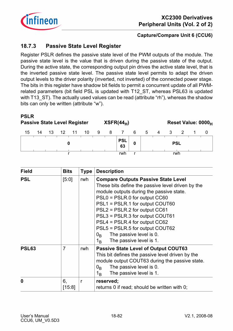
XC2300 DerivativesPeripheral Units (Vol. 2 of 2)
Capture/Compare Unit 6 (CCU6)
18.7.3 Passive State Level RegisterRegister PSLR defines the passive state level of the PWM outputs of the module. Thepassive state level is the value that is driven during the passive state of the output.During the active state, the corresponding output pin drives the active state level, that isthe inverted passive state level. The passive state level permits to adapt the drivenoutput levels to the driver polarity (inverted, not inverted) of the connected power stage.The bits in this register have shadow bit fields to permit a concurrent update of all PWM-related parameters (bit field PSL is updated with T12_ST, whereas PSL63 is updatedwith T13_ST). The actually used values can be read (attribute “rh”), whereas the shadowbits can only be written (attribute “w”).
PSLR Passive State Level Register XSFR(44H) Reset Value: 0000H
15 14 13 12 11 10 9 8 7 6 5 4 3 2 1 0
0 PSL63 0 PSL
r rwh r rwh
Field Bits Type DescriptionPSL [5:0] rwh Compare Outputs Passive State Level
These bits define the passive level driven by the module outputs during the passive state.PSL0 = PSLR.0 for output CC60PSL1 = PSLR.1 for output COUT60PSL2 = PSLR.2 for output CC61PSL3 = PSLR.3 for output COUT61PSL4 = PSLR.4 for output CC62PSL5 = PSLR.5 for output COUT620B The passive level is 0.1B The passive level is 1.
PSL63 7 rwh Passive State Level of Output COUT63This bit defines the passive level driven by the module output COUT63 during the passive state.0B The passive level is 0.1B The passive level is 1.
0 6,[15:8]
r reserved;returns 0 if read; should be written with 0;
User’s Manual 18-82 V2.1, 2008-08CCU6, UM_V0.5D3

XC2300 DerivativesPeripheral Units (Vol. 2 of 2)
Capture/Compare Unit 6 (CCU6)
18.7.4 Multi-Channel Mode RegistersRegister MCMCTR contains control bits for the multi-channel functionality.
MCMCTR Multi-Channel Mode Control Register
XSFR(4EH) Reset Value: 0000H
15 14 13 12 11 10 9 8 7 6 5 4 3 2 1 0
0 SWSYN 0 SWSEL
r rw r rw
Field Bits Type DescriptionSWSEL [2:0] rw Switching Selection
Bit field SWSEL selects one of the following trigger request sources (next multi-channel event) for the shadow transfer MCM_ST from MCMPS to MCMP. The trigger request is stored in the reminder flag R until the shadow transfer is done and flag R is cleared automatically with the shadow transfer. The shadow transfer takes place synchronously with an event selected in bit field SWSYN.000B No trigger request will be generated001B Correct Hall pattern detected (CM_CHE)010B T13 period-match detected (while counting up)011B T12 one-match (while counting down)100B T12 channel 1 compare-match detected
(phase delay function)101B T12 period match detected (while counting up)else reserved, no trigger request will be generated
User’s Manual 18-83 V2.1, 2008-08CCU6, UM_V0.5D3

XC2300 DerivativesPeripheral Units (Vol. 2 of 2)
Capture/Compare Unit 6 (CCU6)
SWSYN [5:4] rw Switching SynchronizationBit field SWSYN defines the synchronization mechanism of the shadow transfer event MCM_ST if it has been requested before (flag R set by an event selected by SWSEL) and if MCMEN = 1. This feature permits the synchronization of the outputs to the PWM source, that is used for modulation (T12 or T13).00B Direct; the trigger event immediately leads to
the shadow transfer01B T13 zero-match triggers the shadow transfer10B a T12 zero-match (while counting up) triggers
the shadow transfer11B reserved; no action
0 3, [15:6]
r reserved;returns 0 if read; should be written with 0;
Field Bits Type Description
User’s Manual 18-84 V2.1, 2008-08CCU6, UM_V0.5D3
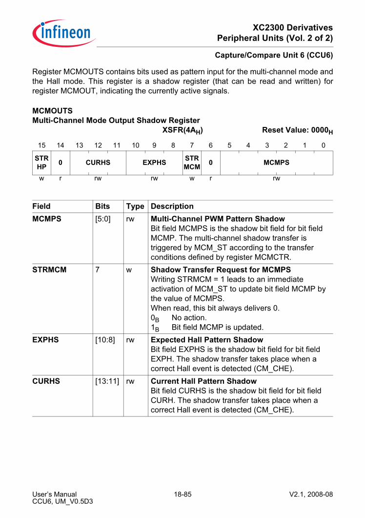
XC2300 DerivativesPeripheral Units (Vol. 2 of 2)
Capture/Compare Unit 6 (CCU6)
Register MCMOUTS contains bits used as pattern input for the multi-channel mode andthe Hall mode. This register is a shadow register (that can be read and written) forregister MCMOUT, indicating the currently active signals.
MCMOUTS Multi-Channel Mode Output Shadow Register XSFR(4AH) Reset Value: 0000H
15 14 13 12 11 10 9 8 7 6 5 4 3 2 1 0
STRHP 0 CURHS EXPHS STR
MCM 0 MCMPS
w r rw rw w r rw
Field Bits Type DescriptionMCMPS [5:0] rw Multi-Channel PWM Pattern Shadow
Bit field MCMPS is the shadow bit field for bit field MCMP. The multi-channel shadow transfer is triggered by MCM_ST according to the transfer conditions defined by register MCMCTR.
STRMCM 7 w Shadow Transfer Request for MCMPSWriting STRMCM = 1 leads to an immediate activation of MCM_ST to update bit field MCMP by the value of MCMPS.When read, this bit always delivers 0.0B No action.1B Bit field MCMP is updated.
EXPHS [10:8] rw Expected Hall Pattern ShadowBit field EXPHS is the shadow bit field for bit field EXPH. The shadow transfer takes place when a correct Hall event is detected (CM_CHE).
CURHS [13:11] rw Current Hall Pattern ShadowBit field CURHS is the shadow bit field for bit field CURH. The shadow transfer takes place when a correct Hall event is detected (CM_CHE).
User’s Manual 18-85 V2.1, 2008-08CCU6, UM_V0.5D3

XC2300 DerivativesPeripheral Units (Vol. 2 of 2)
Capture/Compare Unit 6 (CCU6)
STRHP 15 w Shadow Transfer Request for the Hall PatternWriting STRHP = 1 leads to an immediate activation of HP_ST to update bit fields EXPH and CURH by EXPHS and CURHS.When read, this bit always delivers 0.0B No action.1B Bit fields EXPH and CURH are updated.
0 6, 14 r reserved;returns 0 if read; should be written with 0;
MCMOUT Multi-Channel Mode Output Register
XSFR(4CH) Reset Value: 0000H
15 14 13 12 11 10 9 8 7 6 5 4 3 2 1 0
0 CURH EXPH 0 R MCMP
r rh rh r rh rh
Field Bits Type DescriptionMCMP [5:0] rh Multi-Channel PWM Pattern
Bit field MCMP defines the output pattern for the multi-channel mode. If this mode is enabled by MODCTR.MCMEN = 1, the output state of all T12 related PWM outputs can be modified.This bit field is 0 while IS.IDLE = 1.MCMP0 = MCMOUT.0 for output CC60MCMP1 = MCMOUT.1 for output COUT60MCMP2 = MCMOUT.2 for output CC61MCMP3 = MCMOUT.3 for output COUT61MCMP4 = MCMOUT.4 for output CC62MCMP5 = MCMOUT.5 for output COUT620B The output is set to the passive state. A PWM
generated by T12 or T13 are not taken into account.
1B The output can be in the active state, depending on the enabled PWM modulation signals generated by T12, T13 and the trap state.
Field Bits Type Description
User’s Manual 18-86 V2.1, 2008-08CCU6, UM_V0.5D3

XC2300 DerivativesPeripheral Units (Vol. 2 of 2)
Capture/Compare Unit 6 (CCU6)
R 6 rh Reminder FlagThis flag indicates that the shadow transfer from MCMPS to MCMP has been requested by the selected trigger source. It is cleared when the shadow transfer takes place or while MCMEN=0.0B A shadow transfer MCM_ST is not requested.1B A shadow transfer MCM_ST is requested, but
has not yet been executed, because the selected synchronization condition has not yet occurred.
EXPH [10:8] rh Expected Hall PatternBit field EXPH is updated by a shadow transfer HP_ST from bit field EXPHS.If HCRDY = 1, EXPH is compared to the sampled CCPOSx inputs in order to detect the occurrence of the next desired (=expected) hall pattern or a wrong pattern.If the sampled hall pattern at the hall input pins is equal to bit field EXPH, a correct Hall event has been detected (CM_CHE).
CURH [13:11] rh Current Hall PatternBit field CURH is updated by a shadow transfer HP_ST from bit field CURHS.If HCRDY = 1, CURH is compared to the sampled CCPOSx inputs in order to detect a spike.If the sampled Hall pattern at the Hall input pins is equal to bit field CURH, no Hall event has been detected.If the sampled Hall input pattern is neither equal to CURH nor equal to EXPH, the Hall event was not the desired one and may be due to a fatal error (e.g. blocked rotor, etc.). In this case, a wrong Hall event has been detected (CM_WHE).
0 7,[15:14]
r reserved;returns 0 if read; should be written with 0;
Field Bits Type Description
User’s Manual 18-87 V2.1, 2008-08CCU6, UM_V0.5D3
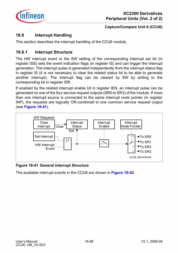
XC2300 DerivativesPeripheral Units (Vol. 2 of 2)
Capture/Compare Unit 6 (CCU6)
18.8 Interrupt HandlingThis section describes the interrupt handling of the CCU6 module.
18.8.1 Interrupt StructureThe HW interrupt event or the SW setting of the corresponding interrupt set bit (inregister ISS) sets the event indication flags (in register IS) and can trigger the interruptgeneration. The interrupt pulse is generated independently from the interrupt status flagin register IS (it is not necessary to clear the related status bit to be able to generateanother interrupt). The interrupt flag can be cleared by SW by writing to thecorresponding bit in register ISR.If enabled by the related interrupt enable bit in register IEN, an interrupt pulse can begenerated on one of the four service request outputs (SR0 to SR3) of the module. If morethan one interrupt source is connected to the same interrupt node pointer (in registerINP), the requests are logically OR-combined to one common service request output(see Figure 18-41).
Figure 18-41 General Interrupt Structure
The available interrupt events in the CCU6 are shown in Figure 18-42.
CCU6_MCA05549
HW InterruptEvent
InterruptStatus
SW Requests
Set
ClearInterrupt
>1_Set Interrupt To SR0
To SR1To SR2To SR3
InterruptEnable
InterruptNode PointerClear
User’s Manual 18-88 V2.1, 2008-08CCU6, UM_V0.5D3

XC2300 DerivativesPeripheral Units (Vol. 2 of 2)
Capture/Compare Unit 6 (CCU6)
Figure 18-42 Interrupt Sources and Events
CCU6_MCA05548
InterruptControl Logic
Node PointerRegister INP
SR0
Interrupt ResetRegister ISR
Interrupt EnableRegister IEN
Interrupt StatusRegister IS
T12 Counter
T12_PM
T12_OM
T12 CaptureCompare
Channels CC6x
CC6x_R
CC6x_F
T13 Counter T13_PM
T13 CompareChannel CC63
CM_63
Trap Handling
TRPF
TRPS
Hall CompareLogic
CM_CHE
CM_WHE
Multi-ChannelMode Logic
STR
CDIR
Interrupt SetRegister ISS
SR1
SR2
SR3 Interrupt RequestReg. CC6x_3IC
Interrupt RequestReg. CC6x_2IC
Interrupt RequestReg. CC6x_1IC
Interrupt RequestReg. CC6x_0IC
User’s Manual 18-89 V2.1, 2008-08CCU6, UM_V0.5D3

XC2300 DerivativesPeripheral Units (Vol. 2 of 2)
Capture/Compare Unit 6 (CCU6)
18.8.2 Interrupt Registers
18.8.2.1 Interrupt Status RegisterRegister IS contains the individual interrupt request bits. This register can only be read,write actions have no impact on the contents of this register. The SW can set or clear thebits individually by writing to the registers ISS (to set the bits) or to register ISR (to clearthe bits).The interrupt generation is independent from the value of the bits in register IS, e.g. theinterrupt will be generated (if enabled) even if the corresponding bit is already set. Thetrigger for an interrupt generation is the detection of a set condition (by HW or SW) forthe corresponding bit in register IS.In compare mode (and hall mode), the timer-related interrupts are only generated whilethe timer is running (T1xR=1). In capture mode, the capture interrupts are also generatedwhile the timer T12 is stopped.Note: Not all bits in register IS can generate an interrupt. Other status bits have been
added, that have a similar structure for their set and clear actions. It isrecommended that SW checks the interrupt bits bit-wisely (instead of common ORover the bits).
IS Interrupt Status Register XSFR(50H) Reset Value: 0000H
15 14 13 12 11 10 9 8 7 6 5 4 3 2 1 0
STR IDLE WHE CHE TRPS
TRPF
T13PM
T13CM
T12PM
T12OM
ICC62F
ICC62R
ICC61F
ICC61R
ICC60F
ICC60R
rh rh rh rh rh rh rh rh rh rh rh rh rh rh rh rh
Field Bits Type DescriptionICC60R,ICC61R,ICC62R
0,2,4
rh Capture, Compare-Match Rising Edge FlagThis bit indicates that event CC6x_R has been detected. This event occurs in compare mode when a compare-match is detected while T12 is counting up (CM_6x and CDIR = 0) and in capture mode when a rising edge is detected at the related input CC6xIN.0B The event has not yet been detected.1B The event has been detected.
User’s Manual 18-90 V2.1, 2008-08CCU6, UM_V0.5D3
XC2300 DerivativesPeripheral Units (Vol. 2 of 2)
Capture/Compare Unit 6 (CCU6)
ICC60F,ICC61F,ICC62F
1,3,5
rh Capture, Compare-Match Falling Edge FlagThis bit indicates that event CC6x_F has been detected. This event occurs in compare mode when a compare-match is detected while T12 is counting down (CM_6x and CDIR = 1) and in capture mode when a falling edge is detected at the related input CC6xIN.0B The event has not yet been detected.1B The event has been detected.
T12OM 6 rh Timer T12 One-Match FlagThis bit indicates that a timer T12 one-match while counting down (T12_OM and CDIR = 1) has been detected.0B The event has not yet been detected.1B The event has been detected.
T12PM 7 rh Timer T12 Period-Match FlagThis bit indicates that a timer T12 period-match while counting up (T12_PM and CDIR = 0) has been detected.0B The event has not yet been detected.1B The event has been detected.
T13CM 8 rh Timer T13 Compare-Match FlagThis bit indicates that a timer T13 compare-match (CM_63) has been detected.0B The event has not yet been detected.1B The event has been detected.
T13PM 9 rh Timer T13 Period-Match FlagThis bit indicates that a timer T13 period-match (T13_PM) has been detected.0B The event has not yet been detected.1B The event has been detected.
TRPF 10 rh Trap FlagThis bit indicates if a trap condition (input CTRAP = 0 or by SW) is / has been detected. If TRM2= 0, it becomes cleared automatically if CTRAP = 1 or TRPPEN = 0, whereas if TRM2 = 1, it has to be cleared by writing RTRPF = 1.0B The trap condition has not been detected.1B The trap condition is / has been detected.
Field Bits Type Description
User’s Manual 18-91 V2.1, 2008-08CCU6, UM_V0.5D3
XC2300 DerivativesPeripheral Units (Vol. 2 of 2)
Capture/Compare Unit 6 (CCU6)
TRPS 11 rh Trap State1)
This bit indicates the actual trap state. It is set if TRPF = 1 and becomes cleared according to the mode selected in register TRPCTR.0B The trap state is not active.1B The trap state is active.
CHE 12 rh Correct Hall EventThis bit indicates that a correct Hall event (CM_CHE) has been detected.0B The event has not yet been detected.1B The event has been detected.
WHE 13 rh Wrong Hall EventThis bit indicates that a wrong Hall event (CM_WHE) has been detected.0B The event has not yet been detected.1B The event has been detected.
IDLE 14 rh IDLE StateIf enabled by ENIDLE = 1, this bit is set together with bit WHE and it has to be cleared by SW.0B No action.1B Bit field MCMP is cleared, the selected outputs
are set to passive state.STR 15 rh Multi-Channel Mode Shadow Transfer Request
This bit indicates that a shadow transfer from MCMPS to MCMP (MCM_ST) has taken place.0B The event has not yet been detected.1B The event has been detected.
1) During the trap state, the selected outputs are set to the passive state. The logic level driven during the passivestate is defined by the corresponding bit in register PSLR. Bits TRPS=1 and TRPF=0 can occur if the trapcondition is no longer active but the selected synchronization has not yet taken place.
Field Bits Type Description
User’s Manual 18-92 V2.1, 2008-08CCU6, UM_V0.5D3

XC2300 DerivativesPeripheral Units (Vol. 2 of 2)
Capture/Compare Unit 6 (CCU6)
18.8.2.2 Interrupt Status Set RegisterRegister ISS contains individual interrupt request set bits to generate a CCU6 interruptrequest by software. Writing a 1 sets the bit(s) in register IS at the corresponding bitposition(s) and can generate an interrupt event (if available and enabled).All bit positions read as 0.
ISS Interrupt Status Set Register XSFR(52H) Reset Value: 0000H
15 14 13 12 11 10 9 8 7 6 5 4 3 2 1 0
SSTR
SIDLE
SWHE
SCHE
SWHC
STRP
F
ST13PM
ST13CM
ST12PM
ST12OM
SCC62F
SCC62R
SCC61F
SCC61R
SCC60F
SCC60R
w
w w w w w w w w w w w w w w w w
Field Bits Type DescriptionSCC60R,SCC61R,SCC62R
0,2,4
w Set Capture, Compare-Match Rising Edge Flag0B No action1B Bit CC6xR will be set.
SCC60F,SCC61F,SCC62F
1,3,5
w Set Capture, Compare-Match Falling Edge Flag0B No action1B Bit CC6xF will be set.
ST12OM 6 w Set Timer T12 One-Match Flag0B No action1B Bit T12OM will be set.
ST12PM 7 w Set Timer T12 Period-Match Flag0B No action1B Bit T12PM will be set.
ST13CM 8 w Set Timer T13 Compare-Match Flag0B No action1B Bit T13CM will be set.
ST13PM 9 w Set Timer T13 Period-Match Flag0B No action1B Bit T13PM will be set.
STRPF 10 w Set Trap Flag0B No action1B Bits TRPF and TRPS will be set.
User’s Manual 18-93 V2.1, 2008-08CCU6, UM_V0.5D3

XC2300 DerivativesPeripheral Units (Vol. 2 of 2)
Capture/Compare Unit 6 (CCU6)
SWHC 11 w Software Hall Compare0B No action1B The Hall compare action is triggered.
SCHE 12 w Set Correct Hall Event Flag0B No action1B Bit CHE will be set.
SWHE 13 w Set Wrong Hall Event Flag0B No action1B Bit WHE will be set.
SIDLE 14 w Set IDLE Flag0B No action1B Bit IDLE will be set.
SSTR 15 w Set STR Flag0B No action1B Bit STR will be set.
Field Bits Type Description
User’s Manual 18-94 V2.1, 2008-08CCU6, UM_V0.5D3

XC2300 DerivativesPeripheral Units (Vol. 2 of 2)
Capture/Compare Unit 6 (CCU6)
18.8.2.3 Status Reset RegisterRegister ISR contains bits to individually clear the interrupt event flags by software.Writing a 1 clears the bit(s) in register IS at the corresponding bit position(s).All bit positions read as 0.
ISR Interrupt Status Reset Register XSFR(54H) Reset Value: 0000H
15 14 13 12 11 10 9 8 7 6 5 4 3 2 1 0
RSTR
RIDLE
RWHE
RCHE 0
RTRP
F
RT13PM
RT13CM
RT12PM
RT12OM
RCC62F
RCC62R
RCC61F
RCC61R
RCC60F
RCC60R
w
w w w w r w w w w w w w w w w w
Field Bits Type DescriptionRCC60R,RCC61R,RCC62R
0,2,4
w Reset Capture, Compare-Match Rising Edge Flag0B No action1B Bit CC6xR will be cleared.
RCC60F,RCC61F,RCC62F
1,3,5
w Reset Capture, Compare-Match Falling Edge Flag0B No action1B Bit CC6xF will be cleared.
RT12OM 6 w Reset Timer T12 One-Match Flag0B No action1B Bit T12OM will be cleared.
RT12PM 7 w Reset Timer T12 Period-Match Flag0B No action1B Bit T12PM IS will be cleared.
RT13CM 8 w Reset Timer T13 Compare-Match Flag0B No action1B Bit T13CM will be cleared.
RT13PM 9 w Reset Timer T13 Period-Match Flag0B No action1B Bit T13PM will be cleared.
RTRPF 10 w Reset Trap Flag0B No action1B Bit TRPF will be cleared (not taken into
account while input CTRAP=0 and TRPPEN=1.
User’s Manual 18-95 V2.1, 2008-08CCU6, UM_V0.5D3

XC2300 DerivativesPeripheral Units (Vol. 2 of 2)
Capture/Compare Unit 6 (CCU6)
RCHE 12 w Reset Correct Hall Event Flag0B No action1B Bit CHE will be cleared.
RWHE 13 w Reset Wrong Hall Event Flag1B No action0B Bit WHE will be cleared.
RIDLE 14 w Reset IDLE Flag0B No action1B Bit IDLE will be cleared.
RSTR 15 w Reset STR Flag0B No action1B Bit STR will be cleared.
0 11 r reserved;returns 0 if read; should be written with 0;
Field Bits Type Description
User’s Manual 18-96 V2.1, 2008-08CCU6, UM_V0.5D3
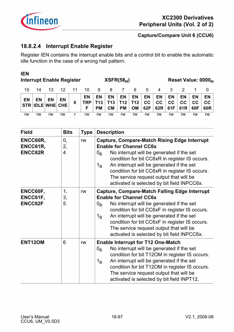
XC2300 DerivativesPeripheral Units (Vol. 2 of 2)
Capture/Compare Unit 6 (CCU6)
18.8.2.4 Interrupt Enable RegisterRegister IEN contains the interrupt enable bits and a control bit to enable the automaticidle function in the case of a wrong hall pattern.
IEN Interrupt Enable Register XSFR(58H) Reset Value: 0000H
15 14 13 12 11 10 9 8 7 6 5 4 3 2 1 0
ENSTR
ENIDLE
ENWHE
ENCHE 0
ENTRP
F
ENT13PM
ENT13CM
ENT12PM
ENT12OM
ENCC62F
ENCC62R
ENCC61F
ENCC61R
ENCC60F
ENCC60R
rw rw rw rw r rw rw rw rw rw rw rw rw rw rw rw
Field Bits Type DescriptionENCC60R,ENCC61R,ENCC62R
0,2,4
rw Capture, Compare-Match Rising Edge Interrupt Enable for Channel CC6x0B No interrupt will be generated if the set
condition for bit CC6xR in register IS occurs.1B An interrupt will be generated if the set
condition for bit CC6xR in register IS occurs. The service request output that will be activated is selected by bit field INPCC6x.
ENCC60F,ENCC61F,ENCC62F
1,3,5
rw Capture, Compare-Match Falling Edge Interrupt Enable for Channel CC6x0B No interrupt will be generated if the set
condition for bit CC6xF in register IS occurs.1B An interrupt will be generated if the set
condition for bit CC6xF in register IS occurs. The service request output that will be activated is selected by bit field INPCC6x.
ENT12OM 6 rw Enable Interrupt for T12 One-Match0B No interrupt will be generated if the set
condition for bit T12OM in register IS occurs.1B An interrupt will be generated if the set
condition for bit T12OM in register IS occurs. The service request output that will be activated is selected by bit field INPT12.
User’s Manual 18-97 V2.1, 2008-08CCU6, UM_V0.5D3

XC2300 DerivativesPeripheral Units (Vol. 2 of 2)
Capture/Compare Unit 6 (CCU6)
ENT12PM 7 rw Enable Interrupt for T12 Period-Match0B No interrupt will be generated if the set
condition for bit T12PM in register IS occurs.1B An interrupt will be generated if the set
condition for bit T12PM in register IS occurs. The service request output that will be activated is selected by bit field INPT12.
ENT13CM 8 rw Enable Interrupt for T13 Compare-Match0B No interrupt will be generated if the set
condition for bit T13CM in register IS occurs.1B An interrupt will be generated if the set
condition for bit T13CM in register IS occurs. The service request output that will be activated is selected by bit field INPT13.
ENT13PM 9 rw Enable Interrupt for T13 Period-Match0B No interrupt will be generated if the set
condition for bit T13PM in register IS occurs.1B An interrupt will be generated if the set
condition for bit T13PM in register IS occurs. The service request output that will be activated is selected by bit field INPT13.
ENTRPF 10 rw Enable Interrupt for Trap Flag0B No interrupt will be generated if the set
condition for bit TRPF in register IS occurs.1B An interrupt will be generated if the set
condition for bit TRPF in register IS occurs. The service request output that will be activated is selected by bit field INPERR.
ENCHE 12 rw Enable Interrupt for Correct Hall Event0B No interrupt will be generated if the set
condition for bit CHE in register IS occurs.1B An interrupt will be generated if the set
condition for bit CHE in register IS occurs.The service request output that will be activated is selected by bit field INPCHE.
Field Bits Type Description
User’s Manual 18-98 V2.1, 2008-08CCU6, UM_V0.5D3
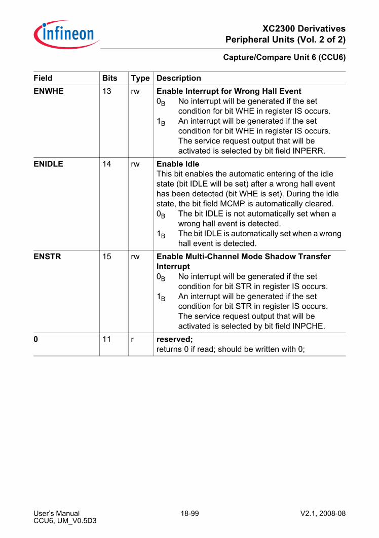
XC2300 DerivativesPeripheral Units (Vol. 2 of 2)
Capture/Compare Unit 6 (CCU6)
ENWHE 13 rw Enable Interrupt for Wrong Hall Event0B No interrupt will be generated if the set
condition for bit WHE in register IS occurs.1B An interrupt will be generated if the set
condition for bit WHE in register IS occurs.The service request output that will be activated is selected by bit field INPERR.
ENIDLE 14 rw Enable IdleThis bit enables the automatic entering of the idle state (bit IDLE will be set) after a wrong hall event has been detected (bit WHE is set). During the idle state, the bit field MCMP is automatically cleared.0B The bit IDLE is not automatically set when a
wrong hall event is detected.1B The bit IDLE is automatically set when a wrong
hall event is detected.ENSTR 15 rw Enable Multi-Channel Mode Shadow Transfer
Interrupt0B No interrupt will be generated if the set
condition for bit STR in register IS occurs.1B An interrupt will be generated if the set
condition for bit STR in register IS occurs.The service request output that will be activated is selected by bit field INPCHE.
0 11 r reserved;returns 0 if read; should be written with 0;
Field Bits Type Description
User’s Manual 18-99 V2.1, 2008-08CCU6, UM_V0.5D3
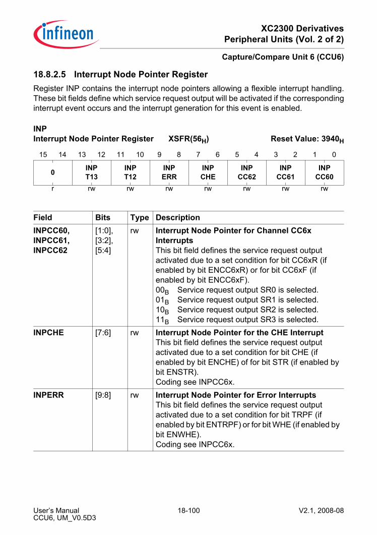
XC2300 DerivativesPeripheral Units (Vol. 2 of 2)
Capture/Compare Unit 6 (CCU6)
18.8.2.5 Interrupt Node Pointer RegisterRegister INP contains the interrupt node pointers allowing a flexible interrupt handling.These bit fields define which service request output will be activated if the correspondinginterrupt event occurs and the interrupt generation for this event is enabled.
INP Interrupt Node Pointer Register XSFR(56H) Reset Value: 3940H
15 14 13 12 11 10 9 8 7 6 5 4 3 2 1 0
0 INPT13
INPT12
INPERR
INPCHE
INPCC62
INPCC61
INPCC60
r rw rw rw rw rw rw rw
Field Bits Type DescriptionINPCC60,INPCC61,INPCC62
[1:0],[3:2],[5:4]
rw Interrupt Node Pointer for Channel CC6x InterruptsThis bit field defines the service request output activated due to a set condition for bit CC6xR (if enabled by bit ENCC6xR) or for bit CC6xF (if enabled by bit ENCC6xF).00B Service request output SR0 is selected.01B Service request output SR1 is selected.10B Service request output SR2 is selected.11B Service request output SR3 is selected.
INPCHE [7:6] rw Interrupt Node Pointer for the CHE InterruptThis bit field defines the service request output activated due to a set condition for bit CHE (if enabled by bit ENCHE) of for bit STR (if enabled by bit ENSTR).Coding see INPCC6x.
INPERR [9:8] rw Interrupt Node Pointer for Error InterruptsThis bit field defines the service request output activated due to a set condition for bit TRPF (if enabled by bit ENTRPF) or for bit WHE (if enabled by bit ENWHE).Coding see INPCC6x.
User’s Manual 18-100 V2.1, 2008-08CCU6, UM_V0.5D3
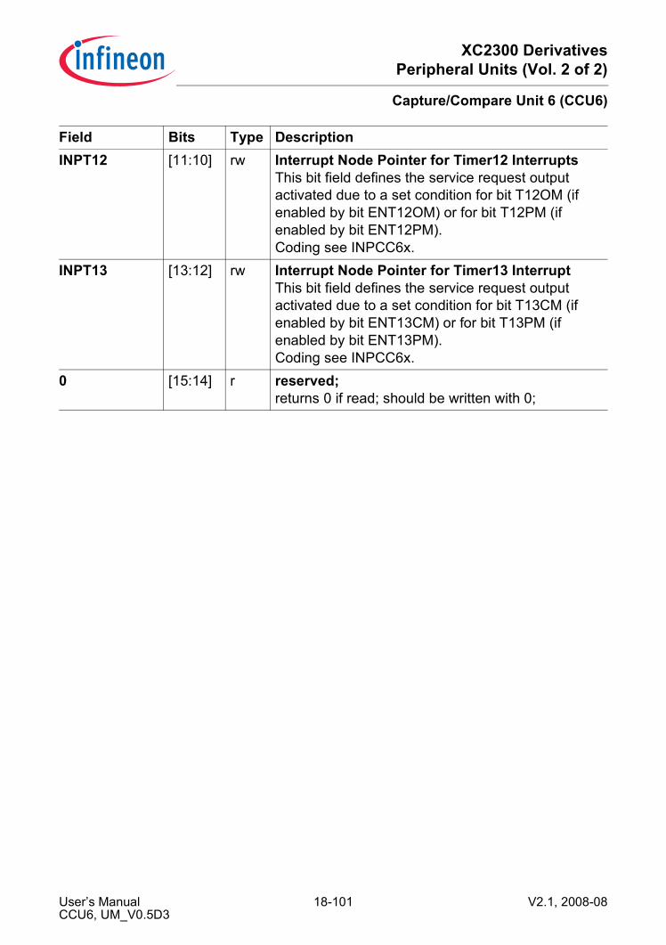
XC2300 DerivativesPeripheral Units (Vol. 2 of 2)
Capture/Compare Unit 6 (CCU6)
INPT12 [11:10] rw Interrupt Node Pointer for Timer12 InterruptsThis bit field defines the service request output activated due to a set condition for bit T12OM (if enabled by bit ENT12OM) or for bit T12PM (if enabled by bit ENT12PM).Coding see INPCC6x.
INPT13 [13:12] rw Interrupt Node Pointer for Timer13 InterruptThis bit field defines the service request output activated due to a set condition for bit T13CM (if enabled by bit ENT13CM) or for bit T13PM (if enabled by bit ENT13PM).Coding see INPCC6x.
0 [15:14] r reserved;returns 0 if read; should be written with 0;
Field Bits Type Description
User’s Manual 18-101 V2.1, 2008-08CCU6, UM_V0.5D3
XC2300 DerivativesPeripheral Units (Vol. 2 of 2)
Capture/Compare Unit 6 (CCU6)
18.9 General Module OperationThis section provides information about the:• Configuration of the behavior of the different device operating modes (see mode
control description in Section 18.9.1)• Input selection (see Section 18.9.2)• General register description (see Section 18.9.3)
18.9.1 Mode ControlThe mode control concept for system control tasks, such as power saving, or suspendrequest for debugging, allows to program the module behavior under different deviceoperating conditions. The behavior of a CCU6 kernel can be programmed for each of thedevice operating modes, that are requested by the global state control part of the SCU.Therefore, a CCU6 module provides a kernel state configuration register KSCFGdefining the behavior in the following device operating modes:• Normal operation:
This operating mode is the default operating mode when neither a suspend requestnor a clock-off request are pending. The module clock is not switched off and theCCU6 registers can be read or written. The kernel behavior is defined byKSCFG.NOMCFG.
• Suspend mode:This operating mode is requested when a suspend request (issued by a debugger)is pending in the device. The module clock is not switched off and the CCU6 registerscan be read or written. The kernel behavior is defined by KSCFG.SUMCFG.
• Clock-off mode:This operating mode is requested for power saving purposes. The module clock isswitched off automatically when all kernels of the CCU6 module reached theirspecified state in a stop mode. In this case, CCU6 registers can not be accessed. Thekernel behavior is defined by KSCFG.COMCFG.
The kernel distinguishes four different blocks (T12, T13, Hall logic, and trap logic). Theseblocks can be individually enabled for the request of stop mode 0 and stop mode 1 bythe sensitivity bits KSCSR.SBx. If the request sensitivity is disabled, the block continuesnormal operation. If the request sensitivity is enabled, the block operates as specified forthe selected stop mode.The complete CCU6 acknowledge is given to the GSC when all four blocks havereached their defined end condition.
User’s Manual 18-102 V2.1, 2008-08CCU6, UM_V0.5D3

XC2300 DerivativesPeripheral Units (Vol. 2 of 2)
Capture/Compare Unit 6 (CCU6)
The behavior of the CCU6 kernel can be programmed for each of the device operatingmodes (normal operation, suspend mode, clock-off mode). Therefore, it supports fourkernel modes, as shown in Table 18-13.
Table 18-12 CCU6 Functional BlocksBlock Function Sensitivity Bit0 Timer T12:
A functional enable is delivered until the specified stop condition is reached. Then, T12 stops counting and the CC6xIN input stages are frozen.
KSCSR.SB0
1 Timer T13:A functional enable is delivered until the specified stop condition is reached. Then, T13 stops counting.
KSCSR.SB1
2 Hall Logic:The hall logic is stopped immediately and the CCPOSx input stages are frozen.
KSCSR.SB2
3 Trap Logic:The trap logic is stopped immediately and the CTRAP input stage is frozen.
KSCSR.SB3
Table 18-13 CCU6 Kernel BehaviorKernel Mode Kernel Behavior Coderun mode 0 kernel operation as specified, no impact on CCU6 operation
(same behavior for run mode 0 and run mode 1)00B
run mode 1 01B
User’s Manual 18-103 V2.1, 2008-08CCU6, UM_V0.5D3
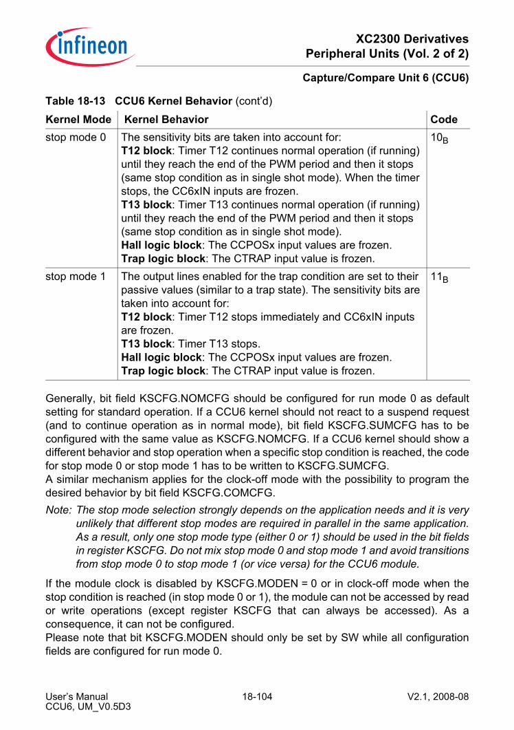
XC2300 DerivativesPeripheral Units (Vol. 2 of 2)
Capture/Compare Unit 6 (CCU6)
Generally, bit field KSCFG.NOMCFG should be configured for run mode 0 as defaultsetting for standard operation. If a CCU6 kernel should not react to a suspend request(and to continue operation as in normal mode), bit field KSCFG.SUMCFG has to beconfigured with the same value as KSCFG.NOMCFG. If a CCU6 kernel should show adifferent behavior and stop operation when a specific stop condition is reached, the codefor stop mode 0 or stop mode 1 has to be written to KSCFG.SUMCFG.A similar mechanism applies for the clock-off mode with the possibility to program thedesired behavior by bit field KSCFG.COMCFG.Note: The stop mode selection strongly depends on the application needs and it is very
unlikely that different stop modes are required in parallel in the same application.As a result, only one stop mode type (either 0 or 1) should be used in the bit fieldsin register KSCFG. Do not mix stop mode 0 and stop mode 1 and avoid transitionsfrom stop mode 0 to stop mode 1 (or vice versa) for the CCU6 module.
If the module clock is disabled by KSCFG.MODEN = 0 or in clock-off mode when thestop condition is reached (in stop mode 0 or 1), the module can not be accessed by reador write operations (except register KSCFG that can always be accessed). As aconsequence, it can not be configured.Please note that bit KSCFG.MODEN should only be set by SW while all configurationfields are configured for run mode 0.
stop mode 0 The sensitivity bits are taken into account for:T12 block: Timer T12 continues normal operation (if running) until they reach the end of the PWM period and then it stops (same stop condition as in single shot mode). When the timer stops, the CC6xIN inputs are frozen.T13 block: Timer T13 continues normal operation (if running) until they reach the end of the PWM period and then it stops (same stop condition as in single shot mode).Hall logic block: The CCPOSx input values are frozen.Trap logic block: The CTRAP input value is frozen.
10B
stop mode 1 The output lines enabled for the trap condition are set to their passive values (similar to a trap state). The sensitivity bits are taken into account for:T12 block: Timer T12 stops immediately and CC6xIN inputs are frozen.T13 block: Timer T13 stops.Hall logic block: The CCPOSx input values are frozen.Trap logic block: The CTRAP input value is frozen.
11B
Table 18-13 CCU6 Kernel Behavior (cont’d)
Kernel Mode Kernel Behavior Code
User’s Manual 18-104 V2.1, 2008-08CCU6, UM_V0.5D3

XC2300 DerivativesPeripheral Units (Vol. 2 of 2)
Capture/Compare Unit 6 (CCU6)
18.9.2 Input SelectionEach CCU6 input signal can be selected from a vector of four possible inputs byprogramming the port input select registers PISELL and PISELH. This permits to adaptthe pin functionality of the device to the application requirements.The output pins for the module output signals are chosen in the ports.Naming convention:The input vector CC60IN[D:A] for input signal CC60IN is composed of the signalsCC60INA to CC60IND.Note: All functional inputs of the CCU6 are synchronized to fCC6 before they affect the
module internal logic. The resulting delay of 2/fCC6 and for asynchronous signalsan additional uncertainty of 1/fCC6 have to be taken into account for precise timingcalculation. An edge of an input signal can only be correctly detected if the highphase and the low phase of the input signal are both longer than 1/fCC6.
User’s Manual 18-105 V2.1, 2008-08CCU6, UM_V0.5D3
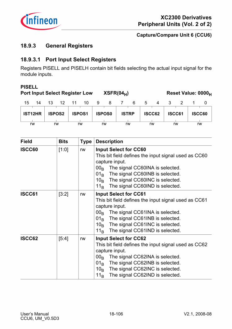
XC2300 DerivativesPeripheral Units (Vol. 2 of 2)
Capture/Compare Unit 6 (CCU6)
18.9.3 General Registers
18.9.3.1 Port Input Select RegistersRegisters PISELL and PISELH contain bit fields selecting the actual input signal for themodule inputs.
PISELL Port Input Select Register Low XSFR(04H) Reset Value: 0000H
15 14 13 12 11 10 9 8 7 6 5 4 3 2 1 0
IST12HR ISPOS2 ISPOS1 ISPOS0 ISTRP ISCC62 ISCC61 ISCC60
rw rw rw rw rw rw rw rw
Field Bits Type DescriptionISCC60 [1:0] rw Input Select for CC60
This bit field defines the input signal used as CC60 capture input.00B The signal CC60INA is selected.01B The signal CC60INB is selected.10B The signal CC60INC is selected.11B The signal CC60IND is selected.
ISCC61 [3:2] rw Input Select for CC61 This bit field defines the input signal used as CC61 capture input.00B The signal CC61INA is selected.01B The signal CC61INB is selected.10B The signal CC61INC is selected.11B The signal CC61IND is selected.
ISCC62 [5:4] rw Input Select for CC62 This bit field defines the input signal used as CC62 capture input.00B The signal CC62INA is selected.01B The signal CC62INB is selected.10B The signal CC62INC is selected.11B The signal CC62IND is selected.
User’s Manual 18-106 V2.1, 2008-08CCU6, UM_V0.5D3
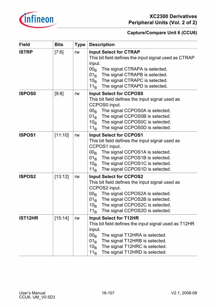
XC2300 DerivativesPeripheral Units (Vol. 2 of 2)
Capture/Compare Unit 6 (CCU6)
ISTRP [7:6] rw Input Select for CTRAP This bit field defines the input signal used as CTRAP input.00B The signal CTRAPA is selected.01B The signal CTRAPB is selected.10B The signal CTRAPC is selected.11B The signal CTRAPD is selected.
ISPOS0 [9:8] rw Input Select for CCPOS0 This bit field defines the input signal used as CCPOS0 input.00B The signal CCPOS0A is selected.01B The signal CCPOS0B is selected.10B The signal CCPOS0C is selected.11B The signal CCPOS0D is selected.
ISPOS1 [11:10] rw Input Select for CCPOS1 This bit field defines the input signal used as CCPOS1 input.00B The signal CCPOS1A is selected.01B The signal CCPOS1B is selected.10B The signal CCPOS1C is selected.11B The signal CCPOS1D is selected.
ISPOS2 [13:12] rw Input Select for CCPOS2 This bit field defines the input signal used as CCPOS2 input.00B The signal CCPOS2A is selected.01B The signal CCPOS2B is selected.10B The signal CCPOS2C is selected.11B The signal CCPOS2D is selected.
IST12HR [15:14] rw Input Select for T12HRThis bit field defines the input signal used as T12HR input.00B The signal T12HRA is selected.01B The signal T12HRB is selected.10B The signal T12HRC is selected.11B The signal T12HRD is selected.
Field Bits Type Description
User’s Manual 18-107 V2.1, 2008-08CCU6, UM_V0.5D3

XC2300 DerivativesPeripheral Units (Vol. 2 of 2)
Capture/Compare Unit 6 (CCU6)
PISELH Port Input Select Register High XSFR(06H) Reset Value: 0000H
15 14 13 12 11 10 9 8 7 6 5 4 3 2 1 0
0 ISCNT13 ISCNT12 IST13HR
r rw rw rw
Field Bits Type DescriptionIST13HR [1:0] rw Input Select for T13HR
This bit field defines the input signal used as T13HR input.00B The signal T13HRA is selected.01B The signal T13HRB is selected.10B The signal T13HRC is selected.11B The signal T13HRD is selected.
ISCNT12 [3:2] rw Input Select for T12 Counting InputThis bit field defines the input event leading to a counting action of T12.00B The T12 prescaler generates the counting
events. Bit TCTR4.T12CNT is not taken into account.
01B Bit TCTR4.T12CNT written with 1 is a counting event. The T12 prescaler is not taken into account.
10B The timer T12 is counting each rising edge detected in the selected T12HR signal.
11B The timer T12 is counting each falling edge detected in the selected T12HR signal.
User’s Manual 18-108 V2.1, 2008-08CCU6, UM_V0.5D3
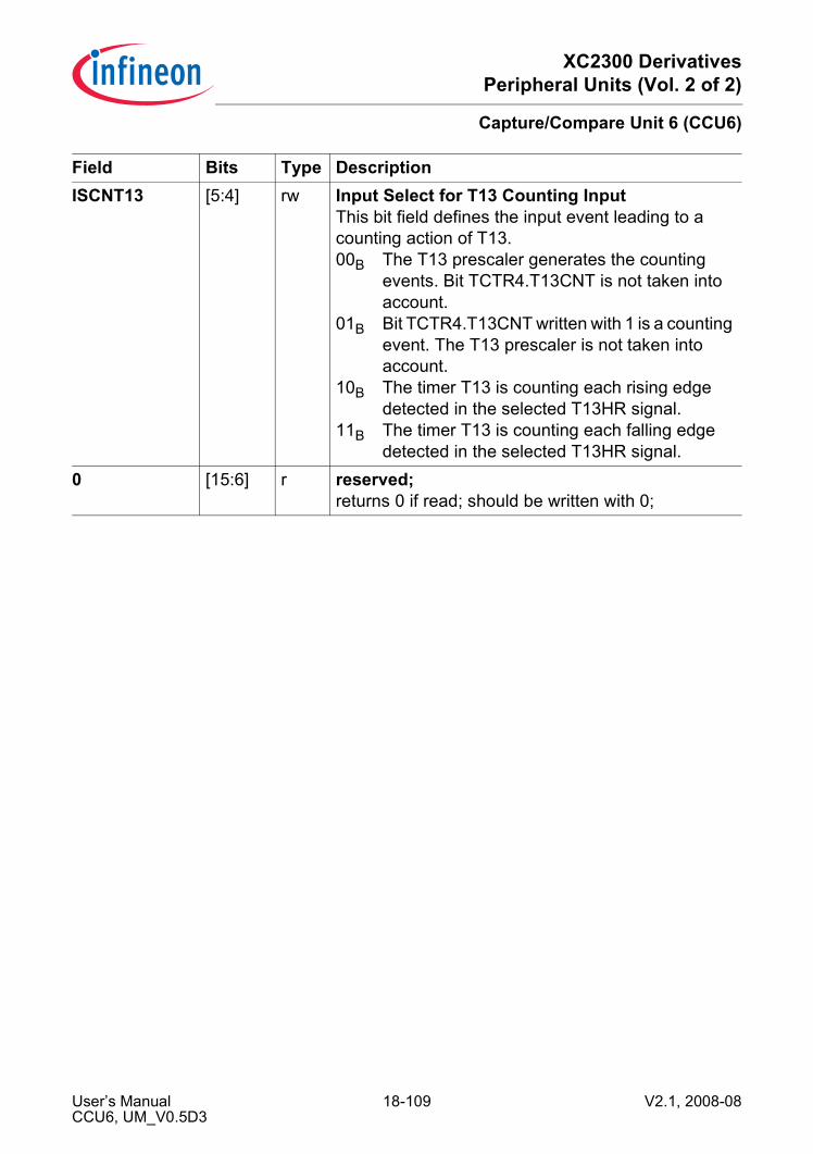
XC2300 DerivativesPeripheral Units (Vol. 2 of 2)
Capture/Compare Unit 6 (CCU6)
ISCNT13 [5:4] rw Input Select for T13 Counting InputThis bit field defines the input event leading to a counting action of T13.00B The T13 prescaler generates the counting
events. Bit TCTR4.T13CNT is not taken into account.
01B Bit TCTR4.T13CNT written with 1 is a counting event. The T13 prescaler is not taken into account.
10B The timer T13 is counting each rising edge detected in the selected T13HR signal.
11B The timer T13 is counting each falling edge detected in the selected T13HR signal.
0 [15:6] r reserved;returns 0 if read; should be written with 0;
Field Bits Type Description
User’s Manual 18-109 V2.1, 2008-08CCU6, UM_V0.5D3

XC2300 DerivativesPeripheral Units (Vol. 2 of 2)
Capture/Compare Unit 6 (CCU6)
18.9.3.2 Kernel State Configuration RegisterThe kernel state configuration register KSCFG allows the selection of the desired kernelmodes for the different device operating modes.Bit fields KSCFG.NOMCFG and KSCFG.COMCFG are reset by an application reset. Bitfield KSCFG.SUMCFG is reset by a debug reset.Note: The coding of the bit fields NOMCFG, SUMCFG and COMCFG is described in
Table 18-13.
KSCFG Kernel State Configuration Register
XSFR(00H) Reset Value: 0000H
15 14 13 12 11 10 9 8 7 6 5 4 3 2 1 0
BPCOM 0 COMCFG BP
SUM 0 SUMCFG BPNOM 0 NOMCFG 0
BPMODEN
MODEN
w r rw w r rw w r rw r w rw
Field Bits Type DescriptionMODEN 0 rw Module Enable
This bit enables the module kernel clock and the module functionality.0B The module is switched off immediately
(without respecting a stop condition).It does not react on mode control actions and the module clock is switched off. The module does not react on read accesses and ignores write accesses (except to KSCFG).
1B The module is switched on and can operate. After writing 1 to MODEN, it is recommended to read register KSCFG to avoid pipeline effects in the control block before accessing other CCU6 registers.
BPMODEN 1 w Bit Protection for MODENThis bit enables the write access to the bit MODEN. It always reads 0.0B MODEN is not changed.1B MODEN is updated with the written value.
User’s Manual 18-110 V2.1, 2008-08CCU6, UM_V0.5D3
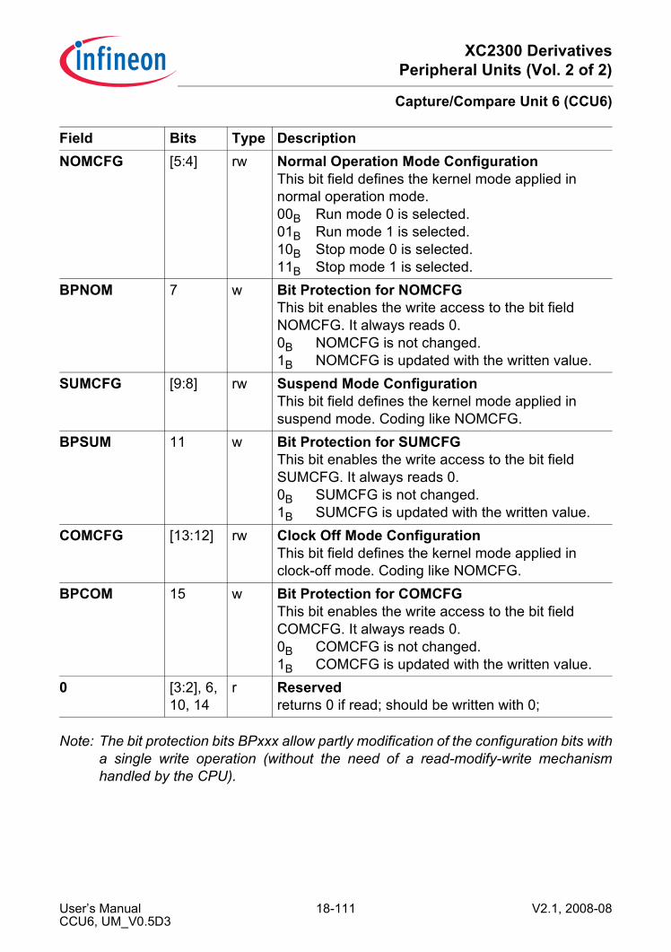
XC2300 DerivativesPeripheral Units (Vol. 2 of 2)
Capture/Compare Unit 6 (CCU6)
Note: The bit protection bits BPxxx allow partly modification of the configuration bits witha single write operation (without the need of a read-modify-write mechanismhandled by the CPU).
NOMCFG [5:4] rw Normal Operation Mode ConfigurationThis bit field defines the kernel mode applied in normal operation mode.00B Run mode 0 is selected.01B Run mode 1 is selected.10B Stop mode 0 is selected.11B Stop mode 1 is selected.
BPNOM 7 w Bit Protection for NOMCFGThis bit enables the write access to the bit field NOMCFG. It always reads 0.0B NOMCFG is not changed.1B NOMCFG is updated with the written value.
SUMCFG [9:8] rw Suspend Mode ConfigurationThis bit field defines the kernel mode applied in suspend mode. Coding like NOMCFG.
BPSUM 11 w Bit Protection for SUMCFGThis bit enables the write access to the bit field SUMCFG. It always reads 0.0B SUMCFG is not changed.1B SUMCFG is updated with the written value.
COMCFG [13:12] rw Clock Off Mode ConfigurationThis bit field defines the kernel mode applied in clock-off mode. Coding like NOMCFG.
BPCOM 15 w Bit Protection for COMCFGThis bit enables the write access to the bit field COMCFG. It always reads 0.0B COMCFG is not changed.1B COMCFG is updated with the written value.
0 [3:2], 6, 10, 14
r Reservedreturns 0 if read; should be written with 0;
Field Bits Type Description
User’s Manual 18-111 V2.1, 2008-08CCU6, UM_V0.5D3

XC2300 DerivativesPeripheral Units (Vol. 2 of 2)
Capture/Compare Unit 6 (CCU6)
18.9.3.3 Kernel State Sensitivity Control RegisterThe kernel state control sensitivity register bits define which internal block is effected bystop modes 0 and 1.
KSCSR Kernel State Control Sensitivity Register
XSFR(0EH) Reset Value: 0000H
15 14 13 12 11 10 9 8 7 6 5 4 3 2 1 0
0 SB3 SB2 SB1 SB0
r rw rw rw rw
Field Bits Type DescriptionSB0,SB1,SB2,SB3
0,1,2,3
rw Sensitivity Block xThis bit defines if block x of the CCU6 kernel is sensitive to stop mode 0 or stop mode 1. The functional definition of the blocks is given in Table 18-12.0B Block x is not sensitive to stop mode 0 or stop
mode 1 and behaves like in run mode 0. It continues normal operation without respecting the defined stop condition.
1B Block x is sensitive to stop mode 0 or stop mode 1. It is respecting the defined stop condition.
0 [15:4] r reserved;returns 0 if read; should be written with 0;
User’s Manual 18-112 V2.1, 2008-08CCU6, UM_V0.5D3

XC2300 DerivativesPeripheral Units (Vol. 2 of 2)
Capture/Compare Unit 6 (CCU6)
18.10 ImplementationThis section describes the implementation of the CCU6 modules in the XC2300 device.• Address map (see Section 18.10.1)• Interrupt control registers (see Section 18.10.2)• Synchronous start (see Section 18.10.3)• Connections of CCU60 (see Section 18.10.4.1)• Connections of CCU61 (see Section 18.10.4.2)• Connections of CCU62 (see Section 18.10.4.3)• Connections of CCU63 (see Section 18.10.4.4)
18.10.1 Address MapThe four CCU6x modules (named CCU60 to CCU63) can be accessed in the followingaddress ranges.The exact register address is given by the relative address of the register (given inTable 18-1) plus the kernel base address (given in Table 18-14) of the module.
Table 18-14 Registers Address SpaceModule Base Address End Address NoteCCU60 EA00H EA7EH
CCU61 EA80H EAFEH
CCU62 EB00H EB7EH
CCU63 EB80H EBFEH
User’s Manual 18-113 V2.1, 2008-08CCU6, UM_V0.5D3
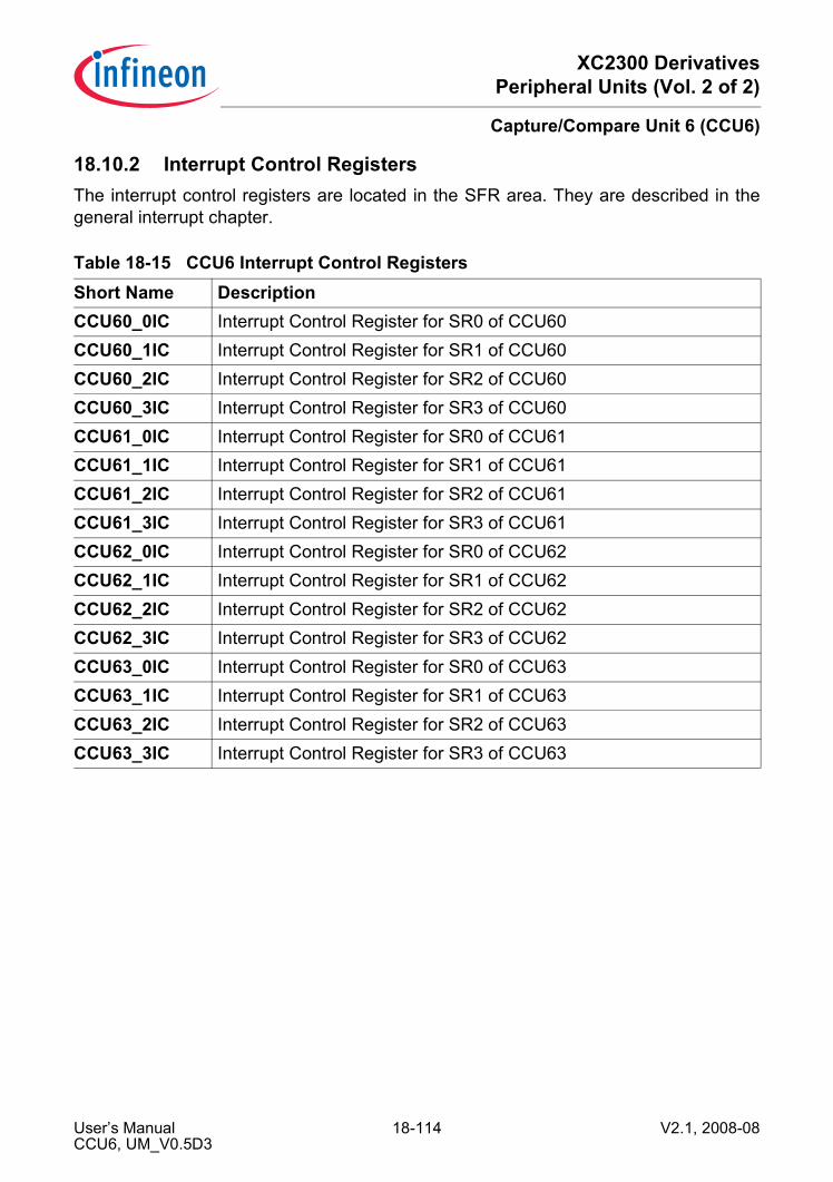
XC2300 DerivativesPeripheral Units (Vol. 2 of 2)
Capture/Compare Unit 6 (CCU6)
18.10.2 Interrupt Control RegistersThe interrupt control registers are located in the SFR area. They are described in thegeneral interrupt chapter.
Table 18-15 CCU6 Interrupt Control RegistersShort Name DescriptionCCU60_0IC Interrupt Control Register for SR0 of CCU60CCU60_1IC Interrupt Control Register for SR1 of CCU60CCU60_2IC Interrupt Control Register for SR2 of CCU60CCU60_3IC Interrupt Control Register for SR3 of CCU60CCU61_0IC Interrupt Control Register for SR0 of CCU61CCU61_1IC Interrupt Control Register for SR1 of CCU61CCU61_2IC Interrupt Control Register for SR2 of CCU61CCU61_3IC Interrupt Control Register for SR3 of CCU61CCU62_0IC Interrupt Control Register for SR0 of CCU62CCU62_1IC Interrupt Control Register for SR1 of CCU62CCU62_2IC Interrupt Control Register for SR2 of CCU62CCU62_3IC Interrupt Control Register for SR3 of CCU62CCU63_0IC Interrupt Control Register for SR0 of CCU63CCU63_1IC Interrupt Control Register for SR1 of CCU63CCU63_2IC Interrupt Control Register for SR2 of CCU63CCU63_3IC Interrupt Control Register for SR3 of CCU63
User’s Manual 18-114 V2.1, 2008-08CCU6, UM_V0.5D3

XC2300 DerivativesPeripheral Units (Vol. 2 of 2)
Capture/Compare Unit 6 (CCU6)
18.10.3 Synchronous Start FeatureSynchronous start is supported by bit SYSCON.GLCCST (global capture/compare start)in the SCU module that is connected to the T12HR and T13HR inputs of all CCU6xmodules.The same signal can also be connected to other capture/compare units in order to allowa synchronous start of the capture/compare timers.
Figure 18-43 Synchronization Concept
edgeselection
byT12RSEL
SYSCON.GLCCSTSCU
T12R
set
edgeselection
byT13RSEL
T13R
set
CCU60
T13HRT12HR
edgeselection
byT12RSEL
T12R
set
edgeselection
byT13RSEL
T13R
set
CCU61
T13HRT12HR
CCU6_sync_start
User’s Manual 18-115 V2.1, 2008-08CCU6, UM_V0.5D3

XC2300 DerivativesPeripheral Units (Vol. 2 of 2)
Capture/Compare Unit 6 (CCU6)
18.10.4 Digital ConnectionsThe following tables show the digital connections of the CCU6x modules with othermodules or pins in the XC2300 device.Each input signal can be selected among 4 possible input lines, e.g. the input vector forinput signal CC60IN is composed of CC60IN[D:A].The following sections refer to the interface signals, whereas the connections of theservice request outputs SR[3:0] to the interrupt control registers of each CCU6x to theinterrupt control registers is given in Section 18.10.2.The CCU6x modules are clocked with the XC2300 system clock, so fCC6 = fSYS.Note: All functional inputs of the CCU6 are synchronized to fCC6 before they can affect
the module internal logic. The resulting delay of 2/fCC6 and an uncertainty of 1/fCC6have to be taken into account for precise timing calculation.An edge of an input signal can only be correctly detected if both, the high phaseand the low phase of the input signal are each longer than 1/fCC6.
18.10.4.1 Connections of CCU60This table describes the module interconnections of CCU60.
Table 18-16 CCU60 Digital Connections in XC2300
Signal from/toModule
I/O to CCU60
Can be used to/as
CC60INA P10.0 I input signals for capture event on channel CC60CC60INB P8.0 I
CC60INC 0 ICC60IND RTC interrupt ICC61INA P10.1 I input signals for capture event on
channel CC61CC61INB P8.1 ICC61INC 0 ICC61IND 0 ICC62INA P10.2 I input signals for capture event on
channel CC62CC62INB P8.2 ICC62INC 0 ICC62IND 0 I
User’s Manual 18-116 V2.1, 2008-08CCU6, UM_V0.5D3

XC2300 DerivativesPeripheral Units (Vol. 2 of 2)
Capture/Compare Unit 6 (CCU6)
CTRAPA P10.6 I input signals for CTRAP,the ESRx input refers to the synchronized input signal, that can be filtered (if enabled)
CTRAPB P8.6 ICTRAPC ESR2 ICTRAPD 1 ICCPOS0A P10.7 I input signals for CCPOS0CCPOS0B P9.7 ICCPOS0C 0 ICCPOS0D 0 ICCPOS1A P10.8 I input signals for CCPOS1CCPOS1B P9.6 ICCPOS1C 0 ICCPOS1D 0 ICCPOS2A P10.9 I input signals for CCPOS2CCPOS2B P9.5 ICCPOS2C 0 ICCPOS2D 0 IT12HRA CCU63_MCM_ST I input signals for T12HRT12HRB P5.5 IT12HRC P5.8 IT12HRD SYSCON.GLCCST IT13HRA EXTCLK (SCU) I input signals for T13HRT13HRB CCU60_T12_ZM IT13HRC P5.8 IT13HRD SYSCON.GLCCST ICC60 P10.0
P8.0O compare outputs of channel CC60
COUT60 P10.3P8.3
O
Table 18-16 CCU60 Digital Connections in XC2300 (cont’d)
Signal from/toModule
I/O to CCU60
Can be used to/as
User’s Manual 18-117 V2.1, 2008-08CCU6, UM_V0.5D3
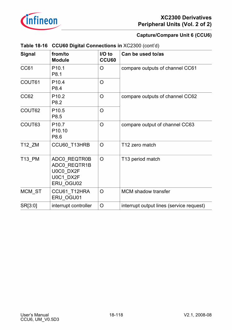
XC2300 DerivativesPeripheral Units (Vol. 2 of 2)
Capture/Compare Unit 6 (CCU6)
CC61 P10.1P8.1
O compare outputs of channel CC61
COUT61 P10.4P8.4
O
CC62 P10.2P8.2
O compare outputs of channel CC62
COUT62 P10.5P8.5
O
COUT63 P10.7P10.10P8.6
O compare output of channel CC63
T12_ZM
CCU60_T13HRB O T12 zero match
T13_PM
ADC0_REQTR0BADC0_REQTR1BU0C0_DX2FU0C1_DX2FERU_OGU02
O T13 period match
MCM_ST
CCU61_T12HRAERU_OGU01
O MCM shadow transfer
SR[3:0] interrupt controller O interrupt output lines (service request)
Table 18-16 CCU60 Digital Connections in XC2300 (cont’d)
Signal from/toModule
I/O to CCU60
Can be used to/as
User’s Manual 18-118 V2.1, 2008-08CCU6, UM_V0.5D3
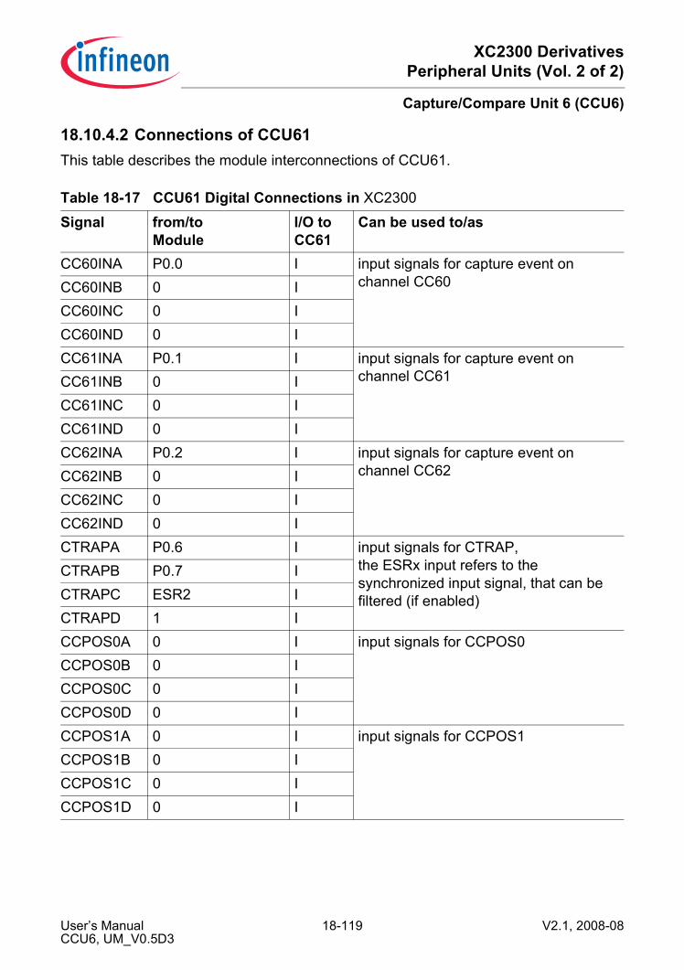
XC2300 DerivativesPeripheral Units (Vol. 2 of 2)
Capture/Compare Unit 6 (CCU6)
18.10.4.2 Connections of CCU61This table describes the module interconnections of CCU61.
Table 18-17 CCU61 Digital Connections in XC2300
Signal from/toModule
I/O to CC61
Can be used to/as
CC60INA P0.0 I input signals for capture event on channel CC60CC60INB 0 I
CC60INC 0 ICC60IND 0 ICC61INA P0.1 I input signals for capture event on
channel CC61CC61INB 0 ICC61INC 0 ICC61IND 0 ICC62INA P0.2 I input signals for capture event on
channel CC62CC62INB 0 ICC62INC 0 ICC62IND 0 ICTRAPA P0.6 I input signals for CTRAP,
the ESRx input refers to the synchronized input signal, that can be filtered (if enabled)
CTRAPB P0.7 ICTRAPC ESR2 ICTRAPD 1 ICCPOS0A 0 I input signals for CCPOS0CCPOS0B 0 ICCPOS0C 0 ICCPOS0D 0 ICCPOS1A 0 I input signals for CCPOS1CCPOS1B 0 ICCPOS1C 0 ICCPOS1D 0 I
User’s Manual 18-119 V2.1, 2008-08CCU6, UM_V0.5D3

XC2300 DerivativesPeripheral Units (Vol. 2 of 2)
Capture/Compare Unit 6 (CCU6)
CCPOS2A 0 I input signals for CCPOS2CCPOS2B 0 ICCPOS2C 0 ICCPOS2D 0 IT12HRA CCU60_MCM_ST I input signals for T12HRT12HRB P1.2 IT12HRC P5.8 IT12HRD SYSCON.GLCCST IT13HRA 0 I input signals for T13HRT13HRB CCU61_T12_ZM IT13HRC P5.8 IT13HRD SYSCON.GLCCST ICC60 P0.0 O compare outputs of channel CC60COUT60 P0.3 OCC61 P0.1 O compare outputs of channel CC61COUT61 P0.4 OCC62 P0.2 O compare outputs of channel CC62COUT62 P0.5 OCOUT63 P0.6 O compare output of channel CC63T12_ZM
CCU61_T13HRB O T12 zero match
T13_PM
ADC1_REQTR0BADC1_REQTR1BU1C0_DX2FU1C1_DX2FERU_OGU12
O T13 period match
MCM_ST
CCU62_T12HRAERU_OGU11
O MCM shadow transfer
Table 18-17 CCU61 Digital Connections in XC2300 (cont’d)
Signal from/toModule
I/O to CC61
Can be used to/as
User’s Manual 18-120 V2.1, 2008-08CCU6, UM_V0.5D3

XC2300 DerivativesPeripheral Units (Vol. 2 of 2)
Capture/Compare Unit 6 (CCU6)
18.10.4.3 Connections of CCU62This table describes the module interconnections of CCU62.
Table 18-18 CCU62 Digital Connections in XC2300
Signal from/toModule
I/O to CCU62
Can be used to/as
CC60INA P1.7 I input signals for capture event on channel CC60CC60INB 0 I
CC60INC 0 ICC60IND 0 ICC61INA P1.6 I input signals for capture event on
channel CC61CC61INB 0 ICC61INC 0 ICC61IND 0 ICC62INA P1.2 I input signals for capture event on
channel CC62CC62INB 0 ICC62INC 0 ICC62IND 0 ICTRAPA P7.1 I input signals for CTRAP,
the ESRx input refers to the synchronized input signal, which can be filtered (if enabled)
CTRAPB P1.0 ICTRAPC ESR2 ICTRAPD 1 ICCPOS0A P7.2 I input signals for CCPOS0CCPOS0B 0 ICCPOS0C 0 ICCPOS0D 0 ICCPOS1A P7.3 I input signals for CCPOS1CCPOS1B 0 ICCPOS1C 0 ICCPOS1D 0 I
User’s Manual 18-121 V2.1, 2008-08CCU6, UM_V0.5D3

XC2300 DerivativesPeripheral Units (Vol. 2 of 2)
Capture/Compare Unit 6 (CCU6)
CCPOS2A P7.4 I input signals for CCPOS2CCPOS2B 0 ICCPOS2C 0 ICCPOS2D 0 IT12HRA CCU61_MCM_ST I input signals for T12HRT12HRB P1.3 IT12HRC P5.8 IT12HRD SYSCON.GLCCST IT13HRA CAN_INT_O15 I input signals for T13HRT13HRB CCU62_T12_ZM IT13HRC P5.8 IT13HRD SYSCON.GLCCST ICC60 P1.7 O compare outputs of channel CC60COUT60 P1.5 OCC61 P1.6 O compare outputs of channel CC61COUT61 P1.4 OCC62 P1.2 O compare outputs of channel CC62COUT62 P1.1 OCOUT63 P1.3 O compare output of channel CC63T12_ZM
CCU62_T13HRB O T12 zero match
T13_PM
ADC0_REQTR2BU2C0_DX2FU2C1_DX2FERU_OGU22
O T13 period match
MCM_ST
CCU63_T12HRAERU_OGU21
O MCM shadow transfer
Table 18-18 CCU62 Digital Connections in XC2300 (cont’d)
Signal from/toModule
I/O to CCU62
Can be used to/as
User’s Manual 18-122 V2.1, 2008-08CCU6, UM_V0.5D3

XC2300 DerivativesPeripheral Units (Vol. 2 of 2)
Capture/Compare Unit 6 (CCU6)
18.10.4.4 Connections of CCU63This table describes the module interconnections of CCU63.
Table 18-19 CCU63 Digital Connections in XC2300
Signal from/toModule
I/O to CCU63
Can be used to/as
CC60INA P9.0 I input signals for capture event on channel CC60CC60INB P2.0 I
CC60INC 0 ICC60IND 0 ICC61INA P9.1 I input signals for capture event on
channel CC61CC61INB P2.1 ICC61INC 0 ICC61IND 0 ICC62INA P9.2 I input signals for capture event on
channel CC62CC62INB P2.2 ICC62INC 0 ICC62IND 0 ICTRAPA P9.6 I input signals for CTRAP,
the ESRx input refers to the synchronized input signal, which can be filtered (if enabled)
CTRAPB P9.7 ICTRAPC ESR2 ICTRAPD 1 ICCPOS0A P11.0 I input signals for CCPOS0CCPOS0B 0 ICCPOS0C 0 ICCPOS0D 0 ICCPOS1A P11.1 I input signals for CCPOS1CCPOS1B 0 ICCPOS1C 0 ICCPOS1D 0 I
User’s Manual 18-123 V2.1, 2008-08CCU6, UM_V0.5D3
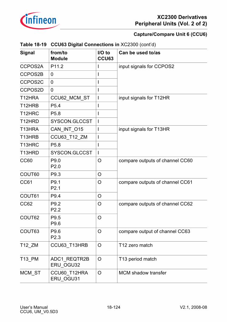
XC2300 DerivativesPeripheral Units (Vol. 2 of 2)
Capture/Compare Unit 6 (CCU6)
CCPOS2A P11.2 I input signals for CCPOS2CCPOS2B 0 ICCPOS2C 0 ICCPOS2D 0 IT12HRA CCU62_MCM_ST I input signals for T12HRT12HRB P5.4 IT12HRC P5.8 IT12HRD SYSCON.GLCCST IT13HRA CAN_INT_O15 I input signals for T13HRT13HRB CCU63_T12_ZM IT13HRC P5.8 IT13HRD SYSCON.GLCCST ICC60 P9.0
P2.0O compare outputs of channel CC60
COUT60 P9.3 OCC61 P9.1
P2.1O compare outputs of channel CC61
COUT61 P9.4 OCC62 P9.2
P2.2O compare outputs of channel CC62
COUT62 P9.5P9.6
O
COUT63 P9.6P2.3
O compare output of channel CC63
T12_ZM
CCU63_T13HRB O T12 zero match
T13_PM
ADC1_REQTR2BERU_OGU32
O T13 period match
MCM_ST
CCU60_T12HRAERU_OGU31
O MCM shadow transfer
Table 18-19 CCU63 Digital Connections in XC2300 (cont’d)
Signal from/toModule
I/O to CCU63
Can be used to/as
User’s Manual 18-124 V2.1, 2008-08CCU6, UM_V0.5D3

XC2300 DerivativesPeripheral Units (Vol. 2 of 2)
Universal Serial Interface Channel
19 Universal Serial Interface ChannelThe Universal Serial Interface Channel module (USIC) is a flexible interface modulecovering several serial communication protocols. A USIC module contains twoindependent communication channels named UxC0 and UxC1, with x being the numberof the USIC module (e.g. channel y of USIC module x is referenced as UxCy). The usercan program during run-time which protocol will be handled by each communicationchannel and which pins are used.This chapter is structured as follows:• Introduction (see Page 19-1)• Operating the USIC (see Page 19-13)• ASC protocol for UART and LIN (see Page 19-111)• SSC protocol (see Page 19-131)• IIC protocol (see Page 19-160)• IIS protocol (see Page 19-184)• Module implementation in XC2300 (see Page 19-204)
19.1 IntroductionThis section gives an overview about the feature set of the USIC and introduces theUSIC structure. It describes the:• Feature set overview (see Page 19-2)• Channel structure (see Page 19-5)• Input stages (see Page 19-6)• Output signals (see Page 19-7)• Baud rate generator (see Page 19-8)• Channel events and interrupts (see Page 19-9)• Data shifting and handling (see Page 19-9)
User’s Manual 19-1 V2.1, 2008-08USIC, V1.0

XC2300 DerivativesPeripheral Units (Vol. 2 of 2)
Universal Serial Interface Channel
19.1.1 Feature Set OverviewEach USIC channel can be individually configured to match the application needs, e.g.the protocol can be selected or changed during run time without the need for a reset. Thefollowing protocols are supported:• UART (ASC, asynchronous serial channel)
– Module capability: receiver/transmitter with max. baud rate fSYS/4– Application target baud rate range: 1.2 kBaud to 3.5 MBaud– Number of data bits per data frame: 1 to 63– MSB or LSB first
• LIN Support by hardware (low-cost network, baud rate up to 20 kBaud)– Data transfers based on ASC protocol– Baud rate detection possible by built-in capture event of baud rate generator– Checksum generation under software control for higher flexibility
• SSC/SPI (synchronous serial channel with or without slave select lines)– Module capability: slave mode with max. baud rate fSYS/2– Module capability: master mode with max. baud rate fSYS/2– Application target baud rate range: 2 kBaud to 10 MBaud– Number of data bits per data frame 1 to 63, more with explicit stop condition– MSB or LSB first
• IIC (Inter-IC Bus)– Application baud rate 100 kBaud to 400 kBaud– 7-bit and 10-bit addressing supported– Full master and slave device capability
• IIS (infotainment audio bus)– Module capability: receiver with max. baud rate fSYS– Module capability: transmitter with max. baud rate fSYS/2– Application target baud rate range: up to 26 MBaud
In addition to the flexible choice of the communication protocol, the USIC structure hasbeen designed to reduce the system load (CPU load) allowing efficient data handling.The following aspects have been considered:• Data buffer capability
The standard buffer capability includes a double word buffer for receive data and asingle word buffer for transmit data. This allows longer CPU reaction times (e.g.interrupt latency).
• Additional FIFO buffer capabilityIn addition to the standard buffer capability, the received data and the data to betransmitted can be buffered in a FIFO buffer structure. The size of the receive andthe transmit FIFO buffer can be programmed independently. Depending on theapplication needs, a total buffer capability of 64 data words can be assigned to thereceive and transmit FIFO buffers of a USIC module (the two channels of the USICmodule share the 64 data word buffer).
User’s Manual 19-2 V2.1, 2008-08USIC, V1.0

XC2300 DerivativesPeripheral Units (Vol. 2 of 2)
Universal Serial Interface Channel
In addition to the FIFO buffer, a bypass mechanism allows the introduction of high-priority data without flushing the FIFO buffer.
• Transmit control informationFor each data word to be transmitted, a 5-bit transmit control information has beenadded to automatically control some transmission parameters, such as word length,frame length, or the slave select control for the SPI protocol. The transmit controlinformation is generated automatically by analyzing the address where the usersoftware has written the data word to be transmitted (32 input locations = 25 = 5 bittransmit control information).This feature allows individual handling of each data word, e.g. the transmit controlinformation associated to the data words stored in a transmit FIFO can automaticallymodify the slave select outputs to select different communication targets (slavedevices) without CPU load. Alternatively, it can be used to control the frame length.
• Flexible frame length controlThe number of bits to be transferred within a data frame is independent of the dataword length and can be handled in two different ways. The first option allowsautomatic generation of frames up to 63 bits with a known length. The second optionsupports longer frames (even unlimited length) or frames with a dynamicallycontrolled length.
• Interrupt capabilityThe events of each USIC channel can be individually routed to one of 4 servicerequest outputs SR[3:0], depending on the application needs. Furthermore, specificstart and end of frame indications are supported in addition to protocol-specificevents.
• Flexible interface routingEach USIC channel offers the choice between several possible input and output pinsconnections for the communications signals. This allows a flexible assignment ofUSIC signals to pins that can be changed without resetting the device.
• Input conditioningEach input signal is handled by a programmable input conditioning stage withprogrammable filtering and synchronization capability.
• Baud rate generationEach USIC channel contains an own baud rate generator. The baud rate generationcan be based either on the internal module clock or on an external frequency input.This structure allows data transfers with a frequency that can not be generatedinternally, e.g. to synchronize several communication partners.
• Transfer trigger capabilityIn master mode, data transfers can be triggered by events generated outside theUSIC module, e.g. at an input pin or a timer unit (transmit data validation). Thisfeature allows time base related data transmission.
• Debugger supportThe USIC offers specific addresses to read out received data without interaction with
User’s Manual 19-3 V2.1, 2008-08USIC, V1.0

XC2300 DerivativesPeripheral Units (Vol. 2 of 2)
Universal Serial Interface Channel
the FIFO buffer mechanism. This feature allows debugger accesses without the riskof a corrupted receive data sequence.
To reach a desired baud rate, two criteria have to be respected, the module capabilityand the application environment. The module capability is defined with respect to themodule’s input clock frequency, being the base for the module operation. Although themodule’s capability being much higher (depending on the module clock and the numberof module clock cycles needed to represent a data bit), the reachable baud rate isgenerally limited by the application environment. In most cases, the applicationenvironment limits the maximum reachable baud rate due to driver delays, signalpropagation times, or due to EMI reasons.Note: Depending on the selected additional functions (such as digital filters, input
synchronization stages, sample point adjustment, data structure, etc.), themaximum reachable baud rate can be limited. Please also take care aboutadditional delays, such as (internal or external) propagation delays and driverdelays (e.g. for collision detection in ASC mode, for IIC, etc.).
User’s Manual 19-4 V2.1, 2008-08USIC, V1.0

XC2300 DerivativesPeripheral Units (Vol. 2 of 2)
Universal Serial Interface Channel
19.1.2 Channel StructureThe USIC module contains two independent communication channels, with a structureas shown in Figure 19-1.The data shift unit and the data buffering of each channel support full-duplex datatransfers. The protocol-specific actions are handled by the protocol pre-processors(PPP). In order to simplify data handling, an additional FIFO data buffer is optionallyavailable for each USIC module to store transmit and receive data for each channel. ThisFIFO data buffer is not necessarily available in all devices (please refer to USICimplementation chapter for details).Due to the independent channel control and baud rate generation, the communicationprotocol, baud rate and the data format can be independently programmed for eachcommunication channel.
Figure 19-1 Channel Structure
USIC_Module
UxC0
Interrupt Generation
Data Shift Unit
PPP(ASC,
SSC. ..)
Input Stages
Baud Rate Generator
Data Buffer
fSYS
UxC1
Data Shift Unit
PPP
(ASC, SSC. ..)
Input Stages
Baud Rate Generator
Data Buffer
fSYS
Use
r Int
erfa
ce
SRx
Optional : FIFO Data Buffer sharedbetween UxC 0 and UxC1
Sig
nal D
istri
butio
n
To InterruptRegisters
Pins
USICModule x
Channel 0
Channel 1
User’s Manual 19-5 V2.1, 2008-08USIC, V1.0

XC2300 DerivativesPeripheral Units (Vol. 2 of 2)
Universal Serial Interface Channel
19.1.3 Input StagesFor each protocol up to three input signals are available, the number of actually usedinputs depends on the selected protocol. Each input signal is handled by an input stage(called DX0, DX1, DX2) for signal conditioning, such as input selection, polarity control,or a digital input filter. They can be classified according to their meaning for the protocols,see Table 19-1.The inputs marked as “optional” are not needed for the standard function of a protocoland may be used for enhancements. The descriptions of protocol-specific items aregiven in the related protocol chapters, for the external frequency input please refer to thebaud rate generator, and for the transmit data validation to the data handling section.
Note: To allow a certain flexibility in assigning required USIC input functions to port pinsof the device, each input stage can select the desired input location among severalpossibilities.The available USIC signals and their port locations are listed in the implementationchapter, see Page 19-210.
Table 19-1 Input Signals for Different ProtocolsSelectedProtocol
Shift Data Input(handled by DX0)
Shift Clock Input(handled by DX1)
Shift Control Input(handled by DX2)
ASC, LIN RXD optional:external frequency input or TXD collision detection
optional:transmit data validation
SSC, SPI(Master)
DIN(MRST, MISO)
optional:external frequency input or delay compensation
optional:transmit data validation or delay compensation
SSC, SPI(Slave)
DIN(MTSR, MOSI)
SCLKIN SELIN
IIC SDA SCL optional:transmit data validation
IIS(Master)
DIN optional:external frequency input or delay compensation
optional:transmit data validation or delay compensation
IIS(Slave)
DIN SCLKIN WAIN
User’s Manual 19-6 V2.1, 2008-08USIC, V1.0

XC2300 DerivativesPeripheral Units (Vol. 2 of 2)
Universal Serial Interface Channel
19.1.4 Output SignalsFor each protocol up to eleven protocol-related output signals are available, the numberof actually used outputs depends on the selected protocol. They can be classifiedaccording to their meaning for the protocols, see Table 19-2. The outputs marked as “optional” are not needed for the standard function of a protocoland may be used for enhancements. The descriptions of protocol-specific items aregiven in the related protocol chapters. The MCLKOUT output signal has a stablefrequency relation to the shift clock output (the frequency of MCLKOUT can be higherthan for SCLKOUT) for synchronization purposes of a slave device to a master device.If the baud rate generator is not needed for a specific protocol (e.g. in SSC slave mode),the SCLKOUT and MCLKOUT signals can be used as clock outputs with 50% duty cyclewith a frequency that can be independent from the communication baud rate.
Note: To allow a certain flexibility in assigning required USIC output functions to portpins of the device, most output signals are made available on several port pins.The port control itself defines pin-by-pin which signal is used as output signal fora port pin (see port chapter).The available USIC signals and their port locations are listed in the implementationchapter, see Page 19-210.
Table 19-2 Output Signals for Different ProtocolsSelectedProtocol
Shift Data OutputDOUT
Shift Clock Output SCLKOUT
Shift Control OutputsSELO[7:0]
Master Clock OutputMCLKOUT
ASC, LIN TXD not used not used optional:master time base
SSC, SPI(master)
DOUT(MTSR, MOSI)
master shift clock slave select,chip select
optional:master time base
SSC, SPI(slave)
DOUT(MRST, MISO)
optional:independent clock output
not used optional:independent clock output
IIC SDA SCL not used optional:master time base
IIS(master)
DOUT master shift clock WA optional:master time base
IIS(slave)
DOUT optional:independent clock output
not used optional:independent clock output
User’s Manual 19-7 V2.1, 2008-08USIC, V1.0

XC2300 DerivativesPeripheral Units (Vol. 2 of 2)
Universal Serial Interface Channel
19.1.5 Baud Rate GeneratorEach USIC Channel contains a baud rate generator structured as shown in Figure 19-2.It is based on coupled divider stages, providing the frequencies needed for the differentprotocols. It contains:• A fractional divider to generate the input frequency fPIN = fFD for baud rate generation
based on the internal system frequency fSYS.• The DX1 input to generate the input frequency fPIN = fDX1 for baud rate generation
based on an external signal.• A protocol-related counter to provide the master clock signal MCLK, the shift clock
signal SCLK, and other protocol-related signals. It can also be used for time intervalmeasurement, e.g. baud rate detection.
• A time quanta counter associated to the protocol pre-processor defining protocol-specific timings, such shift control signals or bit timings, based on the input frequencyfCTQIN.
• The output signals MCLKOUT and SCLKOUT of the protocol-related divider that canbe made available on pins. In order to adapt to different applications, some outputcharacteristics of these signals can be configured.For device-specific details about availability of USIC signals on pins please refer tothe implementation section.
Figure 19-2 Baud Rate Generator
USIC_BaudRateGen
OutputConfigration
fCTQIN
SCLK OutputConfigration
Protocol Pre-Processor
ProtocolRelatedCounter
MCLK
SCLKOUT
MCLKOUT
fDX1
fFD
fSYS
fPIN
DX1Input
FractionalDivider
Enable
Enable
2
CLKSEL
BRGL
User’s Manual 19-8 V2.1, 2008-08USIC, V1.0

XC2300 DerivativesPeripheral Units (Vol. 2 of 2)
Universal Serial Interface Channel
19.1.6 Channel Events and InterruptsThe notification of the user about events occurring during data traffic and data handlingis based on:• Data transfer events related to the transmission or reception of a data word,
independent of the selected protocol.• Protocol-specific events depending on the selected protocol.• Data buffer events related to data handling by the optional FIFO data buffers.
19.1.7 Data Shifting and HandlingThe data handling of the USIC module is based on an independent data shift unit (DSU)and a buffer structure that is similar for the supported protocols. The data shift and bufferregisters are 16-bit wide (maximum data word length), but several data words can beconcatenated to achieve longer data frames. The DSU inputs are the shift data (handledby input stage DX0), the shift clock (handled by the input stage DX1), and the shift control(handled by the input stage DX2). The signal DOUT represents the shift data output.
Figure 19-3 Principle of Data Buffering
The principle of data handling comprises:• A transmitter with a transmit shift register (TSR) in the DSU and a transmit data buffer
(TBUF). A data validation scheme allows triggering and gating of data transfers byexternal events under certain conditions.
• A receiver with two alternating receive shift registers (RSR0 and RSR1) in the DSUand a double receive buffer structure (RBUF0, RBUF1). The alternating receive shift
USIC_DataBuffer
Basic Data Buffer Shift Data Input
DX0Input
DOUT
Shift Data Output
Shift Clock Input
DX1Input
Shift Control Input
DX2Input
DataShiftUnit
(DSU)
RSR0
RSR1
RBUF0
RBUF1
TBUF TSR
Bypass
FIFO
Optional TransmitData Buffer
Optional ReceiveData Buffer
In Out
Bypass Data
BYP
INx
Buffered Transmit DataTBUFxTransmit Data
Buffered Receive Data
OUTRL
Receive Data
RBUF
Use
r Int
erfa
ce
FIFO InOut
User’s Manual 19-9 V2.1, 2008-08USIC, V1.0
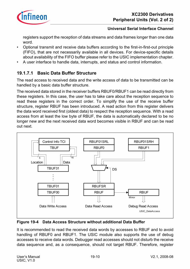
XC2300 DerivativesPeripheral Units (Vol. 2 of 2)
Universal Serial Interface Channel
registers support the reception of data streams and data frames longer than one dataword.
• Optional transmit and receive data buffers according to the first-in-first-out principle(FIFO), that are not necessarily available in all devices. For device-specific detailsabout availability of the FIFO buffer please refer to the USIC implementation chapter.
• A user interface to handle data, interrupts, and status and control information.
19.1.7.1 Basic Data Buffer StructureThe read access to received data and the write access of data to be transmitted can behandled by a basic data buffer structure.The received data stored in the receiver buffers RBUF0/RBUF1 can be read directly fromthese registers. In this case, the user has to take care about the reception sequence toread these registers in the correct order. To simplify the use of the receive bufferstructure, register RBUF has been introduced. A read action from this register deliversthe data word received first (oldest data) to respect the reception sequence. With a readaccess from at least the low byte of RBUF, the data is automatically declared to be nolonger new and the next received data word becomes visible in RBUF and can be readout next.
Figure 19-4 Data Access Structure without additional Data Buffer
It is recommended to read the received data words by accesses to RBUF and to avoidhandling of RBUF0 and RBUF1. The USIC module also supports the use of debugaccesses to receive data words. Debugger read accesses should not disturb the receivedata sequence and, as a consequence, should not target RBUF. Therefore, register
USIC_DataAccess
TBUF01
TBUF00
Data Write Access Data Read Access
....
TBUF
Control Info TCI
DataLocation16
TBUF31
5
RBUFSR
RBUF
RBUF0
RBUF01SRL
RBUF1
RBUF01SRH
DS
Debug Read Access
RBUFMirror
User’s Manual 19-10 V2.1, 2008-08USIC, V1.0

XC2300 DerivativesPeripheral Units (Vol. 2 of 2)
Universal Serial Interface Channel
RBUFD has been introduced. It contains the same value as RBUF, but a read accessfrom RBUFD does not change the status of the data (same data can be read severaltimes). In addition to the received data, some additional status information about eachreceived data word is available in the receiver buffer status registers RBUF01SRL/H(related to data in RBUF0 and RBUF1) and RBUFSR (related to data in RBUF).Transmit data can be loaded to TBUF by software by writing to the transmit buffer inputlocations TBUFx (x = 00-31), consisting of 32 consecutive addresses. The data writtento one of these input locations is stored in the transmit buffer TBUF. Additionally, theaddress of the written location is evaluated and can be used for additional controlpurposes. This 5-bit wide information (named Transmit Control Information TCI) can beused for different purposes in different protocols.
19.1.7.2 FIFO Buffer StructureTo allow easier data setup and handling, an additional data buffering mechanism can beoptionally supported. The data buffer is based on the first-in-first-out principle (FIFO) thatensures that the sequence of transferred data words is respected.If a FIFO buffer structure is used, the data handling scheme (data with associated controlinformation) is similar to the one without FIFO. The additional FIFO buffer can beindependently enabled/disabled for transmission and reception (e.g. if data FIFO buffersare available for a specific USIC channel, it is possible to configure the transmit data pathwithout and the receive data path with FIFO buffering).The transmit FIFO buffer is addressed by using 32 consecutive address locations for INxinstead of TBUFx (x=00-31) regardless of the FIFO depth. The 32 addresses are usedto store the 5-bit TCI (together with the written data) associated with each FIFO entry.The receive FIFO can be read out at two independent addresses, OUTR and OUTDRLinstead of RBUF and RBUFD. A read from the OUTR location triggers the next datapacket to be available for the next read (general FIFO mechanism). In order to allow non-intrusive debugging (without risk of data loss), a second address location (OUTDRL) hasbeen introduced. A read at this location delivers the same value as OUTR, but withoutmodifying the FIFO contents.The transmit FIFO also has the capability to bypass the data stream and to load bypassdata to TBUF. This can be used to generate high-priority messages or to send anemergency message if the transmit FIFO runs empty. The transmission control of theFIFO buffer can also use the transfer trigger and transfer gating scheme of thetransmission logic for data validation (e.g. to trigger data transfers by events).Note: The available size of a FIFO data buffer for a USIC channel depends on the
specific device. Please refer to the implementation chapter for details aboutavailable FIFO buffer capability.
User’s Manual 19-11 V2.1, 2008-08USIC, V1.0
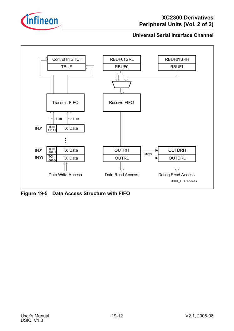
XC2300 DerivativesPeripheral Units (Vol. 2 of 2)
Universal Serial Interface Channel
Figure 19-5 Data Access Structure with FIFO
USIC_FIFOAccess
TX Data
TX Data
Data Write Access Data Read Access
....
TBUF
Control Info TCI
16-bit
TX Data
OUTRH
OUTRL
RBUF0
RBUF01SRL
RBUF1
RBUF01SRH
Debug Read Access
Mirror
5-bit
Transmit FIFO Receive FIFO
OUTDRH
OUTDRLTCI=00000IN00
TCI=00001IN01
TCI=11111IN31
User’s Manual 19-12 V2.1, 2008-08USIC, V1.0

XC2300 DerivativesPeripheral Units (Vol. 2 of 2)
Universal Serial Interface Channel
19.2 Operating the USICThis section describes how to operate the USIC communication channel.It describes:• Register Overview (see Page 19-13)• General channel operation (see Page 19-18)• Channel control and configuration registers (see Page 19-26)• Protocol related registers (see Page 19-34)• Input stages (see Page 19-37)• Input stage control registers (see Page 19-39)• Baud rate generation (see Page 19-42)• Baud rate and shift control registers (see Page 19-47)• Operating the transmit path (see on Page 19-52)• Operating the receive path (see Page 19-56)• Transfer control and status registers (see Page 19-58)• Data buffer registers (see Page 19-70)• Operating the FIFO data buffer (see Page 19-80)• FIFO buffer and bypass registers (see Page 19-90)
19.2.1 Register OverviewThe module itself being 32-bit wide, some registers have been split up in two parts forthe 16-bit implementation. Both parts keep the same name as the former 32-bit register,with an additional index. The lower part ends with the index L, whereas the upper(higher) part ends with the index H. Former 32-bit registers consisting of only 16 usedbits keep their name (without additional index), because only the used bits appear in theregister map.Table 19-3 shows all registers which are required for programming a USIC channel, aswell as the FIFO buffer. It summarizes the USIC communication channel registers anddefines the relative addresses and the reset values.Please note that all registers can be accessed with any access width (8-bit, 16-bit),independent of the described width. Short addressing is not supported.All USIC registers (except bit field KSCFG.SUMCFG) are always reset by a class 3reset. Bit field KSCFG.SUMCFG is reset by a class 1 reset.Note: The register bits marked “w” always deliver 0 when read. They are used to modify
flip-flops in other registers or to trigger internal actions.
User’s Manual 19-13 V2.1, 2008-08USIC, V1.0

XC2300 DerivativesPeripheral Units (Vol. 2 of 2)
Universal Serial Interface Channel
Figure 19-6 shows the register types of the USIC module registers and channelregisters. In a specific microcontroller, module registers of USIC module “x” are markedby the module prefix “USICx_”. Channel registers of USIC module “x” are marked by thechannel prefix “UxC0_” and “UxC1_”.
Figure 19-6 USIC Module and Channel Registers
Table 19-3 USIC Kernel-Related and Kernel RegistersRegisterShort Name
Register Long Name Offset Addr.
ResetValue
Description see
Module Registers1)
IDL Module Identification Register L 008H C0XXH Page 19-206IDH Module Identification Register H 00AH 003AH Page 19-207Channel RegistersFDRL Fractional Divider Register L 004H 0000H Page 19-47FDRH Fractional Divider Register H 006H 0000H Page 19-48KSCFG Kernel State Configuration Register 00CH 0000H Page 19-30CCR Channel Control Register 010H 0000H Page 19-26INPRL Interrupt Node Pointer Register L 014H 0000H Page 19-32INPRH Interrupt Node Pointer Register H 016H 0000H Page 19-33CCFG Channel Configuration Register 018H 00CFH Page 19-29BRGL Baud Rate Generator Register L 01CH 0000H Page 19-49
USIC_RegMap
Channel 0Registers
Module Registers
ChannelRegisters
FIFOBuffer
Registers
ChannelRegisters
FIFOBuffer
Registers
USICx Module
Channel 1Registers
User’s Manual 19-14 V2.1, 2008-08USIC, V1.0
XC2300 DerivativesPeripheral Units (Vol. 2 of 2)
Universal Serial Interface Channel
BRGH Baud Rate Generator Register H 01EH 0000H Page 19-51DX0CR Input Control Register 0 020H 0000H Page 19-39DX1CR Input Control Register 1 024H 0000H
DX2CR Input Control Register 2 028H 0000H
SCTRL Shift Control Register L 030H 0000H Page 19-58SCTRH Shift Control Register H 032H 0000H Page 19-60FMRL Flag Modification Register L 038H 0000H Page 19-68FMRH Flag Modification Register H 03AH 0000H Page 19-69TCSRL Transmit Control/Status Register L 03CH 0000H Page 19-61TCSRH Transmit Control/Status Register H 03EH 0000H Page 19-66PCRL Protocol Control Register L 040H 0000H Page 19-342)
Page 19-1233)
Page 19-1514)
Page 19-1785)
Page 19-1986)
PCRH Protocol Control Register H 042H 0000H Page 19-342)
Page 19-1263)
Page 19-1534)
Page 19-1785)
Page 19-2006)
Table 19-3 USIC Kernel-Related and Kernel Registers (cont’d)
RegisterShort Name
Register Long Name Offset Addr.
ResetValue
Description see
User’s Manual 19-15 V2.1, 2008-08USIC, V1.0

XC2300 DerivativesPeripheral Units (Vol. 2 of 2)
Universal Serial Interface Channel
PSR Protocol Status Register 044H 0000H Page 19-352)
Page 19-1273)
Page 19-1554)
Page 19-1815)
Page 19-2016)
PSCR Protocol Status Clear Register 048H 0000H Page 19-36RBUFD Receiver Buffer Register for
Debugger04CH 0000H Page 19-78
RBUF0 Receiver Buffer Register 0 050H 0000H Page 19-71RBUF1 Receiver Buffer Register 1 054H 0000H Page 19-74RBUFSR Receiver Buffer Status Register 058H 0000H Page 19-79RBUF Receiver Buffer Register 05CH 0000H Page 19-77RBUF01SRL Receiver Buffer 01 Status Register L 060H 0000H Page 19-71RBUF01SRH Receiver Buffer 01 Status Register H 062H 0000H Page 19-74– Reserved; do not access this
location.06CH – –
– Reserved; do not access this location.
06EH – –
TBUFx Transmit Buffer Input Location x(x = 00-31)
080H + x*4
0000H Page 19-70
FIFO Buffer RegistersBYP Bypass Data Register 100H 0000H Page 19-90BYPCRL Bypass Control Register L 104H 0000H Page 19-90BYPCRH Bypass Control Register H 106H 0000H Page 19-92TRBPTRL Transmit/Receive Buffer Pointer
Register L108H 0000H Page 19-109
TRBPTRH Transmit/Receive Buffer Pointer Register H
10AH 0000H Page 19-110
Table 19-3 USIC Kernel-Related and Kernel Registers (cont’d)
RegisterShort Name
Register Long Name Offset Addr.
ResetValue
Description see
User’s Manual 19-16 V2.1, 2008-08USIC, V1.0
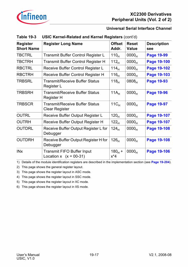
XC2300 DerivativesPeripheral Units (Vol. 2 of 2)
Universal Serial Interface Channel
TBCTRL Transmit Buffer Control Register L 110H 0000H Page 19-99TBCTRH Transmit Buffer Control Register H 112H 0000H Page 19-100RBCTRL Receive Buffer Control Register L 114H 0000H Page 19-102RBCTRH Receive Buffer Control Register H 116H 0000H Page 19-103TRBSRL Transmit/Receive Buffer Status
Register L118H 0808H Page 19-93
TRBSRH Transmit/Receive Buffer Status Register H
11AH 0000H Page 19-96
TRBSCR Transmit/Receive Buffer Status Clear Register
11CH 0000H Page 19-97
OUTRL Receive Buffer Output Register L 120H 0000H Page 19-107OUTRH Receive Buffer Output Register H 122H 0000H Page 19-107OUTDRL Receive Buffer Output Register L for
Debugger124H 0000H Page 19-108
OUTDRH Receive Buffer Output Register H for Debugger
126H 0000H Page 19-108
INx Transmit FIFO Buffer Input Location x (x = 00-31)
180H + x*4
0000H Page 19-106
1) Details of the module identification registers are described in the implementation section (see Page 19-204).2) This page shows the general register layout.3) This page shows the register layout in ASC mode.4) This page shows the register layout in SSC mode.5) This page shows the register layout in IIC mode.6) This page shows the register layout in IIS mode.
Table 19-3 USIC Kernel-Related and Kernel Registers (cont’d)
RegisterShort Name
Register Long Name Offset Addr.
ResetValue
Description see
User’s Manual 19-17 V2.1, 2008-08USIC, V1.0

XC2300 DerivativesPeripheral Units (Vol. 2 of 2)
Universal Serial Interface Channel
19.2.2 Operating the USIC Communication ChannelThis section describes how to operate a USIC communication channel, includingprotocol control and status, mode control and interrupt handling. The following aspectshave to be taken into account:• Enable the USIC module for operation and configure the behavior for the different
device operation modes (see Page 19-19).• Configure the pinning (refer to description in the corresponding protocol section).• Configure the data structure (shift direction, word length, frame length, polarity, etc.).• Configure the data buffer structure of the optional FIFO buffer area. A FIFO buffer
can only be enabled if the related bit in register CCFG is set.• Select a protocol by CCR.MODE. A protocol can only be selected if the related bit in
register CCFG is set.
19.2.2.1 Protocol Control and StatusThe protocol-related control and status information are located in the protocol controlregisters PCRL and PCRH and in the protocol status register PSR. These registers areshared between the available protocols. As a consequence, the meaning of the bitpositions in these registers is different within the protocols.
Use of PCRL/H BitsThe signification of the bits in registers PCRL/PCRH is indicated by the protocol-relatedalias names for the different protocols.• PCRL/PRCH for the ASC protocol (see Page 19-123)• PCRL/PRCH for the SSC protocol (see Page 19-151)• PCRL/PRCH for the IIC protocol (see Page 19-178)• PCRL/PRCH for the IIS protocol (see Page 19-198)
Use of PSR FlagsThe signification of the flags in register PSR is indicated by the protocol-related aliasnames for the different protocols.• PSR flags for the ASC protocol (see Page 19-127)• PSR flags for the SSC protocol (see Page 19-155)• PSR flags for the IIC protocol (see Page 19-181)• PSR flags for the IIS protocol (see Page 19-201)
User’s Manual 19-18 V2.1, 2008-08USIC, V1.0

XC2300 DerivativesPeripheral Units (Vol. 2 of 2)
Universal Serial Interface Channel
19.2.2.2 Mode ControlThe mode control concept for system control tasks, such as power saving, or suspendrequest for debugging, allows to program the module behavior under different deviceoperating conditions. The behavior of a communication channel can be programmed foreach of the device operating modes, that are requested by the global state control partof the SCU. Therefore, each communication channel has an associated kernel stateconfiguration register KSCFG defining its behavior in the following operating modes:• Normal operation:
This operating mode is the default operating mode when neither a suspend requestnor a clock-off request are pending. The module clock is not switched off and theUSIC registers can be read or written. The channel behavior is defined byKSCFG.NOMCFG.
• Suspend mode:This operating mode is requested when a suspend request is pending in the device.The module clock is not switched off and the USIC registers can be read or written.The channel behavior is defined by KSCFG.SUMCFG.
• Clock-off mode:This operating mode is requested for power saving purposes. The module clock isswitched off automatically when all channels of the USIC module reached theirspecified state in a stop mode. In this case, USIC registers can not be accessed. Thechannel behavior is defined by KSCFG.COMCFG.
The behavior of a USIC communication channel can be programmed for each of thedevice operating modes (normal operation, suspend mode, clock-off mode). Therefore,the USIC communication channel provides four kernel modes, as shown in Table 19-4.
Generally, bit field KSCFG.NOMCFG should be configured for run mode 0 as defaultsetting for standard operation. If a communication channel should not react to a suspendrequest (and to continue its operation as in normal mode), bit field KSCFG.SUMCFG hasto be configured with the same value as KSCFG.NOMCFG. If the communicationchannel should show a different behavior and stop operation when a specific stopcondition is reached, the code for stop mode 0 or stop mode 1 have to be written toKSCFG.SUMCFG.
Table 19-4 USIC Communication Channel BehaviorKernel Mode Channel Behavior KSCFG.
NOMCFGRun mode 0 Channel operation as specified, no impact on data transfer 00B
Run mode 1 01B
Stop mode 0 Explicit stop condition as described in the protocol chapters 10B
Stop mode 1 11B
User’s Manual 19-19 V2.1, 2008-08USIC, V1.0

XC2300 DerivativesPeripheral Units (Vol. 2 of 2)
Universal Serial Interface Channel
A similar mechanism applies for the clock-off mode with the possibility to program thedesired behavior by bit field KSCFG.COMCFG.The stop conditions are defined for the selected protocol (see mode control descriptionin the protocol section).Note: The stop mode selection strongly depends on the application needs and it is very
unlikely that different stop modes are required in parallel in the same application.As a result, only one stop mode type (either 0 or 1) should be used in the bit fieldsin register KSCFG. Do not mix stop mode 0 and stop mode 1 and avoid transitionsfrom stop mode 0 to stop mode 1 (or vice versa) for the same communicationchannel.
If the module clock is disabled by KSCFG.MODEN = 0 or in clock-off mode when thestop condition is reached (in stop mode 0 or 1), the module can not be accessed by reador write operations (except register KSCFG that can always be accessed).
19.2.2.3 General Channel Events and InterruptsThe general event and interrupt structure is shown in Figure 19-7. If a defined conditionis met, an event is detected and an event indication flag becomes automatically set. Theflag stays set until it is cleared by software. If enabled, an interrupt can be generated ifan event is detected. The actual status of the event indication flag has no influence onthe interrupt generation. As a consequence, the event indication flag does not need tobe cleared to generate further interrupts.Additionally, the service request output SRx of the USIC channel that becomes activatedin case of an event condition can be selected by an interrupt node pointer. This structureallows to assign events to interrupts, e.g. depending on the application, several eventscan share the same interrupt routine (several events activate the same SRx output) orcan be handled individually (only one event activates one SRx output).The SRx outputs are connected to interrupt control registers to handle the CPU reactionto the service requests. This assignment is described in the implementation section onPage 19-208.
User’s Manual 19-20 V2.1, 2008-08USIC, V1.0
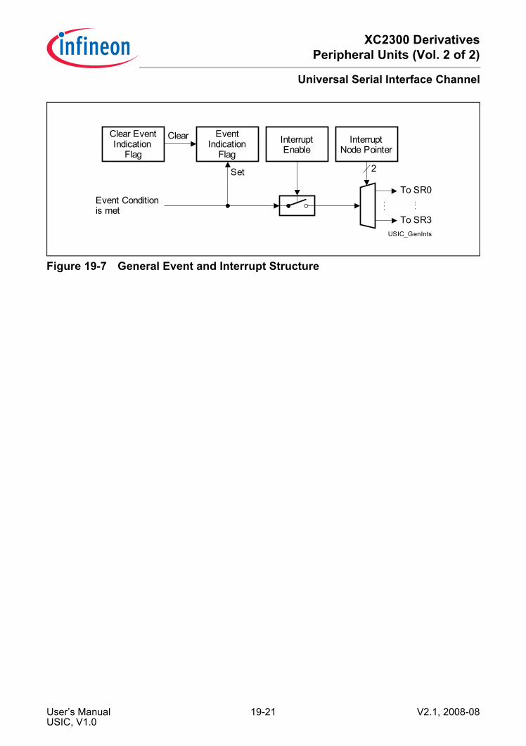
XC2300 DerivativesPeripheral Units (Vol. 2 of 2)
Universal Serial Interface Channel
Figure 19-7 General Event and Interrupt Structure
Interrupt Enable
Event Indication
Flag
USIC_GenInts
Event Condition is met
Set 2
To SR0
To SR3
......
InterruptNode Pointer
Clear EventIndication
Flag
Clear
User’s Manual 19-21 V2.1, 2008-08USIC, V1.0
XC2300 DerivativesPeripheral Units (Vol. 2 of 2)
Universal Serial Interface Channel
19.2.2.4 Data Transfer Events and InterruptsThe data transfer events are based on the transmission or reception of a data word. Therelated indication flags are located in register PSR. All events can be individually enabledfor interrupt generation.• Receive event to indicate that a data word has been received:
If a new received word becomes available in the receive buffer RBUF, either areceive event or an alternative receive event occurs.The receive event occurs if bit RBUFSR.PERR = 0. It is indicated by flag PSR.RIFand can lead to a receive interrupt (if enabled).
• Receiver start event to indicate that a data word reception has started:When the receive clock edge that shifts in the first bit of a new data word is detectedand reception is enabled, a receiver start event occurs. It is indicated by flagPSR.RSIF and can lead to a transmit buffer interrupt (if enabled).In full duplex mode, this event follows half a shift clock cycle after the transmit bufferevent and indicates when the shift control settings are internally “frozen” for thecurrent data word reception and a new setting can be programmed.In SSC and IIS mode, the transmit data valid flag TCSRL.TDV is cleared in singleshot mode with the receiver start event.
• Alternative receive event to indicate that a specific data word has been received:If a new received word becomes available in the receive buffer RBUF, either areceive event or an alternative receive event occurs.The alternative receive event occurs if bit RBUFSR.PERR = 1. It is indicated by flagPSR.AIF and can lead to an alternative receive interrupt (if enabled).Depending on the selected protocol, bit RBUFSR.PERR is set to indicate a parityerror in ASC mode, the reception of the first byte of a new frame in IIC mode, and theWA information about right/left channel in IIS mode, whereas it is always 0 in SSCmode.
• Transmit shift event to indicate that a data word has been transmitted:A transmit shift event occurs with the last shift clock edge of a data word. It isindicated by flag PSR.TSIF and can lead to a transmit shift interrupt (if enabled).
• Transmit buffer event to indicate that a data word transmission has been started:When a data word from the transmit buffer TBUF has been loaded to the shift registerand a new data word can be written to TBUF, a transmit buffer event occurs. Thishappens with the transmit clock edge that shifts out the first bit of a new data wordand transmission is enabled. It is indicated by flag PSR.TBIF and can lead to atransmit buffer interrupt (if enabled).This event also indicates when the shift control settings (word length, shift direction,etc.) are internally “frozen” for the current data word transmission.In ASC and IIC mode, the transmit data valid flag TCSRL.TDV is cleared in singleshot mode with the transmit buffer event.
• Data lost event to indicate a loss of the oldest received data word:If the data word available in register RBUF (oldest data word from RBUF0 or RBUF1)
User’s Manual 19-22 V2.1, 2008-08USIC, V1.0

XC2300 DerivativesPeripheral Units (Vol. 2 of 2)
Universal Serial Interface Channel
has not been read out before it becomes overwritten with new incoming data, thisevent occurs. It is indicated by flag PSR.DLIF and can lead to a protocol interrupt (ifenabled).
Table 19-5 shows the registers, bits and bit fields indicating the data transfer events andcontrolling the interrupts of a USIC channel.
Figure 19-8 shows the two transmit events and interrupts.
Figure 19-8 Transmit Events and Interrupts
Table 19-5 Data Transfer Events and Interrupt HandlingEvent Indication
FlagIndication cleared by
Interrupt enabled by
SRx Output selected by
Standard receive event PSR.RIF PSCR.CRIF CCR.RIEN INPRL.RINPReceive start event PSR.RSIF PSCR.CRSIF CCR.RSIEN INPRL.TBINPAlternative receive event PSR.AIF PSCR.CAIF CCR.AIEN INPRL.AINPTransmit shift event PSR.TSIF PSCR.CTSIF CCR.TSIEN INPRL.TSINPTransmit buffer event PSR.TBIF PSCR.CTBIF CCR.TBIEN INPRL.TBINPData lost event PSR.DLIF PSCR.CDLIF CCR.DLIEN INPRH.PINP
TSIEN
CCR
USIC_TransInts
Transmit Shift Event(End of last transmit shift clock period of data word)
TSIF
PSR
Set 2
TSINP
INPRL
SR0
SR3
......
CTSIF
PSCRClear
TBIEN
CCR
Transmit Buffer Event(First transmit shift clock of data word)
TBIF
PSR
Set 2
TBINP
INPRL
CTBIF
PSCRClear
SR0
SR3
......
Transmit Shift Interrupt
Transmit Buffer Interrupt
User’s Manual 19-23 V2.1, 2008-08USIC, V1.0
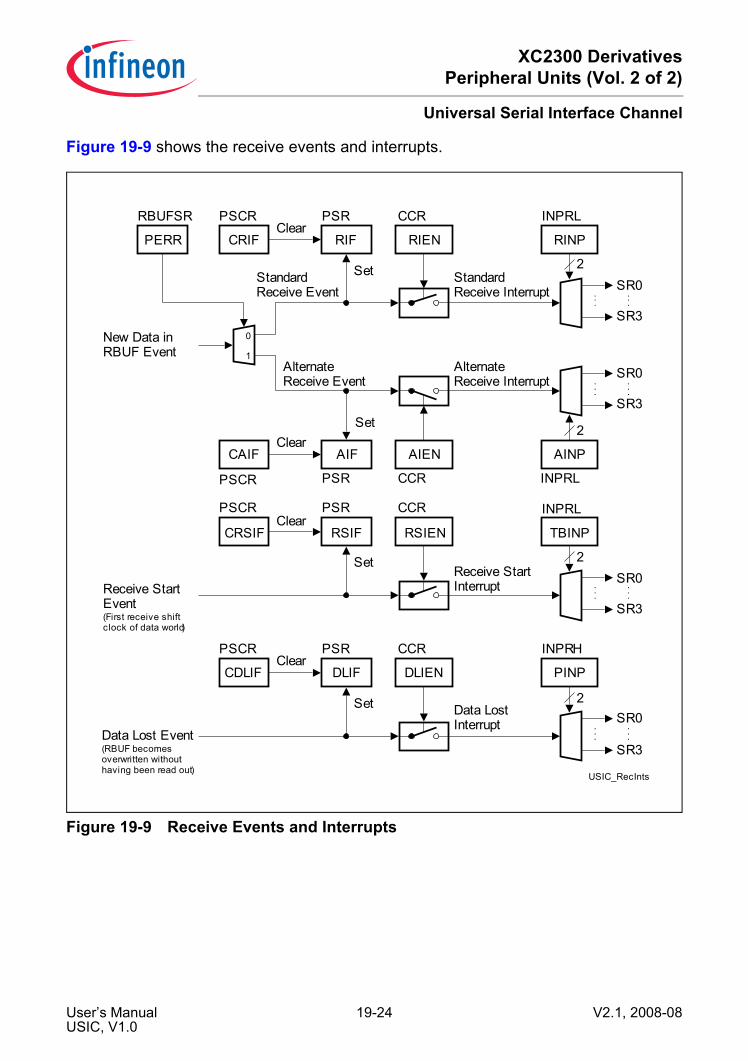
XC2300 DerivativesPeripheral Units (Vol. 2 of 2)
Universal Serial Interface Channel
Figure 19-9 shows the receive events and interrupts.
Figure 19-9 Receive Events and Interrupts
DLIEN
CCR
USIC_RecInts
Data Lost Event(RBUF becomes overwritten without having been read out)
DLIF
PSR
Set 2
PINP
INPRH
SR0
SR3
......
CDLIF
PSCRClear
RSIEN
CCR
Receive Start Event(First receive shift clock of data world)
RSIF
PSR
Set 2
TBINP
INPRL
SR0
SR3
......
CRSIF
PSCRClear
AIEN
CCR
AIF
PSR
AINP
INPRL
CAIF
PSCR
Clear
RIEN
CCR
RIF
PSR
Set 2
RINP
INPRL
SR0
SR3
......
CRIF
PSCRClear
SR0
SR3
......
2Set
New Data in RBUF Event
0
1
Standard Receive Event
Alternate Receive Event
PERR
RBUFSR
Standard Receive Interrupt
Alternate Receive Interrupt
Receive Start Interrupt
Data Lost Interrupt
User’s Manual 19-24 V2.1, 2008-08USIC, V1.0
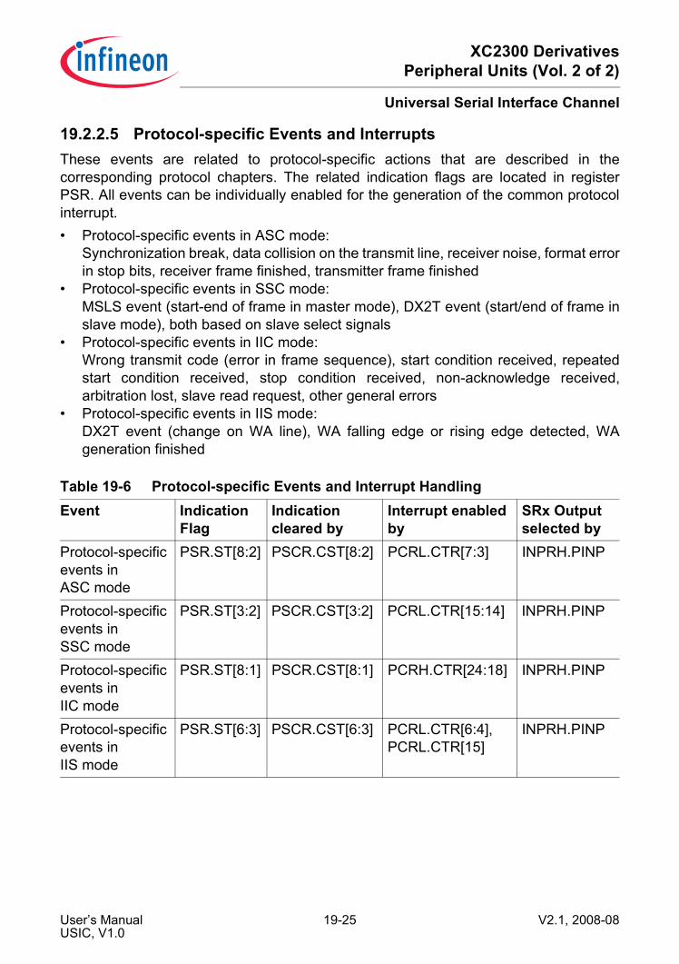
XC2300 DerivativesPeripheral Units (Vol. 2 of 2)
Universal Serial Interface Channel
19.2.2.5 Protocol-specific Events and InterruptsThese events are related to protocol-specific actions that are described in thecorresponding protocol chapters. The related indication flags are located in registerPSR. All events can be individually enabled for the generation of the common protocolinterrupt.• Protocol-specific events in ASC mode:
Synchronization break, data collision on the transmit line, receiver noise, format errorin stop bits, receiver frame finished, transmitter frame finished
• Protocol-specific events in SSC mode:MSLS event (start-end of frame in master mode), DX2T event (start/end of frame inslave mode), both based on slave select signals
• Protocol-specific events in IIC mode:Wrong transmit code (error in frame sequence), start condition received, repeatedstart condition received, stop condition received, non-acknowledge received,arbitration lost, slave read request, other general errors
• Protocol-specific events in IIS mode:DX2T event (change on WA line), WA falling edge or rising edge detected, WAgeneration finished
Table 19-6 Protocol-specific Events and Interrupt HandlingEvent Indication
FlagIndication cleared by
Interrupt enabled by
SRx Output selected by
Protocol-specific events in ASC mode
PSR.ST[8:2] PSCR.CST[8:2] PCRL.CTR[7:3] INPRH.PINP
Protocol-specific events in SSC mode
PSR.ST[3:2] PSCR.CST[3:2] PCRL.CTR[15:14] INPRH.PINP
Protocol-specific events in IIC mode
PSR.ST[8:1] PSCR.CST[8:1] PCRH.CTR[24:18] INPRH.PINP
Protocol-specific events in IIS mode
PSR.ST[6:3] PSCR.CST[6:3] PCRL.CTR[6:4],PCRL.CTR[15]
INPRH.PINP
User’s Manual 19-25 V2.1, 2008-08USIC, V1.0
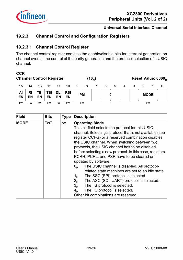
XC2300 DerivativesPeripheral Units (Vol. 2 of 2)
Universal Serial Interface Channel
19.2.3 Channel Control and Configuration Registers
19.2.3.1 Channel Control RegisterThe channel control register contains the enable/disable bits for interrupt generation onchannel events, the control of the parity generation and the protocol selection of a USICchannel.
CCR Channel Control Register (10H) Reset Value: 0000H
15 14 13 12 11 10 9 8 7 6 5 4 3 2 1 0
AIEN
RIEN
TBIEN
TSIEN
DLIEN
RSIEN PM 0 MODE
rw rw rw rw rw rw rw r rw
Field Bits Type DescriptionMODE [3:0] rw Operating Mode
This bit field selects the protocol for this USIC channel. Selecting a protocol that is not available (see register CCFG) or a reserved combination disables the USIC channel. When switching between two protocols, the USIC channel has to be disabled before selecting a new protocol. In this case, registers PCRH, PCRL, and PSR have to be cleared or updated by software.0H The USIC channel is disabled. All protocol-
related state machines are set to an idle state.1H The SSC (SPI) protocol is selected.2H The ASC (SCI, UART) protocol is selected.3H The IIS protocol is selected.4H The IIC protocol is selected.Other bit combinations are reserved.
User’s Manual 19-26 V2.1, 2008-08USIC, V1.0
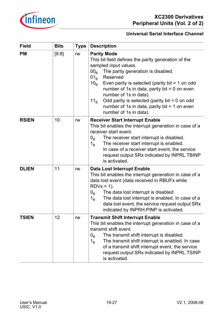
XC2300 DerivativesPeripheral Units (Vol. 2 of 2)
Universal Serial Interface Channel
PM [9:8] rw Parity ModeThis bit field defines the parity generation of the sampled input values.00B The parity generation is disabled.01B Reserved10B Even parity is selected (parity bit = 1 on odd
number of 1s in data, parity bit = 0 on even number of 1s in data).
11B Odd parity is selected (parity bit = 0 on odd number of 1s in data, parity bit = 1 on even number of 1s in data).
RSIEN 10 rw Receiver Start Interrupt EnableThis bit enables the interrupt generation in case of a receiver start event.0B The receiver start interrupt is disabled.1B The receiver start interrupt is enabled.
In case of a receiver start event, the service request output SRx indicated by INPRL.TBINP is activated.
DLIEN 11 rw Data Lost Interrupt EnableThis bit enables the interrupt generation in case of a data lost event (data received in RBUFx while RDVx = 1).0B The data lost interrupt is disabled.1B The data lost interrupt is enabled. In case of a
data lost event, the service request output SRx indicated by INPRH.PINP is activated.
TSIEN 12 rw Transmit Shift Interrupt EnableThis bit enables the interrupt generation in case of a transmit shift event.0B The transmit shift interrupt is disabled.1B The transmit shift interrupt is enabled. In case
of a transmit shift interrupt event, the service request output SRx indicated by INPRL.TSINP is activated.
Field Bits Type Description
User’s Manual 19-27 V2.1, 2008-08USIC, V1.0
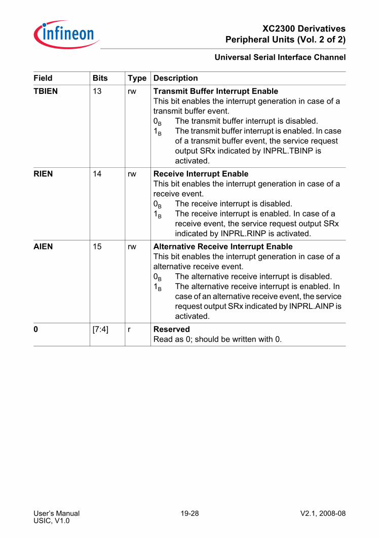
XC2300 DerivativesPeripheral Units (Vol. 2 of 2)
Universal Serial Interface Channel
TBIEN 13 rw Transmit Buffer Interrupt EnableThis bit enables the interrupt generation in case of a transmit buffer event.0B The transmit buffer interrupt is disabled.1B The transmit buffer interrupt is enabled. In case
of a transmit buffer event, the service request output SRx indicated by INPRL.TBINP is activated.
RIEN 14 rw Receive Interrupt EnableThis bit enables the interrupt generation in case of a receive event.0B The receive interrupt is disabled.1B The receive interrupt is enabled. In case of a
receive event, the service request output SRx indicated by INPRL.RINP is activated.
AIEN 15 rw Alternative Receive Interrupt EnableThis bit enables the interrupt generation in case of a alternative receive event.0B The alternative receive interrupt is disabled.1B The alternative receive interrupt is enabled. In
case of an alternative receive event, the service request output SRx indicated by INPRL.AINP is activated.
0 [7:4] r ReservedRead as 0; should be written with 0.
Field Bits Type Description
User’s Manual 19-28 V2.1, 2008-08USIC, V1.0
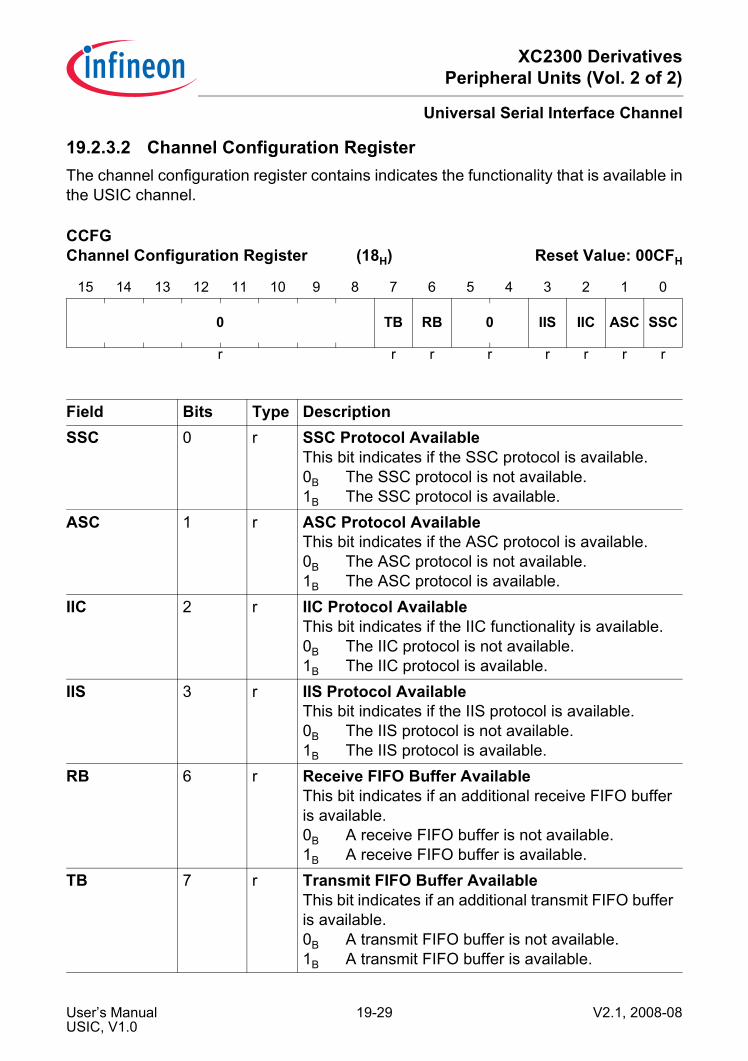
XC2300 DerivativesPeripheral Units (Vol. 2 of 2)
Universal Serial Interface Channel
19.2.3.2 Channel Configuration RegisterThe channel configuration register contains indicates the functionality that is available inthe USIC channel.
CCFG Channel Configuration Register (18H) Reset Value: 00CFH
15 14 13 12 11 10 9 8 7 6 5 4 3 2 1 0
0 TB RB 0 IIS IIC ASC SSC
r r r r r r r r
Field Bits Type DescriptionSSC 0 r SSC Protocol Available
This bit indicates if the SSC protocol is available.0B The SSC protocol is not available.1B The SSC protocol is available.
ASC 1 r ASC Protocol AvailableThis bit indicates if the ASC protocol is available.0B The ASC protocol is not available.1B The ASC protocol is available.
IIC 2 r IIC Protocol AvailableThis bit indicates if the IIC functionality is available.0B The IIC protocol is not available.1B The IIC protocol is available.
IIS 3 r IIS Protocol AvailableThis bit indicates if the IIS protocol is available.0B The IIS protocol is not available.1B The IIS protocol is available.
RB 6 r Receive FIFO Buffer AvailableThis bit indicates if an additional receive FIFO buffer is available.0B A receive FIFO buffer is not available.1B A receive FIFO buffer is available.
TB 7 r Transmit FIFO Buffer AvailableThis bit indicates if an additional transmit FIFO buffer is available.0B A transmit FIFO buffer is not available.1B A transmit FIFO buffer is available.
User’s Manual 19-29 V2.1, 2008-08USIC, V1.0
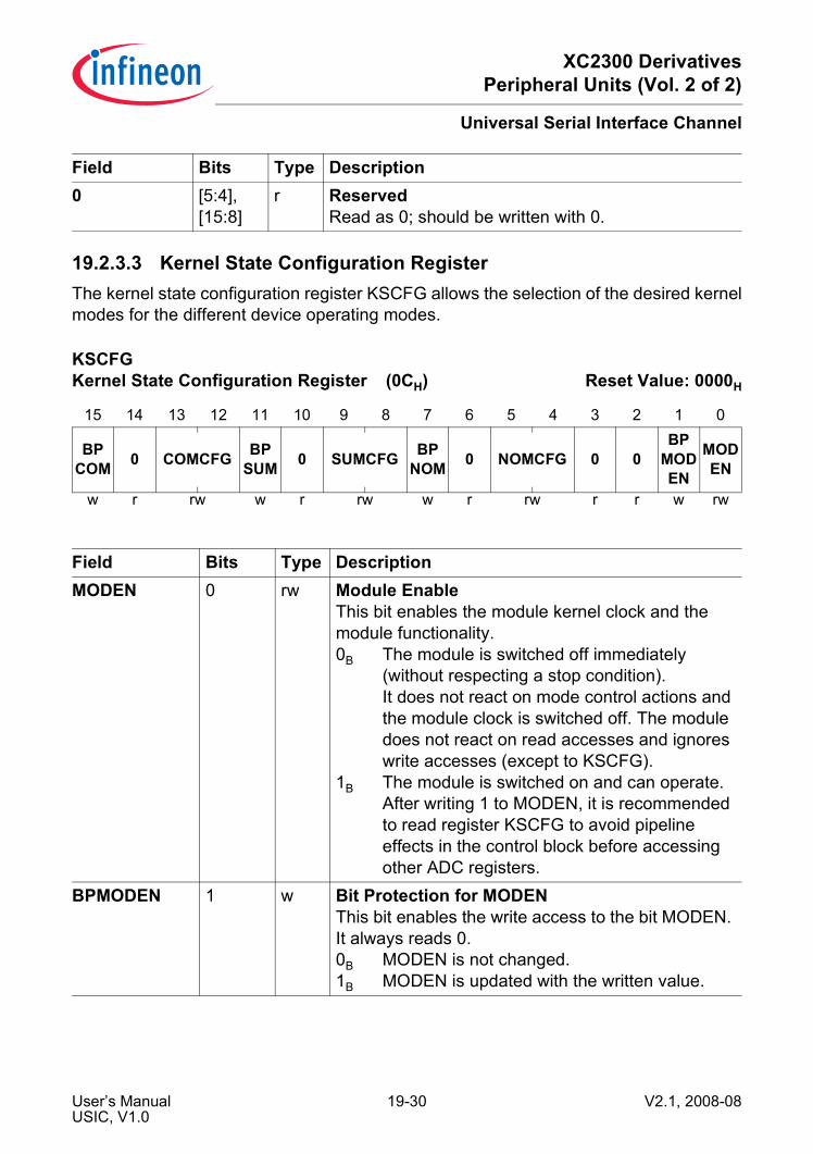
XC2300 DerivativesPeripheral Units (Vol. 2 of 2)
Universal Serial Interface Channel
19.2.3.3 Kernel State Configuration RegisterThe kernel state configuration register KSCFG allows the selection of the desired kernelmodes for the different device operating modes.
0 [5:4], [15:8]
r ReservedRead as 0; should be written with 0.
KSCFG Kernel State Configuration Register (0CH) Reset Value: 0000H
15 14 13 12 11 10 9 8 7 6 5 4 3 2 1 0
BPCOM 0 COMCFG BP
SUM 0 SUMCFG BPNOM 0 NOMCFG 0 0
BPMODEN
MODEN
w r rw w r rw w r rw r r w rw
Field Bits Type DescriptionMODEN 0 rw Module Enable
This bit enables the module kernel clock and the module functionality.0B The module is switched off immediately
(without respecting a stop condition).It does not react on mode control actions and the module clock is switched off. The module does not react on read accesses and ignores write accesses (except to KSCFG).
1B The module is switched on and can operate. After writing 1 to MODEN, it is recommended to read register KSCFG to avoid pipeline effects in the control block before accessing other ADC registers.
BPMODEN 1 w Bit Protection for MODENThis bit enables the write access to the bit MODEN. It always reads 0.0B MODEN is not changed.1B MODEN is updated with the written value.
Field Bits Type Description
User’s Manual 19-30 V2.1, 2008-08USIC, V1.0
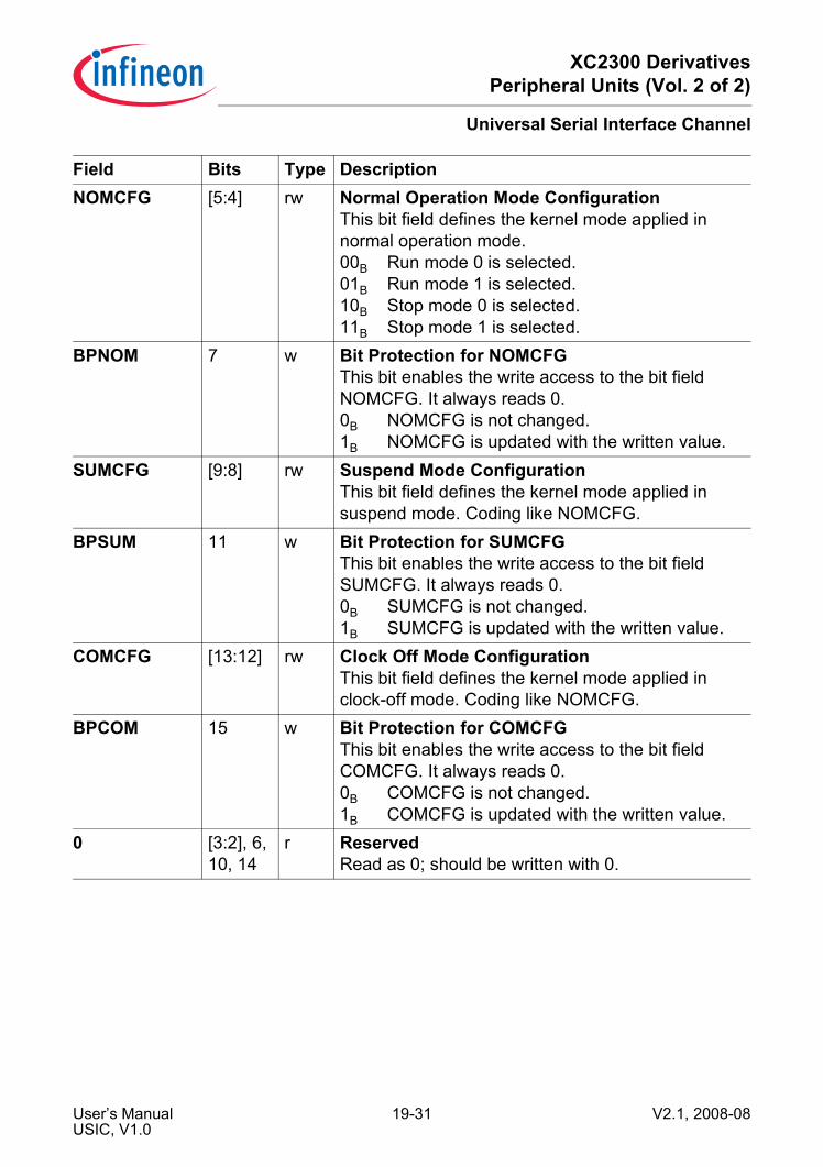
XC2300 DerivativesPeripheral Units (Vol. 2 of 2)
Universal Serial Interface Channel
NOMCFG [5:4] rw Normal Operation Mode ConfigurationThis bit field defines the kernel mode applied in normal operation mode.00B Run mode 0 is selected.01B Run mode 1 is selected.10B Stop mode 0 is selected.11B Stop mode 1 is selected.
BPNOM 7 w Bit Protection for NOMCFGThis bit enables the write access to the bit field NOMCFG. It always reads 0.0B NOMCFG is not changed.1B NOMCFG is updated with the written value.
SUMCFG [9:8] rw Suspend Mode ConfigurationThis bit field defines the kernel mode applied in suspend mode. Coding like NOMCFG.
BPSUM 11 w Bit Protection for SUMCFGThis bit enables the write access to the bit field SUMCFG. It always reads 0.0B SUMCFG is not changed.1B SUMCFG is updated with the written value.
COMCFG [13:12] rw Clock Off Mode ConfigurationThis bit field defines the kernel mode applied in clock-off mode. Coding like NOMCFG.
BPCOM 15 w Bit Protection for COMCFGThis bit enables the write access to the bit field COMCFG. It always reads 0.0B COMCFG is not changed.1B COMCFG is updated with the written value.
0 [3:2], 6, 10, 14
r ReservedRead as 0; should be written with 0.
Field Bits Type Description
User’s Manual 19-31 V2.1, 2008-08USIC, V1.0

XC2300 DerivativesPeripheral Units (Vol. 2 of 2)
Universal Serial Interface Channel
19.2.3.4 Interrupt Node Pointer RegistersThe interrupt node pointer registers define the service request output SRx that isactivated if the corresponding event occurs and interrupt generation is enabled.
INPRL Interrupt Node Pointer Register L (14H) Reset Value: 0000H
15 14 13 12 11 10 9 8 7 6 5 4 3 2 1 0
0 AINP 0 RINP 0 TBINP 0 TSINP
r rw r rw r rw r rw
Field Bits Type DescriptionTSINP [1:0] rw Transmit Shift Interrupt Node Pointer
This bit field defines which service request output SRx becomes activated in case of a transmit shift interrupt.00B Output SR0 becomes activated.01B Output SR1 becomes activated.10B Output SR2 becomes activated.11B Output SR3 becomes activated.
TBINP [5:4] rw Transmit Buffer Interrupt Node PointerThis bit field defines which service request output SRx will be activated in case of a transmit buffer interrupt or a receive start interrupt.Coding like TSINP.
RINP [9:8] rw Receive Interrupt Node PointerThis bit field defines which service request output SRx will be activated in case of a receive interrupt.Coding like TSINP.
AINP [13:12] rw Alternative Receive Interrupt Node PointerThis bit field defines which service request output SRx will be activated in case of a alternative receive interrupt.Coding like TSINP.
0 [3:2], [7:6], [11:10], [15:14]
r ReservedRead as 0; should be written with 0.
User’s Manual 19-32 V2.1, 2008-08USIC, V1.0
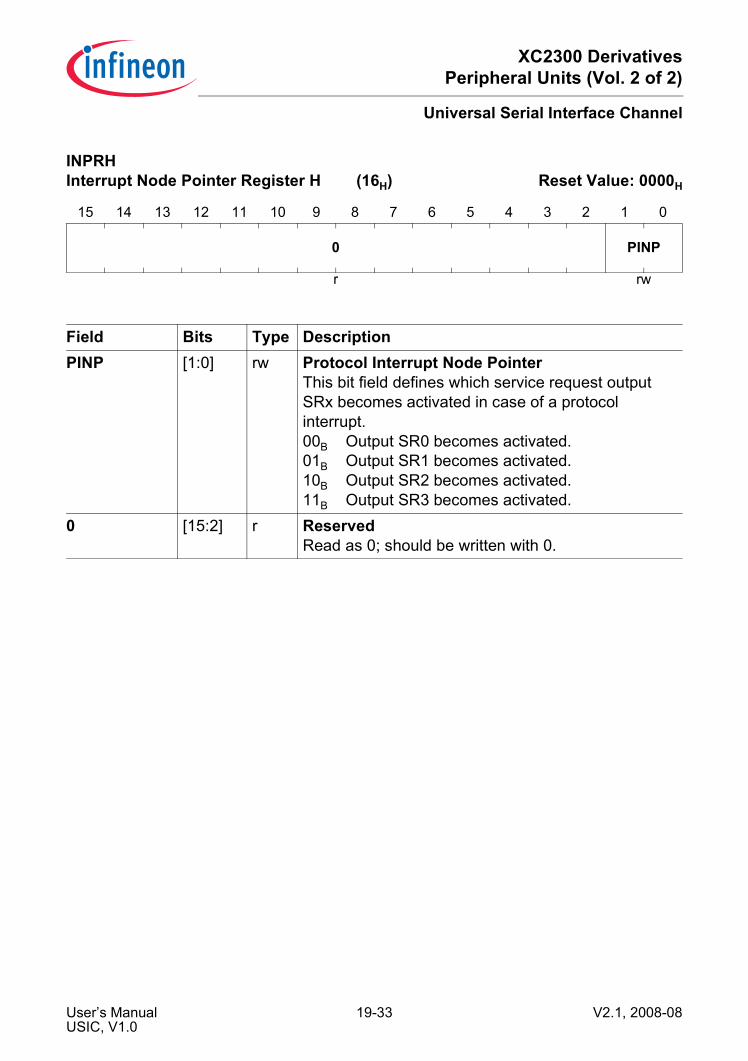
XC2300 DerivativesPeripheral Units (Vol. 2 of 2)
Universal Serial Interface Channel
INPRH Interrupt Node Pointer Register H (16H) Reset Value: 0000H
15 14 13 12 11 10 9 8 7 6 5 4 3 2 1 0
0 PINP
r rw
Field Bits Type DescriptionPINP [1:0] rw Protocol Interrupt Node Pointer
This bit field defines which service request output SRx becomes activated in case of a protocol interrupt.00B Output SR0 becomes activated.01B Output SR1 becomes activated.10B Output SR2 becomes activated.11B Output SR3 becomes activated.
0 [15:2] r ReservedRead as 0; should be written with 0.
User’s Manual 19-33 V2.1, 2008-08USIC, V1.0
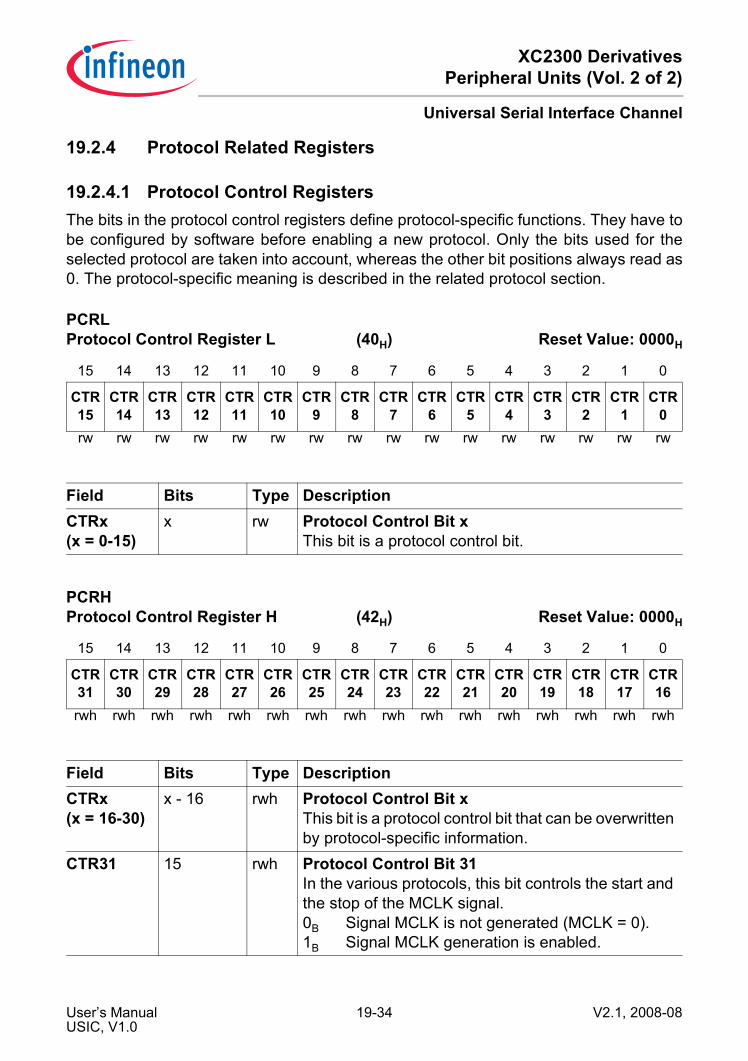
XC2300 DerivativesPeripheral Units (Vol. 2 of 2)
Universal Serial Interface Channel
19.2.4 Protocol Related Registers
19.2.4.1 Protocol Control RegistersThe bits in the protocol control registers define protocol-specific functions. They have tobe configured by software before enabling a new protocol. Only the bits used for theselected protocol are taken into account, whereas the other bit positions always read as0. The protocol-specific meaning is described in the related protocol section.
PCRL Protocol Control Register L (40H) Reset Value: 0000H
15 14 13 12 11 10 9 8 7 6 5 4 3 2 1 0
CTR15
CTR14
CTR13
CTR12
CTR11
CTR10
CTR9
CTR8
CTR7
CTR6
CTR5
CTR4
CTR3
CTR2
CTR1
CTR0
rw rw rw rw rw rw rw rw rw rw rw rw rw rw rw rw
Field Bits Type DescriptionCTRx(x = 0-15)
x rw Protocol Control Bit xThis bit is a protocol control bit.
PCRH Protocol Control Register H (42H) Reset Value: 0000H
15 14 13 12 11 10 9 8 7 6 5 4 3 2 1 0
CTR31
CTR30
CTR29
CTR28
CTR27
CTR26
CTR25
CTR24
CTR23
CTR22
CTR21
CTR20
CTR19
CTR18
CTR17
CTR16
rwh rwh rwh rwh rwh rwh rwh rwh rwh rwh rwh rwh rwh rwh rwh rwh
Field Bits Type DescriptionCTRx(x = 16-30)
x - 16 rwh Protocol Control Bit xThis bit is a protocol control bit that can be overwritten by protocol-specific information.
CTR31 15 rwh Protocol Control Bit 31In the various protocols, this bit controls the start and the stop of the MCLK signal.0B Signal MCLK is not generated (MCLK = 0).1B Signal MCLK generation is enabled.
User’s Manual 19-34 V2.1, 2008-08USIC, V1.0

XC2300 DerivativesPeripheral Units (Vol. 2 of 2)
Universal Serial Interface Channel
19.2.4.2 Protocol Status RegisterThe flags in the protocol status register can be cleared by writing a 1 to thecorresponding bit position in register PSCR. Writing a 1 to a bit position in PSR sets thecorresponding flag, but doesn’t lead to further actions (no interrupt generation). Writinga 0 has no effect. These flags should be cleared by software before enabling a newprotocol. The protocol-specific meaning is described in the related protocol section.
PSR Protocol Status Register (44H) Reset Value: 0000H
15 14 13 12 11 10 9 8 7 6 5 4 3 2 1 0
AIF RIF TBIF TSIF DLIF RSIF ST9 ST8 ST7 ST6 ST5 ST4 ST3 ST2 ST1 ST0
rwh rwh rwh rwh rwh rwh rwh rwh rwh rwh rwh rwh rwh rwh rwh rwh
Field Bits Type DescriptionSTx(x = 0-9)
x rwh Protocol Status Flag xSee protocol specific description.
RSIF 10 rwh Receiver Start Indication Flag0B A receiver start event has not occurred.1B A receiver start event has occurred.
DLIF 11 rwh Data Lost Indication Flag0B A data lost event has not occurred.1B A data lost event has occurred.
TSIF 12 rwh Transmit Shift Indication Flag0B A transmit shift event has not occurred.1B A transmit shift event has occurred.
TBIF 13 rwh Transmit Buffer Indication Flag0B A transmit buffer event has not occurred.1B A transmit buffer event has occurred.
RIF 14 rwh Receive Indication Flag0B A receive event has not occurred.1B A receive event has occurred.
AIF 15 rwh Alternative Receive Indication Flag0B An alternative receive event has not occurred.1B An alternative receive event has occurred.
User’s Manual 19-35 V2.1, 2008-08USIC, V1.0

XC2300 DerivativesPeripheral Units (Vol. 2 of 2)
Universal Serial Interface Channel
19.2.4.3 Protocol Status Clear RegisterRead accesses to this register always deliver 0 at all bit positions.
PSCR Protocol Status Clear Register (48H) Reset Value: 0000H
15 14 13 12 11 10 9 8 7 6 5 4 3 2 1 0
CAIF
CRIF
CTBIF
CTSIF
CDLIF
CRSIF
CST9
CST8
CST7
CST6
CST5
CST4
CST3
CST2
CST1
CST0
w w w w w w w w w w w w w w w w
Field Bits Type DescriptionCSTx(x = 0-9)
x w Clear Status Flag x in PSR0B No action1B Flag PSR.STx is cleared.
CRSIF 10 w Clear Receiver Start Indication Flag0B No action1B Flag PSR.RSIF is cleared.
CDLIF 11 w Clear Data Lost Indication Flag0B No action1B Flag PSR.DLIF is cleared.
CTSIF 12 w Clear Transmit Shift Indication Flag0B No action1B Flag PSR.TSIF is cleared.
CTBIF 13 w Clear Transmit Buffer Indication Flag0B No action1B Flag PSR.TBIF is cleared.
CRIF 14 w Clear Receive Indication Flag0B No action1B Flag PSR.RIF is cleared.
CAIF 15 w Clear Alternative Receive Indication Flag0B No action1B Flag PSR.AIF is cleared.
User’s Manual 19-36 V2.1, 2008-08USIC, V1.0
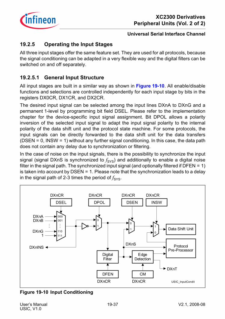
XC2300 DerivativesPeripheral Units (Vol. 2 of 2)
Universal Serial Interface Channel
19.2.5 Operating the Input StagesAll three input stages offer the same feature set. They are used for all protocols, becausethe signal conditioning can be adapted in a very flexible way and the digital filters can beswitched on and off separately.
19.2.5.1 General Input StructureAll input stages are built in a similar way as shown in Figure 19-10. All enable/disablefunctions and selections are controlled independently for each input stage by bits in theregisters DX0CR, DX1CR, and DX2CR.The desired input signal can be selected among the input lines DXnA to DXnG and apermanent 1-level by programming bit field DSEL. Please refer to the implementationchapter for the device-specific input signal assignment. Bit DPOL allows a polarityinversion of the selected input signal to adapt the input signal polarity to the internalpolarity of the data shift unit and the protocol state machine. For some protocols, theinput signals can be directly forwarded to the data shift unit for the data transfers(DSEN = 0, INSW = 1) without any further signal conditioning. In this case, the data pathdoes not contain any delay due to synchronization or filtering. In the case of noise on the input signals, there is the possibility to synchronize the inputsignal (signal DXnS is synchronized to fSYS) and additionally to enable a digital noisefilter in the signal path. The synchronized input signal (and optionally filtered if DFEN = 1)is taken into account by DSEN = 1. Please note that the synchronization leads to a delayin the signal path of 2-3 times the period of fSYS.
Figure 19-10 Input Conditioning
USIC_InputCondit
DFEN CM
DXnCR DXnCR
DSEL
DXnCR
DPOL
DXnCR
DSEN
DXnCR
INSW
DXnCR
DXnT
DXnSDXnINS
1
0DXnA 000
001
. . .
111
DXnB
1
. . .
DXnG 110
DigitalFilter
ProtocolPre-Processor
Data Shift Unit1
0
0
1
EdgeDetection
User’s Manual 19-37 V2.1, 2008-08USIC, V1.0

XC2300 DerivativesPeripheral Units (Vol. 2 of 2)
Universal Serial Interface Channel
If the input signals are handled by a protocol pre-processor, the data shift unit is directlyconnected to the protocol pre-processor by INSW = 0. The protocol pre-processor isconnected to the synchronized input signal DXnS and, depending on the selectedprotocol, also evaluates the edges.
19.2.5.2 Digital FilterThe digital filter can be enabled to reduce noise on the input signals. Before beingfiltered, the input signal becomes synchronized to fSYS. If the filter is disabled, signalDXnS corresponds to the synchronized input signal. If the filter is enabled, pulses shorterthan one filter sampling period are suppressed in signal DXnS. After an edge of thesynchronized input signal, signal DXnS changes to the new value if two consecutivesamples of the new value have been detected.In order to adapt the filter sampling period to different applications, it can beprogrammed. The first possibility is the system frequency fSYS. Longer pulses can besuppressed if the fractional divider output frequency fFD is selected. This frequency isprogrammable in a wide range and can also be used to determine the baud rate of thedata transfers.In addition to the synchronization delay of 2-3 periods of fSYS, an enabled filter adds adelay of up to two filter sampling periods between the selected input and signal DXnS.
19.2.5.3 Edge DetectionThe synchronized (and optionally filtered) signal DXnS can be used as input to the datashift unit and is also an input to the selected protocol pre-processor. If the protocol pre-processor does not use the DXnS signal for protocol-specific handling, DXnS can beused for other tasks, e.g. to control data transmissions in master mode (a data word canbe tagged valid for transmission, see chapter about data buffering).A programmable edge detection indicates that the desired event has occurred byactivating the trigger signal DXnT (introducing a delay of one period of fSYS before areaction to this event can take place).
19.2.5.4 Selected Input MonitoringThe selected input signal of each input stage has been made available with the signalsDX0INS, DX1INS, and DX2INS. These signals can be used in the system to trigger otheractions, e.g. to generate interrupts.
19.2.5.5 Loop Back ModeThe USIC transmitter output signals can be connected to the corresponding receiverinputs of the same communication channel in loop back mode. Therefore, the input “G”of the input stages that are needed for the selected protocol have to be selected. In this
User’s Manual 19-38 V2.1, 2008-08USIC, V1.0

XC2300 DerivativesPeripheral Units (Vol. 2 of 2)
Universal Serial Interface Channel
case, drivers for ASC, SSC, and IIS can be evaluated on-chip without the connectionsto port pins. Data transferred by the transmitter can be received by the receiver as if itwould have been sent by another communication partner.
19.2.6 Input Stage Register
19.2.6.1 Input Control RegistersThe input control registers contain the bits to define the characteristics of the inputstages (input stage DX0 is controlled by register DX0CR, etc.).
DX0CR Input Control Register 0 (20H) Reset Value: 0000HDX1CR Input Control Register 1 (24H) Reset Value: 0000HDX2CR Input Control Register 2 (28H) Reset Value: 0000H
15 14 13 12 11 10 9 8 7 6 5 4 3 2 1 0
DXS 0 CM SFSEL
DPOL 0 DS
ENDFEN
INSW 0 DSEL
rh r rw rw rw r rw rw rw r rw
Field Bits Type DescriptionDSEL [2:0] rw Data Selection for Input Signal
This bit field defines the input data signal for the corresponding input line for protocol pre-processor. The selection can be made from the input vector DXn[G:A].000B The data input DXnA is selected.001B The data input DXnB is selected....110B The data input DXnG is selected.111B The data input is always 1.
User’s Manual 19-39 V2.1, 2008-08USIC, V1.0

XC2300 DerivativesPeripheral Units (Vol. 2 of 2)
Universal Serial Interface Channel
INSW 4 rw Input SwitchThis bit defines if the data shift unit input is derived from the input data path DXn or from the selected protocol pre-processors.0B The input of the data shift unit is controlled by the
protocol pre-processor.1B The input of the data shift unit is connected to
the selected data input line. This setting is used if the signals are directly derived from an input pin without treatment by the protocol pre-processor.
DFEN 5 rw Digital Filter EnableThis bit enables/disables the digital filter for signal DXnS.0B The input signal is not digitally filtered.1B The input signal is digitally filtered.
DSEN 6 rw Data Synchronization EnableThis bit selects if the asynchronous input signal or the synchronized (and optionally filtered) signal DXnS can be used as input for the data shift unit.0B The un-synchronized signal can be taken as
input for the data shift unit.1B The synchronized signal can be taken as input
for the data shift unit.DPOL 8 rw Data Polarity for DXn
This bit defines the signal polarity of the input signal.0B The input signal is not inverted.1B The input signal is inverted.
SFSEL 9 rw Sampling Frequency SelectionThis bit defines the sampling frequency of the digital filter for the synchronized signal DXnS.0B The sampling frequency is fSYS.1B The sampling frequency is fFD.
Field Bits Type Description
User’s Manual 19-40 V2.1, 2008-08USIC, V1.0
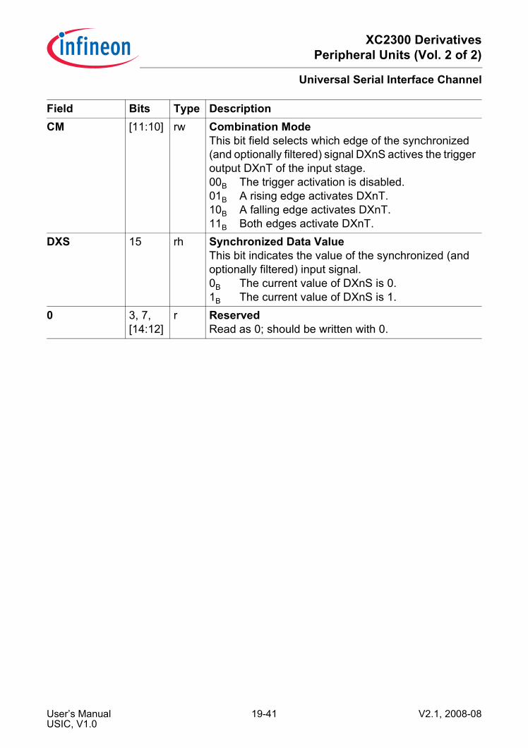
XC2300 DerivativesPeripheral Units (Vol. 2 of 2)
Universal Serial Interface Channel
CM [11:10] rw Combination ModeThis bit field selects which edge of the synchronized (and optionally filtered) signal DXnS actives the trigger output DXnT of the input stage.00B The trigger activation is disabled.01B A rising edge activates DXnT.10B A falling edge activates DXnT.11B Both edges activate DXnT.
DXS 15 rh Synchronized Data ValueThis bit indicates the value of the synchronized (and optionally filtered) input signal.0B The current value of DXnS is 0.1B The current value of DXnS is 1.
0 3, 7, [14:12]
r ReservedRead as 0; should be written with 0.
Field Bits Type Description
User’s Manual 19-41 V2.1, 2008-08USIC, V1.0

XC2300 DerivativesPeripheral Units (Vol. 2 of 2)
Universal Serial Interface Channel
19.2.7 Operating the Baud Rate GeneratorThe following blocks can be configured to operate the baud rate generator, see alsoFigure 19-2 on Page 19-8.
19.2.7.1 Fractional DividerThe fractional divider generates its output frequency fFD by dividing the input frequencyfSYS either by an integer factor n or by multiplication by n/1024. It has two operatingmodes:• Normal divider mode (FDRL.DM = 01B):
In this mode, the output frequency fFD is derived from the input clock fSYS by aninteger division by a value between 1 and 1024. The division is based on a counterFDRH.RESULT that is incremented by 1 with fSYS. After reaching the value 3FFH, thecounter is loaded with FDRL.STEP and then continues counting. In order to achievefFD = fSYS, the value of STEP has to be programmed with 3FFH.The output frequency in normal divider mode is defined by the equation:
(19.1)
• Fractional divider mode (FDRL.DM = 10B):In this mode, the output frequency fFD is derived from the input clock fSYS by afractional multiplication by n/1024 for a value of n between 0 and 1023. In general,the fractional divider mode allows to program the average output clock frequency witha finer granularity than in normal divider mode. Please note that in fractional dividermode fFD can have a maximum period jitter of one fSYS period. This jitter is notaccumulated over several cycles.The frequency fFD is generated by an addition of FDRL.STEP to FDRH.RESULT withfSYS. The frequency fFD is based on the overflow of the addition result over 3FFH.The output frequency in fractional divider mode is defined by the equation:
(19.2)
The output frequency fFD of the fractional divider is selected for baud rate generation byBRGL.CLKSEL = 00B.
19.2.7.2 External Frequency InputThe baud rate can be generated referring to an external frequency input (instead of tofSYS) if in the selected protocol the input stage DX1 is not needed (DX1CTR.INSW = 0).In this case, an external frequency input signal at the DX1 input stage can besynchronized and sampled with the system frequency fSYS. It can be optionally filtered
with n = 1024 - STEPfFD = fSYS × n1
with n = STEPfFD = fSYS × 1024
nn
User’s Manual 19-42 V2.1, 2008-08USIC, V1.0
XC2300 DerivativesPeripheral Units (Vol. 2 of 2)
Universal Serial Interface Channel
by the digital filter in the input stage. This feature allows data transfers with frequenciesthat can not be generated by the device itself, e.g. for specific audio frequencies.If BRGL.CLKSEL = 10B, the trigger signal DX1T determines fDX1. In this mode, either therising edge, the falling edge, or both edges of the input signal can be used for baud rategeneration, depending on the configuration of the DX1T trigger event by bit fieldDX1CTR.CM. The signal MCLK toggles with each trigger event of DX1T.If BRGL.CLKSEL = 11B, the rising edges of the input signal can be used for baud rategeneration. The signal MCLK represents the synchronized input signal DX1S.Both, the high time and the low time of external input signal must each have a length ofminimum 2 periods of fSYS to be used for baud rate generation.
19.2.7.3 Protocol-Related Counter in Divider ModeIn divider mode, the protocol-related counter is used for an integer division delivering theoutput frequency fPDIV. Additionally, two divider stages with a fixed division by 2 providethe output signals MCLK and SCLK with 50% duty cycle. If the fractional divider mode isused, the maximum fractional jitter of 1 period of fSYS can also appear in these signals.The outputs frequencies of this divider is controlled by registers BRGL and BRGH.In order to define a frequency ratio between the master clock MCLK and the shift clockSCLK, the divider stage for MCLK is located in front of the divider by PDIV+1, whereasthe divider stage for SCLK is located at the output of this divider.
(19.3)
(19.4)
In the case that the master clock is used as reference for external devices (e.g. for IIScomponents) and a fixed phase relation to SCLK and other timing signals is required, itis recommended to use the MCLK signal as input for the PDIV divider. If the MCLK signalis not used or a fixed phase relation is not necessary, the faster frequency fPIN can beselected as input frequency.
(19.5)
2fPINfMCLK =
2fPDIVfSCLK =
fPDIV = if PPPEN = 0fPIN × PDIV + 1
1
if PPPEN = 1fMCLK × PDIV + 1
1fPDIV =
User’s Manual 19-43 V2.1, 2008-08USIC, V1.0

XC2300 DerivativesPeripheral Units (Vol. 2 of 2)
Universal Serial Interface Channel
Figure 19-11 Protocol-Related Counter (Divider Mode)
19.2.7.4 Protocol-Related Counter in Capture ModeIn capture mode, the protocol-related counter stage can be used for time intervalmeasurement (BRGL.TMEN = 1). In this case, the frequency division is disabled(reception and transmission are not possible) and the counter is working as capture timerby counting fPPP periods. When reaching its maximum value, the counter stops counting.If an event is indicated by DX0T or DX1T, the actual counter value is captured into bitfield BRGH.PDIV and the counter restarts from 0. Additionally, a transmit shift interruptevent is generated (bit PSRL.TSIF becomes set).
Figure 19-12 Protocol-Related Counter (Capture Mode)
The capture mode can be used to measure the baud rate in slave mode before startingdata transfers, e.g. to measure the time between two edges of a data signal (by DX0T)
USIC_PDIVTMEN0
SCLK
01
10
11
00
fPIN
fMCLKfPDIV fSCLK
fCTQIN
MCLK
Divideby 2
Divide byPDIV + 11
0
fPPP
PPPEN TMEN = 0 CRQSEL
Divideby 2
BRGL BRGL BRGL
USIC_PDIVTMEN1
fPIN
fMCLK
MCLK
Capture inPDIVUp-Counter
1
0
fPPP
PPPEN TMEN = 1
Divideby 2
BRGL BRGL
≥1
Clear Capture
DX0TDX1T
User’s Manual 19-44 V2.1, 2008-08USIC, V1.0

XC2300 DerivativesPeripheral Units (Vol. 2 of 2)
Universal Serial Interface Channel
or of a shift clock signal (by DX1T). The conditions to activate the DXnT trigger signalscan be configured in each input stage.
19.2.7.5 Time Quanta CounterThe time quanta counter CTQ associated to the protocol pre-processor allows togenerate time intervals for protocol-specific purposes. The length of a time quantum tq isgiven by the selected input frequency fCTQIN and the programmed pre-divider value.The meaning of the time quanta depend on the selected protocol, please refer to thecorresponding chapters for more protocol-specific information.
Figure 19-13 Time Quanta Counter
19.2.7.6 Shift Clock Output ConfigurationThe master clock output signal MCLKOUT available at the corresponding output pin canbe configured in polarity. The MCLK signal can be generated for each protocol in orderto provide a kind of higher frequency time base compared to the shift clock. The configuration mechanism of the master clock output signal MCLKOUT ensures thatno shortened pulses can occur. Each MCLK period consists of two phases, an activephase, followed by a passive phase. The polarity of the MCLKOUT signal during theactive phase is defined by the inverted level of bit BRGH.MCLKCFG, evaluated at thestart of the active phase. The polarity of the MCLKOUT signal during the passive phaseis defined by bit BRGH.MCLKCFG, evaluated at the start of the passive phase. If bitBRGH.MCLKOUT is programmed with another value, the change is taken into accountwith the next change between the phases. This mechanism ensures that no shorterpulses than the length of a phase occur at the MCLKOUT output. In the example shownin Figure 19-14, the value of BRGH.MCLKCFG is changed from 0 to 1 during thepassive phase of MCLK period 2. The generation of the MCLKOUT signal is enabled/disabled by the protocol pre-processor, based on bit PCRH.MCLK. After this bit has become set, signal MCLKOUTis generated with the next active phase of the MCLK period. If PCRH.MCLK = 0(MCLKOUT generation disabled), the level for the passive phase is also applied foractive phase.
USIC_CTQ
fCTQIN
PCTQ DCTQ
Pre-Divider
BRGL BRGL
Time QuantaCounter CTQ
tq ProtocolPre-Processor
User’s Manual 19-45 V2.1, 2008-08USIC, V1.0

XC2300 DerivativesPeripheral Units (Vol. 2 of 2)
Universal Serial Interface Channel
Figure 19-14 Master Clock Output Configuration
The shift clock output signal SCLKOUT available at the corresponding output pin can beconfigured in polarity and additionally, a delay of one period of fPDIV (= half SCLK period)can be introduced. The delay allows to adapt the order of the shift clock edges to theapplication requirements. If the delay is used, it has to be taken into account for thecalculation of the signal propagation times and loop delays.The mechanism for the polarity control of the SCLKOUT signal is similar to the one forMCLKOUT, but based on bit field BRGH.SCLKCFG. The generation of the SCLKOUTsignal is enabled/disabled by the protocol pre-processor. Depending on the selectedprotocol, the protocol pre-processor can control the generation of the SCLKOUT signalindependently of the divider chain, e.g. for protocols without the need of a shift clockavailable at a pin, the SCLKOUT generation is disabled.
USIC_MCLKOUTCfg
Passive Phase
MCLKOUT
ActivePhase
Passive Phase
ActivePhase
Passive Phase
ActivePhase
Passive Phase
ActivePhase
MCLK Period 1 MCLK Period 2 MCLK Period 3 MCLK Period 4
Bit BRGH.MCLKCFG 0 1
User’s Manual 19-46 V2.1, 2008-08USIC, V1.0
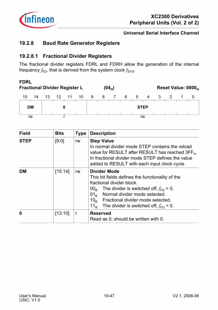
XC2300 DerivativesPeripheral Units (Vol. 2 of 2)
Universal Serial Interface Channel
19.2.8 Baud Rate Generator Registers
19.2.8.1 Fractional Divider RegistersThe fractional divider registers FDRL and FDRH allow the generation of the internalfrequency fFD, that is derived from the system clock fSYS.
FDRL Fractional Divider Register L (04H) Reset Value: 0000H
15 14 13 12 11 10 9 8 7 6 5 4 3 2 1 0
DM 0 STEP
rw r rw
Field Bits Type DescriptionSTEP [9:0] rw Step Value
In normal divider mode STEP contains the reload value for RESULT after RESULT has reached 3FFH.In fractional divider mode STEP defines the value added to RESULT with each input clock cycle.
DM [15:14] rw Divider ModeThis bit fields defines the functionality of the fractional divider block.00B The divider is switched off, fFD = 0.01B Normal divider mode selected.10B Fractional divider mode selected.11B The divider is switched off, fFD = 0.
0 [13:10] r ReservedRead as 0; should be written with 0.
User’s Manual 19-47 V2.1, 2008-08USIC, V1.0
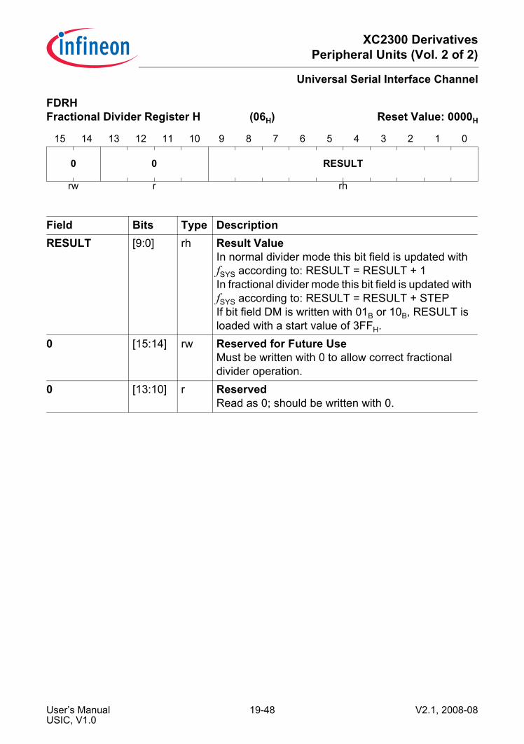
XC2300 DerivativesPeripheral Units (Vol. 2 of 2)
Universal Serial Interface Channel
FDRH Fractional Divider Register H (06H) Reset Value: 0000H
15 14 13 12 11 10 9 8 7 6 5 4 3 2 1 0
0 0 RESULT
rw r rh
Field Bits Type DescriptionRESULT [9:0] rh Result Value
In normal divider mode this bit field is updated with fSYS according to: RESULT = RESULT + 1In fractional divider mode this bit field is updated with fSYS according to: RESULT = RESULT + STEPIf bit field DM is written with 01B or 10B, RESULT is loaded with a start value of 3FFH.
0 [15:14] rw Reserved for Future UseMust be written with 0 to allow correct fractional divider operation.
0 [13:10] r ReservedRead as 0; should be written with 0.
User’s Manual 19-48 V2.1, 2008-08USIC, V1.0

XC2300 DerivativesPeripheral Units (Vol. 2 of 2)
Universal Serial Interface Channel
19.2.8.2 Baud Rate Generator RegistersThe protocol-related divider for baud rate generation is controlled by the registers BRGLand BRGH.
BRGL Baud Rate Generator Register L (1CH) Reset Value: 0000H
15 14 13 12 11 10 9 8 7 6 5 4 3 2 1 0
0 DCTQ PCTQ CTQSEL 0 PPPEN
TMEN 0 CLKSEL
r rw rw rw r rw rw r rw
Field Bits Type DescriptionCLKSEL [1:0] rw Clock Selection
This bit field defines the input frequency fPIN00B The fractional divider frequency fFD is selected.01B Reserved, no action10B The trigger signal DX1T defines fPIN. Signal
MCLK toggles with fPIN.11B Signal MCLK corresponds to the DX1S signal
and the frequency fPIN is derived from the rising edges of DX1S.
TMEN 3 rw Timing Measurement EnableThis bit defines the functionality of the protocol-related divider.0B Divider mode: fPDIV = fPPP / (PDIV + 1)
Data transfers are possible and the trigger signals DX0T and DX1T are ignored.
1B Capture mode:The 10-bit counter is incremented by 1 with fPPP and stops counting when reaching its maximum value. If one of the trigger signals DX0T or DX1T become active, the counter value is captured into bit field PDIV, the counter is cleared and a transmit shift event is generated. Data transfers are not possible.
User’s Manual 19-49 V2.1, 2008-08USIC, V1.0
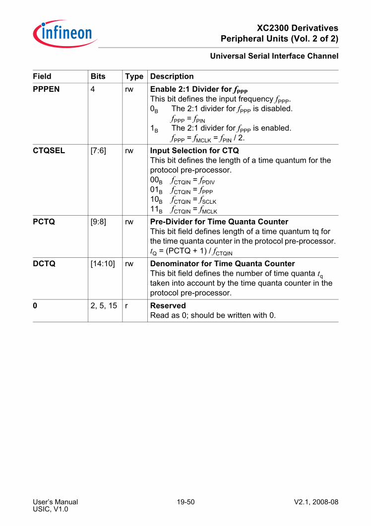
XC2300 DerivativesPeripheral Units (Vol. 2 of 2)
Universal Serial Interface Channel
PPPEN 4 rw Enable 2:1 Divider for fPPPThis bit defines the input frequency fPPP.0B The 2:1 divider for fPPP is disabled.
fPPP = fPIN1B The 2:1 divider for fPPP is enabled.
fPPP = fMCLK = fPIN / 2.CTQSEL [7:6] rw Input Selection for CTQ
This bit defines the length of a time quantum for the protocol pre-processor.00B fCTQIN = fPDIV01B fCTQIN = fPPP10B fCTQIN = fSCLK11B fCTQIN = fMCLK
PCTQ [9:8] rw Pre-Divider for Time Quanta CounterThis bit field defines length of a time quantum tq for the time quanta counter in the protocol pre-processor.tQ = (PCTQ + 1) / fCTQIN
DCTQ [14:10] rw Denominator for Time Quanta CounterThis bit field defines the number of time quanta tq taken into account by the time quanta counter in the protocol pre-processor.
0 2, 5, 15 r ReservedRead as 0; should be written with 0.
Field Bits Type Description
User’s Manual 19-50 V2.1, 2008-08USIC, V1.0

XC2300 DerivativesPeripheral Units (Vol. 2 of 2)
Universal Serial Interface Channel
BRGH Baud Rate Generator Register H (1EH) Reset Value: 0000H
15 14 13 12 11 10 9 8 7 6 5 4 3 2 1 0
SCLKCFGM
CLKCFG
0 PDIV
rw rw r rwh
Field Bits Type DescriptionPDIV [9:0] rwh Divider Mode: Divider Factor to Generate fPDIV
This bit field defines the ratio between the input frequency fPPP and the divider frequency fPDIV.Capture Mode: Captured Time IntervalThe value of the counter is captured into this bit field if one of the trigger signals DX0T or DX1T are activated by the corresponding input stage.
MCLKCFG 13 rw Master Clock ConfigurationThis bit field defines the level of the passive phase of the MCLKOUT signal.0B The passive level is 0.1B The passive level is 1.
SCLKCFG [15:14] rw Shift Clock Output ConfigurationThis bit field defines the level of the passive phase of the SCLKOUT signal and enables/disables a delay of half of a SCLK period.00B The passive level is 0 and the delay is disabled.01B The passive level is 1 and the delay is disabled.10B The passive level is 0 and the delay is enabled.11B The passive level is 1 and the delay is enabled.
0 [12:10] r ReservedRead as 0; should be written with 0.
User’s Manual 19-51 V2.1, 2008-08USIC, V1.0
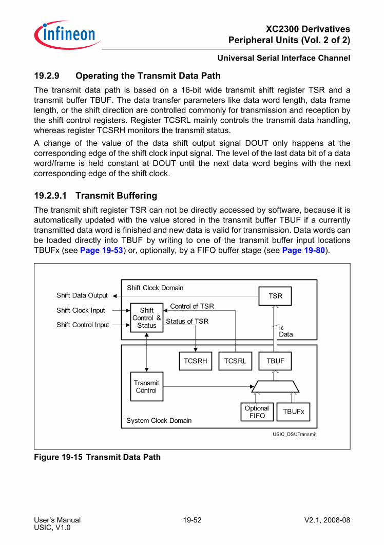
XC2300 DerivativesPeripheral Units (Vol. 2 of 2)
Universal Serial Interface Channel
19.2.9 Operating the Transmit Data PathThe transmit data path is based on a 16-bit wide transmit shift register TSR and atransmit buffer TBUF. The data transfer parameters like data word length, data framelength, or the shift direction are controlled commonly for transmission and reception bythe shift control registers. Register TCSRL mainly controls the transmit data handling,whereas register TCSRH monitors the transmit status.A change of the value of the data shift output signal DOUT only happens at thecorresponding edge of the shift clock input signal. The level of the last data bit of a dataword/frame is held constant at DOUT until the next data word begins with the nextcorresponding edge of the shift clock.
19.2.9.1 Transmit BufferingThe transmit shift register TSR can not be directly accessed by software, because it isautomatically updated with the value stored in the transmit buffer TBUF if a currentlytransmitted data word is finished and new data is valid for transmission. Data words canbe loaded directly into TBUF by writing to one of the transmit buffer input locationsTBUFx (see Page 19-53) or, optionally, by a FIFO buffer stage (see Page 19-80).
Figure 19-15 Transmit Data Path
USIC_DSUTransmit
OptionalFIFO TBUFx
TCSRLTCSRH
TransmitControl
TSR
TBUF
Status of TSR
Control of TSRShift Control &
Status
System Clock Domain
Shift Clock DomainShift Data Output
Shift Clock Input
Shift Control Input 16Data
User’s Manual 19-52 V2.1, 2008-08USIC, V1.0
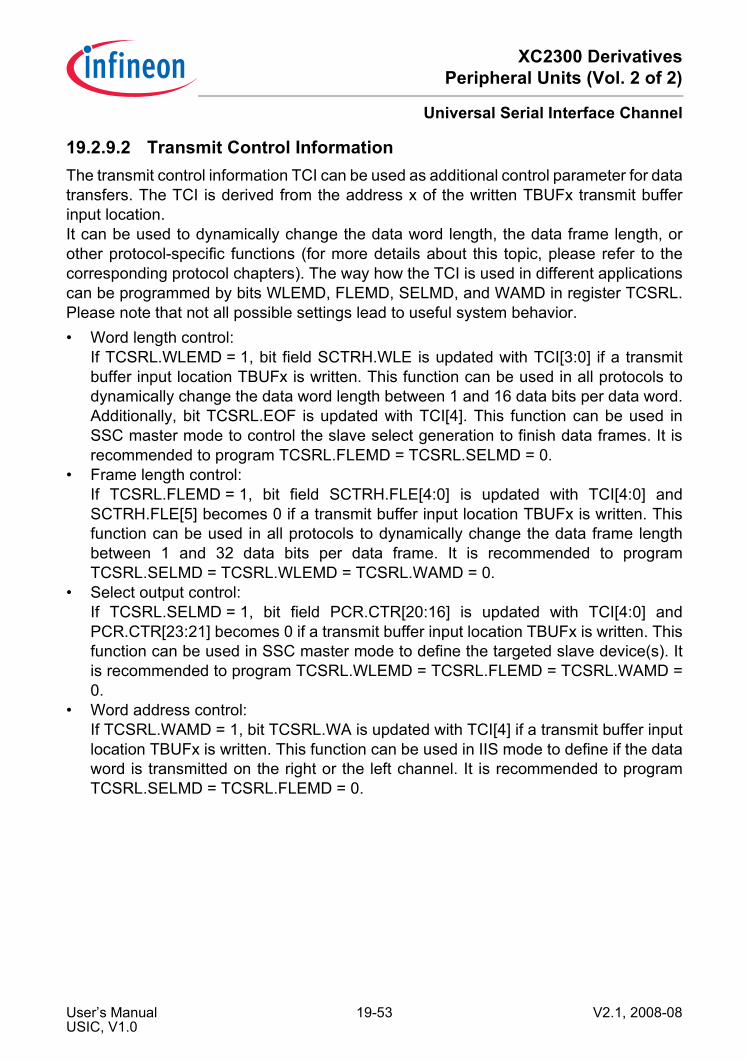
XC2300 DerivativesPeripheral Units (Vol. 2 of 2)
Universal Serial Interface Channel
19.2.9.2 Transmit Control InformationThe transmit control information TCI can be used as additional control parameter for datatransfers. The TCI is derived from the address x of the written TBUFx transmit bufferinput location.It can be used to dynamically change the data word length, the data frame length, orother protocol-specific functions (for more details about this topic, please refer to thecorresponding protocol chapters). The way how the TCI is used in different applicationscan be programmed by bits WLEMD, FLEMD, SELMD, and WAMD in register TCSRL.Please note that not all possible settings lead to useful system behavior.• Word length control:
If TCSRL.WLEMD = 1, bit field SCTRH.WLE is updated with TCI[3:0] if a transmitbuffer input location TBUFx is written. This function can be used in all protocols todynamically change the data word length between 1 and 16 data bits per data word.Additionally, bit TCSRL.EOF is updated with TCI[4]. This function can be used inSSC master mode to control the slave select generation to finish data frames. It isrecommended to program TCSRL.FLEMD = TCSRL.SELMD = 0.
• Frame length control:If TCSRL.FLEMD = 1, bit field SCTRH.FLE[4:0] is updated with TCI[4:0] andSCTRH.FLE[5] becomes 0 if a transmit buffer input location TBUFx is written. Thisfunction can be used in all protocols to dynamically change the data frame lengthbetween 1 and 32 data bits per data frame. It is recommended to programTCSRL.SELMD = TCSRL.WLEMD = TCSRL.WAMD = 0.
• Select output control:If TCSRL.SELMD = 1, bit field PCR.CTR[20:16] is updated with TCI[4:0] andPCR.CTR[23:21] becomes 0 if a transmit buffer input location TBUFx is written. Thisfunction can be used in SSC master mode to define the targeted slave device(s). Itis recommended to program TCSRL.WLEMD = TCSRL.FLEMD = TCSRL.WAMD =0.
• Word address control:If TCSRL.WAMD = 1, bit TCSRL.WA is updated with TCI[4] if a transmit buffer inputlocation TBUFx is written. This function can be used in IIS mode to define if the dataword is transmitted on the right or the left channel. It is recommended to programTCSRL.SELMD = TCSRL.FLEMD = 0.
User’s Manual 19-53 V2.1, 2008-08USIC, V1.0

XC2300 DerivativesPeripheral Units (Vol. 2 of 2)
Universal Serial Interface Channel
19.2.9.3 Transmit Data ValidationThe data word in the transmit buffer TBUF can be tagged valid or invalid for transmissionby bit TCSRL.TDV (transmit data valid). A combination of data flow related and eventrelated criteria define whether the data word is considered valid for transmission. A datavalidation logic checks the start conditions for each data word. Depending on the resultof the check, the transmit shift register is loaded with different values, according to thefollowing rules:• If a USIC channel is the communication master (it defines the start of each data word
transfer), a data word transfer can only be started with valid data in the transmit bufferTBUF. In this case, the transmit shift register is loaded with the content of TBUF, thatis not changed due to this action.
• If a USIC channel is a communication slave (it can not define the start itself, but hasto react), a data word transfer requested by the communication master has to bestarted independently of the status of the data word in TBUF. If a data word transferis requested and started by the master, the transmit shift register is loaded at the firstcorresponding shift clock edge either with the data word in TBUF (if it is valid fortransmission) or with the level defined by bit SCTRL.PDL (if the content of TBUF hasnot been valid at the transmission start). In both cases, the content of TBUF is notchanged.
The control and status bits for the data validation are located in registers TCSRL orTCSRH. The data validation is based on the logic blocks shown in Figure 19-16.
Figure 19-16 Transmit Data Validation
• A transfer gating logic enables or disables the data word transfer from TBUF undersoftware or under hardware control. If the input stage DX2 is not needed for data
USIC_TDV_
TDEN
TDVTR
TransferGating
TCSRL
DX2S
Data Shift UnitDSU
TBUFData
Validation
TransferTrigger
TDSSMTCSRL
TE
TDV
TCSRL
DX2T
Shift ControlInput DX2
TCSRL
User’s Manual 19-54 V2.1, 2008-08USIC, V1.0

XC2300 DerivativesPeripheral Units (Vol. 2 of 2)
Universal Serial Interface Channel
shifting, signal DX2S can be used for gating purposes. The transfer gating logic iscontrolled by bit field TCSRL.TDEN.
• A transfer trigger logic supports data word transfers related to events, e.g. timerbased or related to an input pin. If the input stage DX2 is not needed for data shifting,signal DX2T can be used for trigger purposes. The transfer trigger logic is controlledby bit TCSRL.TDVTR and the occurrence of a trigger event is indicated by bitTCSRH.TE.
• A data validation logic combining the inputs from the gating logic, the triggering logicand DSU signals. A transmission of the data word located in TBUF can only bestarted if the gating enables the start, bit TCSRL.TDV = 1, and bit TCSRH.TE = 1.The content of the transmit buffer TBUF should not be overwritten with new datawhile it is valid for transmission and a new transmission can start. If the content ofTBUF has to be changed, it is recommended to clear bit TCSRL.TDV by writingFMRL.MTDV = 10B before updating the data. Bit TCSRL.TDV becomesautomatically set when TBUF is updated with new data. Another possibility are theinterrupts TBI (for ASC and IIC) or RSI (for SSC and IIS) indicating that atransmission has started. While a transmission is in progress, TBUF can be loadedwith new data. In this case the user has to take care that an update of the TBUFcontent takes place before a new transmission starts.
With this structure, the following data transfer functionality can be achieved:• If bit TCSRL.TDSSM = 0, the content of the transmit buffer TBUF is always
considered as valid for transmission. The transfer trigger mechanism can be used tostart the transfer of the same data word based on the selected event (e.g. on a timerbase or an edge at a pin) to realize a kind of life-sign mechanism. Furthermore, inslave mode, it is ensured that always a correct data word is transmitted instead of thepassive data level.
• Bit TCSRL.TDSSM = 1 has to be programmed to allow word-by-word datatransmission with a kind of single-shot mechanism. After each transmission start, anew data word has to be loaded into the transmit buffer TBUF, either by softwarewrite actions to one of the transmit buffer input locations TBUFx or by an optionaldata buffer (e.g. FIFO buffer). To avoid that data words are sent out several times orto allow data handling with an additional data buffer (e.g. FIFO), bit TCSRL.TDSSMhas to be 1.
• Bit TCSRL.TDV becoming automatically set when a new data word is loaded into thetransmit buffer TBUF, a transmission start can be requested by a write action of thedata to be transmitted to at least the low byte of one of the transmit buffer inputlocations TBUFx. The additional information TCI can be used to control the data wordlength or other parameters independently for each data word by a single writeaccess.
• Bit field FMRL.MTDV allows software driven modification (set or clear) of bitTCSRL.TDV. Together with the gating control bit field TCSRL.TDEN, the user can setup the transmit data word without starting the transmission. A possible program
User’s Manual 19-55 V2.1, 2008-08USIC, V1.0

XC2300 DerivativesPeripheral Units (Vol. 2 of 2)
Universal Serial Interface Channel
sequence could be: clear TCSRL.TDEN = 00B, write data to TBUFx, clearTCSRL.TDV by writing FMRL.MTDV = 10B, re-enable the gating withTCSRL.TDEN = 01B and then set TCSRL.TDV under software control by writingFMRL.MTDV = 01B.
19.2.10 Operating the Receive Data PathThe receive data path is based on two 16-bit wide receive shift registers RSR0 andRSR1 and a receive buffer for each of them (RBUF0 and RBUF1). The data transferparameters like data word length, data frame length, or the shift direction are controlledcommonly for transmission and reception by the shift control registers.Register RBUF01SRL monitors the status of RBUF0 and register RBUF01SRH ofRBUF1.
19.2.10.1 Receive BufferingThe receive shift registers cannot be directly accessed by software, but their contentsare automatically loaded into the receive buffer registers RBUF0 (or RBUF1respectively) if a complete data word has been received or the frame is finished. Thereceived data words in RBUF0 or RBUF1 can be read out in the correct order directlyfrom register RBUF or, optionally, from a FIFO buffer stage (see Page 19-80).
Figure 19-17 Receive Data Path
USIC_DSUReceive
RBUF
ReceiveControl
16
RBUF0
Shift Control
&Status
System Clock Domain
Shift Clock Domain
Shift Data Input
Shift Clock Input
Shift Control Input
RBUF1
16
RBUFSR
RBUF01SRL
RBUF01SRH
Status ofRSR0
RSR0
RSR1
Status ofRSR1 Data Data
User’s Manual 19-56 V2.1, 2008-08USIC, V1.0

XC2300 DerivativesPeripheral Units (Vol. 2 of 2)
Universal Serial Interface Channel
19.2.10.2 Baud Rate ConstraintsThe following baud rate constraints have to be respected to ensure correct datareception and buffering. The user has to take care about these restrictions whenselecting the baud rate and the data word length with respect to the module clockfrequency fSYS.• A received data word in a receiver shift register RSRx must be held constant for at
least 4 periods of fSYS in order to ensure correct loading of the related receiver bufferregister RBUFx.
• The shift control signal has to be constant inactive for at least 5 periods of fSYSbetween two consecutive frames in order to correctly detect the end of a frame.
• The shift control signal has to be constant active for at least 1 period of fSYS in orderto correctly detect a frame (shortest frame).
• A minimum setup and hold time of the shift control signal with respect to the shiftclock signal has to be ensured.
User’s Manual 19-57 V2.1, 2008-08USIC, V1.0

XC2300 DerivativesPeripheral Units (Vol. 2 of 2)
Universal Serial Interface Channel
19.2.11 Transfer Control and Status Registers
19.2.11.1 Shift Control RegistersThe data shift unit is controlled by the following registers. The values in these registersare applied for data transmission and reception.Please note that the shift control settings SDIR, WLE, and FLE are shared betweentransmitter and receiver. They are internally “frozen” for a each data word transfer in thetransmitter with the first transmit shift clock edge and with the first receive shift clockedge in the receiver. The software has to take care that updates of these bit fields bysoftware are done coherently (e.g. refer to the receiver start event indication PSR.RSIF).
SCTRL Shift Control Register L (30H) Reset Value: 0000H
15 14 13 12 11 10 9 8 7 6 5 4 3 2 1 0
0 TRM DOCFG 0 PDL SDIR
r rw rw r rw rw
Field Bits Type DescriptionSDIR 0 rw Shift Direction
This bit defines the shift direction of the data words for transmission and reception.0B Shift LSB first. The first data bit of a data word
is located at bit position 0.1B Shift MSB first. The first data bit of a data word
is located at the bit position given by bit field SCTRH.WLE.
PDL 1 rw Passive Data LevelThis bit defines the output level at the shift data output signal when no data is available for transmission. The PDL level is output with the first relevant transmit shift clock edge of a data word.0B The passive data level is 0.1B The passive data level is 1.
DOCFG [7:6] rw Data Output ConfigurationThis bit defines the relation between the internal shift data value and the data output signal DOUT.X0B DOUT = shift data valueX1B DOUT = inverted shift data value
User’s Manual 19-58 V2.1, 2008-08USIC, V1.0
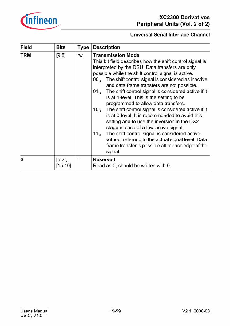
XC2300 DerivativesPeripheral Units (Vol. 2 of 2)
Universal Serial Interface Channel
TRM [9:8] rw Transmission ModeThis bit field describes how the shift control signal is interpreted by the DSU. Data transfers are only possible while the shift control signal is active.00B The shift control signal is considered as inactive
and data frame transfers are not possible.01B The shift control signal is considered active if it
is at 1-level. This is the setting to be programmed to allow data transfers.
10B The shift control signal is considered active if it is at 0-level. It is recommended to avoid this setting and to use the inversion in the DX2 stage in case of a low-active signal.
11B The shift control signal is considered active without referring to the actual signal level. Data frame transfer is possible after each edge of the signal.
0 [5:2], [15:10]
r ReservedRead as 0; should be written with 0.
Field Bits Type Description
User’s Manual 19-59 V2.1, 2008-08USIC, V1.0

XC2300 DerivativesPeripheral Units (Vol. 2 of 2)
Universal Serial Interface Channel
SCTRH Shift Control Register H (32H) Reset Value: 0000H
15 14 13 12 11 10 9 8 7 6 5 4 3 2 1 0
0 WLE 0 FLE
r rwh r rwh
Field Bits Type DescriptionFLE [5:0] rwh Frame Length
This bit field defines how many bits are transferred within a data frame. A data frame can consist of several concatenated data words.If TCSRL.FLEMD = 1, the value can be updated automatically by the data handler.
WLE [11:8] rwh Word LengthThis bit field defines the data word length (amount of bits that are transferred in each data word) for reception and transmission. The data word is always right-aligned in the data buffer at the bit positions [WLE down to 0].If TCSRL.WLEMD = 1, the value can be updated automatically by the data handler.0H The data word contains 1 data bit located at bit
position 0.1H The data word contains 2 data bits located at bit
positions [1:0]....FH The data word contains 16 data bits located at
bit positions [15:0].0 [7:6],
[15:12]r Reserved
Read as 0; should be written with 0.
User’s Manual 19-60 V2.1, 2008-08USIC, V1.0

XC2300 DerivativesPeripheral Units (Vol. 2 of 2)
Universal Serial Interface Channel
19.2.11.2 Transmission Control and Status RegistersThe data transmission is controlled by register TCSRL.
TCSRL Transmit Control/Status Register L (3CH) Reset Value: 0000H
15 14 13 12 11 10 9 8 7 6 5 4 3 2 1 0
0 WA TDVTR TDEN 0 TD
SSM TDV EOF SOF 0 WAMD
FLEMD
SELMD
WLEMD
r rwh rw rw r rw rh rwh rwh r rw rw rw rw
Field Bits Type DescriptionWLEMD 0 rw WLE Mode
This bit enables the data handler to automatically update the bit field SCTRH.WLE by the transmit control information TCI[3:0] and bit TCSR.EOF by TCI[4] (see Page 19-53). If enabled, an automatic update takes place when new data is loaded to register TBUF, either by writing to one of the transmit buffer input locations TBUFx or by an optional data buffer.0B The automatic update of SCTRH.WLE and
TCSR.EOF is disabled.1B The automatic update of SCTR.WLE and
TCSR.EOF is enabled.SELMD 1 rw Select Mode
This bit can be used mainly for the SSC protocol. It enables the data handler to automatically update bit field PCRH.CTR[20:16] by the transmit control information TCI[4:0] and clear bit field PCRH.CTR[23:21] (see Page 19-53). If enabled, an automatic update takes place when new data is loaded to register TBUF, either by writing to one of the transmit buffer input locations TBUFx or by an optional data buffer.0B The automatic update of PCRH.CTR[23:16] is
disabled.1B The automatic update of PCRH.CTR[23:16] is
disabled.
User’s Manual 19-61 V2.1, 2008-08USIC, V1.0

XC2300 DerivativesPeripheral Units (Vol. 2 of 2)
Universal Serial Interface Channel
FLEMD 2 rw FLE ModeThis bit enables the data handler to automatically update bits SCTRH.FLE[4:0] by the transmit control information TCI[4:0] and to clear bit SCTRH.FLE[5] (see Page 19-53). If enabled, an automatic update takes place when new data is loaded to register TBUF, either by writing to one of the transmit buffer input locations TBUFx or by an optional data buffer.0B The automatic update of FLE is disabled.1B The automatic update of FLE is enabled.
WAMD 3 rw WA ModeThis bit can be used mainly for the IIS protocol. It enables the data handler to automatically update bit TCSRL.WA by the transmit control information TCI[4] (see Page 19-53). If enabled, an automatic update takes place when new data is loaded to register TBUF, either by writing to one of the transmit buffer input locations TBUFx or by an optional data buffer.0B The automatic update of bit WA is disabled.1B The automatic update of bit WA is enabled.
SOF 5 rw Start Of FrameThis bit is only taken into account for the SSC protocol, otherwise it is ignored.It indicates that the data word in TBUF is considered as the first word of a new SSC frame if it is valid for transmission (TCSRL.TDV = 1). This bit becomes cleared when the TBUF data word is transferred to the transmit shift register.0B The data word in TBUF is not considered as
first word of a frame.1B The data word in TBUF is considered as first
word of a frame. A currently running frame is finished and MSLS becomes deactivated (respecting the programmed delays).
Field Bits Type Description
User’s Manual 19-62 V2.1, 2008-08USIC, V1.0

XC2300 DerivativesPeripheral Units (Vol. 2 of 2)
Universal Serial Interface Channel
EOF 6 rwh End Of FrameThis bit is only taken into account for the SSC protocol, otherwise it is ignored. It can be modified automatically by the data handler if bit WLEMD = 1.It indicates that the data word in TBUF is considered as the last word of an SSC frame. If it is the last word, the MSLS signal becomes inactive after the transfer, respecting the programmed delays. This bit becomes cleared when the TBUF data word is transferred to the transmit shift register.0B The data word in TBUF is not considered as
last word of an SSC frame.1B The data word in TBUF is considered as last
word of an SSC frame.TDV 7 rh Transmit Data Valid
This bit indicates that the data word in the transmit buffer TBUF can be considered as valid for transmission. The TBUF data word can only be sent out if TDV = 1. It is automatically set when data is moved to TBUF (by writing to one of the transmit buffer input locations TBUFx, or optionally, by the bypass or FIFO mechanism).0B The data word in TBUF is not valid for
transmission.1B The data word in TBUF is valid for transmission
and a transmission start is possible. New data should not be written to a TBUFx input location while TDV = 1.
Field Bits Type Description
User’s Manual 19-63 V2.1, 2008-08USIC, V1.0

XC2300 DerivativesPeripheral Units (Vol. 2 of 2)
Universal Serial Interface Channel
TDSSM 8 rw TBUF Data Single Shot ModeThis bit defines if the data word TBUF data is considered as permanently valid or if the data should only be transferred once.0B The data word in TBUF is not considered as
invalid after it has been loaded into the transmit shift register. The loading of the TBUF data into the shift register does not clear TDV.
1B The data word in TBUF is considered as invalid after it has been loaded into the shift register. In ASC and IIC mode, TDV is cleared with the TBI event, whereas in SSC and IIS mode, it is cleared with the RSI event.TDSSM = 1 has to be programmed if an optional data buffer is used.
TDEN [11:10] rw TBUF Data EnableThis bit field controls the gating of the transmission start of the data word in the transmit buffer TBUF.00B A transmission start of the data word in TBUF is
disabled. If a transmission is started, the passive data level is sent out.
01B A transmission of the data word in TBUF can be started if TDV = 1.
10B A transmission of the data word in TBUF can be started if TDV = 1 while DX2S = 0.
11B A transmission of the data word in TBUF can be started if TDV = 1 while DX2S = 1.
TDVTR 12 rw TBUF Data Valid TriggerThis bit enables the transfer trigger unit to set bit TCSRH.TE if the trigger signal DX2T becomes active for event driven transfer starts, e.g. timer-based or depending on an event at an input pin. Bit TDVTR has to be 0 for protocols where the input stage DX2 is used for data shifting.0B Bit TCSRH.TE is permanently set.1B Bit TCSRH.TE is set if DX2T becomes active
while TDV = 1.
Field Bits Type Description
User’s Manual 19-64 V2.1, 2008-08USIC, V1.0
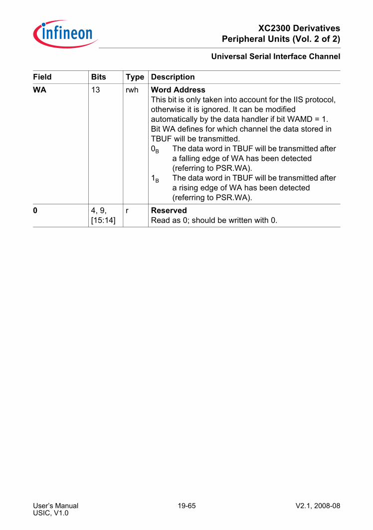
XC2300 DerivativesPeripheral Units (Vol. 2 of 2)
Universal Serial Interface Channel
WA 13 rwh Word AddressThis bit is only taken into account for the IIS protocol, otherwise it is ignored. It can be modified automatically by the data handler if bit WAMD = 1.Bit WA defines for which channel the data stored in TBUF will be transmitted.0B The data word in TBUF will be transmitted after
a falling edge of WA has been detected (referring to PSR.WA).
1B The data word in TBUF will be transmitted after a rising edge of WA has been detected (referring to PSR.WA).
0 4, 9, [15:14]
r ReservedRead as 0; should be written with 0.
Field Bits Type Description
User’s Manual 19-65 V2.1, 2008-08USIC, V1.0

XC2300 DerivativesPeripheral Units (Vol. 2 of 2)
Universal Serial Interface Channel
The data transmission status is monitored by register TCSRH.
TCSRH Transmit Control/Status Register H (3EH) Reset Value: 0000H
15 14 13 12 11 10 9 8 7 6 5 4 3 2 1 0
0 TE TVC TV 0 TSOF 0
r rh rh rh r rh r
Field Bits Type DescriptionTSOF 8 rh Transmitted Start Of Frame
This bit indicates if the latest start of a data word transmission has taken place for the first data word of a new data frame. This bit is updated with the transmission start of each data word.0B The latest data word transmission has not been
started for the first word of a data frame.1B The latest data word transmission has been
started for the first word of a data frame.TV 10 rh Transmission Valid
This bit represents the transmit buffer underflow and indicates if the latest start of a data word transmission has taken place with a valid data word from the transmit buffer TBUF. This bit is updated with the transmission start of each data word.0B The latest start of a data word transmission has
taken place while no valid data was available. As a result, the transmission of a data words with passive level (SCTRL.PDL) has been started.
1B The latest start of a data word transmission has taken place with valid data from TBUF.
TVC 11 rh Transmission Valid CumulatedThis bit cumulates the transmit buffer underflow indication TV. It is cleared automatically together with bit TV and has to be set by writing FMRL.ATVC = 1.0B Since TVC has been set, at least one data
buffer underflow condition has occurred.1B Since TVC has been set, no data buffer
underflow condition has occurred.
User’s Manual 19-66 V2.1, 2008-08USIC, V1.0
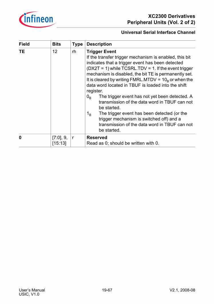
XC2300 DerivativesPeripheral Units (Vol. 2 of 2)
Universal Serial Interface Channel
TE 12 rh Trigger EventIf the transfer trigger mechanism is enabled, this bit indicates that a trigger event has been detected (DX2T = 1) while TCSRL.TDV = 1. If the event trigger mechanism is disabled, the bit TE is permanently set. It is cleared by writing FMRL.MTDV = 10B or when the data word located in TBUF is loaded into the shift register.0B The trigger event has not yet been detected. A
transmission of the data word in TBUF can not be started.
1B The trigger event has been detected (or the trigger mechanism is switched off) and a transmission of the data word in TBUF can not be started.
0 [7:0], 9, [15:13]
r ReservedRead as 0; should be written with 0.
Field Bits Type Description
User’s Manual 19-67 V2.1, 2008-08USIC, V1.0
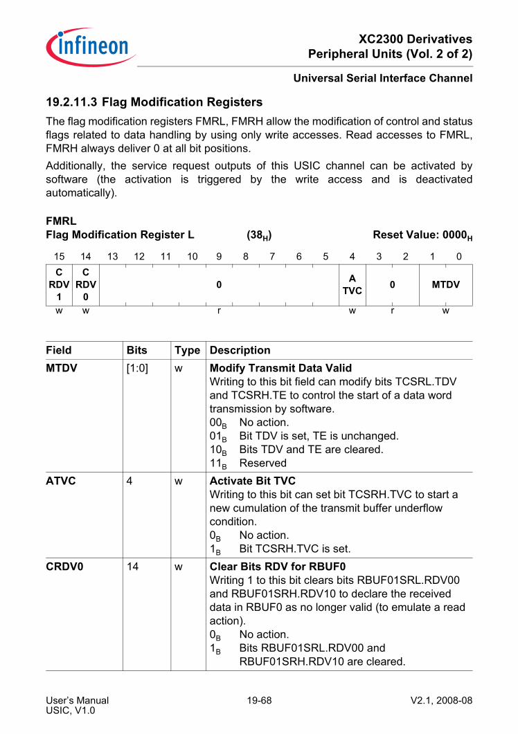
XC2300 DerivativesPeripheral Units (Vol. 2 of 2)
Universal Serial Interface Channel
19.2.11.3 Flag Modification RegistersThe flag modification registers FMRL, FMRH allow the modification of control and statusflags related to data handling by using only write accesses. Read accesses to FMRL,FMRH always deliver 0 at all bit positions.Additionally, the service request outputs of this USIC channel can be activated bysoftware (the activation is triggered by the write access and is deactivatedautomatically).
FMRL Flag Modification Register L (38H) Reset Value: 0000H
15 14 13 12 11 10 9 8 7 6 5 4 3 2 1 0C
RDV1
CRDV
00 A
TVC 0 MTDV
w w r w r w
Field Bits Type DescriptionMTDV [1:0] w Modify Transmit Data Valid
Writing to this bit field can modify bits TCSRL.TDV and TCSRH.TE to control the start of a data word transmission by software.00B No action.01B Bit TDV is set, TE is unchanged.10B Bits TDV and TE are cleared.11B Reserved
ATVC 4 w Activate Bit TVCWriting to this bit can set bit TCSRH.TVC to start a new cumulation of the transmit buffer underflow condition.0B No action.1B Bit TCSRH.TVC is set.
CRDV0 14 w Clear Bits RDV for RBUF0Writing 1 to this bit clears bits RBUF01SRL.RDV00 and RBUF01SRH.RDV10 to declare the received data in RBUF0 as no longer valid (to emulate a read action).0B No action.1B Bits RBUF01SRL.RDV00 and
RBUF01SRH.RDV10 are cleared.
User’s Manual 19-68 V2.1, 2008-08USIC, V1.0
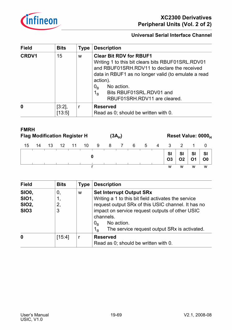
XC2300 DerivativesPeripheral Units (Vol. 2 of 2)
Universal Serial Interface Channel
CRDV1 15 w Clear Bit RDV for RBUF1Writing 1 to this bit clears bits RBUF01SRL.RDV01 and RBUF01SRH.RDV11 to declare the received data in RBUF1 as no longer valid (to emulate a read action).0B No action.1B Bits RBUF01SRL.RDV01 and
RBUF01SRH.RDV11 are cleared.0 [3:2],
[13:5]r Reserved
Read as 0; should be written with 0.
FMRH Flag Modification Register H (3AH) Reset Value: 0000H
15 14 13 12 11 10 9 8 7 6 5 4 3 2 1 0
0 SIO3
SIO2
SIO1
SIO0
r w w w w
Field Bits Type DescriptionSIO0,SIO1,SIO2,SIO3
0,1,2,3
w Set Interrupt Output SRxWriting a 1 to this bit field activates the service request output SRx of this USIC channel. It has no impact on service request outputs of other USIC channels.0B No action.1B The service request output SRx is activated.
0 [15:4] r ReservedRead as 0; should be written with 0.
Field Bits Type Description
User’s Manual 19-69 V2.1, 2008-08USIC, V1.0
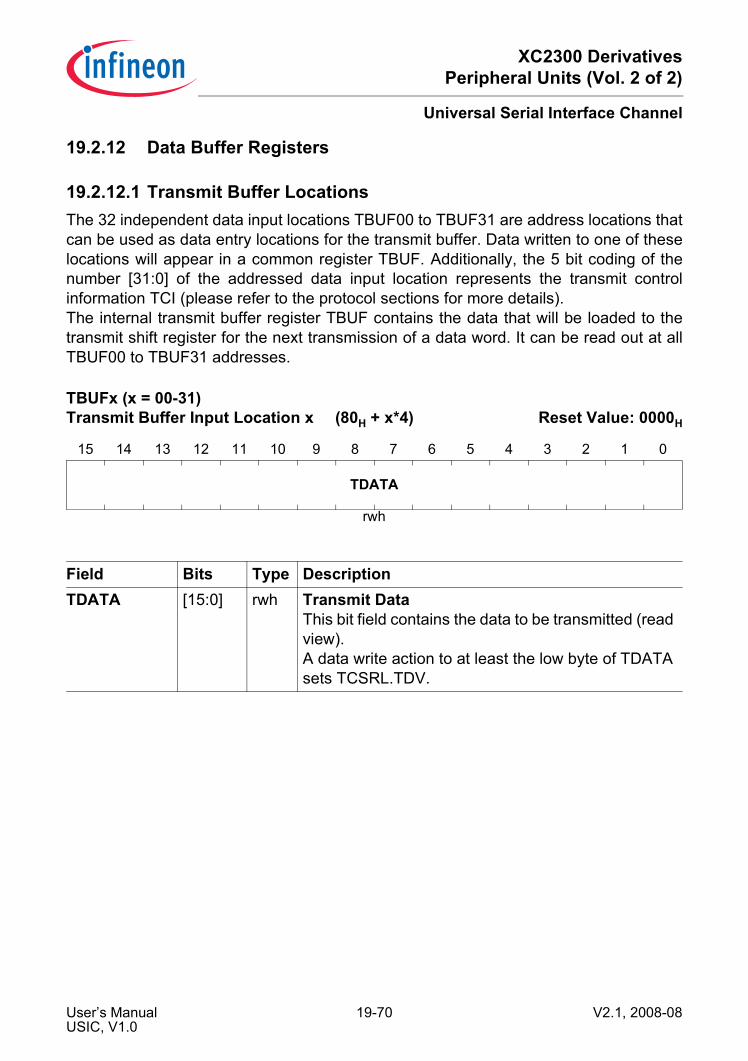
XC2300 DerivativesPeripheral Units (Vol. 2 of 2)
Universal Serial Interface Channel
19.2.12 Data Buffer Registers
19.2.12.1 Transmit Buffer LocationsThe 32 independent data input locations TBUF00 to TBUF31 are address locations thatcan be used as data entry locations for the transmit buffer. Data written to one of theselocations will appear in a common register TBUF. Additionally, the 5 bit coding of thenumber [31:0] of the addressed data input location represents the transmit controlinformation TCI (please refer to the protocol sections for more details).The internal transmit buffer register TBUF contains the data that will be loaded to thetransmit shift register for the next transmission of a data word. It can be read out at allTBUF00 to TBUF31 addresses.
TBUFx (x = 00-31) Transmit Buffer Input Location x (80H + x*4) Reset Value: 0000H
15 14 13 12 11 10 9 8 7 6 5 4 3 2 1 0
TDATA
rwh
Field Bits Type DescriptionTDATA [15:0] rwh Transmit Data
This bit field contains the data to be transmitted (read view).A data write action to at least the low byte of TDATA sets TCSRL.TDV.
User’s Manual 19-70 V2.1, 2008-08USIC, V1.0

XC2300 DerivativesPeripheral Units (Vol. 2 of 2)
Universal Serial Interface Channel
19.2.12.2 Receive Buffer Registers RBUF0, RBUF1The receive buffer register RBUF0 contains the data received from RSR0. A read actiondoes not change the status of the receive data from “not yet read = valid” to “already read= not valid”.
The receive buffer status register RBUF01SRL provides the status of the data in receivebuffer RBUF0.
RBUF0 Receiver Buffer Register 0 (50H) Reset Value: 0000H
15 14 13 12 11 10 9 8 7 6 5 4 3 2 1 0
DSR0
rh
Field Bits Type DescriptionDSR0 [15:0] rh Data of Shift Register 0
RBUF01SRL Receiver Buffer 01 Status Register L (60H) Reset Value: 0000H
15 14 13 12 11 10 9 8 7 6 5 4 3 2 1 0
DS0
RDV01
RDV00 0
PERR
0
PAR0 0 SOF
0 0 WLEN0
rh rh rh r rh rh r rh r rh
Field Bits Type DescriptionWLEN0 [3:0] rh Received Data Word Length in RBUF0
This bit field indicates how many bits have been received within the last data word stored in RBUF0. This number indicates how many data bits have to be considered as receive data, whereas the other bits in RBUF0 have been cleared automatically. The received bits are always right-aligned.0H One bit has been received....FH Sixteen bits have been received.
User’s Manual 19-71 V2.1, 2008-08USIC, V1.0

XC2300 DerivativesPeripheral Units (Vol. 2 of 2)
Universal Serial Interface Channel
SOF0 6 rh Start of Frame in RBUF0This bit indicates whether the data word in RBUF0 has been the first data word of a data frame.0B The data in RBUF0 has not been the first data
word of a data frame.1B The data in RBUF0 has been the first data word
of a data frame.PAR0 8 rh Protocol-Related Argument in RBUF0
This bit indicates the value of the protocol-related argument. This value is elaborated depending on the selected protocol and adds additional information to the data word in RBUF0.The meaning of this bit is described in the corresponding protocol chapter.
PERR0 9 rh Protocol-related Error in RBUF0This bit indicates if the value of the protocol-related argument meets an expected value. This value is elaborated depending on the selected protocol and adds additional information to the data word in RBUF0.The meaning of this bit is described in the corresponding protocol chapter.0B The received protocol-related argument PAR
matches the expected value. The reception of the data word sets bit PSR.RIF and can generate a receive interrupt.
1B The received protocol-related argument PAR does not match the expected value. The reception of the data word sets bit PSR.AIF and can generate an alternative receive interrupt.
Field Bits Type Description
User’s Manual 19-72 V2.1, 2008-08USIC, V1.0
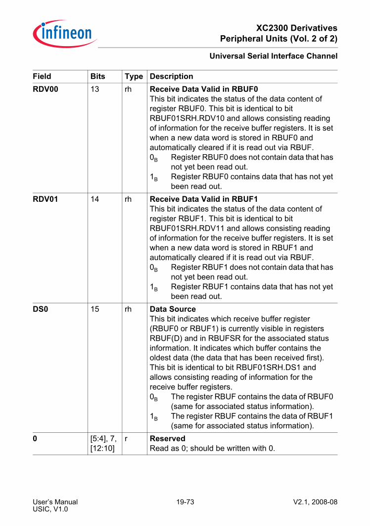
XC2300 DerivativesPeripheral Units (Vol. 2 of 2)
Universal Serial Interface Channel
RDV00 13 rh Receive Data Valid in RBUF0This bit indicates the status of the data content of register RBUF0. This bit is identical to bit RBUF01SRH.RDV10 and allows consisting reading of information for the receive buffer registers. It is set when a new data word is stored in RBUF0 and automatically cleared if it is read out via RBUF.0B Register RBUF0 does not contain data that has
not yet been read out.1B Register RBUF0 contains data that has not yet
been read out.RDV01 14 rh Receive Data Valid in RBUF1
This bit indicates the status of the data content of register RBUF1. This bit is identical to bit RBUF01SRH.RDV11 and allows consisting reading of information for the receive buffer registers. It is set when a new data word is stored in RBUF1 and automatically cleared if it is read out via RBUF.0B Register RBUF1 does not contain data that has
not yet been read out.1B Register RBUF1 contains data that has not yet
been read out.DS0 15 rh Data Source
This bit indicates which receive buffer register (RBUF0 or RBUF1) is currently visible in registers RBUF(D) and in RBUFSR for the associated status information. It indicates which buffer contains the oldest data (the data that has been received first). This bit is identical to bit RBUF01SRH.DS1 and allows consisting reading of information for the receive buffer registers.0B The register RBUF contains the data of RBUF0
(same for associated status information).1B The register RBUF contains the data of RBUF1
(same for associated status information).0 [5:4], 7,
[12:10]r Reserved
Read as 0; should be written with 0.
Field Bits Type Description
User’s Manual 19-73 V2.1, 2008-08USIC, V1.0
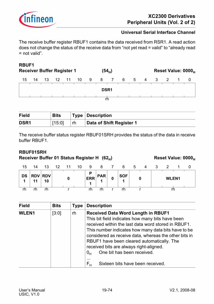
XC2300 DerivativesPeripheral Units (Vol. 2 of 2)
Universal Serial Interface Channel
The receive buffer register RBUF1 contains the data received from RSR1. A read actiondoes not change the status of the receive data from “not yet read = valid” to “already read= not valid”.
The receive buffer status register RBUF01SRH provides the status of the data in receivebuffer RBUF1.
RBUF1 Receiver Buffer Register 1 (54H) Reset Value: 0000H
15 14 13 12 11 10 9 8 7 6 5 4 3 2 1 0
DSR1
rh
Field Bits Type DescriptionDSR1 [15:0] rh Data of Shift Register 1
RBUF01SRH Receiver Buffer 01 Status Register H (62H) Reset Value: 0000H
15 14 13 12 11 10 9 8 7 6 5 4 3 2 1 0
DS1
RDV11
RDV10 0
PERR
1
PAR1 0 SOF
1 0 WLEN1
rh rh rh r rh rh r rh r rh
Field Bits Type DescriptionWLEN1 [3:0] rh Received Data Word Length in RBUF1
This bit field indicates how many bits have been received within the last data word stored in RBUF1. This number indicates how many data bits have to be considered as receive data, whereas the other bits in RBUF1 have been cleared automatically. The received bits are always right-aligned.0H One bit has been received....FH Sixteen bits have been received.
User’s Manual 19-74 V2.1, 2008-08USIC, V1.0

XC2300 DerivativesPeripheral Units (Vol. 2 of 2)
Universal Serial Interface Channel
SOF1 6 rh Start of Frame in RBUF1This bit indicates whether the data word in RBUF1 has been the first data word of a data frame.0B The data in RBUF1 has not been the first data
word of a data frame.1B The data in RBUF1 has been the first data word
of a data frame.PAR1 8 rh Protocol-Related Argument in RBUF1
This bit indicates the value of the protocol-related argument. This value is elaborated depending on the selected protocol and adds additional information to the data word in RBUF1.The meaning of this bit is described in the corresponding protocol chapter.
PERR1 9 rh Protocol-related Error in RBUF1This bit indicates if the value of the protocol-related argument meets an expected value. This value is elaborated depending on the selected protocol and adds additional information to the data word in RBUF1.The meaning of this bit is described in the corresponding protocol chapter.0B The received protocol-related argument PAR
matches the expected value. The reception of the data word sets bit PSR.RIF and can generate a receive interrupt.
1B The received protocol-related argument PAR does not match the expected value. The reception of the data word sets bit PSR.AIF and can generate an alternative receive interrupt.
RDV10 13 rh Receive Data Valid in RBUF0This bit indicates the status of the data content of register RBUF0. This bit is identical to bit RBUF01SRL.RDV00 and allows consisting reading of information for the receive buffer registers.0B Register RBUF0 does not contain data that has
not yet been read out.1B Register RBUF0 contains data that has not yet
been read out.
Field Bits Type Description
User’s Manual 19-75 V2.1, 2008-08USIC, V1.0
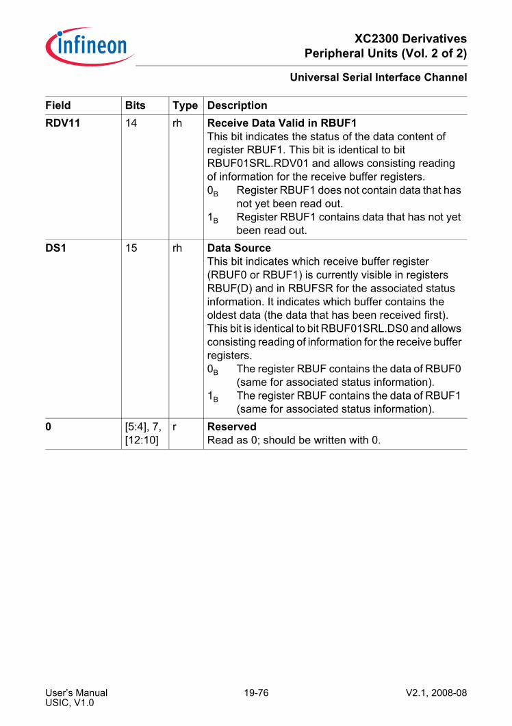
XC2300 DerivativesPeripheral Units (Vol. 2 of 2)
Universal Serial Interface Channel
RDV11 14 rh Receive Data Valid in RBUF1This bit indicates the status of the data content of register RBUF1. This bit is identical to bit RBUF01SRL.RDV01 and allows consisting reading of information for the receive buffer registers.0B Register RBUF1 does not contain data that has
not yet been read out.1B Register RBUF1 contains data that has not yet
been read out.DS1 15 rh Data Source
This bit indicates which receive buffer register (RBUF0 or RBUF1) is currently visible in registers RBUF(D) and in RBUFSR for the associated status information. It indicates which buffer contains the oldest data (the data that has been received first). This bit is identical to bit RBUF01SRL.DS0 and allows consisting reading of information for the receive buffer registers.0B The register RBUF contains the data of RBUF0
(same for associated status information).1B The register RBUF contains the data of RBUF1
(same for associated status information).0 [5:4], 7,
[12:10]r Reserved
Read as 0; should be written with 0.
Field Bits Type Description
User’s Manual 19-76 V2.1, 2008-08USIC, V1.0

XC2300 DerivativesPeripheral Units (Vol. 2 of 2)
Universal Serial Interface Channel
19.2.12.3 Receive Buffer Registers RBUF, RBUFD, RBUFSRThe receiver buffer register RBUF shows the content of the either RBUF0 or RBUF1,depending on the order of reception. Always the oldest data (the data word that has beenreceived first) from both receive buffers can be read from RBUF. It is recommended toread out the received data from RBUF instead of RBUF0/1. With a read access of at leastthe low byte of RBUF, the status of the receive data is automatically changed from “notyet read = valid” to “already read = not valid”, the content of RBUF becomes updated,and the next received data word becomes visible in RBUF.
RBUF Receiver Buffer Register (5CH) Reset Value: 0000H
15 14 13 12 11 10 9 8 7 6 5 4 3 2 1 0
DSR
rh
Field Bits Type DescriptionDSR [15:0] rh Received Data
This bit field monitors the content of either RBUF0 or RBUF1, depending on the reception sequence.
User’s Manual 19-77 V2.1, 2008-08USIC, V1.0
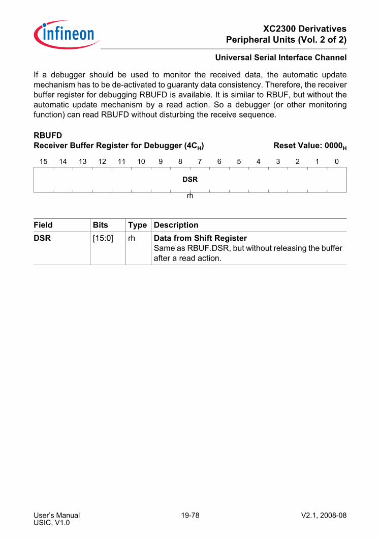
XC2300 DerivativesPeripheral Units (Vol. 2 of 2)
Universal Serial Interface Channel
If a debugger should be used to monitor the received data, the automatic updatemechanism has to be de-activated to guaranty data consistency. Therefore, the receiverbuffer register for debugging RBUFD is available. It is similar to RBUF, but without theautomatic update mechanism by a read action. So a debugger (or other monitoringfunction) can read RBUFD without disturbing the receive sequence.
RBUFD Receiver Buffer Register for Debugger (4CH) Reset Value: 0000H
15 14 13 12 11 10 9 8 7 6 5 4 3 2 1 0
DSR
rh
Field Bits Type DescriptionDSR [15:0] rh Data from Shift Register
Same as RBUF.DSR, but without releasing the buffer after a read action.
User’s Manual 19-78 V2.1, 2008-08USIC, V1.0

XC2300 DerivativesPeripheral Units (Vol. 2 of 2)
Universal Serial Interface Channel
The receive buffer status register RBUFSR provides the status of the data in receivebuffers RBUF and RBUFD. If bits RBUF01SRL.DS0 (or RBUF01SRH.DS1) are 0, thecontent of RBUF01SRL is monitored in RBUFSR, otherwise the content of RBUF01SRHis shown.
RBUFSR Receiver Buffer Status Register (58H) Reset Value: 0000H
15 14 13 12 11 10 9 8 7 6 5 4 3 2 1 0
DS RDV1
RDV0 0 P
ERR PAR 0 SOF 0 WLEN
rh rh rh r rh rh r rh r rh
Field Bits Type DescriptionWLEN [3:0] rh Received Data Word Length in RBUF or RBUFD
Description see RBUF01SRL.WLEN0 or RBUF01SRH.WLEN1.
SOF 6 rh Start of Frame in RBUF or RBUFDDescription see RBUF01SRL.SOF0 or RBUF01SRH.SOF1.
PAR 8 rh Protocol-Related Argument in RBUF or RBUFDDescription see RBUF01SRL.PAR0 or RBUF01SRH.PAR1.
PERR 9 rh Protocol-related Error in RBUF or RBUFDDescription see RBUF01SRL.PERR0 or RBUF01SRH.PERR1.
RDV0 13 rh Receive Data Valid in RBUF or RBUFDDescription see RBUF01SRL.RDV00 or RBUF01SRH.RDV10.
RDV1 14 rh Receive Data Valid in RBUF or RBUFDDescription see RBUF01SRL.RDV01 or RBUF01SRH.RDV11.
DS 15 rh Data Source of RBUF or RBUFDDescription see RBUF01SRL.DS0 or RBUF01SRH.DS1.
0 [5:4], 7, [12:10]
r ReservedRead as 0; should be written with 0.
User’s Manual 19-79 V2.1, 2008-08USIC, V1.0

XC2300 DerivativesPeripheral Units (Vol. 2 of 2)
Universal Serial Interface Channel
19.2.13 Operating the FIFO Data BufferThe FIFO data buffers of a USIC module are built in a similar way, with transmit bufferand receive buffer capability for each channel. Depending on the device, the amount ofavailable FIFO buffer area can vary. In the XC2300, totally 64 buffer entries can bedistributed among the transmit or receive FIFO buffers of both channels of the USICmodule.
Figure 19-18 FIFO Buffer Overview
In order to operate the FIFO data buffers, the following issues have to be considered:• FIFO buffer available and selected:
The transmit FIFO buffer and the bypass structure are only available if CCFG.TB = 1,whereas the receive FIFO buffer is only available if CCFG.RB = 1.It is recommended to configure all buffer parameters while there is no data traffic forthis USIC channel and the FIFO mechanism is disabled by TBCTRH.SIZE = 0 (fortransmit buffer) or RBCTRH.SIZE = 0 (for receive buffer). The allocation of a bufferarea by writing TBCTRL or RBCTRL has to be done while the corresponding FIFObuffer is disabled. The FIFO buffer interrupt control bits can be modifiedindependently of data traffic.
• FIFO buffer setup:The total amount of available FIFO buffer entries limits the length of the transmit andreceive buffers for each USIC channel.
USIC_FIFOBidirect
ReceiveFIFO
Buffered Transmit DataTransmit Data
Buffered Receive Data Receive Data
Shift Data Output
Shift Data Input
Bypass
DataShiftUnit
(DSU)
RBUF
TBUFTransmit
FIFO
UxC0
ReceiveFIFO
Buffered Transmit DataTransmit Data
Buffered Receive Data Receive Data
Shift Data Output
Shift Data Input
Bypass
DataShiftUnit
(DSU)
RBUF
TBUFTransmit
FIFO
UxC1
UserInter-face
OUTR
OUTR
INx
INx
User’s Manual 19-80 V2.1, 2008-08USIC, V1.0
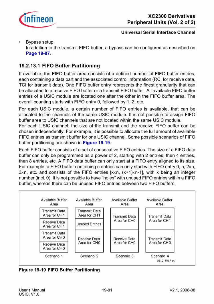
XC2300 DerivativesPeripheral Units (Vol. 2 of 2)
Universal Serial Interface Channel
• Bypass setup:In addition to the transmit FIFO buffer, a bypass can be configured as described onPage 19-87.
19.2.13.1 FIFO Buffer PartitioningIf available, the FIFO buffer area consists of a defined number of FIFO buffer entries,each containing a data part and the associated control information (RCI for receive data,TCI for transmit data). One FIFO buffer entry represents the finest granularity that canbe allocated to a receive FIFO buffer or a transmit FIFO buffer. All available FIFO bufferentries of a USIC module are located one after the other in the FIFO buffer area. Theoverall counting starts with FIFO entry 0, followed by 1, 2, etc.For each USIC module, a certain number of FIFO entries is available, that can beallocated to the channels of the same USIC module. It is not possible to assign FIFObuffer area to USIC channels that are not located within the same USIC module.For each USIC channel, the size of the transmit and the receive FIFO buffer can bechosen independently. For example, it is possible to allocate the full amount of availableFIFO entries as transmit buffer for one USIC channel. Some possible scenarios of FIFObuffer partitioning are shown in Figure 19-19.Each FIFO buffer consists of a set of consecutive FIFO entries. The size of a FIFO databuffer can only be programmed as a power of 2, starting with 2 entries, then 4 entries,then 8 entries, etc. A FIFO data buffer can only start at a FIFO entry aligned to its size.For example, a FIFO buffer containing n entries can only start with FIFO entry 0, n, 2×n,3×n, etc. and consists of the FIFO entries [x×n, (x+1)×n-1], with x being an integernumber (incl. 0). It is not possible to have “holes” with unused FIFO entries within a FIFObuffer, whereas there can be unused FIFO entries between two FIFO buffers.
Figure 19-19 FIFO Buffer Partitioning
USIC_FifoPart
Transmit DataArea for CH1
Receive DataArea for CH1
Transmit DataArea for CH0
Receive DataArea for CH0
Scenario 1
Available Buffer Area
Transmit DataArea for CH1
Receive DataArea for CH0
Unused Entries
Scenario 2
Available Buffer Area
Transmit DataArea for CH0
Receive DataArea for CH0
Scenario 3
Available Buffer Area
Transmit DataArea for CH1
Transmit DataArea for CH0
Scenario 4
Available Buffer Area
User’s Manual 19-81 V2.1, 2008-08USIC, V1.0

XC2300 DerivativesPeripheral Units (Vol. 2 of 2)
Universal Serial Interface Channel
The data storage inside the FIFO buffers is based on pointers, that are internally updatedwhenever the data contents of the FIFO buffers have been modified. This happensautomatically when new data is put into a FIFO buffer or the oldest data is taken from aFIFO buffer. As a consequence, the user program does not need to modify the pointersfor data handling. Only during the initialization phase, the start entry of a FIFO buffer hasto be defined by writing the number of the first FIFO buffer entry in the FIFO buffer to thecorresponding bit field DPTR in register RBCTRL (for a receive FIFO buffer) or TBCTRL(for a transmit FIFO buffer) while the related bit field RBCTRH.SIZE=0 (orTBCTRH.SIZE = 0, respectively). The assignment of buffer entries to a FIFO buffer(regarding to size and pointers) must not be changed by software while the related USICchannel is taking part in data traffic.
19.2.13.2 Data Buffer Events and InterruptsThe transmit FIFO buffer mechanism detects the following events, that can lead tointerrupts (if enabled).• Standard transmit buffer event:
The filling level of the transmit buffer (given by TRBSRH.TBFLVL) exceeds(TBCTRH.LOF = 1) or falls below (TBCTRH.LOF = 0) a programmed limit(TBCTRL.LIMIT). The trigger of this event is the transition from equal to below orbigger, not the fact of being below or above.If the standard transmit buffer event is used to indicate that new data has to be writtento one of the INx locations, TBCTRH.LOF = 0 should be programmed.
• Transmit buffer error event:The software has written to a full buffer. The written value is ignored.
User’s Manual 19-82 V2.1, 2008-08USIC, V1.0
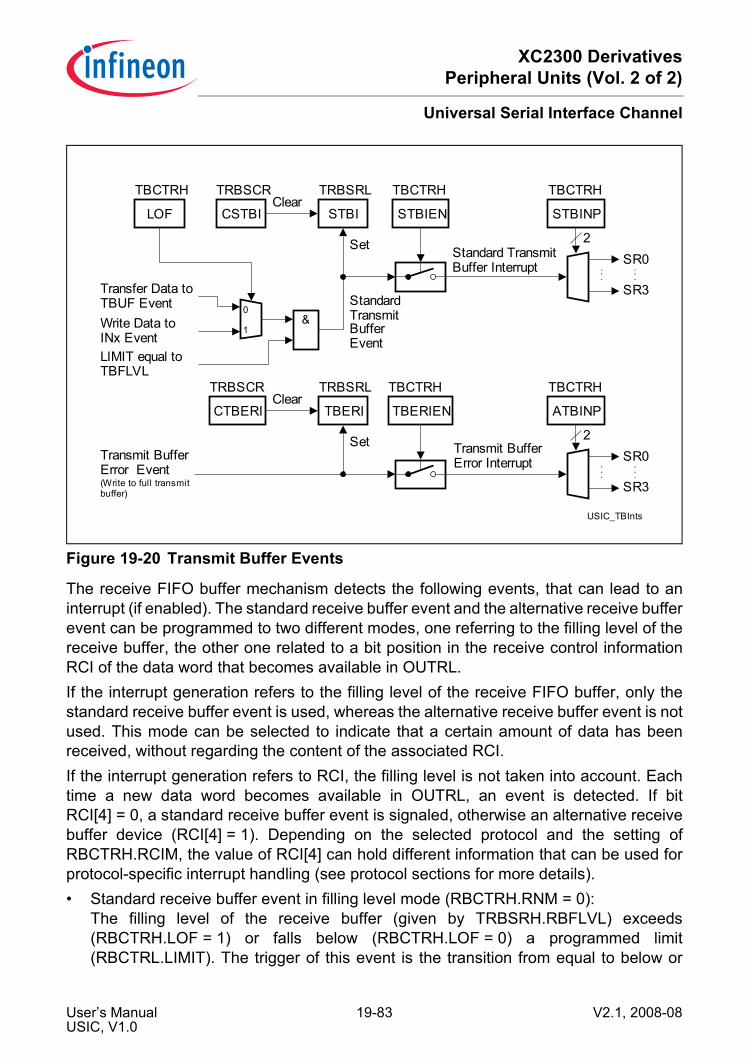
XC2300 DerivativesPeripheral Units (Vol. 2 of 2)
Universal Serial Interface Channel
Figure 19-20 Transmit Buffer Events
The receive FIFO buffer mechanism detects the following events, that can lead to aninterrupt (if enabled). The standard receive buffer event and the alternative receive bufferevent can be programmed to two different modes, one referring to the filling level of thereceive buffer, the other one related to a bit position in the receive control informationRCI of the data word that becomes available in OUTRL.If the interrupt generation refers to the filling level of the receive FIFO buffer, only thestandard receive buffer event is used, whereas the alternative receive buffer event is notused. This mode can be selected to indicate that a certain amount of data has beenreceived, without regarding the content of the associated RCI.If the interrupt generation refers to RCI, the filling level is not taken into account. Eachtime a new data word becomes available in OUTRL, an event is detected. If bitRCI[4] = 0, a standard receive buffer event is signaled, otherwise an alternative receivebuffer device (RCI[4] = 1). Depending on the selected protocol and the setting ofRBCTRH.RCIM, the value of RCI[4] can hold different information that can be used forprotocol-specific interrupt handling (see protocol sections for more details).• Standard receive buffer event in filling level mode (RBCTRH.RNM = 0):
The filling level of the receive buffer (given by TRBSRH.RBFLVL) exceeds(RBCTRH.LOF = 1) or falls below (RBCTRH.LOF = 0) a programmed limit(RBCTRL.LIMIT). The trigger of this event is the transition from equal to below or
USIC_TBInts
TBERIEN
TBCTRH
Transmit Buffer Error Event(Write to full transmit buffer)
TBERI
TRBSRL
Set 2SR0
SR3
......
CTBERI
TRBSCRClear
STBIEN
TBCTRH
STBI
TRBSRL
Set 2
STBINP
TBCTRH
CSTBI
TRBSCRClear
SR0
SR3
......
Transfer Data to TBUF Event 0
1
LOF
TBCTRH
Standard Transmit Buffer Interrupt
Transmit Buffer Error Interrupt
ATBINP
TBCTRH
&
LIMIT equal to TBFLVL
Write Data to INx Event
StandardTransmitBufferEvent
User’s Manual 19-83 V2.1, 2008-08USIC, V1.0

XC2300 DerivativesPeripheral Units (Vol. 2 of 2)
Universal Serial Interface Channel
greater, not the fact of being below or above.If the standard receive buffer event is used to indicate that new data has to be readfrom OUTRL, RBCTRH.LOF = 1 should be programmed.
• Standard receive buffer event in RCI mode (RBCTRH.RNM = 1):If the OUTR stage is updated with a new data value with RCI[4] = 0.
• Alternative receive buffer event in filling level mode (RBCTRH.RNM = 0): not used• Alternative receive buffer event in RCI mode (RBCTRH.RNM = 1):
If the OUTR stage is updated with a new value with RCI[4] = 1.• Receive buffer error event:
The software reads from an empty buffer. The read data is invalid.Figure 19-21 shows the receiver buffer events and interrupts in filling level mode.Note: A buffer event in filling level mode occurs only when the filling level transitions
away from the threshold value. Transitions starting with a filling level other thanthe threshold level generate no trigger event.
Figure 19-21 Receiver Buffer Events in Filling Level Mode
USIC _RBRNM0
RBERIEN
RBCTRH
Receive Buffer Error Event(Read from empty receive buffer)
RBERI
TRBSRL
Set 2SR0
SR3
......
CRBERI
TRBSCRClear
STBIEN
RBCTRH
SRBI
TRBSRL
Set 2
SRBINP
RBCTRH
CSRBI
TRBSCRClear
SR0
SR3
......
Data Read Out Event 0
1
LOF
RBCTRH
Standard Receive Buffer Interrupt
Receive Buffer Error Interrupt
ARBINP
RBCTRH
&
LIMIT equal to RBFLVL
New Data Received Event
StandardReceiveBufferEvent
User’s Manual 19-84 V2.1, 2008-08USIC, V1.0

XC2300 DerivativesPeripheral Units (Vol. 2 of 2)
Universal Serial Interface Channel
Figure 19-22 shows the receiver buffer events and interrupts in RCI mode.
Figure 19-22 Receiver Buffer Events in RCI Mode
Table 19-7 shows the registers, bits and bit fields to indicate the buffer events and tocontrol the interrupts related to the FIFO buffers (transmit and the receive) of a USICchannel.
Table 19-7 Buffer Events and Interrupt HandlingEvent Indication
FlagIndication cleared by
Interrupt enabled by
SRx Output selected by
Standard transmit buffer event TRBSRL.STBI
TRBSCR.CSTBI
TBCTRH.STBIEN
TBCTRH.STBINP
Transmit buffer error event TRBSRL.TBERI
TRBSCR.CTBERI
TBCTRH.TBERIEN
TBCTRH.ATBINP
Standard receive buffer event TRBSRL.SRBI
TRBSCR.CSRBI
RBCTRH.SRBIEN
RBCTRH.SRBINP
USIC _RBRNM1
RBERIEN
RBCTRH
Receive Buffer Error Event(Read from empty receive buffer)
RBERI
TRBSRL
Set 2SR0
SR3
......
CRBERI
TRBSCRClear
ARBIEN
RBCTRH
ARBI
TRBSRL
ARBINP
RBCTRH
CARBI
TRBSCR
Clear
SRBIEN
RBCTRH
SRBI
TRBSRL
Set 2
SRBINP
RBCTRH
SR0
SR3
......
CSRBI
TRBSCRClear
SR0
SR3
......
2Set
New Data in OUTRL Event
0
1
Standard ReceiveBuffer Event
RCI[4]
OUTRH
Standard Receive Buffer Interrupt
Receive Buffer Error Interrupt
Alternate ReceiveBuffer Event
Alternate Receive Buffer Interrupt
User’s Manual 19-85 V2.1, 2008-08USIC, V1.0

XC2300 DerivativesPeripheral Units (Vol. 2 of 2)
Universal Serial Interface Channel
Alternative receive buffer event TRBSRL.ARBI
TRBSCR.CARBI
RBCTRH.ARBIEN
RBCTRH.ARBINP
Receive buffer error event TRBSRL.RBERI
TRBSCR.CRBERI
RBCTRH.RBERIEN
RBCTRH.ARBINTXDP
Table 19-7 Buffer Events and Interrupt HandlingEvent Indication
FlagIndication cleared by
Interrupt enabled by
SRx Output selected by
User’s Manual 19-86 V2.1, 2008-08USIC, V1.0
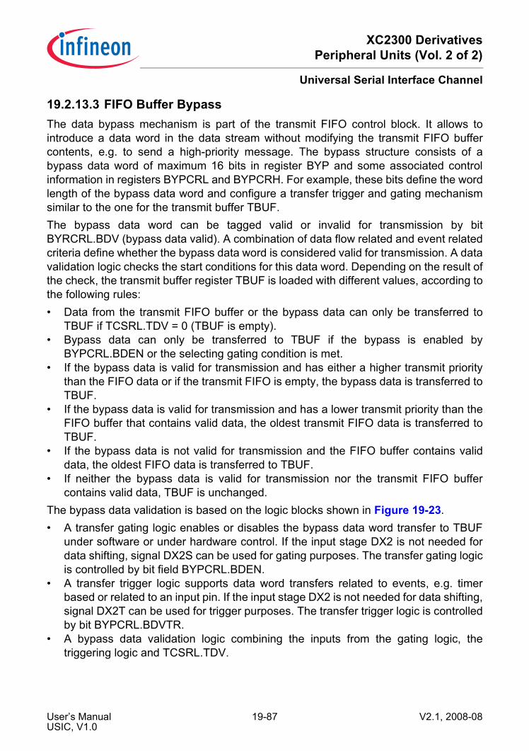
XC2300 DerivativesPeripheral Units (Vol. 2 of 2)
Universal Serial Interface Channel
19.2.13.3 FIFO Buffer BypassThe data bypass mechanism is part of the transmit FIFO control block. It allows tointroduce a data word in the data stream without modifying the transmit FIFO buffercontents, e.g. to send a high-priority message. The bypass structure consists of abypass data word of maximum 16 bits in register BYP and some associated controlinformation in registers BYPCRL and BYPCRH. For example, these bits define the wordlength of the bypass data word and configure a transfer trigger and gating mechanismsimilar to the one for the transmit buffer TBUF.The bypass data word can be tagged valid or invalid for transmission by bitBYRCRL.BDV (bypass data valid). A combination of data flow related and event relatedcriteria define whether the bypass data word is considered valid for transmission. A datavalidation logic checks the start conditions for this data word. Depending on the result ofthe check, the transmit buffer register TBUF is loaded with different values, according tothe following rules:• Data from the transmit FIFO buffer or the bypass data can only be transferred to
TBUF if TCSRL.TDV = 0 (TBUF is empty).• Bypass data can only be transferred to TBUF if the bypass is enabled by
BYPCRL.BDEN or the selecting gating condition is met.• If the bypass data is valid for transmission and has either a higher transmit priority
than the FIFO data or if the transmit FIFO is empty, the bypass data is transferred toTBUF.
• If the bypass data is valid for transmission and has a lower transmit priority than theFIFO buffer that contains valid data, the oldest transmit FIFO data is transferred toTBUF.
• If the bypass data is not valid for transmission and the FIFO buffer contains validdata, the oldest FIFO data is transferred to TBUF.
• If neither the bypass data is valid for transmission nor the transmit FIFO buffercontains valid data, TBUF is unchanged.
The bypass data validation is based on the logic blocks shown in Figure 19-23.• A transfer gating logic enables or disables the bypass data word transfer to TBUF
under software or under hardware control. If the input stage DX2 is not needed fordata shifting, signal DX2S can be used for gating purposes. The transfer gating logicis controlled by bit field BYPCRL.BDEN.
• A transfer trigger logic supports data word transfers related to events, e.g. timerbased or related to an input pin. If the input stage DX2 is not needed for data shifting,signal DX2T can be used for trigger purposes. The transfer trigger logic is controlledby bit BYPCRL.BDVTR.
• A bypass data validation logic combining the inputs from the gating logic, thetriggering logic and TCSRL.TDV.
User’s Manual 19-87 V2.1, 2008-08USIC, V1.0

XC2300 DerivativesPeripheral Units (Vol. 2 of 2)
Universal Serial Interface Channel
Figure 19-23 Bypass Data Validation
With this structure, the following bypass data transfer functionality can be achieved:• Bit BYPCRL.BDSSM = 1 has to be programmed for a single-shot mechanism. After
each transfer of the bypass data word to TBUF, the bypass data word has to betagged valid again. This can be achieved either by writing a new bypass data wordto BYP or by DX2T if BDVTR = 1 (e.g. trigger on a timer base or an edge at a pin).
• Bit BYPCRL.BDSSM = 0 has to be programmed if the bypass data is permanentlyvalid for transmission (e.g. as alternative data if the data FIFO runs empty).
19.2.13.4 FIFO Access ConstraintsThe data in the shared FIFO buffer area is accessed by the hardware mechanisms fordata transfer of each communication channel (for transmission and reception) and bysoftware to read out received data or to write data to be transmitted. As a consequence,the data delivery rate can be limited by the FIFO mechanism. Each access by hardwareto the FIFO buffer area has priority over a software access, that is delayed in case of anaccess collision.In order to avoid data loss and stalling of the CPU due to delayed software accesses, thebaud rate, the word length and the software access mechanism have to be taken intoaccount. Each access to the FIFO data buffer area by software or by hardware takes oneperiod of fSYS. Especially a continuous flow of very short, consecutive data words canlead to an access limitation.
USIC_BDV
BDEN
BDVTR
TransferGating
BYPCRL
DX2S
TBUFTDV
BypassData
Validation
TransferTrigger
BDSSMBYPCRL
BDVBYPCRL
DX2T
Shift ControlInput DX2
BYPCRL
User’s Manual 19-88 V2.1, 2008-08USIC, V1.0
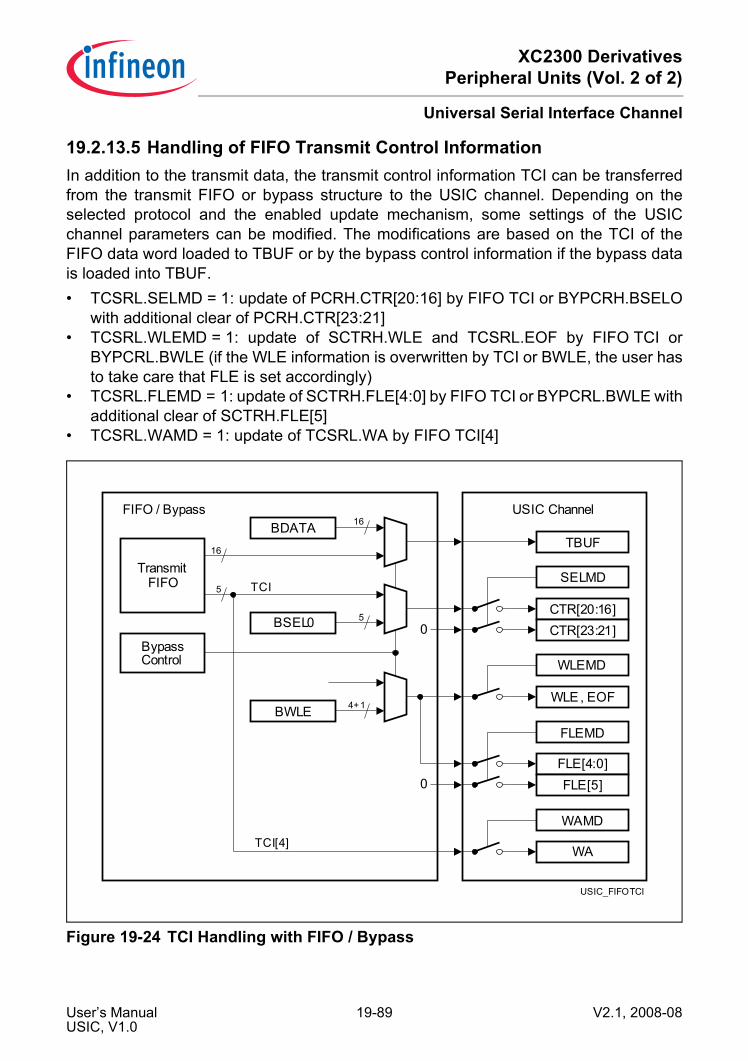
XC2300 DerivativesPeripheral Units (Vol. 2 of 2)
Universal Serial Interface Channel
19.2.13.5 Handling of FIFO Transmit Control InformationIn addition to the transmit data, the transmit control information TCI can be transferredfrom the transmit FIFO or bypass structure to the USIC channel. Depending on theselected protocol and the enabled update mechanism, some settings of the USICchannel parameters can be modified. The modifications are based on the TCI of theFIFO data word loaded to TBUF or by the bypass control information if the bypass datais loaded into TBUF.• TCSRL.SELMD = 1: update of PCRH.CTR[20:16] by FIFO TCI or BYPCRH.BSELO
with additional clear of PCRH.CTR[23:21]• TCSRL.WLEMD = 1: update of SCTRH.WLE and TCSRL.EOF by FIFO TCI or
BYPCRL.BWLE (if the WLE information is overwritten by TCI or BWLE, the user hasto take care that FLE is set accordingly)
• TCSRL.FLEMD = 1: update of SCTRH.FLE[4:0] by FIFO TCI or BYPCRL.BWLE withadditional clear of SCTRH.FLE[5]
• TCSRL.WAMD = 1: update of TCSRL.WA by FIFO TCI[4]
Figure 19-24 TCI Handling with FIFO / Bypass
USIC_FIFOTCI
CTR[20:16]CTR[23:21]
SELMD
TBUF
WLE, EOF
WLEMD
FLE[4:0]FLE[5]
FLEMD
WA
WAMD
USIC Channel
0
0
BDATA
BSEL0
BWLE
16
5
4+1
TransmitFIFO
BypassControl
5
16
TCI
TCI[4]
FIFO / Bypass
User’s Manual 19-89 V2.1, 2008-08USIC, V1.0

XC2300 DerivativesPeripheral Units (Vol. 2 of 2)
Universal Serial Interface Channel
19.2.14 FIFO Buffer and Bypass Registers
19.2.14.1 Bypass RegistersA write action to at least the low byte of the bypass data register sets BYPCRL.BDV = 1(bypass data tagged valid).
BYP Bypass Data Register (100H) Reset Value: 0000H
15 14 13 12 11 10 9 8 7 6 5 4 3 2 1 0
BDATA
rw
Bit (Field) Width Type DescriptionBDATA [15:0] rw Bypass Data
This bit field contains the bypass data.
BYPCRL Bypass Control Register L (104H) Reset Value: 0000H
15 14 13 12 11 10 9 8 7 6 5 4 3 2 1 0
BDV 0 BPRIO
BDVTR BDEN 0 BD
SSM 0 BWLE
rh r rw rw rw r rw r rw
Field Bits Type DescriptionBWLE [3:0] rw Bypass Word Length
This bit field defines the word length of the bypass data. The word length is given by BWLE + 1 with the data word being right-aligned in the data buffer at the bit positions [BWLE down to 0].The bypass data word is always considered as an own frame with the length of BWLE.Same coding as SCTRH.WLE.
User’s Manual 19-90 V2.1, 2008-08USIC, V1.0

XC2300 DerivativesPeripheral Units (Vol. 2 of 2)
Universal Serial Interface Channel
BDSSM 8 rw Bypass Data Single Shot ModeThis bit defines if the bypass data is considered as permanently valid or if the bypass data is only transferred once (single shot mode).0B The bypass data is still considered as valid after
it has been loaded into TBUF. The loading of the data into TBUF does not clear BDV.
1B The bypass data is considered as invalid after it has been loaded into TBUF. The loading of the data into TBUF clears BDV.
BDEN [11:10] rw Bypass Data EnableThis bit field defines if and how the transfer of bypass data to TBUF is enabled.00B The transfer of bypass data is disabled.01B The transfer of bypass data to TBUF is
possible. Bypass data will be transferred to TBUF according to its priority if BDV = 1.
10B Gated bypass data transfer is enabled. Bypass data will be transferred to TBUF according to its priority if BDV = 1 and while DX2S = 0.
11B Gated bypass data transfer is enabled. Bypass data will be transferred to TBUF according to its priority if BDV = 1 and while DX2S = 1.
BDVTR 12 rw Bypass Data Valid TriggerThis bit enables the bypass data for being tagged valid when DX2T is active (for time framing or time-out purposes).0B Bit BDV is not influenced by DX2T.1B Bit BDV is set if DX2T is active.
BPRIO 13 rw Bypass PriorityThis bit defines the priority between the bypass data and the transmit FIFO data.0B The transmit FIFO data has a higher priority
than the bypass data.1B The bypass data has a higher priority than the
transmit FIFO data.
Field Bits Type Description
User’s Manual 19-91 V2.1, 2008-08USIC, V1.0

XC2300 DerivativesPeripheral Units (Vol. 2 of 2)
Universal Serial Interface Channel
BDV 15 rh Bypass Data ValidThis bit defines if the bypass data is valid for a transfer to TBUF. This bit is set automatically by a write access to at least the low-byte of register BYP. It can be cleared by software by writing TRBSCR.CBDV.0B The bypass data is not valid.1B The bypass data is valid.
0 [7:4], 9, 14
r ReservedRead as 0; should be written with 0.
BYPCRH Bypass Control Register H (106H) Reset Value: 0000H
15 14 13 12 11 10 9 8 7 6 5 4 3 2 1 0
0 BSELO
r rw
Field Bits Type DescriptionBSELO [4:0] rw Bypass Select Outputs
This bit field contains the value that is written to PCRH.CTR[20:16] if bypass data is transferred to TBUF while TCSRL.SELMD = 1.In the SSC protocol, this bit field can be used to define which SELOx output line will be activated when bypass data is transmitted.
0 [15:5] r ReservedRead as 0; should be written with 0.
Field Bits Type Description
User’s Manual 19-92 V2.1, 2008-08USIC, V1.0
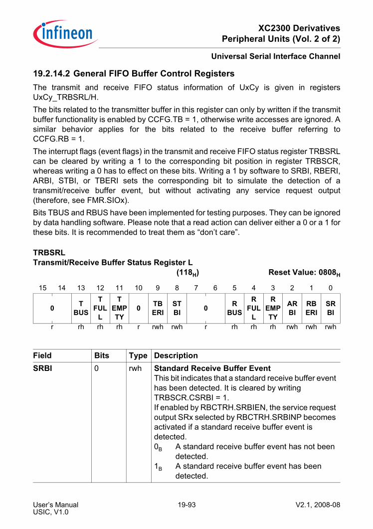
XC2300 DerivativesPeripheral Units (Vol. 2 of 2)
Universal Serial Interface Channel
19.2.14.2 General FIFO Buffer Control RegistersThe transmit and receive FIFO status information of UxCy is given in registersUxCy_TRBSRL/H.The bits related to the transmitter buffer in this register can only by written if the transmitbuffer functionality is enabled by CCFG.TB = 1, otherwise write accesses are ignored. Asimilar behavior applies for the bits related to the receive buffer referring toCCFG.RB = 1.The interrupt flags (event flags) in the transmit and receive FIFO status register TRBSRLcan be cleared by writing a 1 to the corresponding bit position in register TRBSCR,whereas writing a 0 has to effect on these bits. Writing a 1 by software to SRBI, RBERI,ARBI, STBI, or TBERI sets the corresponding bit to simulate the detection of atransmit/receive buffer event, but without activating any service request output(therefore, see FMR.SIOx).Bits TBUS and RBUS have been implemented for testing purposes. They can be ignoredby data handling software. Please note that a read action can deliver either a 0 or a 1 forthese bits. It is recommended to treat them as “don’t care”.
TRBSRL Transmit/Receive Buffer Status Register L
(118H) Reset Value: 0808H
15 14 13 12 11 10 9 8 7 6 5 4 3 2 1 0
0 TBUS
TFUL
L
TEMPTY
0 TBERI
STBI 0 R
BUS
RFUL
L
REMPTY
ARBI
RBERI
SRBI
r rh rh rh r rwh rwh r rh rh rh rwh rwh rwh
Field Bits Type DescriptionSRBI 0 rwh Standard Receive Buffer Event
This bit indicates that a standard receive buffer event has been detected. It is cleared by writing TRBSCR.CSRBI = 1.If enabled by RBCTRH.SRBIEN, the service request output SRx selected by RBCTRH.SRBINP becomes activated if a standard receive buffer event is detected.0B A standard receive buffer event has not been
detected.1B A standard receive buffer event has been
detected.
User’s Manual 19-93 V2.1, 2008-08USIC, V1.0
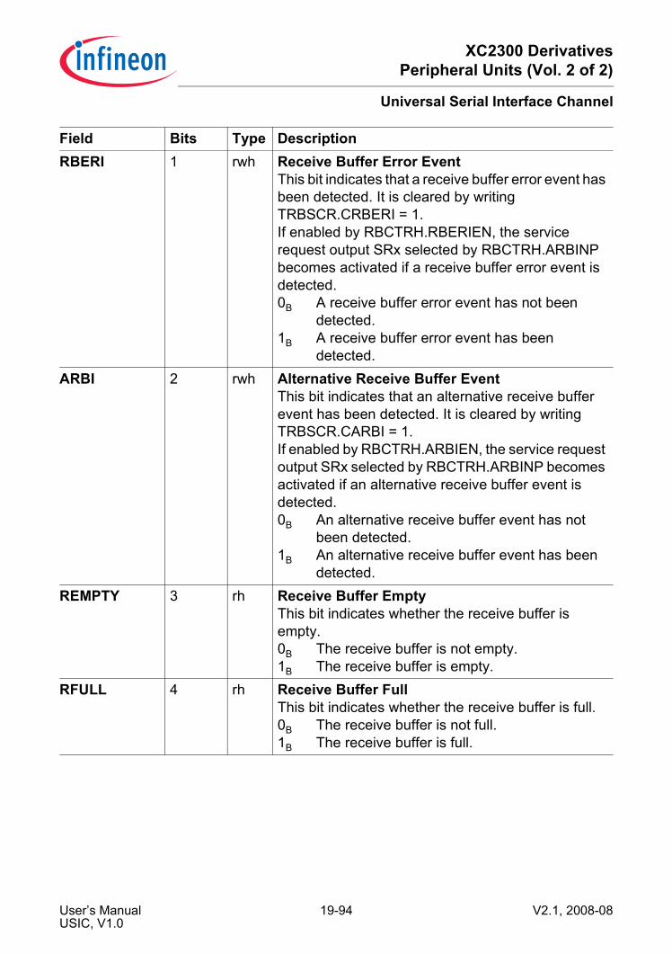
XC2300 DerivativesPeripheral Units (Vol. 2 of 2)
Universal Serial Interface Channel
RBERI 1 rwh Receive Buffer Error EventThis bit indicates that a receive buffer error event has been detected. It is cleared by writing TRBSCR.CRBERI = 1.If enabled by RBCTRH.RBERIEN, the service request output SRx selected by RBCTRH.ARBINP becomes activated if a receive buffer error event is detected.0B A receive buffer error event has not been
detected.1B A receive buffer error event has been
detected.ARBI 2 rwh Alternative Receive Buffer Event
This bit indicates that an alternative receive buffer event has been detected. It is cleared by writing TRBSCR.CARBI = 1.If enabled by RBCTRH.ARBIEN, the service request output SRx selected by RBCTRH.ARBINP becomes activated if an alternative receive buffer event is detected.0B An alternative receive buffer event has not
been detected.1B An alternative receive buffer event has been
detected.REMPTY 3 rh Receive Buffer Empty
This bit indicates whether the receive buffer is empty.0B The receive buffer is not empty.1B The receive buffer is empty.
RFULL 4 rh Receive Buffer FullThis bit indicates whether the receive buffer is full.0B The receive buffer is not full.1B The receive buffer is full.
Field Bits Type Description
User’s Manual 19-94 V2.1, 2008-08USIC, V1.0

XC2300 DerivativesPeripheral Units (Vol. 2 of 2)
Universal Serial Interface Channel
RBUS 5 rh Receive Buffer BusyThis bit indicates whether the receive buffer is currently updated by the FIFO handler.0B The receive buffer information has been
completely updated.1B The OUTRL/H update from the FIFO memory
is ongoing. A read from OUTRL/H will be delayed. FIFO pointers from the previous read are not yet updated.
STBI 8 rwh Standard Transmit Buffer EventThis bit indicates that a standard transmit buffer event has been detected. It is cleared by writing TRBSCR.CSTBI = 1.If enabled by TBCTRH.STBIEN, the service request output SRx selected by TBCTRH.STBINP becomes activated if a standard transmit buffer event is detected.0B A standard transmit buffer event has not been
detected.1B A standard transmit buffer event has been
detected.TBERI 9 rwh Transmit Buffer Error Event
This bit indicates that a transmit buffer error event has been detected. It is cleared by writing TRBSCR.CTBERI = 1.If enabled by TBCTRH.TBERIEN, the service request output SRx selected by TBCTRH.ATBINP becomes activated if a transmit buffer error event is detected. 0B A transmit buffer error event has not been
detected.1B A transmit buffer error event has been
detected.TEMPTY 11 rh Transmit Buffer Empty
This bit indicates whether the transmit buffer is empty.0B The transmit buffer is not empty.1B The transmit buffer is empty.
Field Bits Type Description
User’s Manual 19-95 V2.1, 2008-08USIC, V1.0
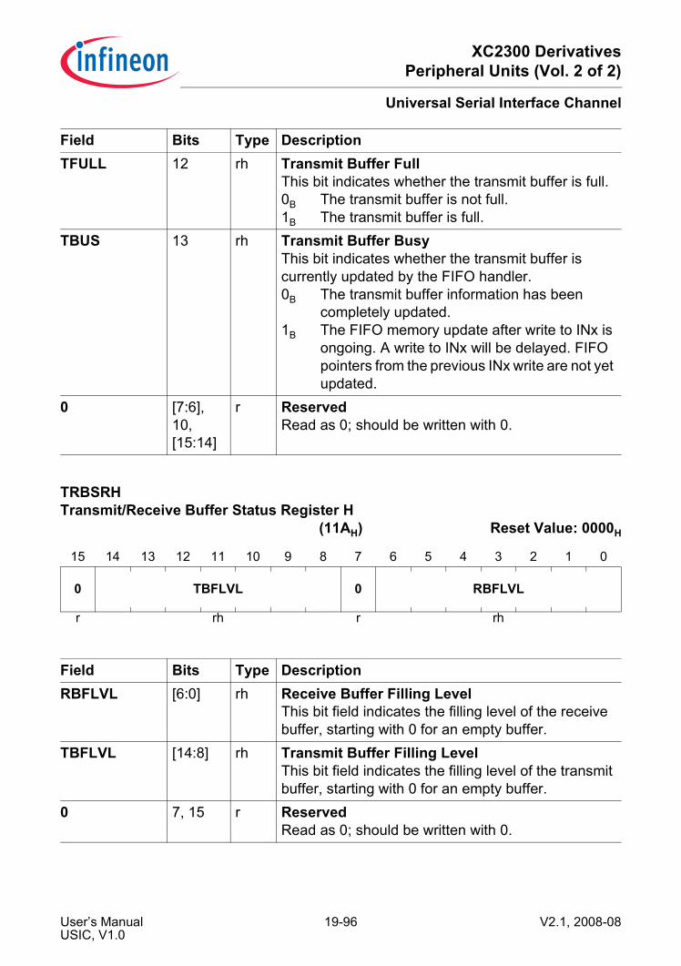
XC2300 DerivativesPeripheral Units (Vol. 2 of 2)
Universal Serial Interface Channel
TFULL 12 rh Transmit Buffer FullThis bit indicates whether the transmit buffer is full.0B The transmit buffer is not full.1B The transmit buffer is full.
TBUS 13 rh Transmit Buffer BusyThis bit indicates whether the transmit buffer is currently updated by the FIFO handler.0B The transmit buffer information has been
completely updated.1B The FIFO memory update after write to INx is
ongoing. A write to INx will be delayed. FIFO pointers from the previous INx write are not yet updated.
0 [7:6], 10, [15:14]
r ReservedRead as 0; should be written with 0.
TRBSRH Transmit/Receive Buffer Status Register H
(11AH) Reset Value: 0000H
15 14 13 12 11 10 9 8 7 6 5 4 3 2 1 0
0 TBFLVL 0 RBFLVL
r rh r rh
Field Bits Type DescriptionRBFLVL [6:0] rh Receive Buffer Filling Level
This bit field indicates the filling level of the receive buffer, starting with 0 for an empty buffer.
TBFLVL [14:8] rh Transmit Buffer Filling LevelThis bit field indicates the filling level of the transmit buffer, starting with 0 for an empty buffer.
0 7, 15 r ReservedRead as 0; should be written with 0.
Field Bits Type Description
User’s Manual 19-96 V2.1, 2008-08USIC, V1.0

XC2300 DerivativesPeripheral Units (Vol. 2 of 2)
Universal Serial Interface Channel
The bits in register TRBSCR are used to clear the notification bits in register TRBSRL orto clear the FIFO mechanism for the transmit or receive buffer. A read action alwaysdelivers 0.
TRBSCR Transmit/Receive Buffer Status Clear Register
(11CH) Reset Value: 0000H
15 14 13 12 11 10 9 8 7 6 5 4 3 2 1 0FLUSHTB
FLUSHRB
0 CBDV
CTBERI
CSTBI
0C
ARBI
CRBERI
CSRBI
w w r w w w r w w w
Field Bits Type DescriptionCSRBI 0 w Clear Standard Receive Buffer Event
0B No effect.1B Clear TRBSRL.SRBI.
CRBERI 1 w Clear Receive Buffer Error Event0B No effect.1B Clear TRBSRL.RBERI.
CARBI 2 w Clear Alternative Receive Buffer Event0B No effect.1B Clear TRBSRL.ARBI.
CSTBI 8 w Clear Standard Transmit Buffer Event0B No effect.1B Clear TRBSRL.STBI.
CTBERI 9 w Clear Transmit Buffer Error Event0B No effect.1B Clear TRBSRL.TBERI.
CBDV 10 w Clear Bypass Data Valid0B No effect.1B Clear BYPCRL.BDV.
FLUSHRB 14 w Flush Receive Buffer0B No effect.1B The receive FIFO buffer is cleared (filling level
is cleared and output pointer is set to input pointer value). Should only be used while the FIFO buffer is not taking part in data traffic.
User’s Manual 19-97 V2.1, 2008-08USIC, V1.0
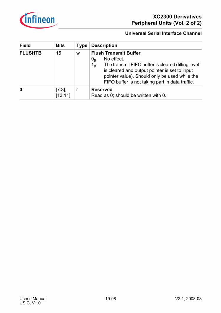
XC2300 DerivativesPeripheral Units (Vol. 2 of 2)
Universal Serial Interface Channel
FLUSHTB 15 w Flush Transmit Buffer0B No effect.1B The transmit FIFO buffer is cleared (filling level
is cleared and output pointer is set to input pointer value). Should only be used while the FIFO buffer is not taking part in data traffic.
0 [7:3], [13:11]
r ReservedRead as 0; should be written with 0.
Field Bits Type Description
User’s Manual 19-98 V2.1, 2008-08USIC, V1.0

XC2300 DerivativesPeripheral Units (Vol. 2 of 2)
Universal Serial Interface Channel
19.2.14.3 Transmit FIFO Buffer Control RegistersThe transmit FIFO buffer is controlled by registers TBCTRL and TBCTRH. Theseregisters can only by written if the transmit buffer functionality is enabled byCCFG.TB = 1, otherwise write accesses are ignored.
TBCTRL Transmitter Buffer Control Register L (110H) Reset Value: 0000H
15 14 13 12 11 10 9 8 7 6 5 4 3 2 1 0
0 LIMIT 0 DPTR
r rw r w
Field Bits Type DescriptionDPTR [5:0] w Data Pointer
This bit field defines the start value for the transmit buffer pointers when assigning the FIFO entries to the transmit FIFO buffer. A read always delivers 0.When writing DPTR while SIZE = 0, both tranmitter pointers TDIPTR and RTDOPTR in register TRBPTRL are updated with the written value and the buffer is considered as empty. A write access to DPTR while SIZE > 0 is ignored and does not modify the pointers.
LIMIT [13:8] rw Limit For Interrupt GenerationThis bit field defines the target filling level of the transmit FIFO buffer that is used for the standard transmit buffer event detection.
0 [7:6], [15:14]
r ReservedRead as 0; should be written with 0.
User’s Manual 19-99 V2.1, 2008-08USIC, V1.0
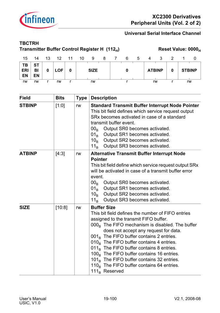
XC2300 DerivativesPeripheral Units (Vol. 2 of 2)
Universal Serial Interface Channel
TBCTRH Transmitter Buffer Control Register H (112H) Reset Value: 0000H
15 14 13 12 11 10 9 8 7 6 5 4 3 2 1 0TBERIEN
STBIEN
0 LOF 0 SIZE 0 ATBINP 0 STBINP
rw rw r rw r rw r rw r rw
Field Bits Type DescriptionSTBINP [1:0] rw Standard Transmit Buffer Interrupt Node Pointer
This bit field defines which service request output SRx becomes activated in case of a standard transmit buffer event.00B Output SR0 becomes activated.01B Output SR1 becomes activated.10B Output SR2 becomes activated.11B Output SR3 becomes activated.
ATBINP [4:3] rw Alternative Transmit Buffer Interrupt Node PointerThis bit field define which service request output SRx will be activated in case of a transmit buffer error event.00B Output SR0 becomes activated.01B Output SR1 becomes activated.10B Output SR2 becomes activated.11B Output SR3 becomes activated.
SIZE [10:8] rw Buffer SizeThis bit field defines the number of FIFO entries assigned to the transmit FIFO buffer.000B The FIFO mechanism is disabled. The buffer
does not accept any request for data.001B The FIFO buffer contains 2 entries.010B The FIFO buffer contains 4 entries.011B The FIFO buffer contains 8 entries.100B The FIFO buffer contains 16 entries.101B The FIFO buffer contains 32 entries.110B The FIFO buffer contains 64 entries.111B Reserved
User’s Manual 19-100 V2.1, 2008-08USIC, V1.0

XC2300 DerivativesPeripheral Units (Vol. 2 of 2)
Universal Serial Interface Channel
LOF 12 rw Buffer Event on Limit OverflowThis bit defines which relation between filling level and programmed limit leads to a standard transmit buffer event.0B A standard transmit buffer event occurs when
the filling level equals the limit value and gets lower due to transmission of a data word.
1B A standard transmit buffer interrupt event occurs when the filling level equals the limit value and gets bigger due to a write access to a data input location INx.
STBIEN 14 rw Standard Transmit Buffer Interrupt EnableThis bit enables/disables the generation of a standard transmit buffer interrupt in case of a standard transmit buffer event.0B The standard transmit buffer interrupt
generation is disabled.1B The standard transmit buffer interrupt
generation is enabled.TBERIEN 15 rw Transmit Buffer Error Interrupt Enable
This bit enables/disables the generation of a transmit buffer error interrupt in case of a transmit buffer error event (software writes to a full transmit buffer).0B The transmit buffer error interrupt generation
is disabled.1B The transmit buffer error interrupt generation
is enabled.0 2, [7:5],
11, 13r Reserved
Read as 0; should be written with 0.
Field Bits Type Description
User’s Manual 19-101 V2.1, 2008-08USIC, V1.0
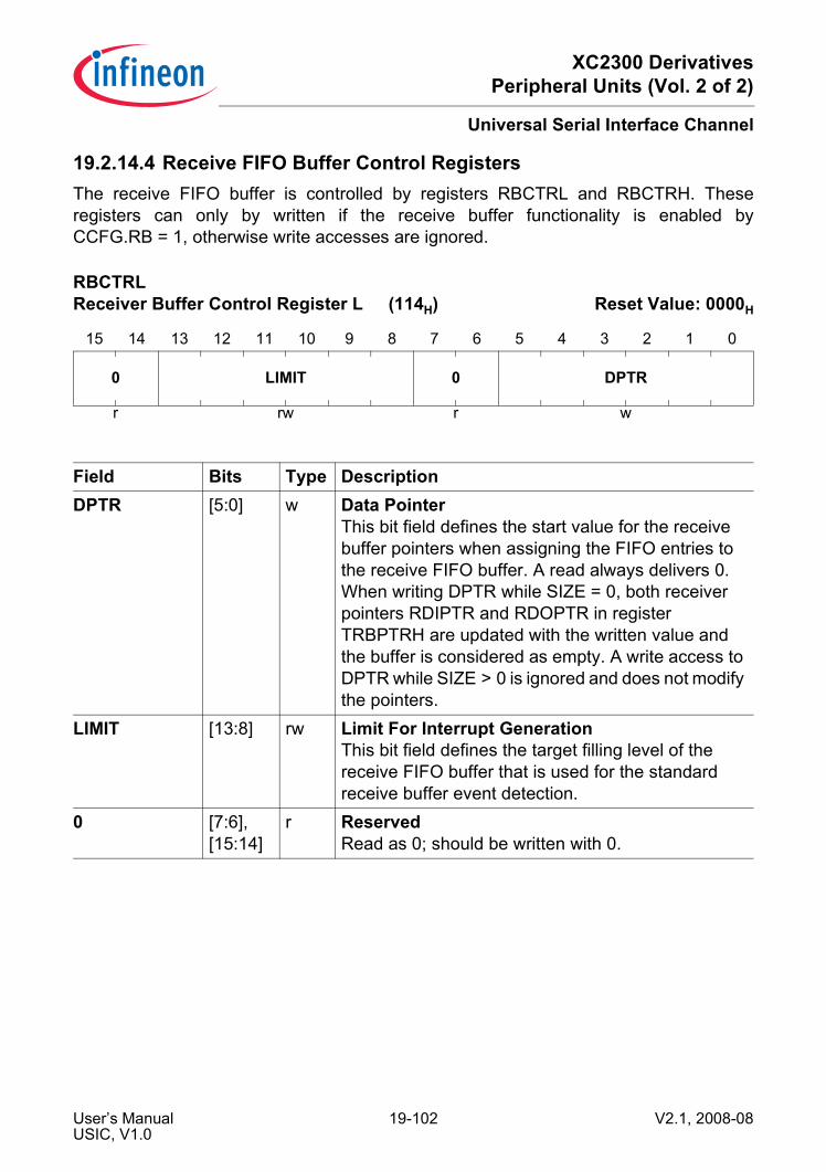
XC2300 DerivativesPeripheral Units (Vol. 2 of 2)
Universal Serial Interface Channel
19.2.14.4 Receive FIFO Buffer Control RegistersThe receive FIFO buffer is controlled by registers RBCTRL and RBCTRH. Theseregisters can only by written if the receive buffer functionality is enabled byCCFG.RB = 1, otherwise write accesses are ignored.
RBCTRL Receiver Buffer Control Register L (114H) Reset Value: 0000H
15 14 13 12 11 10 9 8 7 6 5 4 3 2 1 0
0 LIMIT 0 DPTR
r rw r w
Field Bits Type DescriptionDPTR [5:0] w Data Pointer
This bit field defines the start value for the receive buffer pointers when assigning the FIFO entries to the receive FIFO buffer. A read always delivers 0.When writing DPTR while SIZE = 0, both receiver pointers RDIPTR and RDOPTR in register TRBPTRH are updated with the written value and the buffer is considered as empty. A write access to DPTR while SIZE > 0 is ignored and does not modify the pointers.
LIMIT [13:8] rw Limit For Interrupt GenerationThis bit field defines the target filling level of the receive FIFO buffer that is used for the standard receive buffer event detection.
0 [7:6], [15:14]
r ReservedRead as 0; should be written with 0.
User’s Manual 19-102 V2.1, 2008-08USIC, V1.0

XC2300 DerivativesPeripheral Units (Vol. 2 of 2)
Universal Serial Interface Channel
RBCTRH Receiver Buffer Control Register H (116H) Reset Value: 0000H
15 14 13 12 11 10 9 8 7 6 5 4 3 2 1 0RBERIEN
SRBIEN
ARBIEN
LOF RNM SIZE RCIM 0 ARBINP 0 SRBINP
rw rw rw rw rw rw rw r rw r rw
Field Bits Type DescriptionSRBINP [1:0] rw Standard Receive Buffer Interrupt Node Pointer
This bit field defines which service request output SRx becomes activated in case of a standard receive buffer event.00B Output SR0 becomes activated.01B Output SR1 becomes activated.10B Output SR2 becomes activated.11B Output SR3 becomes activated.
ARBINP [4:3] rw Alternative Receive Buffer Interrupt Node PointerThis bit field defines which service request output SRx becomes activated in case of an alternative receive buffer event or a receive buffer error event.00B The output SR0 becomes activated.01B The output SR1 becomes activated.10B The output SR2 becomes activated.11B The output SR3 becomes activated.
RCIM [7:6] rw Receiver Control Information ModeThis bit field defines which information from the receiver status register RBUFSR is propagated as 5 bit receiver control information RCI[4:0] to the receive FIFO buffer and can be read out in registers OUT(D)RH.00B RCI[4] = PERR, RCI[3:0] = WLEN01B RCI[4] = SOF, RCI[3:0] = WLEN10B RCI[4] = 0, RCI[3:0] = WLEN11B RCI[4] = PERR, RCI[3] = PAR,
RCI[2:1] = 00B, RCI[0] = SOF
User’s Manual 19-103 V2.1, 2008-08USIC, V1.0

XC2300 DerivativesPeripheral Units (Vol. 2 of 2)
Universal Serial Interface Channel
SIZE [10:8] rw Buffer SizeThis bit field defines the number of FIFO entries assigned to the receive FIFO buffer.000B The FIFO mechanism is disabled. The buffer
does not accept any request for data.001B The FIFO buffer contains 2 entries.010B The FIFO buffer contains 4 entries.011B The FIFO buffer contains 8 entries.100B The FIFO buffer contains 16 entries.101B The FIFO buffer contains 32 entries.110B The FIFO buffer contains 64 entries.111B Reserved
RNM 11 rw Receiver Notification ModeThis bit defines the receive buffer event mode. The receive buffer error event is not affected by RNM.0B Filling level mode:
A standard receive buffer event occurs when the filling level equals the limit value and changes, either due to a read access from OUTRL (LOF = 0) or due to a new received data word (LOF = 1).
1B RCI mode:A standard receive buffer event occurs when register OUTRL is updated with a new value if the corresponding value in OUTRH.RCI[4] = 0. If OUTRH.RCI[4] = 1, an alternative receive buffer event occurs instead of the standard receive buffer event.
LOF 12 rw Buffer Event on Limit OverflowThis bit defines which relation between filling level and programmed limit leads to a standard receive buffer event in filling level mode (RNM = 0). In RCI mode (RNM = 1), bit fields LIMIT and LOF are ignored.0B A standard receive buffer event occurs when
the filling level equals the limit value and gets lower due to a read access from OUTRL.
1B A standard receive buffer event occurs when the filling level equals the limit value and gets bigger due to the reception of a new data word.
Field Bits Type Description
User’s Manual 19-104 V2.1, 2008-08USIC, V1.0

XC2300 DerivativesPeripheral Units (Vol. 2 of 2)
Universal Serial Interface Channel
ARBIEN 13 rw Alternative Receive Buffer Interrupt EnableThis bit enables/disables the generation of an alternative receive buffer interrupt in case of an alternative receive buffer event.0B The alternative receive buffer interrupt
generation is disabled.1B The alternative receive buffer interrupt
generation is enabled.SRBIEN 14 rw Standard Receive Buffer Interrupt Enable
This bit enables/disables the generation of a standard receive buffer interrupt in case of a standard receive buffer event.0B The standard receive buffer interrupt
generation is disabled.1B The standard receive buffer interrupt
generation is enabled.RBERIEN 15 rw Receive Buffer Error Interrupt Enable
This bit enables/disables the generation of a receive buffer error interrupt in case of a receive buffer error event (the software reads from an empty receive buffer).0B The receive buffer error interrupt generation is
disabled.1B The receive buffer error interrupt generation is
enabled.0 2, 5 r Reserved
Read as 0; should be written with 0.
Field Bits Type Description
User’s Manual 19-105 V2.1, 2008-08USIC, V1.0
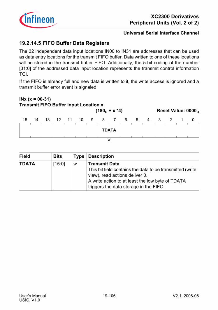
XC2300 DerivativesPeripheral Units (Vol. 2 of 2)
Universal Serial Interface Channel
19.2.14.5 FIFO Buffer Data RegistersThe 32 independent data input locations IN00 to IN31 are addresses that can be usedas data entry locations for the transmit FIFO buffer. Data written to one of these locationswill be stored in the transmit buffer FIFO. Additionally, the 5-bit coding of the number[31:0] of the addressed data input location represents the transmit control informationTCI.If the FIFO is already full and new data is written to it, the write access is ignored and atransmit buffer error event is signaled.
INx (x = 00-31) Transmit FIFO Buffer Input Location x
(180H + x *4) Reset Value: 0000H
15 14 13 12 11 10 9 8 7 6 5 4 3 2 1 0
TDATA
w
Field Bits Type DescriptionTDATA [15:0] w Transmit Data
This bit field contains the data to be transmitted (write view), read actions deliver 0.A write action to at least the low byte of TDATA triggers the data storage in the FIFO.
User’s Manual 19-106 V2.1, 2008-08USIC, V1.0
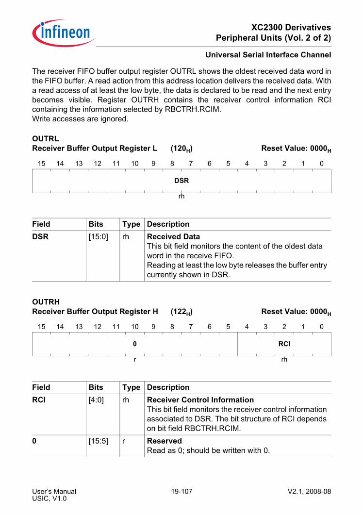
XC2300 DerivativesPeripheral Units (Vol. 2 of 2)
Universal Serial Interface Channel
The receiver FIFO buffer output register OUTRL shows the oldest received data word inthe FIFO buffer. A read action from this address location delivers the received data. Witha read access of at least the low byte, the data is declared to be read and the next entrybecomes visible. Register OUTRH contains the receiver control information RCIcontaining the information selected by RBCTRH.RCIM. Write accesses are ignored.
OUTRL Receiver Buffer Output Register L (120H) Reset Value: 0000H
15 14 13 12 11 10 9 8 7 6 5 4 3 2 1 0
DSR
rh
Field Bits Type DescriptionDSR [15:0] rh Received Data
This bit field monitors the content of the oldest data word in the receive FIFO.Reading at least the low byte releases the buffer entry currently shown in DSR.
OUTRH Receiver Buffer Output Register H (122H) Reset Value: 0000H
15 14 13 12 11 10 9 8 7 6 5 4 3 2 1 0
0 RCI
r rh
Field Bits Type DescriptionRCI [4:0] rh Receiver Control Information
This bit field monitors the receiver control information associated to DSR. The bit structure of RCI depends on bit field RBCTRH.RCIM.
0 [15:5] r ReservedRead as 0; should be written with 0.
User’s Manual 19-107 V2.1, 2008-08USIC, V1.0

XC2300 DerivativesPeripheral Units (Vol. 2 of 2)
Universal Serial Interface Channel
If a debugger should be used to monitor the received data in the FIFO buffer, the FIFOmechanism must not be activated in order to guaranty data consistency. Therefore, asecond address set is available, named OUTDRL/H (D like debugger), having the samebit fields like the original buffer output register OUTRL/H, but without the FIFOmechanism. A debugger can read here (in order to monitor the receive data flow) withoutthe risk of data corruption. Write accesses are ignored.
OUTDRL Receiver Buffer Output Register L for Debugger
(124H) Reset Value: 0000H
15 14 13 12 11 10 9 8 7 6 5 4 3 2 1 0
DSR
rh
Field Bits Type DescriptionDSR [15:0] rh Data from Shift Register
Same as OUTRL.DSR, but without releasing the buffer after a read action.
OUTDRH Receiver Buffer Output Register H for Debugger
(126H) Reset Value: 0000H
15 14 13 12 11 10 9 8 7 6 5 4 3 2 1 0
0 RCI
r rh
Field Bits Type DescriptionRCI [4:0] rh Receive Control Information from Shift Register
Same as OUTRH.RCI.0 [15:5] r Reserved
Read as 0; should be written with 0.
User’s Manual 19-108 V2.1, 2008-08USIC, V1.0

XC2300 DerivativesPeripheral Units (Vol. 2 of 2)
Universal Serial Interface Channel
19.2.14.6 FIFO Buffer Pointer RegistersThe pointers for FIFO handling of the transmit and receive FIFO buffers are located inregisters TRBPTRL (for the transmit buffer) and TRBPTRH (for the receive buffer). Thepointers are automatically handled by the FIFO buffer mechanism and do not need to bemodified by software. As a consequence, these registers can only be read by software(e.g. for verification purposes), whereas write accesses are ignored.
TRBPTRL Transmit/Receive Buffer Pointer Register L
(108H) Reset Value: 0000H
15 14 13 12 11 10 9 8 7 6 5 4 3 2 1 0
0 TDOPTR 0 TDIPTR
r rh r rh
Field Bits Type DescriptionTDIPTR [5:0] rh Transmitter Data Input Pointer
This bit field indicates the buffer entry that will be used for the next transmit data coming from the INx addresses.
TDOPTR [13:8] rh Transmitter Data Output PointerThis bit field indicates the buffer entry that will be used for the next transmit data to be output to TBUF.
0 [7:6], [15:14]
r ReservedRead as 0; should be written with 0.
User’s Manual 19-109 V2.1, 2008-08USIC, V1.0

XC2300 DerivativesPeripheral Units (Vol. 2 of 2)
Universal Serial Interface Channel
TRBPTRH Transmit/Receive Buffer Pointer Register H
(10AH) Reset Value: 0000H
15 14 13 12 11 10 9 8 7 6 5 4 3 2 1 0
0 RDOPTR 0 RDIPTR
r rh r rh
Field Bits Type DescriptionRDIPTR [5:0] rh Receiver Data Input Pointer
This bit field indicates the buffer entry that will be used for the next receive data coming from RBUF.
RDOPTR [13:8] rh Receiver Data Output PointerThis bit field indicates the buffer entry that will be used for the next receive data to be output at the OUT(D)RL addresses.
0 [7:6], [15:14]
r ReservedRead as 0; should be written with 0.
User’s Manual 19-110 V2.1, 2008-08USIC, V1.0
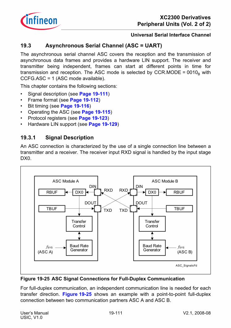
XC2300 DerivativesPeripheral Units (Vol. 2 of 2)
Universal Serial Interface Channel
19.3 Asynchronous Serial Channel (ASC = UART)The asynchronous serial channel ASC covers the reception and the transmission ofasynchronous data frames and provides a hardware LIN support. The receiver andtransmitter being independent, frames can start at different points in time fortransmission and reception. The ASC mode is selected by CCR.MODE = 0010B withCCFG.ASC = 1 (ASC mode available).This chapter contains the following sections:• Signal description (see Page 19-111)• Frame format (see Page 19-112)• Bit timing (see Page 19-116)• Operating the ASC (see Page 19-115)• Protocol registers (see Page 19-123)• Hardware LIN support (see Page 19-129)
19.3.1 Signal DescriptionAn ASC connection is characterized by the use of a single connection line between atransmitter and a receiver. The receiver input RXD signal is handled by the input stageDX0.
Figure 19-25 ASC Signal Connections for Full-Duplex Communication
For full-duplex communication, an independent communication line is needed for eachtransfer direction. Figure 19-25 shows an example with a point-to-point full-duplexconnection between two communication partners ASC A and ASC B.
ASC_SignalsFd
DX0DIN
DOUT
RBUF
ASC Module A
TransferControl
Baud RateGenerator
TBUF
fSYS
(ASC A)
RXD
TXD
DX0DIN
DOUT
RBUF
ASC Module B
TransferControl
Baud RateGenerator
TBUF
fSYS
(ASC B)
RXD
TXD
User’s Manual 19-111 V2.1, 2008-08USIC, V1.0

XC2300 DerivativesPeripheral Units (Vol. 2 of 2)
Universal Serial Interface Channel
For half-duplex or multi-transmitter communication, a single communication line isshared between the communication partners. Figure 19-26 shows an example with apoint-to-point half-duplex connection between ASC A and ASC B. In this case, the userhas to take care that only one transmitter is active at a time. In order to supporttransmitter collision detection, the input stage DX1 can be used to monitor the level ofthe transmit line and to check if the line is in the idle state or if a collision occurred.There are two possibilities to connect the receiver input DIN to the transmitter outputDOUT. Communication partner ASC A uses an internal connection with only the transmitpin TXD, that is delivering its input value as RXD to the DX0 input stage for receptionand to DX1 to check for transmitter collisions. Communication partner ASC B uses anexternal connection between the two pins TXD and RXD.
Figure 19-26 ASC Signal Connections for Half-Duplex Communication
19.3.2 Frame FormatA standard ASC frame is shown in Figure 19-27. It consists of:• An idle time with the signal level 1.• One start of frame bit (SOF) with the signal level 0.• A data field containing a programmable number of data bits (1-63).• A parity bit (P), programmable for either even or odd parity. It is optionally possible to
handle frames without parity bit.• One or two stop bits with the signal level 1.
ASC_SignalsHd
DX0DIN
DOUT
RBUF
ASC Module A
TransferControl
Baud RateGenerator
TBUF
fSYS
(ASC A)
TXD
DX0DIN
DOUT
RBUF
ASC Module B
TBUF
fSYS
(ASC B)
RXD
TXDDX1
TransferControl
Baud RateGenerator
DX1
User’s Manual 19-112 V2.1, 2008-08USIC, V1.0

XC2300 DerivativesPeripheral Units (Vol. 2 of 2)
Universal Serial Interface Channel
Figure 19-27 Standard ASC Frame Format
The protocol specific bits (SOF, P, STOP) are automatically handled by the ASC protocolstate machine and do not appear in the data flow via the receive and transmit buffers.
19.3.2.1 Idle TimeThe receiver and the transmitter independently check the respective data input lines(DX0, DX1) for being idle. The idle detection ensures that an SOF bit of a recentlyenabled ASC module does not collide with an already running frame of another ASCmodule.In order to start the idle detection, the user software has to clear bits PSR.RXIDLE and/orPSR.TXIDLE, e.g. before selecting the ASC mode or during operation. If a bit is clearedby software while a data transfer is in progress, the currently running frame transfer isfinished normally before starting the idle detection again. Frame reception is onlypossible if PSR.RXIDLE = 1 and frame transmission is only possible if PSR.TXIDLE = 1.The duration of the idle detection depends on the setting of bit PCRL.IDM. In the casethat a collision is not possible, the duration can be shortened and the bus can bedeclared as being idle by setting PCRL.IDM = 0.In the case that the complete idle detection is enabled by PCRL.IDM = 1, the data inputof DX0 is considered as idle (PSR.RXIDLE becomes set) if a certain number ofconsecutive passive bit times has been detected. The same scheme applies for thetransmitter’s data input of DX1. Here, bit PSR.TXIDLE becomes set if the idle conditionof this input signal has been detected.The duration of the complete idle detection is given by the number of programmed databits per frame plus 2 (in the case without parity) or plus 3 (in the case with parity). Thecounting of consecutive bit times with 1 level restarts from the beginning each time anedge is found, after leaving a stop mode or if ASC mode becomes enabled.If the idle detection bits PSR.RXIDLE and/or TXIDLE are cleared by software, thecounting scheme is not stopped (no re-start from the beginning). As a result, the clearedbit(s) can become set immediately again if the respective input line still meets the idlecriterion.Please note that the idle time check is based on bit times, so the maximum time can beup to 1 bit time more than programmed value (but not less).
ASC_FrameFormat
1 Bit
SOF1
0IDLE IDLESTOPP
1-63 Bit 0-1 Bit 1-2 Bits
DATA
User’s Manual 19-113 V2.1, 2008-08USIC, V1.0

XC2300 DerivativesPeripheral Units (Vol. 2 of 2)
Universal Serial Interface Channel
19.3.2.2 Start Bit DetectionThe receiver input signal DIN (selected signal of input stage DX0) is checked for a fallingedge. An SOF bit is detected when a falling edge occurs while the receiver is idle or afterthe sampling point of the last stop bit. To increase noise immunity, the SOF bit timingstarts with the first falling edge that is detected. If the sampled bit value of the SOF is 1,the previous falling edge is considered to be due to noise and the receiver is consideredto be idle again.
19.3.2.3 Data FieldThe length of the data field (number of data bits) can be programmed by bit fieldSCTRH.FLE. It can vary between 1 and 63 data bits, corresponding to values ofSCTRH.FLE = 0 to 62 (the value of 63 is reserved and must not be programmed in ASCmode).The data field can consist of several data words, e.g. a transfer of 12 data bits can becomposed of two 8-bit words, with the 12 bits being split into 8-bits of the first word and4 bits of the second word. The user software has to take care that the transmit data isavailable in-time, once a frame has been started. If the transmit buffer runs empty duringa running data frame, the passive data level (SCTRL.PDL) is sent out.The shift direction can be programmed by SCTRL.SDIR. The standard setting for ASCframes with LSB first is achieved with the default setting SDIR = 0.
19.3.2.4 Parity BitThe ASC allows parity generation for transmission and parity check for reception onframe base. The type of parity can be selected by bit field CCR.PM, common fortransmission and reception (no parity, even or odd parity). If the parity handling isdisabled, the ASC frame does not contain any parity bit. For consistency reasons, allcommunication partners have to be programmed to the same parity mode.After the last data bit of the data field, the transmitter automatically sends out itscalculated parity bit if parity generation has been enabled. The receiver interprets this bitas received parity and compares it to its internally calculated one. The received parity bitvalue and the result of the parity check are monitored in the receiver buffer statusregisters as receiver buffer status information. These registers contain bits to monitor aprotocol-related argument (PAR) and protocol-related error indication (PERR).
19.3.2.5 Stop Bit(s)Each ASC frame is completed by 1 or 2 of stop bits with the signal level 1 (same level asthe idle level). The number of stop bits is programmable by bit PSR.STPB. A new startbit can be transferred directly after the last stop bit.
User’s Manual 19-114 V2.1, 2008-08USIC, V1.0

XC2300 DerivativesPeripheral Units (Vol. 2 of 2)
Universal Serial Interface Channel
19.3.3 Operating the ASCIn order to operate the ASC protocol, the following issues have to be considered:• Select ASC mode:
It is recommended to configure all parameters of the ASC that do not change duringrun time while CCR.MODE = 0000B. Bit field SCTRL.TRM = 01B has to beprogrammed. The configuration of the input stages has to be done whileCCR.MODE = 0000B to avoid unintended edges of the input signals and the ASCmode can be enabled by CCR.MODE = 0010B afterwards.
• Pin connections:Establish a connection of input stage DX0 with the selected receive data input pin(signal DIN) with DX0CR.INSW = 0 and configure a transmit data output pin (signalDOUT). For collision or idle detection of the transmitter, the input stage DX1 has tobe connected to the selected transmit output pin, also with DX1CR.INSW = 0.Additionally, program DX2CR.INSW = 0.Due to the handling of the input data stream by the synchronous protocol handler, thepropagation delay of the synchronization in the input stage has to be considered.
• Bit timing configuration:The desired baud rate setting has to be selected, comprising the fractional divider,the baud rate generator and the bit timing. Please note that not all featurecombinations can be supported by the application at the same time, e.g. due topropagation delays. For example, the length of a frame is limited by the frequencydifference of the transmitter and the receiver device. Furthermore, in order to use theaverage of samples (SMD = 1), the sampling point has to be chosen to respect thesignal settling and data propagation times.
• Data format configuration:The word length, the frame length, and the shift direction have to be set up accordingto the application requirements by programming the registers SCTRL and SCTRH. Ifrequired by the application, the data input and output signals can be inverted.Additionally, the parity mode has to be configured (CCR.PM).
User’s Manual 19-115 V2.1, 2008-08USIC, V1.0
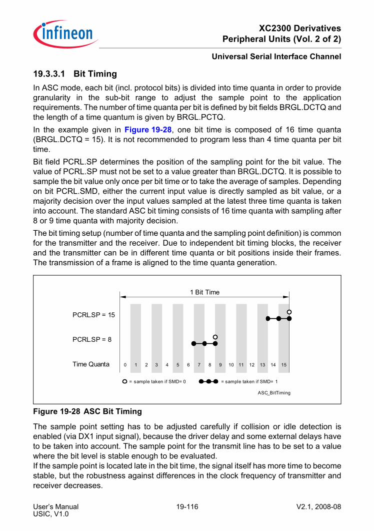
XC2300 DerivativesPeripheral Units (Vol. 2 of 2)
Universal Serial Interface Channel
19.3.3.1 Bit TimingIn ASC mode, each bit (incl. protocol bits) is divided into time quanta in order to providegranularity in the sub-bit range to adjust the sample point to the applicationrequirements. The number of time quanta per bit is defined by bit fields BRGL.DCTQ andthe length of a time quantum is given by BRGL.PCTQ.In the example given in Figure 19-28, one bit time is composed of 16 time quanta(BRGL.DCTQ = 15). It is not recommended to program less than 4 time quanta per bittime.Bit field PCRL.SP determines the position of the sampling point for the bit value. Thevalue of PCRL.SP must not be set to a value greater than BRGL.DCTQ. It is possible tosample the bit value only once per bit time or to take the average of samples. Dependingon bit PCRL.SMD, either the current input value is directly sampled as bit value, or amajority decision over the input values sampled at the latest three time quanta is takeninto account. The standard ASC bit timing consists of 16 time quanta with sampling after8 or 9 time quanta with majority decision.The bit timing setup (number of time quanta and the sampling point definition) is commonfor the transmitter and the receiver. Due to independent bit timing blocks, the receiverand the transmitter can be in different time quanta or bit positions inside their frames.The transmission of a frame is aligned to the time quanta generation.
Figure 19-28 ASC Bit Timing
The sample point setting has to be adjusted carefully if collision or idle detection isenabled (via DX1 input signal), because the driver delay and some external delays haveto be taken into account. The sample point for the transmit line has to be set to a valuewhere the bit level is stable enough to be evaluated.If the sample point is located late in the bit time, the signal itself has more time to becomestable, but the robustness against differences in the clock frequency of transmitter andreceiver decreases.
ASC_BitTiming
PCRL.SP = 15
Time Quanta
= sample taken if SMD = 0
PCRL.SP = 8
1514131211109876543210
1 Bit Time
= sample taken if SMD = 1
User’s Manual 19-116 V2.1, 2008-08USIC, V1.0
XC2300 DerivativesPeripheral Units (Vol. 2 of 2)
Universal Serial Interface Channel
19.3.3.2 Baud Rate GenerationThe baud rate fASC in ASC mode depends on the number of time quanta per bit time andtheir timing. The baud rate setting should only be changed while the transmitter and thereceiver are idle. The bits in register BRGL define the baud rate setting:• BRGL.CTQSEL
to define the input frequency fCTQIN for the time quanta generation• BRGL.PCTQ
to define the length of a time quantum (division of fCTQIN by 1, 2, 3, or 4)• BRGL.DCTQ
to define the number of time quanta per bit timeThe standard setting is given by CTQSEL = 00B (fCTQIN = fPDIV) and PPPEN = 0(fPPP = fPIN). Under these conditions, the baud rate is given by:
(19.6)
In order to generate slower frequencies, two additional divide-by-2 stages can beselected by CTQSEL = 10B (fCTQIN = fSCLK) and PPPEN = 1 (fPPP = fMCLK), leading to:
(19.7)
19.3.3.3 Noise DetectionThe ASC receiver permanently checks the data input line of the DX0 stage for noise (thecheck is independent from the setting of bit PCRL.SMD). Bit PSR.RNS (receiver noise)becomes set if the three input samples of the majority decision are not identical at thesample point for the bit value. The information about receiver noise gets accumulatedover several bits in bit PSR.RNS (it has to be cleared by software) and can trigger aprotocol interrupt each time noise is detected if enabled by PCRL.RNIEN.
19.3.3.4 Collision DetectionIn some applications, such as data transfer over a single data line shared by severalsending devices (see Figure 19-26), several transmitters have the possibility to send onthe same data output line TXD. In order to avoid collisions of transmitters being active atthe same time or to allow a kind of arbitration, a collision detection has beenimplemented.The data value read at the TXD input at the DX1 stage and the transmitted data bit valueare compared after the sampling of each bit value. If enabled by PCRL.CDEN = 1 and abit sent is not equal to the bit read back, a collision is detected and bit PSR.COL is set.If enabled, bit PSR.COL = 1 disables the transmitter (the data output lines become 1)
fASC = fPIN × PDIV + 1
1 × PCTQ + 1
1 × DCTQ + 1
1
fASC = 2 × 2 PDIV + 1
1 × PCTQ + 1
1 ×
DCTQ + 11 ×
fPIN
User’s Manual 19-117 V2.1, 2008-08USIC, V1.0
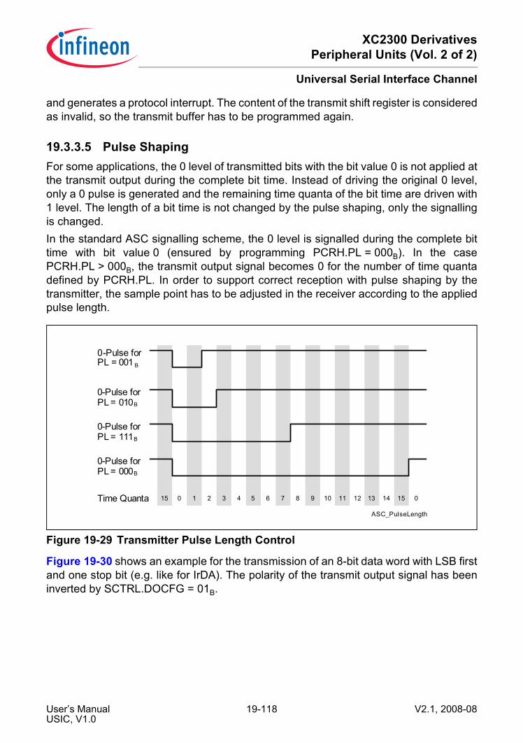
XC2300 DerivativesPeripheral Units (Vol. 2 of 2)
Universal Serial Interface Channel
and generates a protocol interrupt. The content of the transmit shift register is consideredas invalid, so the transmit buffer has to be programmed again.
19.3.3.5 Pulse ShapingFor some applications, the 0 level of transmitted bits with the bit value 0 is not applied atthe transmit output during the complete bit time. Instead of driving the original 0 level,only a 0 pulse is generated and the remaining time quanta of the bit time are driven with1 level. The length of a bit time is not changed by the pulse shaping, only the signallingis changed.In the standard ASC signalling scheme, the 0 level is signalled during the complete bittime with bit value 0 (ensured by programming PCRH.PL = 000B). In the casePCRH.PL > 000B, the transmit output signal becomes 0 for the number of time quantadefined by PCRH.PL. In order to support correct reception with pulse shaping by thetransmitter, the sample point has to be adjusted in the receiver according to the appliedpulse length.
Figure 19-29 Transmitter Pulse Length Control
Figure 19-30 shows an example for the transmission of an 8-bit data word with LSB firstand one stop bit (e.g. like for IrDA). The polarity of the transmit output signal has beeninverted by SCTRL.DOCFG = 01B.
ASC_PulseLength
0-Pulse forPL = 001 B
0-Pulse forPL = 010B
0-Pulse forPL = 111B
0-Pulse forPL = 000B
Time Quanta 15 0 1 2 3 4 5 6 7 8 9 10 11 12 13 14 15 0
User’s Manual 19-118 V2.1, 2008-08USIC, V1.0

XC2300 DerivativesPeripheral Units (Vol. 2 of 2)
Universal Serial Interface Channel
Figure 19-30 Pulse Output Example
19.3.3.6 Automatic Shadow MechanismThe contents of the protocol control registers PCRL and PCRH, as well as bit fieldSCTRH.FLE are internally kept constant while a data frame is transferred by anautomatic shadow mechanism (shadowing takes place with each frame start). Theregisters can be programmed all the time with new settings that are taken into accountfor the next data frame. During a data frame, the applied (shadowed) setting is notchanged, although new values have been written after the start of the data frame.Bit fields SCTRH.WLE and SCTRL.SDIR are shadowed automatically with the start ofeach data word. As a result, a data frame can consist of data words with a differentlength. It is recommended to change SCTRL.SDIR only when no data frame is runningto avoid interference between hardware and software.Please note that the starting point of a data word can be different for a transmitter and areceiver. In order to ensure correct handling, it is recommended to modify SCTRH.WLEonly while transmitter and receiver are both idle. If the transmitter and the receiver arereferring to the same data signal (e.g. in a LIN bus system), SCTRH.WLE can bemodified while a data transfer is in progress after the RSI event has been detected.
19.3.3.7 End of Frame ControlThe number of bits per ASC frame is defined by bit field SCTRH.FLE. In order to supportdifferent frame length settings for consecutively transmitted frames, this bit field can bemodified by hardware. The automatic update mechanism is enabled byTCSRL.FLEMD = 1 (in this case, bits TCSRL.WLEMD, SELMD, and WAMD have to becleared).If enabled, the transmit control information TCI automatically overwrites the bit fieldTCSRL.FLEMD when the ASC frame is started (leading to frames with 1 to 32 data bits).The TCI value represents the written address location of TBUFxx (without additional data
ASC_PulseOut
Bit Value
DOUT Pulse
SO
F
D0
D1
D2
D3
D4
D5
D6
STO
P
Idle Idle
D7
ASC Frame
User’s Manual 19-119 V2.1, 2008-08USIC, V1.0

XC2300 DerivativesPeripheral Units (Vol. 2 of 2)
Universal Serial Interface Channel
buffer) or INxx (with additional data buffer). With this mechanism, an ASC with 8 databits is generated by writing a data word to TBUF07 (IN07, respectively).
19.3.3.8 Mode Control BehaviorIn ASC mode, the following kernel modes are supported:• Run Mode 0/1:
Behavior as programmed, no impact on data transfers.• Stop Mode 0:
Bit PSR.TXIDLE is cleared. A new transmission is not started. A current transmissionis finished normally. Bit PSR.RXIDLE is not modified. Reception is still possible.When leaving stop mode 0, bit TXIDLE is set according to PCR.IDM.
• Stop Mode 1:Bit PSR.TXIDLE is cleared. A new transmission is not started. A current transmissionis finished normally. Bit PSR.RXIDLE is cleared. A new reception is not possible. Acurrent reception is finished normally.When leaving stop mode 1, bits TXIDLE and RXIDLE are set according to PCR.IDM.
19.3.3.9 Disabling ASC ModeIn order to switch off ASC mode without any data corruption, the receiver and thetransmitter have to be both idle. This is ensured by requesting Stop Mode 1 in registerKSCFG. After waiting for the end of the frame, the ASC mode can be disabled.
19.3.3.10 Protocol Interrupt EventsThe following protocol-related events are generated in ASC mode and can lead to aprotocol interrupt. The collision detection and the transmitter frame finished events arerelated to the transmitter, whereas the receiver events are given by the synchronizationbreak detection, the receiver noise detection, the format error checks and the end of thereceived frame.Please note that the bits in register PSR are not automatically cleared by hardware andhave to be cleared by software in order to monitor new incoming events.• Collision detection:
This interrupt indicates that the transmitted value (DOUT) does not match with theinput value of the DX1 input stage at the sample point of a bit. For more details referto Page 19-117.
• Transmitter frame finished:This interrupt indicates that the transmitter has completely finished a frame. BitPSR.TFF becomes set at the end of the last stop bit. The DOUT signal assignmentto port pins can be changed while no transmission is in progress.
• Receiver frame finished:This interrupt indicates that the receiver has completely finished a frame. Bit
User’s Manual 19-120 V2.1, 2008-08USIC, V1.0

XC2300 DerivativesPeripheral Units (Vol. 2 of 2)
Universal Serial Interface Channel
PSR.RFF becomes set at the end of the last stop bit. The DIN signal assignment toport pins can be changed while no reception is in progress.
• Synchronization break detection:This interrupt can be used in LIN networks to indicate the reception of thesynchronization break symbol (at the beginning of a LIN frame).
• Receiver noise detection:This interrupt indicates that the input value at the sample point of a bit and at the twotime quanta before are not identical.
• Format error:The bit value of the stop bit(s) is defined as 1 level for the ASC protocol. A formaterror is signalled if the sampled bit value of a stop bit is 0.
19.3.3.11 Data Transfer Interrupt HandlingThe data transfer interrupts indicate events related to ASC frame handling.• Transmit buffer interrupt TBI:
Bit PSR.TBIF is set after the start of first data bit of a data word. This is the earliestpoint in time when a new data word can be written to TBUF.With this event, bit TCSRL.TDV is cleared and new data can be loaded to thetransmit buffer.
• Transmit shift interrupt TSI:Bit PSR.TSIF is set after the start of the last data bit of a data word.
• Receiver start interrupt RSI:Bit PSR.RSIF is set after the sample point of the first data bit of a data word.
• Receiver interrupt RI and alternative interrupt AI:Bit PSR.RIF is set after the sampling point of the last data bit of a data word if thisdata word is not directly followed by a parity bit (parity generation disabled or not thelast word of a data frame).If the data word is directly followed by a parity bit (last data word of a data frame andparity generation enabled), bit PSR.RIF is set after the sampling point of the parity bitif no parity error has been detected. If a parity error has been detected, bit PSR.AIFis set instead of bit PSR.RIF.The first data word of a data frame is indicated by RBUFSR.SOF = 1 for the receivedword.Bit PSR.RIF is set for a receiver interrupt RI with WA = 0. Bit PSR.AIF is set for aalternative interrupt AI with WA = 1.
User’s Manual 19-121 V2.1, 2008-08USIC, V1.0
XC2300 DerivativesPeripheral Units (Vol. 2 of 2)
Universal Serial Interface Channel
19.3.3.12 Protocol-Related Argument and ErrorThe protocol-related argument (RBUFSR.PAR) and the protocol-related error(RBUFSR.PERR) are two flags that are assigned to each received data word in thecorresponding receiver buffer status registers.In ASC mode, the received parity bit is monitored by the protocol-related argument andthe result of the parity check by the protocol-related error indication (0 = received paritybit equal to calculated parity value). This information being elaborated only for the lastreceived data word of each data frame, both bit positions are 0 for data words that arenot the last data word of a data frame or if the parity generation is disabled.
19.3.3.13 Receive Buffer HandlingIf a receive FIFO buffer is available (CCFG.RB = 1) and enabled for data handling(RBCTRH.SIZE > 0), it is recommended to set RBCTRH.RCIM = 11B in ASC mode. Thisleads to an indication that the data word has been the first data word of a new data frameif bit OUTRH.RCI[0] = 1, a parity error is indicated by OUTRH.RCI[4] = 1, and thereceived parity bit value is given by OUTRH.RCI[3].The standard receive buffer event and the alternative receive buffer event can be usedfor the following operations in RCI mode (RBCTRH.RNM = 1):• A standard receive buffer event indicates that a data word can be read from OUTRL
that has been received without parity error.• An alternative receive buffer event indicates that a data word can be read from
OUTRL that has been received with parity error.
19.3.3.14 Sync-Break DetectionThe receiver permanently checks the DIN signal for a certain number of consecutive bittimes with 0 level. The number is given by the number of programmed bits per frame(SCTRH.FLE) plus 2 (in the case without parity) or plus 3 (in the case with parity). If a 0level is detected at a sample point of a bit after this event has been found, bit PSR.SBDis set and additionally, a protocol interrupt can be generated (if enabled byPCRL.SBD = 1). The counting restarts from 0 each time a falling edge is found at inputDIN. This feature can be used for the detection of a synchronization break for slavedevices in a LIN bus system (the master doesn’t check for sync break).For example, in a configuration for 8 data bits without parity generation, bit PCRL.SBDis set after at the next sample point at 0 level after 10 complete bit times have elapsed(representing the sample point of the 11th bit time since the first falling edge).
User’s Manual 19-122 V2.1, 2008-08USIC, V1.0

XC2300 DerivativesPeripheral Units (Vol. 2 of 2)
Universal Serial Interface Channel
19.3.4 ASC Protocol RegistersIn ASC mode, the registers PCRH, PCRL and PSR handle ASC related information.
19.3.4.1 ASC Protocol Control RegistersIn ASC mode, the PCRL/PCRH register bits or bit fields are defined as described in thissection.
PCRL Protocol Control Register L [ASC Mode]
(40H) Reset Value: 0000H
15 14 13 12 11 10 9 8 7 6 5 4 3 2 1 0
PL SP FFIEN
FEIEN
RNIEN
CDEN
SBIEN IDM STP
B SMD
rw rw rw rw rw rw rw rw rw rw
Field Bits Type DescriptionSMD 0 rw Sample Mode
This bit field defines the sample mode of the ASC receiver. The selected data input signal can be sampled only once per bit time or three times (in consecutive time quanta). When sampling three times, the bit value shifted in the receiver shift register is given by a majority decision among the three sampled values.0B Only one sample is taken per bit time. The current
input value is sampled.1B Three samples are taken per bit time and a majority
decision is made.STPB 1 rw Stop Bits
This bit defines the number of stop bits in an ASC frame.0B The number of stop bits is 1.1B The number of stop bits is 2.
User’s Manual 19-123 V2.1, 2008-08USIC, V1.0
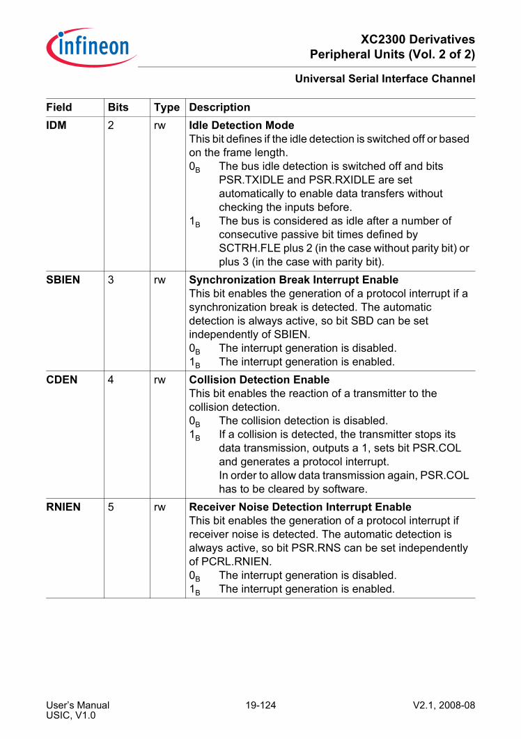
XC2300 DerivativesPeripheral Units (Vol. 2 of 2)
Universal Serial Interface Channel
IDM 2 rw Idle Detection ModeThis bit defines if the idle detection is switched off or based on the frame length.0B The bus idle detection is switched off and bits
PSR.TXIDLE and PSR.RXIDLE are set automatically to enable data transfers without checking the inputs before.
1B The bus is considered as idle after a number of consecutive passive bit times defined by SCTRH.FLE plus 2 (in the case without parity bit) or plus 3 (in the case with parity bit).
SBIEN 3 rw Synchronization Break Interrupt EnableThis bit enables the generation of a protocol interrupt if a synchronization break is detected. The automatic detection is always active, so bit SBD can be set independently of SBIEN.0B The interrupt generation is disabled.1B The interrupt generation is enabled.
CDEN 4 rw Collision Detection EnableThis bit enables the reaction of a transmitter to the collision detection.0B The collision detection is disabled.1B If a collision is detected, the transmitter stops its
data transmission, outputs a 1, sets bit PSR.COL and generates a protocol interrupt.In order to allow data transmission again, PSR.COL has to be cleared by software.
RNIEN 5 rw Receiver Noise Detection Interrupt EnableThis bit enables the generation of a protocol interrupt if receiver noise is detected. The automatic detection is always active, so bit PSR.RNS can be set independently of PCRL.RNIEN.0B The interrupt generation is disabled.1B The interrupt generation is enabled.
Field Bits Type Description
User’s Manual 19-124 V2.1, 2008-08USIC, V1.0

XC2300 DerivativesPeripheral Units (Vol. 2 of 2)
Universal Serial Interface Channel
FEIEN 6 rw Format Error Interrupt EnableThis bit enables the generation of a protocol interrupt if a format error is detected. The automatic detection is always active, so bits PSR.FER0/FER1 can be set independently of PCRL.FEIEN.0B The interrupt generation is disabled.1B The interrupt generation is enabled.
FFIEN 7 rw Frame Finished Interrupt EnableThis bit enables the generation of a protocol interrupt if the receiver or the transmitter reach the end of a frame. The automatic detection is always active, so bits PSR.RFF or PSR.TFF can be set independently of PCRL.FFIEN.0B The interrupt generation is disabled.1B The interrupt generation is enabled.
SP [12:8] rw Sample PointThis bit field defines the sample point of the bit value. The sample point must not be located outside the programmed bit timing (PCRL.SP ≤ BRGL.DCTQ).
PL [15:13] rw Pulse LengthThis bit field defines the length of a 0 data bit, counted in time quanta, starting with the time quantum 0 of each bit time. Each bit value that is a 0 can lead to a 0 pulse that is shorter than a bit time, e.g. for IrDA applications. The length of a bit time is not changed by PL, only the length of the 0 at the output signal.The pulse length must not be longer than the programmed bit timing (PCRH.PL ≤ BRGL.DCTQ).This bit field is only taken into account by the transmitter and is ignored by the receiver.000B The pulse length is equal to the bit length (no
shortened 0).001B The pulse length of a 0 bit is 2 time quanta.010B The pulse length of a 0 bit is 3 time quanta....111B The pulse length of a 0 bit is 8 time quanta.
Field Bits Type Description
User’s Manual 19-125 V2.1, 2008-08USIC, V1.0
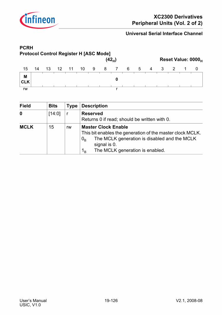
XC2300 DerivativesPeripheral Units (Vol. 2 of 2)
Universal Serial Interface Channel
PCRH Protocol Control Register H [ASC Mode]
(42H) Reset Value: 0000H
15 14 13 12 11 10 9 8 7 6 5 4 3 2 1 0
MCLK 0
rw r
Field Bits Type Description0 [14:0] r Reserved
Returns 0 if read; should be written with 0.MCLK 15 rw Master Clock Enable
This bit enables the generation of the master clock MCLK.0B The MCLK generation is disabled and the MCLK
signal is 0.1B The MCLK generation is enabled.
User’s Manual 19-126 V2.1, 2008-08USIC, V1.0
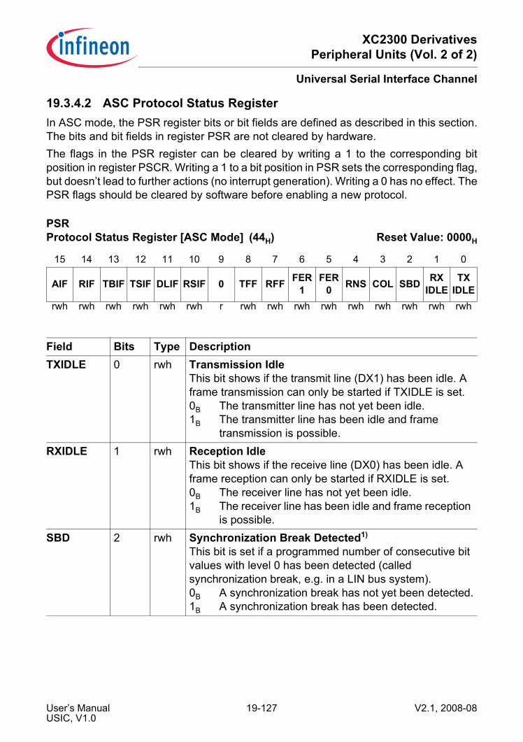
XC2300 DerivativesPeripheral Units (Vol. 2 of 2)
Universal Serial Interface Channel
19.3.4.2 ASC Protocol Status RegisterIn ASC mode, the PSR register bits or bit fields are defined as described in this section.The bits and bit fields in register PSR are not cleared by hardware.The flags in the PSR register can be cleared by writing a 1 to the corresponding bitposition in register PSCR. Writing a 1 to a bit position in PSR sets the corresponding flag,but doesn’t lead to further actions (no interrupt generation). Writing a 0 has no effect. ThePSR flags should be cleared by software before enabling a new protocol.
PSR Protocol Status Register [ASC Mode] (44H) Reset Value: 0000H
15 14 13 12 11 10 9 8 7 6 5 4 3 2 1 0
AIF RIF TBIF TSIF DLIF RSIF 0 TFF RFF FER1
FER0 RNS COL SBD RX
IDLETX
IDLErwh rwh rwh rwh rwh rwh r rwh rwh rwh rwh rwh rwh rwh rwh rwh
Field Bits Type DescriptionTXIDLE 0 rwh Transmission Idle
This bit shows if the transmit line (DX1) has been idle. A frame transmission can only be started if TXIDLE is set.0B The transmitter line has not yet been idle.1B The transmitter line has been idle and frame
transmission is possible.RXIDLE 1 rwh Reception Idle
This bit shows if the receive line (DX0) has been idle. A frame reception can only be started if RXIDLE is set.0B The receiver line has not yet been idle.1B The receiver line has been idle and frame reception
is possible.SBD 2 rwh Synchronization Break Detected1)
This bit is set if a programmed number of consecutive bit values with level 0 has been detected (called synchronization break, e.g. in a LIN bus system).0B A synchronization break has not yet been detected.1B A synchronization break has been detected.
User’s Manual 19-127 V2.1, 2008-08USIC, V1.0
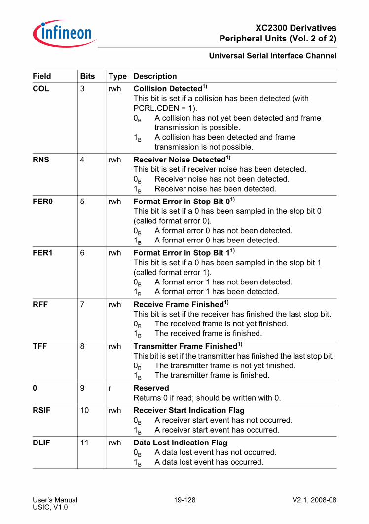
XC2300 DerivativesPeripheral Units (Vol. 2 of 2)
Universal Serial Interface Channel
COL 3 rwh Collision Detected1)
This bit is set if a collision has been detected (with PCRL.CDEN = 1).0B A collision has not yet been detected and frame
transmission is possible.1B A collision has been detected and frame
transmission is not possible.RNS 4 rwh Receiver Noise Detected1)
This bit is set if receiver noise has been detected.0B Receiver noise has not been detected.1B Receiver noise has been detected.
FER0 5 rwh Format Error in Stop Bit 01)
This bit is set if a 0 has been sampled in the stop bit 0 (called format error 0).0B A format error 0 has not been detected.1B A format error 0 has been detected.
FER1 6 rwh Format Error in Stop Bit 11)
This bit is set if a 0 has been sampled in the stop bit 1 (called format error 1).0B A format error 1 has not been detected.1B A format error 1 has been detected.
RFF 7 rwh Receive Frame Finished1)
This bit is set if the receiver has finished the last stop bit.0B The received frame is not yet finished.1B The received frame is finished.
TFF 8 rwh Transmitter Frame Finished1)
This bit is set if the transmitter has finished the last stop bit.0B The transmitter frame is not yet finished.1B The transmitter frame is finished.
0 9 r ReservedReturns 0 if read; should be written with 0.
RSIF 10 rwh Receiver Start Indication Flag0B A receiver start event has not occurred.1B A receiver start event has occurred.
DLIF 11 rwh Data Lost Indication Flag0B A data lost event has not occurred.1B A data lost event has occurred.
Field Bits Type Description
User’s Manual 19-128 V2.1, 2008-08USIC, V1.0
XC2300 DerivativesPeripheral Units (Vol. 2 of 2)
Universal Serial Interface Channel
19.3.5 Hardware LIN SupportIn order to support the LIN protocol, bit TCSRL.FLEMD = 1 should be set for the master.For slave devices, it can be cleared and the fixed number of 8 data bits has to be set(SCTRH.FLE = 7). For both, master and slave devices, the parity generation has to beswitched off (CCR.PM = 00B) and transfers take place with LSB first (SCTRL.SDIR = 0)and 1 stop bit (PCRL.STPB = 0).The Local Interconnect Network (LIN) data exchange protocol contains several symbolsthat can all be handled in ASC mode. Each single LIN symbol represents a completeASC frame. The LIN bus is a master-slave bus system with a single master and multipleslaves (for the exact definition please refer to the official LIN specification).A complete LIN frame contains the following symbols:• Synchronization break:
The master sends a synchronization break to signal the beginning of a new frame. Itcontains at least 13 consecutive bit times at 0 level, followed by at least one bit timeat 1 level (corresponding to 1 stop bit). Therefore, TBUF11 (or IN11) has to be writtenwith 0 (leading to a frame with SOF followed by 12 data bits at 0 level).A slave device shall detect 11 consecutive bit times at 0 level, which done by thesynchronization break detection. Bit PSR.SBD is set if such an event is detected anda protocol interrupt can be generated. Additionally, the received data value of 0appears in the receive buffer and a format error is signaled.If the baud rate of the slave has to be adapted to the master, the baud ratemeasurement has to be enabled for falling edges by setting BRGL.TMEN = 1,DX0CR.CM = 10H and DX1CR.CM = 00H before the next symbol starts.
TSIF 12 rwh Transmit Shift Indication Flag0B A transmit shift event has not occurred.1B A transmit shift event has occurred.
TBIF 13 rwh Transmit Buffer Indication Flag0B A transmit buffer event has not occurred.1B A transmit buffer event has occurred.
RIF 14 rwh Receive Indication Flag0B A receive event has not occurred.1B A receive event has occurred.
AIF 15 rwh Alternative Receive Indication Flag0B An alternative receive event has not occurred.1B An alternative receive event has occurred.
1) This status bit can generate a protocol interrupt (see Page 19-25). The general interrupt status flags aredescribed in the general interrupt chapter.
Field Bits Type Description
User’s Manual 19-129 V2.1, 2008-08USIC, V1.0
XC2300 DerivativesPeripheral Units (Vol. 2 of 2)
Universal Serial Interface Channel
• Synchronization byte:The master sends this symbol after writing the data value 55H to TBUF07 (or IN07).A slave device can either receive this symbol without any further action (and candiscard it) or it can use the falling edges for baud rate measurement. BitPSR.TSIF = 1 (with optionally the corresponding interrupt) indicates the detection ofa falling edge and the capturing of the elapsed time since the last falling edge inBRGH.PDIV. Valid captured values can be read out after the second, third, fourth andfifth activation of TSIF. After the fifth activation of TSIF within this symbol, the baudrate detection has to be disabled (BRGL.TMEN = 0) and BRGH.PDIV can beprogrammed with the formerly captured value divided by twice the number of timequanta per bit (assuming BRGL.PCTQ = 00B).
• Other symbols:The other symbols of a LIN frame can be handled with ASC data frames withoutspecific actions.
If LIN frames should be sent out on a frame base by the LIN master, the input DX2 canbe connected to external timers to trigger the transmit actions (e.g. the synchronizationbreak symbol has been prepared but is started if a trigger occurs). Please note thatduring the baud rate measurement of the ASC receiver, no transmission can take placeby the ASC transmitter of the same USIC channel.
User’s Manual 19-130 V2.1, 2008-08USIC, V1.0

XC2300 DerivativesPeripheral Units (Vol. 2 of 2)
Universal Serial Interface Channel
19.4 Synchronous Serial Channel (SSC)The synchronous serial channel SSC covers the data transfer function of an SPI-likemodule. It can handle reception and transmission of synchronous data frames betweena device operating in master mode and at least one device in slave mode. The SSCmode is selected by CCR.MODE = 0001B with CCFG.SSC = 1 (SSC mode is available).This chapter contains the following sections:• Signal description (see Page 19-131)• General SSC issues (see Page 19-139)• Master mode operation (see Page 19-142)• Slave mode operation (see Page 19-149)• Protocol registers (see Page 19-151)• Timing considerations (see Page 19-157)
19.4.1 Signal DescriptionA synchronous SSC data transfer is characterized by a simultaneous transfer of a shiftclock signal together with the transmit and/or receive data signal(s) to determine whenthe data is valid (definition of transmit and sample point).
Figure 19-31 SSC Signals for Full-Duplex Communication
In order to explicitly indicate the start and the end of a data transfer and to address morethan one slave devices individually, the SSC module supports the handling of slave
SSC_Signals_
fSYS
Master Transmit /Slave Receive
(Master)fSYS
(Slave)
DX0
DOUT
DINRBUF
SSC Communication Master
Slave SelectGenerator
Baud RateGenerator
TBUF
SCLKOUT
SELOx
DX0DIN
DOUTTBUF
SSC Communication Slave
RBUF
SCLKIN
SELIN
DX1
DX2
Master Receive /Slave Transmit
Slave Clock
Slave Select
User’s Manual 19-131 V2.1, 2008-08USIC, V1.0

XC2300 DerivativesPeripheral Units (Vol. 2 of 2)
Universal Serial Interface Channel
select signals. They are optional and are not necessarily needed for SSC data transfers.The SSC module supports up to 8 different slave select output signals for master modeoperation (named SELOx, with x = 0-7) and 1 slave select input SELIN for slave mode.In most applications, the slave select signals are active low.A device operating in master mode controls the start and end of a data frame, as well asthe generation of the shift clock and slave select signals. This comprises the baud ratesetting for the shift clock and the delays between the shift clock and the slave selectoutput signals. If several SSC modules are connected together, there can be only oneSSC master at a time, but several slaves. Slave devices receive the shift clock andoptionally a slave select signal(s). For the programming of the input stages DX0, DX1,and DX2 please refer to Page 19-37.
Figure 19-32 4-Wire SSC Standard Communication Signals
Table 19-8 SSC Communication SignalsSSC Mode Receive Data Transmit Data Shift Clock Slave Select(s)Master MRST1),
input DIN,handled by DX0
1) MRST = master receive slave transmit, also known as MISO = master in slave out
MTSR2),Output DOUT
2) MTSR = master transmit slave receive, also known as MOSI = master out slave in
Output SCLKOUT
Output(s)SELOx
Slave MTSR,input DIN,handled by DX0
MRST,Output DOUT
Input SCLKIN,handled by DX1
input SELIN,handled by DX2
SSC_Standard_
ShiftClock
TransmitData
ReceiveData
D0
Data Frame
D1 Dn D0 D1
D0 D1 Dn D0 D1
Dn
Dn
SlaveSelect
Data Word 0 Data Word x
User’s Manual 19-132 V2.1, 2008-08USIC, V1.0

XC2300 DerivativesPeripheral Units (Vol. 2 of 2)
Universal Serial Interface Channel
19.4.1.1 Transmit and Receive Data SignalsIn half-duplex mode, a single data line is used, either for data transfer from the masterto a slave or from a slave to the master. In this case, MRST and MTSR are connectedtogether, one signal as input, the other one as output, depending on the data direction.The user software has to take care about the data direction to avoid data collision (e.g.by preparing dummy data of all 1s for transmission in case of a wired AND connectionwith open-drain drivers or by enabling/disabling push/pull output drivers). In full-duplexmode, data transfers take place in parallel between the master device and a slave devicevia two independent data signals MTSR and MRST, as shown in Figure 19-31.The receive data input signal DIN is handled by the input stage DX0. In master mode(referring to MRST) as well as in slave mode (referring to MTSR), the data input signalDIN is taken from an input pin. The signal polarity of DOUT (data output) with respect tothe data bit value can be configured in block DOCFG (data output configuration) by bitfield SCTRL.DOCFG.
Figure 19-33 SSC Data Signals
SSC_DataSignals_
DIN DOUTMTSRMaster Mode
MRSTSlave Mode
Input StageDX0
Data ShitUnit DOCFG
SCTRLMRSTMaster Mode
MTSRSlave Mode
User’s Manual 19-133 V2.1, 2008-08USIC, V1.0

XC2300 DerivativesPeripheral Units (Vol. 2 of 2)
Universal Serial Interface Channel
19.4.1.2 Shift Clock SignalsThe shift clock signal is handled by the input stage DX1. In slave mode, the signalSCLKIN is received from an external master, so the DX1 stage has to be connected toan input pin. The input stage can invert the received input signal to adapt to the polarityof SCLKIN to the function of the data shift unit (data transmission on rising edges, datareception on falling edges).In master mode, the shift clock is generated by the internal baud rate generator. Theoutput signal SCLK of the baud rate generator is taken as shift clock input for the datashift unit. The internal signal SCLK is made available for external slave devices by signalSCLKOUT.
Figure 19-34 SSC Shift Clock Signals
Due to the multitude of different SSC applications, in master mode, there are differentways to configure the shift clock output signal SCLKOUT with respect to SCLK. This isdone in the block SCLKCFG (shift clock configuration) by bit field BRGH.SCLKCFG,allowing 4 possible settings, as shown in Figure 19-35.• No delay, no polarity inversion (SCLKCFG = 00B, SCLKOUT equals SCLK):
The inactive level of SCLKOUT is 0, while no data frame is transferred. The first databit of a new data frame is transmitted with the first rising edge of SCLKOUT and thefirst data bit is received in with the first falling edge of SCLKOUT. The last data bit ofa data frame is transmitted with the last rising clock edge of SCLKOUT and the lastdata bit is received in with the last falling edge of SCLKOUT. This setting can be usedin master and in slave mode. It corresponds to the behavior of the internal data shiftunit.
• No delay, polarity inversion (SCLKCFG = 01B):The inactive level of SCLKOUT is 1, while no data frame is transferred. The first data
SSC_ShiftClock_
SCLKIN
SSC in Master ModeSSC in Slave Mode
SCLKOUT
SCLKCFG
Baud Rate Generator
TransferControl LogicData Shift Unit
Input StageDX1
SCLK
Delay of ½ Bit Time
User’s Manual 19-134 V2.1, 2008-08USIC, V1.0

XC2300 DerivativesPeripheral Units (Vol. 2 of 2)
Universal Serial Interface Channel
bit of a new data frame is transmitted with the first falling clock edge of SCLKOUTand the first data bit is received with the first rising edge of SCLKOUT. The last databit of a data frame is transmitted with the last falling edge of SCLKOUT and the lastdata bit is received with the last rising edge of SCLKOUT. This setting can be usedin master and in slave mode.
• SCLKOUT is delayed by 1/2 shift clock period, no polarity inversion(SCLKCFG = 10B):The inactive level of SCLKOUT is 0, while no data frame is transferred.The first data bit of a new data frame is transmitted 1/2 shift clock period before thefirst rising clock edge of SCLKOUT. Due to the delay, the next data bits seem to betransmitted with the falling edges of SCLKOUT. The last data bit of a data frame istransmitted 1/2 period of SCLKOUT before the last rising clock edge of SCLKOUT.The first data bit is received 1/2 shift clock period before the first falling edge ofSCLKOUT. Due to the delay, the next data bits seem to be received with the risingedges of SCLKOUT. The last data bit is received 1/2 period of SCLKOUT before thelast falling clock edge of SCLKOUT.This setting can be used only in master mode and not in slave mode (the connectedslave has to provide the first data bit before the first SCLKOUT edge, e.g. as soon asit is addressed by its slave select).
• SCLKOUT is delayed by 1/2 shift clock period, polarity inversion (SCLKCFG = 11B):The inactive level of SCLKOUT is 1, while no data frame is transferred.The first data bit of a new data frame is transmitted 1/2 shift clock period before thefirst falling clock edge of SCLKOUT. Due to the delay, the next data bits seem to betransmitted with the rising edges of SCLKOUT. The last data bit of a data frame istransmitted 1/2 period of SCLKOUT before the last falling clock edge of SCLKOUT.The first data bit is received 1/2 shift clock period before the first rising edge ofSCLKOUT. Due to the delay, the next data bits seem to be received with the fallingedges of SCLKOUT. The last data bit is received 1/2 period of SCLKOUT before thelast rising clock edge of SCLKOUT.This setting can be used only in master mode and not in slave mode (the connectedslave has to provide the first data bit before the first SCLKOUT edge, e.g. as soon asit is addressed by its slave select).
User’s Manual 19-135 V2.1, 2008-08USIC, V1.0
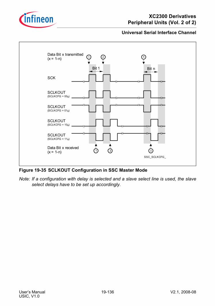
XC2300 DerivativesPeripheral Units (Vol. 2 of 2)
Universal Serial Interface Channel
Figure 19-35 SCLKOUT Configuration in SSC Master Mode
Note: If a configuration with delay is selected and a slave select line is used, the slaveselect delays have to be set up accordingly.
SSC_SCLKCFG_
SCK
1 2 n
SCLKOUT(SCLKCFG = 00B)
SCLKOUT(SCLKCFG = 01B)
SCLKOUT(SCLKCFG = 10B)
SCLKOUT(SCLKCFG = 11B)
Data Bit x received(x = 1-n)
Bit 1 Bit n
1 2 nData Bit x transmitted(x = 1-n)
User’s Manual 19-136 V2.1, 2008-08USIC, V1.0

XC2300 DerivativesPeripheral Units (Vol. 2 of 2)
Universal Serial Interface Channel
19.4.1.3 Slave Select SignalsThe slave select signal is handled by the input stage DX2. In slave mode, the input signalSELIN is received from an external master via an input pin. The input stage can invertthe received input signal to adapt the polarity of signal SELIN to the function of the datashift unit (the module internal signals are considered as high active, so a data transfer isonly possible while the slave select input of the data shift unit is at 1-level, otherwise, shiftclock pulses are ignored and do not lead to data transfers). If an input signal SELIN islow active, it should be inverted in the DX2 input stage.In master mode, a master slave select signal MSLS is generated by the internal slaveselect generator. In order to address different external slave devices independently, theinternal MSLS signal is made available externally via up to 8 SELOx output signals thatcan be configured by the block SELCFG (select configuration).
Figure 19-36 SSC Slave Select Signals
The control of the SELCFG block is based on protocol specific bits and bit fields in theprotocol control register parts PCRL and PCRH. For the generation of the MSLS signalplease refer to Section 19.4.3.2.• PCRL.SELCTR to chose between direct and coded select mode• PCRL.SELINV to invert the SELOx outputs• PCRH.SELO[7:0] as individual value for each SELOx lineThe SELCFG block supports the following configurations of the SELOx output signals:• Direct Select Mode (SELCTR = 1):
Each SELOx line (with x = 0-7) can be directly connected to an external slave device.If bit x in bit field SELO is 0, the SELOx output is permanently inactive. A SELOxoutput becomes active while the internal signal MSLS is active (see
SSC_SlaveSelect_
SELIN
SSC in Master ModeSSC in Slave Mode
SELOxx = 0-7
. . . . . .
SELCFG
Slave Select Generator
TransferControl LogicData Shift Unit
Input StageDX2
MSLS
User’s Manual 19-137 V2.1, 2008-08USIC, V1.0

XC2300 DerivativesPeripheral Units (Vol. 2 of 2)
Universal Serial Interface Channel
Section 19.4.3.2) and bit x in bit field SELO is 1. Several external slave devices canbe addressed in parallel if more than one bit in bit field SELO are set during a dataframe. The number of external slave devices that can be addressed individually islimited to the number of available SELOx outputs.
• Coded Select Mode (SELCTR = 0):The SELOx lines (with x = 1-7) can be used as addresses for an external addressdecoder to increase the number of external slave devices. These lines only changewith the start of a new data frame and have no other relation to MSLS. Signal SELO0can be used as enable signal for the external address decoder. It is active whileMSLS is active (during a data frame) and bit 0 in bit field SELO is 1. Furthermore, incoded select mode, this output line is delayed by one cycle of fSYS compared to MSLSto allow the other SELOx lines to stabilize before enabling the address decoder.
User’s Manual 19-138 V2.1, 2008-08USIC, V1.0

XC2300 DerivativesPeripheral Units (Vol. 2 of 2)
Universal Serial Interface Channel
19.4.2 Operating the SSCThis chapter contains SSC issues, that are of general interest and not directly linked toeither master mode or slave mode.
19.4.2.1 Automatic Shadow MechanismThe contents of the baud rate control registers BRGL and BRGH, bit field SCTRH.FLEas well as the protocol control registers PCRL and PCRH are internally kept constantwhile a data frame is transferred (= while MSLS is active) by an automatic shadowmechanism. The registers can be programmed all the time with new settings that aretaken into account for the next data frame. During a data frame, the applied (shadowed)setting is not changed, although new values have been written after the start of the dataframe.Bit fields SCTRH.WLE and SCTRL.SDIR are shadowed automatically with the start ofeach data word. As a result, a data frame can consist of data words with a differentlength. It is recommended to change SCTRL.SDIR only when no data frame is runningto avoid interference between hardware and software.Please note that the starting point of a data word are different for a transmitter (first bittransmitted) and a receiver (first bit received). In order to ensure correct handling, it isrecommended to refer to the receive start interrupt RSI before modifying SCTRL.WLE.If TCSRL.WLEMD = 1, it is recommended to update TCSRL and TBUFxx after thereceiver start interrupt has been generated.
19.4.2.2 Mode Control BehaviorIn SSC mode, the following kernel modes are supported:• Run Mode 0/1:
Behavior as programmed, no impact on data transfers.• Stop Mode 0/1:
The content of the transmit buffer is considered as not valid for transmission.Although being considered as 0, bit TCSRL.TDV it is not modified by the stop modecondition.In master mode, a currently running word transfer is finished normally, but no newdata word is started (the stop condition is not considered as end-of-frame condition).In slave mode, a currently running word transfer is finished normally. Passive datawill be sent out instead of a valid data word if a data word transfer is started by theexternal master while the slave device is in stop mode. In order to avoid passive slavetransmit data, it is recommended not to program stop mode for an SSC slave deviceif the master device does not respect the slave device’s stop mode.
User’s Manual 19-139 V2.1, 2008-08USIC, V1.0

XC2300 DerivativesPeripheral Units (Vol. 2 of 2)
Universal Serial Interface Channel
19.4.2.3 Disabling SSC ModeIn order to disable SSC mode without any data corruption, the receiver and thetransmitter have to be both idle. This is ensured by requesting Stop Mode 1 in registerKSCFG. After Stop Mode 1 has been acknowledged by KSCFG.ACK = 1, the SSC modecan be disabled.
19.4.2.4 Data Frame ControlAn SSC data frame can consist of several consecutive data words that may beseparated by an inter-word delay. Without inter-word delay, the data words seem to forma longer data word, being equivalent to a data frame. The length of the data words aremost commonly identical within a data frame, but may also differ from one word toanother. The data word length information (defined by SCTRH.WLE) is evaluated foreach new data word, whereas the frame length information (defined by SCTRH.FLE) isevaluated at the beginning at each start of a new frame.The length of an SSC data frame can be defined in two different ways:• By the number of bits per frame:
If the number of bits per data frame is defined (frame length FLE), a slave selectsignal is not necessarily required to indicate the start and the end of a data frame.If the programmed number of bits per frame is reached within a data word, the frameis considered as finished and remaining data bits in the last data word are ignoredand are not transferred.This method can be applied for data frames with up to 63 data bits.
• By the slave select signal:If the number of bits per data frame is not known, the start/end information of a dataframe is given by a slave select signal. If a deactivation of the slave select signal isdetected within a data word, the frame is considered as finished and remaining databits in the last data word are ignored and are not transferred.This method has to be applied for frames with more than 63 data bits (programminglimit of FLE). The advantage of slave select signals is the clearly defined start andend condition of data frames in a data stream. Furthermore, slave select signals allowto address slave devices individually.
19.4.2.5 Parity ModeParity generation is not supported in SSC mode and bit field CCR.PM = 00B has to beprogrammed.
19.4.2.6 Transfer ModeIn SSC mode, bit field SCTRL.TRM = 01B has to be programmed to allow data transfers.Setting SCTRL.TRM = 00B disables and stops the data transfer immediately.
User’s Manual 19-140 V2.1, 2008-08USIC, V1.0

XC2300 DerivativesPeripheral Units (Vol. 2 of 2)
Universal Serial Interface Channel
19.4.2.7 Data Transfer Interrupt HandlingThe data transfer interrupts indicate events related to SSC frame handling.• Transmit buffer interrupt TBI:
Bit PSR.TBIF is set after the start of first data bit of a data word.• Transmit shift interrupt TSI:
Bit PSR.TSIF is set after the start of the last data bit of a data word.• Receiver start interrupt RSI:
Bit PSR.RSIF is set after the reception of the first data bit of a data word.With this event, bit TCSRL.TDV is cleared and new data can be loaded to thetransmit buffer.
• Receiver interrupt RI:Bit PSR.RIF is set at after the reception of the last data bit of a data word. BitRBUFSR.SOF indicates whether the received data word has been the first data wordof a new data frame.
• Alternative interrupt AI:In SSC mode, this interrupt is not used.
19.4.2.8 Protocol-Related Argument and ErrorThe protocol-related argument (PAR) and the protocol-related error (PERR) are twoflags that are assigned to each received data word in the corresponding receiver bufferstatus registers.In SSC mode, these flags are always 0 (parity handling must be disabled).
19.4.2.9 Receive Buffer HandlingIf a receive FIFO buffer is available (CCFG.RB = 1) and enabled for data handling(RBCTRH.SIZE > 0), it is recommended to set RBCTRH.RCIM = 01B in SSC mode. Thisleads to an indication that the data word has been the first data word of a new data frameif bit OUTRH.RCI[4] = 1, and the word length of the received data is given byOUTRH.RCI[3:0].The standard receive buffer event and the alternative receive buffer event can be usedfor the following operation in RCI mode (RBCTRH.RNM = 1):• A standard receive buffer event indicates that a data word can be read from OUTRL
that has not been the first word of a data frame.• An alternative receive buffer event indicates that the first data word of a new data
frame can be read from OUTRL.
User’s Manual 19-141 V2.1, 2008-08USIC, V1.0

XC2300 DerivativesPeripheral Units (Vol. 2 of 2)
Universal Serial Interface Channel
19.4.3 Operating the SSC in Master ModeIn order to operate the SSC in master mode, the following issues have to be considered:• Select SSC mode:
It is recommended to configure all parameters of the SSC that do not change duringrun time while CCR.MODE = 0000B. Bit field SCTRL.TRM = 01B has to beprogrammed. The configuration of the input stages has to be done whileCCR.MODE = 0000B to avoid unintended edges of the input signals and the SSCmode can be enabled by CCR.MODE = 0001B afterwards.
• Pin connections:Establish a connection of input stage DX0 with the selected receive data input pin(DIN) with DX0CR.INSW = 1 and configure a transmit data output pin (DOUT).
• Baud rate generation:The desired baud rate setting has to be selected, comprising the fractional dividerand the baud rate generator. Bit DX1CR.INSW = 0 has to be programmed to use thebaud rate generator output SCLK directly as input for the data shift unit. Configure ashift clock output pin (signal SCLKOUT).
• Slave select generation:The slave select delay generation has to be enabled by setting PCRL.MSLSEN = 1and the programming of the time quanta counter setting. Bit DX2CR.INSW = 0 hasto be programmed to use the slave select generator output MSLS as input for thedata shift unit. Configure slave select output pins (signals SELOx) if needed.
• Data format configuration:The word length, the frame length, and the shift direction have to be set up accordingto the application requirements by programming the registers SCTRL and SCTRH.
Note: The USIC can only receive in master mode if it is transmitting, because the masterframe handling refers to bit TDV of the transmitter part.
19.4.3.1 Baud Rate GenerationThe baud rate (determining the length of one data bit) of the SSC is defined by thefrequency of the SCLK signal (one period of fSCLK represents one data bit). The SSCbaud rate generation does not imply any time quanta counter.In a standard SSC application, the phase relation between the optional MCLK outputsignal and SCLK is not relevant and can be disabled (BRGL.PPPEN = 0). In this case,the SCLK signal directly derives from the protocol input frequency fPIN. In the exceptionalcase that a fixed phase relation between the MCLK signal and SCLK is required (e.g.when using MCLK as clock reference for external devices), the additional divider by 2stage has to be taken into account (BRGL.PPPEN = 1).
User’s Manual 19-142 V2.1, 2008-08USIC, V1.0

XC2300 DerivativesPeripheral Units (Vol. 2 of 2)
Universal Serial Interface Channel
The adjustable divider factor is defined by bit field BRGH.PDIV.
(19.8)
19.4.3.2 MSLS GenerationThe slave select signals indicate the start and the end of a data frame and are also usedby the communication master to individually select the desired slave device. A slaveselect output of the communication master becomes active a programmable time beforea data part of the frame is started (leading delay Tld), necessary to prepare the slavedevice for the following communication. After the transfer of a data part of the frame, itbecomes inactive again a programmable time after the end of the last bit (trailing delayTtd) to respect the slave hold time requirements. If data frames are transferred back-to-back one after the other, the minimum time between the deactivation of the slave selectand the next activation of a slave select is programmable (next-frame delay Tnf). If a dataframe consists of more than one data word, an optional delay between the data wordscan also be programmed (inter-word delay Tiw).
Figure 19-37 MSLS Generation in SSC Master Mode
fSCLK = if PPPEN = 0PDIV + 11
if PPPEN = 1PDIV + 1
1fSCLK = 2 × 2
× fPIN
2 × fPIN
SSC_MSLS_
ShiftClock
TransmitData
ReceiveData
D0
Data Frame
D1 Dn D0 D1
D0 D1 Dn D0 D1
Dn
Dn
MSLS
Data Word 1Data Word 0
Tld Tiw Ttd TnfActive
Inactive
SELOx(SELINV = 1)
User’s Manual 19-143 V2.1, 2008-08USIC, V1.0

XC2300 DerivativesPeripheral Units (Vol. 2 of 2)
Universal Serial Interface Channel
In SSC master mode, the slave select delays are defined as follows:• Leading delay Tld:
The leading delay starts if valid data is available for transmission. The internal signalMSLS becomes active with the start of the leading delay. The first shift clock edge(rising edge) of SCLK is generated by the baud rate generator after the leading delayhas elapsed.
• Trailing delay TtdThe trailing delay starts at the end of the last SCLK cycle of a data frame. The internalsignal MSLS becomes inactive with the end of the trailing delay.
• Inter-word delay Tiw:This delay is optional and can be enabled/disabled by PCRH.TIWEN. If the inter-word delay is disabled (TIWEN = 0), the last data bit of a data word is directlyfollowed by the first data bit of the next data word of the same data frame. If enabled(TIWEN = 1), the inter-word delay starts at the end of the last SCLK cycle of a dataword. The first SCLK cycle of the following data word of the same data frame isstarted when the inter-word delay has elapsed. During this time, no shift clock pulsesare generated and signal MSLS stays active. The communication partner has time to“digest” the previous data word or to prepare for the next one.
• Next-frame delay Tnf:The next-frame delay starts at the end of the trailing delay. During this time, no shiftclock pulses are generated and signal MSLS stays inactive. A frame is considered asfinished after the next-frame delay has elapsed.
19.4.3.3 Automatic Slave Select UpdateIf the number of bits per SSC frame and the word length are defined by bit fieldsSCTRH.FLE and SCTRH.WLE, the transmit control information TCI can be used toupdate the slave select setting PCRH.CTR[23:16] to control the SELOx select outputs.The automatic update mechanism is enabled by TCSRL.SELMD = 1 (bitsTCSRL.WLEMD, FLEMD, and WAMD have to be cleared). In this case, the TCI of thefirst data word of a frame defines the slave select setting of the complete frame due tothe automatic shadow mechanism (see Page 19-119).
User’s Manual 19-144 V2.1, 2008-08USIC, V1.0
XC2300 DerivativesPeripheral Units (Vol. 2 of 2)
Universal Serial Interface Channel
19.4.3.4 Slave Select Delay GenerationThe slave select delay generation is based on time quanta. The length of a time quantum(defined by the period of the fCTQIN) and the number of time quanta per delay can beprogrammed.In standard SSC applications, the leading delay Tld and the trailing delay Ttd are mainlyused to ensure stability on the input and output lines as well as to respect setup and holdtimes of the input stages. These two delays have the same length (in most cases shorterthan a bit time) and can be programmed with the same set of bit fields.• BRGL.CTQSEL
to define the input frequency fCTQIN for the time quanta generation for Tld and Ttd• BRGL.PCTQ
to define the length of a time quantum (division of fCTQIN by 1, 2, 3, or 4) for Tld and Ttd• BRGL.DCTQ
to define the number of time quanta for the delay generation for Tld and Ttd
The inter-word delay Tiw and the next-frame delay Tnf are used to handle received dataor to prepare data for the next word or frame. These two delays have the same length(in most cases in the bit time range) and can be programmed with a second, independentset of bit fields.• PCRL.CTQSEL1
to define the input frequency fCTQIN for the time quanta generation for Tnf and Tiw• PCRL.PCTQ1
to define the length of a time quantum (division of fCTQIN by 1, 2, 3, or 4) for Tnf and Tiw• PCRL.DCTQ1
to define the number of time quanta for the delay generation for Tnf and Tiw• PCRH.TIWEN
to enable/disable the inter-word delay Tiw
Each delay depends on the length of a time quantum and the programmed number oftime quanta given by the bit fields CTQSEL/CTQSEL1, PCTQ/DCTQ andPCTQ1/DCTQ1 (the coding of CTQSEL1 is similar to CTQSEL, etc.). To provide a highflexibility in programming the delay length, the input frequencies can be selectedbetween several possibilities (e.g. based on bit times or on the faster inputs of theprotocol-related divider). The delay times are defined as follows:
(19.9)
(PCTQ + 1) × (DCTQ + 1) fCTQIN
Tld = Ttd =
(PCTQ1 + 1) × (DCTQ1 + 1) fCTQIN
Tiw = Tnf =
User’s Manual 19-145 V2.1, 2008-08USIC, V1.0
XC2300 DerivativesPeripheral Units (Vol. 2 of 2)
Universal Serial Interface Channel
19.4.3.5 Protocol Interrupt EventsThe following protocol-related events generated in SSC mode and can lead to a protocolinterrupt. They are related to the start and the end of a data frame. After the start of adata frame a new setting could be programmed for the next data frame and after the endof a data frame the SSC connections to pins can be changed.Please note that the bits in register PSR are not all automatically cleared by hardwareand have to be cleared by software in order to monitor new incoming events.• MSLS Interrupt:
This interrupt indicates in master mode (MSLS generation enabled) that a data framehas started (activation of MSLS) and has been finished (deactivation of MSLS). Anychange of the internal MSLS signal sets bit PSR.MSLSEV and additionally, a protocolinterrupt can be generated if PCRL.MSLSIEN = 1. The actual state of the internalMSLS signal can be read out at PSR.MSLS to take appropriate actions when thisinterrupt has been detected.
• DX2T Interrupt:This interrupt monitors edges of the input signal of the DX2 stage (although thissignal is not used as slave select input for data transfers).A programmable edge detection for the DX2 input signal sets bit PSR.DX2TEV andadditionally, a protocol interrupt can be generated if PCRL.DX2TIEN = 1. The actualstate of the selected input signal can be read out at PSR.DX2S to take appropriateactions when this interrupt has been detected.
User’s Manual 19-146 V2.1, 2008-08USIC, V1.0

XC2300 DerivativesPeripheral Units (Vol. 2 of 2)
Universal Serial Interface Channel
19.4.3.6 End-of-Frame ControlThe information about the frame length is required for the MSLS generator of the masterdevice. In addition to the mechanism based on the number of bits per frame (selectedwith SCTRH.FLE < 63), the following alternative mechanisms for end of frame handlingare supported. It is recommended to set SCTRH.FLE = 63 (if several end of framemechanisms are activated in parallel, the first end condition being found finishes theframe).• Software-based start of frame indication TCSRL.SOF:
This mechanism can be used if software handles the TBUF data without data FIFO.If bit SOF is set, a valid content of TBUF is considered as first word of a new frame.Bit SOF has to be set before the content of TBUF is transferred to the transmit shiftregister, so it is recommended to write it before writing data to TBUF. A current dataword transfer is finished completely and the slave select delays Ttd and Tnf areapplied before starting a new data frame with Tld and the content of TBUF.For software-handling of bit SOF, bit TCSRL.WLEMD = 0 has to be programmed. Inthis case, all TBUF[31:0] address locations show an identical behavior (TCI not takeninto account for data handling).
• Software-based end of frame indication TCSRL.EOF:This mechanism can be used if software handles the TBUF data without data FIFO.If bit EOF is set, a valid content of TBUF is considered as last word of a new frame.Bit EOF has to be set before the content of TBUF is transferred to the transmit shiftregister, so it is recommended to write it before writing data to TBUF. The data wordin TBUF is sent out completely and the slave select delays Ttd and Tnf are applied. Anew data frame can start with Tld with the next valid TBUF value.For software-handling of bit EOF, bit TCSRL.WLEMD = 0 has to be programmed. Inthis case, all TBUF[31:0] address locations show an identical behavior (TCI not takeninto account for data handling).
• Software-based address related end of frame handling:This mechanism can be used if software handles the TBUF data without data FIFO.If bit TCSRL.WLEMD = 1, the address of the written TBUF[31:0] is used as transmitcontrol information TCI[4:0] to update SCTRH.WLE (= TCI[3:0]) and TCSRL.EOF(= TCI[4]) for each data word. The written TBUF[31:0] address location defines theword length and the end of a frame (locations TBUF[31:16] lead to a frame end).For example, writing transmit data to TBUF[07] results in a data word of 8-bit lengthwithout finishing the frame, whereas writing transmit data to TBUF[31] leads to a dataword length of 16 bits, followed by Ttd, the deactivation of MSLS and Tnf.If TCSRL.WLEMD = 1, bits TCSRL.EOF and SOF, as well as SCTRH.WLE must notbe written by software after writing data to a TBUF location. Furthermore, it isrecommended to clear bits TCSRL.SELMD, FLEMD and WAMD.
• FIFO-based address related end of frame handling:This mechanism can be used if a data FIFO is used to store the transmit data. Thegeneral behavior is similar to the software-based address related end of frame
User’s Manual 19-147 V2.1, 2008-08USIC, V1.0
XC2300 DerivativesPeripheral Units (Vol. 2 of 2)
Universal Serial Interface Channel
handling, except that transmit data is not written to the locations TBUF[31:0], but tothe FIFO input locations IN[31:0] instead. In this case, software must not write to anyof the TBUF locations.
• TBUF related end of frame handling:If bit PCRL.FEM = 0, an end of frame is assumed if the transmit buffer TBUF doesnot contain valid transmit data at the end of a data word transmission(TCSRL.TDV = 0 or in Stop Mode). In this case, the software has to take care thatTBUF does not run empty during a data frame in Run Mode. If bit PCRL.FEM = 1,signal MSLS stays active while the transmit buffer is waiting for new data(TCSRL.TDV = 1 again) or until Stop Mode is left.
• Explicit end of frame by software:The software can explicitly stop a frame by clearing bit PSR.MSLS by writing a 1 tothe related bit position in register PSCR. This write action immediately clears bitPSR.MSLS, whereas the internal MSLS signal becomes inactive after finishing acurrently running word transfer and respecting the slave select delays Ttd and Tnf.
User’s Manual 19-148 V2.1, 2008-08USIC, V1.0

XC2300 DerivativesPeripheral Units (Vol. 2 of 2)
Universal Serial Interface Channel
19.4.4 Operating the SSC in Slave ModeIn order to operate the SSC in slave mode, the following issues have to be considered:• Select SSC mode:
It is recommended to configure all parameters of the SSC that do not change duringrun time while CCR.MODE = 0000B. Bit field SCTRL.TRM = 01B has to beprogrammed. The configuration of the input stages has to be done whileCCR.MODE = 0000B to avoid unintended edges of the input signals and the SSCmode can be enabled afterwards by CCR.MODE = 0001B.
• Pin connections:Establish a connection of input stage DX0 with the selected receive data input pin(signal DIN) with DX0CR.INSW = 1 and configure a transmit data output pin (signalDOUT).Establish a connection of input stage DX1 with the selected shift clock input pin(signal SCLKIN) with DX1CR.INSW = 1.Establish a connection of input stage DX2 with the selected slave select input pin(signal SELIN) with DX2CR.INSW = 1. If no slave select input signal is used, the DX2stage has to deliver a 1-level to the data shift unit to allow data reception andtransmission. If a slave device is not selected (DX2 stage delivers a 0 to the data shiftunit) and a shift clock pulse are received, the incoming data is not received and theDOUT signal outputs the passive data level defined by SCTRL.PDL.
• Baud rate generation:The baud rate generator is not needed and can be switched off by the fractionaldivider.
• Slave select generation:The slave select delay generation is not needed and can be switched off. The bitsand bit fields MSLSEN, SELCTR, SELINV, CTQSEL1, PCTQ1, DCTQ1, MSLSIEN,SELO[7:0], and TIWEN in registers PCRL/PCRH are not necessary and can beprogrammed to 0.
19.4.4.1 Protocol InterruptsThe following protocol-related events generated in SSC mode and can lead to a protocolinterrupt. They are related to the start and the end of a data frame. After the start of adata frame a new setting could be programmed for the next data frame and after the endof a data frame the SSC connections to pins can be changed.Please note that the bits in register PSR are not all automatically cleared by hardwareand have to be cleared by software in order to monitor new incoming events.• MSLS event:
The MSLS generation being switched off, this event is not available.• DX2T event:
The slave select input signal SELIN is handled by the DX2 stage and the edges ofthe selected signal can generate a protocol interrupt. This interrupt allows to indicate
User’s Manual 19-149 V2.1, 2008-08USIC, V1.0
XC2300 DerivativesPeripheral Units (Vol. 2 of 2)
Universal Serial Interface Channel
that a data frame has started and/or that a data frame has been completely finished.A programmable edge detection for the DX2 input signal activates DX2T, sets bitPSR.DX2TEV and additionally, a protocol interrupt can be generated ifPCRL.DX2TIEN = 1. The actual state of the selected input signal can be read out atPSR.DX2S to take appropriate actions when this interrupt has been detected.
19.4.4.2 End-of-Frame ControlIn slave mode, the following possibilities exist to determine the frame length. The slavedevice either has to refer to an external slave select signal, or to the number of receiveddata bits.• Frame length known in advance by the slave device, no slave select:
In this case bit field SCTRH.FLE can be programmed to the known value (if it doesnot exceed 63 bits). A currently running data word transfer is considered as finishedif the programmed frame length is reached.
• Frame length not known by the slave, no slave select:In this case, the slave device’s software has to decide on data word base if a frameis finished. Bit field SCTRH.FLE can be either programmed to the word lengthSCTRH.WLE, or to its maximum value to disable the slave internal frame lengthevaluation by counting received bits.
• Slave device addressed via slave select signal SELIN:If the slave device is addressed by a slave select signal delivered by thecommunication master, the frame start and end information are given by this signal.In this case, bit field SCTRH.FLE should be programmed to its maximum value todisable the slave internal frame length evaluation.
User’s Manual 19-150 V2.1, 2008-08USIC, V1.0

XC2300 DerivativesPeripheral Units (Vol. 2 of 2)
Universal Serial Interface Channel
19.4.5 SSC Protocol RegistersIn SSC mode, the registers PCRL, PCRH and PSR handle SSC related information.
19.4.5.1 SSC Protocol Control RegistersIn SSC mode, the PCRL/PCRH register bits or bit fields are defined as described in thissection.
PCRL Protocol Control Register L [SSC Mode]
(40H) Reset Value: 0000H
15 14 13 12 11 10 9 8 7 6 5 4 3 2 1 0
DX2TIEN
MSLSIEN 0 DCTQ1 PCTQ1 CTQSEL1 FEM SE
INVSELCTR
MSLSEN
rw rw rw rw rw rw rw rw rw
Field Bits Type DescriptionMSLSEN 0 rw MSLS Enable
This bit enables/disables the generation of the master slave select signal MSLS. If the SSC is a transfer slave, the SLS information is read from a pin and the internal generation is not needed. If the SSC is a transfer master, it has to provide the MSLS signal.0B The MSLS generation is disabled (MSLS = 0).
This is the setting for SSC slave mode.1B The MSLS generation is enabled.
This is the setting for SSC master mode.SELCTR 1 rw Select Control
This bit selects the operating mode for the SELO[7:0] outputs.0B The coded select mode is enabled.1B The direct select mode is enabled.
SELINV 2 rw Select InversionThis bit defines if the polarity of the SELO[7:0] outputs in relation to the master slave select signal MSLS.0B The SELO outputs have the same polarity as the
MSLS signal (active high).1B The SELO outputs have the inverted polarity to the
MSLS signal (active low).
User’s Manual 19-151 V2.1, 2008-08USIC, V1.0
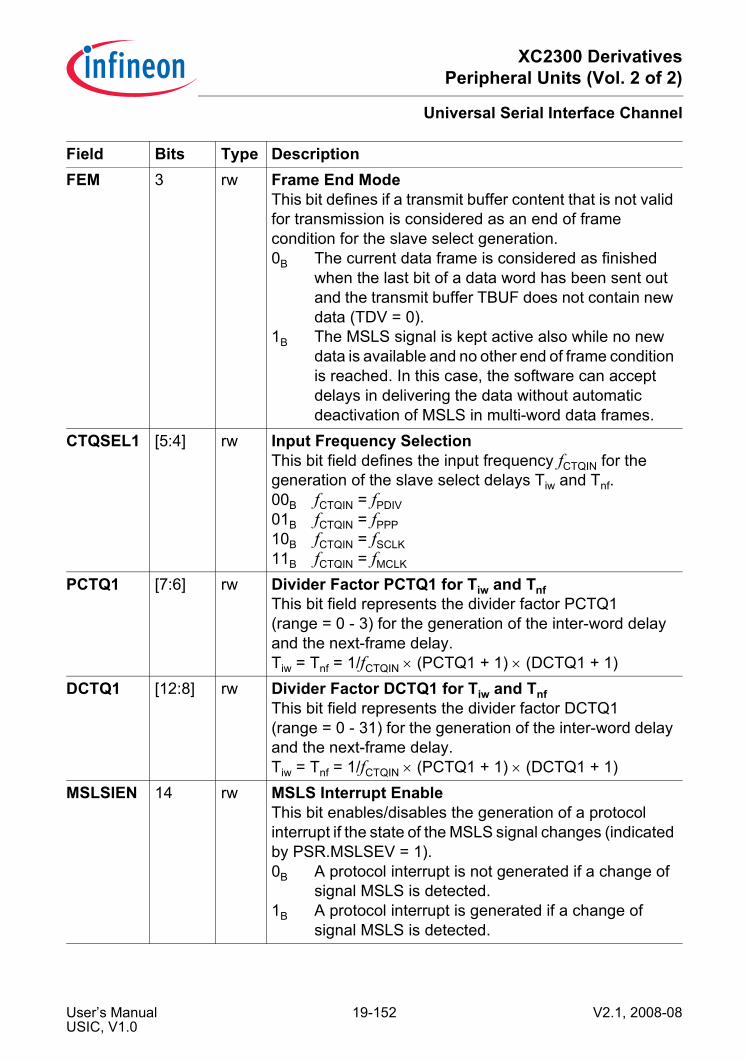
XC2300 DerivativesPeripheral Units (Vol. 2 of 2)
Universal Serial Interface Channel
FEM 3 rw Frame End ModeThis bit defines if a transmit buffer content that is not valid for transmission is considered as an end of frame condition for the slave select generation.0B The current data frame is considered as finished
when the last bit of a data word has been sent out and the transmit buffer TBUF does not contain new data (TDV = 0).
1B The MSLS signal is kept active also while no new data is available and no other end of frame condition is reached. In this case, the software can accept delays in delivering the data without automatic deactivation of MSLS in multi-word data frames.
CTQSEL1 [5:4] rw Input Frequency SelectionThis bit field defines the input frequency fCTQIN for the generation of the slave select delays Tiw and Tnf.00B fCTQIN = fPDIV01B fCTQIN = fPPP10B fCTQIN = fSCLK11B fCTQIN = fMCLK
PCTQ1 [7:6] rw Divider Factor PCTQ1 for Tiw and TnfThis bit field represents the divider factor PCTQ1 (range = 0 - 3) for the generation of the inter-word delay and the next-frame delay.Tiw = Tnf = 1/fCTQIN × (PCTQ1 + 1) × (DCTQ1 + 1)
DCTQ1 [12:8] rw Divider Factor DCTQ1 for Tiw and TnfThis bit field represents the divider factor DCTQ1 (range = 0 - 31) for the generation of the inter-word delay and the next-frame delay.Tiw = Tnf = 1/fCTQIN × (PCTQ1 + 1) × (DCTQ1 + 1)
MSLSIEN 14 rw MSLS Interrupt EnableThis bit enables/disables the generation of a protocol interrupt if the state of the MSLS signal changes (indicated by PSR.MSLSEV = 1).0B A protocol interrupt is not generated if a change of
signal MSLS is detected.1B A protocol interrupt is generated if a change of
signal MSLS is detected.
Field Bits Type Description
User’s Manual 19-152 V2.1, 2008-08USIC, V1.0

XC2300 DerivativesPeripheral Units (Vol. 2 of 2)
Universal Serial Interface Channel
DX2TIEN 15 rw DX2T Interrupt EnableThis bit enables/disables the generation of a protocol interrupt if the DX2T signal becomes activated (indicated by PSR.DX2TEV = 1).0B A protocol interrupt is not generated if DX2T is
activated.1B A protocol interrupt is generated if DX2T is
activated.0 13 rw Reserved
Returns 0 if read; should be written with 0.
PCRH Protocol Control Register H [SSC Mode]
(42H) Reset Value: 0000H
15 14 13 12 11 10 9 8 7 6 5 4 3 2 1 0
MCLK 0 TIW
EN SELO
rw rw rw rw
Field Bits Type DescriptionSELO [7:0] rw Select Output
This bit field defines the setting of the SELO[7:0] output lines.0B The corresponding SELOx line cannot be activated.1B The corresponding SELOx line can be activated
(according to the mode selected by SELCTR).TIWEN 8 rw Enable Inter-Word Delay Tiw
This bit enables/disables the inter-word delay Tiw after the transmission of a data word.0B No delay between data words of the same frame.1B The inter-word delay Tiw is enabled and introduced
between data words of the same frame.
Field Bits Type Description
User’s Manual 19-153 V2.1, 2008-08USIC, V1.0
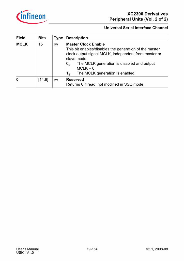
XC2300 DerivativesPeripheral Units (Vol. 2 of 2)
Universal Serial Interface Channel
MCLK 15 rw Master Clock EnableThis bit enables/disables the generation of the master clock output signal MCLK, independent from master or slave mode.0B The MCLK generation is disabled and output
MCLK = 0.1B The MCLK generation is enabled.
0 [14:9] rw ReservedReturns 0 if read; not modified in SSC mode.
Field Bits Type Description
User’s Manual 19-154 V2.1, 2008-08USIC, V1.0

XC2300 DerivativesPeripheral Units (Vol. 2 of 2)
Universal Serial Interface Channel
19.4.5.2 SSC Protocol Status RegisterIn SSC mode, the PSR register bits or bit fields are defined as described in this section.The bits and bit fields in register PSR are not cleared by hardware.The flags in the PSR register can be cleared by writing a 1 to the corresponding bitposition in register PSCR. Writing a 1 to a bit position in PSR sets the corresponding flag,but doesn’t lead to further actions (no interrupt generation). Writing a 0 has no effect. ThePSR flags should be cleared by software before enabling a new protocol.
PSR Protocol Status Register [SSC Mode] (44H) Reset Value: 0000H
15 14 13 12 11 10 9 8 7 6 5 4 3 2 1 0
AIF RIF TBIF TSIF DLIF RSIF 0 DX2TEV
MSLSEV
DX2S
MSLS
rwh rwh rwh rwh rwh rwh r rwh rwh rwh rwh
Field Bits Type DescriptionMSLS 0 rwh MSLS Status
This bit indicates the current status of the MSLS signal. It must be cleared by software to stop a running frame.0B The internal signal MSLS is inactive (0).1B The internal signal MSLS is active (1).
DX2S 1 rwh DX2S StatusThis bit indicates the current status of the DX2S signal that can be used as slave select input SELIN.0B DX2S is 0.1B DX2S is 1.
MSLSEV 2 rwh MSLS Event Detected1)
This bit indicates that the MSLS signal has changed its state since MSLSEV has been cleared. Together with the MSLS status bit, the activation/deactivation of the MSLS signal can be monitored.0B The MSLS signal has not changed its state.1B The MSLS signal has changed its state.
DX2TEV 3 rwh DX2T Event Detected1)
This bit indicates that the DX2T trigger signal has been activated since DX2TEV has been cleared.0B The DX2T signal has not been activated.1B The DX2T signal has been activated.
User’s Manual 19-155 V2.1, 2008-08USIC, V1.0
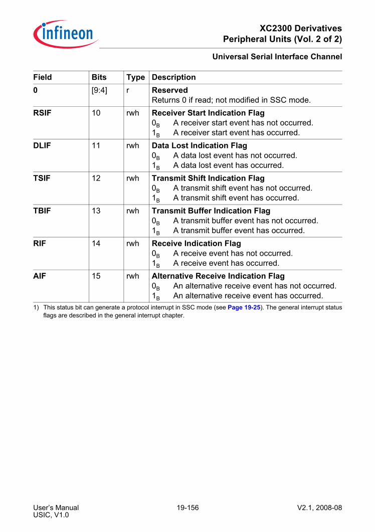
XC2300 DerivativesPeripheral Units (Vol. 2 of 2)
Universal Serial Interface Channel
0 [9:4] r ReservedReturns 0 if read; not modified in SSC mode.
RSIF 10 rwh Receiver Start Indication Flag0B A receiver start event has not occurred.1B A receiver start event has occurred.
DLIF 11 rwh Data Lost Indication Flag0B A data lost event has not occurred.1B A data lost event has occurred.
TSIF 12 rwh Transmit Shift Indication Flag0B A transmit shift event has not occurred.1B A transmit shift event has occurred.
TBIF 13 rwh Transmit Buffer Indication Flag0B A transmit buffer event has not occurred.1B A transmit buffer event has occurred.
RIF 14 rwh Receive Indication Flag0B A receive event has not occurred.1B A receive event has occurred.
AIF 15 rwh Alternative Receive Indication Flag0B An alternative receive event has not occurred.1B An alternative receive event has occurred.
1) This status bit can generate a protocol interrupt in SSC mode (see Page 19-25). The general interrupt statusflags are described in the general interrupt chapter.
Field Bits Type Description
User’s Manual 19-156 V2.1, 2008-08USIC, V1.0

XC2300 DerivativesPeripheral Units (Vol. 2 of 2)
Universal Serial Interface Channel
19.4.6 SSC Timing ConsiderationsThe input and output signals have to respect certain timings in order to ensure correctdata reception and transmission. In addition to module internal timings (due to inputfilters, reaction times on events, etc.), also the timings from the input pin via the inputstage (Tin) to the module and from the module via the output driver stage to the pin (Tout),as well as the signal propagation on the wires (Tprop) have to be taken into account.Please note that there might by additional delays in the DXn input stages, because thedigital filter and the synchronization stages lead to systematic delays, that have to beconsidered if these functions are used.
19.4.6.1 Closed-loop DelayA system-inherent limiting factor for the baud rate of an SSC connection is the closed-loop delay. In a typical application setup, a communication master device is connectedto a slave device in full-duplex mode with independent lines for transmit and receivedata. In a general case, all transmitters refer to one shift clock edge for transmission andall receivers refer to the other shift clock edge for reception. The master device’s SSCmodule sends out the transmit data, the shift clock and optionally the slave select signal.Therefore, the baud rate generation (BRG) and slave select generation (SSG) are partof the master device. The frame control is similar for SSC modules in master and slavemode, the main difference is the fact which module generates the shift clock andoptionally, the slave select signals.
Figure 19-38 SSC Closed-loop Delay
SSC_ClosedLoop
ToutMTSR
RBUF
SSC Master Device
FrameControl
TBUF
Shift Clock
TinMRST
Tprop
Tprop
Tout
BRG
Tout
SSG
SSC Master Module
Tprop
Slave Select Tprop
RBUF
Tin
Tout
TBUF
FrameControl
SSC Slave Device
Tin
Tin
SSC Slave Module
User’s Manual 19-157 V2.1, 2008-08USIC, V1.0

XC2300 DerivativesPeripheral Units (Vol. 2 of 2)
Universal Serial Interface Channel
The signal path between the SSC modules of the master and the slave device includesthe master’s output driver, the wiring to the slave device and the slave device’s inputstage. With the received shift clock edges, the slave device receives the master’stransmit data and transmits its own data back to the master device, passing by a similarsignal path in the other direction. The master module receives the slave’s transmit datarelated to its internal shift clock edges. In order to ensure correct data reception in themaster device, the slave’s transmit data has to be stable (respecting setup and holdtimes) as master receive data with the next shift clock edge of the master (generally 1/2shift clock period). To avoid data corruption, the accumulated delays of the input andoutput stages, the signal propagation on the wiring and the reaction times of thetransmitter/receiver have to be carefully considered, especially at high baud rates.In the given example, the time between the generation of the shift clock signal and theevaluation of the receive data by the master SSC module is given by the sum of Tout_master+ 2 × Tprop + Tin_slave + Tout_slave + Tin_master + module reaction times + input setup times.The input path is characterized by an input delay depending mainly on the input stagecharacteristics of the pads. The output path delay is determined by the output driverdelay and its slew rate, the external load and current capability of the driver. The devicespecific values for the input/output driver are given in the Data Sheet.
19.4.6.2 Delay Compensation in Master ModeA higher baud rate can be reached by delay compensation in master mode. Thiscompensation is possible if (at least) the shift clock pin is bidirectional.
Figure 19-39 SSC Master Mode with Delay Compensation
SSC_DelayComp
ToutMTSR
RBUF
SSC Master Device
FrameControl
TBUF
Shift Clock
TinMRST
Tprop
Tprop
BRG
SSG
SSC Master Module
Tprop
Slave Select Tprop
RBUF
Tin
Tout
TBUF
FrameControl
SSC Slave Device
Tin
Tin
SSC Slave Module
User’s Manual 19-158 V2.1, 2008-08USIC, V1.0

XC2300 DerivativesPeripheral Units (Vol. 2 of 2)
Universal Serial Interface Channel
If the shift clock signal in master mode is directly taken from the input function in parallelto the output signal, the output delay of the master device’s shift clock output iscompensated and only the difference between the input delays of the master and theslave devices have to be taken into account instead of the complete master’s outputdelay and the slave’s input delay of the shift clock path.In the given example, the time between the evaluation of the shift clock signal and thereceive data by the master SSC module is reduced by Tin_master + Tout_master.Although being a master mode, the shift clock input and optionally the slave select signalare not directly connected internally to the data shift unit, but are taken as externalsignals from input pins (DXnCR.INSW = 1). The delay compensation does not lead toadditional pins for the SSC communication if the shift clock output pin (slave selectoutput pin, respectively) is/are bidirectional. In this case, the input signal is decoupledfrom other internal signals, because it is related to the signal level at the pin itself.
User’s Manual 19-159 V2.1, 2008-08USIC, V1.0

XC2300 DerivativesPeripheral Units (Vol. 2 of 2)
Universal Serial Interface Channel
19.5 Inter-IC Bus Protocol (IIC)The IIC protocol of the USIC refers to the IIC bus specification version 2.1, january 2000from Philips Semiconductors. Contrary to that specification, the USIC device assumesrise/fall times of the bus signals of max. 300 ns in all modes. Please refer to the padcharacteristics in the AC/DC chapter for the driver capability. CBUS mode and HS modeare not supported.The IIC mode is selected by CCR.MODE = 0100B with CCFG.IIC = 1 (IIC modeavailable).This chapter contains the following sections:• Introduction (see Page 19-160)• Operating the IIC protocol (see Page 19-164)• Symbol timing and programming (see Page 19-170)• Data flow handling (see Page 19-173)• IIC protocol registers (see Page 19-178)
19.5.1 IntroductionUSIC IIC Features:• Two-wire interface, with one line for shift clock transfer and synchronization (shift
clock SCL), the other one for the data transfer (shift data SDA)• Communication in standard mode (100 kBit/s) or in fast mode (up to 400 kBit/s)• Support of 7-bit addressing, as well as 10-bit addressing• Master mode operation,
where the IIC controls the bus transactions and provides the clock signal.• Slave mode operation,
where an external master controls the bus transactions and provides the clock signal.• Multi-master mode operation,
where several masters can be connected to the bus and bus arbitration can takeplace, i.e. the IIC module can be master or slave. The master/slave operation of anIIC bus participant can change from frame to frame.
• Efficient frame handling (low software effort), also allowing PEC transfers• Powerful interrupt handling due to multitude of indication flags• Compensation support for input delays
User’s Manual 19-160 V2.1, 2008-08USIC, V1.0
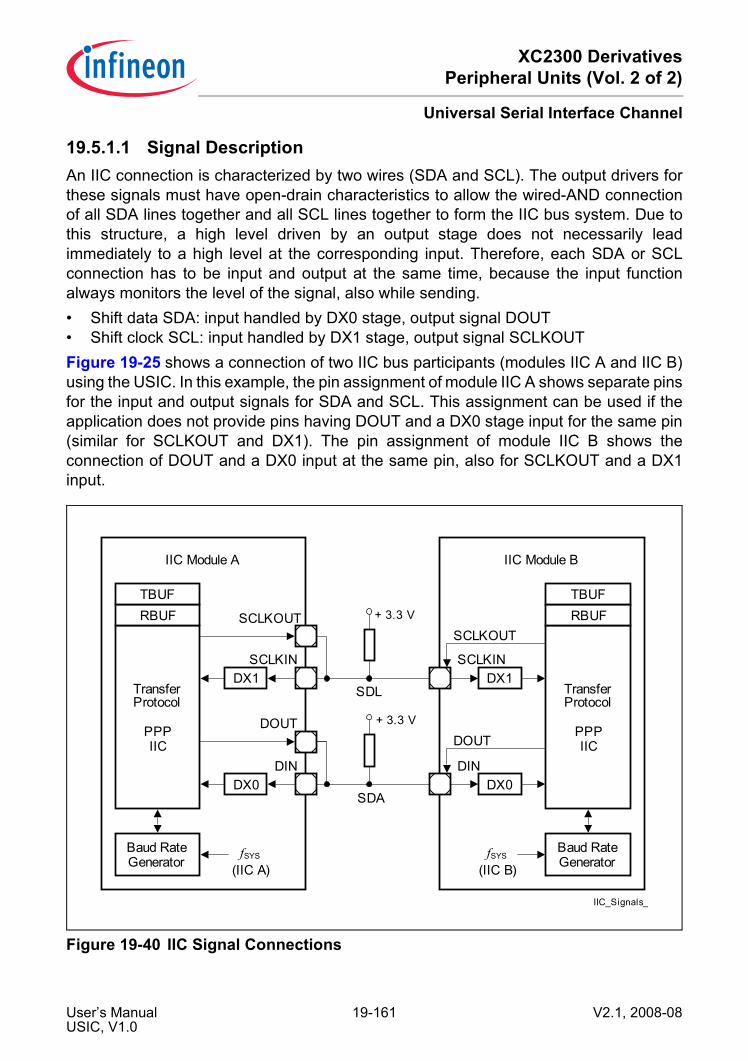
XC2300 DerivativesPeripheral Units (Vol. 2 of 2)
Universal Serial Interface Channel
19.5.1.1 Signal DescriptionAn IIC connection is characterized by two wires (SDA and SCL). The output drivers forthese signals must have open-drain characteristics to allow the wired-AND connectionof all SDA lines together and all SCL lines together to form the IIC bus system. Due tothis structure, a high level driven by an output stage does not necessarily leadimmediately to a high level at the corresponding input. Therefore, each SDA or SCLconnection has to be input and output at the same time, because the input functionalways monitors the level of the signal, also while sending.• Shift data SDA: input handled by DX0 stage, output signal DOUT• Shift clock SCL: input handled by DX1 stage, output signal SCLKOUTFigure 19-25 shows a connection of two IIC bus participants (modules IIC A and IIC B)using the USIC. In this example, the pin assignment of module IIC A shows separate pinsfor the input and output signals for SDA and SCL. This assignment can be used if theapplication does not provide pins having DOUT and a DX0 stage input for the same pin(similar for SCLKOUT and DX1). The pin assignment of module IIC B shows theconnection of DOUT and a DX0 input at the same pin, also for SCLKOUT and a DX1input.
Figure 19-40 IIC Signal Connections
IIC_Signals_
DX1
SCLKOUT
SCLKIN
IIC Module A
Baud RateGenerator
TransferProtocol
PPPIIC
RBUFTBUF
DX0
DOUT
DIN
fSYS
(IIC A)
DX1
SCLKOUT
SCLKIN
IIC Module B
Baud RateGenerator
TransferProtocol
PPPIIC
RBUFTBUF
DX0DIN
fSYS
(IIC A)fSYS
(IIC B)
DOUT
SDA
SDL
+ 3.3 V
+ 3.3 V
User’s Manual 19-161 V2.1, 2008-08USIC, V1.0
XC2300 DerivativesPeripheral Units (Vol. 2 of 2)
Universal Serial Interface Channel
19.5.1.2 SymbolsA symbol is a sequence of edges on the lines SDA and SCL. Symbols contain 10 or 25time quanta tq, depending on the selected baud rate. The baud rate generatordetermines the length of the time quanta tq, the sequence of edges in a symbol ishandled by the IIC protocol pre-processor, and the sequence of symbols can beprogrammed by the user according to the application needs.The following symbols are defined:• Bus idle:
SDA and SCL are high. No data transfer takes place currently.• Data bit symbol:
SDA stable during the high phase of SCL. SDA then represents the transferred bitvalue. There is one clock pulse on SCL for each transferred bit of data. During datatransfers SDA may only change while SCL is low.
• Start symbol:Signal SDA being high followed by a falling edge of SDA while SCL is high indicatesa start condition. This start condition initiates a data transfer over the IIC bus after thebus has been idle.
• Repeated start symbol:This start condition initiates a data transfer over the bus after a data symbol when thebus has not been idle. Therefore, SDA is set high and SCL low, followed by a startsymbol.
• Stop symbol:A rising edge on SDA while SCL is high indicates a stop condition. This stop conditionterminates a data transfer to release the bus to idle state. Between a start conditionand a stop condition an arbitrary number of bytes may be transferred.
User’s Manual 19-162 V2.1, 2008-08USIC, V1.0
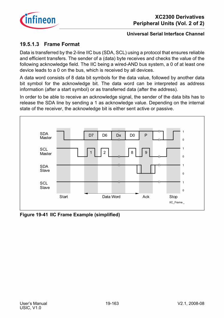
XC2300 DerivativesPeripheral Units (Vol. 2 of 2)
Universal Serial Interface Channel
19.5.1.3 Frame FormatData is transferred by the 2-line IIC bus (SDA, SCL) using a protocol that ensures reliableand efficient transfers. The sender of a (data) byte receives and checks the value of thefollowing acknowledge field. The IIC being a wired-AND bus system, a 0 of at least onedevice leads to a 0 on the bus, which is received by all devices.A data word consists of 8 data bit symbols for the data value, followed by another databit symbol for the acknowledge bit. The data word can be interpreted as addressinformation (after a start symbol) or as transferred data (after the address).In order to be able to receive an acknowledge signal, the sender of the data bits has torelease the SDA line by sending a 1 as acknowledge value. Depending on the internalstate of the receiver, the acknowledge bit is either sent active or passive.
Figure 19-41 IIC Frame Example (simplified)
IIC_Frame _
SDAMaster
SCLMaster 9
SDASlave
SCLSlave
D70
1Dx PD6 D0
8210
1
0
1
0
1
Data WordStart Ack Stop
User’s Manual 19-163 V2.1, 2008-08USIC, V1.0

XC2300 DerivativesPeripheral Units (Vol. 2 of 2)
Universal Serial Interface Channel
19.5.2 Operating the IICIn order to operate the IIC protocol, the following issues have to be considered:• Select IIC mode:
It is recommended to configure all parameters of the IIC that do not change duringrun time while CCR.MODE = 0000B. Bit field SCTRL.TRM = 11B should to beprogrammed. The configuration of the input stages has to be done whileCCR.MODE = 0000B to avoid unintended edges of the input signals and the IICmode can be enabled by CCR.MODE = 0100B afterwards.
• Pin connections:Establish a connection of input stage DX0 (with DX0CR.DPOL = 0) to the selectedshift data pin SDA (signal DIN) with DX0CR.INSW = 0 and configure the transmitdata output signal DOUT (with SCTRL.DOCFG = 00B) to the same pin. If available,this can be the same pin for input and output, or connect the selected input pin andthe output pin to form the SDA line.The same mechanism applies for the shift clock line SCL. Here, signal SCLKOUT(with BRGH.SCLKCFG = 00B) and an input of the DX1 stage have to be connected(with DX1CR.DPOL = 0).The input stage DX2 is not used for the IIC protocol.If the digital input filters are enabled in the DX0/1 stages, their delays have to betaken into account for correct calculation of the signal timings.The pins used for SDA and SCL have to be set to open-drain mode to support thewired-AND structure of the IIC bus lines.Note that the basic I/O port configuration for the IIC I/O pins must also setup correctlybefore the IIC mode becomes enabled by CCR.MODE = 0100B.
• Bit timing configuration:In standard mode (100 kBit/s) a minimum module frequency of 2 MHz is necessary,whereas in fast mode (400 kBit/s) a minimum of 10 MHz is required. Additionally, ifthe digital filter stage should be used to eliminate spikes up to 50 ns, a filter frequencyof 20 MHz is necessary.There could be an uncertainty in the SCL high phase timing of maximum 1/fPPP ifanother IIC participant lengthens the SCL low phase on the bus.More details are given in Section 19.5.3.
• Data format configuration:The data format has to be configured for 8 data bits (SCTRH.WLE = 7), unlimiteddata flow (SCTRH.FLE = 3FFH), and MSB shifted first (SCTRL.SDIR = 1). The paritygeneration has to be disabled (CCR.PM = 00B).
• General hints:The IIC slave module becomes active (for reception or transmission) if it is selectedby the address sent by the master. In the case that the slave sends data to themaster, it uses the transmit path. So a master must not request to read data from theslave address defined for its own channel in order to avoid collisions.The built-in error detection mechanisms are only activated while the IIC module is
User’s Manual 19-164 V2.1, 2008-08USIC, V1.0
XC2300 DerivativesPeripheral Units (Vol. 2 of 2)
Universal Serial Interface Channel
taking part in IIC bus traffic.If the slave can not deal with too high frequencies, it can lengthen the low phase ofthe SCL signal.For data transfers according to the IIC specification, the shift data line SDA shall onlychange while SCL = 0 (defined by IIC bus specification).
19.5.2.1 Transmission ChainThe IIC bus protocol requiring a kind of in-bit-response during the arbitration phase andwhile a slave is transmitting, the resulting loop delay of the transmission chain can limitthe reachable maximal baud rate, strongly depending on the bus characteristics (busload, module frequency, etc.).Figure 19-25 shows the general signal path and the delays in the case of a slavetransmission. The shift clock SCL is generated by the master device, output on the wire,then it passes through the input stage and the input filter. Now, the edges can bedetected and the SDA data signal can be generated accordingly. The SDA signal passesthrough the output stage and the wire to the master receiver part. There, it passesthrough the input stage and the input filter before it is sampled.This complete loop has to be finished (including all settling times to obtain stable signallevels) before the SCL signal changes again. The delays in this path have to be takeninto account for the calculation of the baud rate as a function of fSYS and fPPP.
19.5.2.2 Byte StretchingIf a device is selected as transceiver and should transmit a data byte but the transmitbuffer TBUF does not contain valid data to be transmitted, the device ties down SCL = 0at the end of the previous acknowledge bit. The waiting period is finished if new validdata has been detected in TBUF.
19.5.2.3 Baud Rate UpdateThe baud rate setting can be changed from frame to frame. The BRGL/H register settingand PCR.STIM are sampled (shadowed) while the IIC bus is idle. A new setting of thesebits can be programmed while a frame is running. The new setting will be taken intoaccount with the start of the next frame. In order to minimize the risk of inconsistencieswhen changing baud rate setting (several registers have to be updated), it isrecommended to avoid baud rate changes while the IIC protocol is enabled, especiallyfor slave devices.
19.5.2.4 Master ArbitrationDuring the address and data transmission, the master transmitter checks at the risingedge of SCL for each data bit if the value it is sending is equal to the value read on theSDA line. If yes, the next data bit values can be 0. If this is not the case (transmitted
User’s Manual 19-165 V2.1, 2008-08USIC, V1.0
XC2300 DerivativesPeripheral Units (Vol. 2 of 2)
Universal Serial Interface Channel
value = 1, value read = 0), the master has lost the transmit arbitration. This is indicatedby status flag PSR.ARL and can generate a protocol interrupt if enabled byPCRH.ARLIEN.When the transmit arbitration has been lost, the software has to initialize the completeframe again, starting with the first address byte together with the start condition for a newmaster transmit attempt. Arbitration also takes place for the ACK bit.
19.5.2.5 Release of TBUFIn case of a non-acknowledge or an error, the content of TBUF becomes invalid. In bothcases, the software has to flush the transmit buffer and to set it up again with appropriatevalues to react on the previous event.
19.5.2.6 Mode Control BehaviorIn multi-master mode, only run mode 0 and stop mode 0 are supported, the other modesmust not be programmed.• Run Mode 0:
Behavior as programmed. If TCSRL.TDV = 0 (no new valid TBUF entry found) whena new TBUF entry needs to be processed, the IIC module waits for TDV becomingset to continue operation.
• Run Mode 1:Behavior as programmed. If in master mode, TCSRL.TDV = 0 (no new valid TBUFentry found) when a new TBUF entry needs to be processed, the IIC module sendsa stop condition to finish the frame. In slave mode, no difference to run mode 0.
• Stop Mode 0:Bit TCSRL.TDV is internally considered as 0 (the bit itself is not modified by the stopmode). A currently running word is finished normally, but no new word is started incase of master mode (wait for TDV active).Bit TDV being considered as 0 for master and slave, the slave will force a wait stateon the bus if read by an external master, too.Additionally, it is not possible to force the generation of a STOP condition out of thewait state. The reason is, that a master read transfer must be finished with a not-acknowledged followed by a STOP condition to allow the slave to release his SDAline. Otherwise the slave may force the SDA line to 0 (first data bit of next byte)making it impossible to generate the STOP condition (rising edge on SDA).To continue operation, the mode must be switched to run mode 0
• Stop Mode 1:Same as stop mode 0, but additionally, a master sends a STOP condition to finishthe frame.If stop mode 1 is requested for a master device after the first byte of a 10 bit address,a stop condition will be sent out. In this case, a slave device will issue an errorinterrupt.
User’s Manual 19-166 V2.1, 2008-08USIC, V1.0

XC2300 DerivativesPeripheral Units (Vol. 2 of 2)
Universal Serial Interface Channel
19.5.2.7 IIC Protocol Interrupt EventsThe following protocol-related events are generated in IIC mode and can lead to aprotocol interrupt.Please note that the bits in register PSR are not all automatically cleared by hardwareand have to be cleared by software in order to monitor new incoming events.• Transmit buffer event:
The transmit buffer event indication flag PSR.TBIF is set when the content of thetransmit buffer TBUF has been loaded to the transmit shift register, indicating that theaction requested by the TBUF entry has started.With this event, bit TCSRL.TDV is cleared. This interrupt can be used to write thenext TBUF entry while the last one is in progress (handled by the transmitter part).
• Receive event:This receive event indication flag PSR.RIF indicates that a new data byte has beenwritten to the receive buffer RBUF0/1 (except for the first address byte of a newframe, that is indicated by an alternative receive interrupt). The flag becomes setwhen the data byte is received (after the falling edge of SCL). This interrupt can beused to read out the received data while a new data byte can be in progress (handledby the receiver part).
• Alternate receive event:The alternative receive event indication flag AIF is based on bit RBUFSR[9] (sameas RBUF[9]), indicating that the received data word has been the first data word of anew data frame.
• Protocol interrupt events:The IIC protocol related interrupt events are either indicating the reception of symbolsor the detection of frame errors (common indication PSR.ERR) or unexpected/wrongTDF codes (common indication PSR.WTDF).- start condition received at a correct position in a frame (PSR.SCR)- repeated start condition received at a correct position in a frame (PSR.RSCR)- stop condition transferred at a correct position in a frame (PSR.PCR)- master arbitration lost (PSR.ARL)- slave read requested (PSR.SRR)- non-acknowledge received (PSR.NACK)- start condition not at the expected position in a frame (PSR.ERR)- stop condition not at the expected position in a frame (PSR.ERR)- as slave, 10-bit address interrupted by a stop condition after the first address byte (PSR.ERR)- TDF slave code in master mode (PSR.WTDF)- TDF master code in slave mode (PSR.WTDF)- Reserved TDF code found (PSR.WDTF)- Start condition code during a running frame in master mode (PSR.WTDF)- Data byte transmission code after transfer direction has been changed to reception (master read) in master mode (PSR.WTDF)
User’s Manual 19-167 V2.1, 2008-08USIC, V1.0
XC2300 DerivativesPeripheral Units (Vol. 2 of 2)
Universal Serial Interface Channel
If a wrong TDF code is found in TBUF, the error event is active until the TDF value iseither corrected or invalidated. If the related interrupt is enabled, the interrupt handlershould check PSR.WDTF first and correct or invalidate TBUF, before dealing with theother possible interrupt events.
19.5.2.8 Receiver Address AcknowledgeAfter a (repeated) start condition, the master sends a slave address to identify the targetdevice of the communication. The start address can comprise one or two address bytes(for 7 bit or for 10 bit addressing schemes). After an address byte, a slave sensitive tothe transmitted address has to acknowledge the reception.Therefore, the slave’s address can be programmed in the device, where it is comparedto the received address. In case of a match, the slave answers with an acknowledge(SDA = 0). Slaves that are not targeted answer with an non-acknowledge (SDA = 1).In addition to the match of the programmed address, an other address byte value has tobe answered with an acknowledge if the slave is capable to handle the correspondingrequests. The address byte 00H indicates a general call address, that can beacknowledged. The value 01H stands for a start byte generation, that is notacknowledgedIn order to allow selective acknowledges for the different values of the address byte(s),the following control mechanism is implemented:• The address byte 00H is acknowledged if bit PCRH.ACK00 is set.• The address byte 01H is not acknowledged.• The first 7 bits of a received first address byte are compared to the programmed slave
address (PCR.SLAD[15:9]). If these bits match, the slave sends an acknowledge. Inaddition to this, if the slave address is programmed to 1111 0XXB, the slave devicewaits for a second address byte and compares it also to PCR.SLAD[7:0] and sendsan acknowledge accordingly to cover the 10 bit addressing mode. The user has totake care about reserved addresses (refer to IIC specification for more detaileddescription). Only the address 1111 0XXB is supported.
Under each of these conditions, bit PSR.SLSEL will be set when the addressingdelivered a match. This bit is cleared automatically by a (repeated) start condition.
19.5.2.9 Receiver HandlingA selected slave receiver always acknowledges a received data byte. If the receivebuffers RBUF0/1 are already full and can not accept more data, the respective registeris overwritten (PSR.DLI becomes set in this case and a protocol interrupt can begenerated).An address reception also uses the registers RBUF0/1 to store the address beforechecking if the device is selected. The received addresses do not set RDV0/1, so theaddresses are not handled like received data.
User’s Manual 19-168 V2.1, 2008-08USIC, V1.0

XC2300 DerivativesPeripheral Units (Vol. 2 of 2)
Universal Serial Interface Channel
19.5.2.10 Receiver Status InformationIn addition to the received data byte, some IIC protocol related information is stored inthe 16-bit data word of the receive buffer. The received data byte is available at the bitpositions RBUF[7:0], whereas the additional information is monitored at the bit positionsRBUF[12:8]. This structure allows to identify the meaning of each received data bytewithout reading additional registers, also when using a FIFO data buffer.• RBUF[8]:
Value of the received acknowledge bit. This information is also available inRBUFSR[8] as protocol argument.
• RBUF[9]:A 1 at this bit position indicates that after a (repeated) start condition followed by theaddress reception the first data byte of a new frame has been received. A 0 at this bitposition indicates further data bytes. This information is also available in RBUFSR[9],allowing different interrupt routines for the address and data handling.
• RBUF[10]:A 1 at this bit position indicates that the data byte has been received when the devicehas been in slave mode, whereas a 1 indicates a reception in master mode.
• RBUF[11]:A 1 at this bit position indicates an incomplete/erroneous data byte in the receivebuffer caused by a wrong position of a START or STOP condition in the frame. Thebit is not identical to the frame error status bit in PSR, because the bit in the PSR hasto be cleared by software (“sticky” bit), whereas RBUF[11] is evaluated data byte bydata byte. If RBUF[11] = 0, the received data byte has been correct, independent offormer errors.
• RBUF[12]:A 0 at this bit position indicates that the programmed address has been received. A1 indicates a general call address.
User’s Manual 19-169 V2.1, 2008-08USIC, V1.0

XC2300 DerivativesPeripheral Units (Vol. 2 of 2)
Universal Serial Interface Channel
19.5.3 Symbol TimingThe symbol timing of the IIC is determined by the master stimulating the shift clock lineSCL. It is different for standard and fast IIC mode.• 100 kBaud standard mode (PCRH.STIM = 0):
The symbol timing is based on 10 time quanta tq per symbol. A minimum moduleclock frequency fSYS = 2 MHz is required.
• 400 kBaud standard mode (PCRH.STIM = 1):The symbol timing is based on 25 time quanta tq per symbol. A minimum moduleclock frequency fSYS = 10 MHz is required.
The baud rate setting should only be changed while the transmitter and the receiver areidle or CCR.MODE = 0. The bits in register BRGL define the length of a time quantum tqthat is given by one period of fPCTQ.• BRGL.CTQSEL
to define the input frequency fCTQIN for the time quanta generation• BRGL.PCTQ
to define the length of a time quantum (division of fCTQIN by 1, 2, 3, or 4)• BRGL.DCTQ
to define the number of time quanta per symbol (number of tq = DCTQ + 1)The standard setting is given by CTQSEL = 00B (fCTQIN = fPDIV) and PPPEN = 0(fPPP = fIN Under these conditions, the frequency fPCTQ is given by:
(19.10)
To respect the specified SDA hold time of 300 ns after a falling edge of signal SCL, ahold delay tHDEL has been introduced. It also prevents an erroneous detection of a startor a stop condition. The length of this delay can be programmed by bit field PCRH.HDEL.Taking into account the input sampling and output update, bit field HDEL can beprogrammed according to:
(19.11)
If the digital input filter is used, HDEL compensates the filter delay of 2 filter periods (fPPPshould be used) in case of a spike on the input signal. This ensures that a data bit on theSDA line changing just before the rising edge or behind the falling edge of SCL won’t betreated as a start or stop condition.
fPCTQ = PDIV + 1
1 × PCTQ + 1
1fPIN ×
HDEL ≥ 300 ns × fPPP - fSYS
fPPP + 13 × with digital filter and HDELmin = 2
HDEL ≥ 300 ns × fPPP - fSYS
fPPP + 23 × without digital filter and HDELmin = 1
User’s Manual 19-170 V2.1, 2008-08USIC, V1.0

XC2300 DerivativesPeripheral Units (Vol. 2 of 2)
Universal Serial Interface Channel
19.5.3.1 Start SymbolFigure 19-42 shows the general start symbol timing.
Figure 19-42 Start Symbol Timing
19.5.3.2 Repeated Start SymbolDuring the first part of a repeated start symbol, an SCL low value is driven for thespecified number of time quanta. Then a high value is output. After the detection of arising edge at the SCL input, a normal start symbol is generated, as shown inFigure 19-43.
Figure 19-43 Repeated Start Symbol Timing
IIC_StartTiming
SDA
SCL
StandardMode
FastMode
Start SymbolBus Idle
tq
X 0 4 5 9 X. . . . . . . .
X 0 15 16 24 X. . . . . . . .
IIC_RepStartTiming
SDA
SCL
StandardMode
FastMode
tq
X 0 4 0 9 X. . . .
X 0 15 0 24 X
tHDEL
Repeated Start Symbol
4 5. . . . . . . .
15 16. . . . . . . .
Start Symbol
User’s Manual 19-171 V2.1, 2008-08USIC, V1.0

XC2300 DerivativesPeripheral Units (Vol. 2 of 2)
Universal Serial Interface Channel
19.5.3.3 Stop SymbolFigure 19-44 shows the stop symbol timing.
Figure 19-44 Stop Symbol Timing
19.5.3.4 Data Bit SymbolFigure 19-45 shows the general data bit symbol timing.
Figure 19-45 Data Bit Symbol
Output SDA changes after the time tHDEL defined by PCRH.HDEL has elapsed if a fallingedge is detected at the SCL input to respect the SDA hold time. The value of
IIC_StopTiming
SDA
SCL
StandardMode
FastMode
Stop SymbolBus Idle
tq
X 0 4 5 9 X. . . . . . . .
X 0 15 16 24 X. . . . . . . .
tHDEL
IIC_DataBitTiming
SDA
SCL
StandardMode
FastMode
Data Bit Symbol
tq
X 0 4 5 9 X. . . . . . . .
X 0 15 16 24 X. . . . . . . .
tHDEL
User’s Manual 19-172 V2.1, 2008-08USIC, V1.0
XC2300 DerivativesPeripheral Units (Vol. 2 of 2)
Universal Serial Interface Channel
PCRH.HDEL allows compensation of the delay of the SCL input path (sampling,filtering).In the case of an acknowledge transmission, the USIC IIC waits for the receiverindicating that a complete byte has been received. This adds an additional delay of 3periods of fSYS to the path. The minimum module input frequency has to be selectedproperly to ensure the SDA setup time to SCL rising edge.
19.5.4 Data Flow HandlingThe handling of the data flow and the sequence of the symbols in an IIC frame iscontrolled by the IIC transmitter part of the USIC communication channel. The IIC busprotocol is byte-oriented, whereas a USIC data buffer word can contain up to 16 databits. In addition to the data byte to be transmitted (located at TBUF[7:0]), bit field TDF(transmit data format) to control the IIC sequence is located at the bit positionsTBUF[10:8]. The TDF code defines for each data byte how it should be transmitted (IICmaster or IIC slave), and controls the transmission of (repeated) start and stop symbols.This structure allows the definition of a complete IIC frame for an IIC master device onlyby writing to TBUFx or by using a FIFO data buffer mechanism, because no other controlregisters have to be accessed.If a wrong or unexpected TDF code is encountered (e.g. due to a software error duringsetup of the transmit buffer), a stop condition will be sent out by the master. This leadsto an abort of the currently running frame. A slave module waits for a valid TDF code andsets SCL = 0. The software then has to invalidate the unexpected TDF code and write avalid one.Please note that during an arbitration phase in multi-master bus systems anunpredictable bus behavior may occur due to an unexpected stop condition.
19.5.4.1 Transmit Data FormatsThe following transmit data formats are available in master mode:• Send data byte as master (TDF = 000B):
This format is used to transmit a data byte from the master to a slave. The transmittersends its data byte (TBUF[7:0]), receives and checks the acknowledge bit sent by theslave.
• Receive data byte and send acknowledge 0 (TDF = 010B):This format is used by the master to read a data byte from a slave. The masteracknowledges the transfer with a 0-level to continue the transfer. The content ofTBUF[7:0] is ignored.
• Receive data byte and send acknowledge 1 (TDF = 011B):This format is used by the master to read a data byte from a slave. The master doesnot acknowledge the transfer with a 1-level to finish the transfer. The content ofTBUF[7:0] is ignored.
User’s Manual 19-173 V2.1, 2008-08USIC, V1.0

XC2300 DerivativesPeripheral Units (Vol. 2 of 2)
Universal Serial Interface Channel
• Send start condition (TDF = 100B):If TBUF contains this entry while the bus is idle, a start condition will be generated.The content of TBUF[7:0] is taken as first address byte for the transmission (bitsTBUF[7:1] are the address, the LSB is the read/write control).
• Send repeated start condition (TDF = 101B):If TBUF contains this entry and SCL = 0 and a byte transfer is not in progress, arepeated start condition will be sent out if the device is the current master. Thecurrent master is defined as the device that has set the start condition (and also wonthe master arbitration) for the current message. The content of TBUF[7:0] is taken asfirst address byte for the transmission (bits TBUF[7:1] are the address, the LSB is theread/write control).
• Send stop condition (TDF = 110B):If the current master has finished its last byte transfer (including acknowledge), itsends a stop condition if this format is in TBUF. The content of TBUF[7:0] is ignored.
• TDF = 111B:Reserved and must not be programmed. No additional action except releasing theTBUF entry and setting the error bit in PSR (that can lead to a protocol interrupt).
The following transmit data format is available in slave mode (the symbols in a frame arecontrolled by the master and the slave only has to send data if it has been “asked” by themaster):• Send data byte as slave (TDF = 001B):
This format is used to transmit a data byte from a slave to the master. The transmittersends its data byte (TBUF[7:0]) plus the acknowledge bit as a 1.
User’s Manual 19-174 V2.1, 2008-08USIC, V1.0

XC2300 DerivativesPeripheral Units (Vol. 2 of 2)
Universal Serial Interface Channel
19.5.4.2 Valid Master Transmit Data FormatsDue to the IIC frame format definitions, only some specific sequences of TDF codes arepossible and valid. If the USIC IIC module detects a wrong TDF code in a running frame,the transfer is aborted and flag PCR.WTDF is set. Additionally, an interrupt can begenerated if enabled by the user. In case of a wrong TDF code, the frame will be abortedimmediately with a STOP condition if the USIC IIC master still owns the SDA line. But ifthe accessed slave owns the SDA line (read transfer), the master must perform a dummyread with a non-acknowledge so that the slave releases the SDA line before a STOPcondition can be sent. The received data byte of the dummy read will be stored inRBUF0/1, but RDV0/1 won’t be set. Therefore the dummy read won’t generate a receiveinterrupt and the data byte won’t be stored into the receive FIFO.If the transfer direction has changed in the current frame (master read access), thetransmit data request (TDF = 000B) is not possible and won't be accepted (leading to awrong TDF Code indication).
• First TDF code:A master transfer starts with the TDF start code (100B). All other codes are ignored,but no WTDF error will be indicated.
• TDF code after a start (100B) or repeated start code (101B) in case of a read access:If a master-read transfer is started (determined by the LSB of the address byte = 1),the transfer direction of SDA changes and the slave will actively drive the data line.In this case, only the codes 010B and 011B are valid. To abort the transfer in case ofa wrong code, a dummy read must be performed by the master before the STOPcondition can be generated.
Table 19-9 Valid TDF Codes OverviewFrame Position Valid TDF CodesFirst TDF code (master idle) Start (100B)Read transfer: second TDF code (after start or repeated start)
Receive with acknowledge (010B) orreceive with not-acknowledge (011B)
Write transfer: second TDF code (after start or repeated start)
Transmit (000B), repeated start (101B), or stop (110B)
Read transfer: third and subsequent TDF code after acknowledge
Receive with acknowledge (010B) orreceive with not-acknowledge (011B)
Read transfer: third and subsequent TDF code after not-acknowledge
Repeated start (101B) or stop (110B)
Write transfer: third and subsequent TDF code
Transmit (000B), repeated start (101B), orstop (110B)
User’s Manual 19-175 V2.1, 2008-08USIC, V1.0
XC2300 DerivativesPeripheral Units (Vol. 2 of 2)
Universal Serial Interface Channel
• TDF code after a start (100B) or repeated start code (101B) in case of a write access:If a master-write transfer is started (determined by the LSB of the address byte = 0),the master still owns the SDA line. In this case, the transmit (000B), repeated start(101B) and stop (110B) codes are valid. The other codes are considered as wrong.To abort the transfer in case of a wrong code, the STOP condition is generatedimmediately.
• TDF code of the third and subsequent command in case of a read access withacknowledged previous data byte:If a master-read transfer is started (determined by the LSB of the address byte), thetransfer direction of SDA changes and the slave will actively drive the data line. Toforce the slave to release the SDA line, the master has to not-acknowledge a bytetransfer. In this case, only the receive codes 010B and 011B are valid. To abort thetransfer in case of a wrong code, a dummy read must be performed by the masterbefore the STOP condition can be generated.
• TDF code of the third and subsequent command in case of a read access with a not-acknowledged previous data byte:If a master-read transfer is started (determined by the LSB of the address byte), thetransfer direction of SDA changes and the slave will actively drive the data line. Toforce the slave to release the SDA line, the master has to not-acknowledge a bytetransfer. In this case, only the restart (101B) and stop code (110B) are valid. To abortthe transfer in case of a wrong code, the STOP condition is generated immediately.
• TDF code of the third and subsequent command in case of a write access:If a master-write transfer is started (determined by the LSB of the address byte), themaster still owns the SDA line. In this case, the transmit (000B), repeated start (101B)and stop (110B) codes are valid. The other codes are considered as wrong. To abortthe transfer in case of a wrong code, the STOP condition is generated immediately.
• After a master device has received a non-acknowledge from a slave device, a stopcondition will be sent out automatically, except if the following TDF code requests arepeated start condition. In this case, the TDF code is taken into account, whereasall other TDF codes are ignored.
User’s Manual 19-176 V2.1, 2008-08USIC, V1.0

XC2300 DerivativesPeripheral Units (Vol. 2 of 2)
Universal Serial Interface Channel
Figure 19-46 IIC Master Transmission
IIC_MasterTrFlow
yes
TDF= 100B?
Bus idle?
TDF= 000B? TDF
= 010B?
TDF= 011B?
TDF= 101 B?
TDF= 110 B?
Transmitor receive ?
Arbitrationlost ?
Send TBUF[7:0]with ACK = 1
Indicate errorIgnore TBUF
Send repeatedstart condition
Indicate arbitrationloss and release
bus
no
Send startcondition
Get new validTBUF value
Transmit
Receive
Send all 1swith ACK = 0
Send all 1swith ACK = 1
Send stop condition
no
yes
no
yes
yes
no
yesnoyes
no
no
yes
yes no
User’s Manual 19-177 V2.1, 2008-08USIC, V1.0
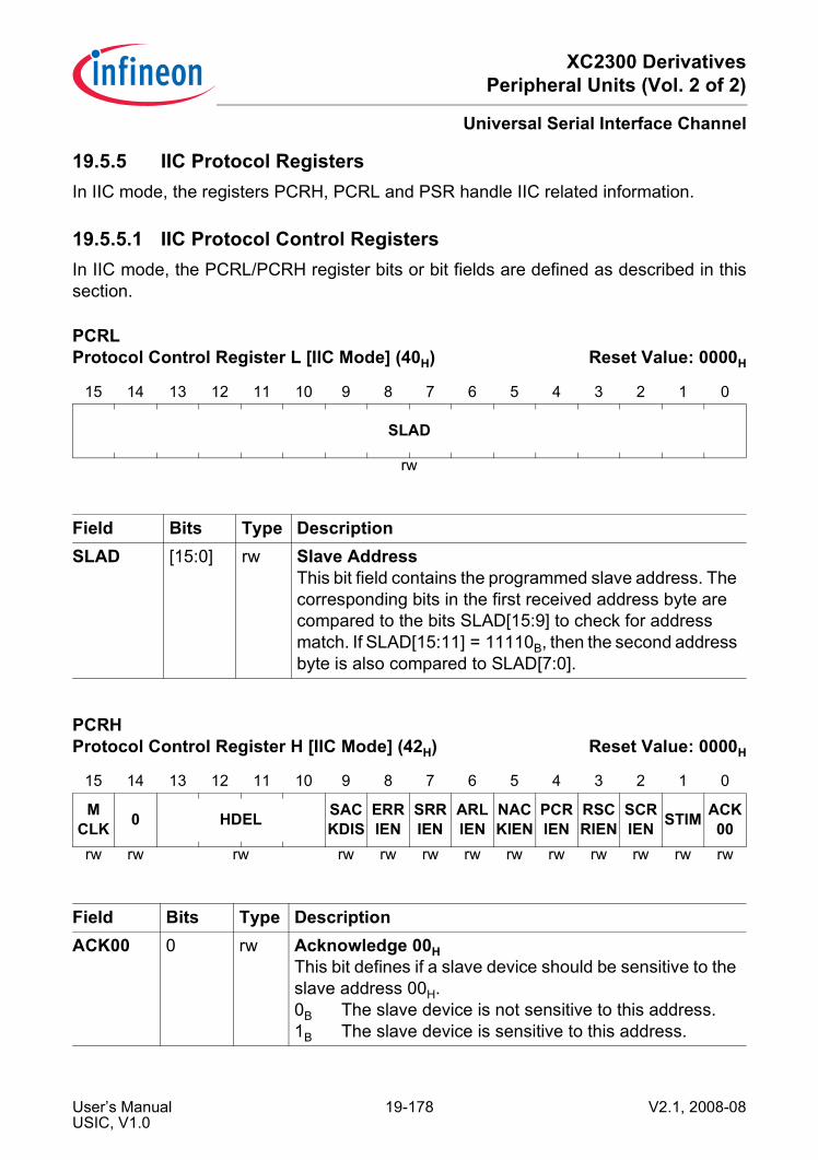
XC2300 DerivativesPeripheral Units (Vol. 2 of 2)
Universal Serial Interface Channel
19.5.5 IIC Protocol RegistersIn IIC mode, the registers PCRH, PCRL and PSR handle IIC related information.
19.5.5.1 IIC Protocol Control RegistersIn IIC mode, the PCRL/PCRH register bits or bit fields are defined as described in thissection.
PCRL Protocol Control Register L [IIC Mode] (40H) Reset Value: 0000H
15 14 13 12 11 10 9 8 7 6 5 4 3 2 1 0
SLAD
rw
Field Bits Type DescriptionSLAD [15:0] rw Slave Address
This bit field contains the programmed slave address. The corresponding bits in the first received address byte are compared to the bits SLAD[15:9] to check for address match. If SLAD[15:11] = 11110B, then the second address byte is also compared to SLAD[7:0].
PCRH Protocol Control Register H [IIC Mode] (42H) Reset Value: 0000H
15 14 13 12 11 10 9 8 7 6 5 4 3 2 1 0
MCLK 0 HDEL SAC
KDISERRIEN
SRRIEN
ARLIEN
NACKIEN
PCRIEN
RSCRIEN
SCRIEN STIM ACK
00rw rw rw rw rw rw rw rw rw rw rw rw rw
Field Bits Type DescriptionACK00 0 rw Acknowledge 00H
This bit defines if a slave device should be sensitive to the slave address 00H.0B The slave device is not sensitive to this address.1B The slave device is sensitive to this address.
User’s Manual 19-178 V2.1, 2008-08USIC, V1.0
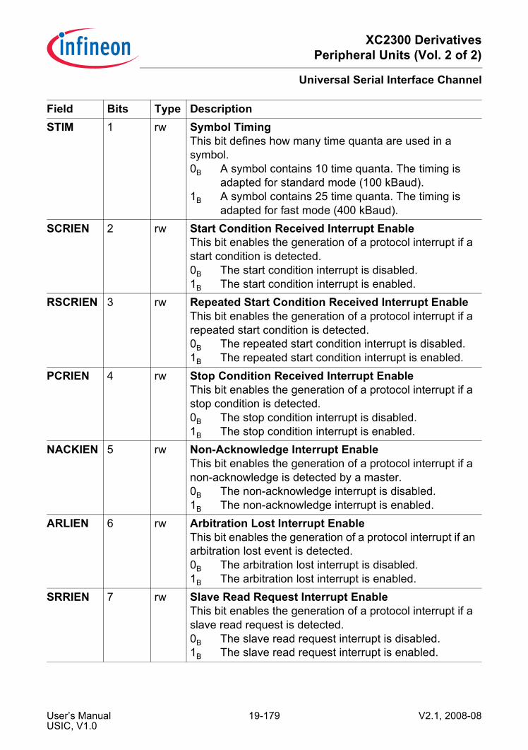
XC2300 DerivativesPeripheral Units (Vol. 2 of 2)
Universal Serial Interface Channel
STIM 1 rw Symbol TimingThis bit defines how many time quanta are used in a symbol.0B A symbol contains 10 time quanta. The timing is
adapted for standard mode (100 kBaud).1B A symbol contains 25 time quanta. The timing is
adapted for fast mode (400 kBaud).SCRIEN 2 rw Start Condition Received Interrupt Enable
This bit enables the generation of a protocol interrupt if a start condition is detected.0B The start condition interrupt is disabled.1B The start condition interrupt is enabled.
RSCRIEN 3 rw Repeated Start Condition Received Interrupt EnableThis bit enables the generation of a protocol interrupt if a repeated start condition is detected.0B The repeated start condition interrupt is disabled.1B The repeated start condition interrupt is enabled.
PCRIEN 4 rw Stop Condition Received Interrupt EnableThis bit enables the generation of a protocol interrupt if a stop condition is detected.0B The stop condition interrupt is disabled.1B The stop condition interrupt is enabled.
NACKIEN 5 rw Non-Acknowledge Interrupt EnableThis bit enables the generation of a protocol interrupt if a non-acknowledge is detected by a master.0B The non-acknowledge interrupt is disabled.1B The non-acknowledge interrupt is enabled.
ARLIEN 6 rw Arbitration Lost Interrupt EnableThis bit enables the generation of a protocol interrupt if an arbitration lost event is detected.0B The arbitration lost interrupt is disabled.1B The arbitration lost interrupt is enabled.
SRRIEN 7 rw Slave Read Request Interrupt EnableThis bit enables the generation of a protocol interrupt if a slave read request is detected.0B The slave read request interrupt is disabled.1B The slave read request interrupt is enabled.
Field Bits Type Description
User’s Manual 19-179 V2.1, 2008-08USIC, V1.0

XC2300 DerivativesPeripheral Units (Vol. 2 of 2)
Universal Serial Interface Channel
ERRIEN 8 rw Error Interrupt EnableThis bit enables the generation of a protocol interrupt if an IIC error condition is detected (indicated by PSR.ERR or PSR.WTDF).0B The error interrupt is disabled.1B The error interrupt is enabled.
SACKDIS 9 rw Slave Acknowledge DisableThis bit disables the generation of an active acknowledge signal for a slave device (active acknowledge = 0 level). Once set by software, it is automatically cleared with each (repeated) start condition. If this bit is set after a byte has been received (indicated by an interrupt) but before the next acknowledge bit has started, the next acknowledge bit will be sent with passive level. This would indicate that the receiver does not accept more bytes. As a result, a minimum of 2 bytes will be received if the first receive interrupt is used to set this bit.0B The generation of an active slave acknowledge is
enabled (slave acknowledge with 0 level = more bytes can be received).
1B The generation of an active slave acknowledge is disabled (slave acknowledge with 1 level = reception stopped).
HDEL [13:10] rw Hardware DelayThis bit field defines the delay used to compensate the internal treatment of the SCL signal (see Page 19-170) in order to respect the SDA hold time specified for the IIC protocol.
0 14 rw ReservedReturns 0 if read; should be written with 0.
MCLK 15 rw Master Clock EnableThis bit enables generation of the master clock MCLK (not directly used for IIC protocol, can be used as general frequency output).0B The MCLK generation is disabled and MCLK is 0.1B The MCLK generation is enabled.
Field Bits Type Description
User’s Manual 19-180 V2.1, 2008-08USIC, V1.0

XC2300 DerivativesPeripheral Units (Vol. 2 of 2)
Universal Serial Interface Channel
19.5.5.2 IIC Protocol Status RegisterThe following PSR status bits or bit fields are available in IIC mode. Please note that thebits in register PSR are not cleared by hardware.The flags in the PSR register can be cleared by writing a 1 to the corresponding bitposition in register PSCR. Writing a 1 to a bit position in PSR sets the corresponding flag,but doesn’t lead to further actions (no interrupt generation). Writing a 0 has no effect.These flags should be cleared by software before enabling a new protocol.
PSR Protocol Status Register [IIC Mode] (44H) Reset Value: 0000H
15 14 13 12 11 10 9 8 7 6 5 4 3 2 1 0
AIF RIF TBIF TSIF DLIF RSIF 0 ERR SRR ARL NACK PCR R
SCR SCR WTDF
SLSEL
rwh rwh rwh rwh rwh rwh r rwh rwh rwh rwh rwh rwh rwh rwh rwh
Field Bits Type DescriptionSLSEL 0 rwh Slave Select
This bit indicates that this device has been selected as slave.0B The device is not selected as slave.1B The device is selected as slave.
WTDF 1 rwh Wrong TDF Code Found1)
This bit indicates that an unexpected/wrong TDF code has been found. A protocol interrupt can be generated if PCRH.ERRIEN = 1.0B A wrong TDF code has not been found.1B A wrong TDF code has been found.
SCR 2 rwh Start Condition Received1)
This bit indicates that a start condition has been detected on the IIC bus lines.A protocol interrupt can be generated if PCRH.SCRIEN = 1.0B A start condition has not yet been detected.1B A start condition has been detected.
User’s Manual 19-181 V2.1, 2008-08USIC, V1.0

XC2300 DerivativesPeripheral Units (Vol. 2 of 2)
Universal Serial Interface Channel
RSCR 3 rwh Repeated Start Condition Received1)
This bit indicates that a repeated start condition has been detected on the IIC bus lines. A protocol interrupt can be generated if PCRH.RSCRIEN = 1.0B A repeated start condition has not yet been
detected.1B A repeated start condition has been detected.
PCR 4 rwh Stop Condition Received1)
This bit indicates that a stop condition has been detected on the IIC bus lines. A protocol interrupt can be generated if PCRH.PCRIEN = 1.0B A stop condition has not yet been detected.1B A stop condition has been detected.
NACK 5 rwh Non-Acknowledge Received1)
This bit indicates that a non-acknowledge has been received in master mode. This bit is not set in slave mode. A protocol interrupt can be generated if PCRH.NACKIEN = 1.0B A non-acknowledge has not been received.1B A non-acknowledge has been received.
ARL 6 rwh Arbitration Lost1)
This bit indicates that an arbitration has been lost. A protocol interrupt can be generated if PCRH.ARLIEN = 1.0B An arbitration has not been lost.1B An arbitration has been lost.
SRR 7 rwh Slave Read Request1)
This bit indicates that a slave read request has been detected. It becomes active to request the first data byte to be made available in the transmit buffer. For further consecutive data bytes, the transmit buffer issues more interrupts. For the end of the transfer, the master transmitter sends a stop condition. A protocol interrupt can be generated if PCRH.SRRIEN = 1.0B A slave read request has not been detected.1B A slave read request has been detected.
Field Bits Type Description
User’s Manual 19-182 V2.1, 2008-08USIC, V1.0
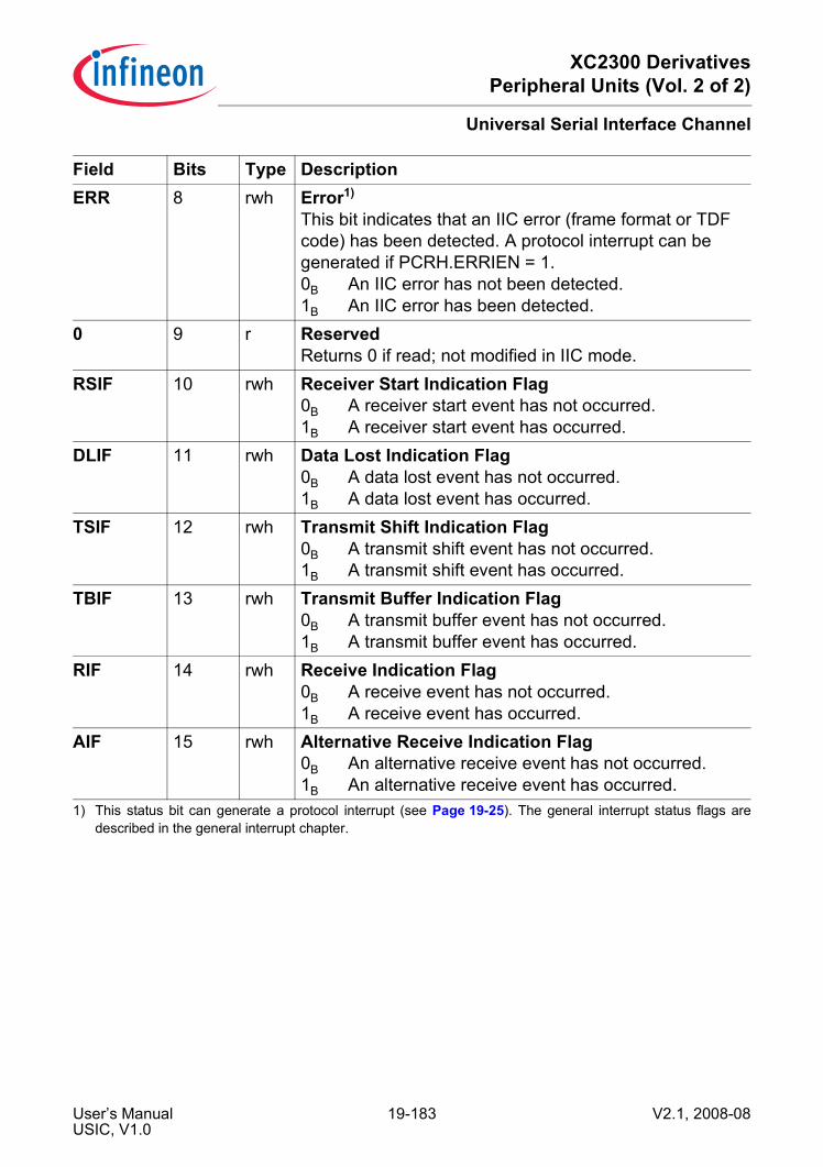
XC2300 DerivativesPeripheral Units (Vol. 2 of 2)
Universal Serial Interface Channel
ERR 8 rwh Error1)
This bit indicates that an IIC error (frame format or TDF code) has been detected. A protocol interrupt can be generated if PCRH.ERRIEN = 1.0B An IIC error has not been detected.1B An IIC error has been detected.
0 9 r ReservedReturns 0 if read; not modified in IIC mode.
RSIF 10 rwh Receiver Start Indication Flag0B A receiver start event has not occurred.1B A receiver start event has occurred.
DLIF 11 rwh Data Lost Indication Flag0B A data lost event has not occurred.1B A data lost event has occurred.
TSIF 12 rwh Transmit Shift Indication Flag0B A transmit shift event has not occurred.1B A transmit shift event has occurred.
TBIF 13 rwh Transmit Buffer Indication Flag0B A transmit buffer event has not occurred.1B A transmit buffer event has occurred.
RIF 14 rwh Receive Indication Flag0B A receive event has not occurred.1B A receive event has occurred.
AIF 15 rwh Alternative Receive Indication Flag0B An alternative receive event has not occurred.1B An alternative receive event has occurred.
1) This status bit can generate a protocol interrupt (see Page 19-25). The general interrupt status flags aredescribed in the general interrupt chapter.
Field Bits Type Description
User’s Manual 19-183 V2.1, 2008-08USIC, V1.0
XC2300 DerivativesPeripheral Units (Vol. 2 of 2)
Universal Serial Interface Channel
19.6 IIS ProtocolThis chapter describes how the USIC module handles the IIS protocol. This serialprotocol can handle reception and transmission of synchronous data frames between adevice operating in master mode and a device in slave mode. An IIS connection basedon a USIC communication channel supports half-duplex and full-duplex data transfers.The IIS mode is selected by CCR.MODE = 0011B with CCFG.IIS = 1 (IIS mode isavailable).This chapter contains the following sections:• Introduction (see Page 19-184)• General IIS issues (see Page 19-188)• Master mode operation (see Page 19-193)• Slave mode operation (see Page 19-197)• Protocol registers (seePage 19-198)
19.6.1 IntroductionThe IIS protocol is a synchronous serial communication protocol mainly for audio andinfotainment applications and refers to the Philips specification, 1986, revised June 5,1996.
19.6.1.1 Signal DescriptionA connection between an IIS master and an IIS slave is based on the following signals:• A shift clock signal SCK, generated by the transfer master. It is permanently
generated while an IIS connection is established, also while no valid data bits aretransferred.
• A word address signal WA (also named WS), generated by the transfer master. Itindicates the beginning of a new data word and the targeted audio channel (e.g.left/right). The word address output signal WA is available on all SELOx outputs if theWA generation is enabled (by PCR.WAGEN = 1 for the transfer master). The WAsignal changes synchronously to the falling edges of the shift clock.
• If the transmitter is the IIS master device, it generates a master transmit slave receivedata signal. The data changes synchronously to the falling edges of the shift clock.
• If the transmitter is the IIS slave device, it generates a master receive slave transmitdata signal. The data changes synchronously to the falling edges of the shift clock.
The transmitter part and the receiver part of the USIC communication channel can beused together to establish a full-duplex data connection between an IIS master and aslave device.
User’s Manual 19-184 V2.1, 2008-08USIC, V1.0

XC2300 DerivativesPeripheral Units (Vol. 2 of 2)
Universal Serial Interface Channel
Figure 19-47 IIS Signals
Two additional signals are available for the USIC IIS communication master:• A master clock output signal MCLKOUT with a fixed phase relation to the shift clock
to support oversampling for audio components. It can also be used as master clockoutput of a communication network with synchronized IIS connections.
• A synchronization clock input SCLKIN for synchronization of the shift clockgeneration to an external frequency to support audio frequencies that can not bedirectly derived from the system clock fSYS of the communication master. It can beused as master clock input of a communication network with synchronized IISconnections.
Table 19-10 IIS IO SignalsIIS Mode Receive Data Transmit Data Shift Clock Word AddressMaster Input DIN,
handled by DX0Output DOUT Output
SCLKOUTOutput(s)SELOx
Slave Input DIN,handled by DX0
Output DOUT Input SCLKIN,handled by DX1
Input SELIN,handled by DX2
IIS_Signals_fSYS
Master Transmit /Slave Receive
(Master)
fSYS
(Slave)
DX0
DOUT
DINRBUF
IIS Communication Master
WAGenerator
Baud RateGenerator
TBUF
SCLKOUT
SELOx
DX0DIN
DOUTTBUF
IIS Communication Slave
RBUF
SCLKIN
SELIN
DX1
DX2
Master Receive /Slave Transmit
Shift Clock
Word Address(Word Select )
MCLKOUT
DX1
Master ClockOutput
Synchronization Clock Input
SCLKIN
User’s Manual 19-185 V2.1, 2008-08USIC, V1.0

XC2300 DerivativesPeripheral Units (Vol. 2 of 2)
Universal Serial Interface Channel
19.6.1.2 Protocol OverviewAn IIS connection supports transfers for two different data frames via the same data line,e.g. a data frames for the left audio channel and a data frame for the right audio channel.The word address signal WA is used to distinguish between the different data frames.Each data frame can consist of several data words.In a USIC communication channel, data words are tagged for being transmitted for theleft or for the right channel. Also the received data words contain a tag identifying the WAstate when the data has been received.
Figure 19-48 Protocol Overview
19.6.1.3 Transfer DelayThe transfer delay feature allows the transfer of data (transmission and reception) witha programmable delay (counted in shift clock periods).
Figure 19-49 Transfer Delay for IIS
IIS_Prot_
WA (WS)
SCK
DIN
DOUT
Right Channel
0 Right Data Frame 0MSB LSB
Left Data FrameMSB LSB
0
Left Channel
X Right Data Frame XMSB LSB
Left Data FrameMSB LSB
X
IIS_TransferDelay
Without Delay
DATA
WA
SCK
With Delay 1
DATA
WA
SCK
User’s Manual 19-186 V2.1, 2008-08USIC, V1.0

XC2300 DerivativesPeripheral Units (Vol. 2 of 2)
Universal Serial Interface Channel
19.6.1.4 Connection of External Audio ComponentsThe IIS signals can be used to communicate with external audio devices (such asCodecs) or other audio data sources/destinations.
Figure 19-50 Connection of External Audio Devices
In some applications, especially for Audio-ADCs or Audio-DACs, a master clock signalis required with a fixed phase relation to the shift clock signal. The frequency ofMCLKOUT is a multiple of the shift frequency SCLKOUT. This factor defines theoversampling factor of the external device (commonly used values: 256 or 384).
IIS_ExtCodecs
MCLKOUT
USIC IIS
SCLKOUT
WA
DIN
DOUT
Audio-ADC
Audio-DAC
MCLK_IN
SCK_IN
WA_IN
SD_OUT
MCLK_IN
SCK_IN
WA_IN
SD_IN
R
LAnalogOutputs
R
LAnalogInputs
User’s Manual 19-187 V2.1, 2008-08USIC, V1.0

XC2300 DerivativesPeripheral Units (Vol. 2 of 2)
Universal Serial Interface Channel
19.6.2 Operating the IISThis chapter contains IIS issues, that are of general interest and not directly linked tomaster mode or slave mode.
19.6.2.1 Frame Length and Word Length ConfigurationAfter each change of the WA signal, a complete data frame is intended to be transferred(frame length ≤ system word length). The number of data bits transferred after a changeof signal WA is defined by SCTRH.FLE. A data frame can consist of several data wordswith a data word length defined by SCTRH.WLE. The changes of signal WA define thesystem word length as the number of SCLK cycles between two changes of WA (numberof bits available for the right channel and same number available for the left channel).If the system word length is longer than the frame length defined by SCTRH.FLE, theadditional bits are transmitted with passive data level (SCTRL.PDL). If the system wordlength is smaller than the device frame length, not all LSBs of the transmit data can betransferred.It is recommended to program bits WLEMD, FLEMD and SELMD in register TCSRL to 0.
19.6.2.2 Automatic Shadow MechanismThe baud rate and shift control setting are internally kept constant while a data frame istransferred by an automatic shadow mechanism. The registers can be programmed allthe time with new settings that are taken into account for the next data frame. During adata frame, the applied (shadowed) setting is not changed, although new values havebeen written after the start of the data frame. The setting is internally “frozen” with thestart of each data frame.Although this shadow mechanism being implemented, it is recommended to change thebaud rate and shift control setting only while the IIS protocol is switched off.
19.6.2.3 Mode Control BehaviorIn IIS mode, the following kernel modes are supported:• Run Mode 0/1:
Behavior as programmed, no impact on data transfers.• Stop Mode 0/1:
Bit PCRL.WAGEN is internally considered as 0 (the bit itself is not changed). IfWAGEN = 1, then the current system word cycle is finished and then the WAgeneration is stopped, but PSR.END is not set. The complete data frame is finishedbefore entering stop mode, including a possible delay due to PCRH.TDEL.When leaving a stop mode with WAGEN = 1, the WA generation starts from thebeginning.
User’s Manual 19-188 V2.1, 2008-08USIC, V1.0

XC2300 DerivativesPeripheral Units (Vol. 2 of 2)
Universal Serial Interface Channel
19.6.2.4 Transfer DelayThe transfer delay can be used to synchronize a data transfer to an event (e.g. a changeof the WA signal). This event has to be synchronously generated to the falling edge ofthe shift clock SCK (like the change of the transmit data), because the input signal forthe event is directly sampled in the receiver (as a result, the transmitter can use thedetection information with its next edge).Event signals that are asynchronous to the shift clock while the shift clock is running mustnot be used. In the example in Figure 19-49, the event (change of signal WA) isgenerated by the transfer master and as a result, is synchronous to the shift clock SCK.With the rising edge of SCK, signal WA is sampled and checked for a change. If achange is detected, a transfer delay counter TDC is automatically loaded with itsprogrammable reload value (PCRH.TDEL), otherwise it is decremented with each risingedge of SCK until it reaches 0, where it stops. The transfer itself is started if the value ofTDC has become 0. This can happen under two conditions:• TDC is reloaded with a PCRH.TDEL = 0 when the event is detected• TDC has reached 0 while counting downThe transfer delay counter is internal to the IIS protocol pre-processor and can not beobserved by software. The transfer delay in SCK cycles is given by PCRH.TDEL+1.In the example in Figure 19-51, the reload value PCRH.TDEL for TDC is 0. When thesamples taken on receiver side show the change of the WA signal, the counter TDC isreloaded. If the reload value is 0, the data transfer starts with 1 shift clock cycle delaycompared to the change of WA.
Figure 19-51 Transfer Delay with Delay 1
IIS_TransferDelay1
SCK
DINsampled
X
0
s s s s s ss
D0 D1 D0
D0D0 D1
X
0 0
WA
TDC
DOUT
s = sampling of WA
User’s Manual 19-189 V2.1, 2008-08USIC, V1.0
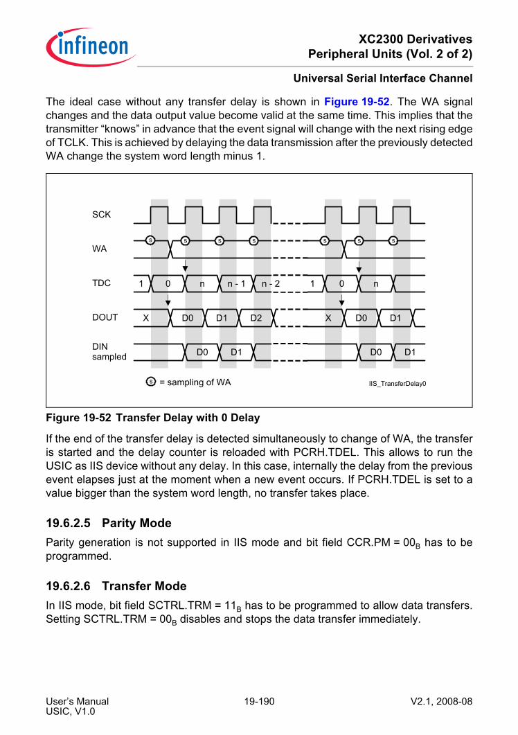
XC2300 DerivativesPeripheral Units (Vol. 2 of 2)
Universal Serial Interface Channel
The ideal case without any transfer delay is shown in Figure 19-52. The WA signalchanges and the data output value become valid at the same time. This implies that thetransmitter “knows” in advance that the event signal will change with the next rising edgeof TCLK. This is achieved by delaying the data transmission after the previously detectedWA change the system word length minus 1.
Figure 19-52 Transfer Delay with 0 Delay
If the end of the transfer delay is detected simultaneously to change of WA, the transferis started and the delay counter is reloaded with PCRH.TDEL. This allows to run theUSIC as IIS device without any delay. In this case, internally the delay from the previousevent elapses just at the moment when a new event occurs. If PCRH.TDEL is set to avalue bigger than the system word length, no transfer takes place.
19.6.2.5 Parity ModeParity generation is not supported in IIS mode and bit field CCR.PM = 00B has to beprogrammed.
19.6.2.6 Transfer ModeIn IIS mode, bit field SCTRL.TRM = 11B has to be programmed to allow data transfers.Setting SCTRL.TRM = 00B disables and stops the data transfer immediately.
IIS_TransferDelay0
SCK
DINsampled
X
0
s s s s s ss
D0 D2 D1
D1D1
X
n
WA
TDC
DOUT
s = sampling of WA
1 n n - 1 n - 2
D1
D0
1 0
D0
D0
User’s Manual 19-190 V2.1, 2008-08USIC, V1.0

XC2300 DerivativesPeripheral Units (Vol. 2 of 2)
Universal Serial Interface Channel
19.6.2.7 Data Transfer Interrupt HandlingThe data transfer interrupts indicate events related to IIS frame handling.• Transmit buffer interrupt TBI:
Bit PSR.TBIF is set after the start of first data bit of a data word.• Transmit shift interrupt TSI:
Bit PSR.TSIF is set after the start of the last data bit of a data word.• Receiver start interrupt RSI:
Bit PSR.RSIF is set after the reception of the first data bit of a data word.With this event, bit TCSRL.TDV is cleared and new data can be loaded to thetransmit buffer.
• Receiver interrupt RI and alternative interrupt AI:Bit PSR.RIF is set at after the reception of the last data bit of a data word with WA = 0.Bit RBUFSR.SOF indicates whether the received data word has been the first dataword of a new data frame.
• Alternative interrupt AI:Bit PSR.AIF is set at after the reception of the last data bit of a data word with WA = 1.Bit RBUFSR.SOF indicates whether the received data word has been the first dataword of a new data frame.
19.6.2.8 Protocol-Related Argument and ErrorIn order to distinguish between data words received for the left or the right channel, theIIS protocol pre-processor samples the level of the WA input (just after the WA transition)and propagates it as protocol-related error (although it is not an error, but an indication)to the receive buffer status register at the bit position RBUFSR[9]. This bit positiondefines if either a standard receive interrupt (if RBUFSR[9] = 0) or an alternative receiveinterrupt (if RBUFSR[9] = 1) becomes activated when a new data word has beenreceived. Incoming data can be handled by different interrupts or DMA mechanisms forthe left and the right channel if the corresponding events are directed to different interruptnodes. Flag PAR is always 0.
19.6.2.9 Transmit Data HandlingThe IIS protocol pre-processor allows to distinguish between the left and the rightchannel for data transmission. Therefore, bit TCSRL.WA indicates on which channel thedata in the buffer will be transmitted. If TCSRL.WA = 0, the data will be transmitted aftera falling edge of WA. If TCSRL.WA = 1, the data will be transmitted after a rising edgeof WA. The WA value sampled after the WA transition is considered to distinguishbetween both channels (referring to PSR.WA).Bit TCSRL.WA can be automatically updated by the transmit control information TCI[4]for each data word if TCSRL.WAMD = 1. In this case, data written to TBUF[15:0] (orIN[15:0] if a FIFO data buffer is used) is considered as left channel data, whereas data
User’s Manual 19-191 V2.1, 2008-08USIC, V1.0

XC2300 DerivativesPeripheral Units (Vol. 2 of 2)
Universal Serial Interface Channel
written to TBUF[31:16] (or IN[31:16] if a FIFO data buffer is used) is considered as rightchannel data.
19.6.2.10 Receive Buffer HandlingIf a receive FIFO buffer is available (CCFG.RB = 1) and enabled for data handling(RBCTRH.SIZE > 0), it is recommended to set RBCTRH.RCIM = 11B in IIS mode. Thisleads to an indication that the data word has been the first data word of a new data frameif bit OUTRH.RCI[0] = 1, and the channel indication by the sampled WA value is givenby OUTRH.RCI[4].The standard receive buffer event and the alternative receive buffer event can be usedfor the following operation in RCI mode (RBCTRH.RNM = 1):• A standard receive buffer event indicates that a data word can be read from OUTRL
that belongs to a data frame started when WA = 0.• An alternative receive buffer event indicates that a data word can be read from
OUTRL that belongs to a data frame started when WA = 1.
19.6.2.11 Loop-Delay CompensationThe synchronous signaling mechanism of the IIS protocol being similar to the one of theSSC protocol, the closed-loop delay has to be taken into account for the applicationsetup. In IIS mode, loop-delay compensation in master mode is also possible to achievehigher baud rates. Please refer to the more detailed description in the SSC chapter.
User’s Manual 19-192 V2.1, 2008-08USIC, V1.0

XC2300 DerivativesPeripheral Units (Vol. 2 of 2)
Universal Serial Interface Channel
19.6.3 Operating the IIS in Master ModeIn order to operate the IIS in master mode, the following issues have to be considered:• Select IIS mode:
It is recommended to configure all parameters of the IIS that do not change duringrun time while CCR.MODE = 0000B. Bit field SCTRL.TRM = 11B has to beprogrammed. The configuration of the input stages has to be done whileCCR.MODE = 0000B to avoid unintended edges of the input signals and the IIS modecan be enabled by CCR.MODE = 0011B afterwards.
• Pin connection for data transfer:Establish a connection of input stage DX0 with the selected receive data input pin(DIN) with DX0CR.INSW = 1. Configure a transmit data output pin (DOUT) for atransmitter.The data shift unit allowing full-duplex data transfers based on the same WA signal,the values delivered by the DX0 stage are considered as data bits (receive functioncan not be disabled independently from the transmitter). To receive IIS data, thetransmitter does not necessarily need to be configured (no assignment of DOUTsignal to a pin).
• Baud rate generation:The desired baud rate setting has to be selected, comprising the fractional dividerand the baud rate generator. Bit DX1CR.INSW = 0 has to be programmed to use thebaud rate generator output SCLK directly as input for the data shift unit. Configure ashift clock output pin with the inverted signal SCLKOUT without additional delay(BRGH.SCLKCFG = 01B).
• Word address WA generation:The WA generation has to be enabled by setting PCRL.WAGEN = 1 and theprogramming of the number of shift clock cycles between the changes of WA. BitDX2CR.INSW = 0 has to be programmed to use the WA generator as input for thedata shift unit. Configure WA output pin for signal SELOx if needed.
• Data format configuration:The word length, the frame length, and the shift direction have to be set up accordingto the application requirements by programming the registers SCTRL and SCTRH.Generally, the MSB is shifted first (SCTRL.SDIR = 1).Bit TCSRL.WAMD can be set to use the transmit control information TCI[4] todistinguish the data words for transmission while WA = 0 or while WA = 1.
19.6.3.1 Baud Rate GenerationThe baud rate is defined by the frequency of the SCLK signal (one period of fSCLKrepresents one data bit).If the fractional divider mode is used to generate fPIN, there can be an uncertainty of oneperiod of fSYS for fPIN. This uncertainty does not accumulate over several SCLK cycles.
User’s Manual 19-193 V2.1, 2008-08USIC, V1.0

XC2300 DerivativesPeripheral Units (Vol. 2 of 2)
Universal Serial Interface Channel
As a consequence, the average frequency is reached, whereas the duty cycle of 50% ofthe SCLK and MCLK signals can vary by one period of fSYS.In IIS applications, where the phase relation between the optional MCLK output signaland SCLK is not relevant, SCLK can be based on the frequency fPIN (BRGL.PPPEN = 0).In the case that a fixed phase relation between the MCLK signal and SCLK is required(e.g. when using MCLK as clock reference for external devices), the additional divider by2 stage has to be taken into account (BRGL.PPPEN = 1). This division is due to the factthat signal MCLK toggles with each cycle of fPIN. Signal SCLK is then based on signalMCLK, see Figure 19-53.The adjustable integer divider factor is defined by bit field BRGH.PDIV.
(19.12)
Note: In the IIS protocol, the master (unit generating the shift clock and the WA signal)changes the status of its data and WA output line with the falling edge of SCK. Theslave transmitter also has to transmit on falling edges. The sampling of thereceived data is done with the rising edges of SCLK. The input stage DX1 and theSCLKOUT have to be programmed to invert the shift clock signal to fit to theinternal signals.
19.6.3.2 WA GenerationThe word address (or word select) line WA regularly toggles after N cycles of signalSCLK. The time between the changes of WA is called system word length and can beprogrammed by using the following bit fields.In IIS master mode, the system word length is defined by:• BRGL.CTQSEL = 10B
to base the WA toggling on SCLK• BRGL.PCTQ
to define the number N of SCLK cycles per system word length• BRGL.DCTQ
to define the number N of SCLK cycles per system word length
(19.13)
fSCLK = if PPPEN = 0PDIV + 11
if PPPEN = 1PDIV + 1
1fSCLK = 2 × 2
× fPIN
2 × fPIN
N = (PCTQ + 1) × (DCTQ + 1)
User’s Manual 19-194 V2.1, 2008-08USIC, V1.0
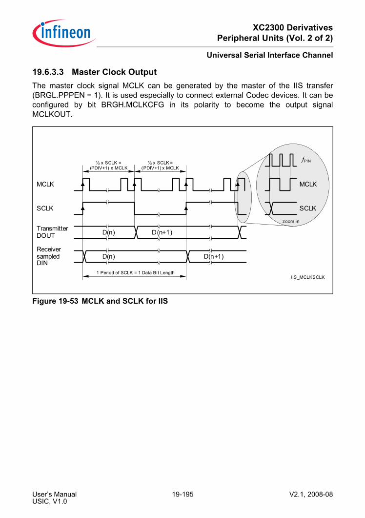
XC2300 DerivativesPeripheral Units (Vol. 2 of 2)
Universal Serial Interface Channel
19.6.3.3 Master Clock OutputThe master clock signal MCLK can be generated by the master of the IIS transfer(BRGL.PPPEN = 1). It is used especially to connect external Codec devices. It can beconfigured by bit BRGH.MCLKCFG in its polarity to become the output signalMCLKOUT.
Figure 19-53 MCLK and SCLK for IIS
IIS_MCLKSCLK
MCLK
SCLK
TransmitterDOUT
ReceiversampledDIN
½ x SCLK =(PDIV+1) x MCLK
fPIN½ x SCLK =(PDIV+1) x MCLK
D(n) D(n+1)
D(n) D(n+1)
1 Period of SCLK = 1 Data Bit Length
MCLK
SCLK
zoom in
User’s Manual 19-195 V2.1, 2008-08USIC, V1.0
XC2300 DerivativesPeripheral Units (Vol. 2 of 2)
Universal Serial Interface Channel
19.6.3.4 Protocol Interrupt EventsThe following protocol-related events are generated in IIS mode and can lead to aprotocol interrupt.Please note that the bits in register PSR are not all automatically cleared by hardwareand have to be cleared by software in order to monitor new incoming events.• WA rising/falling edge events:
The WA generation block indicates two events that are monitored in register PSR.Flag PSR.WAFE is set with the falling edge, flag PSR.WARE with the rising edge ofthe WA signal. A protocol interrupt can be generated if PCRL.WAFEIEN = 1 for thefalling edge, similar for PCRL.WAREIEN = 1 for a rising edge.
• WA end event:The WA generation block also indicates when it has stopped the WA generation afterit has been disabled by writing PCRL.WAGEN = 0. A protocol interrupt can begenerated if PCRL.ENDIEN = 1.
• DX2T event:An activation of the trigger signal DX2T is indicated by PSR.DX2TEV = 1 and cangenerate a protocol interrupt if PCRL.DX2TIEN = 1. This event can be evaluatedinstead of the WA rising/falling events if a delay compensation like in SSC mode (fordetails, refer to corresponding SSC section) is used.
User’s Manual 19-196 V2.1, 2008-08USIC, V1.0
XC2300 DerivativesPeripheral Units (Vol. 2 of 2)
Universal Serial Interface Channel
19.6.4 Operating the IIS in Slave ModeIn order to operate the IIS in slave mode, the following issues have to be considered:• Select IIS mode:
It is recommended to configure all parameters of the IIS that do not change duringrun time while CCR.MODE = 0000B. Bit field SCTRL.TRM = 11B has to beprogrammed. The configuration of the input stages has to be done whileCCR.MODE = 0000B to avoid unintended edges of the input signals and the IIS modecan be enabled by CCR.MODE = 0011B afterwards.
• Pin connection for data transfer:Establish a connection of input stage DX0 with the selected receive data input pin(DIN) with DX0CR.INSW = 1. Configure a transmit data output pin (DOUT) for atransmitter.The data shift unit allowing full-duplex data transfers based on the same WA signal,the values delivered by the DX0 stage are considered as data bits (receive functioncan not be disabled independently from the transmitter). To receive IIS data, thetransmitter does not necessarily need to be configured (no assignment of DOUTsignal to a pin).
• Pin connection for shift clock:Establish a connection of input stage DX1 with the selected shift clock input pin(SCLKIN) with DX1CR.INSW = 1 and with inverted polarity (DX1CR.DPOL = 1).
• Pin connection for WA input:Establish a connection of input stage DX2 with the WA input pin (SELIN) withDX2CR.INSW = 1.
• Baud rate generation:The baud rate generator is not needed and can be switched off by the fractionaldivider.
• WA generation:The WA generation is not needed and can be switched off (PCRL.WAGEN = 0).
19.6.4.1 Protocol Events and InterruptsThe following protocol-related event is generated in IIS mode and can lead to a protocolinterrupt.Please note that the bits in register PSR are not all automatically cleared by hardwareand have to be cleared by software in order to monitor new incoming events.• WA rising/falling/end events:
The WA generation being switched off, these events are not available.• DX2T event:
An activation of the trigger signal DX2T is indicated by PSR.DX2TEV = 1 and cangenerate a protocol interrupt if PCRL.DX2TIEN = 1.
User’s Manual 19-197 V2.1, 2008-08USIC, V1.0
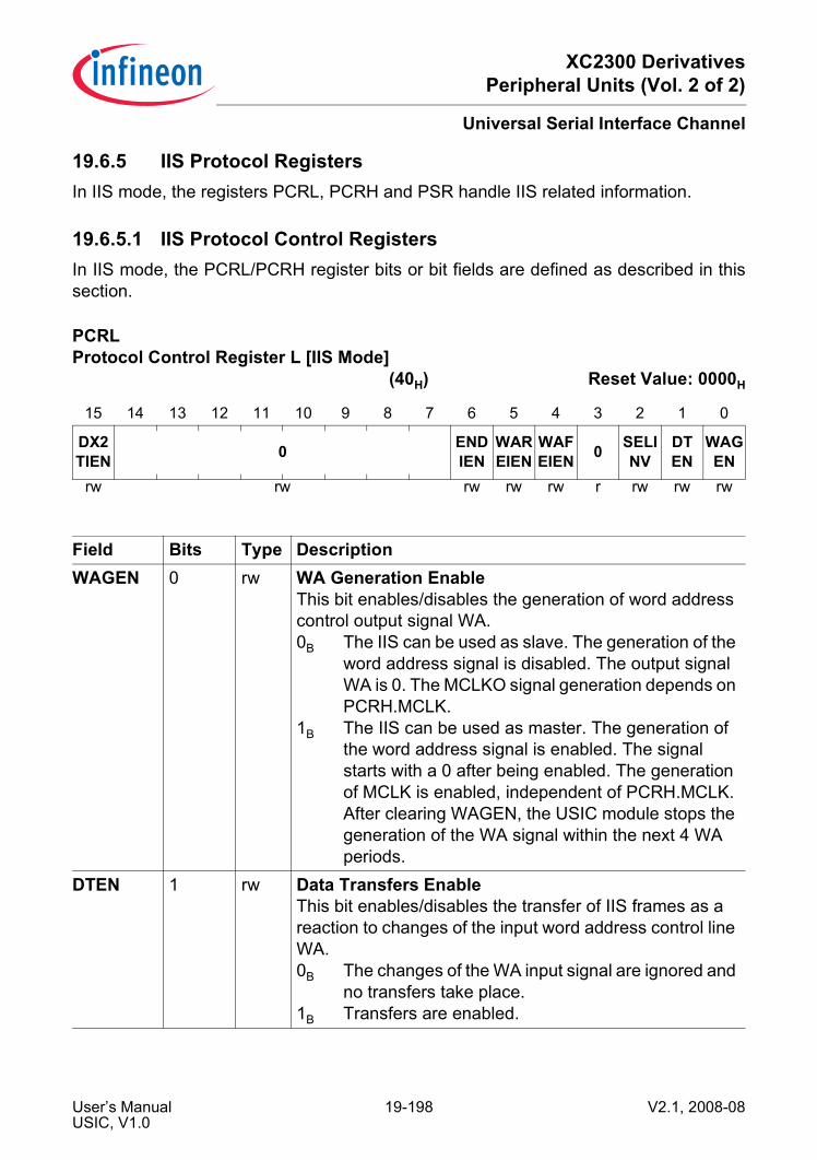
XC2300 DerivativesPeripheral Units (Vol. 2 of 2)
Universal Serial Interface Channel
19.6.5 IIS Protocol RegistersIn IIS mode, the registers PCRL, PCRH and PSR handle IIS related information.
19.6.5.1 IIS Protocol Control RegistersIn IIS mode, the PCRL/PCRH register bits or bit fields are defined as described in thissection.
PCRL Protocol Control Register L [IIS Mode]
(40H) Reset Value: 0000H
15 14 13 12 11 10 9 8 7 6 5 4 3 2 1 0
DX2TIEN 0 END
IENWAREIEN
WAFEIEN 0 SELI
NVDTEN
WAGEN
rw rw rw rw rw r rw rw rw
Field Bits Type DescriptionWAGEN 0 rw WA Generation Enable
This bit enables/disables the generation of word address control output signal WA.0B The IIS can be used as slave. The generation of the
word address signal is disabled. The output signal WA is 0. The MCLKO signal generation depends on PCRH.MCLK.
1B The IIS can be used as master. The generation of the word address signal is enabled. The signal starts with a 0 after being enabled. The generation of MCLK is enabled, independent of PCRH.MCLK.After clearing WAGEN, the USIC module stops the generation of the WA signal within the next 4 WA periods.
DTEN 1 rw Data Transfers EnableThis bit enables/disables the transfer of IIS frames as a reaction to changes of the input word address control line WA.0B The changes of the WA input signal are ignored and
no transfers take place.1B Transfers are enabled.
User’s Manual 19-198 V2.1, 2008-08USIC, V1.0

XC2300 DerivativesPeripheral Units (Vol. 2 of 2)
Universal Serial Interface Channel
SELINV 2 rw Select InversionThis bit defines if the polarity of the SELOx outputs in relation to the internally generated word address signal WA.0B The SELOx outputs have the same polarity as the
WA signal.1B The SELOx outputs have the inverted polarity to the
WA signal.WAFEIEN 4 rw WA Falling Edge Interrupt Enable
This bit enables/disables the activation of a protocol interrupt when a falling edge of WA has been generated.0B A protocol interrupt is not activated if a falling edge
of WA is generated.1B A protocol interrupt is activated if a falling edge of
WA is generated.WAREIEN 5 rw WA Rising Edge Interrupt Enable
This bit enables/disables the activation of a protocol interrupt when a rising edge of WA has been generated.0B A protocol interrupt is not activated if a rising edge
of WA is generated.1B A protocol interrupt is activated if a rising edge of
WA is generated.ENDIEN 6 rw END Interrupt Enable
This bit enables/disables the activation of a protocol interrupt when the WA generation stops after clearing PCR.WAGEN (complete system word length is processed before stopping).0B A protocol interrupt is not activated.1B A protocol interrupt is activated.
DX2TIEN 15 rw DX2T Interrupt EnableThis bit enables/disables the generation of a protocol interrupt if the DX2T signal becomes activated (indicated by PSR.DX2TEV = 1).0B A protocol interrupt is not generated if DX2T is
active.1B A protocol interrupt is generated if DX2T is active.
0 3, [14:7]
rw ReservedReturns 0 if read; should be written with 0;
Field Bits Type Description
User’s Manual 19-199 V2.1, 2008-08USIC, V1.0
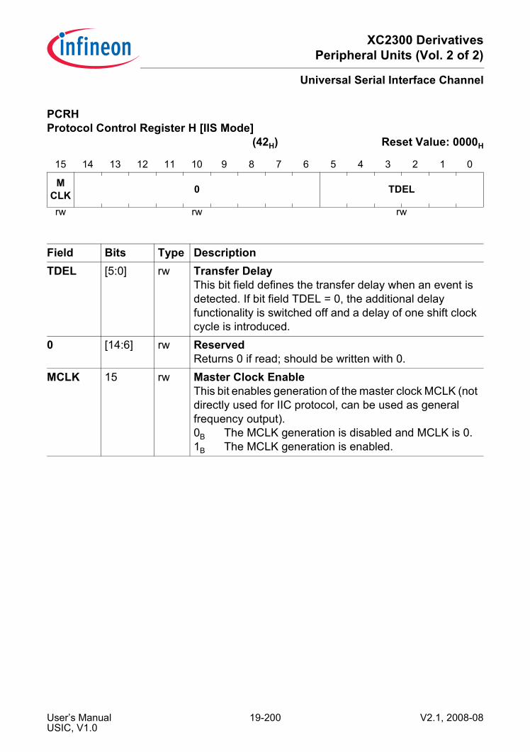
XC2300 DerivativesPeripheral Units (Vol. 2 of 2)
Universal Serial Interface Channel
PCRH Protocol Control Register H [IIS Mode]
(42H) Reset Value: 0000H
15 14 13 12 11 10 9 8 7 6 5 4 3 2 1 0
MCLK 0 TDEL
rw rw rw
Field Bits Type DescriptionTDEL [5:0] rw Transfer Delay
This bit field defines the transfer delay when an event is detected. If bit field TDEL = 0, the additional delay functionality is switched off and a delay of one shift clock cycle is introduced.
0 [14:6] rw ReservedReturns 0 if read; should be written with 0.
MCLK 15 rw Master Clock EnableThis bit enables generation of the master clock MCLK (not directly used for IIC protocol, can be used as general frequency output).0B The MCLK generation is disabled and MCLK is 0.1B The MCLK generation is enabled.
User’s Manual 19-200 V2.1, 2008-08USIC, V1.0
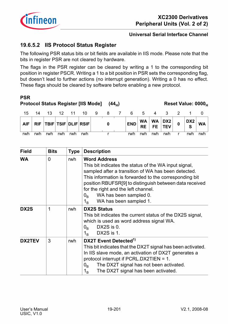
XC2300 DerivativesPeripheral Units (Vol. 2 of 2)
Universal Serial Interface Channel
19.6.5.2 IIS Protocol Status RegisterThe following PSR status bits or bit fields are available in IIS mode. Please note that thebits in register PSR are not cleared by hardware.The flags in the PSR register can be cleared by writing a 1 to the corresponding bitposition in register PSCR. Writing a 1 to a bit position in PSR sets the corresponding flag,but doesn’t lead to further actions (no interrupt generation). Writing a 0 has no effect.These flags should be cleared by software before enabling a new protocol.
PSR Protocol Status Register [IIS Mode] (44H) Reset Value: 0000H
15 14 13 12 11 10 9 8 7 6 5 4 3 2 1 0
AIF RIF TBIF TSIF DLIF RSIF 0 END WARE
WAFE
DX2TEV 0 DX2
S WA
rwh rwh rwh rwh rwh rwh r rwh rwh rwh rwh r rwh rwh
Field Bits Type DescriptionWA 0 rwh Word Address
This bit indicates the status of the WA input signal, sampled after a transition of WA has been detected.This information is forwarded to the corresponding bit position RBUFSR[9] to distinguish between data received for the right and the left channel.0B WA has been sampled 0.1B WA has been sampled 1.
DX2S 1 rwh DX2S StatusThis bit indicates the current status of the DX2S signal, which is used as word address signal WA.0B DX2S is 0.1B DX2S is 1.
DX2TEV 3 rwh DX2T Event Detected1)
This bit indicates that the DX2T signal has been activated. In IIS slave mode, an activation of DX2T generates a protocol interrupt if PCRL.DX2TIEN = 1.0B The DX2T signal has not been activated.1B The DX2T signal has been activated.
User’s Manual 19-201 V2.1, 2008-08USIC, V1.0

XC2300 DerivativesPeripheral Units (Vol. 2 of 2)
Universal Serial Interface Channel
WAFE 4 rwh WA Falling Edge Event1)
This bit indicates that a falling edge of the WA output signal has been generated. This event generates a protocol interrupt if PCRL.WAFEIEN = 1.0B A WA falling edge has not been generated.1B A WA falling edge has been generated.
WARE 5 rwh WA Rising Edge Event1)
This bit indicates that a rising edge of the WA output signal has been generated. This event generates a protocol interrupt if PCRL.WAREIEN = 1.0B A WA rising edge has not been generated.1B A WA rising edge has been generated.
END 6 rwh WA Generation End1)
This bit indicates that the WA generation has ended after clearing PCRL.WAGEN. This bit should be cleared by software before clearing WAGEN.0B The WA generation has not yet ended (if it is
running and WAGEN has been cleared).1B The WA generation has ended (if it has been
running).RSIF 10 rwh Receiver Start Indication Flag
0B A receiver start event has not occurred.1B A receiver start event has occurred.
DLIF 11 rwh Data Lost Indication Flag0B A data lost event has not occurred.1B A data lost event has occurred.
TSIF 12 rwh Transmit Shift Indication Flag0B A transmit shift event has not occurred.1B A transmit shift event has occurred.
TBIF 13 rwh Transmit Buffer Indication Flag0B A transmit buffer event has not occurred.1B A transmit buffer event has occurred.
RIF 14 rwh Receive Indication Flag0B A receive event has not occurred.1B A receive event has occurred.
AIF 15 rwh Alternative Receive Indication Flag0B An alternative receive event has not occurred.1B An alternative receive event has occurred.
Field Bits Type Description
User’s Manual 19-202 V2.1, 2008-08USIC, V1.0
XC2300 DerivativesPeripheral Units (Vol. 2 of 2)
Universal Serial Interface Channel
0 2, [9:7] r ReservedReturns 0 if read; not modified in IIS mode.
1) This status bit can generate a protocol interrupt (see Page 19-25). The general interrupt status flags aredescribed in the general interrupt chapter.
Field Bits Type Description
User’s Manual 19-203 V2.1, 2008-08USIC, V1.0
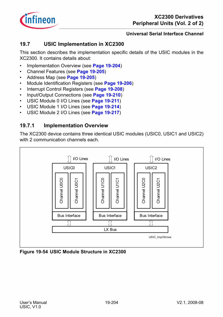
XC2300 DerivativesPeripheral Units (Vol. 2 of 2)
Universal Serial Interface Channel
19.7 USIC Implementation in XC2300This section describes the implementation specific details of the USIC modules in theXC2300. It contains details about:• Implementation Overview (see Page 19-204)• Channel Features (see Page 19-205)• Address Map (see Page 19-205)• Module Identification Registers (see Page 19-206)• Interrupt Control Registers (see Page 19-208)• Input/Output Connections (see Page 19-210)• USIC Module 0 I/O Lines (see Page 19-211)• USIC Module 1 I/O Lines (see Page 19-214)• USIC Module 2 I/O Lines (see Page 19-217)
19.7.1 Implementation OverviewThe XC2300 device contains three identical USIC modules (USIC0, USIC1 and USIC2)with 2 communication channels each.
Figure 19-54 USIC Module Structure in XC2300
USIC_Impl3times
USIC0
Cha
nnel
U0C
0
Cha
nnel
U0C
1
USIC1
Cha
nnel
U1C
0
Cha
nnel
U1C
1
USIC2
Cha
nnel
U2C
0
Cha
nnel
U2C
1
LX Bus
Bus Interface Bus Interface Bus Interface
I/O Lines I/O Lines I/O Lines
User’s Manual 19-204 V2.1, 2008-08USIC, V1.0

XC2300 DerivativesPeripheral Units (Vol. 2 of 2)
Universal Serial Interface Channel
19.7.2 Channel FeaturesThe USIC channels in the XC2300 support the following functionality:
19.7.3 Address MapThe registers of the USIC communication channels are available at the following baseaddresses. The exact register address is given by the relative address of the register(given in Table 19-3) plus the channel base address (given in Table 19-12).
Table 19-11 USIC Module Feature SetChannel ASC
ProtocolLINSupport
SSCProtocol
IICProtocol
IISProtocol
FIFO Buffer Entries
SELOx1)
1) This number refers to the maximum number of signals available in the 144 pin package.
U0C0 yes yes yes yes yes 64 shared
8U0C1 yes yes yes yes yes 4U1C0 yes yes yes yes yes 64
shared8
U1C1 yes yes yes yes yes 5U2C0 yes yes yes yes yes 64
shared6
U2C1 yes yes yes yes yes 2
Table 19-12 Registers Address SpaceModule Base Address End Address NoteU0C0 204000H 2041FFH –U0C1 204200H 2043FFH –U1C0 204800H 2049FFH –U1C1 204A00H 204BFFH –U2C0 205000H 2051FFH –U2C1 205200H 2053FFH –
User’s Manual 19-205 V2.1, 2008-08USIC, V1.0
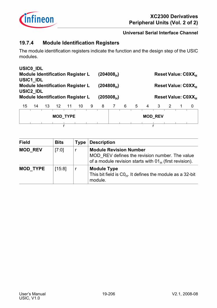
XC2300 DerivativesPeripheral Units (Vol. 2 of 2)
Universal Serial Interface Channel
19.7.4 Module Identification RegistersThe module identification registers indicate the function and the design step of the USICmodules.
USIC0_IDL Module Identification Register L (204008H) Reset Value: C0XXH USIC1_IDL Module Identification Register L (204808H) Reset Value: C0XXH USIC2_IDL Module Identification Register L (205008H) Reset Value: C0XXH
15 14 13 12 11 10 9 8 7 6 5 4 3 2 1 0
MOD_TYPE MOD_REV
r r
Field Bits Type DescriptionMOD_REV [7:0] r Module Revision Number
MOD_REV defines the revision number. The value of a module revision starts with 01H (first revision).
MOD_TYPE [15:8] r Module TypeThis bit field is C0H. It defines the module as a 32-bit module.
User’s Manual 19-206 V2.1, 2008-08USIC, V1.0
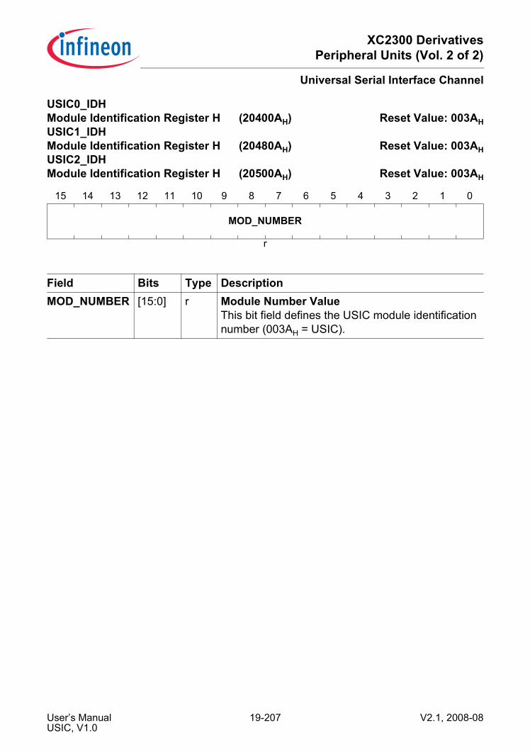
XC2300 DerivativesPeripheral Units (Vol. 2 of 2)
Universal Serial Interface Channel
USIC0_IDH Module Identification Register H (20400AH) Reset Value: 003AHUSIC1_IDH Module Identification Register H (20480AH) Reset Value: 003AHUSIC2_IDH Module Identification Register H (20500AH) Reset Value: 003AH
15 14 13 12 11 10 9 8 7 6 5 4 3 2 1 0
MOD_NUMBER
r
Field Bits Type DescriptionMOD_NUMBER [15:0] r Module Number Value
This bit field defines the USIC module identification number (003AH = USIC).
User’s Manual 19-207 V2.1, 2008-08USIC, V1.0

XC2300 DerivativesPeripheral Units (Vol. 2 of 2)
Universal Serial Interface Channel
19.7.5 Interrupt Control RegistersEach USIC channel provides 4 service request outputs SR[3:0] (not all of them arenecessarily connected to independent interrupt registers UxCy_nIC). Table 19-13shows the assignment of the service request outputs to the interrupt control registers.Each USIC communication channel is connected to 3 dedicated interrupt controlregisters (connected to UxCy_SR[2:0], e.g. one for transmission, one for reception, thethird one for protocol or error handling, or for the alternative receive events). A fourthinterrupt control register per communication channel (connected to UxCy_SR3) isshared with module CC2.The interrupt control registers are located in the SFR area. They are described in thegeneral interrupt chapter.
Table 19-13 USIC Interrupt Control RegistersService Request Output Line Interrupt Control Register/BitSR0 of USIC0 channel 0 U0C0_0ICSR1 of USIC0 channel 0 U0C0_1ICSR2 of USIC0 channel 0 U0C0_2ICSR3 of USIC0 channel 0 SCU_ISSR.4, shared with CC2SR0 of USIC0 channel 1 U0C1_0ICSR1 of USIC0 channel 1 U0C1_1ICSR2 of USIC0 channel 1 U0C1_2ICSR3 of USIC0 channel 1 SCU_ISSR.5, shared with CC2SR0 of USIC1 channel 0 U1C0_0ICSR1 of USIC1 channel 0 U1C0_1ICSR2 of USIC1 channel 0 U1C0_2ICSR3 of USIC1 channel 0 SCU_ISSR.6, shared with CC2SR0 of USIC1 channel 1 U1C1_0ICSR1 of USIC1 channel 1 U1C1_1ICSR2 of USIC1 channel 1 U1C1_2ICSR3 of USIC1 channel 1 SCU_ISSR.7, shared with CC2SR0 of USIC2 channel 0 U2C0_0ICSR1 of USIC2 channel 0 U2C0_1ICSR2 of USIC2 channel 0 U2C0_2ICSR3 of USIC2 channel 0 SCU_ISSR.12, shared with CC2
User’s Manual 19-208 V2.1, 2008-08USIC, V1.0
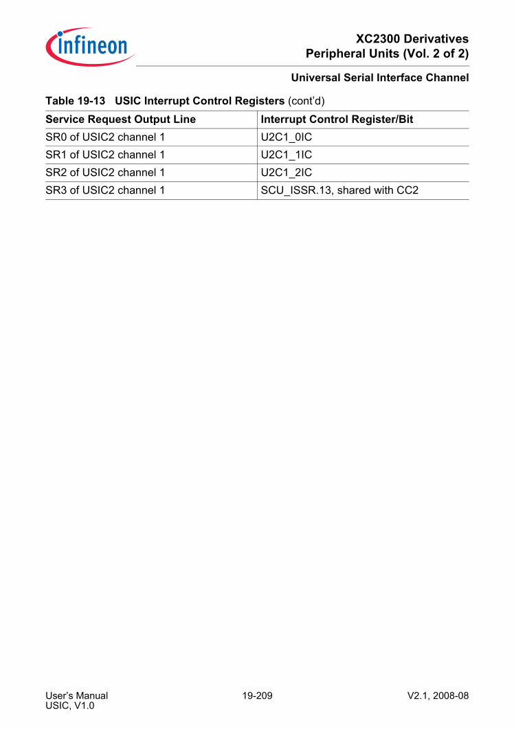
XC2300 DerivativesPeripheral Units (Vol. 2 of 2)
Universal Serial Interface Channel
SR0 of USIC2 channel 1 U2C1_0ICSR1 of USIC2 channel 1 U2C1_1ICSR2 of USIC2 channel 1 U2C1_2ICSR3 of USIC2 channel 1 SCU_ISSR.13, shared with CC2
Table 19-13 USIC Interrupt Control Registers (cont’d)
Service Request Output Line Interrupt Control Register/Bit
User’s Manual 19-209 V2.1, 2008-08USIC, V1.0

XC2300 DerivativesPeripheral Units (Vol. 2 of 2)
Universal Serial Interface Channel
19.7.6 Input/Output ConnectionsFigure 19-1 shows the I/O lines of one USIC channel. The tables in this section definethe pin assignments and internal connections of the USIC channels I/O lines in theXC2300 device. Naming convention: UxCy refers to USIC module x channel y.
Figure 19-55 USIC Channel I/O Lines
The connections of the service request outputs SR[3:0] to the interrupt control registersare defined in Table 19-13 on Page 19-208.
USIC_IOLines
DX0A
DX0INS
DX0B
DX0FDX0G
InputStage
DX0
........
DX1A
DX1INS
DX1B
DX1FDX1G
InputStage
DX1
........
DX2A
DX2INS
DX2B
DX2FDX2G
InputStage
DX2
........
SlaveSelect
Generator
SELO0 SELO1
SELO6 SELO7
........
InterruptControl
SR0 SR1 SR2 SR3
OutputStageDOUT
DOUT
Baud RateGenerator
SCLKOUT MCLKOUT
USIC Channel
User’s Manual 19-210 V2.1, 2008-08USIC, V1.0

XC2300 DerivativesPeripheral Units (Vol. 2 of 2)
Universal Serial Interface Channel
19.7.6.1 USIC Module 0 I/O LinesThe signals of USIC module 0 have the prefix “U0C0_” for channel 0 and “U0C1_” forchannel 1.
Table 19-14 I/O Connections of USIC0Signal Used as From/To
Channel 0 – U0C0 Channel 1 – U0C1Data InputsDX0A Shift data input P10.0 P10.0DX0B Shift data input P10.1 P10.7DX0C Shift data input P10.6 P10.14DX0D Shift data input P7.4 0DX0E Shift data input P2.3 P2.10DX0F Shift data input P2.4 P7.3DX0G Loop back data shift input U0C0_DOUT U0C1_DOUTClock InputsDX1A Shift clock input P10.1 P10.10DX1B Shift clock input P10.2 P10.5DX1C Shift clock input P10.8 P10.15DX1D Shift clock input 0 P2.8DX1E Shift clock input 0 0DX1F Shift clock input 0 0DX1G Loop back shift clock input U0C0_SCLKOUT U0C1_SCLKOUTControl InputsDX2A Shift control input P10.3 P10.3DX2B Shift control input P10.4 P10.4DX2C Shift control input P10.10 P2.7DX2D Shift control input P2.6 0DX2E Input for transmit data validation CC2_8 RTC_T14INTDX2F Input for transmit data validation CCU60_T13_PM CCU60_T13_PMDX2G Loop back shift control input U0C0_SELO0 U0C1_SELO0
User’s Manual 19-211 V2.1, 2008-08USIC, V1.0

XC2300 DerivativesPeripheral Units (Vol. 2 of 2)
Universal Serial Interface Channel
Data OutputsDOUT Shift data output P2.3 P2.9
P7.3 P2.10P10.1 P7.3P10.6 P7.4– P10.0– P10.7– P10.14– P10.15
Clock OutputsMCLKOUT Master clock output, e.g. for IIS P10.8 P10.9SCLKOUT Shift clock output P2.5 P2.8
P10.2 P7.4– P10.5
Control OutputsSELO0 Shift control output 0 P2.6 P2.7
P10.10 P10.8SELO1 Shift control output 1 P2.7 P2.6SELO2 Shift control output 2 P2.11 P2.11SELO3 Shift control output 3 P2.10 P2.12
P10.4 –SELO4 Shift control output 5 P2.12 –
P3.4 –P10.9 –
SELO5 Shift control output 5 P3.5 –SELO6 Shift control output 6 P3.6 –SELO7 Shift control output 7 P3.7 –
System Related Outputs
Table 19-14 I/O Connections of USIC0 (cont’d)
Signal Used as From/ToChannel 0 – U0C0 Channel 1 – U0C1
User’s Manual 19-212 V2.1, 2008-08USIC, V1.0
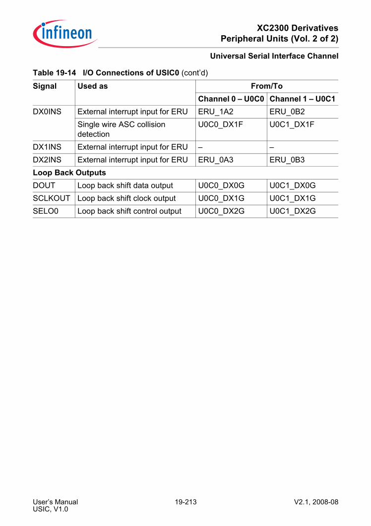
XC2300 DerivativesPeripheral Units (Vol. 2 of 2)
Universal Serial Interface Channel
DX0INS External interrupt input for ERU ERU_1A2 ERU_0B2Single wire ASC collision detection
U0C0_DX1F U0C1_DX1F
DX1INS External interrupt input for ERU – –DX2INS External interrupt input for ERU ERU_0A3 ERU_0B3Loop Back OutputsDOUT Loop back shift data output U0C0_DX0G U0C1_DX0GSCLKOUT Loop back shift clock output U0C0_DX1G U0C1_DX1GSELO0 Loop back shift control output U0C0_DX2G U0C1_DX2G
Table 19-14 I/O Connections of USIC0 (cont’d)
Signal Used as From/ToChannel 0 – U0C0 Channel 1 – U0C1
User’s Manual 19-213 V2.1, 2008-08USIC, V1.0
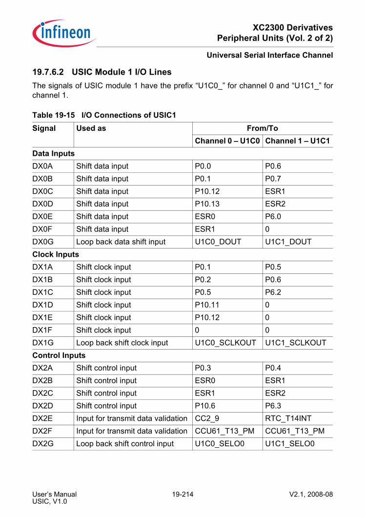
XC2300 DerivativesPeripheral Units (Vol. 2 of 2)
Universal Serial Interface Channel
19.7.6.2 USIC Module 1 I/O LinesThe signals of USIC module 1 have the prefix “U1C0_” for channel 0 and “U1C1_” forchannel 1.
Table 19-15 I/O Connections of USIC1Signal Used as From/To
Channel 0 – U1C0 Channel 1 – U1C1Data InputsDX0A Shift data input P0.0 P0.6DX0B Shift data input P0.1 P0.7DX0C Shift data input P10.12 ESR1DX0D Shift data input P10.13 ESR2DX0E Shift data input ESR0 P6.0DX0F Shift data input ESR1 0DX0G Loop back data shift input U1C0_DOUT U1C1_DOUTClock InputsDX1A Shift clock input P0.1 P0.5DX1B Shift clock input P0.2 P0.6DX1C Shift clock input P0.5 P6.2DX1D Shift clock input P10.11 0DX1E Shift clock input P10.12 0DX1F Shift clock input 0 0DX1G Loop back shift clock input U1C0_SCLKOUT U1C1_SCLKOUTControl InputsDX2A Shift control input P0.3 P0.4DX2B Shift control input ESR0 ESR1DX2C Shift control input ESR1 ESR2DX2D Shift control input P10.6 P6.3DX2E Input for transmit data validation CC2_9 RTC_T14INTDX2F Input for transmit data validation CCU61_T13_PM CCU61_T13_PMDX2G Loop back shift control input U1C0_SELO0 U1C1_SELO0
User’s Manual 19-214 V2.1, 2008-08USIC, V1.0

XC2300 DerivativesPeripheral Units (Vol. 2 of 2)
Universal Serial Interface Channel
Data OutputsDOUT Shift data output P0.0 P0.6
P0.1 P0.7P10.12 P6.1P10.13 –P10.15 –
Clock OutputsMCLKOUT Master clock output, e.g. for IIS P10.8 P1.7SCLKOUT Shift clock output P2.5 P0.5
P10.2 P6.2Control OutputsSELO0 Shift control output 0 P0.3 P0.4
P10.6 P6.3SELO1 Shift control output 1 P0.4 P0.3
P10.14 –SELO2 Shift control output 2 P0.5 P1.6
P10.15 –SELO3 Shift control output 3 P0.7 P1.5
P10.13 –SELO4 Shift control output 5 P1.0 P1.4SELO5 Shift control output 5 P1.1 –SELO6 Shift control output 6 P1.2 –SELO7 Shift control output 7 P1.3 –System Related OutputsDX0INS External interrupt input for ERU ERU_1A2 ERU_1B2
Single wire ASC collision detection
U1C0_DX1F U1C1_DX1F
DX1INS External interrupt input for ERU ERU_3B0 –DX2INS External interrupt input for ERU ERU_1A3 ERU_1B3
Table 19-15 I/O Connections of USIC1 (cont’d)
Signal Used as From/ToChannel 0 – U1C0 Channel 1 – U1C1
User’s Manual 19-215 V2.1, 2008-08USIC, V1.0

XC2300 DerivativesPeripheral Units (Vol. 2 of 2)
Universal Serial Interface Channel
Loop Back OutputsDOUT Loop back shift data output U0C0_DX0G U1C1_DX0GSCLKOUT Loop back shift clock output U0C0_DX1G U1C1_DX1GSELO0 Loop back shift control output U0C0_DX2G U1C1_DX2G
Table 19-15 I/O Connections of USIC1 (cont’d)
Signal Used as From/ToChannel 0 – U1C0 Channel 1 – U1C1
User’s Manual 19-216 V2.1, 2008-08USIC, V1.0

XC2300 DerivativesPeripheral Units (Vol. 2 of 2)
Universal Serial Interface Channel
19.7.6.3 USIC Module 2 I/O LinesThe signals of USIC module 2 have the prefix “U2C0_” for channel 0 and “U2C1_” forchannel 1.
Table 19-16 I/O Connections of USIC2Signal Used as From/To
Channel 0 – U2C0 Channel 1 – U2C1Data InputsDX0A Shift data input P3.0 P3.6DX0B Shift data input P3.1 P3.7DX0C Shift data input P1.5 P1.1DX0D Shift data input P1.6 P1.2DX0E Shift data input P9.5 ESR2DX0F Shift data input 0 0DX0G Loop back data shift input U2C0_DOUT U2C1_DOUTClock InputsDX1A Shift clock input P3.0 P3.5DX1B Shift clock input P3.2 P3.6DX1C Shift clock input P1.7 P1.2DX1D Shift clock input P9.7 0DX1E Shift clock input 0 0DX1F Shift clock input 0 0DX1G Loop back shift clock input U2C0_SCLKOUT U2C1_SCLKOUTControl InputsDX2A Shift control input P3.3 P3.4DX2B Shift control input P1.4 ESR2DX2C Shift control input 0 ESR1DX2D Shift control input 0 0DX2E Input for transmit data validation CC2_10 RTC_T14INTDX2F Input for transmit data validation CCU62_T13_PM CCU62_T13_PMDX2G Loop back shift control input U2C0_SELO0 U2C1_SELO0
User’s Manual 19-217 V2.1, 2008-08USIC, V1.0

XC2300 DerivativesPeripheral Units (Vol. 2 of 2)
Universal Serial Interface Channel
Data OutputsDOUT Shift data output P3.0 P3.6
P3.1 P3.7P1.6 P1.1P9.4 –P9.5 –
Clock OutputsMCLKOUT Master clock output, e.g. for IIS – –SCLKOUT Shift clock output P3.2 P3.5
P1.7 P1.2Control OutputsSELO0 Shift control output 0 P3.3 P3.4SELO1 Shift control output 1 P3.4 P3.3SELO2 Shift control output 2 P3.5 –SELO3 Shift control output 3 P3.7 –SELO4 Shift control output 4 P1.3 –SELO5 Shift control output 5 P1.4 –SELO6 Shift control output 6 – –SELO7 Shift control output 7 – –System Related OutputsDX0INS External interrupt input for ERU
(SCU)ERU_2A2 ERU_2B2
Single wire ASC collision detection
U2C0_DX1F U2C1_DX1F
DX1INS External interrupt input for ERU (SCU)
ERU_2B0 –
DX2INS External interrupt input for ERU (SCU)
ERU_2A3 ERU_2B3
Table 19-16 I/O Connections of USIC2 (cont’d)
Signal Used as From/ToChannel 0 – U2C0 Channel 1 – U2C1
User’s Manual 19-218 V2.1, 2008-08USIC, V1.0

XC2300 DerivativesPeripheral Units (Vol. 2 of 2)
Universal Serial Interface Channel
Loop Back OutputsDOUT Loop back shift data output U2C0_DX0G U2C1_DX0GSCLKOUT Loop back shift clock output U2C0_DX1G U2C1_DX1GSELO0 Loop back shift control output U2C0_DX2G U2C1_DX2G
Table 19-16 I/O Connections of USIC2 (cont’d)
Signal Used as From/ToChannel 0 – U2C0 Channel 1 – U2C1
User’s Manual 19-219 V2.1, 2008-08USIC, V1.0
XC2300 DerivativesPeripheral Units (Vol. 2 of 2)
Universal Serial Interface Channel
User’s Manual 19-220 V2.1, 2008-08USIC, V1.0
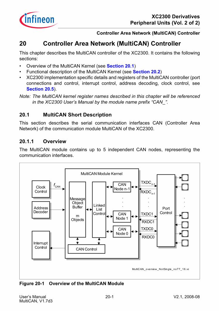
XC2300 DerivativesPeripheral Units (Vol. 2 of 2)
Controller Area Network (MultiCAN) Controller
20 Controller Area Network (MultiCAN) ControllerThis chapter describes the MultiCAN controller of the XC2300. It contains the followingsections:• Overview of the MultiCAN Kernel (see Section 20.1)• Functional description of the MultiCAN Kernel (see Section 20.2)• XC2300 implementation specific details and registers of the MultiCAN controller (port
connections and control, interrupt control, address decoding, clock control, seeSection 20.5).
Note: The MultiCAN kernel register names described in this chapter will be referencedin the XC2300 User’s Manual by the module name prefix “CAN_”.
20.1 MultiCAN Short DescriptionThis section describes the serial communication interfaces CAN (Controller AreaNetwork) of the communication module MultiCAN of the XC2300.
20.1.1 OverviewThe MultiCAN module contains up to 5 independent CAN nodes, representing thecommunication interfaces.
Figure 20-1 Overview of the MultiCAN Module
MultiCAN Module Kernel
MultiCAN_overview_NotSingle_noTT_16.vs
ClockControl
AddressDecoder
InterruptControl
fCAN
PortControlCAN
Node 1
CAN Control
MessageObjectBuffer
mObjects
TXDC0
RXDC0
CANNode 0
CANNode n-1
TXDC1
RXDC1
TXDCn-1
LinkedList
Control
RXDCn-1...
.
.
.
.
.
.
User’s Manual 20-1 V2.1, 2008-08MultiCAN, V1.7d3

XC2300 DerivativesPeripheral Units (Vol. 2 of 2)
Controller Area Network (MultiCAN) Controller
20.1.2 CAN FeaturesSeveral key features contribute to the high performance of the MultiCAN module:• CAN functionality conforms to CAN specification V2.0 B active for each CAN node
(compliant to ISO 11898)• Up to 5 independent CAN nodes available• Up to 128 independent message objects (shared by the CAN nodes)• Dedicated control registers for each CAN node• Data transfer rate up to 1MBaud, individually programmable for each node• Flexible and powerful message transfer control and error handling capabilities• Full-CAN functionality: message objects can be individually
– Assigned to one of the 5 CAN nodes– Configured as transmit or receive object– Participate in a message buffer with FIFO algorithm– Set up to handle frames with 11-bit or 29-bit identifiers– Provided with programmable acceptance mask register for filtering– Monitored via a frame counter– Configured to Remote Monitoring Mode
• Automatic gateway mode support• 16 individually programmable interrupt outputs• CAN Analyzer Mode for bus monitoring• SRAMs in MultiCAN module optionally parity error protected
User’s Manual 20-2 V2.1, 2008-08MultiCAN, V1.7d3

XC2300 DerivativesPeripheral Units (Vol. 2 of 2)
Controller Area Network (MultiCAN) Controller
20.2 CAN Functional DescriptionThis section describes the core features of the CAN module.
20.2.1 Conventions and DefinitionsTable 20-1 defines constants that are used throughout the MultiCAN specification.These are fixed maximum values for a given MultiCAN implementation. Nevertheless, indifferent products, some objects and nodes may be disabled, depending on the productconfiguration.
20.2.2 IntroductionThe MultiCAN module contains 5 Full-CAN nodes operating independently orexchanging data and remote frames via a gateway function.Transmission and receptionof CAN frames is handled in accordance to CAN specification V2.0part B (active). EachCAN node can receive and transmit standard frames with 11-bit identifiers as well asextended frames with 29-bit identifiers.
Table 20-1 Fixed Module ConstantsConstant Value Descriptionn_objects 128 Number of Message Objects
n_objects denotes the total amount of message objects available.
n_interrupts 16 Number of Interrupt Output Linesn_interrupts denotes the total number of interrupt outputs available.
n_pendings 256 Number of Message Pending Bitsn_pendings denotes the number of message pending bits available. The number of message pending registers is given by n_pendings/32.
n_lists 8 Number of Listsn_lists denotes the total number of lists available for allocation of message number.
n_nodes 5 Number of CAN Nodes Availablen_nodes denotes the total number of CAN nodes available. As each CAN node has it’s own list in addition to the list of un-allocated elements, the relation n_nodes < n_lists is true.
User’s Manual 20-3 V2.1, 2008-08MultiCAN, V1.7d3
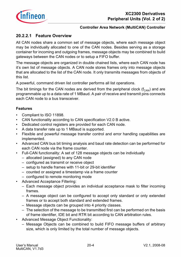
XC2300 DerivativesPeripheral Units (Vol. 2 of 2)
Controller Area Network (MultiCAN) Controller
20.2.2.1 Feature OverviewAll CAN nodes share a common set of message objects, where each message objectmay be individually allocated to one of the CAN nodes. Besides serving as a storagecontainer for incoming and outgoing frames, message objects may be combined to buildgateways between the CAN nodes or to setup a FIFO buffer.The message objects are organized in double chained lists, where each CAN node hasit’s own list of message objects. A CAN node stores frames only into message objectsthat are allocated to the list of the CAN node. It only transmits messages from objects ofthis list.A powerful, command driven list controller performs all list operations.The bit timings for the CAN nodes are derived from the peripheral clock (fCAN) and areprogrammable up to a data rate of 1 MBaud. A pair of receive and transmit pins connectseach CAN node to a bus transceiver.
Features• Compliant to ISO 11898.• CAN functionality according to CAN specification V2.0 B active.• Dedicated control registers are provided for each CAN node.• A data transfer rate up to 1 MBaud is supported.• Flexible and powerful message transfer control and error handling capabilities are
implemented.• Advanced CAN bus bit timing analysis and baud rate detection can be performed for
each CAN node via the frame counter.• Full-CAN functionality: A set of 128 message objects can be individually
– allocated (assigned) to any CAN node– configured as transmit or receive object– setup to handle frames with 11-bit or 29-bit identifier– counted or assigned a timestamp via a frame counter– configured to remote monitoring mode
• Advanced Acceptance Filtering:– Each message object provides an individual acceptance mask to filter incoming
frames.– A message object can be configured to accept only standard or only extended
frames or to accept both standard and extended frames.– Message objects can be grouped into 4 priority classes.– The selection of the message to be transmitted first can be performed on the basis
of frame identifier, IDE bit and RTR bit according to CAN arbitration rules.• Advanced Message Object Functionality:
– Message Objects can be combined to build FIFO message buffers of arbitrarysize, which is only limited by the total number of message objects.
User’s Manual 20-4 V2.1, 2008-08MultiCAN, V1.7d3

XC2300 DerivativesPeripheral Units (Vol. 2 of 2)
Controller Area Network (MultiCAN) Controller
– Message objects can be linked to form a gateway to automatically transfer framesbetween 2 different CAN buses. A single gateway can link any two CAN nodes. Anarbitrary number of gateways may be defined.
• Advanced Data Management:– The Message objects are organized in double chained lists.– List reorganizations may be performed any time, even during full operation of the
CAN nodes.– A powerful, command driven list controller manages the organization of the list
structure and ensures consistency of the list.– Message FIFOs are based on the list structure and can easily be scaled in size
during CAN operation.– Static Allocation Commands offer compatibility with TwinCAN applications, which
are not list based.• Advanced Interrupt Handling:
– Up to 16 interrupt output lines are available. Most interrupt requests can beindividually routed to one of the 16 interrupt output lines.
– Message postprocessing notifications can be flexibly aggregated into a dedicatedregister field of 256 notification bits.
User’s Manual 20-5 V2.1, 2008-08MultiCAN, V1.7d3
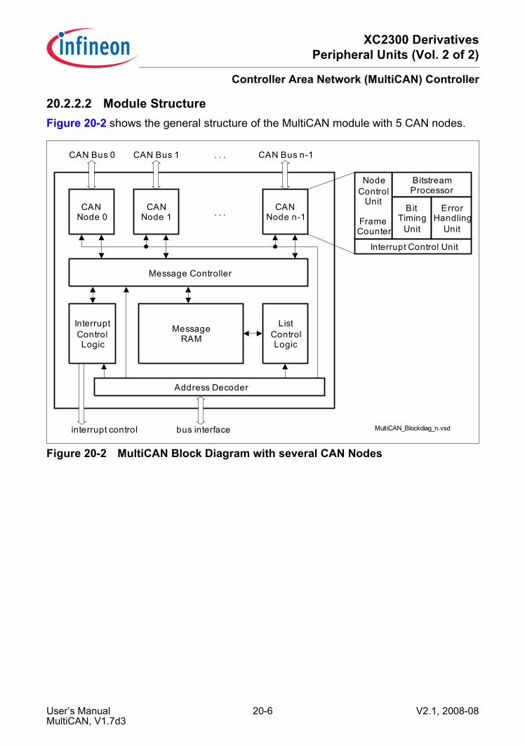
XC2300 DerivativesPeripheral Units (Vol. 2 of 2)
Controller Area Network (MultiCAN) Controller
20.2.2.2 Module StructureFigure 20-2 shows the general structure of the MultiCAN module with 5 CAN nodes.
Figure 20-2 MultiCAN Block Diagram with several CAN Nodes
MultiCAN_Blockdiag_n.vsd
CAN Bus 0
Message Controller
CANNode 0
CAN Bus 1
CANNode 1
. . . CAN Bus n-1
ListControlLogic
MessageRAM
Address Decoder
InterruptControlLogic
CANNode n-1
BitstreamProcessor
BitTiming
Unit
ErrorHandling
Unit
NodeControl
Unit
FrameCounter
Interrupt Control Unit
bus interfaceinterrupt control
. . .
User’s Manual 20-6 V2.1, 2008-08MultiCAN, V1.7d3

XC2300 DerivativesPeripheral Units (Vol. 2 of 2)
Controller Area Network (MultiCAN) Controller
CAN NodesEach CAN node consists of several sub-units as described in Table 20-2.:
Message ControllerThe message controller handles the exchange of CAN frames between the CAN nodesand the message objects which are stored in the Message RAM. It performs:• Receive Acceptance filtering to determine the correct message object for storing of
a received CAN frame.• Transmit Acceptance Filtering to determine the message object to be transmitted
first, individually for each CAN node.• Content transfer between message objects and the CAN nodes, taking into account
the status/control bits of the message objects.• Handling of the FIFO buffering and Gateway functionality.• Aggregation of message pending notification bits.
Table 20-2 Subunits of CAN NodesSubunit DescriptionBit Stream Processor The Bit Stream Processor performs data, remote, error and
overload frame processing according to the ISO 11898 standard. This includes conversion between the serial data stream and the input/output shift registers.
Bit Timing Unit The Bit Timing Unit defines the length of a bit time and the location of the sample point according to the user settings, taking into account propagation delays and phase shift errors. The Bit Timing Unit also performs resynchronization.
Error Handling Unit The Error Handling Unit manages the receive and transmit error counter. According to the contents of both counters the CAN node is set into an “Error Active”, “Error Passive” or “Bus-Off” state.
Node Control Unit The Node Control Unit coordinates the operation of the CAN node: • Enables/disable CAN transfer of the node• Enable/Disable and generate node specific events that
lead to an interrupt request (CAN bus errors, successfulframe transfers etc.)
• Administration of the Frame Counter
User’s Manual 20-7 V2.1, 2008-08MultiCAN, V1.7d3

XC2300 DerivativesPeripheral Units (Vol. 2 of 2)
Controller Area Network (MultiCAN) Controller
List ControllerThe list controller performs all operations that lead to a modification of the doublechained message object lists. Only the list controller is allowed to modify the liststructure. The allocation/deallocation or reallocation of a message object can berequested via a user command interface (command panel). The list controller statemachine then performs the requested command autonomously.
User’s Manual 20-8 V2.1, 2008-08MultiCAN, V1.7d3
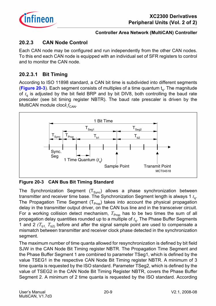
XC2300 DerivativesPeripheral Units (Vol. 2 of 2)
Controller Area Network (MultiCAN) Controller
20.2.3 CAN Node ControlEach CAN node may be configured and run independently from the other CAN nodes.To this end each CAN node is equipped with an individual set of SFR registers to controland to monitor the CAN node.
20.2.3.1 Bit TimingAccording to ISO 11898 standard, a CAN bit time is subdivided into different segments(Figure 20-3). Each segment consists of multiples of a time quantum tq. The magnitudeof tq is adjusted by the bit field BRP and by bit DIV8, both controlling the baud rateprescaler (see bit timing register NBTR). The baud rate prescaler is driven by theMultiCAN module clock fCAN.
Figure 20-3 CAN Bus Bit Timing Standard
The Synchronization Segment (TSync) allows a phase synchronization betweentransmitter and receiver time base. The Synchronization Segment length is always 1 tq.The Propagation Time Segment (TProp) takes into account the physical propagationdelay in the transmitter output driver, on the CAN bus line and in the transceiver circuit.For a working collision detect mechanism, TProp has to be two times the sum of allpropagation delay quantities rounded up to a multiple of tq. The Phase Buffer Segments1 and 2 (Tb1, Tb2) before and after the signal sample point are used to compensate amismatch between transmitter and receiver clock phase detected in the synchronizationsegment.The maximum number of time quanta allowed for resynchronization is defined by bit fieldSJW in the CAN Node Bit Timing register NBTR. The Propagation Time Segment andthe Phase Buffer Segment 1 are combined to parameter TSeg1, which is defined by thevalue TSEG1 in the respective CAN Node Bit Timing register NBTR. A minimum of 3time quanta is requested by the ISO standard. Parameter TSeg2, which is defined by thevalue of TSEG2 in the CAN Node Bit Timing Register NBTR, covers the Phase BufferSegment 2. A minimum of 2 time quanta is requested by the ISO standard. According
MCT04518
Sync.Seg
TSync TProp Tb1 Tb2
TSeg2TSeg1
1 Bit Time
Sample Point Transmit Point
1 Time Quantum (tq)
User’s Manual 20-9 V2.1, 2008-08MultiCAN, V1.7d3

XC2300 DerivativesPeripheral Units (Vol. 2 of 2)
Controller Area Network (MultiCAN) Controller
ISO standard, a CAN bit time, calculated as the sum of TSync, TSeg1 and TSeg2, must notfall below 8 time quanta.Calculation of the bit time:
To compensate phase shifts between clocks of different CAN controllers, the CANcontroller has to synchronize on any edge from the recessive to the dominant bus level.If the hard synchronization is enabled (at the start of frame), the bit time is restarted atthe synchronization segment. Otherwise, the resynchronization jump width TSJW definesthe maximum number of time quanta a bit time may be shortened or lengthened by oneresynchronization. The value of SJW is programmed in the CAN Node Bit TimingRegister.
The maximum relative tolerance for fCAN depends on the Phase Buffer Segments and theresynchronization jump width.
A valid CAN bit timing must be written to the CAN Node Bit Timing Register NBTR beforeresetting the INIT bit in the Node Control Register, i.e. before enabling the operation ofthe CAN node.The Node Bit Timing Register may be written only if bit CCE (Configuration ChangeEnable) is set in the corresponding Node Control Register.
tq = (BRP+1) / fCAN if DIV8 = 0= 8 × (BRP+1) / fCAN if DIV8 = 1
TSync = 1 tqTSeg1 = (TSEG1 + 1) × tq (min. 3 tq)TSeg2 = (TSEG2 + 1) × tq (min. 2 tq)bit time = TSync + TSeg1 + TSeg2 (min. 8 tq)
TSJW = (SJW + 1) × tqTSeg1 ≥ TSJW + Tprop
TSeg2 ≥ TSJW
dfCAN ≤ min (Tb1, Tb2) / 2 × (13 × bit time - Tb2) ANDdfCAN ≤ TSJW / 20 × bit time
User’s Manual 20-10 V2.1, 2008-08MultiCAN, V1.7d3

XC2300 DerivativesPeripheral Units (Vol. 2 of 2)
Controller Area Network (MultiCAN) Controller
20.2.3.2 CAN Error HandlingThe Error Handling Unit of the CAN node is responsible for the fault confinement of theCAN device. Its two counters, the Receive Error Counter and the Transmit Error Counter(control register NECNT), are incremented and decremented by commands from the BitStream Processor. If the Bit Stream Processor itself detects an error while a transmitoperation is running, the Transmit Error Counter is incremented by 8. An increment of 1is used, when the error condition was reported by an external CAN node via an errorframe generation. For error analysis, the transfer direction of the disturbed message andthe node, recognizing the transfer error, are indicated in the control register NECNT ofthe respective CAN node. According to the values of the error counters, the CAN nodeis set into the states "error active", "error passive" and "bus-off".The CAN node is in error active state, if both error counters are below the error passivelimit of 128. It is in error passive state, if at least one of the error counters equals orexceeds 128.The bus-off state is activated if the Transmit Error Counter equals or exceeds the bus-off limit of 256. This state is reported by flag BOFF in the NSR status register of the CANnode. The device remains in this state, until the bus-off recovery sequence is finished.Additionally, there is the bit EWRN in the NSR status register, which is set, if at least oneof the error counters equals or exceeds the error warning limit defined by bit fieldEWRNLVL in the control registers NECNT of the CAN node. Bit EWRN is reset if botherror counters fall below the error warning limit again (see Page 20-63).
20.2.3.3 CAN Frame CounterEach CAN node is equipped with a frame counter which allows to counttransmitted/received CAN frames or to obtain information about the time instant when aframe has been started to transmit or being received by the CAN node. CAN framecounting/bit time counting is performed by a 16 bit counter which is controlled by registerNFCR of the respective CAN node. Bit field CFSEL of register NFCR defines theoperation mode of the frame counter:• Frame Count Mode: The frame counter is incremented after the successful
transmission and/or reception of a CAN frame. The incremented value is copied tothe CFC field of the Interrupt Pointer Register of the message object involved in thetransfer.
• Time Stamp Mode: The frame counter is incremented with the beginning of a new bittime. When the transmission/reception of a frame starts, the value of the framecounter is captured and stored to the CFC field of register NFCR. After the successfultransfer of the frame the captured value is copied to the CFC field of the InterruptPointer Register of the message object involved in the transfer.
• Bit Timing Mode: Used for baud rate detection and analysis of the bit timing(Chapter 20.2.5.3).
User’s Manual 20-11 V2.1, 2008-08MultiCAN, V1.7d3

XC2300 DerivativesPeripheral Units (Vol. 2 of 2)
Controller Area Network (MultiCAN) Controller
20.2.3.4 CAN Node InterruptsEach CAN node is equipped with four interrupt sources.
Figure 20-4 CAN Node Interrupts
MCA05837
TRIE
TRINP
TXOK
RXOK
Receive
Transmit
Correct MessageObject Transfer
LECIE
LECINP
LEC
CAN Error
EWRN
BOFFALINP
ALIE
ALERT
LLE LOE
List Length Error
List Object Error
CFCIE
CFCINP
CFCOV
Frame CounterOverflow/Event
NSRx
NSRx
NCRx
NIPRx
NIPRx
NIPRx
NIPRx
NSRx
NSRx
NCRx
NCRx
NSRx
NSRx NSRx
NFCRxNFCRx
≥1
3
≥1
User’s Manual 20-12 V2.1, 2008-08MultiCAN, V1.7d3

XC2300 DerivativesPeripheral Units (Vol. 2 of 2)
Controller Area Network (MultiCAN) Controller
An interrupt request is generated upon:• The successful transmission/reception of a frame,• An overflow of the frame counter (frame count mode/time stamp mode) or a bit timing
measurement event (bit timing mode),• An error related to the CAN node.
20.2.4 Message Object List StructureThe message objects of the MultiCAN module are organized in double chained lists,where each message object has a pointer to the previous message object in the list aswell as a pointer to the next message object in the list.
20.2.4.1 BasicsThe MultiCAN module provides 16 different lists, where each object is allocated to oneof these lists. A 4 bit LIST bit field in the Message Object Control Register indicates thelist to which the respective message object is currently allocated. In the example ofFigure 20-5 three message objects are allocated to the list with list index 2.
Figure 20-5 Example Allocation of Message Objects to a List
The BEGIN field of the List Register points to the first element in the list (object 5 in theexample) whereas the END field points to the last element in the list (object 3 in theexample). The number of elements in the list is indicated in the SIZE field of the ListRegister (#elements = SIZE + 1, thus SIZE = 2 for the 3 elements of the example). The
MultiCAN_list_basics
MessageObject 5
PPREV = 5
PNEXT = 16
LIST = 2
MessageObject 16
PPREV = 5
PNEXT = 3
LIST = 2
MessageObject 3
PPREV = 16
PNEXT = 3
LIST = 2
Register LIST2
EMPTY = 0 BEGIN = 5 END = 3SIZE = 2
User’s Manual 20-13 V2.1, 2008-08MultiCAN, V1.7d3

XC2300 DerivativesPeripheral Units (Vol. 2 of 2)
Controller Area Network (MultiCAN) Controller
EMPTY bit indicates a list with no elements (EMPTY = 0 in the example, as the list is notempty).Each message object has a pointer PNEXT (located in the Message Object ControlRegister) that points to the next message object in the list and a pointer PREV that pointsto the previous message object in the list. PPREV of the first message object points tothe object itself because the first object has no predecessor (in the example object 5 isthe first object, indicated by PPREV = 5). PNEXT of the last message object also pointsto the object itself because the last element has no successor (in the example object 3is the last object, indicated by PNEXT = 3).Each message object also has a 4 bit LIST field (located in the Message Object ControlRegister) which shows list index of the list to which the object is currently allocated (theobjects of the example are allocated to list 2, thus LIST = 2).
20.2.4.2 List of Unallocated ElementsThe list with list index 0 has a special meaning: It is the list of all unallocated elements.An element is called unallocated if and only if it belongs to list zero. It is called allocatedif and only if it belongs to one of the other lists.After reset all message objects are unallocated, i.e. belong to the list of unallocatedelements. The initial allocation of the message objects within the list of unallocatedobjects is ordered by message number, i.e. the predecessor of message object n isobject n-1 and the successor of object n is object n+1.
20.2.4.3 Connection to the CAN NodesOne CAN node is linked to exactly one unique list of message objects..
Table 20-3 List IndicesList Index Description0 List of unallocated elements1 to n_nodes Lists associated to a CAN node.
List index i belongs to CAN node i -1.n_nodes+1 to n_lists-1
Free user lists, which are not associated to a CAN node.
User’s Manual 20-14 V2.1, 2008-08MultiCAN, V1.7d3

XC2300 DerivativesPeripheral Units (Vol. 2 of 2)
Controller Area Network (MultiCAN) Controller
Figure 20-6 Message Objects Linked to several CAN Nodes
MultiCAN_list_to_can_n.vsd
CANNode 0
1st Objectin List 1
2nd Objectin List 1
Last Objectin List 1
CANNode 1
1st Objectin List 2
2nd Objectin List 2
Last Objectin List 2
CANNode n-1
1st Objectin List n
2nd Objectin List n
Last Objectin List n
CAN Bus 0 CAN Bus 1 . . . CAN Bus n-1
. . .
List of allunallocated
elements
1st Objectin List 0
2nd Objectin List 0
Last Objectin List 0
User’s Manual 20-15 V2.1, 2008-08MultiCAN, V1.7d3
XC2300 DerivativesPeripheral Units (Vol. 2 of 2)
Controller Area Network (MultiCAN) Controller
20.2.4.4 List Command PanelThe list structure may not be modified directly by means of write accesses to the LISTregisters and the PPREV, PNEXT and LIST fields in the message objects as they areread only. The management of the list structure is performed by and limited to the listcontroller unit inside the MultiCAN module. The list controller is controlled via acommand panel which allows the user to issue list allocation commands to the listcontroller. The list controller basically serves two purposes:1. Ensure that all operations that modify the list structure result in a consistent list
structure.2. Present maximum comfort and flexibility to the user.The list controller and the associated command panel allows the programmer toconcentrate on the final properties of the list, which are characterized by the allocationof message objects to a CAN node and the ordering relation between objects which areallocated to the same list. The process of list (re-)building is left to the list controller.A panel command is started by writing the respective command code (see Table 20-9“Panel Commands” on Page 20-52) into to the PANCMD field of the panel controlregister. The corresponding command arguments must be written to PANAR1 andPANAR2 before writing the command code or latest together with the command code ina single 32 bit write access to the panel control register (only possible within 32 bitsystem environments).With the write of a valid command code the BUSY flag in the Panel Control Registerbecomes active (BUSY = 1) and the control panel registers are locked, which means thatwrite accesses to the Panel Control Register are ignored. The BUSY flag remains activeand the control panel remains locked until the execution of the requested command iscompleted.When the issued command is a dynamic allocation which takes an element from the listof unallocated objects, then also the RBUSY bit becomes active together with the BUSYbit (RBUSY = BUSY = 1) to indicate that PANAR1 and PANAR2 are going to be updatedby the list controller:1. The message number of the message object taken from the list of unallocated
elements is written to PANAR1.2. An error status is posted to bit 7 of PANAR2 (Bit 7 = ERR). If ERR = 1 then the list of
unallocated elements was empty and the command is aborted. If ERR = 0 then thelist was not empty and the command will be performed successfully.
The results are written before the list controller starts the actual allocation process. Assoon as the results are available, RBUSY becomes inactive (RBUSY = 0) again, whileBUSY still remains active until completion of the command. This allows the user to setupthe new message object while it is still in the process of list allocation. The access tomessage objects is not limited during ongoing list operations. However, any access to a
User’s Manual 20-16 V2.1, 2008-08MultiCAN, V1.7d3

XC2300 DerivativesPeripheral Units (Vol. 2 of 2)
Controller Area Network (MultiCAN) Controller
register resource located inside the RAM delays the ongoing allocation process by oneaccess cycle.As soon as the command is done the BUSY flag becomes inactive (BUSY = 0) and writeaccesses to the Panel Control Register are enabled again. Also the NOP command codeis automatically written to the CMD field of the Panel Control Register. A new commandmay be started any time during BUSY inactive.All fields of the Panel Control Register except BUSY and RBUSY may be written by theuser. This allows to save and restore the Panel Control Register if the Command Panelshall be used within independent (mutually interruptible) interrupt routines. If this is thecase then any task that uses the Command Panel and that may interrupt another taskalso using the Command Panel should poll the BUSY flag until is becomes inactive andsave the whole PANCTR register to a save memory location before issuing a command.At the end it should restore PANCTR from the said memory location.Before a message object which is allocated to the list of an active CAN node shall bemoved to another list or to another position within the same list, bit MSGVAL (“MessageValid”) should be cleared in the Message Object Control Register of the message object.
User’s Manual 20-17 V2.1, 2008-08MultiCAN, V1.7d3

XC2300 DerivativesPeripheral Units (Vol. 2 of 2)
Controller Area Network (MultiCAN) Controller
20.2.5 CAN Node Analysis FeaturesCAN Analyze Mode allows to monitor the CAN traffic without affecting the logical stateof the CAN bus.
20.2.5.1 Analyze ModeCAN Analyze Mode is selected by setting bit CALM in the Node Control Register. CANAnalyze Mode may be selected for each CAN node individually.In CAN Analyze Mode the transmit pin of the CAN node is held on recessive level. TheCAN node may receive frames (data-, remote-, and error frames) but is not allowed totransmit. Active error frames are sent recessive. Received data/remote frames are notacknowledged (i.e. acknowledge slot is sent recessive), but will be received and storedin matching message objects as long as there is any other node that acknowledges theframe.All message object functionality is available, but no transmit request will be executed.
20.2.5.2 Loop-back ModeThe MultiCAN module provides a loop-back mode to enable an in-system test of theMultiCAN module as well as the development of CAN driver software without access toan external CAN bus.The loop-back feature consists of an internal CAN bus (inside the MultiCAN module) anda bus select switch for each CAN node (Figure 20-7). With the switch each CAN nodecan be wired either to the internal CAN bus (loop-back mode activated) or the externalCAN bus, i.e. the transmit- and receive pins (normal operation). The CAN bus which iscurrently not selected is driven recessive, i.e. the transmit pin is held at 1 and the receivepin is ignored by the CAN nodes which are in loop-back mode.Loop-back Mode is selected individually for each CAN node by setting bit LBM in therespective Node Port Control Register. All CAN nodes that are in loop-back mode maycommunicate on the internal CAN bus without affecting the normal operation of the otherCAN nodes which are not in loop-back mode.
User’s Manual 20-18 V2.1, 2008-08MultiCAN, V1.7d3

XC2300 DerivativesPeripheral Units (Vol. 2 of 2)
Controller Area Network (MultiCAN) Controller
Figure 20-7 Loop-back Mode for several CAN Nodes
CANNode 0
NPCR0.LBM
0
1
ExternalCAN Bus 0
InternalCAN Bus
CANNode 1
NPCR1.LBM
0
1
ExternalCAN Bus 1
CANNode 2
NPCR2.LBM
0
1
ExternalCAN Bus 2
CANNode x
NPCR3.LBM
0
1
ExternalCAN Bus x
MCA05840
User’s Manual 20-19 V2.1, 2008-08MultiCAN, V1.7d3

XC2300 DerivativesPeripheral Units (Vol. 2 of 2)
Controller Area Network (MultiCAN) Controller
20.2.5.3 Bit Timing AnalysisFor each CAN node detailed analysis of the bit timing can be performed by means ofusing dedicated analysis modes of the CAN frame counter. The bit timing analysisfunctionality of the frame counter may be used for automatic detection of the CAN baudrate as well as for the analysis of the timing of the CAN network.Bit timing analysis for a CAN node is selected by CFMOD = 10B (Bit Timing Mode) in theCAN Node Frame Counter Register.Bit timing analysis does not affect the operation of the CAN node.The measurement results are written to the CFC field. Whenever CFC is updated in BitTiming Mode, then also the CFCOV bit is set in order to indicate the update event. IfCFCIE is set then also an interrupt request is generated, where for the the CAN nodei = 0 to 4 the interrupt request is generated on the interrupt output line i.
Automatic Baud Rate DetectionAutomatic baud rate detection requires to measure the time between the observation ofsubsequent dominant edges on the CAN bus. This measurement is automaticallyperformed if CFSE = 000B in the CAN Node Frame Counter Register. With eachdominant edge monitored on the CAN receive input the time (measured in clock cycles)between this edge and the most recent dominant edge is stored in the CFC field.
Synchronization AnalysisThe bit time synchronization is monitored if CFSEL = 010B. The time between the firstdominant edge and the sample point is measured and stored in CFC. The bit timingsynchronization offset may be derived from this time as the first edge after the samplepoint triggers synchronization and there is only one synchronization betweenconsecutive sample points.Synchronization Analysis may be used to fine tune the baud rate during reception of thefirst CAN frame with the measured baud rate.
Driver Delay MeasurementThe delay between a transmitted edge and the corresponding received edge ismeasured with CFSEL = 011B (dominant to dominant) and CFSEL = 001B (recessive torecessive). These delays indicate the time needed to represent a new bit value on thephysical implementation of the CAN bus.
User’s Manual 20-20 V2.1, 2008-08MultiCAN, V1.7d3

XC2300 DerivativesPeripheral Units (Vol. 2 of 2)
Controller Area Network (MultiCAN) Controller
20.2.6 Message Acceptance FilteringThe message acceptance filtering includes receive and transmit filtering.
20.2.6.1 Receive Acceptance FilteringWhen a message object is received on a CAN node, then a unique message object isdetermined in which the received frame will be stored upon successful frame reception.A message object qualifies for the reception of a frame if and only if the followingconditions are fulfilled:1. The message object is allocated to the list of the CAN node on which the frame is
received.2. MSGVAL is set in the Message Control Register3. RXEN is set in the Message Control Register4. The DIR bit in the Message Control Register equals the RTR bit of the received
frame. If DIR = 1 (transmit object) then the message object only accepts remoteframes. If DIR = 0 (receive object) then the message object only accepts dataframes.
5. If MIDE = 1 in the Acceptance Mask Register (MOAMR) then the IDE bit of thereceived frame equals the IDE bit in the Arbitration Register (MOAR). IFMOAR.IDE = 1 then the message object only accepts frames with extendedidentifier. If MOAR.IDE = 0 then the message object only accepts standard frames.If MOAMR.MIDE = 0 then the IDE bit of the received frame is don’t care, i.e. themessage object accepts both standard and extended frames.
6. The identifier of the received frame matches the identifier stored in the ArbitrationRegister of the message object with respect to the acceptance mask in the MOAMRregister. This means that each bit of the received identifier is equal to thecorresponding identifier bit in the Acceptance Register, except those bits for whichthe corresponding mask bits in MOAMR are cleared. These identifier bits are don’tcare. Figure 20-8 illustrates this identifier check.
A priority ordering relation is defined for the message objects:A message object A has higher receive priority than a message object B if and only if thefollowing conditions are fulfilled:1. A belongs to a higher priority class than B, i.e. MOAR.PRI of A must be less than or
equal to MOAR.PRI of B.2. If both objects belong to the same priority class (PRI of A = PRI of B) then message
object B is a list successor of A, i.e. B can be reached by means of successivelystepping forward in the list, starting from A.
Among all messages that fulfill all 6 qualifying criteria the unique message object withhighest receive priority wins acceptance filtering, i.e. is selected for storage of thereceived frame. All other message objects loose receive acceptance filtering.
User’s Manual 20-21 V2.1, 2008-08MultiCAN, V1.7d3
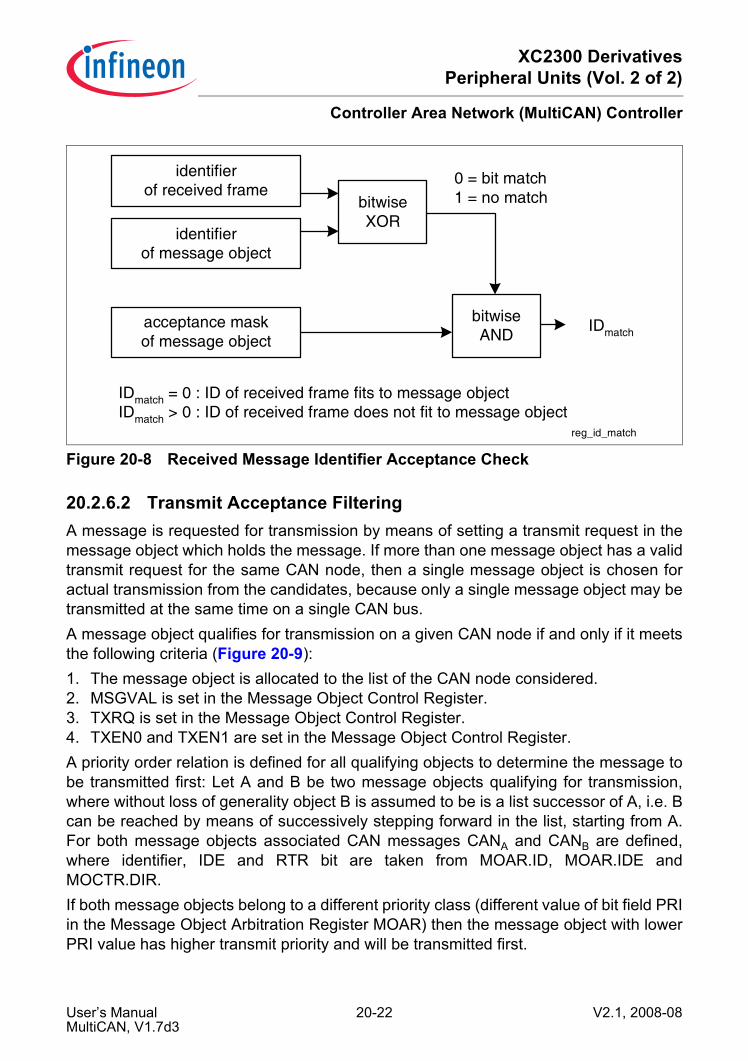
XC2300 DerivativesPeripheral Units (Vol. 2 of 2)
Controller Area Network (MultiCAN) Controller
Figure 20-8 Received Message Identifier Acceptance Check
20.2.6.2 Transmit Acceptance FilteringA message is requested for transmission by means of setting a transmit request in themessage object which holds the message. If more than one message object has a validtransmit request for the same CAN node, then a single message object is chosen foractual transmission from the candidates, because only a single message object may betransmitted at the same time on a single CAN bus.A message object qualifies for transmission on a given CAN node if and only if it meetsthe following criteria (Figure 20-9):1. The message object is allocated to the list of the CAN node considered.2. MSGVAL is set in the Message Object Control Register.3. TXRQ is set in the Message Object Control Register.4. TXEN0 and TXEN1 are set in the Message Object Control Register.A priority order relation is defined for all qualifying objects to determine the message tobe transmitted first: Let A and B be two message objects qualifying for transmission,where without loss of generality object B is assumed to be is a list successor of A, i.e. Bcan be reached by means of successively stepping forward in the list, starting from A.For both message objects associated CAN messages CANA and CANB are defined,where identifier, IDE and RTR bit are taken from MOAR.ID, MOAR.IDE andMOCTR.DIR.If both message objects belong to a different priority class (different value of bit field PRIin the Message Object Arbitration Register MOAR) then the message object with lowerPRI value has higher transmit priority and will be transmitted first.
identifierof received frame
identifierof message object
acceptance maskof message object
bitwiseXOR
bitwiseAND
0 = bit match1 = no match
IDmatch = 0 : ID of received frame fits to message objectIDmatch > 0 : ID of received frame does not fit to message object
IDmatch
reg_id_match
User’s Manual 20-22 V2.1, 2008-08MultiCAN, V1.7d3

XC2300 DerivativesPeripheral Units (Vol. 2 of 2)
Controller Area Network (MultiCAN) Controller
If both message objects belong to the same priority class (equal value of bit fieldMOAR.PRI), then message object A has higher transmit priority than object B if and onlyif one of the following conditions is fulfilled:1. PRI = 10 and CAN message CANA has higher or equal priority than CAN message
CANB with respect to CAN arbitration rules (see Table 20-13).2. PRI = 01 or PRI = 11 (priority by list order).3. PRI = 00 is reserved. Transmit objects with PRI = 00 are not taken into account for
the transmit acceptance filtering.The unique message object that qualifies for transmission and has highest transmitpriority wins transmit acceptance filtering, i.e. will be transmitted first. All other messageobjects lose the current transmit acceptance filtering round. They get a new chance insubsequent filtering rounds.
Figure 20-9 Effective Transmit Request of Message Object
MCA05842
MSGVAL
0 = Object will not be transmitted1 = Object is requested for transmission
TXRQ
TXEN0
TXEN1
&
User’s Manual 20-23 V2.1, 2008-08MultiCAN, V1.7d3

XC2300 DerivativesPeripheral Units (Vol. 2 of 2)
Controller Area Network (MultiCAN) Controller
20.2.7 Message Postprocessing InterfaceWhen a message object has received or transmitted a frame successfully then the CPUmay be notified to perform message postprocessing on the message object. Thepostprocessing interface of the MultiCAN module consists of two elements:1. Message Interrupts to trigger postprocessing.2. Message Pending Registers to aggregate the pending message interrupts into a
common structure for postprocessing.
20.2.7.1 Message InterruptsWhen the storage of a received frame into a message object or the successfultransmission of a frame is completed then a message interrupt my be requested. Foreach message object both transmit and receive interrupts may be routed individually toone of the available interrupt output lines, as illustrated in Table 20-10. A receiveinterrupt is not restricted to the direct storage of a received frame from the CAN node themessage object belongs to. It also occurs upon frame storage induced by FIFO orgateway action. The TXPND and RXPND bits are set whenever a successfultransmission/reception takes place, no matter if the respective interrupt is enabled or not.
Figure 20-10 Message Interrupt Request RoutingMCA05843
TXIE
TXINP
TXPND
Message nReceived
Message nTransmitted
RXINP
MOSTATn MOFCRn
MOIPRn
MOIPRn
Message nFIFO full
OVIE RXIERXPND MMC
&
≥1
&
= 0001B
= 0010B
≥1
MMC = 0001B: Message object n is a Receive FIFO Base ObjectMMC = 0010B: Message object n is a Transmit FIFO Base Object
User’s Manual 20-24 V2.1, 2008-08MultiCAN, V1.7d3

XC2300 DerivativesPeripheral Units (Vol. 2 of 2)
Controller Area Network (MultiCAN) Controller
20.2.7.2 Message PendingsWhen a message interrupt request is generated then also a message pending bit is setin one of the Message Pending Register. To this end the pending bit selection field MPNis defined in the Message Object Interrupt Pointer Register. The value of MPN iscombined with TXINP and RXINP to yield the effective bit position of the Pending bit, asillustrated in Figure 20-11. The bit position consists of 2 parts:1. The high part (bits [7:5]) of the calculated position selects the Message Pending
Register in which the pending bit will be set.2. The low part (bits [4:0]) of the calculated position selects the position (0-31) of the
pending bit within the 32 bit Message Pending Register.The MPSEL bit field in the MultiCAN Control Register allows to include the interruptrequest node pointer (RXINP for reception, TXINP for transmission) so as to implementdifferent target location of the pending bit for receive and transmit.The Message Pending Registers may be written by the CPU, but those bits that arewritten 1 are left unchanged and only those bits which are written 0 are cleared. Thisallows to clear individual bits with a single write access instead of a read/modify/write-back access. Thus there is no access conflict when the MultiCAN module sets anotherpending bit in the same register at the same time.Each Message Pending Register is linked to an individual Message Index Register whichdisplays the lowest bit position of all set (1) bits in the Message Pending Register. TheMessage Index Register is read only and is updated immediately when the value of thecorresponding Message Pending Register changes.There is no direct link between the Message Pending Registers and the interrupt requestnodes. Such a link may, however, be established by the application. For example, eachinterrupt request node could be linked to a unique Message Pending Register. Theexample shown in Figure 20-12 links message Pending Register n to interrupt outputline n (n = 0-7).
User’s Manual 20-25 V2.1, 2008-08MultiCAN, V1.7d3

XC2300 DerivativesPeripheral Units (Vol. 2 of 2)
Controller Area Network (MultiCAN) Controller
Figure 20-11 Target Location of the Message Pending Bit (Transmit/Receive)
255 224
MCA05844
7 6 5 4 3 2 1 0
MPN
Message Object n Interrupt Pointer Register MOIPRn[15:0]
3 2 1 0
TXINP
3 2 1 0
RXINP
15
DEMUX
0
7
DEMUX
0
31
31 0
. . . . . . . . . . . . . . .
. . . . . . . .
4
3 2 1 0
MPSEL
Modul Control Register MCR[31:0]
MSB
Message Pending Registers
0 = transmit event1 = receive event
223
159
191
127
95
63
192
160
128
96
64
32
MSPND0
MSPND1
MSPND2
MSPND3
MSPND4
MSPND5
MSPND6
MSPND7
2
1
0
765
4
3:0
31 0
0
0
1
0
1
0
1
0
1
0 1 0 1 0 1 0 1
User’s Manual 20-26 V2.1, 2008-08MultiCAN, V1.7d3
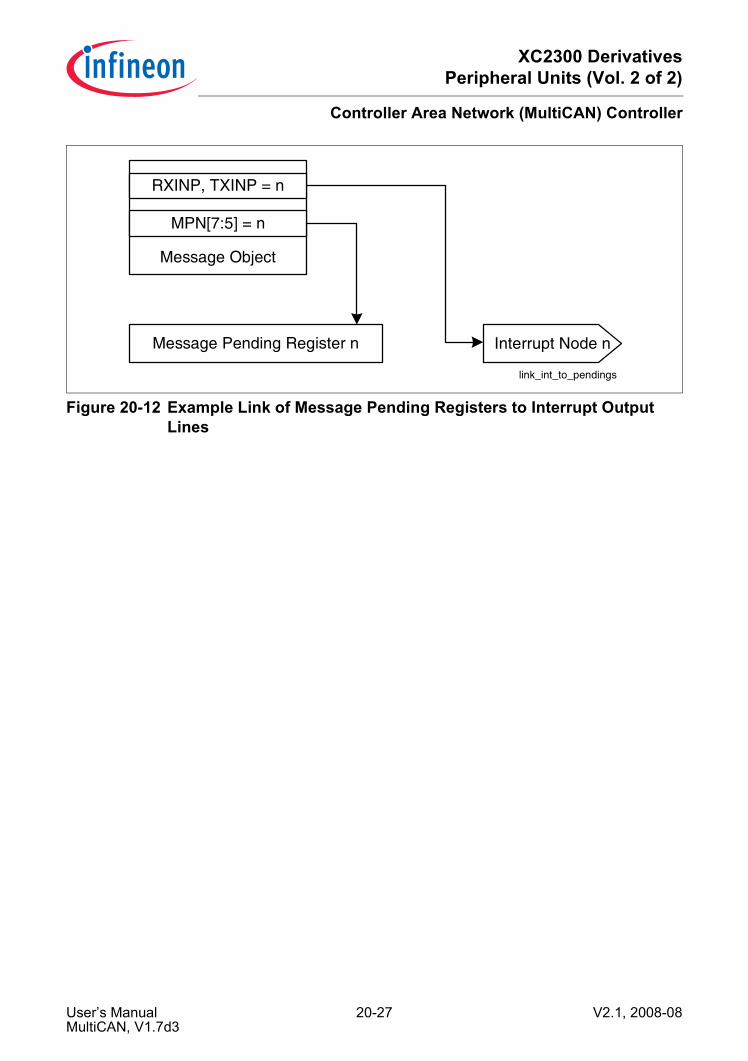
XC2300 DerivativesPeripheral Units (Vol. 2 of 2)
Controller Area Network (MultiCAN) Controller
Figure 20-12 Example Link of Message Pending Registers to Interrupt Output Lines
Message Pending Register n Interrupt Node n
Message Object
RXINP, TXINP = n
MPN[7:5] = n
link_int_to_pendings
User’s Manual 20-27 V2.1, 2008-08MultiCAN, V1.7d3
XC2300 DerivativesPeripheral Units (Vol. 2 of 2)
Controller Area Network (MultiCAN) Controller
20.2.8 Message Object Data HandlingThe follwing section describes the actions taken during a frame reception and during aframe transmition.
20.2.8.1 Frame ReceptionWhen a message is received on the CAN bus then the storage of the message into amessage object is prepared and performed according to the scheme shown inFigure 20-13. The MultiCAN module not just copies the received data into the messageobject, but it provides advanced features to enable consistent data exchange betweenMultiCAN and CPU.
MSGVALThe MSGVAL (“Message Valid”) bit in the Message Object Control Register is the mainswitch of the message object. The MultiCAN module only stores information in themessage object during the frame reception process when MSGVAL is set(MSGVAL = 1).Whenever MSGVAL is reset (MSGVAL = 0) by the CPU then the MultiCAN modulestops all ongoing write accesses to the message object so that the message object maybe reconfigured by the CPU in subsequent write accesses to the message object withoutbeing disturbed by the MultiCAN.
RTSELWhen the CPU re-configures a message object (.i.e. clears MSGVAL, modifies themessage object and sets MSGVAL again) during CAN operation then the followingscenario can occur:1. The message object wins receive acceptance filtering.2. The CPU clears MSGVAL to reconfigure the message object.3. The CPU sets MSGVAL again after reconfiguration.4. The end of the received frame is reached. As MSGVAL is set, the received data are
stored in the message object, a message interrupt request is generated, gateway andfifo actions are processed etc.
The storage of the received data may be undesirable if the context of the message objecthas changed, because the old message object configuration has been used foracceptance filtering of the message.Bit MOCTR.RTSEL (“Receive/Transmit Selected”) allows to disconnect a messageobject from an ongoing frame reception:When a message object wins receive acceptance filtering then bit RTSEL is set(RTSEL = 1) by the MultiCAN in order to indicate an upcoming frame delivery. TheMultiCAN checks RTSEL for value 1 upon successful frame reception in order to verify
User’s Manual 20-28 V2.1, 2008-08MultiCAN, V1.7d3
XC2300 DerivativesPeripheral Units (Vol. 2 of 2)
Controller Area Network (MultiCAN) Controller
that the object is still ready for receiving the frame. The received frame is stored in themessage object (along with all subsequent actions such as message interrupts, FIFO &gateway actions, flag updates) only if RTSEL = 1.When the user invalidates a message object during CAN operation (MSGVAL -> 0) thenthe user should clear RTSEL before setting MSGVAL again (latest with the same writeaccess that sets MSGVAL) in order to prevent the storage of a frame that belongs to theold context of the message object. Thus message object reconfiguration should consistof the following sequence of steps:1. Clear MSGVAL.2. Reconfigure message object while MSGVAL = 0.3. Clear RTSEL and set MSGVAL.
RXENBit MOCTR.RXEN enables a message object for frame reception. A message object canreceive CAN messages from the CAN bus only if RXEN = 1. The MultiCAN evaluatesRXEN only during receive acceptance filtering. After receive acceptance filtering RXENis ignored, i.e. the value of RXEN has no influence on the actual storage of a receivedmessage in a message object.Bit RXEN enables a “soft phase out” of a message object: When the user clears RXENthen a currently received CAN message for which the message object has wonacceptance filtering is still stored in the message object, but for subsequent messagesthe message object no longer wins receive acceptance filtering.
RXUPD, NEWDAT and MSGLSTAn ongoing frame storage process is indicated with the RXUPD (“Receive Updating”) bitin the Message Object Control Register. The MultiCAN module sets RXUPD with thestart and clears RXUPD with the end of a message object update (which consists offrame storage as well as flag updates).After storing the received frame (identifier, IDE bit, DLC and for data frames also the datafield) in the message object NEWDAT (“New Data”) is set by the MultiCAN. If NEWDATwas already set then also MSGLST (“Message Lost”) is set in order to indicate data loss.The RXUPD and NEWDAT flags may be used by the CPU to read consistent frame datafrom the message object during ongoing CAN operation. The following steps arerecommended:1. Clear NEWDAT2. Read message content (identifier, data etc.) from message object3. Read Message Object Control Register and check that both NEWDAT and RXUPD
are cleared. If this is not the case then goto back to step 1.4. As step 3 was successful, the read message content is consistent, i.e. has not been
updated by the MultiCAN while reading.
User’s Manual 20-29 V2.1, 2008-08MultiCAN, V1.7d3
XC2300 DerivativesPeripheral Units (Vol. 2 of 2)
Controller Area Network (MultiCAN) Controller
The bits RXUPD, NEWDAT and MSGLST work in the same fashion for the reception ofdata as well as remote frames.
20.2.8.2 Frame TransmissionThe process of message object transmission is illustrated in Figure 20-14. In addition tocopying the message content (identifier, IDE bit, RTR = DIR bit, DLC and for data framesalso the data field) to the internal transmit buffer of the CAN node that the messageobject belongs to, also several status flags are served and monitored in order to enableconsistent data handling.The transmission process (after transmit acceptance filtering) of a given message objectmakes no difference between remote and data frames.
MSGVAL, TXRQ, TXEN0, TXEN1For the MSGVAL bit the section “MSGVAL” on Page 20-28 for frame reception is alsovalid for transmission.A message may only be transmitted if all four bits MSGVAL (“Message Valid”), TXRQ(“Transmit Request”), TXEN0 (“Transmit Enable 0”), TXEN1(“Transmit Enable 1”) of theMessage Object Control Register are set (1) (see also Figure 20-9). Although these bitsare equivalent with respect to the transmission process, they have different semantics:
Table 20-4 Bits to set (1) in MOCTR for message transmissionBit DescriptionMSGVAL Message Valid
Main Switch of the Message ObjectTXRQ Transmit Request
Standard Transmit Request bit. The CPU should set this bit whenever a message object shall be transmitted. TXRQ is cleared automatically at the end of the successful transmission, except when there are new data (indicated by NEWDAT = 1) to be transmitted.When the single transmit trial bit is set (STT = 1) in the Message Object Function Register then TXRQ is already cleared by the MultiCAN when the content of the message object is copied to the transmit frame buffer of the CAN node.A received remote request (i.e. remote frame received on CAN bus) sets bit TXRQ to request the transmission of the corresponding data frame.
User’s Manual 20-30 V2.1, 2008-08MultiCAN, V1.7d3

XC2300 DerivativesPeripheral Units (Vol. 2 of 2)
Controller Area Network (MultiCAN) Controller
RTSELWhen a message object has been identified to be transmitted next (by acceptancefiltering) then the MultiCAN set bit MOCTR.RTSEL (“Receive/Transmit Selected”).When the MultiCAN copies the message object to the transmit buffer it checks bit RTSELand the message is transmitted only if RTSEL = 1.After the successful transmission of the message bit RTSEL is checked again andmessage postprocessing is only performed if RTSEL = 1.A complete reconfiguration of an operating message object should be done by means ofthe following steps:1. Clear MSGVAL (“Message Valid”).2. Reconfigure message object while MSGVAL = 0.3. Clear RTSEL and set MSGVAL.Here clearing RTSEL ensures that the message object is disconnected from anongoing/scheduled transmission and no message object processing (copying messageto transmit buffer incl. clearing NEWDAT, clearing TXRQ, time stamp update, messageinterrupt etc.) within the old context of the object may occur after the message objectbecomes valid again, but within a new context.
NEWDATWhen the content of a message object has been transferred to the transmit buffer of theCAN node then bit NEWDAT (“New Data”) is cleared to indicate that the transmit data ofthe message object are no longer new.
TXEN0 Transmit Enable 0This bit may be temporarily cleared by the CPU to suppress the transmission of this object when it writes new content to the data field. This avoids transmission of inconsistent frames which consist of a mixture of old and new data.Remote requests are still accepted during TXEN0 = 0, but transmission of the data frame is suspended until the CPU re-enables transmission (TXEN0 = 1).
TXEN1 Transmit Enable 1This bit is used in transmit FIFOs to select the message object which is transmit active within the FIFO structure.For message objects which are not transmit FIFO elements TXEN1 may either be set to 1 permanently or be used as a second, independent transmission enable bit.
Table 20-4 Bits to set (1) in MOCTR for message transmission (cont’d)
Bit Description
User’s Manual 20-31 V2.1, 2008-08MultiCAN, V1.7d3
XC2300 DerivativesPeripheral Units (Vol. 2 of 2)
Controller Area Network (MultiCAN) Controller
When the CAN transmission of the frame is successful and NEWDAT is still cleared (i.e.no new data have been copied to the message object in the meantime) then TXRQ(“Transmit Request”) is cleared automatically.If, however, the NEWDAT bit has been set again by the CPU (because a new frame shallbe transmitted) then TXRQ is not cleared in order to enable the transmission of the newdata.
User’s Manual 20-32 V2.1, 2008-08MultiCAN, V1.7d3

XC2300 DerivativesPeripheral Units (Vol. 2 of 2)
Controller Area Network (MultiCAN) Controller
Figure 20-13 Data Delivery to Message Object by MultiCAN Module
MCA05845a
Object winsacc. filtering?
yes
yes
no
no
CAN rec.successful?
MSGVAL & RTSEL =1? MSGVAL =1?
DIR =1?
NEWDAT =1?
RXIE =1?
RTSEL := 1
RXUPD := 1
Copy frame to message object
TXRQ := 1 in this or in foreign objects
Copy frame to message object
RXUPD := 1
MSGLST := 1
yes
NEWDAT := 1RXUPD := 0RXPND := 1
no
no
yes
yes
no
yes Interrupt Request visible
no
yes
1
2
3
4
no
TimeMilestones
Get data fromgateway/FIFO source
Start receivingCAN frame
Done
User’s Manual 20-33 V2.1, 2008-08MultiCAN, V1.7d3
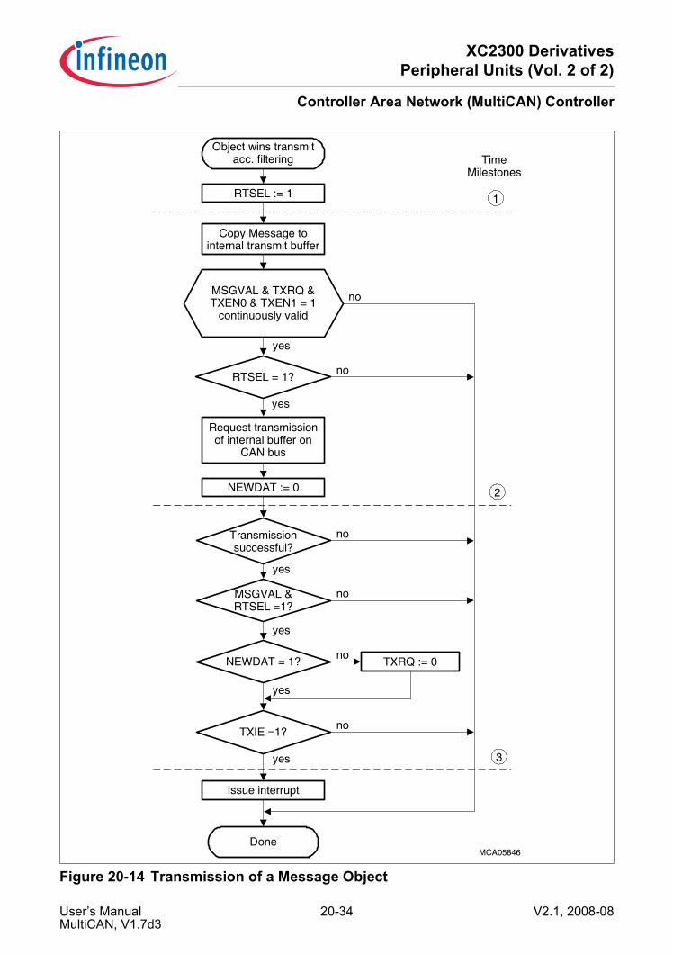
XC2300 DerivativesPeripheral Units (Vol. 2 of 2)
Controller Area Network (MultiCAN) Controller
Figure 20-14 Transmission of a Message Object
yes
MCA05846
RTSEL = 1?
NEWDAT = 1?
TXIE =1?
RTSEL := 1
NEWDAT := 0
no
yes
1
2
3
Copy Message tointernal transmit buffer
MSGVAL & TXRQ &TXEN0 & TXEN1 = 1
continuously valid
Request transmissionof internal buffer on
CAN bus
yes
Transmissionsuccessful?
yes
yes
MSGVAL &RTSEL =1?
yes
TXRQ := 0
Issue interrupt
no
no
no
no
no
TimeMilestones
Done
Object wins transmitacc. filtering
User’s Manual 20-34 V2.1, 2008-08MultiCAN, V1.7d3
XC2300 DerivativesPeripheral Units (Vol. 2 of 2)
Controller Area Network (MultiCAN) Controller
20.2.9 Message Object FunctionalityThis section describes the functionality that is related to each individual Message Object.
20.2.9.1 Standard Message Object ModeStandard message mode is selected via MMC = 0000B in the Message Object FunctionControl Register of the message object. In this mode a message object may transmit andreceive CAN frames according to the basic rules as described in the previous sections.Additional services such as Single Data Transfer Mode or Single Transmit Trial (seesections below) are available and may be selected individually by the user.
20.2.9.2 Single Data Transfer ModeSingle Data Transfer Mode is a useful feature in order to broadcast data over the CANbus without unintended doubling of information. Single Data Transfer Mode is selectedvia bit SDT in the Message Object Function Register of the message object.
Message ReceptionWhen a received message is stored in a message object and further messages arestored in the same message object before the CPU reads the first message object, thenthe content of the first message gets lost and is replaced with the content of thesubsequent messages (indicated by MSGLST = 1).If SDT = 1 (Single Data Transfer Mode activated) then the MultiCAN controllerautomatically clears the MSGVAL bit of the message object after the storage of areceived data frame to prevent the reception of further messages.The reception of a remote frame does not lead to the clearance of MSGVAL.
Message TransmissionWhen a message object receives a series of multiple remote requests then it transmitseveral data frames in response to the requests. If the data within the message objecthas not been updated in the time between the transmissions, the same data may berepresented more than once on the CAN bus.In Single Data Transfer Mode (SDT = 1) this is avoided because the MultiCAN controllerautomatically clears MSGVAL after the successful transmission of a data frame.The transmission of a remote frame does not clear MSGVAL.
20.2.9.3 Single Transmit TrialIf the bit STT in the message object function register is set (STT = 1) then thetransmission request is cleared (TXRQ := 0) when the frame content of the message
User’s Manual 20-35 V2.1, 2008-08MultiCAN, V1.7d3

XC2300 DerivativesPeripheral Units (Vol. 2 of 2)
Controller Area Network (MultiCAN) Controller
object has been copied to the internal transmit buffer of the CAN node. Thus thetransmission of the message object is not tried again when it fails due to CAN bus errors.
20.2.9.4 Message Object FIFO StructureIn case of high CPU load it may be difficult to process a series of CAN frames in time.This may happen for the short term reception of multiple messages as well as thetransmission of a series with tight due date.Therefore a FIFO buffer structure has been implemented in order to avoid loss ofincoming messages and to minimize the setup time for outgoing messages. The FIFOstructure may also be used to automate the reception or transmission of a series of CANmessages and to generate a single message interrupt when the whole series is done.There may be as many FIFOs in parallel as are required by the application. The numberof FIFOs and their size are only limited by the number of message objects available. AFIFO may be installed, resized and deinstalled any time, even during CAN operation.The basic structure of a FIFO is shown in Figure 20-15. A FIFO consists of a single baseobject (shown on the left side) and several slave objects (shown on the right side). Theslave objects are chained together in the same list structure. The base object may beallocated to any list. Although Figure 20-15 shows the base object as a separate itemapart from the slave objects, it is also possible to integrate the base object at any placeinto the chain of slave objects, so that the base object is slave object, too (not possiblefor gateways). The FIFO structure fully relies on the list structure. The absolute objectnumbers of the message objects have no impact on the operation of the FIFO.The base object needs not be allocated to the same list as the slave objects. Only theslave object must be allocated to a common list (as they are chained together). The BOT,CUR and TOP pointer link the base object to the slave objects, no matter whether thebase object is allocated to the same or to another list than the slave objects.The absolute minimum FIFO would consist of a single message object which is bothFIFO base and FIFO slave (not very useful). The biggest possible FIFO would use allmessage objects of the MultiCAN module. Any sizes between these extremes arepossible.In the FIFO base object the boundaries of the FIFO are defined. The BOT field in theFIFO/Gateway Pointer Register of the base object points to the first (bottom) slaveelement in the FIFO. The TOP field in the FIFO/Gateway Pointer Register of the baseobject points to the last (top) slave element.The CUR field in the FIFO/Gateway Pointer Register of the FIFO base object points tothe actual slave object selected by the MultiCAN for message transfer. When a messagetransfer takes place with this object then CUR is moved to the next position. If CUR hasalready reached the top of the FIFO (CUR = TOP) then it is wrapped around to thebottom of the FIFO (CUR := BOT). Otherwise CUR is moved to the next message objectin the list structure of the slave objects (CUR := PNEXT of current object). This scheme
User’s Manual 20-36 V2.1, 2008-08MultiCAN, V1.7d3
XC2300 DerivativesPeripheral Units (Vol. 2 of 2)
Controller Area Network (MultiCAN) Controller
yields a circular FIFO structure where the fields BOT and TOP just establish the link fromthe last to the first element, which is missing in the linear structure.The SEL field in the FIFO/Gateway Pointer register of the base object may be used formonitoring purposes. It allows to select any slave object and to generate a messageinterrupt if the CUR pointer reaches the value of SEL. Thus SEL offers a convenient wayto determine the end of a predefined series of message transfers, or it may be used toissue a warning to the CPU when the FIFO gets full.
User’s Manual 20-37 V2.1, 2008-08MultiCAN, V1.7d3

XC2300 DerivativesPeripheral Units (Vol. 2 of 2)
Controller Area Network (MultiCAN) Controller
Figure 20-15 FIFO Structure with FIFO Base and n FIFO Destinations (Slaves)
Object fn
PPREV=f[n-1]
PNEXT
Object fi
PPREV=f[i-1]
PNEXT=f[i+1]
Object f2
PPREV=f1
PNEXT=f3
Object f1
PPREV
PNEXT=f2
Base Object
PPREV
PNEXT
BOT=f1
CUR=fi
TOP=fn
msgobj_fifo
User’s Manual 20-38 V2.1, 2008-08MultiCAN, V1.7d3
XC2300 DerivativesPeripheral Units (Vol. 2 of 2)
Controller Area Network (MultiCAN) Controller
20.2.9.5 Receive FIFOThe Receive FIFO structure is used to buffer incoming (received) remote or data frames.A Receive FIFO is selected via MMC = 0001B in the Message Object Function ControlRegister of the FIFO base object. This MMC code automatically designates the messageobject as FIFO base object. The message mode of the FIFO slave objects are notrelevant for the operation of the Receive FIFO.When the FIFO base object receives a frame from the CAN node it belongs to, then theframe is not stored in the base object. Instead the message is stored in the messageobject that is selected by the CUR pointer in the FIFO/Gateway Pointer Register of theFIFO base object.The message object selected by CUR receives the CAN message as if it were the directreceiver of the message. However, MMC = 0000B is implicitly assumed for the FIFOslave, i.e. a standard message delivery is performed. The actual message mode (MMC)of the FIFO slave is ignored. There is also no extra acceptance filtering to match thereceived frame against the identifier, IDE bit and DIR bit of the slave object.When the FIFO base object receives a CAN frame then the MultiCAN moves the currentpointer CUR to the next message object in the FIFO structure, which will then be usedto store the next incoming message. The old value of CUR is used for the currenttransfer.IF bit OVIE is set in the Message Object Function Register of the FIFO base object andthe pointer CUR reaches the value stored in SEL then a FIFO overflow interrupt requestis generated. The interrupt request is generated on interrupt output line TXINP (TXINPof the base object) immediately after the storage of the received frame into the slaveobject. Transmit interrupts are still generated if TXIE is set.A CAN message is stored in a FIFO slave only if MSGVAL = 1 in both FIFO base andslave object.In order to avoid direct reception of a message by a slave message object, as if it wasan independent message object and not a part of a FIFO, the bit RXEN of each slaveobject must be cleared. The setting of the bit RXEN is “don’t care” only if the slave objectis located in a list not assigned to a CAN node.
User’s Manual 20-39 V2.1, 2008-08MultiCAN, V1.7d3

XC2300 DerivativesPeripheral Units (Vol. 2 of 2)
Controller Area Network (MultiCAN) Controller
20.2.9.6 Transmit FIFOThe Transmit FIFO structure is used to buffer a series of data or remote frames to betransmitted. A transmit FIFO consists of one base message object and one or moreslave message objects.A Transmit FIFO base object is selected via MMC = 0010B in the Message ObjectFunction Control Register of the FIFO base object. Unlike the Receive FIFO the TransmitFIFO requires the explicit declaration of the FIFO slave objects via MMC = 0011B. TheCUR pointer of all slave objects must point back to the Transmit FIFO Base Object (tobe initialized by user).The TXEN1 bits of all message objects except the one which is selected by the CURpointer of the base object must be cleared (to be initialized by user). TXEN1 of themessage object selected by CUR must be set. CUR may be initialized to any FIFO slaveobject.When tagging the message objects of the FIFO valid to start the operation of the FIFOthen the base object must be tagged valid (MSGVAL := 1) first.When a Transmit FIFO shall be deinstalled during operation, then the slave objects mustbe tagged invalid (MSGVAL := 0) first.The Transmit FIFO uses the TXEN1 bit in the Message Object Control Register of allFIFO elements to select the actual message for transmission. Transmit acceptancefiltering evaluates TXEN1 for each message object and a message object may wintransit acceptance filtering only if TXEN1 is set. When a FIFO element has transmitteda message then in addition to standard transmit postprocessing (clear TXRQ, transmitinterrupt etc.) the MultiCAN clears TXEN1 in that message object and moves the CURpointer in the corresponding FIFO base object to the next message object to betransmitted. TXEN1 is set automatically in the next message object. Thus TXEN1 movesalong the FIFO structure like a token to select the active element.IF bit OVIE is set in the Message Object Function Register of the FIFO base object andthe pointer CUR reaches the value stored in SEL then a FIFO overflow interrupt requestis generated. The interrupt request is generated on interrupt output line as defined byRXINP (RXINP of the base object) when postprocessing of the received frame is done.Receive interrupts are still generated for the Transmit FIFO base object if bit RXIE is set.
User’s Manual 20-40 V2.1, 2008-08MultiCAN, V1.7d3

XC2300 DerivativesPeripheral Units (Vol. 2 of 2)
Controller Area Network (MultiCAN) Controller
20.2.9.7 Gateway ModeThe Gateway Mode allows to establish an automatic information transfer between twoindependent CAN bus systems without CPU interaction.The Gateway Mode operates on message object level. In Gateway mode, information istransferred between two message objects, resulting in an information transfer betweenthe two CAN nodes to which the message objects are allocated. A gateway may beestablished between any pair of CAN nodes and there may be as many gateways asthere are message objects available to build the gateway structure.Gateway Mode is selected via MMC = 0100B in the Message Object Function ControlRegister of the gateway source object. The gateway destination object is selected by theCUR pointer in the FIFO/Gateway Pointer Register of the source object. The gatewaydestination object just needs to be valid (MSGVAL = 1), all other settings are not relevantfor the information transfer from the source object to the destination object.A gateway source object behaves like a standard message objects, but when a CANframe has been received and stored in the source object, some additional actions areperformed by the MultiCAN (Figure 20-16):1. If bit DLCC is set in the Message Object Function Register of the source object, then
the DLC code is copied from the source object to the destination object.2. if bit IDC is set in the Message Object Function Register of the source object, then
the identifier and the IDE bit are copied from the source object to the destinationobject.
3. if bit DATC is set in the Message Object Function Register of the source object, thenthe data field is copied from the source object to the destination object.
4. If bit GDFS is set in the Message Object Function Register of the source object, thenTXRQ is set in the Message Object Control Register of the destination object.
5. RXPND and NEWDAT are set in the Message Object Control Register of thedestination object.
6. A message interrupt request is generated for the destination object if RXIE is set inthe Message Object Control Register of the destination object.
7. The current pointer CUR in the FIFO/Gateway Pointer Register of the source objectis moved to the next destination object according to the FIFO rules as described inChapter 20.2.9.4. A gateway with a single (static) destination object is obtained bymeans of setting TOP = BOT = CUR = destination object.
The link from the source to the destination object works in the same way as the link froma FIFO source to a FIFO slave. This means that a gateway with an integrated destinationFIFO may be created (Figure 20-15), where the object on the left in Figure 20-15 is thegateway source object and the message objects on the right side are the gatewaydestination objects.The gateway works in the same way for the reception of data frames (source object isreceive object, i.e. DIR = 0) as wall as for the reception of remote frames (source objectis transmit object).
User’s Manual 20-41 V2.1, 2008-08MultiCAN, V1.7d3
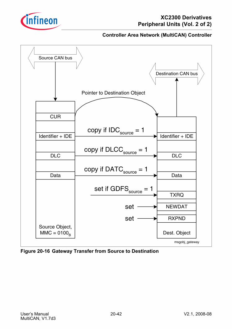
XC2300 DerivativesPeripheral Units (Vol. 2 of 2)
Controller Area Network (MultiCAN) Controller
Figure 20-16 Gateway Transfer from Source to Destination
Source Object,MMC = 0100B
Data
Identifier + IDE
DLC
Dest. Object
Data
Identifier + IDE
DLC
TXRQ
copy if IDCsource = 1
copy if DLCCsource = 1
copy if DATCsource = 1
set if GDFSsource = 1
NEWDAT
RXPND
set
set
Source CAN bus
Destination CAN bus
CUR
Pointer to Destination Object
msgobj_gateway
User’s Manual 20-42 V2.1, 2008-08MultiCAN, V1.7d3
XC2300 DerivativesPeripheral Units (Vol. 2 of 2)
Controller Area Network (MultiCAN) Controller
20.2.9.8 Foreign Remote RequestsWhen a remote frame received on a CAN node is stored in a message object, then atransmit request is set in order to trigger the answer (data frame transmission) to therequest or to automatically issue a secondary request. If bit FRREN is cleared(FRREN = 0) in the Function Control register of the message object where the remoterequest is stored, then TXRQ is set in the Control Register of the same message object.If bit FRREN is set (FRREN = 1: foreign remote request enabled) then TXRQ is set inthe message object that is referenced by pointer CUR in the FIFO/Gateway PointerRegister. The value of CUR is, however, not changed by this feature.Although the foreign remote request feature works independently from the selectedmessage mode, it is especially useful for gateways to issue a remote request on thesource of a gateway upon the reception of a remote request on the gateway destination.According to the setting of FRREN in the gateway destination object there are two waysto handle remote requests that appear on the destination side (assuming that the sourceobject is a receive object and the destination is a transmit object, i.e. DIRsource = 0 andDIRdestination = 1):
FRREN = 0 in the Gateway Destination Object1. A remote frame is received by gateway destination.2. TXRQ is set automatically in the gateway destination object.3. A data frame with the current data stored in the destination object is transmitted on
the destination bus.
FRREN = 1 in the Gateway Destination Object1. A remote frame is received by gateway destination.2. TXRQ is set automatically in the gateway source object (must be referenced by CUR
pointer of the destination object).3. A remote request is transmitted by the source object (which is a receive object) on
the source CAN bus.4. The receiver of the remote request responds with a data frame on the source bus.5. The data frame is stored in the source object.6. The data frame is copied to the destination object (gateway action).7. TXRQ is set in the destination object (assuming GDFSsource = 1).8. The new data stored in the destination object is transmitted on the destination bus,
as response to the initial remote request on the destination bus.
User’s Manual 20-43 V2.1, 2008-08MultiCAN, V1.7d3

XC2300 DerivativesPeripheral Units (Vol. 2 of 2)
Controller Area Network (MultiCAN) Controller
20.3 MultiCAN Kernel RegistersThe register set of the MultiCAN module consists of three distinct subsets:1. The Global Module Registers apply to the whole MultiCAN module and exist only
once.2. The CAN Node Registers apply to a single CAN node and thus exist once for each
CAN node.3. The collection of Message Object Registers defines a single message object and
thus exists once for each message object.
20.3.1 Register Address MapTable 20-5 shows the address map of the MultiCAN module with respect to the baseaddress of the MultiCAN module.
Table 20-5 MultiCAN Address Map (Relative to MultiCAN Base Address)Register Group Start address Total RangeGlobal Module Registers +100H +100H to + 1FFH
CAN Node Registers for CANx, x = 0 - 4 +200H +200H to + 2FFH
Message Objects n = 0 - 127 +1000H +1000H to + 13FFH
User’s Manual 20-44 V2.1, 2008-08MultiCAN, V1.7d3

XC2300 DerivativesPeripheral Units (Vol. 2 of 2)
Controller Area Network (MultiCAN) Controller
Global Module RegistersThe global module registers exist only once. They are listed in Table 20-6 with theirrelative address with respect to the start address of the Global Module Registers.
Table 20-6 Relative Addresses of Global Module RegistersRegister Rel. Address Full Name of RegisterLIST0L 100H List Registers 0 LowLIST0H 102H List Registers 0 HighLIST1L 104H List Registers 1 LowLIST1H 106H List Registers 1 HighLIST2L 108H List Registers 2 LowLIST2H 10AH List Registers 2 HighLIST3L 10CH List Registers 3 LowLIST3H 10EH List Registers 3HighLIST4L 110H List Registers 4 LowLIST4H 112H List Registers 4 HighLIST5L 114H List Registers 5 LowLIST5H 116H List Registers 5 HighLIST6L 118H List Registers 6 LowLIST6H 11AH List Registers 6 HighLIST7L 11CH List Registers 7 LowLIST7H 11EH List Registers 7 HighMSPND0L 140H Message Pending Registers 0 LowMSPND0H 142H Message Pending Registers 0 HighMSPND1L 144H Message Pending Registers 1 LowMSPND1H 146H Message Pending Registers 1 HighMSPND2L 148H Message Pending Registers 2 LowMSPND2H 14AH Message Pending Registers 2 HighMSPND3L 14CH Message Pending Registers 3 LowMSPND3H 14EH Message Pending Registers 3 HighMSPND4L 150H Message Pending Registers 4 LowMSPND4H 152H Message Pending Registers 4 HighMSPND5L 154H Message Pending Registers 5 Low
User’s Manual 20-45 V2.1, 2008-08MultiCAN, V1.7d3

XC2300 DerivativesPeripheral Units (Vol. 2 of 2)
Controller Area Network (MultiCAN) Controller
CAN Node RegistersThe registers of a CAN node are located at consecutive 32 bit addresses accordingtoTable 20-7 which shows the relative address of the 32 bit CAN Node Registers withrespect to the base address of CAN node register block. The CAN Node Register blockexists once for each CAN node.
MSPND5H 156H Message Pending Registers 5 HighMSPND6L 158H Message Pending Registers 6 LowMSPND6H 15AH Message Pending Registers 6 HighMSPND7L 15CH Message Pending Registers 7 LowMSPND7H 146H Message Pending Registers 7 HighMSID0 180H Message Index Registers 0MSID1 184H Message Index Registers 1MSID2 188H Message Index Registers 2MSID3 18CH Message Index Registers 3MSID4 190H Message Index Registers 4MSID5 194H Message Index Registers 5MSID6 198H Message Index Registers 6MSID7 19CH Message Index Registers 7MSIMASKL 1C0H Message Index Mask Register LowMSIMASKH 1C2H Message Index Mask Register HighPANCTRL 1C4H Panel Control Register LowPANCTRH 1C6H Panel Control Register HighMCR 1C8H Module Control RegisterMITR 1CCH Module Interrupt Trigger Register- +120H ... +13EH
+148H ... +17EH+188H ... +1BEH+1CEH ... +1FEH
Reserved
Table 20-6 Relative Addresses of Global Module RegistersRegister Rel. Address Full Name of Register
User’s Manual 20-46 V2.1, 2008-08MultiCAN, V1.7d3
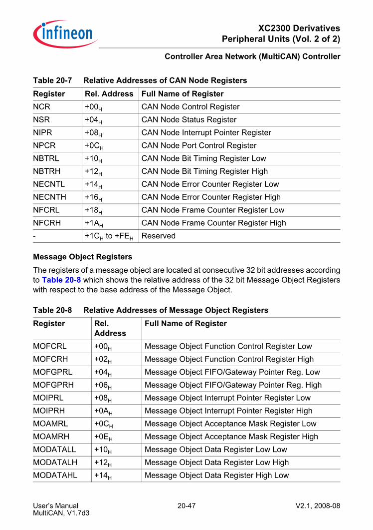
XC2300 DerivativesPeripheral Units (Vol. 2 of 2)
Controller Area Network (MultiCAN) Controller
Message Object RegistersThe registers of a message object are located at consecutive 32 bit addresses accordingto Table 20-8 which shows the relative address of the 32 bit Message Object Registerswith respect to the base address of the Message Object.
Table 20-7 Relative Addresses of CAN Node RegistersRegister Rel. Address Full Name of RegisterNCR +00H CAN Node Control RegisterNSR +04H CAN Node Status RegisterNIPR +08H CAN Node Interrupt Pointer RegisterNPCR +0CH CAN Node Port Control RegisterNBTRL +10H CAN Node Bit Timing Register LowNBTRH +12H CAN Node Bit Timing Register HighNECNTL +14H CAN Node Error Counter Register LowNECNTH +16H CAN Node Error Counter Register HighNFCRL +18H CAN Node Frame Counter Register LowNFCRH +1AH CAN Node Frame Counter Register High- +1CH to +FEH Reserved
Table 20-8 Relative Addresses of Message Object RegistersRegister Rel.
AddressFull Name of Register
MOFCRL +00H Message Object Function Control Register LowMOFCRH +02H Message Object Function Control Register HighMOFGPRL +04H Message Object FIFO/Gateway Pointer Reg. LowMOFGPRH +06H Message Object FIFO/Gateway Pointer Reg. HighMOIPRL +08H Message Object Interrupt Pointer Register LowMOIPRH +0AH Message Object Interrupt Pointer Register HighMOAMRL +0CH Message Object Acceptance Mask Register LowMOAMRH +0EH Message Object Acceptance Mask Register HighMODATALL +10H Message Object Data Register Low LowMODATALH +12H Message Object Data Register Low HighMODATAHL +14H Message Object Data Register High Low
User’s Manual 20-47 V2.1, 2008-08MultiCAN, V1.7d3

XC2300 DerivativesPeripheral Units (Vol. 2 of 2)
Controller Area Network (MultiCAN) Controller
MODATAHH +16H Message Object Data Register High HighMOARL +18H Message Object Arbitration Register LowMOARH +1AH Message Object Arbitration Register HighMOCTRLMOSTATL
+1CH Message Object Control Register LowMessage Object Status Register Low
MOCTRHMOSTATH
+1EH Message Object Control Register HighMessage Object Status Register Low
Table 20-8 Relative Addresses of Message Object RegistersRegister Rel.
AddressFull Name of Register
User’s Manual 20-48 V2.1, 2008-08MultiCAN, V1.7d3

XC2300 DerivativesPeripheral Units (Vol. 2 of 2)
Controller Area Network (MultiCAN) Controller
20.3.2 Global MultiCAN Registers
20.3.2.1 Module Identification Register
ID Module Identification Register (08H) Reset Value: 4001H
15 14 13 12 11 10 9 8 7 6 5 4 3 2 1 0
MOD_NUMBER MOD_REV
r r
Field Bits Type DescriptionMOD_REV [7:0] r Module Revision Number Value
Bits 7-0 bits are used for module revision numbering. The value of the module revision number starts with 01H (first revision), 02H, 03H, ... up to FFH.
MOD_NUMBER [15:8] r Module Identification Number ValueBits 15-8 are used for module identification. The MultiCAN has the module number 40H.
User’s Manual 20-49 V2.1, 2008-08MultiCAN, V1.7d3
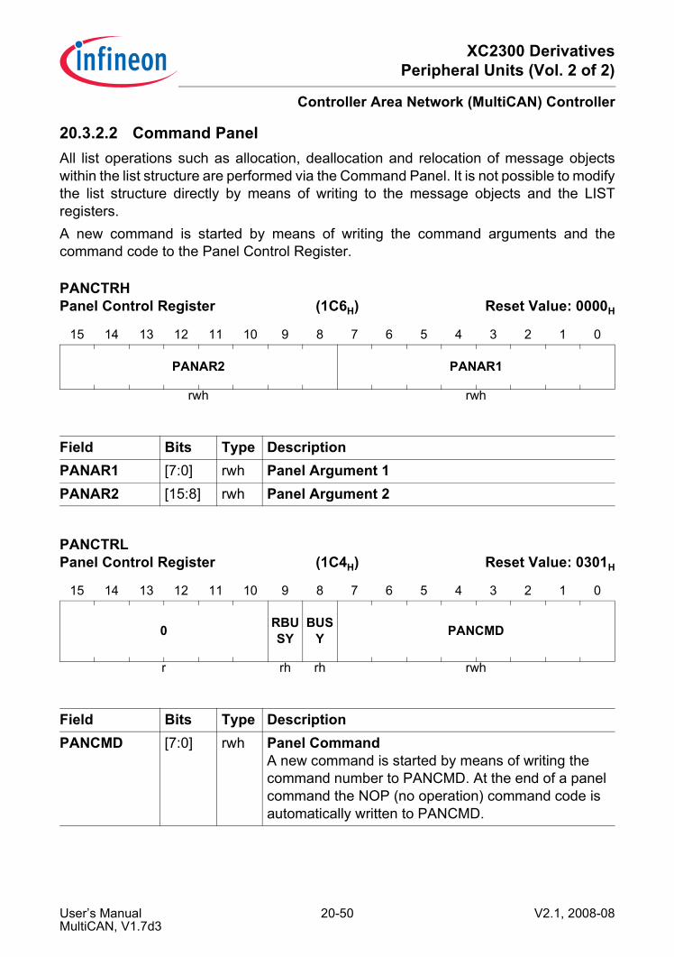
XC2300 DerivativesPeripheral Units (Vol. 2 of 2)
Controller Area Network (MultiCAN) Controller
20.3.2.2 Command PanelAll list operations such as allocation, deallocation and relocation of message objectswithin the list structure are performed via the Command Panel. It is not possible to modifythe list structure directly by means of writing to the message objects and the LISTregisters.A new command is started by means of writing the command arguments and thecommand code to the Panel Control Register.
PANCTRH Panel Control Register (1C6H) Reset Value: 0000H
15 14 13 12 11 10 9 8 7 6 5 4 3 2 1 0
PANAR2 PANAR1
rwh rwh
Field Bits Type DescriptionPANAR1 [7:0] rwh Panel Argument 1PANAR2 [15:8] rwh Panel Argument 2
PANCTRL Panel Control Register (1C4H) Reset Value: 0301H
15 14 13 12 11 10 9 8 7 6 5 4 3 2 1 0
0 RBUSY
BUSY PANCMD
r rh rh rwh
Field Bits Type DescriptionPANCMD [7:0] rwh Panel Command
A new command is started by means of writing the command number to PANCMD. At the end of a panel command the NOP (no operation) command code is automatically written to PANCMD.
User’s Manual 20-50 V2.1, 2008-08MultiCAN, V1.7d3

XC2300 DerivativesPeripheral Units (Vol. 2 of 2)
Controller Area Network (MultiCAN) Controller
BUSY 8 rh Panel Busy0B Panel has finished command and is ready to
accept a new command.1B Panel operation is in progress.
RBUSY 9 rh Result Busy0B No update of PANAR1 and PANAR2 is
scheduled by the list controller.1B A list command is running (BUSY = 1) that will
write results to PANAR1 and PANAR2, but the results are not yet available.
0 [10:15] r reserved;returns ’0’ if read; should be written with ’0’;
Field Bits Type Description
User’s Manual 20-51 V2.1, 2008-08MultiCAN, V1.7d3
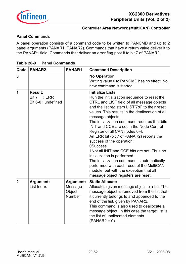
XC2300 DerivativesPeripheral Units (Vol. 2 of 2)
Controller Area Network (MultiCAN) Controller
Panel CommandsA panel operation consists of a command code to be written to PANCMD and up to 2panel arguments (PANAR1, PANAR2). Commands that have a return value deliver it tothe PANAR1 field. Commands that deliver an error flag post it to bit 7 of PANAR2.
Table 20-9 Panel CommandsCode PANAR2 PANAR1 Command Description0 No Operation
Writing value 0 to PANCMD has no effect. No new command is started.
1 Result:Bit 7 : ERRBit 6-0 : undefined
Initialize ListsRun the initialization sequence to reset the CTRL and LIST field of all message objects and the list registers LIST[7:0] to their reset values. This results in the deallocation of all message objects.The initialization command requires that bits INIT and CCE are set in the Node Control Register of all CAN nodes 0-4.An ERR bit (bit 7 of PANAR2) reports the success of the operation:0Success1Not all INIT and CCE bits are set. Thus no initialization is performed.The initialization command is automatically performed with each reset of the MultiCAN module, but with the exception that all message object registers are reset.
2 Argument:List Index
Argument:Message Object Number
Static AllocateAllocate a given message object to a list. The message object is removed from the list that it currently belongs to and appended to the end of the list. given by PANAR2.This command is also used to deallocate a message object. In this case the target list is the list of unallocated elements. (PANAR2 = 0).
User’s Manual 20-52 V2.1, 2008-08MultiCAN, V1.7d3
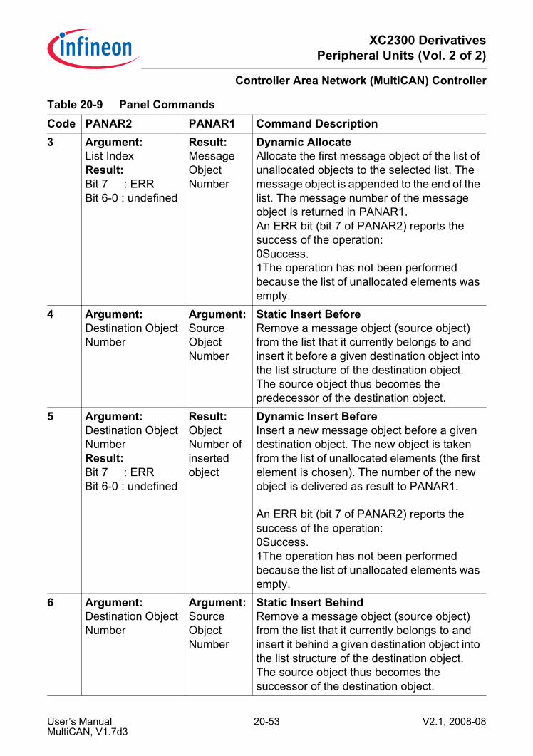
XC2300 DerivativesPeripheral Units (Vol. 2 of 2)
Controller Area Network (MultiCAN) Controller
3 Argument:List IndexResult:Bit 7 : ERRBit 6-0 : undefined
Result:Message Object Number
Dynamic AllocateAllocate the first message object of the list of unallocated objects to the selected list. The message object is appended to the end of the list. The message number of the message object is returned in PANAR1.An ERR bit (bit 7 of PANAR2) reports the success of the operation:0Success.1The operation has not been performed because the list of unallocated elements was empty.
4 Argument:Destination Object Number
Argument:Source Object Number
Static Insert BeforeRemove a message object (source object) from the list that it currently belongs to andinsert it before a given destination object into the list structure of the destination object.The source object thus becomes the predecessor of the destination object.
5 Argument:Destination Object NumberResult:Bit 7 : ERRBit 6-0 : undefined
Result:Object Number of inserted object
Dynamic Insert BeforeInsert a new message object before a given destination object. The new object is taken from the list of unallocated elements (the first element is chosen). The number of the new object is delivered as result to PANAR1.
An ERR bit (bit 7 of PANAR2) reports the success of the operation:0Success.1The operation has not been performed because the list of unallocated elements was empty.
6 Argument:Destination Object Number
Argument:Source Object Number
Static Insert BehindRemove a message object (source object) from the list that it currently belongs to andinsert it behind a given destination object into the list structure of the destination object.The source object thus becomes the successor of the destination object.
Table 20-9 Panel CommandsCode PANAR2 PANAR1 Command Description
User’s Manual 20-53 V2.1, 2008-08MultiCAN, V1.7d3

XC2300 DerivativesPeripheral Units (Vol. 2 of 2)
Controller Area Network (MultiCAN) Controller
7 Argument:Destination Object NumberResult:Bit 7 : ERRBit 6-0 : undefined
Result:Object Number of inserted object
Dynamic Insert BehindInsert a new message object behind a given destination object. The new object is taken from the list of unallocated elements (the first element is chosen). The number of the new object is delivered as result to PANAR1.
An ERR bit (bit 7 of PANAR2) reports the success of the operation:0Success.1The operation has not been performed because the list of unallocated elements was empty.
8 - 255
- - Reserved
Table 20-9 Panel CommandsCode PANAR2 PANAR1 Command Description
User’s Manual 20-54 V2.1, 2008-08MultiCAN, V1.7d3
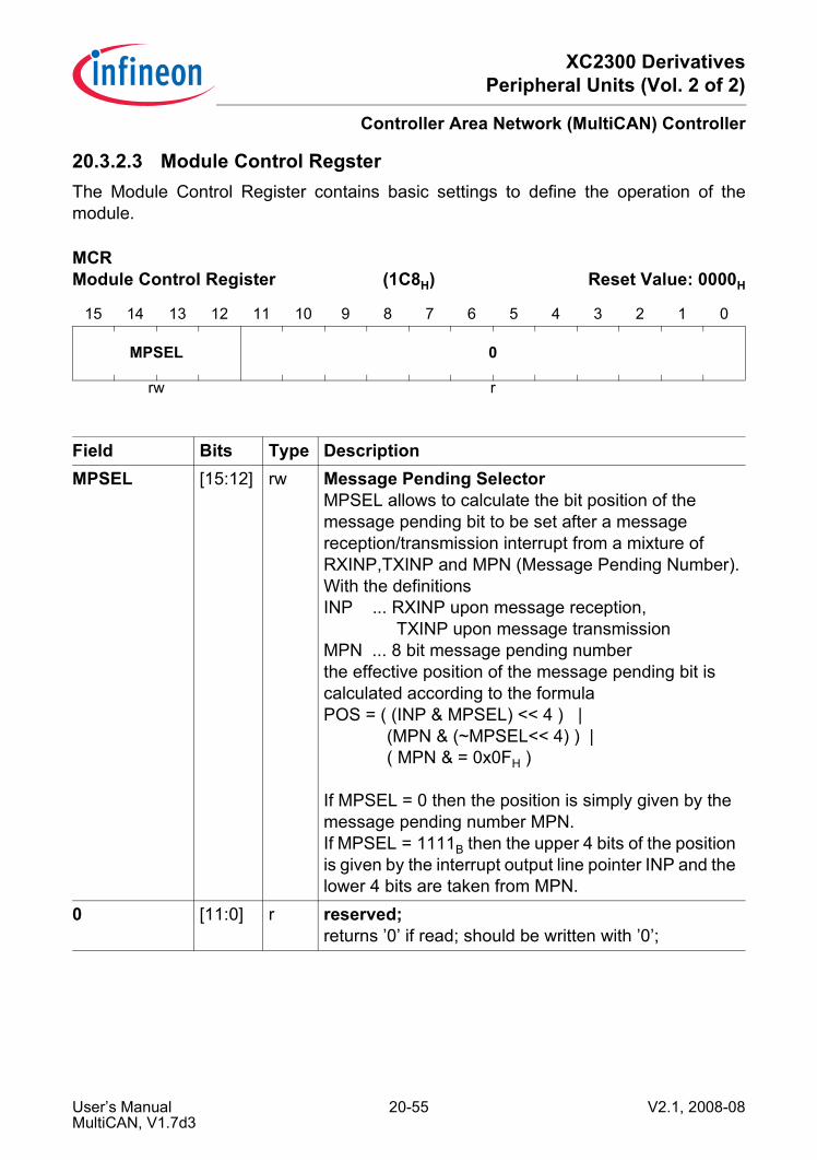
XC2300 DerivativesPeripheral Units (Vol. 2 of 2)
Controller Area Network (MultiCAN) Controller
20.3.2.3 Module Control RegsterThe Module Control Register contains basic settings to define the operation of themodule.
MCR Module Control Register (1C8H) Reset Value: 0000H
15 14 13 12 11 10 9 8 7 6 5 4 3 2 1 0
MPSEL 0
rw r
Field Bits Type DescriptionMPSEL [15:12] rw Message Pending Selector
MPSEL allows to calculate the bit position of the message pending bit to be set after a message reception/transmission interrupt from a mixture of RXINP,TXINP and MPN (Message Pending Number).With the definitionsINP ... RXINP upon message reception, TXINP upon message transmissionMPN ... 8 bit message pending numberthe effective position of the message pending bit is calculated according to the formulaPOS = ( (INP & MPSEL) << 4 ) | (MPN & (~MPSEL<< 4) ) | ( MPN & = 0x0FH )
If MPSEL = 0 then the position is simply given by the message pending number MPN.If MPSEL = 1111B then the upper 4 bits of the position is given by the interrupt output line pointer INP and the lower 4 bits are taken from MPN.
0 [11:0] r reserved;returns ’0’ if read; should be written with ’0’;
User’s Manual 20-55 V2.1, 2008-08MultiCAN, V1.7d3
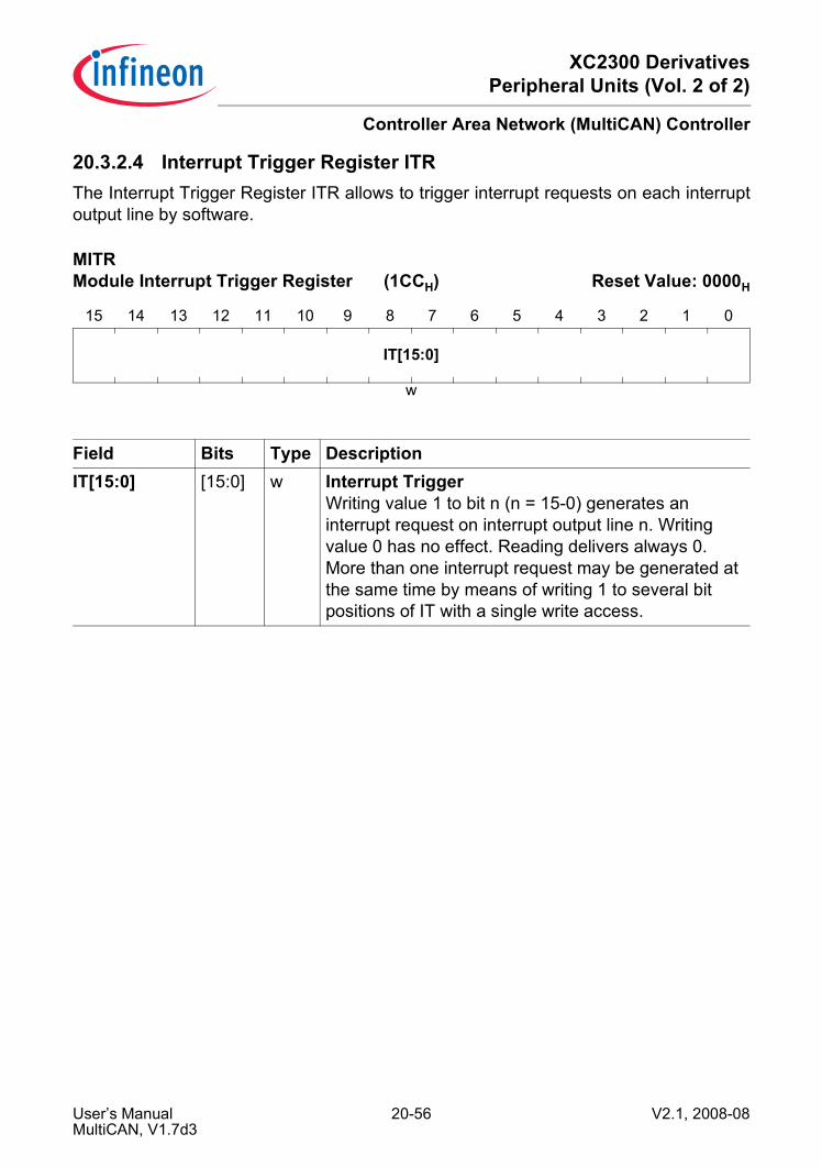
XC2300 DerivativesPeripheral Units (Vol. 2 of 2)
Controller Area Network (MultiCAN) Controller
20.3.2.4 Interrupt Trigger Register ITRThe Interrupt Trigger Register ITR allows to trigger interrupt requests on each interruptoutput line by software.
MITR Module Interrupt Trigger Register (1CCH) Reset Value: 0000H
15 14 13 12 11 10 9 8 7 6 5 4 3 2 1 0
IT[15:0]
w
Field Bits Type DescriptionIT[15:0] [15:0] w Interrupt Trigger
Writing value 1 to bit n (n = 15-0) generates an interrupt request on interrupt output line n. Writing value 0 has no effect. Reading delivers always 0.More than one interrupt request may be generated at the same time by means of writing 1 to several bit positions of IT with a single write access.
User’s Manual 20-56 V2.1, 2008-08MultiCAN, V1.7d3

XC2300 DerivativesPeripheral Units (Vol. 2 of 2)
Controller Area Network (MultiCAN) Controller
20.3.2.5 List PointerEach CAN node has an own list which defines the message objects that are allocated tothe respective node. In addition to that there is the list of all unallocated objects andfinally a general purpose user list which is not associated to a CAN node. Each list isassigned a list index according to Table 20-3 “List Indices” on Page 20-14.Each list is terminated with a List Register which defines the first and the last element inthe list.
LIST0H List Register 0 High (102H) Reset Value: 007FHLISTyH (y = 1-7)List Register y High (102H+y*4) Reset Value: 0100H
15 14 13 12 11 10 9 8 7 6 5 4 3 2 1 0
0 EMPTY SIZE
r rh rh
Field Bits Type DescriptionSIZE [7:0] rh Size of List
The number of elements in the list l is given by#elements = SIZE + 1,provided the list is not empty. If the list l is empty, the value of SIZE is zero.
EMPTY 8 rh List Empty Indication0B At least one message object is allocated to list l.1B No message object is allocated to the list l.
0 [15:9] r Reserved;read as 0; should be written with 0.
User’s Manual 20-57 V2.1, 2008-08MultiCAN, V1.7d3

XC2300 DerivativesPeripheral Units (Vol. 2 of 2)
Controller Area Network (MultiCAN) Controller
LIST0L List Register 0 Low (100H) Reset Value: 7F00HLISTxL (x = 1-7)List Register x Low (100H+x*4) Reset Value: 0000H
15 14 13 12 11 10 9 8 7 6 5 4 3 2 1 0
END BEGIN
rh rh
Field Bits Type DescriptionBEGIN [7:0] rh List Begin
Pointer to the first message object in the list l.END [15:8] rh END Pointer
Pointer to the last message object in the list l.
User’s Manual 20-58 V2.1, 2008-08MultiCAN, V1.7d3
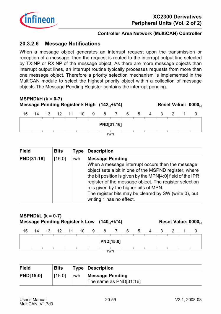
XC2300 DerivativesPeripheral Units (Vol. 2 of 2)
Controller Area Network (MultiCAN) Controller
20.3.2.6 Message NotificationsWhen a message object generates an interrupt request upon the transmission orreception of a message, then the request is routed to the interrupt output line selectedby TXINP or RXINP of the message object. As there are more message objects thaninterrupt output lines, an interrupt routine typically processes requests from more thanone message object. Therefore a priority selection mechanism is implemented in theMultiCAN module to select the highest priority object within a collection of messageobjects.The Message Pending Register contains the interrupt pending.
MSPNDkH (k = 0-7) Message Pending Register k High (142H+k*4) Reset Value: 0000H
15 14 13 12 11 10 9 8 7 6 5 4 3 2 1 0
PND[31:16]
rwh
Field Bits Type DescriptionPND[31:16] [15:0] rwh Message Pending
When a message interrupt occurs then the message object sets a bit in one of the MSPND register, where the bit position is given by the MPN[4:0] field of the IPR register of the message object. The register selection n is given by the higher bits of MPN.The register bits may be cleared by SW (write 0), but writing 1 has no effect.
MSPNDkL (k = 0-7) Message Pending Register k Low (140H+k*4) Reset Value: 0000H
15 14 13 12 11 10 9 8 7 6 5 4 3 2 1 0
PND[15:0]
rwh
Field Bits Type DescriptionPND[15:0] [15:0] rwh Message Pending
The same as PND[31:16]
User’s Manual 20-59 V2.1, 2008-08MultiCAN, V1.7d3
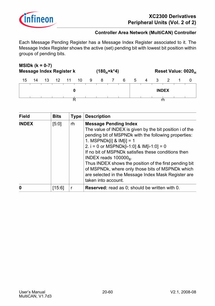
XC2300 DerivativesPeripheral Units (Vol. 2 of 2)
Controller Area Network (MultiCAN) Controller
Each Message Pending Register has a Message Index Register associated to it. TheMessage Index Register shows the active (set) pending bit with lowest bit position withingroups of pending bits.
MSIDk (k = 0-7) Message Index Register k (180H+k*4) Reset Value: 0020H
15 14 13 12 11 10 9 8 7 6 5 4 3 2 1 0
0 INDEX
R rh
Field Bits Type DescriptionINDEX [5:0] rh Message Pending Index
The value of INDEX is given by the bit position i of the pending bit of MSPNDk with the following properties:1. MSPNDk[i] & IM[i] = 12. i = 0 or MSPNDk[i-1:0] & IM[i-1:0] = 0If no bit of MSPNDk satisfies these conditions then INDEX reads 100000B.Thus INDEX shows the position of the first pending bit of MSPNDk, where only those bits of MSPNDk which are selected in the Message Index Mask Register are taken into account.
0 [15:6] r Reserved: read as 0; should be written with 0.
User’s Manual 20-60 V2.1, 2008-08MultiCAN, V1.7d3

XC2300 DerivativesPeripheral Units (Vol. 2 of 2)
Controller Area Network (MultiCAN) Controller
The Message Index Mask Register selects individual bits for the calculation of theMessage Pending Index. The Message Index Mask Register is used commonly for allMessage Pending registers and their associated Message Index registers.
MSIMASKH Message Index Mask Register High (1C2H) Reset Value: 0000H
15 14 13 12 11 10 9 8 7 6 5 4 3 2 1 0
IM[31:16]
rw
Field Bits Type DescriptionIM[31:16] [15:0] rw Message Index Mask
Only those bits in MSPNDk for which the corresponding Index Mask bits are set contribute to the calculation of the Message Index.
MSIMASKL Message Index Mask Register Low (1C0H) Reset Value: 0000H
15 14 13 12 11 10 9 8 7 6 5 4 3 2 1 0
IM[15:0]
rw
Field Bits Type DescriptionIM[15:0] [15:0] rw Message Index Mask
Only those bits in MSPNDk for which the corresponding Index Mask bits are set contribute to the calculation of the Message Index.
User’s Manual 20-61 V2.1, 2008-08MultiCAN, V1.7d3

XC2300 DerivativesPeripheral Units (Vol. 2 of 2)
Controller Area Network (MultiCAN) Controller
20.3.3 CAN Node Specific RegistersThe CAN node specific registers exist once for each CAN node of the MultiCANmodule.They contain information that is directly related to the operation of the CANnodes and which may not be shared among the nodes.
20.3.3.1 Node Control RegisterThe Node Control Register contains basic settings that define the operation of the CANnode and the interaction of the CAN node with the message objects.
NCRx (x = 0-4) Node x Control Register (200H+x*100H) Reset Value: 0001H
15 14 13 12 11 10 9 8 7 6 5 4 3 2 1 0
0 SUSEN
CALM CCE 0 CAN
DIS ALIE LECIE TRIE INIT
r rw rw rw r rw rw rw rw rwh
User’s Manual 20-62 V2.1, 2008-08MultiCAN, V1.7d3
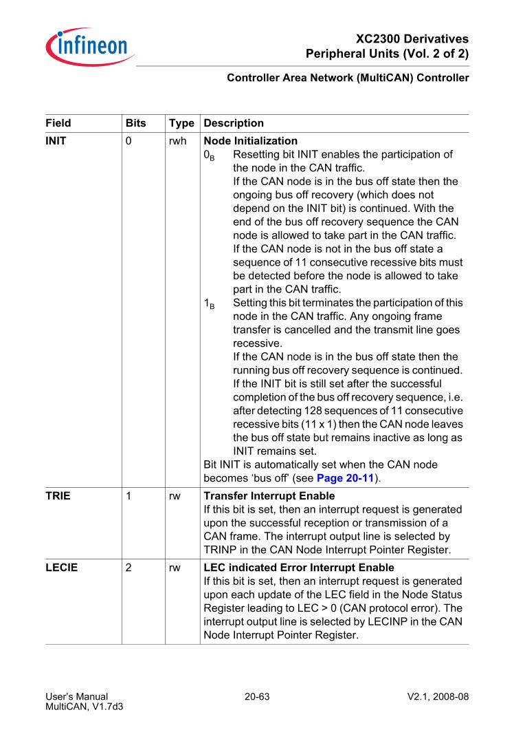
XC2300 DerivativesPeripheral Units (Vol. 2 of 2)
Controller Area Network (MultiCAN) Controller
Field Bits Type DescriptionINIT 0 rwh Node Initialization
0B Resetting bit INIT enables the participation of the node in the CAN traffic.If the CAN node is in the bus off state then the ongoing bus off recovery (which does not depend on the INIT bit) is continued. With the end of the bus off recovery sequence the CAN node is allowed to take part in the CAN traffic.If the CAN node is not in the bus off state a sequence of 11 consecutive recessive bits must be detected before the node is allowed to take part in the CAN traffic.
1B Setting this bit terminates the participation of this node in the CAN traffic. Any ongoing frame transfer is cancelled and the transmit line goes recessive.If the CAN node is in the bus off state then the running bus off recovery sequence is continued. If the INIT bit is still set after the successful completion of the bus off recovery sequence, i.e. after detecting 128 sequences of 11 consecutive recessive bits (11 x 1) then the CAN node leaves the bus off state but remains inactive as long as INIT remains set.
Bit INIT is automatically set when the CAN node becomes ‘bus off’ (see Page 20-11).
TRIE 1 rw Transfer Interrupt EnableIf this bit is set, then an interrupt request is generated upon the successful reception or transmission of a CAN frame. The interrupt output line is selected by TRINP in the CAN Node Interrupt Pointer Register.
LECIE 2 rw LEC indicated Error Interrupt EnableIf this bit is set, then an interrupt request is generated upon each update of the LEC field in the Node Status Register leading to LEC > 0 (CAN protocol error). The interrupt output line is selected by LECINP in the CAN Node Interrupt Pointer Register.
User’s Manual 20-63 V2.1, 2008-08MultiCAN, V1.7d3

XC2300 DerivativesPeripheral Units (Vol. 2 of 2)
Controller Area Network (MultiCAN) Controller
ALIE 3 rw Alert Interrupt EnableIf this bit is set then an alert interrupt is generated on one of the following events:1) change of bit BOFF in the CAN Node Status
Register.2) change of bit EWRN in the CAN Node Status
Register.3) List Length Error, which also sets bit LLE in the
CAN Node Status Register.4) List Object Error, which also sets bit LOE in the
CAN Node Status Register.5) Bit INIT has been set by the MultiCAN.The interrupt is requested on the interrupt output line selected by ALINP in the CAN Node Interrupt Pointer Register.
CANDIS 4 rw CAN DisableSetting this bit disables the CAN node. The CAN node first waits until it is BUS IDLE or BUS OFF. Then bit INIT is automatically set and an alert interrupt is generated if bit ALIE is set.
CCE 6 rw Configuration Change Enable0B The Bit Timing Register, the Port Control
Register and the Error Counter Register may only be read. All attempts to modify them are ignored.
1B The Bit Timing Register, the Port Control Register and the Error Counter Register may be read and written.
CALM 7 rw Can Analyze ModeIf this bit is set then the CAN node operates in analyze mode. This means that messages may be received, but not transmitted. No acknowledge is sent on the CAN bus upon frame reception. Active error flags are sent recessive instead of dominant. The transmit line is continuously held at recessive (1) level.Bit CALM can be written only while bit INIT is set.
Field Bits Type Description
User’s Manual 20-64 V2.1, 2008-08MultiCAN, V1.7d3
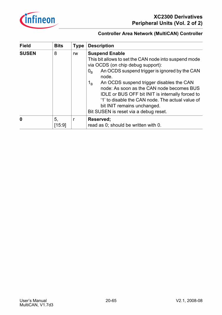
XC2300 DerivativesPeripheral Units (Vol. 2 of 2)
Controller Area Network (MultiCAN) Controller
SUSEN 8 rw Suspend EnableThis bit allows to set the CAN node into suspend mode via OCDS (on chip debug support):0B An OCDS suspend trigger is ignored by the CAN
node.1B An OCDS suspend trigger disables the CAN
node: As soon as the CAN node becomes BUS IDLE or BUS OFF bit INIT is internally forced to ‘1’ to disable the CAN node. The actual value of bit INIT remains unchanged.
Bit SUSEN is reset via a debug reset.0 5,
[15:9]r Reserved;
read as 0; should be written with 0.
Field Bits Type Description
User’s Manual 20-65 V2.1, 2008-08MultiCAN, V1.7d3

XC2300 DerivativesPeripheral Units (Vol. 2 of 2)
Controller Area Network (MultiCAN) Controller
20.3.3.2 Node Status RegisterThe Node Status Register reports errors as well as successfully transferred CAN frames.
NSRx (x = 0-4)Node x Status Register (204H+x*100H) Reset Value: 0000H
15 14 13 12 11 10 9 8 7 6 5 4 3 2 1 0
0 SUSACK LOE LLE BOF
FEWR
NALERT
RXOK
TXOK LEC
r rh rwh rwh rh rh rwh rwh rwh rwh
Field Bits Type DescriptionLEC [2:0] rwh Last Error Code
The encoding of this bit field is detailed in Table 20-10.TXOK 3 rwh Message Transmitted Successfully
0B No successful transmission since last flag reset.1B A message has been transmitted successfully
(error free and acknowledged by at least another node).
TXOK must be reset by software (write 0). Writing 1 has no effect.
RXOK 4 rwh Message Received Successfully0B No successful reception since last flag reset.1B A message has been received successfully.RXOK must be reset by software (write 0). Writing 1 has no effect.
User’s Manual 20-66 V2.1, 2008-08MultiCAN, V1.7d3
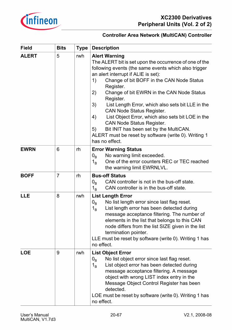
XC2300 DerivativesPeripheral Units (Vol. 2 of 2)
Controller Area Network (MultiCAN) Controller
ALERT 5 rwh Alert WarningThe ALERT bit is set upon the occurrence of one of the following events (the same events which also trigger an alert interrupt if ALIE is set):1) Change of bit BOFF in the CAN Node Status
Register.2) Change of bit EWRN in the CAN Node Status
Register.3) List Length Error, which also sets bit LLE in the
CAN Node Status Register.4) List Object Error, which also sets bit LOE in the
CAN Node Status Register.5) Bit INIT has been set by the MultiCAN.ALERT must be reset by software (write 0). Writing 1 has no effect.
EWRN 6 rh Error Warning Status0B No warning limit exceeded.1B One of the error counters REC or TEC reached
the warning limit EWRNLVL.BOFF 7 rh Bus-off Status
0B CAN controller is not in the bus-off state.1B CAN controller is in the bus-off state.
LLE 8 rwh List Length Error0B No list length error since last flag reset.1B List length error has been detected during
message acceptance filtering. The number of elements in the list that belongs to this CAN node differs from the list SIZE given in the list termination pointer.
LLE must be reset by software (write 0). Writing 1 has no effect.
LOE 9 rwh List Object Error0B No list object error since last flag reset.1B List object error has been detected during
message acceptance filtering. A message object with wrong LIST index entry in the Message Object Control Register has been detected.
LOE must be reset by software (write 0). Writing 1 has no effect.
Field Bits Type Description
User’s Manual 20-67 V2.1, 2008-08MultiCAN, V1.7d3

XC2300 DerivativesPeripheral Units (Vol. 2 of 2)
Controller Area Network (MultiCAN) Controller
SUSACK 10 rh Suspend Acknowledge0B The CAN node is not in suspend mode or a
suspend request is pending, but the CAN node has not yet reached BUS IDLE or BUS OFF.
1B The CAN node is in suspend mode: The CAN node is inactive (bit NCR.INIT internally forced to ‘1’) due to an OCDS suspend request.
0 [15:11] r Reserved;read as 0; should be written with 0.
Field Bits Type Description
User’s Manual 20-68 V2.1, 2008-08MultiCAN, V1.7d3

XC2300 DerivativesPeripheral Units (Vol. 2 of 2)
Controller Area Network (MultiCAN) Controller
Encoding of the LEC Bitfield
Table 20-10 Encoding of the LEC Bit FieldLEC Value Signification000B No Error:
No error was detected for the last message on the CAN bus.001B Stuff Error:
More than 5 equal bits in a sequence have occurred in a part of a received message where this is not allowed.
010B Form Error:A ‘fixed format part’ of a received frame has the wrong format.
011B Ack Error:The transmitted message was not acknowledged by another node.
100B Bit1 Error:During a message transmission the CAN node tried to send a recessive level (1) outside the arbitration field and the acknowledge slot, but the monitored bus value was dominant.
101B Bit0 Error:Two different conditions are signalled by this code:a) During transmission of a message (or acknowledge bit, active error flag, overload flag) the CAN node tried to send a dominant level (0), but the monitored bus value was recessive.b) During bus-off recovery this code is set each time a sequence of 11 recessive bits has been monitored. The CPU may use this code as indication that the bus is not continuously disturbed.
110B CRC Error:The CRC checksum of the received message was incorrect.
111B CPU write to LEC:Whenever the the CPU writes the value 111 to LEC, it takes the value 111. Whenever the CPU writes another value to LEC, the written LEC value is ignored.
User’s Manual 20-69 V2.1, 2008-08MultiCAN, V1.7d3
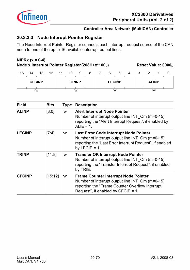
XC2300 DerivativesPeripheral Units (Vol. 2 of 2)
Controller Area Network (MultiCAN) Controller
20.3.3.3 Node Interupt Pointer RegisterThe Node Interrupt Pointer Register connects each interrupt request source of the CANnode to one of the up to 16 available interrupt output lines.
NIPRx (x = 0-4)Node x Interrupt Pointer Register (208H+x*100H) Reset Value: 0000H
15 14 13 12 11 10 9 8 7 6 5 4 3 2 1 0
CFCINP TRINP LECINP ALINP
rw rw rw rw
Field Bits Type DescriptionALINP [3:0] rw Alert Interrupt Node Pointer
Number of interrupt output line INT_Om (m=0-15) reporting the “Alert Interrupt Request”, if enabled by ALIE = 1.
LECINP [7:4] rw Last Error Code Interrupt Node PointerNumber of interrupt output line INT_Om (m=0-15) reporting the “Last Error Interrupt Request”, if enabled by LECIE = 1.
TRINP [11:8] rw Transfer OK Interrupt Node PointerNumber of interrupt output line INT_Om (m=0-15) reporting the “Transfer Interrupt Request”, if enabled by TRIE.
CFCINP [15:12] rw Frame Counter Interrupt Node PointerNumber of interrupt output line INT_Om (m=0-15) reporting the “Frame Counter Overflow Interrupt Request”, if enabled by CFCIE = 1.
User’s Manual 20-70 V2.1, 2008-08MultiCAN, V1.7d3
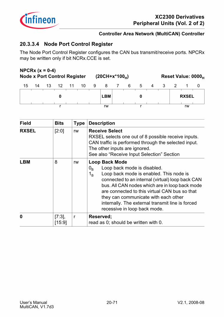
XC2300 DerivativesPeripheral Units (Vol. 2 of 2)
Controller Area Network (MultiCAN) Controller
20.3.3.4 Node Port Control RegisterThe Node Port Control Register configures the CAN bus transmit/receive ports. NPCRxmay be written only if bit NCRx.CCE is set.
NPCRx (x = 0-4) Node x Port Control Register (20CH+x*100H) Reset Value: 0000H
15 14 13 12 11 10 9 8 7 6 5 4 3 2 1 0
0 LBM 0 RXSEL
r rw r rw
Field Bits Type DescriptionRXSEL [2:0] rw Receive Select
RXSEL selects one out of 8 possible receive inputs. CAN traffic is performed through the selected input. The other inputs are ignored.See also “Receive Input Selection” Section
LBM 8 rw Loop Back Mode0B Loop back mode is disabled.1B Loop back mode is enabled. This node is
connected to an internal (virtual) loop back CAN bus. All CAN nodes which are in loop back mode are connected to this virtual CAN bus so that they can communicate with each other internally. The external transmit line is forced recessive in loop back mode.
0 [7:3],[15:9]
r Reserved;read as 0; should be written with 0.
User’s Manual 20-71 V2.1, 2008-08MultiCAN, V1.7d3

XC2300 DerivativesPeripheral Units (Vol. 2 of 2)
Controller Area Network (MultiCAN) Controller
20.3.3.5 Node Bit Timing RegisterThe Node Bit Timing Register contains all parameters to setup the bit timing for the CANtransfer. NBTRx may be written only if bit NCRx.CCE is set.
NBTRxH (x = 0-4) Node x Bit Timing Register High (212H+x*100H) Reset Value: 0000H
15 14 13 12 11 10 9 8 7 6 5 4 3 2 1 0
0 FTX
r rw
Field Bits Type DescriptionFTX 0 rw Fast Transmit (TTC only)
When a message is requested for transmission on the CAN bus, then the start of frame (SOF) symbol is sent with the beginning of a new bit time.
If the CAN bus is in the idle state and bit FTX is set (FTX = 1) then a new bit time is started immediately with the transmit trigger of a new message. This eliminates the variable delay between the transmit trigger of a message and the actual SOF signal on the transmit output. Such a variable delay occurs when transmit triggers occur at different positions within a CAN bit time.
0 [15:1] r reserved;returns ’0’ if read; should be written with ’0’;
NBTRxL (x = 0-4) Node x Bit Timing Register Low (210H+x*100H) Reset Value: 0000H
15 14 13 12 11 10 9 8 7 6 5 4 3 2 1 0
DIV8 TSEG2 TSEG1 SJW BRP
rw rw rw rw rw
User’s Manual 20-72 V2.1, 2008-08MultiCAN, V1.7d3
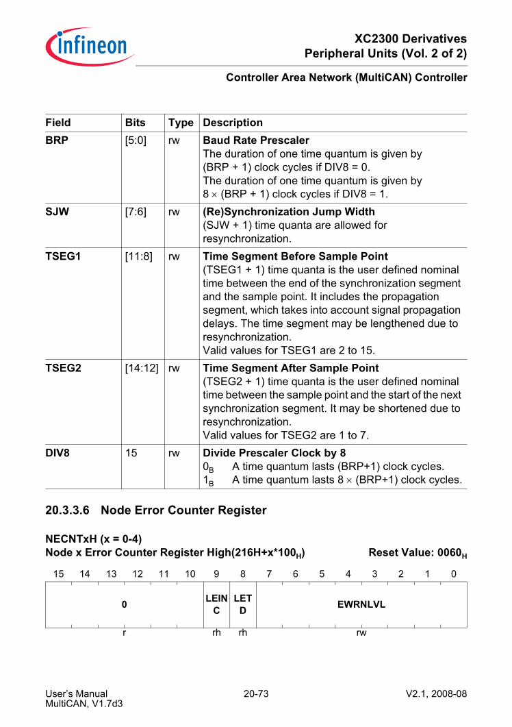
XC2300 DerivativesPeripheral Units (Vol. 2 of 2)
Controller Area Network (MultiCAN) Controller
20.3.3.6 Node Error Counter Register
Field Bits Type DescriptionBRP [5:0] rw Baud Rate Prescaler
The duration of one time quantum is given by (BRP + 1) clock cycles if DIV8 = 0.The duration of one time quantum is given by 8 × (BRP + 1) clock cycles if DIV8 = 1.
SJW [7:6] rw (Re)Synchronization Jump Width(SJW + 1) time quanta are allowed for resynchronization.
TSEG1 [11:8] rw Time Segment Before Sample Point(TSEG1 + 1) time quanta is the user defined nominal time between the end of the synchronization segment and the sample point. It includes the propagation segment, which takes into account signal propagation delays. The time segment may be lengthened due to resynchronization.Valid values for TSEG1 are 2 to 15.
TSEG2 [14:12] rw Time Segment After Sample Point(TSEG2 + 1) time quanta is the user defined nominal time between the sample point and the start of the next synchronization segment. It may be shortened due to resynchronization.Valid values for TSEG2 are 1 to 7.
DIV8 15 rw Divide Prescaler Clock by 80B A time quantum lasts (BRP+1) clock cycles.1B A time quantum lasts 8 × (BRP+1) clock cycles.
NECNTxH (x = 0-4) Node x Error Counter Register High(216H+x*100H) Reset Value: 0060H
15 14 13 12 11 10 9 8 7 6 5 4 3 2 1 0
0 LEINC
LETD EWRNLVL
r rh rh rw
User’s Manual 20-73 V2.1, 2008-08MultiCAN, V1.7d3
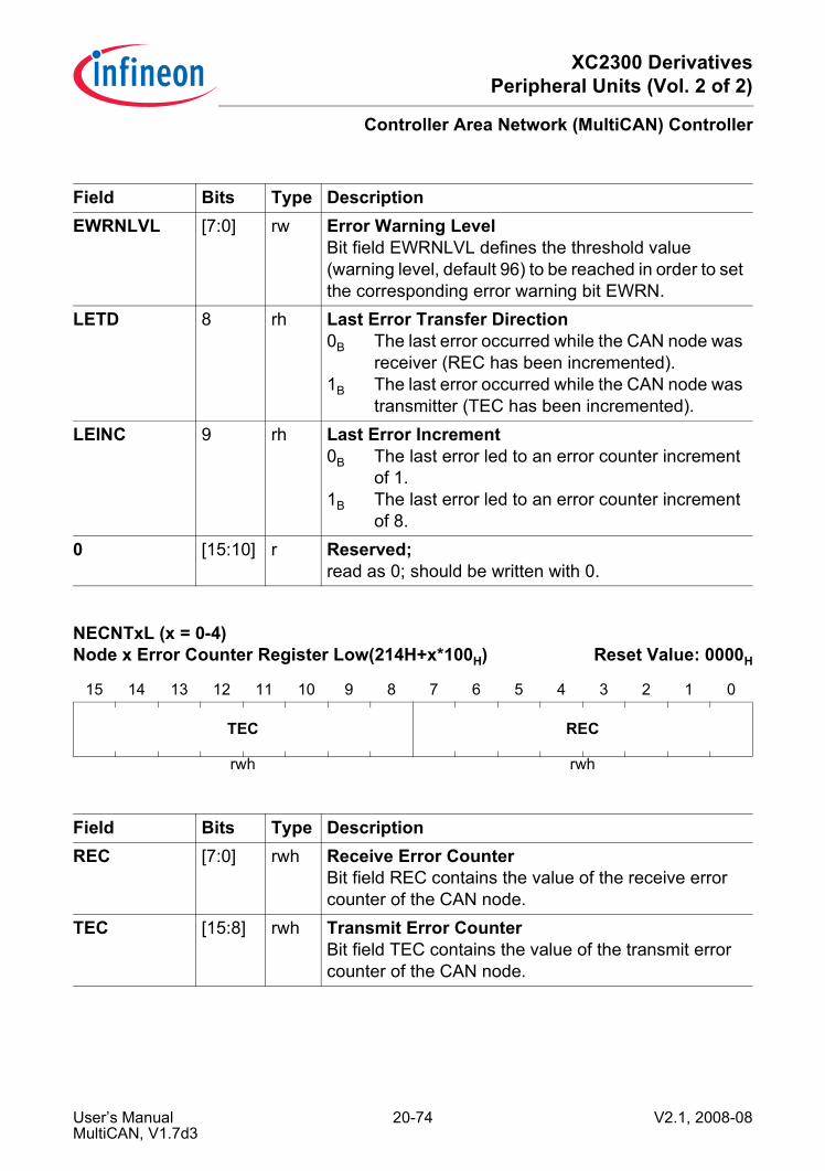
XC2300 DerivativesPeripheral Units (Vol. 2 of 2)
Controller Area Network (MultiCAN) Controller
Field Bits Type DescriptionEWRNLVL [7:0] rw Error Warning Level
Bit field EWRNLVL defines the threshold value (warning level, default 96) to be reached in order to set the corresponding error warning bit EWRN.
LETD 8 rh Last Error Transfer Direction0B The last error occurred while the CAN node was
receiver (REC has been incremented).1B The last error occurred while the CAN node was
transmitter (TEC has been incremented).LEINC 9 rh Last Error Increment
0B The last error led to an error counter increment of 1.
1B The last error led to an error counter increment of 8.
0 [15:10] r Reserved;read as 0; should be written with 0.
NECNTxL (x = 0-4) Node x Error Counter Register Low(214H+x*100H) Reset Value: 0000H
15 14 13 12 11 10 9 8 7 6 5 4 3 2 1 0
TEC REC
rwh rwh
Field Bits Type DescriptionREC [7:0] rwh Receive Error Counter
Bit field REC contains the value of the receive error counter of the CAN node.
TEC [15:8] rwh Transmit Error CounterBit field TEC contains the value of the transmit error counter of the CAN node.
User’s Manual 20-74 V2.1, 2008-08MultiCAN, V1.7d3
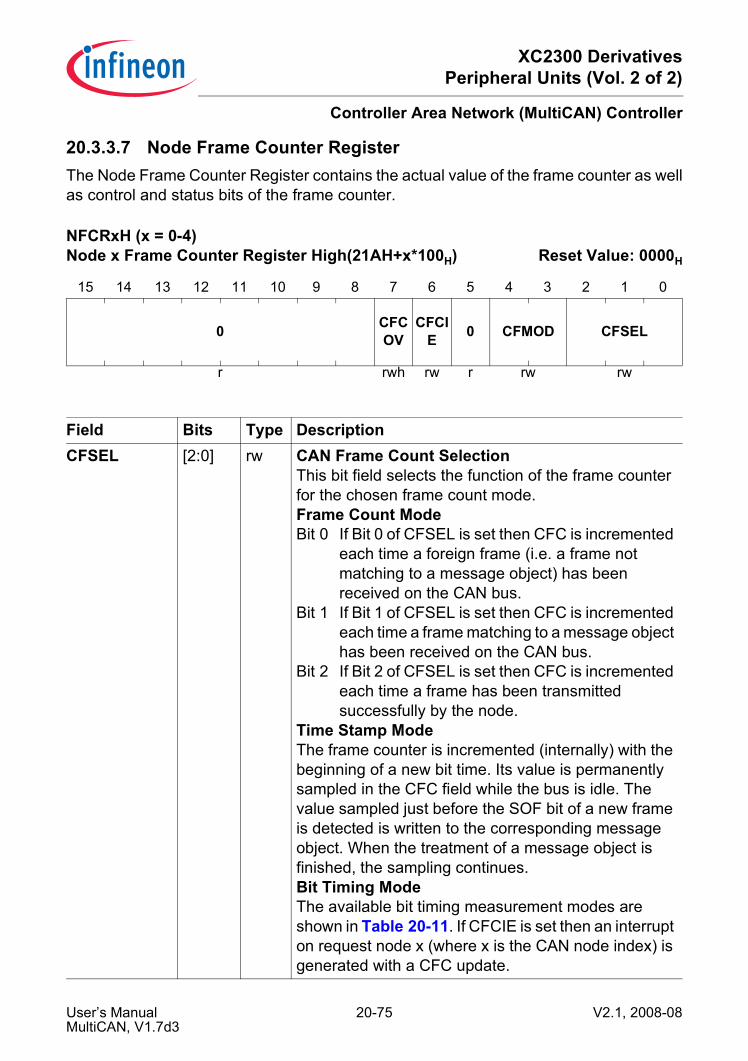
XC2300 DerivativesPeripheral Units (Vol. 2 of 2)
Controller Area Network (MultiCAN) Controller
20.3.3.7 Node Frame Counter RegisterThe Node Frame Counter Register contains the actual value of the frame counter as wellas control and status bits of the frame counter.
NFCRxH (x = 0-4) Node x Frame Counter Register High(21AH+x*100H) Reset Value: 0000H
15 14 13 12 11 10 9 8 7 6 5 4 3 2 1 0
0 CFCOV
CFCIE 0 CFMOD CFSEL
r rwh rw r rw rw
Field Bits Type DescriptionCFSEL [2:0] rw CAN Frame Count Selection
This bit field selects the function of the frame counter for the chosen frame count mode.Frame Count ModeBit 0 If Bit 0 of CFSEL is set then CFC is incremented
each time a foreign frame (i.e. a frame not matching to a message object) has been received on the CAN bus.
Bit 1 If Bit 1 of CFSEL is set then CFC is incremented each time a frame matching to a message object has been received on the CAN bus.
Bit 2 If Bit 2 of CFSEL is set then CFC is incremented each time a frame has been transmitted successfully by the node.
Time Stamp ModeThe frame counter is incremented (internally) with the beginning of a new bit time. Its value is permanently sampled in the CFC field while the bus is idle. The value sampled just before the SOF bit of a new frame is detected is written to the corresponding message object. When the treatment of a message object is finished, the sampling continues.Bit Timing ModeThe available bit timing measurement modes are shown in Table 20-11. If CFCIE is set then an interrupt on request node x (where x is the CAN node index) is generated with a CFC update.
User’s Manual 20-75 V2.1, 2008-08MultiCAN, V1.7d3
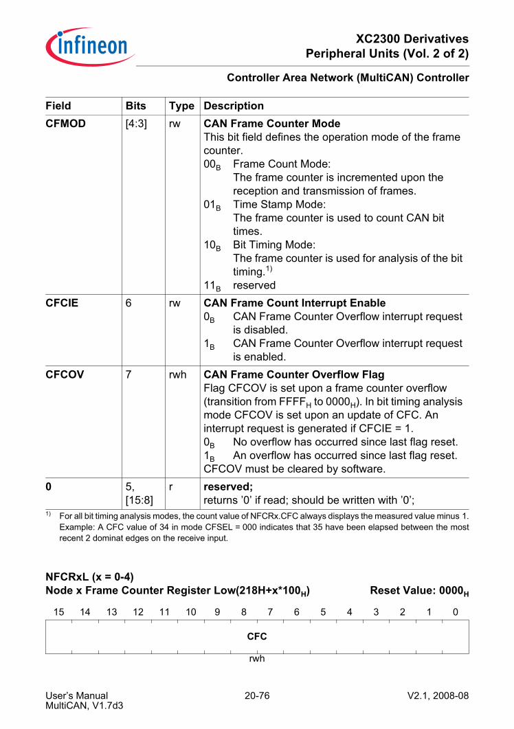
XC2300 DerivativesPeripheral Units (Vol. 2 of 2)
Controller Area Network (MultiCAN) Controller
CFMOD [4:3] rw CAN Frame Counter ModeThis bit field defines the operation mode of the frame counter.00B Frame Count Mode:
The frame counter is incremented upon the reception and transmission of frames.
01B Time Stamp Mode:The frame counter is used to count CAN bit times.
10B Bit Timing Mode:The frame counter is used for analysis of the bit timing.1)
11B reservedCFCIE 6 rw CAN Frame Count Interrupt Enable
0B CAN Frame Counter Overflow interrupt request is disabled.
1B CAN Frame Counter Overflow interrupt request is enabled.
CFCOV 7 rwh CAN Frame Counter Overflow FlagFlag CFCOV is set upon a frame counter overflow (transition from FFFFH to 0000H). In bit timing analysis mode CFCOV is set upon an update of CFC. An interrupt request is generated if CFCIE = 1.0B No overflow has occurred since last flag reset.1B An overflow has occurred since last flag reset.CFCOV must be cleared by software.
0 5,[15:8]
r reserved;returns ’0’ if read; should be written with ’0’;
1) For all bit timing analysis modes, the count value of NFCRx.CFC always displays the measured value minus 1.Example: A CFC value of 34 in mode CFSEL = 000 indicates that 35 have been elapsed between the mostrecent 2 dominat edges on the receive input.
NFCRxL (x = 0-4) Node x Frame Counter Register Low(218H+x*100H) Reset Value: 0000H
15 14 13 12 11 10 9 8 7 6 5 4 3 2 1 0
CFC
rwh
Field Bits Type Description
User’s Manual 20-76 V2.1, 2008-08MultiCAN, V1.7d3
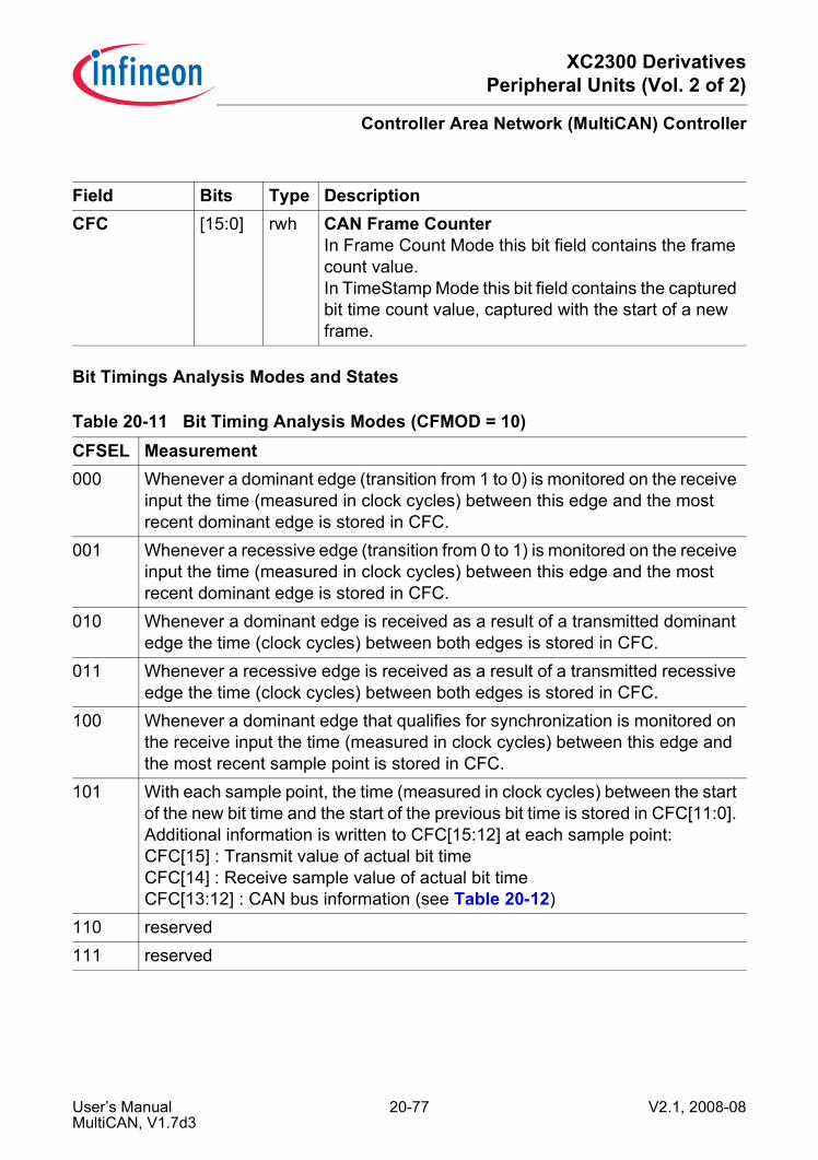
XC2300 DerivativesPeripheral Units (Vol. 2 of 2)
Controller Area Network (MultiCAN) Controller
Bit Timings Analysis Modes and States
Field Bits Type DescriptionCFC [15:0] rwh CAN Frame Counter
In Frame Count Mode this bit field contains the frame count value.In TimeStamp Mode this bit field contains the captured bit time count value, captured with the start of a new frame.
Table 20-11 Bit Timing Analysis Modes (CFMOD = 10)CFSEL Measurement000 Whenever a dominant edge (transition from 1 to 0) is monitored on the receive
input the time (measured in clock cycles) between this edge and the most recent dominant edge is stored in CFC.
001 Whenever a recessive edge (transition from 0 to 1) is monitored on the receive input the time (measured in clock cycles) between this edge and the most recent dominant edge is stored in CFC.
010 Whenever a dominant edge is received as a result of a transmitted dominant edge the time (clock cycles) between both edges is stored in CFC.
011 Whenever a recessive edge is received as a result of a transmitted recessive edge the time (clock cycles) between both edges is stored in CFC.
100 Whenever a dominant edge that qualifies for synchronization is monitored on the receive input the time (measured in clock cycles) between this edge and the most recent sample point is stored in CFC.
101 With each sample point, the time (measured in clock cycles) between the start of the new bit time and the start of the previous bit time is stored in CFC[11:0]. Additional information is written to CFC[15:12] at each sample point:CFC[15] : Transmit value of actual bit timeCFC[14] : Receive sample value of actual bit timeCFC[13:12] : CAN bus information (see Table 20-12)
110 reserved111 reserved
User’s Manual 20-77 V2.1, 2008-08MultiCAN, V1.7d3

XC2300 DerivativesPeripheral Units (Vol. 2 of 2)
Controller Area Network (MultiCAN) Controller
Table 20-12 CAN Bus State InformationCFC[13:12] CAN bus state00 NoBit
The CAN bus is idle, performs bit (de-) stuffing or is in one of the following frame segments:SOF, SRR, CRC, delimiters, first 6 EOF bits, IFS
01 NewBitThis code represents the first bit of a new frame segment.The current bit is the first bit in one of the following frame segments:bit 10 (MSB) of standard ID (transmit only), RTR, reserved bits, IDE, DLC(MSB), bit 7 (MSB) in each data byte and the first bit of the ID extension
10 BitThis code represents a bit inside a frame segment with a length of more than one bit (not the first bit of those frame segments which is indicated by NewBit).The current bit is processed within one of the following frame segments:ID bits (except first bit of standard ID for transmission and first bit of ID extension), DLC (3 LSB) and bits 6-0 in each data byte
11 DoneThe current bit is in one of the following frame segments:Acknowledge slot, last bit of EOF, active/passive error frame, overload frame.Two or more directly consecutive Done codes signal an error frame.
User’s Manual 20-78 V2.1, 2008-08MultiCAN, V1.7d3

XC2300 DerivativesPeripheral Units (Vol. 2 of 2)
Controller Area Network (MultiCAN) Controller
20.3.4 Message Object Registers
20.3.4.1 Message Object Control RegisterThe Message Object Control Register contains control bits for the CAN transfer and themessage object link pointer. Each control bit has a corresponding bit in the CTRL field.A control bit is set by writing 1 to the corresponding bit in CTRL. It is cleared by writing1 to the control bit directly. Any other combination leaves the control bit unchanged . Afterreset initialization the pointer PNEXT (read value of MOCTRnH[15:8]) points to messageobject n+1 (PNEXT = n+1), except for PNEXT of message object 127, which terminatesthe initial list (PNEXT = 127). Pointer PREV (read value of MOCTRnH[7:0]) initially pointsto message object n-1 (PPREV = n-1), except for PPREV of message object 0 whichindicates the start of the initial list (PPREV = 0). This reset initialization means that allmessage objects initially belong to the list of unallocated elements.
MOCTRnH (n = 0-127) Message Object n Control Register High (101EH+n*20H) Reset Value:shiftl8(n+1)+(n-1)1)
1) Exceptions: Message Obj. 0 : Reset val. of PPREV = 0, Message Obj. 127 : Reset val. of PNEXT = 127
15 14 13 12 11 10 9 8 7 6 5 4 3 2 1 0
0 SETDIR
SETTXEN1
SETTXEN0
SETTXR
Q
SETRXE
N
SETRTSEL
SETMSGVAL
SETMSGLST
SETNEWDAT
SETRXUPD
SETTXPND
SETRXPND
w w w w w w w w w w w w w
Field Bits Type DescriptionSETRXPND 0 w Set Receive Pending
This bit sets the RXPND SETTXPND 1 w Set Transmit Pending
This bit sets the TXPND SETRXUPD 2 w Set Receive Updating
This bit sets the RXUPD SETNEWDAT 3 w Set New Data
This bit sets the NEWDAT SETMSGLST 4 w Set Message Lost
This bit sets the MSGLST SETMSGVAL 5 w Set Message Valid
This bit sets the MSGVAL
User’s Manual 20-79 V2.1, 2008-08MultiCAN, V1.7d3

XC2300 DerivativesPeripheral Units (Vol. 2 of 2)
Controller Area Network (MultiCAN) Controller
SETRTSEL 6 w Set Receive/Transmit SelectedThis bit sets the RTSEL
SETRXEN 7 w Set Receive EnableThis bit sets the RXEN
SETTXRQ 8 w Set Transmit RequestThis bit sets the TXRQ
SETTXEN0 9 w Set Transmit Enable 0This bit sets the TXEN0
SETTXEN1 10 w Set Transmit Enable 1This bit sets the TXEN1
SETDIR 11 w Set Message DirectionThis bit sets the DIR
0 [15:12] w ReservedShould be written with 0.
MOCTRnL (n = 0-127) Message Object n Control Register Low(101CH+n*20H) Reset Value: 0000H
15 14 13 12 11 10 9 8 7 6 5 4 3 2 1 0
0 RESDIR
RESTXEN1
RESTXEN0
RESTXR
Q
RESRXE
N
RESRTSEL
RESMSGVAL
RESMSGLST
RESNEWDAT
RESRXUPD
RESTXPND
RESRXPND
w w w w w w w w w w w w w
Field Bits Type DescriptionRESRXPND 0 w Reset Receive Pending
This bit resets the RXPND RESTXPND 1 w Reset Transmit Pending
This bit resets the TXPND RESRXUPD 2 w Reset Receive Updating
This bit resets the RXUPD RESNEWDAT 3 w Reset New Data
This bit resets the NEWDAT RESMSGLST 4 w Reset Message Lost
This bit resets the MSGLST
Field Bits Type Description
User’s Manual 20-80 V2.1, 2008-08MultiCAN, V1.7d3
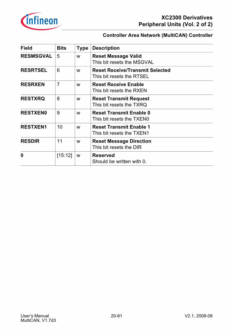
XC2300 DerivativesPeripheral Units (Vol. 2 of 2)
Controller Area Network (MultiCAN) Controller
RESMSGVAL 5 w Reset Message ValidThis bit resets the MSGVAL
RESRTSEL 6 w Reset Receive/Transmit SelectedThis bit resets the RTSEL
RESRXEN 7 w Reset Receive EnableThis bit resets the RXEN
RESTXRQ 8 w Reset Transmit RequestThis bit resets the TXRQ
RESTXEN0 9 w Reset Transmit Enable 0This bit resets the TXEN0
RESTXEN1 10 w Reset Transmit Enable 1This bit resets the TXEN1
RESDIR 11 w Reset Message DirectionThis bit resets the DIR
0 [15:12] w ReservedShould be written with 0.
Field Bits Type Description
User’s Manual 20-81 V2.1, 2008-08MultiCAN, V1.7d3
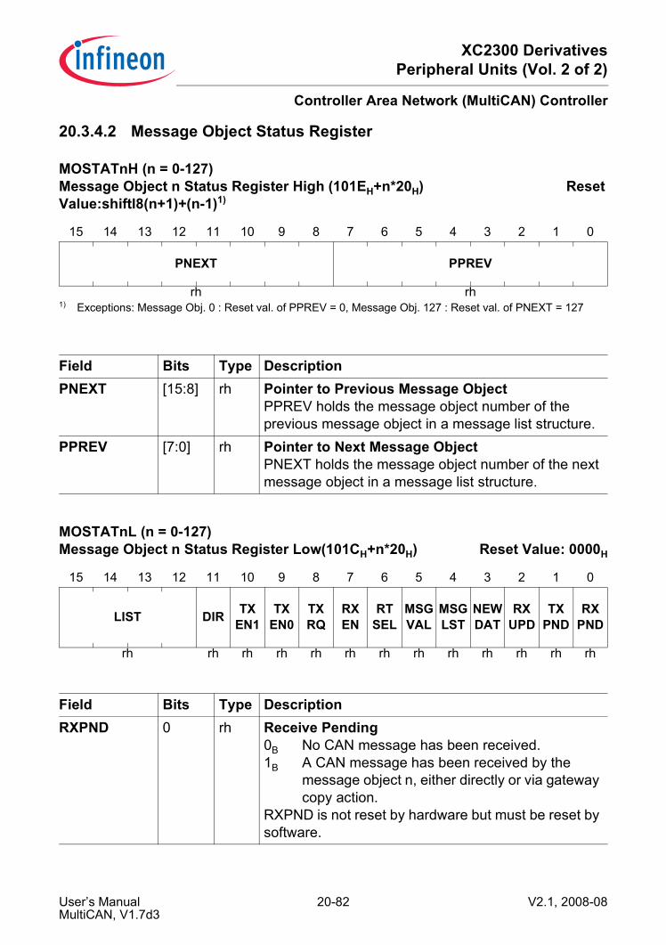
XC2300 DerivativesPeripheral Units (Vol. 2 of 2)
Controller Area Network (MultiCAN) Controller
20.3.4.2 Message Object Status Register
MOSTATnH (n = 0-127) Message Object n Status Register High (101EH+n*20H) Reset Value:shiftl8(n+1)+(n-1)1)
1) Exceptions: Message Obj. 0 : Reset val. of PPREV = 0, Message Obj. 127 : Reset val. of PNEXT = 127
15 14 13 12 11 10 9 8 7 6 5 4 3 2 1 0
PNEXT PPREV
rh rh
Field Bits Type DescriptionPNEXT [15:8] rh Pointer to Previous Message Object
PPREV holds the message object number of the previous message object in a message list structure.
PPREV [7:0] rh Pointer to Next Message ObjectPNEXT holds the message object number of the next message object in a message list structure.
MOSTATnL (n = 0-127) Message Object n Status Register Low(101CH+n*20H) Reset Value: 0000H
15 14 13 12 11 10 9 8 7 6 5 4 3 2 1 0
LIST DIR TXEN1
TXEN0
TXRQ
RXEN
RTSEL
MSGVAL
MSGLST
NEWDAT
RXUPD
TXPND
RXPND
rh rh rh rh rh rh rh rh rh rh rh rh rh
Field Bits Type DescriptionRXPND 0 rh Receive Pending
0B No CAN message has been received.1B A CAN message has been received by the
message object n, either directly or via gateway copy action.
RXPND is not reset by hardware but must be reset by software.
User’s Manual 20-82 V2.1, 2008-08MultiCAN, V1.7d3
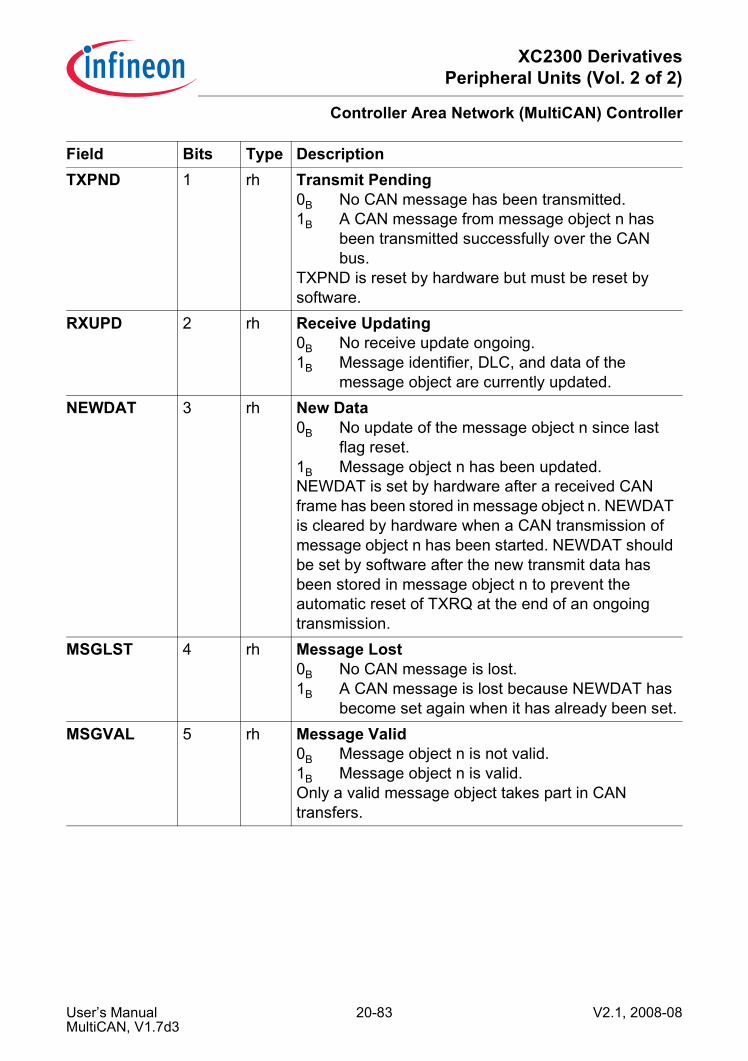
XC2300 DerivativesPeripheral Units (Vol. 2 of 2)
Controller Area Network (MultiCAN) Controller
TXPND 1 rh Transmit Pending0B No CAN message has been transmitted.1B A CAN message from message object n has
been transmitted successfully over the CAN bus.
TXPND is reset by hardware but must be reset by software.
RXUPD 2 rh Receive Updating0B No receive update ongoing.1B Message identifier, DLC, and data of the
message object are currently updated.NEWDAT 3 rh New Data
0B No update of the message object n since last flag reset.
1B Message object n has been updated.NEWDAT is set by hardware after a received CAN frame has been stored in message object n. NEWDAT is cleared by hardware when a CAN transmission of message object n has been started. NEWDAT should be set by software after the new transmit data has been stored in message object n to prevent the automatic reset of TXRQ at the end of an ongoing transmission.
MSGLST 4 rh Message Lost0B No CAN message is lost.1B A CAN message is lost because NEWDAT has
become set again when it has already been set.MSGVAL 5 rh Message Valid
0B Message object n is not valid.1B Message object n is valid.Only a valid message object takes part in CAN transfers.
Field Bits Type Description
User’s Manual 20-83 V2.1, 2008-08MultiCAN, V1.7d3
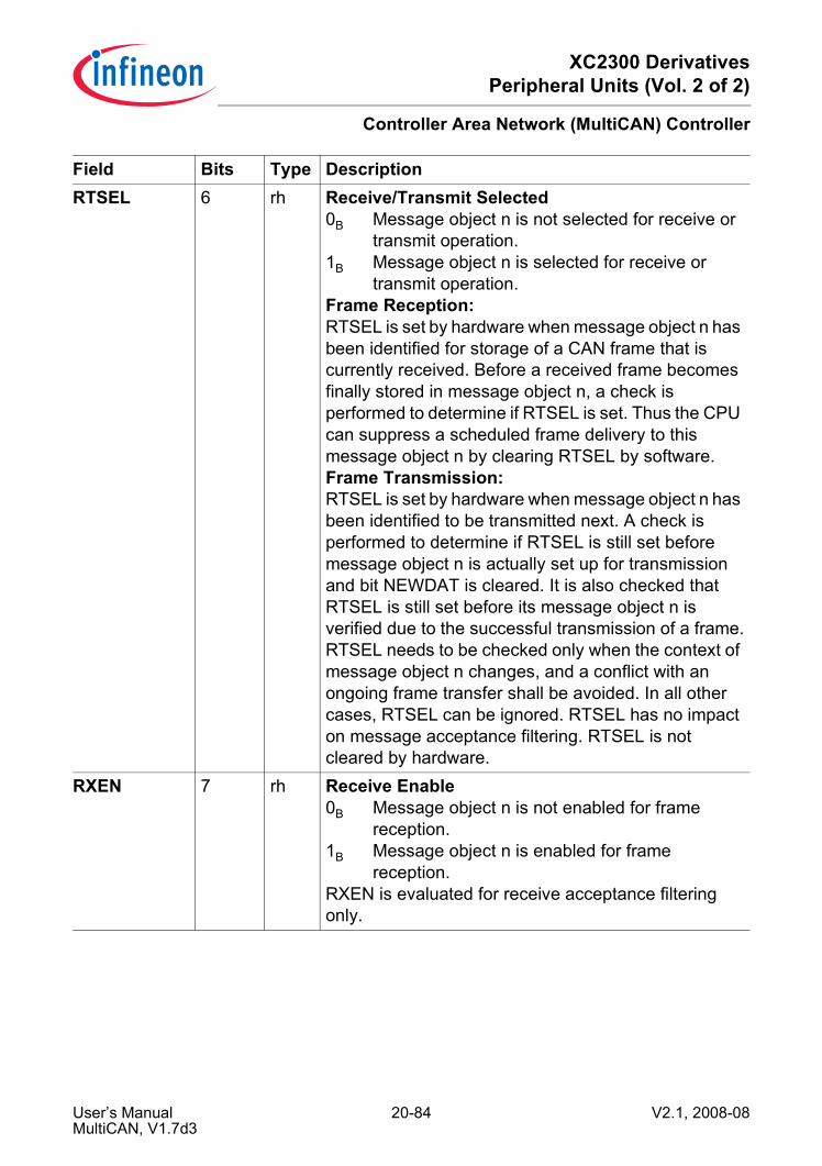
XC2300 DerivativesPeripheral Units (Vol. 2 of 2)
Controller Area Network (MultiCAN) Controller
RTSEL 6 rh Receive/Transmit Selected0B Message object n is not selected for receive or
transmit operation.1B Message object n is selected for receive or
transmit operation.Frame Reception:RTSEL is set by hardware when message object n has been identified for storage of a CAN frame that is currently received. Before a received frame becomes finally stored in message object n, a check is performed to determine if RTSEL is set. Thus the CPU can suppress a scheduled frame delivery to this message object n by clearing RTSEL by software.Frame Transmission:RTSEL is set by hardware when message object n has been identified to be transmitted next. A check is performed to determine if RTSEL is still set before message object n is actually set up for transmission and bit NEWDAT is cleared. It is also checked that RTSEL is still set before its message object n is verified due to the successful transmission of a frame.RTSEL needs to be checked only when the context of message object n changes, and a conflict with an ongoing frame transfer shall be avoided. In all other cases, RTSEL can be ignored. RTSEL has no impact on message acceptance filtering. RTSEL is not cleared by hardware.
RXEN 7 rh Receive Enable0B Message object n is not enabled for frame
reception.1B Message object n is enabled for frame
reception.RXEN is evaluated for receive acceptance filtering only.
Field Bits Type Description
User’s Manual 20-84 V2.1, 2008-08MultiCAN, V1.7d3

XC2300 DerivativesPeripheral Units (Vol. 2 of 2)
Controller Area Network (MultiCAN) Controller
TXRQ 8 rh Transmit Request0B No transmission of message object n is
requested.1B Transmission of message object n on the CAN
bus is requested.The transmit request becomes valid only if TXRQ, TXEN0, TXEN1 and MSGVAL are set. TXRQ is set by hardware if a matching Remote Frame has been received correctly. TXRQ is reset by hardware if message object n has been transmitted successfully and NEWDAT is not set again by software.
TXEN0 9 rh Transmit Enable 00B Message object n is not enabled for frame
transmission.1B Message object n is enabled for frame
transmission.Message object n can be transmitted only if both bits, TXEN0 and TXEN1, are set.The user may clear TXEN0 in order to inhibit the transmission of a message that is currently updated, or to disable automatic response of Remote Frames.
TXEN1 10 rh Transmit Enable 10B Message object n is not enabled for frame
transmission.1B Message object n is enabled for frame
transmission.Message object n can be transmitted only if both bits, TXEN0 and TXEN1, are set.TXEN1 is used by the MultiCAN module for selecting the active message object in the Transmit FIFOs.
Field Bits Type Description
User’s Manual 20-85 V2.1, 2008-08MultiCAN, V1.7d3

XC2300 DerivativesPeripheral Units (Vol. 2 of 2)
Controller Area Network (MultiCAN) Controller
DIR 11 rh Message Direction0B Receive Object selected:
With TXRQ = 1, a Remote Frame with the identifier of message object n is scheduled for transmission. On reception of a Data Frame with matching identifier, the message is stored in message object n.
1B Transmit Object selected:If TXRQ = 1, message object n is scheduled for transmission of a Data Frame. On reception of a Remote Frame with matching identifier, bit TXRQ is set.
LIST [15:12] rh List AllocationLIST indicates the number of the message list to which message object n is allocated. LIST is updated by hardware when the list allocation of the object is modified by a panel command.
Field Bits Type Description
User’s Manual 20-86 V2.1, 2008-08MultiCAN, V1.7d3

XC2300 DerivativesPeripheral Units (Vol. 2 of 2)
Controller Area Network (MultiCAN) Controller
20.3.4.3 Message Object Interrupt Pointer RegisterThe Message Object Interrupt Pointer Registers MOIPR H/L hold various pointersrelated to message interrupts as well as the frame counter value.
MOIPRnH (n = 0-127) Message Object n Interrupt Pointer Register High
(100AH+n*20H) Reset Value: 0000H
15 14 13 12 11 10 9 8 7 6 5 4 3 2 1 0
CFCVAL
rwh
Field Bits Type DescriptionCFCVAL [15:0] rwh CAN Frame Counter Value
When a message is stored in this message object or this message object has been successfully transmitted then the CAN frame counter value CFC of the CAN Node Frame Counter Register (NFCR) is copied to CFCVAL.
MOIPRnL (n = 0-127) Message Object n Interrupt Pointer Register Low
(1008H+n*20H) Reset Value: 0000H
15 14 13 12 11 10 9 8 7 6 5 4 3 2 1 0
MPN TXINP RXINP
rw rw rw
Field Bits Type DescriptionRXINP [3:0] rw Receive Interrupt Node Pointer
Select the interrupt output line INT_Om (m=0-15) for receive interrupts.
TXINP [7:4] rw Transmit Interrupt Node PointerSelect the interrupt output line INT_Om (m=0-15) for transmit interrupts.
User’s Manual 20-87 V2.1, 2008-08MultiCAN, V1.7d3

XC2300 DerivativesPeripheral Units (Vol. 2 of 2)
Controller Area Network (MultiCAN) Controller
MPN [15:8] rw Message Pending NumberThis field selects the bit position of the bit in the message pending register to be set upon a receive/transmit interrupt.
Field Bits Type Description
User’s Manual 20-88 V2.1, 2008-08MultiCAN, V1.7d3
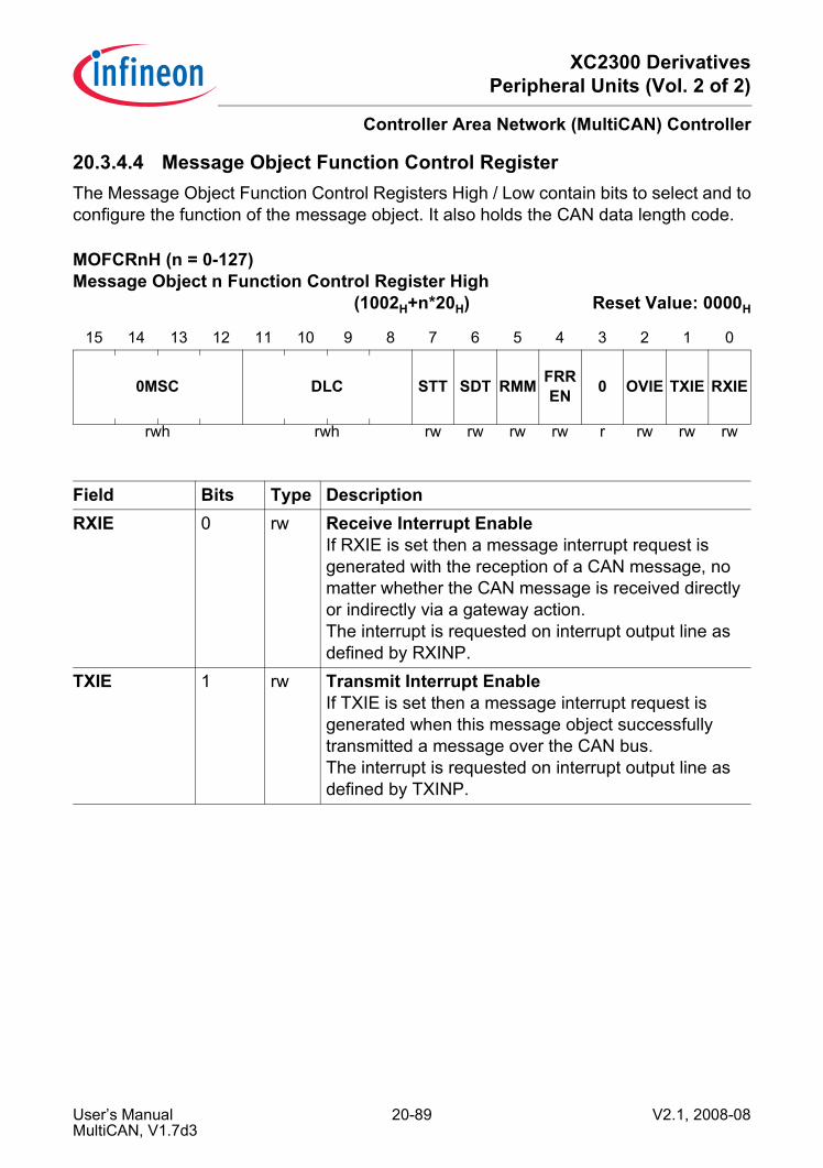
XC2300 DerivativesPeripheral Units (Vol. 2 of 2)
Controller Area Network (MultiCAN) Controller
20.3.4.4 Message Object Function Control RegisterThe Message Object Function Control Registers High / Low contain bits to select and toconfigure the function of the message object. It also holds the CAN data length code.
MOFCRnH (n = 0-127) Message Object n Function Control Register High
(1002H+n*20H) Reset Value: 0000H
15 14 13 12 11 10 9 8 7 6 5 4 3 2 1 0
0MSC DLC STT SDT RMM FRREN 0 OVIE TXIE RXIE
rwh rwh rw rw rw rw r rw rw rw
Field Bits Type DescriptionRXIE 0 rw Receive Interrupt Enable
If RXIE is set then a message interrupt request is generated with the reception of a CAN message, no matter whether the CAN message is received directly or indirectly via a gateway action.The interrupt is requested on interrupt output line as defined by RXINP.
TXIE 1 rw Transmit Interrupt EnableIf TXIE is set then a message interrupt request is generated when this message object successfully transmitted a message over the CAN bus.The interrupt is requested on interrupt output line as defined by TXINP.
User’s Manual 20-89 V2.1, 2008-08MultiCAN, V1.7d3
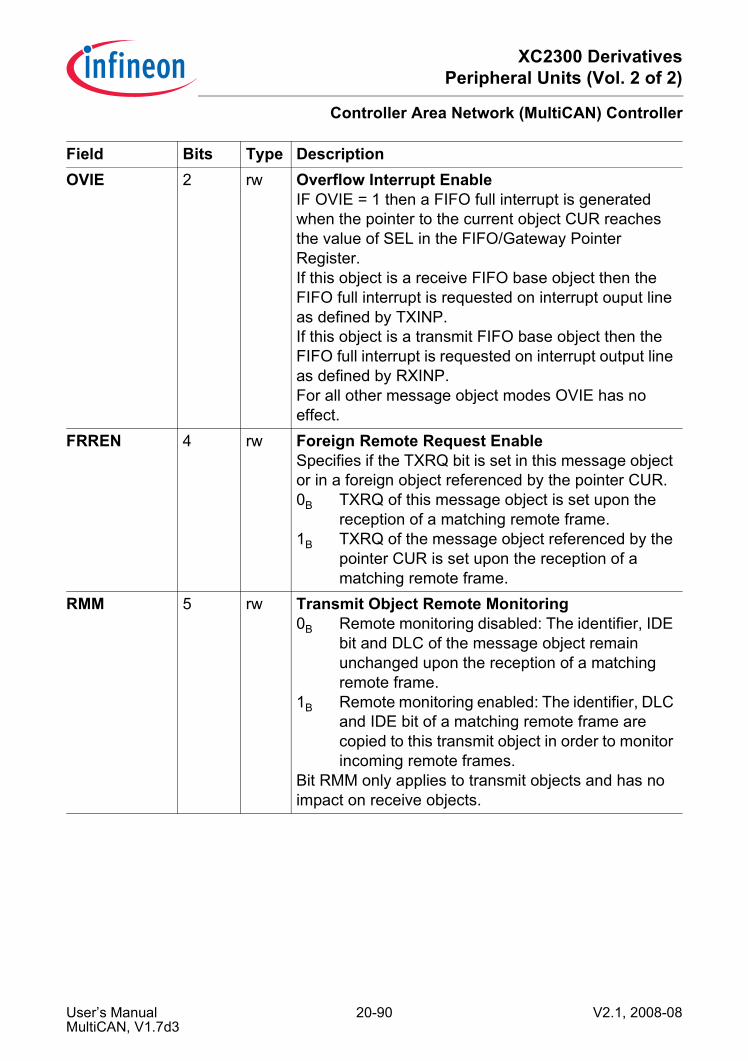
XC2300 DerivativesPeripheral Units (Vol. 2 of 2)
Controller Area Network (MultiCAN) Controller
OVIE 2 rw Overflow Interrupt EnableIF OVIE = 1 then a FIFO full interrupt is generated when the pointer to the current object CUR reaches the value of SEL in the FIFO/Gateway Pointer Register.If this object is a receive FIFO base object then the FIFO full interrupt is requested on interrupt ouput line as defined by TXINP.If this object is a transmit FIFO base object then the FIFO full interrupt is requested on interrupt output line as defined by RXINP.For all other message object modes OVIE has no effect.
FRREN 4 rw Foreign Remote Request EnableSpecifies if the TXRQ bit is set in this message object or in a foreign object referenced by the pointer CUR.0B TXRQ of this message object is set upon the
reception of a matching remote frame.1B TXRQ of the message object referenced by the
pointer CUR is set upon the reception of a matching remote frame.
RMM 5 rw Transmit Object Remote Monitoring0B Remote monitoring disabled: The identifier, IDE
bit and DLC of the message object remain unchanged upon the reception of a matching remote frame.
1B Remote monitoring enabled: The identifier, DLC and IDE bit of a matching remote frame are copied to this transmit object in order to monitor incoming remote frames.
Bit RMM only applies to transmit objects and has no impact on receive objects.
Field Bits Type Description
User’s Manual 20-90 V2.1, 2008-08MultiCAN, V1.7d3

XC2300 DerivativesPeripheral Units (Vol. 2 of 2)
Controller Area Network (MultiCAN) Controller
SDT 6 rw Single Data TransferIf SDT = 1 and this object is not a FIFO base object then MSGVAL is reset when this object has taken part in a successful data transfer (receive or transmit).If SDT = 1 and this object is a FIFO base object then MSGVAL is reset when the pointer to the current object CUR reaches the value of SEL in the FIFO/Gateway Pointer Register.With SDT = 0, bit MSGVAL is not affected.
STT 7 rw Single Transmit TrialIf this bit is set then TXRQ is cleared upon transmission start of this message object. Thus no transmission retry is performed in case of transmission failure.
DLC [11:8] rwh Data Length CodeValid values for the data length are 0 to 8.DLC>8 leads to 8 data bytes, but the DLC code is not truncated upon reception or transmission of CAN frames.
0 [15:12] r Reserved;read as 0; should be written with 0.
0 3 r Reserved;read as 0; should be written with 0.
MOFCRnL (n = 0-127) Message Object n Function Control Register Low
(1000H+n*20H) Reset Value: 0000H
15 14 13 12 11 10 9 8 7 6 5 4 3 2 1 0
0 DATC
DLCC IDC GDF
S 0 MMC
r rw rw rw rw r rw
Field Bits Type Description
User’s Manual 20-91 V2.1, 2008-08MultiCAN, V1.7d3

XC2300 DerivativesPeripheral Units (Vol. 2 of 2)
Controller Area Network (MultiCAN) Controller
Field Bits Type DescriptionMMC [3:0] rw Message Mode Control
Bit field MMC controls the functionality of the message object.0000B Standard Message Object0001B Receive FIFO Base Object0010B Transmit FIFO Base Object0011B Transmit FIFO Slave Object0100B Gateway Source ObjectelseB Reserved
GDFS 8 rw Gateway Data Frame Send1B TXRQ is set in the gateway destination object
after the transfer of a data frame from the gateway source to the gateway destination.
0B TXRQ is not set in the destination object.Applicable only to Gateway Source Object.
IDC 9 rw Identifier CopyIF IDC = 1 then the identifier of the gateway source object (after storing the received frame in the source) is copied to the gateway destination.Applicable only to Gateway Source Object.
DLCC 10 rw Data Length Code CopyIf DLCC = 1 then the data length code of the gateway source object (after storing the received frame in the source) is copied to the gateway destination.Applicable only to Gateway Source Object.
DATC 11 rw Data CopyIf DATC = 1 then the data field (registers MODATA0 and MODATA4) of the gateway source object (after storing the received frame in the source) is copied to the gateway destination.Applicable only to Gateway Source Object.
0 [7:4],[15:12]
r reserved;returns ’0’ if read; should be written with ’0’;
User’s Manual 20-92 V2.1, 2008-08MultiCAN, V1.7d3

XC2300 DerivativesPeripheral Units (Vol. 2 of 2)
Controller Area Network (MultiCAN) Controller
20.3.4.5 Message Object FIFO/Gateway Pointer RegisterThe Message Object FIFO/Gateway Pointer Registers H/L contain a set of messageobject link pointer used for FIFO and gateway functionality
MOFGPRnH (n = 0-127) Message Object n FIFO/Gateway Pointer Register High
(1006H+n*20H) Reset Value: 0000H
15 14 13 12 11 10 9 8 7 6 5 4 3 2 1 0
SEL CUR
rw rwh
Field Bits Type DescriptionCUR [7:0] rwh Current Object Pointer
The Current Object Pointer links to the actual target object within a FIFO/Gateway structure.After a FIFO/gateway operation CUR is updated with the message number of the next message object in the list structure (given by PNEXT of the message control register) until it reaches the FIFO top element (given by TOP) when it is reset to the bottom element (given by BOT).
SEL [15:8] rw Object Select PointerThe Object Select Pointer is the second (software) pointer to complement the hardware pointer CUR in the FIFO structure. SEL is used for monitoring purposes only.
MOFGPRnL (n = 0-127) Message Object n FIFO/Gateway Pointer Register Low
(1004H+n*20H) Reset Value: 0000H
15 14 13 12 11 10 9 8 7 6 5 4 3 2 1 0
TOP BOT
rw rw
User’s Manual 20-93 V2.1, 2008-08MultiCAN, V1.7d3

XC2300 DerivativesPeripheral Units (Vol. 2 of 2)
Controller Area Network (MultiCAN) Controller
Note: The pointers in this register must be set to objects assigned to the same CANnode. It is forbidden to refer to objects that are not in the linked list for the sameCAN node.
Field Bits Type DescriptionBOT [7:0] rw Bottom Pointer
The Bottom Pointer points to the first element in a FIFO structure.
TOP [15:8] rw Top PointerThe TOP pointer points to the last element in a FIFO structure.
User’s Manual 20-94 V2.1, 2008-08MultiCAN, V1.7d3

XC2300 DerivativesPeripheral Units (Vol. 2 of 2)
Controller Area Network (MultiCAN) Controller
20.3.4.6 Message Object Acceptance Mask RegisterRegisters MOAMR H/L contain the mask bits for the acceptance filtering of the mesageobject.
MOAMRnH (n = 0-127) Message Object n Acceptance Mask Register High
(100EH+n*20H) Reset Value: 3FFFH
15 14 13 12 11 10 9 8 7 6 5 4 3 2 1 0
0 MIDE AM[28:16]
r rw rw
Field Bits Type DescriptionAM[28:16] [12:0] rw Acceptance Mask for Message Identifier High
see description of MOAMRnL.AM[15:0]MIDE 13 rw Acceptance Mask bit for Message IDE bit
0B This message objects accepts the reception of both standard and extended frames.
1B This message object only receives frames with matching IDE bit.
0 [15:14] r Reserved;read as 0; should be written with 0.
MOAMRnL (n = 0-127) Message Object n Acceptance Mask Register Low
(100CH+n*20H) Reset Value: FFFFH
15 14 13 12 11 10 9 8 7 6 5 4 3 2 1 0
AM[15:0]
rw
User’s Manual 20-95 V2.1, 2008-08MultiCAN, V1.7d3

XC2300 DerivativesPeripheral Units (Vol. 2 of 2)
Controller Area Network (MultiCAN) Controller
Field Bits Type DescriptionAM[15:0] [15:0] rw Acceptance Mask for Message Identifier
Mask to filter incoming messages with standard identifiers (AM[28:18]) or extended identifiers (AM[28:0]). For standard identifiers bits AM[17:0] are “don’t care”.
User’s Manual 20-96 V2.1, 2008-08MultiCAN, V1.7d3
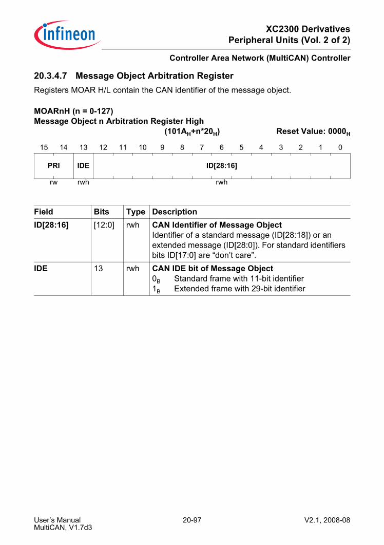
XC2300 DerivativesPeripheral Units (Vol. 2 of 2)
Controller Area Network (MultiCAN) Controller
20.3.4.7 Message Object Arbitration RegisterRegisters MOAR H/L contain the CAN identifier of the message object.
MOARnH (n = 0-127) Message Object n Arbitration Register High
(101AH+n*20H) Reset Value: 0000H
15 14 13 12 11 10 9 8 7 6 5 4 3 2 1 0
PRI IDE ID[28:16]
rw rwh rwh
Field Bits Type DescriptionID[28:16] [12:0] rwh CAN Identifier of Message Object
Identifier of a standard message (ID[28:18]) or an extended message (ID[28:0]). For standard identifiers bits ID[17:0] are “don’t care”.
IDE 13 rwh CAN IDE bit of Message Object0B Standard frame with 11-bit identifier1B Extended frame with 29-bit identifier
User’s Manual 20-97 V2.1, 2008-08MultiCAN, V1.7d3

XC2300 DerivativesPeripheral Units (Vol. 2 of 2)
Controller Area Network (MultiCAN) Controller
PRI [15:14] rw Priority ClassPRI assigns one of the four priority classes 0, 1, 2, 3 to the message object, with lower PRI number meaning higher priority. Message objects with lower PRI value always win acceptance filtering for frame reception and transmission over message objects with higher PRI value. Acceptance filtering based on identifier/mask and list position is only performed between message objects of the same priority class.PRI also defines the acceptance filtering method for transmission:00B Reserved. Transmit objects with PRI = 00 are
not taken into account for the transmit acceptance filtering.
01B Transmit acceptance filtering is based on the list order, i.e. this message object is considered for transmission only if there is no other message object with valid transmit request (MSGVAL & TXRQ & TXEN0 & TXEN1 = 1) somewhere before this object in the list.
10B Transmit acceptance filtering is based on the CAN identifier, i.e. this message object is considered for transmission only if there is no other message object with higher priority identifier+IDE+DIR (with respect to CAN arbitration rules) somewhere in the list.
11B Transmit acceptance filtering is based on the list order (like PRI = 01).
MOARnL (n = 0-127) Message Object n Arbitration Register Low
(1018H+n*20H) Reset Value: 0000H
15 14 13 12 11 10 9 8 7 6 5 4 3 2 1 0
ID[15:0]
rwh
Field Bits Type Description
User’s Manual 20-98 V2.1, 2008-08MultiCAN, V1.7d3

XC2300 DerivativesPeripheral Units (Vol. 2 of 2)
Controller Area Network (MultiCAN) Controller
Transmit Priority
Field Bits Type DescriptionID[15:0] [15:0] rwh CAN Identifier of Message Object Low
Identifier of a standard message (ID[28:18]) or an extended message (ID[28:0]). For standard identifiers bits ID[17:0] are “don’t care”.
Table 20-13 Transmit Priority based on CAN Arbitration RulesSettings of arbitrarily chosen message objects A and B,where A has higher transmit priority than B
Comment
A.MOAR[28:18] < B.MOAR[28:18](11 bit standard identifier of A less than 11 bit standard identifier of B)
Messages with lower standard identifier have higher priority than messages with higher standard identifier. MOAR[28] is the most significant bit (MSB) of the standard identifier. MOAR[18] is the least significant bit of the standard identifier.
A.MOAR[28:18] = B.MOAR[28:18]A.MOAR.IDE = 0 (send standard frame)B.MOAR.IDE = 1 (send extended frame)
Standard frames have higher transmit priority than extended frames with equal standard identifier.
A.MOAR[28:18] = B.MOAR[28:18]A.MOAR.IDE = B.MOAR.IDE = 0A.MOCTR.DIR = 1 (send data frame)B.MOCTR.DIR = 0 (send remote frame)
Standard data frames have higher transmit priority than standard remote frames with equal identifier.
A.MOAR[28:0] = B.MOAR[28:0]A.MOAR.IDE = B.MOAR.IDE = 1A.MOCTR.DIR = 1 (send data frame)B.MOCTR.DIR = 0 (send remote frame)
Extended data frames have higher transmit priority than extended remote frames with equal identifier.
A.MOAR[28:0] < B.MOAR[28:0]A.MOAR.IDE = B.MOAR.IDE = 1(29 bit identifier)
Extended frames with lower identifier have higher transmit priority than extended frames with higher identifier. MOAR[28] is the most significant bit (MSB) of the overall identifier (standard identifier MOAR[28:18] and identifier extension MOAR[17:0]). MOAR[0] is the least significant bit (LSB) of the overall identifier.
User’s Manual 20-99 V2.1, 2008-08MultiCAN, V1.7d3

XC2300 DerivativesPeripheral Units (Vol. 2 of 2)
Controller Area Network (MultiCAN) Controller
20.3.4.8 Message Object Data Registers
MODATAnLH (n = 0-127) Message Object n Data Register Low High
(1012H+n*20H) Reset Value: 0000H
15 14 13 12 11 10 9 8 7 6 5 4 3 2 1 0
DB3 DB2
rwh rwh
Field Bits Type DescriptionDB2 [7:0] rwh CAN Data Byte 2DB3 [15:8] rwh CAN Data Byte 3
MODATAnLL (n = 0-127) Message Object n Data Register Low Low
(1010H+n*20H) Reset Value: 0000H
15 14 13 12 11 10 9 8 7 6 5 4 3 2 1 0
DB1 DB0
rwh rwh
Field Bits Type DescriptionDB0 [7:0] rwh CAN Data Byte 0DB1 [15:8] rwh CAN Data Byte 1
User’s Manual 20-100 V2.1, 2008-08MultiCAN, V1.7d3
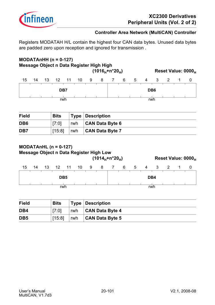
XC2300 DerivativesPeripheral Units (Vol. 2 of 2)
Controller Area Network (MultiCAN) Controller
Registers MODATAH H/L contain the highest four CAN data bytes. Unused data bytesare padded zero upon reception and ignored for transmission .
MODATAnHH (n = 0-127) Message Object n Data Register High High
(1016H+n*20H) Reset Value: 0000H
15 14 13 12 11 10 9 8 7 6 5 4 3 2 1 0
DB7 DB6
rwh rwh
Field Bits Type DescriptionDB6 [7:0] rwh CAN Data Byte 6DB7 [15:8] rwh CAN Data Byte 7
MODATAnHL (n = 0-127) Message Object n Data Register High Low
(1014H+n*20H) Reset Value: 0000H
15 14 13 12 11 10 9 8 7 6 5 4 3 2 1 0
DB5 DB4
rwh rwh
Field Bits Type DescriptionDB4 [7:0] rwh CAN Data Byte 4DB5 [15:8] rwh CAN Data Byte 5
User’s Manual 20-101 V2.1, 2008-08MultiCAN, V1.7d3

XC2300 DerivativesPeripheral Units (Vol. 2 of 2)
Controller Area Network (MultiCAN) Controller
20.4 General Control and StatusThe following section describes the general clock, debug and interrupt topics.
20.4.1 Clock ControlThe CAN clock frequency fCAN of the functional blocks of the MultiCAN module is derivedfrom the system clock fSYS (= clock on the system bus). The fractional divider FDIV in themodule is used to generate the CAN clock frequency for the bit timing calculation. Thisfrequency is identical for all CAN nodes. The scheduler itself is in the fSYS domain. Theclock generation can be enabled/disabled by the fractional divider control bit fieldFDR.DM.
Figure 20-17 MultiCAN Clock Generation
The fractional divider FDIV output fCAN is based on the system clock fSYS, but only everyn-th clock pulse is taken. The register file is in the system frequency domain. Thesuspend signal (coming as acknowledge from the module as answer to the OCDSsuspend request) freezes or resets the fractional divider.Note: The receive input line contains a synchronization stage to ensure stable input
data. Together with the internal CAN state machine, this leads to a minimumreaction time of at least 3 clock cycles of fSYS between CAN input and output. Theswitching delay of the input stages can be generally neglected, whereas therise/fall times of the port output drivers (programmable values) should be takeninto account, especially for higher baud rates.
The table below indicates the minimum frequencies of fSYS in MHz for MultiCAN moduleoperation (acceptance filtering, MO handling, etc.), that are required for a baud rate of1 Mbit/s for the active CAN nodes (the highest CAN baud rate of the activated CANnodes has to be taken into account). If less baud rate is desired, the values can be scaledlinearly (e.g. for a maximum of 500 kbit/s, 50% of the indicated value are required).
FDIV baud rateprescalers
MultiCAN_clocks--
fSYS fCAN
register file
User’s Manual 20-102 V2.1, 2008-08MultiCAN, V1.7d3
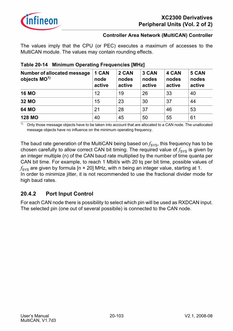
XC2300 DerivativesPeripheral Units (Vol. 2 of 2)
Controller Area Network (MultiCAN) Controller
The values imply that the CPU (or PEC) executes a maximum of accesses to theMultiCAN module. The values may contain rounding effects.
The baud rate generation of the MultiCAN being based on fSYS, this frequency has to bechosen carefully to allow correct CAN bit timing. The required value of fSYS is given byan integer multiple (n) of the CAN baud rate multiplied by the number of time quanta perCAN bit time. For example, to reach 1 Mbit/s with 20 tq per bit time, possible values offSYS are given by formula [n × 20] MHz, with n being an integer value, starting at 1.In order to minimize jitter, it is not recommended to use the fractional divider mode forhigh baud rates.
20.4.2 Port Input ControlFor each CAN node there is possibility to select which pin will be used as RXDCAN input.The selected pin (one out of several possibile) is connected to the CAN node.
Table 20-14 Minimum Operating Frequencies [MHz]Number of allocated message objects MO1)
1) Only those message objects have to be taken into account that are allocated to a CAN node. The unallocatedmessage objects have no influence on the minimum operating frequency.
1 CAN nodeactive
2 CAN nodesactive
3 CAN nodesactive
4 CAN nodesactive
5 CAN nodesactive
16 MO 12 19 26 33 4032 MO 15 23 30 37 4464 MO 21 28 37 46 53128 MO 40 45 50 55 61
User’s Manual 20-103 V2.1, 2008-08MultiCAN, V1.7d3

XC2300 DerivativesPeripheral Units (Vol. 2 of 2)
Controller Area Network (MultiCAN) Controller
20.4.3 Suspend ModeThe suspend mode can be triggered by the OCDS in order to freeze the state of themodule and to have access to the registers (at least for read actions). There are severalaspects related to the suspend mode:• All actions are immediately stopped ("hard suspend"):
The module clock is switched off as soon as the suspend line becomes active. Thismode is supported by the fast switch off feature of the BPI. Write actions to themodule are not supported and only combinatorial read actions deliver the desireddata (the CAN RAM and the CAN registers can not be accessed).In this mode, all further module actions are disabled and there is a very highprobability that the communication with other devices is made impossible and that theCAN bus is blocked by the device in hard suspend mode (e.g. if the suspended CANjust sends a dominant level). A normal continuation when the suspend mode is left isnot always possible and reset must be activated.
• The current action is finished ("soft suspend"):The module functions are stopped (clock is still running!) automatically after internalactions have been finished, for example after a CAN frame has been sent out. Dueto this behavior, the communication network is not blocked due to the suspend modeof one communication partner. Furthermore, all registers are accessible for read andwrite actions. As a result, the debugger can stop the module actions and modifyregisters. These modifications are taken into account after the suspend mode is left.This mode is designed to be able to modify registers or to read them by the OCDSwhile the rest of the systems is still running and not corrupted by the suspend mode.
In the MultiCAN module a suspend mechanism is implemented allowing the individualfreeze of CAN nodes. The fast switch off feature (hard suspend) of the BPI must not beactivated by the user in order to support the soft suspend mode. In order to allow therequired flexibility for the system, each CAN node can be individually enabled for the softsuspend mode.The hard suspend feature can be enabled/disabled for the complete MultiCAN module,whereas the soft suspend feature can be enabled/disabled independently for each CANnode. The fractional divider disables the CAN clock only if all CAN nodes signal that theycan be suspended. A CAN node that is not active can always be suspended.
User’s Manual 20-104 V2.1, 2008-08MultiCAN, V1.7d3

XC2300 DerivativesPeripheral Units (Vol. 2 of 2)
Controller Area Network (MultiCAN) Controller
20.4.4 Interrupt StructureThe general interrupt structure is shown in the figure below. The interrupt event cantrigger the interrupt generation. The interrupt pulse is generated independently from theinterrupt flag in the interrupt status register. The interrupt flag can be reset by SW bywriting a 0 to it.If enabled by the related interrupt enable bit in the interrupt enable register, an interruptpulse can be generated at one of the 16 interrupt output lines INT_Ox of the module. Ifmore than one interrupt source is connected to the same interrupt node pointer (in theinterrupt node pointer register), the requests are combined to one common line.
Figure 20-18 General Interrupt Structure
int_event ANDint_enable
int_flagint_reset_SW INP
OR
other interrupt sourceson the same INP
to INT_O0
to INT_O1
...
to INT_O15
MultiCAN_int_struct
User’s Manual 20-105 V2.1, 2008-08MultiCAN, V1.7d3

XC2300 DerivativesPeripheral Units (Vol. 2 of 2)
Controller Area Network (MultiCAN) Controller
20.5 MultiCAN Module ImplementationThis section describes CAN module interfaces with the clock control, port connections,interrupt control, and address decoding.
20.5.1 Interfaces of the CAN ModuleFigure 20-19 shows the XC2300 specific implementation details and interconnections ofthe CAN module. The I/O lines of the CAN module kernel (two I/O lines of each CANnode) are connected to the ports as described in Table 20-18. The CAN module isfurther supplied by clock control, interrupt control, and address decoding logic.
Figure 20-19 CAN Module Implementation and Interconnections
The MultiCAN interrupt control register x is connected to the CAN interrupt output lineINT_Ox, with x = 15 - 0. Additionally, the signal INT_O15 can be used to start timers.
mc_multican_block5.vsd
MultiCAN Module Kernel
InterruptControl
fCAN
PortControlCAN
Node 1
CAN Control
MessageObjectBuffer
128Objects
CANNode 0
LinkedList
Control
ClockControl
AddressDecoder
CANNode 4
TXDC4RXDC4
TXDC1RXDC1
TXDC0RXDC0
.
.
.
.
.
.
.
.
.
User’s Manual 20-106 V2.1, 2008-08MultiCAN, V1.7d3

XC2300 DerivativesPeripheral Units (Vol. 2 of 2)
Controller Area Network (MultiCAN) Controller
20.5.2 Module Clock GenerationAs shown in Figure 20-20, the clock signals for the MultiCAN module are generated andcontrolled by a clock generation unit. This clock generation unit is responsible for theenable/disable control, the clock frequency adjustment, and the debug clock control.The frequency control of the module timer clock fCAN is performed via the CAN_FDRregister.
Figure 20-20 MultiCAN Module Clock Generation
The module control clock fSYS is used inside the MultiCAN module kernel for controlpurposes such as e.g. for clocking of control logic and register operations. The frequencyof fSYS is identical to the system clock frequency fSYS.The module timer clock fCAN is used inside the MultiCAN module kernels as input clockfor all timing relevant operations.The frequency of fCAN is defined by:
Note: The upper formula applies to normal divider mode of the fractional divider(CAN_FDR.DM = 01B). The lower formula applies to fractional divider mode(CAN_FDR.DM = 10B).
Note: Input signal ECEN of the MultiCAN fractional divider is wired to 0.
20.5.2.1 Fractional Divider OverviewThe fractional divider allows to generate output clocks from an input clock using aprogrammable divider. The fractional divider divides an input clock fIN either by the factor1/n or by a fraction of n/1024 for any value of n from 0 to 1023 and outputs the clock
CANClockGen_P11
fSYS
MultiCAN Clock Generation
fCANfSYS Fractional DividerRegister
CAN_FDR
1fCAN = fSYS × n with n = 1024 - CAN_FDR.STEP
or fCAN = fSYS × 1024 with n = 0-1023
n
User’s Manual 20-107 V2.1, 2008-08MultiCAN, V1.7d3
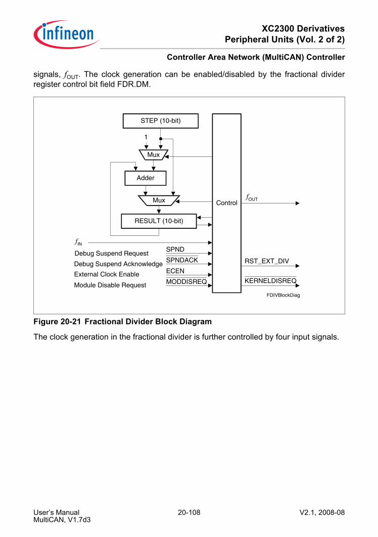
XC2300 DerivativesPeripheral Units (Vol. 2 of 2)
Controller Area Network (MultiCAN) Controller
signals, fOUT. The clock generation can be enabled/disabled by the fractional dividerregister control bit field FDR.DM.
Figure 20-21 Fractional Divider Block Diagram
The clock generation in the fractional divider is further controlled by four input signals.
FDIVBlockDiag
fIN
fOUT
RESULT (10-bit)
STEP (10-bit)
Mux
Adder
Control
Mux
1
Debug Suspend Request
Debug Suspend Acknowledge RST_EXT_DIV
External Clock Enable ECEN
SPND
Module Disable Request
SPNDACK
MODDISREQ KERNELDISREQ
User’s Manual 20-108 V2.1, 2008-08MultiCAN, V1.7d3
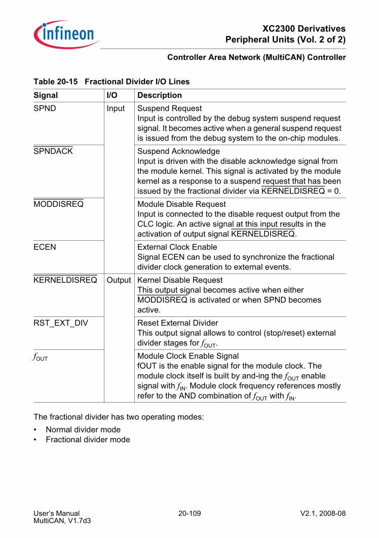
XC2300 DerivativesPeripheral Units (Vol. 2 of 2)
Controller Area Network (MultiCAN) Controller
The fractional divider has two operating modes:• Normal divider mode• Fractional divider mode
Table 20-15 Fractional Divider I/O LinesSignal I/O DescriptionSPND Input Suspend Request
Input is controlled by the debug system suspend request signal. It becomes active when a general suspend request is issued from the debug system to the on-chip modules.
SPNDACK Suspend AcknowledgeInput is driven with the disable acknowledge signal from the module kernel. This signal is activated by the module kernel as a response to a suspend request that has been issued by the fractional divider via KERNELDISREQ = 0.
MODDISREQ Module Disable RequestInput is connected to the disable request output from the CLC logic. An active signal at this input results in the activation of output signal KERNELDISREQ.
ECEN External Clock EnableSignal ECEN can be used to synchronize the fractional divider clock generation to external events.
KERNELDISREQ Output Kernel Disable RequestThis output signal becomes active when either MODDISREQ is activated or when SPND becomes active.
RST_EXT_DIV Reset External DividerThis output signal allows to control (stop/reset) external divider stages for fOUT.
fOUT Module Clock Enable SignalfOUT is the enable signal for the module clock. The module clock itself is built by and-ing the fOUT enable signal with fIN. Module clock frequency references mostly refer to the AND combination of fOUT with fIN.
User’s Manual 20-109 V2.1, 2008-08MultiCAN, V1.7d3
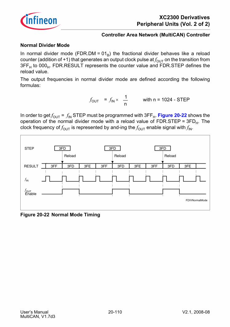
XC2300 DerivativesPeripheral Units (Vol. 2 of 2)
Controller Area Network (MultiCAN) Controller
Normal Divider ModeIn normal divider mode (FDR.DM = 01B) the fractional divider behaves like a reloadcounter (addition of +1) that generates an output clock pulse at fOUT on the transition from3FFH to 000H. FDR.RESULT represents the counter value and FDR.STEP defines thereload value.The output frequencies in normal divider mode are defined according the followingformulas:
In order to get fOUT = fIN STEP must be programmed with 3FFH. Figure 20-22 shows theoperation of the normal divider mode with a reload value of FDR.STEP = 3FDH. Theclock frequency of fOUT is represented by and-ing the fOUT enable signal with fIN.
Figure 20-22 Normal Mode Timing
1fOUT = fIN × n
with n = 1024 - STEP
FDIVNormalMode
RESULT 3FF
fIN
3FE3FD 3FF 3FD3FD 3FE 3FF
3FD
3FE
STEP
Reload
3FD
Reload
3FD
Reload
fOUTEnable
User’s Manual 20-110 V2.1, 2008-08MultiCAN, V1.7d3

XC2300 DerivativesPeripheral Units (Vol. 2 of 2)
Controller Area Network (MultiCAN) Controller
Fractional Divider ModeWhen the fractional divider mode is selected (FDR.DM = 10B), the output clock fOUT isderived from the input clock fIN by division of a fraction of n/1024 for any value of n from0 to 1023. In general, the fractional divider mode allows to program the average outputclock frequency with a higher accuracy than in normal divider mode.In fractional divider mode an output clock pulse at fOUT is generated dependent on theresult of the addition FDR.RESULT + FDR.STEP. If the addition leads to an overflowover 3FFH a pulse is generated at fOUT. Note that in fractional divider mode the clock fOUTcan have a maximum period jitter of one fIN clock period.The output frequencies in fractional divider mode are defined according the followingformulas:
Figure 20-23 shows the operation of the fractional divider mode with a reload value ofFDR.STEP = 234H (= factor 564/1024 = 0.55). The clock frequency of fOUT isrepresented by and-ing the fOUT enable signal with fIN.
Figure 20-23 Fractional Divider Mode Timing
Suspend Mode ControlThe fractional divider allows to control its operation according to the input SuspendRequest (SPND). This input is activated in suspend mode by the on-chip debug controllogic. In suspend mode, the module registers are accessible for read and write actions,but the other module internal functions are frozen. Suspend mode is requested bySPND = 1. Suspend mode is entered one fIN clock cycle after the suspend mode requesthas been acknowledged by setting SPNDACK to 0 (granted suspend mode) and
nfOUT = fIN ×
1024 with n = 0-1023
RESULT 150
fIN
STEP = 234H : fOUT = 0.55 x fIN
fOUTEnable
384 1B8
+234
3EC 220 054 288 0BC 2F0 124 358 18C
+234 +234 +234 +234 +234 +234 +234 +234
3C0
+234 +234 +234 +234
FDIVFraDivMode
User’s Manual 20-111 V2.1, 2008-08MultiCAN, V1.7d3
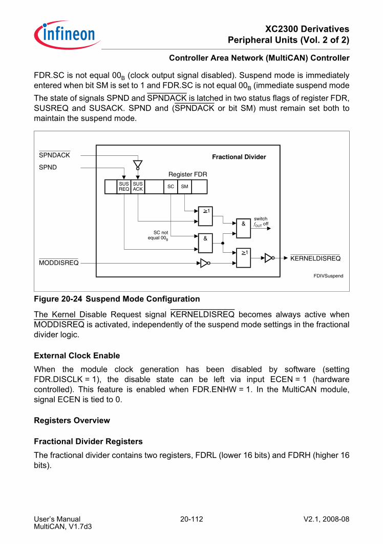
XC2300 DerivativesPeripheral Units (Vol. 2 of 2)
Controller Area Network (MultiCAN) Controller
FDR.SC is not equal 00B (clock output signal disabled). Suspend mode is immediatelyentered when bit SM is set to 1 and FDR.SC is not equal 00B (immediate suspend modeThe state of signals SPND and SPNDACK is latched in two status flags of register FDR,SUSREQ and SUSACK. SPND and (SPNDACK or bit SM) must remain set both tomaintain the suspend mode.
Figure 20-24 Suspend Mode Configuration
The Kernel Disable Request signal KERNELDISREQ becomes always active whenMODDISREQ is activated, independently of the suspend mode settings in the fractionaldivider logic.
External Clock EnableWhen the module clock generation has been disabled by software (settingFDR.DISCLK = 1), the disable state can be left via input ECEN = 1 (hardwarecontrolled). This feature is enabled when FDR.ENHW = 1. In the MultiCAN module,signal ECEN is tied to 0.
Registers Overview
Fractional Divider RegistersThe fractional divider contains two registers, FDRL (lower 16 bits) and FDRH (higher 16bits).
FDIVSuspend
SUSREQ
SUSACK
&
SPNDRegister FDR
Fractional DividerSPNDACK
MODDISREQKERNELDISREQ
SC
>1
SC notequal 00B
&switchfOUT off
>1
SM
User’s Manual 20-112 V2.1, 2008-08MultiCAN, V1.7d3

XC2300 DerivativesPeripheral Units (Vol. 2 of 2)
Controller Area Network (MultiCAN) Controller
FDRLFractional Divider Register L (0CH) Reset Value: 0000H
15 14 13 12 11 10 9 8 7 6 5 4 3 2 1 0
DM SC SM 0 STEP
rw rw rw r rw
Field Bits Type DescriptionSTEP [9:0] rw Step Value
In normal divider mode STEP contains the reload value for RESULT.In fractional divider mode this bit field defines the 10-bit value that is added to the RESULT with each input clock cycle.
SM 11 rw Suspend ModeSM selects between granted or immediate suspend mode.0 Granted suspend mode selected1 Immediate suspend mode selected
SC [13:12] rw Suspend ControlThis bit field defines the behavior of the fractional divider in suspend mode (bit SUSREQ and SUSACK set).00 Clock generation continues.01 Clock generation is stopped and the clock
output signals are not generated. RESULT is not changed except when writing bit field DM with 01B or 10B.
10 Clock generation is stopped and the clock output signals are not generated. RESULT is loaded with 3FFH.
11 Same as SC = 10B but RST_EXT_DIV is 1 (independently of bit field DM).
User’s Manual 20-113 V2.1, 2008-08MultiCAN, V1.7d3
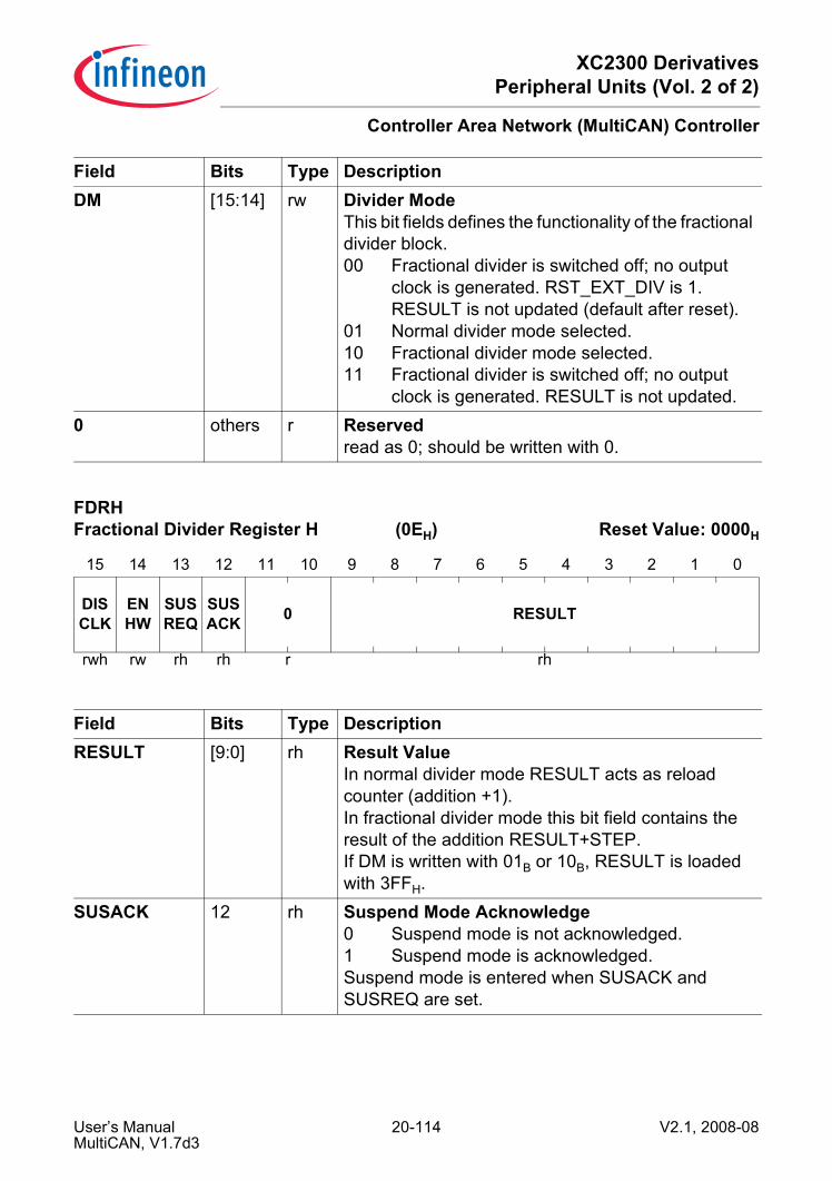
XC2300 DerivativesPeripheral Units (Vol. 2 of 2)
Controller Area Network (MultiCAN) Controller
DM [15:14] rw Divider ModeThis bit fields defines the functionality of the fractional divider block.00 Fractional divider is switched off; no output
clock is generated. RST_EXT_DIV is 1. RESULT is not updated (default after reset).
01 Normal divider mode selected.10 Fractional divider mode selected.11 Fractional divider is switched off; no output
clock is generated. RESULT is not updated.0 others r Reserved
read as 0; should be written with 0.
FDRHFractional Divider Register H (0EH) Reset Value: 0000H
15 14 13 12 11 10 9 8 7 6 5 4 3 2 1 0
DISCLK
ENHW
SUSREQ
SUSACK 0 RESULT
rwh rw rh rh r rh
Field Bits Type DescriptionRESULT [9:0] rh Result Value
In normal divider mode RESULT acts as reload counter (addition +1).In fractional divider mode this bit field contains the result of the addition RESULT+STEP.If DM is written with 01B or 10B, RESULT is loaded with 3FFH.
SUSACK 12 rh Suspend Mode Acknowledge0 Suspend mode is not acknowledged.1 Suspend mode is acknowledged.Suspend mode is entered when SUSACK and SUSREQ are set.
Field Bits Type Description
User’s Manual 20-114 V2.1, 2008-08MultiCAN, V1.7d3

XC2300 DerivativesPeripheral Units (Vol. 2 of 2)
Controller Area Network (MultiCAN) Controller
Fractional Divider Operation Modes
SUSREQ 13 rh Suspend Mode Request0 Suspend mode is not requested.1 Suspend mode is requested.Suspend mode is entered when SUSREQ and SUSACK are set.
ENHW 14 rw Enable Hardware Clock Control0 Bit DISCLK cannot be reset by HW by a high
level at input signal ECEN.1 Bit DISCLK is reset by hardware while input
signal ECEN is at high level.DISCLK 15 rwh Disable Clock
0 Clock generation of fOUT is enabled according to the setting of bit field DM.
1 Fractional divider is stopped. The enable signal fOUT becomes inactive. No change except when writing bit field DM.
0 others r Reservedread as 0; should be written with 0.
Table 20-16 Fractional Divider Function TableMode SC DM RES_EXT
_DIVRESULT fOUT Operation of
Fractional Divider
Normal Mode
– 00 1 unchanged inactive switched off01 0 continuously
updated1)active normal divider
mode10 fractional divider
mode11 unchanged inactive switched off
Field Bits Type Description
User’s Manual 20-115 V2.1, 2008-08MultiCAN, V1.7d3
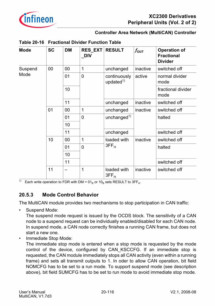
XC2300 DerivativesPeripheral Units (Vol. 2 of 2)
Controller Area Network (MultiCAN) Controller
20.5.3 Mode Control BehaviorThe MultiCAN module provides two mechanisms to stop participation in CAN traffic:• Suspend Mode:
The suspend mode request is issued by the OCDS block. The sensitivity of a CANnode to a suspend request can be individually enabled/disabled for each CAN node.In suspend mode, a CAN node correctly finishes a running CAN frame, but does notstart a new one.
• Immediate Stop Mode:The immediate stop mode is entered when a stop mode is requested by the modecontrol of the device, configured by CAN_KSCCFG. If an immediate stop isrequested, the CAN module immediately stops all CAN activity (even within a runningframe) and sets all transmit outputs to 1. In oder to allow CAN operation, bit fieldNOMCFG has to be set to a run mode. To support suspend mode (see descriptionabove), bit field SUMCFG has to be set to run mode to avoid immediate stop mode.
Suspend Mode
00 00 1 unchanged inactive switched off01 0 continuously
updated1)active normal divider
mode10 fractional divider
mode11 unchanged inactive switched off
01 00 1 unchanged inactive switched off01 0 unchanged1) halted1011 unchanged switched off
10 00 1 loaded with 3FFH
inactive switched off01 0 halted1011 switched off
11 – 1 loaded with 3FFH
inactive switched off
1) Each write operation to FDR with DM = 01B or 10B sets RESULT to 3FFH.
Table 20-16 Fractional Divider Function TableMode SC DM RES_EXT
_DIVRESULT fOUT Operation of
Fractional Divider
User’s Manual 20-116 V2.1, 2008-08MultiCAN, V1.7d3

XC2300 DerivativesPeripheral Units (Vol. 2 of 2)
Controller Area Network (MultiCAN) Controller
20.5.4 Mode ControlThe mode control concept for system control tasks, such as power saving, or suspendrequest for debugging, allows to program the module behavior under different deviceoperating conditions. The behavior of the MultiCAN kernel can be programmed for eachof the device operating modes, that are requested by the global state control part of theSCU. MultiCAN has an associated register CAN_KSCCFG defining the behavior of thekernel of the module in the following device operating modes:• Normal operation:
This operating mode is the default operating mode when neither a suspend requestnor a clock-off request are pending. The module clock is not switched off and theMultiCAN registers can be read or written. The kernel behavior is defined byKSCCFG.NOMCFG.
• OCDS suspend mode:This operating mode is requested when a suspend request (issued by a debugger)is pending in the device. The module clock is not switched off and the MultiCANregisters can be read or written. The KSCCFG.SUMCFG = 00, and the OCDSregisters are properly configured.
• Clock-off mode:This operating mode is requested for power saving purposes. The module clock isswitched off .
For the MultiCAN module, the following internal actions can be influenced by modecontrol:• A current transmision of a CAN message:
If there is a pending request, it can be started. This start has to be enabled by themode control. If the current kernel mode allows the start (run modes 0 and 1), it willbe executed. If the kernel mode does not allow a start (stop modes 0 and 1), therequest is not started. The start request is not cancelled, but frozen. A “frozen”request is started as programmed if the kernel mode is changed to a run mode again.
The behavior of the MultiCAN kernel can be programmed for each of the deviceoperating modes (normal operation, suspend mode, clock-off mode), as shown inTable 20-17.
User’s Manual 20-117 V2.1, 2008-08MultiCAN, V1.7d3

XC2300 DerivativesPeripheral Units (Vol. 2 of 2)
Controller Area Network (MultiCAN) Controller
Generally, bit field KSCCFG.NOMCFG should be configured for run mode 0 as defaultsetting for standard operation. If the MultiCAN kernel should not react to a suspendrequest (and to continue operation as in normal mode), bit field KSCCFG.SUMCFG hasto be configured with the same value as KSCCFG.NOMCFG. If the MultiCAN kernelshould show a different behavior and stop operation when a specific stop condition isreached, the code for stop mode 0 or stop mode 1 has to be written toKSCCFG.SUMCFG.A similar mechanism applies for the clock-off mode with the possibility to program thedesired behavior by bit field KSCCFG.COMCFG.Note: The stop mode selection strongly depends on the application needs and it is very
unlikely that different stop modes are required in parallel in the same application.As a result, only one stop mode type (either 0 or 1) should be used in the bit fieldsin register KSCCFG. Do not mix stop mode 0 and stop mode 1 and avoidtransitions from stop mode 0 to stop mode 1 (or vice versa) for the MultiCANmodule.
Please note that bit KSCCFG.MODEN should only be set by SW while all configurationfields are configured for run mode 0.
Table 20-17 MultiCAN Kernel BehaviorKernel Mode Kernel Behavior Coderun mode 0 kernel operation as specified, no impact on data transfer
(same behavior for run mode 0 and run mode 1)00B
run mode 1 01B
stop mode 0 The module is stopped after finishing some internal actions which may take several clock cycles. Pending CAN transfers are not completed. The device is driving recessive level on the external bus. No read / write access to the registers is possible.
10B
stop mode 1 11B
User’s Manual 20-118 V2.1, 2008-08MultiCAN, V1.7d3

XC2300 DerivativesPeripheral Units (Vol. 2 of 2)
Controller Area Network (MultiCAN) Controller
20.5.5 Mode Control Register Description
20.5.5.1 Kernel State Configuration RegisterThe kernel state configuration register KSCCFG allows the selection of the desiredkernel modes for the different device operating modes.The bit fields KSCCFG.NOMCFG and KSCCFG.COMCFG are reset by an applicationreset, whereas the bit field KSCCFG.SUMCFG is reset by a debug reset.Note: The coding of the bit fields NOMCFG, SUMCFG and COMCFG is described in
Table 20-17.
CAN_KSCCFGKernel State Configuration Register
SFR(FE1EH) Reset Value: 0000H
15 14 13 12 11 10 9 8 7 6 5 4 3 2 1 0
BPCOM 0 COMCFG BP
SUM 0 SUMCFG BPNOM 0 NOMCFG 0
BPMODEN
MODEN
w r rw w r rw w r rw r w rw
Field Bits Type DescriptionMODEN 0 rw Module Enable
This bit enables the module kernel clock and the module functionality.0B The module is switched off immediately
(without respecting a stop condition).It does not react on mode control actions and the module clock is switched off. The module does not react on read accesses and ignores write accesses (except to KSCCFG).
1B The module is switched on and can operate. After writing 1 to MODEN, it is recommended to read register KSCCFG to avoid pipeline effects in the control block before accessing other MultiCAN registers.
Note: This bit is reset by an application reset.
User’s Manual 20-119 V2.1, 2008-08MultiCAN, V1.7d3
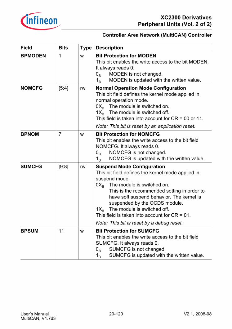
XC2300 DerivativesPeripheral Units (Vol. 2 of 2)
Controller Area Network (MultiCAN) Controller
BPMODEN 1 w Bit Protection for MODENThis bit enables the write access to the bit MODEN. It always reads 0.0B MODEN is not changed.1B MODEN is updated with the written value.
NOMCFG [5:4] rw Normal Operation Mode ConfigurationThis bit field defines the kernel mode applied in normal operation mode.0XB The module is switched on.1XB The module is switched off.This field is taken into account for CR = 00 or 11.Note: This bit is reset by an application reset.
BPNOM 7 w Bit Protection for NOMCFGThis bit enables the write access to the bit field NOMCFG. It always reads 0.0B NOMCFG is not changed.1B NOMCFG is updated with the written value.
SUMCFG [9:8] rw Suspend Mode ConfigurationThis bit field defines the kernel mode applied in suspend mode.0XB The module is switched on.
This is the recommended setting in order to have soft suspend behavior. The kernel is suspended by the OCDS module.
1XB The module is switched off.This field is taken into account for CR = 01.Note: This bit is reset by a debug reset.
BPSUM 11 w Bit Protection for SUMCFGThis bit enables the write access to the bit field SUMCFG. It always reads 0.0B SUMCFG is not changed.1B SUMCFG is updated with the written value.
Field Bits Type Description
User’s Manual 20-120 V2.1, 2008-08MultiCAN, V1.7d3

XC2300 DerivativesPeripheral Units (Vol. 2 of 2)
Controller Area Network (MultiCAN) Controller
Note: The bit protection bits BPxxx allow partly modification of the configuration bits witha single write operation (without the need of a read-modify-write mechanismhandled by the CPU).
COMCFG [13:12] rw Clock Off Mode ConfigurationThis bit field defines the kernel mode applied in clock off mode.0XB The module is switched on.1XB The module is switched off.This field is taken into account for CR = 10.Note: This bit is reset by an application reset.
BPCOM 15 w Bit Protection for COMCFGThis bit enables the write access to the bit field COMCFG. It always reads 0.0B COMCFG is not changed.1B COMCFG is updated with the written value.
0 [3:2], 6, 10, 14
r Reservedreturns 0 if read; should be written with 0;
Field Bits Type Description
User’s Manual 20-121 V2.1, 2008-08MultiCAN, V1.7d3
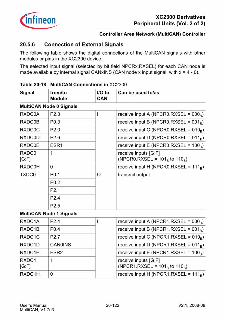
XC2300 DerivativesPeripheral Units (Vol. 2 of 2)
Controller Area Network (MultiCAN) Controller
20.5.6 Connection of External SignalsThe following table shows the digital connections of the MultiCAN signals with othermodules or pins in the XC2300 device.The selected input signal (selected by bit field NPCRx.RXSEL) for each CAN node ismade available by internal signal CANxINS (CAN node x input signal, with x = 4 - 0).
Table 20-18 MultiCAN Connections in XC2300
Signal from/toModule
I/O to CAN
Can be used to/as
MultiCAN Node 0 SignalsRXDC0A P2.3 I receive input A (NPCR0.RXSEL = 000B)RXDC0B P0.3 receive input B (NPCR0.RXSEL = 001B)RXDC0C P2.0 receive input C (NPCR0.RXSEL = 010B)RXDC0D P2.6 receive input D (NPCR0.RXSEL = 011B)RXDC0E ESR1 receive input E (NPCR0.RXSEL = 100B)RXDC0[G:F]
1 receive inputs [G:F](NPCR0.RXSEL = 101B to 110B)
RXDC0H 0 receive input H (NPCR0.RXSEL = 111B)TXDC0 P0.1 O transmit output
P0.2P2.1P2.4P2.5
MultiCAN Node 1 SignalsRXDC1A P2.4 I receive input A (NPCR1.RXSEL = 000B)RXDC1B P0.4 receive input B (NPCR1.RXSEL = 001B)RXDC1C P2.7 receive input C (NPCR1.RXSEL = 010B)RXDC1D CAN0INS receive input D (NPCR1.RXSEL = 011B)RXDC1E ESR2 receive input E (NPCR1.RXSEL = 100B)RXDC1[G:F]
1 receive inputs [G:F](NPCR1.RXSEL = 101B to 110B)
RXDC1H 0 receive input H (NPCR1.RXSEL = 111B)
User’s Manual 20-122 V2.1, 2008-08MultiCAN, V1.7d3

XC2300 DerivativesPeripheral Units (Vol. 2 of 2)
Controller Area Network (MultiCAN) Controller
TXDC1 P0.6 O transmit outputP2.2P2.9
MultiCAN Node 2 SignalsRXDC2A P4.3 I receive input A (NPCR2.RXSEL = 000B)RXDC2B P10.11 receive input B (NPCR2.RXSEL = 001B)RXDC2C CAN1INS receive input C (NPCR2.RXSEL = 010B)RXDC2D ESR0 receive input D (NPCR2.RXSEL = 011B)RXDC2[G:E]
1 receive inputs [G:E](NPCR2.RXSEL = 100B to 110B)
RXDC2H 0 receive input H (NPCR2.RXSEL = 111B)TXDC2 P4.1 O transmit output
P4.2P10.12
MultiCAN Node 3 SignalsRXDC3A P3.3 I receive input A (NPCR3.RXSEL = 000B)RXDC3B P3.0 receive input B (NPCR3.RXSEL = 001B)RXDC3C P10.14 receive input C (NPCR3.RXSEL = 010B)RXDC3D CAN2INS receive input D (NPCR3.RXSEL = 011B)RXDC3[G:E]
1 receive inputs [G:E](NPCR3.RXSEL = 100B to 110B)
RXDC3H 0 receive input H (NPCR3.RXSEL = 111B)TXDC3 P3.1 O transmit output
P3.2P10.13
Table 20-18 MultiCAN Connections in XC2300 (cont’d)
Signal from/toModule
I/O to CAN
Can be used to/as
User’s Manual 20-123 V2.1, 2008-08MultiCAN, V1.7d3

XC2300 DerivativesPeripheral Units (Vol. 2 of 2)
Controller Area Network (MultiCAN) Controller
MultiCAN Node 4 SignalsRXDC4A P3.4 I receive input A (NPCR4.RXSEL = 000B)RXDC4B P7.0 receive input B (NPCR4.RXSEL = 001B)RXDC4C P10.7 receive input C (NPCR4.RXSEL = 010B)RXDC4D CAN3INS receive input D (NPCR4.RXSEL = 011B)RXDC4[G:E]
1 receive inputs [G:E](NPCR4.RXSEL = 100B to 110B)
RXDC4H 0 receive input H (NPCR4.RXSEL = 111B)TXDC4 P3.6 O transmit output
P7.1P7.2P10.6
General MultiCAN SignalsINT_O[15:0] interrupt controller O interrupt output lines (service requests)
INT_O15 toCCU62 and CCU63
notification for timer start
Table 20-18 MultiCAN Connections in XC2300 (cont’d)
Signal from/toModule
I/O to CAN
Can be used to/as
User’s Manual 20-124 V2.1, 2008-08MultiCAN, V1.7d3
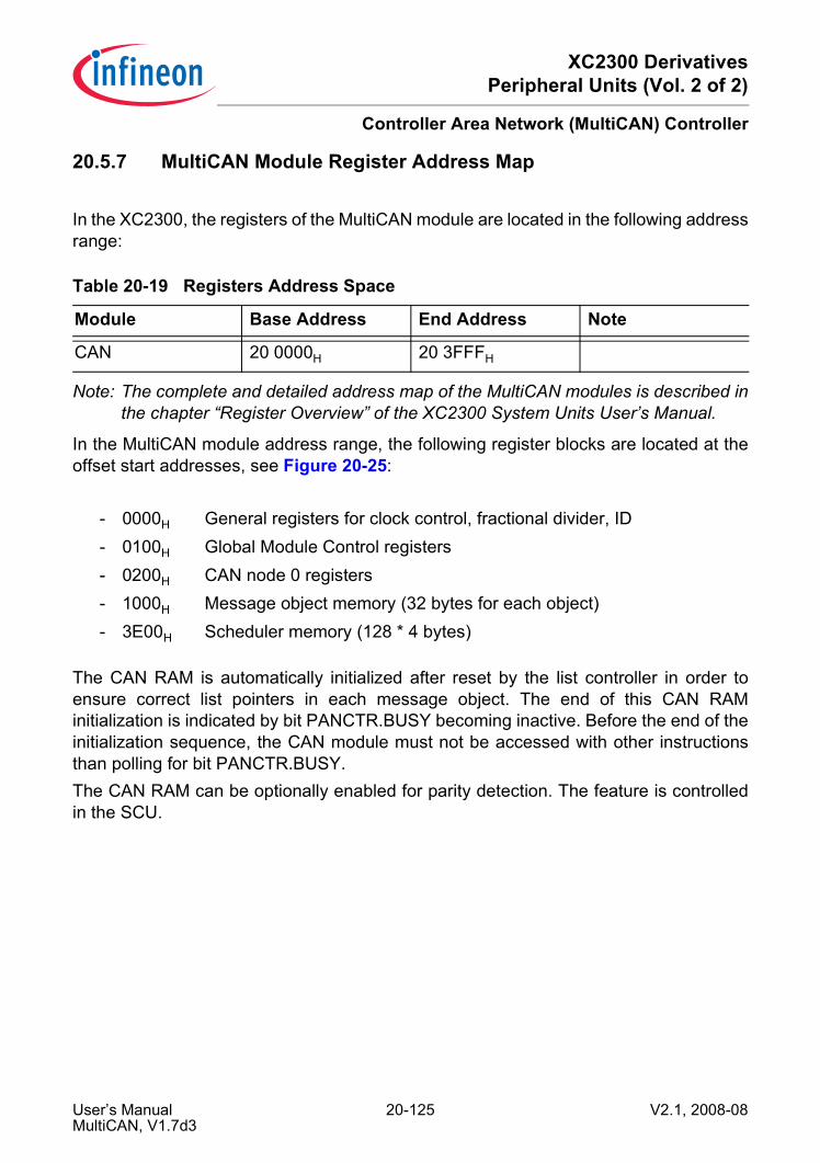
XC2300 DerivativesPeripheral Units (Vol. 2 of 2)
Controller Area Network (MultiCAN) Controller
20.5.7 MultiCAN Module Register Address Map
In the XC2300, the registers of the MultiCAN module are located in the following addressrange:
Note: The complete and detailed address map of the MultiCAN modules is described inthe chapter “Register Overview” of the XC2300 System Units User’s Manual.
In the MultiCAN module address range, the following register blocks are located at theoffset start addresses, see Figure 20-25:
The CAN RAM is automatically initialized after reset by the list controller in order toensure correct list pointers in each message object. The end of this CAN RAMinitialization is indicated by bit PANCTR.BUSY becoming inactive. Before the end of theinitialization sequence, the CAN module must not be accessed with other instructionsthan polling for bit PANCTR.BUSY.The CAN RAM can be optionally enabled for parity detection. The feature is controlledin the SCU.
Table 20-19 Registers Address Space
Module Base Address End Address Note
CAN 20 0000H 20 3FFFH
- 0000H General registers for clock control, fractional divider, ID- 0100H Global Module Control registers- 0200H CAN node 0 registers- 1000H Message object memory (32 bytes for each object)- 3E00H Scheduler memory (128 * 4 bytes)
User’s Manual 20-125 V2.1, 2008-08MultiCAN, V1.7d3

XC2300 DerivativesPeripheral Units (Vol. 2 of 2)
Controller Area Network (MultiCAN) Controller
Figure 20-25 MultiCAN Module Register Map
MultiCAN_P11MR_regmap--.vsd
GeneralModuleControl
GlobalModuleControl
000H
+100H
List Registers l H/L
Msg. Index Mask Reg. H/L + C2H / C0 H
+ C6H / C4 HPanel Control Register H/L
Module Control Register
+ 02H / 00 H
Msg. Pending Reg. k H/L
Msg. Index Registers k
Module Interrupt Trg. Reg
+ 42H / 40H
+ 80H
+ C8H
+ CCH
Module Identification Register
Fractional Divider Register H/L
+ 08H
Node 0 Control Reg.
Node 0 Status Registers
NO = Node; x = 0-4
Node 0 Interrupt Ptr. Reg.
Node 0 Port Control Reg.
Node 0 Bit Timing Reg. H/L
Node 0 Error Counter Reg. H/L
Node 0 Frame Counter Reg. H/L
+ 00H
MO n Function Control Reg. H/L
MO n FIFO/Gtw. Ptr. Reg. H/L
MO = Message Object; n = 0-127
MO n Interrupt Ptr. Reg. H/L
MO n Accept. Mask Reg. H/L
MO n Arbitration Reg. H/L
MO n Data Register LH/LL
MO n Data Register HH/HL
+1000H Message Object 0+1020H
.
.
.
.
.
.
.
.
.
.
.
.
.
.
.
.
MO n Control Register H/L +1EH / 1CH
+3FFCH MOBASE = 1000H + n * 20 H
+ 04H
+ 08H
+ 0CH
+ 12H / 10 H
+ 16H / 14 H
+ 1AH / 18H
Message Object 1+1040H
+1FE0H
NOBASE = 200H + x * 100 H
MOBASE +
NO BASE +
+ 02H / 00H
+ 06H / 04H
+ 0AH / 08H
+ 0EH / 0C H
+ 12H / 10H
+ 16H / 14H
+ 1AH / 18H
Message Object 127
+600H
+500H
+400H
+300H
+200H
Message Object 126
+ 0EH / 0C H
CAN Registers Node 0
CAN Registers Node 1
CAN Registers Node 4
CAN Registers Node 2
CAN Registers Node 3
User’s Manual 20-126 V2.1, 2008-08MultiCAN, V1.7d3

XC2300 DerivativesPeripheral Units (Vol. 2 of 2)
Keyword Index
Keyword IndexThis section lists a number of keywords which refer to specific details of the XC2300 interms of its architecture, its functional units or functions. This helps to quickly find theanswer to specific questions about the XC2300.
This User’s Manual consists of two Volumes, “System Units” and “Peripheral Units”. Foryour convenience this keyword index refers to both volumes, so you can immediatelyfind the reference to the desired section in the corresponding document ([1] or [2]).
Note: Registers are listed in a separate index: Register Index.
AAcronyms 1-9 [1]Addressing Modes
CoREG Addressing Mode 4-50 [1]DSP Addressing Modes 4-46 [1]Indirect Addressing Modes 4-44 [1]Long Addressing Modes 4-41 [1]Short Addressing Modes 4-39 [1]
ALU 4-57 [1]
BBANKSEL0 Register 5-35 [1]BANKSEL1 Register 5-35 [1]Baudrate
Bootstrap Loader 10-21 [1]Bit
Handling 4-60 [1]Manipulation Instructions 12-2 [1]protected 4-61 [1]reserved 2-17 [1]
Block Diagram ITC / PEC 5-3 [1]Bootstrap Loader 10-14 [1]
CCAN
Block diagram 20-1 [2]Clock control 20-102 [2]Features 20-2 [2]Functional description 20-3 [2]Interrupt structure 20-105 [2]Module implementation 20-106 [2]
MultiCANAnalysis mode 20-18 [2]Bit timing 20-9 [2]Block diagram 20-6 [2]Error handling 20-11 [2]Gateway mode 20-41 [2]Interrupts 20-12 [2]Message acceptance filtering 20-21 [2]Message object FIFO 20-36 [2]Message object lists 20-13 [2]Node control 20-9 [2]
Overview 20-4 [2]Registers
LISTiH 20-57 [2]LISTiL 20-58 [2]MCR 20-55 [2]MITR 20-56 [2]MOAMRnH 20-95 [2]MOAMRnL 20-95 [2]MOARnH 20-97 [2]MOARnL 20-98 [2]MOCTRnH 20-79 [2], 20-82 [2]MOCTRnL 20-80 [2], 20-82 [2]MODATAnHH 20-101 [2]MODATAnHL 20-101 [2]MODATAnLH 20-100 [2]MODATAnLL 20-100 [2]MOFCRnH 20-89 [2]MOFCRnL 20-91 [2]MOFGPRnH 20-93 [2]
User’s Manual L-1 V2.1, 2008-08

XC2300 DerivativesPeripheral Units (Vol. 2 of 2)
Keyword Index
MOFGPRnL 20-93 [2]MOIPRnH 20-87 [2]MOIPRnL 20-87 [2]MSIDk 20-60 [2]MSIMASKH 20-61 [2]MSIMASKL 20-61 [2]MSPNDkH 20-59 [2]MSPNDkL 20-59 [2]NBTRxH 20-72 [2]NBTRxL 20-72 [2]NCRx 20-62 [2]NECNTxH 20-73 [2]NECNTxL 20-74 [2]NFCRxH 20-75 [2]NFCRxL 20-76 [2]NIPRx 20-70 [2]NPCRx 20-71 [2]NSRx 20-66 [2]PANCTRH 20-50 [2]PANCTRL 20-50 [2]
CAPCOM12Capture Mode 17-14 [2]Counter Mode 17-9 [2]
CAPCOM2 2-17 [1]Capture Mode
GPT1 14-26 [2]GPT2 (CAPREL) 14-48 [2]
Capture/Compare Registers 17-11 [2]CCU6 2-19 [1]Clock
generation 2-32 [1]output signal 6-20 [1]
Clock SystemMain oscillator 6-4 [1]Oscillator run detection 6-12 [1]
Clock systemClock source 6-6 [1]PLL, see “PLL”
Concatenation of Timers 14-22 [2], 14-47 [2]
ContextPointer Updating 4-34 [1]Switch 4-33 [1]
Switching 5-34 [1]Count direction 14-6 [2], 14-36 [2]Counter 14-20 [2], 14-45 [2]Counter Mode (GPT1) 14-10 [2], 14-40 [2]CPU 2-2 [1], 4-1 [1]
DData Management Unit (Introduction)
2-9 [1]Data Page 4-42 [1]Development Support 1-8 [1]Direction
count 14-6 [2], 14-36 [2]Disable
Interrupt 5-31 [1]Division 4-62 [1]Double-Register Compare 17-24 [2]DPP 4-42 [1]
EEBC
Bus Signals 9-3 [1]Enable
Interrupt 5-31 [1]End of PEC Interrupt Sub Node 5-30 [1]ESR 6-68 [1]ESRx 5-1 [1]External
Bus 2-14 [1]Interrupts 5-37 [1]
FFlags 4-56 [1]–4-59 [1]Flash
RecommdationsEEPROM Emulation 3-50 [1]Programming Code and Constant Data 3-49 [1]
Recommendations 3-49 [1]Fractional divider
Block diagram 20-108 [2]Operating modes 20-110 [2]Suspend mode 20-111 [2]
User’s Manual L-2 V2.1, 2008-08

XC2300 DerivativesPeripheral Units (Vol. 2 of 2)
Keyword Index
Frequencyoutput signal 6-20 [1]
GGated timer mode (GPT1) 14-9 [2]Gated timer mode (GPT2) 14-39 [2]GPT 2-20 [1]GPT1 14-2 [2]GPT2 14-32 [2]
HHardware
Traps 5-42 [1]
IIncremental Interface Mode (GPT1)
14-11 [2]Instruction 12-1 [1]
Bit Manipulation 12-2 [1]Pipeline 4-11 [1]protected 12-6 [1]
InterfaceExternal Bus 9-1 [1]
InterruptArbitration 5-4 [1]Enable/Disable 5-31 [1]External 5-37 [1]Jump Table Cache 5-18 [1]Latency 5-40 [1]Node Sharing 5-36 [1]Priority 5-7 [1]Processing 5-1 [1]RTC 15-13 [2]System 2-8 [1], 5-2 [1]
LLatency
Interrupt, PEC 5-40 [1]LXBus 2-14 [1]
MMemory 2-10 [1]Multiplication 4-62 [1]
OOCDS
Requests 5-39 [1]
PPEC 2-10 [1], 5-20 [1]
Latency 5-40 [1]Transfer Count 5-21 [1]
PeripheralEvent Controller --> PEC 5-20 [1]Summary 2-15 [1]
Pins 8-1 [1]Pipeline 4-11 [1]PLL 6-5 [1]
Functionality 6-6 [1]Switching parameters 6-14 [1]
Port 2-30 [1]Temperature compensation 6-157 [1]
PortsConfiguring a Pin 7-14 [1]Output register Pn_OUT 7-9 [1]Pad driver control 7-6 [1]Structure
Analog 7-4 [1]Hardware Override 7-3 [1]Standard 7-2 [1]
Program Management Unit (Introduction) 2-9 [1]
ProtectedBits 4-61 [1]instruction 12-6 [1]
RReal Time Clock (->RTC) 2-22 [1], 15-1 [2]Register
BANKSEL0 5-35 [1]BANKSEL1 5-35 [1]SRCPx 5-25 [1]
Reserved bits 2-17 [1]Reset 6-49 [1]
Module behavior 6-56 [1]RTC 2-22 [1], 15-1 [2]
User’s Manual L-3 V2.1, 2008-08
XC2300 DerivativesPeripheral Units (Vol. 2 of 2)
Keyword Index
RegistersT14 15-8 [2]T14REL 15-8 [2]
SSegmentation 4-37 [1]Sharing
Interrupt Nodes 5-36 [1]Software
Traps 5-42 [1]SR0 5-47 [1]SR1 5-47 [1]SRCPx Register 5-25 [1]Stack 4-52 [1]
TTemperature compensation 6-157 [1]Timer 14-2 [2], 14-32 [2]
Auxiliary Timer 14-15 [2], 14-41 [2]Concatenation 14-22 [2], 14-47 [2]Core Timer 14-4 [2], 14-34 [2]Counter Mode (GPT1) 14-10 [2], 14-40 [2]Gated Mode (GPT1) 14-9 [2]Gated Mode (GPT2) 14-39 [2]Incremental Interface Mode (GPT1) 14-11 [2]Mode (GPT1) 14-8 [2]Mode (GPT2) 14-38 [2]
Tools 1-8 [1]Traps 5-42 [1]
UUSIC
ASC mode 19-111 [2]Automatic shaping 19-119 [2]Baud rate 19-117 [2]Bit timing 19-116 [2]Collision detection 19-117 [2]Data transfer interrupts 19-121 [2]EOF control 19-119 [2]Frame format 19-112 [2]Noise detection 19-117 [2]
Protocol interrupts 19-120 [2]Protocol registers 19-123 [2]Pulse shaping 19-118 [2]Receive buffer 19-122 [2]Signals 19-111 [2]Sync-break detection 19-122 [2]
Baud rate 19-8 [2]Channel structure 19-5 [2]Data buffer 19-10 [2]Data shifting and handling 19-9 [2]Data transfer interrupts 19-22 [2]External frequency 19-42 [2]Feature set 19-2 [2]FIFO buffer 19-11 [2]FIFO data buffer 19-80 [2]Fractional divider 19-42 [2]General interrupts 19-20 [2]IIC mode 19-160 [2]
Baud rate 19-165 [2]Byte stretching 19-165 [2]Data bit symbol 19-172 [2]Data flow handling 19-173 [2]Frame format 19-163 [2]Master arbitration 19-165 [2]Master transmission 19-177 [2]Mode control 19-166 [2]Protocol interrupts 19-167 [2]Protocol registers 19-178 [2]Receiver address acknowledge 19-168 [2]Receiver handling 19-168 [2]Receiver status 19-169 [2]Signals 19-161 [2]Start symbol 19-171 [2]Stop symbol 19-172 [2]Symbol timing 19-170 [2]Transmission chain 19-165 [2]Transmit data 19-173 [2]
IIS mode 19-184 [2]Baud rate 19-193 [2]Connection of Audio devices 19-187 [2]Data interrupts 19-191 [2]
User’s Manual L-4 V2.1, 2008-08
XC2300 DerivativesPeripheral Units (Vol. 2 of 2)
Keyword Index
Frame and word length 19-188 [2]Mode control 19-188 [2]Protocol interrupts 19-196 [2], 19-197 [2]Protocol overview 19-186 [2]Protocol registers 19-198 [2]Receive data 19-192 [2]Signals 19-184 [2]Slave mode operation 19-197 [2]Transfer delay 19-186 [2], 19-189 [2]Transmit data 19-191 [2]WA generation 19-194 [2], 19-195 [2]
ImplementationAddress map 19-205 [2]Channels 19-205 [2]I/O connections 19-210 [2]I/O lines of USIC0 19-211 [2]I/O lines of USIC1 19-214 [2]I/O lines of USIC2 19-217 [2]Interrupt registers 19-208 [2]Overview 19-204 [2]
Input stages 19-6 [2], 19-37 [2]Kernel registers
Baud rate registers 19-47 [2]BRGH 19-51 [2]BRGL 19-49 [2]BYP 19-90 [2]BYPCRH 19-92 [2]BYPCRL 19-90 [2]CCFG 19-29 [2]CCR 19-26 [2]Channel control and configuration registers 19-26 [2]Data buffer registers 19-70 [2]DX0CR 19-39 [2]DX1CR 19-39 [2]DX2CR 19-39 [2]FDRH 19-48 [2]FDRL 19-47 [2]FIFO buffer and bypass registers 19-90 [2]
FMRH 19-69 [2]FMRL 19-68 [2]INPRH 19-33 [2]INPRL 19-32 [2]Input stage register 19-39 [2]INx 19-106 [2]KSCFG 19-30 [2]OUTDRH 19-108 [2]OUTDRL 19-108 [2]OUTRH 19-107 [2]OUTRL 19-107 [2]Overview 19-14 [2]PCRH 19-34 [2], 19-126 [2], 19-153 [2], 19-178 [2], 19-200 [2]PCRL 19-34 [2], 19-123 [2], 19-151 [2], 19-178 [2], 19-198 [2]Protocol registers 19-34 [2]PSCR 19-36 [2]PSR 19-35 [2], 19-127 [2], 19-155 [2], 19-181 [2], 19-201 [2]RBCTRH 19-103 [2]RBCTRL 19-102 [2]RBUF 19-77 [2]RBUF0 19-71 [2]RBUF01SRH 19-74 [2]RBUF01SRL 19-71 [2]RBUF1 19-74 [2]RBUFD 19-78 [2]RBUFSR 19-79 [2]SCTRH 19-60 [2]SCTRL 19-58 [2]TBCTRH 19-100 [2]TBCTRL 19-99 [2]TBUFx 19-70 [2]TCSRH 19-66 [2]TCSRL 19-61 [2]Transfer control/status registers 19-58 [2]TRBPTRH 19-110 [2]TRBPTRL 19-109 [2]TRBSCR 19-97 [2]TRBSRH 19-96 [2]TRBSRL 19-93 [2]
User’s Manual L-5 V2.1, 2008-08

XC2300 DerivativesPeripheral Units (Vol. 2 of 2)
Keyword Index
Mode control 19-19 [2]Module registers
USIC0_IDH 19-207 [2]USIC0_IDL 19-206 [2]USIC1_IDH 19-207 [2]USIC1_IDL 19-206 [2]USIC2_IDH 19-207 [2]USIC2_IDL 19-206 [2]
Output signals 19-7 [2]Protocol control and status 19-18 [2]Protocol interrupts 19-25 [2]Protocol related counter 19-43 [2]Receive buffering 19-56 [2]Registers overview 19-14 [2]SSC mode 19-131 [2]
Automatic Shadow mechanism 19-139 [2]Baud rate 19-142 [2]Data frame control 19-140 [2]EOF control 19-147 [2], 19-150 [2]Master mode 19-142 [2]Protocol interrupts 19-146 [2], 19-149 [2]Protocol registers 19-151 [2]Receive buffer 19-141 [2]Signals 19-131 [2]Slave mode 19-149 [2]Slave select delay 19-145 [2]Slave select generation 19-143 [2]
Time quanta counter 19-45 [2]Transmit buffering 19-52 [2]
WWatchdog 2-29 [1]Watchdog Timer 6-161 [1]
Kernel Registers 6-166 [1]Modes of operation
Disable Mode 6-164 [1]Normal Mode 6-163 [1]Prewarning Mode 6-164 [1]
Period calculation 6-162 [1]
User’s Manual L-6 V2.1, 2008-08

XC2300 DerivativesPeripheral Units (Vol. 2 of 2)
Register Index
Register IndexThis section lists the registers of the XC2300. This helps to quickly find the reference tothe description of the respective register.
This User’s Manual consists of two Volumes, “System Units” and “Peripheral Units”. Foryour convenience this register index refers to both volumes, so you can immediately findthe reference to the desired section in the corresponding document ([1] or [2]).
Note: Keywords are listed in a separate index: Keyword Index.
AADC0_KSCFG 16-23 [2]ADCx_ALR0 16-76 [2]ADCx_ASENR 16-36 [2]ADCx_CHCTRx 16-67 [2]ADCx_CHINCR 16-72 [2]ADCx_CHINFR 16-71 [2]ADCx_CHINPRx 16-73 [2]ADCx_CRCRx 16-42 [2]ADCx_CRMRx 16-44 [2]ADCx_CRPRx 16-43 [2]ADCx_EMCTR 16-100 [2]ADCx_EMENR 16-101 [2]ADCx_EVINCR 16-92 [2]ADCx_EVINFR 16-91 [2]ADCx_EVINPRx 16-93 [2]ADCx_GLOBCTR 16-25 [2]ADCx_GLOBSTR 16-27 [2]ADCx_INPRx 16-69 [2]ADCx_LCBRx 16-70 [2]ADCx_PISEL 16-30 [2]ADCx_Q0Rx 16-56 [2]ADCx_QBURx 16-58 [2]ADCx_QINRx 16-60 [2]ADCx_QMRx 16-51 [2]ADCx_QSRx 16-54 [2]ADCx_RCRx 16-89 [2]ADCx_RESRAVx 16-86 [2]ADCx_RESRAx 16-86 [2]ADCx_RESRVx 16-85 [2]ADCx_RESRx 16-85 [2]ADCx_RSPRx 16-37 [2]
ADCx_RSSR 16-87 [2]ADCx_SYNCTR 16-102 [2]ADCx_VFR 16-88 [2]ADDRSELx 9-23 [1]
CCAN_LISTiH 20-57 [2]CAN_LISTiL 20-58 [2]CAN_MCR 20-55 [2]CAN_MITR 20-56 [2]CAN_MOAMRnH 20-95 [2]CAN_MOAMRnL 20-95 [2]CAN_MOARnH 20-97 [2]CAN_MOARnL 20-98 [2]CAN_MOCTRnH 20-79 [2]CAN_MOCTRnL 20-80 [2]CAN_MODATAnHH 20-101 [2]CAN_MODATAnHL 20-101 [2]CAN_MODATAnLH 20-100 [2]CAN_MODATAnLL 20-100 [2]CAN_MOFCRnH 20-89 [2]CAN_MOFCRnL 20-91 [2]CAN_MOFGPRnH 20-93 [2]CAN_MOFGPRnL 20-93 [2]CAN_MOIPRnH 20-87 [2]CAN_MOIPRnL 20-87 [2]CAN_MOSTATnH 20-82 [2]CAN_MOSTATnL 20-82 [2]CAN_MSIDk 20-60 [2]CAN_MSIMASKH 20-61 [2]CAN_MSIMASKL 20-61 [2]CAN_MSPNDkH 20-59 [2]
User’s Manual L-7 V2.1, 2008-08
XC2300 DerivativesPeripheral Units (Vol. 2 of 2)
Register Index
CAN_MSPNDkL 20-59 [2]CAN_NBTRxH 20-72 [2]CAN_NBTRxL 20-72 [2]CAN_NCRx 20-62 [2]CAN_NECNTxH 20-73 [2]CAN_NECNTxL 20-74 [2]CAN_NFCRxH 20-75 [2]CAN_NFCRxL 20-76 [2]CAN_NIPRx 20-70 [2]CAN_NPCRx 20-71 [2]CAN_NSRx 20-66 [2]CAN_PANCTRH 20-50 [2]CAN_PANCTRL 20-50 [2]CAPREL 14-57 [2]CC2_CCyIC 17-36 [2]CC2_DRM 17-25 [2]CC2_IOC 17-31 [2]CC2_KSCCFG 17-39 [2]CC2_M4/5/6/7 17-11 [2]CC2_OUT 17-27 [2]CC2_SEE 17-29 [2]CC2_SEM 17-29 [2]CC2_T78CON 17-5 [2]CC2_T7IC 17-10 [2]CC2_T8IC 17-10 [2]CCU6x_CC63R 18-64 [2]CCU6x_CC63SR 18-64 [2]CCU6x_CC6xR 18-33 [2]CCU6x_CC6xSR 18-34 [2]CCU6x_CMPMODIF 18-39 [2]CCU6x_CMPSTAT 18-37 [2]CCU6x_IEN 18-97 [2]CCU6x_INP 18-100 [2]CCU6x_IS 18-90 [2]CCU6x_ISR 18-95 [2]CCU6x_ISS 18-93 [2]CCU6x_KSCFG 18-110 [2]CCU6x_KSCSR 18-112 [2]CCU6x_MCMCTR 18-83 [2]CCU6x_MCMOUT 18-86 [2]CCU6x_MCMOUTS 18-85 [2]CCU6x_MODCTR 18-77 [2]CCU6x_PISELH 18-108 [2]
CCU6x_PISELL 18-106 [2]CCU6x_PSLR 18-82 [2]CCU6x_T12 18-32 [2]CCU6x_T12DTC 18-35 [2]CCU6x_T12MSEL 18-40 [2]CCU6x_T12PR 18-32 [2]CCU6x_T13 18-62 [2]CCU6x_T13PR 18-63 [2]CCU6x_TCTR0 18-41 [2]CCU6x_TCTR2 18-44 [2]CCU6x_TCTR4 18-47 [2]CCU6x_TRPCTR 18-79 [2]CP 4-36 [1]CPUCON1 4-26 [1]CPUCON2 4-27 [1]CRIC 14-58 [2]CSP 4-38 [1]
DDPP0/1/2/3 4-42 [1]DSTPx 5-25 [1]
EEBCMOD0 9-14 [1]EBCMOD1 9-16 [1]EOPIC 5-29 [1]
FFCONCS0 9-20 [1]FCONCS1/2/3/4/7 9-21 [1]FINT0/1ADDR 5-18 [1]FINT0/1CSP 5-18 [1]FSR_BUSY 3-58 [1]FSR_OP 3-58 [1]FSR_PROT 3-60 [1]
GGPT12E_CAPREL 14-57 [2]GPT12E_CRIC 14-58 [2]GPT12E_KSCCFG 14-59 [2]GPT12E_T2,-T3,-T4 14-30 [2]GPT12E_T2/3/4IC 14-31 [2]GPT12E_T2CON 14-15 [2]
User’s Manual L-8 V2.1, 2008-08

XC2300 DerivativesPeripheral Units (Vol. 2 of 2)
Register Index
GPT12E_T3CON 14-4 [2]GPT12E_T4CON 14-15 [2]GPT12E_T5,-T6 14-57 [2]GPT12E_T5/6IC 14-58 [2]GPT12E_T5CON 14-41 [2]GPT12E_T6CON 14-34 [2]
IIDX0/1 4-46 [1]IMBCTRH 3-55 [1]IMBCTRL 3-53 [1]INTCTR 3-56 [1]IP 4-38 [1]
MMAH 4-69 [1]MAL 4-68 [1]MAR 3-62 [1]MCW 4-65 [1]MDC 4-63 [1]MDH 4-62 [1]MDL 4-63 [1]MRW 4-72 [1]MSW 4-70 [1]
OONES 4-74 [1]
PPECCx 5-21 [1]PECISNC 5-29 [1]PECSEGx 5-25 [1]Pn_DIDIS
P15 7-16 [1]P5 7-16 [1]
Pn_IN 7-12 [1]Pn_IOCRx 7-13 [1]Pn_OMRH
P10 7-10 [1]P2 7-10 [1]
Pn_OMRL 7-10 [1]Pn_OUT 7-9 [1]Pn_POCON 7-7 [1]
PortsPn_IN 7-12 [1]Pn_IOCRx 7-13 [1]Pn_OMR 7-10 [1]
PROCONx 3-63 [1]PSW 4-56 [1]
QQR0/1 4-45 [1]QX0/1 4-47 [1]
RRELH/L 15-10 [2]RTC_CON 15-6 [2]RTC_IC 15-14 [2]RTC_ISNC 15-14 [2]RTC_KSCCFG 15-15 [2]RTC_RELH/L 15-10 [2]RTC_RTCH/L 15-9 [2]RTC_T14 15-8 [2]RTC_T14REL 15-8 [2]RTCH/L 15-9 [2]
SSCU
RegistersESREXCON1 6-72 [1]ESREXCON2 6-73 [1]WICR 6-46 [1]
SP 4-53 [1]SPSEG 4-53 [1]SRCPx 5-25 [1]STKOV 4-55 [1]STKUN 4-55 [1]
TT14 15-8 [2]T14REL 15-8 [2]T2, T3, T4 14-30 [2]T2/3/4IC 14-31 [2]T2CON 14-15 [2]T3CON 14-4 [2]T4CON 14-15 [2]
User’s Manual L-9 V2.1, 2008-08
XC2300 DerivativesPeripheral Units (Vol. 2 of 2)
Register Index
T5, T6 14-57 [2]T5/6IC 14-58 [2]T5CON 14-41 [2]T6CON 14-34 [2]T7IC 17-10 [2]T8IC 17-10 [2]TCONCS0 9-17 [1]TCONCS1/2/3/4 9-18 [1], 9-19 [1]TFR 5-44 [1]
UUSIC0_IDH 19-207 [2]USIC0_IDL 19-206 [2]USIC1_IDH 19-207 [2]USIC1_IDL 19-206 [2]USIC2_IDH 19-207 [2]USIC2_IDL 19-206 [2]UxCy_BRGH 19-51 [2]UxCy_BRGL 19-49 [2]UxCy_BYP 19-90 [2]UxCy_BYPCRH 19-92 [2]UxCy_BYPCRL 19-90 [2]UxCy_CCFG 19-29 [2]UxCy_CCR 19-26 [2]UxCy_DX0CR 19-39 [2]UxCy_DX1CR 19-39 [2]UxCy_DX2CR 19-39 [2]UxCy_FDRH 19-48 [2]UxCy_FDRL 19-47 [2]UxCy_FMRH 19-69 [2]UxCy_FMRL 19-68 [2]UxCy_INPRH 19-33 [2]UxCy_INPRL 19-32 [2]UxCy_INx 19-106 [2]UxCy_KSCFG 19-30 [2]UxCy_OUTDRH 19-108 [2]UxCy_OUTDRL 19-108 [2]UxCy_OUTRH 19-107 [2]UxCy_OUTRL 19-107 [2]UxCy_PCRH 19-34 [2], 19-126 [2],
19-153 [2], 19-178 [2], 19-200 [2]UxCy_PCRL 19-34 [2], 19-123 [2],
19-151 [2], 19-178 [2], 19-198 [2]
UxCy_PSCR 19-36 [2]UxCy_PSR 19-35 [2], 19-127 [2],
19-155 [2], 19-181 [2], 19-201 [2]UxCy_RBCTRH 19-103 [2]UxCy_RBCTRL 19-102 [2]UxCy_RBUF 19-77 [2]UxCy_RBUF0 19-71 [2]UxCy_RBUF01SRH 19-74 [2]UxCy_RBUF01SRL 19-71 [2]UxCy_RBUF1 19-74 [2]UxCy_RBUFD 19-78 [2]UxCy_RBUFSR 19-79 [2]UxCy_SCTRH 19-60 [2]UxCy_SCTRL 19-58 [2]UxCy_TBCTRH 19-100 [2]UxCy_TBCTRL 19-99 [2]UxCy_TBUFx 19-70 [2]UxCy_TCSRH 19-66 [2]UxCy_TCSRL 19-61 [2]UxCy_TRBPTRH 19-110 [2]UxCy_TRBPTRL 19-109 [2]UxCy_TRBSCR 19-97 [2]UxCy_TRBSRH 19-96 [2]UxCy_TRBSRL 19-93 [2]
VVECSEG 5-12 [1]
XxxIC (gen.) 5-6 [1]
ZZEROS 4-74 [1]
User’s Manual L-10 V2.1, 2008-08

w w w . i n f i n e o n . c o m
Published by Infineon Technologies AG
B158-H9135-G1-X-7600