
Infineon Power and Sensing Selection Guide 2018
266
Power and Sensing Selection Guide 2018 www.infineon.com/powerandsensing-selectionguide EN
-
Upload
khangminh22 -
Category
Documents
-
view
1 -
download
0
Transcript of Infineon Power and Sensing Selection Guide 2018

Power and SensingSelection Guide 2018
www.infineon.com/powerandsensing-selectionguide EN


3
Dear Customer,
The world around us is getting smarter. What was once just fantasy and science fiction is now finding a place in our homes, our offices, and our workplaces. Automotive, home, industrial, and consumer devices are becoming a part of the Internet of Things (IoT) a network of cyber-physical objects that contain embedded electronics to sense, computer actuate, and communicate. New and innovative Human-Machine Interface (HMI) technologies are being developed, and the boundary between devices and the people operating them is becoming blurred.
This incredibly rapid advancement in technology is opening up new opportunities for people in all corners of our world. We are discovering new ways to communicate with the tools that are an indispensable part of our daily lives. Mobile devices with 3D and gesture sensing, high end audio systems with beam-forming microphones, highly efficient wireless charging systems, and innovative power-efficient lighting systems are merging together to shape this technological revolution.
Infineon is a world leader in offering semiconductor solutions that make your life easier, safer, and greener. The Power and Sensing Selection Guide for 2018 opens the door to this better future, providing you with inspiration as you make your products more efficient, cost-effective, and innovative.
尊敬的客户,
我们所处的世界正在变得越来越智能。曾经仅存在于幻想和科幻小说中的事物正出现在我们的家里、办公室和工作场所内。汽车、家居、工业和消费电子设备正在成为物联网 (IoT) 的一部分,这种信息物理对象网络包含嵌入式电子设备,进行传感、计算机启动以及通信。新型的创新人机界面 (HMI) 技术正在开发中,设备与操作人员之间的界限将变得模糊。科技的迅猛发展正在为世界各地的人们开创新的机遇。我们正在探索新的方法,与日常生活中不可缺少的工具进行交互。 具有 3D 和手势感应功能的移动设备、具有波束成形麦克风的高端音频系统、高效无线充电系统以及创新的节能照明系统正在融合,共同形成此次技术革命。 英飞凌是全球领先的半导体解决方案提供商,让您的生活更轻松、更安全、更环保。
《2018 年功率和传感选型指南》为这个美好的未来打开了大门,为您提供灵感,让您的产品更高效、更具成本效益和创新性。
Andreas UrschitzDivision President of Power Management & Multimarket
电源管理及多元化市场总裁

4
Applications 8
3D printer 8
Automatic opening system 10
Battery powered applications 12
E-mobility 14
PowIRaudio™ class D audio amplifier 18
DC-DC enterprise power solution for data processing 20
Industrial automation 23
Industrial welding 24
LED lighting 26
Major home appliance 28
Induction cooking 28
Air conditioning 29
Microwave oven 30
Multicopter 32
OPTIGA™ Trust product family 36
Robotics 37
SMPS 40
Laptop adapter 40
Mobile charger 42
PC power supply 43
TV power supply 44
Embedded power supply 46
Server power supply 47
Telecom power supply 49
DC EV charging 51
Uninterruptible power supply 53
Gate driver application guide 54
XENSIV™ sensors family overview 56
Solar 58
Wireless charging 63
20 V – 400 V MOSFETs 68
500 V – 900 V MOSFETs 96
SiC discretes & Si diodes 122
Discrete IGBTs 136
Power ICs 150
Motor control and gate driver ICs 208
Microcontrollers 230
Sensors 242
Packages 260
Contents

5
We make life easier, safer and greener – with technology that achieves more, consumes less and is accessible to everyone.
From product thinking to system understanding Infineon enables eff icient generation, transmission and conversion of electrical energy
www.infineon.com/power

6
Infineon offers best-in-class sensors, unique algorithms, and powerful processors that together form the foundation required to create active human machine interfaces that can understand who we are, how we act and what we do in our daily lives.
Sensors allow smart devices to see, hear and understand their surroundings. This contextual awareness sensitivity enables humans to interact with smart devices in a more natural and seamless way than ever before. At Infineon, we are providing the inspiration needed to enhance voice and gesture recognition in innovative human machine user interfaces, making the technological boundary between humans and machines gradually disappear.
We drive contextual awareness within the HMI segments with our best-in-class XENSIV™ sensors – with radar and TOF technologies, pressure sensors and silicon microphones. Together with strong industry partners we develop solutions that make the technology disappear – for your end customers’ convenience.
From ordinary speech recognition to contextual awarenessSeamless interaction with smart devices
www.infineon.com/sensors
XENSIV™ Fusion
Bringing together Infineon’s XENSIV™ sensors with our partners’ hardware, we provide the sensor fusion that is key to communication between humans and machines. By fusing radar with silicon microphones, Infineon has achieved the first step towards context awareness. Through sensor fusion, devices are, for the first time, able to do things such as differentiate whether a keyword was spoken by a person in the room or the command came from another source such as a TV or radio.
1980
Mouse Touch Voice Contextualawareness
2000 2017 2025


8
Today, consumers can create a growing list of objects with nothing more than a digital file and a 3D printer. While the excitement is understandably big, 3D printers continue to face a number of limitations – most notably size and speed – that currently prevent the technology from fully replacing a number of assembly line manufacturing processes. Moving beyond those limitations to create winning 3D printing designs requires a highly reliable motor control solution with excellent speed control and position detection capabilities. Furthermore, the compact power supply must offer top energy efficiency and power density.
Within Infineon’s complete portfolio of semiconductor solutions, you will find components for 3D printing designs destined for high acclaim. We offer system solutions with every product you require – such as 40 V-800 V MOSFETs, CoolSET™ or integrated point-of-load converters (SupIRBuck™) for power management, our CIPOS™ Nano, Nova-lithIC™, IFX9201, sensor solutions and XMC4500 microcontroller for motor control, our OPTIGA™ Trust E for authentica-tion and OPTIGA™ Trust TPM for security of data communication. As a leader in power management, Infineon offers benchmark product solutions for your power supply designs, ensuring highest efficiency ratings and higher power density. Our high level of integration of motor control solutions (up to 300 W), for example with our H-bridge IFX9201, CIPOS™ Nano or NovalithIC™, allows you to significantly reduce PCB space and system cost.
Our sensor solutions enable precise rotor position detection and more accurate switching points to ensure higher torque in our motor solutions. As proven by Infineon’s exceptional track record, every component bearing the Infineon name is as robust as it is reliable.
3D printerIndustry-leading full system solution
Microcontroller
Motor driver Motor driverMotor driver
M MM12 V 12 V 12 V
X-axis Y-axis Z-axis
Temperature sensorfor PCB
Heatedprinter bed
SD cardSPI
Status LED
USB
Power supply unit
Security
MUX
Motor driver
M12 V
Extruder
3D printer
Block diagram
www.infineon.com/3dprinter

Appl
icat
ions
9
Functional block Products Selection/benefit
Motor control CIPOS™ Nano High integration
NovalithIC™ Integrated solution with fast signal processing and short delay times
Angle sensor Low power consumption and high accurate angular and linear position detection
IFX9201 DC motor control for industrial applications – high integration, small package, protection features
Hall switches Recommendation
Industrial microcontroller XMC1100/XMC4500 Recommendation
Industrial transceiver Recommendation
Power supply: PFC stage
600 V CoolMOS™ P6/CE Ease-of-use and high efficiency
650 V PFC control IC High efficiency
650 V CoolSET™ F3 High efficiency
650 V rapid 1/rapid 2 diodes Efficiency
CoolSiC™ Schottky diodes 650 V G5 Ease-of-use and cost-optimized solution
EiceDRIVER™ 2EDN gate driver Fast and robust gate driver
Low-side gate driver (IRS44273) Fast and robust gate driver
Power supply: Main stage
650 V quasi-resonant controller High efficiency
650 V LLC controller High efficiency
800 V CoolMOS™ CE High efficiency
EiceDRIVER™ 2EDN gate driver Fast and robust gate driver
Low-side gate driver (IRS44273) Fast and robust gate driver
High voltage half-bridge and high- and low-side gate driver ICs Industrial standard rugged gate driver
Main stage: Synchronous rectification
OptiMOS™ 40 V - 60 V High efficiency
60 V synchronous rectification MOSFET (IRLR3636) High efficiency
EiceDRIVER™ 2EDN gate driver Fast and robust gate driver
Low-side gate driver (IRS44273) Fast and robust gate driver
High voltage half-bridge and high- and low-side gate driver ICs Industrial standard rugged gate driver
Power supply: DC-DC point-of-load
Integrated power stages DC-DC: PowIRstage™, DrMOS High performance
Fully integrated point-of-load converter SupIRBuck™ High performance DC-DC point-of-load solution
Recommended microcontroller + DC-DC converter
Industrial microcontroller XMC1300, XMC4xxx-series Recommendation
DC-DC voltage regulator (IFX90121, IFX91041, IFX81481, IFX80471) High performance
Security OPTIGA™ Trust E/OPTIGA™ TPM Enhanced embedded security
3D printer
Infineon’s product recommendation for 3D printer
www.infineon.com/3dprinter

10
Every building and household utilizes openings at numerous positions in and around the building: sliding and swing doors, garage doors, sun-blinds and automated gates. When automated, these doors are equipped with systems that are able to manage the opening action, avoid unintentional opening, control the speed and torque, detect the pres-ence of objects along the path, and a number of other functions. Automatic opening systems incorporate smart sen-sors, motor controls, power supplies and battery management, which help to reduce energy losses in all conditions. This is where Infineon comes into place.
Within Infineon’s complete portfolio of semiconductor solutions, we offer system solutions for every product you require, ranging from power semiconductors over sensors to security products. Infineon products make your motor designs more energy efficient and secure against unauthorized manipulation of firmware updates while our radar solu-tions cover a 16 times larger area than infrared solutions.
Automatic opening system Automatic opening system
Benchmark efficiency solutions for motor control and power management
Automatic opening system
Integrated or discrete motor drivers
Current sensing
Current sensing
EiceDRIVER™gate driver
3-phaseinverter
USB,serial COMethernet
XMC™microcontroller
MStatusindication
User interface&
buildingautomation
network
Power management
AC-DC DC-DC
(Isolated and non-isolated with ADC and DSD)
Hall &GMR sensors
Position sensing
(Isolated and non-isolated with ADC and DSD)
Security
Security
Block diagram
www.infineon.com/automaticopeningsystem

Appl
icat
ions
11
Functional block Products Selection/benefit
Motor control 650 V TRENCHSTOP™ IGBT Recommendation
Low voltage MOSFETs – OptiMOS™/StrongIRFET™ Recommendation
Intelligent power modules/CIPOS™ High integration
Intelligent power modules – NovalithIC™ High integration
Angle sensors Integrated solution with fast signal processing, short delay times
Hall switches Low power consumption and high accurate angular and linear position detection
Double hall switches (TLE4966) High integrated sensor solution for position detection including direction detection
Gate driver ICs - EiceDRIVER™ 2EDL/6EDL Industrial standard rugged gate driver
Industrial microcontroller XMC1000/XMC4000 Recommendation
DC-DC converter High performance
Power management AC-DC integrated power stage – 650 V CoolSET™ F3 High efficiency
High voltage MOSFETs – 600 V CoolMOS™ P6 High efficiency
650 V TRENCHSTOP™ IGBT High efficiency
Low voltage MOSFETs – OptiMOS™ (20 V - 300 V) High efficiency
PWM ICs for PFC/LLC/Combi PFC+LLC High efficiency
High voltage half-bridge and high- and low-side gate driver ICs Industrial standard rugged gate driver
Motion sensor 24GHz radar sensor – BGT24MTR11/BGT24LTR11 High performance
24GHz radar sensor – BGT24MR2 High performance
24GHz radar sensor – BGT24MTR12 High performance
Security Security controller ICs – OPTIGA™ Trust E/OPTIGA™ TPM Enhanced embedded security
Automatic opening system
www.infineon.com/automaticopeningsystem
Infineon’s product recommendation for automatic opening system

12
Battery powered applications
Based on industry leading technology, highest quality and manufacturing expertise, Infineon provides a variety of innovative power semiconductors which enable designers to develop highly reliable and efficient solutions. Through our comprehensive portfolio we can address a broad range of battery powered motor control applications, such as power tools, forklifts, all kinds of light electric vehicles including e-skateboards, e-scooters, pedelecs, low speed cars and many others. Infineon offers an excellent selection of devices for power management and consumption, as well as voltage regulation – such as power MOSFETs (e.g. CoolMOS™ and OptiMOS™), XMC™ microcontrollers, EiceDRIVER™ gate drivers and more.
Key enabling products are: › Low voltage power MOSFETs – OptiMOS™ and StrongIRFET™ › Small Signal products › High voltage power MOSFETs – CoolMOS™ › EiceDRIVER™/Half-bridge and three-phase gate driver ICs › Magnetic sensors and voltage regulators › Microcontrollers – XMC™ › Motion control ICs – iMOTION™ IRMCK099 › Authentication IC OPTIGA™ Trust B
Battery powered applicationsHighest performance in motor control
Typical battery powered three-phase system: a one-stop-shop for battery powered drives
www.infineon.com/motorcontrol
Current sensing
Current sensing
Gate driver ICsEiceDRIVER™
200 V driver ICs
3-phaseinverter
OptiMOS™StrongIRFET™HEXFET™IPM
USB,
XMC™Microcontroller
& digital controller
& iMOTION™IRMCK099
MStatus
indicationLED drivers ≤ 60 V
Userinterface
Power management
Battery managementCoolMOS™OPTIGA™
OptiMOS™StrongIRFET™
HEXFET™Linear voltage/DC-DC switching regulators
serial COM & ethernet CA
N tr
ansc
eive
r
Position sensing
Hall switches, Linear Hall sensors,
angle and current sensors
Home and professional Consumer robotics Light electric vehicle
Power tools, gardening tools, commercial multicopters, cordless home appliance, cordless vacuum cleaners, healthcare equipment
Consumer multicopters, vacuum robots, RC toys, service robotics, household robotics and other consumer robots
eScooter, eBike, electric wheelchair, electric forklift, low speed cars (LSEV), electric motorcycle, other battery vehicles

Appl
icat
ions
13
Application requirements › Efficiency: reduction of overall system energy
consumption, increasing battery operating and life time, optimized thermal management
› Reliability: reliable operating in harsh environments and avoiding system downtime
› Maintenance: low maintenance and long lifetime of components
› Size and cost: reduction of overall system size and cost › Time-to-market: reduction of development time and cost
Benefits of Infineon components › Portfolio: complete portfolio out of one hand
– enables scalability › Reliability: increased lifetime due to Infineon’s
reliability and quality › Size and cost: smallest area required for highest power
density and BOM cost reduction due to lowest RDS(on) › Time-to-market: complete eco-system: simulations,
documentation and demoboard solution for high-end solutions available
To shorten customer development cycle time and cost we offer a complete portfolio of low voltage motor control application kits:
Battery powered applications
A complete set of components that ensure system-cost competitiveness and high performance solution
Infineon product offering Consumer robotics Home and professional Light electric vehiclesSupply voltage 12 V-48 V 10.8 V-56 V 24 V-144 V
MOSFET OptiMOS™ StrongIRFET™
Voltage 25 V-100 V 20 V -100 V 60 V-300 V
Package SuperSO8/PQFN 3x3/DirectFET™ S/M-Can SuperSO8/PQFN 3x3/DirectFET™ S/M/L-Can TOLL/TO-220/DPAK/D²PAK
TO-220/DPAK/D²PAK/D²PAK 7pin/TOLL/DirectFET™ L-Can
HV MOSFETsCoolMOS™ P7
Voltage 600 V – 700 V* 600 V – 700 V* 600 V**
Gate driver ICs 6EDL04N02PR/2EDL05N06PF/IRS2005,7,8 IRS2301/IRS2136/IRS21867/IRS2334
1EDN/2EDN/6EDL04N02PR/2EDL05N06PFIRS2005,7,8 /IRS2301/IRS2136/IRS21867/IRS2334
IPM – CIPOS™ Nano IRSM836-0x4MA (x=2,4,8)IRSM808-204MH
IRSM005-800MH IRSM005-301MH
Authentication IC**) OPTIGA™ Trust B OPTIGA™ Trust B OPTIGA™ Trust B
Microcontroller XMC XMC1100 XMC1300 XMC1300
iMOTION™ IRMCK099M IRMCK099M XMC4400/4500
Microcontroller & driver supply IFX1763/IFX54441/IFX54211/IFX30081/ IFX90121/IFX91041
IFX1763/IFX54441/IFX54211/IFX30081/ IFX90121/IFX91041
IFX1763/IFX54441/IFX54211/IFX30081/ IFX90121/IFX91041
CAN transceivers IFX1050, IFX1051 IFX1050, IFX1051 IFX1050, IFX1051
Sensors Hall switches (TLE496X), Angle sensor (TLI5012B), 3D magnetic sensor (TLV493D)
Hall switches (TLE496X),Angle sensor (TLI5012B),3D magnetic sensor (TLV493D)
Hall switches (TLE496X),Angle sensor (TLE5012B),3D magnetic sensor (TLV493D)
1) If the necessary package/RDS(on) combination is not available in the new CoolMOS™ P7 series yet, the previous CoolMOS™ CE and P6 series are the preferred series* standard grade** industrial grade
StrongIRFET™ 20 V-300 V
EiceDRIVER™/Half-bridge and three-phase gate driver ICs
CIPOS™ Nano
iMOTION™
XMC1300/XMC1400
Linear voltage and DC-DC switching regulators
IFX1050, IFX1051
Hall and xMR sensors
OPTIGA™ Trust B
OptiMOS™ 25 V-80 V
200 V to 600 V gate driver ICs
XMC4500/XMC4400
CoolMOS™ P7 (standard grade)1 CoolMOS™ P7 (industrial grade)1
OptiMOS™ 80 V-300 V
Home and professional
MOSFETs
Gate driver ICs
Microcontrollers
IPM
Microcontroller & driver supply
CAN transceivers
Magnetic sensors
Authentication
Light electric vehiclesConsumer robotics
XMC1000 motor controlapplication kit
XMC4000 motor controlapplication kit
iMOTION™ modular application design kit (MADK)
40 V Medium Can ME/MF DirectFET™ 3-phase BLDC motor drive demo board (DEMO-PTOOL-300W-M)

14
E-mobility
To recharge the battery of an electric or hybrid/electric car, a charger is needed. Chargers can be implemented on-board or off-board the vehicle. Electric energy is transferred to the vehicle by wire or by wireless methods like resonant inductive power transfer. Power units on-board the vehicle require automotive-grade components, while the wider product selection of industrial-grade components can be used for off-board units.
On-board chargersIn cars with on-board chargers the batteries can be recharged from any standard AC power outlet, which provides maximum power of 3.6 kW best case (single-phase 230 V/16 A). This standard charging at low power takes several hours (overnight). Battery charging via the power grid requires a flexible power converter topology to handle different voltage and power ratings wherever the car may go to, and on-board chargers need to be as efficient and small as pos-sible to stay cool at lowest possible weight.
Off-board chargersIn off-board chargers, the power conversion from AC grid voltage to DC battery voltage is done outside the car and the result-ing DC power is transmitted by wire to the DC-charging socket in an electric vehicle. Ultra-fast chargers with power ratings at 50 kW and more have been designed in this way. As the power converter is off-board, automotive grade qualification is not required for the respective electronic components. Apart from fast and ultra-fast chargers, there may be a market for off-board chargers in the power range up to 10 kW, for example to charge small and economic electric vehicles (LEVs). Also in case of the off-board chargers, selecting the right topology to enable maximum conversion efficiency is an important design criterion.
AC-DC battery chargers: functional blocks
E-mobilityBest solutions for battery chargers, wireless charging and battery management
*For off-board chargers only
RFIfilter
PFCDC-DC
converter
RFIfilter
PFCDC-DC
converter
RFIfilter
PFCDC-DC
converter
Power(Grid)
Auxiliarypowersupply
Control + display
Isolation
Batterymanagement
L1
L2
L3
N
L1L2L3
I/V
mea
sure
men
t
Single-phase charger
Microcontrollerpower supply
32-bitMicrocontroller
TC23xLTC26xD
XMC1000*XMC4000*
Isolated currentsensor
Transceiver
Gate driver ICs
Microcontroller
Input
Protection
EMI Filter
AC input PFC stage PFC output
Driver ICs
Driver ICs
Driver ICs
www.infineon.com/emobility
Driver ICsHigh
voltage
battery
Digital Isolation
Driver ICs
Microcontroller
PFC stage output Full bridge converter PWM stage - secondary rectification
Driver ICs

Appl
icat
ions
15
E-mobility
Product portfolio for on-board and off-board charger applications Infineon’s comprehensive portfolio of semiconductors (sensors, microcontrollers, power semiconductors, etc.) lends itself perfectly to designs of compact units for on-board, off-board and wireless charging. Our products in this sector support high switching frequencies at lowest possible RDS(on) to enable compact and efficient designs: MOSFETs such as CoolMOS™, IGBTs such as TRENCHSTOP™ 5 and SiC Schottky diodes, such as 650 V CoolSiC™ diode. In addition, integrated MOSFET and IGBT drivers, controller ICs for active CCM PFC high-performance microcontroller solutions and highly accurate current sensors complete our product portfolio. For more information about off-board chargers, please refer to page 52 DC EV charging.
Typical part number Product family Description1ED020I12FA2 Automotive EiceDRIVER™ Single-channel isolated driver for 650 V/1200 V IGBTs and MOSFETs
1ED020I12FTA Automotive EiceDRIVER™ Single-channel isolated driver, two-level turn-off for 650 V/1200 V IGBTs 2ED020I12FA Automotive EiceDRIVER™ Dual-channel isolated driver for 650 V/1200 V IGBTs and MOSFETs IPx65RxxxCFDA CoolMOS™ 650 V MOSFET with integrated fast body diode
TC23xL, TC26xD AURIX™ 32-bit lockstep microcontroller TLF35584 1) System supply New ISO26262-system-supply optimized for AURIX™ TLE7250G Transceiver High-speed automotive CAN transceiverTLE6251D Transceiver High-speed automotive CAN transceiver, with wake-up
Typical part number Product family DescriptionIKWxxN65F5/H5/EH5, IKZxxN65EH5/NH5 TRENCHSTOP™ 5 650 V ultra-fast/fast IGBT with rapid 1 diodeIGWxxN65F5/H5, IGZxxN65H5 TRENCHSTOP™ 5 650 V ultra-fast/fast IGBT IDWxxG65/120C5(B3)) CoolSiC™ diode 650 V/1200 V SiC Schottky diode generation 5IDWDxxG120C5 CoolSiC™ diode 1200 V SiC Schottky diode generation 5 TO-247 2pinIMW/Z120RxxxM1 CoolSiC™ MOSFET 1200 V SiC MOSFETIPW65RxxxC7 CoolMOS™ 650 V MOSFET, CoolMOS™ C7 series for hard switching topologiesHYBRIDPACK™ 1 Power module 1200 V/200 A for fast and ultra-fast charging (>10 kW/phase)XMC1000 2), XMC4000 2) XMC™ microcontroller 32-bit ARM® Cortex® M0/M4F microcontrollers, up to 125ºC ambient temperature (XMC4000)IFX1763, IFX54441, IFX54211 Linear voltage regulator Linear voltage regulator family with output current capability of 500 mA/300 mA/150 mA respectivelyIFX1050, IFX1021 Transceiver High-speed CAN transceiver/LIN transceiverTLI4970 Current sensor 600 V functional isolation, ± 50 A2EDNxxxxF/R EiceDRIVER™ 2EDN 2-channel low-side, non-isolated1EDIxxN12AF 1EDL EiceDRIVER™ Compact 1-channel high-side isolated
1) in development2) for external chargers3) „B“ in product name refers to common-cathode configuration
Wireless chargingWireless methods for power transfer to charge the batteries of electric vehicles are gaining attention. Several concepts for wireless power transfer systems have been proposed, which in general seek to compensate the significant stray inductances on primary and secondary sides of the magnetic couplers by adaptive resonant methods. By the end of 2013, SAE announced a future standard for inductive charging which will define three power levels at 85 kHz. Infineon’s TRENCHSTOP™ 5 IGBT and CoolSiC™ diodes are perfectly suited for driving inductive power transfer systems on the road side which operate inside the 80 kHz to 90 kHz band.
Power
(grid)
50/60 Hz
High voltage
battery~
+
-
+
-
+
-
Road side Car side
M
~ ~
Inverter
Resonance
loops
PFC
AC-DC
Receiver
Resonance
loops
Rectifier
Battery
management85 kHz
High
voltage
switch
Microcontroller
High
voltage
switch
Gate driver ICs Gate driver ICs
Microcontroller
www.infineon.com/emobility
Automotive products for on-board units
Industrial products for off-board units

16
E-mobility
Charger concepts without galvanic isolation of the power stages
Transformerless design, without galvanic isolation inside the power stages, are economic and efficient. But enhanced safety measures may be required to operate such designs from standard AC-grid power outlets. Type-B RCD (GFCI) safety switches are needed on the grid side to immediately break the circuit in case an unintended feedback of DC-voltage from the HV-battery into the AC-grid occurs under worst case failure conditions, but type-B safety switches on the grid side are not standard by today. The main reason why non-isolated designs are currently not accepted for on-board chargers is because the level of safety measures on the grid side of the charging spot is uncertain. However, inside an off-board charger installation with an integrated type-B safety switch, the use of non-isolated concepts may be indicated. To highlight their opportunities, Infineon has investigated non-isolated concepts, built and evaluated laboratory-demonstrators of single-phase 3 kW chargers without galvanic isolation inside the power stages.
Typical part number Product family Description
ICE3PCS01G Integrated controller For active CCM PFC, PG-DSO-14
IPW65R019C7 CoolMOS™ C7 650 V MOSFET, 19 mΩ, TO-247
IDW30G65C5 CoolSiC™ diode 650 V SiC Schottky diode generation 5, 30 A, TO-247
TLI4970 Current sensor 600 V functional isolation, ± 50 A
Typical part number Product family Description
1ED020I12FA2 Automotive EiceDRIVER™ Single-channel isolated driver for 650 V/1200 V IGBTs and MOSFETs
1ED020I12FTA Automotive EiceDRIVER™ Single-channel isolated driver, 2-level turn-off for 650 V/1200 V IGBTs
2ED020I12FA Automotive EiceDRIVER™ Dual-channel isolated driver for 650 V/1200 V IGBTs and MOSFETs
IPx65RxxxCFDA CoolMOS™ 650 V MOSFET with integrated fast body diode
TC23xL, TC26xD AURIX™ 32-bit lockstep microcontroller
TLF35584 1) System supply New ISO26262-system-supply optimized for AURIX™
RCD
(GFCI)
type B
AC-DC
PFC w/o
galvanic
isolation
DC-DC
buck
Power
(grid)~
+
-N
+
-
L1
To EV‘s DC
charging socket
High
voltage
switch
Gate driver ICs
Microcontroller
1) in development2) Automotive version under consideration
Concept demonstrator of lean and efficient off-board DC-charger without galvanic isolation Input 230 V/50 Hz single-phase AC Output 220 V-390 VDC, max. power 3.3 kW at 350 V with 96.2 percent efficiency. More detailed information about this demonstrator is available upon request.
Typical part number Product family Description
IKW40N65F5 TRENCHSTOP™ 5 Fast IGBT with rapid 1 Diode, 40 A, TO-247
IGW40N65F5 TRENCHSTOP™ 5 Fast IGBT, single, 40 A, TO-247
IDW40G65C5 CoolSiC™ diode 650 V SiC Schottky diode generation 5, 40 A, TO-247 2)
XMC4000 XMC™ Microcontroller 32-bit ARM® Cortex® -M4F microcontrollers, up to 125 ºC ambient temperature
IFX1763, IFX54441 Linear voltage regulator Linear voltage regulator family with output current capability of 500 mA or 300 mA respectively
TLI4970 Current sensor 600 V functional isolation, ± 50 A
*Available in different current ratings
www.infineon.com/emobility
Automotive products for the car side*
Industrial products for the road side*
Industrial products for the road side

Appl
icat
ions
17
1) in development
E-mobility
Best solution for battery management
An intelligent Battery Management System (BMS) is necessary to sustain battery performance throughout its entire lifetime – the challenge there is to tune the utilization of each battery cell individually. Passive cell balancing is the default approach where the weakest one of the cells sets the limits for battery lifetime and cruising range. Infineon’s microcontrollers and sensors, in combination with our power devices, enable active cell balancing while charging and discharging. An active cell balancing system helps to increase the effective cruising range and the battery’s lifetime by 5 to 10 percent, compared to passive balancing. In this context, highlights are our 8-bit XC886CM microcontroller fam-ily for the slave blocks and the new 32-bit AURIX™ microcontroller family for the master block, OptiMOS™ low voltage MOSFETs, automotive CAN transceivers TLE7250G, TLE6251D, as well as step-down DC-DC controllers TLE6389-2GV and brand-new TLF35584.
Typical part number Description
TC23xL, TC26xD New 32-bit AURIX™ lockstep microcontroller
TLF35584 1) New ISO26262-system-supply optimized for AURIX™
TLE7250G High-speed automotive CAN transceiver
TLE6251D High-speed automotive CAN transceiver, with wake-up
Typical part number Description
XC886CM 8051 compatible 8-bit automotive microcontroller
TLE6389-2GV Step-down DC-DC controller
TLE7250G High-speed automotive CAN transceiver
IPG20N04S4L OptiMOS™ -T2 power transistor, logic level, dual, 40 V/8.2 mW
IPD70N03S4L OptiMOS™ -T2 power transistor, logic level, 30 V/4.3 mW
IPD70N10S3L OptiMOS™ -T2 power transistor, logic level, 100 V/11.5 mW
Typical part number Product family Description
IPx65RxxxCFDA CoolMOS™ CFDA 650 V MOSFET with integrated fast body diode
Main switch
CoolMOS™ 650 V
Battery master
32-bit microcontrollerTC23xL/TC26xD
TLF35584
HS-CAN transceiverTLE7250G
Private CAN
Public CAN
150 V-400 V
+
-
Battery block slave
8-bit µC XC 886CM6x IPG20N04S4L-08
IPD70N03S4LIPD70N10S3L
TLE7250G
TLE6389-2GV
Battery block slave
8-bit uC XC 886CM6x IPG20N04S4L-08
IPD70N03S4LIPD70N10S3L
TLE7250G
TLE6389-2GV
Battery block slave
8-bit µC XC 886CM6x IPG20N04S4L-08
IPD70N03S4LIPD70N10S3L
TLE7250G
TLE6389-2GV
High voltageswitch
Gate driver ICs
Microcontroller
www.infineon.com/emobility
Main switch
Battery master
Battery master

18
PowIRaudio™ class D audio amplifierAttractive solutions for highest efficiency and power density
Infineon’s audio solutions enable designers to improve the performance of their power amplifiers while increasing effi-ciency and reducing system size. Advances in semiconductor processes are behind a portfolio of class D technologies that allow professional home audio and car audio to benefit from the performance, power density and reliability that previously have been the domain of high-end systems.
Integrated class D audio modulesThe integrated class D audio module family of devices integrates PWM controller and digital audio power MOSFETs in a single package to offer a highly efficient, compact solution that reduces component count, shrinks PCB size up to 70 percent and simplifies class D amplifier design.
Class D audio ICs Infineon’s family of ICs developed specifically for class D audio applications enable audio system manufacturers to safely and efficiently design audio amplifiers with superior audio performance.
Class D MOSFETs Audio MOSFETs are specifically designed for class D audio amplifier applications. Key parameters such as RDS(on), QG, and Qrr are optimized for maximizing efficiency, THD and EMI amplifier performance.
The Infineon advantage › Unified design platform; scalable output power by replacing the MOSFETs › Best-in-class power efficiency › Class D tailored MOSFETs offer high efficiency and improve audio performance › Large voltage and current headroom
Class D audio amplifier
PWM
modulator
Analog input class D driver family
Protection
Digital
audio
MOSFET
Gate driver
Integrated PowIRaudio™ class D IC family
PWM input class D driver family
Block diagram
www.infineon.com/audio

Appl
icat
ions
19
www.infineon.com/audio
Class D audio amplifier
Class D driver IC selection guide
CoolGaN™ 400 V and 600 V e-mode GaN HEMTs for class D audio product portfolio
Integrated class D audio modules
IR4301M IR4321M IR4311M IR4302M IR4322M IR4312M
Specifications Number of audio channels 1 1 1 2 2 2
Max. power per channel 160 W 90 W 45 W 130 W 100 W 40 W
Supply voltage ~ ±3 4 V or 68 V ~ ±25 V or 50 V ~ ±15 V or 32 V ~ ±32 V or 64 V ~ ±25 V or 50 V ~ ±16 V or 32 V
Max. PWM frequency 500 kHz 500 kHz 500 kHz 500 kHz 500 kHz 500 kHz
Features Differential audio input
Over-current protection
Integrated power MOSFET (80 V) (60 V) (40 V) (80 V) (60 V) (40 V)
PWM controller
Thermal shutdown
Click noise reduction
Clip detection
Fault output
Package type 5 x 6 mm QFN 5 x 6 mm QFN 5 x 6 mm QFN 7 x 7 mm QFN 7 x 7 mm QFN 7 x 7 mm QFN
Reference design IRAUDAMP12, IRAUDAMP19
IRAUDAMP21 IRAUDAMP15 IRAUDAMP16, IRAUDAMP17
IRAUDAMP22 IRAUDAMP18
IRS20965S IRS20957S IRS2092S IRS2052M IRS2093M IRS2452AM
Specifications Number of audio channels 1 1 1 2 4 2
Max. power per channel 500 W 500 W 500 W 300 W 300 W 500 W
Supply voltage ±100 V ±100 V ±100 V ±100 V ±100 V ±200 V
Gate sink/source current 2.0/2.0 A 1.2/1.0 A 1.2/1.0 A 0.6/0.5 A 0.6/0.5 A 0.6/0.5 A
Features Over-current protection
Over-current flag
PWM input
Floating input
Dead time
Protection control logic
PWM controller
Clip detection
Click noise reduction
Temperature sensor input
Thermal shutdown
Clock input
Package type 16pin SOIC narrow 16pin SOIC narrow 16pin SOIC narrow MLPQ48 MLPQ48 MLPQ32
Reference design - IRAUDAMP4A, IRAUDAMP6
IRAUDAMP5, IRAUDAMP7S, IRAUDAMP7D,
IRAUDAMP9
IRAUDAMP10 IRAUDAMP8 EVAL_IRAUDAMP23
PG-DSO-20-87 PG-TOLL
Pmax Up to 500 W Up to 200 W
RDS(on) max. 70 Ω 70 Ω
Typical part number IGOT40R070D1 E8220 IGT60R070D1 E8220

20
DC-DC
DC-DC enterprise power solution for data processing applicationsMultiphase and point-of-load DC-DC solution
An industry leader in digital power management, Infineon delivers solutions for the next generation server, communi-cation, storage and client computing applications. Infineon offers a complete portfolio, including digital PWM controllers, integrated power stages, integrated point-of-load (POL), MOSFET drivers, power blocks and discrete MOSFETs. These proven technologies offer full flexibility to our customers to optimize a complete system solution for space, perfor-mance, ease-of-design and cost to meet critical design goal objectives.In addition, our latest software tools help simplify design, shorten design cycles and improve time-to-market.
Benefit Advantage
Best-in-class efficiency Digital controller + power stage provide Industry‘s best efficiency of more than 95%
Support all major VID interface and control schemes Intel SVID, AMD SVI2, NVIDIA PWM VID, Parallel VID (up to 8-bit) , PMBus™ Rev1.3, AVS Bus (PMBus™ Rev1.3)
Complete system solution A broad portfolio of fully integrated point-of-load, integrated power stage and digital controller solutions in addition to discrete drivers & MOSFETs offers full flexibility to optimize complete system solutions requiring 1 A to 300 A+, single output/single-phase to multiple output/multi-phase
Digital controller flexibility The industry’s benchmark full featured 8-phase, multiple output, flexible configuration digital controllers
Ease-of-design GUI based optimization and configuration significantly reduces design cycle time
Smallest solution size High density packaging and unique control schemes enable reduced external component count and overall board space
CPU, GPU, DDR
AC adapters
Battery
chargerChip set, I/O,
other peripheral loads
OptiMOS™
OptiMOS™
OptiMOS™
DC-DCPWM
controller
www.infineon.com/dataprocessing

Appl
icat
ions
21
Multiphase DC-DC system solution
DC-DC
Server/storage
Server-Intel/IBM/AMD/ARM
Workstation
Storage
High-end consumer
High-end desktop
Notebook
Gaming
Graphic
Industrial PC
Comms
Datacom
Comms core
SOHO SAN
Edge access
Telecom
Basestation
(macro + distributed)
Powered ICs
Server chip set
Voltage
VCCIO
VMCP
Vcore
Vmem
ASIC
ASSP
FPGA
FPGAs (~0.5 V – 3.3 V) Networking SoCs & ASICs, FPGAs
Multi-core processors
Ethernet switch ICs
PC chip set
Vcore
Graphics
ASICs (~1.0 V)
ASSPs (~1.0 V)
10 A - 30 A
single-phase (multi-rail)
> 30 A
multi-phase/rail
www.infineon.com/dataprocessing

22
DC-DC enterprise power solution for data processing applicationsIntegrated point-of-load converters
Infineon’s point-of-load converters integrate a PWM controller, driver and MOSFETs into a small PQFN package for ease-of-use. The patented PWM modulation scheme allows greater than 1 MHz switching frequencies to deliver ultra compact layouts and smallest bill of materials. A PMBus™ interface is available for monitoring and control in systems that use advanced CPUs, ASICs and FPGAs.
DC-DC IPOL portfolioDigital interface IPOL Analog interface IPOL
Block diagram
POLIR38XXX
POLIR38XXX
POLIR38XXX
I/O I/O
Core
Memory
+
+
+
+
0.9 V
1.5 V
1.8 V
12 V
PMBus™
CPU/ASIC/FPGA/DSP
Key features › Input voltage range
4.5 V-21 V › Output current 1 A-35 A › Operating temperature
range of -40°C to 125°C
Key benefits › Integrated controller,
driver, MOSFETs for small footprint
› High efficiency MOSFETs and thermally enhanced packages for operation without heat sinks
DC-DC
www.infineon.com/dataprocessing
I²C PMBus™, telemetry, margin, faults, SVID PVIDDigital control/configuration, telemetry and diagnostic
Part number Max. current [A]
Package size [mm]
Max. Vin Max. fsw Distinctive features
IR38064 35 5 x 7 21 V 1500 KHz PMBus™
IR38063 25 5 x 7 21 V 1500 KHz
IR38062 15 5 x 7 21 V 1500 KHz
IR38060 6 5 x 6 21 V 1500 KHz
IR38163 30 5 x 7 16 V 1500 KHz OptiMOS™ 5, SVID + PMBus™
IR38165 30 5 x 7 16 V 1500 KHz OptiMOS™ 5, SVID
IR38363 15 5 x 7 16 V 1500 KHz OptiMOS™ 5, SVID + PMBus™
IR38365 15 5 x 7 16 V 1500 KHz OptiMOS™ 5, SVID
IR38263 30 5 x 7 16 V 1500 KHz OptiMOS™ 5,PVID + PMBus™
IR38265 30 5 x 7 16 V 1500 KHz OptiMOS™ 5, PVID
IR38164 30 5 x 7 16 V 1500 KHz OptiMOS™ 5, SVID + PMBus™, enhanced Imon
IRPS5401 4+4+2+2+0.5 7 x 7 14 V 1500 KHz 5 output PMIC, PMBus™
„Performace“ voltage mode PWMUltra-low jitter and noise, high accuracy and low ripple
Part number Max. current [A]
Package size [mm]
Max. Vin Max. fsw Distinctive features
IR3883 3 3 x 3 14 V 800 KHz Constant-on-time
IR3823 3 3.5 x 3.5 21 V 1500 KHz 3 soft start
IR3897 4 4 x 5 21 V 1500 KHz DDR tracking andanalog voltagemargin/AVSOIR3898 6 4 x 5 21 V 1500 KHz
IR3899 9 4 x 5 21 V 1500 KHz
IR3894 12 5 x 6 21 V 1500 KHz
IR3895 16 5 x 6 21 V 1500 KHz
IR3826 23 5 x 6 17 V 1500 KHz OptiMOS™ 5,3-level OCP
IR3448 16 5 x 6 21 V 1500 KHz True differentialremote sensing for accuracy and ther-mally enhanced Cu clip package
IR3847 25 5 x 6 21 V 1500 KHz
IR3846 35 5 x 7 21 V 1500 KHz
IR3891 4+4 5 x 6 21 V 1500 KHz Dual output for density and out-of-phase for less input capacitor
IR3892 6+6 5 x 6 21 V 1500 KHz

Appl
icat
ions
23
Industrial automation
Industrial automation The smart choice for smart factories
The growing pace of industrial automation and networking across industrial control systems presents manufacturers with evolving challenges. They need industrial-grade components that can withstand harsh manufacturing environ-ments, meet the latest energy efficiency standards and offer robust levels of security. A microcontroller, for example, that does not support an extended temperature range is simply not fit for purpose. Other success factors include the right price/performance ratio, long term availability, thanks to guaranteed roadmaps and design support.
At Infineon, we are committed to making your automation designs as simple, energy efficient, secure and reliable as possible. Not only do we cover the full automation design flow from power management through control to interfacing and security, we also support our high quality, industrial-grade semiconductor offering with proven reference designs for easy design-in and rapid time-to-market. Benefit from our wide portfolio of smart switches for highly integrated and discrete solutions of I/O modules. In addition, we are the only manufacturer with a comprehensive portfolio of isolated I/O devices (ISOFACE™). As connectivity continues to boom, security is key to protecting your customers’ operations. As the market-leading supplier, we offer embedded security solutions, such as OPTIGA™ Trust and OPTIGA™ TPM, to protect against attacks, counterfeiting, and manipulation. Infineon products are also engineered to allow a high level of integration while saving valuable space. Our semiconductor solutions are also speeding the transition towards the fourth “industrial revolution” by optimizing processes and sharing information across the entire value chain. An increasingly automated, connected environment presents new security challenges. Here, Infineon’s hardware-based authentication systems and encryption solutions provide robust protection for product specifications, design blue-prints, production schedules and industrial secrets as they fly through cyberspace.
www.infineon.com/automation
Control level
Sensor
module
Sensor
Power Bus
Sensor
Cross-application control› XMC™ microcontrollers;
for automation applications
Cross-application controlXMC™ microcontrollers;
for automation applications
Eicient power managementISOFACE™; PROFET™; HITFET™
OptiMOS™
Eicient power management› MOSFET, smart switches, gate driver ICs
› IGBT power modules, IPMs, for
industrial controllers and robots
Advanced sensing capabilities› Hall sensors for speed, position,
torque and angle measurement
› Radar solutions to scan the
robots‘ environment
CAN/LIN transceiver
Protection
Control
Security module
Transceiver
Security
module
Security
module
Digital
control uC,
DSP, FPGA
Digital
output
switch
Digital
output
switch
Digital
input
Power
supply
unit
Motor
control
Valve
control
Load
control
Motor
control
Field level
ESD/TVS diodesTrusted security protection
› OPTIGA™ family for protection of IP,
know-how and platform integrity
› M2M SIM and NFC tags for smart assets
control
Robot

24
Industrial welding
Industrial welding*High efficiency, easy design and cost competitive solutions
Discrete IGBTs are used in small inverterized single-phase hand-held welders with current output from 120 A to 200 A and three-phase industrial welding machines with current output up to 280 A. Infineon offers a wide product range to address key industry trends.
Price competitive 650 V TRENCHSTOP™ 5 WR5 series has been specifically developed for the low power single-phase welding machine market. The TRENCHSTOP™ 5 WR5 offers low switching losses coupled with low conduction losses to provide efficiency to customers and outstanding thermal performance.
For the best-in-class performance, where customers strive for differentiation, the 650 V TRENCHSTOP™ 5 H5 series offers outstanding efficiency for optimized, low inductance designs.
The new high speed, soft switching 650 V TRENCHSTOP™ 5 S5 series have soft and smooth switching behavior with no tail current, while keeping very competitive switching performance. The TRENCHSTOP™ 5 S5 series can be used as plug and play replacement of previous generations of Infineon’s IGBTs. The low VCE(sat) 650 V TRENCHSTOP™ 5 L5 series is an excellent solution for secondary Inverter AC output welding machines used for Aluminum (Al) or Magnesium (Mg) welding. For three-phase welding Inverters the 1200 V HighSpeed 3 family keeps leading market position for the best efficiency and highest reliability.
Vin
Double switch forward topology
Single-phase inverters
Gate driver
Control unit
Auxiliary
power supply
Secondary
side
rectification
PFC
(optional)
DC outputfor welding
AC inputGate
driverIC
Typical topologies for inverter welding machine < 280 A
www.infineon.com/welding*(MMA/TIG < 280 A)

Appl
icat
ions
25
VIN
Primary inverter
full-bridge
Gate driver
Control unit
Secondary
side
rectification
DC outputfor welding
Auxiliary
power supply
PFC
(optional)
AC inputGate
driverIC
Industrial welding
Stage Topology Voltage class Technology/product family Selection/benefit
PFC AC-DC Boost converter/switch 650 V TRENCHSTOP™ 5 WR5 Cost/performaceBoost converter/switch 650 V TRENCHSTOP™ 5 S5 Efficiency and ease-of-useBoost converter/switch 650 V TRENCHSTOP™ 5 H5 Best efficiency
Boost converter/switch 1200 V HighSpeed 3 Efficiency
Inverter DC-DC Two transistor forward 650 V TRENCHSTOP™ 5 WR5 Cost/performaceTwo transistor forward 650 V Rapid 1 diode EfficiencyFull-bridge/half-bridge 650 V TRENCHSTOP™ 5 WR5 Cost/performaceFull-bridge/half-bridge 650 V TRENCHSTOP™ 5 S5 Efficiency and ease-of-useFull-bridge/half-bridge 650 V TRENCHSTOP™ 5 H5 Best efficiency
DC-AC Al/Mg welding secondary inverter
650 V TRENCHSTOP™ 5 L5 Low VCE(sat)
Efficiency
Secondary side rectification
DC-DC Output rectifier 650 V Rapid 1 diode EfficiencyOutput rectifier 650 V Rapid 1 diode – common cathode Efficiency
Gate driver ICs Low-side and half-bridge 25 V/650 V/1200 V IRS44273L Rugged and reliableSingle channel 1200 V EiceDRIVER™ 1ED Compact/
EiceDRIVER™ Enhanced 1ED020I12-F2Rugged and reliable
Controller Controller Boost converter 650 V CoolSET™ F3 RecommendationBoost converter - XMC1000 Flexibility
Microcontroller supply Linear voltage regulator up to 20 V IFX54211 Efficiency
www.infineon.com/welding
Infineon’s product recommendation for industrial welding

26
LED lighting
LED lightingSolutions for cost sensitive applications as well as for smart lighting
Our focus at Infineon lies on supplying tailored products for LED drivers , LED tubes, LED controls and LED strips. Our portfolio of high-quality, energy-efficient products and solutions comprises LED driver ICs, MOSFETs and microcon-trollers suited for LED drivers as well as sensors and ICs for secure communication. In addition to offering products of proven quality, a highly competent global lighting team, in collaboration with channel partners, optimally supports our lighting customers in designing LED lighting products and systems.
Key trends and challenges in LED lighting and our offering: › Light quality and human centric light
– No current ripple by using two stage topologies (i.e. ICL5102) – Avoiding light flicker with analog dimming or puls density modulation
(XMC1300) to very low dimming levels – Easy implementation of tunable light color
› Designing smaller and flatter LED drivers – Integrating up to 25 discrete components in one 0 V-10 V
dimming interface IC (i.e. CDM10V) – Primary control with wide range input and output voltage range
enabled by digital LED driver ICs (i.e. XDPL8105) › Cost effectiveness
– High voltage SJ MOSFETs in SOT-223 housing › Smart lighting enabled by sensors
– Reliable presence detection and large area coverage up to 300 m² enabled by 24GHz radar transceiver solutions (BGT24LTR11)
www.infineon.com/lighting
LED drivers
AC-lineinput
MCUcommunication
intellegent control
Hardware basedsecurity
wired/wirelesscommunication
0-10 Vdimming interface
Sensors
LED module
Dimmer
PFC stage Main stage
Combo IC

Appl
icat
ions
27
LED drivers
LED lighting
www.infineon.com/lighting
Functional block Product type IC product family MOSFET technology Voltage class
PFC stage PFC IRS2505 CoolMOS™ CE 600 V
TDA4863 CoolMOS™ P7 600 V/700 V
Combo solutions for PFC and main stage
PFC+LLC (constant current /constant voltage) ICL5101ICL5102
CoolMOS™ CE 600 V/650 V
CoolMOS™ P6 600 V
PFC + flyback (dual-stage) XDPL8220XDPL8221*
CoolMOS™ CE 600 V
CoolMOS™ P7 800 V/700 V/600 V
PFC/flyback (single-stage) XDPL8105 CoolMOS™ P7 800 V
Buck solutions Buck (single-stage) ICL8201 CoolMOS™ P7 600 V
Secondary buck ILD6150 Integrated -
XMC1300/XMC1400* OptiMOS™ 100 V/150 V/ 200 V/250 V/ 300V
Synchronous rectification Synchronous rectification controller IR116xx OptiMOS™ 100 V/150 V/200 V
Dimming 0 V-10 V dimming interface IC CDM10V - -
CDM10VD - -
Hardware based security OPTIGA™ OPTIGA™ Trust - -
MCU XMC™ microcontroller XMC1100 - -
Sensors Radar sensor BGT24LTR11 - -
LED driver with constant voltage output + linear/switch mode LED driver ICs
AC-lineinput Synchronous
rectification
LED string
typ.:>150 mA
Main
stagePFC stage
LED moduleSwitch mode
LED driver IC
Linear LED
driver IC
typ.: 10 mA-200 mA
* coming Q2/2018** including communication
Linear/switch mode LED driver ICs
Functional block Topology IC product family MOSFET technology Voltage class
Linear LED driver IC Linear BCR400 series Integrated (extra transistor for BCR450) -
Switch mode LED driver IC Buck ILD4000 series Integrated (OptiMOS™ for ILD4001) 30 V/60 V
ILD6000 series Integrated -
XMC1300/XMC1400** OptiMOS™ 100 V/150 V/200 V/250 V/ 300 V
Buck/boost ILD1151 OptiMOS™ 60 V/100 V

28
Induction cooking
Resonant-switching applications such as induction cooktops and inverterized microwave ovens have unique system requirements. The consumer marketplace demands that they be cost effective, energy efficient and reliable. To achieve these goals, designers need solutions that are developed specifically for these applications.
Infineon’s RC discrete IGBTs were developed for resonant switching with a monolithically integrated reverse conducting diode. With this technology leadership and a broad portfolio of devices from 650 V to 1600 V, it is the market leader and provides the industry benchmark performance in terms of switching and conduction losses.
The newest family, RC-E, is cost- and feature-optimized specifically for low- to mid-range induction cookers and other resonant applications. This new family offers Infineon’s proven quality in RC IGBTs with the best price-performance ratio and ease-of-use.
Infineon also offers a range of complementary products, such as low-side gate drivers and high voltage level-shift gate drivers which can be used with the IGBTs, as well as in the central control and power supply subsystems of induction cooking appliances.
Induction heating Topology Voltage class Technology/product family Selection/benefit
DC-AC Series-resonant half-bridge 650 V RC-H5 Recommendation
Quasi-resonant single switch 1100 V RC-H3 Recommendation
Quasi-resonant single switch 1200 V RC-H5, RC-E Recommendation
Quasi-resonant single switch 1350 V RC-H5 Recommendation
Quasi-resonant single switch 1600 V RC-H2 Recommendation
Gate driver ICs High-side and low side; half-bridge 600 V/1200 V 2ED2304S06F, 2ED218xS07, IR2213/4 Rugged and reliable
Single-channel low-side 25 V IRS44273 Rugged and reliable
Microcontroller 32-bit ARM® Cortex®-M0 - XMC1302 Recommendation
Microcontroller supply Linear voltage regulator Up to 20 V IFX54211 Efficiency
AUX Flyback fixed-frequency 800 V CoolSET™ F3 (VJZ-series) Recommendation
Induction heating inverter (current resonance) Induction heating inverter (voltage resonance)
Major home applianceHighest performance and efficiency for induction cooking
Single switchHalf-bridgeAUX
MC
U
Lres
Lf
RC - IGBT
Cbus
CK2
CK1
VAC
Cres
2
Cres
2
Lf
CbusVAC
AUX
MC
U
RC - IGBT
Lres
Cres
RC - IGBT
Ga
te d
rive
r IC
s
Ga
te d
rive
r IC
s
www.infineon.com/homeappliance

Appl
icat
ions
29
Air conditioning
Product designers are facing the daunting challenge of delivering smaller, smarter, more powerful and more energy-efficient appliances. Based on industry-leading technology and manufacturing expertise, our line of innovative components for household appliances meets and exceeds even the most rigorous requirements for reliability and quality. The following block diagram example of an air conditioning system, together with the product selection table, provides effective guidelines for engineers in selecting the right component for each power management stage inside major home appliances.
Functional block Topology Voltage class Technology/product family Selection/benefit
PFC AC-DC IGBT – PFC CCM (high frequency – SC) 600 V HighSpeed 3 Recommendation
IGBT – PFC CCM (low frequency – SC) 600 V TRENCHSTOP™ Performance Recommendation
IGBT – PFC CCM (cost competitive – No SC) 650 V TRENCHSTOP™ 5 – H5 Recommendation
IGBT - PFC CCM (low losses - SC) 650 V TRENCHSTOP™ IGBT6 Recommendation
MOSFET – PFC CCM 600 V CoolMOS™ P7 Reference
Diode – PFC CCM 650 V Rapid 1 and Rapid 2 diodes Recommendation
Controller – PFC CCM – ICE2PCS0xG, ICE3PCS0xG Recommendation
IPM - PFC CCM 600 V CIPOS™ Recommendation
Low-side gate driver ICs 25 V IRS44273 Rugged and reliable
DC-AC IGBT – B6-VSI 650 V TRENCHSTOP™ IGBT6 Efficiency
IGBT – B6-VSI 600 V RC-Drives Fast Recommendation
MOSFET - B6-VSI 500 V/600 V CoolMOS™ CE Cost/performance
IPM – B6-VSI 600 V CIPOS™ Recommendation
Gate driver ICs Driver for 3-phase 600 V 6EDL04I06PT, 6ED003L06-F2 Rugged and reliable
Driver for half-bridge 600 V 2ED2304S06F Rugged and reliable
AUX Flyback fixed-frequency 800 V CoolSET™ F3R (VJZ-series) Recommendation
Microcontroller/motor control IC 32-bit ARM® Cortex®-M4 - XMC4100/XMC4200 Recommendation
iMOTION™ - IRMCxx motor control IC (incl. motion control algorithm)
Recommendation
Microcontroller supply Linear voltage regulator Up to 20 V IFX1763, IFX54441, IFX54211, IFX3008
Efficiency
Communication CAN transceiver - IFX1050, IFX1051, IFX1040 Robustness
Position sensing Angle sensor - TLE5009, TLI5012B Recommendation
Hall switch - TLI496x Recommendation
Major home applianceInnovative approach for air conditioning
Re
ctif
ica
tio
n
Power management
DCsupply
User interface
&
communication
Central control
unit
Gate driver ICs
MCU
AF discretes Sense & monitor Rotor position detection
Driver stage
M
IGBT
Plug
Air conditioning
www.infineon.com/homeappliance

30
Solid state RF powered oven solutions Technology improving life quality
In the 1970s, Radio Frequency (RF) heating brought a convenient cooking experience to every household by using elec-tromagnetic radiation in the microwave spectrum. With this technology consumers can reheat meals, defrost foods, etc. Microwaves have changed the way we cook meals by allowing families to rapidly heat food. However, the quality of the food cooking does not fulfill modern life standards due to the microwave’s current design, as they cook unevenly and tend to lose power over time. These aspects will destroy user experience. Furthermore, microwave ovens are traditionally con-sidered to pose safety risks due to the high voltages during operation or even while unplugged, as there is a high voltage magnetron and a high voltage capacitor inside that can retain a dangerous charge for a long time after being disconnected.
Solid state RF powered oven solutions from InfineonWith the latest solid state RF powered oven solution from Infineon, consumers will reach a higher level of cooking experience. Families can enjoy more precise cooking, improved food quality, greater consistency in quality of cooking, selective heating, and versatile and complex cooking combinations. Using the latest LDMOS, manufacturers can use one or several of these 250 W units to build a microwave oven with the desired power level. The RF power transistors and archi-tectures will provide a full range of power control, phase shifting, and frequency adjustment, allowing microwaves to cook complex food combinations. Also, safety is improved due to the 30 V operational voltage, which will replace the magnetron’s 4 kV power supply, and the product lifetime is significantly improved. Moving in alignment with the home appliance trend, the solution from Infineon includes a reliable Wi-Fi interface. Users can enjoy and share the cooking experience with the cloud community through the sensitivity, strong signal capability and interference immunity of this solution.
Infineon’s solution differentiates through important value driversBy enabling OEMs innovation of smart, intelligent and connected home appliances, it helps OEMs to go from being an “appliance manufacturer” to becoming a vital ‘technology provider.’
RF power control
Reflected power measurement
Temperature measurement
PLLRF VCO
Infi
ne
on
Mic
ro
co
ntro
lle
r m
od
ule
for s
oli
d s
tate
mic
ro
wa
ve
ov
en
de
mo
nstra
tor
XMC™series
µP ~ Chopper
°CSPI interface
SPI interface
Driver + PA submodule
PXFD252207NF
RF power module #1
PTFC270101M
2.4 GHz-2.5 GHzRF output 1
2.4 GHz-2.5 GHzRF output 2
RF power control
Reflected power measurement
Temperature measurement
PLLRF VCO
~ Chopper
°C
SPI interface
SPI interface
Driver + PA submodule
PXFD252207NFPTFC270101M
+28V
RF power module #2
AC input
BFQ790
BFQ790
SMPS
InfineonWiFi LNA & RF Schottky diodes
LDO/voltage regulator+12V
Microwave oven
www.infineon.com/microwave

Appl
icat
ions
31
Product recommendation
Sub application Recommendation Key benefits
Power supply CoolSET™: ICE2QR1765G, etc. High integrated AC-DC power controller, low standby, balancing of cost and performance
PFC controller: ICE3PCS01G CCM, high power factor, low THD, multi-functional protection
PFC MOS: IPW60R070P6 CoolMOS™ proven quality and performance, balancing of cost and performance
PFC diode: IDH06G65C5 SiC generation 5, low FOM Vf * Qc
LLC controller: ICE1HS01G-01 DSO-8, high performce, low cost
LLC HB MOS driver: IRS21834 Noise immunity, robust, ease-of-use
LLC HB MOS: IPW60R099P6 CoolMOS™ proven quality and performance, balancing of hard and soft switching
SR MOS: IPP020N08N5 OptiMOS™ 5, best-in-class FOM
SR driver controller: IR11672 200 V proprietary IC technology, 7 A peak turn off drive current, Vcc range from 11.3 V to 20 V
LDO: IFX1963TEV Low dropout, Low current consumption, wide temperature range, multi-protection
Gate driver ICs EiceDRIVER™ 1EDN Rugged and reliable
RF power Medium power amplifier: BFQ790 Silicon Germanium (SiGe) technology, highly linear output stages
LDMOS driver: PTFC270101M Operating from 900 MHz to 2700 MHz, excellent gain, efficiency and linearity performance
LDMOS: PXFD252207NF Thermally-enhanced high power RF LDMOS FET, high reliability and consistency
Wi-Fi 5 G band LNA: BFP840ESD Best-in-class noise figure (0.95 dB), high transition, highest gain (18 dB)
2.3 – 3.5 GHz LNA: BFP842ESD High linearity , high transition frequency, high robustness
MCU XMC4500 ARM® Cortex®-M4 core, 32-bit, 120 MHz, 160 kB SRAM
+28 V
PFC DC-DC LLC
GND
Isolation
CoolSET™
PFC controller SR controller
AUX power supply
Gate driver Gate driverGate driver
+5 V
+12 V
PWM controller
Bridge diode
Microwave oven
Infineon’s highly efficient and cost effective switching power solution enhance the microwave oven performance.
Infineon offers a comprehensive portfolio to address a broad range. For further information visit our homepage.
www.infineon.com/microwave

32
Multicopter A new cost effective system solution
Multicopters are well on their way to become a huge hit in the consumer market. Currently, seldom manufacturers offer a system solution including everything from power electronics to controllers and sensors. But that is precisely what you need to design a highly efficient multicopter capable of what counts most among consumers: exceptionally long airtime. With great development progress in the field of data processing, navigation and control, the overall system performance is determined from reliable and efficient power management. Flying is the most critical application in terms of performance, efficiency and control. The high quality standards and system knowledge in automotive and industrial power electronics offer customers a wide spectrum of system solutions, with the highest quality and performance standards.
Multicopter solutions from Infineon With Infineon’s comprehensive portfolio of high quality products, you will find the best-possible components for multicopter designs. We offer a near system solution – everything from XMC™ microcontrollers, to iMOTION™ motor control ICs, to mag-netic sensors and more – with the exception of one commodity, an IMU (Inertial Measurement Units) for existing solutions. Infineon is quickly becoming a one-stop-shop for existing multicopter applications. In the very fast growing multicopter mar-ket, energy efficiency and reliability are becoming more important. Camera applications, autonomous flying and sophisticated on-board equipment are pushing the limits of power management and reliability. Being a recognized leader in automotive and industrial power electronic systems, Infineon offers high quality system solutions for the next generation of multicopters.
Multicopter
www.infineon.com/multicopter
Current sensing
Gate driver
3-phaseinverter
XMC4000Microcontroller
&digital control ICs
M
Power management
Batterymanagement
Authentication
LED
Gimbal
XMC1400Microcontroller
Video Camera
Silicon microphones
CAN
USB
ESD
2.4/5.0 GHzWireless
LTE/GPS
24 GHzRadar sensor
Pressure Sensor
Authentication& remote control
M
Security
Inertial measurement unit(IMU)
3-axis gyroscope3-axis accelerometer3-axis magnetometer
DC-DC
LDO
Electronic speedcontroller
IRMCK099 / XMC1300Mictrocontroller
YawMotor controlM
I2C/SPI
Position sensor
Position sensor
Rollmotor control
Pitchmotor control
Position sensor
M

Appl
icat
ions
33
Benefits Offer Development effort and cost reduction
› With no or little experience in motor control, customers can implement the iMOTION™ motor control IC and take flight › Project development can be reduced up to 30 percent by using reference designs and the DAVE™ platform for microcontroller programming
Authentication › Infineon’s solutions enable authentication of components connected to the system › Guaranteed safety and protection of the product, avoiding liability
Ease of precision control for flight and data
› Through the benefits of multifunction sensors, the user can experience an easy, stable, smooth and accurate control of the multicopter › Closed loop control of gimbal motor, sensors enhanced camera stability and data transmission when recording video
Lighter › The highly efficient components and effective flight control can make the multicopter lighter, which results in longer flight time
Collision avoidance › 24GHz radar sensors have the capability of detecting the proximity of objects such as trees, buildings, etc.
Broader portfolio › Infineon can provide all the necessary critical semiconductor components for multicopters
Multicopter
Infineon offers a comprehensive portfolio to address a broad range of multicopters. For further information please explore our homepage.
www.infineon.com/multicopter
Flight control ESC
Microcontrollers Sensors DC-DC modules LDO Low noise amplifer(LNA) SensorsMicrocontrollers Intelligent power
modules
› XMC4000 family › XMC1000 family › AURIX™
› Pressure sensor: DPS310
› 24GHz radar sensor: BGT24MTR11, BGT24MTR12
› Current sensor: TLI4970
› ToF imager: IRS1645C
› IFX90121ELV50 › IFX91041EJV33 › IFX91041EJV50
› IFX1117ME › IFX54441EJV › IFX1763XEJV33
› LTE: BGA7H, BGA7M, BGA7L
› GPS: BGA524N6, BGA824N6
› Wi-Fi: BFP842ESD, BFR840L3RHESD, BFR843L3, etc.
› Hall sensor: TLI4961, TLV4961
› Angle sensor: TLI5012B, TLE5009
Security Accessoryauthentication Joystick Interface protec-
tion diodes LED drivers Dual n-channel
power MOSFETs MOSFET gate
driversLow voltage
MOSFETs
› OPTIGA™ Trust E SLS32AIA
› OPTIGA™ Trust P SLJ52ACA
› OPTIGA™ TPM SLB96XX
› OPTIGA™ Trust › SLS10ERE › OPTIGA™ Trust B
SLE95250
› 3D magnetic sensor: TLV493D
› ESD102 series › BCR450 › BCR321U › BCR421U
› IR3742, etc. › BSC0925ND, etc.
› XMC1300 family › iMOTION™
IRMCK099 › ePOWER:
TLE9879QXA40
› IRSM005-800MH › IRSM836-084MA
› 6EDL04N02PR › 2EDL05N06PF › IRS2005/7/8 › IRS2301 › IRS2136 › IRS21867 › IRS2334
› OptiMOS™ 5 series › StrongIRFET™ series
Gimbal control
Microcontrollers Angle sensors LDO CAN transceivers Low voltage MOSFETs
Silicon microphones
Dual n-channel power MOSFETs
MOSFET gate drivers
› XMC1400 family
› TLI5012B › TLE5009
› IFX1117ME › IFX54441EJV › IFX1763XEJV33
› HS CAN IFX1050G › IFX1050GVIO
› OptiMOS™ 5 25 V-30 V
› StrongIRFET™ 25 V–30 V
› P-channel MOSFETs
› XENSIV™ IM69D family
› IRFHM8363TRPBF etc.
› 6EDL04N02PR › 2EDL05N06PF › IRS2005/7/8 › IRS2301 › IRS2136 › IRS21867 › IRS2334
Charger Battery management
High voltage MOSFETs Low voltage MOSFETs Stand alone PWM controllers Authentication ICs Cell balancing Low voltage MOSFETs
› 600 V–650 V CoolMOS™ CE › 600 V CoolMOS™ P7
(standard grade)
› OptiMOS™ 5 40 V–80 V in TO-220, SuperSO8
› StrongIRFET™ 40 V–75 V
› ICE2QS03G › OptiMOS™ 30 V in SSO8, S308, DirectFET™
› StrongIRFET™ 30 V
› OPTIGA™ Trust B SLE95250 › OptiMOS™ 5 in SuperSO8, S3O8, DirectFET™
› StrongIRFET™ 40 V-80 V › OptiMOS™ LinearFET
Solution tree for multicopters

34
The ready-to-use solution can bring differentiation and innovation
The TLE987x is a single chip 3-phase motor driver that integrates the industry standard ARM® Cortex®-M3 core, six fully integrated n-channel MOSFET drivers, optimized to drive a 3-phase motor via six external power n-channel MOSFETs, a charge pump enabling low voltage operation and programmable current along with current slope control for optimized EMC behavior. Its peripheral set includes a current sense amplifier, a successive approximation ADC synchronized with the capture and compare unit for PWM control and 16-bit timers. Also integrated is a LIN transceiver to enable communi-cation and an on-chip linear voltage regulator to supply external loads.
Block diagram: TLE987x embedded power IC – cost and space efficient automotive solution
Multicopter
www.infineon.com/multicopter
DMA
Internalsupply Diagnostic
ADC8-bitExternal
supply
PLL
UART 1
MON GPIO
UART 2
LIN
LIN TRX SSC2
SSC1
Fail safe
SYSTICK
2 x WDT
T2/T21
T3
GPT12
ARM® Cortex®-M3
DB
G
TMS
KL30
LIN
KL15 MON
RESET 10 x GPIO
SWD
VS
VDDPVDDC
VDEXT
XTAL
FLASH SRAM ROMDebug NVIC
System
Communication
Input/output
Timer
TLE986/7x
Motor control
Computation
CAPCOM6
2 or 3~ bridge driver
BEMFComparator
Meas-ADC10-bit
Chargepump
Comparator Amplifier
NFETstage
VCP
Reversepolarity
B6 bridge
VDH/VSD
GHx
GLx
SL
OP2
OP1
SHx M
5 x Analog in

Appl
icat
ions
35
Block diagram: Position2Go New demoboard available – 24GHz radar solutions bring innovation
Multicopter
Infineon radar demo board based on the BGT24MTR12– FMCW and Doppler (position of object with distance and angle; speed and direction of movement detection) › BGT24MTR12 › XMC4700
This development kit allows the user to implement and test several sensing applications at the 24 GHz ISM band such as FMCW distance measurement including angle detection; doppler based movement detection including angle, doppler based direction of movement detection, and doppler based speed measurements of targets.
www.infineon.com/multicopter
Txantenna
Rxantenna
Rxantenna
+3.3 VTemp.sensor
Wilkinson
2nd
harmonicfilter
Freq.counter
I/O
Loopfilter
HPF
HPF
Stand-by LED
SPI
Controloutputs
LED2
LED1
PLL
Tx powersensor AMUXSPI
LO powersensor
XMC4700VCO modulation
FFT, DSP
Microcontroller
Switch
Buer MPA
ADC
ADC
ADC
ADC
Microcontroller(breakable board)
UART
XMC4200On boarddebugger SWD
SCK
PA
IFQ1IFQX1
IFI1IFIX1
HPF
HPF
IFQ2IFQX2
IFI2IFIX2
PGA
Q1
Q2 SI, CS, CLK
FromMCU PWM
3.3 V
2
3
+3.3 V+3.3 V
2ANA
Tx
TxxMicroUSB
Powersupply
DebugLED
To PC
+5 V
+3.3 V
PPF*
LObuer
LNA
RFIN2
IFIX2IFI2
IFQX2IFQ290°
0°
PPF*
LObuer
LNA
RFIN1
IFIX1IFI1
IFQX1IFQ190°
0°
16
65536
40 MHz
Power supply
Micro USB
External DC input(maximum +5 V)
To PC
+5 V+3.3 V

OPTIGA™ Trust product familyEnabling secured communication for IoT
An increasingly connected world enables new services and features leading to new business models. For these ser-vices, high system reliability and data integrity is a key necessity. The Internet of Things generates an increased amount of data due to the proliferation of sensors and actuators that have become available at attractive cost. Intelligent lighting systems represent one of the leading applications that enable collection of information that goes beyond pure lighting functionality. Lighting systems manufacturers are looking into new functions like gas, pressure and sound sensing in order to increase customer value in smart buildings and smart cities. Proliferation of interconnected nodes poses serious challenges in terms of ensuring that the IoT does not offer backdoors to cybercrimes. Infineon offers several products that build an “anchor of trust” in order to ensure secure data communication with the OPTIGA™ Trust product family. In a connected world, digitally controlled power supplies have been adopted for their higher perfor-mance and reliability. The performance and security of these systems can be continuously improved by firmware updates. How ever, at the same time, system reliability is incredibly important and can be at danger when unauthorized updates are pushed into a system. The firmware of digitally controlled power supplies typically needs to be updated, and given the potential physical damage (e.g. overvoltage) caused by unauthorized updates. The implementation of a high security standard when authenticating, decrypting and checking authenticity of a firmware update for a digi-tal power supply is fundamental. To prevent unauthorized firmware updates, these can be sent with a cryptographic signature as encrypted files allowing the receiving system to verify and decrypt the update before installing it. With Infineon’s OPTIGA™ Trust product family, the keys used for the signature and encryption are stored in the hardware-based OPTIGA™ security solution, therefore cannot be easily read out or altered.
Key benefits of OPTIGA™ securityCombining state-of-the-art hardware security controllers with software › Reliable turnkey products with a proven track record › Strong security based on the latest cryptography › Offering a variety of interfaces to match your system
architecture
› Easy to integrate based on evaluation kits, host code and reference applets
› Developed and manufactured in certified environment
Application flow for secure software update
Server sends update to device
Update is signed with private key (inserted in development environment)
Update is encrypted with secret key
Power supply uses OPTIGA™ Trust product to verify signature with the public key
Update is decrypted withsecret key stored in OPTIGA™ Trust product
Update file is transferred from the device to the digital power supply
File can be installed
OPTIGA™
www.infineon.com/optiga
36

Appl
icat
ions
OPTIGA™ Trust product familyEnabling secured communication for IoT
37
The robotic revolution has started as new technologies and applications have transformed our professional and private spheres of everyday life. Robots are now about to join the ranks of such innovative and disruptive technologies by revo-lutionizing traditional habits and processes. Therefore, we at Infineon offer dedicated solutions for the industrial and service robot market addressing the different needs of our customers. Discover our solutions and product portfolios for robotics and drive the robotics revolution in domestic as well as in industrial environments.
Industrial robotics
Industrial robots came a long way from their invention to their newest generations. Historically, industrial robots are com-monly seen as the working horses of highly automated production lines performing extremely repetitive tasks with highest accuracy. The robot’s workspace is protected by safety cells, which clearly separate workers and robots in order to prevent from collision and clamping situations. They perform high precision tasks for example in welding environments or handle heavy loads such as carrying car bodies in automotive production sites. But times are changing as the new generation of industrial robots called collaborative robots or “cobots” will work alongside humans without safety cells, assisting them and thereby augmenting the robot’s and the worker’s skills, thus creating new kinds of collaboration. In addition, they will be equipped with a higher number of axes in order to enable full freedom of movement. Nevertheless, this kind of bound-less collaboration requires highest safety standard for the robots (EN ISO 10218 and ISO/TS 15066). Infineon is able to address all the requirements of “traditional” industrial robots and the new demands of collaborative robots.
Block diagram – industrial robotics
RoboticsSuperior solutions for industrial and service robotics
Gate driver
3-phase
inverter
XMC™
microcontroller
XMC™ 4xxx
sensor interface
M
Power management
SMPS
Authentification
Communications
Security
CAN
Wireless
Angle sensor
LEDs
Output signal
EtherCAT®
Human device
interface
USB
LDO
DC-DC
Gyro
Pushbutton
Accelerometer
Radar sensor
Pressure sensor
Light/optical
sensor
3D image sensor
Hall latches
Current sensing
Position sensing
Actuators
Sensing
www.infineon.com/industrial-roboticswww.infineon.com/service-robotics
Robotics

38
Block diagram – service robotics
Robotics
Service robotics – powerful and quiet solutions
Service robotics is another fast growing segment with a 15 percent CAGR within the next 5 years. The key applications are electric vacuum cleaners and lawn mowers. High performance Infineon components such as low RDS(on) MOSFETs, powerful microcontrollers and sensors enable high power density, weight reduction and quietness.
www.infineon.com/industrial-roboticswww.infineon.com/service-robotics
Microcontroller
XMC1000
iMOTION™
Gate driver ICs
EiceDRIVER™
Driver
CoolMOS™
CoolSET™
Low side drivers
AC
Current
senseSensors
Power stage
StrongIRFET™
OptiMOS™
Small Signal MOSFET
Power p-channel MOSFET
CoolMOS™
Battery management
Battery
OptiMOS™ CoolSET™ XMC™LDO and DCDC
regulators
Stepper motor

Appl
icat
ions
39
Robotics
www.infineon.com/industrial-roboticswww.infineon.com/service-robotics
Functional block Products Selection/benefit
Power management 600 V CoolMOS™ P6 Ease-of-use
600 V/650 V CoolMOS™ C7 Best power density
800 V CoolMOS™ C3 Higher MTBF
EiceDRIVER™ ICs Higher drive capability
650 V CoolSiC™ G5 SiC diode Improved density
650 V CoolMOS™ CFD2 Better reliability
OptiMOS™ 5 Higher output current
650 V and 800 V CoolSET™ Quasi-resonant operation for better EMI
DC-DC switching regulators Energy efficiency
LDOs Small system design
Motor control IGBT modules High power density – save space in the switch cabinet
IGBT modules – IPOSIM Lifetime calculation of converter based on power cycling capability
IPMs (low power up to ~2 kW) Compact converter size due to high integration, high power density
Smart high side switches/PROFET™ Robustness including diagnosis and protection
OptiMOS™ 30 V-300 V Highest system efficiency, best-in-class performance (industry’s lowest RDS(on))
StrongIRFET™ High current carrying capability – high system reliability
XMC1000/XMC4000 microcontroller family Precise motor control and current sensing, realization of precise position measurement
EiceDRIVER™ IC with coreless transformer technology
Small system design – high power density, excellent position accuracy
TLE50XX angle sensors – rotor position sensing (FOC, sinusoidal)
Highest accuracy, dual die concept – redundancy in signal generation fulfilling highest safety standards
TLE496X Hall latches – rotor position sensing (BLDC, prediction for sinusoidal)
Small system design
TLE499X linear Hall sensors – torque sensing Dual die concept – redundancy in signal generation fulfilling highest safety standards, high accuracy over whole temperature range
Radar sensing and microphone
BGT24LTR11 24 GHz – radar intelligent motion sensing and object classification, direction of move-ment, speed detection for highest safety requirements
BGT60TR24 60 GHz – intelligent motion sensing and object classification, direction of movement, speed detection for highest safety requirements
Silicon microphone Comfortable voice controlled teaching
Security/authentication OPTIGA™ family Protection of business model
Prevent from line-down
IP protection
Brand protection
Prevent from counterfeit products
Communication CAN transceivers Highly reliable and robust communication
XMC4000 family Ethernet – easy realization of embedded servers
Easy and code efficient implementation of standard filed bus interface mode
USIC (serial communication for SPI, dSPI, qSPI, UART, IIC)
USB – standardized interface for easy maintenance
XMC4300 and XMC4800 series Integrated EtherCAT® slave controller – most cost and time efficient EtherCAT® implementation on the market
Infineon’s product recommendation for robotics

40
Laptop adapter
Manufacturing of slimmer and lighter adapters requires ICs enabling high efficiency with good EMI performance and low standby power. It also requires cost effective MOSFETs in small packages that feature good electromagnetic interference (EMI) and excellent thermal performance. Infineon offers a wide range of products specifically designed for adapters includ-ing high voltage MOSFETs and control ICs for PFC and PWM stages, as well as low voltage MOSFETs for synchronous rectifi-cation. With these products, Infineon supports the trend towards a significantly higher efficiency level, especially in partial load conditions, as well as miniaturization of the adapter. Especially versatile are the recently released P7 series, which combine high efficiency and optimized cost with ease-of-use. Infineon developed a family of packages, characterized by having a short lead, IPAK Short Lead with ISO-Standoff and wide creepage that enable our customers cheap and reliable manufacturing specifically for adapters. High power density at low manufacturing cost can be delivered using Infineon’s SOT-223 cost effective package which enables SMT manufacturing, while maintaining very good thermal performances. For synchronous rectification, Infineon’s OptiMOS™ series offers extremely low on-state resistance and low capacitances.
New control ICs support topologies such as quasi-resonant flyback and forced frequency resonant flyback (zero voltage switching) operation, ideal to implement high power density adapters and well supporting USB-PD requirements.
Regional regulations and a general increased sensitivity toward the containment of electronic waste are pointing toward the adoption of universal adapters. The implementations, methodologies and protocols are not yet harmonized, however Infineon is already closely monitoring and partnering with the decision makers to timely ensure the offer of a competitive semiconductor solution. The capability to efficiently manage different power classes and protocols will be key in this application, and Infineon is getting ready for supporting adapter makers in this challenge.
SMPSBroad portfolio for highly efficient laptop adapter
Functional block Product category Topology Product family Benefits
Flyback converter High voltage MOSFETs Flyback 600 V/700 V/800 V CoolMOS™ P7 › Fast switching speed for improved efficiency and thermals › Reduced gate charge for enhanced light load efficiency › Optimized VGS threshold for lower turn-off losses
Flyback 600 V/650 V/700 V/800 V CoolMOS™ CE
› Easy control of switching behavior due to higher RG,int
› Better transition losses versus standard MOSFET
Low voltage MOSFETs Flyback/auxiliary synchronous rectification
OptiMOS™ 100 V-150 V › Low conduction losses and reduced overshoot › Logic level can support low voltage gate drive to achieve
high efficiency
Control ICs QR flyback IC ICE2QS03G, ICE5QSAG › High efficiency and low standby power
FFR flyback IC IDP2105 › High power density and digital control
PFC High voltage MOSFETs DCM PFC 600 V CoolMOS™ P7 › Fast switching speed for improved efficiency › Reduced gate charge for enhanced light load efficiency › Optimized VGS threshold for lower turn-off losses
DCM/CCM PFC 600 V/650 V CoolMOS™ CE › Easy control of switching behavior even in not optimized layout › Better switching losses in comparison with its predecessor
DCM PFC 650 V Rapid 1 › Easy control of switching behavior due to higher RG,int
› Better transition losses versus standard MOSFET
Boost diode DCM/PFC 650 V Rapid 1 › Low conduction losses
Control ICs DCM PFC ICs TDA4863G, IRS2505LTRPBF
› Simple external circuitry › High power factor and low THD
Main stage High voltage MOSFETs HB LLC 600 V CoolMOS™ P7 › Fast switching speed for improved efficiency and thermals › Reduced gate charge for enhanced light load efficiency › Optimized VGS threshold for lower turn-off losses
500 V/600 V CoolMOS™ CE › Easy control of switching behavior due to higher RG,int
› Better transition losses versus standard MOSFET
Synchronous rectification
Low voltage MOSFETs Synchronous rectification OptiMOS™ 5 100 V-150 V › Low conduction losses, reduced overshoot › Logic level switching
Control ICs Synchronous rectification IR1161LTRPBF › High efficiency › Simple external circuitry
www.infineon.com/smps

Appl
icat
ions
41
Laptop adapter
Block diagram
DCPFC Main stageAC
Vin Vbus Vout
PFC-PWM non-AUX
Rectification
DCFlybackAC
Vin Vout
Flyback non-AUX
Rectification
www.infineon.com/smps

42
Mobile charger
Modern mobile devices require a charger that provides faster charging but comes in a small size. High power density and cost effective power supplies can be designed by operating the converter at a higher switching frequency to avoid a con-siderable increase in transformer and output capacitor size. In realizing the required thermal performance and EMI behav-ior, power devices with lower losses and controlled switching behavior enable effective and fast product development.
Infineon’s new control ICs support topologies such as quasi-resonant flyback and forced frequency resonant flyback (zero voltage switching) operation, ideal to implement high power density adapters and well supporting USB-PD requirements.
To address these requirements, Infineon offers its new CoolMOS™ P7 SJ MOSFET family for adapters and chargers. Special care has been taken to ensure very good thermal behavior, increased efficiency and fulfillment of all EMI requirements, enabling our customers to easily design products based on this new family. In addition, power devices in IPAK/SMD pack-ages enable optimal PCB layout through minimal footprint. SMD packages offer additional benefits for automatized large volume production. Specifically, high power density at low manufacturing cost can be delivered using Infineon’s SOT-223 cost effective package, which enables SMT manufacturing maintaining very good thermal performances.
The CoolMOS™ high voltage MOSFETs, OptiMOS™ low voltage MOSFETs and synchronous rectification IC portfolios, enable high power density designs whilst meeting the thermal requirements.
Functional block Product category Topology Product family Benefits
Flyback converter High voltage MOSFETs Flyback 700 V CoolMOS™ P7 (standard grade) › Best price competitive CoolMOS™ SJ MOSFET family › Lower switching losses versus standard MOSFET
Control ICs QR flyback ICE5QSAG , ICE5QSAG › High efficiency and low standby power
FFR flyback IC IDP2105 › High power density and ideal for USB-PD
Synchronous rectification Low voltage MOSFETs Synchronous recti-fication
40 V-120 V OptiMOS™ 5 Logic Level › Low conduction losses and reduced overshoot › Logic level switching › S308/PQFN 3.3x3.3 package available
Control ICs Synchronous recti-fication
IR1161LTRPBF › High efficiency › Simple external circuitry
SMPSBest solutions for mobile charger
Block diagram
www.infineon.com/smps
Type-C connectorDC
Main stageAC
Vin Vout
SwitchRectification
SR & protocol controlPrimary side PWM control

Appl
icat
ions
43
PC power supply
The PC power market is diversified into high-end gaming PC and better cost-performance sectors, to achieve a bet-ter price performance goal for desktop SMPS. The PC OEMs are implementing the desktop SMPS by removing the AUX power block, to save the cost of having a flyback circuit.
Infineon’s IDP2321 is the first digital PFC + LLC combo IC worldwide to meet world leading PC manufacturers’ specifications, with integrated drivers and a 600 V depletion cell to achieve low standby power and lower cost. The PFC controlling loop is a configurable CrCM/DCM multimode to meet highest light-load efficiency. And the most important of all, IDP2321 has approximately 30 to 40 less part counts than traditional analogue solutions, thanks to the state-of-the-art digital control.
Furthermore, Infineon’s IDP2321 offers flexible IC parameter configuration with friendly GUI, which means R&D engi-neers can key in the parameters on the PC to fine tune and debug the system performance instead of soldering the pas-sive components. Infineon offers the best total system solutions for non-AUX PC power, together with Infineon’s SMD and through-hole MOSFETs.
SMPSMore efficient PC power supply
Functional block Topology Voltage class Technology Benefits
PFC/Main stage High voltage MOSFETs CrCM/DCM PFC 600 V CoolMOS™ P7 › Best thermal performance › Rugged body diode › ESD enhancement for production line › Wide RDS(on) portfolio including both THD and
SMD packages available
600 V CoolMOS™ P6 › Fast switching speed for improved efficiency and thermals › Low gate charge for enhanced light load efficiency and low
power consumption at no load condition › Optimized VGS threshold for low turn-off losses
500 V CoolMOS™ CE › Optimize cost/performance › Better transition losses versus standard MOSFET
Boost diodes DCM PFC 650 V Rapid 1 › Low conduction losses
CCM PFC 650 V Rapid 2 › Low reverse recovery losses and PFC switch turn-on losses
Control ICs CCM PFC IC ICE3PCS0xG › High PFC and low THD
Main stage Control ICs HB LLC IC 650 V – ICE1HS01G-1/ ICE2HS01G
› High efficiency and low EMI
Synchronous rectification Mid. voltage diodes HB LLC + center-tap OptiMOS™ 40 V › Optimized cost/performance and low thermal
OptiMOS™ 60 V › Layout tolerance and low thermals
Block diagram
DCAC
Vin Vout
PFC-PWM with AUX and ICs
RectificationPFC Main stage
Vbus
www.infineon.com/smps

44
TV power supply
In addition to their outstanding image quality, new generation TVs gain attention for their user interface, low power con-sumption and for their slim silhouette. This requires the power supply unit (PSU) to either keep a low profile to maintain the TV’s slim appearance and a low thermal dissipation image or to have an external adapter. In addition, a growing number of TV manufacturers will use external adapters to deliver DC power to the TV. Infineon introduced two products based on digi-tal power technology, designed to meet challenging efficiency and standby power requirements for Internet of Things (IoT) enabled TVs (both embedded PSU and adapter). Thanks to digital power, our customers can reduce the number of TV power supplies by adapting the digital IC parameters to different TV and screen models by flexible and easy parameter setting. On top of that, Infineon recently introduced the 5th generation of low standby power flyback controllers, ideal to implement low power adapters for TVs and monitors. The new 600 V CoolMOS™ P7 is the logical successor of the current 600 V CoolMOS™ P6. The series has been developed to cover a broad spectrum of different applications where excellent performance and perfect ease-of-use is required. The rugged body diode enables not only the use in hard switching topologies such as power factor correction, boost and two transistor forward but also resonant topologies such as LLC where the technologies leads to high efficiency in both hard switching and resonant circuits. For higher RDS(on)s there is a new feature of an integrated ESD diode that helps improve the quality in manufacturing. At the same time the low RDS(on) and gate charge QG enable high effi-ciency in the various topologies. The 600 V CoolMOS™ P7 comes with a wide variety of RDS(on)s and packages on both indus-trial and consumer grade to make it suitable for applications such as server, telecom, PC, solar as well as lighting, adapters and TV. Infineon developed specifically for TV power supplies a family of packages, characterized by short lead, SOT-223 mold stopper and wide creepage distance, which enable our customers cheap and reliable manufacturing.
SMPSTV power supply with lowest power consumption
Functional block Product category Topology Product family Benefits
Main stage/PFC combo non-AUX
High voltage MOSFETs
DCM PFC, HB LLC 600 V CoolMOS™ P7 › Fast switching speed for improved efficiency › Low gate charge for enhanced light load efficiency
and low power consumption at no load condition › Optimized VGS threshold for lower turn-off losses › Rugged body diode for HB LLC application
500 V/600 V CoolMOS™ CE › Easy control of switching behavior even in non- optimized layout
› Better switching losses in comparison with its predecessor
› Rugged body diode which prevents device failure during hard commutation
Control ICs IDP2303 PFC-LLC non-AUX digital IC for TV embedded PSU › Low BOM count/system cost due to high integration › Low standby power › High system reliability › Shorter development cycles and higher design and
production flexibility
IDP2303A PFC-LLC non-AUX digital IC for TV adapter › Low BOM count/system cost due to high integration › Low standby power › Small form factor designs › High system reliability
PFC Boost diodes DCM PFC 650 V Rapid diode › Low conduction losses
Control ICs CCM PFC IC ICE3PCS0xG › High PFC and low THD
Main stage Control ICs HB LLC IC ICE1HS01G-1/ICE2HS01G › High efficiency and low EMI
Auxiliary power supply Control ICs QR/FF flyback CoolSET™
700 V/800 V – ICE5QRxx70/80A(Z)(G) › Low standby power, high efficiency and robustness
Flyback Control ICs ICE5QSAG › Selectable active burst mode entry/exit profile to optimize standby power
› Adjustable line input over- and under-voltage protection against abnormal line input
› VCC and CS pin short to ground protection against abnormal operation
Synchronous rectification
Low voltage MOSFETs
Flyback 700 V CoolMOS™ P7 › Optimized for flyback topologies › Best price competitive CoolMOS™ SJ MOSFET family › Lower switching losses versus standard MOSFET › Controlled dV/dt and di/dt for better EMI
www.infineon.com/smps

DC outputAC input
PFC RectificationLLC MOS
CCM PFC
controllerLLC controller
AUX/standby
DC outputAC input
PFC RectificationLLC MOS
PFC + PWM
(digital combi)
DC outputAC input
RectificationHV MOS
PWM
Non-AUX digital solution for large screen size
High power solution for larger screen size
Flyback solution for small screen size
Appl
icat
ions
45
www.infineon.com/smps
TV power supply

46
Embedded power supply
Customers who design or manufacture a product that needs embedded intelligence typically want to focus on the system design of their product, be it a white good, a vending machine, an automatic door opener or any other product. They do not want to spend valuable efforts and time in designing the power supply systems. They just want to use them, having a trouble less, EMI friendly and reliable power supply.
Infineon decided to build a scalable, broad range of products and flexible scalable and easy to reuse reference designs aimed at helping its customers with best fitting solutions tailored for different customer needs.
Depending on their specific needs our customers can select very low cost power supply reference designs featuring high integration or using a platform approach to reuse the same power designs for different products that need differ-ent power supplies. Or if high efficiency is needed, for example to meet energy star labels or to improve overall thermal performance, Infineon offers highest efficiency power supply reference designs.
In addition, Infineon offers comprehensive reference designs and application notes helping customers to drastically improve the efficiency of their power supply by using secondary side synchronous rectification instead of a rectifier diode. Benefits of synchronous rectification are better efficiency and better thermal performance of your power supply.
SMPSFull system solutions for embedded power supplies
www.infineon.com/smps
Functional block Product category Topology Technology Benefits
Auxiliary power supply Control ICs QR/FF flyback CoolSET™ 700 V/800 VICE5QRxx70/80A(Z)(G)
› Low standby power, high efficiency and robustness
Flyback Control ICs QR flyback ICE5QSAG › High efficiency and low standby power
High voltage MOSFET Flyback 600 V/650 V/700 V/800 V CoolMOS™ CE700 V/800 V CoolMOS™ P7
› Best price competitive CoolMOS™ family › Lower switching losses versus standard
MOSEFET › Controlled dV/dt and di/dt for better EMI
Block diagram
DCFlybackAC
Vin Vout
Flyback non-AUX
Rectification
DCAC
Vin Vout
Flyback non-AUX
RectificationPFC Main stage
Vbus

Appl
icat
ions
47
Server power supply
The trend of the enterprise server and datacenter server is to deliver more power per rack, meanwhile the higher rising cost of energy and environmental concerns make SMPS efficiency optimization a key requirement across the entire load range for server and data center design. This challenging task is combined with the requirement for higher power and higher power density with cost effective design. In the PFC stage, and in general hard switching topologies used in server applications, Infineon proposes 600 V CoolMOS™ C7 family with the lowest FOM RDS(on) *QG and RDS(on) *Eoss. This provides the lowest switching losses, which are necessary in fast switching needed in high-end server SMPS, thus optimizing the efficiency starting from very light load operation. The very compact SMD packages such as ThinPAK, offer benefits in space and power density, and are used with Infineon’s new industry standard non-isolated driver family 2EDN752x.
Complementary to 600 V CoolMOS™ C7 in high efficiency PFC is the CoolSiC™ Schottky diodes generation 5 family. The 600 V CoolMOS™ P6 family offers a good compromise between price and performance. This is valuable in both PFC and HV DC-DC stages where the low QG and turn-off losses are important benefits, especially in the case of high switch-ing frequency operation and high light load efficiency requirements. In applications with a low output voltage and high output current, further efficiency improvements have been made possible by the continuous reduction of on-resistance by Infineon’s low voltage OptiMOS™ MOSFET series used in the synchronous rectification stage. Infineon’s low voltage families are complemented by StrongIRFET™ which is optimized for lower switching frequencies and highest system robustness.
SMPSHighly efficient server power supply
Block diagram
DC
Auxiliary power
Control and housekeeping
AC
Vin Vout
DC
Vaux
PFC-PWM with AUX and ICs
RectificationPFC Main stage
Vbus
www.infineon.com/smps

48
Server power supply
Functional block Product category Topology Product family Benefits
PFC High voltage MOSFETs CCM/interleaved PFC; TTF 600 V/650 V CoolMOS™ C7600 V/650 V CoolMOS™ C7 Gold in TOLL
› Best FOM RDS(on)*QG and RDS(on)*Eoss
› Lowest RDS(on) per package › Low dependency of switching losses form Rg,ext
SiC diodes CCM/interleaved PFC 650 V CoolSiC™ Schottky diode generation 5
› Low FOM VF*QG
Control ICs CCM PFC IC ICE3PCS0xG › Ease-of-use
IGBTs CCM/interleaved PFC 650 V TRENCHSTOP™ H5 › High PFC and low THD
650 V TRENCHSTOP™ F5 › High efficiency in low inductance designs
Main stage High voltage MOSFETs ITTF 600 V CoolMOS™ C7/P6 › Fast switching speed for improved efficiency and thermals › Low gate charge for enhanced light load efficiency and low
power consumption at no load condition › Optimized VGS threshold for lower turn-off losses › Rugged body diode which prevents device failure during
hard commutation
LLC, half-bridge below 1 kW
600 V CoolMOS™ C7/P6 › Low turn-off losses › Low Qoss
› Low QG
LLC, phase shift full-bridge below 1 kW
650 V CoolMOS™ CFD2 › Fast and rugged body diode › Highest reliability for 650 V VDS
› Low QG and soft commutation behavior
IGBTs ZVS PS FB; LLC 650 V TRENCHSTOP™ H5 › Improved ruggedness and ease-of-use
ZVS PS FB; LLC, TTF 650 V TRENCHSTOP™ F5 › Improved ruggedness and high efficiency in low inductance designs
Control ICs HB LLC IC ICE1HS01G-1 › High efficiency and low EMI
ICE2HS01G
Sychronous rectification Low voltage MOSFETs HB LLC and centertap 40 V OptiMOS™ › High efficiency over whole load range, layout tolerance
40 V StrongIRFET™ › High robustness and ruggedness
ITTF 60 V OptiMOS™ › High efficiency, low thermals, low VDS overshoot
60 V StrongIRFET™ › High robustness and ruggedness
ZVS PS FB and center-tap 80 V OptiMOS™ › High efficiency over whole load range, low VDS overshoot and oscillations
80 V StrongIRFET™ › High robustness and ruggedness
Auxiliary power supply Control ICs QR/FF flyback CoolSET™ 800 V – ICE2QRxx80(Z)(G)ICE3xRxx80J(Z)(G)700 V ICE5QRxx70A(Z)(G)800 V ICE5QRxx80A(Z)(G)
› Low standby power, high efficiency and robustness › An integrated 700 V/800 V superjunction power MOSFET
with avalanche capability › Burst mode entry/exit to optimize standby power at
different low load conditions
Housekeeping Microcontrollers - XMC1xxx › Flexibility, HR PWM, digital communication › ARM® based standard MCU family and wide family
Conversion Microcontrollers - XMC4xxx › Flexibility, HR PWM and digital communication
PFC, PWM/resonant converter, synchronous rectification
Gate driver ICs - 1EDix EiceDRIVER™ › 100 ns typ. propagation delay time › Functional isolation › Separate source
- 2EDNx EiceDRIVER™ › 8 V UVLO option › -10 V input robusteness › Output robust against reverse current
www.infineon.com/smps

Appl
icat
ions
49
Telecom power supply
www.infineon.com/smps
The telecommunication industry providing data, voice and video is continuously growing supported by the expan sion into new markets and accelerated by the spread of wireless and broadband technologies. The outstanding improve-ments in telecom SMPS performance achieved in the past 10 years have been primarily brought by the dramatic reduc-tion of the on-resistance achieved in high voltage MOSFETs, using the revolutionary superjunction principle. This prin-ciple was introduced by Infineon at the end of the nineties in the CoolMOS™ series. Equally impressive improve ments in reverse-recovery characteristics have been achieved for high voltage CoolSiC™ (Silicon Carbide) diodes. Infineon’s high voltage offerings are complemented by the newly introduced high voltage GaN switches named CoolGaN™, enabling highest electrical conversion efficiency at attractive system cost. In order to achieve the new challenging efficiency targets, the synchronous rectification utilizing the unique performance of OptiMOS™ low voltage MOSFETs has become increasingly popular even in the typically high output voltage of telecom rectifiers.
SMPSFull system solution for telecom power supply
Block diagram
AUX
niPOL, buck
Load
Load
Analog and digital control ICs
DCPFC Main stage
Power
distributionHot swap
Primary side
PWM
Synchronous
rectificationOr-ing
RectificationOr-ing,
hot swap
Battery protection
AC
DC
Vin VBULK Vout
AC-DC rectifier
Isolated DC-DC Non-isolated POL
AUX
Analog and digital control ICs
AC
Vin
DC
Vout
DC
Vaux
AC-DC rectifier
Synchronous
rectificationPFC
DC-DC
main stage
Vbulk
Or-ing

50
Functional block Product category Topology Product family BenefitsPFC High voltage MOSFETs CCM/interleaved PFC; TTF 600 V/650 V CoolMOS™ C7 › Best FOM RDS(on)*QG and RDS(on)*Eoss › Lowest RDS(on) per package
› Low dependency of switching losses form Rg,ext
600 V CoolMOS™ P7 › Low turn-off losses › Low Qoss › Low QG
High voltage GaN PFC, totem pole full-bridge 600 V CoolGaN™ › Switching at high frequencies (> Si) › Enables high power desnity
SiC diodes CCM/interleaved PFC 650 V CoolSiC™ Schottky diode generation 6
› Low FOM VF*QC
Control ICs CCM PFC IC 800 V – ICE3PCS0xG › High PFC and low THD
DC-DC main stage High voltage MOSFETs CCM/interleaved PFC; TTF HB LLC
600 V CoolMOS™ C7/P7 › Fast switching speed for improved efficiency and thermals › Low gate charge for enhanced light load efficiency and low power
consumption at no load condition › Optimized VGS threshold for lower turn-off losses › Rugged body diode which prevents device failure during hard
commutation
LLC 600 V CoolMOS™ C7 › Low turn-off losses › Low Qoss › Low QG
CCM/interleaved PFC; TTF HB LLC
600 V CoolMOS™ CFD7 › Best-in-class Qrr and trr level › Significant reduced Qg › Improved efficiency over previous CoolMOS™ fast body diode series
Control ICs HB LLC IC ICE1HS01G-1ICE2HS01G
› High efficiency and low EMI
Synchronous rectification Low voltage MOSFETs Synchronous rectification MOSFET
OptiMOS™ 80 V-100 V › Industry’s lowest FOM (RDS(on)*QG) leading to high efficiency at good price/performance
› Low voltage overshoots enabling easy design-in › Industry’s lowest RDS(on) › Highest system efficiency and power density › Outstanding quality and reliability › Reduces the need for a snubber circuit
Auxiliary power supply Control ICs 5th generation QR/FF flyback CoolSET™
QR 800 V - ICE5QRxx80AxFF 800 V - ICE5xRxx80AG
› Quasi-resonant switching operation for high efficiency and low EMI signature
› Fixed frequency switching operation for ease-of-design – 100 KHz and 125 KHz
› Fast and robust start-up with cascode configuration › Robust protection with adjustable line input over-voltage protection,
VCC and CS pin short-to-ground protection › Optimized light-load efficiency with selectable burst mode entry/
exit profile › Frequency reduction for mid and light load condition to reduce
switching losses and increase efficiency › Direct feedback and regulation with integrated error
amplifier for non-isolated output › High power delivery of up to 42 W with 800 V heatsink-less SMD
package CoolSET™
Housekeeping Microcontrollers - XMC1xxx › Flexibility, HR PWM, digital communication › ARM® based standard MCU family and wide family
Conversion Microcontrollers - XMC4xxx › Flexibility, HR PWM, digital communication › ARM® based standard MCU family and wide family
PFC, PWM/resonant converter, synchronous rectification
Gate driver ICs Single channel non-isolated
1EDN751x EiceDRIVER™ › 8 V UVLO option › (-)10 V input robustness › Output robust against reverse current
Single channel non-isolated
1EDN7550 EiceDRIVER™ › 8 V UVLO option › (-)10 V input robustness › True differential inputs for >100 VAC ground shift robustness
Dual channel non-isolated 2EDN7x EiceDRIVER™ › 8 V UVLO option › (-)10 V input robustness › Output robust against reverse current
Dual channel junction isolated 2EDL811x EiceDRIVER™ (Expected Q2 2018)
› 20 ns typ. propagation delay time › 20V bootstrap capability on high side › (-)7 V input robustness
Single channel isolated 1EDi Compact EiceDRIVER™ › 100 ns typ. propagation delay time › Functional isolation 1.2 kV Separate source and sync outputs
Dual channel isolated 2EDFx EiceDRIVER™ › 35 ns typ. propagation delay time › Functional isolation 1.5 kVCMTI > 150 V/ns
Dual channel isolated 2EDSx EiceDRIVER™ › 35 ns typ. propagation delay time › Reinforced (safe) isolation 6 kV CMTI > 150 V/ns
Or-ing Low voltage MOSFETs Or-ing MOSFET OptiMOS™ 60 V-200 V › Industry’s lowest FOM (RDS(on)*QG) leading to high efficiency at good price/performance
› Low voltage overshoots enabling easy design-inBattery protection Low voltage MOSFETs MOSFET OptiMOS™ 60 V-150 V
Isolated DC-DC Low voltage MOSFETs Primary side PWM MOSFET OptiMOS™ 60 V-200 V › Industry’s lowest RDS(on) › Highest system efficiency and power density › Outstanding quality and reliability › Reduces the need for a snubber circuit
StrongIRFET™ 60 V-200 V
Small Signal 60 V-200 V
Synchronous rectification MOSFET
OptiMOS™ 40 V-100 V
StrongIRFET™ 40 V-100 V
Or-ing MOSFET OptiMOS™ 25 V-30 V
StrongIRFET™ 25 V-30 V
Non-isolated POL buck For more detailed information see chapters DC-DC multiphase enterprise power solution for data processing applications (page 20) and non-isolated DC-DC (page 166)
Telecom power supply
www.infineon.com/smps

Appl
icat
ions
51
Off-board DC EV charging
www.infineon.com/ev-charging
What speaks for off-board DC EV charging?With the growing number of electric vehicles (EVs), now in some markets viable alternatives to traditional internal combustion engine vehicles, the demand for enhanced power supplies for charging stations increases, too. Currently, all eyes are on China where EVs have gained traction in the rapidly expanding middle class. And also the United States is expected to follow suit soon. However, to truly welcome EVs on a large scale these markets need to provide wide-spread availability of DC charging infrastructure so that drivers can quickly charge their vehicles. DC charging stations are an attractive choice because they offer much faster charging than a standard AC EV charging pile which many EV drivers have at home. Today a DC charging pile with e.g. 120 kW can charge around 80 percent of an EV’s battery in just 30 minutes. As charging technologies improve the charging time will drop even further. Consequently, off-board charg-ing is becoming more and more attractive.
Challenges on the horizonOf course reaching the next level in designing DC EV charging power supplies confronts engineers with many new chal-lenges. For a DC power supply design to be a long term success you must:
› Enhance output power to shorten the charging time › Improve power density within the set dimensions of the charging station › Increase efficiency by boosting the load and decreasing power dissipation › Reduce design cost per watt
Overcoming all of the mentioned issues is possible – with the right partner.
SMPSPower supplies for off-board DC EV charging stations
AC charging
Every vehicle needs to haveits own on-board equipment
Infrastructure investment isshared with hundreds of users
DC charging
On-boardcharger
DC fast charging
stationBattery management
systemLi-ion battery
Turn to Infineon for high efficiency and high power densityOff-board charging is becoming more attractive on the market:

52
Off-board DC EV charging
www.infineon.com/ev-charging
AUX + driver ICs
Analog and digital control ICs
PFCHV DC-DC
main stage
AC
or 31
Vin VBULK HV DC Controlled
constant
output current
Block diagram: DC EV charging and internal power supply
Functional block Product category Product family Product Additional informationPFC stage(3-phase input Vienna PFC stage)
High voltage MOSFETs 600 V CoolMOS™ P6 IPW60R041P6 600 V, 41 mΩ, TO-247
IPW60R070P6 600 V, 70 mΩ, TO-247
650 V CoolMOS™C7 IPW65R019C7 650 V, 19 mΩ, TO-247
600 V CoolMOS™ C7 IPW60R017C7 600 V, 17 mΩ, TO-247
600 V CoolMOS™ P7 IPW60R037P7IPW60R060P7
600 V, 37 mΩ, TO-247600 V, 60 mΩ, TO-247
HV DC-DC main stage(Soft switching type full-bridge stage)
High voltage MOSFETs 650 V CoolMOS™ CFD2 IPW65R041CFD 650 V, 41 mΩ, TO-247
IPW65R080CFD 650 V, 80 mΩ, TO-247
600 V CoolMOS™ CFD7 IPW60R031CFD7 600 V, 31 mΩ, TO-247
IPW60R040CFD7 600 V, 40 mΩ, TO-247
IPW60R055CFD7 600 V, 55 mΩ, TO-247
Analog and digital control ICs Microcontroller XMC™ XMC1400 family (PFC stage) ARM® Cortex® M0 based µC
XMC4000 family (HV DC-DC/PWM stage) ARM® Cortex® M4F based µC
AUX AC-DC power conversion CoolSET™ 5 QR/FF flyback ICE5QR0680AG 800 V, 42 W, 0.8 mΩ, PG-DSO-12
ICE5AR0680AG 800 V, 42 W, 0.8 mΩ, PG-DSO-12
Driver ICs(PFC and LLC)
Gate driver ICs for MOSFETs EiceDRIVER™ 2EDN 2EDN7524F/R 2-channel low-side, non-isolated, 5 A
EiceDRIVER™ 1EDN 1EDN7x 1-channel low side, non-isolated, 4 A source, 8 A sink
1EDN7550x 1-channel low-side, non-isolated, true differential inputs
EiceDRIVER™ 2EDFx Upcoming 2-channel functional isolated (1.5 kV)
EiceDRIVER™ 2EDSx Upcoming 2-channel reinforced (safe) isolated (6 kV)

Appl
icat
ions
53
UPS
Uninterruptible power supply (UPS)Attractive solutions for highest efficiency and power density
Today’s uninterruptible power supply systems introduce a wide range of challenges. Overcoming them requires an increase in output power, power density and energy efficiency. For all your UPS power supply applications, Infineon’s high quality products provide you with complete system level solutions. Equipped with our semiconductors, UPS applications can achieve best-possible power conversion efficiency and cutting-edge power density. The benefits: cost reduction and fewer passive components – regardless of the topology used. By choosing Infineon for UPS applications you get solutions that fulfill the latest market requirements. This includes the trend of modularization of UPS brick units due to scalable power demand from datacenter, as well as the topology shift from 2-level to 3-level to achieve higher efficiency. Our products are suitable for any kind of uninterruptible power supplies in telecom, datacenter, servers or industrial automation environment.
Stage Topology Voltage class Technology Selection/benefit
Rectifier 3-phase 800 V/1600 V EasyBRIDGE, EconoBridge™ Recommendation
PFC Boost PFC 1200 V TRENCHSTOP™ Ease-of-use
Boost PFC 1200 V HighSpeed 3 Efficiency
Boost PFC 650 V TRENCHSTOP™ 5 H5 Efficiency
Boost PFC 650 V TRENCHSTOP™ 5 S5 Efficiency and ease-of-use
Boost PFC 650 V Rapid diode Efficiency
Boost PFC 600 V/1200 V EASYPACK™ Recommendation
PFC 600 V CoolMOS™ P6 Recommendation
PFC 600 V CoolMOS™ C7 Recommendation
Inverter NPC 1 650 V TRENCHSTOP™ 5 H5 Efficiency
NPC 1 650 V TRENCHSTOP™ 5 S5 Efficiency and ease-of-use
NPC 1 650 V Rapid diode Efficiency
NPC 2 1200 V TRENCHSTOP™ Ease-of-use
NPC 2 1200 V HighSpeed 3 Efficiency
NPC 2 650 V TRENCHSTOP™ 5 H5 Efficiency
NPC 2 650 V TRENCHSTOP™ 5 S5 Efficiency and ease-of-use
NPC 2 650 V Rapid diode Efficiency
2-level 600 V/1200 V EconoPACK™ , EASYPACK™ , Efficiency and ease-of-use, power density
2-level 600 V/1200 V EconoPIM™, EconoDUAL™ Efficiency and ease-of-use, power density
3-level NPC1 600 V/1200 V EconoPACK™ , EASYPACK™ Power density, ease-of-use
3-level NPC2 600 V/1200 V EconoPACK™ , EASYPACK™, 62 mm Power density, ease-of-use high integration
Charger controller Half-bridge 1200 V HighSpeed 3 Efficiency
Gate driver ICs Single-channel 1200 V EiceDRIVER™ 1ED Compact Recommendation
AUX - 650 V-800 V CoolSET™ Recommendation
Active
front end
or
rectifier
Inverter
Microcontroller
Auxiliary powersupply &voltage
regulation
Gate driver+
isolation
Gate driver+
isolation
Grid Load
Communicationinterface
Battery charger
www.infineon.com/ups

54
1) Requires pulse-transformer2) Secondary side controlled 3) 600 V for soft- and hard-switching high-performance, 650 V for hard-switching4) Rugged hard- and soft-switching* coming Q2/2018
Industrial, server, telecom SMPS and inverters
EV charging
High voltage DC-DC
High voltage DC-DC
Phase-shift ZVS full-bridge/LLC
CoolMOS™ CFD7
CoolMOS™ CFD7
2EDN1)
1EDN1)
2EDS*
Primary side controlled Primary side controlled
LLC
CoolMOS™ CFD7, P7
IR(S)21834 IR(S)2183 IR(S)2184
CoolMOS™ CFD7, P7
Boost PFC („classic“: Diode
+ FET)
CoolSiC™ Schottky diode G5/G6
n.a.
CoolMOS™ C7, P7
2EDN 1EDN
Interleaved Boost- PFC („clas-sic“: Diode + FET)
CoolSiC™ Schottky diode G5/G6
n.a.
CoolMOS™ C7, P7
2EDN 1EDN
Bridgeless PFC (Vienna)
CoolMOS™ C7, P7
1EDI
2EDF*
CoolMOS™ C7, P7
2EDN 1EDN
LLC
CoolMOS™ CFD7, P7
2EDN1)
1EDN1)
2EDS*
CoolMOS™ CFD7, P7
ZVS
CoolMOS™ CFD7
2EDN1)
1EDN1)
2EDS*
CoolMOS™ CFD7
(i)TTF
CoolMOS™ C7, P7
2EDN1)
1EDN1)
2EDS*
CoolMOS™ C7, P7
Secondary side controlledFunctionality
Functionality
Topology
Topology
Switching device
Switching device
Gate driver IC
Gate driver IC
High-side
High-side
High-side
High-side
Low-side
Low-side
Low-side
Low-side
PFC
PFC
Interleaved boost PFC
CoolSiC™ Schottky diode G5/G6
CoolMOS™ C7
n.a.
2EDN 1EDN
2EDN 1EDN
2EDF*
1EDI Compact
Vienna PFC
CoolMOS™ C7, P7
CoolMOS™ C7, P7
Gate driver application guide
Gate driver application guide

Appl
icat
ions
55
Industrial, server, telecom SMPS and inverters General DC-DC supplies
Low voltage drives
High voltage DC-DC
IRS2127(1) IRS2127(1) IRS2127(1) n.a.
2EDN1)
1EDN1)
2EDS*
n.a.IRS2005
IRS21867 IRS2301
2EDL05N06PF2EDN 1EDN
2EDN 1EDN
2EDN 1EDN
2EDN 1EDN
2EDL05N06PF IRS2005
IRS21867
2EDN 1EDN
Center tapped
n.a.
n.a.
OptiMOS™ 5
2EDN 2 x 1EDN
Full-bridge
OptiMOS™ 5
2EDL2EDF*
OptiMOS™ 5
Classic
Motor control Motor control
Boost PFC
n.a.
CoolMOS™ P7
n.a.
OptiMOS™ 3, 5; StrongIRFET™
LLC
CoolMOS™ P7
CoolMOS™ P7
Synchronous rectification
n.a.
OptiMOS™ 3, 5; StrongIRFET™
Battery management
Battery protection
Charger
n.a. n.a.
OptiMOS™ 3, 5; StrongIRFET™
OptiMOS™ 3, 5; StrongIRFET™
Telco brick48 V to 12 V
Center tapped SR
OptiMOS™ 3, 5
n.a.
OptiMOS™ 3, 5
2EDN
Without transformer
Power tools
< 200 W
Active clamp
n.a. n.a.
2EDN 2 x 1EDN
2EDN 2 x 1EDN
2EDL2EDL
OptiMOS™ 3, 5; StrongIRFET™ n.a.
OptiMOS™ 3, 5; StrongIRFET™ HEXFET™
Full-/half-bridgeBuck Push-pull
With transformer
Light electric vehicles
> 200 W
Synchronous rectification
Full-bridge
CoolMOS™ C73), P74)
2EDN1)
1EDN1)
2EDS*
CoolMOS™ C73), P74)
400 V DC-link
Gate driver application guide

56
XENSIV™ sensors family overviewInspiring the next step in smart and seamless connectivity
With a proven track record in IoT innovation, we continue to seamlessly and securely connect people and machines. Many IoT trends such as smart devices and wearables, electromobility and connected cars, smart factories and homes, energy intelligence are being driven by technologies that we develop, with our XENSIV™ sensors families being one of the key elements. Today, we are already inspiring the next generation of smart environments – capable of under-standing and responding to human communication. Our semiconductors are at the very heart of machine-to-machine (M2M), human-machine interface (HMI), mobile and wireless infrastructure technologies. As the technological bound-ary between humans and machines gradually disappears, these devices need even more advanced intelligence, enriched with voice assistance capabilities and the latest sensor fusion innovations, not to mention robust security technologies to protect personal data. Sensors and microphones from Infineon are already delivering this intelligent functionality and inspiring the next step in mobile connectivity.
www.infineon.com/24GHzwww.infineon.com/pressuresensorwww.infineon.com/microphones
Our increasing range of sensors
Our increasing range of XENSIV™ sensors families like XENSIV™ radar ICs, XENSIV™ MEMS microphones or environmen-tal sensors as XENSIV™ barometric pressure sensors are beside various magnetic speed, hall and angle sensors support-ing industrial and consumer as well as automotive applications.
For a detailled overview please refer to the sensor solution selection guide: www.infineon.com/sensors

Appl
icat
ions
57
www.infineon.com/24GHzwww.infineon.com/pressuresensorwww.infineon.com/microphones
Application overview
XENSIV™ radar ICs › Presence detection in
lighting and security › People Tracking and occupancy
detection in IOT/smart home › Collision avoidance in
multicopter and robotics › Vital sensing
XENSIV™ MEMS microphones › Voice user interfaces › Recording › Active noise cancellation › Predictive maintainance
XENSIV™ barometric pressure sensors › Altitude control › indoor/outdoor navigation › Multicopter: air flight control › Motion, gesture recognition
Our increasing range of sensors

58
Infineon provides a comprehensive portfolio to deliver the best efficiency and reliability for solar applications. Infineon’s leading edge technology like CoolMOS™ SJ MOSFET, HighSpeed 3 and TRENCHSTOP™ 5, CoolSiC™ Schottky diodes, CoolSiC™ MOSFET, coreless transformer driver etc., combined with rich experience and the highest quality, ensured our number 1 position in solar applications. The newest add ARM® Cortex®-M4 based MCU enables easy and high efficiency design.
Infineon leading products for complete solar system
SolarHigh efficiency designs for solar power systems
Optimizer250 W-750 W
Single/Dual microinverter250 W-600 W; 900 W
String inverter1 kW-30 kW
Schottky diode BAT165 Schottky diode
Auxiliary power supply CoolSET™800 V
MOSFETOptiMOS™
SuperSO8/DirectFET™ | 75 V-150 V
CoolMOS™ D2PAK/ThinPAK | 600 V-800 V
CoolMOS™ TO-247 | 600 V/650 V | 19 mΩ-99 mΩ
OptiMOS™ 150 V-300 V
Microcontroller XMC1xxx ARM® Cortex®-M0 XMC1xxx ARM® Cortex®-M0XMC1xxx ARM® Cortex®-M0
XMC45xx ARM® Cortex®-M4 XMC45xx ARM® Cortex®-M4XMC45xx ARM® Cortex®-M4
SiC diode CoolSiC™ Schottky diodesDPAK/TO-220 | 600 V/1200 V
D2PAK | 650 V
CoolSiC™ Schottky diodes TO-220/TO-247 | 650 V/1200 V
Power module and stack EASYPACK™ 1B/2B Press FIT
IGBT TRENCHSTOP™/HighSpeed 3TO-247 single/TO-247 DuoPack | 600 V/650 V/1200 V
Gate driver ICs EiceDRIVER™ 1ED CompactEiceDRIVER™ Enhanced
1ED020I12-F2/2ED020I12-F2
Central inverter 500 kW-5000 kW
XMC1xxx ARM® Cortex®-M0
XMC45xx ARM® Cortex®-M4
Primepack; EconoDual3
EiceDRIVER™ 1ED CompactEiceDRIVER™ Enhanced
1ED020I12-F2/2ED020I12-F22EDN EiceDRIVER™
OptiMOS™ SuperSO8 | 60 V-200 V
CoolSiC™ MOSFETTO-247-3/TO-247-4 | 1200 V
GridPhotovoltaic
panels
EiceDRIVER™
...
Sensing
MPPTcalculation
PWMgeneration
ADC
MCU with ARM® Cortex®-M4
MPP tracker
DC-DC conversion
DC-AC
conversion
EiceDRIVER™Sensing
Auxiliary power
supply
Energy storage
(optional)
EiceDRIVER™
Sensing
Battery management
...
...
Solar
www.infineon.com/solar

Appl
icat
ions
59
Solar
Microinverter
DC 20 V to 90 V
45 V (typ.)
MPPTcalculation
PWMgeneration ADC
XMC1000/XMC4000
Op
tiM
OS
™O
pti
MO
S™
Op
tiM
OS
™O
pti
MO
S™
Co
olM
OS
™C
oo
lMO
S™
Co
olM
OS
™C
oo
lMO
S™
Co
olS
iC™
Sch
ott
ky
dio
de
Co
olS
iC™
Sch
ott
ky
dio
de
Co
olS
iC™
Sch
ott
ky
dio
de
Co
olS
iC™
Sch
ott
ky
dio
de
PV Grid
Microcontrollerpower supply
Gate driver ICs Gate driver ICs
OptiMOS™ MOSFETs for microinverter
CoolMOS™ MOSFETs for microinverter CoolSiC™ Schottky diodes for microinverter
Microcontrollers for microinverter
Input voltage Topology MOSFET breakdown voltage SuperSO8 DirectFET™ D2PAK
Up to 48 V Half-bridge, full-bridge, LLC and other resonant
60 V BSC014N06NS BSC016N06NS BSC028N06NS BSC039N06NS
BSB028N06NN3G –
Up to 64 V Half-bridge, full-bridge, LLC and other resonant
80 V BSC030N08NS5 BSC037N08NS5 BSC052N08NS5
BSB044N08NN3G –
Up to 80 V Half-bridge, full-bridge, LLC and other resonant
100 V BSC035N10NS5 BSC040N10NS5
– IPB020N10N5
Up to 60 V Flyback 150 V BSC091N15NS5BSC108N15NS5BSC160N15NS5BSC175N15NS5
BSB165N15NZ3 IPB041N15N5IPB063N15N5IPB108N15N3G
Push-pull 200 V BSC320N20NS3G – IPB107N20N3G
Topology Package Voltage class CoolMOS™
Current source D²PAK 800 V SPB17N80C3
Current/voltage source
D²PAK 650 V IPB65R190C6
IPB65R190C7
IPB65R125C7
IPB65R095C7
IPB65R065C7
IPB65R045C7
ThinPAK 8x8 600 V IPL60R185P7
IPL60R125P7
IPL60R105P7
IPL60R085P7
IPL60R065P7
IPL60R185C7
IPL60R125C7
IPL60R104C7
IPL60R065C7
650 V IPL65R195C7
IPL65R130C7
IPL65R099C7
IPL65R070C7
Topology Package Voltage class Part number
Rectifier TO-252 (DPAK) 1200 V IDM02G120C5
IDM05G120C5
IDM08G120C5
600 V IDD05SG60C
D2PAK 650 V IDK04G65C5
Topology Package Voltage class Technology
Microcontroller All All XMC1000
Microcontroller supply Linear voltage regulator Up to 20 V IFX1763, IFX54441, IFX54211
Microcontroller All All XMC4000
Functional block Product category
Product family
Benefits
PFC, PWM/resonant converter, synchronous rectification
Gate driver ICs 1ED Compact EiceDRIVER™
› 100 ns typ. propagation delay time
› Functional isolation › Separate source
2EDNx EiceDRIVER™
› 8 V UVLO option › (-)10 V input robusteness › Output robust against
reverse current
www.infineon.com/solar

Optimizer
DC 20 V to 150 V
45 V (typ.)~ DC 80 V (typ.)
MPPTcalculation
PWMgeneration ADC
XMC1000
Op
tiM
OS
™O
pti
MO
S™
Op
tiM
OS
™O
pti
MO
S™
PV
Microcontrollerpower supply
Gate driver ICs
OptiMOS™ MOSFETs for optimizer DC-DC power conversion
Input voltage
Topology MOSFET breakdown voltage
SuperSO8 S308/PQFN 3.3 x 3.3 DirectFET™ D2PAK and DPAK
Up to 48 V Buck-boost 60 V BSC014N06NSBSC016N06NS
BSZ042N06NS BSB028N06NN3G IPB026N06N
Up to 64 V Buck-boost 80 V BSC027N08NS5 BSC040N08NS5 BSC052N08NS5BSC117N08NS5
BSZ075N08NS5 BSZ084N08NS5 BSZ110N08NS5
BSB044N08NN3G BSF134N10NJ3G
IPB017N08N5 IPB031N08N5 IPB049N08N5
Up to 80 V Buck-boost 100 V BSC035N10NS5BSC040N10NS5BSC060N10NS3
BSZ097N10NS5 BSB056N10NN3 IPB020N10N5
Up to 125 V Buck-boost 200 V BSC320N20NS3G BSZ900N20NS3 G – IPD320N20N3G
Microcontrollers for power optimizer
Modules for string inverter
EiceDRIVER™ for string inverter
Topology Package Voltage class Technology
Microcontroller All All XMC1000
Microcontroller supply Linear voltage regulator Up to 20 V IFX1763, IFX54441, IFX54211
Microcontroller All All XMC4000
Salesname Package Pin Description Voltage class
F4-75R07W2H3_B51 EASYPACK™ 2B PressFIT Integrated booster/inverter module (3 kVA–8 kVA)
1200 V
FD-DF80R12W1H3_B52 EASYPACK™ 2B PressFIT Buck and boost module (3 kVA-8 kVA)
EiceDRIVER™ 1EDN/2EDN
› 8 V UVLO option › (-)10 V input robustness › Output robust against reverse current
60
Solar
Single-phase string inverter (non-isolated) – standard solution
Inverter
PV
PV
EiceDRIVER™
...
EiceDRIVER™
...
Sensors
MPPTcalculation
PWMgeneration
ADC
XMC4000MPPT
PWM
Boost
Co
olM
OS
™
TR
EN
CH
ST
OP
™ 5
/Hig
hS
pe
ed
3
< 600 VDC
(typ.)Grid
TR
EN
CH
ST
O P
™ 5
/Hig
hS
pe
ed
3
Microcontrollerpower supply
CoolSiC™
Schottky
diode/
Rapid diode
www.infineon.com/solar

Single-phase string inverter – multilevel topology
Topology MOSFET breakdown voltage [V]
Family SuperS08 D2PAK TO-220 TO-247
Three-level PWM floating H-bridge inverter 150 OptiMOS™ 5 BSC093N15NS5BSC110N15NS5BSC160N15NS5
IPB044N15N5IPB048N15N5IPB060N15N5IPB073N15N5
IPP051N15N5IPP076N15N5
–
Three-level PWM floating H-bridge inverter 200, 250, 300 StrongIRFET™ – – – IRF200P222IRF200P223IRF250P224IRF250P225IRF300P226IRF300P227
PV
PV
EiceDRIVER™ EiceDRIVER™Sensors
MPPTcalculation
PWMgeneration
ADC
XMC4000MPPT
PWM
Boost
Co
olM
OS
™/
IGB
T
Op
tiM
OS
™ 5
Op
tiM
OS
™ 5
Op
tiM
OS
™ 5
Op
tiM
OS
™ 5
Str
on
gIR
FE
T™
Str
on
gIR
FE
T™
PV
Grid
Multilevel inverter
Microcontrollerpower supply
CoolSiC™
Schottky diode/
Rapid diode
Appl
icat
ions
61
www.infineon.com/solar
With multilevel inverter four high voltage MOSFETs/IGBTs in H-bridge topology will be replaced with a higher number of lower voltage MOSFETs. Compared to a conventional H-bridge inverter a multilevel inverter, built by lower voltage MOSFETs, offers several advantages: › With much lower RDS(on) and switching loss parameters, it will significantly reduce conduction and switching losses › Higher effective output frequency (smaller magnetics) is possible with lower switching losses › Improved EMC due to reduced switching voltages › Significant reduction in cooling system, size and weight
Discrete power devices for multilevel string inverter
Solar

62
String inverter (three-phase)
Discrete power devices for string inverter
Inverter type Function Product series Part number Voltage classSingle-phase Boost CoolMOS™ C7 IPW60R040C7 600 V
CoolSiC™ diode IDW20G65C5 650 VDC-DC CoolMOS™ P7 IPW60R037P7 600 V
CoolSiC™ diode IDW20G65C5 650 VRapid diode IDW15E65D2 650 V
Inverter HighSpeed 3 IKW40N60H3 600 VTRENCHSTOP™ 5 H5 IKW40N65H5 650 VCoolMOS™ P7 IPW60R037P7 600 V
Three-phase Boost HighSpeed 3 IKW40N120H3 1200 VCoolSiC™ diode IDW20G120C5B
IDW30G120C5BIDW40G120C5B
1200 V
TRENCHSTOP™ 5 S5 IKW40N65ES5 650 VTRENCHSTOP™ 5 L5 IKW30N65EL5 650 V
Inverter HighSpeed 3 IKW40N120H3 1200 VCoolSiC™ MOSFET IMW120R045M1
IMZ120R045M11200 V
Voltage class Part number
800 V ICE3AR2280JZ
650 V ICE3BR1765JZ
CoolSET™ for string inverter
Power device Driving method Voltage class Part number
IGBT/SiC MOSFET Single channel 1200 V EiceDRIVER™ 1ED CompactEiceDRIVER™ Enhanced 1ED020I12-F2/ 2ED020I12-F2
IGBT/SiC MOSFET Half-bridge & high- and low-side
1200 V EiceDRIVER™ Enhanced 2ED020I12-F2/FI
Gate driver ICs for string inverter
Microcontrollers for string inverter
Inverter
PV
PV
EiceDRIVER™
...
Sensors
MPPTcalculation
PWMgeneration ADC
XMC4000MPPT
PWM
Boost
Hig
hS
pe
ed
31
20
0 V<1000 V
(typ.) 3~
Grid
Hig
hS
pe
ed
3 1
20
0 V
TRENCHSTOP™ 5650 V
Grid
Microcontrollerpower supply
EiceDRIVER™
...
Phase A
Phase B
Phase C
CoolSiC™
Schottky
diode
Topology Package Voltage class Technology
Microcontroller All All XMC1000
Microcontroller supply Linear voltage regulator Up to 20 V IFX1763, IFX54441, IFX54211
Microcontroller All All XMC4000
www.infineon.com/solarwww.infineon.com/igbtmodules1200v
For Infineon’s extensive module portfolio for string and central inverters, visit:
Solar

Appl
icat
ions
63
Wireless charging solutions Highest efficiency for the next level of charging
Over the last years, wireless charging has gained more and more traction in the market and is expected to heavily influence our daily lives in future. Infineon offers a broad portfolio of efficient, high quality products and solutions to serve the key requirements of the dominant market standards: inductive (Qi (WPC)) and resonant (AirFuel). Whether you charge a smartphone (e.g. at home or in the car), a handful of wearables, a power tool, a laptop or a service robot, Infineon’s components and solutions help you overcome a wide range of common wireless power transfer challenges for consumer, industrial and automotive wireless charging designs.
Many end markets for wireless battery charging
Key enabling products for transmitter and adapter › Low and mid voltage power MOSFETs – OptiMOS™ and StrongIRFET™ › Gate driver ICs – EiceDRIVER™ or OptiMOS™ driver › Microcontrollers – 32-bit ARM® Cortex®-M XMC™ › P-channel and n-channel Small Signal power MOSFETs › High voltage power MOSFETs – CoolMOS™ › PWM/flyback controllers and integrated power stage ICs – CoolSET™ › Synchronous rectification ICs and MOSFETs – OptiMOS™ › Gallium Nitride (GaN)- GaN e-mode HEMTs (600 V already available)
Make use of our evaluation boards for low cost charger and adapter applications (see pages 40 and 42).
System diagram: inductive wireless charging
System diagram: resonant wireless charging – class D, full-bridge
www.infineon.com/wirelesscharging
EiceDRIVER™
2EDL
gate driver
EiceDRIVER™
2EDL
gate driver
Pre-regulators
Receiver
XMC™
Microcontroller
AC-DC converter
Adapter Wireless charging transmitter
Receiver 1
(Rx) embedded in end
application,
e.g. smartphone,
wearable, power tool
Receiver 2
(Rx)
Receiver N
(Rx)
Transmitter (Tx) Selection coil 1
5 V-20 V
Wireless charging
receiver
Selection coil 2
Half-bridge or
full-bridge
inverter
Pre-regulators
(if needed)AC-DC converterMains
85...264 V~
XMC™
microcontroller &
digital control ICs
Driver
Selection coil N
Wireless charging

64
Wireless charging
Components for inductive (Qi) and low switching frequency transmitter solutions Especially for the emerging higher power (15 W+) transmitter applications equipping your half- or full-bridge with components from the OptiMOS™ 30 V product family will pay off with superior power transfer performance. Single and dual n-channel OptiMOS™ versions with excellent RDS(on) and charge characteristics are available in small footprint pack-ages for your wireless power transmitter design. For multi-coil designs, there are very suitable IR MOSFET™ devices in 2 x 2 mm packages ready to use. In addition, Infineon’s XMC™ 32-bit industrial microcontrollers provide the flexibility to charge “just about anything”. Our portfolio supports individual needs by either an ARM® Cortex®-M0 core (XMC1000 family) or a Cortex®-M4 core with a floating point unit (XMC4000 family). We also develop solutions, including software, for selected applications (please check on page 236 for further details).
Inductive (Qi) and low frequency transmitter solutions
Sub-application Voltage class Package Part number RDS(on) max @ VGS = 4.5 V [mQ] Recommendation
Inverter MOSFETs 30 V Super SO8 BSC0996NS 11.8 Right fit
BSC0993ND 7 Best performance
PQFN 3.3 x 3.3 BSZ0589NS 4.4 Best performance
BSZ0994NS 8.6 Right fit
BSZ0909NS 15 Right fit
PQFN 3.3 x 3.3 Dual BSZ0909ND 25 Best performance
BSZ0910ND 13 Best performance
PQFN 2 x 2 IRFHS8342PbF 25 Right fit
IRLHS6342PbF 15.5 Best performance
Coil selection switch 20 V PQFN 2 x 2 IRLHS6242PbF 11.7 (=2.5 V drive capable) Right fit
25 V
IRFHS8242PbF 21 Right fit
30 V IRFHS8342PbF 25 Right fit
IRLHS6342PbF 15.5 (=2.5 V drive capable) Right fit
PQFN 3.3 x 3.3 BSZ0994NS 8.6 Best performance
BSZ0909NS 15 Right fit
Driver IC PX3517, PX3519 or AURIS2301S
Microcontroller XMC1302, XMC14xx, XMC4108 (Software available for selected applications, please check for details on the web)
www.infineon.com/wirelesscharging
Components for resonant (AirFuel) and high switching frequency transmitter solutions Infineon offers superior power MOSFET technology especially in the 30 V-100 V areas for class D inverter designs and in the 150 V-250 V voltage class for class E inverter to address MHz switching implementations. We provide leading products in the industry when it comes to fast switching and have the best figure-of-merit for gate charge times RDS(on) and for Coss thus enabling you to achieve 6.78 MHz inverter designs using robust silicon MOSFET technology. There are even more targeted products in the pipeline and Infineon will soon bring its own GaN technology to market with a significant performance increase over Silicon MOSFETs. Infineon offers the “coolest” driver ICs in the industry, already available as low side drivers for class E implementations and very soon as level shifted half-bridge driver for class D topologies. If your transmitter design uses a pre-regulator (buck or buck/boost) to control the input voltage of your amplifier you can find OptiMOS™ solutions in the 20 V-400 V MOSFETs section. Here again, the XMC™ 32-bit industrial microcontrollers are a great fit to charge “just about anything”.

Appl
icat
ions
65
Wireless charging
Sub-application Voltage class Package Part number RDS(on) max @ VGS = 4.5 V [mQ]
QG typical[nC]
Coss typical[pF]
Topology
Inverter MOSFETs 30 V PQFN 2 x 2 Dual IRLHS6376PbF 48 2.8 32 Class DPQFN 3.3 x 3.3 Dual BSZ0909ND 25 1.8 120 Class D
BSZ0910ND 13 5.6 230 Class DSOT 23 IRLML0030pbf 33 2.75 84 Class D
40 V SOT 23 IRLML0040pbf 62 2.8 49 Class D60 V SOT 23 IRLML0060pbf 98 2.6 37 Class D80 V PQFN 2 x 2 IRL80HS120 32 3.5 68 Class D/E100 V PQFN 2 x 2 IRL100HS121 42 2.7 62 Class D/E150 V PQFN 3.3 x 3.3 BSZ900N15NS3 75** 4.1** 46 Class E
BSZ520N15NS3 42** 7.2** 80 Class E200 V BSZ900N20NS3 78** 7.2** 52 Class E
BSZ22DN20NS3 200** 3.5** 24 Class EBSZ12DN20NS3 111** 5.4** 39 Class E
250 V BSZ42DN25NS3 375** 3.6** 21 Class E
Driver ICs EiceDRIVER™ 2EDL71* EiceDRIVER™ 1EDN and 2EDN
Microcontroller XMC1302, XMC14xx, XMC4108 (Software available for selected applications, please check for details on the web)
Wireless in-car charging (automotive)
The next generation of in-cabin wireless charging systems have to meet strict automotive safety, security, environmen-tal and regulatory requirements while still enabling industry-leading charging performance and efficiency. Infineon’s AURIX™ microcontroller, voltage regulators, power MOSFET technologies and network ICs will easily support these requirements with a complete charging solution. With 15 W charging that meets existing standards, including fast charge smartphones, the solution easily supports future changes with a software update. A new innovative Foreign Object Detection (FOD) system or our unique improved power drive architecture that provides unparalleled EMI perfor-mance are just some benefits to address the design challenges in the automotive wireless charging market. Discover our complete offerings for in-cabin charging on a system level on our webpage - something you will not find just anywhere.
Transmitter components for A4WP and high switching frequency
* In development** VGS = 8 V
www.infineon.com/wirelesscharging

66
Automotive products for wireless charging
Voltage class Package Part number RDS(on) max @ VGS = 4.5 V [mQ]
QG typical[nC]
Inverter automotive grade MOSFETs 40 V SSO8 5 x 6 Dual IPG20N04S4-12A 15.5 9S3O8 3.3 x 3.3 IPZ40N04S5L-4R8 6.7 11
IPZ40N04S5L-7R4 10.7 6.5
Automotive products for wireless charging
Voltage class Package Part number RDS(on) max @ VGS = 4.5 V [mQ]
RDS(on) max @ VGS = 10 V [mQ]
Coil selection switch 60 V TDSON-8 IPG20N06S4L-11A 15.8 11.2100 V 5 x 6 SSO8 Dual IPG20N10S4L-22A 28 22
IPG20N10S4L-35A 45 35IPG16N10S4L-61A 78 61
MCU AURIX™ SAK-TC212S-4F100N
Power supply TLD5190 – buck-boost controller/TLE8366, TLS4120x,TLS203x/TLF35584 – safety MCU supply + CAN supply
CAN TLE7250SJ – high performance CAN transceiver
Drivers AUIRS2301S
Wireless charging
www.infineon.com/wirelesscharging
System solutions for wireless charging
Master your design challenges with Infineon. With our broad range of designs customers have the possibility to make wireless charging available for different kinds of applications. For more information on the availability of our boards please visit us on www.infineon.com/wirelesscharging or get in contact with us via www.infineon.com/support.
Find the right solutions for your wireless charging designs in four steps
Infineon’s selection tool for wireless charging designs that allows you to find the right solutions foryour designs in just four steps: select the application, power range, standard and the topology youwant to apply and get an overview of Infineon’s most recommended offerings for your design.
15 W Qi inductive
Consumer/industrial solutionAutomotive
15 W Qi inductive 2.5 W resonant60 W Qi inductive 16/20 W resonant
Resonant solutionsInductive solutions
Dedicated for automotive in-cabin wireless charging
System diagram: wireless in-car-chargingReceiver 1
(Rx) embedded in end
application,
e.g. smartphone,
wearable, power tool
Receiver 2
(Rx)
Receiver N
(Rx)
Selection coil 1
6 V-40 V
Selection coil 2
Bridge inverter
Buck-boost converter
MCU
AURIX™
Driver
Selection coil N
CAN transceiverCAN BUS
MCU
power supply

Videoswww.infineon.com/mediacenter
Infineon support for applicationsUseful links and helpful information
Learn more about our system solutions for your application. Find block diagrams, evaluation boards, videos, tools and related material for download.
www.infineon.com/3dprinterwww.infineon.com/audiowww.infineon.com/automaticopeningsystemwww.infineon.com/automationwww.infineon.com/consumerwww.infineon.com/dataprocessingwww.infineon.com/emobilitywww.infineon.com/ev-chargingwww.infineon.com/homeappliancewww.infineon.com/industrial-roboticswww.infineon.com/lev
www.infineon.com/lightingwww.infineon.com/microwavewww.infineon.com/motorcontrolwww.infineon.com/multicopterwww.infineon.com/optigawww.infineon.com/service-roboticswww.infineon.com/smpswww.infineon.com/solarwww.infineon.com/upswww.infineon.com/weldingwww.infineon.com/wirelesspower
Appl
icat
ions
Application support

68
OptiMOS™ and StrongIRFET™20 V–300 V n-channel power MOSFETs
Infineon’s semiconductors are designed to bring more efficiency, power density and cost effectiveness. The full range of OptiMOS™ and StrongIRFET™ power MOSFETs enables innovation and performance in applications such as switch mode power supplies (SMPS), motor control and drives, inverters and computing.
Infineon’s highly innovative OptiMOS™ and StrongIRFET™ families consistently meet the highest quality and performance demands in key specifications for power system design such as on-state resistance and figure-of-merit characteristics.
OptiMOS™ power MOSFETs provide excellent best-in-class performance. Features include ultra-low RDS(on), as well as low charge for high switching frequency applications. StrongIRFET™ power MOSFETs are designed for rugged industrial applications and are ideal for designs with a low switching frequency as well as those that require a high current carrying capability.
OptiMOS™ and StrongIRFET™
www.infineon.com/powermosfet-20V-300V
OptiMOS™
Best-in-class technology
Designed for high performance applications
Optimized for high switching frequency
Industry’s best figure-of-merit
High efficiency and power density
StrongIRFET™
Robust and excellent price/performance ratio
Designed for industrial applications
Optimized for low switching frequency
High current carrying capability
Rugged silicon

69
20
V-4
00
V M
OS
FE
Ts
Guidance for applications and voltage classes
www.infineon.com/powermosfet-20V-300V
OptiMOS™ and StrongIRFET™
OptiMOS™ and StrongIRFET™ portfolio, covering 20 V up to 300 V MOSFETs, can address a broad range of needs from low to high switching frequencies. The tables below provide a guidance overview for the recommended OptiMOS™ or StrongIRFET™ products for each major sub-application and voltage class.
40 60 75–8020–30
40 60 75–8020–30
60 75–80 100
100
100
150 200
150 200
60 75–80 100
40 60 75–8020–30
40 60 75–8020–30
40 60 75–8020–30
40 60 75–8020–30
40 60 75–8020–30
40 60 75–8020–30
60 75–80
60 75–80
Breakdown voltage
135 200
135 200
40 60 75–80 100
40 60 75–80 100
40 60 75–80 100
40 60 75–80 100
40 60
40 60
60 75–80 100
60 75–80 100
40 60 75–80
40 60 75–80
75–80 100 150 200
75–80 100
40 60 75–80 100 15020–30
40 60 75–80 10020–30
Breakdown voltage
Charger
60 75–80 100 150
60 75–80 100
40 60 75–80 100 150 200 250 30020–30
40 60 75–80 10020–30
40 60
40 60
Breakdown voltage
150 200 250 300
OptiMOS™ BVDSS
StrongIRFET™ BVDSS
Family Breakdown voltage
Recommended
Recommended
Available
Available
Legend

70
OptiMOS™ and StrongIRFET™
www.infineon.com/powermosfet-20V-300V
Space saving and high performance packages
TO-247 TO-220 D2PAK D2PAK 7pin TO-Leadless
Optimized for high power applications and high current capability
Height [mm] 5.0 4.4 4.4 4.4 2.3
Outline [mm2] 40.15 x 15.9 29.5 x 10.0 15.0 x 10.0 15.0 x 10.0 11.68 x 9.9
Current capability [A] 195.0 195.0 195.0 240.0 300.0
Thermal resistance RthJC [K/W] 2.0 0.5 0.5 0.5 0.4
SuperSO8 Power Block PQFN 3.3 x 3.3 PQFN 2 x 2 DirectFET™
For highest efficiency and power management
Significant design shrink For highest efficiency and power management
Enables significant space saving
Best thermal behavior in a tiny footprint
Height [mm]1.0 1.0 1.0 0.9 Small: 0.65
Medium: 0.65 Large: 0.71
Outline [mm2]5.15 x 6.15 5.0 x 6.0 3.3 x 3.3 2.0 x 2.0 Small: 4.8 x 3.8
Medium: 6.3 x 4.9 Large: 9.1 x 6.98
Current capability [A]100.0 50.0 40.0 18.5 Small: 75.0
Medium: 180.0Large: 375.0
Thermal resistance RthJC [K/W] 0.8 1.5 3.2 11.1 0.5

71
20
V-4
00
V M
OS
FE
Ts
OptiMOS™ and StrongIRFET™
www.infineon.com/powermosfet-20V-300V
Discrete and integrated packages
Small signal and Small power MOSFETs
OptiMOS™ and StrongIRFET™ technologies are available in different packages to address the demands for higher current carrying capability and significant space saving.
The broad portfolio enables footprint reduction and boosted current rating as well as optimized thermal performance. While the surface mount leadless devices enable footprint reduction, through hole packages are characterized by a high power rating.
Furthermore, Infineon offers innovative packages such as DirectFET™ and TO-Leadless. DirectFET™ is designed for high frequency applications by offering lowest parasitic resistance. This package is available in three different sizes: small, medium and large. TO-Leadless is optimized to handle currents of up to 300 A, increasing power density with a substantial reduction in footprint.
Small signal and Small power MOSFETs are available in eight industry-standard package types ranging from the largest SOT-223 to the smallest PQFN 2 x 2.
Products are offered in single, dual and complementary configurations and are suitable for a wide range of applications including battery protection, LED lighting, low voltage drives and DC-DC converters.
400
300
250
200
150
100
50
I max
[A]
Outline [mm2]
DirectFET™ L
DirectFET™ M
DirectFET™ S
PQFN 3.3 x 3.3 Power Block 5 x 6
Super SO8 DPAK IPAK TO-220 (FullPAK)TO-220
I2PAK
D2PAK
D2PAK 7pin
D2PAK 7pin+
TOLL
TO-247
SMD (leadless + dual side cooling)
Legend
SMD (leadless)
SMD (with leads)
THDPQFN 2 x 2
SO-8
20 40 60 80 100 150 300 400 500
20
10
5
2.5
10
PQFN 2 x 2
I max
[A]
Outline [mm2]
TSOP-6
SC-59SOT-89 SOT-223
SOT-23
SOT-323SOT-363
20 30 40 50

72
www.infineon.com/superso8-175degrees
OptiMOS™ 5 175°C in SuperSO8 Enhanced temperature rating for improved robustness
Future Infineon products in SuperSO8 will offer an enhanced temperature capability (TJ_MAX) of 175°C to support higher power density designs and improved robustness.
Compared to lower rated devices, the 175°C TJ_MAX feature offers either more power at a higher operating junction temperature or longer lifetime at the same operating junction temperature.
The new products are the perfect fit for applications such as server and telecom. The first wave of products offering this enhanced temperature rating includes OptiMOS™ fast diode as well as OptiMOS™ 5 in 30 V, 40 V and 60 V.
TJ_MAX =175°CDT=25°CTJ_OPE=150°C
TJ_MAX=150°CDT=25°CTJ_OPE=125°C
175°C SuperSO8

73
20
V-4
00
V M
OS
FE
Ts
www.infineon.com/optimos-linearfet
OptiMOS™ Linear FET Combining low RDS(on) with wide safe operating area
OptiMOS™ Linear FET is a revolutionary approach to avoid the trade-off between on-state resistance (RDS(on)) and linear mode capability – operation in the saturation region of an enhanced mode MOSFET. It offers the state-of-the-art RDS(on) of a trench MOSFET as well as the wide safe operating area of a classic planar MOSFET.
This new product is the perfect fit for hot-swap and e-fuse applications commonly seen in telecom and battery management systems. OptiMOS™ Linear FET prevents damage at the load in case of a short circuit by limiting high inrush currents.
OptiMOS™ Linear FET is currently available in three voltage classes – 100 V, 150 V, and 200 V – in either D2PAK or D2PAK 7pin package.
Safe operating area comparison
Whilst the OptiMOS™ 5 100 V, 1.7 mΩ power MOSFET has a safe operating area of 0.5 A, the OptiMOS™ Linear FET version at the same RDS(on) offers a much wider SOA of 11.5 A (@ 54 V, 10 ms).
103
102
101
100
10-1
103
102
101
100
10-1
10-1 100 101 102 103 10-1 100 101 102 103
VDS [V]
I D [A
]
VDS [V]
I D [A
]
1 µs 1 µs
10 µs10 µs
100 µs 100 µs
1 ms
1 ms
10 ms
10 ms
DC
DC
OptiMOS™ 5
RDS(on) = 1.7 mΩOptiMOS™ Linear FET
RDS(on) = 1.7 mΩ
0.5 A @ 54 Vtpulse= 10 ms
11.5 A @ 54 Vtpulse= 10 ms
OptiMOS™ Linear FET

74
Product portfolio
* Optimized for resonant applications (e.g. LLC converter)** Monolithically integrated Schottky-like diode
*** RDS(on) max @ VGS=4.5 V1) 2.5 VGS capable
OptiMOS™ & StrongIRFET™ 20 V (super) logic level RDS(on) max @ VGS=10 V
[mΩ]
TO-252(DPAK)
DirectFET™ PQFN 2 x 2 PQFN 3.3 x 3.3 SuperSO8 SO-8 SOT-23
< 1IRL6283MTRPBFRDS(on)=0.65 mΩ
IRFH6200TRPBFRDS(on)=0.99 mΩ
2-4
BSC026N02KS GRDS(on)=2.6 mΩ
IRF6201TRPBFRDS(on)=2.45 mΩ
IRLR6225TRPBFRDS(on)=4.0 mΩ
IRL6297SDTRPBF**RDS(on)=3.8 mΩ; dual
IRLH6224TRPBFRDS(on)=3.0 mΩ
4-10BSC046N02KS GRDS(on)=4.6 mΩ
IRF3717RDS(on)=4.4 mΩ
> 10
IRLHS6242TRPBFRDS(on)=11.7 mΩ
IRLML6244 1) ***RDS(on)=21 mΩ
IRLHS6276TRPBF**RDS(on)=45.0 mΩ; dual
IRLML6246 1) ***RDS(on)=46 mΩ
www.infineon.com/powermosfet-20V-30V
OptiMOS™ & StrongIRFET™ 25 V logic level RDS(on) max @ VGS=10 V
[mΩ]
DirectFET™ PQFN 2 x 2 PQFN 3.3 x 3.3 SuperSO8 SO-8 SOT-23
< 1
IRF6718L2TRPBFRDS(on)=0.7 mΩ
BSC009NE2LSRDS(on)=0.9 mΩ
BSB008NE2LXRDS(on)=0.8 mΩ
BSC009NE2LS5RDS(on)=0.9 mΩBSC009NE2LS5I**RDS(on)=0.95 mΩ
1-2
IRF6898MTRPBF**RDS(on)=1.1 mΩ
BSZ013NE2LS5I**RDS(on)=1.3 mΩ
BSC010NE2LSRDS(on)=1.0 mΩ
BSB012NE2LXI**RDS(on)=1.2 mΩ
BSZ014NE2LS5IF * **RDS(on)=1.45 mΩ
BSC010NE2LSI**RDS(on)=1.05 mΩ
IRF6717MTRPBFRDS(on)=1.25 mΩ
BSZ017NE2LS5I**RDS(on)=1.7 mΩ
BSC014NE2LSI**RDS(on)=1.4 mΩ
IRF6894MTRPBF**RDS(on)=1.3 mΩ
BSZ018NE2LSRDS(on)=1.8 mΩ
IRFH5250DRDS(on)=1.4 mΩ
BSB013NE2LXI**RDS(on)=1.3 mΩ
BSZ018NE2LSI**RDS(on)=1.8 mΩ
BSC015NE2LS5I**RDS(on)=1.5 mΩ
IRF6797MTRPBF**RDS(on)=1.4 mΩ
BSC018NE2LSRDS(on)=1.8 mΩ
IRF6716MRDS(on)=1.6 mΩ
BSC018NE2LSI**RDS(on)=1.8 mΩ
IRF6715MTRPBFRDS(on)=1.6 mΩIRF6893MTRPBF**RDS(on)=1.6 mΩIRF6892STRPBF**RDS(on)=1.7 mΩIRF6795MTRPBF**RDS(on)=1.8 mΩ
2-4
IRF6714MTRPBFRDS(on)=2.1 mΩ
BSZ031NE2LS5RDS(on)=3.1 mΩ
BSC024NE2LSRDS(on)=2.4 mΩ
BSF030NE2LQRDS(on)=3.0 mΩ
BSZ033NE2LS5RDS(on)=3.3 mΩ
BSC026NE2LS5RDS(on)=2.6 mΩ
IRF8252RDS(on)=2.7 mΩ
BSF035NE2LQRDS(on)=3.5 mΩ
BSZ036NE2LSRDS(on)=3.6 mΩ
BSC032NE2LSRDS(on)=3.2 mΩ
IRF6811STRPBF**RDS(on)=3.7 mΩ
4-10
IRF6802SDRDS(on)=4.2 mΩIRF6710S2TRPBFRDS(on)=4.5 mΩ
IRFHM8228TRPBFRDS(on)=5.2 mΩ
BSC050NE2LSRDS(on)=5.0 mΩ
IRF6712STRPBFRDS(on)=4.9 mΩ
BSZ060NE2LSRDS(on)=6.0 mΩ
IRF6810STRPBF**RDS(on)=5.2 mΩ
IRFHM8235TRPBF RDS(on)=7.7 mΩ
> 10 IRFHS8242RDS(on)=13 mΩ
IRFML8244RDS(on)=24 mΩ

75
20
V-4
00
V M
OS
FE
Ts
Product portfolio
OptiMOS™ & StrongIRFET™ 25 V/30 V in power stage 5 x 6 Part number Package Monolithically
integrated Schottky like diode
BVDSS [V] RDS(on), max. [mΩ] @ VGS=4.5 V max. Qg [nC] @ VGS=4.5 V typ.
High-side Low-side High-side Low-side
BSC0910NDI TISON 5 x 6 ü 25 5.9 1.6 7.7 25.0
BSC0911ND TISON 5 x 6 – 25 4.8 1.7 7.7 25.0
BSC0921NDI TISON 5 x 6 ü 30 7.0 2.1 5.8 21.0
BSC0923NDI TISON 5 x 6 ü 30 7.0 3.7 5.2 12.2
BSC0924NDI TISON 5 x 6 ü 30 7.0 5.2 5.2 8.6
BSC0925ND TISON 5 x 6 – 30 6.4 6.4 5.2 6.7
OptiMOS™ & StrongIRFET™ 25 V/30 V in Power Block 5 x 6 and 5 x 4 Part number Package Monolithically
integrated Schottky like diode
BVDSS [V] RDS(on), max. [mΩ] @ VGS=4.5 V max. Qg [nC] @ VGS=4.5 V typ.
High-side Low-side High-side Low-side
BSG0810NDI TISON 5 x 6 ü 25 4.0 1.2 5.6 16.0BSG0811ND TISON 5 x 6 – 25 4.0 1.1 5.6 20.0
BSG0813NDI TISON 5 x 6 ü 25 4.0 1.7 5.6 12.0
IRFH4257DTRPBF PQFN 5 x 4 ü 25 4.7 1.8 9.7 23.0
www.infineon.com/powermosfet-20V-30V

76
Product portfolio
OptiMOS™ & StrongIRFET™ 30 V logic level RDS(on), max.
@ VGS=10 V [mΩ]
TO-252(DPAK)
TO-263(D²PAK)
TO-263(D²PAK 7pin)
TO-220
<1IPB009N03L GRDS(on)=0.95 mΩ
1-2IRLS3813TRLPBFRDS(on)=1.95 mΩ
IRLB3813PBFRDS(on)=1.95 mΩ
2-4
IRLR8743TRPBFRDS(on)=3.1 mΩ
IRLB8314PBFRDS(on)=2.4 mΩ
IPD031N03L GRDS(on)=3.1 mΩ
IRL3713PBFRDS(on)=3.0 mΩ
IPB034N03L GRDS(on)=3.4 mΩ
IRLB8743PBFRDS(on)=3.2 mΩ
IPD040N03L GRDS(on)=4.0 mΩ
IPP034N03L GRDS(on)=3.4 mΩ
4-10
IPD050N03L GRDS(on)=5.0 mΩ
IPB042N03L GRDS(on)=4.2 mΩ
IPP042N03L GRDS(on)=4.2 mΩ
IRLR8726TRPBFRDS(on)=5.8 mΩ
IPB055N03L GRDS(on)=5.5 mΩ
IRLB8748PBFRDS(on)=4.8 mΩ
IPD060N03L GRDS(on)=6.0 mΩ
IPB065N03L GRDS(on)=6.5 mΩ
IPP055N03L GRDS(on)=5.5 mΩ
IPD075N03L GRDS(on)=7.5 mΩ
IPB080N03L GRDS(on)=8.0 mΩ
IRL8113PBFRDS(on)=6.0 mΩ
IRLR8729TRPBFRDS(on)=8.9 mΩ
IRLB8721PBFRDS(on)=8.7 mΩ
IPD090N03L G RDS(on)=9.0 mΩ
10-25
IPD135N03L GRDS(on)=13.5 mΩIRLR3103RDS(on)=19.0 mΩ
OptiMOS™ & StrongIRFET™ 30 V logic level
RDS(on), max. @ VGS=10 V
[mΩ]
Bare die (RDS(on) typ.)
DirectFET™ PQFN 3.3 x 3.3 SuperSO8 TO-Leadless
<1IPT004N03LRDS(on)=0.4 mΩ
1-2
IRFH8303TRPBFRDS(on)=1.1 mΩ BSC011N03LSRDS(on)=1.1 mΩBSC011N03LSI**RDS(on)=1.1 mΩIRFH8307TRPBFRDS(on)=1.3 mΩ BSC0500NSI**RDS(on)=1.3 mΩ
IRF8301MTRPBFRDS(on)=1.5 mΩ
BSC014N03LS GRDS(on)=1.4 mΩ
BSZ0500NSI**RDS(on)=1.5 mΩ
BSC0901NSRDS(on)=1.9 mΩ
IRF8302MTRPBF**RDS(on)=1.8 mΩ
BSZ019N03LSRDS(on)=1.9 mΩ
BSC0501NSI**RDS(on)=1.9 mΩ
BSZ0901NSRDS(on)=2.0 mΩ
BSC0901NSI**RDS(on)=2.0 mΩ
IPC055N03L3***RDS(on)=2.7 mΩ
BSZ0501NSI**RDS(on)=2.0 mΩ
** Monolithically integrated Schottky-like diode*** RDS(on) max. @ VGS=4.5 V
www.infineon.com/powermosfet-20V-30Vwww.infineon.com/baredie

77
20
V-4
00
V M
OS
FE
Ts
Product portfolio
OptiMOS™ & StrongIRFET™ 30 V logic level RDS(on), max.
@VGS=10 V [mΩ]
Bare die (RDS(on) typ.)
DirectFET™ PQFN 3.3 x 3.3 SuperSO8 SO-8 SO-8Dual
PQFN 2 x 2
< 4
BSC011N03LSTRDS(on)=1.1 mΩ
IRF8304MTRPBFRDS(on)=2.2 mΩ
BSZ0901NSI**RDS(on)=2.1 mΩ
BSC020N03LS GRDS(on)=2.0 mΩ
IPC042N03L3***RDS(on)=3.7 mΩ
IRLHM620TRPBFRDS(on)=2.5 mΩ
BSC0502NSI**RDS(on)=2.4 mΩ
IRF8306MTRPBF**RDS(on)=2.5 mΩ
BSZ0902NSRDS(on)=2.6 mΩ
BSC025N03LS GRDS(on)=2.5 mΩBSC0902NSRDS(on)=2.6 mΩIRF8252TRPBFRDS(on)=2.7 mΩ
BSZ0902NSI**RDS(on)=2.8 mΩ
BSC0902NSI**RDS(on)=2.8 mΩ
IRF8788TRPBFRDS(on)=2.8 mΩ
BSZ0502NSI**RDS(on)=2.8 mΩ
IRFH8316TRPBFRDS(on)=2.95 mΩBSC030N03LS GRDS(on)= 3.0 mΩ
BSZ0503NSI**RDS(on)=3.4 mΩ
IRFH8318TRPBFRDS(on)=3.1 mΩ
IRLHM630***RDS(on)= 3.5 mΩ
BSC0503NSI**RDS(on)=3.2 mΩ
IRF7862TRPBFRDS(on)=3.3 mΩ
BSZ035N03LS GRDS(on)=3.5 mΩ
BSC034N03LS GRDS(on)=3.4 mΩ
IRF8734TRPBFRDS(on)=3.5 mΩ
IRFHM830RDS(on)= 3.8 mΩ
BSC0504NSI**RDS(on)=3.7 mΩ
BSZ0904NSI**RDS(on)=4.0 mΩ
BSC0904NSI**RDS(on)=3.7 mΩ
4-10
IRFHM830DRDS(on)= 4.3 mΩ
IRFH8324TRPBFRDS(on)=4.1 mΩ
BSZ0506NSRDS(on)=4.4 mΩ
BSC042N03LS GRDS(on)=4.2 mΩ
IRFHM8326TRPBFRDS(on)=4.7 mΩ
BSC0906NSRDS(on)=4.5 mΩIRFH8321TRPBFRDS(on)=4.9 mΩ
IPC028N03L3 RDS(on)=5.0 mΩ
BSZ050N03LS GRDS(on)=5.0 mΩ
IRFH8325TRPBFRDS(on)=5.0 mΩ
IRF8736TRPBFRDS(on)=4.8 mΩ
BSZ058N03LS GRDS(on)=5.8 mΩ
BSC050N03LS GRDS(on)=5.0 mΩ
IPC022N03L3RDS(on)=5.3 mΩ
IRFHM8329TRPBFRDS(on)=6.1 mΩ
BSC052N03LSRDS(on)=5.2 mΩ
BSZ065N03LSRDS(on)=6.5 mΩ
BSC057N03LS GRDS(on)=5.7 mΩ
IRF8327S2RDS(on)= 7.3 mΩ
IRFHM8330TRPBFRDS(on)=6.6 mΩ
IRFH8330TRPBFRDS(on)=6.6 mΩ
BSZ0994NSRDS(on)= 7.0mΩ
BSC080N03LS GRDS(on)=8.0 mΩ
IRFHM831RDS(on)= 7.8 mΩ
IRFH8334TRPBFRDS(on)=9.0 mΩ
IRF8721TRPBFRDS(on)=8.5 mΩ
BSZ088N03LS GRDS(on)=8.8 mΩ
BSC090N03LS GRDS(on)=9.0 mΩ
IRF8714TRPBFRDS(on)=8.7 mΩ
IRFHM8334TRPBFRDS(on)=9.0 mΩ
BSC0909NSRDS(on)=9.2 mΩ
BSZ100N03LS GRDS(on)=10.0 mΩ
10-63
IPC014N03L3RDS(on)=10.3 mΩ
BSZ0909NSRDS(on)=12.0 mΩ
BSC120N03LS GRDS(on)=12.0 mΩ
IRF8707TRPBFRDS(on)=11.9 mΩ
IRF7907TRPBFRDS(on)=11.8 mΩ+16.4 mΩ
IRLHS6342***RDS(on)= 16 mΩ
IRFHM8337TRPBFRDS(on)=12.4 mΩ
IRFH8337TRPBFRDS(on)=12.8 mΩ
IRL6342 1) ***RDS(on) = 14.6 mΩ
IRF8513TRPBFRDS(on)=2.7 mΩ+15.5 mΩ
IRFHS8342RDS(on)= 16 mΩ
BSZ130N03LS GRDS(on)=13.0 mΩ
IRL6372 1) ***RDS(on) = 18 mΩ; dual
IRF8313TRPBFRDS(on)=15.5 mΩ+15.5 mΩ
IRLHS6376***RDS(on)= 63 mΩ; dual
IRFHM8363TRPBFRDS(on)=14.9 mΩ
IRF7905TRPBFRDS(on)=17.1 mΩ+21.8 mΩ
2 x 7.2BSC072N03LD GRDS(on)=7.2 mΩ
2 x 9.5BSZ0910NDRDS(on)=9.5 mΩ; dual
2 x 15 BSC150N03LD GRDS(on)=15.0 mΩ
2 x 18 BSZ0909NDRDS(on)=18 mΩ; dual
1) 2.5 VGS capable** Monolithically integrated Schottky-like diode*** RDS(on) max @ VGS=4.5 V
www.infineon.com/powermosfet-20V-30V

78
Product portfolio
OptiMOS™ & StrongIRFET™ 30 V logic level 5 V optimized RDS(on), max.
@VGS=10 V [mΩ]
PQFN 3.3 x 3.3 SuperSO8 SO-8 SO-8Dual
SOT-23 TSOP-6
1-2
BSC014N03MS GRDS(on) =1.4 mΩBSC016N03MS GRDS(on) =1.6 mΩBSC020N03MS GRDS(on) =2.0 mΩ
2-4
BSC025N03MS GRDS(on) =2.5 mΩ
BSO033N03MS GRDS(on) =3.3 mΩ
BSZ035N03MS GRDS(on) =3.5 mΩ
BSC030N03MS GRDS(on) =3.0 mΩ
BSO040N03MS GRDS(on) =4.0 mΩ
4-10
BSC042N03MS GRDS(on) =4.2 mΩ
BSZ050N03MS GRDS(on) =5.0 mΩ
BSC050N03MS GRDS(on) =5.0 mΩBSC057N03MS GRDS(on) =5.7 mΩ
BSZ058N03MS GRDS(on) =5.8 mΩ
BSC080N03MS GRDS(on) =8.0 mΩ
BSZ088N03MS GRDS(on) =8.8 mΩ
BSC090N03MS GRDS(on) =9.0 mΩ
BSZ100N03MS GRDS(on) =10.0 mΩ
BSC100N03MS GRDS(on) =10.0 mΩ
>10
BSZ130N03MS GRDS(on) =13.0 mΩ
BSC120N03MS GRDS(on) =12.0 mΩ
BSO110N03MS GRDS(on) =11.0 mΩ
IRLML0030RDS(on)=27 mΩ
IRLTS6342***RDS(on)=14.6 mΩ
IRLML6344 1) *** RDS(on)=29 mΩ
IRFTS8342RDS(on)=19 mΩ
IRLML6346 1) ***RDS(on)=63 mΩIRLML2030RDS(on)=100 mΩ
2 x 15 BSO150N03MD GRDS(on) =15.0 mΩ
2 x 22 BSO220N03MD GRDS(on) =22.0 mΩ
OptiMOS™ & StrongIRFET™ 40 V normal level
RDS(on), max. @VGS=10 V
[mΩ]
TO-252(DPAK)
TO-263(D2PAK)
TO-263(D2PAK 7pin)
TO-220 TO-247 Bare die (RDS(on) typ.)
DirectFET™ PQFN 3.3 x 3.3 SuperSO8 TO-220 FullPAK
<1 IRFS7430TRL7PPRDS(on) =0.75 mΩ
IPC218N04N3RDS(on) =0.9 mΩ
1-2
IRFS7430TRLPBFRDS(on) =1.3 mΩ
IRFS7434TRL7PPRDS(on) =1.0 mΩ
IRFB7430PBFRDS(on) =1.3 mΩ
IRFP7430PBFRDS(on) =1.3 mΩ
IPC171N04NRDS(on) =1.1 mΩ
IRF7739L1TRPBFRDS(on) =1.0 mΩ
IRFH7084TRPBFRDS(on) =1.25 mΩ
IPB015N04N GRDS(on) =1.5 mΩ
IPB011N04N GRDS(on) =1.1 mΩ
IPP015N04N GRDS(on) =1.5 mΩ
IRF7480MTRPBFRDS(on) =1.2 mΩ
IRFH7004TRPBFRDS(on) =1.4 mΩ
IRFS3004RDS(on) =1.75 mΩ
IRFS3004-7PRDS(on) =1.25 mΩ
IRF7946TRPBFRDS(on) =1.4 mΩ
BSC017N04NS GRDS(on) =1.7 mΩ
IRFS7434TRLPBFRDS(on) =1.6 mΩ
IRFS7437TRL7PPRDS(on) =1.4 mΩ
IRFB7434PBFRDS(on) =1.6 mΩ
BSB015N04NX3 GRDS(on) =1.5 mΩ
IRF40H210RDS(on) =1.7 mΩ
IRFS7437TRLPBFRDS(on) =1.8 mΩ
IPB020N04N GRDS(on) =2.0 mΩ
IRFB7437PBFRDS(on) =2.0 mΩ
IRF40DM229RDS(on)=1.85 mΩ
BSC019N04NS GRDS(on) =1.9 mΩ
2-4
IRFR7440TRPBFRDS(on) =2.4 mΩ
IPP023N04N GRDS(on) =2.3 mΩ
IRF7483MTRPBFRDS(on) =2.3 mΩ
IRFH7440TRPBFRDS(on) =2.4 mΩ
IRFR7446TRPBFRDS(on) =3.9 mΩ
IRFS7440TRLPBFRDS(on) =2.5 mΩ
IRFB7440PBFRDS(on) =2.5 mΩ
BSC030N04NS GRDS(on) =3.0 mΩ
IRF1404SRDS(on) =4.0 mΩ
IRFB7446PBFRDS(on) =3.3 mΩ
IRFH7446TRPBFRDS(on) =3.3 mΩ
4-10
IPP041N04N GRDS(on) =4.1 mΩ
BSC054N04NS GRDS(on)=5.4 mΩ
IPA041N04N GRDS(on)=4.1mΩ
IRF40R207RDS(on) =5.1 mΩ
IRF40B207RDS(on) =4.5 mΩIPP048N04N GRDS(on)=4.8 mΩ
>10
BSZ105N04NS GRDS(on) =10.5 mΩBSZ165N04NS GRDS(on) =16.5 mΩ
w
www.infineon.com/powermosfet-20V-30Vwww.infineon.com/powermosfet-40V-75V1) 2.5 VGS capable*** RDS(on) max @ VGS=4.5 V

79
20
V-4
00
V M
OS
FE
Ts
Product portfolio
OptiMOS™ & StrongIRFET™ 40 V logic level
RDS(on), max. @VGS=10 V
[mΩ]
TO-252(DPAK)
TO-263(D2PAK)
TO-263(D2PAK 7pin)
TO-220 TO-247 DirectFET™ PQFN 3.3 x 3.3 SuperSO8
<1
IRL40SC228RDS(on) =0.65 mΩIRL40SC209RDS(on) =0.8 mΩ
1-2
IPB015N04L G RDS(on) =1.5 mΩ
IPB011N04L G RDS(on) =1.1 mΩ
IRL40B209RDS(on) =1.25 mΩ
IRLP3034PBFRDS(on) =1.7 mΩ
BSB014N04LX3 GRDS(on) =1.4 mΩ
BSC010N04LSRDS(on) =1.0 mΩ
IRLS3034TRLPBFRDS(on) =1.7 mΩ
IRLS3034TRL7PRDS(on) =1.4 mΩ
IRLB3034PBFRDS(on) =1.7 mΩ
IRL7486MTRPBFRDS(on) =1.4 mΩ
BSC010N04LST RDS(on)=1.0 mΩ
IRL40S212RDS(on) =1.9 mΩ
IRL40B212RDS(on) =1.9 mΩ
IRL7472L1TRPBFRDS(on) =2.0 mΩ
BSC010N04LSIRDS(on) =1.05 mΩBSC014N04LST RDS(on) =1.4 mΩ BSC014N04LSRDS(on) =1.4 mΩBSC014N04LSIRDS(on) =1.45 mΩBSC016N04LS GRDS(on) =1.6 mΩBSC018N04LS GRDS(on) =1.8 mΩBSC019N04LSRDS(on) =1.9 mΩ
2-4
IRL40B215RDS(on) =2.7 mΩ
BSC022N04LSRDS(on) =2.2 mΩ
IPP039N04L GRDS(on) =3.9 mΩ
BSZ025N04LSRDS(on) =2.5 mΩ
BSC026N04LSRDS(on) =2.6 mΩ
BSZ028N04LSRDS(on) =2.8 mΩ
BSC027N04LS GRDS(on) =2.7 mΩBSC032N04LSRDS(on) =3.2 mΩ
IPD036N04L G RDS(on)=3.6 mΩ
IRL1404SRDS(on) =4.0 mΩ
BSZ034N04LSRDS(on) =3.4 mΩ
BSC035N04LS GRDS(on) =3.5 mΩ
4-10
IRLR31142TRPBFRDS(on) =4.5 mΩ
BSZ040N04LS GRDS(on) =4.0 mΩ
BSC050N04LS GRDS(on) =5.0 mΩ
BSZ097N04LS GRDS(on) =9.7 mΩ
BSC059N04LS GRDS(on) =5.9 mΩBSC093N04LS GRDS(on) =9.3 mΩ
w
www.infineon.com/powermosfet-40V-75V

80
Product portfolio
2) 6 V rated (RDS(on) also specified @ VGS=6 V)
OptiMOS™ & StrongIRFET™ 60 V normal level
RDS(on), max. @VGS=10 V
[mΩ]
TO-252(DPAK)
TO-263(D2PAK)
TO-263(D2PAK 7pin)
TO-262(I2PAK)
TO-220 TO-220FullPAK
TO-247
1-2
IPB010N06N 2) RDS(on) =1.0 mΩIRFS7530TRL7PPRDS(on) =1.4 mΩIPB014N06N 2)
RDS(on) =1.4 mΩIPB017N06N3 GRDS(on) =1.7 mΩ
IRFS7530TRLPBFRDS(on) =2.0 mΩ
IRFS7534TRL7PPRDS(on) =1.95 mΩ
IPI020N06N 2)
RDS(on) =2.0 mΩIRFB7530PBFRDS(on) =2.0 mΩ
IRFP7530PBFRDS(on) =2.0 mΩ
2-4
IPD025N06N 2)
RDS(on) =2.5 mΩIRFS7534TRLPBFRDS(on) =2.4 mΩ
IRFS3006TRL7PPRDS(on) =2.1 mΩ
IPP020N06N 2)
RDS(on) =2.0 mΩIRFS3006RDS(on) =2.5 mΩ
IPI024N06N3 GRDS(on) =2.4 mΩ
IRFB7534PBFRDS(on) =2.4 mΩ
IPB026N06N 2)
RDS(on) =2.6 mΩIPP024N06N3 G 2)
RDS(on) =2.4 mΩIRFP3006PBFRDS(on) =2.5 mΩ
IPB029N06N3 GRDS(on) =2.9 mΩ
IPI029N06N 2)
RDS(on) =2.9 mΩIPP029N06N 2)
RDS(on) =2.9 mΩIPA029N06N 2)
RDS(on) =2.9 mΩIRFP3206PBFRDS(on) =3.0 mΩ
IPD033N06N 2)
RDS(on)=3.3 mΩIRFS3206RDS(on)=3.0 mΩ
IPI032N06N3 GRDS(on) =3.2 mΩ
IPP032N06N3 GRDS(on) =3.2 mΩ
IPA032N06N3 GRDS(on) =3.2 mΩ
IPD034N06N3 GRDS(on) =3.4 mΩ
IRFS7537TRLPBFRDS(on) =3.3 mΩ
IRFB7537PBFRDS(on) =3.3 mΩ
IRFP7537PBFRDS(on) =3.3 mΩ
IPD038N06N3 GRDS(on) =3.8 mΩ
IPB037N06N3 GRDS(on) =3.7 mΩ
IPP040N06N3 G
RDS(on) =4.0 mΩIRFS3306RDS(on) =4.2 mΩ
IPI040N06N3 GRDS(on) =4.0 mΩ
IPP040N06N 2)
RDS(on) =4.0 mΩIPA040N06N 2)
RDS(on) =4.0 mΩ
4-10
IRFR7540TRPBFRDS(on) =4.8 mΩ
IRFS7540TRLPBFRDS(on) =5.1 mΩ
IRFB7540PBFRDS(on) =5.1 mΩ
IPA057N06N3 GRDS(on) =5.7 mΩ
IPD053N06N 2)
RDS(on) =5.3 mΩIPB054N06N3 G RDS(on)=5.4 mΩ
IPP057N06N3 G 2)
RDS(on) =5.7 mΩIPB057N06N 2)
RDS(on) =5.7 mΩIRFB7545PBFRDS(on) =5.9 mΩ
IRFR7546TRPBFRDS(on) =7.9 mΩ
IRF1018ESRDS(on)=8.4 mΩ
IPP060N06N 2)
RDS(on) =6.0 mΩIPA060N06N 2)
RDS(on) =6.0 mΩIPD088N06N3 G RDS(on)=8.8 mΩ
IRF60B217RDS(on) =9.0 mΩ
IPA093N06N3 GRDS(on) =9.3 mΩ
IRF60R217RDS(on) =9.9 mΩ
IPB090N06N3 GRDS(on) =9.0 mΩ
IPP093N06N3 GRDS(on) =9.3 mΩ
>10IRFS3806RDS(on) =15.8 mΩ
www.infineon.com/powermosfet-40V-75V

81
20
V-4
00
V M
OS
FE
Ts
Product portfolio
2) 6 V rated (RDS(on) also specified @ VGS = 6 V)
OptiMOS™ & StrongIRFET™ 60 V normal level
RDS(on), max. @VGS=10 V
[mΩ]
Bare die (RDS(on) typ.)
DirectFET™ PQFN 3.3 x 3.3 SuperSO8 TO-Leadless
<1 IPT007N06N 2)
RDS(on) =0.7 mΩ
1-2
IPC218N06N3RDS(on) =1.3 mΩ
IRF7749L1TRPBFRDS(on) =1.5 mΩ
BSC014N06NS 2)
RDS(on) =1.4 mΩIPT012N06N 2)
RDS(on) =1.2 mΩ BSC014N06NST 2)
RDS(on) =1.45 mΩ BSC016N06NST 2)
RDS(on) =1.6 mΩBSC016N06NS 2)
RDS(on) =1.6 mΩBSC019N06NS 2)
RDS(on) =1.9 mΩ
2-4
IRF7748L1TRPBFRDS(on) =2.2 mΩ
BSC028N06NS 2)
RDS(on) =2.8 mΩBSC028N06NST 2)
RDS(on) =2.8 mΩBSB028N06NN3 GRDS(on) =2.8 mΩ
BSC031N06NS3 GRDS(on) =3.1 mΩ
IRF60DM206RDS(on) =2.9 mΩ
IRFH7085TRPBFRDS(on) =3.2 mΩ BSC034N06NS 2)
RDS(on) =3.4 mΩIRF7580MTRPBFRDS(on) =3.6 mΩ
BSC039N06NS 2)
RDS(on) =3.9 mΩ
4-10
IRF6648RDS(on) =7.0 mΩ
BSZ042N06NS 2)
RDS(on) =4.2 mΩIRLH5036TRPBFRDS(on) =4.4 mΩ
IRF6674RDS(on) =11.0 mΩ
IRFH7545TRPBFRDS(on) =5.2 mΩ
BSZ068N06NS 2)
RDS(on) =6.8 mΩBSC066N06NS 2)
RDS(on) =6.6 mΩBSC076N06NS3 GRDS(on) =7.6 mΩ
BSZ100N06NS 2)
RDS(on) =10.0 mΩBSC097N06NS 2)
RDS(on) =9.7 mΩBSC097N06NST 2)
RDS(on)=9.7 mΩ
>10 BSZ110N06NS3 GRDS(on) =11.0 mΩ
BSC110N06NS3 GRDS(on) =11.0 mΩ
OptiMOS™ & StrongIRFET™ 60 V logic level
RDS(on), max. @VGS=10 V
[mΩ]
TO-252(DPAK)
TO-263(D2PAK)
TO-263(D2PAK 7pin)
TO-262(I2PAK)
TO-220 Bare die (RDS(on) typ.)
PQFN 2 x 2 PQFN 3.3 x 3.3 SuperSO8 SOT-23
1-2
IPB019N06L3 GRDS(on) =1.9 mΩ
IPB016N06L3 GRDS(on) =1.6 mΩ
IPC218N06L3RDS(on) =1.2 mΩ
IRL60S216RDS(on) =1.95 mΩ
IRL60SL216RDS(on) =1.95 mΩ
IRL60B216RDS(on) =1.9 mΩ
2-4
IRLS3036TRLPBFRDS(on) =2.4 mΩ
IRLB3036PBFRDS(on) =2.4 mΩ
BSC027N06LS5RDS(on) =2.7 mΩ
IPD031N06L3 GRDS(on) =3.1 mΩ
IPB034N06L3 GRDS(on) =3.4 mΩ
IPP037N06L3 G
RDS(on) =3.7 mΩBSC028N06LS3 GRDS(on) =2.8 mΩ
4-10
IPD048N06L3 GRDS(on) =4.8 mΩ
IPP052N06L3 GRDS(on) =5.2 mΩ
BSZ040N06LS5 RDS(on) =4.0 mΩ
IRLH5036TRPBFRDS(on) =4.4 mΩ
IRLR3636TRPBFRDS(on) =6.8 mΩ
BSZ065N06LS5 RDS(on) =6.5 mΩ
BSC065N06LS5 RDS(on)=6.5 mΩ
IPD079N06L3 GRDS(on) =7.9 mΩ
IPB081N06L3 GRDS(on) =8.1 mΩ
IPI084N06L3 GRDS(on) =8.4 mΩ
IPP084N06L3 GRDS(on) =8.4 mΩ
BSZ067N06LS3 GRDS(on) =6.7 mΩ
BSC067N06LS3 GRDS(on) =6.7 mΩ
BSZ099N06LS5RDS(on) =9.9 mΩ
BSC094N06LS5 RDS(on) =9.4 mΩ
BSZ100N06LS3 GRDS(on) =10.0 mΩ
BSC100N06LS3 GRDS(on) =10.0 mΩ
>10
IPD350N06L GRDS(on) =35.0 mΩ
IRL60HS118RDS(on)=19.0 mΩ
IRLML0060RDS(on)=92 mΩIRLML2060RDS(on)=480 mΩ
www.infineon.com/powermosfet-40V-75V

82
Product portfolio
OptiMOS™ & StrongIRFET™ 75 V normal level
RDS(on), max. @VGS=10 V
[mΩ]
TO-252(DPAK)
TO-263(D²PAK)
TO-263(D²PAK 7pin)
TO-220 TO-247 Bare die (RDS(on) typ.)
DirectFET™ SuperSO8
1-2IPB020NE7N3 GRDS(on) =2.0 mΩ
IRFS7730TRL7PPRDS(on) =2.0 mΩ
IRFP7718PBFRDS(on) =1.8 mΩ
IPC302NE7N3RDS(on) =1.2 mΩ
2-4
IRFS7730TRLPBFRDS(on) =2.6 mΩ
IPP023NE7N3 GRDS(on) =2.3 mΩ
IPB031NE7N3 GRDS(on) =3.1 mΩ
IRFS7734TRL7PPRDS(on) =3.05 mΩ
IRFB7730PBFRDS(on) =2.6 mΩ
BSC036NE7NS3 GRDS(on) =3.6 mΩ
IRFS7734TRLPBFRDS(on) =3.5 mΩ
IPP034NE7N3 GRDS(on) =3.4 mΩ IRFB7734PBFRDS(on) =3.5 mΩ
4-10
IPB049NE7N3 GRDS(on) =4.9 mΩ
IPP052NE7N3 GRDS(on) =5.2 mΩ
BSC042NE7NS3 GRDS(on) =4.2 mΩ
IRFS7762TRLPBFRDS(on) =6.7 mΩ
IPP062NE7N3 GRDS(on) =6.2 mΩ
IRF7780MTRPBFRDS(on) =5.7 mΩ
IRFR7740TRPBFRDS(on) =7.2 mΩ
IRFB7740PBFRDS(on) =7.3 mΩ
IRFS7787TRLPBFRDS(on) =8.4 mΩ
IRFB7787PBFRDS(on) =8.4 mΩ
IRFH7787TRPBFRDS(on) =8.0 mΩ
>10IRFR7746TRPBFRDS(on) =11.2 mΩ
IRFB7746PBFRDS(on) =10.6 mΩ
BSF450NE7NH3 1)
RDS(on) =45.0 mΩ
1) DirectFET™ S
OptiMOS™ & StrongIRFET™ 80 V normal level – logic level
RDS(on), max. @VGS=10 V
[mΩ]
TO-252(DPAK)
TO-263(D²PAK)
TO-263(D²PAK 7pin)
TO-262(I2PAK)
TO-220 TO-220FullPAK
Bare die (RDS(on) typ.)
DirectFET™ PQFN 2 x 2 PQFN 3.3 x 3.3
SuperSO8 TO-Lead-less
1-2
IPB017N08N5RDS(on) =1.7 mΩ
IPB015N08N5RDS(on) =1.5 mΩ
IPC302N08N3RDS(on) =1.2 mΩ
IPT012N08N5RDS(on) =1.2 mΩ
IPB020N08N5RDS(on) =2.0 mΩ
IPB019N08N3 GRDS(on) =1.9 mΩ
IPP020N08N5RDS(on) =2.0 mΩ
2-4
IPB024N08N5RDS(on) =2.4 mΩ
IPP023N08N5RDS(on) =2.3 mΩ
IPB025N08N3 GRDS(on) =2.5 mΩ
IPB030N08N3 GRDS(on) =3.0 mΩ
IPP027N08N5RDS(on) =2.7 mΩ
BSC026N08NS5RDS(on) =2.6 mΩ
IPP028N08N3 GRDS(on) =2.8 mΩ
IPA028N08N3 GRDS(on) =2.8 mΩ
BSC030N08NS5RDS(on) =3.0 mΩ
IPT029N08N5RDS(on) =2.9 mΩ
IPB031N08N5RDS(on) =3.1 mΩ
IPP034N08N5RDS(on) =3.4 mΩ
BSC037N08NS5RDS(on) =3.7 mΩ
IPB035N08N3 GRDS(on) =3.5 mΩ
IPI037N08N3 GRDS(on) =3.7 mΩ
IPP037N08N3 GRDS(on) =3.7 mΩ
IPA037N08N3 GRDS(on) =3.7 mΩ
BSC040N08NS5RDS(on) =4.0 mΩ
4-10
IPD046N08N5RDS(on)=4.6 mΩ
IPB049N08N5RDS(on) =4.9 mΩ
IPP052N08N5RDS(on) =5.2 mΩ
BSB044N08NN3 GRDS(on) =4.4 mΩ
BSC047N08NS3 GRDS(on) =4.7 mΩ
IPD053N08N3 GRDS(on) =5.3 mΩ
IPB054N08N3 GRDS(on) =5.4 mΩ
IPP057N08N3 GRDS(on) =5.7 mΩ
IPA057N08N3 GRDS(on) =5.7 mΩ
BSC052N08NS5RDS(on) =5.2 mΩ
IPB067N08N3 GRDS(on) =6.7 mΩ
BSZ070N08LS5RDS(on) =7.0 mΩ
BSC057N08NS3 GRDS(on) =5.7 mΩ
BSZ075N08NS5RDS(on) =7.5 mΩ
BSC061N08NS5RDS(on) =6.1 mΩ
IPD096N08N3 GRDS(on) =9.6 mΩ
IPP100N08N3 GRDS(on) =9.7 mΩ
BSZ084N08NS5RDS(on) =8.4 mΩ
BSC072N08NS5RDS(on) =7.2 mΩ
>10
BSB104N08NP3RDS(on) =10.4 mΩ
IRL80HS120RDS(on)=32.0 mΩ
BSZ110N08NS5RDS(on) =11.0 mΩ
BSC117N08NS5RDS(on) =11.7 mΩ
IPD135N08N3 GRDS(on) =13.5 mΩ
BSZ123N08NS3 GRDS(on) =12.3 mΩ
BSC123N08NS3RDS(on) =12.3 mΩ
BSZ340N08NS3 GRDS(on) =34.0 mΩ
BSC340N08NS3 GRDS(on) =34.0 mΩ
www.infineon.com/powermosfet-40V-75Vwww.infineon.com/powermosfet-80V-100V

83
20
V-4
00
V M
OS
FE
Ts
Product portfolio
OptiMOS™ & StrongIRFET™ 100 V normal level RDS(on), max.
@VGS=10 V [mΩ]
TO-252(DPAK)
TO-263(D²PAK)
TO-263(D²PAK 7pin)
TO-262(I2PAK)
TO-220 TO-220FullPAK
TO-247
1-2
IPB020N10N5RDS(on) =2.0 mΩ
IPB017N10N5RDS(on) =1.7 mΩ
IPB020N10N5LFRDS(on)=2.0 mΩ
IPB017N10N5LFRDS(on)=1.7 mΩ
2-4
IPB027N10N3 GRDS(on) =2.7 mΩ
IPB024N10N5RDS(on) =2.4 mΩ
IPP023N10N5RDS(on) =2.3 mΩ
IRFP4468PBFRDS(on) =2.6 mΩ
IPB027N10N5RDS(on) =2.7 mΩ
IPB025N10N3 GRDS(on) =2.5 mΩ
IPI030N10N3 GRDS(on) =3.0 mΩ
IPP030N10N3 GRDS(on) =3.0 mΩ
IPA030N10N3 GRDS(on) =3.0 mΩ
IPB033N10N5LFRDS(on) =3.3 mΩ
IPB032N10N5RDS(on) =3.2 mΩ
IPP030N10N5RDS(on)=3.0 mΩ
IPB039N10N3 GRDS(on) =3.9 mΩ
IPP039N10N5RDS(on)=3.9 mΩ
4-10
IPD050N10N5
RDS(on)=5.0 mΩIPB042N10N3 GRDS(on) =4.2 mΩ
IPI045N10N3 GRDS(on) =4.5 mΩ
IRFB4110PBFRDS(on) =4.5 mΩ
IPA045N10N3 GRDS(on) =4.5 mΩ
IRFP4110PBFRDS(on) =4.5 mΩ
IPD068N10N3 GRDS(on) =6.8 mΩ
IRFS4010TRLPBFRDS(on) =4.7 mΩ
IPP045N10N3 GRDS(on) =4.5 mΩ
IPA083N10N5RDS(on) =8.3 mΩ
IRFP4310ZPBFRDS(on) =6.0 mΩ
IPB065N10N3 GRDS(on)=6.5 mΩ
IRFB4310ZPBFRDS(on) =6.0 mΩ
IPA086N10N3 GRDS(on) =8.6 mΩ
IRFS4310ZTRLPBFRDS(on) =7.0 mΩ
IPI072N10N3 GRDS(on) =7.2 mΩ
IPP072N10N3 GRDS(on) =7.2 mΩ
IPD082N10N3 GRDS(on) =8.2 mΩ
IPP083N10N5RDS(on) =8.3 mΩ
IPB083N10N3 GRDS(on) =8.3 mΩ
IPI086N10N3 GRDS(on) =8.6 mΩ
IPP086N10N3 GRDS(on) =8.6 mΩ
IRFS4410ZTRLPBFRDS(on) =9.0 mΩ
IRFS4410ZTRLPBFRDS(on) =9.0 mΩ
IRFP4410ZPBFRDS(on) =9.0 mΩ
10-25
IPD122N10N3 G RDS(on) =12.2 mΩ IPD12CN10N G RDS(on)=12.4 mΩ
IPB123N10N3 GRDS(on) =12.3 mΩ
IRFR4510TRPBFRDS(on) =13.9 mΩ
IRFS4510TRLPBFRDS(on) =13.9 mΩ
IPD180N10N3 GRDS(on) =18.0 mΩ
IPI180N10N3 GRDS(on) =18.0 mΩ
IPD25CN10N GRDS(on) =25.0 mΩ
>25
IPD33CN10N G
RDS(on) =33.0 mΩIPD78CN10N G
RDS(on) =78.0 mΩ
www.infineon.com/powermosfet-80V-100V

84
Product portfolio
1) DirectFET™ S2) RDS(on) typ. specified @ 4.5 V3) In development
OptiMOS™ & StrongIRFET™ 100 V normal level
RDS(on), max. @VGS=10 V
[mΩ]
Bare die (RDS(on) typ.)
DirectFET™ PQFN 3.3 x 3.3 SuperSO8 SO-8 TO-Leadless
1-2
IPC302N10N3RDS(on) =1.7 mΩ
IPT015N10N5RDS(on) =1.5 mΩ
IPC313N10N3RRDS(on) =1.9 mΩ
IPT020N10N3RDS(on) =2.0 mΩ
2-4
IPC26N10NRRDS(on) =3.2 mΩ
IRF7769L1TRPBFRDS(on) =3.5 mΩ
BSC035N10NS5
RDS(on) =3.5 mΩIPC173N10N3RDS(on) =3.6 mΩ
BSC040N10NS5RDS(on) =4.0mΩ
4-10
IRF100DM116 3)
RDS(on)=4.3 mΩBSC046N10NS3 GRDS(on) =4.6 mΩ
BSB056N10NN3 GRDS(on) =5.6 mΩ
BSC060N10NS3 GRDS(on) =6.0 mΩBSC070N10NS3 GRDS(on) =7.0 mΩBSC070N10NS5RDS(on) =7.0 mΩIRFH5010TRPBFRDS(on) =9.0 mΩ
BSZ097N10NS5RDS(on) =9.7 mΩ
BSC098N10NS5RDS(on) =9.8 mΩ
10-25
BSC109N10NS3 G RDS(on) =10.9 mΩBSC118N10NS G RDS(on) =11.8 mΩ
BSF134N10NJ3 G 1)
RDS(on) =13.4 mΩIRFH7110TRPBFRDS(on) =13.5 mΩ
IPC045N10N3RDS(on)=15.2 mΩ
BSZ160N10NS3 GRDS(on) =16.0 mΩ
BSC160N10NS3 GRDS(on) =16.0 mΩ
IRF6662TRPBFRDS(on) =22.0 mΩ
BSC196N10NS GRDS(on) =19.6 mΩ
IRF7853TRPBFRDS(on) =18.0 mΩ
>25
IRF6645TRPBFRDS(on) =35.0 mΩ
BSZ440N10NS3 GRDS(on) =44.0 mΩ
BSC252N10NSF GRDS(on)=25.2 mΩ
IRF7665S2TRPBFRDS(on) =62.0 mΩ
BSC440N10NS3 GRDS(on) =44.0 mΩ
2 x 75BSC750N10ND GRDS(on) =75.0 mΩ; dual
2 x 195IRFHM792TRPBFRDS(on) =195.0 mΩ
OptiMOS™ & StrongIRFET™ 100 V logic level RDS(on), max.
@VGS=10 V [mΩ]
TO-252(DPAK)
TO-263(D2PAK)
TO-263(D²PAK 7pin)
TO-220 Bare die (RDS(on) typ.)
PQFN 2 x 2 PQFN 3.3 x 3.3 SuperSO8 SOT-23
2-4IRLS4030TRL7PPRDS(on) =3.9 mΩ
4-10IRLS4030TRLPBFRDS(on) =4.3 mΩ
IRLB4030PBFRDS(on) =4.3 mΩ
BSZ096N10LS5RDS(on) =9.6 mΩ
10-25
IPP12CN10L GRDS(on) =12.0 mΩ
IPC045N10L32) RDS(on)= 16.0 mΩ
BSZ146N10LS5 RDS(on) =14.6 mΩ
BSC123N10LS GRDS(on) =12.3 mΩ
IRLR3110ZTRPBFRDS(on) =14.0 mΩ
BSZ150N10LS3RDS(on) =15.0 mΩ
>25IPC020N10L3 2)
RDS(on) =42.0 mΩIRL100HS121 3)
RDS(on)=43.0 mΩBSC265N10LSF GRDS(on) =26.5 mΩ
IRLML0100RDS(on)=220 mΩ
www.infineon.com/powermosfet-80V-100V

85
20
V-4
00
V M
OS
FE
Ts
Product portfolio
OptiMOS™ & StrongIRFET™ 120 V normal level
RDS(on), max. @VGS=10 V
[mΩ]
TO-252(DPAK)
TO-263(D2PAK)
TO-263(D²PAK 7pin)
TO-262(I2PAK)
TO-220 Bare die (RDS(on) typ.)
PQFN 3.3 x 3.3 SuperSO8
2-4
IPC302N12N3RDS(on) =2.5 mΩIPC26N12NRDS(on) =3.0 mΩ
IPB038N12N3 GRDS(on) =3.8 mΩ
IPB036N12N3 GRDS(on) =3.6 mΩ
IPC26N12NRRDS(on)=3.2 mΩ
4-10
IPI041N12N3 GRDS(on) =4.1 mΩ
IPP041N12N3 GRDS(on) =4.1 mΩIPP048N12N3 GRDS(on) =4.8 mΩ
IPI076N12N3 GRDS(on) =7.6 mΩ
IPP076N12N3 GRDS(on) =7.6 mΩ
BSC077N12NS3 GRDS(on) =7.7 mΩ
10-25
IPD110N12N3 GRDS(on) =11.0 mΩ
IPP114N12N3 GRDS(on) =11.4 mΩ
IPB144N12N3 GRDS(on) =14.4 mΩ
IPI147N12N3 GRDS(on) =14.7 mΩ
IPP147N12N3 GRDS(on) =14.7 mΩ
BSZ240N12NS3 GRDS(on) =24.0 mΩ
BSC190N12NS3 GRDS(on) =19.0 mΩ
www.infineon.com/powermosfet-120V-300V

86
2) 8 V rated (RDS(on) also specified @ VGS = 8 V)3) In development5) 135 V
OptiMOS™ & StrongIRFET™ 135 V-150 V normal level
RDS(on), max. @VGS=10 V
[mΩ]
TO-252(DPAK)
TO-263(D2PAK)
TO-263(D²PAK 7pin)
TO-251/TO-251 Short Lead(IPAK/IPAK Short
Lead)
TO-262(I2PAK)
TO-220 TO-220FullPAK
TO-247
4-10
IPB048N15N5 RDS(on)=4.8 mΩ
IPB044N15N5RDS(on)=4.4 mΩ
IPI051N15N5 RDS(on)=5.1 mΩ
IPP051N15N5 2)
RDS(on)=5.1 mΩIPB048N15N5LFRDS(on)=4.8 mΩ
IRF135SA204 5)
RDS(on) =5.9 mΩIPB072N15N3 G
RDS(on) =7.2 mΩIPB060N15N5RDS(on)= 6.0 mΩ
IPI075N15N3 G
RDS(on) =7.5 mΩIPP075N15N3 GRDS(on) =7.5 mΩ
IRFP4568PBFRDS(on) =5.9 mΩ
IPB073N15N5RDS(on)=7.3 mΩ
IPB065N15N3 GRDS(on) =6.5 mΩ
IPI076N15N5 RDS(on)=7.6 mΩ
IPP076N15N5 RDS(on)=7.6 mΩ
IPA075N15N3 GRDS(on) =7.5 mΩ
IPB083N15N5LFRDS(on)=8.3 mΩIRF135S203 5)
RDS(on) =8.4 mΩIRF135B203 5)
RDS(on) =8.4 mΩ
10-25
IPB108N15N3 GRDS(on) =10.8 mΩ
IRFS4115TRL7PPRDS(on) =11.8 mΩ
IPI111N15N3 GRDS(on) =11.1 mΩ
IPP111N15N3 GRDS(on) =11.1 mΩ
IPA105N15N3 GRDS(on) =10.5 mΩ
IRFS4321RDS(on) =15.0 mΩ
IRFS4321TRL7PPRDS(on) =14.7 mΩ
IRFB4321PBFRDS(on) =15.0 mΩ
IRFP4321PBFRDS(on) =15.5 mΩ
IPD200N15N3 GRDS(on) =20.0 mΩ
IPB200N15N3 GRDS(on) =20.0 mΩ
IPP200N15N3 G 2)
RDS(on) =20.0 mΩ
>25
IRFS4615PBFRDS(on) =42.0 mΩ
IRFB4615PBFRDS(on) =39.0 mΩ
IRFR4615RDS(on) =42.0 mΩ
IRFS5615PBFRDS(on) =42.0 mΩ
IRFU4615PBFRDS(on) =42.0 mΩ
IRFB5615PBFRDS(on) =39.0 mΩ
IPD530N15N3 GRDS(on) =53.0 mΩ
IPB530N15N3 GRDS(on) =53.0 mΩ
IPI530N15N3 G 2)
RDS(on) =53.0 mΩIPP530N15N3 G 2)
RDS(on) =53.0 mΩIRFB4019PBFRDS(on) =95.0 mΩ
Product portfolio
www.infineon.com/powermosfet-120V-300V
OptiMOS™ & StrongIRFET™ 135 V-150 V normal level
RDS(on), max. @VGS=10 V
[mΩ]
Bare die (RDS(on) typ.)
DirectFET™ PQFN 3.3 x 3.3 SuperSO8 TO-Leadless
4-10
IPC302N15N3
RDS(on) =4.9 mΩBSC093N15NS5RDS(on) =9.3 mΩ
IPT059N15N3RDS(on) = 5.9 mΩ
IPC300N15N3RRDS(on) =4.9 mΩ
10-25
IRF7779L2TRPBF 5)
RDS(on) =11.0 mΩBSC110N15NS5RDS(on) =11.0 mΩ
IRF150DM115 3)
RDS(on)=11.4 mΩBSC160N15NS5RDS(on) =16.0 mΩ
BSB165N15NZ3 GRDS(on) =16.5 mΩ
BSC190N15NS3 GRDS(on) =19.0 mΩ
>25
BSB280N15NZ3 GRDS(on) =28.0 mΩ
BSZ300N15NS5RDS(on) =30.0 mΩ
BSC360N15NS3 GRDS(on) =36.0 mΩ
IRF6643TRPBFRDS(on) =34.5 mΩ
BSZ520N15NS3 GRDS(on) =52.0 mΩ
BSC520N15NS3 GRDS(on) =52.0 mΩ
IRF6775MTRPBFRDS(on) =56.0 mΩ
BSZ900N15NS3 GRDS(on) =90.0 mΩ

87
20
V-4
00
V M
OS
FE
Ts
4) Part qualified according to AEC Q101
OptiMOS™ & StrongIRFET™ 200 V normal level
RDS(on), max. @VGS=10 V
[mΩ]
TO-252(DPAK)
TO-263(D2PAK)
TO-262(I2PAK)
TO-220 TO-247
4-10
IRF200P222RDS(on)=6.6 mΩIRFP4668PBFRDS(on) =9.7 mΩ
10-25
IPB107N20N3 GRDS(on) =10.7 mΩ
IPI110N20N3 GRDS(on) =11.0 mΩ
IPP110N20N3 GRDS(on) =11.0 mΩ
IRF200P223RDS(on)=11.5 mΩ
IPB107N20NA 4)
RDS(on) =10.7 mΩIPB110N20N3LFRDS(on)=11.0 mΩ
IPP120N20NFDRDS(on) =12.0 mΩ
IRFP4127PBFRDS(on) =21.0 mΩ
IPB117N20NFDRDS(on) =11.7 mΩ
IRFB4127PBFRDS(on) =20.0 mΩ
IRFP4227PBFRDS(on) =25.0 mΩ
IRFS4127TRLPBFRDS(on) =22.0 mΩ
>25
IRFS4227TRLPBFRDS(on) =26.0 mΩ
IRFB4227PBFRDS(on) =26.0 mΩ
IPD320N20N3 GRDS(on) =32.0 mΩ
IPB320N20N3 GRDS(on) =32.0 mΩ
IPI320N20N3 GRDS(on) =32.0 mΩ
IPP320N20N3 GRDS(on) =32.0 mΩIRFB4620PBFRDS(on) =72.5 mΩ
IRFR4620TRLPBFRDS(on) =78.0 mΩ
IRFS4620TRLPBFRDS(on) =78.0 mΩ
IRFB5620PBFRDS(on) =72.5 mΩ
IRFS4020TRLPBFRDS(on) =105.0 mΩ
IRFB4020PBFRDS(on) =100.0 mΩIRF200B211RDS(on) =170.0 mΩ
Product portfolio
www.infineon.com/powermosfet-120V-300V
OptiMOS™ & StrongIRFET™ 200 V normal level
RDS(on), max. @VGS=10 V
[mΩ]
Bare die (RDS(on) typ.)
DirectFET™ PQFN 3.3 x 3.3 SuperSO8 SO-8 TO-Leadless TO-247
4-10
IPC300N20N3RDS(on) =9.2 mΩ
IRF200P222RDS(on)= 6.6 mΩ
IPC302N20N3RDS(on) =9.2 mΩ
>25
IPC302N20NFDRDS(on) = 9.4 mΩ
BSC320N20NS3 GRDS(on) =32.0 mΩ
IPT111N20NFDRDS(on)=11.1 mΩ
IRF200P223RDS(on)= 11.5 mΩ
BSC350N20NSFDRDS(on)=35.0 mΩBSC500N20NS3GRDS(on) =50.0 mΩ
IRF6641TRPBFRDS(on) =59.9 mΩ
IRFH5020RDS(on) =55.0 mΩ
BSZ900N20NS3 GRDS(on) =90.0 mΩ
BSC900N20NS3 GRDS(on) =90.0 mΩ
IRF7820TRPBFRDS(on) =78.0 mΩ
IRF6785TRPBFRDS(on) =100.0 mΩ
BSZ12DN20NS3 GRDS(on) =125.0 mΩ
BSC12DN20NS3 GRDS(on) =125.0 mΩ
BSZ22DN20NS3 GRDS(on) =225.0 mΩ
BSC22DN20NS3 GRDS(on) =225.0 mΩ

88
OptiMOS™ & StrongIRFET™ 250 V normal level
RDS(on), max. @VGS=10 V
[mΩ]
TO-252(DPAK)
TO-263(D2PAK)
TO-262(I2PAK)
TO-220 TO-247 Bare die (RDS(on) typ.)
PQFN 3.3 x 3.3 SuperSO8 TO-Leadless
10-25
IPB200N25N3 GRDS(on) =20.0 mΩ
IPI200N25N3 GRDS(on) =20.0 mΩ
IPP200N25N3 GRDS(on) =20.0 mΩ
IRF250P224RDS(on)=12.0 mΩ
IPP220N25NFDRDS(on) =22.0 mΩ
IRFP4768PBFRDS(on) =17.5 mΩ
IPC302N25N3RDS(on)=16.0 mΩ
IPT210N25NFDRDS(on)=21.0 mΩ
IRF250P225RDS(on)=22.0 mΩ
>25
IRFS4229TRLPBFRDS(on) =48.0 mΩ
IRFB4332PBFRDS(on) =33.0 mΩ
IRFP4332PBFRDS(on) =33.0 mΩ
BSC600N25NS3 GRDS(on) =60.0 mΩBSC670N25NSFDRDS(on)=67.0 mΩ
IPD600N25N3 GRDS(on) =60.0 mΩ
IPB600N25N3 GRDS(on) =60.0 mΩ
IPI600N25N3 GRDS(on) =60.0 mΩ
IRFB4229PBFRDS(on) =46.0 mΩ
IRFP4229PBFRDS(on) =46.0 mΩ
BSZ16DN25NS3 GRDS(on) =165.0 mΩ
IRFH5025RDS(on) =100.0 mΩ
IPP600N25N3 GRDS(on) =60.0 mΩ
IPC045N25N3RDS(on) =146.0 mΩ
BSZ42DN25NS3 GRDS(on) =425.0 mΩ
BSC16DN25NS3 GRDS(on) =165.0 mΩ
OptiMOS™ & StrongIRFET™ 300 V normal level RDS(on), max.
@VGS=10 V [mΩ]
TO-263(D2PAK)
TO-220 TO-247 SuperSO8
0-25IRF300P226RDS(on)=19.0 mΩ
>25
IPB407N30NRDS(on) =40.7 mΩ
IPP410N30NRDS(on) =41.0 mΩ
IRFP4868PBFRDS(on) =32.0 mΩIRF300P227RDS(on)=40.0 mΩ
IRFB4137PBFRDS(on) =69.0 mΩ
IRFP4137PBFRDS(on) =69.0 mΩ
BSC13DN30NSFDRDS(on)=130.0 mΩ
Product portfolio
www.infineon.com/powermosfet-120V-300V

89
20
V-4
00
V M
OS
FE
Ts
All products are qualified to Automotive AEC Q101 (except the parts marked with *)1) RDS(on) 4.5 V rated
Small Signal p-channel Voltage
[V]SOT-223 TSOP-6 SOT-89 SC59 SOT-23 SOT-323 SOT-363 PQFN 2 x 2
P-ch
anne
l MO
SFET
s
-250
BSP317P4 Ω, -0.43 A, LL
BSS192P12 Ω, -0.19 A, LL
BSR92P11 Ω, -0.14 A, LL
BSP92P12 Ω, -0.26 A, LL
-100
BSP321P900 mΩ, -0.98 A, NLBSP322P800 mΩ, -1.0 A, LLBSP316P1.8 Ω, -0.68 A, LL
BSR316P1.8 Ω, -0.36 A, LL
-60
BSP612P120 mΩ, 3 A, LL
BSS83P2 Ω, -0.33 A, LL
BSS84PW8 Ω, -0.15 A, LL
BSP613P130 mΩ, 2.9 A, NL
BSS84P8 Ω, -0.17 A, LL
BSP170P300 mΩ, -1.9 A, NLBSP171P300 mΩ, -1.9 A, LLBSP315P800 mΩ, -1.17 A, LL
BSR315P800 mΩ, -0.62 A, LL
- 30
BSL303SPE33 mΩ, -6.3 A, LL
BSS308PE80 mΩ, -2.1 A, LL, ESD
BSD314SPE140 mΩ, -1.5 A, LL, ESD
IRFHS9301*37 mΩ, -6.0 A, LL
IRFTS9342TRPBF*40 mΩ, -5.8 A, LL
BSS314PE140 mΩ, -1.5 A, LL, ESD
BSL307SP 43 mΩ, -5.5 A, LL
BSS315P150 mΩ, -1.5 A, LL
IRFHS9351*170 mΩ, -2.3 A, LL
BSL305SPE45 mΩ, -5.5 A, LLBSL308PE80 mΩ, -2.1 A, LL, dual, ESDBSL314PE140 mΩ, -1.5 A, LL, ESD, dual
-20
BSL207SP41 mΩ, -6 A, SLL
IRLML2244* 1)
54 mΩ, 4.3 A, LLBSL211SP67 mΩ, -4.7 A, SLL
IRLML2246* 1)
135 mΩ, 2.6 A, LLBSS209PW550 mΩ, -0.58 A, SLL
BSV236SP175 mΩ, -1.5 A, SLL
IRLHS2242* 1)
31 mΩ, -7.2 A, SLLBSS215P150 mΩ, -1.5 A, SLL
BSS223PW1.2 Ω, -0.39 A, SLL
BSD223P1.2 Ω, -0.39 A, SLL, dual
Small Signal complementary Voltage
[V]SOT-223 TSOP-6 SOT-89 SC59 SOT-23 SOT-323 SOT-363
Com
plem
enta
ry
-20/20BSL215CN: 140 mΩ, 1.5 A, SLL P: 150 mΩ, 1.5 A, SLL
BSD235CN: 350 mΩ, 0.95 A, SLL P: 1.2 Ω, 0.53 A, SLL
-30/30
BSL308C N: 57 mΩ, 2.3 A, LL P: 80 mΩ, -2.0 A, LL BSL316C N: 160 mΩ, 1.4 A, LL P: 150 mΩ, -1.5 A, LL
Product portfolio
www.infineon.com/smallsignal

90
Small Signal n-channel
Voltage[V]
SOT-223 TSOP-6 SOT-89 SC59 SOT-23 SOT-323 SOT-363 PQFN 2 x 2
N-c
hann
el
20
BSL802SN22 mΩ, 7.5 A, ULL
BSR802N23 mΩ, 3.7 A, ULL
IRLML6244* 1)
21 mΩ, 6.3 A, LLIRLHS6242* 1)
11.7 mΩ, 10.0 A, SLLBSL202SN22 mΩ, 7.5 A, SLL
BSR202N21 mΩ, 3.8 A, SLL
IRLML6246* 1)
46 mΩ, 4.1 A, LLIRLHS6276* 1)
45 mΩ, 4.5 A, SLLBSL205N 50 mΩ, 2.5 A, SLL, dual
BSS205N50 mΩ, 2.5 A, SLL
BSD214SN140 mΩ, 1.5 A, SLL
BSS806NE57 mΩ, 2.3 A, ULL, ESD
BSD816SN160 mΩ, 1.4 A, ULL
BSL207N70 mΩ, 2.1 A, SLL, dual
BSS806N57 mΩ, 2.3 A, ULL
BSS214NW140 mΩ, 1.5 A, SLL
BSD235N350 mΩ, 0.95 A, SLL, dual
BSL214N140 mΩ, 1.5 A, SLL, dual
BSS214N140 mΩ, 1.5 A, SLL
BSS816NW160 mΩ, 1.4 A, ULL
BSD840N400 mΩ, 0.88 A, ULL, dual
25IRFML8244*24 mΩ, 5.8 A, NL
30
IRLTS6342* 1)
17.5 mΩ, 8.3 A, LLBSR302N23 mΩ, 3.7 A, LL
IRLML0030*27 mΩ, 5.3 A, LL
BSD316SN160 mΩ, 1.4A, LL
IRLHS6342* 1)
15.5 mΩ, 8.7 A, SLLIRFTS8342*19 mΩ. 8.2 A, NL
IRLML6344* 1)
29 mΩ, 5.0 A, LLIRLHS6376* 1)
63 mΩ, 3.6 A, SLLBSL302SN25 mΩ, 7.1 A, LL
BSS306N57 mΩ, 2.3 A, LL
BSL306N57 mΩ, 2.3 A, LL, dual
IRLML6346* 1)
63 mΩ, 3.4 A, LLIRLML2030*100 mΩ, 1.4 A, LLBSS316N160 mΩ, 1.4 A, LL
55BSS670S2L650 mΩ, 0.54 A, LL
BSS340NW400 mΩ, 0.88 A, LL
60
BSP318S90 mΩ, 2.6 A, LL
BSL606SN60 mΩ, 4.5 A, LL
BSS606N60 mΩ, 3.2 A, LL
BSR606N60 mΩ, 2.3 A, LL
IRLML0060*92 mΩ, 2.7 A, LL
BSS138W3.5 Ω, 0.28 A, LL
2N7002DW3 Ω, 0.3 A, LL, dual
IRL60HS118*17 mΩ, 18.5 A, LL
BSP320S120 mΩ, 2.9 A, NL
IRLML2060*480 mΩ, 1.2 A, LL
SN7002W5 Ω, 0.23 A, LL
BSP295300 mΩ, 1.8 A, LL
BSS138N3.5 Ω, 0.23 A, LLBSS7728N5 Ω, 0.2 A, LLSN7002N5 Ω, 0.2 A, LL2N70023 Ω, 0.3 A, LLBSS159N8 Ω, 0.13 A, depl.
75BSP716N160 mΩ, 2.3 A, LL
BSL716SN150 mΩ, 2.5 A, LL
80IRL80HS120*32 mΩ, 12.5 A, LL
100
BSP372N 230 mΩ, 1.8 A, LL
BSL372SN 220 mΩ, 2.0 A, LL
IRLML0100*220 mΩ, 1.6 A, LL
IRL100HS121*42 mΩ, 11.0 A, LL
BSP373N 240 mΩ, 1.8 A, NL
BSL373SN 230 mΩ, 2.0 A, NL
BSS119N 6 Ω, 0.19 A, LLVGS(th) 1.8 V to 2.3 V
BSP296N600 mΩ, 1.2 A, LL
BSL296SN460 mΩ, 1.4 A, LL
BSS123N 6 Ω, 0.19 A, LL VGS(th) 0.8 V to 1.8 V BSS169 12 Ω, 0.09 A, depl.
200
BSP2971.8 Ω, 0.66 A, LLBSP1493.5 Ω,0.14 A, depl.
240
BSP886 Ω, 0.35 A, 2.8 V rated
BSS876 Ω, 0.26 A, LL
BSS13114 Ω, 0.1 A, LL
BSP896 Ω, 0.35 A, LLBSP1296 Ω, 0.05 A, depl.
250BSS13930 Ω, 0.03 A, depl.
400
BSP2983 Ω, 0.5 A, NLBSP17924 Ω, 0.04 A, depl.BSP32425 Ω, 0.17 A, LL
500BSP2994 Ω, 0.4 A, NL
600
BSP12545 Ω, 0.12 A, LL
BSS22545 Ω, 0.09 A, LL
BSS127500 Ω, 0.023 A, LL
BSP13560 Ω, 0.02 A, depl.
BSS126700 Ω, 0.007 A, depl.
800BSP30020 Ω, 0.19 A, NL
All products are qualified to Automotive AEC Q101 (except 2N7002) (except the parts marked with *)1) RDS(on) specified at 4.5 V
Product portfolio
www.infineon.com/smallsignal

91
20
V-4
00
V M
OS
FE
Ts
1) 5-leg2) 2.5 VGS capable
* Products are qualified to Automotive AEC Q101**RDS(on) specified at 4.5 V*** RDS(on) max. @ VGS=4.5 V
Power p-channel MOSFETs Voltage
[V]TO-252(DPAK)
DirectFET™ SOT-23 PQFN 3.3 x 3.3 SuperSO8 SO-8 PQFN 2 x 2 TSOP-6
P-ch
anne
l MO
SFET
s
-20
BSO201SP HRDS(on) =7.0 mΩBSO203SP HRDS(on) =21.0 mΩBSO203P HRDS(on) =21.0 mΩ
IRLHS2242TRPBF**RDS(on) =31.0 mΩ
IRLTS2242RDS(on)=39 mΩ
IRLML2244 2) *** RDS(on)=54 mΩ
BSO207P HRDS(on) =45.0 mΩ
IRLML2246 2) *** RDS(on)=135 mΩ
BSO211P HRDS(on) =67.0 mΩ
-30
BSC030P03NS3 GRDS(on) =3.0 mΩ
IRF9310RDS(on)=4.6 mΩ
IPD042P03L3 GRDS(on) =4.2 mΩ
BSC060P03NS3E GRDS(on) =6.0 mΩ; ESD
IRF9317RDS(on)=6.6 mΩ
BSZ086P03NS3 GRDS(on) =8.6 mΩ
IRF9321RDS(on)=7.2 mΩ
SPD50P03L G 1)*RDS(on) =7.0 mΩ
IRF9395MRDS(on)=7.0 mΩ; dual
BSZ086P03NS3E GRDS(on) =8.6 mΩ
BSO080P03NS 3 GRDS(on) =8.0 mΩ
BSC084P03NS3 GRDS(on) =8.4 mΩ
BSO080P03NS3E GRDS(on) =8.0 mΩ; ESD
BSC084P03NS3E GRDS(on) =8.4 mΩ; ESD
BSO080P03S HRDS(on) =8.0 mΩ
BSZ120P03NS3 GRDS(on) =12.0 mΩ
BSO301SP HRDS(on) =8.0 mΩ
BSZ120P03NS3E GRDS(on) =12.0 mΩ; ESD
IRF9328RDS(on)=11.9 mΩIRF9388TRPBFRDS(on)=11.9 mΩ BSO130P03S HRDS(on) =13.0 mΩIRF9358RDS(on)=16 mΩ; dual
IRFHM9331 2)
RDS(on)=15 mΩIRF9332RDS(on)=17.5 mΩIRF9392TRPBFRDS(on)= 17.5 mΩ
BSZ180P03NS3 GRDS(on) =18.0 mΩ
IRF9333RDS(on)=19.4 mΩ
BSZ180P03NS3E GRDS(on) =18.0 mΩ; ESD
BSO200P03S HRDS(on) =20.0 mΩBSO303SP HRDS(on) =21.0 mΩ
IRFH9301TRPBFRDS(on) =37.0 mΩ
IRLML9301TRPBFRDS(on)=64 mΩ
BSO303P HRDS(on) =21.0 mΩ; dual
IRLML9303TRPBFRDS(on)=165 mΩ
IRF9362RDS(on)=21 mΩ; dual
IRFHS9351TRPBFRDS(on) =170.0 mΩ; dual
IRFTS9342***RDS(on)=32 mΩ
IRF9335RDS(on)=59 mΩ
Power p-channel MOSFETs Voltage
[V]TO-252(DPAK)
TO-263(D2PAK)
TO-220 PQFN 3.3 x 3.3 SuperSO8 SO-8 PQFN 2 x 2
P-ch
anne
l MO
SFET
s
-60
SPB80P06P G*RDS(on) =23.0 mΩ
SPP80P06P H*RDS(on) =23.0 mΩ
SPD30P06P G*RDS(on) =75.0 mΩSPD18P06P G*RDS(on) =130.0 mΩ
SPB18P06P G*RDS(on) =130.0 mΩ
SPP18P06P H*RDS(on) =130.0 mΩ
BSO613SPV G*RDS(on) =130.0 mΩ
SPD09P06PL G*RDS(on) =250.0 mΩSPD08P06P G*RDS(on) =300.0 mΩ
SPB08P06P G*RDS(on) =300.0 mΩ
SPP08P06P H* RDS(on) =300.0 mΩ
-100
SPD15P10PL G*RDS(on) =200.0 mΩ
SPP15P10PL H*RDS(on) =200.0 mΩ
SPD15P10P G*RDS(on) =240.0 mΩ
SPP15P10P H*RDS(on) =240.0 mΩ
SPD04P10PL G*RDS(on) =850.0 mΩSPD04P10P G*RDS(on) =1000.0 mΩ
Product portfolio
www.infineon.com/pchannel

92
Power p-channel MOSFETs complementary Voltage
[V]TO-252(DPAK)
TO-263(D2PAK)
TO-220 PQFN 3.3 x 3.3 SuperSO8 SO-8
Com
plem
enta
ry
-20/20 >50 mΩ
BSZ15DC02KD H*/**N: 55 mΩ, 5.1 AP: 150 mΩ, -3.2 ABSZ215C H*/**N: 55 mΩ, 5.1 AP: 150 mΩ, -3.2 A
-60/60 11-30 Ω
BSO612CV G* N: 0.12 Ω, 3.0 AP: 0.30 Ω, -2.0 ABSO615C G*N: 0.11 Ω, 3.1 AP: 0.30 Ω, -2.0 A
Product portfolio
*Products are qualified to Automotive AEC Q101**RDS(on) specified at 4.5 V
www.infineon.com/complementary

93
20
V-4
00
V M
OS
FE
Ts
Naming system
OptiMOS™
LBSC 014 N GS03
RDS(on) [mΩ] Divide by 10 to get RDS(on)
value e.g. 014 = 1.4 mΩ
However, if the sixth character is a C, the fourth and the fifth character indicate the RDS(on) e.g. 12C = 12 mΩFor chip products chip area in mm2 multiplied by 10
Breakdown voltage [V]Multiply by 10 to get voltage class e.g. 03 = 30 VE = Extended, +5 V, e.g. E2 = 25 V
N = N-channelP = P-channelC = Complementary
RoHS compliant
LevelN = Normal level (NL) 10.0M = Logic level 5 V opt. (LL) 4.5 L = Logic level (ELL) 4.5K = Super logic level (SLL) 2.5J = Ultra logic level (ULL) 1.8
Package optionsSO-8/SuperSO8/PQFN 3.3 x 3.3/PQFN 2 x 2 S = Single chipD = Dual chip
DirectFET™X = MX footprintN = MN footprintZ = MZ footprintQ = SQ footprint T = ST footprintH = SH footprintJ = SJ footprint
3 = Technology generationI = Monolithically integrated Schottky-like diodeFD = Fast diodeLF = Linear mode capability
X E
FeaturesF = Fast switchingR = Integrated gate resistorE = ESD protectionA = Qualified according to AEC Q101
to be used from VGS
Package typeBSB = DirectFET™ (M Can)BSC = SuperSO8BSF = DirectFET™ (S Can)BSK = PQFN 2 x 2BSO = SO-8BSZ = PQFN 3.3 x 3.3 IPA = FullPAKSPB/IPB = D2PAKIPC = Chip productSPD/IPD = DPAKIPI = I2PAKSPP/IPP = TO-220IPS = IPAK Short LeadsIPT = TO-Leadless
OptiMOS™ 30 V
Package type
Consecutive numberwithout any correlation to product specification
ChannelsN = N-channelP = P-channel
D = DualE = ESDS = Single
I = Monolithically integrated Schottky-like diode
BSC 0901 N X I
OptiMOS™ nomenclature

94
StrongIRFET™ nomenclature
StrongIRFET™ (from May 2015 onwards)
Drive voltageF = 4.5 VGS capable for BV ≤ 30 VL = 2.5 VGS capable for BV ≤ 30 V, 4.5 VGS capable for BV ≥ 40 V
2 to 3 digit voltageFor example:25 = 25 V135 = 135 V
Package1 or 2 lettersB = TO-220BA = Super220C = Bare die or waferDL = DirectFET™ 1.5 Large CanDM = DirectFET™ 1.5 Medium CanDS = DirectFET™ 1.5 Small CanFF = TO-220 FullPAKH = PQFN 5 x 6HB = Power Block 5 x 6HM = PQFN 3.0 x 3.0 or 3.3 x 3.3HS = PQFN 2 x 2I = TO-220 FullPAKK = SO-8L = SOT-223ML = SOT-23P = TO-247PS = Super247R = DPAKS = D2PAKSL = TO-262SA = D2 7pin with pin 2 voidSN = D2 7pin with pins voidSC = D2 7pin with pin 4 voidT = TollFETTS = TSOP-6U = IPAK
3 sequential digits3 digits issued sequentially
IR F 135 SA 204
Small Signal
“X” indicates the packageD = SOT-363P = SOT-223R = SC59S = SOT-89, SOT-23, SOT-323L = TSOP-6
3 digits product identifiermeaning dependent onproduct generation
Only present in following caseS = Single (only for packages which are also used for multichip products)
PolarityN = N-channelP = P-channelC = Complementary (N-ch + p-ch)
Only present in following caseW = to distinguish SOT-323 from SOT-23
Additional featuresE = ESD protected MOSFET
BSX J1 Y J2 Z

Further information, datasheets and documentswww.infineon.com/powermosfet-20V-30Vwww.infineon.com/powermosfet-40V-75Vwww.infineon.com/powermosfet-80V-100Vwww.infineon.com/powermosfet-120V-300Vwww.infineon.com/smallsignal www.infineon.com/pchannel
www.infineon.com/depletionwww.infineon.com/complementary www.infineon.com/barediewww.infineon.com/optimos-latest-packageswww.infineon.com/optimos-strongirfet-family-selection
Evaluationboards and simulation modelswww.infineon.com/to-leadless-evaluationboardwww.infineon.com/powermosfet-simulationmodels
Videoswww.infineon.com/mediacenter
Infineon support for low voltage MOSFETsUseful links and helpful information
Simulation
20
V-4
00
V M
OS
FE
Ts
Low voltage MOSFETs support

CoolMOS™ SJ MOSFETs and CoolGaN™ HEMTs Trusted leader in high voltage MOSFETs
The revolutionary CoolMOS™ power MOSFET family sets new standards in the field of energy efficiency. Our CoolMOS™ products offer a significant reduction of conduction, switching and driving losses, and enable high power density and efficiency for superior power conversion systems.
Not for new design
CoolMOS™ superjunction MOSFET
for low power SMPS (<150 W)
CoolMOS™ superjunction MOSFET
for high power SMPS (>150 W), automotive and CoolGaN™
1) Optimized for flyback topologies
Price-performance Highest performance Fast recovery diode Automotive
Time
Active ActiveNot for new design
Active and
preferred
Active and
preferred
Time
600/650 V C6/E6
800 V CE800 V P7 1)
500/600 V CP
600/650 V C6/E6
500/600/650 V C3
600 V CFD
600 V P6
600/650 V G7
600 V CoolGaN™
600/650 V C7
600 V P7
600 V CFD7
650 V CFDA
600 V CPA
650 V CFD2
900 V C3
700 V P7 1)
600 V P7
500 V CE
650/700 V CE
800 V C3
600 V CE
600 V P6
500/600/650 V C3
In low power SMPS, high voltage superjunction MOSFETs address applications, such as smartphone/tablet chargers, notebook adapters, LED lighting, as well as audio and TV power supplies. Increasingly, customers replace standard MOSFETs by superjunction MOSFETs to benefit from higher efficiency and less power consumption for the end users.CoolMOS™ P7 sets a new benchmark by offering high performance and competitive price all at once.
Also for high power applications such as server, telecom, PC power, solar, UPS or industrial, Infineon’s latest CoolMOS™ 7 superjunction MOSFET series with C7, G7, CFD7 and P7 product families offer what you need - from highest efficiency to best price performance. Infineon now also starts to complement the portfolio with first CoolGaN™ e-mode GaN HEMTs products to further optimize efficiency and system cost.
Infineon’s CoolMOS™ superjunction MOSFET offering is complemented by the automotive qualified series 600 V CPA, 650 V CFDA and 800 V C3A. Combining the broad experience from the industrial series, excellent performance and outstanding quality standards well beyond AEC Q101, these series are first choice, if you plan to grab share in the rapidly growing on-board charger and DC-DC converter markets.
www.infineon.com/coolmoswww.infineon.com/gan
96
CoolMOS™

600 V CoolMOS™ P7 SJ MOSFET Perfect combination between high efficiency and ease-of-use
The 600 V CoolMOS™ P7 is a general purpose series, targeting a broad variety of applications, ranging from low power SMPS up to the highest power levels. In the low power arena it is the successor of the 600 V CoolMOS™ CE, and for high power SPMS applications it is the replacement for the 600 V CoolMOS™ P6, which makes it the perfect choice for applications such as server, telecom, PC, solar, ligthing, adapters and TV. The 600 V CoolMOS™ P7 is Infineon’s most well balanced CoolMOS™ technology in terms of combining ease-of-use and excellent efficiency performance. Compared to its predecessors, it offers highest efficiency and improved power density due to the significantly reduced QG and Eoss levels, as well as optimized RDS(on). The carefully selected integrated gate resistors enable very low ringing tendency and, due to its outstanding robustness of body diode against hard commutation, it is suitable for hard, as well as soft switching topologies, like LLC. In addition, the feature of an excellent ESD capabilty helps to improve the quality in manufacturing. The 600 V CoolMOS™ P7 offers a wide range of RDS(on)/package combinations, including THD, as well as SMD devices, at an RDS(on) granularity from 24 mΩ to 600 mΩ and comes along with the most competitive price/performance ratio of all 600 V CoolMOS™ offerings.
Portfolio
Eiciency
CoolMOS™ P7 CoolMOS™ P6 CoolMOS™ C7 CoolMOS™ CE
Low ringing
Commutationruggedness
Price competitiveness
ESD
Key features › Suitable for hard and soft switching (PFC and LLC) due to an outstanding commutation ruggedness
› Optimized balance between efficiency and ease-of-use › Significant reduction of switching and conduction losses leading to low MOSFET temperature
› Excellent ESD robustness >2 kV (HBM) for all products › Better RDS(on)/package products compared to competition › Large portfolio with granular RDS(on) selection qualified for a variety of industrial and consumer applications
Key benefits › Ease-of-use and fast design-in through low ringing tendency and usage across PFC and PWM stages
› Improved efficiency and simplified thermal management due to low switching and conduction losses
› Higher manufacturing quality due to >2 kV ESD protection
› Increased power density solutions enabled by using products with smaller footprint
› Suitable for a wide variety of applications and power ranges
www.infineon.com/600V-p7
Charger
97
50
0 V
-90
0 V
MO
SF
ETs
600 V CoolMOS™ P7 SJ MOSFET

700 V CoolMOS™ P7 SJ MOSFETOur answer for flyback topologies
The 700 V CoolMOS™ P7 series has been developed to serve today’s and, especially, tomorrow’s trends in flyback topologies. The technology addresses the low power SMPS market, mainly focusing on mobile phone chargers and notebook adapters, but suitable for power supplies, used within lighting applications, home entertainment (TV, game consoles or audio), as well as auxiliary power supplies. 700 V CoolMOS™ P7 achieves outstanding efficiency gains of up to 4 percent and a decrease in device temperature of up to 16 percent compared to competition. In contrast with the previous 650 V CoolMOS™ C6 technology, 700 V CoolMOS™ P7 offers 2.4 percent gain in efficiency and 12K lower device temperature, measured at a flyback based charger application, operated at 140 kHz switching speed.
Keeping the ease-of-use in mind, Infineon kept an eye on launching the technology with a low VGS(th) of 3 V and a very narrow tolerance of ±0.5 V. This makes the P7 easy to design-in and enables the usage of lower gate source voltage, which makes it easy to drive and leads to less idle losses. To increase the ESD ruggedness up to HBM class 2 level, 700 V CoolMOS™ P7 has an integrated Zener diode. This helps to support increased assembly yield, leads to less production related failures and, finally, manufacturing cost savings on customer side.
Key features › Highly performant technology
– Low switching losses (Eoss) – Highly efficient – Excellent thermal behavior
› Allowing high speed switching › Integrated protection Zener diode › Optimized VGS(th) of 3 V with very narrow tolerance of ±0.5 V › Finely graduated portfolio
Key benefits › Cost competitive technology › Further efficiency gain at higher switching speed › Supporting less magnetic size with lower BOM costs › High ESD ruggedness up to HBM class 2 level › Easy to drive and design-in › Enabler for smaller form factors and high power density designs
› Excellent choice in selecting the best fitting product
www.infineon.com/700V-p7
Charger
98
700 V CoolMOS™ P7 SJ MOSFET
0.50.0
-0.5-1.0-1.5-2.0-2.5-3.03.5
-4.0-4.5
0.5 1.0 1.5 2.0 2.5Iout [A]
CoolMOS™ P7
Relative eiciency@ 230 VAC; Tamb=25°C
4
%
Relative temperature @ 230 VAC; Tamb=25°C, 30 min burn-in
et
a [%
]
Te
mp
[K]
13
16
5
18
16
14
12
10
8
6
4
2
0
CoolMOS™ C6
Competitor 1 Competitor 2
CoolMOS™ P7 CoolMOS™ C6
Competitor 1 Competitor 2
1
.5%
1
6 K
5.0
4.5
4.0
3.5
3.0
2.5
2.0
1.5
CoolMOS™ P7 Comp. 1
Gate threshold voltage and tolerance
VG
Sth t
yp
. [V
]
Comp. 2 Comp. 3 Comp. 4 Comp. 5 Comp. 6

800 V CoolMOS™ P7 SJ MOSFETA benchmark in efficiency and thermal performance
With the 800 V CoolMOS™ P7 series, Infineon sets a benchmark in 800 V superjunction technologies and combines best-in-class performance with state-of-the-art ease-of-use. This new product family is a perfect fit for flyback based consumer SMPS applications. In addition, it is also suitable for PFC stages within consumer, as well as solar applications, fully covering the market needs in terms of its price/performance ratio.
The technology offers fully optimized key parameters to deliver best-in-class efficiency as well as thermal performance. As demonstrated at a 80 W LED driver, bought on the market, the >45 percent reduction in Eoss and Coss as well as the significant improvement in Ciss and QG, compared to competitor technologies, lead to 0.5 percent higher efficiency at light load which helps to reduce standby power at the end application. At full load the observed improvement is up to 0.3 percent higher efficiency and 6°C lower device temperature.
EMI is a system level topic, and the optimization needs to be done on system level only. Nevertheless, a pure plug and play measurement at an Infineon 45 W adapter reveals that 800 V CoolMOS™ P7 shows similar EMI performance compared to Infineon’s previous technologies but also when compared to competitors’ technologies.
Compared to competition, the 800 V CoolMOS™ P7 technology allows to integrate much lower RDS(on) values into small packages, such as a DPAK. This finally enables high power density designs at highly competitive price levels.
The complete P7 platform has been developed with an integrated Zener diode that is used as an ESD protection mechanism, which increases the overall device ruggedness up to HBM class 2 level.
www.infineon.com/800V-p7
0.6
0.5
0.4
0.3
0.2
0.1
0
0 10 20 30 40 50 60 70 80 90
Plug and play in an 80 W LED driver from market
Pout [W]
Rela
tive
eic
ienc
y [%
]
CoolMOS™ P7
0.5%
0.3%
CoolMOS™ C3 Competitor 1 Competitor 2
60
50
40
30
20
10
0
30
CoolMOS™ C3
300Frequency [MHz]
800 V CoolMOS™ exceptional EMI performance
CoolMOS™ P7 Competitor 1 Competitor 2
CoolMOS™ P7 sets a new benchmark in best-in-class DPAK RDS(on)
Customer benefits: › High power density › Lower BOM cost › Less production cost
850 mΩ
Competitor 2
630 mΩ
Competitor 1
280 mΩ
CoolMOS™ P7
360 mΩ
CoolMOS™ P7
450 mΩ
CoolMOS™ P7
-56%
Overview of lowest DPAK RDS(on) for 800 V superjunction MOSFET
99
50
0 V
-90
0 V
MO
SF
ETs
800 V CoolMOS™ P7 SJ MOSFET

600 V CoolMOS™ CFD7 SJ MOSFETInfineon's answer to resonant switching high power applications
The 600 V CoolMOS™ CFD7 is Infineon’s latest high voltage superjunction MOSFET series with an integrated fast body diode. It is the ideal choice for resonant topologies, such as LLC and ZVS PSFB, and targets the high SMPS market.
As a result of significantly reduced gate charge (QG), improved turn-off behavior, a reverse recovery charge (Qrr) of up to 69 percent lower compared to the competition, as well as the lowest reverse recovery time (trr) in the market, it combines highest efficiency and best-in-class reliability in soft switching applications, whilst not sacrificing the easy implementation in the design-in process.
In addition to that, the 600 V CoolMOS™ CFD7 enables higher power density solutions by offering best-in-class RDS(on) package combinations in through-hole devices, as well as in surface-mount devices. In ThinPAK 8x8 and TO-220 with CoolMOS™ CFD7 a RDS(on) of around 30 percent below the next best competitor offering can be achieved. All this together makes CoolMOS™ CFD7 the perfect fit for server and telecom applications, and it is also suitable for EV charging stations.
Key features › Ultra-fast body diode › Best-in-class reverse recovery charge (Qrr) › Improved reverse diode dv/dt and dif/dt ruggedness › Lowest figure-of-merit RDS(on) x QG x Eoss
› Best-in-class RDS(on)/packages combinations
Key benefits › Best-in-class hard commutation ruggedness › Highest reliability for resonant topologies › Highest efficiency with outstanding ease-of-use/performance trade-off
› Enabling increased power density solutions
www.infineon.com/cfd7
1200
1000
800
600
400
200
0Comp. C Comp. A Comp. D
Qrr [
nC
]
Comp. B
-69 %
-32 %
CFD2 CFD7
World‘s best Qrr got even better!
Qrr
comparison of 170 mΩ CFD vs. 190 mΩ range competition*
*Comparison based on datasheet values
Δ E
ici
ency
[%]
Load current [A]
1
0.8
0.6
0.4
0.2
0
-0.2
-0.4
-0.6
-0.80 10 20 30 40
IPW60R070CFD7 IPW65R080CFD Competitor A
Competitor B Competitor C Competitor D
Eiciency comparison of CFD7 vs. CFD2 and competition in 2 kW ZVS
Δ 1.45% Δ 0.17%
100
600 V CoolMOS™ CFD7 SJ MOSFET

www.infineon.com/600V-c7www.infineon.com/650V-c7www.infineon.com/c7-gold-toll
600 V and 650 V CoolMOS™ C7 and C7 Gold (G7) SJ MOSFET Infineon’s highest efficiency superjunction MOSFET series
The 600 V and 650V CoolMOS™ C7 and C7 Gold (G7) superjunction MOSFET series are designed to achieve record level efficiency performance – they offer substan-tial efficiency benefits over the whole load range in hard switching applications compared to previous series and competition. This is achieved by minimizing switching losses via ultra-low levels of Eoss (approximately 50 per-cent reduction compared to the CoolMOS™ CP), reduced QG and a careful balance of other relevant product key parameters. The low Eoss and QG also enable operation at higher switching frequency and related size-reduction of the circuit magnetics.
This together with several best-in-class RDS(on) offerings in established packages makes the CoolMOS™ C7 and C7 Gold series a key enabler for the highest power density. While the 650V CoolMOS™ C7 and (C7 Gold) G7 superjunction MOSFET series are solely designed for hard switching applications such as PFC, the 600 V version is also well suited for high-end LLC stages due to its rugged body diode that withstands slew rates up to 20 V/ns. The product portfolio con-tains TO-247 4pin, ThinPAK 8x8 and TO-Leadless packages which come with additional Kelvin source contacts enabling further efficiency advantages over the classical 3pin approach.
Key features of CoolMOS™ C7 and C7 Gold (G7) › Reduced switching loss parameters such as QG, Coss, enabling higher switching frequency
› 50 percent Eoss reduction compared to older CoolMOS™ CP › Suitable for hard switching topologies (650 V and 600 V) › Suitable for high-end resonant (600 V only) topologies
Key benefits of CoolMOS™ C7 and C7 Gold (G7) › Increased efficiency in hard switching topologies such as PFC and TTF
› Reduced size and cost of magnetic components by increased switching frequency (e.g. 65 kHz -130 kHz)
› Increased power density by smaller packages for same RDS(on)
–50%
7
6
5
4
3
2
1
0
0 100 200 300 400
Drain source voltage VDS [V]
Reduction of EOSS
Stor
ed e
nerg
y E O
SS [µ
J]GaN HEMT IPP60R199CP IPP60R180C7
0.8
0.7
0.6
0.5
0.4
0.3
0.2
0.1
0.0
IPZ60R040C7
0 200 400 600 800 1.000 1.200
PFC CCM 1200 W eiciency dierence for 90 VAC (PFC CCM, 1.150 W @ 65 kHz)
Pout [W]
∆ E
ic
ien
cy [
%]
IPW60R040C7 IPW60R045CP
Average
0.7% 0.4%
CoolMOS™ CP CoolMOS™ C7 CoolMOS™ CP CoolMOS™ C7
65 kHz 130 kHz
1.9 2.8 2.1 2.9
2.1
3.0
0.1
0.1
0.1
0.2
7.1
4.7
6.6
12.4
0.8
6.0
1.5
2.11.0 4.1
CoolMOS™ CP
CoolMOS™ C7
Gate charge Turn-o Turn-on Conduction
MOSFET losses [W]
IPW60R045CP vs. IPZ60R060C7, highline 2.5 kW
101
50
0 V
-90
0 V
MO
SF
ETs
600/650 V CoolMOS™ C7/G7 SJ MOSFET

600 V and 650 V CoolMOS™ C7 Gold SJ MOSFET in TO-Leadless package (G7) – High power goes SMD
Combining an improved 600 V resp. 650 V CoolMOS™ C7 technology (C7 Gold), low parasitic package inductance and a 4pin Kelvin source option with the outstanding thermal performance of the TOLL package, Infineon for the first time enables an SMD solution for mid to high power SMPS designs.
Key features of G7 technology in TOLL package › Best-in-class figure-of-merit RDS(on) x QG and RDS(on) x Eoss
› World‘s lowest RDS(on)/package › Thermal improvement over D2PAK and similar to TO-220
› Space reduction versus D2PAK and TO-220 › 4pin option for Kelvin source connection, low parasitic inductance
› MSL1 compliant, wave and reflow solderable › Visual solder-joint inspection possibility due to grooved leads
Key benefits of G7 technology in TOLL package › Improved efficiency performance › Improved power density › Can be used in higher current applications › Improved ease-of-use › Highest quality › Improved manufacturing
www.infineon.com/c7-gold-toll
102
600/650 V CoolMOS™ C7/G7 SJ MOSFET

CoolMOS™ CE SJ MOSFETHigh voltage superjunction MOSFETs for consumer
CoolMOS™ CE is a product family launched by Infineon to address consumer and lighting applications. It offers benefits in efficiency and thermal behavior versus standard MOSFETs and has been optimized for ease-of-use and cost competi-tiveness, while at the same time delivering the right fit performance and excellent Infineon quality.
CoolMOS™ CE customer benefits
Product portfolio We offer a broad portfolio covering five voltage classes in both through-hole and SMD packages
Capacity We own the world largest capacity for power devices, with three dedicated frontends and four backends
Quality Our field failure rates are as low as 0.1 DPM
Design-in support We have a large field application engineering team to provide professional and flexible support for your design
www.infineon.com/ce
Application example: 10 W and 15 W smartphone charger
10 W chargerIPS65R1K5CE
100
90
80
70
60
50
40
30
20
10
0
Tem
pe
ratu
re [
°C]
CoolMOS™ CE meets typical MOSFET
case temperature requirements in charger applications
19°C13°C 14°C
7°C
15 W chargerIPS65R1K0CE
High line Low line
CoolMOS™ CE case temperature:the maximum MOSFET case temperature is required to be below 90°C. CoolMOS™ CE meets this requirement and offers enough margin required for design-in flexibility.
10 W chargerIPS65R1K5CE
10095908580757065605550
Aver
age
eic
ienc
y [%
]
CoolMOS™ CE meets the standard eiciency requirements in charger application
4.5% 4.5% 14% 7%
15 W chargerIPS65R1K0CE
High line Low line
CoolMOS™ CE efficiency performance:CoolMOS™ CE meets the 80 percent standard efficiency requirement and offers enough margin required for design-in flexibility.
The performance of CoolMOS™ CE in the 10 W and 15 W design demonstrates that the series meets common EMI requirements for charger applications and thus, is also offering design-in flexibility.
40
30
20
10
0
-10
30M 50 60 80 100M
Frequency [Hz]
10 W design: IPS65R1K5CE
EN 55022 B radiated HF-field
30 MHz – 1 GHz position
15 W design: IPS65R1K0CE
EN 55022 B radiated HF-field
30 MHz – 1 GHz position
Leve
l [dB
µV/m
]
Leve
l [dB
µV/m
]
200 300 400 500 800 1G
40
30
20
10
0
-10
Frequency [Hz]
30M 50 60 80 100M 200 300 400 500 800 1G
EN 55022 B RE 10 m OP EN 55022 B RE 10 m OP
Horizontal direction Vertical direction Horizontal direction Vertical direction
Charger
103
50
0 V
-90
0 V
MO
SF
ETs
CoolMOS™ CE SJ MOSFET

CoolMOS™ SJ MOSFET high power package innovationsSpace saving and high performance packages
TO-247 4pin with asymmetric leads
The TO-247 4pin package with asymmetric leads is an optimized version of the standard TO-247 4pin and enables highest efficiency and controllability in the high power SMPS market. The fourth pin acts as a Kelvin source. The main cur-rent of the switch is placed outside of the gate loop and the feedback is elimi-nated. This leads to less switching losses, especially at high currents. Secondly, the EMI will be reduced due to cleaner waveforms. In addition, the asymmetric leads further improve the ease-of-use in the design-in process. Compared to the standard TO-247 4pin the distance between the critical pins has been increased to enable simplified wave soldering and reduced board yield loss.
ThinPAK 8x8
With very small footprint of only 64 mm² (vs. 150 mm² for the D²PAK) and a very low profile with only 1 mm height (vs. 4.4 mm for the D²PAK) the ThinPAK 8x8 leadless SMD package for high voltage MOSFETs is a first choice to decrease system size in power-density driven designs. Low parasitic inductance and a separate 4pin Kelvin source connection offer best efficiency and ease-of-use. The package is RoHS compliant with Halogen free mold compound.
TO-Leadless
Combined with the latest CoolMOS™ C7 Gold (G7) technology, the TO-Leadless (TOLL) package is Infineon’s flagship SMD package for high power/high current SMD solutions. Compared to D2PAK 7pin, TO-Leadless shows a 30 percent reduction in footprint, yet offers improved thermal performance. This and the 50 percent height reduction result in a significant advantage whenever highest power density is demanded. Equipped with 4pin Kelvin source connection and low parasitic inductances the package offers best efficiency and ease of use. The package is MSL1 compliant and reflow solderable.
For highest efficiency and controllability in high power SMPS markets
Enabling significant space savings
Optimized for high power applications
www.infineon.com/thinpak8x8www.infineon.com/toll
104
CoolMOS™ high power packages

CoolMOS™ SJ MOSFET low power package innovationsAddressing today’s consumer needs
SOT-223
The SOT-223 package without middle pin is a cost-effective alternative to DPAK, addressing the need for cost reductions in price sensitive applications. It offers a smaller footprint, while still being pin-to-pin compatible with DPAK, thus, allowing a drop-in replacement for DPAK and second sourcing. Moreover, SOT-223 achieves comparable thermal performance to DPAK and enables customers to achieve improved form factors or space savings in designs with low power dissipation.
IPAK Short Lead with ISO Standoff
With a well-defined mold feature at the bottom of the package body, the package allows to fully insert the MOSFET into the PCB, while preserving a well-defined isolation distance of 0.3 mm between PCB and package body. This way, the residues between these two can be effectively removed after cleaning, improving yield and reducing cost. It also helps to increase the effec-tive creepage distance between the legs. The optimized leg width and length makes this package more suitable for chargers.
TO-220 FullPAK Narrow Lead
Infineon’s TO-220 FullPAK Narrow Lead addresses customer needs with regards to height reduction requirements in adapter and charger applications. By offer-ing an optimized standoff width and height and improved creepage distance, the package can be fully inserted into the PCB without any production concerns and, therefore, is especially suitable for slim and semi-slim adapter solutions.
TO-220 FullPAK Wide Creepage
This package solution has an increased creepage distance between the pins to 4.25 mm compared to 2.54 mm of a TO-220 FullPAK package. It targets open frame power supplies such as TV sets and PC power, where dust can enter the case through air vents. Dust particles can reduce the effective creepage between pins over time, which may lead to high voltage arcing. The package meets the requirements of open frame power supplies without any additional measures. Thus, it reduces system cost by offering an alternative to frequently used approaches to increase creepage distance.
Cost-effective drop-in replacement for DPAK
Solution for higher assembly yield in charger applications
Solution for height reduction in adapters and chargers
Improved creepage distance for open frame power supplies
www.infineon.com/sot-223www.infineon.com/ipak-sl-isostandoff
www.infineon.com/to220-fp-narrowleadwww.infineon.com/to220-fp-widecreepage
105
50
0 V
-90
0 V
MO
SF
ETs
CoolMOS™ low power packages

CoolMOS™ SJ MOSFET for automotive 600 V CoolMOS™ CPA and 650 V CoolMOS™ CFDA – on the fast lane in automotive applications
Highest system performance in a size and weight constrained environment, outstanding and proven product quality and reliability, as well as 100 percent reliable delivery are the needs of our automotive customers. With the high voltage automotive MOSFET series 600 V CoolMOS™ CPA and 650 V CoolMOS™ CFDA, Infineon is perfectly prepared to take the challenges in the strongly growing automotive market.
CoolMOS™ SJ MOSFET automotive – benchmark in quality and reliability
Focus on top-notch quality and reliability without any compromise – that is the principle Infineon applies during development and qualification of all CoolMOS™ superjunction technologies. For our automotive grade derivatives the great quality levels of the industrial base technologies are further boosted by special screening measures in front end and back, as well as by extended qualification procedures. The Infineon robustness validation approach with extended stress-test procedures, doubling the real application requirements, is one of our key elements to ensure a quality level well beyond the formal requirements of the AEC Q101 standard. Aside from extended stress times on standard qualifi-cation tests, it comprises of test procedures, specially developed by Infineon to ensure highest quality of e.g. the power metallization of our devices. Usage of robust package technologies, 100 percent gate oxide screening, and top-notch production monitoring, including yield screening measures, part average testing (PAT), statistical bin alarm (SBA), and pattern recognition procedures, complete our package to guarantee highest automotive quality. This holistic approach results in an unrivalled quality position of our 600 V CoolMOS™ CPA and 650V CoolMOS™ CFDA.
AEC Q101
Robustness validation – example for thermal cycling test
1.000 cycles1.270 cycles
+254%
2.540 cycles
Customer mission
profile
Infineon automotive
robustness validation
www.infineon.com/cfda www.infineon.com/coolmos-automotive
Product series Key features Applications Quality
600 V CoolMOS™ CPA Best choice for demanding hard swit-ching applications › Lowest RDS(on) per package › Lowest gate charge value QG
› Hard switching topologies › PFC boost stages in on-board charger › Active clamp or two transistor forward in DC-DC converter
Quality level well beyond the formal requirements of the AEC Q101 standard through › Special screening measures in front end, back end › Mission-profile based qualification procedures
650 V CoolMOS™ CFDA Easy implementation of layout and design › Integrated fast body diode › Limited voltage overshoot during hard commutation – self-limiting dI/dt and dV/dt › Low Qrr at repetitive commutation on body diode and low Qoss
› Resonant switching topologies › DC-DC stage of OBC › LLC or full-bridge ZVS in DC-DC converter › HID lamp
106
CoolMOS™ automotive

CoolMOS™ SJ MOSFET automotive – ready to support future application trends
Driven by the CO2 reduction initiatives, the market of plug in hybrid PHEV and pure EV is strongly growing. Higher ranges of the electric vehicles are realized by increasing the battery capacity and the energy efficiency of the used electric com-ponents. The used battery voltage classes tend to become standardized at 270 V, 480 V and 870 V with a trend towards the higher voltages, as this supports faster charging times and enables lighter cabling within the vehicle. Discrete high voltage components are used widely for on board charger (OBC) and DC-DC converter (LDC) applications, as price pres-sure more and more displaces module based solutions. The trend towards fast charging impacts on the power range de-manded from OBC topologies. While in the past and still today a vast majority of OBC topologies are found in the range from 3.2 kW to 7.2 kW, the future trend goes to 11 kW or even up to 22 kW. This development, paired with a demand for high efficiency and power density at low system cost, is a strong driver for the usage of 3-phase solutions.
While for the lower power OBC solutions classic PFC approaches are the well-established approaches in the market, the Vienna Rectifier is the optimal solution for the higher power levels. As a true 3-phase topology, it delivers full power if at-tached to a 3-phase input but is flexible enough to run on a single phase if required. The 3-level topology minimizes the filter effort compared to other solutions. By using the doubled frequency on the magnetic components it also helps to significantly reduce the size of the passives. As a 3-level topology, the Vienna Rectifier, followed by two paralleled DC-DC stages, furthermore leads to a relaxed voltage stress level on the power MOSFETs. This way, it enables to handle upcoming higher battery voltage levels. The RDS(on), required to yield a desired efficiency level in a Vienna Rectifier, is a function of ap-plied switching frequency and demanded power level. With our 600 V CoolMOS™ CPA and 650 V CoolMOS™ CFDA portfolio, covering an RDS(on) range from 48 mΩ to 660 mΩ, we are well prepared to support your next generation 3-phase Vienna Recti-fier design. With CoolMOS™ you are ready to grab your share in the emerging high-power on board charger markets!
www.infineon.com/coolmos-automotive
107
50
0 V
-90
0 V
MO
SF
ETs
CoolMOS™ automotive
Classic PFC stage for OBC OBC Vienna Rectifier for 3-phase PFC in OBC

www.infineon.com/gan
CoolGaN™ 600 V e-mode GaN HEMTs The highest efficiency and power density with reduced system costs
The enhancement mode (e-mode) concept offers fast turn-on and turn-off speed as well as a better path towards integration either on a chip or package level. CoolGaN™ enables simpler and more cost effective half-bridge topologies. Enhancement mode is more suitable for multi-chip integration. As enhancement mode based solutions reach maturity, ease-of-use and solution costs will make them the more prominent solution. The 600 V CoolGaN™ series is realized according to a specific, GaN-tailored qualification process which goes well beyond the standards for silicon power devices. 600 V CoolGaN™ is tailored for telecom, datacom and server SMPS, telecom rectifiers, mobile chargers as well as most of other industrial and consumer applications. It is the most robust and performing concept in the market. The CoolGaN™ portfolio is built around high performing SMD packages to fully exploit the benefits of GaN.
CoolGaN™ for PFCCoolGaN™ enables the adoption of simpler half-bridge topologies (including elimination of the lossy input bridge rectifier). What results is the choice between either slightly improved efficiency with significant BOM cost savings or record efficiency (>99 percent) for a slight BOM premium
Applicationprofile
Degradationmodels
Qualification plan
Rel. investigation atdevelopment phase
QRP – qualityrequirement profile
Released product
CoolGaN™ for resonant topologiesIn resonant applications, 10x lower Qoss and QG enables high frequency operations (>1 MHz) at the highest efficiency levels › Linear output capacitance leads to 8 to 10 times lower dead-time › Devices can be easily paralleled › Power density can be pushed even further by optimizing the cooling approach
› CoolGaN™ enables to push the efficiency forward thus enabling further gain in power density e.g. in low power chargers
The highest qualityThe qualification of GaN switches requires a dedicated approach, well beyond existing silicon standards › Infineon qualifies GaN devices well beyond the standards › Application profiles are an integral part of the qualification › Failure models, based on accelerated test conditions, ensure target lifetime and quality are met
› Infineon sets the next level of wide-bandgap quality
FB totempole
250 500 750 1000 1250 1500 1750 2000 2250 2500
99.1899.33 99.33 99.31 99.25 99.17
99.07 99.00 98.90
98.75
Eiciency versus load (fsw = 65 kHz)*
Output power [W]
E
icie
ncy
[%
]
100
99
98
97
96
FLAT EFFICIENCY
> 99 % over wide load range
MEASURED VALUES
All available boards within +/- 0.1%
IGO60R070D1
* No external power supplies – everything included.
Vin = 230 VAC, Vout = 390 VDC, tambient = 25 °C
Q3
400 V
AC IN
Q4
L1Q1
Q2
› 2x 70 mΩ CoolGaN™ in DSO-20 BSC › 2x 33 mΩ CoolMOS™ (2x 1EDI for GaN) (2x driver IC for CoolMOS™)
108
600 V CoolGaN™

700 V CoolMOS™ CE
Charger
RDS(on)
[mΩ]TO-220 TO-220 FullPAK
Wide CreepageTO-262(I2PAK)
TO-251(IPAK Short Lead
with ISO Standoff)
TO-252(DPAK)
TO-251(IPAK)
TO-251(IPAK Short Lead)
SOT-223
600 IPAW70R600CE IPSA70R600CE IPD70R600CE950 IPAW70R950CE IPI70R950CE IPSA70R950CE IPD70R950CE IPS70R950CE
1000 IPN70R1K0CE1400 IPSA70R1K4CE IPD70R1K4CE IPS70R1K4CE1500 IPN70R1K5CE2000 IPSA70R2K0CE IPD70R2K0CE IPS70R2K0CE2100 IPN70R2K1CE
900 V CoolMOS™ C3 ACTIVE & PREFERRED RDS(on)
[mΩ]TO-220 TO-262
(I2PAK)TO-263(D2PAK)
TO-220 FullPAK TO-247 TO-252(DPAK)
120 IPW90R120C3340 IPP90R340C3 IPI90R340C3 IPB90R340C3 IPA90R340C3 IPW90R340C3500 IPI90R500C3 IPA90R500C3 IPW90R500C3800 IPP90R800C3 IPA90R800C3
1000 IPP90R1K0C3 IPA90R1K0C31200 IPP90R1K2C3 IPI90R1K2C3 IPA90R1K2C3 IPD90R1K2C3
800 V CoolMOS™ P7 ACTIVE & PREFERRED RDS(on)
[mΩ]TO -220 TO-220 FullPAK TO-247 TO-252
(DPAK)TO-251(IPAK)
TO-251(IPAK Short Lead)
SOT-223 TO-220 FullPAK narrow lead
280 IPP80R280P7 IPA80R280P7 IPW80R280P7 IPD80R280P7 IPAN80R280P7360 IPP80R360P7 IPA80R360P7 IPW80R360P7 IPD80R360P7 IPAN80R360P7450 IPP80R450P7 IPA80R450P7 IPD80R450P7 IPAN80R450P7600 IPP80R600P7 IPA80R600P7 IPD80R600P7 IPU80R600P7 IPS80R600P7 IPN80R600P7750 IPP80R750P7 IPA80R750P7 IPD80R750P7 IPU80R750P7 IPS80R750P7 IPN80R750P7
900/950 IPP80R900P7 IPA80R900P7 IPD80R900P7 IPU80R900P7 IPS80R900P7 IPN80R950P71200 IPP80R1K2P7 IPA80R1K2P7 IPD80R1K2P7 IPU80R1K2P7 IPS80R1K2P7 IPN80R1K2P71400 IPP80R1K4P7 IPA80R1K4P7 IPD80R1K4P7 IPU80R1K4P7 IPS80R1K4P7 IPN80R1K4P72000 IPD80R2K0P7 IPU80R2K0P7 IPS80R2K0P7 IPN80R2K0P72400 IPD80R2K4P7 IPU80R2K4P7 IPS80R2K4P7 IPN80R2K4P73300 IPD80R3K3P7 IPU80R3K3P7 IPN80R3K3P74500 IPD80R4K5P7 IPU80R4K5P7 IPN80R4K5P7
www.infineon.com/coolmoswww.infineon.com/c3
www.infineon.com/cewww.infineon.com/800v-p7
www.infineon.com/700v-p7
800 V CoolMOS™ CE RDS(on)
[mΩ]TO-220 TO-220 FullPAK TO-247 TO-252
(DPAK)TO-251(IPAK)
TO-251(IPAK Short Lead)
310 IPA80R310CE460 IPA80R460CE650 IPA80R650CE
1000 IPA80R1K0CE IPD80R1K0CE IPU80R1K0CE1400 IPA80R1K4CE IPD80R1K4CE2800 IPD80R2K8CE
700 V CoolMOS™ P7 ACTIVE & PREFERRED
Charger
RDS(on)
[mΩ]TO -220 TO – 262
(I2PAK)TO-251
(IPAK Short Lead)
TO-220 FullPAK TO-247 TO-252 (DPAK)
TO-220 FullPAK narrow lead
TO-251(IPAK Short Leadw/ ISO Standoff)
SOT-223
360 IPS70R360P7S IPA70R360P7S IPD70R360P7S IPAN70R360P7S IPSA70R360P7S IPN70R360P7S450 IPA70R450P7S IPAN70R450P7S IPSA70R450P7S IPN70R450P7S600 IPS70R600P7S IPA70R600P7S IPD70R600P7S IPAN70R600P7S IPSA70R600P7S IPN70R600P7S750 IPA70R750P7S IPAN70R750P7S IPSA70R750P7S IPN70R750P7S900 IPS70R900P7S IPA70R900P7S IPD70R900P7S IPAN70R900P7S IPSA70R900P7S IPN70R900P7S
1200 IPSA70R1K2P7S IPN70R1K2P7S1400 IPS70R1K4P7S IPD70R1K4P7S IPSA70R1K4P7S IPN70R1K4P7S2000 IPSA70R2K0P7S IPN70R2K0P7S
800 V CoolMOS™ C3 RDS(on)
[mΩ]TO-220 TO-262
(I2PAK)TO-263(D2PAK)
TO-220 FullPAK TO-247 TO-252(DPAK)
85 SPW55N80C3290 SPP17N80C3 SPB17N80C3 SPA17N80C3 SPW17N80C3450 SPP11N80C3 SPA11N80C3 SPW11N80C3650 SPP08N80C3 SPA08N80C3900 SPP06N80C3 SPA06N80C3 SPD06N80C3
1300 SPP04N80C3 SPA04N80C3 SPD04N80C32700 SPA02N80C3 SPD02N80C3
109
50
0 V
-90
0 V
MO
SF
ETs
CoolMOS™ product portfolio

650 V CoolMOS™ C7 ACTIVE & PREFERRED RDS(on)
[mΩ]TO-220 TO-263
(D2PAK)TO-220 FullPAK TO-247 TO-247 4pin TO-252
(DPAK)ThinPAK 8x8
19 IPW65R019C7 IPZ65R019C7
45 IPP65R045C7 IPB65R045C7 IPA65R045C7 IPW65R045C7 IPZ65R045C7
65 IPP65R065C7 IPB65R065C7 IPA65R065C7 IPW65R065C7 IPZ65R065C7
70 IPL65R070C7
95 IPP65R095C7 IPB65R095C7 IPA65R095C7 IPW65R095C7 IPZ65R095C7
99 IPL65R099C7
125 IPP65R125C7 IPB65R125C7 IPA65R125C7 IPW65R125C7
130 IPL65R130C7
190 IPP65R190C7 IPB65R190C7 IPA65R190C7 IPW65R190C7 IPD65R190C7
195 IPL65R195C7
225 IPP65R225C7 IPB65R225C7 IPA65R225C7 IPD65R225C7
230 IPL65R230C7
650 V CoolMOS™ CFD2 RDS(on)
[mΩ]TO-220 TO-262
(I2PAK)TO-263(D2PAK)
TO-220 FullPAK TO-247 TO-252(DPAK)
ThinPAK 8x8
41 IPW65R041CFD80 IPW65R080CFD
110 IPP65R110CFD IPB65R110CFD IPA65R110CFD IPW65R110CFD150 IPP65R150CFD IPI65R150CFD IPB65R150CFD IPA65R150CFD IPW65R150CFD165 IPL65R165CFD190 IPP65R190CFD IPI65R190CFD IPB65R190CFD IPA65R190CFD IPW65R190CFD210 IPL65R210CFD310 IPP65R310CFD IPI65R310CFD IPB65R310CFD IPA65R310CFD340 IPL65R340CFD420 IPP65R420CFD IPA65R420CFD IPW65R420CFD IPD65R420CFD460 IPL65R460CFD660 IPA65R660CFD IPD65R660CFD950 IPD65R950CFD
1400 IPD65R1K4CFD
www.infineon.com/coolmoswww.infineon.com/c7-gold-tollwww.infineon.com/c7
www.infineon.com/cfd2www.infineon.com/ce
650 V CoolMOS™ CE
Charger
RDS(on)
[mΩ]TO-220 TO-220 FullPAK TO-247 TO-252
(DPAK)TO-251(IPAK)
TO-251(IPAK Short Lead)
SOT-223 TO-220 FullPAKNarrow Lead
400 IPA65R400CE IPD65R400CE IPS65R400CE
650 IPA65R650CE IPD65R650CE IPS65R650CE IPAN65R650CE
1000 IPA65R1K0CE IPD65R1K0CE IPS65R1K0CE
1500 IPA65R1K5CE IPD65R1K5CE IPN65R1K5CE
650 V CoolMOS™ C7 Gold (G-series) ACTIVE & PREFERRED
RDS(on)
[mΩ]TO -220 TO-Leadless
(TOLL)TO-263 (D2PAK)
TO-220 FullPAK
TO-247 TO -252 (DPAK)
33 IPT65R033G7
105 IPT65R105G7
195 IPT65R195G7
110
CoolMOS™ product portfolio

600 V CoolMOS™ C7 ACTIVE & PREFERRED RDS(on)
[mΩ]TO-220 TO-263
(D2PAK)TO-220 FullPAK TO-247 TO-247 4pin TO-252
(DPAK)ThinPAK 8x8
17 IPW60R017C7 IPZ60R017C740 IPP60R040C7 IPB60R040C7 IPW60R040C7 IPZ60R040C760 IPP60R060C7 IPB60R060C7 IPA60R060C7 IPW60R060C7 IPZ60R060C765 IPL60R065C799 IPP60R099C7 IPB60R099C7 IPA60R099C7 IPW60R099C7 IPZ60R099C7
104 IPL60R104C7120 IPP60R120C7 IPB60R120C7 IPA60R120C7 IPW60R120C7125 IPL60R125C7180 IPP60R180C7 IPB60R180C7 IPA60R180C7 IPW60R180C7 IPD60R180C7185 IPL60R185C7
600 V CoolMOS™ CFD7 ACTIVE & PREFERRED
Charger
RDS(on)
[mΩ]TO-220 TO-263
(D2PAK)TO-220 FullPAK TO-247 TO-247 4pin TO-252
(DPAK)ThinPAK 8x8
31 IPW60R31CFD740 IPW60R40CFD755 IPW60R55CFD770 IPP60R70CFD7 IPW60R70CFD775 IPL60R75CFD790 IPP60R90CFD7 IPW60R90CFD7
125 IPP60R125CFD7 IPA60R125CFD7 IPW60R125CFD7170 IPP60R170CFD7 IPA60R170CFD7 IPW60R170CFD7 IPD60R170CFD7185 IPL60R185CFD7280 IPP60R280CFD7 IPA60R280CFD7 IPD60R280CFD7
www.infineon.com/coolmoswww.infineon.com/c7
www.infineon.com/600v-p7www.infineon.com/c7-gold-toll
600 V CoolMOS™ P7 ACTIVE & PREFERRED
Industrial grade RDS(on)
[mΩ]TO -220 TO-220 FullPAK TO-247 TO-247 4pin
asymmetric leadsTO-252(DPAK)
TO-220 FullPAKWide Creepage
ThinPAK 8x8 D2PAK
37 IPW60R037P7 IPZA60R037P760 IPP60R060P7 IPA60R060P7 IPW60R060P7 IPZA60R060P7 IPB60R060P765 IPL60R065P780 IPP60R080P7 IPA60R080P7 IPW60R080P7 IPZA60R080P7 IPL60R085P7 IPB60R080P799 IPP60R099P7 IPA60R099P7 IPW60R099P7 IPZA60R099P7 IPB60R099P7
105 IPL60R105P7120 IPP60R120P7 IPA60R120P7 IPW60R120P7 IPZA60R120P7 IPB60R120P7125 IPL60R125P7180 IPP60R180P7 IPA60R180P7 IPW60R180P7 IPZA60R180P7 IPD60R180P7 IPB60R180P7185 IPL60R185P7280 IPP60R280P7 IPA60R280P7 IPD60R280P7 IPB60R280P7285 IPL60R285P7360 IPP60R360P7 IPA60R360P7 IPD60R360P7 IPB60R360P7365 IPL60R365P7600 IPP60R600P7 IPA60R600P7 IPD60R600P7
600 V CoolMOS™ C7 Gold (G-series) ACTIVE & PREFERRED RDS(on)
[mΩ]TO -220 TO-Leadless
(TOLL)TO-220 FullPAK TO-247 TO-252
(Quadruple DPAK)TO-247 4 pin TO-252
(Double DPAK)ThinPAK 8x8
28 IPT60R028G7 IPDQ60R028G7*50 IPT60R050G7 IPDQ60R050G7* IPDD60R050G7*80 IPT60R080G7 IPDQ60R080G7* IPDD60R080G7*
102 IPT60R102G7 IPDQ60R102G7* IPDD60R102G7*125 IPT60R125G7 IPDD60R125G7*150 IPT60R150G7 IPDD60R150G7*190 IPDD60R190G7*
600 V CoolMOS™ P7 ACTIVE & PREFERRED
Standard grade
Charger
RDS(on)
[mΩ]TO -220 TO-220 FullPAK TO-247 TO-247 4pin TO-252
(DPAK)TO-220 FullPAKWide Creepage
ThinPAK 8x8 SOT-223
180 IPA60R180P7S IPD60R180P7S IPAW60R180P7S280 IPA60R280P7S IPD60R280P7S IPAW60R280P7S360 IPA60R360P7S IPD60R360P7S IPAW60R360P7S IPN60R360P7S600 IPA60R600P7S IPD60R600P7S IPAW60R600P7S IPN60R600P7S
*coming soon
111
50
0 V
-90
0 V
MO
SF
ETs
CoolMOS™ product portfolio

600 V CoolMOS™ P6 RDS(on)
[mΩ]TO-220 TO-263
(D2PAK)TO-220 FullPAK TO-247 TO-247 4pin TO-252
(DPAK)ThinPAK 5x6 ThinPAK 8x8
41 IPW60R041P6
70 IPW60R070P6 IPZ60R070P6
99 IPP60R099P6 IPA60R099P6 IPW60R099P6 IPZ60R099P6
125 IPP60R125P6 IPA60R125P6 IPW60R125P6
160 IPP60R160P6 IPB60R160P6 IPA60R160P6 IPW60R160P6
180 IPL60R180P6
190 IPP60R190P6 IPA60R190P6 IPW60R190P6
210 IPL60R210P6
230 IPB60R230P6 IPA60R230P6
255
280 IPP60R280P6 IPB60R280P6 IPA60R280P6 IPW60R280P6
330/360 IPB60R330P6 IPL60R360P6S
380 IPA60R380P6 IPD60R380P6
600 IPB60R600P6 IPA60R600P6 IPD60R600P6
650 IPL60R650P6S
600 V CoolMOS™ CE
Charger
RDS(on)
[mΩ]TO-220 FullPAK TO-220 FullPAK
Wide CreepageTO-247 TO-252
(DPAK)TO-251(IPAK)
TO-251(IPAK Short Lead)
SOT-223 TO-220 FullPAKNarrow Lead
190 IPAW60R190CE
280 IPAW60R280CE
380 IPAW60R380CE
400 IPA60R400CE IPD60R400CE IPS60R400CE
460 IPA60R460CE IPD60R460CE IPS60R460CE
600 IPAW60R600CE
650 IPA60R650CE IPD60R650CE IPS60R650CE IPAN60R650CE
800 IPD60R800CE IPS60R800CE IPAN60R800CE
1000 IPA60R1K0CE IPD60R1K0CE IPU60R1K0CE IPS60R1K0CE IPN60R1K0CE
1500 IPA60R1K5CE IPD60R1K5CE IPU60R1K5CE IPS60R1K5CE IPN60R1K5CE
2100 IPD60R2K1CE IPU60R2K1CE IPS60R2K1CE IPN60R2K1CE
3400 IPD60R3K4CE IPS60R3K4CE IPN60R3K4CE
www.infineon.com/coolmoswww.infineon.com/p6www.infineon.com/ce
112
CoolMOS™ product portfolio

500 V CoolMOS™ CE ACTIVE & PREFERRED RDS(on)
[mΩ]TO-220 TO-220 FullPAK TO-247 TO-252
(DPAK)TO-251(IPAK)
TO-251(IPAK Short Lead)
SOT-223 TO-220 FullPAKNarrow Lead
190 IPP50R190CE IPA50R190CE
280 IPP50R280CE IPA50R280CE IPD50R280CE
380 IPP50R380CE IPA50R380CE IPD50R380CE
500 IPA50R500CE IPD50R500CE IPAN50R500CE
650 IPD50R650CE IPN50R650CE
800 IPA50R800CE IPD50R800CE IPN50R800CE
950 IPA50R950CE IPD50R950CE IPN50R950CE
1400 IPD50R1K4CE IPN50R1K4CE
2000 IPD50R2K0CE IPN50R2K0CE
3000 IPD50R3K0CE IPN50R3K0CE
www.infineon.com/coolmoswww.infineon.com/500v-ce
500 V CoolMOS™ CP RDS(on)
[mΩ]TO-220 TO-220 FullPAK TO-247 TO-252
(DPAK)TO-262(I2PAK)
TO-263(D2PAK)
TO-251 (IPAK Short Lead)
140 IPP50R140CP IPA50R140CP IPW50R140CP IPB50R140CP
199 IPP50R199CP IPA50R199CP IPB50R199CP
250 IPP50R250CP IPA50R250CP IPW50R250CP
299 IPP50R299CP
350 IPP50R350CP IPA50R350CP IPI50R350CP
399 IPP50R399CP IPD50R399CP IPI50R399CP
520 IPP50R520CP IPD50R520CP IPS50R520CP
600 V CoolGaN™ ** RDS(on)
[mΩ]DSO-20-85 DSO-20-87 HSOF-8-3
(TOLL)DFN 8 x 8
70 IGO60R070D1 IGOT60R070D1 IGT60R070D1 IGLD60R070D1
190 IGT60R070D1S* IGLD60R190D1
All parts are industrial grade qualified*Standard grade** Full production Q4/2018
113
50
0 V
-90
0 V
MO
SF
ETs
CoolMOS™ product portfolio

www.infineon.com/coolmoswww.infineon.com/coolmos-automotivewww.infineon.com/cfda
CoolMOS™ SJ MOSFET automotive
600 V CoolMOS™ CPA ACTIVE & PREFERRED Product type RDS(on) @ TJ = 25°C
VGS = 10 V[mΩ]
ID,max. @ TJ = 25°C[A]
ID_puls,max.
[A] VGS(th),min.-max.
[V]QG,typ.
[nC]RthJC,max.
[K/W]Package
IPB60R099CPA 99 31 93 -20 … 20 60 0.5 TO-263
IPB60R199CPA 199 16 51 -20 … 20 32 0.9 TO-263
IPB60R299CPA 299 11 34 -20 … 20 22 1.3 TO-263
IPP60R099CPA 99 31 93 -20 … 20 60 0.5 TO-220
IPW60R045CPA 45 60 230 -20 … 20 150 0.29 TO-247
IPW60R075CPA 75 39 130 -20 … 20 87 0.4 TO-247
IPW60R099CPA 99 31 93 -20 … 20 60 0.5 TO-247
IPI60R099CPA 99 31 93 -20 … 20 60 0.5 TO-262
650 V CoolMOS™ CFDA ACTIVE & PREFERRED Product type RDS(on) @ TJ = 25°C
VGS = 10 V[mΩ]
ID,max. @ TJ = 25°C[A]
ID_puls,max.
[A] VGS(th),min.-max.
[V]QG,typ.
[nC]RthJC,max.
[K/W]Package
IPD65R420CFDA 420 8.7 27 3.5...4.5 32 1.5 TO-252
IPD65R660CFDA 660 6 17 3.5...4.5 20 2 TO-252
IPB65R110CFDA 110 31.2 99.6 3.5...4.5 11 0.45 TO-263
IPB65R150CFDA 150 22.4 72 3.5...4.5 86 0.64 TO-263
IPB65R190CFDA 190 17.5 57.2 3.5...4.5 68 0.83 TO-263
IPB65R310CFDA 310 11.4 34.4 3.5...4.5 41 1.2 TO-263
IPB65R660CFDA 660 6 17 3.5...4.5 20 2 TO-263
IPP65R110CFDA 110 31.2 99.6 3.5...4.5 11 0.45 TO-220
IPP65R150CFDA 150 22.4 72 3.5...4.5 86 0.64 TO-220
IPP65R190CFDA 190 17.5 57.2 3.5...4.5 68 0.83 TO-220
IPP65R310CFDA 310 11.4 34.4 3.5...4.5 41 1.2 TO-220
IPP65R660CFDA 660 6 17 3.5...4.5 20 2 TO-220
IPW65R048CFDA 48 63.3 228 3.5...4.5 27 0.25 TO-247
IPW65R080CFDA 80 43.3 127 3.5...4.5 16 0.32 TO-247
IPW65R110CFDA 110 31.2 99.6 3.5...4.5 11 0.45 TO-247IPW65R150CFDA 150 22.4 72 3.5...4.5 86 0.64 TO-247IPW65R190CFDA 190 17.5 57.2 3.5...4.5 68 0.83 TO-247
114
CoolMOS™ product portfolio

www.infineon.com/coolmos-latest-packages
TO-247RDS(on) [mΩ]
Voltage [V] Series 0-59 60-89 90-149 150-199 200-299 300-400 401-600 601-899 900-1500 >1500
500 CP 140 250
600
P7 37 60/80 99/120 180C7 17/40 60 99/120 180P6 41 70 99/125 160/190 280
CFD7 31/40/55 70 90/125 170CPA 45 75 99
650C7 19/45 65 95/125 190
CFD2 41 80 110 150/190 420CFDA 48 80 110 150/190
800P7 280 360C3 85 290 450
900 C3 120 340 500
SOT-223RDS(on) [mΩ]
Voltage [V] Series 0-59 60-89 90-149 150-199 200-299 300-400 401-600 601-899 900-1500 >1500500 CE 650/800 950/1400 2000/3000
600P7 360 600CE 1000/1500 2100/3400
650 CE 1500
700P7 360 450/600 700 900/1200/1400 2000CE 1000/1500/2100
800 P7 650/750 950/1200/1400 2000/2400/ 3300/4500
TO-247 4pinRDS(on) [mΩ]
Voltage [V] Series 0-59 60-89 90-149 150-199 200-299 300-400 401-600 601-899 900-1500 >1500
600C7 17/40 60 99
P6 70 99
650 C7 19/45 65 95
TO-247 4pin asymmetric leadsRDS(on) [mΩ]
Voltage [V] Series 0-59 60-89 90-149 150-199 200-299 300-400 401-600 601-899 900-1500 >1500
600 P7 37 60/80 99/120 180
IPAKRDS(on) [mΩ]
Voltage [V] Series 0-59 60-89 90-149 150-199 200-299 300-400 401-600 601-899 900-1500 >1500
600 CE 1000/1500 2100
800P7 600 750 900/1200/1400 2000/2400
3300/4500
CE 1000
ACTIVE & PREFERRED
115
50
0 V
-90
0 V
MO
SF
ETs
CoolMOS™ product portfolio

IPAK Short LeadRDS(on) [mΩ]
Voltage [V] Series 0-59 60-89 90-149 150-199 200-299 300-400 401-600 601-899 900-1500 >1500500 CP 520600 CE 400 460 650/800 1000/1500 2100/3400650 CE 400 650 1000
700 P7 360/600 900/1400CE 950/1400 2000
800 P7 600 750 900/1200/1400 2000/2400
IPAK Short Lead with ISO StandoffRDS(on) [mΩ]
Voltage [V] Series 0-59 60-89 90-149 150-199 200-299 300-400 401-600 601-899 900-1500 >1500
700 P7 300 450/600 750 900/1200/1400 2000CE 600 950/1400 2000
DPAKRDS(on) [mΩ]
Voltage [V] Series 0-59 60-89 90-149 150-199 200-299 300-400 401-600 601-899 900-1500 >1500
500 CE 280 380 500 650/800 950/1400 2000/3000CP 399 520
600
P7 180 280 360 600C7 180CE 400 460 650/800 1000/1500 2100/3400P6 380 600
CFD7 170 280
650
C7 190 225CE 400 650 1000/1500
CFD2 420 660 950/1400CFDA 420 660
700 P7 360 600 900/1400CE 600 950/1400 2000
800
P7 280 360 450/600 750 900/1200/1400 2000/24003300/4500
C3 900/1300 2700CE 1000/1400 2800
900 C3 1200
I²PAKRDS(on) [mΩ]
Voltage [V] Series 0-59 60-89 90-149 150-199 200-299 300-400 401-600 601-899 900-1500 >1500500 CP 350/399600 CPA 99650 CFD2 150/199 310700 CE 950900 C3 340 500 1200
www.infineon.com/coolmos-latest-packages
ACTIVE & PREFERRED
116
CoolMOS™ product portfolio

TO-220 FullPAKRDS(on) [mΩ]
Voltage [V] Series 0-59 60-89 90-149 150-199 200-299 300-400 401-600 601-899 900-1500 >1500
500 CE 190 280 380 500 800 950CP 140 199 250 350
600
P7 60/80 99/120 180 280 360 600C7 60 99/120 180CE 400 460 650 1000/1500
CFD7 125 170 280P6 99/125 160/190 230/280 380 600
650C7 45 65 95/125 190 225CE 400 650 1000/1500
CFD2 110 150/190 310 420 660700 P7 360 450/600 750 900
800P7 280 360 450/600 750 900/1200/1400C3 290 450 650 900/1300 2700CE 310 460 650 1000/1400
900 C3 340 500 800 1000/1200
TO-220 FullPAK Narrow Lead RDS(on) [mΩ]
Voltage [V] Series 0-59 60-89 90-149 150-199 200-299 300-400 401-600 601-899 900-1500 >1500500 CE 500600 CE 650/800650 CE 650 700 P7 360 450/600 750 900800 P7 280 360 450
D²PAKRDS(on) [mΩ]
Voltage [V] Series 0-59 60-89 90-149 150-199 200-299 300-400 401-600 601-899 900-1500 >1500500 CP 140 199
600
C7 40 60 99/120 180P6 160 230/280 330 600P7 60/80 99/120 180 280 360
CPA 99 199 299
650C7 45 65 95/125 190 225
CFD2 110 150/190 310CFDA 110 150/190 310 660
800 C3 290900 C3 340
DDPAKRDS(on) [mΩ]
Voltage [V] Series 0-59 60-89 90-149 150-199 200-299 300-400 401-600 601-899 900-1500 >1500600 G7 50 80 102/125 150/190
QDPAKRDS(on) [mΩ]
Voltage [V] Series 0-59 60-89 90-149 150-199 200-299 300-400 401-600 601-899 900-1500 >1500600 G7 28/50 80 102
TO-Leadless RDS(on) group [mΩ]
Voltage [V] Series 0-59 60-89 90-149 150-199 200-299 300-400 401-600 601-899 900-1500 >1500
600 G7 28/50 80 102/125 150
650 G7 33 105 195
www.infineon.com/coolmos-latest-packages
ACTIVE & PREFERRED
117
50
0 V
-90
0 V
MO
SF
ETs
CoolMOS™ product portfolio

TO-220RDS(on) [mΩ]
Voltage [V] Series 0-59 60-89 90-149 150-199 200-299 300-400 401-600 601-899 900-1500 >1500
500CE 190 280 380
CP 140 199 250/299 350/399 520
600
P7 60/80 99/120 180 280 360 600
C7 40 60 99/120 180
P6 99/125 160/190 280
CFD7 70 90/125 170 280
CPA 99
650
C7 45 65 95/125 190 225
CFD2 110 150/190 310 420
CFDA 110 150/190 310 660
800P7 280 360 450/600 750 900/1200/1400
C3 290 450 650 900/1300
900 C3 340 800 1000/1200
ThinPAK 8 x 8RDS(on) [mΩ]
Voltage [V] Series 0-59 60-89 90-149 150-199 200-299 300-400 401-600 601-899 900-1500 >1500
600
P7 65/85 105/125 185 285 365
C7 65 104/125 185
CFD7 75 185
P6 180 210
650C7 70 99/130 195 230
CFD2 165 210 340 460
ThinPAK 5 x 6RDS(on) [mΩ]
Voltage [V] Series 0-59 60-89 90-149 150-199 200-299 300-400 401-600 601-899 900-1500 >1500
600 P6 360 650
TO-220 FullPAK Wide CreepageRDS(on) [mΩ]
Voltage [V] Series 0-59 60-89 90-149 150-199 200-299 300-400 401-600 601-899 900-1500 >1500
600P7 180 280 360 600
CE 190 280 380 600
700 CE 600 950
www.infineon.com/coolmos-latest-packages
ACTIVE & PREFERRED
118
CoolMOS™ product portfolio

Power MOSFETs (naming system from October 2015 onwards)
Power MOSFETs (naming system until 2005)
Naming system
S P P 20 N 60 C 3
CompanyS = Formerly Siemens
DeviceP = Power MOSFET
Continuous drain current (@ TC = 25°C) [A]
Package typeA = TO-220 FullPAKB = TO-263 (D2PAK)D = TO-252 (DPAK)I = TO-262 (I2PAK)N = SOT-223P = TO-220U = TO-251 (IPAK)W = TO-247Z = TO-247 4pin
Breakdown voltage Divided by 10 (60x10 = 600 V)
SpecificationsC3 = CoolMOSTM C3S5 = CoolMOSTM S5
Technology N = N-channel transistors
I P DD 80 R 190 P7
CompanyI = Infineon
DeviceP = Power MOSFET
Breakdown voltageDivided by 10 (80x10 = 800 V)
Package type (max. 2 digits)A = TO-220 FullPAKB = TO-263 (D2PAK)C = Bare dieD = TO-252 (DPAK)I = TO-262 (I2PAK)L = ThinPAK 8x8N = SOT-223P = TO-220S = TO-251 (IPAK Short Lead)U = TO-251 (IPAK Long Lead)W = TO-247Z = TO-247 4pinT = TO-LeadlessDD = TO-252 (Double DPAK)AW = TO-220 (Wide Creepage)AN = TO-220 (Narrow Lead)LS = ThinPAK 5x6LK = ThinPAK 5x6 Kelvin sourceDQ = TO-252 (Quadruple DPAK)SA = TO-251 (IPAK Short Lead with ISO Stando)ZA = TO-247 4pin asymmetric
Series name (2-4 digits)In this case CoolMOS™ P7(max. digits e.g. CFD7)
Reliability gradeblank = IndustrialA = AutomotiveS = Standard
R = RDS(on)
As a seperator between voltage und RDS(on)
RDS(on) [mΩ]
119
50
0 V
-90
0 V
MO
SF
ETs
CoolMOS™ nomenclature

Automotive MOSFETs
CoolGaN™
I P P 60 R 099 C P A
Package typeB = PG-TO-263 (D2PAK)I = PG-TO-262 (I2PAK)P = PG-TO-220W = PG-TO-247
Automotive
Series nameCoolMOS™ CP and CoolMOS™ CFD
CompanyI = Infineon
DeviceP = Power MOSFET
Breakdown voltage Divided by 10 (60x10 = 600 V)
RDS(on) [mΩ]
R = RDS(on)
I G T 60 R 070 D 1
Package typeLD = DFN 8 x 8-LSONT = TOLLO = DSO20-BSCOT = DSO20-TSC
Generation1 = 1st generation
Product typeD = DiscreteS = System
CompanyI = Infineon
TechnologyG = GaN
Voltage Divided by 10 (60x10 = 600 V)
RDS(on) [mΩ]
R = RDS(on)
Reliability gradeblank = IndustrialA = AutomotiveS = Standard
120
CoolMOS™ nomenclature

Further information, datasheets and documentswww.infineon.com/coolmoswww.infineon.com/coolmos-latest-packageswww.infineon.com/coolmos-automotive www.infineon.com/gan
Evaluationboards and simulation modelswww.infineon.com/coolmos-boardswww.infineon.com/powermosfet-simulationmodels
Videoswww.infineon.com/mediacenter
Infineon support for high voltage MOSFETsUseful links and helpful information
Simulation
50
0 V
-90
0 V
MO
SF
ETs
High voltage MOSFETs support

122
Silicon Carbide
Silicon CarbideImprove efficiency and solution costs
Silicon Carbide (SiC) devices belong to the so-called wide band gap semiconductor group, which offers a number of attractive characteristics for high voltage power semiconductors when compared to commonly used Silicon (Si). In particular, the much higher breakdown field strength and thermal conductivity of Silicon Carbide allow creating devices, which by far outperform the corresponding Si ones, and enable efficiency levels unattainable otherwise. The Infineon portfolio of SiC devices covers 600 V and 650 V to 1200 V Schottky diodes and the revolutionary CoolSiC™ MOSFET is now also announced.
CoolSiC™ Silicon Carbide Schottky diodesThe differences in material properties between Silicon Carbide and Silicon limit the fabrication of practical Silicon unipolar diodes (Schottky diodes) to a range up to 100 V–150 V, with relatively high on-state resistance and leakage current. In SiC material Schottky diodes can reach a much higher breakdown voltage. Infineon offers products up to 1200 V in discrete packages and up to 1700 V in modules.
Features › No reverse recovery
charge › Purely capacitive
switching › High operating
temperature (Tj, max 175°C)
Advantages › Low turn-off losses › Reduction of CoolMOS™
or IGBT turn-on loss › Switching losses
independent from load current, switching speed and temperature
Benefits › System efficiency
improvement compared to Si diodes
› Reduced cooling requirements
› Enabling higher frequency/increased power density
› Higher system reliability due to lower operating temperature
› Reduced EMI
Applications › Server › Telecom › Solar › UPS › EV charging › Energy storage › PC power › Motor drives › Lighting
Reverse recovery charge of SiC Schottky diodes versus Si pin diodesThe majority carrier characteristics of the device imply no reverse recovery charge and the only contribution to the switching losses comes from the tiny displacement charge of capacitive nature. In the same voltage range, Silicon devices show a bipolar component resulting in much higher switching losses. The graph shows the comparison between various 600 V devices.
Improved system efficiency (PFC in CCM mode operation, full load, low line)The fast switching characteristics of the SiC diodes provide clear efficiency improvements at system level. The performance gap between SiC and high-end Silicon devices increases with the operating frequency.
10
8
6
4
2
0
-2
-4
-6
-8
-100.07 0.1 0.13 0.16 0.19 0.22 0.25
T=125°C, VDC= 400 V, IF=6 A, di/dt=200 A/µs
SiC Schottky diodeSi pin double diode (2*300 V)
Ultrafast Si pin diode
I [A
]
Time [µs]
95.0
94.5
94.0
93.5
93.0
92.5
92.0
91.5
91.060 120 180 240
Switchting frequency [kHz]
Eic
ienc
y [%
]
Infineon SiC 6 A Comp. 1 6 A Comp. 2 6 A
www.infineon.com/sic

123
SiC
dis
cret
es
& S
i dio
de
s
Infineon is the world’s first SiC discrete power supplier. Long market presence and experience enable Infineon to deliver highly reliable, industry-leading SiC performance. With over 10 years pioneering experience in developing and manufacturing SiC diodes, Infineon’s latest CoolSiC™ Schottky diodes generation 5 family sets benchmark in quality, efficiency and reliability.
CoolSiC™ Schottky diodes 650 VCoolSiC™ Schottky diodes 650 V G6
The new CoolSiC™ Schottky diode 650 V G6 product family is built over the strong characteristics of the previous generation G5, fully leveraging technology and process innovation to propose the best efficiency and price/ performance products to date.
The established CoolSiC™ Schottky diodes G5 product family has been optimized regarding all key aspects including junction structure, substrate and die attach. It represents a well-balanced product family which offers state of the art performance and high surge current capability at competitive cost level.
Innovation: optimized junction, substrate and die attachInfineon SiC Schottky diode generation 5 is optimized with regard to all key aspects relevant for high power and high efficiency SMPS applications.
Junction: merged PN structureOn the junction level, it has an optimized merged PN structure. Compared to competitors, Infineon’s SiC diode has additional P doped area, together with the N doped EPI layer, it forms a PN junction diode. Thus it is a combination of Schottky diode and PN Junction diode. Under normal conditions it works like a standard Schottky diode. Under abnormal conditions such as lighting, AC line drop-out, it works like a PN Junction diode. At high current level, the PN Junction diode has significantly lower VF than Schottky diode, this leads to less power dissipation, thus significantly improving the surge current capability.
Substrate: thin wafer technology On the substrate level, Infineon introduced thin wafer technology, at the later stage of our SiC diode production thin wafer process is used to reduce the wafer thickness by about 2/3, this significantly reduces the substrate resistance contribution thus improve both VF and thermal performance.
Silicon Carbide
Backside & packaging
SiC substrate
Field stop layer
epi
layer
Al
Al wire bond
Ti
110 µm
p+ p+p+ p+p+
60
50
40
30
20
10
00 2 4 6 8
VF [V]
I F [
A/m
m2]
Generation 5 Generation 2, 3
0
5
10
15
20
25
30
35
40
0.00 2.00 4.00 8.00 10.00 12.00 14.00
I F (
A)
VF (V)
Bipolar PN diode
forward characteristic
Schottky diode
forward characteristic
Combined
characteristic
surg
e cu
rren
t
RthJC=2.0 K/W RthJC=1.5 K/W
Diffusion Soldering
Die attach: diffusion solderingOn the backside, package level diffusion soldering is introduced, which significantly improves the thermal path between lead frame and the diode, enhancing the thermal performance. With the same chip size and power dissipation, the junction temperature is reduced by 30°C.
www.infineon.com/sic

124
CoolSiC™ generation 6
Infineon’s CoolSiC™ Schottky diodes offer the optimum efficiency and ruggedness. Lower VF means lower conduction loss and lower Qc means lower switching loss. Qc x VF is the figure of merit for efficiency and a comparison indicates that the latest generation 6 boasts the lowest Qc x VF on the market. Infineon’s CoolSiC™ Schottky diodes offer a surge current robustness far better than the one offered by the most efficient products. Thus, under abnormal conditions this surge current capability offers excellent device robustness.
In terms of efficiency, the 8 A G6 device has been tested in CCM PFC. The maximum output power is 3.5 kW. The left figure shows the relative efficiency at 65 KHz, while the right figure shows the relative efficiency at 130 kHz. This shows that Infineon’s CoolSiC™ Schottky diode G6 delivers better efficiency over the full load range, keeping this advantage at 130 kHz, therefore meeting the needs of those designers who want to increase the switching frequencies in their designs to attain more power density.
On the top of these technologies, the CoolSiC™ Schottky diodes G6 product family introduces a novel and proprietary Schottky metal system. This contributes to lower the VF (forward voltage) to levels difficult to match by competition, determining a measurable decrease of the conduction losses.
Efficiency comparison
www.infineon.com/coolsic-g6
0.02
0.00
-0.02
-0.04
-0.06
-0.08
-1.00
-1.02
0.02
0.00
-0.02
-0.04
-0.06
-0.08
-1.00
-1.02
E
icie
ncy
di
ere
nce
[%
]
Output power [% of nominal]
10 20 30 40 50 60 70 80 90 100
E
icie
ncy
di
ere
nce
[%
]
Output power [% of nominal]
10 20 30 40 50 60 70 80 90 100
G6 Competitor 1 Competitor 2 Competitor 3
20
16
12
8
4
00.5 1 1.5 2
VF [V]
I F [
A]
Minimized VF
IDH08G65C6_25C IDH08G65C6_175C
IDH08G65C5_25C
rated current
IDH08G65C5_175C

125
SiC
dis
cret
es
& S
i dio
de
s
The best price performance
CoolSiC™ Schottky diodes G6 are the outcome of Infineon’s continuous technological and process improvements, enabling the design and development of SiC, getting more price competitive and increasing performance across generations. As a result, G6 is Infineon’s best price/performance CoolSiC™ Schottky diode generation, offering the best efficiency per dollar. In addition, Infineon offers the peace of mind of dealing with an industry leader. Customers can leverage the Infineon acknowledged quality and proven supply chain reliability. They can benefit from “one-stop-shop” advantages and maximize system performance, combining CoolSiC™ Schottky diodes with the superjunction MOSFETs of the CoolMOS™ 7 family such as 600 V C7, 650 V C7, 600 V G7, 650 V G7 and 600 V P7.
CoolSiC™ generation 6
www.infineon.com/coolsic-g6
G2*
G3
G5
G6
Performance (eiciency, density)
Price
* G2 is discontinued

126
CoolSiC™ generation 5
CoolSiC™ Schottky diodes 1200 VNew level of system efficiency and reliability
By using hybrid Si IGBT/SiC diode sets, designers of industrial applications will gain flexibility for system optimization compared to Silicon only based solution. System improvements by higher efficiency, higher output power or higher switching frequency are enabled by SiC diodes. In the CoolSiC™ Schottky diodes 1200 V G5 technology, the zero reverse recovery charge comes with a reduction of forward voltage and extended surge current capability compared to previous generation. The ultra-low forward voltage, even at high operating temperature, results in 30 percent static loss gain versus previous generation during full-load condition. Implementing CoolSiC™ diodes generation 5 in combination with Infineon’s 1200 V HighSpeed 3 IGBT, designers can achieve outstanding system level performance and reliability. Key features generation 5 › Low forward voltage (VF) › Mild positive temperature dependency of VF › Extended surge current capability up to 14 times
nominal current › Up to 40 A rated diode
Key benefits 1200 V generation 5 › Up to 30 percent lower static losses › Reduced cooling requirements through lower diode
losses and lower case temperatures › High system reliability by extended surge current
1200 V Si IGBT + SiC diode or ultrafast Si diode in a boost stage topology, fsw = 20 kHz
Infineon system solution examples for booster stage with 1200 V components*
Inverter function SiC diode IGBT IGBT driver Microcontroller
Boost IDH08G120C5 IKW15N120H3 1ED020I12-F2 XMC4000Boost IDH10G120C5 IKW25N120H3 1ED020I12-F2 XMC4000
Boost IDW10G120C5B IKW40N120H3 1ED020I12-F2 XMC4000
*As rule of thumb for boost design: 3 kW for a 10 A SiC diode or 30 A Si diode
www.infineon.com/sic
Ultrafast Si diode SiC diode
Case
tem
pera
ture
[°C]
Output power [W] Output power [W]
15°C cooler
100
90
80
70
60
50
40 0 500 1000 1500 2000 2500 3000 3500
98.2
98.0
97.8
97.6
97.4
97.2
97.0
Ultrafast Si diode temperature Si IGBT temperature with ultrafast Si diode
SiC diode temperatureSi IGBT temperature with SiC diode
Eic
ienc
y [%
] +0.8% eiciency enables e.g. 30% higher output power!
0 500 1000 1500 2000 2500 3000

127
SiC
dis
cret
es
& S
i dio
de
s
CoolSiC™ Silicon Carbide MOSFET – Revolution to rely onInfineon’s CoolSiC™ technology enables radical new product designs
Silicon Carbide (SiC) opens up new degrees of freedom for designers to harness never before seen levels of efficiency and system flexibility. In comparison to traditional silicon (Si) based switches like IGBTs and MOSFETs, the SiC MOSFET offers a series of advantages. These include, the low switching losses with 1200 V switches, very low reverse recovery losses of the internal commutation proof body diode, temperature independent low switching losses, and threshold-free on-state characteristics. Based on volume experience and compatibility know-how, Infineon introduces the revolutionary SiC technology which enables radical new product designs with high performance and high reliability. CoolSiC™ MOSFET first products are targeted for photovoltaic inverters, battery charging and energy storage. CoolSiC™ MOSFET features › Very low switching losses with temperature
independent › Very low reverse recovery losses of body diode › Fully controllable dv/dt › Threshold-free on-state characteristic compared to IGBT › IGBT-compatible driving voltage (15 V for turn-on) › Benchmark gate threshold voltage, VGS(th)=4.5 V
Benefits › Best-in-class system performance › Efficiency improvement and reduced cooling effort › Significant reduction in junction temperature for longer
lifetime and higher reliability › Enables higher frequency operation for reduction in
system cost and shrink › Allows for increase in power density › 2-level topologies can replace 3-level with same
efficiency for lower complexity and cost › Ease-of-design and implementation › Excellent for hard switching and resonant switching
topologies like LLC and ZVS
Sales product RDS(on) VDS Package
IMW120R045M1 45 mOhm 1200 V TO-247 3pinIMZ120R045M1 45 mOhm 1200 V TO-247 4pin
CoolSiCTM MOSFET
www.infineon.com/coolsic-mosfet
CoolSiCTM MOSFET
TO-247 4pin package contains an additional connection to the source (Kelvin connection) that is used as a reference potential for the gate driving voltage, thereby eliminating the effect of voltage drops over the source inductance. The result is even lower switching losses than for TO-247 3pin version, especially at higher currents and higher switching frequencies.
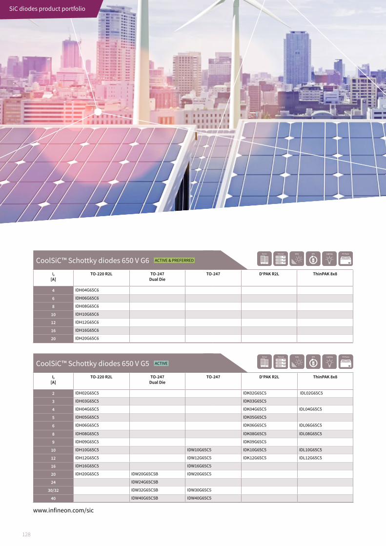
128
SiC diodes product portfolio
www.infineon.com/sic
CoolSiC™ Schottky diodes 650 V G5 ACTIVE IF
[A]TO-220 R2L TO-247
Dual DieTO-247 D2PAK R2L ThinPAK 8x8
2 IDH02G65C5 IDK02G65C5 IDL02G65C5
3 IDH03G65C5 IDK03G65C5
4 IDH04G65C5 IDK04G65C5 IDL04G65C5
5 IDH05G65C5 IDK05G65C5
6 IDH06G65C5 IDK06G65C5 IDL06G65C5
8 IDH08G65C5 IDK08G65C5 IDL08G65C5
9 IDH09G65C5 IDK09G65C5
10 IDH10G65C5 IDW10G65C5 IDK10G65C5 IDL10G65C5
12 IDH12G65C5 IDW12G65C5 IDK12G65C5 IDL12G65C5
16 IDH16G65C5 IDW16G65C5
20 IDH20G65C5 IDW20G65C5B IDW20G65C5
24 IDW24G65C5B
30/32 IDW32G65C5B IDW30G65C5
40 IDW40G65C5B IDW40G65C5
CoolSiC™ Schottky diodes 650 V G6 ACTIVE & PREFERRED IF
[A]TO-220 R2L TO-247
Dual DieTO-247 D2PAK R2L ThinPAK 8x8
4 IDH04G65C6
6 IDH06G65C6
8 IDH08G65C6
10 IDH10G65C6
12 IDH12G65C6
16 IDH16G65C6
20 IDH20G65C6

129
SiC
dis
cret
es
& S
i dio
de
s
SiC diodes product portfolio
www.infineon.com/sic
„B“ in product name refers to common-cathode configuration
CoolSiC™ Schottky diodes 1200 V G5 ACTIVE & PREFERRED
IF [A]
TO-220 R2L TO-247Dual Die
TO-247 TO-247 R2L DPAK R2L
2 IDH02G120C5 IDM02G120C5
5 IDH05G120C5 IDM02G120C5
8 IDH08G120C5 IDM08G120C5
10 IDH10G120C5 IDW10G120C5B IDWD10G120C5* IDM10G120C5
15/16 IDH16G120C5 IDW15G120C5B IDWD15G120C5*
20 IDH20G120C5 IDW20G120C5B IDWD20G120C5*
30 IDW30G120C5B IDWD30G120C5*
40 IDW40G120C5B IDWD40G120C5*
CoolSiC™ Schottky diodes 650 V G3 ACTIVE IF
[A]TO-220 R2L TO-247
Dual DieTO-247 DPAK R2L D2PAK ThinPAK 8x8
3 IDH03SG60C IDD03SG60C
4 IDH04SG60C IDD04SG60C
5 IDH05SG60C IDD05SG60C
6 IDH06SG60C IDD06SG60C
8 IDH08SG60C IDD08SG60C
9 IDH09SG60C IDD09SG60C
10 IDH10SG60C IDD10SG60C
12 IDH12SG60C IDD12SG60C
* coming 2018

Naming system
CoolSiC™ Schottky diodes G2 and G3
Continuous forward current
[A]
I D H X S XG C
Company
I = Infineon
Specifications
C = Surge current stable
Device
D = Diode
Package Type
D = DPAK
H = TO-220 R2L
B = D2PAK
D = DPAK = TO-220
V = TO-220 FullPAK
W = TO-247
Breakdown voltage
60 = 600 V
120 = 1200 V
G = Low thermal resistance
(diffusion soldering)
Technology
S = SiC diode
CoolSiC™ Schottky diodes G5 and G6
Continuous forward current
[A]
I D WD X G CX 5 B
Company
I = Infineon
Series name
5 = Generation 5
6 = Generation 6
B = Common-cathode configuration
Device
D = Diode
Package type
H = TO-220 R2L
W = TO-247
K = D2PAK R2L
L = ThinPAK 8x8
M = DPAK R2L
WD = TO-247 R2L
Specifications
C = Surge current stable
Breakdown voltage
65 = 650 V
120 = 1200 V
G = Low thermal resistance
130
SiC diodes nomenclature
www.infineon.com/sic

CoolSiC™ MOSFET
Breakdown voltage Divided by 10120 = 1200 V
I M W 120 R M145
CompanyI = Infineon
Reliable gradeblank = IndustrialA = AutomotiveS = StandardDevice
M = MOSFET
Package TypeW = TO-247Z = TO-247 4pin
Series name (2 digits)M1 = Generation 1
RDS(on) [mΩ]
R = RDS(on)
As a separator betweenvoltage und RDS(on)
131
SiC
dis
cret
es
& S
i dio
de
s
SiC diodes nomenclature
www.infineon.com/sic

Ictam quodita dolorep
132
Silicon power diodesFilling the gap between SiC diodes and emitter controlled diodes
The rapid diode family complements Infineon’s existing high power 600 V/650 V diode portfolio by filling the gap between SiC diodes and previously released emitter controlled diodes. They represent a perfect cost/performance balance and target high efficiency applications switching between 18 kHz and 100 kHz. rapid 1 and rapid 2 diodes are optimized to have excellent compatibility with CoolMOS™ and high speed IGBTs (Insulated Gate Bipolar Transistor) such as the TRENCHSTOP™ 5 and HighSpeed 3.
The rapid 1 diode familyRapid 1 is forward voltage drop (VF) optimized to address low switching frequency applications between 18 kHz and 40 kHz, for example air conditioner and welder PFC stages.
› 1.35 V temperature-stable forward voltage (VF) › Lowest peak reverse recovery current (Irrm) › Reverse recovery time (trr) < 100 ns › High softness factor
The rapid 2 diode familyRapid 2 is Qrr/trr optimized hyperfast diode to address high speed switching applications between 40 kHz and 100 kHz, typically found in PFCs in high efficiency switch mode power supplies (SMPS) and welding machines.
› Lowest reverse recovery charge (Qrr): VF ratio for best-in-class performance › Lowest peak reverse recovery current (Irrm) › Reverse recovery trr < 50 ns › High softness factor
Emitter controlled diodes Rapid 2 SiCRapid 1
0 Hz 18 kHz 40 kHz 100 kHz >100 kHz
1000
900
800
700
600
500
400
300
200
100
0
1.3 1.4 1.5 1.6 1.7 1.8 1.9 2.0 2.1 2.2 2.3
30 A competitor A
IDW30E65D1
IDP08E65D28 A competitor C
8 A competitor D
30 A competitor B
Qrr
[n
C]
VF [V]
VF - Qrr trade-o, rapid 1 diF/dt = 1000 A/us, rapid 2 diF/dt = 300 A/us
97.6
97.4
97.2
97.0
96.8
96.6
96.4
96.2
96.0
95.8
95.6
0 100 200 300 400 500 600 700 800
E
icie
ncy
[%
]
Output Power [W]
IDP08E65D2
Competitor S
Competitor F
PFC Eiciency @ 60 kHz – Vin = 230 V
98.2
98.0
97.8
97.6
97.4
97.2
97.0
96.8
96.6
96.4
96.2
0 200 400 600 800 1000 1200 1400 1600
E
icie
ncy
[%
]
Output Power [W]
PFC Eiciency @ 70 kHz – Vin = 230 V
Rapid 2
SiC
www.infineon.com/rapiddiodeswww.infineon.com/ultrasoftdiodes
Silicon power diodes

133
SiC
dis
cret
es
& S
i dio
de
s
Rapid 1 diodes650 V product family Continuous
current Ic
@TC=100°C[A]
TO-220 TO-220FullPAK
TO-220 Common Cathode
TO-247 TO-247 Common Cathode
TO-247Advanced Isolation
8 IDP08E65D1
15 IDP15E65D1
20 IDV20E65D1
30 IDP30E65D1 IDW30E65D1 IDW30C65D1
40 IDW40E65D1 IDFW40E65D1E
60 IDW60C65D1
75 IDW75D65D1
80 IDW80C65D1
Rapid 2 diodes650 V product family Continuous
current Ic
@TC=100°C[A]
TO-220 TO-220 FullPAK
TO-220 Common Cathode
TO-247 TO-247 Common Cathode
8 IDP08E65D2 IDV08E65D2
15 IDP15E65D2 IDV15E65D2 IDW15E65D2
20 IDP20E65D2 IDP20C65D2 IDW20C65D2
30 IDP30E65D2 IDV30E65D2 IDP30C65D2 IDW30C65D2
40 IDP40E65D2 IDW40E65D2
80 IDW80C65D2
www.infineon.com/rapiddiodes
Silicon power diodes

Ictam quodita dolorep
134
Emitter controlled diodes600 V and 1200 V product families Continuous
current Ic
@TC=100°C[A]
TO-252(DPAK)
TO-263(D2PAK)
TO-220 Real 2pin
TO-247
600
V
6 IDD06E60
9 IDD09E60
15 IDD15E60 IDB15E60 IDP15E60
30 IDB30E60 IDP30E60 IDW30E60
45 IDP45E60
50 IDW50E60
75 IDW75E60
100 IDW100E60
1200
V 12 IDP12E120
18 IDP18E120
30 IDB30E120 IDP30E120
Naming system
Silicon power diodes
CompanyI = Infineon
I D
DeviceD = Diode
Package typeP = TO-220V = TO-220 FullPAKW = TO-247D = TO-252 (DPAK)B = TO-263 (D2PAK)FW = TO-247 Advanced Isolation
D1 = Rapid 1D2 = Rapid 2
W 75 E 65 D1
Nominal current (@ 100°C) [A]
Nominal voltageDivided by 10 (650 V/10 = 65)
TechnologyE = Std. diode configuration – replacement for FullPAK packages or TO-247 + medium performance insulator C = Common cathodeD = Dual anode
www.infineon.com/ultrasoftdiodes
Silicon power diodes

Infineon support for SiC discretes and Si diodesUseful links and helpful information
Further information, datasheets and documentswww.infineon.com/sic www.infineon.com/rapiddiodeswww.infineon.com/ultrasoftdiodes
Videoswww.infineon.com/mediacenter
SiC
dis
cret
es
& S
i dio
de
s
SiC discretes & Si diodes support

136
Discrete IGBTs
Discrete IGBTs Market leadership through groundbreaking innovation and application focus
Resolute to achieve the highest standards in performance and quality, Infineon offers comprehensive application-specific discrete IGBTs.
New products are application-specific, developed to achieve highest value.
Overview of discrete IGBTs
Product portfolio
New best-in-class technologies and applications
TO-252 (DPAK)
TO-263(D2PAK)
TO-220 TO-220FullPAK
TO-247 TO-247 4pin TO-247PLUS TO-247PLUS 4pin
Package options
Voltage class 600 V, 650 V, 1100 V, 1200 V, 1350 V, 1600 VConfiguration DuoPack (with diode), single IGBTs
Continuous collector current TC = 100°C 2 A – 120 A
Technology Application
TRENCHSTOP™ 5 H5/F5 650 V
TRENCHSTOP™ 5 L5 650 V
Rapid diode 650 V
RC-H5650 V/1200 V/1350 V
RC-E1200 V
WR5650 V
RC-drives
RC-drives fast600 V
TRENCHSTOP™ 5S5 650 V
TRENCHSTOP™ IGBT6 650 V
www.infineon.com/igbtdiscretes

137
Dis
cret
e IG
BTs
TRENCHSTOP™ 5 L5
Best-in-class IGBT low VCE(sat) IGBTVCE(sat) IGBT – 1.05 VBest trade-off VCE(sat) Vss Ets for frequencies below 20 kHz
Solar, welding, UPS, PFC › Ultra low frequency converters › 3-level inverter type I NPC 1 and NPC 2 › Modified HERIC inverter › AC output (Aluminum/Magnesium welding)
TRENCHSTOP™ 5 S5
Best-in-class ease-of-use IGBT Elimination of: › Collector-emitter snubber capacitor and gate capacitor in low
inductance designs (<100 nH) › Softer switching than TRENCHSTOP™ 5 H5
Solar, welding, UPS, battery charger › Medium frequency converters › Multilevel inverter stages › Output stages › PFC
TRENCHSTOP™ 5 H5/F5
Best-in-class high frequency IGBT › Bridge to superjunction MOSFET performance › Highest efficiency, especially under light load conditions
Solar, welding, UPS › High frequency converters › Multilevel inverter stages › Output stages › PFC
TRENCHSTOP™ 5 R5Price/performance optimizedapplication specific IGBT
Induction heating – RC-H5Half-bridge topologies in induction cooking appliances and other resonant switching applications
TRENCHSTOP™ 5 WR5
Price optimized application specific IGBT for zero current switching (ZCS) › Optimized full rated hard switching turn-off typically found in
welding › Excellent RG controllability › Soft recovery plus low Qrr for diode
Welding, PFC › Medium frequency converters › Zero-voltage switching › PFC
650 V TRENCHSTOP™ 5
650 V TRENCHSTOP™ 5 IGBT
In terms of switching and conduction losses, there is no other IGBT on the market that can match the performance of the TRENCHSTOP™ 5. Wafer thickness has been reduced by more than 25 percent, which enables a dramatic improvement in both switching and conduction losses, whilst providing an increased breakthrough voltage of 650 V. Based on TRENCHSTOP™ 5 IGBT technology, Infineon has developed six different product families optimized for specific applications, allowing designers to optimize for high efficiency, system cost or reliability demands of the market. The quantum leap of efficiency improvement provided by the TRENCHSTOP™ 5 IGBT families opens up new opportunities for designers to explore.
0 10 20 30 40 50 60 70 80 90 100 110 120 130 140 150 kHz
TRENCHSTOP™ 5 L5 (hard switching)
TRENCHSTOP™ 5 S5 (hard switching)
TRENCHSTOP™ 5 WR5 (resonant switching)
RC-H5 (resonant switching)
TRENCHSTOP™ 5 H5 (hard switching)
TRENCHSTOP™ 5 F5 (hard switching)
www.infineon.com/trenchstop5

138
1200 V discrete IGBTs
Overview of 1200 V IGBT families
Infineon’s 1200 V TRENCHSTOP™ 2 IGBT technology combines trench top-cell and field stop concepts to offer significant improvement of static as well as dynamic performance of the device. The combination of IGBT with a soft recovery emitter controlled diode further minimizes the turn-on losses. The highest efficiency is reached due to the best compromise between switching and conduction losses.
The 1200 V HighSpeed 3 discrete IGBTs provides the lowest losses and highest reliability for switching above 20 kHz. Transition to fast switching high speed devices allows reduction in the size of the active components (25 kHz – 70 kHz). The smaller size of the components allows high power density designs with reduced system cost.
The RC-H5 family is the latest generation in the RC-H series of reverse conducting IGBT. With a monolithically integrated diode, they offer optimized performance for resonant switching applications such as induction cooking. R5 devices are also available in 1350 V blocking voltage.
RC-H5
World famous TRENCHSTOP™ RC-H productsHigh performance and low losses
Induction cookingResonant switching Medium to high frequency converters
RC-E
New TRENCHSTOPTM RC-EPrice versus performance leader
Induction cookingResonant switching Low to medium power cookers
TRENCHSTOP™ 2
Best-in-class 1200 V IGBT › Outstanding efficiency › Lowest conduction and switching losses › Market proven and recognized quality leader
Motor control, drives, solar, UPS Low frequency converters
HighSpeed 3 H3
High speed/high power IGBT › First tailless/low loss IGBT on market › Market proven and recognized quality leader
Solar, UPS, welding Medium frequency converters
0 5 10 15 20 25 30 35 40 45 50 55 60 kHz
TRENCHSTOP™ R3/R5 (resonant switching)
HighSpeed 3 H3 (hard switching)
TRENCHSTOP™ 2 (hard switching)
TRENCHSTOP™ RC-E (resonant switching)
www.infineon.com/600V-1200V-trenchstopwww.infineon.com/highspeed3www.infineon.com/rch5www.infineon.com/rc-e

139
Dis
cret
e IG
BTs
www.infineon.com/igbt6
TRENCHSTOP™ IGBT6 650 V trench and field-stop IGBT for low power motor drives
Motor drives up to 1 kW are used in a wide variety of applications from home appliance fans and compressors to com-mercial sewing machines and pumps. The market for these products demands longer lifetimes, high reliability and high efficiency. Therefore, these compact motors require power electronics with the lowest losses and best thermal performance.
The TRENCHSTOP™ IGBT6 family of discrete devices has been designed to meet these specific requirements of motor drives. It has been optimized for the lowest switching losses, which is particularly important in systems with higher switching frequencies up to 30 kHz. Additionally the IGBTs are co-packed with the soft, fast recovery rapid 1 anti-paral-lel diodes for the lowest total losses.
With a higher blocking voltage at 650 V, and short circuit rating, TRENCHSTOP™ IGBT6 is a key contributor to robust motor designs.
The devices are offered in TO-220 FullPAK packages for the required isolation, as well as DPAK for a more compact surface mount solution.
› Optimized for small drives requiring best-in-class efficiency
› Up to 20 percent reduction in total losses
› Lowest switching losses for better heat management and easier design-in
Key features › Lowest VCE(sat) and VF
› 650 V blocking voltage
› 3 μsec short-circuit protection capability
› Optimized for switching frequencies from 8–30 kHz
Key benefits › Good thermal performance, especially at higher fre-
quencies
› Low losses to meet energy efficiency requirements
› Increased design margin and reliability
› Leading price/performance
TRENCHSTOP™ IGBT6
TRENCHSTOP™ IGBT6 IKA15N65ET6
Power losses [W]
550 W @ TA = 25°C, 10 kHz, same dv/dt
TRENCHSTOP™ IKA15N60T
Gen5 IRGIB15B60KD1P
0.5 0.75 1 1.25 1.5 1.75
Pcnd(s) [W] Pcnd(d) [W] Prec(d) [W]Pon(s) [W] Po(s) [W]

140
TRENCHSTOP™ advanced isolation
www.infineon.com/advanced-isolation
TRENCHSTOP™ advanced isolation Fully isolated TO-247 package with industry leading IGBTs
TRENCHSTOP™ advanced isolation solution breaks the limits reached by traditional packaging and isolation tech-niques. This new isolated package enables the highest power density, the best performance and the lowest cooling effort thanks to an effective and reliable thermal path from the IGBT die to the heatsink.
In addition to providing 100 percent electrical isolation, TRENCHSTOP™ advanced isolation also eliminates the need for thermal grease or thermal interface sheets. The new package delivers at least 35 percent lower thermal resistivity, helping designers to increase power density, as well as lower system complexity and assembling costs.This new package solution allows industrial and home appliance designs to fully utilize the high performance of TRENCHSTOP™ IGBTs with no compromises for isolation and cooling.
Key features › 2500 VRMS electrical isolation, 50/60 Hz, t = 1 min
› 100 percent tested isolated mounting surface
› Lowest Rth(j-h)
› Low coupling capacitance, 38 pF
› No need for isolation film or thermal interface material
Key benefits › Up to 35 percent reduction in assembly time
reduces manufacturing cost
› Increased power density
› Improved reliability from higher yield and no isolation film misalignment
› Less EMI filter design effort
› Decreased heatsink size
Technology Version and package Part number Equivalent current rating @ 65°C [A ] Rth(j-h) [K/W] VCEsat [V] @ Tvj = 25°C
TRENCHSTOP™ HighSpeed 3
Price/performance advanced isolation TO-2471)
IKFW40N60DH3E 44 1.35 2.30
IKFW50N60DH3E 60 1.15 2.20
IKFW60N60DH3E 74 1.06 2.20
Best-in-class advanced isolation TO-2472)
IKFW50N60DH3 60 1.03 1.85
IKFW60N60EH3 63 0.91 1.85
IKFW90N60EH3 95 0.84 1.85
TRENCHSTOP™ Best-in-class advanced isolation TO-247
IKFW50N60ET 64 0.91 1.50
IKFW75N60ET 95 0.84 1.50
Technology Version and package Part number Equivalent current rating @ 65°C [A ] Rth(j-h) [K/W] Vf [V]
Rapid 1 diode Price/performance advanced isolation TO-247 IDFW40E65D1E 35 1.92 1.70
TRENCHSTOP™ advanced isolation offers a broad portfolio for specific application needs
Thermal resistivity of package and isolation types
Rth(j-h)
TO-247FullPAK
50% lower
35% lower
TO-247 withisolation film1)
Advancedisolation
1) Isolation material: standard polyimide based reinforced carrier insulator film with 152 µm thickness, 1.3 W/mK thermal conductivity
1) Optimized to replace FullPAK packages or systems including TO-247 with medium performance insulator, standard polyimide based reinforced carrier insulator with 152 µm thickness, 0.9 W/mK thermal conductivity.
2) Optimized to replace systems using TO-247 with high performance insulator, standard polyimide based reinforced carrier insulator with 152 µm thickness, 1.3 W/mK thermal conductivity.

141
Dis
cret
e IG
BTs
Thermal resistivity of package and isolation types
TRENCHSTOP™ 5 selection tree
TRENCHSTOP™ 5 selection tree
650 V
Free wheeling diode (FWD)
50 Hz-20 kHz
low speed
Low VCE(sat)
TRENCHSTOP™ 5 (L5)
IGW30N65L5 IGP20N65H5/F5
IGP30N65H5/F5
IGP40N65H5/F5
IGW30N65H5/F5
IGW40N65H5/F5
IGW50N65H5/F5
IGZ50N65H5
IGZ75N65H5
IGZ100N65H5
IGB15N65S5
IGB20N65S5
IGB50N65S5
IGB50N65H5
IKW30N65EL5
IKW30N65NL5
IKW75N65EL5
IKZ75N65EL5
IKW30N65WR5
IKW40N65WR5
IKW50N65WR5
IKW30N65ES5
IKW40N65ES5
IKW50N65ES5
IKW75N65ES5
IKZ50N65ES5
IKZ75N65ES5
IKB30N65ES5
IKB40N65ES5 IKB40N65EF5
IKP08N65H5
IKP15N65H5
IKP20N65H5
IKP30N65H5
IKP40N65H5
IKA08N65H5
IKA15N65H5
IKW30N65H5
IKW40N65H5
IKW50N65H5
IKW50N65EH5
IKW75N65EH5
IKZ50N65EH5
IKZ50N65NH5
IKZ75N65EH5
IKZ75N65NH5
IKB15N65EH5
IKB20N65EH5
IKB30N65EH5
IKB40N65EH5
IKP08N65F5
IKP15N65F5
IKP20N65F5
IKP30N65F5
IKP40N65F5
IKA08N65F5
IKA15N65F5
IKW30N65F5
IKW40N65F5
IKW50N65F5
Corresponding best fit IGBT Corresponding best fit IGBT
TRENCHSTOP™ 5
(H5/F5/S5)
Low VCE(sat)
TRENCHSTOP™ 5 (L5)
RC TRENCHSTOP™ 5
(WR5)
„So“
TRENCHSTOP™ 5 (S5)
TRENCHSTOP™ 5
(H5)
TRENCHSTOP™ 5
(F5)
30 kHz-120 kHz
high speed
50 Hz-20 kHz
low speed
> 20 kHz-60 kHz
high speed
10 kHz-40 kHz
high speed
30 kHz-100 kHz
high speed
60 kHz-120 kHz
ultra-high speed
No Yes
NEW!
NEW!
www.infineon.com/trenchstop5

142
Diode commutation
IGBT
Frequency range
Voltage range
Part number
Applications
Induction cooking
Microwave
Multifunction printers
Half-bridge resonant
(Current resonance < 650 V)
Single switch
(Voltage resonance > 650 V)
Conduction loss optimized
Solar inverter
Asymmetrical bridge
Symmetrical full-bridge3-level type I or 3-level type II converter
Motor control
Three-phase inverterFull-bridge inverter
Uninterruptable power supply
UPS bridge3-level type II converter
Major home appliances
Symmetrical full-bridge
PFC
Battery charger
Welding
UPS
Solar
Energy storage
SMPS
Air conditioning
HVDC (Telecom/data centers)
PFC
Welding inverter
Full-brigde Half-bridge
Two transistor forward
UPS
3-level NPC1 and NPC2 topology, inner switches
Solar
3-level NPC1 and NPC2 topology, inner switches
Welding
AC output(Al/Mag welding)
UPS
Energy storage
Battery charger
Welding
Solar Inverter
IHpccNvvvR2IHpccNvvvR3
IHpccN60R/RFIHpccNvvvR5IHpccNvvvE1
IKpccN60RIKpccN60RF
IKpccN60T IKpccN60dTP
IKpccT120…
IGpccN60TIGpccN60TP IGpccT120
IGpccN120T2
IKpccN60H3IKpccN120H3
IGpccN60H3
IGpccN120H3
IKpccN65H5IKpccN65F5
IGpccN65H5IGpccN65F5
IKpccN65dR5 IKpccN65dL5
IGpccN65L5
IKpccN65dS5
600 V, 650 V, 1100 V, 1200 V, 1350 V, 1600 V
600 V 600 V, 1200 V
IKpccN65dT6
650 V 650 V 650 V 650 V 650 V600 V, 1200 V
8 kHz – 60 kHzRC series (monolythic) 2 kHz – 30 kHz
So Hard/no diode for IG** parts
RC-drives (monolythic) TRENCHSTOP™ Performance TRENCHSTOP™ IGBT6 So turn-oTRENCHSTOP™ 5 (S5)
HighSpeed 3(H3)
TRENCHSTOP™ 5H5/F5
RC TRENCHSTOP™ 5 (WR5)
Low VCE(sat) TRENCHSTOP™ 5 (L5)
10 kHz – 40 kHz medium speed
> 18 kHz – 60 kHzhigh speed
10 kHz – 100 kHzhigh speed
> 18 kHz – 60 kHz high speed
50 Hz – 20 kHzlow speed
NEW!
NEW!
Discrete IGBTs selection tree
IGBT selection tree
www.infineon.com/igbtdiscretes

143
Dis
cret
e IG
BTs
Diode commutation
IGBT
Frequency range
Voltage range
Part number
Applications
Induction cooking
Microwave
Multifunction printers
Half-bridge resonant
(Current resonance < 650 V)
Single switch
(Voltage resonance > 650 V)
Conduction loss optimized
Solar inverter
Asymmetrical bridge
Symmetrical full-bridge3-level type I or 3-level type II converter
Motor control
Three-phase inverterFull-bridge inverter
Uninterruptable power supply
UPS bridge3-level type II converter
Major home appliances
Symmetrical full-bridge
PFC
Battery charger
Welding
UPS
Solar
Energy storage
SMPS
Air conditioning
HVDC (Telecom/data centers)
PFC
Welding inverter
Full-brigde Half-bridge
Two transistor forward
UPS
3-level NPC1 and NPC2 topology, inner switches
Solar
3-level NPC1 and NPC2 topology, inner switches
Welding
AC output(Al/Mag welding)
UPS
Energy storage
Battery charger
Welding
Solar Inverter
IHpccNvvvR2IHpccNvvvR3
IHpccN60R/RFIHpccNvvvR5IHpccNvvvE1
IKpccN60RIKpccN60RF
IKpccN60T IKpccN60dTP
IKpccT120…
IGpccN60TIGpccN60TP IGpccT120
IGpccN120T2
IKpccN60H3IKpccN120H3
IGpccN60H3
IGpccN120H3
IKpccN65H5IKpccN65F5
IGpccN65H5IGpccN65F5
IKpccN65dR5 IKpccN65dL5
IGpccN65L5
IKpccN65dS5
600 V, 650 V, 1100 V, 1200 V, 1350 V, 1600 V
600 V 600 V, 1200 V
IKpccN65dT6
650 V 650 V 650 V 650 V 650 V600 V, 1200 V
8 kHz – 60 kHzRC series (monolythic) 2 kHz – 30 kHz
So Hard/no diode for IG** parts
RC-drives (monolythic) TRENCHSTOP™ Performance TRENCHSTOP™ IGBT6 So turn-oTRENCHSTOP™ 5 (S5)
HighSpeed 3(H3)
TRENCHSTOP™ 5H5/F5
RC TRENCHSTOP™ 5 (WR5)
Low VCE(sat) TRENCHSTOP™ 5 (L5)
10 kHz – 40 kHz medium speed
> 18 kHz – 60 kHzhigh speed
10 kHz – 100 kHzhigh speed
> 18 kHz – 60 kHz high speed
50 Hz – 20 kHzlow speed
NEW!
NEW!
Discrete IGBTs selection tree

144
TRENCHSTOP™ and RC-drives600 V product family
Continuous collector current
@ Tc=100°C[A]
TO-251(IPAK)
TO-252(DPAK)
TO-263(D2PAK)
TO-220 TO-247Advanced Isolation
TO-220FullPAK
TO-247 TO-247PLUS/Super 247(TO247AA)
Sing
le IG
BT
4 IGU04N60T
6 IGD06N60T IGP06N60T
10 IGB10N60T IGP10N60T
15 IGB15N60T IGP15N60T
30 IGB30N60T IGW30N60TIGW30N60TP
40 IGW40N60TP
50 IGB50N60T IGP50N60T IGW50N60TIGW50N60TP
75 IGW75N60T
IGBT
and
dio
de
3 IKD03N60RF
4 IKD04N60RF IKD04N60R
IKP04N60T
6 IKD06N65ET6 IKD06N60RFIKD06N60R
IKB06N60T IKP06N60T IKA06N60T
10 IKD10N60RFIKD10N60R
IKB10N60T IKP10N60T IKA10N60T
15 IKD15N60RFIKD15N60R
IKB15N60T IKP15N60T IKA15N60T
20 IKB20N60T IKP20N60T IKW20N60T
30 IKW30N60TIKW30N60DTP
40 IKW40N60DTP
50 IKFW50N60ET IKW50N60TIKW50N60DTP
75 IKFW75N60ET IKW75N60T
100 IKQ100N60T
120 IKQ120N60T
Discrete IGBTs product portfolio
www.infineon.com/600V-1200V-trenchstop
NEW!
NEW!NEW!
NEW!
NEW!
NEW!

145
Dis
cret
e IG
BTs
Discrete IGBTs product portfolio
TRENCHSTOP™1200 V product family
Continuous collector current
@ Tc=100°C[A]
TO-252(DPAK)
TO-263(D2PAK)
TO-220 TO-262(I²PAK)
TO-220FullPAK
TO-247 TO-247PLUS 3pin
TRENCHSTOP™ TRENCHSTOP™ 2 TRENCHSTOP™ 2
Sing
le IG
BT
8 IGW08T12015 IGW15T12025 IGW25T12040 IGW40T12060 IGW60T120
DuoP
ack
8 IKW08T12015 IKW15T120 IKW15N120T225 IKW25T120 IKW25N120T2
40 IKW40T120 IKW40N120T2 IKQ40N120CT250 IKQ50N120CT275 IKQ75N120CT2
TRENCHSTOP™ IGBT6650 V product family
Continuous collector current
@ Tc=100°C[A]
TO-251(IPAK)
TO-252(DPAK)
TO-263(D2PAK)
TO-220 TO-262(I²PAK)
TO-220FullPAK
TO-247
6 IKD06N65ET68 IKA08N65ET6*
10 IKA10N65ET6*15 IKA15N65ET6*
www.infineon.com/600V-1200V-trenchstop
* Limited by maximum junction temperature. Applicable for TO-220 standard package.

146
Discrete IGBTs product portfolio
HighSpeed 3 600 V product family
Continuous collector current
@ Tc=100°C[A]
TO-251(IPAK)
TO-252(DPAK)
TO-263(D2PAK)
TO-220 TO-247Advanced Isolation
TO-220 FullPAK
TO-247
IGBT
20 IGB20N60H3 IGP20N60H3 IGW20N60H330 IGB30N60H3 IGP30N60H3 IGW30N60H340 IGW40N60H350 IGW50N60H360 IGW60N60H375 IGW75N60H3
100 IGW100N60H3
DuoP
ack
20 IKB20N60H3 IKP20N60H3 IKW20N60H330 IKW30N60H340 IKFW40N60DH3E IKW40N60H3
50 IKFW50N60DH3EIKFW50N60DH3
IKW50N60H3
60 IKFW60N60DH3EIKFW60N60EH3
IKW60N60H3
75 IKW75N60H390 IKFW90N60EH3
HighSpeed 3 1200 V product family
Continuous collector current
@ Tc=100°C[A]
TO-263(D2PAK)
TO-220 TO-262(I²PAK)
TO-220 FullPAK
TO-247 TO-247PLUS 3pin TO-247PLUS 4pin
IGBT
15 IGW15N120H3
25 IGW25N120H3
40 IGW40N120H3
DuoP
ack
15 IKW15N120H3
25 IKW25N120H3
40 IKW40N120H3 IKQ40N120CH3 IKY40N120CH3
50 IKQ50N120CH3 IKY50N120CH3
75 IKQ75N120CH3 IKY75N120CH3
www.infineon.com/rch5www.infineon.com/rc-ewww.infineon.com/highspeed3
Induction cooking series 650 V, 1100 V, 1200 V, 1350 V and 1600 V product families
Continuous collector current
@ Tc=100°C[A]
TO-247
650 V 1100 V 1200 V 1350 V 1600 V15 IHW15N120E1
20IHW20N65R5
IHW20N120R5 IHW20N135R525 IHW25N120E130 IHW30N65R5 IHW30N110R3 IHW30N120R3 IHW30N135R3 IHW30N160R240 IHW40N65R5 IHW40N120R3 IHW40N135R350 IHW50N65R5
NEW!
NEW!

147
Dis
cret
e IG
BTs
Discrete IGBTs product portfolio
TRENCHSTOP™ 5 F5, H5 and S5 650 V product family
Continuous collector current
@ Tc=100°C[A]
TO-251(IPAK)
TO-252(DPAK)
TO-263(D2PAK)
TO-220 TO-262(I²PAK)
TO-220 FullPAK
TO-247 TO-247 4pin
IGBT
20 IGB20N65S5 IGP20N65F5/H5
30 IGB30N65S5 IGP30N65F5/H5
40 IGP40N65F5/H5 IGW40N65F5/H5
50 IGB50N60H5/S5 IGW50N65F5/H5 IGZ50N65H5
75 IGW75N65H5 IGZ75N65H5
100 IGZ100N65H5
DuoP
ack
8 IKP08N65F5/H5 IKA08N65F5/H5
15 IKB15N65EH5 IKP15N65F5/H5 IKA15N65F5/H5
20 IKB20N65EH5 IKP20N65H5/F5
30 IKB30N65EH5/S5 IKP30N65H5/F5 IKW30N65H5
40 IKB40N65ES5/H5/F5 IKP40N65F5/H5 IKW40N65F5/H5
50 IKW50N65F5/H5IKW50N65EH5
IKZ50N65EH5IKZ50N65NH5
75 IKW75N65EH5 IKZ75N65NH5IKZ75N65EH5
TRENCHSTOP™ 5 L5 low VCE(sat) 650 V product family
Continuous collector current
@ Tc=100°C[A]
TO-251(IPAK)
TO-252(DPAK)
TO-263(D2PAK)
TO-220 TO-262(I²PAK)
TO-220 FullPAK
TO-247 TO-247 4pin
IGBT 30 lGW30N65L5
DuoP
ack
30 IKW30N65EL5IKW30N65NL5
75 IKW75N65EL5 IKZ75N75EL5
TRENCHSTOP™ 5 WR5 650 V product family
Continuous collector current
@ Tc=100°C[A]
TO-251(IPAK)
TO-252(DPAK)
TO-263(D2PAK)
TO-220 TO-262(I²PAK)
TO-220 FullPAK
TO-247 TO-247 4pin
DuoP
ack 30 IKW30N65WR5
40 IKW40N65WR5
50 IKW50N65WR5
TRENCHSTOP™ 5 S5650 V product family
Continuous collector current
@ Tc=100°C[A]
TO-251 TO-252(DPAK)
TO-263(D2PAK)
TO-220 TO-262(I²PAK)
TO-220 FullPAK
TO-247 TO-247 4pin
DuoP
ack
30 IKW30N65ES5
40 IKW40N65ES5
50 IKW50N65ES5 IKZ50N65ES5
75 IKW75N65ES5 IKZ50N65ES5
www.infineon.com/trenchstop5
NEW!
NEW!

148
IGBT nomenclature
Naming systemIGBT (products launched after 03/2013)
IGBT (products launched before 03/2013)
Company I = InfineonS = Formerly Siemens
I K
DeviceG = Single IGBTH = Reverse conductingK = Duo pack
Package typeA = TO-220-3 FullPAKB = TO-263-3 (D2PAK)D = TO-252-3 (DPAK)P = TO-220-3U = TO-251-3 (IPAK)W = TO-247-3Y = TO-247PLUS 4pinFW = TO-247-3 advanced isolationQ = TO-247PLUS/Super 247 (TO247AA)Z = TO-247-4
F5 = Ultra fast IGBT
H5 = High speed IGBT
L5 = Low VCE(sat) IGBT
R5 = Reverse conducting IGBT
E1 = Reverse conducting IGBT
S5 = “Soft” high speed IGBTT6 = TRENCHSTOP™ IGBT6TP = TRENCHSTOP™ PerformanceWR5 = RC TRENCHSTOP™ 5T6 = TRENCHSTOP™ IGBT6
Diode (for duo pack only)B = Emitter controlled half ratedC = Emitter controlled full ratedD = Rapid 1 half ratedE = Rapid 1 full ratedN = Rapid 2 full ratedW = Full rated hard switching
W 75 N 65 L5E
Nominal current [A] @ 100°C Nominal voltage
Divided by 10 (650 V/10 = 65)
TechnologyN = N-channelP = P-channel
CompanyI = InfineonS = Formerly Siemens
I K
DeviceK = IGBT + diode (normal drives)H = Optimized for so
switching applications (e.g. induction heating)
G = Single IGBTD = Diode
Package typeA = TO-220 FullPAKB = TO-263 (D2PAK)D = TO-252 (DPAK)P = TO-220U = TO-251 (IPAK)W = TO-247
– = Fast IGBT (~20 kHz)
Hχ = HighSpeed generation (600 V - 1200 V)
Tχ = TRENCHSTOP™ generation (600 V IGBT 3) (1200 V IGBT 4)
Rχ = Reverse conductingRF = Reverse conducting fastF = HighSpeed FAST 5
Rχ = Rapid diode generation
W 40 N 120 H 3
Generation
Nominal current (@ 100°C) [A]
Nominal voltageDivided by 10 (1200 V/10 = 120)
TechnologyN = N-channelT = TRENCHSTOPTM
E = Emitter-controlled diodes (for diode only)
www.infineon.com/igbtdiscretes

Infineon support for discrete IGBTsUseful links and helpful information
Further information, datasheets and documentswww.infineon.com/igbt www.infineon.com/igbtdiscretes
www.infineon.com/discrete-automotive-igbtwww.infineon.com/latest-discrete-packages
Evaluationboards and simulation models www.infineon.com/eval-TO-247-4pin www.infineon.com/igbtdiscrete-simulationmodels
Videoswww.infineon.com/mediacenter
Simulation
Dis
cret
e IG
BTs
Discrete IGBTs support

150
Power management ICs
Power management ICsTechnology leadership in power supply
AC-DC power management ICs
PFC controller
CCM PFC(Continuous conduction mode)
CrCM PFC(Critical conduction mode)
Combi (PFC+PWM)
Fixed frequency
ICE2PCS02G (65 kHz)
ICE2PCS03G (100 kHz)
Adjustable frequency
ICE2PCS01G (50 kHz - 250 kHz)
ICE2PCS05G (20 kHz - 250 kHz)
ICE3PCS01G (OVP+brown out)
ICE3PCS02G (OVP)
ICE3PCS03G (Brown out)
Stand-alone PWM Fixed frequency CoolSET™
PWM controller
Fixed frequency (FF)
ICE5GSAG (125 Khz)
ICE5ASAG (100 Khz)
ICE3AS03LJG (100 kHz)
ICE3BS03LJG (65 kHz)
Quasi-resonant (QR)
ICE5QSAG
ICE2QS02G
ICE2QS03G
Half-bridge (HB) LLC resonant
ICE1HS01G-1
ICE2HS01G
TDA4862G
TDA4863G
TDA4863-2G
IRS2505LPBF
CrCM + LLC
XDP™ SMPS IDP2308 (DSO-14)
XDP™ SMPS IDP2303 (DSO-16)
XDP™ SMPS IDP2303A (DSO-16)
650 V F3/F3R CoolSET™
ICE3A/BRxx65J(Z)/(G)
ICE3RBRxx65J
ICE3RBRxx65JG
700 V Gen5 CoolSET™
ICE5AR4770AG
ICE5AR4770BZS
800 V F3R CoolSET™
ICE5A/GRxx80AG
ICE5ARxx80BZS
ICE3A/BRxx80JZ
ICE3ARxx80CJZ
ICE3ARxx80VJZ
ICE3ARxx80JG
Quasi-resonant CoolSET™
650 V CoolSET™
ICE2QRxx65(Z)/(G)
700 V CoolSET™
ICE5QRxx70AZ/G
800 V CoolSET™
ICE2QRxx80Z/G
ICE5QRxx80AZ/G

151
Po
we
r IC
s
CrCM PFC ICs
Power factor correction and combo controller
Critical conduction mode PFC ICs
TDA4862G
Power factor controller (PFC) IC for high-power factor and active harmonic filter
› IC for sinusoidal line-current consumption
› Power factor approaching 1
› Controls boost converter as an active harmonics filter
› Internal start-up with low current consumption
› Zero current detector for discontinuous operation mode
› High current totem pole gate driver
› Trimmed ±1.4% internal reference
› Undervoltage lock out with hysteresis
› Very low start-up current consumption
› Pin compatible with world standard
› Output overvoltage protection
› Current sense input with internal low pass filter
› Totem pole output with active shutdown during UVLO
› Junction temperature range -40°C to +150°C
› Available in DIP-8 and SO-8 packages
TDA4863G/TDA4863-2G
Power factor controller IC for high-powerfactor and low THD additional features to TDA4862
› Reduced tolerance of signal levels
› Improved light load behavior
› Open loop protection
› Current sense input with leading edge blanking LEB
› Undervoltage protection
› SO-8 package
IRS2505LPBF
› Critical-conduction mode PFC control
› High power factor and ultra-low THD
› Wide load and line range
› Regulated and programmable DC bus voltage
› No secondary winding required
› MOSFET cycle-by-cycle over-current protection
› DC bus over-voltage protection
› Low EMI gate drive
› Ultra-low start-up current
› 20.8 V internal zener clamp on VCC
› Excellent ESD and latch immunity
› RoHS compliant
› 5pin SOT-23 package
TDA4862G
TDA4863G
TDA4863-2G
IRS2505LPBF
www.infineon.com/acdc

152
CCM PFC ICs
ICE2PCS0xG
ICE3PCS0xG
Continuous conduction mode PFC ICs
2nd generation continuous conduction mode (CCM) Power factor correction IC features
› Fulfills class D requirements of IEC 61000-3-2
› Lowest count of external components
› Adjustable and fixed switching frequencies
› Frequency range from 20 kHz to 250 kHz
› Versions with brown out protection available
› Wide input range supported
› Enhanced dynamic response during load jumps
› Cycle by cycle peak current limiting
› Integrated protections OVP, OCP
› DIP-8 and DSO-8
› Lead free, RoHS compliant
2nd generation continuous conduction mode (CCM) power factor correction IC product portfolio
Product Frequency – fSW Current drives Package
ICE2PCS01G 50 kHz-250 kHz 2.0 A
DSO-8ICE2PCS02G 65 kHz 2.0 A
ICE2PCS03G 100 kHz 2.0 A
ICE2PCS05G 20 kHz-250 kHz 2.0 A
www.infineon.com/acdc

153
Po
we
r IC
s
CCM PFC ICs
3rd generation continuous conduction mode (CCM) Power factor correction IC features
› Fulfills class D requirements of IEC 61000-3-2
› Integrated digital voltage loop compensation
› Boost follower function
› Bulk voltage monitoring signals, brown out
› Multi protections such as double OVP
› Fast output dynamic response during load jump
› External synchronization
› Extra low peak current limitation threshold
› SO-8 and SO-14
› Lead free, RoHS compliant
3rd generation continuous conduction mode (CCM) power factor correction IC product portfolio
Product Frequency – fSW Current drives Features Package
ICE3PCS01G
Adjustable
0.75 A OVP+Brown out SO-14
ICE3PCS02G 0.75 A OVP SO-8
ICE3PCS03G 0.75 A Brown out SO-8
PFC CCM IC by feature ICE2PCS01GICE2PCS05G
ICE2PCS02GICE2PCS03G
ICE3PCS03G ICE3PCS02G ICE3PCS01G
Digital control voltage loop –
Variable frequency –
Synchronous frequency –
Open loop protection
Low peak current limit -1 V -1 V -0.4 V -0.4 V -0.2 V
Brown out protection – –
Over voltage protection
Second over voltage protection –
PFC enable function –
Boost follower mode –
5 V regulator –
www.infineon.com/acdc

www.infineon.com/acdc
154
Resonant LLC half-bridge controller IC
› Novel and simple design (12 components + HB driver)
› Minimum operating frequency is adjustable externally
› Burst mode operation for output voltage regulation during no load and/or bus over-voltage
› Multiple protections in case fault
› Input voltage sense for brown out protection
› Open loop/over load fault detection by FB pin with auto-restart and adjustable blanking/restart time
› Frequency shift for over-current protection
› Lead free, RoHS compliant package
› DSO-8 package
› Novel LLC/SR operation mode and controlled by primary side controller
› Multiple protections for SR operation
› Tight tolerance control
› Accurate setting of switching frequency and dead time
› Simple system design
› Optimized system efficiency
› Multiple Converter protections: OTP, OLP, OCP, latch-off enable
› External disable for either SR switching or HB switching
› Lead free, RoHS compliant package
› DSO-20 package
LLC resonant (No SR)
ICE1HS01G-1
Resonant LLC half-bridge controller IC with integrated synchronized rectifier control
Product Frequency - fsw Dead time Current drives Package
ICE2HS01G 30 kHz~1 MHz 100~1000 ns 0.3 A DSO-20
LLC resonant + SR
ICE2HSO1G
LLC controller ICs
Product Frequency – fSW Dead time Current drives Package
ICE1HS01G-1 30 kHz~600 kHz 380 ns 1.5 A DSO-8

LLC half-bridge controller IC ICE1HS01G-1 ICE2HS01G
Package DSO-8 DSO-20
Switching frequency range up to 600 kHz up to 1 MHz
LLC softstart
LLC burst mode
Adjustable minium frequency
Over load/open loop protection
Mains under-voltage protection with hysteresis
Over current protection 2-level 3-level
Drive signal for synchronous rectification –
Adjustable dead time –
External latch-off and OTP –
Target application LCD-TV, audio, etc. Server, PC, LCD-TV, etc.
www.infineon.com/acdc
155
Po
we
r IC
s
LLC controller ICs

156
Climate saver systems
Climate saver 80 PLUS® and 80 PLUS® Bronze
Climate saver 80 PLUS® Silver
FF CoolSETTM
5 VPFC
DC-DC
12 V
5 V
3.3 VDC-DC
PWM
FF CoolSETTM
PFC/PWM
12 V
5 V
3.3 V
5 V
PFC block ICE1CS02/G
PWM block
Standby blockFF CoolSET™
ICE5GR4780AG
ICE5GR2280AG
ICE5GR1680AG
ICE3AR1080JG
ICE5AR0680AG
PFC blockICE2PCS01G
ICE2PCS02G
PWM block ICE1HS01G-1
Standby blockFF CoolSET™
ICE5GR4780AG
ICE5GR2280AG
ICE5GR1680AG
ICE3AR1080JG
ICE5AR0680AG
80 PLUS® Silver
80 PLUS® and 80 PLUS® Bronze

157
Po
we
r IC
s
Climate saver systems
www.infineon.com/pcpowerwww.infineon.com/acdcwww.infineon.com/coolset
FF CoolSETTM
DC-DC
PFC PWM
DC-DC
5 V
3.3 V
12 V
5 V
Climate saver 80 PLUS® Gold Climate saver 80 PLUS® PlatinumCertification for Infineon's PC power reference design
PFC block
ICE3PCS01G
ICE3PCS02G
ICE3PCS03G
PWM block ICE2HS01G
Standby blockFF CoolSET™
ICE5GR4780AG
ICE5GR2280AG
ICE5GR1680AG
ICE3AR1080JG
ICE5AR0680AG
PFC block
ICE3PCS01G
ICE3PCS02G
ICE3PCS03G
PWM block ICE2HS01G
Standby blockQR CoolSET™
ICE5QR4780AZ
ICE2QR4780G
ICE5QR2280AZ
ICE2QR2280G-1
ICE5QR1680AG
ICE2QR1080G
ICE5QR0680AG
80 PLUS® Gold80 PLUS® Platinum Certification for Infineon's PC power reference design

158
Isolated AC-DC
5th generation quasi-resonant PWM IC and CoolSET™ features
Isolated AC-DC
› Integrated CoolMOS™ in both 700 V and 800 V MOSFET with cascode configuration
› Digital frequency reduction with reducing load
› Novel quasi-resonant to minimize the spread of switching frequency between low and high line AC input
› Selectable active burst mode entry/exit profile
› Auto restart mode for line over voltage protection
› Auto restart mode for brown out protection
› Auto restart mode for VCC under voltage/over voltage protection
› Auto restart mode for open-loop and output overload protection
› Auto restart mode for over-temper-ature protection with hysteresis
› Auto restart mode for output over voltage
› Auto restart mode for CS pin short to ground protection
› Limited charging current during VCC pin short to ground protection
› Peak power limitation with input voltage compensation
› Minimum switching frequency limitation (no audible noise on power units on/off)
› DSO package (Controller) and DIP-7/DSO-12 (CoolSET™ )
5th generation quasi-resonant CoolSET™
Output power 1)
85 VAC~300 VAC
Ta=50°C
15 W 22 W 27 W 32 W 41 W~42 W
RDS(on) max 5.18 Ω 2.35 Ω 1.75 Ω 1.25 Ω 0.80 Ω
700 VDIP-7 ICE5QR4770AZ ICE5QR2270AZ ICE5QR1070AZ
DSO-12 ICE5QR4770AG
800 VDIP-7 ICE5QR4780AZ ICE5QR2280AZ ICE5QR0680AZ
DSO-12 ICE5QR1680AG ICE5QR0680AG
2nd Generation quasi-resonant CoolSET™
Output power 1) 85 VAC~300 VAC
Ta=50°C
14 W~15 W 20 W~21 W 23 W~26 W 31 W 38 W~42 W
RDS(on) max 5.44 Ω ~ 5.18 Ω 2.62 Ω 1.96 Ω 1.11 Ω 0.75 Ω~0.71 Ω
650 V
DIP-7 ICE2QR4765Z ICE2QR1765Z ICE2QR0665Z
DIP-8 ICE2QR4765 ICE2QR1765 ICE2QR0665
DSO-12 ICE2QR4765G ICE2QR1765G ICE2QR0665G
800 VDIP-7 ICE2QR4780Z ICE2QR2280Z ICE2QR0680Z
DSO-12 ICE2QR4780G ICE2QR2280GICE2QR2280G-1
ICE2QR1080G
1) Calculated maximum output power in an open frame design at Ta=50°C, Tj=125°C and without copper area as heat sink
QR CoolSETTM
zero crossingdetector
www.infineon.com/coolset

159
Po
we
r IC
s
5th generation fixed frequency CoolSET™
Output power 1)
85 VAC~300 VAC
Ta=50°C
15 W 23 W 27 W 40 W
RDS(on) max 5.18 Ω 2.35 Ω 1.75 Ω 0.80 Ω
700 VDIP-7 ICE5AR4770BZS
DSO-12 ICE5AR4770AG
800 VDIP-7 ICE5AR4780BZS ICE5AR0680BZS
DSO-12 ICE5GR4780AG ICE5GR2280AG ICE5GR1680AG ICE5AR0680AG
3rd generation fixed frequency CoolSET™
Output power 1) 85 VAC~300 VAC
Ta=50°C
10~15 W 19~21 W 23~26 W 30~34 W 37~41 W
RDS(on) max 11.1 ~ 5.44 Ω 3.42 ~ 2.62 Ω 1.96 ~ 1.71 Ω 1.11 ~ 1.05 Ω 0.75 ~ 0.71 Ω
650 V
DIP-7 ICE3RBR4765JZ ICE3RBR1765JZ ICE3RBR0665JZ
DIP-8 ICE3BR4765J ICE3A1065ELJ ICE3BR1765J ICE3A2065ELJ ICE3BR0665J
DSO-12 ICE3RBR4765JG ICE3RBR1765JG ICE3RBR0665JG
800 VDIP-7
ICE3AR4780JZ ICE3AR2280JZ ICE3AR1580VJZ ICE3AR1080VJZ ICE3AR0680JZ
ICE3AR4780VJZ ICE3BR2280JZ ICE3BR0680JZ
ICE3AR4780CJZ ICE3AR2280VJZ ICE3AR0680VJZ
ICE3AR10080CJZ ICE3AR2280CJZ
DSO-12 ICE3AR4780JG ICE3AR2280JG ICE3AR1080JG
Isolated AC-DC
1) Calculated DCM maximum output power in an open-frame design based on Ta=50° C and Tj=125°C without copper area as heatsink
5th generation fixed frequency PWM IC and CoolSET™ features
› Integrated CoolMOS™ in both 700 V and 800 V MOSFET
› Cascode configuration for brown in protection, fast and robust start-up
› Available in both 100 kHz and 125 kHz fixed switching frequency
› Frequency reduction in tandem with load reduction to increase efficiency
› Selectable active burst mode entry/exit profile to optimize standby power and ability to disable
› Support CCM flyback operation with in-build slope compensation
› Integrated error amplifier for direct feedback (e.g. non-isolated flyback)
› Adjustable line input over voltage protection (only ICE5xRxxxxAG)
› VCC and CS pin short to ground protection
› Auto restart protection mode to minimize interruption to operation
› DSO-8 package (standalone controller), DIP-7 and DSO-12 package for CoolSET™
FF CoolSETTM
www.infineon.com/coolset

160
Isolated AC-DC
5th generation 3rd generation
FF PWM IC ICE5ASAG ICE5GSAG ICE3AS03LJG ICE3BS03LJG
Package DSO–8 DSO–8
Switching frequency 100 Khz 125 Khz 100 Khz 65 Khz
Operating temperature -40°C ~ 129°C -25°C ~ 130°C
Start-up cell Cascode
VCC on/off threshold 16 V/10 V 18 V/10.5 V
Soft start time 12 ms 10 ms 20 ms
Frequency jittering
Modulated gate drive
Active burst mode (3 level selectable)
Slope compensation for CCM –
Frequency reduction –
Integrated error amplifier for direct feedback –
Adjustable line Input overvoltage protection with auto restart –
Adjustable brown in protection with auto restart –
CS pin short-to-ground protection with auto restart –
VCC pin short-to-ground protection (no start–up) –
VCC under voltage protection with auto restart with auto restart
VCC over voltage protection with auto restart with latch–up
Overload /open loop protection with auto restart with auto restart
Over temperature protection with auto restart and hysteresis with latch–up
External blanking time extension – with auto restart
External protection enable pin – with latch–up
Feature ICE5QSAG ICE2QS02G ICE2QS03G
Package DSO-8 DSO-8 DSO-8
Switching scheme Novel QR with 10 zero crossing counters
QR with 7 zero crossing counters QR with 7 zero crossing counters
Operating temperature -40°C ~ 129°C -25°C ~ 130°C -25°C ~ 130°C
Startup cell Cascode –
VCC on/off 16 V/10 V 12 V/11 V 18 V/10.5 V
Power saving during standby active burst mode in QR switching 2-level selectable burst mode
entry/exit level
– active burst mode 52 kHz
Digital frequency reduction for high average efficiency
OLP blanking time Fixed Adjustable Fixed
Auto restart timer Through VCC charging/discharging Setting with external components Through VCC charging/discharging
Maximum input power limitation Vin pin voltage dependent Adjustable through ZC resistor Adjustable through ZC resistor
VCC under voltage protection with auto restart with latch with auto restart
Adjustable output overvoltage protection with auto restart with latch with latch
Adjustable line input overvoltage protection
– –
Brownout feature –
VCC and CS pin short to ground protection – –
Target application Home Appliances, set-top-box, AUX SMPS
AUX power supply to VCC eg. LCD TV multi/main, audio main,
PDP TV multi/address
Self-power supply to VCC eg. smart meter, industrial applications
Fixed frequency PWM IC
Quasi-resonant PWM IC
www.infineon.com/acdc

161
Po
we
r IC
s
Isolated AC-DC
2nd generationICE2QRxxxxZ/G
2nd generationICE2QRxx80G-1
5th generationICE5QRxxxxAZ/G
Switching scheme QR with 7 zero crossing counters Novel QR with 10 zero crossing counters
Integrated MOSFET 650 V and 800 V 800 V 700 V and 800 V
High voltage start-up cell Cascode
Power saving during standby Active burst mode fSW @ 52 kHz 2 level selectable active burst mode quasi-resonant
VCC on/off threshold (typ.) 18 V/10.5 V 18 V/9.85 V 16 V/10 V
Adjustable output over voltage protection with latch with auto restart
VCC over/undervoltage protection with auto restart with auto restart
Overload/open loop protection with auto restart with auto restart
Over temperature protection with auto restart (Auto restart with hysteresis)
Adjustable line input overvoltage protection – with auto restart
Brown out – with auto restart
CS pin short to ground – with auto restart
VCC pin short to ground – (No start-up)
Package DIP-7DIP-8
DSO-12
DIP-7DSO-12
DIP-7DSO-12
Quasi-resonant CoolSET™
www.infineon.com/coolset

162
Isolated AC-DC
Fixed frequency CoolSET™
1) Calculated 85 VAC~300 VAC DCM maximum output power in an open-frame design based on Ta=50°C and Tj=125°C without copper area as heatsink
700 V CoolSET™ 650 V CoolSET™ 800 V CoolSET™
Gen5ICE5ARxx70AG(BZS)
Gen3 ICE3Axx65ELJ
Gen3RICE3BRxx65J
Gen3RICE3RBRxx65JZ(G)
Gen3R ICE3A(B)Rxx80JZ
Gen3RICE3ARxx80CJZ
Gen3RICE3ARxx80JG
Gen3RICE3ARxx80VJZ
Gen5ICE5ARxx80AG(BZS)
Gen5ICE5GRxx80AG
Package DIP-7, DSO-12 DIP-8 DIP-7, DSO-12 DIP–7 DSO–12 DIP–7 DIP–7, DSO–12 DSO–12
Output power range 15 W 19 W~34 W 15 W~41 W 14 W~39 W 10 W~40 W 11 W~23 W 14 W~30 W 15 W~39 W 15 W~40 W 15 W~27 W
Operating temperature range -40°C ~ 129°C -25°C ~ 130°C -40°C ~ 130°C –25°C ~ 130°C –40°C ~ 130°C –40°C ~ 129°C
Switching frequency 100 kHz 100 kHz 65 kHz 65 kHz 100 kHz/65 kHz 100 kHz 100 kHz 100 kHz 125 kHz
Frequency reduction – –
Integrated error amplifier – –
Slope compensation for CCM mode – – –
VCC on/off threshold 16 V/10 V 18 V/10.5 V 17 V/10.5 V 16 V/10 V
Soft start time 12 ms 20 ms 10 ms 12 ms
Active burst mode selection 3 level 1 level 4 level 3 level 4 level 3 level
CS pin short-to-ground protection Auto restart – – Auto restart
VCC pin short-to-ground protection No start-up – – No start–up
VCC over voltage protection Auto restart Latch Auto restart Auto restart
Over temperature protection Auto restart with hysteresis Latch Auto restart Auto restart with hysteresis
External protection enable pin - Latch Auto restart Auto restart Latch Auto restart –
Adjustable brown in/out protection Brown IN only – Auto restart – Brown IN only
Adjustable line input over voltage protection Only ICE5ARxx70AG – – Auto restart Only ICE5ARxx80AG Auto restart
Fast AC reset – – –
Product available ICE5AR4770AGICE5AR4770BZS
ICE3A1065ELJICE3A2065ELJ
ICE3BR4765JICE3BR1765JICE3BR0665J
ICE3RBR4765JZICE3RBR1765JZICE3RBR0665JZICE3RBR4765JGICE3RBR1765JGICE3RBR0665JG
ICE3AR10080JZICE3AR4780JZICE3AR2280JZICE3AR0680JZICE3BR2280JZICE3BR0680JZ
ICE3AR10080CJZICE3AR4780CJZICE3AR2280CJZ
ICE3AR4780JGICE3AR2280JGICE3AR1080JG
ICE3AR4780VJZICE3AR2280VJZICE3AR1580VJZICE3AR1080VJZICE3AR0680VJZ
ICE5AR0680AGICE5AR4780BZSICE5AR0680BZS
ICE5GR4780AGICE5GR2280AGICE5GR1680AG
www.infineon.com/coolset

163
Po
we
r IC
s
700 V CoolSET™ 650 V CoolSET™ 800 V CoolSET™
Gen5ICE5ARxx70AG(BZS)
Gen3 ICE3Axx65ELJ
Gen3RICE3BRxx65J
Gen3RICE3RBRxx65JZ(G)
Gen3R ICE3A(B)Rxx80JZ
Gen3RICE3ARxx80CJZ
Gen3RICE3ARxx80JG
Gen3RICE3ARxx80VJZ
Gen5ICE5ARxx80AG(BZS)
Gen5ICE5GRxx80AG
Package DIP-7, DSO-12 DIP-8 DIP-7, DSO-12 DIP–7 DSO–12 DIP–7 DIP–7, DSO–12 DSO–12
Output power range 15 W 19 W~34 W 15 W~41 W 14 W~39 W 10 W~40 W 11 W~23 W 14 W~30 W 15 W~39 W 15 W~40 W 15 W~27 W
Operating temperature range -40°C ~ 129°C -25°C ~ 130°C -40°C ~ 130°C –25°C ~ 130°C –40°C ~ 130°C –40°C ~ 129°C
Switching frequency 100 kHz 100 kHz 65 kHz 65 kHz 100 kHz/65 kHz 100 kHz 100 kHz 100 kHz 125 kHz
Frequency reduction – –
Integrated error amplifier – –
Slope compensation for CCM mode – – –
VCC on/off threshold 16 V/10 V 18 V/10.5 V 17 V/10.5 V 16 V/10 V
Soft start time 12 ms 20 ms 10 ms 12 ms
Active burst mode selection 3 level 1 level 4 level 3 level 4 level 3 level
CS pin short-to-ground protection Auto restart – – Auto restart
VCC pin short-to-ground protection No start-up – – No start–up
VCC over voltage protection Auto restart Latch Auto restart Auto restart
Over temperature protection Auto restart with hysteresis Latch Auto restart Auto restart with hysteresis
External protection enable pin - Latch Auto restart Auto restart Latch Auto restart –
Adjustable brown in/out protection Brown IN only – Auto restart – Brown IN only
Adjustable line input over voltage protection Only ICE5ARxx70AG – – Auto restart Only ICE5ARxx80AG Auto restart
Fast AC reset – – –
Product available ICE5AR4770AGICE5AR4770BZS
ICE3A1065ELJICE3A2065ELJ
ICE3BR4765JICE3BR1765JICE3BR0665J
ICE3RBR4765JZICE3RBR1765JZICE3RBR0665JZICE3RBR4765JGICE3RBR1765JGICE3RBR0665JG
ICE3AR10080JZICE3AR4780JZICE3AR2280JZICE3AR0680JZICE3BR2280JZICE3BR0680JZ
ICE3AR10080CJZICE3AR4780CJZICE3AR2280CJZ
ICE3AR4780JGICE3AR2280JGICE3AR1080JG
ICE3AR4780VJZICE3AR2280VJZICE3AR1580VJZICE3AR1080VJZICE3AR0680VJZ
ICE5AR0680AGICE5AR4780BZSICE5AR0680BZS
ICE5GR4780AGICE5GR2280AGICE5GR1680AG
Isolated AC-DC

164
XDP™ digital power
XDP™ SMPSIDP2303/8 and IDP2303A – digital multi-mode PFC+LLC combo controller
The IDP2303, IDP2303A and IDP2308 are high performance digital combo controllers with integrated drivers and 600 V deple-tion cell designed for boost PFC and half-bridge LLC targeting switched mode power supplies (SMPS) from 75 W to 300 W.
› Support non-AUX operation with lowest standby performance and startup cell
› Support multi-mode PFC operation for optimized efficiency curve
› Configurable frequency setting for LLC soft-start and normal operation
› Synchronous PFC and LLC burst mode control with soft-start to prevent acoustic noise
› Excellent dynamic response by adaptive LLC burst mode
› Configurable and comprehensive protections for PFC/LLC/IC temp
› IEC62368-1 certified active X-cap discharge function
› Flexible IC parameter setting with digital UART interface supports PSU platform approach
Key benefits › Low BOM count due to high integration of digital control
› No auxiliary power supply needed
› Easy design of system schematic and PCB layout
› Small form factor design
› Higher system reliability
› Shorter development cycles and higher design and production flexibility
www.infineon.com/xdp-smps
IDP2303A - power adapter
GDO
ZCD
CSOVS
VAC
HV
HBFB
GND
VCC
CS1GD1HSGNDHSVCCHSGD
IDP2303A
VCC
UART
SR IC
Vout
Product Target application Major difference Package
IDP2303 TV embedded PSU 2nd redundant PFC output over voltage protection
DSO-16
IDP2308 DSO-14 (with enhanced HV creepage distance)
IDP2303A Adapter, general SMPS Constant output voltage DSO-16

165
Po
we
r IC
s
www.infineon.com/xdp-smps
XDP™ digital power
GDO
ZCD
CSOVS
VAC
HV
HBFB
GND
VCC
CS1GD1HSGNDHSVCCHSGD
IDP2303/8
UART
Vout_1
Vout_2
Power_on/
standby
Vbulk
Target applications › LCD TV power supply
› General SMPS
› Power adapter
IDP2303/8– embedded PSU

166
Non-isolated DC-DC
Non-isolated DC-DCMOSFET gate driver IC
The OptiMOS™ driver products PX3517 and PX3519 are high speed drivers, designed to drive a wide range of dual high-side and low-side n-channel power MOSFETs in applications such as computing and telecom point-of-load (POL).
Combining the new devices with the Primarion™/Infineon digital multi-phase controllers IC family and Infineon n-channel MOSFETs, the new devices form a complete core-voltage regulator solution for advanced micro and graphic processors as well as point-of-load applications.
To tailor the efficiency of the system based on the customer conditions and needs, the OptiMOS™ driver devices provide the capability of driving the high-side gate and low-side gate with a variable gate driving voltage ranging from 4.5 V up to 8 V.
General features › High frequency operation up to 1.2 MHz
› Wide VCC input voltage range from 4.5 V to 8 V
› Capability to drive MOSFET at 50 A continuous current per phase
› Wide input voltage range: up to 16 V
› Low power dissipation
› Includes bootstrap diode
› Adaptive shoot through protection
› Compatible with standard + 3.3 V PWM controller ICs
› Tri-state PWM input functionality
› RoHS compliant
4K25
BOOT
HS driver
10 K
10 K
VCC
PVCCRT
UGATE
PHASE
LGATE
GND
PWM
THW#
3.3 V
3.3 V
PVCC
Logic unitLS driver
LSLogic
Shoot ThroughProtection Unit
4K0
-
Inputlogic
3 state
HSlogic
UVLO
Thermalsense
cell
Levelshier
4 K
4K25
-
BOOT
HS driver
10 K
10 K
VCC EN
UGATE
PHASE
LGATE
GND
PWM
Levelshier
3.3 V
VCC
100 K
to GND
HSlogic
Logic unitLS driver
LSlogic
Inputlogic
3 state
Shoot throughprotection unit
Application diagramsPX3517 offers a thermal warning report function.
PX3519 features a gate disable pin (EN) for low power consumption.
Gate driver PX3517 PX3519
Package 3 x 3 mm TDSON-10 3 x 3 mm VDSON-8
RoHS compliant
Max. junction temperature -40°C to 125°C -40°C to 125°C
Supply voltage and driving voltage, VCC +4.5 V to 8 V +4.5 V to 8 V
Boot to GND 30 30
PWM inputs Tri-state compatibility Tri-state compatibility
Quiescent current IQ 660 µA 780 µA
Features Thermal warning Driver enable pin
www.infineon.com/optimosdriver

167
Po
we
r IC
s
Non-isolated DC-DC
Integrated power stages
TDA21231 – 5x5 high performance driver+MOS
Features › Recommended input voltage 4.5 V to 16 V
› Low-side source-down for lowest parasitics and max. performance
› Fast switching technology for 500 kHz to 1 MHz high-switching frequencies
Benefits › More than 95% peak efficiency
› Thermal warning
› Remote driver disable function
› Integrated bootstrap diode (no need of ext. diode) with refresh circuit
TDA21231
Input voltage range 4.5 V to 16 V
Peak efficiency > 95%
Heavy load efficiency @ 40 A > 95%
PWM interface 3.3 V
Max. average load current 55 A
Temperature monitor and OTP Thermal warning
RoHS compliant
DrMOS application diagram
UVLO
Shoot throughprotection unit
PVCC
PGND
PVCC
PVCC
GL
PHFLT#
AGND
PWM
EN
VCC PHASE BOOT GH
Driver IC
SW
VIN
Inputlogic
3 state
Thermalsense
cell
HSlogic
100 K
3.3 V4.25 K
4K25
1.5 K
10 K
10 K
AGND
AGND
HSdriver
HSMOSFET
LSMOSFET
LSdriver
Levelshier
LSlogic
www.infineon.com/drmos

168
Non-isolated DC-DC
Integrated power stages
40 A, 50 A and 60 A with integrated current sense
Infineon’s integrated power stage family contains a synchronous buck gate driver IC which is co-packed with control and synchronous MOSFETs and a Schottky diode to further improve efficiency. The package is optimized for PCB lay-out, heat transfer, driver/MOSFET control timing and minimal switch node ringing when layout guidelines are followed. The paired gate driver and MOSFET combination enables higher efficiency at lower output voltages required by cutting edge CPU, GPU, ASIC and DDR memory designs. The IR3555 integrated power stages internal MOSFET cur-rent sense algorithm with integrated temperature compensation achieves superior current sense accuracy versus best-in-class controller based inductor DCR sense methods. Up to 1.0 MHz switching frequency enables high perfor-mance transient response, allowing miniaturization of output inductors, as well as input and output capacitors while maintaining industry leading efficiency. The IR3555 is optimized for CPU core power delivery in server applications. The ability to meet the stringent requirements of the server market also makes the IR3555 ideally suited for powering GPU, ASIC, DDR memory, and other high current designs.
Features › Integrated driver, Schottky diode, control MOSFET and synchronous MOSFET
› 5 mV/A on-chip MOSFET current sensing with temperature compensated reporting
› Input voltage (Vin) range of 4.5 V to 15 V
› VCC and VDRV supply of 4.5 V to 7 V
› Output voltage range from 0.25 V up to 5.5 V
› Output current capability of 60 A
› Operation up to 1.0 MHz
› VCC undervoltage lockout (UVLO)
› 8 mV/°C temperature analog output and thermal flag pull-up to 3.3 V
› Over-temperature protection (OTP)
› Cycle-by-cycle self-preservation overcurrent protection (OCP)
› MOSFET phase fault detection and flag
› Preliminary overvoltage protection (Pre-OVP)
› Compatible with 3.3 V tri-state PWM input
› Body-Braking™ load transient support through PWM tri-state
› Diode emulation mode (DEM) for improved light load efficiency
› Efficient dual sided cooling
› Small 6.0 x 6.0 x 0.9 mm3 PQFN package
Applications › High frequency, high current, low profile DC-DC converters
› Voltage regulators for CPUs, GPUs, ASICs, and DDR memory arrays
Part type Iout
[A]Package
IR3555 60 Over-mold
IR3556 55 Over-mold
IR3557 45 Over-mold
IR3578 50 Exposed
IR3579 60 Exposed
www.infineon.com/integrated-powerstages

169
Po
we
r IC
s
Non-isolated DC-DC
Digital controllers
Point-of-load power management
Infineon’s digital multi-phase and multi-rail controllers provide power for today’s medium and high current POL applications used in telecom/datacom and server and storage environments. Infineon’s digital controller family enables OEMs and ODMs to improve efficiency and total cost of ownership while increasing power density and optimizing the to-tal system footprint of the voltage regulator. The PX7247, PX7241, PX7143, PX7242 and PX7141 are the first products out of our fourth generation digital controller family and support up to two rails with 1-6 phases on individual rails. The I2C/PMBus™ interface connects the digital controllers to the application system and provides real time telemetry informa-tion, monitoring and control capabilities. The digital controllers are fully configurable through our PowerCode™ graphi-cal user interface that allows for easy to use and simplified design optimization.
Multiple-phase configurations are supported for best power optimization
Advantages of a digital controllerProtection features include a set of sophisticated overvoltage, undervoltage, over-temperature, and overcurrent pro-tections. PX7247, PX7241, PX7143, PX7242 and PX7141 also detect and protect against an open circuit on the remote sensing inputs. These attributes provide a complete and advanced protection feature set for microprocessor, DSP, FPGA or ASIC power systems. Accurate current sense telemetry is achieved through internal calibration that measures and corrects current sense offset error sources upon startup. Programmable temperature compensation provides accurate current sense information even when using DCR current sense.
Feature Controller family
Configurable output rails Dual/single rail Dual rail Single rail Dual rail Single rail Single rail Dual rail Dual rail
Part No. PMBus™ PX7247HDN PX7241HDN PX7143HDM PX7242HDM PX7141HDM IR3580 IR3581 IR3584
Phase configuration
Main 6+1 3+3 3 ph 1+1 1 ph 8 ph 6+1 4+1
Sub configura-tions
6+0, 5+1, 5+0, 4+1
3+2, 3+1, 2+2, 2+1
2 ph - - NA NA NA
Vout_max 5 V 5 V 5 V 5 V 5 V 3.3 V 3.3 V 3.3 V
Switching frequency Up to 2 MHz Up to 2 MHz Up to 2 MHz Up to 2 MHz Up to 2 MHz Up to 2 MHz Up to 2 MHz Up to 2 MHz
Operating temperature range 0°C…85°C 0°C…85°C 0°C…85°C 0°C…85°C 0°C…85°C 0°C…125°C 0°C…125°C 0°C…125°C
VQFN package 48-lead(6 x 6)
0.4 mm pitch
48-lead(6 x 6)
0.4 mm pitch
40-lead(5 x 5)
0.4 mm pitch
40-lead(5 x 5)
0.4 mm pitch
40-lead(5 x 5)
0.4 mm pitch
48-lead(6 x 6)
0.4 mm pitch
48-lead(6 x 6)
0.4 mm pitch
40-lead(5 x 5)
0.4 mm pitch
www.infineon.com/digital-controller

170
Non-isolated DC-DC
Typical multiphase application circuit
CVIN1Cboost1
L1
12 V
CVCC1VGD
CVIN2Cboost2
L2
12 V
CVIN3
L3
12 V
CVIN4
L4
12 V
V_CPU_L2
LOAD
CCSRS2
1uF
3.3 V
10nF1K
13K12V
10nF13K13K
1uF
VIN_1RVIN1_1
Rseries
RVIN1_2
10nF1K
13K12VVIN_2
RVIN2_1
RVIN2_2
I2C BusIf pin is configured
for SM_ALERT
VV
CPU SerialBus3.3V
1K
VV
From System
VV Bus
CCSRS2Rseries
V_CPU_L1
LOAD
CVIN_L2
L4
12 V
10nF1K
TOUT/FLT
PWM
IOUT
REFIN
ZCD_
EN#
VCC
VDRV
VIN
BOOST
SW
PGND
GATEL
IR3555
LGND
CVDRV1
CVCC2VGD
TOUT/FLT
PWM
IOUT
REFIN
ZCD_
EN#
VCC
VDRV
VIN
BOOST
SW
PGND
GATEL
IR3555
LGND
CVDRV2
Cboost3
CVCC3VGD
TOUT/FLT
PWM
IOUT
REFIN
ZCD_
EN#
VCC
VDRV
VIN
BOOST
SW
PGND
GATEL
IR3555
LGND
CVDRV3
Cboost4
CVCC4VGD
CVDRV4
Cboost5
CVCC5VGD
TOUT/FLT
PWM
IOUT
REFIN
ZCD_
EN#
VCC
VDRV
VIN
BOOST
SW
PGND
GATEL
IR3555
LGND
CVDRV5
TOUT/FLT
PWM
REFIN
IOUT
ZCD_
EN#
VCC
VDRV
VIN
BOOST
SW
PGND
GATEL
IR3555
LGND
RCSP
RCSMVCC
VSENVRTN
TSEN
CFILT
VINSEN
SM_ALERT#/VINSEN2/PSI#1
SV_ALERT#SV_DIOSV_CLK
VRHOT_ICRIT#
ENEN_L2/INMODE/CAT_FLT
SV_ADDR
SM_DIOSM_CLK
RCSP_L2
RCSM_L2
VSEN_L2
VRTN_L2
GND
PWM1
ISEN1
IRTN1
PWM2
ISEN2
IRTN2
PWM3
ISEN3
IRTN3
PWM4
ISEN4
IRTN4
PWM1_L2
ISEN1_L2
IRTN1_L2
VRDY1VRDY2
ADDR_PROT
IR3584
I2C

Pow
er IC
s

172
LED driver ICs
LED driver ICs for general lighting
Professional lighting
Infineon's innovative multi-mode LED driver ICs deliver high efficiency, high power factor and low harmonics to LED lighting applications while supporting dimming levels down to one percent. The high level of integration simplifies designs by reducing the need for external components. The XDP™ digital power technology supports quick design and simplifies logistics handling, hence saving effort and cost.
ICL5101– resonant controller with PFC for LED driver
The ICL5101 integrates a half-bridge controller with a PFC stage in a single package. The high level of integration assures a low count of external components, enabling small form factor designs ideal for compact power supplies in lighting applica-tions, such as LED driver. All operation parameters of the IC are adjustable by simple resistors, this being the ideal choice for affordable and reliable configuration. A comprehensive set of protection features including an adjustable external over tem-perature protection and capacitive load protection, ensures the detection of fault conditions to increase the system safety.
Features and benefits › Secondary-side constant voltage or constant current control
› PFC in CCM mode during nominal load and DCM mode in low-load condition down to 0.1 percent for operation without audible noise
› High-power quality with PF > 0.96, THD < 10 percent
› Highest efficiency of up to 95 percent due to resonant topology
› Allows secondary-side IC dimming down to 1 percent
› PFC/LLC combo IC allows the best matching of PFC stage and LLC stage timing control
› Supports a wide input voltage range from 90 V-305 V
› Ultra-fast time-to-light < 200 ms
› Complete set of protection features including external thermal protection
Typical application schematic
www.infineon.com/icl5101
Order information for ICL5101
Type Description Ordering code
ICL5101 Resonant controller with PFC SP001213622
EVALLEDICL5101E1 PFC/LLC evaluation board 110 W SP001296078

173
Po
we
r IC
s
Typical application schematic
Order information for ICL5102
New ICL5102 - High performance PFC + resonant controller for LCC and LLC
Features and benefits › Small form factor LED driver and low BOM
The high level of integration assures a low count of external components, enabling small form factor designs ideal for compact and slim line power supplies for lighting, such as LED driver for indoor and outdoor applications
› High performance, digital PFC and advanced HB driver The high performance digital PFC stage achieves power factor of 99 percent, through operation in CrCM and DCM mode, in a frequency range of 22 kHz to 500 kHz. This supports stable operation even at low load conditions down to 0.1 percent of the nominal power without audible noise
› Fast time-to-light and low standby With startup current of less than 100 µA the controller provides very fast time-to-light within less than 300 ms. While standby the controller changes into active burst mode which reduces power consumption to less than 300 mW
› Safety first The controller has a comprehensive set of protection features built in to increase the system safety. It monitors in the run mode the complete system regarding bus over- and undervoltage, open loop, overcurrent of PFC and/or inverter, output overvoltage, over temperature and capacitive load operation
LED driver ICs
www.infineon.com/icl5102
Type Description Ordering code
ICL5102 PFC and resonant controller for LCC and LLC SP001609012
EVAL-ICL5102-U130W-CC PFC/LLC-CC constant current evaluation board 130 W LED driver SP001667160

174
LED driver ICs
XDP™ LEDThe digital IC family XDP™ is the first all-in-one package solutions that integrates a digital power controller with key peripherals to simplify your innovations. XDP™ LED is tailor-made for LED lighting applications.
XDPL8105 – Digital flyback controller IC for LED driver
The XDPL8105 is a high performance microcontroller based digital single-stage flyback controller with power factor cor-rection (PFC) for constant output current LED driver. The IC is available in a DSO-8 package and supports a wide feature set, requiring a minimum of external components. The digital engine offers the possibility to configure operation param-eters and protection modes, which helps to ease the design phase and allows to reduce the number of hardware variants. Accurate primary side output current control is implemented to eliminate the need for secondary side feedback circuitry.
Features and benefits › Smooth operation with extended dimming capability
› Shorter product development and less hardware variants
› Low BOM
› Cost optimized dimming
› Supports AC and DC input
› AC input voltage 90 VAC-305 VAC
› Highly accurate primary side control output current typ. ±3 percent
› Configurable output current with no BOM change
› Efficiency 91 percent
› High power quality, typical power factor 0.99 and THD <10 percent
› Integrated 600 V startup cell
› Internal temperature guard with adaptive thermal management
› All relevant error conditions are monitored and protected
www.infineon.com/xdpl8105
Typical application schematic
Type Description Ordering code
XDPL8105 Digital flyback controller IC SP001639446
REF-XDPL8105-CDM10V 40 W reference design with CDM10V isolated 0 V-10 V dimming interface SP001649474
Order information for XDPL8105
85 … 305 Vac
VCC
CS
GD
GND
ZCD
XDPL8105
Output
HV
R_ZCD_1
R_ZCD_1
R_CS
C_VCC
N_p N_s
N_a
R_HV
L_p
V_out_cap_rating
Iout
I_GD_pk
Co
olM
OS
™
Optional VCC
regulator

175
Po
we
r IC
s
XDPL8210 – Digital flyback constant current controller IC for LED driver with 1 percent dimming
The XDPL8210 is a digital single-stage flyback controller with power factor correction (PFC) for constant output cur-rent. The IC is available in a DSO-8 package and supports a wide feature set with a minimum number of external com-ponents. The possibility to tune operational parameters and protection modes helps to ease and speed up the design phase. Additionally this reduces the number of hardware variants. Accurate primary side output current regulation saves the parts for secondary side feedback circuitry.
Wide input voltage range from 90 VAC to 305 VAC Excellent power factor and THD › PF>0.9 and THD<15 percent over the whole input voltage range down to one third of the nominal load
› Meets IEC61000-3-2 class C requirementsProtections › Accurate AC input under-/overvoltage protection with configurable threshold and hysteresis
› Reliable output and VCC under-/overvoltage protection with configurable limits and hysteresis
› Primary side overcurrent protection (protection for transformer shorts or a broken current sense line)
› Over temperature protection
› For most of the protections the reaction can be configured (off, fast auto restart, auto restart or latch mode)Exceptional low stand-by power consumption › 35 W reference board consumes <100 mW at 277 VAC and open load
Multi-mode operation › XDPL8210 supports quasi-resonant, discontinuous conduction and an advanced burst mode
› The controller automatically selects the optimal mode, appropriate to the actual load and input voltage combination
www.infineon.com/xdpl8210
Typical application schematic
LED driver ICs
Type Description Ordering code
XDPL81210 Digital flyback constant current controller IC SP001643692
REF-XDPL8210-U35W 35 W reference design with CDM10V isolated 0 V-10 V dimming interface SP001886070
Order information for XDPL8210
XDPL8210
PW M
UART
90 … 305 Vac
VCC
CS
GD
GND
ZCD
Output
HV
RZCD,2
RZCD,1
RCS
CVCC
NpNs
Na
RHV
Lp
Vout,cap,rating
Iout
IGD,pk
Optional VCC
regulator
Co
olM
OS
™

176
New XDPL8218 – High power factor constant voltage flyback IC
LEDs need a constant current (CC) for safe operation. To improve the performance – especially low flicker - there is a need for a 2-stage architecture with a primary stage constant voltage (CV) circuit. A buck regulator or LDO on secondary side enable high performance LED drivers. Also LED drivers with multiple channels utilize the topology primary side constant voltage output plus secondary side regulators. One requirement for lighting appliances is a high power factor and little harmonics (THD). XDPL8218 provides a constant voltage output with a high power factor.
Wide input voltage range › Supports extended voltage range from 90 VAC to 305 VAC plus tolerance
Excellent power factor and THD › PF>0.9 and THD<15 percent over the whole input voltage range down to one third of the nominal load
› Meets IEC61000-3-2 class C requirementsProtections › Accurate AC input under-/overvoltage protection with configurable threshold and hysteresis
› Reliable output and VCC under-/overvoltage protection with configurable limits and hysteresis
› Primary side overcurrent protection (protection for transformer shorts or a broken current sense line)
› Over temperature protection
› For most of the protections the reaction can be configured (off, fast auto restart, auto restart or latch mode)Exceptional low stand-by power consumption › 40 W reference board consumes <100 mW at 277 VAC at open load
Multi-mode operation › XDPL8218 supports quasi-resonant, discontinuous conduction and an advanced burst mode
› XDPL8218 automatically selects the optimal mode appropriate to the actual load and input voltage combination
www.infineon.com/xdpl8218
Type Description Ordering code
XDPL8218 Digital flyback CV-output controller IC SP001707258
REF-XDPL8218-U40W 40W reference board with replaceable feedback circuit SP001710980
Order information for XDPL8218*
LED driver ICs
Feedback Circuit
Input
RHV
VCC
CS
GD
ZCD
Output
HV
FBGND
RZCD,1
CVCC
NpNs
Na
Lp
V out,cap,rating
RCS
IGD,pk
UART
XDPL8218
Co
olM
OS
™
RZCD,2
Typical application schematic
* coming Q2/2018

177
Po
we
r IC
s
XDPL8220 - Digital dual stage multi-mode flyback controller for CC, CV, LP
Modern LED technology offers many advanced possibilities for lighting applications. The digital and configurable LED driver IC XDPL8220 enables the lighting industry to realize essential features for smart lighting and increases the benefits to the end user and the manufacturers.
Features and benefits › Flexibility saves efforts and cost
The advanced control algorithms provide the possibility to realize lighting Electronic Control Gear (ECG) for constant current or constant voltage mode with the same circuit.
› Essentially now low frequency flicker The modern two stage architecture offered by the XDPL8220 significantly eases the implementation of up and coming flicker standards by eliminating the low frequency variation from the mains supply and guaranteeing a stable output.
› Low stand-by power facilitates permanent operation of the ECG Supporting a standby power of less than 70 mW, the XDPL8220 significantly reduces the non-active power consump-tion while still reacting to external events or user requests.
› Intelligent temperature management protects longevity of luminaries Any over temperature of external components, measured via an external NTC resistor, managed intelligently by gradually reducing the output current until the over temperature situation is resolved. As last resort when the tem-perature still exceeds the limit the device will shut down.
› Small BOM due to integration and primary side control The primary side control saves extra components especially an optocoupler, thus reducing cost and effort and increasing reliability. The digital control loop saves the parts and efforts for external loop compensation. With its integrated functionality the XDPL8220 enables an increase of the feature set without external parts.
www.infineon.com/xdpl8220
Type Description Ordering code
XDPL8220 Digital dual stage multi-mode flyback Controller for CC, CV, LP SP001398160
REF-XDPL8220-U30W 30 W reference board with CDM10V isolated 0 V-10 V dimming interface SP001630060
REF-XDPL8220-U50W 50 W reference board with CDM10V isolated 0 V-10 V dimming interface SP001630066
REF-XDPL8220-U100W 100 W reference board with CDM10V isolated 0 V-10 V dimming interface SP001630068
Order information for XDPL8220
LED driver ICs
Input
voltage
L
N
GDF
CSF
XDPL8220
GN
PW M
UART GND
V VC
ZC
ART
Vsupply
SPFC
DPFC
S
LED-
LED+
PW M
EM P
B
L_ p
N _ p
N _ s
N _ a_ 1
_ 2
C
R_CS_F
R_ZCD_FB
R_ZCD_FB
R_VS_1
R_VS_2R_NTC
R_HV
R_CS_PF
Co
olM
OS
™Co
olM
OS
™
Typical application schematic

178
LED driver ICs
New XDPL8221 - Digital dual stage multi-mode flyback controller for CC, CV, LP and 1 percent dimming and serial Interface
Modern LED technology offers many advanced possibilities for lighting applications. The digital and configurable LED driver IC XDPL8220 enables the lighting industry to realize essential features for smart lighting and increases the ben-efits to the end user and the manufacturers.
Features and benefits › Flicker free dimming down to 1 percent: The two-stage PFC and flyback architecture combined with digital control loops
inside the XDPL8221 shift automatically and flicker free between the optimal operating mode (quasi-resonant, discontinu-ous or advanced burst). This engine enables dimming down to 1 percent of the target current over a wide operating range.
› Ready for the upcoming communication needs: The XDPL8221 comes with a serial interface to communicate with ex-ternal microcontrollers that implement high-level control features or a communication protocol wired or wireless. The commands of a microcontroller changes the setting or provides information of the operating status of the XDPL8221.
› Flexibility saves efforts and cost: The digital core of the XDPL8221 enables a variety of systems based on the same hard-ware. Its advanced control algorithms provide the possibility to realize lighting electronic control gear (ECG) for constant current or constant voltage mode in the same circuit. The power limitation mode keeps the light on while it optimally utilizes the components capabilities. The device is adaptable to the target application, by providing a comprehensive parameter set for the tuning of operating constraints.
› No low frequency flicker: The modern two stage architecture offered by the XDPL8221 significantly eases the imple-mentation of up and coming flicker standards by eliminating the low frequency variation from the mains supply and guaranteeing a stable output.
› Low stand-by power facilitates permanent operation of the ECG: Supporting a standby power of less than 100 mW, the XDPL8221 significantly reduces the open load power consumption, while still reacting to external events or user requests.
› Small BOM due to integration and primary side control: The primary side control saves extra components especially an opto-coupler, thus reducing cost and effort and increasing reliability. The digital control loop saves the parts and efforts for external loop compensation. With its integrated functionality the XDPL8221 enables an increase of the feature set without external parts.
www.infineon.com/xdpl8221
Type Description Ordering code
XDPL8221 Digital dual stage multi-mode flyback Controller for CC, CV, LP with 1 percent dimming SP001684238
REF-XDPL8221-U50W 50 W reference board with CDM10V isolated 0 V-10 V dimming interface SP00xxxxxxx
REF-XDPL8221-U100W 100 W reference board with CDM10V isolated 0 V-10 V dimming interface SP00xxxxxxxxx
Order information for XDPL8221*
Typical application schematic
Input
voltage
XDPL8221
GDPFC
CSPFC
TEMP
HV
VS
UART PWM PWM
GND
ZCD
VCC
CSFB
GDFB
R_VS_1
R_VS_2R_NTC
R_HV
N
L
LED-
LED+
B
L_ p
N _ p
N _ s
N_a_ 1
_ 2
R_CS_F
R_ZCD_FB
R_ZCD_FB
UART Vsupply GND
* coming Q2/2018

179
Po
we
r IC
s
LED driver ICs
Linear current regulators
BCR401W/BCR402W/BCR401U/BCR402U/BCR405U/BCR430U
The BCR40x family is the smallest size and lowest cost series of LED drivers. These products are perfectly suited for driving low power LEDs in general lighting applications. Thanks to AEC-Q101 qualification, it may also be used in automotive applications such as brake lights or interior.
The advantage versus resistor biasing is: › Long lifetime of LEDs due to constant current in each LED string
› Homogenous LED light output independent of LED forward voltage binning, temperature increase and supply voltage variations
› See application note AN182 for details on replacing resistors
The advantage versus discrete semiconductors is: › Reduced part count and assembly effort
› Pretested output current
› Defined negative temperature co-efficient protection
Features and benefits: › Output current from 10 mA to 100 mA (adjustable by external resistor)
› Supply voltage up to 18 V (BCR401W, BCR402W) and up to 40 V (BCR401U, BCR402U, BCR405U, BCR430U)
› Reduction of output current at high temperature, contributing to long lifetime LED systems
› Ease-of-use
› Very small form factor packages with up to 750 mW max. power handling capability
Low-power LED driver ICs (5 mA-100 mA)
Type Group Topology Vs (min.)[V]
Vs (max.)[V]
Iout (typ.)[mA]
Iout (max.)[mA]
Dimming Package Ptot (max.)[ mW]
BCR205W LED controller Linear 1.8 18 0.5 ext. switch No SOT343 100
BCR401U LED drivers for low-power LEDs Linear 1.4 40 10.0 65 PWM by ext. transistor SC74 750
BCR401W LED drivers for low-power LEDs Linear 1.2 18 10.0 60 PWM by ext. transistor SOT343 500
BCR402U LED drivers for low-power LEDs Linear 1.4 40 20.0 65 PWM by ext. transistor SC74 750
BCR402W LED drivers for low-power LEDs Linear 1.4 18 20.0 60 PWM by ext. transistor SOT343 500
BCR405U LED drivers for low-power LEDs Linear 1.4 40 50.0 65 PWM by ext. transistor SC74 750
BCR430U NEW LED driver for low-power LEDs Linear 6 42 Defined by Rset 100 PWM by ext. transistor SOT23 600
www.infineon.com/bcr
I LE
D [
mA
]
Vdrop [mV]
Rset = 9.1 kΩRset = 6.2 kΩ
40
30
50
60
70
80
90
100
110
100 150 200 250 300 350 400
The voltage drop at the integrated LED driver stage can go down to 135 mV at 50 mA and less improving the overall system efficiency and providing extra voltage headroom to compensate for tolerances of LED forward voltage or supply voltage. With the BCR430U, additional LEDs can be added to lighting designs without changing the supply voltage.
LED current versus voltage drop (VS = 24 V)
NEW: Ultra low voltage drop version BCR430U with only 135 mV at 50 mA

180
www.infineon.com/bcr
LED driver ICs
Type Group Topology Vs (min.)[V]
Vs (max.)[V]
Iout (typ.)[mA]
Iout (max.)[mA]
Dimming Package Ptot (max.)[ mW]
BCR320U LED drivers for mid-power LEDs Linear 1.4 24 250 300 No SC74 1000
BCR321U LED drivers for mid-power LEDs Linear 1.4 24 250 300 Digital input SC74 1000
BCR420U LED drivers for mid-power LEDs Linear 1.4 40 150 200 No SC74 1000
BCR421U LED drivers for mid-power LEDs Linear 1.4 40 150 200 Digital input SC74 1000
BCR450 LED controller Linear 3.0 27 70 ext. switch Digital input SC74 500
BCR320U/BCR321U/BCR420U/BCR421U/BCR450
The BCR32x and BCR42x LED drivers are dedicated linear regulators for 0.5 W LEDs with a maximum output current of 250 mA. They are optimized in terms of cost, size and feature set for medium power LEDs in general lighting applica-tions. Thanks to AEC-Q101 qualification, it may also be used in automotive applications such as brake lights or interior.
Features and benefits › Output current from 10 mA up to 300 mA for BCR32x (200 mA for BCR42xU), adjustable by external resistor
› Supply voltage up to 40 V for BCR42x (24 V for BCR32x)
› Direct Microcontroller interface for PWM dimming with BCR321U/BCR421U
› Reduction of output current at high temperature, contributing to long lifetime LED systems
› Ease-of-use
› Very small form factor packages with up to 1.000 mW max. power handling capability
Medium- and high-power LED driver ICs
RSENSE
(optional)
VS
Von:BCR320BCR420
Von:BCR321BCR421
+–
µC

181
Po
we
r IC
s
DC-DC switch mode LED driver ICs
ILD1151/ILD4001/ILD4035/ILD6070/ILD6150
The ILD series are switch mode LED driver ICs for high power LEDs. They combine protection features that contribute to the lifetime of LEDs with the flexibility in output current range from 150 mA up to multiple amperes. The new ILD series include LED driver ICs with integrated power stage as well as with external MOSFET achieving up to 98 percent driver efficiency across a wide range of general lighting applications.
Type Vs (min.)[V]
Vs (max).[V]
Iout (typ.)[mA]
Iout (max.)[mA]
Package Dimming Topology fsw Features
ILD1151 4.5 45 90.0 3.000 SSOP-14 Analog/digital
Boost,buckboost SEPIC
Adjustable100 kHz-500 kHz
Multi topology controller, constant current or constant voltage mode, overvoltage, overcurrent, short on GND protection
ILD4001 4.5 42 10.0 3.000 SC74 Analog/digital
Hystereticbuck
< 500 kHz Thermal protection, scalable by external switch
ILD4035 4.5 40 350 400 SC74 Analog/digital
Hystereticbuck
< 500 kHz Smart thermal protection, over-voltage, over-current protection
ILD6070 4.5 60 700 700 DSO-8-27 Analog/digital
Hystereticbuck
< 1000 kHz Integrated switch rated up to 700 mA, PWM or analog dimming, adjustable over tempe-rature protection, overcurrent protection
ILD6150 4.5 60 1.500 1.500 DSO-8-27 Analog/digital
Hysteretic buck
< 1000 kHz Integrated switch rated up to 1.500 mA, PWM or analog dimming, adjustable over temperature protection, overcurrent protection
Features and benefits › Wide input voltage range up to 60 V
› Scalability in output current from 150 mA up to multiple amperes
› Alternative dimming concepts: digital or analog
› Superior adjustable over temperature protection for ILD6150 and ILD6070
› Overvoltage and overcurrent protection
› Smart thermal protection for ILD6070, ILD6150, ILD4035 and ILD4001 contributing to longer LED lifetime
› ILD1151 supports boost, buck-boost and SEPIC topologies
www.infineon.com/bcr
LED driver ICs

182
Dimming solution
CDM10V and CDM10VD – most flexible dimming interface ICs for 0–10 V Infineon’s fully integrated dimming solutions
Infineon’s CDM10V and CDM10VD are the industry’s first single-chip lighting interface ICs. They are capable of trans-forming an analog 0–10 V input into a PWM or dimming input signal, required by a lighting controller IC. CDM10V and CDM10VD devices are dedicated for commercial and industrial LED lighting applications. The compact and highly integrated devices allow designers to replace up to 25 discrete components, used in conventional 0–10 V dimming schemes, with a single device. Supplied in an ultra-miniature 6-pin SOT package, the CDM10Vx and CDM10VDx per-fectly match small PCBs with high component densities.
Key features › Active dimming (0–10 V) and passive dimming (resistor)
› Embedded digital signal processing which maintains
› minimum variations from device to device
› PWM input
› One-time configurable device: CDM10V and pre-configured devices with various feature sets
Key benefits › Single-device solution leading to low BOM and PCB savings
› Dimming ICs in small SOT-23 package for high power density designs
› Granular portfolio for highest flexibility and easy design-in
› Wide input VCC range 11–25 V, extended range down to 6 V for CDM10V
› Attractive pricing and faster time-to-market
www.infineon.com/cdm10V
Product type Iout
[mA]Min. duty cycle
[%]PWM output
frequency [kHz]Dimmer/Resistor Bias Current [μA]
Dimm-to-Off OPN SP number
CDM10V 5 1/2/5/10 0.2/0.5/1/2 50/100/200/500 Disabled/enabled CDM10VXTSA1 SP001424754
CDM10V-2 5 n.a. 1 200 Enabled CDM10V2XTSA1 SP001684884
CDM10V-3 5 1 1 200 Disabled CDM10V3XTSA1 SP001715882
CDM10V-4 5 n.a. 2 100 Enabled CDM10V4XTSA1 SP001727960
CDM10VD 5 5 1 120 Enabled CDM10VDXTSA1 SP001619792
CDM10VD-2 5 10 1 120 Enabled CDM10V2DXTSA1 SP001619794
CDM10VD-3 1 5 1 120 Enabled CDM10V3DXTSA1 SP001619796
CDM10VD-4 1 10 1 120 Enabled CDM10V4DXTSA1 SP001630006
Board name Description SP numberCOOLDIM_PRG_BOARD Configuration board for CDM10V only SP001493166
REF-XDPL8220-U30W 30 W two stage PFC FB digital power, efficient and flicker free reference design with CDM10V SP001630060
REF-XDPL8105-CDM10V 40 W single stage PFC FB digital power reference design with CDM10V SP001649474
› 0–10 V interface› Resistor/potentiometer› PWM-generator
ICL8105
CDM10V
VCC supply11–25 V
LDOVCC
Iout
GND
Rdim+
RxD
VFSS
OSC
Bandgap
UVLO
FSM eFuses8-bit
PWM_gen
DigitalAnalog
UART
Currentsource
DIM
ADC8-bit
Currentsource
PWM_out
85–305 V AC Linefilter
Typical application schematic using CDM10V

183
Po
we
r IC
s
Ballast control IC
Ballast control IC for fluorescent lamp
Ballast control ICs from Infineon integrate all functions required to operate FL lamps such as preheat, ignition and run-mode and protection features.
› Integrated high performance PFC stage
› Intelligent digital/mixed signal power control
› Integrated high voltage half-bridge driver
› All parameters set using only resistors
› Highly accurate timing and frequency control over a wide temperature range
› Different types for single, series and parallel lamps
Features › Able to handle lamp chokes with higher saturation
behavior
› Separate adjustable levels of lamp overload and rectifier effect detection
› Adjustment of the preheat time
› No high voltage capacitor required for detection of lamp removal (capacitive mode operation)
› Automatically restarts by surge and inverter overcurrent events
› Self-adapting dead time adjustment of the half-bridge driver
Benefits › Optimized lamp choke size and reduced BOM costs
› Dramatically reduced time for key tests such as end of life detection, preheat/ignition timeout and pre-run operation modes
› Suitable for dimming and multi-power ballasts
› Enables ballast compatibility with a wider range of lamp types
› Flexible support of both current and voltage mode preheating
› Reduced BOM costs
› Intelligent discrimination between surge and half-bridge overcurrent events
› Meets standards for emergency lighting (according to DIN VDE 0108)
› Eases design of multi-power ballasts and reduces EMI
› Enhanced reliability of ballasts
PFC controllerBallast controller
HV-driver
Function ICB2FL03G ICB2FL02G ICB2FL01G
Capacitive load protection Activated Deactivated Activated
Suitable for dimming
Max. adjustable run frequency 140 kHz 140 kHz 120 kHz
Package SO-16 small body SO-19 wide body SO-19 wide body
Driver capability 650 V 900 V 900 V
Lamp connection Single and series Single, series and parallel Single, series and parallel
www.infineon.com/lighting-ics

184
IR MOSFET™ IPOL
The digital interface IPOL devices are easy-to-use, fully integrated and highly efficient DC-DC regulator offering I2C/PMBus™, parallel VID, Intel SVID. The on-board PWM controller and MOSFETs make the family a space efficient solution, providing accurate power delivery for low output voltage and high current applications. The IR3806x family of PMBus™ enabled IR MOSFET™ IPOL based SupIRBuck™ voltage regulators offers:
› Compactness of integrated controller, driver and MOSFETs
› High performance analog voltage mode engine
› Flexibility of a rich PMBus™ interface
The IR381(2/3)6x family features OptiMOS™ 5 for the highest efficiency and adds Intel SVID support (IR381(/3)6x) for Intel based systems or parallel VID (IR3826x) for voltage scaling or 8 programmable output voltages booting options to avoid programming at start up. Pin compatible options with and without PMBus™ are available to allow the flexibility of using PMBus™ only during evaluation or easily upgrade a system to PMBus™ without re-layout.
Main features › PMBus™ revision 1.2 compliant
› ≥ 66 PMBus™ commands
› Wide input voltage range and single 5 V – 16 V input operations
› Differential remote sense
› Ultra-low jitter voltage mode eingine
› Operation temp: -40° to 125° C
Main benefits › Only single chip solution with extensive PMBus™, par-
allel VID, Intel SVID support allows 50 percent space saving versus external power competition
› Intel SVID support for Intel-based systems
› Parallel VID or PMBus™ for voltage setting and margining
› Telemetry status via digital bus
› Remote monitoring and update
› Parameter changes by register
› Flexible sequencing
› High accuracy low ripple
› Integrated sequencing, margin, current and voltage monitoring
Analog IPOL voltage regulators
High efficiency and accuracy: Our point-of-load converters integrate a PWM controller, driver and MOSFETs into a small PQFN package for ease-of-use. The patented PWM modulation scheme allows greater than 1 MHz switching frequencies to deliver ultra compact layouts and smallest bill-of-materials. Wide operating temperature from -40° to 125°C.
Main benefits › Enhanced voltage mode PWM devices offer high ac-
curacy, ultra-low ripple and noise and higher control bandwidth for less capacitors
› Scalable solutions from 3 A to 35 A
› For designs requiring high density, low cost and easy design, the family includes a 3 A device with enhanced stability constant-on-time engine that does not require external compensation enabling easy designs and fast time-to-market
www.infineon.com/ipol
Integrated point-of-load convertersDigital interface IPOL voltage regulators
PQFN 5 x 7 mm
PQFN 5 x 6 mm
PQFN 4 x 5 mm
35 A Iout
PQFN 3.5 x 3.5 mmPQFN 3 x 3 mm
1 A
~1 – 3 A
~2 – 10 A
~6 – 25 A
~20 – 35 A
Integrated POL portfolio

185
Po
we
r IC
s
www.infineon.com/ipolwww.infineon.com/analog-ipol
IR MOSFET™ IPOL
Point-of-load products – how to choose
DC-DC IPOL portfolio
DC-DC products 1 A to 35 A
Analog (VM) IR MOSFET™ IPOL
Flexibility/low jitterIR389x/IR384x: 3 A-35 A
Programmable
› Fsw
› Transient
› Tracking
› Remote sense
› Telemetry
› Margining
› 50 mA light load efficiency = 75%
(12 Vin →1.2 Vout)
Digital interfaceIR3806x: 6 A-35 A
PMBus™ digital IR MOSFET™ IPOL
Constant on-time IR MOSFET™ IPOL
Easy/light-load efficiencyIR3883: 3 A
VCC
EnFCCM PVINVIN
PGOODPGOOD
Vo
4.5 V < Vin < 54 V
EnFCCM
Boot
SW
PGND
VoFb
Gnd PGnd OCSet
Vin
PGOOD
SCL
SDA
SAle
rt
RS+RS–
PVIN Boot
SWVOPower
good
Vin
Inventory
Configuration
Control
Telemetry
Status
Device ID
On/o configurationfault/warnings
Sequencing delay/rampfault response
Vout, Iout, powertemperature, peak values
Comms, data, temps
Digital mode: I2C/PMBus™ interface
Dierential remote sense foroptimum output accuracy
PMBus™ IC capabilities
NEW!
908580757065605550
0.01 0.1 1Load current
Eiciency (12 Vin , 1.2 Vout , 800 kHz)PGOOD
VCC/
LDO_out
PVINVIN
12 V
VC
PGOOD
R1
Enable Comp
Fb
Vsns
ILIMSW
Boot
GND PGND
Digital interface IPOL
Analog interface IPOLI²C PMBus™, telemetry, margin, faults, SVID PVID
Digital control/configuration, telemetry and diagnostic
Part number
Max. current
[A]
Package size
[mm]
Max. Vin Max. fsw Distinctive features
IR38064 35 5 x 7 21 V 1500 KHz PMBus™
IR38063 25 5 x 7 21 V 1500 KHz
IR38062 15 5 x 7 21 V 1500 KHz
IR38060 6 5 x 6 21 V 1500 KHz
IR38163 30 5 x 7 16 V 1500 KHz OptiMOS™ 5, SVID + PMBus™
IR38165 30 5 x 7 16 V 1500 KHz OptiMOS™ 5, SVID
IR38363 15 5 x 7 16 V 1500 KHz OptiMOS™ 5, SVID + PMBus™
IR38365 15 5 x 7 16 V 1500 KHz OptiMOS™ 5, SVID
IR38263 30 5 x 7 16 V 1500 KHz OptiMOS™ 5,PVID + PMBus™
IR38265 30 5 x 7 16 V 1500 KHz OptiMOS™ 5, PVID
IR38164 30 5 x 7 16 V 1500 KHz OptiMOS™ 5, SVID + PMBus™, enhanced Imon
IRPS5401 4+4+2+2+0.5 7 x 7 14 V 1500 KHz 5 output PMIC, PMBus™
„Performace“ voltage mode PWMUltra-low jitter and noise, high accuracy and low ripple
Part number
Max. current
[A]
Package size
[mm]
Max. Vin
Max. fsw Distinctive features
IR3883 3 3 x 3 14 V 800 KHz Constant-on-time
IR3823 3 3.5 x 3.5 21 V 1500 KHz 3 soft start
IR3897 4 4 x 5 21 V 1500 KHz DDR tracking andanalog voltagemargin/AVSOIR3898 6 4 x 5 21 V 1500 KHz
IR3899 9 4 x 5 21 V 1500 KHz
IR3894 12 5 x 6 21 V 1500 KHz
IR3895 16 5 x 6 21 V 1500 KHz
IR3826 23 5 x 6 17 V 1500 KHz OptiMOS™ 5,3-level OCP
IR3448 16 5 x 6 21 V 1500 KHz True differentialremote sensing for accuracy and ther-mally enhanced Cu clip package
IR3847 25 5 x 6 21 V 1500 KHz
IR3846 35 5 x 7 21 V 1500 KHz
IR3891 4+4 5 x 6 21 V 1500 KHz Dual output for density and out-of-phase for less input capacitor
IR3892 6+6 5 x 6 21 V 1500 KHz

186
CAN transceivers
CAN transceiversProven quality for power management applications
Our CAN transceivers provide proven quality, reliable track records and high robustness in automation applications. Fea-tures include excellent electromagnetic performance and low levels of electromagnetic interference (EMI). They are also designed for ISO compliance. While our IFX1050G, IFX1050 GVIO and IFX1040SJ devices are optimized for high-speed CAN communication the new IFX1051 transceiver family addresses the upcoming CAN FD (flexible data rate) markets beyond 1Mbit/s.
Key features › Transmission rates up to 2 Mbit/s ISO11898 compliant
› Low-power modes
› Receive-only mode
› Standby/sleep mode
› Bus wake up
› Thermal protection
› CAN FD compliance
Key benefits › Low current consumption
› Thermal protection
› Low power modes
› Excellent EMI performance and EMI robustness
› Standby/sleep mode
› Pin-to-pin replacements for industry-standard parts
CAN FD transceiver
In addition to the classic CAN transceiver portfolio, Infineon is also offering a CAN FD transceiver. By using two reserved bits in the protocol, CAN-FD will boost the baudrate of CAN systems. The so-called “Bit-Rate-Switch"(BRS) bit increases the bit rate within the CAN data field from 1 to 2 Mbit/s whereas the so-called "Extended-Data-Length" (EDL) bit in-creased "payload" from 8 bytes to 64 bytes resulting in higher bandwith.
The Infineon CAN FD transceiver IFX1051, being designed for HS CAN networks in industrial applications, acts as an interface between the physical bus layer and the CAN protocol controller: it drives the signals to the bus and protects the microcontroller against interferences generated within the network. Based on the high symmetry of the CANH and CANL signals, the IFX1051 provides a very low level of electromagnetic emission (EME) within a wide frequency range.
Product number Package Transceiver type ISO compliance Transmission rate (max.)
IFX1050G PG-DSO-8 High speed CAN ISO11898-2 1 Mbps
IFX1050GVIO PG-DSO-8 High speed CAN ISO11898-2 1 Mbps
IFX1040SJ PG-DSO-8 High speed CAN ISO11898-2, ISO11898-5 1 Mbps
IFX1051SJ PG-DSO8 CAN FD ISO 11898-2 2 Mbps
IFX1051LE PG-TSON8 CAN FD ISO 11898-2 2 Mbps
Product portfolio
www.infineon.com/industrial-transceivers

187
Po
we
r IC
s
IFX1051 key features › Fully compatible to ISO 11898-2
› Wide common mode range for EMI
› Very low EME
› Excellent ESD robustness
› Guaranteed loop delay symmetry to support CAN FD data frames up to 2 Mbit/s
› VIO input for voltage adaption to the microcontroller supply
› Extended supply range on VCC and VIO supply
› CAN short-circuit proof to ground, battery and VCC
› TxD time-out function with very long TxD timeout timing
› Low CAN bus leakage current in power-down state
› Overtemperature protection
› Protected against transients
› Receive-only mode
› Green product (RoHS compliant)
› Two package options: tiny package PG-TSON-8 or standard package PG-DSO-8
IFX1051 key benefits › Cost efficient replacement to industry market
standard device *1051
› High speed communication up to 2 Mbit/s
› Wide temperature range
CAN FD IFX1051 block diagramm
=
VCC
VCC/2
Bus-biasing
TxD
RxD
INH
CANH7
6CANL
2GND
3
1
V335
8
4
Outputstage Temperature
protection
Modecontrol
Driver
Receiver
www.infineon.com/industrial-transceivers
CAN transceivers

188
Voltage regulators
Voltage regulatorsEnergy-efficient voltage regulators and trackers
Our linear voltage regulators and trackers help to reduce energy consumption, extending operating time and minimizing operating costs across all kinds of systems. The wide supply voltage range, low quiescent current, rich protective feature set and choice of packages make our devices the perfect fit across a broad application spectrum, apart from automation systems as well for heath care, traffic, power tools, lighting and many other multi-market systems. Our trackers are ideal as additional supplies for off-board loads to increase system reliability.
Key features › Input voltage up to 60 V
› Output current up to 1.5 A
› Output voltage adjustable or fixed to specific values
› Quiescent current down to 5 µA
› Overload, overtemperature, short-circuit and reverse-polarity protection
› Low current consumption
› Extended temperature range -40°C ... +125°C
Key benefits › Pin-to-pin compatibility with
industry-standard parts
› Very low dropout voltage
› Trackers for optimized heat distribution and external protection
› Trackers for maximum system cost reduction
› Small robust packages
Infineon microcontroller families and industrial voltage regulators
Microcontroller family Input voltage [V] Input current (max.) [mA] Voltage regulator
XMC1000 family 1.8 … 5.5 <100 IFX54211/IFX2931/IFX4949/IFX25001/IFX544xx/ IFX30081
XMC4000 family 3.3 <500/300 IFX1763/IFX544xx/IFX1117/IFX30081
XC8xx 3.3 … 5.0 200 IFX20001/IFX30081/IFX21401/IFX4949/IFX544xx
XE166/XC2000 1.5 and 3.3 or 5.0 100 IFX25401/IFX24401/IFX2931/IFX4949/IFX1763/IFX54441
TriCore™ 1.5 … 3.3 >400 IFX27001/IFX8117/IFX91041/IFX80471/IFX25001/IFX1117
20 V
≤500 mA ≥500 mA<500 mA>500 mA
> 20 V ... 60 V
1 3 3
4
5
5
6
6
7
2
Maximum input voltage
Output current
IFX54441EJ VAdj, 3.3 V, 5 V
EN, rev. pol, 2%
300 mA
IFX1117Adj, 3.3 V
2% accuracy
800 mA
IFX1763Adj, 3.3 V, 5 V
EN, rev. pol, 2.5%
500 mA
1
Output current
Low quiescent current
2 Low noise behavior
3 Small package
4 Tracker! High accuracy
5 Ultra low quiescent current
6 Dual output
7 Very low dropout
IFX1963Adj
EN, rev. pol, 1.5%
1500 mA
IFX200013.3 V, 5 V
EN, rev. pol, 4%
30 mA
IFX200023.3 V, 5 V
EN, rev. pol, 4%
30 mA
IFX542113.3 V
EN
150 mA
IFX244015 V
EN, 2%
300 mA
IFX250012.5 V, 3.3 V, 5 V
45 V, rev. pol, 4%
400 mA
IFX21401
0.5%
50 mA
Output current
IFX21004
60 V
30/150 mA
IFX78M05
35 V, 4%
500 mA
IFX78055 V
35 V, 4%
1000 mA
IFX27001Adj, 1.5 V, 1.8 V, 2.6 V, 3.3 V, 5 V
40 V, 3%
1000 mA
IFX25401Adj, 5 V
EN, rev. pol, 2%
400 mA
IFX4949
RST, 1%
100 mA
IFX29313.3 V, 5 V
100 mA
IFX30081Adj, 3.3 V
50 mA, 5 uA
Industrial linear voltage regulator (selection tree)
www.infineon.com/industrial-voltage-regulators

189
Po
we
r IC
s
DC-DC converters
www.infineon.com/industrial-dcdc-converters
DC-DC convertersRobust range of converters for the widest application spectrum
Our high-efficiency switching regulators and controllers help to reduce energy consumption. In addition to extending the operating time of battery powered systems, they also significantly improve the thermal budget of the application. Overall, this translates into minimal operating costs. For your design flexibility, they are available as adjustable voltage variants as well as with dedicated fixed output voltage values.
Key features › Input voltage up to 60 V
› Output currents going from 500 mA up to 10 A
› Switching frequencies ranging from 100 kHz to 2.2 MHz
› Shutdown quiescent current down to below 2 µA
› Current limitation and overtemperature protection
› Enable feature
Key benefits › High-efficiency regulation
› Only a few external components needed for stable regulation
› Perfectly suited for regulation in pre-/post-regulation power supply architectures
Soft-start rampgenerator
Charge pump
Band-gapreference
Overtemperatureshutdown
Enable
Buckconverter
Oscillator
Feed forward
7EN
IFX91041
VS
3
BUO
BDS
FB1
2
8
5
COMP
SYNC
GND
6
4
45 V
≤1 A≥2 A
>1 A
> 45 V … 60 VMaximum input voltage
Output current
IFX901215 V
2.2 MHz
500 mA
IFX91041Adj., 5 V, 3.3 V
370 kHz
1.8 A
IFX80471Adj., 5 V
60 V, 360 kHz
2.3 A
IFX81481Adj.
Synchronouscontroller
10 A
Output current
Block diagram IFX91041 Industrial DC-DC buck regulators (selection tree)
DC-DC converters
Part number VQ (multiple)
Output current type
Output current[A]
Product features Package
IFX81481ELV Adjustable Buck controller 10.0 10 A synchronous DC-DC adjustable step down controller; f = 100 kHz-700 kHz, N
PG-SSOP-14
IFX90121EL V50 5.0 V Buck converter 0.5 Vin up to 45 V, 2.2 MHz step-down regulator with low quiescent current PG-SSOP-14
IFX80471SK V Adjustable Buck controller 2.3 Vin up to 60 V; VQ adjustable from 1.25 V up to 15 V; external MOSFET PG-DSO-14
IFX80471SK V50 5.0 V Buck controller 2.3 Vin up to 60 V; external MOSFET PG-DSO-14
IFX91041EJV Adjustable Buck converter 1.8 VQ adjustable from 0.6 V up to 16 V; tolerance 2% up to 1000 mA PG-DSO-8
IFX91041EJ V33 3.3 V Buck converter 1.8 VQ fixed to 3.3 V; tolerance 2% up to 1000 mA PG-DSO-8
IFX91041EJ V50 5.0 V Buck converter 1.8 VQ fixed to 5.0 V; tolerance 2% up to 1000 mA PG-DSO-8

190
Digital I/O ICs
ISOFACE™ Galvanic isolated high-side switches and input ICs
Our ISOFACE™ product family provides robust and intelligent galvanic isolation for industrial control applications such as programmable logic controllers, sensor input modules, control panels and general control equipment. The outputswitches are compact in design, enabling robust and reliable operation at low system cost. Ideal for high speed applications, input ICs are equally robust, reliable and compact – also offering superior EMI robustness and diagnostics.
Isolated output switches Key features › Integrated galvanic isolation (500 V)
› Eight channels (0.6 or 1.2 A, each)
› Inductive load switching
› Diagnostic feedback (over-temperature, over-load)
› Serial and parallel MCU interface
Key benefits › Robust and reliable
› Compact system solution
› Lower system cost
› System status feedback
› Directly interfacing with all MPUs and MCUs
Product overview ISO1H801G ISO1H811G ISO1H812G ISO1H815G ISO1H816G
Switch
Vbb operational range: 11 V to 35 V
Max. continuous load current per channel 0.6 A 0.6 A 0.6 A 1.2 A 1.2 A
Load current increase by using outputs in parallel
Inductive clamping energy per channel: 1 Joule
µC interfaceType Parallel Parallel Serial Parallel Serial
Nominal voltages 5 V 3.3 V/5 V 3.3 V/5 V 3.3 V/5 V 3.3 V/5 V
Safety features
Isolation voltage: VISO = 500 VUL508 and EN 61131-2 certified
Active current limitation
Thermal shut-down
Common output disable pin
Diagnosticsfeedback
Over-temperature
Vbb under-voltage
Package DSO-36 (16x14mm)
Infineon ordering code SP000722122 SP000413798 SP000413800 SP000555576 SP000555578
Typical block diagram isolated output switch
Controland
protectionunit
Controlunit
µCi.e.
XMC1xxxXMC4xxx
Logic
Tran
smis
sion
Tran
smis
sion
Parallel orserial
interface
VbbVCC
VCC
DIAG
GND
VbbVCC
OUT0
DIS
CSWR
D0
D7
DIAG
GNDCC GNDBB
OUT1
OUT7
ISO1H81xG
www.infineon.com/isoface

191
Po
we
r IC
s
Digital I/O ICs
Isolated digital input ICs Key features › Integrated galvanic isolation (500 V)
› Eight channels (IEC type 1/2/3)
› Up to 500 kHz sampling speed
› Programmable input filters
› Channel-specific diagnostics (wire-break, under-voltage)
Key benefits › Robust and reliable
› Compact system solution
› High-speed applications
› Superior EMI robustness
› System status feedback
› Valuable maintenance support
Product overview ISO1I811T ISO1I813T
Input characteristics IEC type: I, II, III
Input status LED
Max. sampling frequency 125 kHz 500 kHz
Deglitching filter setting Hard wired Software, individual per channel
Synchronous data acquisition –
µC interface 3.3 V/5 V
Serial and parallel
Safety features 500 V isolation voltage
Wire break, channel-specific –
Vbb under-voltage –
Support for external Vbb supply –
Package TSSOP-48 (8x12.5 mm)
Infineon ordering code SP000876494 SP000876504
Typical block diagram digital input switch
XMC4800 Automation Board V2The Automation Board utilizes Infineon’s industry leading XMC™ ARM® Cortex®-M4 microcontroller in combination with Infineon supply, interface, communication and safety products.
› Complete automation kit gateway
› Combined MCU with EtherCAT® slave application
› Isolated interfaces w/ diagnose
› Ethernet connectivity with software examples available
› 24 V supply
› CAN connectivity
› Full software DAVE™ examplesOrdering code: SP001632038
Digitalfilter
Digitalfilter
Seria
lize
Logi
c
Dese
rializ
e
µCe.g.
XE166Parallelor serialinterface
VFI
IN7
8 se
nsor
s
IN0 2 kΩ
330 nF
12 kΩ
GNDFI
I0H ERR
CS
Sync
GND
DCENA
I0L
TS
SW1 S W2Vbb VCC
WB
I7HI7L
GNDBBISO1I813T
2 kΩ
12 kΩ
www.infineon.com/isoface

192
High-side switches
Industrial PROFET™Protected high-side switches
The well-established high-side switch Industrial PROFET™ products were designed for targeting a variety of industrial applications which include all types of resistive, inductive and capacitive loads. Due to their outstanding energy robust-ness, they are perfectly suitable for switching even higher inductive loads and driving relays. Their main application areas include high-voltage applications (VBAT up to 58 V), high-speed PWM applications (up to 1 kHz) and they are most notably capable of switching higher inductances smoothly. Industrial PROFET™ can be applied to drive any kind of sen-sor units, indicators, displays, LEDs, relays, valves and magnetic actuators or replace electromechanical relays, fuses and discrete circuits. Industrial PROFET™ are also the perfect match for applications with long wiring or any other kind of inductive loads or applications with space constraints.
Key applications › Industrial automation
› Programmable Logic Controller (PLC)
› Digital I/O modules
› Robotics
› Building and home management
› Solar applications
› Wind energy systems
› Smart grid
› Medical
› E-bikes
› Motor control and drives
› Power supplies
www.infineon.com/industrial-profet
Control
Control
Process
Power bus
Powersupply
unit
Motorcontrol
Motorcontrol
Robotcontrol
Motorcontrol
Motorcontrol
Sensormodule
Sensormodule
Securitymodule
Securitymodule
Securitymodule
Sensormodule
PLC/micro-
controller
Digitaloutputswitch
Digitalinput
Digitaloutputswitch
System benefits › Right fit for digital output switches, motor or robot
control, protected switching of decentralized loads like sensors or auxiliary supply
› Suitable for all types of complex loads including high inductances (high EAS)
› Outstanding robustness & reliability as required by industrial mission profiles
Industrial automation system diagram
› Thermally optimized products with low RDS(on) to deal with the high ambient temperatures and limited or even no cooling
› Diagnosis & protection for safe system operation
› Small & compact design for higher integration and applications with space constraints

193
Po
we
r IC
s
Industrial PROFET™ evaluation board plus samples: Additional evaluation boards: › ITS4060S-SJ-N, ITS4100S-SJ-N, ITS4200S-SJ-D,
ITS4300S-SJ-D, ITS4200S-ME-N, ITS4200S-ME-O, ITS4200S-ME-P, ITS41K0S-ME-N Order: INDPROFETEVALBOARDTOBO1
› ITS42008, Order: DEMOBOARDITS42008TOBO1
› ITS42K5D-LD-F, Order: DEMOBOARDITS42K5DTOBO1
www.infineon.com/industrial-profet
High-side switches
PLC – Programmable Logic Controller digital output modules
System benefits › Suitable for all types of complex loads including high
inductances (EAS) as PLC manufacturers cannot predict how the end customer will use the digital outputs
› Outstanding robustness & reliability as required by industrial mission profiles
› Thermally optimized products with low RDS(on) to deal with
the high ambient temperatures within I/O modules with limited or even no cooling
› Diagnosis & protection for safe system operation
› Small & compact design for higher integration
› Addressing the I/O modules quasi standard currents 2 A & 0.5 A, but also lower currents as within micro-PLCs
Protectiondiagnosis
Isolation
Protectiondiagnosis
Multichannelswitch
Switch
Switch
Load 1
Load 2Microcontrolleror
bus ASIC
Industrial PROFET™ Protected high-sideswitches
Load 3
Load 4
Field levelControl level
Product Number of channels
RDS(on) (typ)
[mΩ]
Nominal load cur-
rent [A]
EAS
[mJ]
Recommended operating voltage range
[V]
IL(SC) (typ)
[A]
Diagnosis Package
ITS4060S-SJ-N 1 50 3.10 900 @ 1.50 A 5.00 … 34.00 17.0 n/a DSO-8ISP772T 1 50 2.60 900 @ 1.50 A 5.00 … 34.00 17.0 n/a DSO-8ITS428L2 1 60 7.00 190 @ 7.00 A 4.75 … 41.00 22.0 Digital TO252-5ITS4100S-SJ-N 1 70 2.40 870 @ 1.00 A 5.00 … 34.00 10.0 n/a PG-DSO-8ISP762T 1 70 2.00 870 @ 1.00 A 5.00 … 34.00 10.0 n/a DSO-8ITS4200S-ME-O 1 150 1.10 700 @ 0.50 A 11.00 … 45.00 1.4 n/a SOT223-4ITS4141N 1 150 1.10 700 @ 0.50 A 12.00 … 45.00 1.4 n/a SOT223-4ITS4141D 1 150 1.10 12,000 @ 0.50 A 12.00 … 45.00 1.4 n/a TO-252-5ITS4200S-ME-P 1 150 2.20 160 @ 1.00 A 11.00 … 45.00 3.0 n/a SOT223-4ITS4142N 1 150 2.20 160 @ 1.00 A 12.00 … 45.00 3.0 n/a SOT223-4ITS4200S-ME-N 1 160 1.20 500 @ 0.50 A 5.00 … 34.00 1.5 n/a DSO-8ISP452 1 160 1.20 500 @ 0.50 A 5.00 … 34.00 1.5 n/a SOT223-4ITS4200S-SJ-D 1 150 1.70 125 @ 1.00 A 6.00 … 52.00 6.5 Digital DSO-8ISP752R 1 200 1.70 125 @ 1.00 A 6.00 … 52.00 6.5 Digital DSO-8ISP752T 1 200 1.70 125 @ 1.00 A 6.00 … 52.00 6.5 n/a DSO-8ITS4300S-SJ-D 1 250 0.80 800 @ 0.30 A 5.00 … 34.00 1.2 Digital DSO-8ISP742RI 1 350 0.80 800 @ 0.30 A 5.00 … 34.00 1.2 Digital, inverted DSO-8ITS41K0S-ME-N 1 1000 0.55 1000 @ 0.15 A 4.90 … 60.00 0.9 n/a SOT223-4ITS4140N 1 1000 0.55 1000 @ 0.15 A 4.90 … 60.00 0.9 n/a SOT223-4ITS5215L 2 90 2 x 2.00 178 @ 3.50 A 5.50 … 40.00 15.0 Digital DSO-12ITS42K5D-LD-F 2 2500 2 x 0.25 Freewheeling 4.50 … 45.00 0.6 Digital TSON-10ITS724G 4 90 4 x 2.00 120 @ 3.30 A 5.50 … 40.00 15.0 Digital DSO-20ITS716G 4 140 4 x 1.00 76 @ 2.30 A 5.50 … 40.00 9.0 Digital DSO-20ITS711L1 4 200 4 x 1.00 150 @ 1.90 A 5.00 … 35.00 7.5 Digital DSO-20ITS42008-SB-D 8 200 8 x 0.60 10,000 @ 625 mA 11.00 … 45.00 3.0 Digital DSO-36ITS4880R 8 200 8 x 0.60 10,000 @ 625 mA 11.00 … 45.00 3.0 Digital DSO-36

194
Low-side switches
HITFET™ Protected low-side switches
HITFET™ stands for highly integrated temperature protected MOSFET. These well-established low-side switches offer a compelling feature set with protection against over temperature, short circuit and overload conditions as well as ESD robustness. The HITFET™+ family is the new generation based on a new technology, enabling a significant shrink com-pared to the existing HITFET™ portfolio (up to 50 percent shrink). This new generation consists of standard and fully featured protected low-side switches (35 mΩ to 125 mΩ) in the TO252-3 and TDSO-8 packages. HITFET™ and HITFET™+ devices address a wide range of applications including resistive, inductive and resistive loads.
Key features › Low-side switches with integrated protection features
› Scalable in RDS(on) ranges from 490 mΩ down to 11 mΩ
› Adjustable slew rate control (BTFxxx)
› Thermal shutdown with auto-restart or latch behavior
› Status feedback via – Increased input current (HITFET™ 2nd gen.) – Digital read out via SRP (BTF3050TE) – Via STATUS pin (BTF3xxxEJ)
Key applications › Industrial automation (see page 192)
› Programmable logic controller (PLC) (see page 193 )
› Digital I/O modules
› Building and home management
› All kind of solenoid or valve driving
› Power modules
› Solar power inverters
Application diagramm example for HITFET™+
VBAT
Voltage regulator
IN
OUT
Load
Rstatus
OUT
GND
IN
STATUS
OUTPWM
Microcontroller
GND
VDD
SRP
RSRP
IN/OUT
Diagnosisreset
VDD
OUT ENABLE
CVDD
BTF3xxxEJ
Key benefits › High design flexibility with scalable RDS(on) and package
› Driving applications with high switching speed require-ments up to 25 kHz (e.g. valve, solenoid)
› Easy to design-in
› Choice of packages to match individual application needs
www.infineon.com/hitfet

195
Po
we
r IC
s
Low-side switches
Product type Product family
Channels RDS(on) @25°C [mW]
Nominal load current
[A]
EAS [mJ] Operating voltage range
[V]
IL(SD) (typ)
[A]
IL(LIM) (typ)
[A]
IL(LIM)_TRIGGER (typ)
[A]
Diagnosis Package
BTS3011TE HITFET+ 1 10.7 10 300 @ 5A up to 28 - 35 70 STATUS pin TO252-5 (DPAK 5-leg) BTS3035EJ HITFET+ 1 28 5.00 105 @ 5 A up to 31 – 20.00 – STATUS pin TDSO-8BTS3035TF HITFET+ 1 30 5.00 106 @ 5 A up to 31 – 20.00 – – TO252-3 (DPAK 3-leg)BTF3035EJ* HITFET+ 1 28 5.00 95 @ 5 A up to 32 – 14.00 41.00 STATUS pin TDSO-8BTF3050TE HITFET+ 1 40 3.00 120 @ 3 A up to 28 – 8.00 30.00 through SRP pin TO252-5 (DPAK 5-leg)BTS3050EJ HITFET+ 1 40 4.00 62 @ 3 A up to 31 – 15.00 – STATUS pin TDSO-8BTS3050TF HITFET+ 1 44 4.00 64 @ 4 A up to 31 – 15.00 – – TO252-3 (DPAK 3-leg)BTF3050EJ* HITFET+ 1 40 4.00 62 @ 4 A up to 32 – 10.00 29.00 STATUS pin TDSO-8BTS3060TF HITFET+ 1 50 3.00 55 @ 3 A up to 35 – 10.50 – – TO252-3 (DPAK 3-leg)BTS3080EJ HITFET+ 1 64 3.00 35 @ 3 A up to 31 – 10.00 – STATUS pin TDSO-8BTS3080TF HITFET+ 1 69 3.00 38 @ 3 A up to 31 – 10.00 – – TO252-3 (DPAK 3-leg)BTF3080EJ* HITFET+ 1 64 3.00 33 @ 3 A up to 32 – 7.00 18.00 STATUS pin TDSO-8BTS3125EJ HITFET+ 1 100 2.00 30 @ 2 A up to 31 – 7.00 – STATUS pin TDSO-8BTS3125TF HITFET+ 1 108 2.00 24 @ 2 A up to 31 – 7.00 – – TO252-3 (DPAK 3-leg)BTF3125EJ* HITFET+ 1 100 2.00 23 @ 2 A up to 32 – 5.00 12.00 STATUS pin TDSO-8BTS3018TC HITFET 1 14 6.00 1900 up to 36 – 30.00 – through input pin TO263-3-2 (TO220-3
(SMD))BTS141TC HITFET 1 25 5.10 4000 up to 36 – 25.00 – through input pin TO263-3-2 (TO220-3
(SMD))BTS3028SDL HITFET 1 28 5.00 350 up to 36 – 18.00 – through input pin TO252-3 (DPAK 3-leg)BTS3028SDR HITFET 1 28 5.00 350 up to 36 – 18.00 – through input pin TO252-3 (DPAK 3-leg)BTS133TC HITFET 1 40 3.80 2000 up to 36 – 21.00 – through input pin TO263-3-2 (TO220-3
(SMD))BTS3046SDL HITFET 1 46 3.60 140 up to 36 – 10.00 – through input pin TO252-3 (DPAK 3-leg)BTS3046SDR HITFET 1 46 3.60 140 up to 36 – 10.00 – through input pin TO252-3 (DPAK 3-leg)BTS117TC HITFET 1 80 3.50 1000 up to 36 – 7.00 – through input pin TO263-3-2 (TO220-3
(SMD))BTS3104SDL HITFET 1 104 2.00 50 up to 36 – 6.00 – through input pin TO252-3 (DPAK 3-leg)BTS3104SDR HITFET 1 104 2.00 50 up to 36 – 6.00 – through input pin TO252-3 (DPAK 3-leg)AUIPS2041L HITFET 1 100 1.40 - up to 35 5.00 – – – SOT-223AUIPS2051L HITFET 1 250 0.90 - up to 35 1.80 – – – SOT-223AUIPS2052G HITFET 2 250 0.90 - up to 35 1.80 – – – SO-8 (DSO-8)BTS3408G HITFET 2 480 0.55 800 up to 36 – 1.00 – through input pin DSO-8BSP75N HITFET 1 490 0.70 550 up to 36 – 1.00 – through input pin SOT-223
Low-side switch shield with BTF3050TE
The low-side switch shield from Infineon consists out of three BTF3050TE low-side switches of the HITFET™+ family providing three independent power channels that can be controlled via the input pins. The shield is compatible with microcontroller boards using the Arduino form factor, for example the corresponding ARM® powered XMC™ microcontroller kits from Infineon and supports fast and easy prototyping of applications with BTF3050TE.
Key features › PWM up to 14 kHz (10 percent duty cycle)
› Driver circuit with logic level inputs
› Fault feedback
› Protection e.g. against overtemperature and overcurrent
› Able to switch all kinds of resistive, inductive and capacitive loads
Operating conditions › Nominal voltage range 8 V – 18 V
› Nominal current 3 A (typ.) DC
www.infineon.com/hitfetwww.infineon.com/shields-for-arduino* Available in Q2 2018
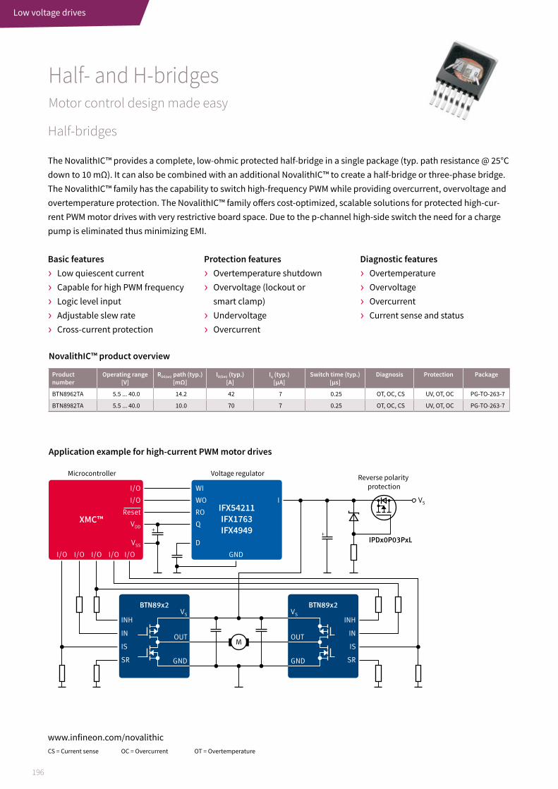
196
Low voltage drives
Half- and H-bridges Motor control design made easy
Half-bridges
The NovalithIC™ provides a complete, low-ohmic protected half-bridge in a single package (typ. path resistance @ 25°C down to 10 mΩ). It can also be combined with an additional NovalithIC™ to create a half-bridge or three-phase bridge. The NovalithIC™ family has the capability to switch high-frequency PWM while providing overcurrent, overvoltage and overtemperature protection. The NovalithIC™ family offers cost-optimized, scalable solutions for protected high-cur-rent PWM motor drives with very restrictive board space. Due to the p-channel high-side switch the need for a charge pump is eliminated thus minimizing EMI.
Basic features › Low quiescent current
› Capable for high PWM frequency
› Logic level input
› Adjustable slew rate
› Cross-current protection
Protection features › Overtemperature shutdown
› Overvoltage (lockout or smart clamp)
› Undervoltage
› Overcurrent
Diagnostic features › Overtemperature
› Overvoltage
› Overcurrent
› Current sense and status
Product number
Operating range[V]
RDS(on) path (typ.)[mΩ]
ID(lim) (typ.)[A]
Iq (typ.)[µA]
Switch time (typ.)[µs]
Diagnosis Protection Package
BTN8962TA 5.5 ... 40.0 14.2 42 7 0.25 OT, OC, CS UV, OT, OC PG-TO-263-7
BTN8982TA 5.5 ... 40.0 10.0 70 7 0.25 OT, OC, CS UV, OT, OC PG-TO-263-7
NovalithIC™ product overview
CS = Current sense OC = Overcurrent OT = Overtemperature
www.infineon.com/novalithic
XMC™
IFX54211
IFX1763
IFX4949
Voltage regulatorReverse polarity
protection
Microcontroller
Application example for high-current PWM motor drives

197
Po
we
r IC
s
Integrated multi half-bridge driver ICs
The TLE94xyz are protected half-bridge drivers designed for 12 V motion control applications such as small DC motors for heating, ventilation and air conditioning (HVAC), as well as automotive mirror adjustment and fold. The family of-fers 3-, 4-, 6-, 8-, 10-, and 12-fold integrated half-bridge driver. All devices can drive DC motor loads up to 0.9 A per out-put in cascaded or parallel operation. They provide diagnosis of short circuit, open load, power supply failure and over temperature for each half-bridge to ensure safe operation in HVAC or other systems. The TLE94xyz offers enhanced EMC performance, which in combination with the low quiescent current and a small package makes the product at-tractive for a wide range of 12 V automotive and industrial applications.
Key features and benefits › 3-, 4-, 6-, 8-, 10-, 12-half-bridges with
integrated output stages and PWM
› 16-bit SPI or direct inputs for control and diagnosis
› Voltage supply range: 5.5 V– 20 V
› Adjustable open load threshold for two outputs
› Variable driving schemes for up to 11 motors
› OUT 1 and 2 optimized for driving
› HS loads (e.g. LED)
Key applications › 12 V automotive and industrial
applications
› Flap motors in HVAC systems
› Mirror adjustment and fold
› Small DC motors (≤ 0.9 A/output)
› Bi-stable relays
Product name
Config. IL(NOM)
[A]IL(lim)
[A]Iq
[μA]VS(OP)
[V]Protection Diagnostic
interfaceHighlights VCE(sat)/RDS(on) Package
TLE94003EP 1) 3 x half-bridge 3 x 0.30 3 x 0.90 0.6 5.5…20 OC, OT, VS, UV/OV Error flag TLE94xyz family concept + small package
850 mΩ/switch TSDSO-14-EP
TLE94103EP 1) 3 x half-bridge 3 x 0.30 3 x 0.90 0.6 5.5…20 OC, OT, OL, VS, UV/OV 16-bit SPI TLE94xyz family concept + small package
850 mΩ/switch TSDSO-14-EP
TLE94004EP 1) 4 x half-bridge 4 x 0.30 4 x 0.90 0.6 5.5…20 OC, OT, VS, UV/OV Error flag TLE94xyz family concept + small package
850 mΩ/switch TSDSO-14-EP
TLE94104EP 1) 4 x half-bridge 4 x 0.30 4 x 0.90 0.6 5.5…20 OC, OT, OL, VS, UV/OV 16-bit SPI TLE94xyz family concept + small package
850 mΩ/switch TSDSO-14-EP
TLE94106EL 6 x half-bridge 6 x 0.30 6 x 0.90 0.6 5.5…20 OC, OT, OL, VS, UV/OV 16-bit SPI TLE94xyz family concept + back-wards compatible to TLE84106EL
850 mΩ/switch SSOP-24
TLE94108EL 8 x half-bridge 8 x 0.30 8 x 0.90 0.6 5.5…20 OC, OT, OL, VS, UV/OV 16-bit SPI TLE94xyz family concept 850 mΩ/switch SSOP-24
TLE94110EL 10 x half-bridge 10 x 0.30 10 x 0.90 0.6 5.5…20 OC, OT, OL, VS, UV/OV 16-bit SPI TLE94xyz family concept + back-wards compatible to TLE84106EL
850 mΩ/switch SSOP-24
TLE94112EL 12 x half-bridge 12 x 0.30 12 x 0.90 0.6 5.5…20 OC, OT, OL, VS, UV/OV 16-bit SPI TLE94xyz family concept + 12 outputs in one package
850 mΩ/switch SSOP-24
1) coming in Q1/2018
www.infineon.com/dc-motor-bridges
Low voltage drives
Overloaddetection
Overtemp.detection
Open-loaddetection
PWMgenerator
Charge pumpUndervoltage andovervoltage monitor
Overloaddetection
Overtemp.detection
Open-loaddetection
Temperaturesensor
Logic control andlatch SPI interface
Errordetection
VDD VS1 VS2
CSN
GND GND GND GND
EN
12-foldhalf-bridge driverSPI interface
SCLK
SDI
SDO
Power driver
OUT3OUT2OUT1
12x driver stage
High-sidedriver
Low-sidedriver
OUT4OUT5OUT6
OUT9OUT8OUT7
OUT10OUT11OUT12
Bias andmonitor
Block diagram TLE94112EL
Product table

198
Low voltage drives
www.infineon.com/shields-for-arduinowww.infineon.com/makers
DC motor control shield with BTN8982TA for Arduino
DC motor shield with TLE94112EL for Arduino
The DC motor control shield is capable of driving two uni-directional DC motors (half-bridge configuration) or one bi-directional DC motor (H-bridge configuration). The implemented half-bridge NovalithIC™ BTN8982TA can be con-trolled by a PWM via the IN pin. Interfacing to a microcontroller is made easy by the integrated driver IC which features logic level inputs, diagnosis with current sense, slew rate adjustment, dead time generation and protection against overtemperature, undervoltage, overcurrent and short circuit.
The DC motor shield is a small evaluation board equipped with TLE94112EL for use with Arduino. The TLE94112EL is capable to drive up to 6 small DC motors in parallel mode or up to 11 DC motors in cascaded mode. All outputs can drive up to 0.9 A. The outputs can be used stand-alone or combined to increase driving capability up to 3.6 A.
Infineon shields for Arduino are compatible with microcontroller boards using the Arduino form factor, e.g. Infineon's XMC™ microcontroller kits.
Features › Capable of high frequency PWM, e.g. 30 kHz
› Adjustable slew rates for optimized EMI by changing external resistor
› Driver circuit with logic level inputs
› Diagnosis with current sense
Target applications › Brushed DC motor control up to 250 W continuous load
› 8 V–18 V nominal input voltage (max. 6 V–40 V)
› Average motor current 30 A restricted due to PCB (BTN8982TA current limitation @ 55 A min.)
Features › Driver with 12 half-bridge outputs to drive DC motors,
resistive or inductive loads
› Driver is protected against over-temperature, overcurrent, overvoltage, undervoltage and enables diagnosis of overcurrent, overvoltage, undervoltage
› SPI interface with zero clock diagnosis
› Enhanced EMC performance
› Integrated PWM generator with 3 different frequencies (80 Hz, 100 Hz, 200 Hz)
Target applications › Multi-motor applications
› DC motors and voltage controlled bipolar stepper motors
› Toys
› HVAC systems
DC motor control with half-bridge BTN8982 DC motor control with multi half-bridge TLE94112EL

199
Po
we
r IC
s
Low voltage drives
Application example H-bridge with error flag
SOGND
Microcontroller
IFX9201SG
SISCKCSNDIRPWMDIS
VSO
VS
OUT1
OUT2
3.3 or 5 VDigital supply
VBat
< 33 nF
100 nF100 µFVS < 40 V
< 33 nF
M
+–
+–
+–
+–
PWM_2
XMC1300
PWM_1
Step
2-phase
stepper motor
Direction (DIR)
Disable (DIS)IFX9202ED
PWM_1
PWM_2 OUT2_2
OUT2_1
OUT1_2
OUT1_1
GND GND
Application example H-bridge with SPI interface
SOGND
Microcontroller
SISCKCSNDIRPWMDIS
VSO
VS
OUT1
OUT2
VBat
M
< 33 nF
100 nF100 µFVS < 40 V
< 33 nF
3.3 or 5 VDigital supply IFX9201SG
+–
+–
+–
+–
PWM_2
IFX9201XMC1300
IFX9201
PWM_1
Step
2-phase
stepper motor
Direction (DIR)
Disable (DIS)
www.infineon.com/dc-motor-bridges
Integrated H-bridges
IFX9201SG and IFX9202ED* are general purpose 6 A H-bridges designed for the control of small DC motors and induc-tive loads. The outputs can be pulse width modulated at frequencies up to 20 kHz – that enables operation above the human sonic range – by means of PWM/DIR control. While the signal at the DIR input defines the direction of the DC motor, the PWM signal controls the duty cycle. For load currents above the current limitation threshold (8 A typ.) the H-bridges switch into chopper current limitation mode.
Key features and benefits › Up to nominal 36 V supply voltage
› Short circuit, over-temperature protection and under voltage shutdown
› Detailed SPI diagnosis or simple error flag
› Simple design with few external components
› Small and robust PG-DSO-12-17 (IFX9201SG) and PG-DSO-36-72 (IFX9202ED) packages
Product number Operating voltage [V]
Current limit (min.) [A]
Quiescent current (typ.) [µA]
Operating range[A]
RDS(on) (typ./switch)[mΩ]
Packages RthJC (max.)[K/W]
IFX9201SG 5.0...36 6 10 70 7 PG-DSO-12 (power) 2
IFX9202ED* 5.0..36 6 10 70 7 PG-DSO-36 (dual gauge) 1
Product summary
Applications examples
* IFX9202ED is a dual h-bridge with two independent h-bridges in one package

200
Low voltage drives
H-bridge Kit 2Go with IFX9201SG
Stepper motor control shield with IFX9201SG and XMC1300 for Arduino
The H-bridge Kit 2GO is a ready to use evaluation kit. It is fully populated with all electronic components equipped with the H-bridge IFX9201 combined with XMC1100 microcontroller based on ARM® Cortex®-M0 CPU. Realize your own DC motor control. It is designed for the control of DC motors or other inductive loads up to 6 A or up to 36 V of supply.
Target applications › DC motor control for industrial applications
› Home and building automation
› Power tools battery management
› Industrial robotic applications
› Electric toys applications
The stepper motor control shield from Infineon Technologies is one of the first high current stepper motor control boards being compatible to Arduino as well as to Infineon’s XMC1100 boot kit. The stepper motor control shield is ca-pable to drive the two coils in a stepper motors featuring dual-half bridge configuration. The implemented integrated IFX9201 half-bridges can be controlled by a STEP-signal via the STEP pin. Interfacing to a microcontroller is made easy by the integrated XMC1300 microcontroller that holds the peripherals to allow high-speed current control. Microstep-ping of the stepper motor can be achieved using the internal comparators, operational amplifiers are installed to adapt the motor current sense signal to the microcontroller’s input levels.
Features › Compatible with microcontroller boards using the
› Arduino form factor, e.g. Infineon's XMCTM microcontroller kits
› Capable of high frequency PWM, e.g. 30 kHz
› Adjustable slew rates for optimized EMI by changing external resistor
› Driver circuit with logic level inputs
› Diagnosis with current sense
Target applications › Stepper motors up to 5 A phase current
› 24 V nominal input voltage for the power stage
› Average motor current 3 A without additional cooling effort, 5 A possible with proper cooling
Benefits › Fast and inexpensive prototyping of stepper
motor control
› Simple testing of microstepping algorithms
› Diagnose pin to allow hardware feedback during development
› Overtemperature shut down with latch behavior and undervoltage shut down of the power section
www.infineon.com/h-bridge-kit-2gowww.infineon.com/IFX9201SG-stepper-motor-shieldwww.infineon.com/makers

201
Po
we
r IC
s
Low voltage drives
www.infineon.com/dc-motor-bridges
Stepper drivers Cost-efficient, durable and reliable
The TLE4726G, TCA3727G and TLE8444SL are designed to drive bipolar stepper motors, DC motors and other inductive loads that operate on a constant current. The TLE4726G and TCA3727G have integrated control logic and power output stages for two bipolar windings.
Key features › Full to half-step operation
› Protected bipolar power stages
› Implemented current control
› Error flag for diagnosis
› Overtemperature protection
Applications › ATM
› Franking machines
› Vending machine
› Idle speed control
› Printer
› Toys
Product number
IL(NOM) IL(lim) Iq
[µA]VS(op) Step
operationsProtection Diagnostic
interfaceHighlights Package
TCA3727G 2x0.75 2x1.5 200 5–50 Full to mini-step OT – High operating voltage, lowquiescent current with inhibit
PG-DSO-24
TLE4726G 2x0.75 2x1.5 200 5–50 Full to mini-step OT – High operating voltage, lowquiescent current with inhibit
PG-DSO-24
TLE8444SL 4x0.50 4x0.90 1 1–18 Full to half-step SC, OT, OV, UV, OL Status flag Open load detection in on-state
SSOP-24-7
Stepper drivers product overview
CS = Current senseOC = OvercurrentOT = Overtemperature
SC = Short circuitUV = UndervoltageOL = Open-load

CIPOS™ IPM familyControl Integrated Power System (CIPOS™) Intelligent Power Modules (IPM)
Key benefits › Shorter time-to-market
› Increased reliability
› Reduced system design complexity
› Improved manufacturability
› Reduced PCB board space
Product lineup
Compact IPM Standard IPM
MOSFET: 40/100/250/500 VPQFN packages
Half-bridge and 3-phase inverters
12 x 12 x 0.9 mm8 x 9 x 0.9 mm7 x 8 x 0.9 mm
29 x 12 x 3.1 mm
36 x 21 x 3.1 mm
CIPOS™ Nano
MOSFET: 250/500 VIGBT: 600 V
DIP23 and SOP23 packagesInverter
CIPOS™ Micro
IGBT: 600 V 4 A to 30 A MDIP-24 Fullpack and
MDIP-21/24 DCB packagesInverter, SRM, PFC
CIPOS™ Mini
Motor current0.1 Arms 20 Arms
Performance IPM
Depending on the level of integration and power to be handled, Infineon offers a variety of IPMs, with different semiconductors in different packages and different voltage and current classes. These IPMs are separated into Compact, Standard and Performance families. The CIPOS™ IPMs are families of highly integrated, compact power modules designed to drive motors in applications ranging from home appliances, to fans, pumps and general purpose drives.
Infineon’s energy-efficient IPMs integrate the latest power semiconductor and control IC technology leveraging Infineon’s advanced IGBTs, MOSFETs, next-generation gate driver ICs and state-of-the-art thermo-mechanical technology.
Block diagram for CIPOS™
CIPOS™
ProtectionGate drive
boot-strap
PFC
NTC
EMI-filter
&
rectifier
+VINAC
UVLO
RSH
Motor
MInverter
NTC (optional)
202
IPM
www.infineon.com/ipm

PQFN 12 x 1212 x 12 x 0.9 mm
Major applications
PQFN 8 x 98 x 9 x 0.9 mm PQFN 7 x 87 x 8 x 0.9 mm
203
Po
we
r IC
s
www.infineon.com/ipm
IPM
CIPOS™ Nano is a family of highly integrated, ultra-compact power modules for high efficiency appliance and light industrial applications, including rectifier, converter, inverter in power management circuits and motor drives for hair dryer, air purifier, ceiling fan, circulation pump and ventilators. By utilizing an innovative packaging solution, the CIPOSTM Nano family delivers a new benchmark in device size, offering up to a 60 percent smaller footprint than existing 3-phase motor control power IPMs.
CIPOS™ Nano products comprise of a series of fully integrated 3-phase or half-bridge surface-mount motor control circuit solutions. The new alternative approach utilizes PCB copper traces to dissipate heat from the module, providing cost savings through a smaller package design and even eliminating the need for an external heat sink.
CIPOS™ Nano3-phase or half-bridge driver with MOSFETs
Key features › Smallest IPMs on the market
› Integrated gate driver IC and bootstrap functionality
› Suitable for sinusoidal or trapezoidal modulation
› Low RDS(on) Trench FREDFET
› Under-voltage lockout for all channels
› Matched propagation delay for all channels
› Optimized dV/dt for loss and EMI trade offs
› 3.3 V input logic compatible
› Active high HIN and LIN
› Isolation 1500 VRMS, 1 minute
Key benefits › Cost savings from smaller footprint
and reduced PCB space
› Easy implementation of 2 or 3-phase motor drives with half-bridge IPMs
› IPMs distribute heat dissipation and enable elimination of heat sink
› Same PCB footprint to address multiple application markets (100 VAC - 230 VAC)

CIPOS™ Micro is a family of compact IPMs for low power motor drive applications including fans, pumps, air purifiers and refrigerator compressor drives.
It offers a cost effective power solution by leveraging industry standard footprints and processes compatible with various PCB substrates. The family features rugged and efficient high voltage FREDFET MOSFETs specifically optimized for variable frequency drives with voltage ratings of 250 V, 500 V and 600 V IGBTs. These devices are paired with the most advanced high voltage driver ICs tuned to achieve optimal balance between EMI and switching losses. CIPOS™ Micro family offers DC current ratings ranging up to 6 A to drive motors up to 100 W without heatsink and up to 300 W with heatsink, and are available in both through-hole and surface mount package options.
CIPOS™ MicroSolution for low power motor drive applications
Key features › Integrated bootstrap functionality
› Under-voltage lockout for all channels
› Matched propagation delay for all channels
› Optimized dV/dt for loss and EMI trade off
› Advanced input filter with shoot-through protection
› Separate low-side emitter pins for single or leg-shunt current sensing
› 3.3 V logic compatible
› Up to 1900 VRMS, 1 min isolation (UL certified: file number E252584)
› UL certified NTC thermistor for temperature feedback available
› Various lead forms available including through-hole and surface mounted
Key benefits › Ease-of-design and short time-to-market
› Compact package with three lead form options available
› Wide range of current and voltage ratings in the same package
› Wide range of modules for 110 VAC or 230 VAC applications in the same footprint
› Simplified design and manufacturing
› Lower losses than similar modules in the market
› Heat sink-less operation possible
SOP2329 x 12 x 3.1 mm
DIP2329 x 12 x 3.1 mm
Major applications
204
IPM
www.infineon.com/ipm

MDIP-24 Fullpack36 x 21 x 3.1 mm
MDIP-24/21 DCB36 x 21 x 3.1 mm
Major applications
205
Po
we
r IC
s
IPM
www.infineon.com/ipm
CIPOS™ Mini modules integrate various power and control components to increase reliability, and to optimize PCB size and system costs. This simplifies the power design and reduces significantly time-to-market.
CIPOS™ Mini modules are designed to control AC motors in variable speed drives for applications from 4 A up to 30 A such as air conditioning, washing machines, refrigerators, VACuum cleaners, compressors and industrial drives up to 3 kW.
The package concept is specially adapted to power applications that need good thermal conduction and electrical isolation, but also EMI-safe control, innovative FAULT indication and overload protection. The feature of Infineon’s reverse conducting IGBTs or TRENCHSTOP™ IGBT is used with a new optimized Infineon SOI gate driver IC for excellent electrical performance.
CIPOS™ MiniBroad range of applications from PFC to inverter
Key features › Dual-in-line transfer molded package with DCB or
Fullpack substrate
› Current rating from 4 A to 30 A, power rating up to 3 kW
› Optimized for home appliances and motor drives
› Rugged SOI gate driver IC technology
› Advanced protection features
› UL1577 certified
Key benefits › High integration (bootstrap circuit, thermistor) for easy
design and system space saving
› Single platform possible from 4 A to 30 A
› Enhanced robustness of the advanced IGBT and gate driver IC technology
› High power density
› Two kinds of substrates provide cost efficient solution for home appliances
› UL certified thermistor

IPM lineup
Family Package dimensions [mm] Motor Irms range Topology Lineup Product PN
CIPOS™ Nano PQFN 12 x 1212 x 12 x 0.9
0.1 Arms - 1.2 Arms 3-phase inverter 250 V MOSFET 0.45 Ω, 1.05 Ω, 2.2 Ω IRSM836-0x4MA500 V MOSFET 1.7 Ω, 2.2 Ω, 4.0 Ω, 6.0 Ω IRSM836-0x5MA
IRSM836-035MBPQFN 8 x 98 x 9 x 0.9
0.4 Arms – 2 Arms Half-bridge 250 V MOSFET 0.15 Ω IRSM808-204MH
500 V MOSFET 0.8 Ω, 1.7 Ω IRSM807-105MHIRSM808-105MHIRSM807-045MH
PQFN 7 x 87 x 8 x 0.9
1 Arms - 10 Arms Low voltage half-bridge
40 V MOSFET 4.5 mΩ IRSM005-800MH100 V MOSFET 21 mΩ IRSM005-301MH
iMOTION™ Smart
PQFN 12 x 1212 x 12 x 0.9
0.2 Arms - 0.5 Arms Fully integrated 3-phase inverter (Power stage + gate driver + controller)
500 V MOSFET 1.7 Ω, 2.2 Ω, 4.0 Ω, 6.0 Ω IRDM983-025MBIRDM982-035MBIMM001T-0x5M
CIPOS™ Micro DIP23 and SOP2329 x 12 x 3.1
0.1 Arms - 2.0 Arms 3-phase inverter 250 V MOSFET 0.45 Ω, 1.05 Ω, 2.4 Ω IRSM5y5-0x4zA
500 V MOSFET 1.3 Ω, 1.7 Ω, 2.2 Ω, 4.0 Ω, 6.0 Ω IRSM5y5-0x5zA
600 V IGBT 6 A IRSM5y6-076zA
CIPOS™ Mini MDIP-24 Fullpack36 x 21 x 3.1
Up to 13 Arms 3-phase inverter 600 V IGBT4 A/6 A/10 A/15 A/20 A/30 A
IGCM04F(G)60yAIGCM06F(G)60yAIGCM10F60yAIGCM15F60yAIGCM20F60yAIKCM10L60yAIKCM15L(F)60yAIKCM20L60yAIKCM30F60yA
600 V IGBT10 A/15 A
IKCM10H60yAIKCM15H60yA
2-phase inverter 650 V CoolMOS™ 0.31 Ω IM512-L6A
3-phase inverter 650 V CoolMOS™ 0.31 Ω IM513-L6A
MDIP-24/21 DCB36 x 21 x 3.1
Up to 16 Arms 2-phase interleaved PFC 650 V IGBT20/30 A
IFCM20T65GDIFCM30T65GD
Up to 24 Arms 3-phase interleaved PFC 650 V IGBT20/30 A
IFCM20U65GD IFCM30U65GD
Up to 10 Arms 3-phase inverter + PFC 600 V IGBT10/15 A
IFCM10S60GD IFCM10P60GDIFCM15S60GDIFCM15P60GD
Up to 20 Arms 3-phase inverter 600 V IGBT15/20/30 A
IKCM15L60yDIKCM20L60yDIKCM30F60yD
Up to 10 Arms 2-phase asymmetric inverter for SRM
600 V IGBT15/20 A
IKCM15R60GDIKCM20R60GD
x = current rating y = 0 (with thermistor) Y = 1 (without thermistor) z = D (through-hole) or P (SMD)
206
IPM
www.infineon.com/ipm

Further information, datasheets and documentswww.infineon.com/acdcwww.infineon.com/coolsetwww.infineon.com/optimosdriverwww.infineon.com/integrated-powerstageswww.infineon.com/drmoswww.infineon.com/digital-controllerwww.infineon.com/lighting-icswww.infineon.com/isofacewww.infineon.com/eicedriverwww.infineon.com/industrial-transceivers
www.infineon.com/industrial-voltage-regulatorswww.infineon.com/industrial-dcdc-converterswww.infineon.com/industrial-profetwww.infineon.com/novalithicwww.infineon.com/dc-motor-bridgeswww.infineon.com/shields-for-arduinowww.infineon.com/ipolwww.infineon.com/analog-ipolwww.infineon.com/xdpwww.infineon.com/ipm
Videos and eLearningswww.infineon.com/mediacenter
Infineon support for power ICsUseful links and helpful information
Simulation
Po
we
r IC
s
Power ICs support

208
EiceDRIVER™
Industrial and general purpose gate driver ICsThe expert's choice
Leveraging the application expertise and advanced technologies of Infineon, the industrial and general purpose gate driver ICs are well suited for many applications such as industrial motor drives, solar inverters, UPS, switch mode power supplies, lighting and major home appliances. Infineon offers a comprehensive portfolio of industrial and general purpose gate driver ICs with a variety of configurations, voltage classes, isolation levels, protection features, and pack-age options. These flexible gate driver ICs are complementary to Infineon IGBTs, MOSFETs, SiC JFET and other power switches in discrete gate drive applications or as part of integrated power modules.
1EDN MOSFET EiceDRIVER™ familyRugged, cool and fast, 1-channel low-side 4/8 A gate driver ICs
1EDN family overview1-channel MOSFET gate driver ICs are the crucial link between control ICs and powerful MOSFET and GaN switching devices. Gate driver ICs enable high system level efficiencies, excellent power density and consistent system robustness.
1EDN family: fast, precise, strong and compatible › Highly efficient SMPS enabled by 5 ns short slew rates and ± 5 ns propagation delay precision for fast MOSFET and
GaN switching
› Separate source and sink outputs simplify the application design
› Industry standard packages and pinout ease system design upgrades
1EDN family: the new reference in ruggedness and low power dissipation › -10 V robustness of control and enable inputs provides crucial safety margin when driving pulse transformers
› 5 A reverse output current robustness eliminates the need for Schottky switching diodes when driving MOSFETs in TO-220 and TO-247 packages
› Cool driver ICs thanks to true rail-to-rail low impedance output stages
› 4 V and 8 V UVLO (Under Voltage Lock Out) options for instant MOSFET protection during start-up and under abnor-mal conditions
Applications › PFC
› Synchronous rectification
› DC-DC converters
› Telecom bricks
› Power tools
› Industrial SMPS
› Motor control
› Wireless charging
www.infineon.com/1edn

209
Gat
e d
rive
r IC
s
EiceDRIVER™
Product features
› 4 A source/8 A sink current › 6 ns rise/5 ns fall times › ± 5 ns propagation delay precision
› True rail-to-rail low impedance output stages
› 4 V and 8 V UVLO options › 19 ns propagation delay
› -10 V robustness of inputs
› 5 A reverse output current robustness
› Industry standard pinout and packages
Product benefits
› Fast Miller plateau transition › Precise timing
› Low power dissipation in driver IC
› Fast and reliable MOSFET turn-off, independent of control IC
› Increased GND-bounce robustness
› Saves switching diodes
› Straight forward design upgrades
Application benefits
› High power efficiency – in hard switching PFC with SiC diode – in half-bridges and synchronous rectifications
› Cooler driver IC operation › Higher MOSFET drive capability
› Instant MOSFET protection during start-up and under abnormal operation
› Crucial safety margin to drive pulse transformer
› Increases power density › BOM savings
› Short time-to-market
PFC controller
L
GND
N
+12 V
Isolation
1EDN
gate driver
1EDN
gate driver
2EDN
gate
driver
Pulse
transformer
PWM controller
1EDN
gate driver
Synchronous rectificationLLCPFC
CoolSiC™
Schottky diode G6
OptiMOS™ 5 OptiMOS™ 5
CoolMOS™
CFD7 or P7
CoolMOS™
CFD7 or P7
CoolMOS™
C7 or P7
Application overview 800 W switched mode power supply
Package UVLO Product name Orderable part number Pinout
SOT-23 6pin
4 V 1EDN7511B 1EDN7511BXUSA1 1
1EDN
VDD
2
3
IN+
GND
6
IN-5
4OUT_SNK
OUT_SRC
8 V 1EDN8511B 1EDN8511BXUSA1
SOT-23 5pin 4 V 1EDN7512B 1EDN7512BXTSA1
1
1EDN
VDD
2
3
OUT
IN-
5
4IN+
GND
WSON 6pin 4 V 1EDN7512G 1EDN7512GXTMA1
1
1EDN
IN-
2
3
IN+
OUT
VDD
6
5
4GND
GND
Product portfolio
www.infineon.com/1edn

210
EiceDRIVER™
2EDN MOSFET EiceDRIVER™ familyRugged, cool and fast, 2-channel low-side 4 A/5 A driver IC
2EDN family overview2-channel MOSFET Driver ICs are the crucial link between digital control ICs and powerful MOSFET and GaN switch-ing devices. MOSFET Driver ICs enable high system level efficiencies, excellent power density and consistent system robustness.
2EDN family: fast, precise, strong and compatible › Highly efficient SMPS enabled by 5 ns short slew rates and 10 ns propagation delay precision
for fast MOSFET and GaN switching
› Numerous deployment options due to two 4 A/5 A channels. 1 ns channel-to-channel accuracy to use two channels in parallel
› Industry standard packages and pinout ease system design upgrades
2EDN family: the new reference in ruggedness and low power dissipation › 4 V and 8 V UVLO (Under Voltage Lock Out) options for instant MOSFET protection under abnormal conditions
› -10 V robustness of control and enable inputs provides crucial safety margin when driving pulse transformers or driving MOSFETs in TO-220 and TO-247 packages
› 5 A reverse output current robustness eliminates the need for Schottky switching diodes and reduces bill-of-material
› Cool driver ICs from true rail-to-rail low impedance output stages
Applications › Server
› Telecom
› DC-DC converters
› Bricks
› Power tools
› Industrial SMPS
› Motor control
› Solar
Product features
› 5 A souce/sink current › 5 ns rise/fall times › <10 ns propagation delay precision
› True rail-to-rail low impedance output stages
› 4 V and 8 V UVLO options › 19 ns propagation delay for both control and
enable inputs
› -10 V robustness of control and enable inputs
› 5 A reverse output current robustness
› 2 independent channels › Excellent 1 ns channel-to-channel accuracy
› Industry standard pinout and packages
Product benefits
› Fast Miller plateau transition › Precise timing
› Low power dissipation in driver IC
› Fast and reliable MOSFET turn-off, independent of control IC
› Increased GND-bounce robustness
› Saves switching diodes
› Option to increase drive current by truly concurrent switching of 2 channels
› Straight forward design upgrades
Application benefits
› High power efficiency – in hard switching PFC with SiC diode – in half-bridges and synchronous rectifications
› Cooler driver IC operation › Higher MOSFET drive capability
› Instant MOSFET protection under abnormal operation
› Crucial safety margin to drive pulse transformer
› Increases power density › BOM savings
› One IC covering many applications
› Short time-to-market
www.infineon.com/2edn

211
Gat
e d
rive
r IC
s
EiceDRIVER™
Application overview 800 W 130 kHz switched mode power supply
110 VAC
- 240 VAC
2EDN
Gate driver
PFC controller
Isolation
PWM controller
2EDN
Gate driver2EDN
Gate
driver
Pulse
transformer
GND
GND
+12 V
CoolMOS™
CFD7 or P7
CoolSiC™
Schottky diode G6
CoolMOS™
C7 or P7
LLC Sync. rec.PFC
CoolMOS™
CFD7 or P7
ICE3PCS01G
ICE2HS01G
or
XMC4000
OptiMOS™ 5
OptiMOS™ 5
Package UVLO Inputs Product name Orderable part number
DSO 8pin
4 V
Direct 2EDN7524F 2EDN7524FXTMA1
Inverted 2EDN7523F 2EDN7523FXTMA1
Direct 2EDN7424F 2EDN7424FXTMA1
8 VDirect 2EDN8524F 2EDN8524FXTMA1
Inverted 2EDN8523F 2EDN8523FXTMA1
TSSOP 8pin
4 V
Direct 2EDN7524R 2EDN7524RXUMA1
Inverted 2EDN7523R 2EDN7523RXUMA1
Direct 2EDN7424R 2EDN7424RXUMA1
8 VDirect 2EDN8524R 2EDN8524RXUMA1
Inverted 2EDN8523R 2EDN8523RXUMA1
WSON 8pin 4 VDirect 2EDN7524G 2EDN7524GXTMA1
Inverted 2EDN7523G 2EDN7523GXTMA1
Industry standard pinout configuration
www.infineon.com/2edn
1
2EDN7524
ENA
2INA
3GND
4
ENB
OUTA
VDD
OUTB
8
7
6
5INB
Product portfolio

212
EiceDRIVER™ Safe
The new SRC EiceDRIVER™ family, which includes 1EDS20I12SV, 1EDU20I12SV, and 1EDI20I12SV, is addressing the latest genera-tion of highly efficient low-EMI electric drive systems, with lower EMI and improved efficiency. Based on the Infineon coreless transformer technology, it is the first high voltage isolated gate driver on the market with dynamic slew-rate control (SRC), which allows on-the-fly dV/dt control of electric drives through precise gate current control, providing the best trade-off be-tween minimum power dissipation and minimum EMI depending on operating conditions. To turn on the IGBT, the driver works as an adjustable current source in conjunction with an external PMOS transistor and a sense resistor. To turn off the IGBT, the driver uses a 2 A MOSFET output stage. Several important and advanced protection functions are integrated. The driver includes desaturation protection for IGBTs and overcurrent protection for sense IGBTs via the fault status output pin. Two ready-state output pins indicate proper driver power supply level and normal driver operation. Two-level turn-off with adjustable timing and voltage protects against excessive overvoltage in case of the IGBT operating at overcurrent or a short circuit. The 1EDx20I12SV family is tailored for industrial drive applications such as those using 1200 V power modules for current up to 900 A like the EconoDUAL™ 3. The "S" version 1EDS20I12SV provides reinforced galvanic isolation certification according to both VDE 0884-10 (VIORM=1420 V) and UL 1577 (VISO=5000 V). The "U" version 1EDU20I12SV is UL 1577 certified only, with a VISO rating of 5000 V for 1 minute. The ”I” version 1EDI20I12SV provides functional isolation. The driver meets today’s long-term stability requirements for industrial applications. It is offered in a DSO-36 package with a package width of 300 mil. It is RoHS compliant, green, and halogen-free.
Key features › 1200 V single-channel IGBT driver
› Precise dynamic gate current control
› Unique: selective short circuit protection for 3-level inverters
› Overcurrent protection for sense IGBTs and conventional IGBTs
› DESAT, soft turn-off, two-level turn-off
› Drive power modules up to 900 A
Applications › AC and brushless DC motor drives
› High-voltage DC-DC converters
› UPS systems
› Servo drives
The slew-rate control EiceDRIVER™ with reinforced isolation1200 V single-channel isolated driver family with dynamic slew-rate control
Simplified application diagram
RSOFF
ROFF
VCC2
T1
Co
ntr
ol u
nit
5V5V
GND
RS
RPRB2
T2
RDESAT
DDESAT
RF
CDESAT
CF
C3 C2
VCC2
RD
CD
C1
DESAT
RDY2
RDY1
CS
/FLT
GATE
ON
GND2
VZ
VCC2
OFF
CZ
RSENSE
VEE2
SOFF
OCOFF
INP
SPEED
SIGI
SIGO
VCC1
INN
PADP
EN
PADN
GND1
PRB
RPRB1
www.infineon.com/SRC

213
Gat
e d
rive
r IC
s
EiceDRIVER™ Safe
www.infineon.com/SRC
1EDS-SRC driver board with EconoDUAL™ 3 power module
Feature – real-time gate current control Effect – gate turn-on tunable across a very large dV/dt range:
Benefits › Low EMI during low load conditions and high efficiency during high load conditions
› Reduction or elimination of dV/dt filter
-1.5
-1
-0.5
-3.5
0
-2
-2.5
-3
-42000
IC [A]
dV/d
t [k
V/µs
]
400 600 800 1000
dV/dt = f(IC, 25°C, VSPEED)
Adjustable
dV/dt rangeMinimum speed
Maximum speed
Time
I GA
TE [
A]
Ad
just
ab
le g
ate
cu
rre
nt
Preboost phase
SRC controlled
gate current in 11 levels

214
EiceDRIVER™ 1ED Compact
EiceDRIVER™ 1ED Compact gate driver IC family1200 V galvanically isolated single-channel gate driver ICs
Infineon’s new EiceDRIVER™ 1EDC Compact 300 mil family is recognized under UL 1577 with an insulation test voltage of VISO = 2500 V(rms) for 1 min. The functional isolated EiceDRIVER™ 1EDI Compact 150 mil and 300 mil families are also available. The EiceDRIVER™ 1ED Compact family is the perfect driver for superjunction MOSFETs such as CoolMOS™, IGBTs, silicon carbide (SiC) MOSFETs such as CoolSiC™, and IGBT modules.
Product features › Provide DSO-8 300 mil wide body package with 7.6 mm creepage distance
› Up to 10 A typical peak rail-to-rail output
› Suitable for operation at high ambient temperature
› Separate source and sink outputs or active miller clamp
› More than 100 kV/μs CMTI
› Optimized pin out for low inductance power supply
1EDI Compact 150 mil 1EDI60I12AF 1EDI40I12AF 1EDI20I12AF 1EDI05I12AF 1EDI60N12AF 1EDI20N12AF 1EDI30I12MF 1EDI20I12MF 1EDI10I12MF
1EDI Compact 300 mil 1EDI60I12AH 1EDI40I12AH 1EDI20I12AH 1EDI05I12AH 1EDI60H12AH 1EDI20H12AH 1EDI30I12MH 1EDI20I12MH 1EDI10I12MH
1EDC Compact 300 mil 1EDC60I12AH 1EDC40I12AH 1EDC20I12AH 1EDC05I12AH 1EDC60H12AH 1EDC20H12AH 1EDC30I12MH 1EDC20I12MH 1EDC10I12MH
Typ. output current [A] 10/-9.4 7.5/-6.8 4/-3.5 1.3/-0.9 10/-9.4 4/-3.5 5.9/-6.2 4.4/-4.1 2.2/-2.3
Output configuration Separate sink/source outputs
Separate sink/source outputs
Separate sink/source outputs
Separate sink/source outputs
Separate sink/source outputs
Separate sink/source outputs
Active Miller clamp
Active Miller clamp
Active Miller clamp
Typ. propagation delay [ns] 300 300 300 300 125 125 300 300 300
UVLO Input [V] 2.85/2.75 2.85/2.75 2.85/2.75 2.85/2.75 2.85/2.75 2.85/2.75 2.85/2.75 2.85/2.75 2.85/2.75
Output [V] 12/11.1 12/11.1 12/11.1 12/11.1 12/11.1 (H)9.1/8.5 (N)
12/11.1 (H)9.1/8.5 (N)
11.9/11 11.9/11 11.9/11
www.infineon.com/gatedriverwww.infineon.com/1EDcompact
Simplified application diagram
+5 V
+15 V
SGND
100nVCC1
OUT+10R
1μ
3R3OUT-
VCC2
GND2
GND1
IN+
IN-
IN

215
Gat
e d
rive
r IC
s
EiceDRIVER™ Enhanced
EiceDRIVER™ Enhanced gate driver IC family1200 V galvanically isolated enhanced gate driver ICs
The EiceDRIVER™ 1ED Enhanced gate driver ICs are galvanic isolated single channel IGBT and SiC MOSFET drivers in DSO-16 package that provideoutput current capabilities of typically 2 A. The precision DESAT function for IGBT is also an excellent solution for SiC MOSFET short-circuit protection.
All logic pins are 5 V CMOS compati-ble. 2ED020I12-F2 is the dual-channel version of 1ED020I12-F2 in DSO-36package. 2ED020I12-FI is a high volt-age, high speed power MOSFET and IGBT driver with interlocking high and low side referenced outputs.
Product features › Available in wide body package
with 7.6 mm creepage distance
› Suitable for operation at high am-bient temperature
› Active miller clamp
› Short circuit clamping and active shutdown
› ≥ 100 kV/μs CMTI
› Precision DESAT protection
EiceDRIVER™ Enhanced 1ED020I12-F2 2ED020I12-F2 1ED020I12-FT 1ED020I12-B2 1ED020I12-BT 2ED020I12-FI
Configuration Single Dual Single Single Single Half Bridge
Package (all 300 mil) DSO-16 DSO-36 DSO-16 DSO-16 DSO-16 DSO-18
Galvanic isolationFunctional Functional Functional
Basic(VDE 0884-10)
Basic(VDE 0884-10)
Functionalon High Side
Protection functionDESAT, UVLO DESAT, UVLO
DESAT, UVLO,two-level turn-off
DESAT, UVLODESAT, UVLO,
two-level turn-offUVLO, OPAMP,
comparator
UVLO Input [V] 4.1/3.8 4.1/3.8 4.1/3.8 4.1/3.8 4.1/3.8 12/11
Output [V] 12/11 12/11 12/11 12/11 12/11 12/11
DESAT charge current [μA] 500 500 500 500 500 –
Bipolar output supply –
Active miller clamp –
Inverting and non-inverting inputs –
Combinable enable/shutdownand fault feedback signals –
TLSET – – – –
Typical propagation delay [ns] 170 170 170 + TLTOff 170 170 + TLTOff 85
Isolation definitions
Functional isolation Isolation between conductive parts which is necessary only for the proper functioning of the equipment.
Basic isolation (VDE 0884-10) Isolation applied to live parts to provide basic protection against electric shock.
www.infineon.com/gatedriverwww.infineon.com/1EDcompact
Simplified application diagram
+15 V+5 V
RDY
FLT
RST
SGND
10k
10k 100n
VCC11μ
10R
220p
1k
VEE2
VCC2
GND2
NC
OUT
CLAMP
DESATGND1
IN+
RDY
/FLT
/RST
IN-
IN

216
IRS2890DS
Product features
› Advanced input filter › Deadtime and cross-conduction prevention logic
› Fully operational to +600 V off-set voltage › Logic operational for VS of -8 V › Operational for transient negative VS -50 V with a 50 ns pulse width
› Integrated bootstrap FET › Integrated comparator (with 0.5 V ± 5 % Reference) for overcurrent protection › Fault and enable multifunction pin
IRS2890DSNew 600 V half-bridge gate driver with overcurrent protection
The new IRS2890DS half-bridge gate driver provides typical 0.22 A source and 0.48 A sink currents in a 14-lead SOIC package for IGBT and MOSFETs. The IRS2890DS integrates over current protection, fault reporting and bootstrap FET.
Product benefits
› Reliable switching › Protection under abnormal operation
› Improved reliability › High power capability
› Easy-to-use, straight-forward design › Fast time-to-market › BOM savings
DC BUS+
DC BUS–
VCC
HIN
LIN
RFE
COM ITRIP
LO
VS
HO
VB
Typical block diagram
www.infineon.com/gatedriver

217
Gat
e d
rive
r IC
s
2ED2304S06F
2ED2304S06F
The 2ED2304S06F is a high voltage, high speed power MOSFET and IGBT half bridge driver. Based on the proven Infineon SOI-technology there is an excellent ruggedness and noise immunity. No parasitic thysistor structures are present in the device. Hence, no parasitic latch up may occur at all temperature and voltage conditions. Additionally, the offline online clamping function provides an inherent protection of the parasitic turn-on by floating gate conditions.
Product features › Floating channel designed for bootstrap operation
› Thin-film-SOI-technology
› Fully operational to 650 V
› Integrated ultra-fast bootstrap diode
› Short propagation delay and delay matching (20 ns, maximum)
› Tolerant to negative transient voltage up to -50 V (pulse width is up 500 ns) given by SOI-technology
› dV/dt immune ±50 V
› Gate drive supply range from 10 to 20 V
› Undervoltage lockout for both channels
› 3.3 V, 5 V and 15 V input logic compatible
› Schmitt trigger inputs with hysteresis and pull down
› Output source/sink current capability +0.36 A/-0.7 A
› RoHS compliant
Typical applications › Motor drives
› Solar inverter and UPS drives
› General purpose inverter drives
› Half-bridge and full-bridge converters in offline AC-DC
› Power supplies for telecom and lighting
Typical block diagram
www.infineon.com/gatedriver

218
IRS200x 200 V IC familyNew half-bridge and high- and low-side gate driver ICs
The 200 V half-bridge and high- and low-side driver IC family is tailored for low voltage (24 V, 36 V, and 48 V) and mid-volt-age (60 V, 80 V and 100 V) motor drive applications.
The IRS200x family utilizes our advanced high voltage IC process to realize a compact, efficient and robust monolithic construction.
The new IRS200x family consists of four devices with a typical output sink current of 600 mA and typical output source current of 290 mA. These 200 V devices are 3.3 V, 5 V, and 15 V logic compatible and have Vs operational logic of -8 V. The IRS2008 and IRS2007 include integrated dead-time and shoot-through protection and all IRS200x devices include under-voltage lockout (UVLO) protection. Additionally, the IRS2008 includes a shutdown input pin. These 200 V devices also feature low quiescent currents.
All three parts are offered in an eight-pin SOIC package or (for IRS2005) in a small form-factor fourteen-pin 4x4 mm MLPQ package. With various logic input options and standard pin-out configurations, these 200 V devices are easy to design-in for fast time-to-market
Applications › Appliance motor drives
› Servo drives
› Micro inverter drives
› General purpose three phase inverters
› E-bike
› Drones
Gate driver ICs
Product features
› 290 mA/600 mA typical source/sink current › 70 ns/35 ns typical turn-on rise and turn-off fall time › Less than 60 ns delay matching time
› Under-voltage lockout (UVLO) protection › Deadtime and cross-conduction prevention logic
› Fully operational to +200 V off-set voltage › Tolerate to negative transient voltage, dV/dt immune
› Low quiescent current
› Various input options › Standard pin-out and packages
Benefits
› Fast and reliable switching
› Protection under abnormal operation
› Increased device reliability
› Low cost bootstrap power supply › BOM savings
› Easy-to-use, straight forward design › Fast time-to-market
www.infineon.com/200vHVIC

219
Gat
e d
rive
r IC
s
Gate driver ICs
Product portfolio
Typical connection diagram (IRS2008)
Typical connection diagram (IRS2007) Typical connection diagram (IRS2005)
Pin configurations
VB
IRS2008
1 8
HO2 7
VS3 6
HIN
LIN
COM
LO4 5
VCC
VB
IRS2005S
1 8
IN
HO2 7
SD
VS3 6
COM
LO4 5
VCC VB
IRS2007
1 8
HIN HO2 7
LIN VS3 6
COM LO4 5
VCC
IRS2005MHINLIN
COM
HOVS
VCC VB
1211
9
1234
5 6 7 8
16 14 13
Part number Voltage class [V]
Channels Source/sink current typ.
[mA]
Deadtimetyp. [ns]
Typ. propagation delay [ns]
Control inputs UVLO typ. [V] Package MSL
on off
IRS2008S 200 2 290/600 520 680 150 IN, SD +8.9/-8.2 8-lead SOIC 2
IRS2007S 200 2 290/600 520 160 150 HIN, LIN +8.9/-8.2 8-lead SOIC 2
IRS2005S 200 2 290/600 – 160 150 HIN, LIN +8.9/-8.2 8-lead SOIC 2
IRS2005M 200 2 290/600 – 160 150 HIN, LIN +8.9/-8.2 14-lead 4x4 MLPQ 2
www.infineon.com/200vHVIC
Up to 200 V
to load
VCC
VCC VB
VS
IN IN HO
COM LO
SD SD
Up to 200 V
to load
VCC
VCC VB
VS
HIN HIN HO
COM LO
LIN LIN
Up to 200 V
to load
VCC
VCC VB
VS
HIN HIN HO
COM LO
LIN LIN
IRS2005 replaces IRS2001 (IRS2001 is not recommended for new designs)IRS2007 can replace IRS2003IRS2008 can replace IRS2004

220
Gate driver ICs portfolio
www.infineon.com/gatedriverwww.infineon.com/gdfinder
Industrial and general purpose gate driver ICs
Infineon's gate driver IC solutions are the expert's choice. With more than 500 reliable and efficient gate driver solu-tions, we provide a comprehensive portfolio for virtually any application. Addressing various application requirements, Infineon delivers solutions with an assortment of gate driver topologies, voltage classes, drive capability, features and package options to optimize performance, minimize size and reduce cost. Some discrete gate driver ICs are also avail-able in bare die. The table below shows additional gate driver IC features available in the current portfolio.
Infineon's industrial and general purpose gate driver ICs utilize the following technologies:
› (1) Coreless transformer technology (CT)
› (2) Level-shifting silicon-on-insulator technology (SOI) › (3) Level-shifting junction-isolation technology (JI)
› (4) Non-isolated technology (N-ISO)
Coreless transformer (CT) technology uses semiconductor manufacturing processes to integrate a transformer con-sisting of metal spirals and silicon oxide insulation. The transformer is placed on the transmitter chip. Bond wires con-nect the upper winding with the receiver chip.Level-shifting silicon-on-insulator (SOI) technology is an advanced technique for MOS/CMOS fabrication. In Infineon SOI technology, the silicon is separated by a buried silicon dioxide layer. The top layer, which is the silicon film, is used to produce the transistor. The bottom layer is used as the silicon substrate. The buried silicon dioxide provides an insulation barrier between the active layer and silicon substrate. Infineon’s advanced process allows monolithic high voltage and low voltage circuitry construction with additional technology-enhanced features. Level-shifting junction isolation (JI) technology is a mature MOS/CMOS fabrication technique where silicon is used to produce the transistors. Infineon's proprietary HVIC and latch immune CMOS technologies enable ruggedized mono-lithic construction. The advanced process allows monolithic high voltage and low voltage circuitry construction with the best price for performance. Non-isolated (N-ISO) technology refers to gate drivers utilizing low voltage circuitry. Infineon's world-class fabrication techniques enable tiny low side drivers in DSO-8 and SOT-23 packages with high current capabilities.
Feature Benefit
Active Miller clamp Protection against inadvertent dynamic turn-on because of parasitic effectsBrake chopper Integrated brake IGBT driver with protectionComparator General purpose comparator includedCurrent amplifier An independent opamp for current measurement or over-current detectionCurrent sense Dedicated input detects over-current eventsDedicated JFET control Optimized to drive SiC JFETDesaturation protection Protects the switch (IGBT) at short circuitEnable Dedicated pin terminates all outputsError reporting with shutdown Pin indicates fault conditions and programs shutdown timeFault reporting Indicates an over-current or under-voltage shutdown has occurredFault reset Dedicated pin resets the DESAT-FAULT-state of the chip High-voltage start-up Provides easy and fast circuit start-up while enabling low circuit standby lossesIntegrated bootstrap diode Integrated bootstrap reduces BOMOver temperature shutdown Internal over temperature protection circuit protects the IC against excessive power loss and overheatingOver-current protection Ensures safe application operation in case of over-currentProgrammable dead time Dead time is programmable with external resistor for flexible designProgrammable shutdown A shutdown feature has been designed into a pinSelf-oscillating Integrated front end oscillatorSeparate pin for logic ground Dedicated pin or logic ground for improved noise immunitySeparate sink/source outputs Simplifies gate resistor selection, reduces BOM, and improves dV/dt controlShoot-through protection Functionality such as deadtime and interlockShutdown Dedicated pin disables the IC outputsSoft over-current shutdown Dedicated pin turns off the desaturated transistor, preventing over-voltagesTwo-level turn-off Lowers VCE overshoots at turn off during short circuits or over current eventsUnder-voltage lockout Ensures safe application operation by avoiding unexpected driver behavior

221
Gat
e d
rive
r IC
s
Gate driver ICs portfolio
www.infineon.com/gatedriverwww.infineon.com/gdfinder
Product overview
To ease the selection process, this overview is structured along the configurations of the gate driver ICs, as opposed to by application topology.
Half-bridge Voltage
class [V]
IO+/IO- typ[mA]
Typ. UVLOon/off
[V]
Typ. prop delay: off/
on [ns]
Base PN
Tech
nolo
gy
Com
para
tor
Curr
ent a
mpl
ifier
Desa
tura
tion
prot
ectio
n
Enab
le
Faul
t rep
ortin
g
Inte
grat
ed b
oots
trap
dio
de
Over
-cur
rent
pro
tect
ion
Prog
ram
mab
le d
ead
time
Prog
ram
mab
le sh
utdo
wn
Self-
osci
llatin
g
Sepa
rate
pin
for l
ogic
gro
und
Shoo
t-thr
ough
pro
tect
ion
Shut
dow
n
Soft
over
-cur
rent
shut
dow
n
DSO
-8
DSO
-14
DSO
-18
DIP-
8
DIP-
14
SSO
P-24
VQFN
-14
CHIP
Features Package
1200 1500/2500 12.2/11.2 85/85 2ED020I12-FI CT 2000/3000 10.2/9.3 440/440 IR2214 JI
700 78/169 8.9/8.2 220/220 IR7304 JI 1900/2300 8.9/8.2 270/680 IR7184 JI 2500/2500 9.1/8.2 200/200 2ED2183S07** SOI 2500/2500 9.1/8.2 200/200 2ED2184S07** SOI
650 1500/2500 13.5/0 85/85 2ED020I06-FI CT 360/700 9.1/8.3 310/300 2ED2304S06F* SOI
600 78/169 8.9/8.2 220/220 IR2304 JI 8.9/8.2 IR25601 JI
180/260 9/8 na IR21531 JI 9/8 IR21531D JI 9/8 IR25603 JI 11/9 IRS2153(1)D JI
200/350 8.9/8.2 200/220 IR2108 JI 8.9/8.2 IR21084 JI 8.9/8.2 IR2308 JI 8.9/8.2 IR25606 JI 8.9/8.2 200/750 IR2109 JI 8.9/8.2 IR21091 JI 8.9/8.2 IR21094 JI 4.1/3.8 IR2302 JI
210/360 8.9/8.2 150/680 IR2103 JI 8.9/8.2 IR2104 JI 8.9/8.2 IR25602 JI
220/480 8.9/7.7 500/500 IRS2890D* JI 250/500 8.6/8.2 150/750 IR2111 JI 290/600 8.9/8.2 150/150 IRS2304 JI
8.9/8.2 150/680 IRS2103 JI 8.9/8.2 IRS2104 JI 8.6/8.2 150/750 IRS2111 JI 8.9/8.2 200/220 IRS2108 JI 8.9/8.2 IRS2308 JI 8.9/8.2 IRS21084 JI 8.9/8.2 200/750 IRS2109 JI 8.9/8.2 IRS21091 JI 8.9/8.2 IRS21094 JI
360/700 9.1/8.3 300/310 2EDL05N06P SOI 12.5/11.6 400/420 2EDL05I06P SOI
1900/2300 8.9/8.2 220/180 IRS2183 JI 8.9/8.2 IR2183 JI 8.9/8.2 IR(S)21834 JI 8.9/8.2 270/680 IRS2184 JI 8.9/8.2 IR2184 JI 8.9/8.2 IR21844 JI 8.9/8.2 IRS21844 JI
2000/3000 10.2/9.3 440/440 IR2114 JI 2300/2800 9.1/8.3 300/310 2EDL23N06P SOI
12.5/11.6 400/420 2EDL23I06P SOI 200 290/600 8.9/8.2 150/160 IRS2007*1) JI
130/270 150/680 IRS2003 JI 290/600 IRS2008*2) JI 130/270 IRS2004 JI
1) IRS2007 replaces IRS20032) IRS2008 replaces IRS2004
* New** Coming soon

222
Gate driver ICs portfolio
www.infineon.com/gatedriverwww.infineon.com/gdfinder
Three-phase Voltage
class [V]
IO+/IO- typ[mA]
Typ. UVLOon/off
[V]
Typ. prop delay: off/
on [ns]
Base PN
Tech
nolo
gy
Curr
ent a
mpl
ifier
Desa
tura
tion
prot
ectio
n
Enab
le
Faul
t rep
ortin
g
Inte
grat
ed b
oots
trap
dio
de
Out
put f
or b
rake
cho
pper
Ove
r-cu
rren
t pro
tect
ion
Prog
ram
mab
le d
ead
time
Sepa
rate
pin
for l
ogic
gro
und
Shoo
t-thr
ough
pro
tect
ion
Shut
dow
n
DSO
-20
WB
DSO
-24
DSO
-28
WB
DIP-
28
LCC-
32
MQ
FP-6
4
TSSO
P-28
VQFN
-28
VQFN
-34
CHIP
Features Package
1200 250/500 8.6/8.2 700/750 IR2233 JI
10.4/9.4 IR2235 JI
350/540 11.2/10.2 550/550 IR2238 JI
350/650 11.4/10.4 600/600 6ED2230S12** SOI
600 165/375 11.7/9.8 490/530 6ED003L06-F2 SOI
11.7/9.8 6EDL04I06(N,P) SOI
9/8.1 530/530 6EDL04N06P SOI
200/350 8.9/8.2 400/425 IR2136 JI
11.1/10.9 IR21363 JI
11.1/10.9 IR21365 JI
8.9/8.2 IR21368 JI
10.4/9.4 530/500 IR21364 JI
11.1/10.9 530/530 IRS2334 JI
8.9/8.2 IRS2336 JI
8.9/8.2 IRS2336D JI
8.9/8.2 IRS23364D JI
8.9/8.2 IRS23365D JI
250/500 9/8.7 425/675 IR213(0,2) JI
8.7/8.3 600/1300 IR2131 JI
8.6/8.2 700/750 IR2133 JI
10.4/9.4 IR2135 JI
200 165/375 11.7/9.8 490/530 6ED003L02-F2 SOI
9/8.1 530/530 6EDL04N02P SOI
** Coming soon

223
Gat
e d
rive
r IC
s
Gate driver ICs portfolio
www.infineon.com/gatedriverwww.infineon.com/gdfinder
SRC = Turn on slew rate control* New** Coming soon
Single high-side Voltage class [V]
IO+/IO- typ[mA]
Typ. UVLOon/off
[V]
Typ. prop delay:
off/on [ns]
Base PN
Tech
nolo
gy
Activ
e M
iller
cla
mp
Curr
ent s
ense
Dedi
cate
d co
ntro
l for
JFE
T
Desa
tura
tion
prot
ectio
n
Enab
le
Erro
r rep
ortin
g w
ith sh
utdo
wn
Faul
t rep
ortin
g
Faul
t res
et
Ove
r-cu
rren
t pro
tect
ion
Sepa
rate
pin
for l
ogic
gro
und
Sepa
rate
sink
/sou
rce
outp
uts
Soft
over
-cur
rent
shut
dow
n
Two-
leve
l tur
n-off
DSO
-8
DSO
-8 3
00m
il
DSO
-16
WB
DSO
-19
DSO
-36
DIP-
8
SOT2
3-6
CHIP
Features Packages
1200 1300/900 12/11.1 300/300 1EDI05I12A CT
1EDC05I12A* CT
2000/2000 12/11 165/170 1ED020I12-(B,F)2 CT
1750/1750 1ED020I12-(B,F)T CT
2200/2300 12/11.1 300/300 1EDI10I12M CT
1EDC10I12M* CT
4000/3500 9.1/8.5 120/115 1EDI20N12A CT
12/11.1 125/120 1EDI20H12A CT
1EDC20H12A* CT
300/300 1EDI20I12A CT
1EDC20I12A* CT
4400/4100 1EDI20I12M CT
1EDC20I12M* CT
4000/4000 16.9/16.4 80/80 1EDI30J12C CT
5900/6200 12/11.1 300/300 1EDI30I12M CT
1EDC30I12M* CT
7500/6800 1EDI40I12A CT
1EDC40I12A* CT
SRC/2000 11.9/11 460/460 1ED(I,U,S)20I12SV** CT
10000/9400 12/11.1 125/120 1EDI60H12A CT
1EDC60H12A* CT
300/300 1EDI60I12A CT
1EDC60I12A* CT
600 160/240 9/8 215/140 IRS25752 JI
250/500 8.6/8.2 105/125 IR2117 JI
IR2118 JI
10.3/9 150/200 IR2127 JI
7.2/6.8 IR21271 JI
10.3/9 IR2128 JI
290/600 8.6/8.2 105/125 IRS211(7,8) JI
10.3/9 150/150 IRS2127 JI
7.2/6.8 IRS21271 JI
500 1600/3300 9.2/8.3 200/170 IR2125 JI
200 160/240 9/8 215/140 IRS20752 JI
100 IRS10752 JI

224
Dual high-side Voltage
class [V]
IO+/IO- typ[mA]
Typ. UVLOon/off
[V]
Typ. prop delay: off/on
[ns]
Base PN
Tech
nolo
gy
Desa
tura
tion
prot
ectio
n
Faul
t rep
ortin
g
Faul
t res
et
Sepa
rate
pin
for l
ogic
gr
ound
DSO
-36
Features Package
1200 2000/2000 12/11 165/170 2ED020I12-F2 CT
High-side and low-sideVoltage
class[V]
IO+/IO- typ[mA]
Typ. UVLOon/off
[V]
Typ. prop delay: off/on
[ns]
Base PN
Tech
nolo
gy
Und
er v
olta
ge lo
ckou
t
Inte
grat
ed b
oots
trap
dio
de
Sepa
rate
pin
for l
ogic
gr
ound
Shut
dow
n
DSO
-8
DSO
-14
DSO
-16
WB
DSO
-16N
B
DIP-
8
DIP-
14
VQFN
-14
LGA-
13
CHIP
Features Packages6000 4000/8000 8.0/7.0 35 2EDS8255H CT 6000 4000/8000 8.0/7.0 35 2EDS8265H CT 6000 1000/2000 8.0/7.0 35 2EDS8155H CT 6000 1000/2000 8.0/7.0 35 2EDS8165H CT 1500 4000/8000 4.2/3.9 35 2EDF7275F CT 1500 4000/8000 4.2/3.9 35 2EDF7275K CT 1500 4000/8000 4.2/3.9 35 2EDF7235K CT 1200 2000/2500 10.2/9.3 225/280 IR2213 JI 700 220/350 8.9/8.2 200/220 IR7106 JI
290/700 9.1/8.2 200/200 2ED2106S07** SOI 600 200/350 8.9/8.2 200/220 IR2106 JI
8.9/8.2 IR21064 JI 4.1/3.8 IR2301 JI 8.9/8.2 IR25604 JI 4.1/3.8 IRS2301 JI
210/360 8.9/8.2 150/160 IR2101 JI 8.9/8.2 IR2102 JI
250/500 8.6/8.2 105/125 IR2112 JI 290/600 8.6/8.2 130/135 IRS2112 JI
8.9/8.2 150/160 IRS2101 JI 8.9/8.2 200/220 IRS2106 JI 8.9/8.2 IRS21064 JI
360/700 12.5/11.6 400/420 2EDL05I06BF SOI 1900/2300 8.9/8.2 220/180 IRS2181 JI
8.9/8.2 IR2181 JI 8.9/8.2 IR21814 JI 8.9/8.2 IRS21814 JI
2500/2500 8.6/8.2 94/120 IR2113 JI 8.6/8.2 IR25607 JI 8.5/8.2 120/130 IRS2113 JI
4000/4000 8.9/8.2 170/170 IRS2186 JI 8.9/8.2 IRS21864 JI 6/5.5 IRS21867 JI
500 2500/2500 8.6/8.2 94/120 IR2110 JI 8.5/8.2 120/130 IRS2110 JI
200 290/600 8.9/8.2 150/160 IRS2005* JI 1000/1000 9/8.2 60/60 IRS2011 JI
9/8.2 75/80 IR2011 JI 3000/3000 8.6/8.2 65/95 IR2010 JI
* New** Coming soon
Gate driver ICs portfolio
www.infineon.com/gatedriverwww.infineon.com/gdfinder

225
Gat
e d
rive
r IC
s
Related IC: current sense Voltage class [V]
Base PN
Tech
nolo
gy
Curr
ent s
ense
Ove
r-cu
rren
t pro
tect
ion
Sepa
rate
pin
for
logi
c gr
ound
DSO
-8
DSO
-16
WB
DIP-
8
SOT2
3-5
Features Package
1200 IR2277(1) JI 600 IR2172 JI
IR2175 JI IR2177(1) JI IR25750 JI
Dual low-side Voltage
class [V]
IO+/IO- typ[mA]
Typ. UVLOon/off
[V]
Typ. prop delay: off/on
[ns]
Base PN
Tech
nolo
gy
Enab
le
DSO
-8
DIP-
8
WSO
N-8
TSSO
P-8
Features Package25 2300/3300 - 50/50 IRS4426 N-ISO
10.2/9.2 IRS44262 N-ISO - IRS4427 N-ISO
65/85 IR25600 N-ISO IR442(6,7) N-ISO
20 5000/5000 4.2/3.9 19/19 2EDN752(3,4) N-ISO 8/7 2EDN852(3,4) N-ISO
Single low-side Voltage
class [V]
IO+/IO- typ[mA]
Typ. UVLOon/osff
[V]
Typ. prop delay: off/on
[ns]
Base PN
Tech
nolo
gy
Curr
ent s
ense
Enab
le
Erro
r rep
ortin
g w
ith
shut
dow
n
Faul
t rep
ortin
g
Ove
r-cu
rren
t pro
tect
ion
Sepa
rate
sink
/sou
rce
outp
uts
DIP-
8
SOT2
3-5
SOT2
3-6
WSO
N-6
Features Packages25 300/550 5/4.15 50/50 IR44252 N-ISO
1500/1500 10,2/9,2 50/50 IRS44273 N-ISO 1700/1500 5/4.15 50/50 IR44272 N-ISO
5/4.15 IR44273 N-ISO 20 4000/8000 4.2/3.9 19/19 1EDN7511B N-ISO
8/7 1EDN8511B N-ISO 4.2/3.9 1EDN7512 N-ISO
5 1600/3300 8,9/8 200/150 IR2121 N-ISO
Related IC: high voltage start-up IC Voltage
class [V]
Base PN
Tech
nolo
gy
Enab
le
Hig
h vo
ltage
star
t-up
Ove
r tem
pera
ture
sh
utdo
wn
SOT2
3-5
Package
480 IRS25751 N-ISO
Gate driver ICs portfolio
www.infineon.com/gatedriverwww.infineon.com/gdfinder

226
Gate driver ICs support
www.infineon.com/gatedriverwww.infineon.com/gdfinder
Gate driver selection tool
To simplify the gate driver selection process, Infineon offers an online easy-to-use gate driver selection tool. By selecting a few key parameters, the tool quickly guides you in finding the right driver for your application.
For recommended gate drivers by application, visit www.infineon.com/gdapplication to download the PDF version of the gate driver application matrix handout.
Visit the gate driver selection tool by going to www.infineon.com/gdfinder
Home Appliances
General Air Conditioner (Residential)
Commercial Lighting
Electric Tools (Battery)
Hood Fan/Ceiling Fan/Freezer Fan
Power Tools (AC)
Refrigerator/Washer/
Dryer
Vacuum Cleaner
PFC IRS4427S IRS44273L 2EDN8524F
IRS44273L 2EDN8524F 1EDN8511B
IRS4427S IRS44273L 2EDN8524F
SMPS ICE5QR4770AZ (CoolSET™)
2EDN8524F IRS4427S IRS2153(1)D
DC-DC 1EDI20N12AF
Inverter (<1 kW)
6EDL04I06PT IR2136S IRS2890DS 2ED2304S06F
6EDL04N02PR IRS2007S IRS2301S
6EDL04I06PT IR2136S 2ED2304S06F
6EDL04I06PT IR2136S 2EDL05I06PF
6EDL04I06PT IRS2890DS 2ED2304S06F
Inverter (<3 kW)
IR2235 2EDL23I06PJ IR2214SS
SR Motor Inverter
2EDL05I06PF IRS2181(4) IRS2890DS
Half-bridge Topology
2EDL05N06PF 2ED2304S06F IRS2153(1)D
HS-Buck IRS2117 IRS25752L IRS20752L
Sync-Buck 2EDL05N06PF 2ED2304S06F
Recommended Gate Drivers
Home AppliancesDiscover the next level of power and efficiency
Infineon’s gate driver ICs utilize level-shift silicon-on-insulator technology (SOI), and level-shift junction isolation technology (JI) to meet the high performance requirements in home appliance applications.
Charger

Further information, datasheets and documentswww.infineon.com/gatedriver www.infineon.com/gatedriver-cn www.infineon.com/eicedriver www.infineon.com/ifxdesigner www.infineon.com/crs www.infineon.com/gdbrochure www.infineon.com/gdfinder www.infineon.com/1edn www.infineon.com/2edn
www.infineon.com/SiC-GD www.infineon.com/gdsic-cnwww.infineon.com/200vhvicwww.infineon.com/1EDcompactwww.infineon.com/700vhvic www.infineon.com/microhvicwww.infineon.com/200vhvic-cnwww.infineon.com/1EDcompact-cnwww.infineon.com/gdapplication
Videoswww.infineon.com/gdvideointrowww.infineon.com/gdvideo1EDN
www.infineon.com/gdvideo2EDLwww.infineon.com/mediacenter
Infineon support for gate driver ICsUseful links and helpful information
Gat
e d
rive
r IC
s
Gate driver ICs support

228
iMOTION™
iMOTION™Flexible and scalable platform for motor control solutions
iMOTION™ products are highly integrated devices used to control variable speed drives. By integrating both the required hardware and algorithms to perform control of Permanent Magnet Synchronous Motors (PMSM) they provide the shortest time-to-market for inverterized motor systems at the lowest system and development cost.
Observed market trends › Energy efficiency regulations drive inverterization rate
› Shorter design cycles are driven by reduced product life cycles
› Focus on key differentiators drives trend to outsourcing
› Increased price pressure requires system cost reduction Key benefits › Easy to use – no special motor control know-how required
› High performance and energy optimized solution
› Reduced cost of ownership due to R&D and BOM savings
› Fastest time-to-market
MCEWizardSW tool to generate initial drive control parameters
MCEDesignerSW tool to test, monitor and fine-tune the motor drive – including trace features for live monitoring the drive status
MCEProgrammerSW tool to program MCE parameter sets
iMOTION™ Link/MCETOOLV2HW interfaces to the iMOTION™ devices
iMOTION™ ecosystem
PC tools and evaluation kits available to configure, test and fine tune the drive inverter.
www.infineon.com/iMOTION
Our markets
M
Motion Control Engine (MCE)built-in sinusoidal FOC algorithm allows smooth operation at wide speed ranges
IRMCK099/IMC100T
iMOTION™ controller iMOTION™ Smart IPM
MCE + additional MCU customer specific application code
can be added
IRMCF100/IMC300A
Full inverter system in one small package, e.g. up to 60 W
in PQFN 12 x 12 mm2
IRDM983/IMM001T/IMM100
Gate driveriMOTION™ 3-phase inverter
ARM®Cortex®-M0(optional)
› MCE supervision› Sensors› Safety functions› Communication
› Motor control› PFC control› Protection
Motion ControlEngine(MCE)
iMOTION™
M
Gate driver 3-phase inverter
› Motor control› PFC control› Protection› Communication
Motion ControlEngine(MCE)
iMOTION™ product offering

229
Mot
or co
ntro
l ICs
iMOTION™ Modular Application Design KitInfineon‘s motor control evaluation platform
The iMOTION™ Modular Application Design Kit (MADK) evaluation platform covers motor drive applications up to 1 kW. The platform offers a modular and scalable system solution with different control board options and a wide range of power boards. While the M1 platform provides control of a Permanent Magnet Synchronous Motor (PMSM), the M3 platform also integrates the power factor correction (PFC) implemented as a boost or totem pole PFC.
Using the iMOTION™ MADK standardized platform interface, different control and power boards can be combined in a system that perfectly matches the requirements of the application. This modular approach allows developers the maximum flexibility and scalability during evaluation and development phase at affordable cost.
Get a motor running in less than 1 hour!
www.infineon.com/iMOTIONwww.infineon.com/MADK
iMOTION™ MADK
Motor control boards
M1
EVAL-M1-101TIMC101T-T038Control card
EVAL-M1-099MIRMCK099Control card
EVAL-M1-183IRMCF183Control card
EVAL-M1-1302XMC1302MCU control card
Wide range of power boardsM
1EVAL-M1-36-84ACIPOS™ Nano-power boardIRSM836-084MA ~110 V/80 W
EVAL-M1-36-45ACIPOS™ Nano-power boardIRSM836-045 A ~220 V/80 W
EVAL-M1-05F310CIPOS™ Nano-power boardIRSM005-310MH -100 V/300 W
EVAL-M1-CM610N3CIPOS™-Mini power boardIKCM10H60GA ~220 V/750 W
Motor + PFC control boards
M3
EVAL-M3-102TIMC102T-F064Control card
EVAL-M3-188IRMCF188Control card
Power boards with PFC
M3
EVAL-M3-CM615PNCIPOS™ mini with boost PFCIFCM15S60GD ~220 V/800 W
EVAL-M3-CM615TNCIPOS™ mini with totem pole PFCIKCM15H60GA ~220 V/800 W

230
XMC™ microcontrollers
XMC™One microcontroller platform. Countless solutions.
Infineon’s XMC™ 32-bit industrial microcontroller portfolio is designed for efficiency and demanding industrial applications.
XMC™ MCU portfolio › RAM: 8 kB up to 352 kB
› Flash: 16 kB up to 2 MB
› Accurate analog-mixed signal peripherals
› Fast timer/PMW peripherals
› Rich communication interfaces
› 16pin to 196pin count packages
XMC1000 family › ARM® Cortex®-M0 up to 48 MHz
› Peripherals up to 96 MHz
› One time Event Request Unit (ERU)
› VDD: 1.8 to 5.5 V
› TAmbient: -40°C to 105°C
XMC4000 family › ARM® Cortex®-M4 up to 144 MHz
› Built in DSP, SFPU
› Peripherals up to 144 MHz
› Event Request Unit (ERU)
› TAmbient: -40°C to 125°C
www.infineon.com/xmc
Factoryautomation
Buildingautomation
Power & energy Transportation Home &
personal
XMC1000ARM® Cortex® M0
up to 48 MHz core/96 MHz peripheral
8-200 KB Flash
XMC4000ARM® Cortex® M4F up to 144 MHz core 64 KB-2 MB Flash
XMC1100Basic control & connectivity TSSOP-16, 38/VQFN-24, -40
up to 105°C
XMC4100Basic control & connectivity
VQFN-48/LQFP-64 up to 125°C
XMC™ entry
XMC1200, XMC1300Flicker-free dimming,
SMPS control, connectivity TSSOP-16, 28, 38/VQFN-24, -40
up to 105°C
XMC1400Flicker-free dimming, SMPS
control, dual channel, connectivity
VQFN-40, -64/LQFP-64 up to 105°C
LED lighting
XMC1300Basic SMPS control
TSSOP-16, 38/VQFN-24, -40 up to 105°C
XMC1400SMPS control, dual channel,
connectivity VQFN-40, -64/LQFP-64
up to 105°C
XMC4200Server power supplies,
150 ps HRPWM LQFP-64, -100
up to 125°C
XMC4500UPS, solar
three-level inverter LQFP-100, -144/LFBGA-144
up to 125°C
Digital power
XMC1300Motor control, hall &
encoder I/F, co-processor TSSOP-16, 38/VQFN-24, -40
up to 105°C
XMC1400Motor control, hall &
encoder I/F, co-processor VQFN-40, -64/LQFP-64
up to 105°C
XMC4500, XMC4400Industrial drives, hall &
encoder I/F, Δ∑ demodulator LQFP-64, -100, 144/
LFBGA-144 up to 125°C
XMC4700Industrial drives
LQFP-100, -144/LFBGA-196 up to 125°C
Motor control
XMC1400Multi CAN 2 nodes
VQFN-48, -64/LQFP-64 up to 105°C
XMC4500Multi CAN 3 nodes, external memory, Ethernet, SD/MMC,
industrial drivesLQFP-100, -144/LFBGA-144 up to 125°C
XMC4800, XMC4300EtherCAT®, Multi CAN 6 nodes, industrial drives
LQFP-100, -144/LFBGA-196 up to 125°C
Industrial I/O

231
Mic
roco
ntr
oll
ers
XMC™ ecosystem, enablement and partners
XMC™ microcontrollers
Infineon enablement for XMC™ MCUs › DAVE™ – www.infineon.com/dave
Professional and free-of-charge development platform
› XMC™ library for Embedded Coder® – www.infineon.com/matlab Model-based design from MATLAB® and Simulink® environment, download free-of-charge
› IEC60730 class B library for XMC™ – www.infineon.com/iec60730 Free-of-charge available for XMC™ industrial microcontrollers
› µC/Probe™ XMC™ – www.infineon.com/ucprobexmc Free-of-charge version of µC/Probe™ for XMC™ MCUs to build user interfaces for visualizing, observing, and control of the internals of XMC™ MCUs
› XMC™ Link – www.infineon.com/xmclink Functional isolated debug probe, based on SEGGER J-Link technology
In addition to a rich third party ecosystem and enablement land-scape, which support the entire development cycle from evalua-tion to production.For more www.infineon.com/xmc-ecosystem
From evaluation to production
Third partiesHand-in-hand with third party tools
DAVE™ Apps
Graphical-
configurable
application-
oriented
soware
components
XMC™ Lib
Low-level
driver library/
APIs for
peripherals
Idea Product
DAVE™Professional free-of-charge IDE
XMC™ 32-bit industrial microcontroller portfolio
Examples
XMC™ Lib and
DAVE™ Apps
composed to
create more
complex
applications
DAVE™ SDK
Modify, enhance, and
develop DAVE™ Apps
A comprehensive set of tools, products, components, and services are available for fast and efficient design with XMC™ microcontrollers.

232
XMC™ microcontrollers
Infineon’s XMC™ 32-bit industrial microcontroller portfolio is designed for system cost and efficiency for demanding industrial applications. It comes with the most advanced peripheral set in the industry. Fast and largely autonomous peripherals can be configured to support individual needs.
Highlights include analog-mixed signal, timer/PWM and communication peripherals powered by either an ARM® Cortex®-M0 core (XMC1000 family) or a Cortex®-M4 core with a floating point unit (XMC4000 family).
Memory Analog Timer/PWM Connectivity Package
ARM® Cortex®-M0 Fr
eque
ncy
[MH
z]
ADC1
2-b
it/S&
H
Num
ber o
f cha
nnel
s
DAC1
2-b
it
CCU
4 (4
ch)
CCU
8 (4
ch)
HRP
WM
(150
ps)
POSI
F
∑ De
mod
ulat
or
US IC
CAN
2.0
B
USB
Ethe
rnet
Ethe
rCAT
®
XMC41x80
Flash 64-128 kB2/2 Up to 9 2 ch 2x 1x 1x 1x - 4x Up to 2 - - - VQFN 48
TQFP 64RAM 20 kB
XMC42x80
Flash 256 kB2/2 Up to 9 2 ch 2x 1x 4 ch 1x - 4x 2x 1x - - VQFN 48
TQFP 64RAM 40 kB
XMC43x144
Flash 256 kB2/2 Up to 14 2 ch 2x 1x - - - 4x 2x 1x 1x 1x LQFP 100
RAM 128 kB
XMC44x120
Flash 256-512 kB4/4 Up to 18 2 ch 4x 2x 4 ch 2x 4ch 4x 2x 1x 1x - TQFP 64
LQFP 100RAM 80 kB
XMC45x120
Flash 512 MB4/4 Up to 26 2 ch 4x 2x - 2x 4 ch 4x Up to 3 1x 1x - LQFP 100/144
LFBGA 144RAM 128-160 kB
XMC47x144
Flash 1.5-2 MB4/4 Up to 26 2 ch 4x 2x - 2x 4 ch 6x 6x 1x 1x - LQFP 100/144
LFBGA 196RAM 276-352 kB
XMC48x144
Flash 1-2 MB4/4 Up to 26 2 ch 4x 2x - 2x 4 ch 6x 6x 1x 1x 1x LQFP 100/144
LFBGA 196RAM 200-352 kB
Supply voltage range 3.1-3.6 V
Temperature range -40°C … 85°C/125°C
Clocks Memory Analog Timer/PWM Connectivity Package
ARM® Cortex®-M0 Co
-pro
cess
or
Freq
uenc
y
Perip
hera
ls
ADC1
2-b
it/S&
H
Num
ber o
f cha
nnel
s
Anal
og co
mpa
rato
rs
CCU
4 (4
ch)
CCU
8 (4
ch)
POS
IF
BCCU
US IC
CAN
2.0
B
XMC11x- 32 64
Flash 8-64 kB1/1 Up to
12 - 1x - - - 2x - VQFN 24/40TSSOP 16/38RAM 16 kB
XMC12x- 32 64
Flash 16-200 kB1/2 Up to
12 Up to 3 1x - - 1x 2x - VQFN 24/40TSSOP 16/28/38RAM 16 kB
XMC13x 32 64
Flash 8-200 kB1/2 Up to
12 Up to 3 1x 1x 1x 1x 2x - VQFN 24/40TSSOP 16/38RAM 16 kB
XMC14x 48 96
Flash 32-200 kB1/2 Up to
12 Up to 4 2x 2x 2x 1x 4x Up to 2
VQFN 40/48/64LQFP 64RAM 16 kB
Supply voltage range 1.8 V – 5.5 V
Temperature range -40°C … 85°C/105°C
www.infineon.com/xmcwww.infineon.com/dave

233
Mic
roco
ntr
oll
ers
XMC™ power conversion kits
XMC™ digital power explorer kitThe new digital power explorer kit is designed with the particular goal of making it easy for engineers to take the first steps into digital power control with XMC™ microcontrollers. It showcases both XMC™ families Cortex®-M microcontrollers: XMC4000 and XMC1000, 30 V dual n-channel OptiMOS™ MOSFETs and IRS2011S gate drivers. The kit includes two different control card options, XMC1300 control card (ARM® Cortex®-M0) and XMC4200 control card (ARM® Cortex®-M4F), which allow designers to evaluate both XMC™ microcontroller families and make the right price/performance choice for their application.
Key features › Synchronous buck converter evaluation kit controlled
with XMC4200 or XMC1300 ARM® Cortex®-M MCUs
› On-board resistive load banks
› Featuring BSC0924NDI dual n-channel OptiMOS™ and IRS2011S high and low-side gate driver
› Different control schemes possible – Voltage mode control – Peak current mode control (with slope compensation)
Customer benefits › Easy entry in digital power control applications
› Understand the details of voltage/peak current control and how to extract the maximum of XMC™ devices
› DAVE™ v4 APPs for buck converter and much more examples
XMC™ digital power explorer kit Specification Infineon components
Vin 12 VDC MCU XMC4200 or XMC1300
Vout_nom 3.3 VDC MOSFETs OptiMOS™BSC0924NDI
Iout 2 A MOSFET HB driver IRS2011S
Pout 6 W
www.infineon.com/xmc

234
XMC™ power conversion kits
600 W LLC digital control600 W LLC digital control evaluation board shows how to design the half-bridge LLC stage of a server SMPS with the target to meet 80+ Titanium standard efficiency requirements. On this purpose the latest CoolMOS™ technologies, 600 V CoolMOS™ C7 or P6 power MOSFET have been applied on the primary side, and OptiMOS™ low voltage power MOSFET in SuperSO8 BSC010N04LS, in the synchronous rectification secondary stage in combination with QR Cool-SET™ ICE2QR2280Z, hi-low-side driver 2EDL05N06PF, low-side gate driver 2EDN7524F and a XMC4200 microcontroller.
Key features: › 600 W LLC half-bridge stage with synchronous
rectification (SR)
› All controlled with XMC4200 including: – Start up (PWM to PFM) and burst mode algorithms – Adaptive dead time and capacitive mode detection – No hard commutation at any condition
Customer benefits › Learn LLC topology with a complete system solution
from Infineon – HW and SW available
› Close to customer solution – High efficiency → 97.8% – Reliability and power density
600 W LLC digital control Specification Infineon components
Vin 350 VDC-410 VDC MCU XMC4200 (VQFN48)
Vout_nom 12 VDC MOSFET SR BSC010N04LS
Iout 50 A HB driver 2EDL05N06PF
Pout 600 W LLC HB MOSFET CoolMOS™ IPP60R190P6
fres 157 kHz Auxiliary PSU ICE2QR2280Z
www.infineon.com/xmc
800 W PFC CCM with XMC1300 The 800 W PFC CCM evaluation board demonstrates the design and practical results of an 800 W 130 kHz platinum server PFC demo board based on Infineon devices, in terms of power semiconductors, non-isolated gate drivers, ana-log and digital controllers for the PFC converter as well as flyback controller for the auxiliary supply. This demo board verifies the performance of the latest 600 V CoolMOS™ C7 MOSFET technology working at 130 kHz in a PFC CCM boost converter along with EiceDRIVER™ ICs and 650 V CoolSiC™ Schottky diode generation 5 using digital control.
Key features › Classic PFC boost stage digitally controlled with
XMC1302 including voltage and current loops
› Protections, including cycle-by-cycle current protection included
› Run time debug with isolated UART to PC interface and PC software
Customer benefits › High efficient PFC stage with a complete system
solution from Infineon
› HW and SW available
› Higher switching frequency permits higher power density
800 W PFC CCM with XMC1300 Specification Infineon components
Vin 90-265 VAC MCU XMC1302 (TSSOP38)
Vout_nom 380 VDC MOSFET 600 V CoolMOS™ C7
Iout 2 A MOSFET driver 2EDN7524F non-isolated
PWM frequency 130 kHz Diode 650 V CoolSiC™ Schottky diode generation 5
THD < 10% Auxiliary PSU ICE2QR4780Z
Power factor > 0.9 from 20% load
Efficiency 97% (peak)

235
Mic
roco
ntr
oll
ers
XMC™ power conversion kits
3 kW dual-phase LLC converter using XMC4400The 3 kW dual-phase LLC demo board is an example of a high efficiency isolated DC-DC converter using state-of-the-art Infineon components, both power devices and controller/driver ICs. The use of an advanced digital control using the XMC4400 microcontroller, together with the latest generation of CoolMOS™ and OptiMOS™ devices, allows to achieve a very flat efficiency curve in the entire load range. The demo board is targeting the HV DC-DC stage of high-end telecom rectifiers.
Key features › Full digital control by XMC4400 on the secondary side
› Digital current sharing with phase shedding
› Accurate algorithm able to prevent hard commutation and capacitive load mode in LLC operation
Customer benefits › Full digital control by XMC4400 on the secondary side
› Efficiency peak 98.5% and more than 97.2% in the entire load range.
› Easy monitoring and parameter setting via a graphic user interface.
3 kW dual-phase LLC converter using XMC4400 Specification Infineon components
Vin 350 VDC-410 VDC MCU XMC4400 (LQFP64)
Vout_nom 54.3 VDC MOSFETs SR OptiMOS™BSC093N15NS5
Iout_max 55 A Drivers 1EDI60N12AF2EDN7524R
Pout 3000 W LLC HB MOSFET
CoolMOS™ P6IPW60R041P6
frange 90 kHz-200 kHz Auxiliary PSU ICE2QR2280Z
Peak efficiency >98.4%
Preferred design houses
For information about our partners and preferred design houses please visit: www.infineon.com/pdh
RGB LED lighting shield with XMC1202 for ArduinoThe RGB LED lighting shield with XMC1202 for Arduino uses a DC-DC buck topology and is able to drive up to 3 LED channels with constant current. The shield itself is powered by a programmable XMC™ 32-bit ARM® MCU with embed-ded brightness color control unit (BCCU, XMC1200 MCU series), for flicker-free LED dimming and color control.
Features › Compatible with Arduino Uno R3 and XMC1100
boot kit from Infineon
› Easily configurable for various light engines and any input voltage (within operating conditions)
› Wide DC input voltage range
› Simple I2C interface
Operating conditions › Nominal: 12 V-48 V input voltage (max. 6 V-60 V)
› Average LED current up to 700 mA (max. peak current 1 A)
The Infineon shields mentioned above are hardware compat-ible with Arduino and Infineon’s XMC™ boot and relax kits.
www.infineon.com/shields-for-arduino

236
XMC™ power conversion kits
www.infineon.com/automationkit www.infineon.com/wirelesscharging
XMC4800 automation board V2 – explore XMC4800 microcontroller based on ARM® Cortex®-M4
The XMC4800 automation board V2 utilizes Infineon’s industry leading XMC™ ARM® Cortex®-M4 microcontroller in combination with Infineon supply, interface, communication and safety products. The XMC4800 automation board V2 is designed to evaluate the capabilities of the XMC4800 microcontroller especially in EtherCAT® slave applications and can be used with a wide range of development tools including Infineon’s free of charge Eclipse based IDE, DAVE™.
XMC™ wireless power controller – enabling wireless charging transmitter applicationsInfineon's XMC™ wireless power controller, based on the ARM® Cortex®-M0 core, provides a powerful and cost-effective platform for high performance, smart and safe wireless charging applications. The XMC™ wireless power controller helps the next-generation wireless charging systems to meet strict safety, environmental and regulatory requirements, while still enabling industry-leading charging performance and efficiency. This controller works seamlessly with Infineon's power devices in a scalable architecture to provide a complete charging solution for everything from a fast charge smartphone, to a 20 W robot, or a 60 W drone and beyond.
For a detailed overview of Infineon's wireless charging solutions, check pages 63 to 66.
XMC4800 automation board V2 Type Description Ordering codeKIT_XMC48_AUT_BASE_V2 The XMC4800 Automation Board V2 utilizes Infineon’s industry leading
XMC ARM® Cortex®-M4 microcontroller in combination with Infineon supply, interface/communication and safety products.
KITXMC48AUTBASEV2TOBO1
XMC4800-E196K2048 ARM® Cortex®-M4 microcontroller XMC4800E196K2048AAXQMA1ISO2H823V2.5 24 V 8-channel isolated output ISO2H823V25XUMA1ISO1I813T 24 V 8-channel isolated input ISO1I813TXUMA1SLS 32AIA020A4 USON10 OPTIGA™ Trust E – embedded security solution SLS32AIA020A4USON10XTMA2TLE6250GV33 Infineon CAN transceiver TLE6250GV33XUMA1IFX54441LDV Infineon voltage regulator IFX54441LDVXUMA1
Key features › XMC4800-E196 MCU based on ARM® Cortex®-M4 at 144 MHz
› EtherCAT® slave controller, 2 MB flash and 352 KB RAM
› OPTIGA™ Trust E embedded security solution (CC EAL6+)
› Real time clock crystal
› SPI FRAM (64 kB non-volatile memory)
› EtherCAT® slave node (2 EtherCAT® PHY and RJ45 Jacks)
› 24 V ISOFACE™ 8-channel inputs and 8-channel outputs CAN transceiver
› CAN transceiver
Customer benefits › Complete Automation kit gateway
› Combined MCU with EtherCAT slave application
› Isolated interfaces w/ diagnose
› Ethernet connectivity with soft ware examples available
› 24 V Supply
› CAN connectivity
› Full soft ware DAVE™ examples
Key features › Supports inductive and resonant charging methods
› Power levels up to 60 W
› Multiple industry standard and custom charging pro-files using the same hardware architecture
› Single and multi-coil transmitters
› Half- and full-bridge support
› Variable and fixed frequency transmitter types
› Buck and boost topologies
› Integrated FLASH for parameter storage
› Voltage supply 1.8- 5.5 V
› Space saving PG-VQFN-40 package
Customer benefits › Supports 15 W charging and existing standards, includ-
ing fast charging of smartphones
› Full power 15 W without exotic thermal management
› Achieves charging rates equivalent to wired charging
› Supports custom charging profiles and industry stan-dards on the same hardware
› Foreign object detection (FOD) with improved accuracy quality-factor monitoring
› Foreign object detection capability can be extended beyond existing standards to improve detection
› Supports custom coils, and greater than three coils

237
Mic
roco
ntr
oll
ers
AURIX™ microcontroller
AURIX™ – 32-bit microcontrollers32-bit multicore TriCore™ – safety joins performance
AURIX™ is Infineon’s family of microcontrollers serving exactly the needs of industrial applications in terms of performance and safety. Its innovative multi-core architecture, based on up to three independent 32-bit TriCore™ CPUs @ 300 MHz has been designed to meet the highest safety standards while increasing the performance at the same time. Using the AURIX™ scalable platform, developers will be able to implement applications like motor control and drives, PLC or any other automa tion application. Developments using AURIX™ require less effort to achieve the SIL/ IEC61508 standard based on its innovative safety concept and multiple HW safety features. Furthermore, AURIX™ has enhanced communication capabilities to support communication between CAN, LIN, FlexRay and Ethernet buses.
Key features › TriCore™ with DSP functionality
› Best-in-class real-time performance: triple TriCore™ with up to 300 MHz per core
› Supporting floating point and fix point with all cores
› Up to 2.75 MB of internal RAM, up to 8 MB of flash
› Innovative single supply 5 V or 3.3 V
› IEC61508 conformance to support safety requirements up to SIL 3
› Embedded EEPROM
› Advanced communication peripherals: CAN FD, LIN, SPI, FlexRay, Ethernet
Key benefits › High scalability gives the best cost-performance fit
› High integration leads to significant cost savings
› High integration leads to reduced complexity
› Innovative supply concept leads to best-in-class power consumption
AURIX™ family package scalability
Upgrade/downgrade with pin-compatible packages
9x seriesup to 8 MB
Max. SRAM 2.75 MBtriple-core
TQFP-80 LQFP-144TQFP-144TQFP-100 LQFP-176 LFBGA-292 BGA-416 LFBGA-516
TC297 TC298 TC299
7x seriesup to 4 MB
Max. SRAM 472 KBtriple-core
TC275 TC277
TC267
TC237
6x seriesup to 2.5 MB
Max. SRAM 752 KBdual-core
TC264 TC265
3x seriesup to 2 MB
Max. SRAM 708 KBlockstep-core
TC233 TC234
2x seriesup to 1 MB
Max. SRAM 96 KBlockstep-core
TC223 TC224
TC2141x seriesup to 512 KB
Max. SRAM 56 KBlockstep-core
TC213
TC222
TC212
www.infineon.com/aurix

238
AURIX™ microcontroller
www.infineon.com/aurix
AURIX™ microcontroller
Prod
uct t
ype
Max
. clo
ck fr
eque
ncy
[MH
z]
Prog
ram
mem
ory
[KBy
te]
SRAM
(inc
l. ca
che)
[KBy
te]
Co-p
roce
ssor
1)
Core
s/lo
ckst
ep
Tim
ed I/
O
Num
ber o
f ADC
cha
nnel
s
Exte
rnal
bus
inte
rfac
e
CAN
nod
es
Com
mun
icat
ion
inte
rfac
es 2
)
Tem
pera
ture
rang
es 3
)
Pack
ages
Addi
tiona
l fea
ture
s/re
mar
ks 4
)
TC299TX 300 8000 2728 FPU 3/1 263 84/10 DS yes 6 4xASCLIN, 6xQSPI, 3xMSC, 2xI2C,15xSENT, HSSL, 5xPSI5, 2xFlexRay, Ethernet, CAN FD K PG-LFBGA-516 EVR, STBU, HSM
TC299TP 300 8000 728 FPU 3/1 263 84/10 DS yes 6 4xASCLIN, 6xQSPI, 3xMSC, 2xI2C, 15xSENT, HSSL, 5xPSI5, 2xFlexRay, Ethernet, CAN FD K PG-LFBGA-516 EVR, STBU, HSM
TC298TP 300 8000 728 FPU 3/1 232 60/10 DS yes 6 4xASCLIN, 6xQSPI, 3xMSC, 2xI2C, 15xSENT, HSSL, 5xPSI5, 2xFlexRay, Ethernet, CAN FD K PG-LBGA-416 EVR, STBU, HSM
TC297TA 300 8000 2728 FPU, FFT, CIF 3/1 169 60/10 DS no 6 4xASCLIN, 4xQSPI, 3xMSC, 2xI2C, 15xSENT, HSSL, 5xPSI5, 2xFlexRay, Ethernet, CAN FD K PG-LFBGA-292 EVR, STBU, HSM
TC297TX 300 8000 2728 FPU 3/1 263 60/10 DS no 6 4xASCLIN, 4xQSPI, 3xMSC, 2xI2C, 15xSENT, HSSL, 5xPSI5, 2xFlexRay, Ethernet, CAN FD K PG-LFBGA-292 EVR, STBU,HSM
TC297TP 300 8000 728 FPU 3/1 169 60/10 DS no 6 4xASCLIN, 4xQSPI, 3xMSC, 2xI2C, 15xSENT, HSSL, 5xPSI5, 2xFlexRay, Ethernet, CAN FD K PG-LFBGA-292 EVR, STBU, HSM
TC277TP 200 4000 472 FPU 3/2 169 60/6 DS no 4 4xASCLIN, 4xQSPI, 2xMSC, HSSL, 2xI2C, 10xSENT, 3xPSI5, FlexRay, Ethernet, CAN FD K PG-LFBGA-292 EVR, WUT, HSM
TC275TP 200 4000 472 FPU 3/2 112 60/6 DS no 4 4xASCLIN, 4xQSPI, 2xMSC,HSSL, 2xI2C, 10xSENT, 3xPSI5, FlexRay, Ethernet, CAN FD K PG-LQFP-176 EVR, WUT, HSM
TC267D 200 2500 240 FPU 2/1 169 50/3 DS no 5 4xASCLIN, 4xQSPI, 2xMSC, 2xI2C, 10xSENT, 3xPSI5, HSSL, FlexRay, Ethernet, CAN FD K PG-LFBGA-292 EVR, STBU
TC265D 200 2500 240 FPU 2/1 112 50/3 DS no 5 4xASCLIN, 4xQSPI, 2xMSC, 2xI2C, 10xSENT, HSSL, 3xPSI5, FlexRay, Ethernet, CAN FD K PG-LQFP-176 EVR, STBU
TC264DA 200 2500 752 FPU, FFT,CIF 2/1 88 40/3 DS no 5 4xASCLIN, 4xQSPI, 2xMSC, 2xI2C, 10xSENT, HSSL, 3xPSI5, FlexRay, Ethernet, CAN FD K PG-LQFP-144 EVR, STBU
TC264D 200 2500 240 FPU 2/1 88 40/3 DS no 5 4xASCLIN, 4xQSPI, 2xMSC, 2xI2C, 10xSENT, HSSL, 3xPSI5, FlexRay, Ethernet, CAN FD K PG-LQFP-144 EVR, STBU
TC237LP 200 2000 192 FPU 1/1 120 24 no 6 2xASCLIN, 4xQSPI, 4xSENT, FlexRay, CAN FD K PG-LFBGA-292 EVR, WUT, HSM
TC234LA 200 2000 704 FPU, FFT 1/1 120 24 no 6 2xASCLIN, 4xQSPI, 4xSENT, FlexRay, Ethernet K PG-TQFP-144 EVR, WUT, HSM
TC234LX 200 2000 704 FPU 1/1 120 24 no 6 2xASCLIN, 4xQSPI, 4xSENT, FlexRay, Ethernet K PG-TQFP-144 EVR, WUT, HSM
TC234LP 200 2000 192 FPU 1/1 120 24 no 6 2xASCLIN, 4xQSPI, 4xSENT, FlexRay, CAN FD K PG-TQFP-144 EVR, WUT, HSM
TC233LP 200 2000 192 FPU 1/1 78 24 no 6 2xASCLIN, 4xQSPI, 4xSENT, FlexRay, CAN FD K PG-TQFP-100 EVR, WUT, HSM
TC224L 133 1000 96 FPU 1/1 120 24 no 3 2xASCLIN, 4xQSPI, 4xSENT, CAN FD K PG-TQFP-144 EVR, WUT
TC223L 133 1000 96 FPU 1/1 78 24 no 3 2xASCLIN, 4xQSPI, 4xSENT, CAN FD K PG-TQFP-100 EVR, WUT
TC222L 133 1000 96 FPU 1/1 59 24 no 3 2xASCLIN, 4xQSPI, 4xSENT, CAN FD K PG-TQFP-80 EVR, WUT
TC214L 133 500 96 FPU 1/1 120 14 no 3 2xASCLIN, 4xQSPI, 4xSENT, CAN FD K PG-TQFP-144 EVR, WUT
TC213L 133 500 96 FPU 1/1 78 24 no 3 2xASCLIN, 4xQSPI, 4xSENT, CAN FD K PG-TQFP-100 EVR, WUT
TC212L 133 500 96 FPU 1/1 59 24 no 3 2xASCLIN, 4xQSPI, 4xSENT, CAN FD K PG-TQFP-80 EVR, WUT
1) CIF = Camera and external ADC Interface, FFT = Fast Fourier Transform Accelerator, FPU = Floating Point Unit, PCP = Peripheral Control Processor2) ASC = Asynchronous Serial Channel, ASCLIN = Asyn/Synchronous Local Interconnect Network, HSSL= High Speed serial Link, I2C = Inter-Integrated Circuit, LIN = Local
Interconnect Network, MLI = Micro Link Interface, MSC = Micro Second Channel, PSI5 = Peripheral Sensor Interface 5, QSPI = Queued Serial Peripheral Interface, SENT = Single Edge Nibble Transmission, SSC = Synchronous Serial Channel, CAN FD ISO11898-1:2015
3) Ambient Temperature Range: A = -40°C ... 140°C, B = 0°C ... 70°C, F = -40°C ... 85°C, H = -40°C ... 110°C, K = -40°C ... 125°C, L = -40°C ... 150°C, X = -40°C ... 105°C4) EVR = Embedded Voltage Regulator, HSM = Hardware Security Module, STBU = Stand-by Control Unit, WUT = Wake-Up Timer

239
Mic
roco
ntr
oll
ers
AURIX™ microcontroller
Expert kitsInfineon TriCore™ family starter kits are powerful evaluation systems that enable evaluation and development well before the target hardware is available. They offer a solid platform for both hardware and software engineers to evalu-ate and prototype designs that are closely aligned with their final applications.
Our kits include › Full-featured evaluation board
› USB cable
› Easy connectivity to all peripheral modules
› Extension board
› Development tools for evaluation such as compilers, debuggers and DAVE™
› Technical documentation – user manuals, architecture manuals, application notes, data sheets, board documentation
Further information on TriCore™ starter kits:http://ehitex.com/starter-kits/for-tricore
Flexible application development platform with TFT-screen for the 32-bit AURIX™ multicore TriCore™ familyTo simplify the development of your own application, the kit is supplied with a variety of on-board components includ-ing a highly-integrated software development environment that gives you everything you need to compile, debug and flash your AURIX™ multicore application.
Including › AURIX™ application board
› 3 V lithium battery
› Link to the free TriCore™ entry tool chain including getting started, first 3 steps to
– install the tools – set up your hardware – write, compile and debug your first program
Further information on AURIX™ application kits:http://ehitex.com/shopware.php/sViewport,search/sSearch,AURIX+application+kit
www.infineon.com/aurix

240
AURIX™ microcontroller
ACT– AURIX™ configuration toolACT is a powerful tool that helps engineers to jump-startprogramming of Infineon microcontrollers.
Key feature › Altium TASKING VX TriCore™ Lite Version including build-in
– AURIX™ pin mapping incl. interactive package view – AURIX™ iLLD (low-level driver) – AURIX™ OSEK
GUI
Pinning data
Driver config. data
OS config. data
Generation of configuration files
Various configuration .c and .h files
Driver files+ OS
Selected drivers source files
OS source files
Free TriCore™ entry tool chainThis free of charge tooling entry tool chain provides allrequired features to develop and test software for TriCore™and AURIX™. The tool can be used with all available TriCore™and AURIX™ starter kit and application boards.
Key features › Eclipse based IDE
› Project wizard to easy define the project properties for device and board support
› High performance GNU C compiler
› Integrated source level debugger
› On-chip flash programming support
Preferred design houses
For information about our partners and preferred design houses please visit: www.infineon.com/pdh
www.infineon.com/aurix

Videoswww.infineon.com/xmc-mediacenter
Infineon support for industrial microcontrollersOne platform, countless solutions
Further information, datasheets and documentswww.infineon.com/xmcwww.infineon.com/xmc1000www.infineon.com/xmc4000
www.infineon.com/aurixwww.infineon.com/shields-for-arduino
XMC™ MCUs ecosystem and enablement – kits, board, tools and softwareDAVE™ IDE: www.infineon.com/dave Boards and kits: www.infineon.com/xmc-devEcosystem and tools: www.infineon.com/xmc-ecosystem
Mic
roco
ntr
oll
ers
Microcontroller support

242
XENSIV™ MEMS microphone
XENSIV™ MEMS microphoneTime to debottleneck your audio chain
The popularity of voice user interfaces and the usage of audio recording to share information and experiences are increasing dramatically. However, the performance of microphones often limits the potential of today’s cutting-edge devices. Not anymore!
Infineon XENSIV™ MEMS microphones introduce a new performance class for digital MEMS microphones that over-comes existing audio chain limitations. IM69D130 is designed for applications where low self-noise (high SNR), wide dynamic range, low distortions and a high acoustic overload point are required.
Features › 69 dB(A) signal-to-noise ratio › Below 1 percent distortions at 128dBSPL (130dBSPL AOP) › Digital (PDM) interface with 6 µs group delay at 1 kHz › Tight sensitivity (-36 ±1 dB) and phase (± 2deg) tolerances › 28 Hz low frequency roll-off
Benefits › High fidelity and far field audio recording › Matched, noise and distortion free audio signals for
advanced audio processing › Ultra-low group delay for latency-critical applications › No analog components required
Don’t miss a single thing!With XENSIV™ MEMS microphones, you can create a new user experience benchmark in audio recording.
Talk to tomorrow and be heard!With XENSIV™ MEMS microphones, you can define the benchmark in speech recognition for a new user experience.
Hear nothing but your favorite beats!With XENSIV™ MEMS microphones, you can create headsets offering users a benchmark noise cancellation experience.
www.infineon.com/microphones

243
Se
nso
rs
XENSIV™ MEMS microphone
Infineon's dual backplate MEMS technology is based on a miniaturized symmetrical microphone design, similar as utilized in studio condenser microphones, and results in high linearity of the output signal within a dynamic range of 105 dB. The microphone noise floor is at 25 dB[A] (69 dB[A] SNR) and distortion does not exceed 1 percent even at sound pressure lev-els of 128 dB SPL (AOP 130 dB SPL). The flat frequency response (28 Hz low-frequency roll-off) and tight manufacturing tol-erance result in close phase matching of the microphones, which is important for multi-microphone (array) applications.
Devices with voice user interface
TV, laptop and set top box
+ Highest beam-forming precision + Best speech recognition
+ Sensitive to softest audio signals
+ Extended voice pick-up distance
+ Best noise attenuation + Smallest pattern deviation detection
+ Best audio quality
Audio
Digital voice assistance and robots
Security
Smart home appliances
Headsets Industry 4.0
+ Ultra clear voice pick-up
Conference
www.infineon.com/microphones
All dimensions in mm
3.00
4.00
1.20
Ground
Data Clock
SelectVDD
Acoustic port
0.60
Typical applications › High quality audio capturing: e.g. cameras, camcorders, conference systems › Voice user interface: e.g. smart speaker, home automation and IoT devices › Active noise cancellation: headphones and earphones › Audio pattern detection: predictive maintenance, security or safety applications

244
Pressure sensor
Infineon’s digital barometric pressure sensorFor mobile and wearable devices
Infineon’s digital barometric pressure sensor family are the best choice for mobile and wearable devices enabling navigation experience, activity level monitoring, gesture recognition or weather monitoring. DPS310 and DPS422 are miniaturized digital barometric air pressure sensors based on capacitive technology which guarantees high precision during temperature changes. Both devices offer dual function pressure and temperature sensors and operate at low power consumption. The DPS310 is offering high accuracy pressure level providing ultra-high precision up to 5 cm and ±0.6 hPa relative accuracy.
The DPS422 is a monolithic chip solution having ultra-small critical area. The sensor offers robustness against envi-ronments with a high level of accuracy in temperature like ±0.4ºC. The sensor's internal signal processor converts the output from the pressure and temperature sensor elements to 24-bit results. Each pressure sensor has been calibrated individually and contains calibration coefficients. The coefficients are used in the application to convert the measure-ment results to true pressure and temperature values. Both sensors have FIFO that can store the latest 32 measure-ments. DPS422 has enhanced FIFO features including adjustable watermark. Since the host processor can remain in a sleep mode for a longer period between readouts, a FIFO can reduce the system power consumption. Sensor measure-ments and calibration coefficients are available via the serial I2C/SPI interface.
Typical applications › Indoor navigation
– Floor detection e.g. in shopping malls and parking garages › Health and sports
– Accurate elevation gain and vertical speed › Outdoor navigation
– GPS start-up time and accuracy improvement – Dead-reckoning e.g. in tunnels
› Local weather station
Key product features DPS310 DPS422
Operating pressure range 300...1200 hPa
Operating temperature range -40 ...85ºC
Pressure level precision < 0.5 Pa 0.5 Pa
Temperature accuracy 0.5ºC < 0.4ºC
Pressure temperature sensitivity 0.5 Pa/K
Measurement time, low power mode 3 ms
Average current consumption, low power mode, 1 Hz 3 µA
Standby current < 1 µA
Supply voltage VDDIO: 1.2 – 3.6 V; VDD: 1.7 – 3.6 V
Operating modes Command (manual), background (automatic), standby
Interface I2C and SPI, both with optional interrupt
Package 8 pins LGA: 2.0 x 2.5 x 1.0 mm 8 pins WLGA: 2.0 x 2.5 x 0.73 mm
www.infineon.com/pressuresensor

245
Se
nso
rs
Pressure sensor
Functional block diagram
Application circuit example (in I2C configuration)
Pin configuration (top view)
DPS422 package drawingDPS310 package drawing
www.infineon.com/pressuresensor
SCK
INT
SDA
I2C serial interface
C
SDO
SCK
SDI
CSB
GND
GND
VDD
VDDIO
Pressure sensor
Processor
VDDIO
1.7 … 3.6 V
1.2 … 3.6 V
C
R
VDDIO
R
N.C.
Interrupt (optional)
I2C/SPI
VDDIO
VDD
Temperaturesensor
Digital signalprocessing
Calibrationcoefficients
FIFO
Capacitivepressure sensor
Digital core
Memoryinterface
Voltageregulators
Digital interfaceMUX ADC
4
3
2
1
5
6
7
8 GND
CSB
SDI
SCK
VDD
GND
VDDIO
SDO
Vent hole
Pin Name Function
1 GND Ground
2 CSB Chip select
3 SDI Serial data in/out
4 SCK Serial clock
5 SDO Serial data out
6 VDDIO Digital interface supply
7 GND Ground
8 VDD Analog supply

246
24GHz radar sensor
24GHz radar sensor
Infineon offers a wide portfolio of mmWave radar sensors to address different customer requirements. The BGT24M/L family is the largest and highest integrated 24GHz radar transceiver family currently on the market, saving ~30 percent board space compared to discrete line ups. Infineon provides a total of four 24GHz industrial radar chips, providing a range of different transmitter and receiver channel configurations, supporting different application requirements.
In addition to the Infineon BGT24M/L family of MMIC chips, Infineon provides a continuously expanding range of evaluation and demo boards to support the testing and development of radar in multiple applications. All boards are provided with base level software to support ease-of-use and faster to market integration.
Utilizing our strong network of partners, the radar portfolio is extended to include a range of easy-to-integrate modules which each contain an Infineon 24GHz MMIC.
Infineon's radar offerings
Applications › Building and smart home (IoT) › Indoor/outdoor lighting › Smart street lighting › UAV/multicopter › Security › Robotics
Key benefits › Direction, proximity and speed detection › Hidden mounting capability › Maintains operation through harsh weather
conditions › Motion tracking › Ghost target suppression › Target positioning › Adaptable to different application requirements
www.infineon.com/24GHz
Infineon MMIC Evaluation and demo boards Radar modules
BGT24M/L family Supporting testing and development Turnkey modules and design support

247
Se
nso
rs
24GHz radar sensor
Infineon BGT24M/L family of MMIC chips
› 24GHz ISM band operation for motion, speed, direction move-ment and distance measurements
› 4 MMIC chips available
› Long range distance detection of moving objects up to 30 m
› Wide range speed detection up to ±100 km/h
The Infineon range of 24GHz industrial radar chips provide four configurations of transmit and receiver channels ensuring there is a chip to support your specific application. From basic applications such as motion detection in security systems which only require one transmit and one receive channel, through to more complex applications like 3D positioning which require two or more receive channels, our range of radar chips support all of your requirements.
The BGT24LTR11N16 key features › 24GHz transceiver MMIC › Fully integrated low phase noise VCO
› Built in temperature compensation circuit for VCO stabilization
› Low power consumption
› Fully ESD protected device › Single ended RF and IF terminals › 200 GHz bipolar SiGe:C technology b7hf200 › Single supply voltage 3.3 V
Block diagram
www.infineon.com/24GHz
Features Infineon MMIC Benefits
BGT24MTR11 BGT24MR2 BGT24MTR12 BGT24LTR11
› Transceiver 1Tx+1Rx/ IQ differential › RFin 24.0-26.0 GHz › 500 mW @3.3 V › 4.5 x 5.5 mm -VQFN-32
› Twin receiver 2Rx/ IQ differential › RFin 24.0-26.0 GHz › 300 mW @3.3 V › 4.5 x 5.5 mm -VQFN-32
› Transceiver 1Tx+2Rx/IQ differential › RFin 24.0-26.0 GHz › 700 mW @3.3 V › 4.5 x 5.5 mm -VQFN-32 › VCO integrated, SPI › Power/temp sensor
› Transceiver (1Tx+1Rx) › Single- ended › BITE Tested › RFin 24.0 – 24.25 GHz › 150 mW @3.3 V › 2.4 x 2.4 mm -TSNP-16
2.4 m
m
2.4 mm5.5 mm
4.5 m
m
Balu
n
Balu
n Balu
n
Balu
n
Balu
n
filte
rPo
lyph
ase
Balu
n
MPA
VCC
VTUNE
VEE
VCC _DIV DIV
TxVEE
VEE
R_TUNE V_PTAT VCC
RFINVEE
Tx_ON
LNA
90°
IFI IFQ
0°
f-div PTAT
_PTAT
For similar level of information on the other MMIC listed above, please visit:

248
24GHz evaluation and demo boards
Our range of 24GHz evaluation and demo boards continues to expand to support the needs of our customers and the increasing number of innovative ways radar is being incorporated into new applications.
› Three system boards available › All include 24GHz radar and
XMC™ microcontroller › Kit contains user manual,
GUI, MATLAB compiler and Gerber files
› Requires software
› Capability to detect motion, speed and direction of movement (approaching or retreating) distance and angle of arrival based on hardware
› FW/SW available for each radar mode
Features Infineon development kit Benefits
Sense2GOL (BGT24LTR11 + XMC1300) Distance2Go (BGT24MTR11 + XMC4200) Position2Go (BGT24MTR12 + XMC4700)
› Capability to detect motion, speed and direction of movement (approaching or retreating) Precise mea-surement of object detection compared to PIR › Operates in harsh environments and detects through non-metallic materials › Low power mode for enhanced battery life › One of the world’s smallest complete radar + MCU development kit › BGT24LTR11 – 24GHz highly integrated RF MMIC › XMC1300 ARM® Cortex®-M0 –32-bit industrial microcontroller › Debug over cortex 10 pin debug connector › Integrated multiple element patch antennas
› Capability to detect distance of multiple targets › Capability to detect motion, speed and direction of movement (approaching or retreating) › Operates in harsh environments and detects through non-metallic materials › BGT24MTR11 – 24GHz highly integrated RF MMIC › XMC4200 ARM® Cortex®-M4 –32-bit industrial microcontroller › Debug over cortex 10 pin debug connector › Integrated multiple element patch antennas
› Capability to detect position of multiple targets › Capability to detect distance of multiple targets › Capability to detect motion, speed and direction of movement (approaching or retreating) › Operates in harsh environments and detects through non-metallic materials › BGT24MTR12 – 24GHz highly integrated RF MMIC › XMC4700 ARM® Cortex®-M4 –32-bit industrial microcontroller › Debug over cortex 10 pin debug connector › Integrated multiple element patch antennas
Main applications › Security › Lighting control › Automatic door opener › Vital sensing
Main applications › Drone: soft landing/obstacle avoidance › Smart toilets › Tank level sensing › Intelligent switches
Main applications › Drone/robots: obstacle avoidance › Security › People tracking (IoT, smart home) › Vital sensing
Board dimensions › 25 mm x 25 mm (pictured with the Segger Debugger break-off board for reprogramming)
Board dimensions › Board 36 mm x 45 mm
Board dimensions › Board 50 mm x 45 mm
Kit contents › User's manual › SW GUI to operate kit › Schematic and bill-of-materials of module
Kit contents › User's manual › SW GUI to operate kit › FMCW FW and SW 1)
› Doppler FW and SW 1)
› Schematic and bill-of-materials of module
Kit contents › User's manual › SW GUI to operate kit › FMCW FW and SW › Doppler FW and SW › Schematic and bill-of-materials of module
Demokit with SW, reference design
+ Software
www.infineon.com/24GHz
1) Usage of the FMCW and/or Doppler FW and SW requires agreeing to Infineon’s user’s agreement and licensing terms.
24GHz radar sensor

249
Se
nso
rs
24GHz radar sensor
24GHz modules
Partnering with the leading radar solution providers enables Infineon to connect our customers looking for turnkey solutions and design support for a complete range of applications.
By integrating the Infineon 24GHz MMIC chip into their own easy-to-use, and simple to integrate modules we have reduced the complexity and time to market for a range of applications from home automation, multicopter, robotics and street lighting.
Lighting
Security
Touch free switches
Door automation
New application or simple PIR replacement? Radar has it covered.Radar used in motion detection applications increases accuracy when compared to passive infrared (PIR) technology allowing a more precise measurement of object detection and providing new capabilities such as the detection of speed and direction of moving objects. Radar is also superior to camera-based systems by allowing detection of the objects while keeping identities anonymous.
Visit the link below to view our network of partners who provide modules and design support for all 24GHz industrial applications: www.infineon.com/24GHzpartners
› Complete module, including radar MMIC, antenna options, MCU signal processing options, and SW options (Doppler, FSK and FMCW versions available)
› Ease-of-design › Turn-key solution for customers
with limited radar/RF/SW know-how
Features Partner modules using Infineon chips
Benefits
www.infineon.com/24GHz
Module (RF module; RF module + MCU including SW)

250
Current sensors
Current sensorsThe miniaturization advantage
TLI4970 is a high-precision current sensor based on our proven Hall technology. Its coreless concept supports the miniaturization trend defining today’s sensor designs. It is a fully digital solution with the added bonus of ease-of-use. There is no need for any external calibration or other parts (such as A/D converters, Op-amps, reference voltage sourc-es), reducing the overall implementation effort, PCB space and cost significantly.TLI4970 provides superior accuracy compared with existing open- or closed-loop systems with magnetic cores. It has additional functionality such as overcurrent detection and programmable filters, while offering a significantly smaller footprint and lower power consumption. Key applications include AC-DC inverters, DC-DC converters and PFC power supplies and current monitoring.
Key features › AC & DC measurement range up to ±50 A › Highly accurate over temperature range and lifetime
(max. 1.0% (0 h), 1.6% (over lifetime) of indicated value) › Low offset error (max. 75 mA over temperature and lifetime) › High magnetic stray field suppression › Fast overcurrent detection with configurable threshold › Galvanic isolation up to 2.5 kV max. rated isolation
voltage (UL1577) › 16-bit digital SPI output (13-bit current value) › Small 7.0 x 7.0 mm2 SMD package
Key benefits › Plug and play solution – no external calibration needed › Reduced implementation effort, PCB space and cost › Small package size and weight for SMD mounting › CSA component acceptance
Product summary
www.infineon.com/tli4970
Product number Description Primary current range Max. accuracy error1) Package
TLI4970-D050T4 Qualified according to industrial standards:For use in industrial and consumer applications
50 A ±1.6 PG-TISON-8
TLI4970-D050T5 50 A ±3.5
TLI4970-D025T4 25 A ±1.6
TLI4970-D025T5 25 A ±3.5
Block diagram TLI4970
VDD
MUXT
S
Supply, biasing,reset, oscillator,
bandgap
EEPROM
DSP Digital IF
DAC
ADC
ADC
Fast overcurrent detection (open-drain)
CS
GND
IP+
IP-
Galvanicseparation
SCLK
DOUT
FOC
Di.hall
1) Accuracy error includes temperature and lifetime drifts

251
Se
nso
rs
Sales code Package Product description Potential applications
TLx4961 PG-SOT23, PG-SSO-3-2, PG-TO92S Latch Index counting systems, BLDC motor commutation
TLx4964 PG-SOT23, PG-SSO-3-2, PG-TO92S Unipolar Position sensing
TLx4968 PG-SOT23, PG-SSO-3-2, PG-TO92S Bipolar Index counting systems, BLDC motor commutation
Hall switches
Hall-effect switchesThe energy-saving option with excellent accuracy and robustness
Our portfolio of Hall switches (e.g. TLV496x, TLI496x) comprises unipolar switches, bipolar latches and double Hall switches. They are suited to a wide range of applications such as position sensing, index counting, BLDC motor control, etc. These devices show excellent accuracy and robustness against electrical disturbances and are available in a variety of packages.
Key features › Operating supply voltage 3 V–32 V › Reverse polarity protection (-18 V) › Overvoltage capability up to 42 V without
external resistor › Low current consumption (1.6 mA) › Active error compensation › High ESD performance, up to 7 kV HBM › Small SMD package SOT23 › Leaded package PG-TO92S-3
Key benefits › Reduction of system power consumption › Reduced system size › Removal of protection devices › Reliable system operation › Increased motor efficiency › Broad range of switching thresholds available
for all applications › Special industrial and consumer
versions available
Branded Side of ICB
Absolute position sensing in power operated systems
Proximity detectionMain application:BLDC motor commutation
Double Hall Speed/Direction SwitchesLatch (bipolar) Uni-/omnipolar switches
Speed
Direction
t
RotationDirection
N
N
NN
N
S
S
S
S
S
B
Hall switch types
www.infineon.com/Hall-switches

252
Hall sensors
Linear Hall sensorsHighly accurate angular and linear position measurement
All products of our linear Hall family measure the vertical component of a magnetic field. The output signal is directly proportional to the sensed magnetic field. Building on these principles, our TLE499x family of linear Hall ICs has been designed specifically to meet the requirements of highly accurate angular and linear position measurement.
The linear Hall sensor TLE4997 provides a ratio metric analog output voltage, which is ideally suited to Analog-to-Digital (A/D) conversion with the supply voltage as a reference. The digital signal processing using a 16-bit DSP architecture and digital temperature compensation guarantees excellent stability over a long period of time and temperature range. The minimum overall resolution is 12 bits. The digital linear Hall sensor TLE4998 is available in three protocol options: Puls Width Modulation (PWM), SENT (Single Edge Nibble Transmission, SAE J2716) protocol and SPC (Short PWM Code). The SPC protocol allows transmissions initiated by the ECU. The output stage is an open-drain driver pulling the output pin to low only. Therefore, the high level needs to be obtained by an external pull-up resistor. This output type has the advantage that the receiver may use an even lower supply voltage (e.g. 3.3 V). In this case the pull-up resistor must be connected to the given receiver supply.
Key features › Single supply voltage 4.5 V-5.5 V › Temperature range -40°C ... +150°C › Linear ratiometric output between ±50 mT and
± 200mT within three ranges › Sensitivity offset and clamping programmable › Digital temperature and stress compensation › High-voltage capability and reverse polarity protection › Low drift of output signal over temperature and lifetime › 12-bit/16-bit resolution (internal 20-bit digital signal
processing) › Analog and digital interfaces › Single and dual die products › Leaded and SMD packages PG-SSO-3, PG-SSO-4, PG-TDSO-8
Key benefits › Highly accurate contactless position sensing › In-system calibration possible › Flexible system implementation
www.infineon.com/magnetic-sensors
Type Qualification Linear magnetic range Resolution IDD Output Package Temperature range
Ordering code
TLE4997E2 AECQ-100 ±50 mT/±100 mT/±200 mT 12-bit 3-10 mA Ratiometric analog
SSO-3 -40°C – 150°C SP000235288
TLE497A8 TLE4997A8D
AECQ-100 ±50 mT/±100 mT/±200 mT 16-bit 3-10 mA Ratiometric analog
TDSO-8 -40°C – 150°C SP000902756SP000902760
TLE4998x3
TLE4998x4
AECQ-100 ±50 mT/±100 mT/±200 mT 16-bit 30-10 mA Digital protocolPWM, SENT, SPC
SSO-3 SSO-4
-40°C – 150°C SP000412104 (P)SP000412108 (S)SP000476468 (C)SP000412106 (P)SP000412110 (S)SP000440972 (C)
TLE4998x8
TLE4998x8D
AECQ-100 ±50 mT/±100 mT/±200 mT 16-bit 30-10 mA Digital protocolPWM, SENT, SPC
TDSO-8 -40°C – 125°C SP000902780 (S)SP000902772 (P)SP000902764 (C)SP000902776 (P)SP000902784 (S)SP000802768 (C)

253
Se
nso
rs
Dual Linear Hall ICs
Two sensors in one SMD package
The new SMD package (TDSO) includes two independent sensors with separate power supply and separate signal outputs. Due to special mounting technology, Infineon is able to keep dual-sensor package size very small to enable compact PCB layouts and small magnet sizes. Infineon offers a wide range of Hall sensors In the TDSO package. The two sensors in one package offer sensor redundancy in one package. Sensor redundancy is especially interesting for new generation EPS steering systems with increased ISO 26262 requirements and other safety critical applications. All sensors are automotive qualified. Most products are also available as single-sensor solution with only one sensor.
Features › Two sensors in one package › Separate power supply and signal output
AEC-Q100 qualified › Temperature range front -40 to +125°C › Outstanding quality › Single-sensor versions available › 16-pin and 8-pin versions available › ISO 26262 ready
Automotive applications › Steering torque systems › Pedal position › Any other safety critical application
Linear Halls
www.infineon.com/linear-hall
Product Interface Dual-/single-sensor available Package
TLE4997A8D Analog yes/yes TDSO-8
TLE4998P8D PWM yes/yes TDSO-8
TLE4998S8D SENT yes/yes TDSO-8
TLE4998C8D SPC yes/yes TDSO-8

254
Angle sensors
iGMR angle sensorsCompact designs in small outline packages
Our angle sensor family is based on integrated Giant Magneto Resistance (iGMR) technology. These sensors detect the orientation of an applied magnetic field by measuring sine and cosine angle components with monolithically integrated magneto-resistive elements. This allows them to easily determine the absolute orientation of the magnetic field between 0° and 360°. Data processing and communication interfaces are integrated on the same silicon chip as the sensing elements, allowing a compact design using small outline packages. Our angle sensor family offers a broad variety of communication interfaces, as well as different levels of data processing and self-test capabilities. Ideal for functional safety-critical applications, our TLE5309D combines a TLE5009 iGMR with a TLE5109 iAMR chip, whereas the TLE5012BD combines two TLE5012B iGMR in one fully integrated dual-sensor package. Target applications of our iGMR sensors include contactless angle measurement, rotational position measurement and BLDC motor commutation.
Features › Integrated GMR (iGMR) technology › 0°–360° angle measurement with sine and cosine bridge › Supply voltage 3.3 V or 5.0 V › On-chip temperature compensation of amplitude and offset › Temperature range -40°C ... +150°C (single die) – PG-DSO-8 package › Temperature range -40°C ... +125°C (dual die) – PG-TDOS16 package
Product portfolio
Sales number Description Interface
TLE5009 E1000 VDD: 3.3 V; static offset compensation Analog
TLE5009 E1010 VDD: 3.3 V; TCO1) Analog
TLE5009 E2000 VDD: 5.0 V; static offset compensation Analog
TLE5009 E2010 VDD: 5.0 V; TCO1) Analog
TLE5012B E1000 VDD: 3.3 V and 5.0 V SPI2), IIF3)
TLE5012B E5000 VDD: 3.3 V and 5.0 V SPI2), PWM4)
TLE5012BD E1200 VDD: 3.3 V and 5.0 V DualDie SPI2), IIF3)
TLE5309D E1211 VDD: 3.3 V (AMR and GMR), TCO1), DualDie Analog
TLE5309D E2211 VDD: 5.0 V (AMR and GMR), TCO1), DualDie Analog
TLE5309D E5201 VDD: 5.0 V (AMR) and 3.3 V (GMR), DualDie Analog
TLI5012B E1000 VDD: 3.3 V and 5.0 V SPI2), IIF3)
1) TCO = Temperature compensation2) SPI = Serial peripheral interface
3) IIF = Incremental interface4) PWM = Pulse width modulation
www.infineon.com/angle-sensors

255
Se
nso
rs
Angle sensors
Benefits TLE5009 › The analog sensor output signals can be directly
connected to the analog inputs of a microcontroller › The output signals are offset- and temperature-
compensated › Output signals can be read as single-ended or
differential voltage › Signal amplitudes are independent from supply
voltage variations
Benefits TLI5012B/TLE5012B › Different digital interfaces available
(SPI, PWM, IIF) › Integrated angle calculation based on sine and
cosine values › Increased accuracy with auto-calibration functionality › Prediction of output signal to compensate latency › High-speed angle update rate up to 23.4 kHz
www.infineon.com/angle-sensors
Block diagram TLE5009
Block diagram TLI5012B/TLE5012B
VDD
VGMR
COS_P
Amplifier
PMU & temperature compensation
X-GMRDC- offset &fuses
COS_N
SIN_P
AmplifierY-GMR
SIN_N
GND1
GND2
VRG VRA
X
GMRSD-ADC
Y
GMRSD-ADC
Temp. SD-ADC
VRD
VDD
CLK
CSQ
DATA
OSC
PLL
SSC
interface
Incremental IF
PWM
HSM
SPC
SCK
IFACCU
Digital
signal
processing
CORDIC
FUSES IFB
GND

256
3D magnetic sensor
www.infineon.com/3dmagnetic
3D magnetic sensorTLV493D-A1B6, TLI493D-A2B6, TLE493D-W2B6 A0 – for consumer, industrial and automotive market
The 493D- sensor family realizes accurate 3D magnetic sensing with extremely low power consumption in a tiny 6 pin package. Capable of detecting the magnetic field in the x, y, and z-direction, the sensor is ideally suited for the measurement of linear, rotational or 3 dimensional movements. The sensors provide with the I²C protocol a standard 2-wire digital PC interface, which enables high speed bi-directional communication between the sensor and the micro-controller. The product family includes consumer, industrial and automotive qualified products.
With focus to the simplest human machine interface, the TLE493D family focusses on all kind of control elements. The sensors are available or planned as consumer, industry and automotive grade derivatives. Featuring contactless posi-tion sensing and high temperature stability of the magnetic threshold, this system concept keeps getting smaller, more accurate and more robust. Typical examples are anti-tempering circuits in e-meters for the consumer range applica-tions and joystick positioning sensing targeting industrial needs. Within the automotive area the focus is the range of control elements like simple human machine interfaces, e.g. detent switches or knobs, direction indicators as well as gear position sensors.
The key benefit is the replacement of mechanical or optical solutions by more reliable systems that are also ready for functional safety support.In keeping with the highest quality standards and environmental regulations, the sensor is RoHs compliant, AEC-Q100 qualified. The TLE493D-W2B6 version is prepared to support system developments in ac-cordance to functional safety standard ISO26262.
Rotation movement 3D movement Linear movement
Key applications › Anti-tampering for e-meters › Joystick e.g. finger, thumb and gaming paddles › Control elements e.g. white goods, multifunction knob

257
Se
nso
rs
3D magnetic sensor
www.infineon.com/3dmagnetic
Key features TLV493D – A1B6 › 3D magnetic sensing › Integrated temperature sensing › Low current consumption -
0.007 μA in power-down mode › 7 nA in power-down mode › 10 μA in ultra-low power mode › 2.9 V to 3.5 V operating supply voltage › Digital output via a 2-wire stan-
dard I2C interface › Bx, Bz and Bz linear field measure-
ment ±100mT to ±160 mT › 12-bit data resolution for each
measurement direction
› Various resolution options from 67 μT/LSB to 134 μT
› Operating temperature range up to -40°C to 125°C
› JESD47 qualified
Additional features TLI493D-A2B6 and TLE493D-A2B6 › Enhanced μC compatibility › Sensor address read back › Two selectable sensor ranges
› Higher update frequency allows for an application field that re-quires faster update speed
› Operating temperature range: – TLI: -40°C to 105°C – TLE: -40°C to 125°C
Additional features TLE493D-W2B6 › Wake up by magnetic field exceed-
ing programmable threshold › Angular mode for 2D operation
Type Qualification Linear magnetic range Resolution IDD Update rate Temperature range
Ordering code
TLV493D-A1B6 JESD47 ± 130 mT (typ) 98 µT /LSB 7 nA - 3.7 mA 10 Hz - 3.3 KHz -40°C to 125°C SP001286056
TLI493D-A2B6 JESD47 ± 160 mT (min) 134 µT /LSB (67 µT/LSB)* 7 nA - 3.3 mA 0.04 Hz - 7.8 KHz -40°C to 105°C Coming soon
TLE493D-W2B6 A0…A3 AECQ-100 ± 160 mT (min) 134 µT /LSB (67 µT/LSB)* 7 nA - 3.3 mA 0.04 Hz - 7.8 KHz -40°C to 125°C SP001605334SP001605340SP001605344SP001605348
TLE493D-A1B6 AECQ-100 ± 60 mT 130 µT/LSB 7 nA - 3.3 mA 0.04 Hz - 7.8 KHz -40°C to 125°C SP001368598
TLE493D-A2B6 AECQ-100 ± 160 mT(100 mT) 130 µT/LSB (65 µT/LSB)* 7 nA - 3.3 mA 6 Hz - 7.8 KHz -40°C to 125°C SP001689848
* Half-range mode

258
2GO evaluation kits
www.infineon.com/sensors2go
2GO evaluation kitsSmallest, fully featured sensor 2GO evaluation kits for current and 3D magnetic sensors, joystick adapter and rotation knob for the 3D magnetic sensor 2GO
Infineon's sensor 2GO kits are new budget-priced evaluation boards that are already equipped with a sensor com- bined with an ARM® Cortex®-M0 CPU. The sensor 2GO kits provide a complete set of on-board devices, including an on-board debugger. Build your own application and gadget with the sensor 2GO kits. Our 2GO kits are ready-to-useplug-and-play boards.
Benefits › Plug-and-measure evaluation board › First measurements possible within minutes › Mechanical adapter (joystick/rotation knob) available for quick evaluation
Joystick adapter for the 3D magnetic sensor 2GO features › In addition to the 3D magnetic sensor 2GO evalu-
ation kit, Infineon also offers the new joystick adapter, which can be easily mounted on the evaluation board
– Easy mounting on the 3D magnetic sensor 2GO – First magnetic Joystick measurements within
minutes › The user manual in the download area precisely
explains usage, mounting and functionality Rotation knob for the 3D magnetic sensor 2GO features › Rotate and push button control element › Simulates rotational and angle
sensing movements › The user manual in the download area precisely
explains usage, mounting and functionality
3D magnetic sensor 2GO features › TLV493D-A1 B6 (three-dimen-sional magnetic
sensor) › XMC1100 (ARM® Cortex®-M0 based) › On-board J-link lite debugger (realized with
XMC4200 microcontroller) › Power over USB (micro USB), ESD and
reverse current protection › GUI for free download
Current sensor 2GO features › TLI4970- D050T4 (current sensor with digital
interface) › XMC1100 (ARM® Cortex®-M0 based) › On-board J-link lite debugger (realized with
XMC4200 microcontroller) › Power over USB (micro USB), [SD and reverse
current protection › GUI for free download

Infineon support for sensorsUseful links and helpful information
Further information, datasheets and documentswww.infineon.com/sensorswww.infineon.com/microphoneswww.infineon.com/magnetic-sensorswww.infineon.com/current-sensor www.infineon.com/hall-switches
www.infineon.com/angle-sensorswww.infineon.com/3dmagneticwww.infineon.com/pressuresensorwww.infineon.com/24GHz
Evaluationboards and simulation models www.infineon.com/sensors2go
Videos & eLearningswww.infineon.com/sensor-mediacenterwww.infineon.com/sensor-eLearnings
Se
nso
rs
Sensors support

Package overview
Packages
All products are RoHS Compliant.
DPAK (TO-252-2) DPAK (TO-252) Reverse DPAK (Rev. TO-252) DPAK 5pin (TO-252) HDSOP-10-1 HDSOP-22-12 9.9 x 6.5 x 2.3 3 9.9 x 6.5 x 2.3 3 9.7 x 6.6 x 2.34 5 9.9 x 6.5 x 2.3 10 20.96 x 6.5 x 2.3 22 20.96 x 15.0 x 2.3
D2PAK (TO-263) D2PAK (TO-263-2) D2PAK 7pin (TO-263) TO-Leadless (TOLL) SC59 SOT-233 15.0 x 10.0 x 4.4 2 15.0 x 10.0 x 4.4 7 15.0 x 10.0 x 4.4 8 11.68 x 9.9 x 2.3 3 3.0 x 2.8 x 1.1 3 2.9 x 2.4 x 1.0
SOT-89 SOT-223 SOT-323 SOT-363 TSOP-6 PQFN 2x23 4.5 x 4.0 x 1.5 4 6.5 x 7.0 x 1.6 3 2.0 x 2.1 x 0.9 6 2.0 x 2.1 x 0.9 6 2.9 x 2.5 x 1.1 6 2.0 x 2.0 x 0.9
PQFN 2x2 dual PQFN 3.3x3.3 SuperSO8 SuperSO8 dual SuperSO8 fused leads TDSON-8-476 2.0 x 2.0 x 0.9 8 3.3 x 3.3 x 1.0 8 5.15 x 6.15 x 1.0 8 5.15 x 6.15 x 1.0 8 5.15 x 6.15 x 1.0 8 5.15 x 6.15 x 1.0
TDSON-10-2 TDSON-10-7 TSDSON-8-25 fused leads TISON-8 TISON-8 (power stage 5x6) TISON-8-4 (Power Block)10 3.0 x 3.0 x 0.9 10 3.0 x 3.0 x 0.9 8 3.3 x 3.3 x 1.0 8 7.0 x 7.0 x 1.0 8 5.0 x 6.0 x 1.0 8 5.0 x 6.0 x 1.0
TSON-8-1 TSON-8-3 TSON-8 ThinPAK 5x6 TSON-10 VSON-4 ThinPAK 8x8 VDSON-88 3.0 x 3.0 x 1.0 8 5.0 x 6.0 x 1.0 8 5.0 x 5.0 x 1.0 10 3.3 x 3.3 x 1.0 4 8.0 x 8.0 x 1.0 8 4.0 x 4.0 x 0.9
WSON-10 DirectFET™ Small Can DirectFET™ Medium Can DirectFET™ Large Can Package (JEITA-code)10 4.0 x 4.0 x 0.8 V 4.8 x 3.8 x 0.65 V 6.3 x 4.9 x 0.65 V 9.1 x 6.98 x 0.71 X L x W x H
pin-count V = Variable number of pins
All dimensions in mm
Surface mount device technology
www.infineon.com/packages
Packages
260

All products are RoHS Compliant.
IQFN-27-2 IQFN-30 (DrMOS 4 x 4) IQFN-31 (DrMOS 5 x 5) IQFN-36 IQFN-39 IQFN-4027 3.3 x 6.0 x 0.9 30 4.0 x 4.0 x 1.0 31 5.0 x 5.0 x 0.8 36 7.5 x 6.0 x 0.9 39 5.0 x 6.0 x 0.9 40 6.0 x 6.0 x 0.8
SO-8/SO-8 dual SO-16/12 SO-14 SO-16 SO-18 DSO-128 5.0 x 6.0 x 1.75 12 10.0 x 6.0 x 1.75 14 8.75 x 6.0 x 1.75 16 10.0 x 6.0 x 1.75 18 12.8 x 10.3 x 2.65 12 10.3 x 7.8 x 2.6 (max)
DSO-24 SSOP-24 TDSO-16 SO-19 SO-20 DSO-2824 10.5 x 15.6 x 2.65 (max) 24 6 x 8.65 x 1.75 (max) 16 5.0 x 6.0 x 1.2 19 12.8 x 10.3 x 2.65 20 12.8 x 10.3 x 2.65 28 18.1 x 10.3 x 2.65
SO-36 TSSOP-28 TSSOP-48 LFBGA-516-5 LFBGA-292-6 BGA-416-26 36 15.9 x 11.0 x 3.5 28 9.7 x 6.4 x 1.2 48 12.5 x 6.1 x 1.1 516 25.3 x 25.3 x 2.8 292 17.3 x 17.3 x 2.35 416 27.3 x 27.3 x 3.2
LQFP-176-22 LQFP-144-22 TQFP-144-27 TQFP-100-23 TQFP-80-7 Package (JEITA-code)176 26.7 x 26.7 x 2.1 144 22.4 x 22.4 x 2.2 144 18.7 x 18.7 x 1.6 100 14.5 x 14.5 x 1.5 80 12.6 x 12.6 x 1.5 X L x W x H
pin-count V = Variable number of pins
All dimensions in mm
Package overview
www.infineon.com/packages
Packages
261
Pa
cka
ges

Package overview
www.infineon.com/packages
IPAK (TO-251) IPAK SL (TO-251 SL) I2PAK (TO-262) TO-220 real 2pin TO-220 2pin TO-220 3pin3 15.5 x 6.5 x 2.3 3 10.7 x 6.5 x 2.3 3 25.1 x 10 x 4.4 2 29.15 x 10.0 x 4.4 2 29.1 x 9.9 x 4.4 3 29.15 x 10.0 x 4.4
TO-220 FullPAK TO-220 FullPAK Narrow Lead TO-220 FullPAK Wide Creepage TO-220-6-46 TO-220-6-47 TO-2473 29.6 x 10.5 x 4.7 3 29.6 x 10.5 x 4.7 3 28.85 x 11 x 4.7 6 21.7 x 9.9 x 4.4 6 26.1 x 9.9 x 4.4 3 40.15 x 15.9 x 5.0
TO-247-3-AI TO-247 4pin DIP-7 DIP-8 DIP-14 DIP-203 41.3 x 10.9 x 5.18 4 40.15 x 15.9 x 5.0 7 9.52 x 8.9 x 4.37 8 9.52 x 8.9 x 4.37 14 19.5 x 8.9 x 4.37 20 24.6 x 9.9 x 4.2
Super220 Super247 SSO-3-9 SSO-3-10 SSO-4-1 TO92S-3-1
3 28.25 x 10.5 x 4.5 3 34.6 x 15.6 x 5 3 A: 3.71 x 5.34 x 1B: 2.68 x 5.34 x 1.2 3 4.06 x 1.5 x 4.05 4 5.34 x 1.0 x 3.71 3 4.0 x 1.52 x 3.15
TO92S-3-2 Package (JEITA-code)3 4.0 x 1.52 x 3.15 X L x W x H
pin-count V = Variable number of pins
All dimensions in mm
Through hole device technology
All products are RoHS Compliant.
A
B
Packages
262

Infineon support for packagesUseful links and helpful information
Further information, datasheets and documentswww.infineon.com/packageswww.infineon.com/coolmos-latest-packageswww.infineon.com/optimos-latest-packages
Videoswww.infineon.com/mediacenter
Pa
cka
ges
Packages support

General supportwww.infineon.com/supportwww.infineon.com/wheretobuywww.infineon.com/qualitywww.infineon.com/packageswww.infineon.com/greenwww.infineon.com/opn
Request reliability (FIT) datahttp://infineon-community.com/FIT_1
Infineon’s powerful supportUseful links and helpful information
Tools and deskswww.infineon.com/solutionfinderwww.infineon.com/lightdesk
Register for the Newsletter4Engineershttp://infineon-community.com/Newsletter4Engineers

We make life easier, safer and greener – with technology that achieves more, consumes less and is accessible to everyone.
From product thinking to system understanding Infineon enables eff icient generation, transmission and conversion of electrical energy
www.infineon.com/power

Service hotline
Infineon offers its toll-free 0800/4001 service hotline as one central number, available 24/7 in English, Mandarin and German.
› Germany .................... 0800 951 951 951 (German/English) › China, mainland ....... 4001 200 951 (Mandarin/English) › India .......................... 000 800 4402 951 (English) › USA ............................ 1-866 951 9519 (English/German) › Other countries ......... 00* 800 951 951 951 (English/German) › Direct access ............. +49 89 234-0 (interconnection fee, German/English)
* Please note: Some countries may require you to dial a code other than “00” to access this international number. Please visit www.infineon.com/service for your country!
Where to buy
Infineon distribution partners and sales offices: www.infineon.com/wheretobuy
Published by Infineon Technologies Austria AG9500 Villach, Austria
© 2018 Infineon Technologies AG. All Rights Reserved.
Order number: B111-I0587-V1-7600-EU-EC-PDate: 02 / 2018
Please note!THIS DOCUMENT IS FOR INFORMATION PURPOSES ONLY AND ANY INFORMATION GIVEN HEREIN SHALL IN NO EVENT BE REGARDED AS A WARRANTY, GUARANTEE OR DESCRIPTION OF ANY FUNCTIONALITY, CONDITIONS AND/OR QUALITY OF OUR PRODUCTS OR ANY SUITABILITY FOR A PARTICULAR PURPOSE. WITH REGARD TO THE TECHNICAL SPECIFICATIONS OF OUR PRODUCTS, WE KINDLY ASK YOU TO REFER TO THE RELEVANT PRODUCT DATA SHEETS PROVIDED BY US. OUR CUSTOMERS AND THEIR TECHNICAL DEPARTMENTS ARE REQUIRED TO EVALUATE THE SUITABILITY OF OUR PRODUCTS FOR THE INTENDED APPLICATION.
WE RESERVE THE RIGHT TO CHANGE THIS DOCUMENT AND/OR THE INFORMATION GIVEN HEREIN AT ANY TIME.
Additional informationFor further information on technologies, our products, the application of our products, delivery terms and conditions and/or prices, please contact your nearest Infineon Technologies office (www.infineon.com).
WarningsDue to technical requirements, our products may contain dangerous substances. For information on the types in question, please contact your nearest Infineon Technologies office.
Except as otherwise explicitly approved by us in a written document signed by authorized representatives of Infineon Technologies, our products may not be used in any life- endangering applications, including but not limited to medical, nuclear, military, life-critical or any other applications where a failure of the product or any consequences of the use thereof can result in personal injury.
Mobile product catalogMobile app for iOS and Android.
www.infineon.com