
Design of active bridge line rectification for SMPS - Infineon ...
34
Application Note Please read the Important Notice and Warnings at the end of this document V 1.0 www.infineon.com/s7 page 1 of 34 2020-04-24 AN_1905_PL52_1905_101502 Design of active bridge line rectification for SMPS About this document Scope and purpose This document is an application note describing the design and operation of active bridge line rectification. It helps readers understand and build an active bridge line rectification device more easily. Moreover, it illustrates voltage and current waveforms in normal and burst mode operations of PFC to explain the activation function required for active bridge rectification under burst mode operation in a power supply. This application note proposes simple formulas to calculate power losses in bridge rectifiers and MOSFETs for estimating the total efficiency improvements in power supplies. Looking at the package outline, it compares MOSFETs based on RDS(on) package area and package volume. Reference boards with MOSFETs in various packages provide a visual concept to estimate space occupation. System solutions and a bridge rectifier are necessary to prevent active bridge line rectification MOSFETs from being damaged by overvoltage and over-current in a lightning surge test to IEC-61000-4-5, and under abnormal test, like AC cycle drop-out. Efficiency test results and a reference schematic are provided to demonstrate active bridge line rectification performance. Intended audience This document is intended for power supply designers, application engineers, students and anyone who wants to quickly improve the whole power range efficiency of a SMPS to achieve higher efficiency, such as that offered by 80 PLUS Titanium, or to improve the thermal status of power devices in high power density power supply units. Table of contents About this document ....................................................................................................................... 1 Table of contents ............................................................................................................................ 1 1 Efficiency improvement with active bridge line rectification....................................................... 3 1.1 Efficiency requirements .......................................................................................................................... 3 1.2 Efficiency improvement by reducing power loss on the bridge rectifier .............................................. 4 1.2.1 (a) Dual-boost bridgeless PFC circuit ................................................................................................ 5 1.2.2 (b) Totem-pole bridgeless PFC circuit ............................................................................................... 5 1.2.3 (c) Active bridge line rectification ...................................................................................................... 6 2 Control method for active bridge line rectification ..................................................................... 8 2.1 Control concept for active bridge line rectification ............................................................................... 8 2.2 Control method of active bridge line rectification for burst mode control ........................................ 10 3 MOSFET selection for active bridge line rectification ................................................................. 12 4 Device replacement and power loss calculation ........................................................................ 15 4.1 Formula for calculating the conduction loss of bridge diodes and MOSFETs .................................... 15 4.2 Estimating the conduction loss of bridge diodes and MOSFETs in real test ....................................... 16 5 Surge voltage and surge current solutions for active bridge line rectification .............................. 22 5.1 Solutions for surge voltage in active bridge line rectification ............................................................. 22 5.2 Solutions for surge current in active bridge line rectification ............................................................. 25 6 Efficiency improvements demonstration with active bridge line rectification .............................. 29
-
Upload
khangminh22 -
Category
Documents
-
view
4 -
download
0
Transcript of Design of active bridge line rectification for SMPS - Infineon ...

Application Note Please read the Important Notice and Warnings at the end of this document V 1.0
www.infineon.com/s7 page 1 of 34 2020-04-24
AN_1905_PL52_1905_101502
Design of active bridge line rectification for
SMPS
About this document
Scope and purpose
This document is an application note describing the design and operation of active bridge line rectification. It helps readers understand and build an active bridge line rectification device more easily. Moreover, it
illustrates voltage and current waveforms in normal and burst mode operations of PFC to explain the activation
function required for active bridge rectification under burst mode operation in a power supply. This application note proposes simple formulas to calculate power losses in bridge rectifiers and MOSFETs for estimating the
total efficiency improvements in power supplies. Looking at the package outline, it compares MOSFETs based on RDS(on) package area and package volume. Reference boards with MOSFETs in various packages provide a
visual concept to estimate space occupation. System solutions and a bridge rectifier are necessary to prevent
active bridge line rectification MOSFETs from being damaged by overvoltage and over-current in a lightning surge test to IEC-61000-4-5, and under abnormal test, like AC cycle drop-out. Efficiency test results and a reference schematic are provided to demonstrate active bridge line rectification performance.
Intended audience
This document is intended for power supply designers, application engineers, students and anyone who wants
to quickly improve the whole power range efficiency of a SMPS to achieve higher efficiency, such as that offered
by 80 PLUS Titanium, or to improve the thermal status of power devices in high power density power supply
units.
Table of contents
About this document ....................................................................................................................... 1
Table of contents ............................................................................................................................ 1
1 Efficiency improvement with active bridge line rectification ....................................................... 3
1.1 Efficiency requirements .......................................................................................................................... 3
1.2 Efficiency improvement by reducing power loss on the bridge rectifier .............................................. 4 1.2.1 (a) Dual-boost bridgeless PFC circuit ................................................................................................ 5
1.2.2 (b) Totem-pole bridgeless PFC circuit ............................................................................................... 5
1.2.3 (c) Active bridge line rectification ...................................................................................................... 6
2 Control method for active bridge line rectification ..................................................................... 8
2.1 Control concept for active bridge line rectification ............................................................................... 8
2.2 Control method of active bridge line rectification for burst mode control ........................................ 10
3 MOSFET selection for active bridge line rectification ................................................................. 12
4 Device replacement and power loss calculation ........................................................................ 15
4.1 Formula for calculating the conduction loss of bridge diodes and MOSFETs .................................... 15 4.2 Estimating the conduction loss of bridge diodes and MOSFETs in real test ....................................... 16
5 Surge voltage and surge current solutions for active bridge line rectification .............................. 22 5.1 Solutions for surge voltage in active bridge line rectification ............................................................. 22 5.2 Solutions for surge current in active bridge line rectification ............................................................. 25
6 Efficiency improvements demonstration with active bridge line rectification .............................. 29

Application Note 2 of 34 V 1.0
2020-04-24
Design of active bridge line rectification for SMPS
Table of contents
6.1 Active bridge line rectification in a 2400 W single-phase CCM PFC ..................................................... 29 6.2 Active bridge line rectification in a 130 W slim-type adapter .............................................................. 29
6.3 Reference schematic of active bridge line rectification ....................................................................... 30
7 Summary ............................................................................................................................. 31
8 References ........................................................................................................................... 32
Revision history............................................................................................................................. 33

Application Note 3 of 34 V 1.0
2020-04-24
Design of active bridge line rectification for SMPS
Efficiency improvement with active bridge line rectification
1 Efficiency improvement with active bridge line rectification
1.1 Efficiency requirements
It is well known fact that efficiency and high power density are important in SMPS design. A variety of efficiency requirements, such as 80 PLUS or EuP, are defined for various SMPS. However, the product must also meet specifications, otherwise it may not be allowed to be sold in some markets.
Table 1 indicates the 80 PLUS efficiency requirements for non-redundant internal power supplies.
Table 1 80 PLUS efficiency requirements classification
80 PLUS efficiency
requirement
115 V internal non-redundant (percent) 230 V internal non-redundant (percent)
10 20 50 100 10 20 50 100
80 PLUS 80 80 80
80 PLUS Bronze 82 85 82 81 85 81
80 PLUS Silver 85 88 85 85 89 85
80 PLUS Gold 87 90 87 88 92 88
80 PLUS Platinum 90 92 89 90 94 91
80 PLUS Titanium 90 92 94 90 90 94 96 91
In addition to 80 PLUS, some customers define similar but stricter efficiency requirements based on system operation conditions. For example, as shown in Figure 1, in 80 PLUS Platinum requirements, the efficiency
requirements at 20 percent and 50 percent of rated loads are at 90 percent and 94 percent respectively. Customer A redefines the efficiency requirement of 94 percent from 20 percent to 70 percent of rated power.
Even when the efficiency requirement is still 94 percent at 50 percent of rated power, efficiency results from a real test indicate 95 percent at 50 percent of rated power in order to fulfill the 94 percent efficiency requirement
at 20 percent of rated power.
These standards define efficiency requirements at an input voltage of 230 V AC; however, some customers define the same efficiency requirements at 180 V AC, which in turn increases the efficiency requirements at 230 V AC. Besides, different customers define different efficiency requirements, from light load to full load, as their only system requirement. As a result, any effective method that is able to improve the efficiency of the whole
power range will be quite attractive for power supply designers.

Application Note 4 of 34 V 1.0
2020-04-24
Design of active bridge line rectification for SMPS
Efficiency improvement with active bridge line rectification
Figure 1 Standards and customized efficiency requirements for a redundant power supply
1.2 Efficiency improvement by reducing power loss on the bridge rectifier
A SMPS, with traditional PFC and highly efficient DC-DC converter, can intuitively meet the 80 PLUS Platinum efficiency requirements. In order to achieve a higher efficiency, such as 80 PLUS Titanium, maintaining the
same circuit structure but adding efficiency improvements will not suffice. By only replacing the power
components with better ones, like a MOSFET with lower RDS(on) or an inductor with less core material loss, it is almost impossible to achieve sufficient efficiency improvements.
Figure 2 shows the power dissipation of power devices in a 1000 W traditional PFC circuit. The bridge rectifier’s
power dissipation dominates among power devices, regardless of low-line or high-line input voltage. Reducing
the power dissipation of a bridge rectifier is the most effective way to improve efficiency.
In order to reduce the power dissipation generated by the bridge rectifier, several bridgeless PFC topologies
have been developed, as shown in Figure 3.
Figure 2 Power dissipation of power devices with a 1000 W PFC circuit at 85 V AC and 230 V AC

Application Note 5 of 34 V 1.0
2020-04-24
Design of active bridge line rectification for SMPS
Efficiency improvement with active bridge line rectification
(a)
(b)
Figure 3 (a) Dual-boost bridgeless PFC circuit; (b) totem-pole bridgeless PFC
1.2.1 (a) Dual-boost bridgeless PFC circuit
A dual-boost bridgeless PFC combines two interleaved classic PFC circuits with two MOSFETs, Q3 and Q4, shown in Figure 3(a), as return paths for positive and negative AC cycles respectively. The control method of a dual-
boost bridgeless PFC is equal to a classic PFC circuit with a classic PFC controller. Each boost PFC stage in the dual-boost bridgeless PFC operates at positive and negative AC voltage cycles.
However, two power stages requiring dual-boost bridgeless PFC circuits makes it difficult to meet high power density requirements in most SMPS.
1.2.2 (b) Totem-pole bridgeless PFC circuit
A totem-pole bridgeless PFC, illustrated in Figure 3(b), is composed of one inductor, two switching MOSFETs
(Q3 and Q4) and return MOSFETs (Q1 and Q2); it is therefore easier to achieve high power density than with a dual-boost bridgeless PFC. Considering the body diode conduction of both switching MOSFETs, wide-bandgap
MOSFETs like GaN or SiC MOSFETs are inevitably used as switching MOSFETs in this topology. On the other
hand, the control method in totem-pole PFCs means it is complicated to operate the MOSFET Q3 as a switching MOSFET and MOSFET Q4 as a synchronous freewheeling MOSFET at a positive AC polarity voltage cycle, but inversely at a negative AC cycle. Moreover, another challenge from the single inductor of the totem-pole PFC
circuit is full duty-cycle operation near the AC zero-crossing area, but the inductor current direction should be inversed as input voltage crossing zero voltage from positive to negative or vice versa. Suitable duty-cycle
control near the AC zero-crossing area is necessary to avoid the inductor’s current spikes deteriorating the PF value and Total Harmonic Distortion (THD). Hence, as the controller, an MCU with AC voltage level and polarity detection is necessary in a totem-pole bridgeless PFC used for high-end power supplies, such as server power
or telecom power.
Q2
Co
L1D1
Q1Q3
Q4
Co
L
Q4
Q3
Q2
Q1

Application Note 6 of 34 V 1.0
2020-04-24
Design of active bridge line rectification for SMPS
Efficiency improvement with active bridge line rectification
In addition to the MCU and the complicated control, an auxiliary power circuit with a low standby power dissipation is necessary to power the internal controllers in the above two bridgeless PFC circuits. However, for
some applications such as high power density adapters, constraints from topology, space, power-saving requirements and thermal considerations make it impossible to use the above two bridgeless PFC circuits.
Active bridge line rectification then becomes a possible alternative solution for improving the efficiency and temperature of power supplies.
1.2.3 (c) Active bridge line rectification
An active bridge line rectification with PFC circuit is illustrated in Figure 4. It is implemented by paralleling low RDS(on) of MOSFETs with a bridge rectifier to reduce the conduction loss of the forward voltage of the bridge rectifier. For effective efficiency improvements, the product of the current and MOSFET RDS(on) should be lower than the forward voltage of the bridge rectifier even in a high current.
Figure 4 Active bridge line rectification with PFC circuit
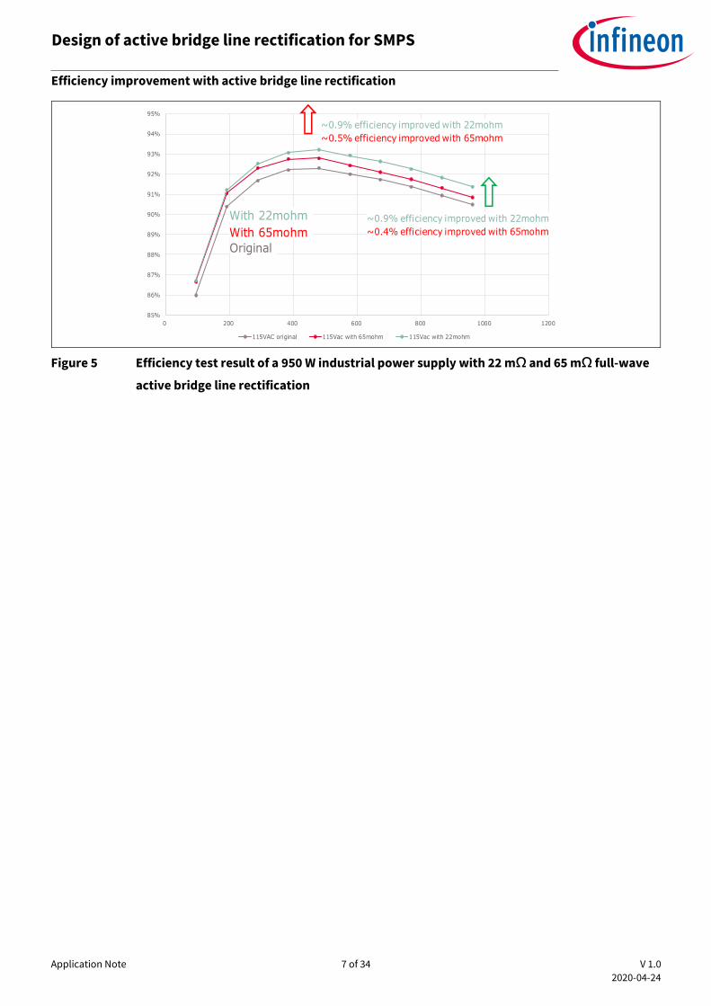
Figure 5 shows an example of a 950 W industrial power supply, tested with an active bridge line rectification of
22 mΩ and 65 mΩ MOSFETs in a TOLL package at an AC voltage of 115 V. The efficiency is improved by 0.9 percent with an active bridge line rectification of 22 mΩ MOSFET at half load and full load. That is improved by
0.5 percent and 0.4 percent with an active bridge line rectification of 65 mΩ MOSFET at half load and full load respectively.
Application Note 7 of 34 V 1.0
2020-04-24
Design of active bridge line rectification for SMPS
Efficiency improvement with active bridge line rectification
Figure 5 Efficiency test result of a 950 W industrial power supply with 22 mΩ and 65 mΩ full-wave
active bridge line rectification
85%
86%
87%
88%
89%
90%
91%
92%
93%
94%
95%
0 200 400 600 800 1000 1200
115VAC original 115Vac with 65mohm 115Vac with 22mohm
Original
With 65mohm
With 22mohm
~0.9% efficiency improved with 22mohm
~0.5% efficiency improved with 65mohm
~0.9% efficiency improved with 22mohm
~0.4% efficiency improved with 65mohm
Application Note 8 of 34 V 1.0
2020-04-24
Design of active bridge line rectification for SMPS
Control method for active bridge line rectification
2 Control method for active bridge line rectification
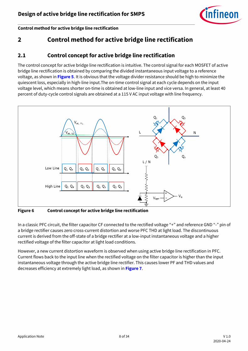
2.1 Control concept for active bridge line rectification
The control concept for active bridge line rectification is intuitive. The control signal for each MOSFET of active
bridge line rectification is obtained by comparing the divided instantaneous input voltage to a reference voltage, as shown in Figure 5. It is obvious that the voltage divider resistance should be high to minimize the
quiescent loss, especially in high-line input.The on-time control signal at each cycle depends on the input voltage level, which means shorter on-time is obtained at low-line input and vice versa. In general, at least 40 percent of duty-cycle control signals are obtained at a 115 V AC input voltage with line frequency.
Figure 6 Control concept for active bridge line rectification
In a classic PFC circuit, the filter capacitor CF connected to the rectified voltage “+” and reference GND “-” pin of
a bridge rectifier causes zero cross-current distortion and worse PFC THD at light load. The discontinuous current is derived from the off-state of a bridge rectifier at a low-input instantaneous voltage and a higher
rectified voltage of the filter capacitor at light load conditions.
However, a new current distortion waveform is observed when using active bridge line rectification in PFC.
Current flows back to the input line when the rectified voltage on the filter capacitor is higher than the input instantaneous voltage through the active bridge line rectifier. This causes lower PF and THD values and
decreases efficiency at extremely light load, as shown in Figure 7.

Application Note 9 of 34 V 1.0
2020-04-24
Design of active bridge line rectification for SMPS
Control method for active bridge line rectification
Figure 7 Decreased PF and THD values under light load conditions originating from current flowing
back from the filter capacitor to the input line
Two possible solutions are useful for solving such current distortions. First, only use MOSFETs at the low side of active bridge line rectification, like the Q3 and Q4 in Figure 7. The distortion comes from the discharging current
from the filter capacitor to the input line through the MOSFET, as the capacitor voltage is higher than the input instantaneous voltage. MOSFETs provide bi-directional paths for current. Without a MOSFET on the high side,
the current never flows from the filter capacitor to the input line. As the efficiency improvement is enough, an active bridge line rectification with a MOSFET only at its low side prevents a worse THD.
Second, using a SR controller as the controller in the active bridge line rectification, shown in Figure 8. The
control concept behind a SR controller is to detect the voltage level on the MOSFET when it is on. When the
absolute voltage level of the MOSFET changes from high to low, a potential reverse current incident on the MOSFET may occur, and then the controller stops driving the signal. The occurrence of deteriorating PF and THD caused by a reverse current is almost impossible with a SR controller.
Vrec with diode only
Vrec with MOSFET
Irec with diode only
Irec with MOSFET
Vac

Application Note 10 of 34 V 1.0
2020-04-24
Design of active bridge line rectification for SMPS
Control method for active bridge line rectification
Figure 8 Using a SR controller in active bridge line rectification
It is worth mentioning that deteriorating THD and efficiency at light load caused by an active bridge line
rectification depends on the input voltage, filter capacitance and load condition. Faced with these issues,
designers may adopt different approaches regarding power supplies for different applications, different PFC
topologies and output power. A CCM PFC with low filter capacitance is mostly adopted by power supplies of higher power (kW and above). Under light load testing conditions, such as a 10 percent load, THD and efficiency
deteriorations caused by an active bridge rectification might be hardly noticeable. But this is significant in a 200
W adapter with CrM PFC and high filter capacitance, where the aforementioned issues can be noticed under
light load conditions. The designers may check the waveform and choose a suitable control method based on the PFC topology, load and test condition.
2.2 Control method of active bridge line rectification for burst mode control
The benefits from active bridge line rectification for power supplies do not only improve efficiency, but also the temperature of the power device, especially for high-density power supplies relying exclusively on natural
convection. In external power supplies, like adapters, burst mode control is a necessary function to meet the input power specification at no-load conditions. How does the active bridge line rectification control the MOSFET at burst mode in external power supplies?
Figure 9(a) shows the voltage waveform on a filter capacitor and current through a bridge rectifier without any
active bridge line rectification. Few pulse currents are observed, and the input power at no-load conditions meets the specifications. However, the voltage waveform on the filter capacitor and current using active bridge
line rectification in Figure 9(b) shows a different scenario. Current through active bridge line rectification consists of a higher-level pulse current and a negative current. The input power of the adapter with active
bridge line rectification is much higher than that without active bridge line rectification at no-load conditions.
The increment is around at 70 mW as provided by a real test. The external power supply with an activated active bridge line rectification does not meet the power specification at no-load conditions.

Application Note 11 of 34 V 1.0
2020-04-24
Design of active bridge line rectification for SMPS
Control method for active bridge line rectification
(a) (b)
Figure 9 In burst mode, rectified voltage and current waveform (a) without active bridge line
rectification; (b) with active bridge line rectification
An activation function for the active bridge line rectification used in external power units with burst mode is necessary through using a VCC power circuit with a burst mode indication signal from the main board, as shown
in Figure 10.
Figure 10 VCC power circuit deactivates active bridge line rectification in burst mode

Application Note 12 of 34 V 1.0
2020-04-24
Design of active bridge line rectification for SMPS
MOSFET selection for active bridge line rectification
3 MOSFET selection for active bridge line rectification
Switching loss and conduction loss of MOSFET are the losses that lead its temperature increasing. The
switching loss of MOSFET in active bridge line rectification can be almost ignored due to the switching frequency of the MOSFET being the line frequency; the conduction loss of MOSFET depends on the current and the MOSFET RDS(on) MOSFET which relies on the die and package technology, is the key factor to achieve high performance in active bridge line rectification.
The challenges for MOSFET manufacturers in such applications are to produce the lowest MOSFET RDS(on) within the same die area and to create high performance packages with low parasitic resistance and high thermal
conductivity. From the characteristic, MOSFET RDS(on) is increasing along with junction temperature. Packages with better heat conductivity help to stabilize the device temperature and minimize a further power dissipation
from higher RDS(on) caused by an even higher junction temperature.
High power density design is one of the key features for power supply units that utilize active bridge line rectification for both efficiency and thermal considerations. The same RDS(on) of MOSFET in a smaller package or a smaller RDS(on) of MOSFET in the same package is the criteria to select the MOSFET for this application.
Therefore, a comparison of the lowest MOSFETs RDS(on) from different manufacturers in the market is shown in Figure 11. The lowest MOSFETs RDS(on) in TO247 package is 10mΩ in the market that is manufactured by
Infineon technology. That fact demonstrates the advance silicon technology of power MOSFET in Infineon. Considering the MOSFET in the SMD package, the lowest MOSFET RDS(on) in TOLL package is 22mΩ.
Figure 11 Comparison of lowest RDS(on) of MOSFETs from different manufacturers
Figure 12(a) shows Infineon’s lowest RDS(on) in different packages. TO247 is the possible selection if considering the lowest RDS(on) in one package. 10mΩ is the lowest RDS(on) value in this packages. However, when considering
the RDS(on) and package area, TOLL is the most suitable package as its lowest RDS(on) is 22mΩ. Accordingly,
ThinPAK is another good choice with the smallest package volume and lowest RDS(on) at 60mΩ.

Application Note 13 of 34 V 1.0
2020-04-24
Design of active bridge line rectification for SMPS
MOSFET selection for active bridge line rectification
(a)
(b)
Figure 12 Comparison of Infineon’s lowest RDS(on) in different packages (a) by RDS(on) value; (b) by
package area and package volume
0
20
40
60
80
100
120
140
160
TO247 TO220 TOLL DDPAK D2PAK ThinPAK DPAK
RDS,ON vs Package
3.4 3.6 2.6
7.0 8.4
3.9
6.1
17.7 16.6
6.2
16.4
38.3
4.3
14.6
0.0
5.0
10.0
15.0
20.0
25.0
30.0
35.0
40.0
45.0
0.0
5.0
10.0
15.0
20.0
25.0
30.0
35.0
40.0
TO247 TO220 TOLL DDPAK D2PAK ThinPAK DPAK
RDS,ON X Area RDS,ON X Volume

Application Note 14 of 34 V 1.0
2020-04-24
Design of active bridge line rectification for SMPS
MOSFET selection for active bridge line rectification
Figure 13 Infineon’s top-side cooling SMD packages – DDPAK
A heat sink is helpful for thermal conduction for top-side cooling of the DDPAK as shown in Figure13. The heat can spread via the lead frame on the top side of the MOSFET to the heat sink and then to the environment. The
lowest RDS(on) in DDPAK is 50mΩ.
In addition, height is one of the constraints, especially in high power density power supply units. Figure 14 shows four daughter boards with MOSFETs in different packages designed for height constraints of different
power supply units. Considering the space and outline, ThinPAK and DDPAK are suitable for low-profile power
supply units. The maximum height of the daughter board with these two packages is 20 mm.
The daughter board shown here is helpful for immediately evaluating the performance of active bridge line rectification with the customer’s current power supply. Another possible daughter board design is to divide
active bridge line rectification into two parts: upper bridge with driver and lower bridge with controller. The control signals between both boards are connected via the main board. With such daughter board structures,
even a TOLL package may be utilized in power units with a height constraint of 20 mm.
Figure 14 Active bridge line rectification daughter board with MOSFETs of various packages for
visual concept
29mm
36.5mm
29mm
36.5mm
20mm
40mm
18mm
50mm
TOLL
DDPAKThinPAK
D2PAK
8.5mm 6.6mm
5.3mm 5.9mm
Application Note 15 of 34 V 1.0
2020-04-24
Design of active bridge line rectification for SMPS
Device replacement and power loss calculation
4 Device replacement and power loss calculation
4.1 Formula for calculating the conduction loss of bridge diodes and
MOSFETs
The advantage of active bridge line rectification for power supply is not only to improve the efficiency from light load to full load, but also to improve the temperature of the power device. To estimate the efficiency
improvement made by active bridge line rectification, the power dissipation of a bridge rectifier and power MOSFET needs to be calculated first.
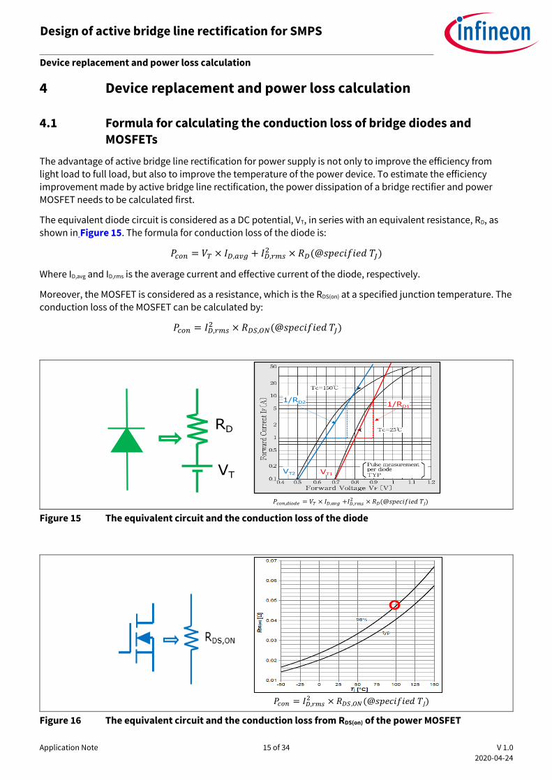
The equivalent diode circuit is considered as a DC potential, VT, in series with an equivalent resistance, RD, as shown in Figure 15. The formula for conduction loss of the diode is:
𝑃𝑐𝑜𝑛 = 𝑉𝑇 × 𝐼𝐷,𝑎𝑣𝑔 + 𝐼𝐷,𝑟𝑚𝑠2 × 𝑅𝐷(@𝑠𝑝𝑒𝑐𝑖𝑓𝑖𝑒𝑑 𝑇𝐽)
Where ID,avg and ID,rms is the average current and effective current of the diode, respectively.
Moreover, the MOSFET is considered as a resistance, which is the RDS(on) at a specified junction temperature. The
conduction loss of the MOSFET can be calculated by:
𝑃𝑐𝑜𝑛 = 𝐼𝐷,𝑟𝑚𝑠2 × 𝑅𝐷𝑆,𝑂𝑁(@𝑠𝑝𝑒𝑐𝑖𝑓𝑖𝑒𝑑 𝑇𝐽)
Figure 15 The equivalent circuit and the conduction loss of the diode
Figure 16 The equivalent circuit and the conduction loss from RDS(on) of the power MOSFET
RD
VTVT2
1/RD2 1/RD1
VT1
𝑃𝑐𝑜𝑛, 𝑜 = 𝑉𝑇 × 𝐼𝐷,𝑎𝑣𝑔 +𝐼𝐷,𝑟𝑚𝑠2 × 𝑅𝐷(@𝑠𝑝𝑒𝑐𝑖𝑓𝑖𝑒𝑑 𝑇 )
𝑃𝑐𝑜𝑛 = 𝐼𝐷,𝑟𝑚𝑠2 × 𝑅𝐷𝑆,𝑂𝑁(@𝑠𝑝𝑒𝑐𝑖𝑓𝑖𝑒𝑑 𝑇 )

Application Note 16 of 34 V 1.0
2020-04-24
Design of active bridge line rectification for SMPS
Device replacement and power loss calculation
Theoretically, it is simple to calculate the power loss improvement by subtracting the power dissipation of the MOSFET from that of the bridge rectifier. The efficiency improvement can be obtained from the power loss
reduction at different load conditions. However, it is not simple in real calculations for the following reasons:
a. The equivalent circuit of diode power dissipation is considered as DC potential in series with an equivalent resistance. However, these two parameters are not fixed and change along with the temperature and current
of the diode. The curves at all of the possible temperatures are not provided by the manufacturers. In most cases, only curves at 25°C and 150°C are found in the datasheet.
b. The RDS (on) of the MOSFET varies along with its junction temperature and current. However, the PCB parasitic resistance is not ignored when using an extremely low RDS(on) device, such as 10 mΩ, which makes it difficult to estimate the power dissipation on active bridge line rectification.
4.2 Estimating the conduction loss of bridge diodes and MOSFETs in real
test
It is a challenge to estimate the efficiency improvement at specified load conditions from the diode and power MOSFET conduction loss. A simple circuit as shown in Figure 17 is used to test and estimate the power
dissipation of a bridge diode and power MOSFET. The test is implemented by utilizing a standard resistor as
load and adjustable AC voltage source to control the input voltage and load current through a bridge rectifier or MOSFETs.
Measuring the input voltage, output voltage and load current of the test circuit is required for power loss
calculation. Measuring the temperature of the bridge rectifier and MOSFET is required for evaluating power dissipation according to the formula. In principle, the load current multiplies the difference between input and
output voltage, which is the power dissipation of the bridge rectifier or MOSFET. We may calculate an effective
voltage representing the loss of the bridge rectifier and MOSFET.
This measurement result is used to verify the accuracy of power loss calculation based on the formula.
Figure 17 Power dissipation test circuit for the bridge rectifier and active bridge line rectification
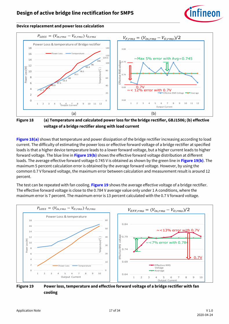
The first test is implemented with a bridge rectifier, GBJ1506, under natural convection only. Device temperature is recorded as well, as shown in Figure 18(a). The effective voltage and power loss under various load currents is calculated in Figure 18.
Vo
Io
Vin
T
T
𝑃 𝑂𝑆𝑆 = (𝑉 𝑛,𝑟𝑚𝑠 𝑉𝑂,𝑟𝑚𝑠) 𝐼𝑂,𝑟𝑚𝑠𝑉 ,𝑟𝑚𝑠 = (𝑉 𝑛,𝑟𝑚𝑠 𝑉𝑂,𝑟𝑚𝑠)
R
Application Note 17 of 34 V 1.0
2020-04-24
Design of active bridge line rectification for SMPS
Device replacement and power loss calculation
(a) (b)
Figure 18 (a) Temperature and calculated power loss for the bridge rectifier, GBJ1506; (b) effective
voltage of a bridge rectifier along with load current
Figure 18(a) shows that temperature and power dissipation of the bridge rectifier increasing according to load current. The difficulty of estimating the power loss or effective forward voltage of a bridge rectifier at specified loads is that a higher device temperature leads to a lower forward voltage, but a higher current leads to higher
forward voltage. The blue line in Figure 19(b) shows the effective forward voltage distribution at different loads. The average effective forward voltage 0.745 V is obtained as shown by the green line in Figure 19(b). The
maximum 5 percent calculation error is obtained by the average forward voltage. However, by using the
common 0.7 V forward voltage, the maximum error between calculation and measurement result is around 12
percent.
The test can be repeated with fan cooling. Figure 19 shows the average effective voltage of a bridge rectifier.
The effective forward voltage is close to the 0.784 V average value only under 1 A conditions, where the maximum error is 7 percent. The maximum error is 13 percent calculated with the 0.7 V forward voltage.
Figure 19 Power loss, temperature and effective forward voltage of a bridge rectifier with fan
cooling
27.733.3
40.947.1
53.360
70.1
78.1
89.496
106
114.5
0
20
40
60
80
100
120
140
0
2
4
6
8
10
12
14
16
18
1 2 3 4 5 6 7 8 9 10 11 12
Tem
pera
ture
(℃)
Pow
er L
oss(
W)
Output Current
Power Loss & temperature of Bridge rectifier
Power Loss Temperature
𝑃 𝑂𝑆𝑆 = (𝑉 𝑛,𝑟𝑚𝑠 𝑉𝑂,𝑟𝑚𝑠) 𝐼𝑂,𝑟𝑚𝑠
0.64
0.69
0.74
0.79
0.84
1 2 3 4 5 6 7 8 9 10 11 12
Effe
ctiv
e R
MS
volt
age
Output Current
Effective RMS Voltage Average
~Max 5% error with Avg=0.745
0.7V~< 12% error with 0.7V
𝑉 ,𝑟𝑚𝑠 = (𝑉 𝑛,𝑟𝑚𝑠 𝑉𝑂,𝑟𝑚𝑠)/2
𝑃 𝑂𝑆𝑆 = (𝑉 𝑛,𝑟𝑚𝑠 𝑉𝑂,𝑟𝑚𝑠) 𝐼𝑂,𝑟𝑚𝑠
0
10
20
30
40
50
60
0
2
4
6
8
10
12
14
16
18
1 2 3 4 5 6 7 8 9 10
Tem
pera
ture
(℃)
Pow
er L
oss(
W)
Output Current
Power Loss & temperature
Power Loss Temperature
0.64
0.69
0.74
0.79
0.84
1 2 3 4 5 6 7 8 9 10
Eff
ective R
MS v
oltage
Output Current
Effective RMS
Voltage
Average
~<7% error with 0.784
0.7V
~<13% error with 0.7V
𝑉 ,𝑟𝑚𝑠 = (𝑉 𝑛,𝑟𝑚𝑠 𝑉𝑂,𝑟𝑚𝑠)/2
Application Note 18 of 34 V 1.0
2020-04-24
Design of active bridge line rectification for SMPS
Device replacement and power loss calculation
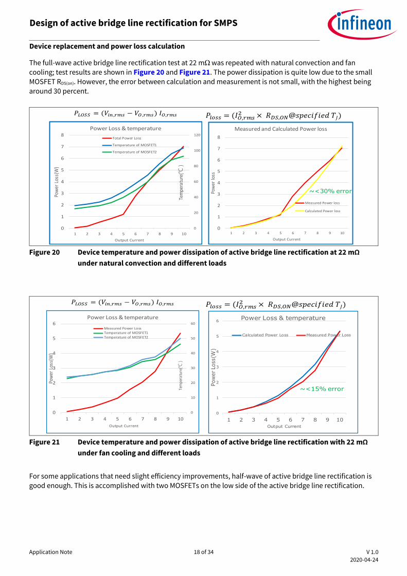
The full-wave active bridge line rectification test at 22 mΩ was repeated with natural convection and fan cooling; test results are shown in Figure 20 and Figure 21. The power dissipation is quite low due to the small
MOSFET RDS(on). However, the error between calculation and measurement is not small, with the highest being around 30 percent.
Figure 20 Device temperature and power dissipation of active bridge line rectification at 22 mΩ
under natural convection and different loads
Figure 21 Device temperature and power dissipation of active bridge line rectification with 22 mΩ
under fan cooling and different loads
For some applications that need slight efficiency improvements, half-wave of active bridge line rectification is
good enough. This is accomplished with two MOSFETs on the low side of the active bridge line rectification.
0
20
40
60
80
100
120
0
1
2
3
4
5
6
7
8
1 2 3 4 5 6 7 8 9 10
Tem
pera
ture
(℃)
Pow
er L
oss(
W)
Output Current
Power Loss & temperature
Total Power Loss
Temperature of MOSFET1
Temperature of MOSFET2
𝑃 𝑂𝑆𝑆 = (𝑉 𝑛,𝑟𝑚𝑠 𝑉𝑂,𝑟𝑚𝑠) 𝐼𝑂,𝑟𝑚𝑠
0
1
2
3
4
5
6
7
8
1 2 3 4 5 6 7 8 9 10
Pow
er l
oss
Output Current
Measured and Calculated Power loss
Measured Power loss
Calculated Power loss
𝑃 𝑜𝑠𝑠 = (𝐼𝑂,𝑟𝑚𝑠2 × 𝑅𝐷𝑆,𝑂𝑁@𝑠𝑝𝑒𝑐𝑖𝑓𝑖𝑒𝑑 𝑇 )
~<30% error
𝑃 𝑂𝑆𝑆 = (𝑉 𝑛,𝑟𝑚𝑠 𝑉𝑂,𝑟𝑚𝑠) 𝐼𝑂,𝑟𝑚𝑠
0
10
20
30
40
50
60
0
1
2
3
4
5
6
1 2 3 4 5 6 7 8 9 10
Tem
pera
ture
(℃)
Pow
er L
oss(
W)
Output Current
Power Loss & temperature
Measured Power LossTemperature of MOSFET1Temperature of MOSFET2
𝑃 𝑜𝑠𝑠 = (𝐼𝑂,𝑟𝑚𝑠2 × 𝑅𝐷𝑆,𝑂𝑁@𝑠𝑝𝑒𝑐𝑖𝑓𝑖𝑒𝑑 𝑇 )
0
1
2
3
4
5
6
1 2 3 4 5 6 7 8 9 10
Pow
er Loss(W
)
Output Current
Power Loss & temperature
Calculated Power Loss Measured Power Loss
~<15% error

Application Note 19 of 34 V 1.0
2020-04-24
Design of active bridge line rectification for SMPS
Device replacement and power loss calculation
The test was repeated with two MOSFETs, and the results are shown in Figure 22 and Figure 23. Figure 22 shows the test results under natural convection, and the error between measurement and calculation of power
dissipation is only 5 percent by utilizing the formula VEFF,rms=0.7+Io,rms×RDS(on)@specified TJ for calculating the effective forward voltage in combination with a bridge rectifier and half-wave active bridge line rectification;
with fan cooling, the error between measurement and calculation of power dissipation is only 7 percent by utilizing the formula of VEFF,rms=0.75+Io,rms×RDS(on)@specified TJ.
Figure 22 Effective forward voltage, power loss and device temperature of bridge rectifier and half-
wave active bridge line rectification under natural convection
Figure 23 Effective forward voltage, power loss and device temperature of bridge rectifier and half-
wave active bridge line rectification under fan cooling
0
20
40
60
80
100
120
0
1
2
3
4
5
6
7
8
9
10
1 2 3 4 5 6 7 8 9
Tem
pera
ture
(℃)
Pow
er L
oss(
W)
Output Current
Power Loss & temperature
Total Power LossTemperature of BDTemperature of MOSFET
𝑃 𝑂𝑆𝑆 = (𝑉 𝑛,𝑟𝑚𝑠 𝑉𝑂,𝑟𝑚𝑠) 𝐼𝑂,𝑟𝑚𝑠
0.68
0.73
0.78
0.83
0.88
0.93
0.98
1.03
1.08
1 2 3 4 5 6 7 8 9
Effe
ctiv
e R
MS
volt
age
Output Current
Measured EffectiveRMS Voltage
Calculate EffectiveVoltage
~<5% error
𝑉 ,𝑟𝑚𝑠 = ( + 𝐼𝑂,𝑟𝑚𝑠× 𝑅𝐷𝑆,𝑂𝑁@𝑇 )
𝑃 𝑂𝑆𝑆 = (𝑉 𝑛,𝑟𝑚𝑠 𝑉𝑂,𝑟𝑚𝑠) 𝐼𝑂,𝑟𝑚𝑠
0
10
20
30
40
50
60
0
2
4
6
8
10
12
1 2 3 4 5 6 7 8 9 10
Tem
per
atu
re(℃)
Po
wer
Lo
ss(W
)
Output Current
Power Loss & temperature
Total Power LossTemperature of BDTemperature of MOSFET
~< 7% error
𝑉 ,𝑟𝑚𝑠 = ( + 𝐼𝑂,𝑟𝑚𝑠× 𝑅𝐷𝑆,𝑂𝑁@𝑇 )
0.68
0.73
0.78
0.83
0.88
0.93
0.98
1.03
1.08
1 2 3 4 5 6 7 8 9 10
Effe
ctiv
e R
MS
volt
age
Output Current
Measured EffectiveRMS Voltage
Calculate EffectiveVoltage
Application Note 20 of 34 V 1.0
2020-04-24
Design of active bridge line rectification for SMPS
Device replacement and power loss calculation
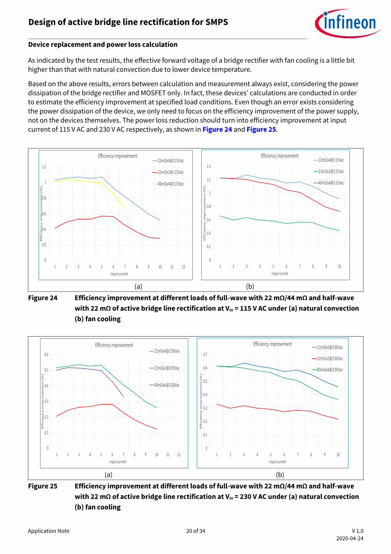
As indicated by the test results, the effective forward voltage of a bridge rectifier with fan cooling is a little bit higher than that with natural convection due to lower device temperature.
Based on the above results, errors between calculation and measurement always exist, considering the power dissipation of the bridge rectifier and MOSFET only. In fact, these devices’ calculations are conducted in order to estimate the efficiency improvement at specified load conditions. Even though an error exists considering
the power dissipation of the device, we only need to focus on the efficiency improvement of the power supply, not on the devices themselves. The power loss reduction should turn into efficiency improvement at input current of 115 V AC and 230 V AC respectively, as shown in Figure 24 and Figure 25.
(a) (b)
Figure 24 Efficiency improvement at different loads of full-wave with 22 mΩ/44 mΩ and half-wave
with 22 mΩ of active bridge line rectification at Vin = 115 V AC under (a) natural convection
(b) fan cooling
(a) (b)
Figure 25 Efficiency improvement at different loads of full-wave with 22 mΩ/44 mΩ and half-wave
with 22 mΩ of active bridge line rectification at Vin = 230 V AC under (a) natural convection
(b) fan cooling
0
0.2
0.4
0.6
0.8
1
1.2
1 2 3 4 5 6 7 8 9 10 11 12
Eff
icie
ncy
im
prv
oe
me
nt
(%)
Input current
Efficiency improvement22mΩx4@115Vac
22mΩx2@115Vac
40mΩx4@115Vac
0
0.2
0.4
0.6
0.8
1
1.2
1.4
1 2 3 4 5 6 7 8 9 10
Effic
ien
cy
im
prv
oe
me
nt (
%)
Input current
Efficiency improvement22mΩx4@115Vac
22mΩx2@115Vac
40mΩx4@115Vac
0
0.1
0.2
0.3
0.4
0.5
0.6
1 2 3 4 5 6 7 8 9 10 11 12
Effic
ien
cy
im
prv
oe
me
nt (
%)
Input current
Efficiency improvement22mΩx4@230Vac
22mΩx2@230Vac
40mΩx4@230Vac
0
0.1
0.2
0.3
0.4
0.5
0.6
0.7
1 2 3 4 5 6 7 8 9 10
Eff
icie
ncy
im
prv
oe
me
nt (
%)
Input current
Efficiency improvement22mΩx4@230Vac
22mΩx2@230Vac
40mΩx4@230Vac

Application Note 21 of 34 V 1.0
2020-04-24
Design of active bridge line rectification for SMPS
Device replacement and power loss calculation
According to the test results in this section, designers can choose full-wave or half-wave active bridge line rectification with different RDS(on). In general, full-wave active bridge line rectification with low RDS(on) improves
the efficiency the most; half-wave active bridge line rectification with low RDS(on) improves efficiency slightly.
It is a rule of thumb that the RDS(on) of a MOSFET in this application should be less than 100 mΩ due to thermal considerations and especially with natural convection.

Application Note 22 of 34 V 1.0
2020-04-24
Design of active bridge line rectification for SMPS
Surge voltage and surge current solutions for active bridge line rectification
5 Surge voltage and surge current solutions for active bridge
line rectification
5.1 Solutions for surge voltage in active bridge line rectification
A lightning surge voltage test, such as the IEC-61000-4-5, is a basic test for all of SMPS units. Figure 26 shows the lightning test circuit, in which high voltage is generated by a combination wave generator and transferred
via a resistor and decoupling capacitor to the power unit.
Figure 26 IEC-61000-4-5 test circuit
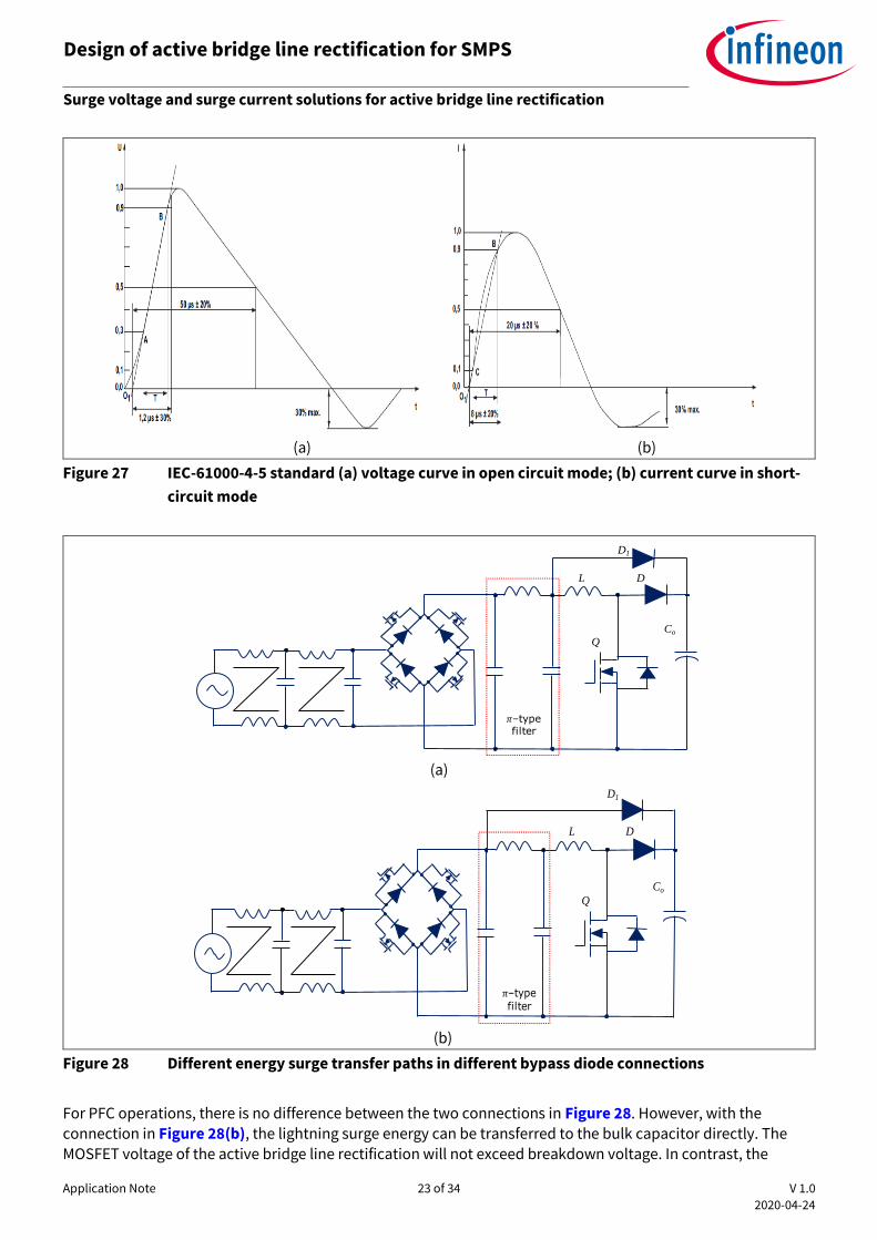
The IEC-61000-4-5 standard defines the voltage waveform in open-circuit mode, and current waveform in short-
circuit mode, as shown in Figure 27. Applications and products should comply with the corresponding standard class. In general, the adapter should comply with class 2 standards; class 3 standards apply to server
applications.
The surge current capacity of a bridge rectifier is much higher compared to a power MOSFET. For instance, the
bridge rectifier has a current capacity of 350 A within 10 ms. Besides current capacity, the maximum reverse voltage of a bridge rectifier that you can find in the market is 1000 V. This means high voltage and current
specifications of a bridge rectifier are the possible solutions in case of damage caused during an abnormal test. However, within the application circuit, active bridge line rectification is parallel to the bridge rectifier. It is imperative that the surge voltage and current capacity of the MOSFET are considered during abnormal tests.
As the voltage of a MOSFET exceeds its breakdown voltage, the MOSFET may enter avalanche mode. The
MOSFET must be able to withstand the surge energy from overvoltage during an abnormal test. For instance, by adopting the IPT60R028G7 in active bridge line rectification, the breakdown voltage is 650 V at TJ,max, and single-
pulse avalanche energy is 288 mJ. Clearly, the surge energy should be absorbed by the protection device or
transferred to storage devices; otherwise, the active bridge line rectification MOSFET will be damaged even with a 1 kV lightning surge differential mode. We may rely on surge energy absorbing devices, like the MOV or
gas tube; and energy storage devices, like a bulk capacitor. The bypass diode connection within the PFC circuit
determines the energy transfer path to the bulk capacitor during a lightning surge test.
Two types of bypass diode connections within a critical-mode PFC circuit with π-type filter are shown in Figure
28. Figure 28(a) shows a bypass diode connected between the π-type filter and the bulk capacitor; Figure 28(b) shows a bypass diode connected between the active bridge line rectifier and the bulk capacitor.
DUT
Phase
Neutral
Earth
Combination
Wave generator
RextDecoupling network
DUT
Application Note 23 of 34 V 1.0
2020-04-24
Design of active bridge line rectification for SMPS
Surge voltage and surge current solutions for active bridge line rectification
(a) (b)
Figure 27 IEC-61000-4-5 standard (a) voltage curve in open circuit mode; (b) current curve in short-
circuit mode
(a)
(b)
Figure 28 Different energy surge transfer paths in different bypass diode connections
For PFC operations, there is no difference between the two connections in Figure 28. However, with the connection in Figure 28(b), the lightning surge energy can be transferred to the bulk capacitor directly. The MOSFET voltage of the active bridge line rectification will not exceed breakdown voltage. In contrast, the
Q
Co
L D
–type filter
D1
Q
Co
L D
–type filter
D1

Application Note 24 of 34 V 1.0
2020-04-24
Design of active bridge line rectification for SMPS
Surge voltage and surge current solutions for active bridge line rectification
connection in Figure 28(a) will have the active bridge line rectification MOSFET damaged due to the lightning surge energy being blocked by the π-type filter in a short time due to surge energy being unable to be
transferred to the bulk capacitor directly.
Furthermore, common choke and differential choke are always used at the input terminal for EMI suppression. All of the differential choke or differential inductance from common choke resonate with the capacitor
connected to them. A gas tube should be connected with a differential choke or common choke to clamp the resonance voltage winding, as shown in Figure 29. MOV is another surge-energy-absorbing device connected to the input terminal. It is worth mentioning that the clamping voltage of the MOV is determined by its leakage current, as shown in Figure 30. The leakage current depends on loop resistance and surge voltage value. For higher surge voltage specifications, more part counts of MOV will be necessary to absorb more energy.
Figure 29 Surge voltage solution for active bridge line rectification
Figure 30 Feature of voltage clamping device, MOV
QCo
L D

Application Note 25 of 34 V 1.0
2020-04-24
Design of active bridge line rectification for SMPS
Surge voltage and surge current solutions for active bridge line rectification
5.2 Solutions for surge current in active bridge line rectification
Some customers raise questions regarding whether the original bridge rectifier is necessary when adopting active bridge line rectification. In terms of current capability, a bridge rectifier is determined by I2t, but the
MOSFET is determined by junction temperature and thermal conduction. From Figure 31 we find that the current capacity of a bridge rectifier is higher than that of a MOSFET when considering time spans longer than 10 ms.
Figure 31 Current capability of a bridge rectifier and MOSFET
Regardless of whether a bridge rectifier or active bridge line rectification is adopted, higher current capacity is
required under several conditions:
(a) Inrush current from the input voltage to charge the bulk capacitor at power up
(b) Recharging current to bulk capacitor after AC cycle drop-out
(c) Surge current from a lightning surge voltage test, such as the IEC61000-4-5
The inrush current limitation resistor only suppresses the inrush current at power up. In the other two cases,
the active bridge line rectification MOSFETs with lower current capability, compared to a bridge rectifier,
cannot easily withstand the surge current, especially during lightning surge voltage test. The surge current may go up to several hundred amperes depending on the surge voltage level and loop resistance.
Assuming the bridge rectifier and active bridge line rectification are parallel, prior to power up, the driving voltage of the active bridge line rectification has not been established. Without the driving voltage, the bridge
rectifier and MOSFET are parallel, acting as two diodes. From the forward voltage of the MOSFET and bridge
rectifier, the MOSFETs’ body diodes conduct the majority of total current due to lower forward voltage. As the
temperature of the MOSFETs increases, the MOSFETs’ body diodes conduct more current; the current sharing then becomes more unbalanced due to the negative temperature coefficient. Figure 32 shows a higher current through the body diode of the MOSFET as the MOSFET temperature is increasing.
~350A current capability
within 1cycle=20ms
D25XB60

Application Note 26 of 34 V 1.0
2020-04-24
Design of active bridge line rectification for SMPS
Surge voltage and surge current solutions for active bridge line rectification
Figure 32 Current sharing between a bridge rectifier and the body diode of a MOSFET
With driving voltage, the active bridge line rectification MOSFET conducts the majority of the total current as
the product of the current, and RDS(on) is lower than the forward voltage of the bridge rectifier, as shown in Figure 33. MOSFETs with driving voltage represent a power device of positive temperature coefficient; when in
parallel with a bridge rectifier, better current sharing is attained even when the temperature of the device has
increased, as illustrated in Figure 34.

Application Note 27 of 34 V 1.0
2020-04-24
Design of active bridge line rectification for SMPS
Surge voltage and surge current solutions for active bridge line rectification
Figure 33 Current sharing between the bridge rectifier and MOSFET
Figure 34 Current sharing between the bridge rectifier and MOSFET at different device
temperatures

Application Note 28 of 34 V 1.0
2020-04-24
Design of active bridge line rectification for SMPS
Surge voltage and surge current solutions for active bridge line rectification
Assuming that the forward voltage of a bridge rectifier is 0.5 V under a total current of 15 A at normal operation, the temperature of the MOSFET is 25°C and the temperature of the bridge rectifier is 25°C, then the current of
the MOSFET is 99.9 percent of total current. At the same load condition but the temperature of MOSFET is 125°C and the temperature of the bridge rectifier is 25°C, then the current of the MOSFET is 99 percent of total current.
Assuming in another case that the forward voltage of the bridge rectifier is 1 V with a higher current of 70 A at
abnormal condition and the temperature of the MOSFET and bridge rectifier is 125°C and 25°C respectively, then the current of the MOSFET drops to 60 A, which is 85 percent of the total current. From the calculation results, the bridge rectifier does share more current when the MOSFET is at higher current.
Figure 35 shows a total current and current of a bridge rectifier waveform in a 1200 W PFC after an AC cycle drop-out. During normal operation, almost no current flows through the bridge rectifier. With higher currents, the bridge rectifier shares a portion of the total current to prevent active bridge line rectification from being
damaged by extremely high currents.
Figure 35 Current sharing by a bridge rectifier after an AC cycle drop-out
Application Note 29 of 34 V 1.0
2020-04-24
Design of active bridge line rectification for SMPS
Efficiency improvements demonstration with active bridge line rectification
6 Efficiency improvements demonstration with active bridge
line rectification
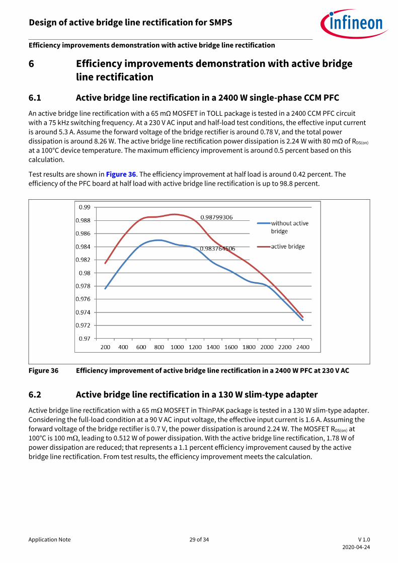
6.1 Active bridge line rectification in a 2400 W single-phase CCM PFC
An active bridge line rectification with a 65 mΩ MOSFET in TOLL package is tested in a 2400 CCM PFC circuit with a 75 kHz switching frequency. At a 230 V AC input and half-load test conditions, the effective input current
is around 5.3 A. Assume the forward voltage of the bridge rectifier is around 0.78 V, and the total power dissipation is around 8.26 W. The active bridge line rectification power dissipation is 2.24 W with 80 mΩ of RDS(on) at a 100°C device temperature. The maximum efficiency improvement is around 0.5 percent based on this calculation.
Test results are shown in Figure 36. The efficiency improvement at half load is around 0.42 percent. The efficiency of the PFC board at half load with active bridge line rectification is up to 98.8 percent.
Figure 36 Efficiency improvement of active bridge line rectification in a 2400 W PFC at 230 V AC
6.2 Active bridge line rectification in a 130 W slim-type adapter
Active bridge line rectification with a 65 mΩ MOSFET in ThinPAK package is tested in a 130 W slim-type adapter. Considering the full-load condition at a 90 V AC input voltage, the effective input current is 1.6 A. Assuming the forward voltage of the bridge rectifier is 0.7 V, the power dissipation is around 2.24 W. The MOSFET RDS(on) at 100°C is 100 mΩ, leading to 0.512 W of power dissipation. With the active bridge line rectification, 1.78 W of
power dissipation are reduced; that represents a 1.1 percent efficiency improvement caused by the active
bridge line rectification. From test results, the efficiency improvement meets the calculation.

Application Note 30 of 34 V 1.0
2020-04-24
Design of active bridge line rectification for SMPS
Efficiency improvements demonstration with active bridge line rectification
Figure 37 Efficiency test results of active bridge line rectification in a 130 W adapter
6.3 Reference schematic of active bridge line rectification
An active bridge line rectification reference schematic is shown in Figure 38 for readers to build an active
bridge line rectification.
Figure 38 Reference schematic of active bridge line rectification

Application Note 31 of 34 V 1.0
2020-04-24
Design of active bridge line rectification for SMPS
Summary
7 Summary
Active bridge line rectification is a circuit which can improve the efficiency within entire power ranges for high efficiency and high power density in SMPS. It demonstrates a flexible design with different daughter board MOSFET RDS(on) for various efficiency requirements of different applications without any other circuit
modification. For high power density adapters with burst mode control and convection cooling, but without internal auxiliary power, active bridge line rectification does reduce the power loss and temperature of power devices. For server power supplies, active bridge line rectification does help to improve the efficiency and extend the power range with at least 94 percent efficiency. The total power loss reduction and efficiency
improvement can be estimated by the simple formulas provided in this application note.
For best performance, the MOSFET RDS(on) plays an important role in this application. Considering the
mechanical outline, space and thermal conduction inside power supplies, various MOSFET packages are the
key to achieve flexibility for such applications. Infineon provides the lowest MOSFET RDS(on) within the same package and MOSFETs with new top-side cooling SMD packages.
Taking into consideration abnormal conditions and EMC tests, solutions for surge voltage and surge current are necessary for MOSFETs. These are also discussed in this application note. Even when active bridge line rectification acts as a bridge rectifier, a bridge rectifier is still needed, as when they are used in parallel, higher
surge current capabilities are possible for abnormal conditions.
Efficiency improvement results with active bridge line rectification are demonstrated in a 2400 W PFC and 130 slim-type adapter. A schematic of a reference circuit is provided in this application note, so that readers can
design and manufacture an active bridge line rectification board following the concept.

Application Note 32 of 34 V 1.0
2020-04-24
Design of active bridge line rectification for SMPS
References
8 References
[1] Infineon application note, “IR11688 Smart RectifierTM control IC design notes”
[2] Diodes datasheet, “GBJ15005-GBJ1510”
[3] Shindengen datasheet, “D25XB60”

Application Note 33 of 34 V 1.0
2020-04-24
Design of active bridge line rectification for SMPS
Revision history
Revision history
Document
version Date of release Description of changes
V 1.0 24-04-2020 First release

Trademarks All referenced product or service names and trademarks are the property of their respective owners.
Edition 2020-04-24
AN_1905_PL52_1905_101502
Published by
Infineon Technologies AG
81726 Munich, Germany
© 2020 Infineon Technologies AG.
All Rights Reserved.
Do you have a question about this
document?
Email: [email protected]
Document reference
IMPORTANT NOTICE The information contained in this application note is given as a hint for the implementation of the product only and shall in no event be regarded as a description or warranty of a certain functionality, condition or quality of the product. Before implementation of the product, the recipient of this application note must verify any function and other technical information given herein in the real application. Infineon Technologies hereby disclaims any and all warranties and liabilities of any kind (including without limitation warranties of non-infringement of intellectual property rights of any third party) with respect to any and all information given in this application note. The data contained in this document is exclusively intended for technically trained staff. It is the responsibility of customer’s technical departments to evaluate the suitability of the product for the intended application and the completeness of the product information given in this document with respect to such application.
For further information on the product, technology, delivery terms and conditions and prices please contact your nearest Infineon Technologies office (www.infineon.com).
WARNINGS Due to technical requirements products may contain dangerous substances. For information on the types in question please contact your nearest Infineon Technologies office. Except as otherwise explicitly approved by Infineon Technologies in a written document signed by authorized representatives of Infineon Technologies, Infineon Technologies’ products may not be used in any applications where a failure of the product or any consequences of the use thereof can reasonably be expected to result in personal injury.