

Implementing Battery Charging Features Using HX3 - Infineon ...
Upload
khangminh22Category
view
0download
0
User ’s Manual , V2.2, Jan. 2004
Microcontrol lers
N e v e r s t o p t h i n k i n g .
XC16116-Bit S ingle-Chip Microcontrol lerwi th C166SV2 Core
Volume 1 (of 2) : System Units

Edition 2004-01
Published by Infineon Technologies AG,St.-Martin-Strasse 53,81669 München, Germany
© Infineon Technologies AG 2004.All Rights Reserved.
Attention please!
The information herein is given to describe certain components and shall not be considered as a guarantee of characteristics.Terms of delivery and rights to technical change reserved.We hereby disclaim any and all warranties, including but not limited to warranties of non-infringement, regarding circuits, descriptions and charts stated herein.
Information
For further information on technology, delivery terms and conditions and prices please contact your nearest Infineon Technologies Office (www.infineon.com).
Warnings
Due to technical requirements components may contain dangerous substances. For information on the types in question please contact your nearest Infineon Technologies Office.Infineon Technologies Components may only be used in life-support devices or systems with the express written approval of Infineon Technologies, if a failure of such components can reasonably be expected to cause the failure of that life-support device or system, or to affect the safety or effectiveness of that device or system. Life support devices or systems are intended to be implanted in the human body, or to support and/or maintain and sustain and/or protect human life. If they fail, it is reasonable to assume that the health of the user or other persons may be endangered.
User ’s Manual , V2.2, Jan. 2004
Microcontrol lers
N e v e r s t o p t h i n k i n g .
XC161
Volume 1 (of 2) : System Units
16-Bi t S ingle-Chip Microcontrol lerwi th C166SV2 Core
Template: mc_tmplt_a5.fm / 3 / 2003-09-01
Controller Area Network (CAN): License of Robert Bosch GmbH
XC161 Volume 1 (of 2): System Units Revision History: V2.2, 2004-01
Previous Version: V2.2, 2003-09 (Pre-release)V2.1, 2003-06V2.0, 2003-03V1.1, 2002-02 (Draft Manual)V1.0, 2001-04 (Draft Manual)
Page Subjects (major changes since version V2.1)1)
1) In order to create the current version V2.2 of this manual, the layout of several graphics and text structureshas been adapted to company documentation rules. The contents have not been changed otherwise, exceptfor the Pre-release note on page 1-2 or obvious typographical errors.
all Page header corrected
several Register names adapted (see next item)
1-10 Section “Naming Conventions” added
2-8 Interrupt response time corrected
3-26 Description of margin control improved
5-8 Description of IEN improved
5-16 Description of interrupt jump table cache improved
5-39 Association of interrupt nodes corrected
6-12 Phrasing corrected
6-28 Description of main oscillator gain reduction improved
6-32 Notes added
6-34f Description improved
6-37 Clock domain table corrected and enhanced
6-60 Section added
7-36ff Description of port 3 improved
7-44, 7-51,7-56, 7-67,7-75, 7-83
Figure corrected
12-4 Description of TRAP instruction corrected
12-5 Instruction ENWDT added
We Listen to Your CommentsAny information within this document that you feel is wrong, unclear or missing at all?Your feedback will help us to continuously improve the quality of this document.Please send your proposal (including a reference to this document) to:[email protected]

XC161 DerivativesSystem Units (Vol. 1 of 2)
Table of Contents Page
This User’s Manual consists of two Volumes, “System Units” and “Peripheral Units”. Foryour convenience this table of contents (and also the keyword index) lists both volumes,so can immediately find the reference to the desired section in the correspondingdocument ([1] or [2]).
1 Introduction . . . . . . . . . . . . . . . . . . . . . . . . . . . . . . . . . . . . . . . . . . . . 1-1 [1]1.1 Members of the 16-bit Microcontroller Family . . . . . . . . . . . . . . . . . . . 1-3 [1]1.2 Summary of Basic Features . . . . . . . . . . . . . . . . . . . . . . . . . . . . . . . . 1-5 [1]1.3 Abbreviations . . . . . . . . . . . . . . . . . . . . . . . . . . . . . . . . . . . . . . . . . . . . 1-9 [1]1.4 Naming Conventions . . . . . . . . . . . . . . . . . . . . . . . . . . . . . . . . . . . . . 1-10 [1]
2 Architectural Overview . . . . . . . . . . . . . . . . . . . . . . . . . . . . . . . . . . . 2-1 [1]2.1 Basic CPU Concepts and Optimizations . . . . . . . . . . . . . . . . . . . . . . . 2-2 [1]2.1.1 High Instruction Bandwidth/Fast Execution . . . . . . . . . . . . . . . . . . . 2-4 [1]2.1.2 Powerful Execution Units . . . . . . . . . . . . . . . . . . . . . . . . . . . . . . . . . 2-5 [1]2.1.3 High Performance Branch-, Call-, and Loop-Processing . . . . . . . . . 2-6 [1]2.1.4 Consistent and Optimized Instruction Formats . . . . . . . . . . . . . . . . 2-7 [1]2.1.5 Programmable Multiple Priority Interrupt System . . . . . . . . . . . . . . 2-8 [1]2.1.6 Interfaces to System Resources . . . . . . . . . . . . . . . . . . . . . . . . . . . 2-9 [1]2.2 On-Chip System Resources . . . . . . . . . . . . . . . . . . . . . . . . . . . . . . . 2-10 [1]2.3 On-Chip Peripheral Blocks . . . . . . . . . . . . . . . . . . . . . . . . . . . . . . . . 2-14 [1]2.4 Clock Generation . . . . . . . . . . . . . . . . . . . . . . . . . . . . . . . . . . . . . . . . 2-29 [1]2.5 Power Management Features . . . . . . . . . . . . . . . . . . . . . . . . . . . . . . 2-29 [1]2.6 On-Chip Debug Support (OCDS) . . . . . . . . . . . . . . . . . . . . . . . . . . . 2-31 [1]2.7 Protected Bits . . . . . . . . . . . . . . . . . . . . . . . . . . . . . . . . . . . . . . . . . . 2-32 [1]
3 Memory Organization . . . . . . . . . . . . . . . . . . . . . . . . . . . . . . . . . . . . 3-1 [1]3.1 Address Mapping . . . . . . . . . . . . . . . . . . . . . . . . . . . . . . . . . . . . . . . . 3-3 [1]3.2 Special Function Register Areas . . . . . . . . . . . . . . . . . . . . . . . . . . . . . 3-4 [1]3.3 Data Memory Areas . . . . . . . . . . . . . . . . . . . . . . . . . . . . . . . . . . . . . . . 3-8 [1]3.4 Program Memory Areas . . . . . . . . . . . . . . . . . . . . . . . . . . . . . . . . . . . 3-10 [1]3.5 System Stack . . . . . . . . . . . . . . . . . . . . . . . . . . . . . . . . . . . . . . . . . . . 3-12 [1]3.6 IO Areas . . . . . . . . . . . . . . . . . . . . . . . . . . . . . . . . . . . . . . . . . . . . . . . 3-13 [1]3.7 External Memory Space . . . . . . . . . . . . . . . . . . . . . . . . . . . . . . . . . . 3-14 [1]3.8 Crossing Memory Boundaries . . . . . . . . . . . . . . . . . . . . . . . . . . . . . . 3-15 [1]3.9 The On-Chip Program Flash Module . . . . . . . . . . . . . . . . . . . . . . . . . 3-16 [1]3.9.1 Flash Operating Modes . . . . . . . . . . . . . . . . . . . . . . . . . . . . . . . . . 3-18 [1]3.9.2 Command Sequences . . . . . . . . . . . . . . . . . . . . . . . . . . . . . . . . . . 3-19 [1]3.9.3 Error Correction and Data Integrity . . . . . . . . . . . . . . . . . . . . . . . . 3-25 [1]3.9.4 Protection and Security Features . . . . . . . . . . . . . . . . . . . . . . . . . 3-27 [1]3.9.5 Flash Status Information . . . . . . . . . . . . . . . . . . . . . . . . . . . . . . . . 3-32 [1]3.9.6 Operation Control and Error Handling . . . . . . . . . . . . . . . . . . . . . . 3-35 [1]
User’s Manual I-1 V2.2, 2004-01
XC161 DerivativesSystem Units (Vol. 1 of 2)
Table of Contents Page
3.10 Program Memory Control . . . . . . . . . . . . . . . . . . . . . . . . . . . . . . . . . 3-37 [1]3.10.1 Address Map . . . . . . . . . . . . . . . . . . . . . . . . . . . . . . . . . . . . . . . . . 3-38 [1]3.10.2 Flash Memory Access . . . . . . . . . . . . . . . . . . . . . . . . . . . . . . . . . . 3-39 [1]3.10.3 IMB Control Functions . . . . . . . . . . . . . . . . . . . . . . . . . . . . . . . . . . 3-41 [1]
4 Central Processing Unit (CPU) . . . . . . . . . . . . . . . . . . . . . . . . . . . . 4-1 [1]4.1 Components of the CPU . . . . . . . . . . . . . . . . . . . . . . . . . . . . . . . . . . . 4-4 [1]4.2 Instruction Fetch and Program Flow Control . . . . . . . . . . . . . . . . . . . . 4-5 [1]4.2.1 Branch Detection and Branch Prediction Rules . . . . . . . . . . . . . . . . 4-7 [1]4.2.2 Correctly Predicted Instruction Flow . . . . . . . . . . . . . . . . . . . . . . . . 4-7 [1]4.2.3 Incorrectly Predicted Instruction Flow . . . . . . . . . . . . . . . . . . . . . . . 4-9 [1]4.3 Instruction Processing Pipeline . . . . . . . . . . . . . . . . . . . . . . . . . . . . . 4-11 [1]4.3.1 Pipeline Conflicts Using General Purpose Registers . . . . . . . . . . . 4-13 [1]4.3.2 Pipeline Conflicts Using Indirect Addressing Modes . . . . . . . . . . . 4-15 [1]4.3.3 Pipeline Conflicts Due to Memory Bandwidth . . . . . . . . . . . . . . . . 4-17 [1]4.3.4 Pipeline Conflicts Caused by CPU-SFR Updates . . . . . . . . . . . . . 4-20 [1]4.4 CPU Configuration Registers . . . . . . . . . . . . . . . . . . . . . . . . . . . . . . 4-26 [1]4.5 Use of General Purpose Registers . . . . . . . . . . . . . . . . . . . . . . . . . . 4-29 [1]4.5.1 GPR Addressing Modes . . . . . . . . . . . . . . . . . . . . . . . . . . . . . . . . 4-31 [1]4.5.2 Context Switching . . . . . . . . . . . . . . . . . . . . . . . . . . . . . . . . . . . . . 4-33 [1]4.6 Code Addressing . . . . . . . . . . . . . . . . . . . . . . . . . . . . . . . . . . . . . . . . 4-37 [1]4.7 Data Addressing . . . . . . . . . . . . . . . . . . . . . . . . . . . . . . . . . . . . . . . . 4-39 [1]4.7.1 Short Addressing Modes . . . . . . . . . . . . . . . . . . . . . . . . . . . . . . . . 4-39 [1]4.7.2 Long Addressing Modes . . . . . . . . . . . . . . . . . . . . . . . . . . . . . . . . 4-41 [1]4.7.3 Indirect Addressing Modes . . . . . . . . . . . . . . . . . . . . . . . . . . . . . . 4-45 [1]4.7.4 DSP Addressing Modes . . . . . . . . . . . . . . . . . . . . . . . . . . . . . . . . . 4-47 [1]4.7.5 The System Stack . . . . . . . . . . . . . . . . . . . . . . . . . . . . . . . . . . . . . 4-53 [1]4.8 Standard Data Processing . . . . . . . . . . . . . . . . . . . . . . . . . . . . . . . . . 4-57 [1]4.8.1 16-bit Adder/Subtracter, Barrel Shifter, and 16-bit Logic Unit . . . . 4-61 [1]4.8.2 Bit Manipulation Unit . . . . . . . . . . . . . . . . . . . . . . . . . . . . . . . . . . . 4-61 [1]4.8.3 Multiply and Divide Unit . . . . . . . . . . . . . . . . . . . . . . . . . . . . . . . . 4-63 [1]4.9 DSP Data Processing (MAC Unit) . . . . . . . . . . . . . . . . . . . . . . . . . . . 4-65 [1]4.9.1 Representation of Numbers and Rounding . . . . . . . . . . . . . . . . . . 4-66 [1]4.9.2 The 16-bit by 16-bit Signed/Unsigned Multiplier and Scaler . . . . . 4-67 [1]4.9.3 Concatenation Unit . . . . . . . . . . . . . . . . . . . . . . . . . . . . . . . . . . . . 4-67 [1]4.9.4 One-bit Scaler . . . . . . . . . . . . . . . . . . . . . . . . . . . . . . . . . . . . . . . . 4-67 [1]4.9.5 The 40-bit Adder/Subtracter . . . . . . . . . . . . . . . . . . . . . . . . . . . . . 4-67 [1]4.9.6 The Data Limiter . . . . . . . . . . . . . . . . . . . . . . . . . . . . . . . . . . . . . . 4-68 [1]4.9.7 The Accumulator Shifter . . . . . . . . . . . . . . . . . . . . . . . . . . . . . . . . 4-68 [1]4.9.8 The 40-bit Signed Accumulator Register . . . . . . . . . . . . . . . . . . . . 4-69 [1]4.9.9 The MAC Unit Status Word MSW . . . . . . . . . . . . . . . . . . . . . . . . . 4-70 [1]4.9.10 The Repeat Counter MRW . . . . . . . . . . . . . . . . . . . . . . . . . . . . . . 4-72 [1]4.10 Constant Registers . . . . . . . . . . . . . . . . . . . . . . . . . . . . . . . . . . . . . . 4-74 [1]
User’s Manual I-2 V2.2, 2004-01
XC161 DerivativesSystem Units (Vol. 1 of 2)
Table of Contents Page
5 Interrupt and Trap Functions . . . . . . . . . . . . . . . . . . . . . . . . . . . . . . 5-1 [1]5.1 Interrupt System Structure . . . . . . . . . . . . . . . . . . . . . . . . . . . . . . . . . . 5-2 [1]5.2 Interrupt Arbitration and Control . . . . . . . . . . . . . . . . . . . . . . . . . . . . . 5-4 [1]5.3 Interrupt Vector Table . . . . . . . . . . . . . . . . . . . . . . . . . . . . . . . . . . . . 5-10 [1]5.4 Operation of the Peripheral Event Controller Channels . . . . . . . . . . 5-18 [1]5.4.1 The PEC Source and Destination Pointers . . . . . . . . . . . . . . . . . . 5-22 [1]5.4.2 PEC Transfer Control . . . . . . . . . . . . . . . . . . . . . . . . . . . . . . . . . . 5-24 [1]5.4.3 Channel Link Mode for Data Chaining . . . . . . . . . . . . . . . . . . . . . . 5-26 [1]5.4.4 PEC Interrupt Control . . . . . . . . . . . . . . . . . . . . . . . . . . . . . . . . . . 5-27 [1]5.5 Prioritization of Interrupt and PEC Service Requests . . . . . . . . . . . . 5-29 [1]5.6 Context Switching and Saving Status . . . . . . . . . . . . . . . . . . . . . . . . 5-31 [1]5.7 Interrupt Node Sharing . . . . . . . . . . . . . . . . . . . . . . . . . . . . . . . . . . . 5-34 [1]5.8 External Interrupts . . . . . . . . . . . . . . . . . . . . . . . . . . . . . . . . . . . . . . 5-35 [1]5.9 OCDS Requests . . . . . . . . . . . . . . . . . . . . . . . . . . . . . . . . . . . . . . . . 5-40 [1]5.10 Service Request Latency . . . . . . . . . . . . . . . . . . . . . . . . . . . . . . . . . 5-41 [1]5.11 Trap Functions . . . . . . . . . . . . . . . . . . . . . . . . . . . . . . . . . . . . . . . . . 5-43 [1]
6 General System Control Functions . . . . . . . . . . . . . . . . . . . . . . . . . 6-1 [1]6.1 System Reset . . . . . . . . . . . . . . . . . . . . . . . . . . . . . . . . . . . . . . . . . . . 6-2 [1]6.1.1 Reset Sources and Phases . . . . . . . . . . . . . . . . . . . . . . . . . . . . . . . 6-3 [1]6.1.2 Status After Reset . . . . . . . . . . . . . . . . . . . . . . . . . . . . . . . . . . . . . . 6-6 [1]6.1.3 Application-Specific Initialization Routine . . . . . . . . . . . . . . . . . . . 6-11 [1]6.1.4 System Startup Configuration . . . . . . . . . . . . . . . . . . . . . . . . . . . . 6-14 [1]6.1.5 Hardware Configuration in External Start Mode . . . . . . . . . . . . . . 6-18 [1]6.1.6 Default Configuration in Single-Chip Mode . . . . . . . . . . . . . . . . . . 6-23 [1]6.1.7 Reset Behavior Control . . . . . . . . . . . . . . . . . . . . . . . . . . . . . . . . . 6-24 [1]6.2 Clock Generation . . . . . . . . . . . . . . . . . . . . . . . . . . . . . . . . . . . . . . . . 6-26 [1]6.2.1 Oscillators . . . . . . . . . . . . . . . . . . . . . . . . . . . . . . . . . . . . . . . . . . . 6-27 [1]6.2.2 Clock Generation and Frequency Control . . . . . . . . . . . . . . . . . . . 6-30 [1]6.2.3 Clock Distribution . . . . . . . . . . . . . . . . . . . . . . . . . . . . . . . . . . . . . . 6-37 [1]6.2.4 Oscillator Watchdog . . . . . . . . . . . . . . . . . . . . . . . . . . . . . . . . . . . . 6-38 [1]6.2.5 Interrupt Generation . . . . . . . . . . . . . . . . . . . . . . . . . . . . . . . . . . . . 6-38 [1]6.2.6 Generation of an External Clock Signal . . . . . . . . . . . . . . . . . . . . 6-39 [1]6.3 Central System Control Functions . . . . . . . . . . . . . . . . . . . . . . . . . . . 6-43 [1]6.3.1 Status Indication . . . . . . . . . . . . . . . . . . . . . . . . . . . . . . . . . . . . . . 6-45 [1]6.3.2 Reset Source Indication . . . . . . . . . . . . . . . . . . . . . . . . . . . . . . . . 6-46 [1]6.3.3 Peripheral Shutdown Handshake . . . . . . . . . . . . . . . . . . . . . . . . . 6-47 [1]6.3.4 Flexible Peripheral Management . . . . . . . . . . . . . . . . . . . . . . . . . . 6-47 [1]6.3.5 Debug System Control . . . . . . . . . . . . . . . . . . . . . . . . . . . . . . . . . . 6-49 [1]6.3.6 Register Security Mechanism . . . . . . . . . . . . . . . . . . . . . . . . . . . . 6-51 [1]6.4 Watchdog Timer (WDT) . . . . . . . . . . . . . . . . . . . . . . . . . . . . . . . . . . 6-55 [1]6.5 Identification Control Block . . . . . . . . . . . . . . . . . . . . . . . . . . . . . . . . 6-60 [1]
User’s Manual I-3 V2.2, 2004-01
XC161 DerivativesSystem Units (Vol. 1 of 2)
Table of Contents Page
7 Parallel Ports . . . . . . . . . . . . . . . . . . . . . . . . . . . . . . . . . . . . . . . . . . . 7-1 [1]7.1 Input Threshold Control . . . . . . . . . . . . . . . . . . . . . . . . . . . . . . . . . . . . 7-2 [1]7.2 Output Driver Control . . . . . . . . . . . . . . . . . . . . . . . . . . . . . . . . . . . . . . 7-3 [1]7.3 Alternate Port Functions . . . . . . . . . . . . . . . . . . . . . . . . . . . . . . . . . . . 7-8 [1]7.4 PORT0 . . . . . . . . . . . . . . . . . . . . . . . . . . . . . . . . . . . . . . . . . . . . . . . . . 7-9 [1]7.5 PORT1 . . . . . . . . . . . . . . . . . . . . . . . . . . . . . . . . . . . . . . . . . . . . . . . . 7-13 [1]7.6 Port 2 . . . . . . . . . . . . . . . . . . . . . . . . . . . . . . . . . . . . . . . . . . . . . . . . . 7-24 [1]7.7 Port 3 . . . . . . . . . . . . . . . . . . . . . . . . . . . . . . . . . . . . . . . . . . . . . . . . . 7-29 [1]7.8 Port 4 . . . . . . . . . . . . . . . . . . . . . . . . . . . . . . . . . . . . . . . . . . . . . . . . . 7-41 [1]7.9 Port 5 . . . . . . . . . . . . . . . . . . . . . . . . . . . . . . . . . . . . . . . . . . . . . . . . . 7-51 [1]7.10 Port 6 . . . . . . . . . . . . . . . . . . . . . . . . . . . . . . . . . . . . . . . . . . . . . . . . . 7-54 [1]7.11 Port 7 . . . . . . . . . . . . . . . . . . . . . . . . . . . . . . . . . . . . . . . . . . . . . . . . . 7-65 [1]7.12 Port 9 . . . . . . . . . . . . . . . . . . . . . . . . . . . . . . . . . . . . . . . . . . . . . . . . . 7-72 [1]7.13 Port 20 . . . . . . . . . . . . . . . . . . . . . . . . . . . . . . . . . . . . . . . . . . . . . . . . 7-82 [1]
8 Dedicated Pins . . . . . . . . . . . . . . . . . . . . . . . . . . . . . . . . . . . . . . . . . . 8-1 [1]
9 The External Bus Controller EBC . . . . . . . . . . . . . . . . . . . . . . . . . . 9-1 [1]9.1 External Bus Signals . . . . . . . . . . . . . . . . . . . . . . . . . . . . . . . . . . . . . . 9-3 [1]9.2 Timing Principles . . . . . . . . . . . . . . . . . . . . . . . . . . . . . . . . . . . . . . . . . 9-4 [1]9.2.1 Basic Bus Cycle Protocols . . . . . . . . . . . . . . . . . . . . . . . . . . . . . . . . 9-4 [1]9.2.1.1 Demultiplexed Bus . . . . . . . . . . . . . . . . . . . . . . . . . . . . . . . . . . . . 9-5 [1]9.2.1.2 Multiplexed Bus . . . . . . . . . . . . . . . . . . . . . . . . . . . . . . . . . . . . . . 9-6 [1]9.2.2 Bus Cycle Phases . . . . . . . . . . . . . . . . . . . . . . . . . . . . . . . . . . . . . . 9-7 [1]9.2.2.1 A Phase - CS Change Phase . . . . . . . . . . . . . . . . . . . . . . . . . . . 9-7 [1]9.2.2.2 B Phase - Address Setup/ALE Phase . . . . . . . . . . . . . . . . . . . . . 9-7 [1]9.2.2.3 C Phase - Delay Phase . . . . . . . . . . . . . . . . . . . . . . . . . . . . . . . . 9-7 [1]9.2.2.4 D Phase - Write Data Setup/MUX Tristate Phase . . . . . . . . . . . . 9-7 [1]9.2.2.5 E Phase - RD/WR Command Phase . . . . . . . . . . . . . . . . . . . . . . 9-7 [1]9.2.2.6 F Phase - Address/Write Data Hold Phase . . . . . . . . . . . . . . . . . 9-8 [1]9.2.3 Bus Cycle Examples: Fastest Access Cycles . . . . . . . . . . . . . . . . . 9-8 [1]9.3 Functional Description . . . . . . . . . . . . . . . . . . . . . . . . . . . . . . . . . . . . 9-10 [1]9.3.1 Configuration Register Overview . . . . . . . . . . . . . . . . . . . . . . . . . . 9-10 [1]9.3.2 The EBC Mode Register 0 . . . . . . . . . . . . . . . . . . . . . . . . . . . . . . . 9-12 [1]9.3.3 The EBC Mode Register 1 . . . . . . . . . . . . . . . . . . . . . . . . . . . . . . . 9-14 [1]9.3.4 The Timing Configuration Registers TCONCSx . . . . . . . . . . . . . . 9-15 [1]9.3.5 The Function Configuration Registers FCONCSx . . . . . . . . . . . . . 9-16 [1]9.3.6 The Address Window Selection Registers ADDRSELx . . . . . . . . . 9-18 [1]9.3.6.1 Definition of Address Areas . . . . . . . . . . . . . . . . . . . . . . . . . . . . 9-18 [1]9.3.6.2 Address Window Arbitration . . . . . . . . . . . . . . . . . . . . . . . . . . . 9-20 [1]9.3.7 Ready Controlled Bus Cycles . . . . . . . . . . . . . . . . . . . . . . . . . . . . 9-21 [1]9.3.7.1 General . . . . . . . . . . . . . . . . . . . . . . . . . . . . . . . . . . . . . . . . . . . 9-21 [1]9.3.7.2 The Synchronous/Asynchronous READY . . . . . . . . . . . . . . . . . 9-22 [1]
User’s Manual I-4 V2.2, 2004-01
XC161 DerivativesSystem Units (Vol. 1 of 2)
Table of Contents Page
9.3.7.3 Combining the READY Function with Predefined Wait States . 9-22 [1]9.3.8 Access Control to TwinCAN . . . . . . . . . . . . . . . . . . . . . . . . . . . . . 9-23 [1]9.3.9 External Bus Arbitration . . . . . . . . . . . . . . . . . . . . . . . . . . . . . . . . . 9-24 [1]9.3.9.1 Initialization of Arbitration . . . . . . . . . . . . . . . . . . . . . . . . . . . . . . 9-24 [1]9.3.9.2 Arbitration Master Scheme . . . . . . . . . . . . . . . . . . . . . . . . . . . . 9-24 [1]9.3.9.3 Arbitration Slave Scheme . . . . . . . . . . . . . . . . . . . . . . . . . . . . . 9-26 [1]9.3.9.4 Bus Lock Function . . . . . . . . . . . . . . . . . . . . . . . . . . . . . . . . . . . 9-27 [1]9.3.9.5 Direct Master Slave Connection . . . . . . . . . . . . . . . . . . . . . . . . 9-27 [1]9.3.10 Shutdown Control . . . . . . . . . . . . . . . . . . . . . . . . . . . . . . . . . . . . . 9-28 [1]9.4 LXBus Access Control and Signal Generation . . . . . . . . . . . . . . . . . 9-29 [1]9.5 EBC Register Table . . . . . . . . . . . . . . . . . . . . . . . . . . . . . . . . . . . . . . 9-29 [1]
10 The Bootstrap Loader . . . . . . . . . . . . . . . . . . . . . . . . . . . . . . . . . . 10-1 [1]10.1 Entering the Bootstrap Loader . . . . . . . . . . . . . . . . . . . . . . . . . . . . . . 10-2 [1]10.2 Loading the Startup Code . . . . . . . . . . . . . . . . . . . . . . . . . . . . . . . . . 10-4 [1]10.3 Exiting Bootstrap Loader Mode . . . . . . . . . . . . . . . . . . . . . . . . . . . . . 10-4 [1]10.4 Choosing the Baudrate for the BSL . . . . . . . . . . . . . . . . . . . . . . . . . 10-5 [1]
11 Debug System . . . . . . . . . . . . . . . . . . . . . . . . . . . . . . . . . . . . . . . . . 11-1 [1]11.1 Introduction . . . . . . . . . . . . . . . . . . . . . . . . . . . . . . . . . . . . . . . . . . . . 11-1 [1]11.2 Debug Interface . . . . . . . . . . . . . . . . . . . . . . . . . . . . . . . . . . . . . . . . . 11-2 [1]11.3 OCDS Module . . . . . . . . . . . . . . . . . . . . . . . . . . . . . . . . . . . . . . . . . . 11-3 [1]11.3.1 Debug Events . . . . . . . . . . . . . . . . . . . . . . . . . . . . . . . . . . . . . . . . 11-5 [1]11.3.2 Debug Actions . . . . . . . . . . . . . . . . . . . . . . . . . . . . . . . . . . . . . . . . 11-6 [1]11.4 Cerberus . . . . . . . . . . . . . . . . . . . . . . . . . . . . . . . . . . . . . . . . . . . . . . 11-7 [1]11.4.1 Functional Overview . . . . . . . . . . . . . . . . . . . . . . . . . . . . . . . . . . . 11-7 [1]11.5 Emulation Device . . . . . . . . . . . . . . . . . . . . . . . . . . . . . . . . . . . . . . . . 11-9 [1]
12 Instruction Set Summary . . . . . . . . . . . . . . . . . . . . . . . . . . . . . . . . 12-1 [1]
13 Device Specification . . . . . . . . . . . . . . . . . . . . . . . . . . . . . . . . . . . . 13-1 [1]
14 The General Purpose Timer Units . . . . . . . . . . . . . . . . . . . . . . . . . 14-1 [2]14.1 Timer Block GPT1 . . . . . . . . . . . . . . . . . . . . . . . . . . . . . . . . . . . . . . 14-2 [2]14.1.1 GPT1 Core Timer T3 Control . . . . . . . . . . . . . . . . . . . . . . . . . . . . 14-4 [2]14.1.2 GPT1 Core Timer T3 Operating Modes . . . . . . . . . . . . . . . . . . . . . 14-8 [2]14.1.3 GPT1 Auxiliary Timers T2/T4 Control . . . . . . . . . . . . . . . . . . . . . 14-15 [2]14.1.4 GPT1 Auxiliary Timers T2/T4 Operating Modes . . . . . . . . . . . . . 14-18 [2]14.1.5 GPT1 Clock Signal Control . . . . . . . . . . . . . . . . . . . . . . . . . . . . . 14-27 [2]14.1.6 GPT1 Timer Registers . . . . . . . . . . . . . . . . . . . . . . . . . . . . . . . . . 14-29 [2]14.1.7 Interrupt Control for GPT1 Timers . . . . . . . . . . . . . . . . . . . . . . . . 14-30 [2]14.2 Timer Block GPT2 . . . . . . . . . . . . . . . . . . . . . . . . . . . . . . . . . . . . . 14-31 [2]14.2.1 GPT2 Core Timer T6 Control . . . . . . . . . . . . . . . . . . . . . . . . . . . 14-33 [2]14.2.2 GPT2 Core Timer T6 Operating Modes . . . . . . . . . . . . . . . . . . . . 14-36 [2]
User’s Manual I-5 V2.2, 2004-01
XC161 DerivativesSystem Units (Vol. 1 of 2)
Table of Contents Page
14.2.3 GPT2 Auxiliary Timer T5 Control . . . . . . . . . . . . . . . . . . . . . . . . 14-39 [2]14.2.4 GPT2 Auxiliary Timer T5 Operating Modes . . . . . . . . . . . . . . . . . 14-41 [2]14.2.5 GPT2 Register CAPREL Operating Modes . . . . . . . . . . . . . . . . . 14-45 [2]14.2.6 GPT2 Clock Signal Control . . . . . . . . . . . . . . . . . . . . . . . . . . . . . 14-50 [2]14.2.7 GPT2 Timer Registers . . . . . . . . . . . . . . . . . . . . . . . . . . . . . . . . . 14-53 [2]14.2.8 Interrupt Control for GPT2 Timers and CAPREL . . . . . . . . . . . . . 14-54 [2]14.3 Interfaces of the GPT Module . . . . . . . . . . . . . . . . . . . . . . . . . . . . . 14-55 [2]
15 Real Time Clock . . . . . . . . . . . . . . . . . . . . . . . . . . . . . . . . . . . . . . . 15-1 [2]15.1 Defining the RTC Time Base . . . . . . . . . . . . . . . . . . . . . . . . . . . . . . . 15-2 [2]15.2 RTC Run Control . . . . . . . . . . . . . . . . . . . . . . . . . . . . . . . . . . . . . . . . 15-5 [2]15.3 RTC Operating Modes . . . . . . . . . . . . . . . . . . . . . . . . . . . . . . . . . . . . 15-7 [2]15.3.1 48-bit Timer Operation . . . . . . . . . . . . . . . . . . . . . . . . . . . . . . . . . 15-10 [2]15.3.2 System Clock Operation . . . . . . . . . . . . . . . . . . . . . . . . . . . . . . . 15-10 [2]15.3.3 Cyclic Interrupt Generation . . . . . . . . . . . . . . . . . . . . . . . . . . . . . 15-11 [2]15.4 RTC Interrupt Generation . . . . . . . . . . . . . . . . . . . . . . . . . . . . . . . . 15-12 [2]
16 The Analog/Digital Converter . . . . . . . . . . . . . . . . . . . . . . . . . . . . 16-1 [2]16.1 Mode Selection . . . . . . . . . . . . . . . . . . . . . . . . . . . . . . . . . . . . . . . . . 16-3 [2]16.1.1 Compatibility Mode . . . . . . . . . . . . . . . . . . . . . . . . . . . . . . . . . . . . 16-3 [2]16.1.2 Enhanced Mode . . . . . . . . . . . . . . . . . . . . . . . . . . . . . . . . . . . . . . . 16-5 [2]16.2 ADC Operation . . . . . . . . . . . . . . . . . . . . . . . . . . . . . . . . . . . . . . . . . 16-8 [2]16.2.1 Fixed Channel Conversion Modes . . . . . . . . . . . . . . . . . . . . . . . . 16-11 [2]16.2.2 Auto Scan Conversion Modes . . . . . . . . . . . . . . . . . . . . . . . . . . . 16-12 [2]16.2.3 Wait for Read Mode . . . . . . . . . . . . . . . . . . . . . . . . . . . . . . . . . . . 16-13 [2]16.2.4 Channel Injection Mode . . . . . . . . . . . . . . . . . . . . . . . . . . . . . . . . 16-14 [2]16.3 Automatic Calibration . . . . . . . . . . . . . . . . . . . . . . . . . . . . . . . . . . . 16-17 [2]16.4 Conversion Timing Control . . . . . . . . . . . . . . . . . . . . . . . . . . . . . . . 16-18 [2]16.5 A/D Converter Interrupt Control . . . . . . . . . . . . . . . . . . . . . . . . . . . . 16-21 [2]16.6 Interfaces of the ADC Module . . . . . . . . . . . . . . . . . . . . . . . . . . . . . 16-22 [2]
17 Capture/Compare Units . . . . . . . . . . . . . . . . . . . . . . . . . . . . . . . . . . 17-1 [2]17.1 The CAPCOM Timers . . . . . . . . . . . . . . . . . . . . . . . . . . . . . . . . . . . . 17-4 [2]17.2 CAPCOM Timer Interrupts . . . . . . . . . . . . . . . . . . . . . . . . . . . . . . . . . 17-9 [2]17.3 Capture/Compare Channels . . . . . . . . . . . . . . . . . . . . . . . . . . . . . . 17-10 [2]17.4 Capture Mode Operation . . . . . . . . . . . . . . . . . . . . . . . . . . . . . . . . . 17-13 [2]17.5 Compare Mode Operation . . . . . . . . . . . . . . . . . . . . . . . . . . . . . . . . 17-14 [2]17.5.1 Compare Mode 0 . . . . . . . . . . . . . . . . . . . . . . . . . . . . . . . . . . . . . 17-15 [2]17.5.2 Compare Mode 1 . . . . . . . . . . . . . . . . . . . . . . . . . . . . . . . . . . . . . 17-15 [2]17.5.3 Compare Mode 2 . . . . . . . . . . . . . . . . . . . . . . . . . . . . . . . . . . . . . 17-18 [2]17.5.4 Compare Mode 3 . . . . . . . . . . . . . . . . . . . . . . . . . . . . . . . . . . . . . 17-18 [2]17.5.5 Double-Register Compare Mode . . . . . . . . . . . . . . . . . . . . . . . . 17-22 [2]17.6 Compare Output Signal Generation . . . . . . . . . . . . . . . . . . . . . . . . 17-25 [2]17.7 Single Event Operation . . . . . . . . . . . . . . . . . . . . . . . . . . . . . . . . . . 17-27 [2]
User’s Manual I-6 V2.2, 2004-01
XC161 DerivativesSystem Units (Vol. 1 of 2)
Table of Contents Page
17.8 Staggered and Non-Staggered Operation . . . . . . . . . . . . . . . . . . . . 17-29 [2]17.9 CAPCOM Interrupts . . . . . . . . . . . . . . . . . . . . . . . . . . . . . . . . . . . . . 17-34 [2]17.10 External Input Signal Requirements . . . . . . . . . . . . . . . . . . . . . . . . 17-36 [2]17.11 Interfaces of the CAPCOM Units . . . . . . . . . . . . . . . . . . . . . . . . . . . 17-37 [2]
18 Asynchronous/Synchronous Serial Interface (ASC) . . . . . . . . . . 18-1 [2]18.1 Operational Overview . . . . . . . . . . . . . . . . . . . . . . . . . . . . . . . . . . . . 18-3 [2]18.2 Asynchronous Operation . . . . . . . . . . . . . . . . . . . . . . . . . . . . . . . . . 18-5 [2]18.2.1 Asynchronous Data Frames . . . . . . . . . . . . . . . . . . . . . . . . . . . . . 18-6 [2]18.2.2 Asynchronous Transmission . . . . . . . . . . . . . . . . . . . . . . . . . . . . . 18-9 [2]18.2.3 Transmit FIFO Operation . . . . . . . . . . . . . . . . . . . . . . . . . . . . . . . 18-9 [2]18.2.4 Asynchronous Reception . . . . . . . . . . . . . . . . . . . . . . . . . . . . . . . 18-12 [2]18.2.5 Receive FIFO Operation . . . . . . . . . . . . . . . . . . . . . . . . . . . . . . . 18-12 [2]18.2.6 FIFO Transparent Mode . . . . . . . . . . . . . . . . . . . . . . . . . . . . . . . 18-15 [2]18.2.7 IrDA Mode . . . . . . . . . . . . . . . . . . . . . . . . . . . . . . . . . . . . . . . . . . 18-16 [2]18.2.8 RxD/TxD Data Path Selection in Asynchronous Modes . . . . . . . 18-17 [2]18.3 Synchronous Operation . . . . . . . . . . . . . . . . . . . . . . . . . . . . . . . . . 18-19 [2]18.3.1 Synchronous Transmission . . . . . . . . . . . . . . . . . . . . . . . . . . . . . 18-20 [2]18.3.2 Synchronous Reception . . . . . . . . . . . . . . . . . . . . . . . . . . . . . . . . 18-20 [2]18.3.3 Synchronous Timing . . . . . . . . . . . . . . . . . . . . . . . . . . . . . . . . . . 18-20 [2]18.4 Baudrate Generation . . . . . . . . . . . . . . . . . . . . . . . . . . . . . . . . . . . 18-22 [2]18.4.1 Baudrate in Asynchronous Mode . . . . . . . . . . . . . . . . . . . . . . . . . 18-22 [2]18.4.2 Baudrate in Synchronous Mode . . . . . . . . . . . . . . . . . . . . . . . . . 18-26 [2]18.5 Autobaud Detection . . . . . . . . . . . . . . . . . . . . . . . . . . . . . . . . . . . . 18-27 [2]18.5.1 General Operation . . . . . . . . . . . . . . . . . . . . . . . . . . . . . . . . . . . . 18-27 [2]18.5.2 Serial Frames for Autobaud Detection . . . . . . . . . . . . . . . . . . . . . 18-28 [2]18.5.3 Baudrate Selection and Calculation . . . . . . . . . . . . . . . . . . . . . . . 18-29 [2]18.5.4 Overwriting Registers on Successful Autobaud Detection . . . . . 18-33 [2]18.6 Hardware Error Detection Capabilities . . . . . . . . . . . . . . . . . . . . . . 18-34 [2]18.7 Interrupts . . . . . . . . . . . . . . . . . . . . . . . . . . . . . . . . . . . . . . . . . . . . . 18-35 [2]18.8 Registers . . . . . . . . . . . . . . . . . . . . . . . . . . . . . . . . . . . . . . . . . . . . . 18-39 [2]18.9 Interfaces of the ASC Modules . . . . . . . . . . . . . . . . . . . . . . . . . . . . 18-56 [2]
19 High-Speed Synchronous Serial Interface (SSC) . . . . . . . . . . . . 19-1 [2]19.1 Introduction . . . . . . . . . . . . . . . . . . . . . . . . . . . . . . . . . . . . . . . . . . . . 19-1 [2]19.2 Operational Overview . . . . . . . . . . . . . . . . . . . . . . . . . . . . . . . . . . . . 19-1 [2]19.2.1 Operating Mode Selection . . . . . . . . . . . . . . . . . . . . . . . . . . . . . . . 19-3 [2]19.2.2 Full-Duplex Operation . . . . . . . . . . . . . . . . . . . . . . . . . . . . . . . . . . 19-8 [2]19.2.3 Half-Duplex Operation . . . . . . . . . . . . . . . . . . . . . . . . . . . . . . . . 19-11 [2]19.2.4 Continuous Transfers . . . . . . . . . . . . . . . . . . . . . . . . . . . . . . . . . 19-12 [2]19.2.5 Baudrate Generation . . . . . . . . . . . . . . . . . . . . . . . . . . . . . . . . . 19-12 [2]19.2.6 Error Detection Mechanisms . . . . . . . . . . . . . . . . . . . . . . . . . . . 19-14 [2]19.2.7 SSC Register Summary . . . . . . . . . . . . . . . . . . . . . . . . . . . . . . . . 19-16 [2]
User’s Manual I-7 V2.2, 2004-01
XC161 DerivativesSystem Units (Vol. 1 of 2)
Table of Contents Page
19.2.8 Port Configuration Requirements . . . . . . . . . . . . . . . . . . . . . . . . 19-17 [2]19.3 Interfaces of the SSC Modules . . . . . . . . . . . . . . . . . . . . . . . . . . . . 19-18 [2]
20 IIC-Bus Module . . . . . . . . . . . . . . . . . . . . . . . . . . . . . . . . . . . . . . . . 20-1 [2]20.1 Overview . . . . . . . . . . . . . . . . . . . . . . . . . . . . . . . . . . . . . . . . . . . . . . 20-2 [2]20.2 Register Description . . . . . . . . . . . . . . . . . . . . . . . . . . . . . . . . . . . . . 20-5 [2]20.3 IIC-Bus Module Operation . . . . . . . . . . . . . . . . . . . . . . . . . . . . . . . 20-12 [2]20.3.1 Operation in Single-Master Mode . . . . . . . . . . . . . . . . . . . . . . . . 20-12 [2]20.3.2 Operation in Multimaster Mode . . . . . . . . . . . . . . . . . . . . . . . . . . 20-12 [2]20.3.3 Operation in Slave Mode . . . . . . . . . . . . . . . . . . . . . . . . . . . . . . 20-13 [2]20.3.4 Transmit/Receive Buffer . . . . . . . . . . . . . . . . . . . . . . . . . . . . . . . 20-14 [2]20.3.5 Baud Rate Generation . . . . . . . . . . . . . . . . . . . . . . . . . . . . . . . . . 20-15 [2]20.3.6 Notes for Programming the IIC-Bus Module . . . . . . . . . . . . . . . . 20-16 [2]20.4 Interrupt Request Operation . . . . . . . . . . . . . . . . . . . . . . . . . . . . . . 20-17 [2]20.5 Port Connection and Configuration . . . . . . . . . . . . . . . . . . . . . . . . . 20-19 [2]20.6 Interfaces of the IIC-Bus Module . . . . . . . . . . . . . . . . . . . . . . . . . . . 20-21 [2]20.7 IIC-Bus Overview . . . . . . . . . . . . . . . . . . . . . . . . . . . . . . . . . . . . . . . 20-22 [2]
21 TwinCAN Module . . . . . . . . . . . . . . . . . . . . . . . . . . . . . . . . . . . . . . 21-1 [2]21.1 Kernel Description . . . . . . . . . . . . . . . . . . . . . . . . . . . . . . . . . . . . . . . 21-1 [2]21.1.1 Overview . . . . . . . . . . . . . . . . . . . . . . . . . . . . . . . . . . . . . . . . . . . . 21-1 [2]21.1.2 TwinCAN Control Shell . . . . . . . . . . . . . . . . . . . . . . . . . . . . . . . . . 21-4 [2]21.1.2.1 Initialization Processing . . . . . . . . . . . . . . . . . . . . . . . . . . . . . . 21-4 [2]21.1.2.2 Interrupt Request Compressor . . . . . . . . . . . . . . . . . . . . . . . . . 21-5 [2]21.1.2.3 Global Control and Status Logic . . . . . . . . . . . . . . . . . . . . . . . . 21-6 [2]21.1.3 CAN Node Control Logic . . . . . . . . . . . . . . . . . . . . . . . . . . . . . . . 21-7 [2]21.1.3.1 Overview . . . . . . . . . . . . . . . . . . . . . . . . . . . . . . . . . . . . . . . . . . 21-7 [2]21.1.3.2 Timing Control Unit . . . . . . . . . . . . . . . . . . . . . . . . . . . . . . . . . . 21-9 [2]21.1.3.3 Bitstream Processor . . . . . . . . . . . . . . . . . . . . . . . . . . . . . . . . 21-11 [2]21.1.3.4 Error Handling Logic . . . . . . . . . . . . . . . . . . . . . . . . . . . . . . . . 21-11 [2]21.1.3.5 Node Interrupt Processing . . . . . . . . . . . . . . . . . . . . . . . . . . . 21-12 [2]21.1.3.6 Message Interrupt Processing . . . . . . . . . . . . . . . . . . . . . . . . 21-13 [2]21.1.3.7 Interrupt Indication . . . . . . . . . . . . . . . . . . . . . . . . . . . . . . . . . 21-13 [2]21.1.4 Message Handling Unit . . . . . . . . . . . . . . . . . . . . . . . . . . . . . . . . 21-15 [2]21.1.4.1 Arbitration and Acceptance Mask Register . . . . . . . . . . . . . . . 21-16 [2]21.1.4.2 Handling of Remote and Data Frames . . . . . . . . . . . . . . . . . . 21-17 [2]21.1.4.3 Handling of Transmit Message Objects . . . . . . . . . . . . . . . . . . 21-18 [2]21.1.4.4 Handling of Receive Message Objects . . . . . . . . . . . . . . . . . . 21-21 [2]21.1.4.5 Single Data Transfer Mode . . . . . . . . . . . . . . . . . . . . . . . . . . . 21-23 [2]21.1.5 CAN Message Object Buffer (FIFO) . . . . . . . . . . . . . . . . . . . . . . 21-24 [2]21.1.5.1 Buffer Access by the CAN Controller . . . . . . . . . . . . . . . . . . . 21-26 [2]21.1.5.2 Buffer Access by the CPU . . . . . . . . . . . . . . . . . . . . . . . . . . . . 21-27 [2]21.1.6 Gateway Message Handling . . . . . . . . . . . . . . . . . . . . . . . . . . . . 21-28 [2]
User’s Manual I-8 V2.2, 2004-01
XC161 DerivativesSystem Units (Vol. 1 of 2)
Table of Contents Page
21.1.6.1 Normal Gateway Mode . . . . . . . . . . . . . . . . . . . . . . . . . . . . . . 21-29 [2]21.1.6.2 Normal Gateway with FIFO Buffering . . . . . . . . . . . . . . . . . . . 21-33 [2]21.1.6.3 Shared Gateway Mode . . . . . . . . . . . . . . . . . . . . . . . . . . . . . . 21-36 [2]21.1.7 Programming the TwinCAN Module . . . . . . . . . . . . . . . . . . . . . . 21-40 [2]21.1.7.1 Configuration of CAN Node A/B . . . . . . . . . . . . . . . . . . . . . . . 21-40 [2]21.1.7.2 Initialization of Message Objects . . . . . . . . . . . . . . . . . . . . . . . 21-40 [2]21.1.7.3 Controlling a Message Transfer . . . . . . . . . . . . . . . . . . . . . . . 21-41 [2]21.1.8 Loop-Back Mode . . . . . . . . . . . . . . . . . . . . . . . . . . . . . . . . . . . . . 21-44 [2]21.1.9 Single Transmission Try Functionality . . . . . . . . . . . . . . . . . . . . 21-45 [2]21.1.10 Module Clock Requirements . . . . . . . . . . . . . . . . . . . . . . . . . . . . 21-46 [2]21.2 TwinCAN Register Description . . . . . . . . . . . . . . . . . . . . . . . . . . . . 21-47 [2]21.2.1 Register Map . . . . . . . . . . . . . . . . . . . . . . . . . . . . . . . . . . . . . . . 21-47 [2]21.2.2 CAN Node A/B Registers . . . . . . . . . . . . . . . . . . . . . . . . . . . . . . . 21-49 [2]21.2.3 CAN Message Object Registers . . . . . . . . . . . . . . . . . . . . . . . . . 21-64 [2]21.2.4 Global CAN Control/Status Registers . . . . . . . . . . . . . . . . . . . . . 21-80 [2]21.3 XC161 Module Implementation Details . . . . . . . . . . . . . . . . . . . . . . 21-82 [2]21.3.1 Interfaces of the TwinCAN Module . . . . . . . . . . . . . . . . . . . . . . . 21-82 [2]21.3.2 TwinCAN Module Related External Registers . . . . . . . . . . . . . . . 21-83 [2]21.3.2.1 System Registers . . . . . . . . . . . . . . . . . . . . . . . . . . . . . . . . . . . 21-84 [2]21.3.2.2 Port Registers . . . . . . . . . . . . . . . . . . . . . . . . . . . . . . . . . . . . . 21-85 [2]21.3.2.3 Interrupt Registers . . . . . . . . . . . . . . . . . . . . . . . . . . . . . . . . . . 21-90 [2]21.3.3 Register Table . . . . . . . . . . . . . . . . . . . . . . . . . . . . . . . . . . . . . . . 21-91 [2]
22 Serial Data Link Module SDLM . . . . . . . . . . . . . . . . . . . . . . . . . . . 22-1 [2]22.1 Overview . . . . . . . . . . . . . . . . . . . . . . . . . . . . . . . . . . . . . . . . . . . . . . 22-1 [2]22.2 SDLM Kernel Description . . . . . . . . . . . . . . . . . . . . . . . . . . . . . . . . . 22-2 [2]22.2.1 J1850 Concept . . . . . . . . . . . . . . . . . . . . . . . . . . . . . . . . . . . . . . . . 22-2 [2]22.2.1.1 Frame Format Basics . . . . . . . . . . . . . . . . . . . . . . . . . . . . . . . . 22-3 [2]22.2.1.2 J1850 Bits and Symbols . . . . . . . . . . . . . . . . . . . . . . . . . . . . . . 22-5 [2]22.2.1.3 Frame Arbitration . . . . . . . . . . . . . . . . . . . . . . . . . . . . . . . . . . . 22-6 [2]22.2.2 Block Diagram . . . . . . . . . . . . . . . . . . . . . . . . . . . . . . . . . . . . . . . . 22-6 [2]22.2.2.1 4x Mode . . . . . . . . . . . . . . . . . . . . . . . . . . . . . . . . . . . . . . . . . . . 22-8 [2]22.2.2.2 Break Operation . . . . . . . . . . . . . . . . . . . . . . . . . . . . . . . . . . . . . 22-8 [2]22.2.3 Interrupt Handling . . . . . . . . . . . . . . . . . . . . . . . . . . . . . . . . . . . . . 22-9 [2]22.2.3.1 Message Operating Mode . . . . . . . . . . . . . . . . . . . . . . . . . . . . 22-10 [2]22.2.3.2 Receive Operation . . . . . . . . . . . . . . . . . . . . . . . . . . . . . . . . . . 22-10 [2]22.2.3.3 Transmit Operation . . . . . . . . . . . . . . . . . . . . . . . . . . . . . . . . . 22-11 [2]22.2.4 In-Frame Response (IFR) Operation . . . . . . . . . . . . . . . . . . . . . . 22-12 [2]22.2.5 Block Mode . . . . . . . . . . . . . . . . . . . . . . . . . . . . . . . . . . . . . . . . . 22-13 [2]22.2.6 Bus Access in FIFO Mode . . . . . . . . . . . . . . . . . . . . . . . . . . . . . . 22-15 [2]22.2.7 Flowcharts . . . . . . . . . . . . . . . . . . . . . . . . . . . . . . . . . . . . . . . . . . 22-16 [2]22.2.7.1 Overview . . . . . . . . . . . . . . . . . . . . . . . . . . . . . . . . . . . . . . . . . 22-16 [2]22.2.7.2 Transmission Control . . . . . . . . . . . . . . . . . . . . . . . . . . . . . . . . 22-17 [2]
User’s Manual I-9 V2.2, 2004-01

XC161 DerivativesSystem Units (Vol. 1 of 2)
Table of Contents Page
22.2.7.3 Read Operations . . . . . . . . . . . . . . . . . . . . . . . . . . . . . . . . . . . 22-20 [2]22.2.8 IFR Handling . . . . . . . . . . . . . . . . . . . . . . . . . . . . . . . . . . . . . . . . 22-22 [2]22.2.8.1 IFR Types 1, 2 via IFRVAL . . . . . . . . . . . . . . . . . . . . . . . . . . . 22-22 [2]22.3 SDLM Register Description . . . . . . . . . . . . . . . . . . . . . . . . . . . . . . 22-23 [2]22.3.1 Global Control and Timing Registers . . . . . . . . . . . . . . . . . . . . . . 22-24 [2]22.4 Control and Status Registers . . . . . . . . . . . . . . . . . . . . . . . . . . . . . . 22-29 [2]22.4.1 Transmission Related Registers . . . . . . . . . . . . . . . . . . . . . . . . . 22-39 [2]22.4.2 Reception Related Registers . . . . . . . . . . . . . . . . . . . . . . . . . . . . 22-43 [2]22.5 SDLM Module Register Table . . . . . . . . . . . . . . . . . . . . . . . . . . . . . 22-50 [2]22.6 XC161 Module Implementation Details . . . . . . . . . . . . . . . . . . . . . . 22-51 [2]22.6.1 Interfaces of the SDLM Module . . . . . . . . . . . . . . . . . . . . . . . . . . 22-51 [2]22.6.2 SDLM Module Related External Registers . . . . . . . . . . . . . . . . . 22-53 [2]22.6.2.1 System Registers . . . . . . . . . . . . . . . . . . . . . . . . . . . . . . . . . . . 22-54 [2]22.6.2.2 Port Registers . . . . . . . . . . . . . . . . . . . . . . . . . . . . . . . . . . . . . 22-55 [2]22.6.2.3 Interrupt Registers . . . . . . . . . . . . . . . . . . . . . . . . . . . . . . . . . . 22-60 [2]
23 Register Set . . . . . . . . . . . . . . . . . . . . . . . . . . . . . . . . . . . . . . . . . . . 23-1 [2]23.1 PD+BUS Peripherals . . . . . . . . . . . . . . . . . . . . . . . . . . . . . . . . . . . . . 23-1 [2]23.2 LXBUS Peripherals . . . . . . . . . . . . . . . . . . . . . . . . . . . . . . . . . . . . . 23-16 [2]
Keyword Index . . . . . . . . . . . . . . . . . . . . . . . . . . . . . . . . . . . . . . . . . i-1 [1+2]
User’s Manual I-10 V2.2, 2004-01

XC161 DerivativesSystem Units (Vol. 1 of 2)
Introduction
1 IntroductionThe rapidly growing area of embedded control applications is representing one of themost time-critical operating environments for today’s microcontrollers. Complex controlalgorithms have to be processed based on a large number of digital as well as analoginput signals, and the appropriate output signals must be generated within a definedmaximum response time. Embedded control applications also are often sensitive toboard space, power consumption, and overall system cost.
Embedded control applications therefore require microcontrollers, which:
• offer a high level of system integration• eliminate the need for additional peripheral devices and the associated software
overhead• provide system security and fail-safe mechanisms• provide effective means to control (and reduce) the device’s power consumption
The increasing complexity of embedded control applications requires microcontrollersfor new high-end embedded control systems to possess a significant increase in CPUperformance and peripheral functionality over conventional 8-bit controllers. To achievethis high performance goal Infineon has decided to develop its families of 16-bit CMOSmicrocontrollers without the constraints of backward compatibility.
Nonetheless the architectures of the 16-bit microcontroller families pursue successfulhardware and software concepts, which have been established in Infineon’s popular8-bit controller families.
User’s Manual 1-1 V2.2, 2004-01Introduction_X1, V2.1
XC161 DerivativesSystem Units (Vol. 1 of 2)
Introduction
About this Manual
This manual describes the functionality of a number of 16-bit microcontrollers of theInfineon XC166 Family.
These microcontrollers provide identical functionality to a large extent, but each devicetype has specific unique features as indicated here.
The descriptions in this manual cover a superset of the provided features and refer to thefollowing derivatives:
• XC161CJ-16F– 128 Kbytes Program Flash, 8 Kbytes on-chip RAM,– 12 analog input channels,– 8 serial interfaces (2 × ASC, 2 × SSC, 2 × CAN, J1850, IIC)
This manual is valid for these derivatives and describes all variations of the differentavailable temperature ranges and packages.
For simplicity, these various device types are referred to by the collective term XC161throughout this manual. The complete pro-electron conforming designations are listed inthe respective data sheets.
Some sections of this manual do not refer to all of the XC161 derivatives which arecurrently available or planned (such as devices with different types of on-chip memoryor peripherals). These sections contain respective notes wherever possible.
User’s Manual 1-2 V2.2, 2004-01Introduction_X1, V2.1
XC161 DerivativesSystem Units (Vol. 1 of 2)
Introduction
1.1 Members of the 16-bit Microcontroller Family
The microcontrollers in the Infineon 16-bit family have been designed to meet the highperformance requirements of real-time embedded control applications. The architectureof this family has been optimized for high instruction throughput and minimized responsetime to external stimuli (interrupts). Intelligent peripheral subsystems have beenintegrated to reduce the need for CPU intervention to a minimum extent. This alsominimizes the need for communication via the external bus interface. The high flexibilityof this architecture allows to serve the diverse and varying needs of different applicationareas such as automotive, industrial control, or data communications.
The core of the 16-bit family has been developed with a modular family concept in mind.All family members execute an efficient control-optimized instruction set (additionalinstructions for members of the second generation). This allows easy and quickimplementation of new family members with different internal memory sizes andtechnologies, different sets of on-chip peripherals, and/or different numbers of IO pins.
The XBUS concept (internal representation of the external bus interface) provides astraightforward path for building application-specific derivatives by integratingapplication-specific peripheral modules with the standard on-chip peripherals.
As programs for embedded control applications become larger, high level languages arefavored by programmers, because high level language programs are easier to write, todebug and to maintain. The C166 Family supports this starting with its 2nd generation.
The 80C166-type microcontrollers were the first generation of the 16-bit controllerfamily. These devices established the C166 architecture.
The C165-type and C167-type devices are members of the second generation of thisfamily. This second generation is even more powerful due to additional instructions forHLL support, an increased address space, increased internal RAM, and highly efficientmanagement of various resources on the external bus.
Enhanced derivatives of this second generation provide more features such asadditional internal high-speed RAM, an integrated CAN-Module, an on-chip PLL, etc.
The design of more efficient systems may require the integration of application-specificperipherals to boost system performance while minimizing the part count. These effortsare supported by the XBUS, defined for the Infineon 16-bit microcontrollers (secondgeneration). The XBUS is an internal representation of the external bus interface whichopens and simplifies the integration of peripherals by standardizing the requiredinterface. One representative taking advantage of this technology is the integrated CANmodule.
The C165-type devices are reduced functionality versions of the C167 because they donot have the A/D converter, the CAPCOM units, and the PWM module. This results in asmaller package, reduced power consumption, and design savings.
User’s Manual 1-3 V2.2, 2004-01Introduction_X1, V2.1
XC161 DerivativesSystem Units (Vol. 1 of 2)
Introduction
The C164-type devices, the C167CS derivatives, and some of the C161-type devicesare further enhanced by a flexible power management and form the third generation ofthe 16-bit controller family. This power management mechanism provides an effectivemeans to control the power that is consumed in a certain state of the controller and thusminimizes the overall power consumption for a given application.
The XC16x derivatives represent the fourth generation of the 16-bit controller family.The XC166 Family dramatically increases the performance of 16-bit microcontrollers byseveral major improvements and additions. The MAC-unit adds DSP-functionality tohandle digital filter algorithms and greatly reduces the execution time of multiplicationsand divisions. The 5-stage pipeline, single-cycle execution of most instructions, andPEC-transfers within the complete addressing range increase system performance.Debugging the target system is supported by integrated functions for On-Chip DebugSupport (OCDS).
A variety of different versions is provided which offer various kinds of on-chip programmemory1):
• Mask-programmable ROM• Flash memory• OTP memory• ROMless without non-volatile memory.
Also there are devices with specific functional units.
The devices may be offered in different packages, temperature ranges and speedclasses.
Additional standard and application-specific derivatives are planned and are indevelopment.
Note: Not all derivatives will be offered in all temperature ranges, speed classes,packages, or program memory variations.
Information about specific versions and derivatives will be made available with thedevices themselves. Contact your Infineon representative for up-to-date material or referto http://www.infineon.com/microcontrollers.
Note: As the architecture and the basic features, such as the CPU core and built-inperipherals, are identical for most of the currently offered versions of the XC161,descriptions within this manual that refer to the “XC161” also apply to the othervariations, unless otherwise noted.
1) Not all derivatives are offered with all kinds of on-chip memory.
User’s Manual 1-4 V2.2, 2004-01Introduction_X1, V2.1

XC161 DerivativesSystem Units (Vol. 1 of 2)
Introduction
1.2 Summary of Basic Features
The XC161 devices are enhanced members of the Infineon family of full featured 16-bitsingle-chip CMOS microcontrollers. The XC161 combines the extended functionalityand performance of the C166SV2 Core with powerful on-chip peripheral subsystemsand on-chip memory units and provides a means for power reduction.Several key features contribute to the high performance of the XC161:
High Performance 16-bit CPU with Five-Stage Pipeline and MAC Unit
• Single clock cycle instruction execution• 1 cycle minimum instruction cycle time (most instructions)• 1 cycle multiplication (16-bit × 16-bit)• 4 + 17 cycles division (32-bit/16-bit), 4 cycles delay, 17 cycles background execution• 1 cycle multiply and accumulate instruction (MAC) execution• Automatic saturation or rounding included• Multiple high bandwidth internal data buses• Register-based design with multiple, variable register banks• Two additional fast register banks• Fast context switching support• 16 Mbytes of linear address space for code and data (Von Neumann architecture)• System stack cache support with automatic stack overflow/underflow detection• High performance branch, call, and loop processing• Zero-cycle jump execution
Control Oriented Instruction Set with High Efficiency
• Bit, byte, and word data types• Flexible and efficient addressing modes for high code density• Enhanced boolean bit manipulation with direct addressability of 6 Kbits for peripheral
control and user-defined flags• Hardware traps to identify exception conditions during runtime• HLL support for semaphore operations and efficient data access
Power Management Features
• Gated clock concept for improved power consumption and EMC• Programmable system slowdown via clock generation unit• Flexible management of peripherals, can be individually disabled• Sleep-mode supports wake-up via fast external interrupts or on-chip RTC• Programmable frequency output
User’s Manual 1-5 V2.2, 2004-01Introduction_X1, V2.1
XC161 DerivativesSystem Units (Vol. 1 of 2)
Introduction
Integrated On-Chip Memory
• Up to 2 Kbytes Dual-Port RAM (DPRAM) for variables, register banks, and stacks• Up to 4 Kbytes on-chip high-speed Data SRAM (DSRAM) for variables and stacks• Up to 2 Kbytes on-chip high-speed Program/Data SRAM (PSRAM) for code and data• 128 Kbytes on-chip Program Memory for instruction code or constant data
(Flash or Mask ROM, not for ROMless devices)
Note: The system stack can be located in any memory area within the completeaddressing range.
External Bus Interface
• Up to 12 Mbytes external address space for code and data• Multiplexed or demultiplexed bus configurations• Segmentation capability and chip select signal generation• 8-bit or 16-bit data bus• Bus cycle characteristics selectable for five programmable address areas• Hold- and Hold-Acknowledge bus arbitration support for external multimaster bus
16-Priority-Level Interrupt System
• 80 interrupt nodes with separate interrupt vectors on 15 priority levels (8 group levels)• 13 cycles minimum interrupt latency in case of internal program execution• Fast external interrupts• Programmable external interrupt source selection• Programmable vector table (start location and step-width)
8-Channel Peripheral Event Controller (PEC)
• Interrupt driven single cycle data transfer• Programmable PEC interrupt request level, (15 down to 8)• Transfer count option
(standard CPU interrupt after programmable number of PEC transfers)• Separate interrupt level for PEC termination interrupts selectable• Overhead from saving and restoring system state for interrupt requests eliminated• Full 24-bit addresses for source and destination pointers, supporting transfers within
the total address space
Intelligent On-Chip Peripheral Subsystems
• 12-channel A/D Converter with programmable resolution (10-bit or 8-bit) andconversion time (down to 2.55 µs or 2.15 µs), auto scan modes, channel injection
• Two Capture/Compare Units with 2 independent time bases each,very flexible PWM unit/event recording unit with different operating modes,includes four 16-bit timers/counters, maximum resolution fSYS
User’s Manual 1-6 V2.2, 2004-01Introduction_X1, V2.1
XC161 DerivativesSystem Units (Vol. 1 of 2)
Introduction
• Two Multifunctional General Purpose Timer Units:– GPT1: three 16-bit timers/counters, maximum resolution fSYS/4– GPT2: two 16-bit timers/counters, maximum resolution fSYS/2
• Two Asynchronous/Synchronous Serial Channels (USARTs)with baud rate generator, parity, framing, and overrun error detection,with auto baud rate detection, receive/transmit FIFOs, and IrDA support
• Two High Speed Synchronous Serial Channels (SPI-compatible)with programmable data length and shift direction
• Controller Area Network (TwinCAN) Module, Rev. 2.0B active, two nodes operatingindependently or exchanging data via a gateway function, Full-CAN/Basic-CAN
• Real Time Clock with alarm interrupt• Watchdog Timer with programmable time intervals• Bootstrap Loader for flexible system initialization• Protection management for system configuration and control registers
On-Chip Debug Support
• On-chip debug controller and related interface to JTAG controller• JTAG interface and break interface on separate pins• Hardware, software and external pin breakpoints• Up to 4 instruction pointer breakpoints• Debug event control, e.g. with monitor call or CPU halt or trigger of data transfer• Dedicated DEBUG instructions with control via JTAG interface• Access to any internal register or memory location via JTAG interface• Single step support and watchpoints with MOV-injection
Up to 99 IO Lines With Individual Bit Addressability
• Tri-stated in input mode• Selectable input thresholds (not on all pins)• Push/pull or open drain output mode• Programmable port driver control• I/O voltage is 5 V (core-logic and oscillator input voltage is 2.5 V)
Various Temperature Ranges1)
• 0 to +70 °C• -40 to +85 °C• -40 to +125 °C
1) Not all derivatives are offered in all temperature ranges.
User’s Manual 1-7 V2.2, 2004-01Introduction_X1, V2.1

XC161 DerivativesSystem Units (Vol. 1 of 2)
Introduction
Infineon CMOS Process
• Low power CMOS technology enables power saving Idle, Sleep, and Power Downmodes with flexible power management.
144-Pin Plastic Thin Quad Flat Pack (TQFP) Package
• P-TQFP, 20 × 20 mm body, 0.5 mm (19.7 mil) lead spacing,surface mount technology
Complete Development Support
For the development tool support of its microcontrollers, Infineon follows a clear thirdparty concept. Currently around 120 tool suppliers world-wide, ranging from local nichemanufacturers to multinational companies with broad product portfolios, offer powerfuldevelopment tools for the Infineon C500, C166, and XC166 microcontroller families,guaranteeing a remarkable variety of price-performance classes as well as earlyavailability of high quality key tools such as compilers, assemblers, simulators,debuggers or in-circuit emulators.
Infineon incorporates its strategic tool partners very early into the product developmentprocess, making sure embedded system developers get reliable, well-tuned toolsolutions, which help them unleash the power of Infineon microcontrollers in the mosteffective way and with the shortest possible learning curve.
The tool environment for the Infineon 16-bit microcontrollers includes the following tools:
• Compilers (C, MODULA2, FORTH)• Macro-assemblers, linkers, locators, library managers, format-converters• Architectural simulators• HLL debuggers• Real-time operating systems• VHDL chip models• In-circuit emulators (based on bondout or standard chips)• Plug-in emulators• Emulation and clip-over adapters, production sockets• Logic analyzer disassemblers• Starter kits• Evaluation boards with monitor programs• Industrial boards (also for CAN, FUZZY, PROFIBUS, FORTH applications)• Network driver software (CAN, PROFIBUS)
User’s Manual 1-8 V2.2, 2004-01Introduction_X1, V2.1
XC161 DerivativesSystem Units (Vol. 1 of 2)
Introduction
1.3 Abbreviations
The following acronyms and terms are used within this document:
JTAG Joint Test Access Group
ADC Analog Digital Converter
ALE Address Latch Enable
ALU Arithmetic and Logic Unit
ASC Asynchronous/synchronous Serial Channel
CAN Controller Area Network (License Bosch)
CAPCOM CAPture and COMpare unit
CISC Complex Instruction Set Computing
CMOS Complementary Metal Oxide Silicon
CPU Central Processing Unit
DMU Data Management Unit
EBC External Bus Controller
ESFR Extended Special Function Register
Flash Non-volatile memory that may be electrically erased
GPR General Purpose Register
GPT General Purpose Timer unit
HLL High Level Language
IIC Inter Integrated Circuit (Bus)
IO Input/Output
LXBus Internal representation of the external bus
OCDS On-Chip Debug Support
OTP One-Time Programmable memory
PEC Peripheral Event Controller
PLA Programmable Logic Array
PLL Phase Locked Loop
PMU Program Management Unit
PWM Pulse Width Modulation
RAM Random Access Memory
RISC Reduced Instruction Set Computing
User’s Manual 1-9 V2.2, 2004-01Introduction_X1, V2.1
XC161 DerivativesSystem Units (Vol. 1 of 2)
Introduction
1.4 Naming Conventions
The manifold bitfields used for control functions and status indication and the registershousing them are equipped with unique names wherever applicable. Thereby thesecontrol structured can be referred to by their names rather than by their location. Thismakes the descriptions by far more comprehensible.
To describe regular structures (such as ports) indices are used instead of a plethora ofsimilar bit names, so bit 3 of port 5 is referred to as P5.3.
Where it helps to clarify the relation between several named structures, the next higherlevel is added to the respective name to make it unambiguous.
The term ADC_CTR0 clearly identifies register CTR0 as part of module ADC, the termSYSCON1.CPSYS clearly identifies bitfield CPSYS as part of register SYSCON1.
ROM Read Only Memory
RTC Real Time Clock
SFR Special Function Register
SSC Synchronous Serial Channel
User’s Manual 1-10 V2.2, 2004-01Introduction_X1, V2.1
XC161 DerivativesSystem Units (Vol. 1 of 2)
Architectural Overview
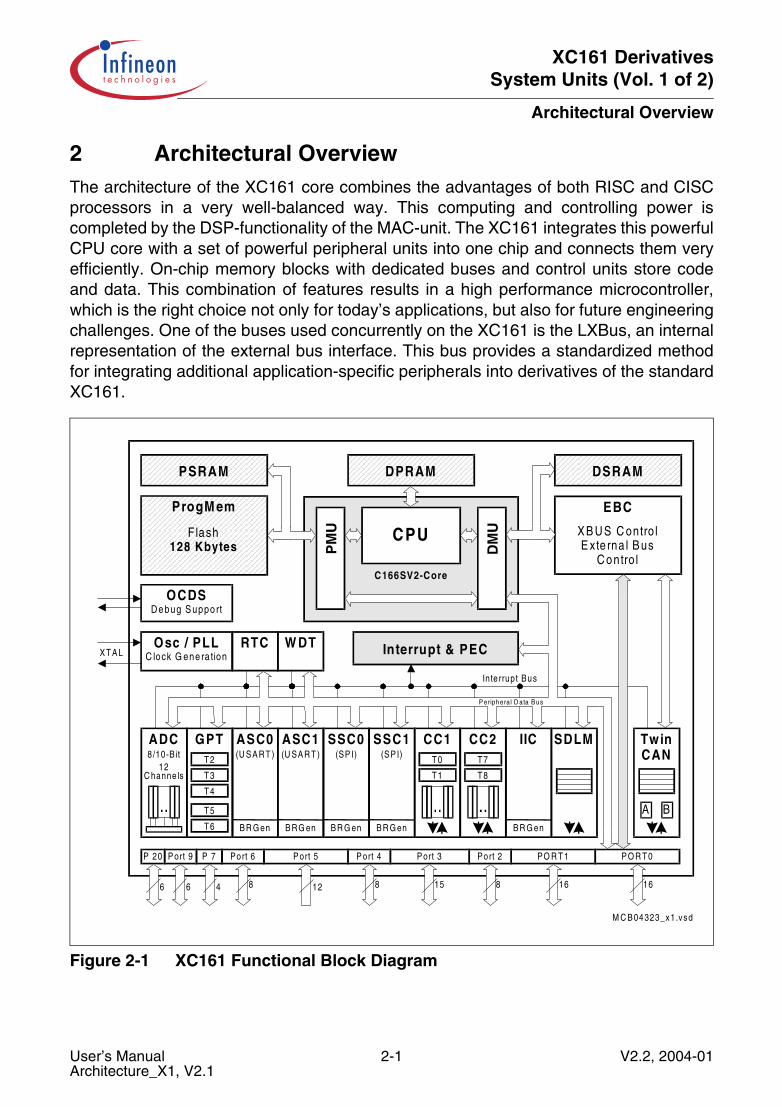
2 Architectural OverviewThe architecture of the XC161 core combines the advantages of both RISC and CISCprocessors in a very well-balanced way. This computing and controlling power iscompleted by the DSP-functionality of the MAC-unit. The XC161 integrates this powerfulCPU core with a set of powerful peripheral units into one chip and connects them veryefficiently. On-chip memory blocks with dedicated buses and control units store codeand data. This combination of features results in a high performance microcontroller,which is the right choice not only for today’s applications, but also for future engineeringchallenges. One of the buses used concurrently on the XC161 is the LXBus, an internalrepresentation of the external bus interface. This bus provides a standardized methodfor integrating additional application-specific peripherals into derivatives of the standardXC161.
Figure 2-1 XC161 Functional Block Diagram
In te rrupt Bus
XTAL
M C B 04323_x1.vsd
Osc / PLLC lock G ene ra tion
RTC W DT
GPTT2
T3
T4
T5
T6
SSC0
B R G en
(SP I)ASC1
B R G en
(U SA R T)ADC8 /10-B it
12C hanne ls
CC2T7
T8
EBC
X B U S C ontro lE xte rna l B us
C ontro l
ProgM em
Flash128 Kbytes
P 20
4 12
P ort 5
16
PSRAM DPRAM DSRAM
C166SV2-Core
PM
U
DM
UCPU
ASC0
B R G en
(U S A R T )IIC
B R G en
SSC1
B R G en
(S P I)CC1
T0
T1
TwinCAN
A B
PO R T1
SDLM
P O R T0Port 2P ort 3P ort 4Port 6P 7P ort 9
168158866
Interrupt & PEC
P eriph era l D ata B us
OCDSD e bug S uppo rt
User’s Manual 2-1 V2.2, 2004-01Architecture_X1, V2.1

XC161 DerivativesSystem Units (Vol. 1 of 2)
Architectural Overview
2.1 Basic CPU Concepts and Optimizations
The main core of the CPU consists of a set of optimized functional units including theinstruction fetch/processing pipelines, a 16-bit Arithmetic and Logic Unit (ALU), a 40-bitMultiply and Accumulate Unit (MAC), an Address and Data Unit (ADU), an InstructionFetch Unit (IFU), a Register File (RF), and dedicated Special Function Registers (SFRs).
Single clock cycle execution of instructions results in superior CPU performance, whilemaintaining C166 code compatibility. Impressive DSP performance, concurrent accessto different kinds of memories and peripherals boost the overall system performance.
Figure 2-2 CPU Block Diagram
DPRAM
CPU
IPIP
RF
R 0R 1
G P R s
R 14R 15
R 0R 1
G P R s
R 14R 15
IFU
Injection/Exception
Handler
ADU
MAC
m ca04917_x.vsd
C P U C O N 1
C P U C O N 2
C S P IP
R etu rnS tackF IFO
B ranchU n it
P refetchU n it
V E C S E G
TFR
+/-
ID X 0
ID X 1Q X 0
Q X 1
Q R 0
Q R 1
D P P 0
D P P 1D P P 2
D P P 3
S P S E G
S PS TK O V
S TK U N
+ /-
M R W
M C W
M S W
M A L
+/-
M A H
M ultip lyU n it
ALU
D iv is ion U n it
M u ltip ly U n it
B it-M ask-G en .
Barre l-Sh ifte r
+ /-
M D C
P S W
M D H
ZE R O S
M D L
O N E S
R 0R 1
G P R s
R 14R 15
C P
W B
B uffer
2-S tagePrefe tch
P ipe line
5-S tagePipe line
R 0R 1
G PR s
R 14R 15
PMU
DMU
DSRAMEBC
Peripherals
PSRAMFlash/ROM
User’s Manual 2-2 V2.2, 2004-01Architecture_X1, V2.1

XC161 DerivativesSystem Units (Vol. 1 of 2)
Architectural Overview
Summary of CPU Features
• Opcode fully upward compatible with C166 Family• 2-stage instruction fetch pipeline with FIFO for instruction pre-fetching• 5-stage instruction execution pipeline• Pipeline forwarding controls data dependencies in hardware• Multiple high bandwidth buses for data and instructions• Linear address space for code and data (von Neumann architecture)• Nearly all instructions executed in one CPU clock cycle • Fast multiplication (16-bit × 16-bit) in one CPU clock cycle• Fast background execution of division (32-bit/16-bit) in 21 CPU clock cycles• Built-in advanced MAC (Multiply Accumulate) Unit:
– Single cycle MAC instruction with zero cycle latency including a 16 × 16 multiplier– 40-bit barrel shifter and 40-bit accumulator to handle overflows– Automatic saturation to 32 bits or rounding included with the MAC instruction– Fractional numbers supported directly– One Finite Impulse Response Filter (FIR) tap per cycle with no circular buffer
management• Enhanced boolean bit manipulation facilities• High performance branch-, call-, and loop-processing• Zero cycle jump execution• Register-based design with multiple variable register banks (byte or word operands)• Two additional fast register banks• Variable stack with automatic stack overflow/underflow detection• “Fast interrupt” and “Fast context switch” features
The high performance and flexibility of the CPU is achieved by a number of optimizedfunctional blocks (see Figure 2-2). Optimizations of the functional blocks are describedin detail in the following sections.
User’s Manual 2-3 V2.2, 2004-01Architecture_X1, V2.1

XC161 DerivativesSystem Units (Vol. 1 of 2)
Architectural Overview
2.1.1 High Instruction Bandwidth/Fast Execution
Based on the hardware provisions, most of the XC161’s instructions can be executed injust one clock cycle (1/fCPU). This includes arithmetic instructions, logic instructions, andmove instructions with most addressing modes.
Special instructions such as SRST or PWRDN take more than one machine cycle. Divideinstructions are mainly executed in the background, so other instructions can beexecuted in parallel. Due to the prediction mechanism (see Section 4.2), correctlypredicted branch instructions require only one cycle or can even be overlaid with anotherinstruction (zero-cycle jump).
The instruction cycle time is dramatically reduced through the use of instructionpipelining. This technique allows the core CPU to process portions of multiple sequentialinstruction stages in parallel. Up to seven stages can operate in parallel:
The two-stage instruction fetch pipeline fetches and preprocesses instructions fromthe respective program memory:
PREFETCH: Instructions are prefetched from the PMU in the predicted order. Theinstructions are preprocessed in the branch detection unit to detect branches. Theprediction logic determines if branches are assumed to be taken or not.
FETCH: The instruction pointer for the next instruction to be fetched is calculatedaccording to the branch prediction rules. The branch folding unit preprocesses detectedbranches and combines them with the preceding instructions to enable zero-cyclebranch execution. Prefetched instructions are stored in the instruction FIFO, while storedinstructions are moved from the instruction FIFO to the instruction processing pipeline.
The five-stage instruction processing pipeline executes the respective instructions:
DECODE: The previously fetched instruction is decoded and the GPR used for indirectaddressing is read from the register file, if required.
ADDRESS: All operand addresses are calculated. For instructions implicitly accessingthe stack the stack pointer (SP) is decremented or incremented.
MEMORY: All required operands are fetched.
EXECUTE: The specified operation (ALU or MAC) is performed on the previouslyfetched operands. The condition flags are updated. Explicit write operations to CPU-SFRs are executed. GPRs used for indirect addressing are incremented ordecremented, if required.
WRITE BACK: The result operands are written to the specified locations. Operandslocated in the DPRAM are stored via the write-back buffer.
User’s Manual 2-4 V2.2, 2004-01Architecture_X1, V2.1

XC161 DerivativesSystem Units (Vol. 1 of 2)
Architectural Overview
2.1.2 Powerful Execution Units
The 16-bit Arithmetic and Logic Unit (ALU) performs all standard (word) arithmeticand logical operations. Additionally, for byte operations, signals are provided from bits 6and 7 of the ALU result to set the condition flags correctly. Multiple precision arithmeticis provided through a ‘CARRY-IN’ signal to the ALU from previously calculated portionsof the desired operation.
Most internal execution blocks have been optimized to perform operations on either 8-bitor 16-bit quantities. Instructions have been provided as well to allow byte packing inmemory while providing sign extension of bytes for word wide arithmetic operations. Theinternal bus structure also allows transfers of bytes or words to or from peripherals basedon the peripheral requirements.
A set of consistent flags is updated automatically in the PSW after each arithmetic,logical, shift, or movement operation. These flags allow branching on specific conditions.Support for both signed and unsigned arithmetic is provided through user-specifiablebranch tests. These flags are also preserved automatically by the CPU upon entry intoan interrupt or trap routine.
A 16-bit barrel shifter provides multiple bit shifts in a single cycle. Rotates and arithmeticshifts are also supported.
The Multiply and Accumulate Unit (MAC) performs extended arithmetic operationssuch as 32-bit addition, 32-bit subtraction, and single-cycle 16-bit × 16-bit multiplication.The combined MAC operations (multiplication with cumulative addition/subtraction)represent the major part of the DSP performance of the CPU.
The Address Data Unit (ADU) contains two independent arithmetic units to generate,calculate, and update addresses for data accesses. The ADU performs the followingmajor tasks:
• The Standard Address Unit supports linear arithmetic for the short, long, and indirectaddressing modes. It also supports data paging and stack handling.
• The DSP Address Generation Unit contains an additional set of address pointers andoffset registers which are used in conjunction with the CoXXX instructions only.
The CPU provides a lot of powerful addressing modes for word, byte, and bit dataaccesses (short, long, indirect). The different addressing modes use different formatsand have different scopes.
Dedicated bit processing instructions provide efficient control and testing of peripheralswhile enhancing data manipulation. These instructions provide direct access to twooperands in the bit-addressable space without requiring them to be moved intotemporary flags. Logical instructions allow the user to compare and modify a control bitfor a peripheral in one instruction. Multiple bit shift instructions (single cycle execution)avoid long instruction streams of single bit shift operations. Bitfield instructions allow themodification of multiple bits from one operand in a single instruction.
User’s Manual 2-5 V2.2, 2004-01Architecture_X1, V2.1
XC161 DerivativesSystem Units (Vol. 1 of 2)
Architectural Overview
2.1.3 High Performance Branch-, Call-, and Loop-Processing
Pipelined execution delivers maximum performance with a stream of subsequentinstructions. Any disruption requires the pipeline to be refilled and the new instruction tostep through the pipeline stages. Due to the high percentage of branching in controllerapplications, branch instructions have been optimized to require pipeline refilling only inspecial cases. This is realized by detecting and preprocessing branch instructions in theprefetch stage and by predicting the respective branch target address.
Prefetching then continues from the predicted target address. If the prediction wascorrect subsequent instructions can be fed to the execution pipeline without a gap, evenif a branch is executed, i.e. the code execution is not linear. Branch target prediction (seealso Section 4.2.1) uses the following rules:
• Unconditional branches: Branch prediction is trivial in this case, as the brancheswill always be taken and the target address is defined. This applies to implicitlyunconditional branches such as JMPS, CALLR, or RET as well as to branches withcondition code “unconditional” such as JMPI cc_UC.
• Fixed prediction: Branch instructions which are often used to realize loops areassumed to be taken if they branch backward to a previous location (the begin of theloop). This applies to conditional branches such as JMPR cc_XX or JNB.
• Variable prediction: In this case the respective prediction (taken or not taken) iscoded into the instruction and can, therefore, be selected for each individual branchinstruction. Thus, the software designer can optimize the instruction flow to thespecific code to be executed1). This applies to the branch instructions JMPA andCALLA.
• Conditional indirect branches: These branches are always assumed to be nottaken. This applies to branch instructions JMPI cc_XX, [Rw] and CALLI cc_XX, [Rw].
The system state information is saved automatically on the internal system stack, thusavoiding the use of instructions to preserve state upon entry and exit of interrupt or traproutines. Call instructions push the value of the IP on the system stack, and require thesame execution time as branch instructions. Additionally, instructions have beenprovided to support indirect branch and call instructions. This feature supportsimplementation of multiple CASE statement branching in assembler macros and highlevel languages.
1) The programming tools accept either dedicated mnemonics for each prediction leaving the choice up toprogrammer, or they accept generic mnemonics and apply their own prediction rules.
User’s Manual 2-6 V2.2, 2004-01Architecture_X1, V2.1

XC161 DerivativesSystem Units (Vol. 1 of 2)
Architectural Overview
2.1.4 Consistent and Optimized Instruction Formats
To obtain optimum performance in a pipelined design, an instruction set has beendesigned which incorporates concepts from Reduced Instruction Set Computing (RISC).These concepts primarily allow fast decoding of the instructions and operands whilereducing pipeline holds. These concepts, however, do not preclude the use of complexinstructions required by microcontroller users. The instruction set was designed to meetthe following goals:
• Provide powerful instructions for frequently-performed operations which traditionallyhave required sequences of instructions. Avoid transfer into and out of temporaryregisters such as accumulators and carry bits. Perform tasks in parallel such assaving state upon entry into interrupt routines or subroutines.
• Avoid complex encoding schemes by placing operands in consistent fields for eachinstruction and avoid complex addressing modes which are not frequently used.Consequently, the instruction decode time decreases and the development ofcompilers and assemblers is simplified.
• Provide most frequently used instructions with one-word instruction formats. All otherinstructions use two-word formats. This allows all instructions to be placed on wordboundaries: this alleviates the need for complex alignment hardware. It also has thebenefit of increasing the range for relative branching instructions.
The high performance of the CPU-hardware can be utilized efficiently by a programmerby means of the highly functional XC161 instruction set which includes the followinginstruction classes:
• Arithmetic Instructions• DSP Instructions• Logical Instructions• Boolean Bit Manipulation Instructions• Compare and Loop Control Instructions• Shift and Rotate Instructions• Prioritize Instruction• Data Movement Instructions• System Stack Instructions• Jump and Call Instructions• Return Instructions• System Control Instructions• Miscellaneous Instructions
Possible operand types are bits, bytes, words, and doublewords. Specific instructionssupport the conversion (extension) of bytes to words. Various direct, indirect, andimmediate addressing modes are provided to specify the required operands.
User’s Manual 2-7 V2.2, 2004-01Architecture_X1, V2.1
XC161 DerivativesSystem Units (Vol. 1 of 2)
Architectural Overview
2.1.5 Programmable Multiple Priority Interrupt System
The XC161 provides 80 separate interrupt nodes that may be assigned to 16 prioritylevels with 8 group priorities on each level. Most interrupt sources are connected to adedicated interrupt node. In some cases, multi-source interrupt nodes are incorporatedfor efficient use of system resources. These nodes can be activated by several sourcerequests and are controlled via interrupt subnode control registers.
The following enhancements within the XC161 allow processing of a large number ofinterrupt sources:
• Peripheral Event Controller (PEC): This processor is used to off-load many interruptrequests from the CPU. It avoids the overhead of entering and exiting interrupt or traproutines by performing single-cycle interrupt-driven byte or word data transfersbetween any two locations with an optional increment of the PEC source pointer, thedestination pointer, or both. Only one cycle is ‘stolen’ from the current CPU activity toperform a PEC service.
• Multiple Priority Interrupt Controller: This controller allows all interrupts to beassigned any specified priority. Interrupts may also be grouped, which enables theuser to prevent similar priority tasks from interrupting each other. For each of theinterrupt nodes, there is a separate control register which contains an interruptrequest flag, an interrupt enable flag, and an interrupt priority bitfield. After beingaccepted by the CPU, an interrupt service can be interrupted only by a higherprioritized service request. For standard interrupt processing, each of the interruptnodes has a dedicated vector location.
• Multiple Register Banks: Two local register banks for immediate context switchingadd to a relocatable global register bank. The user can specify several register bankslocated anywhere in the internal DPRAM and made of up to sixteen general purposeregisters. A single instruction switches from one register bank to another (switchingbanks flushes the pipeline, changing the global bank requires a validation sequence).
The XC161 is capable of reacting very quickly to non-deterministic events because itsinterrupt response time is within a very narrow range of typically 13 clock cycles (in thecase of internal program execution). Its fast external interrupt inputs are sampled everyclock cycle and allow even very short external signals to be recognized.
The XC161 also provides an excellent mechanism to identify and process exceptions orerror conditions that arise during run-time, so called ‘Hardware Traps’. A hardware trapcauses an immediate non-maskable system reaction which is similar to a standardinterrupt service (branching to a dedicated vector table location). The occurrence of ahardware trap is additionally signified by an individual bit in the trap flag register (TFR).Unless another, higher prioritized, trap service is in progress, a hardware trap willinterrupt any current program execution. In turn, a hardware trap service can normallynot be interrupted by a standard or PEC interrupt.
Software interrupts are supported by means of the ‘TRAP’ instruction in combination withan individual trap (interrupt) number.
User’s Manual 2-8 V2.2, 2004-01Architecture_X1, V2.1
XC161 DerivativesSystem Units (Vol. 1 of 2)
Architectural Overview
2.1.6 Interfaces to System Resources
The CPU of the XC161 interfaces to the system resources via several bus systemswhich contribute to the overall performance by transferring data concurrently. Thisavoids stalling the CPU because instructions or operands need to be transferred.
The Dual Port RAM (DPRAM) is directly coupled to the CPU because it houses theglobal register banks. Transfers from/to these locations affect the performance and are,therefore, carefully optimized.
The Program Management Unit (PMU) controls accesses to the on-chip programmemory blocks such as the ROM/Flash module and the Program/Data RAM (PSRAM)and also fetches instructions from external memory.
The 64-bit interface between the PMU and the CPU delivers the instruction words, whichare requested by the CPU. The PMU decides whether the requested instruction wordhas to be fetched from on-chip memory or from external memory.
The Data Management Unit (DMU) controls accesses to the on-chip Data RAM(DSRAM), to the on-chip peripherals connected to the peripheral bus, and to resourceson the external bus. External accesses (including accesses to peripherals connected tothe on-chip LXBus) are executed by the External Bus Controller (EBC).
The 16-bit interface between the DMU and the CPU handles all data transfers(operands). Data accesses by the CPU are distributed to the appropriate busesaccording to the defined address map.
PMU and DMU are directly coupled to perform cross-over transfers with high speed.Crossover transfers are executed in both directions:
• PMU via DMU: Code fetches from external locations are redirected via the DMU toEBC. Thus, the XC161 can execute code from external resources. No code can befetched from the Data RAM (DSRAM).
• DMU via PMU: Data accesses can also be executed to on-chip resources controlledby the PMU. This includes the following types of transfers:– Read a constant from the on-chip program ROM/Flash– Read data from the on-chip PSRAM– Write data to the on-chip PSRAM (required prior to executing out of it)– Program/Erase the on-chip Flash memory
User’s Manual 2-9 V2.2, 2004-01Architecture_X1, V2.1
XC161 DerivativesSystem Units (Vol. 1 of 2)
Architectural Overview
2.2 On-Chip System Resources
The XC161 controllers provide a number of powerful system resources designed aroundthe CPU. The combination of CPU and these resources results in the high performanceof the members of this controller family.
Peripheral Event Controller (PEC) and Interrupt Control
The Peripheral Event Controller enables response to an interrupt request with a singledata transfer (word or byte) which consumes only one instruction cycle and does notrequire saving and restoring the machine status. Each interrupt source is prioritized forevery machine cycle in the interrupt control block. If PEC service is selected, a PECtransfer is started. If CPU interrupt service is requested, the current CPU priority levelstored in the PSW register is tested to determine whether a higher priority interrupt iscurrently being serviced. When an interrupt is acknowledged, the current state of themachine is saved on the internal system stack and the CPU branches to the systemspecific vector for the peripheral.
The PEC contains a set of SFRs which store the count value and control bits for eightdata transfer channels. In addition, the PEC uses a dedicated area of RAM whichcontains the source and destination addresses. The PEC is controlled in a mannersimilar to any other peripheral: through SFRs containing the desired configuration ofeach channel.
An individual PEC transfer counter is implicitly decremented for each PEC serviceexcept in the continuous transfer mode. When this counter reaches zero, a standardinterrupt is performed to the vector location related to the corresponding source. PECservices are very well suited, for example, to moving register contents to/from a memorytable. The XC161 has eight PEC channels, each of which offers such fast interrupt-driven data transfer capabilities.
Memory Areas
The memory space of the XC161 is configured in a Von Neumann architecture. Thismeans that code memory, data memory, registers, and IO ports are organized within thesame linear address space which covers up to 16 Mbytes. The entire memory space canbe accessed bytewise or wordwise. Particular portions of the on-chip memory have beenmade directly bit addressable as well.
128 Kbytes of on-chip Flash memory store code or constant data. The on-chip Flashmemory is organized as four 8-Kbyte sectors, one 32-Kbyte sector, and one 64-Kbytesector. Each sector can be separately write protected1), erased and programmed (inblocks of 128 bytes). The complete Flash area can be read-protected. A passwordsequence temporarily unlocks protected areas. The Flash module combines very fast
1) Each two 8-Kbyte sectors are combined for write-protection purposes.
User’s Manual 2-10 V2.2, 2004-01Architecture_X1, V2.1
XC161 DerivativesSystem Units (Vol. 1 of 2)
Architectural Overview
64-bit one-cycle1) read accesses with protected and efficient writing algorithms forprogramming and erasing. Dynamic error correction provides extremely high read datasecurity for all read accesses.Programming typically takes 2 ms per 128-byte block (5 ms max.), erasing a sectortypically takes 200 ms (500 ms max.).
Note: Program execution from on-chip program memory is the fastest of all possiblealternatives and results in maximum performance. The type of the on-chipprogram memory depends on the chosen derivative. On-chip program memoryalso includes the PSRAM.
2 Kbytes of on-chip Program SRAM (PSRAM) are provided to store user code or data.The PSRAM is accessed via the PMU and is therefore optimized for code fetches.
4 Kbytes of on-chip Data SRAM (DSRAM) are provided as a storage for general userdata.The DSRAM is accessed via the DMU and is therefore optimized for data accesses.
2 Kbytes of on-chip Dual-Port RAM (DPRAM) are provided as a storage for userdefined variables, for the system stack, and in particular for general purpose registerbanks. A register bank can consist of up to 16 wordwide (R0 to R15) and/or bytewide(RL0, RH0, …, RL7, RH7) so-called General Purpose Registers (GPRs).The upper 256 bytes of the DPRAM are directly bitaddressable. When used by a GPR,any location in the DPRAM is bitaddressable.
The CPU has an actual register context of up to 16 wordwide and/or bytewide globalGPRs at its disposal, which are physically located within the on-chip RAM area. AContext Pointer (CP) register determines the base address of the active global registerbank to be accessed by the CPU at a time. The number of register banks is restrictedonly by the available internal RAM space. For easy parameter passing, a register bankmay overlap other register banks.
A system stack of up to 32 Kwords is provided as storage for temporary data. The systemstack can be located anywhere within the complete addressing range and it is accessedby the CPU via the Stack Pointer (SP) register and the Stack Pointer Segment (SPSEG)register. Two separate SFRs, STKOV and STKUN, are implicitly compared against thestack pointer value upon each stack access for the detection of a stack overflow orunderflow. This mechanism also supports the control of a bigger virtual stack. Maximumperformance for stack operations is achieved by allocating the system stack to internaldata RAM areas (DPRAM, DSRAM).
Hardware detection of the selected memory space is placed at the internal memorydecoders and allows the user to specify any address directly or indirectly and obtain thedesired data without using temporary registers or special instructions.
1) Flash accesses may require waitstates, depending on the actual operating frequency. For the exact Flashmemory access timing and the required waitstates please refer to Section 3.10.2.
User’s Manual 2-11 V2.2, 2004-01Architecture_X1, V2.1

XC161 DerivativesSystem Units (Vol. 1 of 2)
Architectural Overview
For Special Function Registers three areas of the address space are reserved: Thestandard Special Function Register area (SFR) uses 512 bytes, while the ExtendedSpecial Function Register area (ESFR) uses the other 512 bytes. A range of 4 Kbytes isprovided for the internal IO area (XSFR). SFRs are wordwide registers which are usedfor controlling and monitoring functions of the different on-chip units. Unused SFRaddresses are reserved for future members of the XC166 Family with enhancedfunctionality. Therefore, they should either not be accessed, or written with zeros, toensure upward compatibility.
In order to meet the needs of designs where more memory is required than is providedon chip, up to 12 Mbytes (approximately, see Table 2-1) of external RAM and/or ROMcan be connected to the microcontroller. The External Bus Interface also providesaccess to external peripherals.
Table 2-1 XC161 Memory Map1)
1) Accesses to the shaded areas generate external bus accesses.
Address Area Start Loc. End Loc. Area Size2)
2) The areas marked with “<” are slightly smaller than indicated, see column “Notes”.
Notes
Flash register space FF’F000H FF’FFFFH 4 Kbytes 3)
3) Not defined register locations return a trap code.
Reserved (Acc. trap) F8’0000H FF’EFFFH < 0.5 Mbytes Minus Flash regs
Reserved for PSRAM E0’0800H F7’FFFFH < 1.5 Mbytes Minus PSRAM
Program SRAM E0’0000H E0’07FFH 2 Kbytes Maximum
Reserved for pr. mem. C2’0000H DF’FFFFH < 2 Mbytes Minus Flash
Program Flash C0’0000H C1’FFFFH 128 Kbytes –
Reserved BF’0000H BF’FFFFH 64 Kbytes –
External memory area 40’0000H BE’FFFFH < 8 Mbytes Minus res. seg.
External IO area4)
4) Several pipeline optimizations are not active within the external IO area. This is necessary to control externalperipherals properly.
20’0800H 3F’FFFFH < 2 Mbytes Minus TwinCAN
TwinCAN registers 20’0000H 20’07FFH 2 Kbytes –
External memory area 01’0000H 1F’FFFFH < 2 Mbytes Minus segment 0
Data RAMs and SFRs 00’8000H 00’FFFFH 32 Kbytes Partly used
External memory area 00’0000H 00’7FFFH 32 Kbytes –
User’s Manual 2-12 V2.2, 2004-01Architecture_X1, V2.1

XC161 DerivativesSystem Units (Vol. 1 of 2)
Architectural Overview
External Bus Interface
To meet the needs of designs where more memory is required than is provided on chip,up to 12 Mbytes of external RAM and/or ROM can be connected to the XC161microcontroller via its external bus interface.
All of the external memory accesses are performed by a particular on-chip External BusController (EBC). It can be programmed either to Single Chip Mode when no externalmemory is required, or to one of four different external memory access modes1), whichare as follows:
• 16 … 24-bit Addresses, 16-bit Data, Demultiplexed• 16 … 24-bit Addresses, 16-bit Data, Multiplexed• 16 … 24-bit Addresses, 8-bit Data, Multiplexed• 16 … 24-bit Addresses, 8-bit Data, Demultiplexed
In the demultiplexed bus modes, addresses are output on PORT1 and data isinput/output on PORT0 or P0L, respectively. In the multiplexed bus modes bothaddresses and data use PORT0 for input/output. The high order address (segment) linesuse Port 4. The number of active segment address lines is selectable, restricting theexternal address space to 8 Mbytes … 64 Kbytes. This is required when interface linesare assigned to Port 4.
For up to five address areas the bus mode (multiplexed/demultiplexed), the data buswidth (8-bit/16-bit) and even the length of a bus cycle (waitstates, signal delays) can beselected independently. This allows access to a variety of memory and peripheralcomponents directly and with maximum efficiency.
Access to very slow memories or modules with varying access times is supported via aparticular ‘Ready’ function. The active level of the control input signal is selectable.
A HOLD/HLDA protocol is available for bus arbitration and allows the sharing of externalresources with other bus masters.
The external bus timing is related to the rising edge of the reference clock outputCLKOUT. The external bus protocol is compatible with that of the standard C166 Family.
For applications which require less than 64 Kbytes of address space, a non-segmentedmemory model can be selected, where all locations can be addressed by 16 bits. Thus,Port 4 is not needed as an output for the upper address bits (Axx … A16), as is the casewhen using the segmented memory model.
The EBC also controls accesses to resources connected to the on-chip LXBus. TheLXBus is an internal representation of the external bus and allows accessing integratedperipherals and modules in the same way as external components.
The TwinCAN module is connected and accessed via the LXBus.
1) Bus modes are switched dynamically if several address windows with different mode settings are used.
User’s Manual 2-13 V2.2, 2004-01Architecture_X1, V2.1
XC161 DerivativesSystem Units (Vol. 1 of 2)
Architectural Overview
2.3 On-Chip Peripheral Blocks
The XC166 Family clearly separates peripherals from the core. This structure permitsthe maximum number of operations to be performed in parallel and allows peripherals tobe added or deleted from family members without modifications to the core. Eachfunctional block processes data independently and communicates information overcommon buses. Peripherals are controlled by data written to the respective SpecialFunction Registers (SFRs). These SFRs are located within either the standard SFR area(00’FE00H … 00’FFFFH), the extended ESFR area (00’F000H … 00’F1FFH), or within theinternal IO area (00’E000H … 00’EFFFH).
These built-in peripherals either allow the CPU to interface with the external world orprovide functions on-chip that otherwise would need to be added externally in therespective system.
The XC161 generic peripherals are:
• Two General Purpose Timer Blocks (GPT1 and GPT2)• Two Asynchronous/Synchronous Serial Interfaces (ASC0 and ASC1)• Two High Speed Serial Interfaces (SSC0 and SSC1)• Serial Data Link Module (SDLM), optional• IIC Bus Module• A Watchdog Timer• Two Capture/Compare units (CAPCOM1 and CAPCOM2)• A 10-bit Analog/Digital Converter (ADC)• A Real Time Clock (RTC)• Ten I/O ports with a total of 103 I/O lines
Because the LXBus is the internal representation of the external bus, it does not supportbit-addressing. Accesses are executed by the EBC as if it were external accesses. TheLXBus connects on-chip peripherals to the CPU:
• TwinCAN module with 2 CAN nodes and gateway functionality
Each peripheral also contains a set of Special Function Registers (SFRs) which controlthe functionality of the peripheral and temporarily store intermediate data results. Eachperipheral has an associated set of status flags. Individually selected clock signals aregenerated for each peripheral from binary multiples of the master clock.
User’s Manual 2-14 V2.2, 2004-01Architecture_X1, V2.1

XC161 DerivativesSystem Units (Vol. 1 of 2)
Architectural Overview
Peripheral Interfaces
The on-chip peripherals generally have two different types of interfaces: an interface tothe CPU and an interface to external hardware. Communication between the CPU andperipherals is performed through Special Function Registers (SFRs) and interrupts. TheSFRs serve as control/status and data registers for the peripherals. Interrupt requestsare generated by the peripherals based on specific events which occur during theiroperation, such as operation complete, error, etc.
To interface with external hardware, specific pins of the parallel ports are used, when aninput or output function has been selected for a peripheral. During this time, the port pinsare controlled either by the peripheral (when used as outputs) or by the externalhardware which controls the peripheral (when used as inputs). This is called the‘alternate (input or output) function’ of a port pin, in contrast to its function as a generalpurpose I/O pin.
Peripheral Timing
Internal operation of the CPU and peripherals is based on the master clock (fMC). Theclock generation unit uses the on-chip oscillator to derive the master clock from thecrystal or from the external clock signal. The clock signal gated to the peripherals isindependent from the clock signal that feeds the CPU. During Idle mode, the CPU’s clockis stopped while the peripherals continue their operation. Peripheral SFRs may beaccessed by the CPU once per state. When an SFR is written to by software in the samestate where it is also to be modified by the peripheral, the software write operation haspriority. Further details on peripheral timing are included in the specific sectionsdescribing each peripheral.
Programming Hints
• Access to SFRs: All SFRs reside in data page 3 of the memory space. The followingaddressing mechanisms allow access to the SFRs:– Indirect or direct addressing with 16-bit (mem) addresses must guarantee that
the used data page pointer (DPP0 … DPP3) selects data page 3.– Accesses via the Peripheral Event Controller (PEC) use the SRCPx and DSTPx
pointers instead of the data page pointers.– Short 8-bit (reg) addresses to the standard SFR area do not use the data page
pointers but directly access the registers within this 512-byte area.– Short 8-bit (reg) addresses to the extended ESFR area require switching to the
512-byte Extended SFR area. This is done via the EXTension instructions EXTR,EXTP(R), EXTS(R).
User’s Manual 2-15 V2.2, 2004-01Architecture_X1, V2.1
XC161 DerivativesSystem Units (Vol. 1 of 2)
Architectural Overview
• Byte Write Operations to wordwide SFRs via indirect or direct 16-bit (mem)addressing or byte transfers via the PEC force zeros in the non-addressed byte. Bytewrite operations via short 8-bit (reg) addressing can access only the low byte of anSFR and force zeros in the high byte. It is therefore recommended, to use the bit fieldinstructions (BFLDL and BFLDH) to write to any number of bits in either byte of anSFR without disturbing the non-addressed byte and the unselected bits.
• Reserved Bits: Some of the bits which are contained in the XC161’s SFRs aremarked as ‘Reserved’. User software should never write ‘1’s to reserved bits. Thesebits are currently not implemented and may be used in future products to invoke newfunctions. In that case, the active state for those new functions will be ‘1’, and theinactive state will be ‘0’. Therefore writing only ‘0’s to reserved locations allowsportability of the current software to future devices. After read accesses, reserved bitsshould be ignored or masked out.
Capture/Compare Units (CAPCOM1/2)
The CAPCOM units support generation and control of timing sequences on up to32 channels with a maximum resolution of 1 system clock cycle (8 cycles in staggeredmode). The CAPCOM units are typically used to handle high speed I/O tasks such aspulse and waveform generation, pulse width modulation (PMW), Digital to Analog (D/A)conversion, software timing, or time recording relative to external events.
Four 16-bit timers (T0/T1, T7/T8) with reload registers provide two independent timebases for each capture/compare register array.
The input clock for the timers is programmable to several prescaled values of the internalsystem clock, or may be derived from an overflow/underflow of timer T6 in module GPT2.This provides a wide range of variation for the timer period and resolution and allowsprecise adjustments to the application specific requirements. In addition, external countinputs for CAPCOM timers T0 and T7 allow event scheduling for the capture/compareregisters relative to external events.
Both of the two capture/compare register arrays contain 16 dual purposecapture/compare registers, each of which may be individually allocated to eitherCAPCOM timer T0 or T1 (T7 or T8, respectively), and programmed for capture orcompare function.All registers of each module have each one port pin associated with it which serves asan input pin for triggering the capture function, or as an output pin to indicate theoccurrence of a compare event.
User’s Manual 2-16 V2.2, 2004-01Architecture_X1, V2.1
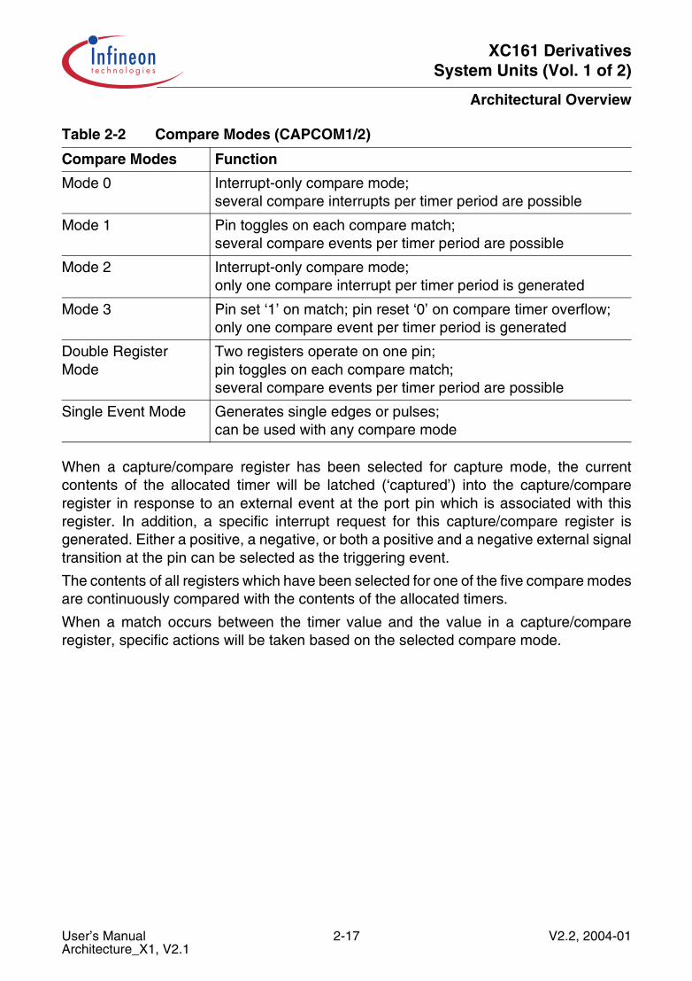
XC161 DerivativesSystem Units (Vol. 1 of 2)
Architectural Overview
When a capture/compare register has been selected for capture mode, the currentcontents of the allocated timer will be latched (‘captured’) into the capture/compareregister in response to an external event at the port pin which is associated with thisregister. In addition, a specific interrupt request for this capture/compare register isgenerated. Either a positive, a negative, or both a positive and a negative external signaltransition at the pin can be selected as the triggering event.
The contents of all registers which have been selected for one of the five compare modesare continuously compared with the contents of the allocated timers.
When a match occurs between the timer value and the value in a capture/compareregister, specific actions will be taken based on the selected compare mode.
Table 2-2 Compare Modes (CAPCOM1/2)
Compare Modes Function
Mode 0 Interrupt-only compare mode;several compare interrupts per timer period are possible
Mode 1 Pin toggles on each compare match;several compare events per timer period are possible
Mode 2 Interrupt-only compare mode;only one compare interrupt per timer period is generated
Mode 3 Pin set ‘1’ on match; pin reset ‘0’ on compare timer overflow;only one compare event per timer period is generated
Double Register Mode
Two registers operate on one pin;pin toggles on each compare match;several compare events per timer period are possible
Single Event Mode Generates single edges or pulses;can be used with any compare mode
User’s Manual 2-17 V2.2, 2004-01Architecture_X1, V2.1
XC161 DerivativesSystem Units (Vol. 1 of 2)
Architectural Overview
General Purpose Timer (GPT12E) Unit
The GPT12E unit represents a very flexible multifunctional timer/counter structure whichmay be used for many different time related tasks such as event timing and counting,pulse width and duty cycle measurements, pulse generation, or pulse multiplication.
The GPT12E unit incorporates five 16-bit timers which are organized in two separateblocks, GPT1 and GPT2. Each timer in each block may operate independently in anumber of different modes, or may be concatenated with another timer of the sameblock.
Each of the three timers T2, T3, T4 of block GPT1 can be configured individually for oneof four basic modes of operation, which are Timer, Gated Timer, Counter, andIncremental Interface Mode. In Timer Mode, the input clock for a timer is derived fromthe system clock, divided by a programmable prescaler, while Counter Mode allows atimer to be clocked in reference to external events.Pulse width or duty cycle measurement is supported in Gated Timer Mode, where theoperation of a timer is controlled by the ‘gate’ level on an external input pin. For thesepurposes, each timer has one associated port pin (TxIN) which serves as gate or clockinput. The maximum resolution of the timers in block GPT1 is 4 system clock cycles.
The count direction (up/down) for each timer is programmable by software or mayadditionally be altered dynamically by an external signal on a port pin (TxEUD) tofacilitate e.g. position tracking.
In Incremental Interface Mode the GPT1 timers (T2, T3, T4) can be directly connectedto the incremental position sensor signals A and B via their respective inputs TxIN andTxEUD. Direction and count signals are internally derived from these two input signals,so the contents of the respective timer Tx corresponds to the sensor position. The thirdposition sensor signal TOP0 can be connected to an interrupt input.
Timer T3 has an output toggle latch (T3OTL) which changes its state on each timer over-flow/underflow. The state of this latch may be output on pin T3OUT e.g. for time outmonitoring of external hardware components. It may also be used internally to clocktimers T2 and T4 for measuring long time periods with high resolution.
In addition to their basic operating modes, timers T2 and T4 may be configured as reloador capture registers for timer T3. When used as capture or reload registers, timers T2and T4 are stopped. The contents of timer T3 is captured into T2 or T4 in response to asignal at their associated input pins (TxIN). Timer T3 is reloaded with the contents of T2or T4 triggered either by an external signal or by a selectable state transition of its togglelatch T3OTL. When both T2 and T4 are configured to alternately reload T3 on oppositestate transitions of T3OTL with the low and high times of a PWM signal, this signal canbe constantly generated without software intervention.
With its maximum resolution of 2 system clock cycles, the GPT2 block provides preciseevent control and time measurement. It includes two timers (T5, T6) and acapture/reload register (CAPREL). Both timers can be clocked with an input clock which
User’s Manual 2-18 V2.2, 2004-01Architecture_X1, V2.1
XC161 DerivativesSystem Units (Vol. 1 of 2)
Architectural Overview
is derived from the CPU clock via a programmable prescaler or with external signals. Thecount direction (up/down) for each timer is programmable by software or mayadditionally be altered dynamically by an external signal on a port pin (TxEUD)1).Concatenation of the timers is supported via the output toggle latch (T6OTL) of timer T6,which changes its state on each timer overflow/underflow.
The state of this latch may be used to clock timer T5, and/or it may be output on pinT6OUT. The overflows/underflows of timer T6 can additionally be used to clock theCAPCOM1/2 timers, and to cause a reload from the CAPREL register.
The CAPREL register may capture the contents of timer T5 based on an external signaltransition on the corresponding port pin (CAPIN), and timer T5 may optionally be clearedafter the capture procedure. This allows the XC161 to measure absolute time differencesor to perform pulse multiplication without software overhead.
The capture trigger (timer T5 to CAPREL) may also be generated upon transitions ofGPT1 timer T3’s inputs T3IN and/or T3EUD. This is especially advantageous when T3operates in Incremental Interface Mode.
1) If the respective derivative provides these pins.
User’s Manual 2-19 V2.2, 2004-01Architecture_X1, V2.1
XC161 DerivativesSystem Units (Vol. 1 of 2)
Architectural Overview
Real Time Clock
The Real Time Clock (RTC) module of the XC161 is directly clocked via a separate clockdriver either with the on-chip auxiliary oscillator frequency (fRTC = fOSCa) or with theprescaled on-chip main oscillator frequency (fRTC = fOSCm/32). It is therefore independentfrom the selected clock generation mode of the XC161.
The RTC basically consists of a chain of divider blocks:
• a selectable 8:1 divider (on - off)• the reloadable 16-bit timer T14• the 32-bit RTC timer block (accessible via registers RTCH and RTCL), made of:
– a reloadable 10-bit timer– a reloadable 6-bit timer– a reloadable 6-bit timer– a reloadable 10-bit timer
All timers count up. Each timer can generate an interrupt request. All requests arecombined to a common node request. Additionally, T14 can generate a separate noderequest.
Note: The registers associated with the RTC are not affected by a reset in order tomaintain the correct system time even when intermediate resets are executed.
The RTC module can be used for different purposes:
• System clock to determine the current time and date,optionally during idle mode, sleep mode, and power down mode
• Cyclic time based interrupt, to provide a system time tick independent of CPUfrequency and other resources, e.g. to wake-up regularly from idle mode
• 48-bit timer for long term measurements (maximum timespan is > 100 years)• Alarm interrupt for wake-up on a defined time
User’s Manual 2-20 V2.2, 2004-01Architecture_X1, V2.1

XC161 DerivativesSystem Units (Vol. 1 of 2)
Architectural Overview
A/D Converter
For analog signal measurement, a 10-bit A/D converter with 12 multiplexed inputchannels and a sample and hold circuit has been integrated on-chip. It uses the methodof successive approximation. The sample time (for loading the capacitors) and theconversion time is programmable (in two modes) and can thus be adjusted to theexternal circuitry. The A/D converter can also operate in 8-bit conversion mode, wherethe conversion time is further reduced.
Overrun error detection/protection is provided for the conversion result register(ADDAT): either an interrupt request will be generated when the result of a previousconversion has not been read from the result register at the time the next conversion iscomplete, or the next conversion is suspended in such a case until the previous resulthas been read.
For applications which require less analog input channels, the remaining channel inputscan be used as digital input port pins.
The A/D converter of the XC161 supports four different conversion modes. In thestandard Single Channel conversion mode, the analog level on a specified channel issampled once and converted to a digital result. In the Single Channel Continuous mode,the analog level on a specified channel is repeatedly sampled and converted withoutsoftware intervention. In the Auto Scan mode, the analog levels on a prespecifiednumber of channels are sequentially sampled and converted. In the Auto ScanContinuous mode, the prespecified channels are repeatedly sampled and converted. Inaddition, the conversion of a specific channel can be inserted (injected) into a runningsequence without disturbing this sequence. This is called Channel Injection Mode.
The Peripheral Event Controller (PEC) may be used to automatically store theconversion results into a table in memory for later evaluation, without requiring theoverhead of entering and exiting interrupt routines for each data transfer.
After each reset and also during normal operation the ADC automatically performscalibration cycles. This automatic self-calibration constantly adjusts the converter tochanging operating conditions (e.g. temperature) and compensates process variations.
These calibration cycles are part of the conversion cycle, so they do not affect the normaloperation of the A/D converter. The calibration cycles after a conversion can be disabled,so the overall conversion time is reduced again.
In order to decouple analog inputs from digital noise and to avoid input trigger noisethose pins used for analog input can be disconnected from the digital IO or input stagesunder software control. This can be selected for each pin separately via register P5DIDIS(Port 5 Digital Input Disable).
The Auto-Power-Down feature of the A/D converter minimizes the power consumptionwhen no conversion is in progress.
User’s Manual 2-21 V2.2, 2004-01Architecture_X1, V2.1
XC161 DerivativesSystem Units (Vol. 1 of 2)
Architectural Overview
Asynchronous/Synchronous Serial Interfaces (ASC0/ASC1)
The Asynchronous/Synchronous Serial Interfaces ASC0/ASC1 (USARTs) provide serialcommunication with other microcontrollers, processors, terminals or external peripheralcomponents. They are upward compatible with the serial ports of the Infineon 8-bitmicrocontroller families and support full-duplex asynchronous communication and half-duplex synchronous communication. A dedicated baud rate generator with a fractionaldivider precisely generates all standard baud rates without oscillator tuning.
In asynchronous mode, 8- or 9-bit data frames (with optional parity bit) are transmittedor received, preceded by a start bit and terminated by one or two stop bits. Formultiprocessor communication, a mechanism to distinguish address from data bytes hasbeen included (8-bit data plus wake-up bit mode). IrDA data transmissions up to115.2 kbit/s with fixed or programmable IrDA pulse width are supported. An autobauddetection unit allows to detect asynchronous data frames with its baudrate and modewith automatic initialization of the baudrate generator and the mode control bits.
In synchronous mode, bytes (8 bits) are transmitted or received synchronously to a shiftclock which is generated by the ASC0/1.
The LSB is always shifted first. In both modes, transmission and reception of data isFIFO-buffered (8 entries per direction). A loop-back option is available for testingpurposes. Five separate interrupt vectors are provided for transmit buffer, transmission,reception, autobaud detection, and error handling.
A number of optional hardware error detection capabilities has been included to increasethe reliability of data transfers. A parity bit can automatically be generated ontransmission or be checked on reception. Framing error detection allows to recognizedata frames with missing stop bits. An overrun error will be generated, if the lastcharacter received has not been read out of the receive buffer register at the time thereception of a new character is complete.
Summary of Features
• Full-duplex asynchronous operating modes– 8- or 9-bit data frames, LSB first, one or two stop bits, parity generation/checking– Baudrate from 2.5 Mbit/s to 0.6 bit/s (@ 40 MHz)– Multiprocessor mode for automatic address/data byte detection– Support for IrDA data transmission/reception up to max. 115.2 kbit/s (@ 40 MHz)– Loop-back capability– Auto baudrate detection
• Half-duplex 8-bit synchronous operating mode at 5 Mbit/s to 406.9 bit/s (@ 40 MHz)• Buffered transmitter/receiver with FIFO support (8 entries per direction)• Loop-back option available for testing purposes• Interrupt generation on transmitter buffer empty condition, last bit transmitted
condition, receive buffer full condition, error condition (frame, parity, overrun error),start and end of an autobaud detection
User’s Manual 2-22 V2.2, 2004-01Architecture_X1, V2.1
XC161 DerivativesSystem Units (Vol. 1 of 2)
Architectural Overview
High Speed Synchronous Serial Channels (SSC0/SSC1)
The High Speed Synchronous Serial Channels SSC0/SSC1 support full-duplex and half-duplex synchronous communication. They may be configured so they interface withserially linked peripheral components, full SPI functionality is supported.
A dedicated baud rate generator allows to set up all standard baud rates withoutoscillator tuning.
The SSC transmits or receives characters of 2 … 16 bits length synchronously to a shiftclock which can be generated by the SSC (master mode) or by an external master (slavemode). The SSC can start shifting with the LSB or with the MSB and allows the selectionof shifting and latching clock edges as well as the clock polarity.
A loop-back option is available for testing purposes.
Three separate interrupt vectors are provided for transmission, reception, and errorhandling.
A number of optional hardware error detection capabilities has been included to increasethe reliability of data transfers. Transmit error and receive error supervise the correcthandling of the data buffer. Phase error and baudrate error detect incorrect serial data.
Summary of Features
• Master or Slave mode operation• Full-duplex or Half-duplex transfers• Baudrate generation from 20 Mbit/s to 305.18 bit/s (@ 40 MHz)• Flexible data format
– Programmable number of data bits: 2 to 16 bits– Programmable shift direction: LSB-first or MSB-first– Programmable clock polarity: idle low or idle high– Programmable clock/data phase: data shift with leading or trailing clock edge
• Loop back option available for testing purposes• Interrupt generation on transmitter buffer empty condition, receive buffer full
condition, error condition (receive, phase, baudrate, transmit error)• Three pin interface with flexible SSC pin configuration
User’s Manual 2-23 V2.2, 2004-01Architecture_X1, V2.1
XC161 DerivativesSystem Units (Vol. 1 of 2)
Architectural Overview
Serial Data Link Module (SDLM)
The Serial Data Link Module (SDLM) provides serial communication on a J1850 typemultiplexed serial bus via an external J1850 bus transceiver. The module conforms tothe SAE Class B J1850 specification for variable pulse width modulation (VPW).
General SDLM Features:
• Compliant to the SAE Class B J1850 specification (VPW)• Class 2 protocol fully supported• Variable Pulse Width (VPW) operation at 10.4 kbit/s• High Speed 4X operation at 41.6 kbit/s• Programmable Normalization Bit• Programmable Delay for transceiver interface• Digital Noise Filter• Power Down mode with automatic wake-up support upon bus activity• Single Byte Header and Consolidated Header supported• CRC generation and checking• Receive and transmit Block Mode
Data Link Operation Features:
• 11-Byte Transmit Buffer• Double buffered 11-Byte receive buffer (optional overwrite enable)• Support for In Frame Response (IFR) types 1, 2 and 3• Transmit and Receiver Message Buffers configurable for either FIFO or Byte mode• Advanced Interrupt Handling with 8 separately enabled sources:
– Error, format or bus shorted– CRC error– Lost Arbitration– Break received– In-Frame-Response request– Header received– Complete message received– Transmit successful
• Automatic IFR transmission (Types 1 and 2) for 3-Byte consolidated headers• User configurable clock divider• Bus status flags (IDLE, EOF, EOD, SOF, Tx and Rx in progress)
User’s Manual 2-24 V2.2, 2004-01Architecture_X1, V2.1
XC161 DerivativesSystem Units (Vol. 1 of 2)
Architectural Overview
On-Chip TwinCAN Module
The integrated TwinCAN module handles the completely autonomous transmission andreception of CAN frames in accordance with the CAN specification V2.0 part B (active),i.e. the on-chip TwinCAN module can receive and transmit standard frames with 11-bitidentifiers as well as extended frames with 29-bit identifiers.
Two Full-CAN nodes share the TwinCAN module’s resources to optimize the CAN bustraffic handling and to minimize the CPU load. The module provides up to 32 messageobjects, which can be assigned to one of the CAN nodes and can be combined to FIFO-structures. Each object provides separate masks for acceptance filtering.
The flexible combination of Full-CAN functionality and FIFO architecture reduces theefforts to fulfill the real-time requirements of complex embedded control applications.Improved CAN bus monitoring functionality as well as the number of message objectspermit precise and comfortable CAN bus traffic handling.
Gateway functionality allows automatic data exchange between two separate CAN bussystems, which reduces CPU load and improves the real time behavior of the entiresystem.
The bit timing for both CAN nodes is derived from the master clock and is programmableup to a data rate of 1 Mbit/s. Each CAN node uses two pins (configurable) to interface toan external bus transceiver. The interface pins are assigned via software.
Summary of Features
• CAN functionality according to CAN specification V2.0 B active• Data transfer rate up to 1 Mbit/s• Flexible and powerful message transfer control and error handling capabilities• Full-CAN functionality and Basic CAN functionality for each message object• 32 flexible message objects
– Assignment to one of the two CAN nodes– Configuration as transmit object or receive object– Concatenation to a 2-, 4-, 8-, 16-, or 32-message buffer with FIFO algorithm– Handling of frames with 11-bit or 29-bit identifiers– Individual programmable acceptance mask register for filtering for each object– Monitoring via a frame counter– Configuration for Remote Monitoring Mode
• Up to eight individually programmable interrupt nodes can be used• CAN Analyzer Mode for bus monitoring is implemented
User’s Manual 2-25 V2.2, 2004-01Architecture_X1, V2.1
XC161 DerivativesSystem Units (Vol. 1 of 2)
Architectural Overview
On-Chip IIC Bus Module
The integrated IIC Bus Module handles the transmission and reception of frames overthe two-line IIC bus in accordance with the IIC Bus specification. The IIC Module canoperate in slave mode, in master mode or in multi-master mode. It can receive andtransmit data using 7-bit or 10-bit addressing. Up to 4 send/receive data bytes can bestored in the extended buffers.
Up to three physical interfaces (port pin pairs) can be established dynamically undersoftware control. The respective pins must be configured for open drain mode to enableIIC bus communication. Data can be transferred at the standard speed of 100 kbit/s orup to 400 kbit/s.
Two interrupt nodes dedicated to the IIC module allow efficient interrupt service and alsosupport operation via PEC transfers.
Watchdog Timer
The Watchdog Timer represents one of the fail-safe mechanisms which have beenimplemented to prevent the controller from malfunctioning for longer periods of time.
The Watchdog Timer is always enabled after a reset of the chip, and can be disableduntil the EINIT instruction has been executed (compatible mode), or it can be disabledand enabled at any time by executing instructions DISWDT and ENWDT (enhancedmode). Thus, the chip’s start-up procedure is always monitored. The software has to bedesigned to restart the Watchdog Timer before it overflows. If, due to hardware orsoftware related failures, the software fails to do so, the Watchdog Timer overflows andgenerates an internal hardware reset and pulls the RSTOUT pin low in order to allowexternal hardware components to be reset.
The Watchdog Timer is a 16-bit timer, clocked with the system clock divided by2/4/128/256. The high byte of the Watchdog Timer register can be set to a prespecifiedreload value (stored in WDTREL) to allow further variation of the monitored time interval.Each time it is serviced by the application software, the high byte of the Watchdog Timeris reloaded and the low byte is cleared. Thus, time intervals between 13 µs and 419 mscan be monitored (@ 40 MHz).The default Watchdog Timer interval after reset is 3.28 ms (@ 40 MHz).
User’s Manual 2-26 V2.2, 2004-01Architecture_X1, V2.1
XC161 DerivativesSystem Units (Vol. 1 of 2)
Architectural Overview
Parallel Ports
The XC161 provides up to 103 I/O lines which are organized into nine input/output portsand one input port. All port lines are bit-addressable, and all input/output lines areindividually (bit-wise) programmable as inputs or outputs via direction registers. The I/Oports are true bidirectional ports which are switched to high impedance state whenconfigured as inputs. The output drivers of some I/O ports can be configured (pin by pin)for push/pull operation or open-drain operation via control registers. During the internalreset, all port pins are configured as inputs (except for pin RSTOUT).
The edge characteristics (shape) and driver characteristics (output current) of the portdrivers can be selected via registers POCONx.
The input threshold of some ports is selectable (TTL or CMOS like), where the specialCMOS like input threshold reduces noise sensitivity due to the input hysteresis. Theinput threshold may be selected individually for each byte of the respective ports.
All port lines have programmable alternate input or output functions associated withthem. All port lines that are not used for these alternate functions may be used as generalpurpose IO lines.
Table 2-3 Summary of the XC161’s Parallel Ports
Port Control Alternate Functions
PORT0 Pad drivers Address/Data lines or data lines1)
PORT1 Pad drivers Address lines2)
Capture inputs or compare outputs,Serial interface lines
Port 2 Pad drivers,Open drain,Input threshold
Capture inputs or compare outputs,Timer control signal,Fast external interrupt inputs
Port 3 Pad drivers,Open drain,Input threshold
Timer control signals, serial interface lines,Optional bus control signal BHE/WRH,System clock output CLKOUT (or FOUT)
Port 4 Pad drivers,Open drain,Input threshold
Segment address lines3)
CAN/SDLM interface lines4)
Port 5 Input stage disable
Analog input channels to the A/D converter,Timer control signals
Port 6 Pad drivers,Open drain,Input threshold
Capture inputs or compare outputs,Bus arbitration signals BREQ, HLDA, HOLD,Optional chip select signals
User’s Manual 2-27 V2.2, 2004-01Architecture_X1, V2.1
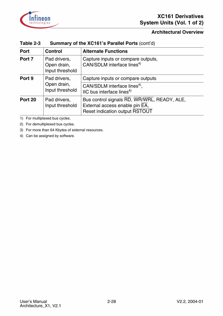
XC161 DerivativesSystem Units (Vol. 1 of 2)
Architectural Overview
Port 7 Pad drivers,Open drain,Input threshold
Capture inputs or compare outputs,CAN/SDLM interface lines4)
Port 9 Pad drivers,Open drain,Input threshold
Capture inputs or compare outputs
CAN/SDLM interface lines4),IIC bus interface lines4)
Port 20 Pad drivers,Input threshold
Bus control signals RD, WR/WRL, READY, ALE,External access enable pin EA,Reset indication output RSTOUT
1) For multiplexed bus cycles.
2) For demultiplexed bus cycles.
3) For more than 64 Kbytes of external resources.
4) Can be assigned by software.
Table 2-3 Summary of the XC161’s Parallel Ports (cont’d)
Port Control Alternate Functions
User’s Manual 2-28 V2.2, 2004-01Architecture_X1, V2.1
XC161 DerivativesSystem Units (Vol. 1 of 2)
Architectural Overview
2.4 Clock Generation
The Clock Generation Unit uses a programmable on-chip PLL with multiple prescalersto generate the clock signals for the XC161 with high flexibility. The master clock fMC isthe reference clock signal, and is used for TwinCAN and is output to the external system.The CPU clock fCPU and the system clock fSYS are derived from the master clock eitherdirectly (1:1) or via a 2:1 prescaler (fSYS = fCPU = fMC/2).
The on-chip oscillator can drive an external crystal or accepts an external clock signal.The oscillator clock frequency can be multiplied by the on-chip PLL (by a programmablefactor) or can be divided by a programmable prescaler factor.
If the bypass mode is used (direct drive or prescaler) the PLL can deliver an independentclock to monitor the clock signal generated by the on-chip oscillator. This PLL clock isindependent from the XTAL1 clock. When the expected oscillator clock transitions aremissing the Oscillator Watchdog (OWD) activates the PLL Unlock/OWD interrupt nodeand supplies the CPU with an emergency clock, the PLL clock signal. Under thesecircumstances the PLL will oscillate with its basic frequency.
The oscillator watchdog can be disabled by switching the PLL off. This reduces powerconsumption, but also no interrupt request will be generated in case of a missingoscillator clock.
2.5 Power Management Features
The basic power reduction modes (Idle and Power Down) are enhanced by additionalpower management features (see below). These features can be combined to reducethe controller’s power consumption to correspond to the application’s possible minimum.
• Basic power saving modes• Flexible clock generation• Flexible peripheral management (peripherals can be disabled and enabled)• Periodic wake-up from Idle mode via RTC timer
The listed features provide effective means to realize standby conditions for the systemwith an optimum balance between power reduction (standby time) and peripheraloperation (system functionality).
Basic Power Saving Modes
The XC161 can be switched into special operating modes (control via instructions)where its power consumption (and functionality) is reduced.Idle Mode stops the CPU while the peripherals can continue to operate.Sleep Mode and Power Down Mode stop all clock signals and all operation (RTC mayoptionally continue running). Sleep Mode can be terminated by external interrupt signals.
User’s Manual 2-29 V2.2, 2004-01Architecture_X1, V2.1

XC161 DerivativesSystem Units (Vol. 1 of 2)
Architectural Overview
Flexible Clock Generation
The flexible clock generation system combines a variety of improved mechanisms (partlyuser controllable) to provide the XC161 modules with clock signals. This is especiallyimportant in power sensitive modes such as standby operation.
The power optimized oscillator generally reduces the amount of power which isconsumed in order to generate the clock signal within the XC161.
The clock system controls the distribution and the frequency of internal and externalclock signals. The user can reduce the XC161’s CPU clock frequency which drasticallyreduces the consumed power.External circuitry can be controlled via the programmable frequency output FOUT.
Flexible Peripheral Management
Flexible peripheral management provides a mechanism to enable and disable eachperipheral module separately. In each situation (such as several system operatingmodes, standby, etc.) only those peripherals may be kept running which are required forthe specified functionality, for example, to maintain communication channels. All othersmay be switched off. The registers of disabled peripherals can still be accessed.
Periodic Wake-up from Idle or Sleep Mode
Periodic wake-up from Idle mode or from Sleep mode combines the drastically reducedpower consumption in Idle/Sleep mode (in conjunction with the additional powermanagement features) with a high level of system availability. External signals andevents can be scanned (at a lower rate) by periodically activating the CPU and selectedperipherals which then return to powersave mode after a short time. This greatly reducesthe system’s average power consumption. Idle/Sleep mode can also be terminated byexternal interrupt signals.
User’s Manual 2-30 V2.2, 2004-01Architecture_X1, V2.1
XC161 DerivativesSystem Units (Vol. 1 of 2)
Architectural Overview
2.6 On-Chip Debug Support (OCDS)
The On-Chip Debug Support system provides a broad range of debug and emulationfeatures built into the XC161. The user software running on the XC161 can thus bedebugged within the target system environment.
The OCDS is controlled by an external debugging device via the debug interface,consisting of the IEEE-1149-conforming JTAG port and a break interface. The debuggercontrols the OCDS via a set of dedicated registers accessible via the JTAG interface.Additionally, the OCDS system can be controlled by the CPU, e.g. by a monitor program.An injection interface allows the execution of OCDS-generated instructions by the CPU.
Multiple breakpoints can be triggered by on-chip hardware, by software, or by anexternal trigger input. Single stepping is supported as well as the injection of arbitraryinstructions and read/write access to the complete internal address space. A breakpointtrigger can be answered with a CPU-halt, a monitor call, a data transfer, or/and theactivation of an external signal.
The data transferred at a watchpoint (see above) can be obtained via the JTAG interfaceor via the external bus interface for increased performance.
The debug interface uses a set of 6 interface signals (4 JTAG lines, 2 break lines) tocommunicate with external circuitry. These interface signals use dedicated pins.
Complete system emulation is supported by the New Emulation Technology (NET)interface. Via this full-featured emulation interface (including internal buses, control,status, and pad signals) the XC161 chip can be connected to a NET carrier chip.
The use of the XC161 production chip together with the carrier chip provides superioremulation behavior, because the emulation system shows exactly the same functionalityas the production chip (use of the identical silicon).
User’s Manual 2-31 V2.2, 2004-01Architecture_X1, V2.1

XC161 DerivativesSystem Units (Vol. 1 of 2)
Architectural Overview
2.7 Protected Bits
The XC161 provides a special mechanism to protect bits which can be modified by theon-chip hardware from being changed unintentionally by software accesses to relatedbits (see also Section 4.8.2). The following bits are protected:
Table 2-4 XC161 Protected Bits
Register Bit Name Notes
GPT12E_T3CON T3OTL GPT1 timer output toggle latches
GPT12E_T6CON T6OTL GPT2 timer output toggle latches
ASC0_CON REN ASC0 receiver enable flag
ASC1_CON REN ASC1 receiver enable flag
SSC0_CON BSY SSC0 busy flag
SSC0_CON BE, PE, RE, TE SSC0 error flags
SSC1_CON BSY SSC1 busy flag
SSC1_CON BE, PE, RE, TE SSC1 error flags
ADC_CON/ADC_CTR0
ADST, ADCRQ ADC start flag/injection request flag
TFR TFR.15, 14, 13, 12 Class A trap flags
TFR TFR.7, 4, 3, 2 Class B trap flags
PECISNC C7IR … C0IR All channel interrupt request flags
CC1_SEE SEE.15 … SEE.0 Single event enable bits
CC2_SEE SEE.15 … SEE.0 Single event enable bits
CC1_OUT CC15IO … CC0IO Compare output bits
CC2_OUT CC15IO … CC0IO Compare output bits
P1L P1L.7 Those bits of PORT1 used for CAPCOM2
P1H P1H.7-4, P1H.0 Those bits of PORT1 used for CAPCOM2
P2 P2.15 … P2.8 All bits of Port 2 used for CAPCOM1
P6 P6.7 … P6.0 All bits of Port 6 used for CAPCOM1
P7 P7.7 … P7.4 All bits of Port 7 used for CAPCOM2
P9 P9.5 … P9.0 All bits of Port 9 used for CAPCOM2
RTC_ISNC T14IR,CNT3IR … CNT0IR
Interrupt node sharing request flags
CC1_CC15-0IC CC15IR … CC0IR CAPCOM1 interrupt request flags
CC2_CC31-16IC CC31IR … CC16IR CAPCOM2 interrupt request flags
User’s Manual 2-32 V2.2, 2004-01Architecture_X1, V2.1
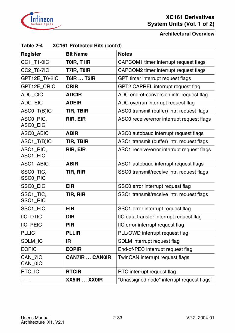
XC161 DerivativesSystem Units (Vol. 1 of 2)
Architectural Overview
CC1_T1-0IC T0IR, T1IR CAPCOM1 timer interrupt request flags
CC2_T8-7IC T7IR, T8IR CAPCOM2 timer interrupt request flags
GPT12E_T6-2IC T6IR … T2IR GPT timer interrupt request flags
GPT12E_CRIC CRIR GPT2 CAPREL interrupt request flag
ADC_CIC ADCIR ADC end-of-conversion intr. request flag
ADC_EIC ADEIR ADC overrun interrupt request flag
ASC0_T(B)IC TIR, TBIR ASC0 transmit (buffer) intr. request flags
ASC0_RIC, ASC0_EIC
RIR, EIR ASC0 receive/error interrupt request flags
ASC0_ABIC ABIR ASC0 autobaud interrupt request flags
ASC1_T(B)IC TIR, TBIR ASC1 transmit (buffer) intr. request flags
ASC1_RIC, ASC1_EIC
RIR, EIR ASC1 receive/error interrupt request flags
ASC1_ABIC ABIR ASC1 autobaud interrupt request flags
SSC0_TIC, SSC0_RIC
TIR, RIR SSC0 transmit/receive intr. request flags
SSC0_EIC EIR SSC0 error interrupt request flag
SSC1_TIC, SSC1_RIC
TIR, RIR SSC1 transmit/receive intr. request flags
SSC1_EIC EIR SSC1 error interrupt request flag
IIC_DTIC DIR IIC data transfer interrupt request flag
IIC_PEIC PIR IIC error interrupt request flag
PLLIC PLLIR PLL/OWD interrupt request flag
SDLM_IC IR SDLM interrupt request flag
EOPIC EOPIR End-of-PEC interrupt request flag
CAN_7IC, CAN_0IC
CAN7IR … CAN0IR TwinCAN interrupt request flags
RTC_IC RTCIR RTC interrupt request flag
----- XX5IR … XX0IR “Unassigned node” interrupt request flags
Table 2-4 XC161 Protected Bits (cont’d)
Register Bit Name Notes
User’s Manual 2-33 V2.2, 2004-01Architecture_X1, V2.1
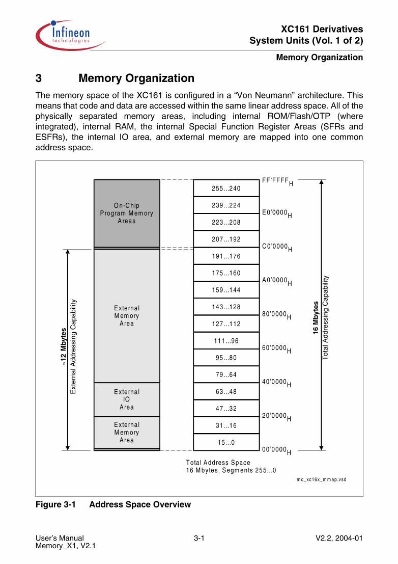
XC161 DerivativesSystem Units (Vol. 1 of 2)
Memory Organization
3 Memory OrganizationThe memory space of the XC161 is configured in a “Von Neumann” architecture. Thismeans that code and data are accessed within the same linear address space. All of thephysically separated memory areas, including internal ROM/Flash/OTP (whereintegrated), internal RAM, the internal Special Function Register Areas (SFRs andESFRs), the internal IO area, and external memory are mapped into one commonaddress space.
Figure 3-1 Address Space Overview
E xte rna lM em ory
A rea
O n-C hipP rogram M em ory
A reas
m c_xc16x_m m ap.vsd
239 ...224
223 ...208
191 ...176
175 ...160
159 ...144
143 ...128
127 ...112
111...96
95 ...80
79 ...64
63 ...48
47 ...32
31 ...16
15...000 ’0000H
C 0’0000H
FF ’FFFFH
40 ’0000H
80 ’0000H16
Mb
ytes
Tot
al A
ddre
ssin
g C
apab
ility
To ta l A ddress S pace16 M bytes, S egm ents 255...0
255 ...240
207 ...192
20 ’0000H
60 ’0000H
A 0’0000H
E 0’0000H
E xte rna lIO
A rea
E xte rna lM em ory
A rea
~12
Mby
tes
Ext
erna
l Add
ress
ing
Cap
abili
ty
User’s Manual 3-1 V2.2, 2004-01Memory_X1, V2.1

XC161 DerivativesSystem Units (Vol. 1 of 2)
Memory Organization
The XC161 provides a total addressable memory space of 16 Mbytes. This addressspace is arranged as 256 segments of 64 Kbytes each, and each segment is againsubdivided into four data pages of 16 Kbytes each (see Figure 3-1).
Bytes are stored at even or odd byte addresses. Words are stored in ascending memorylocations with the low byte at an even byte address being followed by the high byte atthe next odd byte address. Double words (code only) are stored in ascending memorylocations as two subsequent words. Single bits are always stored in the specified bitposition at a word address. Bit position 0 is the least significant bit of the byte at an evenbyte address, and bit position 15 is the most significant bit of the byte at the next oddbyte address. Bit addressing is supported for a part of the Special Function Registers, apart of the internal RAM and for the General Purpose Registers.
Figure 3-2 Storage of Words, Bytes, and Bits in a Byte Organized Memory
Note: Byte units forming a single word or a double word must always be stored withinthe same physical (internal, external, ROM, RAM) and organizational (page,segment) memory area.
MCD01996
15 14 8
067
Hxxxx6
Bits
Bits
Byte
Byte
Word (High Byte)
Word (Low Byte)
xxxx5H
xxxx4 H
xxxx3 H
xxxx2H
xxxx1 H
xxxx0H
xxxxF H
User’s Manual 3-2 V2.2, 2004-01Memory_X1, V2.1

XC161 DerivativesSystem Units (Vol. 1 of 2)
Memory Organization
3.1 Address Mapping
All the various memory areas and peripheral registers (see Table 3-1) are mapped intoone contiguous address space. All sections can be accessed in the same way. Thememory map of the XC161 contains some reserved areas, so future derivatives can beenhanced in an upward-compatible fashion.
Table 3-1 XC161 Memory Map1)
1) Accesses to the shaded areas generate external bus accesses.
Address Area Start Loc. End Loc. Area Size2)
2) The areas marked with “<” are slightly smaller than indicated, see column “Notes”.
Notes
Flash register space FF’F000H FF’FFFFH 4 Kbytes 3)
3) Not defined register locations return a trap code.
Reserved (Acc. trap) F8’0000H FF’EFFFH < 0.5 Mbytes Minus Flash regs
Reserved for PSRAM E0’0800H F7’FFFFH < 1.5 Mbytes Minus PSRAM
Program SRAM E0’0000H E0’07FFH 2 Kbytes Maximum4)
4) This is the maximum implemented in the derivatives described in this manual.
Reserved for pr. mem. C2’0000H DF’FFFFH < 2 Mbytes Minus Flash
Program Flash C0’0000H C1’FFFFH 128 Kbytes –
Reserved BF’0000H BF’FFFFH 64 Kbytes –
External memory area 40’0000H BE’FFFFH < 8 Mbytes Minus res. seg.
External IO area5)
5) Several pipeline optimizations are not active within the external IO area. This is necessary to control externalperipherals properly.
20’0800H 3F’FFFFH < 2 Mbytes Minus TwinCAN
TwinCAN registers 20’0000H 20’07FFH 2 Kbytes Accessed via EBC
External memory area 01’0000H 1F’FFFFH < 2 Mbytes Minus segment 0
SFR area 00’FE00H 00’FFFFH 0.5 Kbyte –
Dual-Port RAM 00’F600H 00’FDFFH 2 Kbytes –
Reserved for DPRAM 00’F200H 00’F5FFH 1 Kbyte –
ESFR area 00’F000H 00’F1FFH 0.5 Kbyte –
XSFR area 00’E000H 00’EFFFH 4 Kbytes –
Reserved 00’D000H 00’DFFFH 4 Kbytes –
Data SRAM 00’C000H 00’CFFFH 4 Kbytes –
Reserved for DSRAM 00’8000H 00’BFFFH 16 Kbytes –
External memory area 00’0000H 00’7FFFH 32 Kbytes –
User’s Manual 3-3 V2.2, 2004-01Memory_X1, V2.1
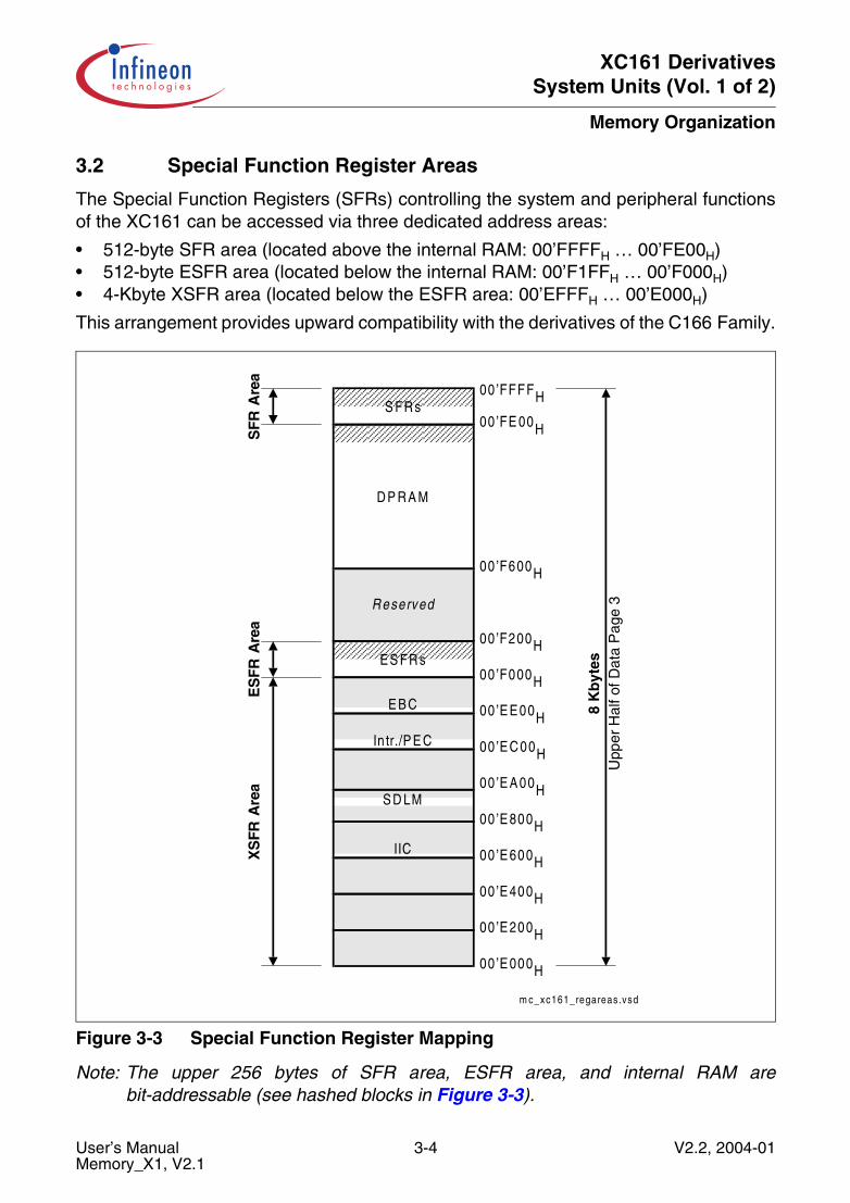
XC161 DerivativesSystem Units (Vol. 1 of 2)
Memory Organization
3.2 Special Function Register Areas
The Special Function Registers (SFRs) controlling the system and peripheral functionsof the XC161 can be accessed via three dedicated address areas:
• 512-byte SFR area (located above the internal RAM: 00’FFFFH … 00’FE00H)• 512-byte ESFR area (located below the internal RAM: 00’F1FFH … 00’F000H)• 4-Kbyte XSFR area (located below the ESFR area: 00’EFFFH … 00’E000H)
This arrangement provides upward compatibility with the derivatives of the C166 Family.
Figure 3-3 Special Function Register Mapping
Note: The upper 256 bytes of SFR area, ESFR area, and internal RAM arebit-addressable (see hashed blocks in Figure 3-3).
m c_xc161_regareas.vsd
D P R A M
R eserved
E S FR s
E B C
In tr./P E C
S D LM
IIC
00 ’E 000H
00 ’F600H
00 ’FFFFH
00 ’E 800H
00 ’F000H
8 K
byt
esU
pper
Hal
f of D
ata
Pag
e 3
S FR s
00 ’E 400H
00 ’E C 00H
00 ’F200H
00 ’FE 00H
XS
FR A
rea
00 ’E 200H
00 ’E 600H
00 ’E A 00H
00 ’E E 00H
ES
FR
Are
aS
FR
Are
a
User’s Manual 3-4 V2.2, 2004-01Memory_X1, V2.1

XC161 DerivativesSystem Units (Vol. 1 of 2)
Memory Organization
Special Function Registers
The functions of the CPU, the bus interface, the IO ports, and the on-chip peripherals ofthe XC161 are controlled via a number of Special Function Registers (SFRs).
All Special Function Registers can be addressed via indirect and long 16-bit addressingmodes. The (word) SFRs and their respective low bytes in the SFR/ESFR areas can beaddressed using an 8-bit offset together with an implicit base address. However, thisdoes not work for the respective high bytes!
Note: Writing to any byte of an SFR causes the not addressed complementary byte tobe cleared.
The upper half of the SFR-area (00’FFFFH … 00’FF00H) and the ESFR-area (00’F1FFH… 00’F100H) is bit-addressable, so the respective control/status bits can be modifieddirectly or checked using bit addressing.
When accessing registers in the ESFR area using 8-bit addresses or direct bitaddressing, an Extend Register (EXTR) instruction is required beforehand to switch theshort addressing mechanism from the standard SFR area to the Extended SFR area.This is not required for 16-bit and indirect addresses. The GPRs R15 … R0 areduplicated, i.e. they are accessible within both register blocks via short 2-, 4-, or 8-bitaddresses without switching.
ESFR_SWITCH_EXAMPLE:EXTR #4 ;Switch to ESFR area for next 4 instr.MOV ODP9, #data16 ;ODP9 uses 8-bit reg addressingBFLDL DP9, #mask, #data8 ;Bit addressing for bit fieldsBSET DP1H.7 ;Bit addressing for single bitsMOV T8REL, R1 ;T8REL uses 16-bit mem address, ;R1 is duplicated into the ESFR space ;(EXTR is not required for this access);---- ;--------------- ;The scope of the EXTR #4 instruction … ;… ends here!MOV T8REL, R1 ;T8REL uses 16-bit mem address, ;R1 is accessed via the SFR space
In order to minimize the use of the EXTR instructions the ESFR area mostly holdsregisters which are mainly required for initialization and mode selection. Registers thatneed to be accessed frequently are allocated to the standard SFR area, whereverpossible.
Note: The tools are equipped to monitor accesses to the ESFR area and willautomatically insert EXTR instructions, or issue a warning in case of missing orexcessive EXTR instructions.
Accesses to registers in the XSFR area use 16-bit addresses and require no specificaddressing modes or precautions.
User’s Manual 3-5 V2.2, 2004-01Memory_X1, V2.1
XC161 DerivativesSystem Units (Vol. 1 of 2)
Memory Organization
General Purpose Registers
The General Purpose Registers (GPRs) use a block of 16 consecutive words eitherwithin the global register bank or within one of the two local register banks. Bitfield BANKin register PSW selects the currently active register bank. The global register bank ismirrored to a section in the DPRAM, the Context Pointer (CP) register determines thebase address of the currently active global register bank section. This register bank mayconsist of up to 16 Word-GPRs (R0, R1, … R15) and/or of up to 16 byte-GPRs (RL0,RH0, … RL7, RH7). The sixteen byte-GPRs are mapped onto the first eight Word-GPRs(see Table 3-2).
In contrast to the system stack, a register bank grows from lower towards higher addresslocations and occupies a maximum space of 32 bytes. The GPRs are accessed via short2-, 4-, or 8-bit addressing modes using the Context Pointer (CP) register as baseaddress for the global bank (independent of the current DPP register contents).Additionally, each bit in the currently active register bank can be accessed individually.
Table 3-2 Mapping of General Purpose Registers to DPRAM Addresses
DPRAM Address High Byte Registers Low Byte Registers Word Register
<CP> + 1EH – – R15
<CP> + 1CH – – R14
<CP> + 1AH – – R13
<CP> + 18H – – R12
<CP> + 16H – – R11
<CP> + 14H – – R10
<CP> + 12H – – R9
<CP> + 10H – – R8
<CP> + 0EH RH7 RL7 R7
<CP> + 0CH RH6 RL6 R6
<CP> + 0AH RH5 RL5 R5
<CP> + 08H RH4 RL4 R4
<CP> + 06H RH3 RL3 R3
<CP> + 04H RH2 RL2 R2
<CP> + 02H RH1 RL1 R1
<CP> + 00H RH0 RL0 R0
User’s Manual 3-6 V2.2, 2004-01Memory_X1, V2.1

XC161 DerivativesSystem Units (Vol. 1 of 2)
Memory Organization
The XC161 supports fast register bank (context) switching. Multiple global register bankscan physically exist within the DPRAM at the same time. Only the global register bankselected by the Context Pointer register (CP) is active at a given time, however.Selecting a new active global register bank is simply done by updating the CP register.A particular Switch Context (SCXT) instruction performs register bank switching byautomatically saving the previous context and loading the new context. The number ofimplemented register banks (arbitrary sizes) is limited only by the size of the availableDPRAM.
Note: The local GPR banks are not memory mapped and the GPRs cannot be accessedusing a long or indirect memory address.
PEC Source and Destination Pointers
The source and destination address pointers for data transfers on the PEC channels arelocated in the XSFR area.
Each channel uses a pair of pointers stored in two subsequent word locations with thesource pointer (SRCPx) on the lower and the destination pointer (DSTPx) on the higherword address (x = 7 … 0). An additional segment register stores the associated sourceand destination segments, so PEC transfers can move data from/to any location withinthe complete addressing range.
Whenever a PEC data transfer is performed, the pair of source and destination pointers(selected by the specified PEC channel number) accesses the locations referred to bythese pointers independently of the current DPP register contents.
If a PEC channel is not used, the corresponding pointer locations can be used for otherpurposes.
For more details about the use of the source and destination pointers for PEC datatransfers see Section 5.4.
Note: Writing to any byte of the PEC pointers causes the not addressed complementarybyte to be cleared.
User’s Manual 3-7 V2.2, 2004-01Memory_X1, V2.1
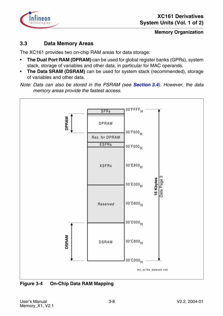
XC161 DerivativesSystem Units (Vol. 1 of 2)
Memory Organization
3.3 Data Memory Areas
The XC161 provides two on-chip RAM areas for data storage:
• The Dual Port RAM (DPRAM) can be used for global register banks (GPRs), systemstack, storage of variables and other data, in particular for MAC operands.
• The Data SRAM (DSRAM) can be used for system stack (recommended), storageof variables and other data.
Note: Data can also be stored in the PSRAM (see Section 3.4). However, the datamemory areas provide the fastest access.
Figure 3-4 On-Chip Data RAM Mapping
m c_xc16x_dataram .vsd
D P R A M
R es. fo r D P R A M
E S FR s
R eserved
D S R A M
00 ’C 000H
00 ’F000H
00 ’FFFFH
00 ’D 000H
00 ’E 000H
16 K
byt
esD
ata
Pag
e 3
S FR s
00 ’C 800H
00 ’D 800H
00 ’E 800H
00 ’F600H
DS
RA
MD
PR
AM
X S FR s
User’s Manual 3-8 V2.2, 2004-01Memory_X1, V2.1
XC161 DerivativesSystem Units (Vol. 1 of 2)
Memory Organization
Dual-Port RAM (DPRAM)
The XC161 provides 2 Kbytes of DPRAM (00’F600H … 00’FDFFH). Any word or bytedata in the DPRAM can be accessed via indirect or long 16-bit addressing modes, if theselected DPP register points to data page 3. Any word data access is made on an evenbyte address. The highest possible word data storage location in the DPRAM is00’FDFEH.
For PEC data transfers, the DPRAM can be accessed independent of the contents of theDPP registers via the PEC source and destination pointers.
The upper 256 bytes of the DPRAM (00’FD00H through 00’FDFFH) are provided forsingle bit storage, and thus they are bitaddressable (see hashed block in Figure 3-4).
Note: Code cannot be executed out of the DPRAM.
An area of 3 Kbytes is dedicated to DPRAM (00’F200H … 00’FDFFH). The locationswithout implemented DPRAM are reserved.
Data SRAM (DSRAM)
The XC161 provides 4 Kbytes of DSRAM (00’C000H … 00’CFFFH). Any word or bytedata in the DSRAM can be accessed via indirect or long 16-bit addressing modes, if theselected DPP register points to data page 3. Any word data access is made on an evenbyte address. The highest possible word data storage location in the DSRAM is00’CFFEH.
For PEC data transfers, the DSRAM can be accessed independent of the contents of theDPP registers via the PEC source and destination pointers.
Note: Code cannot be executed out of the DSRAM.
An area of 20 Kbytes is dedicated to DSRAM (00’8000H … 00’CFFFH). The locationswithout implemented DSRAM are reserved.
User’s Manual 3-9 V2.2, 2004-01Memory_X1, V2.1
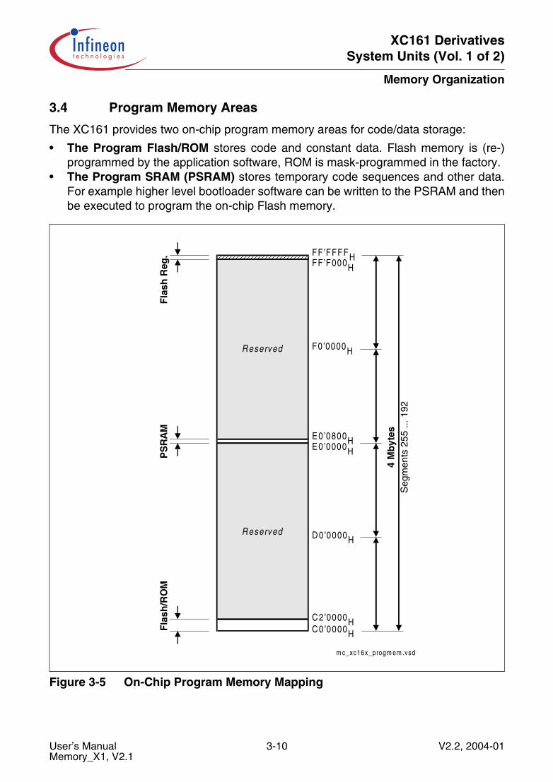
XC161 DerivativesSystem Units (Vol. 1 of 2)
Memory Organization
3.4 Program Memory Areas
The XC161 provides two on-chip program memory areas for code/data storage:
• The Program Flash/ROM stores code and constant data. Flash memory is (re-)programmed by the application software, ROM is mask-programmed in the factory.
• The Program SRAM (PSRAM) stores temporary code sequences and other data.For example higher level bootloader software can be written to the PSRAM and thenbe executed to program the on-chip Flash memory.
Figure 3-5 On-Chip Program Memory Mapping
m c_xc16x_progm em .vsd
R eserved
R eserved
C 0’0000H
F0’0000H
FF’FFFFH
D 0’0000H
E 0 ’0000H
4 M
byt
esS
egm
ents
255
... 1
92
Fla
sh/R
OM
C 2’0000H
PS
RA
MF
lash
Reg
.
E 0 ’0800H
FF’F000H
User’s Manual 3-10 V2.2, 2004-01Memory_X1, V2.1
XC161 DerivativesSystem Units (Vol. 1 of 2)
Memory Organization
Program/Data SRAM (PSRAM)
The XC161 provides 2 Kbytes of PSRAM (E0’0000H … E0’07FFH). The PSRAMprovides fast code execution without initial delays. Therefore, it supports non-sequentialcode execution, for example via the interrupt vector table.
Any word or byte data in the PSRAM can be accessed via indirect or long 16-bitaddressing modes, if the selected DPP register points to data page 896. Any word dataaccess is made on an even byte address. The highest possible word data storagelocation in the PSRAM is E0’07FEH.
For PEC data transfers, the PSRAM can be accessed independent of the contents of theDPP registers via the PEC source and destination pointers.
Any data can be stored in the PSRAM. Because the PSRAM is optimized for codefetches, however, data accesses to the data memories provide higher performance.
Note: The PSRAM is not bitaddressable.
An area of 1.5 Mbytes is dedicated to PSRAM (E0’0000H … F7’FFFFH). The locationswithout implemented PSRAM are reserved.
Non-Volatile Program Memory (Flash)
The XC161 provides 128 Kbytes of program Flash (C0’0000H … C1’FFFFH). Code anddata fetches are always 64-bit aligned, using byte select lines for word and byte data.Any word or byte data in the program memory can be accessed via indirect or long 16-bitaddressing modes, if the selected DPP register points to one of the respective datapages. Any word data access is made on an even byte address. The highest possibleword data storage location in the program memory is C1’FFFEH.
For PEC data transfers, the program memory can be accessed independent of thecontents of the DPP registers via the PEC source and destination pointers.
Note: The program memory is not bitaddressable.
An area of 2 Mbytes is dedicated to program memory (C0’0000H … DF’FFFFH). Thelocations without implemented program memory are reserved.
User’s Manual 3-11 V2.2, 2004-01Memory_X1, V2.1

XC161 DerivativesSystem Units (Vol. 1 of 2)
Memory Organization
3.5 System Stack
The system stack may be defined anywhere within the XC161’s memory areas (includingexternal memory).
For all system stack operations the respective stack memory is accessed via a 24-bitstack pointer. The Stack Pointer (SP) register provides the lower 16 bits of the stackpointer (stack pointer offset), the Stack Pointer Segment (SPSEG) register adds theupper 8 bits of the stack pointer (stack segment). The system stack grows downwardfrom higher towards lower locations as it is filled. Only word accesses are supported tothe system stack.
Register SP is decremented before data is pushed on the system stack, andincremented after data has been pulled from the system stack. Only word accesses aresupported to the system stack.
By using register SP for stack operations, the size of the system stack is limited to64 Kbytes. The stack must be located in the segment defined by register SPSEG.
The stack pointer points to the latest system stack entry, rather than to the next availablesystem stack address.
A stack overflow (STKOV) register and a stack underflow (STKUN) register are providedto control the lower and upper limits of the selected stack area. These two stackboundary registers can be used both for protection against data corruption.
For best performance it is recommended to locate the stack to the DPRAM or to theDSRAM. Using the DPRAM may conflict with register banks or MAC operands.
User’s Manual 3-12 V2.2, 2004-01Memory_X1, V2.1
XC161 DerivativesSystem Units (Vol. 1 of 2)
Memory Organization
3.6 IO Areas
The following areas of the XC161’s address space are marked as IO area:
• The external IO area is provided for external peripherals (or memories) and alsocomprises the on-chip LXBus-peripherals, such as the TwinCAN module.It is located from 20’0000H to 3F’FFFFH (2 Mbytes).
• The internal IO area provides access to the internal peripherals and is split into threeblocks:– The SFR area, located from 00’FE00H to 00’FFFFH (512 bytes)– The ESFR area, located from 00’F000H to 00’F1FFH (512 bytes)– The XSFR area, located from 00’E000H to 00’EFFFH (4 Kbytes)
Note: The external IO area supports real byte accesses. The internal IO area does notsupport real byte transfers, the complementary byte is cleared when writing to abyte location.
The IO areas have special properties, because peripheral modules must be controlledin a different way than memories:
• Accesses are not buffered and cached, the write back buffers and caches are notused to store IO read and write accesses.
• Speculative reads are not executed, but delayed until all speculations are solved (e.g.prefetching after conditional branches).
• Data forwarding is disabled, an IO read access is delayed until all IO writes pendingin the pipeline are executed, because peripherals can change their internal state aftera write access.
User’s Manual 3-13 V2.2, 2004-01Memory_X1, V2.1
XC161 DerivativesSystem Units (Vol. 1 of 2)
Memory Organization
3.7 External Memory Space
The XC161 is capable of using an address space of up to 16 Mbytes. Only parts of thisaddress space are occupied by internal memory areas or are reserved. A total area ofapproximately 12 Mbytes references external memory locations. This external memoryis accessed via the XC161’s external bus interface.
Selectable memory bank sizes are supported: The maximum size of a bank in theexternal memory space depends on the number of activated address bits. It can varyfrom 64 Kbytes (with A15 … 0 activated) to 12 Mbytes (with A23 … 0 activated). Thelogical size of a memory bank and its location in the address space is defined byprogramming the respective address window. It can vary from 4 Kbytes to 12 Mbytes.
• Non-segmented mode:– 64 Kbytes with A15 … A0 on PORT0 or PORT1
• 1-bit segmented mode:– 128 Kbytes with A16 on Port 4– and A15 … A0 on PORT0 or PORT1
• 2-bit … 7-bit segmented mode:– with Ax … A16 on Port 4– and A15 … A0 on PORT0 or PORT1
• 8-bit segmented mode:– 12 Mbytes with A23 … A16 on Port 4– and A15 … A0 on PORT0 or PORT1
Each bank can be directly addressed via the address bus, while the programmable chipselect signals can be used to select various memory banks.
The XC161 also supports four different bus types:
• Multiplexed 16-bit Bus with address and data on PORT0 (Default after Reset)• Multiplexed 8-bit Bus with address and data on PORT0/P0L• Demultiplexed 16-bit Bus with address on PORT1 and data on PORT0• Demultiplexed 8-bit Bus with address on PORT1 and data on P0L
Memory model and bus mode are preselected during reset by pin EA and PORT0 pins.For further details about the external bus configuration and control please refer toChapter 9.
External word and byte data can only be accessed via indirect or long 16-bit addressingmodes using one of the four DPP registers. There is no short addressing mode forexternal operands. Any word data access is made to an even byte address.
For PEC data transfers the external memory can be accessed independent of thecontents of the DPP registers via the PEC source and destination pointers.
Note: The external memory is not bitaddressable.
User’s Manual 3-14 V2.2, 2004-01Memory_X1, V2.1
XC161 DerivativesSystem Units (Vol. 1 of 2)
Memory Organization
3.8 Crossing Memory Boundaries
The address space of the XC161 is implicitly divided into equally sized blocks of differentgranularity and into logical memory areas. Crossing the boundaries between theseblocks (code or data) or areas requires special attention to ensure that the controllerexecutes the desired operations.
Memory Areas are partitions of the address space assigned to different kinds ofmemory (if provided at all). These memory areas are the SFR areas, the on-chipprogram or data RAM areas, the on-chip ROM/Flash/OTP (if available), the on-chipLXBus-peripherals (if integrated), and the external memory.
Accessing subsequent data locations which belong to different memory areas is noproblem. However, when executing code, the different memory areas must be switchedexplicitly via branch instructions. Sequential boundary crossing is not supported andleads to erroneous results.
Note: Changing from the external memory area to the on-chip RAM area takes placewithin segment 0.
Segments are contiguous blocks of 64 Kbytes each. They are referenced via the CodeSegment Pointer CSP for code fetches and via an explicit segment number for dataaccesses overriding the standard DPP scheme.During code fetching, segments are not changed automatically, but rather must beswitched explicitly. The instructions JMPS, CALLS and RETS will do this.
In larger sequential programs, make sure that the highest used code location of asegment contains an unconditional branch instruction to the respective followingsegment to prevent the prefetcher from trying to leave the current segment.
Data Pages are contiguous blocks of 16 Kbytes each. They are referenced via the datapage pointers DPP3 … DPP0 and via an explicit data page number for data accessesoverriding the standard DPP scheme. Each DPP register can select one of the possible1024 data pages. The DPP register which is used for the current access is selected viathe two upper bits of the 16-bit data address. Therefore, subsequent 16-bit dataaddresses which cross the 16-Kbyte data page boundaries will use different data pagepointers, while the physical locations need not be subsequent within memory.
User’s Manual 3-15 V2.2, 2004-01Memory_X1, V2.1
XC161 DerivativesSystem Units (Vol. 1 of 2)
Memory Organization
3.9 The On-Chip Program Flash Module
The XC161 incorporates 128 Kbytes of embedded Flash memory (starting at locationC0’0000H, see Figure 3-5) for code or constant data. It is operated from the 5 V padsupply and requires no additional programming voltage.The on-chip voltage generatorsrequire a power stabilization time of approx. 250 µs. The Flash array is organized in sixsectors of 4 × 8 Kbytes, 1 × 32 Kbytes, and 1 × 64 Kbytes. It combines the advantagesof very fast read accesses with protected but simple writing algorithms for programmingand erasing. The 64-bit code read accesses realize maximum CPU performance byfetching two double word instructions (or four single word instructions) in a single accesscycle.
Data integrity is enhanced by an error correction code enabling dynamic correction ofsingle bit errors. Additionally, special margin checks are provided to detect and correctproblematic bits before they lead to actual malfunctions.
All Flash operations are controlled by command sequences (according to the JEDECsingle-power-supply Flash standard). The algorithms for programming and erasing areexecuted automatically by the internal Flash state control machine. This avoidsinadvertent destruction of the Flash contents at a reasonably low software overhead.Command sequences consist of subsequent write (or read) accesses to virtual locationswithin the Flash space or the Flash register space. The virtual Flash locations aredefined by special addresses (see command sequence table).
For optimized programming efficiency, paging mode (burst mode) allows 128 bytes to beloaded into a page buffer with fast CPU accesses before this buffer is programmed intothe Flash with one single store command (2 ms typical1)). Each sector can be erasedseparately (200 ms typical1)).
Note: Erased Flash memory cells contain all ‘0’s, contrary to standard EPROMs.
Security is provided by a general read/write protection (complete Flash array) and asector-specific2) write protection. The temporary disabling of these hardware protectionfeatures is secured with a password check sequence. The lock information and thekeywords used for the password check sequence are stored apart from the user’s codeand data in a separate security sector (see Section 3.9.4).
A dedicated Flash status register returns global and sector-specific status information.The correct execution of an operation and the general status of the Flash module can bechecked via the Flash status register at any time.
The physical address range of the Flash module covers byte addresses from 0’0000H to1’FFFFH. These physical addresses are mapped to the XC161’s program memory areastarting at C0’0000H. Also the separate security sector is mapped to this area. Accessconflicts are avoided by special security commands.
1) For exact parameters please refer to the data sheet.2) For write protection two 8-Kbyte sectors are combined to one lockable 16-Kbyte section.
User’s Manual 3-16 V2.2, 2004-01Memory_X1, V2.1

XC161 DerivativesSystem Units (Vol. 1 of 2)
Memory Organization
In-System-Programming is supported by the automatic program/erase algorithms andthe large page buffer, which may be filled by a programming routine executed out of theFlash memory itself. During the actual program/erase algorithm Flash read accesses arestalled. Also completely erased Flash modules can be programmed within the system.The built-in bootstrap loader can load an initial programming routine via the serialinterface, which in turn can then program the Flash module. This is useful for the initialprogramming (virgin Flash) as well as in case of a problem (e.g. power failure) duringreprogramming, when no safety routines are provided.
Note: Accesses to a protected Flash are totally disabled during bootstrap mode. Beforeany program/erase operation the protection must be temporarily disabled usingthe correct password sequence.
Figure 3-6 Mapping of the On-Chip Flash Module Sectors
m c_xc16x_flashm ap.vsd
S egm ent 194
S egm ent 193
S egm ent 192
C 0 ’0000H
C 4’0000H
2 M
byt
esF
lash
/RO
M A
rea
Program Memory(S egm ents)
S egm ents196 ... 223
S egm ent 195
C 1 ’0000H
C 2’0000H
C 3’0000H
D F’FFFFH
8 K by tes8 K by tes8 K by tes8 K by tes
32 K bytes
64 K bytes
Flash Sectors
128
Kb
ytes
Fla
sh M
odul
e
0 ’0000H
1 ’0000H
1 ’FFFFH
LocationPhysicalAddress
User’s Manual 3-17 V2.2, 2004-01Memory_X1, V2.1
XC161 DerivativesSystem Units (Vol. 1 of 2)
Memory Organization
3.9.1 Flash Operating Modes
Two basic operating modes of the on-chip Flash module can be distinguished:
• Standard read mode: code and data can be read from the Flash module• Command mode: the Flash module executes a previously defined command
Standard Read Mode
In standard read mode (the normal operating mode) the Flash memory appears like astandard ROM, allowing code and data accesses in any addressing mode.
Standard read mode is entered in the following cases:
• After the deactivation of the system reset (after power stabilization)• After execution of the reset command, if no program or erase operation is active• After every completed command execution (program, erase, etc.)• When a command sequence error is detected• When a protection violation is detected (program or erase a protected sector)
Note: Standard read mode is indicated by status bit BUSY = ‘0’.
Standard read mode is terminated when the last command of a command sequenceis decoded and a Flash array operation is started (program or erase). Therefore, all stepsof a command sequence before the last command (in particular the loading of the pagebuffer) can be executed by code read from the Flash module itself.
Each read access to the Flash memory activates the automatic error detection. Double-bit errors are detected and indicated, single-bit errors are detected, indicated, andautomatically corrected (see Section 3.9.3).
Note: Single bit errors can be located and avoided by a margin check operation.
Command Mode
All Flash operation except for standard read operations are initiated by commandsequences written to the (virtual) Flash command register (a location within the Flashspace). Protected commands additionally require four passwords for validation.
Command mode is entered after the last command of a command sequence has beenwritten. For all other command sequences, which activate a Flash array operation suchas erase sector, the command execution and thus the command mode remains activefor a defined time. While in command mode (busy) read accesses to the Flash array aredelayed until the Flash module returns to standard read mode.
Note: Command mode is indicated by status bit BUSY = ‘1’.
Command mode is terminated by the correct execution of the command or by an errorcondition as indicated in the status register.
Command sequences not starting Flash operations (e.g. Enter Page Mode) areexecuted immediately and command mode is not entered.
User’s Manual 3-18 V2.2, 2004-01Memory_X1, V2.1
XC161 DerivativesSystem Units (Vol. 1 of 2)
Memory Organization
3.9.2 Command Sequences
All operations besides normal read operations are initiated and controlled by commandsequences written to the Flash state machine. The different write cycles of commandsequences define the intended command, but also establish a fail-safe mechanism toprotect against inadvertent operations. Commands not directly controlling Flash arrayoperations are single cycle commands for performance reasons, commands affectingthe Flash array require several cycles, commands affecting security issues require a64-bit security code (four passwords) to be accepted. Command cycles need not beconsecutively received (pauses allowed).
Command sequences can be performed simultaneously to instruction fetch operations,so instructions for command sequences also can be executed out of the on-chip Flash,as long as the Flash module is in read mode and not executing an erase or programmingoperation. Command sequences for polling the status register are allowed in any state,also during erase and programming operations, if they are executed out of memoryoutside the Flash module. Otherwise, instruction fetching is stalled.
Writing incorrect address and data values or writing them in the improper sequence willabort the intended operation, reset the module to read mode, and set the sequence errorflag in the status register.
Read Status commands address the separate Flash register space and do not requirecommand sequences. Register write cycles are only executed with a command cycle.
Programming operations are supported by a 128-byte page buffer which can beloaded with maximum speed, and is then programmed with one single commandsequence. Programming is done in three steps:
• Initialize the page buffer with the Enter Page Mode command (this also defines thetarget page address).
• Load the page buffer with consecutive Load Page command (the page buffer offsetis incremented automatically).
• Program the complete buffer with the Write Page command.
Erase operations clear all bits of a selected sector or of a 256-byte wordline. Erasecommand sequences include the address of the target sector or wordline.
After being requested the program/erase operation is executed automatically andrequires no additional user control. The operation itself and its termination are indicatedby status flags. A Power Down request is delayed until the termination of theprogram/erase operation. A reset aborts the program/erase operation within the powerstabilization time, indicated by an operation error (OPER) in the Flash status register.
The three tables below summarize the implemented command sequences for:
• organizational Flash accesses (Table 3-3),• programming and erasing (Table 3-4),• protection control (Table 3-5).
Note: Each command sequence lists the required address (A = …) and data (D = …).
User’s Manual 3-19 V2.2, 2004-01Memory_X1, V2.1

XC161 DerivativesSystem Units (Vol. 1 of 2)
Memory Organization
Organizational Commands
Notes:
RLOC is the respective register offset (rr) within the Flash register area starting atFF’F000H (FF’F0rrH).<status> is the returned status word.margin is the control word used for margin control.
The shown virtual address (Cx’xxAAH) must point to the Flash space (e.g. C0’00AAH).
The “Read Flash status” command may be executed during command mode in order tocheck the BUSY bit of the Flash module.
The Reset To Read command aborts not completed command sequences and clearsthe error flags in the status register FSR. The reset command can be issued at any pointduring the command sequence, except for parts of the password check sequence. Itdoes not terminate command mode, i.e. abort busy state.
The Clear Status command clears the error flags and the write status bits PROG andERASE (the hardware-controlled indication flags are not affected). The clear statuscommand is only accepted in Read Mode and otherwise generates a sequence error.
The Read Register command returns the contents of the following registers:
• The Flash Status Register FSR providing general Flash status information.• The Protection Configuration Register PROCON indicating the protected sectors.• The Margin Control Register MAR indicating the selected Flash read margin.
The Write Margin Register command is used for verify operations and for user-controlled refresh operations to identify and correct problematic bits (see Section 3.9.3).
Table 3-3 Command Sequence Definitions (Organizational Accesses)
Cyc
le Reset to Read Mode
Clear Status Read Flash Status or Margin
Write Margin
1 A = Cx’xxAAHD = xxF0H
A = Cx’xxAAHD = xxF5H
A = RLOCD = <status>
A = Cx’xxAAHD = xxFAH
2 – – – A = FF’F00CHD = margin
User’s Manual 3-20 V2.2, 2004-01Memory_X1, V2.1
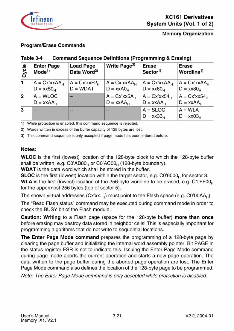
XC161 DerivativesSystem Units (Vol. 1 of 2)
Memory Organization
Program/Erase Commands
Notes:
WLOC is the first (lowest) location of the 128-byte block to which the 128-byte buffershall be written, e.g. C0’AB80H or C0’AC00H (128-byte boundary).WDAT is the data word which shall be stored in the buffer.SLOC is the first (lowest) location within the target sector, e.g. C0’6000H for sector 3.WLA is the first (lowest) location of the 256-byte wordline to be erased, e.g. C1’FF00Hfor the uppermost 256 bytes (top of sector 5).
The shown virtual addresses (Cx’xx..H) must point to the Flash space (e.g. C0’00AAH).
The “Read Flash status” command may be executed during command mode in order tocheck the BUSY bit of the Flash module.
Caution: Writing to a Flash page (space for the 128-byte buffer) more than oncebefore erasing may destroy data stored in neighbor cells! This is especially important forprogramming algorithms that do not write to sequential locations.
The Enter Page Mode command prepares the programming of a 128-byte page byclearing the page buffer and initializing the internal word assembly pointer. Bit PAGE inthe status register FSR is set to indicate this. Issuing the Enter Page Mode commandduring page mode aborts the current operation and starts a new page operation. Thedata written to the page buffer during the aborted page operation are lost. The EnterPage Mode command also defines the location of the 128-byte page to be programmed.
Note: The Enter Page Mode command is only accepted while protection is disabled.
Table 3-4 Command Sequence Definitions (Programming & Erasing)
Cyc
le Enter Page Mode1)
1) While protection is enabled, this command sequence is rejected.
Load Page Data Word2)
2) Words written in excess of the buffer capacity of 128 bytes are lost.
Write Page3)
3) This command sequence is only accepted if page mode has been entered before.
Erase Sector1)
Erase Wordline1)
1 A = Cx’xxAAHD = xx50H
A = Cx’xxF2HD = WDAT
A = Cx’xxAAHD = xxA0H
A = Cx’xxAAHD = xx80H
A = Cx’xxAAHD = xx80H
2 A = WLOCD = xxAAH
– A = Cx’xx5AHD = xxAAH
A = Cx’xx54HD = xxAAH
A = Cx’xx54HD = xxAAH
3 – – – A = SLOCD = xx33H
A = WLAD = xx03H
User’s Manual 3-21 V2.2, 2004-01Memory_X1, V2.1
XC161 DerivativesSystem Units (Vol. 1 of 2)
Memory Organization
The Load Page Data Word command adds the accompanying data word to the pagebuffer. The offset within the page buffer is determined by the internal buffer pointer whichis incremented after each load operation. Data words written in excess of the buffercapacity of 128 bytes are lost (no error indicated).
Note: The Load Page Data Word command is only accepted while page mode is active.
The Write Page command writes (programs) the contents of the 128-byte page buffer(including the error correction code) to the Flash array. The address of the programmedpage is defined by the preceding Enter (Security) Page Mode command.
After the Write Page command the Flash module enters command mode, indicated byPAGE = 0, PROG = 1, BUSY = 1. Read accesses to the Flash module are delayed untilcommand mode is terminated. The programming operation itself is executedautomatically and requires no additional user control.
If a security page is written the new protection configuration (including keywords orprotection confirmation code) is valid directly after execution of this command.
Note: The Write Page command is only accepted while page mode is active.
The Erase Sector command clears all bits within the selected sector (see SLOC).
After the Erase Sector command the Flash module enters command mode, indicated byERASE = 1, BUSY = 1. Read accesses to the Flash module are delayed until commandmode is terminated. The erase operation itself is executed automatically and requires noadditional user control.
Note: The Erase Sector command is only accepted while protection is disabled.
The Erase Wordline command clears all bits within the selected 256-byte wordline (seeWLA).
After the Erase Wordline command the Flash module enters command mode, indicatedby ERASE = 1, BUSY = 1. Read accesses to the Flash module are delayed untilcommand mode is terminated. The erase operation itself is executed automatically andrequires no additional user control.
Note: The Erase Wordline command is only accepted while protection is disabled.
User’s Manual 3-22 V2.2, 2004-01Memory_X1, V2.1
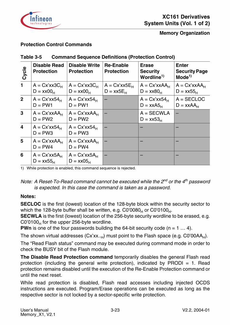
XC161 DerivativesSystem Units (Vol. 1 of 2)
Memory Organization
Protection Control Commands
Note: A Reset-To-Read command cannot be executed while the 2nd or the 4th passwordis expected. In this case the command is taken as a password.
Notes:
SECLOC is the first (lowest) location of the 128-byte block within the security sector towhich the 128-byte buffer shall be written, e.g. C0’0080H or C0’0100H.SECWLA is the first (lowest) location of the 256-byte security wordline to be erased, e.g.C0’0100H for the upper 256-byte wordline.PWn is one of the four passwords building the 64-bit security code (n = 1 … 4).
The shown virtual addresses (Cx’xx..H) must point to the Flash space (e.g. C0’00AAH).
The “Read Flash status” command may be executed during command mode in order tocheck the BUSY bit of the Flash module.
The Disable Read Protection command temporarily disables the general Flash readprotection (including the general write protection), indicated by PRODI = 1. Readprotection remains disabled until the execution of the Re-Enable Protection command oruntil the next reset.
While read protection is disabled, Flash read accesses including injected OCDSinstructions are executed. Program/Erase operations can be executed as long as therespective sector is not locked by a sector-specific write protection.
Table 3-5 Command Sequence Definitions (Protection Control)
Cyc
le
Disable Read Protection
Disable Write Protection
Re-Enable Protection
Erase Security Wordline1)
1) While protection is enabled, this command sequence is rejected.
Enter Security Page Mode1)
1 A = Cx’xx3CHD = xx00H
A = Cx’xx3CHD = xx00H
A = Cx’xx5EHD = xx5EH
A = Cx’xxAAHD = xx80H
A = Cx’xxAAHD = xx55H
2 A = Cx’xx54HD = PW1
A = Cx’xx54HD = PW1
– A = Cx’xx54HD = xxA5H
A = SECLOCD = xxAAH
3 A = Cx’xxAAH
D = PW2A = Cx’xxAAH
D = PW2– A = SECWLA
D = xx53H
–
4 A = Cx’xx54HD = PW3
A = Cx’xx54HD = PW3
– – –
5 A = Cx’xxAAH
D = PW4A = Cx’xxAAH
D = PW4– – –
6 A = Cx’xx5AHD = xx55H
A = Cx’xx5AHD = xx05H
– – –
User’s Manual 3-23 V2.2, 2004-01Memory_X1, V2.1
XC161 DerivativesSystem Units (Vol. 1 of 2)
Memory Organization
Note: This command sequence can also be used to verify the programmed keywordsbefore the protection is locked with the confirmation. A wrong keyword is indicatedby bit PROER in the Flash Status Register FSR.
This is a protected command sequence requiring the 64-bit security code (four user-defined passwords) for validation (see Section 3.9.4).
The Disable Sector Write Protection command temporarily disables the sector-specific write protection for all write-protected sectors, indicated by SUL = 1. Writeprotection remains disabled until the execution of the Re-Enable Protection command oruntil the next reset.
While write protection is disabled, all Flash operations can be executed as long as therespective sector is not locked by the general read/write protection.
Note: This command sequence can also be used to verify the programmed keywordsbefore the protection is locked with the confirmation. A wrong keyword is indicatedby bit PROER in the Flash Status Register FSR.
This is a protected command sequence requiring the 64-bit security code (four user-defined passwords) for validation (see Section 3.9.4).
The Re-Enable Protection command immediately resumes all installed but temporarilydisabled protection features (general read/write protection and/or sector-specific writeprotection).
The Erase Security Wordline command clears all bits within the selected wordline(see SECLOC).
After the Erase Security Wordline command the Flash module enters command mode,indicated by ERASE = 1, BUSY = 1. Read accesses to the Flash module are delayeduntil command mode is terminated. The erase operation itself is executed automaticallyand requires no additional user control.
After the erase operation, the protection configuration (including keywords or protectionconfirmation code) is valid directly after execution of this command (see Section 3.9.4).
Note: The Erase Security Wordline command is only accepted while protection isdisabled.
The Enter Security Page Mode command prepares the programming of a 128-bytepage within the security sector by clearing the page buffer and initializing the internalword assembly pointer. Bit PAGE in the status register FSR is set to indicate this. Issuingthe Enter Security Page Mode command during page mode aborts the current operationand starts a new page operation. The data written to the page buffer during the abortedpage operation are lost. The Enter Security Page Mode command also defines thelocation of the 128-byte page to be programmed. Also refer to Section 3.9.4.
Note: The Enter Security Page Mode command is only accepted while any protection isdisabled.
User’s Manual 3-24 V2.2, 2004-01Memory_X1, V2.1
XC161 DerivativesSystem Units (Vol. 1 of 2)
Memory Organization
3.9.3 Error Correction and Data Integrity
Data integrity is supported by the Error Correction Code (ECC). This ECC is dynamicallygenerated during Flash write operations and stored in the Flash array together with thecorresponding data. For each read access the associated 8-bit ECC is fetched togetherwith the 64-bit read data and is evaluated.
Single bit errors are detected and automatically corrected on-the-fly (during run-time).Therefore, single bit errors do not affect system operation.
Double bit errors are detected and trigger an Access Fault trap. This preventserroneous instructions or data from being used.
Each read error condition is indicated by a dedicated flag (SBER, DBER) in the FlashStatus Register FSR.
The probability of a double bit error (not correctable) is extremely low. Double bit errorscan be avoided by performing a recovery operation after a single bit error has beendetected. For the recovery operation the following steps must be done:
• Detect the wordline containing the erroneous bit• Store the contents of the wordline temporarily• Erase this wordline• Reprogram the erased wordline (requires two write page operations)
The wordline data copied to the temporary buffer are valid, because a single bit errorduring reading is automatically corrected via the ECC. Erasing and programming is doneusing standard command sequences.
Verify Operation
The violated wordline can be detected by a verify operation. After clearing bit SBER acertain area of the Flash memory is read. Since the Flash array always delivers 64-bitdata, the read address can be incremented by 8 after every access, which minimizes thenumber of necessary read cycles. After reading the defined area bit SBER indicates if orif not this area contains the single bit error. The verify algorithm can gradually decreasethe size of the checked area down to the size of a wordline, or can check all wordlinessequentially.
Refresh Operation
Even single bit errors can be avoided by detecting problematic (moving) bits before theylead to a read error (and a recovery operation during runtime) and by reprogramming(refreshing) them in advance. Problematic bits can be detected by combining the verifyoperation with margin check control.
User’s Manual 3-25 V2.2, 2004-01Memory_X1, V2.1
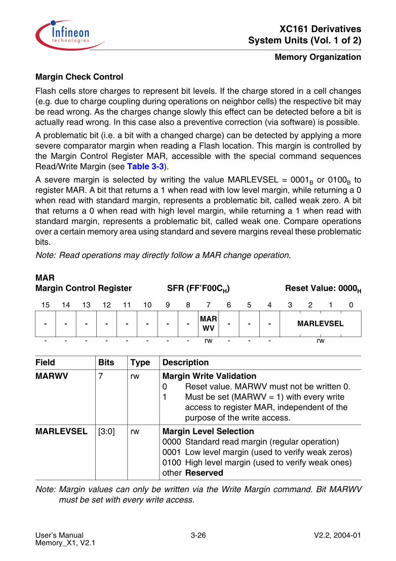
XC161 DerivativesSystem Units (Vol. 1 of 2)
Memory Organization
Margin Check Control
Flash cells store charges to represent bit levels. If the charge stored in a cell changes(e.g. due to charge coupling during operations on neighbor cells) the respective bit maybe read wrong. As the charges change slowly this effect can be detected before a bit isactually read wrong. In this case also a preventive correction (via software) is possible.
A problematic bit (i.e. a bit with a changed charge) can be detected by applying a moresevere comparator margin when reading a Flash location. This margin is controlled bythe Margin Control Register MAR, accessible with the special command sequencesRead/Write Margin (see Table 3-3).
A severe margin is selected by writing the value MARLEVSEL = 0001B or 0100B toregister MAR. A bit that returns a 1 when read with low level margin, while returning a 0when read with standard margin, represents a problematic bit, called weak zero. A bitthat returns a 0 when read with high level margin, while returning a 1 when read withstandard margin, represents a problematic bit, called weak one. Compare operationsover a certain memory area using standard and severe margins reveal these problematicbits.
Note: Read operations may directly follow a MAR change operation.
Note: Margin values can only be written via the Write Margin command. Bit MARWVmust be set with every write access.
MAR Margin Control Register SFR (FF’F00CH) Reset Value: 0000H
15 14 13 12 11 10 9 8 7 6 5 4 3 2 1 0
- - - - - - - -MARWV
- - - MARLEVSEL
- - - - - - - - rw - - - rw
Field Bits Type Description
MARWV 7 rw Margin Write Validation0 Reset value. MARWV must not be written 0.1 Must be set (MARWV = 1) with every write
access to register MAR, independent of the purpose of the write access.
MARLEVSEL [3:0] rw Margin Level Selection0000 Standard read margin (regular operation)0001 Low level margin (used to verify weak zeros)0100 High level margin (used to verify weak ones)other Reserved
User’s Manual 3-26 V2.2, 2004-01Memory_X1, V2.1
XC161 DerivativesSystem Units (Vol. 1 of 2)
Memory Organization
3.9.4 Protection and Security Features
The Flash module provides powerful and flexible protection of data and code againstdestruction (i.e. erasure) and undesired modification (i.e. reprogramming) as well asagainst undesired read access to Flash contents. Two protection mechanisms can beactivated:
• Sector-specific write protection protects individual sectors against erasing andprogramming. This is important for the integrity of boot software and also avoidsmodifications of code/data by malfunction or even manipulation.
• General read/write protection protects the complete program Flash area against allaccesses from outside the module itself. This includes data read accesses,instruction fetches (i.e. jumps into the program Flash area), and OCDS operations.The general read/write protection also disables erasing and programming. Commandsequences and register accesses are executed, however.
Each protection feature is installed by user software. Protection features may bedisabled temporarily to reprogram portions of the Flash memory or to call an externalsubroutine. Disabling and re-enabling is done under software control. However, after areset all installed protection features are active (enabled) automatically.
By combining the two protection features a flexible protection scheme can be installedto protect the Flash memory or parts of it against unauthorized programming or erasingaccording to the application’s requirements.
Note: Protection is provided for the Program Flash only, there is no protection for theProgram SRAM.
Passwords and Security Code
All protection feature control (install, disable, re-enable) is accomplished throughcommand sequences similar to the program/erase sequences (see Table 3-5). The twocommand sequences that temporarily suspend the protection feature are additionallysecured by a password check sequence (64-bit security code) to ensure maximumsafety against undesired accesses.
During password checking, the four passwords entered via the command sequence arecompared to the four keywords (building the 64-bit security code) stored in the securitysector. If any mismatch is detected the respective protection feature remains active, thesector(s) remain(s) locked, and a protection error (PROER) is indicated in the Flashstatus register. In this case, a new Disable Sector Write Protection command or aDisable Read Protection command is only accepted after the next system-reset.
User’s Manual 3-27 V2.2, 2004-01Memory_X1, V2.1

XC161 DerivativesSystem Units (Vol. 1 of 2)
Memory Organization
Security Feature Installation
The security features are installed by programming the following data (see Figure 3-7)into the security sector:
• Security control bits, selecting the security feature(s) to be installed• 64-bit security code (four keywords)• 16-bit confirmation code
Note: If any protection is enabled also the security sector itself is protected.
The security control bits can be checked via register PROCON. The same bit-layoutmust be used when programming the security control bits.
Note: The security configuration can be checked by reading register PROCON.To modify the security configuration the security sector must be modified.
The 64-bit security code (e.g. 494E’4649’4E45’4F4EH) must be correctly entered forcommands that temporarily disable security features. Any failure to enter all four wordscorrectly aborts the command and freezes the current security state until the next systemreset.
The 16-bit confirmation code (8AFEH) is required to validate the security featureinstallation. The installed configuration can be verified prior to validating it.
The security information and the confirmation code are stored in separate wordlines sothey can be programmed and erased independently from each other.
PROCON Protection Control Register SFR (FF’F004H) Reset Value: xxxxH
15 14 13 12 11 10 9 8 7 6 5 4 3 2 1 0
RPRO
- - - - - - - - - - - SL3 SL2 SL1 SL0
rh - - - - - - - - - - - rh rh rh rh
Field Bits Type Description
RPRO 15 rh Read/Write Protection Configuration0 No general protection installed1 General read/write protection is installed
SLn(n = 3 … 0)
3, 2, 1, 0
rw Sector Lock Bit n0 Sector is unprotected1 Write protection installed for sector n
Note: Each two 8-Kbyte sectors are combined to a16-Kbyte region that can be jointly locked bybits SL1 and SL0.
User’s Manual 3-28 V2.2, 2004-01Memory_X1, V2.1

XC161 DerivativesSystem Units (Vol. 1 of 2)
Memory Organization
Each byte of the security information is stored three times and completed with a zero-byte, so each 16-bit word to be stored uses the space of two doublewords (see examplein Figure 3-7). All three copies of a data byte are used for evaluation which providesextreme reliability.
Figure 3-7 Security Sector Structure
m c_xc16x_secsector.vsd
K eyw . 4 K eyw . 3 K eyw . 2 K eyw . 1 P R O C O N
0816243240485664127
S ecurity P age 2
C onfirm .
0816243240485664127
S ecurity P age 1
S ecurity P age 2: C on tro l B its /W ords
S ecurity W ord line 1
S ecurity P age 3 : R eserved
S ecurity P age 1: C on firm ation S ecurity P age 0 : R eserved
S ecurity W ord line 0
01234567
S to rage-S truc tu re fo r a W ord
8A H FE H
01
E xam ple -W ord = C onfirm ation
FE H FE HFE H8A H 8A H00 H 00 H8A H
User’s Manual 3-29 V2.2, 2004-01Memory_X1, V2.1

XC161 DerivativesSystem Units (Vol. 1 of 2)
Memory Organization
Whenever the security configuration is modified (installation, modification, de-installation) the following procedure should be performed:
• Clear confirmation code by erasing security wordline 0.This uninstalls all protection features (PROIN = 0).
• Erase security wordline 1.• Program the intended configuration and keywords into security page 2.• Verify the programmed configuration and keywords.• Program the confirmation code into security page 1.
This installs the new protection features.
Following these steps prevents dead-locks resulting for example from programmingerroneous keywords (e.g. due to power problems during programming) with existingconfirmation code. The security features would be immediately active in this casewhereas the erroneous keywords are not known.
Read/Write Protection Control
Read protection can be activated for code fetches and data reads separately via thecontrol bits DCF (Disable Code Fetch) and DDF (Disable Data Fetch) in registerIMBCTR. Read accesses are blocked as long as the respective disable flag (DCF, DDF)is set and read protection is active, indicated by bit RPA (Read Protection Active) inregister IMBCTR. An access to the protected Flash will deliver a dummy value of 1E9BH.While read protection is disabled (RPA = 0), bits DCF and DDF have no effect on readaccesses.
After a reset starting execution out of the on-chip Flash module bits DCF and DDF arecleared. This enables all accesses while code is executed from a safe source. Bit DDFcan be set by user software to prevent data reads from the Flash module while stillenabling code execution.
After any other reset (including boot mode) both bits are set (if protection is installed). Byentering the 64-bit security code the read protection can be disabled temporarily bysoftware executed out of external sources.
Note: Bits DCF and DDF can only be set via software, they cannot be cleared.
Attention: Be sure not to set DCF while executing out of on-chip Flash with readprotection active.
Read/write protection is active (RPA = 1) if it has been installed (RPRO = 1) and iscurrently not disabled (PRODI = 0).
User’s Manual 3-30 V2.2, 2004-01Memory_X1, V2.1
XC161 DerivativesSystem Units (Vol. 1 of 2)
Memory Organization
Read/Write Protection Handling
After reset, bit RPA indicates if the read/write protection is installed or not. User softwarecan disable the read/write protection temporarily (indicated by RPA = 0). Bits DCF andDDF prevent Flash read accesses while RPA = 1. Because DCF and DDF are clearedafter starting from the on-chip Flash memory, the user software is responsible for theprotection handling.
If the read/write protection is enabled, the debug system is disabled to avoid not-authorized accesses to the Flash via the debug interface. Only if explicitly enabled byuser software, the debug interface can be temporarily activated, even if the read/writeprotection is enabled.
The following rules ensure a safe read/write protection:
• no JUMPs or CALLs to external memory locations• no execution of code loaded via any interface• set DCF and DDF before transferring control to external locations (no return!)• leave the debug system disabled
Note: Of course, external code can be executed intermediately while the read/writeprotection is disabled. Also the debug interface can be enabled, so protecteddevices can be debugged.However, this should only be done after validation (e.g. by a specific security key),because read/write protection does not work during these phases.
User’s Manual 3-31 V2.2, 2004-01Memory_X1, V2.1
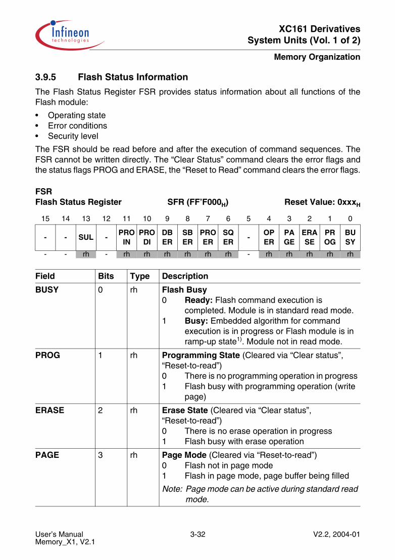
XC161 DerivativesSystem Units (Vol. 1 of 2)
Memory Organization
3.9.5 Flash Status Information
The Flash Status Register FSR provides status information about all functions of theFlash module:
• Operating state• Error conditions• Security level
The FSR should be read before and after the execution of command sequences. TheFSR cannot be written directly. The “Clear Status” command clears the error flags andthe status flags PROG and ERASE, the “Reset to Read” command clears the error flags.
FSR Flash Status Register SFR (FF’F000H) Reset Value: 0xxxH
15 14 13 12 11 10 9 8 7 6 5 4 3 2 1 0
- - SUL -PRO
INPRO
DIDB ER
SB ER
PRO ER
SQ ER
-OP ER
PA GE
ERA SE
PR OG
BU SY
- - rh - rh rh rh rh rh rh - rh rh rh rh rh
Field Bits Type Description
BUSY 0 rh Flash Busy0 Ready: Flash command execution is
completed. Module is in standard read mode.1 Busy: Embedded algorithm for command
execution is in progress or Flash module is in ramp-up state1). Module not in read mode.
PROG 1 rh Programming State (Cleared via “Clear status”, “Reset-to-read”)0 There is no programming operation in progress1 Flash busy with programming operation (write
page)
ERASE 2 rh Erase State (Cleared via “Clear status”, “Reset-to-read”)0 There is no erase operation in progress1 Flash busy with erase operation
PAGE 3 rh Page Mode (Cleared via “Reset-to-read”)0 Flash not in page mode1 Flash in page mode, page buffer being filled
Note: Page mode can be active during standard readmode.
User’s Manual 3-32 V2.2, 2004-01Memory_X1, V2.1

XC161 DerivativesSystem Units (Vol. 1 of 2)
Memory Organization
OPER 4 rh Operation Error (Cleared via “Clear status”,“Reset-to-read”)0 Flash operation successfully finished or
currently in progress1 Flash operation not successfully terminated
(abortion)
SQER 6 rh Command Sequence Error (Cleared via “Clear status”, “Reset-to-read”)0 No command sequence error detected1 State machine operation aborted due to invalid
command step
Note: SQER is not set when a command sequenceis aborted with a “Reset to Read” command.SQER is set when a “Clear Status” commandis attempted while the Flash module is busy(PROG or ERASE are not cleared).
PROER 7 rh Protection Error (Cleared via “Clear status”,“Reset-to-read”)0 No protection error detected1 Protection error has occurred:
attempt to program/erase a locked sector or invalid security code2)
SBER 8 rh Single Bit Error (Cleared via “Clear status”,“Reset-to-read”)0 Read/fetch accesses executed without error1 A single bit error was detected and
automatically corrected
DBER 9 rh Double Bit Error (Cleared via “Clear status”,“Reset-to-read”)0 No double bit error has occurred1 A double bit error was detected (no correction
possible)
PRODI 10 rh Protection Disabled0 General read/write protection active (if
installed)1 General read/write is temporarily disabled
Field Bits Type Description
User’s Manual 3-33 V2.2, 2004-01Memory_X1, V2.1
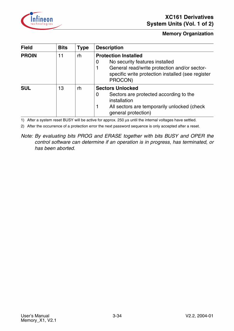
XC161 DerivativesSystem Units (Vol. 1 of 2)
Memory Organization
Note: By evaluating bits PROG and ERASE together with bits BUSY and OPER thecontrol software can determine if an operation is in progress, has terminated, orhas been aborted.
PROIN 11 rh Protection Installed0 No security features installed1 General read/write protection and/or sector-
specific write protection installed (see register PROCON)
SUL 13 rh Sectors Unlocked0 Sectors are protected according to the
installation1 All sectors are temporarily unlocked (check
general protection)1) After a system reset BUSY will be active for approx. 250 µs until the internal voltages have settled.
2) After the occurrence of a protection error the next password sequence is only accepted after a reset.
Field Bits Type Description
User’s Manual 3-34 V2.2, 2004-01Memory_X1, V2.1
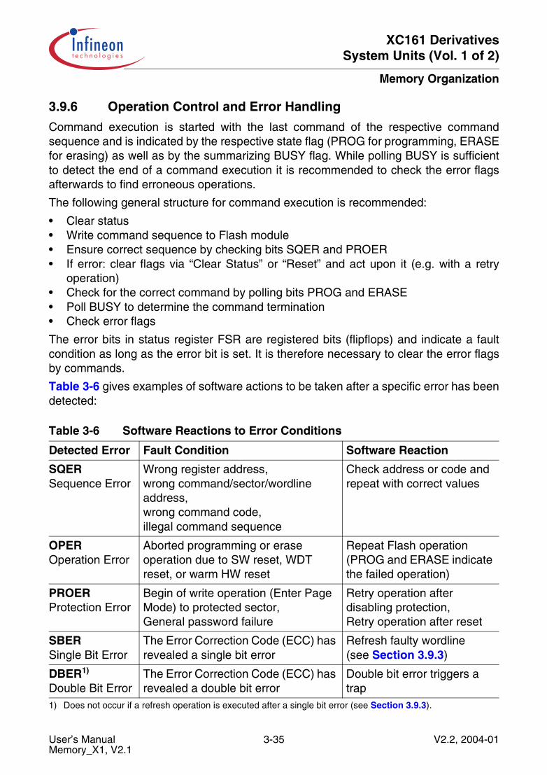
XC161 DerivativesSystem Units (Vol. 1 of 2)
Memory Organization
3.9.6 Operation Control and Error Handling
Command execution is started with the last command of the respective commandsequence and is indicated by the respective state flag (PROG for programming, ERASEfor erasing) as well as by the summarizing BUSY flag. While polling BUSY is sufficientto detect the end of a command execution it is recommended to check the error flagsafterwards to find erroneous operations.
The following general structure for command execution is recommended:
• Clear status• Write command sequence to Flash module• Ensure correct sequence by checking bits SQER and PROER• If error: clear flags via “Clear Status” or “Reset” and act upon it (e.g. with a retry
operation)• Check for the correct command by polling bits PROG and ERASE• Poll BUSY to determine the command termination• Check error flags
The error bits in status register FSR are registered bits (flipflops) and indicate a faultcondition as long as the error bit is set. It is therefore necessary to clear the error flagsby commands.
Table 3-6 gives examples of software actions to be taken after a specific error has beendetected:
Table 3-6 Software Reactions to Error Conditions
Detected Error Fault Condition Software Reaction
SQERSequence Error
Wrong register address,wrong command/sector/wordline address,wrong command code,illegal command sequence
Check address or code and repeat with correct values
OPEROperation Error
Aborted programming or erase operation due to SW reset, WDT reset, or warm HW reset
Repeat Flash operation(PROG and ERASE indicate the failed operation)
PROERProtection Error
Begin of write operation (Enter Page Mode) to protected sector,General password failure
Retry operation after disabling protection,Retry operation after reset
SBERSingle Bit Error
The Error Correction Code (ECC) has revealed a single bit error
Refresh faulty wordline(see Section 3.9.3)
DBER1)
Double Bit Error1) Does not occur if a refresh operation is executed after a single bit error (see Section 3.9.3).
The Error Correction Code (ECC) has revealed a double bit error
Double bit error triggers a trap
User’s Manual 3-35 V2.2, 2004-01Memory_X1, V2.1
XC161 DerivativesSystem Units (Vol. 1 of 2)
Memory Organization
Reset and Power-Down Processing
Upon a reset the Flash module resets its state machine and enters the standard readmode after the internal voltages have stabilized. The internal voltages need to ramp up(e.g. after power down) or to ramp down (e.g. after an interrupted programming or eraseoperation). This power stabilization phase is indicated by flag BUSY. Accesses duringthe power stabilization phase are delayed until power has stabilized.
The Flash module is requested to ramp down its internal voltages by enteringPower Down mode, Sleep mode or Idle mode (with Flash off), by disabling it viaSYSCON3, or by executing a software reset. After completing execution and terminationof the running operation (including program or erase operation) the request isacknowledged and the CPU can complete the intended action.
Note: The delay caused by the stabilization phase must also be considered whencalculating delays for wake-up from idle, sleep, or power down states.
User’s Manual 3-36 V2.2, 2004-01Memory_X1, V2.1

XC161 DerivativesSystem Units (Vol. 1 of 2)
Memory Organization
3.10 Program Memory Control
The internal program memory block IMB consists of an interface part (program memoryinterface PMI) to control the accesses to the memories and the following memory blocks:
• 128 Kbytes program Flash memory, starting at address C0’0000H(including error correction ECC)
• 2 Kbytes program SRAM, starting at address E0’0000H
The Flash memory block and the program SRAM block can contain the program code,but can also store data, which can be accessed by the CPU.
Figure 3-8 Overview of the Internal Program Memory Block IMB
Figure 3-8 shows the main blocks of the IMB, specific control signals are not mentionedfor simplicity reasons.
The behavior of the memories is adaptable to the requirements of the application. If theprogram is executed from the on-chip Flash memory or from the internal SRAM, the
ProgramSRAM
MCA05503
Program Memory Interface (PMI)Control and MultiplexerSCU
Interface
22
Interface
PMU
FlashArray C
FGS
FIM
Emulation Device(Overlay + Monitor)
Interface
64 16 22 64 16
18 64 16
WaitStatesFlash
Flas
hAc
ces
Flas
hR
eady
Program Memory Block
Address
Data
IMBCTR
RPA
EnableStartupROM
1
16
64
21
Ready
15
1
1
User’s Manual 3-37 V2.2, 2004-01Memory_X1, V2.1
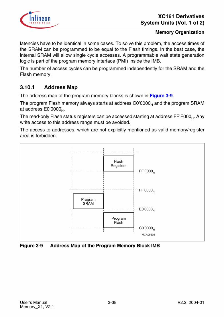
XC161 DerivativesSystem Units (Vol. 1 of 2)
Memory Organization
latencies have to be identical in some cases. To solve this problem, the access times ofthe SRAM can be programmed to be equal to the Flash timings. In the best case, theinternal SRAM will allow single cycle accesses. A programmable wait state generationlogic is part of the program memory interface (PMI) inside the IMB.
The number of access cycles can be programmed independently for the SRAM and theFlash memory.
3.10.1 Address Map
The address map of the program memory blocks is shown in Figure 3-9.
The program Flash memory always starts at address C0’0000H and the program SRAMat address E0’0000H.
The read-only Flash status registers can be accessed starting at address FF’F000H. Anywrite access to this address range must be avoided.
The access to addresses, which are not explicitly mentioned as valid memory/registerarea is forbidden.
Figure 3-9 Address Map of the Program Memory Block IMB
MCA05502
ProgramSRAM
ProgramFlash
C0'0000H
E0'0000H
FF'0000H
FF'F000H
FlashRegisters
User’s Manual 3-38 V2.2, 2004-01Memory_X1, V2.1
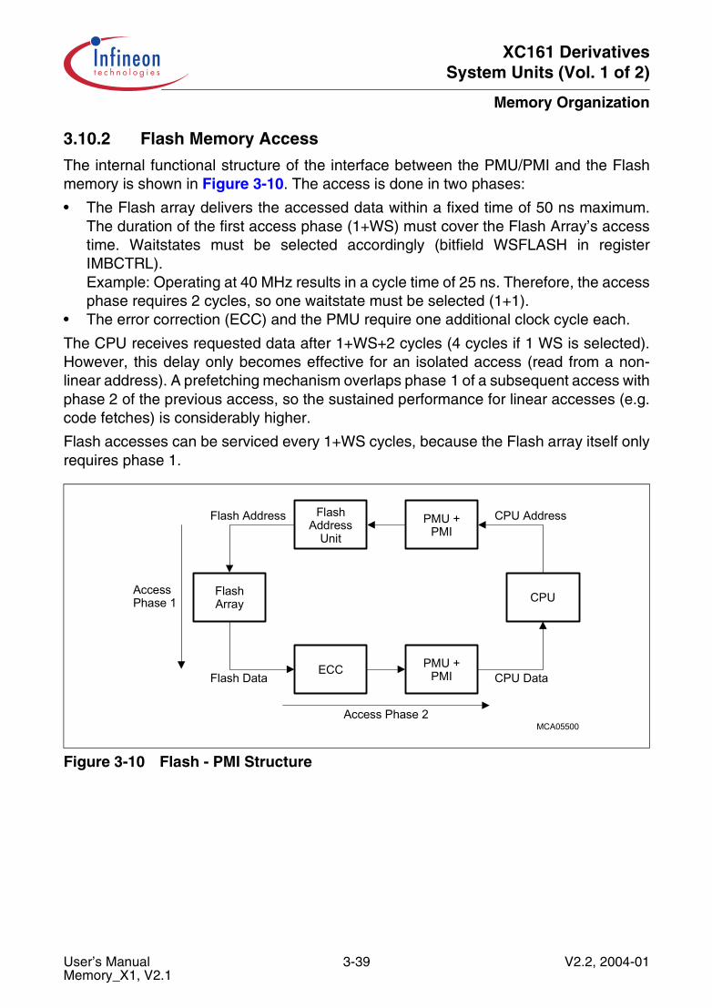
XC161 DerivativesSystem Units (Vol. 1 of 2)
Memory Organization
3.10.2 Flash Memory Access
The internal functional structure of the interface between the PMU/PMI and the Flashmemory is shown in Figure 3-10. The access is done in two phases:
• The Flash array delivers the accessed data within a fixed time of 50 ns maximum.The duration of the first access phase (1+WS) must cover the Flash Array’s accesstime. Waitstates must be selected accordingly (bitfield WSFLASH in registerIMBCTRL).Example: Operating at 40 MHz results in a cycle time of 25 ns. Therefore, the accessphase requires 2 cycles, so one waitstate must be selected (1+1).
• The error correction (ECC) and the PMU require one additional clock cycle each.
The CPU receives requested data after 1+WS+2 cycles (4 cycles if 1 WS is selected).However, this delay only becomes effective for an isolated access (read from a non-linear address). A prefetching mechanism overlaps phase 1 of a subsequent access withphase 2 of the previous access, so the sustained performance for linear accesses (e.g.code fetches) is considerably higher.
Flash accesses can be serviced every 1+WS cycles, because the Flash array itself onlyrequires phase 1.
Figure 3-10 Flash - PMI Structure
MCA05500
CPU
PMU +PMI
PMU +PMI
FlashArray
ECC
FlashAddress
Unit
AccessPhase 1
Flash Address
Flash Data
CPU Address
CPU Data
Access Phase 2
User’s Manual 3-39 V2.2, 2004-01Memory_X1, V2.1
XC161 DerivativesSystem Units (Vol. 1 of 2)
Memory Organization
Example for Flash Accesses with one Wait State (WS = 1)
After the first access (e.g. after a jump to the first address delivered by the CPU), fourclock cycles are necessary to fetch the corresponding data (1+1+2).
This leads to the following sequence of clock cycles between the delivery of subsequentdata words: 4 - 2 - 2 - 2 - 2 - …
In the case that the CPU requests another address than the one proposed by theprefetcher (e.g. in case of a jump), the Flash address unit immediately changes to thenew address and begins a new sequence (4 - …).
Note: If the Flash access phase takes more than two cycles (more than 1 WS), prefetchaccesses make no sense, so the Flash prefetching mechanism is disabled.
User’s Manual 3-40 V2.2, 2004-01Memory_X1, V2.1
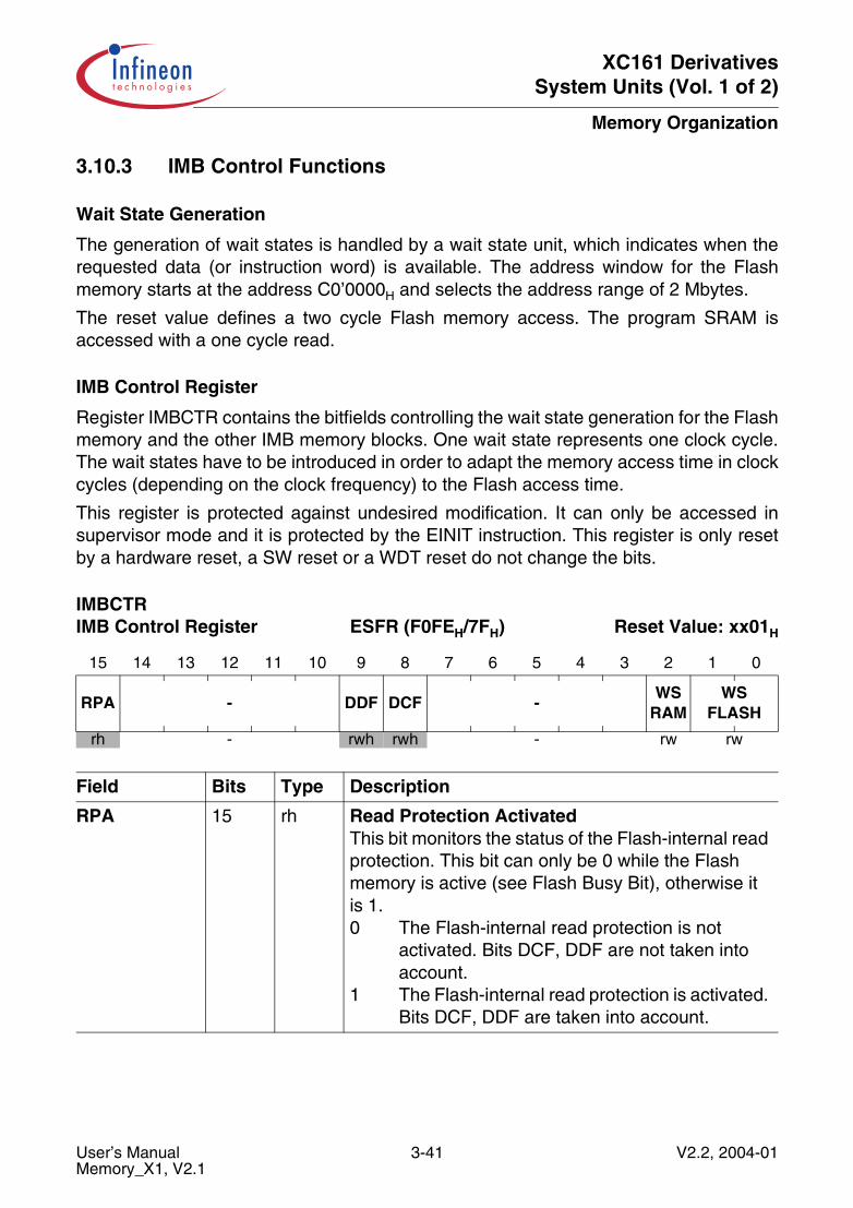
XC161 DerivativesSystem Units (Vol. 1 of 2)
Memory Organization
3.10.3 IMB Control Functions
Wait State Generation
The generation of wait states is handled by a wait state unit, which indicates when therequested data (or instruction word) is available. The address window for the Flashmemory starts at the address C0’0000H and selects the address range of 2 Mbytes.
The reset value defines a two cycle Flash memory access. The program SRAM isaccessed with a one cycle read.
IMB Control Register
Register IMBCTR contains the bitfields controlling the wait state generation for the Flashmemory and the other IMB memory blocks. One wait state represents one clock cycle.The wait states have to be introduced in order to adapt the memory access time in clockcycles (depending on the clock frequency) to the Flash access time.
This register is protected against undesired modification. It can only be accessed insupervisor mode and it is protected by the EINIT instruction. This register is only resetby a hardware reset, a SW reset or a WDT reset do not change the bits.
IMBCTRIMB Control Register ESFR (F0FEH/7FH) Reset Value: xx01H
15 14 13 12 11 10 9 8 7 6 5 4 3 2 1 0
RPA - DDF DCF -WS
RAMWS
FLASH
rh - rwh rwh - rw rw
Field Bits Type Description
RPA 15 rh Read Protection ActivatedThis bit monitors the status of the Flash-internal read protection. This bit can only be 0 while the Flash memory is active (see Flash Busy Bit), otherwise it is 1.0 The Flash-internal read protection is not
activated. Bits DCF, DDF are not taken into account.
1 The Flash-internal read protection is activated. Bits DCF, DDF are taken into account.
User’s Manual 3-41 V2.2, 2004-01Memory_X1, V2.1
XC161 DerivativesSystem Units (Vol. 1 of 2)
Memory Organization
DDF 9 rwh Disable Data Read from Flash MemoryThis bit enables/disables the data read access from the internal Flash memory area. Once set, this bit can only be cleared by a HW reset.0 The data read access from the Flash memory
area is allowed.1 The data read access from the Flash memory
area is not allowed. This bit is not taken into account while RPA = 0.
DCF 8 rwh Disable Code Fetch from Flash MemoryThis bit enables/disables the code fetch from the internal Flash memory area. Once set, this bit can only be cleared by a HW reset.0 The code fetch from the Flash memory area is
allowed.1 The code fetch from the Flash memory area is
not allowed. This bit is not taken into account while RPA = 0.
WSRAM 2 rw Wait State Control for Program RAM AccessThis bit defines the behavior of a memory in the program SRAM area in the IMB for a read access. This memory area is located in the address range from E0’0000H to F7’FFFFH. The write access to this memory area is always handled within one clock cycle for the memory.0 The program SRAM area is accessed with the
maximum access speed, which is a single cycle read access.
1 The program SRAM behaves exactly like the memory located in the Flash memory area. The pipelined structure and the access time are taken into account to rebuild the identical behavior.
Field Bits Type Description
User’s Manual 3-42 V2.2, 2004-01Memory_X1, V2.1
XC161 DerivativesSystem Units (Vol. 1 of 2)
Memory Organization
WSFLASH [1:0] rw Wait States for the Flash MemoryThis bitfield defines the number of additional wait states, which are added for a read access from the Flash memory area, which is located in the address range from C0’0000H to DF’FFFFH.00 No additional wait state is introduced for the
Flash read access. This corresponds to a Flash read access in one clock cycle.
01 One additional wait state is introduced for the Flash read access. This corresponds to a Flash read access in two clock cycles.(default)
10 Two additional wait states are introduced for the Flash read access. This corresponds to a Flash read access in three clock cycles.
11 Three additional wait states are introduced for the Flash read access. This corresponds to a Flash read access in four clock cycles.
Field Bits Type Description
User’s Manual 3-43 V2.2, 2004-01Memory_X1, V2.1
XC161 DerivativesSystem Units (Vol. 1 of 2)
Central Processing Unit (CPU)
4 Central Processing Unit (CPU) Basic tasks of the Central Processing Unit (CPU) are to fetch and decode instructions,to supply operands for the Arithmetic and Logic unit (ALU) and the Multiply andAccumulate unit (MAC), to perform operations on these operands in the ALU and MAC,and to store the previously calculated results. As the CPU is the main engine of theXC161 microcontroller, it is also affected by certain actions of the peripheral subsystem.
Because a five-stage processing pipeline (plus 2-stage fetch pipeline) is implemented inthe XC161, up to five instructions can be processed in parallel. Most instructions of theXC161 are executed in one single clock cycle due to this parallelism.
This chapter describes how the pipeline works for sequential and branch instructions ingeneral, and the hardware provisions which have been made to speed up execution ofjump instructions in particular. General instruction timing is described, including standardtiming, as well as exceptions.
While internal memory accesses are normally performed by the CPU itself, externalperipheral or memory accesses are performed by a particular on-chip External BusController (EBC) which is invoked automatically by the CPU whenever a code or dataaddress refers to the external address space.
Whenever possible, the CPU continues operating while an external memory access is inprogress. If external data are required but are not yet available, or if a new externalmemory access is requested by the CPU before a previous access has been completed,the CPU will be held by the EBC until the request can be satisfied. The EBC is describedin a separate chapter.
The on-chip peripheral units of the XC161 work nearly independently of the CPU with aseparate clock generator. Data and control information are interchanged between theCPU and these peripherals via Special Function Registers (SFRs).
Whenever peripherals need a non-deterministic CPU action, an on-chip InterruptController compares all pending peripheral service requests against each other andprioritizes one of them. If the priority of the current CPU operation is lower than thepriority of the selected peripheral request, an interrupt will occur.
There are two basic types of interrupt processing:
• Standard interrupt processing forces the CPU to save the current program statusand return address on the stack before branching to the interrupt vector jump table.
• PEC interrupt processing steals only one machine cycle from the current CPUactivity to perform a single data transfer via the on-chip Peripheral Event Controller(PEC).
System errors detected during program execution (hardware traps) and external non-maskable interrupts are also processed as standard interrupts with a very high priority.
In contrast to other on-chip peripherals, there is a closer conjunction between thewatchdog timer and the CPU. If enabled, the watchdog timer expects to be serviced by
User’s Manual 4-1 V2.2, 2004-01CPUSV2_X, V2.1
XC161 DerivativesSystem Units (Vol. 1 of 2)
Central Processing Unit (CPU)
the CPU within a programmable period of time, otherwise it will reset the chip. Thus, thewatchdog timer is able to prevent the CPU from going astray when executing erroneouscode. After reset, the watchdog timer starts counting automatically but, it can be disabledvia software, if desired.
In addition to its normal operation state, the CPU has the following particular states:
• Reset state: Any reset (hardware, software, watchdog) forces the CPU into apredefined active state.
• IDLE state: The clock signal to the CPU itself is switched off, while the clocks for theon-chip peripherals keep running.
• SLEEP state: All of the on-chip clocks are switched off (RTC clock selectable),external interrupt inputs are enabled.
• POWER DOWN state: All of the on-chip clocks are switched off (RTC clockselectable), all inputs are disregarded.
Transition to an active CPU state is forced by an interrupt (if in IDLE or SLEEP mode) orby a reset (if in POWER DOWN mode).The IDLE, SLEEP, POWER DOWN, and RESET states can be entered by specificXC161 system control instructions.
A set of Special Function Registers is dedicated to the CPU core (CSFRs):
• CPU Status Indication and Control: PSW, CPUCON1, CPUCON2• Code Access Control: IP, CSP• Data Paging Control: DPP0, DPP1, DPP2, DPP3• Global GPRs Access Control: CP• System Stack Access Control: SP, SPSEG, STKUN, STKOV• Multiply and Divide Support: MDL, MDH, MDC• Indirect Addressing Offset: QR0, QR1, QX0, QX1• MAC Address Pointers: IDX0, IDX1• MAC Status Indication and Control: MCW, MSW, MAH, MAL, MRW• ALU Constants Support: ZEROS, ONES
The CPU also uses CSFRs to access the General Purpose Registers (GPRs). Since allCSFRs can be controlled by any instruction capable of addressing the SFR/CSFRmemory space, there is no need for special system control instructions.
However, to ensure proper processor operation, certain restrictions on the user accessto some CSFRs must be imposed. For example, the instruction pointer (CSP, IP) cannotbe accessed directly at all. These registers can only be changed indirectly via branchinstructions. Registers PSW, SP, and MDC can be modified not only explicitly by theprogrammer, but also implicitly by the CPU during normal instruction processing.
Note: Note that any explicit write request (via software) to an CSFR supersedes asimultaneous modification by hardware of the same register.
User’s Manual 4-2 V2.2, 2004-01CPUSV2_X, V2.1
XC161 DerivativesSystem Units (Vol. 1 of 2)
Central Processing Unit (CPU)
All CSFRs may be accessed wordwise, or bytewise (some of them even bitwise).Reading bytes from word CSFRs is a non-critical operation. Any write operation to asingle byte of a CSFR clears the non-addressed complementary byte within the specifiedCSFR.
Attention: Reserved CSFR bits must not be modified explicitly, and will alwayssupply a read value of 0. If a byte/word access is preferred by theprogrammer or is the only possible access the reserved CSFR bitsmust be written with 0 to provide compatibility with future versions.
User’s Manual 4-3 V2.2, 2004-01CPUSV2_X, V2.1
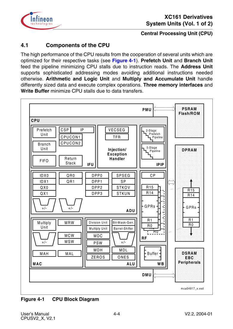
XC161 DerivativesSystem Units (Vol. 1 of 2)
Central Processing Unit (CPU)
4.1 Components of the CPU
The high performance of the CPU results from the cooperation of several units which areoptimized for their respective tasks (see Figure 4-1). Prefetch Unit and Branch Unitfeed the pipeline minimizing CPU stalls due to instruction reads. The Address Unitsupports sophisticated addressing modes avoiding additional instructions neededotherwise. Arithmetic and Logic Unit and Multiply and Accumulate Unit handledifferently sized data and execute complex operations. Three memory interfaces andWrite Buffer minimize CPU stalls due to data transfers.
Figure 4-1 CPU Block Diagram
DPRAM
CPU
IPIP
RF
R 0R 1
G P R s
R 14R 15
R 0R 1
G P R s
R 14R 15
IFU
Injection/Exception
Handler
ADU
MAC
m ca04917_x.vsd
C P U C O N 1
C P U C O N 2
C S P IP
R etu rnS tackF IFO
B ranchU n it
P refetchU n it
V E C S E G
TFR
+/-
ID X 0
ID X 1
Q X 0
Q X 1
Q R 0
Q R 1
D P P 0
D P P 1
D P P 2
D P P 3
S P S E G
S P
S TK O V
S TK U N
+ /-
M R W
M C W
M S W
M A L
+/-
M A H
M ultip lyU n it
ALU
D iv is ion U n it
M u ltip ly U n it
B it-M ask-G en .
Barre l-Sh ifte r
+ /-
M D C
P S W
M D H
ZE R O S
M D L
O N E S
R 0R 1
G P R s
R 14R 15
C P
W B
B uffer
2-S tagePrefe tch
P ipe line
5-S tagePipe line
R 0R 1
G PR s
R 14R 15
PMU
DMU
DSRAMEBC
Peripherals
PSRAMFlash/ROM
User’s Manual 4-4 V2.2, 2004-01CPUSV2_X, V2.1
XC161 DerivativesSystem Units (Vol. 1 of 2)
Central Processing Unit (CPU)
In general the instructions move through 7 pipeline stages, where each stage processesits individual task (see Section 4.3 for a summary):
• the 2-stage fetch pipeline prefetches instructions from program memory and storesthem into an instruction FIFO
• the 5-stage processing pipeline executes each instruction stored in the instructionFIFO
Because passing through one pipeline stage takes at least one clock cycle, any isolatedinstruction takes at least five clock cycles to be completed. Pipelining, however, allowsparallel (i.e. simultaneous) processing of up to five instructions (with branches up to sixinstructions). Therefore, most of the instructions appear to be processed during oneclock cycle as soon as the pipeline has been filled once after reset.
The pipelining increases the average instruction throughput considered over a certainperiod of time.
4.2 Instruction Fetch and Program Flow Control
The Instruction Fetch Unit (IFU) prefetches and preprocesses instructions to provide acontinuous instruction flow. The IFU can fetch simultaneously at least two instructionsvia a 64-bit wide bus from the Program Management Unit (PMU). The prefetchedinstructions are stored in an instruction FIFO.
Preprocessing of branch instructions enables the instruction flow to be predicted. Whilethe CPU is in the process of executing an instruction fetched from the FIFO, theprefetcher of the IFU starts to fetch a new instruction at a predicted target address fromthe PMU. The latency time of this access is hidden by the execution of the instructionswhich have already been buffered in the FIFO. Even for a non-sequential instructionexecution, the IFU can generally provide a continuous instruction flow. The IFU containstwo pipeline stages: the Prefetch Stage and the Fetch Stage.
During the prefetch stage, the Branch Detection and Prediction Logic analyzes up tothree prefetched instructions stored in the first Instruction Buffer (can hold up to sixinstructions). If a branch is detected, then the IFU starts to fetch the next instructionsfrom the PMU according to the prediction rules. After having been analyzed, up to threeinstructions are stored in the second Instruction Buffer (can hold up to three instructions)which is the input register of the Fetch Stage.
In the case of an incorrectly predicted instruction flow, the instruction fetch pipeline isbypassed to reduce the number of dead cycles.
User’s Manual 4-5 V2.2, 2004-01CPUSV2_X, V2.1

XC161 DerivativesSystem Units (Vol. 1 of 2)
Central Processing Unit (CPU)
Figure 4-2 IFU Block Diagram
On the Fetch Stage, the prefetched instructions are stored in the instruction FIFO. TheBranch Folding Unit (BFU) allows processing of branch instructions in parallel withpreceding instructions. To achieve this the BFU preprocesses and reformats the branchinstruction. First, the BFU defines (calculates) the absolute target address. This address— after being combined with branch condition and branch attribute bits — is stored inthe same FIFO step as the preceding instruction. The target address is also used toprefetch the next instructions.
For the Processing Pipeline, both instructions are fetched from the FIFO again and areexecuted in parallel. If the instruction flow was predicted incorrectly (or FIFO is empty),the two stages of the IFU can be bypassed.
Note: Pipeline behavior in case of a incorrectly predicted instruction flow is described inthe following sections.
MCA05501
Branch Detection and Prediction Logic
64-bitData
Instruction Buffer (up to 3 Instr.)
InstructionFIFO
Branch FoldingUnit
PrefetchStage
Bypa
ss F
etch
to D
ecod
e
Bypa
ss P
refe
tch
to D
ecod
e
FetchStage
DecodeStage
Instruction Buffer (up to 1 Instr.)
Injection and ExceptionHandler
TFRVECSEG
Control Registers
CPUCON2
Return Stack
CPUCON1
24-bitAddress
IFU Control IFU Pipeline
CSPIP+/-
Instruction Buffer (up to 6 Instr.)
User’s Manual 4-6 V2.2, 2004-01CPUSV2_X, V2.1
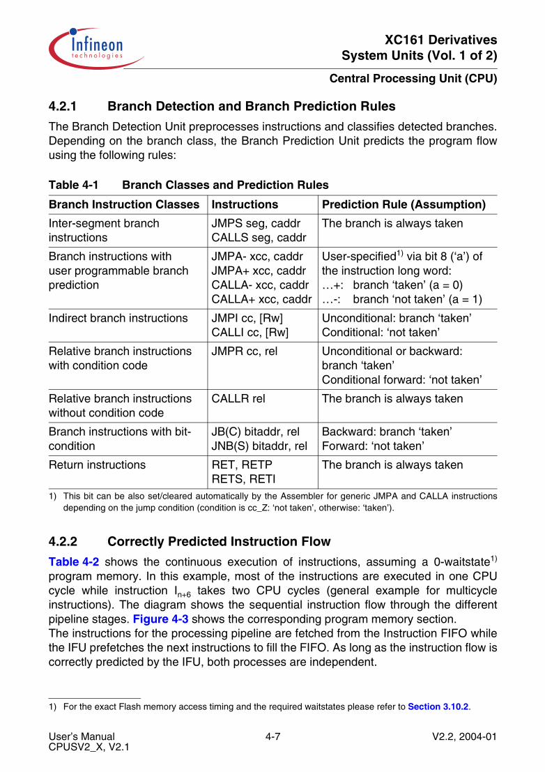
XC161 DerivativesSystem Units (Vol. 1 of 2)
Central Processing Unit (CPU)
4.2.1 Branch Detection and Branch Prediction Rules
The Branch Detection Unit preprocesses instructions and classifies detected branches.Depending on the branch class, the Branch Prediction Unit predicts the program flowusing the following rules:
4.2.2 Correctly Predicted Instruction Flow
Table 4-2 shows the continuous execution of instructions, assuming a 0-waitstate1)
program memory. In this example, most of the instructions are executed in one CPUcycle while instruction In+6 takes two CPU cycles (general example for multicycleinstructions). The diagram shows the sequential instruction flow through the differentpipeline stages. Figure 4-3 shows the corresponding program memory section.The instructions for the processing pipeline are fetched from the Instruction FIFO whilethe IFU prefetches the next instructions to fill the FIFO. As long as the instruction flow iscorrectly predicted by the IFU, both processes are independent.
Table 4-1 Branch Classes and Prediction Rules
Branch Instruction Classes Instructions Prediction Rule (Assumption)
Inter-segment branch instructions
JMPS seg, caddrCALLS seg, caddr
The branch is always taken
Branch instructions withuser programmable branch prediction
JMPA- xcc, caddrJMPA+ xcc, caddrCALLA- xcc, caddrCALLA+ xcc, caddr
User-specified1) via bit 8 (‘a’) of the instruction long word:…+: branch ‘taken’ (a = 0)…-: branch ‘not taken’ (a = 1)
1) This bit can be also set/cleared automatically by the Assembler for generic JMPA and CALLA instructionsdepending on the jump condition (condition is cc_Z: ‘not taken’, otherwise: ‘taken’).
Indirect branch instructions JMPI cc, [Rw]CALLI cc, [Rw]
Unconditional: branch ‘taken’Conditional: ‘not taken’
Relative branch instructions with condition code
JMPR cc, rel Unconditional or backward: branch ‘taken’Conditional forward: ‘not taken’
Relative branch instructions without condition code
CALLR rel The branch is always taken
Branch instructions with bit-condition
JB(C) bitaddr, relJNB(S) bitaddr, rel
Backward: branch ‘taken’Forward: ‘not taken’
Return instructions RET, RETPRETS, RETI
The branch is always taken
1) For the exact Flash memory access timing and the required waitstates please refer to Section 3.10.2.
User’s Manual 4-7 V2.2, 2004-01CPUSV2_X, V2.1
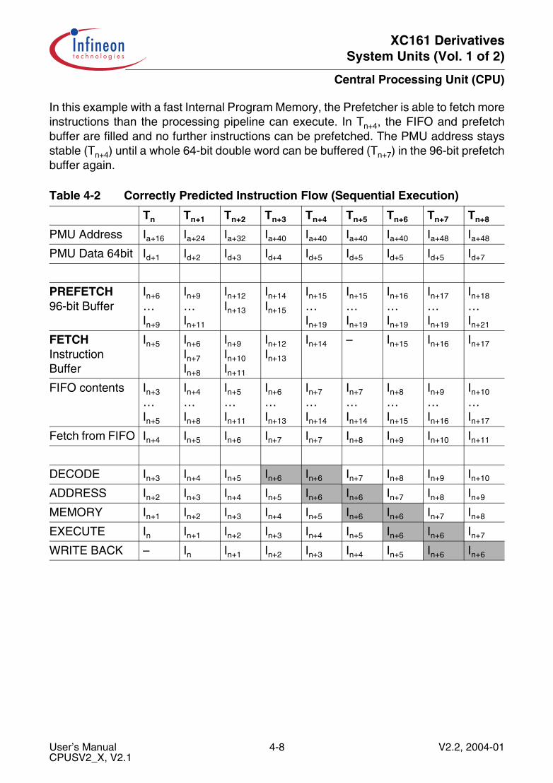
XC161 DerivativesSystem Units (Vol. 1 of 2)
Central Processing Unit (CPU)
In this example with a fast Internal Program Memory, the Prefetcher is able to fetch moreinstructions than the processing pipeline can execute. In Tn+4, the FIFO and prefetchbuffer are filled and no further instructions can be prefetched. The PMU address staysstable (Tn+4) until a whole 64-bit double word can be buffered (Tn+7) in the 96-bit prefetchbuffer again.
Table 4-2 Correctly Predicted Instruction Flow (Sequential Execution)
Tn Tn+1 Tn+2 Tn+3 Tn+4 Tn+5 Tn+6 Tn+7 Tn+8
PMU Address Ia+16 Ia+24 Ia+32 Ia+40 Ia+40 Ia+40 Ia+40 Ia+48 Ia+48
PMU Data 64bit Id+1 Id+2 Id+3 Id+4 Id+5 Id+5 Id+5 Id+5 Id+7
PREFETCH96-bit Buffer
In+6…In+9
In+9…In+11
In+12In+13
In+14In+15
In+15…In+19
In+15…In+19
In+16…In+19
In+17…In+19
In+18…In+21
FETCHInstruction Buffer
In+5 In+6
In+7In+8
In+9
In+10In+11
In+12
In+13
In+14 – In+15 In+16 In+17
FIFO contents In+3…In+5
In+4…In+8
In+5…In+11
In+6…In+13
In+7…In+14
In+7…In+14
In+8…In+15
In+9…In+16
In+10…In+17
Fetch from FIFO In+4 In+5 In+6 In+7 In+7 In+8 In+9 In+10 In+11
DECODE In+3 In+4 In+5 In+6 In+6 In+7 In+8 In+9 In+10
ADDRESS In+2 In+3 In+4 In+5 In+6 In+6 In+7 In+8 In+9
MEMORY In+1 In+2 In+3 In+4 In+5 In+6 In+6 In+7 In+8
EXECUTE In In+1 In+2 In+3 In+4 In+5 In+6 In+6 In+7
WRITE BACK – In In+1 In+2 In+3 In+4 In+5 In+6 In+6
User’s Manual 4-8 V2.2, 2004-01CPUSV2_X, V2.1

XC161 DerivativesSystem Units (Vol. 1 of 2)
Central Processing Unit (CPU)
Figure 4-3 Program Memory Section for Correctly Predicted Flow
4.2.3 Incorrectly Predicted Instruction Flow
If the CPU detects that the IFU made an incorrect prediction of the instruction flow, thenthe pipeline stages and the Instruction FIFO containing the wrong prefetched instructionsare canceled. The entire instruction fetch is restarted at the correct point of the program.
Table 4-3 shows the restarted execution of instructions, assuming a 0-waitstate programmemory. Figure 4-4 shows the corresponding program memory section.
During the cycle Tn, the CPU detects an incorrectly prediction case which leads to acanceling of the pipeline. The new address is transferred to the PMU in Tn+1 whichdelivers the first data in the next cycle Tn+2. But, the target instruction crosses the 64-bitmemory boundary and a second fetch in Tn+3 is required to get the entire 32-bitinstruction. In Tn+4, the Prefetch Buffer contains two 32-bit instructions while the firstinstruction Im is directly forwarded to the Decode stage.
The prefetcher is now restarted and prefetches further instructions. In Tn+5, theinstruction Im+1 is forwarded from the Fetch Instruction Buffer directly to the Decodestage as well. The Fetch row shows all instructions in the Fetch Instruction Buffer andthe instructions fetched from the Instruction FIFO. The instruction Im+3 is the firstinstruction fetched from the FIFO during Tn+6. During the same cycle, instruction Im+2 wasstill forwarded from the Fetch Instruction Buffer to the Decode stage.
MCA04918
In+21 In+21 In+20 In+20
In+19 In+18 In+17 In+16
In+16 In+15 In+15 In+14
In+14 In+13 In+12 In+12
In+11 In+11 In+10 In+10
In+9 In+8 In+7 In+6
Ia+40
Ia+32
Ia+24
Ia+16
Ia+8
Ia
User’s Manual 4-9 V2.2, 2004-01CPUSV2_X, V2.1

XC161 DerivativesSystem Units (Vol. 1 of 2)
Central Processing Unit (CPU)
Figure 4-4 Program Memory Section for Incorrectly Predicted Flow
Table 4-3 Incorrectly Predicted Instruction Flow (Restarted Execution)
Tn Tn+1 Tn+2 Tn+3 Tn+4 Tn+5 Tn+6 Tn+7 Tn+8
PMU Address I… Ia Ia+8 Ia+16 Ia+24 I… I… I… I…
PMU Data 64bit I… – Id Id+1 Id+2 Id+3 I… I… I…
PREFETCH96-bit Buffer
I… – – – ImIm+1
Im+2Im+3
Im+4Im+5
I… I…
FETCHInstruction Buffer
Inext+2 – – – – Im+1 Im+2
Im+3
Im+4
Im+5
I…
Fetch from FIFO – – – – – – Im+3 Im+4 Im+5
DECODE Inext+1 – – – Im Im+1 Im+2 Im+3 Im+4
ADDRESS Inext – – – – Im Im+1 Im+2 Im+3
MEMORY Ibranch – – – – – Im Im+1 Im+2
EXECUTE In Ibranch – – – – – Im Im+1
WRITE BACK – In Ibranch – – – – – Im
MCA04919
I... Im+5 Im+5 Im+4
Im+4 Im+3 Im+3
Im+1
Ia+24
Ia+16
Ia+8
Ia
I...
Im+2
ImIm+1Im+2
Im I... I...
64-bit wide Program Memory with four 16 bit packages
User’s Manual 4-10 V2.2, 2004-01CPUSV2_X, V2.1
XC161 DerivativesSystem Units (Vol. 1 of 2)
Central Processing Unit (CPU)
4.3 Instruction Processing Pipeline
The XC161 uses five pipeline stages to execute an instruction. All instructions passthrough each of the five stages of the instruction processing pipeline. The pipeline stagesare listed here together with the 2 stages of the fetch pipeline:
1st -> PREFETCH: This stage prefetches instructions from the PMU in the predictedorder. The instructions are preprocessed in the branch detection unit to detect branches.The prediction logic decides if the branches are assumed to be taken or not.
2nd -> FETCH: The instruction pointer of the next instruction to be fetched is calculatedaccording to the branch prediction rules. For zero-cycle branch execution, the BranchFolding Unit preprocesses and combines detected branches with the precedinginstructions. Prefetched instructions are stored in the instruction FIFO. At the same time,instructions are transported out of the instruction FIFO to be executed in the instructionprocessing pipeline.
3rd -> DECODE: The instructions are decoded and, if required, the register file isaccessed to read the GPR used in indirect addressing modes.
4th -> ADDRESS: All the operand addresses are calculated. Register SP isdecremented or incremented for all instructions which implicitly access the system stack.
5th -> MEMORY: All the required operands are fetched.
6th -> EXECUTE: An ALU or MAC-Unit operation is performed on the previously fetchedoperands. The condition flags are updated. All explicit write operations to CPU-SFRsand all auto-increment/auto-decrement operations of GPRs used as indirect addresspointers are performed.
7th -> WRITE BACK: All external operands and the remaining operands within theinternal DPRAM space are written back. Operands located in the internal SRAM arebuffered in the Write Back Buffer.
Specific so-called injected instructions are generated internally to provide the timeneeded to process instructions requiring more than one CPU cycle for processing. Theyare automatically injected into the decode stage of the pipeline, then they pass throughthe remaining stages like every standard instruction. Program interrupt, PEC transfer,and OCE operations are also performed by means of injected instructions. Althoughthese internally injected instructions will not be noticed in reality, they help to explain theoperation of the pipeline.
The performance of the CPU (pipeline) is decreased by bandwidth limitations (sameresource is accessed by different stages) and data dependencies between instructions.The XC161’s CPU has dedicated hardware to detect and to resolve different kinds ofdependencies. Some of those dependencies are described in the following section.
Because up to five different instructions are processed simultaneously, additionalhardware has been dedicated to deal with dependencies which may exist betweeninstructions in different pipeline stages. This extra hardware supports ‘forwarding’ of the
User’s Manual 4-11 V2.2, 2004-01CPUSV2_X, V2.1
XC161 DerivativesSystem Units (Vol. 1 of 2)
Central Processing Unit (CPU)
operand read and write values and resolves most of the possible conflicts — such asmultiple usage of buses — in a time optimized way without performance loss. Thismakes the pipeline unnoticeable for the user in most cases. However, there are somerare cases in which the pipeline requires attention by the programmer. In these cases,the delays caused by the pipeline conflicts can be used for other instructions to optimizeperformance.
Note: The XC161 has a fully interlocked pipeline, which means that these conflicts donot cause any malfunction. Instruction re-ordering is only required for performancereasons.
The following examples describe the pipeline behavior in special cases and giveprinciple rules to improve the performance by re-ordering the execution of instructions.
User’s Manual 4-12 V2.2, 2004-01CPUSV2_X, V2.1

XC161 DerivativesSystem Units (Vol. 1 of 2)
Central Processing Unit (CPU)
4.3.1 Pipeline Conflicts Using General Purpose Registers
The GPRs are the working registers of the CPU and there are a lot of possibledependencies between instructions using GPRs. A high-speed five-port register fileprevents bandwidth conflicts. Dedicated hardware is implemented to detect and resolvethe data dependencies. Special forwarding busses are used to forward GPR values fromone pipeline stage to another. In most cases, this allows the execution of instructionswithout any delay despite of data dependencies.
Conflict_GPRs_Resolved:In ADD R0,R1 ;Compute new value for R0In+1 ADD R3,R0 ;Use R0 againIn+2 ADD R6,R0 ;Use R0 againIn+3 ADD R6,R1 ;Use R6 againIn+4 ...
Table 4-4 Resolved Pipeline Dependencies Using GPRs
Stage Tn Tn+1 Tn+2 Tn+31)
1) R0 forwarded from EXECUTE to MEMORY.
Tn+42)
2) R0 forwarded from WRITE BACK to MEMORY.
Tn+53)
3) R6 forwarded from EXECUTE to MEMORY.
DECODE In = ADD R0, R1
In+1 = ADD R3, R0
In+2 = ADD R6, R0
In+3 = ADD R6, R1
In+4 In+5
ADDRESS In-1 In = ADD R0, R1
In+1 = ADD R3, R0
In+2 = ADD R6, R0
In+3 = ADD R6, R1
In+4
MEMORY In-2 In-1 In = ADD R0, R1
In+1 = ADD R3, R0
In+2 = ADD R6, R0
In+3 = ADD R6, R1
EXECUTE In-3 In-2 In-1 In = ADD R0, R1
In+1 = ADD R3, R0
In+2 = ADD R6, R0
WR.BACK In-4 In-3 In-2 In-1 In = ADD R0, R1
In+1 = ADD R3, R0
User’s Manual 4-13 V2.2, 2004-01CPUSV2_X, V2.1
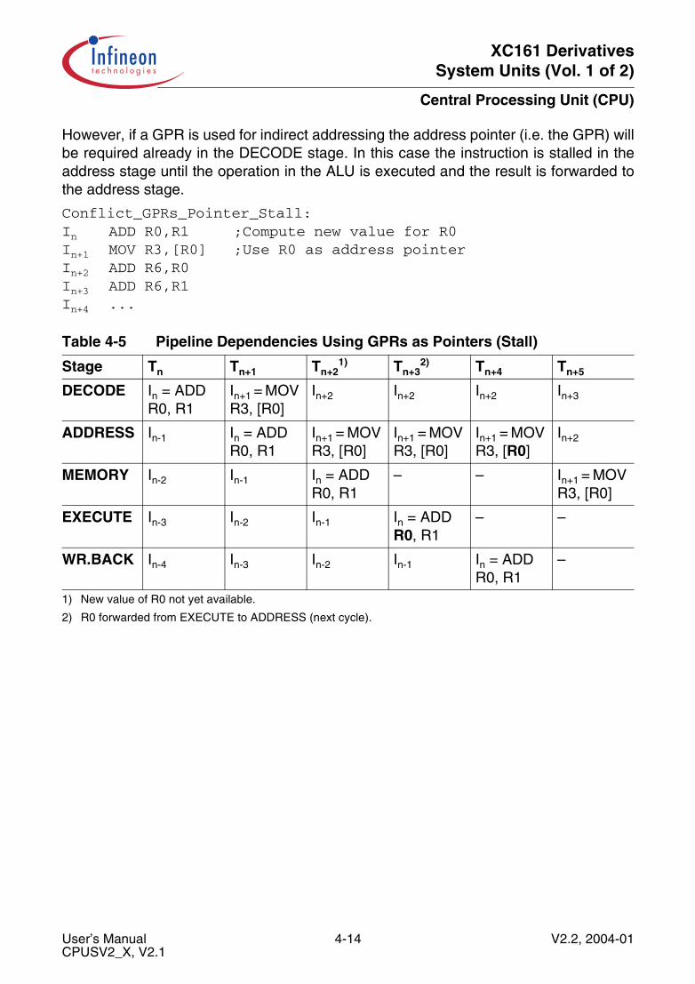
XC161 DerivativesSystem Units (Vol. 1 of 2)
Central Processing Unit (CPU)
However, if a GPR is used for indirect addressing the address pointer (i.e. the GPR) willbe required already in the DECODE stage. In this case the instruction is stalled in theaddress stage until the operation in the ALU is executed and the result is forwarded tothe address stage.
Conflict_GPRs_Pointer_Stall:In ADD R0,R1 ;Compute new value for R0In+1 MOV R3,[R0] ;Use R0 as address pointerIn+2 ADD R6,R0In+3 ADD R6,R1In+4 ...
Table 4-5 Pipeline Dependencies Using GPRs as Pointers (Stall)
Stage Tn Tn+1 Tn+21)
1) New value of R0 not yet available.
Tn+32)
2) R0 forwarded from EXECUTE to ADDRESS (next cycle).
Tn+4 Tn+5
DECODE In = ADD R0, R1
In+1 = MOV R3, [R0]
In+2 In+2 In+2 In+3
ADDRESS In-1 In = ADD R0, R1
In+1 = MOV R3, [R0]
In+1 = MOV R3, [R0]
In+1 = MOV R3, [R0]
In+2
MEMORY In-2 In-1 In = ADD R0, R1
– – In+1 = MOV R3, [R0]
EXECUTE In-3 In-2 In-1 In = ADD R0, R1
– –
WR.BACK In-4 In-3 In-2 In-1 In = ADD R0, R1
–
User’s Manual 4-14 V2.2, 2004-01CPUSV2_X, V2.1
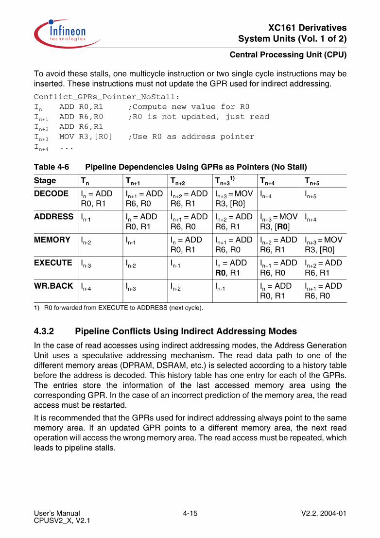
XC161 DerivativesSystem Units (Vol. 1 of 2)
Central Processing Unit (CPU)
To avoid these stalls, one multicycle instruction or two single cycle instructions may beinserted. These instructions must not update the GPR used for indirect addressing.
Conflict_GPRs_Pointer_NoStall:In ADD R0,R1 ;Compute new value for R0In+1 ADD R6,R0 ;R0 is not updated, just readIn+2 ADD R6,R1In+3 MOV R3,[R0] ;Use R0 as address pointerIn+4 ...
4.3.2 Pipeline Conflicts Using Indirect Addressing Modes
In the case of read accesses using indirect addressing modes, the Address GenerationUnit uses a speculative addressing mechanism. The read data path to one of thedifferent memory areas (DPRAM, DSRAM, etc.) is selected according to a history tablebefore the address is decoded. This history table has one entry for each of the GPRs.The entries store the information of the last accessed memory area using thecorresponding GPR. In the case of an incorrect prediction of the memory area, the readaccess must be restarted.
It is recommended that the GPRs used for indirect addressing always point to the samememory area. If an updated GPR points to a different memory area, the next readoperation will access the wrong memory area. The read access must be repeated, whichleads to pipeline stalls.
Table 4-6 Pipeline Dependencies Using GPRs as Pointers (No Stall)
Stage Tn Tn+1 Tn+2 Tn+31)
1) R0 forwarded from EXECUTE to ADDRESS (next cycle).
Tn+4 Tn+5
DECODE In = ADD R0, R1
In+1 = ADD R6, R0
In+2 = ADD R6, R1
In+3 = MOV R3, [R0]
In+4 In+5
ADDRESS In-1 In = ADD R0, R1
In+1 = ADD R6, R0
In+2 = ADD R6, R1
In+3 = MOV R3, [R0]
In+4
MEMORY In-2 In-1 In = ADD R0, R1
In+1 = ADD R6, R0
In+2 = ADD R6, R1
In+3 = MOV R3, [R0]
EXECUTE In-3 In-2 In-1 In = ADD R0, R1
In+1 = ADD R6, R0
In+2 = ADD R6, R1
WR.BACK In-4 In-3 In-2 In-1 In = ADD R0, R1
In+1 = ADD R6, R0
User’s Manual 4-15 V2.2, 2004-01CPUSV2_X, V2.1
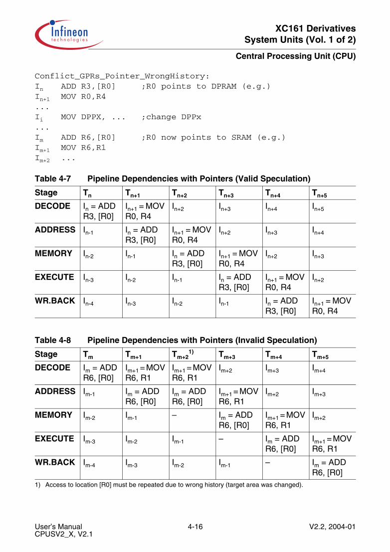
XC161 DerivativesSystem Units (Vol. 1 of 2)
Central Processing Unit (CPU)
Conflict_GPRs_Pointer_WrongHistory:In ADD R3,[R0] ;R0 points to DPRAM (e.g.)In+1 MOV R0,R4...Ii MOV DPPX, ... ;change DPPx...Im ADD R6,[R0] ;R0 now points to SRAM (e.g.)Im+1 MOV R6,R1Im+2 ...
Table 4-7 Pipeline Dependencies with Pointers (Valid Speculation)
Stage Tn Tn+1 Tn+2 Tn+3 Tn+4 Tn+5
DECODE In = ADD R3, [R0]
In+1 = MOV R0, R4
In+2 In+3 In+4 In+5
ADDRESS In-1 In = ADD R3, [R0]
In+1 = MOV R0, R4
In+2 In+3 In+4
MEMORY In-2 In-1 In = ADD R3, [R0]
In+1 = MOV R0, R4
In+2 In+3
EXECUTE In-3 In-2 In-1 In = ADD R3, [R0]
In+1 = MOV R0, R4
In+2
WR.BACK In-4 In-3 In-2 In-1 In = ADD R3, [R0]
In+1 = MOV R0, R4
Table 4-8 Pipeline Dependencies with Pointers (Invalid Speculation)
Stage Tm Tm+1 Tm+21)
1) Access to location [R0] must be repeated due to wrong history (target area was changed).
Tm+3 Tm+4 Tm+5
DECODE Im = ADD R6, [R0]
Im+1 = MOV R6, R1
Im+1 = MOV R6, R1
Im+2 Im+3 Im+4
ADDRESS Im-1 Im = ADD R6, [R0]
Im = ADD R6, [R0]
Im+1 = MOV R6, R1
Im+2 Im+3
MEMORY Im-2 Im-1 – Im = ADD R6, [R0]
Im+1 = MOV R6, R1
Im+2
EXECUTE Im-3 Im-2 Im-1 – Im = ADD R6, [R0]
Im+1 = MOV R6, R1
WR.BACK Im-4 Im-3 Im-2 Im-1 – Im = ADD R6, [R0]
User’s Manual 4-16 V2.2, 2004-01CPUSV2_X, V2.1

XC161 DerivativesSystem Units (Vol. 1 of 2)
Central Processing Unit (CPU)
4.3.3 Pipeline Conflicts Due to Memory Bandwidth
Memory bandwidth conflicts can occur if instructions in the pipeline access the samememory area at the same time. Special access mechanisms are implemented tominimize conflicts. The DPRAM of the CPU has two independent read/write ports; thisallows parallel read and write operation without delays. Write accesses to the DSRAMcan be buffered in a Write Back Buffer until read accesses are finished.
All instructions except the CoXXX instructions can read only one memory operand percycle. A conflict between the read and one write access cannot occur because theDPRAM has two independent read/write ports. Only other pipeline stall conditions cangenerate a DPRAM bandwidth conflict. The DPRAM is a synchronous pipelinedmemory. The read access starts with the valid addresses on the address stage. The dataare delivered in the Memory stage. If a memory read access is stalled in the Memorystage and the following instruction on the Address stage tries to start a memory read, thenew read access must be delayed as well. But, this conflict is hidden by an alreadyexisting stall of the pipeline.
User’s Manual 4-17 V2.2, 2004-01CPUSV2_X, V2.1

XC161 DerivativesSystem Units (Vol. 1 of 2)
Central Processing Unit (CPU)
The CoXXX instructions are the only instructions able to read two memory operands percycle. A conflict between the two read and one pending write access can occur if all threeoperands are located in the DPRAM area. This is especially important for performancein the case of executing a filter routine. One of the operands should be located in theDSRAM to guarantee a single-cycle execution of the CoXXX instructions.
Conflict_DPRAM_Bandwidth:In ADD op1,R1In+1 ADD R6,R0In+2 CoMAC [IDX0],[R0]In+3 MOV R3,[R0]In+4 ...
Table 4-9 Pipeline Dependencies in Case of Memory Conflicts (DPRAM)
Stage Tn Tn+1 Tn+2 Tn+3 Tn+41)
1) COMAC instruction stalls due to memory bandwidth conflict.
Tn+5
DECODE In = ADD op1, R1
In+1 = ADD R6, R0
In+2 = CoMAC …
In+3 = MOV R3, [R0]
In+4 In+4
ADDRESS In-1 In = ADD op1, R1
In+1 = ADD R6, R0
In+2 = CoMAC …
In+3 = MOV R3, [R0]
In+3 = MOV R3, [R0]
MEMORY In-2 In-1 In = ADD op1, R1
In+1 = ADD R6, R0
In+2 = CoMAC …
In+2 = CoMAC …
EXECUTE In-3 In-2 In-1 In = ADD op1, R1
In+1 = ADD R6, R0
–
WR.BACK In-4 In-3 In-2 In-1 In = ADD op1, R1
In+1 = ADD R6, R0
User’s Manual 4-18 V2.2, 2004-01CPUSV2_X, V2.1
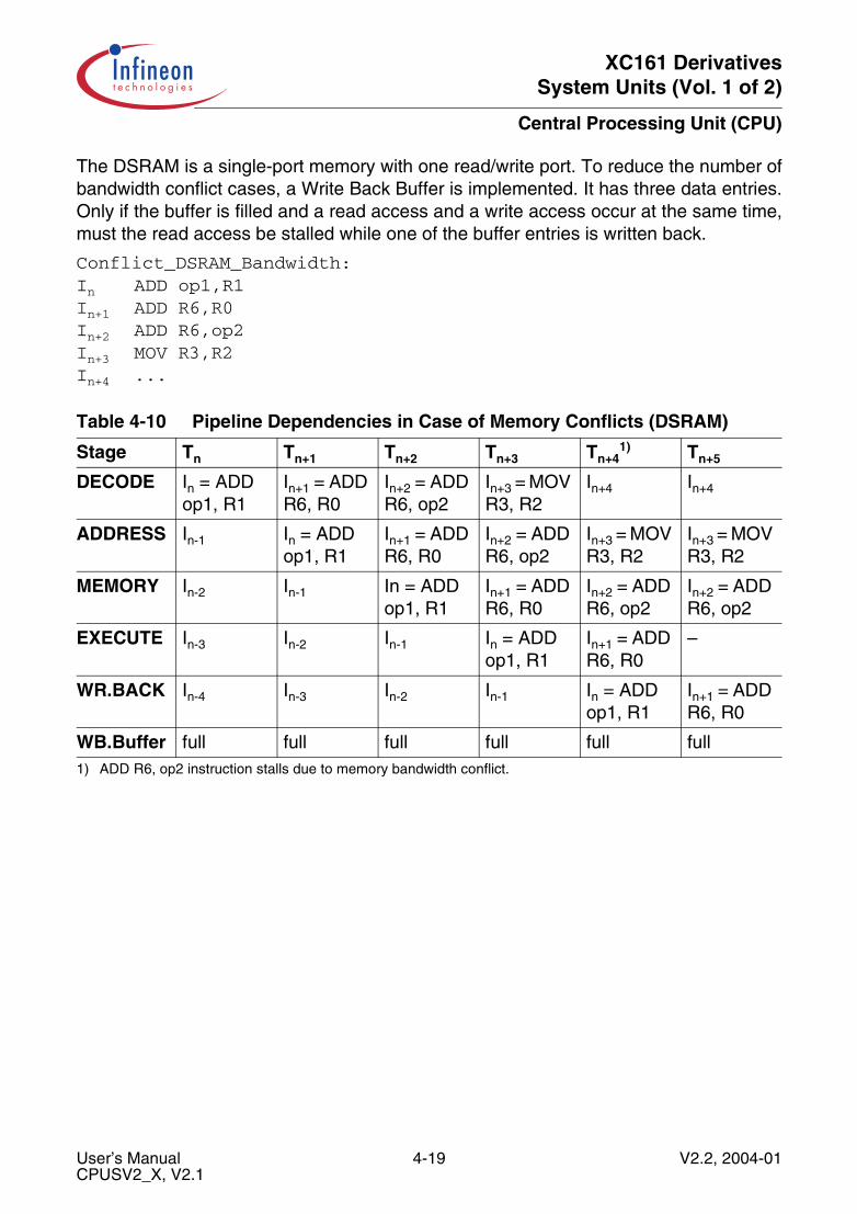
XC161 DerivativesSystem Units (Vol. 1 of 2)
Central Processing Unit (CPU)
The DSRAM is a single-port memory with one read/write port. To reduce the number ofbandwidth conflict cases, a Write Back Buffer is implemented. It has three data entries.Only if the buffer is filled and a read access and a write access occur at the same time,must the read access be stalled while one of the buffer entries is written back.
Conflict_DSRAM_Bandwidth:In ADD op1,R1In+1 ADD R6,R0In+2 ADD R6,op2In+3 MOV R3,R2In+4 ...
Table 4-10 Pipeline Dependencies in Case of Memory Conflicts (DSRAM)
Stage Tn Tn+1 Tn+2 Tn+3 Tn+41)
1) ADD R6, op2 instruction stalls due to memory bandwidth conflict.
Tn+5
DECODE In = ADD op1, R1
In+1 = ADD R6, R0
In+2 = ADD R6, op2
In+3 = MOV R3, R2
In+4 In+4
ADDRESS In-1 In = ADD op1, R1
In+1 = ADD R6, R0
In+2 = ADD R6, op2
In+3 = MOV R3, R2
In+3 = MOV R3, R2
MEMORY In-2 In-1 In = ADD op1, R1
In+1 = ADD R6, R0
In+2 = ADD R6, op2
In+2 = ADD R6, op2
EXECUTE In-3 In-2 In-1 In = ADD op1, R1
In+1 = ADD R6, R0
–
WR.BACK In-4 In-3 In-2 In-1 In = ADD op1, R1
In+1 = ADD R6, R0
WB.Buffer full full full full full full
User’s Manual 4-19 V2.2, 2004-01CPUSV2_X, V2.1
XC161 DerivativesSystem Units (Vol. 1 of 2)
Central Processing Unit (CPU)
4.3.4 Pipeline Conflicts Caused by CPU-SFR Updates
CPU-SFRs control the CPU functionality and behavior. Changes and updates of CSFRsinfluence the instruction flow in the pipeline. Therefore, special care is required to ensurethat instructions in the pipeline always work with the correct CSFR values. CSFRs areupdated late on the EXECUTE stage of the pipeline. Meanwhile, without conflictdetection, the instructions in the DECODE, ADDRESS, and MEMORY stages would stillwork without updated register values. The CPU detects conflict cases and stalls thepipeline to guarantee a correct execution. For performance reasons, the CPUdifferentiates between different classes of CPU-SFRs. The flow of instructions throughthe pipeline can be improved by following the given rules used for instruction re-ordering.
There are three classes of CPU-SFRs:
• CSFRs not generating pipeline conflicts (ONES, ZEROS, MCW)• CSFR result registers updated late in the EXECUTE stage, causing one stall cycle• CSFRs affecting the whole CPU or the pipeline, causing canceling
CSFR Result Registers
The CSFR result registers MDH, MDL, MSW, MAH, MAL, and MRW of the ALU andMAC-Unit are updated late in the EXECUTE stage of the pipeline. If an instruction(except CoSTORE) accesses explicitly these registers in the memory stage, the valuecannot be forwarded. The instruction must be stalled for one cycle on the MEMORYstage.
User’s Manual 4-20 V2.2, 2004-01CPUSV2_X, V2.1

XC161 DerivativesSystem Units (Vol. 1 of 2)
Central Processing Unit (CPU)
Conflict_CSFR_Update_Stall:In MUL R0,R1In+1 MOV R6,MDLIn+2 ADD R6,R1In+3 MOV R3,[R0]In+4 ...
Table 4-11 Pipeline Dependencies with Result CSFRs (Stall)
Stage Tn Tn+1 Tn+2 Tn+31)
1) Cannot read MDL here.
Tn+4 Tn+5
DECODE In = MUL R0, R1
In+1 = MOV R6, MDL
In+2 = ADD R6, R1
In+3 = MOV R3, [R0]
In+3 = MOV R3, [R0]
In+4
ADDRESS In-1 In = MUL R0, R1
In+1 = MOV R6, MDL
In+2 = ADD R6, R1
In+2 = ADD R6, R1
In+3 = MOV R3, [R0]
MEMORY In-2 In-1 In = MUL R0, R1
In+1 = MOV R6, MDL
In+1 = MOV R6, MDL
In+2 = ADD R6, R1
EXECUTE In-3 In-2 In-1 In = MUL R0, R1
– In+1 = MOV R6, MDL
WR.BACK In-4 In-3 In-2 In-1 In = MUL R0, R1
–
User’s Manual 4-21 V2.2, 2004-01CPUSV2_X, V2.1
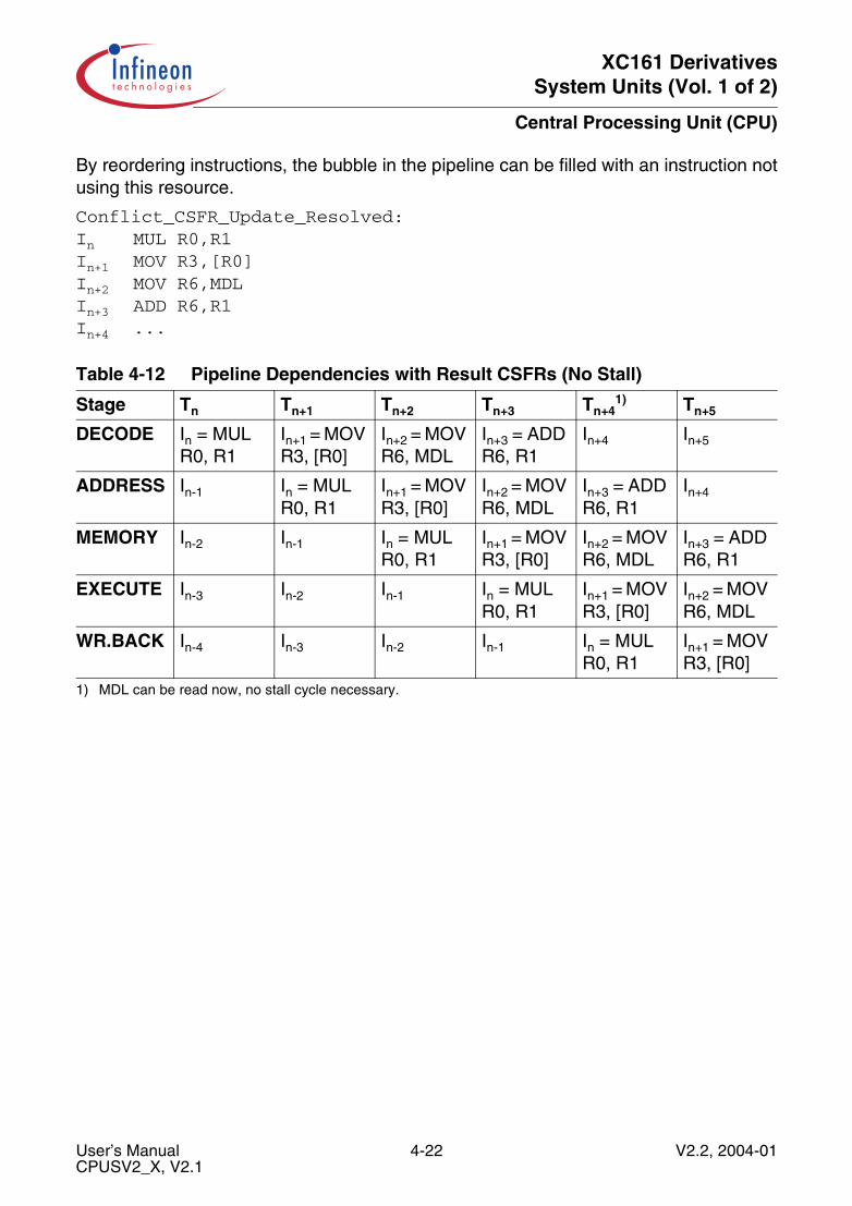
XC161 DerivativesSystem Units (Vol. 1 of 2)
Central Processing Unit (CPU)
By reordering instructions, the bubble in the pipeline can be filled with an instruction notusing this resource.
Conflict_CSFR_Update_Resolved:In MUL R0,R1In+1 MOV R3,[R0]In+2 MOV R6,MDLIn+3 ADD R6,R1In+4 ...
Table 4-12 Pipeline Dependencies with Result CSFRs (No Stall)
Stage Tn Tn+1 Tn+2 Tn+3 Tn+41)
1) MDL can be read now, no stall cycle necessary.
Tn+5
DECODE In = MUL R0, R1
In+1 = MOV R3, [R0]
In+2 = MOV R6, MDL
In+3 = ADD R6, R1
In+4 In+5
ADDRESS In-1 In = MUL R0, R1
In+1 = MOV R3, [R0]
In+2 = MOV R6, MDL
In+3 = ADD R6, R1
In+4
MEMORY In-2 In-1 In = MUL R0, R1
In+1 = MOV R3, [R0]
In+2 = MOV R6, MDL
In+3 = ADD R6, R1
EXECUTE In-3 In-2 In-1 In = MUL R0, R1
In+1 = MOV R3, [R0]
In+2 = MOV R6, MDL
WR.BACK In-4 In-3 In-2 In-1 In = MUL R0, R1
In+1 = MOV R3, [R0]
User’s Manual 4-22 V2.2, 2004-01CPUSV2_X, V2.1
XC161 DerivativesSystem Units (Vol. 1 of 2)
Central Processing Unit (CPU)
CSFRs Affecting the Whole CPU
Some CSFRs affect the whole CPU or the pipeline before the Memory stage. The CPU-SFRs CPUCON1, CP, SP, STKUN, STKOV, VECSEG, TFR, and PSW affect the overallCPU function, while the CPU-SFRs IDX0, IDX1, QX1, QX0, DPP0, DPP1, DPP2, andDPP3 only affect the DECODE, ADDRESS, and MEMORY stage when they aremodified explicitly. In this case the pipeline behavior depends on the instruction andaddressing mode used to modify the CSFR.In the case of modification of these CSFRs by “POP CSFR” or by instructions using thereg,#data16 addressing mode, a special mechanism is implemented to improveperformance during the initialization.
For further explanation, the instruction which modifies the CSFR can be called“instruction_modify_CSFR”. This special case is detected in the DECODE stage whenthe instruction_modify_CSFR enters the processing pipeline. Further on, instructionsdescribed in the following list are held in the DECODE stage (all other instructions arenot held):
• Instructions using long addressing mode (mem)• Instructions using indirect addressing modes ([Rw], [Rw+]…), except JMPI and CALLI• ENWDT, DISWDT, EINIT• All CoXXX instructions
If the CPUCON1, CP, SP, STKUN, STKOV, VECSEG, TFR, or the PSW are modifiedand the instruction_modify_CSFR reaches the EXECUTE stage, the pipeline iscanceled. The modification affects the entire pipeline and the instruction prefetch. Aclean cancel and restart mechanism is required to guarantee a correct instruction flow.In case of modification of IDX0, IDX1, QX1, QX0, DPP0, DPP1, DPP2, or DPP3 only theDECODE, ADDRESS, and MEMORY stages are affected and the pipeline needs not tobe canceled. The modification does not affect the instructions in the ADDRESS,MEMORY stage because they are not using this resource. Other kinds of instructions areheld in the DECODE stage until the CSFR is modified.
The following example shows a case in which the pipeline is stalled. The instruction“MOV R6, R1” after the “MOV IDX1, #12” instruction which modifies the CSFR will beheld in DECODE Stage until the IDX1 register is updated. The next example shows anoptimized initialization routine.
User’s Manual 4-23 V2.2, 2004-01CPUSV2_X, V2.1
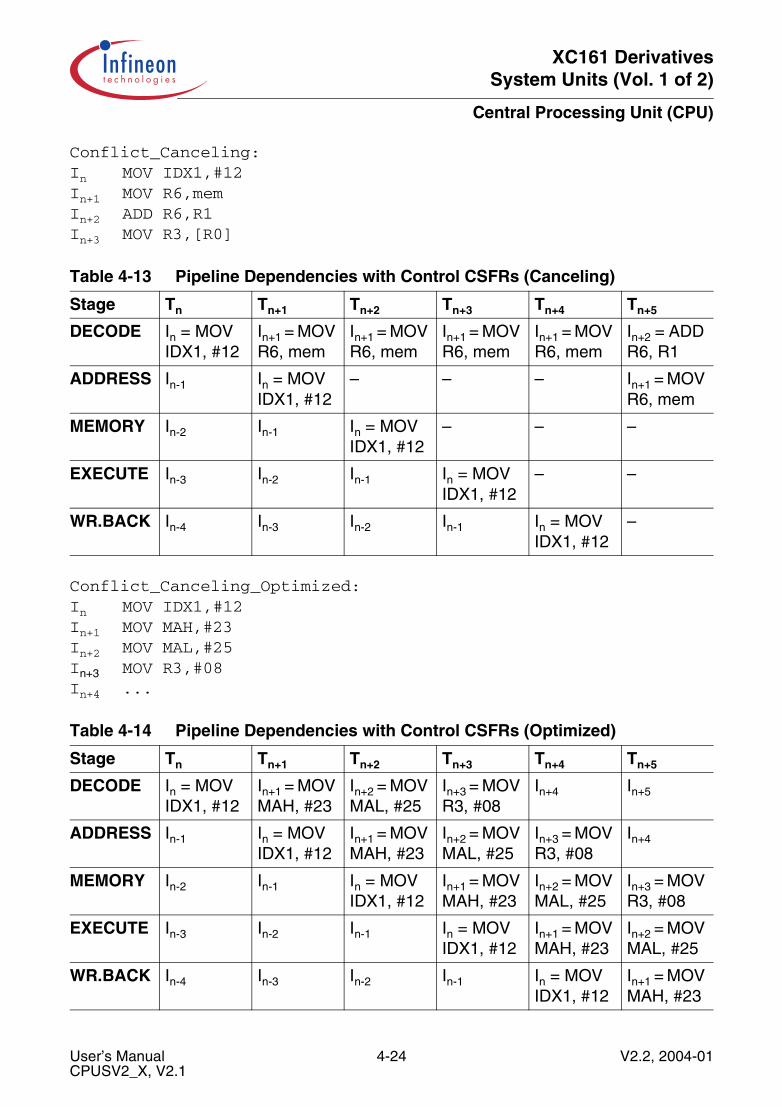
XC161 DerivativesSystem Units (Vol. 1 of 2)
Central Processing Unit (CPU)
Conflict_Canceling:In MOV IDX1,#12In+1 MOV R6,memIn+2 ADD R6,R1In+3 MOV R3,[R0]
Conflict_Canceling_Optimized:In MOV IDX1,#12In+1 MOV MAH,#23In+2 MOV MAL,#25In+3 MOV R3,#08In+4 ...
Table 4-13 Pipeline Dependencies with Control CSFRs (Canceling)
Stage Tn Tn+1 Tn+2 Tn+3 Tn+4 Tn+5
DECODE In = MOV IDX1, #12
In+1 = MOV R6, mem
In+1 = MOV R6, mem
In+1 = MOV R6, mem
In+1 = MOV R6, mem
In+2 = ADD R6, R1
ADDRESS In-1 In = MOV IDX1, #12
– – – In+1 = MOV R6, mem
MEMORY In-2 In-1 In = MOV IDX1, #12
– – –
EXECUTE In-3 In-2 In-1 In = MOV IDX1, #12
– –
WR.BACK In-4 In-3 In-2 In-1 In = MOV IDX1, #12
–
Table 4-14 Pipeline Dependencies with Control CSFRs (Optimized)
Stage Tn Tn+1 Tn+2 Tn+3 Tn+4 Tn+5
DECODE In = MOV IDX1, #12
In+1 = MOV MAH, #23
In+2 = MOV MAL, #25
In+3 = MOV R3, #08
In+4 In+5
ADDRESS In-1 In = MOV IDX1, #12
In+1 = MOV MAH, #23
In+2 = MOV MAL, #25
In+3 = MOV R3, #08
In+4
MEMORY In-2 In-1 In = MOV IDX1, #12
In+1 = MOV MAH, #23
In+2 = MOV MAL, #25
In+3 = MOV R3, #08
EXECUTE In-3 In-2 In-1 In = MOV IDX1, #12
In+1 = MOV MAH, #23
In+2 = MOV MAL, #25
WR.BACK In-4 In-3 In-2 In-1 In = MOV IDX1, #12
In+1 = MOV MAH, #23
User’s Manual 4-24 V2.2, 2004-01CPUSV2_X, V2.1
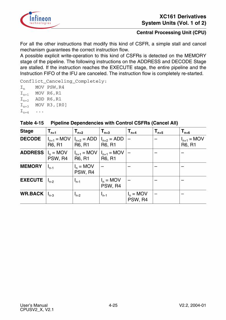
XC161 DerivativesSystem Units (Vol. 1 of 2)
Central Processing Unit (CPU)
For all the other instructions that modify this kind of CSFR, a simple stall and cancelmechanism guarantees the correct instruction flow.A possible explicit write-operation to this kind of CSFRs is detected on the MEMORYstage of the pipeline. The following instructions on the ADDRESS and DECODE Stageare stalled. If the instruction reaches the EXECUTE stage, the entire pipeline and theInstruction FIFO of the IFU are canceled. The instruction flow is completely re-started.
Conflict_Canceling_Completely:In MOV PSW,R4In+1 MOV R6,R1In+2 ADD R6,R1In+3 MOV R3,[R0]In+4 ...
Table 4-15 Pipeline Dependencies with Control CSFRs (Cancel All)
Stage Tn+1 Tn+2 Tn+3 Tn+4 Tn+5 Tn+6
DECODE In+1 = MOV R6, R1
In+2 = ADD R6, R1
In+2 = ADD R6, R1
– – In+1 = MOV R6, R1
ADDRESS In = MOV PSW, R4
In+1 = MOV R6, R1
In+1 = MOV R6, R1
– – –
MEMORY In-1 In = MOV PSW, R4
– – – –
EXECUTE In-2 In-1 In = MOV PSW, R4
– – –
WR.BACK In-3 In-2 In-1 In = MOV PSW, R4
– –
User’s Manual 4-25 V2.2, 2004-01CPUSV2_X, V2.1
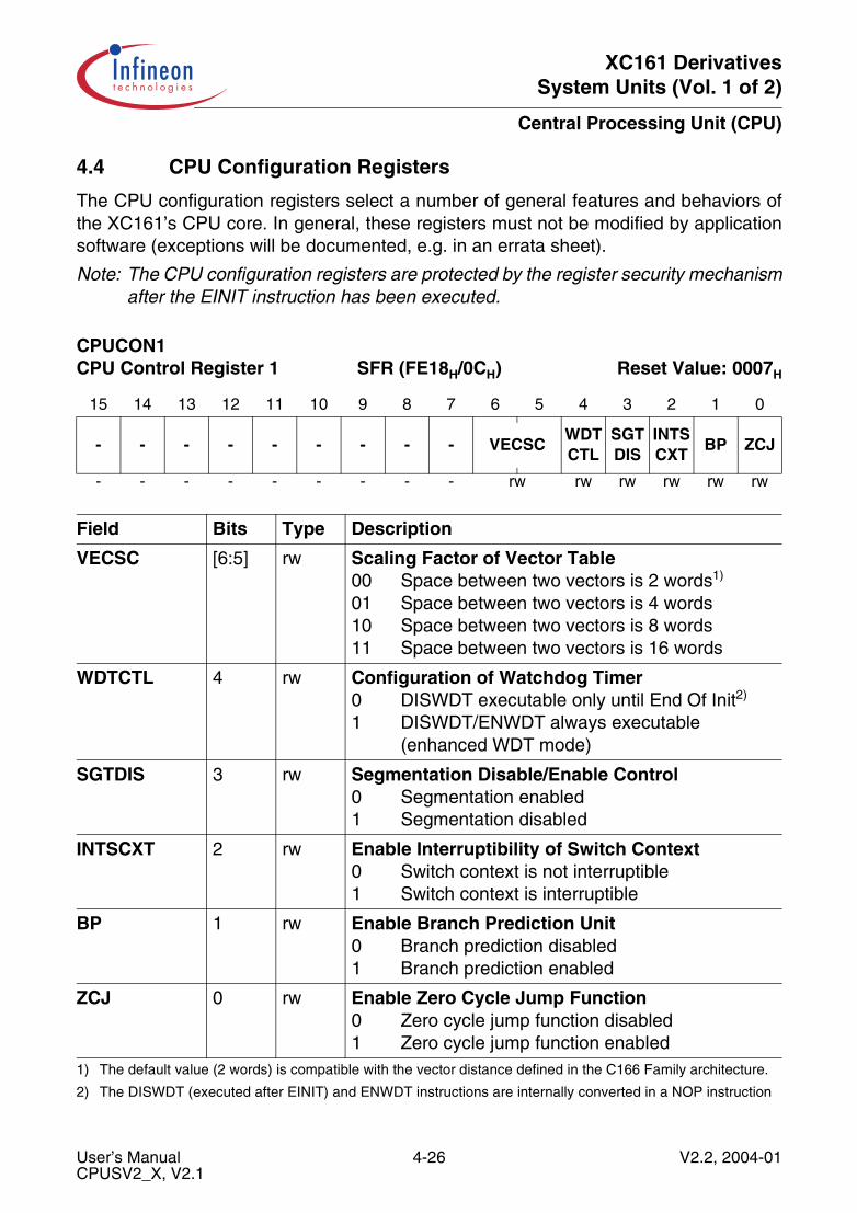
XC161 DerivativesSystem Units (Vol. 1 of 2)
Central Processing Unit (CPU)
4.4 CPU Configuration Registers
The CPU configuration registers select a number of general features and behaviors ofthe XC161’s CPU core. In general, these registers must not be modified by applicationsoftware (exceptions will be documented, e.g. in an errata sheet).
Note: The CPU configuration registers are protected by the register security mechanismafter the EINIT instruction has been executed.
CPUCON1 CPU Control Register 1 SFR (FE18H/0CH) Reset Value: 0007H
15 14 13 12 11 10 9 8 7 6 5 4 3 2 1 0
- - - - - - - - - VECSCWDTCTL
SGTDIS
INTSCXT
BP ZCJ
- - - - - - - - - rw rw rw rw rw rw
Field Bits Type Description
VECSC [6:5] rw Scaling Factor of Vector Table00 Space between two vectors is 2 words1)
01 Space between two vectors is 4 words10 Space between two vectors is 8 words11 Space between two vectors is 16 words
1) The default value (2 words) is compatible with the vector distance defined in the C166 Family architecture.
WDTCTL 4 rw Configuration of Watchdog Timer0 DISWDT executable only until End Of Init2)
1 DISWDT/ENWDT always executable (enhanced WDT mode)
2) The DISWDT (executed after EINIT) and ENWDT instructions are internally converted in a NOP instruction
SGTDIS 3 rw Segmentation Disable/Enable Control0 Segmentation enabled1 Segmentation disabled
INTSCXT 2 rw Enable Interruptibility of Switch Context0 Switch context is not interruptible1 Switch context is interruptible
BP 1 rw Enable Branch Prediction Unit0 Branch prediction disabled1 Branch prediction enabled
ZCJ 0 rw Enable Zero Cycle Jump Function0 Zero cycle jump function disabled1 Zero cycle jump function enabled
User’s Manual 4-26 V2.2, 2004-01CPUSV2_X, V2.1
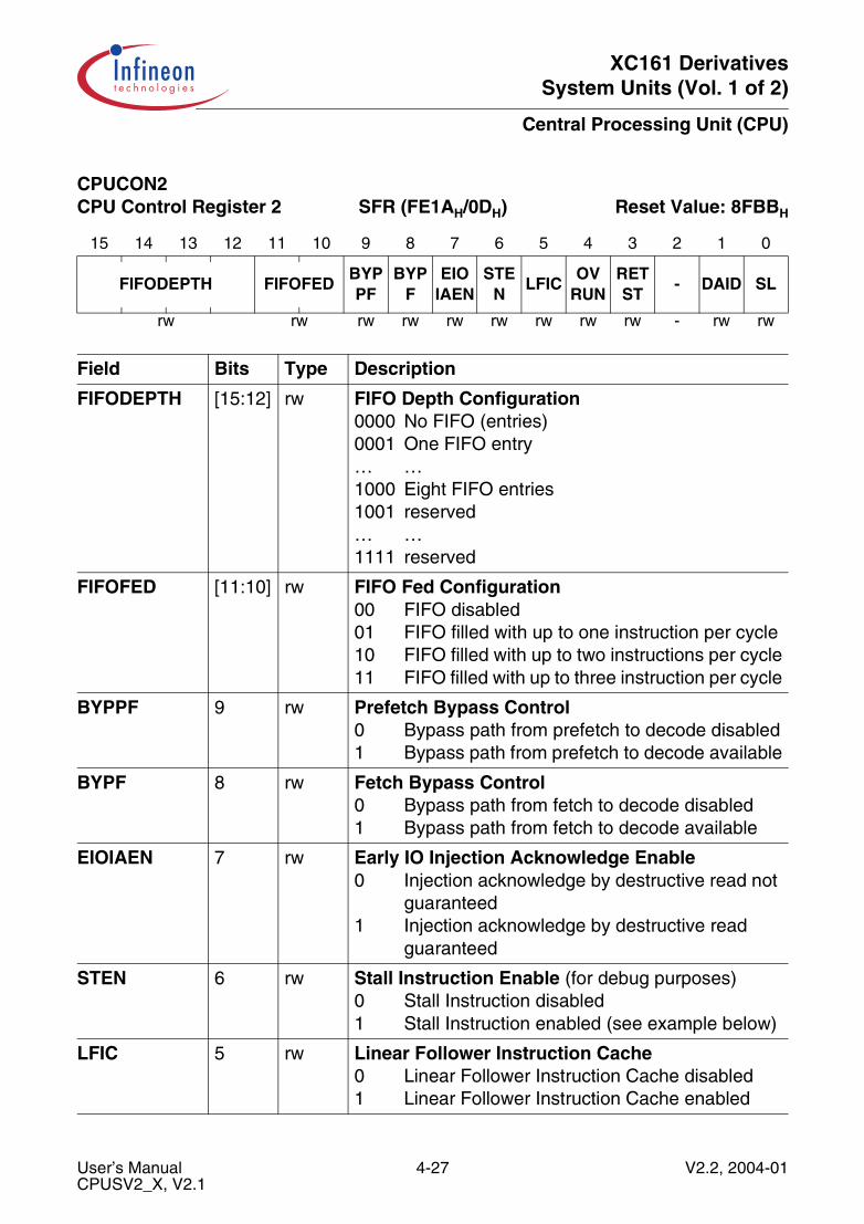
XC161 DerivativesSystem Units (Vol. 1 of 2)
Central Processing Unit (CPU)
CPUCON2 CPU Control Register 2 SFR (FE1AH/0DH) Reset Value: 8FBBH
15 14 13 12 11 10 9 8 7 6 5 4 3 2 1 0
FIFODEPTH FIFOFEDBYPPF
BYPF
EIOIAEN
STEN
LFICOV
RUNRETST
- DAID SL
rw rw rw rw rw rw rw rw rw - rw rw
Field Bits Type Description
FIFODEPTH [15:12] rw FIFO Depth Configuration0000 No FIFO (entries)0001 One FIFO entry… …1000 Eight FIFO entries1001 reserved… …1111 reserved
FIFOFED [11:10] rw FIFO Fed Configuration00 FIFO disabled01 FIFO filled with up to one instruction per cycle10 FIFO filled with up to two instructions per cycle11 FIFO filled with up to three instruction per cycle
BYPPF 9 rw Prefetch Bypass Control0 Bypass path from prefetch to decode disabled1 Bypass path from prefetch to decode available
BYPF 8 rw Fetch Bypass Control0 Bypass path from fetch to decode disabled1 Bypass path from fetch to decode available
EIOIAEN 7 rw Early IO Injection Acknowledge Enable0 Injection acknowledge by destructive read not
guaranteed1 Injection acknowledge by destructive read
guaranteed
STEN 6 rw Stall Instruction Enable (for debug purposes)0 Stall Instruction disabled1 Stall Instruction enabled (see example below)
LFIC 5 rw Linear Follower Instruction Cache0 Linear Follower Instruction Cache disabled1 Linear Follower Instruction Cache enabled
User’s Manual 4-27 V2.2, 2004-01CPUSV2_X, V2.1
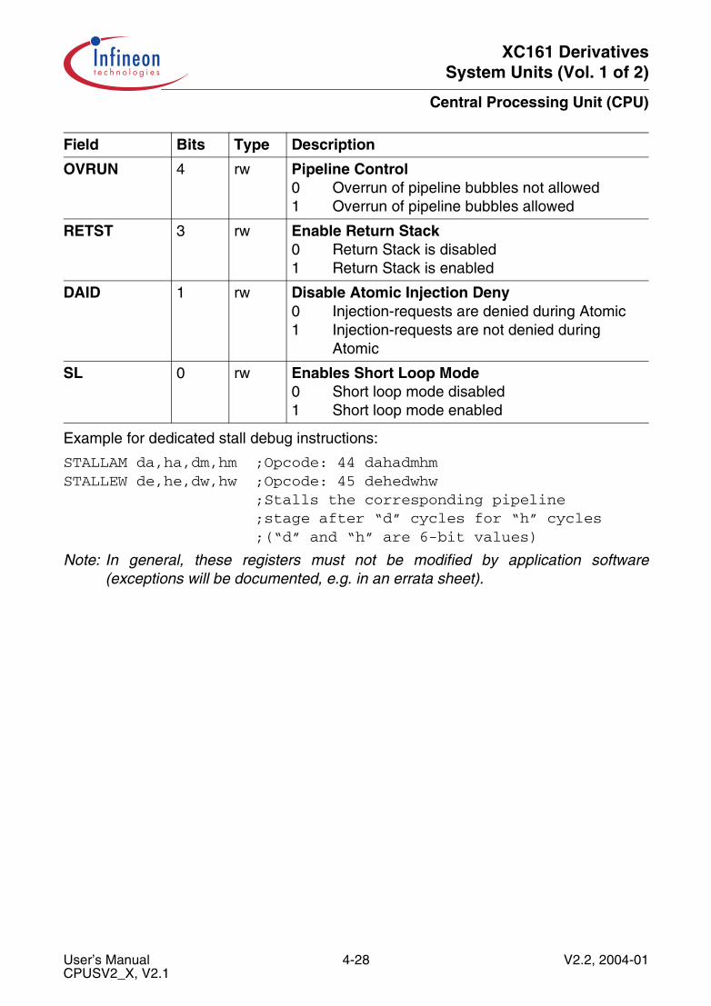
XC161 DerivativesSystem Units (Vol. 1 of 2)
Central Processing Unit (CPU)
Example for dedicated stall debug instructions:
STALLAM da,ha,dm,hm ;Opcode: 44 dahadmhmSTALLEW de,he,dw,hw ;Opcode: 45 dehedwhw ;Stalls the corresponding pipeline ;stage after “d” cycles for “h” cycles ;(“d” and “h” are 6-bit values)
Note: In general, these registers must not be modified by application software(exceptions will be documented, e.g. in an errata sheet).
OVRUN 4 rw Pipeline Control0 Overrun of pipeline bubbles not allowed1 Overrun of pipeline bubbles allowed
RETST 3 rw Enable Return Stack0 Return Stack is disabled1 Return Stack is enabled
DAID 1 rw Disable Atomic Injection Deny0 Injection-requests are denied during Atomic1 Injection-requests are not denied during
Atomic
SL 0 rw Enables Short Loop Mode0 Short loop mode disabled1 Short loop mode enabled
Field Bits Type Description
User’s Manual 4-28 V2.2, 2004-01CPUSV2_X, V2.1

XC161 DerivativesSystem Units (Vol. 1 of 2)
Central Processing Unit (CPU)
4.5 Use of General Purpose Registers
The CPU uses several banks of sixteen dedicated registers R0, R1, R2, … R15, calledGeneral Purpose Registers (GPRs), which can be accessed in one CPU cycle. TheGPRs are the working registers of the arithmetic and logic units and many also serve asaddress pointers for indirect addressing modes.
The register banks are accessed via the 5-port register file providing the high accessspeed required for the CPU’s performance. The register file is split into threeindependent physical register banks. There are two types of register banks:
• Two local register banks which are a part of the register file• A global register bank which is memory-mapped and cached in the register file
Figure 4-5 Register File
R15
MCD04873
R15
R14
R13
R12
R11
R10
R9
R8
R7
R6
R5
R4
R3
R2
R1
R0
R15
R14
R13
R12
R11
R10
R9
R8
R7
R6
R5
R4
R3
R2
R1
R0
Core-RAM
Global Local
R15
R0
Memorymapped
GPR Bank
AGU Write Port
ALU Write Port
AGU Read Port
ALU Read Port 1
ALU Read Port 2
Registerfile
CP
User’s Manual 4-29 V2.2, 2004-01CPUSV2_X, V2.1

XC161 DerivativesSystem Units (Vol. 1 of 2)
Central Processing Unit (CPU)
Bitfield BANK in register PSW selects which of the three physical register banks isactivated. The selected bank can be changed explicitly by any instruction which writesto the PSW, or implicitly by a RETI instruction, an interrupt or hardware trap. In case ofan interrupt, the selection of the register bank is configured via registers BNKSELx in theInterrupt Controller ITC. Hardware traps always use the global register bank.
The local register banks are built of dedicated physical registers, while the global registerbank represents a cache. The banks of the memory-mapped GPRs (global bank) arelocated in the internal DPRAM. One bank uses a block of 16 consecutive words. AContext Pointer (CP) register determines the base address of the current selected bank.To provide the required access speed, the GPRs located in the DPRAM are cached inthe 5-port register file (only one memory-mapped GPR bank can be cached at the time).If the global register bank is activated, the cache will be validated before furtherinstructions are executed. After validation, all further accesses to the GPRs areredirected to the global register bank.
Figure 4-6 Register Bank Selection via Register CP
MCA04921
R15
R13
R12
R11
R10
R9
R8
R7
R6
R5
R4
R3
R2
R1
R0
16-Bit Context Pointer
15 0
Internal DPRAM
R15
R0
Global local
Register File
(CP) + 30
R14 (CP) + 28
(CP) + 2
(CP)
User’s Manual 4-30 V2.2, 2004-01CPUSV2_X, V2.1

XC161 DerivativesSystem Units (Vol. 1 of 2)
Central Processing Unit (CPU)
4.5.1 GPR Addressing Modes
Because the GPRs are the working registers and are accessed frequently, there arethree possible ways to access a register bank:
• Short GPR Address (mnemonic: Rw or Rb)• Short Register Address (mnemonic: reg or bitoff)• Long Memory Address (mnemonic: mem), for the global bank only
Short GPR Addresses specify the register offset within the current register bank(selected via bitfield BANK). Short 4-bit GPR addresses can access all sixteen registers,short 2-bit addresses (used by some instructions) can access the lower four registers.
Depending on whether a relative word (Rw) or byte (Rb) GPR address is specified, theshort GPR address is either multiplied by two (Rw) or not (Rb) before it is used tophysically access the register bank. Thus, both byte and word GPR accesses arepossible in this way.
Note: GPRs used as indirect address pointers are always accessed wordwise.
For the local register banks the resulting offset is used directly, for the global registerbank the resulting offset is logically added to the contents of register CP which points tothe memory location of the base of the current global register bank (see Figure 4-7).
Short 8-Bit Register Addresses within a range from F0H to FFH interpret the four leastsignificant bits as short 4-bit GPR addresses, while the four most significant bits areignored. The respective physical GPR address is calculated in the same way as for short4-bit GPR addresses. For single bit GPR accesses, the GPR’s word address iscalculated in the same way. The accessed bit position within the word is specified by aseparate additional 4-bit value.
Figure 4-7 Implicit CP Use by Logical Short GPR Addressing Modes
1 4-Bit GPRAddress
MCA04922
011 1
1 1 1
12-Bit Context Pointer Specified by reg or bitoff
*1 *2
+
For word GPRaccesses
For byteGPRaccesses
GPRs
Must bewithinthe internalDPRAM area
InternalDRAM
User’s Manual 4-31 V2.2, 2004-01CPUSV2_X, V2.1

XC161 DerivativesSystem Units (Vol. 1 of 2)
Central Processing Unit (CPU)
24-Bit Memory Addresses can be directly used to access GPRs located in the DPRAM(not applicable for local register banks). In case of a memory read access, a hit detectionlogic checks if the accessed memory location is cached in the global register bank. Incase of a cache hit, an additional global register bank read access is initiated. The datathat is read from cache will be used and the data that is read from memory will bediscarded. This leads to a delay of one CPU cycle (MOV R4, mem[CP ≤ mem ≤ CP + 31]). In case of a memory write access, the hit detection logicdetermines a cache hit in advance. Nevertheless, the address conversion needs oneadditional CPU cycle. The value is directly written into the global register bank withoutfurther delay (MOV mem, R4).
Note: The 24-bit GPR addressing mode is not recommended because it requires anextra cycle for the read and write access.
Table 4-16 Addressing Modes to Access GPRs
Word Registers1)
1) The first 8 GPRs (R7 … R0) may also be accessed bytewise. Writing to a GPR byte does not affect the otherbyte of the respective GPR.
Byte Registers Short Address2)
2) Short addressing modes are usable for all register banks.
Name Mem. Addr.3)
3) Long addressing mode only usable for the memory mapped global GPR bank.
Name Mem. Addr.3) 8-Bit 4-Bit 2-Bit
R0 (CP) + 0 RL0 (CP) + 0 F0H 0H 0H
R1 (CP) + 2 RH0 (CP) + 1 F1H 1H 1H
R2 (CP) + 4 RL1 (CP) + 2 F2H 2H 2H
R3 (CP) + 6 RH1 (CP) + 3 F3H 3H 3H
R4 (CP) + 8 RL2 (CP) + 4 F4H 4H ---
R5 (CP) + 10 RH2 (CP) + 5 F5H 5H ---
R6 (CP) + 12 RL3 (CP) + 6 F6H 6H ---
R7 (CP) + 14 RH3 (CP) + 7 F7H 7H ---
R8 (CP) + 16 RL4 (CP) + 8 F8H 8H ---
R9 (CP) + 18 RH4 (CP) + 9 F9H 9H ---
R10 (CP) + 20 RL5 (CP) + 10 FAH AH ---
R11 (CP) + 22 RH5 (CP) + 11 FBH BH ---
R12 (CP) + 24 RL6 (CP) + 12 FCH CH ---
R13 (CP) + 26 RH6 (CP) + 13 FDH DH ---
R14 (CP) + 28 RL7 (CP) + 14 FEH EH ---
R15 (CP) + 30 RH7 (CP) + 15 FFH FH ---
User’s Manual 4-32 V2.2, 2004-01CPUSV2_X, V2.1
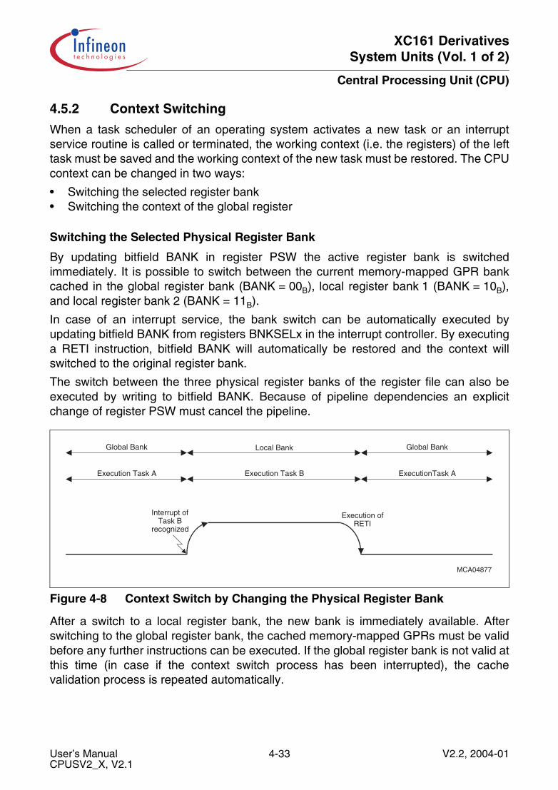
XC161 DerivativesSystem Units (Vol. 1 of 2)
Central Processing Unit (CPU)
4.5.2 Context Switching
When a task scheduler of an operating system activates a new task or an interruptservice routine is called or terminated, the working context (i.e. the registers) of the lefttask must be saved and the working context of the new task must be restored. The CPUcontext can be changed in two ways:
• Switching the selected register bank• Switching the context of the global register
Switching the Selected Physical Register Bank
By updating bitfield BANK in register PSW the active register bank is switchedimmediately. It is possible to switch between the current memory-mapped GPR bankcached in the global register bank (BANK = 00B), local register bank 1 (BANK = 10B),and local register bank 2 (BANK = 11B).
In case of an interrupt service, the bank switch can be automatically executed byupdating bitfield BANK from registers BNKSELx in the interrupt controller. By executinga RETI instruction, bitfield BANK will automatically be restored and the context willswitched to the original register bank.
The switch between the three physical register banks of the register file can also beexecuted by writing to bitfield BANK. Because of pipeline dependencies an explicitchange of register PSW must cancel the pipeline.
Figure 4-8 Context Switch by Changing the Physical Register Bank
After a switch to a local register bank, the new bank is immediately available. Afterswitching to the global register bank, the cached memory-mapped GPRs must be validbefore any further instructions can be executed. If the global register bank is not valid atthis time (in case if the context switch process has been interrupted), the cachevalidation process is repeated automatically.
MCA04877
Interrupt ofTask B
recognized
Execution ofRETI
Execution Task A Execution Task B ExecutionTask A
Global BankLocal BankGlobal Bank
User’s Manual 4-33 V2.2, 2004-01CPUSV2_X, V2.1
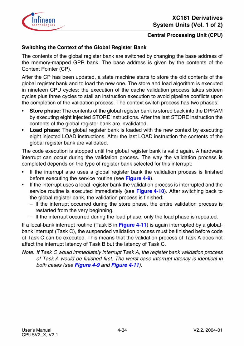
XC161 DerivativesSystem Units (Vol. 1 of 2)
Central Processing Unit (CPU)
Switching the Context of the Global Register Bank
The contents of the global register bank are switched by changing the base address ofthe memory-mapped GPR bank. The base address is given by the contents of theContext Pointer (CP).
After the CP has been updated, a state machine starts to store the old contents of theglobal register bank and to load the new one. The store and load algorithm is executedin nineteen CPU cycles: the execution of the cache validation process takes sixteencycles plus three cycles to stall an instruction execution to avoid pipeline conflicts uponthe completion of the validation process. The context switch process has two phases:
• Store phase: The contents of the global register bank is stored back into the DPRAMby executing eight injected STORE instructions. After the last STORE instruction thecontents of the global register bank are invalidated.
• Load phase: The global register bank is loaded with the new context by executingeight injected LOAD instructions. After the last LOAD instruction the contents of theglobal register bank are validated.
The code execution is stopped until the global register bank is valid again. A hardwareinterrupt can occur during the validation process. The way the validation process iscompleted depends on the type of register bank selected for this interrupt:
• If the interrupt also uses a global register bank the validation process is finishedbefore executing the service routine (see Figure 4-9).
• If the interrupt uses a local register bank the validation process is interrupted and theservice routine is executed immediately (see Figure 4-10). After switching back tothe global register bank, the validation process is finished:– If the interrupt occurred during the store phase, the entire validation process is
restarted from the very beginning.– If the interrupt occurred during the load phase, only the load phase is repeated.
If a local-bank interrupt routine (Task B in Figure 4-11) is again interrupted by a global-bank interrupt (Task C), the suspended validation process must be finished before codeof Task C can be executed. This means that the validation process of Task A does notaffect the interrupt latency of Task B but the latency of Task C.
Note: If Task C would immediately interrupt Task A, the register bank validation processof Task A would be finished first. The worst case interrupt latency is identical inboth cases (see Figure 4-9 and Figure 4-11).
User’s Manual 4-34 V2.2, 2004-01CPUSV2_X, V2.1
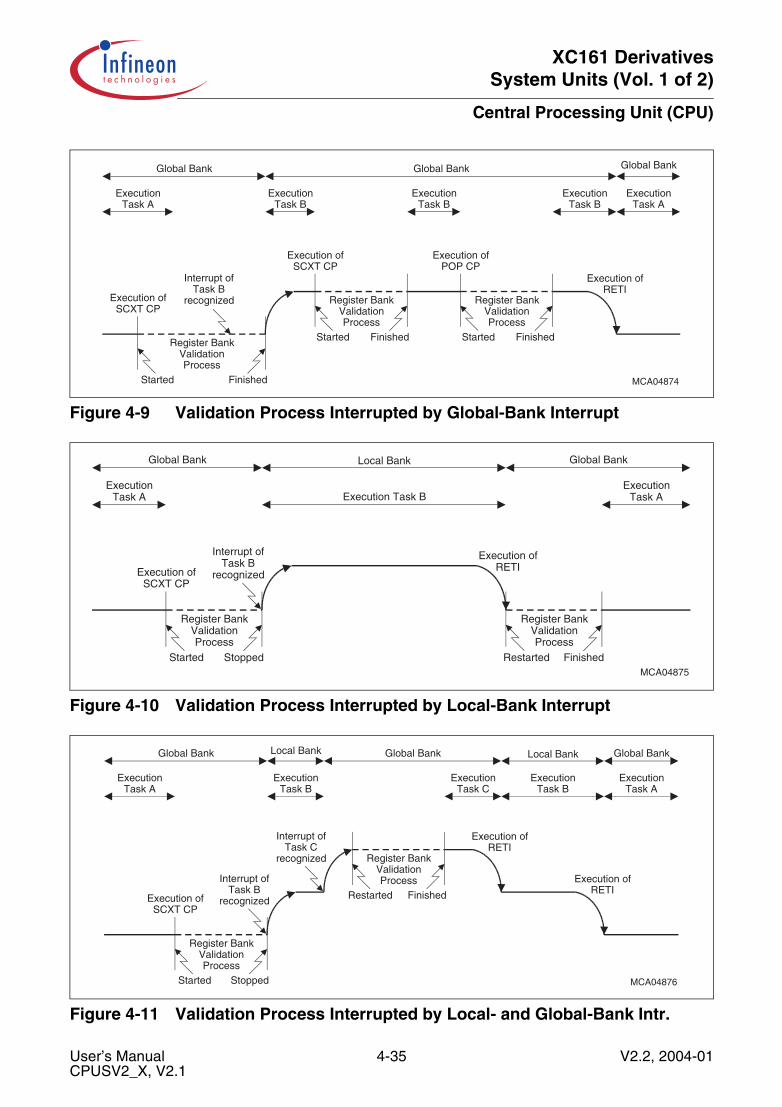
XC161 DerivativesSystem Units (Vol. 1 of 2)
Central Processing Unit (CPU)
Figure 4-9 Validation Process Interrupted by Global-Bank Interrupt
Figure 4-10 Validation Process Interrupted by Local-Bank Interrupt
Figure 4-11 Validation Process Interrupted by Local- and Global-Bank Intr.
MCA04874Finished
Register BankValidationProcess
Started
Execution ofSCXT CP
Interrupt ofTask B
recognized
Finished
Register BankValidationProcess
Started
Execution ofRETI
ExecutionTask A
ExecutionTask B
ExecutionTask B
ExecutionTask B
ExecutionTask A
Global BankGlobal BankGlobal Bank
Finished
Register BankValidationProcess
Started
Execution ofSCXT CP
Execution ofPOP CP
MCA04875
Stopped
Register BankValidationProcess
Started
Execution ofSCXT CP
Interrupt ofTask B
recognized
Execution ofRETI
ExecutionTask A Execution Task B
ExecutionTask A
Global BankLocal BankGlobal Bank
Finished
Register BankValidationProcess
Restarted
MCA04876Stopped
Register BankValidationProcess
Started
Execution ofSCXT CP
Interrupt ofTask B
recognized
Interrupt ofTask C
recognized
Finished
Register BankValidationProcess
Restarted
Execution ofRETI
Execution ofRETI
ExecutionTask A
ExecutionTask B
ExecutionTask C
ExecutionTask B
ExecutionTask A
Global BankLocal BankGlobal BankLocal BankGlobal Bank
User’s Manual 4-35 V2.2, 2004-01CPUSV2_X, V2.1

XC161 DerivativesSystem Units (Vol. 1 of 2)
Central Processing Unit (CPU)
The Context Pointer (CP)
This non-bit-addressable register selects the current global register bank context. It canbe updated via any instruction capable of modifying SFRs.
Note: It is the user’s responsibility to ensure that the physical GPR address specified viaCP register plus short GPR address is always an internal DPRAM location. If thiscondition is not met, unexpected results may occur. Do not set CP below theinternal DPRAM start address.
The XC161 switches the complete memory-mapped GPR bank with a single instruction.After switching, the service routine executes within its own separate context.
The instruction “SCXT CP, #New_Bank” pushes the value of the current context pointer(CP) into the system stack and loads CP with the immediate value “New_Bank”, whichselects a new register bank. The service routine may now use its “own registers”. Thismemory register bank is preserved when the service routine terminates, i.e. its contentsare available on the next call.Before returning from the service routine (RETI), the previous CP is simply popped fromthe system stack which returns the registers to the original bank.
Note: Due to the internal instruction pipeline, a write operation to the CP register stallsthe instruction flow until the register file context switch is really executed. Theinstruction immediately following the instruction that updates CP register can usethe new value of the changed CP.
CPContext Pointer SFR (FE10H/08H) Reset Value: FC00H
15 14 13 12 11 10 9 8 7 6 5 4 3 2 1 0
1 1 1 1 cp 0
r r r r rw r
Field Bits Type Description
cp [11:1] rw Modifiable Portion of Register CPSpecifies the (word) base address of the current global (memory-mapped) register bank.When writing a value to register CP with bits CP[11:9] = 000B, bits CP[11:10] are set to 11B by hardware.
User’s Manual 4-36 V2.2, 2004-01CPUSV2_X, V2.1
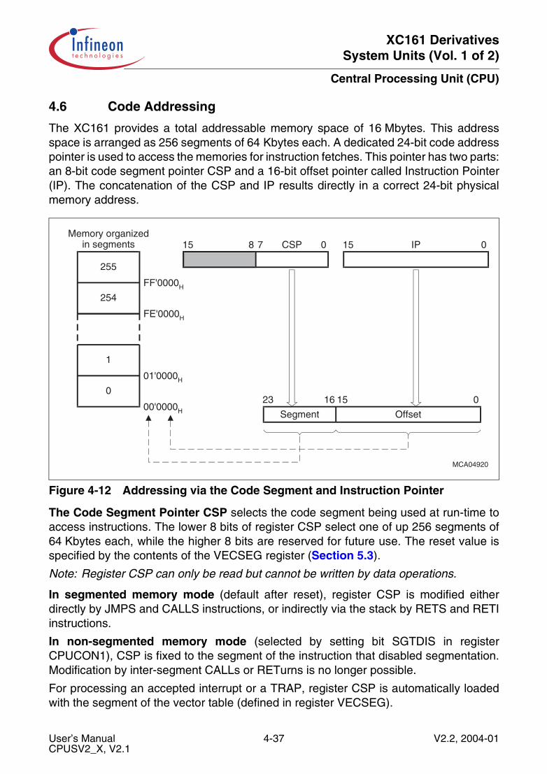
XC161 DerivativesSystem Units (Vol. 1 of 2)
Central Processing Unit (CPU)
4.6 Code Addressing
The XC161 provides a total addressable memory space of 16 Mbytes. This addressspace is arranged as 256 segments of 64 Kbytes each. A dedicated 24-bit code addresspointer is used to access the memories for instruction fetches. This pointer has two parts:an 8-bit code segment pointer CSP and a 16-bit offset pointer called Instruction Pointer(IP). The concatenation of the CSP and IP results directly in a correct 24-bit physicalmemory address.
Figure 4-12 Addressing via the Code Segment and Instruction Pointer
The Code Segment Pointer CSP selects the code segment being used at run-time toaccess instructions. The lower 8 bits of register CSP select one of up 256 segments of64 Kbytes each, while the higher 8 bits are reserved for future use. The reset value isspecified by the contents of the VECSEG register (Section 5.3).
Note: Register CSP can only be read but cannot be written by data operations.
In segmented memory mode (default after reset), register CSP is modified eitherdirectly by JMPS and CALLS instructions, or indirectly via the stack by RETS and RETIinstructions.
In non-segmented memory mode (selected by setting bit SGTDIS in registerCPUCON1), CSP is fixed to the segment of the instruction that disabled segmentation.Modification by inter-segment CALLs or RETurns is no longer possible.
For processing an accepted interrupt or a TRAP, register CSP is automatically loadedwith the segment of the vector table (defined in register VECSEG).
MCA04920
1523 0
Memory organizedin segments
255
254
1
0
FF'0000H
FE'0000H
01'0000H
00'0000H
16
15 0IP15 0CSP78
Segment Offset
User’s Manual 4-37 V2.2, 2004-01CPUSV2_X, V2.1
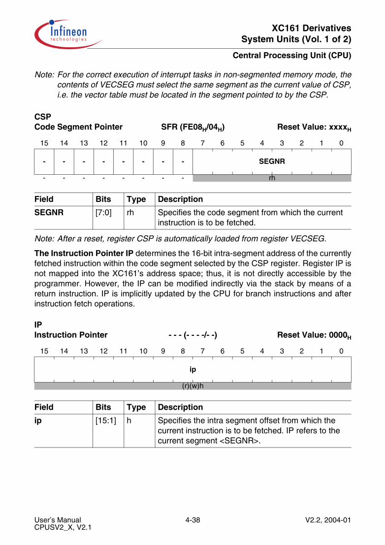
XC161 DerivativesSystem Units (Vol. 1 of 2)
Central Processing Unit (CPU)
Note: For the correct execution of interrupt tasks in non-segmented memory mode, thecontents of VECSEG must select the same segment as the current value of CSP,i.e. the vector table must be located in the segment pointed to by the CSP.
Note: After a reset, register CSP is automatically loaded from register VECSEG.
The Instruction Pointer IP determines the 16-bit intra-segment address of the currentlyfetched instruction within the code segment selected by the CSP register. Register IP isnot mapped into the XC161’s address space; thus, it is not directly accessible by theprogrammer. However, the IP can be modified indirectly via the stack by means of areturn instruction. IP is implicitly updated by the CPU for branch instructions and afterinstruction fetch operations.
CSP Code Segment Pointer SFR (FE08H/04H) Reset Value: xxxxH
15 14 13 12 11 10 9 8 7 6 5 4 3 2 1 0
- - - - - - - - SEGNR
- - - - - - - - rh
Field Bits Type Description
SEGNR [7:0] rh Specifies the code segment from which the current instruction is to be fetched.
IP Instruction Pointer - - - (- - - -/- -) Reset Value: 0000H
15 14 13 12 11 10 9 8 7 6 5 4 3 2 1 0
ip
(r)(w)h
Field Bits Type Description
ip [15:1] h Specifies the intra segment offset from which the current instruction is to be fetched. IP refers to the current segment <SEGNR>.
User’s Manual 4-38 V2.2, 2004-01CPUSV2_X, V2.1
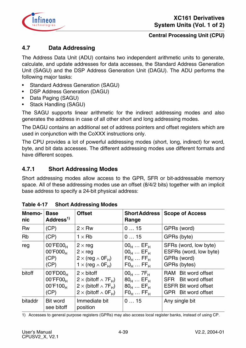
XC161 DerivativesSystem Units (Vol. 1 of 2)
Central Processing Unit (CPU)
4.7 Data Addressing
The Address Data Unit (ADU) contains two independent arithmetic units to generate,calculate, and update addresses for data accesses, the Standard Address GenerationUnit (SAGU) and the DSP Address Generation Unit (DAGU). The ADU performs thefollowing major tasks:
• Standard Address Generation (SAGU)• DSP Address Generation (DAGU)• Data Paging (SAGU)• Stack Handling (SAGU)
The SAGU supports linear arithmetic for the indirect addressing modes and alsogenerates the address in case of all other short and long addressing modes.
The DAGU contains an additional set of address pointers and offset registers which areused in conjunction with the CoXXX instructions only.
The CPU provides a lot of powerful addressing modes (short, long, indirect) for word,byte, and bit data accesses. The different addressing modes use different formats andhave different scopes.
4.7.1 Short Addressing Modes
Short addressing modes allow access to the GPR, SFR or bit-addressable memoryspace. All of these addressing modes use an offset (8/4/2 bits) together with an implicitbase address to specify a 24-bit physical address:
Table 4-17 Short Addressing Modes
Mnemo-nic
Base Address1)
1) Accesses to general purpose registers (GPRs) may also access local register banks, instead of using CP.
Offset Short Address Range
Scope of Access
Rw (CP) 2 × Rw 0 … 15 GPRs (word)
Rb (CP) 1 × Rb 0 … 15 GPRs (byte)
reg 00’FE00H00’F000H(CP)(CP)
2 × reg2 × reg2 × (reg ∧ 0FH)1 × (reg ∧ 0FH)
00H … EFH00H … EFHF0H … FFHF0H … FFH
SFRs (word, low byte)ESFRs (word, low byte)GPRs (word)GPRs (bytes)
bitoff 00’FD00H00’FF00H00’F100H(CP)
2 × bitoff2 × (bitoff ∧ 7FH)2 × (bitoff ∧ 7FH)2 × (bitoff ∧ 0FH)
00H … 7FH80H … EFH80H … EFHF0H … FFH
RAM Bit word offsetSFR Bit word offsetESFR Bit word offsetGPR Bit word offset
bitaddr Bit word see bitoff
Immediate bit position
0 … 15 Any single bit
User’s Manual 4-39 V2.2, 2004-01CPUSV2_X, V2.1

XC161 DerivativesSystem Units (Vol. 1 of 2)
Central Processing Unit (CPU)
Physical Address = Base Address + ∆ × Short Address
Note: ∆ is 1 for byte GPRs, ∆ is 2 for word GPRs.
Rw, Rb: Specifies direct access to any GPR in the currently active context (globalregister bank or local register bank). Both ‘Rw’ and ‘Rb’ require four bits in the instructionformat. The base address of the global register bank is determined by the contents ofregister CP. ‘Rw’ specifies a 4-bit word GPR address, ‘Rb’ specifies a 4-bit byte GPRaddress within a local register bank or relative to (CP).
reg: Specifies direct access to any (E)SFR or GPR in the currently active context (globalor local register bank). The ‘reg’ value requires eight bits in the instruction format. Short‘reg’ addresses in the range from 00H to EFH always specify (E)SFRs. In that case, thefactor ‘∆’ equates 2 and the base address is 00’FE00H for the standard SFR area or00’F000H for the extended ESFR area. The ‘reg’ accesses to the ESFR area require apreceding EXT*R instruction to switch the base address. Depending on the opcode,either the total word (for word operations) or the low byte (for byte operations) of an SFRcan be addressed via ‘reg’. Note that the high byte of an SFR cannot be accessed viathe ‘reg’ addressing mode. Short ‘reg’ addresses in the range from F0H to FFH alwaysspecify GPRs. In that case, only the lower four bits of ‘reg’ are significant for physicaladdress generation and, therefore, it is identical to the address generation described forthe ‘Rb’ and ‘Rw’ addressing modes.
bitoff: Specifies direct access to any word in the bit addressable memory space. The‘bitoff’ value requires eight bits in the instruction format. The specified ‘bitoff’ rangeselects different base addresses to generate physical addresses (see Table 4-17). The‘bitoff’ accesses to the ESFR area require a preceding EXT*R instruction to switch thebase address.
bitaddr: Any bit address is specified by a word address within the bit addressablememory space (see ‘bitoff’) and a bit position (‘bitpos’) within that word. Therefore,‘bitaddr’ requires twelve bits in the instruction format.
User’s Manual 4-40 V2.2, 2004-01CPUSV2_X, V2.1
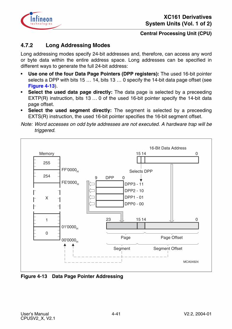
XC161 DerivativesSystem Units (Vol. 1 of 2)
Central Processing Unit (CPU)
4.7.2 Long Addressing Modes
Long addressing modes specify 24-bit addresses and, therefore, can access any wordor byte data within the entire address space. Long addresses can be specified indifferent ways to generate the full 24-bit address:
• Use one of the four Data Page Pointers (DPP registers): The used 16-bit pointerselects a DPP with bits 15 … 14, bits 13 … 0 specify the 14-bit data page offset (seeFigure 4-13).
• Select the used data page directly: The data page is selected by a preceedingEXTP(R) instruction, bits 13 … 0 of the used 16-bit pointer specify the 14-bit datapage offset.
• Select the used segment directly: The segment is selected by a preceedingEXTS(R) instruction, the used 16-bit pointer specifies the 16-bit segment offset.
Note: Word accesses on odd byte addresses are not executed. A hardware trap will betriggered.
Figure 4-13 Data Page Pointer Addressing
MCA04924
9 0DPP
DPP3 - 11
DPP2 - 10
DPP1 - 01
DPP0 - 00
16-Bit Data Address
Selects DPP
23 15 14 0
Page Page Offset
Segment Segment Offset
Memory
255
254
1
0
X
FF'0000H
FE'0000H
01'0000H
00'0000H
015 14
User’s Manual 4-41 V2.2, 2004-01CPUSV2_X, V2.1

XC161 DerivativesSystem Units (Vol. 1 of 2)
Central Processing Unit (CPU)
Data Page Pointers DPP0, DPP1, DPP2, DPP3
These four non-bit-addressable registers select up to four different data pages to beactive simultaneously at run-time. The lower 10 bits of each DPP register select one ofthe 1024 possible 16-Kbyte data pages; the upper 6 bits are reserved for future use.
DPP0Data Page Pointer 0 SFR (FE00H/00H) Reset Value: 0000H
15 14 13 12 11 10 9 8 7 6 5 4 3 2 1 0
- - - - - - DPP0PN
- - - - - - rw
DPP1Data Page Pointer 1 SFR (FE02H/01H) Reset Value: 0001H
15 14 13 12 11 10 9 8 7 6 5 4 3 2 1 0
- - - - - - DPP1PN
- - - - - - rw
DPP2Data Page Pointer 2 SFR (FE04H/02H) Reset Value: 0002H
15 14 13 12 11 10 9 8 7 6 5 4 3 2 1 0
- - - - - - DPP2PN
- - - - - - rw
DPP3Data Page Pointer 3 SFR (FE06H/03H) Reset Value: 0003H
15 14 13 12 11 10 9 8 7 6 5 4 3 2 1 0
- - - - - - DPP3PN
- - - - - - rw
Field Bits Type Description
DPPxPN [9:0] rw Data Page Number of DPPxSpecifies the data page selected via DPPx.
User’s Manual 4-42 V2.2, 2004-01CPUSV2_X, V2.1

XC161 DerivativesSystem Units (Vol. 1 of 2)
Central Processing Unit (CPU)
The DPP registers allow access to the entire memory space in pages of 16 Kbytes each.The DPP registers are implicitly used whenever data accesses to any memory locationare made via indirect or direct long 16-bit addressing modes (except for overrideaccesses via EXTended instructions and PEC data transfers). After reset, the Data PagePointers are initialized in such a way that all indirect or direct long 16-bit addresses resultin identical 18-bit addresses. This allows access to data pages 3 … 0 within segment 0as shown in Figure 4-13. If the user does not want to use data paging, no further actionis required.
Data paging is performed by concatenating the lower 14 bits of an indirect or direct long16-bit address with the contents of the DPP register selected by the upper two bits of the16-bit address. The contents of the selected DPP register specify one of the 1024possible data pages. This data page base address together with the 14-bit page offsetforms the physical 24-bit address (even if segmentation is disabled).
The selected number of segment address bits (via bitfield SALSEL) of the respectiveDPP register is output on the respective segment address pins for all external dataaccesses.
A DPP register can be updated via any instruction capable of modifying an SFR.
Note: Due to the internal instruction pipeline, a write operation to the DPPx registerscould stall the instruction flow until the DPP is actually updated. The instructionthat immediately follows the instruction which updates the DPP register can usethe new value of the changed DPPx.
Figure 4-14 Overriding the DPP Mechanism
MCA04925
15 14 13
14-Bit Page Offset
16-Bit Segment Offset
#pag
#seg
0
15 0
24-Bit Physical Address
24-Bit Physical Address
16-Bit Long Address
16-Bit Long AddressEXTS(R):
EXTP(R):
User’s Manual 4-43 V2.2, 2004-01CPUSV2_X, V2.1
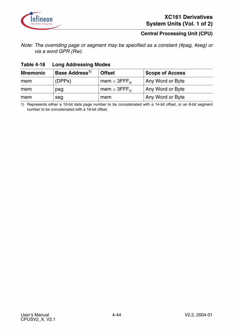
XC161 DerivativesSystem Units (Vol. 1 of 2)
Central Processing Unit (CPU)
Note: The overriding page or segment may be specified as a constant (#pag, #seg) orvia a word GPR (Rw).
Table 4-18 Long Addressing Modes
Mnemonic Base Address1)
1) Represents either a 10-bit data page number to be concatenated with a 14-bit offset, or an 8-bit segmentnumber to be concatenated with a 16-bit offset.
Offset Scope of Access
mem (DPPx) mem ∧ 3FFFH Any Word or Byte
mem pag mem ∧ 3FFFH Any Word or Byte
mem seg mem Any Word or Byte
User’s Manual 4-44 V2.2, 2004-01CPUSV2_X, V2.1

XC161 DerivativesSystem Units (Vol. 1 of 2)
Central Processing Unit (CPU)
4.7.3 Indirect Addressing Modes
Indirect addressing modes can be considered as a combination of short and longaddressing modes. This means that the “long” 16-bit pointer is provided indirectly by thecontents of a word GPR which itself is specified directly by a short 4-bit address(‘Rw’ = 0 … 15).
There are indirect addressing modes, which add a constant value to the GPR contentsbefore the long 16-bit address is calculated. Other indirect addressing modes candecrement or increment the indirect address pointers (GPR contents) by 2 or 1 (referringto words or bytes) or by the contents of the offset registers QR0 or QR1.
Note: Some instructions only use the lowest four word GPRs (R3 … R0) as indirectaddress pointers, which are specified via short 2-bit addresses in that case.
The following indirect addressing modes are provided:
Table 4-19 Generating Physical Addresses from Indirect Pointers
Step Executed Action Calculation Notes
1 Calculate the address of the indirect pointer (word GPR) from its short address
GPR Address = 2 × Short Addr. [+ (CP)]
see Table 4-17
2 Pre-decrement indirect pointer (‘-Rw’) depending on datatype (∆ = 1 or 2 for byte or word operations)
(GPR Address) = (GPR Address) - ∆
Optional step, executed only if required by addressing mode
3 Adjust the pointer by a constant value (‘Rw + const16’)
Pointer = (GPR Address) + Constant
Optional step, executed only if required by addressing mode
4 Calculate the physical 24-bit address using the resulting pointer
Physical Addr. = Page/Segment + Pointer offset
Uses DPPs or page/segment override mechanisms,see Table 4-18
5 Post-in/decrement indirect pointer (‘Rw±’) depending on datatype (∆ = 1 or 2 for byte or word operations), or depending on offset registers (∆ = QRx)1)
1) Post-decrement and QRx-based modification is provided only for CoXXX instructions.
(GPR Address) = (GPR Address) ± ∆
Optional step, executed only if required by addressing mode
User’s Manual 4-45 V2.2, 2004-01CPUSV2_X, V2.1
XC161 DerivativesSystem Units (Vol. 1 of 2)
Central Processing Unit (CPU)
The non-bit-addressable offset registers QR0 and QR1 are used with CoXXXinstructions. For possible instruction flow stalls refer to Section 4.3.4.
Table 4-20 Indirect Addressing Modes
Mnemonic Particularities
[Rw] Most instructions accept any GPR (R15 … R0) as indirect address pointer. Some instructions accept only the lower four GPRs (R3 … R0).
[Rw+] The specified indirect address pointer is automatically post-incremented by 2 or 1 (for word or byte data operations) after the access.
[-Rw] The specified indirect address pointer is automatically pre-decremented by 2 or 1 (for word or byte data operations) before the access.
[Rw + #data16]
The specified 16-bit constant is added to the indirect address pointer, before the long address is calculated.
[Rw-] The specified indirect address pointer is automatically post-decremented by 2 (word data operations) after the access.
[Rw + QRx] The specified indirect address pointer is automatically post-incremented by QRx (word data operations) after the access.
[Rw - QRx] The specified indirect address pointer is automatically post-decremented by QRX (word data operations) after the access.
QR0 Offset Register ESFR (F004H/02H) Reset Value: 0000H
15 14 13 12 11 10 9 8 7 6 5 4 3 2 1 0
QR 0
rw r
QR1 Offset Register ESFR (F006H/03H) Reset Value: 0000H
15 14 13 12 11 10 9 8 7 6 5 4 3 2 1 0
QR 0
rw r
Field Bits Type Description
QR [15:1] rw Modifiable Portion of Register QRxSpecifies the 16-bit word offset address for indirect addressing modes (LSB always zero).
User’s Manual 4-46 V2.2, 2004-01CPUSV2_X, V2.1
XC161 DerivativesSystem Units (Vol. 1 of 2)
Central Processing Unit (CPU)
4.7.4 DSP Addressing Modes
In addition to the Standard Address Generation Unit (SAGU), the DSP AddressGeneration Unit (DAGU) provides an additional set of pointer registers (IDX0, IDX1) andoffset registers (QX0, QX1). The additional set of pointer registers IDX0 and IDX1 allowsthe execution of DSP specific CoXXX instructions in one CPU cycle. An independentarithmetic unit allows the update of these dedicated pointer registers in parallel with theGPR-pointer modification of the SAGU. The DAGU only supports indirect addressingmodes that use the special pointer registers IDX0 and IDX1.
The address pointers can be used for arithmetic operations as well as for the specialCoMOV instruction. The generation of the 24-bit memory address is different:
• For CoMOV instructions, the IDX pointers are concatenated with the DPPs or theselected page/segment address, as described for long addressing modes (seeFigure 4-13 for a summary).
• For arithmetic CoXXX instructions, the IDX pointers are automatically extended toa 24-bit memory address pointing to the internal DPRAM area, as shown inFigure 4-15.
Note: During the initialization of the IDX registers, instruction flow stalls are possible. Forthe proper operation, refer to Section 4.3.4.
IDX0Address Pointer SFR (FF08H/84H) Reset Value: 0000H
15 14 13 12 11 10 9 8 7 6 5 4 3 2 1 0
idx 0
rw r
IDX1Address Pointer SFR (FF0AH/85H) Reset Value: 0000H
15 14 13 12 11 10 9 8 7 6 5 4 3 2 1 0
idx 0
rw r
Field Bits Type Description
idx [15:1] rw Modifiable Portion of Register IDXxSpecifies the 16-bit word address pointer
User’s Manual 4-47 V2.2, 2004-01CPUSV2_X, V2.1
XC161 DerivativesSystem Units (Vol. 1 of 2)
Central Processing Unit (CPU)
There are indirect addressing modes which allow parallel data move operations beforethe long 16-bit address is calculated (see Figure 4-16 for an example). Other indirectaddressing modes allow decrementing or incrementing the indirect address pointers(IDXx contents) by 2 or by the contents of the offset registers QX0 and QX1 (used inconjunction with the IDX pointers).
Note: During the initialization of the QX registers, instruction flow stalls are possible. Forthe proper operation, refer to Section 4.3.4.
QX0 Offset Register ESFR (F000H/00H) Reset Value: 0000H
15 14 13 12 11 10 9 8 7 6 5 4 3 2 1 0
qx 0
rw r
QX1Offset Register ESFR (F002H/01H) Reset Value: 0000H
15 14 13 12 11 10 9 8 7 6 5 4 3 2 1 0
qx 0
rw r
Field Bits Type Description
qx [15:1] rw Modifiable Portion of Register QXxSpecifies the 16-bit word offset for indirect addressing modes
User’s Manual 4-48 V2.2, 2004-01CPUSV2_X, V2.1
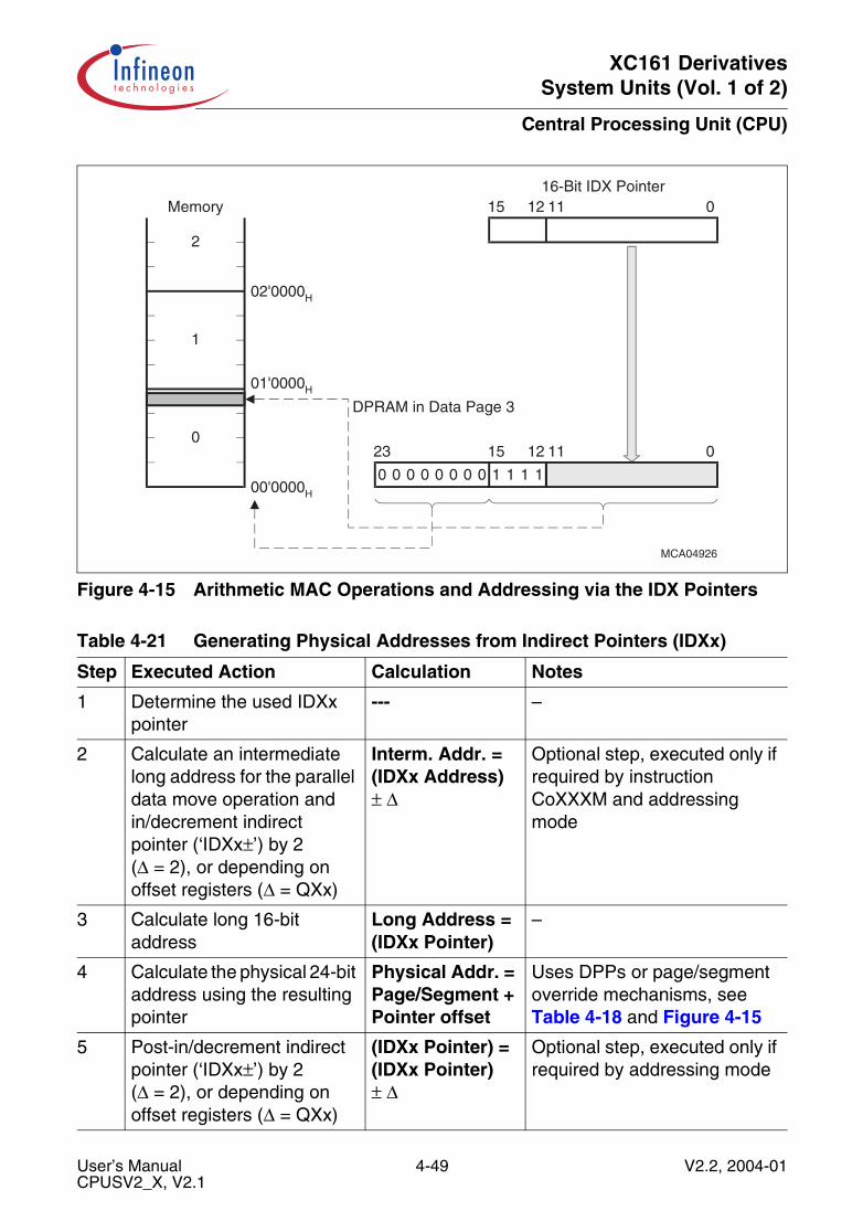
XC161 DerivativesSystem Units (Vol. 1 of 2)
Central Processing Unit (CPU)
Figure 4-15 Arithmetic MAC Operations and Addressing via the IDX Pointers
Table 4-21 Generating Physical Addresses from Indirect Pointers (IDXx)
Step Executed Action Calculation Notes
1 Determine the used IDXx pointer
--- –
2 Calculate an intermediate long address for the parallel data move operation and in/decrement indirect pointer (‘IDXx±’) by 2 (∆ = 2), or depending on offset registers (∆ = QXx)
Interm. Addr. = (IDXx Address) ± ∆
Optional step, executed only if required by instruction CoXXXM and addressing mode
3 Calculate long 16-bit address
Long Address = (IDXx Pointer)
–
4 Calculate the physical 24-bit address using the resulting pointer
Physical Addr. = Page/Segment + Pointer offset
Uses DPPs or page/segment override mechanisms, see Table 4-18 and Figure 4-15
5 Post-in/decrement indirect pointer (‘IDXx±’) by 2 (∆ = 2), or depending on offset registers (∆ = QXx)
(IDXx Pointer) = (IDXx Pointer) ± ∆
Optional step, executed only if required by addressing mode
023
0
2
MCA04926
16-Bit IDX Pointer
15 12
Memory
02'0000H
11
11
01'0000H
00'0000H
DPRAM in Data Page 3
1
0
10 111000000
15 12 0
User’s Manual 4-49 V2.2, 2004-01CPUSV2_X, V2.1

XC161 DerivativesSystem Units (Vol. 1 of 2)
Central Processing Unit (CPU)
The following indirect addressing modes are provided:
Note: An example for parallel data move operations can be found in Figure 4-16.
Table 4-22 DSP Addressing Modes
Mnemonic Particularities
[IDXx] Most CoXXX instructions accept IDXx (IDX0, IDX1) as an indirect address pointer.
[IDXx+] The specified indirect address pointer is automatically post-incremented by 2 after the access.
with parallel data move
In case of a CoXXXM instruction, the address stored in the specified indirect address pointer is automatically pre-decremented by 2 for the parallel move operation. The pointer itself is not pre-decremented. Then, the specified indirect address pointer is automatically post-incremented by 2 after the access.
[IDXx-] The specified indirect address pointer is automatically post-decremented by 2 after the access.
with parallel data move
In case of a CoXXXM instruction, the address stored in the specified indirect address pointer is automatically pre-incremented by 2 for the parallel move operation. The pointer itself is not pre-incremented. Then, the specified indirect address pointer is automatically post-decremented by 2 after the access.
[IDXx + QXx] The specified indirect address pointer is automatically post-incremented by QXx after the access.
with parallel data move
In case of a CoXXXM instruction, the address stored in the specified indirect address pointer is automatically pre-decremented by QXx for the parallel move operation. The pointer itself is not pre-decremented. Then, the specified indirect address pointer is automatically post-incremented by QXx after the access.
[IDXx - QXx] The specified indirect address pointer is automatically post-decremented by QXx after the access.
with parallel data move
In case of a CoXXXM instruction, the address stored in the specified indirect address pointer is automatically pre-incremented by QXx for the parallel move operation. The pointer itself is not pre-incremented. Then, the specified indirect address pointer is automatically post-decremented by QXx after the access.
User’s Manual 4-50 V2.2, 2004-01CPUSV2_X, V2.1
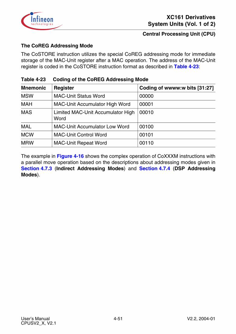
XC161 DerivativesSystem Units (Vol. 1 of 2)
Central Processing Unit (CPU)
The CoREG Addressing Mode
The CoSTORE instruction utilizes the special CoREG addressing mode for immediatestorage of the MAC-Unit register after a MAC operation. The address of the MAC-Unitregister is coded in the CoSTORE instruction format as described in Table 4-23:
The example in Figure 4-16 shows the complex operation of CoXXXM instructions witha parallel move operation based on the descriptions about addressing modes given inSection 4.7.3 (Indirect Addressing Modes) and Section 4.7.4 (DSP AddressingModes).
Table 4-23 Coding of the CoREG Addressing Mode
Mnemonic Register Coding of wwww:w bits [31:27]
MSW MAC-Unit Status Word 00000
MAH MAC-Unit Accumulator High Word 00001
MAS Limited MAC-Unit Accumulator High Word
00010
MAL MAC-Unit Accumulator Low Word 00100
MCW MAC-Unit Control Word 00101
MRW MAC-Unit Repeat Word 00110
User’s Manual 4-51 V2.2, 2004-01CPUSV2_X, V2.1
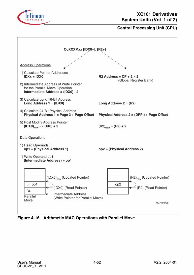
XC161 DerivativesSystem Units (Vol. 1 of 2)
Central Processing Unit (CPU)
Figure 4-16 Arithmetic MAC Operations with Parallel Move
MCA04928
Address Operations
1) Calculate Pointer Addresses IDXx = IDX0 R2 Address = CP + 2 × 2
(Global Register Bank)2) Intermediate Address of Write Pointer for the Parallel Move Operation Intermediate Address = (IDX0) - 2
3) Calculate Long 16-Bit Address Long Address 1 = (IDX0) Long Address 2 = (R2)
4) Calculate 24-Bit Physical Address Physical Address 1 = Page 3 + Page Offset Physical Address 2 = (DPPi) + Page Offset
5) Post Modify Address Pointer (IDX0)new = (IDX0) + 2 (R2)new = (R2) + 2
Data Operations
1) Read Operands op1 = (Physical Address 1) op2 = (Physical Address 2)
1) Write Operand op1 (Intermediate Address) = op1
CoXXXMxx [IDX0+], [R2+]
op1
ParallelMove
(IDX0)new (Updated Pointer)
(IDX0) (Read Pointer)
Intermediate Address(Write Pointer for Parallel Move)
op2
(R2)new (Updated Pointer)
(R2) (Read Pointer)
User’s Manual 4-52 V2.2, 2004-01CPUSV2_X, V2.1
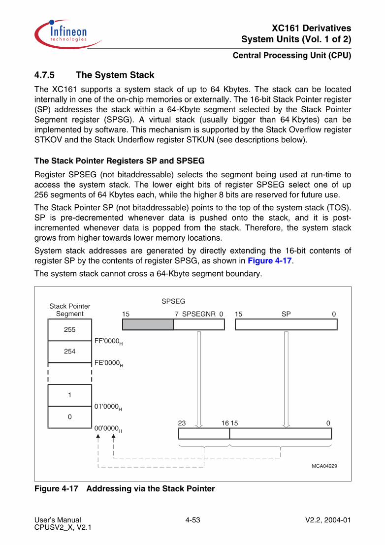
XC161 DerivativesSystem Units (Vol. 1 of 2)
Central Processing Unit (CPU)
4.7.5 The System Stack
The XC161 supports a system stack of up to 64 Kbytes. The stack can be locatedinternally in one of the on-chip memories or externally. The 16-bit Stack Pointer register(SP) addresses the stack within a 64-Kbyte segment selected by the Stack PointerSegment register (SPSG). A virtual stack (usually bigger than 64 Kbytes) can beimplemented by software. This mechanism is supported by the Stack Overflow registerSTKOV and the Stack Underflow register STKUN (see descriptions below).
The Stack Pointer Registers SP and SPSEG
Register SPSEG (not bitaddressable) selects the segment being used at run-time toaccess the system stack. The lower eight bits of register SPSEG select one of up256 segments of 64 Kbytes each, while the higher 8 bits are reserved for future use.
The Stack Pointer SP (not bitaddressable) points to the top of the system stack (TOS).SP is pre-decremented whenever data is pushed onto the stack, and it is post-incremented whenever data is popped from the stack. Therefore, the system stackgrows from higher towards lower memory locations.
System stack addresses are generated by directly extending the 16-bit contents ofregister SP by the contents of register SPSG, as shown in Figure 4-17.
The system stack cannot cross a 64-Kbyte segment boundary.
Figure 4-17 Addressing via the Stack Pointer
15
MCA04929
23 0
Stack PointerSegment
255
254
1
0
FF'0000H
FE'0000H
01'0000H
00'0000H
16
15 0SP15 0SPSEGNR7
SPSEG
User’s Manual 4-53 V2.2, 2004-01CPUSV2_X, V2.1
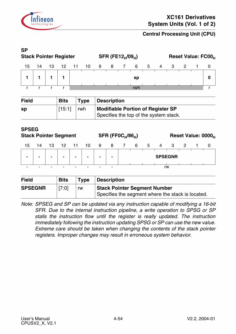
XC161 DerivativesSystem Units (Vol. 1 of 2)
Central Processing Unit (CPU)
Note: SPSEG and SP can be updated via any instruction capable of modifying a 16-bitSFR. Due to the internal instruction pipeline, a write operation to SPSG or SPstalls the instruction flow until the register is really updated. The instructionimmediately following the instruction updating SPSG or SP can use the new value.Extreme care should be taken when changing the contents of the stack pointerregisters. Improper changes may result in erroneous system behavior.
SP Stack Pointer Register SFR (FE12H/09H) Reset Value: FC00H
15 14 13 12 11 10 9 8 7 6 5 4 3 2 1 0
1 1 1 1 sp 0
r r r r rwh r
Field Bits Type Description
sp [15:1] rwh Modifiable Portion of Register SPSpecifies the top of the system stack.
SPSEG Stack Pointer Segment SFR (FF0CH/86H) Reset Value: 0000H
15 14 13 12 11 10 9 8 7 6 5 4 3 2 1 0
- - - - - - - - SPSEGNR
- - - - - - - - rw
Field Bits Type Description
SPSEGNR [7:0] rw Stack Pointer Segment NumberSpecifies the segment where the stack is located.
User’s Manual 4-54 V2.2, 2004-01CPUSV2_X, V2.1
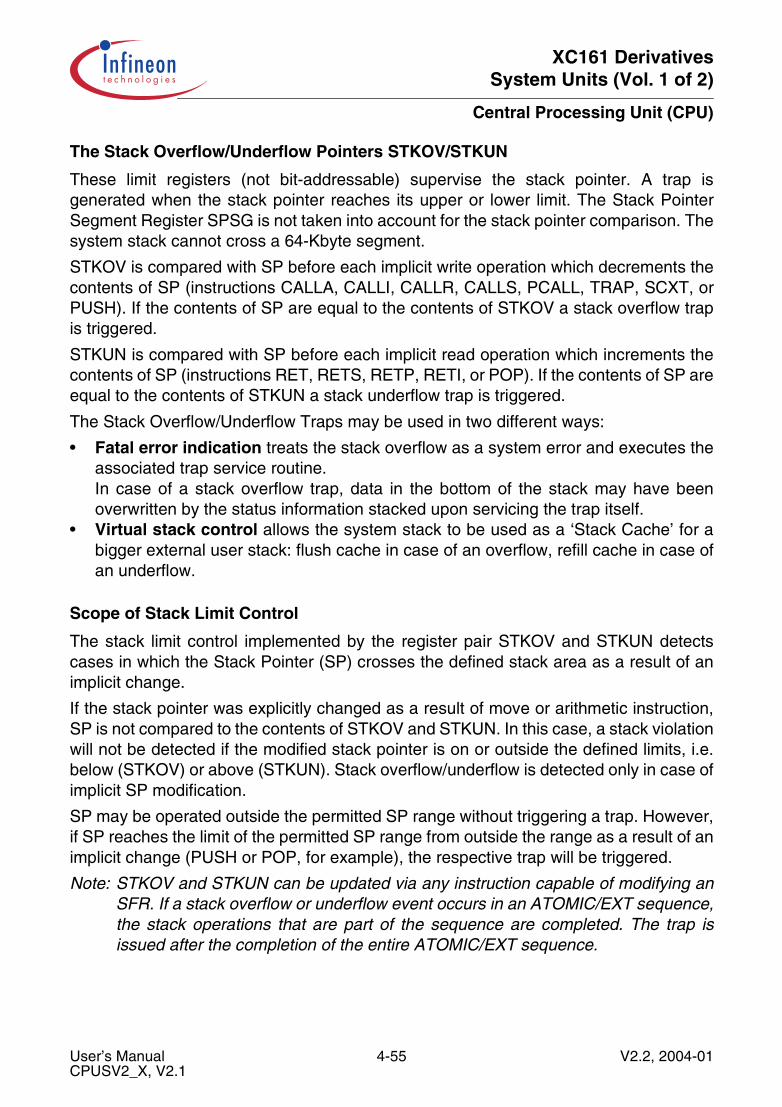
XC161 DerivativesSystem Units (Vol. 1 of 2)
Central Processing Unit (CPU)
The Stack Overflow/Underflow Pointers STKOV/STKUN
These limit registers (not bit-addressable) supervise the stack pointer. A trap isgenerated when the stack pointer reaches its upper or lower limit. The Stack PointerSegment Register SPSG is not taken into account for the stack pointer comparison. Thesystem stack cannot cross a 64-Kbyte segment.
STKOV is compared with SP before each implicit write operation which decrements thecontents of SP (instructions CALLA, CALLI, CALLR, CALLS, PCALL, TRAP, SCXT, orPUSH). If the contents of SP are equal to the contents of STKOV a stack overflow trapis triggered.
STKUN is compared with SP before each implicit read operation which increments thecontents of SP (instructions RET, RETS, RETP, RETI, or POP). If the contents of SP areequal to the contents of STKUN a stack underflow trap is triggered.
The Stack Overflow/Underflow Traps may be used in two different ways:
• Fatal error indication treats the stack overflow as a system error and executes theassociated trap service routine.In case of a stack overflow trap, data in the bottom of the stack may have beenoverwritten by the status information stacked upon servicing the trap itself.
• Virtual stack control allows the system stack to be used as a ‘Stack Cache’ for abigger external user stack: flush cache in case of an overflow, refill cache in case ofan underflow.
Scope of Stack Limit Control
The stack limit control implemented by the register pair STKOV and STKUN detectscases in which the Stack Pointer (SP) crosses the defined stack area as a result of animplicit change.
If the stack pointer was explicitly changed as a result of move or arithmetic instruction,SP is not compared to the contents of STKOV and STKUN. In this case, a stack violationwill not be detected if the modified stack pointer is on or outside the defined limits, i.e.below (STKOV) or above (STKUN). Stack overflow/underflow is detected only in case ofimplicit SP modification.
SP may be operated outside the permitted SP range without triggering a trap. However,if SP reaches the limit of the permitted SP range from outside the range as a result of animplicit change (PUSH or POP, for example), the respective trap will be triggered.
Note: STKOV and STKUN can be updated via any instruction capable of modifying anSFR. If a stack overflow or underflow event occurs in an ATOMIC/EXT sequence,the stack operations that are part of the sequence are completed. The trap isissued after the completion of the entire ATOMIC/EXT sequence.
User’s Manual 4-55 V2.2, 2004-01CPUSV2_X, V2.1
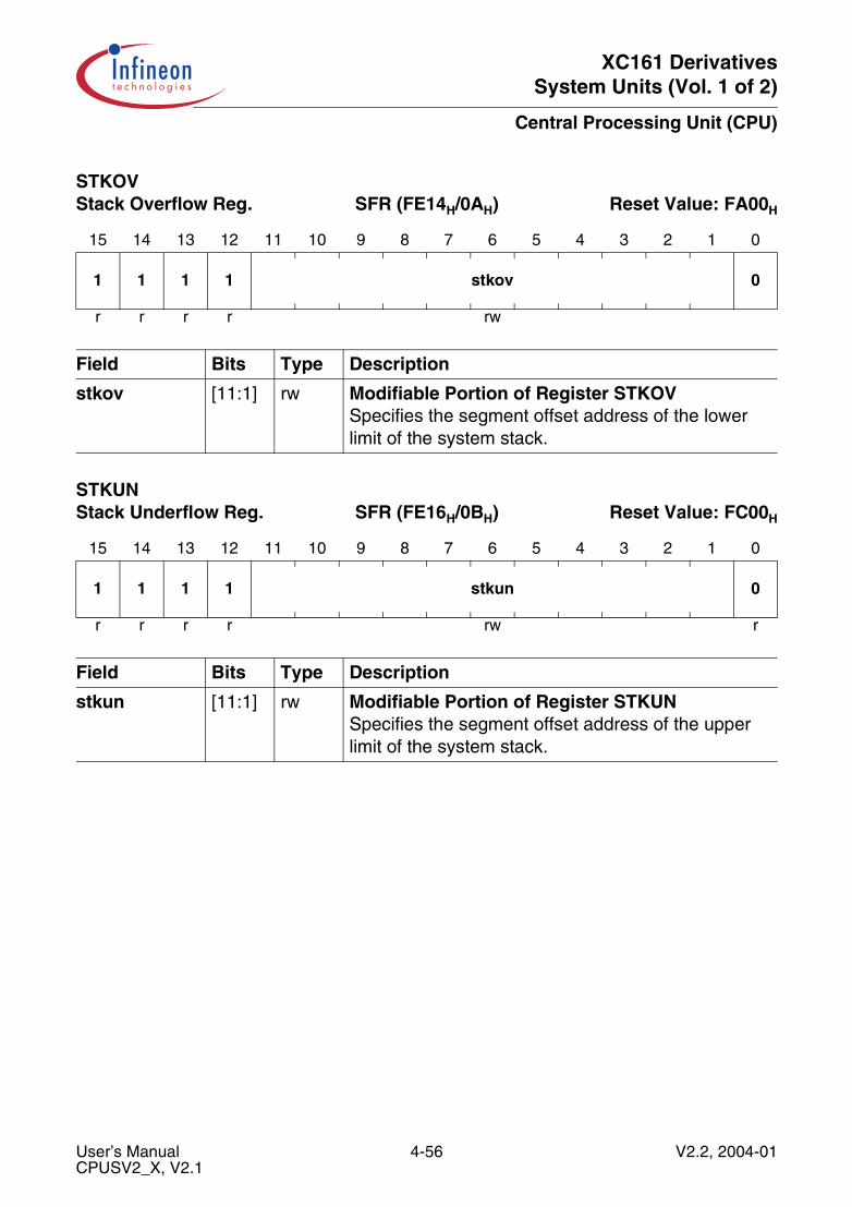
XC161 DerivativesSystem Units (Vol. 1 of 2)
Central Processing Unit (CPU)
STKOV Stack Overflow Reg. SFR (FE14H/0AH) Reset Value: FA00H
15 14 13 12 11 10 9 8 7 6 5 4 3 2 1 0
1 1 1 1 stkov 0
r r r r rw
Field Bits Type Description
stkov [11:1] rw Modifiable Portion of Register STKOVSpecifies the segment offset address of the lower limit of the system stack.
STKUN Stack Underflow Reg. SFR (FE16H/0BH) Reset Value: FC00H
15 14 13 12 11 10 9 8 7 6 5 4 3 2 1 0
1 1 1 1 stkun 0
r r r r rw r
Field Bits Type Description
stkun [11:1] rw Modifiable Portion of Register STKUNSpecifies the segment offset address of the upper limit of the system stack.
User’s Manual 4-56 V2.2, 2004-01CPUSV2_X, V2.1
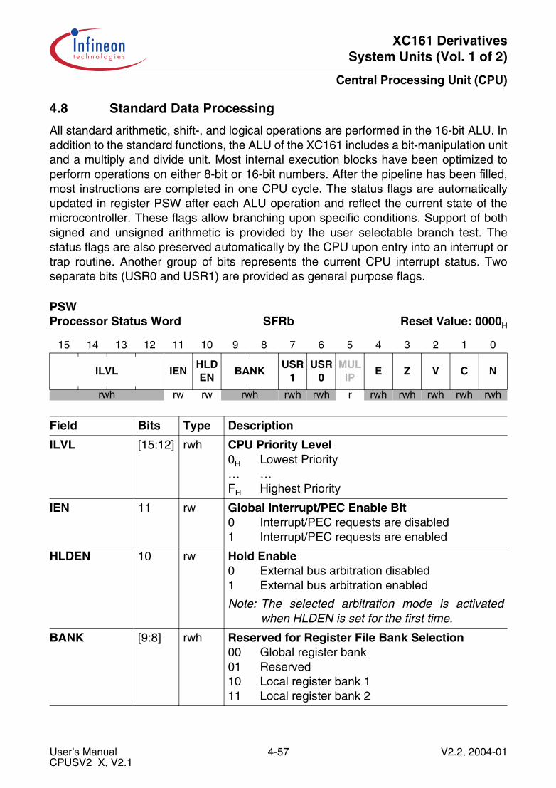
XC161 DerivativesSystem Units (Vol. 1 of 2)
Central Processing Unit (CPU)
4.8 Standard Data Processing
All standard arithmetic, shift-, and logical operations are performed in the 16-bit ALU. Inaddition to the standard functions, the ALU of the XC161 includes a bit-manipulation unitand a multiply and divide unit. Most internal execution blocks have been optimized toperform operations on either 8-bit or 16-bit numbers. After the pipeline has been filled,most instructions are completed in one CPU cycle. The status flags are automaticallyupdated in register PSW after each ALU operation and reflect the current state of themicrocontroller. These flags allow branching upon specific conditions. Support of bothsigned and unsigned arithmetic is provided by the user selectable branch test. Thestatus flags are also preserved automatically by the CPU upon entry into an interrupt ortrap routine. Another group of bits represents the current CPU interrupt status. Twoseparate bits (USR0 and USR1) are provided as general purpose flags.
PSW Processor Status Word SFRb Reset Value: 0000H
15 14 13 12 11 10 9 8 7 6 5 4 3 2 1 0
ILVL IENHLDEN
BANKUSR
1USR
0MUL
IPE Z V C N
rwh rw rw rwh rwh rwh r rwh rwh rwh rwh rwh
Field Bits Type Description
ILVL [15:12] rwh CPU Priority Level0H Lowest Priority… …FH Highest Priority
IEN 11 rw Global Interrupt/PEC Enable Bit0 Interrupt/PEC requests are disabled1 Interrupt/PEC requests are enabled
HLDEN 10 rw Hold Enable0 External bus arbitration disabled1 External bus arbitration enabled
Note: The selected arbitration mode is activatedwhen HLDEN is set for the first time.
BANK [9:8] rwh Reserved for Register File Bank Selection00 Global register bank01 Reserved10 Local register bank 111 Local register bank 2
User’s Manual 4-57 V2.2, 2004-01CPUSV2_X, V2.1

XC161 DerivativesSystem Units (Vol. 1 of 2)
Central Processing Unit (CPU)
ALU/MAC Status (N, C, V, Z, E, USR0, USR1)
The condition flags (N, C, V, Z, E) within the PSW indicate the ALU status after the mostrecently performed ALU operation. They are set by most of the instructions according tospecific rules which depend on the ALU or data movement operation performed by aninstruction.
After execution of an instruction which explicitly updates the PSW register, the conditionflags cannot be interpreted as described below because any explicit write to the PSWregister supersedes the condition flag values which are implicitly generated by the CPU.Explicitly reading the PSW register supplies a read value which represents the state ofthe PSW register after execution of the immediately preceding instruction.
Note: After reset, all of the ALU status bits are cleared.
N-Flag: For most of the ALU operations, the N-flag is set to 1, if the most significant bitof the result contains a 1; otherwise, it is cleared. In the case of integer operations, theN-flag can be interpreted as the sign bit of the result (negative: N = 1, positive: N = 0).
USR1 7 rwh General Purpose FlagMay be used by application
USR0 6 rwh General Purpose FlagMay be used by application
MULIP 5 r Multiplication/Division in Progress
Note: Always set to 0 (MUL/DIV not interruptible),for compatibility with existing software.
E 4 rwh End of Table Flag0 Source operand is neither 8000H nor 80H1 Source operand is 8000H or 80H
Z 3 rwh Zero Flag0 ALU result is not zero1 ALU result is zero
V 2 rwh Overflow Flag0 No Overflow produced0 Overflow produced
C 1 rwh Carry Flag0 No carry/borrow bit produced1 Carry/borrow bit produced
N 0 rwh Negative Result0 ALU result is not negative1 ALU result is negative
Field Bits Type Description
User’s Manual 4-58 V2.2, 2004-01CPUSV2_X, V2.1
XC161 DerivativesSystem Units (Vol. 1 of 2)
Central Processing Unit (CPU)
Negative numbers are always represented as the 2’s complement of the correspondingpositive number. The range of signed numbers extends from -8000H to +7FFFH for theword data type, or from -80H to +7FH for the byte data type. For Boolean bit operationswith only one operand, the N-flag represents the previous state of the specified bit. ForBoolean bit operations with two operands, the N-flag represents the logical XORing ofthe two specified bits.
C-Flag: After an addition, the C-flag indicates that a carry from the most significant bit ofthe specified word or byte data type has been generated. After a subtraction or acomparison, the C-flag indicates a borrow which represents the logical negation of acarry for the addition.This means that the C-flag is set to 1, if no carry from the most significant bit of thespecified word or byte data type has been generated during a subtraction, which isperformed internally by the ALU as a 2’s complement addition, and, the C-flag is clearedwhen this complement addition caused a carry.The C-flag is always cleared for logical, multiply and divide ALU operations, becausethese operations cannot cause a carry.For shift and rotate operations, the C-flag represents the value of the bit shifted out last.If a shift count of zero is specified, the C-flag will be cleared. The C-flag is also clearedfor a prioritize ALU operation, because a 1 is never shifted out of the MSB during thenormalization of an operand.For Boolean bit operations with only one operand, the C-flag is always cleared. ForBoolean bit operations with two operands, the C-flag represents the logical ANDing ofthe two specified bits.
V-Flag: For addition, subtraction, and 2’s complementation, the V-flag is always set to 1if the result exceeds the range of 16-bit signed numbers for word operations (-8000H to+7FFFH), or 8-bit signed numbers for byte operations (-80H to +7FH). Otherwise, theV-flag is cleared. Note that the result of an integer addition, integer subtraction, or 2’scomplement is not valid if the V-flag indicates an arithmetic overflow.For multiplication and division, the V-flag is set to 1 if the result cannot be representedin a word data type; otherwise, it is cleared. Note that a division by zero will always causean overflow. In contrast to the result of a division, the result of a multiplication is validwhether or not the V-flag is set to 1.Because logical ALU operations cannot produce an invalid result, the V-flag is clearedby these operations.
The V-flag is also used as a ‘Sticky Bit’ for rotate right and shift right operations. Withonly using the C-flag, a rounding error caused by a shift right operation can be estimatedup to a quantity of one half of the LSB of the result. In conjunction with the V-flag, theC-flag allows evaluation of the rounding error with a finer resolution (see Table 4-24).
For Boolean bit operations with only one operand, the V-flag is always cleared. ForBoolean bit operations with two operands, the V-flag represents the logical ORing of thetwo specified bits.
User’s Manual 4-59 V2.2, 2004-01CPUSV2_X, V2.1

XC161 DerivativesSystem Units (Vol. 1 of 2)
Central Processing Unit (CPU)
Z-Flag: The Z-flag is normally set to 1 if the result of an ALU operation equals zero,otherwise it is cleared.For the addition and subtraction with carry, the Z-flag is only set to 1, if the Z-flag alreadycontains a 1 and the result of the current ALU operation also equals zero. Thismechanism is provided to support multiple precision calculations.For Boolean bit operations with only one operand, the Z-flag represents the logicalnegation of the previous state of the specified bit. For Boolean bit operations with twooperands, the Z-flag represents the logical NORing of the two specified bits. For theprioritize ALU operation, the Z-flag indicates whether the second operand was zero.
E-Flag: End of table flag. The E-flag can be altered by instructions which perform ALUor data movement operations. The E-flag is cleared by those instructions which cannotbe reasonably used for table search operations. In all other cases, the E-flag valuedepends on the value of the source operand to signify whether the end of a search tableis reached or not. If the value of the source operand of an instruction equals the lowestnegative number which is representable by the data format of the correspondinginstruction (8000H for the word data type, or 80H for the byte data type), the E-flag is setto 1; otherwise, it is cleared.
General Control Functions (USR0, USR1, BANK, HLDEN)
A few bits in register PSW are dedicated to general control functions. Thus, they aresaved and restored automatically upon task switches and interrupts.
USR0/USR1-Flags: These bits can be set automatically during the execution ofrepeated MAC instructions. These bits can also be used as general flags by anapplication.
BANK: Bitfield BANK selects the currently active register bank (local or global). BitfieldBANK is updated implicitly by hardware upon entering an interrupt service routine, andby a RETI instruction. It can be also modified explicitly via software by any instructionwhich can write to PSW.
HLDEN: Setting this bit for the first time activates the selected bus arbitration mode (seeSection 9.3.9). Bus arbitration can be disabled by temporarily clearing bit HLDEN. In thiscase the bus is locked, while the bus arbitration mode remains selected.
Table 4-24 Shift Right Rounding Error Evaluation
C-Flag V-Flag Rounding Error Quantity
0011
0101
No rounding error0 < Rounding error < 1/2 LSBRounding error = 1/2 LSBRounding error > 1/2 LSB
User’s Manual 4-60 V2.2, 2004-01CPUSV2_X, V2.1
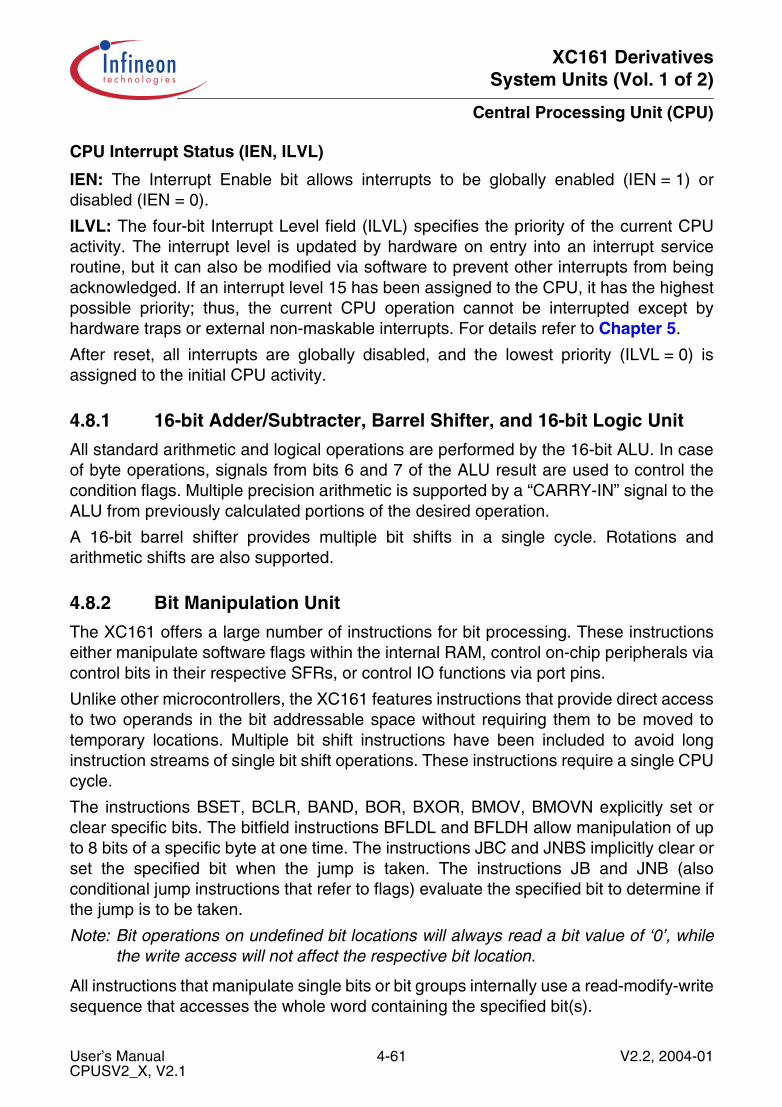
XC161 DerivativesSystem Units (Vol. 1 of 2)
Central Processing Unit (CPU)
CPU Interrupt Status (IEN, ILVL)
IEN: The Interrupt Enable bit allows interrupts to be globally enabled (IEN = 1) ordisabled (IEN = 0).
ILVL: The four-bit Interrupt Level field (ILVL) specifies the priority of the current CPUactivity. The interrupt level is updated by hardware on entry into an interrupt serviceroutine, but it can also be modified via software to prevent other interrupts from beingacknowledged. If an interrupt level 15 has been assigned to the CPU, it has the highestpossible priority; thus, the current CPU operation cannot be interrupted except byhardware traps or external non-maskable interrupts. For details refer to Chapter 5.
After reset, all interrupts are globally disabled, and the lowest priority (ILVL = 0) isassigned to the initial CPU activity.
4.8.1 16-bit Adder/Subtracter, Barrel Shifter, and 16-bit Logic Unit
All standard arithmetic and logical operations are performed by the 16-bit ALU. In caseof byte operations, signals from bits 6 and 7 of the ALU result are used to control thecondition flags. Multiple precision arithmetic is supported by a “CARRY-IN” signal to theALU from previously calculated portions of the desired operation.
A 16-bit barrel shifter provides multiple bit shifts in a single cycle. Rotations andarithmetic shifts are also supported.
4.8.2 Bit Manipulation Unit
The XC161 offers a large number of instructions for bit processing. These instructionseither manipulate software flags within the internal RAM, control on-chip peripherals viacontrol bits in their respective SFRs, or control IO functions via port pins.
Unlike other microcontrollers, the XC161 features instructions that provide direct accessto two operands in the bit addressable space without requiring them to be moved totemporary locations. Multiple bit shift instructions have been included to avoid longinstruction streams of single bit shift operations. These instructions require a single CPUcycle.
The instructions BSET, BCLR, BAND, BOR, BXOR, BMOV, BMOVN explicitly set orclear specific bits. The bitfield instructions BFLDL and BFLDH allow manipulation of upto 8 bits of a specific byte at one time. The instructions JBC and JNBS implicitly clear orset the specified bit when the jump is taken. The instructions JB and JNB (alsoconditional jump instructions that refer to flags) evaluate the specified bit to determine ifthe jump is to be taken.
Note: Bit operations on undefined bit locations will always read a bit value of ‘0’, whilethe write access will not affect the respective bit location.
All instructions that manipulate single bits or bit groups internally use a read-modify-writesequence that accesses the whole word containing the specified bit(s).
User’s Manual 4-61 V2.2, 2004-01CPUSV2_X, V2.1

XC161 DerivativesSystem Units (Vol. 1 of 2)
Central Processing Unit (CPU)
This method has several consequences:
• The read-modify-write approach may be critical with hardware-affected bits. In thesecases, the hardware may change specific bits while the read-modify-write operationis in progress; thus, the writeback would overwrite the new bit value generated by thehardware. The solution is provided by either the implemented hardware protection(see below) or through special programming (see Section 4.3).
• Bits can be modified only within the internal address areas (internal RAM and SFRs).External locations cannot be used with bit instructions.
The upper 256 bytes of SFR area, ESFR area, and internal DPRAM are bit-addressable;so, the register bits located within those respective sections can be manipulated directlyusing bit instructions. The other SFRs must be accessed byte/word wise.
Note: All GPRs are bit-addressable independently from the allocation of the registerbank via the Context Pointer (CP). Even GPRs which are allocated to non-bit-addressable RAM locations provide this feature.
Protected bits are not changed during the read-modify-write sequence, such as whenhardware sets an interrupt request flag between the read and the write of the read-modify-write sequence. The hardware protection logic guarantees that only the intendedbit(s) is/are affected by the write-back operation. A summary of the protected bitsimplemented in the XC161 can be found in Section 2.7.
Note: If a conflict occurs between a bit manipulation generated by hardware and anintended software access, the software access has priority and determines thefinal value of the respective bit.
User’s Manual 4-62 V2.2, 2004-01CPUSV2_X, V2.1
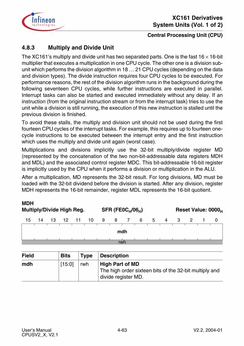
XC161 DerivativesSystem Units (Vol. 1 of 2)
Central Processing Unit (CPU)
4.8.3 Multiply and Divide Unit
The XC161’s multiply and divide unit has two separated parts. One is the fast 16 × 16-bitmultiplier that executes a multiplication in one CPU cycle. The other one is a division sub-unit which performs the division algorithm in 18 … 21 CPU cycles (depending on the dataand division types). The divide instruction requires four CPU cycles to be executed. Forperformance reasons, the rest of the division algorithm runs in the background during thefollowing seventeen CPU cycles, while further instructions are executed in parallel.Interrupt tasks can also be started and executed immediately without any delay. If aninstruction (from the original instruction stream or from the interrupt task) tries to use theunit while a division is still running, the execution of this new instruction is stalled until theprevious division is finished.
To avoid these stalls, the multiply and division unit should not be used during the firstfourteen CPU cycles of the interrupt tasks. For example, this requires up to fourteen one-cycle instructions to be executed between the interrupt entry and the first instructionwhich uses the multiply and divide unit again (worst case).
Multiplications and divisions implicitly use the 32-bit multiply/divide register MD(represented by the concatenation of the two non-bit-addressable data registers MDHand MDL) and the associated control register MDC. This bit-addressable 16-bit registeris implicitly used by the CPU when it performs a division or multiplication in the ALU.
After a multiplication, MD represents the 32-bit result. For long divisions, MD must beloaded with the 32-bit dividend before the division is started. After any division, registerMDH represents the 16-bit remainder, register MDL represents the 16-bit quotient.
MDH Multiply/Divide High Reg. SFR (FE0CH/06H) Reset Value: 0000H
15 14 13 12 11 10 9 8 7 6 5 4 3 2 1 0
mdh
rwh
Field Bits Type Description
mdh [15:0] rwh High Part of MDThe high order sixteen bits of the 32-bit multiply and divide register MD.
User’s Manual 4-63 V2.2, 2004-01CPUSV2_X, V2.1

XC161 DerivativesSystem Units (Vol. 1 of 2)
Central Processing Unit (CPU)
Whenever MDH or MDL is updated via software, the Multiply/Divide Register In Use flag(MDRIU) in the Multiply/Divide Control register (MDC) is set to ‘1’. The MDRIU flag iscleared, whenever register MDL is read via software.
Note: The MDRIU flag indicates the usage of register MD (MDL and MDH). In this caseMD must be saved prior to a new multiplication or division operation.
MDL Multiply/Divide Low Reg. SFR (FE0EH/07H) Reset Value: 0000H
15 14 13 12 11 10 9 8 7 6 5 4 3 2 1 0
mdl
rwh
Field Bits Type Description
mdl [15:0] rwh Low Part of MDThe low order sixteen bits of the 32-bit multiply and divide register MD.
MDC Multiply/Divide Control Reg. SFR (FF0EH/87H) Reset Value: 0000H
15 14 13 12 11 10 9 8 7 6 5 4 3 2 1 0
- - - - - - - - - - -MDR
IU- - - -
- - - - - - - - - - - r(w)h - - - -
Field Bits Type Description
MDRIU 4 rwh Multiply/Divide Register In Use0 Cleared when MDL is read via software.1 Set when MDL or MDH is written via software,
or when a multiply or divide instruction is executed.
User’s Manual 4-64 V2.2, 2004-01CPUSV2_X, V2.1

XC161 DerivativesSystem Units (Vol. 1 of 2)
Central Processing Unit (CPU)
4.9 DSP Data Processing (MAC Unit)
The new CoXXX arithmetic instructions are performed in the MAC unit. The MAC unitprovides single-instruction-cycle, non-pipelined, 32-bit additions; 32-bit subtraction; rightand left shifts; 16-bit by 16-bit multiplication; and multiplication with cumulativesubtraction/addition. The MAC unit includes the following major components, shown inFigure 4-18:
• 16-bit by 16-bit signed/unsigned multiplier with signed result1)
• Concatenation Unit• Scaler (one-bit left shifter) for fractional computing• 40-bit Adder/Subtracter• 40-bit Signed Accumulator• Data Limiter• Accumulator Shifter• Repeat Counter
Figure 4-18 Functional MAC Unit Block Diagram
1) The same hardware-multiplier is used in the ALU.
MCA04930
40-Bit Adder/Subtracter
SignedExt.
Round + Saturation
32
Signed/UnsignedMultiplier
ConcatenationUnit
3232
16 16 16 16
16-Bit Input Operands
40
40-Bit SignedAccumulator
Limiter
40
ACCU-Shifter
40
40
MSW Register
Repeat Counter
MCW Register
User’s Manual 4-65 V2.2, 2004-01CPUSV2_X, V2.1
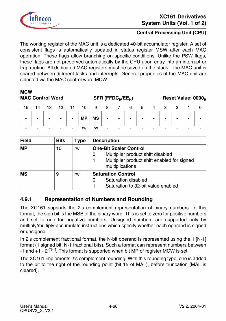
XC161 DerivativesSystem Units (Vol. 1 of 2)
Central Processing Unit (CPU)
The working register of the MAC unit is a dedicated 40-bit accumulator register. A set ofconsistent flags is automatically updated in status register MSW after each MACoperation. These flags allow branching on specific conditions. Unlike the PSW flags,these flags are not preserved automatically by the CPU upon entry into an interrupt ortrap routine. All dedicated MAC registers must be saved on the stack if the MAC unit isshared between different tasks and interrupts. General properties of the MAC unit areselected via the MAC control word MCW.
4.9.1 Representation of Numbers and Rounding
The XC161 supports the 2’s complement representation of binary numbers. In thisformat, the sign bit is the MSB of the binary word. This is set to zero for positive numbersand set to one for negative numbers. Unsigned numbers are supported only bymultiply/multiply-accumulate instructions which specify whether each operand is signedor unsigned.
In 2’s complement fractional format, the N-bit operand is represented using the 1.[N-1]format (1 signed bit, N-1 fractional bits). Such a format can represent numbers between-1 and +1 - 2-[N-1]. This format is supported when bit MP of register MCW is set.
The XC161 implements 2’s complement rounding. With this rounding type, one is addedto the bit to the right of the rounding point (bit 15 of MAL), before truncation (MAL iscleared).
MCW MAC Control Word SFR (FFDCH/EEH) Reset Value: 0000H
15 14 13 12 11 10 9 8 7 6 5 4 3 2 1 0
- - - - - MP MS - - - - - - - - -
- - - - - rw rw - - - - - - - - -
Field Bits Type Description
MP 10 rw One-Bit Scaler Control0 Multiplier product shift disabled1 Multiplier product shift enabled for signed
multiplications
MS 9 rw Saturation Control0 Saturation disabled1 Saturation to 32-bit value enabled
User’s Manual 4-66 V2.2, 2004-01CPUSV2_X, V2.1

XC161 DerivativesSystem Units (Vol. 1 of 2)
Central Processing Unit (CPU)
4.9.2 The 16-bit by 16-bit Signed/Unsigned Multiplier and Scaler
The multiplier executes 16-bit by 16-bit parallel signed/unsigned fractional and integermultiplication in one CPU-cycle. The multiplier allows the multiplication of unsigned andsigned operands. The result is always presented in a signed fractional or integer format.
The result of the multiplication feeds a one-bit scaler to allow compensation for the extrasign bit gained in multiplying two 16-bit 2’s complement numbers.
4.9.3 Concatenation Unit
The concatenation unit enables the MAC unit to perform 32-bit arithmetic operations inone CPU cycle. The concatenation unit concatenates two 16-bit operands to a 32-bitoperand before the 32-bit arithmetic operation is executed in the 40-bit adder/subtracter.The second required operand is always the current accumulator contents. Theconcatenation unit is also used to pre-load the accumulator with a 32-bit value.
4.9.4 One-bit Scaler
The one-bit scaler can shift the result of the concatenation unit or the output of themultiplier one bit to the left. The scaler is controlled by the executed instruction for theconcatenation or by control bit MP in register MCW.
If bit MP is set the product is shifted one bit to the left to compensate for the extra signbit gained in multiplying two 16-bit 2’s-complement numbers. The enabled automaticshift is performed only if both input operands are signed.
4.9.5 The 40-bit Adder/Subtracter
The 40-bit Adder/Subtracter allows intermediate overflows in a series ofmultiply/accumulate operations. The Adder/Subtracter has two input ports. The 40-bitport is the feedback of the accumulator output through the ACCU-Shifter to theAdder/Subtracter. The 32-bit port is the input port for the operand coming from the one-bit Scaler. The 32-bit operands are signed and extended to 40 bits before theaddition/subtraction is performed.
The output of the Adder/Subtracter goes to the accumulator. It is also possible to roundthe result and to saturate it on a 32-bit value automatically after every accumulation. Theround operation is performed by adding 00’0000’8000H to the result. Automaticsaturation is enabled by setting the saturation control bit MS in register MCW.
When the accumulator is in the overflow saturation mode and an overflow occurs, theaccumulator is loaded with either the most positive or the most negative valuerepresentable in a 32-bit value, depending on the direction of the overflow as well as onthe arithmetic used. The value of the accumulator upon saturation is either00’7FFF’FFFFH (positive) or FF’8000’0000H (negative).
User’s Manual 4-67 V2.2, 2004-01CPUSV2_X, V2.1

XC161 DerivativesSystem Units (Vol. 1 of 2)
Central Processing Unit (CPU)
4.9.6 The Data Limiter
Saturation arithmetic is also provided to selectively limit overflow when reading theaccumulator by means of a CoSTORE <destination>., MAS instruction. Limiting isperformed on the MAC-Unit accumulator. If the contents of the accumulator can berepresented in the destination operand size without overflow, then the data limiter isdisabled and the operand is not modified. If the contents of the accumulator cannot berepresented without overflow in the destination operand size, the limiter will substitute a“limited” data as explained in Table 4-25:
Note: In this particular case, both the accumulator and the status register are notaffected. MAS is readable by means of a CoSTORE instruction only.
4.9.7 The Accumulator Shifter
The accumulator shifter is a parallel shifter with a 40-bit input and a 40-bit output. Thesource accumulator shifting operations are:
• No shift (Unmodified)• Up to 16-bit Arithmetic Left Shift• Up to 16-bit Arithmetic Right Shift
Notice that bits ME, MSV, and MSL in register MSW are affected by left shifts; therefore,if the saturation mechanism is enabled (MS) the behavior is similar to the one of theAdder/Subtracter.
Note: Certain precautions are required in case of left shift with saturation enabled.Generally, if MAE contains significant bits, then the 32-bit value in the accumulatoris to be saturated. However, it is possible that left shift may move some significantbits out of the accumulator. The 40-bit result will be misinterpreted and will beeither not saturated or saturated incorrectly. There is a chance that the result ofleft shift may produce a result which can saturate an original positive number tothe minimum negative value, or vice versa.
Table 4-25 Limiter Output
ME-flag MN-flag Output of Limiter
0 x unchanged
1 0 7FFFH
1 1 8000H
User’s Manual 4-68 V2.2, 2004-01CPUSV2_X, V2.1
XC161 DerivativesSystem Units (Vol. 1 of 2)
Central Processing Unit (CPU)
4.9.8 The 40-bit Signed Accumulator Register
The 40-bit accumulator consists of three concatenated registers MAE, MAH, and MAL.MAE is 8 bits wide, MAH and MAL are 16 bits wide. MAE is the Most Significant Byte ofthe 40-bit accumulator. This byte performs a guarding function. MAE is accessed as thelower byte of register MSW.
When MAH is written, the value in the accumulator is automatically adjusted to signedextended 40-bit format. That means MAL is cleared and MAE will be automaticallyloaded with zeros for a positive number (the most significant bit of MAH is 0), and withones for a negative number (the most significant bit of MAH is 1), representing theextended 40-bit negative number in 2’s complement notation. One may see that theextended 40-bit value is equal to the 32-bit value without extension. In other words, afterthis extension, MAE does not contain significant bits. Generally, this condition is presentwhen the highest 9 bits of the 40-bit signed result are the same.
During the accumulator operations, an overflow may happen and the result may not fitinto 32 bits and MAE will change. The extension flag “E” in register MSW is set when thesigned result in the accumulator has exceeded the 32-bit boundary. This condition ispresent when the highest 9 bits of the 40-bit signed result are not the same, i.e. MAEcontains significant bits.
Most CoXXX operations specify the 40-bit accumulator register as a source and/or adestination operand.
MAH Accumulator High Word SFR (FE5EH/2FH) Reset Value: 0000H
15 14 13 12 11 10 9 8 7 6 5 4 3 2 1 0
MAH
rwh
MALAccumulator Low Word SFR (FE5CH/2EH) Reset Value: 0000H
15 14 13 12 11 10 9 8 7 6 5 4 3 2 1 0
MAL
rwh
Field Bits Type Description
MAH, MAL [15:0] rwh High and Low Part of AccumulatorThe 40-bit accumulator is completed by MAE
User’s Manual 4-69 V2.2, 2004-01CPUSV2_X, V2.1

XC161 DerivativesSystem Units (Vol. 1 of 2)
Central Processing Unit (CPU)
4.9.9 The MAC Unit Status Word MSW
The upper byte of register MSW (bit-addressable) shows the current status of the MACUnit. The lower byte of register MSW represents the 8-bit MAC accumulator extension,building the 40-bit accumulator together with registers MAH and MAL.
MSW MAC Status Word SFR (FFDEH/EFH) Reset Value: 0000H
15 14 13 12 11 10 9 8 7 6 5 4 3 2 1 0
- MV MSL ME MSV MC MZ MN MAE
- rwh rwh rwh rwh rwh rwh rwh rwh
Field Bits Type Description
MV 14 rwh Overflow Flag0 No Overflow produced1 Overflow produced
MSL 13 rwh Sticky Limit Flag0 Result was not saturated1 Result was saturated
ME 12 rwh MAC Extension Flag0 MAE does not contain significant bits1 MAE contains significant bits
MSV 11 rwh Sticky Overflow Flag0 No Overflow occurred1 Overflow occurred
MC 10 rwh Carry Flag0 No carry/borrow produced1 Carry/borrow produced
MZ 9 rwh Zero Flag0 MAC result is not zero1 MAC result is zero
MN 8 rwh Negative Result0 MAC result is positive1 MAC result is negative
MAE [7:0] rwh MAC Accumulator ExtensionThe most significant bits of the 40-bit accumulator, completing registers MAH and MAL
User’s Manual 4-70 V2.2, 2004-01CPUSV2_X, V2.1
XC161 DerivativesSystem Units (Vol. 1 of 2)
Central Processing Unit (CPU)
MAC Unit Status (MV, MN, MZ, MC, MSV, ME, MSL)
These condition flags indicate the MAC status resulting from the most recentlyperformed MAC operation. These flags are controlled by the majority of MAC instructionsaccording to specific rules. Those rules depend on the instruction managing the MAC ordata movement operation.
After execution of an instruction which explicitly updates register MSW, the conditionflags may no longer represent an actual MAC status. An explicit write operation toregister MSW supersedes the condition flag values implicitly generated by the MAC unit.An explicit read access returns the value of register MSW after execution of theimmediately preceding instruction. Register MSW can be accessed via any instructioncapable of accessing an SFR.
Note: After reset, all MAC status bits are cleared.
MN-Flag: For the majority of the MAC operations, the MN-flag is set to 1 if the mostsignificant bit of the result contains a 1; otherwise, it is cleared. In the case of integeroperations, the MN-flag can be interpreted as the sign bit of the result (negative: MN = 1,positive: MN = 0). Negative numbers are always represented as the 2’s complement ofthe corresponding positive number. The range of signed numbers extends from80’0000’0000H to 7F’FFFF’FFFFH.
MZ-Flag: The MZ-flag is normally set to 1 if the result of a MAC operation equals zero;otherwise, it is cleared.
MC-Flag: After a MAC addition, the MC-flag indicates that a “Carry” from the mostsignificant bit of the accumulator extension MAE has been generated. After a MACsubtraction or a MAC comparison, the MC-flag indicates a “Borrow” representing thelogical negation of a “Carry” for the addition. This means that the MC-flag is set to 1 if no“Carry” from the most significant bit of the accumulator has been generated during asubtraction. Subtraction is performed by the MAC Unit as a 2’s complement addition andthe MC-flag is cleared when this complement addition caused a “Carry”.For left-shift MAC operations, the MC-flag represents the value of the bit shifted out last.Right-shift MAC operations always clear the MC-flag. The arithmetic right-shift MACoperation can set the MC-flag if the enabled round operation generates a “Carry” fromthe most significant bit of the accumulator extension MAE.
MSV-Flag: The addition, subtraction, 2’s complement, and round operations always setthe MSV-flag to 1 if the MAC result exceeds the maximum range of 40-bit signednumbers. If the MSV-flag indicates an arithmetic overflow, the MAC result of anoperation is not valid.The MSV-flag is a ‘Sticky Bit’. Once set, other MAC operations cannot affect the statusof the MSV-flag. Only a direct write operation can clear the MSV-flag.
ME-Flag: The ME-flag is set if the accumulator extension MAE contains significant bits,that means if the nine highest accumulator bits are not all equal.
User’s Manual 4-71 V2.2, 2004-01CPUSV2_X, V2.1
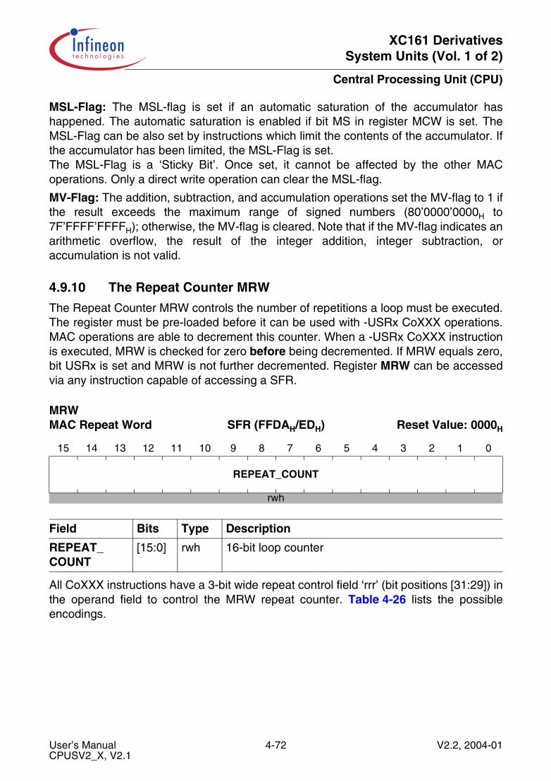
XC161 DerivativesSystem Units (Vol. 1 of 2)
Central Processing Unit (CPU)
MSL-Flag: The MSL-flag is set if an automatic saturation of the accumulator hashappened. The automatic saturation is enabled if bit MS in register MCW is set. TheMSL-Flag can be also set by instructions which limit the contents of the accumulator. Ifthe accumulator has been limited, the MSL-Flag is set.The MSL-Flag is a ‘Sticky Bit’. Once set, it cannot be affected by the other MACoperations. Only a direct write operation can clear the MSL-flag.
MV-Flag: The addition, subtraction, and accumulation operations set the MV-flag to 1 ifthe result exceeds the maximum range of signed numbers (80’0000’0000H to7F’FFFF’FFFFH); otherwise, the MV-flag is cleared. Note that if the MV-flag indicates anarithmetic overflow, the result of the integer addition, integer subtraction, oraccumulation is not valid.
4.9.10 The Repeat Counter MRW
The Repeat Counter MRW controls the number of repetitions a loop must be executed.The register must be pre-loaded before it can be used with -USRx CoXXX operations.MAC operations are able to decrement this counter. When a -USRx CoXXX instructionis executed, MRW is checked for zero before being decremented. If MRW equals zero,bit USRx is set and MRW is not further decremented. Register MRW can be accessedvia any instruction capable of accessing a SFR.
All CoXXX instructions have a 3-bit wide repeat control field ‘rrr’ (bit positions [31:29]) inthe operand field to control the MRW repeat counter. Table 4-26 lists the possibleencodings.
MRW MAC Repeat Word SFR (FFDAH/EDH) Reset Value: 0000H
15 14 13 12 11 10 9 8 7 6 5 4 3 2 1 0
REPEAT_COUNT
rwh
Field Bits Type Description
REPEAT_ COUNT
[15:0] rwh 16-bit loop counter
User’s Manual 4-72 V2.2, 2004-01CPUSV2_X, V2.1

XC161 DerivativesSystem Units (Vol. 1 of 2)
Central Processing Unit (CPU)
Note: Bit USR0 has been a general purpose flag also in previous architectures. Toprevent collisions due to using this flag by programmer or compiler, use‘-USR0 C0XXX’ instructions very carefully.
The following example shows a loop which is executed 20 times. Every time theCoMACM instruction is executed, the MRW counter is decremented.
MOV MRW, #19 ;Pre-load loop counterloop01:-USR1 CoMACM [IDX0+], [R0+] ;Calculate and decrement MSW ADD R2,#0002H JMPA cc_nusr1, loop01 ;Repeat loop until USR1 is set
Note: Because correctly predicted JMPA is executed in 0-cycle, it offers the functionalityof a repeat instruction.
Table 4-26 Encoding of MAC Repeat Word Control
Code in ‘rrr’ Effect on Repeat Counter
000B regular CoXXX instruction
001B RESERVED
010B ‘-USR0 CoXXX’ instruction,decrements repeat counter and sets bit USR0 if MRW is zero
011B ‘-USR1 CoXXX’ instruction,decrements repeat counter and sets bit USR1 if MRW is zero
1XXB RESERVED
User’s Manual 4-73 V2.2, 2004-01CPUSV2_X, V2.1
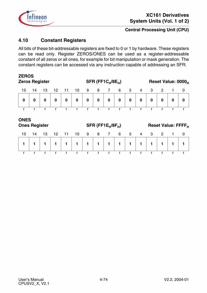
XC161 DerivativesSystem Units (Vol. 1 of 2)
Central Processing Unit (CPU)
4.10 Constant Registers
All bits of these bit-addressable registers are fixed to 0 or 1 by hardware. These registerscan be read only. Register ZEROS/ONES can be used as a register-addressableconstant of all zeros or all ones, for example for bit manipulation or mask generation. Theconstant registers can be accessed via any instruction capable of addressing an SFR.
ZEROS Zeros Register SFR (FF1CH/8EH) Reset Value: 0000H
15 14 13 12 11 10 9 8 7 6 5 4 3 2 1 0
0 0 0 0 0 0 0 0 0 0 0 0 0 0 0 0
r r r r r r r r r r r r r r r r
ONES Ones Register SFR (FF1EH/8FH) Reset Value: FFFFH
15 14 13 12 11 10 9 8 7 6 5 4 3 2 1 0
1 1 1 1 1 1 1 1 1 1 1 1 1 1 1 1
r r r r r r r r r r r r r r r r
User’s Manual 4-74 V2.2, 2004-01CPUSV2_X, V2.1
XC161 DerivativesSystem Units (Vol. 1 of 2)
Interrupt and Trap Functions
5 Interrupt and Trap FunctionsThe architecture of the XC161 supports several mechanisms for fast and flexibleresponse to service requests from various sources internal or external to themicrocontroller. Different kinds of exceptions are handled in a similar way:
• Interrupts generated by the Interrupt Controller (ITC)• DMA transfers issued by the Peripheral Event Controller (PEC)• Traps caused by the TRAP instruction or issued by faults or specific system states
Normal Interrupt Processing
The CPU temporarily suspends current program execution and branches to an interruptservice routine to service an interrupt requesting device. The current program status (IP,PSW, also CSP in segmentation mode) is saved on the internal system stack. Aprioritization scheme with 16 priority levels allows the user to specify the order in whichmultiple interrupt requests are to be handled.
Interrupt Processing via the Peripheral Event Controller (PEC)
A faster alternative to normal software controlled interrupt processing is servicing aninterrupt requesting device with the XC161’s integrated Peripheral Event Controller(PEC). Triggered by an interrupt request, the PEC performs a single word or byte datatransfer between any two locations through one of eight programmable PEC ServiceChannels. During a PEC transfer, normal program execution of the CPU is halted. Nointernal program status information needs to be saved. The same prioritization schemeis used for PEC service as for normal interrupt processing.
Trap Functions
Trap functions are activated in response to special conditions that occur during theexecution of instructions. A trap can also be caused externally by the Non-MaskableInterrupt pin, NMI. Several hardware trap functions are provided to handle erroneousconditions and exceptions arising during instruction execution. Hardware traps alwayshave highest priority and cause immediate system reaction. The software trap functionis invoked by the TRAP instruction that generates a software interrupt for a specifiedinterrupt vector. For all types of traps, the current program status is saved on the systemstack.
External Interrupt Processing
Although the XC161 does not provide dedicated interrupt pins, it allows connection ofexternal interrupt sources and provides several mechanisms to react to external eventsincluding standard inputs, non-maskable interrupts, and fast external interrupts. Exceptfor the non-maskable interrupt and the reset input, these interrupt functions are alternateport functions.
User’s Manual 5-1 V2.2, 2004-01ICU_X1, V2.1
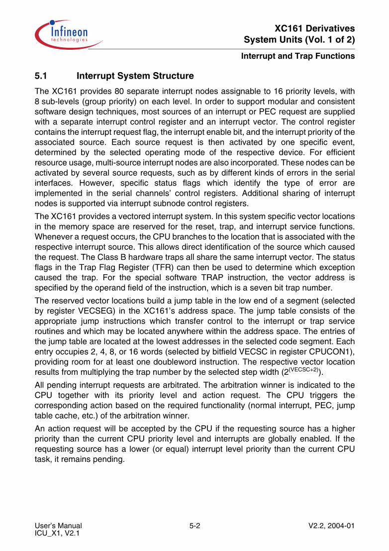
XC161 DerivativesSystem Units (Vol. 1 of 2)
Interrupt and Trap Functions
5.1 Interrupt System Structure
The XC161 provides 80 separate interrupt nodes assignable to 16 priority levels, with8 sub-levels (group priority) on each level. In order to support modular and consistentsoftware design techniques, most sources of an interrupt or PEC request are suppliedwith a separate interrupt control register and an interrupt vector. The control registercontains the interrupt request flag, the interrupt enable bit, and the interrupt priority of theassociated source. Each source request is then activated by one specific event,determined by the selected operating mode of the respective device. For efficientresource usage, multi-source interrupt nodes are also incorporated. These nodes can beactivated by several source requests, such as by different kinds of errors in the serialinterfaces. However, specific status flags which identify the type of error areimplemented in the serial channels’ control registers. Additional sharing of interruptnodes is supported via interrupt subnode control registers.
The XC161 provides a vectored interrupt system. In this system specific vector locationsin the memory space are reserved for the reset, trap, and interrupt service functions.Whenever a request occurs, the CPU branches to the location that is associated with therespective interrupt source. This allows direct identification of the source which causedthe request. The Class B hardware traps all share the same interrupt vector. The statusflags in the Trap Flag Register (TFR) can then be used to determine which exceptioncaused the trap. For the special software TRAP instruction, the vector address isspecified by the operand field of the instruction, which is a seven bit trap number.
The reserved vector locations build a jump table in the low end of a segment (selectedby register VECSEG) in the XC161’s address space. The jump table consists of theappropriate jump instructions which transfer control to the interrupt or trap serviceroutines and which may be located anywhere within the address space. The entries ofthe jump table are located at the lowest addresses in the selected code segment. Eachentry occupies 2, 4, 8, or 16 words (selected by bitfield VECSC in register CPUCON1),providing room for at least one doubleword instruction. The respective vector locationresults from multiplying the trap number by the selected step width (2(VECSC+2)).
All pending interrupt requests are arbitrated. The arbitration winner is indicated to theCPU together with its priority level and action request. The CPU triggers thecorresponding action based on the required functionality (normal interrupt, PEC, jumptable cache, etc.) of the arbitration winner.
An action request will be accepted by the CPU if the requesting source has a higherpriority than the current CPU priority level and interrupts are globally enabled. If therequesting source has a lower (or equal) interrupt level priority than the current CPUtask, it remains pending.
User’s Manual 5-2 V2.2, 2004-01ICU_X1, V2.1
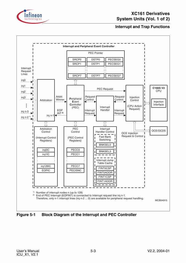
XC161 DerivativesSystem Units (Vol. 1 of 2)
Interrupt and Trap Functions
Figure 5-1 Block Diagram of the Interrupt and PEC Controller
MCB04915
FINT1ADDR
FINT1CSP
FINT0ADDR
FINT0CSP
Interrupt JumpTable Cache
BNKSEL3
BNKSEL0
Fast BankSwitching
InterruptHandler Control
PECC1
PECC0
PECControl
(PEC ControlRegisters)
PECISNC
PECC7
irq1IC
irq0IC
ArbitrationControl
(Interrupt ControlRegisters)
EOPIC
irq126IC
PeripheralEvent
Controller(PEC)
Arbitration
InterruptHandlerInterrupt
Request
RequestControl
EOPINT 2)
Arbitr.Winner
InterruptRequest
RequestControl
InjectionControl
(CPU ActionRequest)
PEC Request
irq n-1
SRCP1
SRCP0
SRCP7
DSTP1
DSTP0
DSTP7
PECSEG1
PECSEG0
PECSEG7
PEC Pointer
Interrupt and Peripheral Event Controller
irq n-2 1)
irq n-3
irq0
irq1
irq2
irq3
InterruptRequestLines
C166S V2CPU
InjectionInterface
OCE/OCDSOCE InjectionRequest & Control
1) Number of interrupt nodes n (up to 128)2) End of PEC Interrupt (EOPINT) is connected to Interrupt request line irq n-1.
Therefore, only n-1 interrupt lines (irq n-2 ... 0) are available for peripheral request handling.
User’s Manual 5-3 V2.2, 2004-01ICU_X1, V2.1
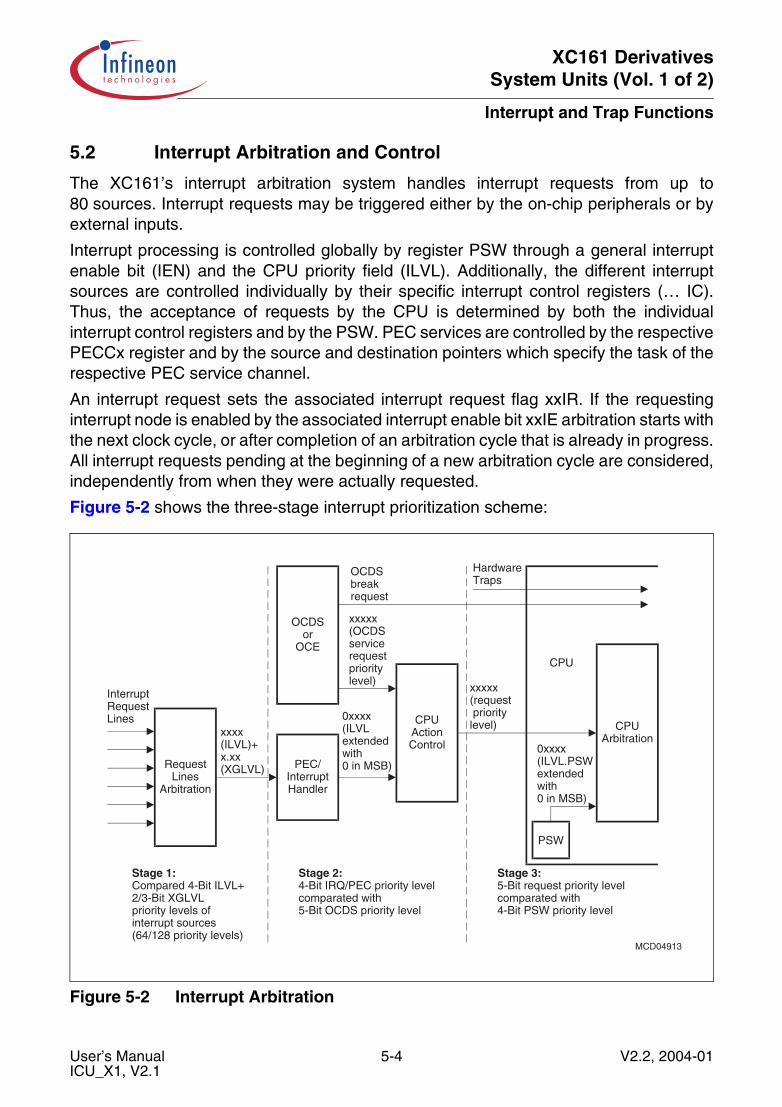
XC161 DerivativesSystem Units (Vol. 1 of 2)
Interrupt and Trap Functions
5.2 Interrupt Arbitration and Control
The XC161’s interrupt arbitration system handles interrupt requests from up to80 sources. Interrupt requests may be triggered either by the on-chip peripherals or byexternal inputs.
Interrupt processing is controlled globally by register PSW through a general interruptenable bit (IEN) and the CPU priority field (ILVL). Additionally, the different interruptsources are controlled individually by their specific interrupt control registers (… IC).Thus, the acceptance of requests by the CPU is determined by both the individualinterrupt control registers and by the PSW. PEC services are controlled by the respectivePECCx register and by the source and destination pointers which specify the task of therespective PEC service channel.
An interrupt request sets the associated interrupt request flag xxIR. If the requestinginterrupt node is enabled by the associated interrupt enable bit xxIE arbitration starts withthe next clock cycle, or after completion of an arbitration cycle that is already in progress.All interrupt requests pending at the beginning of a new arbitration cycle are considered,independently from when they were actually requested.
Figure 5-2 shows the three-stage interrupt prioritization scheme:
Figure 5-2 Interrupt Arbitration
MCD04913
OCDSor
OCE
CPUArbitration
PEC/InterruptHandler
CPUActionControl
0xxxx(ILVLextendedwith0 in MSB)
xxxxx(OCDSservicerequestprioritylevel)
OCDSbreakrequest
xxxxx(request prioritylevel)
PSW
0xxxx(ILVL.PSWextendedwith0 in MSB)
RequestLines
Arbitration
xxxx(ILVL)+x.xx(XGLVL)
InterruptRequestLines
HardwareTraps
CPU
Stage 1:Compared 4-Bit ILVL+2/3-Bit XGLVLpriority levels ofinterrupt sources(64/128 priority levels)
Stage 2:4-Bit IRQ/PEC priority levelcomparated with5-Bit OCDS priority level
Stage 3:5-Bit request priority levelcomparated with4-Bit PSW priority level
User’s Manual 5-4 V2.2, 2004-01ICU_X1, V2.1
XC161 DerivativesSystem Units (Vol. 1 of 2)
Interrupt and Trap Functions
The interrupt prioritization is done in three stages:
• Select one of the active interrupt requests• Compare the priority levels of the selected request and an OCDS service request• Compare the priority level of the final request with the CPU priority level
The First Arbitration Stage
compares the priority levels of the active interrupt request lines. The interrupt prioritylevel of each requestor is defined by bitfield ILVL in the respective xxIC register. Theextended group priority level XGLVL (combined from bitfields GPX and GLVL) definesup to eight sub-priorities within one interrupt level. The group priority level distinguishesinterrupt requests assigned to the same priority level, so one winner can be determined.
Note: All interrupt request sources that are enabled and programmed to the sameinterrupt priority level (ILVL) must have different group priority levels. Otherwise,an incorrect interrupt vector will be generated.
The Second Arbitration Stage
compares the priority of the first stage winner with the priority of OCDS service requests.OCDS service requests bypass the first stage of arbitration and go directly to the CPUAction Control Unit. The CPU Action Control Unit compares the winner’s 4-bit prioritylevel (disregarding the group level) with the 5-bit OCDS service request priority. The 4-bitILVL of the interrupt request is extended to a 5-bit value with MSB = 0. This means thatany OCDS request with MSB = 1 will always win the second stage arbitration. However,if there is a conflict between an OCDS request and an interrupt request, the interruptrequest wins.
The Third Arbitration Stage
compares the priority level of the second stage winner with the priority of the current CPUtask. An action request will be accepted by the CPU only if the priority level of the requestis higher than the current CPU priority level (bitfield ILVL in register PSW) and if interruptand PEC requests are globally enabled by the global interrupt enable flag IEN in registerPSW. To compare with the 5-bit priority level of the second stage winner, the 4-bit CPUpriority level is extended to a 5-bit value with MSB = 0. This means that any request withMSB = 1 will always interrupt the current CPU task. If the requestor has a priority levellower than or equal to the current CPU task, the request remains pending.
Note: Priority level 0000B is the default level of the CPU. Therefore, a request oninterrupt priority level 0000B will be arbitrated, but the CPU will never accept anaction request on this level. However, every individually enabled interrupt request(including all denied interrupt requests and priority level 0000B requests) triggersa CPU wake-up from idle state independent of the global interrupt enable bit IEN.
User’s Manual 5-5 V2.2, 2004-01ICU_X1, V2.1
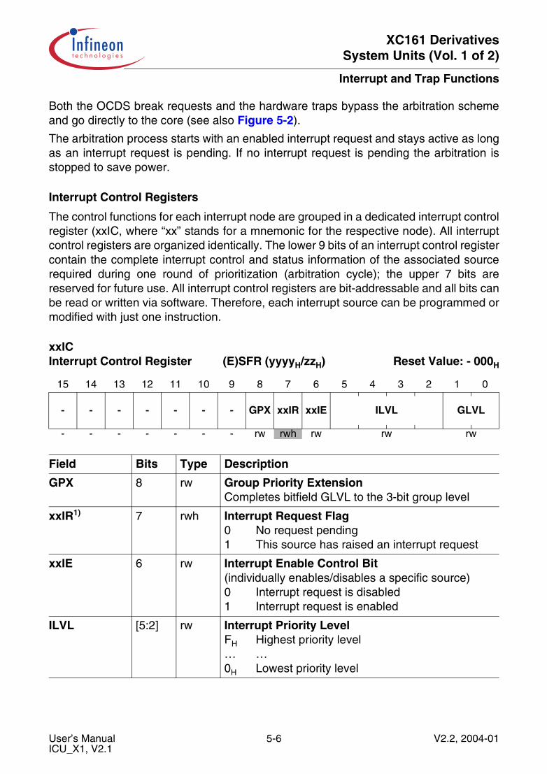
XC161 DerivativesSystem Units (Vol. 1 of 2)
Interrupt and Trap Functions
Both the OCDS break requests and the hardware traps bypass the arbitration schemeand go directly to the core (see also Figure 5-2).
The arbitration process starts with an enabled interrupt request and stays active as longas an interrupt request is pending. If no interrupt request is pending the arbitration isstopped to save power.
Interrupt Control Registers
The control functions for each interrupt node are grouped in a dedicated interrupt controlregister (xxIC, where “xx” stands for a mnemonic for the respective node). All interruptcontrol registers are organized identically. The lower 9 bits of an interrupt control registercontain the complete interrupt control and status information of the associated sourcerequired during one round of prioritization (arbitration cycle); the upper 7 bits arereserved for future use. All interrupt control registers are bit-addressable and all bits canbe read or written via software. Therefore, each interrupt source can be programmed ormodified with just one instruction.
xxICInterrupt Control Register (E)SFR (yyyyH/zzH) Reset Value: - 000H
15 14 13 12 11 10 9 8 7 6 5 4 3 2 1 0
- - - - - - - GPX xxIR xxIE ILVL GLVL
- - - - - - - rw rwh rw rw rw
Field Bits Type Description
GPX 8 rw Group Priority ExtensionCompletes bitfield GLVL to the 3-bit group level
xxIR1) 7 rwh Interrupt Request Flag0 No request pending1 This source has raised an interrupt request
xxIE 6 rw Interrupt Enable Control Bit(individually enables/disables a specific source)0 Interrupt request is disabled1 Interrupt request is enabled
ILVL [5:2] rw Interrupt Priority LevelFH Highest priority level… …0H Lowest priority level
User’s Manual 5-6 V2.2, 2004-01ICU_X1, V2.1
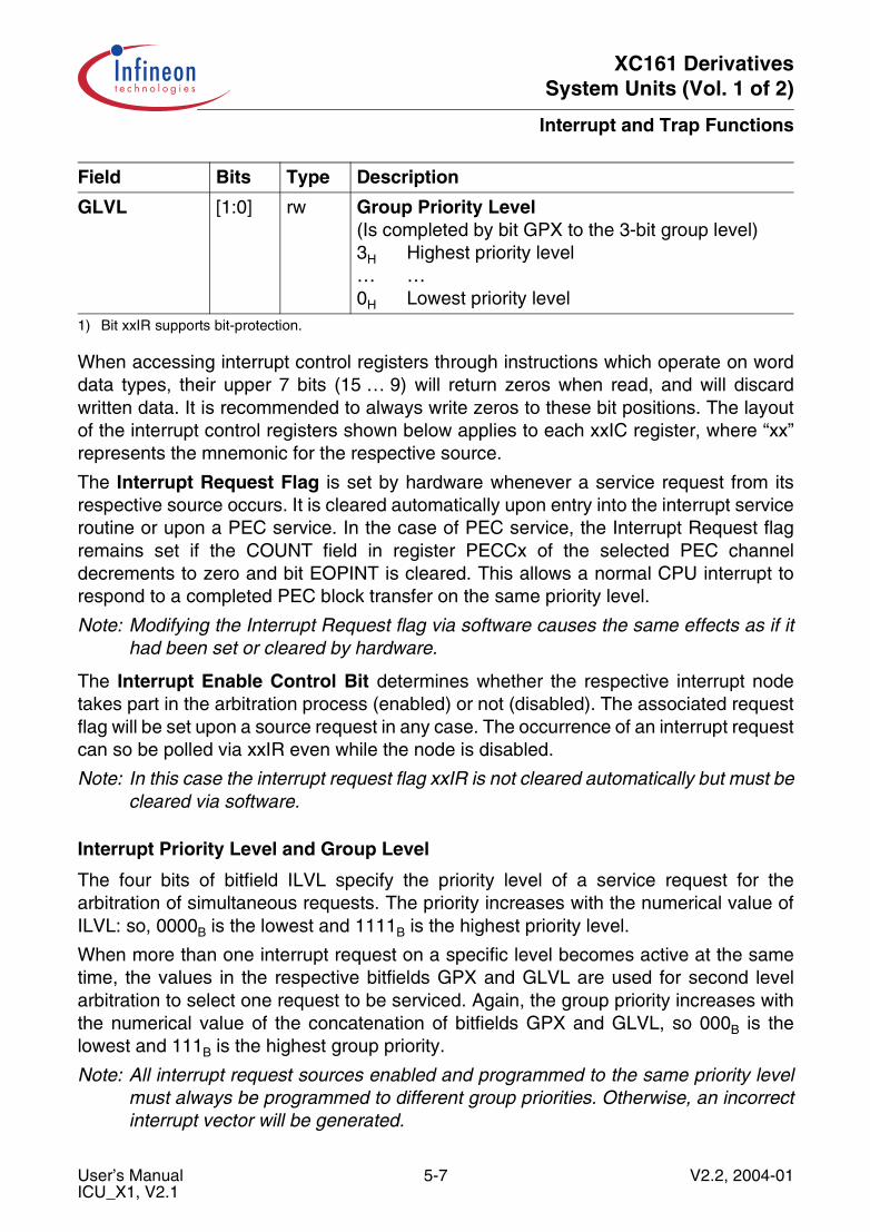
XC161 DerivativesSystem Units (Vol. 1 of 2)
Interrupt and Trap Functions
When accessing interrupt control registers through instructions which operate on worddata types, their upper 7 bits (15 … 9) will return zeros when read, and will discardwritten data. It is recommended to always write zeros to these bit positions. The layoutof the interrupt control registers shown below applies to each xxIC register, where “xx”represents the mnemonic for the respective source.
The Interrupt Request Flag is set by hardware whenever a service request from itsrespective source occurs. It is cleared automatically upon entry into the interrupt serviceroutine or upon a PEC service. In the case of PEC service, the Interrupt Request flagremains set if the COUNT field in register PECCx of the selected PEC channeldecrements to zero and bit EOPINT is cleared. This allows a normal CPU interrupt torespond to a completed PEC block transfer on the same priority level.
Note: Modifying the Interrupt Request flag via software causes the same effects as if ithad been set or cleared by hardware.
The Interrupt Enable Control Bit determines whether the respective interrupt nodetakes part in the arbitration process (enabled) or not (disabled). The associated requestflag will be set upon a source request in any case. The occurrence of an interrupt requestcan so be polled via xxIR even while the node is disabled.
Note: In this case the interrupt request flag xxIR is not cleared automatically but must becleared via software.
Interrupt Priority Level and Group Level
The four bits of bitfield ILVL specify the priority level of a service request for thearbitration of simultaneous requests. The priority increases with the numerical value ofILVL: so, 0000B is the lowest and 1111B is the highest priority level.
When more than one interrupt request on a specific level becomes active at the sametime, the values in the respective bitfields GPX and GLVL are used for second levelarbitration to select one request to be serviced. Again, the group priority increases withthe numerical value of the concatenation of bitfields GPX and GLVL, so 000B is thelowest and 111B is the highest group priority.
Note: All interrupt request sources enabled and programmed to the same priority levelmust always be programmed to different group priorities. Otherwise, an incorrectinterrupt vector will be generated.
GLVL [1:0] rw Group Priority Level(Is completed by bit GPX to the 3-bit group level)3H Highest priority level… …0H Lowest priority level
1) Bit xxIR supports bit-protection.
Field Bits Type Description
User’s Manual 5-7 V2.2, 2004-01ICU_X1, V2.1

XC161 DerivativesSystem Units (Vol. 1 of 2)
Interrupt and Trap Functions
Upon entry into the interrupt service routine, the priority level of the source that won thearbitration and whose priority level is higher than the current CPU level, is copied intobitfield ILVL of register PSW after pushing the old PSW contents onto the stack.
The interrupt system of the XC161 allows nesting of up to 15 interrupt service routinesof different priority levels (level 0 cannot be arbitrated).
Interrupt requests programmed to priority levels 15 … 8 (i.e., ILVL = 1XXXB) can beserviced by the PEC if the associated PEC channel is properly assigned and enabled(please refer to Section 5.4). Interrupt requests programmed to priority levels 7 through1 will always be serviced by normal interrupt processing.
Note: Priority level 0000B is the default level of the CPU. Therefore, a request on level 0will never be serviced because it can never interrupt the CPU. However, anindividually enabled interrupt request (independent of bit IEN) on level 0000B willterminate the XC161’s Idle mode and reactivate the CPU.
General Interrupt Control Functions in Register PSW
The acceptance of an interrupt request depends on the current CPU priority level (bitfieldILVL in register PSW) and the global interrupt enable control bit IEN in register PSW (seeSection 4.8).
CPU Priority ILVL defines the current level for the operation of the CPU. This bitfieldreflects the priority level of the routine currently executed. Upon entry into an interruptservice routine, this bitfield is updated with the priority level of the request being serviced.The PSW is saved on the system stack before the request is serviced. The CPU leveldetermines the minimum interrupt priority level which will be serviced. Any request onthe same or a lower level will not be acknowledged. The current CPU priority level maybe adjusted via software to control which interrupt request sources will beacknowledged. PEC transfers do not really interrupt the CPU, but rather “steal” a singlecycle, so PEC services do not influence the ILVL field in the PSW.
Hardware traps switch the CPU level to maximum priority (i.e. 15) so no interrupt or PECrequests will be acknowledged while an exception trap service routine is executed.
Note: The TRAP instruction does not change the CPU level, so software invoked trapservice routines may be interrupted by higher requests.
Interrupt Enable bit IEN globally enables or disables PEC operation and theacceptance of interrupts by the CPU. When IEN is cleared, no new interrupt requests areaccepted by the CPU (see also Section 4.3.4). When IEN is set to 1, all interruptsources, which have been individually enabled by the interrupt enable bits in theirassociated control registers, are globally enabled. Traps are non-maskable and are,therefore, not affected by the IEN bit.
Note: To generate requests, interrupt sources must be also enabled by the interruptenable bits in their associated control register.
User’s Manual 5-8 V2.2, 2004-01ICU_X1, V2.1
XC161 DerivativesSystem Units (Vol. 1 of 2)
Interrupt and Trap Functions
Register Bank Select bitfield BANK defines the currently used register bank for theCPU operation. When the CPU enters an interrupt service routine, this bitfield is updatedto select the register bank associated with the serviced request:
• Requests on priority levels 15 … 12 use the register bank pre-selected via therespective bitfield GPRSELx in the corresponding BNKSEL register
• Requests on priority levels 11 … 1 always use the global register bank,i.e. BANK = 00B
• Hardware traps always use the global register bank, i.e. BANK = 00B• The TRAP instruction does not change the current register bank
User’s Manual 5-9 V2.2, 2004-01ICU_X1, V2.1

XC161 DerivativesSystem Units (Vol. 1 of 2)
Interrupt and Trap Functions
5.3 Interrupt Vector Table
The XC161 provides a vectored interrupt system. This system reserves a set of specificmemory locations, which are accessed automatically upon the respective trigger event.Entries for the following events are provided:
• Reset (hardware, software, watchdog)• Traps (hardware-generated by fault conditions or via TRAP instruction)• Interrupt service requests
Whenever a request is accepted, the CPU branches to the location associated with therespective trigger source. This vector position directly identifies the source causing therequest, with two exceptions:
• Class B hardware traps all share the same interrupt vector. The status flags in theTrap Flag Register (TFR) are used to determine which exception caused the trap. Fordetails, see Section 5.11.
• An interrupt node may be shared by several interrupt requests, e.g. within a module.Additional flags identify the requesting source, so the software can handle eachrequest individually. For details, see Section 5.7.
The reserved vector locations build a vector table located in the address space of theXC161. The vector table usually contains the appropriate jump instructions that transfercontrol to the interrupt or trap service routines. These routines may be located anywherewithin the address space. The location and organization of the vector table isprogrammable.
The Vector Segment register VECSEG defines the segment of the Vector Table (can belocated in all segments, except for reserved areas).
Bitfield VECSC in register CPUCON1 defines the space between two adjacent vectors(can be 2, 4, 8, or 16 words). For a summary of register CPUCON1, please refer toSection 4.4.
Each vector location has an offset address to the segment base address of the vectortable (given by VECSEG). The offset can be easily calculated by multiplying the vectornumber with the vector space programmed in bitfield VECSC.
Table 5-2 lists all sources capable of requesting interrupt or PEC service in the XC161,the associated interrupt vector locations, the associated vector numbers, and theassociated interrupt control registers.
Note: All interrupt nodes which are currently not used by their associated modules or arenot connected to a module in the actual derivative may be used to generatesoftware controlled interrupt requests by setting the respective IR flag.
User’s Manual 5-10 V2.2, 2004-01ICU_X1, V2.1
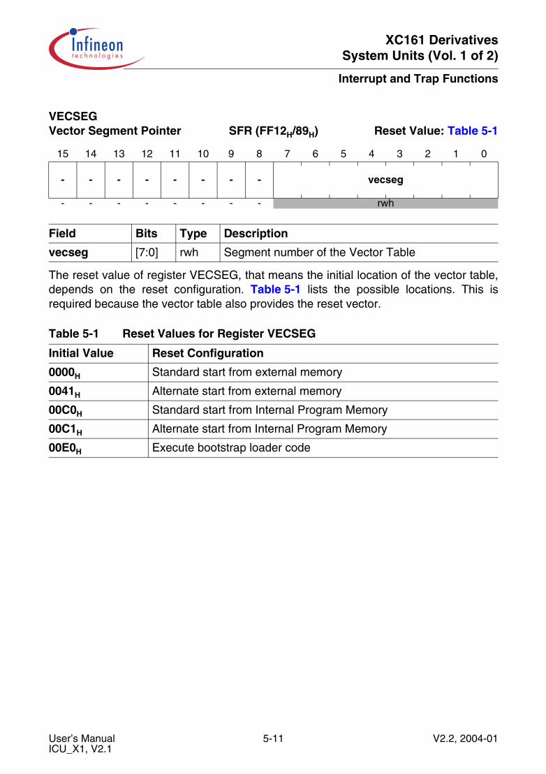
XC161 DerivativesSystem Units (Vol. 1 of 2)
Interrupt and Trap Functions
The reset value of register VECSEG, that means the initial location of the vector table,depends on the reset configuration. Table 5-1 lists the possible locations. This isrequired because the vector table also provides the reset vector.
VECSEG Vector Segment Pointer SFR (FF12H/89H) Reset Value: Table 5-1
15 14 13 12 11 10 9 8 7 6 5 4 3 2 1 0
- - - - - - - - vecseg
- - - - - - - - rwh
Field Bits Type Description
vecseg [7:0] rwh Segment number of the Vector Table
Table 5-1 Reset Values for Register VECSEG
Initial Value Reset Configuration
0000H Standard start from external memory
0041H Alternate start from external memory
00C0H Standard start from Internal Program Memory
00C1H Alternate start from Internal Program Memory
00E0H Execute bootstrap loader code
User’s Manual 5-11 V2.2, 2004-01ICU_X1, V2.1
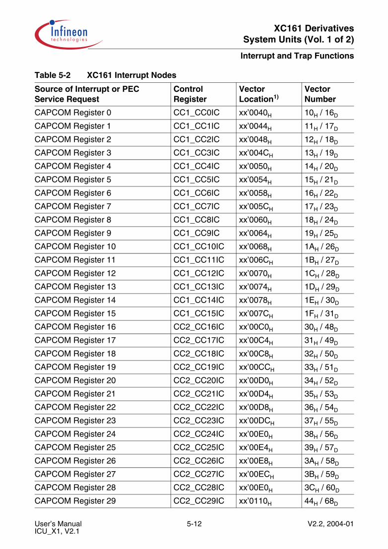
XC161 DerivativesSystem Units (Vol. 1 of 2)
Interrupt and Trap Functions
Table 5-2 XC161 Interrupt Nodes
Source of Interrupt or PEC Service Request
Control Register
Vector Location1)
Vector Number
CAPCOM Register 0 CC1_CC0IC xx’0040H 10H / 16D
CAPCOM Register 1 CC1_CC1IC xx’0044H 11H / 17D
CAPCOM Register 2 CC1_CC2IC xx’0048H 12H / 18D
CAPCOM Register 3 CC1_CC3IC xx’004CH 13H / 19D
CAPCOM Register 4 CC1_CC4IC xx’0050H 14H / 20D
CAPCOM Register 5 CC1_CC5IC xx’0054H 15H / 21D
CAPCOM Register 6 CC1_CC6IC xx’0058H 16H / 22D
CAPCOM Register 7 CC1_CC7IC xx’005CH 17H / 23D
CAPCOM Register 8 CC1_CC8IC xx’0060H 18H / 24D
CAPCOM Register 9 CC1_CC9IC xx’0064H 19H / 25D
CAPCOM Register 10 CC1_CC10IC xx’0068H 1AH / 26D
CAPCOM Register 11 CC1_CC11IC xx’006CH 1BH / 27D
CAPCOM Register 12 CC1_CC12IC xx’0070H 1CH / 28D
CAPCOM Register 13 CC1_CC13IC xx’0074H 1DH / 29D
CAPCOM Register 14 CC1_CC14IC xx’0078H 1EH / 30D
CAPCOM Register 15 CC1_CC15IC xx’007CH 1FH / 31D
CAPCOM Register 16 CC2_CC16IC xx’00C0H 30H / 48D
CAPCOM Register 17 CC2_CC17IC xx’00C4H 31H / 49D
CAPCOM Register 18 CC2_CC18IC xx’00C8H 32H / 50D
CAPCOM Register 19 CC2_CC19IC xx’00CCH 33H / 51D
CAPCOM Register 20 CC2_CC20IC xx’00D0H 34H / 52D
CAPCOM Register 21 CC2_CC21IC xx’00D4H 35H / 53D
CAPCOM Register 22 CC2_CC22IC xx’00D8H 36H / 54D
CAPCOM Register 23 CC2_CC23IC xx’00DCH 37H / 55D
CAPCOM Register 24 CC2_CC24IC xx’00E0H 38H / 56D
CAPCOM Register 25 CC2_CC25IC xx’00E4H 39H / 57D
CAPCOM Register 26 CC2_CC26IC xx’00E8H 3AH / 58D
CAPCOM Register 27 CC2_CC27IC xx’00ECH 3BH / 59D
CAPCOM Register 28 CC2_CC28IC xx’00E0H 3CH / 60D
CAPCOM Register 29 CC2_CC29IC xx’0110H 44H / 68D
User’s Manual 5-12 V2.2, 2004-01ICU_X1, V2.1
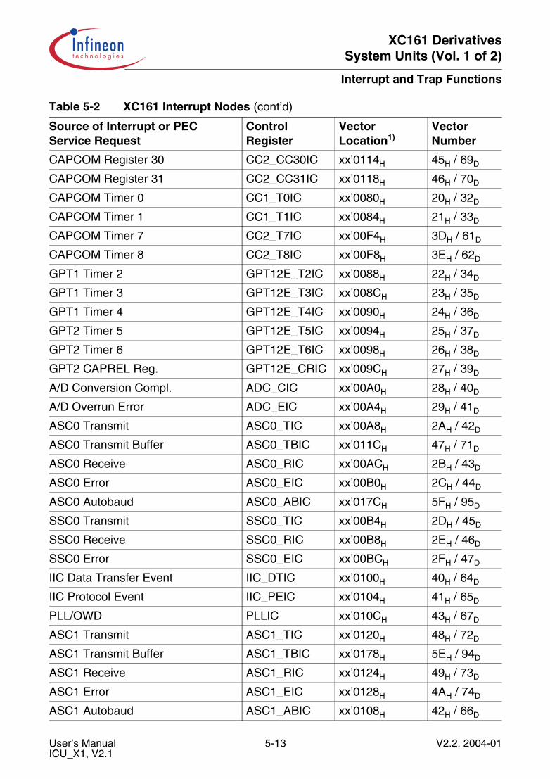
XC161 DerivativesSystem Units (Vol. 1 of 2)
Interrupt and Trap Functions
CAPCOM Register 30 CC2_CC30IC xx’0114H 45H / 69D
CAPCOM Register 31 CC2_CC31IC xx’0118H 46H / 70D
CAPCOM Timer 0 CC1_T0IC xx’0080H 20H / 32D
CAPCOM Timer 1 CC1_T1IC xx’0084H 21H / 33D
CAPCOM Timer 7 CC2_T7IC xx’00F4H 3DH / 61D
CAPCOM Timer 8 CC2_T8IC xx’00F8H 3EH / 62D
GPT1 Timer 2 GPT12E_T2IC xx’0088H 22H / 34D
GPT1 Timer 3 GPT12E_T3IC xx’008CH 23H / 35D
GPT1 Timer 4 GPT12E_T4IC xx’0090H 24H / 36D
GPT2 Timer 5 GPT12E_T5IC xx’0094H 25H / 37D
GPT2 Timer 6 GPT12E_T6IC xx’0098H 26H / 38D
GPT2 CAPREL Reg. GPT12E_CRIC xx’009CH 27H / 39D
A/D Conversion Compl. ADC_CIC xx’00A0H 28H / 40D
A/D Overrun Error ADC_EIC xx’00A4H 29H / 41D
ASC0 Transmit ASC0_TIC xx’00A8H 2AH / 42D
ASC0 Transmit Buffer ASC0_TBIC xx’011CH 47H / 71D
ASC0 Receive ASC0_RIC xx’00ACH 2BH / 43D
ASC0 Error ASC0_EIC xx’00B0H 2CH / 44D
ASC0 Autobaud ASC0_ABIC xx’017CH 5FH / 95D
SSC0 Transmit SSC0_TIC xx’00B4H 2DH / 45D
SSC0 Receive SSC0_RIC xx’00B8H 2EH / 46D
SSC0 Error SSC0_EIC xx’00BCH 2FH / 47D
IIC Data Transfer Event IIC_DTIC xx’0100H 40H / 64D
IIC Protocol Event IIC_PEIC xx’0104H 41H / 65D
PLL/OWD PLLIC xx’010CH 43H / 67D
ASC1 Transmit ASC1_TIC xx’0120H 48H / 72D
ASC1 Transmit Buffer ASC1_TBIC xx’0178H 5EH / 94D
ASC1 Receive ASC1_RIC xx’0124H 49H / 73D
ASC1 Error ASC1_EIC xx’0128H 4AH / 74D
ASC1 Autobaud ASC1_ABIC xx’0108H 42H / 66D
Table 5-2 XC161 Interrupt Nodes (cont’d)
Source of Interrupt or PEC Service Request
Control Register
Vector Location1)
Vector Number
User’s Manual 5-13 V2.2, 2004-01ICU_X1, V2.1

XC161 DerivativesSystem Units (Vol. 1 of 2)
Interrupt and Trap Functions
SDLM SDLM_IC xx’012CH 4BH / 75D
End of PEC Subchannel EOPIC xx’0130H 4CH / 76D
SSC1 Transmit SSC1_TIC xx’0144H 51H / 81D
SSC1 Receive SSC1_RIC xx’0148H 52H / 82D
SSC1 Error SSC1_EIC xx’014CH 53H / 83D
CAN0 CAN_0IC xx’0150H 54H / 84D
CAN1 CAN_1IC xx’0154H 55H / 85D
CAN2 CAN_2IC xx’0158H 56H / 86D
CAN3 CAN_3IC xx’015CH 57H / 87D
CAN4 CAN_4IC xx’0164H 59H / 89D
CAN5 CAN_5IC xx’0168H 5AH / 90D
CAN6 CAN_6IC xx’016CH 5BH / 91D
CAN7 CAN_7IC xx’0170H 5CH / 92D
RTC RTC_IC xx’0174H 5DH / 93D
Unassigned node --- xx’0134H 4DH / 77D
Unassigned node --- xx’0138H 4EH / 78D
Unassigned node --- xx’013CH 4FH / 79D
Unassigned node --- xx’0140H 50H / 80D
Unassigned node --- xx’00FCH 3FH / 63D
Unassigned node --- xx’0160H 58H / 88D
1) Register VECSEG defines the segment where the vector table is located to.Bitfield VECSC in register CPUCON1 defines the distance between two adjacent vectors. This tablerepresents the default setting, with a distance of 4 (two words) between two vectors.
Table 5-2 XC161 Interrupt Nodes (cont’d)
Source of Interrupt or PEC Service Request
Control Register
Vector Location1)
Vector Number
User’s Manual 5-14 V2.2, 2004-01ICU_X1, V2.1

XC161 DerivativesSystem Units (Vol. 1 of 2)
Interrupt and Trap Functions
Table 5-3 lists the vector locations for hardware traps and the corresponding status flagsin register TFR. It also lists the priorities of trap service for those cases in which morethan one trap condition might be detected within the same instruction. After any reset(hardware reset, software reset instruction SRST, or reset by watchdog timer overflow)program execution starts at the reset vector at location xx’0000H. Reset conditions havepriority over every other system activity and, therefore, have the highest priority (trappriority III).
Software traps may be initiated to any defined vector location. A service routine enteredvia a software TRAP instruction is always executed on the current CPU priority levelwhich is indicated in bitfield ILVL in register PSW. This means that routines entered viathe software TRAP instruction can be interrupted by all hardware traps or higher levelinterrupt requests.
Table 5-3 Hardware Trap Summary
Exception Condition Trap Flag Trap Vector Vector Location1)
1) Register VECSEG defines the segment where the vector table is located to.Bitfield VECSC in register CPUCON1 defines the distance between two adjacent vectors. This tablerepresents the default setting, with a distance of 4 (two words) between two vectors.
Vector Number
Trap Priority
Reset Functions:• Hardware Reset• Software Reset• W-dog Timer Overflow
–RESETRESETRESET
xx’0000Hxx’0000H
xx’0000H
00H00H
00H
IIIIIIIII
Class A Hardware Traps:• Non-Maskable Interrupt• Stack Overflow• Stack Underflow• Software Break
NMISTKOFSTKUFSOFTBRK
NMITRAPSTOTRAPSTUTRAPSBRKTRAP
xx’0008Hxx’0010Hxx’0018Hxx’0020H
02H04H06H08H
IIIIIIII
Class B Hardware Traps:• Undefined Opcode• PMI Access Error• Protected Instruction
Fault• Illegal Word Operand
Access
UNDOPCPACERPRTFLT
ILLOPA
BTRAPBTRAPBTRAP
BTRAP
xx’0028Hxx’0028Hxx’0028H
xx’0028H
0AH0AH0AH
0AH
III
I
Reserved – – [2CH - 3CH]
[0BH - 0FH]
–
Software Traps• TRAP Instruction
– – Any1) Any[00H - 7FH]
Current CPU Priority
User’s Manual 5-15 V2.2, 2004-01ICU_X1, V2.1
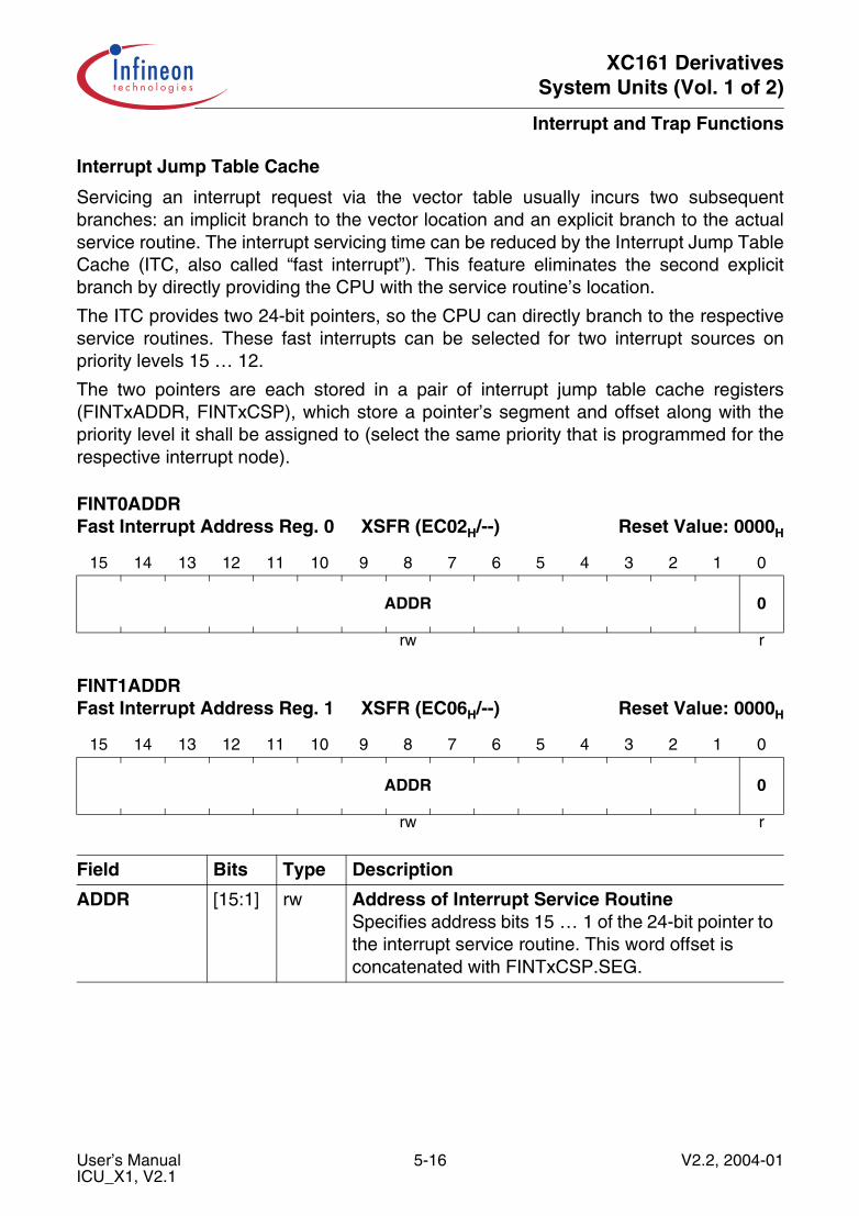
XC161 DerivativesSystem Units (Vol. 1 of 2)
Interrupt and Trap Functions
Interrupt Jump Table Cache
Servicing an interrupt request via the vector table usually incurs two subsequentbranches: an implicit branch to the vector location and an explicit branch to the actualservice routine. The interrupt servicing time can be reduced by the Interrupt Jump TableCache (ITC, also called “fast interrupt”). This feature eliminates the second explicitbranch by directly providing the CPU with the service routine’s location.
The ITC provides two 24-bit pointers, so the CPU can directly branch to the respectiveservice routines. These fast interrupts can be selected for two interrupt sources onpriority levels 15 … 12.
The two pointers are each stored in a pair of interrupt jump table cache registers(FINTxADDR, FINTxCSP), which store a pointer’s segment and offset along with thepriority level it shall be assigned to (select the same priority that is programmed for therespective interrupt node).
FINT0ADDR Fast Interrupt Address Reg. 0 XSFR (EC02H/--) Reset Value: 0000H
15 14 13 12 11 10 9 8 7 6 5 4 3 2 1 0
ADDR 0
rw r
FINT1ADDR Fast Interrupt Address Reg. 1 XSFR (EC06H/--) Reset Value: 0000H
15 14 13 12 11 10 9 8 7 6 5 4 3 2 1 0
ADDR 0
rw r
Field Bits Type Description
ADDR [15:1] rw Address of Interrupt Service RoutineSpecifies address bits 15 … 1 of the 24-bit pointer to the interrupt service routine. This word offset is concatenated with FINTxCSP.SEG.
User’s Manual 5-16 V2.2, 2004-01ICU_X1, V2.1
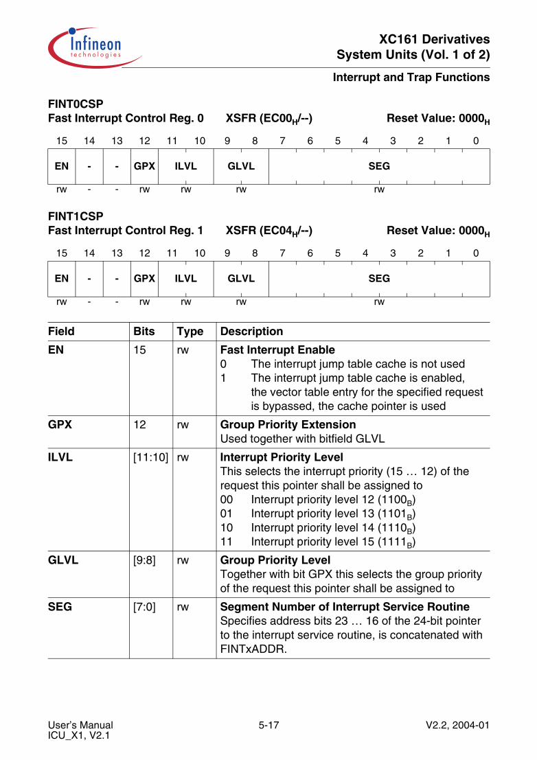
XC161 DerivativesSystem Units (Vol. 1 of 2)
Interrupt and Trap Functions
FINT0CSP Fast Interrupt Control Reg. 0 XSFR (EC00H/--) Reset Value: 0000H
15 14 13 12 11 10 9 8 7 6 5 4 3 2 1 0
EN - - GPX ILVL GLVL SEG
rw - - rw rw rw rw
FINT1CSP Fast Interrupt Control Reg. 1 XSFR (EC04H/--) Reset Value: 0000H
15 14 13 12 11 10 9 8 7 6 5 4 3 2 1 0
EN - - GPX ILVL GLVL SEG
rw - - rw rw rw rw
Field Bits Type Description
EN 15 rw Fast Interrupt Enable0 The interrupt jump table cache is not used1 The interrupt jump table cache is enabled,
the vector table entry for the specified request is bypassed, the cache pointer is used
GPX 12 rw Group Priority ExtensionUsed together with bitfield GLVL
ILVL [11:10] rw Interrupt Priority LevelThis selects the interrupt priority (15 … 12) of the request this pointer shall be assigned to00 Interrupt priority level 12 (1100B)01 Interrupt priority level 13 (1101B)10 Interrupt priority level 14 (1110B)11 Interrupt priority level 15 (1111B)
GLVL [9:8] rw Group Priority LevelTogether with bit GPX this selects the group priority of the request this pointer shall be assigned to
SEG [7:0] rw Segment Number of Interrupt Service RoutineSpecifies address bits 23 … 16 of the 24-bit pointer to the interrupt service routine, is concatenated with FINTxADDR.
User’s Manual 5-17 V2.2, 2004-01ICU_X1, V2.1

XC161 DerivativesSystem Units (Vol. 1 of 2)
Interrupt and Trap Functions
5.4 Operation of the Peripheral Event Controller Channels
The XC161’s Peripheral Event Controller (PEC) provides 8 PEC service channels whichmove a single byte or word between any two locations. A PEC transfer can be triggeredby an interrupt service request and is the fastest possible interrupt response. In manycases a PEC transfer is sufficient to service the respective peripheral request (forexample, serial channels, etc.).
PEC transfers do not change the current context, but rather “steal” cycles from the CPU,so the current program status and context needs not to be saved and restored as withstandard interrupts.
The PEC channels are controlled by a dedicated set of registers which are assigned todedicated PEC resources:
• A 24-bit source pointer for each channel• A 24-bit destination pointer for each channel• A Channel Counter/Control register (PECCx) for each channel, selecting the
operating mode for the respective channel• Two interrupt control registers to control the operation of block transfers
The PECC registers control the action performed by the respective PEC channel.
Transfer Size (bit BWT) controls whether a byte or a word is moved during a PECservice cycle. This selection controls the transferred data size and the increment step forthe pointer(s) to be modified.
Pointer Modification (bitfield INC) controls, which of the PEC pointers is incrementedafter the PEC transfer. If the pointers are not modified (INC = 00B), the respectivechannel will always move data from the same source to the same destination.
Transfer Control (bitfield COUNT) controls if the respective PEC channel remainsactive after the transfer or not. Bitfield COUNT also generally enables a PEC channel(COUNT > 00H).
The PECC registers also select the assignment of PEC channels to interrupt prioritylevels (bitfield PLEV) and the interrupt behavior after PEC transfer completion (bitEOPINT).
Note: All interrupt request sources that are enabled and programmed for PEC serviceshould use different channels. Otherwise, only one transfer will be performed forall simultaneous requests. When COUNT is decremented to 00H, and the CPU isto be interrupted, an incorrect interrupt vector will be generated.PEC transfers are executed only if their priority level is higher than the CPU level.
User’s Manual 5-18 V2.2, 2004-01ICU_X1, V2.1
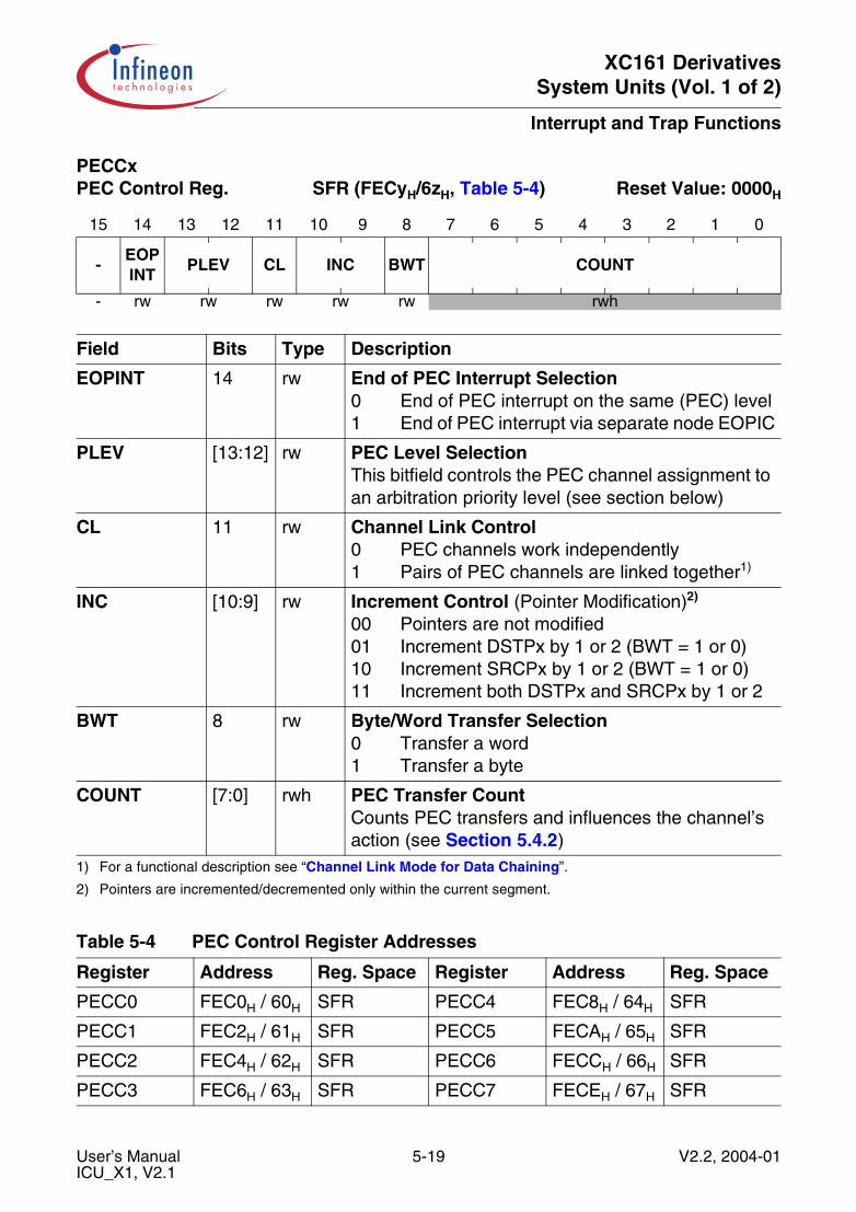
XC161 DerivativesSystem Units (Vol. 1 of 2)
Interrupt and Trap Functions
PECCx PEC Control Reg. SFR (FECyH/6zH, Table 5-4) Reset Value: 0000H
15 14 13 12 11 10 9 8 7 6 5 4 3 2 1 0
-EOP INT
PLEV CL INC BWT COUNT
- rw rw rw rw rw rwh
Field Bits Type Description
EOPINT 14 rw End of PEC Interrupt Selection0 End of PEC interrupt on the same (PEC) level1 End of PEC interrupt via separate node EOPIC
PLEV [13:12] rw PEC Level SelectionThis bitfield controls the PEC channel assignment to an arbitration priority level (see section below)
CL 11 rw Channel Link Control0 PEC channels work independently1 Pairs of PEC channels are linked together1)
INC [10:9] rw Increment Control (Pointer Modification)2)
00 Pointers are not modified01 Increment DSTPx by 1 or 2 (BWT = 1 or 0)10 Increment SRCPx by 1 or 2 (BWT = 1 or 0)11 Increment both DSTPx and SRCPx by 1 or 2
BWT 8 rw Byte/Word Transfer Selection0 Transfer a word1 Transfer a byte
COUNT [7:0] rwh PEC Transfer CountCounts PEC transfers and influences the channel’s action (see Section 5.4.2)
1) For a functional description see “Channel Link Mode for Data Chaining”.
2) Pointers are incremented/decremented only within the current segment.
Table 5-4 PEC Control Register Addresses
Register Address Reg. Space Register Address Reg. Space
PECC0 FEC0H / 60H SFR PECC4 FEC8H / 64H SFR
PECC1 FEC2H / 61H SFR PECC5 FECAH / 65H SFR
PECC2 FEC4H / 62H SFR PECC6 FECCH / 66H SFR
PECC3 FEC6H / 63H SFR PECC7 FECEH / 67H SFR
User’s Manual 5-19 V2.2, 2004-01ICU_X1, V2.1
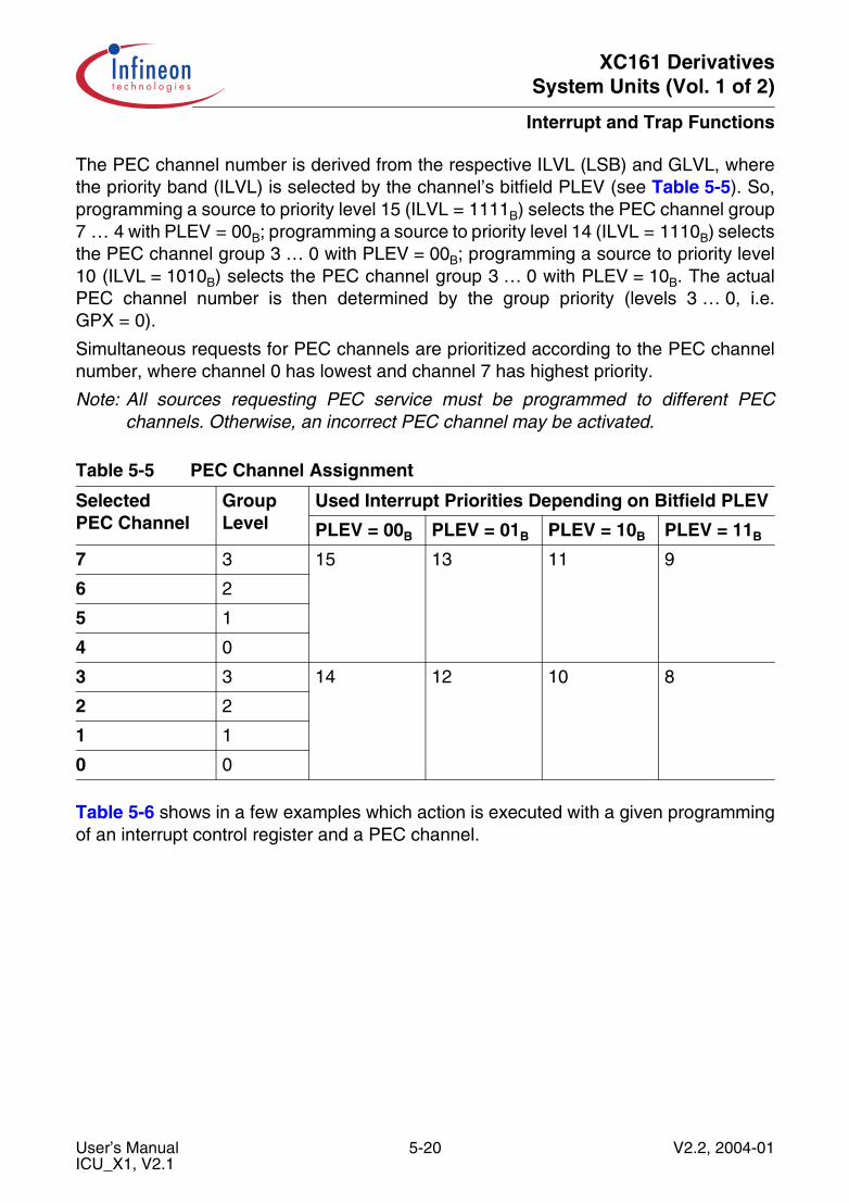
XC161 DerivativesSystem Units (Vol. 1 of 2)
Interrupt and Trap Functions
The PEC channel number is derived from the respective ILVL (LSB) and GLVL, wherethe priority band (ILVL) is selected by the channel’s bitfield PLEV (see Table 5-5). So,programming a source to priority level 15 (ILVL = 1111B) selects the PEC channel group7 … 4 with PLEV = 00B; programming a source to priority level 14 (ILVL = 1110B) selectsthe PEC channel group 3 … 0 with PLEV = 00B; programming a source to priority level10 (ILVL = 1010B) selects the PEC channel group 3 … 0 with PLEV = 10B. The actualPEC channel number is then determined by the group priority (levels 3 … 0, i.e.GPX = 0).
Simultaneous requests for PEC channels are prioritized according to the PEC channelnumber, where channel 0 has lowest and channel 7 has highest priority.
Note: All sources requesting PEC service must be programmed to different PECchannels. Otherwise, an incorrect PEC channel may be activated.
Table 5-6 shows in a few examples which action is executed with a given programmingof an interrupt control register and a PEC channel.
Table 5-5 PEC Channel Assignment
Selected PEC Channel
Group Level
Used Interrupt Priorities Depending on Bitfield PLEV
PLEV = 00B PLEV = 01B PLEV = 10B PLEV = 11B
7 3 15 13 11 9
6 2
5 1
4 0
3 3 14 12 10 8
2 2
1 1
0 0
User’s Manual 5-20 V2.2, 2004-01ICU_X1, V2.1
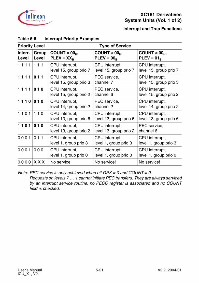
XC161 DerivativesSystem Units (Vol. 1 of 2)
Interrupt and Trap Functions
Note: PEC service is only achieved when bit GPX = 0 and COUNT ≠ 0.Requests on levels 7 … 1 cannot initiate PEC transfers. They are always servicedby an interrupt service routine: no PECC register is associated and no COUNTfield is checked.
Table 5-6 Interrupt Priority Examples
Priority Level Type of Service
Interr. Level
Group Level
COUNT = 00H,PLEV = XXB
COUNT ≠ 00H,PLEV = 00B
COUNT ≠ 00H,PLEV = 01B
1 1 1 1 1 1 1 CPU interrupt,level 15, group prio 7
CPU interrupt,level 15, group prio 7
CPU interrupt,level 15, group prio 7
1 1 1 1 0 1 1 CPU interrupt,level 15, group prio 3
PEC service,channel 7
CPU interrupt,level 15, group prio 3
1 1 1 1 0 1 0 CPU interrupt,level 15, group prio 2
PEC service,channel 6
CPU interrupt,level 15, group prio 2
1 1 1 0 0 1 0 CPU interrupt,level 14, group prio 2
PEC service,channel 2
CPU interrupt,level 14, group prio 2
1 1 0 1 1 1 0 CPU interrupt,level 13, group prio 6
CPU interrupt,level 13, group prio 6
CPU interrupt,level 13, group prio 6
1 1 0 1 0 1 0 CPU interrupt,level 13, group prio 2
CPU interrupt,level 13, group prio 2
PEC service,channel 6
0 0 0 1 0 1 1 CPU interrupt,level 1, group prio 3
CPU interrupt,level 1, group prio 3
CPU interrupt,level 1, group prio 3
0 0 0 1 0 0 0 CPU interrupt,level 1, group prio 0
CPU interrupt,level 1, group prio 0
CPU interrupt,level 1, group prio 0
0 0 0 0 X X X No service! No service! No service!
User’s Manual 5-21 V2.2, 2004-01ICU_X1, V2.1
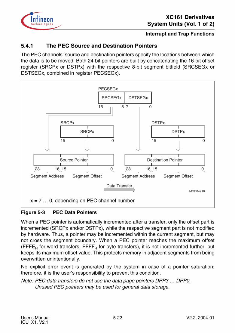
XC161 DerivativesSystem Units (Vol. 1 of 2)
Interrupt and Trap Functions
5.4.1 The PEC Source and Destination Pointers
The PEC channels’ source and destination pointers specify the locations between whichthe data is to be moved. Both 24-bit pointers are built by concatenating the 16-bit offsetregister (SRCPx or DSTPx) with the respective 8-bit segment bitfield (SRCSEGx orDSTSEGx, combined in register PECSEGx).
Figure 5-3 PEC Data Pointers
When a PEC pointer is automatically incremented after a transfer, only the offset part isincremented (SRCPx and/or DSTPx), while the respective segment part is not modifiedby hardware. Thus, a pointer may be incremented within the current segment, but maynot cross the segment boundary. When a PEC pointer reaches the maximum offset(FFFEH for word transfers, FFFFH for byte transfers), it is not incremented further, butkeeps its maximum offset value. This protects memory in adjacent segments from beingoverwritten unintentionally.
No explicit error event is generated by the system in case of a pointer saturation;therefore, it is the user’s responsibility to prevent this condition.
Note: PEC data transfers do not use the data page pointers DPP3 … DPP0.Unused PEC pointers may be used for general data storage.
x = 7 … 0, depending on PEC channel number
MCD04916
Source Pointer
23 16 15 0
Segment Address Segment Offset
Destination Pointer
23 16 15 0
Segment Address Segment Offset
SRCPx
15 0
SRCPx
DSTPx
15 0
DSTPx
DSTSEGx
7 0
SRCSEGx
15 8
PECSEGx
Data Transfer
User’s Manual 5-22 V2.2, 2004-01ICU_X1, V2.1
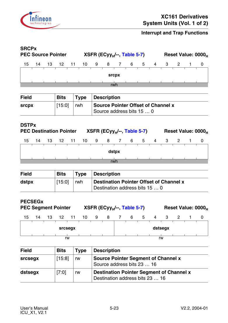
XC161 DerivativesSystem Units (Vol. 1 of 2)
Interrupt and Trap Functions
SRCPx PEC Source Pointer XSFR (ECyyH/--, Table 5-7) Reset Value: 0000H
15 14 13 12 11 10 9 8 7 6 5 4 3 2 1 0
srcpx
rwh
Field Bits Type Description
srcpx [15:0] rwh Source Pointer Offset of Channel xSource address bits 15 … 0
DSTPx PEC Destination Pointer XSFR (ECyyH/--, Table 5-7) Reset Value: 0000H
15 14 13 12 11 10 9 8 7 6 5 4 3 2 1 0
dstpx
rwh
Field Bits Type Description
dstpx [15:0] rwh Destination Pointer Offset of Channel xDestination address bits 15 … 0
PECSEGx PEC Segment Pointer XSFR (ECyyH/--, Table 5-7) Reset Value: 0000H
15 14 13 12 11 10 9 8 7 6 5 4 3 2 1 0
srcsegx dstsegx
rw rw
Field Bits Type Description
srcsegx [15:8] rw Source Pointer Segment of Channel xSource address bits 23 … 16
dstsegx [7:0] rw Destination Pointer Segment of Channel xDestination address bits 23 … 16
User’s Manual 5-23 V2.2, 2004-01ICU_X1, V2.1
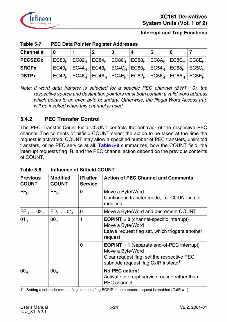
XC161 DerivativesSystem Units (Vol. 1 of 2)
Interrupt and Trap Functions
Note: If word data transfer is selected for a specific PEC channel (BWT = 0), therespective source and destination pointers must both contain a valid word addresswhich points to an even byte boundary. Otherwise, the Illegal Word Access trapwill be invoked when this channel is used.
5.4.2 PEC Transfer Control
The PEC Transfer Count Field COUNT controls the behavior of the respective PECchannel. The contents of bitfield COUNT select the action to be taken at the time therequest is activated. COUNT may allow a specified number of PEC transfers, unlimitedtransfers, or no PEC service at all. Table 5-8 summarizes, how the COUNT field, theinterrupt requests flag IR, and the PEC channel action depend on the previous contentsof COUNT.
Table 5-7 PEC Data Pointer Register Addresses
Channel # 0 1 2 3 4 5 6 7
PECSEGx EC80H EC82H EC84H EC86H EC88H EC8AH EC8CH EC8EH
SRCPx EC40H EC44H EC48H EC4CH EC50H EC54H EC58H EC5CH
DSTPx EC42H EC46H EC4AH EC4EH EC52H EC56H EC5AH EC5EH
Table 5-8 Influence of Bitfield COUNT
Previous COUNT
Modified COUNT
IR after Service
Action of PEC Channel and Comments
FFH FFH 0 Move a Byte/WordContinuous transfer mode, i.e. COUNT is not modified
FEH … 02H FDH … 01H 0 Move a Byte/Word and decrement COUNT
01H 00H 1 EOPINT = 0 (channel-specific interrupt)Move a Byte/WordLeave request flag set, which triggers another request
0 EOPINT = 1 (separate end-of-PEC interrupt)Move a Byte/WordClear request flag, set the respective PEC subnode request flag CxIR instead1)
1) Setting a subnode request flag also sets flag EOPIR if the subnode request is enabled (CxIE = 1).
00H 00H - No PEC action!Activate interrupt service routine rather than PEC channel
User’s Manual 5-24 V2.2, 2004-01ICU_X1, V2.1

XC161 DerivativesSystem Units (Vol. 1 of 2)
Interrupt and Trap Functions
The PEC transfer counter allows service of a specified number of requests by therespective PEC channel, and then (when COUNT reaches 00H) activation of an interruptservice routine, either associated with the PEC channel’s priority level or with the generalend-of-PEC interrupt. After each PEC transfer, the COUNT field is decremented (exceptfor COUNT = FFH) and the request flag is cleared to indicate that the request has beenserviced.
When COUNT contains the value 00H, the respective PEC channel remains idle and theassociated interrupt service routine is activated instead. This allows servicing requestson all priority levels by standard interrupt service routines.
Continuous transfers are selected by the value FFH in bitfield COUNT. In this case,COUNT is not modified and the respective PEC channel services any request until it isdisabled again.
When COUNT is decremented from 01H to 00H after a transfer, a standard interrupt isrequested which can then handle the end of the PEC block transfer (channel-specificinterrupt or common end-of-PEC interrupt, see Table 5-8).
User’s Manual 5-25 V2.2, 2004-01ICU_X1, V2.1
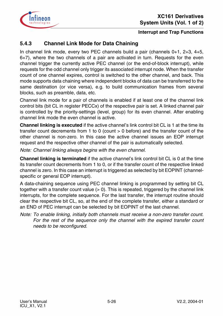
XC161 DerivativesSystem Units (Vol. 1 of 2)
Interrupt and Trap Functions
5.4.3 Channel Link Mode for Data Chaining
In channel link mode, every two PEC channels build a pair (channels 0+1, 2+3, 4+5,6+7), where the two channels of a pair are activated in turn. Requests for the evenchannel trigger the currently active PEC channel (or the end-of-block interrupt), whilerequests for the odd channel only trigger its associated interrupt node. When the transfercount of one channel expires, control is switched to the other channel, and back. Thismode supports data chaining where independent blocks of data can be transferred to thesame destination (or vice versa), e.g. to build communication frames from severalblocks, such as preamble, data, etc.
Channel link mode for a pair of channels is enabled if at least one of the channel linkcontrol bits (bit CL in register PECCx) of the respective pair is set. A linked channel pairis controlled by the priority-settings (level, group) for its even channel. After enablingchannel link mode the even channel is active.
Channel linking is executed if the active channel’s link control bit CL is 1 at the time itstransfer count decrements from 1 to 0 (count > 0 before) and the transfer count of theother channel is non-zero. In this case the active channel issues an EOP interruptrequest and the respective other channel of the pair is automatically selected.
Note: Channel linking always begins with the even channel.
Channel linking is terminated if the active channel’s link control bit CL is 0 at the timeits transfer count decrements from 1 to 0, or if the transfer count of the respective linkedchannel is zero. In this case an interrupt is triggered as selected by bit EOPINT (channel-specific or general EOP interrupt).
A data-chaining sequence using PEC channel linking is programmed by setting bit CLtogether with a transfer count value (> 0). This is repeated, triggered by the channel linkinterrupts, for the complete sequence. For the last transfer, the interrupt routine shouldclear the respective bit CL, so, at the end of the complete transfer, either a standard oran END of PEC interrupt can be selected by bit EOPINT of the last channel.
Note: To enable linking, initially both channels must receive a non-zero transfer count.For the rest of the sequence only the channel with the expired transfer countneeds to be reconfigured.
User’s Manual 5-26 V2.2, 2004-01ICU_X1, V2.1
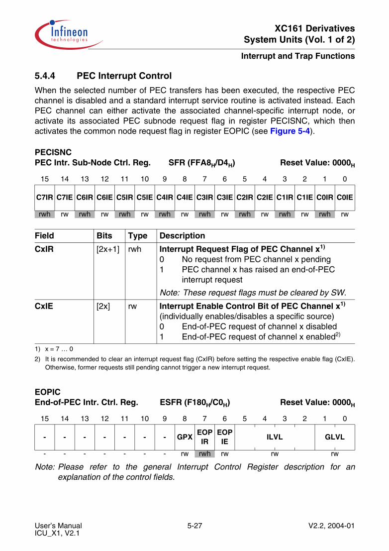
XC161 DerivativesSystem Units (Vol. 1 of 2)
Interrupt and Trap Functions
5.4.4 PEC Interrupt Control
When the selected number of PEC transfers has been executed, the respective PECchannel is disabled and a standard interrupt service routine is activated instead. EachPEC channel can either activate the associated channel-specific interrupt node, oractivate its associated PEC subnode request flag in register PECISNC, which thenactivates the common node request flag in register EOPIC (see Figure 5-4).
Note: Please refer to the general Interrupt Control Register description for anexplanation of the control fields.
PECISNCPEC Intr. Sub-Node Ctrl. Reg. SFR (FFA8H/D4H) Reset Value: 0000H
15 14 13 12 11 10 9 8 7 6 5 4 3 2 1 0
C7IR C7IE C6IR C6IE C5IR C5IE C4IR C4IE C3IR C3IE C2IR C2IE C1IR C1IE C0IR C0IE
rwh rw rwh rw rwh rw rwh rw rwh rw rwh rw rwh rw rwh rw
Field Bits Type Description
CxIR [2x+1] rwh Interrupt Request Flag of PEC Channel x1)
0 No request from PEC channel x pending1 PEC channel x has raised an end-of-PEC
interrupt request
Note: These request flags must be cleared by SW.
1) x = 7 … 0
CxIE [2x] rw Interrupt Enable Control Bit of PEC Channel x1)
(individually enables/disables a specific source)0 End-of-PEC request of channel x disabled1 End-of-PEC request of channel x enabled2)
2) It is recommended to clear an interrupt request flag (CxIR) before setting the respective enable flag (CxIE).Otherwise, former requests still pending cannot trigger a new interrupt request.
EOPIC End-of-PEC Intr. Ctrl. Reg. ESFR (F180H/C0H) Reset Value: 0000H
15 14 13 12 11 10 9 8 7 6 5 4 3 2 1 0
- - - - - - - GPXEOP
IREOP
IEILVL GLVL
- - - - - - - rw rwh rw rw rw
User’s Manual 5-27 V2.2, 2004-01ICU_X1, V2.1
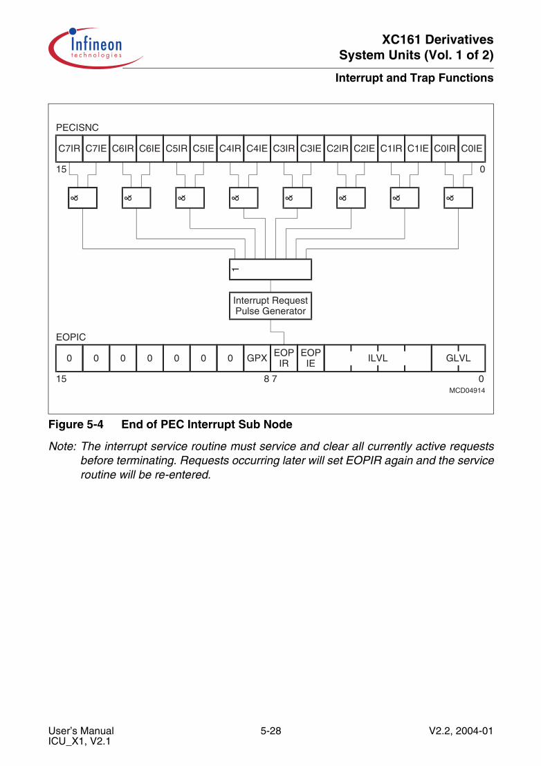
XC161 DerivativesSystem Units (Vol. 1 of 2)
Interrupt and Trap Functions
Figure 5-4 End of PEC Interrupt Sub Node
Note: The interrupt service routine must service and clear all currently active requestsbefore terminating. Requests occurring later will set EOPIR again and the serviceroutine will be re-entered.
MCD04914
C7IR C7IE C6IR C6IE C5IR C5IE C4IR C4IE C3IR C3IE C2IR C2IE C1IR C1IE C0IR C0IE
& & & & & & & &
1
PECISNC
15 0
0 0 0 0 0 0 0 GPX EOPIR
EOPIE ILVL GLVL
15 8 7 0
EOPIC
Interrupt RequestPulse Generator
&
User’s Manual 5-28 V2.2, 2004-01ICU_X1, V2.1
XC161 DerivativesSystem Units (Vol. 1 of 2)
Interrupt and Trap Functions
5.5 Prioritization of Interrupt and PEC Service Requests
Interrupt and PEC service requests from all sources can be enabled so they arearbitrated and serviced (if they win), or they may be disabled, so their requests aredisregarded and not serviced.
Enabling and disabling interrupt requests may be done via three mechanisms:
• Control Bits• Priority Level• ATOMIC and EXTended Instructions
Control Bits allow switching of each individual source “ON” or “OFF” so that it maygenerate a request or not. The control bits (xxIE) are located in the respective interruptcontrol registers. All interrupt requests may be enabled or disabled generally via bit IENin register PSW. This control bit is the “main switch” which selects if requests from anysource are accepted or not.For a specific request to be arbitrated, the respective source’s enable bit and the globalenable bit must both be set.
The Priority Level automatically selects a certain group of interrupt requests to beacknowledged and ignores all other requests. The priority level of the source that wonthe arbitration is compared against the CPU’s current level and the source is servicedonly if its level is higher than the current CPU level. Changing the CPU level to a specificvalue via software blocks all requests on the same or a lower level. An interrupt sourceassigned to level 0 will be disabled and will never be serviced.
The ATOMIC and EXTend instructions automatically disable all interrupt requests forthe duration of the following 1 … 4 instructions. This is useful for semaphore handling,for example, and does not require to re-enable the interrupt system after the inseparableinstruction sequence.
Interrupt Class Management
An interrupt class covers a set of interrupt sources with the same importance, i.e. thesame priority from the system’s viewpoint. Interrupts of the same class must not interrupteach other. The XC161 supports this function with two features:
Classes with up to eight members can be established by using the same interrupt priority(ILVL) and assigning a dedicated group level to each member. This functionality is built-in and handled automatically by the interrupt controller.
Classes with more than eight members can be established by using a number ofadjacent interrupt priorities (ILVL) and the respective group levels (eight per ILVL). Eachinterrupt service routine within this class sets the CPU level to the highest interruptpriority within the class. All requests from the same or any lower level are blocked now,i.e. no request of this class will be accepted.
User’s Manual 5-29 V2.2, 2004-01ICU_X1, V2.1

XC161 DerivativesSystem Units (Vol. 1 of 2)
Interrupt and Trap Functions
The example shown below establishes 3 interrupt classes which cover 2 or 3 interruptpriorities, depending on the number of members in a class. A level 6 interrupt disablesall other sources in class 2 by changing the current CPU level to 8, which is the highestpriority (ILVL) in class 2. Class 1 requests or PEC requests are still serviced, in this case.
In this way, the interrupt sources (excluding PEC requests) are assigned to 3 classes ofpriority rather than to 7 different levels, as the hardware support would do.
Table 5-9 Software Controlled Interrupt Classes (Example)
ILVL (Priority)
Group Level Interpretation
7 6 5 4 3 2 1 0
15 PEC service on up to 8 channels
14
13
12 X X X X X X X X Interrupt Class 19 sources on 2 levels11 X
10
9
8 X X X X X X X X Interrupt Class 217 sources on 3 levels7 X X X X X X X X
6 X
5 X X X X X X X X Interrupt Class 39 sources on 2 levels4 X
3
2
1
0 No service!
User’s Manual 5-30 V2.2, 2004-01ICU_X1, V2.1
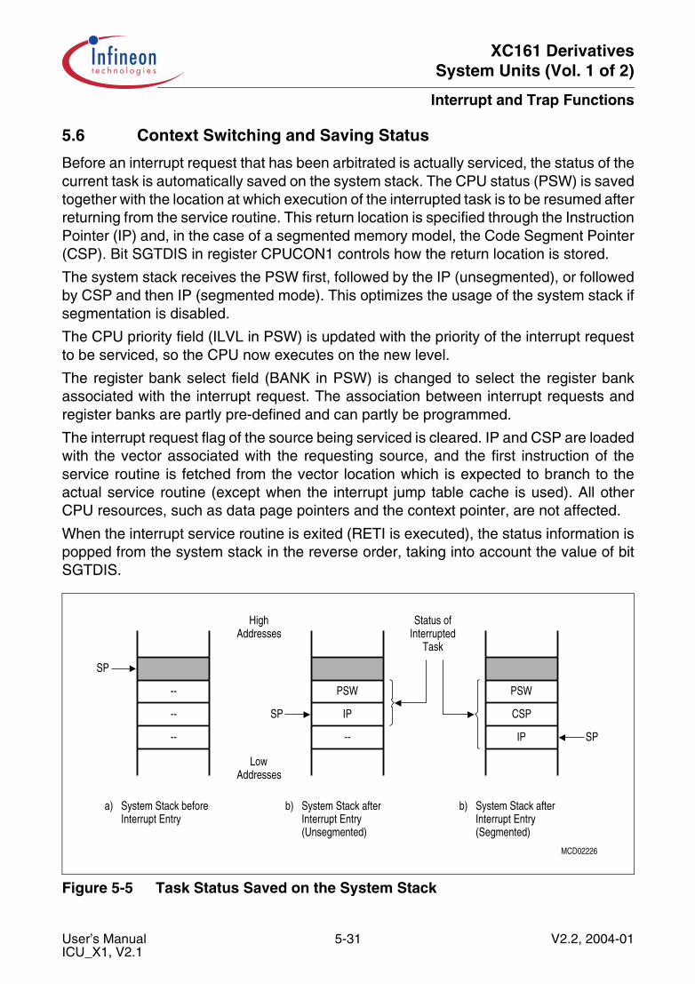
XC161 DerivativesSystem Units (Vol. 1 of 2)
Interrupt and Trap Functions
5.6 Context Switching and Saving Status
Before an interrupt request that has been arbitrated is actually serviced, the status of thecurrent task is automatically saved on the system stack. The CPU status (PSW) is savedtogether with the location at which execution of the interrupted task is to be resumed afterreturning from the service routine. This return location is specified through the InstructionPointer (IP) and, in the case of a segmented memory model, the Code Segment Pointer(CSP). Bit SGTDIS in register CPUCON1 controls how the return location is stored.
The system stack receives the PSW first, followed by the IP (unsegmented), or followedby CSP and then IP (segmented mode). This optimizes the usage of the system stack ifsegmentation is disabled.
The CPU priority field (ILVL in PSW) is updated with the priority of the interrupt requestto be serviced, so the CPU now executes on the new level.
The register bank select field (BANK in PSW) is changed to select the register bankassociated with the interrupt request. The association between interrupt requests andregister banks are partly pre-defined and can partly be programmed.
The interrupt request flag of the source being serviced is cleared. IP and CSP are loadedwith the vector associated with the requesting source, and the first instruction of theservice routine is fetched from the vector location which is expected to branch to theactual service routine (except when the interrupt jump table cache is used). All otherCPU resources, such as data page pointers and the context pointer, are not affected.
When the interrupt service routine is exited (RETI is executed), the status information ispopped from the system stack in the reverse order, taking into account the value of bitSGTDIS.
Figure 5-5 Task Status Saved on the System Stack
(Unsegmented)
PSW
System Stack afterInterrupt EntryInterrupt Entry
System Stack beforea) b)
SP
HighAddresses
LowAddresses
--
--
--
SP IP
--
MCD02226
b)Interrupt EntrySystem Stack after
(Segmented)
TaskInterruptedStatus of
CSP
PSW
IP SP
User’s Manual 5-31 V2.2, 2004-01ICU_X1, V2.1

XC161 DerivativesSystem Units (Vol. 1 of 2)
Interrupt and Trap Functions
Context Switching
An interrupt service routine usually saves all the registers it uses on the stack andrestores them before returning. The more registers a routine uses, the more time is spentsaving and restoring. The XC161 allows switching the complete bank of CPU registers(GPRs) either automatically or with a single instruction, so the service routine executeswithin its own separate context (see also Section 4.5.2).
There are two ways to switch the context in the XC161 core:
Switching Context of the Global Register Bank changes the complete global registerbank of CPU registers (GPRs) by changing by changing the Context Pointer with a singleinstruction, so the service routine executes within its own separate context. Theinstruction “SCXT CP, #New_Bank” pushes the contents of the context pointer (CP) onthe system stack and loads CP with the immediate value “New_Bank”; this in turn,selects a new register bank. The service routine may now use its “own registers”. Thisregister bank is preserved when the service routine terminates, i.e. its contents areavailable on the next call. Before returning (RETI), the previous CP is simply POPpedfrom the system stack, which returns the registers to the original global bank.
Resources used by the interrupting program, such as the DPPs, must eventually besaved and restored.
Note: There are certain timing restrictions during context switching that are associatedwith pipeline behavior.
Switching Context by changing the selected register bank automatically updatesbitfield BANK to select one of the two local register banks or the current global registerbank, so the service routine may now use its “own registers” directly. This local registerbank is preserved when the service routine is terminated; thus, its contents are availableon the next call.When switching to the global register bank, the service routine usually must also switchthe context of the global register bank to get a private set of GPRs, because the globalbank is likely to be used by several tasks.
For interrupt priority levels 15 … 12 the target register bank can be pre-selected andthen be switched automatically. The register bank selection registers BNKSELx providea 2-bit field for each possible arbitration priority level. The respective bitfield is thencopied to bitfield BANK in register PSW to select the register bank, as soon as therespective interrupt request is accepted.
Table 5-10 identifies the arbitration priority level assignment to the respective bitfieldswithin the four register bank selection registers.
User’s Manual 5-32 V2.2, 2004-01ICU_X1, V2.1
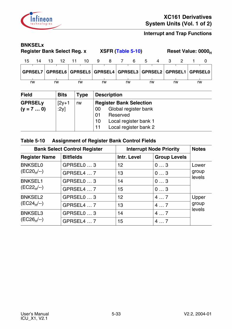
XC161 DerivativesSystem Units (Vol. 1 of 2)
Interrupt and Trap Functions
BNKSELx Register Bank Select Reg. x XSFR (Table 5-10) Reset Value: 0000H
15 14 13 12 11 10 9 8 7 6 5 4 3 2 1 0
GPRSEL7 GPRSEL6 GPRSEL5 GPRSEL4 GPRSEL3 GPRSEL2 GPRSEL1 GPRSEL0
rw rw rw rw rw rw rw rw
Field Bits Type Description
GPRSELy(y = 7 … 0)
[2y+1:2y]
rw Register Bank Selection00 Global register bank01 Reserved10 Local register bank 111 Local register bank 2
Table 5-10 Assignment of Register Bank Control Fields
Bank Select Control Register Interrupt Node Priority Notes
Register Name Bitfields Intr. Level Group Levels
BNKSEL0(EC20H/--)
GPRSEL0 … 3 12 0 … 3 Lower group levels
GPRSEL4 … 7 13 0 … 3
BNKSEL1(EC22H/--)
GPRSEL0 … 3 14 0 … 3
GPRSEL4 … 7 15 0 … 3
BNKSEL2(EC24H/--)
GPRSEL0 … 3 12 4 … 7 Upper group levels
GPRSEL4 … 7 13 4 … 7
BNKSEL3(EC26H/--)
GPRSEL0 … 3 14 4 … 7
GPRSEL4 … 7 15 4 … 7
User’s Manual 5-33 V2.2, 2004-01ICU_X1, V2.1
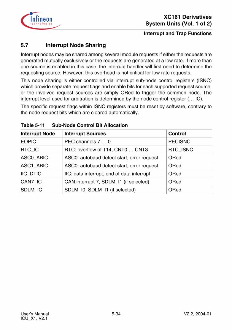
XC161 DerivativesSystem Units (Vol. 1 of 2)
Interrupt and Trap Functions
5.7 Interrupt Node Sharing
Interrupt nodes may be shared among several module requests if either the requests aregenerated mutually exclusively or the requests are generated at a low rate. If more thanone source is enabled in this case, the interrupt handler will first need to determine therequesting source. However, this overhead is not critical for low rate requests.
This node sharing is either controlled via interrupt sub-node control registers (ISNC)which provide separate request flags and enable bits for each supported request source,or the involved request sources are simply ORed to trigger the common node. Theinterrupt level used for arbitration is determined by the node control register (… IC).
The specific request flags within ISNC registers must be reset by software, contrary tothe node request bits which are cleared automatically.
Table 5-11 Sub-Node Control Bit Allocation
Interrupt Node Interrupt Sources Control
EOPIC PEC channels 7 … 0 PECISNC
RTC_IC RTC: overflow of T14, CNT0 … CNT3 RTC_ISNC
ASC0_ABIC ASC0: autobaud detect start, error request ORed
ASC1_ABIC ASC0: autobaud detect start, error request ORed
IIC_DTIC IIC: data interrupt, end of data interrupt ORed
CAN7_IC CAN interrupt 7, SDLM_I1 (if selected) ORed
SDLM_IC SDLM_I0, SDLM_I1 (if selected) ORed
User’s Manual 5-34 V2.2, 2004-01ICU_X1, V2.1
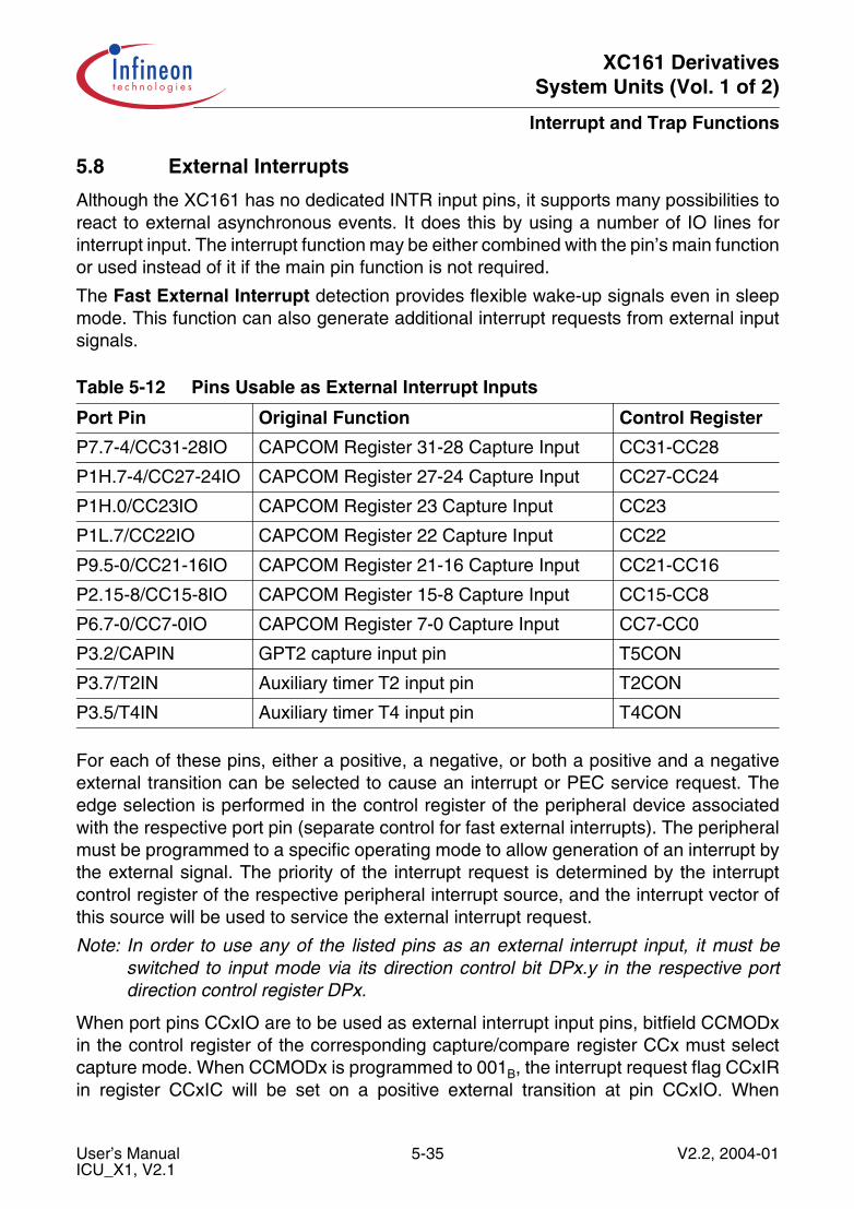
XC161 DerivativesSystem Units (Vol. 1 of 2)
Interrupt and Trap Functions
5.8 External Interrupts
Although the XC161 has no dedicated INTR input pins, it supports many possibilities toreact to external asynchronous events. It does this by using a number of IO lines forinterrupt input. The interrupt function may be either combined with the pin’s main functionor used instead of it if the main pin function is not required.
The Fast External Interrupt detection provides flexible wake-up signals even in sleepmode. This function can also generate additional interrupt requests from external inputsignals.
For each of these pins, either a positive, a negative, or both a positive and a negativeexternal transition can be selected to cause an interrupt or PEC service request. Theedge selection is performed in the control register of the peripheral device associatedwith the respective port pin (separate control for fast external interrupts). The peripheralmust be programmed to a specific operating mode to allow generation of an interrupt bythe external signal. The priority of the interrupt request is determined by the interruptcontrol register of the respective peripheral interrupt source, and the interrupt vector ofthis source will be used to service the external interrupt request.
Note: In order to use any of the listed pins as an external interrupt input, it must beswitched to input mode via its direction control bit DPx.y in the respective portdirection control register DPx.
When port pins CCxIO are to be used as external interrupt input pins, bitfield CCMODxin the control register of the corresponding capture/compare register CCx must selectcapture mode. When CCMODx is programmed to 001B, the interrupt request flag CCxIRin register CCxIC will be set on a positive external transition at pin CCxIO. When
Table 5-12 Pins Usable as External Interrupt Inputs
Port Pin Original Function Control Register
P7.7-4/CC31-28IO CAPCOM Register 31-28 Capture Input CC31-CC28
P1H.7-4/CC27-24IO CAPCOM Register 27-24 Capture Input CC27-CC24
P1H.0/CC23IO CAPCOM Register 23 Capture Input CC23
P1L.7/CC22IO CAPCOM Register 22 Capture Input CC22
P9.5-0/CC21-16IO CAPCOM Register 21-16 Capture Input CC21-CC16
P2.15-8/CC15-8IO CAPCOM Register 15-8 Capture Input CC15-CC8
P6.7-0/CC7-0IO CAPCOM Register 7-0 Capture Input CC7-CC0
P3.2/CAPIN GPT2 capture input pin T5CON
P3.7/T2IN Auxiliary timer T2 input pin T2CON
P3.5/T4IN Auxiliary timer T4 input pin T4CON
User’s Manual 5-35 V2.2, 2004-01ICU_X1, V2.1

XC161 DerivativesSystem Units (Vol. 1 of 2)
Interrupt and Trap Functions
CCMODx is programmed to 010B, a negative external transition will set the interruptrequest flag. When CCMODx = 011B, both a positive and a negative transition will setthe request flag. In all three cases, the contents of the allocated CAPCOM timer will belatched into capture register CCx, independent of whether or not the timer is running.When the interrupt enable bit CCxIE is set, a PEC request or an interrupt request forvector CCxINT will be generated.
Pins T2IN or T4IN can be used as external interrupt input pins when the associatedauxiliary timer T2 or T4 in block GPT1 is configured for capture mode. This mode isselected by programming the mode control fields T2M or T4M in control registersT2CON or T4CON to 101B. The active edge of the external input signal is determined bybitfields T2I or T4I. When these fields are programmed to X01B, interrupt request flagsT2IR or T4IR in registers T2IC or T4IC will be set on a positive external transition at pinsT2IN or T4IN, respectively. When T2I or T4I is programmed to X10B, then a negativeexternal transition will set the corresponding request flag. When T2I or T4I isprogrammed to X11B, both a positive and a negative transition will set the request flag.In all three cases, the contents of the core timer T3 will be captured into the auxiliarytimer registers T2 or T4 based on the transition at pins T2IN or T4IN. When the interruptenable bits T2IE or T4IE are set, a PEC request or an interrupt request for vector T2INTor T4INT will be generated.
Pin CAPIN differs slightly from the timer input pins as it can be used as external interruptinput pin without affecting peripheral functions. When the capture mode enable bit T5SCin register T5CON is cleared to ‘0’, signal transitions on pin CAPIN will only set theinterrupt request flag CRIR in register CRIC, and the capture function of registerCAPREL is not activated.
So register CAPREL can still be used as reload register for GPT2 timer T5, while pinCAPIN serves as external interrupt input. Bitfield CI in register T5CON selects theeffective transition of the external interrupt input signal. When CI is programmed to 01B,a positive external transition will set the interrupt request flag. CI = 10B selects a negativetransition to set the interrupt request flag, and with CI = 11B, both a positive and anegative transition will set the request flag. When the interrupt enable bit CRIE is set, aninterrupt request for vector CRINT or a PEC request will be generated.
Note: The non-maskable interrupt input pin NMI and the reset input RSTIN provideanother possibility for the CPU to react to an external input signal. NMI and RSTINare dedicated input pins which cause hardware traps.
User’s Manual 5-36 V2.2, 2004-01ICU_X1, V2.1
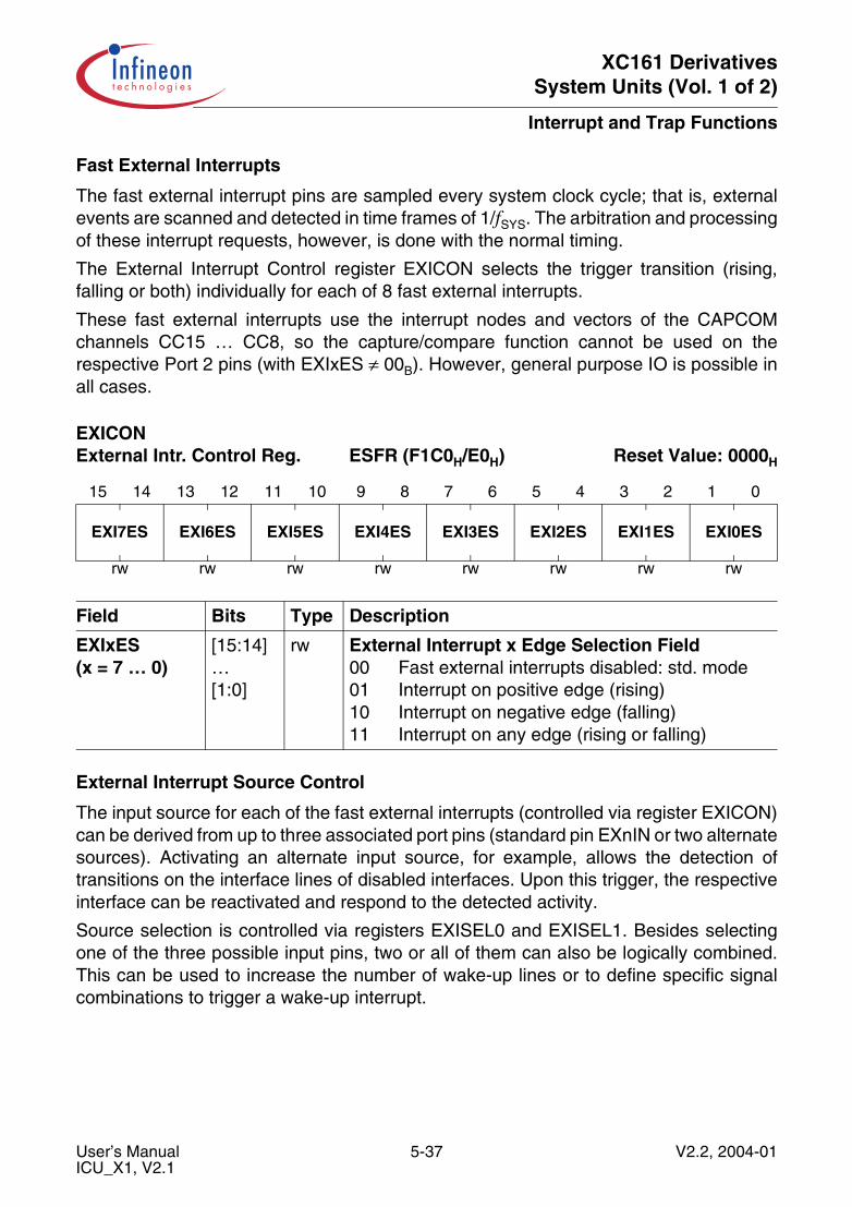
XC161 DerivativesSystem Units (Vol. 1 of 2)
Interrupt and Trap Functions
Fast External Interrupts
The fast external interrupt pins are sampled every system clock cycle; that is, externalevents are scanned and detected in time frames of 1/fSYS. The arbitration and processingof these interrupt requests, however, is done with the normal timing.
The External Interrupt Control register EXICON selects the trigger transition (rising,falling or both) individually for each of 8 fast external interrupts.
These fast external interrupts use the interrupt nodes and vectors of the CAPCOMchannels CC15 … CC8, so the capture/compare function cannot be used on therespective Port 2 pins (with EXIxES ≠ 00B). However, general purpose IO is possible inall cases.
External Interrupt Source Control
The input source for each of the fast external interrupts (controlled via register EXICON)can be derived from up to three associated port pins (standard pin EXnIN or two alternatesources). Activating an alternate input source, for example, allows the detection oftransitions on the interface lines of disabled interfaces. Upon this trigger, the respectiveinterface can be reactivated and respond to the detected activity.
Source selection is controlled via registers EXISEL0 and EXISEL1. Besides selectingone of the three possible input pins, two or all of them can also be logically combined.This can be used to increase the number of wake-up lines or to define specific signalcombinations to trigger a wake-up interrupt.
EXICON External Intr. Control Reg. ESFR (F1C0H/E0H) Reset Value: 0000H
15 14 13 12 11 10 9 8 7 6 5 4 3 2 1 0
EXI7ES EXI6ES EXI5ES EXI4ES EXI3ES EXI2ES EXI1ES EXI0ES
rw rw rw rw rw rw rw rw
Field Bits Type Description
EXIxES(x = 7 … 0)
[15:14]…[1:0]
rw External Interrupt x Edge Selection Field00 Fast external interrupts disabled: std. mode01 Interrupt on positive edge (rising)10 Interrupt on negative edge (falling)11 Interrupt on any edge (rising or falling)
User’s Manual 5-37 V2.2, 2004-01ICU_X1, V2.1
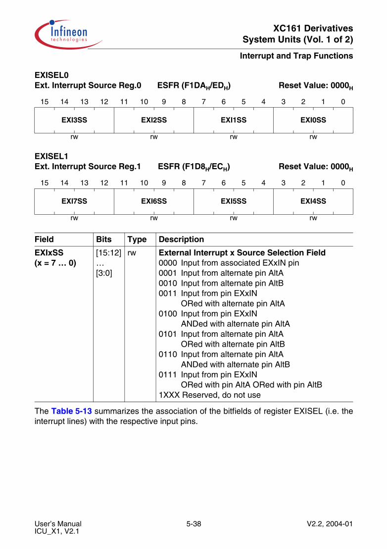
XC161 DerivativesSystem Units (Vol. 1 of 2)
Interrupt and Trap Functions
The Table 5-13 summarizes the association of the bitfields of register EXISEL (i.e. theinterrupt lines) with the respective input pins.
EXISEL0Ext. Interrupt Source Reg.0 ESFR (F1DAH/EDH) Reset Value: 0000H
15 14 13 12 11 10 9 8 7 6 5 4 3 2 1 0
EXI3SS EXI2SS EXI1SS EXI0SS
rw rw rw rw
EXISEL1Ext. Interrupt Source Reg.1 ESFR (F1D8H/ECH) Reset Value: 0000H
15 14 13 12 11 10 9 8 7 6 5 4 3 2 1 0
EXI7SS EXI6SS EXI5SS EXI4SS
rw rw rw rw
Field Bits Type Description
EXIxSS(x = 7 … 0)
[15:12]…[3:0]
rw External Interrupt x Source Selection Field0000 Input from associated EXxIN pin0001 Input from alternate pin AltA0010 Input from alternate pin AltB0011 Input from pin EXxIN
ORed with alternate pin AltA0100 Input from pin EXxIN
ANDed with alternate pin AltA0101 Input from alternate pin AltA
ORed with alternate pin AltB0110 Input from alternate pin AltA
ANDed with alternate pin AltB0111 Input from pin EXxIN
ORed with pin AltA ORed with pin AltB1XXX Reserved, do not use
User’s Manual 5-38 V2.2, 2004-01ICU_X1, V2.1

XC161 DerivativesSystem Units (Vol. 1 of 2)
Interrupt and Trap Functions
External Interrupts During Sleep Mode
During Sleep Mode, all peripheral clock signals are deactivated. This also disables thestandard edge detection logic for the fast external interrupts. However, transitions onthese interrupt inputs must be recognized in order to initiate the wake-up. This isaccomplished by a special edge detection logic for the fast external interrupts whichrequires no clock signal (therefore also works in Sleep mode) and is equipped with ananalog noise filter. This filter suppresses spikes (generated by noise) up to 10 ns. Inputpulses with a duration of 100 ns minimum are recognized and generate an interruptrequest.
This filter delays the recognition of an external wake-up signal by approximately 100 ns,but the spike suppression ensures safe and robust operation of the sleep/wake-upmechanism in an active environment.
Figure 5-6 Input Noise Filter Operation
Table 5-13 Connection of Interrupt Inputs to External Interrupt Nodes
Control Bitfield
Std. Pin EXnIN
Alternate Pin AltA
Alternate Pin AltB
Interrupt Ctrl. Reg.
Associated Interface
Notes
EXI0SS P2.8 P1H.3 P1H.0 CC8IC SSC1 –
EXI1SS P2.9 P3.1 P3.0 CC9IC ASC1 –
EXI2SS P2.10 P3.11 P3.10 CC10IC ASC0 –
EXI3SS P2.11 P3.13 P3.12 CC11IC SSC0 –
EXI4SS P2.12 P4.7 P4.5 CC12IC CAN_A The actual interface pin is programm-able
EXI5SS P2.13 P4.6 P4.4 CC13IC CAN_B, SDLM
EXI6SS P2.14 P7.7 P7.5 CC14IC SDLM
EXI7SS P2.15 P7.6 P7.4 CC15IC CAN_A, CAN_B
MCD04456
InputSignal
InterruptRequest
Rejected Recognized
10 ns100 ns
User’s Manual 5-39 V2.2, 2004-01ICU_X1, V2.1

XC161 DerivativesSystem Units (Vol. 1 of 2)
Interrupt and Trap Functions
External Interrupt Pulse Timing
External interrupt inputs are evaluated by a synchronous logic and by an asynchronouslogic. The synchronous logic supports the recognition of short interrupt pulses at highersystem frequencies, the asynchronous logic ensures recognition of interrupt pulsesduring sleep mode, when no system clock is available.
An external interrupt signal is safely recognized in two cases:
• if it is active for more than 100 ns (async. logic with spike filter), or• if it is active for more than 2 cycles of fSYS (sync. logic).
The interrupt signal is recognized after whatever condition becomes true first.
Note: After wake-up from Sleep mode, the time span until the PLL becomes locked isnot critical for new external interrupt pulses to be correctly synchronized, becausein this case the asynchronous logic will detect the external interrupt correctly, if itis active for at least 100 ns.
Note: The NMI input features the same spike filter and the same timing requirements.
5.9 OCDS Requests
The OCDS module issues high-priority break requests or standard service requests. Thebreak requests are routed directly to the CPU (like the hardware trap requests) and areprioritized there. Therefore, break requests ignore the standard interrupt arbitration andreceive highest priority.
The standard OCDS service requests are routed to the CPU Action Control Unit togetherwith the arbitrated interrupt/PEC requests. The service request with the higher priority issent to the CPU to be serviced. If both the interrupt/PEC request and the OCDS requesthave the same priority level, the interrupt/PEC request wins.
This approach ensures precise break control, while affecting the system behavior as littleas possible.
The CPU Action Control Unit also routes back request acknowledges and denials fromthe core to the corresponding requestor.
User’s Manual 5-40 V2.2, 2004-01ICU_X1, V2.1
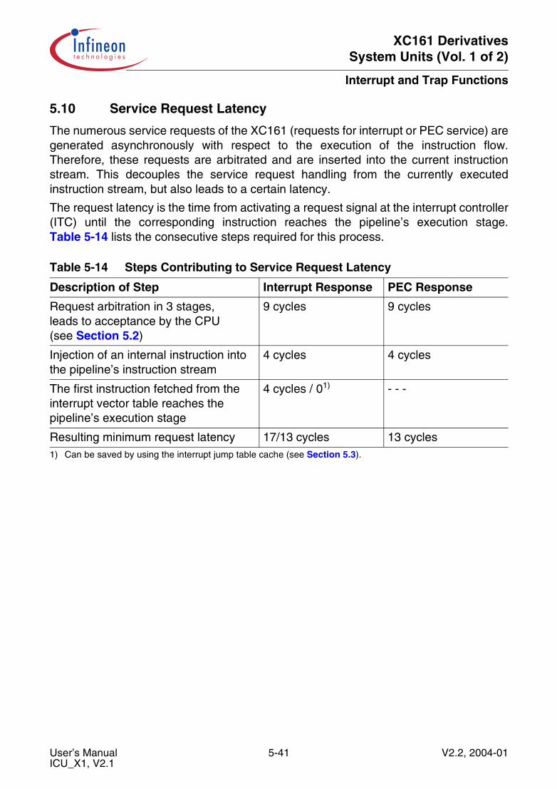
XC161 DerivativesSystem Units (Vol. 1 of 2)
Interrupt and Trap Functions
5.10 Service Request Latency
The numerous service requests of the XC161 (requests for interrupt or PEC service) aregenerated asynchronously with respect to the execution of the instruction flow.Therefore, these requests are arbitrated and are inserted into the current instructionstream. This decouples the service request handling from the currently executedinstruction stream, but also leads to a certain latency.
The request latency is the time from activating a request signal at the interrupt controller(ITC) until the corresponding instruction reaches the pipeline’s execution stage.Table 5-14 lists the consecutive steps required for this process.
Table 5-14 Steps Contributing to Service Request Latency
Description of Step Interrupt Response PEC Response
Request arbitration in 3 stages,leads to acceptance by the CPU(see Section 5.2)
9 cycles 9 cycles
Injection of an internal instruction into the pipeline’s instruction stream
4 cycles 4 cycles
The first instruction fetched from the interrupt vector table reaches the pipeline’s execution stage
4 cycles / 01)
1) Can be saved by using the interrupt jump table cache (see Section 5.3).
- - -
Resulting minimum request latency 17/13 cycles 13 cycles
User’s Manual 5-41 V2.2, 2004-01ICU_X1, V2.1
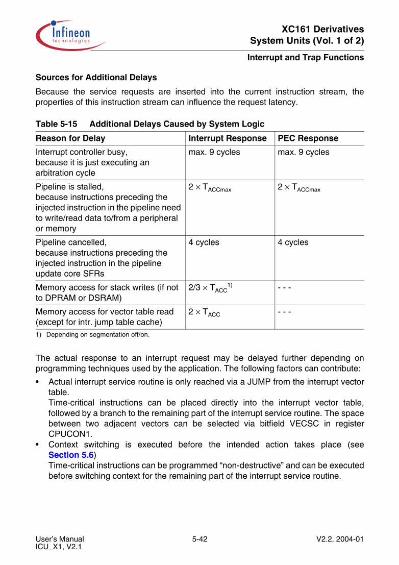
XC161 DerivativesSystem Units (Vol. 1 of 2)
Interrupt and Trap Functions
Sources for Additional Delays
Because the service requests are inserted into the current instruction stream, theproperties of this instruction stream can influence the request latency.
The actual response to an interrupt request may be delayed further depending onprogramming techniques used by the application. The following factors can contribute:
• Actual interrupt service routine is only reached via a JUMP from the interrupt vectortable.Time-critical instructions can be placed directly into the interrupt vector table,followed by a branch to the remaining part of the interrupt service routine. The spacebetween two adjacent vectors can be selected via bitfield VECSC in registerCPUCON1.
• Context switching is executed before the intended action takes place (seeSection 5.6)Time-critical instructions can be programmed “non-destructive” and can be executedbefore switching context for the remaining part of the interrupt service routine.
Table 5-15 Additional Delays Caused by System Logic
Reason for Delay Interrupt Response PEC Response
Interrupt controller busy,because it is just executing an arbitration cycle
max. 9 cycles max. 9 cycles
Pipeline is stalled,because instructions preceding the injected instruction in the pipeline need to write/read data to/from a peripheral or memory
2 × TACCmax 2 × TACCmax
Pipeline cancelled,because instructions preceding the injected instruction in the pipeline update core SFRs
4 cycles 4 cycles
Memory access for stack writes (if not to DPRAM or DSRAM)
2/3 × TACC1)
1) Depending on segmentation off/on.
- - -
Memory access for vector table read(except for intr. jump table cache)
2 × TACC - - -
User’s Manual 5-42 V2.2, 2004-01ICU_X1, V2.1
XC161 DerivativesSystem Units (Vol. 1 of 2)
Interrupt and Trap Functions
5.11 Trap Functions
Traps interrupt current execution in a manner similar to standard interrupts. However,trap functions offer the possibility to bypass the interrupt system’s prioritization processfor cases in which immediate system reaction is required. Trap functions are notmaskable and always have priority over interrupt requests on any priority level.
The XC161 provides two different kinds of trapping mechanisms: Hardware Traps aretriggered by events that occur during program execution (such as illegal access orundefined opcode); Software Traps are initiated via an instruction within the currentexecution flow.
Software Traps
The TRAP instruction causes a software call to an interrupt service routine. The vectornumber specified in the operand field of the trap instruction determines which vectorlocation in the vector table will be branched to.
Executing a TRAP instruction causes an effect similar to the occurrence of an interruptat the same vector. PSW, CSP (in segmentation mode), and IP are pushed on theinternal system stack and a jump is taken to the specified vector location. When a trapis executed, the CSP for the trap service routine is loaded from register VECSEG. NoInterrupt Request flags are affected by the TRAP instruction. The interrupt serviceroutine called by a TRAP instruction must be terminated with a RETI (return frominterrupt) instruction to ensure correct operation.
Note: The CPU priority level and the selected register bank in register PSW are notmodified by the TRAP instruction, so the service routine is executed on the samepriority level from which it was invoked. Therefore, the service routine entered bythe TRAP instruction uses the original register bank and can be interrupted byother traps or higher priority interrupts, other than when triggered by a hardwareevent.
Hardware Traps
Hardware traps are issued by faults or specific system states which occur during runtimeof a program (not identified at assembly time). A hardware trap may also be triggeredintentionally, for example: to emulate additional instructions by generating an IllegalOpcode trap. The XC161 distinguishes eight different hardware trap functions. When ahardware trap condition has been detected, the CPU branches to the trap vector locationfor the respective trap condition. The instruction which caused the trap is completedbefore the trap handling routine is entered.
Hardware traps are non-maskable and always have priority over every other CPUactivity. If several hardware trap conditions are detected within the same instructioncycle, the highest priority trap is serviced (see Table 5-3).
User’s Manual 5-43 V2.2, 2004-01ICU_X1, V2.1
XC161 DerivativesSystem Units (Vol. 1 of 2)
Interrupt and Trap Functions
PSW, CSP (in segmentation mode), and IP are pushed on the internal system stack andthe CPU level in register PSW is set to the highest possible priority level (level 15),disabling all interrupts. The global register bank is selected. Execution branches to therespective trap vector in the vector table. A trap service routine must be terminated withthe RETI instruction.
The eight hardware trap functions of the XC161 are divided into two classes:
Class A traps are:
• External Non-Maskable Interrupt (NMI)• Stack Overflow• Stack Underflow trap• Software Break
These traps share the same trap priority, but have individual vector addresses.
Class B traps are:
• Undefined Opcode• Program Memory Access Error• Protection Fault• Illegal Word Operand Access
The Class B traps share the same trap priority and the same vector address.
The bit-addressable Trap Flag Register (TFR) allows a trap service routine to identify thekind of trap which caused the exception. Each trap function is indicated by a separaterequest flag. When a hardware trap occurs, the corresponding request flag in registerTFR is set to ‘1’.
The reset functions (hardware, software, watchdog) may be regarded as a type of trap.Reset functions have the highest system priority (trap priority III).
Class A traps have the second highest priority (trap priority II), on the 3rd rank areClass B traps, so a Class A trap can interrupt a Class B trap. If more than one Class Atrap occur at a time, they are prioritized internally, with the NMI trap at the highest andthe software break trap at the lowest priority.
In the case where e.g. an Undefined Opcode trap (class B) occurs simultaneously withan NMI trap (class A), both the NMI and the UNDOPC flag is set, the IP of the instructionwith the undefined opcode is pushed onto the system stack, but the NMI trap is executed.After return from the NMI service routine, the IP is popped from the stack andimmediately pushed again because of the pending UNDOPC trap.
Note: The trap service routine must clear the respective trap flag; otherwise, a new trapwill be requested after exiting the service routine. Setting a trap request flag bysoftware causes the same effects as if it had been set by hardware.
User’s Manual 5-44 V2.2, 2004-01ICU_X1, V2.1
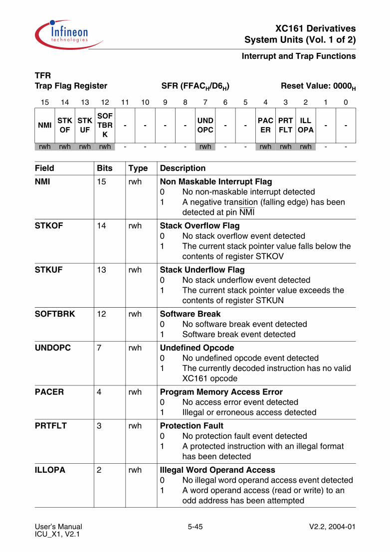
XC161 DerivativesSystem Units (Vol. 1 of 2)
Interrupt and Trap Functions
TFR Trap Flag Register SFR (FFACH/D6H) Reset Value: 0000H
15 14 13 12 11 10 9 8 7 6 5 4 3 2 1 0
NMISTK OF
STK UF
SOFTBR
K- - - -
UND OPC
- -PACER
PRT FLT
ILL OPA
- -
rwh rwh rwh rwh - - - - rwh - - rwh rwh rwh - -
Field Bits Type Description
NMI 15 rwh Non Maskable Interrupt Flag0 No non-maskable interrupt detected1 A negative transition (falling edge) has been
detected at pin NMI
STKOF 14 rwh Stack Overflow Flag0 No stack overflow event detected1 The current stack pointer value falls below the
contents of register STKOV
STKUF 13 rwh Stack Underflow Flag0 No stack underflow event detected1 The current stack pointer value exceeds the
contents of register STKUN
SOFTBRK 12 rwh Software Break0 No software break event detected1 Software break event detected
UNDOPC 7 rwh Undefined Opcode0 No undefined opcode event detected1 The currently decoded instruction has no valid
XC161 opcode
PACER 4 rwh Program Memory Access Error0 No access error event detected1 Illegal or erroneous access detected
PRTFLT 3 rwh Protection Fault0 No protection fault event detected1 A protected instruction with an illegal format
has been detected
ILLOPA 2 rwh Illegal Word Operand Access0 No illegal word operand access event detected1 A word operand access (read or write) to an
odd address has been attempted
User’s Manual 5-45 V2.2, 2004-01ICU_X1, V2.1
XC161 DerivativesSystem Units (Vol. 1 of 2)
Interrupt and Trap Functions
Class A Traps
Class A traps are generated by the high priority system NMI or by special CPU eventssuch as the software break, a stack overflow, or an underflow event. Class A traps arenot used to indicate hardware failures. After a Class A event, a dedicated service routineis called to react on the events. Each Class A trap has its own vector location in thevector table. Class A traps cannot interrupt atomic/extend sequences and I/O accessesin progress, because after finishing the service routine, the instruction flow must befurther correctly executed. For example, an interrupted extend sequence cannot berestarted. All Class A traps are generated in the pipeline during the execution ofinstructions, except for NMI, which is an asynchronous external event. Class A trapevents can be generated only during the memory stage of execution, so traps cannot begenerated by two different instructions in the pipeline in the same CPU cycle. Theexecution of instructions which caused a Class A trap event is always completed. In thecase of an atomic/extend sequence or I/O read access in progress, the completesequence is executed. Upon completion of the instruction or sequence, the pipeline iscanceled and the IP of the instruction following the last one executed is pushed on thestack. Therefore, in the case of a Class A trap, the stack always contains the IP of thefirst not-executed instruction in the instruction flow.
Note: The Branch Folding Unit allows the execution of a branch instruction in parallelwith the preceding instruction. The pre-processed branch instruction is combinedwith the preceding instruction. The branch is executed together with the instructionwhich caused the Class A trap. The IP of the first following not-executedinstruction in the instruction flow is then pushed on the stack.
If more than one Class A trap occur at the same time, they are prioritized internally. TheNMI trap has the highest priority and the software break has the lowest.
Note: In the case of two different Class A traps occurring simultaneously, both trap flagsare set. The IP of the instruction following the last one executed is pushed on thestack. The trap with the higher priority is executed. After return from the serviceroutine, the IP is popped from the stack and immediately pushed again becauseof the other pending Class A trap (unless the trap related to the second trap flagin TFR has been cleared by the first trap service routine).
User’s Manual 5-46 V2.2, 2004-01ICU_X1, V2.1
XC161 DerivativesSystem Units (Vol. 1 of 2)
Interrupt and Trap Functions
Class B Traps
Class B traps are generated by unrecoverable hardware failures. In the case of ahardware failure, the CPU must immediately start a failure service routine. Class B trapscan interrupt an atomic/extend sequence and an I/O read access. After finishing theClass B service routine, a restoration of the interrupted instruction flow is not possible.
All Class B traps have the same priority (trap priority I). When several Class B trapsbecome active at the same time, the corresponding flags in the TFR register are set andthe trap service routine is entered. Because all Class B traps have the same vector, thepriority of service of simultaneously occurring Class B traps is determined by software inthe trap service routine.
The Access Error is an asynchronous external (to the CPU) event while all other Class Btraps are generated in the pipeline during the execution of instructions. Class B trapevents can be generated only during the memory stage of execution, so traps cannot begenerated by two different instructions in the pipeline in the same CPU cycle.Instructions which caused a Class B trap event are always executed, then the pipelineis canceled and the IP of the instruction following the one which caused the trap ispushed on the stack. Therefore, the stack always contains the IP of the first followingnot-executed instruction in the instruction flow.
Note: The Branch Folding Unit allows the execution of a branch instruction in parallelwith the preceding instruction. The pre-processed branch instruction is combinedwith the preceding instruction. The branch is executed together with the instructioncausing the Class B trap. The IP of the first following not-executed instruction inthe instruction flow is pushed on the stack.
A Class A trap occurring during the execution of a Class B trap service routine will beserviced immediately. During the execution of a Class A trap service routine, however,any Class B trap occurring will not be serviced until the Class A trap service routine isexited with a RETI instruction. In this case, the occurrence of the Class B trap conditionis stored in the TFR register, but the IP value of the instruction which caused this trap islost.
Note: If a Class A trap occurs simultaneously with a Class B trap, both trap flags are set.The IP of the instruction following the one which caused the trap is pushed into thestack, and the Class A trap is executed. If this occurs during execution of anatomic/extend sequence or I/O read access in progress, then the presence of theClass B trap breaks the protection of atomic/extend operations and the Class Atrap will be executed immediately without waiting for the sequence completion.After return from the service routine, the IP is popped from the system stack andimmediately pushed again because of the other pending Class B trap. In thissituation, the restoration of the interrupted instruction flow is not possible.
User’s Manual 5-47 V2.2, 2004-01ICU_X1, V2.1
XC161 DerivativesSystem Units (Vol. 1 of 2)
Interrupt and Trap Functions
External NMI Trap
Whenever a high to low transition on the dedicated external NMI pin (Non-MaskableInterrupt) is detected, the NMI flag in register TFR is set and the CPU will enter the NMItrap routine.
Stack Overflow Trap
Whenever the stack pointer is implicitly decremented and the stack pointer is equal tothe value in the stack overflow register STKOV, the STKOF flag in register TFR is setand the CPU will enter the stack overflow trap routine.
For recovery from stack overflow, it must be ensured that there is enough excess spaceon the stack to save the current system state twice (PSW, IP, in segmented mode alsoCSP). Otherwise, a system reset should be generated.
Stack Underflow Trap
Whenever the stack pointer is implicitly incremented and the stack pointer is equal to thevalue in the stack underflow register STKUN, the STKUF flag is set in register TFR andthe CPU will enter the stack underflow trap routine.
Software Break Trap
When the instruction currently being executed by the CPU is a SBRK instruction, theSOFTBRK flag is set in register TFR and the CPU enters the software break debugroutine. The flag generation of the software break instruction can be disabled by the On-chip Emulation Module. In this case, the instruction only breaks the instruction flow andsignals this event to the debugger, the flag is not set and the trap will not be executed.
Undefined Opcode Trap
When the instruction currently decoded by the CPU does not contain a valid XC161opcode, the UNDOPC flag is set in register TFR and the CPU enters the undefinedopcode trap routine. The instruction that causes the undefined opcode trap is executedas a NOP.
This can be used to emulate unimplemented instructions. The trap service routine canexamine the faulting instruction to decode operands for unimplemented opcodes basedon the stacked IP. In order to resume processing, the stacked IP value must beincremented by the size of the undefined instruction, which is determined by the user,before a RETI instruction is executed.
User’s Manual 5-48 V2.2, 2004-01ICU_X1, V2.1
XC161 DerivativesSystem Units (Vol. 1 of 2)
Interrupt and Trap Functions
Program Memory Access Error
When a program memory access error is detected, the PACER flag is set in register TFRand the CPU enters the PMI access error trap routine. The access error is reported inthe following cases:
• access to Flash memory while it is disabled• access to Flash memory from outside while read-protection is active• double bit error detected when reading Flash memory• access to reserved locations (see memory map)• access to Monitor RAM, if not in emulation mode
In case of an access error, additionally the soft-trap code 1E9BH is issued.
Protection Fault Trap
Whenever one of the special protected instructions is executed where the opcode of thatinstruction is not repeated twice in the second word of the instruction and the bytefollowing the opcode is not the complement of the opcode, the PRTFLT flag in registerTFR is set and the CPU enters the protection fault trap routine. The protectedinstructions include DISWDT, EINIT, IDLE, PWRDN, SRST, ENWDT and SRVWDT.The instruction that causes the protection fault trap is executed like a NOP.
Illegal Word Operand Access Trap
Whenever a word operand read or write access is attempted to an odd byte address, theILLOPA flag in register TFR is set and the CPU enters the illegal word operand accesstrap routine.
User’s Manual 5-49 V2.2, 2004-01ICU_X1, V2.1
XC161 DerivativesSystem Units (Vol. 1 of 2)
General System Control Functions
6 General System Control FunctionsThe XC161 System Control Unit (SCU) summarizes a number of central control tasksand product specific features. These features include functional modules such as theWatchdog Timer (WDT) or the Clock Generation Unit (CGU), as well as basic functionssuch as the register protection mechanism or the reset generation.
The following general functions are provided:
• The System Reset is generated by the Reset Control Block and handles the resetand startup behavior (internal initialization) of the chip. It controls the reset triggersas well as the reset timing. This block controls also the basic configuration of theXC161 via external hardware.
• The Clock Generation Unit (CGU) provides the on-chip oscillator and the PhaseLocked Loop (PLL). This block generates all clock signals for the XC161 anddistributes them to the respective modules. Also the status of the clock generationsystem is indicated.
• The Central System Control Functions comprise all central control tasks likesecurity level selection and system behavior in Sleep mode and Powerdown mode.Depending on the application state, different security levels (like protected andunprotected mode) are supported by the security level control state machine.
• The Watchdog Timer (WDT) represents one of the fail-safe mechanisms whichhave been implemented to prevent the controller from malfunctioning. It can detectlong term malfunctions and is always enabled after chip initialization. The WDT canoperate in Compatible mode or in Enhanced WDT mode.
• The Identification Control Block supports a set of six identification registers foridentification of the most important silicon parameters (chip manufacturer, chip typeand its properties). This information can be used for automatic test selection.
User’s Manual 6-1 V2.2, 2004-01SCU_X1, V2.1
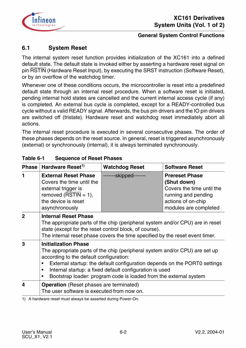
XC161 DerivativesSystem Units (Vol. 1 of 2)
General System Control Functions
6.1 System Reset
The internal system reset function provides initialization of the XC161 into a defineddefault state. The default state is invoked either by asserting a hardware reset signal onpin RSTIN (Hardware Reset Input), by executing the SRST instruction (Software Reset),or by an overflow of the watchdog timer.
Whenever one of these conditions occurs, the microcontroller is reset into a predefineddefault state through an internal reset procedure. When a software reset is initiated,pending internal hold states are cancelled and the current internal access cycle (if any)is completed. An external bus cycle is completed, except for a READY-controlled buscycle without a valid READY signal. Afterwards, the bus pin drivers and the IO pin driversare switched off (tristate). Hardware reset and watchdog reset immediately abort allactions.
The internal reset procedure is executed in several consecutive phases. The order ofthese phases depends on the reset source. In general, reset is triggered asynchronously(external) or synchronously (internal), it is always terminated synchronously.
Table 6-1 Sequence of Reset Phases
Phase Hardware Reset1)
1) A hardware reset must always be asserted during Power-On.
Watchdog Reset Software Reset
1 External Reset PhaseCovers the time until the external trigger is removed (RSTIN = 1),the device is reset asynchronously
-------skipped------- Prereset Phase(Shut down)Covers the time until the running and pending actions of on-chip modules are completed
2 Internal Reset PhaseThe appropriate parts of the chip (peripheral system and/or CPU) are in reset state (except for the reset control block, of course).The internal reset phase covers the time specified by the reset event timer.
3 Initialization PhaseThe appropriate parts of the chip (peripheral system and/or CPU) are set up according to the default configuration:• External startup: the default configuration depends on the PORT0 settings• Internal startup: a fixed default configuration is used• Bootstrap loader: program code is loaded from the external system
4 Operation (Reset phases are terminated)The user software is executed from now on.
User’s Manual 6-2 V2.2, 2004-01SCU_X1, V2.1

XC161 DerivativesSystem Units (Vol. 1 of 2)
General System Control Functions
6.1.1 Reset Sources and Phases
The XC161 executes a reset in several phases whose sequence depends on the resettrigger (see Table 6-1).
External Reset Phase
A hardware reset is asynchronously triggered when the reset input signal RSTIN isrecognized low. A spike suppression input filter in the RSTIN line suppresses all signalsshorter than 10 ns. To ensure the recognition of the RSTIN signal, it must be held low forat least 100 ns so it will safely pass the reset input filter. This is also required after thesupply voltages have become stable.
Note: The minimum duration of the external reset must ensure that the hardwareconfiguration signals have reached their intended logic levels.
Figure 6-1 External Reset Circuitry
A hardware reset on input RSTIN may be triggered in several ways (see Figure 6-1).
• An external pull-up device connected to an external capacitor is sufficient for anautomatic power-on reset.
SystemControl
Unit
ExternalHardware
Spike Filter(10 - 100 ns)
RSTIN
RSTOUT
a) Automatic Power-on Reset
b) Generated Warm Reset ResetControlBlock
50 - 250 kΩ
VDD
ExternalResetSources
&
+
MCS05329
User’s Manual 6-3 V2.2, 2004-01SCU_X1, V2.1
XC161 DerivativesSystem Units (Vol. 1 of 2)
General System Control Functions
• An external pull-up device connected to an external switch provides a manual reset.• RSTIN may also be connected to the output of other logic for generating a warm
reset.
Note: During the external reset phase the complete chip is in reset state. The externalreset phase is left synchronously, when the RSTIN level goes inactive (high).
Pre-Reset Phase
The pre-reset phase is triggered by a software reset. During the pre-reset phase, theCPU first runs its pipeline (including all write back buffers) empty, and then indicates thesoftware reset request to the system control unit. The pipeline stays empty after thisrequest trigger is activated.
As soon as the software reset request occurs, the SCU requests a shutdown from theactive modules equipped with shutdown handshake (see Section 6.3.3). The pre-resetphase is complete as soon as all modules acknowledge the shutdown state.
Upon a shutdown request the EBC will finish the currently running bus cycle. If in aREADY-controlled bus cycle the READY signal is not sampled active after theprogrammed number of waitstates, this bus cycle is aborted in order to prevent a dead-lock situation.
Internal Reset Phase
At the beginning of the internal reset phase the internal reset condition becomes active,that means, the internal reset signal is actually applied to the modules. If the reset wastriggered by hardware, it may be active already.
Note: The reset control block (including the watchdog timer) is not reset, of course.
The duration of the internal reset phase is determined by the reset-length-control bitfieldRSTLEN in register RSTCON. The WDT low byte is used for counting the reset duration.When entering the internal reset phase, the timer is cleared and then counts up withfrequency fWDT. The default count frequency after a hardware reset is fWDT = fSYS/2 =fMC/2. Internal reset triggers do not change the current clock setting and the value ofbitfield WDTIN, so the previously selected fWDT is used.
The actual duration of the internal reset sequence can therefore be calculated using thefollowing formula:
(6.1)tRST2 RSTLEN 1+( )
fWDT
------------------------------=
User’s Manual 6-4 V2.2, 2004-01SCU_X1, V2.1
XC161 DerivativesSystem Units (Vol. 1 of 2)
General System Control Functions
Reset Termination (Initialization Phase)
When the end of the internal reset phase has been reached, the following actions takeplace, before control is passed to the software:
• Set the reset indication flags in register SYSSTAT accordingly• Select initial configuration and reset start address• Deactivate the internal reset signals• Execute bootstrap loader if selected
Note: The WDT continues counting up from its current level (determined by the selectedreset length).
User’s Manual 6-5 V2.2, 2004-01SCU_X1, V2.1
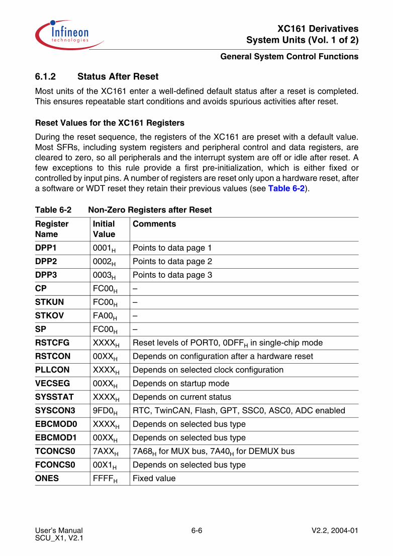
XC161 DerivativesSystem Units (Vol. 1 of 2)
General System Control Functions
6.1.2 Status After Reset
Most units of the XC161 enter a well-defined default status after a reset is completed.This ensures repeatable start conditions and avoids spurious activities after reset.
Reset Values for the XC161 Registers
During the reset sequence, the registers of the XC161 are preset with a default value.Most SFRs, including system registers and peripheral control and data registers, arecleared to zero, so all peripherals and the interrupt system are off or idle after reset. Afew exceptions to this rule provide a first pre-initialization, which is either fixed orcontrolled by input pins. A number of registers are reset only upon a hardware reset, aftera software or WDT reset they retain their previous values (see Table 6-2).
Table 6-2 Non-Zero Registers after Reset
Register Name
Initial Value
Comments
DPP1 0001H Points to data page 1
DPP2 0002H Points to data page 2
DPP3 0003H Points to data page 3
CP FC00H –
STKUN FC00H –
STKOV FA00H –
SP FC00H –
RSTCFG XXXXH Reset levels of PORT0, 0DFFH in single-chip mode
RSTCON 00XXH Depends on configuration after a hardware reset
PLLCON XXXXH Depends on selected clock configuration
VECSEG 00XXH Depends on startup mode
SYSSTAT XXXXH Depends on current status
SYSCON3 9FD0H RTC, TwinCAN, Flash, GPT, SSC0, ASC0, ADC enabled
EBCMOD0 XXXXH Depends on selected bus type
EBCMOD1 00XXH Depends on selected bus type
TCONCS0 7AXXH 7A68H for MUX bus, 7A40H for DEMUX bus
FCONCS0 00X1H Depends on selected bus type
ONES FFFFH Fixed value
User’s Manual 6-6 V2.2, 2004-01SCU_X1, V2.1

XC161 DerivativesSystem Units (Vol. 1 of 2)
General System Control Functions
Operation after Reset
After the internal reset condition is removed, the XC161 fetches the first instruction fromthe selected program memory location (depending on the configuration). As a rule, thisfirst location holds a branch instruction to the actual initialization routine that may belocated anywhere in the address space.
Note: If the Bootstrap Loader Mode was activated during a hardware reset, the XC161does not fetch instructions from the program memory.The standard bootstrap loader expects data via serial interface ASC0.
Watchdog Timer Operation after Reset
The watchdog timer continues running after the internal reset is complete. It will beclocked with the currently selected clock signal fWDT. After a watchdog/software resetfWDT is not changed, after a hardware reset the frequency is fWDT = fSYS/2 = fMC/2. Thedefault reload value is 00H. Thus, a watchdog timer overflow will occur 216 clock cycles(217 fMC cycles after a hardware reset) after completion of the internal reset (dependingon the selected reset length), unless it is disabled, serviced, or reprogrammed in themeantime. If the system reset was caused by a watchdog timer overflow, the WDTR(Watchdog Timer Reset Indication) flag in register SYSSTAT will be set to 1. Thisindicates the cause of the internal reset to the software initialization routine. WDTR isreset to 0 after each other reset. After the internal reset is complete, the operation of thewatchdog timer can be disabled by the DISWDT (Disable Watchdog Timer) instructionprior to the EINIT instruction if using compatibility mode, or anytime in enhanced mode.
The On-Chip RAM Areas after Reset
The contents of the major parts of the on-chip RAMs are preserved during a softwarereset and a WDT reset. There are two exceptions to this rule:
• A part of the DPRAM (the area 00’FBA0H … 00’FC1FH) may be altered during theinitialization phase (see Table 6-1) and, therefore, should not store data to bepreserved beyond a WDT/SW reset.
• During bootstrap loader operation the serially received data is stored in the PSRAMstarting at location E0’0000H.
Because a hardware reset can occur asynchronously to an internal operation, it mayinterrupt a current write operation and so inadvertently corrupt the contents of on-chipRAM. RAM contents are preserved if the hardware reset occurs during Power-Downmode, during Sleep mode, or during Idle mode with no PEC transfers enabled.
Note: After a power-up hardware reset the RAM contents are undefined, of course.
User’s Manual 6-7 V2.2, 2004-01SCU_X1, V2.1

XC161 DerivativesSystem Units (Vol. 1 of 2)
General System Control Functions
External Bus Interface after Reset
If an external start is selected after reset the EBC is initialized accordingly and some ofthe port pins of the XC161 are controlled accordingly. Pin ALE is held low through aninternal pull-down, and pins RD and WR are held high through internal pull-ups. Also, allpins which can be configured for CS output will be pulled high during each reset.
The registers EBCMOD0, EBCMOD1, TCONCS0, and FCONCS0 are initializedaccording to the configuration selected via PORT0.
When an external start is selected (pin EA = 0):
• Bit ENCS in register FCONCS0 is set to 1• Bus Type field (BTYP) in register FCONCS0 is initialized according to
P0L.7 and P0L.6• A default bus timing (depending on the bus mode) is selected via register TCONCS0• The required pins of PORT0 and PORT1 are assigned via register EBCMOD1• Bitfields WRCFG, CSPEN, and SAPEN in register EBCMOD0 are set as selected via
PORT0 (WRC, CSSEL, SASEL)
When an internal start is selected (pin EA = 1):
• Register EBCMOD0 is set to 7400H (EBC-pins disabled)• Registers EBCMOD1, FCONCS0, and TCONCS0 are cleared
Note: This initial configuration of the EBC may be changed by user software at any time.
When the internal reset is complete, the configuration of PORT0, PORT1, Port 4, Port 6,and of the BHE signal (High Byte Enable, alternate function of P3.12) depends on thebus type selected during reset. If any of the external bus modes was selected duringreset, PORT0 will operate in the selected bus mode. Port 4 will output the selectednumber of segment address lines (all zero after reset). Port 6 will drive the selectednumber of CS lines (CS0 will be 0, while the other active CS lines will be 1). If no memoryaccesses above 64 Kbytes are to be performed, segmentation may be disabled.
Ports after Reset
During the internal reset sequence, all port pins of the XC161 are configured as inputsby clearing the associated direction registers, and their pin drivers are switched to thehigh impedance state. This ensures that the XC161 and external devices will not try todrive the same pin to different levels.
Pins assigned to the EBC become active after an external-start reset.
Note: Pull-ups for configuration and possible CS signals are active during each reset.
When the on-chip bootstrap loader was activated during reset, pin TxD0 (alternate portfunction) will be switched to output mode after the reception of the zero byte.
All other pins remain in the high-impedance state until they are changed by software orperipheral operation.
User’s Manual 6-8 V2.2, 2004-01SCU_X1, V2.1
XC161 DerivativesSystem Units (Vol. 1 of 2)
General System Control Functions
Reset Output Pin
The RSTOUT pin is dedicated to the generation of a reset signal for external systemcomponents such as peripherals or Flash memories. The behaviour of RSTOUT can beselected via software and can so be adapted to the respective external system.
RSTOUT is activated asynchronously with an external hardware reset. It may also beactivated (selectable) synchronously with an internal software or watchdog reset.
RSTOUT is deactivated at a selectable time:
• optionally at the end of reset (supports a reset signal to an external program Flash)• upon the execution of the EINIT instruction (latest)• at an earlier time via user software
This allows the complete configuration of the controller including its on-chip peripheralunits before releasing the reset signal for the external peripherals of the system.
Note: RSTOUT will float during adapt mode (see register RSTCFG in Section 6.1.4).
RSTOUT is controlled via several bits in registers RSTCON (see Table 6-3). Theresulting output signal timing is shown in Figure 6-2.
Note: At the very latest, RSTOUT is deactivated by execution of the EINIT instruction,independent of software selections (register RSTCON).
Table 6-3 Usage of RSTOUT Control Bits
Control Bit Operation
RODIS Deactivates RSTOUT when set by software.
ROCON Lets the user software select if RSTOUT is activated upon any reset (0) or only upon an external reset (1). If ROCON = 0 bit RODIS is cleared and pin RSTOUT is activated after a software or WDT reset. The lower part of Figure 6-2 shows both cases (see “Automatic Activation”).
ROCOFF Lets the user software select if RSTOUT is deactivated (1) automatically at the end of reset (after the initialization phase). See “Automatic Deactivation” in Figure 6-2. Bit RODIS is set in this case.If no automatic deactivation is selected (ROCOFF = 0) user software may set bit RODIS at any time.Automatic Deactivation can also be selected by hardware configuration. This supports an external start out of an external Flash memory.
RORMV Lets the user remove the RSTOUT function from pin P20.12 and free it for general purpose IO.P20.12 IO can also be selected by hardware configuration.
User’s Manual 6-9 V2.2, 2004-01SCU_X1, V2.1

XC161 DerivativesSystem Units (Vol. 1 of 2)
General System Control Functions
Figure 6-2 Timings of Reset Signals and Pin RSTOUT
Ext. ResetPhase
Int. ResetPhase
StartupSequence
Hardware Reset
Software/WDT Reset
RSTOUT
Appl. SWUser ApplicationSoftware
RSTIN
RSTOUT
SoftwareReset
Appl. SWPre-ResetPhase
User ApplicationSoftwareWDT
Reset
Int. ResetPhase
StartupSequence
User ApplicationSoftware
User Control
User Control
AutomaticActivation
AutomaticDeactivation
EINIT
MCT05330
User’s Manual 6-10 V2.2, 2004-01SCU_X1, V2.1
XC161 DerivativesSystem Units (Vol. 1 of 2)
General System Control Functions
6.1.3 Application-Specific Initialization Routine
After a reset, the modules of the XC161 must be initialized to enable their operation ona given application. This initialization depends on the task to be performed by the XC161in that application and on some system properties such as operating frequency, externalcircuitry connected, etc.
Typically, the following initializations should be done before the XC161 is prepared to runthe actual application software:
Bus Interface
The external bus interface can be reconfigured after an external reset because the EBCregisters are initialized to default values and may not represent the optimum busconfiguration. The programmable address windows can be enabled in order to adapt thebus cycle characteristics to various memory areas or peripherals. Also, after a single-chip mode reset, the external bus interface can be enabled and configured.
Programmable program memory (on-chip or external) can be programmed, for instance,with data received over a serial link.
Note: Bootstrap loader mode can be used for initial Flash or OTP programming.
System Stack
The default setup for the system stack (size, stack pointer, upper and lower limitregisters) can be adjusted to application-specific values. After reset, registers SP andSTKUN contain the same reset value 00’FC00H, while register STKOV contains00’FA00H. With the default reset initialization, 256 words of system stack are availablein the DPRAM, where the system stack selected by the SP grows downwards from00’FBFEH. The system stack may be moved to the DSRAM and its size can be adjustedto the application’s requirements.
Note: The interrupt system, which is disabled upon completion of the internal reset,should remain disabled until the SP is initialized.Traps (including NMI) may occur, although the interrupt system is still disabled.
Register Bank
The location of a global register bank is defined by the context pointer (CP) and can beadjusted to an application-specific bank before the general purpose registers (GPRs) areused. After reset, register CP contains the value FC00H, i.e. the register bank selectedby the CP grows upward from 00’FC00H.
User’s Manual 6-11 V2.2, 2004-01SCU_X1, V2.1

XC161 DerivativesSystem Units (Vol. 1 of 2)
General System Control Functions
On-Chip RAM
Depending on the application, the user may wish to initialize portions of the internalwritable memory (DPRAM/DSRAM/PSRAM) before normal program operation. After theregister bank has been selected by programming the CP register, the desired portionsof the internal memory can easily be initialized via indirect addressing.
Interrupt System
After reset, the individual interrupt nodes and the global interrupt system are disabled. Inorder to enable interrupt requests, the nodes must be assigned to their respectiveinterrupt priority levels and must be enabled. The vector table can be adjusted if thedefault properties do not fit. Register VECSEG defines the vector table’s location, bitfieldVECSC in register CPUCON1 defines the vector spacing. The vector locations mustreceive pointers to the respective exception handlers. The interrupt system must globallybe enabled by setting bit IEN in register PSW. To avoid such problems as the corruptionof internal memory locations caused by stack operations using an uninitialized stackpointer, care must be taken not to enable the interrupt system before the initialization iscomplete.
Ports
Generally, all ports of the XC161 are switched to input upon reset activation. After reset,some pins may be automatically controlled, such as bus interface pins for an externalstart, TxD in Boot mode, etc. Pins to be used for general purpose IO must be initializedvia software. The required mode (input/output, open drain/push pull, input threshold,etc.) depends on the intended function for a given pin.
Peripherals
Upon reset activation the XC161’s on-chip peripheral modules enter a defined defaultstate (see respective peripheral description) in which they are disabled from operation.In order to use a certain peripheral it must be initialized according to its intendedoperation in the application.
This includes enabling the peripheral, selecting the operating mode (such ascounter/timer), operating parameters (such as baudrate), enabling interface pins (ifrequired), assigning interrupt nodes to the respective priority levels, etc.
After these standard initialization actions, application-specific actions may be required,such as asserting certain levels to output pins, sending codes via interfaces, latchinginput levels, etc.
User’s Manual 6-12 V2.2, 2004-01SCU_X1, V2.1
XC161 DerivativesSystem Units (Vol. 1 of 2)
General System Control Functions
Watchdog Timer
After reset, the watchdog timer is active and counting its default period. If the watchdogtimer is to remain active the desired period should be programmed by selecting theappropriate prescaler value and reload value. Otherwise, the watchdog timer must bedisabled before EINIT.
Termination of Initialization
The software initialization routine should be terminated with the EINIT instruction. Thisinstruction has been implemented as a protected instruction.
Execution of the EINIT instruction has the following effects:
• Disables the action of the DISWDT instruction (unless enhanced mode is selected),• Switches the register security level to “write-protected mode” (see Section 6.3.6),• Causes the RSTOUT pin to go high if it is not high already
(this signal can be used to indicate the end of the initialization routine and the properoperation of the microcontroller to external hardware).
User’s Manual 6-13 V2.2, 2004-01SCU_X1, V2.1
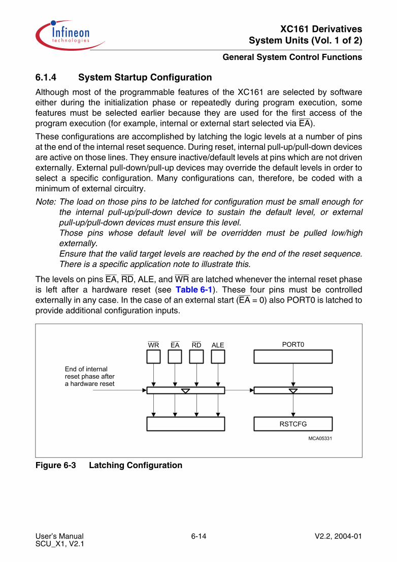
XC161 DerivativesSystem Units (Vol. 1 of 2)
General System Control Functions
6.1.4 System Startup Configuration
Although most of the programmable features of the XC161 are selected by softwareeither during the initialization phase or repeatedly during program execution, somefeatures must be selected earlier because they are used for the first access of theprogram execution (for example, internal or external start selected via EA).
These configurations are accomplished by latching the logic levels at a number of pinsat the end of the internal reset sequence. During reset, internal pull-up/pull-down devicesare active on those lines. They ensure inactive/default levels at pins which are not drivenexternally. External pull-down/pull-up devices may override the default levels in order toselect a specific configuration. Many configurations can, therefore, be coded with aminimum of external circuitry.
Note: The load on those pins to be latched for configuration must be small enough forthe internal pull-up/pull-down device to sustain the default level, or externalpull-up/pull-down devices must ensure this level.Those pins whose default level will be overridden must be pulled low/highexternally.Ensure that the valid target levels are reached by the end of the reset sequence.There is a specific application note to illustrate this.
The levels on pins EA, RD, ALE, and WR are latched whenever the internal reset phaseis left after a hardware reset (see Table 6-1). These four pins must be controlledexternally in any case. In the case of an external start (EA = 0) also PORT0 is latched toprovide additional configuration inputs.
Figure 6-3 Latching Configuration
End of internalreset phase aftera hardware reset
WR EA RD ALE
RSTCFG
PORT0
MCA05331
User’s Manual 6-14 V2.2, 2004-01SCU_X1, V2.1

XC161 DerivativesSystem Units (Vol. 1 of 2)
General System Control Functions
Note: The pull-ups/pull-downs on the configuration pins are activated at the beginning ofa hardware reset.They are deactivated after latching the configuration information.
The further startup behavior of the XC161 can be configured in several ways:
• Read the configuration from PORT0 (EA = 0)• Use a fixed default configuration (EA = 1)
The respective configuration is stored into register RSTCFG and the XC161 isaccordingly initialized. User software may read this register in order to determine theactual configuration. The user can change this startup configuration at any time via thededicated configuration registers, for example with the EBCMOD0/1 registers or with thePLLCON register.
Note: In Single-Chip Mode (internal start with EA = 1) the default configuration selectsclock generation in bypass mode with factor 2:1 ensuring proper operation for thedefined oscillator frequency range of up to 50 MHz.
Table 6-4 Basic Startup Configuration via External Circuitry
EA = 0 (Latch PORT0) EA = 1 (Use Default)
RD = 0 RD = 1 RD = 0 RD = 1
ALE = 0 Standard start external,PLL/OWD off1)
Standard start external,PLL/OWD ON
Standard Boot Standard start internal
ALE = 1 Reserved Reserved Alternate Boot Alternate start internal
WR = 0 RORMV = 0(RSTOUT is always active)
RORMV = 12)
WR = 1 RORMV = 01) Only effective in bypass mode. This option switches off the oscillator watchdog.
2) P20.12 enabled instead of signal RSTOUT, can be used in a single-chip system without external bus system.Pin WR is evaluated independently of pins EA, RD and ALE.
User’s Manual 6-15 V2.2, 2004-01SCU_X1, V2.1
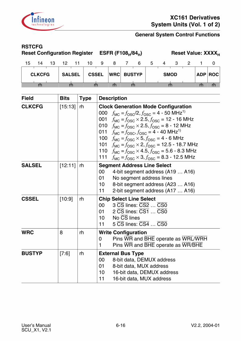
XC161 DerivativesSystem Units (Vol. 1 of 2)
General System Control Functions
RSTCFG Reset Configuration Register ESFR (F108H/84H) Reset Value: XXXXH
15 14 13 12 11 10 9 8 7 6 5 4 3 2 1 0
CLKCFG SALSEL CSSEL WRC BUSTYP SMOD ADP ROC
rh rh rh rh rh rh rh rh
Field Bits Type Description
CLKCFG [15:13] rh Clock Generation Mode Configuration000 fMC = fOSC/2, fOSC = 4 - 50 MHz1)
001 fMC = fOSC × 2.5, fOSC = 12 - 16 MHz010 fMC = fOSC × 2.5, fOSC = 8 - 12 MHz011 fMC = fOSC, fOSC = 4 - 40 MHz1)
100 fMC = fOSC × 5, fOSC = 4 - 6 MHz101 fMC = fOSC × 2, fOSC = 12.5 - 18.7 MHz110 fMC = fOSC × 4.5, fOSC = 5.6 - 8.3 MHz111 fMC = fOSC × 3, fOSC = 8.3 - 12.5 MHz
SALSEL [12:11] rh Segment Address Line Select00 4-bit segment address (A19 … A16)01 No segment address lines10 8-bit segment address (A23 … A16)11 2-bit segment address (A17 … A16)
CSSEL [10:9] rh Chip Select Line Select00 3 CS lines: CS2 … CS001 2 CS lines: CS1 … CS010 No CS lines11 5 CS lines: CS4 … CS0
WRC 8 rh Write Configuration0 Pins WR and BHE operate as WRL/WRH1 Pins WR and BHE operate as WR/BHE
BUSTYP [7:6] rh External Bus Type00 8-bit data, DEMUX address01 8-bit data, MUX address10 16-bit data, DEMUX address11 16-bit data, MUX address
User’s Manual 6-16 V2.2, 2004-01SCU_X1, V2.1
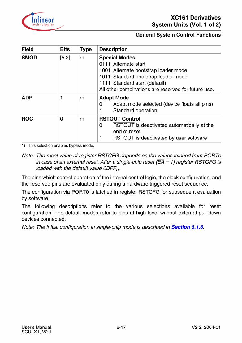
XC161 DerivativesSystem Units (Vol. 1 of 2)
General System Control Functions
Note: The reset value of register RSTCFG depends on the values latched from PORT0in case of an external reset. After a single-chip reset (EA = 1) register RSTCFG isloaded with the default value 0DFFH.
The pins which control operation of the internal control logic, the clock configuration, andthe reserved pins are evaluated only during a hardware triggered reset sequence.
The configuration via PORT0 is latched in register RSTCFG for subsequent evaluationby software.
The following descriptions refer to the various selections available for resetconfiguration. The default modes refer to pins at high level without external pull-downdevices connected.
Note: The initial configuration in single-chip mode is described in Section 6.1.6.
SMOD [5:2] rh Special Modes0111 Alternate start1001 Alternate bootstrap loader mode1011 Standard bootstrap loader mode1111 Standard start (default)All other combinations are reserved for future use.
ADP 1 rh Adapt Mode0 Adapt mode selected (device floats all pins)1 Standard operation
ROC 0 rh RSTOUT Control0 RSTOUT is deactivated automatically at the
end of reset1 RSTOUT is deactivated by user software
1) This selection enables bypass mode.
Field Bits Type Description
User’s Manual 6-17 V2.2, 2004-01SCU_X1, V2.1

XC161 DerivativesSystem Units (Vol. 1 of 2)
General System Control Functions
6.1.5 Hardware Configuration in External Start Mode
For an external start mode reset (indicated by EA = 0) the configuration value (registerRSTCFG) is copied from PORT0. In this case, external circuitry (pull-ups/pull-downs) onPORT0 generate application-specific configuration values.
Clock Generation Control
Pins P0H.7, P0H.6, and P0H.5 (CLKCFG) select the initial clock generation mode duringreset. The oscillator clock either directly feeds the CPU and peripherals (direct drive), isdivided by 2 or is fed to the on-chip PLL which then provides the master clock signal(selectable multiple of the oscillator frequency, i.e. the input frequency). This coarseselection adapts the clock generation unit to the selected oscillator frequency. The userinitialization code may then exactly select the required configuration by updating registerPLLCON.
Default: On-chip PLL is active with a factor of 1:3 (fOSC is multiplied by 3).
Watch the different requirements for frequency of the oscillator input clock for thepossible selections.
Table 6-5 XC161 Clock Generation Modes
(P0H.7-5) (CLKCFG)
Master Clock fMC = fOSC × F
External Clock Input Range1)
1) The external clock input range indicates the operating range of the CGU. If a crystal is connected the oscillatorfrequency range is limited to 4 … 16 MHz.
PLLCON (initial)
Notes
1 1 1 fOSC × 3 8.3 to 12.5 MHz 6B03H Default configuration
1 1 0 fOSC × 4.5 5.6 to 8.3 MHz 7103H –
1 0 1 fOSC × 2 12.5 to 18.7 MHz 6F13H –
1 0 0 fOSC × 5 4 to 6 MHz 7804H –
0 1 1 fOSC × 1 1 to 40 MHz 2780H Direct drive
0 1 0 fOSC × 2.5 8 to 12 MHz 7814H –
0 0 1 fOSC × 2.5 12 to 16 MHz 7854H –
0 0 0 fOSC/2 1 to 50 MHz 2790H 2:1 prescaler
User’s Manual 6-18 V2.2, 2004-01SCU_X1, V2.1
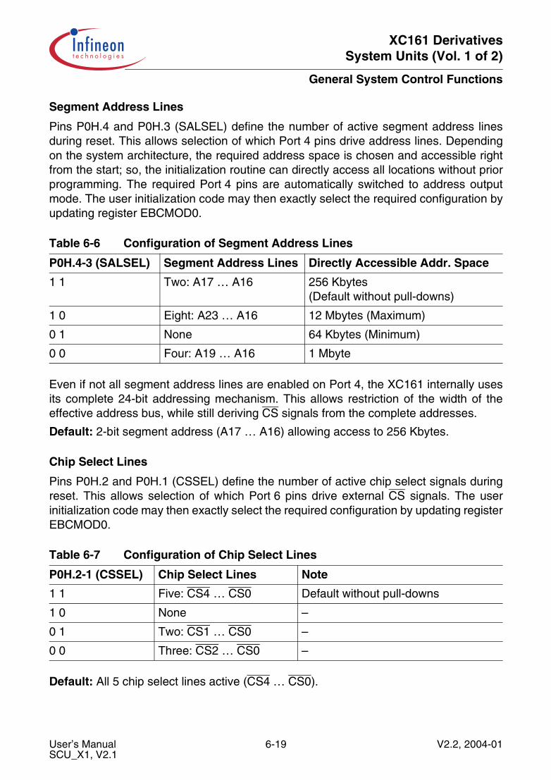
XC161 DerivativesSystem Units (Vol. 1 of 2)
General System Control Functions
Segment Address Lines
Pins P0H.4 and P0H.3 (SALSEL) define the number of active segment address linesduring reset. This allows selection of which Port 4 pins drive address lines. Dependingon the system architecture, the required address space is chosen and accessible rightfrom the start; so, the initialization routine can directly access all locations without priorprogramming. The required Port 4 pins are automatically switched to address outputmode. The user initialization code may then exactly select the required configuration byupdating register EBCMOD0.
Even if not all segment address lines are enabled on Port 4, the XC161 internally usesits complete 24-bit addressing mechanism. This allows restriction of the width of theeffective address bus, while still deriving CS signals from the complete addresses.
Default: 2-bit segment address (A17 … A16) allowing access to 256 Kbytes.
Chip Select Lines
Pins P0H.2 and P0H.1 (CSSEL) define the number of active chip select signals duringreset. This allows selection of which Port 6 pins drive external CS signals. The userinitialization code may then exactly select the required configuration by updating registerEBCMOD0.
Default: All 5 chip select lines active (CS4 … CS0).
Table 6-6 Configuration of Segment Address Lines
P0H.4-3 (SALSEL) Segment Address Lines Directly Accessible Addr. Space
1 1 Two: A17 … A16 256 Kbytes(Default without pull-downs)
1 0 Eight: A23 … A16 12 Mbytes (Maximum)
0 1 None 64 Kbytes (Minimum)
0 0 Four: A19 … A16 1 Mbyte
Table 6-7 Configuration of Chip Select Lines
P0H.2-1 (CSSEL) Chip Select Lines Note
1 1 Five: CS4 … CS0 Default without pull-downs
1 0 None –
0 1 Two: CS1 … CS0 –
0 0 Three: CS2 … CS0 –
User’s Manual 6-19 V2.2, 2004-01SCU_X1, V2.1
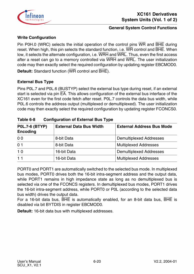
XC161 DerivativesSystem Units (Vol. 1 of 2)
General System Control Functions
Write Configuration
Pin P0H.0 (WRC) selects the initial operation of the control pins WR and BHE duringreset. When high, this pin selects the standard function, i.e. WR control and BHE. Whenlow, it selects the alternate configuration, i.e. WRH and WRL. Thus, even the first accessafter a reset can go to a memory controlled via WRH and WRL. The user initializationcode may then exactly select the required configuration by updating register EBCMOD0.
Default: Standard function (WR control and BHE).
External Bus Type
Pins P0L.7 and P0L.6 (BUSTYP) select the external bus type during reset, if an externalstart is selected via pin EA. This allows configuration of the external bus interface of theXC161 even for the first code fetch after reset. P0L.7 controls the data bus width, whileP0L.6 controls the address output (multiplexed or demultiplexed). The user initializationcode may then exactly select the required configuration by updating register FCONCS0.
PORT0 and PORT1 are automatically switched to the selected bus mode. In multiplexedbus modes, PORT0 drives both the 16-bit intra-segment address and the output data,while PORT1 remains in high impedance state as long as no demultiplexed bus isselected via one of the FCONCS registers. In demultiplexed bus modes, PORT1 drivesthe 16-bit intra-segment address, while PORT0 or P0L (according to the selected databus width) drives the output data.For a 16-bit data bus, BHE is automatically enabled, for an 8-bit data bus, BHE isdisabled via bit BYTDIS in register EBCMOD0.
Default: 16-bit data bus with multiplexed addresses.
Table 6-8 Configuration of External Bus Type
P0L.7-6 (BTYP) Encoding
External Data Bus Width External Address Bus Mode
0 0 8-bit Data Demultiplexed Addresses
0 1 8-bit Data Multiplexed Addresses
1 0 16-bit Data Demultiplexed Addresses
1 1 16-bit Data Multiplexed Addresses
User’s Manual 6-20 V2.2, 2004-01SCU_X1, V2.1
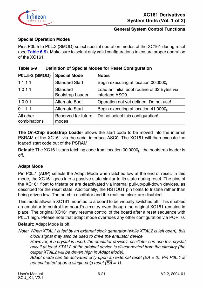
XC161 DerivativesSystem Units (Vol. 1 of 2)
General System Control Functions
Special Operation Modes
Pins P0L.5 to P0L.2 (SMOD) select special operation modes of the XC161 during reset(see Table 6-9). Make sure to select only valid configurations to ensure proper operationof the XC161.
The On-Chip Bootstrap Loader allows the start code to be moved into the internalPSRAM of the XC161 via the serial interface ASC0. The XC161 will then execute theloaded start code out of the PSRAM.
Default: The XC161 starts fetching code from location 00’0000H, the bootstrap loader isoff.
Adapt Mode
Pin P0L.1 (ADP) selects the Adapt Mode when latched low at the end of reset. In thismode, the XC161 goes into a passive state similar to its state during reset. The pins ofthe XC161 float to tristate or are deactivated via internal pull-up/pull-down devices, asdescribed for the reset state. Additionally, the RSTOUT pin floats to tristate rather thanbeing driven low. The on-chip oscillator and the realtime clock are disabled.
This mode allows a XC161 mounted to a board to be virtually switched off. This enablesan emulator to control the board’s circuitry even though the original XC161 remains inplace. The original XC161 may resume control of the board after a reset sequence withP0L.1 high. Please note that adapt mode overrides any other configuration via PORT0.
Default: Adapt Mode is off.
Note: When XTAL1 is fed by an external clock generator (while XTAL2 is left open), thisclock signal may also be used to drive the emulator device.However, if a crystal is used, the emulator device’s oscillator can use this crystalonly if at least XTAL2 of the original device is disconnected from the circuitry (theoutput XTAL2 will be driven high in Adapt Mode).Adapt mode can be activated only upon an external reset (EA = 0). Pin P0L.1 isnot evaluated upon a single-chip reset (EA = 1).
Table 6-9 Definition of Special Modes for Reset Configuration
P0L.5-2 (SMOD) Special Mode Notes
1 1 1 1 Standard Start Begin executing at location 00’0000H
1 0 1 1 StandardBootstrap Loader
Load an initial boot routine of 32 Bytes via interface ASC0.
1 0 0 1 Alternate Boot Operation not yet defined. Do not use!
0 1 1 1 Alternate Start Begin executing at location 41’0000H
All other combinations
Reserved for future modes
Do not select this configuration!
User’s Manual 6-21 V2.2, 2004-01SCU_X1, V2.1
XC161 DerivativesSystem Units (Vol. 1 of 2)
General System Control Functions
RSTOUT Control
Pin P0L.0 (ROC) selects the initial deactivation mode of pin RSTOUT after reset. Whenhigh, this pin selects the standard function, i.e. RSTOUT is deactivated by user software(or at the very latest after the execution of EINIT). When low, it selects immediatedeactivation, i.e. RSTOUT is deactivated automatically at the end of the internal resetstate. Thus, even the first access after a reset can go to a memory controlled by theRSTOUT signal (e.g. an external Flash). The user initialization code may select therequired configuration for each subsequent reset.
Default: Standard function (RSTOUT deactivated by user software).
In addition, the RSTOUT signal can be disabled, so the pin can be used for generalpurpose IO. This is selected by pulling pin WR low during a single-chip-mode reset withEA = 1. The user initialization code may select the required configuration by updating bitRORMV in register RSTCON.
Oscillator Watchdog Control
The on-chip oscillator watchdog (OWD) may be disabled via hardware by (externally)pulling the RD line low upon a reset (see Table 6-4). This option is valid for bypassoperation. The user initialization code may select the required configuration by updatingregister PLLCON.
Default: Oscillator watchdog is active (PLL is on).
Note: If direct drive or prescaler operation is selected as basic clock generation mode(see above) the PLL is switched off whenever bit OWDDIS is set (via software orvia hardware configuration).
User’s Manual 6-22 V2.2, 2004-01SCU_X1, V2.1
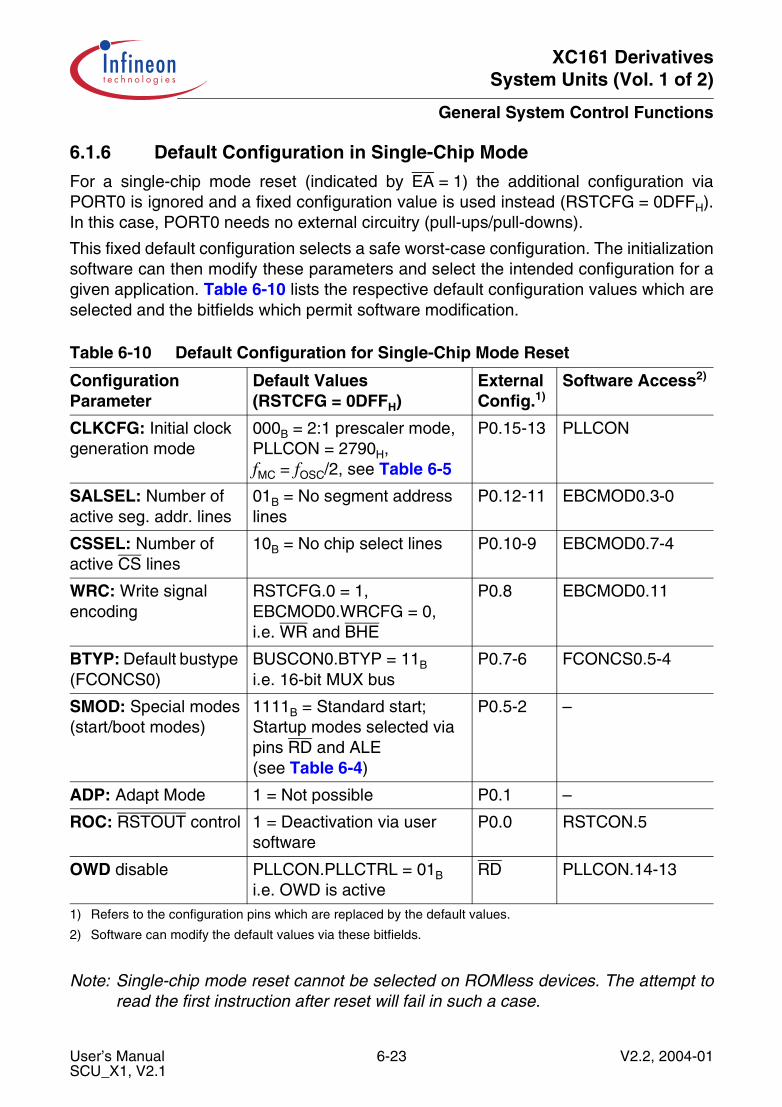
XC161 DerivativesSystem Units (Vol. 1 of 2)
General System Control Functions
6.1.6 Default Configuration in Single-Chip Mode
For a single-chip mode reset (indicated by EA = 1) the additional configuration viaPORT0 is ignored and a fixed configuration value is used instead (RSTCFG = 0DFFH).In this case, PORT0 needs no external circuitry (pull-ups/pull-downs).
This fixed default configuration selects a safe worst-case configuration. The initializationsoftware can then modify these parameters and select the intended configuration for agiven application. Table 6-10 lists the respective default configuration values which areselected and the bitfields which permit software modification.
Note: Single-chip mode reset cannot be selected on ROMless devices. The attempt toread the first instruction after reset will fail in such a case.
Table 6-10 Default Configuration for Single-Chip Mode Reset
Configuration Parameter
Default Values(RSTCFG = 0DFFH)
External Config.1)
1) Refers to the configuration pins which are replaced by the default values.
Software Access2)
2) Software can modify the default values via these bitfields.
CLKCFG: Initial clock generation mode
000B = 2:1 prescaler mode, PLLCON = 2790H,fMC = fOSC/2, see Table 6-5
P0.15-13 PLLCON
SALSEL: Number of active seg. addr. lines
01B = No segment address lines
P0.12-11 EBCMOD0.3-0
CSSEL: Number of active CS lines
10B = No chip select lines P0.10-9 EBCMOD0.7-4
WRC: Write signal encoding
RSTCFG.0 = 1, EBCMOD0.WRCFG = 0,i.e. WR and BHE
P0.8 EBCMOD0.11
BTYP: Default bustype (FCONCS0)
BUSCON0.BTYP = 11B
i.e. 16-bit MUX busP0.7-6 FCONCS0.5-4
SMOD: Special modes(start/boot modes)
1111B = Standard start; Startup modes selected via pins RD and ALE(see Table 6-4)
P0.5-2 –
ADP: Adapt Mode 1 = Not possible P0.1 –
ROC: RSTOUT control 1 = Deactivation via user software
P0.0 RSTCON.5
OWD disable PLLCON.PLLCTRL = 01Bi.e. OWD is active
RD PLLCON.14-13
User’s Manual 6-23 V2.2, 2004-01SCU_X1, V2.1

XC161 DerivativesSystem Units (Vol. 1 of 2)
General System Control Functions
6.1.7 Reset Behavior Control
The reset behavior is controlled by a set of control/status registers. The statusinformation can be used by the initialization code to execute different actions dependingon the reset source.
The reset control register RSTCON is used by the application to program the basic resetbehavior like length of internal reset phase and behavior of the reset output pin RSTOUT(see Figure 6-3).
RSTCON Reset Control Register mem (F1E0H/--) Reset Value: 0000H
1)
1) The reset value is only valid for a hardware reset.
15 14 13 12 11 10 9 8 7 6 5 4 3 2 1 0
- - - - - - - -RODIS
ROCON
ROCOFF
RORMV
- RSTLEN
- - - - - - - - rwh rw rwh rwh - rw
Field Bits Type Description
RODIS 7 rwh RSTOUT Disable Control0 RSTOUT is controlled by other mechanisms1 RSTOUT is deactivated
Note: Bit RODIS is cleared if automatic enabling isselected (ROCON = 0), bit RODIS is set ifautomatic disabling is selected (ROCOFF = 1).
ROCON 6 rw RSTOUT Control Switching ON0 RSTOUT is activated upon any reset1 RSTOUT is only activated upon a hardware
reset
ROCOFF 5 rwh RSTOUT Control Switching Off0 RSTOUT is deactivated by user software1 RSTOUT is automatically deactivated at the
end of reset (RODIS is set)
Note: Automatic deactivation can also be requestedby hardware configuration (ROCOFF is set ifRSTCFG.ROC = 0).
RORMV 4 rwh RSTOUT Remove Control0 Pin delivers the RSTOUT signal (default)1 Pin operates as P20.12 (gen. purpose IO)
(selected if EA = 1 and WR = 0 during reset)
User’s Manual 6-24 V2.2, 2004-01SCU_X1, V2.1
XC161 DerivativesSystem Units (Vol. 1 of 2)
General System Control Functions
Note: RSTCON is protected by the register security mechanism (see Section 6.3.6).RSTCON can only be accessed via its long (mem) address.
RSTLEN [2:0] rw Reset Length Control1)
The duration of the next internal reset phase istRST = tWDT × 2(RSTLEN+1).000 2 tWDT: default duration after hardware reset: :111 256 tWDT: maximum duration
1) RSTLEN is always valid for the next reset sequence. An initial power up reset, however, is controlled byexternal hardware and is expected to last considerably longer than any configurable reset sequence.
Field Bits Type Description
User’s Manual 6-25 V2.2, 2004-01SCU_X1, V2.1
XC161 DerivativesSystem Units (Vol. 1 of 2)
General System Control Functions
6.2 Clock Generation
All activities of the XC161’s controller hardware and its on-chip peripherals are controlledby clock signals which are generated by the Clock Generation Unit (CGU).
This reference clock is generated in three stages:
Oscillators
The on-chip Pierce oscillators (main oscillator and auxiliary oscillator) can either run withan external crystal and appropriate oscillator circuitry or they can be driven by anexternal oscillator or another clock source.
Clock Generation and Frequency Control
The input clock signal of the main oscillator feeds the controller hardware:
• directly, divided by a programmable prescaler factor (1 … 60), either providingphase-coupled operation (factor = 1) or operating the device at low frequencies toreduce power consumption (factor >> 1)
• via an on-chip Phase Locked Loop (PLL) providing maximum performance on lowinput frequency
Clock Distribution
The clock signals are distributed via separate clock drivers which feed the CPU itself andgroups of peripheral modules. Certain sections of the device can be supplied with aprescaled clock signal.
Note: The RTC is fed with the auxiliary oscillator clock or with the prescaled mainoscillator clock via a separate clock driver, so it is not affected by the clock controlfunctions.
User’s Manual 6-26 V2.2, 2004-01SCU_X1, V2.1

XC161 DerivativesSystem Units (Vol. 1 of 2)
General System Control Functions
6.2.1 Oscillators
The main oscillator of the XC161 is a power optimized Pierce oscillator providing aninverter and a feedback element. Pins XTAL1 and XTAL2 connect the inverter to theexternal crystal. The standard external oscillator circuitry (see Figure 6-4) comprises thecrystal, two low end capacitors and series resistor (Rx2) to limit the current through thecrystal. A test resistor (RQ) may be temporarily inserted to measure the oscillationallowance (negative resistance) of the oscillator circuitry.
Figure 6-4 External (Main) Oscillator Circuitry
The on-chip oscillator is optimized for an input frequency range of 4 to 16 MHz.
An external clock signal (e.g. from an external oscillator or from a master device) maybe fed to the input XTAL1. The Pierce oscillator then is not required to support theoscillation itself but is rather driven by the input signal. In this case the input frequencyrange may be 0 to 50 MHz (please note that the maximum applicable input frequency islimited by the device’s maximum clock frequency).
Note: Oscillator measurement within the final target system is strongly recommendedto verify the input amplitude and to determine the actual oscillation allowance(margin or negative resistance) for the oscillator-crystal system.The measurement technique, examples for evaluated systems, andrecommendations are provided in a specific application note about oscillators(available via your representative or www).
The main oscillator is automatically switched off during Power-Down mode and Sleepmode, unless it provides the count clock for the RTC and the RTC remains on. Switchingoff the main oscillator is useful to further reduce the power consumption during phaseswhere only minimum system life functions must be maintained.
mc_osc0100_extcirc.vsd
XTAL1 XTAL2
Rx2RQ
User’s Manual 6-27 V2.2, 2004-01SCU_X1, V2.1
XC161 DerivativesSystem Units (Vol. 1 of 2)
General System Control Functions
Main Oscillator Gain Reduction
The main oscillator starts with a high drive level (gain) during and after a hardware resetto ensure safe startup behavior in the beginning (force the crystal oscillation). Thebeginning of the crystal oscillation is indicated by bit OSCLOCK = 1. When a stableoscillation has been reached after oscillator startup (amplitude more than 90% of itsmaximum), the gain of the main oscillator can be reduced. This reduces the oscillator’spower consumption which is especially important in power reduction modes.
This gain reduction is induced by software and so is transparent in existing software. Theoscillator gain is reduced by setting bit OSCGRED in register SYSCON0 (seeSection 6.3). Because the oscillator amplitude is not measured directly, a delay ofapproximately 215 oscillator clock cycles is required before enabling the gain reduction.
Attention: The oscillator gain must not be reduced before approximately 215
oscillator clock cycles after oscillator startup (startup can bedetermined by OSCLOCK = 1). After this delay the oscillation hasreached more than 90% of its maximum amplitude with an optimizedoscillator circuitry.If the main oscillator is switched off during sleep mode, the oscillatorgain reduction must be removed (OSCGRED = 0) before entering sleepmode. This ensures a safe oscillator startup after wake-up.
User’s Manual 6-28 V2.2, 2004-01SCU_X1, V2.1

XC161 DerivativesSystem Units (Vol. 1 of 2)
General System Control Functions
The auxiliary oscillator of the XC161 is a Pierce oscillator which is highly optimized foroperation at a frequency of approximately 32 kHz. This narrow band optimization allowsan extremely low power consumption of the auxiliary oscillator. Pins XTAL3 and XTAL4connect the inverter to the external crystal. The recommendations given for the mainoscillator apply accordingly.
Note: When the auxiliary oscillator is not used, i.e. is not connected to an external clocksignal or to a crystal, its input XTAL3 should be connected to GND.
Figure 6-5 External (Auxiliary) Oscillator Circuitry
The auxiliary oscillator is automatically switched off while it provides the count clock forthe RTC and the RTC is not running.
Note: Oscillator measurement within the final target system is strongly recommendedto verify the input amplitude and to determine the actual oscillation allowance(margin or negative resistance) for the oscillator-crystal system.The measurement technique, examples for evaluated systems, andrecommendations are provided in a specific application note about oscillators(available via your representative or www).
mc_osc0101_extaux.vsd
XTAL3 XTAL4
RQ
User’s Manual 6-29 V2.2, 2004-01SCU_X1, V2.1
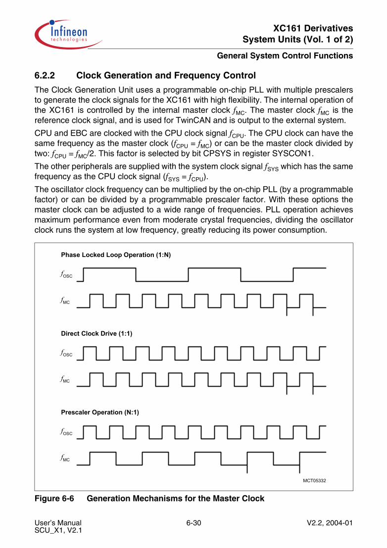
XC161 DerivativesSystem Units (Vol. 1 of 2)
General System Control Functions
6.2.2 Clock Generation and Frequency Control
The Clock Generation Unit uses a programmable on-chip PLL with multiple prescalersto generate the clock signals for the XC161 with high flexibility. The internal operation ofthe XC161 is controlled by the internal master clock fMC. The master clock fMC is thereference clock signal, and is used for TwinCAN and is output to the external system.
CPU and EBC are clocked with the CPU clock signal fCPU. The CPU clock can have thesame frequency as the master clock (fCPU = fMC) or can be the master clock divided bytwo: fCPU = fMC/2. This factor is selected by bit CPSYS in register SYSCON1.
The other peripherals are supplied with the system clock signal fSYS which has the samefrequency as the CPU clock signal (fSYS = fCPU).
The oscillator clock frequency can be multiplied by the on-chip PLL (by a programmablefactor) or can be divided by a programmable prescaler factor. With these options themaster clock can be adjusted to a wide range of frequencies. PLL operation achievesmaximum performance even from moderate crystal frequencies, dividing the oscillatorclock runs the system at low frequency, greatly reducing its power consumption.
Figure 6-6 Generation Mechanisms for the Master Clock
Phase Locked Loop Operation (1:N)
fOSC
fMC
Direct Clock Drive (1:1)
fOSC
fMC
Prescaler Operation (N:1)
fOSC
fMC
MCT05332
User’s Manual 6-30 V2.2, 2004-01SCU_X1, V2.1
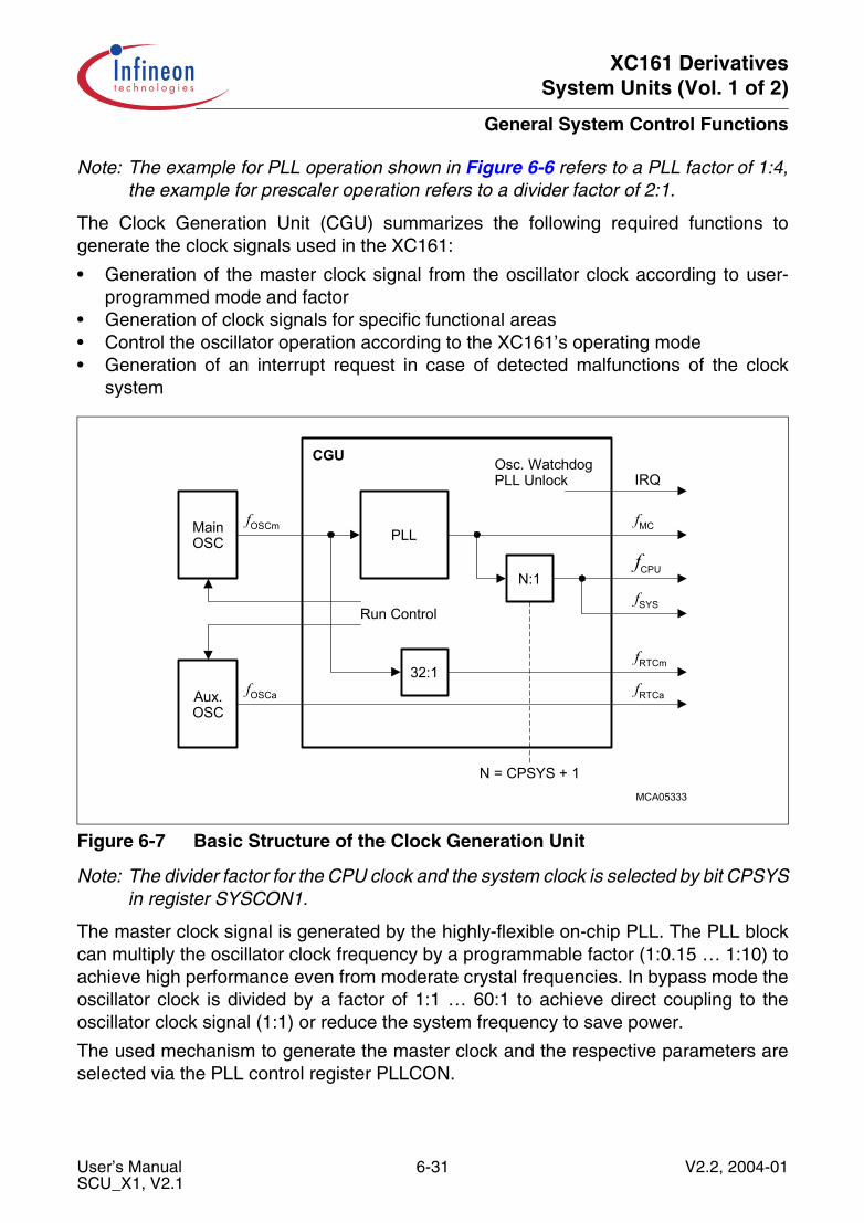
XC161 DerivativesSystem Units (Vol. 1 of 2)
General System Control Functions
Note: The example for PLL operation shown in Figure 6-6 refers to a PLL factor of 1:4,the example for prescaler operation refers to a divider factor of 2:1.
The Clock Generation Unit (CGU) summarizes the following required functions togenerate the clock signals used in the XC161:
• Generation of the master clock signal from the oscillator clock according to user-programmed mode and factor
• Generation of clock signals for specific functional areas• Control the oscillator operation according to the XC161’s operating mode• Generation of an interrupt request in case of detected malfunctions of the clock
system
Figure 6-7 Basic Structure of the Clock Generation Unit
Note: The divider factor for the CPU clock and the system clock is selected by bit CPSYSin register SYSCON1.
The master clock signal is generated by the highly-flexible on-chip PLL. The PLL blockcan multiply the oscillator clock frequency by a programmable factor (1:0.15 … 1:10) toachieve high performance even from moderate crystal frequencies. In bypass mode theoscillator clock is divided by a factor of 1:1 … 60:1 to achieve direct coupling to theoscillator clock signal (1:1) or reduce the system frequency to save power.
The used mechanism to generate the master clock and the respective parameters areselected via the PLL control register PLLCON.
CGU
MainOSC
fOSCm
Aux.OSC
fOSCa
PLL
Run Control
32:1
N:1
Osc. WatchdogPLL Unlock
fMC
fCPU
fSYS
fRTCm
fRTCa
IRQ
N = CPSYS + 1MCA05333
User’s Manual 6-31 V2.2, 2004-01SCU_X1, V2.1
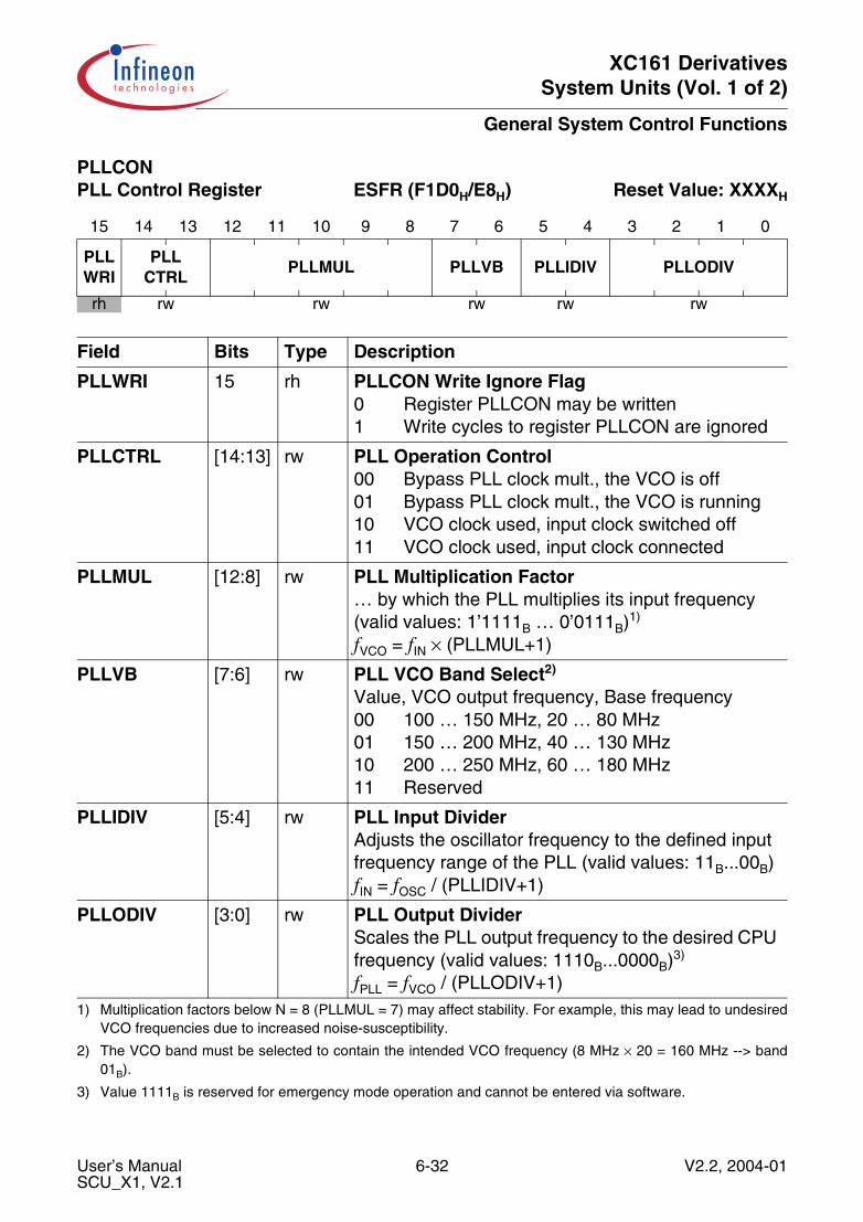
XC161 DerivativesSystem Units (Vol. 1 of 2)
General System Control Functions
PLLCON PLL Control Register ESFR (F1D0H/E8H) Reset Value: XXXXH
15 14 13 12 11 10 9 8 7 6 5 4 3 2 1 0
PLLWRI
PLLCTRL
PLLMUL PLLVB PLLIDIV PLLODIV
rh rw rw rw rw rw
Field Bits Type Description
PLLWRI 15 rh PLLCON Write Ignore Flag0 Register PLLCON may be written1 Write cycles to register PLLCON are ignored
PLLCTRL [14:13] rw PLL Operation Control00 Bypass PLL clock mult., the VCO is off01 Bypass PLL clock mult., the VCO is running10 VCO clock used, input clock switched off11 VCO clock used, input clock connected
PLLMUL [12:8] rw PLL Multiplication Factor… by which the PLL multiplies its input frequency (valid values: 1’1111B … 0’0111B)1)
fVCO = fIN × (PLLMUL+1)
PLLVB [7:6] rw PLL VCO Band Select2)
Value, VCO output frequency, Base frequency00 100 … 150 MHz, 20 … 80 MHz01 150 … 200 MHz, 40 … 130 MHz10 200 … 250 MHz, 60 … 180 MHz11 Reserved
PLLIDIV [5:4] rw PLL Input DividerAdjusts the oscillator frequency to the defined input frequency range of the PLL (valid values: 11B...00B)fIN = fOSC / (PLLIDIV+1)
PLLODIV [3:0] rw PLL Output DividerScales the PLL output frequency to the desired CPU frequency (valid values: 1110B...0000B)3)
fPLL = fVCO / (PLLODIV+1)1) Multiplication factors below N = 8 (PLLMUL = 7) may affect stability. For example, this may lead to undesired
VCO frequencies due to increased noise-susceptibility.
2) The VCO band must be selected to contain the intended VCO frequency (8 MHz × 20 = 160 MHz --> band01B).
3) Value 1111B is reserved for emergency mode operation and cannot be entered via software.
User’s Manual 6-32 V2.2, 2004-01SCU_X1, V2.1
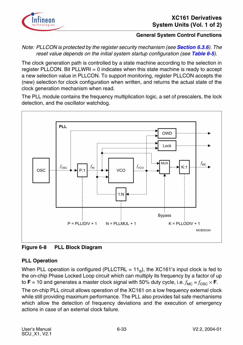
XC161 DerivativesSystem Units (Vol. 1 of 2)
General System Control Functions
Note: PLLCON is protected by the register security mechanism (see Section 6.3.6). Thereset value depends on the initial system startup configuration (see Table 6-5).
The clock generation path is controlled by a state machine according to the selection inregister PLLCON. Bit PLLWRI = 0 indicates when this state machine is ready to accepta new selection value in PLLCON. To support monitoring, register PLLCON accepts the(new) selection for clock configuration when written, and returns the actual state of theclock generation mechanism when read.
The PLL module contains the frequency multiplication logic, a set of prescalers, the lockdetection, and the oscillator watchdog.
Figure 6-8 PLL Block Diagram
PLL Operation
When PLL operation is configured (PLLCTRL = 11B), the XC161’s input clock is fed tothe on-chip Phase Locked Loop circuit which can multiply its frequency by a factor of upto F = 10 and generates a master clock signal with 50% duty cycle, i.e. fMC = fOSC × F.
The on-chip PLL circuit allows operation of the XC161 on a low frequency external clockwhile still providing maximum performance. The PLL also provides fail safe mechanismswhich allow the detection of frequency deviations and the execution of emergencyactions in case of an external clock failure.
MCB05334
PLL
OSC
fMC
K = PLLODIV + 1
fINfOSCP:1
K:1
OWD
Lock
fVCOVCO
1:N
Bypass
N = PLLMUL + 1P = PLLIDIV + 1
MUX
User’s Manual 6-33 V2.2, 2004-01SCU_X1, V2.1
XC161 DerivativesSystem Units (Vol. 1 of 2)
General System Control Functions
When the PLL detects a missing input clock signal it generates an interrupt request. Thiswarning interrupt indicates that the PLL frequency is no longer locked, i.e. no longerrelated to the oscillator frequency. This occurs when the input clock is unstable andespecially when the input clock fails completely, such as due to a broken crystal. In thiscase the synchronization mechanism will reduce the PLL output frequency down to thePLL’s base frequency (depending on the VCO band selected by bitfield PLLVB) andselect the safety output divider factor K = 16. The base frequency is still generated andallows the CPU to execute emergency actions in case of a loss of the external clock. Themaster clock in this emergency case is, therefore, fMCe = fVCObase/16.
Note: During a hardware reset the lowest VCO band is selected together with factor 16.
On power-up the PLL provides a stable clock signal, even if there is no external clocksignal (in this case the PLL will run on its base frequency). The PLL starts synchronizingwith the external clock signal as soon as it is available. After stable oscillations of theexternal clock within the specified frequency range the PLL locks to the external clock.This means the PLL will be synchronous with this clock at a frequency of F × fOSC.
The PLL circuit constantly synchronizes the master clock to the input clock. Thissynchronization is done smoothly, i.e. the master clock frequency does not changeabruptly. Due to the fact that the external frequency is 1/Fth of the PLL output frequencythe output frequency may be slightly higher or lower than the desired frequency. Theslight variation causes a jitter of fMC which also affects the duration of individual masterclock periods. This jitter is irrelevant for longer time periods. For short periods (1 … 4CPU clock cycles) it remains below 9%.
The clock signal passes through several blocks (see Figure 6-8). The total clockmultiplication factor F results from the input divider (P:1), the multiplication factor (1:N),and the output divider (K:1), so F = PLLMUL+1 / ((PLLIDIV+1) × (PLLODIV+1)).
The input clock divider adjusts the oscillator clock frequency to the input frequencyrange for which the PLL is optimized (fIN = fOSC / (PLLIDIV+1) = 4 … 35 MHz).
The PLL core multiplies the adjusted input frequency within the selected VCO band bya selectable factor (fVCO = fIN × (PLLMUL+1)). The valid VCO band (PLLVB) must beselected according to the intended VCO frequency.
Note: This PLL core can be bypassed, e.g. while the PLL is locking to a given factor, toensure a proper CPU clock signal, or if the PLL is not used for clock generation.
The output clock divider scales the VCO’s output frequency by a selectable factor togenerate the master clock signal (fMC = fVCO / (PLLODIV+1)). Adjusting this factor maybe used to control the operating frequency of the XC161 without having to reprogram thePLL core itself.
Figure 6-9 summarizes the subsequent steps the master clock generation.
The maximum multiplication factor Fmax is employed when the highest possible masterclock frequency (40 MHz) shall be generated from the lowest possible input clockfrequency (4 MHz). Therefore, the maximum usable factor is Fmax = 10.
User’s Manual 6-34 V2.2, 2004-01SCU_X1, V2.1
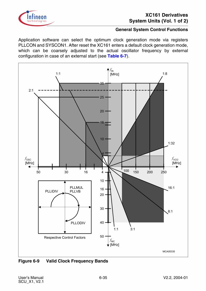
XC161 DerivativesSystem Units (Vol. 1 of 2)
General System Control Functions
Application software can select the optimum clock generation mode via registersPLLCON and SYSCON1. After reset the XC161 enters a default clock generation mode,which can be coarsely adjusted to the actual oscillator frequency by externalconfiguration in case of an external start (see Table 6-7).
Figure 6-9 Valid Clock Frequency Bands
MCA05335
fMC[MHz]
50 30 16 4 150
4
10
16
20
25
35
10
1620
30
40
50
1:1
2:1
1:8
1:32
200 250
1:1 3:1
8:1
16:1
fIN[MHz]
fOSC[MHz]
fVCO[MHz]
Respective Control Factors
PLLIDIVPLLMULPLLVB
PLLODIV
100
User’s Manual 6-35 V2.2, 2004-01SCU_X1, V2.1
XC161 DerivativesSystem Units (Vol. 1 of 2)
General System Control Functions
Bypass Operation
When bypass operation is configured (PLLCTRL = 0XB) the clock signal does not passthrough the PLL core and the master clock is derived from the internal oscillator (inputclock signal XTAL1) through the input- and output-prescalers:
fMC = fOSC / ((PLLIDIV+1) × (PLLODIV+1)).
If both divider factors are selected as 1 (PLLIDIV = PLLODIV = 0) the frequency of fMCdirectly follows the frequency of fOSC so the high and low time of fMC is defined by the dutycycle of the input clock fOSC.
The lowest master clock frequency is achieved by selecting the maximum values for bothdivider factors: fMCmin = fOSC / ((3+1) × (14+1)) = fOSC / 60.
User’s Manual 6-36 V2.2, 2004-01SCU_X1, V2.1
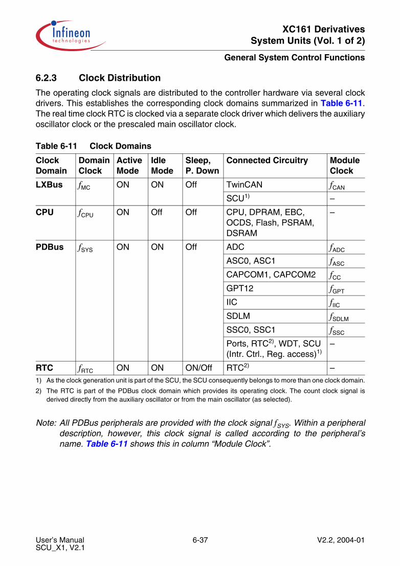
XC161 DerivativesSystem Units (Vol. 1 of 2)
General System Control Functions
6.2.3 Clock Distribution
The operating clock signals are distributed to the controller hardware via several clockdrivers. This establishes the corresponding clock domains summarized in Table 6-11.The real time clock RTC is clocked via a separate clock driver which delivers the auxiliaryoscillator clock or the prescaled main oscillator clock.
Note: All PDBus peripherals are provided with the clock signal fSYS. Within a peripheraldescription, however, this clock signal is called according to the peripheral’sname. Table 6-11 shows this in column “Module Clock”.
Table 6-11 Clock Domains
Clock Domain
Domain Clock
Active Mode
Idle Mode
Sleep,P. Down
Connected Circuitry Module Clock
LXBus fMC ON ON Off TwinCAN fCAN
SCU1)
1) As the clock generation unit is part of the SCU, the SCU consequently belongs to more than one clock domain.
–
CPU fCPU ON Off Off CPU, DPRAM, EBC, OCDS, Flash, PSRAM, DSRAM
–
PDBus fSYS ON ON Off ADC fADC
ASC0, ASC1 fASC
CAPCOM1, CAPCOM2 fCC
GPT12 fGPT
IIC fIIC
SDLM fSDLM
SSC0, SSC1 fSSC
Ports, RTC2), WDT, SCU (Intr. Ctrl., Reg. access)1)
2) The RTC is part of the PDBus clock domain which provides its operating clock. The count clock signal isderived directly from the auxiliary oscillator or from the main oscillator (as selected).
–
RTC fRTC ON ON ON/Off RTC2) –
User’s Manual 6-37 V2.2, 2004-01SCU_X1, V2.1
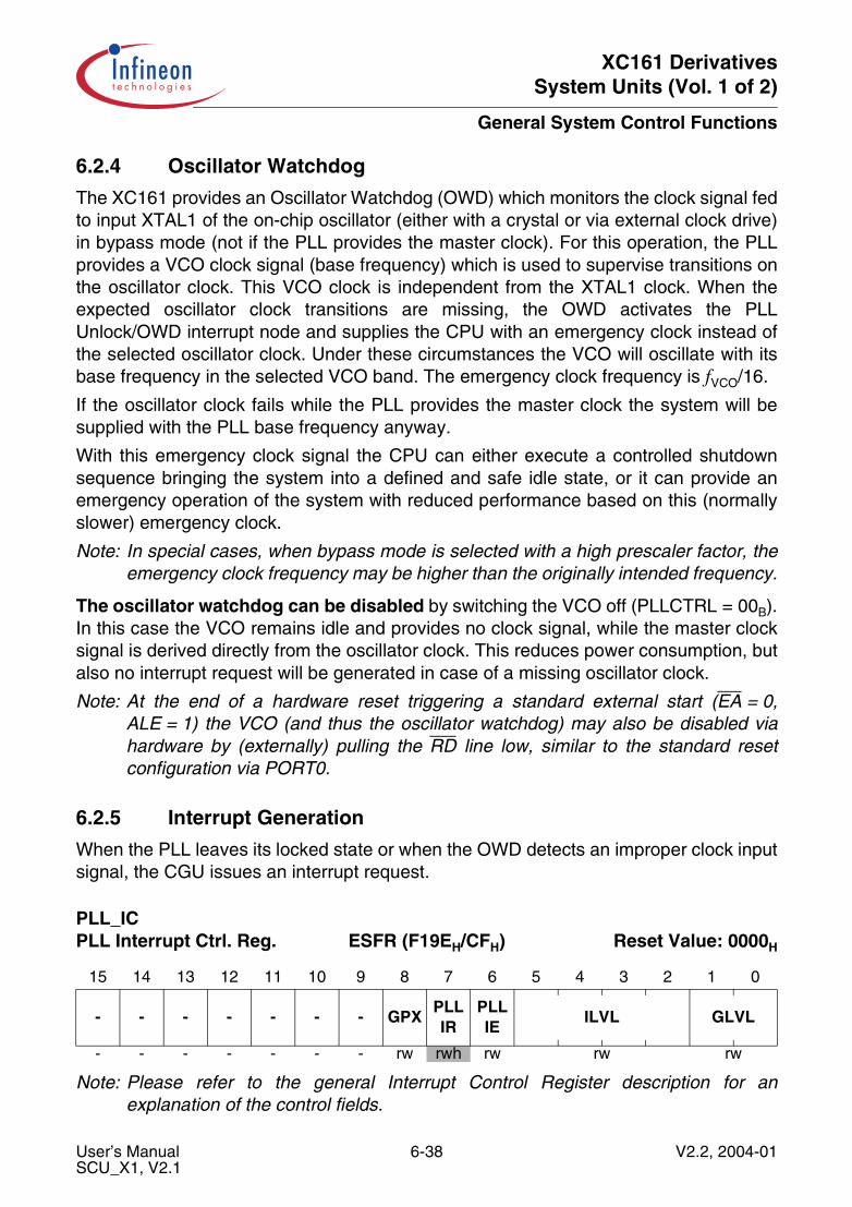
XC161 DerivativesSystem Units (Vol. 1 of 2)
General System Control Functions
6.2.4 Oscillator Watchdog
The XC161 provides an Oscillator Watchdog (OWD) which monitors the clock signal fedto input XTAL1 of the on-chip oscillator (either with a crystal or via external clock drive)in bypass mode (not if the PLL provides the master clock). For this operation, the PLLprovides a VCO clock signal (base frequency) which is used to supervise transitions onthe oscillator clock. This VCO clock is independent from the XTAL1 clock. When theexpected oscillator clock transitions are missing, the OWD activates the PLLUnlock/OWD interrupt node and supplies the CPU with an emergency clock instead ofthe selected oscillator clock. Under these circumstances the VCO will oscillate with itsbase frequency in the selected VCO band. The emergency clock frequency is fVCO/16.
If the oscillator clock fails while the PLL provides the master clock the system will besupplied with the PLL base frequency anyway.
With this emergency clock signal the CPU can either execute a controlled shutdownsequence bringing the system into a defined and safe idle state, or it can provide anemergency operation of the system with reduced performance based on this (normallyslower) emergency clock.
Note: In special cases, when bypass mode is selected with a high prescaler factor, theemergency clock frequency may be higher than the originally intended frequency.
The oscillator watchdog can be disabled by switching the VCO off (PLLCTRL = 00B).In this case the VCO remains idle and provides no clock signal, while the master clocksignal is derived directly from the oscillator clock. This reduces power consumption, butalso no interrupt request will be generated in case of a missing oscillator clock.
Note: At the end of a hardware reset triggering a standard external start (EA = 0,ALE = 1) the VCO (and thus the oscillator watchdog) may also be disabled viahardware by (externally) pulling the RD line low, similar to the standard resetconfiguration via PORT0.
6.2.5 Interrupt Generation
When the PLL leaves its locked state or when the OWD detects an improper clock inputsignal, the CGU issues an interrupt request.
Note: Please refer to the general Interrupt Control Register description for anexplanation of the control fields.
PLL_IC PLL Interrupt Ctrl. Reg. ESFR (F19EH/CFH) Reset Value: 0000H
15 14 13 12 11 10 9 8 7 6 5 4 3 2 1 0
- - - - - - - GPXPLLIR
PLLIE
ILVL GLVL
- - - - - - - rw rwh rw rw rw
User’s Manual 6-38 V2.2, 2004-01SCU_X1, V2.1

XC161 DerivativesSystem Units (Vol. 1 of 2)
General System Control Functions
6.2.6 Generation of an External Clock Signal
The external circuitry can be provided with a clock signal either to operate externalperipherals or for reference purposes. Two types can be selected:
• CLKOUT directly outputs the master clock signal fMC and is mainly used as a timingreference
• FOUT outputs a clock signal with a programmable frequency and can be used todrive and control external circuitry
The programmable frequency output signal fOUT can be controlled via software (contraryto CLKOUT), and so can be adapted to the requirements of the connected externalcircuitry. The programmability also extends the power management to a system level, asalso circuitry (peripherals, etc.) outside the XC161 can be influenced, i.e. run at ascalable frequency or temporarily can be switched off completely.
This clock signal is generated via a reload counter, so the output frequency can beselected in small steps. An optional toggle latch provides a clock signal with a 50% dutycycle.
Figure 6-10 Clock Output Signal Generation
Signal fOUT always provides complete output periods (see Figure 6-11):
• When fOUT is started (FOEN --> 1), FOCNT is loaded from FORV• When fOUT is stopped (FOEN --> 0), FOCNT is stopped when
fOUT has reached (or is) 0.
Register FOCON provides control over the output signal generation (output signal type,frequency, waveform, activation) as well as all status information (counter value, FOTL).
MCA04480
FOCNT
FORV
Ctrl.FOEN
fCPU FOTL
MUX fOUT
FOSS
User’s Manual 6-39 V2.2, 2004-01SCU_X1, V2.1

XC161 DerivativesSystem Units (Vol. 1 of 2)
General System Control Functions
Note: Bitfield FOCNT and bit FOTL cannot be written. This prevents the generation ofinvalid clock cycles when writing to register FOCON, for example to change theoutput frequency or to stop the output clock signal.FOCON is write protected after the execution of EINIT by the register securitymechanism (see Section 6.3.6).
During the generation of CLKOUT and fOUT the shared pin is automatically switched tooutput.
While fOUT is disabled, the pin is controlled by the port latch and the direction latch. PinFOUT must be switched to output and the port latch must be 0 in order to maintain thefOUT inactive level at the pin.
FOCON Frequ.Output Control Reg. SFR (FFAAH/D5H) Reset Value: 0000H
15 14 13 12 11 10 9 8 7 6 5 4 3 2 1 0
FOEN
FOSS
FORVCLKEN
FOTL
FOCNT
rw rw rw rw rh rh
Field Bits Type Description
FOEN 15 rw Frequency Output Enable0 Frequency output generation stops when
signal fOUT is/becomes low.1 FOCNT is running, fOUT is gated to pin.
First reload after 0-1 transition.
FOSS 14 rw Frequency Output Signal Select0 Output of the toggle latch: duty cycle = 50%.1 Output of the reload counter: duty cycle
depends on FORV.
FORV [13:8] rw Frequency Output Reload ValueIs copied to FOCNT upon each underflow of FOCNT.
CLKEN 7 rw CLKOUT Enable0 CLKOUT signal disabled,
P3.15 is IO or outputs FOUT (default)1 P3.15 outputs signal CLKOUT (f = fPLL)
FOTL 6 rh Frequency Output Toggle LatchIs toggled upon each underflow of FOCNT.
FOCNT [5:0] rh Frequency Output Counter
User’s Manual 6-40 V2.2, 2004-01SCU_X1, V2.1
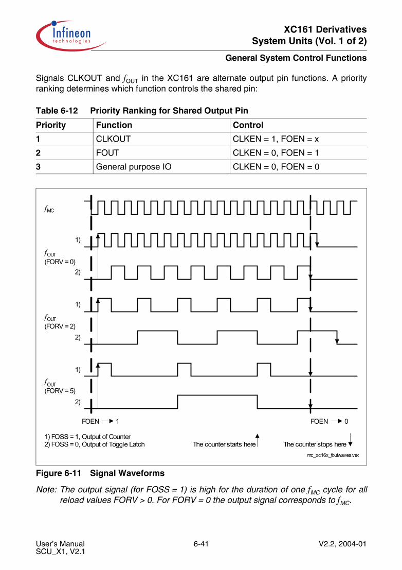
XC161 DerivativesSystem Units (Vol. 1 of 2)
General System Control Functions
Signals CLKOUT and fOUT in the XC161 are alternate output pin functions. A priorityranking determines which function controls the shared pin:
Figure 6-11 Signal Waveforms
Note: The output signal (for FOSS = 1) is high for the duration of one fMC cycle for allreload values FORV > 0. For FORV = 0 the output signal corresponds to fMC.
Table 6-12 Priority Ranking for Shared Output Pin
Priority Function Control
1 CLKOUT CLKEN = 1, FOEN = x
2 FOUT CLKEN = 0, FOEN = 1
3 General purpose IO CLKEN = 0, FOEN = 0
mc_xc16x_foutwaves.vsd
fMC
fOUT(FORV = 0)
1)
2)
1)
2)
fOUT(FORV = 2)
1)
2)
fOUT(FORV = 5)
FOEN 1
1) FOSS = 1, Output of Counter2) FOSS = 0, Output of Toggle Latch
FOEN 0
The counter starts here The counter stops here
User’s Manual 6-41 V2.2, 2004-01SCU_X1, V2.1
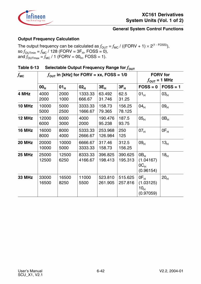
XC161 DerivativesSystem Units (Vol. 1 of 2)
General System Control Functions
Output Frequency Calculation
The output frequency can be calculated as fOUT = fMC / ((FORV + 1) × 2(1 - FOSS)),so fOUTmin = fMC / 128 (FORV = 3FH, FOSS = 0),and fOUTmax = fMC / 1 (FORV = 00H, FOSS = 1).
Table 6-13 Selectable Output Frequency Range for fOUT
fMC fOUT in [kHz] for FORV = xx, FOSS = 1/0 FORV forfOUT = 1 MHz
00H 01H 02H 3EH 3FH FOSS = 0 FOSS = 1
4 MHz 40002000
20001000
1333.33666.67
63.49231.746
62.531.25
01H 03H
10 MHz 100005000
50002500
3333.331666.67
158.7379.365
156.2578.125
04H 09H
12 MHz 120006000
60003000
40002000
190.47695.238
187.593.75
05H 0BH
16 MHz 160008000
80004000
5333.332666.67
253.968126.984
250125
07H 0FH
20 MHz 2000010000
100005000
6666.673333.33
317.46158.73
312.5156.25
09H 13H
25 MHz 2500012500
125006250
8333.334166.67
396.825198.413
390.625195.313
0BH
(1.04167)0CH(0.96154)
18H
33 MHz 3300016500
165008250
110005500
523.810261.905
515.625257.816
0FH(1.03125)10H(0.97059)
20H
User’s Manual 6-42 V2.2, 2004-01SCU_X1, V2.1

XC161 DerivativesSystem Units (Vol. 1 of 2)
General System Control Functions
6.3 Central System Control Functions
Most control functions and status information are tightly coupled to the respectiveperipheral modules of the XC161. However, some of these functions are valid for thecomplete device, rather than for a specific module. These functions, including theassociated control- and status-bits, are part of the SCU.
Note: SYSCON0 is protected by the register security mechanism (see Section 6.3.6).The reset value is only valid for a hardware reset.
SYSCON0 General System Control Reg. ESFR (F1BEH/DFH) Reset Value: 0000H
15 14 13 12 11 10 9 8 7 6 5 4 3 2 1 0
RTCRST
RTCCM
-OSC
G RED
- - - - - - - - - - - -
rwh rw - rw - - - - - - - - - - - -
Field Bits Type Description
RTCRST 15 rwh RTC Reset Trigger0 No action1 The RTC module is reset
Note: RTCRST returns to 0 one SCU clock afterbeing set.
RTCCM 14 rw RTC Clocking Mode0 Synchronous mode:
The RTC operates with the system clock. Registers can be read and written.
1 Asynchronous mode:1)
The RTC operates with the (asynchronous) count clock. No write access is possible.
1) Asynchronous mode is required if the system clock is slower than the 4 × fCOUNT. This is, of course, the casein Sleep mode or Powerdown mode, where the system clock is disabled, while the RTC shall continue to run(see also Chapter 15).
OSCGRED 12 rw Oscillator Gain Reduction Control0 No reduction, retain initial gain level1 Reduce gain (see Section 6.2.1)
User’s Manual 6-43 V2.2, 2004-01SCU_X1, V2.1
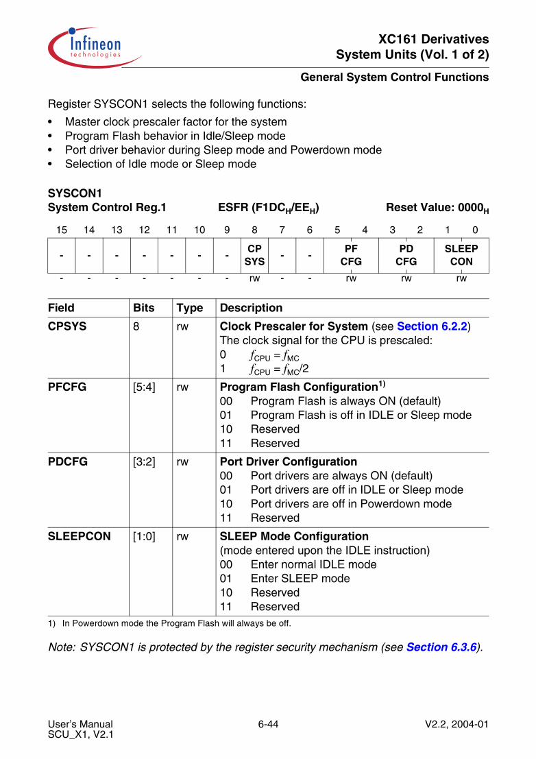
XC161 DerivativesSystem Units (Vol. 1 of 2)
General System Control Functions
Register SYSCON1 selects the following functions:
• Master clock prescaler factor for the system• Program Flash behavior in Idle/Sleep mode• Port driver behavior during Sleep mode and Powerdown mode• Selection of Idle mode or Sleep mode
Note: SYSCON1 is protected by the register security mechanism (see Section 6.3.6).
SYSCON1 System Control Reg.1 ESFR (F1DCH/EEH) Reset Value: 0000H
15 14 13 12 11 10 9 8 7 6 5 4 3 2 1 0
- - - - - - -CP
SYS- -
PFCFG
PDCFG
SLEEPCON
- - - - - - - rw - - rw rw rw
Field Bits Type Description
CPSYS 8 rw Clock Prescaler for System (see Section 6.2.2)The clock signal for the CPU is prescaled:0 fCPU = fMC1 fCPU = fMC/2
PFCFG [5:4] rw Program Flash Configuration1)
00 Program Flash is always ON (default)01 Program Flash is off in IDLE or Sleep mode10 Reserved11 Reserved
1) In Powerdown mode the Program Flash will always be off.
PDCFG [3:2] rw Port Driver Configuration00 Port drivers are always ON (default)01 Port drivers are off in IDLE or Sleep mode10 Port drivers are off in Powerdown mode11 Reserved
SLEEPCON [1:0] rw SLEEP Mode Configuration(mode entered upon the IDLE instruction)00 Enter normal IDLE mode01 Enter SLEEP mode10 Reserved11 Reserved
User’s Manual 6-44 V2.2, 2004-01SCU_X1, V2.1

XC161 DerivativesSystem Units (Vol. 1 of 2)
General System Control Functions
6.3.1 Status Indication
The system status register SYSSTAT indicates the status of the clock generation unitand the recent reset with a number of flags.
SYSSTAT System Status Register mem (F1E4H/--) Reset Value: XXXXH
15 14 13 12 11 10 9 8 7 6 5 4 3 2 1 0
OSCLOC
K
PLLLOC
K
CLKHIX
CLKLOX
-PLLEM
- - - - - - -HWR
SWR
WDTR
rh rh rh rh - rh - - - - - - - rh rh rh
Field Bits Type Description
OSCLOCK 15 rh Oscillator Signal Status Bit0 The oscillator is unlocked1 The oscillator is locked (2048 fOSC periods
have been counted, so it is assumed as stable)
PLLLOCK 14 rh PLL Signal Status Bit0 PLL unlocked (base frequency or adjusting)1 The PLL is locked (stable output frequency)
CLKHIX 13 rh Input Clock High Limit Exceeded0 The input clock frequency is below the upper
limit of the monitored range1 The input clock frequency is too high
CLKLOX 12 rh Input Clock Low Limit Exceeded0 The input clock frequency is above the lower
limit of the monitored range1 The input clock frequency is too low
PLLEM 10 rh PLL Emergency Mode Flag0 No clock generation problem encountered1 A clock generation problem has occurred
Note: PLLEM is cleared automatically if the oscillatorhas locked after a wake-up from sleep mode.Otherwise it remains set until hardware reset.
HWR 2 rh Hardware Reset Indication Flag0 Last reset was no hardware reset1 Last reset was a hardware reset
User’s Manual 6-45 V2.2, 2004-01SCU_X1, V2.1
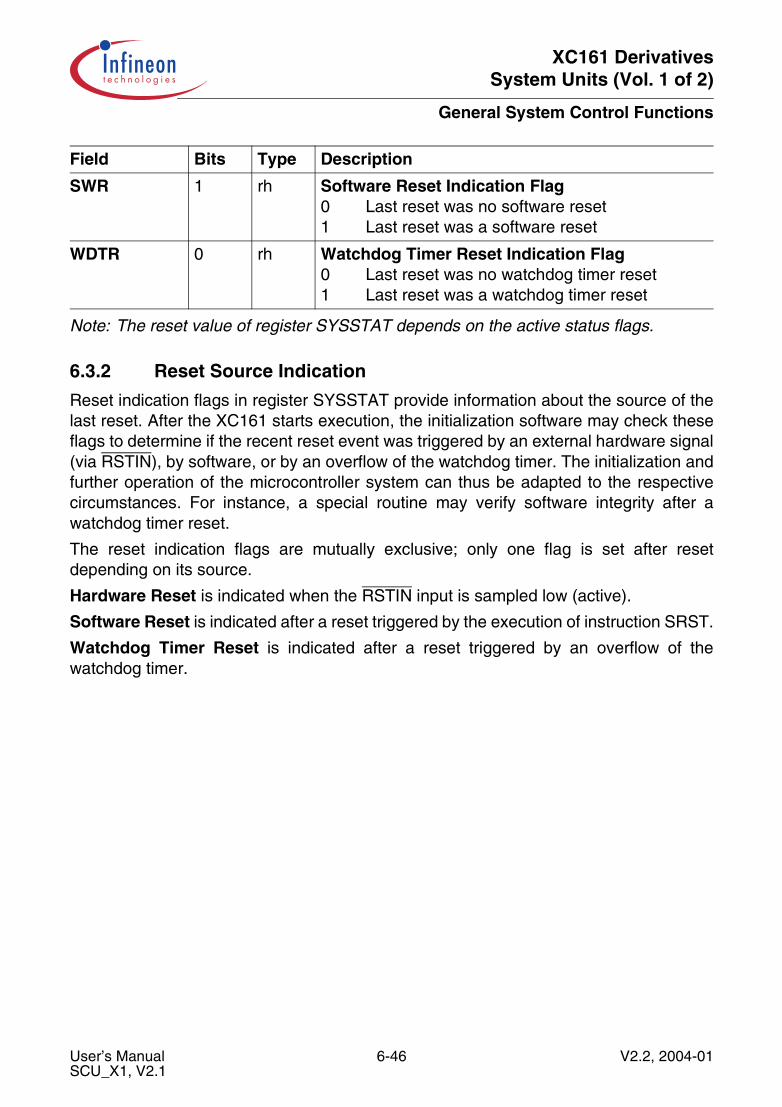
XC161 DerivativesSystem Units (Vol. 1 of 2)
General System Control Functions
Note: The reset value of register SYSSTAT depends on the active status flags.
6.3.2 Reset Source Indication
Reset indication flags in register SYSSTAT provide information about the source of thelast reset. After the XC161 starts execution, the initialization software may check theseflags to determine if the recent reset event was triggered by an external hardware signal(via RSTIN), by software, or by an overflow of the watchdog timer. The initialization andfurther operation of the microcontroller system can thus be adapted to the respectivecircumstances. For instance, a special routine may verify software integrity after awatchdog timer reset.
The reset indication flags are mutually exclusive; only one flag is set after resetdepending on its source.
Hardware Reset is indicated when the RSTIN input is sampled low (active).
Software Reset is indicated after a reset triggered by the execution of instruction SRST.
Watchdog Timer Reset is indicated after a reset triggered by an overflow of thewatchdog timer.
SWR 1 rh Software Reset Indication Flag0 Last reset was no software reset1 Last reset was a software reset
WDTR 0 rh Watchdog Timer Reset Indication Flag0 Last reset was no watchdog timer reset1 Last reset was a watchdog timer reset
Field Bits Type Description
User’s Manual 6-46 V2.2, 2004-01SCU_X1, V2.1

XC161 DerivativesSystem Units (Vol. 1 of 2)
General System Control Functions
6.3.3 Peripheral Shutdown Handshake
When executing a software reset or when entering a power-save mode the SCUrequests a shutdown from those peripheral units that are currently active and provide theshutdown handshake mechanism. Upon this request the respective peripheral unitcompletes the currently active action (if any) and then acknowledges the shutdownrequest to the SCU.
These units are: PMU, DMU, EBC, ADC, and Program Flash.
The shutdown handshake sequence is completed as soon as all units haveacknowledged the shutdown request.
6.3.4 Flexible Peripheral Management
The power consumed by the XC161 also depends on the amount of active logic.Peripheral management deactivates those on-chip peripherals that are not required in agiven system status (e.g. a certain interface mode or standby). This reduces the amountof clocked circuitry. All modules that remain active, however, will still deliver their usualperformance.
Note: A read access to a register of a disabled peripheral returns the valid registercontent, whereas a write access to this register is ignored.A read access will not trigger any actions within a disabled peripheral.
While a peripheral is disabled, its associated output pins remain in the state they had atthe time of disabling.
Software controls this flexible peripheral management via register SYSCON3 whereeach control bit is associated with an on-chip peripheral module.
Writing SYSCON3 requests deactivation/activation of the respective peripheral(s).
Reading SYSCON3 returns the peripherals’ actual status according to the shutdownhandshake mechanism (see Section 6.3.3).
User’s Manual 6-47 V2.2, 2004-01SCU_X1, V2.1
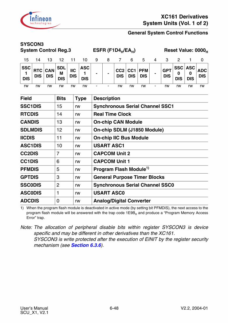
XC161 DerivativesSystem Units (Vol. 1 of 2)
General System Control Functions
Note: The allocation of peripheral disable bits within register SYSCON3 is devicespecific and may be different in other derivatives than the XC161.SYSCON3 is write protected after the execution of EINIT by the register securitymechanism (see Section 6.3.6).
SYSCON3 System Control Reg.3 ESFR (F1D4H/EAH) Reset Value: 0000H
15 14 13 12 11 10 9 8 7 6 5 4 3 2 1 0
SSC1
DIS
RTCDIS
CANDIS
SDLM
DIS
IICDIS
ASC1
DIS- -
CC2DIS
CC1DIS
PFMDIS
-GPTDIS
SSC0
DIS
ASC0
DIS
ADCDIS
rw rw rw rw rw rw - - rw rw rw - rw rw rw rw
Field Bits Type Description
SSC1DIS 15 rw Synchronous Serial Channel SSC1
RTCDIS 14 rw Real Time Clock
CANDIS 13 rw On-chip CAN Module
SDLMDIS 12 rw On-chip SDLM (J1850 Module)
IICDIS 11 rw On-chip IIC Bus Module
ASC1DIS 10 rw USART ASC1
CC2DIS 7 rw CAPCOM Unit 2
CC1DIS 6 rw CAPCOM Unit 1
PFMDIS 5 rw Program Flash Module1)
GPTDIS 3 rw General Purpose Timer Blocks
SSC0DIS 2 rw Synchronous Serial Channel SSC0
ASC0DIS 1 rw USART ASC0
ADCDIS 0 rw Analog/Digital Converter1) When the program flash module is deactivated in active mode (by setting bit PFMDIS), the next access to the
program flash module will be answered with the trap code 1E9BH and produce a “Program Memory AccessError” trap.
User’s Manual 6-48 V2.2, 2004-01SCU_X1, V2.1

XC161 DerivativesSystem Units (Vol. 1 of 2)
General System Control Functions
6.3.5 Debug System Control
The debug and emulation circuitry is controlled by two registers:
• The Emulation Control register EMUCON controls basic OCDS functions.• The OCE/OCDS Peripheral Suspend Enable register OPSEN selects the peripherals
that will be halted by the suspend signal. OPSEN is structured identically to registerSYSCON3.
Note: EMUCON is write protected after the execution of EINIT by the register securitymechanism (see Section 6.3.6).
EMUCON Emulation Control Reg. SFR (FE0AH/05H) Reset Value: 0000H
15 14 13 12 11 10 9 8 7 6 5 4 3 2 1 0
- - - - - - - - - - - - -OCEN
OCDSIOEN
-
- - - - - - - - - - - - - rw rw -
Field Bits Type Description
OCEN 2 rw OCDS/Cerberus Enable0 OCDS and Cerberus are still in reset state1 ODCS and Cerberus are operable
OCDSIOEN 1 rw OCDS Break Input/Output Enable0 OCDS break input/output BRKIN/BRKOUT are
disabled.1 OCDS break input/output BRKIN/BRKOUT are
enabled.
User’s Manual 6-49 V2.2, 2004-01SCU_X1, V2.1

XC161 DerivativesSystem Units (Vol. 1 of 2)
General System Control Functions
Note: For most debugging scenarios it is recommended to keep bit PFMSEN cleared.OPSEN is write protected after the execution of EINIT by the register securitymechanism (see Section 6.3.6).
OPSEN OCE/OCDS P-Susp. En. Reg. ESFR (FE58H/2CH) Reset Value: 0000H
15 14 13 12 11 10 9 8 7 6 5 4 3 2 1 0
SSC1
SEN
RTCSEN
CANSEN
SDLM
SEN
I2CSEN
ASC1
SEN- -
CC2SEN
CC1SEN
PFMSEN
-GPTSEN
SSC0
SEN
ASC0
SEN
ADCSEN
rw rw rw rw rw rw - - rw rw rw - rw rw rw rw
Field Bits Type Description
xxSEN [15:10],[7:5],[3:0]
rw Module xx Suspend Enable0 Respective module remains active
during suspend1 Respective module halts operation
during suspend
User’s Manual 6-50 V2.2, 2004-01SCU_X1, V2.1
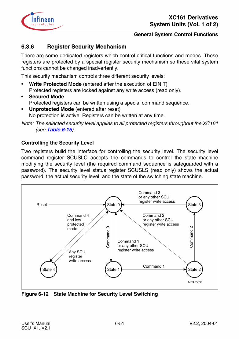
XC161 DerivativesSystem Units (Vol. 1 of 2)
General System Control Functions
6.3.6 Register Security Mechanism
There are some dedicated registers which control critical functions and modes. Theseregisters are protected by a special register security mechanism so these vital systemfunctions cannot be changed inadvertently.
This security mechanism controls three different security levels:
• Write Protected Mode (entered after the execution of EINIT)Protected registers are locked against any write access (read only).
• Secured ModeProtected registers can be written using a special command sequence.
• Unprotected Mode (entered after reset)No protection is active. Registers can be written at any time.
Note: The selected security level applies to all protected registers throughout the XC161(see Table 6-15).
Controlling the Security Level
Two registers build the interface for controlling the security level. The security levelcommand register SCUSLC accepts the commands to control the state machinemodifying the security level (the required command sequence is safeguarded with apassword). The security level status register SCUSLS (read only) shows the actualpassword, the actual security level, and the state of the switching state machine.
Figure 6-12 State Machine for Security Level Switching
State 0
State 1
Command 3or any other SCUregister write access
Com
man
d 0
Command 1or any other SCUregister write access
Command 1State 4
Reset
Command 4and lowprotectedmode
Any SCUregisterwrite access
State 3
State 2
Command 2or any other SCUregister write access
Com
man
d 2
MCA05336
User’s Manual 6-51 V2.2, 2004-01SCU_X1, V2.1

XC161 DerivativesSystem Units (Vol. 1 of 2)
General System Control Functions
Two mechanisms can be used to control the actual security level:
• Changing the security levelcan be done by executing the following command sequence:“command0-command1-command2-command3”.This sequence establishes a new security level and/or a new password.
• Access in secured modecan be achieved by preceding the intended write access with writing “command4” toregister SCUSLC. This quick access is only possible while secured mode is selected.
Read accesses are always possible to all registers of the SCU and will not influence thecommand sequences. In register SCUSLS the actual status of the command statemachine can always be read.
Note: After writing command4 in secured mode the lock mechanism remains disableduntil the next write access to an SCU register or a register on the PD bus, i.e.accesses to registers outside this area do not re-activate the protection.
SCUSLS Sec. Level Status Reg. ESFR (F0C2H/61H) Reset Value: 0000H
15 14 13 12 11 10 9 8 7 6 5 4 3 2 1 0
STATE SL - - - PASSWORD
rh rh - - - rh
Field Bits Type Description
STATE [15:13] rh Current State of Switching State Machine000 Awaiting command0 or command4 (default)001 Awaiting command1010 Awaiting command2011 Awaiting new security level and password100 Next access granted in secured mode101 Reserved11X Reserved
SL [12:11] rh Security Level00 Unprotected mode (default after reset)01 Secured mode10 Reserved11 Write protected mode (entered after EINIT)
PASSWORD [7:0] rh Current Security Control PasswordDefault after reset = 00H
User’s Manual 6-52 V2.2, 2004-01SCU_X1, V2.1

XC161 DerivativesSystem Units (Vol. 1 of 2)
General System Control Functions
Note: Register SCUSLC is not protected by the security mechanism. This is required tobe able to change the security level in any state.
Note: It is recommended to lock all command sequences with an atomic sequence.
Programming Examples
EXTR #4 ;Sequence to change the security levelMOV SCUSLC, #0AAAAH ;Command0MOV SCUSLC, #05554H ;Command1MOV SCUSLC, #096FFH ;Command2: current password = 00HMOV SCUSLC, #008EDH ;Command3: level = 01, new password = EDH
EXTR #1 ;Access sequence in secured modeMOV SCUSLC, #8E12H ;Command4: current password = EDHMOV register, data ;Access enabled by the preceding Command4
SCUSLC Sec. Level Command Reg. ESFR (F0C0H/60H) Reset Value: 0000H
15 14 13 12 11 10 9 8 7 6 5 4 3 2 1 0
COMMAND
rw
Field Bits Type Description
COMMAND [15:0] rw Security Level Control CommandThe commands to control the security level must be written to this register (see Table 6-14)
Table 6-14 Commands for Security Level Control
Command Definition Note
Command0 AAAAH –
Command1 5554H –
Command2 96H || <inverse password> –
Command3 000B || <new level> || 000B || <new password> –
Command4 8EH || <inverse password> Secured mode only
User’s Manual 6-53 V2.2, 2004-01SCU_X1, V2.1
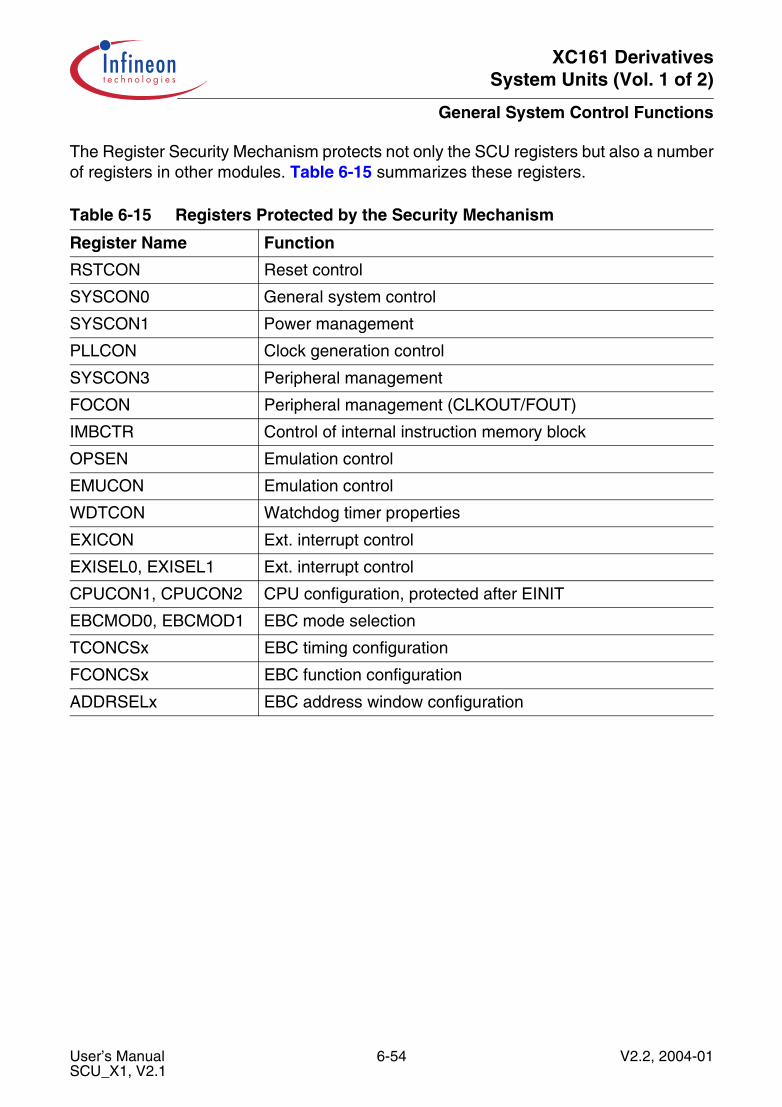
XC161 DerivativesSystem Units (Vol. 1 of 2)
General System Control Functions
The Register Security Mechanism protects not only the SCU registers but also a numberof registers in other modules. Table 6-15 summarizes these registers.
Table 6-15 Registers Protected by the Security Mechanism
Register Name Function
RSTCON Reset control
SYSCON0 General system control
SYSCON1 Power management
PLLCON Clock generation control
SYSCON3 Peripheral management
FOCON Peripheral management (CLKOUT/FOUT)
IMBCTR Control of internal instruction memory block
OPSEN Emulation control
EMUCON Emulation control
WDTCON Watchdog timer properties
EXICON Ext. interrupt control
EXISEL0, EXISEL1 Ext. interrupt control
CPUCON1, CPUCON2 CPU configuration, protected after EINIT
EBCMOD0, EBCMOD1 EBC mode selection
TCONCSx EBC timing configuration
FCONCSx EBC function configuration
ADDRSELx EBC address window configuration
User’s Manual 6-54 V2.2, 2004-01SCU_X1, V2.1

XC161 DerivativesSystem Units (Vol. 1 of 2)
General System Control Functions
6.4 Watchdog Timer (WDT)
To allow recovery from software or hardware failure, the XC161 provides a WatchdogTimer. If the software fails to service this timer before an overflow occurs, an internalreset sequence will be initiated. This internal reset can also pull the RSTOUT pin low,which in turn resets the peripheral hardware which might have caused the malfunction.If the watchdog timer is enabled and the software has been designed to service itregularly before it overflows, the watchdog timer will supervise the program execution soit will overflow only if the program does not progress properly. The watchdog timer willalso time out if a software error was caused by hardware related failures. This preventsthe controller from malfunctioning for a time longer than specified by the user.
The watchdog timer provides two registers:
• a read-only timer register containing the current count, and• a control register for initialization and reset source detection.
Figure 6-13 SFRs and Port Pins Associated with the Watchdog Timer
The watchdog timer is a 16-bit up counter which is clocked with the prescaled systemclock (fSYS). The prescaler divides the system clock:
• by 2 (WDTIN = 00B), or• by 4 (WDTIN = 10B), or• by 128 (WDTIN = 01B), or• by 256 (WDTIN = 11B).
m ca04381_xc.vsd
W D TC O N
R eset Ind ica tion P in D ata /S tatus R eg is te rs C ontro l R egis ters
S Y S C O N 1 S ystem C ontro l R eg is te r 1S Y S S TA T S ystem S tatus R eg is te rC P U C O N 1 C P U C ontro l R egis te r 1
S Y S S TA T m
W D T
W D TC O N W atchdog T im er C on tro l R egis te rW D T W tachdog T im er C oun t R eg is ter
R S TO U T
S Y S C O N 1 E
C P U C O N 1
User’s Manual 6-55 V2.2, 2004-01SCU_X1, V2.1
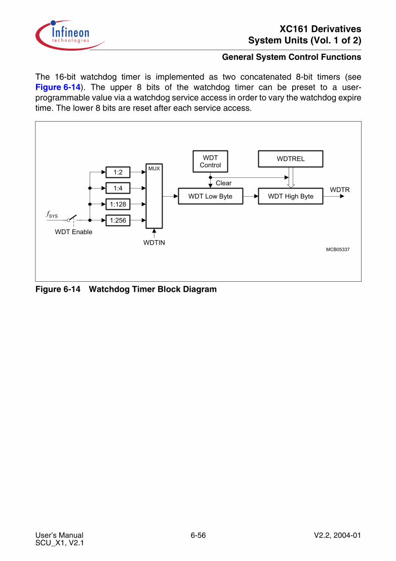
XC161 DerivativesSystem Units (Vol. 1 of 2)
General System Control Functions
The 16-bit watchdog timer is implemented as two concatenated 8-bit timers (seeFigure 6-14). The upper 8 bits of the watchdog timer can be preset to a user-programmable value via a watchdog service access in order to vary the watchdog expiretime. The lower 8 bits are reset after each service access.
Figure 6-14 Watchdog Timer Block Diagram
MCB05337WDTIN
WDTControl
WDT Low Byte
WDTREL
WDT High ByteWDTR
MUX
1:256
1:128
1:4
1:2
WDT Enable
fSYS
Clear
User’s Manual 6-56 V2.2, 2004-01SCU_X1, V2.1
XC161 DerivativesSystem Units (Vol. 1 of 2)
General System Control Functions
Operation of the Watchdog Timer
The current count value of the Watchdog Timer is contained in the Watchdog TimerRegister WDT which is a non-bitaddressable read-only register. Operation of theWatchdog Timer is controlled by its bitaddressable Watchdog Timer Control RegisterWDTCON. This register specifies the reload value for the high byte of the timer, selectsthe input clock prescaling factor, and also provides flags to indicate the source of a reset.
After any reset (except as noted) the watchdog timer is enabled and starts counting upfrom 0000H with the default frequency fWDT = fSYS/2. The default input frequency may bechanged to another frequency (fWDT = fSYS/4, 128, 256) by programming the prescaler(bitfield WDTIN).
The watchdog timer can be disabled by executing the instruction DISWDT (DisableWatchdog Timer). Instruction DISWDT is a protected 32-bit instruction.
In compatible WDT mode instruction DISWDT will ONLY be executed during the timebetween a reset and execution of either the EINIT or the SRVWDT instruction. Either oneof these instructions disables the execution of DISWDT. Once disabled, the WDT canonly be enabled by a reset.
In enhanced WDT mode the watchdog timer can be disabled and enabled at any time(independent of the EINIT instruction). This is controlled by executing instructionsDISWDT and ENWDT, respectively. Instruction ENWDT is a protected 32-bit instruction.
The basic control mode (compatible/enhanced) is selected by bit WDTCTL in registerCPUCON1.
Note: After a hardware reset that activates the Bootstrap Loader the watchdog timer willbe disabled. The WDT is enabled, when the loaded software begins executing.
When the watchdog timer is not disabled via instruction DISWDT it will continue countingup, even in Idle Mode. If it is not serviced via the instruction SRVWDT by the time thecount reaches FFFFH the watchdog timer will overflow and cause an internal reset. Thisreset will pull the external reset indication pin RSTOUT low. The Watchdog Timer ResetIndication Flag (WDTR) in register SYSSTAT will be set in this case.
Attention: A watchdog timer reset is unconditional. All current data/codeaccesses are aborted.
To prevent the watchdog timer from overflowing, it must be serviced periodically by theuser software. The watchdog timer is serviced with the instruction SRVWDT which is aprotected 32-bit instruction. Servicing the watchdog timer clears the low byte and reloadsthe high byte of the watchdog timer register WDT with the preset value from bitfieldWDTREL which is the high byte of register WDTCON. After servicing, the watchdogtimer resumes counting up from the value (<WDTREL> × 28).
Instruction SRVWDT has been encoded in such a way that the chance of unintentionallyservicing the watchdog timer is minimized (such as by fetching and executing a bitpattern from a wrong location). When instruction SRVWDT does not match the format
User’s Manual 6-57 V2.2, 2004-01SCU_X1, V2.1
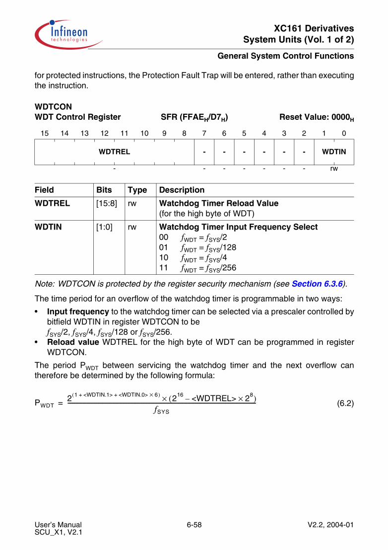
XC161 DerivativesSystem Units (Vol. 1 of 2)
General System Control Functions
for protected instructions, the Protection Fault Trap will be entered, rather than executingthe instruction.
Note: WDTCON is protected by the register security mechanism (see Section 6.3.6).
The time period for an overflow of the watchdog timer is programmable in two ways:
• Input frequency to the watchdog timer can be selected via a prescaler controlled bybitfield WDTIN in register WDTCON to befSYS/2, fSYS/4, fSYS/128 or fSYS/256.
• Reload value WDTREL for the high byte of WDT can be programmed in registerWDTCON.
The period PWDT between servicing the watchdog timer and the next overflow cantherefore be determined by the following formula:
(6.2)
WDTCON WDT Control Register SFR (FFAEH/D7H) Reset Value: 0000H
15 14 13 12 11 10 9 8 7 6 5 4 3 2 1 0
WDTREL - - - - - - WDTIN
- - - - - - - rw
Field Bits Type Description
WDTREL [15:8] rw Watchdog Timer Reload Value(for the high byte of WDT)
WDTIN [1:0] rw Watchdog Timer Input Frequency Select00 fWDT = fSYS/201 fWDT = fSYS/12810 fWDT = fSYS/411 fWDT = fSYS/256
PWDT2 1 <WDTIN.1> <WDTIN.0> 6×+ +( ) 216 <WDTREL> 28×–( )×
fSYS
----------------------------------------------------------------------------------------------------------------------------------------=
User’s Manual 6-58 V2.2, 2004-01SCU_X1, V2.1
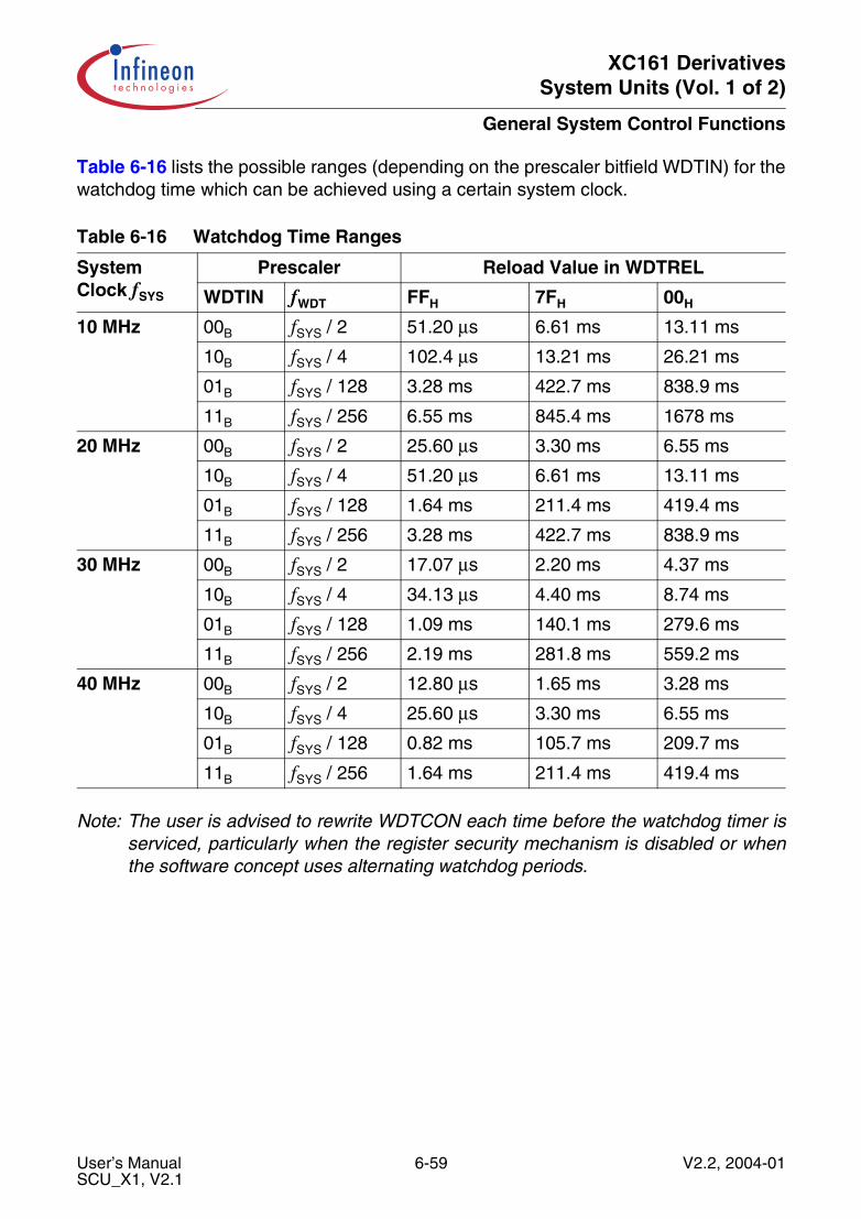
XC161 DerivativesSystem Units (Vol. 1 of 2)
General System Control Functions
Table 6-16 lists the possible ranges (depending on the prescaler bitfield WDTIN) for thewatchdog time which can be achieved using a certain system clock.
Note: The user is advised to rewrite WDTCON each time before the watchdog timer isserviced, particularly when the register security mechanism is disabled or whenthe software concept uses alternating watchdog periods.
Table 6-16 Watchdog Time Ranges
System Clock fSYS
Prescaler Reload Value in WDTREL
WDTIN fWDT FFH 7FH 00H
10 MHz 00B fSYS / 2 51.20 µs 6.61 ms 13.11 ms
10B fSYS / 4 102.4 µs 13.21 ms 26.21 ms
01B fSYS / 128 3.28 ms 422.7 ms 838.9 ms
11B fSYS / 256 6.55 ms 845.4 ms 1678 ms
20 MHz 00B fSYS / 2 25.60 µs 3.30 ms 6.55 ms
10B fSYS / 4 51.20 µs 6.61 ms 13.11 ms
01B fSYS / 128 1.64 ms 211.4 ms 419.4 ms
11B fSYS / 256 3.28 ms 422.7 ms 838.9 ms
30 MHz 00B fSYS / 2 17.07 µs 2.20 ms 4.37 ms
10B fSYS / 4 34.13 µs 4.40 ms 8.74 ms
01B fSYS / 128 1.09 ms 140.1 ms 279.6 ms
11B fSYS / 256 2.19 ms 281.8 ms 559.2 ms
40 MHz 00B fSYS / 2 12.80 µs 1.65 ms 3.28 ms
10B fSYS / 4 25.60 µs 3.30 ms 6.55 ms
01B fSYS / 128 0.82 ms 105.7 ms 209.7 ms
11B fSYS / 256 1.64 ms 211.4 ms 419.4 ms
User’s Manual 6-59 V2.2, 2004-01SCU_X1, V2.1
XC161 DerivativesSystem Units (Vol. 1 of 2)
General System Control Functions
6.5 Identification Control Block
For identification of the most important silicon parameters a set of identification registersis defined that provide information on the chip manufacturer, the chip type and itsproperties. These ID registers can be used for automatic test selection as well as foridentification of unknown silicon.
Note: The not defined locations within the area 00’F070H … 00’F07EH are reserved forfuture identification features.
User’s Manual 6-60 V2.2, 2004-01SCU_X1, V2.1
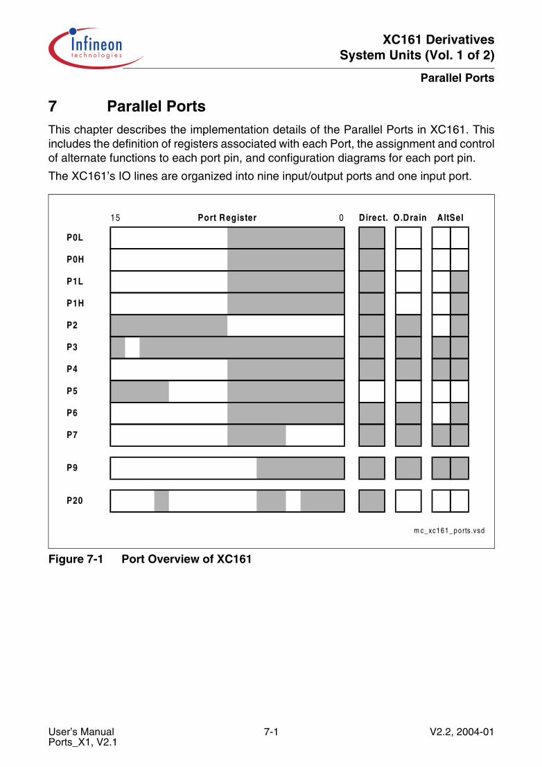
XC161 DerivativesSystem Units (Vol. 1 of 2)
Parallel Ports
7 Parallel PortsThis chapter describes the implementation details of the Parallel Ports in XC161. Thisincludes the definition of registers associated with each Port, the assignment and controlof alternate functions to each port pin, and configuration diagrams for each port pin.
The XC161’s IO lines are organized into nine input/output ports and one input port.
Figure 7-1 Port Overview of XC161
m c_xc161_ ports .vsd
P0L
15
P0H
P1L
P1H
P2
P3
P4
P5
P6
P7
P9
P20
0Port Register Direct. O.Drain AltSel
User’s Manual 7-1 V2.2, 2004-01Ports_X1, V2.1
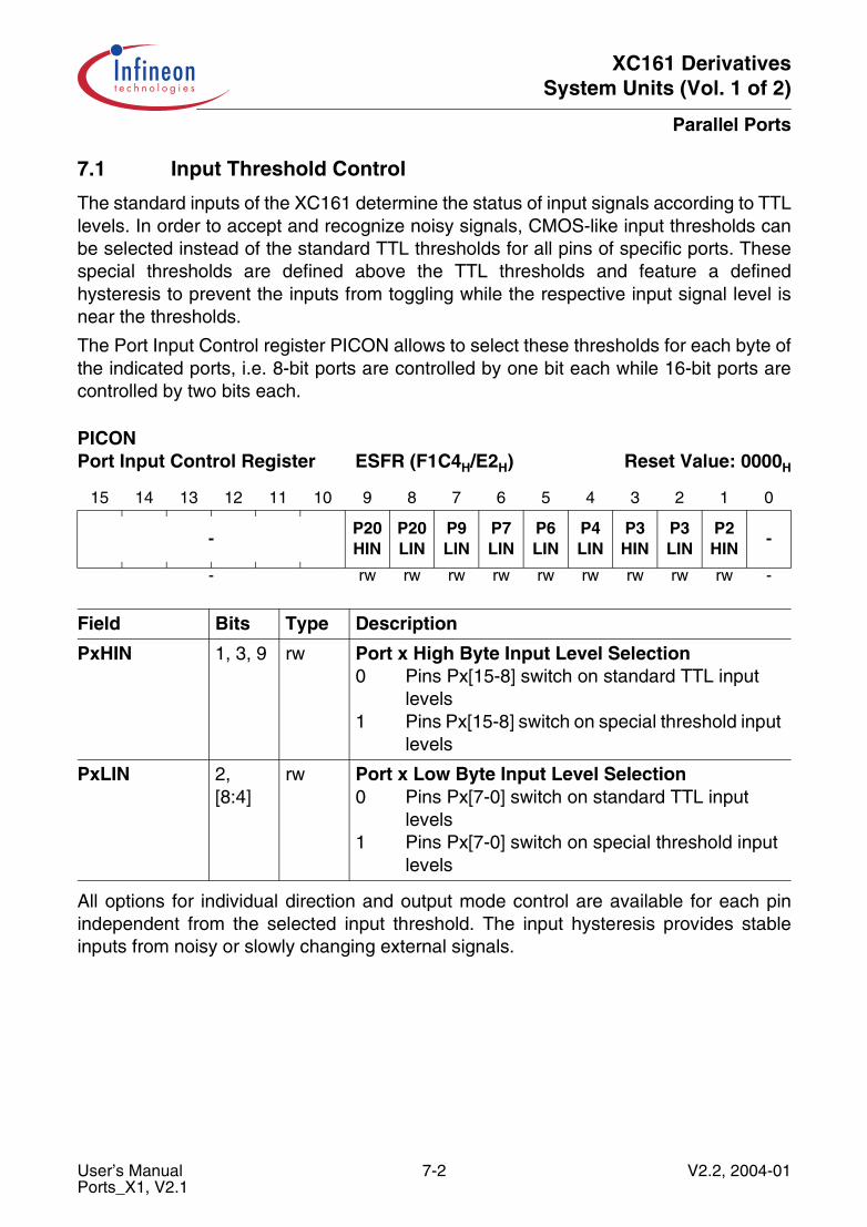
XC161 DerivativesSystem Units (Vol. 1 of 2)
Parallel Ports
7.1 Input Threshold Control
The standard inputs of the XC161 determine the status of input signals according to TTLlevels. In order to accept and recognize noisy signals, CMOS-like input thresholds canbe selected instead of the standard TTL thresholds for all pins of specific ports. Thesespecial thresholds are defined above the TTL thresholds and feature a definedhysteresis to prevent the inputs from toggling while the respective input signal level isnear the thresholds.
The Port Input Control register PICON allows to select these thresholds for each byte ofthe indicated ports, i.e. 8-bit ports are controlled by one bit each while 16-bit ports arecontrolled by two bits each.
All options for individual direction and output mode control are available for each pinindependent from the selected input threshold. The input hysteresis provides stableinputs from noisy or slowly changing external signals.
PICON Port Input Control Register ESFR (F1C4H/E2H) Reset Value: 0000H
15 14 13 12 11 10 9 8 7 6 5 4 3 2 1 0
-P20HIN
P20LIN
P9LIN
P7LIN
P6LIN
P4LIN
P3HIN
P3LIN
P2HIN
-
- rw rw rw rw rw rw rw rw rw -
Field Bits Type Description
PxHIN 1, 3, 9 rw Port x High Byte Input Level Selection0 Pins Px[15-8] switch on standard TTL input
levels1 Pins Px[15-8] switch on special threshold input
levels
PxLIN 2,[8:4]
rw Port x Low Byte Input Level Selection0 Pins Px[7-0] switch on standard TTL input
levels1 Pins Px[7-0] switch on special threshold input
levels
User’s Manual 7-2 V2.2, 2004-01Ports_X1, V2.1

XC161 DerivativesSystem Units (Vol. 1 of 2)
Parallel Ports
Figure 7-2 Hysteresis for Special Input Thresholds
7.2 Output Driver Control
The output driver of a port pin is activated by switching the respective pin to output, i.e.DPx.y = ‘1’. The value that is driven to the pin is determined by the port output latch orby the associated alternate function (e.g. address, peripheral IO, etc.). The user softwarecan control the characteristics of the output driver via the following mechanisms:
• Open Drain Mode: The upper (push) transistor is always disabled. Only ‘0’ is drivenactively, an external pull-up is required.
• Driver Characteristic: The driver strength can be selected.• Edge Characteristic: The rise/fall time of an output signal can be selected.
Open Drain Mode
In the XC161 certain ports provide Open Drain Control, which allows to switch the outputdriver of a port pin from a push/pull configuration to an open drain configuration. Inpush/pull mode a port output driver has an upper and a lower transistor, thus it canactively drive the line either to a high or a low level. In open drain mode the uppertransistor is always switched off, and the output driver can only actively drive the line toa low level. When writing a ‘1’ to the port latch, the lower transistor is switched off andthe output enters a high-impedance state. The high level must then be provided by anexternal pull-up device. With this feature, it is possible to connect several port pinstogether to a Wired-AND configuration, saving external glue logic and/or additionalsoftware overhead for enabling/disabling output signals.
This feature is controlled through the respective Open Drain Control Registers ODPxwhich are provided for each port that has this feature implemented. These registers allowthe individual bit-wise selection of the open drain mode for each port line.
If the respective control bit ODPx.y is ‘0’ (default after reset), the output driver is in thepush/pull mode. If ODPx.y is ‘1’, the open drain configuration is selected. Note that allODPx registers are located in the ESFR space.
Bit State
Input Level
Hysteresis
MCT05338
User’s Manual 7-3 V2.2, 2004-01Ports_X1, V2.1

XC161 DerivativesSystem Units (Vol. 1 of 2)
Parallel Ports
Figure 7-3 Output Drivers in Push/Pull Mode and in Open Drain Mode
Driver Characteristic
This defines either the general driving capability of the respective driver, or if the driverstrength is reduced after the target output level has been reached or not. Reducing thedriver strength increases the output’s internal resistance which attenuates noise that isimported/exported via the output line. For driving LEDs or power transistors, however, astable high output current may still be required.
The controllable output drivers of the XC161 pins feature three differently sizedtransistors (strong, medium and weak) for each direction (push and pull). The time ofactivating/deactivating these transistors determines the output characteristics of therespective port driver.
The strength of the driver can be selected to adapt the driver characteristics to theapplication’s requirements:
In Strong Driver Mode, the medium and strong transistors are activated. In this mode thedriver provides maximum output current even after the target signal level is reached.
In Medium Driver Mode, only the medium transistors are activated while the othertransistors remain off.
In Weak Driver Mode, only the weak transistor is activated while the other transistorsremain off. This results in smooth transitions with low current peaks (and reducedsusceptibility for noise) on the cost of increased transition times, i.e. slower edges,depending on the capacitive load.
User’s Manual 7-4 V2.2, 2004-01Ports_X1, V2.1
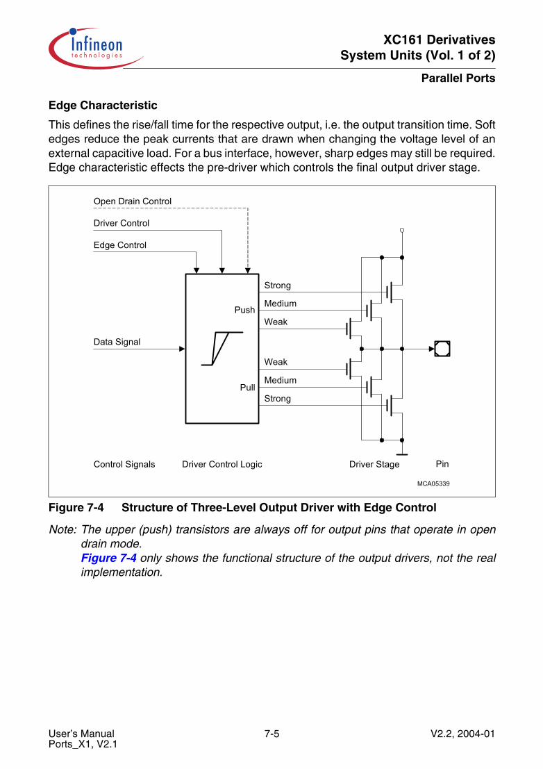
XC161 DerivativesSystem Units (Vol. 1 of 2)
Parallel Ports
Edge Characteristic
This defines the rise/fall time for the respective output, i.e. the output transition time. Softedges reduce the peak currents that are drawn when changing the voltage level of anexternal capacitive load. For a bus interface, however, sharp edges may still be required.Edge characteristic effects the pre-driver which controls the final output driver stage.
Figure 7-4 Structure of Three-Level Output Driver with Edge Control
Note: The upper (push) transistors are always off for output pins that operate in opendrain mode.Figure 7-4 only shows the functional structure of the output drivers, not the realimplementation.
Strong
Medium
Weak
Weak
Medium
Strong
Pin
Push
Pull
Driver StageDriver Control LogicControl Signals
Data Signal
Edge Control
Driver Control
Open Drain Control
MCA05339
User’s Manual 7-5 V2.2, 2004-01Ports_X1, V2.1
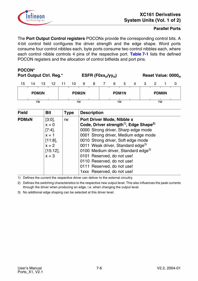
XC161 DerivativesSystem Units (Vol. 1 of 2)
Parallel Ports
The Port Output Control registers POCONx provide the corresponding control bits. A4-bit control field configures the driver strength and the edge shape. Word portsconsume four control nibbles each, byte ports consume two control nibbles each, whereeach control nibble controls 4 pins of the respective port. Table 7-1 lists the definedPOCON registers and the allocation of control bitfields and port pins.
POCON* Port Output Ctrl. Reg.* ESFR (F0xxH/yyH) Reset Value: 0000H
15 14 13 12 11 10 9 8 7 6 5 4 3 2 1 0
PDM3N PDM2N PDM1N PDM0N
rw rw rw rw
Field Bit Type Description
PDMxN [3:0],x = 0[7:4],x = 1[11:8],x = 2[15:12],x = 3
rw Port Driver Mode, Nibble xCode, Driver strength1), Edge Shape2)
0000 Strong driver, Sharp edge mode0001 Strong driver, Medium edge mode0010 Strong driver, Soft edge mode0011 Weak driver, Standard edge3)
0100 Medium driver, Standard edge3)
0101 Reserved, do not use!0110 Reserved, do not use!0111 Reserved, do not use!1xxx Reserved, do not use!
1) Defines the current the respective driver can deliver to the external circuitry.
2) Defines the switching characteristics to the respective new output level. This also influences the peak currentsthrough the driver when producing an edge, i.e. when changing the output level.
3) No additional edge shaping can be selected at this driver level.
User’s Manual 7-6 V2.2, 2004-01Ports_X1, V2.1

XC161 DerivativesSystem Units (Vol. 1 of 2)
Parallel Ports
Table 7-1 Port Output Control Register Allocation
Control Register
Address Controlled Pins (by POCONx.y-z)1) Notes
.15-12 .11-8 .7-4 .3-0
POCON20 F0AAH / 55H P20.12,RSTOUT
--- P20.5-4,ALE
P20.2-0,WR, RD
–
POCON9 F094H / 4AH --- --- P9.5-4 P9.3-0 –
POCON7 F090H / 48H --- --- P7.7-4 --- –
POCON6 F08EH / 47H --- --- P6.7-4 P6.3-0 –
POCON4 F08CH / 46H --- --- P4.7-4 P4.3-0 –
POCON3 F08AH / 45H P3.15-12 P3.11-8 P3.7-4 P3.3-0 –
POCON2 F088H / 44H P2.15-12 P2.11-8 --- --- –
POCON1H F086H / 43H --- --- P1H.7-4 P1H.3-0 –
POCON1L F084H / 42H --- --- P1L.7-4 P1L.3-0 –
POCON0H F082H / 41H --- --- P0H.7-4 P0H.3-0 –
POCON0L F080H / 40H --- --- P0L.7-4 P0L.3-0 –1) x denotes the port number, while y-z represents the bitfield range.
User’s Manual 7-7 V2.2, 2004-01Ports_X1, V2.1
XC161 DerivativesSystem Units (Vol. 1 of 2)
Parallel Ports
7.3 Alternate Port Functions
In order to provide maximum flexibility for different applications and their specific IOrequirements, port lines have programmable alternate input or output functionsassociated with them.
If an alternate output function of a pin is to be used, the direction of this pin must beprogrammed for output (DPx.y = ‘1’), except for some signals that are used directly afterreset and are configured automatically. Otherwise the pin remains in the high-impedancestate and is not effected by the alternate output function. There are port lines, however,whose direction is switched automatically. For instance, in the multiplexed external busmodes of PORT0, the direction must be switched several times for an instruction fetchin order to output the addresses and to input the data. Obviously, this cannot be donethrough instructions. In these cases, the direction of the port line is switchedautomatically by hardware if the alternate function of such a pin is enabled. However, thesoftware controlled output functions of a port are selected with one or two specificALTSELnPx registers (n = 0 or 1).
If an alternate input function is used, the direction of the pin must be programmed forinput (DPx.y = ‘0’) if an external device is driving the pin. The input direction is the defaultafter reset. Alternate inputs are supported for some peripherals and for the externalinterrupt inputs. Alternate inputs for a peripheral are selected with the peripheral’s PISELregister, for example the CAN_PISEL register. Alternate external interrupt inputs areselected with the registers EXISEL0 and EXISEL1 in the SCU.
All port lines that are not used for these alternate functions may be used as generalpurpose IO lines. When using port pins for general purpose output, the initial outputvalue should be written to the port latch prior to enabling the output drivers, in order toavoid undesired transitions on the output pins. This applies to single pins as well as topin groups. In this case, the input operation reads the value stored in the port outputlatch. This can be used for testing purposes to allow a software trigger of an inputfunction by writing to the port output latch.
User’s Manual 7-8 V2.2, 2004-01Ports_X1, V2.1
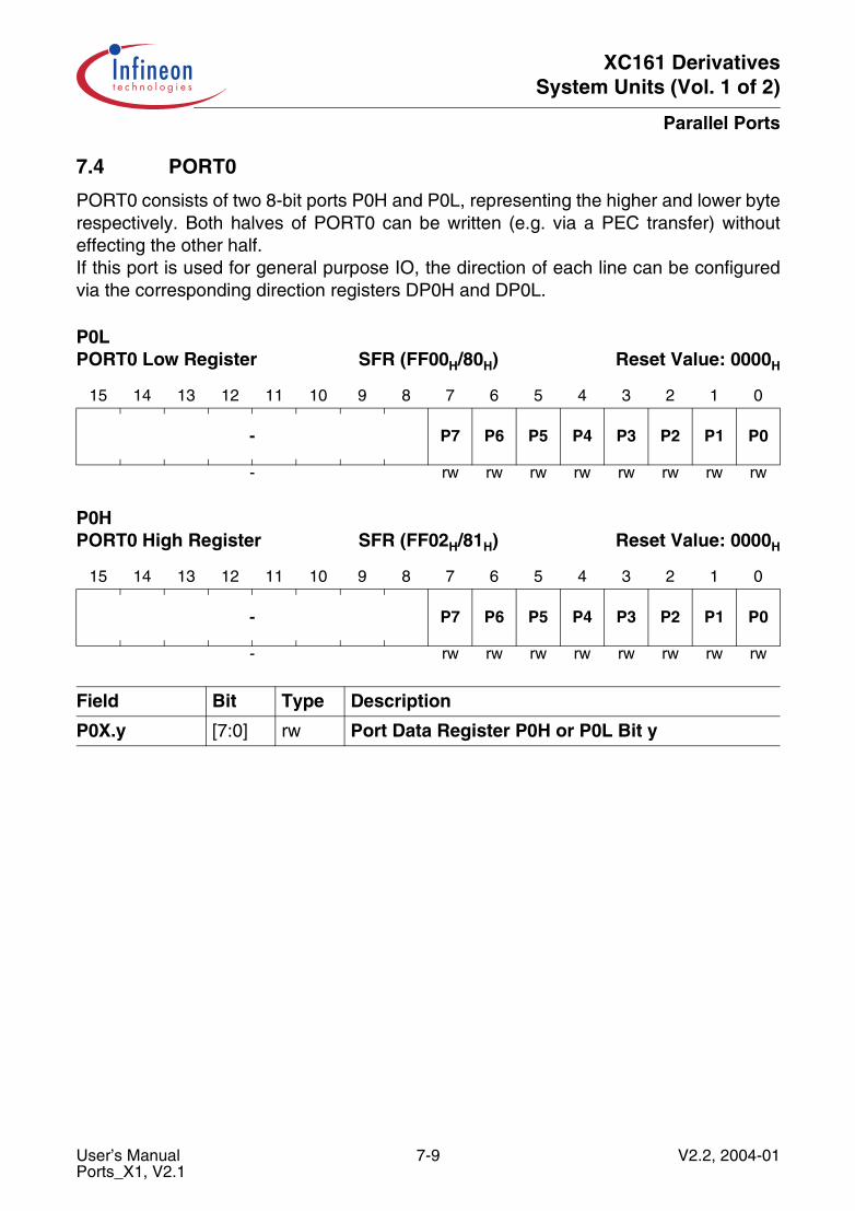
XC161 DerivativesSystem Units (Vol. 1 of 2)
Parallel Ports
7.4 PORT0
PORT0 consists of two 8-bit ports P0H and P0L, representing the higher and lower byterespectively. Both halves of PORT0 can be written (e.g. via a PEC transfer) withouteffecting the other half.If this port is used for general purpose IO, the direction of each line can be configuredvia the corresponding direction registers DP0H and DP0L.
P0L PORT0 Low Register SFR (FF00H/80H) Reset Value: 0000H
15 14 13 12 11 10 9 8 7 6 5 4 3 2 1 0
- P7 P6 P5 P4 P3 P2 P1 P0
- rw rw rw rw rw rw rw rw
P0HPORT0 High Register SFR (FF02H/81H) Reset Value: 0000H
15 14 13 12 11 10 9 8 7 6 5 4 3 2 1 0
- P7 P6 P5 P4 P3 P2 P1 P0
- rw rw rw rw rw rw rw rw
Field Bit Type Description
P0X.y [7:0] rw Port Data Register P0H or P0L Bit y
User’s Manual 7-9 V2.2, 2004-01Ports_X1, V2.1
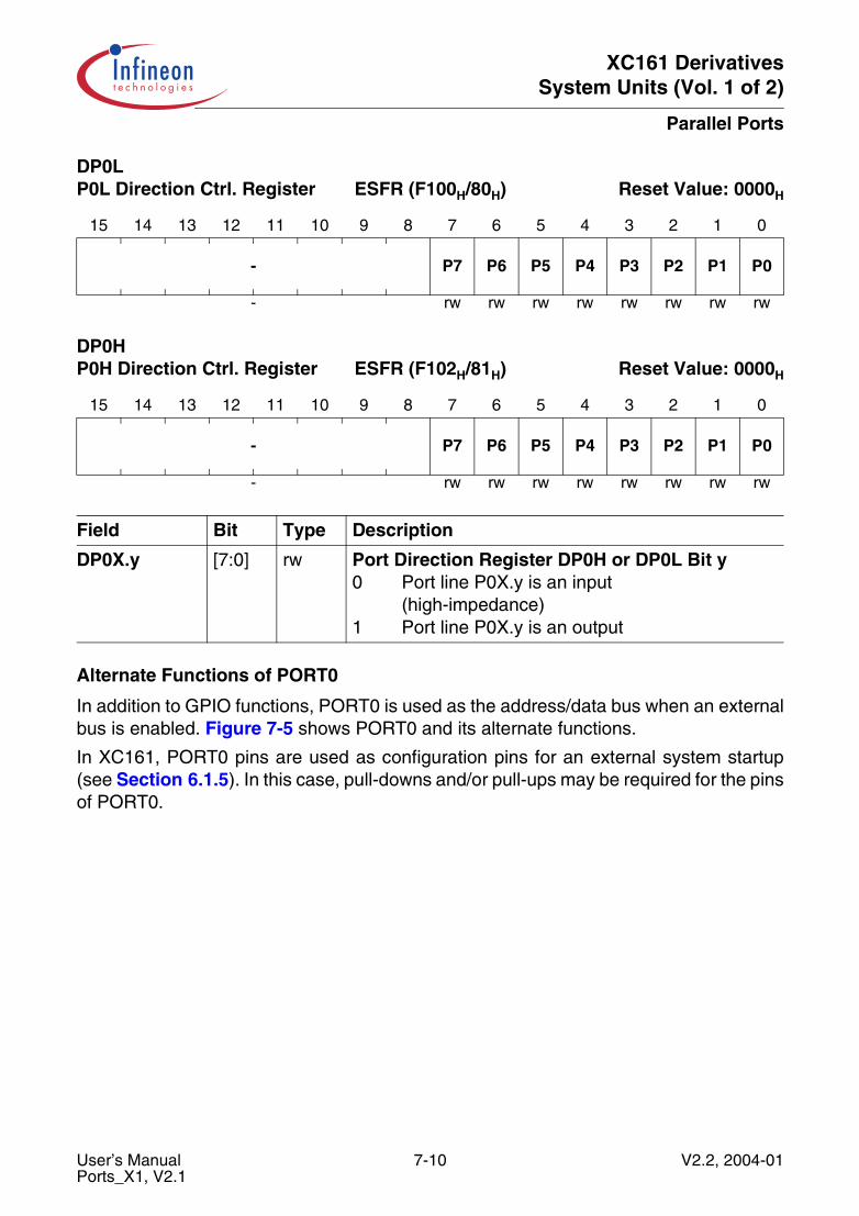
XC161 DerivativesSystem Units (Vol. 1 of 2)
Parallel Ports
Alternate Functions of PORT0
In addition to GPIO functions, PORT0 is used as the address/data bus when an externalbus is enabled. Figure 7-5 shows PORT0 and its alternate functions.
In XC161, PORT0 pins are used as configuration pins for an external system startup(see Section 6.1.5). In this case, pull-downs and/or pull-ups may be required for the pinsof PORT0.
DP0L P0L Direction Ctrl. Register ESFR (F100H/80H) Reset Value: 0000H
15 14 13 12 11 10 9 8 7 6 5 4 3 2 1 0
- P7 P6 P5 P4 P3 P2 P1 P0
- rw rw rw rw rw rw rw rw
DP0HP0H Direction Ctrl. Register ESFR (F102H/81H) Reset Value: 0000H
15 14 13 12 11 10 9 8 7 6 5 4 3 2 1 0
- P7 P6 P5 P4 P3 P2 P1 P0
- rw rw rw rw rw rw rw rw
Field Bit Type Description
DP0X.y [7:0] rw Port Direction Register DP0H or DP0L Bit y0 Port line P0X.y is an input
(high-impedance)1 Port line P0X.y is an output
User’s Manual 7-10 V2.2, 2004-01Ports_X1, V2.1

XC161 DerivativesSystem Units (Vol. 1 of 2)
Parallel Ports
Figure 7-5 PORT0 IO and Alternate Functions
Table 7-2 lists the functions of each pin in PORT0 and also shows how they areconfigured.
Figure 7-6 shows the configuration of a PORT0 pin.
Table 7-2 PORT0 Functions
Port Pin Pin Function Associated Register/ Module
Alternate Function
Control Direction
P0L.x(x = 7-0)
General purpose input P0L.x EBC inactive(AltEN = 0)
DP0L.Px = 0
General purpose output DP0L.Px = 1
Address/data bus: AD7-AD0 EBC EBC active(AltEN = 1)
controlled by EBC (AltDIR)Data bus: D7-D0
P0H.x(x = 7-0)
General purpose input P0H.x EBC inactive(AltEN = 0)
DP0H.Px = 0
General purpose output DP0H.Px = 1
Address/data bus: AD15-AD8 EBC EBC active(AltEN = 1)
controlled by EBC (AltDIR)Data bus: D15-D8
MCA05340
P0H
P0L
PORT0
Alternate Function a)
General PurposeInput/Output
8-bitDEMUX Bus
b)
16-bitDEMUX Bus
c)
8-bitMUX Bus
d)
16-bitMUX Bus
AD15AD14AD13AD12AD11AD10AD9AD8AD7AD6AD5AD4AD3AD2AD1AD0
D15D14D13D12D11D10D9D8D7D6D5D4D3D2D1D0
A15A14A13A12A11A10A9A8AD7AD6AD5AD4AD3AD2AD1AD0
P0H.7P0H.6P0H.5P0H.4P0H.3P0H.2P0H.1P0H.0P0L.7P0L.6P0L.5P0L.4P0L.3P0L.2P0L.1P0L.0
D7D6D5D4D3D2D1D0
User’s Manual 7-11 V2.2, 2004-01Ports_X1, V2.1
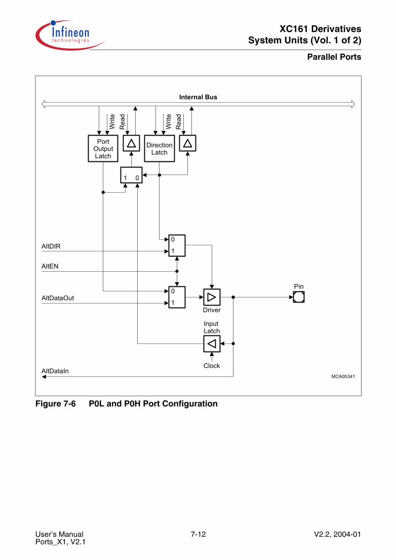
XC161 DerivativesSystem Units (Vol. 1 of 2)
Parallel Ports
Figure 7-6 P0L and P0H Port Configuration
MCA05341
DirectionLatch
Rea
dW
rite
Rea
dW
rite
PortOutputLatch
1 0
AltEN
Driver
InputLatch
Clock
Pin
Internal Bus
0
1
0
1
AltDIR
AltDataOut
AltDataIn
User’s Manual 7-12 V2.2, 2004-01Ports_X1, V2.1
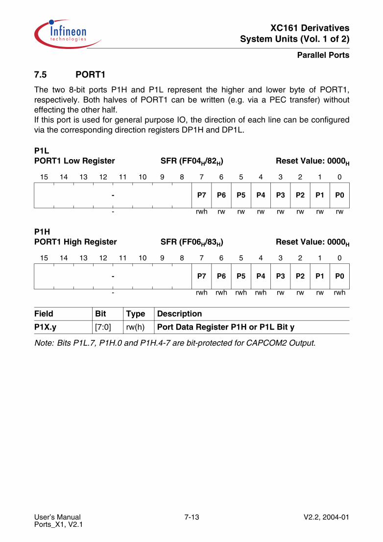
XC161 DerivativesSystem Units (Vol. 1 of 2)
Parallel Ports
7.5 PORT1
The two 8-bit ports P1H and P1L represent the higher and lower byte of PORT1,respectively. Both halves of PORT1 can be written (e.g. via a PEC transfer) withouteffecting the other half.If this port is used for general purpose IO, the direction of each line can be configuredvia the corresponding direction registers DP1H and DP1L.
Note: Bits P1L.7, P1H.0 and P1H.4-7 are bit-protected for CAPCOM2 Output.
P1L PORT1 Low Register SFR (FF04H/82H) Reset Value: 0000H
15 14 13 12 11 10 9 8 7 6 5 4 3 2 1 0
- P7 P6 P5 P4 P3 P2 P1 P0
- rwh rw rw rw rw rw rw rw
P1HPORT1 High Register SFR (FF06H/83H) Reset Value: 0000H
15 14 13 12 11 10 9 8 7 6 5 4 3 2 1 0
- P7 P6 P5 P4 P3 P2 P1 P0
- rwh rwh rwh rwh rw rw rw rwh
Field Bit Type Description
P1X.y [7:0] rw(h) Port Data Register P1H or P1L Bit y
User’s Manual 7-13 V2.2, 2004-01Ports_X1, V2.1
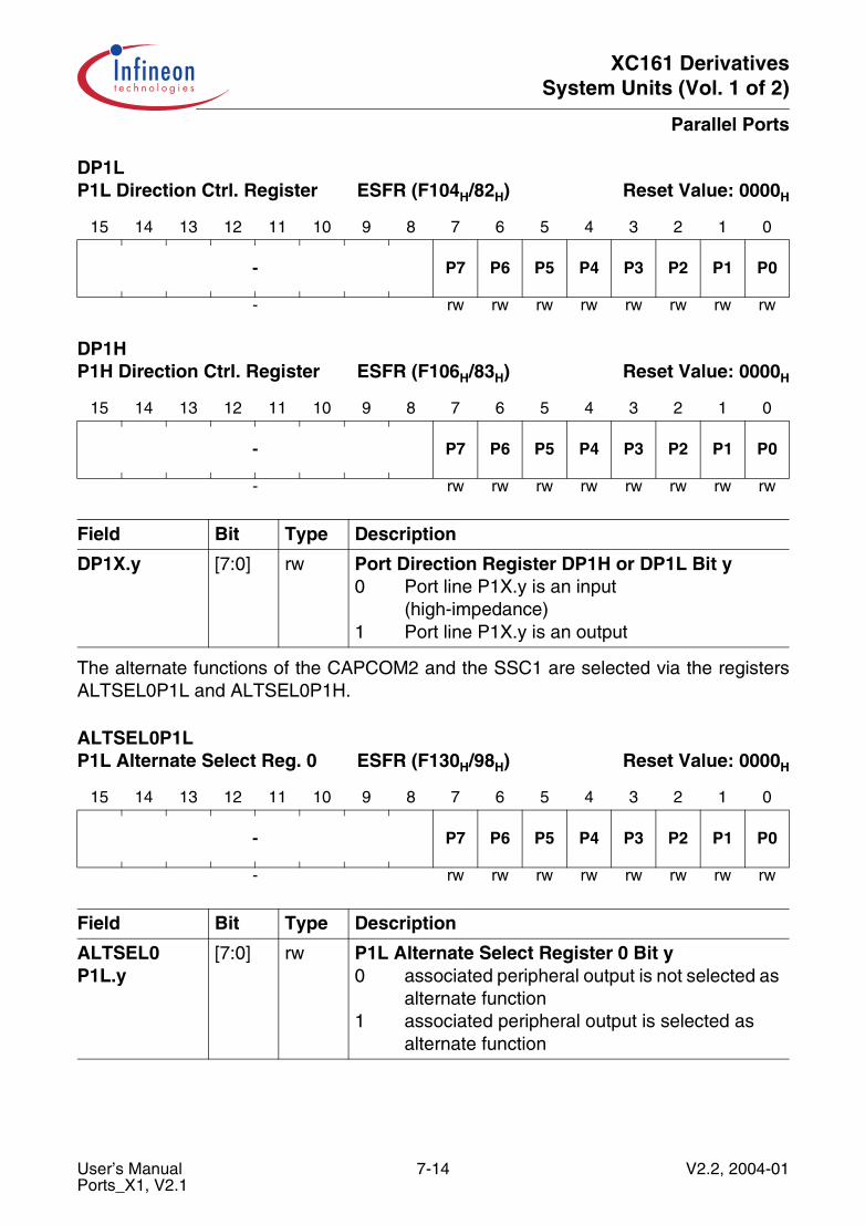
XC161 DerivativesSystem Units (Vol. 1 of 2)
Parallel Ports
The alternate functions of the CAPCOM2 and the SSC1 are selected via the registersALTSEL0P1L and ALTSEL0P1H.
DP1L P1L Direction Ctrl. Register ESFR (F104H/82H) Reset Value: 0000H
15 14 13 12 11 10 9 8 7 6 5 4 3 2 1 0
- P7 P6 P5 P4 P3 P2 P1 P0
- rw rw rw rw rw rw rw rw
DP1HP1H Direction Ctrl. Register ESFR (F106H/83H) Reset Value: 0000H
15 14 13 12 11 10 9 8 7 6 5 4 3 2 1 0
- P7 P6 P5 P4 P3 P2 P1 P0
- rw rw rw rw rw rw rw rw
Field Bit Type Description
DP1X.y [7:0] rw Port Direction Register DP1H or DP1L Bit y0 Port line P1X.y is an input
(high-impedance)1 Port line P1X.y is an output
ALTSEL0P1LP1L Alternate Select Reg. 0 ESFR (F130H/98H) Reset Value: 0000H
15 14 13 12 11 10 9 8 7 6 5 4 3 2 1 0
- P7 P6 P5 P4 P3 P2 P1 P0
- rw rw rw rw rw rw rw rw
Field Bit Type Description
ALTSEL0P1L.y
[7:0] rw P1L Alternate Select Register 0 Bit y0 associated peripheral output is not selected as
alternate function1 associated peripheral output is selected as
alternate function
User’s Manual 7-14 V2.2, 2004-01Ports_X1, V2.1

XC161 DerivativesSystem Units (Vol. 1 of 2)
Parallel Ports
ALTSEL0P1HP1H Alternate Select Reg. 0 ESFR (F120H/90H) Reset Value: 0000H
15 14 13 12 11 10 9 8 7 6 5 4 3 2 1 0
- P7 P6 P5 P4 P3 P2 P1 P0
- rw rw rw rw rw rw rw rw
Field Bit Type Description
ALTSEL0P1H.y
[7:0] rw P1H Alternate Select Register 0 Bit y0 associated peripheral output is not selected as
alternate function1 associated peripheral output is selected as
alternate function
User’s Manual 7-15 V2.2, 2004-01Ports_X1, V2.1
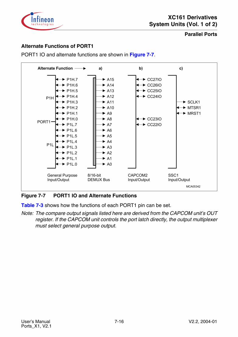
XC161 DerivativesSystem Units (Vol. 1 of 2)
Parallel Ports
Alternate Functions of PORT1
PORT1 IO and alternate functions are shown in Figure 7-7.
Figure 7-7 PORT1 IO and Alternate Functions
Table 7-3 shows how the functions of each PORT1 pin can be set.
Note: The compare output signals listed here are derived from the CAPCOM unit’s OUTregister. If the CAPCOM unit controls the port latch directly, the output multiplexermust select general purpose output.
MCA05342
P1H
P1L
PORT1
Alternate Function
General PurposeInput/Output
a)
8/16-bitDEMUX Bus
b)
CAPCOM2Input/Output
c)
SSC1Input/Output
MTSR1MRST1
SCLK1
CC27IOCC26IOCC25IOCC24IO
CC23IOCC22IO
A15A14A13A12A11A10A9A8A7A6A5A4A3A2A1A0
P1H.7P1H.6P1H.5P1H.4P1H.3P1H.2P1H.1P1H.0P1L.7P1L.6P1L.5P1L.4P1L.3P1L.2P1L.1P1L.0
User’s Manual 7-16 V2.2, 2004-01Ports_X1, V2.1

XC161 DerivativesSystem Units (Vol. 1 of 2)
Parallel Ports
Table 7-3 PORT1 Functions
Port Pin Pin Function Associated Register/ Module
Alternate Function
Control Direction
P1L.0 General purpose input P1L.0 EBC inactive (AltEN1 = 0) and ALTSEL0P1L.P0 = 0
DP1L.P0 = 0
General purpose output DP1L.P0 = 1
Address line outputA0
EBC EBC active (AltEN1 = 1)
Output(AltDIR = 1)
P1L.1 General purpose input P1L.1 EBC inactive (AltEN1 = 0) and ALTSEL0P1L.P1 = 0
DP1L.P1 = 0
General purpose output DP1L.P1 = 1
Address line outputA1
EBC EBC active (AltEN1 = 1)
Output(AltDIR = 1)
P1L.2 General purpose input P1L.2 EBC inactive (AltEN1 = 0) and ALTSEL0P1L.P2 = 0
DP1L.P2 = 0
General purpose output DP1L.P2 = 1
Address line outputA2
EBC EBC active (AltEN1 = 1)
Output(AltDIR = 1)
P1L.3 General purpose input P1L.3 EBC inactive (AltEN1 = 0) and ALTSEL0P1L.P3 = 0
DP1L.P3 = 0
General purpose output DP1L.P3 = 1
Address line outputA3
EBC EBC active (AltEN1 = 1)
Output(AltDIR = 1)
P1L.4 General purpose input P1L.4 EBC inactive (AltEN1 = 0) and ALTSEL0P1L.P4 = 1
DP1L.P4 = 0
General purpose output DP1L.P4 = 1
Address line outputA4
EBC EBC active (AltEN1 = 1)
Output(AltDIR = 1)
User’s Manual 7-17 V2.2, 2004-01Ports_X1, V2.1
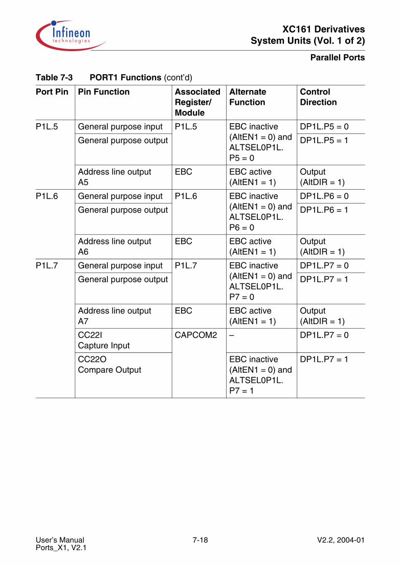
XC161 DerivativesSystem Units (Vol. 1 of 2)
Parallel Ports
P1L.5 General purpose input P1L.5 EBC inactive (AltEN1 = 0) and ALTSEL0P1L.P5 = 0
DP1L.P5 = 0
General purpose output DP1L.P5 = 1
Address line outputA5
EBC EBC active (AltEN1 = 1)
Output(AltDIR = 1)
P1L.6 General purpose input P1L.6 EBC inactive (AltEN1 = 0) and ALTSEL0P1L.P6 = 0
DP1L.P6 = 0
General purpose output DP1L.P6 = 1
Address line outputA6
EBC EBC active (AltEN1 = 1)
Output(AltDIR = 1)
P1L.7 General purpose input P1L.7 EBC inactive (AltEN1 = 0) and ALTSEL0P1L.P7 = 0
DP1L.P7 = 0
General purpose output DP1L.P7 = 1
Address line outputA7
EBC EBC active (AltEN1 = 1)
Output(AltDIR = 1)
CC22ICapture Input
CAPCOM2 – DP1L.P7 = 0
CC22OCompare Output
EBC inactive (AltEN1 = 0) and ALTSEL0P1L.P7 = 1
DP1L.P7 = 1
Table 7-3 PORT1 Functions (cont’d)
Port Pin Pin Function Associated Register/ Module
Alternate Function
Control Direction
User’s Manual 7-18 V2.2, 2004-01Ports_X1, V2.1
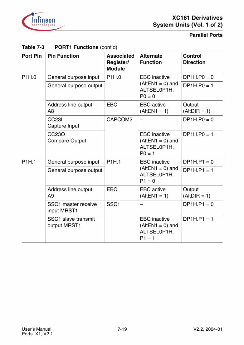
XC161 DerivativesSystem Units (Vol. 1 of 2)
Parallel Ports
P1H.0 General purpose input P1H.0 EBC inactive (AltEN1 = 0) and ALTSEL0P1H.P0 = 0
DP1H.P0 = 0
General purpose output DP1H.P0 = 1
Address line outputA8
EBC EBC active (AltEN1 = 1)
Output(AltDIR = 1)
CC23ICapture Input
CAPCOM2 – DP1H.P0 = 0
CC23OCompare Output
EBC inactive (AltEN1 = 0) and ALTSEL0P1H.P0 = 1
DP1H.P0 = 1
P1H.1 General purpose input P1H.1 EBC inactive (AltEN1 = 0) and ALTSEL0P1H.P1 = 0
DP1H.P1 = 0
General purpose output DP1H.P1 = 1
Address line outputA9
EBC EBC active (AltEN1 = 1)
Output(AltDIR = 1)
SSC1 master receive input MRST1
SSC1 – DP1H.P1 = 0
SSC1 slave transmit output MRST1
EBC inactive (AltEN1 = 0) and ALTSEL0P1H.P1 = 1
DP1H.P1 = 1
Table 7-3 PORT1 Functions (cont’d)
Port Pin Pin Function Associated Register/ Module
Alternate Function
Control Direction
User’s Manual 7-19 V2.2, 2004-01Ports_X1, V2.1

XC161 DerivativesSystem Units (Vol. 1 of 2)
Parallel Ports
P1H.2 General purpose input P1H.2 EBC inactive (AltEN1 = 0) and ALTSEL0P1H.P2 = 0
DP1H.P2 = 0
General purpose output DP1H.P2 = 1
Address line outputA10
EBC EBC active (AltEN1 = 1)
Output(AltDIR = 1)
SSC1 slave receive input MTSR1
SSC1 – DP1H.P2 = 0
SSC1 master transmit output MTSR1
EBC inactive (AltEN1 = 0) and ALTSEL0P1H.P2 = 1
DP1H.P2 = 1
P1H.3 General purpose input P1H.3 EBC inactive (AltEN1 = 0) and ALTSEL0P1H.P3 = 0
DP1H.P3 = 0
General purpose output DP1H.P3 = 1
Address line outputA11
EBC EBC active (AltEN1 = 1)
Output(AltDIR = 1)
SSC1 clock input SCLK1
SSC1 – DP1H.P3 = 0
SSC1 clock output SCLK1
EBC inactive (AltEN1 = 0) and ALTSEL0P1H.P3 = 1
DP1H.P3 = 1
Table 7-3 PORT1 Functions (cont’d)
Port Pin Pin Function Associated Register/ Module
Alternate Function
Control Direction
User’s Manual 7-20 V2.2, 2004-01Ports_X1, V2.1
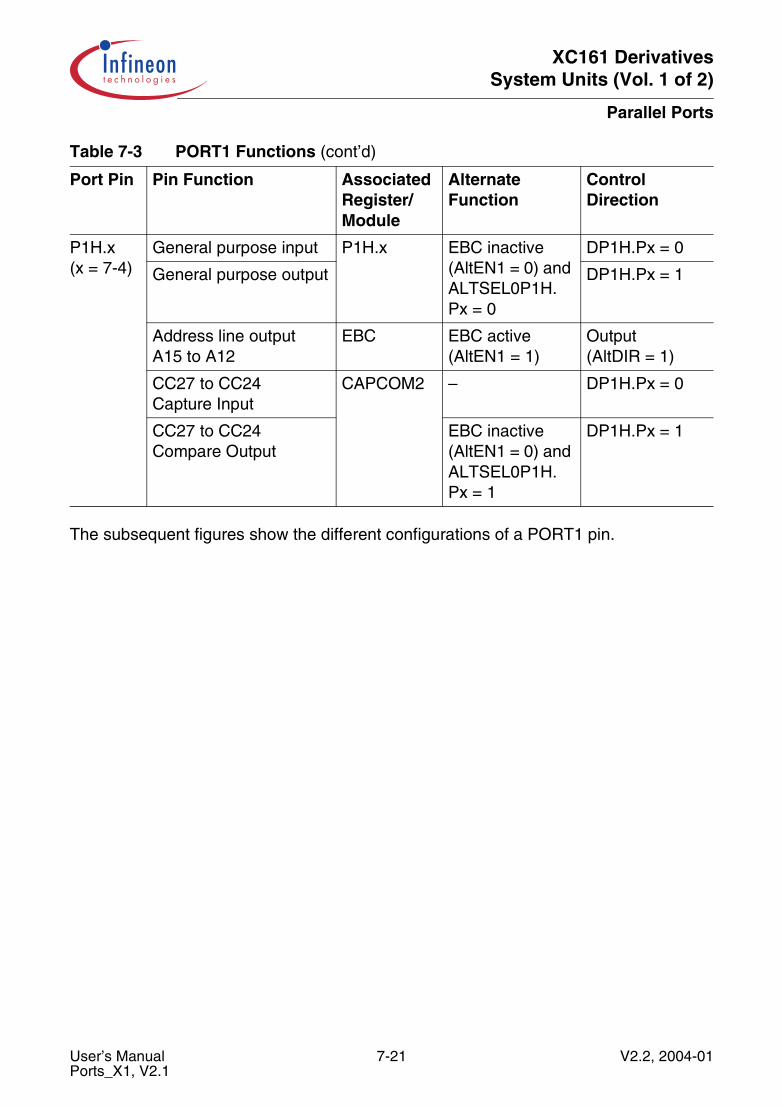
XC161 DerivativesSystem Units (Vol. 1 of 2)
Parallel Ports
The subsequent figures show the different configurations of a PORT1 pin.
P1H.x(x = 7-4)
General purpose input P1H.x EBC inactive (AltEN1 = 0) and ALTSEL0P1H.Px = 0
DP1H.Px = 0
General purpose output DP1H.Px = 1
Address line outputA15 to A12
EBC EBC active (AltEN1 = 1)
Output(AltDIR = 1)
CC27 to CC24Capture Input
CAPCOM2 – DP1H.Px = 0
CC27 to CC24Compare Output
EBC inactive (AltEN1 = 0) and ALTSEL0P1H.Px = 1
DP1H.Px = 1
Table 7-3 PORT1 Functions (cont’d)
Port Pin Pin Function Associated Register/ Module
Alternate Function
Control Direction
User’s Manual 7-21 V2.2, 2004-01Ports_X1, V2.1

XC161 DerivativesSystem Units (Vol. 1 of 2)
Parallel Ports
Figure 7-8 P1L.0 to P1L.6 and P1H.1 to P1H.3 Port Configuration
Table 7-4 P1L.0 to P1L.6 and P1H.1 to P1H.3 Alternate Function Control
Pins Control Lines Registers Function
AltEN AltDIR
DP1L/DP1H
ALTSEL0P1L/P1H2 1
P1L.y(y = 0-6)P1H.x(x = 1-3)
0 0 – 0 or 1 0 GPIO
0 –
– 0 0 – SSC1
1 1 1 SSC1
X 1 1 – X EBC active: address line output
MCA05343
DirectionLatch
Rea
dW
rite
Rea
dW
rite
PortOutputLatch
1 0
X1
10
00
X1
00
10AltDataOut (EBC)
AltEN1 (EBC)
‘1’
AltDataOut (SSC1)
Driver
InputLatch
Clock
Pin
Internal Bus
AlternateFunction
Select Reg. 0
Rea
d
Writ
e
AltDataIn
AltEN2
User’s Manual 7-22 V2.2, 2004-01Ports_X1, V2.1
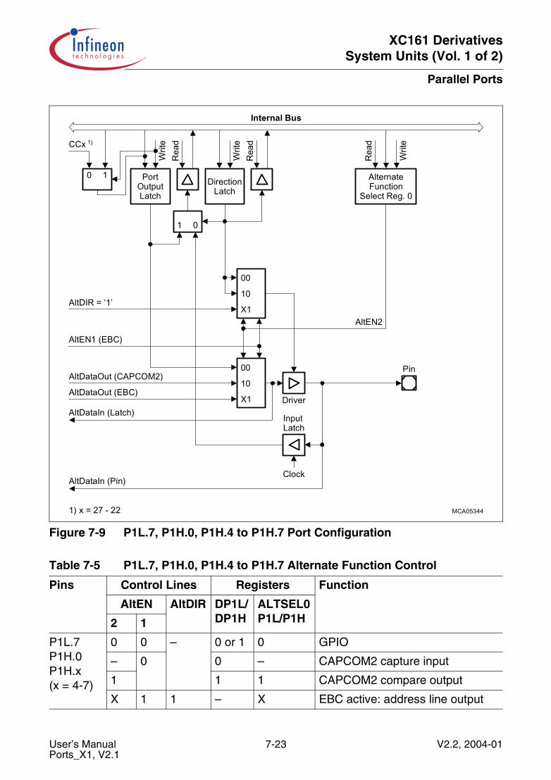
XC161 DerivativesSystem Units (Vol. 1 of 2)
Parallel Ports
Figure 7-9 P1L.7, P1H.0, P1H.4 to P1H.7 Port Configuration
Table 7-5 P1L.7, P1H.0, P1H.4 to P1H.7 Alternate Function Control
Pins Control Lines Registers Function
AltEN AltDIR DP1L/DP1H
ALTSEL0P1L/P1H2 1
P1L.7P1H.0P1H.x(x = 4-7)
0 0 – 0 or 1 0 GPIO
– 0 0 – CAPCOM2 capture input
1 1 1 CAPCOM2 compare output
X 1 1 – X EBC active: address line output
MCA05344
DirectionLatch
Rea
dW
rite
Rea
dW
rite
PortOutputLatch
1 0
X1
10
00
X1
00
10AltDataOut (EBC)
AltEN1 (EBC)
AltDataOut (CAPCOM2)
Driver
InputLatch
Clock
Pin
Internal Bus
AlternateFunction
Select Reg. 0
Rea
d
Writ
eAltDataIn (Latch)
AltDIR = ‘1’
AltDataIn (Pin)
0 1
CCx 1)
1) x = 27 - 22
AltEN2
User’s Manual 7-23 V2.2, 2004-01Ports_X1, V2.1

XC161 DerivativesSystem Units (Vol. 1 of 2)
Parallel Ports
7.6 Port 2
If this 8-bit port is used for general purpose IO, the direction of each line can beconfigured via the corresponding direction register DP2. Each port line can be switchedinto push/pull or open drain mode via the open drain control register ODP2.
Note: Bits P2.8 - P2.15 are bit-protected for CAPCOM1 Output.
P2 Port 2 Data Register SFR (FFC0H/E0H) Reset Value: 0000H
15 14 13 12 11 10 9 8 7 6 5 4 3 2 1 0
P15 P14 P13 P12 P11 P10 P9 P8 -
rwh rwh rwh rwh rwh rwh rwh rwh -
Field Bit Type Description
P2.y [15:8] rwh Port Data Register P2 Bit y
DP2 P2 Direction Ctrl. Register SFR (FFC2H/E1H) Reset Value: 0000H
15 14 13 12 11 10 9 8 7 6 5 4 3 2 1 0
P15 P14 P13 P12 P11 P10 P9 P8 -
rw rw rw rw rw rw rw rw -
Field Bit Type Description
DP2.y [15:8] rw Port Direction Register DP2 Bit y0 Port line P2.y is an input
(high-impedance)1 Port line P2.y is an output
User’s Manual 7-24 V2.2, 2004-01Ports_X1, V2.1
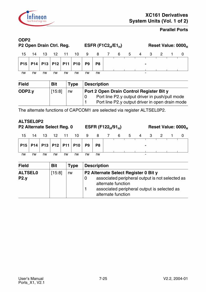
XC161 DerivativesSystem Units (Vol. 1 of 2)
Parallel Ports
The alternate functions of CAPCOM1 are selected via register ALTSEL0P2.
ODP2 P2 Open Drain Ctrl. Reg. ESFR (F1C2H/E1H) Reset Value: 0000H
15 14 13 12 11 10 9 8 7 6 5 4 3 2 1 0
P15 P14 P13 P12 P11 P10 P9 P8 -
rw rw rw rw rw rw rw rw -
Field Bit Type Description
ODP2.y [15:8] rw Port 2 Open Drain Control Register Bit y0 Port line P2.y output driver in push/pull mode1 Port line P2.y output driver in open drain mode
ALTSEL0P2P2 Alternate Select Reg. 0 ESFR (F122H/91H) Reset Value: 0000H
15 14 13 12 11 10 9 8 7 6 5 4 3 2 1 0
P15 P14 P13 P12 P11 P10 P9 P8 -
rw rw rw rw rw rw rw rw -
Field Bit Type Description
ALTSEL0P2.y
[15:8] rw P2 Alternate Select Register 0 Bit y0 associated peripheral output is not selected as
alternate function 1 associated peripheral output is selected as
alternate function
User’s Manual 7-25 V2.2, 2004-01Ports_X1, V2.1
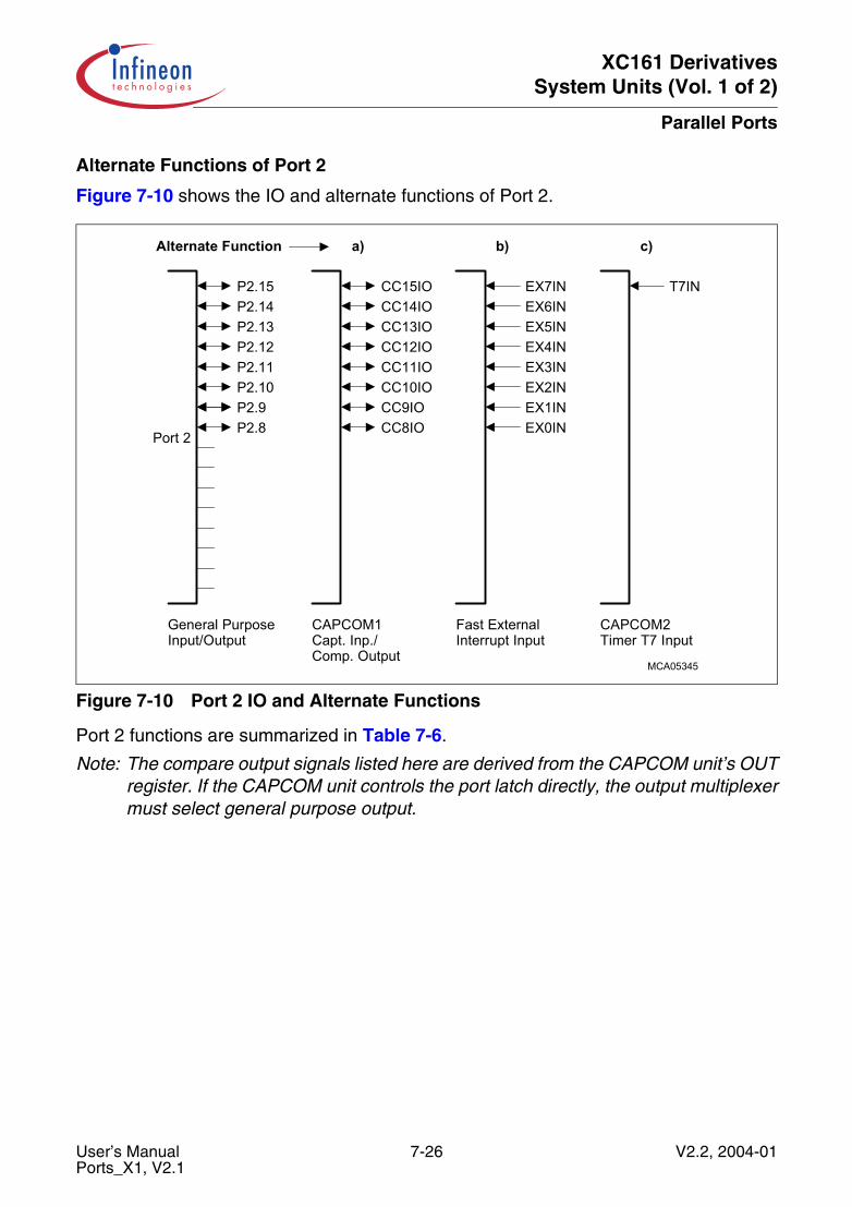
XC161 DerivativesSystem Units (Vol. 1 of 2)
Parallel Ports
Alternate Functions of Port 2
Figure 7-10 shows the IO and alternate functions of Port 2.
Figure 7-10 Port 2 IO and Alternate Functions
Port 2 functions are summarized in Table 7-6.
Note: The compare output signals listed here are derived from the CAPCOM unit’s OUTregister. If the CAPCOM unit controls the port latch directly, the output multiplexermust select general purpose output.
MCA05345
Port 2
Alternate Function a) b) c)
T7IN
General PurposeInput/Output
CAPCOM1Capt. Inp./Comp. Output
Fast ExternalInterrupt Input
CAPCOM2Timer T7 Input
EX7INEX6INEX5INEX4INEX3INEX2INEX1INEX0IN
CC15IOCC14IOCC13IOCC12IOCC11IOCC10IOCC9IOCC8IO
P2.15P2.14P2.13P2.12P2.11P2.10P2.9P2.8
User’s Manual 7-26 V2.2, 2004-01Ports_X1, V2.1
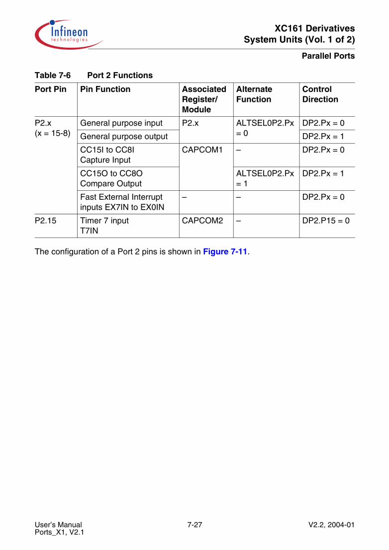
XC161 DerivativesSystem Units (Vol. 1 of 2)
Parallel Ports
The configuration of a Port 2 pins is shown in Figure 7-11.
Table 7-6 Port 2 Functions
Port Pin Pin Function Associated Register/ Module
Alternate Function
Control Direction
P2.x(x = 15-8)
General purpose input P2.x ALTSEL0P2.Px = 0
DP2.Px = 0
General purpose output DP2.Px = 1
CC15I to CC8ICapture Input
CAPCOM1 – DP2.Px = 0
CC15O to CC8OCompare Output
ALTSEL0P2.Px = 1
DP2.Px = 1
Fast External Interrupt inputs EX7IN to EX0IN
– – DP2.Px = 0
P2.15 Timer 7 inputT7IN
CAPCOM2 – DP2.P15 = 0
User’s Manual 7-27 V2.2, 2004-01Ports_X1, V2.1
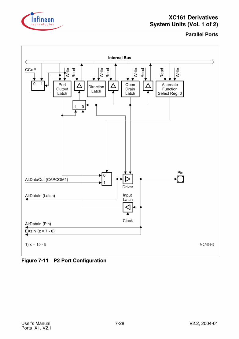
XC161 DerivativesSystem Units (Vol. 1 of 2)
Parallel Ports
Figure 7-11 P2 Port Configuration
MCA05346
DirectionLatch
Rea
dW
rite
Rea
dW
rite
PortOutputLatch
1 0
Driver
InputLatch
Clock
Pin
Internal Bus
0
1AltDataOut (CAPCOM1)
EXzIN (z = 7 - 0)
AlternateFunction
Select Reg. 0
Rea
d
Writ
e
Rea
d
OpenDrainLatch
0 1
CCx 1)
Writ
e
AltDataIn (Pin)
AltDataIn (Latch)
1) x = 15 - 8
User’s Manual 7-28 V2.2, 2004-01Ports_X1, V2.1
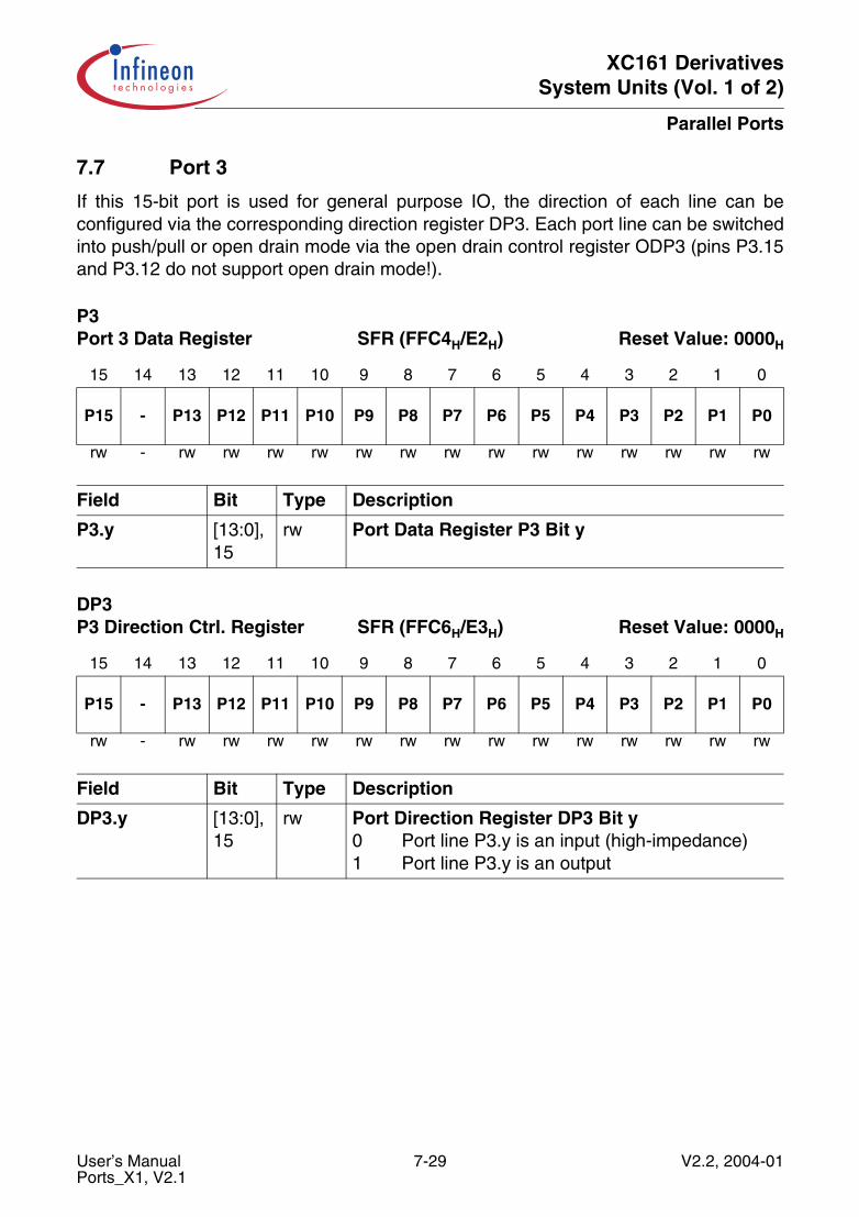
XC161 DerivativesSystem Units (Vol. 1 of 2)
Parallel Ports
7.7 Port 3
If this 15-bit port is used for general purpose IO, the direction of each line can beconfigured via the corresponding direction register DP3. Each port line can be switchedinto push/pull or open drain mode via the open drain control register ODP3 (pins P3.15and P3.12 do not support open drain mode!).
P3 Port 3 Data Register SFR (FFC4H/E2H) Reset Value: 0000H
15 14 13 12 11 10 9 8 7 6 5 4 3 2 1 0
P15 - P13 P12 P11 P10 P9 P8 P7 P6 P5 P4 P3 P2 P1 P0
rw - rw rw rw rw rw rw rw rw rw rw rw rw rw rw
Field Bit Type Description
P3.y [13:0], 15
rw Port Data Register P3 Bit y
DP3 P3 Direction Ctrl. Register SFR (FFC6H/E3H) Reset Value: 0000H
15 14 13 12 11 10 9 8 7 6 5 4 3 2 1 0
P15 - P13 P12 P11 P10 P9 P8 P7 P6 P5 P4 P3 P2 P1 P0
rw - rw rw rw rw rw rw rw rw rw rw rw rw rw rw
Field Bit Type Description
DP3.y [13:0], 15
rw Port Direction Register DP3 Bit y0 Port line P3.y is an input (high-impedance)1 Port line P3.y is an output
User’s Manual 7-29 V2.2, 2004-01Ports_X1, V2.1
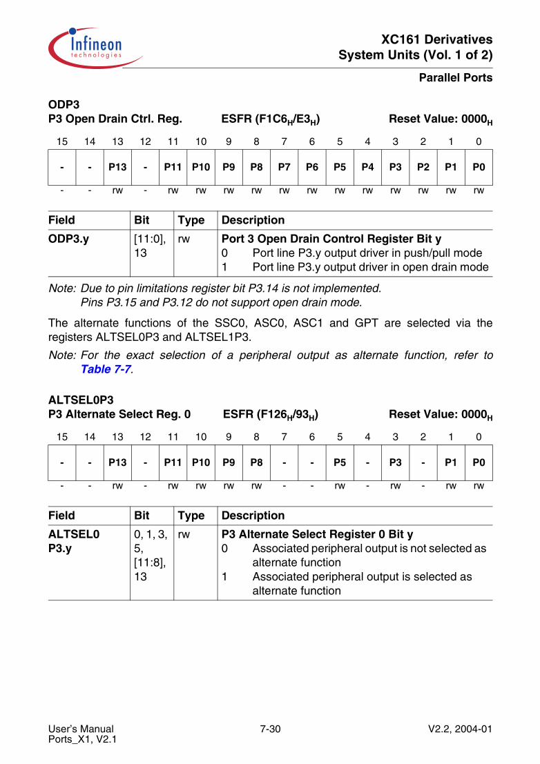
XC161 DerivativesSystem Units (Vol. 1 of 2)
Parallel Ports
Note: Due to pin limitations register bit P3.14 is not implemented.Pins P3.15 and P3.12 do not support open drain mode.
The alternate functions of the SSC0, ASC0, ASC1 and GPT are selected via theregisters ALTSEL0P3 and ALTSEL1P3.
Note: For the exact selection of a peripheral output as alternate function, refer toTable 7-7.
ODP3 P3 Open Drain Ctrl. Reg. ESFR (F1C6H/E3H) Reset Value: 0000H
15 14 13 12 11 10 9 8 7 6 5 4 3 2 1 0
- - P13 - P11 P10 P9 P8 P7 P6 P5 P4 P3 P2 P1 P0
- - rw - rw rw rw rw rw rw rw rw rw rw rw rw
Field Bit Type Description
ODP3.y [11:0], 13
rw Port 3 Open Drain Control Register Bit y0 Port line P3.y output driver in push/pull mode1 Port line P3.y output driver in open drain mode
ALTSEL0P3P3 Alternate Select Reg. 0 ESFR (F126H/93H) Reset Value: 0000H
15 14 13 12 11 10 9 8 7 6 5 4 3 2 1 0
- - P13 - P11 P10 P9 P8 - - P5 - P3 - P1 P0
- - rw - rw rw rw rw - - rw - rw - rw rw
Field Bit Type Description
ALTSEL0P3.y
0, 1, 3, 5, [11:8], 13
rw P3 Alternate Select Register 0 Bit y0 Associated peripheral output is not selected as
alternate function 1 Associated peripheral output is selected as
alternate function
User’s Manual 7-30 V2.2, 2004-01Ports_X1, V2.1
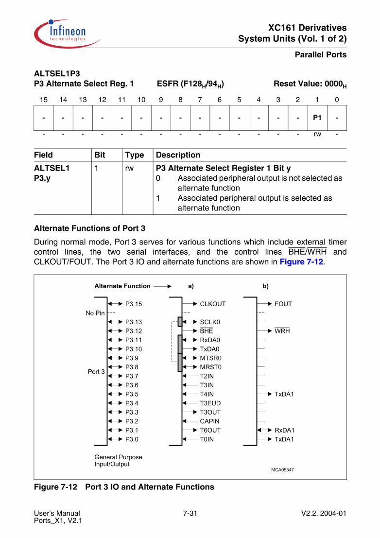
XC161 DerivativesSystem Units (Vol. 1 of 2)
Parallel Ports
Alternate Functions of Port 3
During normal mode, Port 3 serves for various functions which include external timercontrol lines, the two serial interfaces, and the control lines BHE/WRH andCLKOUT/FOUT. The Port 3 IO and alternate functions are shown in Figure 7-12.
Figure 7-12 Port 3 IO and Alternate Functions
ALTSEL1P3P3 Alternate Select Reg. 1 ESFR (F128H/94H) Reset Value: 0000H
15 14 13 12 11 10 9 8 7 6 5 4 3 2 1 0
- - - - - - - - - - - - - - P1 -
- - - - - - - - - - - - - - rw -
Field Bit Type Description
ALTSEL1P3.y
1 rw P3 Alternate Select Register 1 Bit y0 Associated peripheral output is not selected as
alternate function 1 Associated peripheral output is selected as
alternate function
MCA05347
Port 3
Alternate Function
General PurposeInput/Output
No Pin
a) b)
CLKOUT
SCLK0BHERxDA0TxDA0MTSR0MRST0T2INT3INT4INT3EUDT3OUTCAPINT6OUTT0IN
FOUT
WRH
TxDA1
RxDA1TxDA1
P3.15
P3.13P3.12P3.11P3.10P3.9P3.8P3.7P3.6P3.5P3.4P3.3P3.2P3.1P3.0
User’s Manual 7-31 V2.2, 2004-01Ports_X1, V2.1

XC161 DerivativesSystem Units (Vol. 1 of 2)
Parallel Ports
The alternate output functions - TxDA1, T6OUT, T3OUT, MRST0, MTSR0, TxDA0,RxDA0 and SCLK0 - when selected, is ANDed with the port output latch line (generalpurpose output).
A complete listing of Port 3 functions is found in Table 7-7.
Table 7-7 Port 3 Functions
Port Pin Pin Function Associated Register/ Module
Alternate Function
Control Direction
P3.0 General purpose input P3.0 ALTSEL0P3.P0= 0
DP3.P0 = 0
General purpose output DP3.P0 = 1
ASC1 transmitter outputTxDA1
ASC1 ALTSEL0P3.P0= 1 andP3.P0 = 1
DP3.P0 = 1
CAPCOM1 Timer T0 count input, T0IN
CAPCOM1 – DP3.P0 = 0
P3.1 General purpose input P3.1 ALTSEL0P3.P1= 0 and ALTSEL1P3.P1= 0
DP3.P1 = 0
General purpose output DP3.P1 = 1
Timer T6 Toggle Latch output, T6OUT
GPT ALTSEL0P3.P1= 0 and ALTSEL1P3.P1= 1 andP3.P1 = 1
DP3.P1 = 1
ASC1 receiver inputRxDA1, used as input
ASC1 – DP3.P1 = 0
ASC1 receiver inputRxDA1, used as output
ALTSEL0P3.P1= 1
DP3.P1 = 1
P3.2 General purpose input P3.2 – DP3.P2 = 0
General purpose output DP3.P2 = 1
GPT12E Capture inputCAPIN
GPT DP3.P2 = 0
User’s Manual 7-32 V2.2, 2004-01Ports_X1, V2.1

XC161 DerivativesSystem Units (Vol. 1 of 2)
Parallel Ports
P3.3 General purpose input P3.3 ALTSEL0P3.P3= 0
DP3.P3 = 0
General purpose output DP3.P3 = 1
Timer 3 Toggle Latch output, T3OUT
GPT ALTSEL0P3.P3= 1 andP3.P3 = 1
DP3.P3 = 1
P3.4 General purpose input P3.4 – DP3.P4 = 0
General purpose output DP3.P4 = 1
Timer 3 external up/down input, T3EUD
GPT DP3.P4 = 0
P3.5 General purpose input P3.5 ALTSEL0P3.P5= 0
DP3.P5 = 0
General purpose output DP3.P5 = 1
Timer 4 count input, T4IN GPT – DP3.P5 = 0
ASC1 transmitter outputTxDA1
ASC1 ALTSEL0P3.P5= 1
DP3.P5 = 1
P3.6 General purpose input P3.6 – DP3.P6 = 0
General purpose output DP3.P6 = 1
Timer 3 count input, T3IN GPT – DP3.P6 = 0
P3.7 General purpose input P3.7 AltEN1.7 = 0 DP3.P7 = 0
General purpose output DP3.P7 = 1
Timer 2 count input, T2IN GPT – DP3.P7 = 0
P3.8 General purpose input P3.8 ALTSEL0P3.P8= 0
DP3.P8 = 0
General purpose output DP3.P8 = 1
SSC0 master receive input, MRST0
SSC0 – DP3.P8 = 0
SSC0 slave transmit output, MRST0
ALTSEL0P3.P8= 1 andP3.P8 = 1
DP3.P8 = 1
Table 7-7 Port 3 Functions (cont’d)
Port Pin Pin Function Associated Register/ Module
Alternate Function
Control Direction
User’s Manual 7-33 V2.2, 2004-01Ports_X1, V2.1
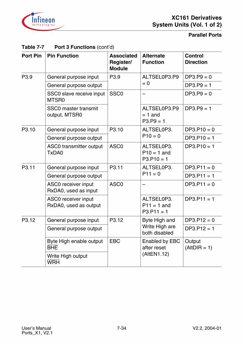
XC161 DerivativesSystem Units (Vol. 1 of 2)
Parallel Ports
P3.9 General purpose input P3.9 ALTSEL0P3.P9= 0
DP3.P9 = 0
General purpose output DP3.P9 = 1
SSC0 slave receive input MTSR0
SSC0 – DP3.P9 = 0
SSC0 master transmit output, MTSR0
ALTSEL0P3.P9= 1 andP3.P9 = 1
DP3.P9 = 1
P3.10 General purpose input P3.10 ALTSEL0P3.P10 = 0
DP3.P10 = 0
General purpose output DP3.P10 = 1
ASC0 transmitter outputTxDA0
ASC0 ALTSEL0P3.P10 = 1 and P3.P10 = 1
DP3.P10 = 1
P3.11 General purpose input P3.11 ALTSEL0P3.P11 = 0
DP3.P11 = 0
General purpose output DP3.P11 = 1
ASC0 receiver inputRxDA0, used as input
ASC0 – DP3.P11 = 0
ASC0 receiver inputRxDA0, used as output
ALTSEL0P3.P11 = 1 andP3.P11 = 1
DP3.P11 = 1
P3.12 General purpose input P3.12 Byte High and Write High are both disabled
DP3.P12 = 0
General purpose output DP3.P12 = 1
Byte High enable output BHE
EBC Enabled by EBC after reset (AltEN1.12)
Output(AltDIR = 1)
Write High outputWRH
Table 7-7 Port 3 Functions (cont’d)
Port Pin Pin Function Associated Register/ Module
Alternate Function
Control Direction
User’s Manual 7-34 V2.2, 2004-01Ports_X1, V2.1
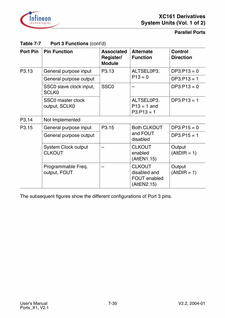
XC161 DerivativesSystem Units (Vol. 1 of 2)
Parallel Ports
The subsequent figures show the different configurations of Port 3 pins.
P3.13 General purpose input P3.13 ALTSEL0P3.P13 = 0
DP3.P13 = 0
General purpose output DP3.P13 = 1
SSC0 slave clock input, SCLK0
SSC0 – DP3.P13 = 0
SSC0 master clock output, SCLK0
ALTSEL0P3.P13 = 1 andP3.P13 = 1
DP3.P13 = 1
P3.14 Not Implemented
P3.15 General purpose input P3.15 Both CLKOUT and FOUT disabled
DP3.P15 = 0
General purpose output DP3.P15 = 1
System Clock outputCLKOUT
– CLKOUT enabled (AltEN1.15)
Output(AltDIR = 1)
Programmable Freq. output, FOUT
– CLKOUT disabled and FOUT enabled (AltEN2.15)
Output(AltDIR = 1)
Table 7-7 Port 3 Functions (cont’d)
Port Pin Pin Function Associated Register/ Module
Alternate Function
Control Direction
User’s Manual 7-35 V2.2, 2004-01Ports_X1, V2.1
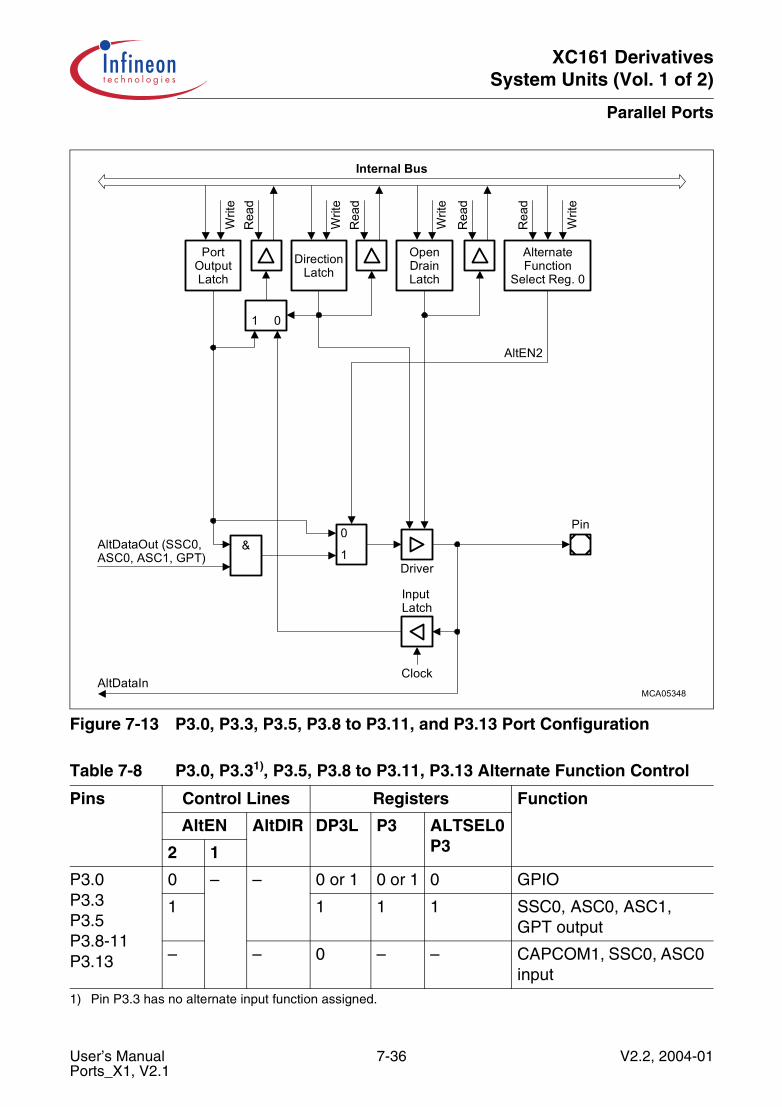
XC161 DerivativesSystem Units (Vol. 1 of 2)
Parallel Ports
Figure 7-13 P3.0, P3.3, P3.5, P3.8 to P3.11, and P3.13 Port Configuration
Table 7-8 P3.0, P3.31), P3.5, P3.8 to P3.11, P3.13 Alternate Function Control
1) Pin P3.3 has no alternate input function assigned.
Pins Control Lines Registers Function
AltEN AltDIR DP3L P3 ALTSEL0P32 1
P3.0P3.3P3.5P3.8-11P3.13
0 – – 0 or 1 0 or 1 0 GPIO
1 1 1 1 SSC0, ASC0, ASC1,GPT output
– – 0 – – CAPCOM1, SSC0, ASC0 input
MCA05348
DirectionLatch
Rea
dW
rite
Rea
dW
rite
PortOutputLatch
1 0
Driver
InputLatch
Clock
Pin
Internal Bus
AlternateFunction
Select Reg. 0
Rea
d
Writ
e
AltDataIn
AltEN2
Rea
d
Writ
e
OpenDrainLatch
&AltDataOut (SSC0,ASC0, ASC1, GPT)
0
1
User’s Manual 7-36 V2.2, 2004-01Ports_X1, V2.1
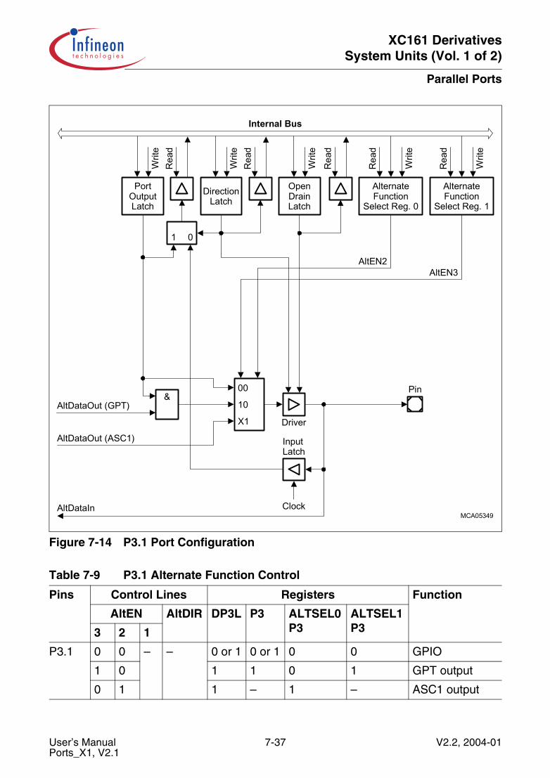
XC161 DerivativesSystem Units (Vol. 1 of 2)
Parallel Ports
Figure 7-14 P3.1 Port Configuration
Table 7-9 P3.1 Alternate Function Control
Pins Control Lines Registers Function
AltEN AltDIR DP3L P3 ALTSEL0P3
ALTSEL1P33 2 1
P3.1 0 0 – – 0 or 1 0 or 1 0 0 GPIO
1 0 1 1 0 1 GPT output
0 1 1 – 1 – ASC1 output
MCA05349
DirectionLatch
Rea
dW
rite
Rea
dW
rite
PortOutputLatch
1 0
X1
00
10
AltDataOut (ASC1)
Driver
InputLatch
Clock
Pin
Internal Bus
AlternateFunction
Select Reg. 0
Rea
d
Writ
e
AltDataIn
AltEN2
AlternateFunction
Select Reg. 1
Rea
d
Writ
e
Writ
e
Rea
d
OpenDrainLatch
AltEN3
&AltDataOut (GPT)
User’s Manual 7-37 V2.2, 2004-01Ports_X1, V2.1
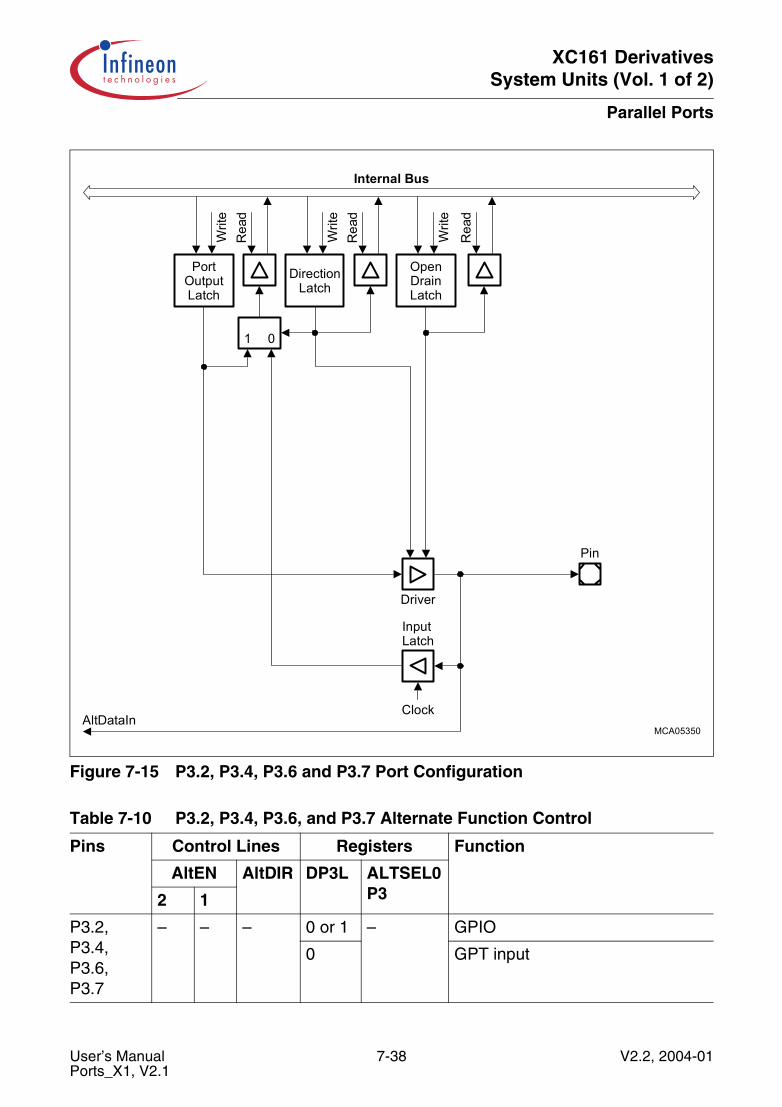
XC161 DerivativesSystem Units (Vol. 1 of 2)
Parallel Ports
Figure 7-15 P3.2, P3.4, P3.6 and P3.7 Port Configuration
Table 7-10 P3.2, P3.4, P3.6, and P3.7 Alternate Function Control
Pins Control Lines Registers Function
AltEN AltDIR DP3L ALTSEL0P32 1
P3.2,P3.4,P3.6,P3.7
– – – 0 or 1 – GPIO
0 GPT input
MCA05350
DirectionLatch
Rea
dW
rite
Rea
dW
rite
PortOutputLatch
1 0
Driver
InputLatch
Clock
Pin
Internal Bus
Rea
d
Writ
e
OpenDrainLatch
AltDataIn
User’s Manual 7-38 V2.2, 2004-01Ports_X1, V2.1

XC161 DerivativesSystem Units (Vol. 1 of 2)
Parallel Ports
Figure 7-16 P3.12 Port Configuration
Table 7-11 P3.12 Alternate Function Control
Pins Control Lines Registers Function
AltEN AltDIR DP3L ALTSEL0P32 1
P3.12 – 0 – 0 or 1 – GPIO
– 1 1 – BHE/WRH output
MCA05351
DirectionLatch
Rea
dW
rite
Rea
dW
rite
PortOutputLatch
1 0
AltEN1 (EBC)
Driver
InputLatch
Clock
Pin
Internal Bus
0
1
0
1
AltDIR = ‘1’
AltDataOut (BHE, WRH)
AltDataIn
User’s Manual 7-39 V2.2, 2004-01Ports_X1, V2.1
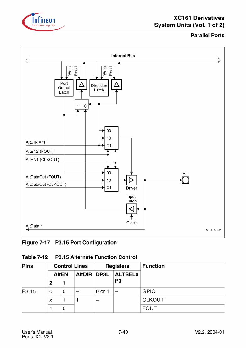
XC161 DerivativesSystem Units (Vol. 1 of 2)
Parallel Ports
Figure 7-17 P3.15 Port Configuration
Table 7-12 P3.15 Alternate Function Control
Pins Control Lines Registers Function
AltEN AltDIR DP3L ALTSEL0P32 1
P3.15 0 0 – 0 or 1 – GPIO
x 1 1 – CLKOUT
1 0 FOUT
MCA05352
DirectionLatch
Rea
dW
rite
Rea
dW
rite
PortOutputLatch
1 0
X1
10
00
X1
00
10
AltEN2 (FOUT)
AltDataOut (CLKOUT)
AltEN1 (CLKOUT)
AltDIR = ‘1’
AltDataOut (FOUT)
AltDataIn
Driver
InputLatch
Clock
Pin
Internal Bus
User’s Manual 7-40 V2.2, 2004-01Ports_X1, V2.1
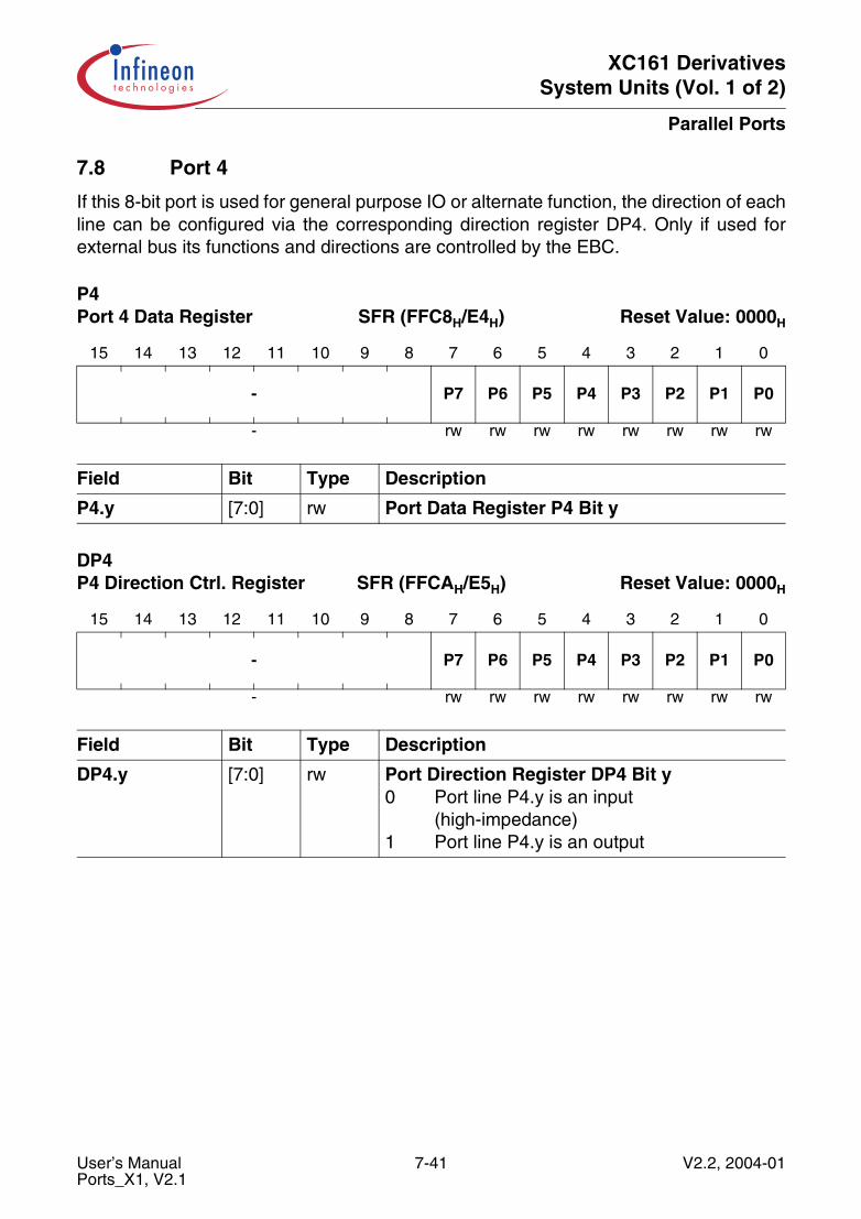
XC161 DerivativesSystem Units (Vol. 1 of 2)
Parallel Ports
7.8 Port 4
If this 8-bit port is used for general purpose IO or alternate function, the direction of eachline can be configured via the corresponding direction register DP4. Only if used forexternal bus its functions and directions are controlled by the EBC.
P4 Port 4 Data Register SFR (FFC8H/E4H) Reset Value: 0000H
15 14 13 12 11 10 9 8 7 6 5 4 3 2 1 0
- P7 P6 P5 P4 P3 P2 P1 P0
- rw rw rw rw rw rw rw rw
Field Bit Type Description
P4.y [7:0] rw Port Data Register P4 Bit y
DP4 P4 Direction Ctrl. Register SFR (FFCAH/E5H) Reset Value: 0000H
15 14 13 12 11 10 9 8 7 6 5 4 3 2 1 0
- P7 P6 P5 P4 P3 P2 P1 P0
- rw rw rw rw rw rw rw rw
Field Bit Type Description
DP4.y [7:0] rw Port Direction Register DP4 Bit y0 Port line P4.y is an input
(high-impedance)1 Port line P4.y is an output
User’s Manual 7-41 V2.2, 2004-01Ports_X1, V2.1
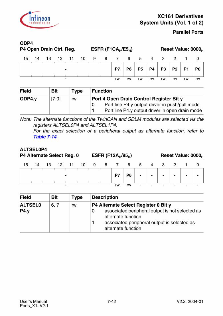
XC161 DerivativesSystem Units (Vol. 1 of 2)
Parallel Ports
Note: The alternate functions of the TwinCAN and SDLM modules are selected via theregisters ALTSEL0P4 and ALTSEL1P4.For the exact selection of a peripheral output as alternate function, refer toTable 7-14.
ODP4 P4 Open Drain Ctrl. Reg. ESFR (F1CAH/E5H) Reset Value: 0000H
15 14 13 12 11 10 9 8 7 6 5 4 3 2 1 0
- P7 P6 P5 P4 P3 P2 P1 P0
- rw rw rw rw rw rw rw rw
Field Bit Type Function
ODP4.y [7:0] rw Port 4 Open Drain Control Register Bit y0 Port line P4.y output driver in push/pull mode1 Port line P4.y output driver in open drain mode
ALTSEL0P4P4 Alternate Select Reg. 0 ESFR (F12AH/95H) Reset Value: 0000H
15 14 13 12 11 10 9 8 7 6 5 4 3 2 1 0
- P7 P6 - - - - - -
- rw rw - - - - - -
Field Bit Type Description
ALTSEL0P4.y
6, 7 rw P4 Alternate Select Register 0 Bit y0 associated peripheral output is not selected as
alternate function1 associated peripheral output is selected as
alternate function
User’s Manual 7-42 V2.2, 2004-01Ports_X1, V2.1

XC161 DerivativesSystem Units (Vol. 1 of 2)
Parallel Ports
Alternate Functions of Port 4
Port 4 pins are utilized as segment address lines during external bus cycles that usesegmentation (i.e. an address space above 64 Kbytes). The number of pins that is usedfor segment address output determines the external address space which is directlyaccessible. The required pins for segment address lines is configured at system start-up. Please refer to System Specification, System Control Unit Chapter.
Note: Port 4 pins (if any) may also be used for general purpose IO or for the CAN orSDLM interface. For the XC161 implementation, the chip select lines are assignedto Port 6.
If segment address lines are selected, the alternate function of Port 4 may be necessaryto access e.g. external memory directly after reset. For this reason Port 4 will beswitched to this alternate function automatically.
Table 7-13 summarizes the possible alternate functions of Port 4 depending on thenumber of selected segment address lines (coded via bitfield SALSEL and defined viaSAPEN in EBCMOD0).
ALTSEL1P4P4 Alternate Select Reg. 1 ESFR (F136H/9BH) Reset Value: 0000H
15 14 13 12 11 10 9 8 7 6 5 4 3 2 1 0
- P7 - - - - - - -
- rw - - - - - - -
Field Bit Type Description
ALTSEL1P4.y
7 rw P4 Alternate Select Register 1 Bit y0 associated peripheral output is not
selected as alternate function 1 associated peripheral output is selected as
alternate function
Table 7-13 Alternate Functions of Port 4
Port 4 Pin
Std. FunctionSALSEL = 0164 KB
Altern. FunctionSALSEL = 11256 KB
Altern. FunctionSALSEL = 001 MB
Altern. FunctionSALSEL = 104 MB
P4.0 GPIO Seg. Addr. A16 Seg. Addr. A16 Seg. Addr. A16
P4.1 GPIO Seg. Addr. A17 Seg. Addr. A17 Seg. Addr. A17
P4.2 GPIO GPIO Seg. Addr. A18 Seg. Addr. A18
P4.3 GPIO GPIO Seg. Addr. A19 Seg. Addr. A19
User’s Manual 7-43 V2.2, 2004-01Ports_X1, V2.1
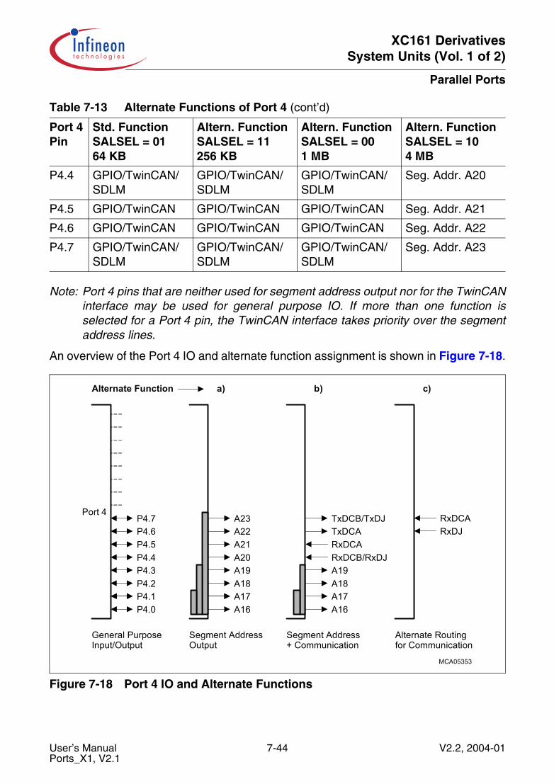
XC161 DerivativesSystem Units (Vol. 1 of 2)
Parallel Ports
Note: Port 4 pins that are neither used for segment address output nor for the TwinCANinterface may be used for general purpose IO. If more than one function isselected for a Port 4 pin, the TwinCAN interface takes priority over the segmentaddress lines.
An overview of the Port 4 IO and alternate function assignment is shown in Figure 7-18.
Figure 7-18 Port 4 IO and Alternate Functions
P4.4 GPIO/TwinCAN/ SDLM
GPIO/TwinCAN/ SDLM
GPIO/TwinCAN/ SDLM
Seg. Addr. A20
P4.5 GPIO/TwinCAN GPIO/TwinCAN GPIO/TwinCAN Seg. Addr. A21
P4.6 GPIO/TwinCAN GPIO/TwinCAN GPIO/TwinCAN Seg. Addr. A22
P4.7 GPIO/TwinCAN/ SDLM
GPIO/TwinCAN/ SDLM
GPIO/TwinCAN/ SDLM
Seg. Addr. A23
Table 7-13 Alternate Functions of Port 4 (cont’d)
Port 4 Pin
Std. FunctionSALSEL = 0164 KB
Altern. FunctionSALSEL = 11256 KB
Altern. FunctionSALSEL = 001 MB
Altern. FunctionSALSEL = 104 MB
MCA05353
Port 4
Alternate Function
General PurposeInput/Output
c)
Alternate Routingfor Communication
a)
Segment AddressOutput
b)
Segment Address+ Communication
TxDCB/TxDJTxDCARxDCARxDCB/RxDJ
RxDCARxDJ
A19A18A17A16
A23A22A21A20A19A18A17A16
P4.7P4.6P4.5P4.4P4.3P4.2P4.1P4.0
User’s Manual 7-44 V2.2, 2004-01Ports_X1, V2.1

XC161 DerivativesSystem Units (Vol. 1 of 2)
Parallel Ports
Table 7-14 Port 4 Functions
Port Pin Pin Function Associated Register/ Module
Alternate Function
Control Direction
P4.x(x = 3-0)
General purpose input P4.x EBC inactive (AltEN1.x = 0)
DP4.Px = 0
General purpose output DP4.Px = 1
Address line outputA19 - A16
EBC EBC active (AltEN1.x = 1)
Output(AltDIR = 1)
P4.4 General purpose input P4.4 EBC inactive (AltEN1.4 = 0)
DP4.P4 = 0
General purpose output DP4.P4 = 1
Address line outputA20
EBC EBC active (AltEN1.4 = 1)
Output(AltDIR = 1)
TwinCAN Receiver input RxDCB
TwinCAN – DP4.P4 = 0
SDLM Receiver input RxDJ
SDLM – DP4.P4 = 0
P4.5 General purpose input P4.5 EBC inactive (AltEN1.5 = 0)
DP4.P5 = 0
General purpose output DP4.P5 = 1
Address line outputA21
EBC EBC active (AltEN1.5 = 1)
Output(AltDIR = 1)
TwinCAN Receiver input RxDCA
TwinCAN – DP4.P5 = 0
P4.6 General purpose input P4.6 EBC inactive (AltEN1.6 = 0) and ALTSEL0P4.P6 = 0
DP4.P6 = 0
General purpose output DP4.P6 = 1
Address line outputA22
EBC EBC active (AltEN1.6 = 1) and ALTSEL0P4.P6 = 0
Output(AltDIR = 1)
TwinCAN Transmitter output TxDCA
TwinCAN ALTSEL0P4.P6 = 1
DP4.P6 = 1
SDLM Receiver input RxDJ
SDLM – DP4.P6 = 0
User’s Manual 7-45 V2.2, 2004-01Ports_X1, V2.1
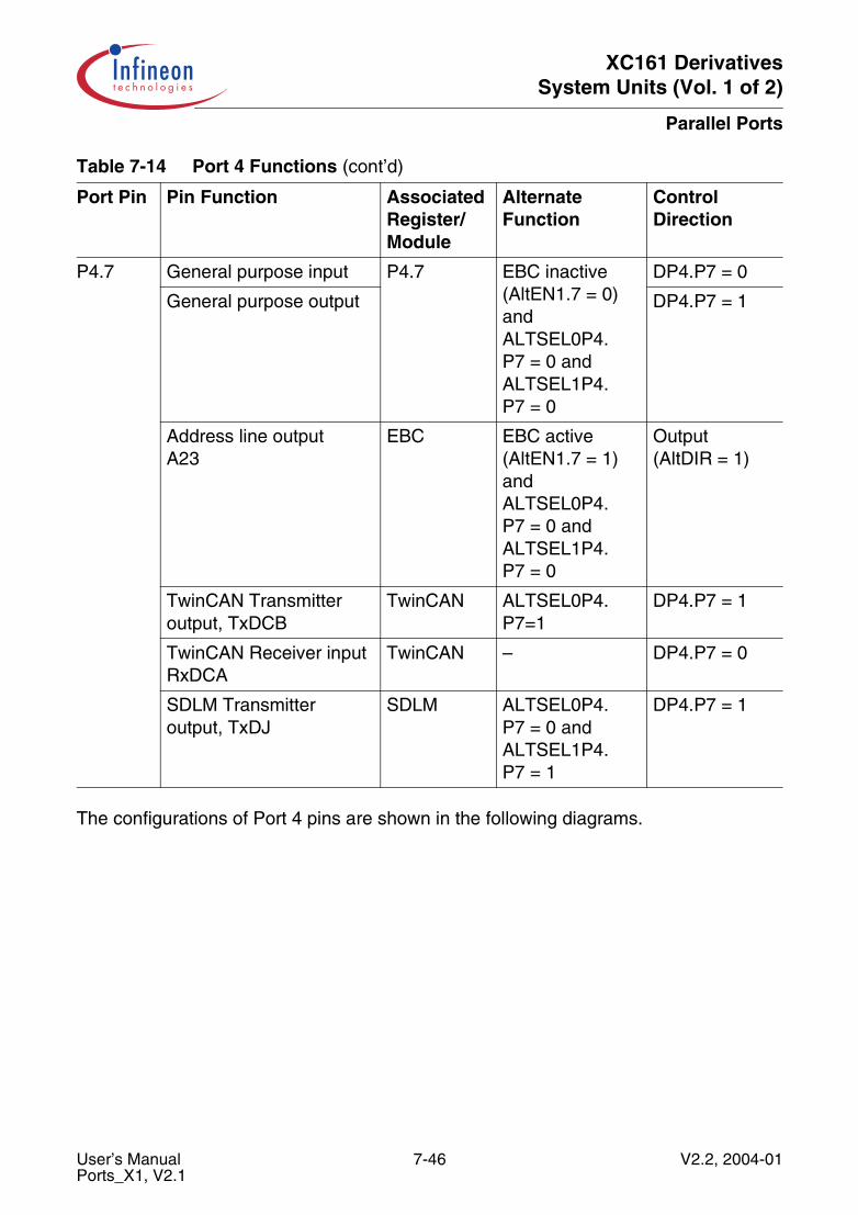
XC161 DerivativesSystem Units (Vol. 1 of 2)
Parallel Ports
The configurations of Port 4 pins are shown in the following diagrams.
P4.7 General purpose input P4.7 EBC inactive (AltEN1.7 = 0) and ALTSEL0P4.P7 = 0 andALTSEL1P4.P7 = 0
DP4.P7 = 0
General purpose output DP4.P7 = 1
Address line outputA23
EBC EBC active (AltEN1.7 = 1) and ALTSEL0P4.P7 = 0 andALTSEL1P4.P7 = 0
Output(AltDIR = 1)
TwinCAN Transmitter output, TxDCB
TwinCAN ALTSEL0P4.P7=1
DP4.P7 = 1
TwinCAN Receiver input RxDCA
TwinCAN – DP4.P7 = 0
SDLM Transmitteroutput, TxDJ
SDLM ALTSEL0P4.P7 = 0 andALTSEL1P4.P7 = 1
DP4.P7 = 1
Table 7-14 Port 4 Functions (cont’d)
Port Pin Pin Function Associated Register/ Module
Alternate Function
Control Direction
User’s Manual 7-46 V2.2, 2004-01Ports_X1, V2.1

XC161 DerivativesSystem Units (Vol. 1 of 2)
Parallel Ports
Figure 7-19 P4.[3:0] Port Configuration
Table 7-15 P4.[3:0] Alternate Function Control
Pins Control Lines Registers Function
AltEN AltDIR DP4L ALTSEL0P4
ALTSEL1P43 2 1
P4.[3:0] – 0 0 – 0 or 1 – – GPIO
X 1 1 – EBC: address
MCA05354
DirectionLatch
Rea
dW
rite
Rea
dW
rite
PortOutputLatch
1 0
AltEN1(EBC for Addr.)
Driver
InputLatch
Clock
Pin
Internal Bus
Rea
d
Writ
e
OpenDrainLatch
0
1
0
1
AltDIR = ‘1’
AltDataOut (A[19:16])
User’s Manual 7-47 V2.2, 2004-01Ports_X1, V2.1
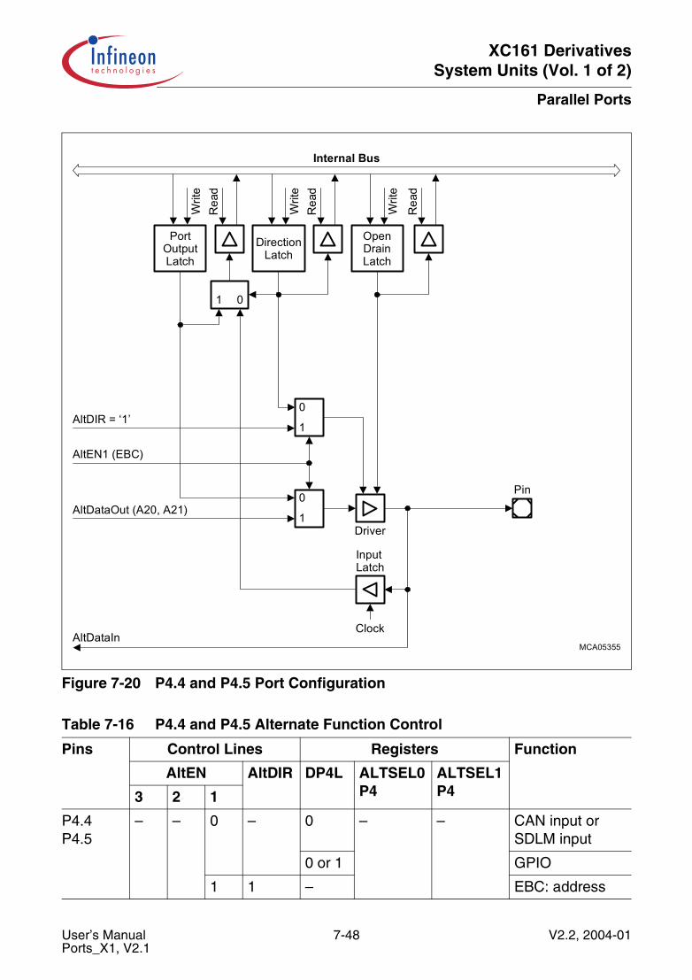
XC161 DerivativesSystem Units (Vol. 1 of 2)
Parallel Ports
Figure 7-20 P4.4 and P4.5 Port Configuration
Table 7-16 P4.4 and P4.5 Alternate Function Control
Pins Control Lines Registers Function
AltEN AltDIR DP4L ALTSEL0P4
ALTSEL1P43 2 1
P4.4P4.5
– – 0 – 0 – – CAN input orSDLM input
0 or 1 GPIO
1 1 – EBC: address
MCA05355
DirectionLatch
Rea
dW
rite
Rea
dW
rite
PortOutputLatch
1 0
AltEN1 (EBC)
Driver
InputLatch
Clock
Pin
Internal Bus
Rea
d
Writ
e
OpenDrainLatch
0
1
0
1
AltDIR = ‘1’
AltDataOut (A20, A21)
AltDataIn
User’s Manual 7-48 V2.2, 2004-01Ports_X1, V2.1

XC161 DerivativesSystem Units (Vol. 1 of 2)
Parallel Ports
Figure 7-21 P4.6 Port Configuration
Table 7-17 P4.6 Alternate Function Control
Pins Control Lines Registers Function
AltEN AltDIR DP4L ALTSEL0P4
ALTSEL1P43 2 1
P4.6 – 0 0 – 0 0 – SDLM input
0 or 1 GPIO
1 1 – EBC: address
1 X – 1 1 CAN output
MCA05356
DirectionLatch
Rea
dW
rite
Rea
dW
rite
PortOutputLatch
1 0
1X
01
00
1X
00
01AltDataOut (CAN)
AltEN1 (EBC)
AltDataOut (A22)
AltDataIn
Driver
InputLatch
Clock
Pin
Internal Bus
AlternateFunction
Select Reg. 0
Rea
d
Writ
e
Rea
d
OpenDrainLatch
Writ
e
AltEN2
AltDIR = ‘1’
User’s Manual 7-49 V2.2, 2004-01Ports_X1, V2.1
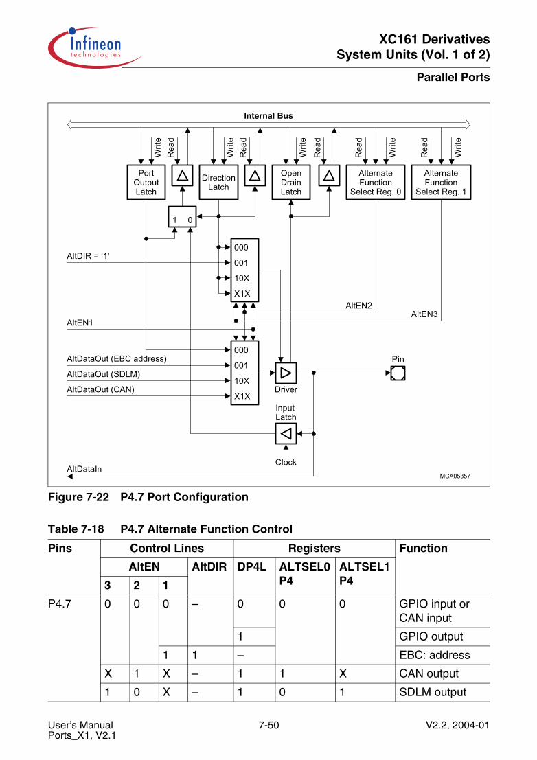
XC161 DerivativesSystem Units (Vol. 1 of 2)
Parallel Ports
Figure 7-22 P4.7 Port Configuration
Table 7-18 P4.7 Alternate Function Control
Pins Control Lines Registers Function
AltEN AltDIR DP4L ALTSEL0P4
ALTSEL1P43 2 1
P4.7 0 0 0 – 0 0 0 GPIO input orCAN input
1 GPIO output
1 1 – EBC: address
X 1 X – 1 1 X CAN output
1 0 X – 1 0 1 SDLM output
MCA05357
AlternateFunction
Select Reg. 0
Rea
d
Writ
e
Rea
d
OpenDrainLatch
DirectionLatch
Rea
dW
rite
Rea
dW
rite
PortOutputLatch
Writ
e
1 0
AltDataOut (SDLM)
AltDataOut (CAN)
AltEN1
AltDataOut (EBC address)
AltDataIn
Driver
InputLatch
Clock
AltEN2
Pin
Internal Bus
AltDIR = ‘1’
X1X
10X
000
001
X1X
10X
000
001
AlternateFunction
Select Reg. 1
Writ
e
Rea
d
AltEN3
User’s Manual 7-50 V2.2, 2004-01Ports_X1, V2.1
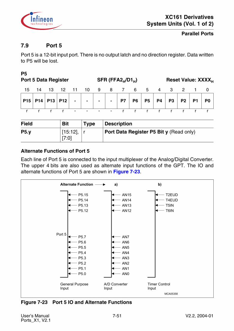
XC161 DerivativesSystem Units (Vol. 1 of 2)
Parallel Ports
7.9 Port 5
Port 5 is a 12-bit input port. There is no output latch and no direction register. Data writtento P5 will be lost.
Alternate Functions of Port 5
Each line of Port 5 is connected to the input multiplexer of the Analog/Digital Converter.The upper 4 bits are also used as alternate input functions of the GPT. The IO andalternate functions of Port 5 are shown in Figure 7-23.
Figure 7-23 Port 5 IO and Alternate Functions
P5 Port 5 Data Register SFR (FFA2H/D1H) Reset Value: XXXXH
15 14 13 12 11 10 9 8 7 6 5 4 3 2 1 0
P15 P14 P13 P12 - - - - P7 P6 P5 P4 P3 P2 P1 P0
r r r r - - - - r r r r r r r r
Field Bit Type Description
P5.y [15:12], [7:0]
r Port Data Register P5 Bit y (Read only)
MCA05358
Port 5
Alternate Function
General PurposeInput
a) b)
A/D ConverterInput
Timer ControlInput
P5.15
P5.13P5.12
P5.7P5.6P5.5P5.4P5.3P5.2P5.1P5.0
P5.14AN15
AN13AN12
AN7AN6AN5AN4AN3AN2AN1AN0
AN14T2EUD
T5INT6IN
T4EUD
User’s Manual 7-51 V2.2, 2004-01Ports_X1, V2.1
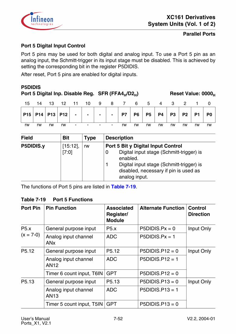
XC161 DerivativesSystem Units (Vol. 1 of 2)
Parallel Ports
Port 5 Digital Input Control
Port 5 pins may be used for both digital and analog input. To use a Port 5 pin as ananalog input, the Schmitt-trigger in its input stage must be disabled. This is achieved bysetting the corresponding bit in the register P5DIDIS.
After reset, Port 5 pins are enabled for digital inputs.
The functions of Port 5 pins are listed in Table 7-19.
P5DIDIS Port 5 Digital Inp. Disable Reg. SFR (FFA4H/D2H) Reset Value: 0000H
15 14 13 12 11 10 9 8 7 6 5 4 3 2 1 0
P15 P14 P13 P12 - - - - P7 P6 P5 P4 P3 P2 P1 P0
rw rw rw rw - - - - rw rw rw rw rw rw rw rw
Field Bit Type Description
P5DIDIS.y [15:12], [7:0]
rw Port 5 Bit y Digital Input Control0 Digital input stage (Schmitt-trigger) is
enabled.1 Digital input stage (Schmitt-trigger) is
disabled, necessary if pin is used as analog input.
Table 7-19 Port 5 Functions
Port Pin Pin Function Associated Register/ Module
Alternate Function Control Direction
P5.x(x = 7-0)
General purpose input P5.x P5DIDIS.Px = 0 Input Only
Analog input channelANx
ADC P5DIDIS.Px = 1
P5.12 General purpose input P5.12 P5DIDIS.P12 = 0 Input Only
Analog input channelAN12
ADC P5DIDIS.P12 = 1
Timer 6 count input, T6IN GPT P5DIDIS.P12 = 0
P5.13 General purpose input P5.13 P5DIDIS.P13 = 0 Input Only
Analog input channelAN13
ADC P5DIDIS.P13 = 1
Timer 5 count input, T5IN GPT P5DIDIS.P13 = 0
User’s Manual 7-52 V2.2, 2004-01Ports_X1, V2.1

XC161 DerivativesSystem Units (Vol. 1 of 2)
Parallel Ports
The configuration of Port 5 is shown in Figure 7-24.
Figure 7-24 P5 Port Configuration
P5.14 General purpose input P5.14 P5DIDIS.P14 = 0 Input Only
Analog input channelAN14
ADC P5DIDIS.P14 = 1
Timer 4 external up/down input, T4EUD
GPT P5DIDIS.P14 = 0
P5.15 General purpose input P5.15 P5DIDIS.P15 = 0 Input Only
Analog input channelAN15
ADC P5DIDIS.P15 = 1
Timer 2 external up/down input, T2EUD
GPT P5DIDIS.P15 = 0
Table 7-19 Port 5 Functions (cont’d)
Port Pin Pin Function Associated Register/ Module
Alternate Function Control Direction
MCA05359
Internal Bus
InputLatch
Clock
Rea
d
P5DIDIS
Rea
d
Writ
e
Pin
AnalogInput
AltDataIn
User’s Manual 7-53 V2.2, 2004-01Ports_X1, V2.1

XC161 DerivativesSystem Units (Vol. 1 of 2)
Parallel Ports
7.10 Port 6
If this 8-bit port is used for general purpose IO, the direction of each line can beconfigured via the corresponding direction register DP6. Each port line can be switchedinto push/pull or open drain mode via the open drain control register ODP6.
Note: Bits P6.0 - P6.7 are bit-protected for CAPCOM1 Output.
P6 Port 6 Data Register SFR (FFCCH/E6H) Reset Value: 0000H
15 14 13 12 11 10 9 8 7 6 5 4 3 2 1 0
- P7 P6 P5 P4 P3 P2 P1 P0
- rwh rwh rwh rwh rwh rwh rwh rwh
Field Bit Type Description
P6.y [7:0] rwh Port Data Register P6 Bit y
DP6 P6 Direction Ctrl. Register SFR (FFCEH/E7H) Reset Value: 0000H
15 14 13 12 11 10 9 8 7 6 5 4 3 2 1 0
- P7 P6 P5 P4 P3 P2 P1 P0
- rw rw rw rw rw rw rw rw
Field Bit Type Description
DP6.y [7:0] rw Port Direction Register DP6 Bit y0 Port line P6.y is an input (high-impedance)1 Port line P6.y is an output
User’s Manual 7-54 V2.2, 2004-01Ports_X1, V2.1
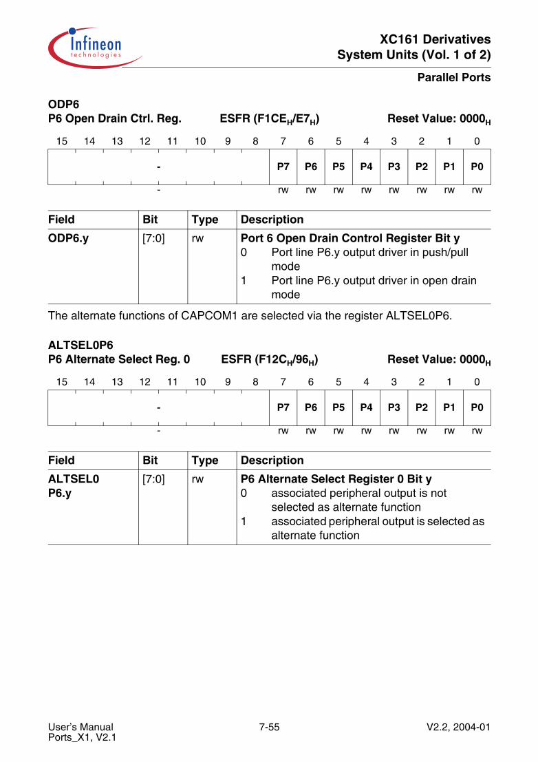
XC161 DerivativesSystem Units (Vol. 1 of 2)
Parallel Ports
The alternate functions of CAPCOM1 are selected via the register ALTSEL0P6.
ODP6 P6 Open Drain Ctrl. Reg. ESFR (F1CEH/E7H) Reset Value: 0000H
15 14 13 12 11 10 9 8 7 6 5 4 3 2 1 0
- P7 P6 P5 P4 P3 P2 P1 P0
- rw rw rw rw rw rw rw rw
Field Bit Type Description
ODP6.y [7:0] rw Port 6 Open Drain Control Register Bit y0 Port line P6.y output driver in push/pull
mode1 Port line P6.y output driver in open drain
mode
ALTSEL0P6P6 Alternate Select Reg. 0 ESFR (F12CH/96H) Reset Value: 0000H
15 14 13 12 11 10 9 8 7 6 5 4 3 2 1 0
- P7 P6 P5 P4 P3 P2 P1 P0
- rw rw rw rw rw rw rw rw
Field Bit Type Description
ALTSEL0P6.y
[7:0] rw P6 Alternate Select Register 0 Bit y0 associated peripheral output is not
selected as alternate function1 associated peripheral output is selected as
alternate function
User’s Manual 7-55 V2.2, 2004-01Ports_X1, V2.1
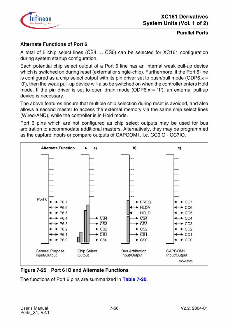
XC161 DerivativesSystem Units (Vol. 1 of 2)
Parallel Ports
Alternate Functions of Port 6
A total of 5 chip select lines (CS4 … CS0) can be selected for XC161 configurationduring system startup configuration.
Each potential chip select output of a Port 6 line has an internal weak pull-up devicewhich is switched on during reset (external or single-chip). Furthermore, if the Port 6 lineis configured as a chip select output with its pin driver set to push/pull mode (ODP6.x =‘0’), then the weak pull-up device will also be switched on when the controller enters Holdmode. If the pin driver is set to open drain mode (ODP6.x = ‘1’), an external pull-updevice is necessary.
The above features ensure that multiple chip selection during reset is avoided, and alsoallows a second master to access the external memory via the same chip select lines(Wired-AND), while the controller is in Hold mode.
Port 6 pins which are not configured as chip select outputs may be used for busarbitration to accommodate additional masters. Alternatively, they may be programmedas the capture inputs or compare outputs of CAPCOM1, i.e. CC0IO - CC7IO.
Figure 7-25 Port 6 IO and Alternate Functions
The functions of Port 6 pins are summarized in Table 7-20.
MCA05360
Port 6
Alternate Function
General PurposeInput/Output
c)
CAPCOM1Input/Output
a)
Chip SelectOutput
b)
Bus ArbitrationInput/Output
BREQP6.7P6.6P6.5P6.4P6.3P6.2P6.1P6.0
CS4CS3CS2CS1CS0
HLDAHOLDCS4CS3CS2CS1CS0
CC7CC6CC5CC4CC3CC2CC1CC0
User’s Manual 7-56 V2.2, 2004-01Ports_X1, V2.1
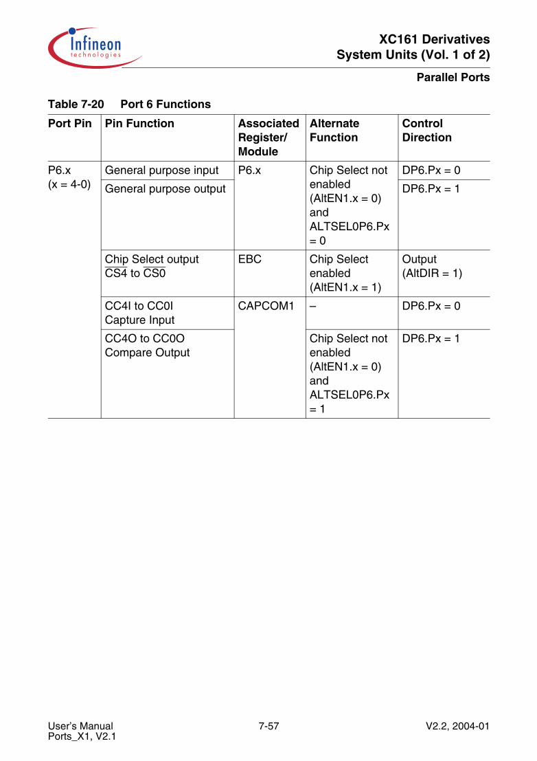
XC161 DerivativesSystem Units (Vol. 1 of 2)
Parallel Ports
Table 7-20 Port 6 Functions
Port Pin Pin Function Associated Register/ Module
Alternate Function
Control Direction
P6.x(x = 4-0)
General purpose input P6.x Chip Select not enabled (AltEN1.x = 0) and ALTSEL0P6.Px= 0
DP6.Px = 0
General purpose output DP6.Px = 1
Chip Select outputCS4 to CS0
EBC Chip Select enabled (AltEN1.x = 1)
Output(AltDIR = 1)
CC4I to CC0ICapture Input
CAPCOM1 – DP6.Px = 0
CC4O to CC0OCompare Output
Chip Select not enabled (AltEN1.x = 0) and ALTSEL0P6.Px= 1
DP6.Px = 1
User’s Manual 7-57 V2.2, 2004-01Ports_X1, V2.1

XC161 DerivativesSystem Units (Vol. 1 of 2)
Parallel Ports
P6.5 General purpose input P6.5 Chip Select (AltEN1.5 = 0) and Bus arbitration (AltEN2 = 0) not enabled, and ALTSEL0P6.P5= 0
DP6.P5 = 0
General purpose output DP6.P5 = 1
HOLD input EBC Chip Select not enabled (AltEN1.5 = 0) and Bus arbitration enabled(AltEN2 = 1)
Input(AltDIR = 0)
CC5ICapture Input
CAPCOM1 – DP6.P5 = 0
CC5OCompare Output
Chip Select not enabled (AltEN1.5 = 0) and Bus arbitration not enabled(AltEN2 = 0) and ALTSEL0P6.P5= 1
DP6.P5 = 1
Table 7-20 Port 6 Functions (cont’d)
Port Pin Pin Function Associated Register/ Module
Alternate Function
Control Direction
User’s Manual 7-58 V2.2, 2004-01Ports_X1, V2.1
XC161 DerivativesSystem Units (Vol. 1 of 2)
Parallel Ports
P6.6 General purpose input P6.6 Chip Select (AltEN1.6 = 0) and Bus arbitration (AltEN2 = 0) not enabled, and ALTSEL0P6.P6= 0
DP6.P6 = 0
General purpose output DP6.P6 = 1
HLDA output(master mode)
EBC Chip Select not enabled (AltEN1.6 = 0) and Bus arbitration enabled(AltEN2 = 1)–
Output(AltDIR = 1)
HLDA input(slave mode)
EBC Input(AltDIR = 0)
CC6ICapture Input
CAPCOM1 – DP6.P6 = 0
CC6OCompare Output
Chip Select not enabled (AltEN1.6 = 0) and Bus arbitration not enabled(AltEN2 = 0) and ALTSEL0P6.P6= 1
DP6.P6 = 1
Table 7-20 Port 6 Functions (cont’d)
Port Pin Pin Function Associated Register/ Module
Alternate Function
Control Direction
User’s Manual 7-59 V2.2, 2004-01Ports_X1, V2.1
XC161 DerivativesSystem Units (Vol. 1 of 2)
Parallel Ports
The configuration of Port 6 pins are shown in the subsequent figures.
P6.7 General purpose input P6.7 Bus arbitration (AltEN2 = 0) not enabled, and ALTSEL0P6.P7= 0
DP6.P7 = 0
General purpose output DP6.P7 = 1
BREQ output EBC Bus arbitration enabled(AltEN2 = 1)
Output(AltDIR = 1)
CC7ICapture Input
CAPCOM1 – DP6.P7 = 0
CC7OCompare Output
Bus arbitration not enabled (AltEN2 = 0) and ALTSEL0P6.P7= 1
DP6.P7 = 1
Table 7-20 Port 6 Functions (cont’d)
Port Pin Pin Function Associated Register/ Module
Alternate Function
Control Direction
User’s Manual 7-60 V2.2, 2004-01Ports_X1, V2.1

XC161 DerivativesSystem Units (Vol. 1 of 2)
Parallel Ports
Figure 7-26 P6.[4:0] Port Configuration
Table 7-21 P6.[4:0] Alternate Function Control
Pins Control Lines Registers Function
AltEN AltDIR DP6L ALTSEL0P63 2 1
P6.[4:0] 0 – 0 – 0 or 1 0 GPIO
X 1 1 – X EBC: chip select
– 0 – 0 – CAPCOM1 input
1 1 1 CAPCOM1 output
MCA05361
DirectionLatch
Rea
dW
rite
Rea
dW
rite
PortOutputLatch
1 0
X1
10
00
X1
00
10AltDataOut (EBC)
AltEN1 (EBC)
AltDataOut (CAPCOM1)
AltDataIn (Pin)
Driver
InputLatch
Clock
Pin
Internal Bus
AlternateFunction
Select Reg. 0
Rea
d
Writ
e
Rea
d
OpenDrainLatch
Writ
e
AltDIR = ‘1’
AlternateFunction
Select Reg. 0
Rea
d
0 1
CCx 1)
Writ
e
AltEN3
1) x = 4 - 0
AltDataIn (Latch)
User’s Manual 7-61 V2.2, 2004-01Ports_X1, V2.1
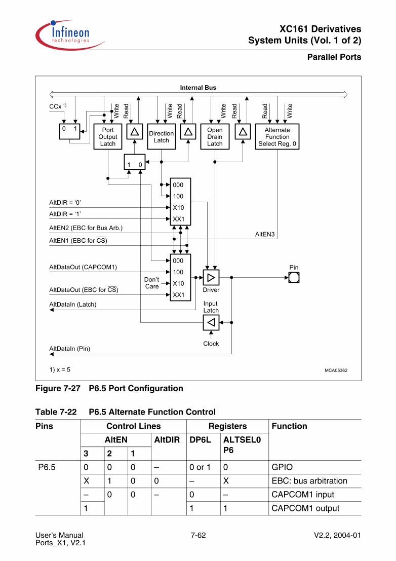
XC161 DerivativesSystem Units (Vol. 1 of 2)
Parallel Ports
Figure 7-27 P6.5 Port Configuration
Table 7-22 P6.5 Alternate Function Control
Pins Control Lines Registers Function
AltEN AltDIR DP6L ALTSEL0P63 2 1
P6.5 0 0 0 – 0 or 1 0 GPIO
X 1 0 0 – X EBC: bus arbitration
– 0 0 – 0 – CAPCOM1 input
1 1 1 CAPCOM1 output
MCA05362
AlternateFunction
Select Reg. 0
Rea
d
Writ
e
Rea
d
OpenDrainLatch
DirectionLatch
Rea
dW
rite
Rea
dW
rite
PortOutputLatch
0 1
CCx 1)
Writ
e
1 0
XX1
X10
000
100
XX1
X10
000
100
AltDataIn (Latch)
AltEN2 (EBC for Bus Arb.)
Don’tCareAltDataOut (EBC for CS)
AltEN1 (EBC for CS)
AltDIR = ‘1’
AltDIR = ‘0’
AltDataOut (CAPCOM1)
AltDataIn (Pin)
Driver
InputLatch
Clock
1) x = 5
AltEN3
Pin
Internal Bus
User’s Manual 7-62 V2.2, 2004-01Ports_X1, V2.1
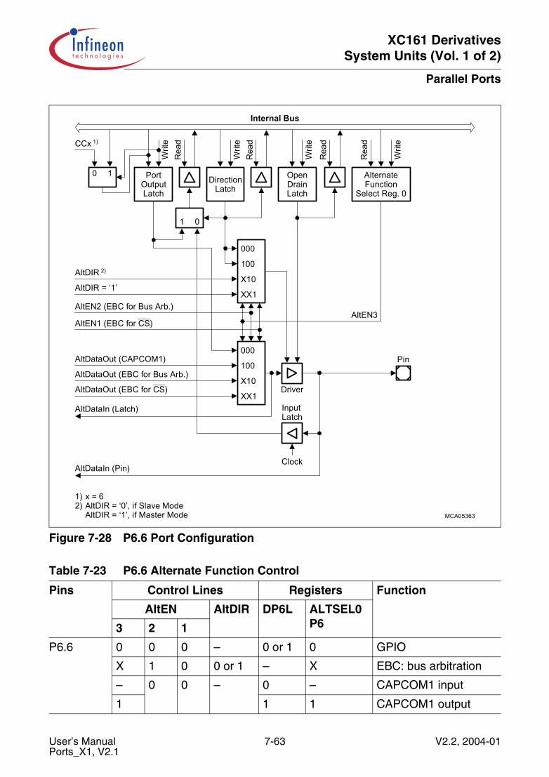
XC161 DerivativesSystem Units (Vol. 1 of 2)
Parallel Ports
Figure 7-28 P6.6 Port Configuration
Table 7-23 P6.6 Alternate Function Control
Pins Control Lines Registers Function
AltEN AltDIR DP6L ALTSEL0P63 2 1
P6.6 0 0 0 – 0 or 1 0 GPIO
X 1 0 0 or 1 – X EBC: bus arbitration
– 0 0 – 0 – CAPCOM1 input
1 1 1 CAPCOM1 output
MCA05363
AlternateFunction
Select Reg. 0
Rea
d
Writ
e
Rea
d
OpenDrainLatch
DirectionLatch
Rea
dW
rite
Rea
dW
rite
PortOutputLatch
0 1
CCx 1)
Writ
e
1 0
XX1
X10
000
100
XX1
X10
000
100
AltDataIn (Latch)
AltEN2 (EBC for Bus Arb.)
AltDataOut (EBC for Bus Arb.)
AltDataOut (EBC for CS)
AltEN1 (EBC for CS)
AltDIR = ‘1’
AltDIR 2)
AltDataOut (CAPCOM1)
AltDataIn (Pin)
Driver
InputLatch
Clock
1) x = 62) AltDIR = ‘0’, if Slave Mode
AltDIR = ‘1’, if Master Mode
AltEN3
Pin
Internal Bus
User’s Manual 7-63 V2.2, 2004-01Ports_X1, V2.1
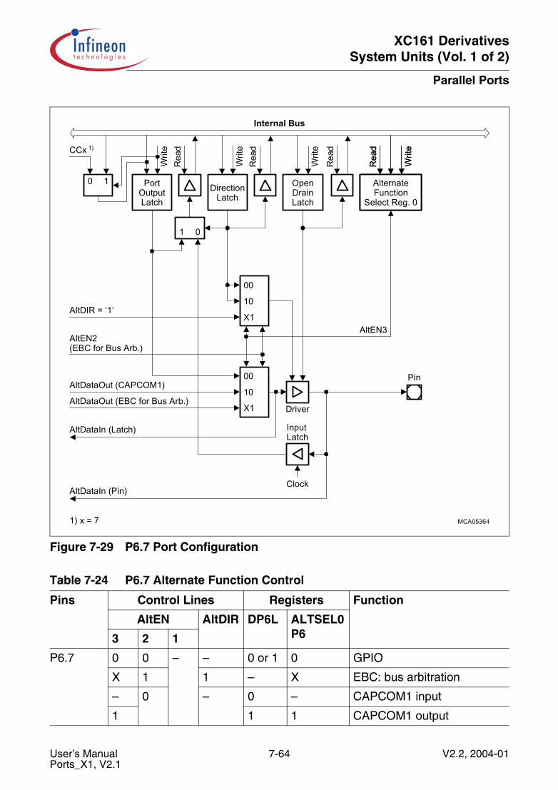
XC161 DerivativesSystem Units (Vol. 1 of 2)
Parallel Ports
Figure 7-29 P6.7 Port Configuration
Table 7-24 P6.7 Alternate Function Control
Pins Control Lines Registers Function
AltEN AltDIR DP6L ALTSEL0P63 2 1
P6.7 0 0 – – 0 or 1 0 GPIO
X 1 1 – X EBC: bus arbitration
– 0 – 0 – CAPCOM1 input
1 1 1 CAPCOM1 output
MCA05364
DirectionLatch
Rea
dW
rite
Rea
dW
rite
PortOutputLatch
1 0
X1
10
00
X1
00
10AltDataOut (EBC for Bus Arb.)
AltEN2(EBC for Bus Arb.)
AltDataOut (CAPCOM1)
AltDataIn (Pin)
Driver
InputLatch
Clock
Pin
Internal Bus
AlternateFunction
Select Reg. 0
Rea
d
Writ
e
Rea
d
OpenDrainLatch
Writ
e
AltDIR = ‘1’
AlternateFunction
Select Reg. 0
Rea
d
0 1
CCx 1)
Writ
e
AltEN3
1) x = 7
AltDataIn (Latch)
User’s Manual 7-64 V2.2, 2004-01Ports_X1, V2.1
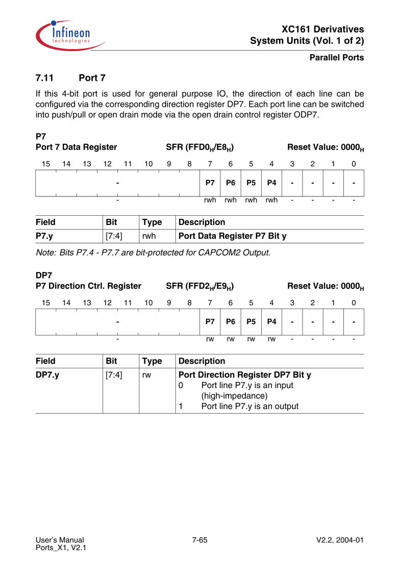
XC161 DerivativesSystem Units (Vol. 1 of 2)
Parallel Ports
7.11 Port 7
If this 4-bit port is used for general purpose IO, the direction of each line can beconfigured via the corresponding direction register DP7. Each port line can be switchedinto push/pull or open drain mode via the open drain control register ODP7.
Note: Bits P7.4 - P7.7 are bit-protected for CAPCOM2 Output.
P7 Port 7 Data Register SFR (FFD0H/E8H) Reset Value: 0000H
15 14 13 12 11 10 9 8 7 6 5 4 3 2 1 0
- P7 P6 P5 P4 - - - -
- rwh rwh rwh rwh - - - -
Field Bit Type Description
P7.y [7:4] rwh Port Data Register P7 Bit y
DP7 P7 Direction Ctrl. Register SFR (FFD2H/E9H) Reset Value: 0000H
15 14 13 12 11 10 9 8 7 6 5 4 3 2 1 0
- P7 P6 P5 P4 - - - -
- rw rw rw rw - - - -
Field Bit Type Description
DP7.y [7:4] rw Port Direction Register DP7 Bit y0 Port line P7.y is an input
(high-impedance)1 Port line P7.y is an output
User’s Manual 7-65 V2.2, 2004-01Ports_X1, V2.1
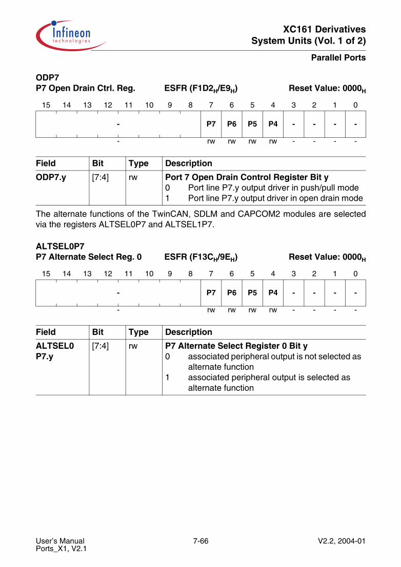
XC161 DerivativesSystem Units (Vol. 1 of 2)
Parallel Ports
The alternate functions of the TwinCAN, SDLM and CAPCOM2 modules are selectedvia the registers ALTSEL0P7 and ALTSEL1P7.
ODP7 P7 Open Drain Ctrl. Reg. ESFR (F1D2H/E9H) Reset Value: 0000H
15 14 13 12 11 10 9 8 7 6 5 4 3 2 1 0
- P7 P6 P5 P4 - - - -
- rw rw rw rw - - - -
Field Bit Type Description
ODP7.y [7:4] rw Port 7 Open Drain Control Register Bit y0 Port line P7.y output driver in push/pull mode1 Port line P7.y output driver in open drain mode
ALTSEL0P7P7 Alternate Select Reg. 0 ESFR (F13CH/9EH) Reset Value: 0000H
15 14 13 12 11 10 9 8 7 6 5 4 3 2 1 0
- P7 P6 P5 P4 - - - -
- rw rw rw rw - - - -
Field Bit Type Description
ALTSEL0P7.y
[7:4] rw P7 Alternate Select Register 0 Bit y0 associated peripheral output is not selected as
alternate function 1 associated peripheral output is selected as
alternate function
User’s Manual 7-66 V2.2, 2004-01Ports_X1, V2.1

XC161 DerivativesSystem Units (Vol. 1 of 2)
Parallel Ports
Alternate Functions of Port 7
Port 7 pins are used as receive data and transmit data lines for TwinCAN and SDLMinterface. Alternatively, they can be used as capture inputs or compare outputs of theCAPCOM2. Its IO and alternate functions are shown in Figure 7-30.
Figure 7-30 Port 7 IO and Alternate Functions
ALTSEL1P7P7 Alternate Select Reg. 1 ESFR (F13EH/9FH) Reset Value: 0000H
15 14 13 12 11 10 9 8 7 6 5 4 3 2 1 0
- P7 P6 P5 P4 - - - -
- rw rw rw rw - - - -
Field Bit Type Description
ALTSEL1P7.y
[7:4] rw P7 Alternate Select Register 1 Bit y0 associated peripheral output is not selected as
alternate function 1 associated peripheral output is selected as
alternate function
MCA05365
Port 7
Alternate Function
General PurposeInput/Output
c)
CAPCOM2Input/Output
a)
CANInput/Output
b)
SDLMInput/Output
P7.7P7.6P7.5P7.4
TxDCARxDCATxDCBRxDCB
RxDJTxDJ
CC31IOCC30IOCC29IOCC28IO
User’s Manual 7-67 V2.2, 2004-01Ports_X1, V2.1
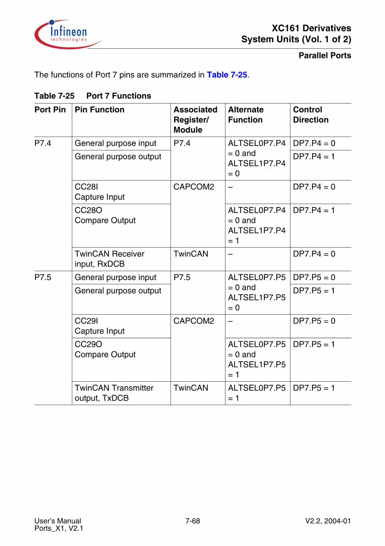
XC161 DerivativesSystem Units (Vol. 1 of 2)
Parallel Ports
The functions of Port 7 pins are summarized in Table 7-25.
Table 7-25 Port 7 Functions
Port Pin Pin Function Associated Register/ Module
Alternate Function
Control Direction
P7.4 General purpose input P7.4 ALTSEL0P7.P4= 0 and ALTSEL1P7.P4= 0
DP7.P4 = 0
General purpose output DP7.P4 = 1
CC28ICapture Input
CAPCOM2 – DP7.P4 = 0
CC28OCompare Output
ALTSEL0P7.P4= 0 and ALTSEL1P7.P4= 1
DP7.P4 = 1
TwinCAN Receiverinput, RxDCB
TwinCAN – DP7.P4 = 0
P7.5 General purpose input P7.5 ALTSEL0P7.P5= 0 and ALTSEL1P7.P5= 0
DP7.P5 = 0
General purpose output DP7.P5 = 1
CC29ICapture Input
CAPCOM2 – DP7.P5 = 0
CC29OCompare Output
ALTSEL0P7.P5= 0 and ALTSEL1P7.P5= 1
DP7.P5 = 1
TwinCAN Transmitteroutput, TxDCB
TwinCAN ALTSEL0P7.P5= 1
DP7.P5 = 1
User’s Manual 7-68 V2.2, 2004-01Ports_X1, V2.1
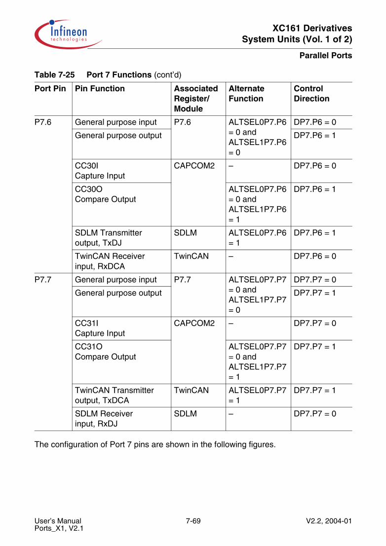
XC161 DerivativesSystem Units (Vol. 1 of 2)
Parallel Ports
The configuration of Port 7 pins are shown in the following figures.
P7.6 General purpose input P7.6 ALTSEL0P7.P6= 0 and ALTSEL1P7.P6= 0
DP7.P6 = 0
General purpose output DP7.P6 = 1
CC30ICapture Input
CAPCOM2 – DP7.P6 = 0
CC30OCompare Output
ALTSEL0P7.P6= 0 and ALTSEL1P7.P6= 1
DP7.P6 = 1
SDLM Transmitteroutput, TxDJ
SDLM ALTSEL0P7.P6= 1
DP7.P6 = 1
TwinCAN Receiverinput, RxDCA
TwinCAN – DP7.P6 = 0
P7.7 General purpose input P7.7 ALTSEL0P7.P7= 0 and ALTSEL1P7.P7= 0
DP7.P7 = 0
General purpose output DP7.P7 = 1
CC31ICapture Input
CAPCOM2 – DP7.P7 = 0
CC31OCompare Output
ALTSEL0P7.P7= 0 and ALTSEL1P7.P7= 1
DP7.P7 = 1
TwinCAN Transmitteroutput, TxDCA
TwinCAN ALTSEL0P7.P7= 1
DP7.P7 = 1
SDLM Receiverinput, RxDJ
SDLM – DP7.P7 = 0
Table 7-25 Port 7 Functions (cont’d)
Port Pin Pin Function Associated Register/ Module
Alternate Function
Control Direction
User’s Manual 7-69 V2.2, 2004-01Ports_X1, V2.1
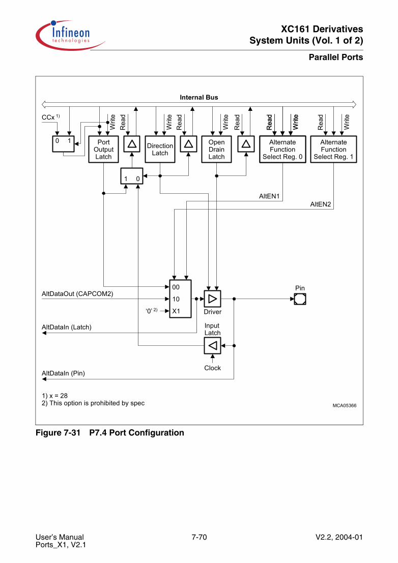
XC161 DerivativesSystem Units (Vol. 1 of 2)
Parallel Ports
Figure 7-31 P7.4 Port Configuration
MCA05366
DirectionLatch
Rea
dW
rite
Rea
dW
rite
PortOutputLatch
1 0
X1
00
10
‘0’ 2)
AltDataOut (CAPCOM2)
AltDataIn (Pin)
Driver
InputLatch
Clock
Pin
Internal Bus
AlternateFunction
Select Reg. 0
Rea
d
Writ
e
Rea
d
OpenDrainLatch
Writ
e
AlternateFunction
Select Reg. 0
Rea
d
0 1
CCx 1)
Writ
e
AltDataIn (Latch)
AlternateFunction
Select Reg. 1
Writ
e
Rea
d
AltEN2AltEN1
1) x = 282) This option is prohibited by spec
User’s Manual 7-70 V2.2, 2004-01Ports_X1, V2.1
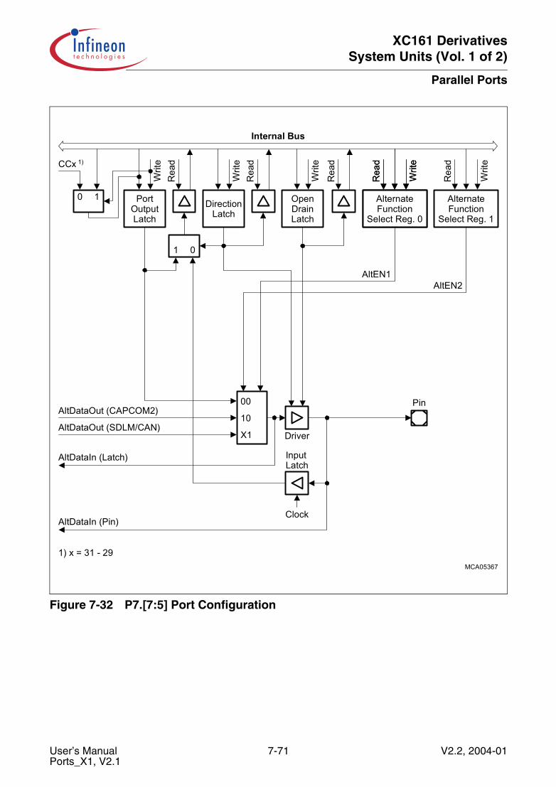
XC161 DerivativesSystem Units (Vol. 1 of 2)
Parallel Ports
Figure 7-32 P7.[7:5] Port Configuration
MCA05367
DirectionLatch
Rea
dW
rite
Rea
dW
rite
PortOutputLatch
1 0
X1
00
10AltDataOut (CAPCOM2)
AltDataIn (Pin)
Driver
InputLatch
Clock
Pin
Internal Bus
AlternateFunction
Select Reg. 0
Rea
d
Writ
e
Rea
d
OpenDrainLatch
Writ
e
AlternateFunction
Select Reg. 0
Rea
d
0 1
CCx 1)
Writ
e
AltDataIn (Latch)
AlternateFunction
Select Reg. 1
Writ
e
Rea
d
AltEN2AltEN1
1) x = 31 - 29
AltDataOut (SDLM/CAN)
User’s Manual 7-71 V2.2, 2004-01Ports_X1, V2.1
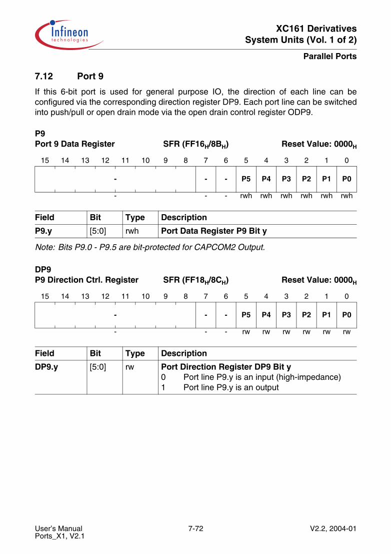
XC161 DerivativesSystem Units (Vol. 1 of 2)
Parallel Ports
7.12 Port 9
If this 6-bit port is used for general purpose IO, the direction of each line can beconfigured via the corresponding direction register DP9. Each port line can be switchedinto push/pull or open drain mode via the open drain control register ODP9.
Note: Bits P9.0 - P9.5 are bit-protected for CAPCOM2 Output.
P9 Port 9 Data Register SFR (FF16H/8BH) Reset Value: 0000H
15 14 13 12 11 10 9 8 7 6 5 4 3 2 1 0
- - - P5 P4 P3 P2 P1 P0
- - - rwh rwh rwh rwh rwh rwh
Field Bit Type Description
P9.y [5:0] rwh Port Data Register P9 Bit y
DP9 P9 Direction Ctrl. Register SFR (FF18H/8CH) Reset Value: 0000H
15 14 13 12 11 10 9 8 7 6 5 4 3 2 1 0
- - - P5 P4 P3 P2 P1 P0
- - - rw rw rw rw rw rw
Field Bit Type Description
DP9.y [5:0] rw Port Direction Register DP9 Bit y0 Port line P9.y is an input (high-impedance)1 Port line P9.y is an output
User’s Manual 7-72 V2.2, 2004-01Ports_X1, V2.1
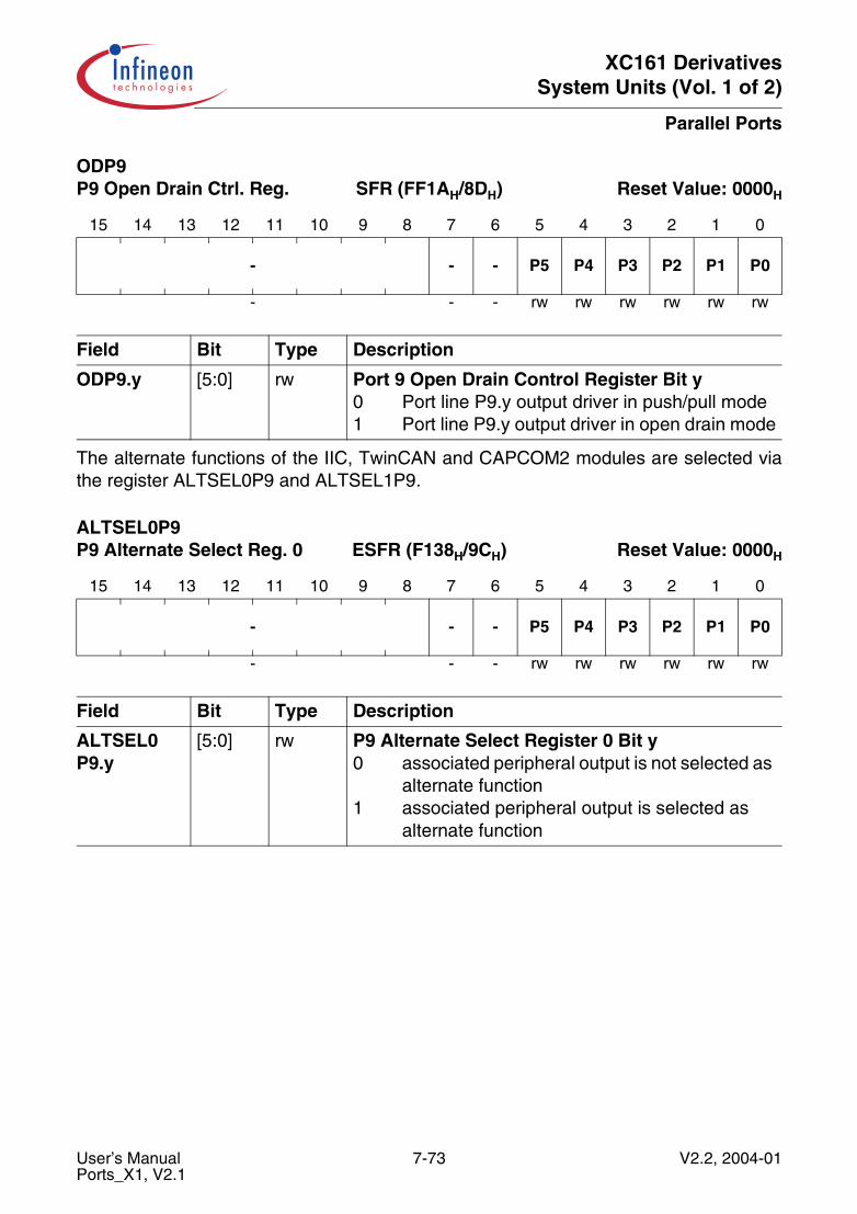
XC161 DerivativesSystem Units (Vol. 1 of 2)
Parallel Ports
The alternate functions of the IIC, TwinCAN and CAPCOM2 modules are selected viathe register ALTSEL0P9 and ALTSEL1P9.
ODP9 P9 Open Drain Ctrl. Reg. SFR (FF1AH/8DH) Reset Value: 0000H
15 14 13 12 11 10 9 8 7 6 5 4 3 2 1 0
- - - P5 P4 P3 P2 P1 P0
- - - rw rw rw rw rw rw
Field Bit Type Description
ODP9.y [5:0] rw Port 9 Open Drain Control Register Bit y0 Port line P9.y output driver in push/pull mode1 Port line P9.y output driver in open drain mode
ALTSEL0P9P9 Alternate Select Reg. 0 ESFR (F138H/9CH) Reset Value: 0000H
15 14 13 12 11 10 9 8 7 6 5 4 3 2 1 0
- - - P5 P4 P3 P2 P1 P0
- - - rw rw rw rw rw rw
Field Bit Type Description
ALTSEL0P9.y
[5:0] rw P9 Alternate Select Register 0 Bit y0 associated peripheral output is not selected as
alternate function 1 associated peripheral output is selected as
alternate function
User’s Manual 7-73 V2.2, 2004-01Ports_X1, V2.1

XC161 DerivativesSystem Units (Vol. 1 of 2)
Parallel Ports
ALTSEL1P9P9 Alternate Select Reg. 1 ESFR (F13AH/9DH) Reset Value: 0000H
15 14 13 12 11 10 9 8 7 6 5 4 3 2 1 0
- - - P5 P4 P3 P2 P1 P0
- - - rw rw rw rw rw rw
Field Bit Type Description
ALTSEL1P9.y
[5:0] rw P9 Alternate Select Register 1 Bit y0 associated peripheral output is not selected as
alternate function 1 associated peripheral output is selected as
alternate function
User’s Manual 7-74 V2.2, 2004-01Ports_X1, V2.1

XC161 DerivativesSystem Units (Vol. 1 of 2)
Parallel Ports
Alternate Functions of Port 9
Port 9 pins can be used as the serial data and clock lines of the IIC interface, thetransmitter and receiver lines of the TwinCAN or SDLM or alternatively, the CAPCOM2input/output lines.
If IIC interface is configured, it is necessary to switch the respective pins to open drainmode (ODP9.y = ‘1’).
Figure 7-33 shows the IO and alternate functions of Port 9.
Figure 7-33 Port 9 IO and Alternate Functions
The functions of Port 9 pins are listed in Table 7-26.
MCA05368
c)
SDLMInput/Output
b)
CANInput/Output
a)
IICInput/Output
Port 9
Alternate Function
General PurposeInput/Output
d)
CAPCOM2Input/Output
P9.5P9.4P9.3P9.2P9.1P9.0
SCL2SDA2SCL1SDA1SCL0SDA0
TxDCBRxDCB
TxDCARxDCA
RxDJTxDJ
CC19CC18CC17CC16
CC21CC20
User’s Manual 7-75 V2.2, 2004-01Ports_X1, V2.1

XC161 DerivativesSystem Units (Vol. 1 of 2)
Parallel Ports
Table 7-26 Port 9 Functions
Port Pin Pin Function Associated Register/ Module
Alternate Function
Control Direction
P9.0 General purpose input P9.0 ALTSEL0P9.P0= 0 and ALTSEL1P9.P0= 0
DP9.P0 = 0
General purpose output DP9.P0 = 1
CC16ICapture input
CAPCOM2 – DP9.P0 = 0
CC16OCompare output
ALTSEL0P9.P0= 0 and ALTSEL1P9.P0= 1
DP9.P0 = 1
TwinCAN Receiver input, RxDCB
TwinCAN – DP9.P0 = 0
IIC serial data line 0 input, SDA0
IIC – DP9.P0 = 0
IIC serial data line 0 output, SDA0
ALTSEL0P9.P0= 1 and ALTSEL1P9.P0= X
DP9.P0 = 1
P9.1 General purpose input P9.1 ALTSEL0P9.P1= 0, and ALTSEL1P9.P1= 0
DP9.P1 = 0
General purpose output DP9.P1 = 1
CC17ICapture input
CAPCOM2 – DP9.P1 = 0
CC17OCompare output
ALTSEL0P9.P1= 0, and ALTSEL1P9.P1= 1
DP9.P1 = 1
TwinCAN Transmitter output, TxDCB
TwinCAN ALTSEL0P9.P1= 1, and ALTSEL1P9.P1= 1
DP9.P1 = 1
User’s Manual 7-76 V2.2, 2004-01Ports_X1, V2.1

XC161 DerivativesSystem Units (Vol. 1 of 2)
Parallel Ports
P9.1 IIC serial clock line 0 input, SCL0
IIC – DP9.P1 = 0
IIC serial clock line 0 output, SCL0
ALTSEL0P9.P1= 1 and ALTSEL1P9.P1= 0
DP9.P1 = 1
P9.2 General purpose input P9.2 ALTSEL0P9.P2= 0 and ALTSEL1P9.P2= 0
DP9.P2 = 0
General purpose output DP9.P2 = 1
CC18ICapture input
CAPCOM2 – DP9.P2 = 0
CC18OCompare output
ALTSEL0P9.P2= 0 and ALTSEL1P9.P2= 1
DP9.P2 = 1
TwinCAN Receiver input, RxDCA
TwinCAN – DP9.P2 = 0
SDLM Transmitteroutput, TxDJ
SDLM ALTSEL0P9.P2= 1 and ALTSEL1P9.P2= 1
DP9.P2 = 1
IIC serial data line 1 input, SDA1
IIC – DP9.P2 = 0
IIC serial clock line 1 output, SDA1
ALTSEL0P9.P2= 1 and ALTSEL1P9.P2= 0
DP9.P2 = 1
Table 7-26 Port 9 Functions (cont’d)
Port Pin Pin Function Associated Register/ Module
Alternate Function
Control Direction
User’s Manual 7-77 V2.2, 2004-01Ports_X1, V2.1

XC161 DerivativesSystem Units (Vol. 1 of 2)
Parallel Ports
P9.3 General purpose input P9.3 ALTSEL0P9.P3= 0 and ALTSEL1P9.P3= 0
DP9.P3 = 0
General purpose output DP9.P3 = 1
CC19ICapture input
CAPCOM2 – DP9.P3 = 0
CC19OCompare output
ALTSEL0P9.P3= 0 and ALTSEL1P9.P3= 1
DP9.P3 = 1
TwinCAN Transmitter output, TxDCA
TwinCAN ALTSEL0P9.P3= 1 and ALTSEL1P9.P3= 1
DP9.P3 = 1
SDLM Receiverinput, RxDJ
SDLM – DP9.P3 = 0
IIC serial clock line 1 input, SCL1
IIC – DP9.P3 = 0
IIC serial clock line 1 output, SCL1
ALTSEL0P9.P3= 1 and ALTSEL1P9.P3= 0
DP9.P3 = 1
P9.4 General purpose input P9.4 ALTSEL0P9.P4= 0 and ALTSEL1P9.P4= 0
DP9.P4 = 0
General purpose output DP9.P4 = 1
CC20ICapture input
CAPCOM2 – DP9.P4 = 0
CC20OCompare output
ALTSEL0P9.P4= 0 and ALTSEL1P9.P4= 1
DP9.P4 = 1
Table 7-26 Port 9 Functions (cont’d)
Port Pin Pin Function Associated Register/ Module
Alternate Function
Control Direction
User’s Manual 7-78 V2.2, 2004-01Ports_X1, V2.1
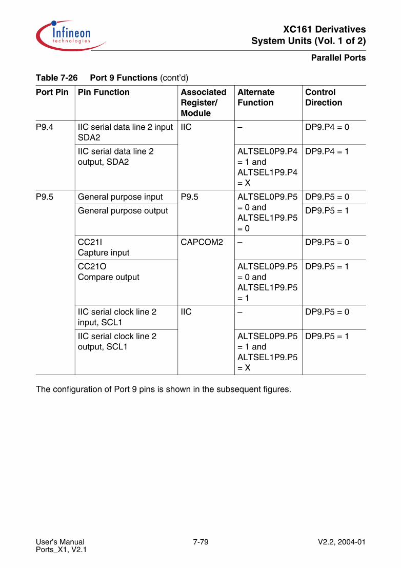
XC161 DerivativesSystem Units (Vol. 1 of 2)
Parallel Ports
The configuration of Port 9 pins is shown in the subsequent figures.
P9.4 IIC serial data line 2 input SDA2
IIC – DP9.P4 = 0
IIC serial data line 2 output, SDA2
ALTSEL0P9.P4= 1 and ALTSEL1P9.P4= X
DP9.P4 = 1
P9.5 General purpose input P9.5 ALTSEL0P9.P5= 0 and ALTSEL1P9.P5= 0
DP9.P5 = 0
General purpose output DP9.P5 = 1
CC21ICapture input
CAPCOM2 – DP9.P5 = 0
CC21OCompare output
ALTSEL0P9.P5= 0 and ALTSEL1P9.P5= 1
DP9.P5 = 1
IIC serial clock line 2 input, SCL1
IIC – DP9.P5 = 0
IIC serial clock line 2 output, SCL1
ALTSEL0P9.P5= 1 and ALTSEL1P9.P5= X
DP9.P5 = 1
Table 7-26 Port 9 Functions (cont’d)
Port Pin Pin Function Associated Register/ Module
Alternate Function
Control Direction
User’s Manual 7-79 V2.2, 2004-01Ports_X1, V2.1
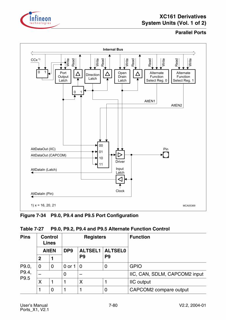
XC161 DerivativesSystem Units (Vol. 1 of 2)
Parallel Ports
Figure 7-34 P9.0, P9.4 and P9.5 Port Configuration
Table 7-27 P9.0, P9.2, P9.4 and P9.5 Alternate Function Control
Pins Control Lines
Registers Function
AltEN DP9 ALTSEL1 P9
ALTSEL0 P92 1
P9.0,P9.4,P9.5
0 0 0 or 1 0 0 GPIO
– 0 – IIC, CAN, SDLM, CAPCOM2 input
X 1 1 X 1 IIC output
1 0 1 1 0 CAPCOM2 compare output
MCA05369
AlternateFunction
Select Reg. 0
AlternateFunction
Select Reg. 1
Rea
d
Writ
e
Rea
d
Writ
e
Rea
d
OpenDrainLatch
DirectionLatch
Rea
dW
rite
Rea
dW
rite
PortOutputLatch
0 1
CCx 1)
Writ
e11
10
00
01
AltDataIn (Latch)
AltDataOut (CAPCOM)
AltDataOut (IIC)
AltDataIn (Pin)
Driver
InputLatch
Clock
1) x = 16, 20, 21
AltEN1
Pin
AltEN2
Internal Bus
0 1
User’s Manual 7-80 V2.2, 2004-01Ports_X1, V2.1

XC161 DerivativesSystem Units (Vol. 1 of 2)
Parallel Ports
Figure 7-35 P9.1, P9.2 and P9.3 Port Configuration
Table 7-28 P9.1, P9.2 and P9.3 Alternate Function Control
Pins Control Lines
Registers Function
AltEN DP9 ALTSEL1P9
ALTSEL0P92 1
P9.1, P9.2, P9.3
0 0 0 or 1 0 0 GPIO
– 0 – IIC, CAN, SDLM, CAPCOM2 input
0 1 1 0 1 IIC output
1 1 0 1 1 CAN or SDLM output
1 0 1 1 0 CAPCOM2 compare output
MCA05370
AlternateFunction
Select Reg. 0
AlternateFunction
Select Reg. 1
Rea
d
Writ
e
Rea
d
Writ
e
Rea
d
OpenDrainLatch
DirectionLatch
Rea
dW
rite
Rea
dW
rite
PortOutputLatch
0 1
CCx 1)
Writ
e11
10
00
01
AltDataIn (Latch)
AltDataOut (CAPCOM)
AltDataOut (CAN, SDLM)
AltDataOut (IIC)
AltDataIn (Pin)
Driver
InputLatch
Clock
1) x = 17, 18, 19
AltEN1
Pin
AltEN2
Internal Bus
0 1
User’s Manual 7-81 V2.2, 2004-01Ports_X1, V2.1

XC161 DerivativesSystem Units (Vol. 1 of 2)
Parallel Ports
7.13 Port 20
If this 6-bit port is used for general purpose IO, the direction of each line can beconfigured via the corresponding direction register DP20.
Port 20 adds general purpose IO functionality to a set of previously dedicated pins.
P20 Port 20 Data Register SFR (FFB4H/DAH) Reset Value: 0000H
15 14 13 12 11 10 9 8 7 6 5 4 3 2 1 0
- - - P12 - - - - - - P5 P4 - P2 P1 P0
- - - rw - - - - - - rw rw - rw rw rw
Field Bit Type Description
P20.y 12, [5:4], [2:0]
rw Port Data Register P20 Bit y
DP20 P20 Direction Ctrl. Register SFR (FFB6H/DBH) Reset Value: 0000H
15 14 13 12 11 10 9 8 7 6 5 4 3 2 1 0
- - - P12 - - - - - - P5 P4 - P2 P1 P0
- - - rw - - - - - - rw rw - rw rw rw
Field Bit Type Description
DP20.y 12, [5:4], [2:0]
rw Port Direction Register DP20 Bit y0 Port line P20.y is an input
(high-impedance)1 Port line P20.y is an output
User’s Manual 7-82 V2.2, 2004-01Ports_X1, V2.1
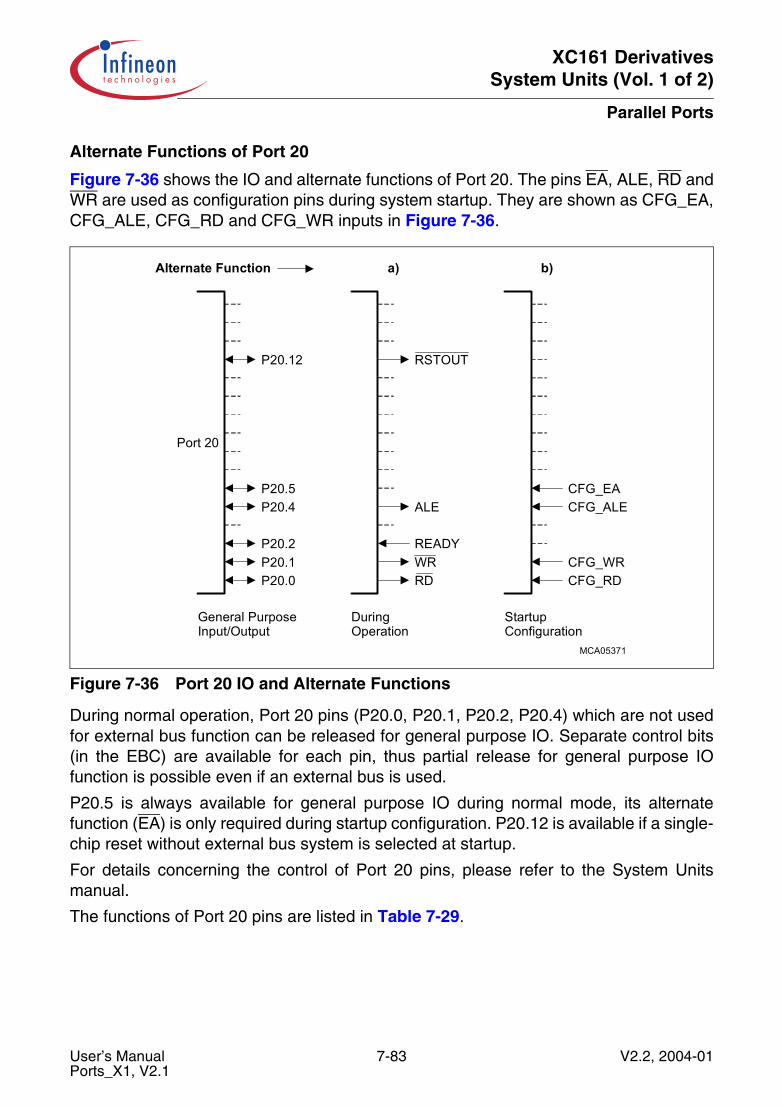
XC161 DerivativesSystem Units (Vol. 1 of 2)
Parallel Ports
Alternate Functions of Port 20
Figure 7-36 shows the IO and alternate functions of Port 20. The pins EA, ALE, RD andWR are used as configuration pins during system startup. They are shown as CFG_EA,CFG_ALE, CFG_RD and CFG_WR inputs in Figure 7-36.
Figure 7-36 Port 20 IO and Alternate Functions
During normal operation, Port 20 pins (P20.0, P20.1, P20.2, P20.4) which are not usedfor external bus function can be released for general purpose IO. Separate control bits(in the EBC) are available for each pin, thus partial release for general purpose IOfunction is possible even if an external bus is used.
P20.5 is always available for general purpose IO during normal mode, its alternatefunction (EA) is only required during startup configuration. P20.12 is available if a single-chip reset without external bus system is selected at startup.
For details concerning the control of Port 20 pins, please refer to the System Unitsmanual.
The functions of Port 20 pins are listed in Table 7-29.
MCA05371
Port 20
Alternate Function
General PurposeInput/Output
a) b)
RSTOUT
DuringOperation
StartupConfiguration
CFG_ALECFG_EA
CFG_RDCFG_WR
P20.12
P20.5P20.4
P20.2P20.1P20.0
ALE
READYWRRD
User’s Manual 7-83 V2.2, 2004-01Ports_X1, V2.1

XC161 DerivativesSystem Units (Vol. 1 of 2)
Parallel Ports
Table 7-29 Port 20 Functions
Port Pin Pin Function Associated Register/ Module
Alternate Function
Control Direction
P20.0 General purpose input P20.0 EBC pins disabled (AltEN1.0 = 0)
DP20.P0 = 0
General purpose output DP20.P0 = 1
Read command signal RD
EBC pins enabled (AltEN1.0 = 1)
Output(AltDIR = 1)
Config. read inputCFG_RD
– Input(AltDIR = 0)
P20.1 General purpose input P20.1 EBC pins disabled (AltEN1.1 = 0)
DP20.P1 = 0
General purpose output DP20.P1 = 1
Write command signal WR/WRL
EBC pins enabled (AltEN1.1 = 1)
Output(AltDIR = 1)
Config. write inputCFG_WR
– Input(AltDIR = 0)
P20.2 General purpose input P20.2 READY pin disabled (AltEN1.2 = 0)
DP20.P2 = 0
General purpose output DP20.P2 = 1
Bus termination input signal, READY
READY pin enabled (AltEN1.2 = 1)
Input(AltDIR = 0)
P20.4 General purpose input P20.4 ALE pin disabled (AltEN1.4 = 0)
DP20.P4 = 0
General purpose output DP20.P4 = 1
Address latch enable signal, ALE
ALE pinenabled (AltEN1.4 = 1)
Output(AltDIR = 1)
Config. ALE inputCFG_ALE
– Input(AltDIR = 0)
P20.5 General purpose input P20.5 AltEN1.5 = 0 DP20.P5 = 0
General purpose output DP20.P5 = 1
Config. EA inputCFG_EA
– Input(AltDIR = 0)
User’s Manual 7-84 V2.2, 2004-01Ports_X1, V2.1
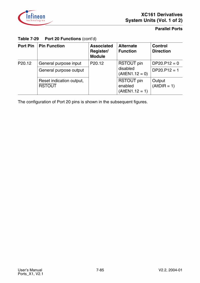
XC161 DerivativesSystem Units (Vol. 1 of 2)
Parallel Ports
The configuration of Port 20 pins is shown in the subsequent figures.
P20.12 General purpose input P20.12 RSTOUT pin disabled(AltEN1.12 = 0)
DP20.P12 = 0
General purpose output DP20.P12 = 1
Reset indication output, RSTOUT
RSTOUT pin enabled(AltEN1.12 = 1)
Output(AltDIR = 1)
Table 7-29 Port 20 Functions (cont’d)
Port Pin Pin Function Associated Register/ Module
Alternate Function
Control Direction
User’s Manual 7-85 V2.2, 2004-01Ports_X1, V2.1

XC161 DerivativesSystem Units (Vol. 1 of 2)
Parallel Ports
Figure 7-37 P20 Port Configuration
Notes:
1. For P20.5: AltEN1 = 0, for others: refer to Table 7-29.2. For P20.0, P20.1, P20.4, P20.12: AltDIR = 1, for P20.2, P20.5: AltDIR = 0.
MCA05372
DirectionLatch
Rea
dW
rite
Rea
dW
rite
PortOutputLatch
1 0
AltEN1
Driver
InputLatch
Clock
Pin
Internal Bus
0
1
0
1
AltDIR
AltDataOut
AltDataIn
User’s Manual 7-86 V2.2, 2004-01Ports_X1, V2.1

XC161 DerivativesSystem Units (Vol. 1 of 2)
Dedicated Pins
8 Dedicated PinsMost of the input/output or control signals of the functional the XC161 are realized asalternate functions of pins of the parallel ports. There is, however, a number of signalsthat use separate pins, including the oscillator, special control signals and, of course, thepower supply.
Table 8-1 summarizes the 45 dedicated pins of the XC161.
The Non-Maskable Interrupt Input NMI allows to trigger a high priority trap via anexternal signal (e.g. a power-fail signal). It also serves to validate the PWRDN instructionthat switches the XC161 into Power-Down mode. The NMI pin is sampled with everysystem clock cycle to detect transitions.
The Oscillator Input XTAL1 and Output XTAL2 connect the internal Main Oscillatorto the external crystal. The oscillator provides an inverter and a feedback element. Thestandard external oscillator circuitry (see Section 6.2.1) comprises the crystal, two lowend capacitors and series resistor to limit the current through the crystal. The mainoscillator is intended for the generation of the basic operating clock signal of the XC161.
An external clock signal may be fed to the input XTAL1, leaving XTAL2 open orterminating it for higher input frequencies.
The Oscillator Input XTAL3 and Output XTAL4 connect the internalAuxiliary Oscillator to the external crystal. The oscillator provides an inverter and a
Table 8-1 XC161 Dedicated Pins
Pin(s) Function
NMI Non-Maskable Interrupt Input
XTAL1, XTAL2 Oscillator Input/Output (main oscillator)
XTAL3, XTAL4 Oscillator Input/Output (auxiliary oscillator)
RSTIN Reset Input
TRST Test Reset Input for the Debug System
TMS, TCK,TDI, TDO
JTAG Interface used for On-Chip Debugging
BRKIN, BRKOUT Break Interface for Debugging
VAREF, VAGND Power Supply for Analog/Digital Converter
VDDI Digital Power Supply for Internal Logic (3 pins)
VDDP Digital Power Supply for Port Drivers (7 pins)
VSS Digital Reference Ground (14 pins)
NC Not Connected Pins (6 pins)
User’s Manual 8-1 V2.2, 2004-01DediPins_X1, V2.0
XC161 DerivativesSystem Units (Vol. 1 of 2)
Dedicated Pins
feedback element. The standard external oscillator circuitry (see Section 6.2.1)comprises the crystal, two low end capacitors and series resistor to limit the currentthrough the crystal. The auxiliary oscillator is intended for the generation of a powersaving backup clock signal for the XC161’s real time clock, especially during powersaving modes.
An external clock signal may be fed to the input XTAL3, leaving XTAL4 open.
Note: In order to reduce its power consumption as much as possible the operating rangeof the auxiliary oscillator is optimized around 32 kHz (10 … 50 kHz when drivenexternally).
The Reset Input RSTIN allows to put the XC161 into the well defined reset conditioneither at power-up or external events like a hardware failure or manual reset.
The Test Reset Input TRST puts the XC161’s debug system into reset state. Duringnormal operation this input should be held active. For debugging purposes the on-chipdebugging system can be enabled by releasing pin TRST.
The JTAG Interface Pins TMS, TCK, TDI, and TDO form the standard debugginginterface used for the on-chip debug system, and also for device testing. Pins TDI andTDO input and output the serial data stream clocked by TCK. TMS provides modecontrol.
The Break Interface Pins BRKIN and BRKOUT support on-chip debugging. Pin BRKINaccepts an external trigger to intermediately suspend the operation of the XC161. PinBRKOUT can indicate the occurrence of a breakpoint. This can automatically stop otherconnected circuitry or can be used as a monitor signal.
The Power Supply pins for the Analog/Digital Converter VAREF and VAGND provide aseparate power supply (reference voltage) for the on-chip ADC. This reduces the noisethat is coupled to the analog input signals from the digital logic sections and so improvesthe stability of the conversion results, when VAREF and VAGND are properly discoupledfrom VDD and VSS.
The Power Supply pins VDDI/VDDP and VSS provide the power supply for the digital logicof the XC161. The respective VDD/VSS pairs should be decoupled as close to the pins aspossible. The VDDI pins (2.5 V) supply the internal logic blocks of the XC161, while theVDDP pins (5.0 V) supply the output port drivers.
Note: All VDD pins and all VSS pins must be connected to the power supplies and ground,respectively.
The Not Connected pins (NC) are spare pins without a function. However, it isrecommended to leave them unconnected on the p.c.-board to provide upwardcompatibility with further products that may have functions assigned to these pins.
Table 8-1 summarizes 6 pins of Port 20 which are used for specific functions eitherduring reset configuration or while the external bus interface is active.
User’s Manual 8-2 V2.2, 2004-01DediPins_X1, V2.0

XC161 DerivativesSystem Units (Vol. 1 of 2)
Dedicated Pins
The Address Latch Enable signal ALE controls external address latches that providea stable address in multiplexed bus modes.ALE is activated for every external bus cycle independent of the selected bus mode,i.e. it is also activated for bus cycles with a demultiplexed address bus.ALE is not activated for internal accesses, i.e. accesses to ROM/OTP/Flash (if provided),the internal RAMs and the special function registers.During reset an internal pull-down ensures an inactive (low) level on the ALE output.
At the end of a true single-chip mode reset (EA = 1) the current level on pin ALE islatched and is used for configuration. Pin ALE selects standard start/boot, when drivenlow (default) or alternate start/boot when driven high.For standard configuration pin ALE should be low or not connected.
The External Read Strobe RD controls the output drivers of external memory orperipherals when the XC161 reads data from these external devices. During accessesto on-chip LXBus-Peripherals RD remains inactive (high).During reset an internal pull-up ensures an inactive (high) level on the RD output.
At the end of reset the current level on pin RD is latched and is used for configuration.
For a reset with external access (EA = 0) pin RD controls the oscillator watchdog. Thedefault high level on pin RD leaves the oscillator watchdog active, while a low leveldisables the watchdog e.g. for testing purposes.
For a true single-chip mode reset (EA = 1) pin RD enables the bootstrap loader, whendriven low (pin ALE is evaluated together with pin RD).
For standard configuration pin RD should be high or not connected.
Table 8-2 XC161 Special Port 20 Pins
Pin(s) Function
ALE Address Latch Enable
RD External Read Strobe
WR/WRL External Write/Write Low Strobe
READY Ready Input
EA External Access Enable
RSTOUT Reset Output
User’s Manual 8-3 V2.2, 2004-01DediPins_X1, V2.0
XC161 DerivativesSystem Units (Vol. 1 of 2)
Dedicated Pins
The External Write Strobe WR/WRL controls the data transfer from the XC161 to anexternal memory or peripheral device. This pin may either provide an general WR signalactivated for both byte and word write accesses, or specifically control the low byte of anexternal 16-bit device (WRL) together with the signal WRH (alternate function of BHE).During accesses to on-chip LXBus-Peripherals WR/WRL remains inactive (high).During reset an internal pull-up ensures an inactive (high) level on the WR/WRL output.
At the end of reset the current level on pin WR is latched and is used for configuration.
For a true single-chip mode reset (EA = 1) pin WR enables the Port 20 IO mode, whendriven low.
The Ready Input READY receives a control signal from an external memory orperipheral device that is used to terminate an external bus cycle, provided that thisfunction is enabled for the current bus cycle. READY may be used as synchronousREADY or may be evaluated asynchronously. When waitstates are defined for a READYcontrolled address window the READY input is not evaluated during these waitstates.The polarity of signal READY is programmable.
The External Access Enable Pin EA determines if the XC161 after reset starts fetchingcode from the on-chip program memory (EA = 1) or via the external bus interface(EA = 0). Be sure to hold this input low for ROMless devices.
At the end of the internal reset sequence the EA signal is latched together with theconfiguration (PORT0, RD, WR, ALE).
Note: The reset configuration is described in Section 6.1.4.
The Reset Output RSTOUT provides a special reset signal for external circuitry.RSTOUT is activated at the beginning of the reset sequence, triggered via RSTIN, awatchdog timer overflow or by the SRST instruction. For internal resets the activation ofRSTOUT can be disabled. RSTOUT remains active (low) until the end of the resetsequence, until disabled by user software, or latest until the EINIT instruction isexecuted. This allows to initialize the controller before the external circuitry is activated.
Note: Section 6.1.2 describes the control mechanisms for RSTOUT.
User’s Manual 8-4 V2.2, 2004-01DediPins_X1, V2.0
XC161 DerivativesSystem Units (Vol. 1 of 2)
The External Bus Controller EBC
9 The External Bus Controller EBC All external memory accesses are performed by a particular on-chip External BusController (EBC). It can be programmed either to Single Chip Mode when no externalmemory is required at all, or dynamically (depending on the selected address range,belonging to a chip-select signal) to one of four different external memory access modes,which are as follows:
• 16/17/18/19 … 24-bit Addresses, 16-bit Data, Demultiplexed• 16/17/18/19 … 24-bit Addresses, 16-bit Data, Multiplexed• 16/17/18/19 … 24-bit Addresses, 8-bit Data, Multiplexed• 16/17/18/19 … 24-bit Addresses, 8-bit Data, Demultiplexed
In the demultiplexed bus modes, addresses are output on PORT1 and data isinput/output on PORT0. In the multiplexed bus modes both addresses and data usePORT0 for input/output. High order address (segment) lines use Port 4. For applicationswhich do not use all address lines for external devices, the external address space canbe restricted to 8 Mbytes, 4 Mbytes, 2 Mbytes, 1 Mbyte, 512 Kbytes, 256 Kbytes,128 Kbytes or 64 Kbytes. In this case Port 4 outputs seven, six, five and so on, or nosegment address lines at all. Up to 5 external CS signals can be generated in order tosave external glue logic. Access to very slow memories is supported via a particular‘Ready’ function. A HOLD/HLDA protocol is available for bus arbitration.
The XC161 External Bus Controller (EBC) allows access to externalperipherals/memories and to internal LXBus modules. The LXBus is an internalrepresentation of the ExtBus and it controls accesses to integrated peripherals andmodules in the same way as accesses to external components. Because some ExtBuscontrol signals are generally configurable, related additional control signals arenecessary for the internal LXBus to support its maybe different configuration.
The function of the EBC is controlled via a set of configuration registers. The basic andgeneral behaviour is programmed via the mode-selection registers EBCMOD0 andEBCMOD1.
Additionally to the supported external bus chip-select channels, one LXBus chip selectchannel is provided (both types together handled as ‘external’ chip select channels).With one exception, each of these chip-select signals is programmable via a set ofregisters. The Function CONtrol register for CSx (FCONCSx) register specifies theexternal bus/LXBus cycles in terms of address (multiplexed/demultiplexed), data(16-bit/8-bit), READY control, and chip-select enable. The timing of the bus access iscontrolled by the Timing CONfiguration registers for CSx (TCONCSx), which specify thetiming of the bus cycle with the lengths of the different access phases. All theseparameters are used for accesses within a specific address area that is defined via thecorresponding ADDRess SELect register ADDRSELx.
The five register sets (FCONCSx/TCONCSx/ADDRSELx) define five independent andprogrammable “address windows”, whereas all external accesses outside these
User’s Manual 9-1 V2.2, 2004-01EBC_X8, V2.0
XC161 DerivativesSystem Units (Vol. 1 of 2)
The External Bus Controller EBC
windows are controlled via registers FCONCS0 and TCONCS0. Chip Select signals CS0… CS4 belong to accesses on external bus, the additional Chip Select CS7 is used foraccess to the internal TwinCAN module on LXBus. Another chip-select channel withfixed (hard-wired) address range and fixed function control is defined for (indirect)accesses to the Startup Memory (in Internal Memory Block IMB).
The external bus timing is related to the reference CLocK OUTput (CLKOUT). All bussignals are generated in relation to the rising edge of this clock. The external bus protocolis compatible with those of the standard C166 Family. However, the external bus timingis improved in terms of wait-state granularity and signal flexibility.
These improvements are configured via an enhanced register set (see above) incomparison to C166 Family. The C16x registers SYSCON and BUSCONx are no longerused. But because the configuration of the external bus controller is done during theapplication initialization, only some initialization code has to be adapted for using thenew EBC module instead of the C16x external bus controller.
User’s Manual 9-2 V2.2, 2004-01EBC_X8, V2.0
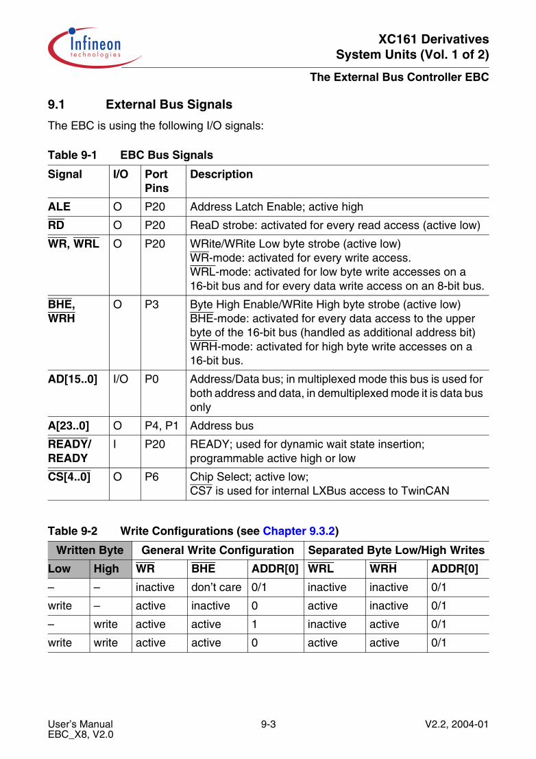
XC161 DerivativesSystem Units (Vol. 1 of 2)
The External Bus Controller EBC
9.1 External Bus Signals
The EBC is using the following I/O signals:
Table 9-1 EBC Bus Signals
Signal I/O Port Pins
Description
ALE O P20 Address Latch Enable; active high
RD O P20 ReaD strobe: activated for every read access (active low)
WR, WRL O P20 WRite/WRite Low byte strobe (active low)WR-mode: activated for every write access.WRL-mode: activated for low byte write accesses on a 16-bit bus and for every data write access on an 8-bit bus.
BHE,WRH
O P3 Byte High Enable/WRite High byte strobe (active low)BHE-mode: activated for every data access to the upper byte of the 16-bit bus (handled as additional address bit)WRH-mode: activated for high byte write accesses on a 16-bit bus.
AD[15..0] I/O P0 Address/Data bus; in multiplexed mode this bus is used for both address and data, in demultiplexed mode it is data bus only
A[23..0] O P4, P1 Address bus
READY/READY
I P20 READY; used for dynamic wait state insertion; programmable active high or low
CS[4..0] O P6 Chip Select; active low;CS7 is used for internal LXBus access to TwinCAN
Table 9-2 Write Configurations (see Chapter 9.3.2)
Written Byte General Write Configuration Separated Byte Low/High Writes
Low High WR BHE ADDR[0] WRL WRH ADDR[0]
– – inactive don’t care 0/1 inactive inactive 0/1
write – active inactive 0 active inactive 0/1
– write active active 1 inactive active 0/1
write write active active 0 active active 0/1
User’s Manual 9-3 V2.2, 2004-01EBC_X8, V2.0
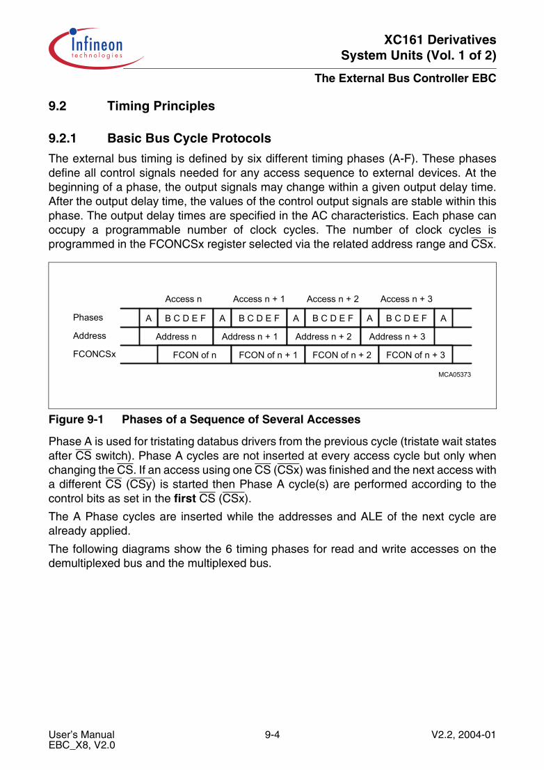
XC161 DerivativesSystem Units (Vol. 1 of 2)
The External Bus Controller EBC
9.2 Timing Principles
9.2.1 Basic Bus Cycle Protocols
The external bus timing is defined by six different timing phases (A-F). These phasesdefine all control signals needed for any access sequence to external devices. At thebeginning of a phase, the output signals may change within a given output delay time.After the output delay time, the values of the control output signals are stable within thisphase. The output delay times are specified in the AC characteristics. Each phase canoccupy a programmable number of clock cycles. The number of clock cycles isprogrammed in the FCONCSx register selected via the related address range and CSx.
Figure 9-1 Phases of a Sequence of Several Accesses
Phase A is used for tristating databus drivers from the previous cycle (tristate wait statesafter CS switch). Phase A cycles are not inserted at every access cycle but only whenchanging the CS. If an access using one CS (CSx) was finished and the next access witha different CS (CSy) is started then Phase A cycle(s) are performed according to thecontrol bits as set in the first CS (CSx).
The A Phase cycles are inserted while the addresses and ALE of the next cycle arealready applied.
The following diagrams show the 6 timing phases for read and write accesses on thedemultiplexed bus and the multiplexed bus.
B C D E F
MCA05373
Phases A A B C D E F A B C D E F A B C D E F A
Access n Access n + 1 Access n + 2 Access n + 3
Address n Address n + 1 Address n + 2 Address n + 3Address
FCON of n FCON of n + 1 FCON of n + 2 FCON of n + 3FCONCSx
User’s Manual 9-4 V2.2, 2004-01EBC_X8, V2.0

XC161 DerivativesSystem Units (Vol. 1 of 2)
The External Bus Controller EBC
9.2.1.1 Demultiplexed Bus
Figure 9-2 Demultiplexed Bus Read
Figure 9-3 Demultiplexed Bus Write
• A phase: Addresses valid, ALE high, no command. CS switch tristate wait states• B phase: Addresses valid, ALE high, no command. ALE length• C phase: Addresses valid, ALE low, no command. R/W delay• D phase: Write data valid, ALE low, no command. Data valid for write cycles• E phase: Command (read or write) active. Access time• F phase: Command inactive, address hold. Read data tristate time, write data hold
time
MCT05374
A B C D E F
Valid
Valid
0 - 3 1 - 2 0 - 3 0 - 1 1 - 32 0 - 3
Phases
ALE
ADDR, CS
RD
Read DATA
ProgrammableClocks
MCT05375
A B C D E F
Valid
Valid
0 - 3 1 - 2 0 - 3 0 - 1 1 - 32 0 - 3
Phases
ALE
ADDR, CS
WR
Write DATA
ProgrammableClocks
User’s Manual 9-5 V2.2, 2004-01EBC_X8, V2.0
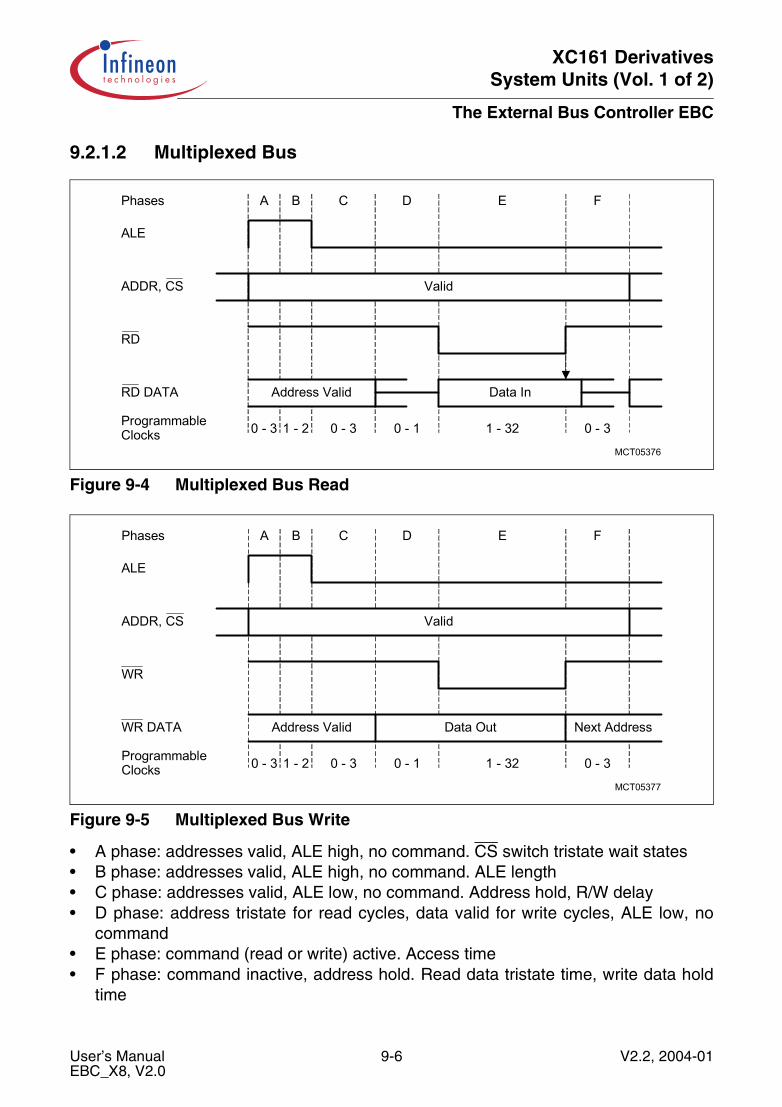
XC161 DerivativesSystem Units (Vol. 1 of 2)
The External Bus Controller EBC
9.2.1.2 Multiplexed Bus
Figure 9-4 Multiplexed Bus Read
Figure 9-5 Multiplexed Bus Write
• A phase: addresses valid, ALE high, no command. CS switch tristate wait states• B phase: addresses valid, ALE high, no command. ALE length• C phase: addresses valid, ALE low, no command. Address hold, R/W delay• D phase: address tristate for read cycles, data valid for write cycles, ALE low, no
command• E phase: command (read or write) active. Access time• F phase: command inactive, address hold. Read data tristate time, write data hold
time
Address Valid
MCT05376
A B C D E F
Valid
Data In
0 - 3 1 - 2 0 - 3 0 - 1 1 - 32 0 - 3
Phases
ALE
ADDR, CS
RD
RD DATA
ProgrammableClocks
Next AddressAddress Valid
MCT05377
A B C D E F
Valid
Data Out
0 - 3 1 - 2 0 - 3 0 - 1 1 - 32 0 - 3
Phases
ALE
ADDR, CS
WR
WR DATA
ProgrammableClocks
User’s Manual 9-6 V2.2, 2004-01EBC_X8, V2.0
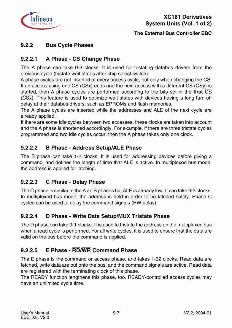
XC161 DerivativesSystem Units (Vol. 1 of 2)
The External Bus Controller EBC
9.2.2 Bus Cycle Phases
9.2.2.1 A Phase - CS Change Phase
The A phase can take 0-3 clocks. It is used for tristating databus drivers from theprevious cycle (tristate wait states after chip select switch).A phase cycles are not inserted at every access cycle, but only when changing the CS.If an access using one CS (CSx) ends and the next access with a different CS (CSy) isstarted, then A phase cycles are performed according to the bits set in the first CS(CSx). This feature is used to optimize wait states with devices having a long turn-offdelay at their databus drivers, such as EPROMs and flash memories.The A phase cycles are inserted while the addresses and ALE of the next cycle arealready applied.If there are some idle cycles between two accesses, these clocks are taken into accountand the A phase is shortened accordingly. For example, if there are three tristate cyclesprogrammed and two idle cycles occur, then the A phase takes only one clock.
9.2.2.2 B Phase - Address Setup/ALE Phase
The B phase can take 1-2 clocks. It is used for addressing devices before giving acommand, and defines the length of time that ALE is active. In multiplexed bus mode,the address is applied for latching.
9.2.2.3 C Phase - Delay Phase
The C phase is similar to the A an B phases but ALE is already low. It can take 0-3 clocks.In multiplexed bus mode, the address is held in order to be latched safely. Phase Ccycles can be used to delay the command signals (RW delay).
9.2.2.4 D Phase - Write Data Setup/MUX Tristate Phase
The D phase can take 0-1 clocks. It is used to tristate the address on the multiplexed buswhen a read cycle is performed. For all write cycles, it is used to ensure that the data arevalid on the bus before the command is applied.
9.2.2.5 E Phase - RD/WR Command Phase
The E phase is the command or access phase, and takes 1-32 clocks. Read data arefetched, write data are put onto the bus, and the command signals are active. Read dataare registered with the terminating clock of this phase.The READY function lengthens this phase, too. READY-controlled access cycles mayhave an unlimited cycle time.
User’s Manual 9-7 V2.2, 2004-01EBC_X8, V2.0
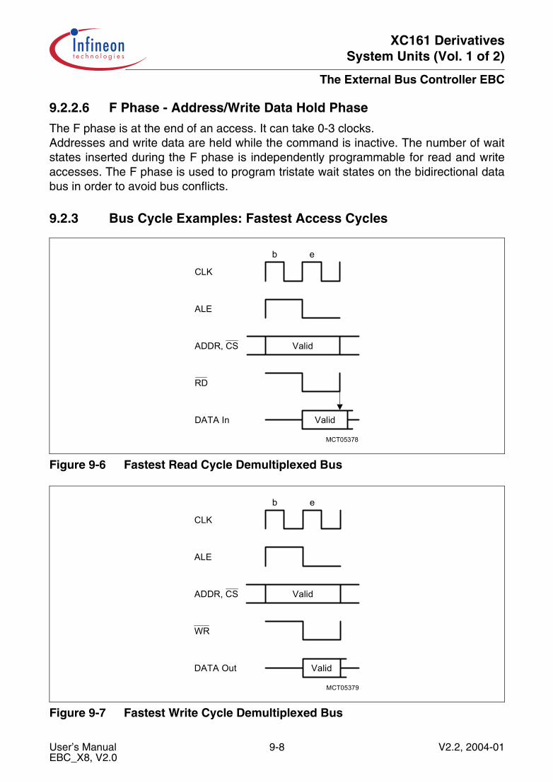
XC161 DerivativesSystem Units (Vol. 1 of 2)
The External Bus Controller EBC
9.2.2.6 F Phase - Address/Write Data Hold Phase
The F phase is at the end of an access. It can take 0-3 clocks.Addresses and write data are held while the command is inactive. The number of waitstates inserted during the F phase is independently programmable for read and writeaccesses. The F phase is used to program tristate wait states on the bidirectional databus in order to avoid bus conflicts.
9.2.3 Bus Cycle Examples: Fastest Access Cycles
Figure 9-6 Fastest Read Cycle Demultiplexed Bus
Figure 9-7 Fastest Write Cycle Demultiplexed Bus
MCT05378
b
CLK
e
ALE
ValidADDR, CS
RD
ValidDATA In
MCT05379
b
CLK
e
ALE
ValidADDR, CS
WR
ValidDATA Out
User’s Manual 9-8 V2.2, 2004-01EBC_X8, V2.0
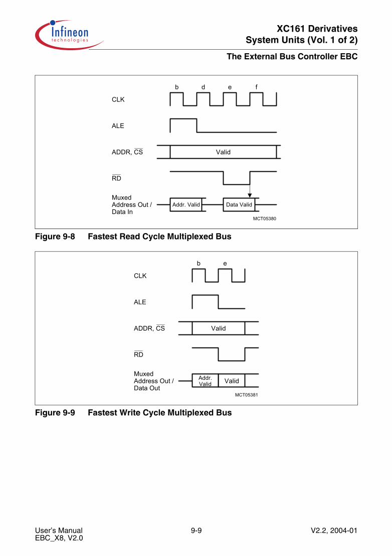
XC161 DerivativesSystem Units (Vol. 1 of 2)
The External Bus Controller EBC
Figure 9-8 Fastest Read Cycle Multiplexed Bus
Figure 9-9 Fastest Write Cycle Multiplexed Bus
MCT05380
b
CLK
d
ALE
ValidADDR, CS
RD
Data ValidMuxedAddress Out /Data In
e f
Addr. Valid
MCT05381
b
CLK
e
ALE
ValidADDR, CS
RD
ValidMuxedAddress Out /Data Out
Addr.Valid
User’s Manual 9-9 V2.2, 2004-01EBC_X8, V2.0

XC161 DerivativesSystem Units (Vol. 1 of 2)
The External Bus Controller EBC
9.3 Functional Description
9.3.1 Configuration Register Overview
There are 3 groups of EBC registers:
• EBC mode registers have influence on global functions.• Chip-select-related registers control the functionality linked to one CS.• TwinCAN and Startup Memory registers are used to control the access to the internal
LXBus.
CS0 is the default chip-select signal that is active whenever no other chip-select orinternal address space is addressed. Therefore, CS0 has no ADDRSEL register.
Note: All EBC registers are write-protected by the EINIT protection mechanism. Thus,after execution of the EINIT instruction, these registers are not writable any more.
A 128-byte address space is occupied/reserved by the EBC.
Table 9-3 EBC Configuration Register Overview
Name CS1)
1) CS5 and CS6 register sets are not available (reserved for future LXBus peripherals).
Description Address00EExxH
Start-up Value
EBCMOD0 all EBC MODe 0;alternate function of EBC pins
00 0xxxH
EBCMOD1 all EBC MODe 1;alternate function of EBC pins
02 0000H
TCONCS0 0 Timing CONtrol for CS0 10 6243H
FCONCS0 0 Function CONtrol for CS0 12 0021H
TCONCS1-71) 1-61), 7
Timing CONtrol for CS1 … CS71) 18, 20, 28, 30, 38, 40, 48
0000H
FCONCS1-71) 1-61), 7
Function CONtrol for CS1 … CS71) 1A, 22, 2A, 32, 3A, 42, 4A
0000H
ADDRSEL1-71) 1-61), 7
ADDress window SELectionfor CS1 … CS71)
1E, 26, 2E, 36, 3E, 46, 4E
0000H
TCONCSSM SM Timing Control for CS to (pointer of) Startup Memory
0E 0000H(reset)
User’s Manual 9-10 V2.2, 2004-01EBC_X8, V2.0
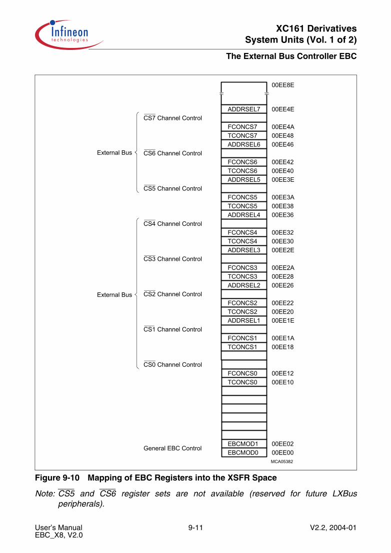
XC161 DerivativesSystem Units (Vol. 1 of 2)
The External Bus Controller EBC
Figure 9-10 Mapping of EBC Registers into the XSFR Space
Note: CS5 and CS6 register sets are not available (reserved for future LXBusperipherals).
MCA05382
EBCMOD0EBCMOD1
TCONCS0FCONCS0
TCONCS1FCONCS1
ADDRSEL1TCONCS2FCONCS2
ADDRSEL2TCONCS3FCONCS3
ADDRSEL3TCONCS4FCONCS4
ADDRSEL4TCONCS5FCONCS5
ADDRSEL5TCONCS6FCONCS6
ADDRSEL6TCONCS7FCONCS7
ADDRSEL7
00EE0000EE02
00EE1000EE12
00EE1800EE1A
00EE1E00EE2000EE22
00EE2600EE2800EE2A
00EE2E00EE3000EE32
00EE3600EE3800EE3A
00EE3E00EE4000EE42
00EE4600EE4800EE4A
00EE4E
00EE8E
General EBC Control
CS0 Channel Control
CS1 Channel Control
CS2 Channel Control
CS3 Channel Control
CS4 Channel Control
CS5 Channel Control
CS6 Channel Control
CS7 Channel Control
External Bus
External Bus
User’s Manual 9-11 V2.2, 2004-01EBC_X8, V2.0
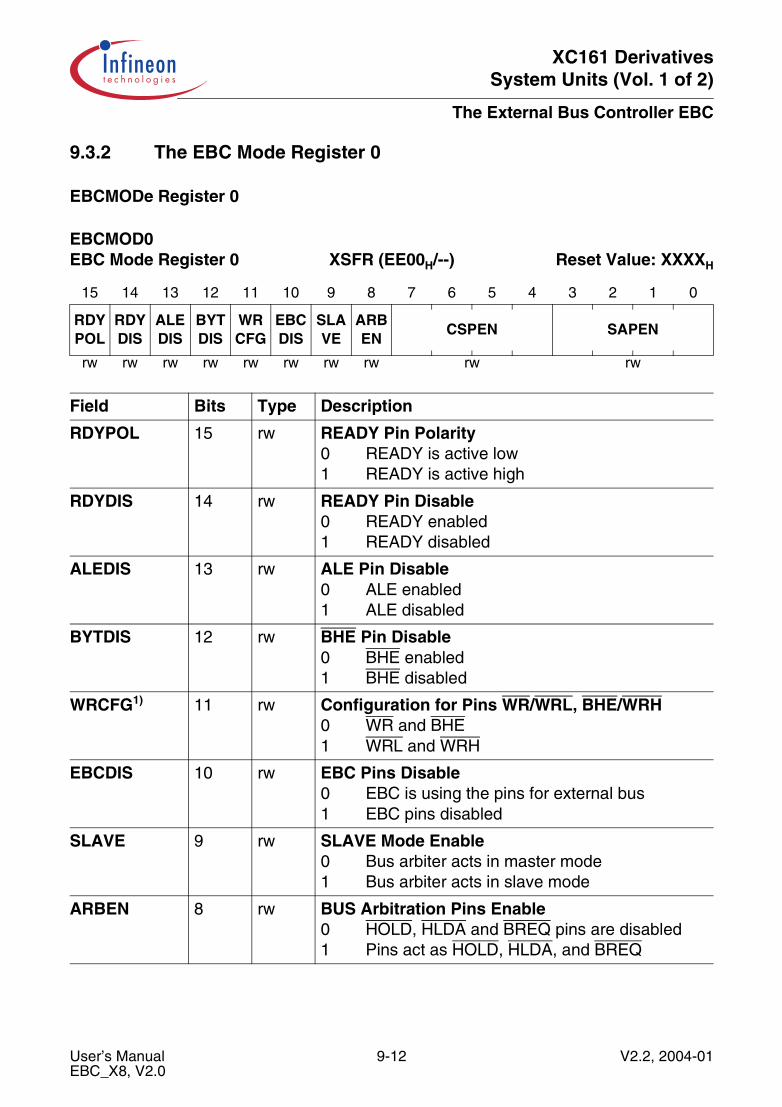
XC161 DerivativesSystem Units (Vol. 1 of 2)
The External Bus Controller EBC
9.3.2 The EBC Mode Register 0
EBCMODe Register 0
EBCMOD0 EBC Mode Register 0 XSFR (EE00H/--) Reset Value: XXXXH
15 14 13 12 11 10 9 8 7 6 5 4 3 2 1 0
RDY POL
RDY DIS
ALE DIS
BYT DIS
WR CFG
EBC DIS
SLA VE
ARB EN
CSPEN SAPEN
rw rw rw rw rw rw rw rw rw rw
Field Bits Type Description
RDYPOL 15 rw READY Pin Polarity0 READY is active low1 READY is active high
RDYDIS 14 rw READY Pin Disable0 READY enabled1 READY disabled
ALEDIS 13 rw ALE Pin Disable0 ALE enabled1 ALE disabled
BYTDIS 12 rw BHE Pin Disable0 BHE enabled1 BHE disabled
WRCFG1) 11 rw Configuration for Pins WR/WRL, BHE/WRH0 WR and BHE1 WRL and WRH
EBCDIS 10 rw EBC Pins Disable0 EBC is using the pins for external bus1 EBC pins disabled
SLAVE 9 rw SLAVE Mode Enable0 Bus arbiter acts in master mode1 Bus arbiter acts in slave mode
ARBEN 8 rw BUS Arbitration Pins Enable0 HOLD, HLDA and BREQ pins are disabled1 Pins act as HOLD, HLDA, and BREQ
User’s Manual 9-12 V2.2, 2004-01EBC_X8, V2.0
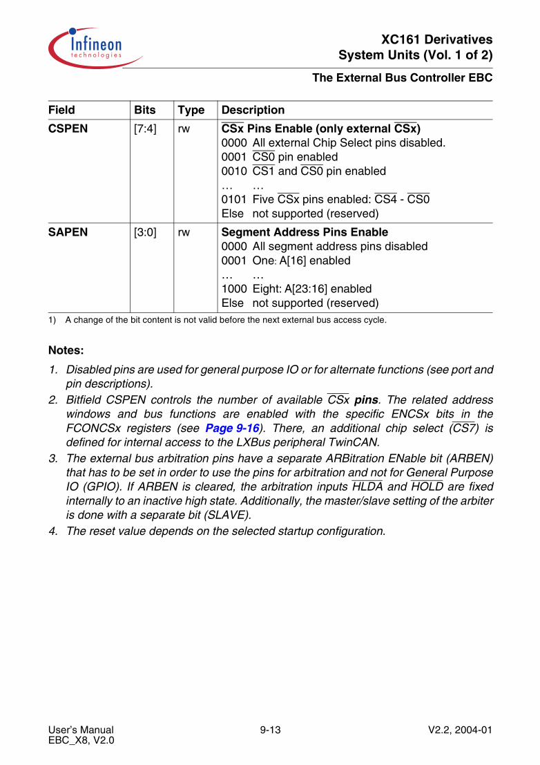
XC161 DerivativesSystem Units (Vol. 1 of 2)
The External Bus Controller EBC
Notes:
1. Disabled pins are used for general purpose IO or for alternate functions (see port andpin descriptions).
2. Bitfield CSPEN controls the number of available CSx pins. The related addresswindows and bus functions are enabled with the specific ENCSx bits in theFCONCSx registers (see Page 9-16). There, an additional chip select (CS7) isdefined for internal access to the LXBus peripheral TwinCAN.
3. The external bus arbitration pins have a separate ARBitration ENable bit (ARBEN)that has to be set in order to use the pins for arbitration and not for General PurposeIO (GPIO). If ARBEN is cleared, the arbitration inputs HLDA and HOLD are fixedinternally to an inactive high state. Additionally, the master/slave setting of the arbiteris done with a separate bit (SLAVE).
4. The reset value depends on the selected startup configuration.
CSPEN [7:4] rw CSx Pins Enable (only external CSx)0000 All external Chip Select pins disabled.0001 CS0 pin enabled0010 CS1 and CS0 pin enabled… …0101 Five CSx pins enabled: CS4 - CS0Else not supported (reserved)
SAPEN [3:0] rw Segment Address Pins Enable0000 All segment address pins disabled0001 One: A[16] enabled… …1000 Eight: A[23:16] enabledElse not supported (reserved)
1) A change of the bit content is not valid before the next external bus access cycle.
Field Bits Type Description
User’s Manual 9-13 V2.2, 2004-01EBC_X8, V2.0
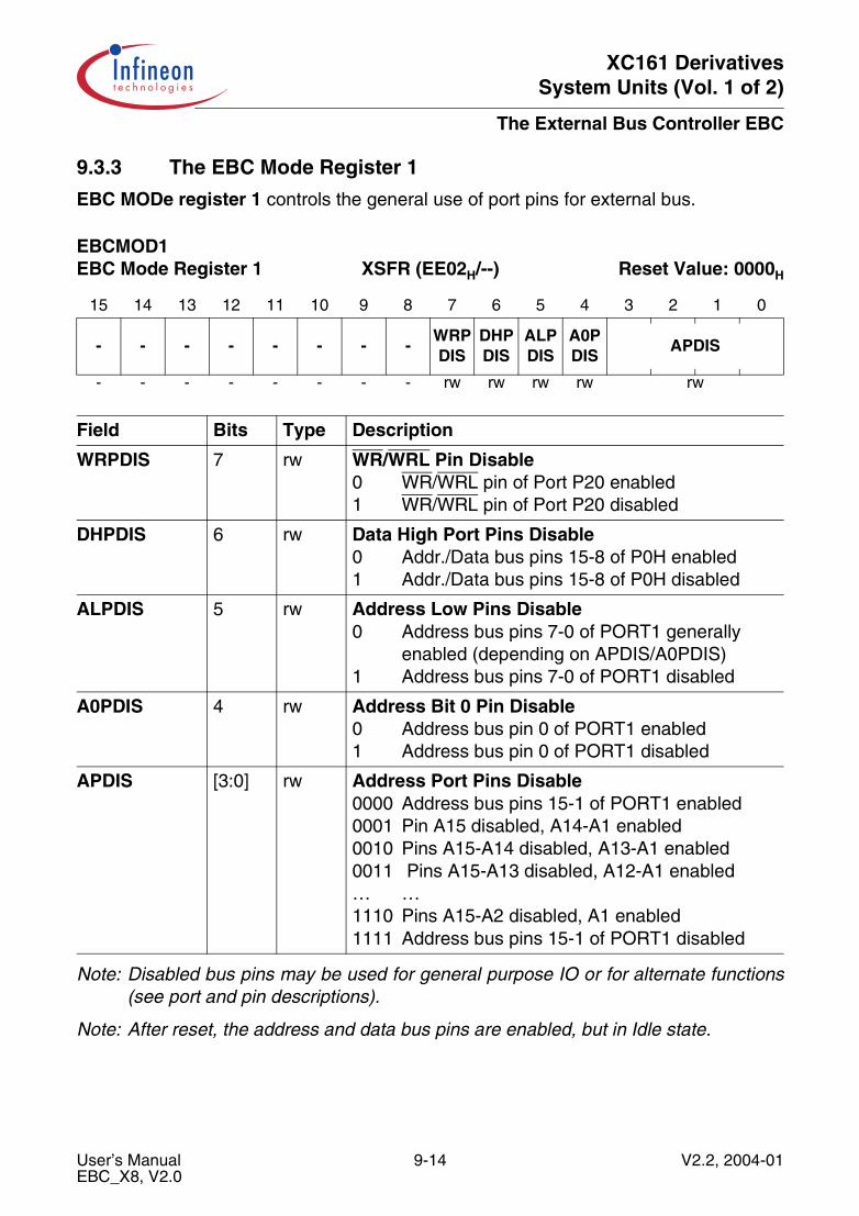
XC161 DerivativesSystem Units (Vol. 1 of 2)
The External Bus Controller EBC
9.3.3 The EBC Mode Register 1
EBC MODe register 1 controls the general use of port pins for external bus.
Note: Disabled bus pins may be used for general purpose IO or for alternate functions(see port and pin descriptions).
Note: After reset, the address and data bus pins are enabled, but in Idle state.
EBCMOD1EBC Mode Register 1 XSFR (EE02H/--) Reset Value: 0000H
15 14 13 12 11 10 9 8 7 6 5 4 3 2 1 0
- - - - - - - -WRPDIS
DHPDIS
ALPDIS
A0PDIS
APDIS
- - - - - - - - rw rw rw rw rw
Field Bits Type Description
WRPDIS 7 rw WR/WRL Pin Disable0 WR/WRL pin of Port P20 enabled1 WR/WRL pin of Port P20 disabled
DHPDIS 6 rw Data High Port Pins Disable0 Addr./Data bus pins 15-8 of P0H enabled1 Addr./Data bus pins 15-8 of P0H disabled
ALPDIS 5 rw Address Low Pins Disable0 Address bus pins 7-0 of PORT1 generally
enabled (depending on APDIS/A0PDIS)1 Address bus pins 7-0 of PORT1 disabled
A0PDIS 4 rw Address Bit 0 Pin Disable0 Address bus pin 0 of PORT1 enabled1 Address bus pin 0 of PORT1 disabled
APDIS [3:0] rw Address Port Pins Disable0000 Address bus pins 15-1 of PORT1 enabled0001 Pin A15 disabled, A14-A1 enabled0010 Pins A15-A14 disabled, A13-A1 enabled0011 Pins A15-A13 disabled, A12-A1 enabled… …1110 Pins A15-A2 disabled, A1 enabled1111 Address bus pins 15-1 of PORT1 disabled
User’s Manual 9-14 V2.2, 2004-01EBC_X8, V2.0

XC161 DerivativesSystem Units (Vol. 1 of 2)
The External Bus Controller EBC
9.3.4 The Timing Configuration Registers TCONCSx
The timing control registers are used to program the described cycle timing for thedifferent access phases. The timing control registers may be reprogrammed during codefetches from the affected address window. The new settings are first valid for the nextaccess.
x = 1 … 4, 7
Note: x = 7 belongs to the additional chip select (CS7) which is used and defined forinternal access to the LXBus peripheral TwinCAN.
TCONCS0Timing Cfg. Reg. for CS0 XSFR (EE10H/--) Reset Value: 7AXXH
15 14 13 12 11 10 9 8 7 6 5 4 3 2 1 0
- WRPHF RDPHF PHE PHD PHC PHB PHA
- rw rw rw rw rw rw rw
TCONCSxTiming Cfg. Reg. for CSx XSFR (EEXXH/--) Reset Value: 0000H
15 14 13 12 11 10 9 8 7 6 5 4 3 2 1 0
- WRPHF RDPHF PHE PHD PHC PHB PHA
- rw rw rw rw rw rw rw
Field Bits Typ Description
WRPHF [14:13] rw Write Phase F00 0 clock cycles… …11 3 clock cycles (default)
RDPHF [12:11] rw Read Phase F00 0 clock cycles (default)… …11 3 clock cycles
PHE [10:6] rw Phase E00000: 1 clock cycle… … (default: 9 clock cycles)11111: 32 clock cycles
User’s Manual 9-15 V2.2, 2004-01EBC_X8, V2.0
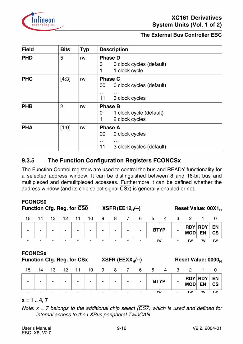
XC161 DerivativesSystem Units (Vol. 1 of 2)
The External Bus Controller EBC
9.3.5 The Function Configuration Registers FCONCSx
The Function Control registers are used to control the bus and READY functionality fora selected address window. It can be distinguished between 8 and 16-bit bus andmultiplexed and demulitplexed accesses. Furthermore it can be defined whether theaddress window (and its chip select signal CSx) is generally enabled or not.
x = 1 .. 4, 7
Note: x = 7 belongs to the additional chip select (CS7) which is used and defined forinternal access to the LXBus peripheral TwinCAN.
PHD 5 rw Phase D0 0 clock cycles (default)1 1 clock cycle
PHC [4:3] rw Phase C00 0 clock cycles (default)… …11 3 clock cycles
PHB 2 rw Phase B0 1 clock cycle (default)1 2 clock cycles
PHA [1:0] rw Phase A00 0 clock cycles… …11 3 clock cycles (default)
FCONCS0Function Cfg. Reg. for CS0 XSFR (EE12H/--) Reset Value: 00X1H
15 14 13 12 11 10 9 8 7 6 5 4 3 2 1 0
- - - - - - - - - - BTYP -RDY MOD
RDYEN
ENCS
- - - - - - - - - - rw - rw rw rw
FCONCSxFunction Cfg. Reg. for CSx XSFR (EEXXH/--) Reset Value: 0000H
15 14 13 12 11 10 9 8 7 6 5 4 3 2 1 0
- - - - - - - - - - BTYP -RDY MOD
RDY EN
ENCS
- - - - - - - - - - rw - rw rw rw
Field Bits Typ Description
User’s Manual 9-16 V2.2, 2004-01EBC_X8, V2.0
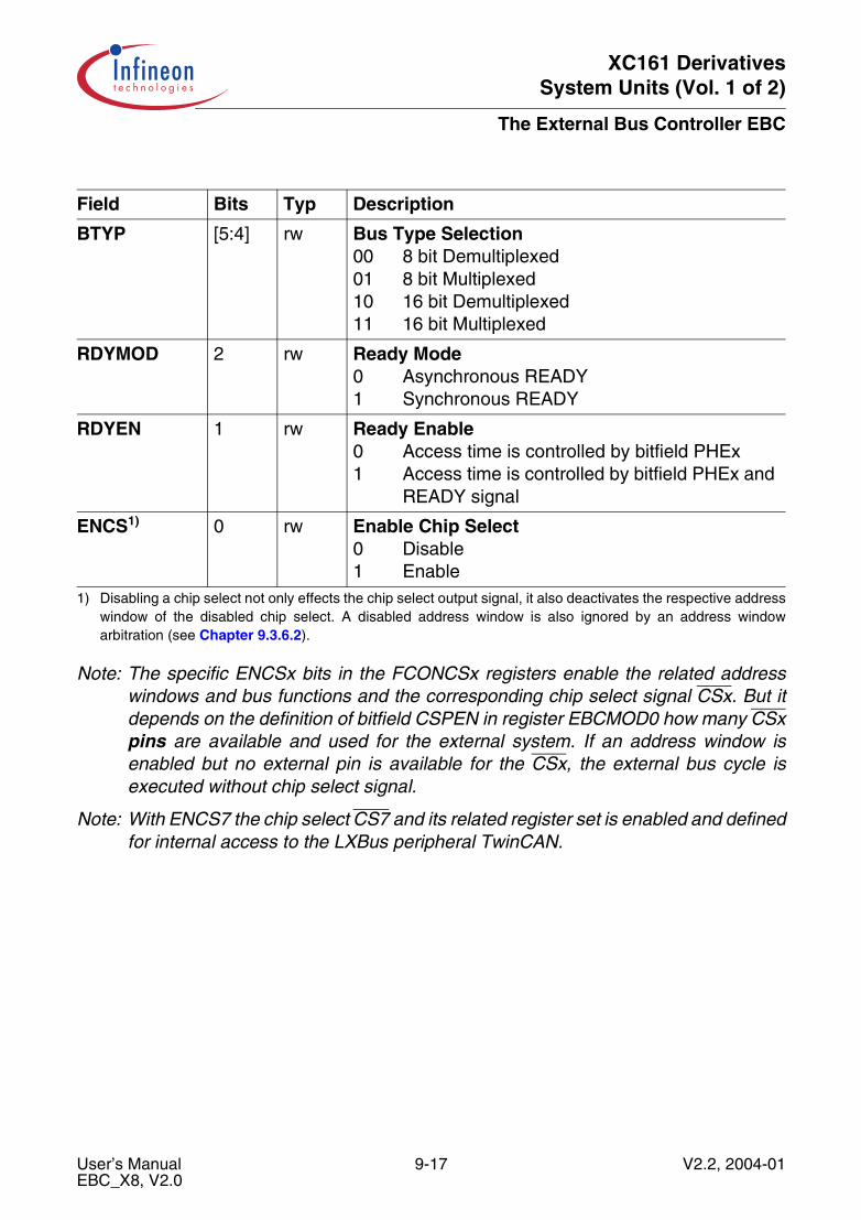
XC161 DerivativesSystem Units (Vol. 1 of 2)
The External Bus Controller EBC
Note: The specific ENCSx bits in the FCONCSx registers enable the related addresswindows and bus functions and the corresponding chip select signal CSx. But itdepends on the definition of bitfield CSPEN in register EBCMOD0 how many CSxpins are available and used for the external system. If an address window isenabled but no external pin is available for the CSx, the external bus cycle isexecuted without chip select signal.
Note: With ENCS7 the chip select CS7 and its related register set is enabled and definedfor internal access to the LXBus peripheral TwinCAN.
Field Bits Typ Description
BTYP [5:4] rw Bus Type Selection00 8 bit Demultiplexed01 8 bit Multiplexed10 16 bit Demultiplexed11 16 bit Multiplexed
RDYMOD 2 rw Ready Mode0 Asynchronous READY1 Synchronous READY
RDYEN 1 rw Ready Enable0 Access time is controlled by bitfield PHEx1 Access time is controlled by bitfield PHEx and
READY signal
ENCS1)
1) Disabling a chip select not only effects the chip select output signal, it also deactivates the respective addresswindow of the disabled chip select. A disabled address window is also ignored by an address windowarbitration (see Chapter 9.3.6.2).
0 rw Enable Chip Select0 Disable1 Enable
User’s Manual 9-17 V2.2, 2004-01EBC_X8, V2.0
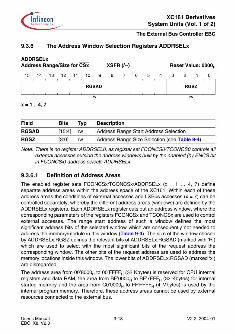
XC161 DerivativesSystem Units (Vol. 1 of 2)
The External Bus Controller EBC
9.3.6 The Address Window Selection Registers ADDRSELx
x = 1 .. 4, 7
Note: There is no register ADDRSEL0, as register set FCONCS0/TCONCS0 controls allexternal accesses outside the address windows built by the enabled (by ENCS bitin FCONCSx) address selects ADDRSELx.
9.3.6.1 Definition of Address Areas
The enabled register sets FCONCSx/TCONCSx/ADDRSELx (x = 1 … 4, 7) defineseparate address areas within the address space of the XC161. Within each of theseaddress areas the conditions of external accesses and LXBus accesses (x = 7) can becontrolled separately, whereby the different address areas (windows) are defined by theADDRSELx registers. Each ADDRSELx register cuts out an address window, where thecorresponding parameters of the registers FCONCSx and TCONCSx are used to controlexternal accesses. The range start address of such a window defines the mostsignificant address bits of the selected window which are consequently not needed toaddress the memory/module in this window (Table 9-4). The size of the window chosenby ADDRSELx.RGSZ defines the relevant bits of ADDRSELx.RGSAD (marked with ‘R’)which are used to select with the most significant bits of the request address thecorresponding window. The other bits of the request address are used to address thememory locations inside this window. The lower bits of ADDRSELx.RGSAD (marked ‘x’)are disregarded.
The address area from 00’8000H to 00’FFFFH (32 Kbytes) is reserved for CPU internalregisters and data RAM, the area from BF’0000H to BF’7FFFH (32 Kbytes) for internalstartup memory and the area from C0’0000H to FF’FFFFH (4 Mbytes) is used by theinternal program memory. Therefore, these address areas cannot be used by externalresources connected to the external bus.
ADDRSELxAddress Range/Size for CSx XSFR (/--) Reset Value: 0000H
15 14 13 12 11 10 9 8 7 6 5 4 3 2 1 0
RGSAD RGSZ
rw rw
Field Bits Typ Description
RGSAD [15:4] rw Address Range Start Address Selection
RGSZ [3:0] rw Address Range Size Selection (see Table 9-4)
User’s Manual 9-18 V2.2, 2004-01EBC_X8, V2.0
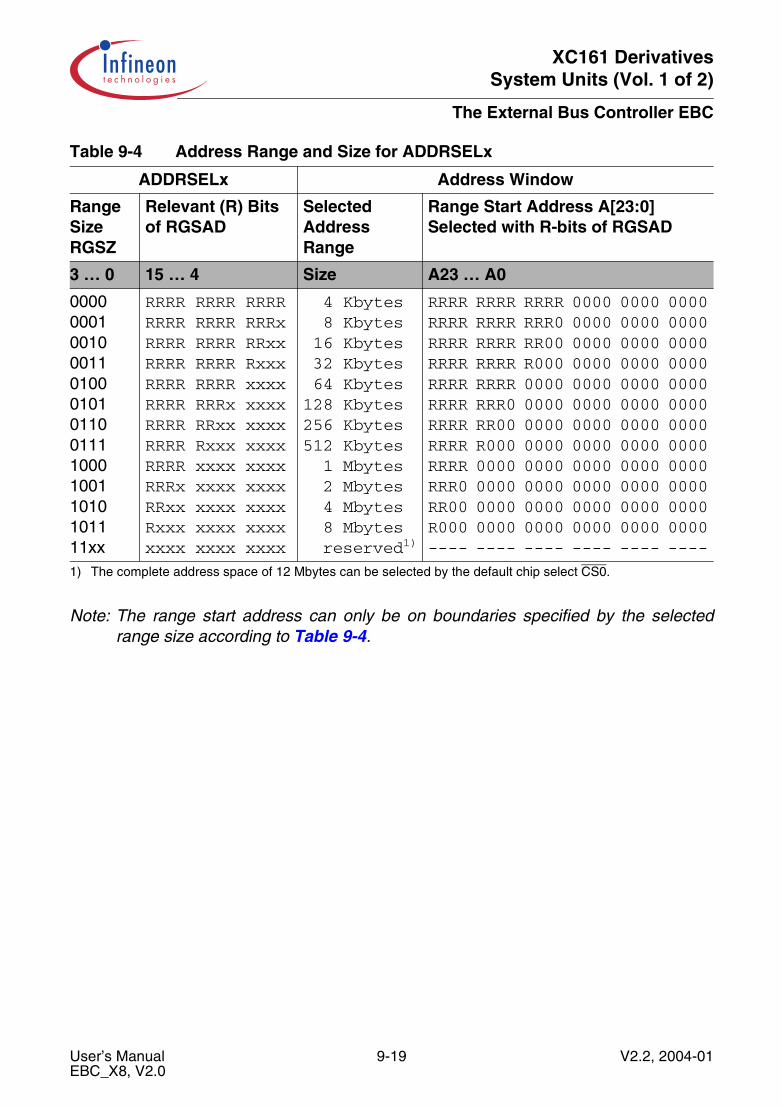
XC161 DerivativesSystem Units (Vol. 1 of 2)
The External Bus Controller EBC
Note: The range start address can only be on boundaries specified by the selectedrange size according to Table 9-4.
Table 9-4 Address Range and Size for ADDRSELx
ADDRSELx Address Window
Range SizeRGSZ
Relevant (R) Bits of RGSAD
Selected Address Range
Range Start Address A[23:0] Selected with R-bits of RGSAD
3 … 0 15 … 4 Size A23 … A0
00000001001000110100010101100111100010011010101111xx
RRRR RRRR RRRRRRRR RRRR RRRxRRRR RRRR RRxxRRRR RRRR RxxxRRRR RRRR xxxxRRRR RRRx xxxxRRRR RRxx xxxxRRRR Rxxx xxxxRRRR xxxx xxxxRRRx xxxx xxxxRRxx xxxx xxxxRxxx xxxx xxxxxxxx xxxx xxxx
4 Kbytes 8 Kbytes 16 Kbytes 32 Kbytes 64 Kbytes128 Kbytes256 Kbytes512 Kbytes 1 Mbytes 2 Mbytes 4 Mbytes 8 Mbytes reserved1)
RRRR RRRR RRRR 0000 0000 0000RRRR RRRR RRR0 0000 0000 0000RRRR RRRR RR00 0000 0000 0000RRRR RRRR R000 0000 0000 0000RRRR RRRR 0000 0000 0000 0000RRRR RRR0 0000 0000 0000 0000RRRR RR00 0000 0000 0000 0000RRRR R000 0000 0000 0000 0000RRRR 0000 0000 0000 0000 0000RRR0 0000 0000 0000 0000 0000RR00 0000 0000 0000 0000 0000R000 0000 0000 0000 0000 0000---- ---- ---- ---- ---- ----
1) The complete address space of 12 Mbytes can be selected by the default chip select CS0.
User’s Manual 9-19 V2.2, 2004-01EBC_X8, V2.0
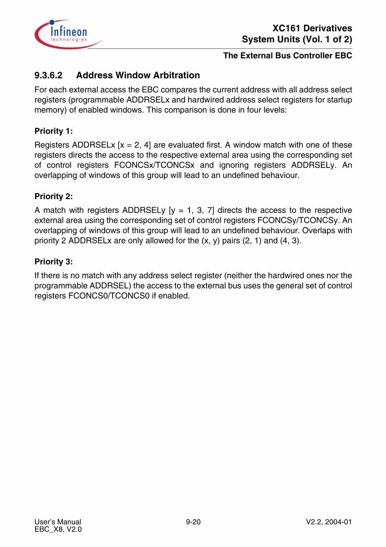
XC161 DerivativesSystem Units (Vol. 1 of 2)
The External Bus Controller EBC
9.3.6.2 Address Window Arbitration
For each external access the EBC compares the current address with all address selectregisters (programmable ADDRSELx and hardwired address select registers for startupmemory) of enabled windows. This comparison is done in four levels:
Priority 1:
Registers ADDRSELx [x = 2, 4] are evaluated first. A window match with one of theseregisters directs the access to the respective external area using the corresponding setof control registers FCONCSx/TCONCSx and ignoring registers ADDRSELy. Anoverlapping of windows of this group will lead to an undefined behaviour.
Priority 2:
A match with registers ADDRSELy [y = 1, 3, 7] directs the access to the respectiveexternal area using the corresponding set of control registers FCONCSy/TCONCSy. Anoverlapping of windows of this group will lead to an undefined behaviour. Overlaps withpriority 2 ADDRSELx are only allowed for the (x, y) pairs (2, 1) and (4, 3).
Priority 3:
If there is no match with any address select register (neither the hardwired ones nor theprogrammable ADDRSEL) the access to the external bus uses the general set of controlregisters FCONCS0/TCONCS0 if enabled.
User’s Manual 9-20 V2.2, 2004-01EBC_X8, V2.0
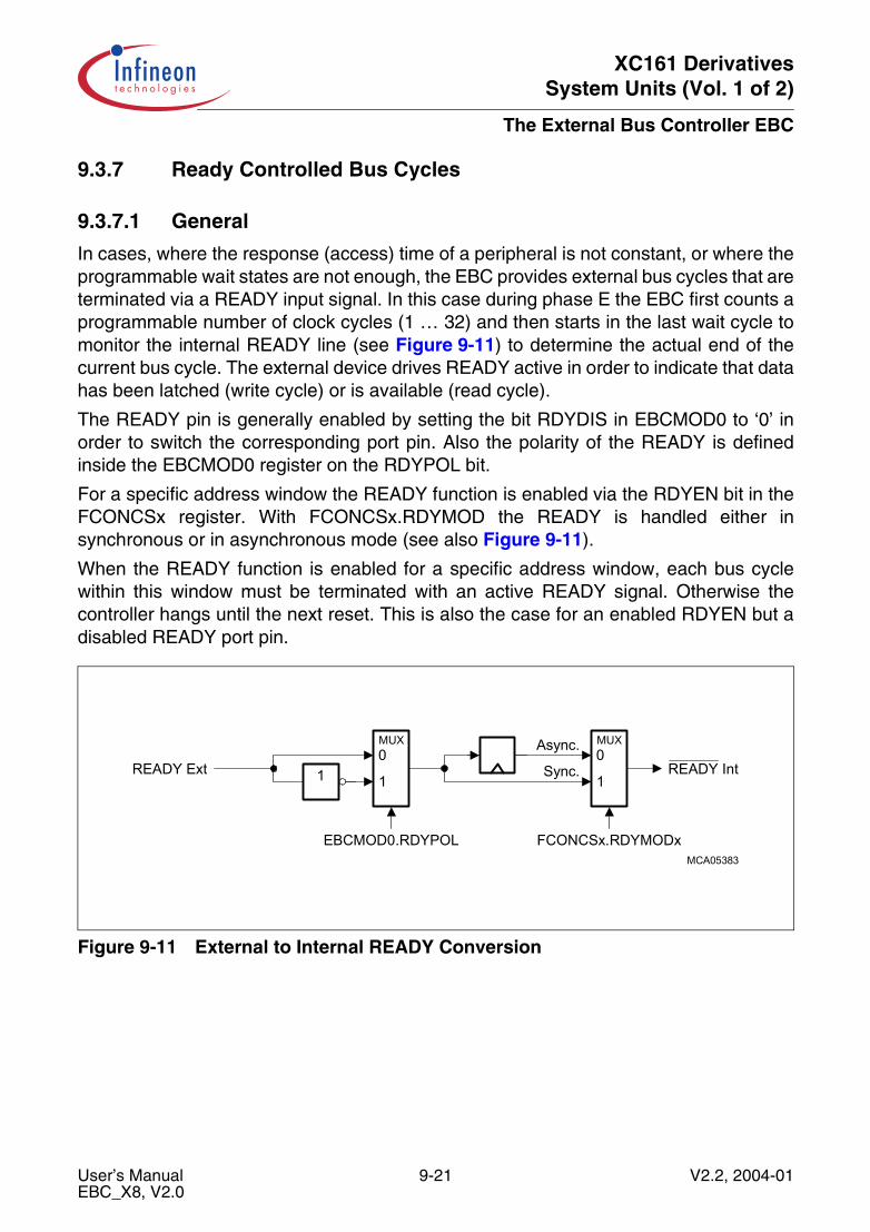
XC161 DerivativesSystem Units (Vol. 1 of 2)
The External Bus Controller EBC
9.3.7 Ready Controlled Bus Cycles
9.3.7.1 General
In cases, where the response (access) time of a peripheral is not constant, or where theprogrammable wait states are not enough, the EBC provides external bus cycles that areterminated via a READY input signal. In this case during phase E the EBC first counts aprogrammable number of clock cycles (1 … 32) and then starts in the last wait cycle tomonitor the internal READY line (see Figure 9-11) to determine the actual end of thecurrent bus cycle. The external device drives READY active in order to indicate that datahas been latched (write cycle) or is available (read cycle).
The READY pin is generally enabled by setting the bit RDYDIS in EBCMOD0 to ‘0’ inorder to switch the corresponding port pin. Also the polarity of the READY is definedinside the EBCMOD0 register on the RDYPOL bit.
For a specific address window the READY function is enabled via the RDYEN bit in theFCONCSx register. With FCONCSx.RDYMOD the READY is handled either insynchronous or in asynchronous mode (see also Figure 9-11).
When the READY function is enabled for a specific address window, each bus cyclewithin this window must be terminated with an active READY signal. Otherwise thecontroller hangs until the next reset. This is also the case for an enabled RDYEN but adisabled READY port pin.
Figure 9-11 External to Internal READY Conversion
MCA05383
1READY Ext
EBCMOD0.RDYPOL
Async.
FCONCSx.RDYMODx
Sync. READY Int
MUX0
1
MUX0
1
User’s Manual 9-21 V2.2, 2004-01EBC_X8, V2.0
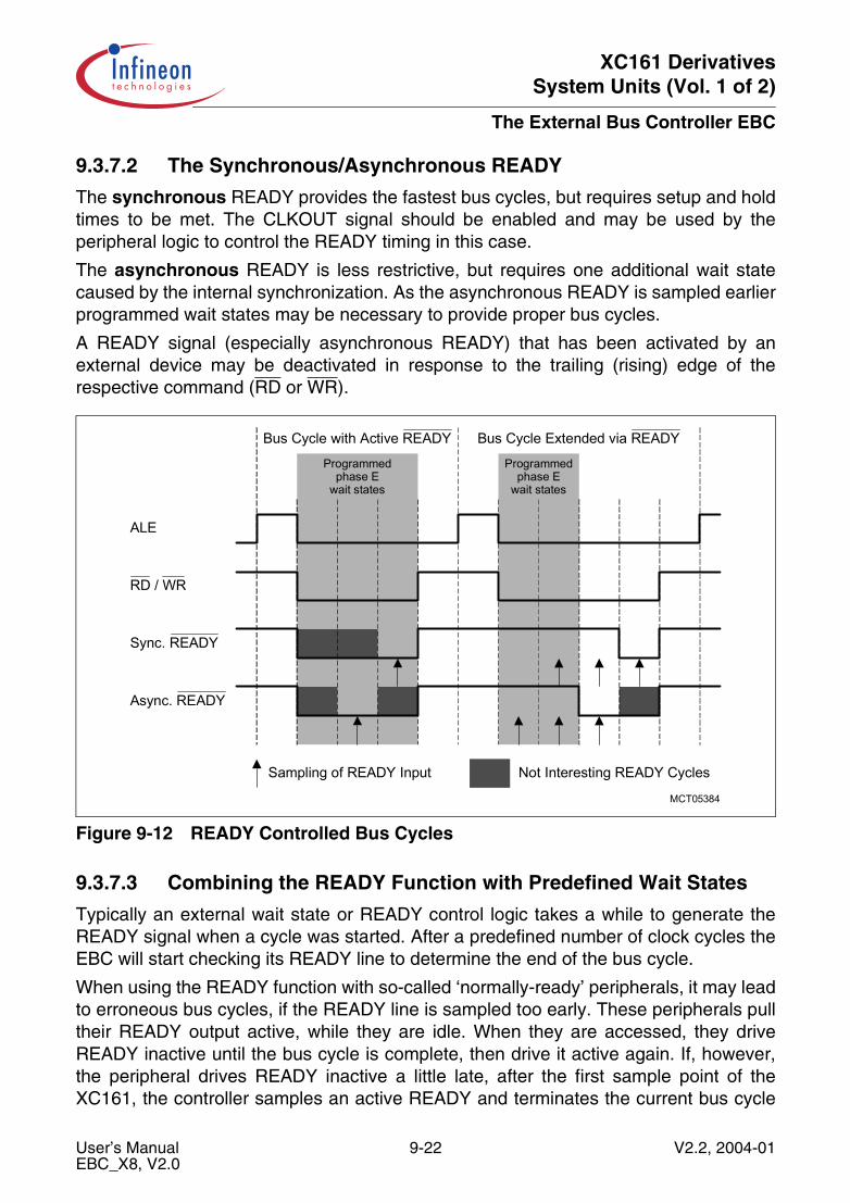
XC161 DerivativesSystem Units (Vol. 1 of 2)
The External Bus Controller EBC
9.3.7.2 The Synchronous/Asynchronous READY
The synchronous READY provides the fastest bus cycles, but requires setup and holdtimes to be met. The CLKOUT signal should be enabled and may be used by theperipheral logic to control the READY timing in this case.
The asynchronous READY is less restrictive, but requires one additional wait statecaused by the internal synchronization. As the asynchronous READY is sampled earlierprogrammed wait states may be necessary to provide proper bus cycles.
A READY signal (especially asynchronous READY) that has been activated by anexternal device may be deactivated in response to the trailing (rising) edge of therespective command (RD or WR).
Figure 9-12 READY Controlled Bus Cycles
9.3.7.3 Combining the READY Function with Predefined Wait States
Typically an external wait state or READY control logic takes a while to generate theREADY signal when a cycle was started. After a predefined number of clock cycles theEBC will start checking its READY line to determine the end of the bus cycle.
When using the READY function with so-called ‘normally-ready’ peripherals, it may leadto erroneous bus cycles, if the READY line is sampled too early. These peripherals pulltheir READY output active, while they are idle. When they are accessed, they driveREADY inactive until the bus cycle is complete, then drive it active again. If, however,the peripheral drives READY inactive a little late, after the first sample point of theXC161, the controller samples an active READY and terminates the current bus cycle
Programmedphase E
wait states
Programmedphase E
wait states
MCT05384
Bus Cycle with Active READY Bus Cycle Extended via READY
ALE
RD / WR
Sync. READY
Async. READY
Sampling of READY Input Not Interesting READY Cycles
User’s Manual 9-22 V2.2, 2004-01EBC_X8, V2.0

XC161 DerivativesSystem Units (Vol. 1 of 2)
The External Bus Controller EBC
too early. By inserting predefined wait states the first READY sample point can be shiftedto a time, where the peripheral has safely controlled the READY line.
9.3.8 Access Control to TwinCAN
Access control to LXBus is required for accesses to the TwinCAN module. In general,accesses to LXBus are not visible on external bus. During LXBus cycles, the externalbus is still enabled, but driven to inactive states (control signals) or switched into the readmode (buses).
For accesses to the TwinCAN, CS7 and its control registers, the ADDRSEL7, TCONCS7and the FCONCS7 are used. The selection of LXBus is controlled with CS7. The addressrange, defined in ADDRSEL7, is recommended to be located in the ‘External IO Range’(range from 20’0000H to 3F’0000H). Only for the External IO Range of the total externaladdress range it is guaranteed that a read access is executed after a preceeding writeaccess.
After reset (controlled by the startup program sequence), the TwinCAN address range isadjusted per default to the area from address 20’0000H to 20’0FFFH (4 KB), resulting inthe ADDRSEL7 default-code of 2000H. This initial value of ADDRSEL7 may be changedafterwards by the user.
The initial default value of the bus function control register FCONCS7 is selectedaccording to the requirements of the TwinCAN: 16-bit demultiplexed bus, access timecontrolled with synchronous READY. This function control is represented by the defaultvalue for FCONCS7 of 0027H.
The initial LXBus cycle timing as controlled with register TCONCS7 after reset is theshortest possible timing using two clock cycles for one bus cycle. But this minimumtiming will be lengthened with waitstate(s) controlled by the TwinCAN itself with theREADY function. This timing control is controlled by the reset value of TCONCS7(0000H).
User’s Manual 9-23 V2.2, 2004-01EBC_X8, V2.0

XC161 DerivativesSystem Units (Vol. 1 of 2)
The External Bus Controller EBC
9.3.9 External Bus Arbitration
The XC161 supports multi master systems on the external bus by its external busarbitration. This bus arbitration allows an external master to request the external bus.The XC161 will release the external bus and will float the data and address bus lines andforce the control signals via pull ups/downs to their inactive state.
9.3.9.1 Initialization of Arbitration
During reset all arbitration pins are tristate, except pin BREQ which is pulled inactive.After reset the XC161 EBC always starts in ‘init mode’ where the external bus is availablebut no arbitration is enabled. All arbitration pins are ignored in this state. Other to theexternal bus connected XC161 EBCs assume to have the bus also, so potential busconflicts are not resolved. For a multimaster system the arbitration should be initializedfirst before starting any bus access. The EBC can either be chosen as arbitration masteror as arbitration slave by programming the EBCMOD0 bit SLAVE. The selected modeand the arbitration gets active by the first setting of the HLDEN bit inside the CPUs PSWregister. Afterwards a change of the slave/master mode is not possible without resettingthe device. Of course for arbitration the dedicated pins have to be activated by settingEBCMOD0.ARBEN.
9.3.9.2 Arbitration Master Scheme
If the XC161 EBC is configured as arbitration master, it is default owner of the externalbus, controls the arbitration protocol and drives the bus also during idle phases with nobus requests. To perform the arbitration handshake a HOLD input allows the request ofthe external bus from the arbitration master. When the arbitration master hands over thebus to the requester this is signaled by driving the hold acknowledge pin HLDA low,which remains at this level until the arbitration slave frees the bus by releasing its requeston the HOLD input. If the arbitration master is not the owner of the bus it treats theexternal bus interface as follows:
• Address and data bus(es) float to tristate• Command lines are pulled high by internal pull-up devices (RD, WR/WRL,
BHE/WRH)• Address latch control line ALE is pulled low by an internal pull-down device• CSx outputs are pulled high by internal pull-up devices.
In this state the arbitration slave can take over the bus.
If the arbitration master requires the bus again, it can request the bus via the bus requestsignal BREQ. As soon as the arbitration master regains the bus it releases the BREQsignal and drives HLDA to high.
User’s Manual 9-24 V2.2, 2004-01EBC_X8, V2.0
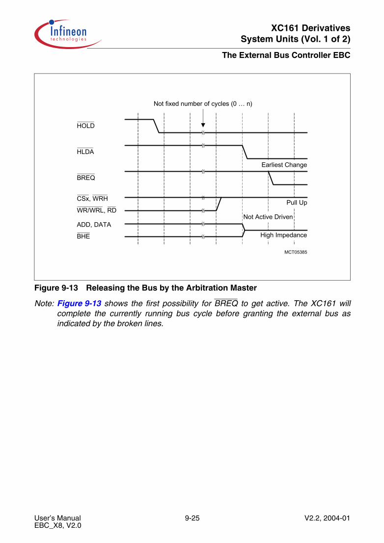
XC161 DerivativesSystem Units (Vol. 1 of 2)
The External Bus Controller EBC
Figure 9-13 Releasing the Bus by the Arbitration Master
Note: Figure 9-13 shows the first possibility for BREQ to get active. The XC161 willcomplete the currently running bus cycle before granting the external bus asindicated by the broken lines.
MCT05385
Not fixed number of cycles (0 … n)
HOLD
HLDA
BREQ
CSx, WRH
WR/WRL, RD
ADD, DATA
BHE
Earliest Change
Not Active Driven
Pull Up
High Impedance
User’s Manual 9-25 V2.2, 2004-01EBC_X8, V2.0

XC161 DerivativesSystem Units (Vol. 1 of 2)
The External Bus Controller EBC
Figure 9-14 Regaining the Bus by the Arbitration Master
Note: The falling BREQ edge shows the last chance for BREQ to trigger the indicatedregain-sequence. Even if BREQ is activated earlier the regain-sequence isinitiated by HOLD going high. Please note that HOLD may also be deactivatedwithout the XC161 requesting the bus.
9.3.9.3 Arbitration Slave Scheme
If the EBC is configured as arbitration slave it is by default not owner of the external busand has to request the bus first. As long as it has not finished all its queued requests andthe arbitration master is not requesting the bus the arbitration slave stays owner of thebus. For the description of the signal handling of the handshake see Chapter 9.3.9.2.For the arbitration slave the hold acknowledge pin HLDA is configured as input.
MCT05386
HOLD
HLDA
BREQ
CSx, WRH
WR/WRL, RD
ADD, BHE
Not Active Driven
Pull Up
High Impedance
Latest Possible Change
No BREQ Request
User’s Manual 9-26 V2.2, 2004-01EBC_X8, V2.0
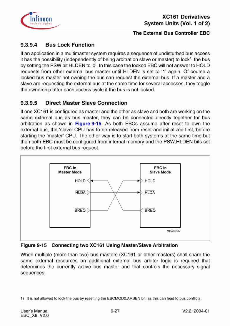
XC161 DerivativesSystem Units (Vol. 1 of 2)
The External Bus Controller EBC
9.3.9.4 Bus Lock Function
If an application in a multimaster system requires a sequence of undisturbed bus accessit has the possibility (independently of being arbitration slave or master) to lock1) the busby setting the PSW bit HLDEN to ‘0’. In this case the locked EBC will not answer to HOLDrequests from other external bus master until HLDEN is set to ‘1’ again. Of course alocked bus master not owning the bus can request the external bus. If a master and aslave are requesting the external bus at the same time for several accesses, they togglethe ownership after each access cycle if the bus is not locked.
9.3.9.5 Direct Master Slave Connection
If one XC161 is configured as master and the other as slave and both are working on thesame external bus as bus master, they can be connected directly together for busarbitration as shown in Figure 9-15. As both EBCs assume after reset to own theexternal bus, the ‘slave’ CPU has to be released from reset and initialized first, beforestarting the ‘master’ CPU. The other way is to start both systems at the same time butthen both EBC must be configured from internal memory and the PSW.HLDEN bits setbefore the first external bus request.
Figure 9-15 Connecting two XC161 Using Master/Slave Arbitration
When multiple (more than two) bus masters (XC161 or other masters) shall share thesame external resources an additional external bus arbiter logic is required thatdetermines the currently active bus master and that controls the necessary signalsequences.
1) It is not allowed to lock the bus by resetting the EBCMOD0.ARBEN bit, as this can lead to bus conflicts.
EBC inMaster Mode
EBC inSlave Mode
MCA05387
HOLD
BREQ
HLDA
HOLD
BREQ
HLDA
User’s Manual 9-27 V2.2, 2004-01EBC_X8, V2.0
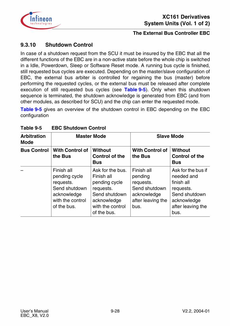
XC161 DerivativesSystem Units (Vol. 1 of 2)
The External Bus Controller EBC
9.3.10 Shutdown Control
In case of a shutdown request from the SCU it must be insured by the EBC that all thedifferent functions of the EBC are in a non-active state before the whole chip is switchedin a Idle, Powerdown, Sleep or Software Reset mode. A running bus cycle is finished,still requested bus cycles are executed. Depending on the master/slave configuration ofEBC, the external bus arbiter is controlled for regaining the bus (master) beforeperforming the requested cycles, or the external bus must be released after completeexecution of still requested bus cycles (see Table 9-5). Only when this shutdownsequence is terminated, the shutdown acknowledge is generated from EBC (and fromother modules, as described for SCU) and the chip can enter the requested mode.
Table 9-5 gives an overview of the shutdown control in EBC depending on the EBCconfiguration
Table 9-5 EBC Shutdown Control
Arbitration Mode
Master Mode Slave Mode
Bus Control With Control of the Bus
Without Control of the Bus
With Control of the Bus
Without Control of the Bus
– Finish all pending cycle requests.Send shutdown acknowledge with the control of the bus.
Ask for the bus.Finish all pending cycle requests.Send shutdown acknowledge with the control of the bus.
Finish all pending requests.Send shutdown acknowledge after leaving the bus.
Ask for the bus if needed and finish all requests.Send shutdown acknowledge after leaving the bus.
User’s Manual 9-28 V2.2, 2004-01EBC_X8, V2.0

XC161 DerivativesSystem Units (Vol. 1 of 2)
The External Bus Controller EBC
9.4 LXBus Access Control and Signal Generation
To connect on_chip peripherals via the EBC, the local system bus LXBus is provided.The LXBus is an internal (local) extension of the external bus. It is controlled by theExternal Bus Controller EBC identically to the external bus, using the select and cyclecontrol functions as described for the external bus. The address range and chip selectcontrol with ADDRSELn registers, the function control with FCONCSn registers and thetiming control with TCONCSn registers is identical to the external bus. Chip selectsCS5 … CS7 are reserved for LXBus peripherals. In XC161, only one standard CSx, theCS7 is used for the LXBus, necessary for the TwinCAN module (see Chapter 9.3.8). Perdefault, the address range of this peripheral is located within the so-called ‘External IORange’ (from 20’0000H to 3F’0000H). Accesses to the IO range are not buffered and notcached, and a read access is delayed until all IO writes pending in the pipeline areexecuted.
Only internal accesses to LXBus peripherals are supported by the EBC. Externalaccesses are not supported in this C166SV2 derivative. Accesses to LXBus peripheralsand memories are not visible on external bus pads.
9.5 EBC Register Table
Table 9-6 lists all EBC Configuration Registers which are implemented in the XC161ordered by their physical address. The registers are all located in the XSFR space(internal IO space).
Table 9-6 EBC Memory Table (ordered by physical address)
Name Physic. Addr.
Description Reset Value1)
EBCMOD0 EE00H EBC Mode Register 0 XXXXH
EBCMOD1 EE02H EBC Mode Register 1 0000H
TCONCS0 EE10H CS0 Timing Configuration Register 7AXXH
FCONCS0 EE12H CS0 Function Configuration Register 00X1H
TCONCS1 EE18H CS1 Timing Configuration Register 0000H
FCONCS1 EE1AH CS1 Function Configuration Register 0000H
ADDRSEL1 EE1EH CS1 Address Size and Range Register 0000H
TCONCS2 EE20H CS2 Timing Configuration Register 0000H
FCONCS2 EE22H CS2 Function Configuration Register 0000H
ADDRSEL2 EE26H CS2 Address Size and Range Register 0000H
TCONCS3 EE28H CS3 Timing Configuration Register 0000H
FCONCS3 EE2AH CS3 Function Configuration Register 0000H
User’s Manual 9-29 V2.2, 2004-01EBC_X8, V2.0
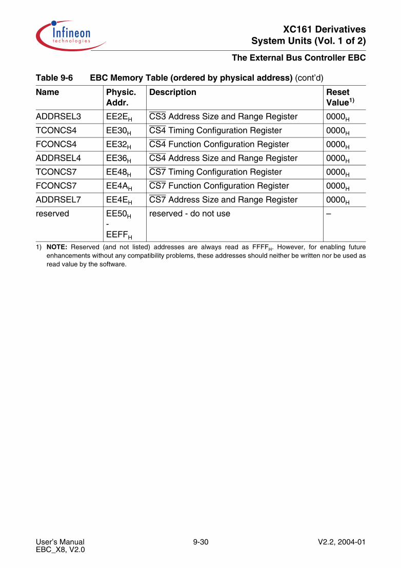
XC161 DerivativesSystem Units (Vol. 1 of 2)
The External Bus Controller EBC
ADDRSEL3 EE2EH CS3 Address Size and Range Register 0000H
TCONCS4 EE30H CS4 Timing Configuration Register 0000H
FCONCS4 EE32H CS4 Function Configuration Register 0000H
ADDRSEL4 EE36H CS4 Address Size and Range Register 0000H
TCONCS7 EE48H CS7 Timing Configuration Register 0000H
FCONCS7 EE4AH CS7 Function Configuration Register 0000H
ADDRSEL7 EE4EH CS7 Address Size and Range Register 0000H
reserved EE50H-EEFFH
reserved - do not use –
1) NOTE: Reserved (and not listed) addresses are always read as FFFFH. However, for enabling futureenhancements without any compatibility problems, these addresses should neither be written nor be used asread value by the software.
Table 9-6 EBC Memory Table (ordered by physical address) (cont’d)
Name Physic. Addr.
Description Reset Value1)
User’s Manual 9-30 V2.2, 2004-01EBC_X8, V2.0
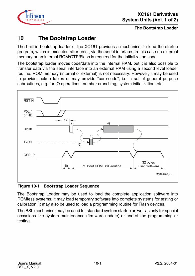
XC161 DerivativesSystem Units (Vol. 1 of 2)
The Bootstrap Loader
10 The Bootstrap Loader The built-in bootstrap loader of the XC161 provides a mechanism to load the startupprogram, which is executed after reset, via the serial interface. In this case no externalmemory or an internal ROM/OTP/Flash is required for the initialization code.
The bootstrap loader moves code/data into the internal RAM, but it is also possible totransfer data via the serial interface into an external RAM using a second level loaderroutine. ROM memory (internal or external) is not necessary. However, it may be usedto provide lookup tables or may provide “core-code”, i.e. a set of general purposesubroutines, e.g. for IO operations, number crunching, system initialization, etc.
Figure 10-1 Bootstrap Loader Sequence
The Bootstrap Loader may be used to load the complete application software intoROMless systems, it may load temporary software into complete systems for testing orcalibration, it may also be used to load a programming routine for Flash devices.
The BSL mechanism may be used for standard system startup as well as only for specialoccasions like system maintenance (firmware update) or end-of-line programming ortesting.
MCT04465_xx
RSTIN
P0L.4or RD
RxD0
TxD0
CSP:IP
1)2) 4)
3)
5)
32 bytesUser Software6) Int. Boot ROM BSL-routine
User’s Manual 10-1 V2.2, 2004-01BSL_X, V2.0
XC161 DerivativesSystem Units (Vol. 1 of 2)
The Bootstrap Loader
10.1 Entering the Bootstrap Loader
The XC161 enters BSL mode triggered by external configuration during a hardwarereset:
• when selected via bitfield SMOD at the end of an external reset (EA = 0)• when pin RD is sampled low at the end of an internal reset (EA = 1).
In this case the built-in bootstrap loader is activated independent of the selected busmode. The bootstrap loader code is stored in a special Boot-ROM, no part of thestandard mask ROM, OTP, or Flash memory area is required for this.
The hardware that activates the BSL during reset may be a simple pull-down resistor forsystems that use this feature upon every hardware reset. You may want to use aswitchable solution (via jumper or an external signal) for systems that only temporarilyuse the bootstrap loader.
The ASC0 receiver is only enabled after the identification byte has been transmitted. Ahalf duplex connection to the host is therefore sufficient to feed the BSL.
Note: The proper reset configuration for BSL mode requires a set of pins to be driven todefined logic levels (see Section 6.1.4).
User’s Manual 10-2 V2.2, 2004-01BSL_X, V2.0
XC161 DerivativesSystem Units (Vol. 1 of 2)
The Bootstrap Loader
Initial State in BSL Mode
After entering BSL mode and the respective initialization the XC161 scans the RxD0 lineto receive a zero byte, i.e. one start bit, eight 0 data bits and one stop bit. From theduration of this zero byte it calculates the corresponding baudrate factor with respect tothe current CPU clock, initializes the serial interface ASC0 accordingly and switches pinTxD0 to output. Using this baudrate, an identification byte is returned to the host thatprovides the loaded data.
This identification byte identifies the device to be booted. The following codes aredefined:
55H: 8xC166.A5H: Previous versions of the C167 (obsolete).B5H: Previous versions of the C165.C5H: C167 derivatives.D5H: All devices equipped with identification registers.
Note: The identification byte D5H does not directly identify a specific derivative. Thisinformation can in this case be obtained from the identification registers.
When the XC161 has entered BSL mode, the following configuration is automatically set(values that deviate from the normal reset values, are marked):
Other than after a normal reset the watchdog timer is disabled, so the bootstrap loadingsequence is not time limited. Pin TxD0 is configured as output, so the XC161 can returnthe identification byte.
Note: Even if the internal ROM/OTP/Flash is enabled, no code can be executed out of itwhile the XC161 is in BSL mode.
Watchdog Timer: Disabled ASC0_BG: XXXXH
P3.10/TxD0: ‘1’ ASC0_CON: 8811H
DP3.10: ‘1’ GPT12E_T6CON: 0880H
ALTSEL0P3.10: ‘1’ GPT12E_T6: XXXXH
User’s Manual 10-3 V2.2, 2004-01BSL_X, V2.0
XC161 DerivativesSystem Units (Vol. 1 of 2)
The Bootstrap Loader
10.2 Loading the Startup Code
After sending the identification byte the BSL enters a loop to receive 32 Bytes via ASC0.These bytes are stored sequentially into locations E0’0004H through E0’0023H of theinternal PSRAM. So up to 16 instructions may be placed into the PSRAM area. The firsttwo words of the PSRAM are loaded with the DISWDT instruction. To execute the loadedcode the BSL then points register VECSEG to location E0’0000H, i.e. the first loadedinstruction1). The bootstrap loading sequence terminates by executing a software reset.Most probably the initially loaded routine will load additional code or data, as an averageapplication is likely to require substantially more than 16 instructions. This secondreceive loop may directly use the pre-initialized interface ASC0 to receive data and storeit to arbitrary user-defined locations.
This second level of loaded code may be the final application code. It may also beanother, more sophisticated, loader routine that adds a transmission protocol to enhancethe integrity of the loaded code or data. It may also contain a code sequence to changethe system configuration and enable the bus interface to store the received data intoexternal memory.
This process may go through several iterations or may directly execute the finalapplication.
Note: Data fetches from a protected ROM will not be executed.
10.3 Exiting Bootstrap Loader Mode
After the bootstrap loader has been activated, the watchdog timer and the debug systemare disabled. The debug system is released automatically when the BSL terminates afterhaving received the 32nd byte from the host. In order to activate the watchdog timer, ifrequired, it must be enabled via instruction ENWDT (before executing the EINITinstruction). Also a reset will re-enable the WDT:
• a software reset (ignoring the external configuration)• a hardware reset, not configuring BSL mode.
After the (non-BSL) reset the XC161 will start executing out of user memory as externallyconfigured via PORT0 or RD/ALE (depending on EA).
1) This includes the execution of the initial DISWDT instruction, ensuring that the 2nd level loader is not abortedby the watchdog timer.
User’s Manual 10-4 V2.2, 2004-01BSL_X, V2.0
XC161 DerivativesSystem Units (Vol. 1 of 2)
The Bootstrap Loader
10.4 Choosing the Baudrate for the BSL
The calculation of the serial baudrate for ASC0 from the length of the first zero byte thatis received, allows the operation of the bootstrap loader of the XC161 with a wide rangeof baudrates. However, the upper and lower limits have to be kept, in order to ensureproper data transfer.
(10.1)
The XC161 uses timer GPT12E_T6 to measure the length of the initial zero byte. Thequantization uncertainty of this measurement implies the first deviation from the realbaudrate, the next deviation is implied by the computation of the ASC0_BG reload valuefrom the timer contents. Equation (10.2) shows the association:
(10.2)
For a correct data transfer from the host to the XC161 the maximum deviation betweenthe internal initialized baudrate for ASC0 and the real baudrate of the host should bebelow 2.5%. The deviation (FB, in percent) between host baudrate and XC161 baudratecan be calculated via Equation (10.3):
(10.3)
Note: Function (FB) does not consider the tolerances of oscillators and other devicessupporting the serial communication.
This baudrate deviation is a nonlinear function depending on the CPU clock and thebaudrate of the host. The maxima of the function (FB) increase with the host baudratedue to the smaller baudrate prescaler factors and the implied higher quantization error(see Figure 10-2).
BMCfSYS
32 ASC0BG 1+( )×-----------------------------------------------------=
ASC0BG T6 36–72
--------------------= T6 94---
fSYS
BHost-------------×=
FBBContr BHost–
BContr------------------------------------- 100%×= FB 2,5%≤
User’s Manual 10-5 V2.2, 2004-01BSL_X, V2.0

XC161 DerivativesSystem Units (Vol. 1 of 2)
The Bootstrap Loader
Figure 10-2 Baudrate Deviation between Host and XC161
The minimum baudrate (BLow in Figure 10-2) is determined by the maximum countcapacity of timer GPT12E_T6, when measuring the zero byte, i.e. it depends on thesystem clock. The minimum baudrate is obtained by using the maximum GPT12E_T6count 216 in the baudrate formula. Baudrates below BLow would cause GPT12E_T6 tooverflow. In this case ASC0 cannot be initialized properly and the communication withthe external host is likely to fail.
The maximum baudrate (BHigh in Figure 10-2) is the highest baudrate where thedeviation still does not exceed the limit, i.e. all baudrates between BLow and BHigh arebelow the deviation limit. BHigh marks the baudrate up to which communication with theexternal host will work properly without additional tests or investigations.
Higher baudrates, however, may be used as long as the actual deviation does notexceed the indicated limit. A certain baudrate (marked I) in Figure 10-2) may e.g. violatethe deviation limit, while an even higher baudrate (marked II) in Figure 10-2) stays verywell below it. Any baudrate can be used for the bootstrap loader provided that thefollowing three prerequisites are fulfilled:
• the baudrate is within the specified operating range for the ASC0• the external host is able to use this baudrate• the computed deviation error is below the limit.
Table 10-1 Bootstrap Loader Baudrate Ranges
fSYS [MHz] 10 12 16 20 25 33
BMAX 312,500 375,000 500,000 625,000 781,250 1,031,250
BHigh 9,600 19,200 19,200 19,200 38,400 38,400
BSTDmin 600 600 600 1,200 1,200 1,200
BLow 344 412 550 687 859 1,133
MCA02260
BF
2.5%
LowB BHigh
Ι
ΙΙ
BHost
User’s Manual 10-6 V2.2, 2004-01BSL_X, V2.0

XC161 DerivativesSystem Units (Vol. 1 of 2)
The Bootstrap Loader
Note: When the bootstrap loader mode is entered via an internal reset (EA = 1), thedefault configuration selects bypass mode with factor 2:1 for clock generation. Inthis case the bootstrap loader will begin to operate with fSYS = fOSC/2 which will limitthe maximum baudrate for ASC0 at low input frequencies intended for PLLoperation.Higher levels of the bootstrapping sequence can then switch the clock generationmode (via register PLLCON) e.g. to PLL in order to achieve higher baudrates forthe download.
User’s Manual 10-7 V2.2, 2004-01BSL_X, V2.0
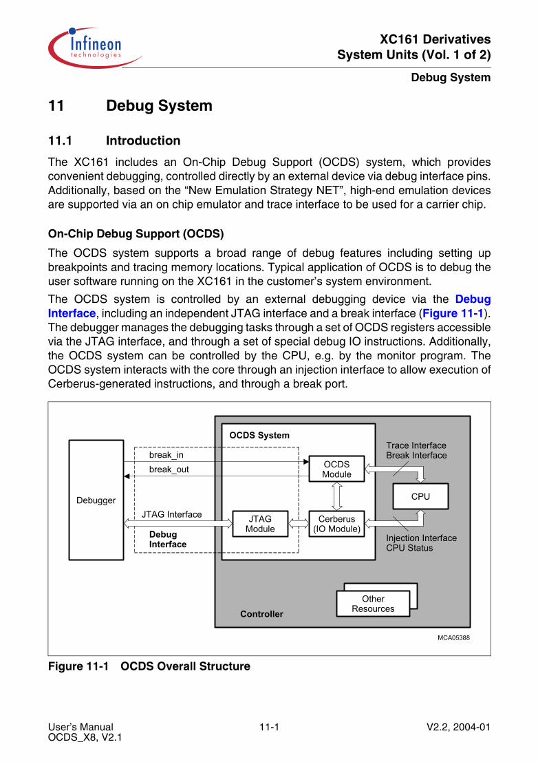
XC161 DerivativesSystem Units (Vol. 1 of 2)
Debug System
11 Debug System
11.1 Introduction
The XC161 includes an On-Chip Debug Support (OCDS) system, which providesconvenient debugging, controlled directly by an external device via debug interface pins.Additionally, based on the “New Emulation Strategy NET”, high-end emulation devicesare supported via an on chip emulator and trace interface to be used for a carrier chip.
On-Chip Debug Support (OCDS)
The OCDS system supports a broad range of debug features including setting upbreakpoints and tracing memory locations. Typical application of OCDS is to debug theuser software running on the XC161 in the customer’s system environment.
The OCDS system is controlled by an external debugging device via the DebugInterface, including an independent JTAG interface and a break interface (Figure 11-1).The debugger manages the debugging tasks through a set of OCDS registers accessiblevia the JTAG interface, and through a set of special debug IO instructions. Additionally,the OCDS system can be controlled by the CPU, e.g. by the monitor program. TheOCDS system interacts with the core through an injection interface to allow execution ofCerberus-generated instructions, and through a break port.
Figure 11-1 OCDS Overall Structure
Controller
OCDS System
Debugger
MCA05388
JTAG Interface JTAGModule
Cerberus(IO Module)Debug
Interface
OCDSModule
OtherResources
Trace InterfaceBreak Interface
Injection InterfaceCPU Status
CPU
break_inbreak_out
User’s Manual 11-1 V2.2, 2004-01OCDS_X8, V2.1
XC161 DerivativesSystem Units (Vol. 1 of 2)
Debug System
The OCDS system functions are represented and controlled by the Debug Interface, theOCDS Module and by the debug IO control module (Cerberus) which provides all thefunctionality necessary to interact between the debug interface (the external debugger)and the internal system.
The OCDS system provides the following basic features:
• Hardware, software and external pin breakpoints• Reaction on break with CPU-Halt, monitor call, data transfer and external signal• Read/write access to the whole address space• Single stepping• Debug Interface pins for JTAG interface and break interface• Injection of arbitrary instructions• Fast memory tracing through transfer to external bus• Analysis and status registers
11.2 Debug Interface
The Debug Interface is a channel to access XC161 On-Chip Debug Support (OCDS)resources. Through it data can be transferred to/from all on- and off-chip (if any)memories and control registers.
Features and Functions
• Independent interface for On-Chip Debug Support (OCDS)• JTAG port based on the IEEE 1149 JTAG standard• Break interface for external trigger and indication of breaks• Generic memory access functionality• Independent data transfer channel for e.g. programming of on-chip non volatile
memory
The Debug Interface is represented by:
• Standard JTAG Interface• Two additional XC161 specific signals - OCDS Break-Interface
User’s Manual 11-2 V2.2, 2004-01OCDS_X8, V2.1
XC161 DerivativesSystem Units (Vol. 1 of 2)
Debug System
JTAG Interface
The JTAG interface is a standardized and dedicated port usually used for boundary scanand for chip internal tests. Because both of these applications are not enabled duringnormal operation of the device in a system, the JTAG port is an ideal interface fordebugging tasks.
This interface holds the JTAG IEEE.1149-standard signals:
• TDI - Serial data input• TDO - Serial data output• TCK - JTAG clock• TMS - State machine control signal• TRST - Reset/Module enable
OCDS Break-Interface
Two additional signals are used to implement a direct asynchronous-break channelbetween the Debugger and XC161 OCDS Module:
• BRKIN (BReaK IN request) allows the Debugger asynchronously to interrupt theCPU and force it to a predefined status/action.
• BRKOUT (BReaK OUT signal) can be activated by OCDS to notify the external worldthat some predefined debug event has happened, while not interrupting the CPU andusing its pin(s).
11.3 OCDS Module
The application of OCDS Module is to debug the user software running on the CPU inthe customer’s system. This is done with an external debugger, that controls the OCDSModule via the independent Debug Interface.
Features
• Hardware, software and external pin breakpoints• Up to 4 instruction pointer breakpoints• Masked comparisons for hardware breakpoints• The OCDS can also be configured by a monitor• Support of multi CPU/master system• Single stepping with monitor or CPU halt• PC is visible in halt mode (IO_READ_IP instruction injection via Cerberus)
User’s Manual 11-3 V2.2, 2004-01OCDS_X8, V2.1
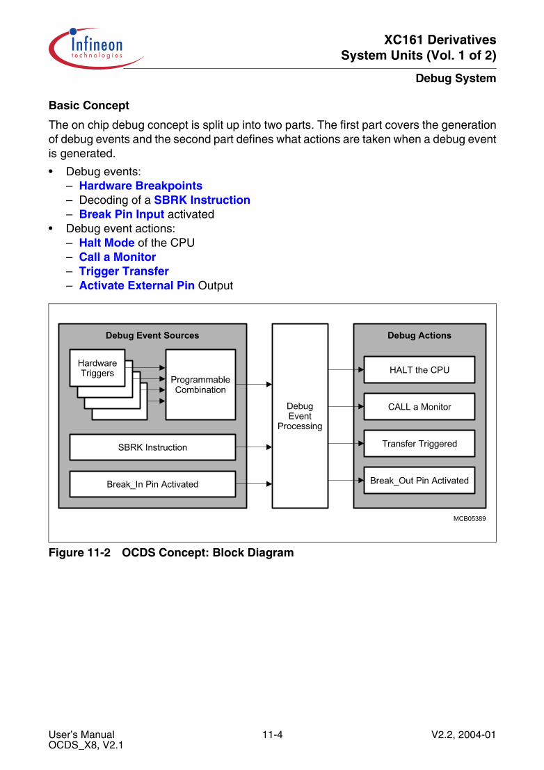
XC161 DerivativesSystem Units (Vol. 1 of 2)
Debug System
Basic Concept
The on chip debug concept is split up into two parts. The first part covers the generationof debug events and the second part defines what actions are taken when a debug eventis generated.
• Debug events:– Hardware Breakpoints– Decoding of a SBRK Instruction– Break Pin Input activated
• Debug event actions:– Halt Mode of the CPU– Call a Monitor– Trigger Transfer– Activate External Pin Output
Figure 11-2 OCDS Concept: Block Diagram
Debug Event Sources Debug Actions
MCB05389
DebugEvent
Processing
SBRK Instruction
Break_In Pin Activated
HALT the CPU
CALL a Monitor
Transfer Triggered
Break_Out Pin Activated
ProgrammableCombination
HardwareTriggers
User’s Manual 11-4 V2.2, 2004-01OCDS_X8, V2.1
XC161 DerivativesSystem Units (Vol. 1 of 2)
Debug System
11.3.1 Debug Events
The Debug Events can come from a few different sources.
Hardware Breakpoints
The Hardware Breakpoint is a debug-event, raised when a single or a combination ofmultiple trigger-signals are matching with the programmed conditions.
The following hardware trigger sources can be used:
SBRK Instruction
This is a mechanism through which the software can explicitly generate a debug event.It can be used for instance by a debugger to temporarily patch code held in RAM in orderto implement Software Breakpoints.
A special SBRK (Software BReaK) instruction is defined with opcode 0x8C00. When thisinstruction has been decoded and it reaches the Execute stage, the whole pipeline iscanceled including the SBRK itself. Hence in fact the SBRK instruction is never“executed” by itself.
The further behavior is dependent on how OCDS has been programmed:
• if the OCDS is enabled and the software breakpoints are also enabled, then the CPUgoes into Halt Mode
• if the OCDS is disabled or the software breakpoints are disabled, then the SoftwareBreak Trap (SBRKTRAP) is executed-Class A Trap, number 08H
Break Pin Input
An external debug break pin (BRKIN) is provided to allow the debugger toasynchronously interrupt the processor.
Table 11-1 Hardware Triggers
Trigger Source Size
Task Identifier 16 bits
Instruction Pointer 24 bits
Data address of reads (two busses monitored) 2 × 24 bits
Data address of writes 24 bits
Data value (reads or writes) 16 bits
User’s Manual 11-5 V2.2, 2004-01OCDS_X8, V2.1
XC161 DerivativesSystem Units (Vol. 1 of 2)
Debug System
11.3.2 Debug Actions
When the OCDS is enabled and a debug event is generated, one of the following actionsis taken:
Trigger Transfer
One of the actions that can be specified to occur on a debug event being raised is totrigger the Cerberus:
• to execute a Data Transfer - this can be used in critical routines where the systemcannot be interrupted to transfer a memory location
• to inject an instruction to the Core - using this mechanism, an arbitrary instruction canbe injected into the XC161 pipeline
Halt Mode
Upon this Action the OCDS Module sends a Break-Request to the Core.
The Core accepts this request, if the OCDS Break Level is higher than current CPUpriority level. In case a Break-Request is accepted, the system suspends execution withhalting the instruction flow.
The Halt Mode can be still interrupted by higher priority user interrupts. It then relies onthe external debugger system to interrogate the target purely through reading andupdating via the debug interface.
Call a Monitor
One of the possible actions to be taken when a debug event is raised is to call a MonitorProgram.
This short entry to a Monitor allows a flexible debug environment to be defined which iscapable of satisfying many of the requirements for efficient debugging of a real timesystem. In the common case the Monitor has the highest priority and can not beinterrupted from any other requesting source.
It is also possible to have an Interruptible Monitor Program. In such a case safety criticalcode can be still served while the Monitor (Debugger) is active, which gives a maximumflexibility to the user.
Activate External Pin
This action activates the external pin BRKOUT of the OCDS Break-Interface. It can beused in critical routines where the system cannot be interrupted to signal to the externalworld that a particular event has happened. The feature could also be useful tosynchronize the internal and external debug hardware.
User’s Manual 11-6 V2.2, 2004-01OCDS_X8, V2.1
XC161 DerivativesSystem Units (Vol. 1 of 2)
Debug System
11.4 Cerberus
Cerberus is the module which provides and controls all the operations necessary tointeract between the external debugger (via the Debug Interface), the OCDS Moduleand the internal system of XC161.
Features
• JTAG interface is used as control and data channel• Generic memory read/write functionality (RW mode) with access to the whole
address space• Reading and writing of general-purpose registers (GPRs)• Injection of arbitrary instructions• External host controls all transactions• All transactions are available at normal run time and in halt mode• Priority of transactions can be configured• Full support for communication between the monitor and an external host (debugger)• Optional error protection• Tracing memory locations through transferring values to the external bus• Analysis Register for internal bus locking situations
The target application of Cerberus is to use the JTAG interface as an independent portfor On Chip Debug Support. The external debugger can access the OCDS registers andarbitrary memory locations with the injection mechanism.
11.4.1 Functional Overview
Cerberus is operated by an external debugger across the JTAG Interface. TheDebugger supplies Cerberus IO Instructions and performs bidirectional data-transfers.
The Cerberus distinguishes between two main modes of operation:
Read/Write Mode of Operation
Read/Write (RW) Mode is the most typical way to operate Cerberus. This mode is usedto read and write memory locations or to inject instructions. The injection interface to thecore is actively used in this mode.
In this mode an external Debugger (host), using JTAG Interface, can:
• read and write memory locations from the target system (data-transfer);• inject arbitrary instructions to be executed by the Core.
All Cerberus IO Instructions can be used in RW mode. The dedicated IO_READ_IPinstruction is provided in RW mode to read the IP of the CPU while in Break.
User’s Manual 11-7 V2.2, 2004-01OCDS_X8, V2.1
XC161 DerivativesSystem Units (Vol. 1 of 2)
Debug System
The access to any memory location is performed with injected instructions, as PECtransfer. The following Cerberus IO Instructions can be used in their generic meaning:
• IO_READ_WORD, IO_WRITE_WORD• IO_READ_BLOCK, IO_WRITE_BLOCK• IO_WRITE_BYTE
Within these instructions, the host writes/reads data to/from a dedicatedregister/memory, while the Cerberus itself takes care of the rest: to perform a PECtransfer by injection of the appropriate instructions to the Core.
Communication Mode of Operation
In this mode the external host (debugger) communicates with a program (Monitor)running on the CPU. The data-transfers are made via a PDBus+ register. The externalhost is master of all transactions, requesting the monitor to write or read a value.
The difference to Read/Write Mode of Operation is that the read or write request nowis not actively executed by the Cerberus, but it sets request bits in a CPU accessibleregister to signal the Monitor, that the host wants to send (IO_WRITE_WORD) or receive(IO_READ_WORD) a value. The Monitor has to poll this status register and performrespectively the proper actions
Communication Mode is the default mode after reset. Only the IO_WRITE_WORD andIO_READ_WORD Instructions are effectively used in Communication Mode.
The Host and the Monitor exchange data directly with the dedicated data-register. For asynchronization of Host (Debugger) and Monitor accesses, there are associated controlbits in a Cerberus status register.
User’s Manual 11-8 V2.2, 2004-01OCDS_X8, V2.1

XC161 DerivativesSystem Units (Vol. 1 of 2)
Debug System
11.5 Emulation Device
The New Emulation Technology (NET) is supported in XC161 to build an EmulationDevice (EDEV) with the XC161 mass production chip and the NET Carrier Chip. Forconnection to the carrier chip, the XC161 provides a broad emulator interface includingall important internal busses for tracing, emulation control and status information as wellas the external pin (pad) signals. The XC161 mass production chip is mounted on theemulation carrier chip upside down and it’s emulator interface signals are connectedacross flip chip pads. On the functional and system level, the NET based emulationdevice is similar to a bondout. The superiority of the NET based emulation device is thehigh-end emulation functionality with full visibility, and with exactly the same functionalityas the mass production chip (no stepping problems as known from bondout chips).
User’s Manual 11-9 V2.2, 2004-01OCDS_X8, V2.1

XC161 DerivativesSystem Units (Vol. 1 of 2)
Instruction Set Summary
12 Instruction Set SummaryThis chapter briefly summarizes the XC161’s instructions ordered by instruction classes.This provides a basic understanding of the XC161’s instruction set, the power andversatility of the instructions and their general usage.
A detailed description of each single instruction, including its operand data type,condition flag settings, addressing modes, length (number of bytes) and object codeformat is provided in the “Instruction Set Manual” for the XC166 Family. This manualalso provides tables ordering the instructions according to various criteria, to allow quickreferences.
Summary of Instruction Classes
Grouping the various instruction into classes aids in identifying similar instructions (e.g.SHR, ROR) and variations of certain instructions (e.g. ADD, ADDB). This provides aneasy access to the possibilities and the power of the instructions of the XC161.
Note: The used mnemonics refer to the detailed description.
Table 12-1 Arithmetic Instructions
Addition of two words or bytes: ADD ADDB
Addition with Carry of two words or bytes: ADDC ADDCB
Subtraction of two words or bytes: SUB SUBB
Subtraction with Carry of two words or bytes: SUBC SUBCB
16 × 16 bit signed or unsigned multiplication: MUL MULU
16/16 bit signed or unsigned division: DIV DIVU
32/16 bit signed or unsigned division: DIVL DIVLU
1’s complement of a word or byte: CPL CPLB
2’s complement (negation) of a word or byte: NEG NEGB
Table 12-2 Logical Instructions
Bitwise ANDing of two words or bytes: AND ANDB
Bitwise ORing of two words or bytes: OR ORB
Bitwise XORing of two words or bytes: XOR XORB
User’s Manual 12-1 V2.2, 2004-01InstructionSummary_X, V2.0

XC161 DerivativesSystem Units (Vol. 1 of 2)
Instruction Set Summary
Table 12-3 Compare and Loop Control Instructions
Comparison of two words or bytes: CMP CMPB
Comparison of two words with post-increment by either 1 or 2:
CMPI1 CMPI2
Comparison of two words with post-decrement by either 1 or 2:
CMPD1 CMPD2
Table 12-4 Boolean Bit Manipulation Instructions
Manipulation of a maskable bit field in either the high or the low byte of a word:
BFLDH BFLDL
Setting a single bit (to ‘1’): BSET –
Clearing a single bit (to ‘0’): BCLR –
Movement of a single bit: BMOV –
Movement of a negated bit: BMOVN –
ANDing of two bits: BAND –
ORing of two bits: BOR –
XORing of two bits: BXOR –
Comparison of two bits: BCMP –
Table 12-5 Shift and Rotate Instructions
Shifting right of a word: SHR –
Shifting left of a word: SHL –
Rotating right of a word: ROR –
Rotating left of a word: ROL –
Arithmetic shifting right of a word (sign bit shifting): ASHR –
Table 12-6 Prioritize Instruction
Determination of the number of shift cycles required to normalize a word operand (floating point support):
PRIOR –
User’s Manual 12-2 V2.2, 2004-01InstructionSummary_X, V2.0
XC161 DerivativesSystem Units (Vol. 1 of 2)
Instruction Set Summary
Note: The data movement instructions can be used with a big number of differentaddressing modes including indirect addressing and automatic pointer in-/decrementing.
Table 12-7 Data Movement Instructions
Standard data movement of a word or byte: MOV MOVB
Data movement of a byte to a word location with either sign or zero byte extension:
MOVBS MOVBZ
Table 12-8 System Stack Instructions
Pushing of a word onto the system stack: PUSH –
Popping of a word from the system stack: POP –
Saving of a word on the system stack, and then updating the old word with a new value (provided for register bank switching):
SCXT –
Table 12-9 Jump Instructions
Conditional jumping to an either absolutely, indirectly, or relatively addressed target instruction within the current code segment:
JMPA JMPI JMPR
Unconditional jumping to an absolutely addressed target instruction within any code segment:
JMPS – –
Conditional jumping to a relatively addressed target instruction within the current code segment depending on the state of a selectable bit:
JB JNB –
Conditional jumping to a relatively addressed target instruction within the current code segment depending on the state of a selectable bit with a post-inversion of the tested bit in case of jump taken (semaphore support):
JBC JNBS –
User’s Manual 12-3 V2.2, 2004-01InstructionSummary_X, V2.0
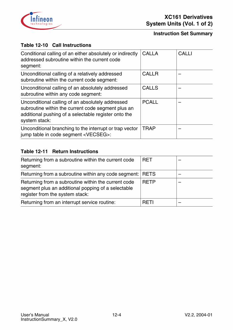
XC161 DerivativesSystem Units (Vol. 1 of 2)
Instruction Set Summary
Table 12-10 Call Instructions
Conditional calling of an either absolutely or indirectly addressed subroutine within the current code segment:
CALLA CALLI
Unconditional calling of a relatively addressed subroutine within the current code segment:
CALLR –
Unconditional calling of an absolutely addressed subroutine within any code segment:
CALLS –
Unconditional calling of an absolutely addressed subroutine within the current code segment plus an additional pushing of a selectable register onto the system stack:
PCALL –
Unconditional branching to the interrupt or trap vector jump table in code segment <VECSEG>:
TRAP –
Table 12-11 Return Instructions
Returning from a subroutine within the current code segment:
RET –
Returning from a subroutine within any code segment: RETS –
Returning from a subroutine within the current code segment plus an additional popping of a selectable register from the system stack:
RETP –
Returning from an interrupt service routine: RETI –
User’s Manual 12-4 V2.2, 2004-01InstructionSummary_X, V2.0
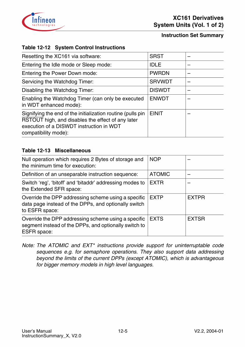
XC161 DerivativesSystem Units (Vol. 1 of 2)
Instruction Set Summary
Note: The ATOMIC and EXT* instructions provide support for uninterruptable codesequences e.g. for semaphore operations. They also support data addressingbeyond the limits of the current DPPs (except ATOMIC), which is advantageousfor bigger memory models in high level languages.
Table 12-12 System Control Instructions
Resetting the XC161 via software: SRST –
Entering the Idle mode or Sleep mode: IDLE –
Entering the Power Down mode: PWRDN –
Servicing the Watchdog Timer: SRVWDT –
Disabling the Watchdog Timer: DISWDT –
Enabling the Watchdog Timer (can only be executed in WDT enhanced mode):
ENWDT –
Signifying the end of the initialization routine (pulls pin RSTOUT high, and disables the effect of any later execution of a DISWDT instruction in WDT compatibility mode):
EINIT –
Table 12-13 Miscellaneous
Null operation which requires 2 Bytes of storage and the minimum time for execution:
NOP –
Definition of an unseparable instruction sequence: ATOMIC –
Switch ‘reg’, ‘bitoff’ and ‘bitaddr’ addressing modes to the Extended SFR space:
EXTR –
Override the DPP addressing scheme using a specific data page instead of the DPPs, and optionally switch to ESFR space:
EXTP EXTPR
Override the DPP addressing scheme using a specific segment instead of the DPPs, and optionally switch to ESFR space:
EXTS EXTSR
User’s Manual 12-5 V2.2, 2004-01InstructionSummary_X, V2.0
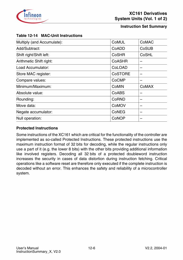
XC161 DerivativesSystem Units (Vol. 1 of 2)
Instruction Set Summary
Protected Instructions
Some instructions of the XC161 which are critical for the functionality of the controller areimplemented as so-called Protected Instructions. These protected instructions use themaximum instruction format of 32 bits for decoding, while the regular instructions onlyuse a part of it (e.g. the lower 8 bits) with the other bits providing additional informationlike involved registers. Decoding all 32 bits of a protected doubleword instructionincreases the security in cases of data distortion during instruction fetching. Criticaloperations like a software reset are therefore only executed if the complete instruction isdecoded without an error. This enhances the safety and reliability of a microcontrollersystem.
Table 12-14 MAC-Unit Instructions
Multiply (and Accumulate): CoMUL CoMAC
Add/Subtract: CoADD CoSUB
Shift right/Shift left: CoSHR CoSHL
Arithmetic Shift right: CoASHR –
Load Accumulator: CoLOAD –
Store MAC register: CoSTORE –
Compare values: CoCMP –
Minimum/Maximum: CoMIN CoMAX
Absolute value: CoABS –
Rounding: CoRND –
Move data: CoMOV –
Negate accumulator: CoNEG –
Null operation: CoNOP –
User’s Manual 12-6 V2.2, 2004-01InstructionSummary_X, V2.0

XC161 DerivativesSystem Units (Vol. 1 of 2)
Device Specification
13 Device SpecificationThe device specification describes the electrical parameters of the device. It lists DCcharacteristics like input, output or supply voltages or currents, and AC characteristicslike timing characteristics and requirements.
Other than the architecture, the instruction set or the basic functions of the XC161 coreand its peripherals, these DC and AC characteristics are subject to changes due todevice improvements or specific derivatives of the standard device.
Therefore these characteristics are not contained in this manual, but rather provided ina separate Data Sheet, which can be updated more frequently.
Please refer to the current version of the Data Sheet of the respective device for allelectrical parameters.
Note: In any case the specific characteristics of a device should be verified, before a newdesign is started. This ensures that the used information is up to date.
Figure 13-1 shows the pin diagram of the XC161. It shows the location of the differentsupply and IO pins. A detailed description of all the pins is also found in the Data Sheet.
Note: Not all alternate functions shown in Figure 13-1 are supported by all derivatives.Please refer to the corresponding descriptions in the data sheets.
User’s Manual 13-1 V2.2, 2004-01DeviceSpec_X1, V2.0
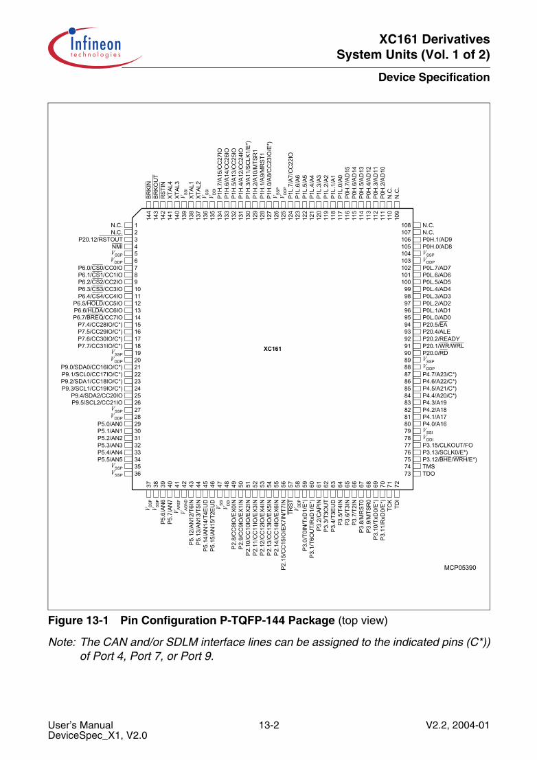
XC161 DerivativesSystem Units (Vol. 1 of 2)
Device Specification
Figure 13-1 Pin Configuration P-TQFP-144 Package (top view)
Note: The CAN and/or SDLM interface lines can be assigned to the indicated pins (C*))of Port 4, Port 7, or Port 9.
MCP05390
TDOTMSP3.12/BHE/WRH/E*)P3.13/SCLK0/E*)P3.15/CLKOUT/FOVDDI
P5.5/AN5P5.4/AN4P5.3/AN3P5.2/AN2P5.1/AN1P5.0/AN0
P9.5/SCL2/CC21IOP9.4/SDA2/CC20IO
P9.3/SCL1/CC19IO/C*)P9.2/SDA1/CC18IO/C*)P9.1/SCL0/CC17IO/C*)P9.0/SDA0/CC16IO/C*)
P7.7/CC31IO/C*)P7.6/CC30IO/C*)P7.5/CC29IO/C*)P7.4/CC28IO/C*)
P6.7/BREQ/CC7IOP6.6/HLDA/CC6IOP6.5/HOLD/CC5IO
P6.4/CS4/CC4IOP6.3/CS3/CC3IOP6.2/CS2/CC2IOP6.1/CS1/CC1IOP6.0/CS0/CC0IO
NMIP20.12/RSTOUT
N.C.N.C.
VDDP
VSSP
VDDP
VSSP
VDDP
VSSP
VSSP
VSSP
P4.0/A16VSSI
P4.1/A17P4.2/A18P4.3/A19P4.4/A20/C*)P4.5/A21/C*)P4.6/A22/C*)P4.7/A23/C*)VDDP
VSSP
P20.0/RDP20.1/WR/WRLP20.2/READYP20.4/ALEP20.5/EAP0L.0/AD0P0L.1/AD1P0L.2/AD2P0L.3/AD3P0L.4/AD4P0L.5/AD5P0L.6/AD6P0L.7/AD7VDDP
VSSP
P0H.0/AD8P0H.1/AD9N.C.N.C.
BRKI
NBR
KOU
TR
STIN
XTAL
4XT
AL3
V SSI
XTAL
1XT
AL2
V SSI
V DD
IP1
H.7
/A15
/CC
27IO
P1H
.6/A
14/C
C26
IOP1
H.5
/A13
/CC
25IO
P1H
.4/A
12/C
C24
IOP1
H.3
/A11
/SC
LK1/
E*)
P1H
.2/A
10/M
TSR
1P1
H.1
/A9/
MR
ST1
P1H
.0/A
8/C
C23
IO/E
*)V S
SPV D
DP
P1L.
7/A7
/CC
22IO
P1L.
6/A6
P1L.
5/A5
P1L.
4/A4
P1L.
3/A3
P1L.
2/A2
P1L.
1/A1
P1L.
0/A0
P0H
.7/A
D15
P0H
.6/A
D14
P0H
.5/A
D13
P0H
.4/A
D12
P0H
.3/A
D11
P0H
.2/A
D10
N.C
.N
.C.
P2.1
5/C
C15
IO/E
X7IN
/T7I
N
V SSP
V SSP
P5.6
/AN
6P5
.7/A
N7
V AR
EFV A
GN
DP5
.12/
AN12
/T6I
NP5
.13/
AN13
/T5I
NP5
.14/
AN14
/T4E
UD
P5.1
5/AN
15/T
2EU
DV S
SIV D
DI
P2.8
/CC
8IO
/EX0
INP2
.9/C
C9I
O/E
X1IN
P2.1
0/C
C10
IO/E
X2IN
P2.1
1/C
C11
IO/E
X3IN
P2.1
2/C
C12
IO/E
X4IN
P2.1
3/C
C13
IO/E
X5IN
P2.1
4/C
C14
IO/E
X6IN
TRSTV D
DP
P3.0
/T0I
N/T
xD1/
E*)
P3.1
/T6O
UT/
RxD
1/E*
)P3
.2/C
APIN
P3.3
/T3O
UT
P3.4
/T3E
UD
P3.5
/T4I
NP3
.6/T
3IN
P3.7
/T2I
NP3
.8/M
RST
0P3
.9/M
TSR
0P3
.10/
TxD
0/E*
)P3
.11/
RxD
0/E*
)TC
KTD
I
XC161
108107106105104103102101100
99989796959493929190898887868584838281807978777675747336
3534333231302928272625242322212019181716151413121110987654321
144
143
142
141
140
139
138
137
136
135
134
133
132
131
130
129
128
127
126
125
124
123
122
121
120
119
118
117
116
115
114
113
112
111
110
109
37 38 39 40 41 42 43 44 45 46 47 48 49 50 51 52 53 54 55 56 57 58 59 60 61 62 63 64 65 66 67 68 69 70 71 72
User’s Manual 13-2 V2.2, 2004-01DeviceSpec_X1, V2.0
XC161 DerivativesSystem Units (Vol. 1 of 2)
Keyword Index
Keyword IndexThis section lists a number of keywords which refer to specific details of the XC161 interms of its architecture, its functional units or functions. This helps to quickly find theanswer to specific questions about the XC161.
This User’s Manual consists of two Volumes, “System Units” and “Peripheral Units”. Foryour convenience this keyword index (and also the table of contents) refers to bothvolumes, so can immediately find the reference to the desired section in thecorresponding document ([1] or [2]).
BG 18-22 [2]
AAcronyms 1-9 [1]Adapt Mode 6-21 [1]ADC 2-21 [1], 16-1 [2]ADC_CIC, ADC_EIC 16-21 [2]ADC_CON 16-3 [2]ADC_CON1 16-4 [2]ADC_CTR0 16-5 [2]ADC_CTR2 16-7 [2]ADC_CTR2IN 16-7 [2]AddressBoundaries 3-15 [1]Mapping 3-3 [1]Segment 6-19 [1]
Addressing ModesCoREG Addressing Mode 4-51 [1]DSP Addressing Modes 4-47 [1]Indirect Addressing Modes 4-45 [1]Long Addressing Modes 4-41 [1]Short Addressing Modes 4-39 [1]
Alternate Port Functions 7-8 [1]ALU 4-58 [1]Analog/Digital Converter 16-1 [2]Arbitration of conversions 16-16 [2]ASC 18-1 [2]
ASCx_EIC, ASCx_RIC 18-35 [2]ASCx_TIC, ASCx_TBIC 18-35 [2]Autobaud Detection 18-27 [2]Error Detection 18-34 [2]Features and Functions 18-1 [2]IrDA Frames 18-8 [2]Register
RBUF 18-12 [2], 18-20 [2]TBUF 18-9 [2], 18-20 [2]
Transmit FIFO 18-9 [2]ASCx_BG 18-42 [2]ASCx_CON 18-40 [2]ASCx_FDV 18-43 [2]Auto Scan conversion 16-12 [2]Autobaud Detection 18-27 [2]
BBANKSELx 5-33 [1]Baudrate
ASC0 18-22 [2]Bootstrap Loader 10-5 [1]CAN 21-56 [2]
BitHandling 4-61 [1]Manipulation Instructions 12-2 [1]protected 2-32 [1], 4-62 [1]reserved 2-16 [1]
Block Diagram ITC / PEC 5-3 [1]Bootstrap Loader 6-21 [1], 10-1 [1]Boundaries 3-15 [1]Bus
ASC 18-1 [2]CAN 2-25 [1]IIC 2-26 [1], 20-1 [2]J1850 2-24 [1]Mode Configuration 6-20 [1]SDLM 22-1 [2]SSC 19-1 [2]
User’s Manual i-1 V2.2, 2004-01
XC161 DerivativesSystem Units (Vol. 1 of 2)
Keyword Index
CCalibration 16-17 [2]CAN
acceptance filtering 21-16 [2]analysing mode 21-7 [2]arbitration 21-16 [2]baudrate 21-56 [2]bit timing 21-9 [2], 21-56 [2]bus off
recovery sequence 21-4 [2]status bit 21-51 [2]
CAN siehe TwinCAN 21-1 [2]error counters 21-55 [2]error handling 21-11 [2]error warning level 21-55 [2]frame counter/time stamp 21-55 [2],21-58 [2]Interface 2-25 [1]single data transfer 21-23 [2]
CAPCOM12 2-16 [1]Capture Mode 17-13 [2]Counter Mode 17-8 [2]
CAPREL 14-53 [2]Capture Mode
GPT1 14-26 [2]GPT2 (CAPREL) 14-45 [2]
Capture/Compare Registers 17-10 [2]CC1_DRM, CC2_DRM 17-23 [2]CC1_IOC, CC2_IOC 17-29 [2]CC1_M0-3 17-10 [2]CC1_OUT, CC2_OUT 17-25 [2]CC1_SEE, CC2_SEE 17-28 [2]CC1_SEM, CC2_SEM 17-27 [2]CC1_T01CON 17-5 [2]CC1_T0IC 17-9 [2]CC1_T1IC 17-9 [2]CC2_M4-7 17-11 [2]CC2_T78CON 17-5 [2]CC2_T7IC 17-9 [2]CC2_T8IC 17-9 [2]CCxIC 17-34 [2]Chip Select
Configuration 6-19 [1]Clock
generation 2-29 [1]generator modes 6-18 [1]output signal 6-39 [1]
Command sequences(Flash) 3-19 [1]
Concatenation of Timers 14-22 [2],14-44 [2]
ConfigurationAddress 6-19 [1]Bus Mode 6-20 [1]Chip Select 6-19 [1]default 6-23 [1]PLL 6-18 [1]Reset 6-14 [1]Reset Output 6-22 [1]special modes 6-21 [1]Write Control 6-20 [1]
ContextPointer Updating 4-34 [1]Switch 4-33 [1]Switching 5-32 [1]
Conversionanalog/digital 16-1 [2]Arbitration 16-16 [2]Auto Scan 16-12 [2]timing control 16-18 [2]
Count direction 14-6 [2], 14-34 [2]Counter 14-20 [2], 14-42 [2]Counter Mode (GPT1) 14-10 [2], 14-38 [2]CP 4-36 [1]CPU 2-2 [1], 4-1 [1]CPUCON1 4-26 [1]CPUCON2 4-27 [1]CRIC 14-54 [2]CSP 4-38 [1]
DData Management Unit (Introduction)
2-9 [1]Data Page 4-42 [1]
boundaries 3-15 [1]
User’s Manual i-2 V2.2, 2004-01
XC161 DerivativesSystem Units (Vol. 1 of 2)
Keyword Index
Data SRAM 3-9 [1]Default startup configuration 6-23 [1]Development Support 1-8 [1]Direction
count 14-6 [2], 14-34 [2]Disable
Interrupt 5-29 [1]Division 4-63 [1]Double-Register Compare 17-22 [2]DP0L, DP0H 7-10 [1]DP1L, DP1H 7-14 [1]DP20 7-82 [1]DP3 7-24 [1], 7-29 [1]DP4 7-41 [1], 21-85 [2], 22-56 [2]DP6 7-54 [1]DP7 7-65 [1], 21-86 [2]DP8 22-57 [2]DP9 7-72 [1], 21-88 [2], 22-58 [2]DPP 4-42 [1]Driver characteristic (ports) 7-4 [1]DSTPx 5-23 [1]Dual-Port RAM 3-9 [1]
EEBC
Bus Signals 9-3 [1]Memory Table 9-29 [1]
EBCMOD0 9-12 [1]Edge characteristic (ports) 7-5 [1]EMUCON 6-49 [1]Enable
Interrupt 5-29 [1]End of PEC Interrupt Sub Node 5-28 [1]EOPIC 5-27 [1]Erase command (Flash) 3-21 [1]Error correction 3-25 [1]Error Detection
ASC 18-34 [2]SSC 19-14 [2]
EXICON 5-37 [1]EXISEL0 5-38 [1]EXISEL1 5-38 [1]External
Bus 2-13 [1]Fast interrupts 5-37 [1]Interrupt pulses 5-40 [1]Interrupt source control 5-37 [1]Interrupts 5-35 [1]Interrupts during sleep mode 5-39 [1]
FFast external interrupts 5-37 [1]FINT0ADDR 5-16 [1]FINT0CSP 5-17 [1]FINT1ADDR 5-16 [1]FINT1CSP 5-17 [1]Flags 4-57 [1]–4-60 [1]Flash
command sequences 3-19 [1]memory 3-11 [1]memory mapping 3-16 [1]waitstates 3-40 [1]
FOCON 6-40 [1]Frame Arbitration SDLM 22-6 [2]Frequency
output signal 6-39 [1]FSR 3-32 [1]
GGated timer mode (GPT1) 14-9 [2]Gated timer mode (GPT2) 14-37 [2]GPR 3-6 [1]GPT 2-18 [1]GPT1 14-2 [2]GPT12E_CAPREL 14-53 [2]GPT12E_T2,-T3,-T4 14-29 [2]GPT12E_T2CON 14-15 [2]GPT12E_T2IC,-T3IC,-T4IC 14-30 [2]GPT12E_T3CON 14-4 [2]GPT12E_T4CON 14-15 [2]GPT12E_T5,-T6 14-53 [2]GPT12E_T5CON 14-39 [2]GPT12E_T5IC,-T6IC,-CRIC 14-54 [2]GPT12E_T6CON 14-33 [2]GPT2 14-31 [2]
User’s Manual i-3 V2.2, 2004-01

XC161 DerivativesSystem Units (Vol. 1 of 2)
Keyword Index
HHardware
Traps 5-43 [1]
II2C 20-1 [2]IDX0, IDX1 4-47 [1]IIC 20-1 [2]
Programming 20-16 [2]Register Overview 20-12 [2]
IIC Interface 2-26 [1]IIC_ADR 20-9 [2]IIC_CFG 20-10 [2]IIC_CON 20-5 [2]IIC_DIC 20-18 [2]IIC_PEIC 20-18 [2]IIC_RTBH 20-11 [2]IIC_RTBL 20-11 [2]IIC_ST 20-7 [2]IMB
block diagram 3-37 [1]control functions 3-41 [1]memories
address map 3-38 [1]wait states 3-41 [1]
IMBCTR 3-41 [1]Incremental Interface Mode (GPT1)
14-11 [2]Indication of reset source 6-46 [1]Instruction 12-1 [1]
Bit Manipulation 12-2 [1]Pipeline 4-11 [1]protected 12-6 [1]
InterfaceASC 18-1 [2]CAN 2-25 [1]External Bus 9-1 [1]IIC 2-26 [1], 20-1 [2]J1850 2-24 [1]SDLM 22-1 [2]SSC 19-1 [2]
Interrupt
Arbitration 5-4 [1]during sleep mode 5-39 [1]Enable/Disable 5-29 [1]External 5-35 [1]Fast external 5-37 [1]input timing 5-40 [1]Jump Table Cache 5-16 [1]Latency 5-41 [1]Node Sharing 5-34 [1]Priority 5-7 [1]Processing 5-1 [1]RTC 15-12 [2]source control 5-37 [1]Sources 5-12 [1]System 2-8 [1], 5-2 [1]Vectors 5-12 [1]
Interrupt HandlingCAN transfer 21-6 [2]SDLM 22-9 [2], 22-52 [2]
IP 4-38 [1]IrDA Frames ASC 18-8 [2]
JJ1850 22-1 [2]J1850 Interface (->SDLM) 2-24 [1]
LLatency
Interrupt, PEC 5-41 [1]LXBus 2-13 [1]
MMAH, MAL 4-69 [1]MAR 3-26 [1]Margin check 3-25 [1]Master mode
IIC Bus 20-12 [2]MCW 4-66 [1]MDC 4-64 [1]MDH 4-63 [1]MDL 4-64 [1]Memory 2-10 [1]
Areas (Data) 3-8 [1]
User’s Manual i-4 V2.2, 2004-01

XC161 DerivativesSystem Units (Vol. 1 of 2)
Keyword Index
Areas (Program) 3-10 [1]DPRAM 3-9 [1]DSRAM 3-9 [1]External 3-14 [1]Flash 3-11 [1]Program Flash 3-16 [1]PSRAM 3-11 [1]
MRW 4-72 [1]MSW 4-70 [1]Multimaster mode
IIC Bus 20-12 [2]Multiplication 4-63 [1]
NNMI 5-1 [1], 5-48 [1]Noise filter (Ext. Interrupts) 5-39 [1]
OOCDS
Requests 5-40 [1]ODP3 7-25 [1], 7-30 [1]ODP4 7-42 [1]ODP6 7-55 [1]ODP7 7-66 [1]ODP9 7-73 [1]ONES 4-74 [1]Open Drain Mode 7-3 [1]OPSEN 6-50 [1]Oscillator
circuitry 6-27 [1], 6-29 [1]measurement 6-27 [1], 6-29 [1]Watchdog 6-22 [1], 6-38 [1]
PP0L, P0H 7-9 [1]P1L, P1H 7-13 [1]P3 7-24 [1], 7-29 [1]P4 7-41 [1]P5 7-51 [1], 7-52 [1]P8 7-54 [1], 7-65 [1], 7-72 [1], 7-82 [1]PEC 2-10 [1], 5-18 [1]
Latency 5-41 [1]Transfer Count 5-19 [1]
PEC pointers 3-7 [1]PECCx 5-19 [1]PECISNC 5-27 [1]PECSEGx 5-23 [1]Peripheral
Event Controller --> PEC 5-18 [1]Register Set 23-1 [2]Summary 2-14 [1]
Phase Locked Loop (->PLL) 6-26 [1]PICON 7-2 [1]Pins 8-1 [1]Pipeline 4-11 [1]PLL 6-18 [1], 6-26 [1]PLL_IC 6-38 [1]PLLCON 6-32 [1]POCON* 7-6 [1]Port 2-27 [1]Ports
Alternate Port Functions 7-8 [1]Driver characteristic 7-4 [1]Edge characteristic 7-5 [1]
Power Management 2-29 [1]PROCON 3-28 [1]Program Management Unit (Introduction)
2-9 [1]Programming command (Flash) 3-21 [1]Protected
Bits 2-32 [1], 4-62 [1]instruction 12-6 [1]
Protectioncommands (Flash) 3-23 [1]features (Flash) 3-27 [1]
PSW 4-57 [1]
QQR0 4-46 [1]QR1 4-46 [1]QX0, QX1 4-48 [1]
RRAM
data SRAM 3-9 [1]dual ported 3-9 [1]
User’s Manual i-5 V2.2, 2004-01

XC161 DerivativesSystem Units (Vol. 1 of 2)
Keyword Index
program/data 3-11 [1]status after reset 6-7 [1]
Real Time Clock (->RTC) 2-20 [1], 15-1 [2]Register Areas 3-4 [1]Register map
TwinCAN module 21-47 [2]Register Table
LXBUS Peripherals 23-16 [2]PD+BUS Peripherals 23-1 [2]
RELH, RELL 15-9 [2]Reserved bits 2-16 [1]Reset 6-2 [1]
Configuration 6-14 [1]Output 6-9 [1]Source indication 6-46 [1]Values 6-6 [1]
RSTCFG 6-16 [1]RSTCON 6-24 [1]RTC 2-20 [1], 15-1 [2]RTC_CON 15-5 [2]RTC_IC 15-13 [2]RTC_ISNC 15-13 [2]RTCH, RTCL 15-8 [2]
SSCUSLC 6-53 [1]SCUSLS 6-52 [1]SDLM 2-24 [1], 22-1 [2]
Frame Arbitration 22-6 [2]Interrupt Handling 22-9 [2], 22-52 [2]Register 22-23 [2]
SDLM_IC 22-60 [2]Security
features (Flash) 3-27 [1]Segment
Address 6-19 [1]boundaries 3-15 [1]
Segmentation 4-37 [1]Self-calibration 16-17 [2]Serial Interface 2-22 [1], 2-23 [1]
ASC 18-1 [2]Asynchronous 18-5 [2]CAN 2-25 [1]
IIC 2-26 [1], 20-1 [2]J1850 2-24 [1]SDLM 22-1 [2]SSC 19-1 [2]Synchronous 18-19 [2]
SFR 3-5 [1]Sharing
Interrupt Nodes 5-34 [1]Slave mode
IIC Bus 20-13 [2]Software
Traps 5-43 [1]Source
Interrupt 5-12 [1]Reset 6-46 [1]
SP 4-54 [1]Special operation modes (config.) 6-21 [1]SPSEG 4-54 [1]SRAM
Data 3-9 [1]SRCPx 5-23 [1]SSC 19-1 [2]
Baudrate generation 19-12 [2]Block diagram 19-3 [2]Continous transfer operation 19-12 [2]Error detection 19-14 [2]Full duplex operation 19-8 [2]General Operation 19-1 [2]Half duplex operation 19-11 [2]Interrupts 19-14 [2]
SSCx_CON 19-4 [2], 19-5 [2]Stack 3-12 [1], 4-53 [1]Startup Configuration 6-14 [1]STKOV 4-56 [1]STKUN 4-56 [1]SYSCON0 6-43 [1]SYSCON1 6-44 [1]SYSCON3 6-48 [1]SYSSTAT 6-45 [1]
TT0IC 17-9 [2]T1IC 17-9 [2]
User’s Manual i-6 V2.2, 2004-01

XC161 DerivativesSystem Units (Vol. 1 of 2)
Keyword Index
T2, T3, T4 14-29 [2]T2CON 14-15 [2]T2IC, T3IC, T4IC 14-30 [2]T3CON 14-4 [2]T4CON 14-15 [2]T5, T6 14-53 [2]T5CON 14-39 [2]T5IC, T6IC 14-54 [2]T6CON 14-33 [2]T7IC 17-9 [2]T8IC 17-9 [2]TFR 5-45 [1]Timer 14-2 [2], 14-31 [2]
Auxiliary Timer 14-15 [2], 14-39 [2]Concatenation 14-22 [2], 14-44 [2]Core Timer 14-4 [2], 14-33 [2]Counter Mode (GPT1) 14-10 [2],14-38 [2]Gated Mode (GPT1) 14-9 [2]Gated Mode (GPT2) 14-37 [2]Incremental Interface Mode (GPT1)14-11 [2]Mode (GPT1) 14-8 [2]Mode (GPT2) 14-36 [2]
Tools 1-8 [1]Transmit FIFO ASC 18-9 [2]Traps 5-43 [1]TwinCAN
FIFObase object 21-24 [2]circular buffer 21-26 [2]configuration 21-73 [2]for CAN messages 21-24 [2]gateway control 21-73 [2]slave objects 21-26 [2]
framescounter 21-8 [2]handling 21-17 [2]
gatewayconfiguration 21-73 [2]normal mode 21-29 [2]shared mode 21-36 [2]with FIFO 21-33 [2]
initialization 21-40 [2]interrupts
indication/INTID 21-13 [2],21-53 [2]node pointer/request compressor21-5 [2]
loop-back mode 21-44 [2]message handling 21-15 [2]
FIFO 21-24 [2]gateway overview 21-28 [2]gateway+FIFO 21-33 [2]normal gateway 21-29 [2]shared gateway 21-36 [2]transfer control 21-41 [2]
message interrupts 21-13 [2]message object
configuration 21-71 [2]control bits 21-68 [2]interrupt indication 21-13 [2]interrupts 21-13 [2]register description 21-64 [2]transfer handling 21-17 [2]
node control 21-7 [2]node interrupts 21-11 [2], 21-12 [2]node selection 21-71 [2]overview 21-1 [2]register map 21-47 [2]registers (global)
receive interrupt pending 21-80 [2]transmit interrupt pending 21-81 [2]
registers (message specific)acceptance mask 21-67 [2]arbitration (identifier) 21-66 [2]configuration 21-71 [2]control 21-68 [2]data 21-64 [2]
registers (node specific)bit timing 21-56 [2]control 21-49 [2]error counter 21-55 [2]frame counter 21-58 [2]global interrupt node pointer21-61 [2]
User’s Manual i-7 V2.2, 2004-01
XC161 DerivativesSystem Units (Vol. 1 of 2)
Keyword Index
interrupt pending 21-53 [2]INTID mask 21-62 [2]status 21-51 [2]
single transmission 21-45 [2]single-shot mode 21-23 [2]transfer interrupts 21-6 [2]
TwinCAN Registers (short names)ABTRH 21-56 [2]ABTRL 21-56 [2]ACR 21-49 [2]AECNTH 21-54 [2]AECNTL 21-54 [2]AFCRH 21-58 [2]AFCRL 21-58 [2]AGINP 21-61 [2]AIMR0H 21-62 [2]AIMR0L 21-62 [2]AIMR4 21-63 [2]AIR 21-53 [2]ASR 21-51 [2]BBTRH 21-56 [2]BBTRL 21-56 [2]BCR 21-49 [2]BECNTH 21-54 [2]BECNTL 21-54 [2]BFCRH 21-58 [2]BFCRL 21-58 [2]BGINP 21-61 [2]BIMR0H 21-62 [2]BIMR0L 21-62 [2]BIMR4 21-63 [2]BIR 21-53 [2]BSR 21-51 [2]MSGAMRHn 21-67 [2]MSGAMRLn 21-67 [2]MSGARHn 21-66 [2]MSGARLn 21-66 [2]MSGCFGHn 21-71 [2]MSGCFGLn 21-71 [2]MSGCTRHn 21-68 [2]MSGCTRLn 21-68 [2]MSGDRH0 21-64 [2]MSGDRH4 21-65 [2]
MSGDRL0 21-64 [2]MSGDRL4 21-65 [2]MSGFGCRHn 21-74 [2]MSGFGCRLn 21-74 [2]RXIPNDH 21-80 [2]RXIPNDL 21-80 [2]TXIPNDH 21-81 [2]TXIPNDL 21-81 [2]
VVECSEG 5-11 [1]
WWaitstates
Flash 3-40 [1]Watchdog 2-26 [1], 6-55 [1]
after reset 6-7 [1]Oscillator 6-22 [1], 6-38 [1]
WDT 6-56 [1]WDTCON 6-58 [1]
ZZEROS 4-74 [1]
User’s Manual i-8 V2.2, 2004-01
Copyright © 2022 FDOKUMEN