
BTS4160DGA - Infineon Technologies
26
BTS4160DGA Smart High-Side Power Switch Data Sheet, Rev. 1.0, March 2008 Automotive Power
-
Upload
khangminh22 -
Category
Documents
-
view
1 -
download
0
Transcript of BTS4160DGA - Infineon Technologies

BTS4160DGASmart High-Side Power Switch
Data Sheet, Rev. 1.0, March 2008
Automot ive Power
Data Sheet 2 Rev. 1.0, 2008-03-18
BTS4160DGA
1 Overview 3
2 Block Diagram 5
3 Pin Configuration 63.1 Pin Assignment 63.2 Pin Definitions and Functions 63.3 Voltage and Current Definition 7
4 General Product Characteristics 84.1 Absolute Maximum Ratings 84.2 Functional Range 94.3 Thermal Resistance 9
5 Power Stage 105.1 Output ON-State Resistance 105.2 Turn ON / OFF Characteristics 105.3 Inductive Output Clamp 115.3.1 Maximum Load Inductance 125.4 Electrical Characteristics Power Stage 13
6 Protection Mechanisms 146.1 Loss of Ground Protection 146.2 Undervoltage Protection 146.3 Overvoltage Protection 146.4 Reverse Polarity Protection 156.5 Overload Protection 156.5.1 Current Limitation 156.6 Electrical Characteristics Protection Functions 17
7 Diagnostic Mechanism 187.1 ST 0/1 Pin 187.2 ST0/1 Signal in Case of Failures 187.2.1 Diagnostic in Open Load, Channel OFF 187.2.2 ST 0/1 Signal in case of Over Temperature 207.3 Electrical Characteristics Diagnostic Functions 20
8 Input Pins 228.1 Input Circuitry 228.2 Electrical Characteristics 22
9 Application Information 239.1 Further Application Information 23
10 Package Outlines 24
11 Revision History 25
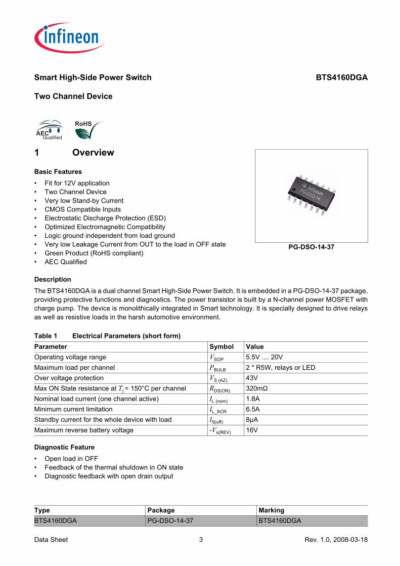
Smart High-Side Power Switch Two Channel Device
BTS4160DGA
PG-DSO-14-37
1 Overview
Basic Features• Fit for 12V application• Two Channel Device• Very low Stand-by Current• CMOS Compatible Inputs• Electrostatic Discharge Protection (ESD)• Optimized Electromagnetic Compatibility• Logic ground independent from load ground• Very low Leakage Current from OUT to the load in OFF state• Green Product (RoHS compliant)• AEC Qualified
DescriptionThe BTS4160DGA is a dual channel Smart High-Side Power Switch. It is embedded in a PG-DSO-14-37 package, providing protective functions and diagnostics. The power transistor is built by a N-channel power MOSFET with charge pump. The device is monolithically integrated in Smart technology. It is specially designed to drive relays as well as resistive loads in the harsh automotive environment.
Diagnostic Feature• Open load in OFF• Feedback of the thermal shutdown in ON state• Diagnostic feedback with open drain output
Table 1 Electrical Parameters (short form)Parameter Symbol ValueOperating voltage range VSOP 5.5V .... 20V Maximum load per channel PBULB 2 * R5W, relays or LEDOver voltage protection VS (AZ) 43VMax ON State resistance at Tj = 150°C per channel RDS(ON) 320mΩNominal load current (one channel active) IL (nom) 1.8AMinimum current limitation IL_SCR 6.5AStandby current for the whole device with load IS(off) 8µAMaximum reverse battery voltage -Vs(REV) 16V
Type Package MarkingBTS4160DGA PG-DSO-14-37 BTS4160DGA
Data Sheet 3 Rev. 1.0, 2008-03-18
BTS4160DGA
Overview
Protection Functions• Short circuit protection• Overload protection• Current limitation• Thermal shutdown• Overvoltage protection (including load dump) with external resistor• Loss of ground and loss of VS protection• Electrostatic discharge protection (ESD)
Application• All types of relays and resistive loads
Data Sheet 4 Rev. 1.0, 2008-03-18
Data Sheet 5 Rev. 1.0, 2008-03-18
BTS4160DGA
Block Diagram
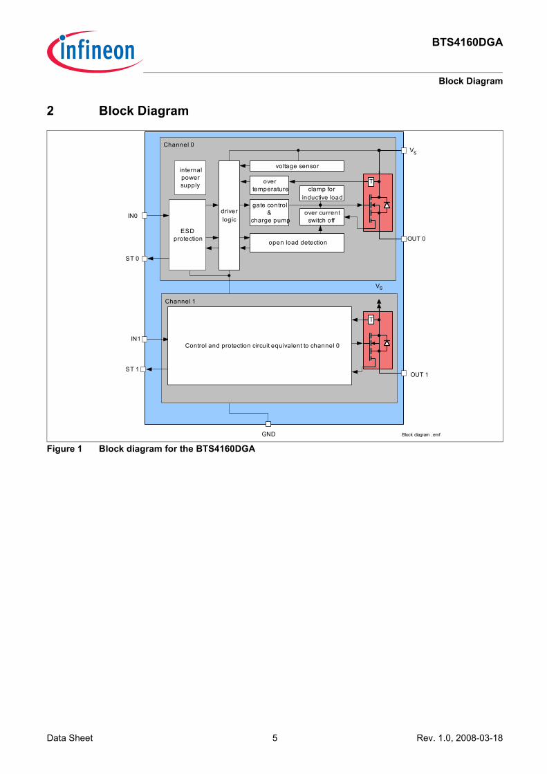
2 Block Diagram
Figure 1 Block diagram for the BTS4160DGABlock diagram .emf
Channel 0VS
OUT 0
IN0
T
driverlogic
gate control&
charge pump
open load detection
overtemperature clamp for
inductive load
over currentswitch off
voltage sensor
GND
ESDprotection
ST 0
internalpowersupply
Channel 1
IN1Control and protection circuit equivalent to channel 0
T
VS
OUT 1ST 1
BTS4160DGA
Pin Configuration
3 Pin Configuration
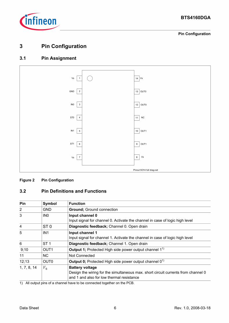
3.1 Pin Assignment
Figure 2 Pin Configuration
3.2 Pin Definitions and Functions
Pin Symbol Function2 GND Ground; Ground connection3 IN0 Input channel 0
Input signal for channel 0. Activate the channel in case of logic high level4 ST 0 Diagnostic feedback; Channel 0. Open drain5 IN1 Input channel 1
Input signal for channel 1. Activate the channel in case of logic high level6 ST 1 Diagnostic feedback; Channel 1. Open drain 9;10 OUT1 Output 1; Protected High side power output channel 11)
1) All output pins of a channel have to be connected together on the PCB.
11 NC Not Connected12;13 OUT0 Output 0; Protected High side power output channel 01)
1, 7, 8, 14 VS Battery voltage Design the wiring for the simultaneous max. short circuit currents from channel 0 and 1 and also for low thermal resistance
1
2
3
4
14
13
12
11ST0
GND
IN0
Vs
OUT0
OUT0
5
6
7
IN1 10
9
8
OUT1
OUT1
Vs
VsVs
ST1
NC
Pinout SO14 full diag.vsd
Data Sheet 6 Rev. 1.0, 2008-03-18
BTS4160DGA
Pin Configuration
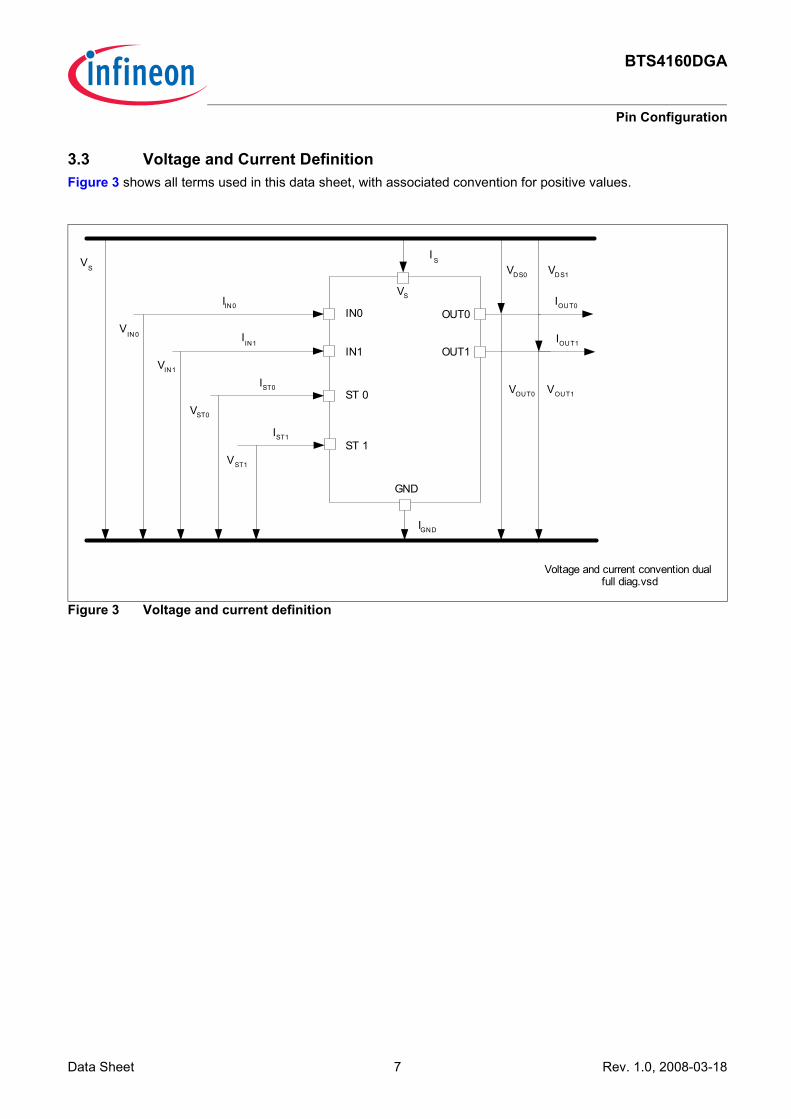
3.3 Voltage and Current DefinitionFigure 3 shows all terms used in this data sheet, with associated convention for positive values.
Figure 3 Voltage and current definition
VS
IN0
IN1
ST 0
GND
OUT0
OUT1
IIN0
IIN1
IST0
VS
VIN 0
VIN1
VST0
I S
IGND
VDS0 VDS1
VOUT0 VOUT1
IOUT1
IOUT0
Voltage and current convention dualfull diag.vsd
ST 1IST1
VST1
Data Sheet 7 Rev. 1.0, 2008-03-18
BTS4160DGA
General Product Characteristics
4 General Product Characteristics
4.1 Absolute Maximum Ratings
Note: Stresses above the ones listed here may cause permanent damage to the device. Exposure to absolute maximum rating conditions for extended periods may affect device reliability.
Absolute Maximum Ratings 1)
Tj = 25°C; (unless otherwise specified)
1) Not subject to production test, specified by design
Pos. Parameter Symbol Limit values Unit ConditionsMin. Max.
Voltages4.1.1 Supply voltage VS -0.3 43 V –4.1.2 Reverse polarity Voltage - VS(REV) 0 16 V –4.1.3 Supply voltage for short circuit protection Vbat(SC) 0 20 V RECU = 20mΩ,
RCable = 16mΩ/m,LCable = 1µH/m,l = 0 or 5m 2)
see Chapter 6
2) Set up in accordance to AEC Q100-012 and AEC Q101-006
Input pins4.1.4 Voltage at INPUT pins VIN -10 16 V –4.1.5 Current through INPUT pins IIN -0.3 0.3 mA –Status pin4.1.6 Current through ST pin IST -5 5 mA –Power stage4.1.7 Load current | IL | – IL(LIM) A –4.1.8 Power dissipation (DC), all channel
activePTOT – 0.9 W TA = 85°C,
Tj <150°C4.1.9 Maximum Switchable inductance, single
pulseEAS – 65 mJ IL = 2.9A,
VS = 12VTemperatures4.1.10 Junction Temperature Tj -40 150 °C –4.1.11 Dynamic temperature increase while
switching∆Tj – 60 K –
4.1.12 Storage Temperature Tstg -55 150 °C –ESD Susceptibility4.1.13 ESD Resistivity IN pin VESD -1 1 kV HBM3)
3) ESD susceptibility HBM according to EIA/JESD 22-A 114B
4.1.14 ESD Resistivity ST pin VESD -4 4 kV HBM3)
4.1.15 ESD Resistivity OUT to all other pins shorted
VESD -5 5 kV HBM3)
Data Sheet 8 Rev. 1.0, 2008-03-18
BTS4160DGA
General Product Characteristics
Note: Integrated protection functions are designed to prevent IC destruction under fault conditions described in the data sheet. Fault conditions are considered as “outside” normal operating range. Protection functions are not designed for continuous repetitive operation.
4.2 Functional Range
Note: Within the functional range the IC operates as described in the circuit description. The electrical characteristics are specified within the conditions given in the related electrical characteristics table.
4.3 Thermal Resistance
Pos. Parameter Symbol Limit values Unit ConditionsMin. Max.
4.2.1 Operating Voltage VSOP 5.5 20 V VIN = 4.5V,RL = 12Ω,VDS < 0.5V
4.2.2 Undervoltage switch OFF VSUV – 4.5 V Tj = -40°C,VDS < 0.5V
4.2.3 Operating currentOne channel activeTwo channels active
IGND––
0.91.7
mA VIN = 5V
4.2.4 Standby current for whole device with load
IS(OFF) –––
8812
µA Tj = 25°CTj = 85°C1)
Tj = 150°C,Vs = 12V,RL = 12Ω,VIN = 0V
1) Not subject to production test. Specified by design
Pos. Parameter Symbol Limit values Unit ConditionsMin. Typ. Max.
4.3.1 Junction to Soldering Point each channel
RthJSP – – 15 K/W –1)
1) Not subject to production test, specified by design
4.3.2 Junction to AmbientOne channel activeTwo channel active
RthJA––
7045
––
K/W with 6cm² cooling area1)
Data Sheet 9 Rev. 1.0, 2008-03-18
BTS4160DGA
Power Stage
5 Power StageThe power stages are built by an N-channel vertical power MOSFET (DMOS) with charge pump.
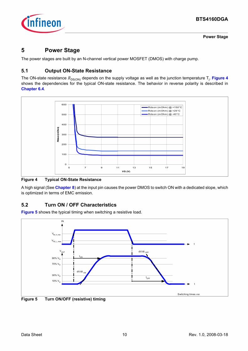
5.1 Output ON-State ResistanceThe ON-state resistance RDS(ON) depends on the supply voltage as well as the junction temperature Tj. Figure 4shows the dependencies for the typical ON-state resistance. The behavior in reverse polarity is described in Chapter 6.4.
Figure 4 Typical ON-State Resistance
A high signal (See Chapter 8) at the input pin causes the power DMOS to switch ON with a dedicated slope, which is optimized in terms of EMC emission.
5.2 Turn ON / OFF CharacteristicsFigure 5 shows the typical timing when switching a resistive load.
Figure 5 Turn ON/OFF (resistive) timing
0
100
200
300
400
500
600
5 7 9 11 13 15 17 19
VS (V)
Rds
on (m
Ohm
)
Rdson (mOhm) @ +150°C
Rdson (mOhm) @ +25°CRdson (mOhm) @ -40°C
IN
t
VOUT
tON
tOFF
90% VS
10% VS
VIN_H_min
VIN_L_max
t
Switching times.vsd
30% VS
70% VS
dV/dt ON
dV/dt OFF
Data Sheet 10 Rev. 1.0, 2008-03-18
BTS4160DGA
Power Stage
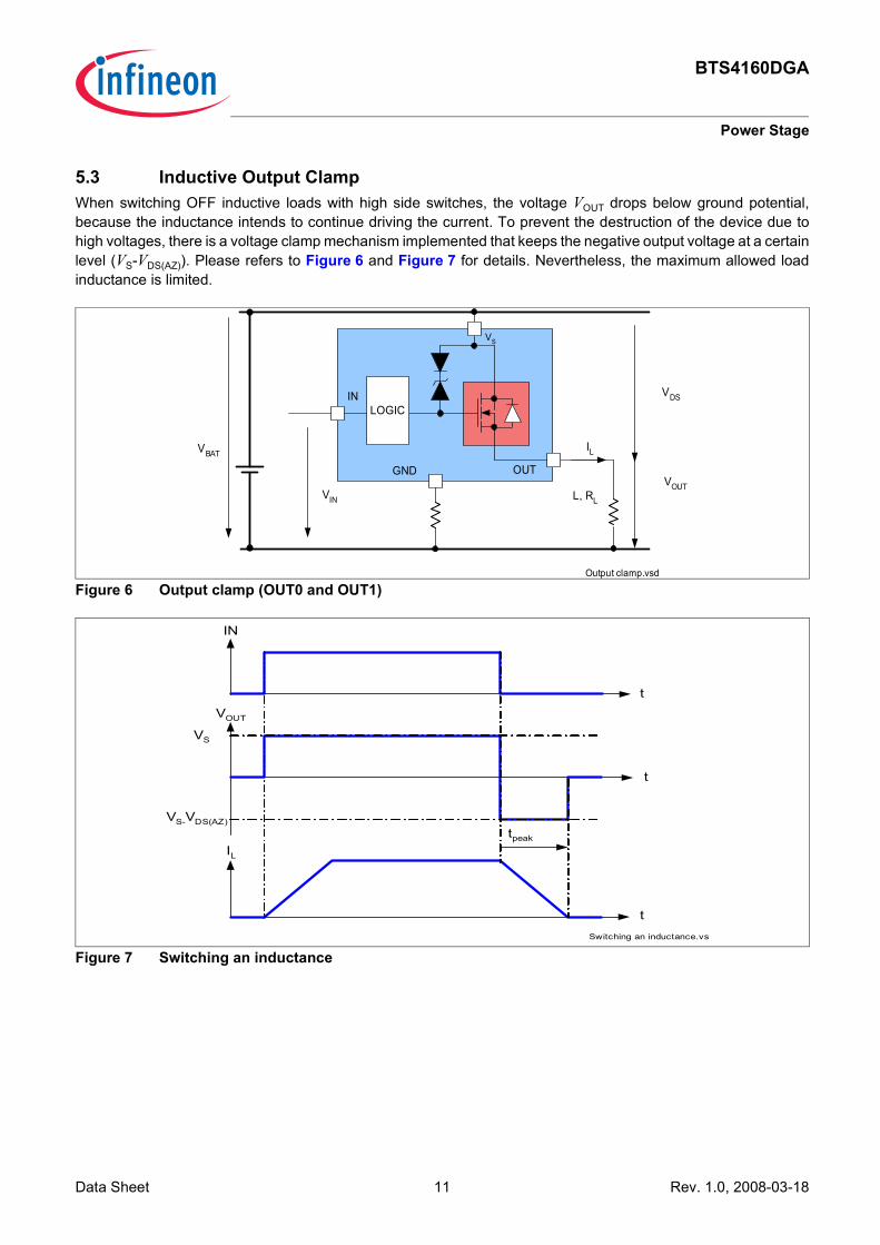
5.3 Inductive Output ClampWhen switching OFF inductive loads with high side switches, the voltage VOUT drops below ground potential, because the inductance intends to continue driving the current. To prevent the destruction of the device due to high voltages, there is a voltage clamp mechanism implemented that keeps the negative output voltage at a certain level (VS-VDS(AZ)). Please refers to Figure 6 and Figure 7 for details. Nevertheless, the maximum allowed load inductance is limited.
Figure 6 Output clamp (OUT0 and OUT1)
Figure 7 Switching an inductance
VBAT
VOUT
IL
L, RL
VS
OUT
VDS
LOGICIN
VIN
Output clamp.vsd
GND
IN
VOUT
IL
VS
VS-VDS(AZ)
t
t
tSwitching an inductance.vsd
tpeak
Data Sheet 11 Rev. 1.0, 2008-03-18
BTS4160DGA
Power Stage
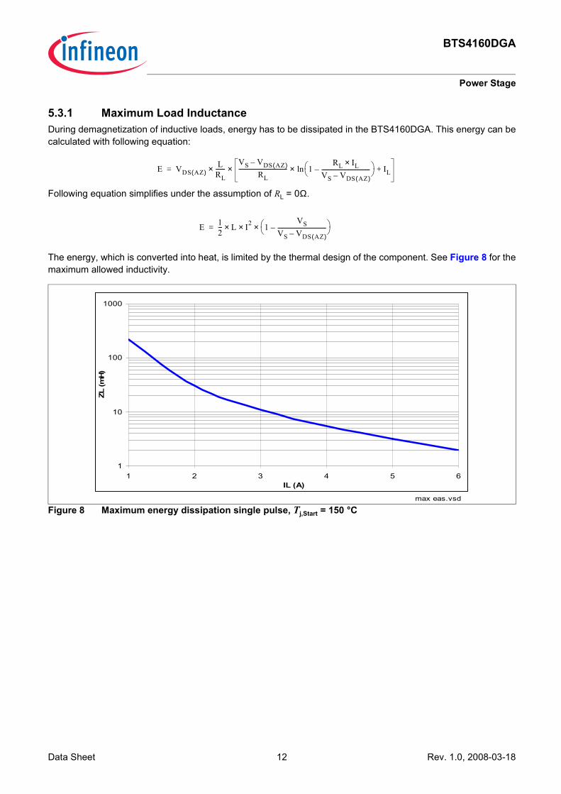
5.3.1 Maximum Load InductanceDuring demagnetization of inductive loads, energy has to be dissipated in the BTS4160DGA. This energy can be calculated with following equation:
Following equation simplifies under the assumption of RL = 0Ω.
The energy, which is converted into heat, is limited by the thermal design of the component. See Figure 8 for the maximum allowed inductivity.
Figure 8 Maximum energy dissipation single pulse, Tj,Start = 150 °C
E VDS AZ( )LRL-------×
VS VDS AZ( )–
RL---------------------------------- 1
RL IL×VS VDS AZ( )–----------------------------------–
ln IL+××=
E 12--- L I2 1
VSVS VDS AZ( )–----------------------------------–
×××=
max eas.vsd
1
10
100
1000
1 2 3 4 5 6IL (A)
ZL (m
H)
Data Sheet 12 Rev. 1.0, 2008-03-18
BTS4160DGA
Power Stage
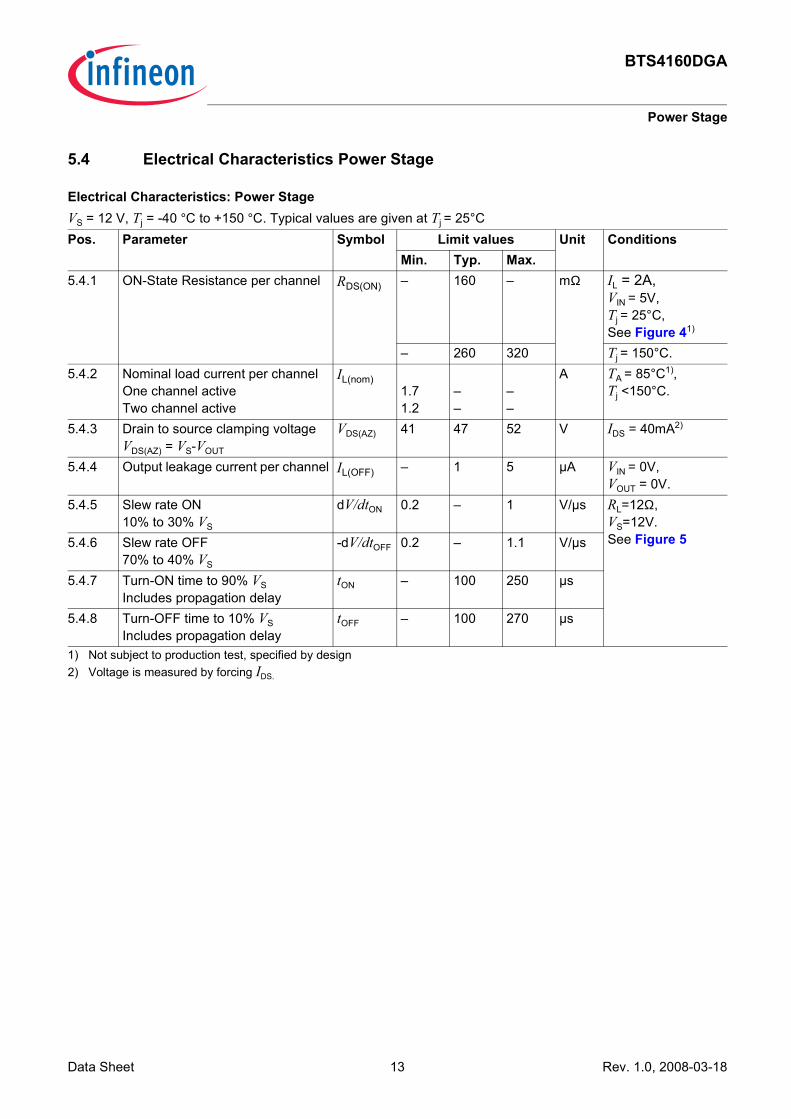
5.4 Electrical Characteristics Power Stage
Electrical Characteristics: Power Stage VS = 12 V, Tj = -40 °C to +150 °C. Typical values are given at Tj = 25°CPos. Parameter Symbol Limit values Unit Conditions
Min. Typ. Max.5.4.1 ON-State Resistance per channel RDS(ON) – 160 – mΩ IL = 2A,
VIN = 5V,Tj = 25°C,See Figure 41)
1) Not subject to production test, specified by design
– 260 320 Tj = 150°C.5.4.2 Nominal load current per channel
One channel activeTwo channel active
IL(nom)1.71.2
––
––
A TA = 85°C1),Tj <150°C.
5.4.3 Drain to source clamping voltageVDS(AZ) = VS-VOUT
VDS(AZ) 41 47 52 V IDS = 40mA2)
2) Voltage is measured by forcing IDS.
5.4.4 Output leakage current per channel IL(OFF) – 1 5 µA VIN = 0V,VOUT = 0V.
5.4.5 Slew rate ON10% to 30% VS
dV/dtON 0.2 – 1 V/µs RL=12Ω,VS=12V.See Figure 55.4.6 Slew rate OFF
70% to 40% VS
-dV/dtOFF 0.2 – 1.1 V/µs
5.4.7 Turn-ON time to 90% VSIncludes propagation delay
tON – 100 250 µs
5.4.8 Turn-OFF time to 10% VSIncludes propagation delay
tOFF – 100 270 µs
Data Sheet 13 Rev. 1.0, 2008-03-18
BTS4160DGA
Protection Mechanisms
6 Protection MechanismsThe device provides embedded protective functions. Integrated protection functions are designed to prevent the destruction of the IC from fault conditions described in the data sheet. Fault conditions are considered as “outside” normal operating range. Protection functions are designed for neither continuous nor repetitive operation.
6.1 Loss of Ground ProtectionIn case of loss of the module ground, where the load remains connected to ground, the device protects itself by automatically turning OFF (when it was previously ON) or remains OFF, regardless of the voltage applied on IN pins. In that case, a maximum I(OUTGND) can flow out of the output.
6.2 Undervoltage ProtectionBelow VSOP_min, , the under voltage mechanism is met. If the supply voltage is below the under voltage mechanism, the device is OFF (turns OFF). As soon as the supply voltage is above the under voltage mechanism, then the device can be switched ON and the protection functions are operational.
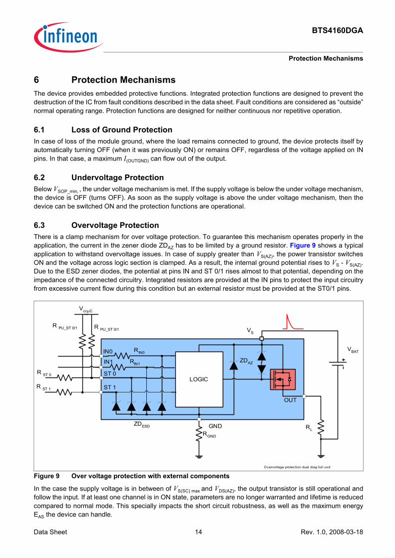
6.3 Overvoltage ProtectionThere is a clamp mechanism for over voltage protection. To guarantee this mechanism operates properly in the application, the current in the zener diode ZDAZ has to be limited by a ground resistor. Figure 9 shows a typical application to withstand overvoltage issues. In case of supply greater than VS(AZ), the power transistor switches ON and the voltage across logic section is clamped. As a result, the internal ground potential rises to VS - VS(AZ). Due to the ESD zener diodes, the potential at pins IN and ST 0/1 rises almost to that potential, depending on the impedance of the connected circuitry. Integrated resistors are provided at the IN pins to protect the input circuitry from excessive current flow during this condition but an external resistor must be provided at the ST0/1 pins.
Figure 9 Over voltage protection with external components
In the case the supply voltage is in between of VS(SC) max and VDS(AZ), the output transistor is still operational and follow the input. If at least one channel is in ON state, parameters are no longer warranted and lifetime is reduced compared to normal mode. This specially impacts the short circuit robustness, as well as the maximum energy EAS the device can handle.
IN1
RIN0IN0
ST 0
RIN1
R ST 0
ZDESD GND
OUT
VS
VBAT
RGND
ZDAZ
LOGIC
Overvoltage protection dual diag full.vsd
R PU_ST 0/1
VccµC
RL
R ST 1 ST 1
R PU_ST 0/1
Data Sheet 14 Rev. 1.0, 2008-03-18
BTS4160DGA
Protection Mechanisms
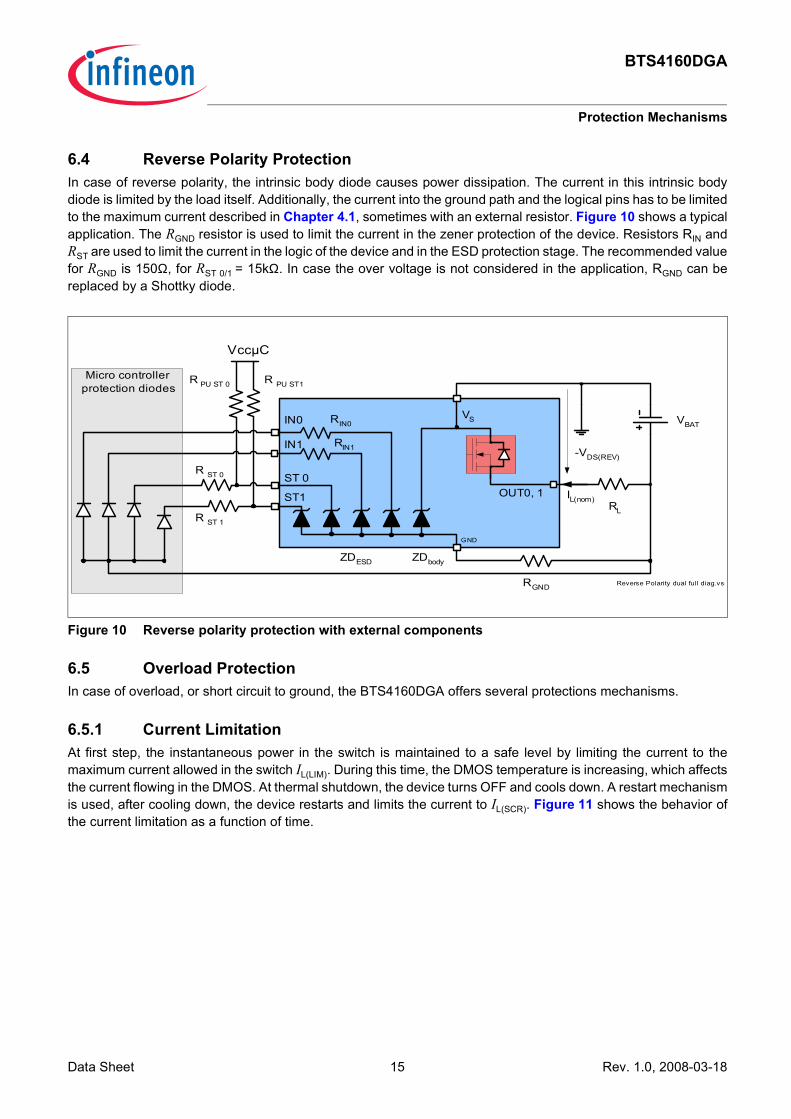
6.4 Reverse Polarity ProtectionIn case of reverse polarity, the intrinsic body diode causes power dissipation. The current in this intrinsic body diode is limited by the load itself. Additionally, the current into the ground path and the logical pins has to be limited to the maximum current described in Chapter 4.1, sometimes with an external resistor. Figure 10 shows a typical application. The RGND resistor is used to limit the current in the zener protection of the device. Resistors RIN and RST are used to limit the current in the logic of the device and in the ESD protection stage. The recommended value for RGND is 150Ω, for RST 0/1 = 15kΩ. In case the over voltage is not considered in the application, RGND can be replaced by a Shottky diode.
Figure 10 Reverse polarity protection with external components
6.5 Overload ProtectionIn case of overload, or short circuit to ground, the BTS4160DGA offers several protections mechanisms.
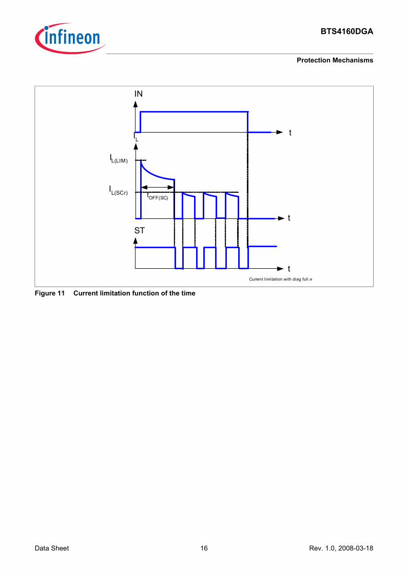
6.5.1 Current LimitationAt first step, the instantaneous power in the switch is maintained to a safe level by limiting the current to the maximum current allowed in the switch IL(LIM). During this time, the DMOS temperature is increasing, which affects the current flowing in the DMOS. At thermal shutdown, the device turns OFF and cools down. A restart mechanism is used, after cooling down, the device restarts and limits the current to IL(SCR). Figure 11 shows the behavior of the current limitation as a function of time.
Micro controllerprotection diodes
GND
OUT0, 1
IN1
VS VBATRIN0IN0
ST 0
RIN1
R ST 0
RGND
ZDbody
Reverse Polarity dual full diag.vsd
-VDS(REV)
IL(nom)RL
R PU ST 0
VccµC
ST1
R ST 1
ZDESD
R PU ST1
Data Sheet 15 Rev. 1.0, 2008-03-18
BTS4160DGA
Protection Mechanisms
Figure 11 Current limitation function of the time
t
IL
IL(LIM)
IL(SCr)
Current limitation with diag full.vs
t
IN
ST
tOFF(SC)
t
Data Sheet 16 Rev. 1.0, 2008-03-18
BTS4160DGA
Protection Mechanisms
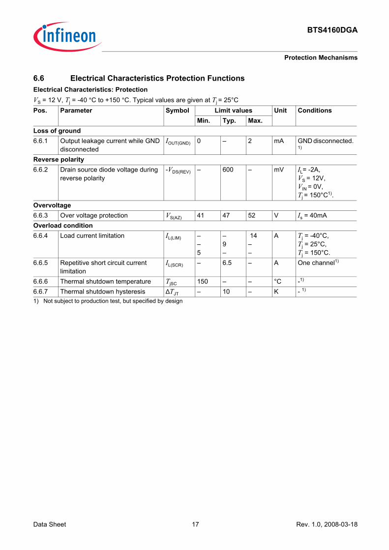
6.6 Electrical Characteristics Protection FunctionsElectrical Characteristics: Protection VS = 12 V, Tj = -40 °C to +150 °C. Typical values are given at Tj = 25°CPos. Parameter Symbol Limit values Unit Conditions
Min. Typ. Max.Loss of ground6.6.1 Output leakage current while GND
disconnectedIOUT(GND) 0 – 2 mA GND disconnected.
1)
Reverse polarity6.6.2 Drain source diode voltage during
reverse polarity-VDS(REV) – 600 – mV IL= -2A,
VS = 12V,VIN = 0V,Tj = 150°C1).
Overvoltage6.6.3 Over voltage protection VS(AZ) 41 47 52 V Is = 40mAOverload condition6.6.4 Load current limitation IL(LIM) –
–5
–9–
14––
A Tj = -40°C,Tj = 25°C,Tj = 150°C.
6.6.5 Repetitive short circuit current limitation
IL(SCR) – 6.5 – A One channel1)
6.6.6 Thermal shutdown temperature TjSC 150 – – °C -1)
6.6.7 Thermal shutdown hysteresis ∆TJT – 10 – K - 1)
1) Not subject to production test, but specified by design
Data Sheet 17 Rev. 1.0, 2008-03-18
BTS4160DGA
Diagnostic Mechanism
7 Diagnostic MechanismFor diagnosis purpose, the BTS4160DGA provides a status pin per channel.
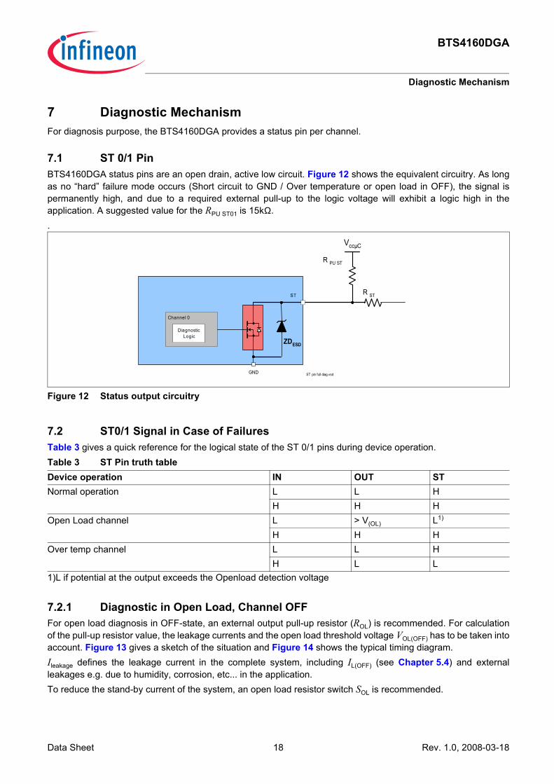
7.1 ST 0/1 PinBTS4160DGA status pins are an open drain, active low circuit. Figure 12 shows the equivalent circuitry. As long as no “hard” failure mode occurs (Short circuit to GND / Over temperature or open load in OFF), the signal is permanently high, and due to a required external pull-up to the logic voltage will exhibit a logic high in the application. A suggested value for the RPU ST01 is 15kΩ..
Figure 12 Status output circuitry
7.2 ST0/1 Signal in Case of FailuresTable 3 gives a quick reference for the logical state of the ST 0/1 pins during device operation.
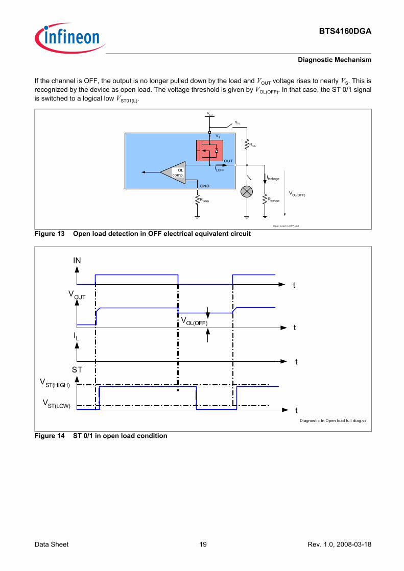
7.2.1 Diagnostic in Open Load, Channel OFFFor open load diagnosis in OFF-state, an external output pull-up resistor (ROL) is recommended. For calculation of the pull-up resistor value, the leakage currents and the open load threshold voltage VOL(OFF) has to be taken into account. Figure 13 gives a sketch of the situation and Figure 14 shows the typical timing diagram.Ileakage defines the leakage current in the complete system, including IL(OFF) (see Chapter 5.4) and external leakages e.g. due to humidity, corrosion, etc... in the application.To reduce the stand-by current of the system, an open load resistor switch SOL is recommended.
Table 3 ST Pin truth tableDevice operation IN OUT STNormal operation L L H
H H HOpen Load channel L > V(OL) L1)
1)L if potential at the output exceeds the Openload detection voltage
H H HOver temp channel L L H
H L L
ST pin full diag.vsdGND
ST R ST
ZDESD
R PU ST
VccµC
Channel 0
DiagnosticLogic
Data Sheet 18 Rev. 1.0, 2008-03-18
BTS4160DGA
Diagnostic Mechanism
If the channel is OFF, the output is no longer pulled down by the load and VOUT voltage rises to nearly VS. This is recognized by the device as open load. The voltage threshold is given by VOL(OFF). In that case, the ST 0/1 signal is switched to a logical low VST01(L).
Figure 13 Open load detection in OFF electrical equivalent circuit
Figure 14 ST 0/1 in open load condition
OUT
VS
Rleakage
ROL
SOL
Vbat
VOL(OFF)
Ileakage
ILOFFOLcomp.
Open Load in OFF.vsd
GND
RGND
IN
VOUT
ST
IL
Diagnostic In Open load full diag.vs
t
t
t
t
VST(HIGH)
VOL(OFF)
VST(LOW)
Data Sheet 19 Rev. 1.0, 2008-03-18
BTS4160DGA
Diagnostic Mechanism
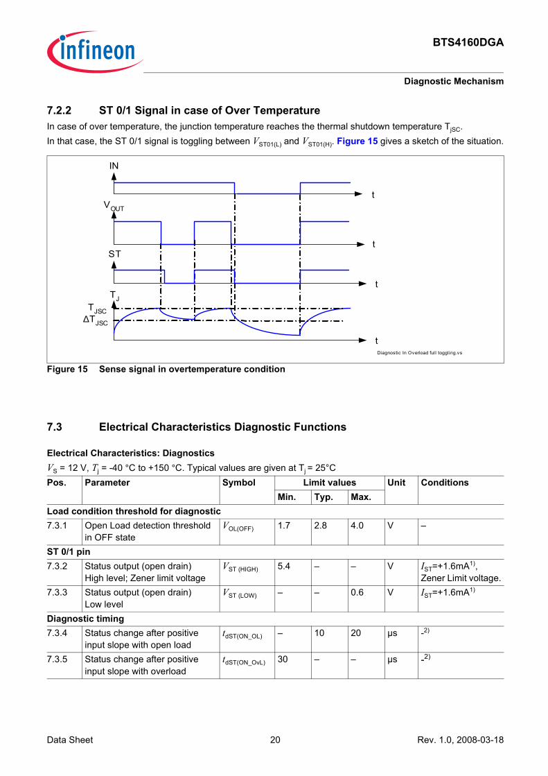
7.2.2 ST 0/1 Signal in case of Over TemperatureIn case of over temperature, the junction temperature reaches the thermal shutdown temperature TjSC. In that case, the ST 0/1 signal is toggling between VST01(L) and VST01(H). Figure 15 gives a sketch of the situation.
Figure 15 Sense signal in overtemperature condition
7.3 Electrical Characteristics Diagnostic Functions
Electrical Characteristics: Diagnostics VS = 12 V, Tj = -40 °C to +150 °C. Typical values are given at Tj = 25°CPos. Parameter Symbol Limit values Unit Conditions
Min. Typ. Max.Load condition threshold for diagnostic7.3.1 Open Load detection threshold
in OFF stateVOL(OFF) 1.7 2.8 4.0 V –
ST 0/1 pin7.3.2 Status output (open drain)
High level; Zener limit voltageVST (HIGH) 5.4 – – V IST=+1.6mA1),
Zener Limit voltage.7.3.3 Status output (open drain)
Low levelVST (LOW) – – 0.6 V IST=+1.6mA1)
Diagnostic timing7.3.4 Status change after positive
input slope with open loadtdST(ON_OL) – 10 20 µs -2)
7.3.5 Status change after positive input slope with overload
tdST(ON_OvL) 30 – – µs -2)
IN
VOUT
ST
TJ
Diagnostic In Overload full toggling.vs
t
t
t
t
TJSC∆TJSC
Data Sheet 20 Rev. 1.0, 2008-03-18
BTS4160DGA
Diagnostic Mechanism
7.3.6 Status change after negative input slope with open load
tdST(OFF_OL) – – 500 µs –
7.3.7 Status change after negative input slope with overload
tdST(OFF_OvL) – – 20 µs -2)
1) If ground resistor RGND is used, the voltage drop across this resistor has to be added2) Not subject to production test, specified by design
Electrical Characteristics: Diagnostics (cont’d)VS = 12 V, Tj = -40 °C to +150 °C. Typical values are given at Tj = 25°CPos. Parameter Symbol Limit values Unit Conditions
Min. Typ. Max.
Data Sheet 21 Rev. 1.0, 2008-03-18
Data Sheet 22 Rev. 1.0, 2008-03-18
BTS4160DGA
Input Pins
8 Input Pins
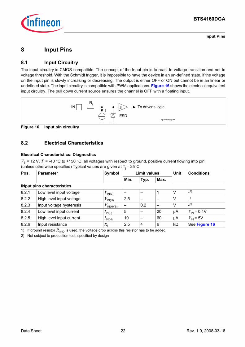
8.1 Input CircuitryThe input circuitry is CMOS compatible. The concept of the Input pin is to react to voltage transition and not to voltage threshold. With the Schmidt trigger, it is impossible to have the device in an un-defined state, if the voltage on the input pin is slowly increasing or decreasing. The output is either OFF or ON but cannot be in an linear or undefined state. The input circuitry is compatible with PWM applications. Figure 16 shows the electrical equivalent input circuitry. The pull down current source ensures the channel is OFF with a floating input.
Figure 16 Input pin circuitry
8.2 Electrical Characteristics
Electrical Characteristics: Diagnostics VS = 12 V, Tj = -40 °C to +150 °C, all voltages with respect to ground, positive current flowing into pin (unless otherwise specified) Typical values are given at Tj = 25°CPos. Parameter Symbol Limit values Unit Conditions
Min. Typ. Max.INput pins characteristics8.2.1 Low level input voltage VIN(L) – – 1 V -1)
1) If ground resistor RGND is used, the voltage drop across this resistor has to be added
8.2.2 High level input voltage VIN(H) 2.5 – – V 1)
8.2.3 Input voltage hysteresis VIN(HYS) – 0.2 – V -2)
2) Not subject to production test, specified by design
8.2.4 Low level input current IIN(L) 5 – 20 µA VIN = 0.4V8.2.5 High level input current IIN(H) 10 – 60 µA VIN = 5V8.2.6 Input resistance RI 2.5 4 6 kΩ See Figure 16
IN
ESD
To driver’s logic
Input circuitry.vsd
RI
II
Data Sheet 23 Rev. 1.0, 2008-03-18
BTS4160DGA
Application Information
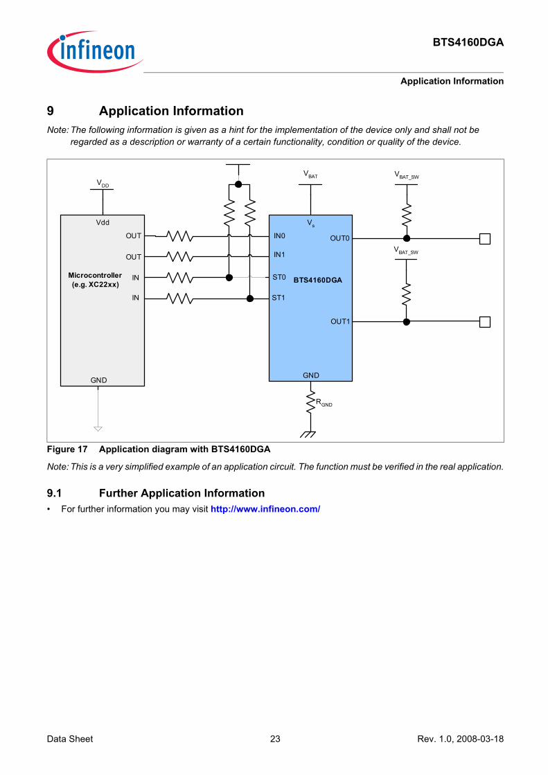
9 Application InformationNote: The following information is given as a hint for the implementation of the device only and shall not be
regarded as a description or warranty of a certain functionality, condition or quality of the device.
Figure 17 Application diagram with BTS4160DGA
Note: This is a very simplified example of an application circuit. The function must be verified in the real application.
9.1 Further Application Information• For further information you may visit http://www.infineon.com/
OUT
OUT
IN
IN
GND
Vdd
Microcontroller(e.g. XC22xx)
IN0
IN1
ST0
ST1
GND
OUT0
OUT1
Vs
RGND
VBAT VBAT_SW
VBAT_SW
VDD
BTS4160DGA
Data Sheet 24 Rev. 1.0, 2008-03-18
BTS4160DGA
Package Outlines
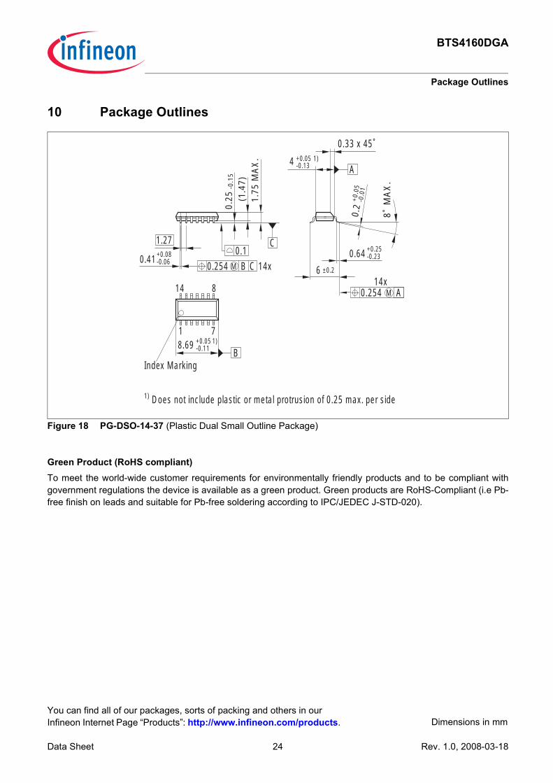
10 Package Outlines
Figure 18 PG-DSO-14-37 (Plastic Dual Small Outline Package)
Green Product (RoHS compliant)To meet the world-wide customer requirements for environmentally friendly products and to be compliant with government regulations the device is available as a green product. Green products are RoHS-Compliant (i.e Pb-free finish on leads and suitable for Pb-free soldering according to IPC/JEDEC J-STD-020).
±0.2
Does not include plastic or metal protrusion of 0.25 max. per side
Index Marking
-0.06
1.27+0.080.41
+0.05-0.118.69
1
14
71)
B
0.254
8
BM
0.1
0.25 (1
.47)
-0.1
5
C
14xC 6
4
1.75
MA
X. +0.05 1)
-0.13
-0.23
14x0.254
+0.250.64
AM
0.2
+0.
05
A
-0.0
1
0.33 x 45˚
8˚1)
MA
X.
You can find all of our packages, sorts of packing and others in our Infineon Internet Page “Products”: http://www.infineon.com/products. Dimensions in mm
Data Sheet 25 Rev. 1.0, 2008-03-18
BTS4160DGA
Revision History
11 Revision History
Version Date Changes1.0 2008-03-18 Creation of the data sheet
Edition 2008-03-18Published by Infineon Technologies AG 81726 Munich, Germany© 2008 Infineon Technologies AG All Rights Reserved.
Legal DisclaimerThe information given in this document shall in no event be regarded as a guarantee of conditions or characteristics. With respect to any examples or hints given herein, any typical values stated herein and/or any information regarding the application of the device, Infineon Technologies hereby disclaims any and all warranties and liabilities of any kind, including without limitation, warranties of non-infringement of intellectual property rights of any third party.
InformationFor further information on technology, delivery terms and conditions and prices, please contact the nearest Infineon Technologies Office (www.infineon.com).
WarningsDue to technical requirements, components may contain dangerous substances. For information on the types in question, please contact the nearest Infineon Technologies Office.Infineon Technologies components may be used in life-support devices or systems only with the express written approval of Infineon Technologies, if a failure of such components can reasonably be expected to cause the failure of that life-support device or system or to affect the safety or effectiveness of that device or system. Life support devices or systems are intended to be implanted in the human body or to support and/or maintain and sustain and/or protect human life. If they fail, it is reasonable to assume that the health of the user or other persons may be endangered.