Flash programming - Infineon Technologies
16
AURIX™ TC3xx Microcontroller Training V1.0.0 Flash_Programming_1 for KIT_AURIX_TC334_LK Flash programming Please read the Important Notice and Warnings at the end of this document
-
Upload
khangminh22 -
Category
Documents
-
view
2 -
download
0
Transcript of Flash programming - Infineon Technologies
AURIX™ TC3xx Microcontroller Training
V1.0.0
Flash_Programming_1
for KIT_AURIX_TC334_LKFlash programming
Please read the Important Notice and Warnings at the end of this document

Scope of work
This example shows how to flash the Program Flash memory and the
Data Flash memory.
In this example, 64 Bytes of the Program Flash memory (PFLASH) are
flashed and verified afterwards. Furthermore, 64 Bytes of the Data Flash
memory (DFLASH) are flashed and verified.
Before any write operation, the flash memories are erased. If the flash
operation is successful, an LED for each tested memory is turned ON.
Copyright © Infineon Technologies AG 2021. All rights reserved.

Introduction
› The Data Memory Unit (DMU) controls command sequences executed on the Program and
Data Flash memories (PFLASH and DFLASH), interfacing with the Flash Standard Interface
(FSI) and the Program Flash Interface (PFI)
› The FSI executes erase, program and verify operations on all flash memories
› The PFI provides a unique point-to-point fast connection for each PFLASH bank to a CPU
› The AURIX™ TC33x device features:
– 1 Program Flash Banks (PFx)
– 2 Data Flash Banks (DFx)
› The AURIX™ TC3xx devices feature PFLASH Banks PFx based on the same sector
structure. PFx banks may vary in size:
– 3 Mbyte Program Flash Bank
– 2 Mbyte Program Flash Bank
– 1 Mbyte Program Flash Bank
Copyright © Infineon Technologies AG 2021. All rights reserved.

Introduction
› AURIX™ TC33x features one Program Flash banks (PF0) with dimension of 2 Mbyte. The
Program Flash bank is divided into Physical Sectors with dimension of 1024 Kbytes and
each Physical Sector is divided into 64 Logical Sectors with dimension of 16 Kbytes
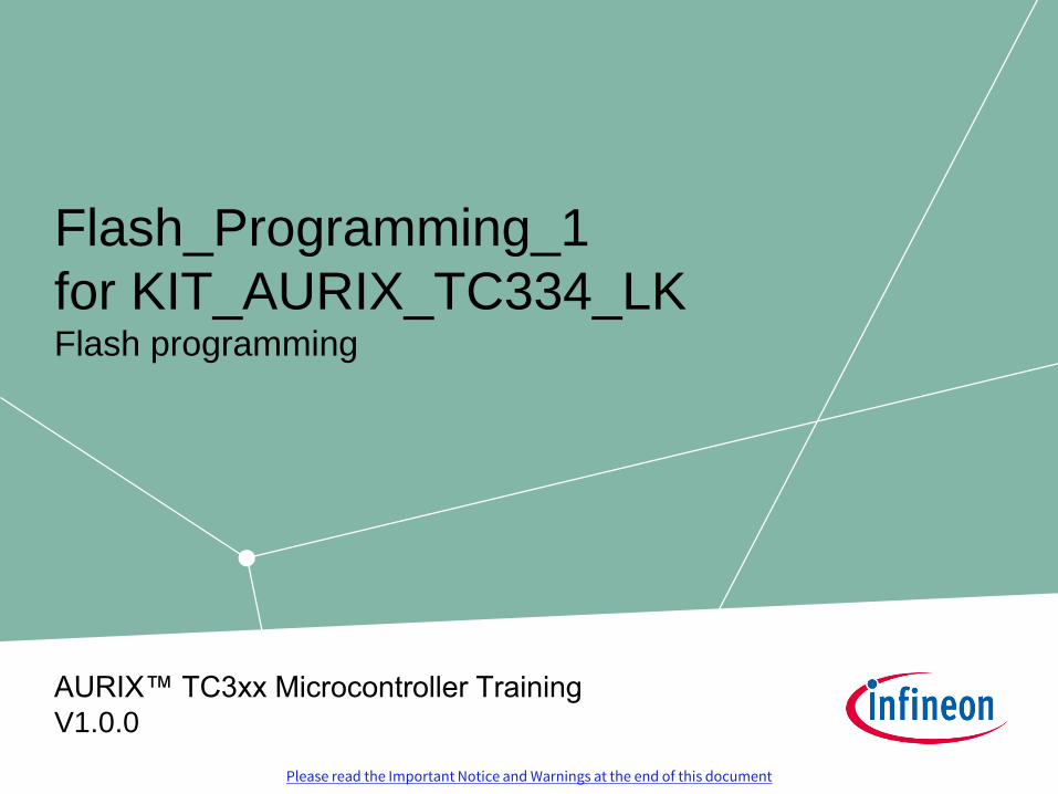
› AURIX™ TC33x features two Data Flash banks, DFLASH0 and DFLASH1. Both include
multiple EEPROM sectors commonly used for EEPROM emulation. Only DFLASH0 includes
User Configuration Blocks (UCBs) for data protection and a Configuration Sector (CFS),
which is not directly accessible by the user
› The DFLASH EEPROM can be either configured in single ended mode (default) or in
complement sensing. Depending on the selected mode, the size of each sector is set to 4
Kbytes and respectively 2 Kbytes
› The minimum amount of data that can be programmed in a flash memory is a page
– Program Flash pages are made of 32 Bytes
– Data Flash pages are made of 8 Bytes
› A page can be programmed only after an erase operation
› The smallest unit on which an erase operation can be performed is a Logical Sector
Copyright © Infineon Technologies AG 2021. All rights reserved.

Introduction
› AURIX™ TC33x Program Flash memory
Copyright © Infineon Technologies AG 2021. All rights reserved.
PFlash
PF0
PS0
S0 (16 KB)
S1 (16 KB)
...
S63 (16 KB)
PS1
S64 (16 KB)
...
S127 (16 KB)
Flash
Bank
Physical
Sector
Logical Sector
Introduction
› AURIX™ TC33x Data Flash memory
Copyright © Infineon Technologies AG 2021. All rights reserved.

Introduction
› All the flash operations are performed with command sequences
› The DMU has a Command Sequence Interpreter (CSI) to process command sequences
› A minimum sequence of commands for programming the Program Flash memory or the
Data Flash memory, is the following:
– Erase the Logical Sectors to be programmed afterwards
– Wait until the flash memory is ready (not busy)
– Enter page mode
– Wait until the flash memory is ready (not busy)
– Load data to be written in a page
– Write the page
– Wait until the flash memory is ready (not busy)
Note: Code that performs PFLASH programming or erasing should not be executed from the
same PFLASH.
Copyright © Infineon Technologies AG 2021. All rights reserved.

This code example has been developed
for the board KIT_A2G_TC334_LITE.
Hardware setup
Copyright © Infineon Technologies AG 2021. All rights reserved.
Implementation
Flashing the Program Flash memory
To perform PFLASH programming, it is recommended to run the code from a memory location
different from the PFLASH that is going to be programmed.
For this reason, before starting the flash operations, the erase and program routines are copied in the
Program Scratch-Pad SRAM (PSPR) of the CPU0 by the function copyFunctionsToPSPR(). This
uses the memcpy() function from the standard c library string.h and assigns a function pointer to the
new memory location.
Then, the actual flash programming operations start by erasing the involved Logical Sectors.
Erase of Logical Sectors
To perform an erase operation, writes have to be enabled on the PFLASH by clearing the EndInit
Protection bit, done through the function IfxScuWdt_clearSafetyEndinitInline().
Then, the erase command sequence for one or more consecutive Logical Sectors can be executed
through the IfxFlash_eraseMultipleSectors() function, executed from the PSPR by the function
pointer eraseSectors().
Finally, the EndInit Protection bit must be set again through the function
IfxScuWdt_setSafetyEndinitInline().
The function IfxFlash_waitUnbusy(), called by the function pointer waitUnbusy(), stalls until the
sector is erased and the PFLASH is ready again.
Copyright © Infineon Technologies AG 2021. All rights reserved.
Implementation
Write operations
After erasing the needed Logical Sectors, the write operations can start.
The function IfxFlash_enterPageMode() called from the PSPR by the function pointer enterPageMode() is used to enter page mode.The function waitUnbusy() is used to stall until the PFLASH is ready and then, the data that has to be written in a page is loaded calling repetitively the function IfxFlash_loadPage2X32(), executed from the PSPR with the function pointer load2X32bits().
The loaded page is then written by calling the function pointer writePage(), which executes the IfxFlash_writePage() function from the PSPR (before and after the write operation, the EndInitProtection bit is cleared and respectively set).Finally, waitUnbusy() is called to wait until the page has been written and the PFLASH is ready again then, the write process can be repeated until all the required data has been successfully written in the PFLASH.
After the flashing operations, the data is read from the PFLASH exploiting the macro MEM(address), and, if it is correct, an LED is turned on.
All the functions used for executing the command sequences for the flashing operations can be found in the iLLD header IfxFlash.h, while the function pointers are declared and assigned in the Flash_Programming.c file.
Copyright © Infineon Technologies AG 2021. All rights reserved.
Implementation
Flashing the Data Flash memory
The procedure for flashing the Data Flash memory is the same used for flashing the Program Flash
memory, but in this case the functions for executing the command sequences for erasing, waiting,
loading and writing can be called directly from the PFLASH, thus copying them into the PSPR is not
needed.
After the flashing operations, the data is read from the DFLASH exploiting the macro MEM(address),
and, if it is correct, an LED is turned on.
Configure and control the LEDs
Two LEDs are configured using methods from the iLLD header IfxPort.h.
The port pins to which the LEDs are connected are configured as push-pull output using the
function IfxPort_setPinMode().
To turn on and off the LEDs, the function IfxPort_setPinState() is used.
Copyright © Infineon Technologies AG 2021. All rights reserved.

Run and Test
After code compilation and flashing the device, observe the behavior of the LEDs.
Check that LED1 (1) and LED2 (2) are turned
on:
› LED1 is turned on to indicate that the
PFLASH memory was correctly written
› LED2 is turned on to indicate that the
DFLASH memory was correctly written
1
2
Copyright © Infineon Technologies AG 2021. All rights reserved.

Run and Test
Check the actual PFLASH memory as an additional test:
› Set two breakpoints in the Flash_Programming.c file inside the writeProgramFlash()
function:
– After calling the eraseFlash() function
– After calling the writeFlash() function
› Run the debugger
› In the memory view, add the address 0xA00E0000
› Resume the debugger and check that when it stops at the first breakpoint, the PFLASH is
erased (the memory viewer will show either 0s or 0xEEEEEEEE because it cannot read the
erased memory)
› Resume the debugger again and check that when it stops at the second breakpoint, the
PFLASH is correctly programmed
Copyright © Infineon Technologies AG 2021. All rights reserved.
Run and Test
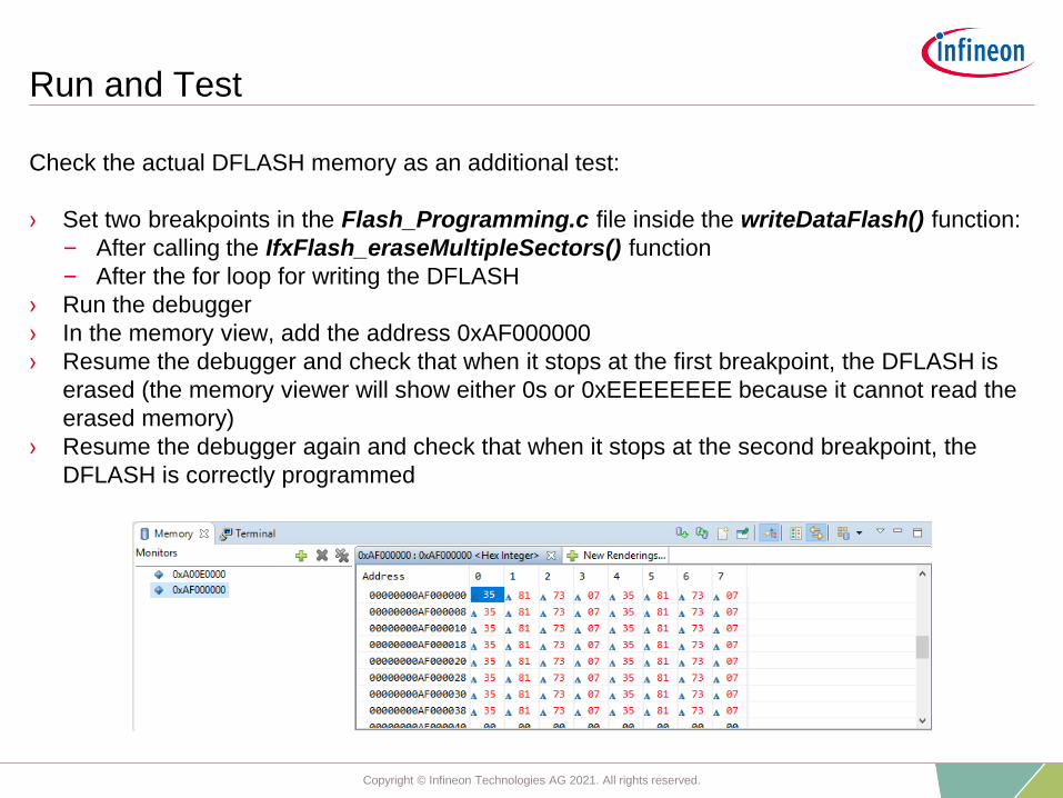
Check the actual DFLASH memory as an additional test:
› Set two breakpoints in the Flash_Programming.c file inside the writeDataFlash() function:
– After calling the IfxFlash_eraseMultipleSectors() function
– After the for loop for writing the DFLASH
› Run the debugger
› In the memory view, add the address 0xAF000000
› Resume the debugger and check that when it stops at the first breakpoint, the DFLASH is
erased (the memory viewer will show either 0s or 0xEEEEEEEE because it cannot read the
erased memory)
› Resume the debugger again and check that when it stops at the second breakpoint, the
DFLASH is correctly programmed
Copyright © Infineon Technologies AG 2021. All rights reserved.
References
› More code examples can be found on the GIT repository:
› https://github.com/Infineon/AURIX_code_examples
› For additional trainings, visit our webpage:
› https://www.infineon.com/aurix-expert-training
› AURIX™ Development Studio is available online:
› https://www.infineon.com/aurixdevelopmentstudio
› Use the „Import...“ function to get access to more code examples.
› For questions and support, use the AURIX™ Forum:
› https://www.infineonforums.com/forums/13-Aurix-Forum
Copyright © Infineon Technologies AG 2021. All rights reserved.
IMPORTANT NOTICEThe information given in this document shall in noevent be regarded as a guarantee of conditions orcharacteristics (“Beschaffenheitsgarantie”) .
With respect to any examples, hints or any typicalvalues stated herein and/or any informationregarding the application of the product, InfineonTechnologies hereby disclaims any and allwarranties and liabilities of any kind, includingwithout limitation warranties of non-infringementof intellectual property rights of any third party.
In addition, any information given in thisdocument is subject to customer’s compliancewith its obligations stated in this document andany applicable legal requirements, norms andstandards concerning customer’s products andany use of the product of Infineon Technologies incustomer’s applications.
The data contained in this document is exclusivelyintended for technically trained staff. It is theresponsibility of customer’s technicaldepartments to evaluate the suitability of theproduct for the intended application and thecompleteness of the product information given inthis document with respect to such application.
For further information on the product,technology, delivery terms and conditions andprices please contact your nearest InfineonTechnologies office (www.infineon.com).
WARNINGSDue to technical requirements products maycontain dangerous substances. For informationon the types in question please contact yournearest Infineon Technologies office.
Except as otherwise explicitly approved byInfineon Technologies in a written documentsigned by authorized representatives of InfineonTechnologies, Infineon Technologies’ productsmay not be used in any applications where afailure of the product or any consequences of theuse thereof can reasonably be expected to resultin personal injury.
Edition 2021-12Published byInfineon Technologies AG81726 Munich, Germany
© 2021 Infineon Technologies AG.All Rights Reserved.
Do you have a question about thisdocument?Email: [email protected]
Document referenceFlash_Programming_1_KIT_TC334_LK
TrademarksAll referenced product or service names and trademarks are the property of their respective owners.