The Effect of the Metal Oxidation on the Vacuum Chamber Impedance
14
1 The Effect of the Metal Oxidation on the Vacuum Chamber Impedance Andranik Tsakanian Hamburg University Martin Dohlus, Igor Zagorodnov Deutsches Electronen-Sinchrotron(DESY) Abstract The oxidation of the metallic vacuum chamber internal surface is an accompanying process of the chamber fabrication and surface treatment. This circumstance changes the electro dynamical properties of the wall material and as consequence the impedance of the vacuum chamber. In this paper the results of longitudinal impedance for oxidised metallic vacuum chamber is presented. The surface impedance matching technique is used to calculate the vacuum chamber impedances. The loss factor is given for various oxides and oxidation thickness. The numerical results for the undulator vacuum chamber of European XFEL project are presented. Introduction The knowledge of the vacuum chamber impedance in accelerators is an important issue to provide the stable operation of the facility from the machine performance and beam physics point of view [1]. The impedances of metallic type vacuum chambers have been studied , for example, in [2-12], including the analytical presentation of the longitudinal and transverse impedances for laminated walls of different materials [8-12] and finite relativistic factor of the particle [11,12]. The metal-dielectric vacuum chamber impedances have been studied in Ref [13-14]. In [14] the longitudinal and transverse impedances for the European XFEL [15] kicker vacuum chamber are calculated based on the field transformation matrix technique [12]. A general approach to evaluate the impedances of the multiplayer vacuum chamber is the field matching technique. In this paper, the longitudinal impedance of metallic vacuum chamber with internal surface oxidation is studied for ultrarelativistic beam case. The explicit analytical solution is obtained for various thicknesses of the metallic layer and oxidation depth. Based on the obtained results the impedance of European XFEL undulator aluminium vacuum chamber is calculated for various oxidation depths. The explicit analytical solution for longitudinal impedance of two-layer tube is obtained. The exact formula for ultra relativistic point like charge moving on axis is introduced in terms of surface impedance. It is shown that in small oxide depth asymptotic limit the surface impedance on boundary with vacuum can be estimated as a sum of oxide and metal surface impedances. Based on this solution the monopole impedances for aluminium beam pipe with different oxide layer thickness are evaluated. TESLA-FEL 2009-05
-
Upload
independent -
Category
Documents
-
view
0 -
download
0
Transcript of The Effect of the Metal Oxidation on the Vacuum Chamber Impedance
1
The Effect of the Metal Oxidation on the Vacuum Chamber Impedance
Andranik Tsakanian Hamburg University
Martin Dohlus, Igor Zagorodnov
Deutsches Electronen-Sinchrotron(DESY)
Abstract The oxidation of the metallic vacuum chamber internal surface is an accompanying process of the chamber fabrication and surface treatment. This circumstance changes the electro dynamical properties of the wall material and as consequence the impedance of the vacuum chamber. In this paper the results of longitudinal impedance for oxidised metallic vacuum chamber is presented. The surface impedance matching technique is used to calculate the vacuum chamber impedances. The loss factor is given for various oxides and oxidation thickness. The numerical results for the undulator vacuum chamber of European XFEL project are presented.
Introduction The knowledge of the vacuum chamber impedance in accelerators is an important issue to provide the stable operation of the facility from the machine performance and beam physics point of view [1]. The impedances of metallic type vacuum chambers have been studied , for example, in [2-12], including the analytical presentation of the longitudinal and transverse impedances for laminated walls of different materials [8-12] and finite relativistic factor of the particle [11,12]. The metal-dielectric vacuum chamber impedances have been studied in Ref [13-14]. In [14] the longitudinal and transverse impedances for the European XFEL [15] kicker vacuum chamber are calculated based on the field transformation matrix technique [12]. A general approach to evaluate the impedances of the multiplayer vacuum chamber is the field matching technique. In this paper, the longitudinal impedance of metallic vacuum chamber with internal surface oxidation is studied for ultrarelativistic beam case. The explicit analytical solution is obtained for various thicknesses of the metallic layer and oxidation depth. Based on the obtained results the impedance of European XFEL undulator aluminium vacuum chamber is calculated for various oxidation depths. The explicit analytical solution for longitudinal impedance of two-layer tube is obtained. The exact formula for ultra relativistic point like charge moving on axis is introduced in terms of surface impedance. It is shown that in small oxide depth asymptotic limit the surface impedance on boundary with vacuum can be estimated as a sum of oxide and metal surface impedances. Based on this solution the monopole impedances for aluminium beam pipe with different oxide layer thickness are evaluated.
TESLA-FEL 2009-05
2
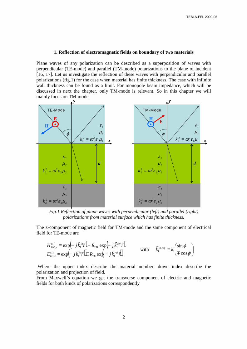
1. Reflection of electromagnetic fields on boundary of two materials
Plane waves of any polarization can be described as a superposition of waves with perpendicular (TE-mode) and parallel (TM-mode) polarizations to the plane of incident [16, 17]. Let us investigate the reflection of these waves with perpendicular and parallel polarizations (fig.1) for the case when material has finite thickness. The case with infinite wall thickness can be found as a limit. For monopole beam impedance, which will be discussed in next the chapter, only TM-mode is relevant. So in this chapter we will mainly focus on TM-mode.
x
ϕ
EH
1122
1
1
1
µεωµε
=k
TM-Mode
3322
3
3
3
µεωµε
=k
2222
2
2
2
µεωµε
=k
d
y
x
ϕ11
221
1
1
µεωµε
=k
TE-Mode
3322
3
3
3
µεωµε
=k
2222
2
2
2
µεωµε
=k
d
y
H
E
x
ϕ
EH
1122
1
1
1
µεωµε
=k
TM-Mode
3322
3
3
3
µεωµε
=k
2222
2
2
2
µεωµε
=k
d
y
x
ϕ
EH
1122
1
1
1
µεωµε
=k
TM-Mode
3322
3
3
3
µεωµε
=k
2222
2
2
2
µεωµε
=k
d
x
ϕ
EH
1122
1
1
1
µεωµε
=k
TM-Mode
3322
3
3
3
µεωµε
=k
2222
2
2
2
µεωµε
=k
d
2222
2
2
2
µεωµε
=k
dd
yy
x
ϕ11
221
1
1
µεωµε
=k
TE-Mode
3322
3
3
3
µεωµε
=k
2222
2
2
2
µεωµε
=k
d
y
H
E
x
ϕ11
221
1
1
µεωµε
=k
TE-Mode
3322
3
3
3
µεωµε
=k
2222
2
2
2
µεωµε
=k
d
2222
2
2
2
µεωµε
=k
dd
yy
H
E
H
E
Fig.1 Reflection of plane waves with perpendicular (left) and parallel (right)
polarizations from material surface which has finite thickness. The z-component of magnetic field for TM-mode and the same component of electrical field for TE-mode are
( ) ( )
( ) ( )rkjRrkjE
rkjRrkjH
refTE
inzTE
refTM
inzTM
rrrr
rrrr
11)1(,
11)1(
,
expexp
expexp
−+−=
−−−= with
=
ϕϕ
cos
sin1
,1
m
rkk refin
Where the upper index describe the material number, down index describe the polarization and projection of field. From Maxwell’s equation we get the transverse component of electric and magnetic fields for both kinds of polarizations correspondently
TESLA-FEL 2009-05
3
( ) ( )( )
( ) ( )( )rkjRrkjj
jk
y
E
jH
rkjRrkjj
jk
y
H
jE
refTE
inzTExTE
refTM
inzTMxTM
rrrr
rrrr
111
1)1(,
1
)1(,
111
1)1(
,
1
)1(,
expexpcos1
expexpcos1
−−−=∂
∂−=
−+−=∂
∂=
ωεϕ
ωµ
ωεϕ
ωε
By using the view of field components we can easily find the surface impedance
TE
TE
xTE
zTETE
TM
TM
zTM
xTMTM
R
R
kyxH
yxEZ
R
Rk
yxH
yxEZ
−+=
==
=
−+=
==
=
11
cos)0,(
)0,(),(
1
1cos
)0,(
)0,(),(
1
1)1(,
)1(,)1(
1
1)1(
,
)1(,)1(
ϕωµϕω
ωεϕϕω
Where TMr and TEr are the reflection coefficients. Taking to account the wave vector view
εµω=k for surface impedance we get
TETM
TETMTETM R
RZ
,
,
1
11)1(, 1
1][cos),(
−+
= ±
εµϕϕω (1)
The refracted wave field components for TM mode are
( ) ( )( ) ( )[ ]rkjbrkja
kE
rkjbrkjaH
refTM
inTM
yxTM
refTM
inTMzTM
rrrr
rrrr
222
2,)2(,
22)2(,
expexp
expexp
−+−=
−−−=
ωε with
=
y
xrefin
k
kk
,2
,2,2
m
r
And for TE mode
( ) ( )( ) ( )[ ]rkjbrkja
kH
rkjbrkjaE
refTE
inTE
yxTE
refTE
inTEzTE
rrrr
rrrr
222
2,)2(,
22)2(,
expexp
expexp
−+−=
−−−=
ωµ
For surface impedance we get
TE
TE
yxTE
zTEaTE
TM
TMy
zTM
xTMaTM
t
t
kyxH
yxEZ
t
tk
yxH
yxEZ
+−=
==
=
+−=
==
=
11
)0,(
)0,(),(
1
1
)0,(
)0,(),(
2,
2)2(,
)2(,)2(
2
2,)2(,
)2(,)2(
ωµϕω
ωεϕω
where TETMTETMTETM abt ,,, /= (2)
where the upper index (2a) shows the first boundary of second material.
TESLA-FEL 2009-05
4
Taking into account the boundary conditions which leads to have continuous tangential component of wave vector ϕsin11,2,3, kkkk xxx ≡==
Using next relation of wave vectors between two medias
εµµε ′′
=′
k
k (3)
We can easily find next result
TE
TE
TE
TEaTE
TM
TM
TM
TMaTM
t
t
t
t
kkZ
t
t
t
tkkZ
+−=
+−
−=
+−=
+−−
=
1
11
1
1
sin),(
11
11sin
),(
22
2
221
22
2)2(
22
2
2
221
22)2(
αεµ
ϕωµϕω
αεµ
ωεϕϕω
Where
ϕµεµεα 2
22
112 sin1−≡
For the second boundary the surface impedance reads
2,
2,
2,
2,1
22
2)2(
,,
)2(,,)2(
,1
1
),(
),(),(
y
y
dkjTETM
dkjTETM
zTETM
xTETMbTETM
et
et
dyxH
dyxEZ
+−
=−=−=
= ±αεµϕω (4)
For third material the field components for TM mode are
( )( )rkj
kg
y
H
jE
rkjgH
yTM
zTMxTM
TMzTM
rr
rr
33
3,)3(,
3
)3(,
3)3(,
exp1
exp
−=∂
∂=
−=
ωεωε
where
−=
y
x
k
kk
,3
,3
3
r
And for TE mode we have
( )( )rkj
kgH
rkjgE
yTExTE
TEzTE
rr
rr
33
3,)3(,
3)3(,
exp
exp
−=
−=
ωµ
And for surface impedance we get next result correspondently
TESLA-FEL 2009-05
5
ϕωµωµϕω
ωεϕ
ωεϕω
221
23
3
3,
3)3(,
)3(,)3(
3
221
23
3
3,)3(,
)3(,)3(
sin),(
),(),(
sin
),(
),(),(
kkkdyxH
dyxEZ
kkk
dyxH
dyxEZ
yxTE
zTETE
y
zTM
xTMTM
−==
−=−=
=
−==
−=−=
=
where d is thickness of material. Using next notation
ϕµεµεα 2
33
113 sin1−≡
and equation (3) we get
13
3
3)3(, ),( ±= α
εµϕωTETMZ (5)
In the case when 113,23,2 εµεµ >> the 13,2 ≈α approximation is valid. Now by matching
the impedances ),()3(, ϕωTETMZ with ),()2(
, ϕωbTETMZ we find the unknown coefficients TMt and
TEt correspondently
2,2
,
,, 1
1ydkj
TETM
TETMTETM e
A
At −
+−
= where ),()3(1
2
2, ϕωα
µε
TETETM ZA m≡ (6)
By matching ),()2(, ϕωaTETMZ with ),()1(
, ϕωTETMZ we find the reflection coefficients for both
polarized fields independently
1
1),(
,
,, +
−=
TETM
TETMTETM u
uR ϕω with
ϕεµ
ϕω
ϕϕω
εµ
cos/
),(
cos),(
/
11
)2(
)2(11
aTE
TE
aTM
TM
Zu
Zu
≡
≡
In the case when the third material is perfect conductor 0),()3( ≈ϕωZ for surface impedance formula is simplified
)tan()tanh(),(
)tan()tanh(),(
2,2,
22,
2,
2)2(
2,2
2,2,
2
2,)2(
yy
yy
aTE
yy
yya
TM
dkk
jjdkk
Z
dkk
jjdkk
Z
ωµωµϕω
ωεωεϕω
=≈
=≈ (7)
Where the y-component of wave vector in second material has the next view
TESLA-FEL 2009-05
6
ϕµεµεω 211222, sin−=yk
In thin oxide depth (d<<1) limit surface impedances will reads
djZ
djZ
aTE
aTM
2)2(
2
21122)2(
),(
sin),(
ωµϕωε
ϕµεµεωϕω
≈
−≈
For non-magnetic materials this formula is simplified
Where εr is relative dielectric permeability. For incident angle 2/πϕ = we get
djZ
djZ
aTE
r
raTM
0)2(
2,
2,0
)2(
)2/,(
1)2/,(
ωµπω
εε
ωµπω
=
−=
Let rewrite this equations in next form
Since the units of parameters TETML , are the same as for inductance, the thin dielectric
coating impact on beam impedance can be considered as influence of inductor impedance. In the case when the third material is not perfect conductor in most practical cases the
1133 εµεµ >> is fulfilled and the surface impedance for both kind of modes are equal
and reads as
)()()()( 0
3
3)3()3()3(
ωκωµ
εµωωω j
ZZZ TETM ≈=≡=
Where ωτ
κωκj+
=1
)( 0 is conductivity of conductor with τ - relaxation time.
djZ
djZ
aTE
r
raTM
0)2(
2,
22,
0)2(
),(
sin),(
ωµϕω
εϕε
ωµϕω
=
−=
dLLjZ
dLLjZ
TETEa
TE
r
rTMTM
aTM
0)2(
2,
22,
0)2(
)(
sin)(),(
µωω
εϕε
µϕωϕω
≡=
−≡=
(8)
TESLA-FEL 2009-05

7
Taking into account notation in eq.(6) after some manipulations for surface impedance on boundary between vacuum and first material we get
TEyTE
y
yy
y
aTE
TMyTM
yyy
yaTM
AdkjA
dk
kdkj
kZ
AdkjA
dkkdkj
kZ
)tan(1
1)(tan)tan(),(
)tan(1
1)(tan)tan(),(
2,
2,2
2,
22,
2,
2)2(
2,
2,2
2
2,2,
2
2,)2(
++
+=
++
+=
ωµωµϕω
ωεωεϕω
(9)
The coefficients TETMA , we right in next form
)(
)(
)3(
2
2,
)3(
2,
2
ωωµ
ωωε
Zk
A
Zk
A
yTE
yTM
=
=
For thin dielectric (d<<1) the asymptotic formula will reads
dj
ZdjZ
Zdj
ZdjZ
aTE
r
raTM
2
21122
)3(
2)2(
)3(2
)3(
2,
22,
0)2(
sin1
)(),(
)(1)(sin
),(
µϕµεµεω
ωωµϕω
ωωεω
εϕε
ωµϕω
−++=
++
−=
Finally taking into account notations in eq.(7) and smallness of dielectric layer thickness we get )(),(),( ,
)2(, ωϕωϕω κZZZ L
TETMa
TETM +≈ (10)
Where meaning of the indexes L and κ are inductor and conductor correspondently.
2. Beam Impedance
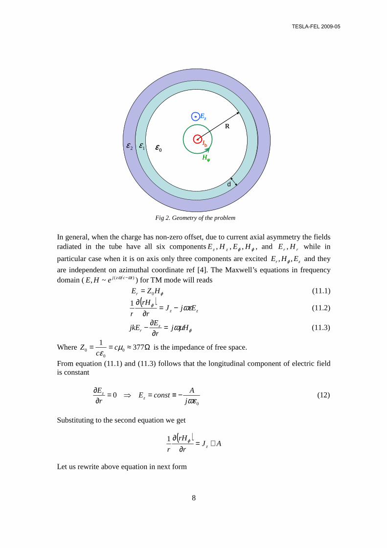
Consider the relativistic point chargeQ moving with speed of light along the z axis of uniform, circular-cylindrical two-layer tube of inner radius R (Fig.2). The charge distribution is then given by )()()(),,( vtzrQzrQ −= δϕδδϕ . The second layer has infinite thickness while the thickness of first one isd .
The cross section of the tube is divided into three concentric regions: 1) Rr ≤≤0 (vacuum), 2) dRrR +≤≤ (first layer), 3) ∞<≤+ rdR (second layer).
TESLA-FEL 2009-05
8
R
Hφ
Ib
Ez
d
0ε1ε2ε
R
Hφ
Ib
Ez
d
0ε1ε2ε
Fig 2. Geometry of the problem
In general, when the charge has non-zero offset, due to current axial asymmetry the fields radiated in the tube have all six components zz HE , , ϕϕ HE , , and rr HE , while in
particular case when it is on axis only three components are excited zr EHE ,, ϕ and they
are independent on azimuthal coordinate ref [4]. The Maxwell’s equations in frequency domain ( )(~, tczjeHE ωω − ) for TM mode will reads
ϕHZEr 0= (11.1)
( )
zz EjJr
rH
rωεϕ −=
∂∂1
(11.2)
ϕωµHjr
EjkE z
r =∂
∂− (11.3)
Where Ω≈== 3771
00
0 µε
cc
Z is the impedance of free space.
From equation (11.1) and (11.3) follows that the longitudinal component of electric field is constant
0
0ωεj
AconstE
r
Ez
z −≡=⇒=∂
∂ (12)
Substituting to the second equation we get
( )AJ
r
rH
r z +=∂
∂ ϕ1
Let us rewrite above equation in next form
TESLA-FEL 2009-05
9
( )
ArrJr
rHz +=
∂∂ ϕ (13)
Taking into account the relation between current and current density
∫∫∫ == drdrJdSJIS
ϕ
The integration of equation (13) gives
ππ ϕ 22
22r
AIrH +=
And for azimuthal component of magnetic field we get
22r
Ar
IH +=
πϕ
Finally all components of EM field will read
−
−
−
−=
+=
+=
tzc
j
z
tzc
j
r
tzc
j
ej
AE
er
Ar
IZE
er
Ar
IH
ωω
ωω
ωω
ϕ
ωε
π
π
0
0 22
22
(14)
The beam impedance will be
0→
=r
zb I
EZ
The unknown coefficient A should be found from boundary condition.
Rr
zs H
EZ
=
=ϕ
The surface impedance on first boundary could be found using matching technique. In terms of surface impedance for this coefficient it is easy to get following expression
TESLA-FEL 2009-05
10
0
0
21
12
Z
ZR
cjR
ZIjA
s
s
ωπωε
+⋅−=
Finally for beam impedance we get
Where surface impedance can be found using the formulas derived in previous chapter where should be taken into account that the electromagnetic field excited by ultra-relativistic charge has only transverse components which leads of 2/πϕ = incident angle.
)()()( ωωω κs
Lss ZZZ +≈ where
)()(
)(
0
ωκωµω
ωω
κ jZ
LjZ
s
Ls
=
= with
ωτκωκ
εεµ
j
dLr
r
+=
−=
1)(
1
0
0
This formula coincides with thin coating asymptotic limit of exact solution for beam impedance of two layer tube derived in ref [10,12].
3. Numerical results In this section we present results of influence of thin oxide layer on loss factor and energy spread. Wake potential of a Gaussian bunch with mb µσ 25= rms length was calculated
for aluminium ( s1570 101.7,1072.3 −⋅=Ω⋅= τκ ) beam pipe with 5mm radius. To evaluate
loss factor and energy spread next formulas have been used
∫
∫><−=>><−<=
>==<
dsλ(s))W(W(s))W(WspreadEnergy
λ(s)W(s)Wfactor Loss
22
ds
Where )(sW is a wake potential and
−= 2
2
2exp
2
1)(
bb
ss
σσπλ is a normalized Gaussian
distribution function.
021
12
Z
ZR
cjR
ZZ
s
sb ωπ +
⋅=
TESLA-FEL 2009-05
11
a)
2=rε
10=rε
5=rε
Los
s fa
cto
r [
V/p
C/m
]
Oxide thickness [ nm ]
2=rε
10=rε
5=rε
Los
s fa
cto
r [
V/p
C/m
]
Oxide thickness [ nm ] b)
En
erg
y sp
read
[V
/pC
/m]
Oxide thickness [nm]
2=rε
10=rε
5=rε
En
erg
y sp
read
[V
/pC
/m]
Oxide thickness [nm]
2=rε
10=rε
5=rε
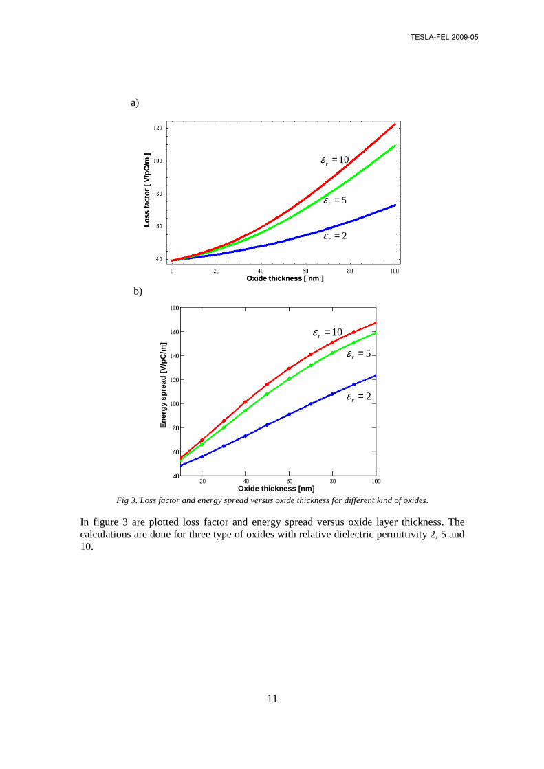
Fig 3. Loss factor and energy spread versus oxide thickness for different kind of oxides.
In figure 3 are plotted loss factor and energy spread versus oxide layer thickness. The calculations are done for three type of oxides with relative dielectric permittivity 2, 5 and 10.
TESLA-FEL 2009-05
12
a)
∆=10 nm
∆=20 nm
∆=30 nm
∆=40 nm
∆=50 nmL
oss
fac
tor
[ V
/pC
/m]
Oxide εr
∆=10 nm
∆=20 nm
∆=30 nm
∆=40 nm
∆=50 nmL
oss
fac
tor
[ V
/pC
/m]
Oxide εr b)
En
erg
y sp
read
[V
/pC
/m]
∆=10 nm
∆=20 nm
∆=30 nm
∆=40 nm
∆=50 nm
Oxide εr
En
erg
y sp
read
[V
/pC
/m]
∆=10 nm
∆=20 nm
∆=30 nm
∆=40 nm
∆=50 nm
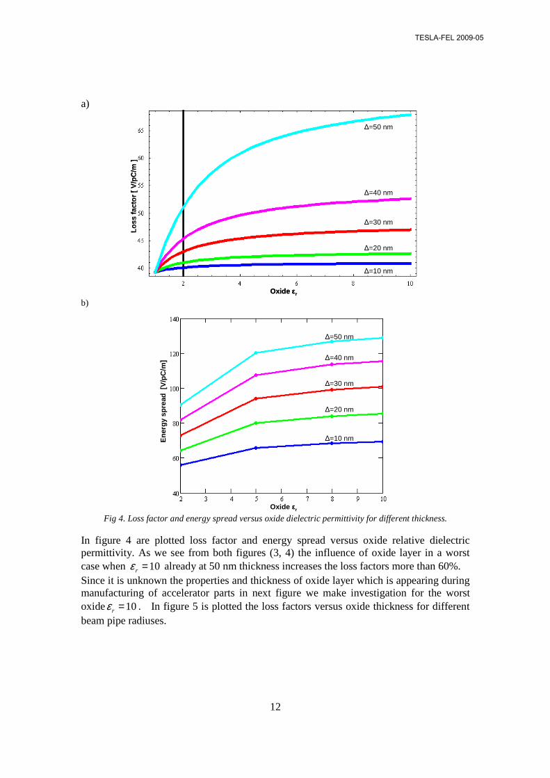
Oxide εr Fig 4. Loss factor and energy spread versus oxide dielectric permittivity for different thickness.
In figure 4 are plotted loss factor and energy spread versus oxide relative dielectric permittivity. As we see from both figures (3, 4) the influence of oxide layer in a worst case when 10=rε already at 50 nm thickness increases the loss factors more than 60%. Since it is unknown the properties and thickness of oxide layer which is appearing during manufacturing of accelerator parts in next figure we make investigation for the worst oxide 10=rε . In figure 5 is plotted the loss factors versus oxide thickness for different beam pipe radiuses.
TESLA-FEL 2009-05
13
a)
R=2mm
R=4mm
R=6mm
R=8mm
R=10mmLo
ss f
acto
r [
V/p
C/m
]
Oxide thickness [ nm ]
R=2mm
R=4mm
R=6mm
R=8mm
R=10mmLo
ss f
acto
r [
V/p
C/m
]
Oxide thickness [ nm ] b)
R=2mm
R=4mm
R=6mm
R=8mm
R=10mm
En
erg
y sp
read
[V
/pC
/m]
Oxide thickness [nm]
R=2mm
R=4mm
R=6mm
R=8mm
R=10mm
En
erg
y sp
read
[V
/pC
/m]
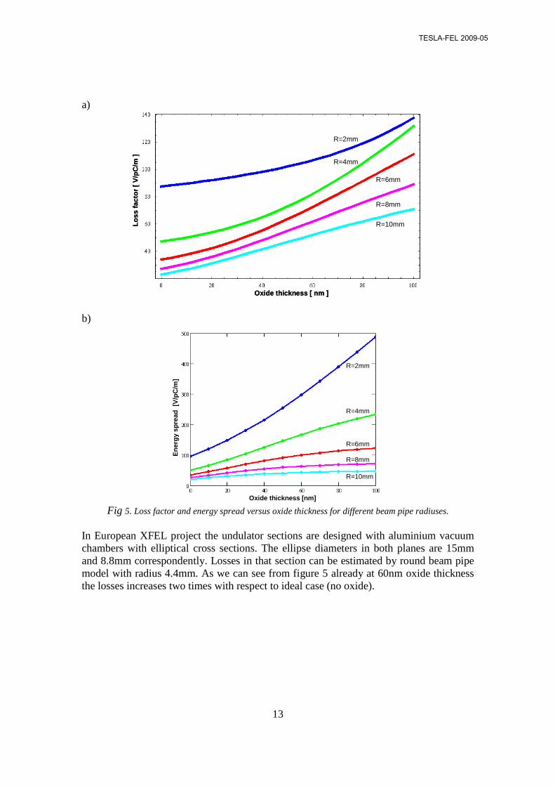
Oxide thickness [nm] Fig 5. Loss factor and energy spread versus oxide thickness for different beam pipe radiuses.
In European XFEL project the undulator sections are designed with aluminium vacuum chambers with elliptical cross sections. The ellipse diameters in both planes are 15mm and 8.8mm correspondently. Losses in that section can be estimated by round beam pipe model with radius 4.4mm. As we can see from figure 5 already at 60nm oxide thickness the losses increases two times with respect to ideal case (no oxide).
TESLA-FEL 2009-05
14
References
1. B.W.Zotter and S.A.Kheifetz, Impedances and Wakes in High-Energy Particle Accelerators (World Scientific, Singapore, 1997).
2. H. Henke and O. Napoly, in Proceedings of the Second European Particle Accelerator Conference, Nice, France, 1990 (Editions Frontiers, Gif-sur-Yvette, 1991), pp. 1046–1048.
3. A. Piwinski, IEEE Trans. Nucl. Sci. 24, 1364 (1977). 4. A. Piwinski, Report No. DESY-94-068, 1994, p. 23. 5. A.W. Chao, Technical Report No. 2946, SLAC-PUB, 1982; see also A.W. Chao,
Physics of Collective Beam Instabilities in High Energy Accelerators (Wiley, New York, 1993).
6. B. Zotter, Part. Accel. 1, 311 (1970). 7. D. Jackson, SSCL Report No. SSC-N-110, 1986. 8. M. Ivanyan and V. Tsakanov, Phys. Rev. ST Accel. Beams 7, 114402 (2004). 9. A.M. Al-khateeb, R.W. Hasse, O. Boine-Frankenheim, W.M. Daga and I.
Hofmann, Phys. Rev. ST Accel. Beams, 10, 064401 (2007). 10. M. Ivanyan and V. Tsakanian, Phys. Rev. ST Accel. Beams, 9, 034404 (2006). 11. N. Wang and Q. Qin, Phys. Rev. ST Accel. Beams, 10, 111003 (2007). 12. M. Ivanyan et al, Phys.Rev.ST Accel.Beams 11, 084001 (2008). 13. A. Burov and A. Novokhatskii, INP-Novosibirsk, Report No. 90-28, 1990. 14. A. Tsakanian, M. Ivanyan, J. Rossbach, EPAC08-TUPP076, Jun 24, 2008. 15. M.Altarelli, R.Brinkmann et al (editors), XFEL. The European X-Ray Free-
Electron Laser, DESY 2006-097, July 2006. 16. R. E. Collin, “Foundation for Microwave Engineering”, McGraw-Hill, 1966. 17. M. Born, E. Wolf, Principles of Optics,(1986)
TESLA-FEL 2009-05