System level DSP synthesis using voltage overscaling, unequal error protection & adaptive quality...
6
SYSTEM LEVEL DSP SYNTHESIS USING VOLTAGE OVERSCALING, UNEQUAL ERROR PROTECTION & ADAPTIVE QUALITY TUNING Georgios Karakonstantis, Debabrata Mohapatra and Kaushik Roy EeE School, Purdue University, West Lafayette, IN - 47907 {gkarakon, dmohapat, kaushik}@purdue.edu ABSTRACT In this paper, we propose a system level design approach considering voltage over-scaling (VaS) that achieves error resiliency using unequal error protection of different computation elements, while incurring minor quality degradation. Depending on user specifications and severity of process variations/channel noise, the degree of vas in each block of the system is adaptively tuned to ensure minimum system power while providing "just-the- right" amount of quality and robustness. This is achieved, by taking into consideration system level interactions and ensuring that under any change of operating conditions only the "less- crucial" computations, that contribute less to block/system output quality, are affected. The design methodology applied to a DCT/IDCT system shows large power benefits (up to 69%) at reasonable image quality while tolerating errors induced by varying operating conditions (VaS, process variations, channel noise). Interestingly, the proposed IDCT scheme conceals channel noise at scaled voltages. Index Terms - Low power, error resilient, supply voltage scaling 1. INTRODUCTION Miniaturization of devices has resulted in the integration of numerous complex and power hungry processing units on a single portable device, constrained mainly by limited battery lifetime. Due to quadratic dependence of power on voltage, supply voltage over-scaling (VaS) has been investigated as an effective method to reduce power [1]. However, vas increases the delays in all computation paths and can result in incorrect or incomplete computation of certain paths. Besides power consumption, process variations also pose major design concern with technology scaling, resulting in delay errors [2]. Conventional wisdom dictates up- scaling the supply voltage or logic gate up-sizing to prevent delay errors and to achieve higher parametric yield. However, such techniques come at a cost of increased power and/or die area. Hence, meeting the contradictory requirements of high yield (in presence of unreliable components), low power and high quality is becoming exceedingly challenging in nanometer designs. A methodology that jointly addresses the issues of low power and error resiliency in digital signal processing (DSP) blocks have been proposed in [3]. The methodology in [3] ensures tolerance to delay errors, utilizing the concept of unequal error protection. By protecting the "crucial" computations (more contributive to output quality) through algorithm/architecture co-design, low power at minor quality degradation is achieved. This methodology has proven to be efficient for the design of individual blocks, by being able to tolerate errors due to VaS/process variations. However, when these blocks are integrated in a system, then the interactions between the individual blocks have to be considered. First, we observe that lower power or good quality for an individual block 978-1-4244-4335-2/09/$25.00 ©2009 IEEE 133 does not necessarily translate to lowest power or best quality for the overall system. Interestingly, while some blocks may operate at lower power and achieve "good" block level quality, subsequent blocks might still be consuming higher power without improving the system quality. This can be due to fact that they are performing "redundant" computations based on VaS-affected incorrect outputs (albeit "less crucial one") of preceding blocks. These computations can be thought of as "redundant" or "less-crucial" for subsequent blocks as they unnecessarily increase system power without improving the overall quality. Second, depending on dynamically changing system/user requirements and operating conditions (process variations, channel noise), the best quality may not always be desired or achievable. In this paper, we propose a system level design approach considering vas that achieves error resiliency, using unequal error protection of different computation elements, while incurring minor quality degradation. By taking into account system level interactions, the proposed approach provides the "right" amount of quality at the right amount of power consumption (by configuring the degree of VaS). Specifically, depending on power, user quality requirements and severity of process variations/channel noise, the degree of vas for each block is adaptively tuned to ensure minimum system power while providing "just-the-right" amount of quality and robustness. This is achieved by guaranteeing that the delay errors due to vas affect only the less-crucial (redundant) computations of the block (system) by efficient algorithmic/ architectural modifications. The proposed approach is applied to system level joint design of a DCT/IDCT system which is ubiquitous in multimedia applications (JPEG, MPEG, digital cameras). Our contributions in this paper can be summarized as: 1) Considering vas based DCT implementation we design a voltage scalable and robust IDCT by accounting for system level interactions in DCT/IDCT system. 2) We identify crucial/less-crucial computations for maintaining high output image quality in IDCT. The IDCT coefficients are modified such that only the less-crucial IDCT computations (based on potentially incorrect DCT outputs) are affected under vas (unequal error protection for different computation elements). This avoids any unnecessary power increase while ensuring minimal quality degradation ofIDCT as well as DCT/IDCT system. 3) Adaptively tune degree of vas for each block (DCT, IDCT) for achieving minimum system power in the presence of process variations/channel noise, meeting user specifications by using unequal error protection, unlike existing implementations [4,5,6]. 4) The proposed IDCT architecture, inherently conceals channel noise at scaled Vdd' s during transmission over noisy channel. The rest of this paper is organized as follows. In section 2 the proposed approach is explained. In section 3 the basics of IDCT are explained along with implementation details. Section 4 SiPS 2009 Authorized licensed use limited to: Purdue University. Downloaded on February 10, 2010 at 16:04 from IEEE Xplore. Restrictions apply.
-
Upload
independent -
Category
Documents
-
view
0 -
download
0
Transcript of System level DSP synthesis using voltage overscaling, unequal error protection & adaptive quality...
SYSTEM LEVEL DSP SYNTHESIS USING VOLTAGE OVERSCALING,UNEQUAL ERROR PROTECTION & ADAPTIVE QUALITY TUNING
Georgios Karakonstantis, Debabrata Mohapatra and Kaushik RoyEeE School, Purdue University, West Lafayette, IN - 47907
{gkarakon, dmohapat, kaushik}@purdue.edu
ABSTRACT
In this paper, we propose a system level design approachconsidering voltage over-scaling (VaS) that achieves errorresiliency using unequal error protection of different computationelements, while incurring minor quality degradation. Depending onuser specifications and severity of process variations/channelnoise, the degree of vas in each block of the system is adaptivelytuned to ensure minimum system power while providing "just-theright" amount of quality and robustness. This is achieved, bytaking into consideration system level interactions and ensuringthat under any change of operating conditions only the "lesscrucial" computations, that contribute less to block/system outputquality, are affected. The design methodology applied to aDCT/IDCT system shows large power benefits (up to 69%) atreasonable image quality while tolerating errors induced byvarying operating conditions (VaS, process variations, channelnoise). Interestingly, the proposed IDCT scheme conceals channelnoise at scaled voltages.
Index Terms - Low power, error resilient, supply voltage scaling
1. INTRODUCTION
Miniaturization of devices has resulted in the integration ofnumerous complex and power hungry processing units on a singleportable device, constrained mainly by limited battery lifetime.Due to quadratic dependence of power on voltage, supply voltageover-scaling (VaS) has been investigated as an effective method toreduce power [1]. However, vas increases the delays in allcomputation paths and can result in incorrect or incompletecomputation of certain paths. Besides power consumption, processvariations also pose major design concern with technology scaling,resulting in delay errors [2]. Conventional wisdom dictates upscaling the supply voltage or logic gate up-sizing to prevent delayerrors and to achieve higher parametric yield. However, suchtechniques come at a cost of increased power and/or die area.Hence, meeting the contradictory requirements of high yield (inpresence of unreliable components), low power and high quality isbecoming exceedingly challenging in nanometer designs.
A methodology that jointly addresses the issues of low powerand error resiliency in digital signal processing (DSP) blocks havebeen proposed in [3]. The methodology in [3] ensures tolerance todelay errors, utilizing the concept of unequal error protection. Byprotecting the "crucial" computations (more contributive to outputquality) through algorithm/architecture co-design, low power atminor quality degradation is achieved. This methodology hasproven to be efficient for the design of individual blocks, by beingable to tolerate errors due to VaS/process variations. However,when these blocks are integrated in a system, then the interactionsbetween the individual blocks have to be considered. First, weobserve that lower power or good quality for an individual block
978-1-4244-4335-2/09/$25.00 ©2009 IEEE 133
does not necessarily translate to lowest power or best quality forthe overall system. Interestingly, while some blocks may operate atlower power and achieve "good" block level quality, subsequentblocks might still be consuming higher power without improvingthe system quality. This can be due to fact that they are performing"redundant" computations based on VaS-affected incorrectoutputs (albeit "less crucial one") of preceding blocks. Thesecomputations can be thought of as "redundant" or "less-crucial"for subsequent blocks as they unnecessarily increase system powerwithout improving the overall quality. Second, depending ondynamically changing system/user requirements and operatingconditions (process variations, channel noise), the best quality maynot always be desired or achievable.
In this paper, we propose a system level design approachconsidering vas that achieves error resiliency, using unequal errorprotection of different computation elements, while incurringminor quality degradation. By taking into account system levelinteractions, the proposed approach provides the "right" amount ofquality at the right amount of power consumption (by configuringthe degree of VaS). Specifically, depending on power, user qualityrequirements and severity of process variations/channel noise, thedegree of vas for each block is adaptively tuned to ensureminimum system power while providing "just-the-right" amount ofquality and robustness. This is achieved by guaranteeing that thedelay errors due to vas affect only the less-crucial (redundant)computations of the block (system) by efficientalgorithmic/architectural modifications.
The proposed approach is applied to system level joint design ofa DCT/IDCT system which is ubiquitous in multimediaapplications (JPEG, MPEG, digital cameras). Our contributions inthis paper can be summarized as:
1) Considering vas based DCT implementation we design avoltage scalable and robust IDCT by accounting for system levelinteractions in DCT/IDCT system.
2) We identify crucial/less-crucial computations for maintaininghigh output image quality in IDCT. The IDCT coefficients aremodified such that only the less-crucial IDCT computations (basedon potentially incorrect DCT outputs) are affected under vas(unequal error protection for different computation elements). Thisavoids any unnecessary power increase while ensuring minimalquality degradation ofIDCT as well as DCT/IDCT system.
3) Adaptively tune degree of vas for each block (DCT, IDCT)for achieving minimum system power in the presence of processvariations/channel noise, meeting user specifications by usingunequal error protection, unlike existing implementations [4,5,6].
4) The proposed IDCT architecture, inherently conceals channelnoise at scaled Vdd' s during transmission over noisy channel.The rest of this paper is organized as follows. In section 2 the
proposed approach is explained. In section 3 the basics of IDCTare explained along with implementation details. Section 4
SiPS 2009
Authorized licensed use limited to: Purdue University. Downloaded on February 10, 2010 at 16:04 from IEEE Xplore. Restrictions apply.
2. DESIGN STRATEGY
discusses the system level design for power awareness and errortolerance. Finally, conclusions are drawn in section 5.
minimize Ps(Vdd A,Vdd B ) = PA(VddA)+PB (Vdd B ) (1)
subject to Q Sys;::: QDES
where QSYS can be expressed in terms of system Signal-to-noise
ratio (SNR) : (jSIG2
(2)QSYS = l Olog., ---2
(j~SYS
In eq. 2, aSIG2 and a~SYS2 are the power of error free system outputand system vas noise power, respectively. Using eq . 2, theconstraint in eq. 1 can be written as:
User l'ower.Quality Req uiremen t
... - - - - - - - - ~ - - - - - .- -... Process Variations: Energy-Process-Quality :<---;I Awarc Co ntro llcr )<- - - ~ ~ Ilalter)' I.if<
_ J , -__ J
3. DCTIIDCT DESIGN
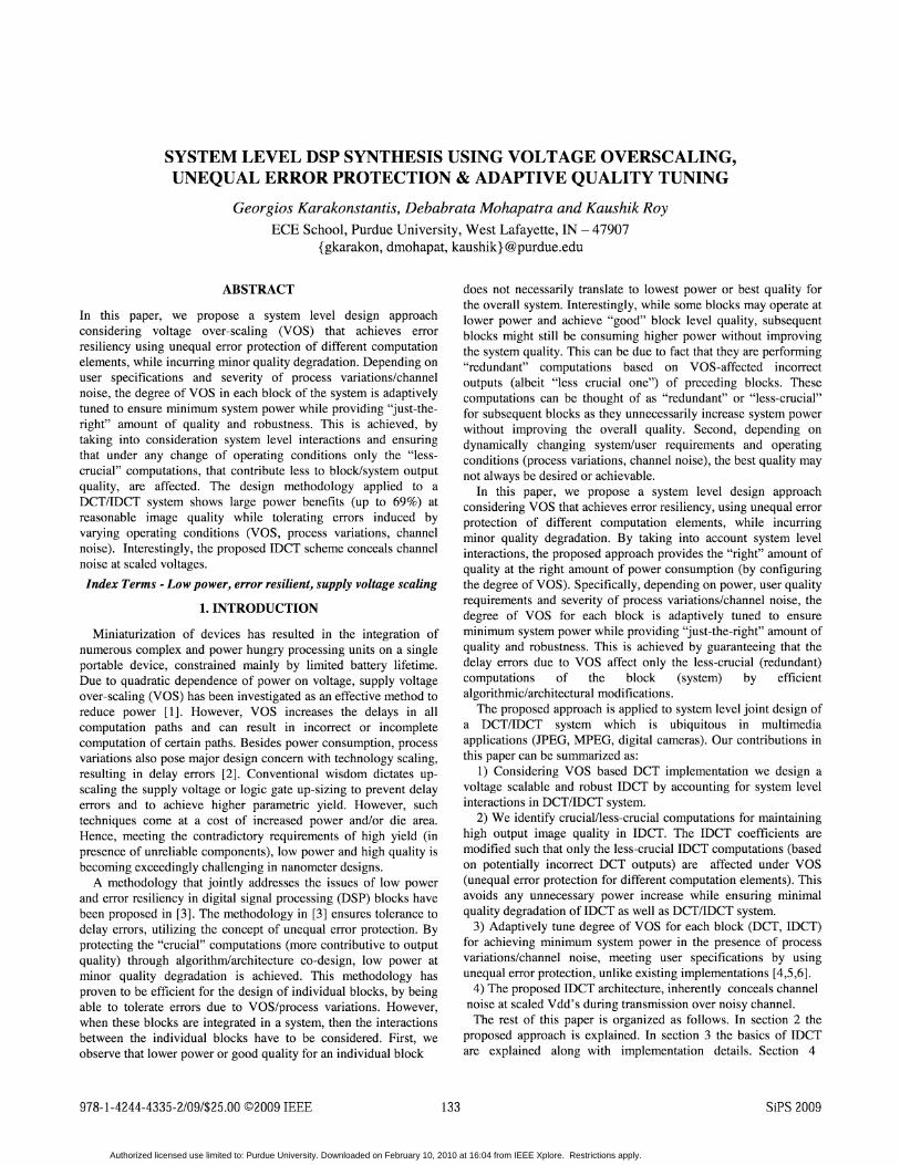
Figure 1: Power and Process Aware System Design
blocks A and B. The noise power due to vas error of A (/'fA) andvas error of B (/'f8) are denoted by a~A2 and a~B2 respectively.Since output of block B depends on output of block A (Fig . 1),they are dependent and hence the inter-dependencies between theerrors of the blocks have to be considered in evaluating a~SYS2.
Hence, a joint design of blocks A, B is necessary for meeting theconstraint given in eq. 1.
In eq. 3, a~SYS2 is shown to be a function of a~A2 and a~l as
system noise power depends on individual block noise power.Since noise power due to vas of a block is directly related to itsVdd, a~A2 and a~l (hence a~SYS2) can be modulated by tuningVdd; and Vddj, respectively. By configuring Vdd; and Vdd B, thesystem quality degradation due to vas (reflected in a~SYS2) can becontrolled such that eq. 3 is satisfied providing the "right" amountquality at minimal power consumption. The above design strategyis applied to a DCT/IDCT system, analyzed in the next section.
3.2. Voltage scalable and error resilient DCT
We can observe from eqs. 6 and 7 that ID-IDCT takes as inputeach output row of DCT (eq. 1: CTZT) denoted by ZO-Z7' Input Zo isthe DC coefficient that contains the low frequencies of an 8x8
We apply the proposed approach to the design of voltage overscalable OCT/IDCT system, widely used in multimediaapplications [4,5,6]. Based on interactions with a DCTarchitecture, we design a voltage scalable and robust IDCT thatperforms system level adaptive quality modulation for minimizingsystem power, utilizing the concept of unequal error protection.
3.1. Conventional mCT
Conventionally, IDCT transforms an NxN block (output ofDCT) from frequency domain to spatial domain and in matrixnotation it can be expressed as: X=CTZC, where C is thecoefficient matrix and Z is the input NxN block that contains theDCT outputs. Using row-column decomposition, IDCT can bedecomposed into two ID-IDCT units, which can be expressed as:
X=C T(CTZ? (4)In such an implementation, the ID-IDCT is applied to each row ofinput data and the result is transposed. A second ID-IDCT isapplied to the rows of the transposed data to obtain IDCT (eq . 4).The 1D-IDCT output of a row in 8x8 block is expressed as:
7 c ( k ) ( 2i + l)k1l' ) . (5)Wi = L --z(k) cos , 1= 0 ,1,2, .. . ,7
k =O 2 16
c(O)=lI.J2, c(k) = 1 if k l' 0
Setting ck=cos(k7C/16), a=c), b=c2> C=C3, d=C4, e=cS,/=C6' g=C 7
and [e:;]lo~ti n[~ sJm~tI ]Of[~i t]h:[lr~~~: _;a]n [b~: w] ritten as [;::
Wz d - f -d b Z4 e -ag e ZsW3 d -b d - f Z6 g -e c - a Z7
[ :~ ] = [~ J -ff~ ] [ ~~ ] _ [ ~ -~ -~ -~ ] [ ~~ ] (7)Ws d - f -d b Z4 e -age ZsW4 d -b d - f Z6 g -e c -a Z7
(3)2
aT/Sys'(a~/(VddA),a~B2(VddB)):'> ~SIG 11 010 DES
where a~SYS2 can be expressed in terms of vas error power of
To elucidate our design approach let us consider an examplewhere a system consists of processing blocks A and B (Fig . 1).The outputs of block A are denoted as ZAb ZA2, ZA3 while that ofblock B is YB=/ (ZAJ,ZA2,ZA3)' As mentioned earlier, vas in blockA would lead to an increase in path delays resulting in somecomputations not being completed within the specified targetdelay. Recent approach in [3] addresses the quality degradation inconventional design under vas by utilizing the concept ofcrucial/less-crucial computations. It identifies block specificcomputations as crucial and less-crucial and ensures that undervas only the less-crucial computations get affected, leading tominimal quality degradation.
Let us assume that block A is designed using such amethodology in which outputs ZAb ZA2 are associated with crucialcomputations, whereas ZA3 is with less-crucial ones. The designensures that under any delay errors due to vas only ZA3 is affectedso that "reasonable" quality is retained. In that case the outputs ofblock A (A(x» which are fed as inputs to block B can be writtenas: A(x) = S+ /'fA , where s is the error free output of A and /'fA is thevas error in A due to the incomplete computation of ZA3'Depending on the computations in each block, such error (/'fA) maydegrade the output quality while causing subsequent blocks toconsume unnecessary system power. Note that low power for blockA does not indicate lowest achievable system power Ps, since thepower consumption can be further reduced by applying vas toblock B. Interestingly, even if block B operates under no vas, theoverall quality of the system QSYS may not improve (potentiallyincorrect ZA3 due to vas in A) . This observation leads us to thinkof a des ign strategy that would allow us to perform vas in blockB without any further degradation of system quality. It is madepossible by ensuring (by proper design) that only thosecomputations of block B that utilize the incorrect outputs of A(such as less-crucial ZA3) are affected under vas in B. Thesecomputations of block B (involving ZA3) can also be thought of asless-crucial, and hence, redundant (under vas of A) for the wholesystem (not contributing to QSYs). Note that if we do not followsuch an approach, the system would be operating under nonoptimal conditions since block B unnecessarily tries to improveQSYS, which under the assumed operating conditions (VaS in A),cannot be achieved.
The proposed design approach is shown in Fig. 1. A power,quality, process aware controller takes feedback from individualblocks and adaptively assigns the parameters Vdd; and Vdd., to A,B respectively, such that minimum system power Ps andreasonable QSYS is ensured (that meets user specified qualityrequirements (QDES»' The design problem can be expressed as:
134
Authorized licensed use limited to: Purdue University. Downloaded on February 10, 2010 at 16:04 from IEEE Xplore. Restrictions apply.
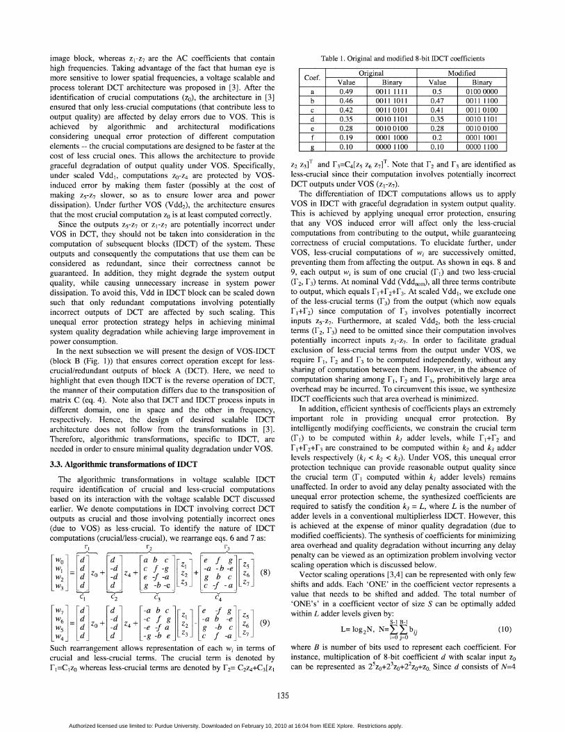
image block, whereas Z1-Z7 are the AC coefficients that containhigh frequencies. Taking advantage of the fact that human eye ismore sensitive to lower spatial frequencies, a voltage scalable andprocess tolerant DCT architecture was proposed in [3]. After theidentification of crucial computations (Zo), the architecture in [3]ensured that only less-crucial computations (that contribute less tooutput quality) are affected by delay errors due to VOS. This isachieved by algorithmic and architectural modificationsconsidering unequal error protection of different computationelements -- the crucial computations are designed to be faster at thecost of less crucial ones. This allows the architecture to providegraceful degradation of output quality under VOS. Specifically,under scaled Vdd., computations ZO-Z4 are protected by VOSinduced error by making them faster (possibly at the cost ofmaking ZS-Z7 slower, so as to ensure lower area and powerdissipation). Under further VOS (Vdd-), the architecture ensuresthat the most crucial computation Zo is at least computed correctly.
Since the outputs ZS-Z7 or Z1-Z7 are potentially incorrect underVOS in DCT, they should not be taken into consideration in thecomputation of subsequent blocks (IDCT) of the system. Theseoutputs and consequently the computations that use them can beconsidered as redundant, since their correctness cannot beguaranteed. In addition, they might degrade the system outputquality, while causing unnecessary increase in system powerdissipation. To avoid this, Vdd in IDCT block can be scaled downsuch that only redundant computations involving potentiallyincorrect outputs of DCT are affected by such scaling. Thisunequal error protection strategy helps in achieving minimalsystem quality degradation while achieving large improvement inpower consumption.
In the next subsection we will present the design of VOS-IDCT(block B (Fig. 1)) that ensures correct operation except for lesscrucial/redundant outputs of block A (DCT). Here, we need tohighlight that even though IDCT is the reverse operation of DCT,the manner of their computation differs due to the transposition ofmatrix C (eq. 4). Note also that DCT and IDCT process inputs indifferent domain, one in space and the other in frequency,respectively. Hence, the design of desired scalable IDCTarchitecture does not follow from the transformations in [3].Therefore, algorithmic transformations, specific to IDCT, areneeded in order to ensure minimal quality degradation under VOS.
3.3. Algorithmic transformations of IDCT
The algorithmic transformations in voltage scalable IDCTrequire identification of crucial and less-crucial computationsbased on its interaction with the voltage scalable DCT discussedearlier. We denote computations in IDCT involving correct DCToutputs as crucial and those involving potentially incorrect ones(due to VOS) as less-crucial. To identify the nature of IDCTcomputations (crucial/less-crucial), we rearrange eqs. 6 and 7 as:
r 1 r} r 3
[ :~ =[f]Zo +['~~]Z4 +[~ ; ~~ ][~~]'+[¥][~:] (8)w3 d d g -b -e 3 c -f -a 7~ '--v---' '----v----' '------v------'
C1 c2 c3
c4
[: : =[~]zo +[~~]Z4 +[~~ ;! [~~]_[:a ~ ~][~:] (9)W4 d d -g -b e 3 c f -a 7
Such rearrangement allows representation of each Wi in terms ofcrucial and less-crucial terms. The crucial term is denoted by[1=C1ZOwhereas less-crucial terms are denoted by [2= C2Z4+C3[Z1
135
Table 1. Original and modified 8-bit mCT coefficients
Coef.Original Modified
Value Binary Value Binarya 0.49 0011 1111 0.5 01000000b 0.46 0011 1011 0.47 0011 1100c 0.42 0011 0101 0.41 0011 0100d 0.35 0010 1101 0.35 0010 1101e 0.28 00100100 0.28 00100100f 0.19 0001 1000 0.2 0001 1001g 0.10 0000 1100 0.10 0000 1100
Z2 Z3]T and [3=C4[ZS Z6 Z7]T. Note that [2 and [3 are identified asless-crucial since their computation involves potentially incorrectDCT outputs under VOS (Z1-Z7).
The differentiation of IDCT computations allows us to applyVOS in IDCT with graceful degradation in system output quality.This is achieved by applying unequal error protection, ensuringthat any VOS induced error will affect only the less-crucialcomputations from contributing to the output, while guaranteeingcorrectness of crucial computations. To elucidate further, underVOS, less-crucial computations of Wi are successively omitted,preventing them from affecting the output. As shown in eqs. 8 and9, each output Wi is sum of one crucial ([1) and two less-crucial(T2, [3) terms. At nominal Vdd (VddnonJ, all three terms contributeto output, which equals [1+[2+[3' At scaled Vdd., we exclude oneof the less-crucial terms ([3) from the output (which now equals[1 +[2) since computation of [3 involves potentially incorrectinputs ZS-Z7' Furthermore, at scaled Vdd-, both the less-crucialterms ([2, [3) need to be omitted since their computation involvespotentially incorrect inputs Z1-Z7' In order to facilitate gradualexclusion of less-crucial terms from the output under VOS, werequire [b [2 and [3 to be computed independently, without anysharing of computation between them. However, in the absence ofcomputation sharing among [1, [2 and [3, prohibitively large areaoverhead may be incurred. To circumvent this issue, we synthesizeIDCT coefficients such that area overhead is minimized.
In addition, efficient synthesis of coefficients plays an extremelyimportant role in providing unequal error protection. Byintelligently modifying coefficients, we constrain the crucial term([1) to be computed within k] adder levels, while [1+[2 and[1+[2+[3 are constrained to be computed within k2 and k3 adderlevels respectively (k] < k2 < k3) . Under VOS, this unequal errorprotection technique can provide reasonable output quality sincethe crucial term (T1 computed within k] adder levels) remainsunaffected. In order to avoid any delay penalty associated with theunequal error protection scheme, the synthesized coefficients arerequired to satisfy the condition k3 = L, where L is the number ofadder levels in a conventional multiplierless IDCT. However, thisis achieved at the expense of minor quality degradation (due tomodified coefficients). The synthesis of coefficients for minimizingarea overhead and quality degradation without incurring any delaypenalty can be viewed as an optimization problem involving vectorscaling operation which is discussed below.
Vector scaling operations [3,4] can be represented with only fewshifts and adds. Each 'ONE' in the coefficient vector represents avalue that needs to be shifted and added. The total number of'ONE's' in a coefficient vector of size S can be optimally addedwithin L adder levels given by:
8-1 B-1
L=log2N , N=LLb i , (10)i=O j=O '}
where B is number of bits used to represent each coefficient. Forinstance, multiplication of 8-bit coefficient d with scalar input Zocan be represented as 2szo+23Z0+22Z0+Z0. Since d consists of N=4
Authorized licensed use limited to: Purdue University. Downloaded on February 10, 2010 at 16:04 from IEEE Xplore. Restrictions apply.
(II)
(12)
'ONE's' (table 1), dzo and hence f l can be optimally computedwithin L=2 adder levels. Similarly, using the original 8-bitcoefficients with N=29 (table 1), the optimal number of adderlevels required for computation of each path Wi (eqs. 8 and 9) isL=S=k3• However, with original coefficients, f], f 2 and f} cannotbe computed independently (without sharing) . Hence, modificationof original coefficients is required in our vas based IDCT design.
First, we note that coefficient d should not be modified since itis multiplied with the crucial DCT output Zo (eqs. 8 and 9) and anychange would affect the output image quality significantly. Thuscomputations involving C, and C2 are separated from the rest asshown in eqs. 8 and 9. Second, we only modify the coefficientscontained in C}and C4. However, since each coefficient appears inboth C} and C4, any change of coefficient in one of the matriceswould affect the other and may result in an increase in path delayof Wi (more than S adder levels) and area overhead. This leads us tothe first constraint in which, the modified coefficients mustguarantee that computational path delay of any Wi does not exceedk3=L=S adder levels. This ensures that the resulting architectureoperates at the same frequency as conventional multiplierlessarchitecture (no delay penalty). Second, the total number of ones ineach row of modified C}and C4 must not exceed that of original C}and C4 , which can be expressed as
'if row ofC} ,C4 : ( SII ~ bij) +(SIt ~ bij) $ 2 11=0 J=O 1=0 J=o
In addition, we desire the crucial (Tj) and less-crucial (f2, f})terms to be computed separately so that under vas, potentiallyincorrect less-crucial terms are prevented from contributing to theoutput. For instance, at scaled Vdd., due to increase of path delay,the computation of k3=L=S adder levels in IDCT may not becompleted. However, reasonable output quality can be obtained ifcrucial f t and one of the less-crucial terms f 2 were evaluatedcorrectly by the k2=4 adder level. This is due to the fact that even ifwe omit f } (output at Vddnom equals f l+f2+f}), minor qualitydegradation is incurred due to its less-crucial nature. Of course,under Vddnom, output quality can be improved by adding f} tof t+f2at the Sth adder level. Hence, the modified coefficients needto be synthesized such that, in the resulting architecture, f], I'2arecomputed within k j=3 adder levels, f t+f2 and f} within k2=4
adder levels and f l+f2+f} within k3=L=S adder levels. Note thatsince the number of adder levels depends on the number of ones inthe coefficient vector, the constraint that requires f} to becomputed within k2=4 adder levels can be expressed as:
(SC4-1 B-1 J SC4-IB-1
V row ofC4: 10gzl ~ ~bij $4 => ~ ~bij$16
Equivalently, the total number of 'ONE's' in each row ofcoefficient matrix C4 should be less than 16. Similarly, theconstraint that requires f 2to be computed within k j=3 adder levelscan be expressed as (the total number of 'ONE's' in each row ofcoefficient matrix C} should be less than 8):
SC3-1 B-1 So-I B-1
'if row of C3 : log2( L ~>i):O;; 3 => L L bij s 8 (13)i=O j=O iefl j=O
Finally, in order to ensure that there is no sharing of anycomputation between less-crucial terms C}[ZI Z2 z}f and f }, thenumbers of 'ONE's' in each row of at least one of the matrices C}or C4 must be even.
Based on the above constraints, the absolute difference betweenthe peak-signal-to-noise ratios (PSNR) of the image obtained usingoriginal coefficients and image PSNR using modified coefficientsis minimized (objective function). The total number of 'ONE's' inthe modified set of coefficients (table 1) is reduced from N=29 toN=23 which overcomes the area overhead (due to no sharing) atminor quality degradation (-0.2 dB) yielding a voltage scalablemCT architecture. Furthermore, the modified coefficients reducethe variance of vas induced errors in mCT, cr~B2, taking intoaccount system level interactions with a vas based DCT, whilemeeting the system constraint stated in eq. 3.
3.4. Proposed Architecture
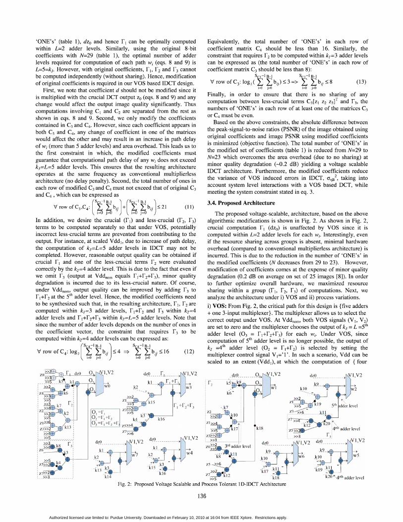
The proposed voltage-scalable, architecture, based on the abovealgorithmic modifications is shown in Fig. 2. As shown in Fig. 2,crucial computation f l (dzo) is unaffected by vas since it iscomputed within L=2 adder levels for each Wi' Interestingly, evenif the resource sharing across groups is absent, minimal hardwareoverhead (compared to conventional multiplierless architecture) isincurred. This is due to the reduction in the number of 'ONE's' inthe modified coefficients (N decreases from 29 to 23). However,modification of coefficients comes at the expense of minor qualitydegradation (0.2 dB on average on set of 2S images [8]). In orderto further optimize overall hardware, we maximized resourcesharing within a group (Tj, f 2, f }) of computations. Next, weanalyze the architecture under i) vas and ii) process variations.
i) VQS: From Fig. 2, the critical path for this design is {five adders+ one 3-input multiplexer}. The multiplexer allows us to select thecorrect output under vas . At Vddnom' both vas signals (V], V2)are set to zero and the multiplexer chooses the output of k3 = L =Sthadder level (a} = f l+f2+f}) for each Wi' Under vas, sincecomputation of Sth adder level is no longer possible, the output ofk2 =4th adder level (02 = f l+f2) is selected by setting themultiplexer control signal Vt='1 '. In such a scenario, Vdd can bescaled to an extent (Vdd.), at which the computation of { four
t~I! "
.k,<) , ' >ffi- ,--->I
klX
.' W9' '. ' '' .9.1,[}I,V2kS' k9 0 ,.' 0 wi
k6- :
· .k7
kl 6
U{\I.. " " " " , .~V I'y2
kllJl,~ 2 m:--l w4., -.7' kJ
' k l 5 _:
k 16
: 1'..5», » 3 r
3,
U{(l :. ,~I :'V2 ,oo'tl{ (l, • • " .~V 1,Y2
k9 ,~<) , ->
,~~;~ w6 ,k~;~ w5
. . ' kll ' k" I " .k l lk I7 c·• ' ,.c·.
» 5 " kIX k20 ' 4 0h adder level
Proposed Voltage Scalable and Process Tolerant ID-IDCT Architecture
~1! .... J I.......>~I 'V2.k).. . r +r,
,~2 w3=-0'"
Fig. 2:
tli:; .,.. .. ,', .. ,~I,'V 2
,k2 . w7"
' k 13 k3kl4136
Authorized licensed use limited to: Purdue University. Downloaded on February 10, 2010 at 16:04 from IEEE Xplore. Restrictions apply.
2:~ _~~:!~gSYSTEMOUTPUT
a e . mage wIt anPSNR(dB) VddAnom VddA1 VddAzVddBnom 34.49 31.82 29.81
VddB' 31.82 31.82 29.81VddBz 29.81 29.81 29.81
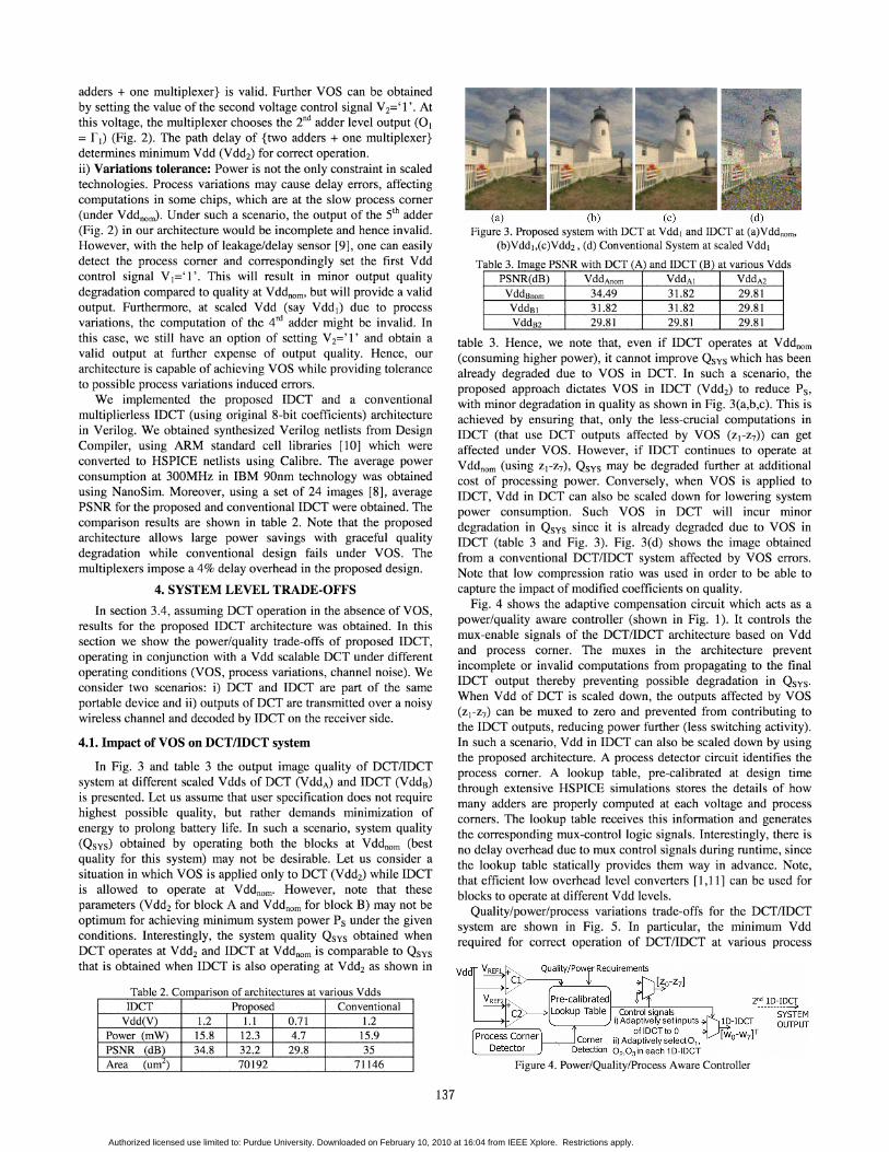
(a) (b) (c) (d)Figure 3. Proposed system with DCT at Vdd, and mCT at (a)Vddnom,
(b)Vddl,(C)Vddz , (d) Conventional Systemat scaled Vdd,
T bl 3 I PSNR ' h DCT (A) d mCT (B) at various Vdds
table 3. Hence, we note that, even if IOCT operates at Vdd nom(consuming higher power), it cannot improve QSYS which has beenalready degraded due to vas in OCT. In such a scenario, theproposed approach dictates vas in mCT (Vdd-) to reduce Ps,with minor degradation in quality as shown in Fig . 3(a,b,c). This isachieved by ensuring that, only the less-crucial computations inmCT (that use OCT outputs affected by vas (ZI-Z7)) can getaffected under vas. However, if IOCT continues to operate atVdd nom (using Z,-Z7), QSYS may be degraded further at additionalcost of processing power. Conversely, when vas is applied tomCT, Vdd in OCT can also be scaled down for lowering systempower consumption. Such vas in OCT will incur minordegradation in QSYS since it is already degraded due to vas inmCT (table 3 and Fig . 3) . Fig. 3(d) shows the image obtainedfrom a conventional OCT/IOCT system affected by vas errors.Note that low compression ratio was used in order to be able tocapture the impact of modified coefficients on quality.
Fig. 4 shows the adaptive compensation circuit which acts as apower/quality aware controller (shown in Fig . 1). It controls themux-enable signals of the OCT/mCT architecture based on Vddand process corner. The muxes in the architecture preventincomplete or invalid computations from propagating to the finalmCT output thereby preventing possible degradation in QSYs.When Vdd of OCT is scaled down , the outputs affected by vas(ZI-Z7) can be muxed to zero and prevented from contributing tothe mCT outputs, reducing power further (less switching activity).In such a scenario, Vdd in mCT can also be scaled down by usingthe proposed architecture. A process detector circuit identifies theprocess corner. A lookup table, pre-calibrated at design timethrough extensive HSPICE simulations stores the details of howmany adders are properly computed at each voltage and processcorners. The lookup table receives this information and generatesthe corresponding mux-control logic signals. Interestingly, there isno delay overhead due to mux control signals during runtime, sincethe lookup table statically provides them way in advance. Note,that effic ient low overhead level converters [I,ll] can be used forblocks to operate at different Vdd levels .
Quality/power/process variations trade-offs for the OCT/mCTsystem are shown in Fig. 5. In particular, the minimum Vddrequired for correct operation of OCT/IOCT at various process
Vddf hibl 2 CTa e ompanson 0 arc itec ures a vanous smCT Proposed Conventional
Vdd(V) 1.2 l.l 0.71 1.2Power (mW) 15.8 12.3 4.7 15.9PSNR (dB) 34.8 32.2 29.8 35Area (urn") 70192 71146
4.1. Impact of VOS on DCTIIDCT system
In Fig . 3 and table 3 the output image quality of OCT/mCTsystem at different scaled Vdds of OCT (Vddj) and mCT (VddB)
is presented. Let us assume that user specification does not requirehighest possible quality, but rather demands minimization ofenergy to prolong battery life . In such a scenario, system quality(QSYs) obtained by operating both the blocks at Vdd nom (bestquality for this system) may not be desirable. Let us consider asituation in which vas is applied only to OCT (Vdd-) while mCTis allowed to operate at Vddnom. However, note that theseparameters (Vdd, for block A and Vdd nomfor block B) may not beoptimum for achieving minimum system power Ps under the givenconditions. Interestingly, the system quality QSYS obtained whenOCT operates at Vdd, and mCT at Vddnomis comparable to QSYSthat is obtained when IOCT is also operating at Vdd, as shown in
adders + one multiplexer} is valid. Further vas can be obtainedby setting the value of the second voltage control signal Vz='1'. Atthis voltage, the multiplexer chooses the 2nd adder level output (O,=r,) (Fig. 2) . The path delay of {two adders + one multiplexer}determines minimum Vdd (Vddz) for correct operation.ii) Variations tolerance: Power is not the only constraint in scaledtechnologies. Process variations may cause delay errors, affectingcomputations in some chips, which are at the slow process corner(under Vddnom)' Under such a scenario, the output of the 51h adder(Fig. 2) in our architecture would be incomplete and hence invalid.However, with the help of leakage/delay sensor [9], one can easilydetect the process corner and correspondingly set the first Vddcontrol signal V ,=' 1' . This will result in minor output qualitydegradation compared to quality at Vddnom' but will provide a validoutput. Furthermore, at scaled Vdd (say Vdd.) due to processvariations, the computation of the 4rd adder might be invalid. Inthis case, we still have an option of setting Vz=' l ' and obtain avalid output at further expense of output quality. Hence, ourarchitecture is capable of achieving vas while providing toleranceto possible process variations induced errors.
We implemented the proposed mCT and a conventionalmultiplierless mCT (using original 8-bit coefficients) architecturein Verilog. We obtained synthesized Verilog netlists from OesignCompiler, using ARM standard cell libraries [10] which wereconverted to HSPICE netlists using Calibre. The average powe rconsumption at 300MHz in IBM 90nm technology was obtainedusing NanoSim. Moreover, using a set of 24 images [8], averagePSNR for the proposed and conventional mCT were obtained. Thecomparison results are shown in table 2. Note that the proposedarchitecture allows large powe r savings with graceful qualitydegradation while conventional design fails under vas. Themultiplexers impose a 4% delay overhead in the proposed design.
4. SYSTEM LEVEL TRADE-OFFS
In section 3.4 , assuming OCT operation in the absence of vas,results for the proposed mCT architecture was obtained. In thissection we show the power/quality trade-offs of proposed mCT,operating in conjunction with a Vdd scalable OCT under differentoperating conditions (VaS, process variations, channel noise). Weconsider two scenarios: i) OCT and IOCT are part of the sameportable device and ii) outputs of OCT are transmitted over a noisywireless channel and decoded by IOCT on the receiver side .
137
Authorized licensed use limited to: Purdue University. Downloaded on February 10, 2010 at 16:04 from IEEE Xplore. Restrictions apply.
S. CONCLUSION
[I] J. Rabaey et aI., "Di gital Integated Circuits", Prentice Hall, 2002[2] S.Borkar et al., "Parameter variations and impact on circuits andmicroarchitecture", IEEE DAC, 2003.[3] N. Banerjee et al., "Low Power Variation Tolerant DCT Architecture,IEEE DATE, 2007.[4] J.-S. Chiang et. al.,"A High Throughput 2-Dimensional DCT/IDCTArchitecture for real-time image and video system", IEEE ICECS , 2001.[5] T. Xanthopoulos , et.al, "Low-Power IDCT Macrocell for MPEG-2MP@ML Exploiting Data Distribution Properties for Minimal Activity",IEEE JSSC, 1999 .[6] K. Lengwehasatit, et. aI, "DCT computation based on variablecomplexity fast approximations", IEEE ICIP , 1998.[7] V.Bhaskaran et aI., "Image and Video Compression Standard Algorithmsand Architecture" , Kluwer Academic Publishers, 1996.[8] http ://rOk.us/graphics/kodak/[9] C.H. Kim et al., "On-die CMOS leakage current sensor for measuringprocess variation in sub-90nm generations", Symp . ofVLSI Circuits , 2004.[IO]ARMLIBS 90nm, http://www.arm.com![II] S. Kulkarni , et. aI, "New level converters and level converting logiccircuits for multi-VDD low power design", IEEE System-on-Chip, 2003.[12] S.c. Hsia, et. aI, "VLSI Implementat ion of High-Performanc e ErrorConcealment Processor for TV Broadcasting",1EEE Tran s. on CSVT ,2007.
REFERENCES
In this paper, we propose a design approach based on system levelinteractions that provides "right" amount of quality and power foreach block, while dissipating minimal system power under thegiven operating conditions . This is achieved by ensuring that onlyless-crucial computations can get affected by the operatingconditions (VaS, process variations, channel noise), therebyincurring minimal quality degradation. Furthermore, the vasbased design methodology can be used as a channel errorconcealment technique while minimizing system powerconsumption (by VaS). To demonstrate the efficacy of theproposed approach, it was applied to a OCT/IDCT system.However, the proposed methodology can also be applied fordesigning other DSP systems where interaction between blocksneed to be considered for providing "just-the-right" amount ofpower/quality and robustness.
Acknowledgement: This research was funded in part by GigascaleSystems Research Center and by National Science Foundation.
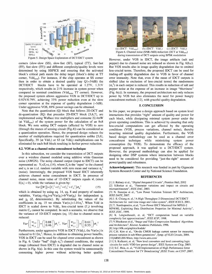
(a) (IDCT - Vddllom) (b) (IDCT - Vdd. ) (c) (IDCT - Vdd-)Figure 6. Channel noise (SNR=9dB) reduction (DCT at Vddnom)
during transmission of DCT outputs using BPSK modulat ion
However, under vas in IDCT, the image artifacts (salt andpepper) due to channel noise are reduced as shown in Fig. 6(b,c).But vas results also in image quality degradation due to omittedless-crucial terms. Therefore, the proposed IDCT can be used fortrading-off quality degradation due to vas in favor of channelerror immunity. Note that, even if the mean of IDCT outputs isshifted (due to exclusion of less-crucial terms) the randomness(a n
2) in each output is reduced. This results in reduction of salt and
pepper noise at the expense of an increase in image "blurriness"(Fig. 6(c)). In summary, the proposed architecture not only reducespower by vas but also eliminates the need for power hungryconcealment methods [12], with graceful quality degradation.
Furthermore, under aggressive vas in IDCT (Vdd-), the Var(wi) isreduced to 0.12a/. Hence, in addition to obtaining power benefits,vas in IDCT can be used for channel error concealment as shownin Fig. 6. Under "bad" (high a/) channel conditions, the outputimage (obtained from IDCT) is degraded due to channel noise asshown in Fig. 6(a). In this case the system would be unnecessarilyconsuming higher power without achieving better quality.
125
~1 00
~ 75
~ 500.
25
!-Q;;;iiiy-iE,; ;;'p i~;:iiy-! 0 , O.
i::::, Levels ! -. O. 2,0 .63 SF SS0 1/(Zo ' Z,) !QII. 01 " , rr e~~0 2/(Zo- z, ) ! "q!'P 02 ~ , FS e~~CO~
' Cl3/(;'o) ! {Q'6>/ 03 FF VtOC
Figure 5. Design Space Exploration of DCT/IDCT system
corners (slow-slow (SS), slow-fast (SF), typical (IT), fast-fast(FF), fast-slow (FF» and different complexity/quality levels weredetermined by using HSPICE and ensuring that the activatedblock 's critical path meets the delay target (block's delay at TTcorner, Vddnom) ' For instance, if the chip operates at SS cornerthen in order to obtain a desired quality (say Ql=34dB) theOCT/IDCT blocks have to be operated at 1.27V, 1.31Vrespectively, which results in 21% increase in system power whencompared to nominal conditions (Vddnom' TT corner) . However,the proposed system allows aggressive vas in OCT/IDCT up to0.92V/0.79V, achieving 33% power reduction even at the slowcorner operation at the expense of quality degradation (-5dB).Under aggressive vas, 69% power savings can be obtained.
Note that the quantization (Q) block that follows 20-0CT andde-quantization (IQ) that precedes 20-IDCT block [5,6,7], areimplemented using Wallace tree multipliers and consume 22AmW(at Vddnom) of the system power for the calculation of an 8x8block. We note setting OCT outputs (affected by VaS) to zero(through the muxes of sensing circuit (FigA)) can be considered asa quantization operation . Hence, the proposed design reduces thenumber of multiplications required for quantization unlike [5,6],Specifically, 39 (at Vdd.) or 63 (at Vdd-) multiplications can beeliminated for each 8x8 block resulting in further power reduction .
4.2. VOS as a channel noise concealment technique
In this subsection, we consider the transmission of DCT outputsover a wireless channel modeled using additive white Gaussiannoise (AWGN). The noisy channel output (input to mCT) can berepresented as: Yj=Zj+Ej(14), where Z, is the 'input' to the channeland Ei is an LLd. random variable with zero mean and variance a/(noise) . Interestingly, the proposed vas based IDCT inherentlyachieves channel noise concealment in IDCT. In presence ofchannel noise, mean value of lD-IDCT outputs equals Wi (sinceE[Ei] = 0), while the variance is given by:
Var([W])=(C, 2+C2' +C32+C/)O"n' (15)
which is obtained by using eq. 14, eq. 8 and property of randomvariables, Var(ax,+b;u)=a2Var(Xl)+b2Var(;u) for independent Xland ;u (Z, deterministic). By substituting the values of thecoefficients in eq. 15 we obtain Var(wi)=1.01an
2. When Vdd in
IDCT is scaled down to Vdd. , less-crucial term (f3) involvingmatrix C4 cannot be computed. In such a scenario, we observe thatthe variance of 1D-IDCT outputs (eq. 15) due to channel noise isreduced:
138
Authorized licensed use limited to: Purdue University. Downloaded on February 10, 2010 at 16:04 from IEEE Xplore. Restrictions apply.