Performance of rotated PSK modulation in Nakagami-m fading channels
Upload
independentCategory
view
1download
0
This article has been accepted for publication in a future issue of this journal, but has not been fully edited. Content may change prior to final publication.
> REPLACE THIS LINE WITH YOUR PAPER IDENTIFICATION NUMBER (DOUBLE-CLICK HERE TO EDIT) <
1
SOI CMOS Implementation of a Multirate PSK Demodulator for Space Communications
Mehmet R. Yuce, Wentai Liu, John Damiano, Bhaskar Bharat, Paul D. Franzon, and Numan S. Dogan
Abstract—A low power PSK demodulator integrated circuit
(IC) has been implemented using Silicon On Insulator (SOI) CMOS technology for deep space and satellite applications. The demodulator employs double differential detection to increase its robustness to the Doppler shift caused by the movement of the space vehicle and sampling technique with 1-bit A/D converter at the front to reduce the complexity and power dissipation. In particular, digital decimation is used after sampling to achieve a low power implementation of multirate transmission. Operating at UHF frequency (435 MHz), the receiver system supports a wide range of data rates (0.1-100 Kbps). From test results, the power consumption of the demodulator circuit including the 1-bit A/D converter is below 1 mW for data rates up to 100 Kbps.
Index Terms—Phase-Shift Keying (PSK), differential detection, space communications, symbol timing circuit, multirate, sampling.
I. INTRODUCTION
emand for low cost, compact and low power receiver circuits for use in wireless communications has continued to increase. In special applications such as
deep space communications, receivers must be robust to radiation hardness and Doppler effect as well. Silicon on insulator (SOI) CMOS technology is attractive for deep space applications, offering high-performance, low power, and good radiation hardness. Unlike standard CMOS, a layer of thin silicon film on the top of an insulator layer (buried oxide) is used in SOI to build active devices and circuits [1]. The buried oxide SiO2 is used to isolate the active device thin-film region from the silicon substrate. Having the isolation between the active region and the substrate provides excellent immunity against high-energy particles. Thus, radiation hardness makes SOI CMOS ideal for the environment with high-energy radiation such as deep space and satellite applications. In addition, the parasitic capacitances at drain (Cdb) and source (Csb) junctions of SOI CMOS devices are smaller than those
of bulk ones. In summary, the ability to reduce parasitic capacitances in SOI technology allows circuits to operate with lower supply voltages, thus reducing the power consumption and improving speed. Therefore, SOI CMOS has risen as one of the major technologies for next generation transceivers [2]. The chip presented in this paper has been designed with Honeywell’s SOI technology. In addition to the above benefits, this technology offers good performance advantage against single event upset (SEU) existing in space [3].
Manuscript received October 9, 2005; revised July 24, 2006. This work
was supported by NASA Glen Research Center through a grant NAG3-2584. M. R. Yuce is with the Department of Electrical Engineering and Computer
Science, University of Newcastle, Callaghan, NSW 2308 Australia (e-mail: [email protected]).
W. Liu is with the Department of Electrical engineering, University of California, Santa Cruz, CA 95064-1077 USA.
J. Damiano, B. Bharat, P. D. Franzon are with the Department of Electrical Engineering, North Carolina State University, Raleigh, NC 27695-7914.
N. Dogan is with the Electrical Engineering Department, North Carolina A&T State University, Greensboro, NC 27411, USA.
Copyright (c) 2006 IEEE. Personal use of this material is permitted. However, permission to use this material for any other purposes must be obtained from the IEEE by sending an email to [email protected].
Since space vehicles are in motion, the resultant Doppler shift causes frequency shift in the original transmitted carrier signal in space communications and often must be handled by circuit techniques. In an environment with a high Doppler shift, many modulation schemes require either pilot transmission technique or additional circuits [4],[5],[11] to handle the frequency shift. Unlike traditional phase-shift keying (PSK) receivers, which usually include one-stage differential detection [6],[7], the proposed PSK receiver implements two-stage differential detection. A PSK demodulation becomes invariant to Doppler frequency offset when used with the double differential detection and enables a simplified, low power circuit implementation [8][9]. The receiver architecture requires no extra circuit such as pilot signal generator or PLL for phase and frequency recovery of the carrier, therefore resulting in high transmission efficiency and low circuit complexity.
Although the receiver presented in this paper is for Mars orbiter-lander communication in deep space environment, it is also applicable to terrestrial use. Low power is one of the most critical priorities of the receiver circuit due to the limited physical size in the telecommunication equipment replaced in the lander (i.e. rover) [10][11]. All digital baseband circuit makes the design of low power receiver feasible. The power consumption in a digital CMOS circuit is P ∝ CV2f, where C is the capacitance in the circuit, V is the supply voltage, and f is the operating frequency [12]. The 1-bit A/D converter is used at the front-end to reduce circuit complexity and capacitance. Besides radiation hardening, SOI CMOS technology also gives the benefit of potentially reducing the operational voltage and capacitance [1]. The ability to minimize C and V allows significant reduction in power consumption of the integrated circuit (IC). In addition to the demodulation, the chip integrates a timing recovery circuit for multiple data rates (0.1–100 Kbps). The demodulator is also designed to be programmable to operate in a single-stage differential detection, either for communications between sur-
D

This article has been accepted for publication in a future issue of this journal, but has not been fully edited. Content may change prior to final publication.
> REPLACE THIS LINE WITH YOUR PAPER IDENTIFICATION NUMBER (DOUBLE-CLICK HERE TO EDIT) <
2
A/D
......3,2,1,0n =
1- Bit A/D
(Hard-Limiter)
rnJn
L
T
sgn
L
T
T
DecimatorAccumulator
DelayRC
yQ (k)
Cos(wLOt )
LNABPF IF Amp.
Tclk
rn-1(k)
xn
yn
Qn
Qn-1
In
In-1
90º
12
4
+=
n
fsf
IF
STR: Symbol Timing Recovery RC: Reset Circuit
m
m
STR
rn
Jn
sT
DSP (Baseband)
IF-sampling
Front-end
Receiver operation modes:1- STR sT=0 input = rn
From front-end sT=1 Input = Jn
NRZ demod. Sig.2-Modulation selection m=0 DDPSK detection m=1 DPSK detection
∑
xI (k)
IC
RF (SAW) Filter
rIF(t )
∑
0
1
0
1
rn(k)
Fig. 1. Single/double differential PSK receiver with IF-sampling front-end. face elements (landers) where Doppler effect does not exists, or for use in terrestrial applications that will exhibit rela-tively high performance while minimizing the complexity [8].
II. RECEIVER ARCHITECTURE The combined single/double differential PSK (D/DPSK)
receiver with the IF-sampling front-end is shown in Fig. 1. The design specifications are listed in Table I. The key properties of the receiver are low-power consumption, flexibility, reduced complexity, robust to Doppler shifts, and the design in SOI process, which is a radiation-hardened process [1]. The test chip presented here covers the baseband with the analog IF amplifier.
The proposed demodulator IC is designed for being used in an IF-sampling front-end, as illustrated in Fig. 1. The incoming signal is specified as a binary phase-shift keying (PSK) modulated waveform with a carrier frequency of 435 MHz. The carrier frequency is down converted to an IF frequency via one-stage analog down conversion. The received RF signal is filtered with a passive surface acoustic wave (SAW) filter, amplified by a low-power low-noise amplifier (LNA), and again filtered with an IF band-pass filter (BPF) [13]. After these steps, the chip presented in this work digitizes and samples the IF signal at 1-bit precision using 4MHz sampling clock. This sampling clock is assumed to be generated from the LO frequency at front-end. The sampled IF signal is later down-converted to 0 Hz digitally in the baseband via the first differential decoding and the decimation filter.
Unlike the heterodyne architecture, the final down conversion is done in the digital domain in an IF-sampling front-end [14]. This reduces power consumption and comp-
TABLE I RECEIVER SPECIFICATIONS
Modulation type PSK
Carrier frequency, fc 435 MHZ
Sampling frequency, fs 4 MHZ
Data rates, fb 0.1-100 Kbps
TABLE II INPUT FREQUENCIES FOR FS= 4 MHZ
Input signal frequency, fIF Sampling factor, n
1 MHz 0 (oversampling)
3 MHz 1 (subsampling) 15 MHz 7 ( || )
25 MHz 12 ( || ) . .
lexity and eliminates I/Q imbalances. The relationship between the sampling frequency fs and the input IF frequency fIF for the proposed receiver is based on the following equation:
,......3,2,1,07
4
5
4
3
4,4
124 ,,....,, =⎥
⎦
⎤⎢⎣
⎡+
= = nfff IFIF
s n (1)
where the sampling factor n is an integer number and defines the frequency of the incoming IF signal for the input of the chip, as the sampling frequency fs is chosen equal to 4 MHz (i.e. fs=4 MHz) in the proposed demodulator. The above equation guarantees that overlapping of images during frequency translation will not occur. In addition, the image is translated to a point (i.e. fs/4) that is away from the DC eliminating 1/f noise [8]. Some examples of input frequencies with appropriate sampling factors are given in Table II. The sampling factor n is desired to be low enough so that the overlapping of the out-of-band noise would not be an issue in case of undersampling [8],[14].
A. Analog Front-end
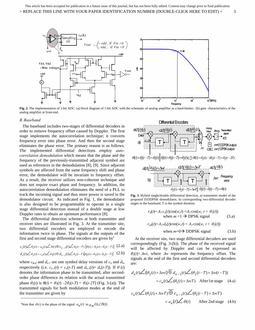
A 1-bit analog-to-digital converter (ADC) is used at the front-end of the demodulator to digitize the analog signal. The 1–bit ADC is ideally suited for deep-space communication due to the absence of interference signals. Furthermore, the 1-bit ADC (i.e. hard-limiter) has been widely used as a part of many satellite transponders [15],[16]. The analog signal is first quantized into two levels by means of the ADC and sampled at 4 MHz (fs = 4 MHz). The ADC consists of a comparator followed by a sampling circuit. The comparator basically converts analog input sine signal to square wave (i.e. hard- limiting). It has been designed as a two-stage differential amplifier providing a gain of 60 dB (as given in Fig. 2) to the input IF analog signal to ease the baseband receiver. The 60-dB dynamic range with adequate bandwidth is more than sufficient to digitize the necesary IF signals for the test chip. The required input dynamic range of the comparator would be provided by the gain of the previous circuits such as LNA and IF-amplifier.
This article has been accepted for publication in a future issue of this journal, but has not been fully edited. Content may change prior to final publication.
> REPLACE THIS LINE WITH YOUR PAPER IDENTIFICATION NUMBER (DOUBLE-CLICK HERE TO EDIT) <
3
Fig. 2. The implementation of 1-bit ADC: (a) block diagram of 1-bit ADC with the schematic of analog amplifier as a hard-limiter, (b) gain characteristics of the analog amplifier at front-end.
B. Baseband The baseband includes two-stages of differential decoders in
order to remove frequency offset caused by Doppler. The first stage implements the autocorrelation technique; it converts frequency error into phase error. And then the second stage eliminates the phase error. The primary reason is as follows. The implemented differential detections employ auto-correlation demodulation which means that the phase and the frequency of the previously-transmitted adjacent symbol are used as references in the demodulation [8], [9]. Since adjacent symbols are affected from the same frequency shift and phase error, the demodulator will be invariant to frequency offset. As a result, the receiver utilizes non-coherent technique and does not require exact phase and frequency. In addition, the autocorrelation demodulation eliminates the need of a PLL to track the incoming signal and thus more power is saved in the demodulator circuit. As indicated in Fig. 1, the demodulator is also designed to be programmable to operate in a single stage differential detection instead of a double stage at low Doppler rates to obtain an optimum performance [8].
The differential detection schemes at both transmitter and receiver sites are illustrated in Fig. 3. At the transmitter site, two differential encoders are employed to encode the information twice in phase. The signals at the outputs of the first and second stage differential encoders are given by1
[ ] (2.a) )()()()()()()( 11111 )()( TtttTtttat tctc nnn −−=−= ∠∠∠ −⊕ θθθθθθ
)()()(1)()()()( 222112 )()( TtttTtttct tdtd nnn −−=−= ∠∠∠ −⊕ θθθθθθ [ ] (2.b)
where cn-1 and dn-1 are one symbol delay versions of cn and dn, respectively (i.e. cn-1(t) = cn(t-T) and dn-1(t)= dn(t-T)). If θ (t) denotes the information phase to be transmitted, after second-order phase difference its relation with the actual transmitted phase θ2(t) is θ(t) = θ2(t) –2θ2(t-T) + θ2(t-2T) (Fig. 3-(a)). The transmitted signals for both modulation modes at the end of the transmitter are given by
Amp.
OSC.
TTT
T Ta)
b)
mm=0,m=1,
DDPSK outputDPSK output
Transmitted signal
r(t)
AnalogMixer
an(t) cn(t)Data
dn(t)
cn(t)
dn(t)
∆w : Frequency error
cn(t) an(t)
Differential Encoders
cn-1(t)
)(tθ )(1 tθ )(2 tθ
wtt ∆+)(2θ wTt ∆+)(1θ )(tθ
wTTtt ∆+−− )()( 22 θθ )()()( 11 tTtt θθθ =−−
)2()(2)( 222)( TtTttt −+−−= θθθθ)()()( 221 tTtt θθθ =−+)()()( 11 tTtt θθθ =−+
0
1
Fig. 3. Hybrid single/double differential detection, a) transmitter model of the proposed D/DDPSK demodulator, b) corresponding two-differential decoder stages in the baseband. T is the symbol duration.
rd(t)=AT cn(t)cos(wct) =AT cos(wc t + θ1(t)) when m =1 DPSK signal (3.a)
rdd(t)=AT dn(t)cos(wct) = AT cos(wc t + θ2(t))
when m=0 DDPSK signal (3.b)
At the receiver site, two stage differential decoders are used correspondingly (Fig. 3-(b)). The phase of the received signal will be affected by Doppler and can be expressed as θ2(t)+∆wt, where ∆w represents the frequency offset. The signals at the end of the first and second differential decoders are:
(4.a)stage1st After ))(()(
))()(()()()(
1
212 )(
wTttc
TtwTttdwtttd
n
nn
∆+=
−∆+−∆+
∠∠∠ −⊕
θ
θθ
(4.b)stage 2ndAfter )(
))(()())(()(
)(111
ta
wTTttwTttc
t
c
n
nn
θ
θθ
∠∠∠
=
∆+−∆+ −⊕
1Note that )(tθ is the phase of the signal in .)(tna θ(t)(t)an ∠
This article has been accepted for publication in a future issue of this journal, but has not been fully edited. Content may change prior to final publication.
4
The phase at the output of the first stage is calculated as θ2(t)+∆wt-[θ2(t-T)+∆w(t-T)]=θ2(t)-θ2(t-T)+∆wT=θ1(t)+∆wT. As it can be clearly seen, a single differential stage eliminates the time-variant frequency uncertainty but is affected by a constant phase error. The phase error ∆wT is eliminated at the output of the second detector (Fig. 3- (b)). The single-stage detection (i.e. DPSK system) is better in terms of performance and low complexity [8]. It is, however, sensitive to frequency offsets. Thus, DPSK mode will be operated mostly when the Doppler effect is not strong or for the communications between surface elements (i.e. landers). DDPSK demodulation is, on the other hand, independent of the frequency error, ∆w. Therefore; the receiver’s DDPSK mode will be activated for communications between the orbiter (satellites) and land vehicles (rovers).
The maximum Doppler shift is 10 KHz and considering the speed of the satellite in the orbit, the largest Doppler rate of change is expected to be 20 Hz/s in the orbiter-lander communication [8][10][11]. The effect of the frequency variation in the sampled signal (the signal we correlate) is therefore not a problem over a bit period in the targeted application. This is usually known as the rate of change of the frequency offset (i.e. Doppler rate). Let us assume the worst case that is the case of the smallest data rate transmission of 100 bps (which has the period of 10 ms), the frequency change during 10 ms will be small and can be negligible. In the implementation, we observed some error pulses resulted from this deviation at the end of the first correlation. However, these error pulses are later eliminated by the accumulator/comparator circuit. This effect was carefully handled in the implementation. For the larger data rates, the effect was relatively very much smaller.
Adding a 1-bit A/D at the front-end relaxes the power dissipation since the rest of the receiver becomes all-digital and four mixers in the baseband are replaced by four logic XNOR’s [17]. The low-pass filters (the match filters) are implemented as accumulators or by up/down counters. The accumulators’ size depends on the number of samples taken by the 1-bit A/D and the decimator (L). The number of samples can be dropped more by the decimator and thus the size of the accumulators can be reduced. Each accumulator are reset the RC unit (reset circuit) periodically in order to realize uncorrelated samples. The RC unit takes the recovered clock from the timing circuit and generates very short pulses in order to reset accumulators every period of data (Fig. 1).
C. Multirate Implementation The support of a wide range of data rates is one of the
unique features of the demodulator. In conventional satellite or orbiter-lander communications, transceivers would use just one bit rate [10], which was not an optimum scheme since the received signal power changes with respect to elevation angles. For example, at some elevation angles the received power will be higher, therefore either a higher bit rate can be allocated or the transmitted signal power can be decreased so as to optimize the communication link efficiently [8]. The receiver given here includes different bit rates to allow the orbiter device to change its bit rate in frequent based on the
Referenceclock
(fs=4MHz)
1 KHz
10 KHz
100 KHz
TM
0.1 Kbps
1 Kbps
10 Kbps
=
TcM
100 Kbps
M
Timing circuit portionDelay unit in digital DDPSK receiver
Tc=mTs=constantControl sig.
÷40
÷10
÷10
.
.
Fig. 4. Multirate delay unit implementation in digital differential based sampling PSK. The indicated multi-stage down conversion of the sampling clock is in the timing circuit and shown in Fig.6.
=Tc = mTs
D
Qrn (k)
rn-1 (k)Tc
D Q D QQ
fs
Drn
rn-1
x(k)= rn(k) x rn-1(k)
Ts : the period of sampling clock
Fig. 5. Digital implementation of auto-correlation differential detection.
received signal strength. Multirate detection is done by using one or more stages of decimation in the delay element, as shown in Fig. 4. Each stage represents one of the bit rates. The control signal selects the appropriate stage with respect to the data rate that is defined by the timing clock. The sampling frequency fs is divided by the decimation ratios, which provides the desired clocks for data rates. After digital decimations, a constant delay unit of Tc follows.
The auto-correlation implementation of each of the differential detection in the proposed demodulator is designed as shown in Fig. 5. As has been mentioned above, a constant delay unit Tc ( Tc = mTs) is used for every discrete bit rate for simplicity, which is designed by 40 flip-flops (i.e. m = 40) in the chip in order to give adequate time delay to the samples in the adjacent symbol. This number corresponds to the highest bit rate of 100 Kbps. That is, if we choose m = 40, then Tc= mTs = 40X0.25µs = 10µs, which is equal to the symbol duration of the data rate of 100 Kbps (1/fb100Kbps =10µs)). Then the decimator rate must be equal to 10 (i.e. M =10) at each stage to arrange the duration of other data rates, providing that the samples will be correlated to the right samples of the adjacent symbol.
D. Synchronization and Symbol Timing Recovery (STR) Carrier frequency and phase synchronizations are required
for all coherent detection schemes. When non-coherent detection is used, only frequency synchronization of the carrier is needed to detect the signal correctly. In the proposed demodulator, we used auto-correlation modulation, which means that the reference signal is taken from the adjacent symbol. Therefore, neither carrier frequency nor carrier phase is necessary for the detection of information. This greatly simplifies the system overhead. Unlike many demodulators, this receiver does not require any pilot or preamble sequence
This article has been accepted for publication in a future issue of this journal, but has not been fully edited. Content may change prior to final publication.
5
NPFD
OutputClock
Tclk
Signal iny(k)
Phase
Estimator
FrequencyController
z(k)Prefilter
Delay
1-Bit ADC
fs
fi
s(k)
sd(k)
fsfsN
rIF(t)
Freq.Divider
XOR
PSK Sig. (rn(k))
Basebandsignal (Jn)
XNORReference
clock( fs= 4 MHz )
40
10
10
fs: Sampling frequency
a)
b)
.
.
FromFrequency Controller
100 KHz
10 KHz
1 KHz
rn(k)
Jn
ST
÷τ
÷
÷
÷=2Ts=2/fsτ
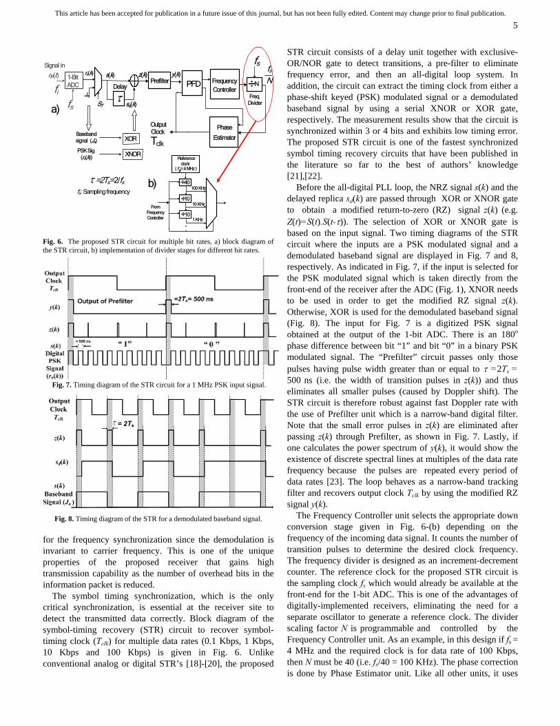
Fig. 6. The proposed STR circuit for multiple bit rates, a) block diagram of the STR circuit, b) implementation of divider stages for different bit rates.
Fig. 7. Timing diagram of the STR circuit for a 1 MHz PSK input signal.
Fig. 8. Timing diagram of the STR for a demodulated baseband signal.
for the frequency synchronization since the demodulation is invariant to carrier frequency. This is one of the unique properties of the proposed receiver that gains high transmission capability as the number of overhead bits in the information packet is reduced.
The symbol timing synchronization, which is the only critical synchronization, is essential at the receiver site to detect the transmitted data correctly. Block diagram of the symbol-timing recovery (STR) circuit to recover symbol-timing clock (Tclk) for multiple data rates (0.1 Kbps, 1 Kbps, 10 Kbps and 100 Kbps) is given in Fig. 6. Unlike conventional analog or digital STR’s [18]-[20], the proposed
STR circuit consists of a delay unit together with exclusive-OR/NOR gate to detect transitions, a pre-filter to eliminate frequency error, and then an all-digital loop system. In addition, the circuit can extract the timing clock from either a phase-shift keyed (PSK) modulated signal or a demodulated baseband signal by using a serial XNOR or XOR gate, respectively. The measurement results show that the circuit is synchronized within 3 or 4 bits and exhibits low timing error. The proposed STR circuit is one of the fastest synchronized symbol timing recovery circuits that have been published in the literature so far to the best of authors’ knowledge [21],[22].
Before the all-digital PLL loop, the NRZ signal s(k) and the delayed replica sd(k) are passed through XOR or XNOR gate to obtain a modified return-to-zero (RZ) signal z(k) (e.g. Z(t)=S(t).S(t-τ)). The selection of XOR or XNOR gate is based on the input signal. Two timing diagrams of the STR circuit where the inputs are a PSK modulated signal and a demodulated baseband signal are displayed in Fig. 7 and 8, respectively. As indicated in Fig. 7, if the input is selected for the PSK modulated signal which is taken directly from the front-end of the receiver after the ADC (Fig. 1), XNOR needs to be used in order to get the modified RZ signal z(k). Otherwise, XOR is used for the demodulated baseband signal (Fig. 8). The input for Fig. 7 is a digitized PSK signal obtained at the output of the 1-bit ADC. There is an 180o phase difference between bit “1” and bit “0” in a binary PSK modulated signal. The “Prefilter” circuit passes only those pulses having pulse width greater than or equal to τ =2Ts = 500 ns (i.e. the width of transition pulses in z(k)) and thus eliminates all smaller pulses (caused by Doppler shift). The STR circuit is therefore robust against fast Doppler rate with the use of Prefilter unit which is a narrow-band digital filter. Note that the small error pulses in z(k) are eliminated after passing z(k) through Prefilter, as shown in Fig. 7. Lastly, if one calculates the power spectrum of y(k), it would show the existence of discrete spectral lines at multiples of the data rate frequency because the pulses are repeated every period of data rates [23]. The loop behaves as a narrow-band tracking filter and recovers output clock Tclk by using the modified RZ signal y(k).
The Frequency Controller unit selects the appropriate down conversion stage given in Fig. 6-(b) depending on the frequency of the incoming data signal. It counts the number of transition pulses to determine the desired clock frequency. The frequency divider is designed as an increment-decrement counter. The reference clock for the proposed STR circuit is the sampling clock fs which would already be available at the front-end for the 1-bit ADC. This is one of the advantages of digitally-implemented receivers, eliminating the need for a separate oscillator to generate a reference clock. The divider scaling factor N is programmable and controlled by the Frequency Controller unit. As an example, in this design if fs = 4 MHz and the required clock is for data rate of 100 Kbps, then N must be 40 (i.e. fs/40 = 100 KHz). The phase correction is done by Phase Estimator unit. Like all other units, it uses
This article has been accepted for publication in a future issue of this journal, but has not been fully edited. Content may change prior to final publication.
6
the sampling clock as a reference to detect the phase. The system is locked when the phase error is within the duration of the sample clock period Ts. In other words, there is a phase ambiguity of ±Ts (= ±250 ns) which is quite small considering small data rates (Ts<<T=1/fb-max= 10 µs).
Since the proposed receiver is designed to support a multiple set of data rates, an initial timing synchronization is needed at the beginning of each discrete data rate that is transmitted in the information packet consecutively. This is accomplished via transmission of a 4-bit preamble sequence as a packet header in the information. The frame structure during transmission for the proposed receiver is shown in Fig. 9. A preamble sequence of “1010” or “0101” is sent at the beginning of each data transmission for initial synchronization to distinguish between two different data rates. From circuit test results, the length of preamble bits for the worst cases(considering the largest Doppler shift) is observed to be 4 bits (i.e. NL = 4 bits). The purpose of the preamble is to allow time for the demodulator for each data rate to achieve lock of the symbol timing which is used to synchronize the receive data clock to the transmit data clock. In addition to the preamble, additional two transition bits (“10”or “01”) are included after every 6 bits in data to introduce enough transitions in order for the timing circuit to track the data accurately when data rate is being changed during transmission. These additional two bits assure that 5 consecutive 0’s or 1’s would not appear at the same time during transmission2. Some sort of scrambler /descrambler is incorporated in many transceivers to ensure that a sufficient density of data transitions occurs in the transmitted data to aid in symbol-timing recovery at the receiver. Although for such systems, additional two bits (“10”) would not be necessary, the system complexity is increased. Thus this technique is not employed in the proposed demodulator.
Fig. 9. Frame structure for multirate transmission. The most critical block in the STR system is the delay unit.
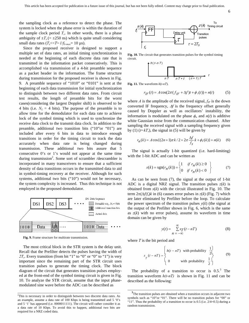
Recall that the Prefilter detects the pulses having the width of 2Ts. Every transition (from bit “1” to “0” or “0” to “1”) is very important since the remaining part of the STR circuit uses transition pulses to generate the timing clock. The block diagram of the circuit that generates transition pulses employ-ed at the front-end of the symbol timing circuit is given in Fig. 10. To analyze the STR circuit, assume that the input phase-modulated sine wave before the ADC can be described as
FF
fs
s (k) z (k)
fiTransition
pulses
ToTiming circuit
τsT2=τ
Delay unit
Fig. 10. The circuit that generates transition pulses for the symbol timing circuit.
t
h ( t -n T )
n T n T + ( n + 1 ) Tτ Fig. 11. The waveform h(t-nT). )())()(2cos()( tnttffAtr iIFIF ++∆+= φπ (5)
where A is the amplitude of the received signal, fIF is the down converted IF frequency, ∆f is the frequency offset generally caused by Doppler as well as oscillators’ instability, the information is modulated on the phase φi, and n(t) is additive white Gaussian noise from the communication channel. After sampling the received signal with a sampling frequency given by (1) (t=kTs), the signal in (5) will be given by
)()}(22/)12cos{()( knkiksffknAknr ++∆++= φππ (6)
The signal is actually 1-bit quantized (i.e. hard-limiting) with the 1-bit ADC and can be written as
(7) ⎭⎬⎫
⎩⎨⎧
<
≥==
0)(00)(1
))(sgn()(knrifknrif
knrks
As can be seen from (7), the signal at the output of 1-bit ADC is a digital NRZ signal. The transition pulses z(k) is obtained from s(k) with the circuit illustrated in Fig. 10. The term 2π(∆f/fs)k in (6) causes error pulses in z(k) (Fig. 7) which are later eliminated by Prefilter before the loop. To calculate the power spectrum of the transition pulses y(k) (the signal at the output of the Prefilter shown in Fig. 6, which is the same as z(k) with no error pulses), assume its waveform in time domain can be given by
(8) ∑∞
−∞=−=
nnTtTsty )()(
where T is the bit period and
⎪⎭
⎪⎬
⎫
⎪⎩
⎪⎨
⎧ −=−
21yprobabilitwith0
21yprobabilitwith)(
)(nTth
nTtsT
(9)
The probability of a transition to occur is 0.5.3 The transition waveform h(t-nT) is shown in Fig. 11 and can be described as the following:
3The transition pulses are obtained when a transition occurs in adjacent two
symbols such as “10”or “01”. There will be no transition pulses for “00” or “11”. Thus the probability of a transition to occur is 0.5 (i.e. 2/4=0.5) during arandom transmission.
2This is necessary in order to distinguish between two discrete data rates. Asan example, assume a data rate of 100 Kbps is being transmitted and 5 ‘0’sand 5 ‘1’ has appeared (i.e. 0000011111). The circuit will rather consider it asa data rate of 10 Kbps. To avoid this to happen, additional two bits arerequired for a NRZ coded data.
This article has been accepted for publication in a future issue of this journal, but has not been fully edited. Content may change prior to final publication.
7
(10) ⎭⎬⎫
⎩⎨⎧
+≤<++≤<
=−TntnT
nTtnTnTth
)1()(0)(1
)(τ
τ
where τ is the width of the transition pulses obtained from the delay element which is depicted in Fig. 10. The amount of delay is τ = 2Ts = 500 ns. The power spectral density of y(t) in (7) is given by [23]
)/(.|)/(|)21(
)()0()41()()
21()(
1
22
222
TmfTmHT
fHTfHTfY
m−+
+=
∑∞+
=
δ
δ (11)
where
(12) τππ τπτ fjft efcdtjenTthfH −+∞
∞−=−−∫= )(sin)()( 2
By substituting the above equation into (11), the power spectral density becomes
⎥⎦
⎤⎢⎣
⎡−+
+=
∑∞+
=
)/().(sin2)()./(
)(sin)/2()(
1
222
22
TmfT
mcfT
fcTfY
mδ
πτδτ
τπτ(13)
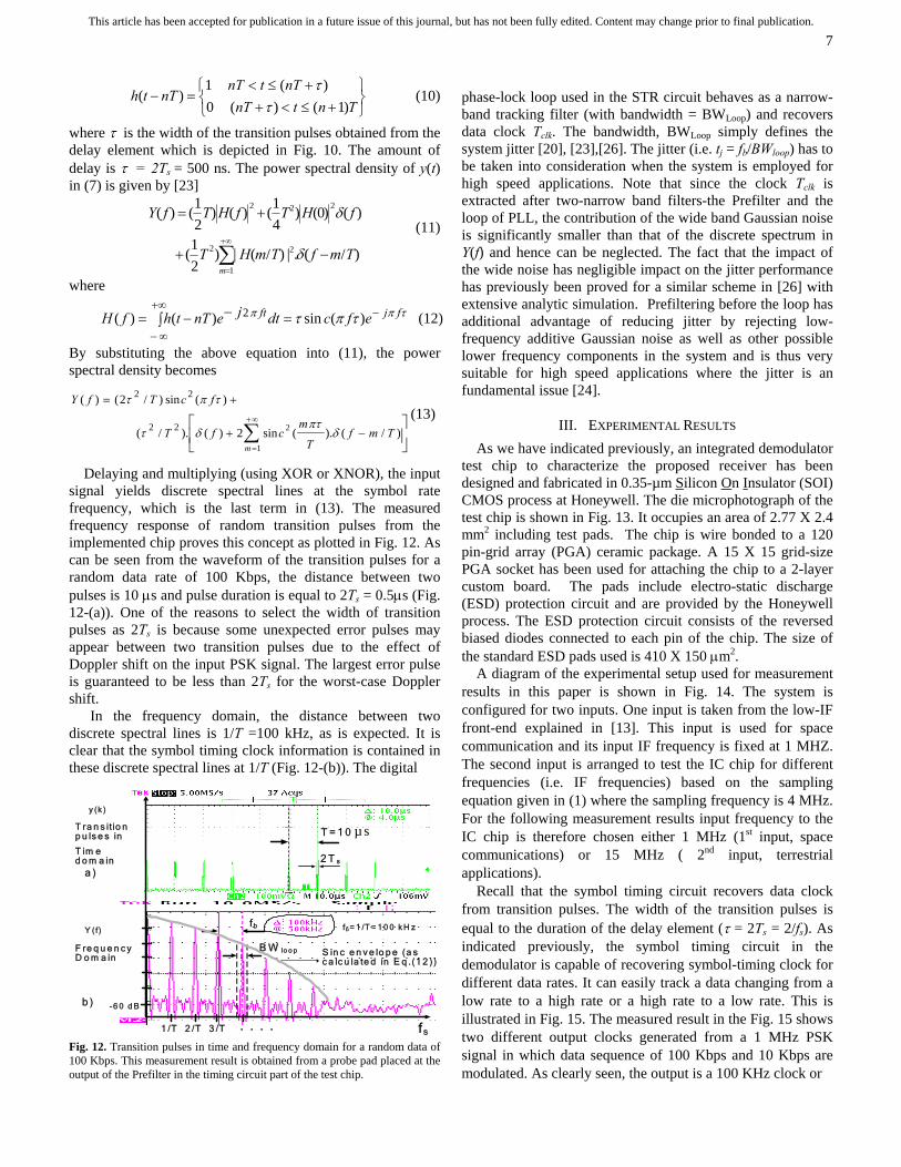
Delaying and multiplying (using XOR or XNOR), the input signal yields discrete spectral lines at the symbol rate frequency, which is the last term in (13). The measured frequency response of random transition pulses from the implemented chip proves this concept as plotted in Fig. 12. As can be seen from the waveform of the transition pulses for a random data rate of 100 Kbps, the distance between two pulses is 10 µs and pulse duration is equal to 2Ts = 0.5µs (Fig. 12-(a)). One of the reasons to select the width of transition pulses as 2Ts is because some unexpected error pulses may appear between two transition pulses due to the effect of Doppler shift on the input PSK signal. The largest error pulse is guaranteed to be less than 2Ts for the worst-case Doppler shift.
In the frequency domain, the distance between two discrete spectral lines is 1/T =100 kHz, as is expected. It is clear that the symbol timing clock information is contained in these discrete spectral lines at 1/T (Fig. 12-(b)). The digital
2 T s
T ra n s itio n p u ls e s in
T im e d o m a in
F re q u e n c y D o m a in
fs
fb
T = 1 0
y (k )
Y (f)
1 /T 2 /T 3 /T . . . .
a )
b )
µ s
B W lo o p S in c e n v e lo p e (a s c a lc u la te d in E q .(1 2 ))
fb = 1 /T = 1 0 0 k H z
-6 0 d B
Fig. 12. Transition pulses in time and frequency domain for a random data of 100 Kbps. This measurement result is obtained from a probe pad placed at the output of the Prefilter in the timing circuit part of the test chip.
phase-lock loop used in the STR circuit behaves as a narrow-band tracking filter (with bandwidth = BWLoop) and recovers data clock Tclk. The bandwidth, BWLoop simply defines the system jitter [20], [23],[26]. The jitter (i.e. tj = fb/BWloop) has to be taken into consideration when the system is employed for high speed applications. Note that since the clock Tclk is extracted after two-narrow band filters-the Prefilter and the loop of PLL, the contribution of the wide band Gaussian noise is significantly smaller than that of the discrete spectrum in Y(f) and hence can be neglected. The fact that the impact of the wide noise has negligible impact on the jitter performance has previously been proved for a similar scheme in [26] with extensive analytic simulation. Prefiltering before the loop has additional advantage of reducing jitter by rejecting low-frequency additive Gaussian noise as well as other possible lower frequency components in the system and is thus very suitable for high speed applications where the jitter is an fundamental issue [24].
III. EXPERIMENTAL RESULTS As we have indicated previously, an integrated demodulator
test chip to characterize the proposed receiver has been designed and fabricated in 0.35-µm Silicon On Insulator (SOI) CMOS process at Honeywell. The die microphotograph of the test chip is shown in Fig. 13. It occupies an area of 2.77 X 2.4 mm2 including test pads. The chip is wire bonded to a 120 pin-grid array (PGA) ceramic package. A 15 X 15 grid-size PGA socket has been used for attaching the chip to a 2-layer custom board. The pads include electro-static discharge (ESD) protection circuit and are provided by the Honeywell process. The ESD protection circuit consists of the reversed biased diodes connected to each pin of the chip. The size of the standard ESD pads used is 410 X 150 µm2.
A diagram of the experimental setup used for measurement results in this paper is shown in Fig. 14. The system is configured for two inputs. One input is taken from the low-IF front-end explained in [13]. This input is used for space communication and its input IF frequency is fixed at 1 MHZ. The second input is arranged to test the IC chip for different frequencies (i.e. IF frequencies) based on the sampling equation given in (1) where the sampling frequency is 4 MHz. For the following measurement results input frequency to the IC chip is therefore chosen either 1 MHz (1st input, space communications) or 15 MHz ( 2nd input, terrestrial applications).
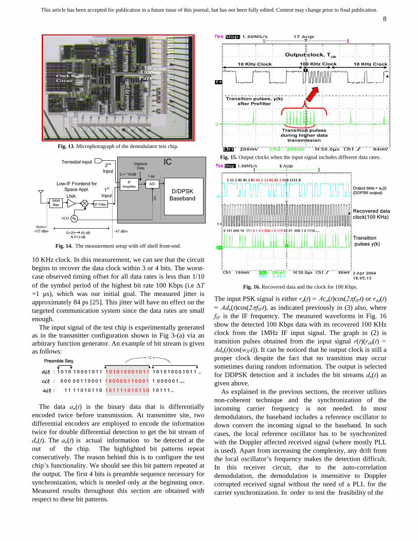
Recall that the symbol timing circuit recovers data clock from transition pulses. The width of the transition pulses is equal to the duration of the delay element (τ = 2Ts = 2/fs). As indicated previously, the symbol timing circuit in the demodulator is capable of recovering symbol-timing clock for different data rates. It can easily track a data changing from a low rate to a high rate or a high rate to a low rate. This is illustrated in Fig. 15. The measured result in the Fig. 15 shows two different output clocks generated from a 1 MHz PSK signal in which data sequence of 100 Kbps and 10 Kbps are modulated. As clearly seen, the output is a 100 KHz clock or
This article has been accepted for publication in a future issue of this journal, but has not been fully edited. Content may change prior to final publication.
8
Fig. 13. Microphotograph of the demodulator test chip.
IF FilterSAW filter
LNA
VCO
A/D
1-bit
fs
Low-IF Frontend for Space Appl.
Smin=-107 dBm G=20 60 dB
N F=3 dB
-47 dBm
G = ~60dB
IF Amplifier
D/DPSKBaseband
Terrestial input DigitizedData
IC
1st Input
2nd Input
Fig. 14. The measurement setup with off shelf front-end.
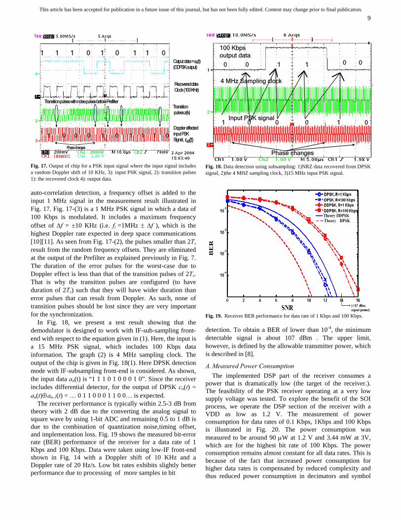
10 KHz clock. In this measurement, we can see that the circuit begins to recover the data clock within 3 or 4 bits. The worst-case observed timing offset for all data rates is less than 1/10 of the symbol period of the highest bit rate 100 Kbps (i.e ∆T =1 µs), which was our initial goal. The measured jitter is approximately 84 ps [25]. This jitter will have no effect on the targeted communication system since the data rates are small enough.
The input signal of the test chip is experimentally generated as in the transmitter configuration shown in Fig 3-(a) via an arbitrary function generator. An example of bit stream is given as follows:
dn(t) : 1 0 1 0 1 0 0 0 1 0 1 1 1 0 1 0 1 0 0 0 1 0 1 1
1 0 0 0 0 0 1 1 0 0 0 1
1 0 1 1 1 1 0 1 0 1 1 0
1 0 1 0 1 0 0 0 1 0 1 1 …
cn(t) : 0 0 0 0 0 1 1 0 0 0 1 1 0 0 0 0 0 1 ……
an(t) : 1 1 1 1 0 1 0 1 1 0 1 0 1 1 1 …
Preamble Seq.
The data an(t) is the binary data that is differentially encoded twice before transmission. At transmitter site, two differential encoders are employed to encode the information twice for double differential detection to get the bit stream of dn(t). The an(t) is actual information to be detected at the out of the chip. The highlighted bit patterns repeat consecutively. The reason behind this is to configure the test chip’s functionality. We should see this bit pattern repeated at the output. The first 4 bits is preamble sequence necessary for synchronization, which is needed only at the beginning once. Measured results throughout this section are obtained with respect to these bit patterns.
Fig. 15. Output clocks when the input signal includes different data rates.
1 11 1 01 01 1 01 01 1 11 01 01 1 01
11 0 1 0 1 000 1 0 111 01 0
0 1111 0
Output data = an(t)(DDPSK output)
Recovered dataclock(100 KHz)
Transition pulses y(k)
0 101 000 10 1 1 000 1 0 1110…….
Fig. 16. Recovered data and the clock for 100 Kbps.
The input PSK signal is either rd(t) = Acn(t)cos(2πfIFt) or rdd(t) = Adn(t)cos(2πfIFt), as indicated previously in (3) also, where fIF is the IF frequency. The measured waveforms in Fig. 16 show the detected 100 Kbps data with its recovered 100 KHz clock from the 1MHz IF input signal. The graph in (2) is transition pulses obtained from the input signal r(t)(rdd(t) = Adn(t)cos(wIFt)). It can be noticed that he output clock is still a proper clock despite the fact that no transition may occur sometimes during random information. The output is selected for DDPSK detection and it includes the bit streams dn(t) as given above.
As explained in the previous sections, the receiver utilizes non-coherent technique and the synchronization of the incoming carrier frequency is not needed. In most demodulators, the baseband includes a reference oscillator to down convert the incoming signal to the baseband. In such cases, the local reference oscillator has to be synchronized with the Doppler affected received signal (where mostly PLL is used). Apart from increasing the complexity, any drift from the local oscillator’s frequency makes the detection difficult. In this receiver circuit, due to the auto-correlation demodulation, the demodulation is insensitive to Doppler corrupted received signal without the need of a PLL for the carrier synchronization. In order to test the feasibility of the
This article has been accepted for publication in a future issue of this journal, but has not been fully edited. Content may change prior to final publication.
9
Recovered dataClock (100 KHz)
1 1 1 0 1 0 1 1 0
Transition pulses z(k)
Doppler affectedinput PSKSignal,
Output data = an(t)(DDPSK output)
Transition pulses with noise pulses before Prefilter
Phase changes
1 0 0 0 1 0 1 1 1 0 rdd(t)
Fig. 17. Output of chip for a PSK input signal where the input signal includes a random Doppler shift of 10 KHz, 3): input PSK signal, 2): transition pulses 1): the recovered clock 4): output data.
auto-correlation detection, a frequency offset is added to the input 1 MHz signal in the measurement result illustrated in Fig. 17. Fig. 17-(3) is a 1 MHz PSK signal in which a data of 100 Kbps is modulated. It includes a maximum frequency offset of ∆f = ±10 KHz (i.e. fi =1MHz ± ∆f ), which is the highest Doppler rate expected in deep space communications [10][11]. As seen from Fig. 17-(2), the pulses smaller than 2Ts result from the random frequency offsets. They are eliminated at the output of the Prefilter as explained previously in Fig. 7. The duration of the error pulses for the worst-case due to Doppler effect is less than that of the transition pulses of 2Ts. That is why the transition pulses are configured (to have duration of 2Ts) such that they will have wider duration than error pulses that can result from Doppler. As such, none of transition pulses should be lost since they are very important for the synchronization.
In Fig. 18, we present a test result showing that the demodulator is designed to work with IF-sub-sampling front-end with respect to the equation given in (1). Here, the input is a 15 MHz PSK signal, which includes 100 Kbps data information. The graph (2) is 4 MHz sampling clock. The output of the chip is given in Fig. 18(1). Here DPSK detection mode with IF-subsampling front-end is considered. As shown, the input data an(t) is “1 1 1 0 1 0 0 0 1 0”. Since the receiver includes differential detector, for the output of DPSK cn(t) = an(t)⊕an-1(t) = … 0 1 1 0 0 0 1 1 0 0… is expected.
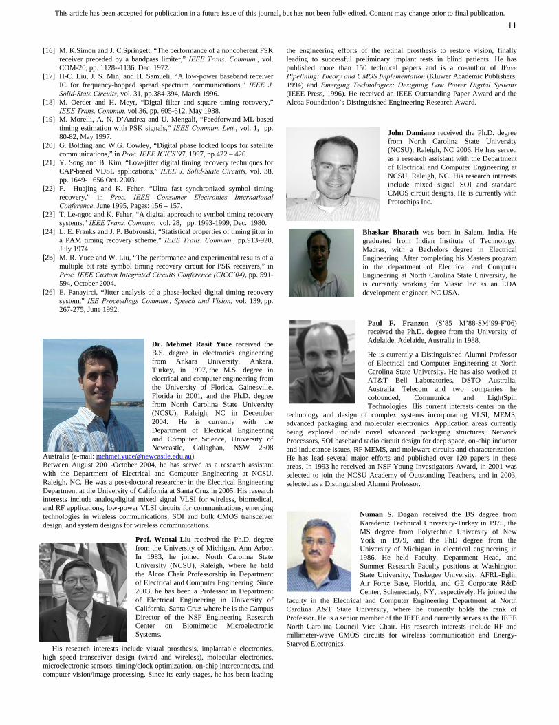
The receiver performance is typically within 2.5-3 dB from theory with 2 dB due to the converting the analog signal to square wave by using 1-bit ADC and remaining 0.5 to 1 dB is due to the combination of quantization noise,timing offset, and implementation loss. Fig. 19 shows the measured bit-error rate (BER) performance of the receiver for a data rate of 1 Kbps and 100 Kbps. Data were taken using low-IF front-end shown in Fig. 14 with a Doppler shift of 10 KHz and a Doppler rate of 20 Hz/s. Low bit rates exhibits slightly better performance due to processing of more samples in bit
Phase changes
Input PSK signal
4 MHz Sampling clock
100 Kbps output data
1 0 0 0 1
0 1 1 0
0
0 0
Fig. 18. Data detection using subsampling: 1)NRZ data recovered from DPSK signal, 2)the 4 MHZ sampling clock, 3)15 MHz input PSK signal.
Fig. 19. Receiver BER performance for data rate of 1 Kbps and 100 Kbps. detection. To obtain a BER of lower than 10-4, the minimum detectable signal is about 107 dBm . The upper limit, however, is defined by the allowable transmitter power, which is described in [8].
A. Measured Power Consumption The implemented DSP part of the receiver consumes a
power that is dramatically low (the target of the receiver.). The feasibility of the PSK receiver operating at a very low supply voltage was tested. To explore the benefit of the SOI process, we operate the DSP section of the receiver with a VDD as low as 1.2 V. The measurement of power consumption for data rates of 0.1 Kbps, 1Kbps and 100 Kbps is illustrated in Fig. 20. The power consumption was measured to be around 90 µW at 1.2 V and 3.44 mW at 3V, which are for the highest bit rate of 100 Kbps. The power consumption remains almost constant for all data rates. This is because of the fact that increased power consumption for higher data rates is compensated by reduced complexity and thus reduced power consumption in decimators and symbol

This article has been accepted for publication in a future issue of this journal, but has not been fully edited. Content may change prior to final publication.
10
timing recovery circuits. The demodulator IC includes around 15,000 gates and consumes a power of about 1 mW including the analog part at the nominal supply voltages.
The hardware characteristics of the demodulator are summarized in Table III by including a comparison with previous works. To have a demodulator robust to Doppler shift, D/DPSK approach provides less complexity when comparing with the FSK given in [11]. In [11], DFT technique is used to handle the Doppler shift, while in our design double differential detection is used with PSK. Both designs (for only digital part) have power consumption that is quite low. Also the designed (D)/DPSK receiver illustrates a BER performance of 10-5 while [11] has a BER of 10-4 (theoretical) with the SNR of 15 dB.
Fig. 20. Power consumptions for different data rates at different supply voltages.
TABLE III. KEY CIRCUIT CHARACTERISTICS
IV. CONCLUSION
The design and implementation of a differential based PSK demodulator for satellite and space applications has been presented. The baseband circuit including 1-bit A/D converter has been designed and fabricated through Honeywell’s 0.35-µm SOI CMOS process. It is mainly designed for low power and radiation hardening and tolerates Doppler shifts. Although the paper focuses on the design and implementation of the proposed demodulator for space applications, the DPSK mode of the demodulator with the low-power implementation
methods presented can be applicable to terrestrial applications. The receiver is designed for multiple bit rates and has a sensitivity of -107 dBm for the data rate of 100 Kbps. Including 1-bit A/D, the digital baseband circuit consumes a power less than 1 mW.
The 1-bit ADC front-end is ideally suited for deep space communications-the target application due to the absence of adjacent channel interference. Using 1-bit A/D requires less dynamic range than multibit A/D converters which makes it more atractive from practical view. Even though the receiver can be used with multi-bit A/D converters, we are mainly interested in 1-bit A/D converter front-end for the reason that a hard-limiter (or 1-bit A/D converter) has been a part of many satellite transponders. However, for terrestrial applications due to the large number of interferers that might affect the performance of the receiver, multiple bits ADC might be preferable with the price of higher circuit complexity and power consumption.
ACKNOWLEDGMENT
The authors would like to thank Gene Fujikawa of NASA Glen Research Center and Mohammed Mojarradi and Norman Lay of JPL for their support and collaboration.
REFERENCES [1] J-P. Colinge, Silicon-on-Insulator Technology: Materials to VLSI.
Kluwer Academic Publishers, 1997. [2] J. Sevenhans, “Silicon radio integration: architectures and technology:
from cartesian zero IF receive & transmit to polar zero I and Q, from silicon bipolar to bulk and SOI CMOS,” in Proc. IEEE Custom Integ. Cir. Conf. (CICC’00), May 2000, pp.333 – 340.
[3] Online. http://www.ssec.honeywell.com/aerospace/technologies/soi.html
[4] W. Rafferty and D. Divsalar, “Modulation and coding for land mobile satellite channels,” in IEEE Proc. ICC’88, June 1988, pp.1105-1111. [5] M. K. Simon and D. Divsalar, “Doppler-corrected differential detection
of MPSK,” IEEE Trans. Commun., vol. 37, pp. 99-109, Feb. 1989. [6] H. Olson, D. Kerek, B. Oelmann, and H Tenhunen, “Differential PSK
detector ASIC design for direct sequence spread spectrum radio,” in proc. IEEE International ASIC Conference, Sept. 1996, pp: 97 – 101.
[7] C. Chien, R. Jain, E. G. Cohen, and H. Samueli, “A single-chip 12.7 Mchips/s digital IF BPSK direct sequence spread-spectrum transceiver in 1.2 um CMOS,” IEEE J. Solid-State Circuits, vol. 29, pp. 1614-1623, Dec. 1994.
[8] M. R. Yuce and W. Liu, “A low-power multirate differential PSK receiver for space applications,” IEEE Trans. Veh. Technol., vol. 54, pp. 2074 - 2084, Nov. 2005.
[9] Y. Okunev, Phase and Phase-Difference Modulation in Digital communication. Norwood, MA: Artech House, 1997.
[10] N. Lay et al., “Developing low-power transceiver technologies for in situ communication applications,” Jet Propulsion Lab. (JPL) IPN Progress Report 42-147, November 15, 2001.
Current design [11] Modulation D/DDPSK FSK Data 0.1-100 Kbps 0.1-10 Kbps Sampling freq. 4 MHz 1.2 MHz BER @ SNR=15 dB 10-5 10-4 Technology 0.35-µ SOI CMOS 0.25-µ CMOS Core Area 2.2X2.0 mm2 0.8 mm2
Die Area 2.77X2.4 mm2 3.1 mm2
Transistor Count 15,000 220,000 Power Supply 1.1-3.3V 0.75-2.5 v Power Consumption 90 µm (digital section)
800 µm (analog section ) 100 µm (digital) No analog
[11] E. Grayver and B. Daneshrad “ VLSI implementation of a 100-µW multirate FSK receiver,” IEEE J. of Solid–State Circuits, vol. 36, pp. 1821-1828, Nov 2001.
[12] A. P. Chandrakasan, S. Sheng and W.R Brodersen, “Low-power CMOS digital design,” IEEE J. J. of Solid–State Circuits, vol.27, pp. 473-484, April 1992.
[13] E. Zencir, N. S. Dogan and E. Arvas, “A low-power UHF RF frontend for a low-IF receiver,” in proc. IEEE ASIC/SOC’02, pp.331 –335.
[14] A. Hairapetian, “An 81-MHz IF receiver in CMOS,” IEEE J. Solid-State Circuits, vol. 31, pp. 1981-1986.Dec. 1996.
[15] P. H. Wu, “The optimal BPSK demodulator with a 1-bit A/D front-end” in Proc. MILCOM’98, vol.3.3, 1998, pages 730-735.
This article has been accepted for publication in a future issue of this journal, but has not been fully edited. Content may change prior to final publication.
11
[16] M. K.Simon and J. C.Springett, “The performance of a noncoherent FSK receiver preceded by a bandpass limiter,” IEEE Trans. Commun., vol. COM-20, pp. 1128--1136, Dec. 1972.
[17] H-C. Liu, J. S. Min, and H. Samueli, “A low-power baseband receiver IC for frequency-hopped spread spectrum communications,” IEEE J. Solid-State Circuits, vol. 31, pp.384-394, March 1996.
[18] M. Oerder and H. Meyr, “Digtal filter and square timing recovery,” IEEE Trans. Commun. vol.36, pp. 605-612, May 1988.
[19] M. Morelli, A. N. D’Andrea and U. Mengali, “Feedforward ML-based timing estimation with PSK signals,” IEEE Commun. Lett., vol. 1, pp. 80-82, May 1997.
[20] G. Bolding and W.G. Cowley, “Digital phase locked loops for satellite communications,” in Proc. IEEE ICICS’97, 1997, pp.422 – 426.
[21] Y. Song and B. Kim, “Low-jitter digital timing recovery techniques for CAP-based VDSL applications,” IEEE J. Solid-State Circuits, vol. 38, pp. 1649- 1656 Oct. 2003.
[22] F. Huajing and K. Feher, “Ultra fast synchronized symbol timing recovery,” in Proc. IEEE Consumer Electronics International Conference, June 1995, Pages: 156 – 157.
[23] T. Le-ngoc and K. Feher, “A digital approach to symbol timing recovery systems,” IEEE Trans. Commun. vol. 28, pp. 1993-1999, Dec. 1980.
[24] L. E. Franks and J. P. Bubrouski, “Statistical properties of timing jitter in a PAM timing recovery scheme,” IEEE Trans. Commun., pp.913-920, July 1974.
[25] M. R. Yuce and W. Liu, “The performance and experimental results of a multiple bit rate symbol timing recovery circuit for PSK receivers,” in Proc. IEEE Custom Integrated Circuits Conference (CICC’04), pp. 591-594, October 2004.
[26] E. Panayirci, “Jitter analysis of a phase-locked digital timing recovery system,” IEE Proceedings Commun., Speech and Vision, vol. 139, pp. 267-275, June 1992.
Dr. Mehmet Rasit Yuce received the B.S. degree in electronics engineering from Ankara University, Ankara, Turkey, in 1997, the M.S. degree in electrical and computer engineering from the University of Florida, Gainesville, Florida in 2001, and the Ph.D. degree from North Carolina State University (NCSU), Raleigh, NC in December 2004. He is currently with the Department of Electrical Engineering and Computer Science, University of Newcastle, Callaghan, NSW 2308
Australia (e-mail: [email protected]). Between August 2001-October 2004, he has served as a research assistant with the Department of Electrical and Computer Engineering at NCSU, Raleigh, NC. He was a post-doctoral researcher in the Electrical Engineering Department at the University of California at Santa Cruz in 2005. His research interests include analog/digital mixed signal VLSI for wireless, biomedical, and RF applications, low-power VLSI circuits for communications, emerging technologies in wireless communications, SOI and bulk CMOS transceiver design, and system designs for wireless communications.
Prof. Wentai Liu received the Ph.D. degree from the University of Michigan, Ann Arbor. In 1983, he joined North Carolina State University (NCSU), Raleigh, where he held the Alcoa Chair Professorship in Department of Electrical and Computer Engineering. Since 2003, he has been a Professor in Department of Electrical Engineering in University of California, Santa Cruz where he is the Campus Director of the NSF Engineering Research Center on Biomimetic Microelectronic Systems.
His research interests include visual prosthesis, implantable electronics, high speed transceiver design (wired and wireless), molecular electronics, microelectronic sensors, timing/clock optimization, on-chip interconnects, and computer vision/image processing. Since its early stages, he has been leading
the engineering efforts of the retinal prosthesis to restore vision, finally leading to successful preliminary implant tests in blind patients. He has published more than 150 technical papers and is a co-author of Wave Pipelining: Theory and CMOS Implementation (Kluwer Academic Publishers, 1994) and Emerging Technologies: Designing Low Power Digital Systems (IEEE Press, 1996). He received an IEEE Outstanding Paper Award and the Alcoa Foundation’s Distinguished Engineering Research Award.
John Damiano received the Ph.D. degree from North Carolina State University (NCSU), Raleigh, NC 2006. He has served as a research assistant with the Department of Electrical and Computer Engineering at NCSU, Raleigh, NC. His research interests include mixed signal SOI and standard CMOS circuit designs. He is currently with Protochips Inc.
Bhaskar Bharath was born in Salem, India. He graduated from Indian Institute of Technology, Madras, with a Bachelors degree in Electrical Engineering. After completing his Masters program in the department of Electrical and Computer Engineering at North Carolina State University, he is currently working for Viasic Inc as an EDA development engineer, NC USA.
Paul F. Franzon (S’85 M’88-SM’99-F’06) received the Ph.D. degree from the University of Adelaide, Adelaide, Australia in 1988.
He is currently a Distinguished Alumni Professor of Electrical and Computer Engineering at North Carolina State University. He has also worked at AT&T Bell Laboratories, DSTO Australia, Australia Telecom and two companies he cofounded, Communica and LightSpin Technologies. His current interests center on the
technology and design of complex systems incorporating VLSI, MEMS, advanced packaging and molecular electronics. Application areas currently being explored include novel advanced packaging structures, Network Processors, SOI baseband radio circuit design for deep space, on-chip inductor and inductance issues, RF MEMS, and moleware circuits and characterization. He has lead several major efforts and published over 120 papers in these areas. In 1993 he received an NSF Young Investigators Award, in 2001 was selected to join the NCSU Academy of Outstanding Teachers, and in 2003, selected as a Distinguished Alumni Professor.
Numan S. Dogan received the BS degree from Karadeniz Technical University-Turkey in 1975, the MS degree from Polytechnic University of New York in 1979, and the PhD degree from the University of Michigan in electrical engineering in 1986. He held Faculty, Department Head, and Summer Research Faculty positions at Washington State University, Tuskegee University, AFRL-Eglin Air Force Base, Florida, and GE Corporate R&D Center, Schenectady, NY, respectively. He joined the
faculty in the Electrical and Computer Engineering Department at North Carolina A&T State University, where he currently holds the rank of Professor. He is a senior member of the IEEE and currently serves as the IEEE North Carolina Council Vice Chair. His research interests include RF and millimeter-wave CMOS circuits for wireless communication and Energy-Starved Electronics.
Copyright © 2022 FDOKUMEN